Cadance OrCAD Layout
32
Cadance OrCAD Layout Capture is the central schematic entry program in the three program suite by Cadance called OrCAD. This suite also consists of Pspice (circuit simulation software) and Layout (circuit board layout) packages. All applications begin with Capture. Overview: This simple tutorial is designed to walk the user through a very basic PCB board design layout providing some hints along the way. It does NOT cover all of the features of Layout, so become familiar with the online manuals that come with the package. Mechanical Design: Designing a PCB is as much a mechanical engineering problem as it is an electrical one. Important issues to consider BEFORE designing the PCB are: Packaging- Is the PCB going into an enclosure? If so, you should have a sample of the enclosure to test fit the d esign. How will I mount the PCB to the enclosure? Think about mounting holes and standoffs. At least 3 fasteners are required for PCB stability. Make sure you design in enough clearances so the PCB and components don’t hit. Is the design serviceable? On a prototype, plan on disassembling and reassembling it often during the development process. Having to unsolder wires or remove connectors would have a major impact on the development time. What about board height? Because the Layout CAD packages are all 2D this is one area where many mistakes are made. Be sure to design the package so the tallest components clear. Be sure the components that generate heat have adequate ventilation. If a component needs a heatsink be sure to check for clearance with adjacent components. Connectors: Connectors are another major source of problems. Check to be sure there is enough clearance, not only for the connector on the PCB, but also the mating connector. Using a wire harness for off board componen ts like potentiometers, connectors, and
Transcript of Cadance OrCAD Layout
8/8/2019 Cadance OrCAD Layout
http://slidepdf.com/reader/full/cadance-orcad-layout 1/32
Cadance OrCAD Layout Capture is the central schematic entry program in the three program suite by Cadance
called OrCAD.
This suite also consists of Pspice (circuit simulation software) and Layout (circuit boardlayout) packages.
All applications begin with Capture.
Overview:This simple tutorial is designed to walk the user through a very basic PCB board design
layout providing some hints along the way.It does NOT cover all of the features of Layout, so become familiar with the online
manuals that come with the package.
Mechanical Design:Designing a PCB is as much a mechanical engineering problem as it is an electrical one.
Important issues to consider BEFORE designing the PCB are:Packaging-
Is the PCB going into an enclosure?
If so, you should have a sample of the enclosure to test fit the design.How will I mount the PCB to the enclosure?
Think about mounting holes and standoffs.
At least 3 fasteners are required for PCB stability.
Make sure you design in enough clearances so the PCB and componentsdon’t hit.
Is the design serviceable?On a prototype, plan on disassembling and reassembling it often duringthe development process.
Having to unsolder wires or remove connectors would have a major
impact on the development time.What about board height?
Because the Layout CAD packages are all 2D this is one area where many
mistakes are made.
Be sure to design the package so the tallest components clear.Be sure the components that generate heat have adequate ventilation.
If a component needs a heatsink be sure to check for clearance with
adjacent components.Connectors:
Connectors are another major source of problems.
Check to be sure there is enough clearance, not only for the connector onthe PCB, but also the mating
connector.
Using a wire harness for off board components like potentiometers,connectors, and
8/8/2019 Cadance OrCAD Layout
http://slidepdf.com/reader/full/cadance-orcad-layout 2/32
displays can be time consuming and cause reliability issues.
Think about mounting as many system components as possible directly to
the PCB.
Component Selection Criteria:
You have to think of the components in their physical form not just their electrical properties.
Ask yourself what are the most important aspects of this design. (Size, ease of assembly,
cost, availability of parts etc.)Many electronic components may not be readily available in all package styles.
Investigate this BEFORE you start to design a board. Even if the manufacturer makes a
particular style it doesn’t mean vendors will stock it.
Through hole components, ones that have leads that go through a hole in the PCB andsolder to a pad on the solder side, are the easiest to work with.
However, some of the newer Integrated Circuits are not available in this package style.
Surface mount components are small but more difficult to work with.
They mount on pads that can be very close together making assembly difficult. Starting the Design:Since there can be many choices in packaging for an individual part, the best approach is
to first gather information on the package type you intend to use.
For all of the components in your design, copy the pages from the data sheets that show
the mechanical package you will be using.Data sheets are available online from the manufacturer or the vendor such as
www.digikey.com
Don’t overlook minor components like resistors and capacitors. They are available in awide range of sizes and styles.
Connectors are especially important. The standards for connectors may not be uniform
so extra care must be taken to be sure the footprint selected is IDENTICAL to the one inthe data sheet. A footprint is the size and shape of the conductors and mounting holes of
the component.
It is HIGHLY recommended that you have an actual sample of all the parts in the design before designing the PCB.
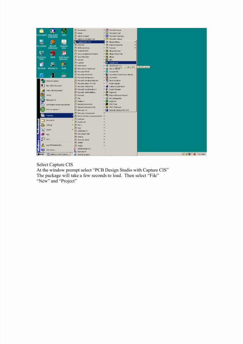
Running the Applications:Schematics are drawn using Capture just as they are for documentation only applications(see help file on OrCAD Capture).
Additionally, in Capture you will need to edit the properties of the parts and specify a
footprint for each component. Loading Capture:
8/8/2019 Cadance OrCAD Layout
http://slidepdf.com/reader/full/cadance-orcad-layout 3/32
8/8/2019 Cadance OrCAD Layout
http://slidepdf.com/reader/full/cadance-orcad-layout 4/32
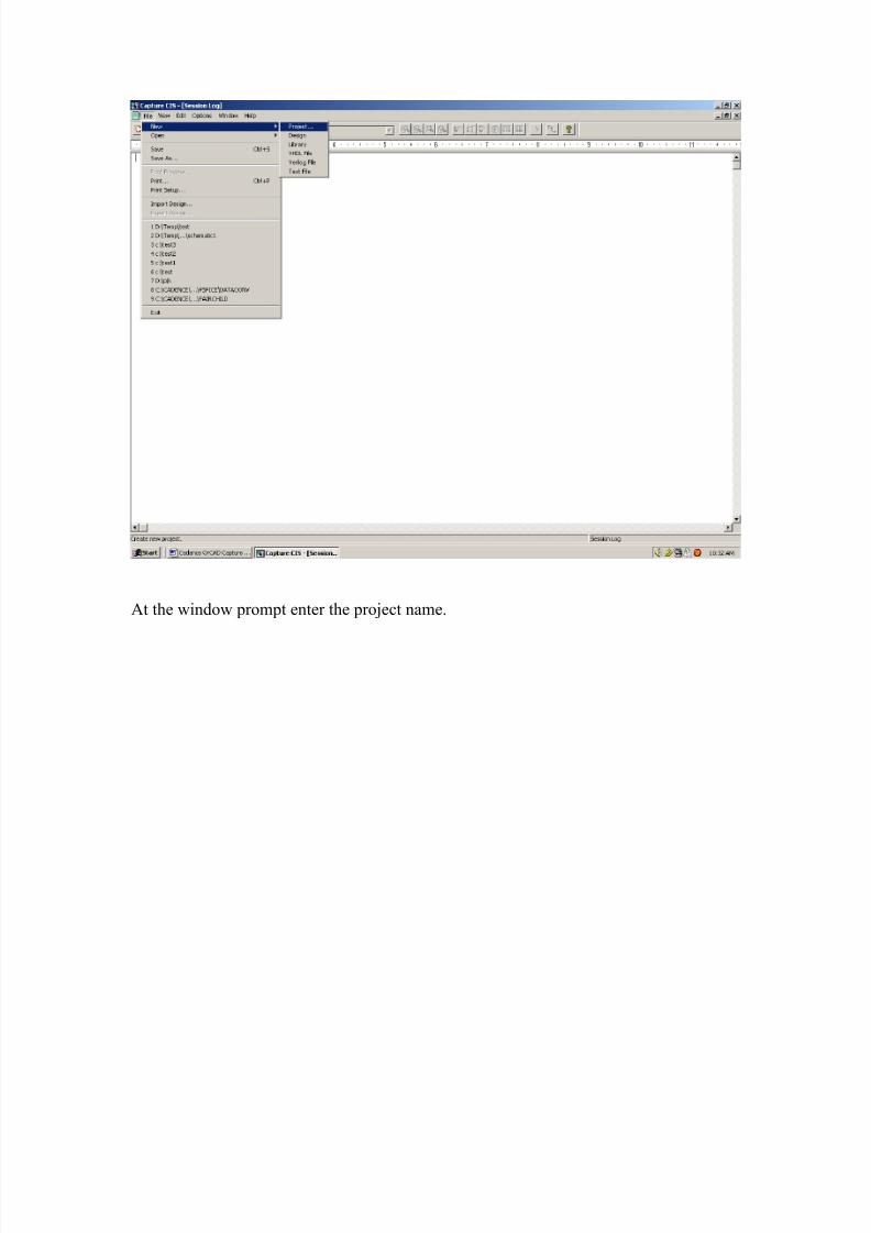
At the window prompt enter the project name.
8/8/2019 Cadance OrCAD Layout
http://slidepdf.com/reader/full/cadance-orcad-layout 5/32
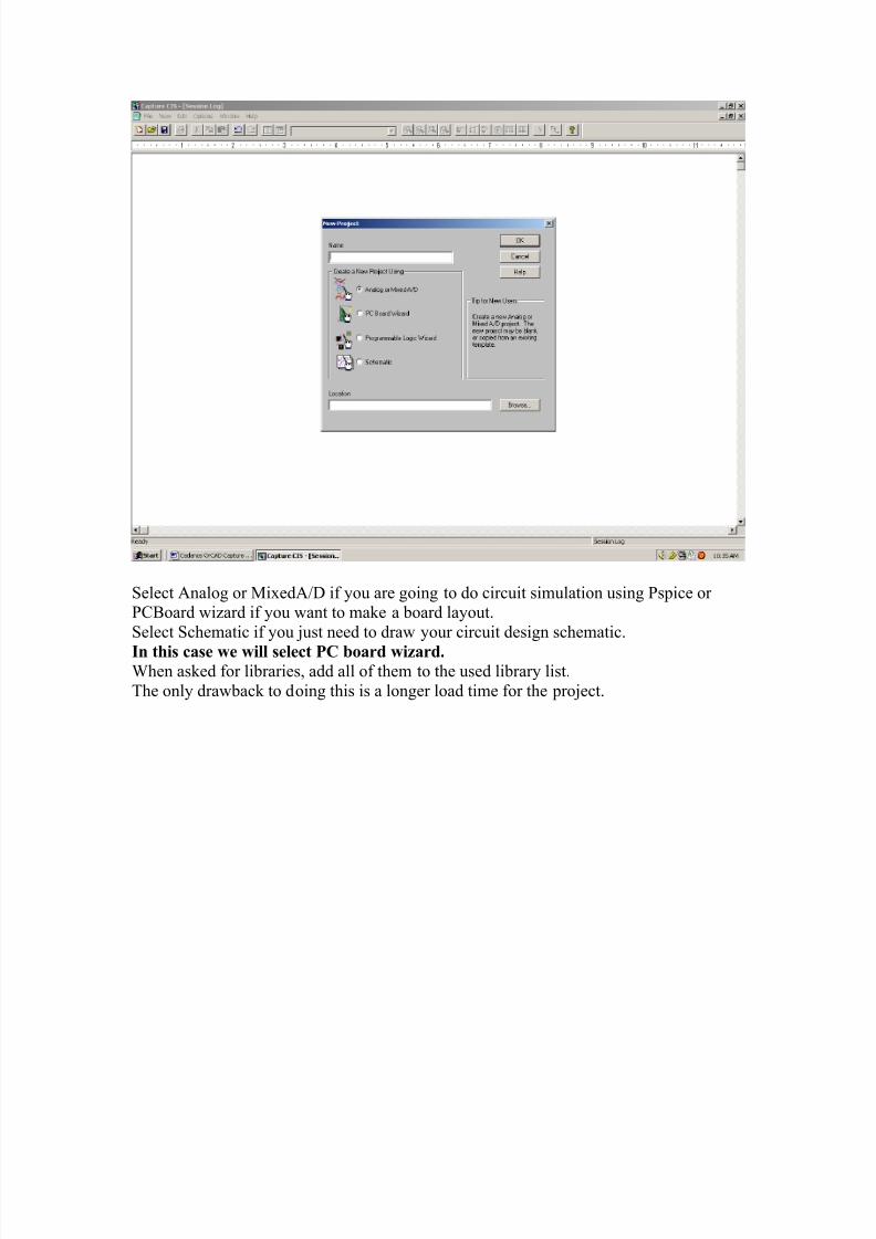
Select Analog or MixedA/D if you are going to do circuit simulation using Pspice or PCBoard wizard if you want to make a board layout.
Select Schematic if you just need to draw your circuit design schematic.
In this case we will select PC board wizard.When asked for libraries, add all of them to the used library list.
The only drawback to doing this is a longer load time for the project.
8/8/2019 Cadance OrCAD Layout
http://slidepdf.com/reader/full/cadance-orcad-layout 6/32
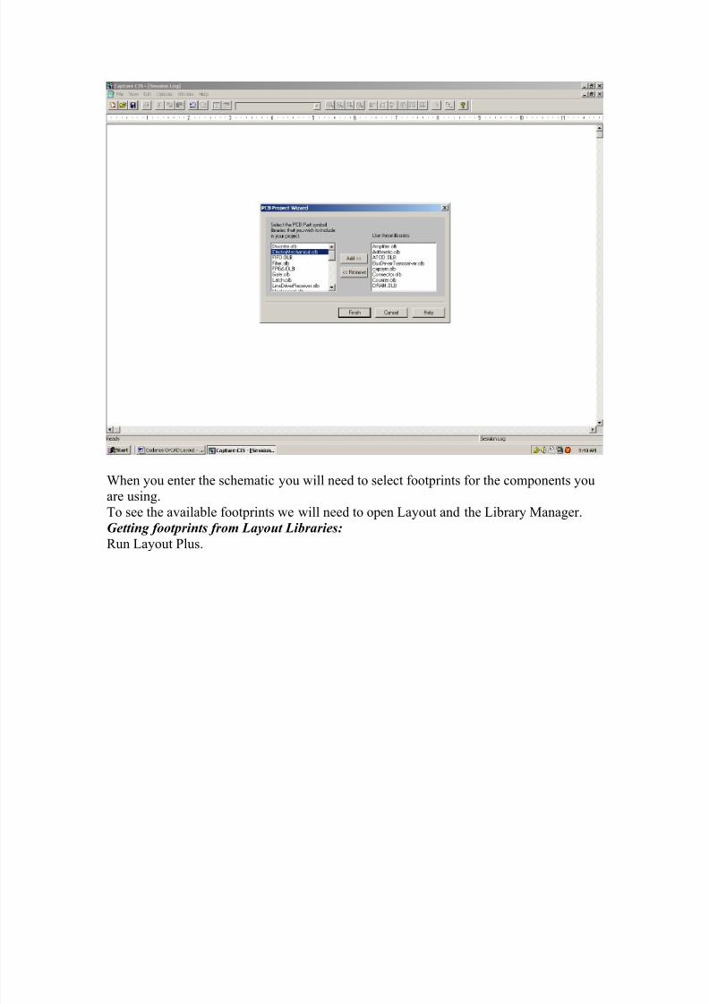
When you enter the schematic you will need to select footprints for the components youare using.
To see the available footprints we will need to open Layout and the Library Manager.
Getting footprints from Layout Libraries:Run Layout Plus.
8/8/2019 Cadance OrCAD Layout
http://slidepdf.com/reader/full/cadance-orcad-layout 7/32
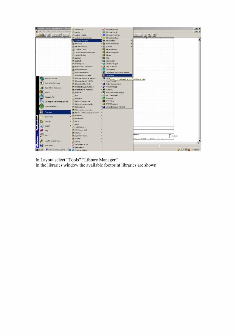
In Layout select “Tools” “Library Manager”In the libraries window the available footprint libraries are shown.
8/8/2019 Cadance OrCAD Layout
http://slidepdf.com/reader/full/cadance-orcad-layout 8/32
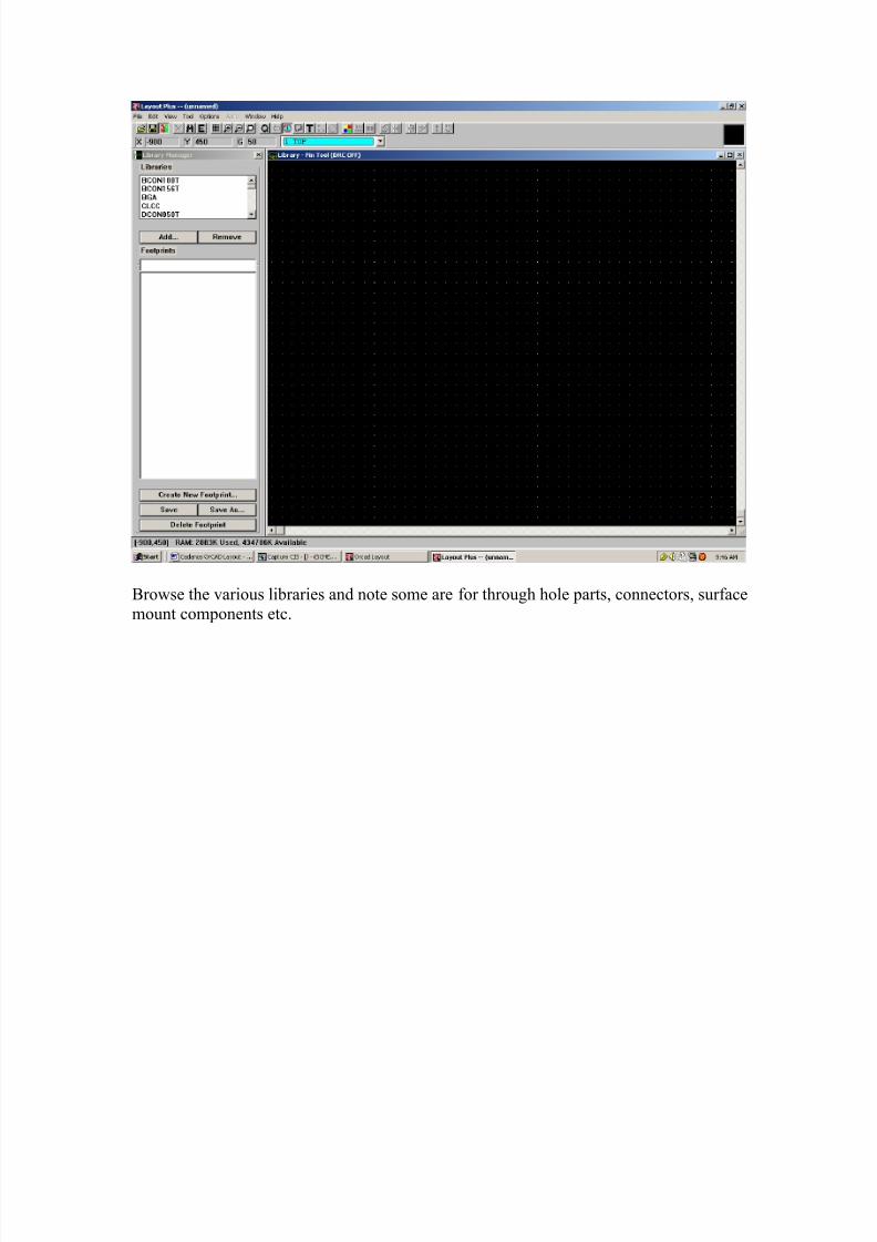
Browse the various libraries and note some are for through hole parts, connectors, surfacemount components etc.
8/8/2019 Cadance OrCAD Layout
http://slidepdf.com/reader/full/cadance-orcad-layout 9/32
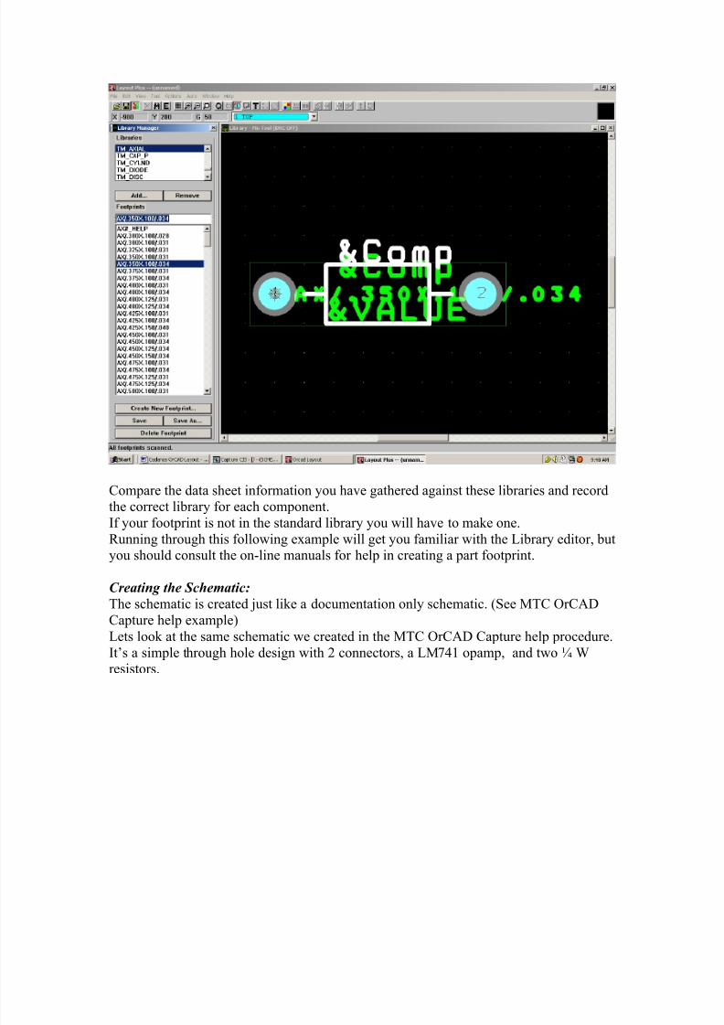
Compare the data sheet information you have gathered against these libraries and recordthe correct library for each component.
If your footprint is not in the standard library you will have to make one.
Running through this following example will get you familiar with the Library editor, butyou should consult the on-line manuals for help in creating a part footprint.
Creating the Schematic:
The schematic is created just like a documentation only schematic. (See MTC OrCAD
Capture help example)
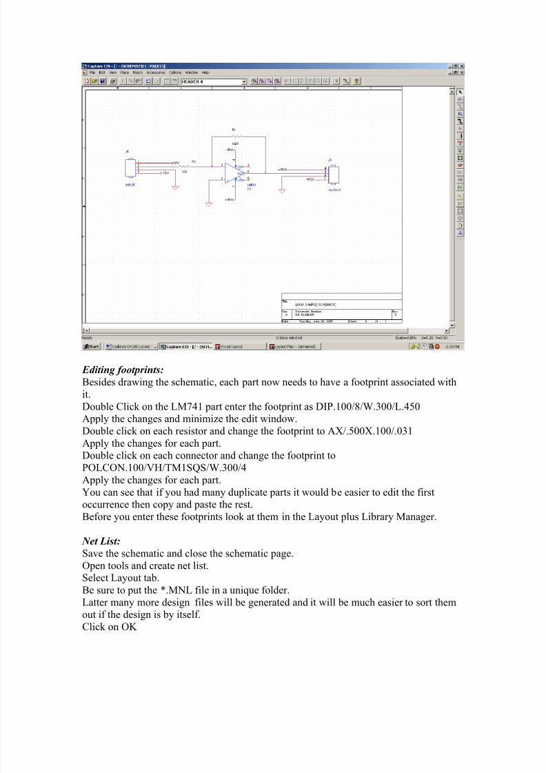
Lets look at the same schematic we created in the MTC OrCAD Capture help procedure.
It’s a simple through hole design with 2 connectors, a LM741 opamp, and two ¼ Wresistors.
8/8/2019 Cadance OrCAD Layout
http://slidepdf.com/reader/full/cadance-orcad-layout 10/32
Editing footprints:
Besides drawing the schematic, each part now needs to have a footprint associated with
it.
Double Click on the LM741 part enter the footprint as DIP.100/8/W.300/L.450Apply the changes and minimize the edit window.
Double click on each resistor and change the footprint to AX/.500X.100/.031
Apply the changes for each part.Double click on each connector and change the footprint to
POLCON.100/VH/TM1SQS/W.300/4
Apply the changes for each part.
You can see that if you had many duplicate parts it would be easier to edit the firstoccurrence then copy and paste the rest.
Before you enter these footprints look at them in the Layout plus Library Manager.
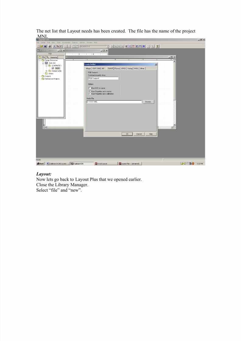
Net List:Save the schematic and close the schematic page.
Open tools and create net list.Select Layout tab.
Be sure to put the *.MNL file in a unique folder.
Latter many more design files will be generated and it will be much easier to sort themout if the design is by itself.
Click on OK
8/8/2019 Cadance OrCAD Layout
http://slidepdf.com/reader/full/cadance-orcad-layout 11/32
The net list that Layout needs has been created. The file has the name of the project
.MNL
Layout:
Now lets go back to Layout Plus that we opened earlier.Close the Library Manager.
Select “file” and “new”.
8/8/2019 Cadance OrCAD Layout
http://slidepdf.com/reader/full/cadance-orcad-layout 12/32
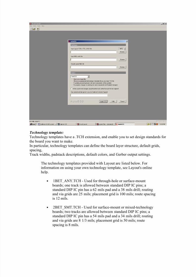
Technology template:
Technology templates have a .TCH extension, and enable you to set design standards for
the board you want to make.
In particular, technology templates can define the board layer structure, default grids,spacing,
Track widths, padstack descriptions, default colors, and Gerber output settings.
The technology templates provided with Layout are listed below. For
information on using your own technology template, see Layout's onlinehelp.
• 1BET_ANY.TCH - Used for through-hole or surface-mount
boards; one track is allowed between standard DIP IC pins; a
standard DIP IC pin has a 62 mils pad and a 38 mils drill; routing
and via grids are 25 mils; placement grid is 100 mils; route spacingis 12 mils.
• 2BET_SMT.TCH - Used for surface-mount or mixed-technology
boards; two tracks are allowed between standard DIP IC pins; astandard DIP IC pin has a 54 mils pad and a 34 mils drill; routing
and via grids are 8 1/3 mils; placement grid is 50 mils; route
spacing is 8 mils.

8/8/2019 Cadance OrCAD Layout
http://slidepdf.com/reader/full/cadance-orcad-layout 13/32
• 2BET_THR.TCH - Used for through-hole boards; two tracks are
allowed between standard DIP IC pins; a standard DIP IC pin has a
54 mils pad and a 34 mils drill; routing and via grids are 20 mils; placement grid is 100 mils; route spacing is 8 mils.
• 3BET_ANY.TCH - Used for through-hole or surface-mount boards; three tracks are allowed between standard DIP IC pins; a
standard DIP IC pin has a 50 mils pad and a 34 mils drill; routingand via grids are 12 1/2 mils; placement grid is 50 mils; route
spacing is 6 mils.
• CERAMIC.TCH - Used for ceramic chip modules.
• DEFAULT.TCH - Used as the default technology template for PCB translators. You might use this technology template for
translation and then load another later as you are working on the
board.
• 386LIB.TCH - Used as the default technology template for translation of PCB386 library files. With this technology template,
you can maintain the color settings of your library.
• HYBRID.TCH - Used for hybrid chips.
• JUMP5535.TCH - Used for single-layer boards; 55 mils vias with35 mils drill.
• JUMP6035.TCH - Used for single-layer boards; 60 mils vias with35 mils drill.
• JUMP6238.TCH - Used for single-layer boards; 62 mils vias with
38 mils drill.
• MCM.TCH - Used for multiple-chip modules.
• METRIC.TCH - Used for metric boards.
• PADS.TCH - Used for boards created using PADS software.
• PROTEL.TCH - Used for boards created using Protel software.
Board template:
Board template files or *.TPL files include the .TCH but have a predetermined board
outline. This is handy if you are making a board to plug into a PC for instance.
There are approximately 70 *.TPL types. (see Layout's online help)
8/8/2019 Cadance OrCAD Layout
http://slidepdf.com/reader/full/cadance-orcad-layout 14/32
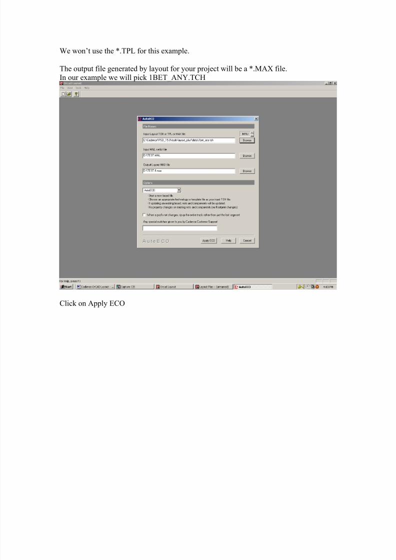
We won’t use the *.TPL for this example.
The output file generated by layout for your project will be a *.MAX file.In our example we will pick 1BET_ANY.TCH
Click on Apply ECO
8/8/2019 Cadance OrCAD Layout
http://slidepdf.com/reader/full/cadance-orcad-layout 15/32
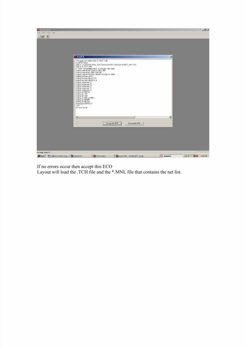
If no errors occur then accept this ECOLayout will load the .TCH file and the *.MNL file that contains the net list.
8/8/2019 Cadance OrCAD Layout
http://slidepdf.com/reader/full/cadance-orcad-layout 16/32
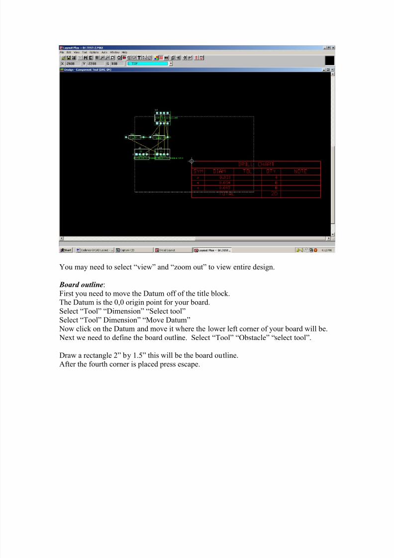
You may need to select “view” and “zoom out” to view entire design.
Board outline:
First you need to move the Datum off of the title block.The Datum is the 0,0 origin point for your board.
Select “Tool” “Dimension” “Select tool”
Select “Tool” Dimension” “Move Datum” Now click on the Datum and move it where the lower left corner of your board will be.
Next we need to define the board outline. Select “Tool” “Obstacle” “select tool”.
Draw a rectangle 2” by 1.5” this will be the board outline.After the fourth corner is placed press escape.
8/8/2019 Cadance OrCAD Layout
http://slidepdf.com/reader/full/cadance-orcad-layout 17/32
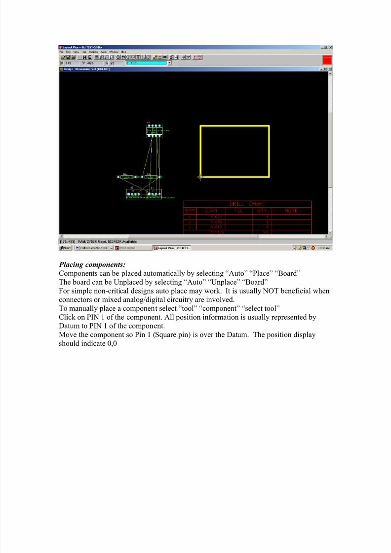
Placing components:
Components can be placed automatically by selecting “Auto” “Place” “Board”
The board can be Unplaced by selecting “Auto” “Unplace” “Board”
For simple non-critical designs auto place may work. It is usually NOT beneficial whenconnectors or mixed analog/digital circuitry are involved.
To manually place a component select “tool” “component” “select tool”
Click on PIN 1 of the component. All position information is usually represented byDatum to PIN 1 of the component.
Move the component so Pin 1 (Square pin) is over the Datum. The position display
should indicate 0,0
8/8/2019 Cadance OrCAD Layout
http://slidepdf.com/reader/full/cadance-orcad-layout 18/32
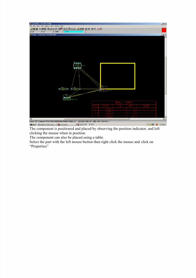
The component is positioned and placed by observing the position indicator, and left
clicking the mouse when in position.The component can also be placed using a table.
Select the part with the left mouse button then right click the mouse and click on
“Properties”
8/8/2019 Cadance OrCAD Layout
http://slidepdf.com/reader/full/cadance-orcad-layout 19/32
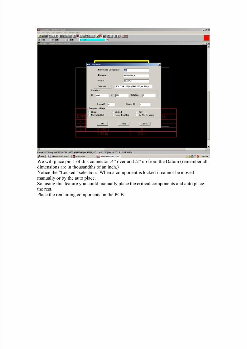
We will place pin 1 of this connector .4” over and .2” up from the Datum (remember all
dimensions are in thousandths of an inch.) Notice the “Locked” selection. When a component is locked it cannot be moved
manually or by the auto place.
So, using this feature you could manually place the critical components and auto placethe rest.
Place the remaining components on the PCB.
8/8/2019 Cadance OrCAD Layout
http://slidepdf.com/reader/full/cadance-orcad-layout 20/32
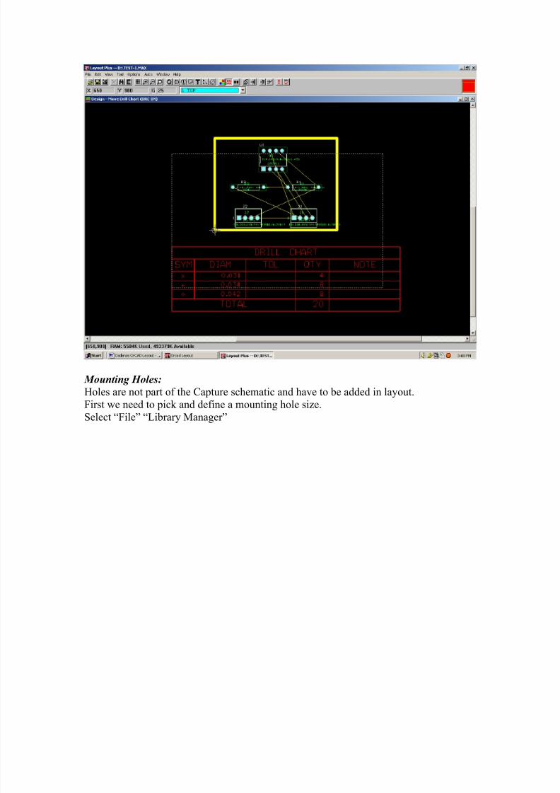
Mounting Holes:
Holes are not part of the Capture schematic and have to be added in layout.
First we need to pick and define a mounting hole size.
Select “File” “Library Manager”
8/8/2019 Cadance OrCAD Layout
http://slidepdf.com/reader/full/cadance-orcad-layout 21/32
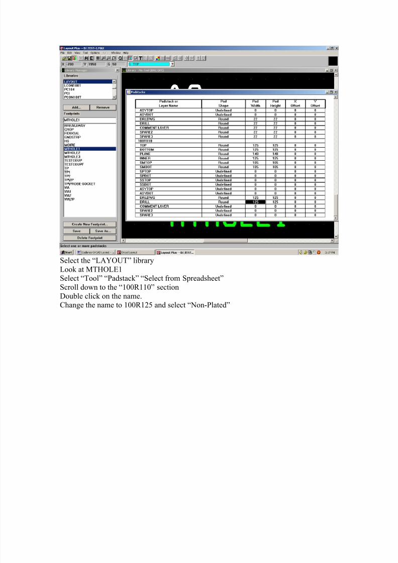
Select the “LAYOUT” library
Look at MTHOLE1Select “Tool” “Padstack” “Select from Spreadsheet”
Scroll down to the “100R110” section
Double click on the name.Change the name to 100R125 and select “Non-Plated”
8/8/2019 Cadance OrCAD Layout
http://slidepdf.com/reader/full/cadance-orcad-layout 22/32
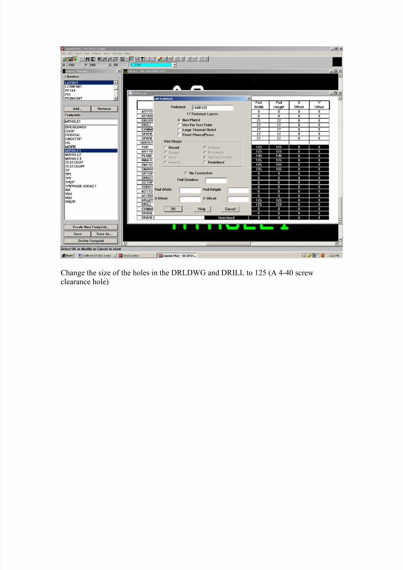
Change the size of the holes in the DRLDWG and DRILL to 125 (A 4-40 screwclearance hole)
8/8/2019 Cadance OrCAD Layout
http://slidepdf.com/reader/full/cadance-orcad-layout 23/32
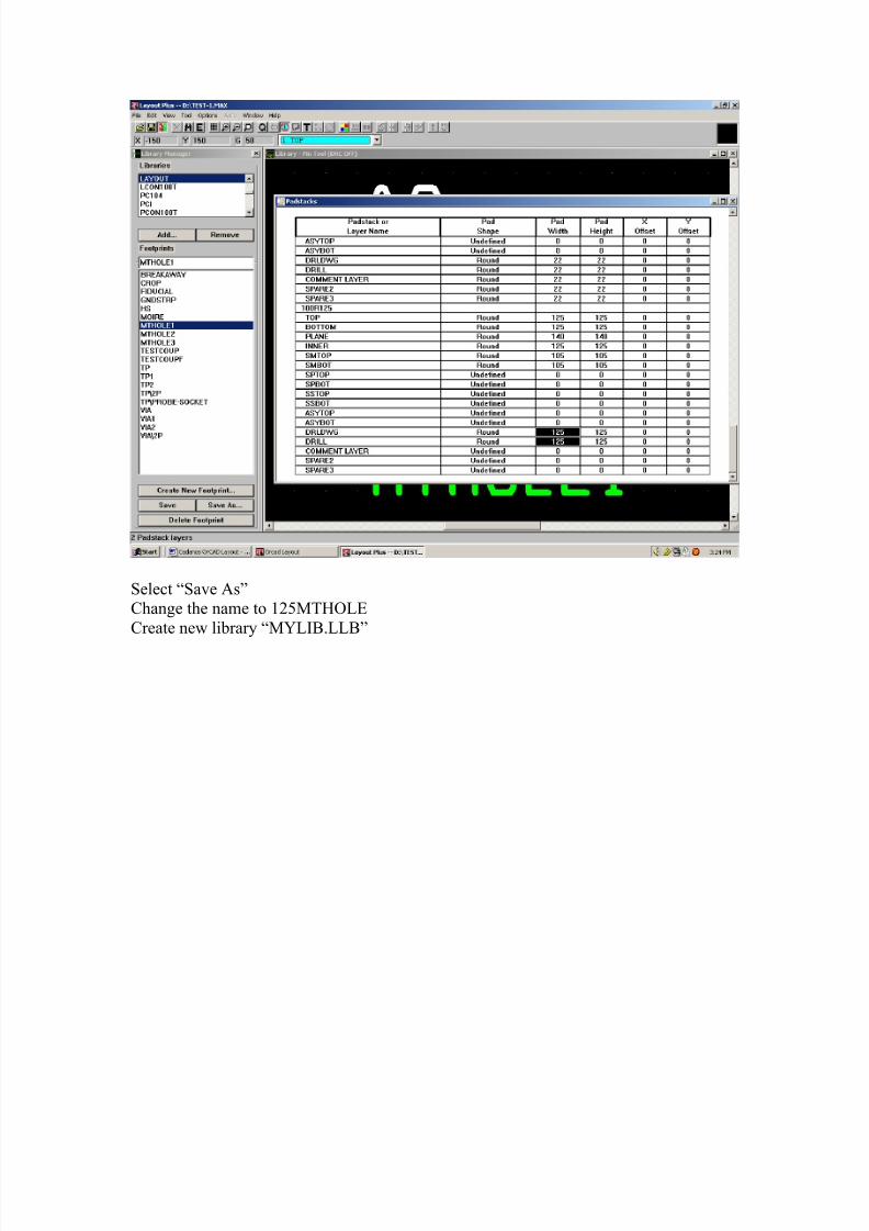
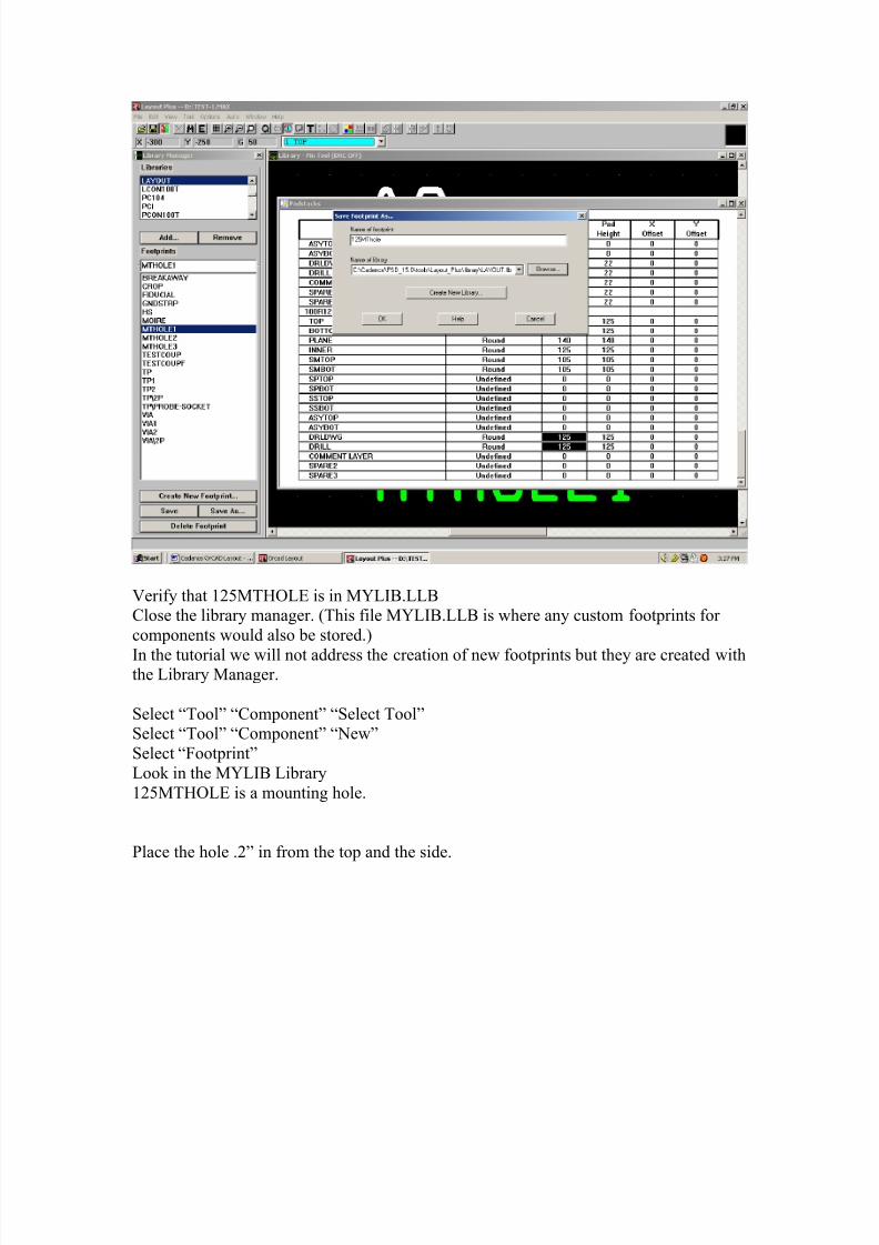
Select “Save As”Change the name to 125MTHOLE
Create new library “MYLIB.LLB”
8/8/2019 Cadance OrCAD Layout
http://slidepdf.com/reader/full/cadance-orcad-layout 24/32
Verify that 125MTHOLE is in MYLIB.LLBClose the library manager. (This file MYLIB.LLB is where any custom footprints for
components would also be stored.)
In the tutorial we will not address the creation of new footprints but they are created withthe Library Manager.
Select “Tool” “Component” “Select Tool”Select “Tool” “Component” “New”
Select “Footprint”
Look in the MYLIB Library
125MTHOLE is a mounting hole.
Place the hole .2” in from the top and the side.
8/8/2019 Cadance OrCAD Layout
http://slidepdf.com/reader/full/cadance-orcad-layout 25/32
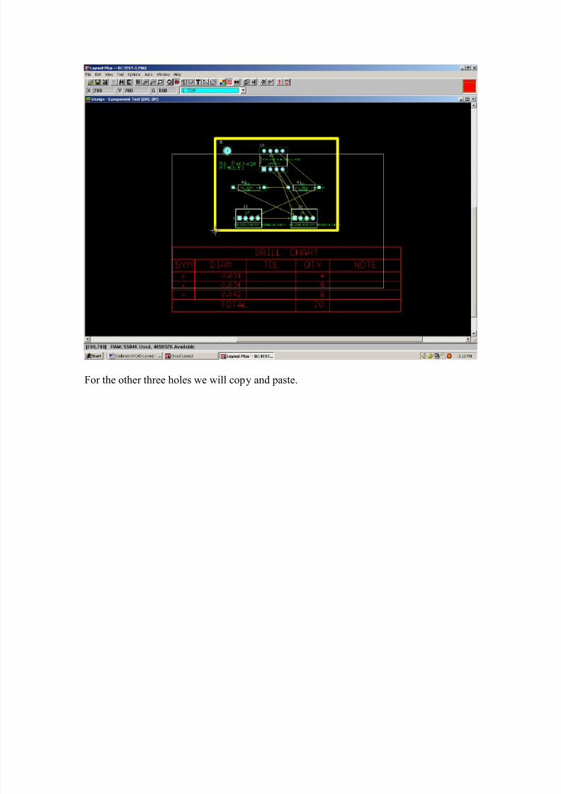
For the other three holes we will copy and paste.
8/8/2019 Cadance OrCAD Layout
http://slidepdf.com/reader/full/cadance-orcad-layout 26/32
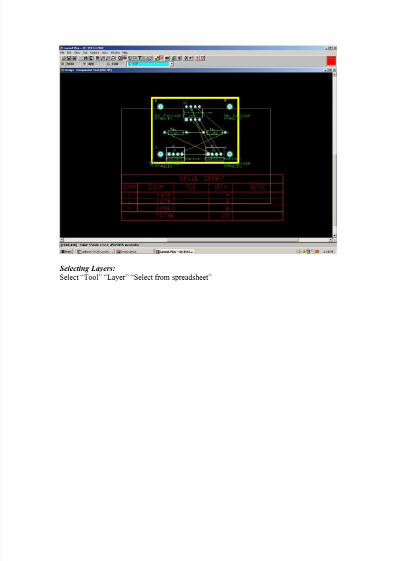
Selecting Layers:
Select “Tool” “Layer” “Select from spreadsheet”
8/8/2019 Cadance OrCAD Layout
http://slidepdf.com/reader/full/cadance-orcad-layout 27/32
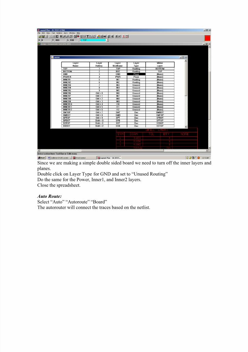
Since we are making a simple double sided board we need to turn off the inner layers and
planes.Double click on Layer Type for GND and set to “Unused Routing”
Do the same for the Power, Inner1, and Inner2 layers.
Close the spreadsheet.
Auto Route:
Select “Auto” “Autoroute” “Board”The autorouter will connect the traces based on the netlist.
8/8/2019 Cadance OrCAD Layout
http://slidepdf.com/reader/full/cadance-orcad-layout 28/32
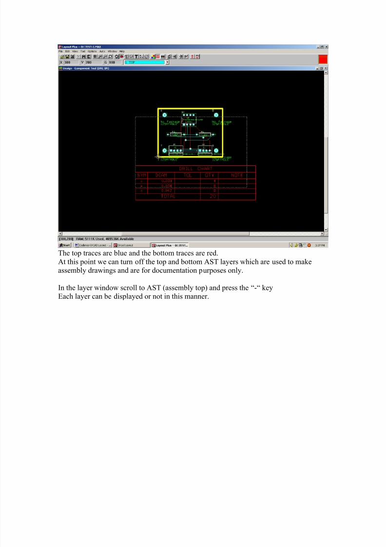
The top traces are blue and the bottom traces are red.
At this point we can turn off the top and bottom AST layers which are used to makeassembly drawings and are for documentation purposes only.
In the layer window scroll to AST (assembly top) and press the “-“ keyEach layer can be displayed or not in this manner.
8/8/2019 Cadance OrCAD Layout
http://slidepdf.com/reader/full/cadance-orcad-layout 29/32
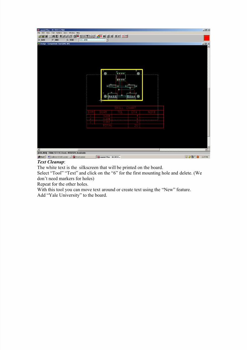
Text Cleanup:
The white text is the silkscreen that will be printed on the board.Select “Tool” “Text” and click on the “6” for the first mounting hole and delete. (We
don’t need markers for holes)
Repeat for the other holes.With this tool you can move text around or create text using the “New” feature.
Add “Yale University” to the board.
8/8/2019 Cadance OrCAD Layout
http://slidepdf.com/reader/full/cadance-orcad-layout 30/32
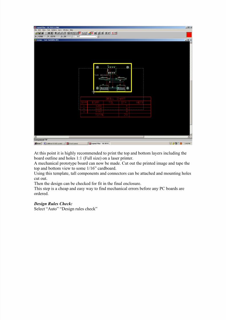
At this point it is highly recommended to print the top and bottom layers including the board outline and holes 1:1 (Full size) on a laser printer.
A mechanical prototype board can now be made. Cut out the printed image and tape the
top and bottom view to some 1/16” cardboard.Using this template, tall components and connectors can be attached and mounting holes
cut out.
Then the design can be checked for fit in the final enclosure.This step is a cheap and easy way to find mechanical errors before any PC boards are
ordered.
Design Rules Check:
Select “Auto” “Design rules check”
8/8/2019 Cadance OrCAD Layout
http://slidepdf.com/reader/full/cadance-orcad-layout 31/32
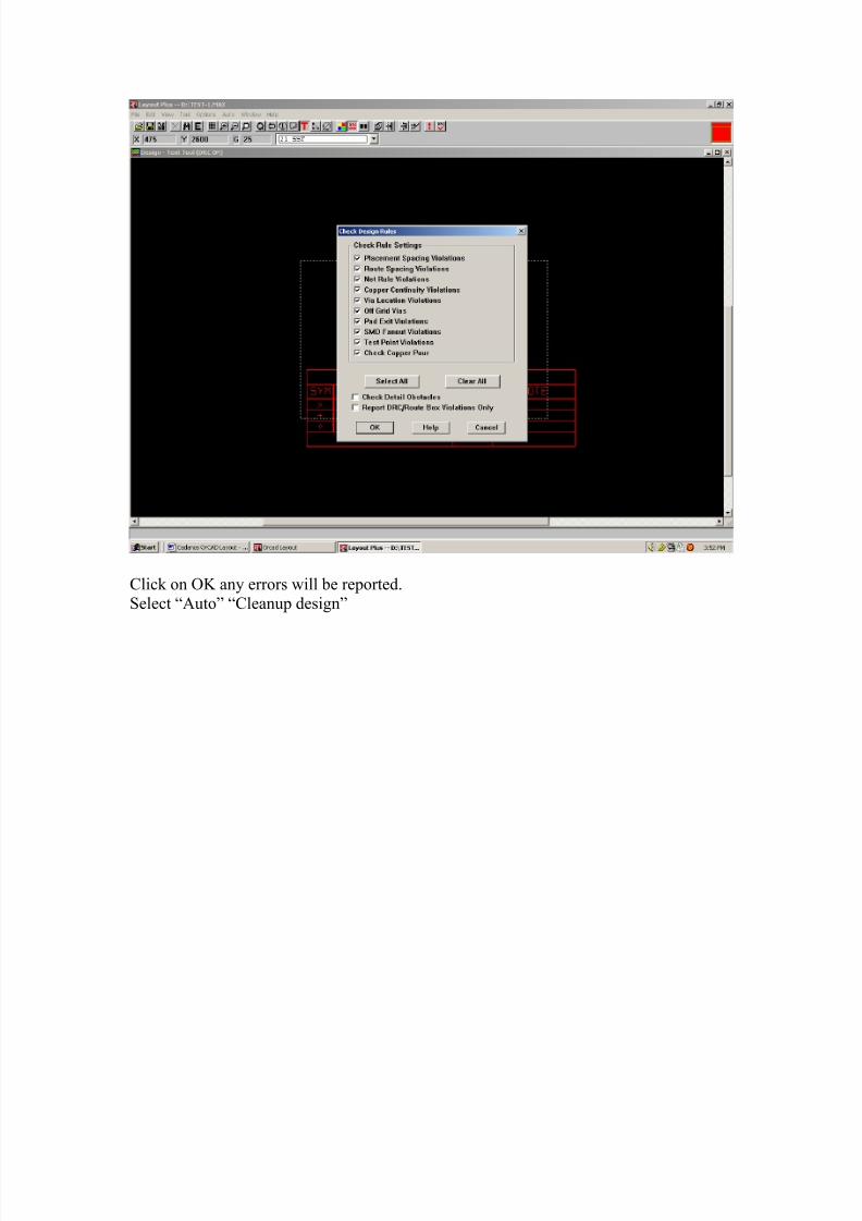
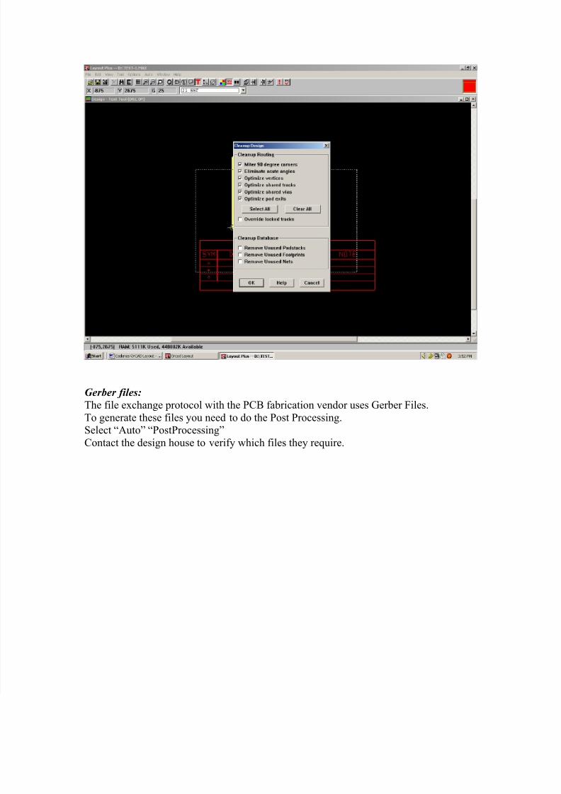
Click on OK any errors will be reported.Select “Auto” “Cleanup design”
8/8/2019 Cadance OrCAD Layout
http://slidepdf.com/reader/full/cadance-orcad-layout 32/32
Gerber files:
The file exchange protocol with the PCB fabrication vendor uses Gerber Files.
To generate these files you need to do the Post Processing.Select “Auto” “PostProcessing”
Contact the design house to verify which files they require.