FM Xmtr Theory
95
I To Design and Build a Portable, Miniaturised, Multichannel FM Transmitter Author Francis Mc Swiggan 9427406 Supervisor Dr. Máirtín Ó Droma University Of Limerick Course B. Eng. Electronic Engineering (LM070) Submitted in part requirement for final year project to University of Limerick, Limerick, Ireland 28/04/98
-
Upload
amsalu-setey -
Category
Documents
-
view
224 -
download
0
Transcript of FM Xmtr Theory
8/20/2019 FM Xmtr Theory
http://slidepdf.com/reader/full/fm-xmtr-theory 1/95
I
To Design and Build a Portable, Miniaturised, Multichannel
FM Transmitter
AuthorFrancis Mc Swiggan
9427406
SupervisorDr. Máirtín Ó Droma
University Of Limerick
Course
B. Eng. Electronic Engineering (LM070)
Submitted in part requirement for final year project to
University of Limerick, Limerick, Ireland
28/04/98
8/20/2019 FM Xmtr Theory
http://slidepdf.com/reader/full/fm-xmtr-theory 2/95
Created by Francis Mc Swiggan([email protected])
II
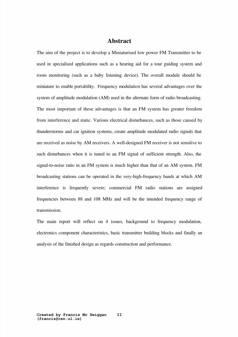
AbstractThe aim of the project is to develop a Miniaturised low power FM Transmitter to be
used in specialised applications such as a hearing aid for a tour guiding system and
room monitoring (such as a baby listening device). The overall module should be
miniature to enable portability. Frequency modulation has several advantages over the
system of amplitude modulation (AM) used in the alternate form of radio broadcasting.
The most important of these advantages is that an FM system has greater freedom
from interference and static. Various electrical disturbances, such as those caused by
thunderstorms and car ignition systems, create amplitude modulated radio signals that
are received as noise by AM receivers. A well-designed FM receiver is not sensitive to
such disturbances when it is tuned to an FM signal of sufficient strength. Also, the
signal-to-noise ratio in an FM system is much higher than that of an AM system. FM
broadcasting stations can be operated in the very-high-frequency bands at which AMinterference is frequently severe; commercial FM radio stations are assigned
frequencies between 88 and 108 MHz and will be the intended frequency range of
transmission.
The main report will reflect on 4 issues, background to frequency modulation,
electronics component characteristics, basic transmitter building blocks and finally an
analysis of the finished design as regards construction and performance.
8/20/2019 FM Xmtr Theory
http://slidepdf.com/reader/full/fm-xmtr-theory 3/95
Created by Francis Mc Swiggan([email protected])
III
Declaration
This report is presented in partial fulfilment of the requirements for the degree of
Bachelor of Engineering.
It is entirely my own work and has not been submitted to any other University or
higher education institution, or for any other academic award in this University. Where
use has been made of the work of other people it has been fully acknowledged and
fully referenced.
Signature: ___________________________
Francis Mc Swiggan
24th April 1998

8/20/2019 FM Xmtr Theory
http://slidepdf.com/reader/full/fm-xmtr-theory 4/95
Created by Francis Mc Swiggan([email protected])
IV
Acknowledgements
I would very much like to gratefully extend my sincere thanks to all the people who
gave generously their time, takes one and all. Especially my supervisor Dr. Máirtín Ó
Droma for the guidance he showed me right through every stage of the project, from
initial conception to final design and construction.
Richard Conway for the loan of Electronic communication Techniques at the initialstage of the project, Elfed Lewis for kindly granting me access to his Pspice lab for
initial simulation work. The technicians Jimmy Kelly, James Keane, John Maurice and
many more of the lads in stores who helped me with a lot of the tedious leg work
involved in giving life to a design and implementation project.
To the various chancers in my course who helped me stay awake during many a long
nights work. The “podger” , “Richie of the hellen” and many more too numerous to
mention, thanx Lads.

8/20/2019 FM Xmtr Theory
http://slidepdf.com/reader/full/fm-xmtr-theory 5/95
Created by Francis Mc Swiggan([email protected])
V
Dedication
To the person who supported me through 4 years of College.
Thanks Mam.
And to the rest of my family.
8/20/2019 FM Xmtr Theory
http://slidepdf.com/reader/full/fm-xmtr-theory 6/95
Created by Francis Mc Swiggan([email protected])
VI
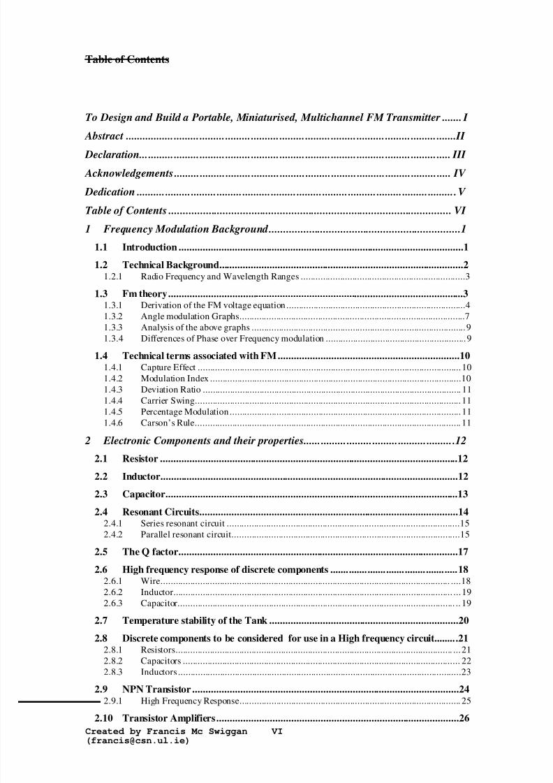
Table of Contents
To Design and Build a Portable, Miniaturised, Multichannel FM Transmitter ....... I
Abstract ....................................................................................................................II Declaration............................................................................................................. III
Acknowledgements ................................................................................................. IV
Dedication ................................................................................................................V
Table of Contents ................................................................................................... VI
1 Frequency Modulation Background...................................................................1
1.1 Introduction ...........................................................................................................11.2 Technical Background............................................................................................2
1.2.1 Radio Frequency and Wavelength Ranges ...................................................................31.3 Fm theory...............................................................................................................3
1.3.1 Derivation of the FM voltage equation.........................................................................41.3.2 Angle modulation Graphs............................................................................................71.3.3 Analysis of the above graphs .......................................................................................91.3.4 Differences of Phase over Frequency modulation .........................................................9
1.4 Technical terms associated with FM....................................................................101.4.1 Capture Effect ...........................................................................................................101.4.2 Modulation Index ......................................................................................................101.4.3 Deviation Ratio ......................................................................................................... 111.4.4 Carrier Swing............................................................................................................111.4.5 Percentage Modulation..............................................................................................111.4.6 Carson’s Rule............................................................................................................ 11
2 Electronic Components and their properties.....................................................12
2.1 Resistor ................................................................................................................122.2 Inductor................................................................................................................122.3 Capacitor..............................................................................................................132.4 Resonant Circuits.................................................................................................14
2.4.1 Series resonant circuit ...............................................................................................152.4.2 Parallel resonant circuit.............................................................................................15
2.5 The Q factor.........................................................................................................172.6 High frequency response of discrete components ................................................18
2.6.1 Wire...................................................................................................................... ....182.6.2 Inductor.................................................................................................................. ...192.6.3 Capacitor................................................................................................................. ..19
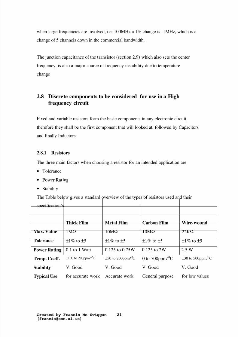
2.7 Temperature stability of the Tank .......................................................................202.8 Discrete components to be considered for use in a High frequency circuit.........21
2.8.1 Resistors................................................................................................................. ...212.8.2 Capacitors ................................................................................................................. 222.8.3 Inductors...................................................................................................................23
2.9 NPN Transistor ....................................................................................................242.9.1 High Frequency Response.......................................................................................... 25
2.10 Transistor Amplifiers...........................................................................................26
8/20/2019 FM Xmtr Theory
http://slidepdf.com/reader/full/fm-xmtr-theory 7/95
Created by Francis Mc Swiggan([email protected])
VII
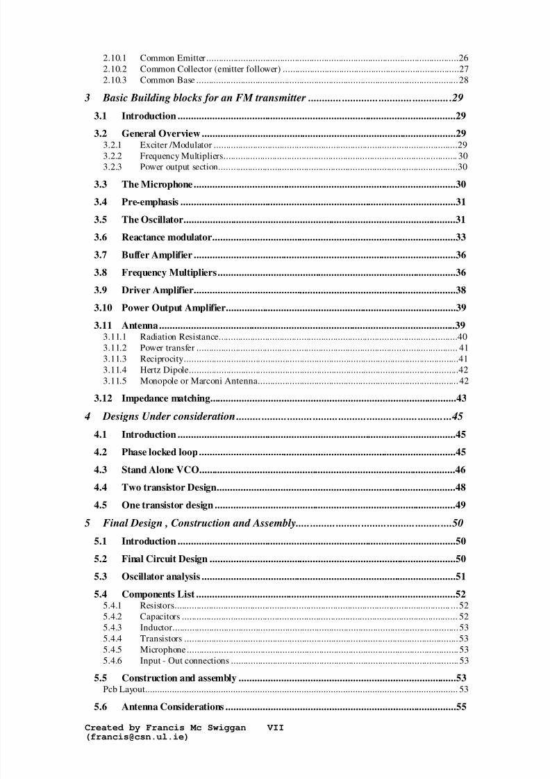
2.10.1 Common Emitter .......................................................................................................262.10.2 Common Collector (emitter follower) ........................................................................272.10.3 Common Base ...........................................................................................................28
3 Basic Building blocks for an FM transmitter ...................................................29
3.1 Introduction .........................................................................................................29
3.2 General Overview................................................................................................293.2.1 Exciter /Modulator ....................................................................................................293.2.2 Frequency Multipliers................................................................................................ 303.2.3 Power output section..................................................................................................30
3.3 The Microphone...................................................................................................303.4 Pre-emphasis ........................................................................................................313.5 The Oscillator.......................................................................................................313.6 Reactance modulator............................................................................................333.7 Buffer Amplifier ...................................................................................................36
3.8 Frequency Multipliers..........................................................................................363.9 Driver Amplifier...................................................................................................383.10 Power Output Amplifier.......................................................................................393.11 Antenna................................................................................................................39
3.11.1 Radiation Resistance..................................................................................................403.11.2 Power transfer ........................................................................................................... 413.11.3 Reciprocity................................................................................................................413.11.4 Hertz Dipole..............................................................................................................423.11.5 Monopole or Marconi Antenna..................................................................................42
3.12 Impedance matching.............................................................................................43
4 Designs Under consideration ............................................................................45
4.1 Introduction .........................................................................................................454.2 Phase locked loop.................................................................................................454.3 Stand Alone VCO.................................................................................................464.4 Two transistor Design..........................................................................................484.5 One transistor design ...........................................................................................49
5 Final Design , Construction and Assembly.......................................................50
5.1 Introduction .........................................................................................................505.2 Final Circuit Design .............................................................................................505.3 Oscillator analysis ................................................................................................515.4 Components List ..................................................................................................52
5.4.1 Resistors................................................................................................................. ...525.4.2 Capacitors ................................................................................................................. 525.4.3 Inductor.....................................................................................................................535.4.4 Transistors ................................................................................................................535.4.5 Microphone............................................................................................................... 535.4.6 Input - Out connections ............................................................................................. 53
5.5 Construction and assembly ..................................................................................53Pcb Layout................................................................................................................................ 53
5.6 Antenna Considerations .......................................................................................55
8/20/2019 FM Xmtr Theory
http://slidepdf.com/reader/full/fm-xmtr-theory 8/95
Created by Francis Mc Swiggan([email protected])
VIII
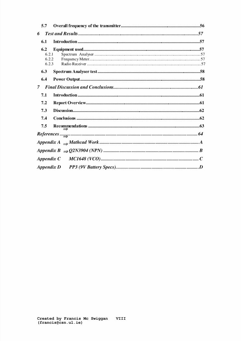
5.7 Overall frequency of the transmitter....................................................................56
6 Test and Results ................................................................................................57
6.1 Introduction .........................................................................................................576.2 Equipment used....................................................................................................57
6.2.1 Spectrum Analyser ...................................................................................................57
6.2.2 Frequency Meter........................................................................................................576.2.3 Radio Receiver ..........................................................................................................57
6.3 Spectrum Analyser test ........................................................................................586.4 Power Output.......................................................................................................58
7 Final Discussion and Conclusions....................................................................61
7.1 Introduction .........................................................................................................617.2 Report Overview..................................................................................................617.3 Discussion.............................................................................................................62
7.4 Conclusions ..........................................................................................................627.5 Recommendations ................................................................................................63
References ...............................................................................................................64
Appendix A Mathcad Work ................................................................................ A
Appendix B Q2N3904 (NPN) ............................................................................. B
Appendix C MC1648 (VCO) ............................................................................... C
Appendix D PP3 (9V Battery Specs)...................................................................D
8/20/2019 FM Xmtr Theory
http://slidepdf.com/reader/full/fm-xmtr-theory 9/95
Created by Francis Mc Swiggan([email protected])
1
1 Frequency Modulation Background
1.1 IntroductionThe comparatively low cost of equipment for an FM broadcasting station, resulted inrapid growth in the years following World War II. Within three years after the closeof the war, 600 licensed FM stations were broadcasting in the United States and bythe end of the 1980s there were over 4,000. Similar trends have occurred in Britainand other countries. Because of crowding in the AM broadcast band and the inabilityof standard AM receivers to eliminate noise, the tonal fidelity of standard stations ispurposely limited. FM does not have these drawbacks and therefore can be used totransmit music, reproducing the original performance with a degree of fidelity thatcannot be reached on AM bands. FM stereophonic broadcasting has drawnincreasing numbers of listeners to popular as well as classical music, so thatcommercial FM stations draw higher audience ratings than AM stations.
The integrated chip has also played its part in the wide proliferation of FM receivers,as circuits got smaller it became easier to make a modular electronic device called the
“Walkman”, which enables the portability of a tape player and an AM/FM radioreceiver. This has resulted in the portability of a miniature FM receiver, which iscarried by most people when travelling on long trips.

8/20/2019 FM Xmtr Theory
http://slidepdf.com/reader/full/fm-xmtr-theory 10/95
8/20/2019 FM Xmtr Theory
http://slidepdf.com/reader/full/fm-xmtr-theory 11/95
Created by Francis Mc Swiggan([email protected])
3
With a bandwidth of 200Khz for one station, up to 100 stations can be fitted between88 & 108Mhz. Station 201 to 300 denote the stations, from 88.1Mhz to 107.9Mhz.
Station 201 to 220 (88Mhz to 91.2) are for non-commercial stations (educational)which could be a good area to transmit in, but in recent years the band from 88MHz to103Mhz has been filled by a lot of commercial channels, making the lower frequenciesvery congested indeed.
1.2.1 Radio Frequency and Wavelength RangesRadio waves have a wide range of applications, including communication duringemergency rescues (transistor and short-wave radios), international broadcasts
(satellites), and cooking food (microwaves). A radio wave is described by itswavelength (the distance from one crest to the next) or its frequency (the number of crests that move past a point in one second). Wavelengths of radio waves rangefrom 100,000 m (270,000 ft) to 1 mm (.004 in). Frequencies range from 3 kilohertzto 300 Giga-hertz.
1.3 Fm theory
Angle and Amplitude Modulation are techniques used in Communication to transmitData or Voice over a particular medium, whether it be over wire cable, fibre optic orair (the atmosphere). A wave that is proportional to the original baseband (a real timeproperty, such as amplitude) information is used to vary the angle or amplitude of ahigher frequency wave (the carrier).
Carrier =Α Cos (t)Φ
φ π α(t) f t +C= 2
Where A is the amplitude of the carrier andφ(t) is the angle of the carrier, which
constitutes the frequency (f C ) and the phase (α) of the carrier. Angle modulation
varies the angle of the carrier by an amount proportional to the information signal.
Angle modulation can be broken into 2 distinct categories, frequency modulation andphase modulation. Formal definitions are given below :
8/20/2019 FM Xmtr Theory
http://slidepdf.com/reader/full/fm-xmtr-theory 12/95
Created by Francis Mc Swiggan([email protected])
4
Phase Modulation(PM) : angle modulation in which the phase of a carrier is
caused to depart from its reference value by an amount proportional to the modulating
signal amplitude.
Frequency Modulation (FM): angle modulation in which the instantaneous
frequency of a sine wave carrier is caused to depart from the carrier frequency by anamount proportional to the instantaneous value of the modulator or intelligence wave.
Phase modulation differs from Frequency modulation in one important way. Take a
carrier of the form A Cos(ωCt + θ) = ReA.e j(ωCt +θ)
Pm will have the carrier phasor in between the + and - excursions of the modulatingsignal. Fm modulation also has the carrier in the middle but the fact that when youintegrate the modulating signal and put it through a phase modulator you get fm, and if the modulating wave were put through a differentiator before a frequency modulatoryou get a phase modulated wave. This may seem confusing at this point, but the above
concept will be reinforced further in the sections to follow.
1.3.1 Derivation of the FM voltage equation
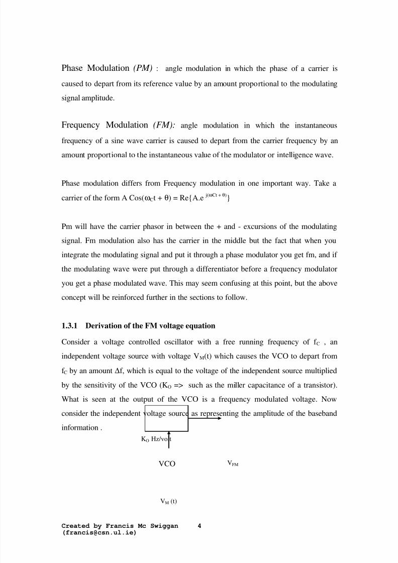
Consider a voltage controlled oscillator with a free running frequency of f C , anindependent voltage source with voltage VM(t) which causes the VCO to depart from
f C by an amount∆f, which is equal to the voltage of the independent source multiplied
by the sensitivity of the VCO (KO => such as the miller capacitance of a transistor).What is seen at the output of the VCO is a frequency modulated voltage. Nowconsider the independent voltage source as representing the amplitude of the basebandinformation .
KO Hz/volt
VCO
VM (t)
VFM
8/20/2019 FM Xmtr Theory
http://slidepdf.com/reader/full/fm-xmtr-theory 13/95
Created by Francis Mc Swiggan([email protected])
5
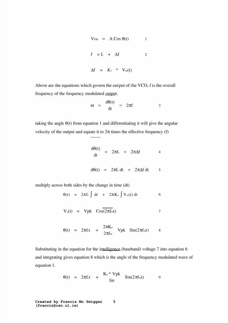
V A Cos (t)FM = θ 1
f = f + f c
∆ 2
(t)V*=f moK ∆
Above are the equations which govern the output of the VCO, f is the overallfrequency of the frequency modulated output.
ω θ π= =d (t)
dt f 2 3
taking the angleθ(t) from equation 1 and differentiating it will give the angular
velocity of the output and equate it to 2π times the effective frequency (f)
d (t)dt 2 f 2 f cθ π π∆= + 4
d (t) 2 f dt 2 f dtcθ π π∆= + 5
multiply across both sides by the change in time (dt)
θ π π(t) = 2 f dt + 2 K V (t) dtc o m∫ ∫ 6
V (t) = Vpk Cos(2 f t)m mπ 7
θ π ππ π(t) = 2 f t + 2 Kf Vpk Sin(2 f t)c
o
mm
2 8
Substituting in the equation for the intelligence (baseband) voltage 7 into equation 6and integrating gives equation 8 which is the angle of the frequency modulated wave of equation 1.
θ π π(t) = 2 f t +K * Vpk
fm Sin(2 f t)co
m 9
8/20/2019 FM Xmtr Theory
http://slidepdf.com/reader/full/fm-xmtr-theory 14/95
Created by Francis Mc Swiggan([email protected])
6
M =K * Vpk
fm Fo
10
M =fc(pk)fm F
∆11
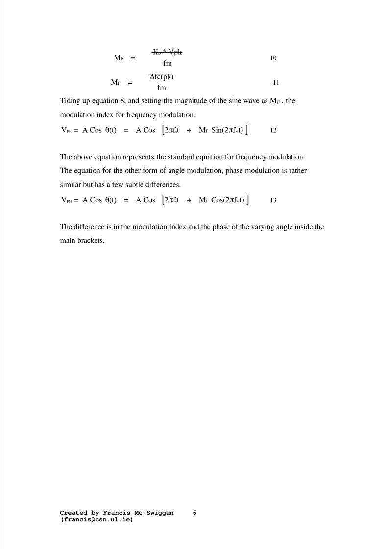
Tiding up equation 8, and setting the magnitude of the sine wave as MF , themodulation index for frequency modulation.
[ ]V = A Cos (t) = A Cos 2 f t + M Sin(2 f t)FM c MFθ π π 12
The above equation represents the standard equation for frequency modulation.The equation for the other form of angle modulation, phase modulation is rathersimilar but has a few subtle differences.
[ ]V = A Cos (t) = A Cos 2 f t + M Cos(2 f t)PM c P Mθ π π 13
The difference is in the modulation Index and the phase of the varying angle inside themain brackets.

8/20/2019 FM Xmtr Theory
http://slidepdf.com/reader/full/fm-xmtr-theory 15/95
Created by Francis Mc Swiggan([email protected])
7
1.3.2 Angle modulation Graphs
0 0.2 0.4 0.6 0.8 12
0
2
Carrier Wave
2
-2
Vc( )t
10 t
Figure 1.3-1
Vc( )t .A cos ( )...2 π fc t
0 0.2 0.4 0.6 0.8 14
2
0
2
4
Baseband Signal
3
-3
Vm( )t
10 t
Figure 1.3-1
Vm( )t ( ).Vpk cos ( )...2 π fm t
0 0.2 0.4 0.6 0.8 12
0
2
Frequency Modulated Wave
2
-1.99989
S1( )t
10 t
Figure 1.3-3
S( )t .A cos ...2 π fc t ...2 π Ko d0
ttVm( )t
8/20/2019 FM Xmtr Theory
http://slidepdf.com/reader/full/fm-xmtr-theory 16/95
Created by Francis Mc Swiggan([email protected])
8
0 0.2 0.4 0.6 0.8 12
0
2
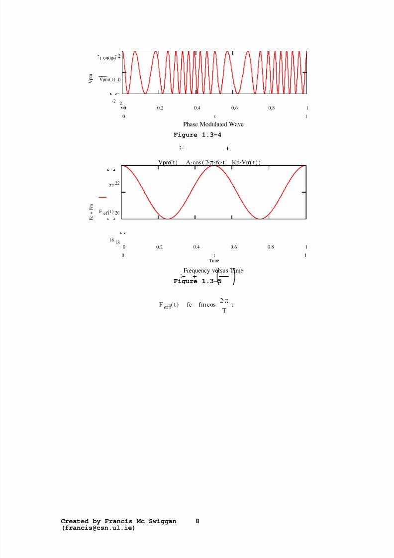
Phase Modulated Wave
V p m
1.99989
-2
Vpm( )t
10 t
Figure 1.3-4
Vpm( )t .A cos ( )...2 π fc t .Kp Vm( )t
0 0.2 0.4 0.6 0.8 118
20
22
Frequency versus TimeTime
F c
+ F m
22
18
F eff ( )t
10 t
Figure 1.3-5
F eff ( )t fc .fmcos ..2 πT
t
8/20/2019 FM Xmtr Theory
http://slidepdf.com/reader/full/fm-xmtr-theory 17/95
Created by Francis Mc Swiggan([email protected])
9
1.3.3 Analysis of the above graphs
There are 5 significant graphs above, The carrier, the Baseband, FM signal, PM signal
and the change of frequency over time. The carrier and baseband are there to show therelative scale, so a link between the carrier and Baseband can be seen.
For FM: the carrier’s frequency is proportional to the baseband’s amplitude, thecarrier increases frequency proportional to the positive magnitude of the baseband anddecreases frequency proportional to the negative magnitude of the baseband.
For PM: the carrier’s frequency is proportional to the baseband’s amplitude, thecarrier increases frequency proportional to the positive rate of change of the basebandand decreases frequency proportional to the negative rate of change of the baseband.In other words when the baseband is a maximum or a minimum, there is Zero rate of change in the baseband, and the carrier’s frequency is equal to the its free runningvalue f C.
In both systems the rate of modulation is equal to the frequency of modulation(baseband’s frequency). The last graph shows the relationship between the frequencyof FM versus Time, this relationship is used (following a limiter which makes sure theamplitude is a constant) by a discriminator at the receiver to extract the Baseband’sAmplitude at the receiver, resulting in an amplitude modulated wave, the information isthen demodulated using a simple diode detector. In common AM/FM receivers for anAM station to be demodulated, the limiter and discriminator can be by passed and theintermediate frequency signal can be fed straight to the diode detector.
1.3.4 Differences of Phase over Frequency modulation
The main difference is in the modulation index, PM uses a constant modulation index,whereas FM varies (Max frequency deviation over the instantaneous basebandfrequency). Because of this the demodulation S/N ratio of PM is far better than FM.

8/20/2019 FM Xmtr Theory
http://slidepdf.com/reader/full/fm-xmtr-theory 18/95
Created by Francis Mc Swiggan([email protected])
10
The reason why PM is not used in the commercial frequencies is because of the factthat PM need a coherent local oscillator to demodulate the signal, this demands aphase lock loop, back in the early years the circuitry for a PLL couldn’t be integrated
and therefore FM, without the need for coherent demodulation was the first on themarket. One of the advantages of FM over PM is that the FM VCO can produce high-index frequency modulation, whereas PM requires multipliers to produce high-indexphase modulation. PM circuitry can be used today because of very large scaleintegration used in electronic chips, as stated before to get an FM signal from a phasemodulator the baseband can be integrated, this is the modern approach taken in thedevelopment of high quality FM transmitters.
For miniaturisation and transmission in the commercial bandwidth to be aims for thetransmitter, PM cannot be even considered, even though Narrow Band PM can beused to produce Wide band FM (Armstrong Method).
1.4 Technical terms associated with FM
Now that Fm has been established as a scheme of high quality baseband transmission,some of the general properties of FM will be looked at.
1.4.1 Capture Effect
Simply put means that if 2 stations or more are transmitting at near the same frequencyFM has the ability t pick up the stronger signal and attenuated the unwanted signalpickup.
1.4.2 Modulation Index
M =fc(pk)fm F
∆ (Was known as the modulation factor)
Modulation Index is used in communications as a measure of the relative amount of information to carrier amplitude in the modulated signal. It is also used to determinethe spectral power distribution of the modulated wave. This can be seen in conjunction
with the Bessel function. The higher the modulation index the more side-bands are
8/20/2019 FM Xmtr Theory
http://slidepdf.com/reader/full/fm-xmtr-theory 19/95
Created by Francis Mc Swiggan([email protected])
11
created and therefore the more bandwidth is needed to capture most of the baseband’sinformation.
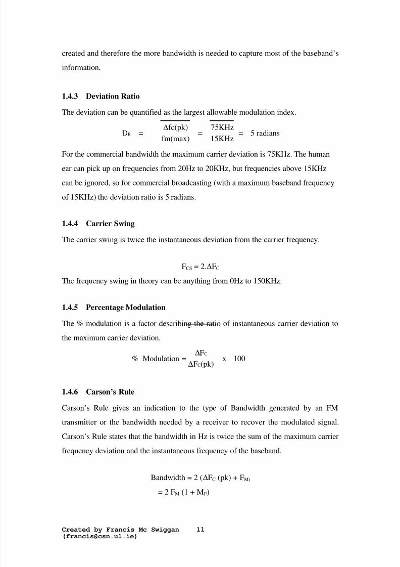
1.4.3 Deviation RatioThe deviation can be quantified as the largest allowable modulation index.
D =fc(pk)
fm(max)KHz
15KHz 5 radiansR∆ = =
75
For the commercial bandwidth the maximum carrier deviation is 75KHz. The humanear can pick up on frequencies from 20Hz to 20KHz, but frequencies above 15KHzcan be ignored, so for commercial broadcasting (with a maximum baseband frequency
of 15KHz) the deviation ratio is 5 radians.
1.4.4 Carrier Swing
The carrier swing is twice the instantaneous deviation from the carrier frequency.
FCS = 2.∆FC
The frequency swing in theory can be anything from 0Hz to 150KHz.
1.4.5 Percentage Modulation
The % modulation is a factor describing the ratio of instantaneous carrier deviation tothe maximum carrier deviation.
% Modulation = ∆∆
FF (pk) x 100
C
C
1.4.6 Carson’s Rule
Carson’s Rule gives an indication to the type of Bandwidth generated by an FMtransmitter or the bandwidth needed by a receiver to recover the modulated signal.Carson’s Rule states that the bandwidth in Hz is twice the sum of the maximum carrierfrequency deviation and the instantaneous frequency of the baseband.
Bandwidth = 2 (∆FC (pk) + FM)
= 2 FM (1 + MF)
8/20/2019 FM Xmtr Theory
http://slidepdf.com/reader/full/fm-xmtr-theory 20/95
Created by Francis Mc Swiggan([email protected])
12
2 Electronic Components and their properties
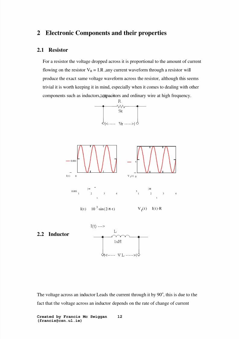
2.1 Resistor
For a resistor the voltage dropped across it is proportional to the amount of currentflowing on the resistor VR = I.R ,any current waveform through a resistor willproduce the exact same voltage waveform across the resistor, although this seemstrivial it is worth keeping it in mind, especially when it comes to dealing with othercomponents such as inductors, capacitors and ordinary wire at high frequency.
1 2 3 40.001
0
0.001
I( )t
t1 2 3 4
5
0
5
V r( )t
t
I( )t .10 3 sin( )..2 π t Vr( )t .I( )t R
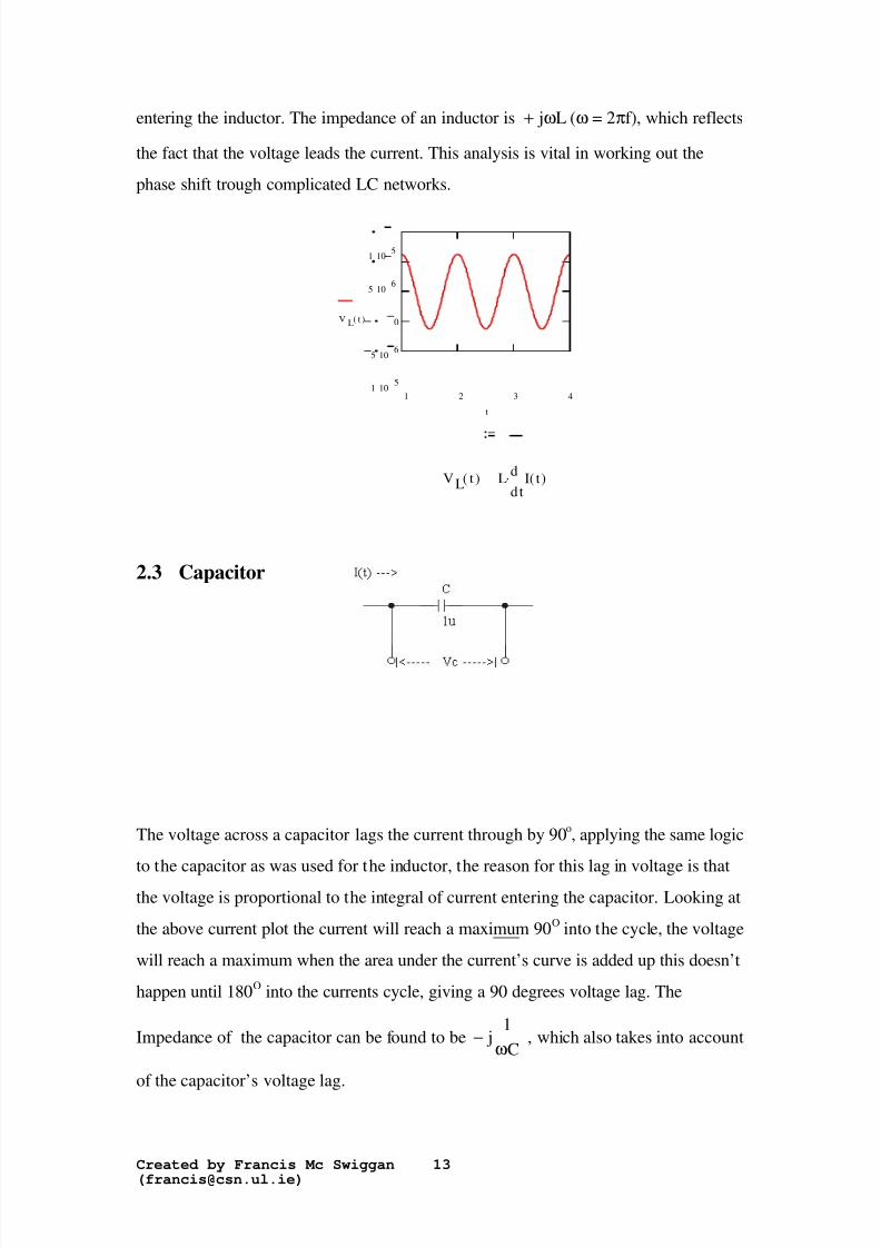
2.2 Inductor
The voltage across an inductor Leads the current through it by 90o
, this is due to thefact that the voltage across an inductor depends on the rate of change of current
8/20/2019 FM Xmtr Theory
http://slidepdf.com/reader/full/fm-xmtr-theory 21/95
Created by Francis Mc Swiggan([email protected])
13
entering the inductor. The impedance of an inductor is+ j Lω (ω = 2πf), which reflects
the fact that the voltage leads the current. This analysis is vital in working out thephase shift trough complicated LC networks.
1 2 3 41 10 5
5 10 6
0
5 10 6
1 10 5
V L( )t
t
VL( )t .L ddt
I( )t
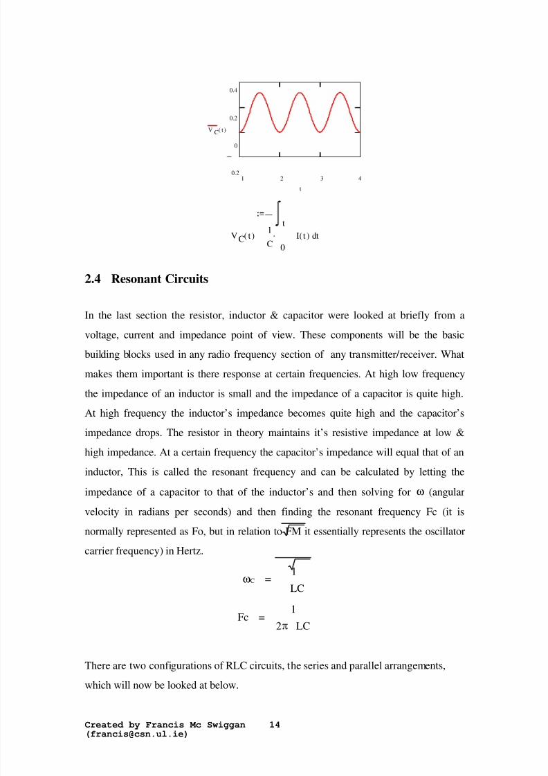
2.3 Capacitor
The voltage across a capacitor lags the current through by 90o, applying the same logic
to the capacitor as was used for the inductor, the reason for this lag in voltage is thatthe voltage is proportional to the integral of current entering the capacitor. Looking atthe above current plot the current will reach a maximum 90O into the cycle, the voltagewill reach a maximum when the area under the current’s curve is added up this doesn’thappen until 180O into the currents cycle, giving a 90 degrees voltage lag. The
Impedance of the capacitor can be found to be− j1Cω , which also takes into account
of the capacitor’s voltage lag.
8/20/2019 FM Xmtr Theory
http://slidepdf.com/reader/full/fm-xmtr-theory 22/95
Created by Francis Mc Swiggan([email protected])
14
1 2 3 40.2
0
0.2
0.4
V C( )t
t
VC( )t .1C
d0
ttI( )t
2.4 Resonant Circuits
In the last section the resistor, inductor & capacitor were looked at briefly from avoltage, current and impedance point of view. These components will be the basicbuilding blocks used in any radio frequency section of any transmitter/receiver. Whatmakes them important is there response at certain frequencies. At high low frequencythe impedance of an inductor is small and the impedance of a capacitor is quite high.
At high frequency the inductor’s impedance becomes quite high and the capacitor’simpedance drops. The resistor in theory maintains it’s resistive impedance at low &high impedance. At a certain frequency the capacitor’s impedance will equal that of aninductor, This is called the resonant frequency and can be calculated by letting the
impedance of a capacitor to that of the inductor’s and then solving forω (angular
velocity in radians per seconds) and then finding the resonant frequency Fc (it isnormally represented as Fo, but in relation to FM it essentially represents the oscillatorcarrier frequency) in Hertz.
ωC1LC
=
Fc =LC
12π
There are two configurations of RLC circuits, the series and parallel arrangements,
which will now be looked at below.
8/20/2019 FM Xmtr Theory
http://slidepdf.com/reader/full/fm-xmtr-theory 23/95
Created by Francis Mc Swiggan([email protected])
15
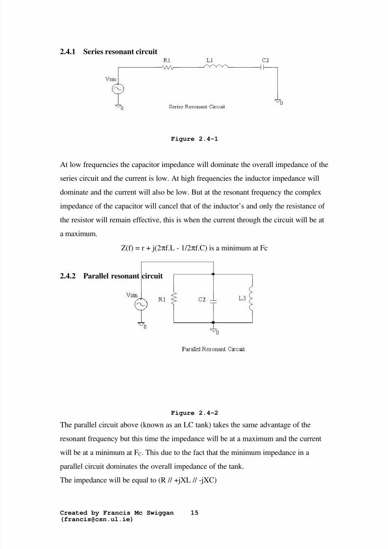
2.4.1 Series resonant circuit
Figure 2.4-1
At low frequencies the capacitor impedance will dominate the overall impedance of theseries circuit and the current is low. At high frequencies the inductor impedance will
dominate and the current will also be low. But at the resonant frequency the compleximpedance of the capacitor will cancel that of the inductor’s and only the resistance of the resistor will remain effective, this is when the current through the circuit will be ata maximum.
Z(f) = r + j(2πf.L - 1/2πf.C) is a minimum at Fc
2.4.2 Parallel resonant circuit
Figure 2.4-2
The parallel circuit above (known as an LC tank) takes the same advantage of theresonant frequency but this time the impedance will be at a maximum and the currentwill be at a minimum at FC. This due to the fact that the minimum impedance in aparallel circuit dominates the overall impedance of the tank.
The impedance will be equal to (R // +jXL // -jXC)

8/20/2019 FM Xmtr Theory
http://slidepdf.com/reader/full/fm-xmtr-theory 24/95
Created by Francis Mc Swiggan([email protected])
16
Z =R
1 + jRL LCω ω−
1
now substitutingωCLC
2 1= , cross multiply and bring the commonωO out of the
brackets to get the impedance as a function frequency.
Z( ) =R
1 + jRLC C
Cω
ωωω
ωω
−
now with the substitution andωO = 2πfo, the parallel impedance at any frequency can
be found. A factor called the Q factor can be introduced which is equal to R/ ωOL .
Z(f) =R
1 + jQf f
f f C
C−
at frequencies above resonance f >> f C the above equation evaluates to
Z(f) = jR.f Q f
C−
1
Which is capacitive.At frequencies above resonance f << f C the above equation evaluates to
Z(f) = jR
Q.f f C
+
Which is inductive impedanceAt resonance the complex component under the line will be zero, yielding a real valueof R which is purely resistive.
8/20/2019 FM Xmtr Theory
http://slidepdf.com/reader/full/fm-xmtr-theory 25/95
Created by Francis Mc Swiggan([email protected])
17
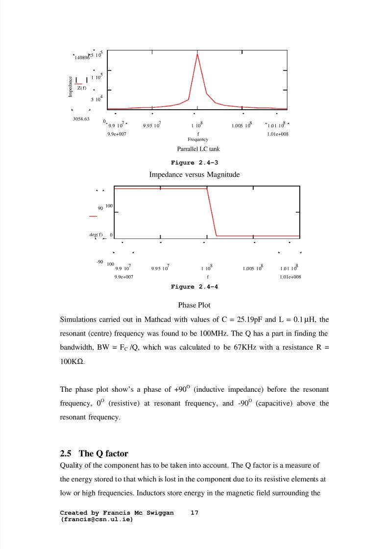
9.9 107 9.95 107 1 108 1.005 108 1.01 1080
5 104
1 105
1.5 105
Parrallel LC tankFrequency
I m p e d a n c e
140896
3058.63
Z( )f
1.01e+0089.9e+007 f
Figure 2.4-3
Impedance versus Magnitude
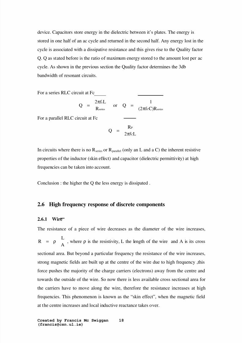
9.9 107 9.95 107 1 108 1.005 108 1.01 108100
0
10090
-90
deg( )f
1.01e+0089.9e+007 f
Figure 2.4-4
Phase Plot
Simulations carried out in Mathcad with values of C = 25.19pF and L = 0.1µH, the
resonant (centre) frequency was found to be 100MHz. The Q has a part in finding thebandwidth, BW = FC /Q, which was calculated to be 67KHz with a resistance R =
100KΩ.
The phase plot show’s a phase of +90O (inductive impedance) before the resonantfrequency, 0O (resistive) at resonant frequency, and -90O (capacitive) above theresonant frequency.
2.5 The Q factorQuality of the component has to be taken into account. The Q factor is a measure of
the energy stored to that which is lost in the component due to its resistive elements atlow or high frequencies. Inductors store energy in the magnetic field surrounding the
8/20/2019 FM Xmtr Theory
http://slidepdf.com/reader/full/fm-xmtr-theory 26/95
Created by Francis Mc Swiggan([email protected])
18
device. Capacitors store energy in the dielectric between it’s plates. The energy isstored in one half of an ac cycle and returned in the second half. Any energy lost in thecycle is associated with a dissipative resistance and this gives rise to the Quality factor
Q. Q as stated before is the ratio of maximum energy stored to the amount lost per accycle. As shown in the previous section the Quality factor determines the 3dbbandwidth of resonant circuits.
For a series RLC circuit at Fc
Q2 f LR
C
series= π or Q (2 f C)RC series
=1
π
For a parallel RLC circuit at Fc Q
R2 f L
P
C= π
In circuits where there is no Rseries or Rparallel (only an L and a C) the inherent resistiveproperties of the inductor (skin effect) and capacitor (dielectric permittivity) at highfrequencies can be taken into account.
Conclusion : the higher the Q the less energy is dissipated .
2.6 High frequency response of discrete components
2.6.1 Wire
The resistance of a piece of wire decreases as the diameter of the wire increases,
R LA= ρ , whereρ is the resistivity, L the length of the wire and A is its cross
sectional area. But beyond a particular frequency the resistance of the wire increases,strong magnetic fields are built up at the centre of the wire due to high frequency ,thisforce pushes the majority of the charge carriers (electrons) away from the centre andtowards the outside of the wire. So now there is less available cross sectional area forthe carriers have to move along the wire, therefore the resistance increases at highfrequencies. This phenomenon is known as the “skin effect”, when the magnetic fieldat the centre increases and local inductive reactance takes over.
8/20/2019 FM Xmtr Theory
http://slidepdf.com/reader/full/fm-xmtr-theory 27/95
Created by Francis Mc Swiggan([email protected])
19
Analysing the skin effect further, it is understood that AC current distributes itself across the cross sectional area of the wire in a parabolic shape, simply put means thatthe majority of the carrier lie in the outside, while few remain at the centre of the wire.
The outside region where most of the electrons reside can be defined as the distance infrom the outside where the number of electrons has dropped to (2.7183)-1 = 36.8 % of the electrons on the outside.
2.6.2 Inductor
Since wire is the main ingredient of inductors and since the resistance of wire increaseswith increasing frequency, therefore the losses of an inductor will increase with
increasing frequency ( as characteristic resistance increases). The amount of loss for agiven inductor through dissipation the inverse of the Q factor.
Dissipation = QR2 fL
-1 series= π
Therefore, since Rseries increases with frequency, therefore the Q factor will decrease
with increasing frequency. Initially, the Q factor of the inductor increases at the samerate as the frequency changes and this continues as long as the series resistanceremains at the DC value. Then, at some frequency that depends on the wire diameterand also on the manner of the windings, the Skin effect sets in and the series resistancestarts to climb. However not at the same rate as the frequency does, and so the Qcontinues to rise, but not as steeply as before. As the frequency increases further, astray capacitance begins to build up between adjacent turns. Along with the inductance
a parallel resonant circuit is formed and the resulting resonant frequency causes the Qfactor to start decreasing.
2.6.3 Capacitor
The resistive element in a capacitor at a high frequency is brought about by thematerial in between the plates of the capacitor, which inherently controls thepermittivity and then also the conductive properties of the capacitor at high
frequencies. The dissipation factor of the capacitor is also the inversely associated with
8/20/2019 FM Xmtr Theory
http://slidepdf.com/reader/full/fm-xmtr-theory 28/95
Created by Francis Mc Swiggan([email protected])
20
the Q factor. The efficiency in capacitors at high frequencies are generally better thanthe inductor as regards the Q factor, but other considerations such as the added seriesinductance of the leads and the internal capacitor plates will greatly effect the
efficiency of the capacitor. Good RF techniques are usually used to combat this bykeeping the leads short when soldering a capacitor into a circuit.
2.7 Temperature stability of the Tank
The temperature coefficient (TC) of a device is the relative change in one of itsparameters per degree Celsius or Kelvin. The units are usually in parts variation permillion per degrees Celsius (ppm/ OC). Taking the case of an oscillator (with an LC
tank) the TC is the fractional change of frequency over the centre frequency per 1O
Ctemperature change. Usually the TC for any given component or system is given, tofind the change in frequency for a given temperature change, simply multiply the TC bythe temperature change and the centre frequency (frequency the oscillator should berunning at).
∆ ∆fcfc TC x T=
An oscillator will always change frequency due to temperature change, because itscomponents have non-zero temperature coefficients. The most likely offender would
be the capacitor. The capacitance is normally worked out by C = (ε.A) / d, whereε is
the permittivity of the dielectric between a capacitor’s plates, A is the common surfacearea that the plates overlap across the dielectric and d is the distance between theplates. One of the best tuning capacitors available is the silvered mica capacitor (oftencalled the chocolate drop, because of it’s smooth brown oval appearance). The
variation of centre frequency of an oscillator will now be looked at with respect withcapacitance change.
( )fc =1
2 LCπ12 , now differentiate with respect to C and then solve for dfc by
multiplying across by dC. Then dividing across by fc will yielddfcfc
fcfc
CC= = −∆ ∆1
2 ,
if the capacitance change due to temperature or any other ageing effects is less than10%. Looking at the equation, it becomes apparent if a 2% increase in capacitanceoccurs, then a 1% decrease in centre frequency shall take place. This seems trivial but
8/20/2019 FM Xmtr Theory
http://slidepdf.com/reader/full/fm-xmtr-theory 29/95
8/20/2019 FM Xmtr Theory
http://slidepdf.com/reader/full/fm-xmtr-theory 30/95
Created by Francis Mc Swiggan([email protected])
22
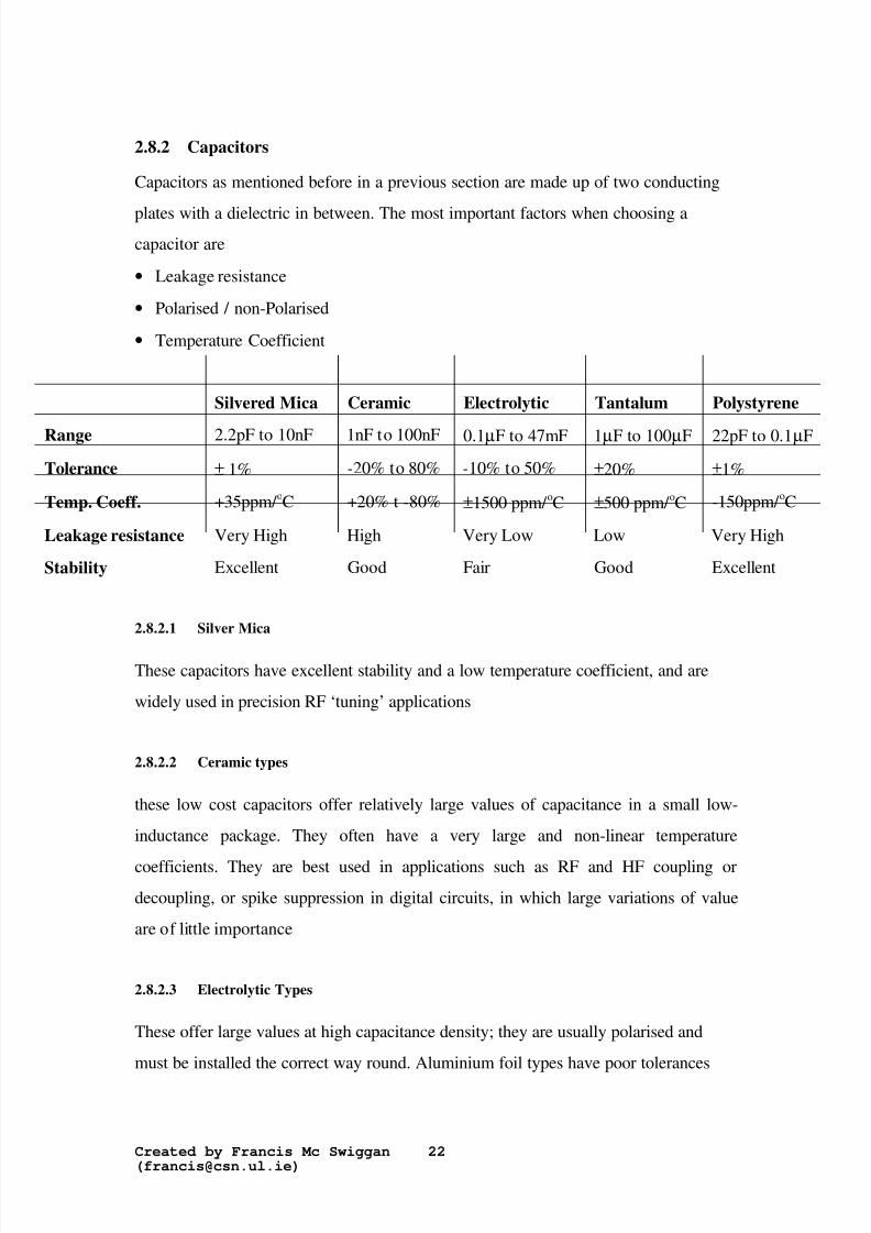
2.8.2 Capacitors
Capacitors as mentioned before in a previous section are made up of two conducting
plates with a dielectric in between. The most important factors when choosing acapacitor are
• Leakage resistance
• Polarised / non-Polarised
• Temperature Coefficient
Silvered Mica Ceramic Electrolytic Tantalum Polystyrene
Range 2.2pF to 10nF 1nF to 100nF0.1µF to 47mF 1µF to 100µF 22pF to 0.1µFTolerance ± 1% -20% to 80% -10% to 50% ±20% ±1%
Temp. Coeff. +35ppm/ oC +20% t -80% ±1500 ppm/ oC ±500 ppm/ oC -150ppm/ oC
Leakage resistance Very High High Very Low Low Very High
Stability Excellent Good Fair Good Excellent
2.8.2.1 Silver Mica
These capacitors have excellent stability and a low temperature coefficient, and arewidely used in precision RF ‘tuning’ applications
2.8.2.2 Ceramic types
these low cost capacitors offer relatively large values of capacitance in a small low-inductance package. They often have a very large and non-linear temperature
coefficients. They are best used in applications such as RF and HF coupling ordecoupling, or spike suppression in digital circuits, in which large variations of valueare of little importance
2.8.2.3 Electrolytic Types
These offer large values at high capacitance density; they are usually polarised andmust be installed the correct way round. Aluminium foil types have poor tolerances
8/20/2019 FM Xmtr Theory
http://slidepdf.com/reader/full/fm-xmtr-theory 31/95
Created by Francis Mc Swiggan([email protected])
23
and stability and are best used in low precision applications such as smoothing filtering,energy storage in PSU’s, and coupling and decoupling in audio circuits.2.8.2.4 Tantalum types
Offer good tolerance, excellent stability, low leakage, low inductance, and a very smallphysical size, and should be used in applications where these features are a positiveadvantage.
2.8.2.5 Poly Types
Of the four main ‘poly’ types of capacitor, polystyrene gives the best performance interms of overall precision and stability. Each of the others (polyester, polycarbonateand polypropylene) gives a roughly similar performance and is suitable for generalpurpose use. ‘Poly’ capacitors usually use a layered ‘Swiss-roll’ form of construction.Metallised film types are more compact that layered film-foil types, but have poorertolerances and pulse ratings than film-foil types. Metallised polyester types aresometimes known as ‘green-caps’
2.8.2.6 Trimmer capacitors
Polypropylene capacitors are ideal variable capacitors, a fact due to the polypropylenedielectric having a high insulation resistance with a low temperature coefficient. Thepolypropylene variable capacitor comes in a 5mm single turn package, which is suitablefor mounting directly on to a PCB. The typical range of capacitance involved would befrom 1.5pF to 50pF.
2.8.3 InductorsThere are two types of inductors that can be discussed, and they are
• Manufactured inductor
• Self made inductor
2.8.3.1 Manufactured inductor
When choosing an inductor from a manufacturer, the core in the coil and the over all Qfactor will have to be taken into account. The core should preferably be made of soft
8/20/2019 FM Xmtr Theory
http://slidepdf.com/reader/full/fm-xmtr-theory 32/95
Created by Francis Mc Swiggan([email protected])
24
ferrite which will in turn minimise the energy losses of the inductor and thereforeincrease the Q factor. The ferrite core can be adjusted to give a slight change ininductance2.8.3.2 Self Made inductor
Inductors can be easily wound around air cored formers, there are a number a variousmanufactured air cored formers on the market. Self made inductors are very usefulwhen a particular inductance is desired.
L Nd
18d +40b2
2
=
where L = inductance inµHd = diameter, in inchesb = coil length, inchesN = number of turns
( )N
L 18d + 40bd=
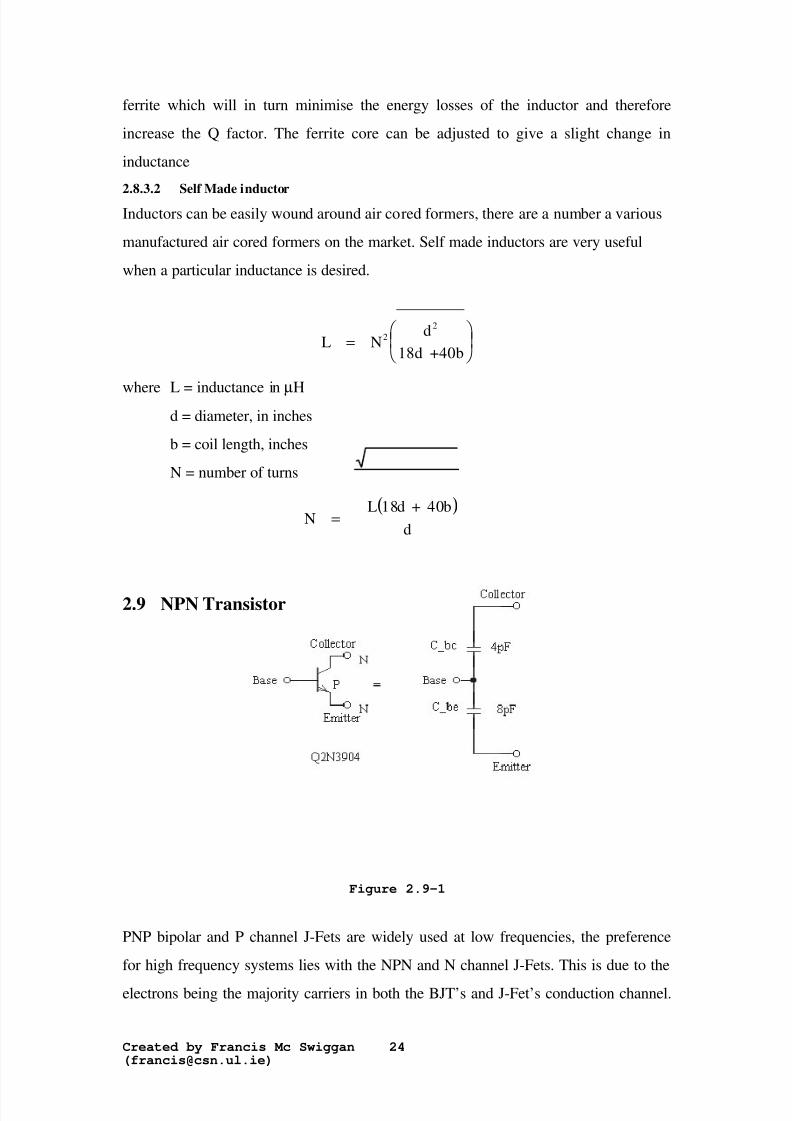
2.9 NPN Transistor
Figure 2.9-1
PNP bipolar and P channel J-Fets are widely used at low frequencies, the preferencefor high frequency systems lies with the NPN and N channel J-Fets. This is due to theelectrons being the majority carriers in both the BJT’s and J-Fet’s conduction channel.
8/20/2019 FM Xmtr Theory
http://slidepdf.com/reader/full/fm-xmtr-theory 33/95
Created by Francis Mc Swiggan([email protected])
25
The NPN BJT is the most commonly used and for the rest of this discussion will be thetransistor that will be focused on.
•
The bias current acts as a controlled flow source which steadily opens up thecollector emitter channel enabling charge carriers to flow, this can be analogous to a
slues gate, this rate of flow is controlled by the current gainβ = IC /IB .
• Transistors are non-linear especially when biased in the saturation region.
• The Input impedance drops as the biasing current being sinked to the collectorincreases.
• As the base current increases to allow more collector current through, the current
gainβ also increases.• The collector-emitter voltage has a maximum value that cannot be exceeded at an
instant in time.
2.9.1 High Frequency Response
The most interesting property is the junction capacitance from the base to emitter andbase-collector, the Figure 2.9-2 shows that for the 2N3904, the base-emitter
capacitance is larger than the base-collector, because of heavier extrinsic doping andit’s forward biasing the depletion region is naturally smaller than the base-collector’s.As the frequencies are increased the two capacitances will drop. Because thecapacitors are effectively in series, the smaller one dominates (base-collectorcapacitance). The capacitance is also influenced by the rate of change in base currentmagnitudes.
A resistance exists of typically in the order of tens of ohms at the base, this parasitic iscaused by impure contact between the base’s polysilicon to silicon junction. Thiscoupled with the r’e resistance and the current gain makes up the input resistance of
the transistor. Rin =β( Rbase + r’e) ; as stated previously the r’e will inevitably drop as
the frequency increases, therefore Rin (base) will inevitably be equal toβ( Rbase). This
makes the system rather unstable, as Rbase is essentially parasitic impedance. Toincrease stability RE, (which is normally RF bypassed), will have to be introduced.

8/20/2019 FM Xmtr Theory
http://slidepdf.com/reader/full/fm-xmtr-theory 34/95
8/20/2019 FM Xmtr Theory
http://slidepdf.com/reader/full/fm-xmtr-theory 35/95
Created by Francis Mc Swiggan([email protected])
27
DC Analysis
Voltage at the base, Vb =R2
R1+R2 Vcc
, Voltage at the Emitter, Ve = Vb - 0.7.
Emitter Current, Ie = Ve / (RE1 + RE2)≈ Ic, Voltage at collector, Vc = Vcc - (Ic.RC)
Voltage across the collector and emitter, Vce = Vc - Ve
AC Analysis
• Rin(base) = β(RE1 + r’e) ; Input Impedance, Rin = R1//R2//Rin(base).
• Output impedance , Rout = (RC // r’c) ; r’c >>RC, therefore Rout≈ RC.
• Voltage gain, Av = RC / (RE1 + r’e), note RE1 is not bypasses because it is moreindependent of temperature change than r’e and therefore increasing stabilityagainst temperature change.
• Current gain, Ai = IC / IB= β• Power Gain, Ap =Av * Ai
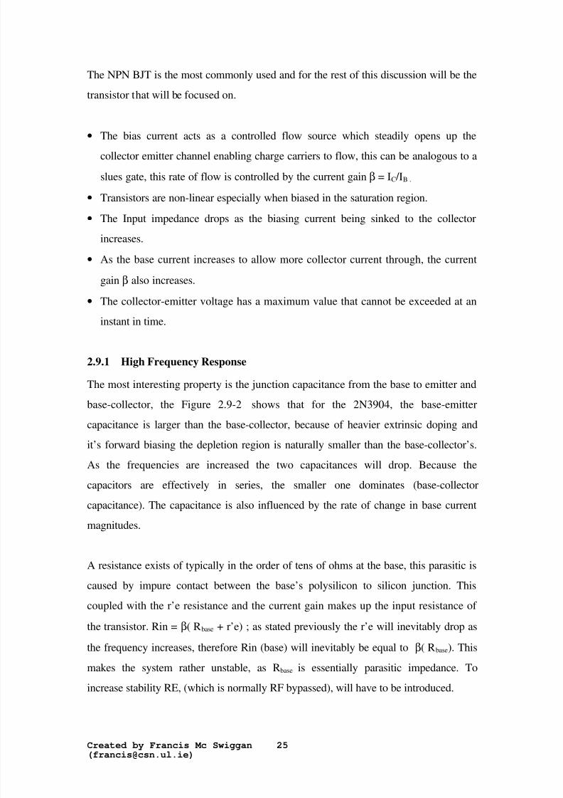
2.10.2 Common Collector (emitter follower)
Figure 2.10-2
DC analysis is similar to the common emitter.
8/20/2019 FM Xmtr Theory
http://slidepdf.com/reader/full/fm-xmtr-theory 36/95
Created by Francis Mc Swiggan([email protected])
28
AC Analysis
• Input impedance is the same as the common emitter.
• Output impedance, Rout =RE1 // r’e ; RE1 >> r’e⇒ Rout≈ r’e (quite low!)
• Voltage gain, Av = RE / (RE1 + r’e) ; RE1 >> r’e⇒ Av ≈ 1• Current Gain, Ai = IE / IB≈ β• Power Gain, Ap ; Same as common emitter.
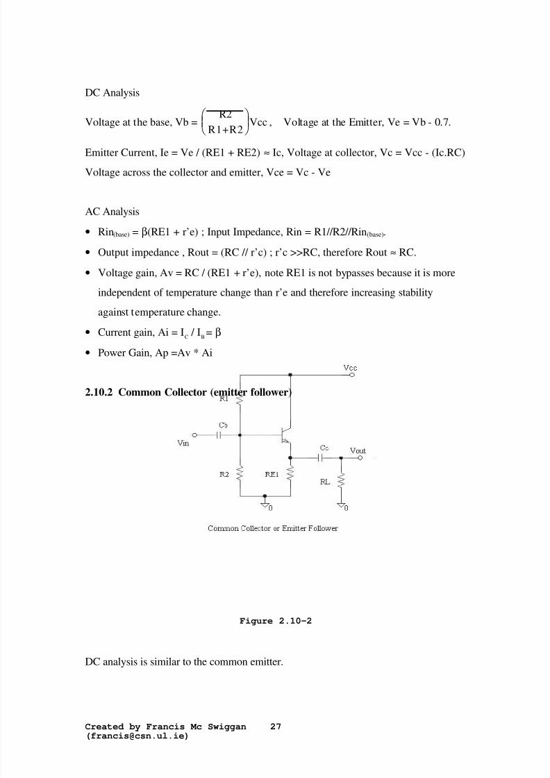
2.10.3 Common Base
Figure 2.10-3
DC analysis is similar to the common emitter.
AC Analysis
• Input Impedance, Rin =RE1 // r’e ; RE1 >> r’e⇒ Rout≈ r’e
• Output impedance, Rout = (RC // r’c) ; r’c >>RC, therefore Rout≈ RC.• Voltage gain, Av = RC / r’e
• Current Gain, Ai = IC / IE≈ 1
• Power Gain, Ap = Av * Ai≈ Av *1 ⇒ Ap ≈ Av.
8/20/2019 FM Xmtr Theory
http://slidepdf.com/reader/full/fm-xmtr-theory 37/95
Created by Francis Mc Swiggan([email protected])
29
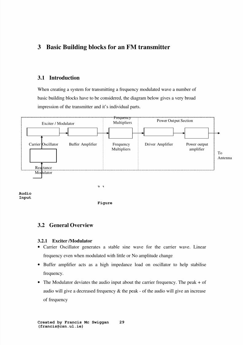
3 Basic Building blocks for an FM transmitter
3.1 Introduction
When creating a system for transmitting a frequency modulated wave a number of basic building blocks have to be considered, the diagram below gives a very broadimpression of the transmitter and it’s individual parts.
3.2 General Overview
3.2.1 Exciter /Modulator• Carrier Oscillator generates a stable sine wave for the carrier wave. Linearfrequency even when modulated with little or No amplitude change
• Buffer amplifier acts as a high impedance load on oscillator to help stabilisefrequency.
• The Modulator deviates the audio input about the carrier frequency. The peak + of audio will give a decreased frequency & the peak - of the audio will give an increaseof frequency
ToAntenna
Carrier Oscillator
ReactanceModulator
Buffer Amplifier FrequencyMultipliers
Driver Amplifier Power outputamplifier
Exciter / ModulatorFrequencyMultipliers Power Output Section
AudioInput
Figure
8/20/2019 FM Xmtr Theory
http://slidepdf.com/reader/full/fm-xmtr-theory 38/95
Created by Francis Mc Swiggan([email protected])
30
3.2.2 Frequency Multipliers
• Frequency multipliers tuned-input, tuned-output RF amplifiers. In which the outputresonance circuit is tuned to a multiple of the input .Commonly they are *2 *3*4 &
*5 .3.2.3 Power output section
• This develops the final carrier power to be transmitter.Also included here is an impedance matching network, in which the output impedanceis the same as that on the load (antenna).
3.3 The MicrophoneMicrophones are acoustic to electrical transducers. The four best known variations of these are the moving coil (‘dynamic’), ribbon, piezo-electric (‘crystal’), and electret(‘capacitor’). The electret type will be discussed because of there incredibly small sizeand high performance at audio frequencies.
A light weight metallised diaphragm forms one plate of a capacitor and the other plateis fixed, the capacitance thus varies in sympathy with the acoustic signal. Thecapacitance acquires a fixed charge, via a high value resistor (input impedance of FET)
and since the voltage across a capacitor is equal to its charge divided by its
+
GFet
Signal Out
Electret
MetallisedDiaphragm
Plastic Case Plastic Case
Plastic Case
1KΩ
1.5 V
4.7µF
Figure
8/20/2019 FM Xmtr Theory
http://slidepdf.com/reader/full/fm-xmtr-theory 39/95
Created by Francis Mc Swiggan([email protected])
31
capacitance, it will have a voltage output which is proportional to the incoming audio(baseband).
The fixed plate at the back is known as Electret which holds an electrostatic charge(dielectric) that is built in during manufacture and can be held for about 100 years. The
IGFET (needs to be powered by a 1.5 volt battery via a 1KΩ resistor) output is then
coupled to the output by an electrolytic capacitor.
3.4 Pre-emphasis
Improving the signal to noise ratio in FM can be achieved by filtering, but no amountof filtering will remove the noise from RF circuits. But noise control is achieved in thelow frequency (audio) amplifiers through the use of a high pass filter at the transmitter(pre-emphasis) and a low pass filter in receiver (de-emphasis) The measurable noise inlow- frequency electronic amplifiers is most pronounced over the frequency range 1 to2KHz. At the transmitter, the audio circuits are tailored to provide a higher level, thegreater the signal voltage yield, a better signal to noise ratio. At the receiver, when the
upper audio frequencies signals are attenuated t form a flat frequency response, theassociated noise level is also attenuated.
3.5 The Oscillator
The carrier oscillator is used to generate a stable sine-wave at the carrier frequency,when no modulating signal is applied to it . When fully modulated it must changefrequency linearly like a voltage controlled oscillator. At frequencies higher than 1MHz
a Colpitts (split capacitor configuration) or Hartley oscillator (split inductorconfiguration) may be deployed.
A parallel LC circuit is at the heart of the oscillator with an amplifier and a feedbacknetwork (positive feedback). The Barkhausen criteria of oscillation requires that theloop gain be unity and that the total phase shift through the system is 360o. I that wayan impulse or noise applied to the LC circuit is fed back and is amplified (due to the
8/20/2019 FM Xmtr Theory
http://slidepdf.com/reader/full/fm-xmtr-theory 40/95
Created by Francis Mc Swiggan([email protected])
32
fact that in practice the loop gain is slightly greater than unity) and sustains a ripple
through the network at a resonant frequency of 1LC2π
Hz.
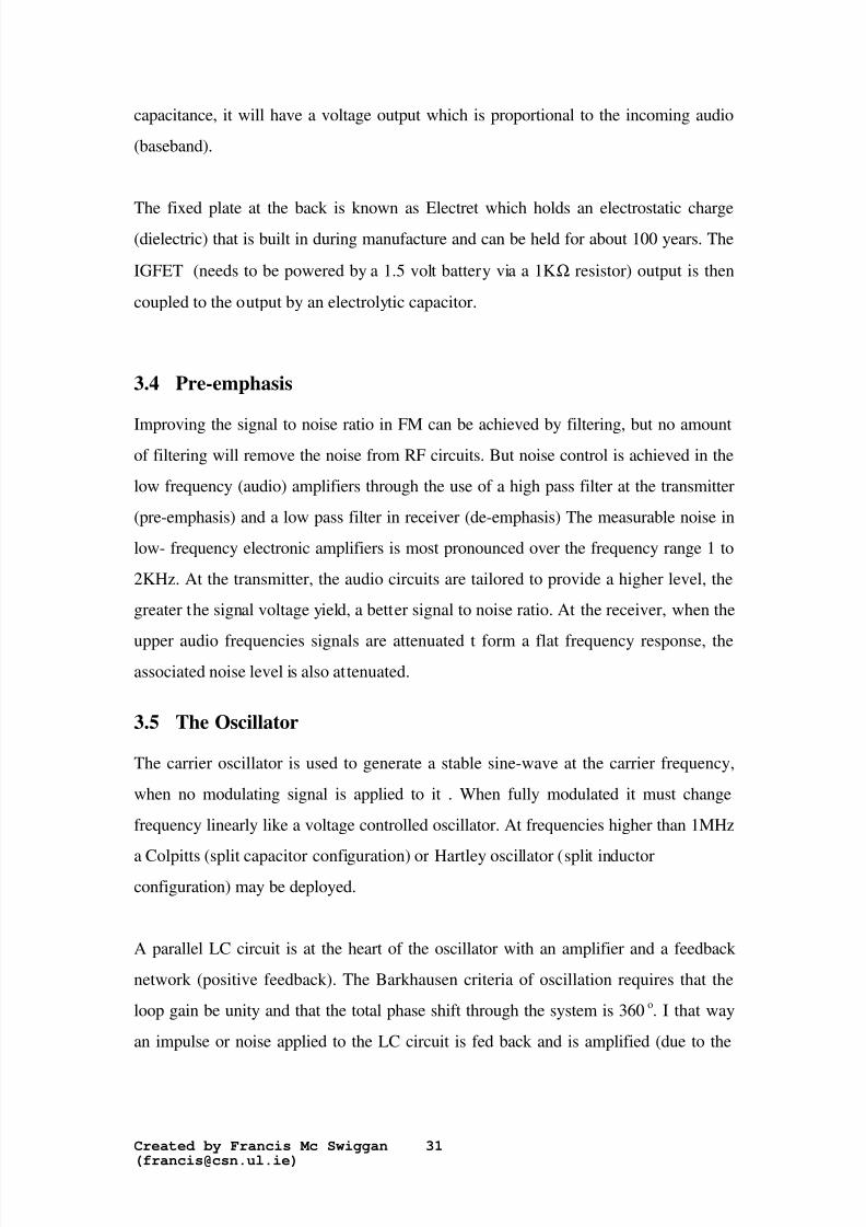
The Barkhausen criteria for sine-wave oscillation maybe deduced from the followingblock diagram
Figure 3.5-1
Condition for oscillation
xo + yo = 0o or 360o
Condition for Sine-wave generationA1 * A2 = 1
2
A2
Frequency selective network with gain A2Phase shift = yOat f O
A1
Amplifier with gain A1Phase shift = xOat f O
8/20/2019 FM Xmtr Theory
http://slidepdf.com/reader/full/fm-xmtr-theory 41/95
Created by Francis Mc Swiggan([email protected])
33
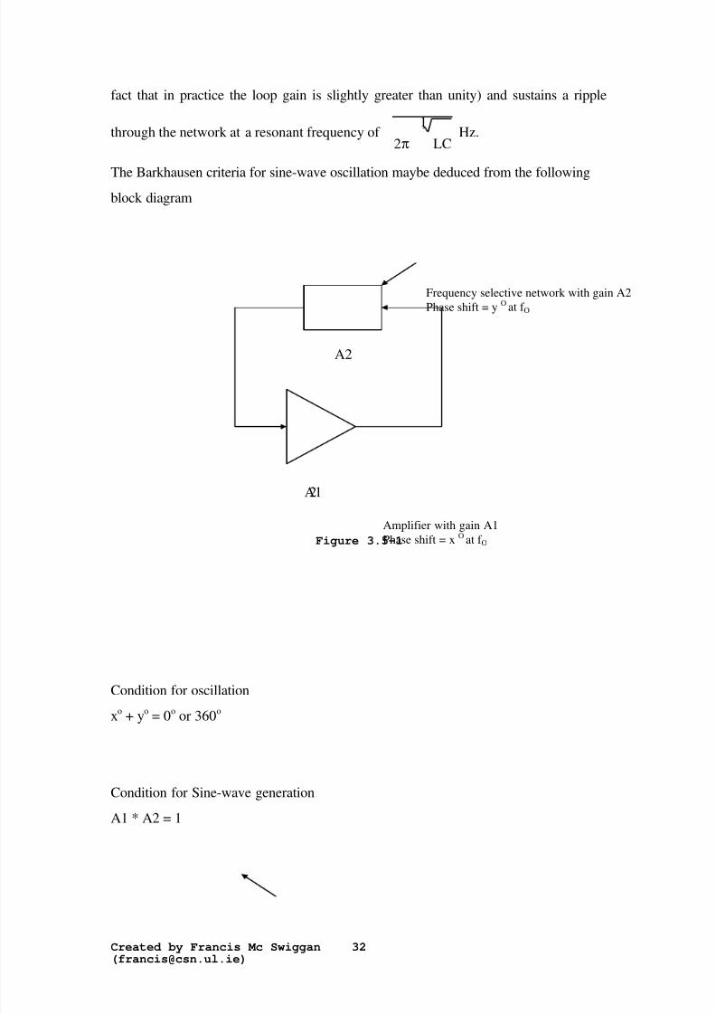
Figure 3.5-2
The above circuit diagram is an example of a colpitts oscillator, an LC (L1, C1 &C2)tank is shown here which is aided by a common emitter amplifier and a feedbackcapacitor (C_fb) which sustains oscillation. From the small signal analysis in order for
oscillation to Kick off and be sustained1C
C2=RL*Gm the frequency of the
oscillator is found to be 1LC*2π
, where C* is C2C1C2*C1
+.
3.6 Reactance modulator
The nature of FM as described before is that when the baseband signal is Zero thecarrier is at it’s “carrier” frequency, when it peaks the carrier deviation is at amaximum and when it troughs the deviation is at its minimum. This deviation is simplya quickening or slowing down of frequency around the carrier frequency by an amountproportional to the baseband signal. In order to convey the that characteristic of FMon the carrier wave the inductance or capacitance (of the tank) must be varied by the
baseband. Normally the capacitance of the tank is varied by a varactor diode. Thevaractor diode (seen below) when in reverse bias has a capacitance across it
8/20/2019 FM Xmtr Theory
http://slidepdf.com/reader/full/fm-xmtr-theory 42/95
Created by Francis Mc Swiggan([email protected])
34
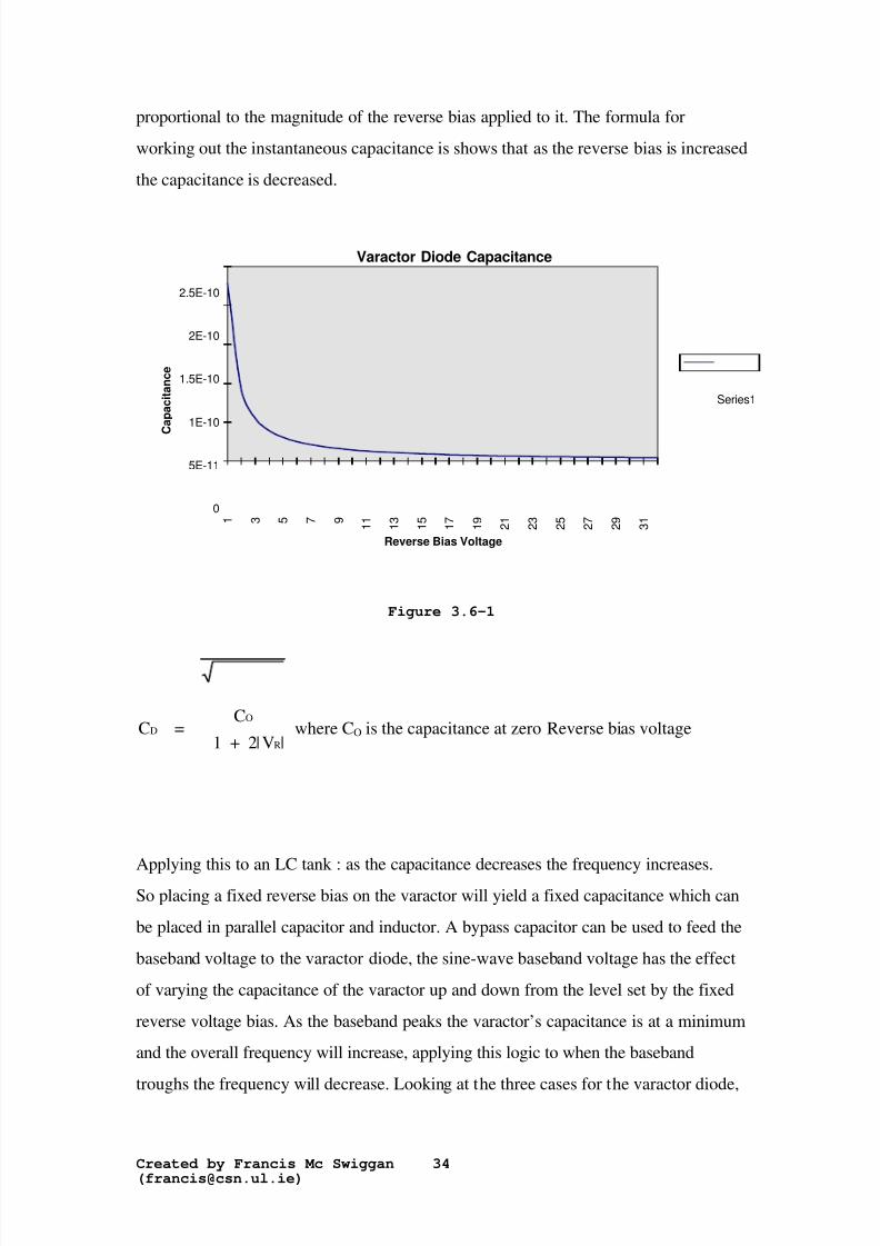
proportional to the magnitude of the reverse bias applied to it. The formula forworking out the instantaneous capacitance is shows that as the reverse bias is increasedthe capacitance is decreased.
Varactor Diode Capacitance
0
5E-11
1E-10
1.5E-10
2E-10
2.5E-10
1 3 5 7 9 1 1
1 3
1 5
1 7
1 9
2 1
2 3
2 5
2 7
2 9
3 1
Reverse Bias Voltage
C a p a c i t a n c e
Series1
Figure 3.6-1
C = C1 + 2|V |
DO
Rwhere CO is the capacitance at zero Reverse bias voltage
Applying this to an LC tank : as the capacitance decreases the frequency increases.So placing a fixed reverse bias on the varactor will yield a fixed capacitance which canbe placed in parallel capacitor and inductor. A bypass capacitor can be used to feed thebaseband voltage to the varactor diode, the sine-wave baseband voltage has the effectof varying the capacitance of the varactor up and down from the level set by the fixedreverse voltage bias. As the baseband peaks the varactor’s capacitance is at a minimumand the overall frequency will increase, applying this logic to when the baseband
troughs the frequency will decrease. Looking at the three cases for the varactor diode,
8/20/2019 FM Xmtr Theory
http://slidepdf.com/reader/full/fm-xmtr-theory 43/95
Created by Francis Mc Swiggan([email protected])
35
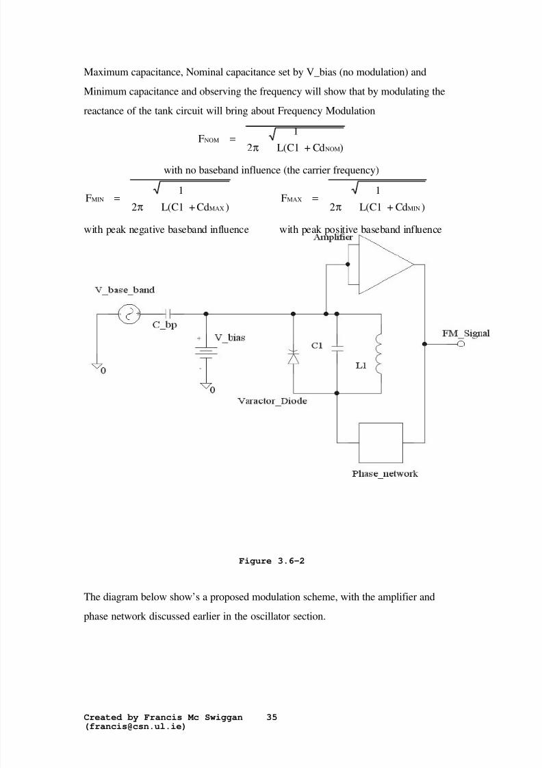
Maximum capacitance, Nominal capacitance set by V_bias (no modulation) andMinimum capacitance and observing the frequency will show that by modulating thereactance of the tank circuit will bring about Frequency Modulation
F 1L(C1 + Cd )NOM
NOM= 2π
with no baseband influence (the carrier frequency)
F 1L(C1 + Cd )
MINMAX
=2π
F 1L(C1 + Cd )
MAXMIN
=2π
with peak negative baseband influence with peak positive baseband influence
Figure 3.6-2
The diagram below show’s a proposed modulation scheme, with the amplifier andphase network discussed earlier in the oscillator section.

8/20/2019 FM Xmtr Theory
http://slidepdf.com/reader/full/fm-xmtr-theory 44/95
Created by Francis Mc Swiggan([email protected])
36
3.7 Buffer Amplifier
The buffer amplifier acts as a high input impedance with a low gain and low outputimpedance associated with it. The high input impedance prevents loading effects fromthe oscillator section, this high input impedance maybe looked upon as RL in theanalysis of the Colpitts Oscillator. The High impedance RL helped to stabilise theoscillators frequency.
Looking at the Buffer amplifier as an electronic block circuit, it may resemble a
common emitter with low voltage gain or simply an emitter follower transistorconfiguration.
Figure 3.7-1
3.8 Frequency Multipliers
Frequency modulation of the carrier by the baseband can be carried out with a highmodulation index, but this is prone to frequency drift of the LC tank, to combat thisdrift, modulation can take place at lower frequencies where the Q factor of the tankcircuit is quite high (i.e. low bandwidth or less carrier deviation) and the carrier can be
created by a crystal controlled oscillator. At low frequency deviations the crystal
8/20/2019 FM Xmtr Theory
http://slidepdf.com/reader/full/fm-xmtr-theory 45/95
Created by Francis Mc Swiggan([email protected])
37
oscillator can produce modulated signals that can keep an audio distortion under 1%.This narrow-band angle modulated wave can be then multiplied up to the requiredtransmission frequency, the deviation brought about by the baseband is also multiplied
up, which means that the percentage modulation and Q remain unchanged. Thisensures a higher performance system that can produce a carrier deviation of±75Khz.
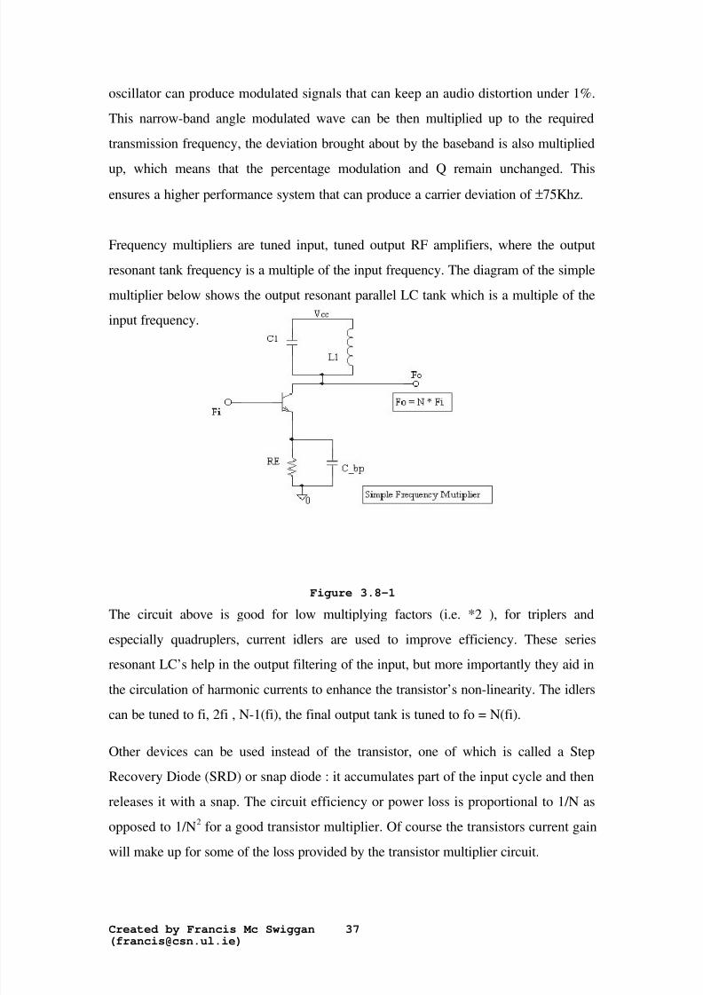
Frequency multipliers are tuned input, tuned output RF amplifiers, where the outputresonant tank frequency is a multiple of the input frequency. The diagram of the simplemultiplier below shows the output resonant parallel LC tank which is a multiple of theinput frequency.
Figure 3.8-1
The circuit above is good for low multiplying factors (i.e. *2 ), for triplers andespecially quadruplers, current idlers are used to improve efficiency. These seriesresonant LC’s help in the output filtering of the input, but more importantly they aid inthe circulation of harmonic currents to enhance the transistor’s non-linearity. The idlerscan be tuned to fi, 2fi , N-1(fi), the final output tank is tuned to fo = N(fi).
Other devices can be used instead of the transistor, one of which is called a StepRecovery Diode (SRD) or snap diode : it accumulates part of the input cycle and thenreleases it with a snap. The circuit efficiency or power loss is proportional to 1/N asopposed to 1/N2 for a good transistor multiplier. Of course the transistors current gainwill make up for some of the loss provided by the transistor multiplier circuit.
8/20/2019 FM Xmtr Theory
http://slidepdf.com/reader/full/fm-xmtr-theory 46/95
Created by Francis Mc Swiggan([email protected])
38
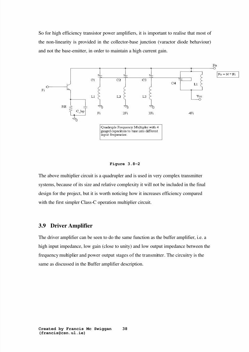
So for high efficiency transistor power amplifiers, it is important to realise that most of the non-linearity is provided in the collector-base junction (varactor diode behaviour)and not the base-emitter, in order to maintain a high current gain.
Figure 3.8-2
The above multiplier circuit is a quadrupler and is used in very complex transmitter
systems, because of its size and relative complexity it will not be included in the finaldesign for the project, but it is worth noticing how it increases efficiency comparedwith the first simpler Class-C operation multiplier circuit.
3.9 Driver Amplifier
The driver amplifier can be seen to do the same function as the buffer amplifier, i.e. a
high input impedance, low gain (close to unity) and low output impedance between thefrequency multiplier and power output stages of the transmitter. The circuitry is thesame as discussed in the Buffer amplifier description.
8/20/2019 FM Xmtr Theory
http://slidepdf.com/reader/full/fm-xmtr-theory 47/95
Created by Francis Mc Swiggan([email protected])
39
3.10 Power Output Amplifier
The power amplifier takes the energy drawn from the DC power supply and converts itto the AC signal power that is to be radiated. The efficiency or lack of it in mostamplifiers is affected by heat being dissipated in the transistor and surroundingcircuitry. For this reason , the final power amplifier is usually a Class-C amplifier forhigh powered modulation systems or just a Class B push-pull amplifier for use in alow-level power modulated transmitter. Therefore the choice of amplifier type dependsgreatly on the output power and intended range of the transmitter.
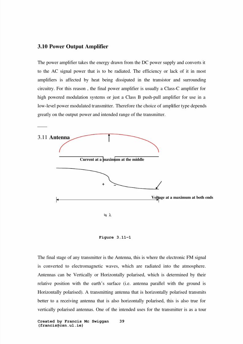
3.11 Antenna
The final stage of any transmitter is the Antenna, this is where the electronic FM signalis converted to electromagnetic waves, which are radiated into the atmosphere.Antennas can be Vertically or Horizontally polarised, which is determined by theirrelative position with the earth’s surface (i.e. antenna parallel with the ground isHorizontally polarised). A transmitting antenna that is horizontally polarised transmits
better to a receiving antenna that is also horizontally polarised, this is also true forvertically polarised antennas. One of the intended uses for the transmitter is as a tour
Figure 3.11-1
½ λ
+ -
Voltage at a maximum at both ends
Current at a maximum at the middle
8/20/2019 FM Xmtr Theory
http://slidepdf.com/reader/full/fm-xmtr-theory 48/95
Created by Francis Mc Swiggan([email protected])
40
guiding aid, where a walkman shall be used as the receiver, for a walkman thereceiving antenna is the co-axial shielding around the earphone wire. The earphonewire is normally left vertical, therefore a vertically polarised whip antenna will be the
chosen antenna for this particular application.
3.11.1 Radiation Resistance
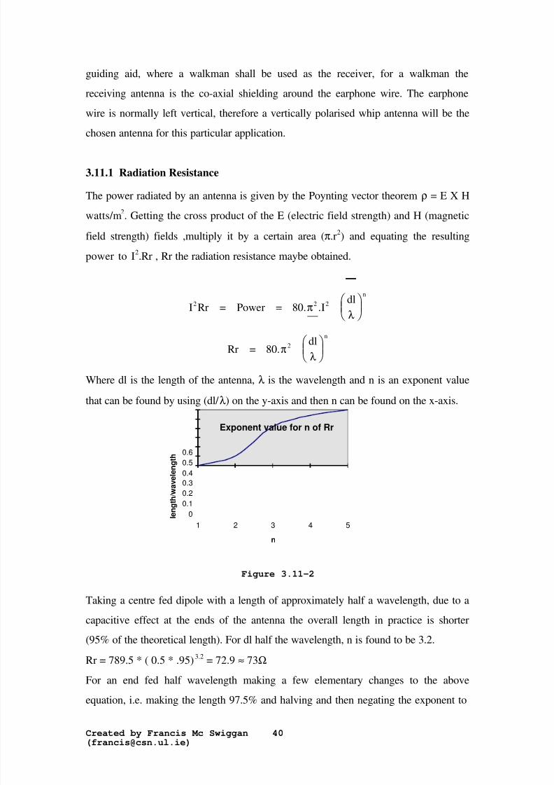
The power radiated by an antenna is given by the Poynting vector theoremρ = E X H
watts/m2. Getting the cross product of the E (electric field strength) and H (magnetic
field strength) fields ,multiply it by a certain area (π.r2) and equating the resulting
power to I2.Rr , Rr the radiation resistance maybe obtained.
I Rr = Power = 80. .Idl2 2 2
n
π λ
Rr = 80.dl2
n
π λ
Where dl is the length of the antenna,λ is the wavelength and n is an exponent value
that can be found by using (dl/ λ) on the y-axis and then n can be found on the x-axis.
Exponent value for n of Rr
0
0.1
0.2
0.3
0.4
0.5
0.6
1 2 3 4 5
n
l e n g t h / w a v e l e n g t h
Figure 3.11-2
Taking a centre fed dipole with a length of approximately half a wavelength, due to acapacitive effect at the ends of the antenna the overall length in practice is shorter(95% of the theoretical length). For dl half the wavelength, n is found to be 3.2.
Rr = 789.5 * ( 0.5 * .95)3.2 = 72.9≈ 73ΩFor an end fed half wavelength making a few elementary changes to the aboveequation, i.e. making the length 97.5% and halving and then negating the exponent to
8/20/2019 FM Xmtr Theory
http://slidepdf.com/reader/full/fm-xmtr-theory 49/95
Created by Francis Mc Swiggan([email protected])
41
give n = -1.6 which results in the radiation resistance equal to 789.5 * (0.5 * .975)-1.6
= 2492≈ 2.5KΩ
3.11.2 Power transferMaximum power transfer between the antenna and the electronics circuitry will have tobe looked at in order to produce an antenna that will be efficient in transmitting anaudio signal to a receiver. Taking the case of the receiver with an antenna of impedance Zin connected with the input terminal, which is terminated with a resistorRg. The maximum power transfer theorem shows that with a voltage induced in theantenna the current flowing into the receiver will be I = V / (Zin + Rg). The power
transferred will be I2 .Rg, differentiating the power with respect to Rg and letting the
derivative equal to Zero for max. power transfer, it is shown that Zin + Rg = 2Rg,which means that Rg will be equal to Zin.
3.11.3 Reciprocity
The theorem for reciprocity states that if an emf is applied to the terminals of a circuitA and produces a current in another circuit B, then the same emf applied to terminals
B, will produce the same current at the terminals of circuit A. Simply put means thatevery antenna will work equally well for transmitting and receiving. So applying thesame logic of max. power transfer at the receiver to a transmitter circuit, the outputimpedance of the transmitter must match the input impedance of the antenna, whichcan be taken as the radiation resistance of the antenna.
Now that a qualitative view of some of the characteristics of an antenna have been
looked at, it is now time to look at some of the basic types of antenna that can beconsidered for this project
8/20/2019 FM Xmtr Theory
http://slidepdf.com/reader/full/fm-xmtr-theory 50/95
Created by Francis Mc Swiggan([email protected])
42
3.11.4 Hertz Dipole
The Hertz Antenna provides the best transmission of electromagnetic waves above 2MHz, with a total length of ½ the wavelength of the transmitted wave.
Placing the + and - terminals in the middle of the antenna and ensuring that the
impedance at the terminals is high (typically 2500Ω) and the impedance at the open
ends is low ( 73Ω ). This will ensure that the voltage will be at a minimum at the
terminal and at a maximum at the ends, which will efficiently accept electrical energyand radiate it into space as electromagnetic waves. The gap at the centre of the antennais negligible for frequencies above 14Mhz.
3.11.5 Monopole or Marconi Antenna
Gugliemo Marconi opened a whole new area of experimentation by popularising thevertically polarised quarter wave dipole antenna, it was theorised that the earth wouldact as the second quarter wave dipole antenna. Comparing the signal emanating from
the quarter wave antenna inµV/m, it has been shown experimentally that for areduction in the antenna fromλ /2 to λ /4 a reduction of 40 % (inµV/m) takes place,
for a reductionλ /4 toλ /10 a reduction of only 5% (inµV/m). This slight reduction of
.05 in transmitted power for a decrease of .75 in antenna length seems impressive, buttheir is a decrease in the area of coverage.
When considering an antenna type and size for this project 2 things have to be taken
into account, the frequency of transmission and the portability of the antenna.
Transmitting in a frequency range of 88 to 108 MHz, the mean frequency is (88 *108)1/2 = 97.5MHZ. Rounding this off to 100MHz, calculating the wavelength gives
(3*108 / 100*106 ) yields a wavelength of approximately 3 metres.λ /2 = 1.5 m ;λ /4 =
.75m ;λ /10 = 30cm
The above analysis concludes that the use of an adjustable end fed whip antenna with
an affective length of 30 to 75 cm could be used with considerable affect.
8/20/2019 FM Xmtr Theory
http://slidepdf.com/reader/full/fm-xmtr-theory 51/95
Created by Francis Mc Swiggan([email protected])
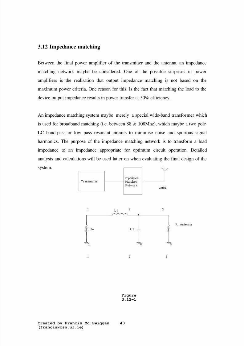
43
3.12 Impedance matching
Between the final power amplifier of the transmitter and the antenna, an impedancematching network maybe be considered. One of the possible surprises in poweramplifiers is the realisation that output impedance matching is not based on themaximum power criteria. One reason for this, is the fact that matching the load to thedevice output impedance results in power transfer at 50% efficiency.
An impedance matching system maybe merely a special wide-band transformer which
is used for broadband matching (i.e. between 88 & 108Mhz), which maybe a two poleLC band-pass or low pass resonant circuits to minimise noise and spurious signalharmonics. The purpose of the impedance matching network is to transform a loadimpedance to an impedance appropriate for optimum circuit operation. Detailedanalysis and calculations will be used latter on when evaluating the final design of thesystem.
Figure3.12-1
8/20/2019 FM Xmtr Theory
http://slidepdf.com/reader/full/fm-xmtr-theory 52/95
Created by Francis Mc Swiggan([email protected])
44
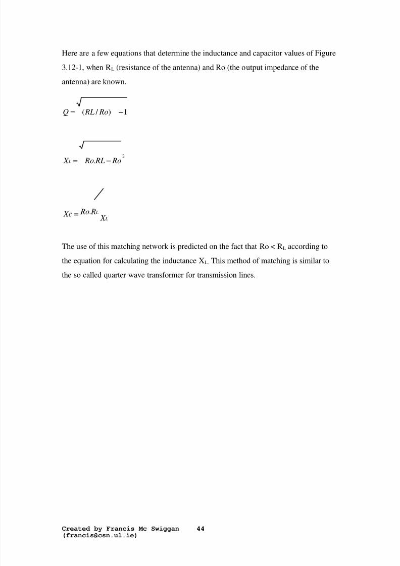
Here are a few equations that determine the inductance and capacitor values of Figure3.12-1, when RL (resistance of the antenna) and Ro (the output impedance of theantenna) are known.
1) / ( −= Ro RLQ
2. Ro RL Ro X L −=
L L
X R Ro Xc .=
The use of this matching network is predicted on the fact that Ro < RL according tothe equation for calculating the inductance XL. This method of matching is similar tothe so called quarter wave transformer for transmission lines.
8/20/2019 FM Xmtr Theory
http://slidepdf.com/reader/full/fm-xmtr-theory 53/95
8/20/2019 FM Xmtr Theory
http://slidepdf.com/reader/full/fm-xmtr-theory 54/95
Created by Francis Mc Swiggan([email protected])
46
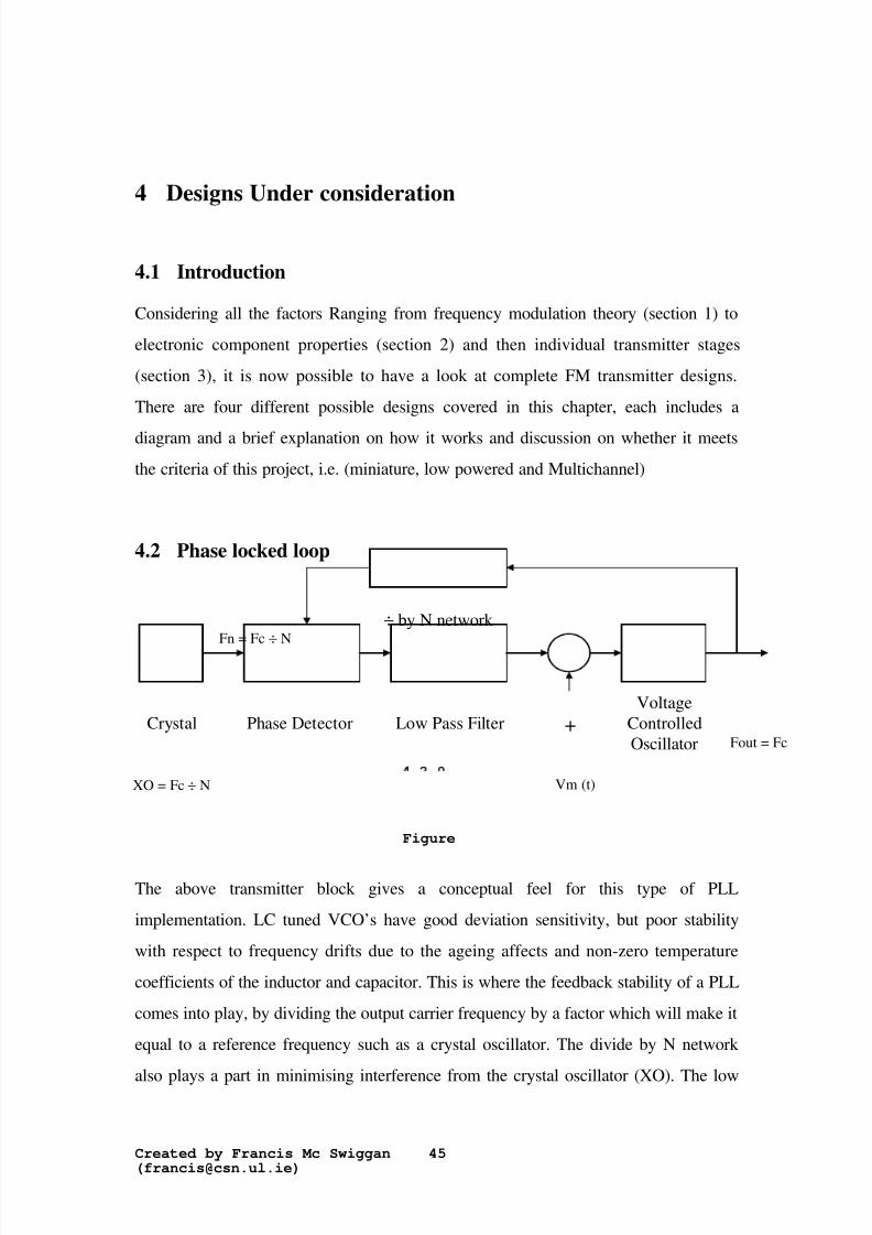
pass filter prevents feedback of modulated frequencies and eliminates the possibility of the loop locking to a side band.The overall system is quite stabile, which is good, but the circuitry involved is quite
large even if the devices were all integrated circuits it still would be quite bulky andrather complicated. The complication would be in making the system multi-channelled.For multi-channel capability it would mean changing the divide by N factor andincluding another block to change the reference frequency XO to equal that of thefeedback network in order for the tracking of phase to be possible when the VCOdrifts from its centre frequency.
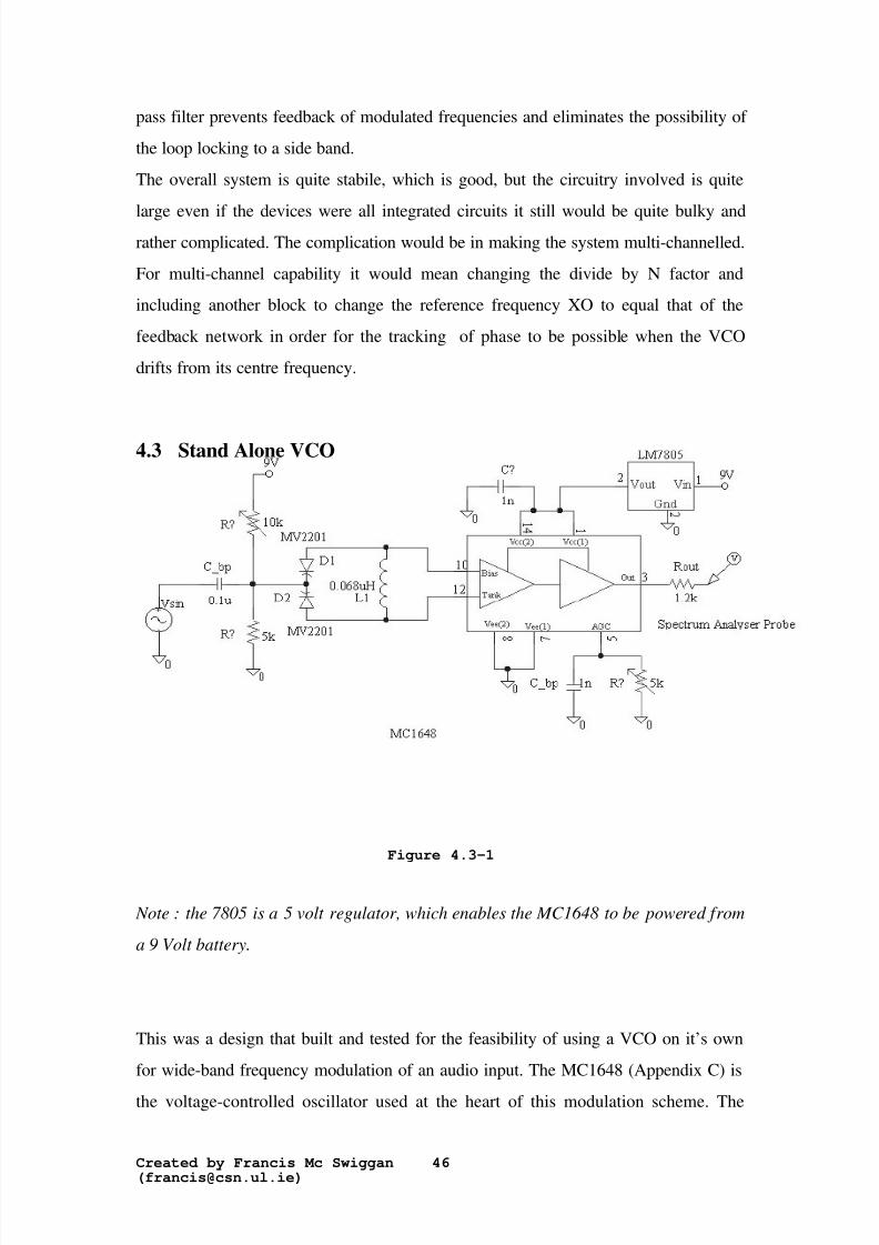
4.3 Stand Alone VCO
Figure 4.3-1
Note : the 7805 is a 5 volt regulator, which enables the MC1648 to be powered from
a 9 Volt battery.
This was a design that built and tested for the feasibility of using a VCO on it’s ownfor wide-band frequency modulation of an audio input. The MC1648 (Appendix C) isthe voltage-controlled oscillator used at the heart of this modulation scheme. The
8/20/2019 FM Xmtr Theory
http://slidepdf.com/reader/full/fm-xmtr-theory 55/95
Created by Francis Mc Swiggan([email protected])
47
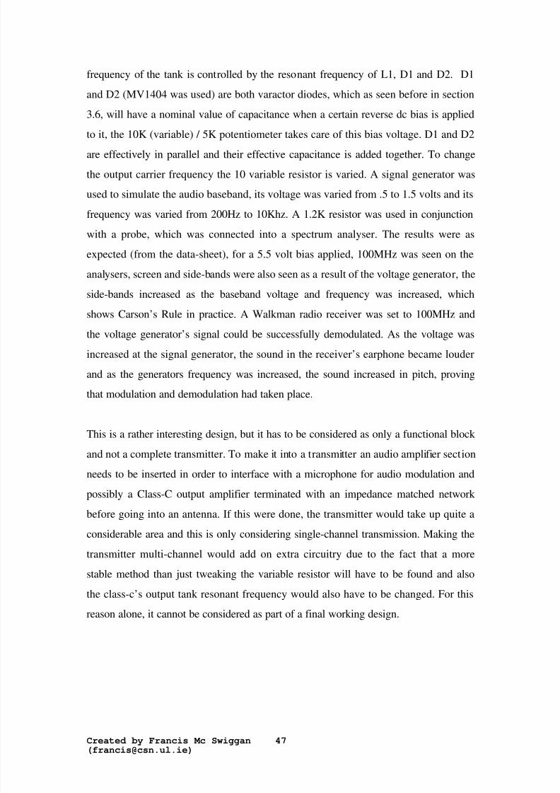
frequency of the tank is controlled by the resonant frequency of L1, D1 and D2. D1and D2 (MV1404 was used) are both varactor diodes, which as seen before in section3.6, will have a nominal value of capacitance when a certain reverse dc bias is applied
to it, the 10K (variable) / 5K potentiometer takes care of this bias voltage. D1 and D2are effectively in parallel and their effective capacitance is added together. To changethe output carrier frequency the 10 variable resistor is varied. A signal generator wasused to simulate the audio baseband, its voltage was varied from .5 to 1.5 volts and itsfrequency was varied from 200Hz to 10Khz. A 1.2K resistor was used in conjunctionwith a probe, which was connected into a spectrum analyser. The results were asexpected (from the data-sheet), for a 5.5 volt bias applied, 100MHz was seen on the
analysers, screen and side-bands were also seen as a result of the voltage generator, theside-bands increased as the baseband voltage and frequency was increased, whichshows Carson’s Rule in practice. A Walkman radio receiver was set to 100MHz andthe voltage generator’s signal could be successfully demodulated. As the voltage wasincreased at the signal generator, the sound in the receiver’s earphone became louderand as the generators frequency was increased, the sound increased in pitch, provingthat modulation and demodulation had taken place.
This is a rather interesting design, but it has to be considered as only a functional blockand not a complete transmitter. To make it into a transmitter an audio amplifier sectionneeds to be inserted in order to interface with a microphone for audio modulation andpossibly a Class-C output amplifier terminated with an impedance matched networkbefore going into an antenna. If this were done, the transmitter would take up quite aconsiderable area and this is only considering single-channel transmission. Making the
transmitter multi-channel would add on extra circuitry due to the fact that a morestable method than just tweaking the variable resistor will have to be found and alsothe class-c’s output tank resonant frequency would also have to be changed. For thisreason alone, it cannot be considered as part of a final working design.
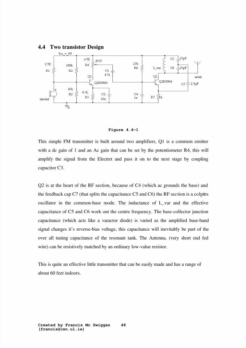
8/20/2019 FM Xmtr Theory
http://slidepdf.com/reader/full/fm-xmtr-theory 56/95
Created by Francis Mc Swiggan([email protected])
48
4.4 Two transistor Design
Figure 4.4-1
This simple FM transmitter is built around two amplifiers, Q1 is a common emitterwith a dc gain of 1 and an Ac gain that can be set by the potentiometer R4, this willamplify the signal from the Electret and pass it on to the next stage by couplingcapacitor C3.
Q2 is at the heart of the RF section, because of C4 (which ac grounds the base) andthe feedback cap C7 (that splits the capacitance C5 and C6) the RF section is a colpittsoscillator in the common-base mode. The inductance of L_var and the effectivecapacitance of C5 and C6 work out the centre frequency. The base-collector junctioncapacitance (which acts like a varactor diode) is varied as the amplified base-bandsignal changes it’s reverse-bias voltage, this capacitance will inevitably be part of theover all tuning capacitance of the resonant tank. The Antenna, (very short end fed
wire) can be resistively matched by an ordinary low-value resistor.
This is quite an effective little transmitter that can be easily made and has a range of about 60 feet indoors.
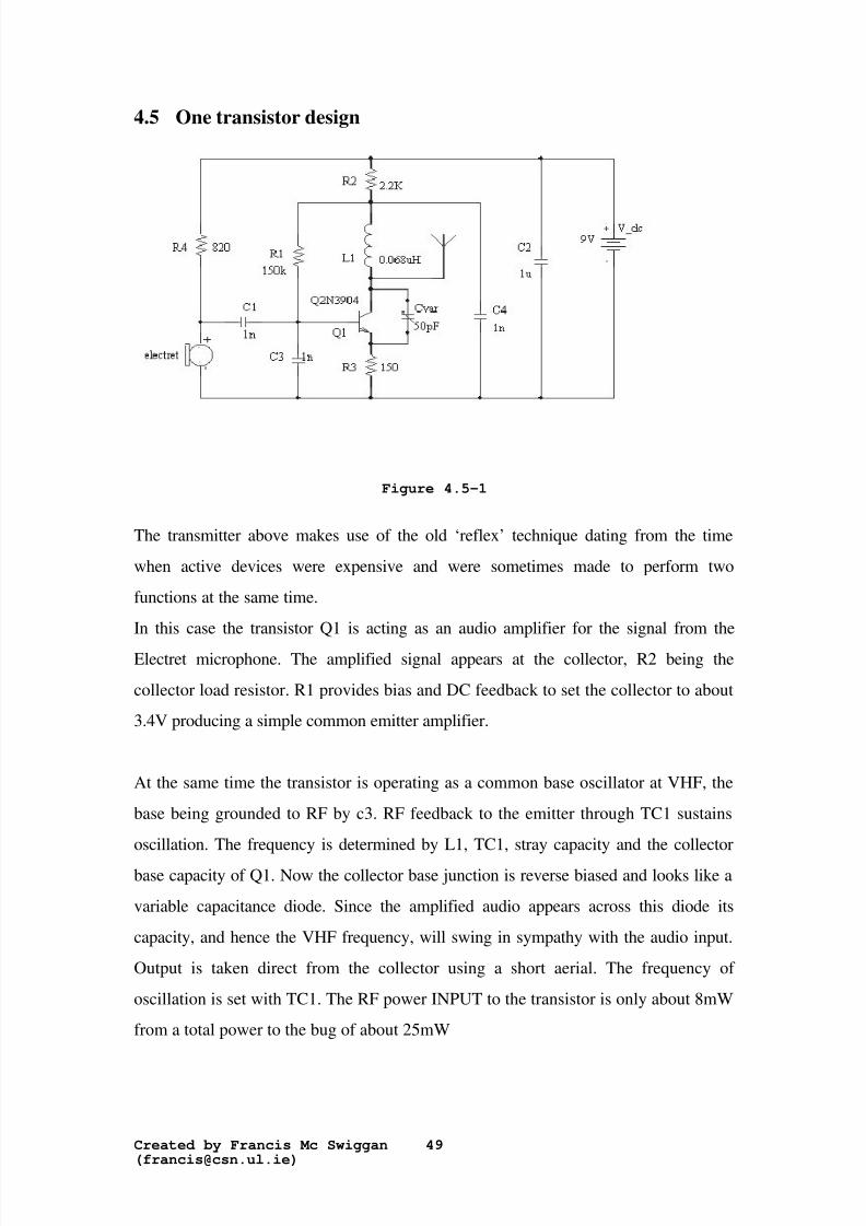
8/20/2019 FM Xmtr Theory
http://slidepdf.com/reader/full/fm-xmtr-theory 57/95
Created by Francis Mc Swiggan([email protected])
49
4.5 One transistor design
Figure 4.5-1
The transmitter above makes use of the old ‘reflex’ technique dating from the timewhen active devices were expensive and were sometimes made to perform twofunctions at the same time.In this case the transistor Q1 is acting as an audio amplifier for the signal from theElectret microphone. The amplified signal appears at the collector, R2 being thecollector load resistor. R1 provides bias and DC feedback to set the collector to about3.4V producing a simple common emitter amplifier.
At the same time the transistor is operating as a common base oscillator at VHF, thebase being grounded to RF by c3. RF feedback to the emitter through TC1 sustainsoscillation. The frequency is determined by L1, TC1, stray capacity and the collectorbase capacity of Q1. Now the collector base junction is reverse biased and looks like avariable capacitance diode. Since the amplified audio appears across this diode itscapacity, and hence the VHF frequency, will swing in sympathy with the audio input.Output is taken direct from the collector using a short aerial. The frequency of oscillation is set with TC1. The RF power INPUT to the transistor is only about 8mWfrom a total power to the bug of about 25mW
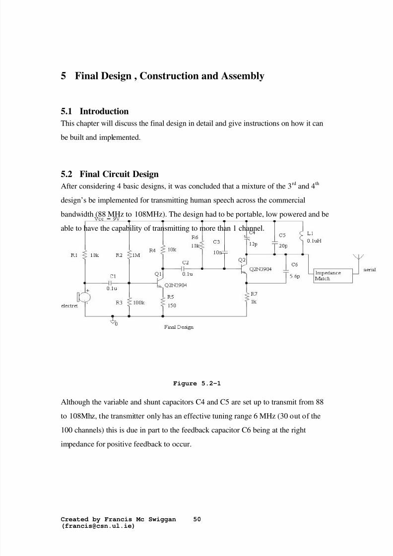
8/20/2019 FM Xmtr Theory
http://slidepdf.com/reader/full/fm-xmtr-theory 58/95
Created by Francis Mc Swiggan([email protected])
50
5 Final Design , Construction and Assembly
5.1 IntroductionThis chapter will discuss the final design in detail and give instructions on how it canbe built and implemented.
5.2 Final Circuit DesignAfter considering 4 basic designs, it was concluded that a mixture of the 3rd and 4th
design’s be implemented for transmitting human speech across the commercialbandwidth (88 MHz to 108MHz). The design had to be portable, low powered and beable to have the capability of transmitting to more than 1 channel.
Figure 5.2-1
Although the variable and shunt capacitors C4 and C5 are set up to transmit from 88to 108Mhz, the transmitter only has an effective tuning range 6 MHz (30 out of the100 channels) this is due in part to the feedback capacitor C6 being at the rightimpedance for positive feedback to occur.
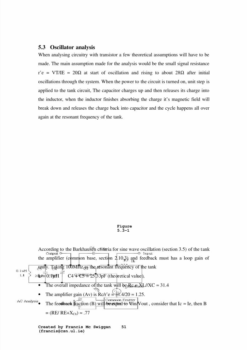
8/20/2019 FM Xmtr Theory
http://slidepdf.com/reader/full/fm-xmtr-theory 59/95
Created by Francis Mc Swiggan([email protected])
51
5.3 Oscillator analysisWhen analysing circuitry with transistor a few theoretical assumptions will have to be
made. The main assumption made for the analysis would be the small signal resistancer’e = VT/IE≈ 20Ω at start of oscillation and rising to about 28Ω after initial
oscillations through the system. When the power to the circuit is turned on, unit step isapplied to the tank circuit, The capacitor charges up and then releases its charge intothe inductor, when the inductor finishes absorbing the charge it’s magnetic field willbreak down and releases the charge back into capacitor and the cycle happens all overagain at the resonant frequency of the tank.
According to the Barkhausen criteria for sine wave oscillation (section 3.5) of the tankthe amplifier (common base, section 2.10.3) and feedback must has a loop gain of unity. Taking 100MHz as the resonant frequency of the tank
L = 0.1µH C4 + C5 = 25.33pF (theoretical value),
• The overall impedance of the tank will be Rc = XL//XC≈ 31.4
• The amplifier gain (Av) is Rc/r’e = 31.4/20≈ 1.25.
• The feedback fraction (B) will be equal to Vin/Vout , consider that Ic≈ Ie, then B
= (RE/ RE+XC6) ≈ .77
Figure5.3-1

8/20/2019 FM Xmtr Theory
http://slidepdf.com/reader/full/fm-xmtr-theory 60/95
Created by Francis Mc Swiggan([email protected])
52
• The closed loop gain of the system will therefore equal to AL = Av * B = 1.57 *0.77 = 1.2, when oscillation is sustained r’e will rise to about 28 and the overallloop gain will fall to unity.
The second Barkhausen Criterion states that in order for sustained oscillation tohappen the phase shift through the network at the resonant frequency will have to bezero, L1, C4 and C5 will yield 0O at the resonant frequency. There is a – 90O phaseshift through C6. The emitter–collector channel has an interesting property when itcomes to current and voltage, the current entering the emitter leads the voltage across
the collector, hence a + 90O
phase shift. Putting the capacitor and transistor togetherthere will be a 0O between the input and output nodes.
5.4 Components List
5.4.1 Resistors
R1 10KΩ Carbon Film Bias for the Electret microphoneR2 1MΩ Carbon Film DC bias for the Base of Q1
R3 100KΩCarbon Film DC bias for the Base of Q1
R4 150Ω Carbon Film Sets the DC & AC gain of Q1
R5 10KΩ Carbon Film Sets the DC & AC gain of Q1
R6 10KΩ Carbon Film Forms a HPF with C2(pre-emphasis)
R7 1KΩ Carbon Film Sets the gain for the oscillator.
5.4.2 Capacitors
C1 0.1µF Non-polarised tantalum Audio coupling capacitor
C2 0.1µF Non-polarised tantalum Forms HPF with R6 .
C3 10nF Ceramic AC grounds the base of Q2.C4 1 to 12pF Silver Mica Tuning cap for MultichannelC5 20pF Ceramic Shunt capacitor for tuningC6 5.6pF Ceramic Feedback for oscillation.
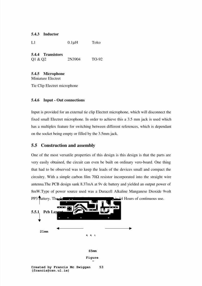
8/20/2019 FM Xmtr Theory
http://slidepdf.com/reader/full/fm-xmtr-theory 61/95
Created by Francis Mc Swiggan([email protected])
53
5.4.3 Inductor
L1 0.1µH Toko
5.4.4 TransistorsQ1 & Q2 2N3904 TO-92
5.4.5 MicrophoneMiniature ElectretTie Clip Electret microphone
5.4.6 Input - Out connections
Input is provided for an external tie clip Electret microphone, which will disconnect thefixed small Electret microphone. In order to achieve this a 3.5 mm jack is used whichhas a multiplex feature for switching between different references, which is dependanton the socket being empty or filled by the 3.5mm jack.
5.5 Construction and assembly
One of the most versatile properties of this design is this design is that the parts arevery easily obtained, the circuit can even be built on ordinary vero-board. One thingthat had to be observed was to keep the leads of the devices small and compact the
circuitry. With a simple carbon film 70Ω resistor incorporated into the straight wire
antenna.The PCB design sank 8.37mA at 9v dc battery and yielded an output power of 8mW.Type of power source used was a Duracell Alkaline Manganese Dioxide 9volt
PP3 battery. The duration for effective transmission is 14 Hours of continuous use.
5.5.1 Pcb Layout
21mm
Figure-
65mm
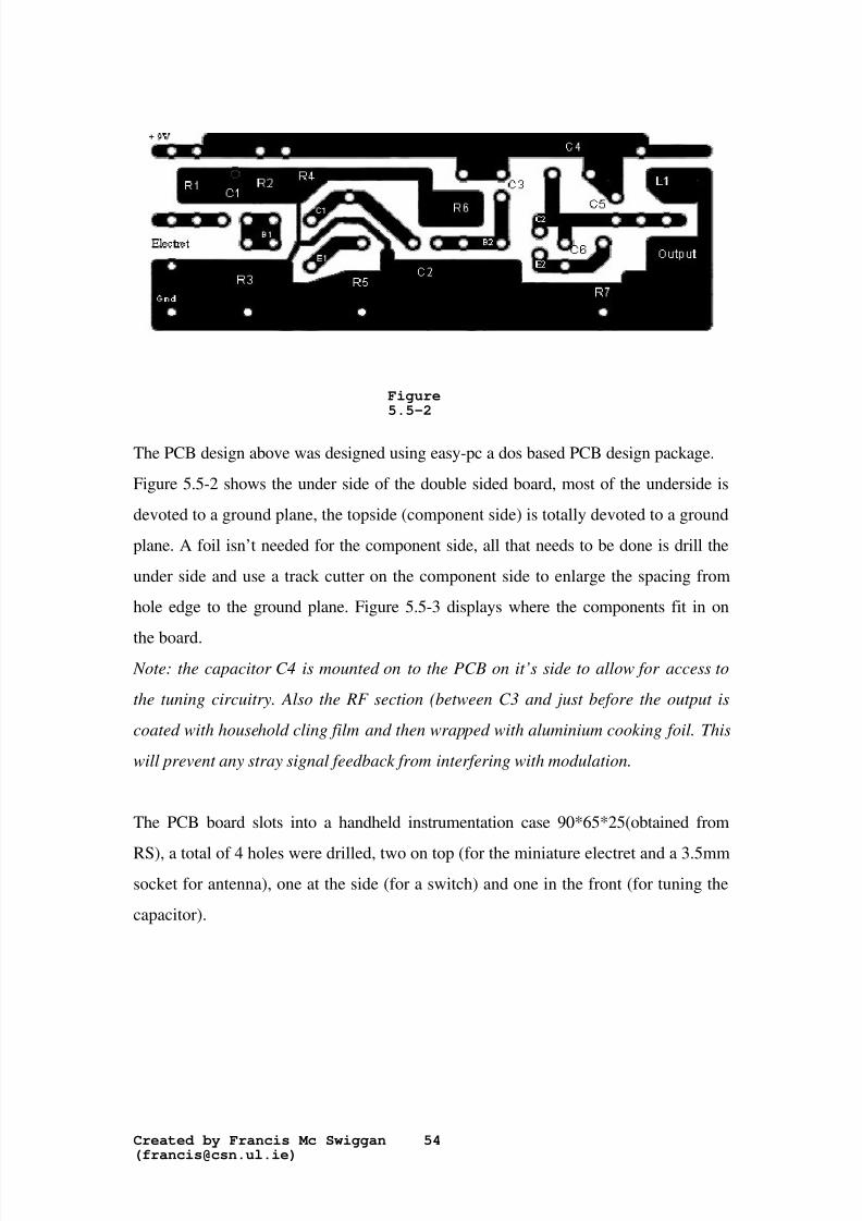
8/20/2019 FM Xmtr Theory
http://slidepdf.com/reader/full/fm-xmtr-theory 62/95
Created by Francis Mc Swiggan([email protected])
54
The PCB design above was designed using easy-pc a dos based PCB design package.Figure 5.5-2 shows the under side of the double sided board, most of the underside isdevoted to a ground plane, the topside (component side) is totally devoted to a groundplane. A foil isn’t needed for the component side, all that needs to be done is drill theunder side and use a track cutter on the component side to enlarge the spacing fromhole edge to the ground plane. Figure 5.5-3 displays where the components fit in on
the board. Note: the capacitor C4 is mounted on to the PCB on it’s side to allow for access to
the tuning circuitry. Also the RF section (between C3 and just before the output is
coated with household cling film and then wrapped with aluminium cooking foil. This
will prevent any stray signal feedback from interfering with modulation.
The PCB board slots into a handheld instrumentation case 90*65*25(obtained from
RS), a total of 4 holes were drilled, two on top (for the miniature electret and a 3.5mmsocket for antenna), one at the side (for a switch) and one in the front (for tuning thecapacitor).
Figure5.5-2
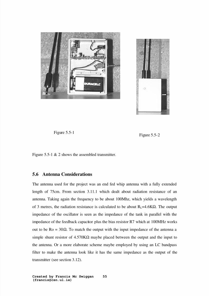
8/20/2019 FM Xmtr Theory
http://slidepdf.com/reader/full/fm-xmtr-theory 63/95
Created by Francis Mc Swiggan([email protected])
55
Figure 5.5-1 & 2 shows the assembled transmitter.
5.6 Antenna Considerations
The antenna used for the project was an end fed whip antenna with a fully extendedlength of 75cm. From section 3.11.1 which dealt about radiation resistance of anantenna. Taking again the frequency to be about 100Mhz, which yields a wavelength
of 3 metres, the radiation resistance is calculated to be about RL=4.6KΩ. The outputimpedance of the oscillator is seen as the impedance of the tank in parallel with theimpedance of the feedback capacitor plus the bias resistor R7 which at 100MHz works
out to be Ro = 30Ω. To match the output with the input impedance of the antenna a
simple shunt resistor of 4.570KΩ maybe placed between the output and the input to
the antenna. Or a more elaborate scheme maybe employed by using an LC bandpassfilter to make the antenna look like it has the same impedance as the output of the
transmitter (see section 3.12).
Figure 5.5-1 Figure 5.5-2
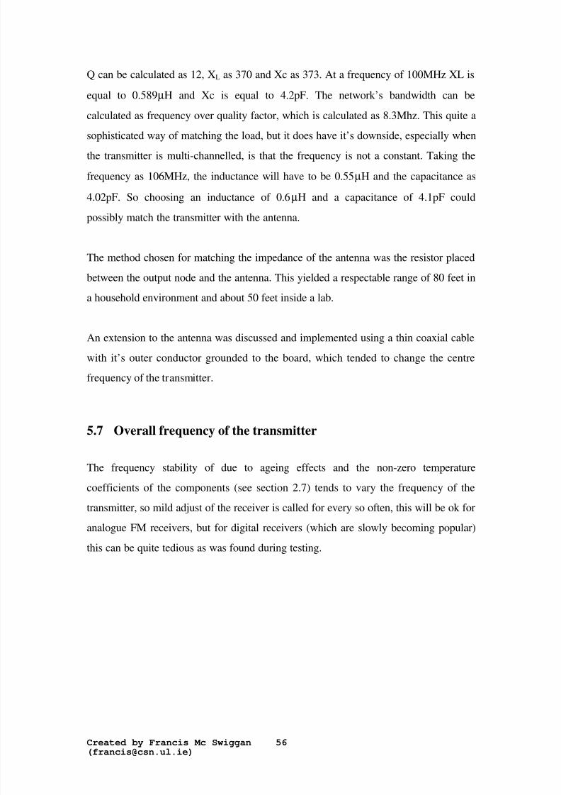
8/20/2019 FM Xmtr Theory
http://slidepdf.com/reader/full/fm-xmtr-theory 64/95
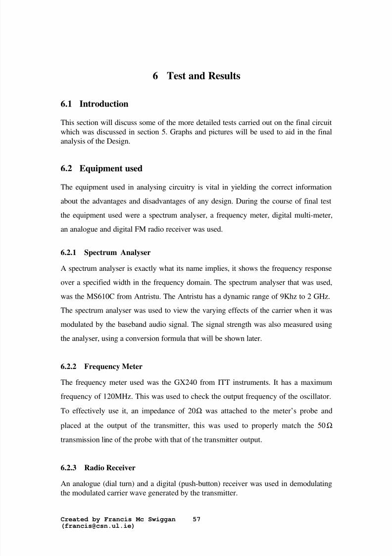
8/20/2019 FM Xmtr Theory
http://slidepdf.com/reader/full/fm-xmtr-theory 65/95
Created by Francis Mc Swiggan([email protected])
57
6 Test and Results
6.1 Introduction
This section will discuss some of the more detailed tests carried out on the final circuitwhich was discussed in section 5. Graphs and pictures will be used to aid in the finalanalysis of the Design.
6.2 Equipment used
The equipment used in analysing circuitry is vital in yielding the correct informationabout the advantages and disadvantages of any design. During the course of final testthe equipment used were a spectrum analyser, a frequency meter, digital multi-meter,an analogue and digital FM radio receiver was used.
6.2.1 Spectrum Analyser
A spectrum analyser is exactly what its name implies, it shows the frequency responseover a specified width in the frequency domain. The spectrum analyser that was used,
was the MS610C from Antristu. The Antristu has a dynamic range of 9Khz to 2 GHz.The spectrum analyser was used to view the varying effects of the carrier when it wasmodulated by the baseband audio signal. The signal strength was also measured usingthe analyser, using a conversion formula that will be shown later.
6.2.2 Frequency Meter
The frequency meter used was the GX240 from ITT instruments. It has a maximumfrequency of 120MHz. This was used to check the output frequency of the oscillator.
To effectively use it, an impedance of 20Ω was attached to the meter’s probe and
placed at the output of the transmitter, this was used to properly match the 50Ωtransmission line of the probe with that of the transmitter output.
6.2.3 Radio Receiver
An analogue (dial turn) and a digital (push-button) receiver was used in demodulatingthe modulated carrier wave generated by the transmitter.
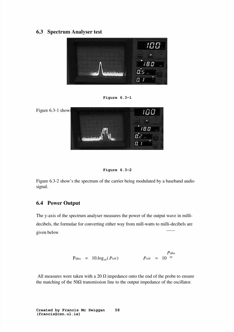
8/20/2019 FM Xmtr Theory
http://slidepdf.com/reader/full/fm-xmtr-theory 66/95
Created by Francis Mc Swiggan([email protected])
58
6.3 Spectrum Analyser test
Figure 6.3-1
Figure 6.3-1 shows the unmodulated carrier spectrum at 100MHz
Figure 6.3-2
Figure 6.3-2 show’s the spectrum of the carrier being modulated by a baseband audiosignal.
6.4 Power Output
The y-axis of the spectrum analyser measures the power of the output wave in milli-decibels, the formulae for converting either way from mill-watts to milli-decibels are
given below
)(10.logP 10dBm mW P= 1010dBm
mW
PP =
All measures were taken with a 20Ω impedance onto the end of the probe to ensurethe matching of the 50Ω transmission line to the output impedance of the oscillator.
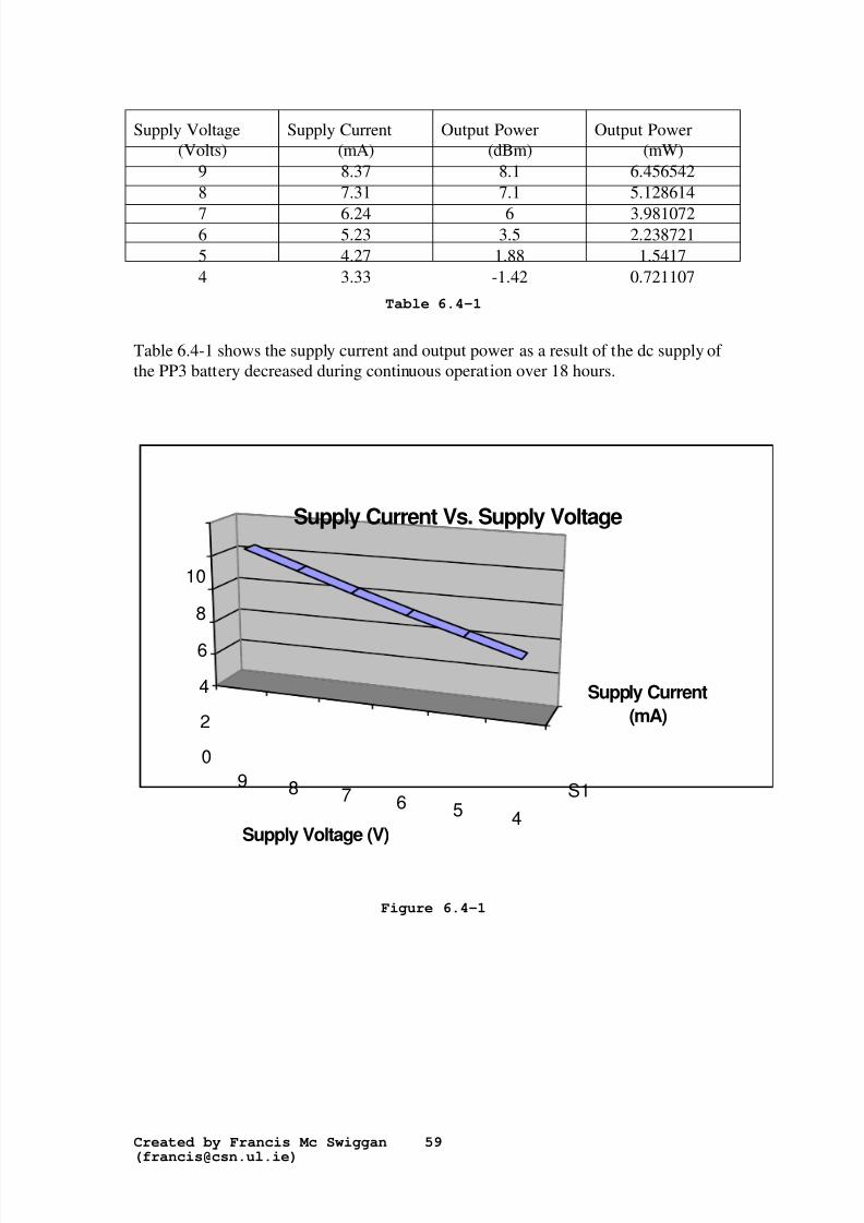
8/20/2019 FM Xmtr Theory
http://slidepdf.com/reader/full/fm-xmtr-theory 67/95
Created by Francis Mc Swiggan([email protected])
59
Supply Voltage(Volts)
Supply Current(mA)
Output Power(dBm)
Output Power(mW)
9 8.37 8.1 6.4565428 7.31 7.1 5.128614
7 6.24 6 3.9810726 5.23 3.5 2.2387215 4.27 1.88 1.54174 3.33 -1.42 0.721107
Table 6.4-1
Table 6.4-1 shows the supply current and output power as a result of the dc supply of the PP3 battery decreased during continuous operation over 18 hours.
9 8 7 6 5 4
S1
0
2
4
6
8
10
Supply Voltage (V)
Supply Current(mA)
Supply Current Vs. Supply Voltage
Figure 6.4-1

8/20/2019 FM Xmtr Theory
http://slidepdf.com/reader/full/fm-xmtr-theory 68/95
Created by Francis Mc Swiggan([email protected])
60
Power Output Vs. Supply Voltage
0
1
2
3
4
5
6
7
9 8 7 6 5 4
Supply voltage of battery (V)
O u
t p u
t P o w e r
( m W )
Figure 6.4-2
It can be easily seen from figure 6.4-1 & 2 that the supply current decreases linearly asthe supply voltage supplied by the battery decreases, also the output power isdecreases as voltage supply to the transmitter decreases. The typical voltage inputfrom the battery source will be 9.2V in the first 30 minutes of operation decreasing to
the 8.8volts to 7 volts band in the next 14 hours of continuous operation anddecreasing to the 7 to 4 volts band of operation in the following 6 hours. This last bandof voltage operation produced fairly low levels of transmission. The Middle band 7 to8.8 volts emitted a very strong transmission indeed, which lasted for 14 hours, this isthe main feature that make the PP3 such a popular battery for intensive dc supply to“walkie talkie’s”, because of this a stable transmission over a long period of time canbe sustained.
8/20/2019 FM Xmtr Theory
http://slidepdf.com/reader/full/fm-xmtr-theory 69/95
8/20/2019 FM Xmtr Theory
http://slidepdf.com/reader/full/fm-xmtr-theory 70/95
Created by Francis Mc Swiggan([email protected])
62
7.3 Discussion
The design chosen was miniature, low powered and tuneable to different frequencies.The parts used are very common and the circuit is very easily constructed. The circuitwas firsts build on vero-board and worked rather well without applying any realeffective RF techniques, all that had to be adhered to was to keep the leads short andcompact the circuitry as much as possible. The PCB, as expected performedexceedingly well, but more of an better attempt had to be made in matching theantenna (section: 3.12 & 5.6) and shielding the RF section from the output as the PCBlayout was a lot more efficient in radiating power out. Unwanted Electro-magneticradiation had to be stopped from destructively interfering with the carrier modulation.To keep the design simple and easy to construct it was decided to just wrap householdcling-film, electrically protecting the circuitry from the Aluminium foil that was used toelectro-magnetically shield the RF stage.
The effective range of the transmitter was 80 feet in a household environment andabout 50 feet in a lab environment, which makes the transmitter ideal aiding Touristshear a Tour Guide within a densely packed room. The Antenna co-axial extension leadhelps in raising the antenna over people’s heads and transmitting to their FM receivers(otherwise the water content in the human body would bounce the electromagneticwaves). Because of the 14 hours of effective transmission given by the PP3 and thepower consumption of the battery, the device could be used as a baby monitoringdevice within the home, with a range of about 80 feet, it reaches out even to the
garden.
7.4 Conclusions
The Miniaturised FM transmitter is essentially a Design and Implementation project.To approach a project like this a parallel path has to be taken in regards to the Theoryand the practical circuitry, for a successful conclusion in any project these path’s mustmeet, and this only happens when they are fully understood. This is why a goodgrounding in the basics of Communication theory and Analogue design must be
8/20/2019 FM Xmtr Theory
http://slidepdf.com/reader/full/fm-xmtr-theory 71/95
Created by Francis Mc Swiggan([email protected])
63
achieved before ever approaching a project like this. To start off looking at blockdiagrams of basic transmitter was a must, even if it seemed abstract and obscure theunderlying meaning of each block can be found out one by one. Which is what made
the overall project challenging and rewarding.
7.5 Recommendations
The design used for this project is essentially quite a simple one, and it is this simplicitywhich partly brings it down when it comes to the overall reliable performance. Themain area of instability is in the oscillator part of the circuit. Shielding (section 5.5) theoscillator helped in part to counteract this.
After learning a lot from this project, there would have been a few things that couldhave been done to the final design to improve it’s performance.
• Use negative temperature coefficients to compensate for typically positive-temperature-coefficient tuned circuits.
•
Follow the oscillator with a buffer amplifier to reduce the effects of load changes.
The standalone Vco design of section 4.3, is worth a look at, maybe if the MC1648soic 4 pin package was used in conjunction with other stages as mentioned in section4.3, the stability of the oscillator could have been greatly increased.
8/20/2019 FM Xmtr Theory
http://slidepdf.com/reader/full/fm-xmtr-theory 72/95
Created by Francis Mc Swiggan([email protected])
64
References
1. Modern electronic communication / Miller, Gary M2. Electronic communications: modulation and transmission / Schoenbeck, Robert
3. Electronics : circuits, amplifiers, and gates / Bugg, D. V. (David Vernon)
4. Antennas / Connor, Frank Robert
5. Fundamentals of reliable circuit design / Xlander, Mel
6. Electronic devices / Floyd, Thomas L
7. Electronic Communication Techniques / Young, Paul H.

8/20/2019 FM Xmtr Theory
http://slidepdf.com/reader/full/fm-xmtr-theory 73/95
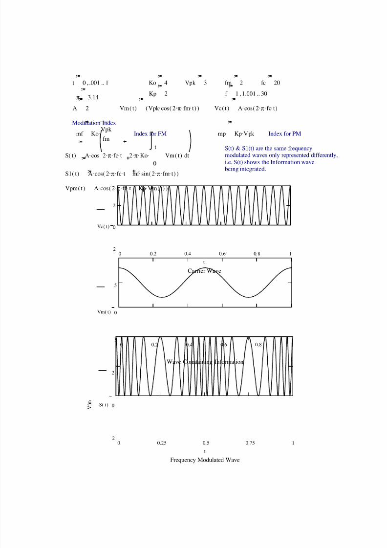
8/20/2019 FM Xmtr Theory
http://slidepdf.com/reader/full/fm-xmtr-theory 74/95
t ..,0 .001 1 Ko 4 Vpk 3 fm 2 fc 20
Kp 2 f ..,1 1.001 30π 3.14A 2 Vm( )t ( ).Vpk cos( )...2 π fm t Vc( )t .A cos( )...2 π fc t
Modulation Indexmf .Ko Vpk
fmIndex for FM mp .Kp Vpk Index for PM
S(t) & S1(t) are the same frequencymodulated waves only represented differently,i.e. S(t) shows the Information wavebeing integrated.
S( )t .A cos ...2 π fc t ...2 π Ko d0
ttVm( )t
S1( )t .A cos( )...2 π fc t .mf sin( )...2 π fm t
Vpm( )t .A cos( )...2 π
fc t .Kp Vm( )t
0 0.2 0.4 0.6 0.8 12
0
2
Carrier Wave
Vc( )t
t
0 0.2 0.4 0.6 0.8 15
0
5
Wave Conataining Information
Vm( )t
t
0 0.25 0.5 0.75 12
0
2
Frequency Modulated Wave
V f m S( )t
t
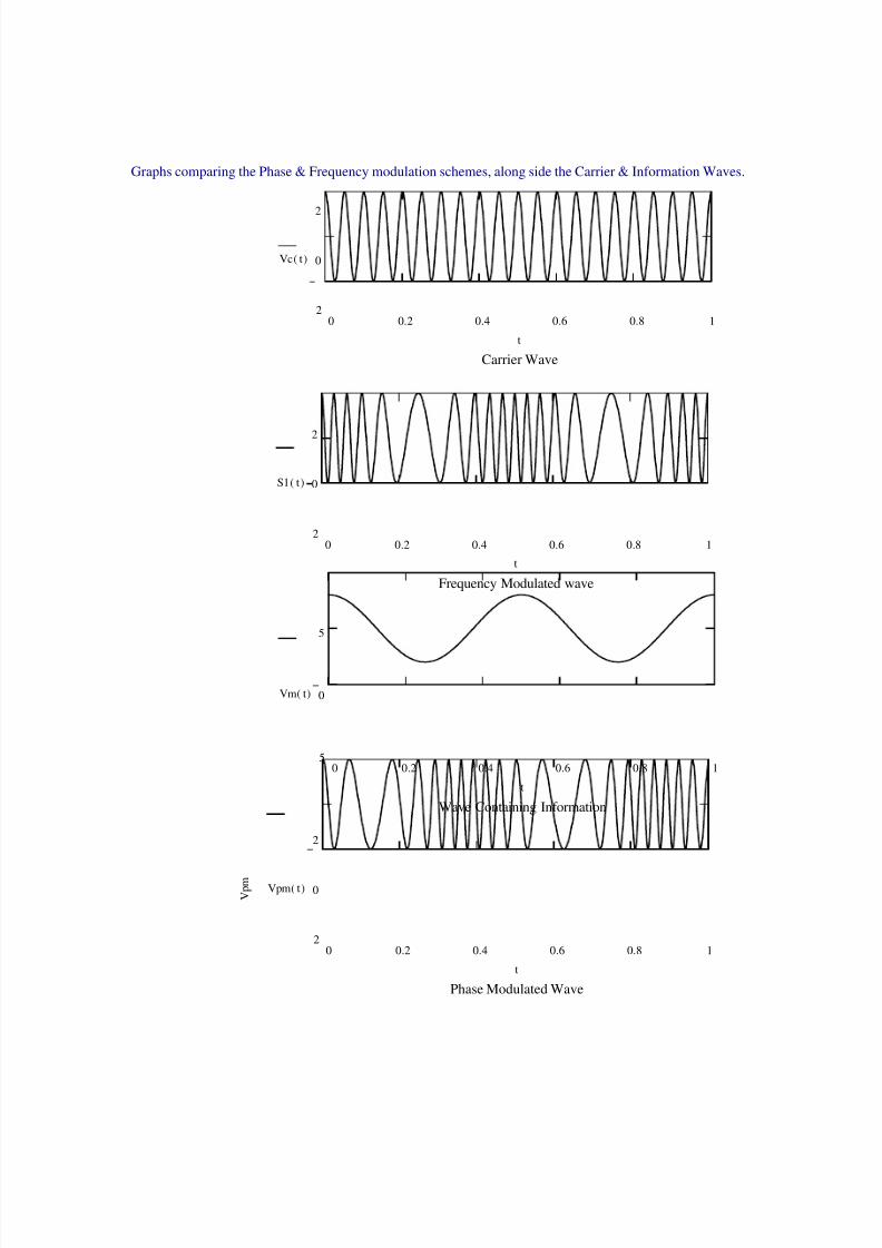
8/20/2019 FM Xmtr Theory
http://slidepdf.com/reader/full/fm-xmtr-theory 75/95
Graphs comparing the Phase & Frequency modulation schemes, along side the Carrier & Information Waves.
0 0.2 0.4 0.6 0.8 12
0
2
Carrier Wave
Vc( )t
t
0 0.2 0.4 0.6 0.8 12
0
2
Frequency Modulated wave
S1( )t
t
0 0.2 0.4 0.6 0.8 15
0
5
Wave Containing Information
Vm( )t
t
0 0.2 0.4 0.6 0.8 12
0
2
Phase Modulated Wave
V p m Vpm( )t
t

8/20/2019 FM Xmtr Theory
http://slidepdf.com/reader/full/fm-xmtr-theory 76/95
This page is concerned with Demodulation !Which means graphing the frequency change with respect to time.
T 1fm
Feff ( )t fc .fm cos ..2 πT
t
0 0.5 118
20
22
Frequency versus TimeTime
F c
+ F m
F eff ( )t
t
N 8
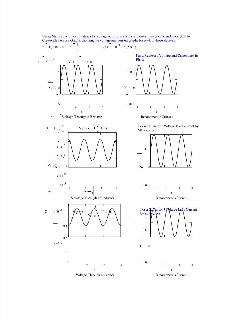
8/20/2019 FM Xmtr Theory
http://slidepdf.com/reader/full/fm-xmtr-theory 77/95
Using Mathcad to enter equations for voltage & current across a resistor, capacitor & inductor. And toCreate Elementary Graphs showing the voltage and current graphs for each of these devices.
t ..,1 1.01 4 f 12
I( )t .10 3 sin( )..2 π t
For a Resistor : Voltage and Current are inPhase!R .5 103 Vr( )t .I( )t R
1 2 3 45
0
5
Voltage Through a Resistor
Vr( )t
t
1 2 3 40.001
0
0.001
Instantaneous Current
I ( )t
t
For an Inductor : Voltage leads current by90 degreesL .1 10 3 VL( )t .L d
d tI( )t
1 2 3 41 10 5
5 10 6
0
5 10 6
1 10 5
Volatage Through an Inductor
VL( )t
t1 2 3 4
0.001
0
0.001
Instantaneous Current
I( )t
t
For a Capacitor : Volatge Lags Currentby 90 degrees.C .1 10 3 VC( )t .1
Cd
0
ttI( )t
1 2 3 40.2
0
0.2
0.4
Voltage Through a Capitor
VC( )t
t1 2 3 4
0.001
0
0.001
Instantaneous Current
I( )t
t
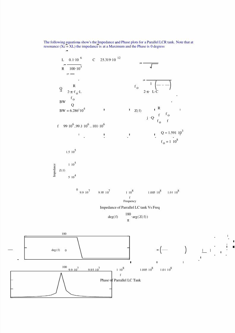
8/20/2019 FM Xmtr Theory
http://slidepdf.com/reader/full/fm-xmtr-theory 78/95
The following equations show's the Impedance and Phase plots for a Parallel LCR tank. Note that atresonance (Xc = XL) the impedance is at a Maximum and the Phase is 0 degress
L .0.1 10 6 C .25.319 1012
R .100 103
f o1
..2 π .L CQ R
...2 π f o L
BWf oQ
=BW 6.286 104 Z( )f R
.. j Q f f o
f of
f ..,.99 106 .99.1 106 .101 106
=Q 1.591 103
=f o 1 108
9.9 107 9.95 107 1 108 1.005 108 1.01 1080
5 104
1 105
1.5 105
Impedance of Parrallel LC tank Vs FreqFrequency
I m
p e d a n c e
Z( )f
f
deg( )f .180π
arg( )Z( )f
9.9 107 9.95 107 1 108 1.005 108 1.01 108100
0
100
Phase of Parrallel LC Tank
deg ( )f
f
8/20/2019 FM Xmtr Theory
http://slidepdf.com/reader/full/fm-xmtr-theory 79/95
Created by Francis Mc Swiggan([email protected])
B
Appendix B
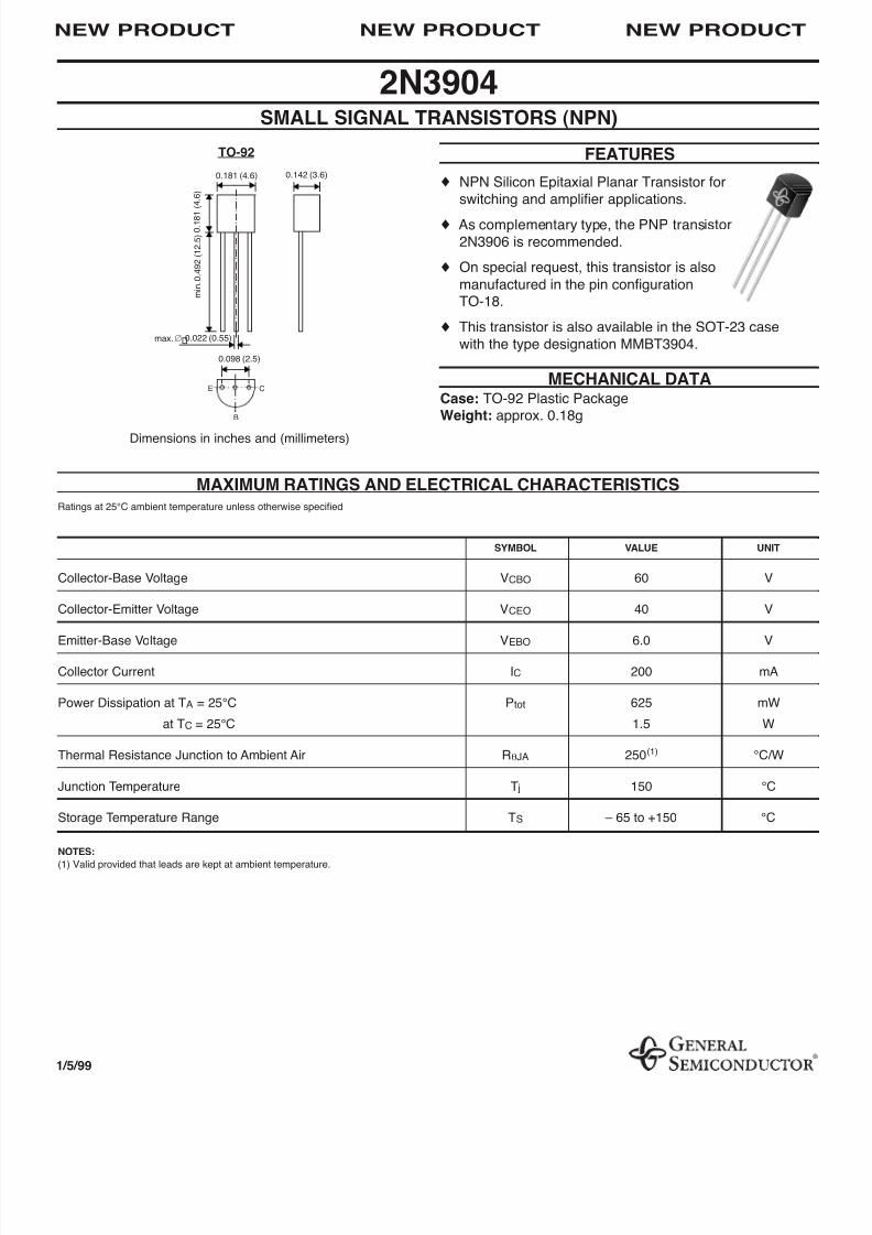
8/20/2019 FM Xmtr Theory
http://slidepdf.com/reader/full/fm-xmtr-theory 80/95
2N3904SMALL SIGNAL TRANSISTORS (NPN)
FEATURES
¨ NPN Silicon Epitaxial Planar Transistor forswitching and amplifier applications.
¨ As complementary type, the PNP transistor2N3906 is recommended.
¨ On special request, this transistor is alsomanufactured in the pin configurationTO-18.
¨ This transistor is also available in the SOT-23 casewith the type designation MMBT3904.
MECHANICAL DATACase: TO-92 Plastic PackageWeight: approx. 0.18g
MAXIMUM RATINGS AND ELECTRICAL CHARACTERISTICSRatings at 25¡C ambient temperature unless otherwise specified
SYMBOL VALUE UNIT
Collector-Base Voltage V CBO 60 V
Collector-Emitter Voltage V CEO 40 V
Emitter-Base Voltage V EBO 6.0 V
Collector Current I C 200 mA
Power Dissipation at T A = 25¡C P tot 625 mW
at T C = 25¡C 1.5 W
Thermal Resistance Junction to Ambient Air R qJA 250 (1) ¡C/W
Junction Temperature T j 150 ¡C
Storage Temperature Range T S Ð 65 to +150 ¡C
NOTES:
(1) Valid provided that leads are kept at ambient temperature.
0.181 (4.6)
m i n
. 0 . 4
9 2 ( 1 2
. 5 ) 0
. 1 8 1 ( 4
. 6 )
0.142 (3.6)
0.098 (2.5)
max. Æ 0.022 (0.55)
E C
B
TO-92
1/5/99
Dimensions in inches and (millimeters)
NEW PRODUCT NEW PRODUCT NEW PRODUCT

8/20/2019 FM Xmtr Theory
http://slidepdf.com/reader/full/fm-xmtr-theory 81/95
2N3904ELECTRICAL CHARACTERISTICS
Ratings at 25¡C ambient temperature unless otherwise specified
SYMBOL MIN. MAX. UNIT
Collector-Base Breakdown Voltageat I C = 10 mA, IE = 0 V (BR)CBO 60 Ð V
Collector-Emitter Breakdown Voltageat I C = 1 mA, I B = 0 V (BR)CEO 40 Ð V
Emitter-Base Breakdown Voltageat I E = 10 mA, IC = 0 V (BR)EBO 6 Ð V
Collector Saturation Voltageat I C = 10 mA, I B = 1 mA V CEsat Ð 0.2 Vat I C = 50 mA, I B = 5 mA V CEsat Ð 0.3 V
Base Saturation Voltageat I C = 10 mA, I B = 1 mA V BEsat Ð 0.85 V
at I C = 50 mA, I B = 5 mA V BEsat Ð 0.95 VCollector-Emitter Cutoff CurrentVEB = 3 V, V CE = 30 V I CEV Ð 50 nA
Emitter-Base Cutoff CurrentVEB = 3 V, V CE = 30 V I EBV Ð 50 nA
DC Current Gainat V CE = 1 V, I C = 0.1 mA h FE 40 Ð Ðat V CE = 1 V, I C = 1 mA h FE 70 Ð Ðat V CE = 1 V, I C = 10 mA h FE 100 300 Ðat V CE = 1 V, I C = 50 mA h FE 60 Ð Ðat V CE = 1 V, I C = 100 mA h FE 30 Ð Ð
Input Impedanceat V CE = 10 V, I C = 1 mA, f = 1 kHz h ie 1 10 k W
Voltage Feedback Ratioat V CE = 10 V, I C = 1 mA, f = 1 kHz h re 0.5 á 10 Ð4 8 á 10 Ð4 Ð
Gain-Bandwidth Productat V CE = 20 V, I C = 10 mA, f = 100 MHz f T 300 Ð MHz
Collector-Base Capacitanceat V CB = 5 V, f = 100 kHz C CBO Ð 4 pF
Emitter-Base Capacitanceat V EB = 0.5 V, f = 100 kHz C EBO Ð 8 pF
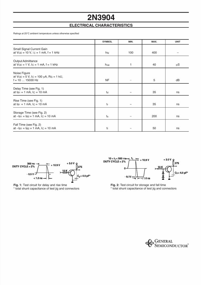
8/20/2019 FM Xmtr Theory
http://slidepdf.com/reader/full/fm-xmtr-theory 82/95
2N3904ELECTRICAL CHARACTERISTICS
Ratings at 25¡C ambient t emperature unless otherwise specified
SYMBOL MIN. MAX. UNIT
Small Signal Current Gainat V CE = 10 V, I C = 1 mA, f = 1 kHz h fe 100 400 Ð
Output Admittanceat V CE = 1 V, I C = 1 mA, f = 1 kHz h oe 1 40 mS
Noise Figureat V CE = 5 V, I C = 100 mA, R G = 1 k W,f = 10 É 15000 Hz NF Ð 5 dB
Delay Time (see Fig. 1)at I B1 = 1 mA, I C = 10 mA t d Ð 35 ns
Rise Time (see Fig. 1)at I B1 = 1 mA, I C = 10 mA t r Ð 35 ns
Storage Time (see Fig. 2)at ÐIB1 = IB2 = 1 mA, I C = 10 mA t s Ð 200 ns
Fall Time (see Fig. 2)at ÐIB1 = IB2 = 1 mA, I C = 10 mA t f Ð 50 ns
Fig. 2: Test circuit for storage and fall time* total shunt capacitance of test jig and connectors
Fig. 1: Test circuit for delay and rise time* total shunt capacitance of test jig and connectors

8/20/2019 FM Xmtr Theory
http://slidepdf.com/reader/full/fm-xmtr-theory 83/95
Created by Francis Mc Swiggan([email protected])
C
Appendix C
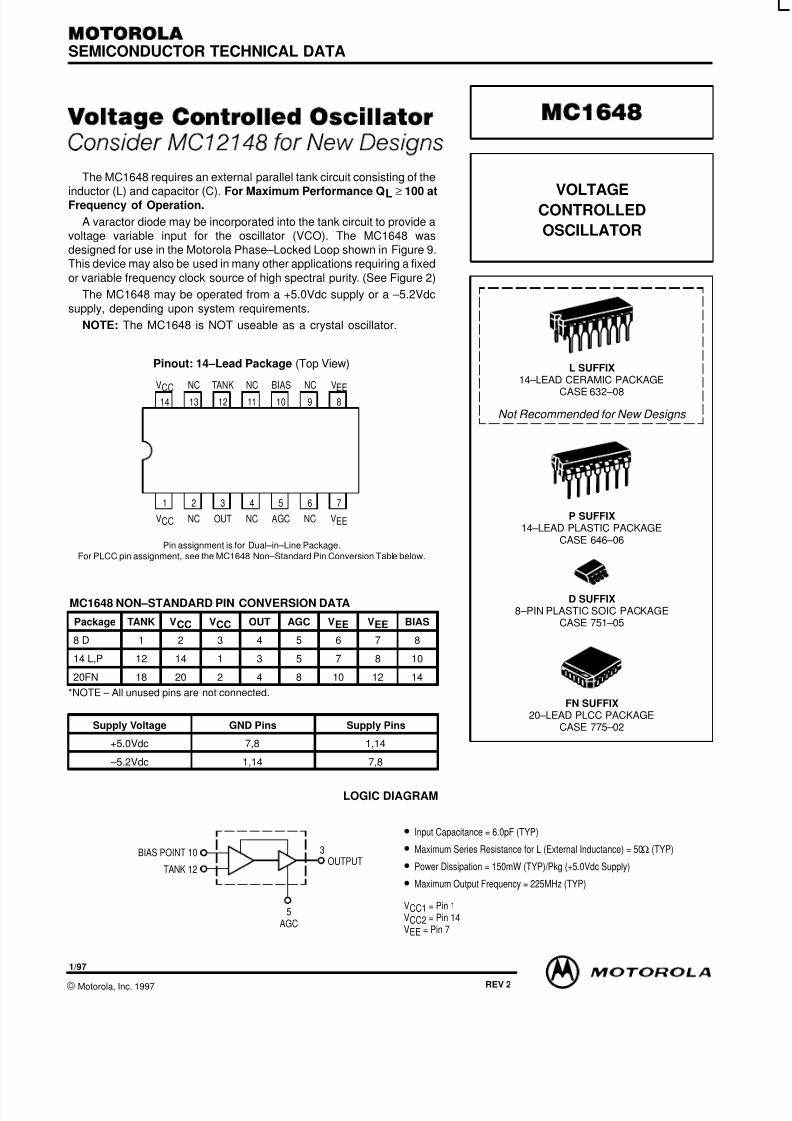
8/20/2019 FM Xmtr Theory
http://slidepdf.com/reader/full/fm-xmtr-theory 84/95
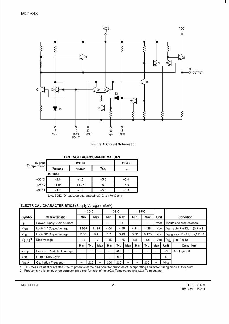
8/20/2019 FM Xmtr Theory
http://slidepdf.com/reader/full/fm-xmtr-theory 85/95
MC1648
MOTOROLA HIPERCOMMBR1334 — Rev 4
2
Figure 1. Circuit Schematic
5AGC
8VEE
12TANK
10BIAS
POINT
7VEE1
VCC214
VCC11
Q4
Q3 Q2
Q1
Q5
D1
Q8
Q7 Q6
Q9
Q10Q11
D2
3OUTPUT
TEST VOLTAGE/CURRENT VALUES
@ Test (Volts) mAdcTemperature
VIHmax
VILmin
VCC
IL
MC1648
–30 °C +2.0 +1.5 +5.0 –5.0
+25 °C +1.85 +1.35 +5.0 –5.0
+85 °C +1.7 +1.2 +5.0 –5.0
Note: SOIC “D” package guaranteed –30 °C to +70 °C only
ELECTRICAL CHARACTERISTICS (Supply Voltage = +5.0V)
–30 °C +25 °C +85 °C
Symbol Characteristic Min Max Min Max Min Max Unit Condition
IE Power Supply Drain Current – – – 41 – – mAdc Inputs and outputs open
VOH Logic “1” Output Voltage 3.955 4.185 4.04 4.25 4.11 4.36 Vdc V ILmin to Pin 12, I L @ Pin 3
VOL Logic “0” Output Voltage 3.16 3.4 3.2 3.43 3.22 3.475 Vdc V IHmax to Pin 12, I L @ Pin 3
VBIAS1 Bias Voltage 1.6 1.9 1.45 1.75 1.3 1.6 Vdc V ILmin to Pin 12
Min Typ Max Min Typ Max Min Typ Max Unit Condition
VP–P Peak–to–Peak Tank Voltage – – – – 400 – – – – mV See Figure 3
Vdc Output Duty Cycle – – – – 50 – – – – %
fmax 2 Oscillation Frequency – 225 – 200 225 – – 225 – MHz
1. This measurement guarantees the dc potential at the bias point for purposes of incorporating a varactor tuning diode at this point.2. Frequency variation over temperature is a direct function of the ∆C/ ∆ Temperature and ∆L/ ∆ Temperature.
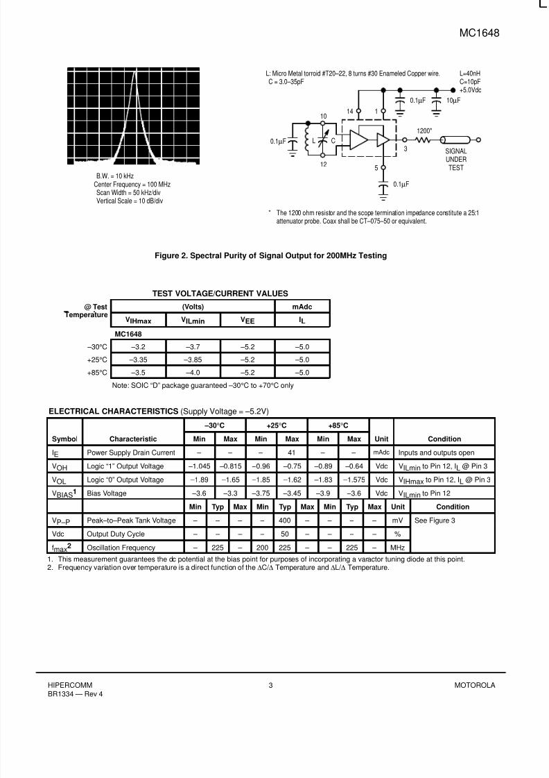
8/20/2019 FM Xmtr Theory
http://slidepdf.com/reader/full/fm-xmtr-theory 86/95
MC1648
HIPERCOMMBR1334 — Rev 4
3 MOTOROLA
Figure 2. Spectral Purity of Signal Output for 200MHz Testing
B.W. = 10 kHzCenter Frequency = 100 MHzScan Width = 50 kHz/divVertical Scale = 10 dB/div
0.1µF1200*
CL
10
12 5
0.1µF
3 SIGNALUNDERTEST
10µF0.1µF114
L=40nHC=10pF+5.0Vdc
L: Micro Metal torroid #T20–22, 8 turns #30 Enameled Copper wire.C = 3.0–35pF
* The 1200 ohm resistor and the scope termination impedance constitute a 25:1attenuator probe. Coax shall be CT–075–50 or equivalent.
TEST VOLTAGE/CURRENT VALUES
@ Test (Volts) mAdcTemperature
VIHmax VILmin VEE IL
MC1648
–30 °C –3.2 –3.7 –5.2 –5.0
+25 °C –3.35 –3.85 –5.2 –5.0
+85 °C –3.5 –4.0 –5.2 –5.0
Note: SOIC “D” package guaranteed –30 °C to +70 °C only
ELECTRICAL CHARACTERISTICS (Supply Voltage = –5.2V)
–30 °C +25 °C +85 °C
Symbol Characteristic Min Max Min Max Min Max Unit Condition
IE Power Supply Drain Current – – – 41 – – mAdc Inputs and outputs open
VOH Logic “1” Output Voltage –1.045 –0.815 –0.96 –0.75 –0.89 –0.64 Vdc V ILmin to Pin 12, I L @ Pin 3
VOL Logic “0” Output Voltage –1.89 –1.65 –1.85 –1.62 –1.83 –1.575 Vdc V IHmax to Pin 12, I L @ Pin 3
VBIAS1 Bias Voltage –3.6 –3.3 –3.75 –3.45 –3.9 –3.6 Vdc V ILmin to Pin 12
Min Typ Max Min Typ Max Min Typ Max Unit Condition
VP–P Peak–to–Peak Tank Voltage – – – – 400 – – – – mV See Figure 3
Vdc Output Duty Cycle – – – – 50 – – – – %
fmax 2 Oscillation Frequency – 225 – 200 225 – – 225 – MHz1. This measurement guarantees the dc potential at the bias point for purposes of incorporating a varactor tuning diode at this point.2. Frequency variation over temperature is a direct function of the ∆C/ ∆ Temperature and ∆L/ ∆ Temperature.
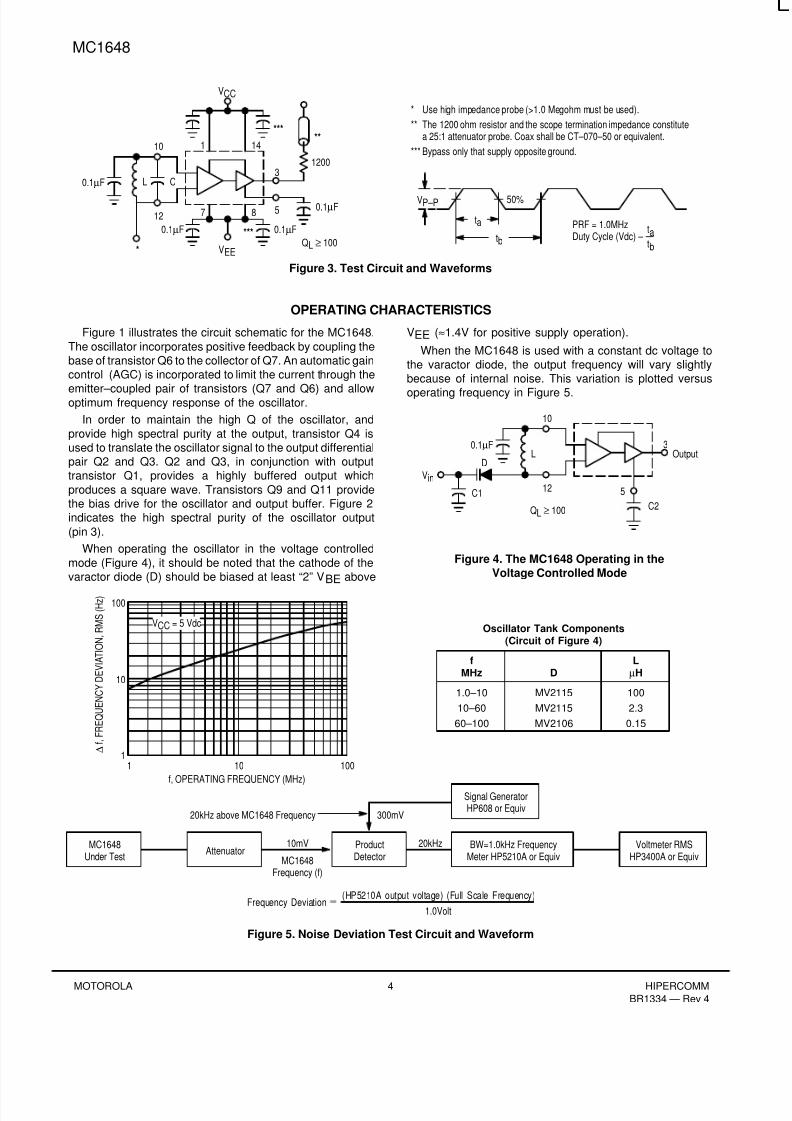
8/20/2019 FM Xmtr Theory
http://slidepdf.com/reader/full/fm-xmtr-theory 87/95
MC1648
MOTOROLA HIPERCOMMBR1334 — Rev 4
4
Figure 3. Test Circuit and Waveforms
0.1µF
1200
CL
10
120.1µF
3
*
VCC
*****
5
VEEQL ≥ 100
* Use high impedance probe (>1.0 Megohm must be used).** The 1200 ohm resistor and the scope termination impedance constitute
a 25:1 attenuator probe. Coax shall be CT–070–50 or equivalent.*** Bypass only that supply opposite ground.
50%
tatb
VP–P
PRF = 1.0MHzDuty Cycle (Vdc) –
tatb
7 8
1 14
0.1µF 0.1µF***
OPERATING CHARACTERISTICS
Figure 1 illustrates the circuit schematic for the MC1648.The oscillator incorporates positive feedback by coupling thebase of transistor Q6 to the collector of Q7. An automatic gaincontrol (AGC) is incorporated to limit the current through the
emitter–coupled pair of transistors (Q7 and Q6) and allowoptimum frequency response of the oscillator.In order to maintain the high Q of the oscillator, and
provide high spectral purity at the output, transistor Q4 isused to translate the oscillator signal to the output differentialpair Q2 and Q3. Q2 and Q3, in conjunction with outputtransistor Q1, provides a highly buffered output whichproduces a square wave. Transistors Q9 and Q11 providethe bias drive for the oscillator and output buffer. Figure 2indicates the high spectral purity of the oscillator output(pin 3).
When operating the oscillator in the voltage controlledmode (Figure 4), it should be noted that the cathode of thevaractor diode (D) should be biased at least “2” V BE above
VEE (≈ 1.4V for positive supply operation).
When the MC1648 is used with a constant dc voltage tothe varactor diode, the output frequency will vary slightlybecause of internal noise. This variation is plotted versus
operating frequency in Figure 5.
Figure 4. The MC1648 Operating in theVoltage Controlled Mode
0.1µFL
10
12
C2
3
5
QL ≥ 100
Output
VinC1
D
1.0–1010–60
60–100
fMHz
Figure 5. Noise Deviation Test Circuit and Waveform
100
1f, OPERATING FREQUENCY (MHz)
VCC = 5 Vdc
f , F R E Q U E N C Y D E V I A T I O N
, R M S ( H z )
10
110 100
∆
Frequency Deviation
(HP5210A output voltage) (Full Scale Frequency)1.0Volt
MV2115MV2115MV2106
D
1002.3
0.15
LµH
Oscillator Tank Components(Circuit of Figure 4)
BW=1.0kHz FrequencyMeter HP5210A or Equiv
Voltmeter RMSHP3400A or EquivMC1648
Frequency (f)
MC1648Under Test Attenuator Product
Detector
Signal GeneratorHP608 or Equiv
10mV 20kHz
300mV20kHz above MC1648 Frequency
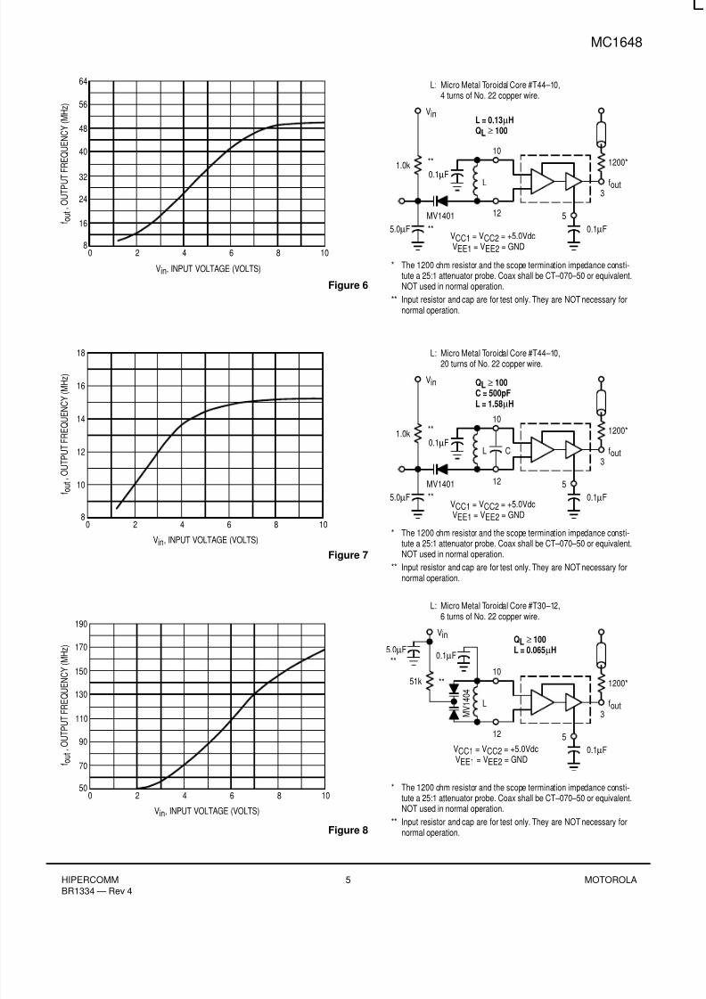
8/20/2019 FM Xmtr Theory
http://slidepdf.com/reader/full/fm-xmtr-theory 88/95
MC1648
HIPERCOMMBR1334 — Rev 4
5 MOTOROLA
* The 1200 ohm resistor and the scope termination impedance consti-tute a 25:1 attenuator probe. Coax shall be CT–070–50 or equivalent.NOT used in normal operation.
** Input resistor and cap are for test only. They are NOT necessary fornormal operation.
* The 1200 ohm resistor and the scope termination impedance consti-tute a 25:1 attenuator probe. Coax shall be CT–070–50 or equivalent.NOT used in normal operation.
** Input resistor and cap are for test only. They are NOT necessary fornormal operation.
Figure 6
Figure 7
Figure 8
Vin, INPUT VOLTAGE (VOLTS)
Vin, INPUT VOLTAGE (VOLTS)
18
08
10
190
50
64
0
Vin, INPUT VOLTAGE (VOLTS)
810
56
48
40
32
24
16
2 4 6 8
f o u t , O U T P U T F R E Q U E N C Y ( M H z )
f o u t , O U T P U T F R E Q U E N C Y ( M H z )
f o u t , O U T P U T F R E Q U E N C Y ( M H z )
16
14
12
10
2 4 6 8
0 102 4 6 8
170
150
130
110
90
70
0.1µF L
10
12
0.1µF
3
5
VCC1 = VCC2 = +5.0VdcVEE1 = VEE2 = GND
fout
Vin
MV1401
1200*
5.0µF
L = 0.13µHQL ≥ 100
L: Micro Metal Toroidal Core #T44–10,4 turns of No. 22 copper wire.
0.1µFL
10
12
0.1µF
3
5
VCC1 = VCC2 = +5.0VdcVEE1 = VEE2 = GND
fout
Vin
MV1401
1200*
5.0µF
QL ≥ 100C = 500pFL = 1.58µH
L: Micro Metal Toroidal Core #T44–10,20 turns of No. 22 copper wire.
C
1.0k
1.0k
* The 1200 ohm resistor and the scope termination impedance consti-tute a 25:1 attenuator probe. Coax shall be CT–070–50 or equivalent.NOT used in normal operation.
** Input resistor and cap are for test only. They are NOT necessary fornormal operation.
0.1µF
L
10
12
0.1µF
3
5VCC1 = VCC2 = +5.0VdcVEE1 = VEE2 = GND
fout
Vin
1200*
QL ≥ 100L = 0.065µH
L: Micro Metal Toroidal Core #T30–12,6 turns of No. 22 copper wire.
51k
M V 1 4 0 4
5.0µF
**
**
**
**
**
**
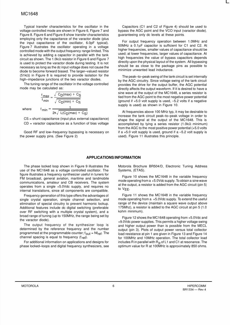
8/20/2019 FM Xmtr Theory
http://slidepdf.com/reader/full/fm-xmtr-theory 89/95
MC1648
MOTOROLA HIPERCOMMBR1334 — Rev 4
6
Typical transfer characteristics for the oscillator in thevoltage controlled mode are shown in Figure 6, Figure 7 andFigure 8. Figure 6 and Figure 8 show transfer characteristicsemploying only the capacitance of the varactor diode (plusthe input capacitance of the oscillator, 6.0pF typical).Figure 7 illustrates the oscillator operating in a voltagecontrolled mode with the output frequency range limited. Thisis achieved by adding a capacitor in parallel with the tankcircuit as shown. The 1.0k Ω resistor in Figure 6 and Figure 7is used to protect the varactor diode during testing. It is notnecessary as long as the dc input voltage does not cause thediode to become forward biased. The larger–valued resistor(51k Ω) in Figure 8 is required to provide isolation for thehigh–impedance junctions of the two varactor diodes.
The tuning range of the oscillator in the voltage controlledmode may be calculated as:
f maxfmin
CD(max) CS
CD(min) CS
where f min
1
2
L(CD(max)
CS )
CS = shunt capacitance (input plus external capacitance)CD = varactor capacitance as a function of bias voltage
Good RF and low–frequency bypassing is necessary onthe power supply pins. (See Figure 2)
Capacitors (C1 and C2 of Figure 4) should be used tobypass the AGC point and the VCO input (varactor diode),guaranteeing only dc levels at these points.
For output frequency operation between 1.0MHz and50MHz a 0.1 µF capacitor is sufficient for C1 and C2. Athigher frequencies, smaller values of capacitance should beused; at lower frequencies, larger values of capacitance. Athigh frequencies the value of bypass capacitors dependsdirectly upon the physical layout of the system. All bypassingshould be as close to the package pins as possible tominimize unwanted lead inductance.
The peak–to–peak swing of the tank circuit is set internallyby the AGC circuitry. Since voltage swing of the tank circuitprovides the drive for the output buffer, the AGC potentialdirectly affects the output waveform. If it is desired to have asine wave at the output of the MC1648, a series resistor istied from the AGC point to the most negative power potential(ground if +5.0 volt supply is used, –5.2 volts if a negativesupply is used) as shown in Figure 10.
At frequencies above 100 MHz typ, it may be desirable toincrease the tank circuit peak–to–peak voltage in order toshape the signal at the output of the MC1648. This isaccomplished by tying a series resistor (1.0k Ω minimum)from the AGC to the most positive power potential (+5.0 voltsif a +5.0 volt supply is used, ground if a –5.2 volt supply isused). Figure 11 illustrates this principle.
APPLICATIONS INFORMATION
The phase locked loop shown in Figure 9 illustrates the
use of the MC1648 as a voltage controlled oscillator. Thefigure illustrates a frequency synthesizer useful in tuners forFM broadcast, general aviation, maritime and landmobilecommunications, amateur and CB receivers. The systemoperates from a single +5.0Vdc supply, and requires nointernal translations, since all components are compatible.
Frequency generation of this type offers the advantages ofsingle crystal operation, simple channel selection, andelimination of special circuitry to prevent harmonic lockup.Additional features include dc digital switching (preferableover RF switching with a multiple crystal system), and abroad range of tuning (up to 150MHz, the range being set bythe varactor diode).
The output frequency of the synthesizer loop isdetermined by the reference frequency and the numberprogrammed at the programmable counter; f out = Nfref . Thechannel spacing is equal to frequency (f ref).
For additional information on applications and designs forphase locked–loops and digital frequency synthesizers, see
Motorola Brochure BR504/D, Electronic Tuning Address
Systems, (ETAS).Figure 10 shows the MC1648 in the variable frequency
mode operating from a +5.0Vdc supply. To obtain a sine waveat the output, a resistor is added from the AGC circuit (pin 5)to VEE .
Figure 11 shows the MC1648 in the variable frequencymode operating from a +5.0Vdc supply. To extend the usefulrange of the device (maintain a square wave output above175Mhz), a resistor is added to the AGC circuit at pin 5 (1.0kohm minimum).
Figure 12 shows the MC1648 operating from +5.0Vdc and+9.0Vdc power supplies. This permits a higher voltage swingand higher output power than is possible from the MECLoutput (pin 3). Plots of output power versus total collectorload resistance at pin 1 are given in Figure 13 and Figure 14for 100MHz and 10MHz operation. The total collector loadincludes R in parallel with R p of L1 and C1 at resonance. Theoptimum value for R at 100MHz is approximately 850 ohms.
8/20/2019 FM Xmtr Theory
http://slidepdf.com/reader/full/fm-xmtr-theory 90/95
MC1648
HIPERCOMMBR1334 — Rev 4
7 MOTOROLA
Figure 9. Typical Frequency Synthesizer Application
PhaseDetectorMC4044
fref
Counter ControlLogic
MC12014
MC12012
÷ P, ÷ (P+1)
÷ NpProgrammable
Counter MC4016
÷AProgrammable
Counter MC4016
Low PassFilter
Voltage ControlledOscillatorMC1648
Modulus Enable Line
Zero Detect Linefout
N = Np • P + A
Counter Reset Line
foutfout = Nfref whereN = Np • P + A
Figure 10. Method of Obtaining a Sine–Wave Output Figure 11. Method of Extending the Useful Rangeof the MC1648 (Square Wave Output)
10
12
7 8
3
5
Output
+5.0Vdc
10
12
7 8
3
5
Output
+5.0Vdc
1 141 14
1.0k min
8/20/2019 FM Xmtr Theory
http://slidepdf.com/reader/full/fm-xmtr-theory 91/95
MC1648
MOTOROLA HIPERCOMMBR1334 — Rev 4
8
Figure 12. Circuit Used for Collector Output Operation
10
12
0.1µF
3
5
Bias Point
L2* Tank
C21.0µF
VCC2 14 1 VCC1
C1
L1
+5.0V
C3
R
0.01µF+9.0V
AGC
+5.0V
1.0µF
1.2k
8 VEE27 VEE1
* QL ≥ 100
Output
Figure 13. Power Output versus Collector Load Figure 14. Power Output versus Collector Load
TOTAL COLLECTOR LOAD (OHMS)
7
10
TOTAL COLLECTOR LOAD (OHMS)
P O W E R O
U T P U T ( m W
R M S )
010,000
6
5
4
3
2
1
100 1000
P O W E R O
U T P U T ( m W
R M S )
10 10,000100 1000
14
0
12
10
8
6
4
2
See test circuit, Figure 12, f = 100MHzC3 = 3.0–35pFCollector Tank
L1 = 0.22 µH C1 = 1.0–7.0pFR = 50 Ω –10k ΩRP of L1 and C1 = 11k Ω @ 100MHz Resonance
Oscillator TankL2 = 4 turns #20 AWG 3/16” IDC2 = 1.0–7.0pF
See test circuit, Figure 12, f = 10MHzC3 = 470pFCollector Tank
L1 = 2.7 µH C1 = 24–200pFR = 50 Ω –10k ΩRP of L1 and C1 = 6.8k Ω @ 10MHz Resonance
Oscillator TankL2 = 2.7 µHC2 = 16–150pF
8/20/2019 FM Xmtr Theory
http://slidepdf.com/reader/full/fm-xmtr-theory 92/95
MC1648
HIPERCOMMBR1334 — Rev 4
9 MOTOROLA
OUTLINE DIMENSIONS
P SUFFIXPLASTIC PACKAGE
CASE 646–06ISSUE L
18.166.103.690.381.02
1.32
0.202.92
0° 0.39
19.566.604.690.531.78
2.41
0.383.43
10°
1.01
2.54 BSC
7.62 BSC
0.7150.2400.1450.0150.040
0.052
0.0080.115
0° 0.015
SEATINGPLANE
0.100 BSC
0.300 BSC
MIN MINMAX MAXINCHES MILLIMETERS
DIM0.7700.2600.1850.0210.070
0.095
0.0150.135
10° 0.039
ABCDFGH
JKLMN
NOTES:1. LEADS WITHIN 0.13 (0.005) RADIUS OF TRUE
POSITION AT SEATING PLANE AT MAXIMUMMATERIAL CONDITION.
2. DIMENSION L TO CENTER OF LEADS WHENFORMED PARALLEL.
3. DIMENSION B DOES NOT INCLUDE MOLDFLASH.
4. ROUNDED CORNERS OPTIONAL.1 7
14 8
B
A
F
H G D
N
K
C
L
J
M
MIN MINMAX MAXINCHES MILLIMETERS
DIMABCDFGJKLMN
0.7850.2800.2000.0200.065
0.0150.170
15° 0.040
0.7500.2450.1550.0150.055
0.0080.125
0° 0.020
19.947.115.080.501.65
0.384.31
15°
1.01
19.056.233.940.391.40
0.213.18
0° 0.51
0.100 BSC
0.300 BSC
2.54 BSC
7.62 BSC
NOTES:1. DIMENSIONING AND TOLERANCING PER ANSI
Y14.5M, 1982.
2. CONTROLLING DIMENSION: INCH.3. DIMENSION L TO CENTER OF LEAD WHENFORMED PARALLEL.
4. DIMESNION F MAY NARROW TO 0.76 (0.030)WHERE THE LEAD ENTERS THE CERAMICBODY.
14 8
1 7
-A-
-B-
-T-SEATING
PLANE
F G N
K
C L
M
0.25 (0.010) T AM S 0.25 (0.010) T BM S
J 14 PLD 14 PL
L SUFFIXCERAMIC PACKAGE
CASE 632–08ISSUE Y
D SUFFIXPLASTIC SOIC PACKAGE
CASE 751–05ISSUE R
SEATINGPLANE
14
58
A0.25 M C B S S
0.25 M B M
h
C
X 45
L
DIM MIN MAXMILLIMETERS
A 1.35 1.75A1 0.10 0.25B 0.35 0.49C 0.18 0.25D 4.80 5.00E
1.27 BSCe3.80 4.00
H 5.80 6.20h
0 7L 0.40 1.25
0.25 0.50
NOTES:1. DIMENSIONING AND TOLERANCING PER ASME
Y14.5M, 1994.2. DIMENSIONS ARE IN MILLIMETERS.3. DIMENSION D AND E DO NOT INCLUDE MOLD
PROTRUSION.4. MAXIMUM MOLD PROTRUSION 0.15 PER SIDE.5. DIMENSION B DOES NOT INCLUDE MOLD
PROTRUSION. ALLOWABLE DAMBARPROTRUSION SHALL BE 0.127 TOTAL IN EXCESSOF THE B DIMENSION AT MAXIMUM MATERIALCONDITION.
D
E H
A
B e
BA1
C A
0.10
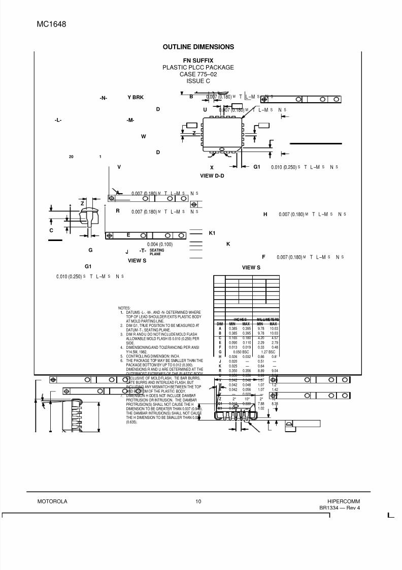
8/20/2019 FM Xmtr Theory
http://slidepdf.com/reader/full/fm-xmtr-theory 93/95
MC1648
MOTOROLA HIPERCOMMBR1334 — Rev 4
10
OUTLINE DIMENSIONS
FN SUFFIXPLASTIC PLCC PACKAGE
CASE 775–02ISSUE C
ABCEFGHJKRUVWXY
ZG1K1
MIN MINMAX MAXINCHES MILLIMETERS
DIM9.789.784.202.290.33
0.660.510.648.898.891.071.071.07 —
2° 7.881.02
10.0310.034.572.790.48
0.81 — —9.049.041.211.211.420.50
10°8.38 —
0.3850.3850.1650.0900.013
0.0260.0200.0250.3500.3500.0420.0420.042
—
2°0.3100.040
0.3950.3950.1800.1100.019
0.032 — —
0.3560.3560.0480.0480.0560.020
10° 0.330
—
1.27 BSC0.050 BSC
NOTES:1. DATUMS -L-, -M-, AND -N- DETERMINED WHERE
TOP OF LEAD SHOULDER EXITS PLASTIC BODYAT MOLD PARTING LINE.
2. DIM G1, TRUE POSITION TO BE MEASURED ATDATUM -T-, SEATING PLANE.
3. DIM R AND U DO NOT INCLUDE MOLD FLASH.ALLOWABLE MOLD FLASH IS 0.010 (0.250) PERSIDE.
4. DIMENSIONING AND TOLERANCING PER ANSIY14.5M, 1982.
5. CONTROLLING DIMENSION: INCH.6. THE PACKAGE TOP MAY BE SMALLER THAN THE
PACKAGE BOTTOM BY UP TO 0.012 (0.300).DIMENSIONS R AND U ARE DETERMINED AT THEOUTERMOST EXTREMES OF THE PLASTIC BODYEXCLUSIVE OF MOLD FLASH, TIE BAR BURRS,GATE BURRS AND INTERLEAD FLASH, BUTINCLUDING ANY MISMATCH BETWEEN THE TOPAND BOTTOM OF THE PLASTIC BODY.
7. DIMENSION H DOES NOT INCLUDE DAMBARPROTRUSION OR INTRUSION. THE DAMBARPROTRUSION(S) SHALL NOT CAUSE THE HDIMENSION TO BE GREATER THAN 0.037 (0.940).THE DAMBAR INTRUSION(S) SHALL NOT CAUSETHE H DIMENSION TO BE SMALLER THAN 0.025(0.635).
-N- Y BRK
-M--L-
W
V
D
D20 1
A
RZ
C
G
G1
E
J
VIEW S
B
U
Z
G1X
H
F
VIEW S
K
K1
VIEW D-D
0.007 (0.180) T L –M S N SM
0.007 (0.180) T L –M S N SM
SEATINGPLANE
-T-
0.010 (0.250) T L –M S N SS
0.007 (0.180) T L –MS N SM
0.007 (0.180) T L –MS N SM
0.010 (0.250) T L –M S N SS
0.007 (0.180) T L –M S N SM
0.007 (0.180) T L –MS N SM
0.004 (0.100)
8/20/2019 FM Xmtr Theory
http://slidepdf.com/reader/full/fm-xmtr-theory 94/95
MC1648
HIPERCOMMBR1334 — Rev 4
11 MOTOROLA
Motorola reserves the right to make changes without further notice to any products herein. Motorola makes no warranty, representation or guarantee regardingthe suitability of its products for any particular purpose, nor does Motorola assume any liability arising out of the application or use of any product or circuit, andspecifically disclaims any and all liability, including without limitation consequential or incidental damages. “Typical” parameters which may be provided in Motoroladata sheets and/or specifications can and do vary in different applications and actual performance may vary over time. All operating parameters, including “Typicals”must be validated for each customer application by customer’s technical experts. Motorola does not convey any license under its patent rights nor the rights ofothers. Motorola products are not designed, intended, or authorized for use as components in systems intended for surgical implant into the body, or otherapplications intended to support or sustain life, or for any other application in which the failure of the Motorola product could create a situation where personal injury
or death may occur. Should Buyer purchase or use Motorola products for any such unintended or unauthorized application, Buyer shall indemnify and hold Motorolaand its officers, employees, subsidiaries, affiliates, and distributors harmless against all claims, costs, damages, and expenses, and reasonable attorney feesarising out of, directly or indirectly, any claim of personal injury or death associated with such unintended or unauthorized use, even if such claim alleges thatMotorola was negligent regarding the design or manufacture of the part. Motorola and are registered trademarks of Motorola, Inc. Motorola, Inc. is an EqualOpportunity/Affirmative Action Employer.
How to reach us:USA/EUROPE/Locations Not Listed : Motorola Literature Distribution; JAPAN : Nippon Motorola Ltd.; Tatsumi–SPD–JLDC, 6F Seibu–Butsuryu–Center,P.O. Box 5405; Denver, Colorado 80217. 303–675–2140 or 1–800–441–2447 3–14–2 Tatsumi Koto–Ku, Tokyo 135, Japan. 81–3–3521–8315
Mfax ™: [email protected] – TOUCHTONE 602–244–6609 ASIA/PACIFIC : Motorola Semiconductors H.K. Ltd.; 8B Tai Ping Industrial Park,INTERNET : http://Design–NET.com 51 Ting Kok Road, Tai Po, N.T., Hong Kong. 852–26629298
MC1648/D◊
8/20/2019 FM Xmtr Theory
http://slidepdf.com/reader/full/fm-xmtr-theory 95/95
Appendix D
DataSheet for the PP3 not available atPresent.


![The Green Lab - [03 B] Measurement theory basics](https://static.fdocuments.nl/doc/165x107/58a27fce1a28ab891a8b585f/the-green-lab-03-b-measurement-theory-basics.jpg)