High Order VCO Based Delta Sigma Modulator Amir …Academiejaar 2016 - 2017 ISBN 978-90-8578-970-3...
157
High Order VCO Based Delta Sigma Modulator Amir Babaie Fishani Promotor: prof. dr. ir. P. Rombouts Proefschrift ingediend tot het behalen van de graad van Doctor in de ingenieurswetenschappen: elektrotechniek Vakgroep Elektronica en Informatiesystemen Voorzitter: prof. dr. ir. R. Van de Walle Faculteit Ingenieurswetenschappen en Architectuur Academiejaar 2016 - 2017
Transcript of High Order VCO Based Delta Sigma Modulator Amir …Academiejaar 2016 - 2017 ISBN 978-90-8578-970-3...

High Order VCO Based Delta Sigma Modulator
Amir Babaie Fishani
Promotor: prof. dr. ir. P. RomboutsProefschrift ingediend tot het behalen van de graad vanDoctor in de ingenieurswetenschappen: elektrotechniek
Vakgroep Elektronica en InformatiesystemenVoorzitter: prof. dr. ir. R. Van de Walle
Faculteit Ingenieurswetenschappen en ArchitectuurAcademiejaar 2016 - 2017

ISBN 978-90-8578-970-3NUR 959Wettelijk depot: D/2017/10.500/5

Universiteit GentFaculteit Ingenieurswetenschappen en Architectuur
Vakgroep Elektronica en Informatiesystemen
Promoter:Prof. dr. ir. Pieter Rombouts
Examination board:Prof. dr. ir. Jan Van Campenhout (chairman) Universiteit GentProf. dr. ir. Pieter Rombouts (promoter*) Universiteit GentProf. dr. ir. Jan Doutreloigne Universiteit GentProf. dr. ir. Georges Gielen Katholieke Universiteit LeuvenProf. dr. ir. Luis Hernandez Universidad Carlos III de MadridProf. dr. ir. Marc Moeneclaey Universiteit GentProf. dr. ir. Guy Torfs Universiteit Gent
* The promoter is not a voting member of the board.
Universiteit GentFaculteit Ingenieurswetenschappen en Architectuur
Vakgroep Elektronica en InformatiesystemenTechnologiepark-Zwijnaarde 15 iGent, 9052 Gent, Belgie.
Tel: +32-9-264-3366Fax: +32-9-264-3594
This work was supported by FWO.
Dissertation submitted to obtain the degree ofDoctor of Electrical Engineering
Academic year 2016-2017


Acknowledgment
First of all, I would like to express my deep appreciation to my advisorProfessor Dr. Pieter Rombouts, you have been a tremendous mentor forme. I would like to thank you for encouraging my research and for allowingme to grow as a research scientist. Your advice on both research as well ason my career have been priceless.
I would also like to thank the members of the examination board. Yourfeedback and comments have been a great help to improve the quality ofthis work.
I am indebted to Prof. Gielen for all the challenging meetings that we’vehave had during these years and for his constructive feedbacks at every turnof my work.
My family, whom I immensely love and miss, have always been therefor me during my years in Iran and their moral support never stoppedafterwards.
I would like to thank the members of the Circuit And System researchgroup (Pieter, Ludo, Maarten, Johan, and Dries) for being such greatfriends to me and for all the help and advice throughout these years.
The most special thanks to my wife for her unconditional support andlove. Thanks for encouraging me to strive towards my goal.
Gent, December 2016Amir Babaie-Fishani
i

ii
Contents
1 Introduction 1
1.1 Dissertation organization . . . . . . . . . . . . . . . . . . . 3
2 Previous work on VCO-ADC 5
2.1 Basics of Analog to Digital Conversion . . . . . . . . . . . . 5
2.1.1 Nyquist rate ADC . . . . . . . . . . . . . . . . . . . 6
2.1.2 Over-sampling ADC . . . . . . . . . . . . . . . . . . 7
2.1.3 Discrete Time Delta Sigma Modulator . . . . . . . . 8
2.1.4 Continuous Time Delta Sigma Modulator . . . . . . 10
2.2 First order VCO-ADC . . . . . . . . . . . . . . . . . . . . . 11
2.2.1 Circuit level considerations . . . . . . . . . . . . . . 13
2.3 PWM pre-coding . . . . . . . . . . . . . . . . . . . . . . . . 14
2.4 Coarse-fine structure . . . . . . . . . . . . . . . . . . . . . . 16
2.5 Voltage-to-phase VCO-based ADC . . . . . . . . . . . . . . 17
2.6 High order VCO-based ADC’s . . . . . . . . . . . . . . . . . 19
2.6.1 Using conventional loop-filter . . . . . . . . . . . . . 19
2.6.2 MASH VCO-ADC . . . . . . . . . . . . . . . . . . . 21
2.6.3 All-VCO CT-DSM . . . . . . . . . . . . . . . . . . . 22
3 High order VCO-based CT-DSM 25
3.1 Modeling a first order VCO-ADC . . . . . . . . . . . . . . . 25
3.1.1 Splitting the Sampling Quantizer . . . . . . . . . . . 25
3.1.2 CT equivalence of a VCO ADC . . . . . . . . . . . . 27
3.2 Using a VCO as the first Integrator . . . . . . . . . . . . . . 29
3.2.1 Introducing the Up-Down Counter . . . . . . . . . . 30
3.2.2 Proposed Scheme . . . . . . . . . . . . . . . . . . . . 31
3.2.3 Simulation results . . . . . . . . . . . . . . . . . . . 33
3.2.4 Implementation considerations . . . . . . . . . . . . 35
iii

iv Contents
3.3 High order All-VCO CT-DSM . . . . . . . . . . . . . . . . . 36
3.3.1 VCO based continuous-time integrator . . . . . . . . 36
3.3.2 VCO based sampling quantizer . . . . . . . . . . . . 38
3.3.3 General All-VCO CT-DSM architecture . . . . . . . 41
4 Linear voltage controlled ring oscillator 43
4.1 Ring oscillator input circuit . . . . . . . . . . . . . . . . . . 43
4.2 Oscillator core design . . . . . . . . . . . . . . . . . . . . . . 45
4.3 Measurement Results . . . . . . . . . . . . . . . . . . . . . . 47
5 Theory and design of a passive ADSM 51
5.1 Analyzing ADSMs without delay . . . . . . . . . . . . . . . 52
5.1.1 Proposed Theory . . . . . . . . . . . . . . . . . . . . 54
5.1.2 Simulation Results . . . . . . . . . . . . . . . . . . . 60
5.1.3 Conclusion . . . . . . . . . . . . . . . . . . . . . . . 63
5.2 Analyzing ADSMs, with loop delay . . . . . . . . . . . . . . 64
5.2.1 Previous theory and its limitations . . . . . . . . . . 65
5.2.2 Proposed approach . . . . . . . . . . . . . . . . . . . 67
5.2.3 Implications and Results . . . . . . . . . . . . . . . . 72
5.2.4 Simulation results . . . . . . . . . . . . . . . . . . . 72
5.2.5 Conclusion . . . . . . . . . . . . . . . . . . . . . . . 75
5.3 Implementation and measurement . . . . . . . . . . . . . . 77
5.3.1 Passive ADSM . . . . . . . . . . . . . . . . . . . . . 77
5.3.2 Circuit design . . . . . . . . . . . . . . . . . . . . . . 78
5.3.3 Measurement Results . . . . . . . . . . . . . . . . . 80
5.3.4 Conclusion . . . . . . . . . . . . . . . . . . . . . . . 83
6 Design and implementation of a mostly digital VCO-basedCT-DSM with 3rd order noise shaping 85
6.1 Simplified Implementation . . . . . . . . . . . . . . . . . . 86
6.1.1 Implementation for a Single phase VCO . . . . . . . 86
6.1.2 Multi phase implementation . . . . . . . . . . . . . . 89
6.1.3 Reduced degree of freedom in the system . . . . . . 91
6.2 VCO and DCO’s . . . . . . . . . . . . . . . . . . . . . . . . 93
6.3 Experimental Results . . . . . . . . . . . . . . . . . . . . . 96
6.4 Conclusion . . . . . . . . . . . . . . . . . . . . . . . . . . . 105
Contents v
7 Implementation of a 3rd order VCO-based CT-DSM withPWM pre-coding 1077.1 Implementation details . . . . . . . . . . . . . . . . . . . . . 1077.2 Implementation and Measurement . . . . . . . . . . . . . . 1107.3 Mismatch, aliasing, and inter-modulation . . . . . . . . . . 1127.4 Conclusion . . . . . . . . . . . . . . . . . . . . . . . . . . . 115
8 Conclusion 1178.1 Contributions . . . . . . . . . . . . . . . . . . . . . . . . . . 1188.2 Future work . . . . . . . . . . . . . . . . . . . . . . . . . . . 119

vi Contents

List of Figures
2.1 (a) A sampling quantizer as a Nyquist rate ADC, (b) sepa-rating the sampling and quantizing functions, and (c) addinganti-aliasing low pass filter. . . . . . . . . . . . . . . . . . . 6
2.2 (a) System level structure of a typical DT-DSM, withoutadditional feed-forward or local feedback paths, and (b) aDT-DSM with a more general loop filter. . . . . . . . . . . 9
2.3 (a) System level structure of a typical CT-DSM, withoutadditional feed-forward or local feedback paths, and (b) aCT-DSM of the kth order. . . . . . . . . . . . . . . . . . . . 11
2.4 (a) an open-loop first order VCO based ADC, and(b) and (c) its equivalent model. . . . . . . . . . . . . . . . 12
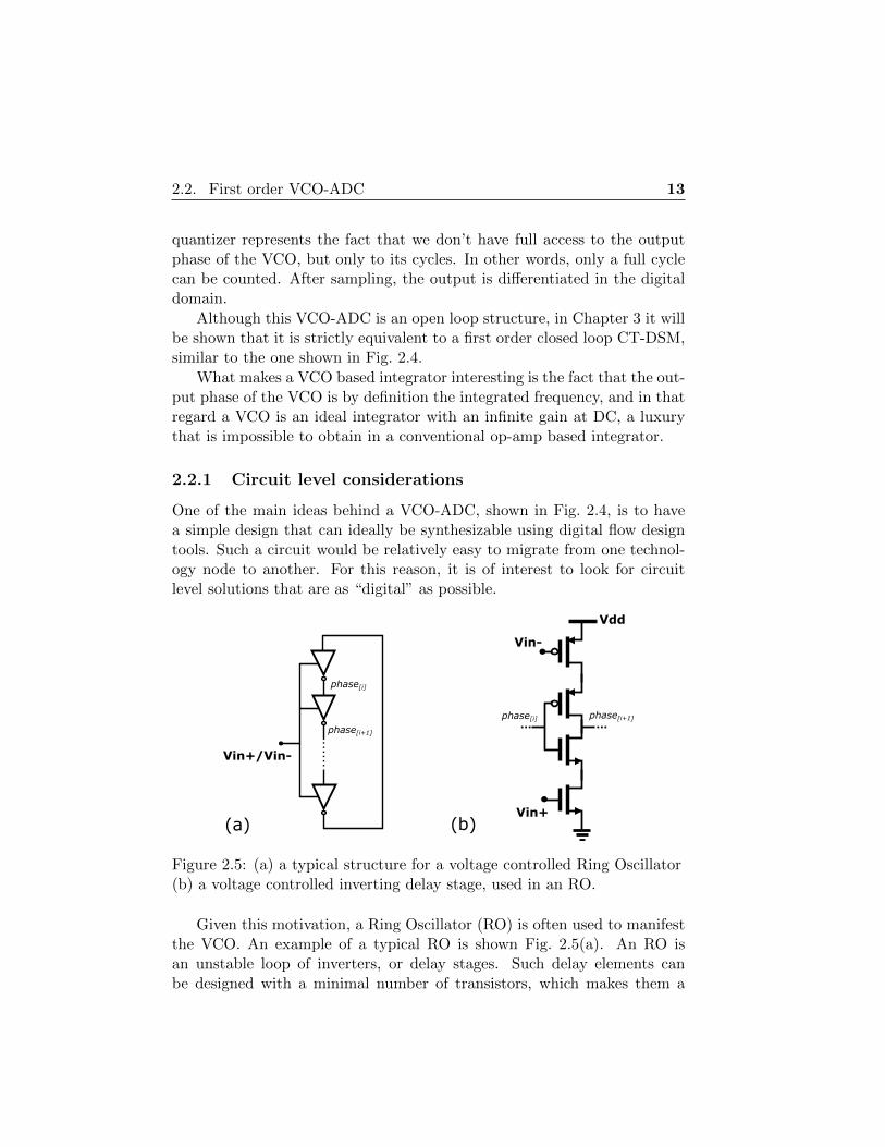
2.5 (a) a typical structure for a voltage controlled Ring Oscillator(b) a voltage controlled inverting delay stage, used in an RO. 13
2.6 (a) a common implementation for a single phase reset-counter,(b) its timing diagram . . . . . . . . . . . . . . . . . . . . . 15
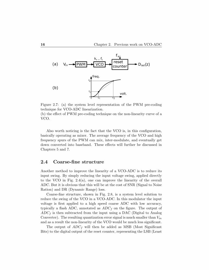
2.7 (a) the system level representation of the PWM pre-codingtechnique for VCO-ADC linearization.(b) the effect of PWM pre-coding technique on the non-linearity curve of a VCO. . . . . . . . . . . . . . . . . . . . 16
2.8 System level representation of a Coarse-fine VCO-ADC struc-ture, also know as 0-1 MASH VCO-ADC or residue cancelingVCO-ADC. . . . . . . . . . . . . . . . . . . . . . . . . . . . 17
2.9 (a) a voltage-to-phase VCO based integrator,(b),(c) its system level equivalents,(d) a first order voltage-to-phase VCO based ADC. . . . . . 18
vii
viii List of Figures
2.10 (a) using a voltage-to-frequency VCO-ADC as a noise shap-ing quantizer in the loop of a CT-DSM,(b) using a voltage-to-phase VCO-ADC as a noise shapingquantizer in the loop of a CT-DSM. . . . . . . . . . . . . . 20
2.11 The system level structure of a second order 1-1 MASHVCO-ADC. . . . . . . . . . . . . . . . . . . . . . . . . . . . 21
2.12 Two high order VCO based ADC’s using voltage-to-phaseand voltage-to-frequency integrators and quantizers. . . . . 22
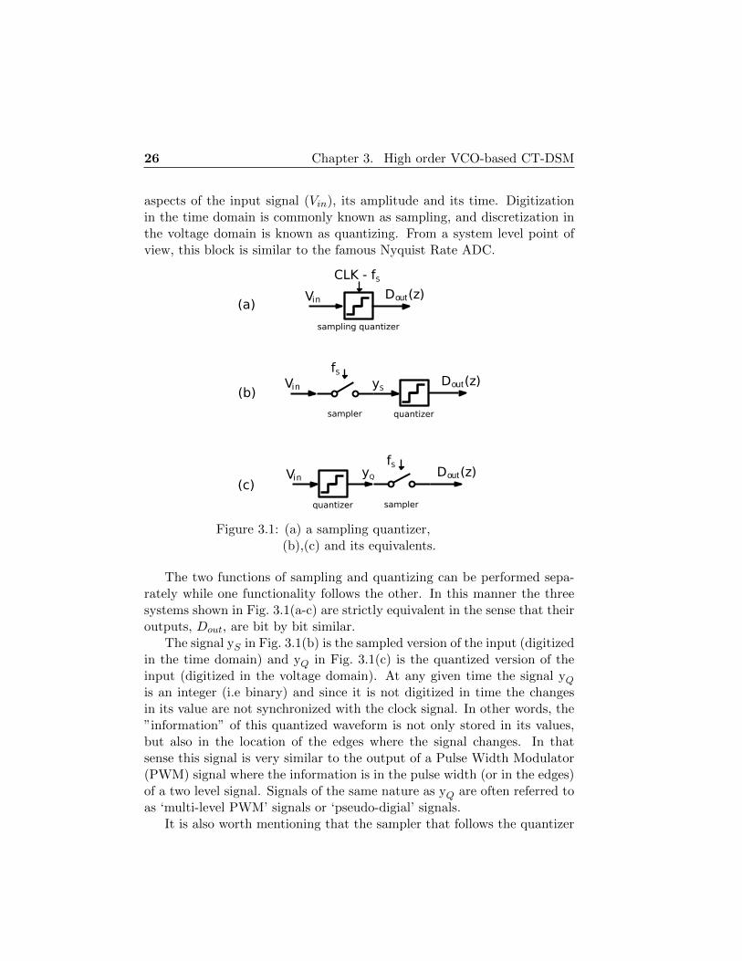
3.1 (a) a sampling quantizer,(b),(c) and its equivalents. . . . . . . . . . . . . . . . . . . . 26
3.2 (a) a first order VCO ADC,(b-f) and its system level equivalents. . . . . . . . . . . . . . 28
3.3 Metamorphosis of an open-loop first order VCO-ADC to aclosed-loop one.(a) the basic structure of a VCO-ADC(b) An equivalent system with up-counter and digital differ-entiator(c) replacing the differentiator with an integrator in the feed-back(d) extending the loop from digital to analog domain(e) replacing the up-counter and the integrator with an up-down counter . . . . . . . . . . . . . . . . . . . . . . . . . . 31
3.4 (a) The proposed system with a VCO as the first integrator,(b),(c) and its CT equivalents. . . . . . . . . . . . . . . . . 32
3.5 Simulation results of two 1-bit CT-DSMs with a -14 dBfsinput tone.(a) output spectrum of a conventional 3rd order modulator(b) output spectrum of a VCO-based modulator with thesame NTF(c) output signal of the first integrator for the conventionalmodulator(d) output signal of the first integrator for the VCO-basedmodulator . . . . . . . . . . . . . . . . . . . . . . . . . . . 34

List of Figures ix
3.6 Simulation results of two 1-bit CT-DSMs with a -6 dBfs in-put tone.(a) output spectrum of a conventional 3rd order modulator(b) output spectrum of a VCO-based modulator with thesame NTF(c) output signal of the first integrator for the conventionalmodulator(d) output signal of the first integrator for the VCO-basedmodulator . . . . . . . . . . . . . . . . . . . . . . . . . . . . 35
3.7 (a) A VCO based integrator(b) and its equivalent continuous-time model. . . . . . . . . 37
3.8 (a) A First-order noise shaping quantizer consisting of aVCO and a reset-counter,(b) an alternative implementation with the same behavior(c) and an equivalent continuous time model. . . . . . . . . 39
3.9 (a) Proposed architecture of a 3rd-order all-VCO CT-DSM(b) and its equivalent CT-DSM. . . . . . . . . . . . . . . . . 40
4.1 Ring oscillator with N differential delay elements. . . . . . . 43
4.2 Delay cell used in the ring oscillator. . . . . . . . . . . . . . 44
4.3 Ring oscillator with resistive input stage . . . . . . . . . . . 45
4.4 (a) Tuning curve with current control exhibiting a negativecurvature,(b) and Control voltage Vctrl vs the input voltage curve ex-hibiting a positive curvature. . . . . . . . . . . . . . . . . . 46
4.5 (a) the voltage to frequency conversion curve of the proposedVCO(b) and the nonlinearity of its frequency error. . . . . . . . 47
4.6 Output spectrum of the pseudo differential VCO ADC ex-periment. . . . . . . . . . . . . . . . . . . . . . . . . . . . . 48
4.7 SNR and SNDR vs. the normalized rail to rail input level(of 2Vpp differentially). . . . . . . . . . . . . . . . . . . . . 49
5.1 A typical spectrum for the output of an ADSM. . . . . . . . 53
5.2 A general representation of an ADSM. . . . . . . . . . . . . 54
5.3 Typical waveforms for the ADSM in Fig. 5.2. . . . . . . . . 55

x List of Figures
5.4 Comparison between simulation results and theory for a 1storder ADSM with a DC input:a) the difference between the DC level of output and inputsignals,b) and the carrier frequency. . . . . . . . . . . . . . . . . . . 62
5.5 Comparison between simulation results and theory for anADSM with a 1st order passive filter. . . . . . . . . . . . . . 63
5.6 Average carrier frequency, fc, and the 3rd order distortion,d3, of a 1st order ADSM as a function of its input amplitudeA. . . . . . . . . . . . . . . . . . . . . . . . . . . . . . . . . 64
5.7 Comparison between simulation results and theory for the3rd order harmonic distortion of a 3rd order ADSM over itsinput frequency. . . . . . . . . . . . . . . . . . . . . . . . . . 65
5.8 Average carrier frequency, fc, and 3rd order distortion, d3,of a 3rd order ADSM vs. the input amplitude, A. . . . . . . 66
5.9 General representation of an ADSM,(a) without extra delay in the loop,(b) and with loop delay. . . . . . . . . . . . . . . . . . . . . 67
5.10 Typical waveforms of an schmitt trigger based ADSM withdelay. . . . . . . . . . . . . . . . . . . . . . . . . . . . . . . 68
5.11 typical waveforms of two ADSMs,a) without any delay in the loop,b) and with loop delay. . . . . . . . . . . . . . . . . . . . . . 73
5.12 Output spectrum of two equivalent ADSMs with first orderloop filter,(a) with some delay in the loop,(b) and without loop delay. . . . . . . . . . . . . . . . . . . 74
5.13 Comparing the distortion of two equivalent second orderADSMs with theory. . . . . . . . . . . . . . . . . . . . . . . 75
5.14 (a) block diagram of a Passive ADSM,(b) and its circuit. . . . . . . . . . . . . . . . . . . . . . . . 77
5.15 (a) Overall Schmitt Trigger structure,(b) schematic of the Pre amplifier, which (apart from thesizing) is identical to the Schmitt Trigger’s schematic,(c) and the digital buffer circuit. . . . . . . . . . . . . . . . 79
5.16 (a) input circuit of a Two-level Ring oscillator,(b) and the actual ring. . . . . . . . . . . . . . . . . . . . . 80
5.17 I/O and nonlinearity plots. (Theory from Eq. 5.53) . . . . . 82
List of Figures xi
5.18 Output spectrum of the linearized VCO for a 550 mVpp
100 kHz input signal. . . . . . . . . . . . . . . . . . . . . . . 82
5.19 SNR and SNDR vs. the normalized rail to rail input level(of 1 Vpp). (Theory in Eq. 5.54) . . . . . . . . . . . . . . . 83
6.1 (a) The proposed implementation of a single phase up-downcounter,(b) and its timing diagram. . . . . . . . . . . . . . . . . . . 87
6.2 (a)The proposed implementation of a reset counter,(b) and its timing diagram. . . . . . . . . . . . . . . . . . . 88
6.3 The proposed implementation of a high order VCO-ADC(with local feedback), where the digital signals are repre-sented by n parallel thermometer encoded bits. . . . . . . . 90
6.4 The equivalent CT-DSM of our implemented VCO-ADC withreduced degree of freedom. . . . . . . . . . . . . . . . . . . . 92
6.5 Output spectrum (160K pt FFT) of a behavioral simulationresult for the case fs=1.6 GHz,fc=250 MHz and n=9:(a) the actual structure of Fig. 6.3(b) the equivalent continuous time model of Fig. 6.4 . . . . 93
6.6 Ring Oscillator core . . . . . . . . . . . . . . . . . . . . . . 94
6.7 Differential delay element used in the Ring Oscillator core . 94
6.8 The level-shifter for RO2 and RO3. . . . . . . . . . . . . . . 95
6.9 The output spectrum (160K pt FFT) of a behavioral simu-lation result for the case fs=1.6 GHz,fc=250 MHz and n=9,where a level shifter delay of 700 ps is inserted after eachVCO. . . . . . . . . . . . . . . . . . . . . . . . . . . . . . . 96
6.10 Chip microscope photograph with annotated layout. . . . . 97
6.11 Measured output spectrum (160K pt FFT) for the case offc = 250 MHz and fs = 1.6 GHz with a 3 MHz input tonewith an amplitude of a 650mVpp differentially:(a) normal (pseudo-differential) output,(b) partially decimated (pseudo-differential) output with off-line digital calibration overlayed on the raw output. . . . . 98
6.12 Static nonlinearity plot of the ADC for the case of of fc =250 MHz and fs = 1.6 GHz in the pseudo differential con-figuration. . . . . . . . . . . . . . . . . . . . . . . . . . . . . 99
xii List of Figures
6.13 Block diagram of an oversampling converter with off-line dig-ital calibration:a) conventional setup discussed in this section,b) and setup used in this work. . . . . . . . . . . . . . . . . 101
6.14 Dynamic range plot for the case of fc = 250 MHz, fs =1.6 GHz and 10 MHz bandwidth. . . . . . . . . . . . . . . . 102
6.15 Baseband FFT plot for the case of two-tone input signalof two tones near 9 MHz with the same peak-to-peak signallevel as for the plot of Fig. 6.11 (650mVpp differentially): (a)normal (pseudo-differential) output, (b) (pseudo-differential)output with off-line digital calibration. . . . . . . . . . . . . 103
7.1 System level representation of the proposed pseudo differen-tial 3rd order VCO-ADC with PWM pre-coding. . . . . . . 108
7.2 The circuit level implementation for the system proposed inFig. 7.1. . . . . . . . . . . . . . . . . . . . . . . . . . . . . . 109
7.3 A photograph of the fabricated die. . . . . . . . . . . . . . . 1107.4 Measured output spectrum of the presented modulator with
a sine wave input voltage, Vpp = 400 mv,(a) single-ended measurement,(b) pseudo-differential measurement. . . . . . . . . . . . . . 111
7.5 The SNR/SNDR curve of the measured ADC. . . . . . . . . 1127.6 Measured output spectrum of the single-ended modulator
with a sine wave input voltage, Vpp = 600 mV . . . . . . . . 1137.7 The output spectrum of a system level noise-less simulation
of the modulator with a sine wave input voltage, Vpp = 600mV .1137.8 Measured output spectrum of the modulator on a linear scale
for input sine wave with a small amplitude. . . . . . . . . . 114

List of Tables
6.1 Comparison with related work . . . . . . . . . . . . . . . . . 104
7.1 Performance summary of the presented works in this book. 115
xiii

xiv List of Tables
Summary
This work aims at exploring new ways of realizing analog functions in timebased blocks, instead of voltage based ones. The two functions that wereof utmost importance to this work are integration and quantization. Usingthese two functions one can implement important analog blocks, such asanalog filters and analog to digital converters.
The main incentive for time-domain signal processing is to benefit fromthe digital blocks that are becoming faster and more efficient in the newerCMOS technologies. Moreover, in the more advanced CMOS processesit has become more challenging to design these functions in the voltagedomain. This is partly due to the fact the transistors can only deliver asmaller gain, the threshold voltage of the transistors is not dropping asrapidly as the supply voltage, and this loss of voltage headroom is causingdynamic-range loss.
This book investigates linear, low-voltage, low-area, solutions for thedesign of Continuous-Time Delta Sigma Modulators (CT-DSM) with highorders of quantization noise shaping. In this pursuit we have proposed thedesign of, and showcased the implementation of, high order VCO-BasedADC’s, linear VCO’s, and Asynchronous Delta Sigma Modulators (ADSM).All of the presented designs are digital friendly and make use of no tradi-tional analog building blocks, like op-amps and highly linear transconduc-tors. Being digital friendly means having the potential to benefit fromtechnology scaling and being synthesizable using digital design flow.
On a system level, a new VCO-based CT-DSM structure is presented. Inthis system the combination of a VCO (Voltage Controlled Oscillator) andsome digital blocks (referred to as up-down counter) is used as an integrator.The quantizer of the modulator is also VCO-based. Since a VCO can beimplemented using an RO (Ring Oscillator), it can be very simple anddigital friendly. In this manner a high order CT-DSM can be designed usingonly these blocks. Typical CT-DSM techniques, such as local feedback can
xv
xvi
be incorporated in this novel structure. Many circuit level innovations andsimplifications are presented to make the implementation of this modulatorpossible. The final circuit level solution is very simple to design and size.Therefore, it is expected to be easy to migrate from one technology nodeto another. The linearity of this modulator is limited by that of the firstVCO on the signal path.
A thorough theoretical work is carried out in modeling an ADSM topredict its linearity performance. ADSM’s are a family of PWM’s (PulseWidth Modulator) that have many applications, like linearizing a VCO-based ADC. It is also proven this block can be implemented using onlya Schmitt trigger and a passive loop filter, which is also simple to designand can benefit from technology scaling. Previous implementations of anADSM or a PWM, presented in literature, required either an op-amp basedor gmC based integrator. The effect of delay in the loop of an ADSM isalso studied and accurate equations to predict the linearity and oscillationfrequencies of an ADSM with loop delay are extracted. As a proof ofconcept, a passive ADSM is implemented in 65nm CMOS technology. Thedesign is operational under a 1 V supply and has more than 10 bit linearityover a 10 MHz bandwidth.
A circuit level solution is presented to design a voltage controlled ringoscillator with high linearity. The implemented prototype of this blockwas shown to be much more linear than previous works – in other worksthe non-linearity of the VCO is not mentioned, it is only stated that theVCO has severe non-linearity and should be compensated using differentmethods. This block can be used as the first VCO in a high order CT-DSM. This block determines the linearity of the overall modulator. Aprototype is implemented in the 65 nm technology and the measured voltageto frequency conversion curve of the VCO for a rail-to-rail input showsa small 0.6 % deviation from an ideal line. Measurements on a pseudo-differential setup proved that the second harmonic distortion of the VCOcan be heavily suppressed.
As a proof of concept, for the first time a 3rd order VCO-based CT-DSM is implemented in the low power version of a 65nm technology fora 10 MHz bandwidth. This prototype shows a measured performance of71/66.2/62.5 dB DR/SNR/SNDR at a 10 MHz bandwidth while consuming1.8 mW from a 1.0 V analog and 1.9 mW from a 1.2 V digital supply. Withdigital calibration, the nonlinearity could be pushed below the noise level,leading to an improved peak SNDR of 66 dB. The modulator covers a small
Summary xvii
silicon area of only 0.01 mm2.As a second attempt to design a linear mostly digital low voltage high
order VCO based CT-DSM, an ADSM is used before the first VCO tolinearize it. A proof of concept is implemented in the low power versionof a 65 nm technology for a 10 MHz bandwidth. This prototype shows ameasured performance of 67.4/59/55.4 dB DR/SNR/SNDR at a 10 MHzbandwidth while consuming 2.3 mW from a 1.0 V analog and 2 mW froma 1.2 V digital supply. The modulator covers a silicon area of 0.018 mm2.
List of the publications that have resulted from this work can be foundhere [1–7].

xviii

Samenvatting
Het doel van dit werk is het verkennen van nieuwe manieren om analogefunctionaliteit te realiseren in het zogenaamde “tijdsdomein” in plaats vanhet gebruikelijke “spanningsdomein”. Er zijn twee basisbewerkingen die degrondslag vormen van de rest van dit werk. Deze basisbewerkingen zijnenerzijds integratie en anderzijds kwantisering. Op basis van deze twee ba-sisbewerkingen kan men belangrijke analoge bouwblokken realiseren, zoalsanaloge filters en analoog-naar-digitaal omzetters.
De belangrijkste stimulans om over te stappen naar “tijdsdomein”-signaalverwerking is om te proberen profijt te halen uit het feit dat dedigitale blokken steeds sneller en efficienter worden in de nieuwere CMOS-technologieen. Bovendien, in de diep-submicron CMOS-processen die van-daag bijna standaard zijn, wordt het steeds moeilijker om deze functies terealiseren in het “spanningsdomein”. Dit is deels te wijten aan het feitdat de diep-submicron-transistoren slechts een lage versterking kunnen re-aliseren. Verder is er het probleem dat de voedingsspanning enorm veelverlaagd is, terwijl de drempelspanning van de transistoren niet evenredigmee verlaagd is. Het gevolg hiervan is dat er niet veel ruimte is om eenacceptabele spanningszwaai te realiseren. Dit stelt uiteraard problemen alsmen een groot dynamisch bereik wil realiseren.
Deze tekst onderzoekt lineaire oplossingen voor het ontwerp van DeltaSigma Modulatoren op basis van filters die in continue tijd werken (Engels:Continuous Time Sigma Delta Modulator, afgekort CT-DSM). Hierbij ishet de bedoeling dat deze circuits bij een lage voedingsspanning kunnenwerken en dat ze een kleine chipoppervlakte innemen. Tijdens onze zoek-tocht hebben we verscheidene ontwerpsmethodes voorgesteld en die ookgedemonstreerd met praktische implementaties. In het bijzonder, hebbenwe Analoog-naar-Digitaal Omzetters op basis van VCO’s voorgesteld die, integenstelling tot wat tot nu toe haalbaar was, een hoge orde van spectraalkneden realiseren. Verder hebben we een zeer lineaire VCO voorgesteld
xix

xx
en Asynschrone Delta Sigma Modulatoren (ASDM). Al de voorgesteldetechnieken en gerealiseerde ontwerpen leunen dicht aan bij digitale cir-cuits (Engels: “digital friendly”): ze vereisen geen veeleisende traditionaleanaloge bouwblokken zoals operationele versterkers, of lineaire transcon-ductantietrappen. Integendeel, alle voorgestelde circuits zouden in principezelfs gedeeltelijk gesynthetiseerd kunnen worden met standaard digitale on-twerpssoftware.
Op systeemniveau, werd een nieuwe CT-DSM-structuur op basis vanVCO’s gepresenteerd. In dit systeem wordt de combinatie van een VCO eneen aantal digitale blokken (die we kunnen beschouwen als een op-en-neer-teller) gebruikt als een analoge integrator. Ook de kwantiseereenheid vande modulator is gebaseerd op een VCO. Aangezien een VCO kan wordenuitgevoerd met behulp van een ringoscillator (RO), kan een dergelijk VCOheel eenvoudig zijn en zelfs bijna als een digitaal circuit beschouwd worden.Door meerdere van deze integratoren te combineren, kan een CT-DSM vanhoge orde worden gemaakt. Typische verfijningen die in CT-DSM toegepastkunnen worden, zoals het gebruikt van lokale terugkoppeling, kunnen ookin deze nieuwe structuur worden opgenomen. Om de praktische realisatievan een prototype modulator mogelijk te maken, werden nog verscheideneinnovaties en vereenvoudigingen op circuitniveau voorgesteld. De oploss-ing die we uiteindelijk op circuitniveau voorstellen, is zeer eenvoudig teontwerpen en te dimensioneren. Daarom verwachten we dat dergelijke cir-cuits gemakkelijk te migreren zullen zijn van de ene technologieknoop naareen andere. De voorgestelde structuur heeft echter een beperking: namelijkdat de lineariteit van de modulator wordt beperkt door die van de eersteVCO in het signaalpad.
In deze context, werd een grondige theoretische studie uitgevoerd omde niet-lineariteit van een ADSM te voorspellen. ADSM’s zijn een familievan PWM’s (Puls Breedte Modulatoren), die vele toepassingen hebben. Detoepassing die ons interesseerde is het linearizeren van onze VCO-ADC. Bijonze studie, is aangetoond dat dit blok kan worden geımplementeerd op ba-sis van een Schmitt-trigger en verder een volledig passief lusfilter. Dit zijnweliswaar analoge circuits, maar ze zijn zo eenvoudig dat het ontwerp ervangeen enkel probleem stelt, zelfs in de geschaalde CMOS-technologie van van-daag. Eerdere implementaties van een ADSM of PWM, die in de literatuurwerden beschreven, vereisten steeds een actieve integrator (met een opera-tionele versterker of een lineaire transconductantietrap). Het effect van devertraging in de lus van een ADSM werd ook bestudeerd en nauwkeurige

Samenvatting xxi
vergelijkingen om de lineariteit en de oscillatiefrequentie van een ADSMmet lusvertraging te voorspellen werden voorgesteld. Als demonstrator,werd een passieve ADSM geımplementeerd in 65 nm CMOS-technologie.Het ontwerp is operationeel bij een voedingsspanning van 1 volt en behaaltmeer dan 10 bit lineariteit bij een bandbreedte van 10 MHz.
Daarnaast werd ook een oplossing op circuitniveau voorgesteld om eenVCO met een hoge lineariteit te realiseren. De lineariteit van ons geımplementeerdprototype van dit circuit bleek grootteordes beter te zijn dan de voorgaande“state-of-the-art”. Dit circuit kan dan worden gebruikt als de eerste VCO inonze CT-DSM met spectrale kneding van hoge orde. We hadden al vermelddat de eerste VCO in deze nieuwe architectuur de lineariteit van de totalemodulator bepaalt. Ons prototype is geımplementeerd in een 65 nm CMOS-technologie en de gemeten spanning naar frequentie omzettingscurve van deVCO, vertoont voor een volledige signaalzwaai van de onderste voedingslijnnaar de bovenste voedingslijn slechts 0.6 % niet-lineariteit (afwijking vande ideale lijn). Daarenboven kan het circuit ook in een pseudo-differentieleopstelling gebruikt worden, waarbij de prestaties nog verder verbeterd wer-den doordat de tweede-orde vervorming van de VCO hierdoor sterk wordtonderdrukt.
Als proof-of-concept, hebben we de voorgestelde concepten dan gecom-bineerd in een CT-DSM op basis van VCO’s. Dit is de eerste keer dateen circuit met 3de orde spectrale kneding van de kwantiseringsruis werdgedemonstreerd. Het ontwerp werd gedaan in de zogenaamde “low power”versie van een 65 nm-technologie. De signaalbandbreedte was 10 MHz.De gemeten prestaties van ons prototype zijn: een DR/SNR/SNDR van71/66.2/62.5 dB bij een bandbreedte van 10 MHz en een verbruik van1.8 mW aan de analoge voeding van 1.0 V en 1.9 mW aan de digitale voed-ing van 1.2V. Met digitale kalibratie kunnnen de fouten door nietlineariteitbeneden het ruisniveau worden geduwd, waardoor een betere piek SNDRvan 66dB behaald werd. De modulator neemt een zeer kleine chipopper-vlakte in van slechts 0.01 mm2.
Daarna hebben we een tweede poging gedaan om een lineaire bijna-digitale CT-DSM op basis van VCO’s te ontwerpen. Weer werd een lagevoedingsspanning en een hoge-orde van spectrale kneding van de kwantis-eringsruis beoogd. Hierbij werd nu een ADSM gebruikt die voor de eersteVCO in het circuit werd geplaatst met als doel de ADC als geheel te lin-eariseren. Een proof-of-concept circuit van dit idee werd geımplementeerd,opnieuw “low power” versie van een 65 nm-technologie. Hierbij werd ook

xxii
gemikt op een signaalbandbreedte van 10 MHz. De gemeten prestaties vandit prototype bij een bandbreedte van 10 MHz zijn: een DR/SNR/SNDRvan 67.4/59/55.4 dB bij een verbruik van 2.3 mW aan de analoge 1.0 Vvoeding en 2 mW aan de digitale 1.2 V voeding. Deze modulator neemteen nog steeds een zeer kleine chipoppervlakte in van 0.018 mm2 (zij hetiets groter dan het eerste prototype).
Glossary of symbols andabbreviations
ADC analog-to-digital converterADSM asynchronous delta sigma modulatorBW bandwidthCT continuous timeCT-DSM continuous time delta sigma modulatorDAC digital-to-analog converterdB decibeldec decadeDEM dynamic element matchingDR dynamic rangeDSM delta sigma modulatorDT discrete timeDT-DSM discrete time delta sigma modulatorDWA data weighted averagingFB feedbackFF feedforwardFS full scalegm trans-conducting amplifierLSB least significant bitMSB most significant bitNRZ non-return-to-zeroNTF noise transfer functionOSR oversampling ratioPWM pulse width modulatorQ quantization noisePM phase margin
xxiii
xxiv
RO ring oscillatorRZ return-to-zeroSCR switched-capacitor-resistorSDR signal-to-distortion ratioSNDR signal-to-noise-and-distortion ratioSNR signal-to-noise ratioSQNR signal-to-quantization-noise ratioSTF signal transfer functionTHD total harmonic distortionVCO voltage controlled oscillatorZOH zero-order hold
Chapter 1
Introduction
Traditionally, high-performance Analog-to-Digital converters (ADCs) haveheavily relied on conventional analog building blocks such as operationalamplifiers, transconductors and comparators [8–14].
Unfortunately, in today’s ultra deep sub-micron CMOS technologiesthese building blocks become increasingly difficult to design because of lim-ited voltage headroom due to the low supply voltage combined with reducedraw ‘analog’ performance of the elementary transistors (e.g. gain, match-ing, 1/f noise) [15]. Moreover these analog circuits have poor portability toother technology nodes and efficient testing is a specialty in itself [16].
For this reason, researchers have attempted to find more ‘digital’ so-lutions for these traditionally analog blocks. A promising approach here,are the VCO-based ADCs [17–26]. If the VCO-core is a ring-oscillator, thiscorresponds to a ‘nearly digital’ implementation. A Ring Oscillator consistsa loop of inverters or buffers, with an input dependent propagation delay,which are easy to design in every given technology.
Such a VCO-ADC was shown to exhibit first-order quantization noiseshaping and to have very similar behavior as a first-order Σ∆ modula-tor [20]. However, in the vast majority of the VCO-ADC designs that havebeen published, the VCO is still combined with sophisticated analog build-ing blocks (i.e. opamps, transconductors, . . . ), e.g. [17–19]. The reasonfor this is to solve the two fundamental problems of VCO-ADC’s. First,VCO-ADC’s have poor linearity, and second, they have only first ordernoise shaping. In this book it is attempted to solve both deficiencies whileavoiding sophisticated analog building blocks. A low supply voltage andlow silicon area consumption have been the main targets through out this
1

2 Chapter 1. Introduction
exploration.
VCO-ADCs suffer from nonlinearity problems because the linearity ofthe voltage to frequency conversion of most VCOs is very poor. This prob-lem can be tackled by combining the VCO-ADC with established analogtechniques such as feedback. However, there are also digital-friendly so-lutions such as digital (self)-calibration [23–28]. And of course, the mostsimple solution would be to start from a VCO-ADC that has sufficient lin-earity, which is explored in this dissertation, where a very simple circuit fora linear ring-oscillator based VCO is proposed.
Another potential solution to solve the linearity issue is to convert theinput voltage into a two-level signal where the information is stored in theduty cycle of the resulting square-wave using an Asynchronous Delta SigmaModulator (ADSM) or a Pulse Width Modulator (PWM). This method isknown as ‘PWM pre-coding’ [29–31]. Until now all reported implementa-tions either required an op-amp, a highly linear ramp source, or a lineargm cell [30–32] (‘gm’ stands for a trans-conducting amplifier). In practicesuch high-performance analog circuits are difficult to implement at today’slow supply voltages (of the order of 1 Volt) and hence are to be avoided.An alternative would be an ADSM with a passive RC loop filter [2, 3, 29].However, it is not obvious how such a passive ADSM should be designedas to achieve simultaneously high bandwidth and good linearity. For thisreason, until now, such a circuit has not yet been demonstrated in prac-tice. In this work, we explain how such a passive ADSM linearization ofa VCO can be designed to achieve good overall performance. The validityof the presented theory is confirmed by measurements on an implementedprototype.
As mentioned earlier, the second reason why most VCO-ADCs are com-bined with analog techniques is that, to the authors’ knowledge, all publi-cations of ‘implemented’ mostly digital VCO-ADC prototypes only exhibitfirst-order quantization noise shaping [23–28]. In some implementationsa VCO-ADC is used as a noise shaping quantizer, to operate as the lastintegrator in the chain of integrators in a Continuous-Time Delta SigmaModulator (CT-DSM). In this manner, the preceding integrators would beimplemented in the traditional analog manner, using op-amp or gm-C basedstructures. So, in these approaches the challenge of designing traditionalanalog blocks would still remain.
This manuscript also contributes on this border and presents the designof – and measurements on – a linear ‘mostly digital’ VCO-ADC with 3rd

1.1. Dissertation organization 3
order quantization noise shaping. The idea of a high order VCO-ADC isfirst introduced on a system level, then a circuit level solution is proposedthat can achieve high orders of quantization noise shaping using only VCO-based integrators and other digital blocks.
1.1 Dissertation organization
This dissertation is organized as follows:
Chapter 2 will examine some of the previous works in the field of VCObased ADC design. The key target is to implement a CT-DSM using VCObased integrators and avoid using traditional op-amp based loop filtersas much as possible. System level solutions to improve the linearity andincrease the order of quantization noise shaping will be discussed.
Chapter 3 introduces the system level concepts that are at the basis ofour high-order noise shaping VCO-ADC. In this chapter it is shown thatthe combination of a VCO and a digital block called “up-down counter”can be used as an integrator in the loop of a CT-DSM and can eventuallylead to a high order CT-DSM with only VCO-based integrators. In thefollowing chapters we will propose circuit level implementations for thismodulator.
The linearity of a VCO-based CT-DSM is limited by that of its firstVCO. In chapter 4 a linear voltage controlled ring oscillator structure isproposed. This circuit level solution is further verified through measure-ment results. Later on in chapter 6 this circuit will be used as the firstVCO of a high order all-VCO CT-DSM.
In Chapter 5 PWM pre-coding technique for linearizing the first VCOis examined. An ADSM structure is chosen to create PWM pulse signals.A full study is done on the behavioral model of an ADSM to predict itslinearity and carrier frequency. The effect of loop delay is also analyzedseparately. Eventually, a circuit level implementation of an ADSM is pro-posed. The effectiveness of the proposed circuit in linearizing a VCO isthen verified by examining the measurement results of a ADSM-VCO com-bination.
Chapter 6 showcases the first prototype of a 3rd order modulator of thistype (VCO-based CT-DSM). This chip uses the linear VCO introduced inchapter 4. Many circuit level innovations are introduced to make this designpossible. The resulting ADC is measured to have a competitive noise andlinearity performance, while being operational under a low supply voltage.
4 Chapter 1. Introduction
The core of the chip occupies many times less silicon area than its conven-tional CT-DSM counterparts. The measurement results are compared withsome of the more relevant prior works.
In chapter 7 a second implementation of a 3rd order VCO-based CT-DSM is presented. In order to have a linear ADC, this design uses theADSM-VCO combination introduced in chapter 5. The resulting modulatoris then compared to the design proposed in chapter 6. It is, afterwards,discussed why the chip with ADSM linearization technique is inferior tothe chip in chapter 6 in almost every aspect.
Chapter 8 concludes the dissertation and discusses future directions forthis research.
Chapter 2
Previous work on VCO-ADC
In this chapter first we will provide some basic background knowledge aboutNyquist Rate and Over-Sampling Analog to Digital Converters. Then wewill give the motivations for designing Discrete Time or Continuous TimeDelta Sigma Modulators (CT-DSM). Afterwards we will examine some ofthe previous works in the field of VCO based ADC design.
The key target is to implement a CT-DSM using VCO based integratorsand avoid using traditional op-amp based loop filters as much as possible.System level solutions to improve the linearity and increase the order ofquantization noise shaping will be discussed. Continuous-Time integratorsand a quantizer are the main ingredients for developing such a modulator.The idea is to replace these with their VCO based equivalents.
2.1 Basics of Analog to Digital Conversion
An analog to digital converter, which is fundamentally a mixed-signal block,converts a continuous-time (CT) analog voltage to a discrete-time discrete-amplitude digital stream, or in other words “digitizes” it. So this digitiza-tion is applied to the both aspects of the input signal, its amplitude andits time. Digitization in the time domain is commonly known as sampling,and digitization in the voltage domain is known as quantizing.
The performance of such a conversion is limited by its sampling speedand quantization accuracy. Sampling puts a limit on the signal bandwidthand quantization adds noise. In this section we will discuss the two majorADC families. In the first group the quantization noise has a white (flat)spectrum, like Nyquist-rate ADCs, and in the second family the quanti-
5

6 Chapter 2. Previous work on VCO-ADC
zation noise is “shaped” such that its effect is minimized in the frequencyrange that is of our interest, like Delta Sigma Modulators.
2.1.1 Nyquist rate ADC
Dout(z)Vi n
CLK - fS
Vi nfS
Dout(z)
sampling quantizer
sampler quantizer
Vi n
yS
(a)
(b)
(c)
fS
Dout(z)
sampler quantizeranti-aliasinglow pass filter
Figure 2.1: (a) A sampling quantizer as a Nyquist rate ADC,(b) separating the sampling and quantizing functions, and(c) adding anti-aliasing low pass filter.
A sampling quantizer, shown in Fig. 2.1(a), is the simplest implementa-tion of an ADC. Here Vin is the continuous-time (CT) input voltage, CLKrepresent the clock signal with a frequency of fs, and Dout is the digitaloutput stream, which is both discrete-time (DT) and quantized in value.
The two functions of sampling and quantizing can be performed sepa-rately while one functionality follows the other. In this manner the systemshown in Fig. 2.1(b) is strictly equivalent to the one in Fig. 2.1(a). Theinput voltage is sampled at the constant rate of fs, resulting in the DTsignal of YS . If the input bandwidth is limited and the sampling rate ishigh enough there will be no loss of information. The maximum bandwidththat the input signal can have to ensure a lossless transformation is fs/2.In other words, the sampling frequency should be at least twice the input

2.1. Basics of Analog to Digital Conversion 7
bandwidth, fs = 2 ∗ fB. This is commonly known as the Nyquist rate.
With a good approximation, the quantizer can be modeled as a lineargain, G, with an additive white noise with a variance of G2σ2/12, where σis the quantization step in the input. In this manner, the Dynamic Range(DR) of the ADC can be calculated.
DR is defined as the ratio of the full-scale input power to the inputpower at which the signal-to-noise ratio (SNR) is one. SNR is defined asthe ratio of the signal power to the noise power at the output. If the ADCdoesn’t introduce any distortion for larger signals the DR would normallybe equal to the SNR for the full-scale input. For this ADC for an inputsine wave Ax sin(ωint) we have:
signal power
noise power=
G2A2x/2
G2σ2/12(2.1)
The accuracy of a quantizer is often reported in its number of bits, nbit,instead of its step size, σ. They can be interchanged like this:
σ =2 ∗Ax{max}
2nbit − 1(2.2)
So the dynamic range of this ADC will be:
DR =3
2(2nbit − 1)2 (2.3)
The SNR that only includes the quantization noise is often referred toas signal-to-quantization-noise ratio (SQNR). These values are normallyreported in dB scale. For this ADC we can have:
DR = SQNRmax[dB] = 6.02nbit+ 1.76 (2.4)
2.1.2 Over-sampling ADC
One of the known problems associated with sampling a CT signal (andconverting it to a DT signal) is aliasing. For example, if an out of bandblocker with an arbitrary frequency of fs+fx is present in the signal Vin inFig. 2.1(b), after sampling the aliasing effect will move this unwanted signalto the frequency of fs − fx. This aliased blocker could therefore fall intothe band of interest and degrade the performance of the ADC. To avoidthis an anti-aliasing low pass filter should precede the sampler, as shownin Fig. 2.1(c). Since we want to maximally benefit from the bandwidth

8 Chapter 2. Previous work on VCO-ADC
that the sampling quantizer (or the Nyquist rate ADC) can provide, theanti-aliasing filter should have a very sharp slope, which can be a seriousdesign challenge.
This problem can be overcome by increasing the sampling frequency ofthe sampling quantizer to relax the design specifications on the slope of theanti-aliasing filter. Besides, since the quantization noise has a white spec-trum a smaller portion of it will fall into the desired bandwidth. In otherwords, by increasing the sampling ratio by a factor two the quantizationnoise power in the baseband would be decreased by the same factor and theSNR will improve by the same factor, or 3 dB. The ratio of the new clockfrequency over the Nyquist rate, 2 ∗ fB, is known as the Over SamplingRatio, OSR = fs/(2 ∗ fB). So, the DR for an over-sampling ADC will beobtained as:
DR = SQNRmax[dB] = 6.02nbit+ 1.76 + 10 log10OSR (2.5)
2.1.3 Discrete Time Delta Sigma Modulator
As mentioned earlier, the quantization noise doesn’t come from the sam-pling function of the ADC but from its quantization function. So, in orderto further benefit from the quantization noise reduction of over-samplingADC one could pass the quantization noise through a high pass filter (adifferentiator). This is known as quantization noise shaping. A commonmethod for this is Delta Sigma modulation, shown in Fig. 2.2(a).
Here the loop filter is a discrete-time low pass filter, typically imple-mented using opamps and switch-cap structure. Let’s assume a simplecase where the loop filter is a first order integrator, H(z) = z−1
1−z−1 . Thequantizer can be modeled as a linear gain, G, and an additive quantizationnoise, Q(z). For simplicity let’s assume a gain of 1 both for the quan-tizer and the DAC. In this way the output, Dout(z) is a function of twoinputs, V (z) which is the sampled version of the input, and Q(z). Usingsuperposition we can write:
Dout(z) = STF (z).V (z) +NTF (z).Q(z) (2.6)
STF (signal transfer function) is the TF from the input to the outputof the modulator and NTF (noise transfer function) is the TF from addedquantization noise to the output. For the system shown in Fig. 2.2(a),assuming H(z) is a first order integrator, we can simply calculate:
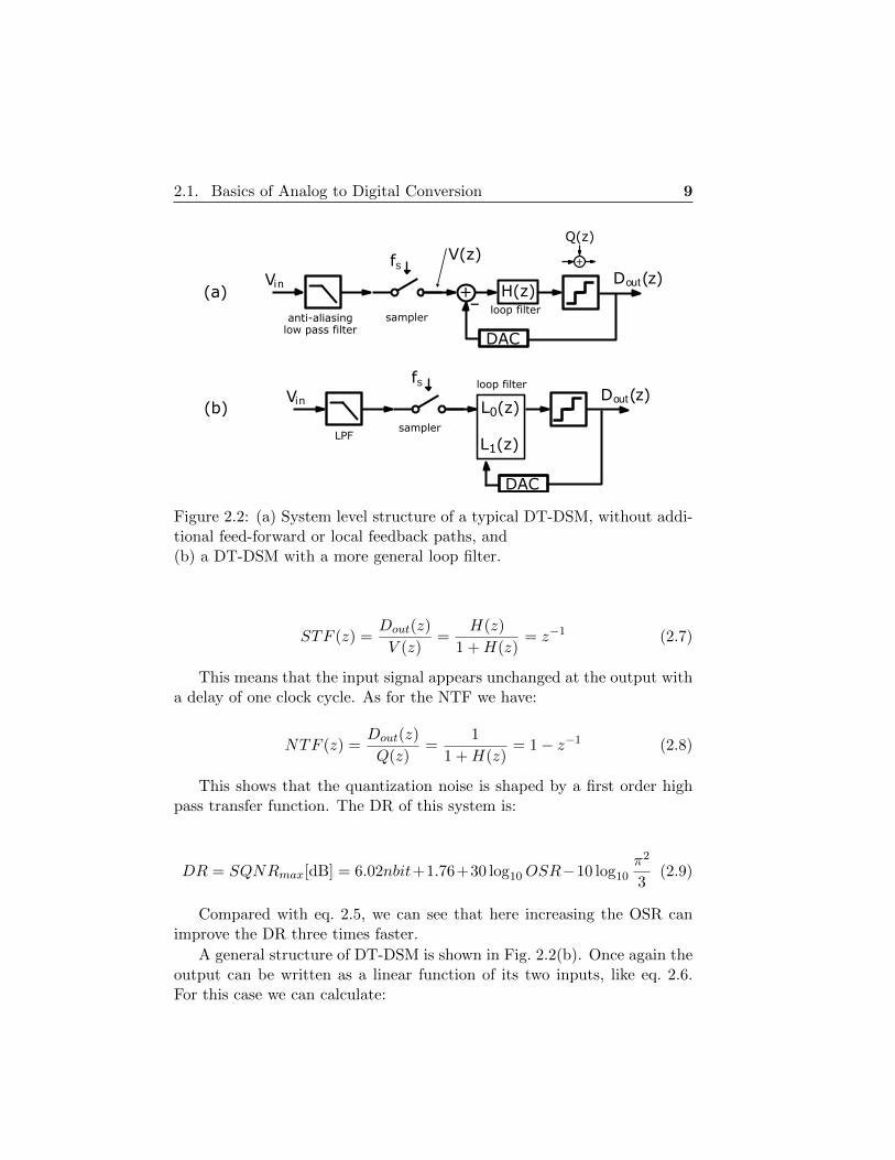
2.1. Basics of Analog to Digital Conversion 9
Dout(z)+−
DAC
Vi nfS
sampler
H(z)
Vi nfS
samplerLPF
L0(z)
L1(z)
loop filterDout(z)
anti-aliasinglow pass filter
loop filter
(a)
(b)
DAC
V(z) +
Q(z)
Figure 2.2: (a) System level structure of a typical DT-DSM, without addi-tional feed-forward or local feedback paths, and(b) a DT-DSM with a more general loop filter.
STF (z) =Dout(z)
V (z)=
H(z)
1 +H(z)= z−1 (2.7)
This means that the input signal appears unchanged at the output witha delay of one clock cycle. As for the NTF we have:
NTF (z) =Dout(z)
Q(z)=
1
1 +H(z)= 1− z−1 (2.8)
This shows that the quantization noise is shaped by a first order highpass transfer function. The DR of this system is:
DR = SQNRmax[dB] = 6.02nbit+1.76+30 log10OSR−10 log10π2
3(2.9)
Compared with eq. 2.5, we can see that here increasing the OSR canimprove the DR three times faster.
A general structure of DT-DSM is shown in Fig. 2.2(b). Once again theoutput can be written as a linear function of its two inputs, like eq. 2.6.For this case we can calculate:

10 Chapter 2. Previous work on VCO-ADC
STF (z) =Dout(z)
V (z)=
L0(z)
1− L1(z)(2.10)
and,
NTF (z) =Dout(z)
Q(z)=
1
1− L1(z)(2.11)
By properly designing L0(z) and L1(z) a higher order NTF can berealized while keeping STF just a few delays. A simple example of a highpass NTF of L order is:
NTF (z) = (1− z−1)L (2.12)
For this case the DR will be:
DR = 6.02nbit+ 1.76 + 10(2L+ 1) log10OSR− 10 log10π2L
2L+ 1(2.13)
Thus, the DR improves with a rate of 2L+1 as the OSR increases, whichis a great improvement over simple oversampling. As a result, the numberbits required to achieve a given DR is considerably less in a DT-DSM thanin a Nyquist rate ADC.
2.1.4 Continuous Time Delta Sigma Modulator
∆Σ ADCs, or DSMs, are divided into two different categories based on thelocation of the sampler. In a discrete-time DSM (DT-DSM), as shown inFig. 2.2, the sampler is located at the input stage and switched cap filtersare normally used to precess the discrete time signals. In a continuous timeDSM (CT-DSM), as shown in Fig. 2.3, the sampling function happens justbefore the quantization, and the two functions can be merged to a singleblock.
The quantization noise shaping characteristic of a CT-DSM is very sim-ilar to that of a DT-DSM and its order is equal to the number of integratorsin its loop filter. Fig. 2.3(b) shows a typical structure of a CT-DSM withan order of k without additional feed-forward or local feedback paths, [33].
It has been argued in the literature that a CT-DSM can operate ata higher clock frequency compared to a DT-DSM, because the latter islimited by the speed of the switches and charging time of the capacitors.

2.2. First order VCO-ADC 11
Dout(z)+−
DAC
Vi n
fS
H(s)
loop filter(and anti-aliasing filter)
f sDout(z)a2
s+−
......a1
s+−
ak
s
DAC
Vi n
(a)
(b)
Figure 2.3: (a) System level structure of a typical CT-DSM, without addi-tional feed-forward or local feedback paths, and(b) a CT-DSM of the kth order.
More importantly, in a CT-DSM the sampler is located after the loop filter.As a result, this filter also operates as an anti-aliasing filter, which can savesome power and chip area.
2.2 First order VCO-ADC
The combination of a VCO and a reset counter, shown in Fig. 2.4(a) isoften used as either a stand-alone ADC with first order quantization noiseshaping or as a noise shaping quantizer in the loop of a high order CT-DSM [20,24,25,29,30,34–40].
The VCO converts the input voltage, Vin, to a square wave of whichthe frequency is proportional to the input voltage. Then the reset countercounts the number of rising edges of the square wave in every clock cycle.This way, it quantizes the phase which is the integral of the frequency. Thereset function compensates this integration with an inherent differentiation.Apart from the quantization error, the resulting digital output signal Dout
will be equal to:
Dout ≈fvcofs
=fc + kvVin
fs(2.14)
where fV CO stands for the VCO output frequency, fc for the free run-

12 Chapter 2. Previous work on VCO-ADC
VCO resetcounter
Vi n Dout(z)
f skv , fc
Vi n 1skv
+fc
quantizer fVCO(Hz)
phase(cycles)
(with steps of 1)
1-z-1Dout(z)
register
f s
sampler
step=1
Vi n kv+
fcf s
Dout(z)+−
ZOH
1s
(a)
(b)
(c)
Figure 2.4: (a) an open-loop first order VCO based ADC, and(b) and (c) its equivalent model.
ning (zero input) frequency of the VCO, kv for the gain of the VCO and fsfor the sampling frequency.
In a previous work [20] a thorough study of first order VCO-basedADC’s has been done and different parameters of the modulator, such asSQNR or DR have been obtained as functions of the VCO and sampler pa-rameters, such as the VCO’s gain (kv), OSR, input amplitude (Ax) numberof phases (np), and sampling frequency (fs).
SQNR = 6.02nq − 3.41 + 30 log10OSR+ 20 log10(sinc(1
2OSR)) (2.15)
where nbit = log2(2Axkvnp/fs) is the resolution of the quantizer.As expected, the SQNR of a VCO ADC is similar to that of first or-
der DSM in terms of quantization noise shaping and dependency on OSR(referring to the term 30 log10OSR in the equation above.)
An equivalent system is depicted in Fig. 2.4(b), [29]. In this modelthe quantization, sampling, and differentiation functions (which previouslyhappened simultaneously in the reset counter) are separated. The conver-sion from frequency to phase domain is modeled as an integrator. The
2.2. First order VCO-ADC 13
quantizer represents the fact that we don’t have full access to the outputphase of the VCO, but only to its cycles. In other words, only a full cyclecan be counted. After sampling, the output is differentiated in the digitaldomain.
Although this VCO-ADC is an open loop structure, in Chapter 3 it willbe shown that it is strictly equivalent to a first order closed loop CT-DSM,similar to the one shown in Fig. 2.4.
What makes a VCO based integrator interesting is the fact that the out-put phase of the VCO is by definition the integrated frequency, and in thatregard a VCO is an ideal integrator with an infinite gain at DC, a luxurythat is impossible to obtain in a conventional op-amp based integrator.
2.2.1 Circuit level considerations
One of the main ideas behind a VCO-ADC, shown in Fig. 2.4, is to havea simple design that can ideally be synthesizable using digital flow designtools. Such a circuit would be relatively easy to migrate from one technol-ogy node to another. For this reason, it is of interest to look for circuitlevel solutions that are as “digital” as possible.
Vin+
Vdd
Vin-
phase[i] phase[i+1]
phase[i]
phase[i+1]
Vin+/Vin-
(a) (b)
Figure 2.5: (a) a typical structure for a voltage controlled Ring Oscillator(b) a voltage controlled inverting delay stage, used in an RO.
Given this motivation, a Ring Oscillator (RO) is often used to manifestthe VCO. An example of a typical RO is shown Fig. 2.5(a). An RO isan unstable loop of inverters, or delay stages. Such delay elements canbe designed with a minimal number of transistors, which makes them a

14 Chapter 2. Previous work on VCO-ADC
suitable option for low voltage applications. Another benefit of an RO isthe fact that it has multiple output phases that can be processed in parallelusing digital blocks.
It is commonly known that RO’s have a relatively linear current to fre-quency conversion curve, so the main challenge would be to develop a lineartransconductance stage to convert the input voltage into current to drivethe RO. Many implementations for such a block already exists, a simplesolution for this is shown in Fig. 2.5(b) as an example [18]. As the figureshows, the input voltage V in+, and its complementary counterpart V in−drive two trans-conducting transistors. This complementary structure, thatuses a trans-conducting NMOS and PMOS at the same time, is chosen tominimize the even order harmonics that exists in the non-linear voltage tocurrent conversion curve of a CMOS transistor.
In the VCO-ADC shown in Fig. 2.4(a) the RO is then followed by areset counter, and since the different phases of the RO can be processedin parallel, each phase will be driving a separate, and rather simple, resetcounter. The outputs of these counters will then be added in a digital adderthat follows them.
Fig. 2.6(a) shows a typical implementation for a single-phase resetcounter [18], where V CO[i] is one of the output phases of the voltage con-trolled RO, and fs is the sampling clock frequency. This particular circuit istriggered by both rising and falling edges of the VCO. The timing diagramof this reset counter is shown in Fig. 2.6(b).
An important parameter that the designer should take into account isthe fact that the output phases of the RO are not rail-to-rail signals. There-fore, a level shifter can be used for the conversion. In some implementations,the first DFF in Fig. 2.6(a) is replaced with a SAFF (sense-amplifier-basedflip-flop) to overcome this problem.
2.3 PWM pre-coding
One of the main issues of the system shown in Fig. 2.4(a) is the fact that thelinearity of the overall ADC is limited by that of the VCO, which typicallyhas a poor linearity performance in its voltage to frequency curve.
One of the system level solutions to overcome this issue is to put a Pulse-Width Modulator (PWM) before the VCO on the signal path, Fig. 2.7(a).The PWM will convert the input voltage to a two level signal, v1 and v2, which will eventually drive the VCO, corresponding to only two instan-

2.3. PWM pre-coding 15
clk
D QVCO[i]
DFF
clk
DQ
^
Dout
^
fs
+1
0
+1
0
+1
0
><
(a)
(b)
VCO3
CLK
Dout
TS><TS
t
t
t
><TS
Figure 2.6: (a) a common implementation for a single phase reset-counter,(b) its timing diagram
taneous frequency values, Fig. 2.7(b). In this manner the non-linearitycurve of the VCO wouldn’t matter anymore, because that dotted line, con-necting the two operating points, would be the new voltage to frequencycurve, which is always inherently linear. This technique is known as PWMpre-coding [29–31,41,42].
The PWM has a gain of one for the baseband signal and is used in serieson the signal path, that’s why it will always directly contribute to the noiseand power budget of the system.
The designer should also take the aliasing effects of the PWM intoaccount. A PWM signal has high frequency spurs around its carrier, andits harmonics, that can alias into baseband. It is normally expected thatthe anti-aliasing characteristics of a CT-DSM can alleviate this problem,but it is possible that a first order VCO-ADC, which is equivalent with afirst order CT-DSM, cannot suppress these spurious tones (spurs) enoughfor a given SNR requirement.
16 Chapter 2. Previous work on VCO-ADC
VCOresetcounterVi n Dout(z)
f skv , fc
PWM
volt.
freq.
f1
f2
v1 v2
(a)
(b)
Figure 2.7: (a) the system level representation of the PWM pre-codingtechnique for VCO-ADC linearization.(b) the effect of PWM pre-coding technique on the non-linearity curve of aVCO.
Also worth noticing is the fact that the VCO is, in this configuration,basically operating as mixer. The average frequency of the VCO and highfrequency spurs of the PWM can mix, inter-modulate, and eventually getdown converted into baseband. These effects will further be discussed inChapters 5 and 7.
2.4 Coarse-fine structure
Another method to improve the linearity of a VCO-ADC is to reduce itsinput swing. By simply reducing the input voltage swing, applied directlyto the VCO in Fig. 2.4(a), one can improve the linearity of the overallADC. But it is obvious that this will be at the cost of SNR (Signal to NoiseRation) and DR (Dynamic Range) loss.
Coarse-fine structure, shown in Fig. 2.8, is a system level solution toreduce the swing of the VCO in a VCO-ADC. In this modulator the inputvoltage is first applied to a high speed coarse ADC with low accuracy,typically a flash ADC, annotated as ADCf on the figure. The output ofADCf is then subtracted from the input using a DAC (Digital to AnalogConverter). The resulting quantization error signal is much smaller than Vinand as a result the non-linearity of the VCO would be much less significant.
The output of ADCf will then be added as MSB (Most SignificantBits) to the digital output of the reset counter, representing the LSB (Least

2.5. Voltage-to-phase VCO-based ADC 17
VCO resetcounter
f skv , fc
+−
Vi nAD
Cf
DAC
f +Dout(z)
Figure 2.8: System level representation of a Coarse-fine VCO-ADC struc-ture, also know as 0-1 MASH VCO-ADC or residue canceling VCO-ADC.
Significant Bits). The overall ADC has no loss of DR due to swing reductionand will have a first order quantization noise shaping.
One of the drawbacks of this structure is the fact that it heavily dependson the DAC gain accuracy. Any mismatch between the DAC and the feed-forward path will increase the swing on the VCO and will degrade thelinearity performance of the ADC. One way to improve this problem is touse this ADC as a noise shaping quantizer in a closed-loop high-order CT-DSM. This way the remaining non-linearity of this ADC will be suppressedby the preceding integrators in the loop of the CT-DSM.
Another downside of this scheme is the fact that the power consumptionof the overall ADC would typically be doubled, compared to a conventionalVCO-ADC with similar DR (Dynamic Range).
Also worth mentioning is the lack of anti-aliasing filtering which inher-ently exists in a conventional VCO-ADC. In a coarse-fine structure the flashADC would require an analog low-pass filtering before it to avoid aliasingproblems.
This technique is often referred to in the literature as ’0-1 MASH VCO-ADC’ or residue canceling VCO-ADC, [22,43–45].
2.5 Voltage-to-phase VCO-based ADC
As explained in the previous section, a VCO is a perfect frequency to phaseintegrator. In order to extract the phase information of the VCO, one couldsample the phase, as it was the case in Fig. 2.4(a). In that approach theintegration function of the VCO was compensated by differentiation indigital domain using a reset-counter. That method is often referred to as

18 Chapter 2. Previous work on VCO-ADC
’voltage-to-frequency VCO-based ADC’ [46–48].
Vi n 1skv1
+fc1
quantizer fVCO(Hz)
phase(cycles)
(steps=1)
1skv2
+fc2
Vi n 1skv1+kv2
+
fc1-fc2
+
spurs near carrier
-1+−
out
out
(a)
(b)
(c)
(d)
VCO2
kv , fc
outVCO1
kv , fc
Vin
+
-
PD+-
VCO2
kv , fc
VCO1
kv , fc
+
-
PD+-
register
f s
sampler
Dout(z)+−
DAC
Vi n
Figure 2.9: (a) a voltage-to-phase VCO based integrator,(b),(c) its system level equivalents,(d) a first order voltage-to-phase VCO based ADC.
Another method for extracting the phase information of a VCO is usingthe VCO-based integrator shown in Fig. 2.9(a). In this pseudo differentialmethod, the input signal is applied to two complementary VCO’s and thedifference between their output phases is detected using a Phase Detector(PD). The output of the PD, which is a pseudo digital Continuous-Timesignal, is the integrated version of the input, plus some high frequency spursaround the carrier of the VCO, fc. As a result, this structure can be usedas a CT integrator in any loop filter, including CT-DSM applications.
A system level model of this integrator is shown in Fig. 2.9(b). Twodifferent values are assumed for the gain and carrier frequency of the two

2.6. High order VCO-based ADC’s 19
VCO’s in order to address the potential issue of mismatch. the quantizationfunction represents the fact that the PD only responds to the rising edgesof the VCO output, or in other words, the phase information of the VCOis only available at the end of a full cycle.
As Fig. 2.9(c) shows, the mismatch between the gain of the two VCO’s isnot important and the overall gain of the integrator equals their summation.The mismatch between the carrier frequency of the two VCO’s, on the otherhand, translates as a DC offset to the input and will also appear as a DCoffset at the output after putting the integrator in a closed loop. The highfrequency spurs due to the quantization in the PD is also modeled in thisfigure.
Using this integrator one can develop a first order voltage-to-phaseVCO-based ADC, shown in Fig. 2.9(d). Bear in mind that the spurs mod-eled in Fig. 2.9(c) will not affect this first order CT-DSM, because in anyDSM there is always a quantization function that completes the loop, andin this case the PD is performing the quantization function. As a result,the sampling quantizer that normally appears in a CT-DSM will reduce toa simple sampler, or register.
Similar to the previously discussed VCO-based integrator, it is alsocommon to use ring oscillators to implement these VCO’s, in which case,each output phase of V CO1 will be coupled to a corresponding outputphase of V CO2, [49,50].
In some implementations, instead of using two VCO’s, the designershave chosen to have only one VCO, and compare its output phase with areference frequency source. This reference source can even be the readilyavailable clock of the system, or a fraction of it.
2.6 High order VCO-based ADC’s
The VCO based ADC’s discussed so far behave as a first order CT-DSM. Inthis section different methods to increase their order of quantization noiseshaping is examined.
2.6.1 Using conventional loop-filter
It is well known that a low order CT-DSM can be used as the last stage ofa high order CT-DSM to behave as a noise shaping quantizer. The samemethod has been used to incorporate a first order VCO-ADC into the loop

20 Chapter 2. Previous work on VCO-ADC
of a high order CT-DSM. In other words, the VCO-ADC will be precededby a conventional Continuous-Time loop-filter such that together they canbe modeled as the system in Fig. 2.3.
The VCO-ADC’s that have been discussed so far only have a first orderquantization noise shaping. In other words, once incorporated into the loopof the CT-DSM in Fig. 2.3, they will replace the last integrator and thesampling quantizer [17,18,46,47,51,52].
VCOresetcounter Dout(z)
f skv , fc
loopfilter
+
-
DAC
Vi n
VCO2
kv , fc
VCO1
kv , fc
+
-
PD+-
register
f s
sampler
Dout(z)
DAC
loopfilter
+
-
Vi n
(a)
(b)
Figure 2.10: (a) using a voltage-to-frequency VCO-ADC as a noise shapingquantizer in the loop of a CT-DSM,(b) using a voltage-to-phase VCO-ADC as a noise shaping quantizer in theloop of a CT-DSM.
Fig. 2.10(a), for example, shows the case where a ‘voltage-to-frequencyVCO ADC’ is used to replace the last integrator and the quantizer of a highorder CT-DSM [53]. As a second example, Fig. 2.10(b) shows a similarconcept for a ‘voltage-to-phase VCO ADC’.
Designing a proper quantizer for CT-DSM applications has becomemore challenging as channel length in the newer CMOS technologies shrinks.Unlike Nyquist rate ADC’s, the quantizer of a CT-DSM should operate ata much higher clock frequency, depending on the OSR (Over Sampling Ra-tio) of the modulator. It is even more challenging to design a multi-bitquantizer. This is the main incentive behind using a VCO based quan-tizer. Such a quantizer can much easier operate at higher clock frequenciesand provide a multi-bit output, mainly because a VCO-quantizer consistsmostly of digital components and benefits from technologies with smallertransistors.

2.6. High order VCO-based ADC’s 21
Nevertheless, the problem of designing the preceding integrators in theloop-filter still remains.
2.6.2 MASH VCO-ADC
A MASH VCO-ADC is an open loop structure that can potentially havehigh orders of quantization noise shaping using only VCO based integrators.In this method, the error signal of the first stage is extracted using onlydigital components, like edge triggered phase detectors, and then appliedto a next VCO-ADC. This process can go on for multiple stages to have ahigher order of quantization noise shaping [54–58].
VCO1 resetcounter
Vi n
Dout(z)
f skv1 , fc1
R ^
S ^
Q
VCO2 resetcounter
f skv2 , fc2
Dig
ital cancellation
filter
Figure 2.11: The system level structure of a second order 1-1 MASH VCO-ADC.
Fig. 2.11 shows the example of a second order MASH VCO-ADC. Asthe figure shows, the outputs of the two ADC’s are not directly added,instead they need to be further processed and filtered in the digital domainbefore they are added.
To obtain the desired performance in the MASH structure, the analogfilters need to be matched with the digital cancellation filters. Any mis-match between these two filters causes leakage of the quantization noiseerror of the first stage. In the VCO based implementation of a MASHstructure the filters are first order integrators implemented by VCOs, thegains of which is proportional to the gain of the VCOs.
To the knowledge of the author, there are no successful implementationsof this idea. This might be due to the fact that this is an open-loop structureand the imperfections of the phase detector, or in this case Set-Reset latch,

22 Chapter 2. Previous work on VCO-ADC
are not compensated in a control loop. Therefore, all the mismatches inthe rise-time and fall-time of this element, and its delay, will leak into thenext stage.
2.6.3 All-VCO CT-DSM
As it was mentioned earlier, the voltage-to-phase VCO based integrator inFig. 2.9(a) can replace a conventional op-amp based integrator in the loop ofa CT-DSM, and a voltage-to-frequency VCO based ADC can only be usedas a noise shaping quantizer in a CT-DSM to replace its quantizer and lastintegrator. In the pursuit of designing a high order CT-DSM with onlyVCO-based integrators and quantizers, one can put the elements discussedearlier in this chapter together to accomplish that.
VCO4
kv2 , fc2
VCO3
kv2 , fc2
+
-
PD+-
register
f s
sampler
Dout(z)
DAC
Vi n+−
VCO2
kv1 , fc1
VCO1
kv1 , fc1
+
-
PD+-+
−
VCO3 resetcounter Dout(z)
f skv3 , fc3
Vi n
VCO2
kv1 , fc1
VCO1
kv1 , fc1
+
-
PD+-+
−
DAC
(a)
(b)
Figure 2.12: Two high order VCO based ADC’s using voltage-to-phase andvoltage-to-frequency integrators and quantizers.
For the case of a second order CT-DSM, for example, two VCO basedmodulators are shown in Fig. 2.12. In Fig. 2.12(a) both integrators ofa second order CT-DSM are replaced with voltage-to-phase VCO-basedintegrator, [59].
In the second example, shown in Fig. 2.12(b), a voltage-to-phase VCObased integrator is used as the first integrator, and a voltage-to-frequencyVCO based quantizer is used replace the second integrator and the quan-tizer [60].
2.6. High order VCO-based ADC’s 23
Although these structures have been previously introduced in literature,there are no implemented proofs of concept for them available.
As mentioned earlier, voltage-to-frequency VCO based integrators canonly be used as the last integrator in the integrator chain of a CT-DSM. Inthe following chapters we will introduce a novel system level solution thatonly uses voltage-to-frequency VCO based integrators. Two measured chipsare also discussed as the first prototypes for such a high order VCO-basedADC.

24 Chapter 2. Previous work on VCO-ADC
Chapter 3
High order VCO-basedCT-DSM
In this chapter a novel approach to use a voltage-controlled oscillator (VCO)as the first integrator of a high-order continuous-time delta-sigma modu-lator (CT-DSM) is presented. In the proposed architecture, the VCO iscombined with a digital updown counter to implement the first integratorof the CT-DSM. Thus, the first integrator is digital-friendly and hence canmaximally benefit from technological scaling.
Afterwards it will be shown that this VCO-based integrator can beused to replace all integrators in the loop of a CT-DSM, resulting in a newarchitectural concept for a mostly-digital all-VCO CT-DSM with a highorder of quantization noise shaping.
3.1 Modeling a first order VCO-ADC
In order to model a first order VCO-ADC, and to prove that it is equivalentto a first order Delta Sigma Modulator, we will revisit the conventionalSampling quantizer and then use the results to model the VCO-ADC.
3.1.1 Splitting the Sampling Quantizer
A sampling quantizer, shown in Fig. 3.1(a), is one of the main buildingblocks of a Delta Sigma Modulator (DSM). This fundamentally mixed-signal block converts a continuous-time (CT) analog voltage to a digitalstream, or in other words ”digitizes” it. This digitization is applied to both
25
26 Chapter 3. High order VCO-based CT-DSM
aspects of the input signal (Vin), its amplitude and its time. Digitizationin the time domain is commonly known as sampling, and discretization inthe voltage domain is known as quantizing. From a system level point ofview, this block is similar to the famous Nyquist Rate ADC.
Dout(z)Vi n
CLK - fS
Vi n
fS
Dout(z)
sampling quantizer
sampler quantizer
Vi n
fSDout(z)
samplerquantizer
yS
yQ
(a)
(b)
(c)
Figure 3.1: (a) a sampling quantizer,(b),(c) and its equivalents.
The two functions of sampling and quantizing can be performed sepa-rately while one functionality follows the other. In this manner the threesystems shown in Fig. 3.1(a-c) are strictly equivalent in the sense that theiroutputs, Dout, are bit by bit similar.
The signal yS in Fig. 3.1(b) is the sampled version of the input (digitizedin the time domain) and yQ in Fig. 3.1(c) is the quantized version of theinput (digitized in the voltage domain). At any given time the signal yQis an integer (i.e binary) and since it is not digitized in time the changesin its value are not synchronized with the clock signal. In other words, the”information” of this quantized waveform is not only stored in its values,but also in the location of the edges where the signal changes. In thatsense this signal is very similar to the output of a Pulse Width Modulator(PWM) signal where the information is in the pulse width (or in the edges)of a two level signal. Signals of the same nature as yQ are often referred toas ‘multi-level PWM’ signals or ‘pseudo-digial’ signals.
It is also worth mentioning that the sampler that follows the quantizer

3.1. Modeling a first order VCO-ADC 27
in Fig. 3.1(c) is basically a clocked (edge-triggered) register, because itsinput has already a digitized (integer) value.
3.1.2 CT equivalence of a VCO ADC
The combination of a VCO and a reset counter, shown in Fig. 3.2 is of-ten used as either an stand-alone ADC with first order quantization noiseshaping or as a noise shaping quantizer in the loop of a high order CT-DSM.
The VCO converts the input voltage, Vin, to a square wave of whichthe frequency is proportional to the input voltage. Then the reset countercounts the number of rising edges of the square wave in every clock cycle.This way, it quantizes the phase which is the integral of the frequency. Thereset function compensates this integration with an inherent differentiation.Apart from the quantization error, the resulting digital output signal Dout
will be equal to:
Dout ≈fvcofs
=fc + kvVin
fs(3.1)
where fV CO stands for the VCO output frequency, fc for the free run-ning (zero input) frequency of the VCO, kv for the gain of the VCO and fsfor the sampling frequency.
An equivalent system is depicted in Fig. 3.2(b), [29]. In this alternativestructure the integration and differentiation functions (which previouslyhappened simultaneously in the reset counter) are separated. After theVCO there is an up-counter which counts the rising edges of the outputwaveform of the VCO (the integration), and after sampling, the output isdifferentiated in the digital domain. Of course this implementation of aVCO-ADC is only conceptual, because in practice the output signal of theup-counter would go to infinity.
The functionality of a VCO as a voltage to frequency converter is shownin Fig. 3.2(c) using its parameters, kv and fc. The up-counter operates onthe output phase of VCO, therefore, an integrator (with a gain of one) isput in place to show the conversion from frequency (Hz) to phase (cycles,or radians/2π). The output of the up-counter is the quantized phase withsteps of one cycle. This functionality is addressed by putting the quantizerin Fig. 3.2(c).
In a next step, the differentiator in Fig. 3.2(c) can be replaced by afeedback loop with an integrator, which results in Fig. 3.2(d) and which is

28 Chapter 3. High order VCO-based CT-DSM
VCO resetcounter
Vi n Dout(z)
VCOVi n up-counter 1-z-1
Dout(z)
f s
register
f s
kv , fc
differentiatoraccumulator sampler
Vi n 1skv
+fc
quantizer fVCO(Hz)
phase(cycles)
(with steps of 1)
kv , fc
1-z-1Dout(z)
register
f s
(a)
(b)
(c)
Vi nkv
+fc
Dout(z)+
1-z-1z-1
−1s(d)
(e)
fS
sampler
sampler
step=1
Vi nkv
+fc
Dout(z)+−
1s
fS
step=1
1s ZOH
fS
Vi nkv
+fc
f s
Dout(z)+−
ZOH
1s(f)
Figure 3.2: (a) a first order VCO ADC,(b-f) and its system level equivalents.

3.2. Using a VCO as the first Integrator 29
still strictly equivalent to Fig. 3.2(c). The sampler and the quantizer arealso interchanged, similar to Fig. 3.1.
Since the quantizer in Fig. 3.2(d) has a step of 1, it is transparent todigital signals (i.e has a gain of one for a digital signal). Therefore, theloop that is created in the digital domain can be extended to the inputof the quantizer, see Fig. 3.2(e). It is also well known that the discrete
time integrator z−1
1−z−1 is equivalent with the CT integrator 1s , preceded by
a ZOH DAC and followed by a sampler (assuming a normalized samplingfrequency of 1 Hz).
By combining the samplers and integrators in Fig. 3.2(e) we will arriveat the system Fig. 3.2(f) which is a conventional first order CT-DSM. Thisproves that a VCO-ADC is strictly equivalent to a first order CT-DSM.
The methodology presented in this section will be used later on in thischapter to use a VCO as the first integrator of a high order CT-DSM.
3.2 Using a VCO as the first Integrator
In most cases, in Continuous Time Delta Sigma Modulators (CT-DSMs)the first integrator is the bottle neck in terms of power consumption andnoise. In deep-submicrometer processes, this block is becoming more andmore difficult to implement in the voltage-domain due to the limited voltageheadroom and gain of narrow channel transistors. For this reason, there isan increasing interest in VCO-based ADCs. One of the main issues withcurrent VCO-ADCs with a VCO input stage is that they can only provide1st order noise shaping. There have been a few attempts to increase theorder by using multi-loop mash approaches [54, 55], but these techniquesare very sensitive to analog imperfections [54].
A notable attempt to obtain a single-loop high-order VCO ADC whichuses a VCO as the first integrator is [61]. However, this approach suffersfrom a high complexity and power consumption, and additionally it hashigh sensitivity to the center frequency of the VCO which makes this ideaimpractical.
In this section, we present a novel approach to use a VCO as the firstintegrator of a high order continuous time Delta Sigma Modulator. Inthe proposed architecture, the VCO is combined with a digital up-downcounter to implement the first integrator of the continuous time Delta SigmaModulator. The up-down counter in its simplest form can be implementedby adding a well established Phase Frequency Detector (PFD). This way,

30 Chapter 3. High order VCO-based CT-DSM
the first integrator is digital friendly and hence can maximally benefit fromtechnological scaling.
3.2.1 Introducing the Up-Down Counter
It was shown in the previous section that the VCO-ADC in Fig. 3.3(a) isequivalent to the model shown in Fig. 3.3(b), and that digital differentiatorcan be replaced by a feedback loop with an integrator, which results inFig. 3.3(c).
The output of the digital integrator is a digital/integer number which istransparent to the sampling quantizer with the step of one. In other words,if a sampling quantizer has a step of one, it is like a gain of one for a digitalinput. Therefore, now that we have managed to create a loop in the digitaldomain, we can extend the loop and bring it to the analog domain using azero order hold DAC, as in Fig. 3.3(d).
In order to have a balance in the terminology in the analog and digitaldomain, an integrator in the digital domain can be called and viewed as an“up-counter”. Since the output of the two up-counters are being subtractedfrom each other, we can combine the two and call it an “up-down counter”,as in Fig. 3.3(e).
This “up-down counter” functions as follows: at every rising edge of theVCO, its output is incremented by one. At every rising edge of the clockthe counter output is decreased by the value Dout of the register (which willnormally be multibit). By using a Return to Zero (RTZ) pulse, every risingedge of the clock also occurs in the feedback signal such that the up-downcounter is now triggered by edges at both its inputs. We will come back tothe implementation of such an asynchronous digital block later on.
We have already discussed that an up(-down) counter, from a systemlevel point of view, behaves as an integrator; so we can clearly see that thesystem proposed in Fig. 3.3(e) is a first order Delta Sigma Modulator.
The output of this up-down counter doesn’t go to infinity, in fact it’s alimited pseudo digital integer number. However, since it can change at therising edge of the VCO wave form, it is not synchronous with the samplingclock. In fact the information is partially stored in the position of the edges.This signal can be referred to as a “multi-level PWM” waveform. Note thatthe structure of Fig. 3.3(e) is still strictly equivalent to Fig. 3.3(a-d).
In the next subsection it will be shown that the combination of a VCOand an up-down counter can be used as the first integrator of a high orderCT-DSM.

3.2. Using a VCO as the first Integrator 31
VCO resetcounterVi n
Dout(z)
VCOVi n up-counter 1-z-1
Dout(z)
VCOVi n up-counter
Dout(z)+
1-z-1z-1
−
VCOVi n up-counter
VCOVi n Dout(z)
Dout(z)+
1-z-1z-1
−
up-downcounter
f s
ZOH
−RTZ
(a)
(b)
(c)
(d)
(e)
step=1
f s
f s
f s
f s
Figure 3.3: Metamorphosis of an open-loop first order VCO-ADC to aclosed-loop one.(a) the basic structure of a VCO-ADC(b) An equivalent system with up-counter and digital differentiator(c) replacing the differentiator with an integrator in the feedback(d) extending the loop from digital to analog domain(e) replacing the up-counter and the integrator with an up-down counter
3.2.2 Proposed Scheme
Now that we have managed to redraw the VCO-ADC as a feedback loop, asin Fig. 3.3(e), the next and final step is to increase its order by introducingadditional integrators in the loop, as in Fig. 3.4(a). It is clear that theresulting structure can be of any order. Its first integrator is implementedby the combination of the VCO and the up-down counter, and hence is
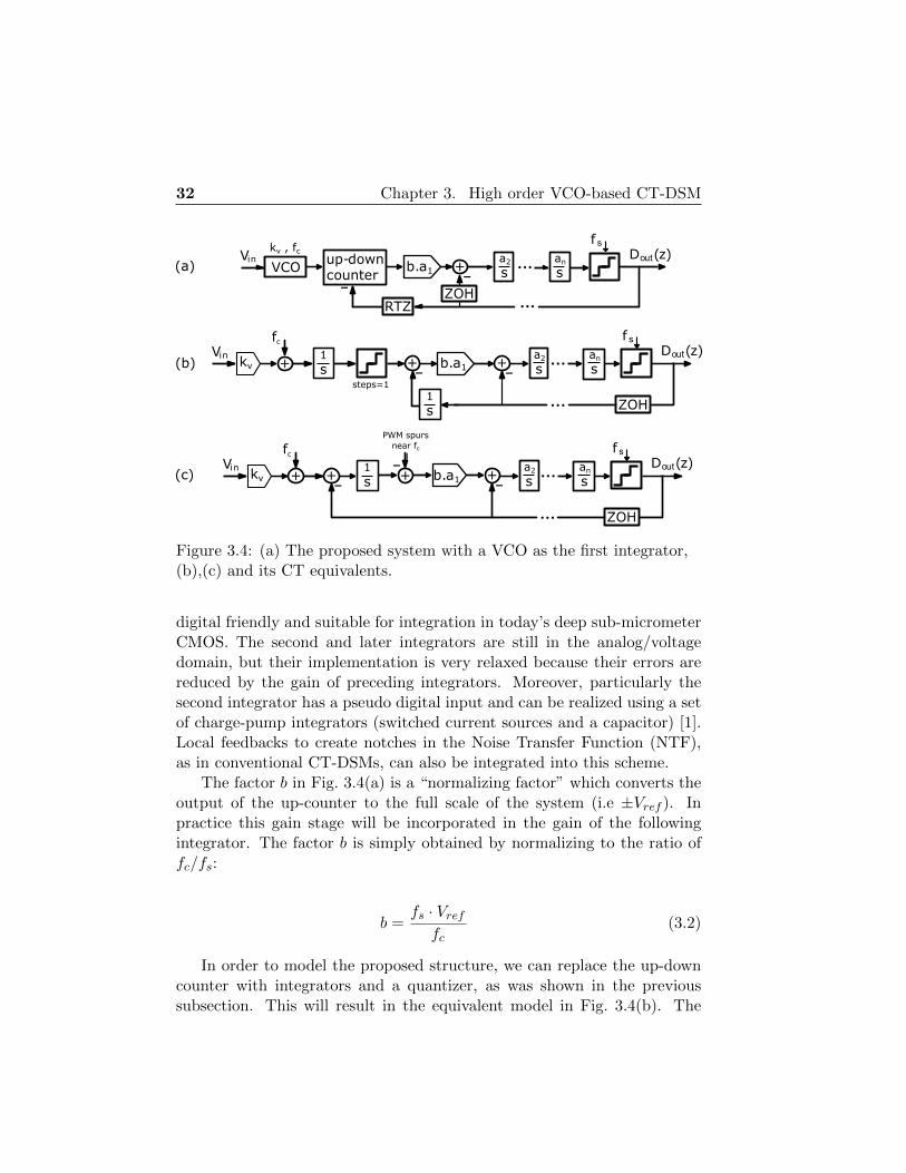
32 Chapter 3. High order VCO-based CT-DSM
b.a1VCOVi n
f sDout(z)
−
up-downcounter
an
s+−
a2
s
f sDout(z)
−an
s+−
a2
s+
kv , fc
Vi n 1skv
+fc
steps=1
b.a1
1s
f sDout(z)
−an
s+−
a2
s+Vi n 1
skv+
fc
b.a1+−−
PWM spurs near fc
(a)
(b)
(c)
RTZZOH
ZOH
ZOH
Figure 3.4: (a) The proposed system with a VCO as the first integrator,(b),(c) and its CT equivalents.
digital friendly and suitable for integration in today’s deep sub-micrometerCMOS. The second and later integrators are still in the analog/voltagedomain, but their implementation is very relaxed because their errors arereduced by the gain of preceding integrators. Moreover, particularly thesecond integrator has a pseudo digital input and can be realized using a setof charge-pump integrators (switched current sources and a capacitor) [1].Local feedbacks to create notches in the Noise Transfer Function (NTF),as in conventional CT-DSMs, can also be integrated into this scheme.
The factor b in Fig. 3.4(a) is a “normalizing factor” which converts theoutput of the up-counter to the full scale of the system (i.e ±Vref ). Inpractice this gain stage will be incorporated in the gain of the followingintegrator. The factor b is simply obtained by normalizing to the ratio offc/fs:
b =fs · Vreffc
(3.2)
In order to model the proposed structure, we can replace the up-downcounter with integrators and a quantizer, as was shown in the previoussubsection. This will result in the equivalent model in Fig. 3.4(b). The
3.2. Using a VCO as the first Integrator 33
output of this quantizer (which has steps of 1) is a multi-level PWM signalwhich consists of two main parts: the low frequency (baseband) compo-nents, which is the integrated input (with some additional gain and bias),and the high frequency components, which are mostly the undesired PWMspurs around the carrier frequency of the VCO, fc.
After combining the two 1s integrators, the high frequency spurs ex-
plained above can be separately modeled, as shown in Fig. 3.4(c). Thesehigh frequency spurs can alias to the baseband after the quantizing samplerhas sampled their contribution in the last stage of the modulator. But onecan expect the integrators before the sampler to alleviate this problem.
The additional branch representing the carrier frequency of the VCO,fc, is added to the system as a DC offset and doesn’t affect spectral integrityof the input signal.
Summarizing, the proposed structure is equivalent to a conventionalCT-DSM with the same integration coefficients, ai. The proposed systemis simulated in the next section to provide a better understanding of thetime domain behavior of the up-down counter. The output spectrum of themodulator is also compared to that of a conventional CT-DSM.
3.2.3 Simulation results
Some typical system level simulation results are shown in Figures 3.5 and 3.6.Here the modulator is a 3rd order single bit design with a Butterworth NTFand a h∞ = 1.6 and a local feedback to create a notch in the NTF, (h∞ isthe stability factor, as defined by the Schreier toolbox). Fig. 3.5(a) showsthe output spectrum for the conventional modulator for the case of a -14 dBfs input signal. The results for the corresponding new structure ofFig. 3.4(a) are shown in Fig. 3.5(b). It is clear that the output spectra forboth cases are nearly identical.
A look at the internal waveforms of the two modulators, however, showsthat they have a completely different time-domain behaviour.
Fig. 3.5(c) and (d) compare the output signals of the first integrators ofthe two ADCs. As it was previously explained, the output of an up-downcounter is a multi-level PWM signal, which is in this case a 3-level signal,Fig. 3.5(d). Despite this obvious difference in the internal waveforms, thetwo modulators maintain almost identical spectral integrity.
The amplitude of the main tone (corresponding to the input signal)at the output of an integrator in a CT-DSM (be it conventional or VCO-based), which is normally the dominant contribution at these nodes, is

34 Chapter 3. High order VCO-based CT-DSM
10−4
10−3
10−2
10−1
−160
−140
−120
−100
−80
−60
−40
−20
0
frequency, normalized to fs
outp
ut s
pect
rum
(dB
)
10−4
10−3
10−2
10−1
−160
−140
−120
−100
−80
−60
−40
−20
0
frequency, normalized to fs
outp
ut s
pect
rum
(dB
)
0 100 200 300 400 500 600−0.2
−0.15
−0.1
−0.05
0
0.05
0.1
0.15
0.2
time, normalized to clock period
volta
ge a
mpl
itude
, nor
mal
ized
to s
uppl
ies
0 100 200 300 400 500 600−0.2
−0.15
−0.1
−0.05
0
0.05
0.1
0.15
0.2
time, normalized to clock period
volta
ge a
mpl
itude
, nor
mal
ized
to s
uppl
ies
(a) (b)
(c) (d)
sndr=68 dBOSR=40Vin=-14dBfsnbit=1
sndr=67.4 dBOSR=40Vin=-14dBfsnbit=1
Figure 3.5: Simulation results of two 1-bit CT-DSMs with a -14 dBfs inputtone.(a) output spectrum of a conventional 3rd order modulator(b) output spectrum of a VCO-based modulator with the same NTF(c) output signal of the first integrator for the conventional modulator(d) output signal of the first integrator for the VCO-based modulator
proportional to the amplitude of the input signal. Therefore, an increasein the input voltage will increase the signal level at these nodes too.
In the case of the proposed VCO-ADC, this higher swing would trans-late to a higher number of levels.
For Fig. 3.6, a higher input amplitude (-6 dB instead of -14 dB) isused. Again the overall output spectra are almost identical. As Fig. 3.6(c)shows, for the conventional CT-DSM, the voltage swing at the internal nodehas clearly increased. The equivalent node for the VCO-based CT-DSM,Fig. 3.5(d), also shows an increase in the signal swing, except here a higher

3.2. Using a VCO as the first Integrator 35
10−4
10−3
10−2
10−1
−160
−140
−120
−100
−80
−60
−40
−20
0
frequency, normalized to fs
outp
ut s
pect
rum
(dB
)
10−4
10−3
10−2
10−1
−160
−140
−120
−100
−80
−60
−40
−20
0
frequency, normalized to fsou
tput
spe
ctru
m (dB
)
0 100 200 300 400 500 600
−0.2
−0.1
0
0.1
0.2
0.3
time, normalized to clock period
volta
ge a
mpl
itude
, nor
mal
ized
to s
uppl
ies
0 100 200 300 400 500 600
−0.2
−0.1
0
0.1
0.2
0.3
time, normalized to clock period
volta
ge a
mpl
itude
, nor
mal
ized
to s
uppl
ies
(c) (d)
(a) (b)
sndr=76.1 dBOSR=40Vin=-6d Bfsnbit=1
sndr=76.1 dBOSR=40Vin=-6d Bfsnbit=1
Figure 3.6: Simulation results of two 1-bit CT-DSMs with a -6 dBfs inputtone.(a) output spectrum of a conventional 3rd order modulator(b) output spectrum of a VCO-based modulator with the same NTF(c) output signal of the first integrator for the conventional modulator(d) output signal of the first integrator for the VCO-based modulator
swing simply means that more levels are used in the PWM waveform.
3.2.4 Implementation considerations
The proposed structure has a VCO input stage and as such it is directlyaffected by VCO’s nonlinearity. However, there are several ways to solvethis problem, including PWM pre-coding [1, 29] and post calibration [62].
Another imperfection that can be associated with a VCO is inaccuracyin its carrier frequency fc and its voltage to frequency conversion gain
36 Chapter 3. High order VCO-based CT-DSM
kvco, but these imperfections in the VCO don’t impose any problem on theproposed scheme. Any error in fc will be translated to a mere DC offset inthe output and an error in the value of kvco can be viewed as a gain errorfor the overall modulator.
The most important new block is the up-down counter which is triggeredby edges at both its inputs. This way, this is basically an asynchronouscircuit and in general its implementation can be challenging. However, itsdesign can be greatly simplified by using a single bit quantizer (as was donein the simulations of Fig. 3.5 and 3.6). An additional important parameteris the signal swing at the output of the up-down counter. This swing canbe controlled either by appropriately scaling the modulator coefficients orby restricting the modulator’s input range. In the particular case that theoutput swing is only three-level (as in fig. 3.5(b)) the up-down counter col-lapses to the well known Phase-Frequency Detector (PFD) which is widelyused in PLL’s and for which efficient implementations are well known. Ifa higher swing is needed, some additional logic of similar complexity as aPFD is needed.
In the next section it will be shown that using a multi-phase VCO,instead of a single-phase one, will heavily simplify the design of the up-down counter and allow the designer to higher signal swings (i.e more levels)at the output of the up-down counter. It will also be shown that thecombination of the VCO and the up-down counter can be used to replaceall the integrators in the loop of a CT-DSM.
3.3 High order All-VCO CT-DSM
In this section the architectural concept of a mostly-digital VCO-ADC withhigh order quantization noise shaping is presented. The system is basedon the combination of a VCO and a digital counter. This combinationcan function as a continuous time integrator to form a high-order Contin-uous Time Delta Sigma Modulator (CT-DSM). The counter consists onlyof digital building blocks and the VCOs can be implemented using RingOscillators, which are also digital friendly. No traditional analog blocks,like op-amps, OTAs or comparators, are needed.
3.3.1 VCO based continuous-time integrator
A core building block for an ADC with high order noise shaping is an in-tegrator. In this context, the structure of Fig. 3.7(a) was studied in the

3.3. High order All-VCO CT-DSM 37
VCO1
Vi n
−
up-downcounter
kv1 , fc1
fc1
yout
Dout
−−< >+
−−
(a) (b)
−
−
PWM spurs near fc1
Dout(z)
1s+
−
ZOH
kv1
f s
+yout
Vi nb
Vout
gain ofoptional
DAC
bVout
optionalDAC
Figure 3.7: (a) A VCO based integrator(b) and its equivalent continuous-time model.
previous section, see Fig. 3.4, which has a continuous time analog input Vinand a discrete time digital input. In a continuous time Delta Sigma Modu-lator (CT-DSM), the discrete time digital input will typically be driven bythe overall ADC’s output signal and is therefore called Dout here. The ana-log input voltage, Vin, is applied to a Voltage Controlled Oscillator VCO1
with a gain Kv1 and a carrier frequency fc1. The VCO is followed by an“up-down counter”, which is a continuous-time digital block. This up-downcounter behaves differently on its positive (up) input (driven by the VCO)and negative (down) input (driven by the discrete time digital signal Dout).It functions as follows: at every rising edge of the VCO its output is incre-mented by one, and at every rising edge of the sampling clock the counteroutput is decreased by the value of the digital output at that time, Dout
(which is a multi-bit integer).
The output yout of the up-down counter is a (multi-bit integer) digitalsignal. However, it does not only change at the clock edges, in fact theinformation is encoded in the position of the edges: hence, it can be viewedas a multi-level PWM signal [5]. If a true analog output is needed, a Digitalto Analog Converter (DAC) with a normalizing gain b can be added. Wewill see later on, that this component can usually be merged into successivebuilding blocks or even omitted. As such in practice, this DAC does notadd to the complexity of this solution.
From the equivalence set up in Fig. 3.4, it follows that this digitalimplementation of a VCO integrator can be modeled by the equivalentsystem shown in Fig. 3.7(b). This can be understood from the fact thatthe analog input signal is integrated and provided as a multi-level PWM atthe output. Due to this, there are PWM-spurs at the output. Also, there isa fixed input referred contribution from the VCO carrier frequency. Clearly,the fact that there are high frequency modulation spurs, is a disadvantage.

38 Chapter 3. High order VCO-based CT-DSM
Nevertheless, since we want to use this block in a CT-DSM, we can expectthat this will not be a severe problem, because these high frequency spurs,normally will be rejected by the inherent anti-aliasing filtering of the CT-DSM [63]. However, in a final design this must be confirmed by systemlevel simulations. It is obvious that the implementation of the integratorshown in Fig. 3.7(a) is much more digital friendly than conventional analogintegrator designs based on op-amps, especially if the optional DAC blockcan be omitted. This integrator is a core ingredient of the high-order noise-shaping ADC in this chapter.
3.3.2 VCO based sampling quantizer
A second core building block in a noise shaping ADC is a sampling quan-tizer. For this, the conceptual structure of Fig. 3.8(a) has widely beenused [53, 64, 65]. This structure performs the sampling, the quantizationand in addition provides a first-order noise shaping of the quantizationnoise. This way, this structure can be used inside a Σ∆ loop and also as astand-alone first order VCO-ADC.
An alternative implementation, that is closer to the implementation ofFig. 3.7, was obtained in the previous section, see Fig. 3.3(e). This struc-ture, drawn again in Fig. 3.8(b), consists of an up-down counter (as theintegrator of Fig. 3.7) and a sampling register, which samples at the sam-pling frequency fs. The main advantage of this alternative implementationis that the input signal of the quantizer yQ is now available. It will beshown below that this signal can be used to provide local feedback in anall-VCO CT-DSM.
By observing that sampling the multi-level PWM signal at the counteroutput, corresponds to a (time-domain) quantization of the integrator out-put, we can obtain the equivalent model of Fig. 3.8(c). Here the quantizer’squantization step is equal to the counter step, which is 1 in this diagram,where the instantaneous counter output is an integer.
This block diagram illustrates the equivalence between a VCO quantizerand a first-order Σ∆ modulator, which was also established in several priorworks (e.g. [20]).
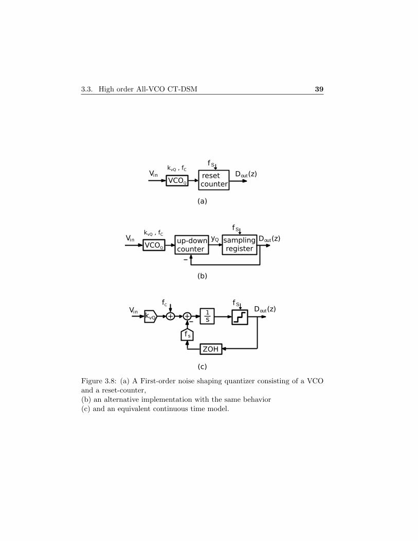
3.3. High order All-VCO CT-DSM 39
fS
resetcounter
Dout(z)kvQ , fC
VCOQ
Vi n
fS
samplingregister
Dout(z)
−
up-downcounter
kvQ , fC
VCOQ
Vi n
(a)
(b)
Dout(z)fSfC
1s+
−
ZOH
kvQ
f s
+Vi n
(c)
yQ
Figure 3.8: (a) A First-order noise shaping quantizer consisting of a VCOand a reset-counter,(b) an alternative implementation with the same behavior(c) and an equivalent continuous time model.
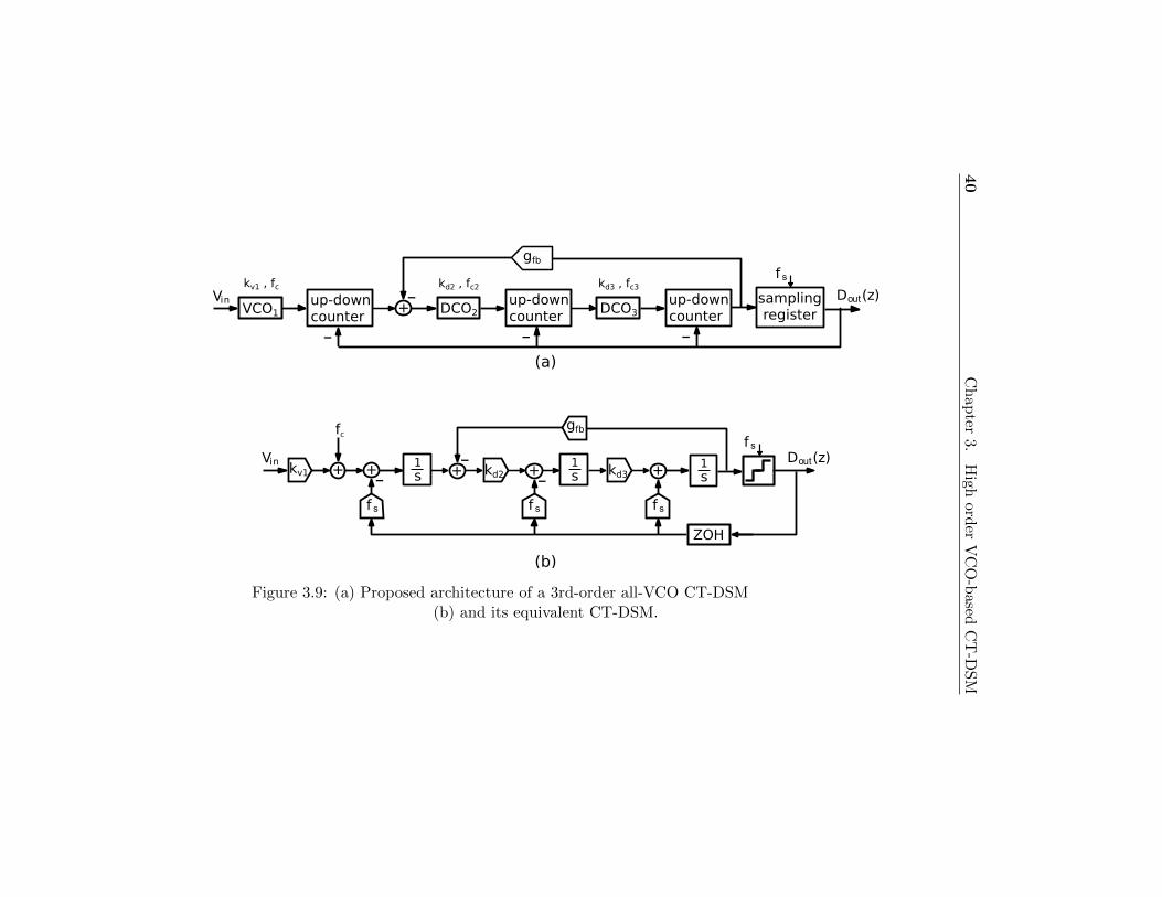
40
Ch
apter
3.H
ighord
erV
CO
-based
CT
-DS
M
kd2 , fc2
VCO1
Vi n
−
up-downcounter
DCO2
Dout(z)kd3 , fc3
−
up-downcounter DCO3
−
up-downcounter
kv1 , fc
+−
gfb
f s
samplingregister
f sDout(z)1
s+1s+
−
ZOH
+−
+−
kd2
Vi nkv1
+
fcgfb
f s f s
kd31s
f s
(a)
(b)
Figure 3.9: (a) Proposed architecture of a 3rd-order all-VCO CT-DSM(b) and its equivalent CT-DSM.
3.3. High order All-VCO CT-DSM 41
3.3.3 General All-VCO CT-DSM architecture
Based on our VCO based integrator and quantizer, we can now develop aVCO-ADC with noise shaping of arbitrary order. As an example of theproposed scheme, a third order all-VCO CT-DSM is shown in Fig. 3.9(a).As the figure shows, the (continuous time) digital output signals of theup-down counters directly drive the succeeding block without the optionalDAC of Fig. 3.7. Due to this, the second and third controlled oscillator,do not have a voltage mode input and hence are not ‘voltage’ controlledoscillators. Instead they have an (integer) digital input, and hence areDigitally Controlled Oscillators (DCOs). Therefore, the gains of these twoDCOs, kd1 and kd2 have the dimension Hz per digit (or simply Hz). We willshow in chapter 6, that in our design the implementation of these DCOs isnot more complex than the implementation of a conventional voltage inputVCO. The optional coefficient gfb is a small (dimensionless) number, andcan be added to optimize the position of the NTF zeros [63].
By using the equivalence, set up in Fig. 3.7 and Fig. 3.8, an equiva-lent CT-DSM of the proposed system can be obtained, which is shown inFig. 3.9(b). The carrier frequency of the first VCO appears on the equiva-lent system in Fig. 3.9(b) as a DC bias added to the input branch.
The carrier frequencies of DCO2 and DCO3 do not contribute to theoutput signal of the modulator, because, when referred to the input, theybecome zero. Therefore, the adding branches that should represent them,are not shown in Fig. 3.9(b). In order not to overload the figure, theextra branches corresponding to the PWM spurs, similar to the one inFig. 3.7(b), are not shown either in Fig. 3.9(b). This is partially justifiedby the assumption that the modulator should provide sufficient anti-aliasingfiltering to suppress them. However, this assumption must be confirmed bysystem level simulations.
In the following chapters we will propose circuit level implementationsfor this modulator. The first VCO is the most challenging component to de-sign. In Chapter 4 a linear VCO design is introduced. In Chapter 5 PWMpre-coding technique for linearizing the first VCO is examined. Chapter 6showcases the first prototype of a 3rd order modulator of this type. Chap-ter 7 is another prototype of the same modulator family, but instead of alinear VCO it utilizes the PWM pre-coding technique.

42 Chapter 3. High order VCO-based CT-DSM

Chapter 4
Linear voltage controlledring oscillator
In this chapter a very simple Ring-Oscillator VCO structure for use inVCO-ADC applications is presented. It has a greatly improved linearitycompared to previously published VCO’s. Measurement results of a 1 Volt,65 nm CMOS prototype confirm the effectiveness of the proposed approach.This oscillator can be used as the first VCO in the system proposed inFig. 3.9. As mentioned in Chapter 3, the first VCO is the most challengingone to design, because it has the most contribution in the noise and non-linearity performance of the overall modulator.
4.1 Ring oscillator input circuit
++
++
++
Ctrl
N stages
Figure 4.1: Ring oscillator with N differential delay elements.
Our starting point is the well known ring oscillator (RO), shown inFig. 4.1. It consists of N differential delay elements placed in a ring. For
43

44 Chapter 4. Linear voltage controlled ring oscillator
the delay element, the circuit of Fig. 4.2 was used [47]. It consists of 2 maininverters and 2 small auxiliary inverters. The task of the auxiliary invertersis to align the edges of both main inverters, such that both main inverterswill switch at (almost) the same time stamp (one will have a rising edgeand the other a falling edge). The circuit can be tuned through its controlterminal (Ctrl).
Vdd
Ctrl
W
2W
maininverters
auxinverters
4x
4x
1x 1x
vin+
vin-
vout-
vout+
Figure 4.2: Delay cell used in the ring oscillator.
For this circuit, we investigated the overall linearity. Surprisingly, theavailable literature guidelines are completely contradictory. Some authorsclaim that the oscillation frequency fRO is proportional to the voltageVRO = Vdd − VCtrl over the inverters in the ring [66, eq.14]. This leadsto the conclusion that direct voltage mode control is the optimal choice.Other authors claim that the oscillation frequency is proportional to thecurrent driven into the control terminal [67, fig.4] [47, fig.4]. This sug-gests that direct current mode control is best. And finally some otherauthors claim that the oscillation frequency is proportional to the ratio ofthe two [66, eq.10] [67, eq.2], which does not directly lead to a simple drivestrategy.
Upon investigation, it turns out that all these claims are approximatelyvalid in a certain operation range of the RO. But the actual curves ex-hibit (depending on how large the tuning range is) nonlinearities of severalpercents. The current control performs best, but, since in most cases theinput signal is available as a voltage rather than a current, this controlstrategy imposes the need of an additional voltage to current conversion.This voltage to current conversion adds to the power budget and introducesadditional nonlinearity.
In this work we propose the simple novel mixed input structure shownin Fig. 4.3. The structure can be considered as a go-between of the cur-rent mode control and the voltage mode control. This structure has severalattractive features. First, the input circuit is much simpler than transcon-

4.2. Oscillator core design 45
Ring-Osc
Vin Ctrl
R1
R2
Vdd
Figure 4.3: Ring oscillator with resistive input stage
ductor based circuits that are widely used. Due to this, it has significantlybetter noise performance and power efficiency than transconductor basedcircuits. Second, the linearity of this resistive input circuit is better thanthe linearity of an RO with an ideal current control. To understand this,the (simulated) frequency tuning curve with ideal current control is shownin Fig. 4.4(a). It is clear that the curve exhibits a negative curvature. Inthe proposed circuit the ring current IRO will be:
IRO = −VinR1
+ VCtrl
(1
R1+
1
R2
)(4.1)
The term −VinR1
is linear in the tuning voltage, but the term proportionalto VCtrl is nonlinear. A simulation of the relation between Vin and VCtrl forthe case of a supply voltage Vdd = 1 V is shown in Fig. 4.4(b). It is clearthat this curve exhibits the opposite curvature of the current mode tuningcurve of Fig. 4.4(a). By appropriately sizing the resistors R1 and R2, bothnonlinear effects will cancel out.
In sizing the resistors there are 2 degrees of freedom: the value of R1
and the value of R2. The ratio R1/R2 should be chosen such that bothnonlinear contribution cancel. In the family of circuits that we examined(where the supply voltage was 1 Volt) the optimum was very close to thecase of matched resistors: R1 = R2 = R. Then, there only remains 1 degreeof freedom: i.e. the value of R. This value should be sized to satisfy thedesired input referred noise of the VCO.
4.2 Oscillator core design
The final step in the VCO design is the sizing of the inverters of the delaycells and the choice of the number of elements in the loop. In the case where
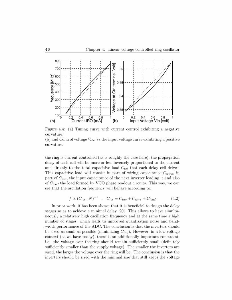
46 Chapter 4. Linear voltage controlled ring oscillator
0 0.2 0.4 0.6 0.8 1100
200
300
400
500
600
700
800
(a) Current IRO [mA]
frequ
ency
[MH
z]
0 0.2 0.4 0.6 0.8 1
0.35
0.4
0.45
0.5
(b) Input Voltage Vin [volt]
Volta
ge a
t Ctrl
term
inal
[vol
t]
Figure 4.4: (a) Tuning curve with current control exhibiting a negativecurvature,(b) and Control voltage Vctrl vs the input voltage curve exhibiting a positivecurvature.
the ring is current controlled (as is roughly the case here), the propagationdelay of each cell will be more or less inversely proportional to the currentand directly to the total capacitive load Ctot that each delay cell drives.This capacitive load will consist in part of wiring capacitance Cwire, inpart of Cinv, the input capacitance of the next inverter loading it and alsoof Cload the load formed by VCO phase readout circuits. This way, we cansee that the oscillation frequency will behave according to:
f ∝ (Ctot ·N)−1 , Ctot = Cinv + Cwire + Cload (4.2)
In prior work, it has been shown that it is beneficial to design the delaystages so as to achieve a minimal delay [20]. This allows to have simulta-neously a relatively high oscillation frequency and at the same time a highnumber of stages, which leads to improved quantisation noise and band-width performance of the ADC. The conclusion is that the inverters shouldbe sized as small as possible (minimizing Cinv). However, in a low-voltagecontext (as we have today), there is an additionally important constraint:i.e. the voltage over the ring should remain sufficiently small (definitelysufficiently smaller than the supply voltage). The smaller the inverters aresized, the larger the voltage over the ring will be. The conclusion is that theinverters should be sized with the minimal size that still keeps the voltage
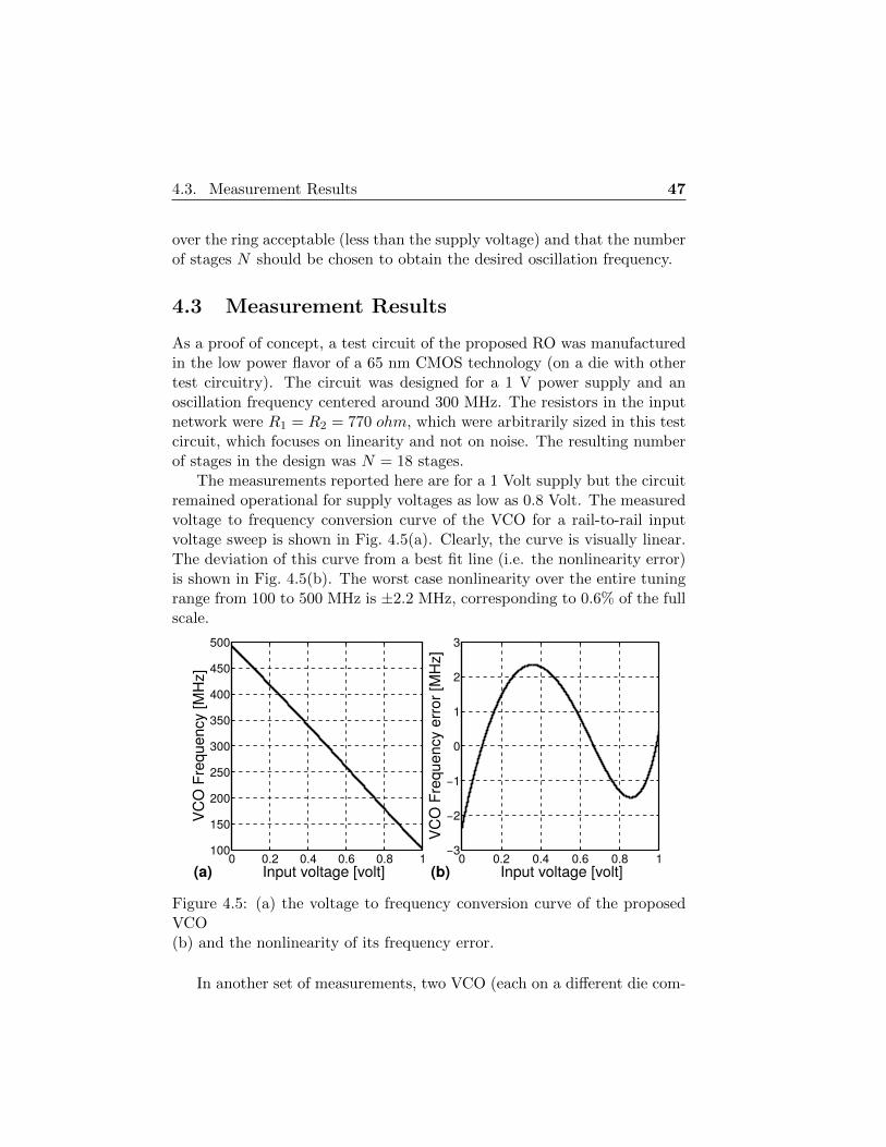
4.3. Measurement Results 47
over the ring acceptable (less than the supply voltage) and that the numberof stages N should be chosen to obtain the desired oscillation frequency.
4.3 Measurement Results
As a proof of concept, a test circuit of the proposed RO was manufacturedin the low power flavor of a 65 nm CMOS technology (on a die with othertest circuitry). The circuit was designed for a 1 V power supply and anoscillation frequency centered around 300 MHz. The resistors in the inputnetwork were R1 = R2 = 770 ohm, which were arbitrarily sized in this testcircuit, which focuses on linearity and not on noise. The resulting numberof stages in the design was N = 18 stages.
The measurements reported here are for a 1 Volt supply but the circuitremained operational for supply voltages as low as 0.8 Volt. The measuredvoltage to frequency conversion curve of the VCO for a rail-to-rail inputvoltage sweep is shown in Fig. 4.5(a). Clearly, the curve is visually linear.The deviation of this curve from a best fit line (i.e. the nonlinearity error)is shown in Fig. 4.5(b). The worst case nonlinearity over the entire tuningrange from 100 to 500 MHz is ±2.2 MHz, corresponding to 0.6% of the fullscale.
0 0.2 0.4 0.6 0.8 1100
150
200
250
300
350
400
450
500
(a) Input voltage [volt]
VCO
Fre
quen
cy [M
Hz]
0 0.2 0.4 0.6 0.8 1−3
−2
−1
0
1
2
3
(b) Input voltage [volt]
VCO
Fre
quen
cy e
rror [
MH
z]
Figure 4.5: (a) the voltage to frequency conversion curve of the proposedVCO(b) and the nonlinearity of its frequency error.
In another set of measurements, two VCO (each on a different die com-

48 Chapter 4. Linear voltage controlled ring oscillator
ing from the same wafer) were configured as a pseudo dfferential ADC. Forthis, they are driven by a differential input signal with a midscale commonmode voltage (of 500 mV). In our test circuit only one of the phases of theVCO was accessible (instead of the 18 phases as would be in an actual VCOADC). Now, for each VCO, this output phase was captured by a 10 GS/ssampling oscilloscope and converted into a bitstream, and differentiatedin the digital domain. Then the results for both VCOs were subtractedform each other. This way we obtain a configuration that is similar to anactual (pseudo-differential) first order noise shaping VCO-ADC (only withreduced performance because we are only using 1 out of the 18 phases) [20].
The corresponding output spectrum for the case of a 100 KHz, 400 mVpp
differential input sine wave is shown in Fig. 4.6. Note that this is -14 dBbelow the absolute maximum signal level which whould be 2 Vpp. The thirdharmonic is clearly visible at -74 dBc. The second harmonic distortion isalso visible at -85 dBc but is so small that it almost does not affect theoverall THD. This is due to the pseudo differential configuration. In thecase where only 1 of the two VCO’s was used (corresponding to a single-ended configuration), the second harmonic was -51 dBc, indicating thatover 30 dB rejection of even order harmonics is easily achieved (even inthis non-optimal configuration, where both VCO’s are on a different die).
104
106
108−140
−120
−100
−80
−60
−40
−20
0
Frequency [Hz]
spec
trum
[dB
]
2MHz passband
74dB6dB/octave
3dB/octave
SNR = 71dBSNDR = 69dB
Figure 4.6: Output spectrum of the pseudo differential VCO ADC experi-ment.
The high frequency noise roll off of 6 dB/octave corresponds to theexpected first order noise shaping. In this configuration, this noise con-tribution dominates above a few MHz, but as explained above this is dueto the fact that only 1 of the 18 VCO phases is used here. Then there is

4.3. Measurement Results 49
a white noise floor (related to the thermal noise of the resistors). At lowfrequencies there is also some 1/f noise. For this case, the SNR and SNDRover a bandwidth of 2 MHz were equal to 71 dB and 69 dB respectively.
−50 −40 −30 −20 −10 030
40
50
60
70
80
90
Normalized Input level [dB]
SNR,SNDR(dB)
pseudo diff: SNR
pseudo diff: SNDRsingle ended: SNDR
69dB
pseudo diff: SNR
56dB
Figure 4.7: SNR and SNDR vs. the normalized rail to rail input level (of2Vpp differentially).
Similar experiments were performed for varying input levels. The corre-sponding results for the SNR and SNDR in a 2 MHz bandwidth are shownin Fig. 4.7. It is clear that for large input signal levels the performanceis limited by distortion, leading to a peak SNDR of 69 dB at 400 mVpp(the case shown in Fig. 4.6). The result for the case where only 1 VCO isread out (in a single ended configuration), is shown as well). Here, at highsignal levels the distortion is dominated by the second harmonic, leadingto a peak SNDR of 56 dB (much worse than the pseudo differential case).
The power consumption of a single VCO was 0.65 mw. This powerconsumption is almost entirely determined by the choice of the resistors R1
and R2 (which were 770 ohm in this case). As explained above, the powercan easily be reduced by using larger resistors, but this is at the expenseof a higher white noise level. The area for a single VCO is 60 µm× 25 µm.
Although the linearity of the proposed VCO circuit is good enough formany applications, in the next chapter we will examine the potential ofPWM pre-coding technique to even further improve linearity of the VCO.

50 Chapter 4. Linear voltage controlled ring oscillator

Chapter 5
Theory and design of apassive ADSM
VCO based Analog to Digital conversion allows easy implementation ofnoise shaping A/D conversion [5,6,20,29–31]. However, in a straightforwardimplementation of such a VCO ADC, the overall linearity will be limitedby the linearity of the VCO, which typically will not be good enough. Apotential solution is to convert the input voltage into a two-level signalwhere the information is stored in the duty cycle of the resulting square-wave using an Asynchronous Delta Sigma Modulator (ADSM) or a PulseWidth Modulator (PWM). This method is known as ’PWM pre-coding’[29–31].
The PWM and ADSM that have been previously presented in the lit-erature make use of typical analog building blocks, such as highly lineartransconductance gain stages or op-amps. As it was discussed before, themain scope of this book is to avoid these traditional blocks, because they arespecially very challenging to design in the most recent CMOS technologieswith smaller transistor channel lengths and lower supply voltages.
As an alternative we propose the use of an ADSM with a passive loopfilter and it will be shown that such a modulator, if properly designed, canprovide sufficient linearity for almost any application.
The previous theoretical work to predict the linearity of passive andactive ADSM was presented in [68], but it had some errors. Therefore, inthe first section of this chapter we will revisit the theory and come up witha more accurate estimation.
In the second section, the effect of loop delay in an ADSM will be
51

52 Chapter 5. Theory and design of a passive ADSM
analyzed. It will be shown that the loop delay, which is normally due tothe Schmitt trigger doesn’t necessarily ruin the performance of the ADSM,as long as it is properly modeled, taken into account, and compensated bylowering the threshold voltage of the Schmitt trigger.
Finally, an implemented prototype is measured and discussed in the lastsection of this chapter. The presented proof of concept is an ADSM with apassive loop filter with an input bandwidth of 10 MHz. This circuit is easyto implement and is operational under low supply voltages, 1 V.
5.1 Analyzing ADSMs without delay
This section investigates the commonly used Asynchronous Delta SigmaModulator which consists of a schmitt-trigger and a continuous time loopfilter. A detailed analysis is presented to accurately predict the distortionof such modulators. The extracted expressions are compared with simu-lation results and they illustrate an excellent match. The results are alsocompared with a previous work by Roza [68] and they show a drastic im-provement in accuracy.
There has been related prior work on the distortion of PWMs, e.g. [68–71]. However, [69] and [70] concern PWM structures that deviate from theclass that is studied in this manuscript. The PWMs studied in [69] areADSMs that have a continuous time loop filter but instead of a schmitt-trigger they have a comparator in the loop. In such ADSMs, the order ofthe loop filter needs to be greater than two to have a stable oscillation.In the family of ADSMs that we are studying here, it is required that thehysteresis of the schmitt trigger is non-zero. The resulting ADSMs canalready work with a passive 1st order loop filter.
On the other hand, [71] and [68] do focus on the same class of ADSMs asour manuscript. However, [71] concerns a simulation based aproach insteadof an analytical one. The only work that presents analytical expressions topredict the 3rd order harmonic distortion of an ADSM is by Roza [68]. Thiswork gives a good insight to the understanding and analysis of an ADSM,but the final equation for the distortion does not have a good match withsimulation results. Therefore we will present a more accurate analysis belowto find an expression for the distortion and carrier frequency of an ADSM,then we will compare the proposed theory with simulation results and withRoza’s results [68] as well.
Fig. 5.1 shows a typical spectrum for the output of an ADSM with a
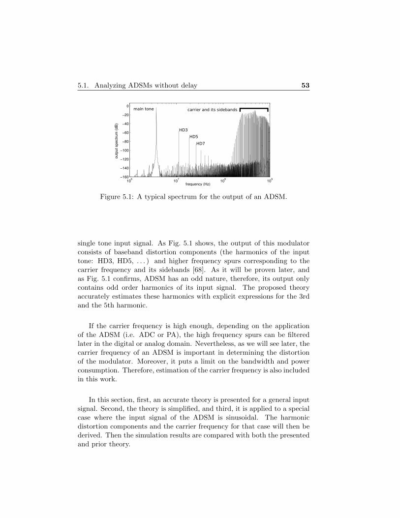
5.1. Analyzing ADSMs without delay 53
106 107 108 109−160
−140
−120
−100
−80
−60
−40
−20
0
frequency (Hz)
outp
utsp
ectru
m(d
B)
[HD3
HD5
HD7
main tone carrier and its sidebands
Figure 5.1: A typical spectrum for the output of an ADSM.
single tone input signal. As Fig. 5.1 shows, the output of this modulatorconsists of baseband distortion components (the harmonics of the inputtone: HD3, HD5, . . . ) and higher frequency spurs corresponding to thecarrier frequency and its sidebands [68]. As it will be proven later, andas Fig. 5.1 confirms, ADSM has an odd nature, therefore, its output onlycontains odd order harmonics of its input signal. The proposed theoryaccurately estimates these harmonics with explicit expressions for the 3rdand the 5th harmonic.
If the carrier frequency is high enough, depending on the applicationof the ADSM (i.e. ADC or PA), the high frequency spurs can be filteredlater in the digital or analog domain. Nevertheless, as we will see later, thecarrier frequency of an ADSM is important in determining the distortionof the modulator. Moreover, it puts a limit on the bandwidth and powerconsumption. Therefore, estimation of the carrier frequency is also includedin this work.
In this section, first, an accurate theory is presented for a general inputsignal. Second, the theory is simplified, and third, it is applied to a specialcase where the input signal of the ADSM is sinusoidal. The harmonicdistortion components and the carrier frequency for that case will then bederived. Then the simulation results are compared with both the presentedand prior theory.

54 Chapter 5. Theory and design of a passive ADSM
F(ω)p(t)
Σe(t)
v(t)
Figure 5.2: A general representation of an ADSM.
5.1.1 Proposed Theory
General Theory
Fig. 5.2 shows the general diagram of an ADSM. Here, v(t) is an arbitraryinput signal and is assumed to be limited to a full scale of ±1. e(t) is thefiltered error signal at the input of the schmitt-trigger. p(t) is the outputsquare wave with a pulse width of α and instantaneous period T , whichtoggles between +1 and −1. As it will be shown later in this section, inthis type of modulation, not only the duty cycle of the output square wave,αT , but also its carrier frequency are dependent on the input signal. Thecarrier frequency of an ADSM for a zero input is referred to as ωc andω1 = 2π
T is the (instantaneous) carrier frequency which is a function of theinput signal, v. According to Fig. 5.2 we can write the signal flow at e(t):
e(t) = ((v − p)⊗ f) (t) (5.1)
where f(t) is the time domain impulse response of the filter, F (ω), and ⊗is the convolution.
In what follows, we will do the analysis based on the so-called quasi-static approximation. This means that we are going to build the theoryassuming that the input signal v(t) is a constant. This will allow us toobtain exact analytical results. Later on, we will apply these analyticalresults as an approximation for the case of a slowly varying input signalv(t). Since the input bandwidth is much lower than ω1, this approximationturns out to be very accurate.
In this case the overall output signal p(t) can be considered to be astable square wave with a fixed angular frequency ω1 and a fixed dutycycle α. If we choose the origin of the time axis as shown in Fig. 5.3, thiscan be described by the Fourier series:
p(t) =
(2α
T− 1
)+ 4× Re
{ ∞∑n=1
sin(nω1
α2
)nπ
ejnω1t
}(5.2)

5.1. Analyzing ADSMs without delay 55
The term (2αT − 1) term in p(t) will be referred to as u. If the input signalv(t) is constant (as we are assuming for the moment), this term u is constantas well. Later on we will consider the case where v(t) is varying very slowlyand then u(t) will also vary slowly over time. Hence, we will refer to u(t)as the baseband component of p(t). It includes the desired signal and itsharmonic distortion components.
From the definition of the duty cycle α we immediately obtain:
u =
(2α
T− 1
)or, ω1α = π(u+ 1) (5.3)
By combining this with (5.2) and (5.1), the signal e(t) can be written as:
e(t) = ((v − u)⊗ f) (t)− 4
∞∑n=1
(sin(nω1
α2
)nπ
)× (5.4)
[Re {F (nω1)} cos(nω1t)− Im {F (nω1)} sin(nω1t)]
Here, the term ((v − u)⊗ f) (t) corresponds to the low-frequency compo-nent of e(t), and will be denoted as elf. In the case where the input signalis constant, elf is a constant as well.
Vth
T/2
T
t
t
e(t)
+1
-1
-Vth
(a)
(b)
-T/2
α/2-α/2
p(t)
Figure 5.3: Typical waveforms for the ADSM in Fig. 5.2.
Fig. 5.3 shows typical waveforms of an ADSM. As the figure shows, theschmitt-trigger toggles when e(t) reaches its positive or negative thresholds,Vth or −Vth. So if we evaluate e(t) for t = −α
2 , we obtain:
Vth = elf − 4
∞∑n=1
(sin(nω1
α2
)nπ
)× (5.5)[
Re {F (nω1)} cos(nω1α
2) + Im {F (nω1)} sin(nω1
α
2)]

56 Chapter 5. Theory and design of a passive ADSM
and for t = α2 we will have:
−Vth = elf − 4∞∑n=1
(sin(nω1
α2
)nπ
)× (5.6)[
Re {F (nω1)} cos(nω1α
2)− Im {F (nω1)} sin(nω1
α
2)]
If we assume that elf is constant, the subtraction of (5.5) and (5.6) willresult in:
∞∑n=1
1
nsin2(nω1
α
2)Im {F (nω1)} = −π
4Vth (5.7)
and the addition will give:
elf =2
π
∞∑n=1
Re {F (nω1)}n
sin (nω1α) (5.8)
Solving (5.7) will give an expression for the oscillation frequency, ω1,as a function of u. Afterwards, solving (5.8) will then give the basebandcomponent of the output signal, u, as a function of the input signal, v.
In order to solve the series in (5.7) and (5.8), we should have an un-derstanding about the loop filter. In most of the conventional filters thatare generally used in ADSMs (like the ones used in the next section asexamples or in [68], for example 1/(1 + sτ)) for ω > ω1 we have:
Re{F (ω)} ≈ 1
(τr · ω)2(5.9)
and,
Im{F (ω)} ≈ 1
τi · ω(5.10)
where τr and τi are filter dependent constants. We will see that theseassumptions are valid if the poles and zeros of the filter are much lowerthan ω1. In this manner, the filter will have about 90◦ phase shift aroundthe carrier frequency. The additional 90◦ phase shift required in the loopfor the oscillation to take place, will be provided by the hysteresis of theschmitt-trigger.
Based on the assumption in (5.10), the series in (5.7) can be simplifiedusing [72, p. 92, Eq. 4], which results in:
ω1 = ωc(1− u2) with, ωc =π
2τi · Vth(5.11)

5.1. Analyzing ADSMs without delay 57
In order to solve (5.8), we will first simplify it by substituting ω1α =π(u+1), according to (5.3). Then, considering the assumption of (5.9), theseries in (5.8) can be evaluated using [72, p. 87, Eq. 4]:
∞∑n=1
Re{F (nω1)}n
sin(nω1α) =−π3
12
(u− u3)(τr · ω1)2
(5.12)
Since ω1 is also a function of u, in the right side of (5.12) we cansubstitute ω1 = ωc(1−u2) from (5.11). Now by inserting (5.12) in (5.8) wewill have:
elf =2
π
(−π3
12
)(u− u3)
(τr · ωc(1− u2))2(5.13)
and taking (5.9) into account, for ωc, will give:
elf = −π2
6Re{F (ωc)}
u
1− u2(5.14)
Untill now, we assumed that the signals v(t), u(t) and elf(t) were con-stant. Now we will use the quasi-static approximation and assume that theresults are also valid for the case where this signals are slowly varying. Thisleads to:
((u− v)⊗ f) (t) =π2
6Re{F (ωc)}
u(t)
1− u2(t)(5.15)
Eq. (5.15) gives a very accurate relationship between the input signal,v, and the baseband output signal, u. Hence, in principle, all non-linearityeffects of the modulator could be derived from this equation using numericalmethods. After obtaining u from this equation, the instantaneous carrierfrequency can also be accurately calculated using (5.11).
Eq. (5.15) also allows to make an important observation: if the realpart of the loop filter transfer is zero, the modulation process does notgenerate in-band harmonic distortions. This occurs when the loop filter isan integrator. This was also already observed in [68] and hence in terms ofmodulation distortion, an integrating loop filter is the optimal choice.
58 Chapter 5. Theory and design of a passive ADSM
Approximate Theory
In what follows we will further elaborate the results of (5.11) and (5.15) forthe case where the input signal v(t) is slowly varying. As a result the base-band component of the output signal u(t) and the instantaneous oscillationangular frequency ω1(t), will also vary slowly over time. However, not tooverload the notation, in the following sections we will drop the explicittime dependence (t) for these signals.
Eq. (5.15) gives u as an accurate yet implicit function of v. Usually,we prefer to have an explicit analytical expression so that we don’t neednumerical methods to solve it. For this, we use Perturbation theory: firstwe make a rough and 1st order estimation of the output signal, u, then weuse that estimation to simplify the equation, solve it again, and find a moreaccurate answer for u.
By observing that the term on the right hand of (5.15) is much smallerthan the ones on the left hand, we obtain in a first approximation that u ≈v. Now, we can use this approximation to estimate the contribution of theright hand of (5.15) and we obtain the following improved approximation:
(u− v)⊗ f ≈ π2
6Re{F (ωc)}
v
1− v2(5.16)
Eq. (5.11) also gives a very accurate expression for ω1. But, since weprefer to have ω1 as a function of the input signal v, rather than the out-put signal u, we can again use the approximation u ≈ v, which gives thefollowing simplified expression:
ω1 ≈π(1− v2)2τi · Vth
(5.17)
Sinusoidal input signal
Now we will apply the approximate theory to the case where the inputsignal is a single tone, v = A sin(µt), to obtain the harmonic distortioncomponents of the modulator. By assuming v = A sin(µt), the right sideof (5.16) can be expanded using its Fourier series. Then we will have:
(u− v)⊗ f =π2
6Re{F (ωc)}
∞∑n=1
Kn(A) sin(nµt) (5.18)

5.1. Analyzing ADSMs without delay 59
where Kn(A) comes from this Fourier integral:
Kn(A) =µ
π
∫ πµ
−πµ
A sin(µt) · sin(nµt)
1− (A sin(µt))2dt (5.19)
It can be shown that the integral in Kn(A) is zero for even values ofn. Therefore, according to (5.18), the Fourier expansion of u should alsoinclude only the odd harmonics of the input frequency, µ. So the Fourierexpansion of u will be:
u =∑n
an · sin(nµt− θn), n = 1, 3, 5, ... (5.20)
By substituting (5.20) in (5.18), we obtain the phase θn and the ampli-tude an for each harmonic by matching the corresponding sin(nµt) termsfrom both sides of the equation. For the main tone, n = 1, since the termson the right hand of (5.18) are much smaller than the main tones on theleft, we can simply deduce that a1 ≈ A. For the harmonics we obtain:
θn = ∠[F (nµ)], an · |F (nµ)| = π2
6Re{F (ωc)}Kn(A) (5.21)
and from that we can finally obtain the ratio of the magnitude of the nthharmonic over the main tone:
dn =ana1≈ an
A=π2
6
Kn(A)
A
Re{F (ωc)}|F (nµ)|
(5.22)
Eq. (5.19) for the Kn factors can also be calculated. E.g. for the 3rd and5th harmonic this leads to (for A ≤ 1):
K3(A) =2A2 − 8
−A3+
6A2 − 8
A3√
1−A2(5.23)
K5(A) =2A4 − 24A2 + 32
−A5+
10A4 − 40A2 + 32
A5√
1−A2(5.24)
By substituting (5.23) in (5.22), we obtain the 3rd order harmonic dis-tortion of an ADSM:
d3 =π2
6
(2A2 − 8
−A4+
6A2 − 8
A4√
1−A2
)Re{F (ωc)}|F (3µ)|
(5.25)
60 Chapter 5. Theory and design of a passive ADSM
The average carrier frequency of the modulator, ω1, can be accuratelycalculated by averaging (5.11). But it is easier to use the estimation in(5.17). For a sinusoidal input, v = A sin(µt), the average carrier frequencywill be:
ω1 =π(1− 0.5A2)
2τi · Vth(5.26)
Except for the accurate value of ω1 in (5.11), the other approximationsfor ωc, ω1, and ω1 in (5.11), (5.17), and (5.26) have been previously reported[68,71,73–75].
5.1.2 Simulation Results
To verify the proposed theory, the ADSM in Fig. 5.2 was simulated inSimulink for two cases, once with a 1st order passive loop filter and thenwith a 3rd order active one. The simulation results for the 3rd order har-monic distortion were also compared with a previous theory by Roza [68]which gave:
d3[Roza] =π2A2
6
Re{F (ω1)}F (µ)
(5.27)
Here, d3[Roza] comes from the series expansion of the output, u ≈ v+d3v3.
This result is frequently misinterpreted as if d3[Roza] corresponds to the3rd harmonic distortion component, this is incorrect because the cube of asine wave equals:
sin3 x =1
4(3 sinx− sin 3x) (5.28)
This way, the correct 3rd harmonic distortion predicted by [68] equalsd3[Roza]/4, corresponding to a difference of 12 dB.
First order passive loop filter
As a first example, an ADSM with a 1st order passive loop filter, F (s) =1
1+sτ , was evaluated. By mapping this to (5.9) and (5.10) we obtain |τi| =|τr| = τ . We have chosen τ = 5 ns. To have a usable ADSM the thresholdvoltage Vth should be sufficiently small (otherwise the oscillation wouldn’tbegin), therefore it was set to Vth = 0.1 which corresponds to a (zero-input) self oscillation frequency, fc = ωc
2π = 500 MHz, according to (5.11).Different simulation setups were employed to examine different aspects ofthe theory.
5.1. Analyzing ADSMs without delay 61
In the first set of simulations, a DC signal has been applied to the inputof the modulator. Both the DC level of the output and its carrier frequencyhave been evaluated. The output DC level has been compared both withthe accurate theory of (5.15) and the approximate theory of (5.16). Takein mind that for DC signals we have F (0) = 1, and Re{F (ωc)} can beobtained by combining (5.9) and (5.11), so (5.15) will collapse to:
v = u−2V 2
th
3
(u
1− u2
)(5.29)
and by doing the same to (5.16) we will have:
u ≈ v +2V 2
th
3
(v
1− v2
)(5.30)
As Fig. 5.4 (a) shows, there is a perfect match between the accuratetheory in (5.29) and the simulation results. The curve corresponding to theapproximate theory, (5.30), also has a good match and only a little deviationfor higher input DC values. The same conclusion applies to Fig. 5.4 (b)where the carrier frequency has been compared with the accurate theory of(5.11) and the approximate theory of (5.17).
In the next set of simulations, a sinusoidal input with an amplitude ofA = 0.7 is applied to the aforementioned modulator and the 3rd harmonic ofthe output is evaluated for a range of input frequencies. According to (5.26),with this input amplitude, an average carrier frequency of ω1 ≈ 377 MHzis expected. Fig. 5.5 shows the corresponding simulation results. The plotalso shows the proposed theory [Eq. (5.25)]. For comparison with [68], twocurves have been added. The first corresponds to the incorrect interpreta-tion of Roza’s theory [i.e. use (5.27) for the 3rd harmonic distortion] andthe other adds −12 dB to it to compensate for the −14 factor accordingto (5.28) and hence corresponds to a correct interpretation of Roza’s the-ory. As this set of simulations confirms, the proposed theory predicts thedistortion of an ADSM much more accurately than [68].
Fig. 5.6 illustrates the dependency of the (average) carrier frequency andthe 3rd order harmonic distortion on the input amplitude, A, according tosimulation and according to (5.26) and (5.25) for the case of an arbitraryinput frequency of µ = 12.5 MHz over a range of input amplitudes. Againthe plot confirms a good match between the simulation and the theory.
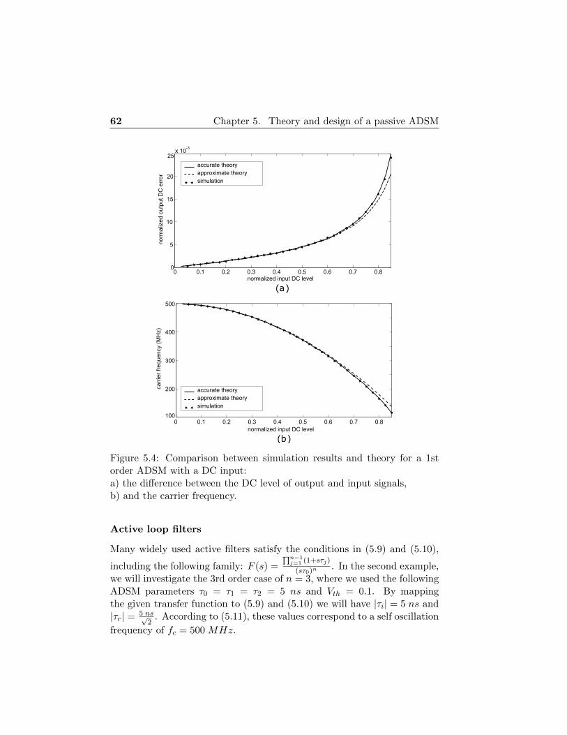
62 Chapter 5. Theory and design of a passive ADSM
0 0.1 0.2 0.3 0.4 0.5 0.6 0.7 0.80
5
10
15
20
25
normalized input DC level
normalizedoutputDCerror
accurate theory
simulationapproximate theory
0 0.1 0.2 0.3 0.4 0.5 0.6 0.7 0.8100
200
300
400
carrierfrequency(MHz)
500
(a)
(b)
x 10-3
normalized input DC level
accurate theory
simulationapproximate theory
Figure 5.4: Comparison between simulation results and theory for a 1storder ADSM with a DC input:a) the difference between the DC level of output and input signals,b) and the carrier frequency.
Active loop filters
Many widely used active filters satisfy the conditions in (5.9) and (5.10),
including the following family: F (s) =∏n−1j=1 (1+sτj)
(sτ0)n. In the second example,
we will investigate the 3rd order case of n = 3, where we used the followingADSM parameters τ0 = τ1 = τ2 = 5 ns and Vth = 0.1. By mappingthe given transfer function to (5.9) and (5.10) we will have |τi| = 5 ns and|τr| = 5 ns√
2. According to (5.11), these values correspond to a self oscillation
frequency of fc = 500 MHz.
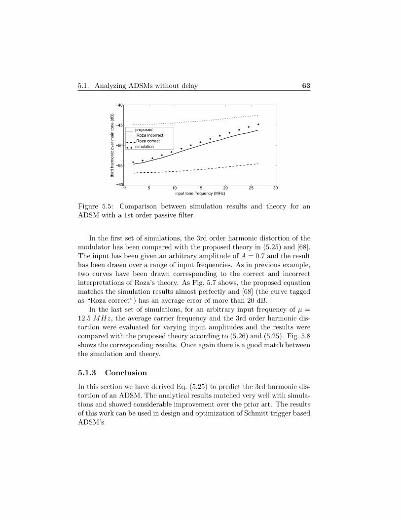
5.1. Analyzing ADSMs without delay 63
−60
−55
−50
−45
−40
input tone frequency (MHz)
third
harm
onic
over
mai
nto
ne(d
B)
0 5 10 15 20 25 30
Roza incorrectRoza correct
proposed
simulation
Figure 5.5: Comparison between simulation results and theory for anADSM with a 1st order passive filter.
In the first set of simulations, the 3rd order harmonic distortion of themodulator has been compared with the proposed theory in (5.25) and [68].The input has been given an arbitrary amplitude of A = 0.7 and the resulthas been drawn over a range of input frequencies. As in previous example,two curves have been drawn corresponding to the correct and incorrectinterpretations of Roza’s theory. As Fig. 5.7 shows, the proposed equationmatches the simulation results almost perfectly and [68] (the curve taggedas “Roza correct”) has an average error of more than 20 dB.
In the last set of simulations, for an arbitrary input frequency of µ =12.5 MHz, the average carrier frequency and the 3rd order harmonic dis-tortion were evaluated for varying input amplitudes and the results werecompared with the proposed theory according to (5.26) and (5.25). Fig. 5.8shows the corresponding results. Once again there is a good match betweenthe simulation and theory.
5.1.3 Conclusion
In this section we have derived Eq. (5.25) to predict the 3rd harmonic dis-tortion of an ADSM. The analytical results matched very well with simula-tions and showed considerable improvement over the prior art. The resultsof this work can be used in design and optimization of Schmitt trigger basedADSM’s.
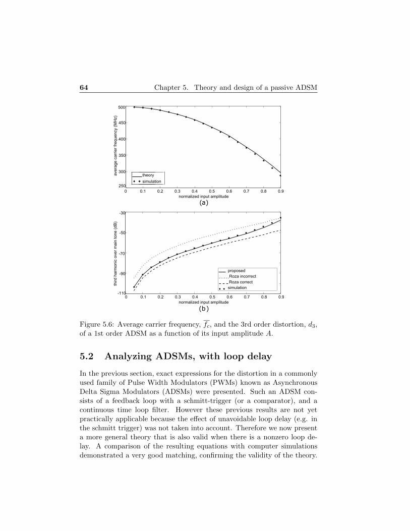
64 Chapter 5. Theory and design of a passive ADSM
0 0.1 0.2 0.3 0.4 0.5 0.6 0.7 0.8 0.9250
300
350
400
450
normalized input amplitude
0 0.1 0.2 0.3 0.4 0.5 0.6 0.7 0.8 0.9
-30
-50
-70
-90
-110
third
harm
oni
cov
erm
ain
tone
(dB
)
500
(b)
(a)
normalized input amplitude
Roza incorrectRoza correct
proposed
simulation
theory
simulation
aver
age
car
rier
freq
uenc
y (M
Hz)
Figure 5.6: Average carrier frequency, fc, and the 3rd order distortion, d3,of a 1st order ADSM as a function of its input amplitude A.
5.2 Analyzing ADSMs, with loop delay
In the previous section, exact expressions for the distortion in a commonlyused family of Pulse Width Modulators (PWMs) known as AsynchronousDelta Sigma Modulators (ADSMs) were presented. Such an ADSM con-sists of a feedback loop with a schmitt-trigger (or a comparator), and acontinuous time loop filter. However these previous results are not yetpractically applicable because the effect of unavoidable loop delay (e.g. inthe schmitt trigger) was not taken into account. Therefore we now presenta more general theory that is also valid when there is a nonzero loop de-lay. A comparison of the resulting equations with computer simulationsdemonstrated a very good matching, confirming the validity of the theory.

5.2. Analyzing ADSMs, with loop delay 65
0 5 10 15 20 25−120
−110
−100
−90
−80
−70
−60
−50
−40
input tone frequency (MHz)
thirdharmonicovermaintone(dB)
Roza incorrectRoza correct
proposed
simulation
30
Figure 5.7: Comparison between simulation results and theory for the 3rdorder harmonic distortion of a 3rd order ADSM over its input frequency.
This way, a designer can now easily understand the relationship betweenthe loop filter dynamics and the linearity of an ADSM.
5.2.1 Previous theory and its limitations
According to [2] (i.e. the previous section), the third harmonic distortion ofan ADSM, as in Fig.5.9 (a), with a loop-filter of F(ω) and an input voltageof v = A sin(µt) is (all voltages normalized to ±1):
d3 =π2
6
(2A2 − 8
−A4+
6A2 − 8
A4√
1−A2
)Re{F (ωc)}|F (3µ)|
(5.31)
where ωc is the self oscillation frequency of the PWM for v = 0 and d3 isthe amplitude of the third harmonic tone, a3 sin(3µt), over the amplitudeof the main tone, d3 = a3
A .This theory was obtained based on some assumptions. First, the highest
order of si in the numerator of F (s) should be exactly one degree less thanthe denominator to have a stable oscillation. Second, it assumes that allpoles and zeros of the filter are at much lower frequency than ωc, and finally,the filter should satisfy the following conditions for ω > ωc :
Re{F (ω)} ≈ 1
(τr.ω)2and, Im{F (ω)} ≈ 1
τi.ω(5.32)
where τr and τi are filter dependent constants, the former could be realor imaginary and the latter could be positive or negative. Then, given aschmitt trigger threshold voltage of ±Vth we will have ωc = π
2τi·Vth .

66 Chapter 5. Theory and design of a passive ADSM
0 0.1 0.2 0.3 0.4 0.5 0.6 0.7 0.8 0.9
0 0.1 0.2 0.3 0.4 0.5 0.6 0.7 0.8 0.9−140
−120
−100
−80
−60
−40
−20
Roza correct
proposed
simulation
Roza incorrect
theory
simulation
normalized input amplitude
(a)
(b)
normalized input amplitude
third
harm
oni
cov
erm
ain
tone
(dB
)
250
300
350
400
450
500
aver
age
car
rier
freq
uenc
y (M
Hz)
Figure 5.8: Average carrier frequency, fc, and 3rd order distortion, d3, ofa 3rd order ADSM vs. the input amplitude, A.
The theory in [2] only applies to a certain category of ADSMs wherethe schmitt trigger is ideal (has no delay). But in an actual circuit, theschmitt trigger always has a delay, modelled as TD in Fig. 5.9 (b), andas the oscillation frequency of the PWM increases, the loop delay becomesmore important in determining the oscillation frequency and the distortion.
In order to evaluate d3 for the case with delay, the first solution thatcomes to mind is to merge the delay of the schmitt trigger in the loop-filteras a e−TDjω factor and use (5.31) for calculating the third harmonic withthe new loop-filter, G(ω) = F (ω).e−TDjω. But it can be easily shown thatRe{G(ω)} and Im{G(ω)} will not satisfy the conditions in (5.32).

5.2. Analyzing ADSMs, with loop delay 67
Σe(t)
v(t)
Σe(t)
v(t)
(a)
(b)
F(ω)
-TDF(ω)p(t)
jωe
p(t)
Figure 5.9: General representation of an ADSM,(a) without extra delay in the loop,(b) and with loop delay.
5.2.2 Proposed approach
Here we will revisit the equations in the previous section with similar as-sumptions while considering a delay of TD for the schmitt trigger. Bare inmind that delay anywhere in the loop can be modelled this way withoutaffecting the spectral qualities of the signals.
In Fig. 5.9 (b), v(t) is a band limited input signal, e(t) is the filterederror signal at the input of the schmitt-trigger, and p(t) is the output squarewave (±1) with a pulse width of α and duration of T . As it will be shownlater in this section, in this type of modulation, not only the duty cycle ofthe output square wave, α
T , but also its carrier frequency are dependent onthe input signal. The self oscillation frequency of this PWM for a zero inputis called ωc and ω1 = 2π
T is the (instantaneous) carrier frequency which is afunction of the input signal, v. According to Fig. 5.9 (b) we can write thesignal at e(t):
e(t) = ((v − p)⊗ f)(t) (5.33)
where f(t) is the time domain impulse response of the filter, F (ω), and ⊗is the convolution.
Just as in section 5.1.1, we will use the quasi-static approximation andbuild the theory assuming that the input signal v(t) is a constant. Thenafterwards, we will adopt the results for the case of a slowly varying inputsignal v(t). Then p(t), which is a square wave, can again be described by

68 Chapter 5. Theory and design of a passive ADSM
its Fourier series:
p(t) =
(2α
T− 1
)+ 4× Re
{ ∞∑n=1
sin(nω1
α2
)nπ
ejnω1t
}(5.34)
As before, the(2αT − 1
)term corresponds to the baseband component of p(t)
and will be referred to as u hereafter. For this, we can say: u =(2αT − 1
)or ω1α = π(u+ 1) .Similarly as before we can also consider the low-frequency component, elf,
of the signal e(t):
elf = ((v − u)⊗ f) (t)
In the approximation that v is a constant, also u, elf and ω1 will be constant.
-Vth
A1
TD
t2T/2
T
t
t
e(t)
P(t)+1
-1
-A2
α/2-α/2t1
VthTD
-T/2
Figure 5.10: Typical waveforms of an schmitt trigger based ADSM withdelay.
Fig. 5.10 shows typical waveforms of an ADSM. As the figure shows,the schmitt-trigger toggles with a delay of TD after e(t) reaches its positiveor negative thresholds, Vth or −Vth. So if we use t = α
2 −TD and substitute(5.34) in (5.33), we obtain:
−Vth = elf − 4
∞∑n=1
(sin(nω1
α2
)nπ
)× (5.35)
(Re {F (nω1)} cos(nω1(α
2− TD))−
Im {F (nω1)} sin(nω1(α
2− TD)))

5.2. Analyzing ADSMs, with loop delay 69
and for t = −α2 − TD we will have:
Vth = elf − 4
∞∑n=1
(sin(nω1
α2
)nπ
)× (5.36)
(Re {F (nω1)} cos(nω1α
2+ nω1TD) +
Im {F (nω1)} sin(nω1α
2+ nω1TD))
By adding the last two equations we will have:
0 = elf − 2∞∑n=1
sin(nω1α)
nπ× (5.37)
(Im{F (nω1)} sinnω1TD + Re{F (nω1)} cosnω1TD)
and subtracting them will give:
−πVth2
=∞∑n=1
1− cos(nω1α)
n× (5.38)
(Im{F (nω1)} cosnω1TD − Re{F (nω1)} sinnω1TD)
If the ADSM has a stable oscillation, then we can deduce from Fig.5.10that 2TD ≤ α+TD ≤ T = ω1
2π and from that we can say 0 ≤ ω1α±ω1TD ≤2π . The terms Re{F (nω1)} and Im{F (nω1)} are obtained from (5.32).This allows us to solve the series in (5.38) using [72]. Then (5.38) willresult in:
ω1 = ωc · (1− u2) =π(τiTD − τ2r ) · (1− u2)
2τ2r τiVth + τiT 2D − 2τ2r TD
(5.39)
This equation accurately gives the instantaneous and self oscillationfrequencies, ω1 and ωc, as functions of the output base band signal, u, andthe parameters of the modulator.
Same as above, we can calculate the series in (5.37) using (5.32), (5.39),[72], and the fact that 0 ≤ ω1α ± ω1TD ≤ 2π . With that all, we cansimplify (5.37) which will give:
−elf =π2u
6(τrωc)2(1− u2)−uT 2
D
2τ2r+uTDτi
(5.40)
Again, the result above was obtained for the case of a constant inputsignal v(t). Just as before we will now apply it to the case of slowly varying
70 Chapter 5. Theory and design of a passive ADSM
input signals. Then also u, elf and ω1 will become time dependent. Thisleads to:
(u− v)⊗ f =π2u
6(τrωc)2(1− u2)−uT 2
D
2τ2r+uTDτi
(5.41)
As before, the explicit time dependencies where dropped in order not tooverload the notation. This equation gives an accurate relationship betweenthe input signal, v, and the output baseband signal, u. In order to avoidthe need to solve an implicit equation to obtain u as a function of v, we cansimplify (5.41) using Perturbation Theory. So at first we make a rough firstorder estimation from (5.41). We can see that the terms on the right sideof the equation are much smaller than the ones on the left, so we can sayu ≈ v. By applying this estimation to (5.41) we will obtain this simplifiedequation which gives u as an explicit function of v:
(u− v)⊗ f ≈ π2v
6(τrωc)2(1− v2)−vT 2
D
2τ2r+vTDτi
(5.42)
Now we will apply a sinusoidal input voltage, v = A sinµt, to (5.42) toobtain the harmonic distortions of the ADSM. We can see that the righthand of this equation is an odd function of v, so we can expect u to onlyhave odd harmonics of v. Therefore, we can replace u with its Fourierexpansion:
u =∑n
an sin(nµt− θn), n = 1, 3, 5, ... (5.43)
Since the terms on the right hand of (5.42) are much smaller than thoseon the left, for the main tone we can say a1 ≈ A. In the right hand of(5.42), only the first term can produce harmonic distortion. So if we writethe Fourier expansion on both sides of (5.42) only for the harmonic tones(n = 3, 5, ...) we will have:
∑n
an sin(nµt− θn)⊗ f ≈ π2
6τ2r ω2c
∑n
Kn(A) sin(nµt) (5.44)
where Kn comes from this Fourier integral:
Kn(A) =µ
π
∫ πµ
−πµ
A sin(µt). sin(nµt)
1− (A sin(µt))2dt (5.45)

5.2. Analyzing ADSMs, with loop delay 71
and from (5.44) we can deduce for each harmonic that:
θn = ∠[F (nµ)], an · |F (nµ)| = π2
6τ2r ω2c
Kn(A) (5.46)
and by considering (5.32) for ωc, we can find the ratio of the magnitude ofthe nth harmonic over the main tone:
dn =ana1≈ an
A=π2
6
Kn(A)
A
Re{F (ωc)}|F (nµ)|
(5.47)
The integral in (5.45) can be solved for any of the harmonics. Forn = 3, 5, for example, it gives (for A ≤ 1):
K3(A) =2A2 − 8
−A3+
6A2 − 8
A3√
1−A2(5.48)
K5(A) =2A4 − 24A2 + 32
−A5+
10A4 − 40A2 + 16
A5√
1−A2(5.49)
By substituting (5.48) in (5.47) we can find the 3rd harmonic distortionof an ADSM with loop delay:
d3 =π2
6
(2A2 − 8
−A4+
6A2 − 8
A4√
1−A2
)Re{F (ωc)}|F (3µ)|
(5.50)
and the term Re{F (ωc)} can be calculated using (5.39) and (5.32):
d3 =1
6
(2A2 − 8
−A4+
6A2 − 8
A4√
1−A2
)1
|F (3µ)|× (5.51)
(2τ2r τiVth + τiT2D − 2τ2r TD)2
τ2r (τiTD − τ2r )2
In ADSMs without loop delay (assuming that a high order aggressiveloop filter is not chosen) the signal at the input of the schmitt trigger islimited to ±Vth, e.g. Fig. 5.11(a). After introducing delay to the loop, acertain amplitude modulation effect occurs, Fig.5.11(b). The (above) enve-lope of this effect can be calculated by evaluating e(t = −α
2 ), see Fig. (5.10).By replacing (5.34) in (5.33) and calculating the series we will have:
e(−α2
) = uTD(TD2τ2r− 1
τi)− TD
τi+τ2r Vth − 0.5T 2
D
τ2r − τiTD(5.52)
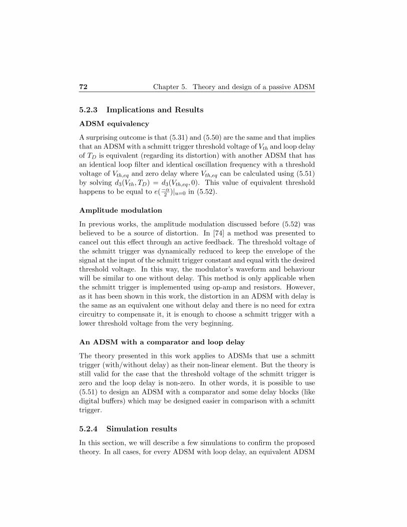
72 Chapter 5. Theory and design of a passive ADSM
5.2.3 Implications and Results
ADSM equivalency
A surprising outcome is that (5.31) and (5.50) are the same and that impliesthat an ADSM with a schmitt trigger threshold voltage of Vth and loop delayof TD is equivalent (regarding its distortion) with another ADSM that hasan identical loop filter and identical oscillation frequency with a thresholdvoltage of Vth,eq and zero delay where Vth,eq can be calculated using (5.51)by solving d3(Vth, TD) = d3(Vth,eq, 0). This value of equivalent thresholdhappens to be equal to e(−α2 )|u=0 in (5.52).
Amplitude modulation
In previous works, the amplitude modulation discussed before (5.52) wasbelieved to be a source of distortion. In [74] a method was presented tocancel out this effect through an active feedback. The threshold voltage ofthe schmitt trigger was dynamically reduced to keep the envelope of thesignal at the input of the schmitt trigger constant and equal with the desiredthreshold voltage. In this way, the modulator’s waveform and behaviourwill be similar to one without delay. This method is only applicable whenthe schmitt trigger is implemented using op-amp and resistors. However,as it has been shown in this work, the distortion in an ADSM with delay isthe same as an equivalent one without delay and there is no need for extracircuitry to compensate it, it is enough to choose a schmitt trigger with alower threshold voltage from the very beginning.
An ADSM with a comparator and loop delay
The theory presented in this work applies to ADSMs that use a schmitttrigger (with/without delay) as their non-linear element. But the theory isstill valid for the case that the threshold voltage of the schmitt trigger iszero and the loop delay is non-zero. In other words, it is possible to use(5.51) to design an ADSM with a comparator and some delay blocks (likedigital buffers) which may be designed easier in comparison with a schmitttrigger.
5.2.4 Simulation results
In this section, we will describe a few simulations to confirm the proposedtheory. In all cases, for every ADSM with loop delay, an equivalent ADSM
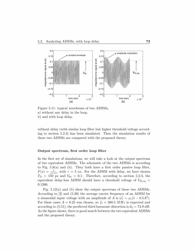
5.2. Analyzing ADSMs, with loop delay 73
0 1 2 3x 10⁻⁷
−0.2
−0.15
−0.1
−0.05
0
0.05
0.1
0.15
0.2
time (sec)
inte
grat
eder
rors
igna
late
(t)
0 1 2 3x 10⁻⁷
−0.2
−0.15
−0.1
−0.05
0
0.05
0.1
0.15
0.2
time (sec)in
tegr
ated
erro
rsig
nala
te(t)
Vth,eqVth
constant envelopeamplitude modulation
(a) (b)
Figure 5.11: typical waveforms of two ADSMs,a) without any delay in the loop,b) and with loop delay.
without delay (with similar loop filter but higher threshold voltage accord-ing to section 5.2.3) has been simulated. Then the simulation results ofthese two ADSMs are compared with the proposed theory.
Output spectrum, first order loop filter
In the first set of simulations, we will take a look at the output spectrumof two equivalent ADSMs. The schematic of the two ADSMs is accordingto Fig. 5.9(a) and (b). They both have a first order passive loop filter,F (s) = 1
1+τs , with τ = 5 ns. For the ADSM with delay, we have chosenTD = 150 ps and Vth = 0.1. Therefore, according to section 5.2.3, theequivalent delay-less ADSM should have a threshold voltage of Vth,eq =0.1266.
Fig. 5.12(a) and (b) show the output spectrum of these two ADSMs.According to [2] and (5.39) the average carrier frequency of an ADSM fora sinusoidal input voltage with an amplitude of A is ω1 = ωc(1 − 0.5A2).For these cases A = 0.25 was chosen, so f1 = 380.5 MHz is expected andaccording to (5.51), the predicted third harmonic distortion is d3 = 74.9 dB.As the figure shows, there is good match between the two equivalent ADSMsand the proposed theory.

74 Chapter 5. Theory and design of a passive ADSM
105 106 107 108 109−160
−140
−120
−100
−80
−60
−40
−20
0
Frequency (Hz)
Mag
nitu
de(d
Bno
rmal
ized
)
input tone
3rd harmonic
74.4 dB
carrier @380.2 MHz
105 106 107 108 109−160
−140
−120
−100
−80
−60
−40
−20
0
Frequency (Hz)
Mag
nitu
de(d
Bno
rmal
ized
)input tone
3rd harmonic
74.9 dB
carrier @380.9 MHz
(a)
TD = 150 psVth = 0.1 vτ = 5 psVm = 0.25 v
Vth = 0.1266τ = 5 psVm = 0.25 v
(b)
Figure 5.12: Output spectrum of two equivalent ADSMs with first orderloop filter,(a) with some delay in the loop,(b) and without loop delay.
A second order ADSM with comparator and loop delay
In section 5.2.3 we argued that an ADSM that has a comparator as itsnon-linear element (instead of a schmitt trigger) and some delay in its loopcan be equivalent with a delay-less ADSM with schmitt trigger.
In order to verify this argument, for this example we have chosen asecond order loop filter, F (s) = 1+sτ1
sτ2·sτ3 , with τ1 = τ2 = τ3 = 5 ns. Thefirst modulator uses a comparator in its loop (Vth = 0) and has a delayof TD = 600 ps. According to section 5.2.3, this modulator should be
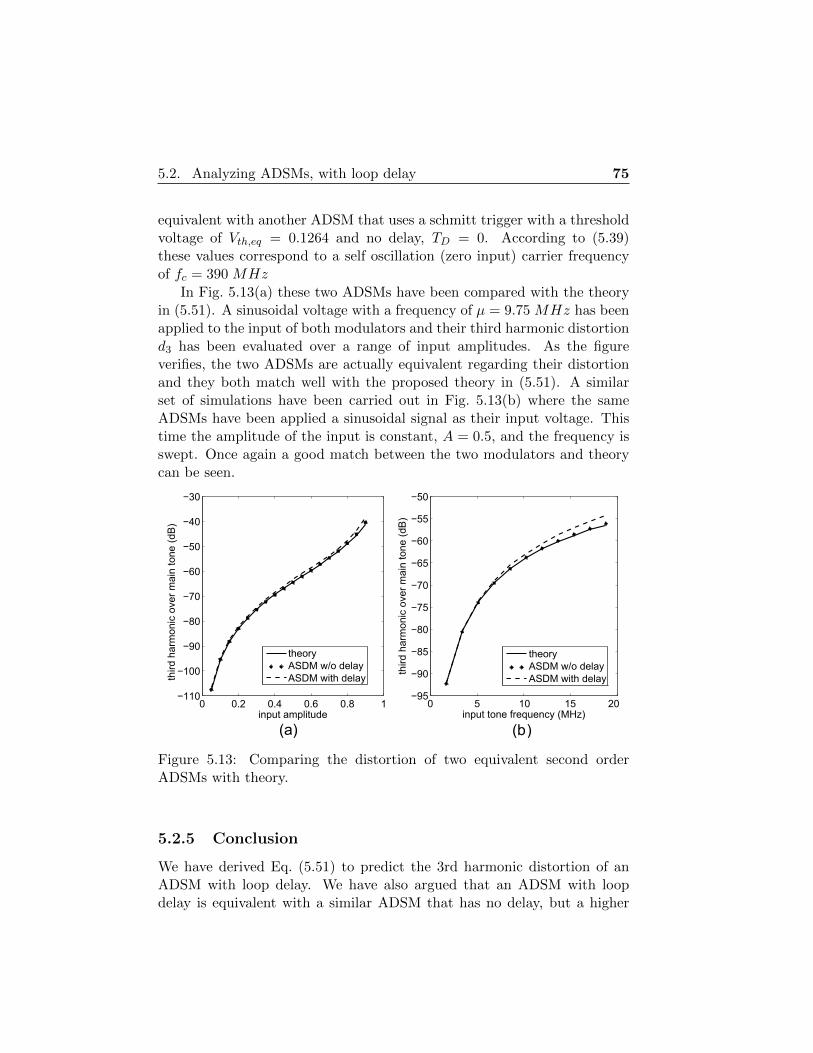
5.2. Analyzing ADSMs, with loop delay 75
equivalent with another ADSM that uses a schmitt trigger with a thresholdvoltage of Vth,eq = 0.1264 and no delay, TD = 0. According to (5.39)these values correspond to a self oscillation (zero input) carrier frequencyof fc = 390 MHz
In Fig. 5.13(a) these two ADSMs have been compared with the theoryin (5.51). A sinusoidal voltage with a frequency of µ = 9.75 MHz has beenapplied to the input of both modulators and their third harmonic distortiond3 has been evaluated over a range of input amplitudes. As the figureverifies, the two ADSMs are actually equivalent regarding their distortionand they both match well with the proposed theory in (5.51). A similarset of simulations have been carried out in Fig. 5.13(b) where the sameADSMs have been applied a sinusoidal signal as their input voltage. Thistime the amplitude of the input is constant, A = 0.5, and the frequency isswept. Once again a good match between the two modulators and theorycan be seen.
0 0.2 0.4 0.6 0.8 1−110
−100
−90
−80
−70
−60
−50
−40
−30
input amplitude0 5 10 15 20
−95
−90
−85
−80
−75
−70
−65
−60
−55
−50
input tone frequency (MHz)
thirdharmonicovermaintone(dB)
theoryASDM w/o delayASDM with delay
theoryASDM w/o delayASDM with delayth
irdharmonicovermaintone(dB)
(a) (b)
Figure 5.13: Comparing the distortion of two equivalent second orderADSMs with theory.
5.2.5 Conclusion
We have derived Eq. (5.51) to predict the 3rd harmonic distortion of anADSM with loop delay. We have also argued that an ADSM with loopdelay is equivalent with a similar ADSM that has no delay, but a higher
76 Chapter 5. Theory and design of a passive ADSM
threshold voltage in its schmitt trigger. The simulation results matchedvery well with the analytical results and verified this equivalency.
From a designer’s point of view, the main conclusion is that the dis-tortion is essentially determined by the loop filter in combination with theself oscillation frequency. The delay in the loop affects the self oscillationfrequency, but if the delay is known, this effect can be counter-acted bytuning the schmitt trigger’s threshold voltage and choosing a lower Vth.
From another perspective, for a given loop filter, better linearity can beobtained by increasing the oscillation frequency, fc, which can be realizedby decreasing the delay or lowering the threshold voltage of the schmitttrigger (even as low as zero). The price of this approach is of course higherswitching activity and power consumption.
In practice, all of the relevant requirements can be optimized using theexplicit equations that have been presented in this chapter.
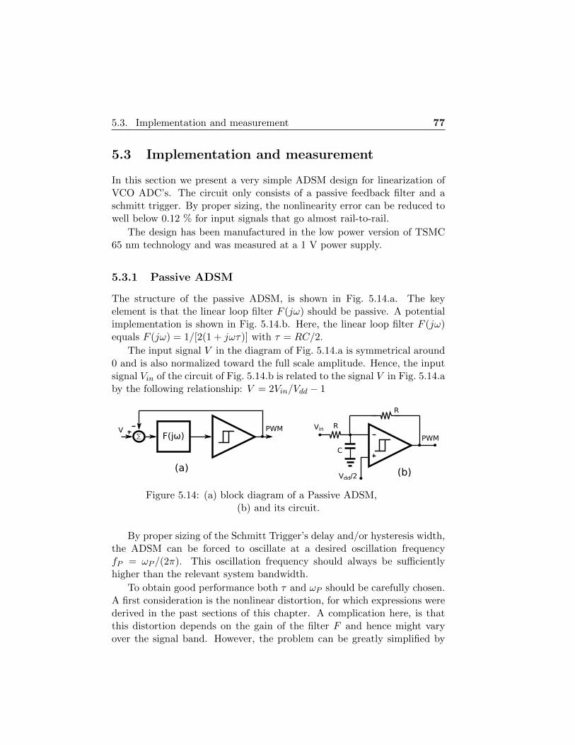
5.3. Implementation and measurement 77
5.3 Implementation and measurement
In this section we present a very simple ADSM design for linearization ofVCO ADC’s. The circuit only consists of a passive feedback filter and aschmitt trigger. By proper sizing, the nonlinearity error can be reduced towell below 0.12 % for input signals that go almost rail-to-rail.
The design has been manufactured in the low power version of TSMC65 nm technology and was measured at a 1 V power supply.
5.3.1 Passive ADSM
The structure of the passive ADSM, is shown in Fig. 5.14.a. The keyelement is that the linear loop filter F (jω) should be passive. A potentialimplementation is shown in Fig. 5.14.b. Here, the linear loop filter F (jω)equals F (jω) = 1/[2(1 + jωτ)] with τ = RC/2.
The input signal V in the diagram of Fig. 5.14.a is symmetrical around0 and is also normalized toward the full scale amplitude. Hence, the inputsignal Vin of the circuit of Fig. 5.14.b is related to the signal V in Fig. 5.14.aby the following relationship: V = 2Vin/Vdd − 1
R
F(jω)V
Vdd/2
PWMPWM
R
C
Vin
(a) (b)
Figure 5.14: (a) block diagram of a Passive ADSM,(b) and its circuit.
By proper sizing of the Schmitt Trigger’s delay and/or hysteresis width,the ADSM can be forced to oscillate at a desired oscillation frequencyfP = ωP /(2π). This oscillation frequency should always be sufficientlyhigher than the relevant system bandwidth.
To obtain good performance both τ and ωP should be carefully chosen.A first consideration is the nonlinear distortion, for which expressions werederived in the past sections of this chapter. A complication here, is thatthis distortion depends on the gain of the filter F and hence might varyover the signal band. However, the problem can be greatly simplified by

78 Chapter 5. Theory and design of a passive ADSM
observing that the input referred noise of the Schmitt Trigger is also in-versely proportional to the gain of the filter F . This means that the effectof comparator noise spectral components that are above the filter cut offfrequency (1/(2πτ)) will be significantly increased. Since this is not toler-able in the usefull signal band, this implies that the filter cut off frequencyshould not be smaller than the usefull signal bandwidth. When we take thisinto account, the filter F must have a flat gain over the signal band and theexpressions of previous sections (in this chapter) are significantly simplified.In particular the expression for the signal band component PWMLF of thePWM signal simplifies into:
PWMLF ≈ v −π2
6
v
1− v21
1 + (τ ωP )2(5.53)
For the case that the input signal is a sine, the expression for the dis-tortion eq. 5.25 (dominated by the 3rd harmonic) becomes:
THD ≈ −20 log
(π2
6A4(1 + (τ ωP )2)
(2A2 − 8− 6A2 − 8√
1−A2
))(5.54)
From this equation, it is clear that the ADSM performance is a strongfunction of the desired input range and of the ADSM oscillation frequencyωP . Based on these considerations, we come to the following design flow.First, size the filter time constant τ such that it corresponds to the desiredsignal bandwidth. Second, decide the input signal range. And third, decidethe desired self-oscillation frequency based on the nonlinearity by evaluatingEq. (5.54). In the circuit that we implemented, we aimed for a 10MHzbandwidth, and a usefull signal range of 750mVpp at a 1V supply voltage.Then we need an oscillation frequency of about 300 MHz to achieve adistortion performance of 65dB.
5.3.2 Circuit design
We implemented a differential version of the conceptual circuit of Fig. 5.14.If we assume that the circuit’s delay is negligible, the Schmitt Trigger hys-teresis width should be as low as 46 mV (differentially), to achieve anoscillation frequency of 300 MHz at a 1 V supply voltage and a filter band-width of 10 MHz. To obtain such a low hysteresis width in a controlledway, we added two pre-amplifier stages with a controlled gain to the actualSchmitt Trigger (as shown in Fig. 5.15.a). The pre amplifier schematic is

5.3. Implementation and measurement 79
Vb
Vdd
out+out-
A
(a)
(b) (c)
low gain pre amplifiers digital buffer
Vdd
B B A
in+ in-
out+out-
in+ in-
Figure 5.15: (a) Overall Schmitt Trigger structure,(b) schematic of the Pre amplifier, which (apart from the sizing) is identicalto the Schmitt Trigger’s schematic,(c) and the digital buffer circuit.
shown in Fig. 5.15.b. It consists of a simple NMOS differential pair with acombination of diode-connected and cross-coupled PMOS load transistors.Here, the weight A of the diode-connected PMOS is larger than the theweight B of the cross-coupled PMOS. The ratio A/B then sets the gain.The actual Schmitt trigger schematic is identical to Fig. 5.15.b, except thatnow the weight B of the cross-coupled PMOS is larger than the weight Aof the diode-connected PMOS load transistors. In this case, the ratio A/Bsets the hysteresis width. Finally a digital buffer (Fig. 5.15.c) is addedto drive the resistors. All these stages consist of maximum three stackedtransistors, and hence are suitable for low voltage designs.
After the first design iteration, it turned out that the circuit’s delay(mostly due to the schmitt trigger) was not negligible and resulted in toolow an oscillation frequency. It was also shown in previous section that loopdelay will not ruin the performance of the ADSM, as long as it is (roughly)estimated, taken into account, and eventually compensated by choosing ahysteresis width of the schmitt trigger. In this case the actual circuit was

80 Chapter 5. Theory and design of a passive ADSM
implemented with a lower hysteresis width of 20 mV and a delay of about0.4 ns.
Two level ring VCO
++
++
++
Ctrl
N stages
PWM
R1
R2M1
Vdd
Ring-Osc
Ctrl
(a) (b)
Figure 5.16: (a) input circuit of a Two-level Ring oscillator,(b) and the actual ring.
The VCO only has to operate at the two PWM levels. This is imple-mented by the circuit of Fig. 5.16a. The two-level PWM signal drives aswitch, M1 in series with a resistor, R1. The two resistors, R1 and R2, al-low to control the two frequencies at which the VCO will oscillate. For theactual ring, any form of current starved Ring Oscillator (see Fig. 5.16(b))could be used. In this work we used a design with the same delay cell asin chapter 4. By turning the transistor M1 off and on, the VCO oscillatesat a low frequency, f1 and a high frequency f2 respectively. The average ofthe two, and their difference, determine the carrier frequency fc and tun-ing range ftune of the VCO. In theory, the best VCO ADC performance isachieved by setting the f1 equal to zero [20]. However, it was found thatthis extreme gives additional switching noise [30]. Therefore in this workwe set f1 to approximately half f2.
If the ADSM is implemented differentially, the two ADSM outputs candrive two pseudo differential VCOs. But unlike [6], the proposed techniqueis also effective in the single-ended configuration of Fig. 5.14.
5.3.3 Measurement Results
The proposed circuit was implemented for a 1 V supply in the low power(high threshold) flavour of a 65nm CMOS technology (on a die with othertest circuitry). The ADSM was sized with a filter bandwith of 10 MHzand an oscillation frequency of 300 MHz. The VCO was a RO (Fig. 5.16)with 18 stages. In the input network, the resistor R2 was sized 2 Kohm
5.3. Implementation and measurement 81
and the series connection of R1 and M1 was sized for the same value. Thecorresponding 2 VCO frequencies are around 350 MHz and 175 MHz. Thetest chip was actually differential (i.e. a fully differential ADSM with 2VCO’s in a pseudo differential configuration). However, due to limitationson the test chip the output of only 1 of the VCOs was accessible. Moreoverof this single VCO, only one of the 18 phases was accessible. Due to this,the measurement results are read out single-ended and are also reportedas a single-ended measurement. For quantitative evaluation, the availableVCO output signal was sampled with a 10 GS/s sampling oscilloscope,converted into a bitstream and differentiated digitally. This way, we obtaina configuration that is similar to an actual (single-ended) linearized VCO-ADC with first order noise shaping (only with reduced performance becausewe are only using 1 out of the 18 phases) [20]. With this set-up, theproposed ADSM is measured together with the VCO, and hence, boththe linearity of the PWM can be determined, and the effectiveness of thislinearisation method.
In a first experiment, the (static) voltage to frequency conversion curveof the ADSM-VCO was measured and is shown in Fig. 5.17(left) Bear inmind that in reality the VCO is switching between two frequencies (around175 MHz and 350 MHz) and the plot actually shows the average frequencyof the VCO (averaged over a long time). Clearly, the curve is visually lin-ear. The deviation of this curve from a best fit line (the nonlinearity error)is shown in Fig. 5.17(right), where also the prediction of the nonlinearityaccording to Eq. (5.53) is shown. It is clear that the measured curve re-sembles the prediction. However, some even distortion is visible. This isattributed to unequal rise and fall times in the PWM signal, and wouldprobably disappear in a fully differential setup. Still, over a near rail-to-rail signal range (50 mV-950 mV) the nonlinearity is well within ±0.2 MHz,corresponding to 0.12 % of the full scale (of 175 MHz).
In another measurement, the circuit was driven with a 550 mVpp, 100 kHzinput sine wave. The corresponding output spectrum is shown in Fig. 5.18.This is about -5 dB below the absolute maximum signal level which whouldbe 1 Vpp. The dominant harmonic is the third at -63 dBc, which is adequatefor several applications. The high frequency noise roll off of 6 dB/octavecorresponds to the expected first order noise shaping. In this measure-ment, this noise contribution already dominates above a few MHz, but asexplained above, this is due to the fact that only 1 of the 18 VCO phases isused here. Finally, there is a white noise floor (related to circuit’s thermal

82 Chapter 5. Theory and design of a passive ADSM
0 0.2 0.4 0.6 0.8 1150
200
250
300
350
Input voltage [volt]
VCO
Fre
quen
cy [M
Hz]
0 0.2 0.4 0.6 0.8 1
−0.2
−0.1
0
0.1
0.2
Input voltage [volt]
VC
O F
requ
ency
err
or [M
Hz]
theory
Measurement
Figure 5.17: I/O and nonlinearity plots. (Theory from Eq. 5.53)
noise). For this case, the SNR and SNDR over a bandwidth of 2 MHz wereequal to 69 dB and 61 dB respectively.
104 106 108−140
−120
−100
−80
−60
−40
−20
0
Frequency [Hz]
2MHz passband
64dB6dB/octave
SNR = 66dBSNDR = 61dB
Spec
trum
[dB]
Figure 5.18: Output spectrum of the linearized VCO for a 550 mVpp
100 kHz input signal.
The measurement of Fig. 5.18 was repeated for a range of input ampli-tudes and based on that a SNR-SNDR plot was drawn, for the case of abandwidth of 2 MHz. The theoretical prediction of the SNDR based on theexpression for the distortion of Eq. 5.54 is shown as well. It is clear thatthe circuit is only limited by the inherent ADSM distortion only at veryhigh signal levels.
The entire (fully differential) ADSM consumes only 240 µW . The powerconsumption of 1 VCO channel is 500 µW . Hence, in a fully differentialconfiguration the power overhead of the ADSM is modest. On the other

5.3. Implementation and measurement 83
−60 −50 −40 −30 −20 −10 00
20
40
60
80
Normalized Input level [dB]
SN
R, S
ND
R (
dB)
SNDR62dB
SNR
SNDR calculated from theory
Figure 5.19: SNR and SNDR vs. the normalized rail to rail input level (of1 Vpp). (Theory in Eq. 5.54)
hand there is a noise penalty (e.g. compared to [6], which comes fromtwo sources: first the ADSM adds noise, and second the VCO full swing isreduced. The silicon area occupied by the PWM is 50 µm × 130 µm and60 µm× 25 µm for a single VCO channel.
5.3.4 Conclusion
Presented was the design of a passive ADSM to linearize VCO ADC’s. Thekey elements are a suitable selection of the filter time constant and theoscillation frequency. The approach is illustrated by a prototype designin 65 nm CMOS which demonstrates a nonlinearity error which is below0.12 % for a near rail-to-rail input signal.

84 Chapter 5. Theory and design of a passive ADSM

Chapter 6
Design and implementationof a mostly digitalVCO-based CT-DSM with3rd order noise shaping
In this chapter a circuit level implementation for the system presented inFig. 3.9(a) is proposed. The proposed circuitry includes no traditional ana-log building blocks, like highly linear transconductance or op-amp. Thisnovel scheme can potentially take advantage of technology scaling, is oper-ational under low supply voltages, and requires a much smaller silicon area,compared to its conventional CT-DSM counterparts.
As a proof of concept, for the first time a 3rd order VCO-based CT-DSM is implemented in the low power version of a 65nm technology fora 10 MHz bandwidth. This prototype shows a measured performance of71/66.2/62.5 dB DR/SNR/SNDR at a 10 MHz bandwidth while consuming1.8 mW from a 1.0 V analog and 1.9 mW from a 1.2 V digital supply. Withdigital calibration, the nonlinearity could be pushed below the noise level,leading to an improved peak SNDR of 66 dB. The modulator covers a smallsilicon area of only 0.01;mm2.
85

86Chapter 6. Design and implementation of a mostly digital VCO-based
CT-DSM with 3rd order noise shaping
6.1 Simplified Implementation
Many circuit level implementations can be developed for the noise shap-ing system presented in Fig. 3.9(a). In this section we will impose severalrestrictions which will enable a very efficient circuit implementation. Indoing so, we sacrifice design freedom at the system level. In our implemen-tation, one of the main parameters that we’ll put a limit on is the gain andcarrier frequency of the oscillators. As will become clear later on, lower-ing the VCO gain will limit the quantization noise shaping performance ofthe system, but as we will show, the resulting structure still has adequateperformance.
6.1.1 Implementation for a Single phase VCO
As most VCO-ADCs, our design is based on a ring oscillator VCO, whichprovides multiple phase-shifted versions of its output. We will also use thesemultiple output phases, but for easier understanding, we will first explainour implementation for the case of a VCO with only 1 output phase.
To simplify the system, we first set the parameters fc2 and fc3 inFig. 3.9(a) equal to zero. This will ensure that the output values of thefirst and second up-down counter (which drive DCO2 and DCO3) are al-ways positive integers. Assuming that kd2 and kd3 are also positive, thiscan be understood by observing that the output frequency of the DCOscan only assume positive values. Moreover, by inspection of Fig. 3.9 wecan conclude that the output of the modulator, Dout will be a digitizedversion of the first VCO’s instantaneous frequency f1 divided by fs andhence cannot be negative. So, Dout and as a result also the output of thelast up-down counter will also be non-negative.
To further simplify the system, we will assume, for the moment, that fcis much smaller than fs. This will ensure that Dout (the digitized value off1/fs) can only have the instantaneous values of 0 and 1. Moreover, underthis assumption, also the first counter can only take the instantaneousvalues of 0 or 1. This can be understood from the following reasoning: letus assume that the loop starts in a ‘rest’ state: i.e. the output Dout = 0and also the counter values are 0. Now, every time V CO1 generates a risingedge, the first up-down counter will go from 0 to 1. This creates a pulse inthe loop, which will be processed and after some time create a ‘1’ in Dout.This will reset the first up-down counter to ‘0’. Since we have assumed thatfs � f1, the loop’s processing time is much smaller than the pulse duration

6.1. Simplified Implementation 87
of V CO1. Hence, it is guaranteed that the counter will be reset before itcould have been incremented from 1 to 2. Due to this, the first countercan only take the values 0 or 1. Under these constraints (i.e. fs � fcand fc2 = fc3 = 0), the up-down counter can be implemented as shown inFig. 6.1(a). The corresponding timing diagram in Fig. 6.1(b) shows how itis triggered to be set and reset by the rising edges of the VCO and Dout,respectively.
clk
DQ
D
l
Q
^
clk
^
VCO1
Dout
out
+1
0
+1
0
+1
0
><
(a)
VCO1
out
TS
t
t
t(b)
Dout
DFF
DFF
Figure 6.1: (a) The proposed implementation of a single phase up-downcounter,(b) and its timing diagram.
The loop of the modulator will dictate DCO2 and DCO3 to have thesame average frequency as V CO1. Hence, if the global loop filter is nottoo aggressive (and hence the quantization noise in the loop is limited), theother counters in the loop will also only take the values 0 and 1. Thanksto this, in our circuit, the second counter can use the same structure asthe first. The implementation for the third (last) up-down counter [seeFig. 3.9(a)] is slightly different, because it is implemented together with

88Chapter 6. Design and implementation of a mostly digital VCO-based
CT-DSM with 3rd order noise shaping
the sampling register. This circuit, shown in Fig. 6.2(a), consists of twoparts: an up-down counter, and a DFF as the sampling register. The up-down counter is very similar to the one shown in Fig. 6.1(a) with the smalldifference that here one of the DFFs can be replaced by a D-Latch. Thetiming diagram of this block is shown in Fig. 6.2(b).
lclk
Q
clk
D Q
^
Dout
CLK - fS^ clk
DQ
D
VCO3
Localfeedback
+1
0
+1
0
+1
0
Local feedback
+1
0
><
(a)
(b)
VCO3
CLK
Dout
TS
><TS
t
t
t
t
DFF
D-LatchDFF
Figure 6.2: (a)The proposed implementation of a reset counter,(b) and its timing diagram.
The circuit of Fig. 6.2(a) has the same functionality as the reset-counter,commonly used in VCO-ADCs [20], but, for our purposes, this structure hastwo advantages over prior reset-counters. First, it allows access to the last

6.1. Simplified Implementation 89
integrator’s output signal, which can be used to optimize the NTF’s zerosby incorporating ‘local feedback’ in the modulators [63]. Second, unlikemost prior implementations, this reset counter doesn’t add loop-delay tothe overall VCO-based CT-DSM.
6.1.2 Multi phase implementation
In a ring-oscillator VCO, there are multiple output phases, which can beexploited to increase the performance. This can also be done in the highorder CT-DSM structure of Fig. 3.9(a) and effectively increases all VCOparameters by a factor n, where n stands for the number of VCO phases.Due to this, all the values of kv, kd and fc in Fig. 3.9(a) should be replacedwith kvi,eff = kvi · ni and fci,eff = fci · ni. Here kvi,eff , kdi,eff , and fci,effare the ‘effective’ values for the gain and carrier frequency and ni is thenumber of phases of the corresponding VCO (or DCO). In theory, the VCOand the DCOs in Fig. 3.9(a) could have a different number of phases, but inour implementation, all the VCO/DCOs have the same number of outputphases, n.
In this case, the single-phase implementation of the up-down countersshown in Fig. 6.1 and Fig. 6.2 can be extended toward a multi-phase im-plementation, by placing n single-phase blocks in parallel. The output isthen provided in thermometer code at the n parallel outputs. The overalloutput signal Dout is a sampled version of the last counter output, andhence is also available in thermometer code to drive the ‘down’ inputs ofthe counter blocks. This is illustrated in Fig. 6.3. Here the blocks RO1,RO2 and RO3 correspond to ring oscillators with n output phases, whichare discussed in more detail below. The first ring oscillator (RO1) is con-trolled through the resistive network R1−R2 and operates as a VCO. Theother ring oscillators (RO2 and R03) operate as DCOs and are controlledby arrays of n matched switched current sources. Each of these arrays isdriven by n thermometer encoded digital signals.

90
Ch
ap
ter6.
Design
and
imp
lemen
tationof
am
ostlyd
igitalV
CO
-based
CT
-DS
Mw
ith3rd
order
noise
shap
ing
Vdd
RO1Vin+
BiasR1
R2
nclk
DQ
D
l
clkQ
^
^
Vdd
Vb
<1:n>
RO2
<1:n>
n
n
clk
DQ
D
l
clkQ
^
^
<1:n>
n
Vdd
Vb
RO3
<1:n>
n l
clkQ
<1:n>
nclk
D Q
^
Dout
up-dncounter
up-dncounter
resetcounter
switchedcurrentsources
switchedcurrentsources
Vdd
Vb
n<1:n>feedback
switchedcurrentsources
CLK - fs^ clk
DQ
D
[VCO1 [DCO2 [DCO3
Figure 6.3: The proposed implementation of a high order VCO-ADC (with local feedback), where the digitalsignals are represented by n parallel thermometer encoded bits.
6.1. Simplified Implementation 91
Consider e.g. the first up-down counter. The n ‘up’ inputs are driven bythe n output phases of the first VCO, while the ‘down’ inputs are driven bythe (thermometer encoded) representation of Dout. Under the constraintsdescribed above, again it can be understood that each of the n parallelsingle-phase blocks can only take the output values 0 or 1. This implies thatevery block that will be set to 1 by a rising edge on the corresponding VCOphase, will be reset to 0 shortly afterwards by a 1 on the correspondingDout wire. As a result, the overall counter output is also available as nthermometer encoded parallel bits. Similar arguments can be made for the2nd and the 3rd counter. Just as for the single phase structure, discussedabove, it is the condition of fc � fs that will ensure that, in a stableloop, neither the DFFs in the output sampler nor the single-phase up-downcounters will ever saturate.
The small feedback switched current sources are optional and can be usedto obtain optimized NTF zeros. The figure clearly illustrates the power ofthis ‘digital’ Continuous Time Sigma Delta Modulation ADC: i.e. thereare no conventional analog blocks and all the internal signals are digital.It should be noted that, except the sampled overall output signal Dout, allthe signals in the structure, are continuous time signals (i.e. they can havetransitions at any moment and not only on clock edges).
6.1.3 Reduced degree of freedom in the system
In order to further simplify the design, all oscillators in the loop were sizedto operate at the same oscillation frequency in the idle channel condition.For this, the current-sources driving RO2 and RO3, were sized such that fora mid-level input signal (i.e. n/2) the corresponding oscillation frequencywas equal to the free running frequency of the first VCO (called simply fcfrom now on). This implies that:
kd1 = kd2 = kd =fcn/2
Taking into account that we are having an n phase design, this leads tothe equivalent CT-DSM of Fig. 6.4, where the quantization step in thequantizer is 1. By inspection of the modulator of Fig. 6.4, it is clear thatthe parameter gfb allows to set the NTF zero position. However, the NTFhas 3 poles and there are only 2 design parameters (i.e. fs and fc) to setthem. This means that we have lost the full control over the NTF. However,

92Chapter 6. Design and implementation of a mostly digital VCO-based
CT-DSM with 3rd order noise shaping
f sDout(z)1
s+1s+
−
ZOH
+−
+−Vi n
nkv1
+
nfc gfb
f s f s
1s
f s
2fc 2fc
Figure 6.4: The equivalent CT-DSM of our implemented VCO-ADC withreduced degree of freedom.
we will see that the system still has enough design freedom to size the loopfor adequate quantization noise shaping.
The number of VCO-phases n, sets the ratio of the quantization step tothe modulator’s full scale rang which corresponds to the effective numberof quantizer levels Nlev = 2n fcfs [20]. This way, there is a trade-off withregard to this parameter: increasing n will improve the quantization noiseperformance, however this will also increase the complexity of the associ-ated digital circuits. While this trade-off already existed as well in priorVCO ADCs, most previous ‘digital’ VCO ADCs did not allow to exploitthis degree of freedom. The reason for this, is that the noise shaping inthese prior designs was fixed to only first-order. This way, the only way toimprove the quantization noise performance was to increase n (the numberof VCO phases), and designers tended to go for the maximum feasible valueof n. However, with our high-order quantization noise shaping structure,adequate quantization noise performance can also be achieved for a lowvalue of n. In our design we have exploited this freedom by choosing a verysmall value of n = 9. As will be demonstrated later on, this leads to acircuit with a very small chip area.
Fig. 6.5 shows results of behavioral simulations of a dedicated sizingof our circuit. The result both for the actual implementation accordingto Fig. 6.3 as well as the equivalent continuous time system of Fig. 6.4, areshown. In the simulation, the local feedback coefficient gfb was set to zero,fs=1.6 GHz and fc=250 MHz.We see that both systems indeed achieve 3rdorder quantization noise shaping, and obtain nearly the same SQNR=80 dBfor an OSR of 80. From this, we can conclude, that with this sizing, non ofthe counters in our modulator overloads. Also, we see that both systemsmatch very well, which indicates that our assumption that the PWM spurscan be neglected is essentially fulfilled in this case.

6.2. VCO and DCO’s 93
1 10 100
−160
−140
−120
−100
−80
−60
−40
−20
0
60dB/dec
SQNR: 80.6dBOSR: 80
frequency (MHz)
Out
puts
pect
rum
(dB)
1 10 100
−160
−140
−120
−100
−80
−60
−40
−20
0
60dB/dec
SQNR: 81.4dBOSR: 80
frequency (MHz)
Out
puts
pect
rum
(dB)
Figure 6.5: Output spectrum (160K pt FFT) of a behavioral simulationresult for the case fs=1.6 GHz,fc=250 MHz and n=9:(a) the actual structure of Fig. 6.3(b) the equivalent continuous time model of Fig. 6.4
6.2 VCO and DCO’s
As explained above, the VCO and DCOs are based on a ring oscillator core,which is shown in Fig. 6.6. It consists of n differential delay elements thatare placed in a feedback loop. This oscillator core has 2 frequency controlterminals (Ctrl+ and Ctrl−). It can be controlled from either or boththese terminals. The differential delay element is shown in Fig. 6.7.
One of the main issues with the proposed system in Fig. 3.9 is the factthat the linearity of the system is limited by that of the first VCO. In thepast, several solutions for this were proposed: calibration [23–28], PWMpre-coding [7] and input swing reduction by adding a coarse first stage [22].All these techniques could be combined with the concepts described in this

94Chapter 6. Design and implementation of a mostly digital VCO-based
CT-DSM with 3rd order noise shaping
++
++
++
Ctrl-
Ctrl+
delay1 delay2 delayn
Figure 6.6: Ring Oscillator core
Ctrl-
W
2W
maininvertors
auxinvertors
4x
4x
1x 1x
Ctrl+
Figure 6.7: Differential delay element used in the Ring Oscillator core
work. However, in our proof-of-concept implementation, we have stickedto the very simple concept of [6] for the first VCO. Here the ring oscillatorcore is controlled through a resistive network consisting of R1–R2 at theCtrl− terminal (shown in Fig. 6.3). It was shown that this circuit canprovide over 11-bit linearity for differential input signals up to 450 mVppif it is used in a pseudo-differential configuration. For this reason, we havealso used a pseudo-differential configuration and the final implementationof the overall ADC consists of two independent parallel channels processingthe two differential inputs, Vin+ and Vin−. The resistors R1–R2 were sized770 ohm. The delay cells in the corresponding Ring Oscillator were sizedas described in [6].
The DCOs (DCO2 and DCO3) are controlled by current control throughtheir top control terminal Ctrl+ (see Fig. 6.3). The linearity of this controlstrategy is somewhat less good than that of the resistive input circuit, butthe nonlinearity error is suppressed by the gain of the preceding integrator.The thermo-coded output of the previous stages directly drives an array of

6.2. VCO and DCO’s 95
nominally matched unit current sources. Since the voltage across a properlydesigned Ring Oscillator doesn’t vary much [6], the current sources don’tneed to have a very high output impedance, and a simple structure withoutcascodes can be used (see Fig. 6.3). Note that any mismatch between then switched current sources that drive the ROs, RO1 and RO2, is alleviatedby the inherent data weighted averaging (DWA) in the system.
Vin+ Vin-
Vdd
out+out-
Figure 6.8: The level-shifter for RO2 and RO3.
Our ring oscillator implementation will be operated at a low voltage of1 Volt. This introduces the problem that the delay elements in the ring(Fig. 6.7) have limited voltage headroom and their output swing is typi-cally only around Vdd/2 (which is barely above the threshold voltage in ourtechnology). This voltage swing is not enough to drive the following digitalblocks. Therefore, a level shifter is needed. The variant corresponding toRO2 and RO3 is shown in Fig. 6.8 (the one for RO1 is flipped). Unfortu-nately, this block has a severe trade-off between its propagation delay andpower consumption. In order to limit the power consumption, we had toallow a rather high propagation delay for the level-shifter, which in worstcase can be as high as 700 ps.
It is well known that delay in a CT-DSM affects its stability. However,the coefficients in our design are not very aggressive, such that even thislarge delay does not make the loop unstable or degrade the SNR perfor-mance. However, it clearly alters the out-of-band shape of the NTF. Thisis illustrated in the simulation result of Fig. 6.9, which apart from the delayis equivalent to Fig. 6.5(a).

96Chapter 6. Design and implementation of a mostly digital VCO-based
CT-DSM with 3rd order noise shaping
1 10 100
−160
−140
−120
−100
−80
−60
−40
−20
0
60dB/dec
SQNR: 80dBOSR: 80
frequency (MHz)
Out
puts
pect
rum
(dB)
Figure 6.9: The output spectrum (160K pt FFT) of a behavioral simulationresult for the case fs=1.6 GHz,fc=250 MHz and n=9, where a level shifterdelay of 700 ps is inserted after each VCO.
6.3 Experimental Results
A pseudo-differential implementation consisting of 2 independent parallelchannels of the circuit depicted in Fig. 6.3 was prototyped in the low powerflavor of a 65 nm CMOS technology. The transistors in our circuits have athreshold voltage (Vth) around 400 mV.
In principle, the digital circuitry of our implementation (Fig. 6.3) couldbe designed through a standard digital flow. However, at the time of thisdesign, we didn’t have access to digital libraries for our target technologyand hence the digital cells were designed by hand. In this proof-of-conceptcircuit, not much effort was done to optimize these cells in terms of power,nor area. Due to this, more than half of our prototype’s power is consumedin these circuits (see below), but this could be significantly reduced by animproved design. The digital blocks were designed for a 1.2 V supply (whichis the technology’s recommended supply voltage). In a mixed-signal design,the analog supply is typically the bottle-neck and it is normally equal to,or higher than, the digital supply. But in our design the analog circuits(VCO, DCOs, level shifters, current sources, biasing, . . . ) were designedfor a supply voltage of only 1 Volt, which is enabled by the fact that thereare no traditional (high-performance) analog components at all.
A photograph of the fabricated die and the annotated layout is shownin Fig. 6.10. We can clearly distinguish the two channels and how thearea is distributed over the different blocks. The resulting circuit measures
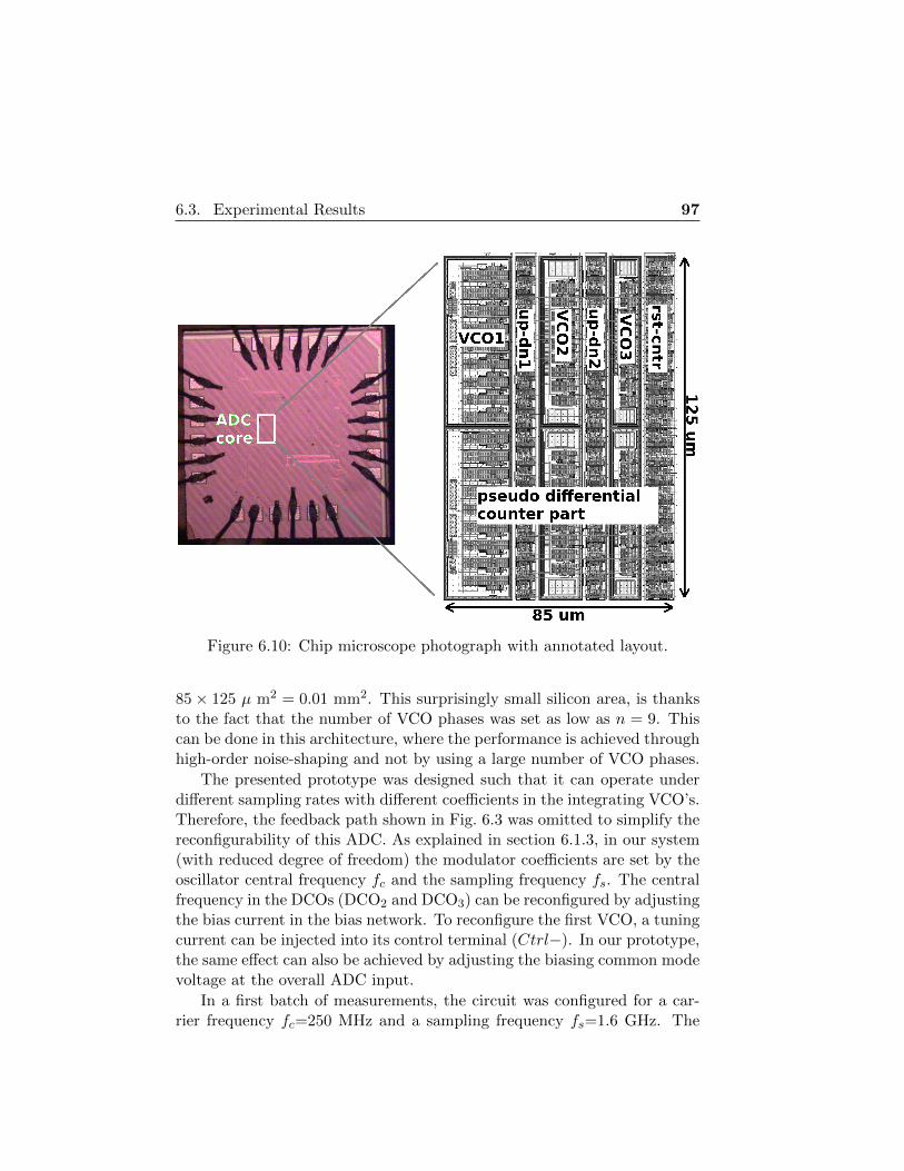
6.3. Experimental Results 97
Figure 6.10: Chip microscope photograph with annotated layout.
85× 125 µ m2 = 0.01 mm2. This surprisingly small silicon area, is thanksto the fact that the number of VCO phases was set as low as n = 9. Thiscan be done in this architecture, where the performance is achieved throughhigh-order noise-shaping and not by using a large number of VCO phases.
The presented prototype was designed such that it can operate underdifferent sampling rates with different coefficients in the integrating VCO’s.Therefore, the feedback path shown in Fig. 6.3 was omitted to simplify thereconfigurability of this ADC. As explained in section 6.1.3, in our system(with reduced degree of freedom) the modulator coefficients are set by theoscillator central frequency fc and the sampling frequency fs. The centralfrequency in the DCOs (DCO2 and DCO3) can be reconfigured by adjustingthe bias current in the bias network. To reconfigure the first VCO, a tuningcurrent can be injected into its control terminal (Ctrl−). In our prototype,the same effect can also be achieved by adjusting the biasing common modevoltage at the overall ADC input.
In a first batch of measurements, the circuit was configured for a car-rier frequency fc=250 MHz and a sampling frequency fs=1.6 GHz. The

98Chapter 6. Design and implementation of a mostly digital VCO-based
CT-DSM with 3rd order noise shaping
bandwidth was set to 10 MHz, corresponding to an OSR=80. In this mode,the analog power consumption was 1.8 mW. The digital power consump-tion (flipflops, latches and xor gates) was slightly higher, i.e. 1.9 mW, butit is expected that this could be cut significantly through an optimizedre-design.
−120
−100
−80
−60
−40
−20
0
1 10 1000.1
60dB
/dec
SNR: 66.2dBSNDR: 58.7dB
frequency (MHz)
Out
put s
pect
rum
(dB)
BW: 10MHz
59.6dB
(a)
−120
−100
−80
−60
−40
−20
0
1 10 100
75.5dB
0.1
SNR: 66.2dBSNDR: 65.7
frequency (MHz)
Out
put s
pect
rum
(dB)
59.6dB
(b)
Figure 6.11: Measured output spectrum (160K pt FFT) for the case offc = 250 MHz and fs = 1.6 GHz with a 3 MHz input tone with an ampli-tude of a 650mVpp differentially:(a) normal (pseudo-differential) output,(b) partially decimated (pseudo-differential) output with off-line digital cal-ibration overlayed on the raw output.
An output spectrum for the case of a 3 MHz input tone with an ampli-tude of 650 mVpp differentially, is shown in Fig. 6.11(a). This amplitude is

6.3. Experimental Results 99
deliberately chosen above the designed linear operating range of the VCO(which is 450 mVpp differentially), such that it creates large harmonics.The plot clearly exhibits the expected peaking in the noise transfer func-tion which is due to the large delay of the VCO read-out circuits (see sec-tion 6.2). As expected for low frequencies, we can see a white noise floor.For this case, the SNR is 66 dB. Thanks to the pseudo-differential setup,where the outputs of both independent channels are subtracted from eachother, there is no even order distortion, which confirms the effectiveness ofthis scheme and is consistent with the measurements of [6]. However, thereis a large 3rd harmonic which limits the SNDR in this case to 59 dB. Asexplained above, this large third harmonic is due to the limited linearity ofthe first VCO in the system. To assess this, the static nonlinearity of theoverall ADC was measured, by sweeping the input signal and averaging theADC’s output over a long time. The result is shown in Fig. 6.12.
−0.4 −0.3 −0.2 −0.1 0 0.1 0.2 0.3 0.4
−0.8
−0.6
−0.4
−0.2
0
0.2
0.4
0.6
0.8
Differential Input signal [Volt]
Inpu
t ref
erre
d N
onlin
earit
y [m
V]
Figure 6.12: Static nonlinearity plot of the ADC for the case of of fc =250 MHz and fs = 1.6 GHz in the pseudo differential configuration.
As mentioned above, our new high-order noise shaping technique canalso be combined with digital calibration techniques, similar to e.g. [23–25].Although not the focus of this work, a first assessment of the effectiveness ofan off-line calibration technique such as the one of [23] was also performedbased on the measured nonlinearity data of Fig. 6.12. The core idea of suchan off-line calibration technique is shown in Fig. 6.13. It is based on theobservation that the nonlinearity of the VCO occurs at the input of the sys-tem (shown as the nonlinear function f(·) in Fig. 6.13). If the nonlinearityis known, it can be inverted at the digital output of the converter (shownas the nonlinear function f−1(·) in Fig. 6.13). This nonlinearity correction
100Chapter 6. Design and implementation of a mostly digital VCO-based
CT-DSM with 3rd order noise shaping
can be implemented very efficiently by interpolating calibration data of asurprisingly small look-up-table [23]. In the conventional scheme, shown inFig. 6.13(a), the nonlinearity correction is performed directly on the rawundecimated modulator digital output signal Dout. However, in this work,this conventional scheme, was found to increase the baseband noise levelsignificantly. The reason for this, is that in our modulator, there is a largeamount of shaped quantization noise, which after passing trough the non-linearity correction block, is in part converted to white noise which in turnpartially falls in the baseband. Therefore the modified setup of Fig. 6.13(b)was used, where first the bulk of the shaped quantization noise is removedin a first coarse decimation step. Then on this relatively clean signal, thenonlinearity correction is applied, and then passed for further decimation.This modified set-up with the nonlinearity correction at an intermediatedecimation step, is preferred over performing the nonlinearity correctionon the overall decimated output Ddec, to avoid that the baseband signalswould be partially filtered (phase shifted or slightly attenuated) prior tothe nonlinearity correction. This scheme was implemented in software (off-chip) and the result is shown in Fig. 6.11(b). As the figure shows, thedistortion is now reduced to a level where it does not affect the SNDRanymore, leading to an SNDR which is virtually equal to the SNR.
Experiments as described above, were repeated for varying input am-plitudes. The results are shown in Fig. 6.14. For the implemented chip(which does not have the calibration on board), the SNDR starts to dropabove a differential input amplitude of 450mVpp, which is consistent withthe designed linear input range of the first VCO [6]. The correspondingpeak SNDR equals 62.5 dB. The peak SNR is 66.2 dB and the dynamicrange 71 dB. The SNDR for the case of the off-line (and off-chip) digitalcalibration is plotted as well and it is nearly identical to the SNR, indicat-ing that digital calibration could work over the entire signal range. Thecorresponding peak SNDR for this case equals 65.7 dB.
To further asses the digital calibration scheme also a two-tone test wasperformed where the input signal is the sum of 2 sine waves with the sameamplitude and input frequencies near the band edge (here: 8.855 MHz and9.068 MHz). The result for the case of a signal level of 650mVpp differen-tially (identical to the case shown in Fig. 6.11) is shown in Fig. 6.15, bothfor the case without and with the digital calibration. Clearly, also in thiscase the calibration can significantly suppress the effect of the distortion.
As was explained above, the proposed implementation can work under

6.3. Experimental Results 101
(a)
(b)
Doutnon-linearity
f( )oversamplingnoise-shaping
modulator
digitalnon-linearity
correction
f-1( )Ddec
decimation80
Vi n
Doutnon-linearity
f( )oversamplingnoise-shaping
modulator
digitalnon-linearity
correction
firstdecimation
16f-1( )
seconddecimation
5
Vi n DdecDcorr
Figure 6.13: Block diagram of an oversampling converter with off-line dig-ital calibration:a) conventional setup discussed in this section,b) and setup used in this work.
multiple sampling frequencies and can have multiple operation modes byadapting the VCO free running frequency values (and corresponding VCOgain values). To illustrate this, the same batch of experiments as describedabove was repeated for the case where the sampling frequency was set tofs = 1 GHz and the VCO central frequency fc to 133 MHz. It was foundthat at this lower operating frequency, the circuit was still functional alsoat reduced supply voltages: i.e. 0.8V analog and 1.1V digital. In thisconfiguration, the accuracy performance (SNR, SNDR) was decreased butalso the power consumption was more than halved. The results for bothcases as well as a comparison with other related works about digital friendlyADCs are summarized in table 6.1. From the table we can see that ourproof-of-concept circuit has a performance that is comparable to the stateof the art, while it has a significantly reduced silicon area.

102Chapter 6. Design and implementation of a mostly digital VCO-based
CT-DSM with 3rd order noise shaping
1 10 100 1000
0
10
20
30
40
50
60
70
differential input amplitude (mV p-p)
SNR
, SN
DR
(dB)
peak SNR: 66.2dBpeak SNDR: 62.5dBpeak SNDR (linearised): 65.7dB
DR: 70.8dB
SNRSNDRSNDRL
Figure 6.14: Dynamic range plot for the case of fc = 250 MHz, fs =1.6 GHz and 10 MHz bandwidth.

6.3. Experimental Results 103
0 1 2 3 4 5 6 7 8 9 10−120
−100
−80
−60
−40
−20
0
2f2-f1
frequency (MHz)
Out
put s
pect
rum
(dB)
2f1-f261.3
dB
61.3
dB(a)
0 1 2 3 4 5 6 7 8 9 10−120
−100
−80
−60
−40
−20
0
−40
2f2-f1
frequency (MHz)
Out
put s
pect
rum
(dB)
81.1
dB
81.1
dB
2f1-f2
(b)
Figure 6.15: Baseband FFT plot for the case of two-tone input signal oftwo tones near 9 MHz with the same peak-to-peak signal level as for theplot of Fig. 6.11 (650mVpp differentially): (a) normal (pseudo-differential)output, (b) (pseudo-differential) output with off-line digital calibration.
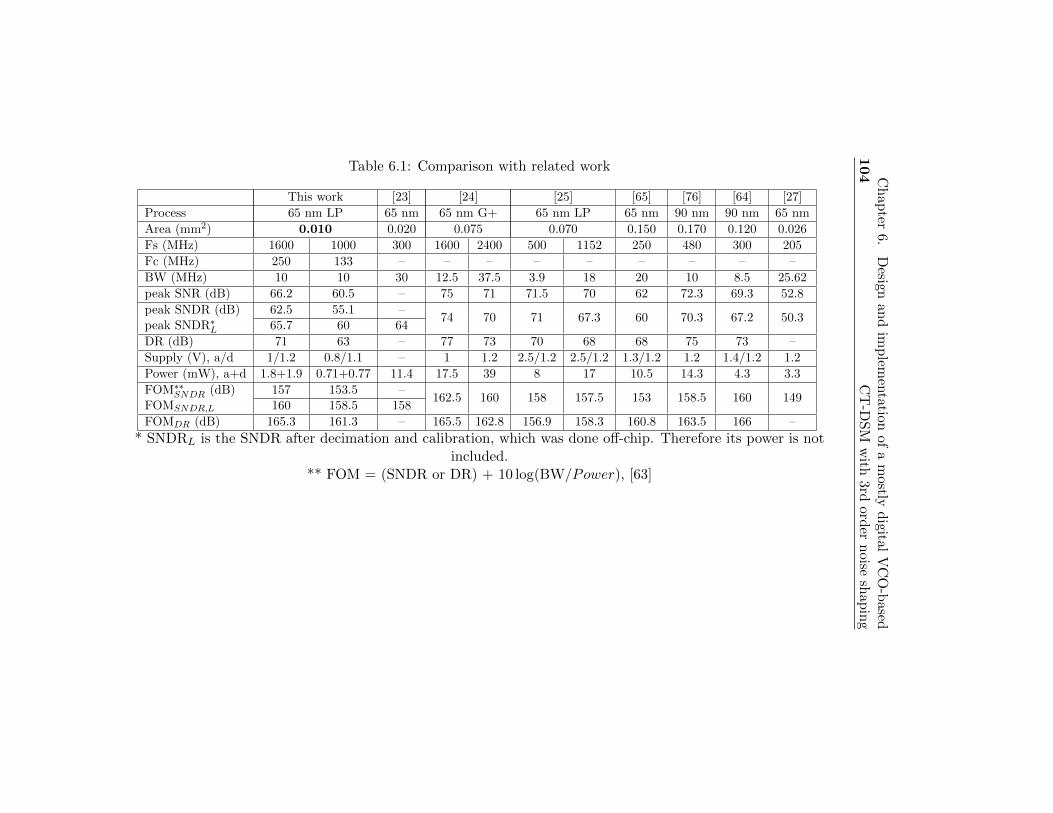
104 C
hap
ter6.
Design
and
imp
lemen
tationof
am
ostlyd
igitalV
CO
-based
CT
-DS
Mw
ith3rd
order
noise
shap
ing
Table 6.1: Comparison with related work
This work [23] [24] [25] [65] [76] [64] [27]
Process 65 nm LP 65 nm 65 nm G+ 65 nm LP 65 nm 90 nm 90 nm 65 nm
Area (mm2) 0.010 0.020 0.075 0.070 0.150 0.170 0.120 0.026
Fs (MHz) 1600 1000 300 1600 2400 500 1152 250 480 300 205
Fc (MHz) 250 133 – – – – – – – – –
BW (MHz) 10 10 30 12.5 37.5 3.9 18 20 10 8.5 25.62
peak SNR (dB) 66.2 60.5 – 75 71 71.5 70 62 72.3 69.3 52.8
peak SNDR (dB) 62.5 55.1 –74 70 71 67.3 60 70.3 67.2 50.3
peak SNDR∗L 65.7 60 64
DR (dB) 71 63 – 77 73 70 68 68 75 73 –
Supply (V), a/d 1/1.2 0.8/1.1 – 1 1.2 2.5/1.2 2.5/1.2 1.3/1.2 1.2 1.4/1.2 1.2
Power (mW), a+d 1.8+1.9 0.71+0.77 11.4 17.5 39 8 17 10.5 14.3 4.3 3.3
FOM∗∗SNDR (dB) 157 153.5 –162.5 160 158 157.5 153 158.5 160 149
FOMSNDR,L 160 158.5 158
FOMDR (dB) 165.3 161.3 – 165.5 162.8 156.9 158.3 160.8 163.5 166 –
* SNDRL is the SNDR after decimation and calibration, which was done off-chip. Therefore its power is notincluded.
** FOM = (SNDR or DR) + 10 log(BW/Power), [63]
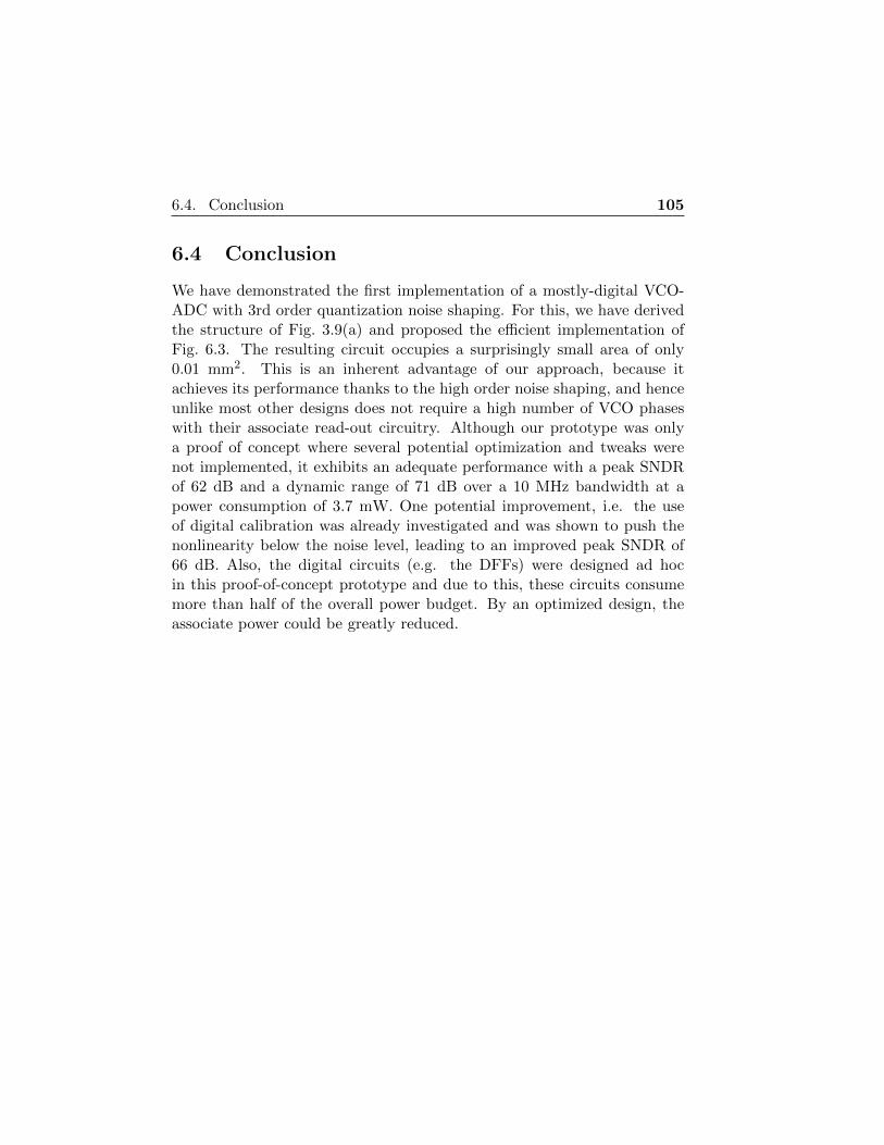
6.4. Conclusion 105
6.4 Conclusion
We have demonstrated the first implementation of a mostly-digital VCO-ADC with 3rd order quantization noise shaping. For this, we have derivedthe structure of Fig. 3.9(a) and proposed the efficient implementation ofFig. 6.3. The resulting circuit occupies a surprisingly small area of only0.01 mm2. This is an inherent advantage of our approach, because itachieves its performance thanks to the high order noise shaping, and henceunlike most other designs does not require a high number of VCO phaseswith their associate read-out circuitry. Although our prototype was onlya proof of concept where several potential optimization and tweaks werenot implemented, it exhibits an adequate performance with a peak SNDRof 62 dB and a dynamic range of 71 dB over a 10 MHz bandwidth at apower consumption of 3.7 mW. One potential improvement, i.e. the useof digital calibration was already investigated and was shown to push thenonlinearity below the noise level, leading to an improved peak SNDR of66 dB. Also, the digital circuits (e.g. the DFFs) were designed ad hocin this proof-of-concept prototype and due to this, these circuits consumemore than half of the overall power budget. By an optimized design, theassociate power could be greatly reduced.

106Chapter 6. Design and implementation of a mostly digital VCO-based
CT-DSM with 3rd order noise shaping

Chapter 7
Implementation of a 3rdorder VCO-based CT-DSMwith PWM pre-coding
As a second attempt to design a linear mostly digital low voltage highorder VCO based CT-DSM, the idea of PWM pre-coding, elaborated inchapter 5, is combined with the system presented in chapter 3.
In order to investigate the effectiveness of the PWM pre-coding tech-nique to linearize a VCO-ADC, it has been applied to a 3rd order VCO-ADC. The design and implementation of this modulator is discussed in thischapter.
A proof of concept is implemented in the low power version of a 65nmtechnology for a 10 MHz bandwidth. This prototype shows a measuredperformance of 67.4/59/55.4 dB DR/SNR/SNDR at a 10 MHz bandwidthwhile consuming 2.3 mW from a 1.0 V analog and 2 mW from a 1.2 Vdigital supply. The modulator covers a silicon area of 0.018 mm2.
7.1 Implementation details
The system level representation of the proposed scheme is shown in Fig. 7.1.As the Figure shows, the core idea of this ADC structure is very similarto the one introduced in Fig. 3.9(a). The key difference is the PWM blockthat precedes the ADC. The final implementation, as the figure shows, ispseudo-differential.
107
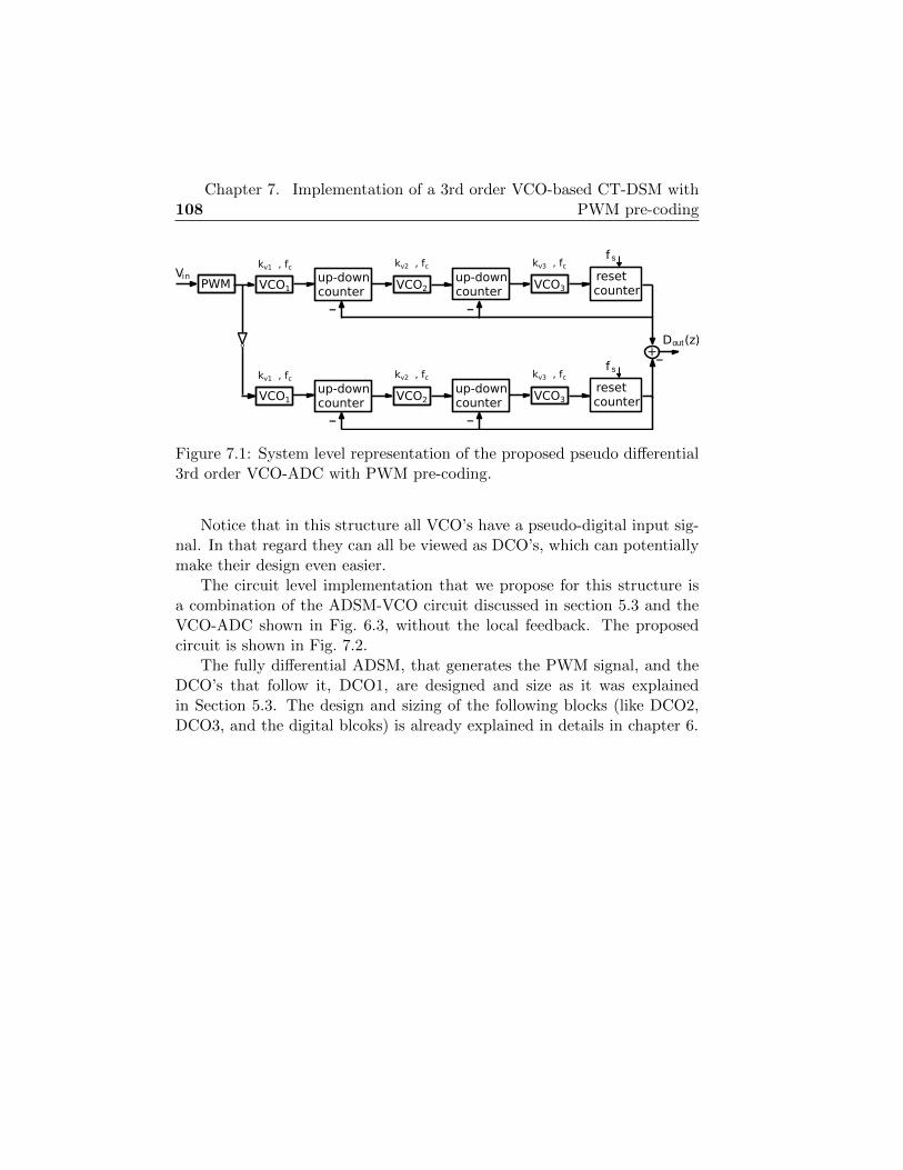
108Chapter 7. Implementation of a 3rd order VCO-based CT-DSM with
PWM pre-coding
kv2 , fc
VCO1
Vi n
f s
−
up-downcounter
VCO2resetcounter
Dout(z)
kv3 , fc
−
up-downcounter
VCO3
kv1 , fc
PWM
kv2 , fc
VCO1
f s
−
up-downcounter
VCO2resetcounter
kv3 , fc
−
up-downcounter
VCO3
kv1 , fc
V−o+−
Figure 7.1: System level representation of the proposed pseudo differential3rd order VCO-ADC with PWM pre-coding.
Notice that in this structure all VCO’s have a pseudo-digital input sig-nal. In that regard they can all be viewed as DCO’s, which can potentiallymake their design even easier.
The circuit level implementation that we propose for this structure isa combination of the ADSM-VCO circuit discussed in section 5.3 and theVCO-ADC shown in Fig. 6.3, without the local feedback. The proposedcircuit is shown in Fig. 7.2.
The fully differential ADSM, that generates the PWM signal, and theDCO’s that follow it, DCO1, are designed and size as it was explainedin Section 5.3. The design and sizing of the following blocks (like DCO2,DCO3, and the digital blcoks) is already explained in details in chapter 6.

7.1.
Imp
lemen
tation
deta
ils109
Vdd
RO1
Bias
R1
R2
nclk
DQ
D
l
clkQ
^
^
Vdd
Vb
<1:n>
RO2
<1:n>
n
n
clk
DQ
D
l
clkQ
^
^
<1:n>
n
Vdd
Vb
RO3
<1:n>
n l
clkQ
<1:n>
nclk
D Q
^
D
up-dncounter
up-dncounter
resetcounter
switchedcurrentsources
switchedcurrentsources
CLK - fs^ clk
DQ
D
[DCO1 [DCO2 [DCO3
PWM+
R
in+V
in-V
R
R
R
C
PWM-
Pseudo Differential Counter-Part
Dout
n
out+
Dout-
Figure 7.2: The circuit level implementation for the system proposed in Fig. 7.1.

110Chapter 7. Implementation of a 3rd order VCO-based CT-DSM with
PWM pre-coding
7.2 Implementation and Measurement
A pseudo-differential implementation was prototyped in the low power fla-vor of a 65 nm CMOS technology. The transistors in our circuits havea threshold voltage (Vth) around 400 mV and the circuit was designed towork under a 1 V supply, while the nominal supply for this technology is1.2 V.
Figure 7.3: A photograph of the fabricated die.
A photograph of the fabricated die and the annotated layout is shownin Fig. 7.3. We can clearly distinguish the two channels and how the area isdistributed over the different blocks. The resulting circuit measures 132×138 µm2 = 0.018mm2. This surprisingly small silicon area, is thanks to thefact that the number of VCO phases was set as low as n = 9.
The samplers in the reset counters were clocked at fs=1.6 GHz. Thebandwidth was set to 10 MHz, corresponding to an OSR of 80. The analogpower consumption was 2.3 mW, including 0.3 mW for the ADSM, and2 mW for the six DCO’s. The digital power consumption (flipflops, latchesand xor gates) was of the same order, i.e. 2 mW, but it is expected thatthis could be cut significantly through an optimized re-design.
All the oscillators have a carrier frequency of around 260 MHz. Thewhole system shows little sensitivity to the mismatch between the carrierfrequency of the oscillators, even when increased up to 20%.

7.2. Implementation and Measurement 111
1 10 100−120
−100
−80
−60
−40
−20
0
60dB/dec
SNR: 53.5dB
SNDR: 52.6dB
d3−d1: −63.8dB
d2−d1: −62.3dB
f−in: 3MHz
BW: 10MHz
CLK: 1.6GHz
frequency (MHz)
Out
put s
pect
rum
(dB
)
(a)
1 10 100−120
−100
−80
−60
−40
−20
0
60dB/dec
SNR: 55.9dB
SNDR: 55.4dB
d3−d1: −66.6dB
d2−d1: −69.6dB
f−in: 3MHz
BW: 10MHz
CLK: 1.6GHz
frequency (MHz)
Out
put s
pect
rum
(dB
)
(b)
Figure 7.4: Measured output spectrum of the presented modulator with asine wave input voltage, Vpp = 400 mv,(a) single-ended measurement,(b) pseudo-differential measurement.
In the first batch of measurements a sine wave voltage source with anamplitude of 400 mv, peak to peak, and frequency of 3 MHz is applied tothe input of the modulator. An output spectrum for this case is shown inFig. 7.4.
The spectrum shown in Fig. 7.4(a) corresponds to the single-ended out-put of the modulator and the one in Fig. 7.4(b) is for the differential casewhere the two single-ended outputs are subtracted off-chip in a software.
As it was shown in chapter 5, an ADSM generates only odd order har-monics of the input tone. Nevertheless, even order harmonics can be ex-
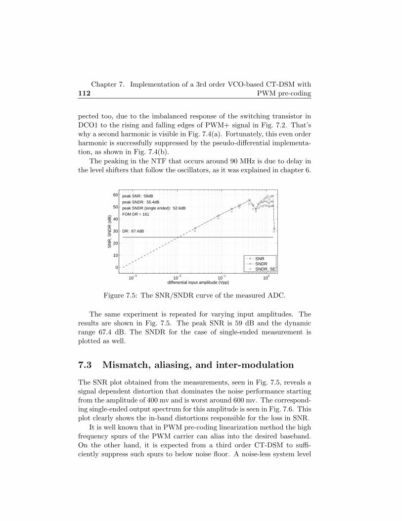
112Chapter 7. Implementation of a 3rd order VCO-based CT-DSM with
PWM pre-coding
pected too, due to the imbalanced response of the switching transistor inDCO1 to the rising and falling edges of PWM+ signal in Fig. 7.2. That’swhy a second harmonic is visible in Fig. 7.4(a). Fortunately, this even orderharmonic is successfully suppressed by the pseudo-differential implementa-tion, as shown in Fig. 7.4(b).
The peaking in the NTF that occurs around 90 MHz is due to delay inthe level shifters that follow the oscillators, as it was explained in chapter 6.
10−3
10−2
10−1
100
0
10
20
30
40
50
60
differential input amplitude (Vpp)
SN
R, S
ND
R (
dB)
peak SNR: 59dB
peak SNDR: 55.4dB
peak SNDR (single ended): 52.6dB
FOM DR = 161
DR: 67.4dB
SNRSNDRSNDR, SE
Figure 7.5: The SNR/SNDR curve of the measured ADC.
The same experiment is repeated for varying input amplitudes. Theresults are shown in Fig. 7.5. The peak SNR is 59 dB and the dynamicrange 67.4 dB. The SNDR for the case of single-ended measurement isplotted as well.
7.3 Mismatch, aliasing, and inter-modulation
The SNR plot obtained from the measurements, seen in Fig. 7.5, reveals asignal dependent distortion that dominates the noise performance startingfrom the amplitude of 400 mv and is worst around 600 mv. The correspond-ing single-ended output spectrum for this amplitude is seen in Fig. 7.6. Thisplot clearly shows the in-band distortions responsible for the loss in SNR.
It is well known that in PWM pre-coding linearization method the highfrequency spurs of the PWM carrier can alias into the desired baseband.On the other hand, it is expected from a third order CT-DSM to suffi-ciently suppress such spurs to below noise floor. A noise-less system level
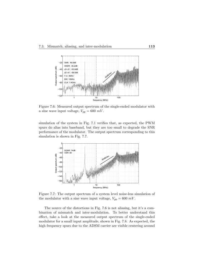
7.3. Mismatch, aliasing, and inter-modulation 113
1 10 100−120
−100
−80
−60
−40
−20
0
60dB/dec
SNR: 46.6dB
SNDR: 46.2dB
d3−d1: −63.8dB
d2−d1: −58.5dB
f−in: 3MHz
BW: 10MHz
CLK: 1.6GHz
frequency (MHz)
Out
put s
pect
rum
(dB
)
Figure 7.6: Measured output spectrum of the single-ended modulator witha sine wave input voltage, Vpp = 600 mV .
simulation of the system in Fig. 7.1 verifies that, as expected, the PWMspurs do alias into baseband, but they are too small to degrade the SNRperformance of the modulator. The output spectrum corresponding to thissimulation is shown in Fig. 7.7.
1 10 100
−160
−140
−120
−100
−80
−60
−40
−20
0
60dB/dec
SQNR: 74dBOSR: 80
frequency (MHz)
Out
put s
pect
rum
(dB
)
Figure 7.7: The output spectrum of a system level noise-less simulation ofthe modulator with a sine wave input voltage, Vpp = 600 mV .
The source of the distortions in Fig. 7.6 is not aliasing, but it’s a com-bination of mismatch and inter-modulation. To better understand thiseffect, take a look at the measured output spectrum of the single-endedmodulator for a small input amplitude, shown in Fig. 7.8. As expected, thehigh frequency spurs due to the ADSM carrier are visible centering around

114Chapter 7. Implementation of a 3rd order VCO-based CT-DSM with
PWM pre-coding
307 MHz. But there are also clear spurs around 258 Mhz, which is theaverage frequency of the oscillators.
On a system level these oscillator spurs wouldn’t be visible, because itis the effective frequency of a ring oscillator that matters (n × fvco), notthe average oscillation frequency of one phase of the ring oscillator. But inpractice there is a mismatch between the readout circuits that follow eachphase of the RO. This mismatch generates a pattern that repeats itself atthe frequency of fvco, so it can be referred to the input of the oscillatoras some spurs around fvco. The spurs due to DCO2 and DCO3 will besufficiently suppressed by the loop, but the spurs generated by the first ROwill directly appear at the output, as seen in Fig. 7.8 at 258 Mhz.
1 2 3 4 5 6 7 8
x 100
−120
−100
−80
−60
−40
−20
0
frequency (MHz)
Out
put s
pect
rum
(dB
)
Figure 7.8: Measured output spectrum of the modulator on a linear scalefor input sine wave with a small amplitude.
Furthermore, DCO1 operates as a mixer. In other words, the PWMspurs (307 MHz) and DCO1 spurs (258 MHz) and their harmonics, whichare visible in Fig. 7.8, can inter-modulate. This mixing effect gives rise tothe spurs visible at 209 MHz which is the mixing product of the secondharmonic of the oscillator and the PWM spurs, (2× 258− 307 = 209).
As the input amplitude rises, both the PWM spurs and DCO1 spursbecome more widespread [71] and the chance of their inter-modulationproducts falling into baseband increases. After reaching that particularamplitude where the down converted spurs fall into the baseband, all theamplitudes higher than that will also suffer from the same distortion, asseen in Fig. 7.5.

7.4. Conclusion 115
7.4 Conclusion
We have demonstrated an implementation of a mostly-digital VCO-ADCwith 3rd order quantization noise shaping and PWM linearization. Theresulting circuit, implemented in the low power flavor of the 65nm tech-nology, occupies a small area of only 0.018 mm2. The analog circuitry wasoperational under a small supply voltage of 1v.
This proof of concept exhibits a peak SNDR of 55.4 dB and a dynamicrange of 67.4 dB over a 10 MHz bandwidth at a power consumption of4.3 mW.
The digital circuits (e.g. the DFFs) were designed ad hoc and due tothis, they consume around half of the overall power budget and require ahigher supply voltage than the analog blocks. In an optimized design, theassociated power and supply voltage could be greatly reduced.
Table 7.1: Performance summary of the presented works in this book.
Presented in Chapter 6 Chapter 7
Process 65 nm LP
Area (mm2) 0.010 0.018
Fs (MHz) 1600 1600
Fc (MHz) 250 258
BW (MHz) 10 10
peak SNR (dB) 66.2 59
peak SNDR (dB) 62.5 55.4peak SNDR∗L 65.7 –
DR (dB) 71 67.4
Supply (V), a/d 1/1.2 1/1.2
Power (mW), a+d 1.8+1.9 2.3+2
FOM∗∗SNDR (dB) 157 149FOMSNDR,L 160 –
FOMDR (dB) 165.3 161
* SNDRL is the SNDR after decimation and calibration, which was doneoff-chip. Therefore its power is not included.
** FOM = (SNDR or DR) + 10 log(BW/Power), [63]for comparison with prior works, refer to Table 6.1
In order to better assess the effectiveness of the PWM pre-coding tech-nique, the performance of the ADC presented in this chapter is compared
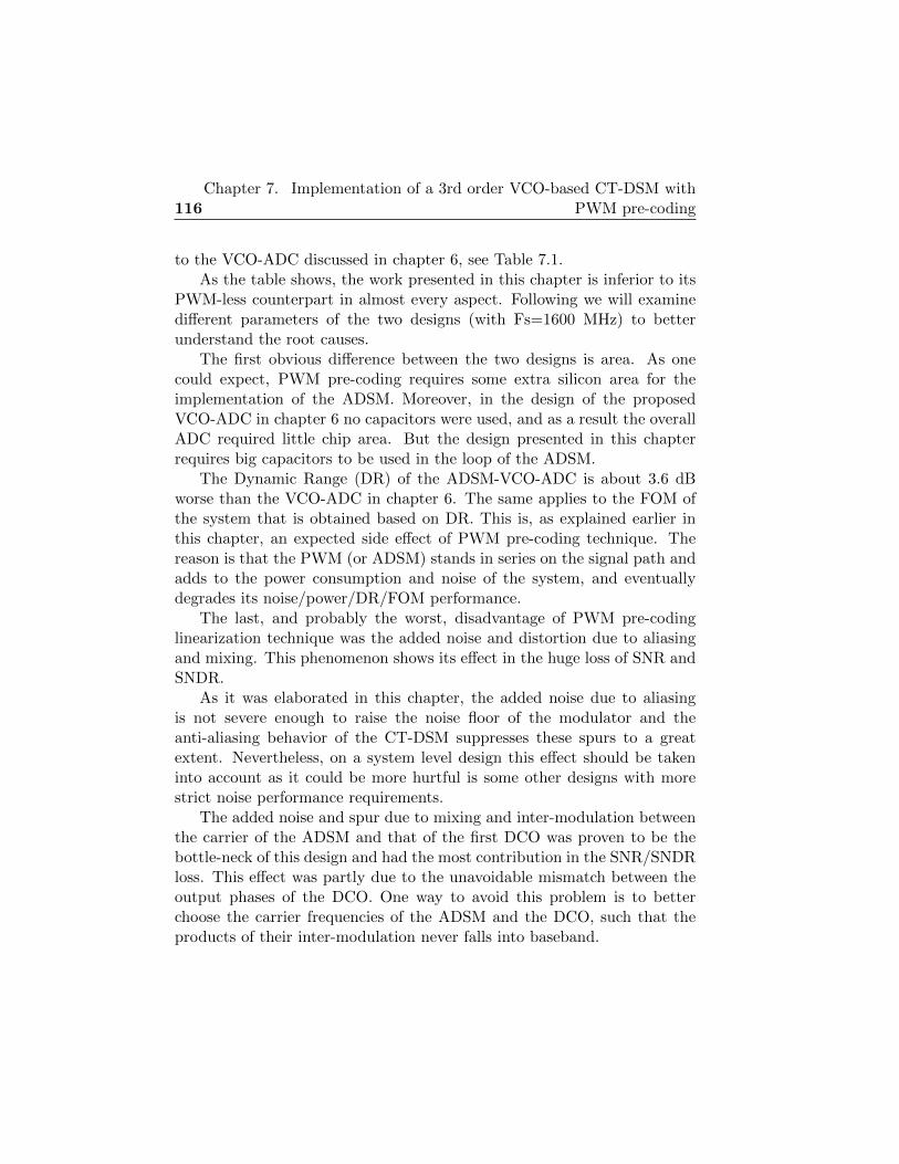
116Chapter 7. Implementation of a 3rd order VCO-based CT-DSM with
PWM pre-coding
to the VCO-ADC discussed in chapter 6, see Table 7.1.As the table shows, the work presented in this chapter is inferior to its
PWM-less counterpart in almost every aspect. Following we will examinedifferent parameters of the two designs (with Fs=1600 MHz) to betterunderstand the root causes.
The first obvious difference between the two designs is area. As onecould expect, PWM pre-coding requires some extra silicon area for theimplementation of the ADSM. Moreover, in the design of the proposedVCO-ADC in chapter 6 no capacitors were used, and as a result the overallADC required little chip area. But the design presented in this chapterrequires big capacitors to be used in the loop of the ADSM.
The Dynamic Range (DR) of the ADSM-VCO-ADC is about 3.6 dBworse than the VCO-ADC in chapter 6. The same applies to the FOM ofthe system that is obtained based on DR. This is, as explained earlier inthis chapter, an expected side effect of PWM pre-coding technique. Thereason is that the PWM (or ADSM) stands in series on the signal path andadds to the power consumption and noise of the system, and eventuallydegrades its noise/power/DR/FOM performance.
The last, and probably the worst, disadvantage of PWM pre-codinglinearization technique was the added noise and distortion due to aliasingand mixing. This phenomenon shows its effect in the huge loss of SNR andSNDR.
As it was elaborated in this chapter, the added noise due to aliasingis not severe enough to raise the noise floor of the modulator and theanti-aliasing behavior of the CT-DSM suppresses these spurs to a greatextent. Nevertheless, on a system level design this effect should be takeninto account as it could be more hurtful is some other designs with morestrict noise performance requirements.
The added noise and spur due to mixing and inter-modulation betweenthe carrier of the ADSM and that of the first DCO was proven to be thebottle-neck of this design and had the most contribution in the SNR/SNDRloss. This effect was partly due to the unavoidable mismatch between theoutput phases of the DCO. One way to avoid this problem is to betterchoose the carrier frequencies of the ADSM and the DCO, such that theproducts of their inter-modulation never falls into baseband.
Chapter 8
Conclusion
This work aimed at exploring new ways of realizing analog functions intime domain, instead of voltage domain. The two functions that were ofutmost importance to this work are integration and quantization. Usingthese two functions one can implement important analog blocks, such asanalog filters and analog to digital converters.
The main incentive for time-domain signal processing is to benefit fromthe digital blocks that are becoming faster and more efficient in the newerCMOS technologies. Moreover, in the more advanced CMOS processesit has become more challenging to design these functions in the voltagedomain. This is partly due to the fact the transistors can deliver a smallergain, the threshold voltage of the transistors is not dropping as rapidly asthe supply voltage, and the loss of voltage headroom is causing dynamic-range loss.
This book investigated linear, low-voltage, low-area, solutions for thedesign of Continuous-Time Delta Sigma Modulators (CT-DSM) with highorders of quantization noise shaping. In this pursuit we have proposedthe design of, and showcased the implementation of, high order VCO-Based ADC’s, linear VCO’s, and Asynchronous Delta Sigma Modulators(ADSM). All of the presented designs are digital friendly and make use of notraditional analog building blocks, like op-amps and highly linear transcon-ductors. Digital friendly means, the potential to benefit from technologyscaling and being synthesizable using digital design flow.
117

118 Chapter 8. Conclusion
8.1 Contributions
• On a system level, a new VCO-based CT-DSM structure is presented.In this system the combination of a VCO (Voltage Controlled Oscilla-tor) and some digital blocks (referred to as up-down counter) is usedas an integrator. The quantizer of the modulator is also VCO-based.Since a VCO can be implemented using an RO (Ring Oscillator), itcan be very simple and digital friendly. In this manner a high orderCT-DSM can be designed using only these blocks. Typical CT-DSMtechniques, such as local feedback can be incorporated in this novelstructure.
• Many circuit level innovations and simplifications are presented tomake the implementation of this modulator possible. The final cir-cuit level solution is very simple to design and size. Therefore, it isexpected to be easy to migrate from one technology node to another.The modulator has little sensitivity to mismatch between the VCO’s.The DACs are also benefiting from the inherent DWA provided bythis system.
• A thorough theoretical work is carried out in modeling an ADSM topredict its linearity performance. ADSM’s are a family of PWM’s(Pulse Width Modulator) that have many applications, like lineariz-ing a VCO-based ADC. It is also proven this block can be imple-mented using only a Schmitt trigger and a passive loop filter, which isalso simple to design and can benefit from technology scaling. Previ-ous implementations of an ADSM or a PWM, presented in literature,required either an op-amp based or gmC based integrator.
• The effect of delay in the loop of an ADSM is also studied and accurateequations to predict the linearity and oscillation frequencies of anADSM with loop delay are extracted. It is proven that loop delayin an ADSM doesn’t necessarily degrade the linearity performance ofan ADSM and extra circuitry is not needed to counteract its effect.Instead the effect of the loop-delay can simply be compensated bylowering the threshold voltage of the Schmitt trigger.
• As a proof of concept, a passive ADSM is implemented in 65 nmCMOS technology. The design is operational under a 1v supply andhas more than 10 bit linearity over a 10 MHz bandwidth.
8.2. Future work 119
• A low-voltage circuit level solution is presented to design a voltagecontrolled ring oscillator with high linearity. The implemented pro-totype of this block was shown to be much more linear than previousworks. This block can be used as the VCO in a high order CT-DSM.This block determines the linearity of the overall modulator. A proto-type is implemented in the 65nm technology and the measured volt-age to frequency conversion curve of the VCO for a rail-to-rail inputshows a small 0.6 % deviation from an ideal line. Measurements on apseudo-differential setup proved that the second harmonic distortionof the VCO can be heavily suppressed.
• As a proof of concept, for the first time a 3rd order VCO-based CT-DSM is implemented in the low power version of a 65 nm technologyfor a 10 MHz bandwidth. This prototype shows a measured perfor-mance of 71/66.2/62.5 dB DR/SNR/SNDR at a 10 MHz bandwidthwhile consuming 1.8 mW from a 1.0 V analog and 1.9 mW from a1.2 V digital supply. With digital calibration, the nonlinearity couldbe pushed below the noise level, leading to an improved peak SNDRof 66 dB. The modulator covers a small silicon area of only 0.01 mm2.
• As a second attempt to design a linear mostly digital low voltage highorder VCO based CT-DSM, an ADSM is used before the first VCO tolinearize it. A proof of concept is implemented in the low power ver-sion of a 65 nm technology for a 10 MHz bandwidth. This prototypeshows a measured performance of 67.4/59/55.4 dB DR/SNR/SNDRat a 10 MHz bandwidth while consuming 2.3 mW from a 1.0 V ana-log and 2 mW from a 1.2 V digital supply. The modulator covers asilicon area of 0.018 mm2.
8.2 Future work
• The commonly available simulation tools cannot properly model the1/f noise of switching transistors. Such transistors are the main ingre-dient of a ring oscillator and their noise performance directly affectsthe SNR of a VCO-based CT-DSM. Therefore, a study on this lowfrequency noise source seems to be necessary.
• In this work all the switching transistors in the ring oscillators had aminimum size channel length and the width was chosen such that they

120 Chapter 8. Conclusion
provide sufficient parasitic capacitive load for their previous delaystage. Nevertheless, it is not obvious whether this is the optimumchoice in terms of the noise performance of the switching transistors.A transistor with double the length and half the width can havethe same capacitive load, and potentially a better, or worse, noiseperformance. Other secondary effects, such as threshold voltage of thetransistor and voltage drop over the ring also needs to be investigated.
• The proposed VCO-based CT-DSM relied on a digital block calledan “up-down counter”. A simple circuit level for this block was pre-sented. One of the main limitations of this solution was the fact thefor larger inputs the output of the counter wouldn’t just saturate,but overflows. This effect destabilizes the modulator for a few clockcycles. A simple solution would be to use PFD’s (Phase FrequencyDetectors) instead of PD’s. This potential solution needs to be veri-fied.
• The digital circuitry doesn’t contribute to the noise performance ofthe modulator in the same way as analog blocks. In other words,scaling their power consumption doesn’t directly affect the SNR. Asa result, a low power design for these blocks can greatly improve theFOM of the system.
• The level shifters that followed the output phases of the ring oscilla-tors where proven to be too slow and added too much loop delay inthe overall CT-DSM. A better design of this block can decrease theloop delay, and eventually make the loop filter design more relaxed.
• The frequency of the ADSM carrier and that of the VCO in the secondimplementation were too close to each other and this caused a lossof SNR due to inter-modulation. In simulations this effect can onlybe detected when mismatch is taken into account. A study of theoptimum choice for these carrier frequency could solve this problem.

Bibliography
[1] A. Babaie-Fishani and P. Rombouts, “Continuous time Delta Sigmamodulation with PWM pre-coding and binary g(m) blocks,” Electron.Lett., vol. 48, no. 19, pp. 1187–1188, Sep 13 2012.
[2] A. Babaie-Fishani, B. Van Keymeulen, and P. Rombouts, “AnalyticalExpressions for the Distortion of Asynchronous Sigma–Delta Modula-tors,” IEEE Trans. Circuits Syst.-II: Express Briefs, vol. 60, no. 8, pp.472–476, 2013.
[3] A. Babaie-Fishani, M. De Bock, and P. Rombouts, “Analyzing Distor-tion in ASDMs with Loop Delay,” in Proc. IEEE Int. Symp. Circuitsand Syst. (ISCAS), 2014, pp. 77–80.
[4] M. De Bock, A. Babaie-Fishani, and P. Rombouts, “Improved offlinecalibration for DAC mismatch in low OSR Sigma Delta ADCs withdistributed feedback,” in Proc. IEEE Int. Symp. Circuits and Syst.(ISCAS), 2014, pp. 938–941.
[5] A. Babaie-Fishani and P. Rombouts, “True high-order VCO-basedADC,” Electron. Lett., vol. 51, no. 1, pp. 23–U53, Jan. 8 2015.
[6] ——, “Highly linear VCO for use in VCO-ADCs,” Electron. Lett.,vol. 52, no. 4, pp. 268–269, FEB 18 2016.
[7] ——, “Design of a low-voltage op-amp-less ASDM to linearise VCO-ADC,” Electron. Lett., vol. 52, no. 11, pp. 911–913, 2016.
[8] Paton, S. and Di Giandomenico, A. and Hernandez, L. and Wiesbauer,A. and Potscher, T., “A 70-mW 300-MHz CMOS Continuous-TimeΣ∆ ADC With 15-MHz Bandwidth and 11 Bits of Resolution,” IEEEJ. Solid-State Circuits, vol. 39, no. 7, pp. 1056–1062, 2004.
121

122 Bibliography
[9] L. Bos, G. Vandersteen, P. Rombouts, A. Geis, A. Morgado, Y. Rolain,G. Van der Plas, and J. Ryckaert, “Multirate Cascaded Discrete-TimeLow-Pass Delta Sigma Modulator for GSM/Bluetooth/UMTS,” IEEEJ. Solid-State Circuits, vol. 45, no. 6, pp. 1198–1208, Jun. 2010.
[10] M. Bolatkale, L. Breems, R. Rutten, and K. Makinwa, “A 4 GHzContinuous-Time ∆Σ ADC With 70 dB DR and -74 dBFS THD in125 MHz BW,” IEEE J. Solid-State Circuits, no. 12, pp. 2857–2868,Dec. 2011.
[11] O. Rajaee, T. Musah, N. Maghari, S. Takeuchi, M. Aniya,K. Hamashita, and U.-K. Moon, “Design of a 79 dB 80 MHz 8X-OSRHybrid Delta-Sigma/Pipelined ADC,” IEEE J. Solid-State Circuits,vol. 45, no. 4, pp. 719–730, Apr. 2010.
[12] R. Zanbaghi, P. K. Hanumolu, and T. S. Fiez, “An 80-dB DR, 7.2-MHzBandwidth Single Opamp Biquad Based CT Delta Sigma ModulatorDissipating 13.7-mW,” IEEE J. Solid-State Circuits, vol. 48, no. 2, pp.487–501, Feb. 2013.
[13] J. G. Kauffman, P. Witte, M. Lehmann, J. Becker, Y. Manoli, andM. Ortmanns, “A 72 dB DR, CT Delta Sigma Modulator Using Dig-itally Estimated, Auxiliary DAC Linearization Achieving 88 fJ/conv-step in a 25 MHz BW,” IEEE J. Solid-State Circuits, vol. 49, no. 2,pp. 392–404, Feb. 2014.
[14] S. Ho, C.-L. Lo, J. Ru, and J. Zhao, “A 23 mW, 73 dB DynamicRange, 80 MHz BW Continuous-Time Delta-Sigma Modulator in 20nm CMOS,” IEEE J. Solid-State Circuits, vol. 50, no. 4, pp. 908–919,Apr. 2015.
[15] Kinget, Peter R., “Scaling Analog Circuits into Deep NanoscaleCMOS: Obstacles and Ways to Overcome Them,” in Proc. IEEE Cus-tom Int. Circuits Conf. (CICC), 2015.
[16] M. Burns, G. W. Roberts, and G. W. R. Mark Burns, An introductionto mixed-signal IC test and measurement. Oxford series in electricaland computer engineering, 2001.
[17] M. Park and M. H. Perrott, “A 78 dB SNDR 87 mW 20 MHz Band-width Continuous-Time Delta Sigma ADC With VCO-Based Integra-

Bibliography 123
tor and Quantizer Implemented in 0.13 µ m CMOS,” IEEE J. Solid-State Circuits, vol. 44, no. 12, pp. 3344–3358, Dec. 2009.
[18] M. Straayer and M. Perrott, “A 12-Bit, 10-MHz Bandwidth,Continuous-Time ADC With a 5-Bit, 950-MS/s VCO-Based Quan-tizer,” IEEE J. Solid-State Circuits, vol. 43, no. 4, pp. 805–814, 2008.
[19] K. Reddy, S. Rao, R. Inti, B. Young, A. Elshazly, M. Talegaonkar,and P. K. Hanumolu, “A 16-mW 78-dB SNDR 10-MHz BW CT DeltaSigma ADC Using Residue-Cancelling VCO-Based Quantizer,” IEEEJ. Solid-State Circuits, vol. 47, no. 12, SI, pp. 2916–2927, Dec. 2012.
[20] J. Kim, T.-K. Jang, Y.-G. Yoon, and S. Cho, “Analysis and Designof Voltage-Controlled Oscillator Based Analog-to-Digital Converter,”IEEE Trans. Circuits Syst.-I: Regular Papers, vol. 57, no. 1, pp. 18–30,Jan. 2010.
[21] P. Zhu, X. Xing, and G. Gielen, “A 40-MHz Bandwidth 0-2 MASHVCO-Based Delta-Sigma ADC With 35-fJ/Step FoM,” IEEE Trans.Circuits Syst.-II: Express Briefs, vol. 62, no. 10, pp. 952–956, Oct 2015.
[22] X. Xing and G. G. E. Gielen, “A 42 fJ/Step-FoM Two-Step VCO-Based Delta-Sigma ADC in 40 nm CMOS,” IEEE J. Solid-State Cir-cuits, vol. 50, no. 3, pp. 714–723, Mar. 2015.
[23] J. Daniels, W. Dehaene, M. Steyaert, and A. Wiesbauer, “A 0.02mm2
65nm CMOS 30MHz BW All-Digital Differential VCO-based ADCwith 64dB SNDR,” in Proc. Symp. on VLSI Circuits, 2010, pp. 155–156.
[24] G. Taylor and I. Galton, “A Reconfigurable Mostly-Digital Delta-Sigma ADC With a Worst-Case FOM of 160 dB,” IEEE J. Solid-StateCircuits, vol. 48, no. 4, pp. 983–995, 2013.
[25] ——, “A Mostly-Digital Variable-Rate Continuous-Time Delta-SigmaModulator ADC,” IEEE J. Solid-State Circuits, vol. 45, no. 12, pp.2634 –2646, dec. 2010.
[26] S. Rao, K. Reddy, B. Young, and P. K. Hanumolu, “A Determinis-tic Digital Background Calibration Technique for VCO-Based ADCs,”IEEE J. Solid-State Circuits, vol. 49, no. 4, pp. 950–960, Apr. 2014.

124 Bibliography
[27] V. Unnikrishnan and M. Vesterbacka, “Time-mode analog-to-digitalconversion using standard cells,” IEEE Trans. Circuits Syst.-I: RegularPapers, vol. 61, no. 12, pp. 3348–3357, Dec 2014.
[28] V. Unnikrishnan, S. R. Pathapati, and M. Vesterbacka, “A fully syn-thesized all-digital VCO-based analog-to-digital converter,” in NordicCircuits and Systems Conf. (NORCAS): NORCHIP Int. Symp. onSystem-on-Chip, Oct 2015, pp. 1–4.
[29] L. Hernandez, S. Paton, and E. Prefasi, “VCO-based sigma delta mod-ulator with PWM precoding,” Electron. Lett., vol. 47, no. 10, pp. 588–589, May 12 2011.
[30] S. Rao, B. Young, A. Elshazly, W. Yin, N. Sasidhar, and P. Hanumolu,“A 71db sfdr open loop vco-based adc using 2-level pwm modulation,”in VLSI Circuits (VLSIC), 2011 Symposium on, 2011, pp. 270–271.
[31] J. Zhang, C. Wang, S. Diao, and F. Lin, “A low-power vco based adcwith asynchronous sigma-delta modulator in 65nm cmos,” in DesignAutomation Conference (ASP-DAC), 2015 20th Asia and South Pa-cific, Jan 2015, pp. 38–39.
[32] L. Ferreira and S. Sonkusale, “A 0.25-V 28-nW 58-dB Dynamic RangeAsynchronous Delta Sigma Modulator in 130-nm Digital CMOS Pro-cess,” IEEE Trans. on Very Large Scale Integration Syst., vol. 23, no. 5,pp. 926–934, May 2015.
[33] R. Schreier and G. Temes, Understanding Delta-Sigma Data Converters. Wiley, 2004. [Online]. Available:https://books.google.be/books?id=5HNqQgAACAAJ
[34] J. Kim and S. Cho, “A time-based analog-to-digital converter usinga multi-phase voltage controlled oscillator,” in Circuits and Systems,2006. ISCAS 2006. Proceedings. 2006 IEEE International Symposiumon, 2006, pp. 4 pp.–3937.
[35] T.-K. Jang, J. Kim, Y.-G. Yoon, and S. Cho, “A Highly-Digital VCO-Based Analog-to-Digital Converter Using Phase Interpolator and Dig-ital Calibration,” IEEE Trans. on Very Large Scale Integration Syst.,vol. 20, no. 8, pp. 1368–1372, 2012.
Bibliography 125
[36] J. Kim, W. Yu, and S. Cho, “A digital-intensive multimode multi-band receiver using a sinc filter-embedded vco-based adc,” MicrowaveTheory and Techniques, IEEE Transactions on, vol. 60, no. 10, pp.3254–3262, 2012.
[37] S. Rao, K. Reddy, B. Young, and P. Hanumolu, “A 4.1mw, 12-bitenob, 5mhz bw, vco-based adc with on-chip deterministic digital back-ground calibration in 90nm cmos,” in VLSI Circuits (VLSIC), 2013Symposium on, 2013, pp. C68–C69.
[38] R. Yadav and N. Sun, “A 1.2 mW 67.5 dB SQDR VCO-based Σ∆ ADCwith Non-linearity Cancellation Technique,” in Circuits and Systems(MWSCAS), 2013 IEEE 56th International Midwest Symposium on,2013, pp. 570–573.
[39] E. Gutierrez and L. Hernandez, “Spectral analysis of multibit VCO-ADCs and PFM-ADCs with sinusoidal inputs,” in 2015 IEEE Inter-national Symposium on Circuits and Systems (ISCAS), May 2015, pp.1258–1261.
[40] L. Hernandez and E. Gutierrez, “Analytical Evaluation of VCO-ADCQuantization Noise Spectrum Using Pulse Frequency Modulation,”IEEE Signal Processing Letters, vol. 22, no. 2, pp. 249–253, FEB 2015.
[41] L. Hernandez, E. Prefasi, S. Paton, and P. Rombouts, “Analysis ofvco based noise shaping adcs linearized by pwm modulation,” in Proc.IEEE Int. Conf. Electronics, Circuits and Syst. (ICECS), Dec. 2012,pp. 352–355.
[42] E. Prefasi, E. Gutierrez, L. Hernandez, S. Paton, S. Walter, andU. Gaier, “A 0.03mm2, 40nm cmos 1.5gs/s all-digital complementarypwm-gro,” in Electronics, Circuits and Systems (ICECS), 2014 21stIEEE International Conference on, Dec 2014, pp. 116–119.
[43] X. Xing, P. Gao, and G. Gielen, “A 40mhz-bw two-step open-loopvco-based adc with 42fj/step fom in 40nm cmos,” in ESSCIRC (ESS-CIRC), 2013 Proceedings of the, 2013, pp. 327–330.
[44] K. Ragab and N. Sun, “A 12b enob, 2.5mhz-bw, 4.8mw vco-based 0-1 mash adc with direct digital background nonlinearity calibration,”in Custom Integrated Circuits Conference (CICC), 2015 IEEE, Sept2015, pp. 1–4.

126 Bibliography
[45] A. Sanyal and N. Sun, “A 18.5-fj/step vco-based 0-1 mash delta sigmaadc with digital background calibration,” in 2016 IEEE Symposiumon VLSI Circuits (VLSI-Circuits), June 2016, pp. 1–2.
[46] M. Park and M. Perrott, “A 0.13 µm cmos 78db sndr 87mw 20mhzbw ct δσ adc with vco-based integrator and quantizer,” in Proc. IEEEInt. Solid State Circuits Conf. (ISSCC), 2009, pp. 170–171,171a.
[47] K. Lee, Y. Yoon, and N. Sun, “A 1.8mW 2MHz-BW 66.5dB-SNDR∆Σ ADC using VCO-based integrators with intrinsic CLA,” in CustomIntegrated Circuits Conference (CICC), 2013 IEEE, 2013, pp. 1–4.
[48] ——, “A Scaling-Friendly Low-Power Small-Area ∆Σ ADC WithVCO-Based Integrator and Intrinsic Mismatch Shaping Capability,”IEEE Journal on Emerging and Selected Topics in Circuits and Sys-tems, vol. 5, no. 4, pp. 561–573, Dec 2015.
[49] ——, “A 10mhz-bw, 5.6mw, 70db sndr delta sigma adc using vco-basedintegrators with intrinsic dem,” in Circuits and Systems (ISCAS), 2013IEEE International Symposium on, 2013, pp. 2006–2009.
[50] Y. Yoon, K. Lee, S. Hong, X. Tang, L. Chen, and N. Sun, “A 0.04-mm2 0.9-mw 71-db sndr distributed modular as adc with vco-basedintegrator and digital dac calibration,” in Custom Integrated CircuitsConference (CICC), 2015 IEEE, Sept 2015, pp. 1–4.
[51] B. Young and P. K. Hanumolu, “Phase-locked loop based delta-sigmaADC,” Electron. Lett., vol. 46, no. 6, pp. 403–404, Mar. 18 2010.
[52] P. Zhu, X. Xing, and G. Gielen, “A 40mhz-bw 35fj/step-fomnonlinearity-cancelling two-step adc with dual-input vco-based quan-tizer,” in European Solid State Circuits Conference (ESSCIRC), ESS-CIRC 2014 - 40th, Sept 2014, pp. 63–66.
[53] B. Yousefzadeh, A. Hajian, and M. Sharifkhani, “A 10MHz CTDSMwith differential VCO-based quantizer in 90nm,” in Int. Conf. DesignTechnology of Integrated Systems in Nanoscale Era (DTIS), 2013, pp.128–133.
[54] P. Gao, X. Xing, J. Craninckx, and G. Gielen, “Design of anintrinsically-linear double-VCO-based ADC with 2nd-order noise shap-ing,” in Design, Automation Test in Europe Conference Exhibition(DATE), march 2012, pp. 1215–1220.

Bibliography 127
[55] L. Hernandez, “VCO based multi-stage noise shaping ADC,” Electron.Lett., vol. 48, no. 4, pp. 206–207, FEB 16 2012.
[56] W. Yu, J. Kim, K. Kim, and S. Cho, “A Time-Domain High-OrderMASH ∆Σ ADC Using Voltage-Controlled Gated-Ring Oscillator,”IEEE Trans. Circuits Syst.-I: Regular Papers, vol. PP, no. 99, pp. 1–1.
[57] S. Zaliasl, S. Saxena, P. Hanumolu, K. Mayaram, and T. Fiez, “A 12.5-bit 4 MHz 13.8 mW MASH Modulator With Multirated VCO-BasedADC,” IEEE Trans. Circuits Syst.-I: Regular Papers, vol. 59, no. 8,pp. 1604–1613, 2012.
[58] T. Konishi, H. Lee, S. Izumi, M. Yoshimoto, and H. Kawaguchi, “A40-nm 640-µm2 45-dB opampless all-digital second-order MASH DeltaSigma ADC,” in Circuits and Systems (ISCAS), 2011 IEEE Interna-tional Symposium on, 2011, pp. 518–521.
[59] Y. Yoon, K. Lee, P. Wang, and N. Sun, “A purely-VCO-based single-loop high-order continuous-time Delta Sigma ADC,” in 2014 IEEE In-ternational Symposium on Circuits and Systems (ISCAS), June 2014,pp. 926–929.
[60] A. Sanyal and N. Sun, “Second-order vco-based delta sigma adc usinga modified dpll,” Electronics Letters, vol. 52, no. 14, pp. 1204–1205,2016.
[61] M. Park and M. Perrott, “A vco-based analog-to-digital converterwith second-order sigma-delta noise shaping,” in Circuits and Sys-tems, 2009. ISCAS 2009. IEEE International Symposium on, 2009,pp. 3130–3133.
[62] M. De Bock, X. Xing, L. Weyten, G. Gielen, and P. Rombouts, “Cal-ibration of DAC Mismatch Errors in Sigma Delta ADCs Based on aSine-Wave Measurement,” IEEE Trans. Circuits Syst.-I: Regular Pa-pers, vol. 60, no. 9, pp. 567–571, Sep. 2013.
[63] R. Schreier and G. C. Temes, Understanding Delta-Sigma Data Con-verters. IEEE, 2005.
[64] C. H. Weng, T. A. Wei, E. Alpman, C. T. Fu, and T. H. Lin, “AContinuous-Time Delta-Sigma Modulator Using ELD-Compensation-Embedded SAB and DWA-Inherent Time-Domain Quantizer,” IEEEJ. Solid-State Circuits, vol. 51, no. 5, pp. 1235–1245, May 2016.

128 Bibliography
[65] V. Dhanasekaran, M. Gambhir, M. M. Elsayed, E. Sanchez-Sinencio,J. Silva-Martinez, C. Mishra, L. Chen, and E. J. Pankratz, “A Con-tinuous Time Multi-Bit ∆Σ ADC Using Time Domain Quantizer andFeedback Element,” IEEE J. Solid-State Circuits, vol. 46, no. 3, pp.639 –650, Mar. 2011.
[66] B. Drost, M. Talegaonkar, and P. K. Hanumolu, “Analog Filter De-sign Using Ring Oscillator Integrators,” IEEE J. Solid-State Circuits,vol. 47, no. 12, SI, pp. 3120–3129, DEC 2012.
[67] M. Voelker, S. Pashmineh, J. Hauer, and M. Ortmanns, “Current Feed-back Linearization Applied to Oscillator Based ADCs,” IEEE Trans.Circuits Syst.-I: Regular Papers, vol. 61, no. 11, pp. 3066–3074, Nov2014.
[68] E. Roza, “Analog-to-digital conversion via duty-cycle modulation,”IEEE Trans. Circuits Syst.-II, vol. 44, no. 11, pp. 907–914, nov 1997.
[69] T. Piessens and M. Steyaert, “Behavioral analysis of self-oscillatingclass d line drivers,” IEEE Trans. Circuits Syst.-I: Regular Papers,vol. 52, no. 4, pp. 706 – 714, april 2005.
[70] F. Colodro and A. Torralba, “Spectral Analysis of Pulsewidth-Modulated Sampled Signals,” IEEE Trans. Circuits Syst.-II, vol. 57,no. 8, pp. 622–626, AUG 2010.
[71] S. Ouzounov, E. Roza, J. Hegt, G. van der Weide, and A. van Roer-mund, “Analysis and design of high-performance asynchronous sigma-delta modulators with a binary quantizer,” IEEE J. Solid-State Cir-cuits, vol. 41, no. 3, pp. 588–596, MAR 2006.
[72] V. Mangulis, Handbook of series for scientists and engineers, ser. Pureand Applied Physics. Academic Press, 1965. [Online]. Available:https://books.google.be/books?id=l95QAAAAMAAJ
[73] G. Roberts and M. Ali-Bakhshian, “A brief introduction to time-to-digital and digital-to-time converters,” IEEE Trans. Circuits Syst.-II:Express Briefs, vol. 57, no. 3, pp. 153 –157, march 2010.
[74] T. Matic, T. Svedek, and M. Herceg, “A method for the schmitt-trigger propagation-delay compensation in asynchronous sigma deltamodulator,” IEEE Trans. Circuits Syst.-II: Express Briefs, vol. 59,no. 7, pp. 404 –408, july 2012.

Bibliography 129
[75] J. Daniels, W. Dehaene, M. Steyaert, and A. Wiesbauer, “A/d con-version using an asynchronous delta-sigma modulator and a time-to-digital converter,” in Circuits and Systems, 2008. ISCAS 2008. IEEEInternational Symposium on, May, pp. 1648–1651.
[76] R. Ritter, J. G. Kauffman, J. Becker, and M. Ortmanns, “A 10 MHzBandwidth, 70 dB SNDR Continuous Time Delta-Sigma ModulatorWith Digitally Improved Reconfigurable Blocker Rejection,” IEEE J.Solid-State Circuits, vol. 51, no. 3, pp. 660–670, March 2016.


![for... · 3-+6+ ,+81+5a+c3 ?5?;/6+ 959 ,+5?0?8+b9)/,/8c3=+ 3>=2+>23 !3;9a?=>+" ... vmvltmti aws]bqxpi\pi hmbqxpq qqvo‘isq mbqvws]ji spwvi bmvoywvlw vmbws]bqxpi\pi s] ...](https://static.fdocuments.nl/doc/165x107/5ad8cae67f8b9a98098e7fff/for3-6-815ac3-56-959-508b98c3-3223-39a-vmvltmti.jpg)