Adobe AcrobatからのPDF書き出しについて Acrobat …ap).pdfAdobe...
5
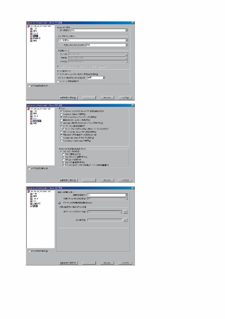
Adobe Acrobat からの PDF 書き出しについて Acrobat Distiller にて、ジョブオプションを設定します。 ※画像は Acrobat10
Transcript of Adobe AcrobatからのPDF書き出しについて Acrobat …ap).pdfAdobe...
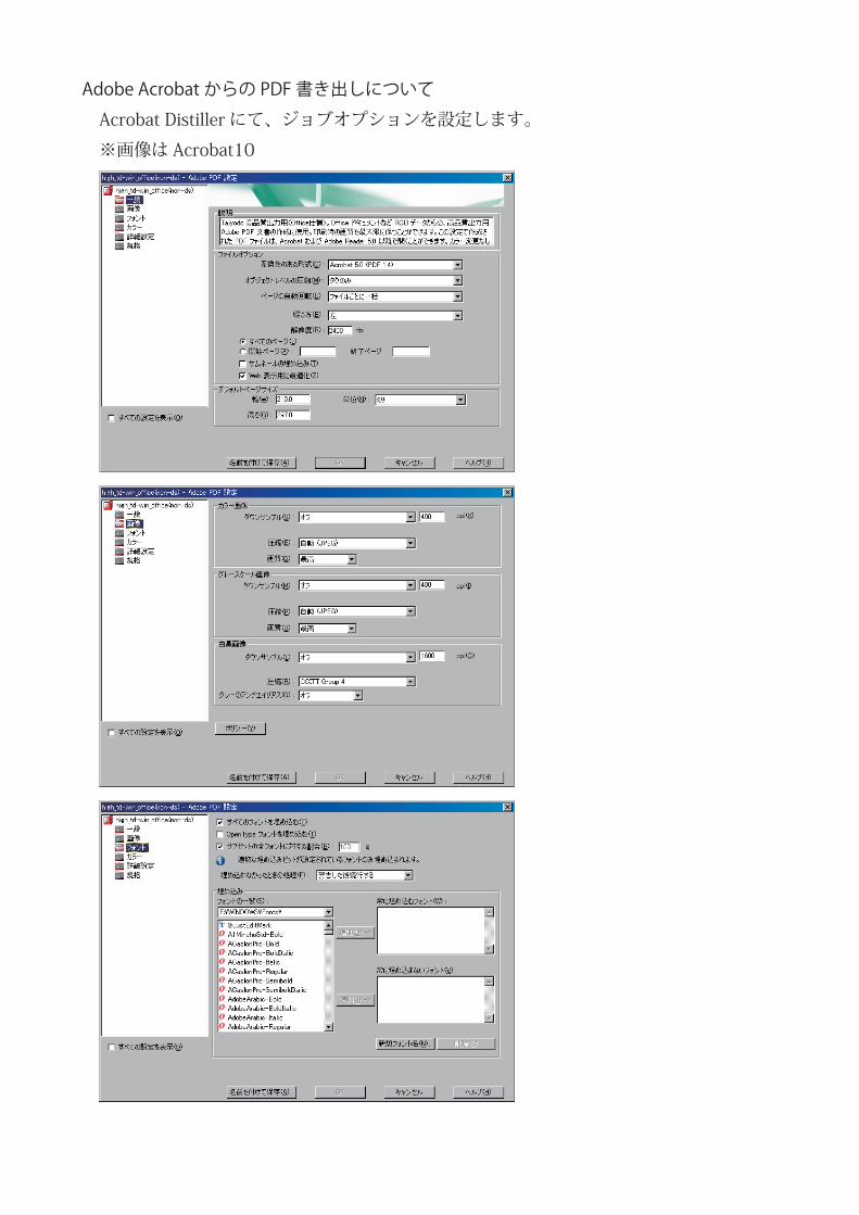
Adobe Acrobat からの PDF 書き出しについて
Acrobat Distiller にて、ジョブオプションを設定します。
※画像は Acrobat10
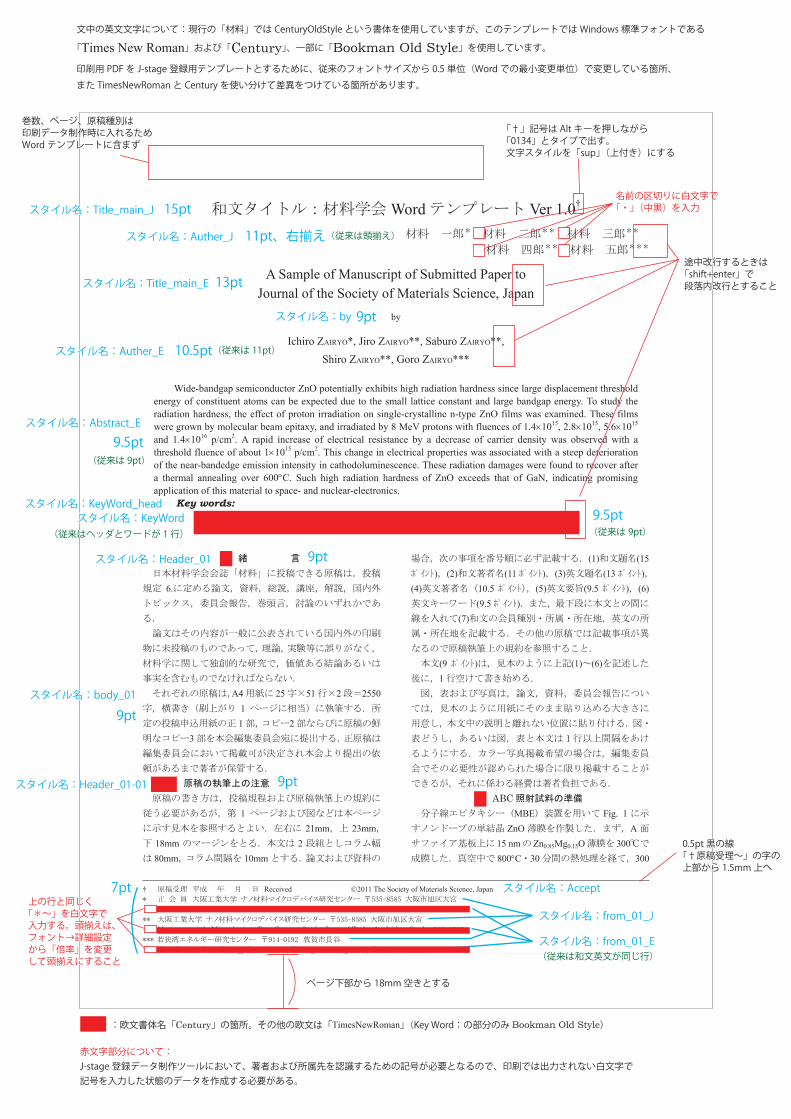
Word Ver 1.0†
A Sample of Manuscript of Submitted Paper to Journal of the Society of Materials Science, Japan
by
Ichiro ZAIRYO*, Jiro ZAIRYO**, Saburo ZAIRYO**, Shiro ZAIRYO**, Goro ZAIRYO***
Wide-bandgap semiconductor ZnO potentially exhibits high radiation hardness since large displacement threshold
energy of constituent atoms can be expected due to the small lattice constant and large bandgap energy. To study the radiation hardness, the effect of proton irradiation on single-crystalline n-type ZnO films was examined. These films were grown by molecular beam epitaxy, and irradiated by 8 MeV protons with fluences of 1.4 1015, 2.8 1015, 5.6 1015 and 1.4 1016 p/cm2. A rapid increase of electrical resistance by a decrease of carrier density was observed with a threshold fluence of about 1 1015 p/cm2. This change in electrical properties was associated with a steep deterioration of the near-bandedge emission intensity in cathodoluminescence. These radiation damages were found to recover after a thermal annealing over 600 C. Such high radiation hardness of ZnO exceeds that of GaN, indicating promising application of this material to space- and nuclear-electronics.
Key words: ZnO, 8 MeV protons, Radiation damage, Radiation hardness, Thermal annealing, xxxxxxxxxxx, xxxxxxxx, xxx, xxxxxxxxxxx
1
6.
A4 25 51 2 2550
11 2
3
1 1
121mm 23mm
18mm 280mm 10mm
(1) (15) (2) (11 ) (3) (13 )
(4) 10.5 (5) (9.5 ) (6)(9.5 )
(7)
(9 ) (1) (6)1
2 ABC
MBE Fig. 1ZnO A
15 nm Zn0.85Mg0.15O 300800 C 30 300
† Received 2011 The Society of Materials Science, Japan * 535-8585
* Nanomaterials Microdevices Res. Center, Osaka Inst. of Tech., Asahi-ku, Osaka 535-8585. ** 535-8585
** Nanomaterials Microdevices Res. Center, Osaka Inst. of Tech., Asahi-ku, Osaka 535-8585. *** 914-0192
*** The Wakasa Wan Energy Res. Center, Tsuruga-shi Nagatani, Fukui 914-0192.
名前の区切りに白文字で「・」(中黒)を入力
途中改行するときは「shift+enter」で段落内改行とすること
途中改行するときは「shift+enter」で段落内改行とすること
文中の英文文字について:現行の「材料」では CenturyOldStyle という書体を使用していますが、このテンプレートではWindows 標準フォントである
「Times New Roman」および「Century」、一部に「Bookman Old Style」を使用しています。印刷用 PDF を J-stage 登録用テンプレートとするために、従来のフォントサイズから 0.5 単位(Word での最小変更単位)で変更している箇所、
また TimesNewRoman と Century を使い分けて差異をつけている箇所があります。
上の行と同じく「*~」を白文字で入力する。頭揃えは、フォント→詳細設定から「倍率」を変更して頭揃えにすること
上の行と同じく「*~」を白文字で入力する。頭揃えは、フォント→詳細設定から「倍率」を変更して頭揃えにすること
巻数、ページ、原稿種別は印刷データ制作時に入れるためWord テンプレートに含まず
巻数、ページ、原稿種別は印刷データ制作時に入れるためWord テンプレートに含まず
0.5pt 黒の線「†原稿受理~」の字の上部から 1.5mm上へ
0.5pt 黒の線「†原稿受理~」の字の上部から 1.5mm上へ
ページ下部から 18mm空きとするページ下部から 18mm空きとする
:欧文書体名「Century」の箇所。その他の欧文は「TimesNewRoman」(Key Word:の部分のみ Bookman Old Style):欧文書体名「Century」の箇所。その他の欧文は「TimesNewRoman」(Key Word:の部分のみ Bookman Old Style)
赤文字部分について:J-stage 登録データ制作ツールにおいて、著者および所属先を認識するための記号が必要となるので、印刷では出力されない白文字で記号を入力した状態のデータを作成する必要がある。
15ptスタイル名:Title_main_Jスタイル名:Title_main_J
スタイル名:Title_main_Eスタイル名:Title_main_E
スタイル名:by 9ptスタイル名:by 9pt
スタイル名:Auther_Jスタイル名:Auther_J
スタイル名:Auther_Eスタイル名:Auther_E
スタイル名:Abstract_Eスタイル名:Abstract_E
スタイル名:KeyWordスタイル名:KeyWord
スタイル名:Header_01スタイル名:Header_01
スタイル名:Header_01-01スタイル名:Header_01-01
スタイル名:body_01スタイル名:body_01
スタイル名:Acceptスタイル名:Accept
スタイル名:from_01_Jスタイル名:from_01_J
スタイル名:from_01_Eスタイル名:from_01_E
(従来はヘッダとワードが 1行)(従来はヘッダとワードが 1行)
(従来は 9pt)(従来は 9pt)
(従来は 9pt)(従来は 9pt)
(従来は和文英文が同じ行)(従来は和文英文が同じ行)
スタイル名:KeyWord_headスタイル名:KeyWord_head
「†」記号は Alt キーを押しながら「0134」とタイプで出す。文字スタイルを「sup」(上付き)にする
13pt
11pt、右揃え(従来は頭揃え)
10.5pt(従来は 11pt)
9.5pt
9pt
9pt
9pt
9.5pt
7pt
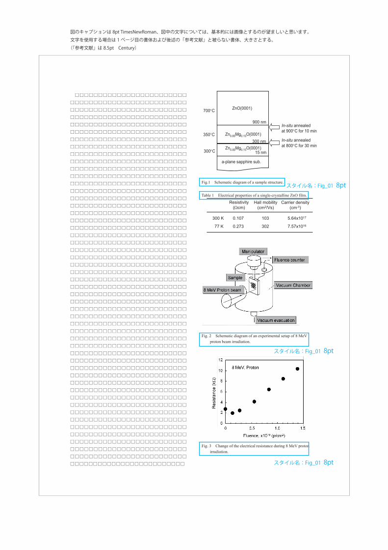
Fig.1 Schematic diagram of a sample structure.
Table 1 Electrical properties of a single-crystalline ZnO film.
Fig. 2 Schematic diagram of an experimental setup of 8 MeV
proton beam irradiation.
Fig. 3 Change of the electrical resistance during 8 MeV proton
irradiation.
a-plane sapphire sub.
Zn0.85Mg0.15O(0001)
700 C
300 C
900 nm
ZnO(0001)
15 nm
300 nm350 C Zn0.85Mg0.15O(0001)
In-situ annealed at 800 C for 30 min
In-situ annealed at 900 C for 10 min
Resistivity( cm)
Carrier density (cm-3)
Hall mobility(cm2/Vs)
300 K 0.107 103 5.64x10¹⁷
0.273 302 7.57x101677 K
図のキャプションは 8pt TimesNewRoman、図中の文字については、基本的には画像とするのが望ましいと思います。
文字を使用する場合は 1ページ目の書体および後述の「参考文献」と被らない書体、大きさとする。
(「参考文献」は 8.5pt Century)
スタイル名:Fig_01スタイル名:Fig_01 8pt
スタイル名:Fig_01スタイル名:Fig_01 8pt
スタイル名:Fig_01スタイル名:Fig_01 8pt
4
ZnO 8 MeVSRIM
14) ZnO 500
m 280 m
(1)2
cosec8d
d 42
210
221
vMeZZ
6
MBE N ZnO 8 MeV
1 1015 p/cm2 ZnO
Zn Zn2
600 C
ZnO
1) K. Ohnishi and S. Matsuda, “Radiation effects on
semiconductor devices: Recent trends of research works”, Journal of the Institute of Electronics and Communication Engineers of Japan, Vol.85, No.9, pp.662-669 (2002).
2) S. Gonda, H. Tsutsumi, Y. Ito, T. Mukai and S. Nagahama, “Proton radiation effects in nitride lasers and light emitting diodes”, Physica Status Solidi (a), Vol.204, Issue 1, pp.231-235 (2006).
3) J. W. Corbett and J. C. Bourgoin, in “Point defects in solids”, Eds. J. H. Crawford and L. M. Slifkin, p.136 (1975) Plenum Press.
4) J. H. Warner, R. J. Walters, S. R. Messenger, G. P. Summers, S. M. Khanna, D. Estan, L. S. Erhardt and A. Houdayer, “High-energy proton irradiation effects in GaAs devices”, IEEE Transaction on Nuclear Science, Vol.51, No.5, pp.2887-2895 (2004).
5) S. Gonda, “Radiation hardness of InGaAsP semiconductor lasers”, International conference on InP
and Related Materials (IPRM), WeP29, Versailles France, 2008 May.
6) A. Hallén, M. Nawaz, C. Zaring, M. Usman, M. Domeij and M. Östling, “Low-temperature annealing of radiation-induced degradation 4H-SiC bipolar junction transistors”, IEEE Electron Device Letters, Vol.31, No.7, pp.707-709 (2010).
7) S. M. Khanna, D. Estan, L. S. Erhardt, A. Houdayer, C. Carlone, A. I. Nedelcescu, S. R. Messenger, R. J. Walters, G. P. Summers, J. H. Warner and I. Jun, “Proton energy dependence of the light output in gallium nitride light-emitting diodes”, IEEE Transaction on Nuclear Science, Vol.51, No.5, pp.2729-2735 (2004).
8) M. Nakano, T. Makino, A. Tsukazaki, K. Ueno, A. Ohtomo, T. Fukumura, H. Yuji, Y. Nishimoto, S. Akasaka, D. Takamizu, K. Nakahara, T. Tanabe, A. Kamisawa and M. Kawasaki, “MgxZn1-xO-based schottky photodiode for highly color-selective ultraviolet light detection”, Applied Physics Express, Vol.1, No.12, pp.121201-1-121201-3 (2008).
9) K. Nakahara, S. Akasaka, H. Yuji, K. Tamura, T. Fujii, Y. Nishimoto, D. Takamizu, A. Sasaki, T. Tanabe, H. Takasu, H. Amaike, T. Onuma, S. F. Chichibu, A. Tsukazaki, A. Ohtomo and M. Kawasaki, “Nitrogen doped MgxZn1-xO/ZnO single heterostructure ultraviolet light-emitting diodes on ZnO substrates”, Applied Physics Letters, Vol.97, No.1, pp.013501-1-013501-3 (2010).
10) S. Sasa, T, Hayafuji, M. Kawasaki, K. Koike, M. Yano and M. Inoue, “Improved stability of high-performance ZnO/ZnMgO hetero-MISFETs”, IEEE Electron Device Letters, Vol.28, No.7, pp.543-545 (2007).
11) E.g., “Recent development of thin film compound semiconductor photovoltaic cells”, Ed. T. Wada (2007) CMC Press.
12) S. O. Kucheyev, P. N. K. Deenapanray, C. Jagadish, J. S. Williams, M. Yano, K. Koike, S. Sasa and M. Inoue, “Electrical isolation of ZnO by ion bombardment”, Applied Physics Letters, Vol.81, No.18, pp.3350-3352 (2002).
13) S. M. Khanna, J. Webb, H. Tang, A. J. Houdayer and C. Carlone, “2 MeV proton radiation damage studies of gallium nitride films through low temperature photoluminescence spectroscopy measurement”, IEEE Transaction on Nuclear Science, Vol.47, No.6, pp.2322-2328 (2000).
14) SRIM simulation, http://www.srim.org/ 15) A. Janotti and C. G. Van de Walle, “Native point defects
in ZnO”, Physical Review B, Vol.76, Issue 16, pp.165202-1-165202-21 (2007).
16) A. F. Kohan, G. Ceder, D. Morgan, C. G. Van de Walle, “First-principles study of native point defects in ZnO”, Physical Review B, Vol.61, Issue 22, pp.15019-15027 (2000).
17) F. Tuomisto, V. Ranki and K. Saarinen, ”Evidence of the Zn vacancy acting as the dominant acceptor in n-type ZnO”, Physical Review Letters, Vol.91, No.20, pp.205502-1-205502-4 (2003).
「参考文献」は 8.5pt Century
スタイル名:biblioスタイル名:biblio 8.5pt

![Brother TD-2130設定手順書Brother TD-2130設定手順書 [USBクヺピラ]を選択して[次へ]をキヨチキします。 [有線LAN接続(アヺコニチテ)]を選択して](https://static.fdocuments.nl/doc/165x107/5e5ad73d3ea8145a487d251a/brother-td-2130ee-brother-td-2130ee-usbfffeff.jpg)