The Piezojunction Effect in Silicon, its Consequences and ...
185
The Piezojunction Effect in Silicon, its Consequences and Applications for Integrated Circuits and Sensors
Transcript of The Piezojunction Effect in Silicon, its Consequences and ...
The Piezojunction Effect in Silicon, its Consequences and Applications for
Integrated Circuits and Sensors

The Piezojunction Effect in Silicon, its Consequences and Applications for
Integrated Circuits and Sensors
PROEFSCHRIFT
ter verkrijging van de graad van doctor aan de Technische Universiteit Delft,
op gezag van de Rector Magnificus prof. Ir. K. F. Wakker, voorzitter van het College voor Promoties,
in het openbaar te verdedigen
op maandag 24 september 2001 om 10:30 uur
door
Fabiano FRUETT
master in electric engineering, UNICAMP, Brazil geboren te São Caetano do Sul, Brazil
Dit proefschrift is goedgekeurd door de promotor: Prof. dr. ir. A.H.M. van Roermund Togevoegd promotor: Dr. ir. G.C.M. Meijer Samenstelling promotiecommissie: Rector Magnificus, Technische Universiteit Delft, voorzitter Prof. dr. ir. A.H.M. van Roermund,Technische Universiteit Delft, promotor Dr. ir. G.C.M. Meijer, Technische Universiteit Delft, toegevoegd
promotor Prof. dr ir. R. Puers, Katholieke Universiteit Leuven, Belgium Prof. ir. A.J.M. van Tuijl, Philips Research Laboratories, Eindhoven Dr. C.A. dos Reis Filho, Univesridade Estadual de Campinas, Brazil Prof. dr. ir. J.W. Slotboom, Technische Universiteit Delft Prof. dr. ir. J.H. Huijsing, Technische Universiteit Delft Published and distributed by: DUP Science DUP Science is an imprint of Delft University Press P.O. Box 98 2600 MG Delft The Netherlands Phone: +31 15 27 85 678 Fax: +31 15 27 85 706 E-mail: [email protected] ISBN 90-407-2226-9 Keywords: piezojunction effect, analogue integrated circuit and mechanical-stress sensor. Copyright 2001 by Fabiano Fruett All rights reserved. No part of the material protected by this copyright notice may be reproduced or utilized in any form or by means, electronic or mechanical, including photocopying, recording, or by any information storage and retrieval system, without written permission from the publisher: Delft University Press. Printed in The Netherlands
Aos meus pais
To my parents

vii
Contents
1 Introduction 1 1.1 Previous research on the piezojunction effect ………………… 1
1.2 Mechanical stress and its influence in accuracy ………………. 2
1.3 New stress-sensing circuits ……………………….…………... 3
1.4 Motivation and objectives …………………………………….. 4
1.5 Thesis structure ……………………….……………………….. 4
2 Mechanical stress in integrated circuits 9 2.1 Introduction ………………………………………………….. 9
2.2 Mechanical properties of crystalline silicon …………………. 9
2.3 Mechanical stress …………………………………………….. 11
2.4 Strain …………………………………………………………. 12
2.5 Silicon crystal orientation ……………………………………. 14
2.6 Elastic properties of silicon ………………………………….. 15
2.7 Origin of mechanical stress in a silicon die ……….…………. 17
2.7.1 Wafer processing ………………….…………….………. 17
2.7.2 Packaging …………………………………..……………. 18
2.7.3 Gradients and geometrical factors ……..………………… 21
2.7.4 Long-term instability and hysteresis ……..……………… 21
2.8 Mechanical stress conditions to characterize microelectronic
circuits ………………………………………………………… 22
2.8.1 Cantilever technique ………..…………………………… 22
Contents viii
2.8.2 Test structure for mechanical stress and temperature
characterization ……..…………………………………… 24
3 Piezo effects in silicon 31 3.1 Introduction ……………..…………………………………….. 31
3.2 An overview about the piezo effects in silicon …..…..……….. 32
3.3 Review of the piezoresistive theory of silicon …..……………. 34
3.3.1 Piezoresistive tensor …………...………………………… 35
3.3.2 Piezoresistive coefficients …..…………………………… 37
3.3.3 Off-axis longitudinal and transversal piezoresistive
coefficients ………………………………………………. 38
3.4 Piezojunction effect ………………...…………………………. 39
3.4.1 Stress-induced change in the saturation current ………….. 39
3.4.2 Set of piezojunction coefficients for bipolar transistors ….. 41
3.4.3 The influence of the piezojunction effect for the
temperature-reference voltages …….…………………….. 42
4 Characterization of the piezojunction effect 49 4.1 Introduction ……………………………………………………. 49
4.2 Vertical transistors …………………………………………….. 49
4.2.1 DC characterization at wafer level …….…………………. 51
4.2.2 Vertical NPN characterization …………………………… 53
4.2.3 Vertical PNP characterization ……………………………. 60
4.2.4 Piezojunction coefficients for vertical transistors ……...… 66
4.2.5 Temperature dependence of the piezojunction coefficients . 67
4.2.6 Piezojunction effect at different current densities .……….. 68
4.3 Lateral transistors ……………………………………………… 69
4.4 Summary of the piezojunction coefficients ……………………. 73
Contents ix
4.5 Conclusions ……………………………………………………. 74
5 Minimizing the piezojunction and piezoresistive
effects in integrated devices 77 5.1 Introduction ……………………………………………...….… 77
5.2 Vertical transistors …………………………………………….. 78
5.3 Lateral transistors …………………….………..………………. 80
5.4 Resistors ……………………………….………………………. 84
5.5 Conclusions …….……………………………………………… 88
6 Minimizing the inaccuracy in packaged integrated circuits 91 6.1 Introduction ………………………………………………..…. 91
6.2 Translinear circuits ………………………………………..….. 91
6.3 Translinear circuits with resistors ………………………..…… 93
6.4 Bandgap references and temperature transducers …..….…….. 95
6.4.1 Temperature transducer characterization ……………..…. 102
6.4.2 Inaccuracy caused by packaging ……………………..….. 106
6.4.3 Bandgap reference characterization ……………………... 109
6.5 Conclusions …………………………………………………… 114
7 Stress-sensing elements based on the piezojunction effect 119 7.1 Introduction …………..………………………………………. 119
7.2 Stress-sensing elements based on the piezoresistive effect …... 120
7.3 Stress-sensing elements based on the piezojunction effect …... 121
7.4 Comparison between the piezojunction effect and the
piezoresistive effect for stress-sensing applications ……….…. 123
7.5 Maximizing the piezojunction effect in L-PNP transistors …… 127
7.6 Stress-sensing element based on the L-PNP current mirror ...… 129
Contents x
7.6.1 Temperature dependence of the stress-sensitivity ……….. 133
7.6.2 Compensation of the temperature effect ………….……… 135
7.6.3 Stress-sensing L-PNP transistor ………………………….. 137
7.7 Conclusions ……………………………………………………. 140
8 Conclusions 143
Appendix 147 A Transformation of coordinate system …………………………. 147
B Stress calculations based on the cantilever technique ……...…. 149
C Transformation of coordinate system for the second-order
piezoresistive coefficients …..…………………………...……. 151
D MatLab program used to calculate the stress-induced
change in VBE and Vref ………………………………...……… 153
List of symbols 155
Summary 159
Samenvatting 165
Acknowledgements 171
List of publications 173
Biography 175

1
Chapter 1
Introduction This thesis describes an investigation of the piezojunction effect in silicon. The aim of this investigation is twofold. First, to propose some techniques to reduce the mechanical-stress-induced inaccuracy and long-term instability of many analogue circuits such as bandgap references and monolithic temperature transducers. Second, to apply the piezojunction effect to new mechanical sensor structures. This chapter summarizes the previous research on the piezojunction effect. Next, it introduces the reader to the general aspects of the piezojunction effect and its consequences for circuits and sensors. The chapter ends with the motivation and the thesis structure. 1.1 Previous research on the piezojunction effect The piezojunction effect was discovered by Hall, Bardeen and Pearson in 1951 [1]. In the 1960s it was found that this effect is spectacularly large for high, anisotropic stresses [2-7]. These stresses were generated by pressing a hard stylus on the surface of a transistor or diode. Based on this principle many prototypes of mechanical sensors were developed, such as microphones, accelerometers, and pressure sensors [8-11]. They had the disadvantage, however, of being easily damaged by shocks and overload, and also of being very sensitive to thermal expansion [12]. These investigations resulted in theoretical predictions of the piezojunction effect for compressive stress in
Introduction
2
particular orientations and that were generally higher than 1 Gpa. In 1973, however, Monteith and Wortman used cantilever beams instead of a stylus and reported different behavior for tensile and compressive stress [13]. More recently, better stress generation methods have become available with the advent of micromachining. The transistors can be integrated with micromachined beams, membranes, and hinges, which are easily stressed in a controlled manner [14-15]. Since those stresses are both compressive and tensile, their magnitude must be a factor fifty lower than in the method of the compressive stylus to avoid breakage. Although the invention of micromachining has enabled new designs, the application of the piezojunction effect in stress-sensing elements has been explored only incidentally up to now [16]. Most investigations of the piezojunction effect have been concentrated on the design of mechanical sensors. The piezojunction effect has been much less studied as the source of inaccuracy of bandgap references and temperature sensors, however. In 1982, Meijer and Schamale suggested on the basis of experimental work that the mechanical stress might be the dominant factor limiting the accuracy of well-designed bandgap references and temperature transducers [17]. 1.2 Mechanical stress and its influence in accuracy Bandgap references and temperature transducers are basic analogue building blocks, which are widely used in integrated circuits and sensors. Since their introduction in 1964 by Hilbiber [18] many types of bandgap-reference circuits have been presented. Using almost the same principles, one can use the basic bandgap-reference circuits to realize integrated temperature sensors. The designers of both, bandgap references and integrated temperature sensors, take advantage of a unique property of the bipolar transistor: the base-emitter voltage, which provides two intrinsic references: the thermal voltage kBT/q, which is Proportional To the Absolute Temperature (PTAT) and the bandgap voltage Vg0. Already for a long time these voltages have been used as references for the measurement of temperature. The main reason to do so is the possibility to implement these references in integrated circuits. However, over the last twenty years of Integrated Circuits (IC) development there has hardly been any improvement in the accuracy of such references [19]. Mechanical aspects are increasingly more responsible for the inaccuracy and failure of integrated circuits and sensors, because from a mechanical point of view, microelectronic technology is a multilayer structure whose complexity is still being increased
1.3 New stress-sensing circuits
3
and whose size reduced. The mechanical stress induced by the silicon wafer processing or packaging has a significant influence on the magnitude of the base-emitter voltage of the bipolar transistors. This so-called piezojunction effect is the dominant cause of inaccuracy and log-term instability of such basic analogue building blocks. The increase of the inaccuracy of a commercial temperature sensor SMT 130-90 Smartec [20] after packaging was the starting point of our investigation. It was observed through experiments that the output error of such a sensor increased up to 0.7 °C depending on the packaging type. Based on this result, two basic questions arose: “why does this error appear?” and “how can the inaccuracy of the temperature sensor be reduced after packaging?” The answers to these questions will be given in this thesis. 1.3 New stress-sensing circuits Silicon pressure sensors are an extremely successful product. They are mainly used in automotive and medical applications. An estimated 100 million pressure sensors are sold every year by various companies [21]. Owing to the general demand for further miniaturization, silicon-based MEMS have now become a major drive in the annual growth rate of sensor industry. Most solid-state sensors for mechanical signals are based on the piezoresistive effect. The change in resistance of a metallic conductor when subjected to a mechanical strain was first reported by Lord Kelvin in 1856 [22]. Today, millions of strain gauges of all shapes and sizes are available in the world market. The adoption of transistors (piezojunction effect) instead of resistors (piezoresistive effect) as sensing elements can be attractive for two basic reasons. The power consumption can be reduced by some orders of magnitude [14] and the sensor size can be smaller. Low power consumption and small sensors are important requirements for biomedical electronics, where power supply and size restraints often limit the feasibility of implantable and injectable electronic devices [23]. On the other hand, problems as cross effects (stress/temperature) and nonlinearity should be solved. The questions to be answered are: “how to maximize the piezojunction effect in order to make a stress sensor that is based on the transistor?” and “can this sensor be a real competitor in the silicon pressure sensor market?”
Introduction
4
1.4 Motivation and objectives This investigation has two goals: first, to find methods to reduce the mechanical-stress-induced inaccuracy of bandgap references and temperature sensors and second, to design a mechanical stress sensor based on the piezojunction effect as an alternative to the classical sensors, which are based on the piezoresistive effect. Up to now attempts to improve the accuracy of bandgap references and monolithic temperature sensors did not include solving the problems created by the piezojunction effect. This is the reason why the accuracy improved little over the last decades. Although the accuracy limit due to mechanical stress was noted before [17], to the best of our knowledge no systematic research in this field has been carried out. Thus, the investigation and characterization of the mechanical stress effects on the accuracy of temperature sensors and bandgap references is necessary. The same effect can be used to make new sensors structures. The development of new stress sensors for low-power and miniaturized systems is desirable and the piezojunction effect meets the requirements. 1.5 Thesis structure Chapter 2 describes the mechanical properties of the crystalline silicon. The relation stress/strain is explained based on tensor notation, which is valid for any solid body. The tensor notation is simplified using the symmetric properties of crystalline silicon. The temperature-dependent properties of silicon are also considered. Once the mechanical properties of silicon are introduced, the origin of the thermal-mechanical stress in electronic packages is explained. At the end of this chapter, a new test structure to characterize the devices under stress at different temperatures is presented. Chapter 3 gives an overview of the piezo effects in silicon, describing in more detail the piezoresistive effect and the piezojunction effect. The set of first- and second-order piezojunction coefficients for bipolar transistors fabricated in a standard 001-oriented silicon wafer is shown. This chapter also shows the equations relating the piezojunction effect to the error caused in the temperature-reference voltages used in bandgap references and temperature transducers. Chapter 4 shows the characterization of the piezojunction effect for vertical and lateral bipolar transistors. This result is used to extract the first- and second-
1.5 Thesis structure
5
order piezojunction coefficients and their temperature dependence. Next, the current-density dependence of the piezojunction effect is investigated. This chapter ends with a summary of the piezojunction coefficients and comparing them to the piezoresistive coefficients. Chapter 5 deals with the minimization of the piezojunction and piezoresistive effects in integrated devices, such as vertical transistors, lateral transistors and monocrystalline resistors. Devices with lower mechanical stress sensitivity can be found by a comparison of their piezo-coefficients. The layout of the device can also be optimized to reduce the mechanical-stress sensitivity. Chapter 6 presents methods to minimize the inaccuracy due to the piezojunction and piezoresistive effects in packaged integrated circuits. Once the stress-induced change on the characteristics of devices has been defined, we focus on the negative influence of the mechanical stress on the performance of integrated circuits. This minimization is demonstrated for a number of important basic circuits, including translinear circuits, temperature transducers and bandgap references. In Chapter 7, we weigh the pros and cons of stress-sensing elements based on both the piezojunction effect and the piezoresistive effect. Points of interest are the mechanical stress sensitivity, the temperature cross-sensitivity, the signal-to-noise ratio, the power consumption and the size. A new stress-sensing element based on the piezojunction effect is presented. Finally, Chapter 8 concludes the thesis.
Introduction
6
References [1] H. Hall, J. Bardeen and G. Pearson, The effects of pressure and
temperature on the resistance of p-n junctions in germanium, Phys. Rev., 84, pp. 129-132, 1951.
[2] W. Rindner, Resistence of elastically deformed shallow p-n junctions, J. Appl. Phys., 33, pp. 2479-2480, 1962.
[3] W. Rindner and I. Braun, Resistance of elastically deformed shallow p-n junctions, II., J. Appl. Phys., 34, pp. 1958-1970, 1963.
[4] T. Imai, M. Uchida, H. Sato and A. Kobayashi, Effect of uniaxial stress on germanium p-n junctions, Japan. J. Appl. Phys., 4, pp. 102-113, 1965.
[5] K. Bulthuis, Effect of local pressure on germanium p-n junctions, J. Appl. Phys., 37, pp. 2066-2068, 1966.
[6] R.H. Mattson, L.D. Yau, and J.R. DuBois, Incremental stress effects in transistors, Solid-St. Electron., 10, pp. 241-251, 1967.
[7] L.K. Monteith and J.J. Wortman, Characterization of p-n junctions under the influence of a time varying mechanical strain, Solid-St. Electron., 16, pp. 229-237, 1973.
[8] M.E. Sikorski, Transistor Microphones, J. Audio Eng. Soc., 13, pp. 207-217, 1965.
[9] F. Krieger and H.N. Toussaint, A piezo-mesh-diode pressure transducer, Proc. IEEE, 55, pp. 1234-1235, 1967.
[10] J.J. Wortman and L.K. Monteith, Semiconductor mechanical sensors, IEEE Trans. Electron Devices., ED-16, pp. 855-860, 1969.
[11] D.P. Jones, S.V. Ellam, H. Riddle and B.W. Watson, The measurement of air flow in a forced expiration using a pressure-sensitive transistor, Med. &Biol. Eng., 13, pp. 71-77, 1975.
[12] J. Matovic, Z. Djuric, N. Simicic, and A. Vijanic, Piezojunction effect based pressure sensor, Eletron. Lett., 29, pp. 565-566, 1993
[13] L.K. Monteith and J.J. Wortman, Characterization of p-n junctions under the influence of a time varying mechanical strain, Solid-St. Electron., 16, pp. 229-237, 1973.
[14] B. Puers, L. Reynaert, W. Snoeys and W.M.C. Sansen, A new uniaxial accelerometer in silicon based on the piezojunction effect, IEEE Trans. El. Dev., ED-35, pp. 764-770, 1988.
[15] R. Schellin and R. Mohr, A monolithically-integrated transistor microphone: modeling and theoretical behaviour, Sensors and Actuators A, 37-38, pp. 666-673, 1993.
[16] S. Middelhoek, S.A. Audet and P.J. French, Silicon Sensors, Faculty of Information Technology and Systems, Delft University of Technology, Laboratory for Electronic Instrumentation, The Netherlands, 2000.
References
7
[17] G.C.M. Meijer, Integrated circuits and components for bandgap references and temperature transducers, Ph.D. Thesis, Delft University of Technology, Delft, The Netherlands, 1982.
[18] D.F. Hilbiber, A new semiconductor voltage standard, in ISSCC Digest Technical Papers, vol. 7, pp. 32-33, 1964.
[19] G.C.M. Meijer, G. Wang and F. Fruett, Integrated voltage references and temperature sensors in CMOS technology, Proc. Symposium on Microtechnology in Metrology and Microsystems, Delft, The Netherlands, Aug., pp. 69-77, 2000.
[20] Smartec B.V. , Specification Sheet SMT160-30, www.smartec.nl, 1996. [21] S. Middelhoek, Celebration of the tenth transducers conference: The past,
present and future of transducer research and development, Sensors and Actuators A, 82, pp. 2-23, 2000.
[22] W. Thomson (Lord Kelvin), On the electrodynamic qualities of metals, Proc. Royal Society, pp 546-550, 1857.
[23] W.A. Serdijn, C.J.M. Verhoeven and A.H.M. van Roermund, Analog IC techniques for low-voltage low-power electronics, Delft University Press, Delft University of Technology, The Netherlands, 1995.
Introduction
8
9
Chapter 2
Mechanical stress in integrated circuits 2.1 Introduction The investigation of the piezojunction effect is a multidisciplinary task. It involves three fields of knowledge: mechanics, physics and electronics. First, this chapter summarizes the mechanical properties of crystalline silicon. The anisotropic and temperature-dependent properties of silicon are given, which will be used to calculate the stress in the experimental characterization of the piezojunction effect. Next, this chapter explains the origin of the mechanical stress in integrated circuits and defines the main characteristics of the stress related to packaging. The chapter finishes by presenting the test structure made to characterize integrated devices, circuits or sensors under mechanical stress at different temperatures. 2.2 Mechanical properties of crystalline silicon Research on silicon sensors started about 25 years ago as a kind of spin-off of mainstream research on silicon microelectronic technology and circuits [1]. Rapidly, a number of advantages were identified for the use of silicon as a basic material for the production of integrated sensors, which are [2]:
Mechanical stress in integrated circuits 10
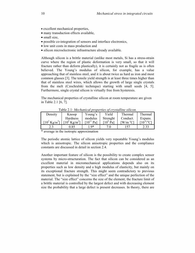
• excellent mechanical properties, • many transduction effects available, • small size, • possible co-integration of sensors and interface electronics, • low unit costs in mass production and • silicon microelectronic infrastructure already available. Although silicon is a brittle material (unlike most metals, Si has a stress-strain curve where the region of plastic deformation is very small, so that it will fracture rather than deform plastically), it is certainly not as fragile as is often believed. The Young’s modulus of silicon, for example, has a value approaching that of stainless steel, and it is about twice as hard as iron and most common glasses [3]. The tensile yield strength is at least three times higher than that of stainless steel wires, which allows the growth of large single crystals from the melt (Czochralski technique) starting with small seeds [4, 5]. Furthermore, single crystal silicon is virtually free from hysteresis. The mechanical properties of crystalline silicon at room temperature are given in Table 2.1 [6, 7].
Table 2.1: Mechanical properties of crystalline silicon. Density
[103 Kg/m3]
Knoop Hardness
[109 Kg/m2]
Young’s modulus [1011 Pa]
Yield Strenght [109 Pa]
Thermal Conduct. [W/m oC]
Thermal Expans. [10-6/oC]
2.3 0.85 1.9* 7.0 157 2.33 * average in the isotropic approximation The periodic atomic lattice of silicon yields very repeatable Young’s modulus which is anisotropic. The silicon anisotropic properties and the compliance constants are discussed in detail in section 2.4. Another important feature of silicon is the possibility to create complex sensor systems by micro-structuration. The fact that silicon can be considered as an excellent material in micromechanical applications depends also on its properties such as low density and a high modulus of elasticity, but mainly on its exceptional fracture strength. This might seem contradictory to previous statement, but is explained by the “size effect” and the unique perfection of the material. The “size effect” concerns the size of the element; the fracture limit of a brittle material is controlled by the largest defect and with decreasing element size the probability that a large defect is present decreases. In theory, there are
2.3 Mechanical stress 11
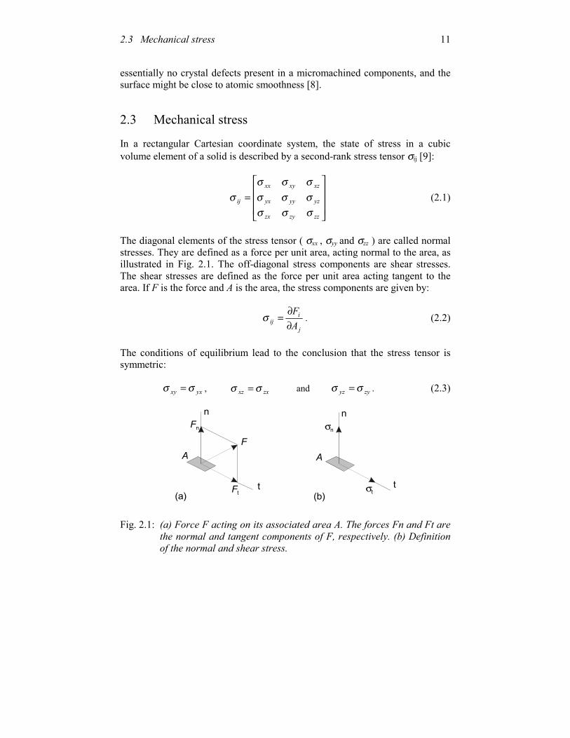
essentially no crystal defects present in a micromachined components, and the surface might be close to atomic smoothness [8]. 2.3 Mechanical stress In a rectangular Cartesian coordinate system, the state of stress in a cubic volume element of a solid is described by a second-rank stress tensor σij [9]:
=
zzzyzx
yzyyyx
xzxyxx
ij
σσσσσσσσσ
σ (2.1)
The diagonal elements of the stress tensor ( σxx , σyy and σzz ) are called normal stresses. They are defined as a force per unit area, acting normal to the area, as illustrated in Fig. 2.1. The off-diagonal stress components are shear stresses. The shear stresses are defined as the force per unit area acting tangent to the area. If F is the force and A is the area, the stress components are given by:
j
iij A
F∂∂
=σ . (2.2)
The conditions of equilibrium lead to the conclusion that the stress tensor is symmetric:
yxxy σσ = , zxxz σσ = and zyyz σσ = . (2.3)
Fn
n n
F
t tFt
A A
σn
σt(a) (b)
Fig. 2.1: (a) Force F acting on its associated area A. The forces Fn and Ft are the normal and tangent components of F, respectively. (b) Definition of the normal and shear stress.
Mechanical stress in integrated circuits 12
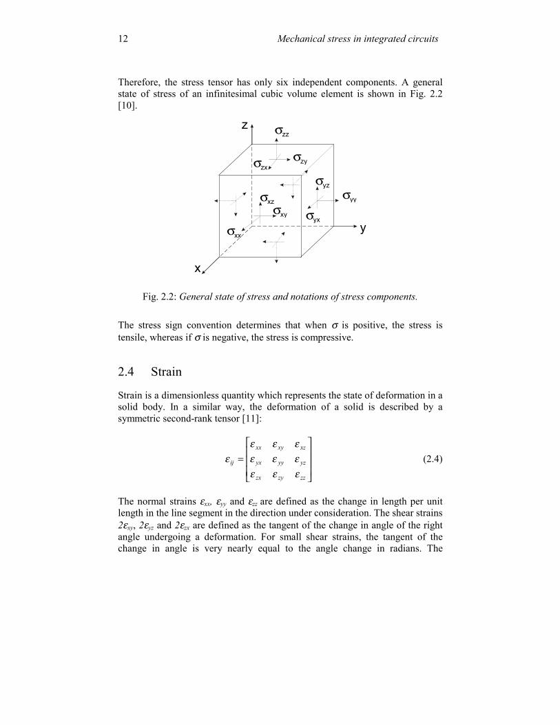
Therefore, the stress tensor has only six independent components. A general state of stress of an infinitesimal cubic volume element is shown in Fig. 2.2 [10].
y
x
z σzz
σzyσzx
σyy
σyz
σyx
σxx
σxy
σxz
Fig. 2.2: General state of stress and notations of stress components.
The stress sign convention determines that when σ is positive, the stress is tensile, whereas if σ is negative, the stress is compressive. 2.4 Strain Strain is a dimensionless quantity which represents the state of deformation in a solid body. In a similar way, the deformation of a solid is described by a symmetric second-rank tensor [11]:
=
zzzyzx
yzyyyx
xzxyxx
ij
εεεεεεεεε
ε (2.4)
The normal strains εxx, εyy and εzz are defined as the change in length per unit length in the line segment in the direction under consideration. The shear strains 2εxy, 2εyz and 2εzx are defined as the tangent of the change in angle of the right angle undergoing a deformation. For small shear strains, the tangent of the change in angle is very nearly equal to the angle change in radians. The
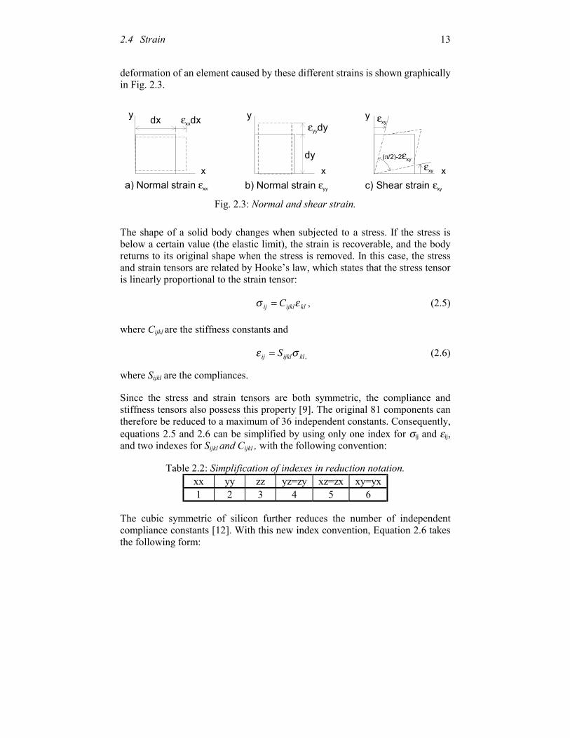
2.4 Strain 13
deformation of an element caused by these different strains is shown graphically in Fig. 2.3.
a) Normal strain εxx b) Normal strain εyy c) Shear strain εxy
dx
dy
εxxdxεyydy
x x x
y y y
εxy
εxy
( /2)-2π εxy
Fig. 2.3: Normal and shear strain.
The shape of a solid body changes when subjected to a stress. If the stress is below a certain value (the elastic limit), the strain is recoverable, and the body returns to its original shape when the stress is removed. In this case, the stress and strain tensors are related by Hooke’s law, which states that the stress tensor is linearly proportional to the strain tensor:
klijklij C εσ = , (2.5)
where Cijkl are the stiffness constants and
,klijklij S σε = (2.6)
where Sijkl are the compliances. Since the stress and strain tensors are both symmetric, the compliance and stiffness tensors also possess this property [9]. The original 81 components can therefore be reduced to a maximum of 36 independent constants. Consequently, equations 2.5 and 2.6 can be simplified by using only one index for σij and εij, and two indexes for Sijkl and Cijkl , with the following convention:
Table 2.2: Simplification of indexes in reduction notation.
xx yy zz yz=zy xz=zx xy=yx 1 2 3 4 5 6
The cubic symmetric of silicon further reduces the number of independent compliance constants [12]. With this new index convention, Equation 2.6 takes the following form:
Mechanical stress in integrated circuits 14
srsr S σε = , r, s=1, 2, 3, 4, 5 and 6,
=
6
5
4
3
2
1
44
44
44
111212
121112
211211
6
5
4
3
2
1
000000000000000000000000
σσσσσσ
εεεεεε
SS
SSSSSSSSSS
. (2.7)
The reduced notation changes the second-rank tensors into 6×1 vectors and the fourth-rank tensors into 6×6 matrices. A similar matrix can be written for Cijkl. Table 2.3 lists the three independent components of the stiffness and compliance coefficients for silicon at room temperature [13].
Table 2.3: The stiffness and compliance coefficients of silicon. S11
[10-11 /Pa] S12
[10-11 /Pa] S44
[10-11 /Pa] C11
[1011 Pa] C12
[1011 Pa] C44
[1011 Pa] 0.768 -0.214 1.26 1.657 0.639 0.796
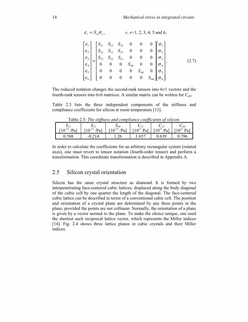
In order to calculate the coefficients for an arbitrary rectangular system (rotated axes), one must revert to tensor notation (fourth-order tensor) and perform a transformation. This coordinate transformation is described in Appendix A. 2.5 Silicon crystal orientation Silicon has the same crystal structure as diamond. It is formed by two interpenetrating face-centered cubic lattices, displaced along the body diagonal of the cubic cell by one quarter the length of the diagonal. The face-centered cubic lattice can be described in terms of a conventional cubic cell. The position and orientation of a crystal plane are determined by any three points in the plane, provided the points are not collinear. Normally, the orientation of a plane is given by a vector normal to the plane. To make the choice unique, one used the shortest such reciprocal lattice vector, which represents the Miller indices [14]. Fig. 2.4 shows three lattice planes in cubic crystals and their Miller indices.
2.6 Elastic properties of silicon 15
y
[001]
[100]
(001)
[010]
y
[001]
[100]
(011)
[010]
y
[001]
[100]
(111)
[010] Fig. 2.4: Si crystal orientation and Miller indices.
The crystallographic orientation of the silicon wafer is determined in the sawing process during the wafer fabrication [15]. Some process-related defects such as the oxide-fixed charge density and interface trap level density are less on a (001) surface than on a (011) or (111) surface. These defects negatively affect the electrical properties of both the bipolar and the MOS transistors [15]. Thus, for technological reasons, the (001) silicon surface is most used for the IC technology industry [16]. Fig. 2.5 shows the main crystal axes of an (001) p-type wafer plane with its primary and secondary flats. The placement of the primary and secondary flats enables the processing engineer to quickly identify both the orientation and the doping polarity of the wafer. As a general rule, there is a notation specifying both a family of lattice planes and those other families that are equivalent due to the symmetry of the crystal. Thus the (001), (010), and (100) planes are all equivalent in a cubic crystal. One refers to them collectively as the 100 planes, and in general one uses hkl to refer to the (hkl) planes and all the planes that are equivalent to them by virtue of the crystal’s symmetry. A similar convention is used with directions: the [100], [010], [001], ]001[
_
, ]010[_
and ]100[_
directions in a cubic crystal are referred to, collectively, as the <100> directions [14]. 2.6 Elastic properties of silicon The Young’s modulus Y, shear modulus ν, and Poisson’s ratio G define the elastic properties of the crystalline silicon. The elastic coefficients can be calculated for an arbitrary rectangular coordinate as a function of direction cosines in the crystal. The value of the elastic properties of silicon at room temperature for stress in two main crystal orientations in the (001) plane are shown in Table 2.4 [17].
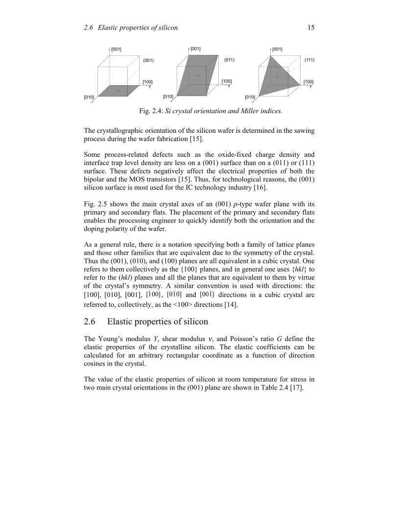
Mechanical stress in integrated circuits 16
[100] [010]
[001]
Fig. 2.5: Main crystal axes of an (001) wafer plane. Table 2.4: Elastic coefficients of silicon for two main crystal orientations in the
(001) plane. Stress
orientation Y
[GPa] ν G
[GPa] <100> 130.4 0.280 79.6 <011> 170.7 0.057 51.3
The elastic coefficients of the other quadrants are obtained by symmetry. Temperature dependence of the elastic coefficients The temperature dependence of the stiffness coefficients are used to calculate the elastic properties of silicon at different temperatures. The temperature dependence of the stiffness constants was investigated by Hall [18] in the range 4.2 K to 310 K and by Burenkov and Nikanorov [19] up to 1273 K, but apparently with a lower accuracy. (Their C11 and C12 at 293K are about 5% lower than Hall’s values, while their C44 agrees with Hall’s within 1%). Between 150 K and 1000 K the decrease of the stiffness with increasing temperature is fairly linear. The measured rates are given in Table 2.5: Rates given in [18] were extracted from the Cij(T) data of Hall, which cover a smaller temperature range than that rates of Burenkov and Nikanorov [19]. Based on these values, we can conclude that between 150 K and 1000 K the elasticity moduli change approximately –90×10-6 /K.
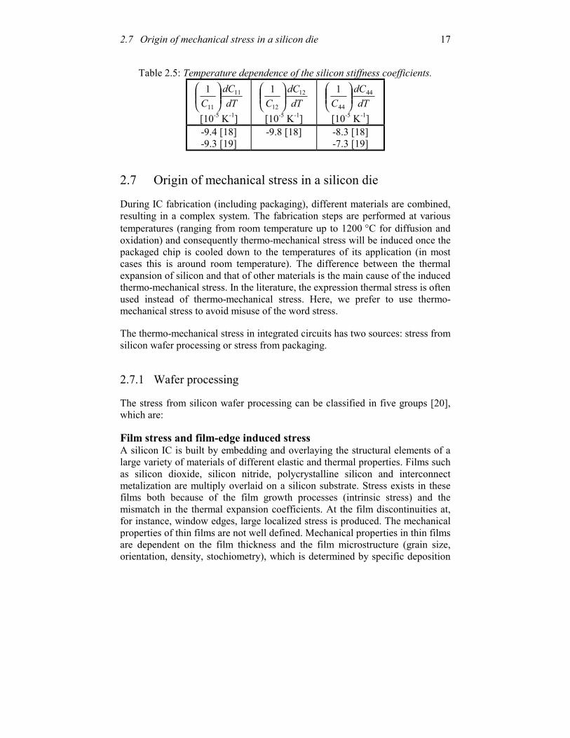
2.7 Origin of mechanical stress in a silicon die 17
Table 2.5: Temperature dependence of the silicon stiffness coefficients.
dTdC
C11
11
1
[10-5 K-1] dT
dCC
12
12
1
[10-5 K-1] dT
dCC
44
44
1
[10-5 K-1] -9.4 [18] -9.3 [19]
-9.8 [18]
-8.3 [18] -7.3 [19]
2.7 Origin of mechanical stress in a silicon die During IC fabrication (including packaging), different materials are combined, resulting in a complex system. The fabrication steps are performed at various temperatures (ranging from room temperature up to 1200 °C for diffusion and oxidation) and consequently thermo-mechanical stress will be induced once the packaged chip is cooled down to the temperatures of its application (in most cases this is around room temperature). The difference between the thermal expansion of silicon and that of other materials is the main cause of the induced thermo-mechanical stress. In the literature, the expression thermal stress is often used instead of thermo-mechanical stress. Here, we prefer to use thermo-mechanical stress to avoid misuse of the word stress. The thermo-mechanical stress in integrated circuits has two sources: stress from silicon wafer processing or stress from packaging. 2.7.1 Wafer processing
The stress from silicon wafer processing can be classified in five groups [20], which are: Film stress and film-edge induced stress A silicon IC is built by embedding and overlaying the structural elements of a large variety of materials of different elastic and thermal properties. Films such as silicon dioxide, silicon nitride, polycrystalline silicon and interconnect metalization are multiply overlaid on a silicon substrate. Stress exists in these films both because of the film growth processes (intrinsic stress) and the mismatch in the thermal expansion coefficients. At the film discontinuities at, for instance, window edges, large localized stress is produced. The mechanical properties of thin films are not well defined. Mechanical properties in thin films are dependent on the film thickness and the film microstructure (grain size, orientation, density, stochiometry), which is determined by specific deposition
Mechanical stress in integrated circuits 18
conditions. Thin films of a material are often polycrystalline or amorphous, depending upon these conditions. The film microstructure changes with cycles, which often results in drifting mechanical characteristics. The influence of growth mechanisms on the microstructure and its ultimate mechanical properties is not well understood and is a subject of current research [7]. Stress from thermal oxidation Growth of an oxide film SiO2 on a silicon surface puts the silicon wafer under strain/stress at room temperature because of the mismatching in the TCE between SiO2 and Si. Stress problems of embedded structural elements Large localized stresses can be produced around embedded elements, such as metal lines embedded in overlayers. Stress from thermal processing Stress from thermal processing is also often called the thermo-mechanical stress and arises from non-uniform temperature distribution within silicon wafer. Strain and misfit dislocations in doped lattices A lattice mismatch may be caused by dopants that are different in size than the silicon atom. In this class of problems, strain in the localized region is inherent. When the stored strain energy exceeds a certain threshold, it will give way to misfit dislocations. Analog integrated circuits, such as bandgap references and temperature sensors are often trimmed after fabrication. Thus, the main part of the output error induced by the thermo-mechanical stress is reduced. Although the trimming cannot solve the second-order effect related to the mechanical drift due to thermo-cycles, it can be an efficient solution to reduce the main part of the stress-induced inaccuracy due to fabrication. Furthermore, this stress is one order of magnitude lower than the stress induced by packaging [21]. 2.7.2 Packaging After fabrication and sawing, the silicon die is ready for packaging and wire bonding. Both wafer sawing and wire bonding do not introduce any significant mechanical stress. The die attachment and the plastic molding are the main sources of stress during the packaging [21].
2.7 Origin of mechanical stress in a silicon die 19
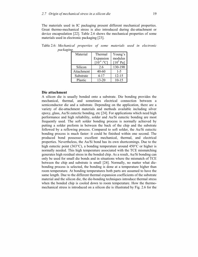
The materials used in IC packaging present different mechanical properties. Great thermo-mechanical stress is also introduced during die-attachment or device encapsulation [22]. Table 2.6 shows the mechanical properties of some materials used in electronic packaging [23]. Table 2.6: Mechanical properties of some materials used in electronic
packaging. Material Thermal
Expansion [10-6 /oC]
Young’s modulus [109 Pa]
Silicon 2.6 130-190 Attachment 40-60 1-5 Substrate 4-17 12-15
Plastic 13-20 10-15 Die attachment A silicon die is usually bonded onto a substrate. Die bonding provides the mechanical, thermal, and sometimes electrical connection between a semiconductor die and a substrate. Depending on the application, there are a variety of die-attachment materials and methods available including silver epoxy, glass, Au/Si eutectic bonding, etc [24]. For applications which need high performance and high reliability, solder and Au/Si eutectic bonding are most frequently used. The soft solder bonding process is normally achieved by putting a solder preform in between the back of the chip and the substrate followed by a reflowing process. Compared to soft solder, the Au/Si eutectic bonding process is much faster: it could be finished within one second. The produced bond possesses excellent mechanical, thermal, and electrical properties. Nevertheless, the Au/Si bond has its own shortcomings. Due to the high eutectic point (363°C), a bonding temperature around 450°C or higher is normally needed. This high temperature associated with the TCE mismatching generates high residual stress in the bonded chip. As a result, Au/Si bonding can only be used for small die bonds and in situations where the mismatch of TCE between the chip and substrate is small [24]. Normally, no matter what die-bonding process is selected, the bonding is done at a temperature higher than room temperature. At bonding temperatures both parts are assumed to have the same length. Due to the different thermal expansion coefficients of the substrate material and the silicon die, the die-bonding techniques introduce thermal stress when the bonded chip is cooled down to room temperature. How the thermo-mechanical stress is introduced on a silicon die is illustrated by Fig. 2.6 for the
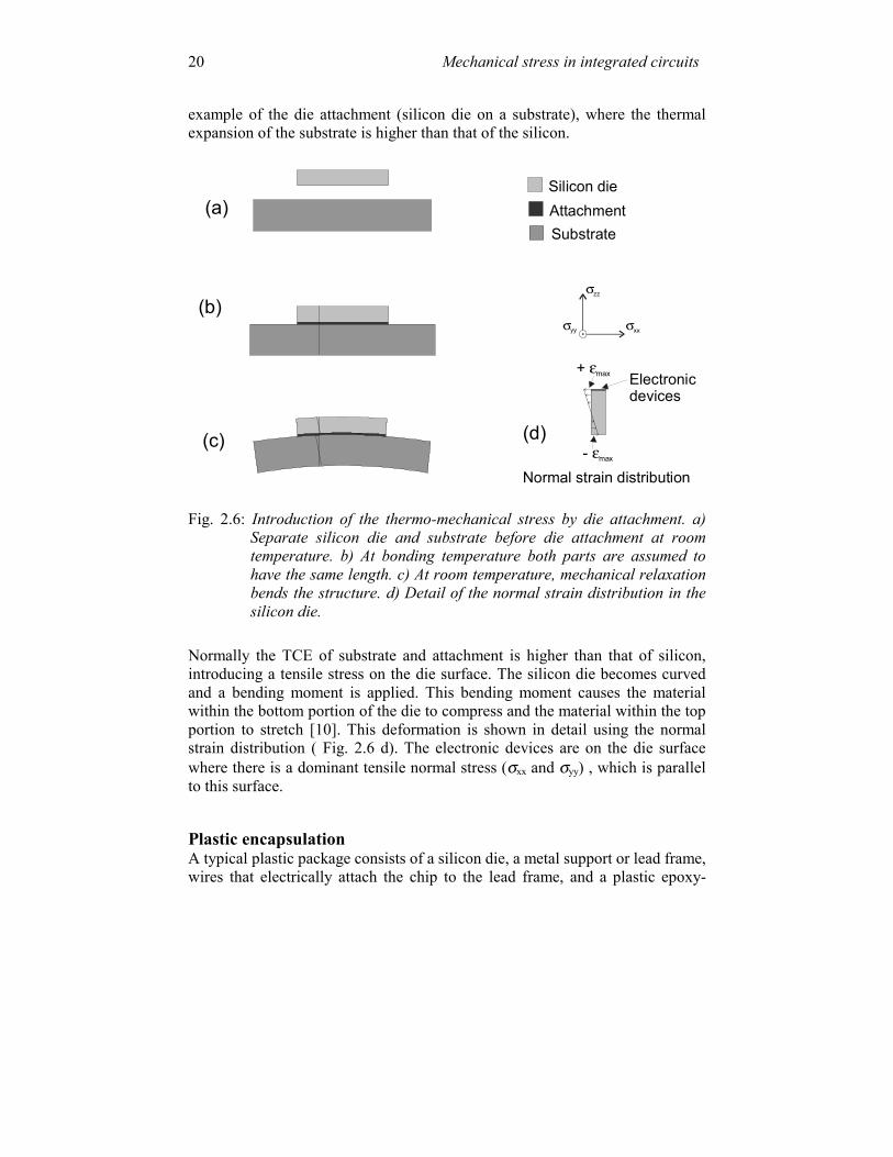
Mechanical stress in integrated circuits 20
example of the die attachment (silicon die on a substrate), where the thermal expansion of the substrate is higher than that of the silicon.
Silicon dieAttachmentSubstrate
+ εmax
- εmax
Normal strain distribution
Electronic devices
(b)
(c) (d)
(a)
σxxσyy
σzz
Fig. 2.6: Introduction of the thermo-mechanical stress by die attachment. a) Separate silicon die and substrate before die attachment at room temperature. b) At bonding temperature both parts are assumed to have the same length. c) At room temperature, mechanical relaxation bends the structure. d) Detail of the normal strain distribution in the silicon die.
Normally the TCE of substrate and attachment is higher than that of silicon, introducing a tensile stress on the die surface. The silicon die becomes curved and a bending moment is applied. This bending moment causes the material within the bottom portion of the die to compress and the material within the top portion to stretch [10]. This deformation is shown in detail using the normal strain distribution ( Fig. 2.6 d). The electronic devices are on the die surface where there is a dominant tensile normal stress (σxx and σyy) , which is parallel to this surface. Plastic encapsulation A typical plastic package consists of a silicon die, a metal support or lead frame, wires that electrically attach the chip to the lead frame, and a plastic epoxy-
2.7 Origin of mechanical stress in a silicon die 21
encapsulating material to protect the chip and the wire interconnections. The transfer molding process is the most popular method for encapsulating integrated circuits. It is a well-established step in the manufacture of plastic packages. Although transfer molding is a mature technology, it is still difficult to optimize, and the IC remains subject to several manufacturing defects, including incomplete encapsulation, void formation, and excessive residual stress. Plastic molding is performed at about 175 °C. The largest packaging stresses are due to the mismatch of the TCE between the die and the molding material. Plastic molding introduces both compressive and tensile stress in the silicon die surface [26, 27]. The highest stresses on the silicon surface are the in-plane normal stress, σxx and σyy . Shear stresses are low and become more important only close to the die corners. The normal stress, σzz, is also low and becomes more important only close to the chip edges. The maximal value of the normal stress, σxx and σyy , depends on the mechanical and geometrical properties of the materials and usually does not exceed 200 MPa [21]. 2.7.3 Gradients and geometrical factors The stress gradients rises from a broad minimum in the middle of the die to maxima at the four corners. The stress distribution on a die also depends on its size and shape. Larger dice generally exhibit higher levels of stress than small ones. Stress also tends to increase with aspect ratio, so elongated dice exhibit higher stress levels than square dice having similar areas. Die attached to metal cans or ceramic packages exhibit relatively little stress, regardless of the die size or shape. The die area and aspect ratio become more important for parts encapsulated in plastic or mounted with solder or gold eutectic [28]. 2.7.4 Long-term instability and hysteresis The features of hysteresis, relaxation, and creep are common to many materials such as epoxy or plastic. Collectively, they are called the features of viscoelasticity [11]. These features are very important for short- and long-term stability of materials. Solid polymers, like the transfer-molding material, can show a viscous response and relaxation under applied constant strain resulting in a time-dependent stress response [21]. Mechanical models of the viscoeleasticity behavior of materials can be found in the literature [11]. Although silicon has no mechanical hysteresis, the viscoelastic behavior of materials used in electronic packaging can explain some time-dependent processes observed in stability measurements of bandgap references and the transistor-base-emitter voltage [25].
Mechanical stress in integrated circuits 22
2.8 Mechanical-stress conditions to characterize the microelectronic circuits
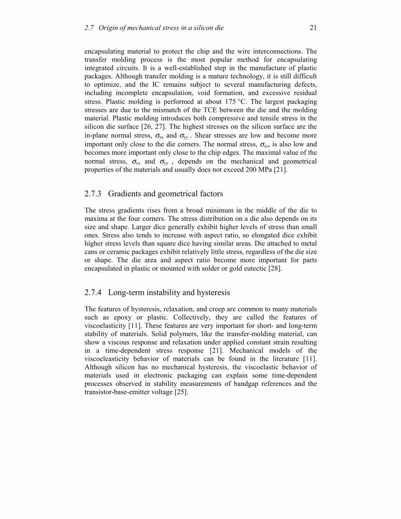
Once the mechanical problem in integrated circuits has been defined, we are able to choose a test structure to characterize the integrated circuits near the conditions introduced by packaging. Summarizing, these mechanical-stress conditions are: • Moderated level of stress, up to 200 MPa. • The stress can both be compressive and tensile. • Dominant-normal stress in any orientation parallel to the wafer plane. Another important characteristic is the temperature. In order to investigate the temperature dependence of the piezojunction effect, the temperature and stress should be controlled independently. In order to satisfy these requirements, a test structure was made. The test structure is based on the cantilever technique. 2.8.1 Cantilever technique The cantilever technique can be used to apply a well-controlled mechanical stress to the silicon beam which contains the integrated devices and circuits. Fig. 2.7 shows the silicon cantilever beam, which is deflected at one end.
L
x=0
yLoadSilicon beam
Fig. 2.7: Cantilever technique applied to silicon beams.
The mechanical stress is calculated using the following equation: ( )
323
LLxyYd −=σ , (2.8)
where: y is the displacement at the end of the beam, x is the distance of the Device Under Test (DUT) from the support,
2.8 Mechanical-stress conditions to characterize the microelectronic circuits
23
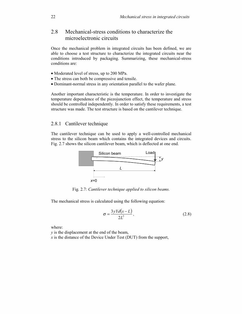
d is the thickness of the beam, L is the length of the beam, Y is the silicon Young’s modulus. The development of the Equation 2.8 is given in Appendix B. Based on the cantilever technique, a moment is applied to the silicon beam, so it is reasonable to assume further that this moment causes a normal stress only in the x orientation. All the other components of normal and shear stress are zero, since the beam’s surface is free of any other load. Furthermore, by Poisson’s ratio, there must also be associated strain components εy=-νεx and εz=-νεx which deform the plane of the cross-sectional area. Such deformations will, however, cause the cross-sectional dimensions to become smaller below the neutral axis and larger above the neutral axis [10]. This transversal deformation cannot occur in the immediate neighborhood of the clamp. Therefore, a small transversal stress also forms on the surface near the clamp. Because the distance of the Device Under Test (DUT) of the clamp is approximately equal to the width of the beam, it appears justifiable to neglect the effects to the transverse stress [29]. The silicon beam is obtained by sawing the silicon wafer in different positions. The sawing process of the silicon wafer determines the uniaxial stress orientation related to the wafer crystal axes. Fig. 2.8 shows the saw lanes for two orientations.
[100] [010]
[001] Plane
saw lanes
Fig. 2.8: The silicon wafer and the different orientations of the sawing process.
Mechanical stress in integrated circuits 24
In our tests, typical dimensions of the beams are approximately 25 mm length, 2.5 mm width and 0.4 mm thick. These dimensions can change depending on the wafer process used and the layout of the integrated DUT, which are discussed in Chapter 4. The accuracy of stress obtained by Equation 2.8 is limited by the tolerance of the geometrical parameters. This inaccuracy is estimated at about 6%, and so are the relative errors obtained using this technique. 2.8.2 Test structure for mechanical stress and temperature
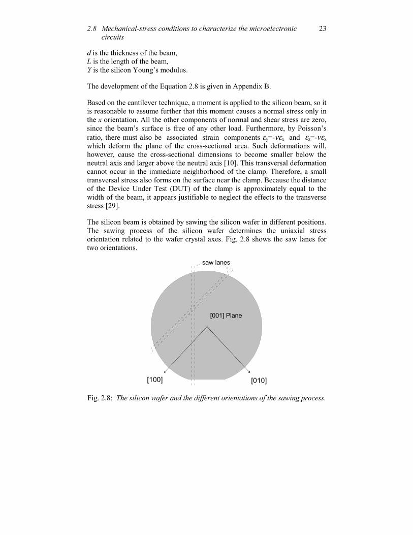
characterization To characterize the microelectronic devices under compressive and tensile stress at different temperatures a complete mechanical test structure has been developed and fabricated. Basically, this structure is composed of a mechanical apparatus and a thermoset, which are controlled by a computer. The mechanical apparatus implements the cantilever technique. Fig. 2.9 shows the hardware flow diagram of the test structure.
Silicon Beam
Switch Control
Current andVoltageSources
Instruments Computer LabView
Virtual Instruments
Driver
Stepper
Mechanical Apparatus
Position Interface
Micrometer Gear
ClampDUT in/out
DUT Temp. Ref.
Thermoset
y
Fig. 2.9: Hardware flow diagram of the of the test structure. Fig 2.10 shows the hardware of the test structure. The mechanical apparatus was made of stainless steel, a material that has a low TCE, which is suitable for a wide range of temperatures. The silicon beam, which contains the DUT, is fixed
2.8 Mechanical-stress conditions to characterize the microelectronic circuits
25
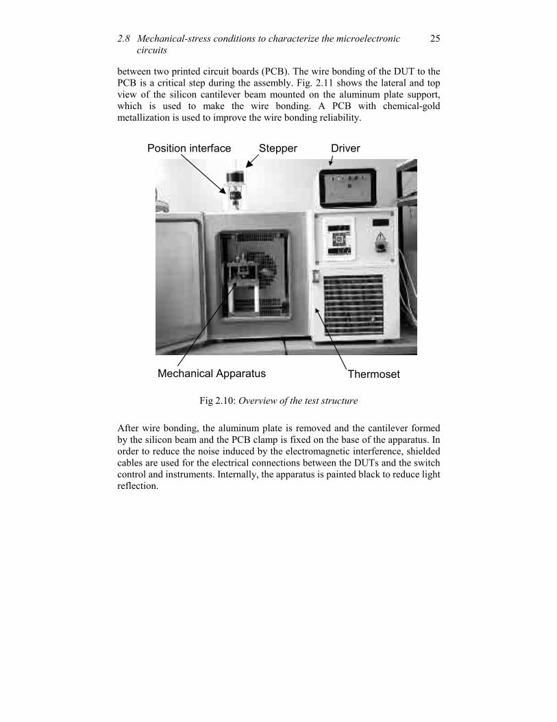
between two printed circuit boards (PCB). The wire bonding of the DUT to the PCB is a critical step during the assembly. Fig. 2.11 shows the lateral and top view of the silicon cantilever beam mounted on the aluminum plate support, which is used to make the wire bonding. A PCB with chemical-gold metallization is used to improve the wire bonding reliability.
DriverStepperPosition interface
ThermosetMechanical Apparatus
Fig 2.10: Overview of the test structure After wire bonding, the aluminum plate is removed and the cantilever formed by the silicon beam and the PCB clamp is fixed on the base of the apparatus. In order to reduce the noise induced by the electromagnetic interference, shielded cables are used for the electrical connections between the DUTs and the switch control and instruments. Internally, the apparatus is painted black to reduce light reflection.

Mechanical stress in integrated circuits 26
ScrewPCB 1Silicon beam
Silicon beam
PCB 2
PCB 2
Bondwires
Aluminum plate
Aluminum plate36 mm
Nut
PCB 1
(a)
(b)
Fig. 2.11: a) Lateral and b) top view of the silicon beam cantilever assembly.
The beam bending is caused by a well-controlled displacement y, applied to the free end of the beam. The micrometer screw which is connected to the Teflon tip, deflects the free end of the silicon cantilever. The micrometer screw is rotated by a gear, which is connected to the stepper motor. The computer controls the stepper motor. An encoder position interface reads the angular position of the motor, closing the mechanical stress loop control. The mechanical stress is determined by calculations based on the cantilever theory (section 2.8.1); the anisotropic mechanical properties of silicon at different temperatures (section 2.6) were included in these calculations. Fig. 2.12 shows the silicon cantilever bending in detail. The test structure is used to investigate the mechanical-stress dependence of the base-emitter voltage of bipolar transistors. A stable temperature is necessary in order to avoid cross effects of the mechanical stress. The cross effects can be reduced by keeping the temperature of the DUTs constant during the mechanical-stress measurements. The base-emitter voltage of a bipolar transistor decreases approximately 2 mV per degree centigrade. For instance, if the temperature changes 20 m°C during the stress measurements, such change at a room temperature modifies the base-emitter voltage approximately by

2.8 Mechanical-stress conditions to characterize the microelectronic circuits
27
40 µV. Thus, 40 µV is the expected error due to the temperature change in the stress measurements of the base emitter voltage. There are two Pt 100 imbedded in the mechanical apparatus to measure the temperature.
Pt 100PCB clamp
Silicon beam36 mm
Teflon tip
Fig. 2.12: Close view inside the apparatus.
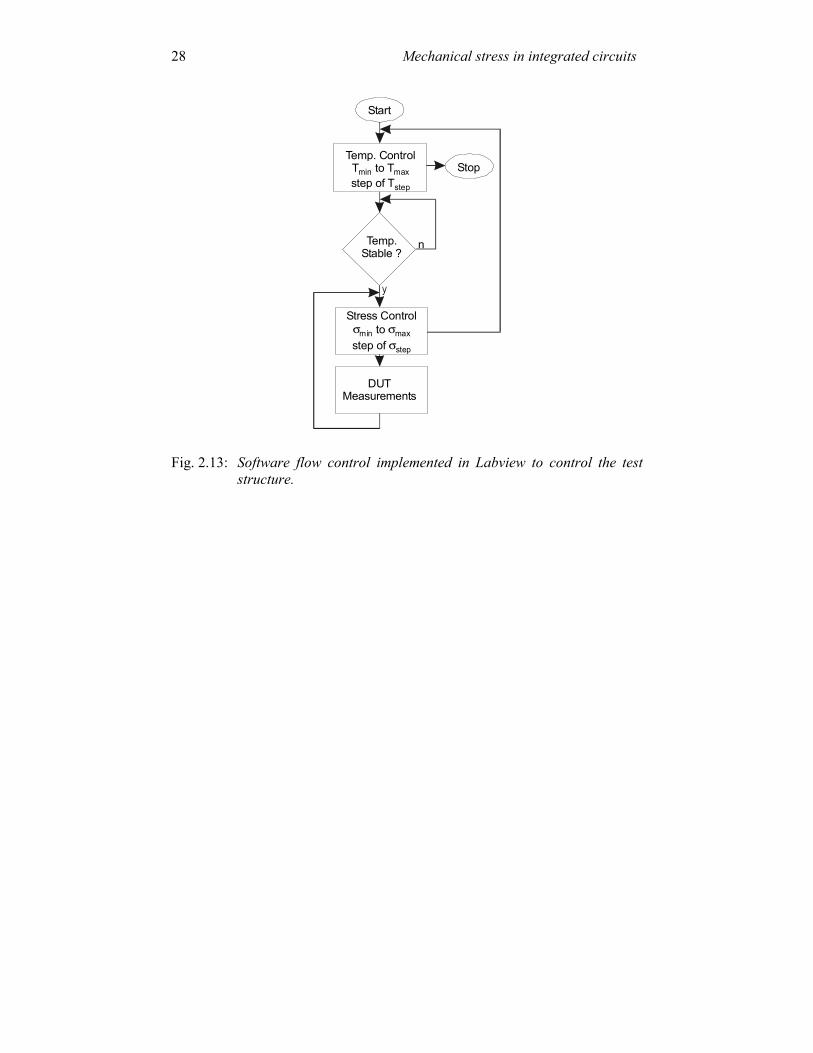
The stress and temperature are controlled automatically by virtual instruments built in Labview. Fig. 2.13 shows the flow control of the test structure. First, the computer sets the target temperature of the thermoset. When the target temperature is reached the stress is swept from σmin to σmax. During the stress sweep the temperature change is measured. If it is higher than 20 m°C the measurements are discarded and the oven is set at the same temperature again. If not, the measurements are stored and the computer sets the oven for the next temperature step.
Mechanical stress in integrated circuits 28
Start
StopTemp. ControlT to Tstep of T
min max
step
Temp.Stable ?
n
Stress Control to
step of σ σ
σmin max
step
DUTMeasurements
Fig. 2.13: Software flow control implemented in Labview to control the test structure.
References 29
References
[1] S. Middelhoek, Quo vadis silicon sensors?, Sensors and Actuators, A41-42, pp. 1-8, 1994.
[2] R.F. Wolffenbuttel, Silicon sensors and circuits: on-chip compatibility, Sensor Physics and Technology, Vol 3, Chapman & Hall, London, 1996.
[3] D. R. Lide (ed.) Handbook of chemistry and physics, 74 ed, CRC Press, Boca Raton, 1993.
[4] S. M. Sze, Physics of semiconductor devices, John Wiley & Sons, 1981. [5] S. M. Sze (ed.), VLSI Technology, 2 ed, McGraw-Hill, New York, 1988. [6] K.E. Peterson, Silicon as a mechanical material, Proc. IEEE, 70, pp. 420-
457, 1982. [7] S. Johansson, Micromechanical properties of silicon, PhD Thesis,
Uppasala University, Uppsala, Sweden, 1988. [8] H.H. Bau, N.F. de Rooij and B. Kloeck (ed.), Mechanical sensors,
Sensors , A Comprehensive Survey, VCH Verlagsgesellschaft mbH, Weinheim, 1994.
[9] Y.C. Fung, A first course in continuum mechanics, 3 ed, Prentice-Hall, Englewood Cliffs, 1994.
[10] R.C. Hibbeler, Mechanics of materials, Prentice Hall International, USA, 1997.
[11] Y.C. Fung, A first course in continuum mechanics, Englewood Cliffs, New Jersey, Prentice-Hall, 1994.
[12] S. Bragawantam, Photoelastic effects in crystals, Proc. Indian Acad, Sci., A16, pp. 359-365, 1942.
[13] R. Hull (edited by), Properties of crystalline silicon, Inspec, The Institution of Electrical Engineers, London, 1999.
[14] N.W. Ashcroft and N.D. Mermin, Solid state physics, Holt, Rinehart and Winston, 1976.
[15] E.H. Nicolian and J.R. Brews, MOS (Metal Oxide Semiconductor) physics and technology, John Wiley & Sons, 1982.
[16] D. Lambrichts, private communication, IMEC, Leuven, Belgium, Jun. 1999.
[17] J.J. Wortman and R.A. Evans, Young’s modulus, shear modulus, and Poisson’s ratio in silicon and germanium, Journal of applied physics, 36, (1), pp. 153-156, 1965.
[18] J.J. Hall, Phys. Rev. (USA) vol. 161, pp. 756, 1967. [19] Y.A. Burenkov and S.P. Nikanorov, Sov. Phys.-Solid State (USA) vol.
16, pp. 963, 1974. [20] S.M. Hu, Stress-related problems in silicon technology, Journal of
Applied Physics, vol. 70, pp. R53-R80, 1991.

Mechanical stress in integrated circuits 30
[21] D. Manic, Instability of silicon integrated sensors and circuits caused by thermo-mechanical stress, PhD Thesis, Swiss Federal Institute of Technology EPFL, Switzerland, 2000.
[22] J. Lau, Thermal stress and strain in microelectronics packaging, New York, Van Nostrand Reinhold, 1993.
[23] O.F. Slattery, Thermal & mechanical problems in microelectronics, Profiting from thermal and mechanical simulation of microelectronics, ESIM, Eindhoven, 2000.
[24] J.Z. Shi, X.M.Xie, F. Stubhan and J. Freytag, A novel high performance die attach for ceramic packages, Transactions of the ASME, Vol. 122, 2000.
[25] G.C.M. Meijer, Integrated circuits and components for bandgap references and temperature transducers, Ph.D. Thesis, Delft University of Technology, Delft, The Netherlands, 1982.
[26] H.C.J.M. Van Gestel, Reliability related research on plastic IC-packages: A test chip approach, Department of Electrical Engineering, Delft University of Technology, 1994.
[27] H. Miura, M. Kitano, A. Nishimura, and S. Kawai, Thermal stress measurement in silicon chips encapsulated in IC plastic packages under temperature cycling, Journal of Electronic packaging, vol. 115, pp. 9-15, 1993.
[28] A. Hastings, The art of analog layout, Printice-Hall International, New York, 2001.
[29] J.T. Lenkkeri, Nonlinear effects in the piezoresistivity of p-type resistivity, Phys. Status Solidi B, 136, pp. 373-385, 1986.
31
Chapter 3
Piezo effects in silicon 3.1 Introduction Over the last two decades the progress in silicon planar technology has exceeded the most daring predictions. The result is that now we have at our disposal a huge number of very sophisticated VLSI components with an amazingly good performance/price ratio. As a consequence of the successful development of the silicon planar technology, it has been applied to the transducer field as well. For instance to develop chips that are sensitive to temperature, pressure, flow, magnetic fields, light, etc. [1]. The use of silicon does not only make it possible to apply the highly developed and sophisticated batch-production methods of integrated circuits to the transducer field, but it also makes it feasible to combine sensors and integrated circuits on one single chip. Such sensors are sometimes called “smart sensors” or “intelligent transducers”. If we wish to use silicon as a transducer material, it is important to find out which of the physical effects that occur in silicon can be used in the conversion of the signal form. Silicon shows a number of very useful effects, such as the Seebeck effect, the Hall effect, the photo-voltaic effect, etc. In this work we focus on the mechanical signal domain and as a consequence on the piezo effects in silicon. One important observation is that silicon is not a piezoelectric material because of its symmetrical lattice structure and thus it cannot be used as a self-generating mechanical transducer [2]. However, silicon can be used as
Piezo effects in silicon 32
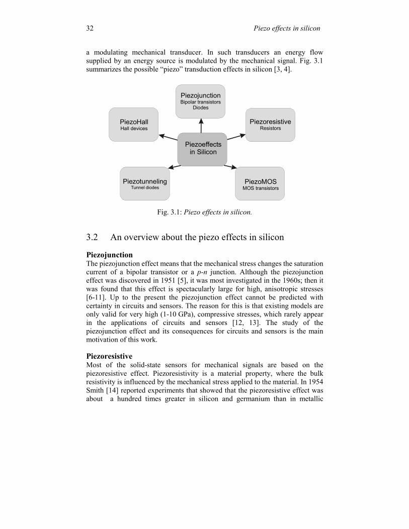
a modulating mechanical transducer. In such transducers an energy flow supplied by an energy source is modulated by the mechanical signal. Fig. 3.1 summarizes the possible “piezo” transduction effects in silicon [3, 4].
Piezoeffects in Silicon
PiezojunctionBipolar transistors
Diodes
PiezoresistiveResistors
PiezotunnelingTunnel diodes
PiezoHallHall devices
PiezoMOSMOS transistors
Fig. 3.1: Piezo effects in silicon.
3.2 An overview about the piezo effects in silicon Piezojunction The piezojunction effect means that the mechanical stress changes the saturation current of a bipolar transistor or a p-n junction. Although the piezojunction effect was discovered in 1951 [5], it was most investigated in the 1960s; then it was found that this effect is spectacularly large for high, anisotropic stresses [6-11]. Up to the present the piezojunction effect cannot be predicted with certainty in circuits and sensors. The reason for this is that existing models are only valid for very high (1-10 GPa), compressive stresses, which rarely appear in the applications of circuits and sensors [12, 13]. The study of the piezojunction effect and its consequences for circuits and sensors is the main motivation of this work. Piezoresistive Most of the solid-state sensors for mechanical signals are based on the piezoresistive effect. Piezoresistivity is a material property, where the bulk resistivity is influenced by the mechanical stress applied to the material. In 1954 Smith [14] reported experiments that showed that the piezoresistive effect was about a hundred times greater in silicon and germanium than in metallic
3.2 An overview about the piezo effects in silicon
33
conductors. This lead to a number of studies in the 1950s and 1960s [15-18], and to application in sensor devices [19, 20]. Many of these devices consisted of a silicon plate or diaphragm in which a Wheatstone bridge is diffused. Recently, the piezoresistive effect has been re-examined to study the effects of packaging on the silicon die and new reliability aspects of circuits [21-23]. The other piezo effects in silicon have many physical similarities to the piezoresistive effect. Piezo-MOS Sensitivity to stress of today’s most commonly used electron devices MOSFETs was studied in the late sixties [24]. However, since then, little attention has been given to quantifying this effect. From time to time, some mechanical sensors based on the piezo-MOS effect have been proposed, such as stress-sensitive differential amplifiers for three-axial accelerometers [25]. MOSFETs are transistors the operation of which is based on the flows of majority carriers. Mechanical stress modifies the drain current through mobility changes. Stress-induced threshold voltage changes or transistor geometry changes can be neglected [23]. Thus, the change in the carrier mobility is the origin of the piezo-MOS effect. The conclusion about the influence of the crystallographic orientation on the piezoresistive coefficients is also valid for the MOSFETs. Recently, more importance has been attached to the negative aspects of the stress sensitivity of the MOSFETs [26, 27]. Matching properties of MOSFETs are affected by thermo-mechanical stress [23-28]. Piezotunneling Recently, a new silicon strain sensor based on the piezotunneling effect was reported [3, 29]. The key element of this sensor is the reverse-biased heavily doped, shallow, lateral junction. The reverse current flowing through the lateral junction is dominated by band-to-band tunneling. Since an induced strain in silicon affects the bands extremely both in energy and shape, the band-to-band tunneling depends on the stress. The gauge factor was about four times lower than the gauge factor of a piezoresistor in the same silicon substrate. However, the temperature cross-sensitivity was one order of magnitude lower for the piezotunneling strain sensor. One disadvantage of the stress sensor based on the piezotunneling effect is the additional process step necessary to generate a heavily doped junction. For conventional microelectronics, the piezotunneling is an unwanted effect related to the thermo-mechanical stress induced by processing and packaging. Piezo-Hall One important group of magnetic sensors is based on the Hall effect, which describes the influence of a magnetic field on an electric current flow. These Hall sensors are relatively simple and can be produced cost-effectively by using
Piezo effects in silicon 34
a standard integrated circuit process [30]. The most important parameter of the Hall plates is the current-related sensitivity to the magnetic field. The current-related sensitivity [31] is modified when a mechanical stress is applied [32]. The effect is similar to the piezoresistive effect in silicon. Recently, the piezo-Hall effect has been used as test vehicle of the instability of integrated sensors caused by thermo-mechanical stress in electronic packaging. The most important advantage of the Hall elements compared to e.g. resistive elements is a low-temperature coefficient of the current-related sensitivity [4]. Among the five piezo effects in silicon, we chose to study the piezojunction effect in more detail for two main reasons. First, there is a lack of information in the literature about the negative influence of the piezojunction effect on integrated electronic circuits, and second, there is no valid theoretical model of the piezojunction effect. Although this work focuses on the consequences of the piezojunction effect for circuits and sensors, an introduction of the piezojunction theory followed by an empirical model is also presented. The effect for moderate stress levels based on physical principles has been modeled parallel and in cooperation with this work by Creemer and French [33-37]. The piezojunction effect shows many physical similarities to the piezoresistive effect, but there are also some important differences. The piezojunction effect changes the bipolar-transistor or p-n junction saturation current [12, 13]. This stress-induced change is mainly caused by the change in the conductivity of the minority-charge carriers, while the piezoresistive effect is caused by the change of the majority-charge carriers. Next, a review of the piezoresistive theory of silicon based on a tensorial approach is presented. Then the piezojunction effect is introduced. 3.3 Review of the piezoresistive theory of silicon The change in resistance of a metallic conductor when subjected to a mechanical strain was first reported by Lord Kelvin in 1856 [37]. Today, millions of strain gauges of all shapes and kinds are cemented to machines, buildings, aircraft wings and so on, to measure strain. Many researchers have studied the piezoresistive properties of silicon [14-22] and nowadays this is a mature theory. The value of resistance R of a block of material can be defined in terms of its resistivity ρ and its dimensions by the following equation:
3.3 Review of the piezoresistive theory of silicon
35
ρWH
LR = , (3.1)
where L is the length, W the width, H the height and ρ the resistivity of an isotropic material. For most metal resistors the geometrical deformations in L, W and H are even the dominant cause of stress sensitivity [39]. For semiconductor resistors, the change in resistivity is dominant, while the geometrical effect contributes only for a few percent to the total resistance change [40]. The piezoresistive effect is caused by the stress-induced change in the semiconductor transport properties. Both the resistivity and its inverse, the conductivity, depend on the concentration of excited electrons n and holes p in the bands and they depend on the mobility. Both concentrations and mobilities appear in the conductivity k, which can be written as:
( )pn pnqk µµρ
+== 1, (3.2)
where q is the unit charge, n and p are the total electron and hole concentrations, respectively, and µn and µp are the electron and hole mobility. In doped silicon, the majority charge carriers dominate the resistivity and conductivity. This is evident from Equation 3.2, where the electron mobility is about three times larger than the hole mobility, but where the difference in concentration may easily amount to a factor 1010. For a p-type resistor, Equation 3.2 can be reduced to:
ppp qpkk µ== , (3.3)
where p
pk is the majority conductivity. For simplicity it is defined as k. The piezoresistive effect in silicon has an anisotropic nature and can be described using a tensorial approach. 3.3.1 Piezoresistive tensor
The piezoresistive tensor characterizes the change in resistivity of a material subjected to stress. This tensor can be found by first considering the theory of electric charge conduction in an anisotropic ohmic conductor. The most general linear equation relating the current density J and the electrical field E is:
Piezo effects in silicon 36
iijj EkJ = , (3.4) where kij are the components of the electrical conductivity tensor, and the summation convention is implied for repeated indices. The subscripts j and i points to the directions of the current density and the electrical field, respectively. Normally, the subscripts 1, 2 and 3 are used to represent the x-, y-, and z-components of the vectors, respectively. Equation 3.4 can be inverted to give:
jiji JE ρ= , (3.5)
where ρij are the components of the resistivity tensor. The resistivity of an unstressed semiconductor crystal is a scalar, thus ρ11=ρ22=ρ33=ρ and the other components are zero. When this semiconductor is mechanically stressed, its crystal cubic symmetry is broken and the resistivity is no longer isotropic [41-43]. So, J is not parallel to E and ρij for i≠j need no longer be zero. The piezoresistance of a material is often represented by a set of empirical constants: the piezoresistive coefficients. The relative change in ρij up to the second order in stress amounts to:
( )30 σσσπσπ
ρρ
Omnklijklmnklijklij ++=
∆, (3.6)
where ρ0 is the resistivity component for the stress free material, σkl and σmn are the second-rank stress tensors (described in Figure 2.2), πijkl and πijklmn are the first- and second-order piezoresistive coefficients respectively and O(σ 3) is the higher-order stress-dependent term. For a moderate level of stress (lower that 200 MPa), O(σ 3) can be neglected and the relative change of the resistivity is reduced up to the second order in stress. An alternative expression can be written for the relative change in the conductivity [44]:
( ) mnklijklmnijklklijklijijij
kk
σσππσπρρ
ρρ
−+−=
∆+
∆−=
∆ −2
1
000 1 , (3.7)
where k0 is the majority carrier conductivity of the stress-free material.
3.3 Review of the piezoresistive theory of silicon
37
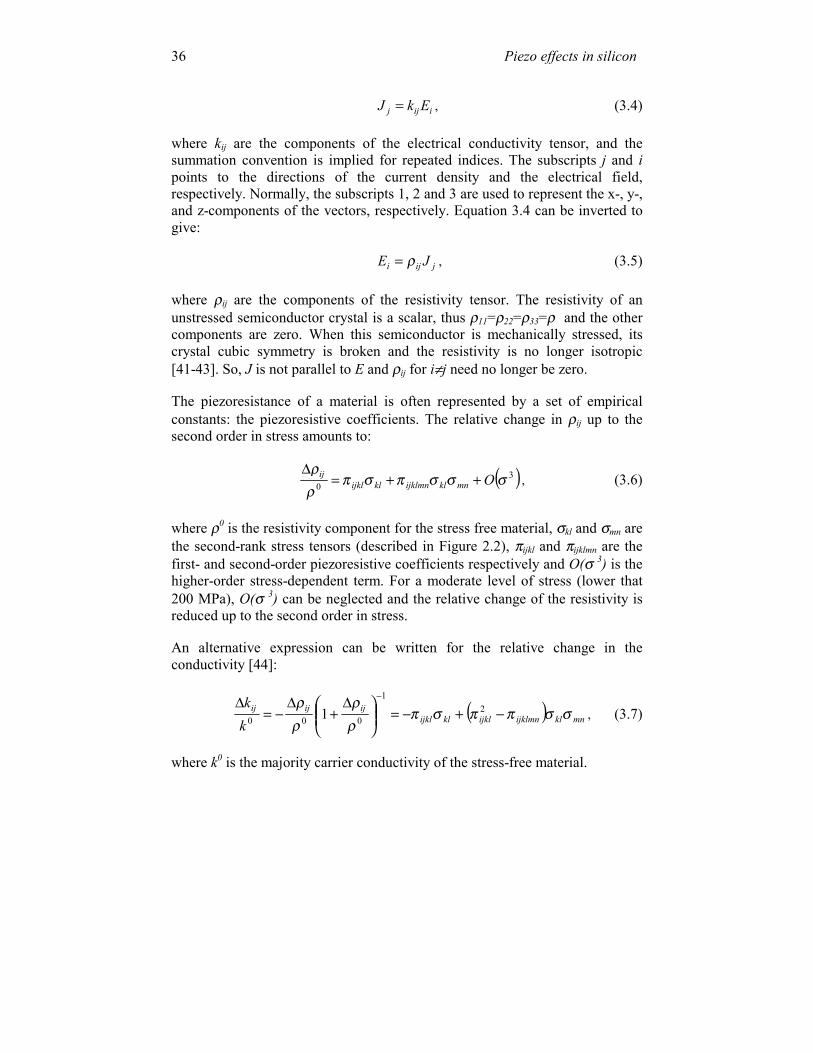
3.3.2 Piezoresistive coefficients The symmetry of the diamond structure reduces the number of first-order piezoresistance coefficients πijkl to three and second-order piezoresistance coefficients πijklmn to nine. Normally, a convention contraction is used to reduce the complexities of the index labels through a renumbering scheme using the six-component notation (suffixes change from 11, 22, 33, 23, 13 and 12 to 1, 2, 3, 4, 5 and 6 respectively). Table 3.1 shows the three first-order piezoresistive coefficients (FOPR) and nine second-order piezoresistive coefficients (SOPR) and their correspondents [44, 45]. Table 3.1: The independent first- and second-order piezoresistance tensor
components of a cubic crystal. FOPR πilkl SOPR πilklmn π11=π22=π33 π111=π222=π333
π12=π21=π13=π31=π23=π32 π112=π113=π212=π223=π313=π323 π44=π55=π66 π122=π211=π133=π311=π233=π322
π123=π213=π312 π144=π255=π366 π166=π155=π244=π266=π344=π355 π616=π626=π515=π535=π424=π434 π414=π525=π636 π456=π546=π645
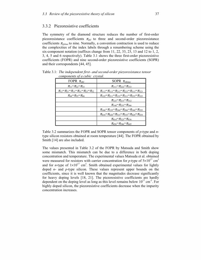
Table 3.2 summarizes the FOPR and SOPR tensor components of p-type and n-type silicon resistors obtained at room temperature [44]. The FOPR obtained by Smith [14] are also included. The values presented in Table 3.2 of the FOPR by Matsuda and Smith show some mismatch. This mismatch can be due to a difference in both doping concentration and temperature. The experimental values Matsuda et al. obtained were measured for resistors with carrier concentration for p-type of 5×1017 cm3 and for n-type of 1×1017 cm3. Smith obtained experimental values for lightly doped n- and p-type silicon. These values represent upper bounds on the coefficients, since it is well known that the magnitudes decrease significantly for heavy doping levels [18, 21]. The piezoresistive coefficients are hardly dependent on the doping level as long as this level remains below 1017 cm-3. For highly doped silicon, the piezoresistive coefficients decrease when the impurity concentration increases.
Piezo effects in silicon 38
Table 3.2: The piezoresistance tensor components of Silicon at room temperature.
p type n type Matsuda [44] Smith [14] Matsuda [44] Smith [14]
FOPR [10-10 Pa-1] π11 -0.6 0.7 -7.7 -10.2 π12 0.1 -0.1 3.9 5.3 π44 11.2 13.8 -1.4 -1.4
SOPR [10-19 Pa-2] π111 -0.2 7.7 π112 0.3 -3.5 π122 -0.7 -3.6 π123 0.1 6.9 π144 -4.7 0.1 π166 10.1 0.3 π616 -2.6 -0.2 π414 0.3 π456 0.3
π414 + π456 5.6
The dependence of the piezoresistive coefficients on impurity concentrations for different temperatures has been studied by Kanda [21]. In a doping concentration below 1018 cm-3 the piezoresistive coefficients strongly depend on the temperature. Between –50 °C and +150 °C for both p- and n-type material the FOPR decrease with increasing temperature by approximately:
=Tijkl
ijkl δδπ
π1 -3×10⁻³ /°C.
The temperature dependence of the piezoresistive coefficients is reduced for highly doped silicon [21]. 3.3.3 Off-axis longitudinal and transversal piezoresistive
coefficients The piezoresistive coefficients for any arbitrary crystallographic orientation of uniaxial stress and direction of current can be derived from a complete set of

3.4 Piezojunction effect
39
tensor components by a coordinate transformation. The coordinate transformation is described in Appendix A. Two typical piezoresistance effects can be considered for a material subjected to stress. One is a longitudinal piezoresistance coefficient when the current and field are in the direction of the stress, denoted by πL. The other is a transverse piezoresistance coefficient when the current and field are perpendicular to the stress, denoted by πT. The longitudinal and transversal piezoresistive coefficients for an arbitrary direction are given by [44]:
( )( )2
121
21
21
21
2144121111 2 nmnlmlL ++−−−= πππππ (3.8)
and
( )( )2
221
22
21
22
2144121112 nnmmllT ++−−+= πππππ , (3.9)
where li, mi and ni are the direction cosines of the transformation of the coordinate system defined in Appendix A. The transformations of the SOPR coefficients are described in Appendix C. 3.4 Piezojunction effect The piezojunction effect concerns the change of the exponential characteristic of a p-n junction caused by mechanical stress. This is also an anisotropic effect having many physical similarities to the piezoresistive effect. The piezojunction effect is also caused by a change in conductivity, but only the minority charge carriers contribute to this conductivity. An empirical model to describe the piezojunction effect is presented. 3.4.1 Stress-induced change in the saturation current For a bipolar transistor at moderated current level and zero at base-collector voltage, the well-known equation for the collector current IC is:
=
TkqVII
B
BESC exp , (3.10)
Piezo effects in silicon 40
where T is the absolute temperature, VBE the base-emitter voltage, q the electron charge, kB the Boltzmann constant and IS the saturation current. For NPN transistors IS is:
( )
B
pn
pB
ES QpnTkAI µ0= , (3.11)
where AE is the emitter area, QB the Gummel number, ( )ppn 0 the product of hole and electron concentration in thermal equilibrium in the p-base and p
nµ the electron mobility in the p-base. A similar equation can also be written for PNP transistors. At a moderate stress level, i.e. lower than 200 MPa, the geometrical deformations in AE and QB are so small that they can be ignored [48]. On the other hand, owing to the silicon energy-band deformation, the product p
npn µ0 is
modified by mechanical stress and consequently, the saturation current is changed. In analogy to Equation 3.3 we can therefore define the conductivity for the minority carrier κ, which is given by:
pn
ppn qn µκκ 0== . (3.12)
If we consider that the stress-induced change in κ is the main reason why IS changes, then the change in IS can be approximated by the change in κ:
00 κκ∆≅∆
S
S
II
, (3.13)
where 0
SI and κ0 are the stress-free saturation current and minority-carrier conductivity, respectively. Equation 3.7 shows the relative change in the majority-carrier conductivity k related to the piezoresistive coefficients. For the minority-carrier conductivity κ, a similar equation can be written, where the piezoresistive coefficients πijkl and πijklmn are replaced by the new piezojunction coefficients ζijkl and ζijklmn, respectively. The piezojunction coefficients are defined for the change in the semiconductor transport properties for minority carriers. These coefficients are
3.4 Piezojunction effect
41
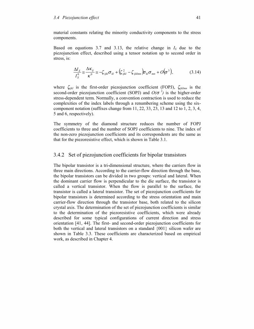
material constants relating the minority conductivity components to the stress components. Based on equations 3.7 and 3.13, the relative change in IS due to the piezojunction effect, described using a tensor notation up to second order in stress, is:
( ) ( )3200 σσσζζσζ
κκ
OII
mnklijklmnijklklijklij
S
S +−+−≅∆
≅∆, (3.14)
where ζijkl is the first-order piezojunction coefficient (FOPJ), ζijklmn is the second-order piezojunction coefficient (SOPJ) and O(σ 3) is the higher-order stress-dependent term. Normally, a convention contraction is used to reduce the complexities of the index labels through a renumbering scheme using the six-component notation (suffixes change from 11, 22, 33, 23, 13 and 12 to 1, 2, 3, 4, 5 and 6, respectively). The symmetry of the diamond structure reduces the number of FOPJ coefficients to three and the number of SOPJ coefficients to nine. The index of the non-zero piezojunction coefficients and its correspondents are the same as that for the piezoresistive effect, which is shown in Table 3.1. 3.4.2 Set of piezojunction coefficients for bipolar transistors The bipolar transistor is a tri-dimensional structure, where the carriers flow in three main directions. According to the carrier-flow direction through the base, the bipolar transistors can be divided in two groups: vertical and lateral. When the dominant carrier flow is perpendicular to the die surface, the transistor is called a vertical transistor. When the flow is parallel to the surface, the transistor is called a lateral transistor. The set of piezojunction coefficients for bipolar transistors is determined according to the stress orientation and main carrier-flow direction through the transistor base, both related to the silicon crystal axis. The determination of the set of piezojunction coefficients is similar to the determination of the piezoresistive coefficients, which were already described for some typical configurations of current direction and stress orientation [41, 44]. The first- and second-order piezojunction coefficients for both the vertical and lateral transistors on a standard 001 silicon wafer are shown in Table 3.3. These coefficients are characterized based on empirical work, as described in Chapter 4.
Piezo effects in silicon 42
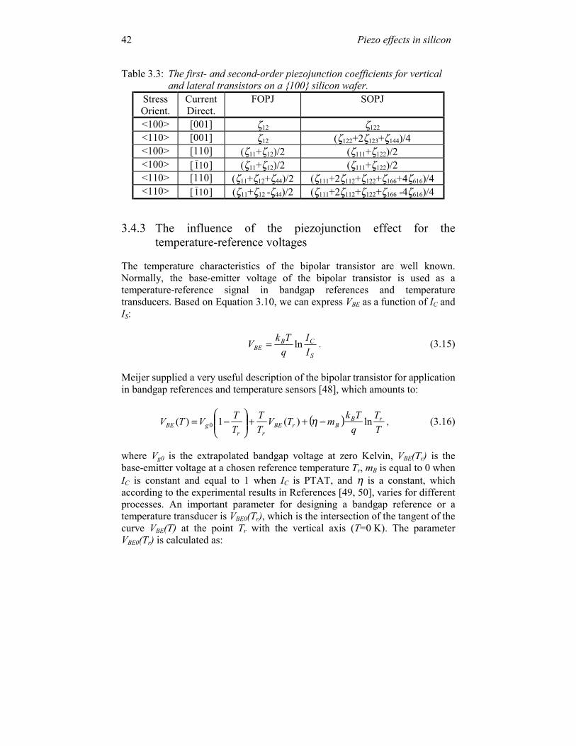
Table 3.3: The first- and second-order piezojunction coefficients for vertical and lateral transistors on a 100 silicon wafer.
Stress Orient.
Current Direct.
FOPJ SOPJ
<100> [001] ζ12 ζ122 <110> [001] ζ12 (ζ122+2ζ123+ζ144)/4 <100> [110] (ζ11+ζ12)/2 (ζ111+ζ122)/2 <100> [ 101
_] (ζ11+ζ12)/2 (ζ111+ζ122)/2
<110> [110] (ζ11+ζ12+ζ44)/2 (ζ111+2ζ112+ζ122+ζ166+4ζ616)/4 <110> [ 101
_] (ζ11+ζ12 -ζ44)/2 (ζ111+2ζ112+ζ122+ζ166 -4ζ616)/4
3.4.3 The influence of the piezojunction effect for the
temperature-reference voltages The temperature characteristics of the bipolar transistor are well known. Normally, the base-emitter voltage of the bipolar transistor is used as a temperature-reference signal in bandgap references and temperature transducers. Based on Equation 3.10, we can express VBE as a function of IC and IS:
S
CBBE I
IqTkV ln= . (3.15)
Meijer supplied a very useful description of the bipolar transistor for application in bandgap references and temperature sensors [48], which amounts to:
( )TT
qTkmTV
TT
TTVTV rB
BrBErr
gBE ln)(1)( 0 −++
−= η , (3.16)
where Vg0 is the extrapolated bandgap voltage at zero Kelvin, VBE(Tr) is the base-emitter voltage at a chosen reference temperature Tr, mB is equal to 0 when IC is constant and equal to 1 when IC is PTAT, and η is a constant, which according to the experimental results in References [49, 50], varies for different processes. An important parameter for designing a bandgap reference or a temperature transducer is VBE0(Tr), which is the intersection of the tangent of the curve VBE(T) at the point Tr with the vertical axis (T=0 K). The parameter VBE0(Tr) is calculated as:
3.4 Piezojunction effect
43
( ) ( )qTkmVTV rB
BgrBE −+= η00 . (3.17)
In the same work, Meijer identified the mechanical-electric interaction as the dominant factor limiting the accuracy of bandgap references and temperature transducers. The stress-induced change in the saturation current caused by the piezojunction effect direct affects the base-emitter voltage. Based on Equation 3.15, the stress-induced change in VBE is:
( )
∆+−=∆ 01ln
S
SBBE I
IqTkV σ , (3.18)
where the change in the saturation current according to the piezojunction coefficients is given in Equation 3.14. We observe in Equation 3.18 that ∆VBE(σ) is proportional to the thermal voltage kBT/q. If VBE is used as a temperature reference signal, stress will cause an equivalent error in the reading temperature. This error is given by:
( )
( )( )rBEBEr
BETVBE
TVVT
V
−
∆=Ε0
)(
1σσ . (3.19)
Another important signal used as a temperature reference is the difference between the base-emitter voltages of a matched pair of transistors operated at unequal emitter-current densities. This differential voltage is Proportional To the Absolute Temperature (PTAT) [48]. When the ratio r (r≠1) of the current densities is constant, the PTAT voltage of two transistors Q1 and Q2 amounts to:
rqTk
II
qTk
IpI
qTkIVpIVV B
S
CB
S
CBCBECBEPTAT lnlnln)()(
2121 =
−
=−= , (3.20)
where VBEi and ISi are the base-emitter voltage and saturation current of the transistor Qi. This equation shows that VPTAT is, next to the constants kB and q, only dependent on T and the current-density ratio r.
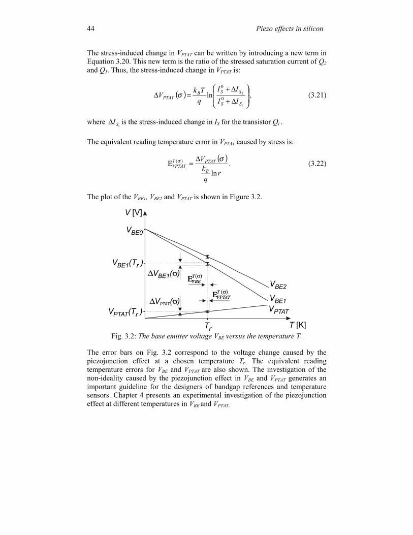
Piezo effects in silicon 44
The stress-induced change in VPTAT can be written by introducing a new term in Equation 3.20. This new term is the ratio of the stressed saturation current of Q2 and Q1. Thus, the stress-induced change in VPTAT is:
( )
∆+∆+
=∆1
2
0
0
lnSS
SSBPTAT II
IIqTkV σ , (3.21)
where
iSI∆ is the stress-induced change in IS for the transistor Qi . The equivalent reading temperature error in VPTAT caused by stress is:
( )r
qk
VB
PTATTVPTAT
ln
)( σσ ∆=Ε . (3.22)
The plot of the VBE1, VBE2 and VPTAT is shown in Figure 3.2.
TVPTATΕ
TVBEΕ
VBE0
V [V]
T [K]
V (T )BE1 r
V (T )PTAT r
∆ σV ( )BE1
∆ σV ( )PTAT
Tr
VBE1
VBE2
VPTAT
TVPTATΕ
TVBEΕ ( )σ
( )σ
Fig. 3.2: The base emitter voltage VBE versus the temperature T.
The error bars on Fig. 3.2 correspond to the voltage change caused by the piezojunction effect at a chosen temperature Tr. The equivalent reading temperature errors for VBE and VPTAT are also shown. The investigation of the non-ideality caused by the piezojunction effect in VBE and VPTAT generates an important guideline for the designers of bandgap references and temperature sensors. Chapter 4 presents an experimental investigation of the piezojunction effect at different temperatures in VBE and VPTAT.

References
45
References [1] S. Middelhoek, J.B. Angell and D.J.W. Noorlag, Microprocessors get
integrated sensors, IEEE Spectrum, 17, pp. 42-46, 1980. [2] S. Middelhoek and D.J.W. Noorlag, Signal conversion in solid-state
transducers, Sensors and Actuators, 2, pp. 211-228, 1982. [3] A.P. Friedrich, Silicon piezo-tunneling strain sensor, PhD Thesis, Swiss
Federal Institute of Technology EPFL, Switzerland, 1999. [4] D. Manic, Instability of silicon integrated sensors and circuits caused by
thermo-mechanical stress, PhD Thesis, Swiss Federal Institute of Technology EPFL, Switzerland, 2000.
[5] H. Hall, J. Bardeen, and G. Pearson, The effects of pressure and temperature on the resistance of p-n junctions in germanium, Phys. Rev.,84, pp. 129-132, 1951.
[6] W. Rindner, Resistence of elastically deformed shallow p-n junctions, J. Appl. Phys., 33, pp. 2479-2480, 1962.
[7] W. Rindner and I. Braun, Resistance of elastically deformed shallow p-n junctions, II., J. Appl. Phys., 34 1958-1970, 1963.
[8] T. Imai, M. Uchida, H. Sato and A. Kobayashi, Effect of uniaxial stress on germanium p-n junctions, Japan. J. Appl. Phys., 4, pp. 102-113, 1965.
[9] K. Bulthuis, Effect of local pressure on germanium p-n junctions, J. Appl. Phys., 37, pp. 2066-2068, 1966.
[10] R.H. Mattson, L.D. Yau, and J.R. DuBois, Incremental stress effects in transistors, Solid-St. Electron., 10, pp. 241-251, 1967.
[11] L.K. Monteith and J.J. Wortman, Characterization of p-n junctions under the influence of a time varying mechanical strain, Solid-St. Electron., 16, pp. 229-237, 1973.
[12] J.J. Wortman, J. R. Hauser, and R. M. Burger, Effect of mechanical stress on p-n junction device characteristics, J. Appl. Phys., 35, pp. 2122-2131, 1964.
[13] Y. Kanda, Effect of stress on germanium and silicon p-n junctions, Jpn. J. Appl. Phys., 6, pp. 475-486, pp. 1967.
[14] C.S. Smith, Piezoresistance effect in germanium and silicon, Phys. Rev., 94, pp. 42-49, 1954.
[15] E.N. Adams, Elastoresistance in p-type Ge and Si, Phys. Rev., 96, pp. 803-804, 1954.
[16] W.P. Mason and R.N. Thurston, Use of piezoresistive materials in the measurement of displacement, force, torque, J. Acc. Soc. Am., 29, pp. 1906-1101, 1957.
[17] F.J. Morin, T.H. Geballe and C. Herring, Temperature dependence of piezoresistance of high purity silicon and germanium, Phys. Rev., 105, pp. 525-539, 1957.
Piezo effects in silicon 46
[18] O.N. Tufte and E.L. Stetzer, Piezoresistive properties of silicon diffused layers, J. Appl. Phys., 34, pp. 313-318, 1963.
[19] O.N. Tufte, P.W. Chapman and D. Long, Silicon-diffused-element piezoresistive diaphragms, J. Appl. Phys., 33, pp. 3322-3327, 1962.
[20] A.C.M. Gieles, Subminiature silicon pressure transducer, Digest, IEEE ISSCC, Philadelphia, , pp. 108-109, 1969.
[21] Y. Kanda, A graphical representation of the piezoresistance coefficients in silicon, IEEE Trans. on electron devices, ed-29, n 1, Jan. 1982.
[22] Y. Kanda, Piezoresistance effect of silicon, Sensors and Actuators A, vol. 28, pp. 83-91, 1991.
[23] R.C. Jaeger, R. Ramanathan and J.C. Suhling, Effects of stress-induced mismatches on CMOS analogue circuits, Proceedings of International VLSI TSA Symposium, Taipei, Taiwan, pp. 354-360, 1995.
[24] A.P. Dorey and T.S. Maddern, The effect of strain on MOS transistors, Solid-State Electronics, vol. 12, pp. 185-189, 1969.
[25] H. Takao, Y. Matsumoto, and M. Ishida, Stress-sensitive differential amplifiers using piezoresistance effects of MOSFETs and their application to three-axial accelerometers, Sensors and Actuators, vol A65, pp. 61-68, 1998.
[26] A. Hamata, T. Furusawa, N. Saito and E. Takeda, A new aspect of mechanical stress effects in scaled MOS devices, IEEE Transactions on Electron Devices, vol. 38, pp. 895-900, 1991.
[27] H. Miura, S. Ikeda and N. Suzuki, Effect of mechanical stress on reliability of gate-oxide film in MOS transistors, Proceedings of International Electron Devices Meeting – IEDM, pp. 743-746, 1996.
[28] H. Tuinhouf and M. Vertregt, Test structures for investigation of metal coverage effects on MOSFET matching, Proceedings of IEEE International Conference on Microelectronic Test Structures, 1997.
[29] A.P. Friedrich, P.A. Besse, E. Fullin, and R.S. Popovic, Lateral backward diodes as strain sensors, Proceedings of International Electron Device Meeting (IEDM 95), Washington DC, USA, , pp. 597-600, 1995.
[30] S. Bellekom, Origins of offset in conventional and spinning-current Hall plates, Ph.D. Thesis, Delft University of Technology, Delft, The Netherlands, 1998.
[31] R.S. Popovic, Hall effect devices, Bristol: Adam Hilger, 1991. [32] B. Halg, Piezo-Hall coefficients of n-type silicon, J. Appl. Phys., vol. 64,
pp. 276-282, 1988. [33] F. Creemer and P.J. French, The piezojunction effect in silicon and its
applications to sensors and circuits, Proc. 1st annual workshop on Semiconductor Sensor and Actuator Technology (SeSens 2000), Veldhoven, the Netherlands, 1, pp. 627-631, Dec. 2000.
References
47
[34] J.F. Creemer and P.J. French, The orientation dependence of the piezojunction effect in bipolar transistors, Proc. 30th European Solid-State Device Research Conference (ESSDERC 2000), Cork, Ireland, 11-13, pp. 416-419, Sep. 2000.
[35] J.F. Creemer and P.J. French, The piezojunction effect in bar transistors at moderate stress levels: a theoretical and experimental study, Sensors and Actuators, A82, pp. 181-185, 2000.
[36] J.F. Creemer and P.J. French, The piezojunction effect in mechanical and bandgap sensors, Proc. 2nd annual workshop on Semiconductor Advances for Future Electronics (SAFE99), Mierlo, the Netherlands, 24-25, pp. 105-110, Nov. 1999.
[37] J.F. Creemer and P.J. French, Theoretical and experimental study of the piezojunction effect in bipolar transistors under moderate stress levels, Dig. 10th International Conference on Solid-State Sensors and Actuators (Transducers’99), Sendai, Japan, Vol. 1, pp. 204-208, Jun. 1999.
[38] W. Thomson (Lord Kelvin), On the electrodynamic qualities of metals, Proc. Royal Society, pp 546-550, 1857.
[39] S. Middelhoek, S.A. Audet and P.J. French, Silicon Sensors, Faculty of Information Technology and Systems, Delft University of Technology, Laboratory for Electronic Instrumentation, The Netherlands, 2000.
[40] J.F. Creemer and P.J. French, Reduction of uncertainty in the measurement of the piezoresistive coefficients of silicon with a three-element rosette, SPIE Conference on Smart Electronics and MEMS, San Diego, USA, 1998.
[41] J.F. Nye, Physical properties of crystals, Clarendon Press, Oxford, 1985. [42] G.L. Bir and G.E. Pikus, Symmetry and strain-induced effects in
semiconductors, Wiley, New York, 1974. [43] C.S. Smith, Macroscopic symmetry and properties of crystals, in F. Seitz
and D. Turnbull (ed.), Solid State Physics, Vol. 6, Academic Press, New York, pp.175-249, 1958.
[44] K. Matsuda, K. Suzuki, K. Yamamura, and Y. Kanda, Nonlinear piezoresistive coeficients in silicon, J. Appl. Phys., 73, 1838-1847, 1993.
[45] J.T. Lenkkeri, Nonlinear effects in the piezoresistivity of p-type resistivity, Phys. Status Solidi B, 136, pp. 373-385, 1986.
[46] O.N. Tufte and E.L. Stetzer, Piezoresistive properties of silicon diffused layers, J. Appl. Phys., 34, pp. 313-318, 1963.
[47] H. Mikoshiba and Y. Tomita, Piezoresistance as the source of stress-induced changes of current gain in bipolar transistors, Solid-State Electron., 25, (3), pp. 197-199, 1982.
[48] G.C.M. Meijer, Integrated circuits and components for bandgap references and temperature transducers, Ph.D. Thesis, Delft University of Technology, Delft, The Netherlands, 1982.
Piezo effects in silicon 48
[49] G.C.M. Meijer, Measurement of the temperature dependence of the IC(VBE) characteristics of integrated bipolar transistors, IEEE J. Solid-State Circuits SC-15 (2), pp. 237-240, Apr. 1980.
[50] A. Ohte, M. Yamahata, A precision silicon transistor thermometer, IEEE Trans. Instrum. Meas. IM-26 (4), pp. 335-341, Dec. 1977.
49
Chapter 4
Characterization of the piezojunction effect 4.1 Introduction This chapter characterizes the piezojunction effect based on experimental tests performed on vertical NPN transistors (V-NPN), vertical PNP transistors (V-PNP) and lateral PNP transistors (L-PNP). These transistors have been produced using a standard 001 oriented silicon wafer plane. The results of this work are used to extract the piezojunction coefficients and their temperature dependence. These results can be applied for two main purposes: firstly, to define the strategies to reduce the influence of the mechanical stress on the accuracy of analogue integrated circuits and secondly, to optimize the design of the transistors in such a way that they can be used for mechanical stress-sensing elements. 4.2 Vertical transistors The vertical transistor action takes place vertically (perpendicular to the wafer plane), in the base region beneath the emitter. The main advantage of the vertical transistor has over the lateral transistor is that the current does not flow
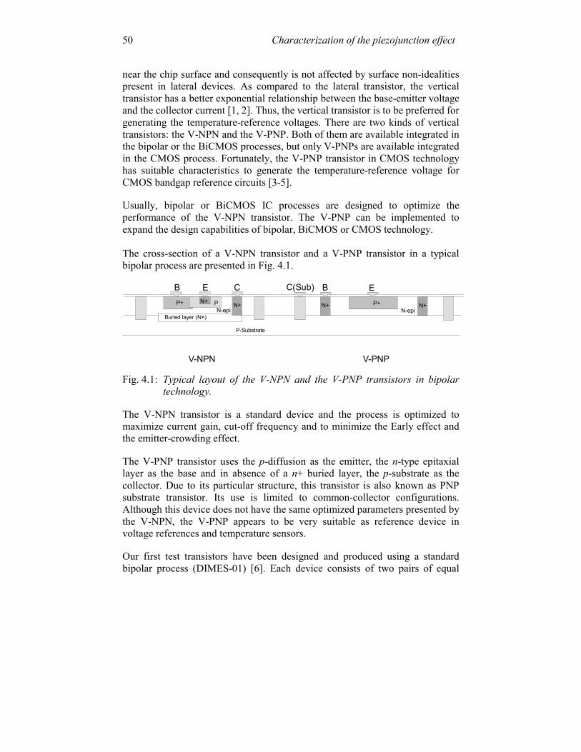
Characterization of the piezojunction effect 50
near the chip surface and consequently is not affected by surface non-idealities present in lateral devices. As compared to the lateral transistor, the vertical transistor has a better exponential relationship between the base-emitter voltage and the collector current [1, 2]. Thus, the vertical transistor is to be preferred for generating the temperature-reference voltages. There are two kinds of vertical transistors: the V-NPN and the V-PNP. Both of them are available integrated in the bipolar or the BiCMOS processes, but only V-PNPs are available integrated in the CMOS process. Fortunately, the V-PNP transistor in CMOS technology has suitable characteristics to generate the temperature-reference voltage for CMOS bandgap reference circuits [3-5]. Usually, bipolar or BiCMOS IC processes are designed to optimize the performance of the V-NPN transistor. The V-PNP can be implemented to expand the design capabilities of bipolar, BiCMOS or CMOS technology. The cross-section of a V-NPN transistor and a V-PNP transistor in a typical bipolar process are presented in Fig. 4.1.
EB EC BC(Sub)
N+ N+N+P+ P+N-epi N-epi
P-Substrate
Buried layer (N+)
PN+
V-NPN V-PNP
Fig. 4.1: Typical layout of the V-NPN and the V-PNP transistors in bipolar technology.
The V-NPN transistor is a standard device and the process is optimized to maximize current gain, cut-off frequency and to minimize the Early effect and the emitter-crowding effect. The V-PNP transistor uses the p-diffusion as the emitter, the n-type epitaxial layer as the base and in absence of a n+ buried layer, the p-substrate as the collector. Due to its particular structure, this transistor is also known as PNP substrate transistor. Its use is limited to common-collector configurations. Although this device does not have the same optimized parameters presented by the V-NPN, the V-PNP appears to be very suitable as reference device in voltage references and temperature sensors. Our first test transistors have been designed and produced using a standard bipolar process (DIMES-01) [6]. Each device consists of two pairs of equal
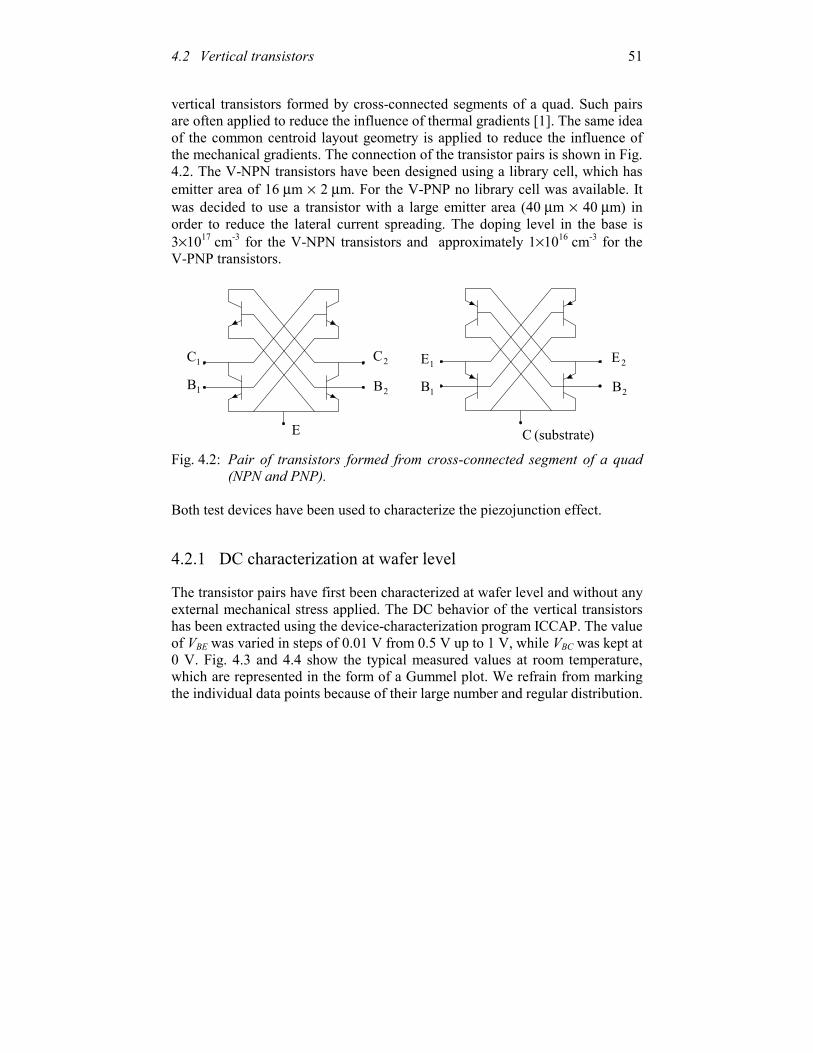
4.2 Vertical transistors 51
vertical transistors formed by cross-connected segments of a quad. Such pairs are often applied to reduce the influence of thermal gradients [1]. The same idea of the common centroid layout geometry is applied to reduce the influence of the mechanical gradients. The connection of the transistor pairs is shown in Fig. 4.2. The V-NPN transistors have been designed using a library cell, which has emitter area of 16 µm × 2 µm. For the V-PNP no library cell was available. It was decided to use a transistor with a large emitter area (40 µm × 40 µm) in order to reduce the lateral current spreading. The doping level in the base is 3×1017 cm-3 for the V-NPN transistors and approximately 1×1016 cm-3 for the V-PNP transistors.
1C 2C
1B 1B 2B2B
E
1E 2E
)(substrate C
Fig. 4.2: Pair of transistors formed from cross-connected segment of a quad (NPN and PNP).
Both test devices have been used to characterize the piezojunction effect. 4.2.1 DC characterization at wafer level The transistor pairs have first been characterized at wafer level and without any external mechanical stress applied. The DC behavior of the vertical transistors has been extracted using the device-characterization program ICCAP. The value of VBE was varied in steps of 0.01 V from 0.5 V up to 1 V, while VBC was kept at 0 V. Fig. 4.3 and 4.4 show the typical measured values at room temperature, which are represented in the form of a Gummel plot. We refrain from marking the individual data points because of their large number and regular distribution.
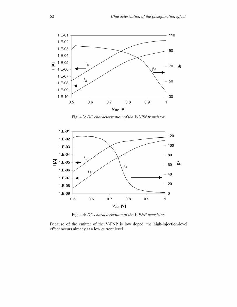
Characterization of the piezojunction effect 52
1.E-10
1.E-09
1.E-08
1.E-07
1.E-06
1.E-05
1.E-04
1.E-03
1.E-02
1.E-01
0.5 0.6 0.7 0.8 0.9 1
V BE [V]
I [A]
30
50
70
90
110
β βββ F
I C
I B
βF
Fig. 4.3: DC characterization of the V-NPN transistor.
1.E-09
1.E-08
1.E-07
1.E-06
1.E-05
1.E-04
1.E-03
1.E-02
1.E-01
0.5 0.6 0.7 0.8 0.9 1
V BE [V]
I [A]
0
20
40
60
80
100
120
β βββ F
βF
I C
I B
Fig. 4.4: DC characterization of the V-PNP transistor.
Because of the emitter of the V-PNP is low doped, the high-injection-level effect occurs already at a low current level.
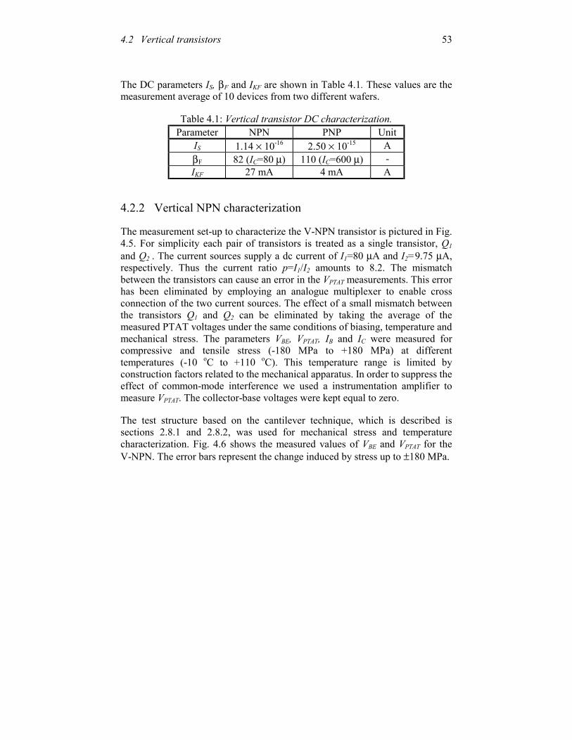
4.2 Vertical transistors 53
The DC parameters IS, βF and IKF are shown in Table 4.1. These values are the measurement average of 10 devices from two different wafers.
Table 4.1: Vertical transistor DC characterization. Parameter NPN PNP Unit
IS 1.14 × 10⁻¹⁶ 2.50 × 10⁻¹⁵ A βF 82 (IC=80 µ) 110 (IC=600 µ) - IKF 27 mA 4 mA A
4.2.2 Vertical NPN characterization The measurement set-up to characterize the V-NPN transistor is pictured in Fig. 4.5. For simplicity each pair of transistors is treated as a single transistor, Q1 and Q2 . The current sources supply a dc current of I1=80 µA and I2=9.75 µA, respectively. Thus the current ratio p=I1/I2 amounts to 8.2. The mismatch between the transistors can cause an error in the VPTAT measurements. This error has been eliminated by employing an analogue multiplexer to enable cross connection of the two current sources. The effect of a small mismatch between the transistors Q1 and Q2 can be eliminated by taking the average of the measured PTAT voltages under the same conditions of biasing, temperature and mechanical stress. The parameters VBE, VPTAT, IB and IC were measured for compressive and tensile stress (-180 MPa to +180 MPa) at different temperatures (-10 oC to +110 oC). This temperature range is limited by construction factors related to the mechanical apparatus. In order to suppress the effect of common-mode interference we used a instrumentation amplifier to measure VPTAT. The collector-base voltages were kept equal to zero. The test structure based on the cantilever technique, which is described is sections 2.8.1 and 2.8.2, was used for mechanical stress and temperature characterization. Fig. 4.6 shows the measured values of VBE and VPTAT for the V-NPN. The error bars represent the change induced by stress up to ±180 MPa.
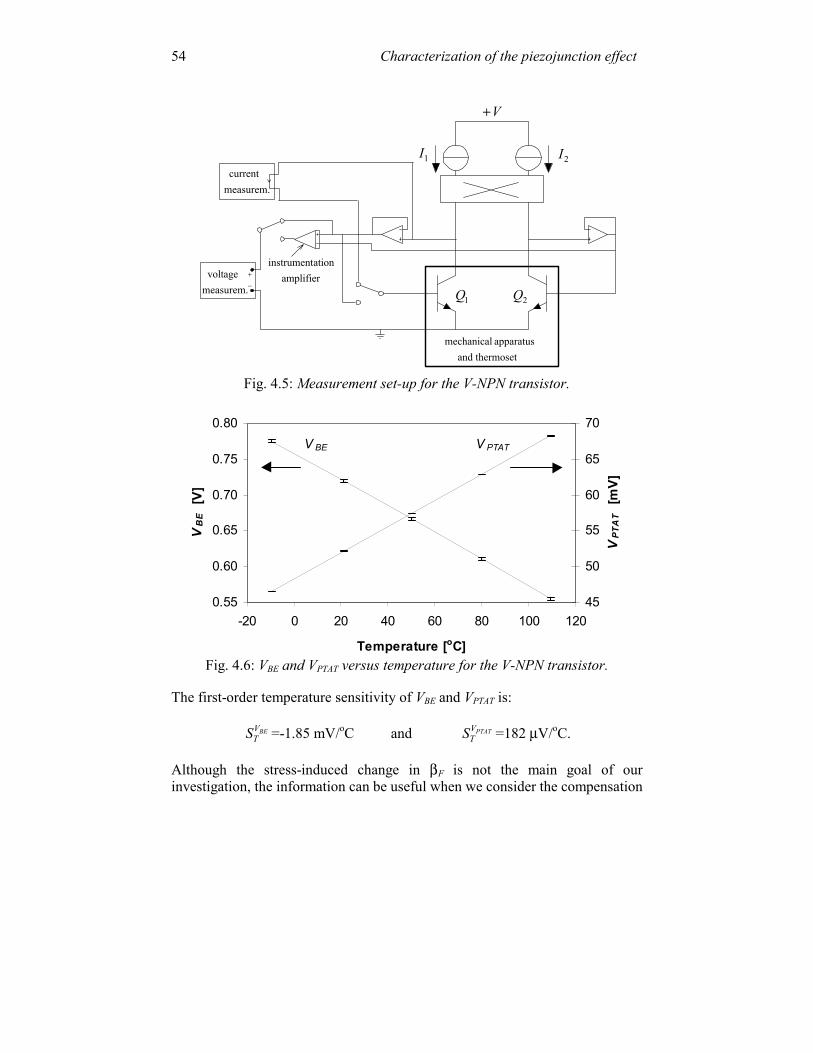
Characterization of the piezojunction effect 54
1I 2I
1Q 2Q+−
thermosetand apparatus mechanical
V+
measurem. current
measurem. voltage amplifier
ationinstrument
Fig. 4.5: Measurement set-up for the V-NPN transistor.
0.55
0.60
0.65
0.70
0.75
0.80
-20 0 20 40 60 80 100 120
Temperature [oC]
VB
E [
V]
45
50
55
60
65
70
VPT
AT [
mV]
V BE V PTAT
Fig. 4.6: VBE and VPTAT versus temperature for the V-NPN transistor.
The first-order temperature sensitivity of VBE and VPTAT is:
BEVTS =-1.85 mV/oC and PTATV
TS =182 µV/oC. Although the stress-induced change in βF is not the main goal of our investigation, the information can be useful when we consider the compensation
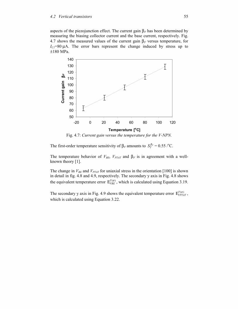
4.2 Vertical transistors 55
aspects of the piezojunction effect. The current gain βF has been determined by measuring the biasing collector current and the base current, respectively. Fig. 4.7 shows the measured values of the current gain βF versus temperature, for IC1=80 µA. The error bars represent the change induced by stress up to ±180 MPa.
50
60
7080
90
100110120
130140
-20 0 20 40 60 80 100 120
Temperature [oC]
Curr
ent g
ain
β βββF
Fig. 4.7: Current gain versus the temperature for the V-NPN.
The first-order temperature sensitivity of βF amounts to F
TS β = 0.55 /oC. The temperature behavior of VBE, VPTAT and βF is in agreement with a well-known theory [1]. The change in VBE and VPTAT for uniaxial stress in the orientation [100] is shown in detail in fig. 4.8 and 4.9, respectively. The secondary y axis in Fig. 4.8 shows the equivalent temperature error )(σT
VBEΕ , which is calculated using Equation 3.19. The secondary y axis in Fig. 4.9 shows the equivalent temperature error )(σT
VPTATΕ , which is calculated using Equation 3.22.
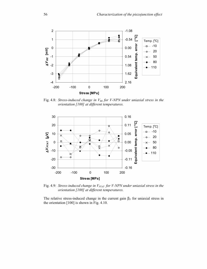
Characterization of the piezojunction effect 56
-4
-3
-2
-1
0
1
2
-200 -100 0 100 200
Stress [MPa]
∆ ∆∆∆V
BE [
mV]
-1.08
-0.54
0.00
0.54
1.08
1.62
2.16
Equi
vale
nt te
mp.
err
or [
o C]
-10 20 50 80110
Temp. [oC]
Fig. 4.8: Stress-induced change in VBE for V-NPN under uniaxial stress in the
orientation [100] at different temperatures.
-30
-20
-10
0
10
20
30
-200 -100 0 100 200
Stress [MPa]
∆ ∆∆∆V
PTA
T [
µ µµµV]
-0.16
-0.11
-0.05
0.00
0.05
0.11
0.16
Equi
vale
nt te
mp.
err
or [
o C] -10 20 50 80110
Temp. [oC]
Fig. 4.9: Stress-induced change in VPTAT for V-NPN under uniaxial stress in the
orientation [100] at different temperatures. The relative stress-induced change in the current gain βF for uniaxial stress in the orientation [100] is shown in Fig. 4.10.
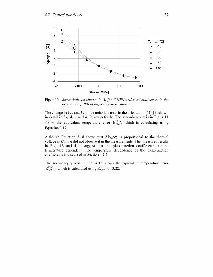
4.2 Vertical transistors 57
-4
-2
0
2
4
6
8
10
-200 -100 0 100 200
Stress [MPa]
∆β
∆β
∆β
∆β F
/β /β/β/βF
[%] -10
20 50 80110
Temp. [oC]
Fig. 4.10: Stress-induced change in βF for V-NPN under uniaxial stress in the
orientation [100] at different temperatures. The change in VBE and VPTAT for uniaxial stress in the orientation [110] is shown in detail in fig. 4.11 and 4.12, respectively. The secondary y axis in Fig. 4.11 shows the equivalent temperature error )(σT
VBEΕ , which is calculating using Equation 3.19. Although Equation 3.18 shows that ∆VBE(σ) is proportional to the thermal voltage kBT/q, we did not observe it in the measurements. The measured results in Fig. 4.8 and 4.11 suggest that the piezojunction coefficients can be temperature dependent. The temperature dependence of the piezojunction coefficients is discussed in Section 4.2.5. The secondary y axis in Fig. 4.12 shows the equivalent temperature error
)(σTVPTATΕ , which is calculated using Equation 3.22.
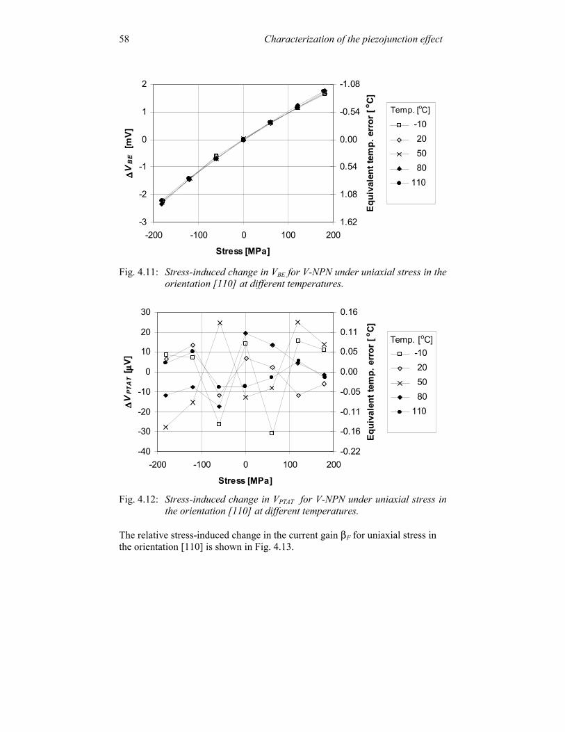
Characterization of the piezojunction effect 58
-3
-2
-1
0
1
2
-200 -100 0 100 200
Stress [MPa]
∆ ∆∆∆V
BE [
mV]
-1.08
-0.54
0.00
0.54
1.08
1.62
Equi
vale
nt te
mp.
err
or [
o C]
-10 20 50 80110
Temp. [oC]
Fig. 4.11: Stress-induced change in VBE for V-NPN under uniaxial stress in the
orientation [110] at different temperatures.
-40
-30
-20
-10
0
10
20
30
-200 -100 0 100 200
Stress [MPa]
∆ ∆∆∆V
PTA
T [ µ µµµ
V]
-0.22
-0.16
-0.11
-0.05
0.00
0.05
0.11
0.16
Equi
vale
nt te
mp.
err
or [
o C]
-10 20 50 80110
Temp. [oC]
Fig. 4.12: Stress-induced change in VPTAT for V-NPN under uniaxial stress in
the orientation [110] at different temperatures. The relative stress-induced change in the current gain βF for uniaxial stress in the orientation [110] is shown in Fig. 4.13.
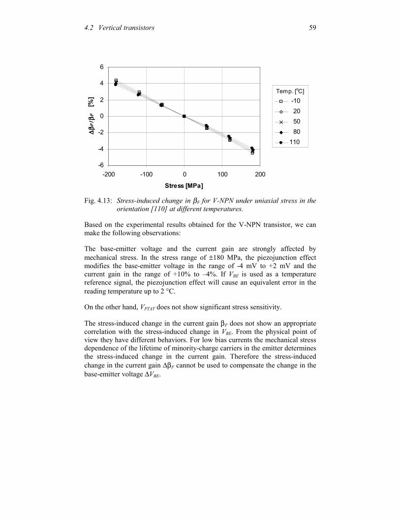
4.2 Vertical transistors 59
-6
-4
-2
0
2
4
6
-200 -100 0 100 200
Stress [MPa]
∆β
∆β
∆β
∆β F
/β /β/β/βF
[%] -10
20 50 80110
Temp. [oC]
Fig. 4.13: Stress-induced change in βF for V-NPN under uniaxial stress in the
orientation [110] at different temperatures. Based on the experimental results obtained for the V-NPN transistor, we can make the following observations: The base-emitter voltage and the current gain are strongly affected by mechanical stress. In the stress range of ±180 MPa, the piezojunction effect modifies the base-emitter voltage in the range of -4 mV to +2 mV and the current gain in the range of +10% to –4%. If VBE is used as a temperature reference signal, the piezojunction effect will cause an equivalent error in the reading temperature up to 2 °C. On the other hand, VPTAT does not show significant stress sensitivity. The stress-induced change in the current gain βF does not show an appropriate correlation with the stress-induced change in VBE. From the physical point of view they have different behaviors. For low bias currents the mechanical stress dependence of the lifetime of minority-charge carriers in the emitter determines the stress-induced change in the current gain. Therefore the stress-induced change in the current gain ∆βF cannot be used to compensate the change in the base-emitter voltage ∆VBE.
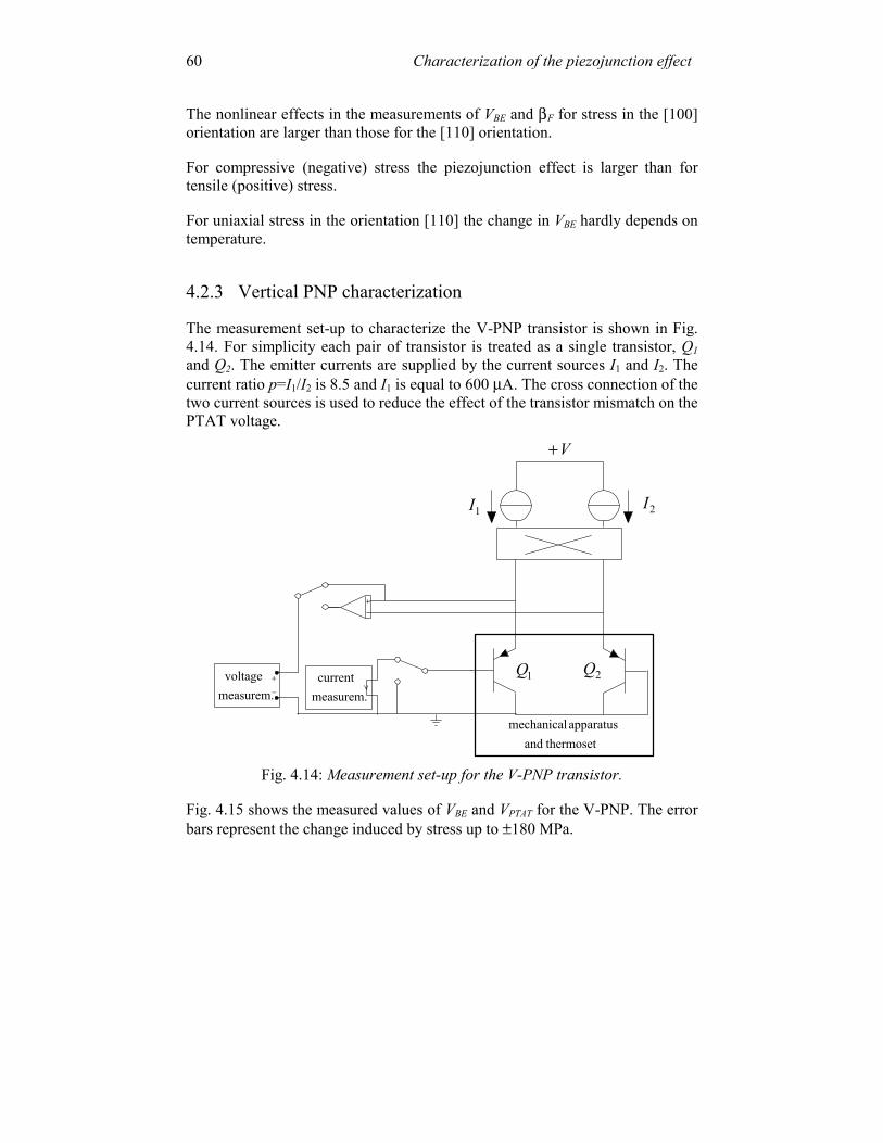
Characterization of the piezojunction effect 60
The nonlinear effects in the measurements of VBE and βF for stress in the [100] orientation are larger than those for the [110] orientation. For compressive (negative) stress the piezojunction effect is larger than for tensile (positive) stress. For uniaxial stress in the orientation [110] the change in VBE hardly depends on temperature. 4.2.3 Vertical PNP characterization The measurement set-up to characterize the V-PNP transistor is shown in Fig. 4.14. For simplicity each pair of transistor is treated as a single transistor, Q1 and Q2. The emitter currents are supplied by the current sources I1 and I2. The current ratio p=I1/I2 is 8.5 and I1 is equal to 600 µA. The cross connection of the two current sources is used to reduce the effect of the transistor mismatch on the PTAT voltage.
1I 2I
1Q 2Qmeasurem. current +
−measurem. voltage
thermosetand apparatus mechanical
V+
Fig. 4.14: Measurement set-up for the V-PNP transistor.
Fig. 4.15 shows the measured values of VBE and VPTAT for the V-PNP. The error bars represent the change induced by stress up to ±180 MPa.
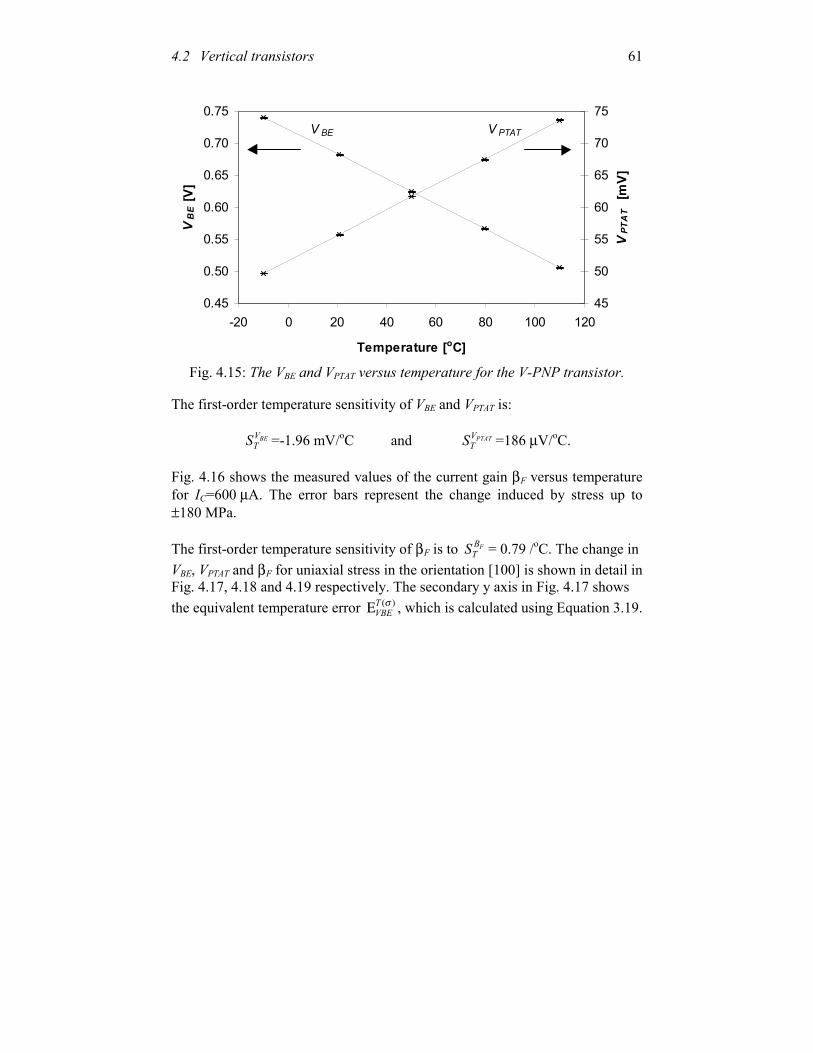
4.2 Vertical transistors 61
0.45
0.50
0.55
0.60
0.65
0.70
0.75
-20 0 20 40 60 80 100 120
Temperature [oC]
VB
E [V
]
45
50
55
60
65
70
75
VPT
AT [
mV]
V BE V PTAT
Fig. 4.15: The VBE and VPTAT versus temperature for the V-PNP transistor.
The first-order temperature sensitivity of VBE and VPTAT is:
BEVTS =-1.96 mV/oC and PTATV
TS =186 µV/oC. Fig. 4.16 shows the measured values of the current gain βF versus temperature for IC=600 µA. The error bars represent the change induced by stress up to ±180 MPa. The first-order temperature sensitivity of βF is to FB
TS = 0.79 /oC. The change in VBE, VPTAT and βF for uniaxial stress in the orientation [100] is shown in detail in Fig. 4.17, 4.18 and 4.19 respectively. The secondary y axis in Fig. 4.17 shows the equivalent temperature error )(σT
VBEΕ , which is calculated using Equation 3.19.

Characterization of the piezojunction effect 62
80
100
120
140
160
180
200
-20 0 20 40 60 80 100 120
Temperature [oC]
β βββ F
Fig. 4.16: Current gain versus temperature for the V-PNP.
-2
-1.5
-1
-0.5
0
0.5
-200 -100 0 100 200
Stress [MPa]
∆ ∆∆∆V
BE [
mV]
-0.26
0.00
0.26
0.51
0.77
1.02
Equi
vale
nt te
mp.
err
or [
o C]
-10 20 50 80110
Temp. [oC]
Fig. 4.17: Stress-induced change in VBE for V-PNP under uniaxial stress in the
orientation [100] at different temperatures. The secondary y axis in Fig. 4.18 shows the equivalent temperature error
)(σTVPTATΕ , which is calculated using Equation 3.22.
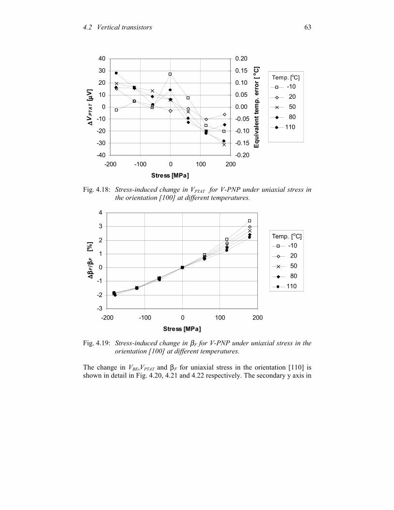
4.2 Vertical transistors 63
-40
-30
-20
-10
0
10
20
30
40
-200 -100 0 100 200
Stress [MPa]
∆ ∆∆∆V
PTA
T [ µ µµµ
V]
-0.20
-0.15
-0.10
-0.05
0.00
0.05
0.10
0.15
0.20
Equi
vale
nt te
mp.
err
or [
o C]
-10 20 50 80110
Temp. [oC]
Fig. 4.18: Stress-induced change in VPTAT for V-PNP under uniaxial stress in
the orientation [100] at different temperatures.
-3
-2
-1
0
1
2
3
4
-200 -100 0 100 200
Stress [MPa]
∆β
∆β
∆β
∆β F
/β /β/β/βF
[%] -10
20 50 80110
Temp. [oC]
Fig. 4.19: Stress-induced change in βF for V-PNP under uniaxial stress in the
orientation [100] at different temperatures. The change in VBE,VPTAT and βF for uniaxial stress in the orientation [110] is shown in detail in Fig. 4.20, 4.21 and 4.22 respectively. The secondary y axis in
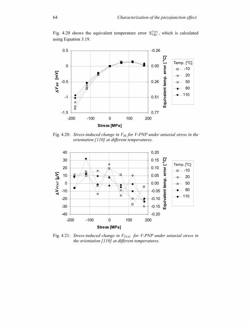
Characterization of the piezojunction effect 64
Fig. 4.20 shows the equivalent temperature error )(σTVBEΕ , which is calculated
using Equation 3.19.
-1.5
-1
-0.5
0
0.5
-200 -100 0 100 200
Stress [MPa]
∆ ∆∆∆V
BE [
mV]
-0.26
0.00
0.26
0.51
0.77
Equi
vale
nt te
mp.
err
or [
o C]
-10 20 50 80110
Temp. [oC]
Fig. 4.20: Stress-induced change in VBE for V-PNP under uniaxial stress in the
orientation [110] at different temperatures.
-40
-30
-20
-10
0
10
20
30
40
-200 -100 0 100 200
Stress [MPa]
∆ ∆∆∆V
PTA
T [ µ µµµ
V]
-0.20
-0.15
-0.10
-0.05
0.00
0.05
0.10
0.15
0.20
Equi
vale
nt te
mp.
err
or [
o C] -10 20 50 80110
Temp. [oC]
Fig. 4.21: Stress-induced change in VPTAT for V-PNP under uniaxial stress in
the orientation [110] at different temperatures.
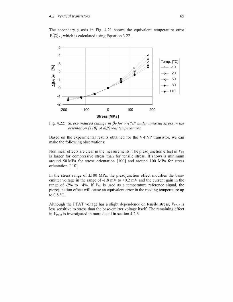
4.2 Vertical transistors 65
The secondary y axis in Fig. 4.21 shows the equivalent temperature error )(σT
VPTATΕ , which is calculated using Equation 3.22.
-2
-1
0
1
2
3
4
5
-200 -100 0 100 200
Stress [MPa]
∆β
∆β
∆β
∆β F
/β /β/β/βF
[%] -10
20 50 80110
Temp. [oC]
Fig. 4.22: Stress-induced change in βF for V-PNP under uniaxial stress in the
orientation [110] at different temperatures. Based on the experimental results obtained for the V-PNP transistor, we can make the following observations: Nonlinear effects are clear in the measurements. The piezojunction effect in VBE is larger for compressive stress than for tensile stress. It shows a minimum around 50 MPa for stress orientation [100] and around 100 MPa for stress orientation [110]. In the stress range of ±180 MPa, the piezojunction effect modifies the base-emitter voltage in the range of -1.8 mV to +0.2 mV and the current gain in the range of -2% to +4%. If VBE is used as a temperature reference signal, the piezojunction effect will cause an equivalent error in the reading temperature up to 0.8 °C. Although the PTAT voltage has a slight dependence on tensile stress, VPTAT is less sensitive to stress than the base-emitter voltage itself. The remaining effect in VPTAT is investigated in more detail in section 4.2.6.
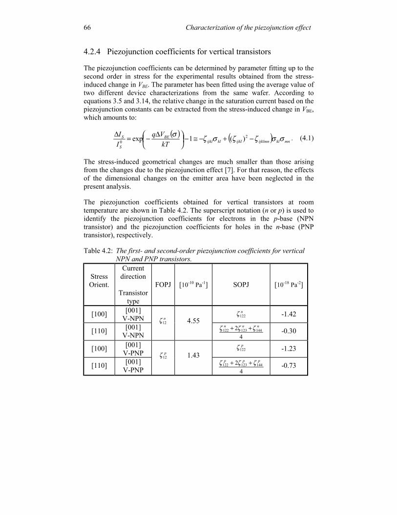
Characterization of the piezojunction effect 66
4.2.4 Piezojunction coefficients for vertical transistors The piezojunction coefficients can be determined by parameter fitting up to the second order in stress for the experimental results obtained from the stress-induced change in VBE. The parameter has been fitted using the average value of two different device characterizations from the same wafer. According to equations 3.5 and 3.14, the relative change in the saturation current based on the piezojunction constants can be extracted from the stress-induced change in VBE, which amounts to:
( ) ( ) mnklijklmnijklklijkl
BE
S
S
kTVq
II σσζζσζσ −+−≅−
∆−=∆ 2
0 )(1exp . (4.1)
The stress-induced geometrical changes are much smaller than those arising from the changes due to the piezojunction effect [7]. For that reason, the effects of the dimensional changes on the emitter area have been neglected in the present analysis. The piezojunction coefficients obtained for vertical transistors at room temperature are shown in Table 4.2. The superscript notation (n or p) is used to identify the piezojunction coefficients for electrons in the p-base (NPN transistor) and the piezojunction coefficients for holes in the n-base (PNP transistor), respectively. Table 4.2: The first- and second-order piezojunction coefficients for vertical
NPN and PNP transistors.
Stress Orient.
Current direction
Transistor
type
FOPJ
[10-10 Pa-1]
SOPJ
[10-18 Pa-2]
[100] [001] V-NPN
n122ζ
-1.42
[110] [001] V-NPN
n
12ζ
4.55
42 144123122
nnn ζζζ ++
-0.30
[100] [001] V-PNP
p122ζ
-1.23
[110] [001] V-PNP
p
12ζ
1.43
42 144123122
ppp ζζζ ++
-0.73
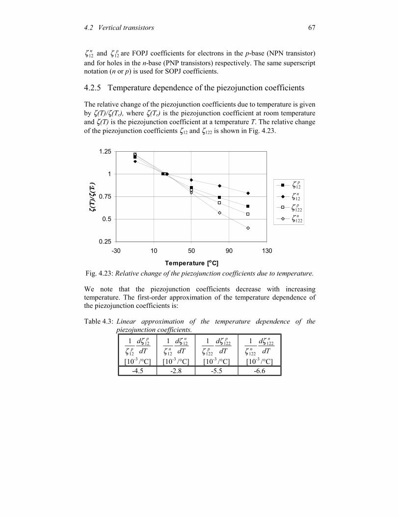
4.2 Vertical transistors 67
n12ζ and p
12ζ are FOPJ coefficients for electrons in the p-base (NPN transistor) and for holes in the n-base (PNP transistors) respectively. The same superscript notation (n or p) is used for SOPJ coefficients. 4.2.5 Temperature dependence of the piezojunction coefficients The relative change of the piezojunction coefficients due to temperature is given by ζ(T)/ζ(Tr), where ζ(Tr) is the piezojunction coefficient at room temperature and ζ(T) is the piezojunction coefficient at a temperature T. The relative change of the piezojunction coefficients ζ12 and ζ122 is shown in Fig. 4.23.
0.25
0.5
0.75
1
1.25
-30 10 50 90 130
Temperature [oC]
ζ(Τ
)/ζ(
Τζ(
Τ)/
ζ(Τ
ζ(Τ
)/ζ(
Τζ(
Τ)/
ζ(Τ r
) ))) p12ζn
12ζp
122ζn
122ζ
Fig. 4.23: Relative change of the piezojunction coefficients due to temperature.
We note that the piezojunction coefficients decrease with increasing temperature. The first-order approximation of the temperature dependence of the piezojunction coefficients is: Table 4.3: Linear approximation of the temperature dependence of the
piezojunction coefficients.
dTd p
p12
12
1 ζζ
[10-3 /°C] dT
d n
n12
12
1 ζζ
[10-3 /°C] dT
d p
p122
122
1 ζζ
[10-3 /°C] dT
d n
n122
122
1 ζζ
[10-3 /°C] -4.5 -2.8 -5.5 -6.6
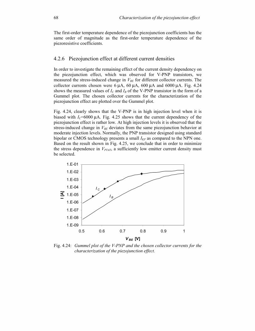
Characterization of the piezojunction effect 68
The first-order temperature dependence of the piezojunction coefficients has the same order of magnitude as the first-order temperature dependence of the piezoresistive coefficients. 4.2.6 Piezojunction effect at different current densities In order to investigate the remaining effect of the current density dependency on the piezojunction effect, which was observed for V-PNP transistors, we measured the stress-induced change in VBE for different collector currents. The collector currents chosen were 6 µA, 60 µA, 600 µA and 6000 µA. Fig. 4.24 shows the measured values of IC and IB of the V-PNP transistor in the form of a Gummel plot. The chosen collector currents for the characterization of the piezojunction effect are plotted over the Gummel plot. Fig. 4.24, clearly shows that the V-PNP is in high injection level when it is biased with IC=6000 µA. Fig. 4.25 shows that the current dependency of the piezojunction effect is rather low. At high injection levels it is observed that the stress-induced change in VBE deviates from the same piezojunction behavior at moderate injection levels. Normally, the PNP transistor designed using standard bipolar or CMOS technology presents a small IKF as compared to the NPN one. Based on the result shown in Fig. 4.25, we conclude that in order to minimize the stress dependence in VPTAT, a sufficiently low emitter current density must be selected.
1.E-09
1.E-08
1.E-07
1.E-06
1.E-05
1.E-04
1.E-03
1.E-02
1.E-01
0.5 0.6 0.7 0.8 0.9 1
V BE [V]
I [A]
I C
I B
Fig. 4.24: Gummel plot of the V-PNP and the chosen collector currents for the
characterization of the piezojunction effect.
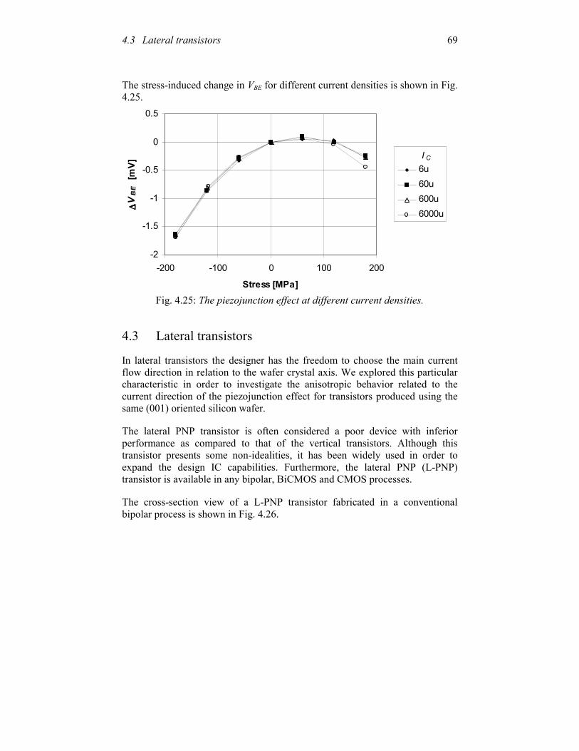
4.3 Lateral transistors 69
The stress-induced change in VBE for different current densities is shown in Fig. 4.25.
-2
-1.5
-1
-0.5
0
0.5
-200 -100 0 100 200
Stress [MPa]
∆ ∆∆∆V
BE [
mV] 6u
60u600u6000u
I C
Fig. 4.25: The piezojunction effect at different current densities.
4.3 Lateral transistors In lateral transistors the designer has the freedom to choose the main current flow direction in relation to the wafer crystal axis. We explored this particular characteristic in order to investigate the anisotropic behavior related to the current direction of the piezojunction effect for transistors produced using the same (001) oriented silicon wafer. The lateral PNP transistor is often considered a poor device with inferior performance as compared to that of the vertical transistors. Although this transistor presents some non-idealities, it has been widely used in order to expand the design IC capabilities. Furthermore, the lateral PNP (L-PNP) transistor is available in any bipolar, BiCMOS and CMOS processes. The cross-section view of a L-PNP transistor fabricated in a conventional bipolar process is shown in Fig. 4.26.

Characterization of the piezojunction effect 70
E B SubC
N+P+ P+N-epi
P-Substrate
Buried layer (N+)
Fig. 4.26: Cross-section of a typical lateral PNP transistor.
The L-PNP is implemented using a p-diffusion in the epitaxial layer (base) as the emitter and a second p-diffusion for the collector. A buried layer is formed to prevent the collection of carriers in the p-substrate. Thus, the effect of the parasitic vertical transistor formed by the p-type emitter, the n-type epitaxial layer and the p-type substrate is minimized. A structure containing four orthogonal L-PNP transistors has been designed and fabricated. Fig. 4.27 shows the main axes of a 001-oriented silicon wafer and the layout of four lateral PNP transistors. The transistor index corresponds to its current flow direction, given by the angle ϕ, which is measured between the crystal axes [100] and the vector pointing to the main current flow direction of each transistor.
3π/4
Q3π/4
Qπ/4
BB
BB
EE
EE
CC
CC
ϕ
[010][100]
Fig. 4.27: Layout of the L-PNP transistors on a 001 silicon wafer.
The transistors Qπ/4 and Q-3π/4 are symmetric and present the same set of piezojunction coefficients. The same is done for the transistors Q3π/4 and Q-π/4. In order to form a common-centroid layout, both pairs of symmetrical transistors are connected in parallel, and in this way the mismatch between the orthogonal transistors generated by mechanical stress gradients is reduced. The measurement set-up characterising the V-PNP transistor is shown in Fig. 4.28.
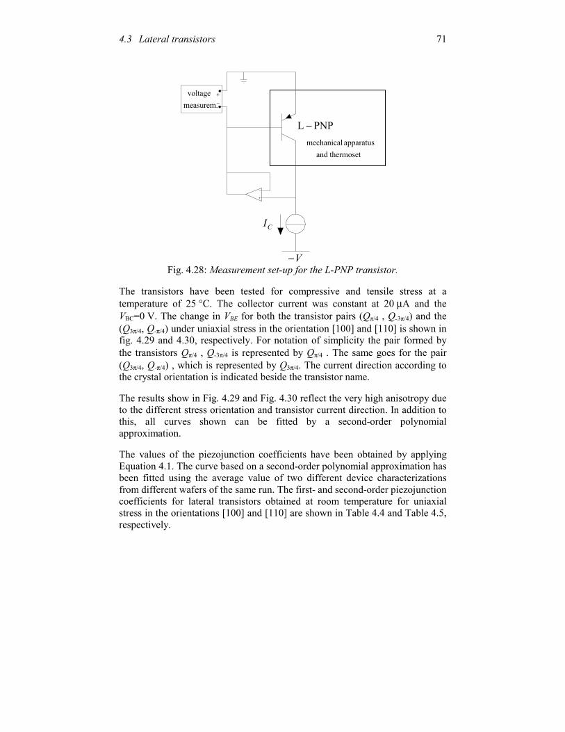
4.3 Lateral transistors 71
V−
CI
PNPL −
+−measurem.
voltage
thermosetand apparatus mechanical
Fig. 4.28: Measurement set-up for the L-PNP transistor.
The transistors have been tested for compressive and tensile stress at a temperature of 25 °C. The collector current was constant at 20 µA and the VBC=0 V. The change in VBE for both the transistor pairs (Qπ/4 , Q-3π/4) and the (Q3π/4, Q-π/4) under uniaxial stress in the orientation [100] and [110] is shown in fig. 4.29 and 4.30, respectively. For notation of simplicity the pair formed by the transistors Qπ/4 , Q-3π/4 is represented by Qπ/4 . The same goes for the pair (Q3π/4, Q-π/4) , which is represented by Q3π/4. The current direction according to the crystal orientation is indicated beside the transistor name. The results show in Fig. 4.29 and Fig. 4.30 reflect the very high anisotropy due to the different stress orientation and transistor current direction. In addition to this, all curves shown can be fitted by a second-order polynomial approximation. The values of the piezojunction coefficients have been obtained by applying Equation 4.1. The curve based on a second-order polynomial approximation has been fitted using the average value of two different device characterizations from different wafers of the same run. The first- and second-order piezojunction coefficients for lateral transistors obtained at room temperature for uniaxial stress in the orientations [100] and [110] are shown in Table 4.4 and Table 4.5, respectively.
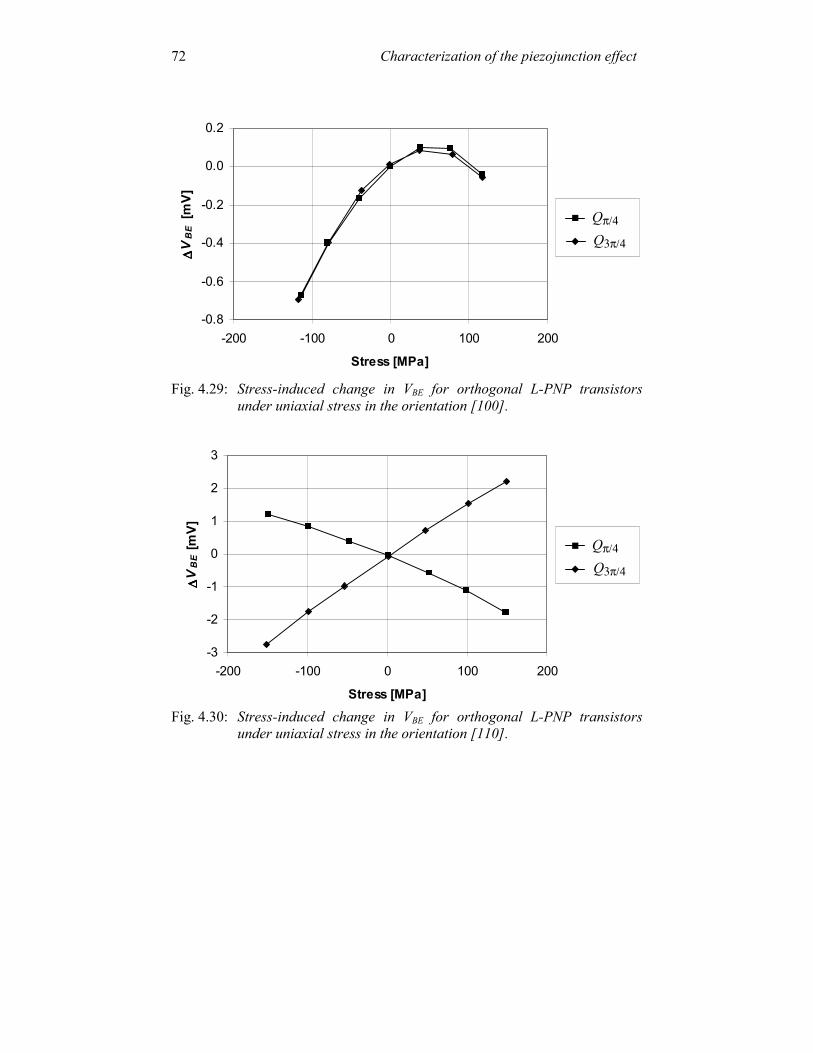
Characterization of the piezojunction effect 72
-0.8
-0.6
-0.4
-0.2
0.0
0.2
-200 -100 0 100 200
Stress [MPa]
∆ ∆∆∆V
BE [
mV]
Fig. 4.29: Stress-induced change in VBE for orthogonal L-PNP transistors
under uniaxial stress in the orientation [100].
-3
-2
-1
0
1
2
3
-200 -100 0 100 200
Stress [MPa]
∆ ∆∆∆V
BE [m
V]
Fig. 4.30: Stress-induced change in VBE for orthogonal L-PNP transistors
under uniaxial stress in the orientation [110].
! Qπ/4
" Q3π/4
! Qπ/4
" Q3π/4
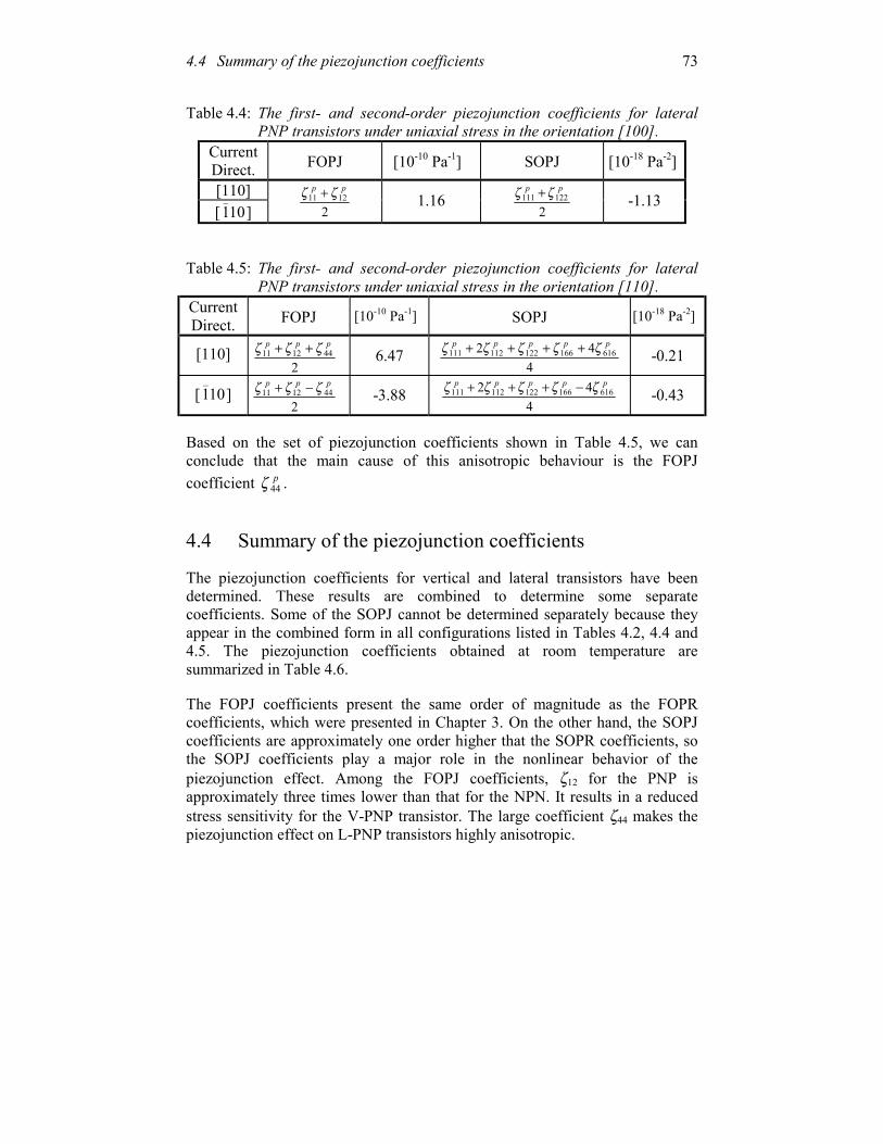
4.4 Summary of the piezojunction coefficients 73
Table 4.4: The first- and second-order piezojunction coefficients for lateral PNP transistors under uniaxial stress in the orientation [100].
Current Direct.
FOPJ
[10-10 Pa-1]
SOPJ
[10-18 Pa-2]
[110] [ 101
_] 2
1211pp ζζ +
1.16 2
122111pp ζζ +
-1.13
Table 4.5: The first- and second-order piezojunction coefficients for lateral
PNP transistors under uniaxial stress in the orientation [110]. Current Direct.
FOPJ
[10-10 Pa-1]
SOPJ
[10-18 Pa-2]
[110] 2
441211ppp ζζζ ++
6.47 4
42 616166122112111ppppp ζζζζζ ++++
-0.21
[ 101_
] 2
441211ppp ζζζ −+
-3.88 4
42 616166122112111ppppp ζζζζζ −+++
-0.43
Based on the set of piezojunction coefficients shown in Table 4.5, we can conclude that the main cause of this anisotropic behaviour is the FOPJ coefficient p
44ζ . 4.4 Summary of the piezojunction coefficients The piezojunction coefficients for vertical and lateral transistors have been determined. These results are combined to determine some separate coefficients. Some of the SOPJ cannot be determined separately because they appear in the combined form in all configurations listed in Tables 4.2, 4.4 and 4.5. The piezojunction coefficients obtained at room temperature are summarized in Table 4.6. The FOPJ coefficients present the same order of magnitude as the FOPR coefficients, which were presented in Chapter 3. On the other hand, the SOPJ coefficients are approximately one order higher that the SOPR coefficients, so the SOPJ coefficients play a major role in the nonlinear behavior of the piezojunction effect. Among the FOPJ coefficients, ζ12 for the PNP is approximately three times lower than that for the NPN. It results in a reduced stress sensitivity for the V-PNP transistor. The large coefficient ζ44 makes the piezojunction effect on L-PNP transistors highly anisotropic.
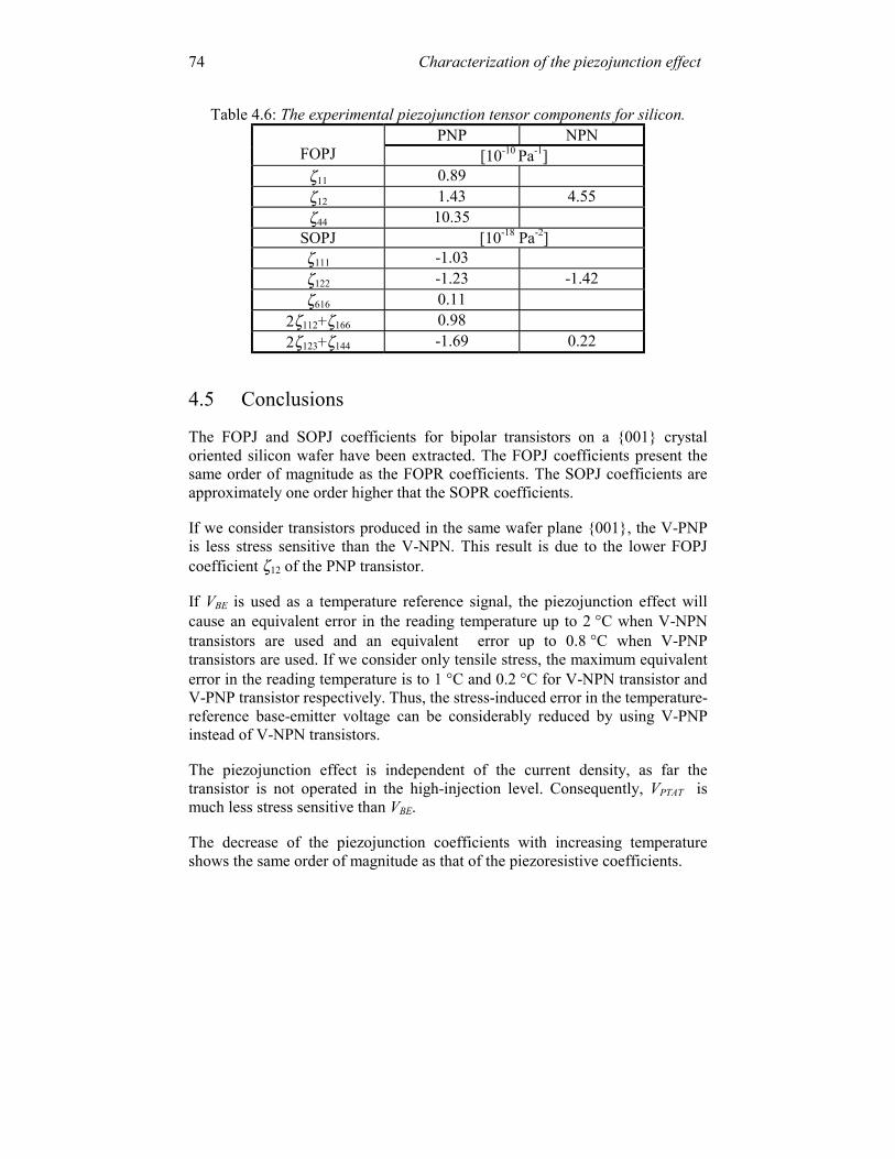
Characterization of the piezojunction effect 74
Table 4.6: The experimental piezojunction tensor components for silicon. PNP NPN
FOPJ [10-10 Pa-1] ζ11 0.89 ζ12 1.43 4.55 ζ44 10.35
SOPJ [10-18 Pa-2] ζ111 -1.03 ζ122 -1.23 -1.42 ζ616 0.11
2ζ112+ζ166 0.98 2ζ123+ζ144 -1.69 0.22
4.5 Conclusions The FOPJ and SOPJ coefficients for bipolar transistors on a 001 crystal oriented silicon wafer have been extracted. The FOPJ coefficients present the same order of magnitude as the FOPR coefficients. The SOPJ coefficients are approximately one order higher that the SOPR coefficients. If we consider transistors produced in the same wafer plane 001, the V-PNP is less stress sensitive than the V-NPN. This result is due to the lower FOPJ coefficient ζ12 of the PNP transistor. If VBE is used as a temperature reference signal, the piezojunction effect will cause an equivalent error in the reading temperature up to 2 °C when V-NPN transistors are used and an equivalent error up to 0.8 °C when V-PNP transistors are used. If we consider only tensile stress, the maximum equivalent error in the reading temperature is to 1 °C and 0.2 °C for V-NPN transistor and V-PNP transistor respectively. Thus, the stress-induced error in the temperature-reference base-emitter voltage can be considerably reduced by using V-PNP instead of V-NPN transistors. The piezojunction effect is independent of the current density, as far the transistor is not operated in the high-injection level. Consequently, VPTAT is much less stress sensitive than VBE. The decrease of the piezojunction coefficients with increasing temperature shows the same order of magnitude as that of the piezoresistive coefficients.
4.5 Conclusions 75
The piezojunction effect in L-PNP is highly anisotropic, and depends on the stress orientation and the current direction. The dominant role of p
44ζ for the anisotropic behavior of the piezojunction effect in L-PNP transistors is evident.
Characterization of the piezojunction effect 76
References [1] G.C.M. Meijer, Integrated circuits and components for bandgap
references and temperature transducers, Ph.D. Thesis, Delft University of Technology, Delft, The Netherlands, 1982.
[2] G.C.M. Meijer, Thermal sensors based on transistors, Sensors and Actuators A, 10, pp. 103-125, 1986.
[3] A. Bakker, High-accuracy CMOS smart temperature sensors, Ph.D Thesis, Delft University of Technology, Delft, The Netherlands, 2000.
[4] G. Wang and G.C.M. Meijer, The temperature characteristics of bipolar transistors for CMOS Temperature sensors, Proc. of Eurosensors XIII, pp. 553-556, Sep. 1999.
[5] G. Wang and G.C.M. Meijer, The temperature characteristics of bipolar transistors fabricated in CMOS technology, Sensors and Actuators A, 87, pp. 81-89, 2000.
[6] L.K. Nanver, E.J.G. Goudena and H.W. van Zeijl, DIMES-01, a baseline BIFET process for smart sensor experimentation, Sensors and Actuators A, 36, pp. 139-147, 1993.
[7] J.T. Lenkkeri, Nonlinear effects in the piezoresistivity of p-type resistivity, Phys. Status Solidi B, 136, pp. 373-385, 1986.
77
Chapter 5
Minimizing the piezojunction and piezoresistive effects in integrated devices 5.1 Introduction The knowledge of the piezojunction and piezoresistive coefficients is used to minimize the undesirable mechanical-stress effects for the electrical characteristic of transistors and resistors, respectively. Devices with lower mechanical stress sensitivity can be found by a comparison of their piezo-coefficients. The layout of the device can also be optimized to reduce the mechanical-stress sensitivity. As shown in Section 2.7, packaging causes most of the mechanical stress on the silicon surface. The mechanical stress introduced by packaging is normally lower than 200 MPa, and it can be compressive and tensile in any orientation parallel to the wafer plane. The minimization of the piezo-effects has to be effective for the stress conditions introduced by packaging.
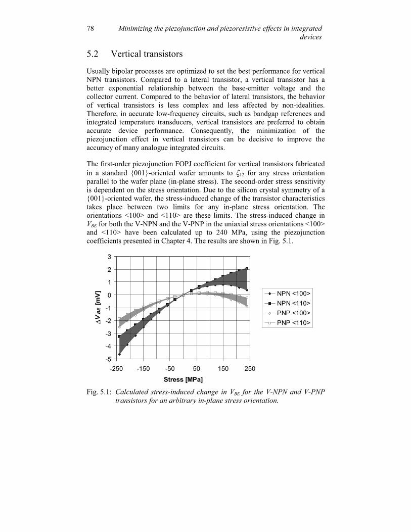
Minimizing the piezojunction and piezoresistive effects in integrated devices
78
5.2 Vertical transistors Usually bipolar processes are optimized to set the best performance for vertical NPN transistors. Compared to a lateral transistor, a vertical transistor has a better exponential relationship between the base-emitter voltage and the collector current. Compared to the behavior of lateral transistors, the behavior of vertical transistors is less complex and less affected by non-idealities. Therefore, in accurate low-frequency circuits, such as bandgap references and integrated temperature transducers, vertical transistors are preferred to obtain accurate device performance. Consequently, the minimization of the piezojunction effect in vertical transistors can be decisive to improve the accuracy of many analogue integrated circuits. The first-order piezojunction FOPJ coefficient for vertical transistors fabricated in a standard 001-oriented wafer amounts to ζ12 for any stress orientation parallel to the wafer plane (in-plane stress). The second-order stress sensitivity is dependent on the stress orientation. Due to the silicon crystal symmetry of a 001-oriented wafer, the stress-induced change of the transistor characteristics takes place between two limits for any in-plane stress orientation. The orientations <100> and <110> are these limits. The stress-induced change in VBE for both the V-NPN and the V-PNP in the uniaxial stress orientations <100> and <110> have been calculated up to 240 MPa, using the piezojunction coefficients presented in Chapter 4. The results are shown in Fig. 5.1.
-5
-4
-3
-2
-1
0
1
2
3
-250 -150 -50 50 150 250Stress [MPa]
∆VBE
[mV] NPN <100>
NPN <110>PNP <100>PNP <110>
-5
-4
-3
-2
-1
0
1
2
3
-250 -150 -50 50 150 250Stress [MPa]
∆VBE
[mV] NPN <100>
NPN <110>PNP <100>PNP <110>
Fig. 5.1: Calculated stress-induced change in VBE for the V-NPN and V-PNP transistors for an arbitrary in-plane stress orientation.
5.2 Vertical transistors 79
For an arbitrarily oriented compressive (negative) or tensile (positive) in-plane stress, the change in VBE is in the shaded areas. Based on this result, we observe that the change in VBE is: • smaller in the V-PNP for stress up to 200 MPa in any orientation along the wafer plane. • larger for compressive stress than for tensile stress for both types of transistors. For compressive stress, the change in VBE of the V-PNP is approximately half that of the V-NPN. For tensile stress, the ratio of both transistor’s changes is determined by the amount of stress. Up to 150 MPa, the change in VBE for V-PNP is about a factor of five less than that for V-NPN. For tensile stress higher than 200 MPa in the orientation <100>, the change in VBE of the V-NPN is smaller than that of the V-PNP. Based on these observations, we can conclude that using the V-PNP instead of the V-NPN can significantly reduce the inaccuracy in VBE caused by mechanical stress. The reduction of the piezojunction effect based on the use of V-PNP is even more attractive if we consider packaging types for which the TCE mismatch introduces a tensile stress on the silicon die surface. This is the case when the chip is attached on ceramic or metallic substrates, which normally present a TCE higher than that of silicon. Unfortunately, it is not always possible to use the V-PNP, as it has the disadvantage that its collector is the global substrate node and therefore the collector current is not available as a separated current. Thus the use of the V-PNP transistor is limited to common-collector configurations. Experimental results Our vertical test transistors have been fabricated in two different Alcatel processes: the BiCMOS (HBIMOS 2.0 µm) for the V-NPN transistors and the CMOS 0.7 µm for the substrate V-PNP transistors. The bipolar substrate transistors in CMOS technology have been chosen because their characteristics are very suitable for realizing accurate temperature sensors [1, 2], while the vertical NPN transistors have been chosen because they are commonly used. In both cases, the wafer plane has the 001 orientation, while the uniaxial stress is applied in the orientation <110>. The wafer is sawn as a silicon cantilever beam, containing the transistors. The transistors have been tested using the cantilever technique described in Chapter 2. The measured results for the stress-
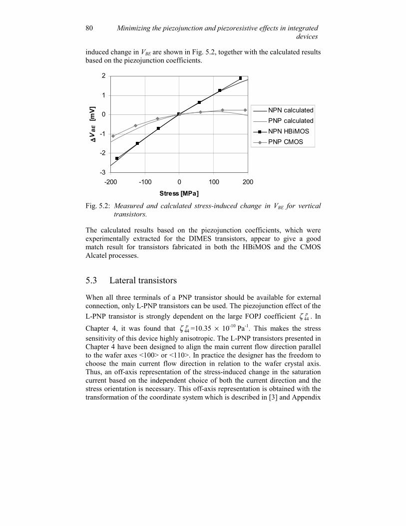
Minimizing the piezojunction and piezoresistive effects in integrated devices
80
induced change in VBE are shown in Fig. 5.2, together with the calculated results based on the piezojunction coefficients.
-3
-2
-1
0
1
2
-200 -100 0 100 200
Stress [MPa]
∆ ∆∆∆VBE [
mV] NPN calculated
PNP calculatedNPN HBiMOSPNP CMOS
Fig. 5.2: Measured and calculated stress-induced change in VBE for vertical
transistors. The calculated results based on the piezojunction coefficients, which were experimentally extracted for the DIMES transistors, appear to give a good match result for transistors fabricated in both the HBiMOS and the CMOS Alcatel processes. 5.3 Lateral transistors When all three terminals of a PNP transistor should be available for external connection, only L-PNP transistors can be used. The piezojunction effect of the L-PNP transistor is strongly dependent on the large FOPJ coefficient p
44ζ . In
Chapter 4, it was found that p44ζ =10.35 × 10⁻¹⁰ Pa-1. This makes the stress
sensitivity of this device highly anisotropic. The L-PNP transistors presented in Chapter 4 have been designed to align the main current flow direction parallel to the wafer axes <100> or <110>. In practice the designer has the freedom to choose the main current flow direction in relation to the wafer crystal axis. Thus, an off-axis representation of the stress-induced change in the saturation current based on the independent choice of both the current direction and the stress orientation is necessary. This off-axis representation is obtained with the transformation of the coordinate system which is described in [3] and Appendix

5.3 Lateral transistors 81
A. The first-order stress dependence of the relative change of the saturation current is given by the following equation:
+
−+
+−=
∆
λϕζ
λϕζλϕζσ
2sin2sin21
2cos2cos21
212cos2cos
21
21
44
12110
p
pp
S
S
II
, (5.1)
where σ is the mechanical stress, λ the in-plane-stress orientation and ϕ the direction of the lateral current density (J). The crystal axis [100] is the reference for the angles λ and ϕ, which are shown in Fig. 5.3. The most often used layout for the L-PNP transistor applies the emitter regular-polygon geometry. This emitter is completely surrounded by a collector doping in order to collect, in the normal forward mode, most of the laterally injected carriers from the emitter. Fig. 5.3 shows the simplified layout of a circular lateral transistor in a 001-wafer plane.
E
C
[100]
λ
B
J
σϕ
Fig. 5.3: Simplified layout of a circular lateral transistor in a 001 wafer plane.
In this analysis we consider the ideal case, where the carriers flow near the silicon surface from the emitter reaching the collector in all directions, given by ϕ, where (0 ≤ ϕ<2π). In practice some of the carriers injected from the emitter reach the substrate. This secondary current flow is known as the substrate collector current of the parasitic vertical transistor. In order to reduce both the
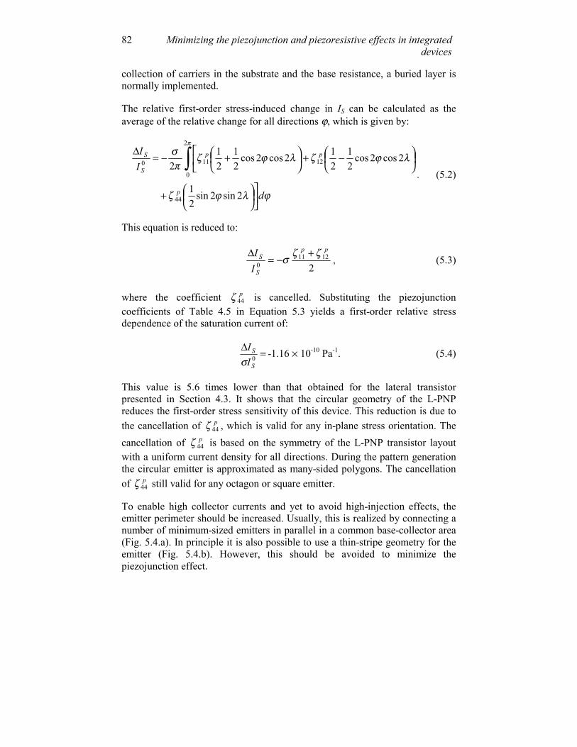
Minimizing the piezojunction and piezoresistive effects in integrated devices
82
collection of carriers in the substrate and the base resistance, a buried layer is normally implemented. The relative first-order stress-induced change in IS can be calculated as the average of the relative change for all directions ϕ, which is given by:
ϕλϕζ
λϕζλϕζπ
σπ
d
II
p
pp
S
S
+
−+
+−=
∆ ∫2sin2sin
21
2cos2cos21
212cos2cos
21
21
2
44
2
0
12110
. (5.2)
This equation is reduced to:
21211
0
pp
S
S
II ζζσ +
−=∆
, (5.3)
where the coefficient p
44ζ is cancelled. Substituting the piezojunction coefficients of Table 4.5 in Equation 5.3 yields a first-order relative stress dependence of the saturation current of:
=∆0S
S
II
σ-1.16 × 10⁻¹⁰ Pa-1. (5.4)
This value is 5.6 times lower than that obtained for the lateral transistor presented in Section 4.3. It shows that the circular geometry of the L-PNP reduces the first-order stress sensitivity of this device. This reduction is due to the cancellation of p
44ζ , which is valid for any in-plane stress orientation. The cancellation of p
44ζ is based on the symmetry of the L-PNP transistor layout with a uniform current density for all directions. During the pattern generation the circular emitter is approximated as many-sided polygons. The cancellation of p
44ζ still valid for any octagon or square emitter. To enable high collector currents and yet to avoid high-injection effects, the emitter perimeter should be increased. Usually, this is realized by connecting a number of minimum-sized emitters in parallel in a common base-collector area (Fig. 5.4.a). In principle it is also possible to use a thin-stripe geometry for the emitter (Fig. 5.4.b). However, this should be avoided to minimize the piezojunction effect.

5.3 Lateral transistors 83
(a) (b)
Fig. 5.4: L-PNP transistors: a) circular split-emitter geometry, b) elongated-
emitter geometry and c) octagon-emitter geometry. Experimental results An L-PNP transistor fabricated in a BiCMOS technology (HBIMOS – Alcatel) has been tested. The circular emitter geometry is adjusted by an octagon polygon. Thus, the L-PNP has an octagonal emitter, which is surrounded by a similar shaped collector, which is shown in Fig. 5.4.c. The measured results for the change in VBE for uniaxial stress in the orientation [110] are shown in Fig. 5.5.
-0.8
-0.6
-0.4
-0.2
0
0.2
0.4
-200 -100 0 100 200
Stress [MPa]
∆ ∆∆∆ V
BE [m
V]
Fig. 5.5: Stress-induced change in VBE for L-PNP under uniaxial stress in the
orientation [110].
Minimizing the piezojunction and piezoresistive effects in integrated devices
84
The relative stress-induced change in IS can be determined by parameter fitting of the experimental results shown in Fig. 5.5. By applying Equation 4.1, the relative stress-induced change in IS we obtain :
2
210 σσ aaII
S
S +=∆
, (5.5)
where a1=-1.14×10⁻¹⁰ Pa-1 and a2=2.32×10⁻¹⁹ Pa-2. The linear part of this equation matches the theoretical result, which has been calculated and amounts to –1.16×10⁻¹⁰ Pa-1. We conclude that applying a layout based on a symmetrical circular, octagonal or square shape cancels the large coefficient p
44ζ . 5.4 Resistors The integrated resistors are surface devices and the current flow is parallel to the wafer plane. The design of an integrated resistor involves specification of a planar shape of resistive material of prescribed thickness, which forms the current path. In each technology, there are several layers that are, in principle, suitable for the implementation of an integrated resistor. The resistors can be implemented using monocrystalline silicon, polysilicon or thin-film materials. The piezoresistive effect occurs in monocrystalline silicon and polysilicon. The random grain structure of polysilicon resistors makes that its piezoresistive effect is a few times smaller than that of monocrystalline resistors. In addition, the piezoresistive effect in polysilicon resistors is influenced by the boundaries between the grains. Since the grains may have many different sizes, the magnitude of the effect depends strongly on the applied technology [4, 5]. On the other hand, the piezoresistive effect in monocrystalline resistors can be well defined by piezoresistive theory. Integrated monocrystalline silicon resistors can be fabricated by using either the p-type or the n-type material. Resistors in p-type material are by far the most popular, because the sheet resistance is several hundred ohms per square, thus permitting a wide range of useful resistor values [6]. The choice of the material (p or n) defines the set of the piezoresistive coefficients. Once the piezoresistive coefficients have been defined, the relative resistance change can be calculated based on the resistor alignment and stress orientation. The uniaxial stress orientation (λ) and the
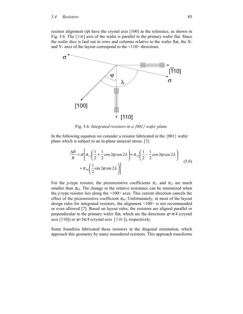
5.4 Resistors 85
resistor alignment (ϕ) have the crystal axis [100] as the reference, as shown in Fig. 5.6. The [ 101
_] axis of the wafer is parallel to the primary wafer flat. Since
the wafer dice is laid out in rows and columns relative to the wafer flat, the X- and Y- axes of the layout correspond to the <110> directions.
[100]
[110]
λ σ
σ
[110]ϕ
Fig. 5.6: Integrated resistors in a 001 wafer plane. In the following equation we consider a resistor fabricated in the 001 wafer plane which is subject to an in-plane uniaxial stress. [3].
+
−+
+=∆
λϕπ
λϕπλϕπσ
2sin2sin21
2cos2cos21
212cos2cos
21
21
44
1211RR
. (5.6)
For the p-type resistor, the piezoresistive coefficients π11 and π12 are much smaller than π44. The change in the relative resistance can be minimized when the p-type resistor lies along the <100> axes. This current direction cancels the effect of the piezoresistive coefficient π44. Unfortunately, in most of the layout design rules for integrated resistors, the alignment <100> is not recommended or even allowed [7]. Based on layout rules, the resistors are aligned parallel or perpendicular to the primary wafer flat, which are the directions ϕ=π/4 (crystal axis [110]) or ϕ=3π/4 (crystal axis [ 101
_]), respectively.
Some foundries fabricated these resistors in the diagonal orientation, which approach this geometry by many meandered resistors. This approach transforms
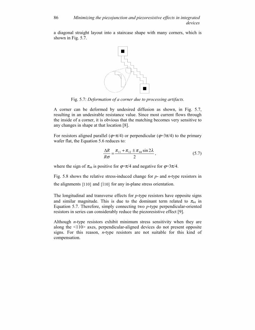
Minimizing the piezojunction and piezoresistive effects in integrated devices
86
a diagonal straight layout into a staircase shape with many corners, which is shown in Fig. 5.7.
Fig. 5.7: Deformation of a corner due to processing artifacts. A corner can be deformed by undesired diffusion as shown, in Fig. 5.7, resulting in an undesirable resistance value. Since most current flows through the inside of a corner, it is obvious that the matching becomes very sensitive to any changes in shape at that location [8]. For resistors aligned parallel (ϕ=π/4) or perpendicular (ϕ=3π/4) to the primary wafer flat, the Equation 5.6 reduces to:
22sin441211 λπππ
σ±+=∆
RR
, (5.7)
where the sign of π44 is positive for ϕ=π/4 and negative for ϕ=3π/4. Fig. 5.8 shows the relative stress-induced change for p- and n-type resistors in
the alignments ]110[ and ]101[_
for any in-plane stress orientation. The longitudinal and transverse effects for p-type resistors have opposite signs and similar magnitude. This is due to the dominant term related to π44 in Equation 5.7. Therefore, simply connecting two p-type perpendicular-oriented resistors in series can considerably reduce the piezoresistive effect [9]. Although n-type resistors exhibit minimum stress sensitivity when they are along the <110> axes, perpendicular-aligned devices do not present opposite signs. For this reason, n-type resistors are not suitable for this kind of compensation.
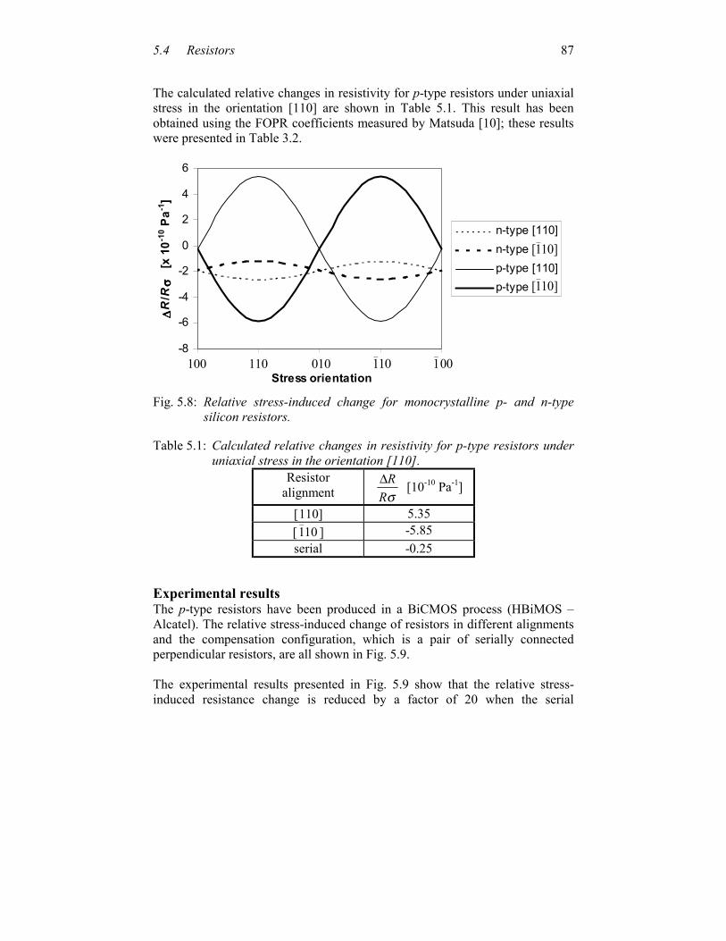
5.4 Resistors 87
The calculated relative changes in resistivity for p-type resistors under uniaxial stress in the orientation [110] are shown in Table 5.1. This result has been obtained using the FOPR coefficients measured by Matsuda [10]; these results were presented in Table 3.2.
-8
-6
-4
-2
0
2
4
6
Stress orientation
∆ ∆∆∆R
/Rσ σσσ
[x
10-1
0 Pa-1
]
n-type [110]n-type p-type [110]p-type
100 110 010 101_
001_
]101[_
]101[_
Fig. 5.8: Relative stress-induced change for monocrystalline p- and n-type
silicon resistors. Table 5.1: Calculated relative changes in resistivity for p-type resistors under
uniaxial stress in the orientation [110]. Resistor
alignment σRR∆ [10-10 Pa-1]
[110] 5.35 [ 101
_] -5.85
serial -0.25 Experimental results The p-type resistors have been produced in a BiCMOS process (HBiMOS – Alcatel). The relative stress-induced change of resistors in different alignments and the compensation configuration, which is a pair of serially connected perpendicular resistors, are all shown in Fig. 5.9. The experimental results presented in Fig. 5.9 show that the relative stress-induced resistance change is reduced by a factor of 20 when the serial
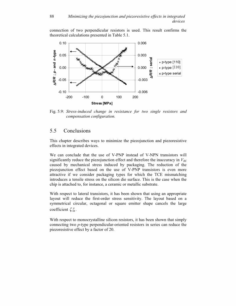
Minimizing the piezojunction and piezoresistive effects in integrated devices
88
connection of two perpendicular resistors is used. This result confirms the theoretical calculations presented in Table 5.1.
-0.10
-0.05
0.00
0.05
0.10
-200 -100 0 100 200
Stress [MPa]
∆ ∆∆∆R/R
; p
- and
n-ty
pe
-0.006
-0.003
0.000
0.003
0.006
∆ ∆∆∆R/R
; se
rial
p-type [110]p-typep-type serial
]101[_
Fig. 5.9: Stress-induced change in resistance for two single resistors and
compensation configuration. 5.5 Conclusions This chapter describes ways to minimize the piezojunction and piezoresistive effects in integrated devices. We can conclude that the use of V-PNP instead of V-NPN transistors will significantly reduce the piezojunction effect and therefore the inaccuracy in VBE caused by mechanical stress induced by packaging. The reduction of the piezojunction effect based on the use of V-PNP transistors is even more attractive if we consider packaging types for which the TCE mismatching introduces a tensile stress on the silicon die surface. This is the case when the chip is attached to, for instance, a ceramic or metallic substrate. With respect to lateral transistors, it has been shown that using an appropriate layout will reduce the first-order stress sensitivity. The layout based on a symmetrical circular, octagonal or square emitter shape cancels the large coefficient p
44ζ . With respect to monocrystalline silicon resistors, it has been shown that simply connecting two p-type perpendicular-oriented resistors in series can reduce the piezoresistive effect by a factor of 20.
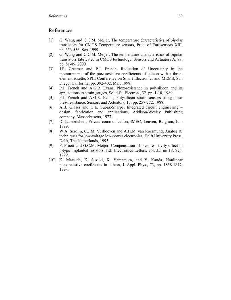
References 89
References [1] G. Wang and G.C.M. Meijer, The temperature characteristics of bipolar
transistors for CMOS Temperature sensors, Proc. of Eurosensors XIII, pp. 553-556, Sep. 1999.
[2] G. Wang and G.C.M. Meijer, The temperature characteristics of bipolar transistors fabricated in CMOS technology, Sensors and Actuators A, 87, pp. 81-89, 2000.
[3] J.F. Creemer and P.J. French, Reduction of Uncertainty in the measurements of the piezoresistive coefficients of silicon with a three-element rosette, SPIE Conference on Smart Electronics and MEMS, San Diego, California, pp. 392-402, Mar. 1998.
[4] P.J. French and A.G.R. Evans, Piezoresistance in polysilicon and its applications to strain gauges, Solid-St. Electron., 32, pp. 1-10, 1989.
[5] P.J. French and A.G.R. Evans, Polysilicon strain sensors using shear piezoresistance, Sensors and Actuators, 15, pp. 257-272, 1988.
[6] A.B. Glaser and G.E. Subak-Sharpe, Integrated circuit engineering – design, fabrication and applications, Addison-Wesley Publishing company, Massachusetts, 1977.
[7] D. Lambrichts , Private communication, IMEC, Leuven, Belgium, Jun. 1999.
[8] W.A. Serdijn, C.J.M. Verhoeven and A.H.M. van Roermund, Analog IC techniques for low-voltage low-power electronics, Delft University Press, Delft, The Netherlands, 1995.
[9] F. Fruett and G.C.M. Meijer, Compensation of piezoresistivity effect in p-type implanted resistors, IEE Electronics Letters, vol. 35, no 18, Sep. 1999.
[10] K. Matsuda, K. Suzuki, K. Yamamura, and Y. Kanda, Nonlinear piezoresistive coeficients in silicon, J. Appl. Phys., 73, pp. 1838-1847, 1993.

Minimizing the piezojunction and piezoresistive effects in integrated devices
90
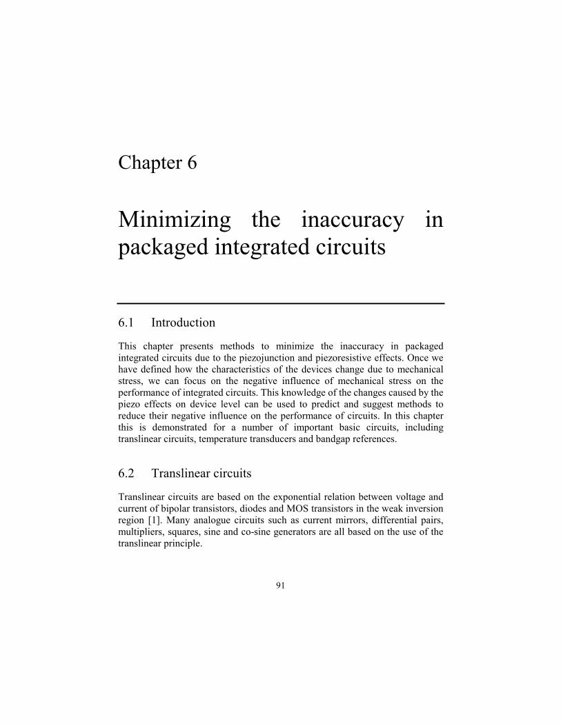
91
Chapter 6
Minimizing the inaccuracy in packaged integrated circuits 6.1 Introduction This chapter presents methods to minimize the inaccuracy in packaged integrated circuits due to the piezojunction and piezoresistive effects. Once we have defined how the characteristics of the devices change due to mechanical stress, we can focus on the negative influence of mechanical stress on the performance of integrated circuits. This knowledge of the changes caused by the piezo effects on device level can be used to predict and suggest methods to reduce their negative influence on the performance of circuits. In this chapter this is demonstrated for a number of important basic circuits, including translinear circuits, temperature transducers and bandgap references. 6.2 Translinear circuits
Translinear circuits are based on the exponential relation between voltage and current of bipolar transistors, diodes and MOS transistors in the weak inversion region [1]. Many analogue circuits such as current mirrors, differential pairs, multipliers, squares, sine and co-sine generators are all based on the use of the translinear principle.
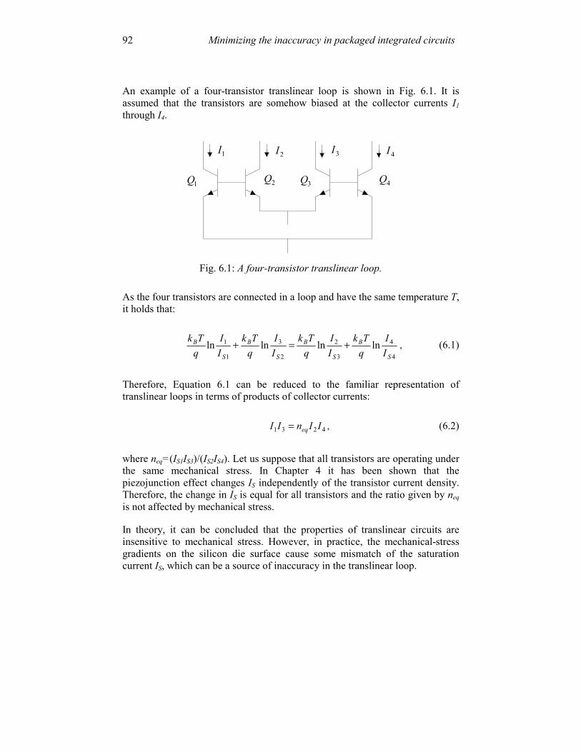
Minimizing the inaccuracy in packaged integrated circuits 92
An example of a four-transistor translinear loop is shown in Fig. 6.1. It is assumed that the transistors are somehow biased at the collector currents I1 through I4.
1I 2I 3I 4I
1Q 2Q 3Q 4Q
Fig. 6.1: A four-transistor translinear loop.
As the four transistors are connected in a loop and have the same temperature T, it holds that:
4
4
3
2
2
3
1
1 lnlnlnlnS
B
S
B
S
B
S
B
II
qTk
II
qTk
II
qTk
II
qTk +=+ , (6.1)
Therefore, Equation 6.1 can be reduced to the familiar representation of translinear loops in terms of products of collector currents:
4231 IInII eq= , (6.2)
where neq=(IS1IS3)/(IS2IS4). Let us suppose that all transistors are operating under the same mechanical stress. In Chapter 4 it has been shown that the piezojunction effect changes IS independently of the transistor current density. Therefore, the change in IS is equal for all transistors and the ratio given by neq is not affected by mechanical stress. In theory, it can be concluded that the properties of translinear circuits are insensitive to mechanical stress. However, in practice, the mechanical-stress gradients on the silicon die surface cause some mismatch of the saturation current IS, which can be a source of inaccuracy in the translinear loop.

6.3 Translinear circuits with resistors
93
Minimizing the stress-induced mismatch The effects of stress on the transistor mismatch can be quantified in terms of piezojunction coefficients, centroid distances and stress gradients. The magnitude of the stress-induced mismatch δσ between two transistors equals:
ccccccd σζδσ ∇= , (6.3)
where ζcc is the transistor stress sensitivity caused by the piezojunction effect, ∇σcc the stress gradient along the line connecting the centroids of the two matched transistors, and dcc equals the distance between the centroids. This formula reveals several ways to minimize stress–induced mismatch. Firstly, the piezojunction effect per transistor can be reduced, as shown in Chapter 5. Secondly, the magnitude of the stress gradients ∇σcc can be reduced by locating the devices properly and by selecting low-stress packaging materials. The stress gradient is usually smallest in the middle of the die and slowly increases towards the edges. At the extreme corners of the die the stress gradient is usually much larger than at any other point. This is due to the discontinuities near the chip edges and corners. Matched components should never be positioned at the corners of a die [2-4]. Therefore, the die center is the best location for matched devices. Thirdly, the mismatch between components can be minimized by applying a common-centroid geometry layout, so this technique, which is already applied to reduce the effect of mismatching caused by thermal gradients and doping-concentration gradients, is also effective to reduce the effects of a mismatch caused by mechanical stress. 6.3 Translinear circuits with resistors Resistors are non-translinear elements that are often used in translinear circuits [5]. Fig. 6.2 shows the example of two translinear circuits with resistors. In the following analysis we consider that: a) the transistors of the translinear loop are well matched and the signal path is not affected by the piezojunction effect and b) the resistors are made using monocrystalline silicon or polysilicon, so the piezoresistive effect is present. Fig. 6.2.(a) shows a current mirror with emitter resistors. The error caused by inequalities in the effects of high-level injection and bulk resistance can be reduced by the use of emitter resistors [6, 7]. Of course, a well-matched pair of emitter resistors is required to minimize the affect of piezoresistivity for the current mirror factor n. The practical guidelines for a stable and well-matched design are valid for the resistors too.
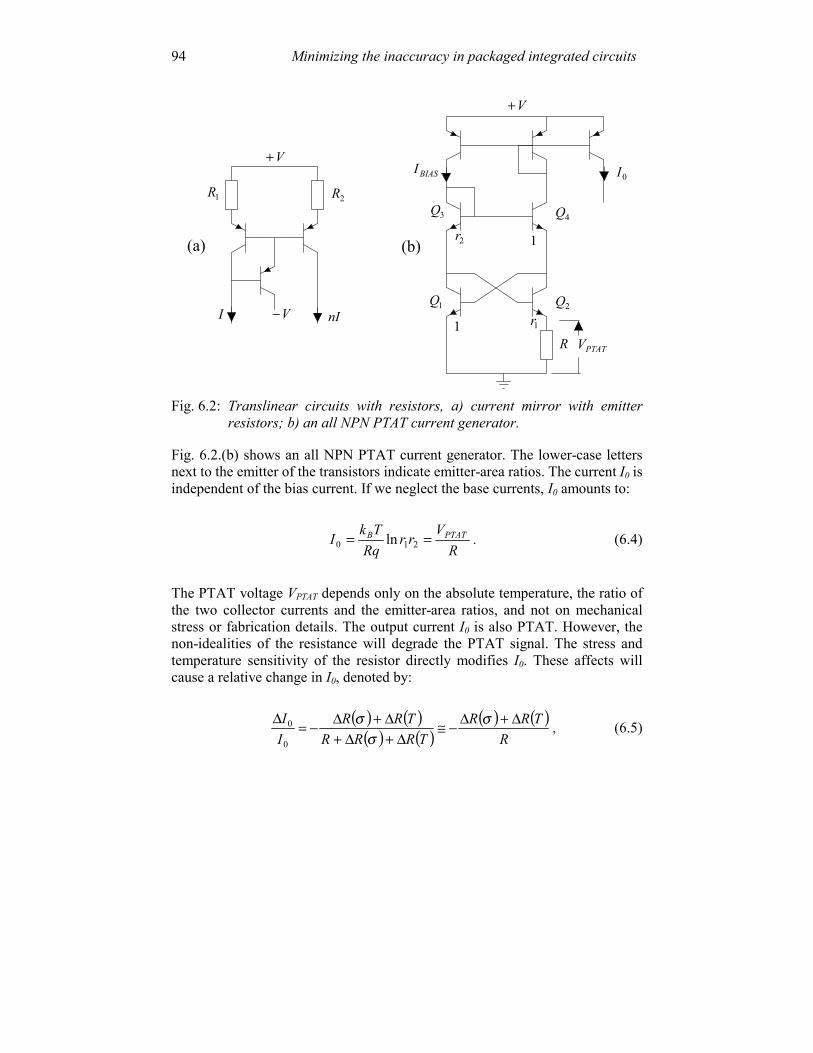
Minimizing the inaccuracy in packaged integrated circuits 94
1Q 2Q
3Q 4Q
PTATVR1 1r
BIASI0I
12r
1R 2R
V+
V−I nI
(a) (b)
V+
Fig. 6.2: Translinear circuits with resistors, a) current mirror with emitter
resistors; b) an all NPN PTAT current generator. Fig. 6.2.(b) shows an all NPN PTAT current generator. The lower-case letters next to the emitter of the transistors indicate emitter-area ratios. The current I0 is independent of the bias current. If we neglect the base currents, I0 amounts to:
RVrr
RqTkI PTATB == 210 ln . (6.4)
The PTAT voltage VPTAT depends only on the absolute temperature, the ratio of the two collector currents and the emitter-area ratios, and not on mechanical stress or fabrication details. The output current I0 is also PTAT. However, the non-idealities of the resistance will degrade the PTAT signal. The stress and temperature sensitivity of the resistor directly modifies I0. These affects will cause a relative change in I0, denoted by:
( ) ( )( ) ( )
( ) ( )R
TRRTRRR
TRRII ∆+∆−≅
∆+∆+∆+∆−=∆ σ
σσ
0
0 , (6.5)
6.4 Bandgap references and temperature transducers
95
where ∆R(σ) and ∆R(T) represent the stress- and temperature-induced resistance changes, respectively. When available, polysilicon resistors can be applied, because both the piezojunction effect and the temperature coefficient of polysilicon resistors are smaller than those of monocrystalline silicon resistors [8, 9]. For monocrystalline silicon resistors, simply setting a serial perpendicular pair of resistors will reduce the stress-induced change in the p-type resistor (see Section 5.4). Next, the designer has to take into account the non-idealities caused by the temperature coefficient of the resistor. The reduction of the piezoresistive effect in the current-mirror circuit shown in Fig. 6.2.(a) depends on the matching of the resistors. The PTAT-current circuit shown in Fib. 6.2.(b) is unbalanced from the point of view of mechanical stress and resistor matching is not possible. The layout proposed in Section 5.4 can be applied to reduce the stress-induced inaccuracy in monocrystalline resistors due to the piezoresistive effect. 6.4 Bandgap references and temperature transducers Circuits based on bandgap references are widely used in analogue integrated circuits, such as voltage regulators, voltage references, AD and DA converters and temperature transducers. In bandgap references the reference voltage is obtained by compensating the base-emitter voltage of a bipolar transistor for its temperature dependence. The temperature coefficient of the base-emitter voltage VBE of a bipolar transistor is approximately –2 mV/ °C. To obtain the desired temperature-stable voltage, a signal with an equal but positive temperature coefficient is added, to compensate for at least the first-order temperature dependence of VBE. This correction voltage, PTAT, is obtained by amplifying the difference between two base-emitter voltages of transistors operated at unequal collector-current densities. In this way an output voltage Vref is obtained for which it holds that:
PTATBEref VAVV 1+= . (6.6)
The parameter A1 is chosen in such a way that the second term in Equation 6.6 exactly cancels the first-order temperature dependence of VBE. Thus, Vref is equal to the extrapolated base-emitter voltage, VBE0 at zero Kelvin. Fig. 6.3.a shows the typical temperature curve of a bandgap-reference circuit.
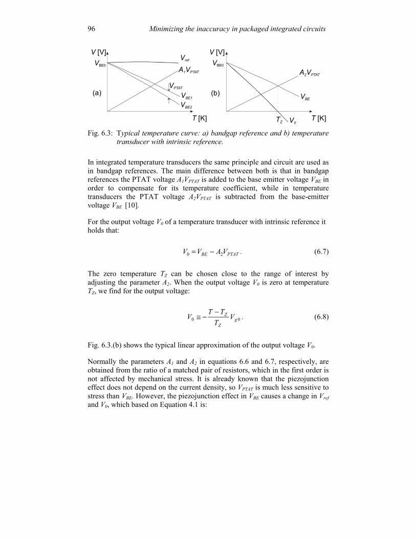
Minimizing the inaccuracy in packaged integrated circuits 96
VBE0 VBE0
V [V]
T [K]
VBE1
VPTAT
V0
VBE2
Vref
A V1 PTAT A V2 PTAT
V [V]
T [K]
VBE
TZ
(a) (b)
Fig. 6.3: Typical temperature curve: a) bandgap reference and b) temperature
transducer with intrinsic reference. In integrated temperature transducers the same principle and circuit are used as in bandgap references. The main difference between both is that in bandgap references the PTAT voltage A1VPTAT is added to the base emitter voltage VBE in order to compensate for its temperature coefficient, while in temperature transducers the PTAT voltage A2VPTAT is subtracted from the base-emitter voltage VBE [10]. For the output voltage V0 of a temperature transducer with intrinsic reference it holds that:
PTATBE VAVV 20 −= . (6.7)
The zero temperature TZ can be chosen close to the range of interest by adjusting the parameter A2. When the output voltage V0 is zero at temperature TZ, we find for the output voltage:
00 gZ
Z VT
TTV
−−≅ . (6.8)
Fig. 6.3.(b) shows the typical linear approximation of the output voltage V0. Normally the parameters A1 and A2 in equations 6.6 and 6.7, respectively, are obtained from the ratio of a matched pair of resistors, which in the first order is not affected by mechanical stress. It is already known that the piezojunction effect does not depend on the current density, so VPTAT is much less sensitive to stress than VBE. However, the piezojunction effect in VBE causes a change in Vref and V0, which based on Equation 4.1 is:

6.4 Bandgap references and temperature transducers
97
( ) ( )( )( )1ln 2 +−+−−=∆ mnklijklmnijklklijklB
BE qTkV σσζζσζσ . (6.9)
Bandgap references and temperature transducers work over a wide temperature range. For this reason, the temperature dependence of the piezojunction coefficients, which were presented in Chapter 4, must also be considered. VBE does not only depend on temperature and mechanical stress, but also on bias. The change in VBE due to the stress-induced change in the bipolar-transistor collector-current bias is shown in Section 6.4.1. Another non-ideality is the nonlinear portion of the temperature dependence of VBE. Unlike the PTAT voltage, which is linearly related to the temperature, VBE shows a slight non-linearity. This well-known non-linearity can be represented by the high-order terms in Equation 3.16, which mainly consist of a second-order term and amount to:
( ) ( )
+−−=
TTTTT
qkmTV r
rB
BNLBE ln, η , (6.10)
A plot of the nonlinear term of the base-emitter voltage VBE versus temperature T for η=4 and mB=1 is shown in Fig. 6.4. Note that the top of the curve occurs at T=Tr. The total inaccuracy in VBE is given by the sum of the piezojunction effect and the nonlinear temperature term. Thus, the total inaccuracy in VBE is:
)()(),( , TVVTV NLBEBEBE +∆=∆ σσ . (6.11)

Minimizing the inaccuracy in packaged integrated circuits 98
-4
-3.5
-3
-2.5
-2
-1.5
-1
-0.5
0
-50 0 50 100 150
Temperature [ oC]
VBE,NL(T)
[m
V]
T r=50oC=323 K
η -m B =3
Fig. 6.4: Nonlinear temperature term of the base-emitter voltage. The calculated results of ∆VBE(σ,T) for a V-NPN transistor which is subject to uniaxial stress in the orientation <110> in the range between +180 MPa and -180 MPa, and which has a temperature between –10 °C and +110 °C are shown in Fig. 6.5. The calculations include the temperature dependency of the piezojunction coefficients. The program listing in MatLab used to calculate the results of ∆VBE(σ,T) in Fig. 6.5, 6.6 and 6.7 is shown in Appendix D. The total voltage deviation ∆V0,tot can be used as a benchmark of the undesirable deviation in VBE, which is given by:
( ) ( )MINBEMAXBEtot TVTVV ,,,0 σσ ∆−∆=∆ . (6.12)
In order to reduce the inaccuracy due to the piezojunction effect and the nonlinear temperature term in Vref and V0, ∆V0,tot should be as small as possible. Fig. 6.5, shows that for the described conditions ∆V0,tot amounts to 5.8 mV and ∆VBE(σ) is approximately 2 times higher than VBE,NL(T). The application of a V-PNP transistor will reduce the stress-induced inaccuracy. Fig. 6.6 shows the calculated results of ∆VBE(σ,T) for a V-PNP transistor subjected to the same temperature and stress conditions.
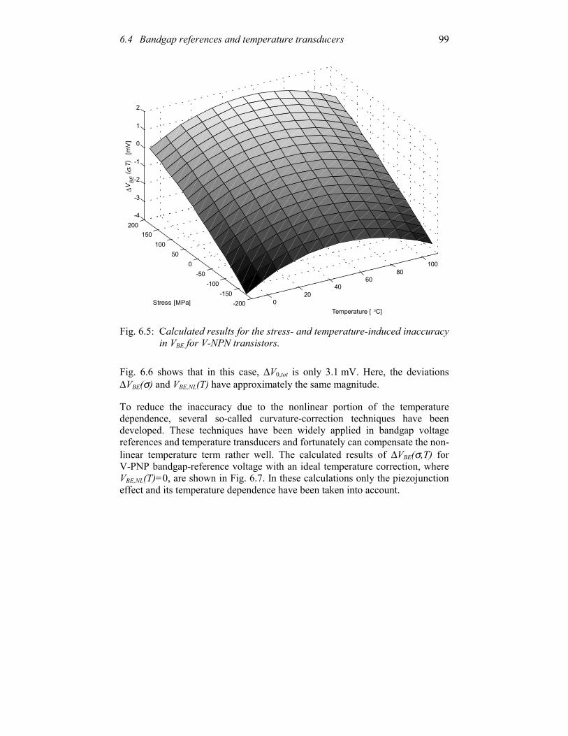
6.4 Bandgap references and temperature transducers
99
020
4060
80100
-200-150
-100-50
050
100150
200-4
-3
-2
-1
0
1
2
Temperature [ °C]Stress [MPa]
∆VB
E ( σ
,T)
[mV
]
Fig. 6.5: Calculated results for the stress- and temperature-induced inaccuracy
in VBE for V-NPN transistors. Fig. 6.6 shows that in this case, ∆V0,tot is only 3.1 mV. Here, the deviations ∆VBE(σ) and VBE,NL(T) have approximately the same magnitude. To reduce the inaccuracy due to the nonlinear portion of the temperature dependence, several so-called curvature-correction techniques have been developed. These techniques have been widely applied in bandgap voltage references and temperature transducers and fortunately can compensate the non-linear temperature term rather well. The calculated results of ∆VBE(σ,T) for V-PNP bandgap-reference voltage with an ideal temperature correction, where VBE,NL(T)=0, are shown in Fig. 6.7. In these calculations only the piezojunction effect and its temperature dependence have been taken into account.
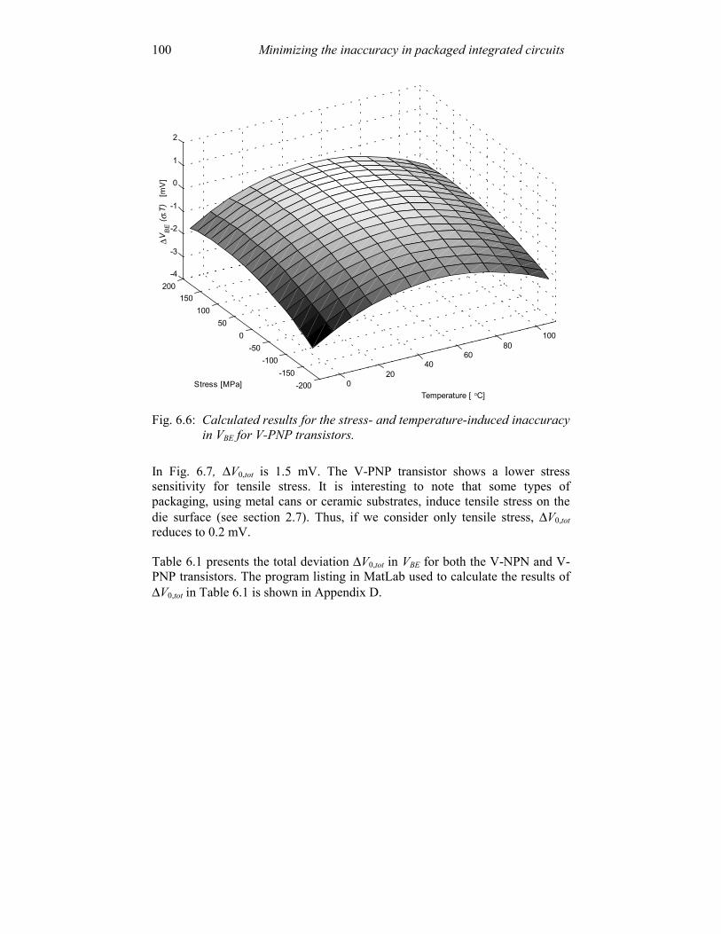
Minimizing the inaccuracy in packaged integrated circuits 100
020
4060
80100
-200-150
-100-50
050
100150
200-4
-3
-2
-1
0
1
2
Temperature [ °C]Stress [MPa]
∆VB
E ( σ
,T)
[mV
]
Fig. 6.6: Calculated results for the stress- and temperature-induced inaccuracy
in VBE for V-PNP transistors. In Fig. 6.7, ∆V0,tot is 1.5 mV. The V-PNP transistor shows a lower stress sensitivity for tensile stress. It is interesting to note that some types of packaging, using metal cans or ceramic substrates, induce tensile stress on the die surface (see section 2.7). Thus, if we consider only tensile stress, ∆V0,tot reduces to 0.2 mV. Table 6.1 presents the total deviation ∆V0,tot in VBE for both the V-NPN and V-PNP transistors. The program listing in MatLab used to calculate the results of ∆V0,tot in Table 6.1 is shown in Appendix D.
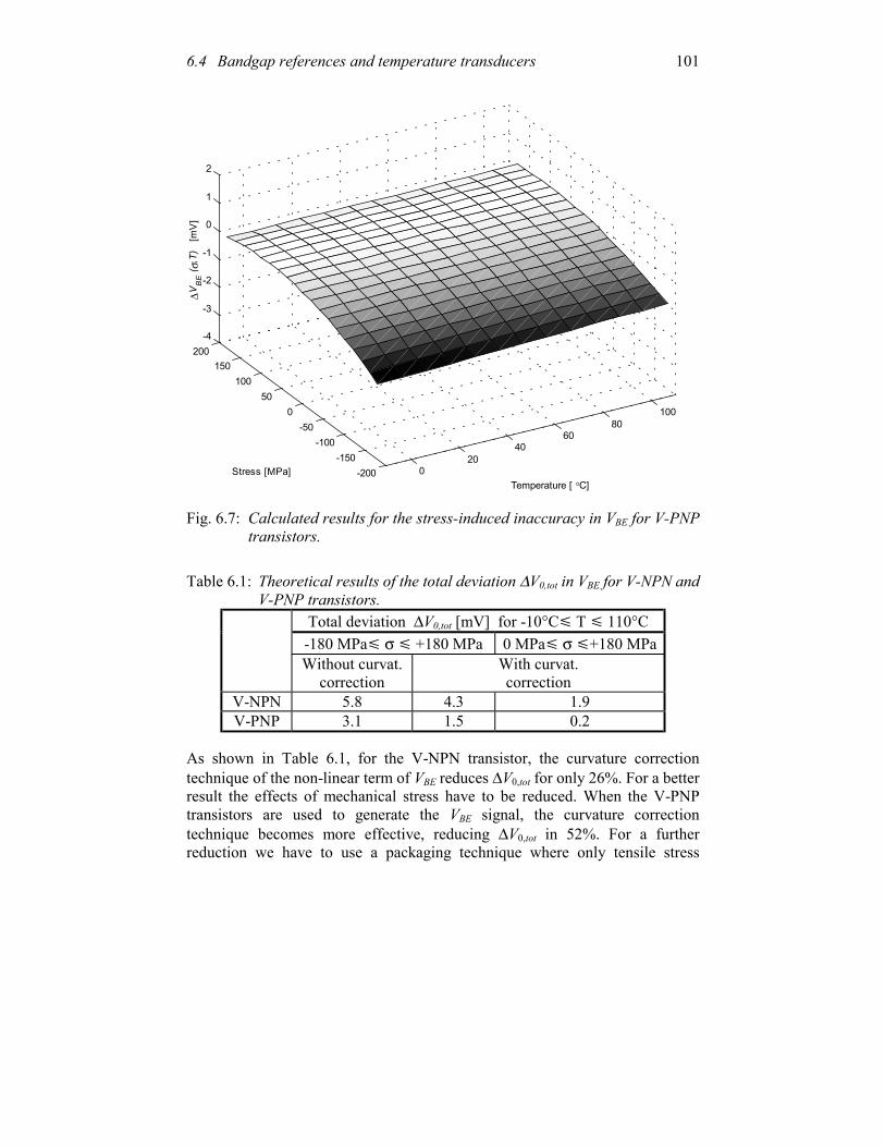
6.4 Bandgap references and temperature transducers
101
020
4060
80100
-200-150
-100-50
050
100150
200-4
-3
-2
-1
0
1
2
Temperature [ °C]Stress [MPa]
∆VB
E ( σ
,T)
[mV
]
Fig. 6.7: Calculated results for the stress-induced inaccuracy in VBE for V-PNP
transistors. Table 6.1: Theoretical results of the total deviation ∆V0,tot in VBE for V-NPN and
V-PNP transistors. Total deviation ∆V0,tot [mV] for -10°C! T ! 110°C -180 MPa! σ ! +180 MPa 0 MPa! σ !+180 MPa
Without curvat. correction
With curvat. correction
V-NPN 5.8 4.3 1.9 V-PNP 3.1 1.5 0.2
As shown in Table 6.1, for the V-NPN transistor, the curvature correction technique of the non-linear term of VBE reduces ∆V0,tot for only 26%. For a better result the effects of mechanical stress have to be reduced. When the V-PNP transistors are used to generate the VBE signal, the curvature correction technique becomes more effective, reducing ∆V0,tot in 52%. For a further reduction we have to use a packaging technique where only tensile stress
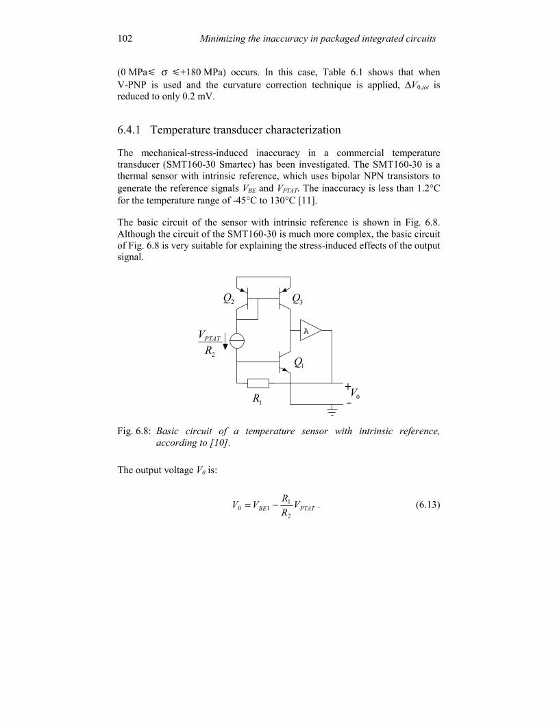
Minimizing the inaccuracy in packaged integrated circuits 102
(0 MPa! σ !+180 MPa) occurs. In this case, Table 6.1 shows that when V-PNP is used and the curvature correction technique is applied, ∆V0,tot is reduced to only 0.2 mV. 6.4.1 Temperature transducer characterization The mechanical-stress-induced inaccuracy in a commercial temperature transducer (SMT160-30 Smartec) has been investigated. The SMT160-30 is a thermal sensor with intrinsic reference, which uses bipolar NPN transistors to generate the reference signals VBE and VPTAT. The inaccuracy is less than 1.2°C for the temperature range of -45°C to 130°C [11]. The basic circuit of the sensor with intrinsic reference is shown in Fig. 6.8. Although the circuit of the SMT160-30 is much more complex, the basic circuit of Fig. 6.8 is very suitable for explaining the stress-induced effects of the output signal.
A
-+
2Q
1Q2R
VPTAT
1R 0V
3Q
Fig. 6.8: Basic circuit of a temperature sensor with intrinsic reference,
according to [10]. The output voltage V0 is:
PTATBE VRRVV
2
110 −= . (6.13)
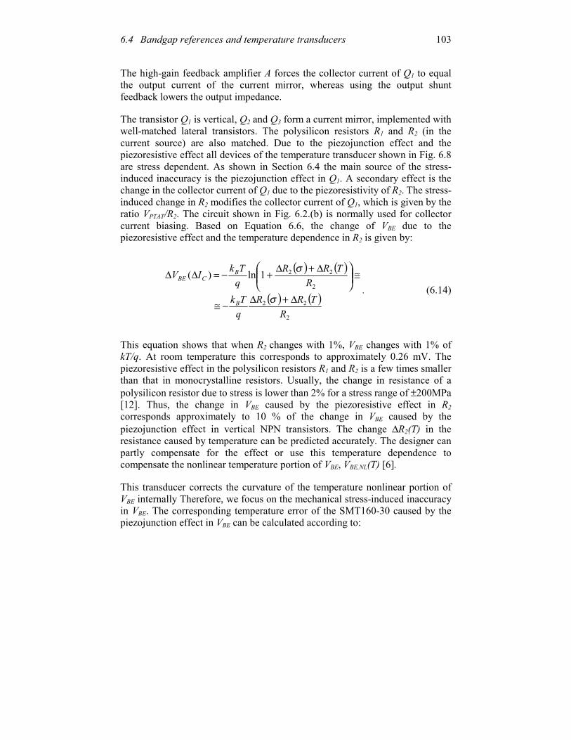
6.4 Bandgap references and temperature transducers
103
The high-gain feedback amplifier A forces the collector current of Q1 to equal the output current of the current mirror, whereas using the output shunt feedback lowers the output impedance. The transistor Q1 is vertical, Q2 and Q3 form a current mirror, implemented with well-matched lateral transistors. The polysilicon resistors R1 and R2 (in the current source) are also matched. Due to the piezojunction effect and the piezoresistive effect all devices of the temperature transducer shown in Fig. 6.8 are stress dependent. As shown in Section 6.4 the main source of the stress-induced inaccuracy is the piezojunction effect in Q1. A secondary effect is the change in the collector current of Q1 due to the piezoresistivity of R2. The stress-induced change in R2 modifies the collector current of Q1, which is given by the ratio VPTAT/R2. The circuit shown in Fig. 6.2.(b) is normally used for collector current biasing. Based on Equation 6.6, the change of VBE due to the piezoresistive effect and the temperature dependence in R2 is given by:
( ) ( )
( ) ( )2
22
2
22
1ln)(
RTRR
qTk
RTRR
qTkIV
B
BCBE
∆+∆−≅
≅
∆+∆+−=∆∆
σ
σ
. (6.14)
This equation shows that when R2 changes with 1%, VBE changes with 1% of kT/q. At room temperature this corresponds to approximately 0.26 mV. The piezoresistive effect in the polysilicon resistors R1 and R2 is a few times smaller than that in monocrystalline resistors. Usually, the change in resistance of a polysilicon resistor due to stress is lower than 2% for a stress range of ±200MPa [12]. Thus, the change in VBE caused by the piezoresistive effect in R2 corresponds approximately to 10 % of the change in VBE caused by the piezojunction effect in vertical NPN transistors. The change ∆R2(T) in the resistance caused by temperature can be predicted accurately. The designer can partly compensate for the effect or use this temperature dependence to compensate the nonlinear temperature portion of VBE, VBE,NL(T) [6]. This transducer corrects the curvature of the temperature nonlinear portion of VBE internally Therefore, we focus on the mechanical stress-induced inaccuracy in VBE. The corresponding temperature error of the SMT160-30 caused by the piezojunction effect in VBE can be calculated according to:
Minimizing the inaccuracy in packaged integrated circuits 104
( )ιχσ
ι
σδδ
==
=
∆=TBE
TBE
OUTji V
VTE , , (6.15)
where ( )
ιχσσ
==∆
TBEV is the change in VBE due to a stress χ at the same
temperature ι, which is calculated using Equation 6.9. The derivative
ιδδ
=TBE
OUT
VT is the sensor-output sensitivity to the base-emitter voltage VBE at a
certain temperature ι. Taking into account the internal signal processing of the SMT160-30, its output sensitivity to VBE depends on the temperature, as shown in Fig. 6.9.
-0.34
-0.32
-0.30
-0.28
-0.26
-0.24
-0.22
-0.20
-30 -10 10 30 50 70 90 110 130
Temperature [ oC]
δ δδδTOUT/ δ δδδVB
E
[o C/m
V]
Fig. 6.9: The SMT160-30 output sensitivity to VBE related to temperature.
Fig. 6.10 shows the results based on Equation 6.15.

6.4 Bandgap references and temperature transducers
105
-1.2
-0.8
-0.4
0
0.4
0.8
1.2
-250 -150 -50 50 150 250
Stress [MPa]
Ei,j
[ o C
] -10 50110
Temp. [oC]
Fig. 6.10: Calculated output error of the SMT160-30 caused by the
piezojunction effect in VBE. Experimental results The mechanical stress effect of the SMT160-30 has been measured at different temperatures. The results for seven different temperatures are shown in Fig. 6.11. Comparison of Fig. 6.10 and Fig. 6.11 shows that about 80% of the stress dependency of the SMT160-30 output signal can be explained by the piezojunction effect in VBE. Thus, we can conclude that the stress-induced inaccuracy of this temperature transducer is mainly due to the piezojunction effect in VBE of the NPN temperature-reference transistor.
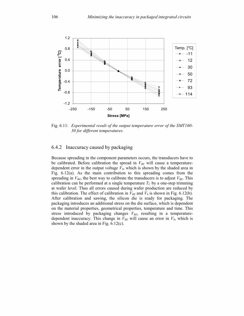
Minimizing the inaccuracy in packaged integrated circuits 106
-1.2
-0.8
-0.4
0.0
0.4
0.8
1.2
-250 -150 -50 50 150 250
Stress [MPa]
Tem
pera
ture
err
or [
0 C]
. -11 12 30 50 72 93114
Temp. [oC]
Fig. 6.11: Experimental result of the output temperature error of the SMT160-
30 for different temperatures. 6.4.2 Inaccuracy caused by packaging Because spreading in the component parameters occurs, the transducers have to be calibrated. Before calibration the spread in VBE will cause a temperature-dependent error in the output voltage V0, which is shown by the shaded area in Fig. 6.12(a). As the main contribution to this spreading comes from the spreading in VBE, the best way to calibrate the transducers is to adjust VBE. This calibration can be performed at a single temperature TC by a one-step trimming at wafer level. Thus all errors caused during wafer production are reduced by this calibration. The effect of calibration in VBE and V0 is shown in Fig. 6.12(b). After calibration and sawing, the silicon die is ready for packaging. The packaging introduces an additional stress on the die surface, which is dependent on the material properties, geometrical properties, temperature and time. This stress introduced by packaging changes VBE, resulting in a temperature-dependent inaccuracy. This change in VBE will cause an error in V0, which is shown by the shaded area in Fig. 6.12(c).
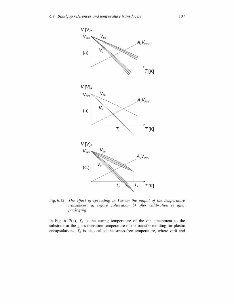
6.4 Bandgap references and temperature transducers
107
V0
V0
A V2 PTAT
A V2 PTAT
VBE0
VBE0
VBE0
V [V]
V [V]
T [K]
T [K]
VBE
VBE
TC
TC
(a)
(b)
V0
A V2 PTAT
V [V]
T [K]
VBE
TA
(c.)
Fig. 6.12: The effect of spreading in VBE on the output of the temperature transducer: a) before calibration b) after calibration c) after packaging.
In Fig. 6.12(c), TA is the curing temperature of the die attachment to the substrate or the glass-transition temperature of the transfer molding for plastic encapsulations. TA is also called the stress-free temperature, where σ=0 and
Minimizing the inaccuracy in packaged integrated circuits 108
therefore ∆VBE(σ)=0. Due to the mismatch between Thermal Coefficients of Expansion TCEs, the mechanical-stress increases for temperatures below TA. Based on Equation 3.17, we observe that ∆VBE(σ) is proportional to the thermal voltage kBT/q. New calibration after packaging will reduce the inaccuracy of V0 at the temperature TC, but this will not be effective for temperatures different from TC. Based on Fig. 6.12(c), the inaccuracy in V0 can be reduced by minimizing both the stress-induced by packaging and the piezojunction coefficients of the transistor. The reduction of the stress induced by packaging is a difficult and challenging task, especially when the integrated circuit is designed for a wide range of operating temperatures. Several known methods to minimize package stresses are based on the use of mechanical-compliance interface materials between the die and packaging [13-15]. A common stress reduction technique is the deposition of a mechanical-compliance overcoat onto the top of the silicon die before the transfer molding. This overcoat prevents direct contact between the silicon die and plastics and consequently lowers the stress in silicon [4]. This interface material has a low Young’s modulus and can accommodate the mismatch between TCEs. Usually, polymide or Room Temperature Vulcanization (RTV) silicone are used as an interface materials. Thus, not only the stress induced by the package in the die but also the stress-free temperature TA is reduced. However, the special equipment required and additional process time consumed can make this an expensive procedure. Furthermore, these materials exhibit poor thermal and electrical conductivity, which are disadvantages for most of the integrated circuits applications. Stresses due to solder or gold eutectic mounting can be minimized by attaching the silicon die on a substrate with a TCE similar to that of silicon, such as molybdenum alloy-42 (a nickel-iron alloy containing 42% nickel). Unfortunately, molybdenum headers are expensive, while alloy-42 is brittle and exhibits poor thermal and electrical conductivity [2]. Another method to minimize the piezojunction effect is to use the V-PNP transistors. This method can offer a low-cost solution, which is implemented on the circuit design level and which does not need any extra steps for the IC fabrication. Experimental results The error induced by packaging has been measured for three samples of the temperature transducers of the type SMT160-30. The output temperature error has been measured for three different steps; 1) after calibration, 2) after wafer sawing and 3) after packaging. A metal-can packaging (TO-18) with eutectic bonding was used. The measured results at room temperature are shown in Fig. 6.13.
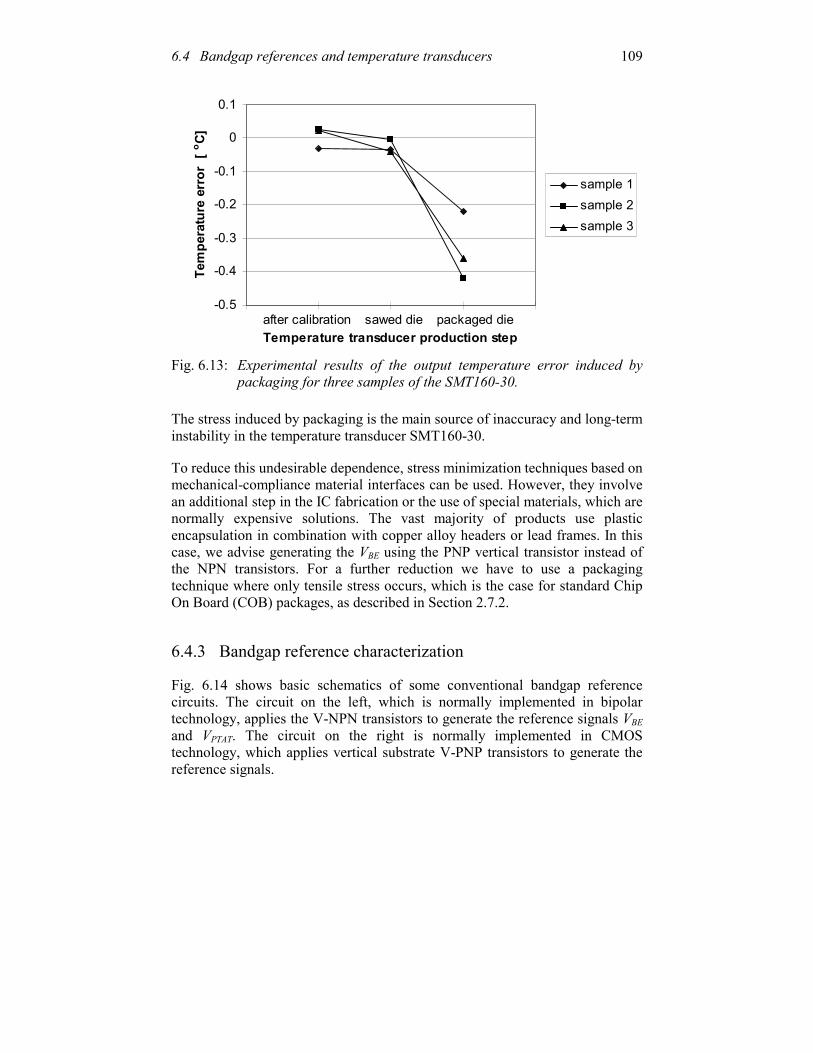
6.4 Bandgap references and temperature transducers
109
-0.5
-0.4
-0.3
-0.2
-0.1
0
0.1
Temperature transducer production step
Tem
pera
ture
err
or [
o C]sample 1sample 2sample 3
after calibration sawed die packaged die
Fig. 6.13: Experimental results of the output temperature error induced by
packaging for three samples of the SMT160-30. The stress induced by packaging is the main source of inaccuracy and long-term instability in the temperature transducer SMT160-30. To reduce this undesirable dependence, stress minimization techniques based on mechanical-compliance material interfaces can be used. However, they involve an additional step in the IC fabrication or the use of special materials, which are normally expensive solutions. The vast majority of products use plastic encapsulation in combination with copper alloy headers or lead frames. In this case, we advise generating the VBE using the PNP vertical transistor instead of the NPN transistors. For a further reduction we have to use a packaging technique where only tensile stress occurs, which is the case for standard Chip On Board (COB) packages, as described in Section 2.7.2. 6.4.3 Bandgap reference characterization Fig. 6.14 shows basic schematics of some conventional bandgap reference circuits. The circuit on the left, which is normally implemented in bipolar technology, applies the V-NPN transistors to generate the reference signals VBE and VPTAT. The circuit on the right is normally implemented in CMOS technology, which applies vertical substrate V-PNP transistors to generate the reference signals.
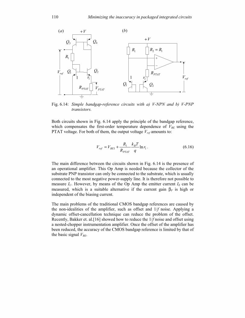
Minimizing the inaccuracy in packaged integrated circuits 110
3Q 4Q
2Q1Q
1R
PTATR
refV
PTATV
1 1r
V+
1Q 2Q
1R 12 RR =
PTATR1 1r refV
V+
)(a )(b
Fig. 6.14: Simple bandgap-reference circuits with a) V-NPN and b) V-PNP
transistors. Both circuits shown in Fig. 6.14 apply the principle of the bandgap reference, which compensates the first-order temperature dependence of VBE using the PTAT voltage. For both of them, the output voltage Vref amounts to:
11
1 ln rqTk
RRVV B
PTATBEref += . (6.16)
The main difference between the circuits shown in Fig. 6.14 is the presence of an operational amplifier. This Op Amp is needed because the collector of the substrate PNP transistor can only be connected to the substrate, which is usually connected to the most negative power-supply line. It is therefore not possible to measure IC. However, by means of the Op Amp the emitter current IE can be measured, which is a suitable alternative if the current gain βF is high or independent of the biasing current. The main problems of the traditional CMOS bandgap references are caused by the non-idealities of the amplifier, such as offset and 1/f noise. Applying a dynamic offset-cancellation technique can reduce the problem of the offset. Recently, Bakker et. al.[16] showed how to reduce the 1/f noise and offset using a nested-chopper instrumentation amplifier. Once the offset of the amplifier has been reduced, the accuracy of the CMOS bandgap reference is limited by that of the basic signal VBE.
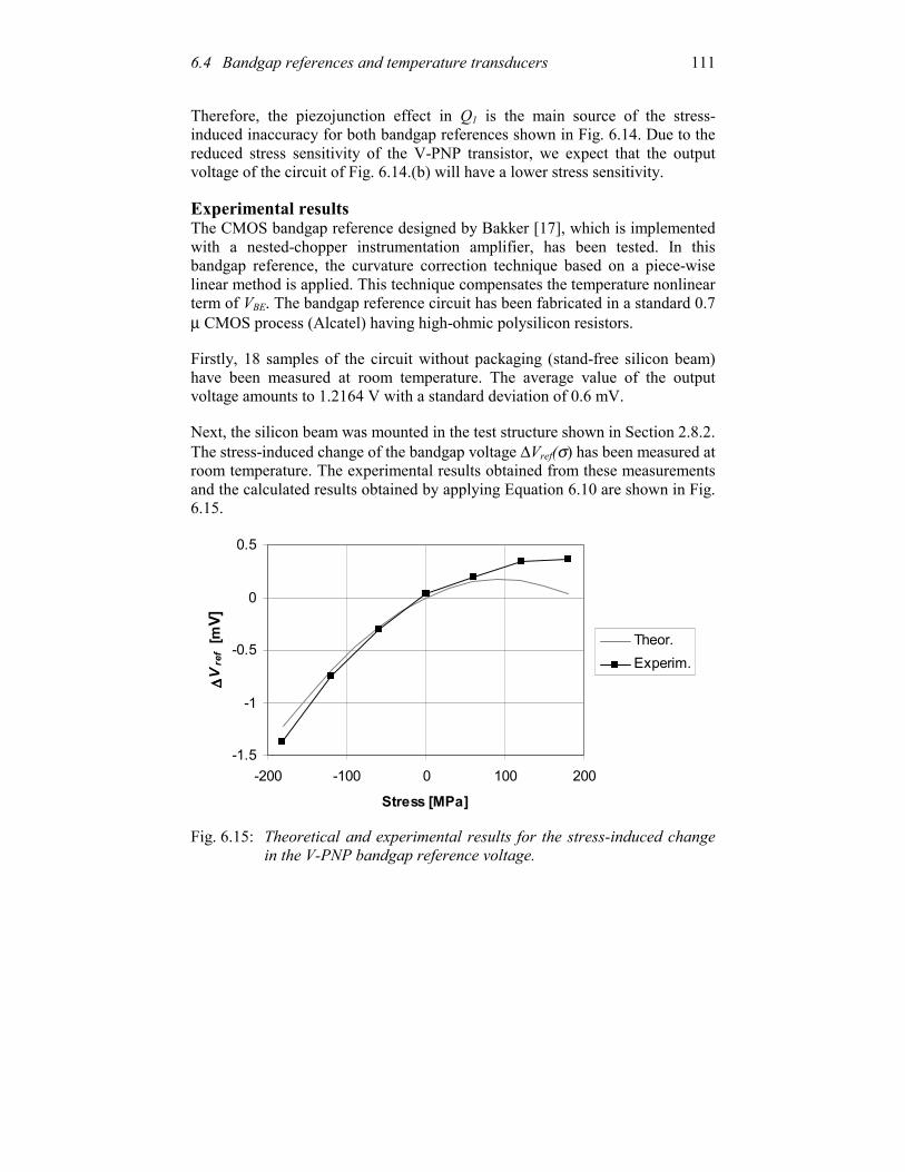
6.4 Bandgap references and temperature transducers
111
Therefore, the piezojunction effect in Q1 is the main source of the stress-induced inaccuracy for both bandgap references shown in Fig. 6.14. Due to the reduced stress sensitivity of the V-PNP transistor, we expect that the output voltage of the circuit of Fig. 6.14.(b) will have a lower stress sensitivity. Experimental results The CMOS bandgap reference designed by Bakker [17], which is implemented with a nested-chopper instrumentation amplifier, has been tested. In this bandgap reference, the curvature correction technique based on a piece-wise linear method is applied. This technique compensates the temperature nonlinear term of VBE. The bandgap reference circuit has been fabricated in a standard 0.7 µ CMOS process (Alcatel) having high-ohmic polysilicon resistors. Firstly, 18 samples of the circuit without packaging (stand-free silicon beam) have been measured at room temperature. The average value of the output voltage amounts to 1.2164 V with a standard deviation of 0.6 mV. Next, the silicon beam was mounted in the test structure shown in Section 2.8.2. The stress-induced change of the bandgap voltage ∆Vref(σ) has been measured at room temperature. The experimental results obtained from these measurements and the calculated results obtained by applying Equation 6.10 are shown in Fig. 6.15.
-1.5
-1
-0.5
0
0.5
-200 -100 0 100 200
Stress [MPa]
∆ ∆∆∆Vref [m
V]
Theor.Experim.
Fig. 6.15: Theoretical and experimental results for the stress-induced change
in the V-PNP bandgap reference voltage.
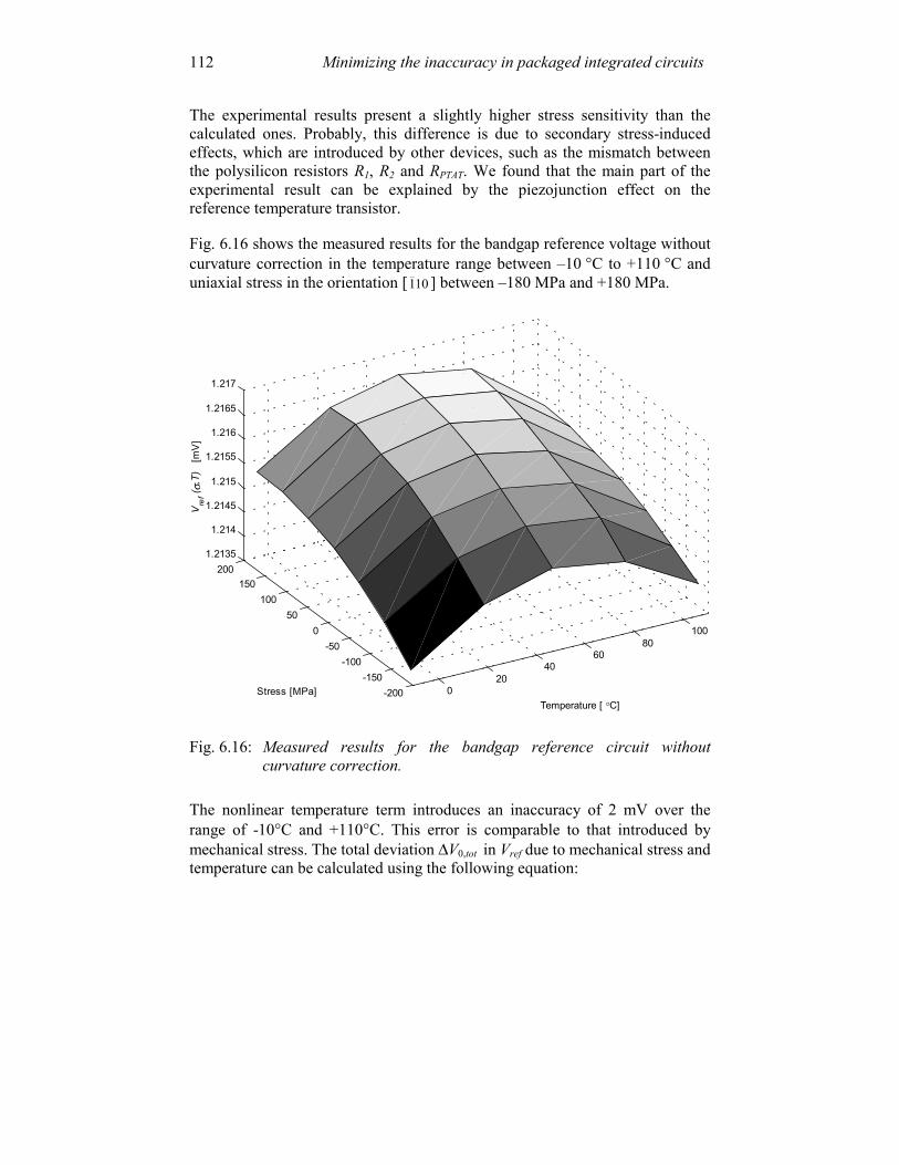
Minimizing the inaccuracy in packaged integrated circuits 112
The experimental results present a slightly higher stress sensitivity than the calculated ones. Probably, this difference is due to secondary stress-induced effects, which are introduced by other devices, such as the mismatch between the polysilicon resistors R1, R2 and RPTAT. We found that the main part of the experimental result can be explained by the piezojunction effect on the reference temperature transistor. Fig. 6.16 shows the measured results for the bandgap reference voltage without curvature correction in the temperature range between –10 °C to +110 °C and uniaxial stress in the orientation [ 101
_] between –180 MPa and +180 MPa.
020
4060
80100
-200-150
-100-50
050
100150
2001.2135
1.214
1.2145
1.215
1.2155
1.216
1.2165
1.217
Temperature [ °C]Stress [MPa]
Vre
f ( σ,T
) [m
V]
Fig. 6.16: Measured results for the bandgap reference circuit without curvature correction.
The nonlinear temperature term introduces an inaccuracy of 2 mV over the range of -10°C and +110°C. This error is comparable to that introduced by mechanical stress. The total deviation ∆V0,tot in Vref due to mechanical stress and temperature can be calculated using the following equation:
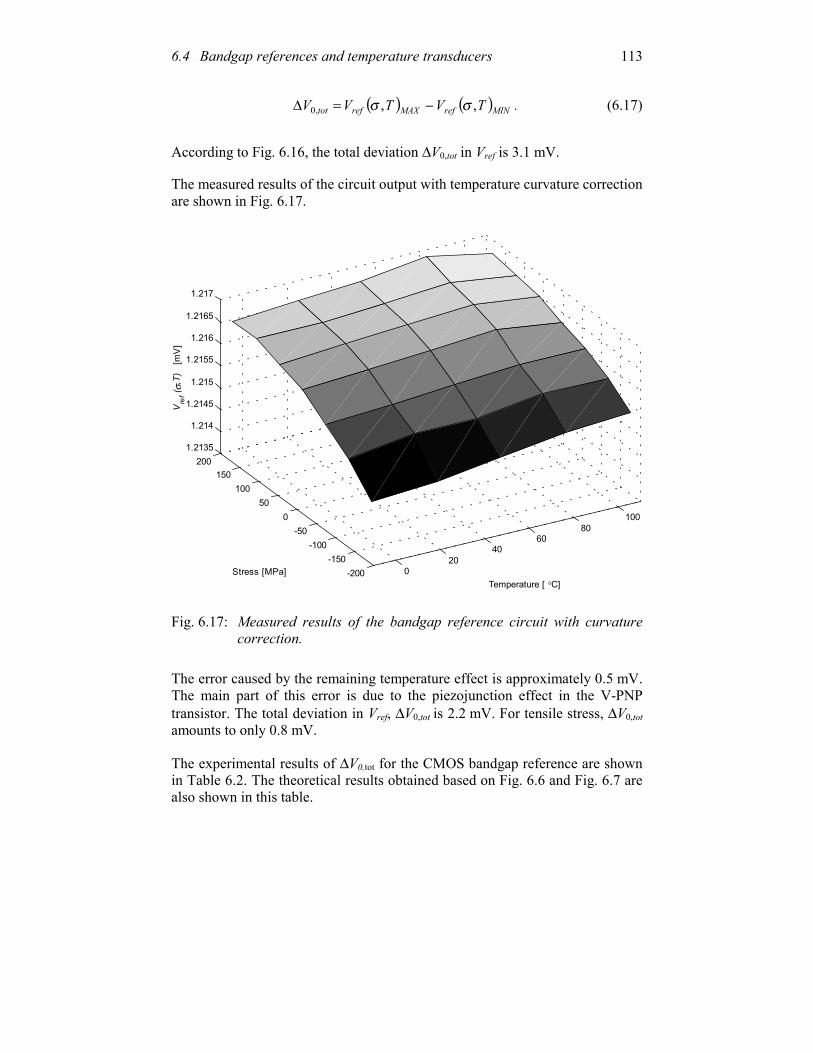
6.4 Bandgap references and temperature transducers
113
( ) ( )MINrefMAXreftot TVTVV ,,,0 σσ −=∆ . (6.17)
According to Fig. 6.16, the total deviation ∆V0,tot in Vref is 3.1 mV. The measured results of the circuit output with temperature curvature correction are shown in Fig. 6.17.
020
4060
80100
-200-150
-100-50
050
100150
2001.2135
1.214
1.2145
1.215
1.2155
1.216
1.2165
1.217
Temperature [ °C]Stress [MPa]
Vre
f ( σ,T
) [m
V]
Fig. 6.17: Measured results of the bandgap reference circuit with curvature correction.
The error caused by the remaining temperature effect is approximately 0.5 mV. The main part of this error is due to the piezojunction effect in the V-PNP transistor. The total deviation in Vref, ∆V0,tot is 2.2 mV. For tensile stress, ∆V0,tot amounts to only 0.8 mV. The experimental results of ∆V0,tot for the CMOS bandgap reference are shown in Table 6.2. The theoretical results obtained based on Fig. 6.6 and Fig. 6.7 are also shown in this table.
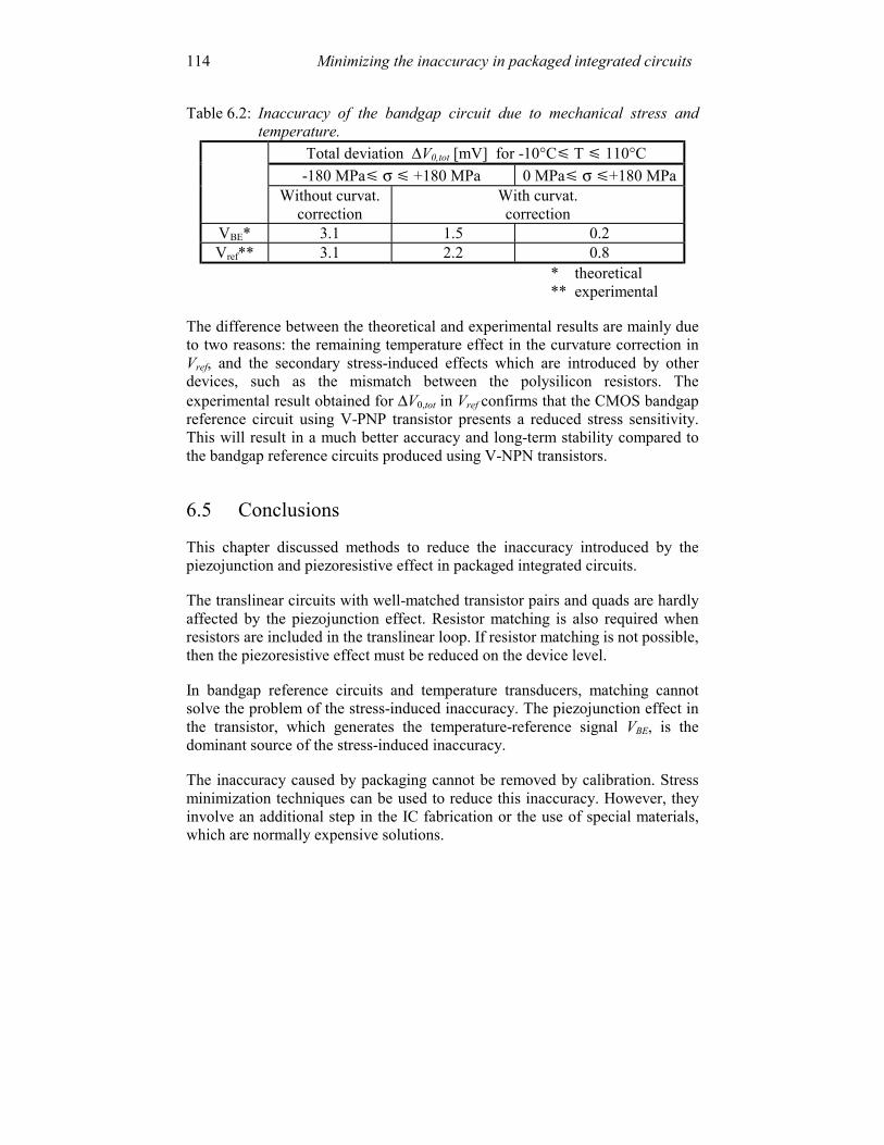
Minimizing the inaccuracy in packaged integrated circuits 114
Table 6.2: Inaccuracy of the bandgap circuit due to mechanical stress and temperature.
Total deviation ∆V0,tot [mV] for -10°C! T ! 110°C -180 MPa! σ ! +180 MPa 0 MPa! σ !+180 MPa
Without curvat. correction
With curvat. correction
VBE* 3.1 1.5 0.2 Vref** 3.1 2.2 0.8
* theoretical ** experimental The difference between the theoretical and experimental results are mainly due to two reasons: the remaining temperature effect in the curvature correction in Vref, and the secondary stress-induced effects which are introduced by other devices, such as the mismatch between the polysilicon resistors. The experimental result obtained for ∆V0,tot in Vref confirms that the CMOS bandgap reference circuit using V-PNP transistor presents a reduced stress sensitivity. This will result in a much better accuracy and long-term stability compared to the bandgap reference circuits produced using V-NPN transistors. 6.5 Conclusions This chapter discussed methods to reduce the inaccuracy introduced by the piezojunction and piezoresistive effect in packaged integrated circuits. The translinear circuits with well-matched transistor pairs and quads are hardly affected by the piezojunction effect. Resistor matching is also required when resistors are included in the translinear loop. If resistor matching is not possible, then the piezoresistive effect must be reduced on the device level. In bandgap reference circuits and temperature transducers, matching cannot solve the problem of the stress-induced inaccuracy. The piezojunction effect in the transistor, which generates the temperature-reference signal VBE, is the dominant source of the stress-induced inaccuracy. The inaccuracy caused by packaging cannot be removed by calibration. Stress minimization techniques can be used to reduce this inaccuracy. However, they involve an additional step in the IC fabrication or the use of special materials, which are normally expensive solutions.
6.5 Conclusions
115
Using the V-PNP transistor instead of the V-NPN transistor to generate the temperature-reference signal VBE significantly reduces the piezojunction effect. Therefore, we advise using these transistors in order to obtain a high accuracy and good long-term stability. For a further reduction a packaging technique must be used only involving tensile stress, which is the case for standard Chip On Board (COB) packages.
Minimizing the inaccuracy in packaged integrated circuits 116
References [1] B. Gilbert, Translinear circuits: a proposed classification, Elec. Letters,
vol. 11, no1, pp. 14-16, Jan. 1975. [2] A. Hastings, The art of analog layout, Printice-Hall International, New
York, 2001. [3] D. Vogel, C. Jian and I.D. Wolf, Experimental validation of finite
element modeling, Benefiting from Thermal and Mechanical Simulation in Micro-electronics, Eindhoven, Mar., pp.113-133, 2000.
[4] D. Manic, Drift in silicon integrated sensors and circuits due to thermo-mechanical stresses, PhD Thesis, Swiss Federal Institute of Technology EPFL, Switzerland, 2000.
[5] J. Mulder, Static and dynamic translinear circuits, Ph.D. Thesis, Delft University of Technology, Delft, The Netherlands, 1998.
[6] G.C.M. Meijer, Integrated circuits and components for bandgap references and temperature transducers, Ph.D. Thesis, Delft University of Technology, Delft, The Netherlands, 1982.
[7] W.A. Serdijn, C.J.M. Verhoeven and A.H.M. van Roermund, Analog IC techniques for low-voltage low-power electronics, Delft University Press, Delft University of Technology, The Netherlands, 1995.
[8] P.J. French and A.G.R. Evans, Piezoresistance in polysilicon and its applications to strain gauges, Solid-St. Electron., 32, pp. 1-10, 1989.
[9] P.J. French and A.G.R. Evans, Polysilicon strain sensors using shear piezoresistance, Sensors and Actuators, 15, pp. 257-272, 1988.
[10] G.C.M. Meijer and A.W. van Herwaarden, Thermal Sensors-Sensors series book, Institute of Physics Publishing Bristol and Philadelphia, 1994.
[11] Smartec B.V. , Specification Sheet SMT160-30, www.smartec.nl, 1996. [12] P.J French, Piezoresistance in polycrystalline silicon and its applications
to pressure sensors, Ph.D. Thesis, University of Southampton, 1986. [13] T.A. Kneckt, Bonding techniques for solid-state pressure sensors, Int.
Conf. Solid-State Sensors Actuators, Transducers, pp.95, 1987. [14] H.L. Offereins, H. Sandmaier, B. Folkmer, U. Steger, and W. Lang,
Stress free assembly technique for a silicon based pressure sensor, Int. Conf. Solid-State Sensors Actuators, Transducers, pp. 986, 1991.
[15] V.L. Spiering, S. Bouwstra, R.M.F.J. Spiering, and M. Elwenspoek, On-chip decoupling zone for package-stress reduction., Int. Conf. Solid-State Sensors Actuators, Transducers, pp. 982, 1991.
[16] A. Bakker, K. Thiele and J.H. Huijsing, A CMOS nested-chopper instrumentation amplifier with 100-nV offset, IEEE Journal of Solid State Circuits, Vol. 35, 12, Dec. 2000.

References
117
[17] A. Bakker, High-accuracy CMOS smart temperature sensors, Ph.D. Thesis, Delft University of Technology, Delft, The Netherlands, 2000.
Minimizing the inaccuracy in packaged integrated circuits 118
119
Chapter 7
Stress-sensing elements based on the piezojunction effect 7.1 Introduction In the silicon sensor market, pressure sensors and accelerometers are well known and widely applied products. They are commonly used in industrial, automotive and medical applications [1]. Most silicon pressure sensors and accelerometers are based on the use of the piezoresistive effect. Although the piezojunction effect was already discovered in 1951 [2], this effect has not yet been applied in commercially available mechanical stress sensors. However, the use of the piezojunction effect instead of the piezoresistive effect can be attractive for two basic reasons. The power consumption of the sensor can be reduced by some orders of magnitude [3] and the sensor size can be smaller. These are important requirements for biomedical electronics, where power supply and size restraints often limit the feasibility of implantable or injectable electronic devices [4]. On the other hand, compared to the piezoresistive effect, the piezojunction effect has a high temperature cross-sensitivity and non-linearity. Fortunately, this drawback can be overcome by an appropriate design. This chapter shows that the stress-sensing elements using the piezojunction effect can be a good alternative for the classical stress-sensing elements based on the piezoresistive effect.

Stress-sensing elements based on the piezojunction effect 120
7.2 Stress-sensing elements based on the piezoresistive effect
Mechanical stress sensors based on the piezoresistive effect in silicon have been available for more than thirty years [1]. These have been produced in both single crystal silicon and later also in polysilicon. In single crystal silicon the effect is highly anisotropic, and also dependent upon the doping type. Stress can be measured using a single resistor, but in order to reduce both the cross-temperature sensitivity and the common-mode effects and to increase the signal output, it is better to measure it using a Wheatstone bridge configuration. The Wheatstone bridge, which is shown in Fig. 7.1, is attractive because it allows the measurement of very small changes in the resistors of which the bridge is composed. When an integrated resistor is subjected to a change in physical parameters, such as stress/strain, temperature, light or the magnetic field, the resistance value changes. If this change is equal for all resistors of which the bridge is composed, then it concerns a common-mode effect and the output bridge signal VdR is still zero. The resistors of a piezoresistive Wheatstone bridge can be aligned along crystal directions in such a way that by applying a mechanical stress, the value of two resistors R1 and R4 increases by ∆R, and the value of the other two, R2 and R3 decreases by ∆R. Therefore, the differential voltage VdR is maximised for stress measurements and others cross effects are reduced. The resistors can be diffused or implanted in a thin silicon diaphragm (membrane) or be part of a micromachined structure. The discussion of the membranes or micromachined structures is beyond the scope of this thesis.
2R
3R 4R
1R
IdRV
+ −
Fig. 7.1: Wheatstone bridge configuration for stress measurement.

7.3 Stress-sensing elements based on the piezojunction effect 121
For practical reasons the Wheatstone bridge does not usually involve the use of n- and p-type resistors together but rather combinations of longitudinal and transversal piezoresistance, or tensile and compressive stress. For monocrystalline silicon resistors the best sensitivity can be achieved using p-type resistors in a <110> direction. The output signal VdR is normally amplified and for this purpose many designs are available [5]. However, the discussions of the amplifiers or conditioning signal circuits are beyond the scope of this thesis. Our discussion will focus on the stress-sensing element, which generates an electrical signal proportional to the stress. 7.3 Stress-sensing elements based on the piezojunction
effect Many prototypes of mechanical sensors based on the piezojunction effect were developed, such as microphones, accelerometers, and pressure sensors [6-9]. Pressing a hard stylus on the surface of a transistor or diode generated those stresses. However, these prototypes had the disadvantage that they were easily damaged by shocks and overload, and also very sensitive to thermal expansion and temperature cross-sensitivity [10]. More recently, better stress generation methods have become available with the advent of micromachining. The transistors can be integrated with micromachined beams, membranes, and hinges, which are easily stressed in a controlled manner [3, 11]. Since those stresses are both compressive and tensile their magnitude must be a factor fifty lower than those based on the method of the compressive stylus to avoid breakage. Although the invention of micromachining has enable new designs, the application of the piezojunction effect in stress-sensing elements has been explored only incidentally up to now [12]. In chapters 5 and 6, we showed how the piezojunction effect can be minimized in devices and circuits, respectively. The same knowledge can now be used to maximize the piezojunction effect. Based on the piezojunction coefficients, a bipolar transistor can be designed to maximize the piezojunction effect for an appropriate stress orientation. Stress can be measured using a single transistor. However, the use of a balanced configuration, such as a pair of matched transistors, is preferred. In this case, the minimization of the common-mode effects, such as temperature cross-sensitivity depends only on the match between the devices.

Stress-sensing elements based on the piezojunction effect 122
Fig. 7.2 shows two configurations which can be used for this purpose. The stress-dependent output can be taken from the differential voltage VdQ (Fig. 7.2(a)) or the current-mirror ratio, m (Fig. 7.2(b)). A different stress can be obtained by placing Q1 and Q2 at different positions on the silicon diaphragm or micromachining structure. To increase the output, Q1 can be under compression and Q2 under tension. A disadvantage of such a configuration is that the different locations of the transistors can also introduce a temperature mismatch between the transistors. Reducing the distance between the transistor centroids can minimize the temperature mismatch. Applying transistors with different stress sensitivities or even opposite sensitivity signs can maximize the stress-dependent output. For this purpose, the L-PNP transistors of which the stress sensitivity strongly depends on the current flow direction can be used. The freedom to choose the current direction in relation to the wafer crystal axes is not available in vertical transistors. Thus, in this application, the L-PNP transistors are preferred over the V-NPN transistors. The transistors Q1 and Q2 are aligned in such a way that their saturation current becomes unbalanced by mechanical stress. The optimum alignment of the L-PNP transistors for maximum stress effects are shown in Section 7.4.
I I
1Q 2Q
V+
I
1Q 2Q
mI
V+
dQV+ −
(a) (b)
Fig. 7.2: Stress-sensing elements using the piezojunction effect: a) differential
voltage and, b) current ratio. To calculate the stress-dependent output of each circuit shown in Fig. 7.2, we consider a pair of identical and well-matched transistors. In this qualitative analysis, the base currents and Early effect are neglected.
7.4 Comparison between the piezojunction effect and the piezoresistive effect for stress-sensing applications
123
For the differential voltage circuit, the stress-dependent signal is given by:
∆+∆+=
101
20
2lnSS
SSBdQ II
IIqTkV , (7.1)
where 0
1SI and 02SI are the stress-free saturation current and ∆IS1 and ∆IS2 are
the stress-dependent variations for the transistors Q1 and Q2, respectively. The current-mirror ratio for the circuit shown in Fig. 7.2(b) is given by:
mmIIII
IIm
SS
SS
C
C ∆+=∆+∆+
== 01
01
20
2
1
2 , (7.2)
where m0 is the stress-free current-mirror ratio and ∆m is the stress-dependent variation in m. 7.4 Comparison between the piezojunction effect and the
piezoresistive effect for stress-sensing applications The adoption of transistors instead of resistors as mechanical-stress-sensing elements involves some pros and cons. In the following we will compare the performance potential of both the piezojunction and the piezoresistive effect for applications in stress-sensing elements. Points of interest are the size, the mechanical-stress sensitivity, the temperature cross-sensitivity, the signal-to-noise ratio and the power consumption. Size The majority of the piezoresistive sensors are made from diffused or implanted resistors. In order to achieve reasonable resistor values in integrated circuit technology, one needs a relatively large area because of the low sheet resistance of the layers available to form resistors. Furthermore, the stress measurement area is very wide due to the large resistor size [13]. Consequently, the optimum location of the stress-sensing resistor in micromachined structures might be a problem. Integrated bipolar transistors require a much smaller area in comparison to that of resistors. Thus, it is better to locate, small-size stress-sensing elements in micromachined structures.
Stress-sensing elements based on the piezojunction effect 124
Mechanical stress sensitivity The stress sensitivity of the silicon resistors is proportional to the piezoresistive coefficients. In the same way, the stress sensitivity of the bipolar transistor saturation current is proportional to the piezojunction coefficients. It has been shown in Chapter 4 that the FOPR and FOPJ coefficients have the same order of magnitude. Thus, we expect that the stress-sensing elements based on the piezojunction effect and piezoresistive effect will have a comparable stress sensitivity. Cross-sensitivity Most transducers are designed to be mainly sensitive to only one signal. When a transducer is also sensitive to other signals, we call it cross-sensitivity of the sensor. Besides mechanical stress, also temperature, magnetic field and light affect the characteristics of the bipolar transistor. For example, the relative-stress induced change in a p-type resistor is approximately ∆R(σ)/Rσ=5×10-10 Pa-1. The same resistor has a first-order temperature coefficient of ∆R(T)/RT=2×10-3 °C-1. Therefore, the temperature cross-sensitivity of the resistor causes an error in stress of 4 MPa/°C. To reduce this problem, a Wheatstone bridge can be used. In this case, the cross-sensitivity is dependent on the match between the devices of which the bridge is composed. When the piezojunction effect is used to measure mechanical stress, the temperature cross-sensitivity is even higher. For example, if we consider a bipolar transistor biased with a constant collector current, VBE will change with stress and temperature, where ∆VBE(σ)=1 mV/100 MPa and ∆VBE(T)=-2 mV/°C. Therefore, the temperature cross-sensitivity of the piezojunction effect causes an error in the measured stress of –200 MPa/°C, which is 50 times as high as that of the piezoresistive effect. Therefore, as was already explained in Section 7.3, the use of a temperature-matched transistor pair is necessary to reduce the temperature cross-sensitivity. Signal-to-noise ratio and power consumption Semiconductor resistors display thermal noise, which is due to the random thermal motion of the electrons, which is directly proportional to the absolute temperature T. In a resistor R the thermal noise is given by the equation:
fTRkv BR ∆= 4__
2 , (7.3)
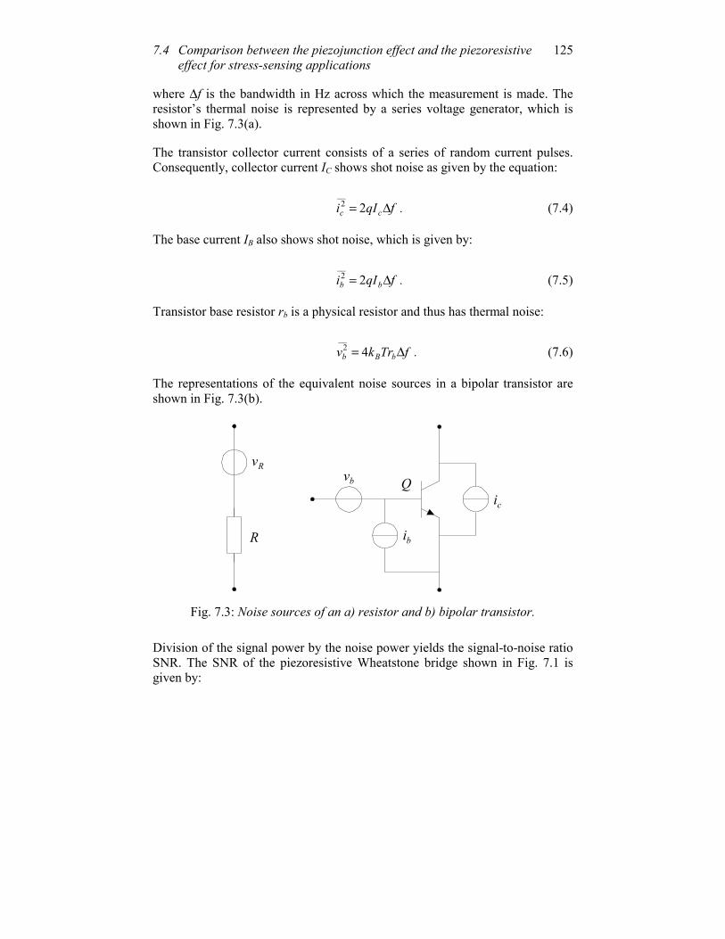
7.4 Comparison between the piezojunction effect and the piezoresistive effect for stress-sensing applications
125
where ∆f is the bandwidth in Hz across which the measurement is made. The resistor’s thermal noise is represented by a series voltage generator, which is shown in Fig. 7.3(a). The transistor collector current consists of a series of random current pulses. Consequently, collector current IC shows shot noise as given by the equation:
fqIi cc ∆= 2__2 . (7.4)
The base current IB also shows shot noise, which is given by:
fqIi bb ∆= 2__2 . (7.5)
Transistor base resistor rb is a physical resistor and thus has thermal noise:
fTrkv bBb ∆= 4__
2 . (7.6) The representations of the equivalent noise sources in a bipolar transistor are shown in Fig. 7.3(b).
Rvbv
bi
ciQ
R
Fig. 7.3: Noise sources of an a) resistor and b) bipolar transistor.
Division of the signal power by the noise power yields the signal-to-noise ratio SNR. The SNR of the piezoresistive Wheatstone bridge shown in Fig. 7.1 is given by:
Stress-sensing elements based on the piezojunction effect 126
fTkRRRI
B ∆
∆
=16
SNR
22
WB , (7.7)
where R=R1=R2=R3=R4 and ∆R is the stress-induced change in R. The SNR of the stress-sensing element based on the bipolar differential pair, which is shown in Fig. 7.2(a), is given by:
fg
rTk
V
mbB
dQ
∆
+
=
218
SNR2
DV , (7.8)
where gm is the transconductance, which is given by:
TkqIg
B
Cm = . (7.9)
The SNR of a unitary-gain current mirror (m0=1) operating as a stress-sensing element (shown in Fig. 7.2(b)) is given by:
( ) fgrqmI
mb ∆+∆=214
SNR2
CM . (7.10)
Fig. 7.4 shows a plot of SNRWB, SNRDV and SNRCM for ∆f=10 KHz. To calculate the results shown in Fig. 7.4, we consider a mechanical stress of 100 MPa in the orientation [110], which results in the following stress-dependent signals: for the piezoresistive bridge ∆R/R=0.1, for the differential pair VdQ=2.5 mV and for the current mirror ∆m=0.1. These values have been estimated based on Fig. 5.9 and Fig. 4.30. The typical values for the resistors are R=200 Ω and rb=300 Ω. For low current levels (I<100 µA), the piezojunction stress-sensing elements show a higher SNR as compared to that of the piezoresistive Wheatstone bridge. In the Wheatstone bridge configuration, the SNRWB is proportional to I2. For low current levels, the SNRCM and SNRDV increase linearly proportional to the current I. At high current levels, the contribution of the base-resistor thermal noise becomes dominant and both the SNRCM and the SNRDV saturate.
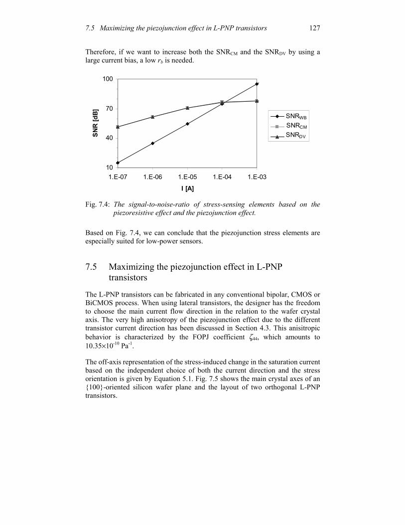
7.5 Maximizing the piezojunction effect in L-PNP transistors 127
Therefore, if we want to increase both the SNRCM and the SNRDV by using a large current bias, a low rb is needed.
10
40
70
100
1.E-07 1.E-06 1.E-05 1.E-04 1.E-03
I [A]
SNR
[dB] SNRWB
SNRCM
SNRDV
Fig. 7.4: The signal-to-noise-ratio of stress-sensing elements based on the
piezoresistive effect and the piezojunction effect. Based on Fig. 7.4, we can conclude that the piezojunction stress elements are especially suited for low-power sensors. 7.5 Maximizing the piezojunction effect in L-PNP
transistors The L-PNP transistors can be fabricated in any conventional bipolar, CMOS or BiCMOS process. When using lateral transistors, the designer has the freedom to choose the main current flow direction in the relation to the wafer crystal axis. The very high anisotropy of the piezojunction effect due to the different transistor current direction has been discussed in Section 4.3. This anisitropic behavior is characterized by the FOPJ coefficient ζ44, which amounts to 10.35×10⁻¹⁰ Pa-1. The off-axis representation of the stress-induced change in the saturation current based on the independent choice of both the current direction and the stress orientation is given by Equation 5.1. Fig. 7.5 shows the main crystal axes of an 100-oriented silicon wafer plane and the layout of two orthogonal L-PNP transistors.
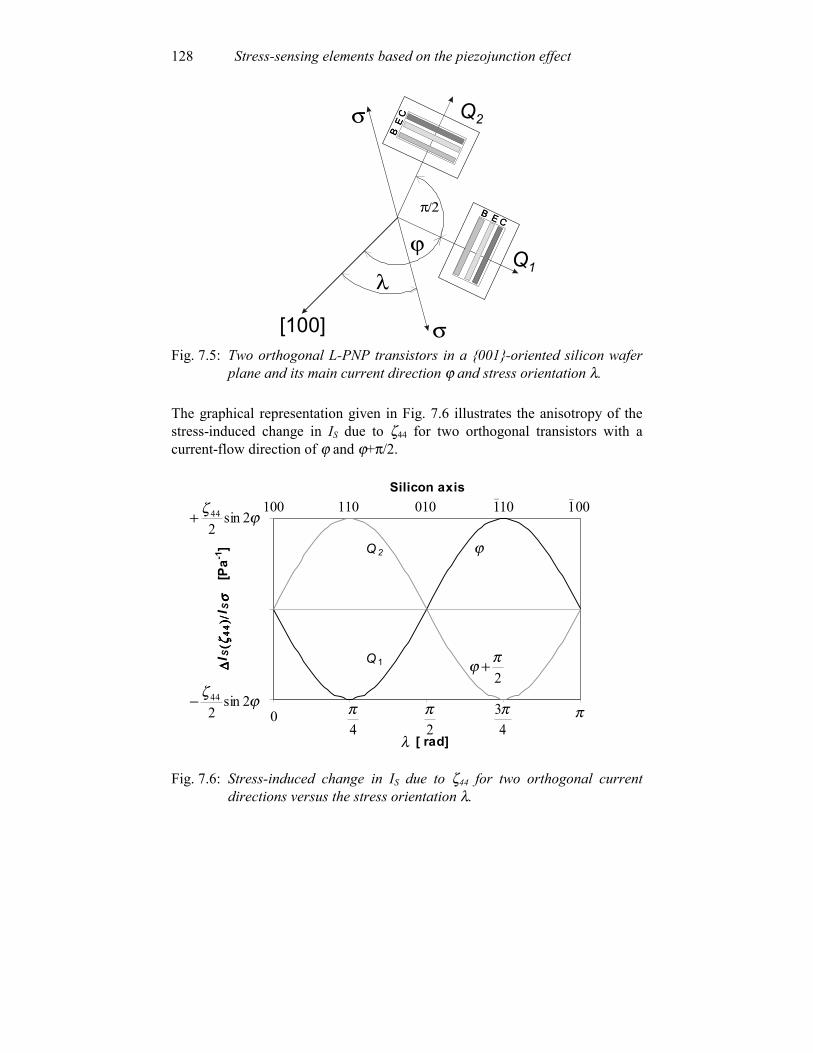
Stress-sensing elements based on the piezojunction effect 128
[100]
λ
ϕ
π/2
σ
σ
B E C
Q1
B E C
BE
CB
EC Q2
Fig. 7.5: Two orthogonal L-PNP transistors in a 001-oriented silicon wafer plane and its main current direction ϕ and stress orientation λ.
The graphical representation given in Fig. 7.6 illustrates the anisotropy of the stress-induced change in IS due to ζ44 for two orthogonal transistors with a current-flow direction of ϕ and ϕ+π/2.
λ [ rad]
∆ ∆∆∆I S
( (((ζ ζζζ4
44
444
44)/ )/)/)/I S
σ
σ
σ
σ
[Pa-1
] ϕ
2πϕ +
0
Silicon axis
4π
2π
43π π
ϕζ 2sin244+
ϕζ 2sin244−
101_
001_
010110100
Q 1
Q2
Fig. 7.6: Stress-induced change in IS due to ζ44 for two orthogonal current directions versus the stress orientation λ.
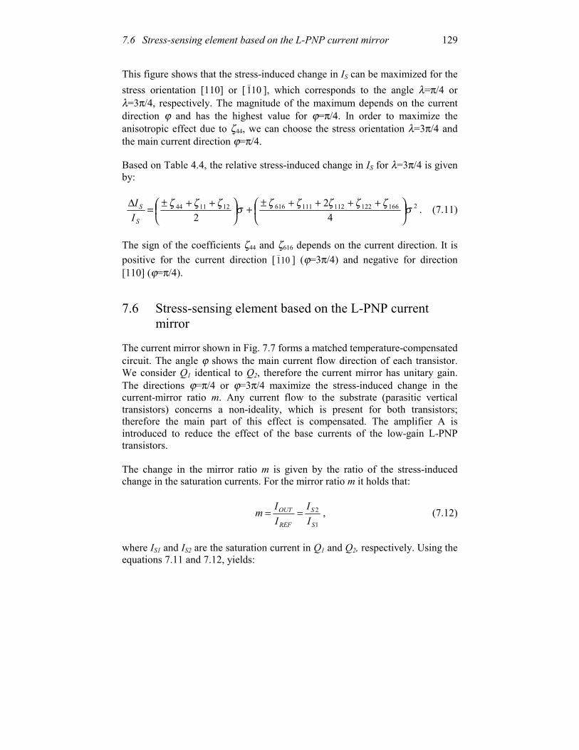
7.6 Stress-sensing element based on the L-PNP current mirror 129
This figure shows that the stress-induced change in IS can be maximized for the stress orientation [110] or [ 101
_], which corresponds to the angle λ=π/4 or
λ=3π/4, respectively. The magnitude of the maximum depends on the current direction ϕ and has the highest value for ϕ=π/4. In order to maximize the anisotropic effect due to ζ44, we can choose the stress orientation λ=3π/4 and the main current direction ϕ=π/4. Based on Table 4.4, the relative stress-induced change in IS for λ=3π/4 is given by:
2166122112111616121144
42
2σζζζζζσζζζ
++++±+
++±=∆
S
S
II . (7.11)
The sign of the coefficients ζ44 and ζ616 depends on the current direction. It is positive for the current direction [ 101
_] (ϕ=3π/4) and negative for direction
[110] (ϕ=π/4). 7.6 Stress-sensing element based on the L-PNP current
mirror The current mirror shown in Fig. 7.7 forms a matched temperature-compensated circuit. The angle ϕ shows the main current flow direction of each transistor. We consider Q1 identical to Q2, therefore the current mirror has unitary gain. The directions ϕ=π/4 or ϕ=3π/4 maximize the stress-induced change in the current-mirror ratio m. Any current flow to the substrate (parasitic vertical transistors) concerns a non-ideality, which is present for both transistors; therefore the main part of this effect is compensated. The amplifier A is introduced to reduce the effect of the base currents of the low-gain L-PNP transistors. The change in the mirror ratio m is given by the ratio of the stress-induced change in the saturation currents. For the mirror ratio m it holds that:
1
2
S
S
REF
OUT
II
IIm == , (7.12)
where IS1 and IS2 are the saturation current in Q1 and Q2, respectively. Using the equations 7.11 and 7.12, yields:
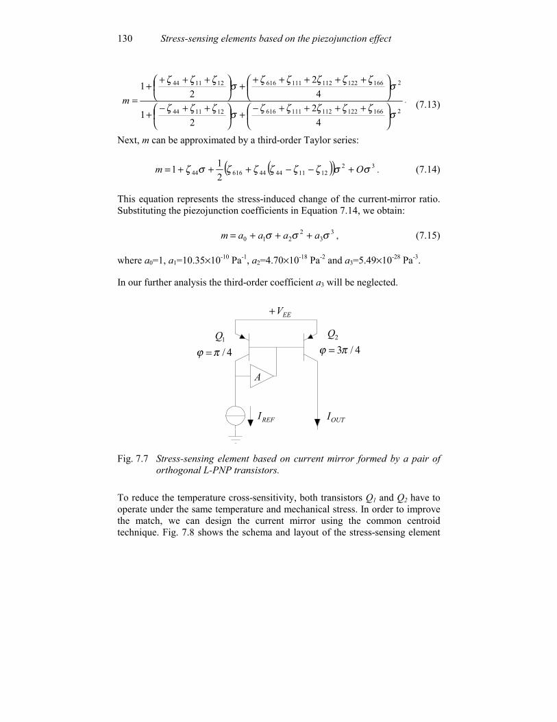
Stress-sensing elements based on the piezojunction effect 130
2166122112111616121144
2166122112111616121144
42
21
42
21
σζζζζζσζζζ
σζζζζζ
σζζζ
++++−
+
++−
+
+++++
+
+++
+=m . (7.13)
Next, m can be approximated by a third-order Taylor series:
( )( ) 321211444461644 2
11 σσζζζζζσζ Om +−−+++= . (7.14)
This equation represents the stress-induced change of the current-mirror ratio. Substituting the piezojunction coefficients in Equation 7.14, we obtain:
3
32
210 σσσ aaaam +++= , (7.15) where a0=1, a1=10.35×10⁻¹⁰ Pa-1, a2=4.70×10⁻¹⁸ Pa-2 and a3=5.49×10⁻²⁸ Pa-3. In our further analysis the third-order coefficient a3 will be neglected.
1Q
REFI
A
OUTI
4/πϕ =2Q
4/3πϕ =
EEV+
Fig. 7.7 Stress-sensing element based on current mirror formed by a pair of
orthogonal L-PNP transistors. To reduce the temperature cross-sensitivity, both transistors Q1 and Q2 have to operate under the same temperature and mechanical stress. In order to improve the match, we can design the current mirror using the common centroid technique. Fig. 7.8 shows the schema and layout of the stress-sensing element
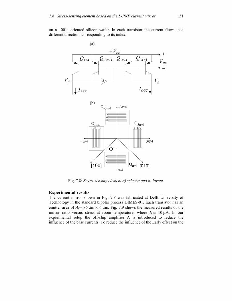
7.6 Stress-sensing element based on the L-PNP current mirror 131
on a 001-oriented silicon wafer. In each transistor the current flows in a different direction, corresponding to its index. (a)
4/3π−Q4/πQ 4/3πQ 4/π−Q
REFI OUTI
EEV+
AAV BV
BEV+
−
(b)
3π/4
Q3π/4
Qπ/4
BB
BB
EE
EE
CC
CC
ϕ
[010][100]
Fig. 7.8: Stress-sensing element a) schema and b) layout. Experimental results The current mirror shown in Fig. 7.8 was fabricated at Delft University of Technology in the standard bipolar process DIMES-01. Each transistor has an emitter area of AE= 86 µm × 6 µm. Fig. 7.9 shows the measured results of the mirror ratio versus stress at room temperature, where IREF=10 µA. In our experimental setup the off-chip amplifier A is introduced to reduce the influence of the base currents. To reduce the influence of the Early effect on the
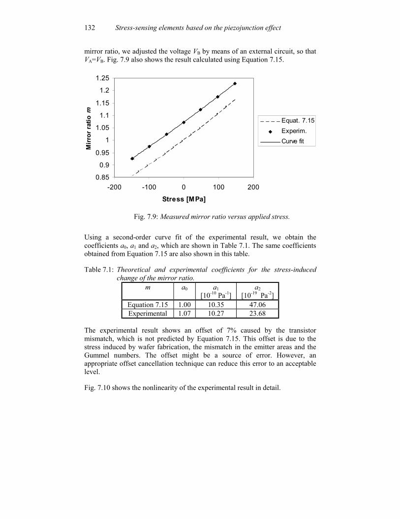
Stress-sensing elements based on the piezojunction effect 132
mirror ratio, we adjusted the voltage VB by means of an external circuit, so that VA=VB. Fig. 7.9 also shows the result calculated using Equation 7.15.
0.85
0.9
0.95
1
1.05
1.1
1.15
1.2
1.25
-200 -100 0 100 200
Stress [MPa]
Mirr
or ra
tio m
Equat. 7.15Experim.Curve fit
Fig. 7.9: Measured mirror ratio versus applied stress.
Using a second-order curve fit of the experimental result, we obtain the coefficients a0, a1 and a2, which are shown in Table 7.1. The same coefficients obtained from Equation 7.15 are also shown in this table. Table 7.1: Theoretical and experimental coefficients for the stress-induced
change of the mirror ratio. m a0 a1
[10-10 Pa-1] a2
[10-19 Pa-2] Equation 7.15 1.00 10.35 47.06 Experimental 1.07 10.27 23.68
The experimental result shows an offset of 7% caused by the transistor mismatch, which is not predicted by Equation 7.15. This offset is due to the stress induced by wafer fabrication, the mismatch in the emitter areas and the Gummel numbers. The offset might be a source of error. However, an appropriate offset cancellation technique can reduce this error to an acceptable level. Fig. 7.10 shows the nonlinearity of the experimental result in detail.

7.6 Stress-sensing element based on the L-PNP current mirror 133
-1
-0.5
0
0.5
1
-200 -100 0 100 200
Stress [MPa]
Nonl
inea
rity
[%]
Fig. 7.10: Nonlinearity of the experimental result shown in Fig. 7.9.
The nonlinearity appears to be less than ±1% for stress in the range of –150 MPa to +150 MPa. For mechanical-stress sensors, the gauge factor K is an important figure of merit. We defined the current-mirror gauge factor similar to that used for piezoresistive gauges. For our stress-sensitive current mirrors, it is a dimensionless quantity representing the relative change of the mirror ratio ∆m/m0 per unit strain.
Emm
Kσ
0∆= , (7.16)
where σ is the stress and E is the Young’s modulus in the direction of the applied strain. In our case, it holds that E=170.7 GPa. For the L-PNP stress-sensing element, at a temperature of of 25 oC we found that K=176. 7.6.1 Temperature dependence of the stress sensitivity The measurement results for the temperature dependence of the sensitivity are shown in Fig. 7.11.
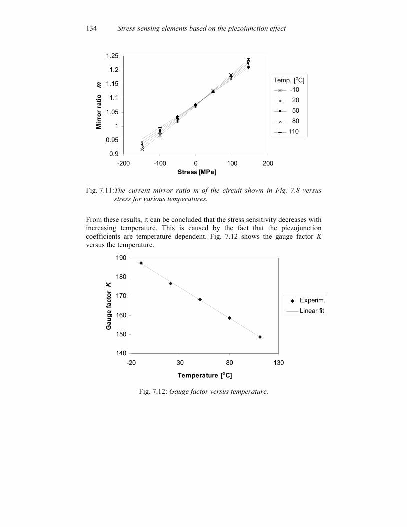
Stress-sensing elements based on the piezojunction effect 134
0.9
0.95
1
1.05
1.1
1.15
1.2
1.25
-200 -100 0 100 200Stress [MPa]
Mirr
or ra
tio m -10
20 50 80110
Temp. [oC]
Fig. 7.11:The current mirror ratio m of the circuit shown in Fig. 7.8 versus
stress for various temperatures.
From these results, it can be concluded that the stress sensitivity decreases with increasing temperature. This is caused by the fact that the piezojunction coefficients are temperature dependent. Fig. 7.12 shows the gauge factor K versus the temperature.
140
150
160
170
180
190
-20 30 80 130
Temperature [oC]
Gau
ge fa
ctor
K
Experim.Linear fit
Fig. 7.12: Gauge factor versus temperature.

7.6 Stress-sensing element based on the L-PNP current mirror 135
The temperature coefficient of the gauge factor can be calculated using the formula:
TTKTKTK
∆−=
)()()(
0
0γ . (7.17)
From Equation 7.17 and Fig. 7.12 it follows that γ =-1.75×10⁻³ °C-1. 7.6.2 Compensation of the temperature effect One interesting characteristic of this piezojunction stress-sensing element is that the temperature coefficient of the gauge factor can be well compensated by that of VBE. Fig. 7.13 shows the base-emitter voltage VBE versus temperature where the error bars show the change caused by stress (from –150 MPa to +150 MPa).
0.4
0.45
0.5
0.55
0.6
0.65
0.7
0.75
-20 30 80 130
Temperature [oC]
VB
E [V
]
Fig. 7.13:The measured base-emitter voltage VBE of the stress-sensing element
of Fig. 7.8 versus temperature. The first-order temperature sensitivity of VBE amounts to λ=-2.13 mV/°C. Because the stress sensitivity is low compared to the temperature sensitivity, VBE can be used directly to measure the temperature. The compensation of γ can be implemented by software, where for instance a microcontroller can process the information (IOUT, IREF and VBE) from the sensing
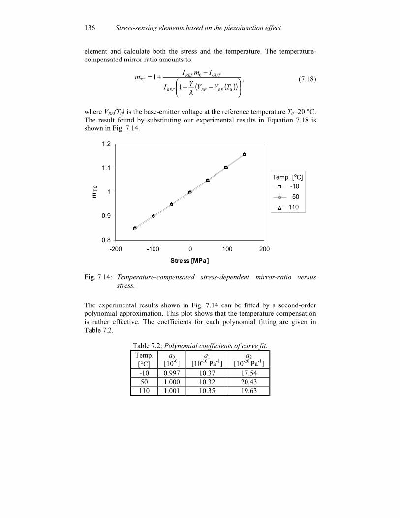
Stress-sensing elements based on the piezojunction effect 136
element and calculate both the stress and the temperature. The temperature-compensated mirror ratio amounts to:
( )( )
−+
−+=0
0
11
TVVI
ImImBEBEREF
OUTREFTC
λγ , (7.18)
where VBE(T0) is the base-emitter voltage at the reference temperature T0=20 °C. The result found by substituting our experimental results in Equation 7.18 is shown in Fig. 7.14.
0.8
0.9
1
1.1
1.2
-200 -100 0 100 200
Stress [MPa]
mTC -10
50110
Temp. [oC]
Fig. 7.14: Temperature-compensated stress-dependent mirror-ratio versus
stress. The experimental results shown in Fig. 7.14 can be fitted by a second-order polynomial approximation. This plot shows that the temperature compensation is rather effective. The coefficients for each polynomial fitting are given in Table 7.2.
Table 7.2: Polynomial coefficients of curve fit. Temp. [°C]
a0 [10-0]
a1 [10-10 Pa-1]
a2 [10-20 Pa-1]
-10 0.997 10.37 17.54 50 1.000 10.32 20.43 110 1.001 10.35 19.63
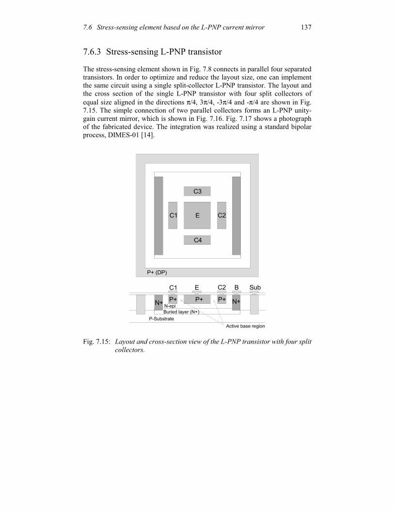
7.6 Stress-sensing element based on the L-PNP current mirror 137
7.6.3 Stress-sensing L-PNP transistor The stress-sensing element shown in Fig. 7.8 connects in parallel four separated transistors. In order to optimize and reduce the layout size, one can implement the same circuit using a single split-collector L-PNP transistor. The layout and the cross section of the single L-PNP transistor with four split collectors of equal size aligned in the directions π/4, 3π/4, -3π/4 and -π/4 are shown in Fig. 7.15. The simple connection of two parallel collectors forms an L-PNP unity-gain current mirror, which is shown in Fig. 7.16. Fig. 7.17 shows a photograph of the fabricated device. The integration was realized using a standard bipolar process, DIMES-01 [14].
P+ (DP)
E
E
E
B Sub
C3
C1
C1
C4
C2
C2
P+N+ N+P+ P+N-epi
P-SubstrateActive base region
Buried layer (N+)
Fig. 7.15: Layout and cross-section view of the L-PNP transistor with four split collectors.
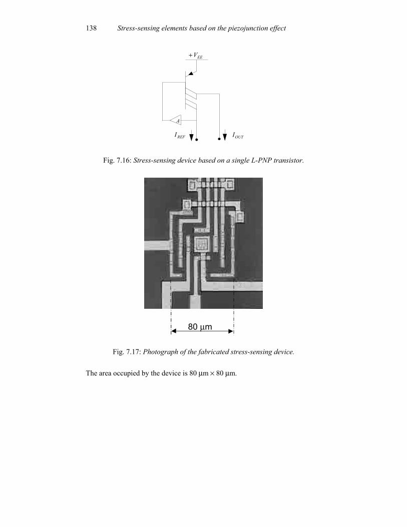
Stress-sensing elements based on the piezojunction effect 138
A
REFI OUTI
EEV+
Fig. 7.16: Stress-sensing device based on a single L-PNP transistor.
80 µm
Fig. 7.17: Photograph of the fabricated stress-sensing device.
The area occupied by the device is 80 µm × 80 µm.
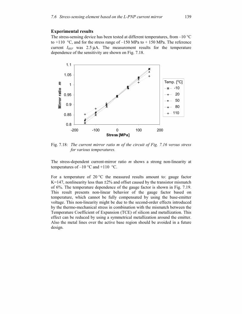
7.6 Stress-sensing element based on the L-PNP current mirror 139
Experimental results The stress-sensing device has been tested at different temperatures, from –10 °C to +110 °C, and for the stress range of –150 MPa to + 150 MPa. The reference current IREF was 2.5 µA. The measurement results for the temperature dependence of the sensitivity are shown on Fig. 7.18.
0.8
0.85
0.9
0.95
1
1.05
1.1
-200 -100 0 100 200Stress [MPa]
Mirr
or ra
tio m -10
20 50 80110
Temp. [oC]
Fig. 7.18: The current mirror ratio m of the circuit of Fig. 7.16 versus stress
for various temperatures. The stress-dependent current-mirror ratio m shows a strong non-linearity at temperatures of –10 °C and +110 °C. For a temperature of 20 °C the measured results amount to: gauge factor K=147, nonlinearity less than ±2% and offset caused by the transistor mismatch of 6%. The temperature dependence of the gauge factor is shown in Fig. 7.19. This result presents non-linear behavior of the gauge factor based on temperature, which cannot be fully compensated by using the base-emitter voltage. This non-linearity might be due to the second-order effects introduced by the thermo-mechanical stress in combination with the mismatch between the Temperature Coefficient of Expansion (TCE) of silicon and metallization. This effect can be reduced by using a symmetrical metallization around the emitter. Also the metal lines over the active base region should be avoided in a future design.
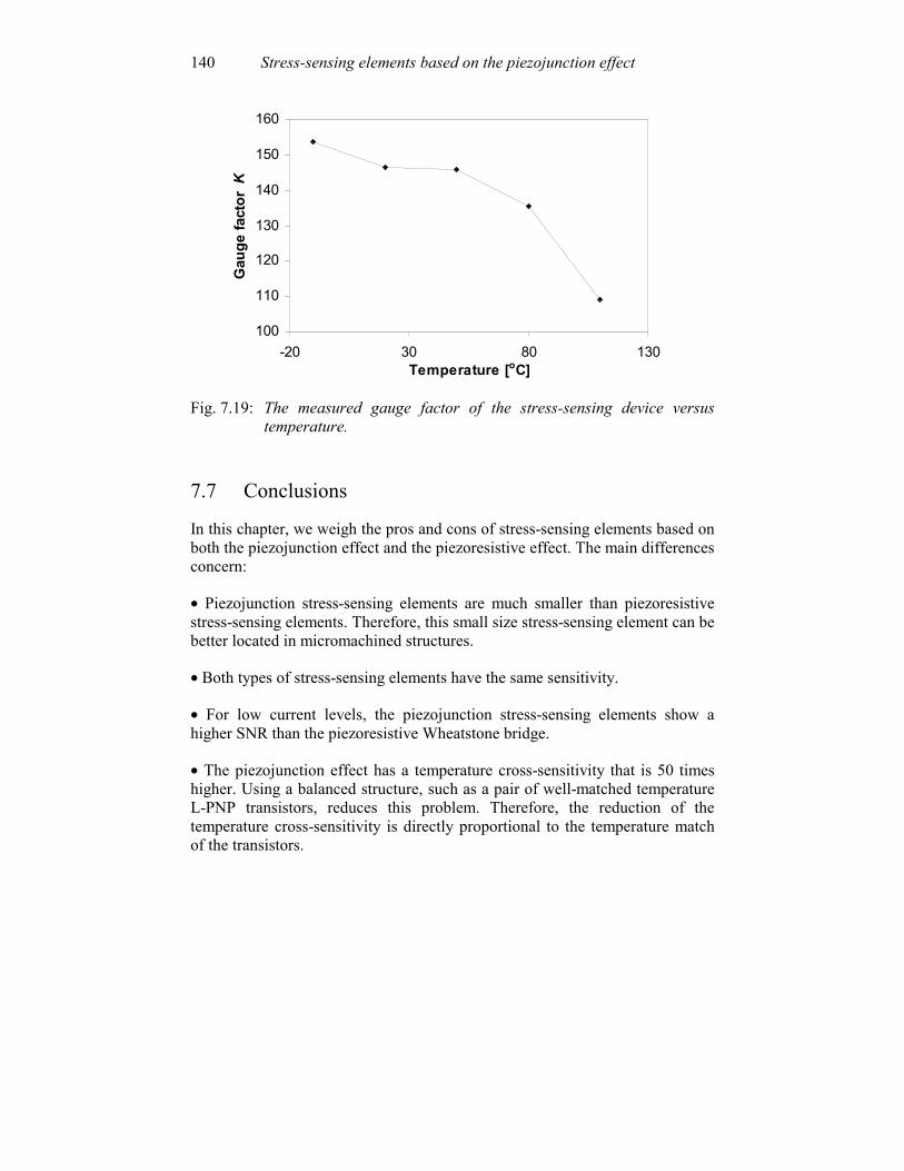
Stress-sensing elements based on the piezojunction effect 140
100
110
120
130
140
150
160
-20 30 80 130Temperature [oC]
Gau
ge fa
ctor
K
Fig. 7.19: The measured gauge factor of the stress-sensing device versus
temperature. 7.7 Conclusions In this chapter, we weigh the pros and cons of stress-sensing elements based on both the piezojunction effect and the piezoresistive effect. The main differences concern: • Piezojunction stress-sensing elements are much smaller than piezoresistive stress-sensing elements. Therefore, this small size stress-sensing element can be better located in micromachined structures. • Both types of stress-sensing elements have the same sensitivity. • For low current levels, the piezojunction stress-sensing elements show a higher SNR than the piezoresistive Wheatstone bridge. • The piezojunction effect has a temperature cross-sensitivity that is 50 times higher. Using a balanced structure, such as a pair of well-matched temperature L-PNP transistors, reduces this problem. Therefore, the reduction of the temperature cross-sensitivity is directly proportional to the temperature match of the transistors.
7.7 Conclusions 141
A new stress-sensing element based on the piezojunction effect has been fabricated using a standard bipolar technology. This stress-sensing element consists of the connection of two orthogonal L-PNP transistor pairs, operating as current mirror, which maximizes the piezojunction effect and reduces the temperature cross-sensitivity. It has been verified that compared to the piezoresistive stress-sensing elements, the piezojunction stress-sensing element has the advantages of a lower power consumption and smaller size. Regarding to the stress sensitivity and linearity, both types of sensors have similar properties. Furthermore, the well-known temperature sensitivity of the base-emitter voltage can be used to compensate for the temperature coefficient of the gauge factor. In order to reduce the layout area even more, a single lateral transistor with four split collectors has been used to implement a stress-sensing device.
Stress-sensing elements based on the piezojunction effect 142
References
[1] S. Middelhoek, Celebration of the tenth transducers conference: The past, present and future of transducer research and development, Sensors and Actuators A, 82, pp. 2-23, 2000.
[2] H. Hall, J. Bardeen and G. Pearson, The effects of pressure and temperature on the resistance of p-n junctions in germanium, Phys. Rev., 84, pp. 129-132, 1951.
[3] B. Puers, L. Reynaert, W. Snoeys and W.M.C. Sansen, A new uniaxial accelerometer in silicon based on the piezojunction effect, IEEE Trans. El. Dev., ED-35, pp. 764-770, 1988.
[4] W.A. Serdijn, C.J.M. Verhoeven and A.H.M. van Roermund, Analog IC techniques for low-voltage low-power electronics, Delft University Press, The Netherlands,1995.
[5] B.J. Hosticka, Circuit and system design for silicon microsensors, IEEE Int. Symp. On Circuits and Systems, San Diego, pp. 1824-1827, May, 1992.
[6] M.E. Sikorski, Transistor Microphones, J. Audio Eng. Soc., 13, pp. 207-217, 1965.
[7] F. Krieger and H.N. Toussaint, A piezo-mesh-diode pressure transducer, Proc. IEEE, 55, pp. 1234-1235, 1967.
[8] J.J. Wortman and L.K. Monteith, Semiconductor mechanical sensors, IEEE Trans. Electron Devices., ED-16, pp. 855-860, 1969.
[9] D.P. Jones, S.V. Ellam, H. Riddle and B.W. Watson, The measurement of air flow in a forced expiration using a pressure-sensitive transistor, Med. &Biol. Eng., 13, pp. 71-77, 1975.
[10] J. Matovic, Z. Djuric, N. Simicic, and A. Vijanic, Piezojunction effect based pressure sensor, Eletron. Lett., 29, pp. 565-566, 1993.
[11] R. Schellin and R. Mohr, A monolithically-integrated transistor microphone: modeling and theoretical behaviour, Sensors and Actuators A, 37-38, pp. 666-673, 1993.
[12] S. Middelhoek, S.A. Audet and P.J. French, Silicon Sensors, Faculty of Information Technology and Systems, Delft University of Technology, Laboratory for Electronic Instrumentation, The Netherlands, 2000.
[13] R.C. Jaeger, J.C. Suhling, R. Ramani, A.T. Bradley and J. Xu, CMOS stress sensors on (100) silicon, IEEE Journal of Solid-State Circuit, Vol. 35, no 1, pp. 85-95, Jan. 2000.
[14] L.K. Nanver, E.J.G. Goudena and H.W. van Zeijl, DIMES-01, a baseline BIFET process for smart sensor experimentation, Sensors and Actuators A, 36, pp. 139-147, 1993.

143
Chapter 8
Conclusions The main contributions of this thesis can be classified into three fields: • Characterization of the piezojunction effect. • Minimization of the piezojunction and the piezoresistive effects in both devices and (packaged) circuits. • Optimization of the piezojunction effect for new stress-sensing elements. We will summarize the conclusions about each of these fields. Characterization of the piezojunction effect The first-order piezojunction (FOPJ) coefficients and the second-order piezojunction (SOPJ) coefficients for bipolar transistors on 001-crystal-oriented silicon wafers have been extracted. It has been found that the FOPJ coefficients are of the same order of magnitude as the FOPR coefficients. On the other hand, the SOPJ coefficients are approximately one order of magnitude higher that the SOPR coefficients. So the piezojunction effect shows strong nonlinear behavior. Among the FOPJ coefficients, ζ12 for PNP transistors is approximately three times lower than that for NPN transistors. Therefore, the stress sensitivity of a vertical PNP (V-PNP) transistor on a 001-crystal-oriented silicon wafer is rather low. The piezojunction effect in lateral PNP

Conclusions 144
(L-PNP) is highly anisotropic, and depends on the stress orientation and the current direction related to the silicon-crystal axis. This anisotropic behavior is characterized by the FOPJ coefficient p
44ζ . The piezojunction effect hardly depends on the current density, as far the transistor is not operated in the high-injection level. Therefore, the proportional-to-absolute-temperature voltage VPTAT is much less stress sensitive than the base-emitter voltage VBE. At high injection levels we observed that the piezojunction effect in VBE is current dependent. In order to minimize the stress dependence in VPTAT, a sufficiently low emitter current density must be selected. The piezojunction coefficients decrease with increasing temperature. The first-order temperature dependence of the piezojunction coefficients has the same order of magnitude as the first-order temperature dependence of the piezoresistive coefficients. Minimization of the piezojunction and the piezoresistive effects in devices and packaged circuits For any stress-orientation in the wafer plane, the V-PNP transistor is less stress sensitive than the V-NPN transistor. The use of the V-PNP transistor instead of the V-NPN transistor will significantly reduce the piezojunction effect and therefore the inaccuracy in VBE caused by mechanical stress induced by packaging. The reduction of the piezojunction effect based on the use of V-PNP transistors is even more attractive if we consider packaging types for which the Temperature Coefficient of Expansion (TCE) mismatching introduces a tensile stress instead of compressive stress on the die surface. With respect to lateral transistors, it has been shown that using an appropriate layout, which is based on a symmetrical circular, octagonal or square emitter shape will reduce the first-order stress sensitivity. These layout geometries minimize the effect of the large FOPJ coefficient p
44ζ . To enable high collector currents and yet to reduce high-injection effects, the emitter perimeter should be increased. Therefore, we recommend the connection of minimum-sized circular, octagonal or square emitters in parallel in a common base-collector area. Lateral transistors with a thin-stripe geometry have a high stress sensitivity and should be avoided. The sensitivity of p-type monocrystalline resistors along the <100> axes to longitudinal stress and to transverse stress has opposite signs and similar dimensions. Therefore, simply connecting two p-type perpendicular-oriented resistors in series can reduce the piezoresistive effect by a factor of 20.
Conclusions 145
Although n-type resistors exhibit minimum stress sensitivity when they are along the <110> axes, perpendicular-aligned devices do not present opposite signs. For this reason, n-type resistors are not suitable for this kind of compensation. The translinear circuits designed with well-matched transistor pairs and quads are hardly affected by the piezojunction effect. When resistors are included in the translinear loop, they also must be matched. If this is not possible, then the piezoresistive effect must be reduced at device level. In bandgap reference circuits and temperature transducers, a good match is important but not enough to solve the problem of stress-induced inaccuracy. The piezojunction effect in the transistor that generates the temperature-reference signal VBE is the dominant source of the stress-induced inaccuracy. Calibration at the wafer level can reduce the inaccuracy caused by the thermo-mechanical stress during wafer fabrication. However, the inaccuracy caused by packaging cannot be removed by this calibration. Stress-minimization techniques based on the use of mechanical-compliance material interfaces can reduce this inaccuracy. However, they involve an additional step in the IC fabrication or the use of special materials. Using the V-PNP transistor instead of the V-NPN transistor to generate the temperature-reference signal VBE, will significantly reduce the piezojunction effect. Therefore, it is advisable to use these transistors in order to obtain a high accuracy and good long-term stability. For a further reduction we have to use a packaging technique where only tensile stress occurs. This is the case when the silicon die is attached to a ceramic or a metallic substrate. Optimization of the piezojunction effect for new stress-sensing elements When stress-sensing elements are implemented with transistors instead of resistors, the following features are obtained: • Integrated bipolar transistors require a smaller area than implanted or diffused resistors. Thus, small-size stress-sensing elements can be fabricated. The small-size stress-sensing elements can be better located in micromachined structures. • The same stress sensitivity is obtained. • For low current levels, the piezojunction stress-sensing elements show a higher signal-to-noise ratio SNR than the piezoresistive Wheatstone bridge.
Conclusions 146
Therefore, the piezojunction stress-sensing elements are more adequate for low-power sensor applications. • The piezojunction effect shows a high temperature cross-sensitivity. Using a balanced structure, such as a pair of well-matched temperature L-PNP transistors can reduce this problem. Based on these characteristics, a new piezojunction stress-sensing element has been designed using a standard bipolar technology. This stress-sensing element consists of two orthogonal L-PNP transistor pairs operated as a current mirror, which maximizes the piezojunction effect and reduces the temperature cross-sensitivity. It has been verified that the linearity, gauge factor and its temperature coefficient are approximately the same as those of the sensors based on the piezoresistive effect. The predictable temperature-dependent base-emitter voltage can be used to compensate for the temperature coefficient of the gauge factor. For further reduction of the sensor area, a single lateral transistor with four split collectors has been designed to implement a stress-sensing device.
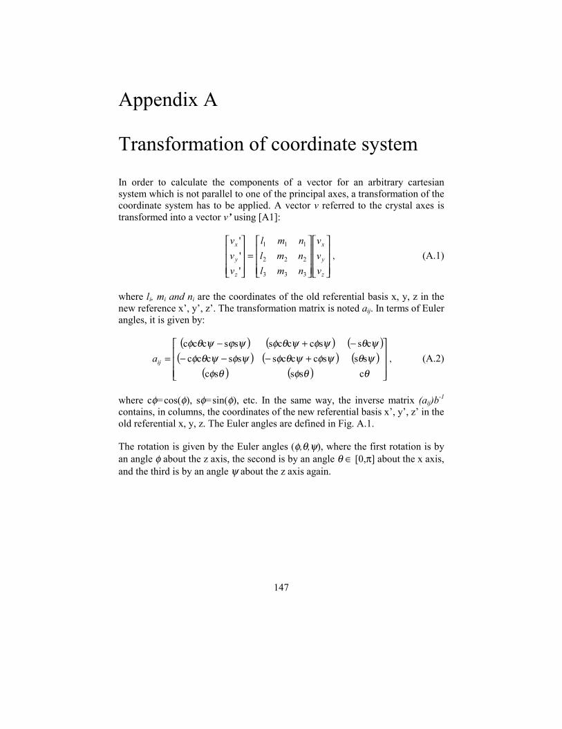
147
Appendix A
Transformation of coordinate system In order to calculate the components of a vector for an arbitrary cartesian system which is not parallel to one of the principal axes, a transformation of the coordinate system has to be applied. A vector v referred to the crystal axes is transformed into a vector v’ using [A1]:
=
z
y
x
z
y
x
vvv
nmlnmlnml
vvv
333
222
111
'''
, (A.1)
where li, mi and ni are the coordinates of the old referential basis x, y, z in the new reference x’, y’, z’. The transformation matrix is noted aij. In terms of Euler angles, it is given by:
( ) ( ) ( )
( ) ( ) ( )( ) ( )
+−−−
−+−=
θθφθφψθψφψθφψφψθφψθψφψθφψϕψθφ
cssscssscccsssccccsscccsssccc
ija , (A.2)
where cφ=cos(φ), sφ=sin(φ), etc. In the same way, the inverse matrix (aij)b-1 contains, in columns, the coordinates of the new referential basis x’, y’, z’ in the old referential x, y, z. The Euler angles are defined in Fig. A.1. The rotation is given by the Euler angles (φ,θ,ψ), where the first rotation is by an angle φ about the z axis, the second is by an angle θ ∈ [0,π] about the x axis, and the third is by an angle ψ about the z axis again.
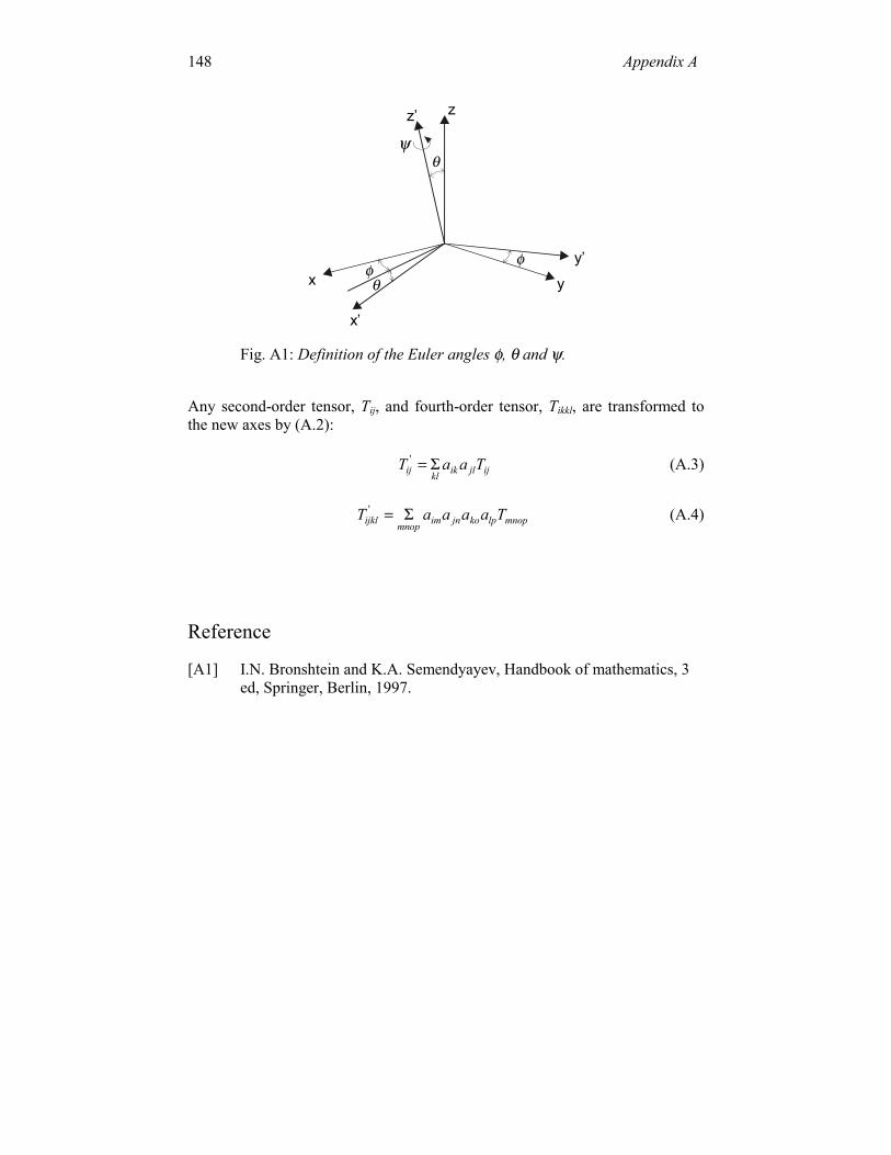
Appendix A
148
θ
θ
φφ
ψ
z’ z
y
y’
x’
x
Fig. A1: Definition of the Euler angles φ, θ and ψ. Any second-order tensor, Tij, and fourth-order tensor, Tikkl, are transformed to the new axes by (A.2):
ijjlikklij TaaT Σ=' (A.3)
mnoplpkojnimmnopijkl TaaaaT Σ=' (A.4)
Reference [A1] I.N. Bronshtein and K.A. Semendyayev, Handbook of mathematics, 3
ed, Springer, Berlin, 1997.

149
Appendix B
Stress calculations based on the cantilever technique The cantilever technique is used to apply a well-controlled stress in silicon beams. In order to simplify the calculations the following assumptions are made: 1) The beam is initially straight and unstressed. 2) The deflection of the beam is small compared to the total length. 3) There are no shearing effects. 4) The material of the beam is perfectly homogeneous. 5) The elastic limit is nowhere exceeded. Figure B.1 shows the deflection of a cantilever beam under a concentrated force W. The bending moment acting upon a certain point at a distance x from the fixed end of the beam is given by:
( )LxWM −= , (B.1)
where W is the concentrated force, L is the length of the beam. The theory of elastic bending states that the normal stress in the surface of the silicon beam is given by:
IMc=maxσ , (B.2)
where c is the distance from the surface to the neutral axis given by d/2 and I is the moment of inertia of the cross-section area computed about the neutral axis. The moment of inertia for a rectangular section is given by:
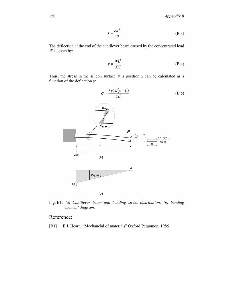
Appendix B 150
12
3edI = . (B.3)
The deflection at the end of the cantilever beam caused by the concentrated load W is given by:
YIWLy3
3
= . (B.4)
Thus, the stress in the silicon surface at a position x can be calculated as a function of the deflection y:
( )
323
LLxyYd −=σ . (B.5)
(b)
x=0
Wd
eneutralaxis
σmax
σmax
M
W(x-L)
(a)
x
L
yW
σmax
Fig. B1: (a) Cantilever beam and bending stress distribution; (b) bending moment diagram.
Reference: [B1] E.J. Hearn, “Mechancial of materials” Oxford Pergamon, 1985.
151
Appendix C
Transformation of coordinate system for the second-order piezoresistive coefficients The second-order piezoresistive coefficients for an arbitrary crystallographic current direction and stress orientation can be derived from a complete set of tensor components by a coordinate transformation. The transformation for longitudinal and transversal mode are given by:
( )
( ) 2456441144123111
1661166122112111111
4422 423
Γ−−−−−Γ−−−−−=
ππππππππππππ LL (C.1)
( ) ( )
( ) ( ) 66611221115456441122111
41441231223166122112111122
222 222
Γ−−−Γ−−−−Γ−−−Γ−+−−=
ππππππππππππππππ TT (C.2)
where:
21
41
21
41
41
21
21
41
41
21
41
211 nmnlnmmlnlml +++++=Γ ,
21
21
212 3 nml=Γ ,
22
22
21
22
22
21
22
22
21
22
22
21
22
22
21
22
22
21
22
22
213 nmnnlnnlnnmmmlmnllmll ++++++=Γ ,
22
22
21
22
22
21
22
22
214 mlnnlmnml ++=Γ ,
( )2
2221122221122
22115 2 nmlmlnmlnlnmlnm ++=Γ and
( )3
221123211
322112
3211
322112
32116 2 mlmlmlmlnlnlnlnlnmnmnmnm +++++=Γ .
Appendix C 152
Reference [C1] K. Matsuda, K. Suzuki, K. Yamamura, and Y. Kanda, Nonlinear
piezoresistive coefficients in silicon, J. Appl. Phys., 73 1838-1847, 1993.
153
Appendix D
MatLab program used to calculate the stress-induced change in VBE and Vref The Matlab program used to calculate the temperature- and stress-induced change in VBE and Vref is shown in the following: clear all % constants k=1.3807E-23; q=1.6022E-19; Tr=323 m=1; n=4; %piezojunction coefficients for V-PNP pi1=1.43E-4; pi2=-0.73E-6; %piezojunction coefficients for V-NPN %pi1=4.55E-4; %pi2=-0.30E-6; for T=-10:10:110; i=i+1; %delta temperature DT=(n-m)*k/q*(T+273-Tr+(T+273)*log(Tr/(T+273)))*1000; TT(i)=T; for S=-180:20:+180; j=j+1; % temperature dependent piezojunction coefficient for PNP
Appendix D 154
pi1T=(1.83E-5*T^2-6.38E-3*T+1.124)*pi1; pi2T=(1.68E-5*T^2-7.22E-3*T+1.146)*pi2; % temperature dependent piezojunction coefficient %pi1T=(8.28E-6*T^2-3.65E-3*T+1.096)*pi1; %pi2T=(1.04E-5*T^2-7.62E-3*T+1.146)*pi2; % delta stress DS=-k*(T+273)/q*log((-pi1T*S)+(pi1T^2-pi2T)*S^2+1 )*1000; SS(j)=S; DTS(i,j)=DS; end j=0; end % Graphical output surf(TT,SS,DTS') view(-30,40) ylabel ('Stress [MPa]') xlabel ('Temperature [ \circC]') zlabel ('\Delta\itV_B_E (\sigma,T^2) [mV]') colormap ('default') max(DTS); min(DTS); grid axis([ -10 110 -200 200 -4 2]) %axis([ -10 110 -200 200 -0.003 0.0005]) grid

155
List of symbols Symbol Description Unit A area m2 AE emitter area m2 A1, A2 adjust parameter of VPTAT - aij transformation of coordinate system, tensor notation - Cijkl stiffness tensor Pa d thickness of the silicon beam m dcc distance between the device centroids m E electrical field V/m
( )σTVPTATE equivalent temperature error due to the
stress-induced change in VPTAT °C
( )σTVBEE equivalent temperature error due to the
stress-induced change in VBE °C
Fi vector force N G Poisson ratio Pa gm transconductance Ω-1
H height m IC collector current A IB base current A IS saturation current A IKF high injection-level knee A
0SI stress-free saturation current A
J current density Am-2 k conductivity of the majority carrier 1Ω-1m-1 K gauge factor - kB Boltzmann’s constant JK-1 L length of the silicon beam m li, mi, ni direction cosines - m current-mirror ratio - mB bias dependent constant - n electron concentration cm-3 neq saturation current ratio - p hole concentration cm-3

List of Symbols 156
q electron charge C QB Gummel number cm-2 R resistance Ω r, r1, r2 current-density ratio - rb base-resistance Ω Sijkl compliance constants Pa-1
BEVTS first-order temperature sensitivity of VBE V °C-1
PTATVTS first-order temperature sensitivity of VPTAT V °C-1
FTS β first-order temperature sensitivity of βF °C-1
T temperature °C, K Tr reference temperature °C, K Tout output temperature of the SMT160-30 °C TA curing temperature of the die attachment K TC calibration temperature K VBE base-emitter voltage V Vg0 extrapolated bandgap voltage at zero Kelvin V VPTAT proportional to the absolute temperature voltage V Vref reference voltage V VdQ stress-dependent differential voltage (piezojunction) V V0 output voltage V VdR stress-dependent differential voltage (piezoresistive) V W width m x distance of the device under test from the support m Y Young’s modulus Pa y displacement of the silicon beam m βF forward current gain - γ temperature coefficient of the gauge factor °C-1
δσ magnitude of the stress-induced mismatching - ∆f bandwidth Hz ∆IS stress-induced saturation current A ∆m stress-induced change in the current mirror ratio - ∆R(T) temperature-induced resistance change Ω ∆R(σ) stress-induced resistance change Ω ∆V0,tot total voltage change due to mechanical
stress and temperature V ∆VBE(σ) stress-induced change in VBE V ∆VPTAT(σ) stress-induced change in VPTAT V ∇σcc mechanical stress gradient Pam-1
εij strain tensor -
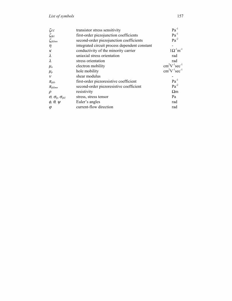
List of symbols 157
ζcc transistor stress sensitivity Pa-1 ζijkl first-order piezojunction coefficients Pa-1 ζijklmn second-order piezojunction coefficients Pa-2 η integrated circuit process dependent constant - κ conductivity of the minority carrier 1Ω-1m-1
λ uniaxial stress orientation rad λ stress orientation rad µn electron mobility cm2V-1sec-1 µp hole mobility cm2V-1sec-1 ν shear modulus - πijkl, first-order piezoresistive coefficient Pa-1 πijklmn second-order piezoresistive coefficient Pa-2 ρ resistivity Ωm σ, σij, σijkl stress, stress tensor Pa φ, θ, ψ Euler’s angles rad ϕ current-flow direction rad

List of Symbols 158

159
Summary This thesis describes an investigation of the piezojunction effect in silicon. The aim of this investigation is twofold. First, to propose some techniques to reduce the mechanical-stress-induced inaccuracy and long-term instability of many analogue circuits such as bandgap references and monolithic temperature transducers. Second, to apply the piezojunction effect to new mechanical sensor structures. Chapter 1. Introduction Up to the present attempts to improve the accuracy of bandgap references and monolithic temperature sensors did not include solving the problems created by the piezojunction effect. This is the reason why the accuracy improved little over the last decades. Although the accuracy limit due to mechanical stress was noted before, to the best of our knowledge no systematic research in this field has been carried out. Thus, the investigation and characterization of the mechanical-stress effects on the accuracy of temperature sensors and bandgap references is necessary. The same effect can be used to make new sensors structures. The development of new stress sensors for low-power and miniaturized systems is desirable and the piezojunction effect meets the requirements. Chapter 2. Mechanical stress in integrated circuits During IC fabrication (including packaging), different materials are combined, resulting in a complex system. The fabrication steps are performed at various temperatures and consequently thermo-mechanical stress will be induced once the packaged chip is cooled down to the temperature of its application. The difference between the thermal expansion of silicon and that of other materials is the main cause of the induced thermo-mechanical stress. The die attachment and the plastic molding are the main sources of stress during the packaging. To characterize the microelectronic devices under compressive and tensile stress at different temperatures we developed and fabricated a complete mechanical test structure. This test structure simulates the mechanical-stress conditions introduced by packaging. Basically, this test structure is composed of a mechanical apparatus and a thermoset, which are controlled by a computer.
Summary 160
Chapter 3. Piezo effects in silicon The piezojunction effect shows many physical similarities to the piezoresistive effect, but there are also some important differences. The piezojunction effect changes the bipolar-transistor saturation current. This stress-induced change is mainly caused by the change in the conductivity of the minority-charge carriers, while the piezoresistive effect is caused by the change of the majority-charge carriers. The piezojunction effect can be modeled by a polynomial approximation with a set of experimental constants, which are called the piezojunction coefficients. The set of piezojunction coefficients is determined according to the stress orientation and main carrier-flow direction through the bipolar-transistor base, both related to the silicon crystal axis. The stress-induced change in the saturation current caused by the piezojunction effect directly affects the base-emitter voltage VBE. Normally, VBE is used as a temperature reference signal. Therefore, mechanical stress will cause an equivalent error in the reading temperature. The characterization of the non-ideality caused by the piezojunction effect in VBE and the voltage that is proportional to absolute temperature VPTAT generates an important guideline for the designers of bandgap references and temperature sensors. Chapter 4. Characterization of the piezojunction effect The first-order piezojunction (FOPJ) coefficients and the second-order piezojunction (SOPJ) coefficients for bipolar transistors on 001-crystal-oriented silicon wafers have been extracted. It has been found that the FOPJ coefficients are of the same order of magnitude as the FOPR coefficients. On the other hand, the SOPJ coefficients are approximately one order of magnitude higher that the SOPR coefficients. So, the piezojunction effect shows a strong nonlinear behavior. Among the FOPJ coefficients, ζ12 for PNP transistors is approximately three times lower than that for NPN transistors. Therefore, the stress sensitivity of a vertical PNP (V-PNP) transistor on a 001-crystal-oriented silicon wafer is rather low. The piezojunction effect in lateral PNP (L-PNP) is highly anisotropic, and depends on the stress orientation and the current direction related to the silicon-crystal axis. This anisotropic behavior is characterized by the FOPJ coefficient p
44ζ . The piezojunction effect hardly depends on the current density, as far the transistor is not operated in the high-injection level. Therefore, the voltage which is proportional to absolute temperature voltage VPTAT is much less stress sensitive than the base-emitter voltage VBE. At high injection levels it is observed that the piezojunction effect in VBE is current dependent. In order to minimize the stress dependence in VPTAT, a sufficiently low emitter current density must be selected.
Summary 161
The piezojunction coefficients decrease with increasing temperature. The first-order temperature dependence of the piezojunction coefficients has the same order of magnitude as the first-order temperature dependence of the piezoresistive coefficients. Chapter 5. Minimizing the piezojunction and piezoresistive effects in integrated devices The knowledge of the piezojunction and piezoresistive coefficients is used to minimize the undesirable mechanical-stress effects on the electrical characteristics of transistors and resistors, respectively. Devices with lower mechanical-stress sensitivity can be found by comparing their piezo-coefficients. The layout of the device can also be optimized to reduce the mechanical-stress sensitivity. The use of the V-PNP transistor instead of the V-NPN transistor can significantly reduce the piezojunction effect. Unfortunately, it is not always possible to use V-PNP transistors, as these have the disadvantage that their collector is the global substrate node and therefore the collector current is not available as a separated current. Thus the use of the V-PNP transistor is limited to common-collector configurations. When all three terminals of a PNP transistor should be available for external connection, only lateral PNP (L-PNP) transistors can be used. The circular geometry of the L-PNP reduces the first-order stress sensitivity of this device. This reduction is valid for any in-plane stress orientation. During the pattern generation the circular emitter is approximated as many-sided polygons. This reduction is still valid for any octagon or square emitter. With respect to monocrystalline silicon resistors, it has been shown that the longitudinal and transverse effects for p-type resistors have opposite signs and similar magnitude. Therefore, simply connecting two p-type perpendicular-oriented resistors in series can reduce the piezoresistive effect by a factor of 20. Although n-type resistors exhibit minimum stress sensitivity when they are along the <110> axes, perpendicular-aligned devices do not have opposite signs. For this reason, n-type resistors are not suitable for this kind of compensation. Chapter 6. Minimizing the inaccuracy in packaged integrated circuits The knowledge of the piezo-effects on device level is used to predict and suggest methods to reduce their negative influence on the performance of
Summary 162
circuits. This is demonstrated for a number of important basic circuits, including translinear circuits, temperature transducers and bandgap references. The translinear circuits designed with well-matched transistor pairs and quads are hardly affected by the piezojunction effect. When resistors are included in the translinear loop, they also must be matched. If this is not possible, the piezoresistive effect must be reduced at device level. In bandgap reference circuits and temperature transducers, a good match is important but not enough to solve the problem of stress-induced inaccuracy. The piezojunction effect in the transistor, which generates the temperature-reference signal VBE, is the dominant source of the stress-induced inaccuracy. Calibration at wafer level can reduce the inaccuracy caused by the thermo-mechanical stress during wafer fabrication. However, the inaccuracy caused by packaging cannot be corrected by this calibration. Stress-minimization techniques based on the use of mechanical-compliance material interfaces can reduce this inaccuracy. However, they involve an additional step in the IC fabrication or the use of special materials. Using the V-PNP transistor instead of the V-NPN transistor to generate the temperature-reference signal VBE will significantly reduce the piezojunction effect. Therefore, it is advisable to use these transistors in order to obtain high accuracy and good long-term stability. For further inaccuracy reduction we have to use a packaging technique where only tensile stress occurs. This is the case when the silicon die is attached to a ceramic or a metallic substrate. Chapter 7. Stress-sensing elements based on the piezojunction effect When stress-sensing elements are implemented with transistors instead of resistors the following features are obtained: • Integrated bipolar transistors require a smaller area than implanted or diffused resistors. Thus, small-size stress-sensing elements can be fabricated. The small-size stress-sensing elements can be better located in micromachined structures. • The same stress-sensitivity is obtained. • For low current levels, the piezojunction stress-sensing elements show a higher signal-to-noise ratio SNR than the piezoresistive Wheatstone bridge. Therefore, the piezojunction stress-sensing elements are more adequate for low-power sensor applications.
Summary 163
• The piezojunction effect shows a high temperature cross-sensitivity. Using a balanced structure, such as a pair of well-matched temperature L-PNP transistors, can reduce this problem. Based on these characteristics, a new piezojunction stress-sensing element has been designed using a standard bipolar technology. This stress-sensing element consists of two orthogonal L-PNP transistor pairs operated as a current mirror, which maximizes the piezojunction effect and reduces the temperature cross-sensitivity. It has been verified that the linearity, gauge factor and its temperature coefficient are approximately the same as those of the sensors based on the piezoresistive effect. The predictable temperature-dependent base-emitter voltage can be used to compensate for the temperature coefficient of the gauge factor. For further reduction of the sensor area, a single lateral transistor with four split collectors has been designed to implement a stress-sensing device.

Summary 164
165
Samenvatting Dit proefschrift beschrijft een onderzoek naar het piëzojunction effect in silicium. Het doel van dit onderzoek is tweeledig: Ten eerste, om technieken te vinden, waarmee het effect van mechanische spanningen op de nauwkeurigheid en lange-termijn stabiliteit van veel analoge schakeling, zoals bandgapreferenties en monolithische temperatuursensoren, kan worden verminderd. Ten tweede, om het piëzojunctie-effect te benutten voor nieuwe mechanische sensoren. Hoofdstuk 1. Introductie Bij pogingen om de nauwkeurigheid van bandgapreferenties en monolithische temperatuursensoren te verbeteren, werd er tot nu toe niets gedaan om de problemen veroorzaakt door het piëzojunctie-effect aan te pakken. Dit is de reden dat deze nauwkeurigheid de laatste decaden zo weinig is verbeterd. Alhoewel dit probleem al langer werd onderkend is er, voor zover ons bekend, geen systematisch onderzoek op dit terrein uitgevoerd. Om deze redenen is een onderzoek en karakterisatie van het effect van mechanische spanningen op de nauwkeurigheid van bandgapreferenties en temperatuursensoren hard nodig. Het piëzojunctie-effect kan benut worden voor de ontwikkeling van nieuwe microsensoren voor het meten van mechanische spanningen met een laag vermogen. Hoofdstuk 2. Mechanische spanning in geïntegreerde schakelingen Gedurende de fabricage en inhuizing van geïntegreerde schakelingen worden verschillende materialen gecombineerd to een complex geheel. De fabricagestappen worden uitgevoerd bij verschillende, veelal hoge, temperaturen. Na afkoeling ontstaan daardoor, als gevolg van verschillen in de thermische uitzettingscoëfficiënten, thermo-mechanische spanningen. Tijdens inkapseling ontstaat een aanzienlijke mechanische spanning, welke wordt veroorzaakt door de plastic gietmassa, en in mindere mate ook door de zogenaamde die-bond. Teneinde de micro-elektronische componenten te karakteriseren voor wat betreft hun gevoeligheid voor rek- en drukspanningen bij verschillende temperaturen, hebben we een complete testopstelling ontwikkeld en gebouwd. Met deze electro-mechanische testopstelling kunnen we de mechanische

Samenvatting 166
spanningen, zoals die ontstaan door inkapseling, nabootsen. De testopstelling bestaat voornamelijk uit een mechanische inrichting and een thermostaat, welke bestuurd worden door een computer. Hoofdstuk 3. Piëzo-effecten in silicium Het piëzojunctie-effect vertoont veel overeenkomst met het piëzoweerstands-effect. Er zijn echter ook enige belangrijke verschillen: Door het piëzojunctie-effect veroorzaakt een mechanische spanning een verandering van de verzadigingsstroom van een bipolaire transistor. Dit is een gevolg van een verandering van de geleidbaarheid van de minderheidsladingsdragers. Bij het piëzoweerstandseffect treedt een soortgelijk effect op in weerstanden, als gevolg van een verandering van de geleidbaarheid van de meerderheidsladingsdragers. Het piëzojunctie-effect kan worden gemodelleerd met een polynomische benadering, gebruikmakend van een aantal experimenteel bepaalde constanten, die piëzojunctie-coëfficiënten worden genoemd. De grootte van de piëzojunctie-coëfficiënten wordt hangt af van de oriëntatie van de mechanische spanning, de richting van de stroom en de richting van de as van het kristal. De verandering in de verzadigingsstroom van een bipolaire transistor, die wordt veroorzaakt door het piëzojunctie-effect, heeft een direct gevolg voor de basisemitterspanning VBE. Deze spanning fungeert als referentiesignaal in monolithische temperatuurtransducenten en bangapreferenties. Daardoor heeft het piëzojunctie-effect een rechtstreekse invloed op de nauwkeurigheid van deze belangrijke bouwstenen. Karakterisatie van het piëzojunctie-effect is daarom een eerste vereiste om een ontwerper van temperatuurtransducenten en bangapreferenties in staat te stellen de nauwkeurigheid van deze circuits te verbeteren. Hoofdstuk 4. Karakterisatie van het piëzojunctie-effect De eerste-orde piëzojunctiecoëfficiënten (FOPJ coëfficiënten) en de tweede-orde piëzojunctiecoëfficiënten (SOPJ coëfficiënten) voor bipolaire transistoren in een 001-georiënteerd kristal zijn experimenteel bepaald. Het blijkt dat de eerste-orde piëzojunctiecoëfficiënten ongeveer even groot zijn als de eerste-orde piëzoweerstandscoëfficiënten. De tweede-orde piëzojunctiecoëfficiënten blijken evenwel veel groter te zijn dan de tweede-orde piëzoweerstandscoëfficiënten. Het piëzojunctie-effect blijkt sterk niet-lineair te zijn. Voor wat betreft de FOPJ coëfficiënten, blijkt dat ζ12 voor PNP transistoren ongeveer drie keer zo groot is, als de overeenkomstige parameter voor NPN transistoren. Als gevolg daarvan is de gevoeligheid voor mechanische spanning bij verticale PNP (V-PNP) transistoren in een 001-siliciumkristal tamelijk gering. Het piëzojunctie-effect in laterale PNP transistoren (L-PNP) is zeer anisotroop, en hangt af van de
Samenvatting 167
oriëntatie van de mechanische spanning en de richting van de stroom ten opzichte van de kristal-as. Dit anisotrope gedrag wordt gekarakteriseerd door de FOPJ coëfficiënt p
44ζ . Het piëzojunctie-effect hangt nauwelijks af van de stroomdichtheid; tenminste zolang de transistor niet in het high-levelgebied wordt gebruikt. Als gevolg daarvan is de PTAT spanning VPTAT veel minder afhankelijk van mechanische spanning dan de basisemitterspanning VBE. Bij hoge stroomdichtheden treden er high-level injectie effecten op in de bipolaire transistoren, die ook van invloed zijn op de PTAT spanning. Teneinde dit effect te voorkomen, moet er voor gezorgd worden dat de emitterstroomdichtheden voldoende laag zijn. De grootte van de piëzojunctiecoëfficiënten neemt af met toenemende temperatuur. De eerste-orde temperatuurafhankelijkheid van de piëzojunctiecoëfficiënten is van de zelfde orde van grootte als die van de piëzoweerstandscoëfficiënten. Hoofdstuk 5. Het minimaliseren van het piëzojunctie-effect en het piëzoweerstandseffect in componenten De kennis van de piëzojunctie en de piëzoweerstandscoëfficiënten kan gebruikt worden om het ongewenste effect van mechanische spanningen op de elektrische karakteristieken van componenten en schakelingen te minimaliseren. Hiertoe kan men componenten uitzoeken met een relatief lage waarden van hun piëzocoëfficiënten. Ook kan men de layout optimaliseren met het oog op de gewenste immuniniteit voor het effect van mechanische spanning. Het gebruik van V-PNP transistoren in plaats van V-NPN transistoren kan een significante reduktie van het piëzojunctie-effect geven. Helaas is dit niet altijd mogelijk, omdat in de meeste gangbare technologieën, in dat geval de collectoren met het substraat zijn doorverbonden. Het gebruik van V-PNP transistoren is daardoor beperkt tot gemeenschappelijke-collectorschakelingen. Indien alle drie de klemmen van een PNP transistor beschikbaar moeten zijn, dan is men aangewezen op laterale PNP (L-PNP) transistoren. De circulaire geometrie van een L-PNP reduceert de eerste-orde piëzojunctie-effect in de transistor. Deze reductie is geldig voor iedere oriëntatie van de mechanische spanning in het kristalvlak. In praktische toepassingen wordt een circulaire emittergeometrie veelal benaderd met een veelhoek. Ook in geval van zo’n benadering is er sprake van een sterke reductie van het piëzojunctie-effect. Voor wat betreft de monokristalijne siliciumweerstanden is aangetoond dat het longitudinale en het transversale effect in een p-type weerstand ongeveer gelijk
Samenvatting 168
maar tegenovergesteld zijn. Hierdoor is het mogelijk om het piëzoweerstandseffect met ongeveer een factor 20 te reduceren door simpelweg twee gelijke weerstanden, maar met een orthogonale oriëntatie, in serie te schakelen. Deze gunstige eigenschap ontbreekt bij n-type weerstanden. Hoewel n-type weerstanden gelegen langs de <110> kristal-as een minimale gevoeligheid vertonen voor mechanische spanning, kunnen er, bij gebrek aan de compensatiemogelijkheden, minder gunstige resultaten bereikt worden dan met p-type weerstanden. Hoofdstuk 6. Het minimaliseren van het piëzojunctie-effect en het piëzoweerstandseffect in geïntegreerde schakelingen Dit hoofdstuk laat zien hoe kennis op componentniveau kan worden gebruikt om de negatieve invloed van de piezo-effecten op het gedrag van circuits te verminderen. Dit wordt gedemonstreerd voor een aantal belangrijke basisschakelingen, waaronder translineaire circuits, temperatuurtransducenten en bandgap referenties. Het blijkt dat translineaire circuits, mits ontworpen met gelijke transistoren, in paren of viertallen en onder gelijke omstandigheden, nauwelijks last hebben van het piëzojunctie-effect. Indien er tevens weerstanden zijn opgenomen in de translineaire lus, dan moeten ook die paarsgewijs gelijk zijn. Indien dit niet mogelijk is dan moet het piëzoweerstandseffect worden gereduceerd op componentniveau. Ook in bandgap referenties en temperatuurtransducenten is een goede componentengelijkheid van belang. Er moet bovendien aandacht worden geschonken aan de transistor waarmeermee het referentiesignaal VBE wordt gegenereerd. Het piëzojunctie-effect in deze transistor is de belangrijkste oorzaak van de onnauwkeurigheid welke door mechanische spanning wordt veroorzaakt. Calibratie op plakniveau kan een klein deel van deze onnauwkeurigheid reduceren, namelijk dat deel dat wordt veroozaakt door thermo-mechanische spanning die tijdens de plakfabricage wordt veroorzaakt. Het belangrijkste deel van de mechanische spanning wordt evenwel door het verpakken veroorzaakt. Het uitvoeren van eencalibratie na het verpakken is een kostbare operatie. Het is mogelijk om speciale technologieën toe te passen, gericht op het minimaliseren van mechanische spanning. Het toepassen van deze technologieën leidt echter eveneens tot een aanzienlijke verhoging van de fabricagekosten. Het gebruik maken van V-PNP transistoren in plaats van V-NPN transistoren om de referentiespanning VBE te genereren reduceert het piëzojunctie-effect aanzienlijk. Het is daarom aan te bevelen om deze transistoren te gebruiken teneinde een goed nauwkeurigheid en lange-termijnstabiliteit te verkrijgen. Een verdere reductie van de onnauwkeurigheid
Samenvatting 169
wordt verkregen door verpakkingtechnieken te gebruiken waarbij uitsluitend rekspanning optreden. Dit is het geval indien de chip wordt bevestigd op een keramisch of een metalen substraat. Hoofdstuk 7. Mechanische spanningsgevoelige sensorelementen gebaseerd op het piëzojunctie-effect In dit hoofdstuk wordt een vergelijking gemaakt tussen mechanische spanningsgevoelige sensoren die gebaseerd is op respectievelijk het piëzojunctie-effect en het piëzoweerstandseffect. Dit leidt tot de volgende conclusies: • Geïntegreerde sensortransistoren hebben minder chipoppervlak nodig dan geïmplanteerde sensorweerstanden. Daardoor lenen de sensortransistoren zich uitstekend voor de vervaardiging van geminiaturiseerde sensorelementen. Met name in “micromachined” structuren kan dit een belangrijk voordeel zijn. • De gevoeligheid van beide typen elementen is ongeveer gelijk. • Bij een kleine instelstroom blijken de piëzojunctie-elementen een betere signal-ruisverhouding SNR te hebeen dan de piëzoweerstandselementen. Daarom zijn de piëzojunctie-elementen bij uitstek geschikt voor laagvermogenstoepasingen. • Het piëzojunctie-effect vertoont een hoge kruiseffect voor temperatuursvariaties. Teneinde dit probleem te verminderen kan evenwel gebruik worden gemaakt van gepaarde L-PNP transistoren.
Gebruikmakend van deze kennis en eigenschappen is een nieuw sensorelement voor het meten van mechanische spanning ontwikkeld. Dit element is vervaardigd in standard bipolaire technologie en bestaat uit een tweetal orthogonale L-PNP transistoren. Door gebruik te maken van een stroomspiegelconfiguratie wordt het temperatuurkruiseffect gereduceerd en het piëzojunctie-effect vergroot. Er is aangetoond dat de lineariteit, de gevoeligheid en de temperatuurcoëfficiënt daarvan ongeveer gelijk zijn aan die van elelmenten gebaseerd op het piëzoweerstandseffect. De goed voorspelbare temperatuurafhankelijkheid van de basis-emitterspanning kan gebruikt worden om de temperatuurafhankelijkheid van de sensorgevoeligheid te compenseren. Een uiterst klein sensorelement kan worden gemaakt door de collector van een enkele laterale transistor te “spijten” in vier gelijke delen.

Samenvatting 170
171
Acknowledgements Writing a thesis is a challenging activity, which could not have been completed successfully without the help and support of many people. To them I would like to express my gratitude. In particular I would like to thank the following people: Dr. Gerard Meijer, my project supervisor, for his friendly and enthusiastic supervision. He gave me total support, scientific or not, during the last four years. In addition, I want to thank prof. Arthur van Roermund for being my promotor. The members of the Electronic Research Laboratory. In special my friend Daniel Rocha, which helped me with the most different matters. Also thanks to Loek van Schie and Will Straver for the technical support. The members of the Instrumentation Research Laboratory. In special dr. ir. Anton Bakker, prof. Patrick French and ir. Fredrik Creemer for the scientific cooperation. Mrs. Mirjam Nieman for correcting the English text of this thesis. Guije Wang, Cleber Marques and Paul de Jong, my room mates for the nice atmosphere of our work place. Thanks also go to many people from DIMES, especially Wim van der Vlist for the technical support. My colleagues dr. Xiujun Li, dr. Stoyan Nihtianov and ir. Harry Kervliet in the smart-sensor group for interesting discussions on all kinds of subjects. The Dutch Technology Foundation (STW) that financially supported this project. The members of the STW user’s committee, dr. L. Korstanje, ir. M. van der Lee, dr. H. Casier, ir R. de Boer and prof. S. Middelhoek for interesting discussions and support. At home, my partner Girliane, for her encouragement and moral support.
Acknowledgements 172
My family and especially my parents, which have provided the essential encouragement during all my life. Thanks also to my uncles, Silvio Cristovão, Paulo Roberto and Pedro Domingos Vendemiatti, for the fruitful discussion about mechanics and the very good work done during one of my vacations in Brazil to finish the first version of the mechanical apparatus that was used to measure most of the experimental results shown in this thesis.

173
List of publications F. Fruett and G.C.M. Meijer, A new sensor structure using the piezojunction effect in PNP lateral transistors, Sensors and Actuators A, 92, pp. 197-202, 2001. G.C.M. Meijer, G. Wang and F. Fruett, Temperature Sensors and Voltage References implemented in CMOS Technology, IEEE Sensors Journal, vol.1, n. 3, Oct. 2001. F. Fruett and G.C.M. Meijer, Mechanical-stress effect in the base-emitter voltage of integrated bipolar transistors, Proc. Electronics 2001, Bulgaria, Sep. 2001. J.F. Creemer, F. Fruett, G.C.M. Meijer and P.J. French, Piezoresistive and piezojunction effects in silicon sensors and circuits, IEEE Sensors Journal, vol. 1, n. 2, Aug. 2001. F. Fruett and G.C.M. Meijer, A mechanical stress sensor using the piezojunction effect, Proc. SeSens 2000, Veldhoven, The Netherlands, Nov. 2000. F. Fruett and G.C.M. Meijer, Stress sensors based on the use of the piezojunction effect, Proc. Electronics 2000, Sozopol, Bulgaria, Sep. 2000. F. Fruett and G.C.M. Meijer, The influence of the piezojunction effect at different temperatures on the accuracy of silicon temperature sensors, Proc. ICMP 2000, Manaus, Brazil, Sep. 2000. F. Fruett, G. Wang and G.C.M. Meijer, The piezojunction effect in NPN and PNP vertical transistors and its influence on silicon temperature sensors, Sensors and Actuators A, 85, pp. 70-74, Aug. 2000. F. Fruett and G.C.M. Meijer, Exploration of the piezojunction effect using PNP lateral transistors on (100) silicon, Proc. Eurosensors XIV, Copenhagen, Denmark, Aug. 2000.
List of publications 174
F. Fruett and G.C.M. Meijer, Measurement and compensation of piezoresistive coefficient π44 for minority-carrier concentration , IEE Electronics Letters, vol. 36, no 2, Jan. 2000. F. Fruett and G.C.M. Meijer, An Experimental study of the influence of the piezojunction effect on the accuracy of silicon temperature sensors II, Proc. SAFE99, Mierlo, The Netherlands, Nov. 1999. F. Fruett and G.C.M. Meijer, Compensation of piezoresistivity effect in p-type implanted resistors, IEE Electronics Letters, vol. 35, no 18, Sep. 1999. F. Fruett and G.C.M. Meijer, A test structure to characterize the piezojunction effect and its influence on silicon temperature sensors, Proc. Eurosensors XIII, The Hague, The Netherlands, Sep. 1999. F. Fruett and G.C.M. Meijer, An experimental study of the influence of the piezojunction effect on the accuracy of silicon temperature sensors, Proc. ICMP 1999, Campinas, Brazil, Aug. 1999.
175
About the Author Fabiano Fruett was born on 27 June 1970 in São Paulo State, Brazil. He received the B.E.E.E. degree from the State University of São Paulo (UNESP-Ilha Solteira), Brazil, in 1994 and the M.S. degree in Electrical Engineering from the State University of Campinas (UNICAMP), Campinas, Brazil, in 1997. He joined the Delft University of Technology at the Faculty of Information Technology and Systems in March 1997, where he worked towards his Ph.D. in the field of electronic sensors. His current research interests are temperature sensors, band-gap references and the study of the piezojunction effect in silicon.