
SuperconductingSinglePhoton Detectors - Delft...
184
Superconducting Single Photon Detectors
Transcript of SuperconductingSinglePhoton Detectors - Delft...

Superconducting Single PhotonDetectors

Superconducting Single PhotonDetectors
Proefschrift
ter verkrijging van de graad van doctor
aan de Technische Universiteit Delft,
op gezag van de Rector Magnificus prof. ir. K.C.A.M. Luyben,
voorzitter van het College voor Promoties,
in het openbaar te verdedigen
op maandag 3 oktober 2011 om 15.00 uur
door
Sander Nugraha DORENBOS
natuurkundig ingenieur
geboren te Jakarta, Indonesie.
Dit proefschrift is goedgekeurd door de promotor:
Prof. dr. ir. L.P. Kouwenhoven
Copromotor:
Dr. V. Zwiller
Samenstelling van de promotiecommissie:Rector Magnificus voorzitter
Prof.dr.ir. L.P. Kouwenhoven Technische Universiteit Delft, promotor
Dr. V. Zwiller Technische Universiteit Delft, copromotor
Prof.dr.ir. T.M. Klapwijk Technische Universiteit Delft
Prof.dr. I.T. Young Technische Universiteit Delft
Prof.dr. H.W.M. Salemink Technische Universiteit Delft
Prof.dr. G.N. Gol’tsman Moscow State Pedagogical University, Rusland
Dr. S.W. Nam National Institute of Standards and Technology,
Verenigde Staten
Prof.dr.ir. L.M.K. Vandersypen Technische Universiteit Delft, reservelid
Published by: Sander Nugraha Dorenbos
Printed by: Gildeprint, Enschede
ISBN: 978-90-8593-017-2
Casimir PhD series, Delft-Leiden 2011-19
Copyright c© 2011 by Sander N. Dorenbos

Preface
After a long hesitation whether quantum mechanics is the right direction for me,
I decided to join the Quantum Transport group as a master student. From the
beginning I noticed that the group was large, but very friendly and willing to
help. I enjoyed this friendly atmosphere and the cooperative attitude very much
and I liked the wide variation of research topics, while meeting people from all
over the world. That‘s why when I was asked to continue as a PhD student it
was easy to say yes. Although it was hard working, the past four years were
great, also because there can be life besides work. Different skills and knowledge
of the people working in the group, helped me for my own research and the good
infrastructure makes life in the lab much easier. The work in this thesis has been
realized with the help of a lot people and hereby I want to thank them.
First of all Val, I was very lucky to have you as a supervisor during the past
four years. Thanks to you we started a number of collaborations with other
groups which often led to nice results. In addition, your ideas are very creative
and your enthusiasm, especially during your talks, inspiring. I learned a lot and
being part of an even bigger growing group was very nice. I am looking forward
to continue working together in Single Quantum.
Second, I want to thank Elisabeth Reiger for helping me with my first steps
on the research path during my master thesis. Your will and patience to teach
me techniques and tricks in the cleanroom and the lab created a great base of
knowledge and I am very grateful for that.
Leo, thanks for creating the nice QT environment. Your physics knowledge
and focus on new and exciting directions is impressive. Your way of running such
a large group is I think very nice.
I also want to thank the other (past) members of the optics group. Reinier,
it was very pleasant working together on the plasmon project, I am glad we
could bring it to a happy end. I learned a lot from your efficient way of thinking
and organizing. Thanks to you the expansion of the lab was smooth. Maarten
van Kouwen, thanks for growing the nice nanowires in Japan and your funny
jokes. Your help finishing the paper was inevitable. Nika and Umberto thanks
v
vi Preface
for building such a nice measurement system. It was a pleasure working with it
and gave nice results, even for the SSPDs. I also want to thank Gilles for the
great help with the white light source. Michael, thanks for the interesting chats
and the nice time in Stockholm: alors on dans! Furthermore I wish the rest,
Maarten van Weert, Gabriele, Maria, Basia good luck, it was great working with
you in the lab.
Today‘s research is often built on past research. Delft‘s SSPDs are built on
the smooth NbTiN films of the NAF group. It was very nice that the deposition
on the oxidized silicon substrates worked so well. Hereby I want to thank Teun
for supplying the films and for your input on our papers. I want to thank Tony
for the deposition and initial help and ideas on fabrication and Eduard for the
deposition during the last stage of my PhD.
The SSPD project also led to collaborations with QT members outside the
optics group. Pol, your help with the Heliox was inevitable. Thanks to you it
finally got to 300 mK, your ideas on improving the readout of the NbSi wires
were very inspiring. Good luck in the US. Tomoko, thanks for growing the NbSi
film, according to the results it was a job well done! Ad, thanks for the input
on the paper. Hatim, 99% QT member, it was nice working with you on several
projects, I am glad you finally got results. Thanks for showing us around in
beautiful Stockholm. Toeno, I enjoyed doing experiments in the tidy diamond
lab, too bad it did not work out. I also rolled my helium dewar outside QT, to
the second floor, hereby I want to thank Qiaole Zhao and Professor Young for
the interesting experiments.
The help with the electronics part from was indispensable. For this I am very
grateful to Raymond, you built and improved the SSPD electronics and your way
of solving problems was very helpful. In addition you also have the ability and
patience to explain everything in a very clear way.
I had the pleasure to supervise a number of students. First there was Tim,
thanks for the great efforts in sealing our setup. Sorry you got injured, but I am
glad it resulted in an UfD-Imtech-Grant. Esteban, I enjoyed working with you
for more than a year. Your cleanroom skills were amazing, and the devices you
made very impressive and attractive. Iman, working with you for a short but
intense time was great, you had a lot of input. I am glad that you decided to
stay.
I already mentioned the nice infrastructure, this has been made possible by
Bram, Remco, Peter, Jelle. Thanks for the technical help and all the helium.
Angele, Yuki, Marja, thanks for the administrative support. One only realizes
how much work this is when you have to do it yourself. Thanks to the other (past)
staff members Hans Mooij, Kees Harmans, Ad Verbruggen, Lieven Vandersypen,

vii
Ronald Hanson and Leo di Carlo for their contributions to create such a nice
research environment. Being part of a group with such diverse directions is
inspiring and I learned a lot from it.
This research would not have been possible without the great devotion of the
cleanroom technicians. I really appreciate the sharing attitude in the cleanroom.
I especially want to thank Marc Zuiddam for the help with the deep etching.
During the course of my work I had the opportunity to work together with a
number of people outside TU Delft. First of all I want to thank the people from
Edinburgh University: Robert Hadfield, Chandra Natarajan, Michael Tanner for
pigtailing our first detectors. The results were above my expectations and I very
much appreciate the chance to do additional experiments with them. Edinburgh
is a great city, I hope to return one day. Second, I had the pleasure to visit
the beautiful island of Hokkaido. I am very grateful to Professor Ikuo Suemune
for inviting me. I really enjoy the Japanese lifestyle. Working together with
Hirotaka Sasakura in the lab was great, I learned a lot from you. Thanks for the
nice experiments we performed. I also want to thank Claus Hermannstaedter for
organizing the relaxing trip to the bath house. I am happy we had nice results the
1st time, sorry for the bad results the 2nd time. To be able to visit the birthplace
of SSPDs, the Pedagogical Institute of Moscow, was a great experience. I want to
thank Professor Goltsman and Alexander Korneev for inviting me and the great
help during and before my visit. Alexander and Nadja: thanks for showing me the
lab and doing experiments. It was also a great pleasure to visit NIST, Boulder,
to learn the craft of self aligned pigtailing. Sae Woo Nam, Burm Baek, Adriana
Lita, Thomas Gerrits, thanks for the hospitality and sharing and showing this
great idea. I also really enjoyed the beautiful environment. In the beginning
of my thesis I had the pleasure to visit the lab of Professor Oliver Benson and
Gesine Steudle. Thanks for the hospitality and the nice results. I also want to
mention the (past) members of the Ultrafast QuantumPhenomena Laboratory
in Rochester: Professor Roman Sobolewski and Jennifer Kitaygorsky, thanks for
the collaboration in the beginning of my thesis. Our collaboration with Michael
Rosticher, Gilles Nogues and Adrian Lupascu from ENS Paris also led to a nice
paper on electron detection, attracting quite some attention. Thanks for that.
I really enjoyed sharing the B007 office with Katja, Juriaan, Linh, Hannes
, Moira , Maria and Vincent. Thanks for all the interesting and funny chats.
Finally I want to thank all the rest of the QT members, present and past, for the
pleasant atmosphere and wish them good luck with the projects.
Last, but definitely not least, I want to thank friends for the life outside the
lab, it was especially nice to now and then meet with my old Apollo friends.
Distracting my focus away from the lab was helpful and relaxing. Jasper, thanks

viii Preface
for our great holidays, I hope we can keep this nice tradition alive. Finally I want
to thank my parents, sister, the rest of the family and Joke, I am very happy to
have you.
Sander Dorenbos
August 2011
Contents
1 Introduction 1
1.1 Single photon detection . . . . . . . . . . . . . . . . . . . . . . . . 1
1.2 Outline . . . . . . . . . . . . . . . . . . . . . . . . . . . . . . . . . 3
2 Device and measurement setup 5
2.1 Introduction to Superconducting Single Photon Detectors . . . . . 5
2.1.1 Detection principle . . . . . . . . . . . . . . . . . . . . . . 6
2.2 Detector characterization . . . . . . . . . . . . . . . . . . . . . . . 8
2.2.1 Detection Efficiency . . . . . . . . . . . . . . . . . . . . . . 8
2.2.2 Dead time . . . . . . . . . . . . . . . . . . . . . . . . . . . 11
2.2.3 Timing jitter . . . . . . . . . . . . . . . . . . . . . . . . . 12
2.2.4 Dark counts . . . . . . . . . . . . . . . . . . . . . . . . . . 13
2.3 Fabrication . . . . . . . . . . . . . . . . . . . . . . . . . . . . . . 15
2.3.1 Layer deposition . . . . . . . . . . . . . . . . . . . . . . . 15
2.3.2 Contact pads . . . . . . . . . . . . . . . . . . . . . . . . . 15
2.3.3 Meander . . . . . . . . . . . . . . . . . . . . . . . . . . . . 15
2.4 Measurement setup . . . . . . . . . . . . . . . . . . . . . . . . . . 16
3 NbTiN SSPDs on an oxidized silicon substrate 21
3.1 Low noise superconducting single photon detectors on silicon . . . 21
3.1.1 Introduction . . . . . . . . . . . . . . . . . . . . . . . . . . 21
3.1.2 Results . . . . . . . . . . . . . . . . . . . . . . . . . . . . . 22
3.1.3 Conclusions . . . . . . . . . . . . . . . . . . . . . . . . . . 25
3.2 Analysis of fabrication yield of NbTiN SSPDs on an oxidized silicon
substrate . . . . . . . . . . . . . . . . . . . . . . . . . . . . . . . . 26
3.2.1 Introduction . . . . . . . . . . . . . . . . . . . . . . . . . . 26
3.2.2 Devices and experiment . . . . . . . . . . . . . . . . . . . 26
3.2.3 Results . . . . . . . . . . . . . . . . . . . . . . . . . . . . . 28
3.2.4 Conclusions . . . . . . . . . . . . . . . . . . . . . . . . . . 30
ix

x Contents
3.3 Efficient and robust fiber coupled superconducting single photon
detectors . . . . . . . . . . . . . . . . . . . . . . . . . . . . . . . . 31
3.3.1 Introduction and motivation . . . . . . . . . . . . . . . . . 31
3.3.2 Chip layout . . . . . . . . . . . . . . . . . . . . . . . . . . 32
3.3.3 Fabrication . . . . . . . . . . . . . . . . . . . . . . . . . . 32
3.3.4 Setup . . . . . . . . . . . . . . . . . . . . . . . . . . . . . 33
3.3.5 Results . . . . . . . . . . . . . . . . . . . . . . . . . . . . . 35
3.3.6 Conclusion . . . . . . . . . . . . . . . . . . . . . . . . . . . 37
4 Cavity enhanced detectors 39
4.1 Enhanced telecom wavelength single-photon detection with NbTiN
superconducting nanowires on oxidized silicon . . . . . . . . . . . 39
4.1.1 Introduction . . . . . . . . . . . . . . . . . . . . . . . . . . 39
4.1.2 Results . . . . . . . . . . . . . . . . . . . . . . . . . . . . . 40
4.1.3 Conclusions . . . . . . . . . . . . . . . . . . . . . . . . . . 44
4.2 SSPDs on a DBR substrate . . . . . . . . . . . . . . . . . . . . . 46
4.2.1 Introduction . . . . . . . . . . . . . . . . . . . . . . . . . . 46
4.2.2 Simulation . . . . . . . . . . . . . . . . . . . . . . . . . . . 47
4.2.3 Optical setup . . . . . . . . . . . . . . . . . . . . . . . . . 50
4.2.4 Results . . . . . . . . . . . . . . . . . . . . . . . . . . . . . 51
4.2.5 Conclusions . . . . . . . . . . . . . . . . . . . . . . . . . . 54
5 Polarization and wavelength dependence 57
5.1 Polarization dependence . . . . . . . . . . . . . . . . . . . . . . . 57
5.1.1 Introduction . . . . . . . . . . . . . . . . . . . . . . . . . . 57
5.1.2 Device . . . . . . . . . . . . . . . . . . . . . . . . . . . . . 58
5.1.3 Measurement setup . . . . . . . . . . . . . . . . . . . . . . 58
5.1.4 Results . . . . . . . . . . . . . . . . . . . . . . . . . . . . . 60
5.1.5 Conclusions . . . . . . . . . . . . . . . . . . . . . . . . . . 62
5.2 Resolving the wavelength using a statistical method . . . . . . . . 63
5.2.1 Introduction . . . . . . . . . . . . . . . . . . . . . . . . . . 63
5.2.2 Experimental setup . . . . . . . . . . . . . . . . . . . . . . 63
5.2.3 Photon energy resolving property . . . . . . . . . . . . . . 64
5.2.4 Conclusions . . . . . . . . . . . . . . . . . . . . . . . . . . 70
6 NbSi SSPDs 73
6.1 Introduction . . . . . . . . . . . . . . . . . . . . . . . . . . . . . . 74
6.2 Theory . . . . . . . . . . . . . . . . . . . . . . . . . . . . . . . . . 74
6.3 Fabrication . . . . . . . . . . . . . . . . . . . . . . . . . . . . . . 75

Contents xi
6.4 Setup . . . . . . . . . . . . . . . . . . . . . . . . . . . . . . . . . . 77
6.5 Results . . . . . . . . . . . . . . . . . . . . . . . . . . . . . . . . . 77
6.6 Conclusion . . . . . . . . . . . . . . . . . . . . . . . . . . . . . . . 79
7 Readout techniques 81
7.1 A superconducting single photon detector array . . . . . . . . . . 81
7.1.1 Introduction . . . . . . . . . . . . . . . . . . . . . . . . . . 81
7.1.2 Serial array . . . . . . . . . . . . . . . . . . . . . . . . . . 83
7.1.3 Parallel array . . . . . . . . . . . . . . . . . . . . . . . . . 83
7.1.4 Combination of parallel and serial array . . . . . . . . . . 84
7.1.5 Conclusions and outlook . . . . . . . . . . . . . . . . . . . 87
7.2 Capacitive readout and gating of superconducting single photon
detectors . . . . . . . . . . . . . . . . . . . . . . . . . . . . . . . . 88
7.2.1 Introduction . . . . . . . . . . . . . . . . . . . . . . . . . . 88
7.2.2 Capacitor readout . . . . . . . . . . . . . . . . . . . . . . . 88
7.2.3 Gating of SSPD . . . . . . . . . . . . . . . . . . . . . . . . 90
7.2.4 Conclusion . . . . . . . . . . . . . . . . . . . . . . . . . . . 92
7.3 HEMT based readout . . . . . . . . . . . . . . . . . . . . . . . . . 94
7.3.1 Introduction . . . . . . . . . . . . . . . . . . . . . . . . . . 94
7.3.2 Setup . . . . . . . . . . . . . . . . . . . . . . . . . . . . . 94
7.3.3 Dark-count versus photon-count events . . . . . . . . . . . 95
7.3.4 Conclusions . . . . . . . . . . . . . . . . . . . . . . . . . . 97
8 Position controlled nanowires for infrared single photon emission101
8.1 Introduction . . . . . . . . . . . . . . . . . . . . . . . . . . . . . . 102
8.2 Nanowires . . . . . . . . . . . . . . . . . . . . . . . . . . . . . . . 102
8.3 Correlation measurements . . . . . . . . . . . . . . . . . . . . . . 104
8.4 Conclusions . . . . . . . . . . . . . . . . . . . . . . . . . . . . . . 107
8.5 Derivation cross correlations fit . . . . . . . . . . . . . . . . . . . 107
9 Quantum nature of light measured with a single detector 109
9.1 Introduction . . . . . . . . . . . . . . . . . . . . . . . . . . . . . . 110
9.2 Single photon sources . . . . . . . . . . . . . . . . . . . . . . . . . 110
9.3 Experimental setup . . . . . . . . . . . . . . . . . . . . . . . . . . 111
9.4 Results . . . . . . . . . . . . . . . . . . . . . . . . . . . . . . . . . 113
9.5 Conclusions . . . . . . . . . . . . . . . . . . . . . . . . . . . . . . 115
9.6 Methods . . . . . . . . . . . . . . . . . . . . . . . . . . . . . . . . 116

xii Contents
10 On-chip single plasmon detection 117
10.1 Introduction . . . . . . . . . . . . . . . . . . . . . . . . . . . . . 118
10.2 Device and setup . . . . . . . . . . . . . . . . . . . . . . . . . . . 118
10.3 Results . . . . . . . . . . . . . . . . . . . . . . . . . . . . . . . . . 119
10.4 Detection of single plasmons . . . . . . . . . . . . . . . . . . . . . 122
10.5 Supplementary . . . . . . . . . . . . . . . . . . . . . . . . . . . . 123
10.5.1 Sample fabrication . . . . . . . . . . . . . . . . . . . . . . 123
10.5.2 Measurement Setup . . . . . . . . . . . . . . . . . . . . . . 123
10.5.3 Quantum Dots . . . . . . . . . . . . . . . . . . . . . . . . 124
10.5.4 Fitting Details . . . . . . . . . . . . . . . . . . . . . . . . 124
11 Particle detection 127
11.1 A high efficiency superconducting nanowire single electron detector 127
11.1.1 Introduction . . . . . . . . . . . . . . . . . . . . . . . . . 127
11.1.2 Device and measurement setup . . . . . . . . . . . . . . . 128
11.1.3 Results . . . . . . . . . . . . . . . . . . . . . . . . . . . . . 129
11.1.4 Conclusions . . . . . . . . . . . . . . . . . . . . . . . . . . 133
12 Conclusions, future directions and applications 135
12.1 Applications . . . . . . . . . . . . . . . . . . . . . . . . . . . . . . 139
Bibliography 144
Summary 159
Samenvatting 163
Curriculum Vitae 167
List of publications 169
Chapter 1
Introduction
1.1 Single photon detection
Single photon generation, manipulation and detection technologies are important
for several areas in quantum optics. In the early 1900s it was postponed by
Max Planck [1] and later Albert Einstein [2] that the energy of a light beam
is distributed in discrete bundles, photons. It was not until 1977 that the first
indisputable proof of the quantum nature of light was shown[3, 4]: light generated
from fluorescence of a two-level atom exhibit photon count statistics [5] which
could only be explained in a non-classical way: the atom emits one photon at a
time.
Recent drives to develop technologies using single photon generation and sin-
gle photon detection are quantum computation, where photons are used as quan-
tum bits[6], and quantum key distribution [7], where photons are used to securely
transfer information over long distances. Single photon detection itself has also
applications in many fields where high timing resolution and high sensitivity to
low photon levels are required, for example in time-of-flight laser ranging [8] and
biophotonic applications[9]. Although single photon detectors are highly devel-
oped for visible wavelengths (from λ=600 nm to λ=1.1 μm silicon avalanche
photodiodes (APDs) can exhibit a peak efficiency of 90%), the short infrared
wavelengths of 1.31 μm and 1.55 μm are preferred when information is to be
transferred over long distances. The reason for this is that optical fibers are
commonly used for transporting photons and the lowest optical loss in a fiber
is achieved for 1.3 and 1.55 μm. [10] For these wavelengths different alternative
techniques are available, a.o. the Transition Edge Sensor (TES) and InGaAs
APDs. TESs have a high efficiency, however only work at very low temperatures
(T<1 K), and their recovery time is long. InGaAs APDs can be operated at room
temperature, however their efficiency is low and their noise very high.
1
2 Chapter 1. Introduction
This thesis is focused on the detection of single photons with a supercon-
ducting nanowire (Superconducting Single Photon Detector, or SSPD). They are
sensitive to photons over a large wavelength range, with excellent timing proper-
ties. Although a temperature below 10 K is needed for operation, this is not a
major obstacle anymore. It is possible to use liquid helium to reach this temper-
ature, but in the past years the development of closed cycle cryostats has made
them affordable and they can reach low enough temperatures without the need
of helium. The work in this thesis is divided in two parts: (1) Properties of
the detectors (2) Implementation in experiments. The first part focuses on im-
proving the quantum efficiency, optical properties (polarization and wavelength
dependence), and new readout schemes for SSPDs. In the second part the results
of implementation in experiments are presented, showing that SSPDs are useful
devices with better performance than existing techniques.
Detector performance is often dependent on the application. For example
the need for a temperature below 10 K for operation makes SSPDs impractical
for consumer applications, however one can define a number of requirements
a detector useful for research laboratories and high-tech applications such as
quantum cryptography must satisfy:
• Efficient over a broad wavelength range, independent of polarization: In
today‘s telecommunication applications the wavelength λ=1550 nm is used
mostly because the optical loss in fibers is the lowest for this wavelength.
However, a large number of single photon emitters emit at other wave-
lengths, such as self assembled quantum dots [11], quantum dots in nano-
wires [12], nitrogen-vacancy defects in diamond[13]. Also efficient detection
further in the infrared yields interesting applications [14]. So it is conve-
nient if one detector covers a broad spectrum. In addition, photons can
be used to transfer information, which is often encoded in the polarization
state of light[15], so it would be inconvenient if detectors can only detect a
certain polarization state.
• Low noise: for single photon detectors two types of noise are important:
noise in the output signal and dark counts. Noise in the output signal affects
the trigger level needed and the timing jitter. Dark counts are detection
events when no photon is absorbed. The more dark counts with respect to
real counts, the longer the measurement time. Furthermore noise limits the
security in quantum key distribution systems.[15]
• Short dead time: dead time is the time it takes after a detection event
before the next event can be registered, this limits the maximum count
1.2 Outline 3
rate.
• Low timing jitter: timing jitter is the accuracy in the timing of a detection
event.
• Photon number resolution: a detector that can tell the number of photons
absorbed at the same time is needed for linear optics quantum computation.
[6]
• Large array: extending the single pixel to an array would allow photon
number resolution, shorter dead time and imaging. The challenge for SSPDs
lies in a scalable readout circuit and reproducibility of fabrication.
The items mentioned above are all addressed in this thesis with respect to
SSPDs.
1.2 Outline
In chapter 2 an introduction to SSPDs is given and relevant previous results
are discussed. In chapter 3 the results on the first SSPDs made in Delft are
presented along with a method for efficient fiber coupling. We have tried to
increase the absorption of photons in the device by investigating the effect of
the surrounding materials, this is described in chapter 4. In chapter 5 the
polarization and wavelength dependence is discussed and a way to circumvent
the polarization dependence. To enhance the efficiency in the infrared we have
fabricated SSPDs from a low superconducting gap material (NbSi), the results of
which is presented in chapter 6. Alternative readout techniques are introduced
in chapter 7: capacitive based readout for avoiding wide band amplifiers, high
electron mobility transistor based readout for photon number resolution and a
readout scheme for making large arrays. In the second part integration of SSPDs
in experiment is discussed, starting with correlation experiments with position
controlled nanowires emitting in the infrared (chapter 8). In chapter 9 it is
shown that correlation experiments can be simplified by making use of the short
dead time of SSPDs. The detection of single surface plasmon polaritons is de-
scribed in chapter 10. In chapter 11 is shown that SSPDs are not only sensitive
to photons, but also to particles, i.e. electrons. In the final chapter conclusions
are drawn and applications as quantum cryptography, quantum computation and
imaging are described.

4 Chapter 1. Introduction
Chapter 2
Device and measurement setup
2.1 Introduction to Superconducting Single Pho-
ton Detectors
Superconducting single photon detectors (SSPDs) offer single-photon sensitivity
from visible to mid-infrared wavelengths, low dark counts, fast recovery times
and low timing jitter. The first results on these detectors have been published in
2001 [16] by Gregory Goltsman, Roman Sobolewski and colleagues. They showed
that when a photon is absorbed in a nanowire carrying a supercurrent, a resistive
hotspot is formed, which could lead to a voltage pulse given that the cross section
of the nanowire is small enough. They have also shown that the count rate is
linearly proportional to the power of the incident light, an important indication of
single photon detection. Their initial detector consists of a NbN superconducting
wire, which is 10 nm thick and 200 nm wide. The detector is operated at cryogenic
temperatures well below the critical temperature (Tc) of the device.
Subsequently it has been shown that decreasing the thickness and decreasing
the width (i.e. decreasing the cross section of the wire) improves the quantum
efficiency [17]. The length of the wire has also been increased for a larger active
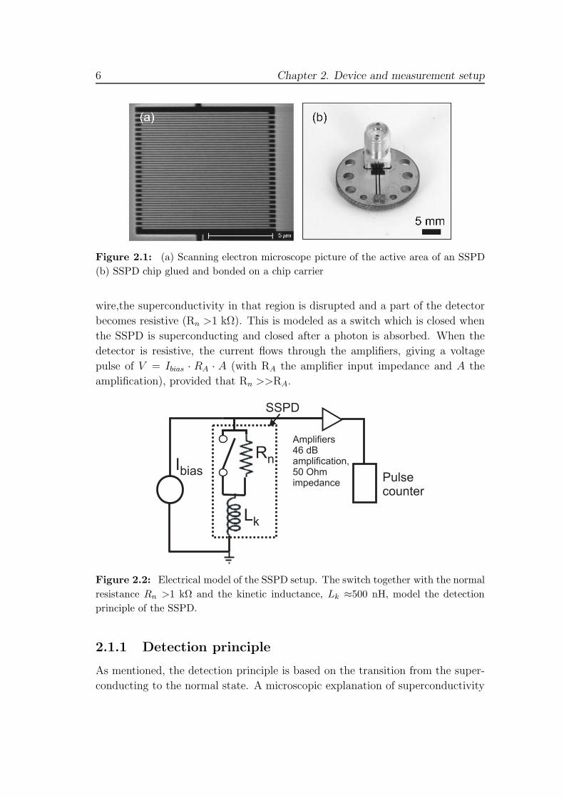
area [18]. A scanning electron microscope picture of an SSPD fabricated at TU
Delft is shown in figure 2.1a. The wire has a rectangular cross section defined by
a thickness of ∼ 6 nm NbTiN and a width of 100 nm. The length is 500 μm, the
filling factor 50%. The wire is folded in a 10x10 μm area. The full chip, glued
and bonded on a chip carrier, is shown in figure 2.1b.
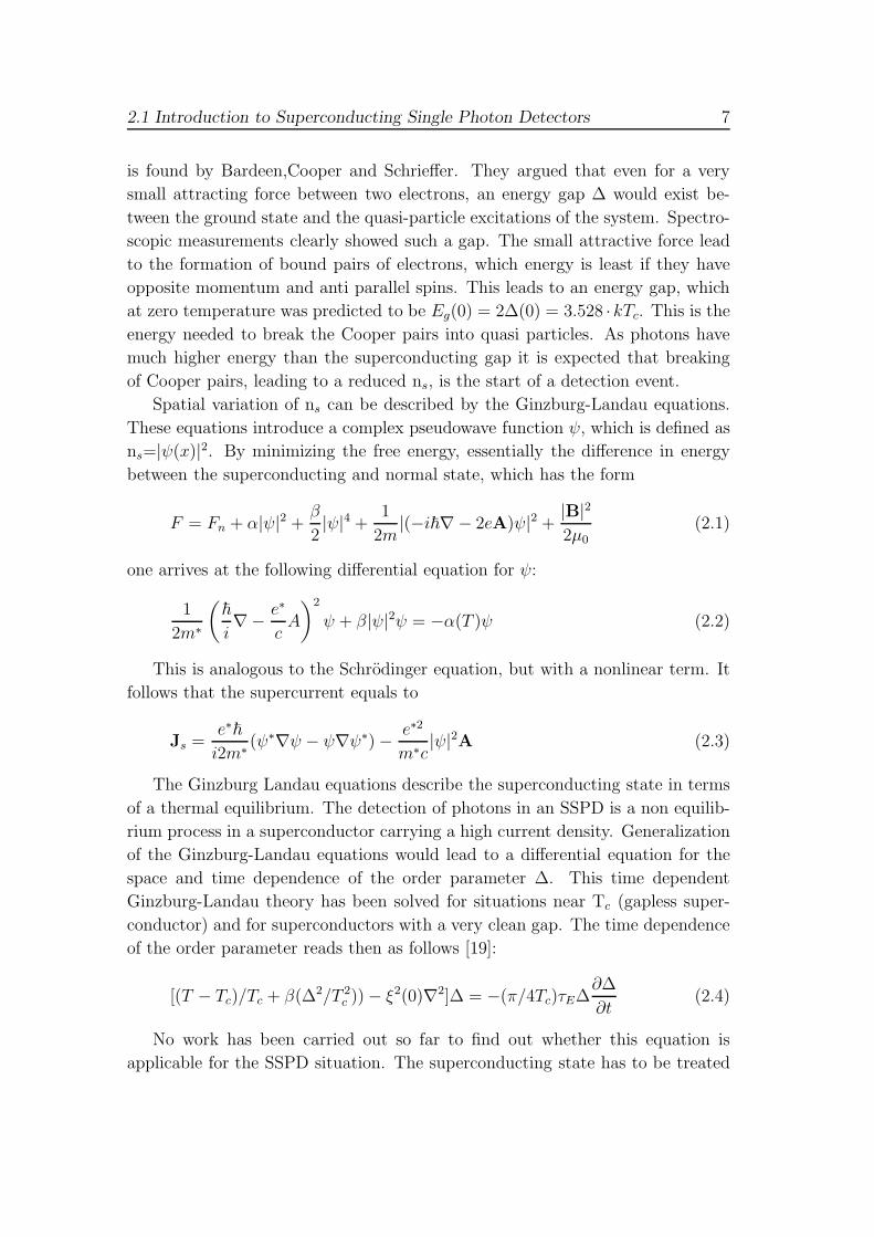
The operation principle of an SSPD is outlined in figure 2.2. The supercon-
ducting nanowire is biased with a direct current (Ibias) close to the critical current
(Ic), meaning that the current density (Jbias) flowing through the wire is near the
critical current density (Jc), above which the superconductivity of the nanowire
breaks down. When an incident photon of sufficient energy is absorbed by the
5
6 Chapter 2. Device and measurement setup
Figure 2.1: (a) Scanning electron microscope picture of the active area of an SSPD
(b) SSPD chip glued and bonded on a chip carrier
wire,the superconductivity in that region is disrupted and a part of the detector
becomes resistive (Rn >1 kΩ). This is modeled as a switch which is closed when
the SSPD is superconducting and closed after a photon is absorbed. When the
detector is resistive, the current flows through the amplifiers, giving a voltage
pulse of V = Ibias · RA · A (with RA the amplifier input impedance and A the
amplification), provided that Rn >>RA.
Ibias
Amplifiers46 dBamplification,50 Ohmimpedance
SSPD
Rn
Lk
Pulsecounter
Figure 2.2: Electrical model of the SSPD setup. The switch together with the normal
resistance Rn >1 kΩ and the kinetic inductance, Lk ≈500 nH, model the detection
principle of the SSPD.
2.1.1 Detection principle
As mentioned, the detection principle is based on the transition from the super-
conducting to the normal state. A microscopic explanation of superconductivity
2.1 Introduction to Superconducting Single Photon Detectors 7
is found by Bardeen,Cooper and Schrieffer. They argued that even for a very
small attracting force between two electrons, an energy gap Δ would exist be-
tween the ground state and the quasi-particle excitations of the system. Spectro-
scopic measurements clearly showed such a gap. The small attractive force lead
to the formation of bound pairs of electrons, which energy is least if they have
opposite momentum and anti parallel spins. This leads to an energy gap, which
at zero temperature was predicted to be Eg(0) = 2Δ(0) = 3.528 · kTc. This is theenergy needed to break the Cooper pairs into quasi particles. As photons have
much higher energy than the superconducting gap it is expected that breaking
of Cooper pairs, leading to a reduced ns, is the start of a detection event.
Spatial variation of ns can be described by the Ginzburg-Landau equations.
These equations introduce a complex pseudowave function ψ, which is defined as
ns=|ψ(x)|2. By minimizing the free energy, essentially the difference in energy
between the superconducting and normal state, which has the form
F = Fn + α|ψ|2 + β
2|ψ|4 + 1
2m|(−i�∇− 2eA)ψ|2 + |B|2
2μ0(2.1)
one arrives at the following differential equation for ψ:
1
2m∗
(�
i∇− e∗
cA
)2
ψ + β|ψ|2ψ = −α(T )ψ (2.2)
This is analogous to the Schrodinger equation, but with a nonlinear term. It
follows that the supercurrent equals to
Js =e∗�i2m∗ (ψ
∗∇ψ − ψ∇ψ∗)− e∗2
m∗c|ψ|2A (2.3)
The Ginzburg Landau equations describe the superconducting state in terms
of a thermal equilibrium. The detection of photons in an SSPD is a non equilib-
rium process in a superconductor carrying a high current density. Generalization
of the Ginzburg-Landau equations would lead to a differential equation for the
space and time dependence of the order parameter Δ. This time dependent
Ginzburg-Landau theory has been solved for situations near Tc (gapless super-
conductor) and for superconductors with a very clean gap. The time dependence
of the order parameter reads then as follows [19]:
[(T − Tc)/Tc + β(Δ2/T 2c ))− ξ2(0)∇2]Δ = −(π/4Tc)τEΔ
∂Δ
∂t(2.4)
No work has been carried out so far to find out whether this equation is
applicable for the SSPD situation. The superconducting state has to be treated
8 Chapter 2. Device and measurement setup
as a two dimensional state, as the width of the wire is much larger than its
coherence length (5 nm), with a reduced superconducting gap (but non-zero) at
low temperatures. The wire carries a high current density and after absorption of
light, excitations have to be taken into account, as well as spatial and temporal
variations during the diffusion and scattering processes. Theoretical work in this
direction could possibly hint towards improving the intrinsic detection efficiency,
however in this thesis the focus is on the practical implementation of SSPDs.
2.2 Detector characterization
In this section different parameters for the practical implementation of the de-
tectors are described.
2.2.1 Detection Efficiency
An important characteristic of a detector is its efficiency. For SSPDs it is a
measure of the probability that an input photon results in an electrical output
pulse. In this probability (DE) different subprocesses can be recognized.
DE = ηd · ηA · ηc (2.5)
where ηd is the probability of electrical pulse generation due to an absorbed
photon, ηA the photon absorption efficiency of the superconducting nanowire
and ηc the optical coupling efficiency between the incident light and the active
area of the detector. The first factor is the intrinsic quantum efficiency of the
nanowire and it is the probability that a voltage pulse will be generated given
that a photon is absorbed. The second factor depends on the absorbing properties
of the nanowire (material composition and geometry), which itself depends on
the surrounding layers (i.e., substrate and coating layers). Coupling losses are
represented by ηc. Coupling losses occur when the photon is coupled to the
detector. This is usually done with an optical fiber or a microscope objective.
As for the ’end-user’ of the detector the coupling loss is not of interest, often
the system detection efficiency (SDE) is defined. This is the probability that the
photon is detected once it is in the ’system’ (before coupling to the detector). The
parameters ηc and ηA depend on the surroundings of the detector, they will be
treated elsewhere in this thesis. The rest of this section is devoted to a description
of ηd, which is linked to physical properties of the device itself.
As was mentioned it is generally believed that the energy of a photon Eph =
h · ν ≈ 1 eV causes breaking of Cooper pairs, with a superconducting bandgap
2.2 Detector characterization 9
energy of Eg ∼ k ·Tc ≈ 5 meV (for NbTiN). The increased number of quasi parti-
cles leads to a finite resistance in a section of the nanowire, inducing a detection
event. It is not presently known how this influences the internal detection effi-
ciency ηd. However, a number of parameters effecting ηd have been investigated
experimentally:
Geometry
The geometry of the device is shown in figure 2.1a. It consists of a long mean-
dering wire. The wire has a rectangular section of approximately 5 x 100 nm.
It has been shown that decreasing the nanowire width, and the nanowire thick-
ness increases the intrinsic efficiency ηdof the device [18]. This is likely due to a
relative increase in the resistive spot size with respect to the wire cross section,
which makes it easier to induce a detection event.
As the wire length is large compared to its cross section, a uniform cross
section is extremely important. If a part of the nanowire is constricted, i.e. it
has a smaller local cross section, the critical current in this constriction is lower
than for the rest of the nanowire. In order to prevent switching to the normal
state the SSPD must be biased close to the critical current of the cross section.
This will mean that the rest of the wire will be biased far from its critical current,
and the internal efficiency in this part is lower than it should be, or in a worst
case scenario the detector is only sensitive at a constriction. Constrictions can be
identified through electrical measurements [20] and local illumination of operating
SSPDs with a focused laser spot.[21]
Bias current
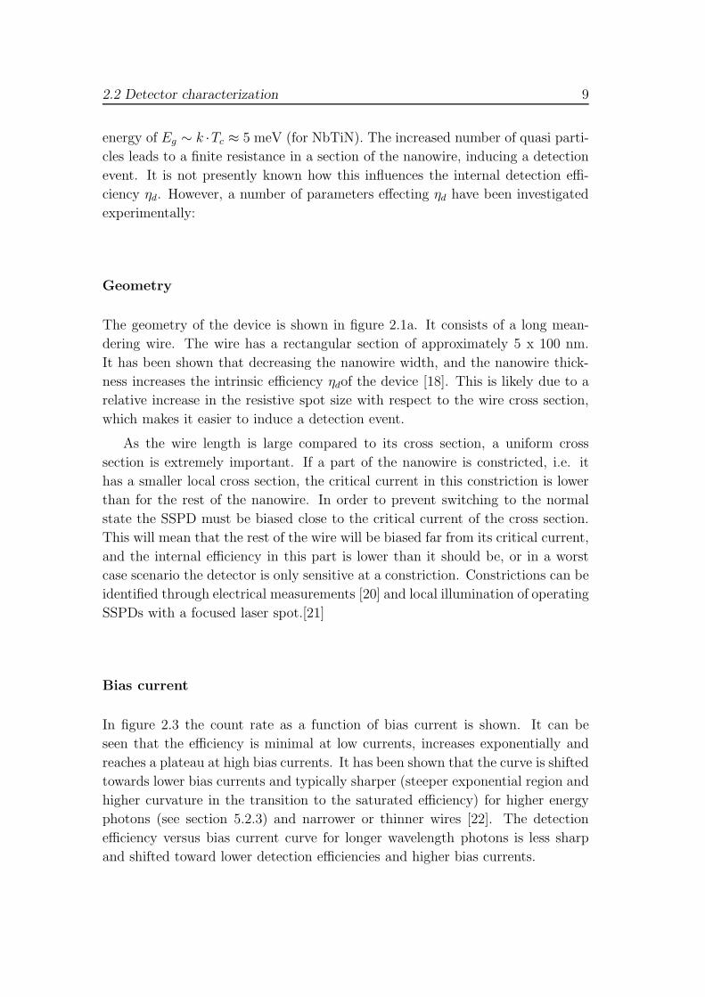
In figure 2.3 the count rate as a function of bias current is shown. It can be
seen that the efficiency is minimal at low currents, increases exponentially and
reaches a plateau at high bias currents. It has been shown that the curve is shifted
towards lower bias currents and typically sharper (steeper exponential region and
higher curvature in the transition to the saturated efficiency) for higher energy
photons (see section 5.2.3) and narrower or thinner wires [22]. The detection
efficiency versus bias current curve for longer wavelength photons is less sharp
and shifted toward lower detection efficiencies and higher bias currents.
10 Chapter 2. Device and measurement setup
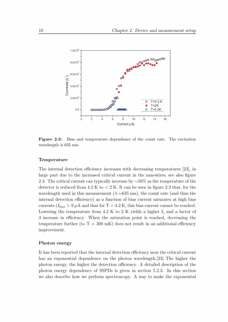
Figure 2.3: Bias and temperature dependence of the count rate. The excitation
wavelength is 635 nm.
Temperature
The internal detection efficiency increases with decreasing temperatures [23], in
large part due to the increased critical current in the nanowires, see also figure
2.3. The critical current can typically increase by ∼50% as the temperature of the
detector is reduced from 4.2 K to < 2 K. It can be seen in figure 2.3 that, for the
wavelength used in this measurement (λ =635 nm), the count rate (and thus the
internal detection efficiency) as a function of bias current saturates at high bias
currents (Ibias > 9 μA and that for T = 4.2 K, this bias current cannot be reached.
Lowering the temperature from 4.2 K to 2 K yields a higher Ic and a factor of
3 increase in efficiency. When the saturation point is reached, decreasing the
temperature further (to T = 300 mK) does not result in an additional efficiency
improvement.
Photon energy
It has been reported that the internal detection efficiency near the critical current
has an exponential dependence on the photon wavelength.[23] The higher the
photon energy, the higher the detection officiency. A detailed description of the
photon energy dependence of SSPDs is given in section 5.2.3. In this section
we also describe how we perform spectroscopy. A way to make the exponential
2.2 Detector characterization 11
dependence less pronounced is presented in chapter 6.
2.2.2 Dead time
The primary limitation to the maximum counting rate of an SSPD is the reset
time since it determines when a second photon can be detected. The detection
response time is set by electrical and thermal properties of the SSPD. The balance
between them even determines if the SSPD actually will reset. Reset will only
occur if the resistive state in the wire is unstable, for this to happen the thermal
time constants (i.e. the time to ”cool down” after a detection event) has to be
sufficiently fast compared to the electric time constants (i.e. the time it takes for
the current to decrease and return in the SSPD). [24, 25] This means that the
electrical time constant cannot be lowered indefinitely.
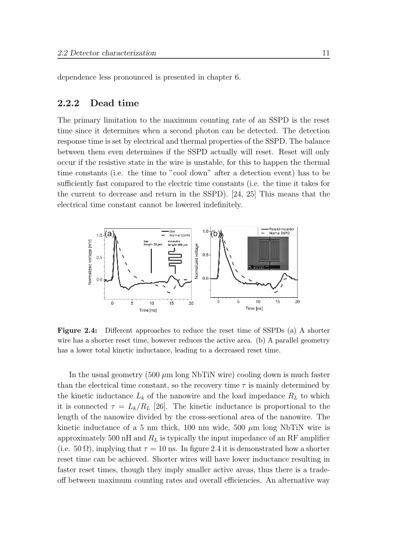
Figure 2.4: Different approaches to reduce the reset time of SSPDs (a) A shorter
wire has a shorter reset time, however reduces the active area. (b) A parallel geometry
has a lower total kinetic inductance, leading to a decreased reset time.
In the usual geometry (500 μm long NbTiN wire) cooling down is much faster
than the electrical time constant, so the recovery time τ is mainly determined by
the kinetic inductance Lk of the nanowire and the load impedance RL to which
it is connected τ = Lk/RL [26]. The kinetic inductance is proportional to the
length of the nanowire divided by the cross-sectional area of the nanowire. The
kinetic inductance of a 5 nm thick, 100 nm wide, 500 μm long NbTiN wire is
approximately 500 nH and RL is typically the input impedance of an RF amplifier
(i.e. 50 Ω), implying that τ = 10 ns. In figure 2.4 it is demonstrated how a shorter
reset time can be achieved. Shorter wires will have lower inductance resulting in
faster reset times, though they imply smaller active areas, thus there is a trade-
off between maximum counting rates and overall efficiencies. An alternative way
12 Chapter 2. Device and measurement setup
to decrease the kinetic inductance is to put more detectors in parallel. The
total kinetic inductance is then 1/Lk,total = 1/Lk,1 + 1/Lk,2.... A third option to
decrease τ is to increase the impedance as seen by the detector (RL).
As illustrated, it is possible to reduce the electrical time constants, however
the thermal constants, dictated by material properties, place a lower limit on
the reset time. Alternative substrates and film materials are under investigation
[27, 28], but producing faster SSPDs by decreasing the thermal time constants
has not been studied in detail.
2.2.3 Timing jitter
The timing jitter in SSPDs is not a limiting factor in the counting rate as it
is much lower than the reset time. While the nature of the timing jitter is
presently not known, it certainly depends on both the electrical time constants
and the details of the readout electronics, however there is also an intrinsic timing
jitter, most likely produced by the variation in time delay of the formation of the
resistive area, which in turn is caused by width variations along the nanowire and
the position where the absorption takes place in the meander.
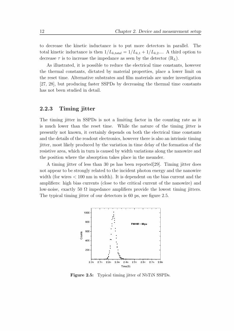
A timing jitter of less than 30 ps has been reported[29]. Timing jitter does
not appear to be strongly related to the incident photon energy and the nanowire
width (for wires < 100 nm in width). It is dependent on the bias current and the
amplifiers: high bias currents (close to the critical current of the nanowire) and
low-noise, exactly 50 Ω impedance amplifiers provide the lowest timing jitters.
The typical timing jitter of our detectors is 60 ps, see figure 2.5.
Figure 2.5: Typical timing jitter of NbTiN SSPDs.
2.2 Detector characterization 13
2.2.4 Dark counts
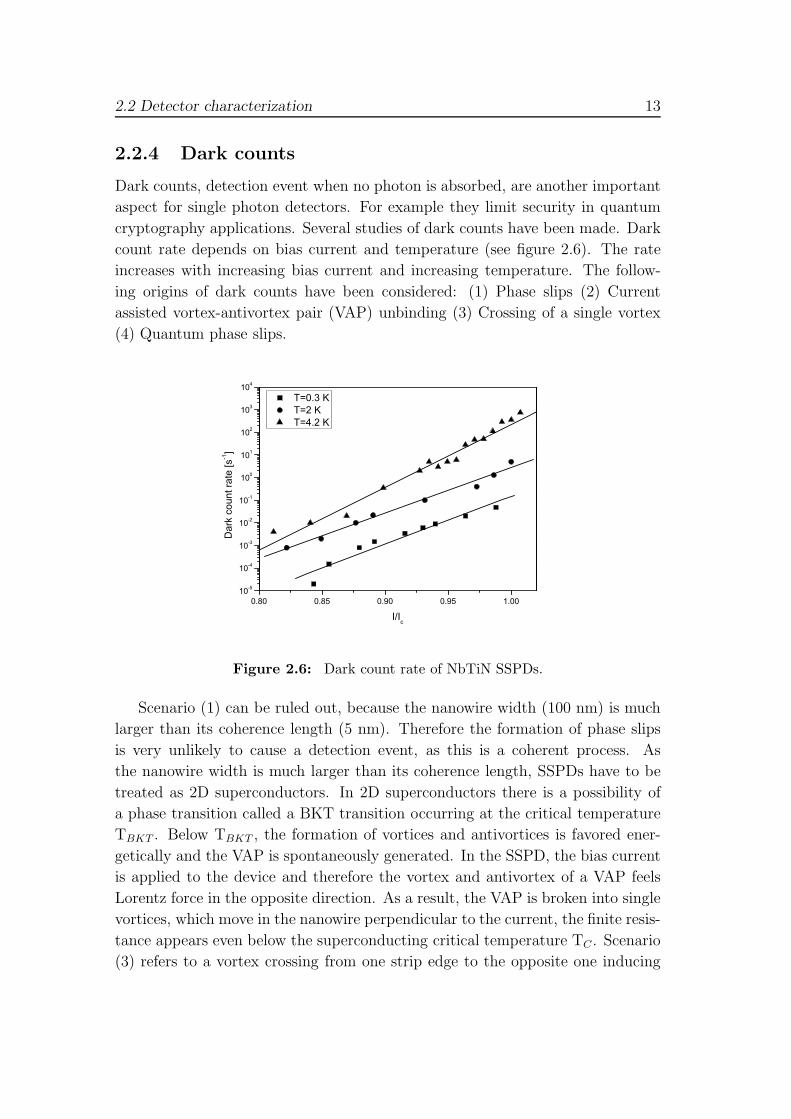
Dark counts, detection event when no photon is absorbed, are another important
aspect for single photon detectors. For example they limit security in quantum
cryptography applications. Several studies of dark counts have been made. Dark
count rate depends on bias current and temperature (see figure 2.6). The rate
increases with increasing bias current and increasing temperature. The follow-
ing origins of dark counts have been considered: (1) Phase slips (2) Current
assisted vortex-antivortex pair (VAP) unbinding (3) Crossing of a single vortex
(4) Quantum phase slips.
Figure 2.6: Dark count rate of NbTiN SSPDs.
Scenario (1) can be ruled out, because the nanowire width (100 nm) is much
larger than its coherence length (5 nm). Therefore the formation of phase slips
is very unlikely to cause a detection event, as this is a coherent process. As
the nanowire width is much larger than its coherence length, SSPDs have to be
treated as 2D superconductors. In 2D superconductors there is a possibility of
a phase transition called a BKT transition occurring at the critical temperature
TBKT . Below TBKT , the formation of vortices and antivortices is favored ener-
getically and the VAP is spontaneously generated. In the SSPD, the bias current
is applied to the device and therefore the vortex and antivortex of a VAP feels
Lorentz force in the opposite direction. As a result, the VAP is broken into single
vortices, which move in the nanowire perpendicular to the current, the finite resis-
tance appears even below the superconducting critical temperature TC . Scenario
(3) refers to a vortex crossing from one strip edge to the opposite one inducing

14 Chapter 2. Device and measurement setup
a phase slip without creating a normal region across the strip width. This phase
slip induces a voltage, leading to a dark count event.
In [30] it was pointed out that the energy barrier for the crossing of a single
vortex is much lower than for the unbinding of a vortex-antivortex pair. How-
ever experimental data [31, 32, 33] suggest that scenario (2) is a more realistic
scenario. For low temperatures (T<1 K) unbinding of a VAP cannot explain the
experimental data. Quantum phase slips (scenario 4) have been proposed, but
the agreement of this model with the experimental data is not complete.[31, 33]
In general, dark counts are low compared to the SSPDs efficiency with respect
to other single photon detectors. For implementation in experiments, detection
events because of stray light is a more problematic issue.
2.3 Fabrication 15
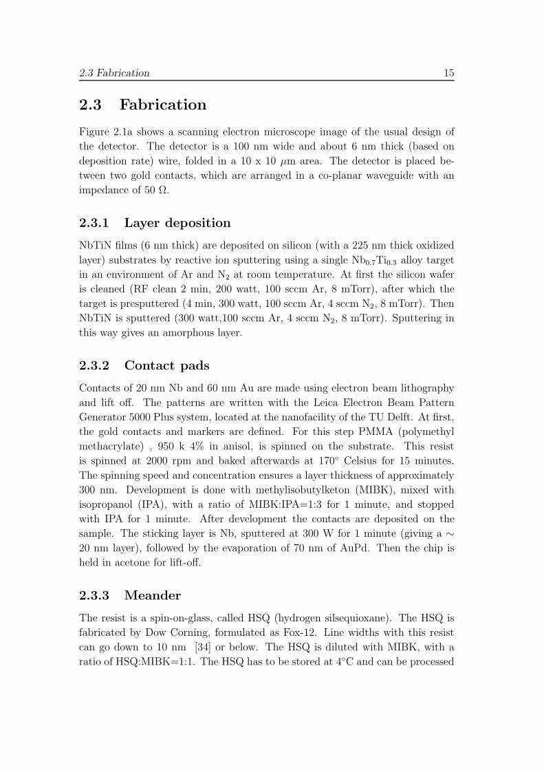
2.3 Fabrication
Figure 2.1a shows a scanning electron microscope image of the usual design of
the detector. The detector is a 100 nm wide and about 6 nm thick (based on
deposition rate) wire, folded in a 10 x 10 μm area. The detector is placed be-
tween two gold contacts, which are arranged in a co-planar waveguide with an
impedance of 50 Ω.
2.3.1 Layer deposition
NbTiN films (6 nm thick) are deposited on silicon (with a 225 nm thick oxidized
layer) substrates by reactive ion sputtering using a single Nb0.7Ti0.3 alloy target
in an environment of Ar and N2 at room temperature. At first the silicon wafer
is cleaned (RF clean 2 min, 200 watt, 100 sccm Ar, 8 mTorr), after which the
target is presputtered (4 min, 300 watt, 100 sccm Ar, 4 sccm N2, 8 mTorr). Then
NbTiN is sputtered (300 watt,100 sccm Ar, 4 sccm N2, 8 mTorr). Sputtering in
this way gives an amorphous layer.
2.3.2 Contact pads
Contacts of 20 nm Nb and 60 nm Au are made using electron beam lithography
and lift off. The patterns are written with the Leica Electron Beam Pattern
Generator 5000 Plus system, located at the nanofacility of the TU Delft. At first,
the gold contacts and markers are defined. For this step PMMA (polymethyl
methacrylate) , 950 k 4% in anisol, is spinned on the substrate. This resist
is spinned at 2000 rpm and baked afterwards at 170◦ Celsius for 15 minutes.
The spinning speed and concentration ensures a layer thickness of approximately
300 nm. Development is done with methylisobutylketon (MIBK), mixed with
isopropanol (IPA), with a ratio of MIBK:IPA=1:3 for 1 minute, and stopped
with IPA for 1 minute. After development the contacts are deposited on the
sample. The sticking layer is Nb, sputtered at 300 W for 1 minute (giving a ∼20 nm layer), followed by the evaporation of 70 nm of AuPd. Then the chip is
held in acetone for lift-off.
2.3.3 Meander
The resist is a spin-on-glass, called HSQ (hydrogen silsequioxane). The HSQ is
fabricated by Dow Corning, formulated as Fox-12. Line widths with this resist
can go down to 10 nm [34] or below. The HSQ is diluted with MIBK, with a
ratio of HSQ:MIBK=1:1. The HSQ has to be stored at 4◦C and can be processed
16 Chapter 2. Device and measurement setup
when it is at room temperature, i.e. it has to warm up before processing. The
spinning speed is 6000 rpm for 55 s to get a layer of 80 nm. In [35] a thorough
testing of HSQ is performed.
Subsequently we define an etch mask of hydrogen silsesquioxane (HSQ) with
electron beam lithography, and the material not covered with HSQ after exposure
and development is etched away by reactive ion etching in a plasma of SF6 and
O2. The etching is done in an environment of SF6 (13.5 sccm) and O2 (5 sccm),
with a power of 50 watt and Vbias=220 V. The etch time is 30 seconds + 10
seconds overetch for NbN films and 30 seconds + 30 seconds overetch for NbTiN
films.
When a sample is etched it is still covered with HSQ. The gold contacts are
also covered with an HSQ layer to prevent Au-contamination of the reactive ion
etching chamber. To contact the gold pads this HSQ has to be removed. This
is done by dipping the sample for 1 second in buffered hydrofluoric acid (BHF),
after which the sample is held in water to stop the etching.
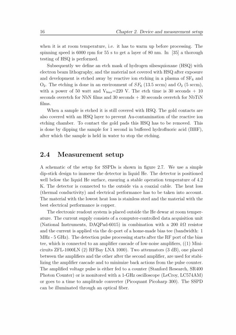
2.4 Measurement setup
A schematic of the setup for SSPDs is shown in figure 2.7. We use a simple
dip-stick design to immerse the detector in liquid He. The detector is positioned
well below the liquid He surface, ensuring a stable operation temperature of 4.2
K. The detector is connected to the outside via a coaxial cable. The heat loss
(thermal conductivity) and electrical performance has to be taken into account.
The material with the lowest heat loss is stainless steel and the material with the
best electrical performance is copper.
The electronic readout system is placed outside the He dewar at room temper-
ature. The current supply consists of a computer-controlled data acquisition unit
(National Instruments, DAQPad-6015) in combination with a 200 kΩ resistor
and the current is applied via the dc-port of a home-made bias tee (bandwidth: 1
MHz - 5 GHz). The detection pulse processing starts after the RF port of the bias
tee, which is connected to an amplifier cascade of low-noise amplifiers, ((1) Mini-
ciruits ZFL-1000LN (2) RFBay LNA 1000). Two attenuators (3 dB), one placed
between the amplifiers and the other after the second amplifier, are used for stabi-
lizing the amplifier cascade and to minimize back actions from the pulse counter.
The amplified voltage pulse is either fed to a counter (Stanford Research, SR400
Photon Counter) or is monitored with a 1-GHz oscilloscope (LeCroy, LC574AM)
or goes to a time to amplitude converter (Picoquant Picoharp 300). The SSPD
can be illuminated through an optical fiber.
2.4 Measurement setup 17
Figure 2.7: Schematic of an SSPD setup. The detector is immersed into liquid He
inside a transport He dewar using a simple dipstick design. The bias current is applied
via the dc port of a bias tee. The SSPD RF signal is amplified and detected by a pulse
counter. The SSPD can be illuminated through an optical fiber. Picture from [36].
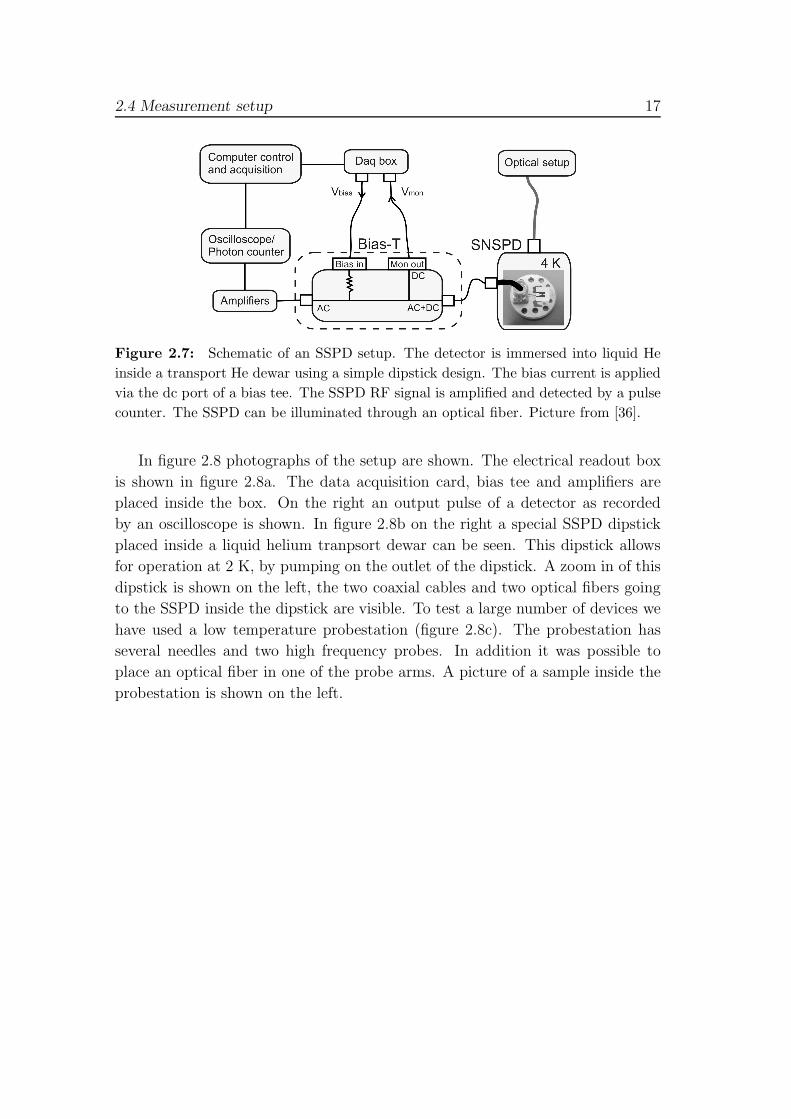
In figure 2.8 photographs of the setup are shown. The electrical readout box
is shown in figure 2.8a. The data acquisition card, bias tee and amplifiers are
placed inside the box. On the right an output pulse of a detector as recorded
by an oscilloscope is shown. In figure 2.8b on the right a special SSPD dipstick
placed inside a liquid helium tranpsort dewar can be seen. This dipstick allows
for operation at 2 K, by pumping on the outlet of the dipstick. A zoom in of this
dipstick is shown on the left, the two coaxial cables and two optical fibers going
to the SSPD inside the dipstick are visible. To test a large number of devices we
have used a low temperature probestation (figure 2.8c). The probestation has
several needles and two high frequency probes. In addition it was possible to
place an optical fiber in one of the probe arms. A picture of a sample inside the
probestation is shown on the left.
18 Chapter 2. Device and measurement setup
Figure 2.8: (a)Electrical readout box and output of SSPD on oscilloscope. (b) (right)
SSPD dipstick in transport dewar. (left) Zoom in of top of SSPD dipstick, with two
coaxial cables and two optical fibers coming out of the dipstick. (c) Photograph of low
temperature probestation. (left) Image of sample in low temperature probestation.

Part 1

Chapter 3
NbTiN SSPDs on an oxidized silicon
substrate
3.1 Low noise superconducting single photon de-
tectors on silicon
We have fabricated superconducting nanowire single photon detectors made of
NbTiN on a silicon substrate. This new type of material reduces the dark count
rate by a factor of 10 compared to identical NbN detectors, enabling single photon
detection with unprecedented signal to noise ratio: we report a noise equivalent
power of 10−19 W·Hz−1/2 at 4.2 K. The compatibility of our superconducting
device with silicon enables its integration with complex structures.
3.1.1 Introduction
So far, NbN has been the material of choice for SSPDs, due to the possibility
of depositing very thin films (4 nm thick [18, 37]), required for SSPDs. Here
we report on detectors made of NbTiN, a material with critical temperature
Tc = 15 K and critical current density Ic = 5.8 · 106 A/cm2, comparable with
NbN (Ic = 2−6 ·106 A/cm2, Tc = 10 K [38]. Our NbTiN detectors are fabricated
on a silicon substrate, enabling easy integration in advanced electronic circuits.
For example, an on-chip amplifier [39] could overcome problems of impedance
matching. Processing the silicon substrate makes integration of an optical cavity
and coupling with a fiber [38] straightforward. We show that an SSPD made of
NbTiN gives a lower dark count rate and matches the quantum efficiency of NbN
detectors, leading to an improved signal-to-noise ratio.
This section is based on S. N. Dorenbos, E.M. Reiger, U. Perinetti, V. Zwiller, T. Zijlstra
and T.M. Klapwijk, Applied Physics Letters 93, 131101 (2008).
21
22 Chapter 3. NbTiN SSPDs on an oxidized silicon substrate
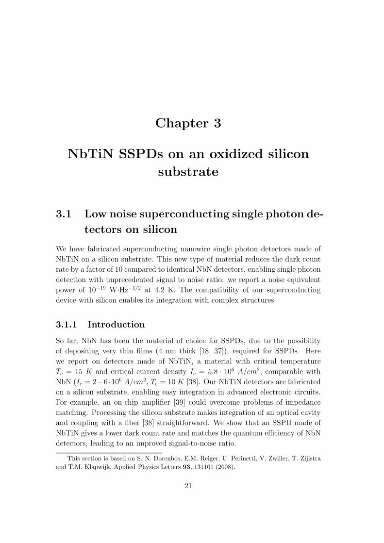
Figure 3.1: Quantum efficiency versus bias current for different wavelengths and
temperatures, with an exponential fit through the data points. Cooling from 4.2 K to
2.4 K exhibits an increase in quantum efficiency. In the inset a time trace of a detection
event is shown.
A detailed description of the fabrication process and the measurement setup
is given in chapter 2.
3.1.2 Results
Quantum efficiency
In figure 3.1 the quantum efficiency for different wavelengths is plotted as a
function of bias current. All measurements shown in this figure were done on
the same device. Each point was measured for 1 second. The quantum efficiency
increases exponentially with increasing bias current, as seen from the exponential
fit through the data points. The best quantum efficiency is achieved for 650
nm wavelength, for longer wavelengths the efficiency gradually goes down. The
wavelength dependence of the quantum efficiency can be used to resolve the
photon energy. By cooling from 4.2 K to 2.4 K, the critical current of the detector
increases from 35 μA to 40.5 μA. The quantum efficiency almost doubles, reaching
a value as high as 2.3% for 650 nm wavelength.
3.1 Low noise superconducting single photon detectors on silicon 23
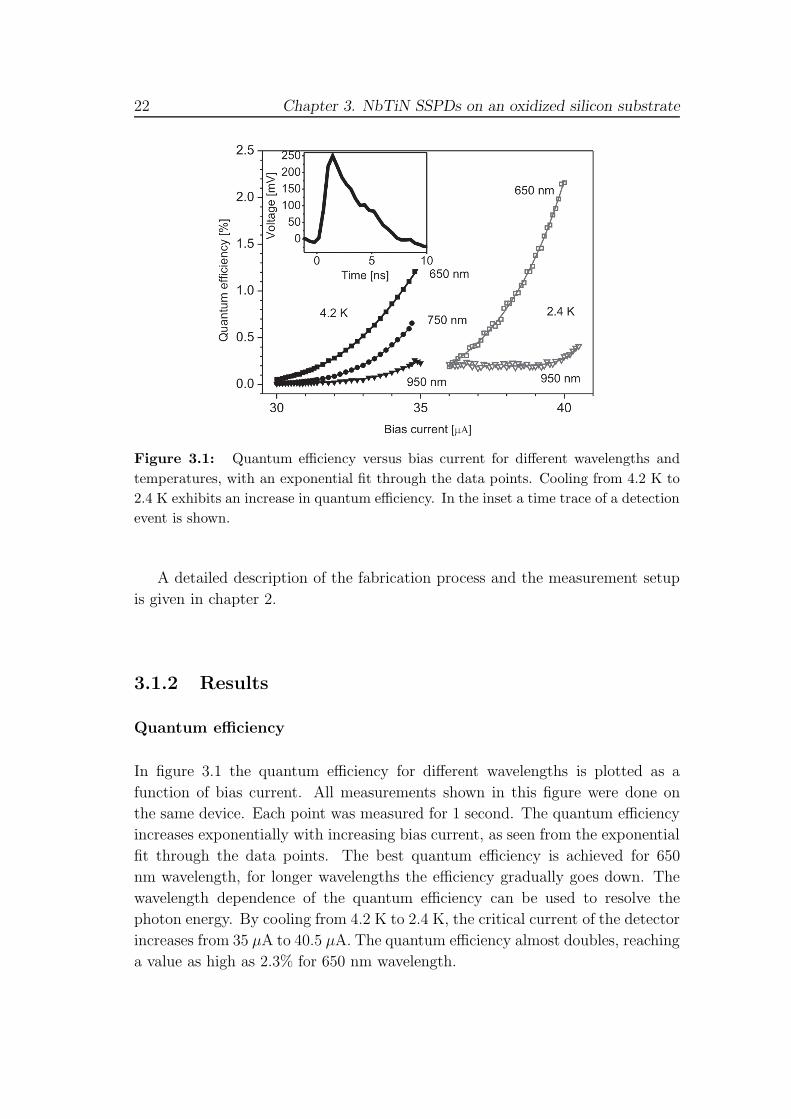
Figure 3.2: (a) Dark counts as a function of bias current and counter trigger level at
a temperature of 4.2 K (Light gray). A dark count trace for an identical NbN detector
is shown for 60 mV counter trigger level (Dark gray). (b) Photon counts per second
as a function of bias current and counter trigger level. The incident laser power is 0.01
nW, with 650 nm wavelength.
Dark count rate and noise equivalent power
In figure 3.2a dark counts are shown as a function of bias current and counter
trigger level for both a NbTiN (yellow) and a NbN (red) detector. 1 The NbN
1The dark counts are measured without fiber coupling.
24 Chapter 3. NbTiN SSPDs on an oxidized silicon substrate
detector was made from a NbN thin film on a sapphire substrate (commercially
obtained [18]), following the same fabrication procedure as the NbTiN detectors.
The dark count trace for the NbN detector is comparable to literature [40, 41].
From figure 3.2a it can be seen that below a certain counter trigger level (40
mV) the counter mainly detects environmental noise not related to dark counts
(detection events without an incident photon) of the superconducting detector.
The dark count rate can be measured by raising the trigger level because dark
counts have similar voltage pulse amplitudes compared to real detection events
(figure 3.1 inset [31]). If the counter trigger level is too high not all photon
absorption events are counted, which is not the case for trigger levels up to 100
mV (fig. 3.2b)), counter trigger levels of 50 to 100 mV are optimum for our
measurements. The measurement time for the dark count rate (fig. 3.2a) was
900 s per point between 0.85·Ic and 0.98·Ic and 1 s per point above 0.98·Ic. Thelowest dark count rate was 4·10−3s−1.
While the quantum efficiency of the NbTiN detectors is as high as for NbN de-
tectors made with the same fabrication procedure, the striking feature of NbTiN
detectors is their low dark count rate: a factor of 10 lower compared to NbN
detectors. This leads to an unequaled low noise equivalent power (NEP). The
NEP is defined to reveal the interplay between dark count rate and quantum
efficiency [42], and is given by
NEP =hν
QE
√2Rdc (3.1)
where hν represents the photon energy, QE the quantum efficiency and Rdc the
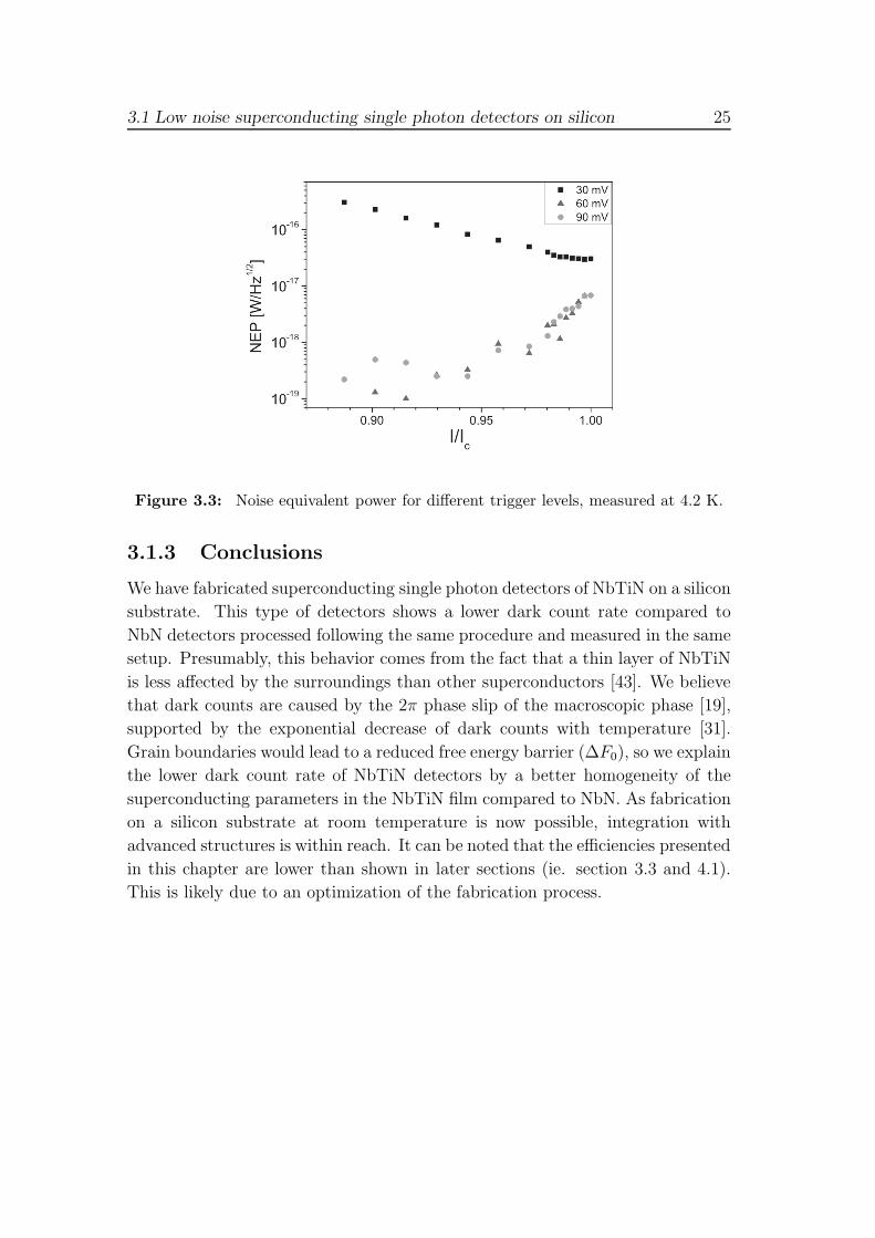
dark count rate. In figure 3.3 the NEP for different trigger levels is shown.2
It can be seen that an NEP of 1 · 10−19W · Hz−1/2 can be reached, 2 orders
of magnitude lower than the best NbN detectors3. Note that the NEP reaches
6·10−19 W ·Hz−1/2 very close to the critical current (0.97·Ic), a desirable behavior,not yet shown for NbN detectors, caused by the fast decrease in dark count rate
with decreasing bias current.
2For a counter trigger level of 30 mV, the dark count rate is high, because of noise in the
output signal, which explains the decrease in NEP with increasing bias current. For higher
counter trigger levels the dark count rate decreases exponentially with decreasing bias current.
Although the QE decreases exponentially with bias current as well, the dark count rate decreases
much faster, explaining the decrease of NEP with decreasing bias current.3NbN detectors show 1 · 10−17W ·Hz−1/2 at a comparable temperature [41]
3.1 Low noise superconducting single photon detectors on silicon 25
Figure 3.3: Noise equivalent power for different trigger levels, measured at 4.2 K.
3.1.3 Conclusions
We have fabricated superconducting single photon detectors of NbTiN on a silicon
substrate. This type of detectors shows a lower dark count rate compared to
NbN detectors processed following the same procedure and measured in the same
setup. Presumably, this behavior comes from the fact that a thin layer of NbTiN
is less affected by the surroundings than other superconductors [43]. We believe
that dark counts are caused by the 2π phase slip of the macroscopic phase [19],
supported by the exponential decrease of dark counts with temperature [31].
Grain boundaries would lead to a reduced free energy barrier (ΔF0), so we explain
the lower dark count rate of NbTiN detectors by a better homogeneity of the
superconducting parameters in the NbTiN film compared to NbN. As fabrication
on a silicon substrate at room temperature is now possible, integration with
advanced structures is within reach. It can be noted that the efficiencies presented
in this chapter are lower than shown in later sections (ie. section 3.3 and 4.1).
This is likely due to an optimization of the fabrication process.
26 Chapter 3. NbTiN SSPDs on an oxidized silicon substrate
3.2 Analysis of fabrication yield of NbTiN SSPDs
on an oxidized silicon substrate
3.2.1 Introduction
In a later part of this thesis it will be shown that SSPDs have proven themselves to
be useful devices for a number of experiments, however the number of applications
can become even larger by extending the single pixel SSPDs to a large array of
SSPDs, eventually resulting in a single photon camera. This could provide a fast
and high resolution imaging sensor suitable for applications like medical optical
tomography [44] where both temporal and spatial information must be obtained.
Another advantage of an array of SSPDs is the possibility of a larger active
area, relaxing the requirements for the accuracy of coupling to an optical fiber.
Furthermore, the maximum count rate for an individual SNSPD decreases as
its active area is increased, due to its kinetic inductance [26], forcing a trade-
off between active area and high count rates. Detector arrays will give a larger
active area while increasing the maximum count rate, as the pixels can be made
smaller and when one pixel is in the off state because of its dead time, the other
pixels can still detect. Large arrays could also provide spatial and photon-number
resolution. In a later section scalable readout methods scalable for large SSPD
arrays will be discussed. In this section another aspect of arrays will be treated.
An important condition to produce a large array of SSPDs is the reproducibility
of the fabrication. A large variation of detection efficiencies for apparent identical
devices has been reported. [29] This is very inconvenient when a large array is
produced, as the yield of good devices will become very low. In Ref. [20] a
study of the variation in efficiency is made for a large number of devices made
of NbN on sapphire. It is demonstrated that these variations can be understood
in terms of ’constrictions’: localized regions where the nanowire cross section is
effectively reduced. These constrictions can appear in the thickness or width of
the nanowire, limiting the critical current, causing the rest of the nanowire to be
underbiased, which yields a lower efficiency. In this section a similar investigation
is presented for NbTiN on oxidized Si.
3.2.2 Devices and experiment
Five wafers (with 2 inch diameter) have been fabricated. The fabrication proce-
dure of the detectors has been described in chapter 2. It starts with sputtering a
NbTiN layer on an oxidized silicon substrate. Because the layer to be obtained
is thin, the sputter time is short (approximately 5 seconds). The timing of the
3.2 Analysis of fabrication yield of NbTiN SSPDs on an oxidized silicon
substrate 27
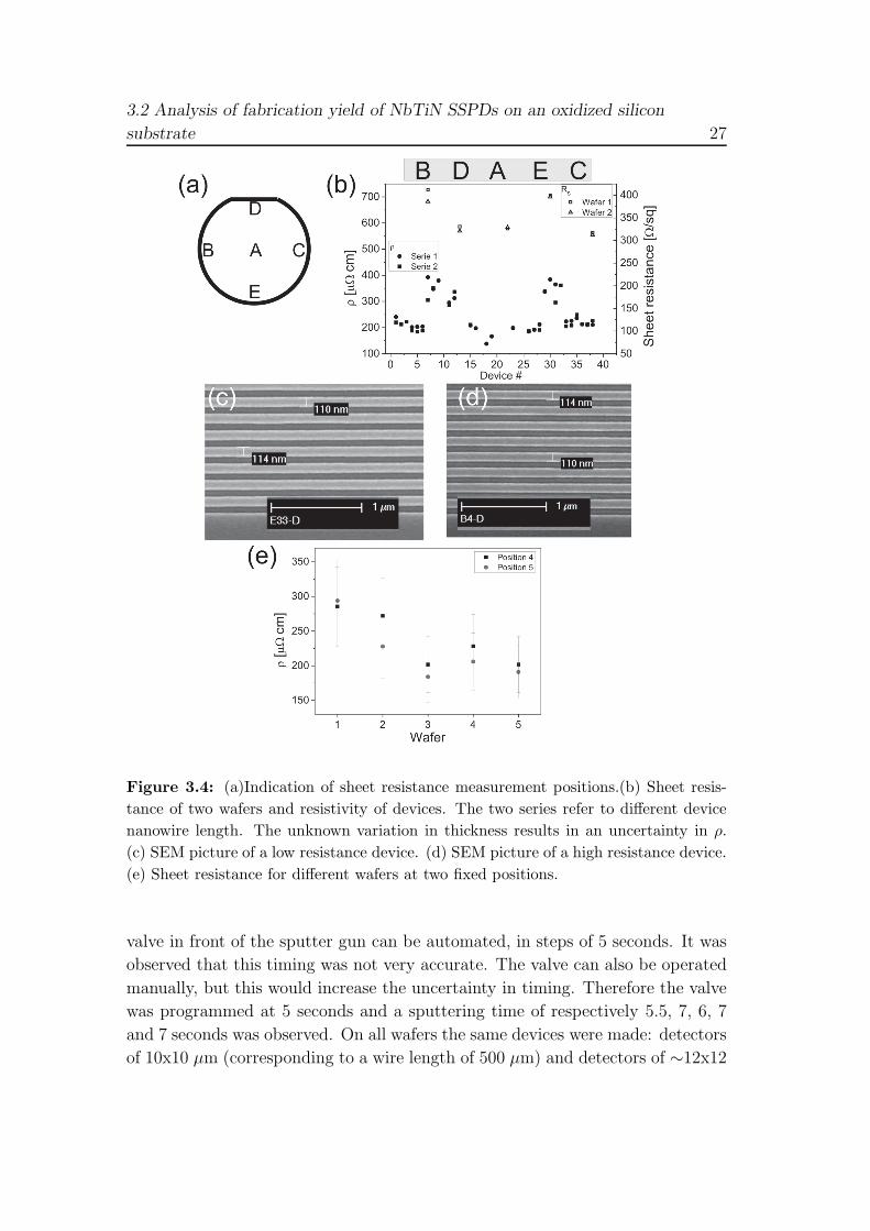
Figure 3.4: (a)Indication of sheet resistance measurement positions.(b) Sheet resis-
tance of two wafers and resistivity of devices. The two series refer to different device
nanowire length. The unknown variation in thickness results in an uncertainty in ρ.
(c) SEM picture of a low resistance device. (d) SEM picture of a high resistance device.
(e) Sheet resistance for different wafers at two fixed positions.
valve in front of the sputter gun can be automated, in steps of 5 seconds. It was
observed that this timing was not very accurate. The valve can also be operated
manually, but this would increase the uncertainty in timing. Therefore the valve
was programmed at 5 seconds and a sputtering time of respectively 5.5, 7, 6, 7
and 7 seconds was observed. On all wafers the same devices were made: detectors
of 10x10 μm (corresponding to a wire length of 500 μm) and detectors of ∼12x12
28 Chapter 3. NbTiN SSPDs on an oxidized silicon substrate
μm (corresponding to a length of 847 μm). To measure the critical temperature
of the film a strip of 10 μm and 1 μm width (200 μm long) was also fabricated.
For all wafers, the sheet resistance of the NbTiN layer is measured with a 4
probe measurement. After fabrication the resistance of the devices is measured
with a 2 point measurement. Then the wafers are cooled down in a low temper-
ature probe station. The probe station has a chuck base temperature of 4 K. A
high frequency probe is used to measure the critical current as well as dark count
rate and efficiency. The efficiency is measured by illuminating the detector with
a fiber probe. In this study a relative efficiency is presented, by comparing the
count rates of the detectors at a fixed power and fiber position. Finally the Tc
was measured in a dipstick with a heater and temperature controller.
3.2.3 Results
In figure 3.4a the positions on the wafer of the sheet resistance measurements (fig-
ure 3.4b) are indicated. Also in figure 3.4b the measurements of the resistivity of
the devices are shown. The resistivity is extracted from resistance measurements
of the devices by dividing the resistance by the length and targeted width and
thickness (respectively 5 and 100 nm), the two series correspond to the two dif-
ferent device lengths. The sheet resistance measurement already indicates that
the layer thickness is not uniform over the whole wafer. However, the variation
occurs for every wafer in the same way (for clarity only the sheet resistances from
2 wafers are shown). So this variation is likely because of the limited dimension of
the (3 inch) target and the plasma. The device resistivity measurements show a
similar variation, i.e. the devices fabricated at places with a high sheet resistance
have a higher resistivity than the devices fabricated at places with a low sheet re-
sistance. This would indicate a high reproducibility of the fabrication procedure,
which is underlined in figure 3.4c and 3.4d, where SEM pictures are shown for a
device with a low resistance and for a device with a high resistance respectively.
It can be seen that the width is similar for both devices. The variation in width
along the wire is less than 5%. It is worth to note the percentage of ’failures’:
devices which have zero or infinite resistance: 24%. The reason for zero resistance
devices is incomplete etching, resulting in ’left over’ NbTiN between the wires,
creating a short. In figure 3.4e the sheet resistance is shown for different wafers
at a fixed position. The difference in resistivity is noteworthy, but is probably
caused by a difference in sputtering time. A thickness measurement is needed to
find the cause for the resistivity variation.
From a number of devices the critical current is measured in the low temper-
ature probe station. The critical current as a function of resistivity is shown in
3.2 Analysis of fabrication yield of NbTiN SSPDs on an oxidized silicon
substrate 29
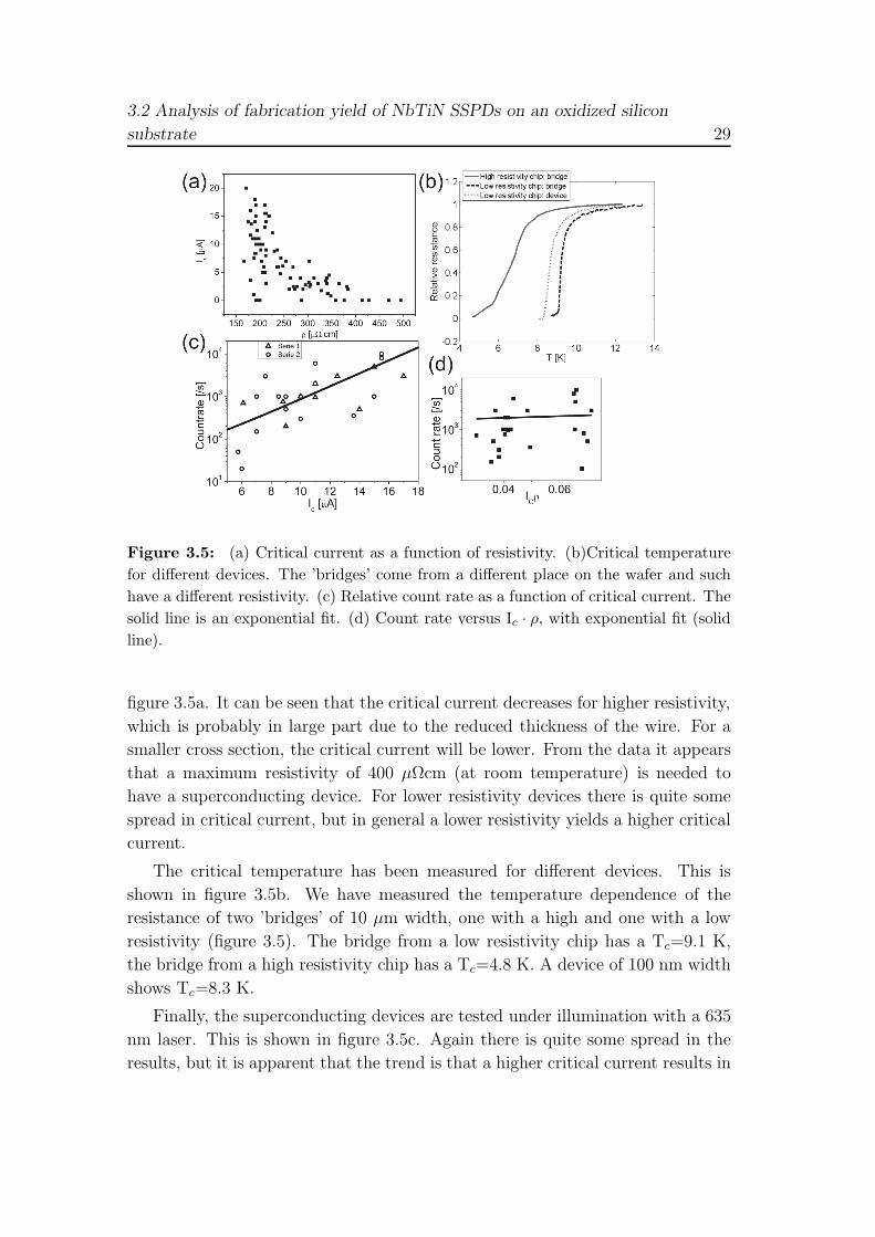
Figure 3.5: (a) Critical current as a function of resistivity. (b)Critical temperature
for different devices. The ’bridges’ come from a different place on the wafer and such
have a different resistivity. (c) Relative count rate as a function of critical current. The
solid line is an exponential fit. (d) Count rate versus Ic · ρ, with exponential fit (solid
line).
figure 3.5a. It can be seen that the critical current decreases for higher resistivity,
which is probably in large part due to the reduced thickness of the wire. For a
smaller cross section, the critical current will be lower. From the data it appears
that a maximum resistivity of 400 μΩcm (at room temperature) is needed to
have a superconducting device. For lower resistivity devices there is quite some
spread in critical current, but in general a lower resistivity yields a higher critical
current.
The critical temperature has been measured for different devices. This is
shown in figure 3.5b. We have measured the temperature dependence of the
resistance of two ’bridges’ of 10 μm width, one with a high and one with a low
resistivity (figure 3.5). The bridge from a low resistivity chip has a Tc=9.1 K,
the bridge from a high resistivity chip has a Tc=4.8 K. A device of 100 nm width
shows Tc=8.3 K.
Finally, the superconducting devices are tested under illumination with a 635
nm laser. This is shown in figure 3.5c. Again there is quite some spread in the
results, but it is apparent that the trend is that a higher critical current results in
30 Chapter 3. NbTiN SSPDs on an oxidized silicon substrate
a higher relative efficiency. In figure 3.5d the count rate versus the product Ic and
ρ is shown. As there is no clear correlation we can conclude that constrictions
are not the source of device failures in our process[20]. The minimum critical
current for a device to respond to light is 5 μA. The percentage of devices that
have a critical current of > 5 μA is 49%.
3.2.4 Conclusions
We have analyzed the fabrication yield of NbTiN SSPDs on an oxidized silicon
substrate. We have observed a variation in sheet resistance and device resistivity
over a wafer. Devices with a high resistivity (> 400μΩcm) have a low critical
current, and are also not very sensitive to photons. It is also shown that a low
critical current gives rise to a low efficiency. Low resistivity does not automati-
cally mean a high critical current, but all devices with high critical current show
a good efficiency. It is confirmed by SEM that the width of a high resistivity
and low resistivity device is similar, but the thickness and composition of the
wires should also be investigated to exclude them as a reason for the low critical
current. This could lead to a higher fabrication yield. In addition, a precise etch
monitor could decrease the number of zero resistance devices.
3.3 Efficient and robust fiber coupled superconducting single photon detectors31
3.3 Efficient and robust fiber coupled supercon-
ducting single photon detectors
e applied a recently developed fiber coupling technique to superconducting single
photon detectors (SSPDs). As the detector area of SSPDs has to be kept as small
as possible, coupling to an optical fiber has been either inefficient or unreliable.
Etching through the silicon substrate allows fabrication of a circularly shaped chip
which self aligns to the core of a ferrule terminated fiber in a fiber sleeve. In situ
alignment at cryogenic temperatures is unnecessary and no thermal stress during
cooldown, causing misalignment, is induced. We measured the quantum efficiency
of these devices with an attenuated tunable broadband source. The combination
of a lithographically defined chip and high precision standard telecommunication
components yields near unity coupling efficiency and a system detection efficiency
of 34 % at a wavelength of 1200 nm. This quantum efficiency measurement is
confirmed by an absolute efficiency measurement using correlated photon pairs
(with λ = 1064 nm) produced by spontaneous parametric down-conversion. The
efficiency obtained via this method agrees well with the efficiency measured with
the attenuated tunable broadband source.
3.3.1 Introduction and motivation
At near infrared wavelengths above 1100 nm, i.e. at telecommunication wave-
lengths, superconducting single photon detectors [16] are an established single
photon counting technology. [46] Due to their short dead time[16], low timing
jitter [47], good device efficiency, and low dark count rate [48] they have already
proved themselves in several experimental applications [49, 50, 51]. Furthermore,
they are not only suitable for single photon detection, but also for single electron
[52] and single plasmon detection [53]. For optical experiments efficient coupling
to an optical fiber is crucial. Because of the low operating temperature and the
small active area of the detector, this task remains challenging. To date differ-
ent techniques of fiber coupling to SSPDs have been shown. A fiber focuser in
combination with a micropositioning stage at low temperature enables in situ
alignment. However, because of loss in the fiber focuser, drift of the micropo-
sitioning stages and mechanical decoupling of the fiber and the detector, it was
estimated that the coupling efficiency was only 80%. [54] Another technique
which is shown by different groups [47, 55] is to mechanically clamp the fiber
close to the detector. This can lead to near unity coupling efficiency, but it is
This section is based on S.N. Dorenbos, R.W. Heeres, E.F.C. Driessen and V. Zwiller,
submitted for publication
32 Chapter 3. NbTiN SSPDs on an oxidized silicon substrate
very sensitive to small shifts, i.e. due to thermal contraction during cool down.
Recently a fiber coupling technique was introduced for transition edge sensor
devices.[56] This technique utilizes micromachining techniques developed for sil-
icon substrates together with optical fiber techniques. Ferrule terminated fibers
can be aligned with respect to each other with a commercially available precisely
fabricated sleeve. As the dimensions of these sleeves are very precisely defined,
it is possible to use sub-micrometer resolution of lithographic technology to fab-
ricate a detector chip with a shape that fits exactly in the sleeve. By fabricating
the detector in the middle of the chip, the alignment of the detector with respect
to the core of the ferrule terminated fiber follows naturally.
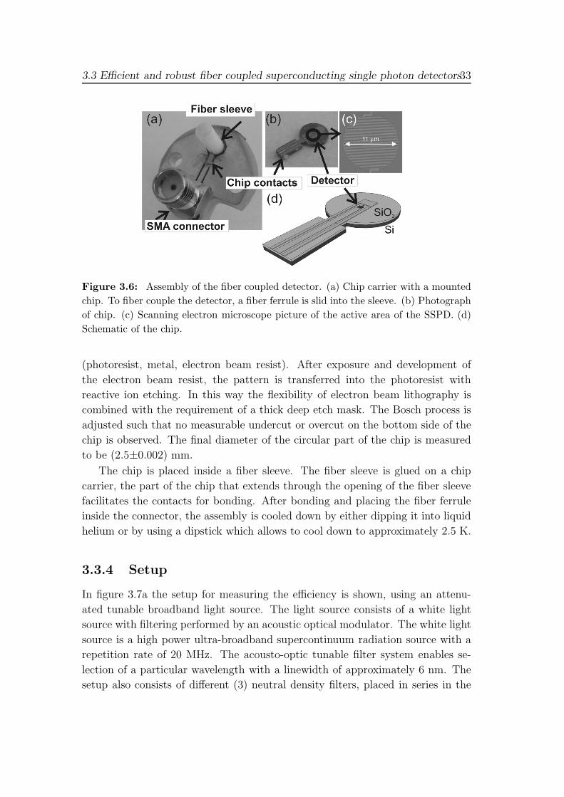
3.3.2 Chip layout
In figure 3.6 the device is pictured. The chip, which has a circular shape (figure
1b) is placed inside the fiber sleeve (figure 3.6a). The detector (figure 3.6c) is
placed exactly in the middle of the circular piece of the chip. The detector itself
also has a circular design to minimize the length of the nanowire, as the output
of a single mode fiber has a Gausssian shape. Although a smaller active area
increases coupling difficulty, it has several advantages. First, a smaller detector
yields a shorter recovery time and second a smaller detector has a decreased
probability of constrictions, which can severely limit device efficiency.[20] The
total length of the nanowire was 847 μm, which results in a recovery time of
approximately 10 ns. We have chosen for an 11 μm diameter detector to match
to the size of a single mode optical fiber. The rectangular part of the chip extends
outside the fiber ferrule, on which contacts are positioned for bonding. In figure
3.6d a schematic of the chip is shown.
3.3.3 Fabrication
The detector is fabricated by sputtering a thin NbTiN film on oxidized silicon and
subsequent electron beam lithography and reactive ion etching.[48] The circular
chip shape is made by deep etching through the silicon substrate. The deep
etching is performed by use of the Bosch dry-etch process[57]. This process
provides highly anisotropic etching and a vertical etch profile through the 300
μm thick Si wafer can be obtained. It consists of a longer etching step (with
SF6) and a shorter passivation step (with C4F8). The passivation step prevents
the side walls from being etched. As a mask for the deep etching a photoresist
with a thickness of 5 μm is placed to protect the SSPD. To be able to apply
electron beam lithography for patterning the chip, a triple layer mask is used
3.3 Efficient and robust fiber coupled superconducting single photon detectors33
Figure 3.6: Assembly of the fiber coupled detector. (a) Chip carrier with a mounted
chip. To fiber couple the detector, a fiber ferrule is slid into the sleeve. (b) Photograph
of chip. (c) Scanning electron microscope picture of the active area of the SSPD. (d)
Schematic of the chip.
(photoresist, metal, electron beam resist). After exposure and development of
the electron beam resist, the pattern is transferred into the photoresist with
reactive ion etching. In this way the flexibility of electron beam lithography is
combined with the requirement of a thick deep etch mask. The Bosch process is
adjusted such that no measurable undercut or overcut on the bottom side of the
chip is observed. The final diameter of the circular part of the chip is measured
to be (2.5±0.002) mm.
The chip is placed inside a fiber sleeve. The fiber sleeve is glued on a chip
carrier, the part of the chip that extends through the opening of the fiber sleeve
facilitates the contacts for bonding. After bonding and placing the fiber ferrule
inside the connector, the assembly is cooled down by either dipping it into liquid
helium or by using a dipstick which allows to cool down to approximately 2.5 K.
3.3.4 Setup
In figure 3.7a the setup for measuring the efficiency is shown, using an attenu-
ated tunable broadband light source. The light source consists of a white light
source with filtering performed by an acoustic optical modulator. The white light
source is a high power ultra-broadband supercontinuum radiation source with a
repetition rate of 20 MHz. The acousto-optic tunable filter system enables se-
lection of a particular wavelength with a linewidth of approximately 6 nm. The
setup also consists of different (3) neutral density filters, placed in series in the
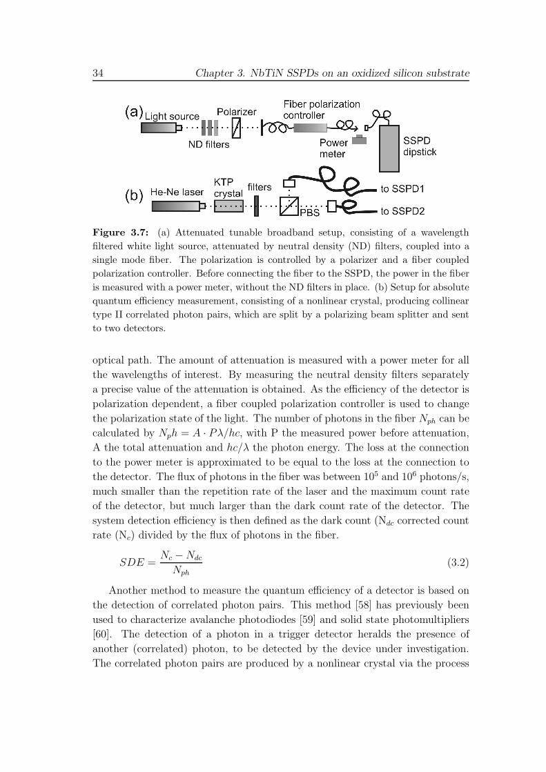
34 Chapter 3. NbTiN SSPDs on an oxidized silicon substrate
Figure 3.7: (a) Attenuated tunable broadband setup, consisting of a wavelength
filtered white light source, attenuated by neutral density (ND) filters, coupled into a
single mode fiber. The polarization is controlled by a polarizer and a fiber coupled
polarization controller. Before connecting the fiber to the SSPD, the power in the fiber
is measured with a power meter, without the ND filters in place. (b) Setup for absolute
quantum efficiency measurement, consisting of a nonlinear crystal, producing collinear
type II correlated photon pairs, which are split by a polarizing beam splitter and sent
to two detectors.
optical path. The amount of attenuation is measured with a power meter for all
the wavelengths of interest. By measuring the neutral density filters separately
a precise value of the attenuation is obtained. As the efficiency of the detector is
polarization dependent, a fiber coupled polarization controller is used to change
the polarization state of the light. The number of photons in the fiber Nph can be
calculated by Nph = A · Pλ/hc, with P the measured power before attenuation,
A the total attenuation and hc/λ the photon energy. The loss at the connection
to the power meter is approximated to be equal to the loss at the connection to
the detector. The flux of photons in the fiber was between 105 and 106 photons/s,
much smaller than the repetition rate of the laser and the maximum count rate
of the detector, but much larger than the dark count rate of the detector. The
system detection efficiency is then defined as the dark count (Ndc corrected count
rate (Nc) divided by the flux of photons in the fiber.
SDE =Nc −Ndc
Nph(3.2)
Another method to measure the quantum efficiency of a detector is based on
the detection of correlated photon pairs. This method [58] has previously been
used to characterize avalanche photodiodes [59] and solid state photomultipliers
[60]. The detection of a photon in a trigger detector heralds the presence of
another (correlated) photon, to be detected by the device under investigation.
The correlated photon pairs are produced by a nonlinear crystal via the process
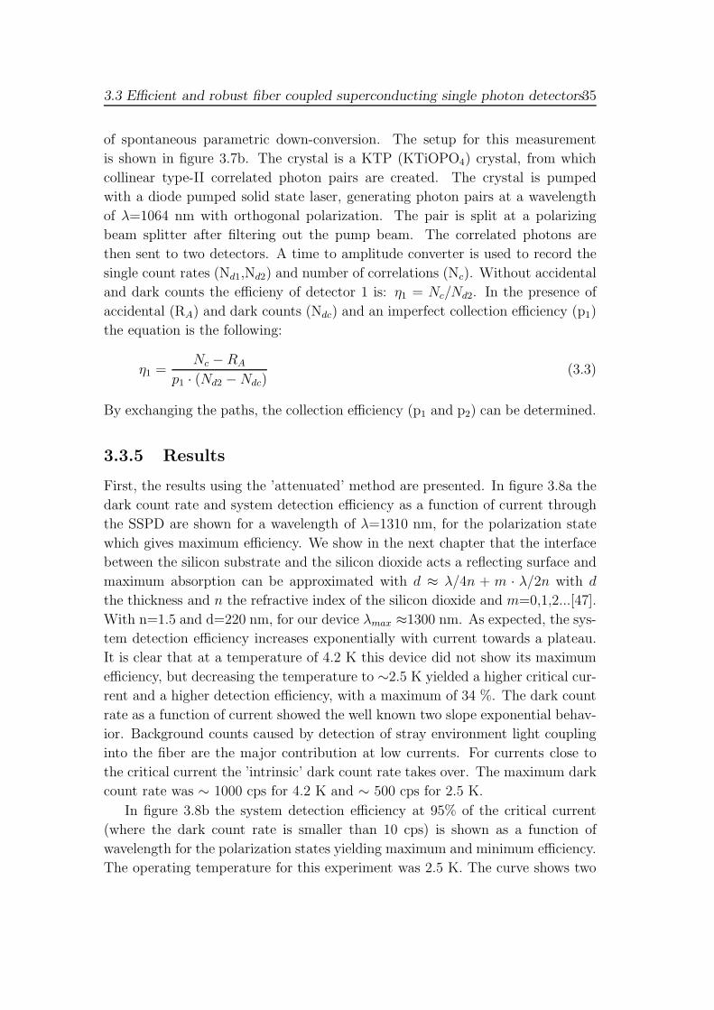
3.3 Efficient and robust fiber coupled superconducting single photon detectors35
of spontaneous parametric down-conversion. The setup for this measurement
is shown in figure 3.7b. The crystal is a KTP (KTiOPO4) crystal, from which
collinear type-II correlated photon pairs are created. The crystal is pumped
with a diode pumped solid state laser, generating photon pairs at a wavelength
of λ=1064 nm with orthogonal polarization. The pair is split at a polarizing
beam splitter after filtering out the pump beam. The correlated photons are
then sent to two detectors. A time to amplitude converter is used to record the
single count rates (Nd1,Nd2) and number of correlations (Nc). Without accidental
and dark counts the efficieny of detector 1 is: η1 = Nc/Nd2. In the presence of
accidental (RA) and dark counts (Ndc) and an imperfect collection efficiency (p1)
the equation is the following:
η1 =Nc − RA
p1 · (Nd2 −Ndc)(3.3)
By exchanging the paths, the collection efficiency (p1 and p2) can be determined.
3.3.5 Results
First, the results using the ’attenuated’ method are presented. In figure 3.8a the
dark count rate and system detection efficiency as a function of current through
the SSPD are shown for a wavelength of λ=1310 nm, for the polarization state
which gives maximum efficiency. We show in the next chapter that the interface
between the silicon substrate and the silicon dioxide acts a reflecting surface and
maximum absorption can be approximated with d ≈ λ/4n + m · λ/2n with d
the thickness and n the refractive index of the silicon dioxide and m=0,1,2...[47].
With n=1.5 and d=220 nm, for our device λmax ≈1300 nm. As expected, the sys-
tem detection efficiency increases exponentially with current towards a plateau.
It is clear that at a temperature of 4.2 K this device did not show its maximum
efficiency, but decreasing the temperature to ∼2.5 K yielded a higher critical cur-
rent and a higher detection efficiency, with a maximum of 34 %. The dark count
rate as a function of current showed the well known two slope exponential behav-
ior. Background counts caused by detection of stray environment light coupling
into the fiber are the major contribution at low currents. For currents close to
the critical current the ’intrinsic’ dark count rate takes over. The maximum dark
count rate was ∼ 1000 cps for 4.2 K and ∼ 500 cps for 2.5 K.
In figure 3.8b the system detection efficiency at 95% of the critical current
(where the dark count rate is smaller than 10 cps) is shown as a function of
wavelength for the polarization states yielding maximum and minimum efficiency.
The operating temperature for this experiment was 2.5 K. The curve shows two
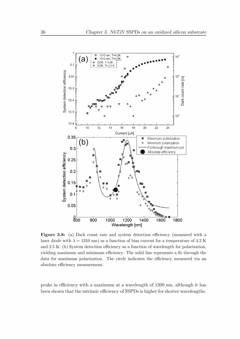
36 Chapter 3. NbTiN SSPDs on an oxidized silicon substrate
Figure 3.8: (a) Dark count rate and system detection efficiency (measured with a
laser diode with λ = 1310 nm) as a function of bias current for a temperature of 4.2 K
and 2.5 K. (b) System detection efficiency as a function of wavelength for polarization,
yielding maximum and minimum efficiency. The solid line represents a fit through the
data for maximum polarization. The circle indicates the efficiency measured via an
absolute efficiency measurement.
peaks in efficiency with a maximum at a wavelength of 1200 nm, although it has
been shown that the intrinsic efficiency of SSPDs is higher for shorter wavelengths.
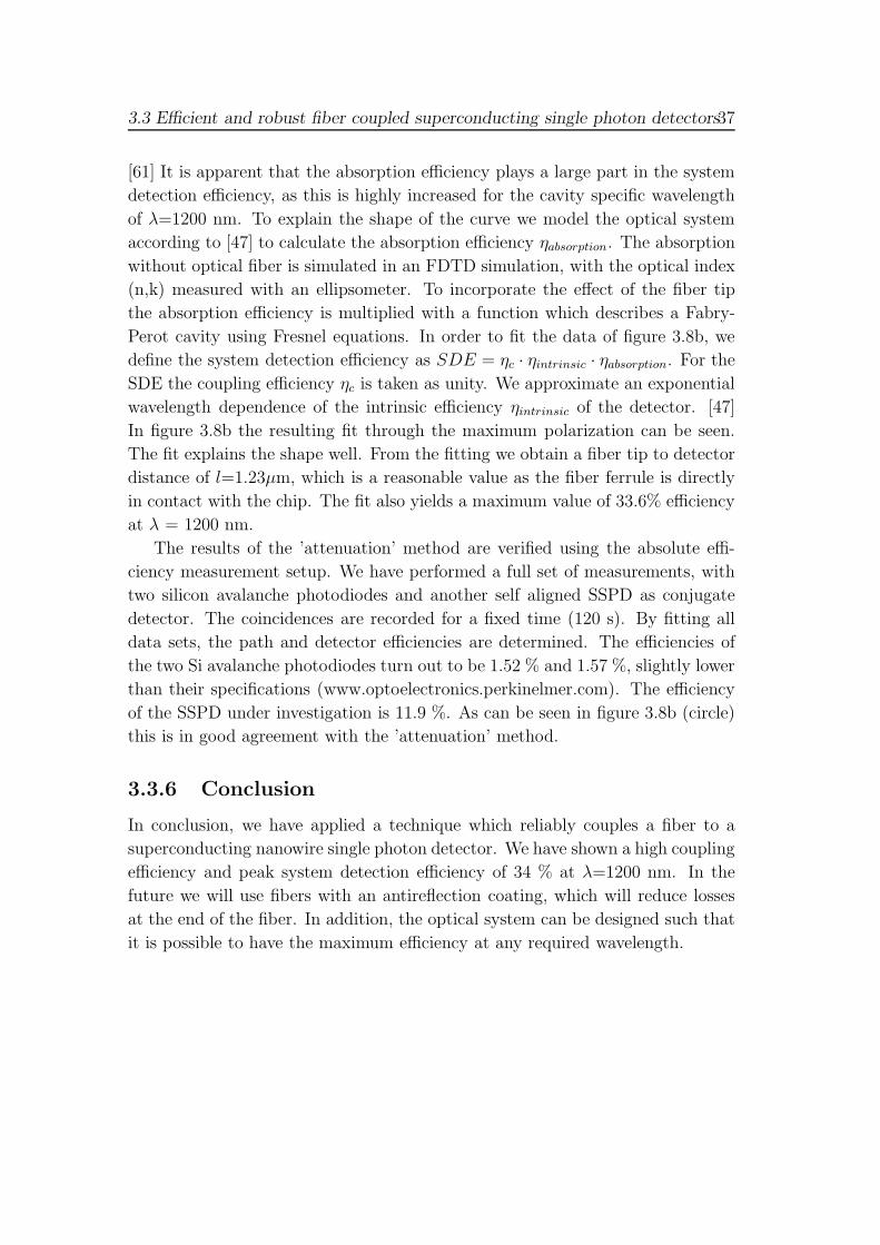
3.3 Efficient and robust fiber coupled superconducting single photon detectors37
[61] It is apparent that the absorption efficiency plays a large part in the system
detection efficiency, as this is highly increased for the cavity specific wavelength
of λ=1200 nm. To explain the shape of the curve we model the optical system
according to [47] to calculate the absorption efficiency ηabsorption. The absorption
without optical fiber is simulated in an FDTD simulation, with the optical index
(n,k) measured with an ellipsometer. To incorporate the effect of the fiber tip
the absorption efficiency is multiplied with a function which describes a Fabry-
Perot cavity using Fresnel equations. In order to fit the data of figure 3.8b, we
define the system detection efficiency as SDE = ηc · ηintrinsic · ηabsorption. For theSDE the coupling efficiency ηc is taken as unity. We approximate an exponential
wavelength dependence of the intrinsic efficiency ηintrinsic of the detector. [47]
In figure 3.8b the resulting fit through the maximum polarization can be seen.
The fit explains the shape well. From the fitting we obtain a fiber tip to detector
distance of l=1.23μm, which is a reasonable value as the fiber ferrule is directly
in contact with the chip. The fit also yields a maximum value of 33.6% efficiency
at λ = 1200 nm.
The results of the ’attenuation’ method are verified using the absolute effi-
ciency measurement setup. We have performed a full set of measurements, with
two silicon avalanche photodiodes and another self aligned SSPD as conjugate
detector. The coincidences are recorded for a fixed time (120 s). By fitting all
data sets, the path and detector efficiencies are determined. The efficiencies of
the two Si avalanche photodiodes turn out to be 1.52 % and 1.57 %, slightly lower
than their specifications (www.optoelectronics.perkinelmer.com). The efficiency
of the SSPD under investigation is 11.9 %. As can be seen in figure 3.8b (circle)
this is in good agreement with the ’attenuation’ method.
3.3.6 Conclusion
In conclusion, we have applied a technique which reliably couples a fiber to a
superconducting nanowire single photon detector. We have shown a high coupling
efficiency and peak system detection efficiency of 34 % at λ=1200 nm. In the
future we will use fibers with an antireflection coating, which will reduce losses
at the end of the fiber. In addition, the optical system can be designed such that
it is possible to have the maximum efficiency at any required wavelength.

38 Chapter 3. NbTiN SSPDs on an oxidized silicon substrate
Chapter 4
Cavity enhanced detectors
4.1 Enhanced telecom wavelength single-photon
detection with NbTiN superconducting nano-
wires on oxidized silicon
We report on the practical performance of packaged NbTiN SSSPDs fabricated
on oxidized silicon substrates in the wavelength range from 830 to 1700 nm. We
exploit constructive interference from the SiO2 / Si interface in order to achieve
enhanced front-side fiber-coupled DE of 23.2 % at 1310 nm, at 1 kHz dark count
rate, with 60 ps full width half maximum timing jitter.
4.1.1 Introduction
The 1300 nm wavelength range is important for quantum information experiments
using telecom-wavelength quantum-dot single-photon sources [62] and medical
applications such as singlet oxygen detection at λ=1273 nm.[63] In this paper we
report on enhanced device efficiency in a Nb-TiN SSPD with a cavity reflection
from the oxidized Si substrate optimized for 1300 nm wavelength. The devices are
front-side fiber-coupled in a fixed package without the need for nanopositioners
or thinning of the substrate used in backside illumination architectures.[29, 55,
54] In this section, we describe device performance as a function of wavelength,
with reference to the device architecture. We demonstrate the highest published
efficiency in a practically packaged SSPD at λ=1310 nm with frontside fiber
illumination, comparable to results achieved with backside illumination.
This section is based on M. G. Tanner, C. M. Natarajan, V. K. Pottapenjara, J. A. OCon-
nor, R. J. Warburton, R. H. Hadfield, B. Baek, S. Nam, S. N. Dorenbos, E. Bermudez Urena,
T. Zijlstra, T. M. Klapwijk, and V. Zwiller, Applied Physics Letters 96, 221109 (2010)
39
40 Chapter 4. Cavity and grating enhanced detectors
Devices used in this study [48] are based on high quality films of NbTiN
deposited by reactive dc magnetron sputtering at room temperature on a Si sub-
strate with a 225 nm SiO2 layer.[64] The devices studied consist of a 10x10 μm2
detector, composed of a meander wire 100 nm wide with 200 nm pitch. This
was aligned to a single-mode optical fiber with 9 μm mode field diameter as
shown in figure 4.1a. The chip-to-fiber spacing was determined through white-
light interferometry d=35 μm, at room temperature decreasing to d=10 μm at
the operating temperature of 2.8 K. Electrical and optical testing is performed
in a GiffordMcMahon cryocooler at a device temperature of 2.8 K, well below
the observed device superconducting transition temperature of 8 K. The exper-
imental arrangement for DE measurements is shown in figure 4.1d. The optical
attenuation of the laser diode source is varied to control the photon flux while
the detector count rate is monitored. Bias current is varied to control the dark
counts.
4.1.2 Results
System DE determined from the fiber input to the cryostat was measured by
use of calibrated laser diodes at 830, 1310, and 1550 nm wavelength with po-
larization optimized for both high and low device DE [65] at multiple biasing
points, as shown in figure 4.2a. High DE is observed at all wavelengths, at 1
kHz dark count rate DE=8.5%, 23.2%, and 7.8% at 830 nm, 1310 nm and 1550
nm wavelength, respectively. At dark count rates as low as 20 Hz, DE of 7.5
%, 10%, and 2.8% are observed for 830 nm, 1310 nm and 1550 nm illumination,
respectively. The most striking feature is that DE is higher at 1310 than 830 or
1550 nm wavelength owing to the optical structure discussed below. Without an
optical cavity, efficiency will decrease with increasing wavelength[17]. In other
respects, the DE versus dark count rate conforms to behavior observed in NbN
SSPDs.[51] When dark count rate is reduced from 1 kHz to 20 Hz, the fractional
loss in device efficiency is greatest at λ=1550 nm (DE20Hz/DE1kHz=0.36), and
least at λ=830 nm (DE20Hz/DE1kHz=0.88). At shorter wavelengths, photons have
sufficient energy to trigger an output pulse even at low bias current.[17, 61] In-
ductance and timing jitter are important performance parameters in SSPDs. The
absolute kinetic inductance value LK sets the recovery time of the device.[26, 51]
Inductance measured as a function of bias, using a vector network analyzer, in-
dicates device uniformity. [20] LK of 342 nH was measured at zero bias current,
which agrees well with observed pulse decay time (1/e) of 6.58 ns. A 25% up-
turn in LK was observed toward Ic. This supports the observation of high DE
and indicates that film quality and wire fabrication are extremely uniform. The
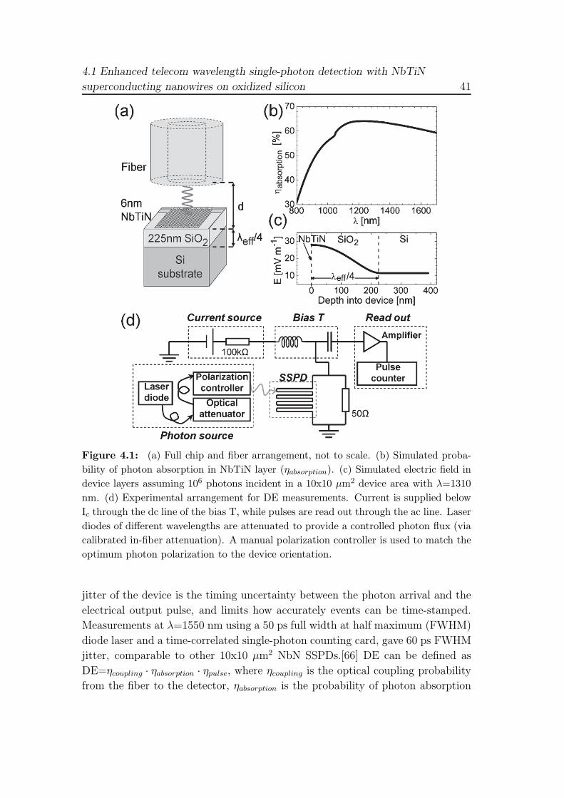
4.1 Enhanced telecom wavelength single-photon detection with NbTiN
superconducting nanowires on oxidized silicon 41
Figure 4.1: (a) Full chip and fiber arrangement, not to scale. (b) Simulated proba-
bility of photon absorption in NbTiN layer (ηabsorption). (c) Simulated electric field in
device layers assuming 106 photons incident in a 10x10 μm2 device area with λ=1310
nm. (d) Experimental arrangement for DE measurements. Current is supplied below
Ic through the dc line of the bias T, while pulses are read out through the ac line. Laser
diodes of different wavelengths are attenuated to provide a controlled photon flux (via
calibrated in-fiber attenuation). A manual polarization controller is used to match the
optimum photon polarization to the device orientation.
jitter of the device is the timing uncertainty between the photon arrival and the
electrical output pulse, and limits how accurately events can be time-stamped.
Measurements at λ=1550 nm using a 50 ps full width at half maximum (FWHM)
diode laser and a time-correlated single-photon counting card, gave 60 ps FWHM
jitter, comparable to other 10x10 μm2 NbN SSPDs.[66] DE can be defined as
DE=ηcoupling · ηabsorption · ηpulse, where ηcoupling is the optical coupling probability
from the fiber to the detector, ηabsorption is the probability of photon absorption
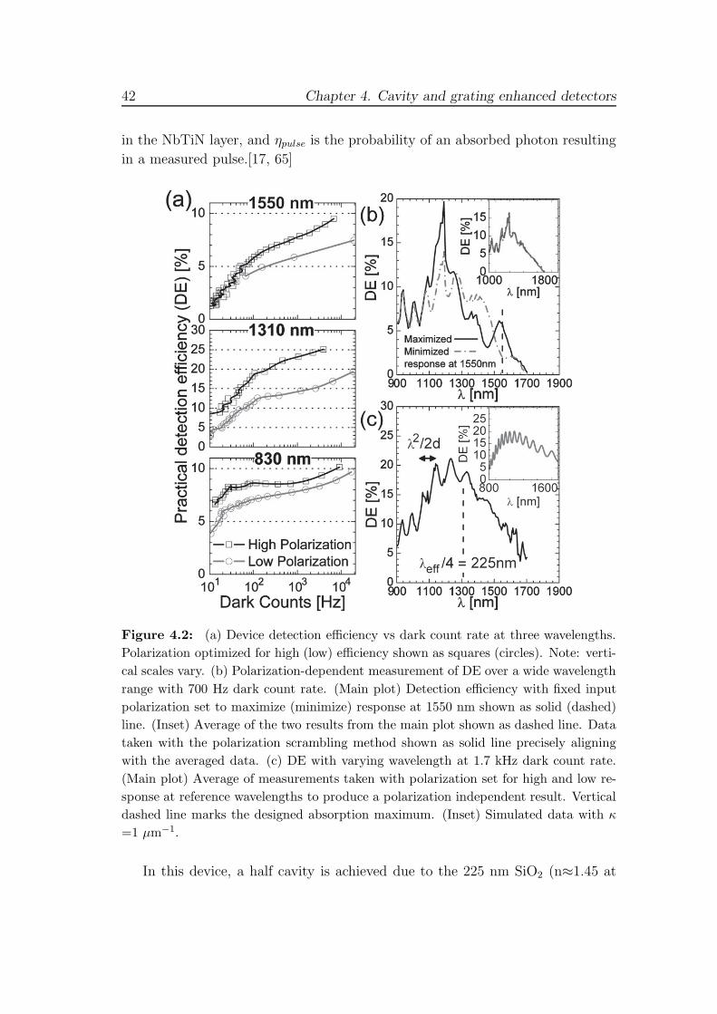
42 Chapter 4. Cavity and grating enhanced detectors
in the NbTiN layer, and ηpulse is the probability of an absorbed photon resulting
in a measured pulse.[17, 65]
Figure 4.2: (a) Device detection efficiency vs dark count rate at three wavelengths.
Polarization optimized for high (low) efficiency shown as squares (circles). Note: verti-
cal scales vary. (b) Polarization-dependent measurement of DE over a wide wavelength
range with 700 Hz dark count rate. (Main plot) Detection efficiency with fixed input
polarization set to maximize (minimize) response at 1550 nm shown as solid (dashed)
line. (Inset) Average of the two results from the main plot shown as dashed line. Data
taken with the polarization scrambling method shown as solid line precisely aligning
with the averaged data. (c) DE with varying wavelength at 1.7 kHz dark count rate.
(Main plot) Average of measurements taken with polarization set for high and low re-
sponse at reference wavelengths to produce a polarization independent result. Vertical
dashed line marks the designed absorption maximum. (Inset) Simulated data with κ
=1 μm−1.
In this device, a half cavity is achieved due to the 225 nm SiO2 (n≈1.45 at
4.1 Enhanced telecom wavelength single-photon detection with NbTiN
superconducting nanowires on oxidized silicon 43
λ=1310 nm) atop the Si substrate (n≈3.5 at λ=1310 nm). Transfer matrix simu-
lations of multilayer reflectivity are used to calculate the absorption of the NbTiN
layer, as shown in 4.1b, giving a clear peak at λ ≈1310 nm (ηabsorption ≈65%).
This corresponds to a SiO2 layer optical thickness of λeff/4 giving an electric field
maximum at the NbTiN layer (figure 4.1c. This matches well with the experiment
(figure 4.2) in which photons at λ=1310 nm were detected more efficiently than
those at 830 or 1550 nm. Without the cavity reflector, ηabsorption is calculated
to be less than 15% at λ=1310 nm; thus the layer structure has significantly in-
creased efficiency in the device. While the cavity is not optimized for λ=830 and
1550 nm, these efficiencies are also increased by the reflection. Without the cav-
ity enhancement (4x at λ =1310 nm, the device would demonstrate efficiencies
comparable to those of NbN devices.[51] However NbTiN has shown favorable
dark count characteristics and is more versatile in growth conditions enabling
the fabrication of the cavity devices. It should be noted that the simulations
are based on the optical properties of an unpatterned 10 nm thick NbTiN film
measured by ellipsometry at room temperature.
The real and imaginary parts of the refractive index (n,k) are n=4.17 and
k=5.63 at λ=1310 nm. This simulation may not link accurately to the absolute
absorption in the nanostructured device but reproduces the trend of absorp-
tion versus wavelength and the enhancement due to the cavity. To further test
the dependence of DE on wavelength, another NbTiN SSPD device from the
same fabrication batch was fiber-coupled and measured in a second experimental
setup. The fixed-wavelength source in figure 4.1d was substituted for a white-
light source and monochromator with calibrated filters and in-fiber polarization
control to produce full spectrum device measurements. Photon count rate was
recorded with constant device biasing as wavelength was varied. However, po-
larization at the device under test varies with wavelength due to birefringence in
the fibers if the photon source arrangement is kept constant. The measurements
in figure 4.2b have been used to examine this polarization dependence. In the
main plot the polarization controller was used to maximize and minimize counts
at a reference input wavelength of 1550 nm (dark counts=700 Hz). The higher
device response is seen to oscillate between the two measurements as polariza-
tion at the device progresses when the input wavelength is swept. The two full
spectrum sweeps for polarization set at the reference wavelength were averaged
to produce the dashed line in the inset plot. An additional data set was taken
with the polarization controller replaced by an automatic polarization scrambler,
shown as the solid line in the plot. The two data sets in the inset match very
well, within the expected variation in the device response. This confirms that
this averaging method is sufficient to produce a polarization-independent result
44 Chapter 4. Cavity and grating enhanced detectors
when a polarization scrambler is not available. To most clearly observe the ef-
fect of the optical cavity on the DE, a higher device biasing was used for the
data in figure 4.2c (dark counts =1.7 kHz), as this reduces the variation in ηpulseacross the wavelength range, making the dependence on ηabsorption more appar-
ent. A peak in DE is seen at a photon wavelength of approximately 1250 nm,
lower than the expected absorption peak at 1310 nm. Additional oscillations
are present in the data, with a period increasing from 60 to 150 nm across the
full wavelength range. These oscillations are due to Fabry Perot interference
between the fiber end and the device surface with separation of d=8 μm. It is
expected that DE is dependent on the ηpulse. As observed in figure 4.2, DE is
more dependent on device biasing for longer wavelength photons (λ=1550 nm),
thus photon energy should be accounted for in λpulse. In order to fit the data
of figure 4.2c, we approximate the wavelength dependence of an SSPD at high
bias as ηpulse ∝ e−λκ, where κ is a fitting constant.[17] The expected efficiency of
the device is then DEsim ∝ ηabsorption · e−κλ if ηcoupling is taken to be a constant
and the fiber-to-device cavity oscillation is included in ηabsorption. The simulated
efficiency dependence on wavelength is shown in the inset of figure 4.2c with κ
=1 μm−1. The form of the experimental response is recreated and fiber-to-device
oscillations are accurately reproduced in scale and period. The energy depen-
dence of ηpulse reduces the wavelength of peak efficiency and causes a greater
drop in efficiency at long wavelengths compared to simulated absorption alone,
as observed in the experimental result; κ is chosen to give the best fit to both
these features. While the form of the simulated absorption matches that of the
experimental result, the features are not precisely aligned; this is likely due to
(a) the difficulty of accurately obtaining optical data for thin film NbTiN at low
temperature, (b) the optical properties of the nanopatterned device, and (c) a
more complex dependence of ηpulse on wavelength than that used in this work.
4.1.3 Conclusions
In this section, we have reported the full characterization of a NbTiN SSPD with a
quarter wavelength cavity reflection optimized for λ=1310 nm. We have achieved
a well understood increase in DE in a practically packaged front side fiber-coupled
system. This gives DE of 23.2% with 1 kHz dark count rate at λ=1310 nm,
with low DE drop-off at lower dark count rates. This is combined with low
jitter and fast reset times suitable for use in a variety of timecorrelated single-
photon counting experiments. Simulation of superconducting layer absorption
with the additional effects of photon energy and FabryPerot oscillations gives a
model of the dependence of detector efficiency on incident photon wavelength that

4.1 Enhanced telecom wavelength single-photon detection with NbTiN
superconducting nanowires on oxidized silicon 45
describes all experimental features. The optical architecture is well understood
and can be optimized for alternative important wavelengths, such as 1550 nm.
46 Chapter 4. Cavity and grating enhanced detectors
4.2 SSPDs on a DBR substrate
4.2.1 Introduction
The main limitation in the SDE of SSPDs arises from the low absorption of
the thin meandering wire. Although NbTiN is a good absorber, with a 6 nm
thick continuous film exhibiting about 30% absorption at 1550 nm, this value
decreases when the film is structured into a meandering wire with 50% filling
factor. It is about 20% for light polarized along the wire, and 10% for light
polarized orthogonal to the wire. These values arise from the interaction with the
subwavelength and periodic structure of the nanowire [65]. In order to enhance
the absorption an SSPD with a mirror was introduced. [67] This concept was
extended by adding an anti-reflection coating to minimize reflection losses from
the illumination side [29]. In that report a DE (ηabs · ηpulse) as high as 57% at
1550 nm was demonstrated. In both works, the authors added an optical cavity
composed of a quarter-wave thick dielectric material and a reflecting metal mirror
on top of the detector to enhance the reflection around a central wavelength of
interest, which in their case was 1550 nm. Although the DE was high, the
requirement of back side illumination can easily result in coupling losses.
So far, most of the efforts to integrate optical cavities with SSPDs have been
concentrated in schemes that require back side illumination (i.e. the optical
cavity and mirror are deposited on top of the detector). Besides the convenience
of post-processing, one of the main reasons for this approach is the difficulty
to fabricate high quality and uniform nanowires on top of an optical cavity.
The film thickness employed in SSPDs requires good surface quality and lattice
matching to ensure film uniformity [27]. Nevertheless an SSPD with an integrated
optical cavity for front side illumination is highly desirable due to the simpler
methods available to efficiently couple an optical fiber with the detector [68],
and the possibility to integrate with on-chip photonic circuits. The capability of
fabricating high quality NbTiN single photon detectors on Si substrates is a viable
solution to the problem since one can introduce Si compatible technologies into
the SSPD fabrication process. Already in this direction, it has been observed in
fiber coupled SSPDs (FC-SSPDs) built on oxidized Si substrates, that there is an
enhanced absorption and thus an enhanced SDE for photons with a wavelength
of λ = 4nd, where n and d are the refractive index and thickness of the SiO2
respectively (see section 4.1). The enhancement was due to the extra reflection
taking place at the SiO2/Si interface and the cavity like behavior of the quarter-
wave thick SiO2 layer, leading to constructive interference at the surface of the
This section is based on E. Bermudez Urena, Master Thesis
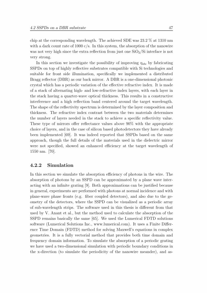
4.2 SSPDs on a DBR substrate 47
chip at the corresponding wavelength. The achieved SDE was 23.2 % at 1310 nm
with a dark count rate of 1000 c/s. In this system, the absorption of the nanowire
was not very high since the extra reflection from just one SiO2/Si interface is not
very strong.
In this section we investigate the possibility of improving ηabs by fabricating
SSPDs on top of highly reflective substrates compatible with Si technologies and
suitable for front side illumination, specifically we implemented a distributed
Bragg reflector (DBR) as our back mirror. A DBR is a one-dimensional photonic
crystal which has a periodic variation of the effective refractive index. It is made
of a stack of alternating high- and low-refractive index layers, with each layer in
the stack having a quarter-wave optical thickness. This results in a constructive
interference and a high reflection band centered around the target wavelength.
The shape of the reflectivity spectrum is determined by the layer composition and
thickness. The refractive index contrast between the two materials determines
the number of layers needed in the stack to achieve a specific reflectivity value.
These type of mirrors offer reflectance values above 90% with the appropriate
choice of layers, and in the case of silicon based photodetectors they have already
been implemented [69]. It was indeed reported that SSPDs based on the same
approach, though the full details of the materials used in the dielectric mirror
were not specified, showed an enhanced efficiency at the target wavelength of
1550 nm. [70].
4.2.2 Simulation
In this section we simulate the absorption efficiency of photons in the wire. The
absorption of photons by an SSPD can be approximated by a plane wave inter-
acting with an infinite grating [9]. Both approximations can be justified because
in general, experiments are performed with photons at normal incidence and with
plane-wave phase fronts (e.g. fiber coupled detectors), and also due to the ge-
ometry of the detectors, where the SSPD can be visualized as a periodic array
of sub-wavelength strips. The software used in this thesis is different from that
used by V. Anant et al., but the method used to calculate the absorption of the
SSPD remains basically the same [65]. We used the Lumerical FDTD solutions
software (Lumerical Solutions Inc., www.lumerical.com). It uses a Finite Differ-
ence Time Domain (FDTD) method for solving Maxwell’s equations in complex
geometries. It is a fully vectorial method that provides both time domain and
frequency domain information. To simulate the absorption of a periodic grating
we have used a two-dimensional simulation with periodic boundary conditions in
the x-direction (to simulate the periodicity of the nanowire meander), and as-
48 Chapter 4. Cavity and grating enhanced detectors
sumed the wire to be infinitely long (out of plane direction). The latter is valid
since the meandering segments have a length which is longer than the incident
wavelength. A snapshot of the simulation cell with the main objects labeled can
be found in figure 4.3a.
Figure 4.3: (a) Snapshot of the simulation working space with the main components
labeled. (b) Schematic of the simulation cell, with a 100 nm wide nanowire inside a
200 nm wide cell.(c) Extinction coefficient (red) and refractive index (black) of a 10
nm thick NbTiN film.
The simulation cell is defined by the enclosing simulation mesh (in orange),
while a smaller mesh surrounding the wire segment (not visible) is placed as
an override region where we can ensure a constant small mesh step size in the
nanowire area. In our simulations, the smallest mesh step size was set to 0.25
nm. Plane waves are injected from the top of the structure and can have either
the electric field polarized along the wire (TM or p-polarization) or orthogonal
to the wire (TE or s-polarization). A group monitor is placed surrounding the
wire segment and allows us to record the electric field intensity (| �E(x, y) |2) andthe imaginary part of the permittivity (ε(ω)) in order to calculate the absorption
of the wire (field and index monitors). A time monitor is placed inside the
simulation cell to ensure that the simulation has run for a sufficiently long time
to ensure the radiation has left the simulation volume. A close-up look of the
nanowire in the cell is schematically illustrated in figure 4.3(b) and represents the
standard features of our SSPDs. The simulation cell contains a 100 nm wide wire
with a filling factor of 50% (i.e. 200 nm period), in this case on top of a Si/SiO2
substrate. The thickness of the NbTiN layer was set to 6 nm. Since the material
database does not include the optical parameters of NbTiN (refractive index
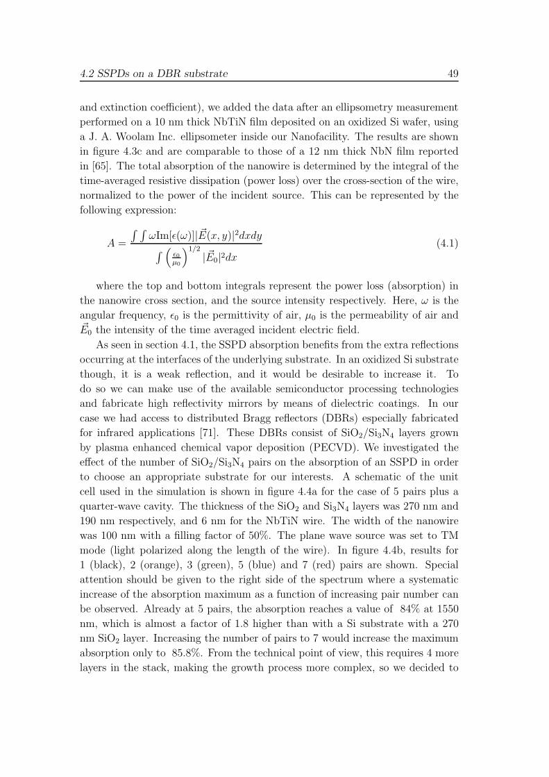
4.2 SSPDs on a DBR substrate 49
and extinction coefficient), we added the data after an ellipsometry measurement
performed on a 10 nm thick NbTiN film deposited on an oxidized Si wafer, using
a J. A. Woolam Inc. ellipsometer inside our Nanofacility. The results are shown
in figure 4.3c and are comparable to those of a 12 nm thick NbN film reported
in [65]. The total absorption of the nanowire is determined by the integral of the
time-averaged resistive dissipation (power loss) over the cross-section of the wire,
normalized to the power of the incident source. This can be represented by the
following expression:
A =
∫ ∫ωIm[ε(ω)]| �E(x, y)|2dxdy∫ (
ε0μ0
)1/2
| �E0|2dx(4.1)
where the top and bottom integrals represent the power loss (absorption) in
the nanowire cross section, and the source intensity respectively. Here, ω is the
angular frequency, ε0 is the permittivity of air, μ0 is the permeability of air and�E0 the intensity of the time averaged incident electric field.
As seen in section 4.1, the SSPD absorption benefits from the extra reflections
occurring at the interfaces of the underlying substrate. In an oxidized Si substrate
though, it is a weak reflection, and it would be desirable to increase it. To
do so we can make use of the available semiconductor processing technologies
and fabricate high reflectivity mirrors by means of dielectric coatings. In our
case we had access to distributed Bragg reflectors (DBRs) especially fabricated
for infrared applications [71]. These DBRs consist of SiO2/Si3N4 layers grown
by plasma enhanced chemical vapor deposition (PECVD). We investigated the
effect of the number of SiO2/Si3N4 pairs on the absorption of an SSPD in order
to choose an appropriate substrate for our interests. A schematic of the unit
cell used in the simulation is shown in figure 4.4a for the case of 5 pairs plus a
quarter-wave cavity. The thickness of the SiO2 and Si3N4 layers was 270 nm and
190 nm respectively, and 6 nm for the NbTiN wire. The width of the nanowire
was 100 nm with a filling factor of 50%. The plane wave source was set to TM
mode (light polarized along the length of the wire). In figure 4.4b, results for
1 (black), 2 (orange), 3 (green), 5 (blue) and 7 (red) pairs are shown. Special
attention should be given to the right side of the spectrum where a systematic
increase of the absorption maximum as a function of increasing pair number can
be observed. Already at 5 pairs, the absorption reaches a value of 84% at 1550
nm, which is almost a factor of 1.8 higher than with a Si substrate with a 270
nm SiO2 layer. Increasing the number of pairs to 7 would increase the maximum
absorption only to 85.8%. From the technical point of view, this requires 4 more
layers in the stack, making the growth process more complex, so we decided to
50 Chapter 4. Cavity and grating enhanced detectors
proceed with the 5 pair DBR substrate. These high absorption values give a lot
of promise to increase the SDE of SSPDs fabricated on Si substrates. With the
samples reported in section 4.1, where a maximum absorption of 44% is expected
at 1550 nm, a SDE of 10% was measured. Assuming that the quality of the
nanowire would be the same for the SSPD on a 5 pair DBR, we can expect a
SDE of 19% at 1550 nm, which would be comparable to the recently reported
values[54] for a SSPD with back side illumination (24 % at 1550 nm).
Figure 4.4: Simulation of the SSPD absorption on top of distributed Bragg reflectors.
(a) Schematic of the simulation cell for the case of an SSPD on top of 5 pairs of
SiO2/Si3N4 plus a quarter-wave cavity. (b) Absorption as a function of wavelength of
an SSPD with increasing number of underlying SiO2/Si3N4 pairs (TM polarization).
4.2.3 Optical setup
To investigate the frequency response of the SSPDs on DBRs we used a supercon-
tinuum white light source (Fianium SC400) coupled to a monochromator (Acton
SpectraPro-150), which enables experiments over a broad wavelength range, from
400 nm to beyond 2 μm. The ’Fianium’ is a high power fiber laser generating su-
percontinuum radiation in the 400-2400 nm spectral band with an average power
of 2 W and spectral density of >1.5 mW/nm. It consists of three main parts: a
master source, a power amplifier and a supercontinuum generator. The master
source consists of a low-power fiber laser which provides light pulses of approx-
imately 5 ps at a repetition rate of 20 MHz. The power amplifier is based on a
double-clad Y b-doped fiber pumped by a high power laser-diode pump module.
The supercontinuum spectrum is generated by means of a highly-nonlinear op-
tical fiber. The output beam of the Fianium is coupled into the entrance slit of
the monochromator.
4.2 SSPDs on a DBR substrate 51
The SpectraPro-150 monochromator has a focal length of 150 mm. It features
an astigmatism-corrected optical system and interchangeable grating turrets. We
used a set of two plane ruled gratings (Newport Corporation) with different groove
density and blazing angles, specifically one with 1200 g/mm blazed at 750 nm and
the other one with 600 g/mm and blazed at 1.6 μm. The blazing angle determines
the wavelength of maximum efficiency. In our experiments, when working in the
range of the telecom wavelengths (1.3 μm and 1.55 μm) we used the grating
blazed at 1.6 μm, while for the visible range we worked with the grating blazed
at 750 nm.
An important feature to consider when working with diffraction gratings is
the existence of different diffraction orders. Light diffracted at a grating satisfies
the grating equation:
mλ = d(sin(α) + sin(β) (4.2)
where m is an integer and represents the diffraction order, λ is the incident
wavelength, d is the groove spacing, and α and β are the incident and diffracted
angle respectively. We implemented long pass filters after beam collimation at the
output of the monochromator in order to eliminate the higher order contributions
of the monochromator.
4.2.4 Results
The first attempts to grow NbTiN on DBR substrates were based upon the al-
ready established growth process on oxidized Si wafers, where a sputtering time
of 5 seconds is typically used to achieve films with 4.5 nm in thickness (0.9 nm/s
growth rate). The superconducting nanowires obtained with these parameters
exhibited low and unstable critical currents (Ic) below 1 μA, hinting that the film
quality was not optimal, with one of the possible reasons being that the film had
a non-uniform microstructure leading to constrictions in the nanowire and thus
limiting the critical currents [20]. In a subsequent batch, the sputtering time was
increased to 7 seconds in order to obtain thicker films (6 nm). With this approach
we were able to obtain superconducting nanowires with higher critical currents
(≈5 μA) and were able to detect photons.
To study the spectral response of our devices we separated our wavelength
range of interest in two regions, below and above 1000 nm, to separate effects
arising from the gratings in our monochromator. For the 500 nm to 1000 nm range
we used the grating blazed at 750 nm without long pass filter. For wavelengths
above 1000 nm we used the grating blazed at 1.6 μm and a long pass filter at 800
nm. The power was measured by connecting a power meter directly to the output
52 Chapter 4. Cavity and grating enhanced detectors
of the fiber (Thorlabs S154C and S120C above and below 1000 nm respectively).
The detection counts and power sensor scans for a given wavelength range were
taken consequently to avoid discrepancies in the efficiency calculation.
The system detection efficiency (SDE) is again calculated as:
SDE =Nc −Ndc
Nph
(4.3)
where Nc is the detection count rate, Nd the dark count rate andNph is the photon
rate at the fiber output, calculated by Nph = P/Ephoton, with P the measured
power.
We coupled the detector to a fiber to have effective overlap between the light
from the output of a single mode fiber and the active area of the detector. This
means that the scaling between detection counts and photon number measured at
the end of the output fiber should yield an accurate value of the maximum SDE
possible with these detectors. The fiber coupled detector on a DBR substrate
(FC-DBR) was operated at a current of Ibias=0.9·Ic, where Ic ≈ 11μA and the
dark count rate was 100 c/s. The SDE of this device is shown in figure 4.5. The
dashed line at 1100 nm marks the boundary between the two scans. The red
trace is the simulated SDE for our device based on the simulations presented in
section 4.2.2. The small shift in the position of the peaks between the simulation
and the experimental data can arise from discrepancies in the actual material
properties and precise DBR layer thicknesses versus the ones used in our FDTD
simulations.
Even though the SDE exhibits the expected wavelength dependency due to the
absorption properties of the nanowire imposed by the DBR substrate, the overall
values are low. At 1550 nm we obtained an SDE of just 0.02%, at least two to
three orders of magnitude lower than expected, assuming that the quality of the
nanowires is as good as in the case of SSPDs on oxidized Si substrates. Evidently
this is not the case, the low measured SDEs are most likely a consequence of non-
uniformities in our nanowires. Since our fabrication process yields uniform wire
widths, our suspicion was that the growth of NbTiN films on DBR substrates
gives rise to films with less uniformity than those grown on oxidized Si wafers,
most probably due to a difference in the surface roughness between the two types
of substrates.
We did not carry out detailed surface studies in our samples; but the kinetic
inductance measurements on our FC-DBR device carried out at Herriot Watt
University in Edinburgh, support the suspicion about the bad quality of our
nanowires. In short, by measuring the kinetic inductance of the SSPD at differ-
ent bias currents and with a suitable model [20], a characteristic value (labeled
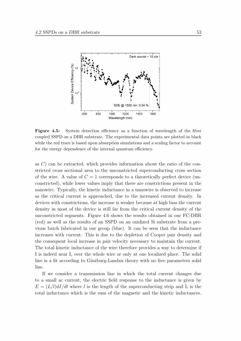
4.2 SSPDs on a DBR substrate 53
Figure 4.5: System detection efficiency as a function of wavelength of the fiber
coupled SSPD on a DBR substrate. The experimental data points are plotted in black
while the red trace is based upon absorption simulations and a scaling factor to account
for the energy dependence of the internal quantum efficiency.
as C) can be extracted, which provides information about the ratio of the con-
stricted cross sectional area to the unconstricted superconducting cross section
of the wire. A value of C = 1 corresponds to a theoretically perfect device (un-
constricted), while lower values imply that there are constrictions present in the
nanowire. Typically, the kinetic inductance in a nanowire is observed to increase
as the critical current is approached, due to the increased current density. In
devices with constrictions, the increase is weaker because at high bias the current
density in most of the device is still far from the critical current density of the
unconstricted segments. Figure 4.6 shows the results obtained in our FC-DBR
(red) as well as the results of an SSPD on an oxidized Si substrate from a pre-
vious batch fabricated in our group (blue). It can be seen that the inductance
increases with current. This is due to the depletion of Cooper pair density and
the consequent local increase in pair velocity necessary to maintain the current.
The total kinetic inductance of the wire therefore provides a way to determine if
I is indeed near Ic over the whole wire or only at one localized place. The solid
line is a fit according to Ginzburg-Landau theory with no free parameters solid
line.
If we consider a transmission line in which the total current changes due
to a small ac current, the electric field response to the inductance is given by
E = (L/l)dI/dt where l is the length of the superconducting strip and L is the
total inductance which is the sum of the magnetic and the kinetic inductances.
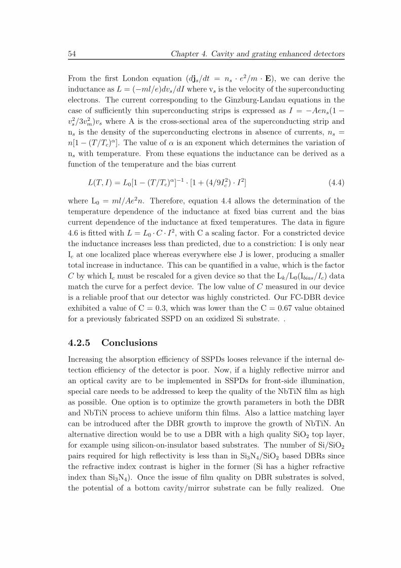
54 Chapter 4. Cavity and grating enhanced detectors
From the first London equation (djs/dt = ns · e2/m · E), we can derive the
inductance as L = (−ml/e)dvs/dI where vs is the velocity of the superconducting
electrons. The current corresponding to the Ginzburg-Landau equations in the
case of sufficiently thin superconducting strips is expressed as I = −Aens(1 −v2s/3v
2m)vs where A is the cross-sectional area of the superconducting strip and
ns is the density of the superconducting electrons in absence of currents, ns =
n[1− (T/Tc)α]. The value of α is an exponent which determines the variation of
ns with temperature. From these equations the inductance can be derived as a
function of the temperature and the bias current
L(T, I) = L0[1− (T/Tc)α]−1 · [1 + (4/9I2c ) · I2] (4.4)
where L0 = ml/Ae2n. Therefore, equation 4.4 allows the determination of the
temperature dependence of the inductance at fixed bias current and the bias
current dependence of the inductance at fixed temperatures. The data in figure
4.6 is fitted with L = L0 ·C · I2, with C a scaling factor. For a constricted device
the inductance increases less than predicted, due to a constriction: I is only near
Ic at one localized place whereas everywhere else J is lower, producing a smaller
total increase in inductance. This can be quantified in a value, which is the factor
C by which Ic must be rescaled for a given device so that the Lk/L0(Ibias/Ic) data
match the curve for a perfect device. The low value of C measured in our device
is a reliable proof that our detector was highly constricted. Our FC-DBR device
exhibited a value of C = 0.3, which was lower than the C = 0.67 value obtained
for a previously fabricated SSPD on an oxidized Si substrate. .
4.2.5 Conclusions
Increasing the absorption efficiency of SSPDs looses relevance if the internal de-
tection efficiency of the detector is poor. Now, if a highly reflective mirror and
an optical cavity are to be implemented in SSPDs for front-side illumination,
special care needs to be addressed to keep the quality of the NbTiN film as high
as possible. One option is to optimize the growth parameters in both the DBR
and NbTiN process to achieve uniform thin films. Also a lattice matching layer
can be introduced after the DBR growth to improve the growth of NbTiN. An
alternative direction would be to use a DBR with a high quality SiO2 top layer,
for example using silicon-on-insulator based substrates. The number of Si/SiO2
pairs required for high reflectivity is less than in Si3N4/SiO2 based DBRs since
the refractive index contrast is higher in the former (Si has a higher refractive
index than Si3N4). Once the issue of film quality on DBR substrates is solved,
the potential of a bottom cavity/mirror substrate can be fully realized. One
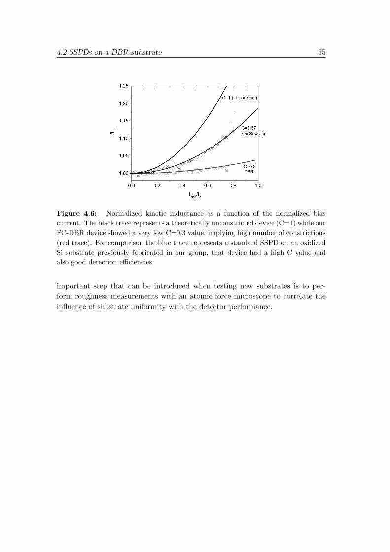
4.2 SSPDs on a DBR substrate 55
Figure 4.6: Normalized kinetic inductance as a function of the normalized bias
current. The black trace represents a theoretically unconstricted device (C=1) while our
FC-DBR device showed a very low C=0.3 value, implying high number of constrictions
(red trace). For comparison the blue trace represents a standard SSPD on an oxidized
Si substrate previously fabricated in our group, that device had a high C value and
also good detection efficiencies.
important step that can be introduced when testing new substrates is to per-
form roughness measurements with an atomic force microscope to correlate the
influence of substrate uniformity with the detector performance.

56 Chapter 4. Cavity and grating enhanced detectors
Chapter 5
Polarization and wavelength dependence
5.1 Polarization dependence
SSPDs are usually fabricated in such a way that a polarization dependence of the
quantum efficiency is inevitable. Their meandering nanowire leads to a preferen-
tial polarization absorption, this is undesired in experiments where the polariza-
tion degree of freedom is used. We have designed two new geometries for which
the polarization dependence is minimized: a detector with two meander-type
parts oriented perpendicular with respect to each other and a spiraling detec-
tor. For these designs the polarization dependence of the quantum efficiency is
minimized.
5.1.1 Introduction
It has already been reported that the quantum efficiency of SSPDs is dependent
on the polarization of the incident light [72, 65]. This effect is usually unwanted
as the polarization degree of freedom is often used in quantum information ex-
periments. Here we present a solution to the problem by exploring two new
geometries.
There are two reasons for the polarization sensitivity of SSPDs, both arising
from the geometry of the detector, consisting of a long narrow wire (100 nm wide
and approximately 500 μm long) typically arranged in a meander-type geometry
to maximize the active area of the device (fig. 5.1a, lower part). This geometry
leads to an increased quantum efficiency for light polarized parallel to the wire
with respect to light polarized perpendicular to the wire. The first reason for this
effect is that light polarized parallel to the wire has a higher probability of being
This section is based on S. N. Dorenbos, E.M. Reiger, U. Perinetti, V. Zwiller, T. Zijlstra
and T.M. Klapwijk, Appl. Phys. Lett. 93, 161102 (2008)
57
58 Chapter 5. Polarization and wavelength dependence
absorbed. This originates from the fact that a large number of parallel wires acts
as a wire-grid polarizer [73]. Light polarized perpendicular to the wire grid causes
surface charges which screen the field and reduce the electric field intensity at
the wire edges, leading to a decreased absorption. For light polarized parallel to
the wire-grid the electric field intensity is uniform across the wire [65]. Anant et
al. suggested a second reason for polarization sensitivity of SSPDs as they found
that the optical effect was not enough to describe the polarization dependence:
also the intrinsic detection probability of polarization parallel to the wire is larger
with respect to light polarized perpendicular to the detector.
Building an SSPD consisting of two sub-parts of the original meander-type
design, where the sub-parts are oriented perpendicular to each other, two prefer-
ential polarization absorption directions and detection probabilities are created,
giving an equal quantum efficiency to all polarization directions. When we let the
nanowire run in a circular geometry (figure 5.1b) no single preferential direction
is left: this detector is minimally polarization dependent.
5.1.2 Device
Detectors are made from two different materials: NbN, the material typically
used for SSPDs, and NbTiN, a material that was recently shown to detect single
photons with a very high signal-to-noise ratio (see chapter 3). A sapphire sub-
strate with a thin NbN layer (approximately 4 nm) was commercially obtained
[40]. The NbTiN detectors are made from a 6 nm layer of NbTiN sputtered on a
silicon substrate at room temperature, a description of the fabrication procedure
can be found in chapter 3. Scanning electron microscope (SEM) images of the
unpolarized detectors are shown in figure 5.1a and 5.1b. The first detector type
consists of two sub-parts, oriented perpendicular with respect to each other, each
orientation filling half of the detector. The wires are 100 nm wide and 4-6 nm
thick, with 50 % fill fraction. The active area is 10 x 10 μm. The second type
consists of spiraling wires, first going towards the center of the detector, after
which they spiral out. The width of the wires is again 100 nm, with 50 % fill
fraction, and the diameter of the detector is 10 μm.
5.1.3 Measurement setup
The measurement setup is shown in figure 5.1c. The detector is placed in an ex-
change gas in a helium bath cryostat (tube length 1 m, with a coaxial feedthrough
and optical window) on XYZ piezo translators, allowing scanning and focusing.
White and laser light are collimated outside the cryostat and focused in situ with
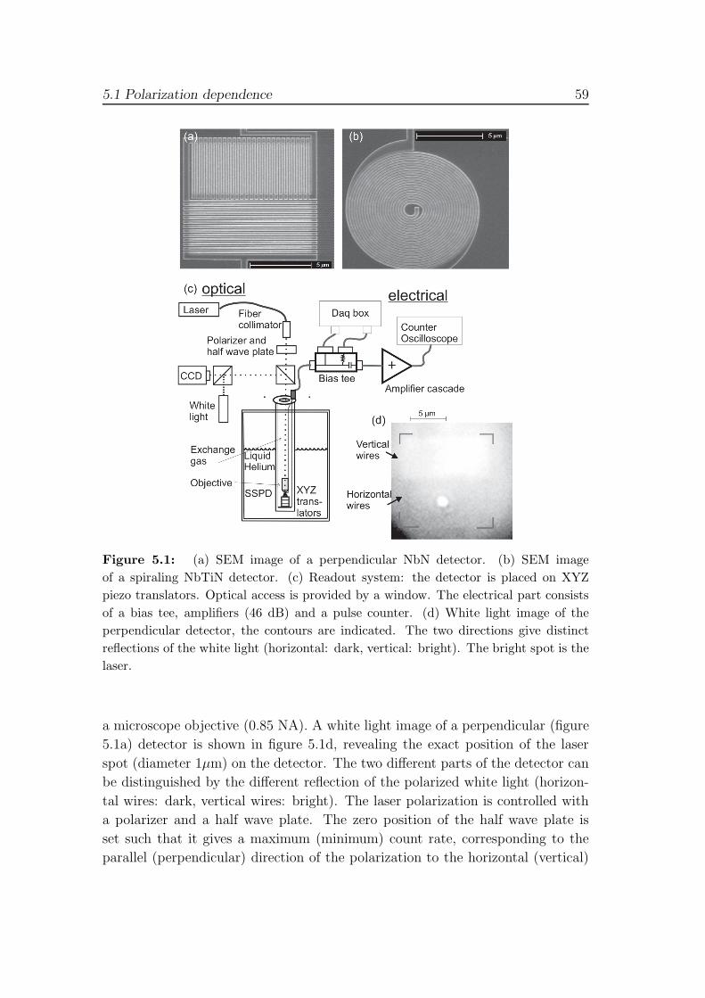
5.1 Polarization dependence 59
Figure 5.1: (a) SEM image of a perpendicular NbN detector. (b) SEM image
of a spiraling NbTiN detector. (c) Readout system: the detector is placed on XYZ
piezo translators. Optical access is provided by a window. The electrical part consists
of a bias tee, amplifiers (46 dB) and a pulse counter. (d) White light image of the
perpendicular detector, the contours are indicated. The two directions give distinct
reflections of the white light (horizontal: dark, vertical: bright). The bright spot is the
laser.
a microscope objective (0.85 NA). A white light image of a perpendicular (figure
5.1a) detector is shown in figure 5.1d, revealing the exact position of the laser
spot (diameter 1μm) on the detector. The two different parts of the detector can
be distinguished by the different reflection of the polarized white light (horizon-
tal wires: dark, vertical wires: bright). The laser polarization is controlled with
a polarizer and a half wave plate. The zero position of the half wave plate is
set such that it gives a maximum (minimum) count rate, corresponding to the
parallel (perpendicular) direction of the polarization to the horizontal (vertical)
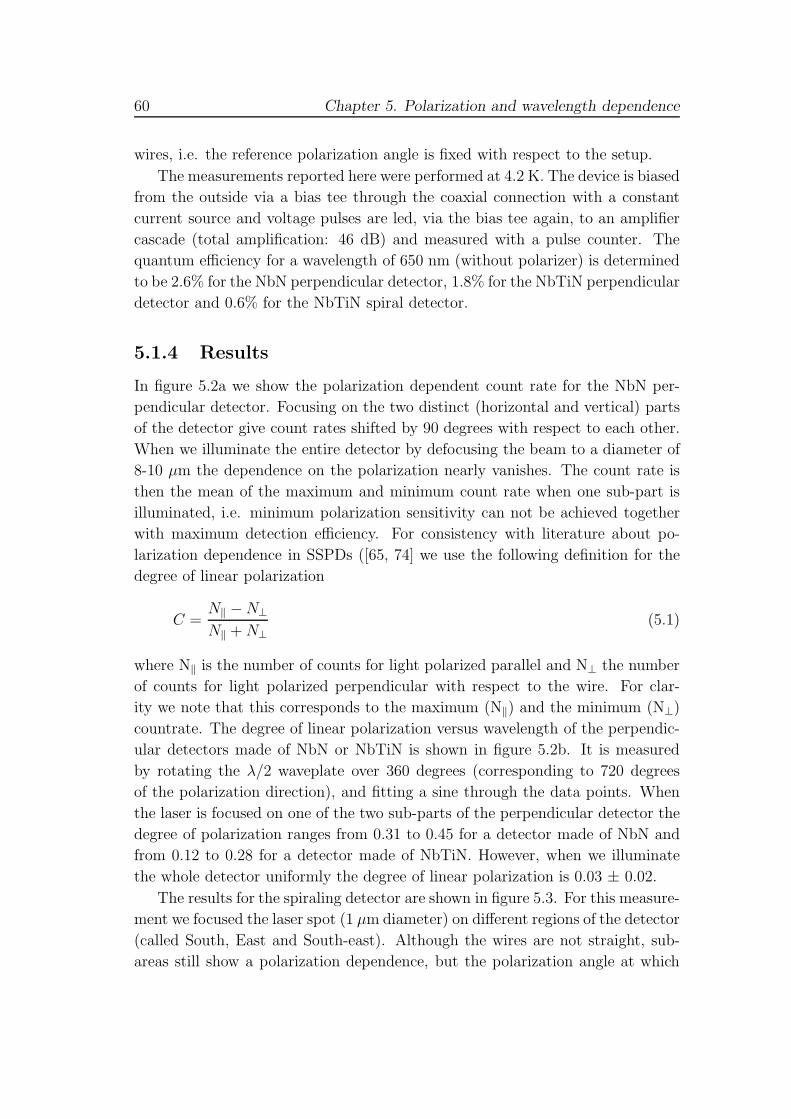
60 Chapter 5. Polarization and wavelength dependence
wires, i.e. the reference polarization angle is fixed with respect to the setup.
The measurements reported here were performed at 4.2 K. The device is biased
from the outside via a bias tee through the coaxial connection with a constant
current source and voltage pulses are led, via the bias tee again, to an amplifier
cascade (total amplification: 46 dB) and measured with a pulse counter. The
quantum efficiency for a wavelength of 650 nm (without polarizer) is determined
to be 2.6% for the NbN perpendicular detector, 1.8% for the NbTiN perpendicular
detector and 0.6% for the NbTiN spiral detector.
5.1.4 Results
In figure 5.2a we show the polarization dependent count rate for the NbN per-
pendicular detector. Focusing on the two distinct (horizontal and vertical) parts
of the detector give count rates shifted by 90 degrees with respect to each other.
When we illuminate the entire detector by defocusing the beam to a diameter of
8-10 μm the dependence on the polarization nearly vanishes. The count rate is
then the mean of the maximum and minimum count rate when one sub-part is
illuminated, i.e. minimum polarization sensitivity can not be achieved together
with maximum detection efficiency. For consistency with literature about po-
larization dependence in SSPDs ([65, 74] we use the following definition for the
degree of linear polarization
C =N‖ −N⊥N‖ +N⊥
(5.1)
where N‖ is the number of counts for light polarized parallel and N⊥ the number
of counts for light polarized perpendicular with respect to the wire. For clar-
ity we note that this corresponds to the maximum (N‖) and the minimum (N⊥)countrate. The degree of linear polarization versus wavelength of the perpendic-
ular detectors made of NbN or NbTiN is shown in figure 5.2b. It is measured
by rotating the λ/2 waveplate over 360 degrees (corresponding to 720 degrees
of the polarization direction), and fitting a sine through the data points. When
the laser is focused on one of the two sub-parts of the perpendicular detector the
degree of polarization ranges from 0.31 to 0.45 for a detector made of NbN and
from 0.12 to 0.28 for a detector made of NbTiN. However, when we illuminate
the whole detector uniformly the degree of linear polarization is 0.03 ± 0.02.
The results for the spiraling detector are shown in figure 5.3. For this measure-
ment we focused the laser spot (1 μm diameter) on different regions of the detector
(called South, East and South-east). Although the wires are not straight, sub-
areas still show a polarization dependence, but the polarization angle at which
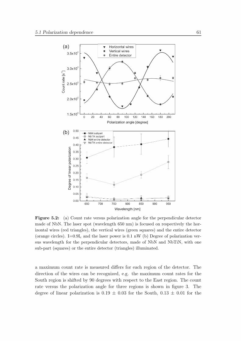
5.1 Polarization dependence 61
Figure 5.2: (a) Count rate versus polarization angle for the perpendicular detector
made of NbN. The laser spot (wavelength 650 nm) is focused on respectively the hor-
izontal wires (red triangles), the vertical wires (green squares) and the entire detector
(orange circles). I=0.9Ic and the laser power is 0.1 nW (b) Degree of polarization ver-
sus wavelength for the perpendicular detectors, made of NbN and NbTiN, with one
sub-part (squares) or the entire detector (triangles) illuminated.
a maximum count rate is measured differs for each region of the detector. The
direction of the wires can be recognized, e.g. the maximum count rates for the
South region is shifted by 90 degrees with respect to the East region. The count
rate versus the polarization angle for three regions is shown in figure 3. The
degree of linear polarization is 0.19 ± 0.03 for the South, 0.13 ± 0.01 for the
62 Chapter 5. Polarization and wavelength dependence
Figure 5.3: Polarization dependent count rate for a spiraling SSPD. The laser spot
(wavelength 650 nm, diameter 1 μm) is focused on different regions (indicated in the
lower part). When the entire active area is illuminated uniformly, the count rate
exhibits almost no polarization dependence (red curve).
East and 0.19 ± 0.02 for the South-East region. When the entire detector is
illuminated the degree of polarization reduces to 0.02 ± 0.01 and also for this
detector the count rate is then averaged. The fabrication yield and performance
of the opposite and spiraling detector was almost equal. The spiraling detector
has the advantage that it is more robust against alignment because of its intrinsic
symmetry.
5.1.5 Conclusions
In conclusion we have fabricated two new SSPD geometries to overcome the prob-
lem of polarization dependence of the quantum efficiency. By using geometries
with either two perpendicular preferential directions or no preferential direction
the polarization dependence can be significantly reduced.
5.2 Resolving the wavelength using a statistical method 63
5.2 Resolving the wavelength using a statistical
method
5.2.1 Introduction
In this section, we investigate the energy resolving property of SSPDs. Due to the
fact that the QE depends on the wavelength of the absorbed photon the photon
energy can be determined with the help of a statistical method. Being able not
only to count individual photons, but also gain information about their energy
opens new experimental possibilities. It should also result in a design of novel,
compact single-photon spectrometers, as no additional refractive device has to
be placed between the source and the detector, and hence optical losses can be
minimized.
5.2.2 Experimental setup
The nominal strip width of the SSPD is 100 nm. The SSPD is pigtailed with
a single-mode fiber (Thorlabs, P1-SMF28, single mode: 1310 nm to 1550 nm).
Assuming that the resistance of the SSPD when it is in its resistive state, RSSPD,
is much higher than the 50 Ω input impedance of the amplifier, the measured
amplitude of the voltage photoresponse pulse is expected to be Vpulse = Ib · 50Ω ·Gsig, withGsig the total gain of the amplifier system within the amplifier passband
[25]. The measured Ic of our SSPD is 11.8 μA and a typical photoresponse shows
a voltage amplitude of 250 mV, when the SSPD is biased with Ib/Ic = 0.8. For
demonstrating the energy resolving properties, we use a tunable Ti:sapphire laser
(Coherent, MIRA900) with a wavelength range between 700 nm and 1000 nm as
photon source. The laser is operated in a continuous-wave mode. To monitor
the laser stability and to be able to compensate for possible laser fluctuations, a
beam splitter is positioned between the laser and the single-mode fiber and the
laser intensity is simultaneously detected by a power meter (Thorlabs, S120A),
together with the SSPD readout. No fiber collimation optics is used to focus the
laser light on the fiber input, with the effect that the coupling is less position-
sensitive with respect to the laser spot. This is expected to give lower variations in
the coupling efficiency, when changing the wavelength of the laser. In addition, we
have sufficiently high laser power to obtain high-count rates. The laser intensity
is varied using a laser stabilization system (Brockton Electrooptic Co.) and a
Parts of this section have been published in E. Reiger, S. Dorenbos, V. Zwiller, A. Korneev,
G. Chulkova, I. Milostnaya, O. Minaeva, G. Goltsman, W. Slysz, J. Kitaygorsky, D. Pan, A.
Jukna, and R. Sobolewski, IEEE Sel. Top. in Quantum El. 13 934(2007)
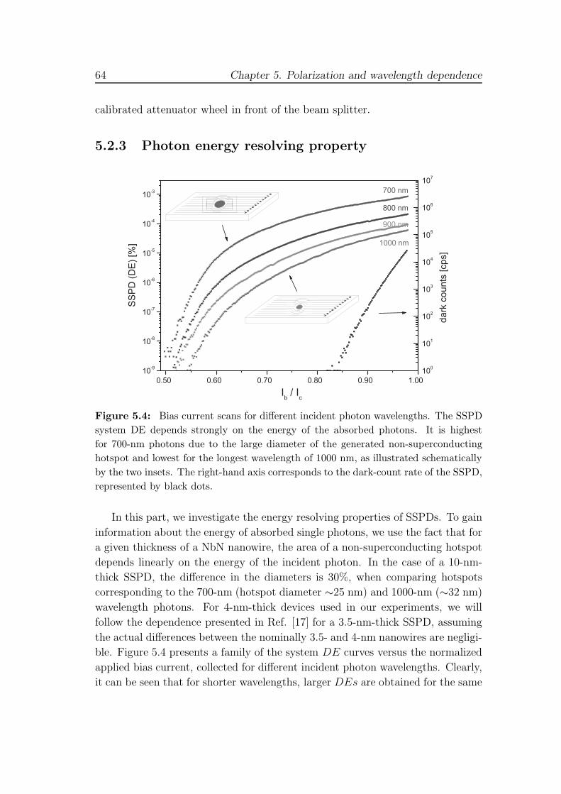
64 Chapter 5. Polarization and wavelength dependence
calibrated attenuator wheel in front of the beam splitter.
5.2.3 Photon energy resolving property
Figure 5.4: Bias current scans for different incident photon wavelengths. The SSPD
system DE depends strongly on the energy of the absorbed photons. It is highest
for 700-nm photons due to the large diameter of the generated non-superconducting
hotspot and lowest for the longest wavelength of 1000 nm, as illustrated schematically
by the two insets. The right-hand axis corresponds to the dark-count rate of the SSPD,
represented by black dots.
In this part, we investigate the energy resolving properties of SSPDs. To gain
information about the energy of absorbed single photons, we use the fact that for
a given thickness of a NbN nanowire, the area of a non-superconducting hotspot
depends linearly on the energy of the incident photon. In the case of a 10-nm-
thick SSPD, the difference in the diameters is 30%, when comparing hotspots
corresponding to the 700-nm (hotspot diameter ∼25 nm) and 1000-nm (∼32 nm)
wavelength photons. For 4-nm-thick devices used in our experiments, we will
follow the dependence presented in Ref. [17] for a 3.5-nm-thick SSPD, assuming
the actual differences between the nominally 3.5- and 4-nm nanowires are negligi-
ble. Figure 5.4 presents a family of the system DE curves versus the normalized
applied bias current, collected for different incident photon wavelengths. Clearly,
it can be seen that for shorter wavelengths, larger DEs are obtained for the same
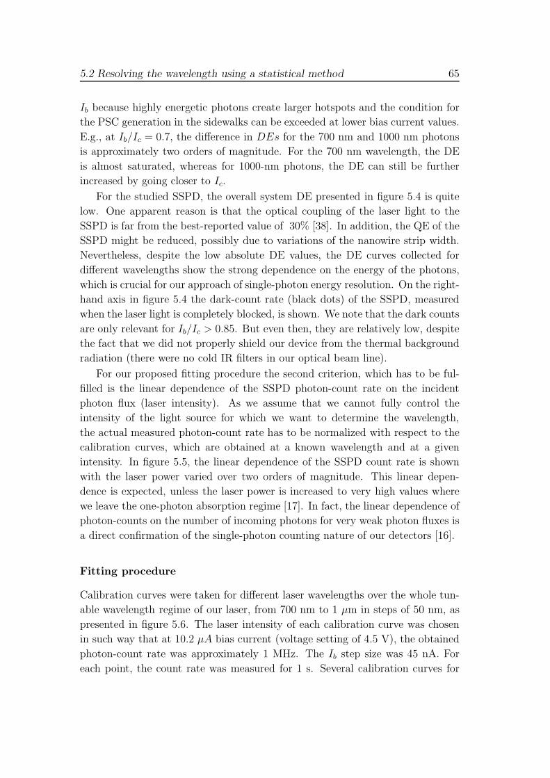
5.2 Resolving the wavelength using a statistical method 65
Ib because highly energetic photons create larger hotspots and the condition for
the PSC generation in the sidewalks can be exceeded at lower bias current values.
E.g., at Ib/Ic = 0.7, the difference in DEs for the 700 nm and 1000 nm photons
is approximately two orders of magnitude. For the 700 nm wavelength, the DE
is almost saturated, whereas for 1000-nm photons, the DE can still be further
increased by going closer to Ic.
For the studied SSPD, the overall system DE presented in figure 5.4 is quite
low. One apparent reason is that the optical coupling of the laser light to the
SSPD is far from the best-reported value of 30% [38]. In addition, the QE of the
SSPD might be reduced, possibly due to variations of the nanowire strip width.
Nevertheless, despite the low absolute DE values, the DE curves collected for
different wavelengths show the strong dependence on the energy of the photons,
which is crucial for our approach of single-photon energy resolution. On the right-
hand axis in figure 5.4 the dark-count rate (black dots) of the SSPD, measured
when the laser light is completely blocked, is shown. We note that the dark counts
are only relevant for Ib/Ic > 0.85. But even then, they are relatively low, despite
the fact that we did not properly shield our device from the thermal background
radiation (there were no cold IR filters in our optical beam line).
For our proposed fitting procedure the second criterion, which has to be ful-
filled is the linear dependence of the SSPD photon-count rate on the incident
photon flux (laser intensity). As we assume that we cannot fully control the
intensity of the light source for which we want to determine the wavelength,
the actual measured photon-count rate has to be normalized with respect to the
calibration curves, which are obtained at a known wavelength and at a given
intensity. In figure 5.5, the linear dependence of the SSPD count rate is shown
with the laser power varied over two orders of magnitude. This linear depen-
dence is expected, unless the laser power is increased to very high values where
we leave the one-photon absorption regime [17]. In fact, the linear dependence of
photon-counts on the number of incoming photons for very weak photon fluxes is
a direct confirmation of the single-photon counting nature of our detectors [16].
Fitting procedure
Calibration curves were taken for different laser wavelengths over the whole tun-
able wavelength regime of our laser, from 700 nm to 1 μm in steps of 50 nm, as
presented in figure 5.6. The laser intensity of each calibration curve was chosen
in such way that at 10.2 μA bias current (voltage setting of 4.5 V), the obtained
photon-count rate was approximately 1 MHz. The Ib step size was 45 nA. For
each point, the count rate was measured for 1 s. Several calibration curves for
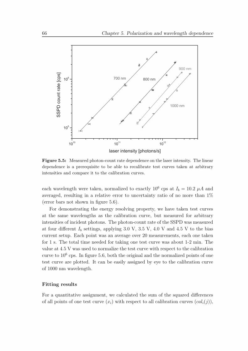
66 Chapter 5. Polarization and wavelength dependence
Figure 5.5: Measured photon-count rate dependence on the laser intensity. The linear
dependence is a prerequisite to be able to recalibrate test curves taken at arbitrary
intensities and compare it to the calibration curves.
each wavelength were taken, normalized to exactly 106 cps at Ib = 10.2 μA and
averaged, resulting in a relative error to uncertainty ratio of no more than 1%
(error bars not shown in figure 5.6).
For demonstrating the energy resolving property, we have taken test curves
at the same wavelengths as the calibration curve, but measured for arbitrary
intensities of incident photons. The photon-count rate of the SSPD was measured
at four different Ib settings, applying 3.0 V, 3.5 V, 4.0 V and 4.5 V to the bias
current setup. Each point was an average over 20 measurements, each one taken
for 1 s. The total time needed for taking one test curve was about 1-2 min. The
value at 4.5 V was used to normalize the test curve with respect to the calibration
curve to 106 cps. In figure 5.6, both the original and the normalized points of one
test curve are plotted. It can be easily assigned by eye to the calibration curve
of 1000 nm wavelength.
Fitting results
For a quantitative assignment, we calculated the sum of the squared differences
of all points of one test curve (xi) with respect to all calibration curves (cali(j)),
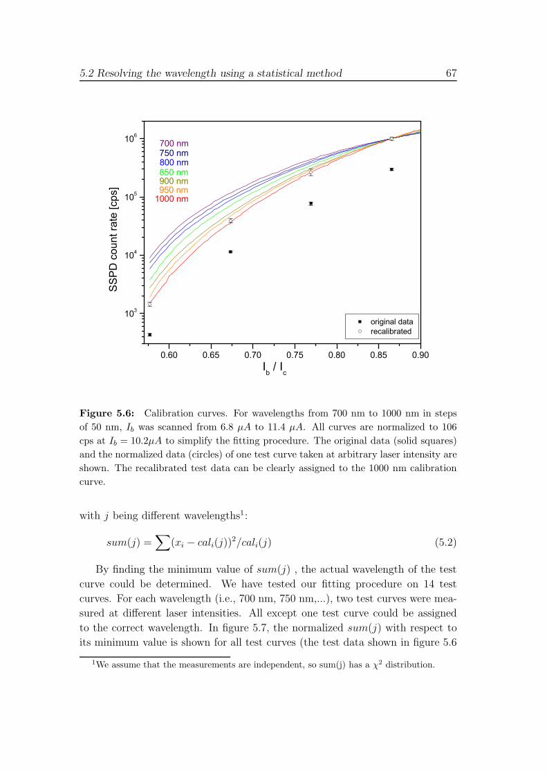
5.2 Resolving the wavelength using a statistical method 67
Figure 5.6: Calibration curves. For wavelengths from 700 nm to 1000 nm in steps
of 50 nm, Ib was scanned from 6.8 μA to 11.4 μA. All curves are normalized to 106
cps at Ib = 10.2μA to simplify the fitting procedure. The original data (solid squares)
and the normalized data (circles) of one test curve taken at arbitrary laser intensity are
shown. The recalibrated test data can be clearly assigned to the 1000 nm calibration
curve.
with j being different wavelengths1:
sum(j) =∑
(xi − cali(j))2/cali(j) (5.2)
By finding the minimum value of sum(j) , the actual wavelength of the test
curve could be determined. We have tested our fitting procedure on 14 test
curves. For each wavelength (i.e., 700 nm, 750 nm,...), two test curves were mea-
sured at different laser intensities. All except one test curve could be assigned
to the correct wavelength. In figure 5.7, the normalized sum(j) with respect to
its minimum value is shown for all test curves (the test data shown in figure 5.6
1We assume that the measurements are independent, so sum(j) has a χ2 distribution.
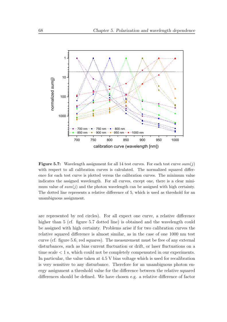
68 Chapter 5. Polarization and wavelength dependence
Figure 5.7: Wavelength assignment for all 14 test curves. For each test curve sum(j)
with respect to all calibration curves is calculated. The normalized squared differ-
ence for each test curve is plotted versus the calibration curves. The minimum value
indicates the assigned wavelength. For all curves, except one, there is a clear mini-
mum value of sum(j) and the photon wavelength can be assigned with high certainty.
The dotted line represents a relative difference of 5, which is used as threshold for an
unambiguous assignment.
are represented by red circles). For all expect one curve, a relative difference
higher than 5 (cf. figure 5.7 dotted line) is obtained and the wavelength could
be assigned with high certainty. Problems arise if for two calibration curves the
relative squared difference is almost similar, as in the case of one 1000 nm test
curve (cf. figure 5.6, red squares). The measurement must be free of any external
disturbances, such as bias current fluctuation or drift, or laser fluctuations on a
time scale < 1 s, which could not be completely compensated in our experiments.
In particular, the value taken at 4.5 V bias voltage which is used for recalibration
is very sensitive to any disturbance. Therefore for an unambiguous photon en-
ergy assignment a threshold value for the difference between the relative squared
differences should be defined. We have chosen e.g. a relative difference of factor
5.2 Resolving the wavelength using a statistical method 69
5,2 which is represented as a dotted line in figure 5.7. We stress, that this latter
condition is satisfied for all test curves except one. If the above threshold is not
reached then simply the measurement of the test curve has to be repeated until
the criterion is fulfilled. The energy information about the incident photons is
obtained statistically, i.e., we have to measure the photon-count rate for at least
two different bias current settings. That requires a stable light source over the
time needed for performing the bias scan, which is 1-2 min in our case when
using 4 different bias current settings. By reducing the number of points and the
amount of averaging, this acquisition time can be lowered, however, at the cost
of accuracy.
Detector instabilities, which cause slightly different count rates for exactly the
same experimental conditions are, probably, the main reason for the observed 50-
nm wavelength resolution limit of our method. When taking calibration curves
with smaller wavelength step size, the error bars of the calibration curves start
to overlap. By using a more uniform SSPD with higher DE and a better-shielded
readout system, our energy resolution should be substantially improved.
Light source with two different wavelengths
We have also investigated the possibility to determine the wavelengths contribu-
tions of a light source emitting simultaneously photons with two different wave-
lengths. For that, we equipped our setup with a single-mode fiber optic coupler
(Thorlabs, 10202A-50-FC) and used the pump laser of our system (Coherent,
Verdi: 530 nm) as the source of one (green) wavelength radiation, while the
Ti:sapphire laser at a wavelength of 900 nm was the second source of photons.
Figure 5.8 presents the photon-count rates obtained for the three different
cases: (a) only the green (530 nm) laser was connected to the single-mode fiber
of the SSPD, (b) only the IR wavelength beam of the Ti:sapphire laser was used,
and, finally, (c) both beams were coupled in at the same time and fed to the
SSPD. Additionally, figure 5.8 shows the calculated sum (open circles) of the
curves (a) and (b). At low values of Ib, the counts rate curve when photons of
both wavelengths are incident on the SSPD is dominated by the contribution
of the green laser. That is due to the fact that the QE is much higher for
green photons as compared to IR photons. As a consequence, the low Ib/Icregime can be used for determining the wavelength of the high-energy photons as
well as their flux number. We note that in general, the photon-count curve (c)
follows almost perfectly the open-symbols curve, obtained by adding together the
2For 7 degrees of freedom, the relative difference corresponds to a cumulative probability of
86%. To have a 95% confidence with respect to the calibration, χ2=2.2 should be used.
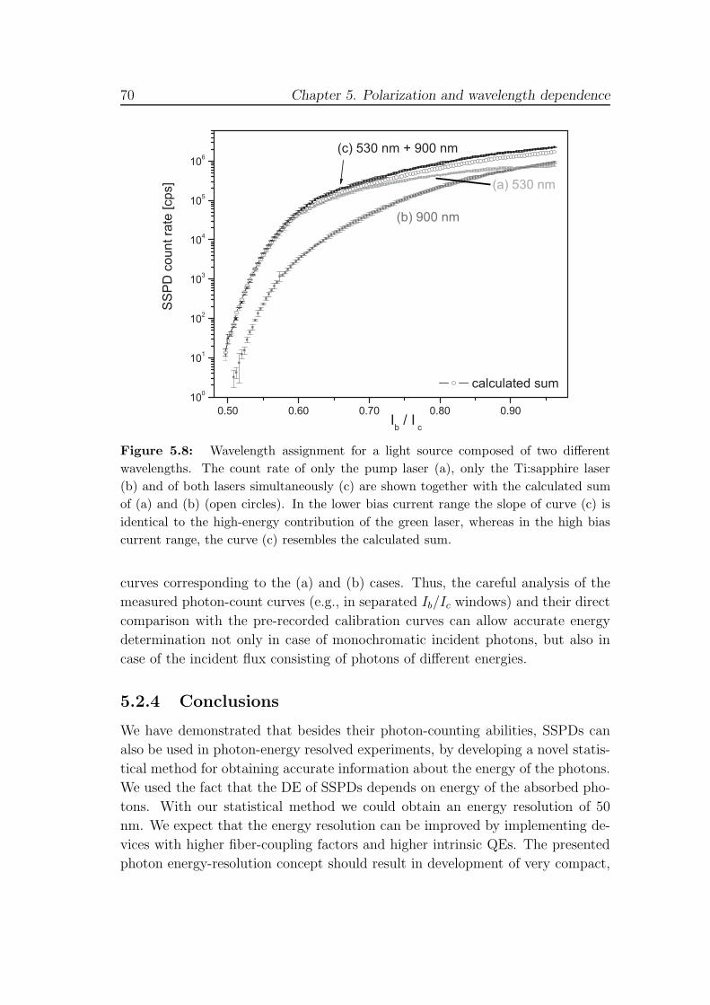
70 Chapter 5. Polarization and wavelength dependence
Figure 5.8: Wavelength assignment for a light source composed of two different
wavelengths. The count rate of only the pump laser (a), only the Ti:sapphire laser
(b) and of both lasers simultaneously (c) are shown together with the calculated sum
of (a) and (b) (open circles). In the lower bias current range the slope of curve (c) is
identical to the high-energy contribution of the green laser, whereas in the high bias
current range, the curve (c) resembles the calculated sum.
curves corresponding to the (a) and (b) cases. Thus, the careful analysis of the
measured photon-count curves (e.g., in separated Ib/Ic windows) and their direct
comparison with the pre-recorded calibration curves can allow accurate energy
determination not only in case of monochromatic incident photons, but also in
case of the incident flux consisting of photons of different energies.
5.2.4 Conclusions
We have demonstrated that besides their photon-counting abilities, SSPDs can
also be used in photon-energy resolved experiments, by developing a novel statis-
tical method for obtaining accurate information about the energy of the photons.
We used the fact that the DE of SSPDs depends on energy of the absorbed pho-
tons. With our statistical method we could obtain an energy resolution of 50
nm. We expect that the energy resolution can be improved by implementing de-
vices with higher fiber-coupling factors and higher intrinsic QEs. The presented
photon energy-resolution concept should result in development of very compact,

5.2 Resolving the wavelength using a statistical method 71
single-photon spectroscopy setups and further lead in their implementation in,
e.g., determination of the emission wavelength of quantum dots or ultraweak
astronomical bodies.

72 Chapter 5. Polarization and wavelength dependence
Chapter 6
NbSi SSPDs
The quantum efficiency of NbN and NbTiN superconducting single photon de-
tectors drops with decreasing photon energy. A lower gap material would enable
single photon detection deeper in the infrared. We have fabricated a NbSi detec-
tor and compare its characteristics with a NbTiN device. NbSi (TC �2 K) has
a smaller superconducting bandgap than NbTiN (and NbN) (TC �15 K). We
measure the detection efficiency for a wavelength range from 1100 to 1900 nm.
In this range the NbSi detector shows a tenfold increase in relative efficiency with
respect to the NbTiN detector.
This chapter is based on S.N. Dorenbos, P. Forn-Dıaz, T. Fuse, A.H. Verbruggen, T. Zijlstra,
T.M. Klapwijk and V. Zwiller, Applied Physics Letters 98,251102 (2011)
73
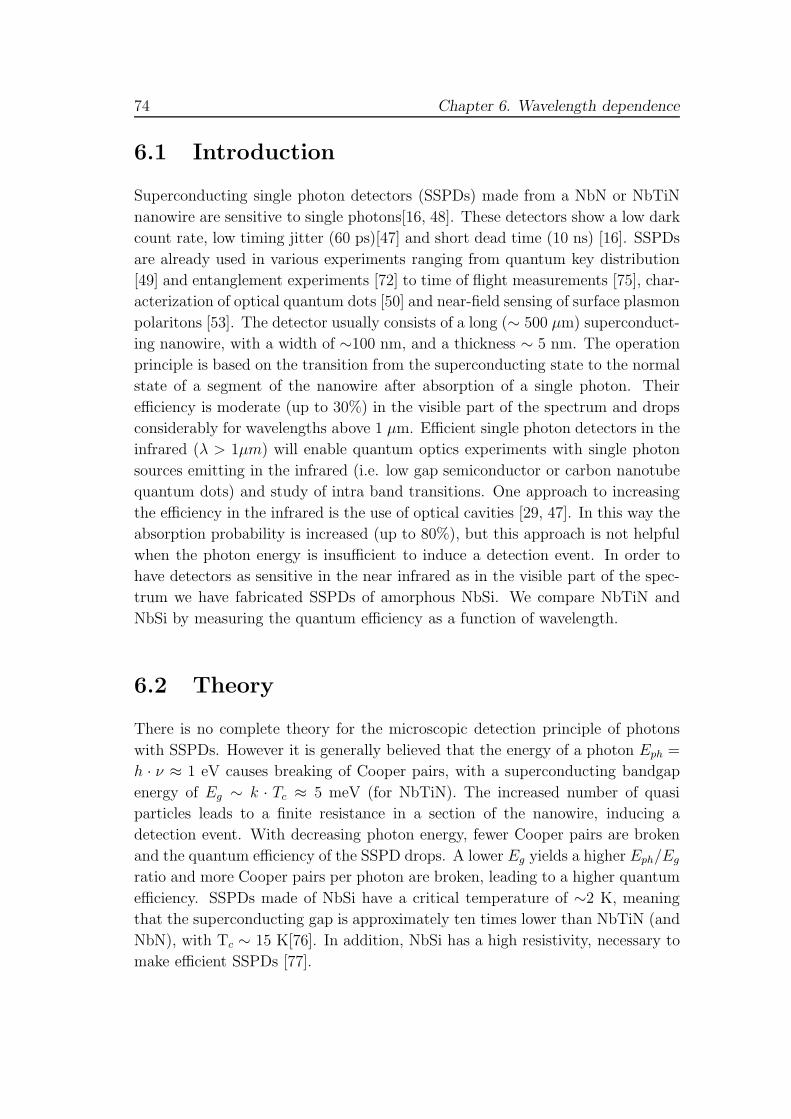
74 Chapter 6. Wavelength dependence
6.1 Introduction
Superconducting single photon detectors (SSPDs) made from a NbN or NbTiN
nanowire are sensitive to single photons[16, 48]. These detectors show a low dark
count rate, low timing jitter (60 ps)[47] and short dead time (10 ns) [16]. SSPDs
are already used in various experiments ranging from quantum key distribution
[49] and entanglement experiments [72] to time of flight measurements [75], char-
acterization of optical quantum dots [50] and near-field sensing of surface plasmon
polaritons [53]. The detector usually consists of a long (∼ 500 μm) superconduct-
ing nanowire, with a width of ∼100 nm, and a thickness ∼ 5 nm. The operation
principle is based on the transition from the superconducting state to the normal
state of a segment of the nanowire after absorption of a single photon. Their
efficiency is moderate (up to 30%) in the visible part of the spectrum and drops
considerably for wavelengths above 1 μm. Efficient single photon detectors in the
infrared (λ > 1μm) will enable quantum optics experiments with single photon
sources emitting in the infrared (i.e. low gap semiconductor or carbon nanotube
quantum dots) and study of intra band transitions. One approach to increasing
the efficiency in the infrared is the use of optical cavities [29, 47]. In this way the
absorption probability is increased (up to 80%), but this approach is not helpful
when the photon energy is insufficient to induce a detection event. In order to
have detectors as sensitive in the near infrared as in the visible part of the spec-
trum we have fabricated SSPDs of amorphous NbSi. We compare NbTiN and
NbSi by measuring the quantum efficiency as a function of wavelength.
6.2 Theory
There is no complete theory for the microscopic detection principle of photons
with SSPDs. However it is generally believed that the energy of a photon Eph =
h · ν ≈ 1 eV causes breaking of Cooper pairs, with a superconducting bandgap
energy of Eg ∼ k · Tc ≈ 5 meV (for NbTiN). The increased number of quasi
particles leads to a finite resistance in a section of the nanowire, inducing a
detection event. With decreasing photon energy, fewer Cooper pairs are broken
and the quantum efficiency of the SSPD drops. A lower Eg yields a higher Eph/Eg
ratio and more Cooper pairs per photon are broken, leading to a higher quantum
efficiency. SSPDs made of NbSi have a critical temperature of ∼2 K, meaning
that the superconducting gap is approximately ten times lower than NbTiN (and
NbN), with Tc ∼ 15 K[76]. In addition, NbSi has a high resistivity, necessary to
make efficient SSPDs [77].
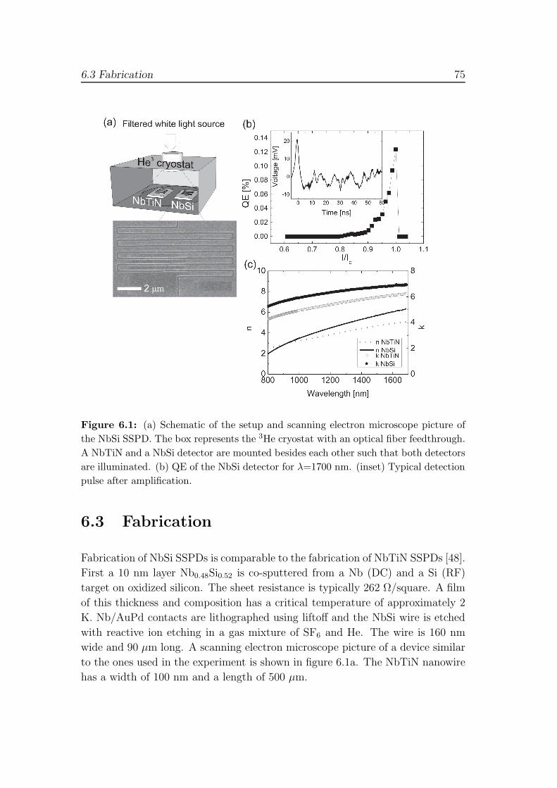
6.3 Fabrication 75
Figure 6.1: (a) Schematic of the setup and scanning electron microscope picture of
the NbSi SSPD. The box represents the 3He cryostat with an optical fiber feedthrough.
A NbTiN and a NbSi detector are mounted besides each other such that both detectors
are illuminated. (b) QE of the NbSi detector for λ=1700 nm. (inset) Typical detection
pulse after amplification.
6.3 Fabrication
Fabrication of NbSi SSPDs is comparable to the fabrication of NbTiN SSPDs [48].
First a 10 nm layer Nb0.48Si0.52 is co-sputtered from a Nb (DC) and a Si (RF)
target on oxidized silicon. The sheet resistance is typically 262 Ω/square. A film
of this thickness and composition has a critical temperature of approximately 2
K. Nb/AuPd contacts are lithographed using liftoff and the NbSi wire is etched
with reactive ion etching in a gas mixture of SF6 and He. The wire is 160 nm
wide and 90 μm long. A scanning electron microscope picture of a device similar
to the ones used in the experiment is shown in figure 6.1a. The NbTiN nanowire
has a width of 100 nm and a length of 500 μm.
76 Chapter 6. Wavelength dependence
Figure 6.2: (a) Count rates and QE for the NbTiN (circles) and NbSi (squares)
detector. The solid lines through the QE measurements are exponential fits. (b) NbSi
count rate as a function of NbTiN count rate for λ=1400 nm and λ=1800 nm. The
slope in the exponential plot is 0.95(0.27) and 0.91(0.16) respectively, close to linear.
6.4 Setup 77
6.4 Setup
In order to perform the experiment a NbSi detector and a NbTiN detector are
cooled down in a 3He cryostat, equipped with a multimode optical fiber. The
measurement temperature is 300 mK. To directly compare the sensitivity of NbSi
with NbTiN we place the two detectors besides each other, and an optical fiber is
mounted above the detectors such that the spot simultaneously illuminates both
detectors with approximately the same intensity (see figure 6.1a). A supercon-
tinuum white light source filtered by a monochromator is used as the excitation
light source. A long pass filter at 1100 nm blocks second orders produced by
the monochromator. The output of the monochromator is calibrated with a
spectrometer and a full width half maximum of the line width of ≤1.6 nm is
measured. We confirm that no second order was present. The SSPDs are biased
with DC current and the output pulses are amplified (gain +30 dB) and read out
with a pulse counter or an oscilloscope. The critical current of the NbSi SSPD
was 2.2 μA (0.9Ic), implying a critical current density of 1.4·105A/cm2 (0.63Ic).
The quantum efficiency under illumination with 1700 nm light is shown in figure
6.1b. As expected, the quantum efficiency exponentially increases with current.
A typical photon detection pulse is shown in the inset of figure 6.1b. The pulse
length (1 ns) is limited by the bandwidth of our amplifiers (0.01-1 GHz). Given
the relatively low kinetic inductance of our device (∼50 nH), the reset time of the
device is shorter than 1 ns. The absorption efficiency is determined by the optical
constants of the material, in particular the complex index of refraction (k)[65].
We have measured the optical constants of NbSi and NbTiN with an ellipsome-
ter. This is shown in figure 6.1c, and it can be seen that the complex index of
refraction of NbSi is comparable to NbTiN, which means that the absorption
efficiency will be similar.
6.5 Results
In figure 6.2a the count rates for the NbTiN detector and the NbSi detector
are shown as a function of wavelength, the detectors were current biased at 10
μA and 1.4 μA, respectively. We observe that latching occurs for higher bias
current for the NbSi detector. We attribute this latching to the low kinetic
inductance of the device, preventing the detector from cooling down and returning
to the superconducting state, as the current in the device increases too fast.[25]
Increasing the length of the wire will increase the kinetic inductance, which allows
biasing the detector closer to the critical current and increases the active area. We
measure a dark count rate of less than 1 count per second for both detectors. For
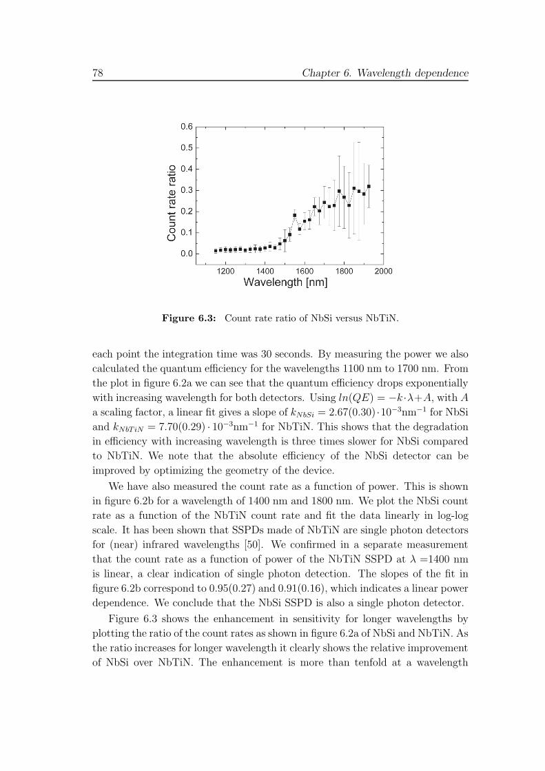
78 Chapter 6. Wavelength dependence
Figure 6.3: Count rate ratio of NbSi versus NbTiN.
each point the integration time was 30 seconds. By measuring the power we also
calculated the quantum efficiency for the wavelengths 1100 nm to 1700 nm. From
the plot in figure 6.2a we can see that the quantum efficiency drops exponentially
with increasing wavelength for both detectors. Using ln(QE) = −k ·λ+A, with Aa scaling factor, a linear fit gives a slope of kNbSi = 2.67(0.30) ·10−3nm−1 for NbSi
and kNbT iN = 7.70(0.29) · 10−3nm−1 for NbTiN. This shows that the degradation
in efficiency with increasing wavelength is three times slower for NbSi compared
to NbTiN. We note that the absolute efficiency of the NbSi detector can be
improved by optimizing the geometry of the device.
We have also measured the count rate as a function of power. This is shown
in figure 6.2b for a wavelength of 1400 nm and 1800 nm. We plot the NbSi count
rate as a function of the NbTiN count rate and fit the data linearly in log-log
scale. It has been shown that SSPDs made of NbTiN are single photon detectors
for (near) infrared wavelengths [50]. We confirmed in a separate measurement
that the count rate as a function of power of the NbTiN SSPD at λ =1400 nm
is linear, a clear indication of single photon detection. The slopes of the fit in
figure 6.2b correspond to 0.95(0.27) and 0.91(0.16), which indicates a linear power
dependence. We conclude that the NbSi SSPD is also a single photon detector.
Figure 6.3 shows the enhancement in sensitivity for longer wavelengths by
plotting the ratio of the count rates as shown in figure 6.2a of NbSi and NbTiN. As
the ratio increases for longer wavelength it clearly shows the relative improvement
of NbSi over NbTiN. The enhancement is more than tenfold at a wavelength

6.6 Conclusion 79
λ=1900 nm with respect to λ=1100 nm.
6.6 Conclusion
In conclusion, we have fabricated and tested NbSi SSPDs. These detectors have
a smaller superconducting bandgap compared to NbTiN detectors, making them
more sensitive for infrared wavelengths. We have compared the relative sensitivity
with NbTiN detectors for different wavelengths and observed an enhancement by
an order of magnitude over a wavelength range from 1100 nm to 1900 nm. By
improving the geometry of the NbSi detector and fiber coupling them[47] a high
system detection efficiency for single photons at infrared wavelengths can be
achieved.

80 Chapter 6. Wavelength dependence
Chapter 7
Readout techniques
7.1 A superconducting single photon detector
array
Superconducting nanowire detectors have opened new possibilities in sensitive
imaging. Targeting such applications requires integration of an array of fast and
efficient detectors with reasonable readout complexity. We report experimental
results of two multiplexing methods (series and parallel) and their combination for
multi-pixel single photon detection. The first method offers simultaneous readout
of all pixels resulting in higher count rates, whereas the second provides efficient
implementation for larger arrays. A larger number of detectors was implemented
within a matrix by combining both types of arrays inheriting all the advantages.
In all cases the readout circuitry complexity was significantly decreased.
7.1.1 Introduction
Array implementations of SSPDs have been proposed [78, 79] with the poten-
tials of increasing count rates and providing spatial information. Higher count
rates can be obtained because while one detector is in its recovery phase, the
others can still detect. Imaging is also possible if one distinguishes pulses from
different detectors. Extending the arrays into a large matrix could provide a fast
and high resolution imaging sensor suitable for applications like medical optical
tomography [44] where both temporal and spatial information must be obtained.
However, no scalable implementation of SSPD matrices has yet been reported.
One important challenge is the readout circuitry complexity which grows linearly
with increasing pixel number using current readout techniques. In this letter we
This section is based on I. Esmaeil Zadeh, S. Dorenbos, and V. Zwiller, A superconducting
single photon detector array, submitted for publication
81
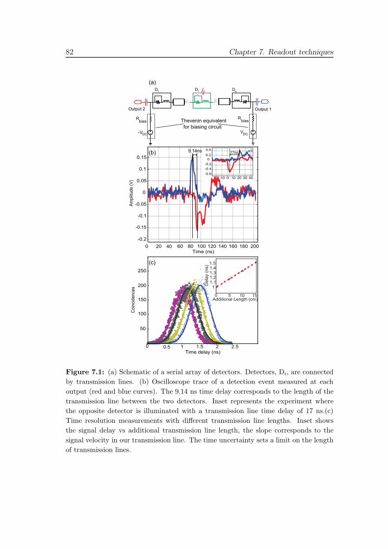
82 Chapter 7. Readout techniques
-V DCV
Time delay (ns)
2001801601401201008060200-0.2
-0.15
-0.1
-0.05
0
0.05
0.1
0.15
Time (ns)
Ampl
itude
(V)
9.14ns
����� �����
Additional Length (cm)
1.3
1.5
Del
ay (n
s)
0 5 10 15
11.11.2
1.4
0 0.5 1 1.5 2 2.5
50
100Coi
ncid
ence
s
150
200
250
Rbias
DC
D1 D Dn
(b)
(c)
(a)i
Rbias
Output 1Output 2
40
Thevenin equivalentfor biasing circuit
-10 0 10 20 30 40-0.6-0.4-0.2
00.20.4
17ns x3
Figure 7.1: (a) Schematic of a serial array of detectors. Detectors, Di, are connected
by transmission lines. (b) Oscilloscope trace of a detection event measured at each
output (red and blue curves). The 9.14 ns time delay corresponds to the length of the
transmission line between the two detectors. Inset represents the experiment where
the opposite detector is illuminated with a transmission line time delay of 17 ns.(c)
Time resolution measurements with different transmission line lengths. Inset shows
the signal delay vs additional transmission line length, the slope corresponds to the
signal velocity in our transmission line. The time uncertainty sets a limit on the length
of transmission lines.
7.1 A superconducting single photon detector array 83
demonstrate two alternative ways for implementation of arrays of SSPDs with a
reduced number of interfaces and amplifiers. The first approach is based on serial
arrangement of SSPDs, providing higher saturation count rate, and the second
method is a parallel implementation with better scalability. Both methods have
minimum number of interfaces which do not increase when scaling up the array.
Finally, a combination of both methods for implementing a larger SSPD matrix,
while maintaining the same low readout complexity is presented.
7.1.2 Serial array
Isolated detectors were interconnected with aluminum bonding wires forming
arrays of SSPDs and coax cables were used as transmission lines for series struc-
tures. The schematic of a serial array is depicted in figure 7.1a, each detector
is modeled as an inductor with a series resistance in parallel with a switch. In
series architecture n detectors are connected via n - 1 transmission lines. Using
these transmission lines the switched detector(s) can be identified by comparing
the time delay between detection pulses at both ends of the cascade. Figure 7.1b
shows an oscilloscope trace for such a measurement where two series SSPDs are
connected through a 9.14 ns transmission line. The connections are made using a
coaxial cable. The inset of figure 7.1b represents the measurement corresponding
to the case where the opposite detector is illuminated and the transmission line
delay is 17 ns. It is clear that using this arrangement, higher photon count rates
as well as additional spatial information can be obtained compared to a conven-
tional single SSPD. However, due to the timing jitter there is a lower bound on
the length of transmission lines and hence the length of the whole series. Figure
7.1c represents the measurement results for different delay lines. As shown in
the figure, there is about 540 ps FWHM uncertainty in the measurements. This
uncertainty can be reduced by averaging over multiple detection events. Yet an-
other limit on the number of pixels in series architecture is set by the signal to
noise ratio (SNR) which is affected by the reflection and attenuation in transmis-
sion lines. SNR can be relaxed by integration of transmission lines and adding
matching circuits. The inset of figure 7.1c shows the linear dependence of time
delay on transmission line length.
7.1.3 Parallel array
An alternative for array implementation of the detectors is to operate them in
parallel. The working principle of this array is based on sequentially activating
the detectors. This is achieved by means of a dedicated resistor for each SSPD
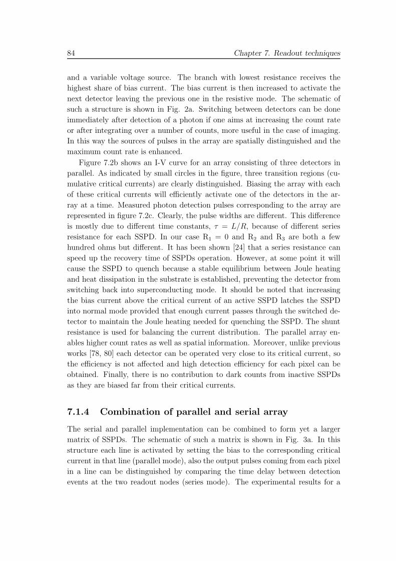
84 Chapter 7. Readout techniques
and a variable voltage source. The branch with lowest resistance receives the
highest share of bias current. The bias current is then increased to activate the
next detector leaving the previous one in the resistive mode. The schematic of
such a structure is shown in Fig. 2a. Switching between detectors can be done
immediately after detection of a photon if one aims at increasing the count rate
or after integrating over a number of counts, more useful in the case of imaging.
In this way the sources of pulses in the array are spatially distinguished and the
maximum count rate is enhanced.
Figure 7.2b shows an I-V curve for an array consisting of three detectors in
parallel. As indicated by small circles in the figure, three transition regions (cu-
mulative critical currents) are clearly distinguished. Biasing the array with each
of these critical currents will efficiently activate one of the detectors in the ar-
ray at a time. Measured photon detection pulses corresponding to the array are
represented in figure 7.2c. Clearly, the pulse widths are different. This difference
is mostly due to different time constants, τ = L/R, because of different series
resistance for each SSPD. In our case R1 = 0 and R2 and R3 are both a few
hundred ohms but different. It has been shown [24] that a series resistance can
speed up the recovery time of SSPDs operation. However, at some point it will
cause the SSPD to quench because a stable equilibrium between Joule heating
and heat dissipation in the substrate is established, preventing the detector from
switching back into superconducting mode. It should be noted that increasing
the bias current above the critical current of an active SSPD latches the SSPD
into normal mode provided that enough current passes through the switched de-
tector to maintain the Joule heating needed for quenching the SSPD. The shunt
resistance is used for balancing the current distribution. The parallel array en-
ables higher count rates as well as spatial information. Moreover, unlike previous
works [78, 80] each detector can be operated very close to its critical current, so
the efficiency is not affected and high detection efficiency for each pixel can be
obtained. Finally, there is no contribution to dark counts from inactive SSPDs
as they are biased far from their critical currents.
7.1.4 Combination of parallel and serial array
The serial and parallel implementation can be combined to form yet a larger
matrix of SSPDs. The schematic of such a matrix is shown in Fig. 3a. In this
structure each line is activated by setting the bias to the corresponding critical
current in that line (parallel mode), also the output pulses coming from each pixel
in a line can be distinguished by comparing the time delay between detection
events at the two readout nodes (series mode). The experimental results for a
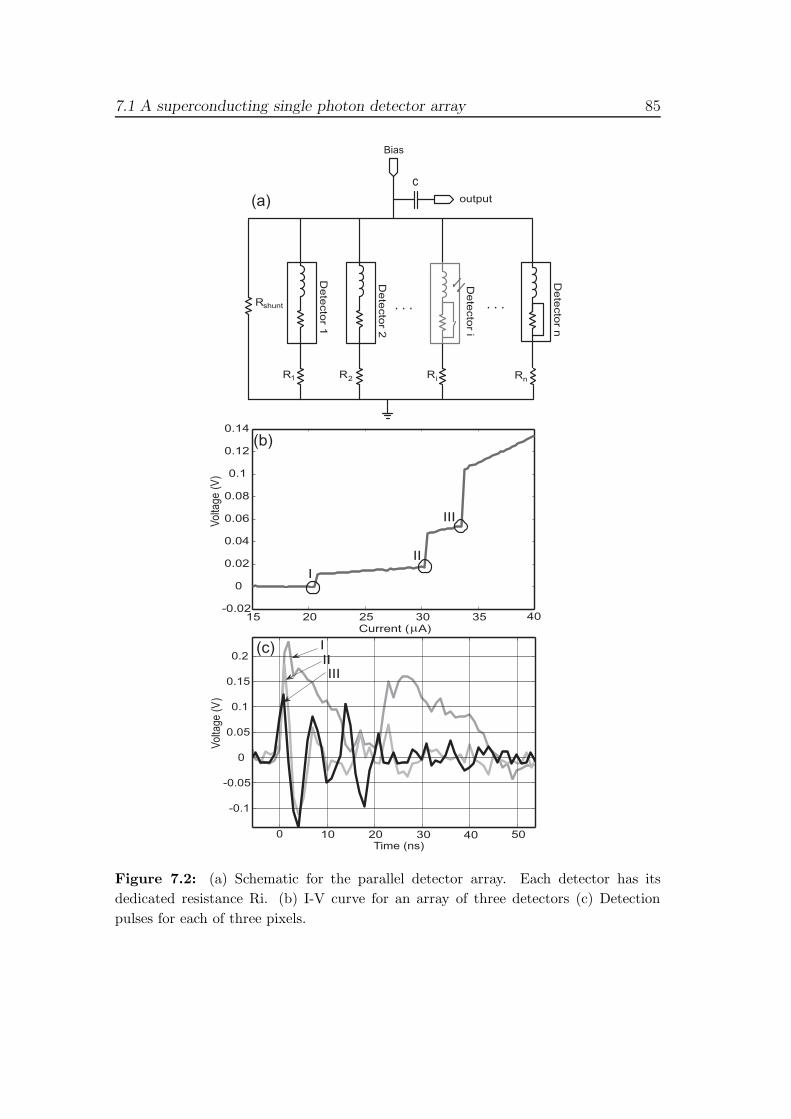
7.1 A superconducting single photon detector array 85
10
Detector 1
c
Detector 2
Detector n
Detector i
15 20 25 30 35 40-0.02
0
0.02
0.04
0.06
0.08
0.1
0.12
0.14
Current (µA)
0
-0.1
-0.05
0
0.05
0.1
0.15
0.2
Volta
ge (V
)
IIIIII
Time (ns)
III
III
(a)
(c)
(b)
Rshunt
output
RnR2R1 Ri
Volta
ge (V
)
20 30 40 50
Bias
Figure 7.2: (a) Schematic for the parallel detector array. Each detector has its
dedicated resistance Ri. (b) I-V curve for an array of three detectors (c) Detection
pulses for each of three pixels.
86 Chapter 7. Readout techniques
(a)
i_m
n_m
1_m1_1
20
10
Detector 1_1
R2_1
Detector 2_1
n_iDetector n_1
Detector i_1Ri_1
. . .
. .
.
Detector 1_ j
Detector 2_ j
Detector n_ j
Rshunt
Detector i_ j
. . .
Detector 1_m
Detector 2_m
Detector n_m
Detector i_m
. . .
. .
.
c
. . .. . . . . .. . .
0 20 30 40 50 60 70 80
-0.2
-0.1
0
0.1
0.2
0.3
0 40 60 80 100 120-0.2
-0.1
0
0.1
0.2
0.3
0.4
0.5
R R
Rshunt
R
R
Rshunt
. .
.
Time (ns)
Time (ns)
Volta
ge (V
)Vo
ltage
(V)
(b)
(c)
c
Bias 2 Bias 1
Output 2 Output 1
R
R
2_m. . .. . .
. . .. . .
. . .. . .
. . .. . .
. . .. . .
. . .. . .
. . .. . .
. . .
. . .
. . .
. . .
. . .. . .
Figure 7.3: (a) Combination of the serial and parallel approach, enabling very large
numbers of detectors to be readout with only two interfaces. (b) detection pulses at 18
μA and (c) 32 μA biasing currents.
7.1 A superconducting single photon detector array 87
2x2 array is presented in figure 7.3b and figure 7.3c. The first two detectors in the
line with lower resistance were activated by setting the bias current to 18 μA and
the second line was enabled by switching the bias to 32 μA. It should be noted
that for biasing currents above 18 μA up to a few μA below 32 μA, detection
events are unlikely to happen. This is because both detectors in the first line are
latched to normal mode and no detector in the second line is sufficiently biased.
Detection pulses in figure 7.3b and figure 7.3c again have different widths due to
different series resistances. As our array consists of isolated detectors connected
by bonding wires and transmission lines (coax cables), reflection and attenuation
occur. However, integration of these detectors will improve SNR and reduce the
reflection. The transmission lines can be approximated using lumped element
circuits or be replaced by simple phase shifters. In our case, detection pulses and
reflections are distinguishable by considering the time delay in transmission lines
and setting a threshold voltage for the counter. This is because detection pulses
are usually larger in amplitude compared to reflection.
7.1.5 Conclusions and outlook
In conclusion we have shown new methods for implementation of multi-pixel
SSPD. The new proposed approaches may work at higher count rates, provide
spatial information and maintain the same complexity for readout interfaces as
is the case for a single or at most two SSPDs. Further study is needed but initial
results for arrays based on our methods, confirm the potentials of SSPD arrays for
imaging. As the only limit on the length of transmission lines in series structures
is set by uncertainty in the time delay between pulses, reducing the timing jitter
makes using shorter transmission lines possible. The ultimate case is measuring
the pulses at two ends of a single detector.
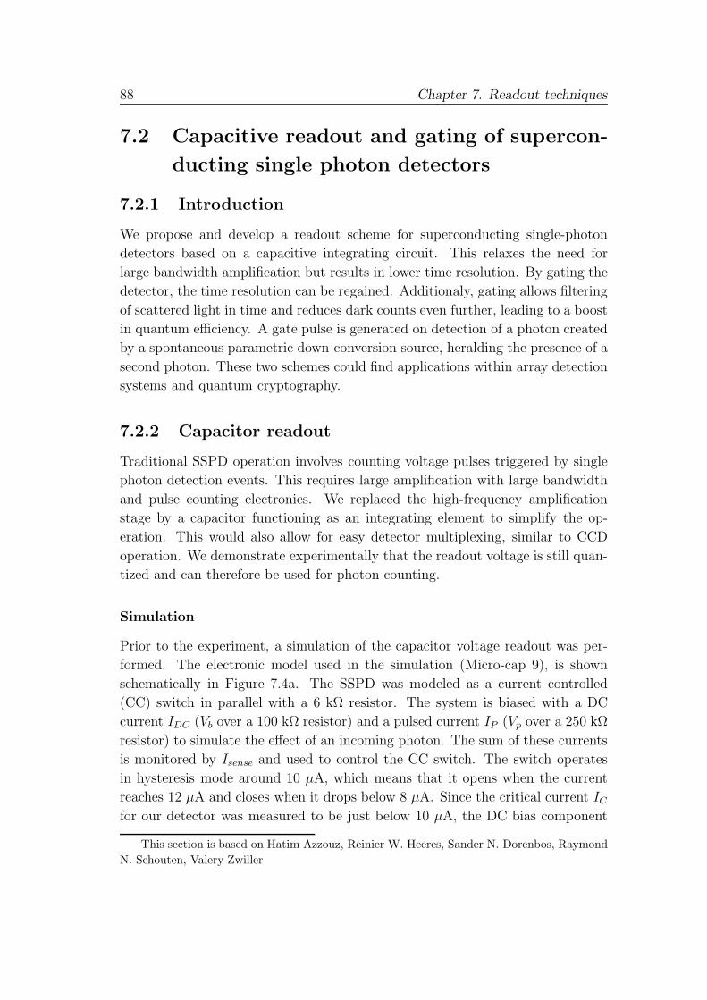
88 Chapter 7. Readout techniques
7.2 Capacitive readout and gating of supercon-
ducting single photon detectors
7.2.1 Introduction
We propose and develop a readout scheme for superconducting single-photon
detectors based on a capacitive integrating circuit. This relaxes the need for
large bandwidth amplification but results in lower time resolution. By gating the
detector, the time resolution can be regained. Additionaly, gating allows filtering
of scattered light in time and reduces dark counts even further, leading to a boost
in quantum efficiency. A gate pulse is generated on detection of a photon created
by a spontaneous parametric down-conversion source, heralding the presence of a
second photon. These two schemes could find applications within array detection
systems and quantum cryptography.
7.2.2 Capacitor readout
Traditional SSPD operation involves counting voltage pulses triggered by single
photon detection events. This requires large amplification with large bandwidth
and pulse counting electronics. We replaced the high-frequency amplification
stage by a capacitor functioning as an integrating element to simplify the op-
eration. This would also allow for easy detector multiplexing, similar to CCD
operation. We demonstrate experimentally that the readout voltage is still quan-
tized and can therefore be used for photon counting.
Simulation
Prior to the experiment, a simulation of the capacitor voltage readout was per-
formed. The electronic model used in the simulation (Micro-cap 9), is shown
schematically in Figure 7.4a. The SSPD was modeled as a current controlled
(CC) switch in parallel with a 6 kΩ resistor. The system is biased with a DC
current IDC (Vb over a 100 kΩ resistor) and a pulsed current IP (Vp over a 250 kΩ
resistor) to simulate the effect of an incoming photon. The sum of these currents
is monitored by Isense and used to control the CC switch. The switch operates
in hysteresis mode around 10 μA, which means that it opens when the current
reaches 12 μA and closes when it drops below 8 μA. Since the critical current ICfor our detector was measured to be just below 10 μA, the DC bias component
This section is based on Hatim Azzouz, Reinier W. Heeres, Sander N. Dorenbos, Raymond
N. Schouten, Valery Zwiller
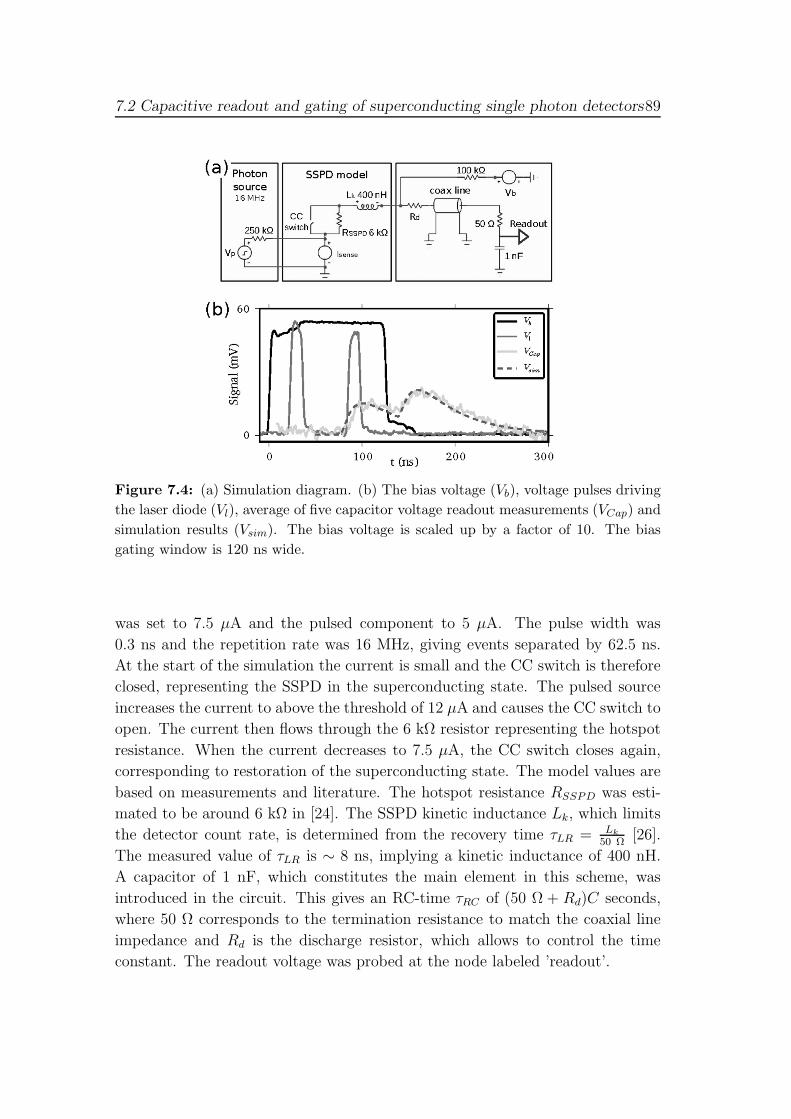
7.2 Capacitive readout and gating of superconducting single photon detectors89
Figure 7.4: (a) Simulation diagram. (b) The bias voltage (Vb), voltage pulses driving
the laser diode (Vl), average of five capacitor voltage readout measurements (VCap) and
simulation results (Vsim). The bias voltage is scaled up by a factor of 10. The bias
gating window is 120 ns wide.
was set to 7.5 μA and the pulsed component to 5 μA. The pulse width was
0.3 ns and the repetition rate was 16 MHz, giving events separated by 62.5 ns.
At the start of the simulation the current is small and the CC switch is therefore
closed, representing the SSPD in the superconducting state. The pulsed source
increases the current to above the threshold of 12 μA and causes the CC switch to
open. The current then flows through the 6 kΩ resistor representing the hotspot
resistance. When the current decreases to 7.5 μA, the CC switch closes again,
corresponding to restoration of the superconducting state. The model values are
based on measurements and literature. The hotspot resistance RSSPD was esti-
mated to be around 6 kΩ in [24]. The SSPD kinetic inductance Lk, which limits
the detector count rate, is determined from the recovery time τLR = Lk
50 Ω[26].
The measured value of τLR is ∼ 8 ns, implying a kinetic inductance of 400 nH.
A capacitor of 1 nF, which constitutes the main element in this scheme, was
introduced in the circuit. This gives an RC-time τRC of (50 Ω + Rd)C seconds,
where 50 Ω corresponds to the termination resistance to match the coaxial line
impedance and Rd is the discharge resistor, which allows to control the time
constant. The readout voltage was probed at the node labeled ’readout’.
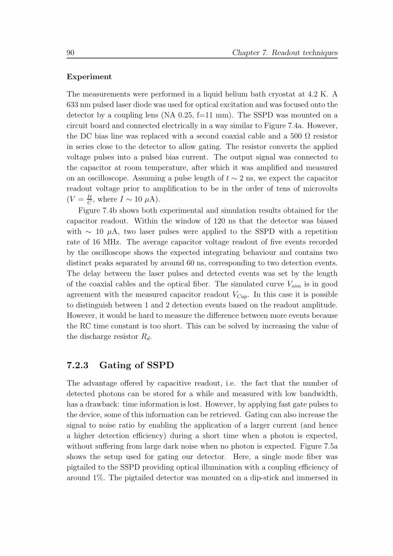
90 Chapter 7. Readout techniques
Experiment
The measurements were performed in a liquid helium bath cryostat at 4.2 K. A
633 nm pulsed laser diode was used for optical excitation and was focused onto the
detector by a coupling lens (NA 0.25, f=11 mm). The SSPD was mounted on a
circuit board and connected electrically in a way similar to Figure 7.4a. However,
the DC bias line was replaced with a second coaxial cable and a 500 Ω resistor
in series close to the detector to allow gating. The resistor converts the applied
voltage pulses into a pulsed bias current. The output signal was connected to
the capacitor at room temperature, after which it was amplified and measured
on an oscilloscope. Assuming a pulse length of t ∼ 2 ns, we expect the capacitor
readout voltage prior to amplification to be in the order of tens of microvolts
(V = ItC, where I ∼ 10 μA).
Figure 7.4b shows both experimental and simulation results obtained for the
capacitor readout. Within the window of 120 ns that the detector was biased
with ∼ 10 μA, two laser pulses were applied to the SSPD with a repetition
rate of 16 MHz. The average capacitor voltage readout of five events recorded
by the oscilloscope shows the expected integrating behaviour and contains two
distinct peaks separated by around 60 ns, corresponding to two detection events.
The delay between the laser pulses and detected events was set by the length
of the coaxial cables and the optical fiber. The simulated curve Vsim is in good
agreement with the measured capacitor readout VCap. In this case it is possible
to distinguish between 1 and 2 detection events based on the readout amplitude.
However, it would be hard to measure the difference between more events because
the RC time constant is too short. This can be solved by increasing the value of
the discharge resistor Rd.
7.2.3 Gating of SSPD
The advantage offered by capacitive readout, i.e. the fact that the number of
detected photons can be stored for a while and measured with low bandwidth,
has a drawback: time information is lost. However, by applying fast gate pulses to
the device, some of this information can be retrieved. Gating can also increase the
signal to noise ratio by enabling the application of a larger current (and hence
a higher detection efficiency) during a short time when a photon is expected,
without suffering from large dark noise when no photon is expected. Figure 7.5a
shows the setup used for gating our detector. Here, a single mode fiber was
pigtailed to the SSPD providing optical illumination with a coupling efficiency of
around 1%. The pigtailed detector was mounted on a dip-stick and immersed in
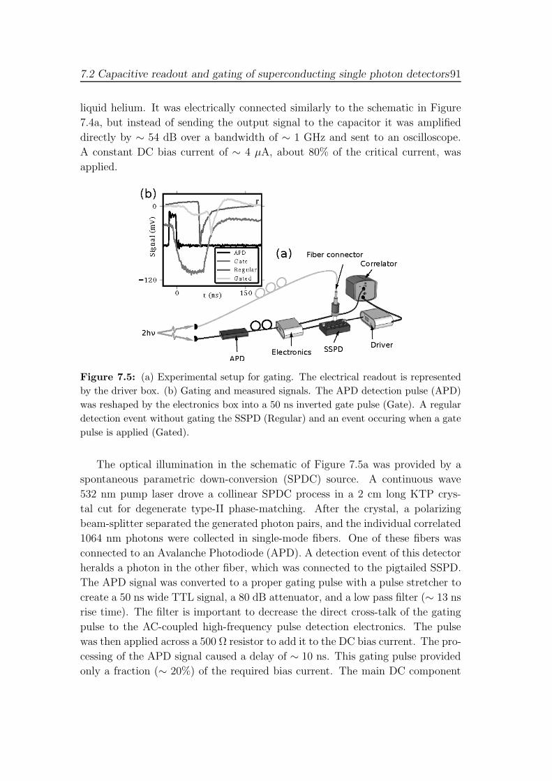
7.2 Capacitive readout and gating of superconducting single photon detectors91
liquid helium. It was electrically connected similarly to the schematic in Figure
7.4a, but instead of sending the output signal to the capacitor it was amplified
directly by ∼ 54 dB over a bandwidth of ∼ 1 GHz and sent to an oscilloscope.
A constant DC bias current of ∼ 4 μA, about 80% of the critical current, was
applied.
Figure 7.5: (a) Experimental setup for gating. The electrical readout is represented
by the driver box. (b) Gating and measured signals. The APD detection pulse (APD)
was reshaped by the electronics box into a 50 ns inverted gate pulse (Gate). A regular
detection event without gating the SSPD (Regular) and an event occuring when a gate
pulse is applied (Gated).
The optical illumination in the schematic of Figure 7.5a was provided by a
spontaneous parametric down-conversion (SPDC) source. A continuous wave
532 nm pump laser drove a collinear SPDC process in a 2 cm long KTP crys-
tal cut for degenerate type-II phase-matching. After the crystal, a polarizing
beam-splitter separated the generated photon pairs, and the individual correlated
1064 nm photons were collected in single-mode fibers. One of these fibers was
connected to an Avalanche Photodiode (APD). A detection event of this detector
heralds a photon in the other fiber, which was connected to the pigtailed SSPD.
The APD signal was converted to a proper gating pulse with a pulse stretcher to
create a 50 ns wide TTL signal, a 80 dB attenuator, and a low pass filter (∼ 13 ns
rise time). The filter is important to decrease the direct cross-talk of the gating
pulse to the AC-coupled high-frequency pulse detection electronics. The pulse
was then applied across a 500 Ω resistor to add it to the DC bias current. The pro-
cessing of the APD signal caused a delay of ∼ 10 ns. This gating pulse provided
only a fraction (∼ 20%) of the required bias current. The main DC component
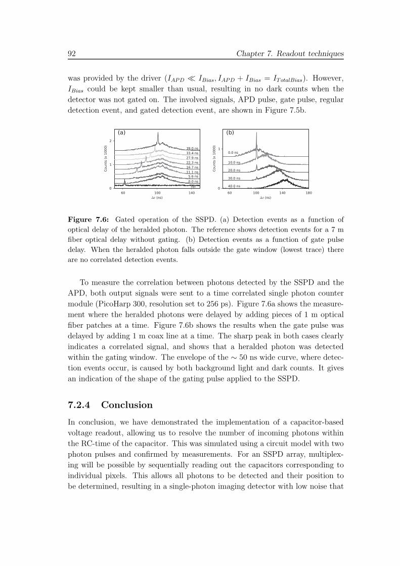
92 Chapter 7. Readout techniques
was provided by the driver (IAPD IBias, IAPD + IBias = ITotalBias). However,
IBias could be kept smaller than usual, resulting in no dark counts when the
detector was not gated on. The involved signals, APD pulse, gate pulse, regular
detection event, and gated detection event, are shown in Figure 7.5b.
Figure 7.6: Gated operation of the SSPD. (a) Detection events as a function of
optical delay of the heralded photon. The reference shows detection events for a 7 m
fiber optical delay without gating. (b) Detection events as a function of gate pulse
delay. When the heralded photon falls outside the gate window (lowest trace) there
are no correlated detection events.
To measure the correlation between photons detected by the SSPD and the
APD, both output signals were sent to a time correlated single photon counter
module (PicoHarp 300, resolution set to 256 ps). Figure 7.6a shows the measure-
ment where the heralded photons were delayed by adding pieces of 1 m optical
fiber patches at a time. Figure 7.6b shows the results when the gate pulse was
delayed by adding 1 m coax line at a time. The sharp peak in both cases clearly
indicates a correlated signal, and shows that a heralded photon was detected
within the gating window. The envelope of the ∼ 50 ns wide curve, where detec-
tion events occur, is caused by both background light and dark counts. It gives
an indication of the shape of the gating pulse applied to the SSPD.
7.2.4 Conclusion
In conclusion, we have demonstrated the implementation of a capacitor-based
voltage readout, allowing us to resolve the number of incoming photons within
the RC-time of the capacitor. This was simulated using a circuit model with two
photon pulses and confirmed by measurements. For an SSPD array, multiplex-
ing will be possible by sequentially reading out the capacitors corresponding to
individual pixels. This allows all photons to be detected and their position to
be determined, resulting in a single-photon imaging detector with low noise that

7.2 Capacitive readout and gating of superconducting single photon detectors93
is sensitive over a broad wavelength range. Furthermore, we have shown that it
is possible to gate an SSPD to provide some of the time-information that is lost
when using capacitive readout. This also gives the opportunity to increase the
detection efficiency in small time windows when photons are expected without
suffering from dark counts outside this window. Further study is needed to con-
firm the detection efficiency and dark count rate during the gate pulse.
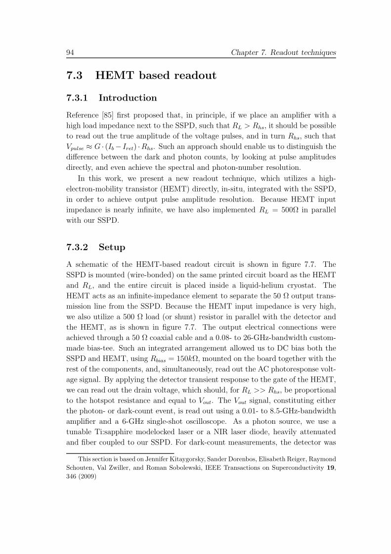
94 Chapter 7. Readout techniques
7.3 HEMT based readout
7.3.1 Introduction
Reference [85] first proposed that, in principle, if we place an amplifier with a
high load impedance next to the SSPD, such that RL > Rhs, it should be possible
to read out the true amplitude of the voltage pulses, and in turn Rhs, such that
Vpulse ≈ G · (Ib− Iret) ·Rhs. Such an approach should enable us to distinguish the
difference between the dark and photon counts, by looking at pulse amplitudes
directly, and even achieve the spectral and photon-number resolution.
In this work, we present a new readout technique, which utilizes a high-
electron-mobility transistor (HEMT) directly, in-situ, integrated with the SSPD,
in order to achieve output pulse amplitude resolution. Because HEMT input
impedance is nearly infinite, we have also implemented RL = 500Ω in parallel
with our SSPD.
7.3.2 Setup
A schematic of the HEMT-based readout circuit is shown in figure 7.7. The
SSPD is mounted (wire-bonded) on the same printed circuit board as the HEMT
and RL, and the entire circuit is placed inside a liquid-helium cryostat. The
HEMT acts as an infinite-impedance element to separate the 50 Ω output trans-
mission line from the SSPD. Because the HEMT input impedance is very high,
we also utilize a 500 Ω load (or shunt) resistor in parallel with the detector and
the HEMT, as is shown in figure 7.7. The output electrical connections were
achieved through a 50 Ω coaxial cable and a 0.08- to 26-GHz-bandwidth custom-
made bias-tee. Such an integrated arrangement allowed us to DC bias both the
SSPD and HEMT, using Rbias = 150kΩ, mounted on the board together with the
rest of the components, and, simultaneously, read out the AC photoresponse volt-
age signal. By applying the detector transient response to the gate of the HEMT,
we can read out the drain voltage, which should, for RL >> Rhs, be proportional
to the hotspot resistance and equal to Vout. The Vout signal, constituting either
the photon- or dark-count event, is read out using a 0.01- to 8.5-GHz-bandwidth
amplifier and a 6-GHz single-shot oscilloscope. As a photon source, we use a
tunable Ti:sapphire modelocked laser or a NIR laser diode, heavily attenuated
and fiber coupled to our SSPD. For dark-count measurements, the detector was
This section is based on Jennifer Kitaygorsky, Sander Dorenbos, Elisabeth Reiger, Raymond
Schouten, Val Zwiller, and Roman Sobolewski, IEEE Transactions on Superconductivity 19,
346 (2009)
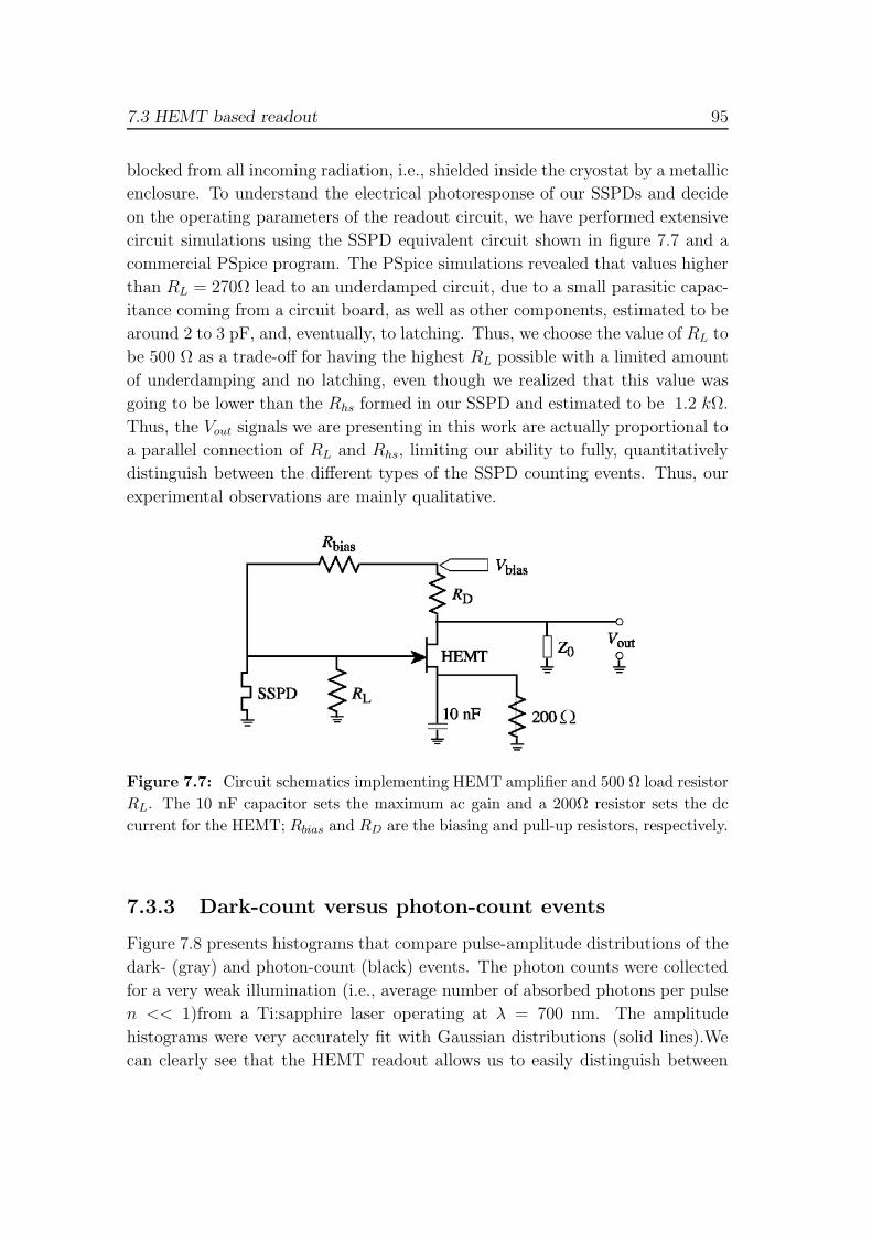
7.3 HEMT based readout 95
blocked from all incoming radiation, i.e., shielded inside the cryostat by a metallic
enclosure. To understand the electrical photoresponse of our SSPDs and decide
on the operating parameters of the readout circuit, we have performed extensive
circuit simulations using the SSPD equivalent circuit shown in figure 7.7 and a
commercial PSpice program. The PSpice simulations revealed that values higher
than RL = 270Ω lead to an underdamped circuit, due to a small parasitic capac-
itance coming from a circuit board, as well as other components, estimated to be
around 2 to 3 pF, and, eventually, to latching. Thus, we choose the value of RL to
be 500 Ω as a trade-off for having the highest RL possible with a limited amount
of underdamping and no latching, even though we realized that this value was
going to be lower than the Rhs formed in our SSPD and estimated to be 1.2 kΩ.
Thus, the Vout signals we are presenting in this work are actually proportional to
a parallel connection of RL and Rhs, limiting our ability to fully, quantitatively
distinguish between the different types of the SSPD counting events. Thus, our
experimental observations are mainly qualitative.
Figure 7.7: Circuit schematics implementing HEMT amplifier and 500 Ω load resistor
RL. The 10 nF capacitor sets the maximum ac gain and a 200Ω resistor sets the dc
current for the HEMT; Rbias and RD are the biasing and pull-up resistors, respectively.
7.3.3 Dark-count versus photon-count events
Figure 7.8 presents histograms that compare pulse-amplitude distributions of the
dark- (gray) and photon-count (black) events. The photon counts were collected
for a very weak illumination (i.e., average number of absorbed photons per pulse
n << 1)from a Ti:sapphire laser operating at λ = 700 nm. The amplitude
histograms were very accurately fit with Gaussian distributions (solid lines).We
can clearly see that the HEMT readout allows us to easily distinguish between
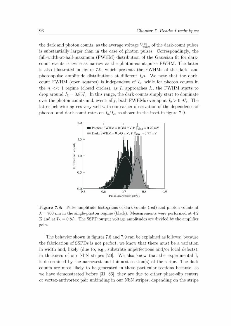
96 Chapter 7. Readout techniques
the dark and photon counts, as the average voltage V avpulse of the dark-count pulses
is substantially larger than in the case of photon pulses. Correspondingly, the
full-width-at-half-maximum (FWHM) distribution of the Gaussian fit for dark-
count events is twice as narrow as the photon-count-pulse FWHM. The latter
is also illustrated in figure 7.9, which presents the FWHMs of the dark- and
photonpulse amplitude distributions at different Ibs. We note that the dark-
count FWHM (open squares) is independent of Ib, while for photon counts in
the n << 1 regime (closed circles), as Ib approaches Ic, the FWHM starts to
drop around Ib = 0.83Ic. In this range, the dark counts simply start to dominate
over the photon counts and, eventually, both FWHMs overlap at Ib > 0.9Ic. The
latter behavior agrees very well with our earlier observation of the dependence of
photon- and dark-count rates on Ib/Ic, as shown in the inset in figure 7.9.
Figure 7.8: Pulse-amplitude histograms of dark counts (red) and photon counts at
λ = 700 nm in the single-photon regime (black). Measurements were performed at 4.2
K and at IL = 0.8Ic. The SSPD output voltage amplitudes are divided by the amplifier
gain.
The behavior shown in figures 7.8 and 7.9 can be explained as follows: because
the fabrication of SSPDs is not perfect, we know that there must be a variation
in width and, likely (due to, e.g., substrate imperfections and/or local defects),
in thickness of our NbN stripes [20]. We also know that the experimental Icis determined by the narrowest and thinnest section(s) of the stripe. The dark
counts are most likely to be generated in these particular sections because, as
we have demonstrated before [31, 86], they are due to either phase-slip centers
or vortex-antivortex pair unbinding in our NbN stripes, depending on the stripe
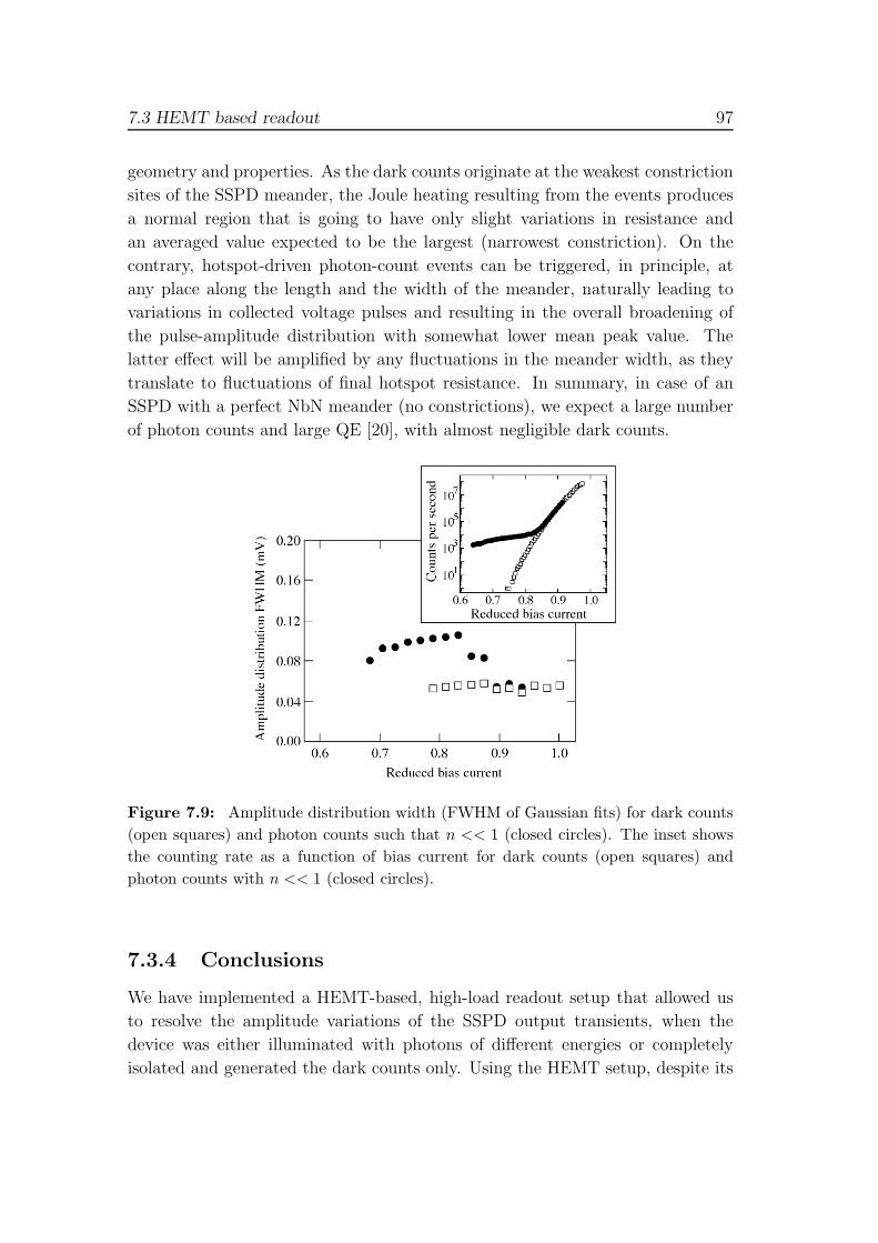
7.3 HEMT based readout 97
geometry and properties. As the dark counts originate at the weakest constriction
sites of the SSPD meander, the Joule heating resulting from the events produces
a normal region that is going to have only slight variations in resistance and
an averaged value expected to be the largest (narrowest constriction). On the
contrary, hotspot-driven photon-count events can be triggered, in principle, at
any place along the length and the width of the meander, naturally leading to
variations in collected voltage pulses and resulting in the overall broadening of
the pulse-amplitude distribution with somewhat lower mean peak value. The
latter effect will be amplified by any fluctuations in the meander width, as they
translate to fluctuations of final hotspot resistance. In summary, in case of an
SSPD with a perfect NbN meander (no constrictions), we expect a large number
of photon counts and large QE [20], with almost negligible dark counts.
Figure 7.9: Amplitude distribution width (FWHM of Gaussian fits) for dark counts
(open squares) and photon counts such that n << 1 (closed circles). The inset shows
the counting rate as a function of bias current for dark counts (open squares) and
photon counts with n << 1 (closed circles).
7.3.4 Conclusions
We have implemented a HEMT-based, high-load readout setup that allowed us
to resolve the amplitude variations of the SSPD output transients, when the
device was either illuminated with photons of different energies or completely
isolated and generated the dark counts only. Using the HEMT setup, despite its

98 Chapter 7. Readout techniques
limitation (namely, that we could not fulfill the condition RL > Rhs) we could,
nevertheless, with the good contrast, qualitatively distinguish the signals coming
from either photon counts or dark counts, confirming that the physical origins of
both events are different.

Part 2

Chapter 8
Position controlled nanowires for
infrared single photon emission
We report the experimental demonstration of single-photon and cascaded photon
pair emission in the infrared, originating from a single InAsP quantum dot em-
bedded in a standing InP nanowire. A regular array of nanowires was fabricated
by epitaxial growth on an electron-beam patterned substrate. Photoluminescence
spectra taken on single quantum dots show narrow emission lines around 1.2 μm.
Superconducting single photon detectors enable us to measure the second order
correlation function as well as cross correlations. Clear antibunching is observed
(g(2)(0) = 0.12). Furthermore we have identified a biexciton-exciton cascade and
two excitonic charge states.
This chapter is based on S. N. Dorenbos, H. Sasakura, M. P. van Kouwen, N. Akopian,
S. Adachi, N. Namekata, M. Jo, J. Motohisa, Y. Kobayashi, K. Tomioka, T. Fukui, S. Inoue,
H. Kumano, C. M. Natarajan, R. H. Hadfield, T. Zijlstra, T. M. Klapwijk, V. Zwiller, and I.
Suemune, Applied Physics Letters 97, 171106 (2010)
101
102Chapter 8. Position controlled nanowires for infrared single photon emission
8.1 Introduction
Semiconductor quantum dot (QD) structures are attractive candidates for solid-
state single photon and/or entangled-photon pair generation.[11, 87, 88, 89, 90,
91] Nanowire quantum dots (NW-QDs) are promising candidates for such sources
due to the controllability of doping, shape, and material freedom.[92, 93, 12, 94]
Furthermore, due to the high light extraction efficiency [95] and straightforward
electrical contacting, nanowires present advantages over self assembled dots. In
addition, fine structure splitting, present in self assembled dots, is predicted to
be absent in NW-QDs, which makes NW-QDs ideal for the creation of entangled
photon pairs. [96] While single photon emission from a NW-QD was shown re-
cently at a wavelength <1000 nm [97, 98], a single photon NW-QD emitter at
telecommunication wavelengths and a detailed study to its emission lines has not
been reported. In this letter we report on the fabrication and characterization
of a regular array of InAsP QD embedded in an InP nanowire and characteri-
zation of the QD photoluminescence. InAsP is an attractive material due to its
band gap, which can be tuned to telecommunication wavelengths by changing its
composition. We demonstrate controlled positioning of the nanowires by grow-
ing them in a regular array. Control of the position allows further advancement
towards practical devices and control of the density, which is necessary for uni-
form properties. We show that a NW-QD indeed is a source of single photons
by measuring non-classical antibunching in second-order photon correlation ex-
periments, proving sub-Poissonian light statistics. Furthermore we perform cross
correlation experiments to identify biexcitonic and excitonic transitions.
8.2 Nanowires
Arrays of InAsP QDs embedded in InP NWs were synthesized by selective area
metal organic vapor phase epitaxy (SA-MOVPE [99]). A metal catalyst is usu-
ally used (i.e. Au) to grow NW structures, however with SA-MOVPE a catalyst
is not needed, preventing diffusion of the metal into the NW. A (111) InP wafer
was covered by 30 nm of SiO2. By electron beam lithography and wet-etching, 40
to 60 nm diameter openings were created to form nanowire nucleation-sites. At
a growth rate of 3 nm/s, first a 1 μm long segment of InP was grown by adding
trimethylindium (TMI) and tertiarybutylphosphine (TBP) to the MOVPE reac-
tor at 640 ◦C. Subsequently the temperature was lowered to 580 ◦C and arsine
(AsH3) was added to the reactor (V/III ratio 340, partial pressure TBP:AsH3 3:1)
to grow a 8 to 10 nm layer of InAsP to form the QDs. To cover the QDs with
an InP shell, InP growth was first performed at 580 ◦C. To finalize the nanowire,
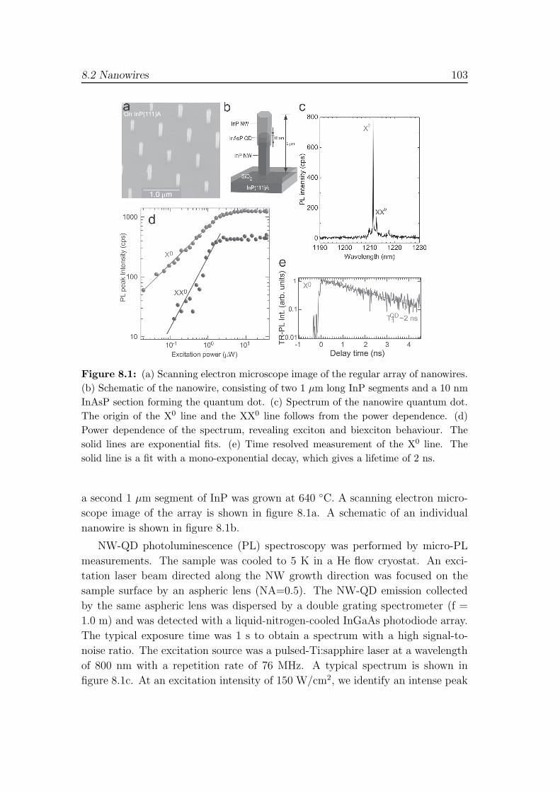
8.2 Nanowires 103
Figure 8.1: (a) Scanning electron microscope image of the regular array of nanowires.
(b) Schematic of the nanowire, consisting of two 1 μm long InP segments and a 10 nm
InAsP section forming the quantum dot. (c) Spectrum of the nanowire quantum dot.
The origin of the X0 line and the XX0 line follows from the power dependence. (d)
Power dependence of the spectrum, revealing exciton and biexciton behaviour. The
solid lines are exponential fits. (e) Time resolved measurement of the X0 line. The
solid line is a fit with a mono-exponential decay, which gives a lifetime of 2 ns.
a second 1 μm segment of InP was grown at 640 ◦C. A scanning electron micro-
scope image of the array is shown in figure 8.1a. A schematic of an individual
nanowire is shown in figure 8.1b.
NW-QD photoluminescence (PL) spectroscopy was performed by micro-PL
measurements. The sample was cooled to 5 K in a He flow cryostat. An exci-
tation laser beam directed along the NW growth direction was focused on the
sample surface by an aspheric lens (NA=0.5). The NW-QD emission collected
by the same aspheric lens was dispersed by a double grating spectrometer (f =
1.0 m) and was detected with a liquid-nitrogen-cooled InGaAs photodiode array.
The typical exposure time was 1 s to obtain a spectrum with a high signal-to-
noise ratio. The excitation source was a pulsed-Ti:sapphire laser at a wavelength
of 800 nm with a repetition rate of 76 MHz. A typical spectrum is shown in
figure 8.1c. At an excitation intensity of 150 W/cm2, we identify an intense peak
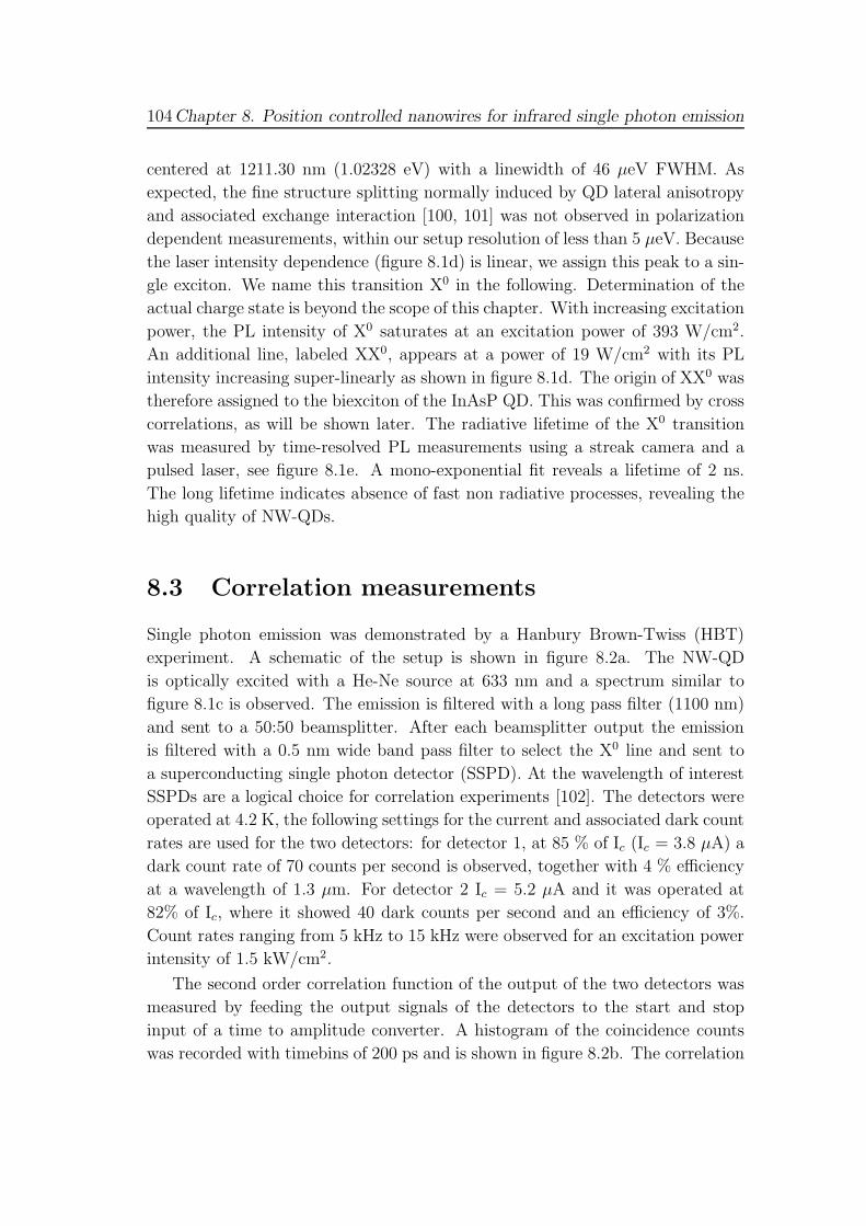
104Chapter 8. Position controlled nanowires for infrared single photon emission
centered at 1211.30 nm (1.02328 eV) with a linewidth of 46 μeV FWHM. As
expected, the fine structure splitting normally induced by QD lateral anisotropy
and associated exchange interaction [100, 101] was not observed in polarization
dependent measurements, within our setup resolution of less than 5 μeV. Because
the laser intensity dependence (figure 8.1d) is linear, we assign this peak to a sin-
gle exciton. We name this transition X0 in the following. Determination of the
actual charge state is beyond the scope of this chapter. With increasing excitation
power, the PL intensity of X0 saturates at an excitation power of 393 W/cm2.
An additional line, labeled XX0, appears at a power of 19 W/cm2 with its PL
intensity increasing super-linearly as shown in figure 8.1d. The origin of XX0 was
therefore assigned to the biexciton of the InAsP QD. This was confirmed by cross
correlations, as will be shown later. The radiative lifetime of the X0 transition
was measured by time-resolved PL measurements using a streak camera and a
pulsed laser, see figure 8.1e. A mono-exponential fit reveals a lifetime of 2 ns.
The long lifetime indicates absence of fast non radiative processes, revealing the
high quality of NW-QDs.
8.3 Correlation measurements
Single photon emission was demonstrated by a Hanbury Brown-Twiss (HBT)
experiment. A schematic of the setup is shown in figure 8.2a. The NW-QD
is optically excited with a He-Ne source at 633 nm and a spectrum similar to
figure 8.1c is observed. The emission is filtered with a long pass filter (1100 nm)
and sent to a 50:50 beamsplitter. After each beamsplitter output the emission
is filtered with a 0.5 nm wide band pass filter to select the X0 line and sent to
a superconducting single photon detector (SSPD). At the wavelength of interest
SSPDs are a logical choice for correlation experiments [102]. The detectors were
operated at 4.2 K, the following settings for the current and associated dark count
rates are used for the two detectors: for detector 1, at 85 % of Ic (Ic = 3.8 μA) a
dark count rate of 70 counts per second is observed, together with 4 % efficiency
at a wavelength of 1.3 μm. For detector 2 Ic = 5.2 μA and it was operated at
82% of Ic, where it showed 40 dark counts per second and an efficiency of 3%.
Count rates ranging from 5 kHz to 15 kHz were observed for an excitation power
intensity of 1.5 kW/cm2.
The second order correlation function of the output of the two detectors was
measured by feeding the output signals of the detectors to the start and stop
input of a time to amplitude converter. A histogram of the coincidence counts
was recorded with timebins of 200 ps and is shown in figure 8.2b. The correlation
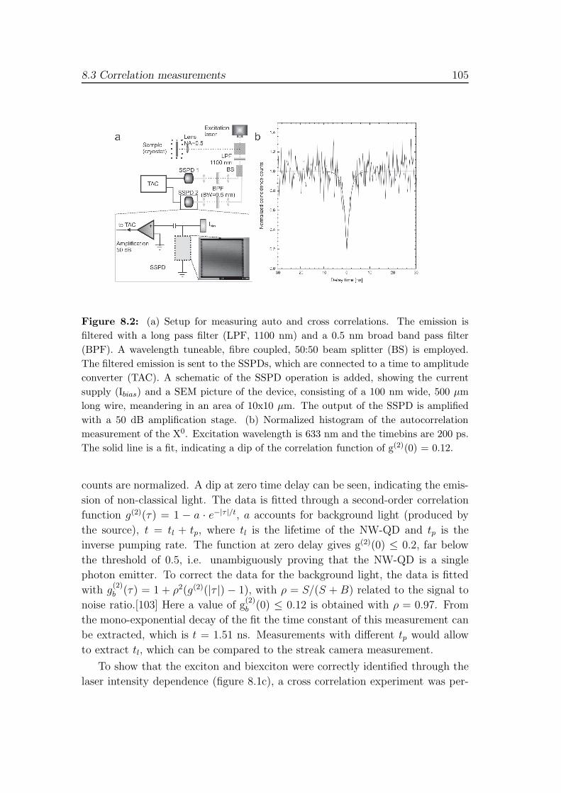
8.3 Correlation measurements 105
Figure 8.2: (a) Setup for measuring auto and cross correlations. The emission is
filtered with a long pass filter (LPF, 1100 nm) and a 0.5 nm broad band pass filter
(BPF). A wavelength tuneable, fibre coupled, 50:50 beam splitter (BS) is employed.
The filtered emission is sent to the SSPDs, which are connected to a time to amplitude
converter (TAC). A schematic of the SSPD operation is added, showing the current
supply (Ibias) and a SEM picture of the device, consisting of a 100 nm wide, 500 μm
long wire, meandering in an area of 10x10 μm. The output of the SSPD is amplified
with a 50 dB amplification stage. (b) Normalized histogram of the autocorrelation
measurement of the X0. Excitation wavelength is 633 nm and the timebins are 200 ps.
The solid line is a fit, indicating a dip of the correlation function of g(2)(0) = 0.12.
counts are normalized. A dip at zero time delay can be seen, indicating the emis-
sion of non-classical light. The data is fitted through a second-order correlation
function g(2)(τ) = 1 − a · e−|τ |/t, a accounts for background light (produced by
the source), t = tl + tp, where tl is the lifetime of the NW-QD and tp is the
inverse pumping rate. The function at zero delay gives g(2)(0) ≤ 0.2, far below
the threshold of 0.5, i.e. unambiguously proving that the NW-QD is a single
photon emitter. To correct the data for the background light, the data is fitted
with g(2)b (τ) = 1 + ρ2(g(2)(|τ |)− 1), with ρ = S/(S + B) related to the signal to
noise ratio.[103] Here a value of g(2)b (0) ≤ 0.12 is obtained with ρ = 0.97. From
the mono-exponential decay of the fit the time constant of this measurement can
be extracted, which is t = 1.51 ns. Measurements with different tp would allow
to extract tl, which can be compared to the streak camera measurement.
To show that the exciton and biexciton were correctly identified through the
laser intensity dependence (figure 8.1c), a cross correlation experiment was per-
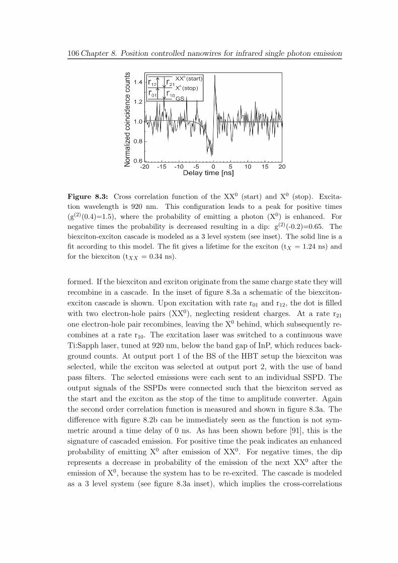
106Chapter 8. Position controlled nanowires for infrared single photon emission
Figure 8.3: Cross correlation function of the XX0 (start) and X0 (stop). Excita-
tion wavelength is 920 nm. This configuration leads to a peak for positive times
(g(2)(0.4)=1.5), where the probability of emitting a photon (X0) is enhanced. For
negative times the probability is decreased resulting in a dip: g(2)(-0.2)=0.65. The
biexciton-exciton cascade is modeled as a 3 level system (see inset). The solid line is a
fit according to this model. The fit gives a lifetime for the exciton (tX = 1.24 ns) and
for the biexciton (tXX = 0.34 ns).
formed. If the biexciton and exciton originate from the same charge state they will
recombine in a cascade. In the inset of figure 8.3a a schematic of the biexciton-
exciton cascade is shown. Upon excitation with rate r01 and r12, the dot is filled
with two electron-hole pairs (XX0), neglecting resident charges. At a rate r21one electron-hole pair recombines, leaving the X0 behind, which subsequently re-
combines at a rate r10. The excitation laser was switched to a continuous wave
Ti:Sapph laser, tuned at 920 nm, below the band gap of InP, which reduces back-
ground counts. At output port 1 of the BS of the HBT setup the biexciton was
selected, while the exciton was selected at output port 2, with the use of band
pass filters. The selected emissions were each sent to an individual SSPD. The
output signals of the SSPDs were connected such that the biexciton served as
the start and the exciton as the stop of the time to amplitude converter. Again
the second order correlation function is measured and shown in figure 8.3a. The
difference with figure 8.2b can be immediately seen as the function is not sym-
metric around a time delay of 0 ns. As has been shown before [91], this is the
signature of cascaded emission. For positive time the peak indicates an enhanced
probability of emitting X0 after emission of XX0. For negative times, the dip
represents a decrease in probability of the emission of the next XX0 after the
emission of X0, because the system has to be re-excited. The cascade is modeled
as a 3 level system (see figure 8.3a inset), which implies the cross-correlations
8.4 Conclusions 107
can be fitted to two decay paths with their own typical time-constants. From
the fitting we conclude that the dip reaches g(2)(-0.2) = 0.65 and the peak has
a value of g(2)(0.4) = 1.5. The exponential decay obtained from the fit leads to
a lifetime of 0.34 ns for the biexciton and 1.24 ns for the exciton. Again, the
function does not reach 0 at τ = 0 , attributed to stray background light. It
has been confirmed that the exciton as well as the biexciton show antibunching
under these conditions (not shown).
8.4 Conclusions
To conclude, we have shown that SSPDs enable efficient correlation measurements
on single nanowire QDs emitting at 1210 nm. Arrays of NW-QDs with very good
properties can be fabricated without the use of catalysts and can form arrays
of non classical light emitters in the infrared. Due to the specific properties of
nanowires, an electrically controlled source [104] of single photons and temporally
correlated photon pairs is now within reach.
8.5 Derivation cross correlations fit
The cross-correlation curves at different intensities can be fitted in terms of the
solutions of a linear system of differential equations that correspond to a three-
level model (inset of figure 8.3)
dnG
dt= −nG
τe+nX
τXdnX
dt=nG
τe−
(1
τe+
1
τX
)nX +
nXX
τXX
dnXX
dt=nX
τe− nXX
τXX
(8.1)
where na is the probability that the system is in level a (with G being the
ground level) τX and τXX are the lifetimes of the exciton and biexciton levels,
while τe is the characteristic time for the excitation process which is inversely
proportional to the incident intensity. The solution is of the form
n = 1 · S+ c2 · e−λXS+ c3 · e−λXX · S (8.2)
with λk and S the eigenvalues and eigenvectors of the matrix in 8.1. The
cross correlation measurement performed in this chapter (figure 8.3) is actually
two measurements: (1) the probability of occupation of the exciton level (nX)

108Chapter 8. Position controlled nanowires for infrared single photon emission
after detection of a biexciton, (2) the probability of occupation of the biexciton
level after detection of an exciton. For positive times the first measurement is
seen and the curve is fitted with the solution for nX . For negative times the
second measurement is represented and the curve is fitted for nXX . From the
data sets the lifetimes can be calculated.
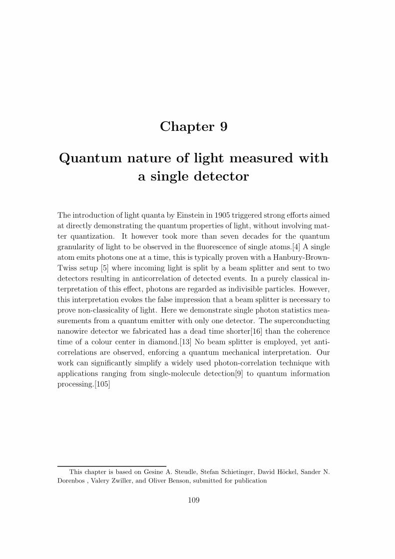
Chapter 9
Quantum nature of light measured with
a single detector
The introduction of light quanta by Einstein in 1905 triggered strong efforts aimed
at directly demonstrating the quantum properties of light, without involving mat-
ter quantization. It however took more than seven decades for the quantum
granularity of light to be observed in the fluorescence of single atoms.[4] A single
atom emits photons one at a time, this is typically proven with a Hanbury-Brown-
Twiss setup [5] where incoming light is split by a beam splitter and sent to two
detectors resulting in anticorrelation of detected events. In a purely classical in-
terpretation of this effect, photons are regarded as indivisible particles. However,
this interpretation evokes the false impression that a beam splitter is necessary to
prove non-classicality of light. Here we demonstrate single photon statistics mea-
surements from a quantum emitter with only one detector. The superconducting
nanowire detector we fabricated has a dead time shorter[16] than the coherence
time of a colour center in diamond.[13] No beam splitter is employed, yet anti-
correlations are observed, enforcing a quantum mechanical interpretation. Our
work can significantly simplify a widely used photon-correlation technique with
applications ranging from single-molecule detection[9] to quantum information
processing.[105]
This chapter is based on Gesine A. Steudle, Stefan Schietinger, David Hockel, Sander N.
Dorenbos , Valery Zwiller, and Oliver Benson, submitted for publication
109
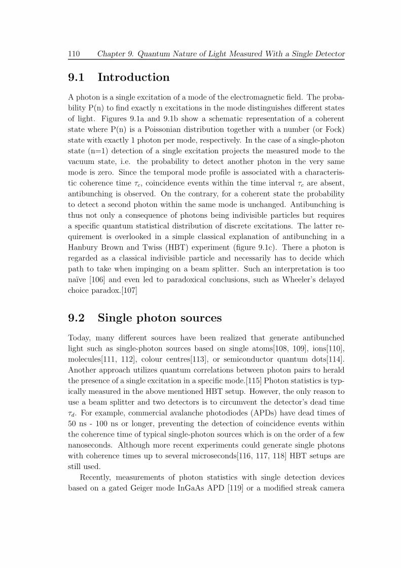
110 Chapter 9. Quantum Nature of Light Measured With a Single Detector
9.1 Introduction
A photon is a single excitation of a mode of the electromagnetic field. The proba-
bility P(n) to find exactly n excitations in the mode distinguishes different states
of light. Figures 9.1a and 9.1b show a schematic representation of a coherent
state where P(n) is a Poissonian distribution together with a number (or Fock)
state with exactly 1 photon per mode, respectively. In the case of a single-photon
state (n=1) detection of a single excitation projects the measured mode to the
vacuum state, i.e. the probability to detect another photon in the very same
mode is zero. Since the temporal mode profile is associated with a characteris-
tic coherence time τc, coincidence events within the time interval τc are absent,
antibunching is observed. On the contrary, for a coherent state the probability
to detect a second photon within the same mode is unchanged. Antibunching is
thus not only a consequence of photons being indivisible particles but requires
a specific quantum statistical distribution of discrete excitations. The latter re-
quirement is overlooked in a simple classical explanation of antibunching in a
Hanbury Brown and Twiss (HBT) experiment (figure 9.1c). There a photon is
regarded as a classical indivisible particle and necessarily has to decide which
path to take when impinging on a beam splitter. Such an interpretation is too
naıve [106] and even led to paradoxical conclusions, such as Wheeler’s delayed
choice paradox.[107]
9.2 Single photon sources
Today, many different sources have been realized that generate antibunched
light such as single-photon sources based on single atoms[108, 109], ions[110],
molecules[111, 112], colour centres[113], or semiconductor quantum dots[114].
Another approach utilizes quantum correlations between photon pairs to herald
the presence of a single excitation in a specific mode.[115] Photon statistics is typ-
ically measured in the above mentioned HBT setup. However, the only reason to
use a beam splitter and two detectors is to circumvent the detector’s dead time
τd. For example, commercial avalanche photodiodes (APDs) have dead times of
50 ns - 100 ns or longer, preventing the detection of coincidence events within
the coherence time of typical single-photon sources which is on the order of a few
nanoseconds. Although more recent experiments could generate single photons
with coherence times up to several microseconds[116, 117, 118] HBT setups are
still used.
Recently, measurements of photon statistics with single detection devices
based on a gated Geiger mode InGaAs APD [119] or a modified streak camera
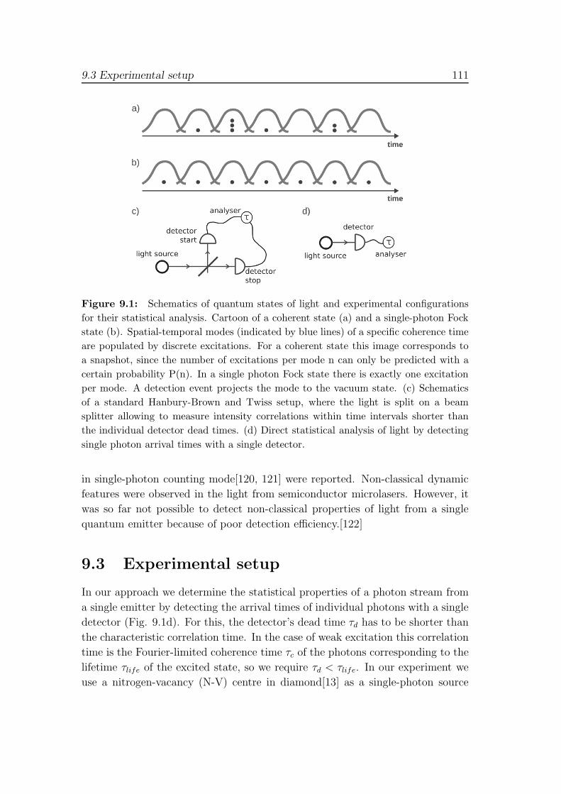
9.3 Experimental setup 111
Figure 9.1: Schematics of quantum states of light and experimental configurations
for their statistical analysis. Cartoon of a coherent state (a) and a single-photon Fock
state (b). Spatial-temporal modes (indicated by blue lines) of a specific coherence time
are populated by discrete excitations. For a coherent state this image corresponds to
a snapshot, since the number of excitations per mode n can only be predicted with a
certain probability P(n). In a single photon Fock state there is exactly one excitation
per mode. A detection event projects the mode to the vacuum state. (c) Schematics
of a standard Hanbury-Brown and Twiss setup, where the light is split on a beam
splitter allowing to measure intensity correlations within time intervals shorter than
the individual detector dead times. (d) Direct statistical analysis of light by detecting
single photon arrival times with a single detector.
in single-photon counting mode[120, 121] were reported. Non-classical dynamic
features were observed in the light from semiconductor microlasers. However, it
was so far not possible to detect non-classical properties of light from a single
quantum emitter because of poor detection efficiency.[122]
9.3 Experimental setup
In our approach we determine the statistical properties of a photon stream from
a single emitter by detecting the arrival times of individual photons with a single
detector (Fig. 9.1d). For this, the detector’s dead time τd has to be shorter than
the characteristic correlation time. In the case of weak excitation this correlation
time is the Fourier-limited coherence time τc of the photons corresponding to the
lifetime τlife of the excited state, so we require τd < τlife. In our experiment we
use a nitrogen-vacancy (N-V) centre in diamond[13] as a single-photon source
112 Chapter 9. Quantum Nature of Light Measured With a Single Detector
together with a superconducting single-photon detector (SSPD). N-V centres in
diamond where a nitrogen atom replaces a carbon atom with an adjacent vacancy
in the diamond lattice are the subject of intense research due to their exceptional
role as single-photon sources at room temperature. The optical transition in
a N-V centre occurs between two spin-triplet states. At least one additional
singlet state introduces an off-state. The fluorescence spectrum of a N-V centre
is broadened by higher phonon lines, but has a pronounced zero phonon line
peak at 638 nm. At room temperature, single-photon emission with count rates
up to 106 s−1 can be observed.[123] The lifetime of the excited state in N-V
centres in diamond nanoparticles is around 30 ns, which is long compared to
other single-photon sources.[124] As a single-photon detector we utilized a fibre-
coupled SSPD[16] (see Methods). It consists of a NbN meandering nanowire
coupled to a single-mode fibre (Fig. 9.2a). Its dead time τd is limited by its
kinetic inductance[26], here τd < 5 ns. Yet, this value is clearly shorter than the
N-V centres lifetime.
Antibunching is quantified by measuring the second-order auto-correlation
function of the electric field, given by
g(2) =< E(t)†E(t+ τ)† >< E(t)†E(t) >2
=<: I(t)I(t+ τ :>
< I(t) >2(9.1)
where E† and E are the field operators and : : denotes normal ordering. For
uncorrelated light, e.g. laser light, with a Poissonian photon number distribution,
g(2)(τ) = 1 for all τ . However, for a number state |n >, at τ=0 it drops to
g(2)(0) = 1− 1/n < 1. Fig. 9.2b shows the experimental setup for measuring the
g(2)-function. Fluorescence was coupled into a single-mode fibre, and detection
was done in two configurations. Configuration 1 is the single detector setup, i.e.
the light was sent via the optical fibre directly to the SSPD. In configuration
2, the HBT setup, light was coupled for comparison into a standard free space
HBT setup consisting of a beam splitter and two APDs. In configuration 1, the
amplified electrical pulses from the SSPD were fed to an oscilloscope with 1 GHz
bandwidth. The oscilloscope was programmed to save a pulse trace whenever a
trigger level of 200 mV was exceeded twice with a time difference of between 5 ns
and 200 ns (see Fig. 9.2c). For measuring the g(2)-function, 30,000 traces were
recorded and analysed. In configuration 2, the time intervals between signals
from the two APDs were recorded with a time interval counter.
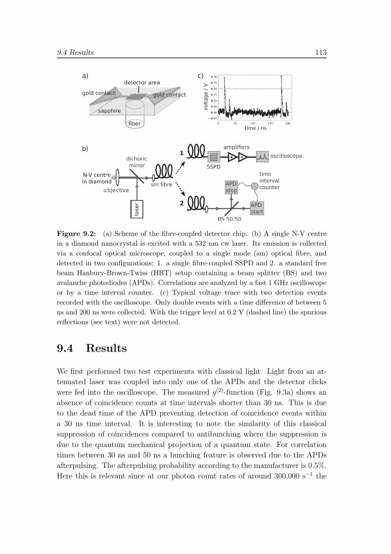
9.4 Results 113
Figure 9.2: (a) Scheme of the fibre-coupled detector chip. (b) A single N-V centre
in a diamond nanocrystal is excited with a 532 nm cw laser. Its emission is collected
via a confocal optical microscope, coupled to a single mode (sm) optical fibre, and
detected in two configurations: 1. a single fibre-coupled SSPD and 2. a standard free
beam Hanbury-Brown-Twiss (HBT) setup containing a beam splitter (BS) and two
avalanche photodiodes (APDs). Correlations are analyzed by a fast 1 GHz oscilloscope
or by a time interval counter. (c) Typical voltage trace with two detection events
recorded with the oscilloscope. Only double events with a time difference of between 5
ns and 200 ns were collected. With the trigger level at 0.2 V (dashed line) the spurious
reflections (see text) were not detected.
9.4 Results
We first performed two test experiments with classical light. Light from an at-
tenuated laser was coupled into only one of the APDs and the detector clicks
were fed into the oscilloscope. The measured g(2)-function (Fig. 9.3a) shows an
absence of coincidence counts at time intervals shorter than 30 ns. This is due
to the dead time of the APD preventing detection of coincidence events within
a 30 ns time interval. It is interesting to note the similarity of this classical
suppression of coincidences compared to antibunching where the suppression is
due to the quantum mechanical projection of a quantum state. For correlation
times between 30 ns and 50 ns a bunching feature is observed due to the APDs
afterpulsing. The afterpulsing probability according to the manufacturer is 0.5%.
Here this is relevant since at our photon count rates of around 300,000 s−1 the
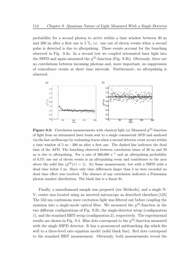
114 Chapter 9. Quantum Nature of Light Measured With a Single Detector
probability for a second photon to arrive within a time window between 30 ns
and 200 ns after a first one is 5 %, i.e. one out of eleven events when a second
pulse is detected is due to afterpulsing. These events account for the bunching
observed in Fig. 9.3a. In a second test we coupled attenuated laser light into
the SSPD and again measured the g(2)-function (Fig. 9.3b). Obviously, there are
no correlations between incoming photons and, more important, no suppression
of coincidence events at short time intervals. Furthermore, no afterpulsing is
observed.
Figure 9.3: Correlation measurements with classical light (a) Measured g(2)-function
of light from an attenuated laser beam sent to a single commercial APD and analysed
via the fast oscilloscope by evaluating traces when a second detector event occurs within
a time window of 5 ns - 200 ns after a first one. The dashed line indicates the dead
time of the APD. The bunching observed between correlation times of 30 ns and 50
ns is due to afterpulsing. For a rate of 300,000 s−1 and an afterpulsing probability
of 0.5% one out of eleven events is an afterpulsing event and contributes to the area
above the solid line (g(2)(τ) = 1). (b) Same measurement, but with a SSPD with a
dead time below 5 ns. Since only time differences larger than 5 ns were recorded no
dead time effect was resolved. The absence of any correlation indicates a Poissonian
photon number distribution. The black line is a linear fit.
Finally, a nanodiamond sample was prepared (see Methods), and a single N-
V- centre was located using an inverted microscope as described elsewhere.[125]
The 532 nm continuous wave excitation light was filtered out before coupling the
emission into a single-mode optical fibre. We measured the g(2)-function in the
two different configurations of Fig. 9.2b, the single-detector setup (configuration
1), and the standard HBT setup (configuration 2), respectively. The experimental
results are shown in Fig. 9.4. Blue dots correspond to the g(2)-function measured
with the single SSPD detector. It has a pronounced antibunching dip which fits
well to a three-level rate equation model (solid black line). Red dots correspond
to the standard HBT measurement. Obviously, both measurements reveal the
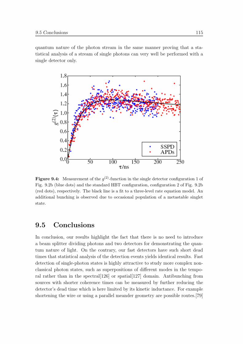
9.5 Conclusions 115
quantum nature of the photon stream in the same manner proving that a sta-
tistical analysis of a stream of single photons can very well be performed with a
single detector only.
Figure 9.4: Measurement of the g(2)-function in the single detector configuration 1 of
Fig. 9.2b (blue dots) and the standard HBT configuration, configuration 2 of Fig. 9.2b
(red dots), respectively. The black line is a fit to a three-level rate equation model. An
additional bunching is observed due to occasional population of a metastable singlet
state.
9.5 Conclusions
In conclusion, our results highlight the fact that there is no need to introduce
a beam splitter dividing photons and two detectors for demonstrating the quan-
tum nature of light. On the contrary, our fast detectors have such short dead
times that statistical analysis of the detection events yields identical results. Fast
detection of single-photon states is highly attractive to study more complex non-
classical photon states, such as superpositions of different modes in the tempo-
ral rather than in the spectral[126] or spatial[127] domain. Antibunching from
sources with shorter coherence times can be measured by further reducing the
detector’s dead time which is here limited by its kinetic inductance. For example
shortening the wire or using a parallel meander geometry are possible routes.[79]
116 Chapter 9. Quantum Nature of Light Measured With a Single Detector
Finally, even beyond fundamental considerations such detectors are useful for
applications in fluorescence correlation spectroscopy[9] in order to simplify the
experimental apparatus.
9.6 Methods
Superconducting Detection System We use a fibre-coupled superconducting
single-photon detector consisting of a 100 nm wide and 5 nm thick NbN mean-
dering wire. The meander structure is fabricated on a sapphire crystal and covers
an area of 10 μm x 10 μm. The detector was coupled to an optical fibre. For that
purpose the sapphire was thinned to a thickness of 100 μm and its back side was
polished. The end facet of a single-mode fibre was aligned on the detector area
and glued directly on the back side of the sapphire crystal. The pulses from the
detector are amplified by 76 dB with two 2 GHz bandwidth amplifiers and fed to
an oscilloscope with 1 GHz bandwidth. Fig. 9.2c shows a typical response curve
recorded with the oscilloscope for two photons absorbed within a time window
of 200 ns. There was always a small reflection of the pulse observed after 14 ns
which we attribute to impedance mismatch. The dark count rate of the detector
was < 50 s−1 and its overall efficiency at 630 nm was around 10 %. The temporal
resolution of the whole detection system (detector and correlation electronics)
was measured by applying femtosecond optical pulses from a titanium-sapphire
laser. The voltage pulses of the SSPD and the trigger signal from the laser were
connected to a time interval counter with 4 ps resolution. We found a time
resolution of our system of 100 ps.
Sample preparation An aqueous suspension of nanodiamonds (diluted ap-
prox. 1:50 from the original batch (Microdiamant AGMSY 0-0.05)) is spin-coated
onto a glass coverslip. Among the nanodiamonds, only around 1 % contains a
single N-V center, deduced from combined optical and atomic force microscopy
measurements. Typical heights between 20 and 35 nm are found while the lateral
extension is up to twice this values.
Chapter 10
On-chip single plasmon detection
Surface plasmon polaritons (plasmons) have the potential to interface electronic
and optical devices. They could prove extremely useful for integrated quantum
information processing. Here we demonstrate on-chip electrical detection of single
plasmons propagating along gold waveguides. The plasmons are excited using the
single-photon emission of an optically emitting quantum dot. After propagating
for several micrometers, the plasmons are coupled to a superconducting detector
in the near-field. Correlation measurements prove that single plasmons are being
detected.
This chapter is based on Reinier W. Heeres, Sander N. Dorenbos, Benny Koene, Glenn S.
Solomon, Leo P. Kouwenhoven, and Valery Zwiller, Nanoletters 10, 661 (2010)
117
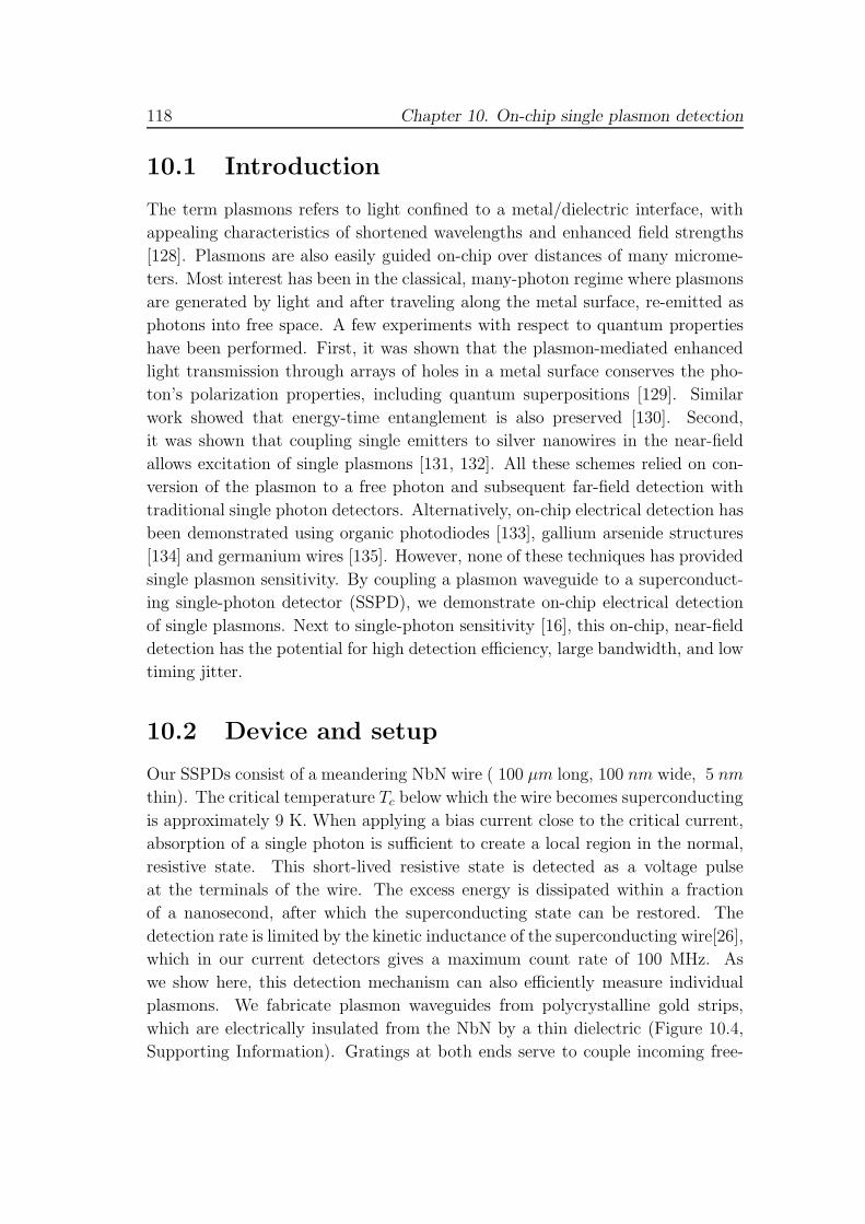
118 Chapter 10. On-chip single plasmon detection
10.1 Introduction
The term plasmons refers to light confined to a metal/dielectric interface, with
appealing characteristics of shortened wavelengths and enhanced field strengths
[128]. Plasmons are also easily guided on-chip over distances of many microme-
ters. Most interest has been in the classical, many-photon regime where plasmons
are generated by light and after traveling along the metal surface, re-emitted as
photons into free space. A few experiments with respect to quantum properties
have been performed. First, it was shown that the plasmon-mediated enhanced
light transmission through arrays of holes in a metal surface conserves the pho-
ton’s polarization properties, including quantum superpositions [129]. Similar
work showed that energy-time entanglement is also preserved [130]. Second,
it was shown that coupling single emitters to silver nanowires in the near-field
allows excitation of single plasmons [131, 132]. All these schemes relied on con-
version of the plasmon to a free photon and subsequent far-field detection with
traditional single photon detectors. Alternatively, on-chip electrical detection has
been demonstrated using organic photodiodes [133], gallium arsenide structures
[134] and germanium wires [135]. However, none of these techniques has provided
single plasmon sensitivity. By coupling a plasmon waveguide to a superconduct-
ing single-photon detector (SSPD), we demonstrate on-chip electrical detection
of single plasmons. Next to single-photon sensitivity [16], this on-chip, near-field
detection has the potential for high detection efficiency, large bandwidth, and low
timing jitter.
10.2 Device and setup
Our SSPDs consist of a meandering NbN wire ( 100 μm long, 100 nm wide, 5 nm
thin). The critical temperature Tc below which the wire becomes superconducting
is approximately 9 K. When applying a bias current close to the critical current,
absorption of a single photon is sufficient to create a local region in the normal,
resistive state. This short-lived resistive state is detected as a voltage pulse
at the terminals of the wire. The excess energy is dissipated within a fraction
of a nanosecond, after which the superconducting state can be restored. The
detection rate is limited by the kinetic inductance of the superconducting wire[26],
which in our current detectors gives a maximum count rate of 100 MHz. As
we show here, this detection mechanism can also efficiently measure individual
plasmons. We fabricate plasmon waveguides from polycrystalline gold strips,
which are electrically insulated from the NbN by a thin dielectric (Figure 10.4,
Supporting Information). Gratings at both ends serve to couple incoming free-
10.3 Results 119
space photons to plasmons confined to the bottom gold/dielectric interface[136].
These plasmons propagate to the detector where they are absorbed and detected
(Figure 10.1b). Measurements are performed in a cryostat at 4 K with the
sample mounted on an XYZ translation stage. A laser is focused through a
cold microscope objective, and a countrate XY-map is measured as a function of
laser-spot position.
Figure 10.1: (a) A scanning electron microscopy image showing the superconducting
detector (cyan) and two gold waveguides (yellow) with coupling gratings. (b) Repre-
sentation of the low-temperature setup. The sample is XY-scanned through the laser
focus. Illumination of the grating excites plasmons at the substrate/gold interface.
After propagating along the waveguide, absorption in the SSPD gives a voltage pulse,
V. (c) SSPD pulse counts versus laser-spot position. (d) 2D XY-scan. The blue and
red lines (WG1 and WG2) indicate where the line-cuts in (c) are taken.
10.3 Results
We find a large detector response when the laser directly illuminates the SSPD
(three peaks at X ≈ 11μm in parts c and d of figure 10.1). The detector response
is very low with the laser spot on the substrate or gold strip, except at the
grating regions. These detector peaks (consistently shifted for waveguides 1 and
2, figure 10.1c) show that light converted to plasmons is detected electrically on-
chip. To substantiate the electrical detection of plasmons, we have performed
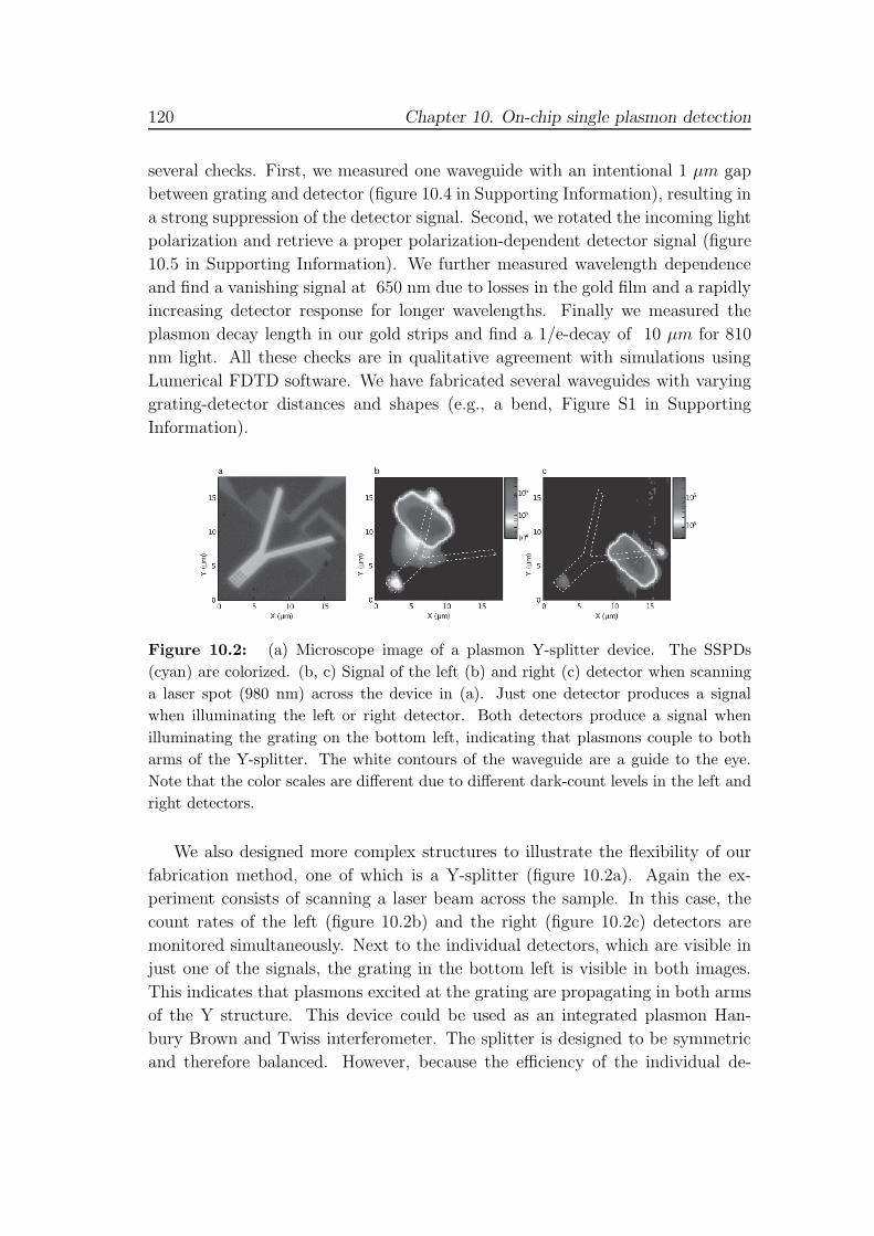
120 Chapter 10. On-chip single plasmon detection
several checks. First, we measured one waveguide with an intentional 1 μm gap
between grating and detector (figure 10.4 in Supporting Information), resulting in
a strong suppression of the detector signal. Second, we rotated the incoming light
polarization and retrieve a proper polarization-dependent detector signal (figure
10.5 in Supporting Information). We further measured wavelength dependence
and find a vanishing signal at 650 nm due to losses in the gold film and a rapidly
increasing detector response for longer wavelengths. Finally we measured the
plasmon decay length in our gold strips and find a 1/e-decay of 10 μm for 810
nm light. All these checks are in qualitative agreement with simulations using
Lumerical FDTD software. We have fabricated several waveguides with varying
grating-detector distances and shapes (e.g., a bend, Figure S1 in Supporting
Information).
Figure 10.2: (a) Microscope image of a plasmon Y-splitter device. The SSPDs
(cyan) are colorized. (b, c) Signal of the left (b) and right (c) detector when scanning
a laser spot (980 nm) across the device in (a). Just one detector produces a signal
when illuminating the left or right detector. Both detectors produce a signal when
illuminating the grating on the bottom left, indicating that plasmons couple to both
arms of the Y-splitter. The white contours of the waveguide are a guide to the eye.
Note that the color scales are different due to different dark-count levels in the left and
right detectors.
We also designed more complex structures to illustrate the flexibility of our
fabrication method, one of which is a Y-splitter (figure 10.2a). Again the ex-
periment consists of scanning a laser beam across the sample. In this case, the
count rates of the left (figure 10.2b) and the right (figure 10.2c) detectors are
monitored simultaneously. Next to the individual detectors, which are visible in
just one of the signals, the grating in the bottom left is visible in both images.
This indicates that plasmons excited at the grating are propagating in both arms
of the Y structure. This device could be used as an integrated plasmon Han-
bury Brown and Twiss interferometer. The splitter is designed to be symmetric
and therefore balanced. However, because the efficiency of the individual de-
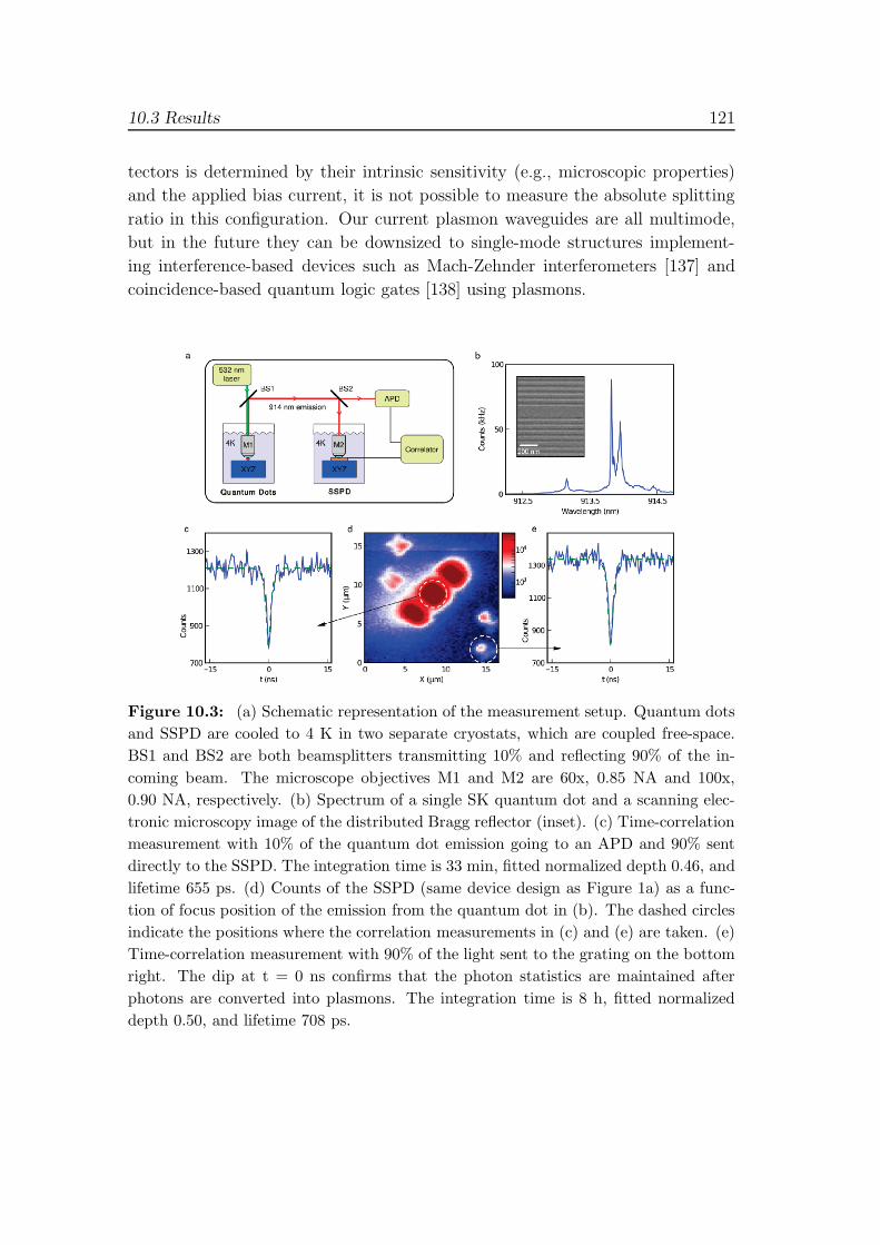
10.3 Results 121
tectors is determined by their intrinsic sensitivity (e.g., microscopic properties)
and the applied bias current, it is not possible to measure the absolute splitting
ratio in this configuration. Our current plasmon waveguides are all multimode,
but in the future they can be downsized to single-mode structures implement-
ing interference-based devices such as Mach-Zehnder interferometers [137] and
coincidence-based quantum logic gates [138] using plasmons.
Figure 10.3: (a) Schematic representation of the measurement setup. Quantum dots
and SSPD are cooled to 4 K in two separate cryostats, which are coupled free-space.
BS1 and BS2 are both beamsplitters transmitting 10% and reflecting 90% of the in-
coming beam. The microscope objectives M1 and M2 are 60x, 0.85 NA and 100x,
0.90 NA, respectively. (b) Spectrum of a single SK quantum dot and a scanning elec-
tronic microscopy image of the distributed Bragg reflector (inset). (c) Time-correlation
measurement with 10% of the quantum dot emission going to an APD and 90% sent
directly to the SSPD. The integration time is 33 min, fitted normalized depth 0.46, and
lifetime 655 ps. (d) Counts of the SSPD (same device design as Figure 1a) as a func-
tion of focus position of the emission from the quantum dot in (b). The dashed circles
indicate the positions where the correlation measurements in (c) and (e) are taken. (e)
Time-correlation measurement with 90% of the light sent to the grating on the bottom
right. The dip at t = 0 ns confirms that the photon statistics are maintained after
photons are converted into plasmons. The integration time is 8 h, fitted normalized
depth 0.50, and lifetime 708 ps.
122 Chapter 10. On-chip single plasmon detection
10.4 Detection of single plasmons
SSPDs are well characterized and proven to have single photon sensitivity [16].
The power dependence (figure 10.6 in Supplementary) already strongly suggests
single plasmon sensitivity, since it is linear even in the regime where the average
number of incoming photons within the detector dead time (10 ns) is much smaller
than 1. However, to unambiguously prove single plasmon sensitivity requires a
single photon source for plasmon excitation in addition to a time-correlation mea-
surement [131]. We performed this measurement by cooling Stranski-Krastanov
(SK) quantum dots (QDs) in a second cryostat. This sample contains QDs at
the center of a distributed Bragg reflector microcavity (Figure 10.3b, inset) to
enhance the brightness[139]. The emission of one of these QDs is collected and
sent through a narrow bandpass filter. The filtered spectrum is shown in figure
10.3b. Ten percent of this emission is collected in an optical fiber and sent to
an avalanche photodiode (APD). The other 90% is coupled through free-space to
the setup containing the SSPD with waveguides (figure 10.3a). To confirm that
we are looking at a single-photon source, we first position the incoming beam di-
rectly at the SSPD. The correlation measurement between detection events from
the APD and the SSPD is shown in figure 10.3c. An antibunching dip with a
fitted depth close to 0.5 is clearly visible. The fact that the dip does not go
below the theoretical limit of 0.5 for a single emitter is likely to be due to back-
ground emission from the substrate and nonperfect filtering, especially since the
two main peaks in the spectrum only constitute 60% of the total counts. The
next step is to perform another XY-scan using the single photons from the QD
(figure 10.3d). This scan clearly confirms that single plasmons can be excited by
illuminating the gratings with single photons. After focusing the emission of the
single-photon source on the lower-right grating, another correlation measurement
is performed between the APD and the SSPD. The SSPD now detects plasmons
that have propagated about 7.5 μm along the waveguide after coupling in through
the grating. The resulting data clearly show that the quantum statistics of the
original photons are maintained and that single plasmons are being detected.
This is the first time that single plasmons are observed onchip in the near-field
and opens up a wide range of possibilities in quantum plasmonics. By placing
a single emitter onchip using nanomanipulation[140], the integration could even
be taken one step further, resulting in a complete optical circuit with efficient
coupling of a single-photon source[141, 142] to a waveguide and a detector on a
monolithic device. Detecting single plasmons on-chip makes our waveguide detec-
tor scheme very promising for ultrafast detection with low dark-count rates. The
time resolution of <70 ps that can be achieved with an SSPD today is comparable
10.5 Supplementary 123
to the best APDs. However, contrary to those detectors the SSPDs also provide
good sensitivity in the nearinfrared range, up to several micrometers in wave-
length. Combined with the flexibility for fabricating various complex waveguide
structures, this results in many potential applications as sensors or interconnects
and for quantum information processing.
10.5 Supplementary
10.5.1 Sample fabrication
The SSPDs are fabricated on a sapphire substrate with a thin layer (∼5 nm)
of NbN. After evaporating Nb/AuPd contacts using an e-beam lift-off step, the
meandering detector lines are defined using reactive ion etching with an HSQ
e-beam mask. A layer of 20 nm SiO2 is sputtered to electrically isolate the
waveguides from the detectors. A conducting layer is required for the next e-beam
step to avoid charging of the isolating sapphire substrate. Therefore a triple layer
of photo-resist (Shipley S1813, 400 nm), tungsten ( 7 nm) and PMMA 950k ( 100
nm) is used. After writing the waveguide structures, the chip is developed and
dry etched (SF6 for tungsten, O2 for photo-resist). Finally, a 125 nm thick layer
of gold is evaporated and lifted-off in acetone. A similar fabrication method was
reported earlier (see [136]).
10.5.2 Measurement Setup
The SSPD sample is placed on an Attocube XYZ positioner stage in a dipstick
at liquid helium temperature. A Leitz microscope objective (100x, 0.90 NA)
is positioned close to the sample and a laser and white-light imaging system is
coupled through free-space. The laser source is either a 785 nm or 980 nm diode
or a tunable Ti:sapphire laser (Spectra-physics 3900) from 750 to 1000 nm. The
SSPD is current-biased close to the critical current Ic = 12 μA using a home-
made bias-T. Pulses are counted using a Stanford Research 400 pulse counter
after being amplified by a Miteq JS2-01000200-10-10A low-noise amplifier. Our
current devices support count-rates up to 100 MHz. Rates beyond 1 GHz are
feasible by reducing the kinetic inductance, using shorter superconducting wires.
After calibrating the forward and backward step sizes of the positioners, the 2D
scans are taken by stepping and recording detector counts at each location. For
the time-correlation measurements, an amplifier and pulse inverter are added
in series, after which the pulses are registered using a Picoquant Picoharp 300
correlator.

124 Chapter 10. On-chip single plasmon detection
10.5.3 Quantum Dots
The quantum dot (QD) sample is made by molecular-beam epitaxy and contains
a dilute ensemble of selfassembled InAs/GaAs QDs grown at the central anti-
node of a planar optical microcavity. The QD density is less than 1 μm−2. The
microcavity consists of two distributed Bragg reflectors (DBR) surrounding a full-
wave GaAs spacer. The DBR region consists of alternating, quarter-wave thick
pairs AlAs and GaAs (15.5 lower and 10 upper). The sample was placed in a liquid
He bath cryostat with a 4.2K base temperature. At this temperature discrete
emission from the QD ensemble spans a wavelength range of approximately 880
to 990 nm. The cavity mode of interest is located at 915 nm. Discrete single
QD emission is coupled to a 60x, 0.85 NA microscope objective (laser spot size 1
μm) and then to free-space optics. A 10 nm band-pass filter (center wavelength:
920 nm, used at an angle to filter at shorter wavelengths) was used to spectrally
select the emission of the QD. The excitation was a standard 532 nm continuous
wave diode pumped solid state laser, with approximately 15 μW of power on the
sample.
10.5.4 Fitting Details
The time correlation data should be fitted with a function of the form A(1 −e(|t−t0|/τ)). However, because the time-response of the system is finite, the expo-
nential is first convolved with a Gaussian Be(−(t/τ)2), where B is a normalization
constant setting the integral of the Gaussian to 1. The parameter τ is also fitted
for, giving the values 305 ps and 345 ps for the fits in figure 10.3c and 10.3e
respectively. This is in good agreement with the expected time-response of the
system containing the APD (Perkin Elmer), SSPD and time-correlator (Pico-
quant Picoharp 300). The APD generates most of the jitter.
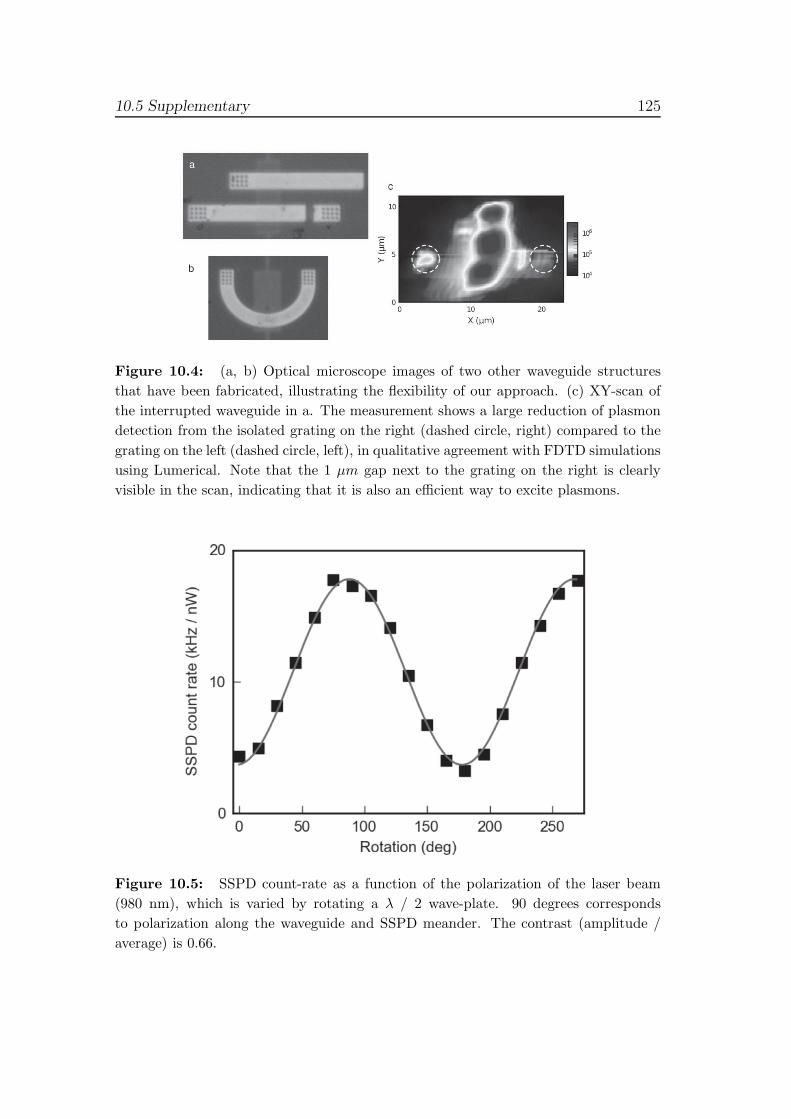
10.5 Supplementary 125
Figure 10.4: (a, b) Optical microscope images of two other waveguide structures
that have been fabricated, illustrating the flexibility of our approach. (c) XY-scan of
the interrupted waveguide in a. The measurement shows a large reduction of plasmon
detection from the isolated grating on the right (dashed circle, right) compared to the
grating on the left (dashed circle, left), in qualitative agreement with FDTD simulations
using Lumerical. Note that the 1 μm gap next to the grating on the right is clearly
visible in the scan, indicating that it is also an efficient way to excite plasmons.
Figure 10.5: SSPD count-rate as a function of the polarization of the laser beam
(980 nm), which is varied by rotating a λ / 2 wave-plate. 90 degrees corresponds
to polarization along the waveguide and SSPD meander. The contrast (amplitude /
average) is 0.66.
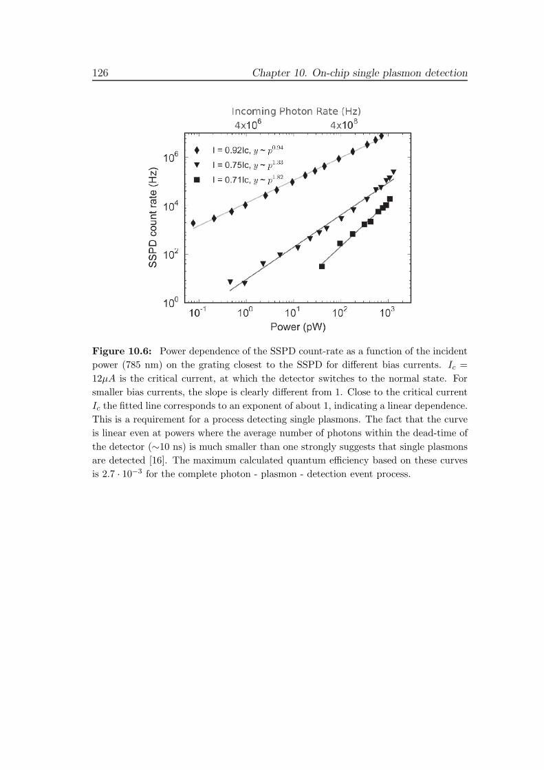
126 Chapter 10. On-chip single plasmon detection
Figure 10.6: Power dependence of the SSPD count-rate as a function of the incident
power (785 nm) on the grating closest to the SSPD for different bias currents. Ic =
12μA is the critical current, at which the detector switches to the normal state. For
smaller bias currents, the slope is clearly different from 1. Close to the critical current
Ic the fitted line corresponds to an exponent of about 1, indicating a linear dependence.
This is a requirement for a process detecting single plasmons. The fact that the curve
is linear even at powers where the average number of photons within the dead-time of
the detector (∼10 ns) is much smaller than one strongly suggests that single plasmons
are detected [16]. The maximum calculated quantum efficiency based on these curves
is 2.7 · 10−3 for the complete photon - plasmon - detection event process.
Chapter 11
Particle detection
11.1 A high efficiency superconducting nanowire
single electron detector
We report the detection of single electrons using a Nb0.7Ti0.3N superconducting
wire deposited on an oxidized silicon substrate. While it is known that this device
is sensitive to single photons, we show that it also detects single electrons with
keV energy emitted from the cathode of a scanning electron microscope with an
efficiency approaching unity. The electron and photon detection efficiency map of
the same device are in good agreement. We also observe detection events outside
the active area of the device, which we attribute to sensitivity to backscattered
electrons.
11.1.1 Introduction
The versatility of superconducting nanowires as single particle detectors relies
on their sensitivity to the minute amount of energy required to locally induce a
resistive transition. From this point of view, the latest achievements involving
the detection of organic molecules [143] and photons in the infrared range [40]
all derive from early experiments with α-particles in the MeV range [144]. In
order to go beyond the optical resolution limit, the scanning electron microscope
(SEM) working at low temperature [145], proved useful. This technique enabled
the visualization of the real size of the hot spot caused by a detection process
[146]. However, the best achieved resolution is limited by thermal diffusion to
about 1 μm and single electron detection has not been demonstrated. In this
This section is based on M. Rosticher, F. R. Ladan, J. P. Maneval, S. N. Dorenbos, T.
Zijlstra, T. M. Klapwijk, V. Zwiller, A. Lupascu, and G. Nogues, Appl. Phys. Lett. 97,
183106 (2010)
127
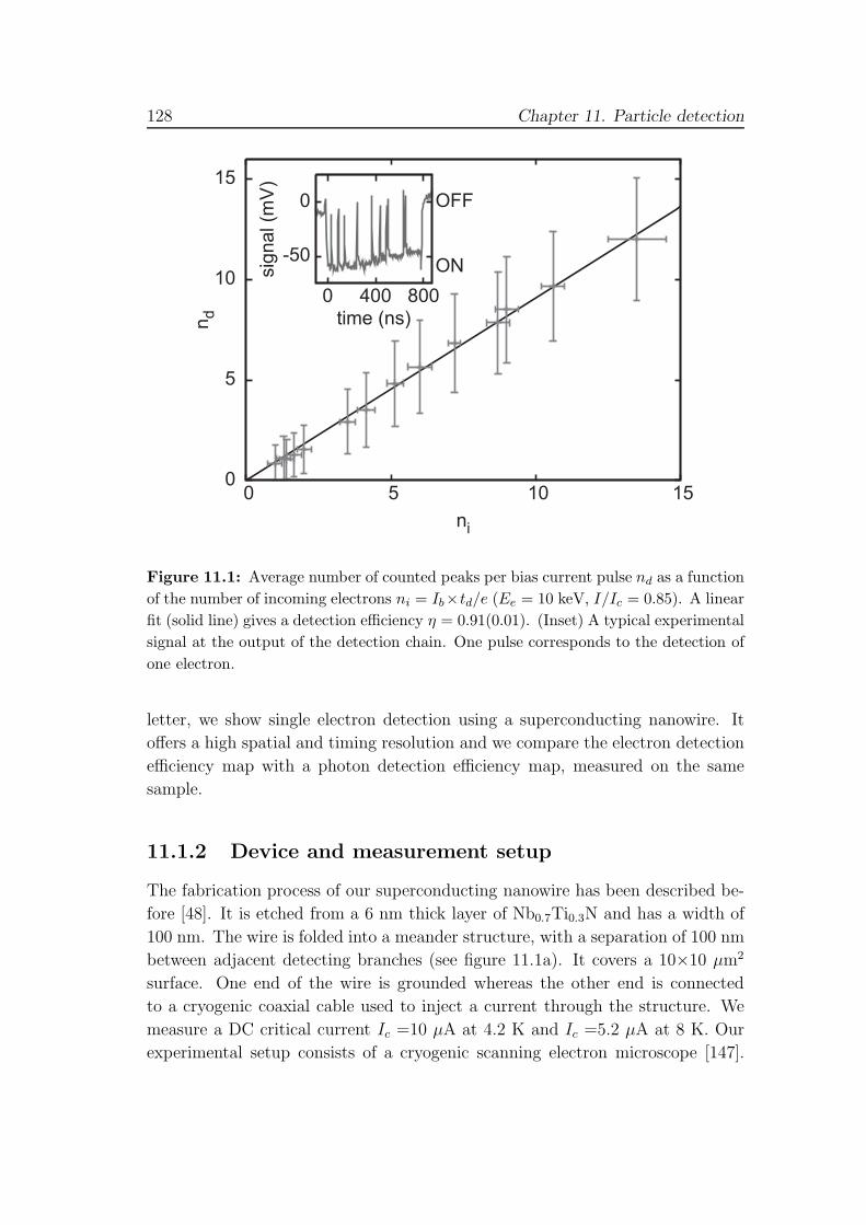
128 Chapter 11. Particle detection
Figure 11.1: Average number of counted peaks per bias current pulse nd as a function
of the number of incoming electrons ni = Ib×td/e (Ee = 10 keV, I/Ic = 0.85). A linear
fit (solid line) gives a detection efficiency η = 0.91(0.01). (Inset) A typical experimental
signal at the output of the detection chain. One pulse corresponds to the detection of
one electron.
letter, we show single electron detection using a superconducting nanowire. It
offers a high spatial and timing resolution and we compare the electron detection
efficiency map with a photon detection efficiency map, measured on the same
sample.
11.1.2 Device and measurement setup
The fabrication process of our superconducting nanowire has been described be-
fore [48]. It is etched from a 6 nm thick layer of Nb0.7Ti0.3N and has a width of
100 nm. The wire is folded into a meander structure, with a separation of 100 nm
between adjacent detecting branches (see figure 11.1a). It covers a 10×10 μm2
surface. One end of the wire is grounded whereas the other end is connected
to a cryogenic coaxial cable used to inject a current through the structure. We
measure a DC critical current Ic =10 μA at 4.2 K and Ic =5.2 μA at 8 K. Our
experimental setup consists of a cryogenic scanning electron microscope [147].
11.1 A high efficiency superconducting nanowire single electron detector 129
The detector is mounted on a cold translation stage at T=8 K under the elec-
tronic beam of an SEM. The current Ib is controlled and can be measured with
a picoammeter (measurement uncertainty 10 %). The energy of the incident
electrons Ee can be varied between 5 and 30 keV.
To block low frequency 1/f noise we use a DC-block, through which we can
only bias the wire with pulses of current amplitude I and duration td = 800 ns
(see inset of Fig. 1). Each pulse is reflected by the circuit. When the current is
on, the detection of an electron triggers a short pulse at the output of the system
(duration of a few ns, see inset of Fig. 1). The change in baseline is caused
by the limited bandwidth (0.1 to 1000 MHz) of the amplification of the output
pulses, but does not affect the bias current of the SSED. We count the average
number of detection pulses and compare it to the average incoming number of
electrons ni = Ib × td/e in order to infer the absolute detection efficiency η. We
can adjust the current Ib down to a few pA, and obtain single electrons separated
by approximately 100 ns. We have measured the number of detection events nd
versus incoming electrons ni (figure 11.1). The linearity of this plot shows that
we detect single electrons. A complete map of η is obtained by scanning the
electron beam over the sample with a full control of the step size and dwell time.
11.1.3 Results
To compare the relative performances of our superconducting nanowire detec-
tor for single electrons and single photons, we present in figure 11.2a a two-
dimensional plot of the photon detection efficiency for our sample, obtained by
scanning a laser spot (1 μm diameter) over the detector with an intensity, low
enough to be in the single photon regime. A detailed description of the setup is
given in Ref. [148]. It shows spatial variations over the active area that could
originate from structural and/or chemical inhomogeneities of the layer. This
reference image can be compared to figure 11.2b which shows the detection effi-
ciency for electrons of energy 30 keV and a bias current I/Ic=0.35. We observe
that the electron detection efficiency is more homogeneous than in the case of
photon detection. There exists however a clear correlation between the two mea-
surements, with the maxima and minima located at the same position for both
images. It demonstrates that the detection process is affected in the same way
for both particles. It shows also that SEM measurements could be used to char-
acterize the performances of superconducting nanowires for photon detection.
With increasing bias current, the electron detection efficiency saturates and be-
comes homogeneous over the whole detector active area as illustrated by fig. 11.2c
(I/Ic =0.85, Ee =20 keV). We note that we have also been able to produce elec-
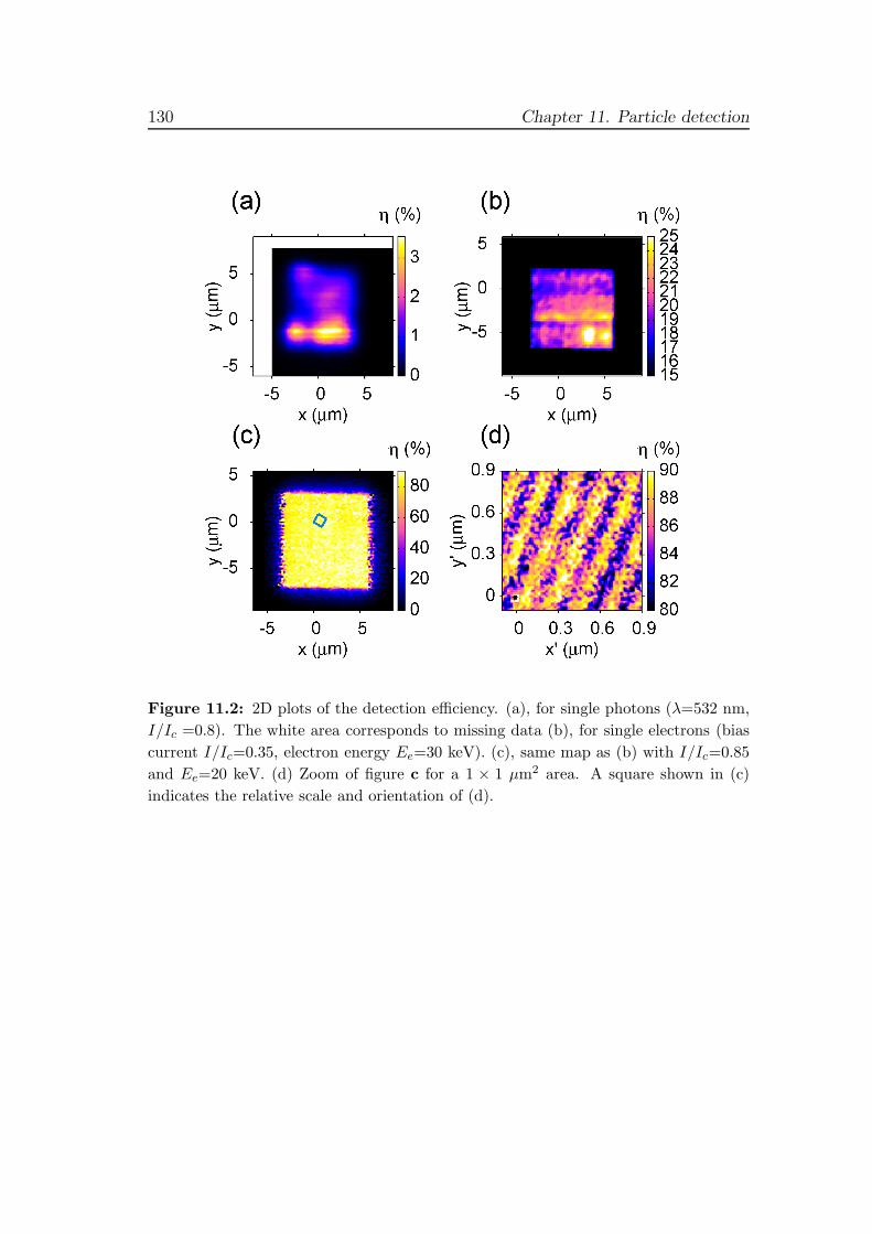
130 Chapter 11. Particle detection
Figure 11.2: 2D plots of the detection efficiency. (a), for single photons (λ=532 nm,
I/Ic =0.8). The white area corresponds to missing data (b), for single electrons (bias
current I/Ic=0.35, electron energy Ee=30 keV). (c), same map as (b) with I/Ic=0.85
and Ee=20 keV. (d) Zoom of figure c for a 1 × 1 μm2 area. A square shown in (c)
indicates the relative scale and orientation of (d).
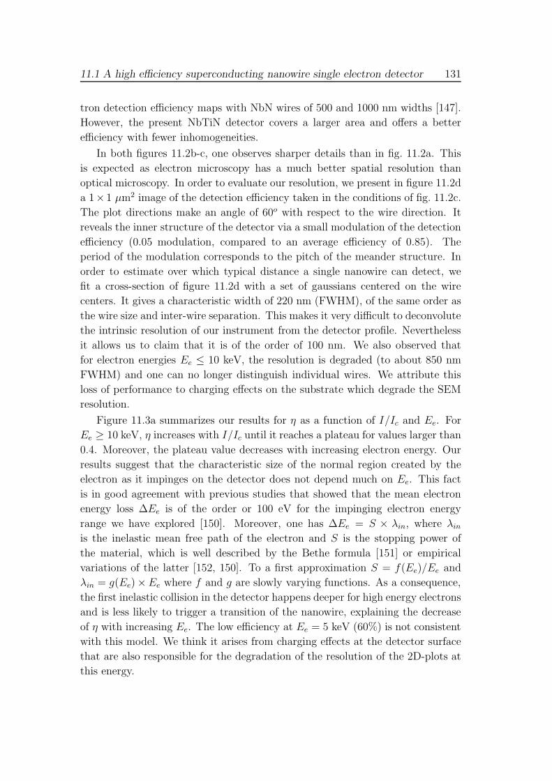
11.1 A high efficiency superconducting nanowire single electron detector 131
tron detection efficiency maps with NbN wires of 500 and 1000 nm widths [147].
However, the present NbTiN detector covers a larger area and offers a better
efficiency with fewer inhomogeneities.
In both figures 11.2b-c, one observes sharper details than in fig. 11.2a. This
is expected as electron microscopy has a much better spatial resolution than
optical microscopy. In order to evaluate our resolution, we present in figure 11.2d
a 1×1 μm2 image of the detection efficiency taken in the conditions of fig. 11.2c.
The plot directions make an angle of 60o with respect to the wire direction. It
reveals the inner structure of the detector via a small modulation of the detection
efficiency (0.05 modulation, compared to an average efficiency of 0.85). The
period of the modulation corresponds to the pitch of the meander structure. In
order to estimate over which typical distance a single nanowire can detect, we
fit a cross-section of figure 11.2d with a set of gaussians centered on the wire
centers. It gives a characteristic width of 220 nm (FWHM), of the same order as
the wire size and inter-wire separation. This makes it very difficult to deconvolute
the intrinsic resolution of our instrument from the detector profile. Nevertheless
it allows us to claim that it is of the order of 100 nm. We also observed that
for electron energies Ee ≤ 10 keV, the resolution is degraded (to about 850 nm
FWHM) and one can no longer distinguish individual wires. We attribute this
loss of performance to charging effects on the substrate which degrade the SEM
resolution.
Figure 11.3a summarizes our results for η as a function of I/Ic and Ee. For
Ee ≥ 10 keV, η increases with I/Ic until it reaches a plateau for values larger than
0.4. Moreover, the plateau value decreases with increasing electron energy. Our
results suggest that the characteristic size of the normal region created by the
electron as it impinges on the detector does not depend much on Ee. This fact
is in good agreement with previous studies that showed that the mean electron
energy loss ΔEe is of the order or 100 eV for the impinging electron energy
range we have explored [150]. Moreover, one has ΔEe = S × λin, where λinis the inelastic mean free path of the electron and S is the stopping power of
the material, which is well described by the Bethe formula [151] or empirical
variations of the latter [152, 150]. To a first approximation S = f(Ee)/Ee and
λin = g(Ee)×Ee where f and g are slowly varying functions. As a consequence,
the first inelastic collision in the detector happens deeper for high energy electrons
and is less likely to trigger a transition of the nanowire, explaining the decrease
of η with increasing Ee. The low efficiency at Ee = 5 keV (60%) is not consistent
with this model. We think it arises from charging effects at the detector surface
that are also responsible for the degradation of the resolution of the 2D-plots at
this energy.
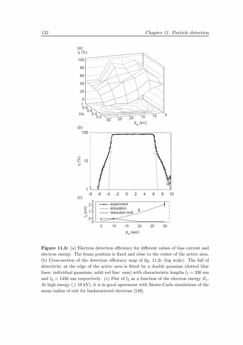
132 Chapter 11. Particle detection
Figure 11.3: (a) Electron detection efficiency for different values of bias current and
electron energy. The beam position is fixed and close to the center of the active area.
(b) Cross-section of the detection efficiency map of fig. 11.2c (log scale). The fall of
detectivity at the edge of the active area is fitted by a double gaussian (dotted blue
lines: individual gaussians, solid red line: sum) with characteristic lengths l1 = 330 nm
and l2 = 1450 nm respectively. (c) Plot of l2 as a function of the electron energy Ee.
At high energy (≥ 10 kV), it is in good agreement with Monte-Carlo simulations of the
mean radius of exit for backscattered electrons [149].
11.1 A high efficiency superconducting nanowire single electron detector 133
Evidence of the detection of backscattered electrons is provided by the cross-
section of the efficiency map of fig. 11.2c, presented in figure 11.3b. We observe
shoulders for the detection efficiency signal at the border of the detector, proving
that it is still possible to detect electrons impinging at distances larger than the
SEM resolution. A double gaussian fit at the edge for different cross-sections, both
horizontal and vertical, gives two average characteristic lengths l1 = 330(40) nm
and l2 = 1760(230) nm, with a ratio in amplitude around 80:20. We attribute
the first length to the intrinsic resolution of our apparatus. It is convoluted
here with the finite step size of the SEM beam for this experiment (200 nm). We
attribute the second length scale to the detection of backscattered electrons. This
distance is consistent with Monte-Carlo simulations of the electron trajectories
that predict a mean distance between the entry and exit points of lMC = 1320 nm.
This distance depends strongly on the energy of the incident electron. We present
in figure 11.3c a comparison of l2 and lMC for different values of Ee. At low energy,
the distance lMC is of the order of or lower than the apparatus resolution degraded
to 500 nm. We only observe a single gaussian. At larger energies, above 10 keV,
the agreement between experiment and simulation is very good.
11.1.4 Conclusions
In conclusion, we have operated a fast and efficient single electron counter us-
ing a superconducting nanowire. We show an efficiency close to unity. Its low
noise, short dead time and high timing accuracy makes this device interesting in
situations where a cryogenic environment is available. Optimizing further these
devices for the specific purpose of electron detection can certainly improve fu-
ture performances. For example, a thin conducting layer on top of the nanowire
can reduce the charging effect and improve the efficiency for low energy elec-
trons (≤ 5 keV). For high energy electrons, increasing the superconducting layer
thickness will improve the performances. Fabricating the devices over a thin
membrane would avoid backscattering. Arrays of such devices, could provide
an imaging system for electrons with a time resolution below 60 ps [47] and a
pixel size below 10 μm. Those figures could significantly improve the technologies
presently used for example in ultrafast electron microscopy [153].

134 Chapter 11. Particle detection
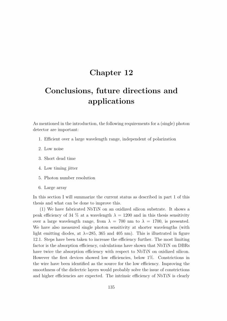
Chapter 12
Conclusions, future directions and
applications
As mentioned in the introduction, the following requirements for a (single) photon
detector are important:
1. Efficient over a large wavelength range, independent of polarization
2. Low noise
3. Short dead time
4. Low timing jitter
5. Photon number resolution
6. Large array
In this section I will summarize the current status as described in part 1 of this
thesis and what can be done to improve this.
(1) We have fabricated NbTiN on an oxidized silicon substrate. It shows a
peak efficiency of 34 % at a wavelength λ = 1200 and in this thesis sensitivity
over a large wavelength range, from λ = 700 nm to λ = 1700, is presented.
We have also measured single photon sensitivity at shorter wavelengths (with
light emitting diodes, at λ=285, 365 and 405 nm). This is illustrated in figure
12.1. Steps have been taken to increase the efficiency further. The most limiting
factor is the absorption efficiency, calculations have shown that NbTiN on DBRs
have twice the absorption efficiency with respect to NbTiN on oxidized silicon.
However the first devices showed low efficiencies, below 1%. Constrictions in
the wire have been identified as the source for the low efficiency. Improving the
smoothness of the dielectric layers would probably solve the issue of constrictions
and higher efficiencies are expected. The intrinsic efficiency of NbTiN is clearly
135
136 Chapter 12. Conclusions
Figure 12.1: UV sensitivity of SSPDs. It is measured using light emitting diodes at
the given wavelength. The dark count rate during this measurement was ∼ 500 cps.
As the illumination was free space a precise efficiency is hard to calculate, but is close
to an expected value of 10%. A linear fit clearly demonstrates single photon efficiency.
dropping for wavelengths larger than 1000 nm. We have used another material
(NbSi) to improve this effect. We expect larger hot spots in a NbSi nanowire
than those in NbTiN, because the superconducting gap energy is smaller, and
thus more Cooper pairs are broken when a photon is absorbed. We report a
relative increase in efficiency for longer wavelengths, optimizing the geometry is
needed to fully make use of this approach. As photons can be used to transfer
information, which is often encoded in the polarization state of light[15], so it is
inconvenient if the detection process is polarization dependent. We have shown
that a spiral geometry removes the polarization dependence of SSPDs. We have
also taken steps to improve the technique of fiber coupling. A fiber coupled device
greatly improves the user friendliness, opening a wide range of applications (see
next section).
(2) SSPDs made of NbTiN on oxidized silicon show a very low intrinsic dark
count rate, especially when it is cooled down to temperatures below 4 K. In the
literature sources of this intrinsic dark count rate have been identified. Further
investigation is needed to use this knowledge to decrease the intrinsic dark count
rate.
(3) We have shown that the dead time of SSPDs is approximately 10 ns. It is
dependent on the kinetic inductance of the wire and the impedance in the circuit.
137
Following [26] we have confirmed by fabricating shorter wires that decreasing the
kinetic inductance shortens the dead time. When the dead time is decreased
further it will at some point be limited by thermal time scales (cooling time
∼100 ps). It is however expected that before this limit is reached by reducing the
electrical dead time (kinetic inductance, impedance of the readout circuit) the
resistive spot after absorption will become stable and the device will latch [24].
Until this issue is resolved dead time of SSPDs will be limited to a few ns.
(4) During this thesis work we took steps to decrease the timing jitter related
to components in our setup. We have taken the timing jitter down to 60 ps.
(5) We have tried to resolve photon number by increasing the input impedance
of the amplifier as suggested in Ref. [85]. We measured the voltage pulse height
as a function of the number of photons absorbed in the device. We did not find
a convincing correlation between the pulse height and photon number. Recent
literature [77] suggests that with this method it is not possible to resolve the
photon number because if two hotspots are formed simultaneously at different
locations along the nanowire, the total energy dissipated in both hotspots will
result in a combined resistance of the two hotspots that is approximately equal
to the resistance of an individual hotspot.
(6) We have shown a preliminary proof of principle to extend a single pixel
detector to a multi pixel device without the need for a complete readout circuit
per pixel. Connecting different pixels in serial and parallel offers two approaches
which could preserve high count rates, provide spatial information and maintain
the same complexity for readout interfaces as is the case for a single or at most
two SSPDs. The experimental results for arrays based on our methods, confirm
the potentials of SSPD arrays for imaging. As the only limit on the length of
transmission lines in series structures is set by uncertainty in the time delay
between pulses, reducing the timing jitter will enable shorter transmission lines,
with the ultimate limit of no transmission line. Another approach is capacitive
readout, which also relaxes the need for large bandwidth amplification.
Implementation in different experiments (part 2 of this thesis) has shown
that SSPDs are indeed useful devices for research laboratories. In table 12.1
a comparison to other single photon detectors is made. It can be seen that
for applications in the (near) infrared, superconducting detectors are the best
option, because the InGaAs APD has a low efficiency, high dark count rate and
a long deadtime. Comparing TES with an SSPD it is noted that although the
TES has a high efficiency, SSPDs are easier in use, and have much better timing
properties. In the visible range of the spectrum the Si APD has a higher efficiency,
however, SSPDs can still be preferred when timing properties are important for
the application.

138 Chapter 12. Conclusions
Detector Operating Operating QE DCR Deadtime Timing
wavelength T jitter
Si APD 400-1100 nm Room 90% 1·103 100 ns 500 ps
InGaAs APD 800-1700 nm Room 10% 1·105 100 ns 500 ps
TES 300 nm- 10 μm 100- 99% 1·105 100 ns - 100 ns
300 mK 10 μs 100 ns
SSPD 300 nm- 10 μm 4 K 30% 1·102 10 ns 60 ps
Table 12.1: Detector comparison.
12.1 Applications 139
12.1 Applications
Quantum cryptography
Cryptography is already used since ancient times to transfer messages in a secure
way from a sender (conventionally called ’Alice’) to a receiver (’Bob’) without
anyone else (’Eve’) to read the message. One of the first examples is the use of
transposition ciphers, which rearrange the order of letters in a message. Of course
one needs a key to de-rearrange the order or decipher the message. It is shown
that for total security, a key as long as the text is needed for encryption. There-
fore, a common used method to generate a key is based on the factorization of
two numbers, leading to a public key and a private key (i.e. the RSA algorithm).
To break the key, computer power which grows exponentially wit the length of
the key, is needed, so it is relatively easy to get the required security. How-
ever, things changed with technology proposals based on quantum mechanics. In
principle, a quantum computer can use Shor‘s algorithm to factorize numbers,
and the amount of quantum computer power required only grows linearly with
the length of the key. In addition, the idea of quantum cryptography is intro-
duced, a method which allows Alice and Bob to determine whether the channel is
eavesdropped. One needs a channel through which quantum information can be
sent. Quantum information for transport over long distances is most conveniently
coded in single photons, so single photon sources and single photon detectors are
required. In theory this method is 100% reliable, but sets requirements on the
technology which can (and for some will) not be reached. For example, a channel
without loss will not exist: this requires error correction, giving Eve the oppor-
tunity to stay hidden. In depth reviews of quantum cryptography can be found
in [15, 154, 155]. Here I will describe what requirements can be set for single
photon detectors. The non perfectness of single photon detectors lie in limited
efficiency, dark counts and dead time.
These limitations impose bounds on the secret key rate. Limited efficiency
causes losses and the rate cannot scale with the distance better than the trans-
mittivity of the line and on the achievable distance where losses are so large that
the signal is lost in spurious events, the ’dark counts’. The dead time also limits
the rate. A bound on the dark count rate can be derived as follows: the detection
rates must be written as
Rn = Rn,p +Rn,d (12.1)
where Rn,p is the contribution of detections and Rn,d is the dark count rate.
There are two differently contributing error mechanisms. The errors on the line
are introduced only on the photon contribution, while the dark counts always
140 Chapter 12. Conclusions
give an error rate of approximately 1/2. If the error rate per bit exceeds 1/4,
there is no way to create a secure key. With such an allowed error rate simple
intercept-measure- resend attack causes Bob and Eve to share (approximately)
half of Alices bits and to know nothing about the other half; hence, Bob does not
possess information that is unavailable to Eve, and no secret key can be distilled.
From 12.1 it follows that
Rn,p > Rn,pd (12.2)
and with non perfect transmission efficiency this constraint becomes: Ncr >
2Ndc/η with Ncr the measured count rate, Ndc the dark count rate per detector
and η the efficiency.
Furthermore, double clicks in detection devices, resulting from dark counts,
cannot be simply ignored, as this would open up a security loophole. A simple at-
tack exploiting this loophole goes as follows: Eve intercepts the photon, measures
the polarization state and resends a pulse containing a large number of photons
in the detected polarization. If Bob measures in the same basis as Eve, he will
receive a single detector click, about which Eve has full information. If Bob
measures in a different basis, he will almost always receive double clicks, which
he discards. Therefore Eve has perfect information about all signals retained by
Eve, allowing her to break the QKD scheme.
In summary, the higher the efficiency and the lower the dark count rate, the
better security over larger distance can be obtained. In 2007 a quantum key
distribution experiment with a 42 dB channel loss using SSPDs was performed,
succeeding in a record distance of 200 km.
Loophole free Bell experiment
The Bell inequality experiment[156] is at the heart of quantum mechanics. This
experiment was performed for the first time with photons emitted from a laser
by Aspect et al. [157]. However, so far all reported Bell experiments suffer from
so-called ”loopholes”, imperfectnesses in the experiments, which could be used
to explain the results with a local realistic theory.
The two main loopholes are: locality loophole and detection loophole. The
locality loophole occurs when the distance between the local measurements is
too small to prevent communication between one observers measurement choice
and the result of the other observers measurement. In other words the detectors
should be separated in space more than light can travel within the measurement
time. A promising candidate for closing the locality loophole are optical photons,
where good polarization analyzers exist and spacelike separation can be achieved.
12.1 Applications 141
In fact, the locality loophole has been closed by Weihs et al. [158]. However,
thus far, all Bell experiments with photons suffer from the detection loophole
[159]. The imperfect efficiency of photodetectors makes the results of all these
experiments compatible with local realistic models. It turns out that the efficiency
needed for ruling out a local realistic explanation is dependent on the dark count
rate: for ∼ 1% dark counts, the efficiency needed is 83 % and for a very low dark
count rate 69 %. [160] Massive particles (i.e. ions) are much easier to detect,
efficiencies can be close to 100%, so in this system the detection loophole has
been closed [161], however they are extremely difficult to separate, so in this
experiment the requirements for the locality loophole are not met. Given the low
dark count rate and short dead time of SSPDs, they are a good candidate to use
in a loophole free Bell experiment, provided that an (overall) efficiency will be
reached of 69 %.
Quantum computation
In 2001 a paper published by Knill, Laflamme, Milburn showed that quantum
computation was possible with single photons as quantum bits and linear opti-
cal elements, such as polarizers, waveplates [6]. Quantum computing with linear
quantum optics, has the advantage that the proposed quantum bits (the photon)
are potentially free from decoherence: The quantum information stored in a pho-
ton tends to stay there. This same fact introduces the difficulty that photons do
not naturally interact with each other, and in order to apply two-qubit quantum
gates such interactions are essential. Cross-Kerr nonlinearities can be used to
induce a single-photon controlled-NOT operation. However, naturally occurring
nonlinearities are many orders of magnitude smaller than what is needed for the
purpose of quantum computation.
An alternative way to induce an effective interaction between photons is to
make projective measurements with photo-detectors. Knill, Laflamme, and Mil-
burn constructed a protocol in which probabilistic two-photon gates are tele-
ported into a quantum circuit with high probability. Subsequent error correction
in the quantum circuit is used to bring the error rate down to fault-tolerant levels.
Initially, the KLM protocol was designed as a proof that linear optics and projec-
tive measurements allow for scalable quantum computing in principle. However,
new experiments in quantum optics, demonstrating the operation of high-fidelity
probabilistic two-photon gates, followed. As pointed out in [105] two photon gates
based on projective measurements are probabilistic, meaning that a percentage
of the operations fail, which could lead to an exponential need for resources.
However the KLM gate provided a success rate which could be made higher than
142 Chapter 12. Conclusions
50%, so the resources time can be scaled linearly with the number of gates. The
only element which was needed, and to date is unavailable, is a high efficiency
photon number resolving detector. Photon number resolving is needed because
the exact number of photons in a mode has to be known. This also means that
the efficiency has to be high because otherwise the number of photons detected
is less than the actual number. In the original paper efficiencies close to 100 %
are needed for the implementation, with error correction this requirement has
become less severe.
Medical imaging
Medical imaging refers to observation of (parts of) the human body. Nowadays
techniques are Rontgen photographs, CT scans and magnetic resonance imaging
(MRI). These techniques all have their disadavantages and imaging based on
(visible) light would be more convenient. Although the human body is absorptive
and scattering, it is slightly transparent. For example fast bursts of optical energy
(laser pulses) are either randomly scattered (losing their coherence) or absorbed
as they travel through a media, however, across short distances, a few photons
keep their coherence and pass through in straight lines without being scattered.
These coherent photons are commonly referred to as ballistic photons. As SSPDs
are sensitive to low light levels, they are a potential candidate for this application.
Imaging techniques cannot rely on a single pixel detector, although the object
can be scanned by scanning the laser, faster operation and a higher resolution
is achieved with a detector array. In this thesis steps have been taken towards
an array of superconducting single photon detectors. This has to be developed
further to fabricate a real device.

12.1 Applications 143

144 Chapter 12. Conclusions

Bibliography
[1] M. Planck Annalen der Physik, vol. 4, p. 553, 1901.
[2] A. Einstein Annalen der Physik, vol. 17, p. 132, 1905.
[3] H. J. Carmichael and D. F. Walls Journal of Physics B: Atomic and Molec-
ular Physics, vol. 9, no. 8, p. 1199, 1976.
[4] H. J. Kimble, M. Dagenais, and L. Mandel Physical Review Letters, vol. 39,
no. 11, p. 691, 1977.
[5] R. H. Brown and R. Q. Twiss Nature, vol. 177, no. 4497, pp. 27–29, 1956.
[6] E. Knill, R. Laflamme, and G. J. Milburn Nature, vol. 409, no. 6816, pp. 46–
52, 2001.
[7] C. Bennett and G. Brassard Proc. IEEE international conference on Com-
puters, Systems and Signal Processing, p. 175, 1984.
[8] J. S. Massa, G. S. Buller, A. C. Walker, S. Cova, M. Umasuthan, and A. M.
Wallace Appl. Opt., vol. 37, no. 31, pp. 7298–7304, 1998.
[9] P. Schwille Cell Biochemistry and Biophysics, vol. 34, no. 3, pp. 383–408,
2001.
[10] J. Hecht, City of light, the story of fiber optics. New York: Oxford Univer-
sity Press, 1999.
[11] Z. Yuan, B. E. Kardynal, R. M. Stevenson, A. J. Shields, C. J. Lobo,
K. Cooper, N. S. Beattie, D. A. Ritchie, and M. Pepper Science, vol. 295,
p. 102, 2002.
[12] M. H. M. van Weert, N. Akopian, U. Perinetti, M. P. van Kouwen, R. E.
Algra, M. A. Verheijen, E. P. A. M. Bakkers, L. P. Kouwenhoven, and
V. Zwiller Nano Letters, vol. 9, no. 5, pp. 1989–1993, 2009.
145
146 BIBLIOGRAPHY
[13] F. Jelezko and J. Wrachtrup physica status solidi (a), vol. 203, no. 13,
pp. 3207–3225, 2006.
[14] G. Temporo, S. Tanzilli, H. Zbinden, N. Gisin, T. Aellen, M. Giovannini,
and J. Faist Opt. Lett., vol. 31, no. 8, pp. 1094–1096, 2006.
[15] N. Gisin, G. Ribordy, eacute, goire, W. Tittel, and H. Zbinden Reviews of
Modern Physics, vol. 74, no. 1, p. 145, 2002.
[16] G. Gol’tsman, O. Okunev, G. Chulkova, A. Lipatov, A. Semenov,
K. Smirnov, B. Voronov, A. Dzardanov, C. Williams, and R. Sobolewski
Applied Physics Letters, vol. 79, no. 6, pp. 705–707, 2001.
[17] A. Verevkin, J. Zhang, R. Sobolewski, A. Lipatov, O. Okunev, G. Chulkova,
A. Korneev, K. Smirnov, G. N. Gol’tsman, and A. Semenov Applied Physics
Letters, vol. 80, no. 25, pp. 4687–4689, 2002.
[18] G. N. Gol’tsman, K. Smirnov, P. Kouminov, B. Voronov, N. Kaurova,
V. Drakinsky, J. Zhang, A. Verevkin, and R. Sobolewski Applied Super-
conductivity, IEEE Transactions on, vol. 13, no. 2, pp. 192–195, 2003.
[19] M. Tinkham, “Introduction to superconductivity,” 1996.
[20] A. J. Kerman, E. A. Dauler, J. K. W. Yang, K. M. Rosfjord, V. Anant,
K. K. Berggren, G. N. Gol’tsman, and B. M. Voronov Applied Physics
Letters, vol. 90, no. 10, p. 101110, 2007.
[21] R. H. Hadfield, P. A. Dalgarno, J. A. O’Connor, E. Ramsay, R. J. Warbur-
ton, E. J. Gansen, B. Baek, M. J. Stevens, R. P. Mirin, and S. W. Nam
Applied Physics Letters, vol. 91, no. 24, pp. 241108–3, 2007.
[22] F. Marsili, F. Najafi, E. Dauler, F. Bellei, X. Hu, M. Csete, R. Molnar, and
K. K. Berggren arXiv:1012.4149v1, 2011.
[23] A. Korneev, P. Kouminov, V. Matvienko, G. Chulkova, K. Smirnov,
B. Voronov, G. N. Gol’tsman, M. Currie, W. Lo, K. Wilsher, J. Zhang,
W. Slysz, A. Pearlman, A. Verevkin, and R. Sobolewski Applied Physics
Letters, vol. 84, no. 26, pp. 5338–5340, 2004.
[24] J. K. W. Yang, A. J. Kerman, E. A. Dauler, V. Anant, K. M. Rosfjord, and
K. K. Berggren Applied Superconductivity, IEEE Transactions on, vol. 17,
no. 2, pp. 581–585, 2007.
BIBLIOGRAPHY 147
[25] A. J. Kerman, J. K. W. Yang, R. J. Molnar, E. A. Dauler, and K. K.
Berggren Physical Review B, vol. 79, no. Copyright (C) 2010 The American
Physical Society, p. 100509, 2009.
[26] A. J. Kerman, E. A. Dauler, W. Keicher, J. K. W. Yang, K. K. Berggren,
G. Gol’tsman, and B. Voronov Applied Physics Letters, vol. 88, no. 11,
p. 111116, 2006.
[27] F. Marsili, A. Gaggero, L. H. Li, A. Surrente, R. Leoni, F. Levy, and
A. Fiore Superconductor Science and Technology, no. 9, p. 095013, 2009.
[28] H. Shibata, H. Takesue, T. Honjo, T. Akazaki, and Y. Tokura Applied
Physics Letters, vol. 97, no. 21, pp. 212504–212504–3, 2010.
[29] K. M. Rosfjord, J. K. W. Yang, E. A. Dauler, A. J. Kerman, V. Anant,
B. M. Voronov, G. N. Gol’tsman, and K. K. Berggren Opt. Express, vol. 14,
no. 2, pp. 527–534, 2006.
[30] L. N. Bulaevskii, M. J. Graf, C. D. Batista, and V. G. Kogan Physical
Review B, vol. 83, no. 14, p. 144526, 2011.
[31] J. Kitaygorsky, J. Zhang, A. Verevkin, A. Sergeev, A. Korneev,
V. Matvienko, P. Kouminov, K. Smirnov, B. Voronov, G. Gol’tsman, and
R. Sobolewski Applied Superconductivity, IEEE Transactions on, vol. 15,
no. 2, pp. 545–548, 2005.
[32] H. Bartolf, A. Engel, A. Schilling, K. Il’in, M. Siegel, uuml, H. W. bers,
and A. Semenov Physical Review B, vol. 81, no. 2, p. 024502, 2010.
[33] T. Yamashita, S. Miki, K. Makise, W. Qiu, H. Terai, M. Fujiwara,
M. Sasaki, and Z. Wang arxiv, vol. 1103.2844, 2011.
[34] M. J. Word, I. Adesida, and P. R. Berger Journal of Vacuum Science and
Technology B: Microelectronics and Nanometer Structures, vol. 21, no. 6,
pp. L12–L15, 2003.
[35] W. Henschel, Y. M. Georgiev, and H. Kurz Journal of Vacuum Science and
Technology B: Microelectronics and Nanometer Structures, vol. 21, no. 5,
pp. 2018–2025, 2003.
[36] E. Bermudez Urena, Master Thesis. PhD thesis, 2010.
148 BIBLIOGRAPHY
[37] J. R. Gao, M. Hajenius, F. D. Tichelaar, T. M. Klapwijk, B. Voronov, E. Gr-
ishin, G. Gol’tsman, C. A. Zorman, and M. Mehregany Applied Physics
Letters, vol. 91, no. 6, pp. 062504–3, 2007.
[38] W. Slysz, M. Wegrzecki, J. Bar, P. Grabiec, M. Gorska, V. Zwiller, C. Latta,
P. Bohi, I. Milostnaya, O. Minaeva, A. Antipov, O. Okunev, A. Korneev,
K. Smirnov, B. Voronov, N. Kaurova, G. Gol’tsman, A. Pearlman, A. Cross,
I. Komissarov, A. Verevkin, and R. Sobolewski Applied Physics Letters,
vol. 88, no. 26, p. 261113, 2006.
[39] J. Kitaygorsky, R. Schouten, S. N. Dorenbos, E. Reiger, V. Zwiller, and
R. Sobolewski, “Measurements of amplitude distibutions of dark counts and
photon counts in nbn superconducting single-photon detectors integrated
with hemt read-out,” 2008.
[40] G. Gol’tsman, O. Minaeva, A. Korneev, M. Tarkhov, I. Rubtsova, A. Di-
vochiy, I. Milostnaya, G. Chulkova, N. Kaurova, B. Voronov, D. Pan, J. Ki-
taygorsky, A. Cross, A. Pearlman, I. Komissarov, W. Slysz, M. Wegrzecki,
P. Grabiec, and R. Sobolewski Applied Superconductivity, IEEE Transac-
tions on, vol. 17, no. 2, pp. 246–251, 2007.
[41] A. Korneev, V. Matvienko, O. Minaeva, I. Milostnaya, I. Rubtsova,
G. Chulkova, K. Smirnov, V. Voronov, G. Gol’tsman, W. Slysz, A. Pearl-
man, A. Verevkin, and R. Sobolewski Applied Superconductivity, IEEE
Transactions on, vol. 15, no. 2, pp. 571–574, 2005.
[42] G. Rieke, Detection of Light, from UV to Submillimeter. Cambridge: Cam-
bridge University Press, 2nd ed., 2002.
[43] R. Barends, H. L. Hortensius, T. Zijlstra, J. J. A. Baselmans, S. J. C.
Yates, J. R. Gao, and T. M. Klapwijk Applied Physics Letters, vol. 92,
no. 22, pp. 223502–3, 2008.
[44] F. E. W. Schmidt, M. E. Fry, E. M. C. Hillman, J. C. Hebden, and D. T.
Delpy Review of Scientific Instruments, vol. 71, no. 1, pp. 256–265, 2000.
[45] B. Sacepe, C. Chapelier, T. I. Baturina, V. M. Vinokur, M. R. Baklanov,
and M. Sanquer Physical Review Letters, vol. 101, no. 15, p. 157006, 2008.
[46] R. H. Hadfield Nature Photonics, vol. 3, no. 12, pp. 696–705, 2009.
[47] M. G. Tanner, C. M. Natarajan, V. K. Pottapenjara, J. A. O’Connor,
R. J. Warburton, R. H. Hadfield, B. Baek, S. Nam, S. N. Dorenbos,
BIBLIOGRAPHY 149
E. Bermudez Urena, T. Zijlstra, T. M. Klapwijk, and V. Zwiller Applied
Physics Letters, vol. 96, no. 22, pp. 221109–3, 2010.
[48] S. N. Dorenbos, E. M. Reiger, U. Perinetti, V. Zwiller, T. Zijlstra, and T. M.
Klapwijk Applied Physics Letters, vol. 93, no. 13, pp. 131101–3, 2008.
[49] H. Takesue, S. W. Nam, Q. Zhang, R. H. Hadfield, T. Honjo, K. Tamaki,
and Y. Yamamoto Nat Photon, vol. 1, no. 6, pp. 343–348, 2007.
[50] S. N. Dorenbos, H. Sasakura, M. P. van Kouwen, N. Akopian, S. Adachi,
N. Namekata, M. Jo, J. Motohisa, Y. Kobayashi, K. Tomioka, T. Fukui,
S. Inoue, H. Kumano, C. M. Natarajan, R. H. Hadfield, T. Zijlstra, T. M.
Klapwijk, V. Zwiller, and I. Suemune Applied Physics Letters, vol. 97,
no. 17, pp. 171106–3, 2010.
[51] R. H. Hadfield, M. J. Stevens, S. S. Gruber, A. J. Miller, R. E. Schwall,
R. P. Mirin, and S. W. Nam Opt. Express, vol. 13, no. 26, pp. 10846–10853,
2005.
[52] M. Rosticher, F. R. Ladan, J. P. Maneval, S. N. Dorenbos, T. Zijlstra, T. M.
Klapwijk, V. Zwiller, A. Lupacu, and G. Nogues Applied Physics Letters,
vol. 97, no. 18, 2010.
[53] R. W. Heeres, S. N. Dorenbos, B. Koene, G. S. Solomon, L. P. Kouwen-
hoven, and V. Zwiller Nano Letters, vol. 10, no. 2, pp. 661–664, 2010.
[54] X. Hu, T. Zhong, J. E. White, E. A. Dauler, F. Najafi, C. H. Herder,
F. N. C. Wong, and K. K. Berggren Opt. Lett., vol. 34, no. 23, pp. 3607–
3609, 2009.
[55] S. Miki, M. Takeda, M. Fujiwara, M. Sasaki, and Z. Wang Opt. Express,
vol. 17, no. 26, pp. 23557–23564, 2009.
[56] A. J. Miller, A. E. Lita, B. Calkins, I. Vayshenker, S. M. Gruber, and S. W.
Nam Opt. Express, vol. 19, no. 10, pp. 9102–9110, 2011.
[57] C. Chienliu Journal of Micromechanics and Microengineering, vol. 15, no. 3,
p. 580, 2005.
[58] D. Klyshko Sov. J. Quantum Electron., vol. 7, p. 591, 1977.
[59] J. G. Rarity, K. D. Ridley, and P. R. Tapster Appl. Opt., vol. 26, no. 21,
pp. 4616–4619, 1987.
150 BIBLIOGRAPHY
[60] P. G. Kwiat, A. M. Steinberg, R. Y. Chiao, P. H. Eberhard, and M. D.
Petroff Physical Review A, vol. 48, no. 2, p. R867, 1993.
[61] E. Reiger, S. Dorenbos, V. Zwiller, A. Korneev, G. Chulkova, I. Milostnaya,
O. Minaeva, G. Gol’tsman, J. Kitaygorsky, P. Dong, W. Sysz, A. Jukna,
and R. Sobolewski Selected Topics in Quantum Electronics, IEEE Journal
of, vol. 13, no. 4, pp. 934–943, 2007.
[62] M. B. Ward, O. Z. Karimov, D. C. Unitt, Z. L. Yuan, P. See, D. G.
Gevaux, A. J. Shields, P. Atkinson, and D. A. Ritchie Applied Physics
Letters, vol. 86, no. 20, pp. 201111–3, 2005.
[63] M. T. Jarvi, M. J. Niedre, M. S. Patterson, and B. C. Wilson Photochem-
istry and Photobiology, vol. 82, no. 5, pp. 1198–1210, 2006.
[64] N. N. Iosad, B. D. Jackson, S. N. Polyakov, P. N. Dmitriev, and T. M. Klap-
wijk, “Reactive magnetron sputter-deposition of nbn and (nb, ti)n films
related to sputtering source characterization and optimization,” vol. 19,
pp. 1840–1845, 2001.
[65] V. Anant, A. J. Kerman, E. A. Dauler, J. K. W. Yang, K. M. Rosfjord,
and K. K. Berggren Opt. Express, vol. 16, no. 14, pp. 10750–10761, 2008.
[66] M. J. Stevens, R. H. Hadfield, R. E. Schwall, J. A. Gupta, N. Sae Woo,
and R. P. Mirin, “Fast lifetime measurements of infrared emitters with
low-jitter superconducting single photon detectors,” in Lasers and Electro-
Optics, 2006 and 2006 Quantum Electronics and Laser Science Conference.
CLEO/QELS 2006. Conference on, pp. 1–2, 2006.
[67] I. Milostnaya, A. Korneev, I. Rubtsova, V. Seleznev, O. Minaeva,
G. Chulkova, O. Okunev, B. Voronov, K. Smirnov, G. Gol’tsman, W. Slysz,
M. Wegrzecki, M. Guziewicz, J. Bar, M. Gorska, A. Pearlman, J. Kitay-
gorsky, A. Cross, and R. Sobolewski Journal of Physics: Conference Series,
vol. 43, no. 1, p. 1334, 2006.
[68] A. E. Lita, A. J. Miller, and S. W. Nam Opt. Express, vol. 16, no. 5,
pp. 3032–3040, 2008.
[69] M. S. Unlu, M. K. Emsley, O. I. Dosunmu, P. Muller, and Y. Leblebici Jour-
nal of Vacuum Science and Technology A: Vacuum, Surfaces, and Films,
vol. 22, no. 3, pp. 781–787, 2004.
BIBLIOGRAPHY 151
[70] B. Baek, J. A. Stern, and S. W. Nam Applied Physics Letters, vol. 95,
no. 19, pp. 191110–3, 2009.
[71] K. Hejduk, K. Pierscinski, W. Rzodkiewicz, J. Muszalski, and J. Kaniewski
Optica Applicata, vol. 35, no. 3, p. 437, 2005.
[72] M. Halder, A. Beveratos, N. Gisin, V. Scarani, C. Simon, and H. Zbinden
Nat Phys, vol. 3, no. 10, pp. 692–695, 2007.
[73] P. Yeh Optics Communications, vol. 26, no. 3, pp. 289–292, 1978.
[74] F. Driessen, E., R. Braakman, F., M. Reiger, E., N. Dorenbos, S.,
V. Zwiller, and J. de Dood, M. Eur. Phys. J. Appl. Phys., vol. 47, no. 1,
p. 10701, 2009.
[75] R. E. Warburton, A. McCarthy, A. M. Wallace, S. Hernandez-Marin, R. H.
Hadfield, S. W. Nam, and G. S. Buller Opt. Lett., vol. 32, no. 15, pp. 2266–
2268, 2007.
[76] T. Matsunaga, H. Maezawa, and T. Noguchi Applied Superconductivity,
IEEE Transactions on, vol. 13, no. 2, pp. 3284–3287, 2003.
[77] A. J. Annunziata, O. Quaranta, D. F. Santavicca, A. Casaburi, L. Frunzio,
M. Ejrnaes, M. J. Rooks, R. Cristiano, S. Pagano, A. Frydman, and D. E.
Prober Journal of Applied Physics, vol. 108, no. 8, pp. 084507–7, 2010.
[78] A. Divochiy, F. Marsili, D. Bitauld, A. Gaggero, R. Leoni, F. Mattioli,
A. Korneev, V. Seleznev, N. Kaurova, O. Minaeva, G. Gol’tsman, K. G.
Lagoudakis, M. Benkhaoul, F. Levy, and A. Fiore Nature Photonics, vol. 2,
no. 5, pp. 302–306, 2008.
[79] E. A. Dauler, B. S. Robinson, A. J. Kerman, J. K. W. Yang, E. K. M.
Rosfjord, V. Anant, B. Voronov, G. Gol’tsman, and K. K. Berggren Applied
Superconductivity, IEEE Transactions on, vol. 17, no. 2, pp. 279–284, 2007.
[80] M. Tarkhov, J. Claudon, J. P. Poizat, A. Korneev, A. Divochiy, O. Minaeva,
V. Seleznev, N. Kaurova, B. Voronov, A. V. Semenov, and G. Gol’tsman
Applied Physics Letters, vol. 92, no. 24, p. 241112, 2008.
[81] S. Deiker, J. Chervenak, G. C. Hilton, K. D. Irwin, J. M. Martinis, S. Nam,
and D. A. Wollman Applied Superconductivity, IEEE Transactions on,
vol. 11, no. 1, pp. 469–472, 2001.
152 BIBLIOGRAPHY
[82] X. Hu, E. A. Dauler, R. J. Molnar, and K. K. Berggren Optics Express,
vol. 19, no. 1, pp. 17–31, 2011.
[83] D. J. Hall, J. C. Hebden, and D. T. Delpy Appl. Opt., vol. 36, no. 28,
pp. 7270–7276, 1997.
[84] G. S. Buller and R. J. CollinsMeasurement Science and Technology, vol. 21,
no. 1, p. 012002, 2010.
[85] M. Bell, A. Antipov, B. Karasik, A. Sergeev, V. Mitin, and A. Verevkin
Applied Superconductivity, IEEE Transactions on, vol. 17, no. 2, pp. 289–
292, 2007.
[86] J. Kitaygorsky, I. Komissarov, A. Jukna, D. Pan, O. Minaeva, N. Kau-
rova, A. Divochiy, A. Korneev, M. Tarkhov, B. Voronov, I. Milostnaya,
G. Gol’tsman, and R. R. Sobolewski Applied Superconductivity, IEEE
Transactions on, vol. 17, no. 2, pp. 275–278, 2007.
[87] N. Akopian, N. H. Lindner, E. Poem, Y. Berlatzky, J. Avron, D. Gershoni,
B. D. Gerardot, and P. M. Petroff Physical Review Letters, vol. 96, no. 13,
p. 130501, 2006.
[88] T. Miyazawa, J. Tatebayashi, S. Hirose, T. Nakaoka, S. Ishida, S. Iwamoto,
K. Takemoto, T. Usuki, N. Yokoyama, M. Takatsu, and Y. Arakawa
Japanese Journal of Applied Physics, vol. 45, no. Copyright (C) 2006 The
Japan Society of Applied Physics, p. 3621, 2006.
[89] V. Zwiller, H. Blom, P. Jonsson, N. Panev, S. Jeppesen, T. Tsegaye, E. Goo-
bar, M.-E. Pistol, L. Samuelson, and G. Bjork Applied Physics Letters,
vol. 78, no. 17, pp. 2476–2478, 2001.
[90] S. Kimura, H. Kumano, M. Endo, I. Suemune, T. Yokoi, H. Sasakura,
S. Adachi, S. Muto, H. Z. Song, S. Hirose, and T. Usuki Japanese Journal
of Applied Physics, vol. 44, no. Copyright (C) 2005 The Japan Society of
Applied Physics, p. L793, 2005.
[91] E. Moreau, I. Robert, L. Manin, V. Thierry-Mieg, J. M. Grard, and
I. Abram Physical Review Letters, vol. 87, no. 18, p. 183601, 2001.
[92] L. J. Lauhon, M. S. Gudiksen, D. Wang, and C. M. Lieber Nature, vol. 420,
no. 6911, pp. 57–61, 2002.
[93] X. Duan, Y. Huang, Y. Cui, J. Wang, and C. M. Lieber Nature, vol. 409,
no. 6816, pp. 66–69, 2001.
BIBLIOGRAPHY 153
[94] M. P. v. Kouwen, M. E. Reimer, A. W. Hidma, M. H. M. van Weert, R. E.
Algra, E. P. A. M. Bakkers, L. P. Kouwenhoven, and V. Zwiller Nano
Letters, vol. 10, no. 5, pp. 1817–1822, 2010.
[95] J. Claudon, J. Bleuse, N. S. Malik, M. Bazin, P. Jaffrennou, N. Gregersen,
C. Sauvan, P. Lalanne, and J.-M. Gerard Nat Photon, vol. 4, no. 3, pp. 174–
177, 2010.
[96] R. Singh and G. Bester Physical Review Letters, vol. 103, no. 6, p. 063601,
2009.
[97] A. Tribu, G. Sallen, T. Aichele, R. Andre, J.-P. Poizat, C. Bougerol,
S. Tatarenko, and K. Kheng Nano Letters, vol. 8, no. 12, pp. 4326–4329,
2008.
[98] M. T. Borgstrm, V. Zwiller, E. Mller, and A. Imamoglu Nano Letters, vol. 5,
no. 7, pp. 1439–1443, 2005.
[99] P. Mohan, J. Motohisa, and T. Fukui Nanotechnology, vol. 16, no. 12,
p. 2903, 2005.
[100] M. Bayer, G. Ortner, O. Stern, A. Kuther, A. A. Gorbunov, A. Forchel,
P. Hawrylak, S. Fafard, K. Hinzer, T. L. Reinecke, S. N. Walck, J. P.
Reithmaier, F. Klopf, and F. Schfer Physical Review B, vol. 65, no. 19,
p. 195315, 2002.
[101] I. A. Akimov, K. V. Kavokin, A. Hundt, and F. Henneberger Physical
Review B, vol. 71, no. 7, p. 075326, 2005.
[102] C. Zinoni, B. Alloing, C. Monat, V. Zwiller, L. H. Li, A. Fiore, L. Lunghi,
A. Gerardino, H. de Riedmatten, H. Zbinden, and N. Gisin Applied Physics
Letters, vol. 88, no. 13, pp. 131102–3, 2006.
[103] C. Becher, A. Kiraz, P. Michler, A. Imamolu, W. V. Schoenfeld, P. M.
Petroff, L. Zhang, and E. Hu Physical Review B, vol. 63, no. 12, p. 121312,
2001.
[104] E. D. Minot, F. Kelkensberg, M. van Kouwen, J. A. van Dam, L. P. Kouwen-
hoven, V. Zwiller, M. T. Borgstrm, O. Wunnicke, M. A. Verheijen, and E. P.
A. M. Bakkers Nano Letters, vol. 7, no. 2, pp. 367–371, 2007.
[105] P. Kok, W. J. Munro, K. Nemoto, T. C. Ralph, J. P. Dowling, and G. J.
Milburn Reviews of Modern Physics, vol. 79, no. 1, p. 135, 2007.
154 BIBLIOGRAPHY
[106] H. Paul Reviews of Modern Physics, vol. 54, no. 4, p. 1061, 1982.
[107] V. Jacques, E. Wu, F. Grosshans, F. Treussart, P. Grangier, A. Aspect,
and J.-F. Roch Science, vol. 315, no. 5814, pp. 966–968, 2007.
[108] P. Grangier, G. Roger, and A. Aspect EPL (Europhysics Letters), vol. 1,
no. 4, p. 173, 1986.
[109] F. Diedrich and H. Walther Physical Review Letters, vol. 58, no. 3, p. 203,
1987.
[110] H. G. Barros, A. Stute, T. Northup, C. Russo, P. Schmidt, and R. Blatt
New Journal of Physics, vol. 11, no. 10, p. 103004, 2009.
[111] R. Brouri, A. Beveratos, J.-P. Poizat, and P. Grangier Physical Review A,
vol. 62, no. 6, p. 063817, 2000.
[112] K. G. Lee, X. W. Chen, H. Eghlidi, P. Kukura, R. Lettow, A. Renn, V. San-
doghdar, and S. Gotzinger Nat. Photon., vol. 5, no. 3, pp. 166–169, 2011.
[113] C. Kurtsiefer, S. Mayer, P. Zarda, and H. Weinfurter Physical Review Let-
ters, vol. 85, no. 2, p. 290, 2000.
[114] P. Michler, A. Kiraz, C. Becher, W. V. Schoenfeld, P. M. Petroff, L. Zhang,
E. Hu, and A. Imamoglu Science, vol. 290, no. 5500, pp. 2282–2285, 2000.
[115] C. K. Hong and L. Mandel Physical Review Letters, vol. 56, no. 1, p. 58,
1986.
[116] H. P. Specht, J. Bochmann, M. Mucke, B. Weber, E. Figueroa, D. L.
Moehring, and G. Rempe Nat Photon, vol. 3, no. 8, pp. 469–472, 2009.
[117] M. Scholz, L. Koch, and O. Benson Physical Review Letters, vol. 102, no. 6,
p. 063603, 2009.
[118] J. S. Neergaard-Nielsen, B. M. Nielsen, H. Takahashi, A. I. Vistnes, and
E. S. Polzik Opt. Express, vol. 15, no. 13, pp. 7940–7949, 2007.
[119] A. R. Dixon, J. F. Dynes, Z. L. Yuan, A. W. Sharpe, A. J. Bennett, and
A. J. Shields Applied Physics Letters, vol. 94, no. 23, pp. 231113–3, 2009.
[120] J. Wiersig, C. Gies, F. Jahnke, M. Aszmann, T. Berstermann, M. Bayer,
C. Kistner, S. Reitzenstein, C. Schneider, S. Hofling, A. Forchel, C. Kruse,
J. Kalden, and D. Hommel Nature, vol. 460, no. 7252, pp. 245–249, 2009.
BIBLIOGRAPHY 155
[121] M. Amann, F. Veit, M. Bayer, M. van der Poel, and J. M. Hvam Science,
vol. 325, no. 5938, pp. 297–300, 2009.
[122] M. Amann, F. Veit, J.-S. Tempel, T. Berstermann, H. Stolz, M. van der
Poel, J. M. Hvam, and M. Bayer Opt. Express, vol. 18, no. 19, pp. 20229–
20241, 2010.
[123] T. Schroeder, F. Gaedeke, M. J. Banholzer, and O. Benson New Journal of
Physics, 2011.
[124] P. e. Michler, Single semiconductor quantum dots. Springer,
Berlin/Heidelberg, 2009.
[125] S. Schietinger, M. Barth, T. Aichele, and O. Benson Nano Letters, vol. 9,
no. 4, pp. 1694–1698, 2009.
[126] P. J. Mosley, A. Christ, A. Eckstein, and C. Silberhorn Physical Review
Letters, vol. 103, no. 23, p. 233901, 2009.
[127] S. Papp, K. Choi, H. Deng, P. Lougovski, S. J. van Enk, and H. J. Kimble
Science, vol. 324, no. 5928, pp. 764–768, 2009.
[128] W. L. Barnes, A. Dereux, and T. W. Ebbesen Nature, vol. 424, no. 6950,
pp. 824–830, 2003.
[129] E. Altewischer, M. P. van Exter, and J. P. Woerdman Nature, vol. 418,
no. 6895, pp. 304–306, 2002.
[130] S. Fasel, F. Robin, E. Moreno, D. Erni, N. Gisin, and H. Zbinden Physical
Review Letters, vol. 94, no. Copyright (C) 2010 The American Physical
Society, p. 110501, 2005.
[131] A. V. Akimov, A. Mukherjee, C. L. Yu, D. E. Chang, A. S. Zibrov, P. R.
Hemmer, H. Park, and M. D. Lukin Nature, vol. 450, no. 7168, pp. 402–406,
2007.
[132] R. Kolesov, B. Grotz, G. Balasubramanian, R. J. Stohr, A. A. L. Nico-
let, P. R. Hemmer, F. Jelezko, and J. Wrachtrup Nat Phys, vol. 5, no. 7,
pp. 470–474, 2009.
[133] H. Ditlbacher, F. R. Aussenegg, J. R. Krenn, B. Lamprecht, G. Jakopic,
and G. Leising Applied Physics Letters, vol. 89, no. 16, pp. 161101–3, 2006.
156 BIBLIOGRAPHY
[134] P. Neutens, P. Van Dorpe, I. De Vlaminck, L. Lagae, and G. Borghs Nat
Photon, vol. 3, no. 5, pp. 283–286, 2009.
[135] A. L. Falk, F. H. L. Koppens, C. L. Yu, K. Kang, N. de Leon Snapp,
A. V. Akimov, M.-H. Jo, M. D. Lukin, and H. Park Nat Phys, vol. 5, no. 7,
pp. 475–479, 2009.
[136] E. Verhagen, A. Polman, and L. Kuipers Opt. Express, vol. 16, no. 1, pp. 45–
57, 2008.
[137] S. I. Bozhevolnyi, V. S. Volkov, E. Devaux, J.-Y. Laluet, and T. W. Ebbesen
Nature, vol. 440, no. 7083, pp. 508–511, 2006.
[138] A. Politi, M. J. Cryan, J. G. Rarity, S. Yu, and J. L. O’Brien Science,
vol. 320, no. 5876, pp. 646–649, 2008.
[139] G. S. Solomon, M. Pelton, and Y. Yamamoto Physical Review Letters,
vol. 86, no. Copyright (C) 2010 The American Physical Society, p. 3903,
2001.
[140] T. v. d. Sar, E. C. Heeres, G. M. Dmochowski, G. d. Lange, L. Robledo,
T. H. Oosterkamp, and R. Hanson Applied Physics Letters, vol. 94, no. 17,
p. 173104, 2009.
[141] D. E. Chang, A. S. Srensen, P. R. Hemmer, and M. D. Lukin Physical
Review Letters, vol. 97, no. Copyright (C) 2010 The American Physical
Society, p. 053002, 2006.
[142] D. E. Chang, A. S. Sorensen, E. A. Demler, and M. D. Lukin Nat Phys,
vol. 3, no. 11, pp. 807–812, 2007.
[143] N. Zen, A. Casaburi, S. Shiki, K. Suzuki, M. Ejrnaes, R. Cristiano, and
M. Ohkubo Applied Physics Letters, vol. 95, no. 17, p. 172508, 2009.
[144] D. E. Spiel, R. W. Boom, and J. E. C. Crittenden Applied Physics Letters,
vol. 7, no. 11, pp. 292–294, 1965.
[145] J. R. Clem and R. P. Huebener Journal of Applied Physics, vol. 51, no. 5,
pp. 2764–2773, 1980.
[146] R. Gross and D. Koelle Reports on Progress in Physics, vol. 57, no. 7,
p. 651, 1994.
BIBLIOGRAPHY 157
[147] A. Lupascu, A. Emmert, M. Brune, G. Nogues, M. Rosticher, J. P. Maneval,
F. R. Ladan, and J. C. Villegier, “Mapping of the quantum efficiency
of a superconducting single electron detector,” in Science and Technology
for Humanity (TIC-STH), 2009 IEEE Toronto International Conference,
pp. 1011–1014, 2009.
[148] S. N. Dorenbos, E. M. Reiger, N. Akopian, U. Perinetti, V. Zwiller, T. Zijl-
stra, and T. M. Klapwijk Applied Physics Letters, vol. 93, no. 16, p. 161102,
2008.
[149] D. Drouin, A. R. Couture, D. Joly, X. Tastet, V. Aimez, and R. Gauvin
Scanning, vol. 29, no. 3, pp. 92–101, 2007.
[150] A. Jablonski, S. Tanuma, and C. J. Powell Surface and Interface Analysis,
vol. 38, no. 2, pp. 76–83, 2006.
[151] H. Bethe and J. Ashkin, Experimental Nuclear Physics. Wiley, New-York,
1953.
[152] D. Joy and S. Luo Scanning, vol. 11, p. 176, 1989.
[153] W. E. King, G. H. Campbell, A. Frank, B. Reed, J. F. Schmerge, B. J.
Siwick, B. C. Stuart, and P. M. Weber Journal of Applied Physics, vol. 97,
no. 11, p. 111101, 2005.
[154] M. Dusek, N. Lutkenhaus, and M. Hendrych, in Progress in Optics. Else-
vier, New York, 2006.
[155] V. Scarani, H. Bechmann-Pasquinucci, N. J. Cerf, M. Duscaronek, uuml,
N. tkenhaus, and M. Peev Reviews of Modern Physics, vol. 81, no. 3,
p. 1301, 2009.
[156] J. Bell Physics, vol. 1, p. 195, 1964.
[157] A. Aspect, P. Grangier, G. Roger, eacute, and rard Physical Review Letters,
vol. 47, no. 7, p. 460, 1981.
[158] G. Weihs, T. Jennewein, C. Simon, H. Weinfurter, and A. Zeilinger Physical
Review Letters, vol. 81, no. 23, p. 5039, 1998.
[159] P. M. Pearle Physical Review D, vol. 2, no. 8, p. 1418, 1970.
[160] P. H. Eberhard Physical Review A, vol. 47, no. 2, p. R747, 1993.

158 BIBLIOGRAPHY
[161] M. A. Rowe, D. Kielpinski, V. Meyer, C. A. Sackett, W. M. Itano, C. Mon-
roe, and D. J. Wineland Nature, vol. 409, no. 6822, pp. 791–794, 2001.
Summary
Superconducting single photon detectors
Superconducting single photon detectors (SSPDs) are sensitive, fast and low
noise single photon detectors. They consist of a long superconducting wire and
the operation principle is based on the formation of a normal state after ab-
sorption of a single photon. The work in this thesis has been focused on: (1)
Improving the properties of SSPDs (2) Implementation in experiments.
In 2001 researchers at the Moscow State Pedagogical University showed that
a (part of a) strip of superconducting material turns into the normal state af-
ter absorption of light. By running current through the wire they could extract
voltage pulses. They showed that the frequency of voltage pulses scales linearly
with the intensity of the light absorbed a clear signature of single photon detec-
tion. They also showed that the dead time, the time it takes before a second
photon can be detected, is low compared to existing single photon detectors (i.e.
InAs Avalanche Photodiodes). This promising proof of principle was the starting
point of this thesis. The aim of this work was to improve the properties such that
the SSPD is competitive with existing technologies and to demonstrate that the
detector indeed meets requirements for implementation in experiments.
The key requirement for implementation in experiments is a high system de-
tection efficiency. System detection efficiency (SDE) means the chance that a
photon is detected after entering the system of a detector (usually an optical
fiber), i.e. the SDE consists of the coupling efficiency between the optical fiber
and the active area of the SSPD, the chance of absorption and the intrinsic ef-
ficiency. At the time the work of this thesis started, the SDE was low (<1%),
because the active area was too small and coupling to a fiber was not demon-
strated. In addition, the absorption efficiency could be improved and also for
longer wavelengths the intrinsic efficiency dropped severely. Furthermore, in opti-
cal experiments information is often coded in the polarization state of the photon.
The absorption efficiency in a long meandering wire is polarization dependent,
which is inconvenient for this type of experiments.
In this thesis we have shown that it is possible to fabricate SSPDs made of
159
160 Summary
NbTiN on a silicon substrate (chapter 3), with an active area of 12x12 μm. The
large active area enabled coupling to an optical fiber. We have demonstrated
two techniques: (1) mechanical coupling (chapter 4, 8 and 9), (2) coupling by
an optical fiber sleeve, enabled by the silicon substrate (chapter 3). In addition
we have demonstrated that a silicon dioxide/silicon interface acts as a reflector,
improving the absorption efficiency and we have taken steps to improve the ab-
sorption efficiency towards unity by fabricating the SSPD on a distributed Bragg
reflector (chapter 4). The geometry of a straight wire has been adjusted such
that the absorption efficiency has become polarization independent (chapter 5).
We have also fabricated an SSPD from a low superconducting gap material, to
increase the intrinsic efficiency in the infrared (chapter 6).
During the course of this thesis, work has also been performed on the read
out of SSPDs. This has been motivated by the fact that the SSPD has to be read
out by large bandwidth amplifiers. Scaling a single SSPD to an array requires
a different read-out approach. We report (chapter 7.1) experimental results of
two multiplexing methods (series and parallel) and their combination for multi-
pixel single photon detection. The first method offers simultaneous readout of
all pixels resulting in higher count rates, whereas the second provides efficient
implementation for larger arrays. A larger number of detectors was implemented
within a matrix by combining both types of arrays inheriting all the advantages.
In all cases the readout circuitry complexity was significantly decreased. Another
approach to scale to large arrays is to couple the SSPD to a capacitor, equivalent
to the well known CCD chips (chapter 7.2). A capacitor keeps the created voltage
for a longer time, relaxing the need for a high bandwidth amplifier. By gating
the detector, the reduced timing resolution can be regained. Additionaly, gating
allows filtering of scattered light in time. For the sake of directly measuring the
resistance of the hotspot the SSPD was read out with a high-electron-mobility
transistor (HEMT) (chapter 7.3). If the input impedance of the amplifier is higher
than the resistance of the hotspot (Rhs), the pulse amplitude is proportional to
Rhs. We utilize an in-situ HEMT to increase the input impedance and are able
to distinguish between photon and dark counts, however no clear correlation
between photon number and output pulse amplitude has been found.
In the second part of this thesis experiments with SSPDs are described. A
typical quantum optics experiment is antibunching of photons emitted from a
singe photon emitter. It is also the ultimate proof that SSPDs are single photon
detectors. This experiment is described in chapter 8. As single photon emitters
a single InAsP quantum dot embedded in a standing InP nanowire is used. A
regular array of nanowires was fabricated by epitaxial growth on an electron-
beam patterned substrate. Photoluminescence spectra taken on single quantum
161
dots show narrow emission lines around 1.2 μm. SSPDs enable us to measure the
second order correlation function as well as cross correlations. Clear antibunching
is observed (g(2)(0) = 0.12). Furthermore we have identified a biexciton-exciton
cascade and two excitonic charge states.
The antibunching as described in chapter 8 is typically demonstrated with a
Hanbury-Brown-Twiss setup where incoming light is split by a beam splitter and
sent to two detectors resulting in anticorrelation of detected events. In a purely
classical interpretation of this effect, photons are regarded as indivisible particles.
However, this interpretation evokes the false impression that a beam splitter is
necessary to prove non-classicality of light. In chapter 9 we demonstrate single
photon statistics measurements from a quantum emitter with only one detector.
The SSPD has a dead time shorter than the coherence time of a colour center
in diamond. No beam splitter is employed, yet anticorrelations are observed,
enforcing a quantum mechanical interpretation.
Another implementation of SSPDs consists of the detection of single surface
plasmon polaritons (chapter 10). Surface plasmon polaritons (plasmons) have the
potential to interface electronic and optical devices. They can prove extremely
useful for integrated quantum information processing. Here we demonstrate on-
chip electrical detection of single plasmons propagating along gold waveguides.
The plasmons are excited using the single-photon emission of an optically emit-
ting quantum dot. After propagating for several micrometers, the plasmons are
coupled to a superconducting detector in the near-field. Correlation measure-
ments prove that single plasmons are being detected.
Finally (chapter 11) we have shown that SSPDs also detect single electrons
with keV energy emitted from the cathode of a scanning electron microscope
with an efficiency approaching unity. The electron and photon detection effi-
ciency map of the same device are in good agreement. We also observe detection
events outside the active area of the device, which we attribute to sensitivity to
backscattered electrons.

162 Summary
Samenvatting
Supergeleidende enkele photon detectoren
Supergeleidende enkele foton detectoren (SSPDs) zijn gevoelige, snelle, enkele
foton detectoren met weinig ruis. Ze bestaan uit een lange supergeleidende draad
en de werking is gebaseerd op de formatie van een normale toestand na het
absorberen van een enkel foton. Het werk in dit proefschrift focust zich op (1)
Verbeteren van de detectoren (2) Implemetatie in experimenten.
In 2001 onderzoekers aan de Moscow State Pedagogical University lieten zien
dat (een deel van) een strip supergeleidend materiaal verandert in de normale toe-
stand na het absorberen van licht. Door het sturen van stroom door de draden
konden ze voltage pulsen verkrijgen. Ze lieten zien dat de frequentie van de
voltage pulsen lineair schaalt met de intensiteit van het licht, een duidelijk sig-
naal voor enkele foton detectie. Ze lieten ook zien dat de dode tijd, de tijd
nodig voordat een tweede foton kan worden gedetecteerd, is kort vergeleken met
bestaande enkele photon detectoren (d.w.z. InAs Avalanche Photodiodes). Dit
veelbelovende proof of principle experiment was het startpunt voor dit proef-
schrift. Het doel van het werk was het verbeteren van de SSPDs zodanig dat ze
kunnen worden gemplementeerd in experimenten.
De belangrijkste voorwaarde voor implementatie in experimenten is een hoge
systeem detectie efficintie (SDE), de kans dat een foton wordt gedetecteerd na
het binnenkomen van het detectie systeem (meestal via een optische fiber). De
SDE bestaat uit de koppelingsefficintie tussen de optische fiber en het gevoelige
deel van de SSPD, de kans op absorptie en de intrinsieke detectie efficintie. Aan
het begin van dit proefschrift de SDE was laag, omdat het gevoelige deel te
klein was, en koppeling met een optische fiber was nog niet gedemonstreerd.
Verder kon de absorptie efficintie worden verbeterd en ook de intrinsieke efficintie
voor lange golflengtes was laag. Verder, in optische experimenten informatie
is vaak gecodeerd in de polarisatie van het foton. De absorptie efficintie in a
lange meanderende draad is polarisatie afhankelijk, wat onhandig is voor dit
type experimenten.
In dit proefschrift hebben we laten zien dat het mogelijk is om SSPDs te
163
164 Samenvatting
fabriceren van NbTiN op een silicium substraat (hoofdstuk 3) met een gevoelig
oppervlak van 12x12 μm. Het grote gevoelige oppervlak maakt koppeling met een
optische fiber mogelijk. We hebben twee technieken laten zien: (1) mechanische
koppeling (hoofdstuk 4,8 en 9), (2) koppeling door een optische fiber sleeve,
mogelijk gemaakt door het silicium substraat (hoofdstuk 3). Verder hebben we
laten zien dat het silicium dioxide/silicium oppervlak zich gedraagt als een spiegel,
wat de absorptie efficintie verbetert en we geprobeerd om de absorptie efficientie
verder te verhogen door de SSPD te fabriceren op een distributed Bragg reflector
(hoofdstuk 4). De geometrie van een rechte draad is zodanig aangepast dat
de absorptie efficintie polarisatie onafhankelijk is geworden. (hoofdstuk 5) We
hebben ook een SSPD gefabriceerd met een lage supergeleidende gap, om de
efficintie voor langere golflengtes te verhogen. (hoofdstuk 6)
We hebben ook gewerkt aan verschillende uitlees schema‘s voor SSPDs. Dit
is gemotiveerd door het feit dat de SSPDs uit moeten worden gelezen door ver-
sterkers met een grote bandbreedte. Het opschalen van een enkele SSPDs naar
een matrix van SSPDs vereist een andere uitlees benadering. We rapporteren
(hoofdstuk 7.1) experimentele resultaten voor twee multiplex methodes (serie en
parallel) en de combinatie voor multi-pixel SSPDs. De eerste methode geeft geli-
jktijdige uitlezing van alle pixels, resulterend in hogere tel frequenties en de tweede
methode geeft efficinte implementatie voor grote matrices. Een aantal detectoren
zijn gemplementeerd in een matrix door het combineren van beide methodes,
wat de voordelen van beide oplevert. In alle gevallen was de complexiteit van het
uitlees circuit verminderd. Een ander benadering voor het opschalen naar grote
matrices is het koppelen van een detector aan een condensator, equivalent aan
CCD chips (hoofdstuk 7.2). De condensator houdt het gecreerde voltage langer
vast, waardoor het uitlezen van meerdere detectoren makkelijker wordt. Door het
gaten van de detector de gereduceerde tijdsresolutie kan worden teruggekregen.
Voor het meten van de hoogte van de voltage puls een high electron mobility
transistor (HEMT) is gemplementeerd. (hoofdstuk 7.3) Als de load weerstand
groter is dan de weerstand van de detector na foton absorptie hangt de hoogte
van de puls af van deze weerstand. Een HEMT is gebruikt om de load weerstand
te verhogen en we kunnen dark detecties van foton detecties onderscheiden, maar
er is geen correlatie gevonden tussen pulse hoogte en het aantal fotonen.
In het tweede deel van het proefschrift experimenten met SSPDs zijn beschreven.
Een typisch quantum optics experiment is antibunching van fotonen uitgezonden
door een enkele foton emitter. Het is ook het ultieme bewijs dat SSPDs enkele
foton detectoren zijn. Als enkel foton emitter wordt een InAsP quantum dot in
een InP nanodraad gebruikt. Een matrix van nanodraden is gefabriceerd door
epitaxiale groei op een door electron-beam beschreven substraat. Photoluminis-
165
centie spectra genomen op een enkele quantum dot laten smalle emissie lijnen zijn
rond 1.2 μm. SSPDs maken het mogelijk correlatie functies te meten. Duidelijke
antibunching is geobserveerd (g(2)(0) = 0.12). Verder hebben we een biexciton-
exciton cascade en twee exciton toestanden gedentificeerd.
De antibunching beschreven in hoofdstuk 8 wordt altijd gedemonstreerd met
een Hanbury-Brown-Twiss setup waar inkomend licht wordt gesplitst door een
beam splitter en naar twee foton detectoren verzonden, resulterend in een anticor-
relatie tussen detecties. In een puur klassieke interpretatie van dit effect worden
fotonen beschouwd als ondeelbare deeltjes. Echter, deze interpretatie geeft de
verkeerde impressie dat een beam splitter nodig is voor het bewijzen dat licht
niet klassiek is. In hoofdstuk 9 laten we een enkele photon statistiek meting zien
van een enkel foton emitter met slechts een detector. De SSPD heeft een dode
tijd korter dan de coherentie tijd van een NV centrum in diamant. Geen beam
splitter is gebruikt, toch worden anticorrelaties geobserveerd, wat een kwantum-
mechanische interpretatie geeft.
Een andere implementatie van SSPDs bestaat uit het detecteren van enkele
surface plasmon polaritons (SPPs). SPPs zouden de interface kunnen zijn tussen
elektronische en optische toepassingen. Hier demonstreren we on-chip detectie
van enkele SPPs in een SPP-geleider van goud. De SPPs worden gexciteerd
door enkele fotonen. Na het propageren over enkele micrometers worden ze gede-
tecteerd door een SSPD in het nabije veld. Correlatie metingen bewijzen dat
enkele SPPs worden gedetecteerd. (hoofdstuk 10)
In hoofdstuk 11 hebben we laten zien dat SSPDs ook enkele elektronen kunnen
detecteren, die keV energie hebben en worden uitgezonden door de kathode van
een scanning electron microscoop. De detectie efficintie is vrijwel 100%. De
elektron en foton detectie efficintie uitlezing van dezelfde detector zijn in goede
overeenstemming. We observeren detecties buiten het actieve gedeelte van de
detector, wat we wijten aan de detectie van teruggekaatste elektronen.

166 Samenvatting
Curriculum Vitae
Sander Nugraha Dorenbos
07-03-1983 Born in Jakarta, Indonesia.
1995-2001 Secondary school at the Erasmiaans Gymnasium in Rotterdam.
2001-2007 M.Sc. Applied Physics,
Delft University of Technology.
Graduate research under supervision of dr. Elisabeth Reiger,
dr. V. Zwiller and prof. dr. ir. L.P. Kouwenhoven.
Subject: ”Fabrication and characterization of superconducting
detectors for single photon counting”
2007-2011 Ph.D research at Delft University of Technology
under supervision of dr. V. Zwiller
and prof.dr.ir. L.P. Kouwenhoven
Subject: ”Superconducting single photon detectors”
167

168
Publications
23. Efficiently fiber coupled superconducting single photon detectors
S.N. Dorenbos, R.W. Heeres, E.F.C. Driessen and V. Zwiller
Submitted
22. Fast path and polarisation manipulation of telecom wavelength single photons in
lithium niobate waveguide devices
D. Bonneau, M. Lobino, P. Jiang, C.M. Natarajan, M.G. Tanner, R.H. Hadfield,
S.N. Dorenbos, V. Zwiller, M.G. Thompson and J.L. O’Brien
Submitted
21. A Superconducting Nanowire Particle Detector
H. Azzouz, S.N. Dorenbos, D. De Vries, E. Bermudez-Urena, T. Zijlstra, V.
Zwiller
Submitted
20. A superconducting single photon detector array
I. Esmaeil Zadeh, S.N. Dorenbos, and V. Zwiller
Submitted
19. Capacitive readout and gating of superconducting single photon detectors
H. Azzouz, R.W. Heeres, S.N. Dorenbos, R.N. Schouten, and V. Zwiller
Submitted
18. Generation and characterization of high-purity, pulsed squeezed light at telecom
wavelengths from pp-KTP for quantum information applications
T. Gerrits, M. J. Stevens, B. Baek, B. Calkins, A. Lita, S. Glancy, E. Knill, S.W.
Nam, R.P. Mirin, R.H. Hadfield, R.S. Bennink, W.P. Grice, S.N. Dorenbos, T.
Zijlstra, T.M. Klapwijk, and V. Zwiller
Submitted
169
170
17. Analysing Non-Classical Photon Statistics of a Single Quantum Emitter with a
Single Superconducting Detector
G.A. Steudle, S. Schietinger, D. Hockel, S.N. Dorenbos, V. Zwiller, and O. Ben-
son
Submitted
16. Correlated photon-pair generation in a periodically poled MgO doped stoichio-
metric lithium tantalate reverse proton exchanged waveguide
M. Lobino, G. D. Marshall, C. Xiong, D. Bonneau, M. Natarajan, M. G. Tan-
ner, R. H. Hadfield, S. N. Dorenbos, T. Zijlstra, V. Zwiller, M. Marangoni, R.
Ramponi, M. G. Thompson, B. J. Eggleton, M. J. Withford, and J. L. OBrien
Applied Physics Letters 99, 081110 (2011)
15. A low bandgap superconducting single photon detector for infrared sensitivity
S. N. Dorenbos, P. Forn-Dıaz, T. Fuse, A.H. Verbruggen, T. Zijlstra, T.M. Klap-
wijk and V. Zwiller
Applied Physics Letters 98, 251102 (2011)
14. Characterization of high-purity, pulsed squeezed light at telecom wavelengths
from pp-KTP for quantum information applications
T. Gerrits, B. Baek, M. Stevens, B. Calkins, A. Lita, S. Glancy, E. Knill, S. W.
Nam, R. P. Mirin, R. H. Hadfield, R. S. Bennink, W. P. Grice, S. N. Dorenbos,
T. Zijlstra, T. Klapwijk, and V. Zwiller
Proceedings of Quantum Electronics and Laser Science Conference, Optical So-
ciety of America, QWA7 (2011)
13. Read-out of superconducting single photon detectors
S. N. Dorenbos, V. Zwiller and R.N. Schouten
Dutch patent 2003572 (2011)
12. Characteristics of correlated photon-pair generation from a chalcogenide As2S3rib waveguide
C. Xiong, G. D. Marshall, A. Peruzzo, M. Lobino, A. S. Clark, D.-Y. Choi, S.
J. Madden, C. M. Natarajan, M. G. Tanner, R. H. Hadfield, S. N. Dorenbos,
V. Zwiller, M. G. Thompson, J. G. Rarity, M. J. Steel, B. Luther-Davies, B. J.
Eggleton and J. L. OBrien
Applied Physics Letters 98, 051101 (2011)
171
11. A high efficiency superconducting nanowire single electron detector
M. Rosticher, F.-R Ladan, J.-P. Maneval, T. Zijlstra, T.M. Klapwijk, S.N. Doren-
bos, V. Zwiller, A. Lupascu, G. Nogues
Applied Physics Letters 97, 183106 (2010)
10. Position controlled nanowires for infrared single photon emission
S.N. Dorenbos, H. Sasakura, M.P. van Kouwen, N. Akopian, S. Adachi, N.
Namekata, M. Jo, J. Motohisa, Y. Kobayashi, K. Tomioka, T. Fukui, S. In-
oue, H. Kumano, C.M. Natarajan, R.H. Hadfield, T. Zijlstra, T.M. Klapwijk, V.
Zwiller, I. Suemune
Applied Physics Letters 97, 171106 (2010)
9. Enhanced telecom wavelength sensitivity in NbTiN superconducting nanowire
single-photon detectors fabricated on oxidized silicon substrates
M.G. Tanner, C. M. Natarajan, V. K. Pottapenjara, J. A. OConnor, R.J. War-
burton, R. H. Hadfield, B. Baek, S. Nam, S.N. Dorenbos, T. Zijlstra, T. Klapwijk,
V. Zwiller
Applied Physics Letters 96, 221109 (2010)
8. Linewidth narrowing and Purcell enhancement in photonic crystal cavities on an
Er-doped silicon nitride platform
Y. Gong, M. Makarova, S. Yerci, R. Li, M.J.,Stevens, B. Baek, S.W. Nam, R.H.
Hadfield, S.N. Dorenbos, V. Zwiller, L. Dal Negro and J. Vuckovic
Optics Express 18, 2601 (2010)
7. On-Chip Single Plasmon Detection
R.W. Heeres, S.N. Dorenbos, B. Koene, G.S. Solomon, L.P. Kouwenhoven, V.
Zwiller
Nanoletters 10, 661 (2010)
6. HEMT-Based Readout Technique for Dark- and Photon-Count Studies in NbN
Superconducting Single-Photon Detectors
J. Kitaygorsky, S.N. Dorenbos, E.M. Reiger, R. Schouten, V. Zwiller, and Roman
Sobolewski
IEEE Transactions on Applied Superconductivity 19, 346 (2009)
5. Impedance model for the polarization-dependent optical absorption of supercon-
ducting single-photon detectors
172
E.F.C. Driessen, F.R. Braakman, E.M. Reiger, S.N. Dorenbos, V. Zwiller, M.J.A.
de Dood
The European Physical Journal of Applied Physics 47, 107017 (2009)
4. Superconducting single photon detectors with minimized polarization depen-
dence
S. N. Dorenbos, E. M. Reiger, N. Akopian, U. Perinetti, V. Zwiller, T. Zijlstra,
and T. M. Klapwijk
Applied Physics Letters 93, 161102 (2008)
Covered in: Nature Photonics 2, 719 (2008)
3. Low noise superconducting single photon detectors on silicon
S.N. Dorenbos, E.M. Reiger, U. Perinetti, V. Zwiller, T. Zijlstra, T.M. Klapwijk
Applied Physics Letters 93, 131101 (2008)
2. Spectroscopy With Nanostructured Superconducting Single Photon Detectors
E.M. Reiger, S.N. Dorenbos, V. Zwiller, A. Korneev, G. Chulkova, I. Milostnaya,
O. Minaeva, G. Goltsman, J. Kitaygorsky, D. Pan, W. Slysz, A. Jukna, and R.
Sobolewski
IEEE Journal Of Selected Topics In Quantum Electronics 13, 934 (2007)
1. Fiber-coupled NbN superconducting single-photon detectors for quantum corre-
lation measurements
W. Slysz, M. Wegrzecki, J. Bar, P. Grabiec, M. Gorska, E. Reiger, S. Dorenbos,
V. Zwiller, I. Milostnaya, O. Minaeva, A. Antipov, O. Okunev, A. Korneev, K.
Smirnov, B. Voronov, N. Kaurova, G.N. Gol’tsman, J. Kitaygorsky, D. Pan, A.
Pearlmann, A. Cross, I. Komissarov and R. Sobolewski
Photon Counting Applications, Quantum Optics, and Quantum Cryptography,
Proceedings of the Society of Photo-Optical Instrumentation Engineers (Spie),
Publisher Spie-Int Soc Optical Engineering, J5830-J5830 (2006)