pressure=300mTorr, and - Atlas
3
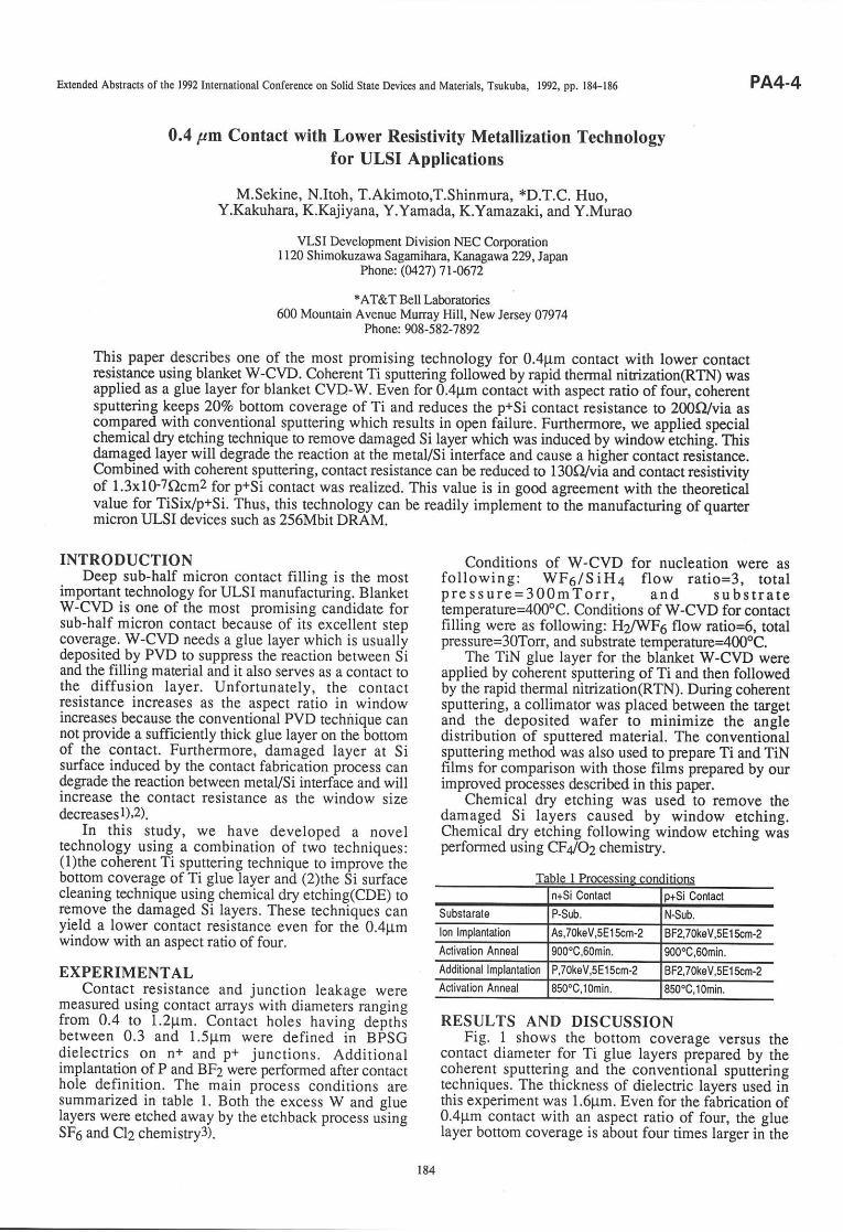
Extended Abstracts of the 1992 International Conference on Solid State Devices and Materials, Tsukuba, 1992, pp.184-186 0.4 pm Contact with Lower Resistivity Metallization Technology for ULSI Applications M.Sekine, N.Itoh, T.Akimoto,T.Shinmura, *D.T.C. Huo, Y.Kakuhara, K.Kaj iyana, Y. Yamada, K.Yam azaki, and Y. Murao VLSI Development Division NEC Corporarion I 1 20 S hi mokuzawa S agamihara, Kanagaw a 229, Japan Phone: (M27)71-0672 600 Mounta'" oT*: "Jlf"i?liiftn Jersey 07 s7 4 Phone: 908-582-7892 This paper describes one of the most promising technology for 0.4pm contact with lower contact resistance using blanket W-CVD. Coherent Ti sputtering follo*ed by rapid thermal nirization(RTN) was applied as a glue layer for blanket CVD-W. Even for 0.4pm contai:t with aspect ratio of four, coherent sputtering keeps 20Vo bottom coverage of Ti and reduces the p+Si contact resistance to 200Q/via as compared-with conventional sputtering which results in open failure. Furthermore, we applied special chemical $V etchigg-technique to remove damaged Si layei which was induced by window 6tching-. This damaged luygl will degrade the reacrion at the metal/Si interface and cause a hilher contact resiJtance. Combined with coherent sputtering, contact resistance can be reduced to 130C/via and contact resistivity of 1.3x10⁻⁷Ocm2 for p+5i contact was realized. This value is in good agreement with the theoretical value for TiSix/p+Si. Thus, t!1s pcllnglggy can be readily implement to the manufacturing of quarter micron IJLSI devices such as 256Mbit DRAM. PA4.4 Conditions of W-CVD for nucleation were as following: WFO/S iHa flow ratio=3, total pressure=300mTorr, and substrate temperature=400oC. Conditions of W-CVD for contact filling were as following: H2|TVF6 flow ratio=6, total pre s SUre= 3 0Torr, and su b strate temperanrre=4OOoC. The TiN glue layer for the blanket W-CVD were applied by coherent sputtering of Ti and then followed by the rapid thermal nitrization(RTN). During coherent sputtering, a collimator was placed between the target and the deposited wafer to minimize the angle distribution of sputtered material. The conventional sputtering method was also used to prepare Ti and TiN films for comparison with those films prepared by our improved processes described in this paper. Chemical dry etching was used to remove the damaged Si layers caused by window etching. Chemical dry etching following window etching was performed usin g CF a,/ Oz chemistry. RESULTS AND DISCUSSION Fig. 1 shows the bottom coverage versus the contact diameter for Ti glue layers prepared by the coherent spultering and the conventional spuffaring techniques. The thickness of dielectric layeri used in this experiment was 1.6pm. Even for the fabrication of 9.+pry contact with an aspecr ratio of four, the glue layer bottom coverage is about four times larger in the INTRODUCTION Deep sub-half micron contact filling is the most lmpgrtant technology for ULSI manufacruring. Blanket W-CVD is one of the most promising candidate for sub-half micron contact because of its excellent step coverage. W-CVD needs a glue layer which is usually deposited by PVD to suppress the reacrion between Si and the filling material and it also serves as a contact to the diffusion layer. Unfortunately, the contact resistance increases as the aspect ratio in window increases because the conventional PVD technique can not provide a sufficiently thick glue layer on the bottom of the contact. Furthermore, damaged layer at Si surface induced by the contact fabrication piocess can degrade the reaction between metaVsi interface and will increase the contact resistance as the window size decreasesl)'2). In this study, we have developed a novel technology using a combination of two techniques: (l)the coherent Ti sputtering technique to improve the bottom coverage of Ti glue layer and (2)the Si surface cleaning technique using chemical dry etching(CDE) to remove the damaged Si layers. These techniques can yigl4 a lower contact resistance even for the 0.4pm window with an aspect ratio of four. EXPERIMENTAL Contact resistance and junction leakage were measured using contact,iurays with diameters ranging from 0.4 to 1.2pm. Contact holes having depths between 0.3 and 1.5pm were defined i; BPSG dielectrics on p* and p+ junctions. Additional implantation of P and BF2 were performed after contacr hole definition. The main process conditions are summarized in table 1. Both the excess W and glue layers were etched away by the etchback process uiing SF6 and Cl2 chemistry3). 184 As,70keV,5E15cm-2 P,70keV,5E15cm-2 BF2,70keV,5E15cm-2 BF2,70keV,5E1Scm-2
Transcript of pressure=300mTorr, and - Atlas
Extended Abstracts of the 1992 International Conference on Solid State Devices and Materials, Tsukuba, 1992, pp.184-186
0.4 pm Contact with Lower Resistivity Metallization Technologyfor ULSI Applications
M.Sekine, N.Itoh, T.Akimoto,T.Shinmura, *D.T.C. Huo,Y.Kakuhara, K.Kaj iyana, Y. Yamada, K.Yam azaki, and Y. Murao
VLSI Development Division NEC CorporarionI 1 20 S hi mokuzawa S agamihara, Kanagaw a 229, Japan
Phone: (M27)71-0672
600 Mounta'" oT*: "Jlf"i?liiftn Jersey 07 s7 4Phone: 908-582-7892
This paper describes one of the most promising technology for 0.4pm contact with lower contactresistance using blanket W-CVD. Coherent Ti sputtering follo*ed by rapid thermal nirization(RTN) wasapplied as a glue layer for blanket CVD-W. Even for 0.4pm contai:t with aspect ratio of four, coherentsputtering keeps 20Vo bottom coverage of Ti and reduces the p+Si contact resistance to 200Q/via ascompared-with conventional sputtering which results in open failure. Furthermore, we applied specialchemical $V etchigg-technique to remove damaged Si layei which was induced by window 6tching-. Thisdamaged luygl will degrade the reacrion at the metal/Si interface and cause a hilher contact resiJtance.Combined with coherent sputtering, contact resistance can be reduced to 130C/via and contact resistivityof 1.3x10⁻⁷Ocm2 for p+5i contact was realized. This value is in good agreement with the theoreticalvalue for TiSix/p+Si. Thus, t!1s pcllnglggy can be readily implement to the manufacturing of quartermicron IJLSI devices such as 256Mbit DRAM.
PA4.4
Conditions of W-CVD for nucleation were asfollowing: WFO/S iHa flow ratio=3, totalpressure=300mTorr, and substratetemperature=400oC. Conditions of W-CVD for contactfilling were as following: H2|TVF6 flow ratio=6, totalpre s SUre= 3 0Torr, and su b strate temperanrre=4OOoC.
The TiN glue layer for the blanket W-CVD wereapplied by coherent sputtering of Ti and then followedby the rapid thermal nitrization(RTN). During coherentsputtering, a collimator was placed between the targetand the deposited wafer to minimize the angledistribution of sputtered material. The conventionalsputtering method was also used to prepare Ti and TiNfilms for comparison with those films prepared by ourimproved processes described in this paper.
Chemical dry etching was used to remove thedamaged Si layers caused by window etching.Chemical dry etching following window etching wasperformed usin g CF a,/ Oz chemistry.
RESULTS AND DISCUSSIONFig. 1 shows the bottom coverage versus the
contact diameter for Ti glue layers prepared by thecoherent spultering and the conventional spuffaringtechniques. The thickness of dielectric layeri used inthis experiment was 1.6pm. Even for the fabrication of9.+pry contact with an aspecr ratio of four, the gluelayer bottom coverage is about four times larger in the
INTRODUCTIONDeep sub-half micron contact filling is the most
lmpgrtant technology for ULSI manufacruring. BlanketW-CVD is one of the most promising candidate forsub-half micron contact because of its excellent stepcoverage. W-CVD needs a glue layer which is usuallydeposited by PVD to suppress the reacrion between Siand the filling material and it also serves as a contact tothe diffusion layer. Unfortunately, the contactresistance increases as the aspect ratio in windowincreases because the conventional PVD technique cannot provide a sufficiently thick glue layer on the bottomof the contact. Furthermore, damaged layer at Sisurface induced by the contact fabrication piocess candegrade the reaction between metaVsi interface and willincrease the contact resistance as the window sizedecreasesl)'2).
In this study, we have developed a noveltechnology using a combination of two techniques:(l)the coherent Ti sputtering technique to improve thebottom coverage of Ti glue layer and (2)the Si surfacecleaning technique using chemical dry etching(CDE) toremove the damaged Si layers. These techniques canyigl4 a lower contact resistance even for the 0.4pmwindow with an aspect ratio of four.
EXPERIMENTALContact resistance and junction leakage were
measured using contact,iurays with diameters rangingfrom 0.4 to 1.2pm. Contact holes having depthsbetween 0.3 and 1.5pm were defined i; BPSGdielectrics on p* and p+ junctions. Additionalimplantation of P and BF2 were performed after contacrhole definition. The main process conditions aresummarized in table 1. Both the excess W and gluelayers were etched away by the etchback process uiingSF6 and Cl2 chemistry3).
184
As,70keV,5E15cm-2
P,70keV,5E15cm-2
BF2,70keV,5E15cm-2
BF2,70keV,5E1Scm-2
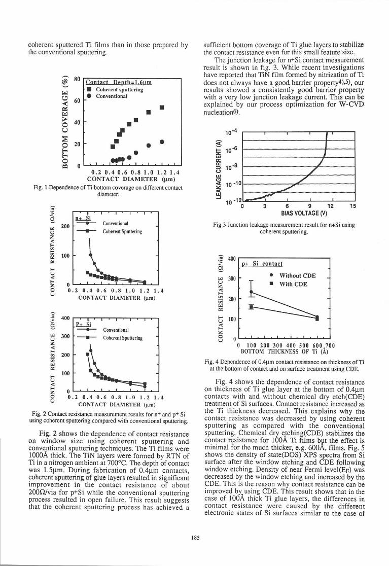
coherent sputtered Ti films thanthe conventional sputtering.
in those prepared by
Contact Depth=l.6UmI Coherent sputteringO Conventional
I
frtII
ooo
-to0.2 0.4 0.6 0.8 1.0 1.2 1.4
CONTACT DIAMETER (trm)
Fig. I Dependence of Ti bottom coverage on diflercnt conuctdiametcr.
-f- Conventional
--'-l- CoherentSputtering
.2 0.4 0.6 0.E 1.0 r.2 l.CONTACT DIAMETER (pm)
-lr- Conventional
-*- CoherentSputtering
.2 0.4 0.6 0.8 1.0 1.2 1.4CONTACT DIAMII'I'B,R (pm)
Fig.2 Contact resistance measurement. results for n+ and p+ g1
using coherent sputtering compared with conventional sputtering.
Fig. 2 shows the dependence of contact resistanceon window size using coherent sputtering andconventional sputtering techniconventional sputtering techniques. The Ti films were1000A thick. The TiN layers were formed by RTN offormed by RTN of
sufficient bottom coverage of Ti glue layers to stabilizethe contact resistance even for this small feature size.
The junction leakage for n+Si contact measurementresult is shown in fig. 3. While recent investigationshave reported that TiN film formed by nitrization of Tidoes not always have a good barrier property4),5), ourresults showed a consistently good barrier propertywith a very low junction leakage current. This can beexplained by our process optimization for W-CVDnucleation6).
10'4
1o-6
1o-8
1o'10
ro'11B|AS VOLTAGE (V)
Fig 3 Junction leakage measurement result. for n+Si usingcoherent sputtering.
p+ Si contact
. Without CDEI With CDE
0 100 200 300 400 500 600^700tloTToM rHrcKNEss oF Ti (A)
Fig. 4 Dependence of 0.4pm contact resisrance on thickness of Tiat he bottom of contact. and on surface treatment using CDE.
Fig. 4 shows the dependence of contact resistanceon thickness of Ti glue layer at rhe bottom of 0.4pmcontacts with and without chemical dry etch(CDE)treatment of Si surfaces. Contact resistance increased asthe Ti thickness decreased. This explains why thecontact resistance was decreased by using coherentsputtering as compared with the conventionalsputtering. Chemical dry e.tching(CDE) stabilizes thecontact resistance for 100A Ti films but the effect isminimal for the much thicker, e.g. 600A, films. Fig. 5shows the density of state(DOs) XPS specrra from Sisurface after the window etching and CDE followingwindow etching. Density of near Fermi level(Ep) wasdecreased by the window etching and increased by theCDE. This is the reason why contact resistance can beimproved by" using CDE. This result shows that in thecase of 100A thick Ti glue layers, the differences incontact resistance were caused by the differentelectronic states of Si surfaces similar to the case of
G' 80
;rli
Y60t4.Ir-'l-l!
b40U
c20FFca0
't
,_r 200
zF-cn
H loo&FOuo0U
SF2utGE=()ul(tvr!
3' 4oo
; 3oo
71
Fe 2oorrl&
b roo
F7-8o
1512
-3 4oo
Ff 3ooz,'ct 200o
. 100FU
-20o0
Ti in a nitrogen ambient ar 700oC. The depth of contacrwas 1.5pm. During fabrication of 0.4prm conracts,coherent sputtering of glue layers resulted in significantimprovement in the contact resistance of about200Q/via fo1 p+Si while rhe conventional sputteringprocess resulted in open failure. This result suggeststhat the coherent sputtering process has achieved a
I I t I
/,/
-/-/
185
il-G'
F-(nzt{F.zzct)(t)
rd
selective W-CVDI),2). These phenomena suggest thatTi silicidation at Ti/Si interface was degraded by thedamaged Si layer, and a part of Ti was consumed toreduce the damaged Si layer ar the initial stage ofsilicidation during RTN. Thus, the surface statQ effectwas more profound ar thinner Ii thickness(100A) thanthe thicker ti thickness(6004.). The chemicat aryetching developed in this experiment can improve the Tisilicidation at the Tilsi interface and stabilize the contactresistance. It can also reduce the required critical gluelayer thickness which will simplify the depositionprocess.
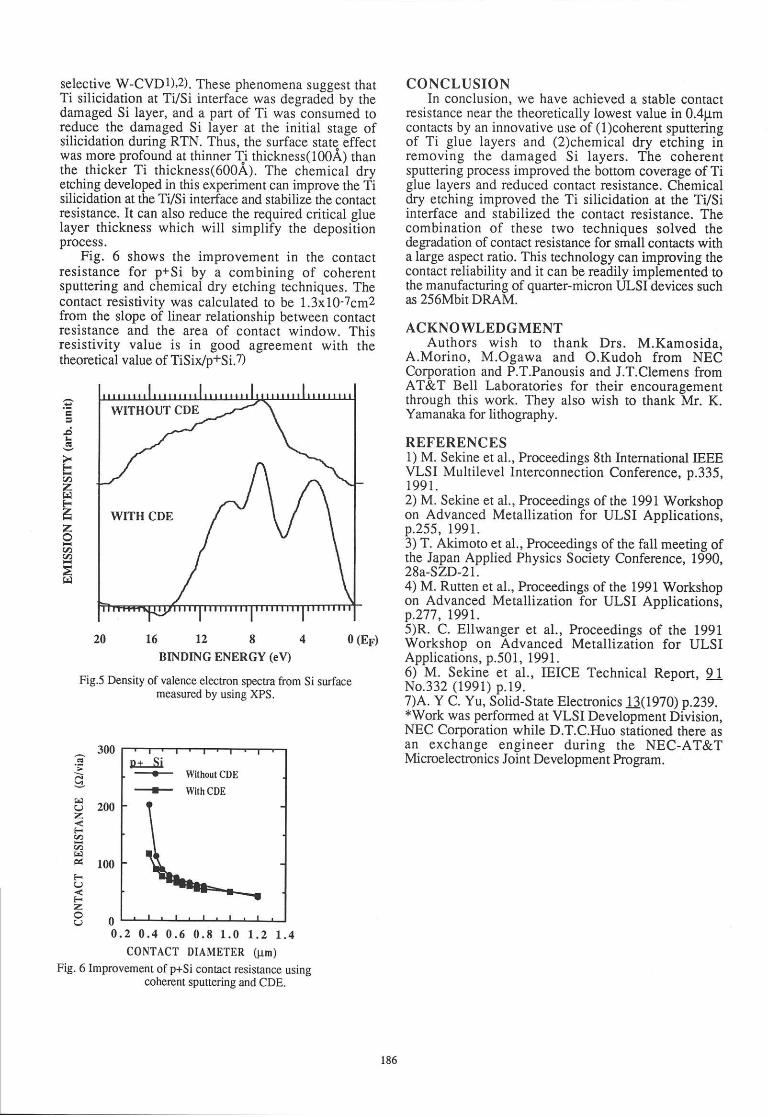
Fig. 6 shows the improvement in the contactresistance for p+Si by a combining of coherentsputtering and chemical dry etching techniques. Thecontact resistivity was calculated to be 1.3x10⁻⁷cm2from the slope of linear relationship between contactresistance and the area of contact window. Thisresistivity value is in good agreement with thetheoretical value of TiSix/p+Si.7)
20 16 12 8 4 O(En)
BINDING ENERGY (eV)
Fig.5 Density of valence electron spectra from Si surfacemeasured by using XPS.
p+ Si---t- Without CDE
--# WithCDE
.2 0.4 0.6 0.8 1.0 t.2 L.4CONTACT DIAMETER (pm)
Fig. 6 Improvement of p+Si contact resistance usingcoherent sputtering and CDE.
CONCLUSIONIn conclusion, we have achieved a stable contact
resistance near the theoretically lowest value in 0.4pmcontacts by an innovative use of (1)coherent sputteringof Ti glue layers and (2)chemical dry etching inremoving the damaged Si layers. The coherentsputtering process improved the bottom coverage of Tiglue layers and reduced contact resistance. Chemicaldry etching improved the Ti silicidation ar rhe TVSiinterface and stabilized the contact resistance. Thecombination of these two techniques solved thedegradation of contact resistance for small contacts witha large aspect ratio. This technology can improving thecontact reliability and it can be readily implemented tothe manufacturing of quarter-micron ULSI devices suchas 256Mbit DRAM.
ACKNOWLEDGMENTAuthors wish to thank Drs. M.Kamosida,
A.Morino, M.Ogawa and O.Kudoh from NECCorporation and P.T.Panousis and J.T.Clemens fromAT&T Bell Laboratories for their encouragementthrough this work. They also wish to thank Mr. K.Yamanaka for lithography.
REFERENCES1) M. Sekine et al., Proceedings 8th International IEEEVLSI Multilevel Interconnection Conference, p.335,1991.2) M. Sekine et al., Proceedings of the 1991 Workshopon Advanced Metallization for ULSI Applications,p.255, 1991.3) T. Akimoto et aI., Proceedings of the fall meeting ofthe Japan Applied Physics Society Conference, 1990,28a-SZD-21.4) M. Rutten et al., Proceedings of the 1991 Workshopon Advanced Metallization for ULSI Applications,p.277, 1991.5)R. C. Ellwanger et al., Proceedings of the 1991Workshop on Advanced Metallizarion for ULSIApplications, p.50L, L991.6) M. Sekine et al., IEICE Technical Report, 9lNo.332 (1991) p.19.7)A. Y C. Yu, Solid-State Electronics 13(1970)p.239.*Work was performed at VLSI Development Division,NEC Corporation while D.T.C.Huo srationed there asan exchange engineer during the NEC-AT&TMicroelectronics Joint Development Program.
300
't
; 2oozFqon L00F-OE-z8o
0
WITHOUT CDE
186