
Ontwerp van een geschakelde xDSL versterker in een ...
238
“doctoraat˙VDG” — 2009/8/13 — 11:30 — page 1 — #1 Ontwerp van een geschakelde xDSL versterker in een submicron hoogspanningstechnologie Design of a Switching xDSL Line Driver in a Submicron High Voltage Technology Vincent De Gezelle Promotor: prof. dr. ir. J. Doutreloigne Proefschrift ingediend tot het behalen van de graad van Doctor in de Ingenieurswetenschappen: Elektrotechniek Vakgroep Electronica en Informatiesystemen Voorzitter: prof. dr. ir. J. Van Campenhout Faculteit Ingenieurswetenschappen Academiejaar 2008–2009
Transcript of Ontwerp van een geschakelde xDSL versterker in een ...
“doctoraat˙VDG” — 2009/8/13 — 11:30 — page 1 — #1
Ontwerp van een geschakelde
xDSL versterker in een submicron
hoogspanningstechnologie
Design of a Switching xDSL Line Driver
in a Submicron High Voltage Technology
Vincent De Gezelle
Promotor: prof. dr. ir. J. Doutreloigne
Proefschrift ingediend tot het behalen van de graad van
Doctor in de Ingenieurswetenschappen: Elektrotechniek
Vakgroep Electronica en Informatiesystemen
Voorzitter: prof. dr. ir. J. Van Campenhout
Faculteit Ingenieurswetenschappen
Academiejaar 2008–2009
“doctoraat˙VDG” — 2009/8/13 — 11:30 — page 2 — #2

“doctoraat˙VDG” — 2009/8/13 — 11:30 — page 3 — #3
Ontwerp van een geschakelde
xDSL versterker in een submicron
hoogspanningstechnologie
Design of a Switching xDSL Line Driver
in a Submicron High Voltage Technology
Vincent De Gezelle
Promotor: prof. dr. ir. J. Doutreloigne
Proefschrift ingediend tot het behalen van de graad van
Doctor in de Ingenieurswetenschappen: Elektrotechniek
Vakgroep Electronica en Informatiesystemen
Voorzitter: prof. dr. ir. J. Van Campenhout
Faculteit Ingenieurswetenschappen
Academiejaar 2008–2009
“doctoraat˙VDG” — 2009/8/13 — 11:30 — page 4 — #4
ISBN 978-90-8578-300-8
NUR 959
Wettelijk depot: D/2009/10.500/58
“doctoraat˙VDG” — 2009/8/13 — 11:30 — page 5 — #5
Promotor:
Prof. dr. ir. J. Doutreloigne
Onderzoeksgroep CMST
Vakgroep Electronica en Informatiesystemen
Technologiepark 914A
B-9052 Zwijnaarde

“doctoraat˙VDG” — 2009/8/13 — 11:30 — page 6 — #6

“doctoraat˙VDG” — 2009/8/13 — 11:30 — page i — #7
Dankwoord
Plots zit ik daar dan, verstand op nul, blik op oneindig en een nog warme stapelvers afgedrukt papier voor mijn neus. De vaststelling dat de georganiseerde cha-os die ik “bureau” noem toch eens wat opgeruimd moet worden, onmiddellijkgevolgd door de gedachte dat ik dan impulsief en met grenzeloos enthousiasmedingen weg zal smijten die ik achteraf toch nog nodig blijk te hebben. De redenvoor dit alles? Na acht jaar ligt hier eindelijk een schriftelijke samenvatting vaneen belangrijk deel van het onderzoek en projectwerk dat ik in die periode ver-richt heb. Dit zou echter nooit mogelijk geweest zijn zonder de steun van eenheleboel mensen.
Als eerste zou ik prof. Andre Van Calster willen bedanken om mij als pas afge-studeerd ingenieur op te nemen in de TFCG/CMST familie en ons van tijd tottijd te verwennen met een diner of een BBQ. Daarnaast heeft natuurlijk ook mijnpromotor, prof. Jan Doutreloigne, een belangrijke rol gespeeld, door regelmatigeens wat licht te doen schijnen in de tunnel, dit proefschrift te lezen en de nodigekritische opmerkingen te formuleren.
Dank ook aan alle collega’s en ex-collega’s, zonder hen was het hier maar saaigeweest. Een aantal van hen zou ik toch extra willen bedanken. Jean, om de set-tings voor mijn designomgeving op punt te helpen zetten en mij te introducerenin een wondere wereld genaamd “Cadence”. Ronny en Michiel om mij te assis-teren bij de meest waanzinnige Unix-problemen en Wim om Cadence draaiendete houden. Dieter, om mij af en toe binnen te smokkelen in de cleanroom als ikweer eens microscoopfotookes nodig had van deze of gene chip. Bjorn voor alhet wirebonden en het fijnere soldeerwerk en Lieven voor de Mentor-support.
Mijn bureaugenoten mogen natuurlijk ook niet ontbreken. Benoit voor de eerstehulp bij speciale devices en Ann om altijd opgewekt te zijn. Zangvogel Stefaan,omdat er toch iemand wat leven in de designerbrouwerij moet brengen en Pieteren Dominique om te allen tijde de kalmte te bewaren. Jodie, bedankt om af en toeeens een lastige vraag te stellen. Hopelijk heb je iets aan dit boek.
Verder wens ik ook enkele mensen van Alcatel-Lucent te bedanken. Marnix, zon-der jou zou het financiele plaatje er ongetwijfeld anders uitgezien hebben. Eddy,bedankt voor de technische support, het ter beschikking stellen van een pak in-teressante documenten en de verhelderende uitleg over alles wat met telefonie temaken heeft.
“doctoraat˙VDG” — 2009/8/13 — 11:30 — page ii — #8
ii Dankwoord
Also a special thanks to the people of ETCA Charleroi to allow me to confiscateseveral power supplies, a signal generator and their spectrum analyzer for my fi-nal measurements. Philippe, Karim, Pierre-Gilles and Stephanie, thank you verymuch.
Naast het professionele gedeelte, zijn er natuurlijk nog mensen die mij, elk ophun manier, tijdens mijn vrije tijd gesteund hebben. De muzikanten van het terziele gegane Tempi Misti en opvolger Guso, door wie ik verplicht ben af en toemijn cello nog eens af te stoffen. De “Insiders”, om te bewijzen dat er behalvewhine-surfers ook nog windsurfers zijn die effectief gaan varen. Daarnaast zijner ook nog “de mannen van Brugge” die mij af en toe meetweefelden om eenander stukje Belgie onveilig te gaan maken.
Als laatste, maar daarom zeker niet minder belangrijk, zijn er nog mijn oudersen zus. Bedankt voor alle kansen die ik gekregen heb, voor de financiele onder-steuning, de goede raad, om mij overal naartoe te voeren of de auto te lenen, ookal wordt die dan steevast mishandeld door tientallen kilo’s aan plastic en carbonop het dak te stouwen, voor al die dingen die evident lijken maar het niet zijn.Charlotte, bedankt om te bewijzen dat een viool best wel mooi kan klinken en ommij te verblijden met weetjes zoals het aantal verschillende noten dat koolmezenen pimpelmezen kunnen produceren.Bedankt voor alles!
Vincent De Gezelle
Gent, 12 augustus 2009

“doctoraat˙VDG” — 2009/8/13 — 11:30 — page iii — #9
Contents
1 Introduction 1
1.1 Wire line communication . . . . . . . . . . . . . . . . . . . . . . . . . 11.1.1 Rise of the network . . . . . . . . . . . . . . . . . . . . . . . . 11.1.2 Extending the applications . . . . . . . . . . . . . . . . . . . 21.1.3 Some properties of xDSL . . . . . . . . . . . . . . . . . . . . 2
1.2 Context and goal of this work . . . . . . . . . . . . . . . . . . . . . . 41.3 Outline . . . . . . . . . . . . . . . . . . . . . . . . . . . . . . . . . . . 7
2 Concept and verification 11
2.1 Preliminary considerations . . . . . . . . . . . . . . . . . . . . . . . . 112.2 Technology overview . . . . . . . . . . . . . . . . . . . . . . . . . . . 14
DMOS transistors . . . . . . . . . . . . . . . . . . . . . . . . . 14MOS transistors . . . . . . . . . . . . . . . . . . . . . . . . . . 14Capacitors . . . . . . . . . . . . . . . . . . . . . . . . . . . . . 15Resistors . . . . . . . . . . . . . . . . . . . . . . . . . . . . . . 15
2.3 Zeroth order . . . . . . . . . . . . . . . . . . . . . . . . . . . . . . . . 162.3.1 Schematics and simulations . . . . . . . . . . . . . . . . . . . 16
Output stage . . . . . . . . . . . . . . . . . . . . . . . . . . . 16Comparator . . . . . . . . . . . . . . . . . . . . . . . . . . . . 20Full simulation . . . . . . . . . . . . . . . . . . . . . . . . . . 25
2.3.2 Layout and measurement results . . . . . . . . . . . . . . . . 302.4 First order . . . . . . . . . . . . . . . . . . . . . . . . . . . . . . . . . 34
2.4.1 Schematics and simulations . . . . . . . . . . . . . . . . . . . 34Opamp and integrator . . . . . . . . . . . . . . . . . . . . . . 34Comparator . . . . . . . . . . . . . . . . . . . . . . . . . . . . 38Biasing circuit . . . . . . . . . . . . . . . . . . . . . . . . . . . 41Output stage . . . . . . . . . . . . . . . . . . . . . . . . . . . 45Full simulation . . . . . . . . . . . . . . . . . . . . . . . . . . 46
2.4.2 Layout and measurement results . . . . . . . . . . . . . . . . 55Reference circuit . . . . . . . . . . . . . . . . . . . . . . . . . 55Amplifiers . . . . . . . . . . . . . . . . . . . . . . . . . . . . . 55
2.5 Conclusion . . . . . . . . . . . . . . . . . . . . . . . . . . . . . . . . . 61
“doctoraat˙VDG” — 2009/8/13 — 11:30 — page iv — #10
iv CONTENTS
3 Theory of operation 653.1 Introduction . . . . . . . . . . . . . . . . . . . . . . . . . . . . . . . . 653.2 Describing functions linearization . . . . . . . . . . . . . . . . . . . 66
3.2.1 Small and large signals . . . . . . . . . . . . . . . . . . . . . . 663.2.2 Large signal approximation . . . . . . . . . . . . . . . . . . . 673.2.3 An example . . . . . . . . . . . . . . . . . . . . . . . . . . . . 70
Offset . . . . . . . . . . . . . . . . . . . . . . . . . . . . . . . . 70Sinewave . . . . . . . . . . . . . . . . . . . . . . . . . . . . . 70Full response . . . . . . . . . . . . . . . . . . . . . . . . . . . 72
3.2.4 Sinusoidal input signals . . . . . . . . . . . . . . . . . . . . . 72A single sinusoid . . . . . . . . . . . . . . . . . . . . . . . . . 72A sinusoid with other signals . . . . . . . . . . . . . . . . . . 74Exponential transfer revisited . . . . . . . . . . . . . . . . . . 74
3.2.5 Limit cycle calculation . . . . . . . . . . . . . . . . . . . . . . 753.3 Distortion calculation . . . . . . . . . . . . . . . . . . . . . . . . . . . 76
3.3.1 Zeroth and first order loop . . . . . . . . . . . . . . . . . . . 773.3.2 Second order loop . . . . . . . . . . . . . . . . . . . . . . . . 803.3.3 Third order loop . . . . . . . . . . . . . . . . . . . . . . . . . 81
3.4 Numerical verification . . . . . . . . . . . . . . . . . . . . . . . . . . 823.4.1 First order loop . . . . . . . . . . . . . . . . . . . . . . . . . . 82
Oscillating frequency . . . . . . . . . . . . . . . . . . . . . . . 82Third order harmonic distortion . . . . . . . . . . . . . . . . 83Simulation . . . . . . . . . . . . . . . . . . . . . . . . . . . . . 83
3.4.2 10MHz second order loop . . . . . . . . . . . . . . . . . . . . 86Oscillating frequency . . . . . . . . . . . . . . . . . . . . . . . 86Third order harmonic distortion . . . . . . . . . . . . . . . . 87Simulation . . . . . . . . . . . . . . . . . . . . . . . . . . . . . 88
3.4.3 30MHz second order loop . . . . . . . . . . . . . . . . . . . . 913.4.4 Third order loop . . . . . . . . . . . . . . . . . . . . . . . . . 94
Oscillating frequency . . . . . . . . . . . . . . . . . . . . . . . 94Third order harmonic distortion . . . . . . . . . . . . . . . . 94Simulation . . . . . . . . . . . . . . . . . . . . . . . . . . . . . 95
3.4.5 Discussion . . . . . . . . . . . . . . . . . . . . . . . . . . . . . 98Limit cycle frequency . . . . . . . . . . . . . . . . . . . . . . 98Third order harmonic distortion . . . . . . . . . . . . . . . . 98What about MTPR? . . . . . . . . . . . . . . . . . . . . . . . . 101
3.5 Conclusion . . . . . . . . . . . . . . . . . . . . . . . . . . . . . . . . . 101
4 Designing the loop 1054.1 Introduction . . . . . . . . . . . . . . . . . . . . . . . . . . . . . . . . 1054.2 Technology overview . . . . . . . . . . . . . . . . . . . . . . . . . . . 106
4.2.1 DMOS transistors . . . . . . . . . . . . . . . . . . . . . . . . . 1064.2.2 MOS transistors . . . . . . . . . . . . . . . . . . . . . . . . . . 106

“doctoraat˙VDG” — 2009/8/13 — 11:30 — page v — #11
CONTENTS v
4.2.3 Capacitors . . . . . . . . . . . . . . . . . . . . . . . . . . . . . 1074.2.4 Resistors . . . . . . . . . . . . . . . . . . . . . . . . . . . . . . 107
4.3 Building blocks . . . . . . . . . . . . . . . . . . . . . . . . . . . . . . 1084.3.1 Opamps . . . . . . . . . . . . . . . . . . . . . . . . . . . . . . 108
Integrator . . . . . . . . . . . . . . . . . . . . . . . . . . . . . 108Voltage follower . . . . . . . . . . . . . . . . . . . . . . . . . 115Biasing circuit . . . . . . . . . . . . . . . . . . . . . . . . . . . 118
4.3.2 Comparator . . . . . . . . . . . . . . . . . . . . . . . . . . . . 1204.3.3 Output stage . . . . . . . . . . . . . . . . . . . . . . . . . . . 1214.3.4 Time delay, level shifter and buffers . . . . . . . . . . . . . . 1274.3.5 Passive filter-divider . . . . . . . . . . . . . . . . . . . . . . . 130
First order loop . . . . . . . . . . . . . . . . . . . . . . . . . . 13110MHz second order loop . . . . . . . . . . . . . . . . . . . . 13230MHz second order loop . . . . . . . . . . . . . . . . . . . . 132Third order loop . . . . . . . . . . . . . . . . . . . . . . . . . 133
4.4 First order system . . . . . . . . . . . . . . . . . . . . . . . . . . . . . 1334.5 10MHz second order system . . . . . . . . . . . . . . . . . . . . . . . 1354.6 30MHz second order system . . . . . . . . . . . . . . . . . . . . . . . 1394.7 Third order system . . . . . . . . . . . . . . . . . . . . . . . . . . . . 1394.8 Second order system with independent loops . . . . . . . . . . . . . 1394.9 Layout considerations . . . . . . . . . . . . . . . . . . . . . . . . . . 146
4.9.1 Interconnection . . . . . . . . . . . . . . . . . . . . . . . . . . 1464.9.2 Components . . . . . . . . . . . . . . . . . . . . . . . . . . . . 147
4.10 Conclusion . . . . . . . . . . . . . . . . . . . . . . . . . . . . . . . . . 147
5 Measurements 1515.1 Introduction . . . . . . . . . . . . . . . . . . . . . . . . . . . . . . . . 1515.2 Initial measurements . . . . . . . . . . . . . . . . . . . . . . . . . . . 154
5.2.1 First order system . . . . . . . . . . . . . . . . . . . . . . . . . 154DC response . . . . . . . . . . . . . . . . . . . . . . . . . . . . 154AC response . . . . . . . . . . . . . . . . . . . . . . . . . . . . 154MTPR response . . . . . . . . . . . . . . . . . . . . . . . . . . 157
5.2.2 10MHz second order system . . . . . . . . . . . . . . . . . . 157DC response . . . . . . . . . . . . . . . . . . . . . . . . . . . . 157AC response . . . . . . . . . . . . . . . . . . . . . . . . . . . . 157MTPR response . . . . . . . . . . . . . . . . . . . . . . . . . . 157
5.2.3 30MHz second order system . . . . . . . . . . . . . . . . . . 159DC response . . . . . . . . . . . . . . . . . . . . . . . . . . . . 159AC response . . . . . . . . . . . . . . . . . . . . . . . . . . . . 164MTPR response . . . . . . . . . . . . . . . . . . . . . . . . . . 164
5.2.4 Third order system . . . . . . . . . . . . . . . . . . . . . . . . 164DC response . . . . . . . . . . . . . . . . . . . . . . . . . . . . 164AC response . . . . . . . . . . . . . . . . . . . . . . . . . . . . 164
“doctoraat˙VDG” — 2009/8/13 — 11:30 — page vi — #12
vi CONTENTS
MTPR response . . . . . . . . . . . . . . . . . . . . . . . . . . 1645.2.5 Second order system with independent loops . . . . . . . . 170
DC response . . . . . . . . . . . . . . . . . . . . . . . . . . . . 170AC response . . . . . . . . . . . . . . . . . . . . . . . . . . . . 170MTPR response . . . . . . . . . . . . . . . . . . . . . . . . . . 170
5.3 Troubleshooting . . . . . . . . . . . . . . . . . . . . . . . . . . . . . . 1735.4 Final measurements . . . . . . . . . . . . . . . . . . . . . . . . . . . . 180
5.4.1 First order system . . . . . . . . . . . . . . . . . . . . . . . . . 181DC response . . . . . . . . . . . . . . . . . . . . . . . . . . . . 181AC response . . . . . . . . . . . . . . . . . . . . . . . . . . . . 181MTPR response . . . . . . . . . . . . . . . . . . . . . . . . . . 181
5.4.2 10MHz second order system . . . . . . . . . . . . . . . . . . 184DC response . . . . . . . . . . . . . . . . . . . . . . . . . . . . 184AC response . . . . . . . . . . . . . . . . . . . . . . . . . . . . 185MTPR response . . . . . . . . . . . . . . . . . . . . . . . . . . 185
5.4.3 30MHz second order system . . . . . . . . . . . . . . . . . . 185DC response . . . . . . . . . . . . . . . . . . . . . . . . . . . . 185AC response . . . . . . . . . . . . . . . . . . . . . . . . . . . . 185MTPR response . . . . . . . . . . . . . . . . . . . . . . . . . . 185
5.4.4 Third order system . . . . . . . . . . . . . . . . . . . . . . . . 191DC response . . . . . . . . . . . . . . . . . . . . . . . . . . . . 191AC response . . . . . . . . . . . . . . . . . . . . . . . . . . . . 192MTPR response . . . . . . . . . . . . . . . . . . . . . . . . . . 192
5.4.5 Second order system with independent loops . . . . . . . . 192DC response . . . . . . . . . . . . . . . . . . . . . . . . . . . . 192AC response . . . . . . . . . . . . . . . . . . . . . . . . . . . . 192MTPR response . . . . . . . . . . . . . . . . . . . . . . . . . . 198
5.5 Conclusion . . . . . . . . . . . . . . . . . . . . . . . . . . . . . . . . . 199
6 Conclusions and outlook 2036.1 Main achievements . . . . . . . . . . . . . . . . . . . . . . . . . . . . 2036.2 Future work . . . . . . . . . . . . . . . . . . . . . . . . . . . . . . . . 2046.3 Feasibility and extensibility . . . . . . . . . . . . . . . . . . . . . . . 204
“doctoraat˙VDG” — 2009/8/13 — 11:30 — page vii — #13
List of Tables
2.1 Key characteristics of I2T100 DMOS devices . . . . . . . . . . . . . . 142.2 Key characteristics of I2T100 MOS devices . . . . . . . . . . . . . . . 152.3 Key characteristics of I2T100 capacitors . . . . . . . . . . . . . . . . 152.4 Key characteristics of I2T100 resistors . . . . . . . . . . . . . . . . . 162.5 Transistor dimensions of level shifter and buffer . . . . . . . . . . . 182.6 Transistor dimensions of the delay circuit . . . . . . . . . . . . . . . 222.7 Transistor dimensions of the comparator . . . . . . . . . . . . . . . . 232.8 Delay times of the comparator . . . . . . . . . . . . . . . . . . . . . . 252.9 Summary of simulation results . . . . . . . . . . . . . . . . . . . . . 282.10 Power dissipation of the single ended amplifier . . . . . . . . . . . . 282.11 Maximum dV/dt capability of the DMOS switches used . . . . . . 292.12 Calculated dimensions of the opamp transistors . . . . . . . . . . . 372.13 Optimized component dimensions of the opamp . . . . . . . . . . . 382.14 Simulation results of the opamp . . . . . . . . . . . . . . . . . . . . . 392.15 Transistor dimensions of the comparator . . . . . . . . . . . . . . . . 412.16 Delay times of the comparator . . . . . . . . . . . . . . . . . . . . . . 412.17 Transistor dimensions of the reference circuit . . . . . . . . . . . . . 452.18 Voltages and currents from the reference circuit . . . . . . . . . . . . 462.19 Transistor dimensions of level shifter and buffer . . . . . . . . . . . 472.20 Transistor dimensions of the delay circuit . . . . . . . . . . . . . . . 482.21 Summary of the simulation results . . . . . . . . . . . . . . . . . . . 522.22 Summary of the calculated results . . . . . . . . . . . . . . . . . . . 542.23 Measured voltages from the reference circuit . . . . . . . . . . . . . 562.24 Comparison of measurement results . . . . . . . . . . . . . . . . . . 61
3.1 Bernoulli numbers . . . . . . . . . . . . . . . . . . . . . . . . . . . . 793.2 Calculated and simulated limit cycle frequencies . . . . . . . . . . . 983.3 Simulated MTPR . . . . . . . . . . . . . . . . . . . . . . . . . . . . . 101
4.1 Key characteristics of I3T80 DMOS devices . . . . . . . . . . . . . . 1064.2 Key characteristics of I3T80 MOS devices . . . . . . . . . . . . . . . 1074.3 Key characteristics of I3T80 capacitors . . . . . . . . . . . . . . . . . 1074.4 Key characteristics of I3T80 resistors . . . . . . . . . . . . . . . . . . 108
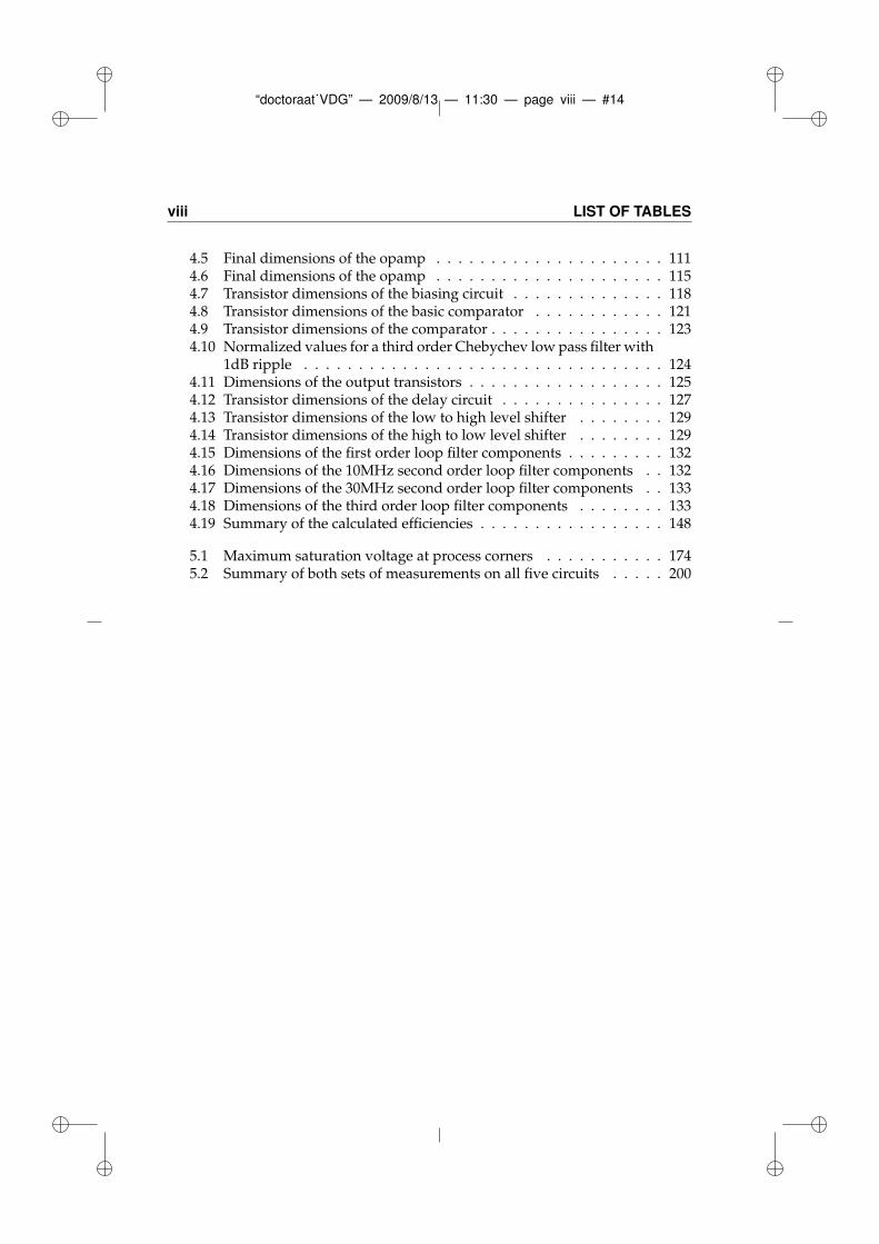
“doctoraat˙VDG” — 2009/8/13 — 11:30 — page viii — #14
viii LIST OF TABLES
4.5 Final dimensions of the opamp . . . . . . . . . . . . . . . . . . . . . 1114.6 Final dimensions of the opamp . . . . . . . . . . . . . . . . . . . . . 1154.7 Transistor dimensions of the biasing circuit . . . . . . . . . . . . . . 1184.8 Transistor dimensions of the basic comparator . . . . . . . . . . . . 1214.9 Transistor dimensions of the comparator . . . . . . . . . . . . . . . . 1234.10 Normalized values for a third order Chebychev low pass filter with
1dB ripple . . . . . . . . . . . . . . . . . . . . . . . . . . . . . . . . . 1244.11 Dimensions of the output transistors . . . . . . . . . . . . . . . . . . 1254.12 Transistor dimensions of the delay circuit . . . . . . . . . . . . . . . 1274.13 Transistor dimensions of the low to high level shifter . . . . . . . . 1294.14 Transistor dimensions of the high to low level shifter . . . . . . . . 1294.15 Dimensions of the first order loop filter components . . . . . . . . . 1324.16 Dimensions of the 10MHz second order loop filter components . . 1324.17 Dimensions of the 30MHz second order loop filter components . . 1334.18 Dimensions of the third order loop filter components . . . . . . . . 1334.19 Summary of the calculated efficiencies . . . . . . . . . . . . . . . . . 148
5.1 Maximum saturation voltage at process corners . . . . . . . . . . . 1745.2 Summary of both sets of measurements on all five circuits . . . . . 200
“doctoraat˙VDG” — 2009/8/13 — 11:30 — page ix — #15
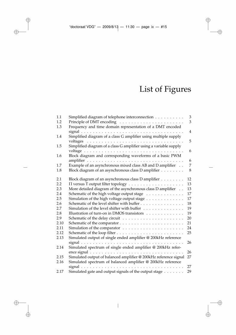
List of Figures
1.1 Simplified diagram of telephone interconnection . . . . . . . . . . 31.2 Principle of DMT encoding . . . . . . . . . . . . . . . . . . . . . . 31.3 Frequency and time domain representation of a DMT encoded
signal . . . . . . . . . . . . . . . . . . . . . . . . . . . . . . . . . . . 41.4 Simplified diagram of a class G amplifier using multiple supply
voltages . . . . . . . . . . . . . . . . . . . . . . . . . . . . . . . . . 51.5 Simplified diagram of a class G amplifier using a variable supply
voltage . . . . . . . . . . . . . . . . . . . . . . . . . . . . . . . . . . 61.6 Block diagram and corresponding waveforms of a basic PWM
amplifier . . . . . . . . . . . . . . . . . . . . . . . . . . . . . . . . . 61.7 Example of an asynchronous mixed class AB and D amplifier . . 71.8 Block diagram of an asynchronous class D amplifier . . . . . . . . 8
2.1 Block diagram of an asynchronous class D amplifier . . . . . . . . 122.2 Π versus T output filter topology . . . . . . . . . . . . . . . . . . . 132.3 More detailed diagram of the asynchronous class D amplifier . . 132.4 Schematic of the high voltage output stage . . . . . . . . . . . . . 172.5 Simulation of the high voltage output stage . . . . . . . . . . . . . 172.6 Schematic of the level shifter with buffer . . . . . . . . . . . . . . . 182.7 Simulation of the level shifter with buffer . . . . . . . . . . . . . . 192.8 Illustration of turn-on in DMOS transistors . . . . . . . . . . . . . 192.9 Schematic of the delay circuit . . . . . . . . . . . . . . . . . . . . . 202.10 Schematic of the comparator . . . . . . . . . . . . . . . . . . . . . . 212.11 Simulation of the comparator . . . . . . . . . . . . . . . . . . . . . 242.12 Schematic of the loop filter . . . . . . . . . . . . . . . . . . . . . . . 252.13 Simulated output of single ended amplifier @ 200kHz reference
signal . . . . . . . . . . . . . . . . . . . . . . . . . . . . . . . . . . . 262.14 Simulated spectrum of single ended amplifier @ 200kHz refer-
ence signal . . . . . . . . . . . . . . . . . . . . . . . . . . . . . . . . 262.15 Simulated output of balanced amplifier @ 200kHz reference signal 272.16 Simulated spectrum of balanced amplifier @ 200kHz reference
signal . . . . . . . . . . . . . . . . . . . . . . . . . . . . . . . . . . . 272.17 Simulated gate and output signals of the output stage . . . . . . . 29
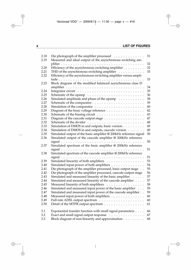
“doctoraat˙VDG” — 2009/8/13 — 11:30 — page x — #16
x LIST OF FIGURES
2.18 Die photograph of the amplifier processed . . . . . . . . . . . . . 312.19 Measured and ideal output of the asynchronous switching am-
plifier . . . . . . . . . . . . . . . . . . . . . . . . . . . . . . . . . . . 322.20 Efficiency of the asynchronous switching amplifier . . . . . . . . . 322.21 THD of the asynchronous switching amplifier . . . . . . . . . . . 332.22 Efficiency of the asynchronous switching amplifier versus ampli-
tude . . . . . . . . . . . . . . . . . . . . . . . . . . . . . . . . . . . . 332.23 Block diagram of the modified balanced asynchronous class D
amplifier . . . . . . . . . . . . . . . . . . . . . . . . . . . . . . . . . 342.24 Integrator circuit . . . . . . . . . . . . . . . . . . . . . . . . . . . . 352.25 Schematic of the opamp . . . . . . . . . . . . . . . . . . . . . . . . 362.26 Simulated amplitude and phase of the opamp . . . . . . . . . . . 382.27 Schematic of the comparator . . . . . . . . . . . . . . . . . . . . . . 392.28 Simulation of the comparator . . . . . . . . . . . . . . . . . . . . . 402.29 Diagram of the basic voltage reference . . . . . . . . . . . . . . . . 422.30 Schematic of the biasing circuit . . . . . . . . . . . . . . . . . . . . 432.31 Diagram of the cascode output stage . . . . . . . . . . . . . . . . . 472.32 Schematic of the divider . . . . . . . . . . . . . . . . . . . . . . . . 482.33 Simulation of DMOS in and outputs, basic version . . . . . . . . . 492.34 Simulation of DMOS in and outputs, cascode version . . . . . . . 492.35 Simulated output of the basic amplifier @ 200kHz reference signal 502.36 Simulated output of the cascode amplifier @ 200kHz reference
signal . . . . . . . . . . . . . . . . . . . . . . . . . . . . . . . . . . . 502.37 Simulated spectrum of the basic amplifier @ 200kHz reference
signal . . . . . . . . . . . . . . . . . . . . . . . . . . . . . . . . . . . 512.38 Simulated spectrum of the cascode amplifier @ 200kHz reference
signal . . . . . . . . . . . . . . . . . . . . . . . . . . . . . . . . . . . 512.39 Simulated linearity of both amplifiers . . . . . . . . . . . . . . . . 532.40 Simulated input power of both amplifiers . . . . . . . . . . . . . . 542.41 Die photograph of the amplifier processed, basic output stage . . 552.42 Die photograph of the amplifier processed, cascode output stage 562.43 Simulated and measured linearity of the basic amplifier . . . . . . 572.44 Simulated and measured linearity of the cascode amplifier . . . . 572.45 Measured linearity of both amplifiers . . . . . . . . . . . . . . . . 582.46 Simulated and measured input power of the basic amplifier . . . 592.47 Simulated and measured input power of the cascode amplifier . . 592.48 Measured input power of both amplifiers . . . . . . . . . . . . . . 602.49 Full-rate ADSL output spectrum . . . . . . . . . . . . . . . . . . . 602.50 Detail of the MTPR output spectrum . . . . . . . . . . . . . . . . . 61
3.1 Exponential transfer function with small signal parameters . . . . 663.2 Exact and small signal output response . . . . . . . . . . . . . . . 673.3 Block diagram of non-linearity and approximation . . . . . . . . . 68
“doctoraat˙VDG” — 2009/8/13 — 11:30 — page xi — #17
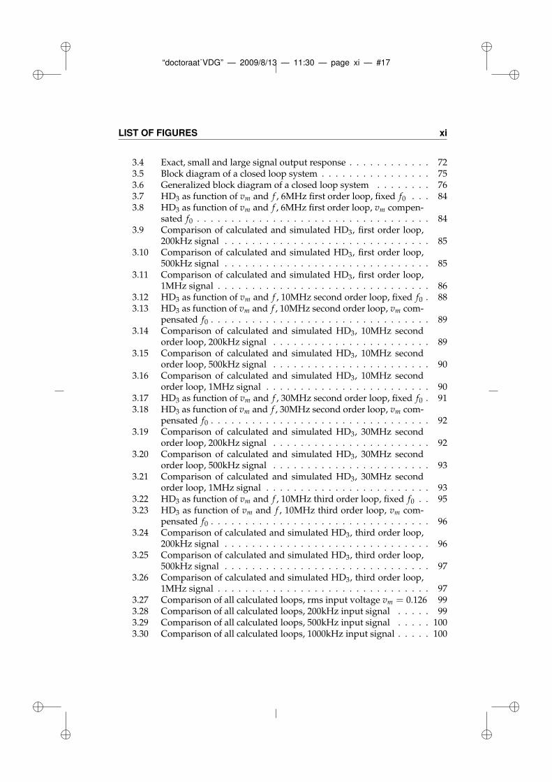
LIST OF FIGURES xi
3.4 Exact, small and large signal output response . . . . . . . . . . . . 723.5 Block diagram of a closed loop system . . . . . . . . . . . . . . . . 753.6 Generalized block diagram of a closed loop system . . . . . . . . 763.7 HD3 as function of vm and f , 6MHz first order loop, fixed f0 . . . 843.8 HD3 as function of vm and f , 6MHz first order loop, vm compen-
sated f0 . . . . . . . . . . . . . . . . . . . . . . . . . . . . . . . . . . 843.9 Comparison of calculated and simulated HD3, first order loop,
200kHz signal . . . . . . . . . . . . . . . . . . . . . . . . . . . . . . 853.10 Comparison of calculated and simulated HD3, first order loop,
500kHz signal . . . . . . . . . . . . . . . . . . . . . . . . . . . . . . 853.11 Comparison of calculated and simulated HD3, first order loop,
1MHz signal . . . . . . . . . . . . . . . . . . . . . . . . . . . . . . . 863.12 HD3 as function of vm and f , 10MHz second order loop, fixed f0 . 883.13 HD3 as function of vm and f , 10MHz second order loop, vm com-
pensated f0 . . . . . . . . . . . . . . . . . . . . . . . . . . . . . . . . 893.14 Comparison of calculated and simulated HD3, 10MHz second
order loop, 200kHz signal . . . . . . . . . . . . . . . . . . . . . . . 893.15 Comparison of calculated and simulated HD3, 10MHz second
order loop, 500kHz signal . . . . . . . . . . . . . . . . . . . . . . . 903.16 Comparison of calculated and simulated HD3, 10MHz second
order loop, 1MHz signal . . . . . . . . . . . . . . . . . . . . . . . . 903.17 HD3 as function of vm and f , 30MHz second order loop, fixed f0 . 913.18 HD3 as function of vm and f , 30MHz second order loop, vm com-
pensated f0 . . . . . . . . . . . . . . . . . . . . . . . . . . . . . . . . 923.19 Comparison of calculated and simulated HD3, 30MHz second
order loop, 200kHz signal . . . . . . . . . . . . . . . . . . . . . . . 923.20 Comparison of calculated and simulated HD3, 30MHz second
order loop, 500kHz signal . . . . . . . . . . . . . . . . . . . . . . . 933.21 Comparison of calculated and simulated HD3, 30MHz second
order loop, 1MHz signal . . . . . . . . . . . . . . . . . . . . . . . . 933.22 HD3 as function of vm and f , 10MHz third order loop, fixed f0 . . 953.23 HD3 as function of vm and f , 10MHz third order loop, vm com-
pensated f0 . . . . . . . . . . . . . . . . . . . . . . . . . . . . . . . . 963.24 Comparison of calculated and simulated HD3, third order loop,
200kHz signal . . . . . . . . . . . . . . . . . . . . . . . . . . . . . . 963.25 Comparison of calculated and simulated HD3, third order loop,
500kHz signal . . . . . . . . . . . . . . . . . . . . . . . . . . . . . . 973.26 Comparison of calculated and simulated HD3, third order loop,
1MHz signal . . . . . . . . . . . . . . . . . . . . . . . . . . . . . . . 973.27 Comparison of all calculated loops, rms input voltage vm = 0.126 993.28 Comparison of all calculated loops, 200kHz input signal . . . . . 993.29 Comparison of all calculated loops, 500kHz input signal . . . . . 1003.30 Comparison of all calculated loops, 1000kHz input signal . . . . . 100
“doctoraat˙VDG” — 2009/8/13 — 11:30 — page xii — #18
xii LIST OF FIGURES
4.1 Basic schematic of a two stage folded cascode opamp . . . . . . . 1094.2 Schematic of the two stage folded cascode opamp with output
common mode control . . . . . . . . . . . . . . . . . . . . . . . . . 1124.3 Simulated Bode diagram of the opamp . . . . . . . . . . . . . . . . 1134.4 Realized integrator . . . . . . . . . . . . . . . . . . . . . . . . . . . 1134.5 Bode plot of the 1.6MHz integrator . . . . . . . . . . . . . . . . . . 1144.6 Bode plot of the 3.2MHz integrator . . . . . . . . . . . . . . . . . . 1144.7 Schematic of the rail-to-rail voltage follower . . . . . . . . . . . . 1164.8 Bode diagram of the voltage follower, 1.65V input common mode 1174.9 Phase margin of the opamp, depending on the common mode
input voltage . . . . . . . . . . . . . . . . . . . . . . . . . . . . . . 1174.10 Gain bandwidth product of the opamp, depending on the com-
mon mode input voltage . . . . . . . . . . . . . . . . . . . . . . . . 1184.11 Biasing circuit for the folded cascode stage . . . . . . . . . . . . . 1194.12 Basic circuit of the comparator . . . . . . . . . . . . . . . . . . . . 1204.13 Final circuit of the comparator . . . . . . . . . . . . . . . . . . . . . 1224.14 Simulation result of the comparator . . . . . . . . . . . . . . . . . 1234.15 Schematic of the high voltage output stage . . . . . . . . . . . . . 1244.16 Comparison of power dissipation between the VFNDM80 and
VFNDM80a DMOS as a function of the time delay, for differentwidths . . . . . . . . . . . . . . . . . . . . . . . . . . . . . . . . . . 125
4.17 Output voltage as a function of duty cycle . . . . . . . . . . . . . . 1264.18 Input power as a function of duty cycle . . . . . . . . . . . . . . . 1264.19 Schematic of the level shifter . . . . . . . . . . . . . . . . . . . . . 1284.20 Schematic of the high to low level shifter . . . . . . . . . . . . . . 1294.21 Simulation of the level shifter . . . . . . . . . . . . . . . . . . . . . 1304.22 Simulation of the buffers . . . . . . . . . . . . . . . . . . . . . . . . 1314.23 Schematic of the filter-divider . . . . . . . . . . . . . . . . . . . . . 1314.24 DC simulation of the first order system . . . . . . . . . . . . . . . 1344.25 Third order harmonic distortion of the first order system . . . . . 1364.26 DC simulation of the 10MHz second order system . . . . . . . . . 1374.27 Third order harmonic distortion of the 10MHz second order system1384.28 DC simulation of the 30MHz second order system . . . . . . . . . 1404.29 Third order harmonic distortion of the 30MHz second order system1414.30 DC simulation of the third order system . . . . . . . . . . . . . . . 1424.31 Third order harmonic distortion of the third order system . . . . . 1434.32 DC simulation of the second order system with independent loops1444.33 Third order harmonic distortion of the second order system with
independent loops . . . . . . . . . . . . . . . . . . . . . . . . . . . 145
5.1 Die photograph of the amplifiers processed . . . . . . . . . . . . . 1525.2 Photograph of the test board . . . . . . . . . . . . . . . . . . . . . . 1535.3 DC measurements on the first order system . . . . . . . . . . . . . 155
“doctoraat˙VDG” — 2009/8/13 — 11:30 — page xiii — #19
LIST OF FIGURES xiii
5.4 Third order harmonic distortion of the first order system . . . . . 1565.5 Noise measurements on the first order system . . . . . . . . . . . 1585.6 MTPR measurements on the first order system . . . . . . . . . . . 1595.7 DC measurements on the 10MHz second order system . . . . . . 1605.8 Third order harmonic distortion of the 10MHz second order system1615.9 Noise measurement on the 10MHz second order system . . . . . 1625.10 MTPR measurements on the 10MHz second order system . . . . . 1625.11 DC measurements on the 30MHz second order system . . . . . . 1635.12 Third order harmonic distortion of the 30MHz second order system1655.13 Noise measurement on the 30MHz second order system . . . . . 1665.14 MTPR measurements on the 30MHz second order system . . . . . 1665.15 DC measurements on the third order system . . . . . . . . . . . . 1675.16 Third order harmonic distortion of the third order system . . . . . 1685.17 Noise measurements on the third order system . . . . . . . . . . . 1695.18 MTPR measurements on the third order system . . . . . . . . . . 1705.19 DC measurements on the second order system with independent
loops . . . . . . . . . . . . . . . . . . . . . . . . . . . . . . . . . . . 1715.20 Third order harmonic distortion of the second order system with
independent loops . . . . . . . . . . . . . . . . . . . . . . . . . . . 1725.21 Noise measurement on the second order system with indepen-
dent loops . . . . . . . . . . . . . . . . . . . . . . . . . . . . . . . . 1735.22 MTPR measurements on the second order system with indepen-
dent loops . . . . . . . . . . . . . . . . . . . . . . . . . . . . . . . . 1735.23 Schematics for worst case simulations and PDMOS transistor mea-
surements . . . . . . . . . . . . . . . . . . . . . . . . . . . . . . . . 1755.24 Resistance of the PDMOS, spice simulation, typical . . . . . . . . 1765.25 Resistance of the PDMOS, spice simulation, worst case 1 . . . . . 1765.26 Resistance of the PDMOS, spice simulation, worst case 2 . . . . . 1775.27 Resistance of the PDMOS, comparison of spice and TCAD simu-
lations . . . . . . . . . . . . . . . . . . . . . . . . . . . . . . . . . . 1775.28 Measured resistance of a 80µm PDMOS . . . . . . . . . . . . . . . 1785.29 Measured resistance of a 4818µm PDMOS . . . . . . . . . . . . . . 1785.30 Temperature of the 4818µm PDMOS package seal . . . . . . . . . 1795.31 Oscillating frequency detail, 25Ω load, 30MHz second order loop 1805.32 Oscillating frequency detail, 50Ω load, 30MHz second order loop 1815.33 DC measurements on the first order system . . . . . . . . . . . . . 1825.34 Third order harmonic distortion of the first order system . . . . . 1835.35 Noise measurement on the first order system . . . . . . . . . . . . 1845.36 MTPR measurements on the first order system . . . . . . . . . . . 1845.37 DC measurements on the 10MHz second order system . . . . . . 1865.38 Third order harmonic distortion of the 10MHz second order system1875.39 Noise measurement on the 10MHz second order system . . . . . 1885.40 MTPR measurements on the 10MHz second order system . . . . . 188
“doctoraat˙VDG” — 2009/8/13 — 11:30 — page xiv — #20
xiv LIST OF FIGURES
5.41 DC measurements on the 30MHz second order system . . . . . . 1895.42 Third order harmonic distortion of the 30MHz second order system1905.43 Noise measurement on the 30MHz second order system . . . . . 1915.44 MTPR measurements on the 30MHz second order system . . . . . 1915.45 DC measurements on the third order system . . . . . . . . . . . . 1935.46 Third order harmonic distortion of the third order system . . . . . 1945.47 Noise measurement on the third order system . . . . . . . . . . . 1955.48 MTPR measurements on the third order system . . . . . . . . . . 1955.49 DC measurements on the second order system with independent
loops . . . . . . . . . . . . . . . . . . . . . . . . . . . . . . . . . . . 1965.50 Third order harmonic distortion of the second order system with
independent loops . . . . . . . . . . . . . . . . . . . . . . . . . . . 1975.51 Noise measurement on the second order system with indepen-
dent loops . . . . . . . . . . . . . . . . . . . . . . . . . . . . . . . . 1985.52 MTPR measurements on the second order system with indepen-
dent loops . . . . . . . . . . . . . . . . . . . . . . . . . . . . . . . . 198
“doctoraat˙VDG” — 2009/8/13 — 11:30 — page xv — #21
Samenvatting
Tijdens de laatste decennia zijn telecommunicatie in het algemeen en digitale da-tacommunicatie in het bijzonder een steeds belangrijkere rol gaan spelen in hetdagdagelijkse leven. Terwijl de interconnectie van de grote datacenters gereali-seerd kan worden door relatief dure oplossingen zoals optische vezel en satelliet-verbindingen, omwille van het grote datadebiet dat daar verwerkt wordt, blijfthet grote probleem het overbruggen van de laatste kilometers naar de eindge-bruiker. Door gebruik te maken van het bestaande telefoon-, kabeltelevisie- ofzelfs het elektriciteitsnetwerk kan deze kost echter beperkt worden.
Dit werk zal zich verder concentreren op de overdracht van digitale data overhet twisted pair telefoonnetwerk, meer in het bijzonder met behulp van de fami-lie van digital subscriber line (xDSL) technologieen. Waar xDSL gekend is om-wille van zijn hoge spectrale efficientie en immuniteit voor stoorinvloeden envervorming, heeft deze het nadeel van een hoge crest factor, gedefinieerd als deverhouding van de piekwaarde tot de kwadratisch gemiddelde waarde van hetsignaal, en de nood aan sterk lineaire lijnversterkers, waardoor de gemiddeldevermogensefficientie beneden de 15% blijft. Dit houdt ook een beperking in vanhet aantal lijnen dat per wijkcentrale aangestuurd kan worden om te voldoen aanthermische- en vermogenseisen.
Een mogelijk alternatief om de efficientie op te drijven, is de klasse van niet-lineaire versterkers, aangezien deze idealiter een efficientie van 100% hebben.Dit betekent natuurlijk ook dat een zorgvuldig ontwerp nodig is om aan de line-ariteitseisen te voldoen.
Het soort versterker dat verder doorheen dit boek gebruikt zal worden, is eenasynchrone versie van de klassieke pulswijdte modulator (PWM). In plaats vanhet ingangssignaal te vergelijken met een zaagtand referentiesignaal op vastefrequentie, wordt een laagdoorlaat gefilterde versie van de blokgolfuitgang ge-bruikt. Het eindresultaat is dus een oscillator, door het gebruik van positieveterugkoppeling in de lus, met het efficientievoordeel van PWM, maar waarbij hetin principe mogelijk moet zijn om op lagere schakelfrequenties te werken, watnatuurlijk de schakelverliezen vermindert. Analoog aan de naamgeving bij syn-chrone Σ∆ omvormers, die een gelijkaardig blokschema hebben, wordt de “orde”van de versterker bepaald door het aantal invertoren in het voorwaartse signaal-pad om systematische identificatie van het blokdiagram te vereenvoudigen.
“doctoraat˙VDG” — 2009/8/13 — 11:30 — page xvi — #22
xvi Samenvatting
Het werkingsprincipe van deze asynchrone lijnversterker wordt getest in hoofd-stuk 2 door de implementatie van een nulde en een eerste orde versterker in deAMIS 0.7µm I2T100 100V technologie, die werkt op een voedingsspanning van50V.
Het ongebalanceerde nulde orde systeem blijkt op een lagere oscillatiefrequentiete werken dan gesimuleerd door de toevoeging van verschillende meetpaden,met een hogere efficientie en distorsie tot gevolg. Voor een 200kHz, 10V referentieuitgangssignaal resulteert dit in een gesimuleerde distorsie van 6.07% en 27.91%efficientie en de gemeten waarden 7.49% voor de distorsie met 31% efficientie.
Het differentiele eerste orde systeem werkt ook op een lagere oscillatiefrequen-tie door onvoldoend gemodelleerde component parasitairen en extra parasitairenin de lay-out, wat opnieuw een positieve invloed heeft op de efficientie. De ge-meten efficientie voor een typisch ADSL signaal is ongeveer 13% tegenover een10% schatting gebaseerd op simulaties. Voor de eerste orde lus is de lineariteitbepaald door de multitone power ratio (MTPR) op te meten, aangezien het uit-eindelijk deze waarde is die in de specificaties opgenomen is. Hiertoe wordt eenDSL signaal versterkt, waarbij op sommige frequenties geen signaal uitgestuurdwordt. De MTPR is dan gedefinieerd als de verhouding van het vermogen, ge-meten op de uitgestuurde frequenties, ten opzichte van het vermogen op dezeongebruikte frequenties. De gemeten waarde voor de MTPR is 40dB, wat ho-ger is dan de gesimuleerde 35dB, maar nog steeds te laag om te voldoen aan devereiste voor ADSL lijnversterkers, die, afhankelijk van de bron, tussen 55dB en65dB bedraagt.
Om het ontwerp van de lusorde en de filters van de asynchrone versterker op eensystematischer manier aan te pakken, is een meer wiskundige beschrijving vanhet systeemgedrag vereist. Alhoewel er legio manieren zijn om het gedrag vanlineaire systemen te beschrijven en het gedrag van PWM versterkers vereenvou-digd wordt door het gebruik van een synchrone klok, zijn deze methodes nietonmiddellijk toepasbaar op de asynchrone versterker.
De berekening van de oscillatiefrequentie is gebaseerd op een lineaire benade-ring van de niet-lineaire component in de lus, door gebruik te maken van de be-schrijvendefunctietheorie en het Nyquist criterium voor stabiliteit van systemenin gesloten lus. De schatting van de derde orde harmonische component van zijnkant gebeurt door het verwachte uitgangssignaal gedurende een oscillatieperio-de uit te schrijven als een Fourier reeks en die dan uit te breiden tot een volledigesignaalperiode.
Dit leidt uiteindelijk tot een stel vergelijkingen die afhankelijk zijn van alle tijd-constanten van het systeem. Deze berekeningen zijn uitgevoerd in hoofdstuk 3,waar de systeemparameters van een eerste en derde orde lus zijn bepaald, samenmet deze van een tweede orde lus met hoge en een met een lagere oscillatiefre-quentie.
“doctoraat˙VDG” — 2009/8/13 — 11:30 — page xvii — #23
xvii
De simulatieresultaten van de systemen met de berekende parameters komengoed overeen met de berekende voorspellingen en leiden tot het niet zo verras-sende besluit dat een hogere lusorde of oscillatiefrequentie beiden een lagere dis-torsie en hogere MTPR waarde tot gevolg hebben.
De resultaten van deze berekeningen worden verder gebruikt als basis voor desimulaties in de AMIS 0.35µm I3T80 80V technologie in hoofdstuk 4. In dit gevalis de gekozen voedingsspanning 25V, wat een verdubbeling van de stroom totgevolg heeft om nog steeds het vereiste vermogen te leveren aan de last.
Wegens de aanwezigheid van tijdvertragingen en parasitaire componenten in hetcircuit, moeten sommige tijdconstanten aangepast worden om de gewenste oscil-latiefrequentie te behouden. Dit heeft natuurlijk tot gevolg dat de overeenkomsttussen de berekeningen van hoofdstuk 3 en de simulaties slechter zal wordennaarmate de tijdvertraging toeneemt ten opzichte van de oscillatieperiode. Alge-meen kan er besloten worden dat de simulaties behoorlijk goed overeenkomenmet de berekeningen, rekening houdend met de ruwe benaderingen die bij deberekeningen gebruikt zijn.
De simulatieresultaten van alle verschillende circuits leiden tot vergelijkbareschattingen voor de efficientie rond de 20%, wat duidelijk hoger is dan de voor-gaande resultaten en de efficienties die in de literatuur vermeld staan.
Tot slot wordt in hoofdstuk 5 een overzicht gegeven van alle meetresultaten op degeıntegreerde circuits. Het eerste wat waargenomen kan worden, is de vermin-dering in oscillatiefrequentie met ongeveer 30% bij alle circuits, wat in principeeen negatieve invloed heeft op de lineariteit.
Ten tweede blijkt het vermogensverbruik in ongebruikte toestand merkbaar ho-ger te zijn dan gesimuleerd, wat tot gevolg heeft dat de efficientie gereduceerdwordt tot minder dan 13%. De oorzaak hiervan is van velerlei aard, zoals deinvloed van parasitairen in de lay-out, het verschil in weglengte van de differen-tiele signaalpaden, de werktemperatuur en de variaties bij de productie. Daaren-boven zal de lage waarde van de schakelvertraging van de uitgangstransistorenook de aanvaardbare tolerantie verder verminderen, aangezien parasitaire tijds-vertragingen dan een relatief belangrijke invloed hebben op het schakeltijdstipen kortsluitstromen in de uitgangstrap mogelijk zijn.
De gemeten waarde voor de MTPR is beperkt tot 20 a 30dB, wat duidelijk min-der is dan de gesimuleerde waarden. Het sterk verminderde bereik van de uit-gangsspanning, ongeveer 9V in plaats van de gesimuleerde minimale waardevan 12.5V, vormt een belangrijke indicatie met betrekking tot de oorzaak van ditprobleem. Uiteindelijk blijkt de zelfopwarming van de uitgangstransistoren, tenminste gedeeltelijk, verantwoordelijk te zijn voor dit verschil, omdat een gedeeltevan de terminatieweerstand voor het filter in de uitgangstrap geıntegreerd is inde transistoren om op silicium oppervlakte te kunnen besparen. Bijkomende oor-zaken voor de lagere lineariteit kunnen de niet-lineariteit van de geıntegreerde

“doctoraat˙VDG” — 2009/8/13 — 11:30 — page xviii — #24
xviii Samenvatting
passieve componenten en de opamps zijn, wat niet verder geverifieerd kon wor-den, aangezien deze signalen niet geconnecteerd zijn met een meetpad.
Verdere simulaties op de circuits, met toevoeging van bijkomende weerstand inserie met de uitgangstransistoren, vertonen een gelijkaardig gedrag als de me-tingen en wijzen op een toename van de derde orde harmonische met ongeveer20dB. Bijkomende metingen, met verhoogde lastweerstand om de relatieve in-vloed van de impedantie van de uitgangstransistoren te beperken, leiden reedstot een toename van de MTPR van ongeveer 10dB, wat de invloed van zelfop-warming op de performantie van de versterker bevestigt.
“doctoraat˙VDG” — 2009/8/13 — 11:30 — page xix — #25
Summary
During the last decades, telecommunication in general and digital data communi-cation in particular played an increasingly prominent role in everyday life. Whilethe interconnection of large data centres, based on their data flow, can be obtainedby rather expensive solutions such as optical fibre and satellite communicationthe main problem remains bridging “the last mile” to the end user. However, theuse of pre-existing infrastructure, such as the telephone and cable TV network oreven the power grid, can alleviate this cost.
This work will further focus on the transmission of digital data over the twistedpair telephone network, more specifically on the digital subscriber line (xDSL)technology family. While xDSL is known to be highly spectral efficient and im-mune to distortion, it has the disadvantage of a high crest factor, defined as thepeak to root mean square ratio of the signal, and to require highly linear linedrivers, resulting in power efficiencies well below 15%. This limits the number oflines that can be served at the central office, due to thermal and power require-ments.
A possible alternative to increase the efficiency would be to use non-linear ampli-fiers, based on their ideal efficiency of 100%. As a consequence, special care mustbe taken in order to obtain the linearity required.
The amplifier class implemented in this work is an asynchronous version of theclassical pulse width modulated (PWM) amplifier. Instead of comparing the in-put signal with a sawtooth reference signal at fixed frequency, a low pass filteredversion of the square wave output is used. The final result basically is an oscilla-tor, due to positive feedback in the loop, having the efficiency advantage of PWMcircuits, but supposedly at lower switching frequencies, thus reducing switch-ing losses. In analogy with the nomenclature used with synchronous Σ∆ con-verters, which also have a similar block diagram, the “order” of the amplifier isdetermined by the number of integrators in the forward signal path, to simplifysystematic identification of the block diagram.
The basic concept of the asynchronous line driver is verified in chapter 2 by theimplementation of a zeroth and first order amplifier in the AMIS 0.7µm I2T100100V technology, operating at a 50V supply voltage.
The single ended zeroth order system was verified to operate at a slightly re-
“doctoraat˙VDG” — 2009/8/13 — 11:30 — page xx — #26
xx Summary
duced oscillating frequency as compared to the simulations due to the insertionof several measurement pads, resulting in both higher efficiency and distortion.For the 200kHz, 10V reference output signal, this led to a simulated distortion of6.07% at 27.91% efficiency and a measured 7.49% distortion at 31% efficiency.
The balanced first order system also operates at a lower oscillating frequency dueto insufficient component parasitics modelling and additional layout parasitics,which again has a positive influence on the amplifier efficiency. Using a typicalADSL signal, the measured efficiency is about 13% instead of the 10% estimateresulting from the simulations. For the first order loop, the multitone power ra-tio (MTPR) is used as the measure for linearity, since the DSL specifications arebased on this figure. For this test, a DSL like signal, composing of all but someDMT tones, is amplified by the line driver and the MTPR is determined as thedifference between the nominal tone power and the power measured at the miss-ing tone frequency. The measured 40dB MTPR also is slightly higher than thesimulated 35dB, but this is still too low to fulfill the ADSL requirements, rangingfrom 55dB to 65dB depending on the source.
To allow for a more systematical design of loop order and the filters of the asyn-chronous amplifier, a mathematical description of the system behaviour is re-quired. While there is a plethora of methods for describing linear circuits andthe description of PWM amplifiers is simplified by the mere presence of a syn-chronous clock, these can not readily be applied on the asynchronous amplifier.
The calculation of the oscillating frequency is based on a linear approximation ofthe non-linear component in the loop, using the describing function theory andthe Nyquist stability criterion for closed loop systems. The third order harmoniccontent on the other hand is approximated by writing the expected output signalduring one oscillation period as its Fourier series, which can then be extended tothe full input signal period.
This finally leads to a set of equations, depending on all time constants of the sys-tem. These calculations are performed in chapter 3, where the system parametersof a first and third order loop are determined, in addition to two second orderloops, one with a low and one with a high oscillating frequency.
The results of simulations using the parameters as calculated correspond wellwith the calculated predictions and lead to the not so surprising conclusion thatan increase in loop order or oscillating frequency both lead to a lower distortionand increased MTPR figure.
The results from these calculations are then used as a basis for the simulations inchapter 4, using the AMIS 0.35µm I3T80 80V technology. In this case, the supplyvoltage chosen is 25V, leading to a doubling of the current to deliver the requiredpower to the load.
Due to the presence of time delays and parasitics in the circuit, some time con-stants needed adjustment in order to maintain the envisaged oscillating fre-
“doctoraat˙VDG” — 2009/8/13 — 11:30 — page xxi — #27
xxi
quency. As a consequence, the correspondence between the calculations fromchapter 3 and the simulations will get worse with increasing time delay com-pared to the oscillating period. In general, it can be concluded that the systemsimulations still correspond rather well with the calculations, given the roughapproximations made.
Simulations on all different circuits also lead to comparable efficiency figures ofabout 20%, which is significantly higher than the previous results and the effi-ciencies reported in the literature.
Chapter 5 finally gives an overview of all measurement results on the circuitsimplemented. A first observation is the reduction of the oscillating frequency by30% for all circuits, which is expected to negatively impact the linearity.
Secondly, the idle power consumption of the amplifier is significantly higherthan simulated, effectively limiting the estimated efficiency to under 13%. This iscaused by a combination of several factors, such as layout parasitics, differencein length of the signal paths, operating temperature and process corners. In addi-tion, the low value of the turn-on delay of the output transistors further reducesthe acceptable tolerance, since additional time delays caused by parasitics willgain influence, possibly causing feed-through currents at the output stage.
The measured MTPR is limited to 20-30dB, well below the simulated values. Animportant indication as to which component might be the culprit, is the largelyreduced output voltage swing, being about 9V instead of minimum 12.5V as sim-ulated. As it turns out, self heating of the output transistors is, at least partially,to blame for this discrepancy, which is caused by the inclusion of part of the filtermatching resistance in the output stage to reduce silicon area usage. Additionalcauses of distortion equally comprise the non-linearity of integrated passives andthe opamp circuits, which could not be verified as those signals remain internalto the circuit.
Simulations on the circuits processed, including additional resistance in serieswith the output transistors, already exhibit similar behaviour as the measure-ments, suggesting a deterioration of the third order harmonic content by 20dB.Additional measurements with increased output impedance, to reduce the rel-ative importance of the output transistor impedance on the system, lead to anincrease of MTPR by about 10dB, which confirms the influence of self heating onthe amplifier performance.
“doctoraat˙VDG” — 2009/8/13 — 11:30 — page xxii — #28
xxii Summary

“doctoraat˙VDG” — 2009/8/13 — 11:30 — page xxiii — #29
List of Abbreviations
Notation Meaning
ADC Analogue to Digital ConverterADSL Asymmetric Digital Subscriber Line
CF Crest FactorCMOS Complementary MOS
CO Central OfficeDAC Digital to Analogue ConverterdBc Decibels relative to the carrier
DMOS Drain extended MOSDMT Discrete MultitoneDSP Digital Signal ProcessorGBW Gain Bandwidth ProductHD3 Third order Harmonic DistortionIFFT Inverse Fast Fourier TransformISDN Integrated Services Digital NetworkLPF Low Pass Filter
MOSFET Metal-Oxide-Semiconductor Field-Effect TransistorMTPR Multitone Power Ratio
NDMOS N-type DMOSOFDM Orthogonal Frequency Division Multiplexing
PDMOS P-type DMOSPM Phase Margin
POTS Plain Old Telephone ServicePSU Power Supply Unit
PWM Pulse Width ModulationQAM Quadrature Amplitude Modulationrms Root Mean Square
TCAD Technology Computer-Aided DesignTHD Total Harmonic DistortionVDSL Very high speed Digital Subscriber Line
“doctoraat˙VDG” — 2009/8/13 — 11:30 — page xxiv — #30
“doctoraat˙VDG” — 2009/8/13 — 11:30 — page 1 — #31
1Introduction
1.1 Wire line communication
1.1.1 Rise of the network
Since the invention of the electrical telegraph in the first half of the 19th century,private investors and government corporations start interconnecting these sim-ple telecommunication devices. At first, wire length is rather limited, but at thebeginning of the 20th century this network already interconnected major citiesworldwide [1].
In parallel to these large scale interconnections, by the second half of the 19thcentury, the invention of the telephone caused a growing number of end usersto show interest in the possibilities offered by this new technology. As with thetelegraph, the first versions were standalone point to point connections using asingle wire. Telegraph contractors however quickly realized they could extendthe principle of the telegraph exchanges to this telephone, effectively creatinga multi subscriber network. Since the bottleneck now shifted to the exchangeoperator, efforts were underway, first to simplify operation, but eventually toautomate this process. Initially this also meant an increase in the number of wiresneeded — up to seven in the case of the Strowger automatic exchange [2]. Finally,only two wires were retained, this mainly for reasons of signal quality, leading tothe classical twisted pair network.
“doctoraat˙VDG” — 2009/8/13 — 11:30 — page 2 — #32
2 Introduction
1.1.2 Extending the applications
As technology evolved in the 20th century, new applications emerged for thenow full-grown telephone network. The increasing performance of computers,and the development of the ARPANET research network yielded expertise thatwas soon to be adopted in the analogue telephone networks [1]. At first, the end-to-end networks were digitized, increasing capacity and data quality. Later on,modems were used to allow for communication between computers, and the inte-grated services digital network (ISDN, originally Integriertes Sprach- und Daten-netz) enabled a fully digitized path between end users. A further improvement ofthis digital communication is the xDSL family, of which asymmetric digital sub-scriber line (ADSL) and very high speed digital subscriber line (VDSL) are thebest known members. A key difference between the classical modem and xDSLis the fact that xDSL uses its own frequency band, allowing for simultaneous useof telephone and xDSL communication.
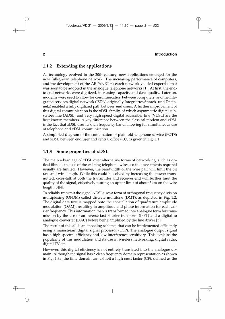
A simplified diagram of the combination of plain old telephone service (POTS)and xDSL between end user and central office (CO) is given in Fig. 1.1.
1.1.3 Some properties of xDSL
The main advantage of xDSL over alternative forms of networking, such as op-tical fibre, is the use of the existing telephone wires, so the investments requiredusually are limited. However, the bandwidth of the wire pair will limit the bitrate and wire length. While this could be solved by increasing the power trans-mitted, cross-talk at both the transmitter and receiver end will further limit thequality of the signal, effectively putting an upper limit of about 5km on the wirelength [3][4].
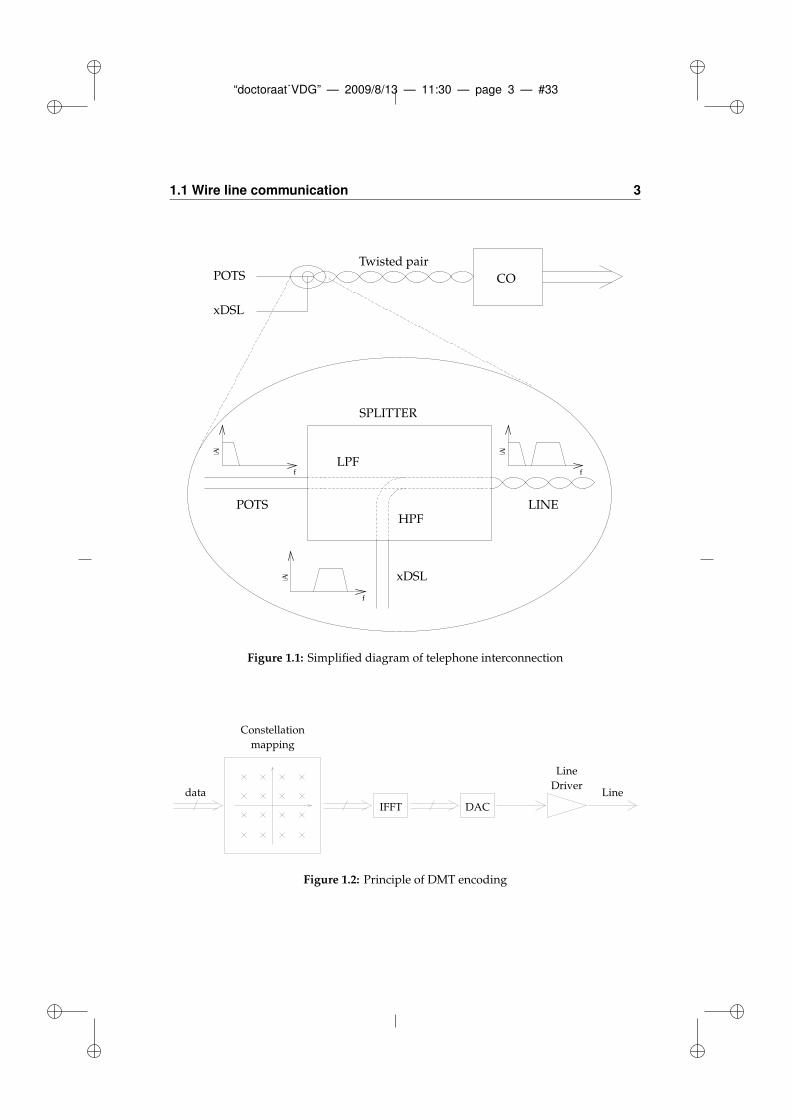
To reliably transmit the signal, xDSL uses a form of orthogonal frequency divisionmultiplexing (OFDM) called discrete multitone (DMT), as depicted in Fig. 1.2.The digital data first is mapped onto the constellation of quadrature amplitudemodulation (QAM), resulting in amplitude and phase information for each car-rier frequency. This information then is transformed into analogue form for trans-mission by the use of an inverse fast Fourier transform (IFFT) and a digital toanalogue converter (DAC) before being amplified by the line driver [5].
The result of this all is an encoding scheme, that can be implemented efficientlyusing a mainstream digital signal processor (DSP). The analogue output signalhas a high spectral efficiency and low interference sensitivity. This explains thepopularity of this modulation and its use in wireless networking, digital radio,digital TV etc.
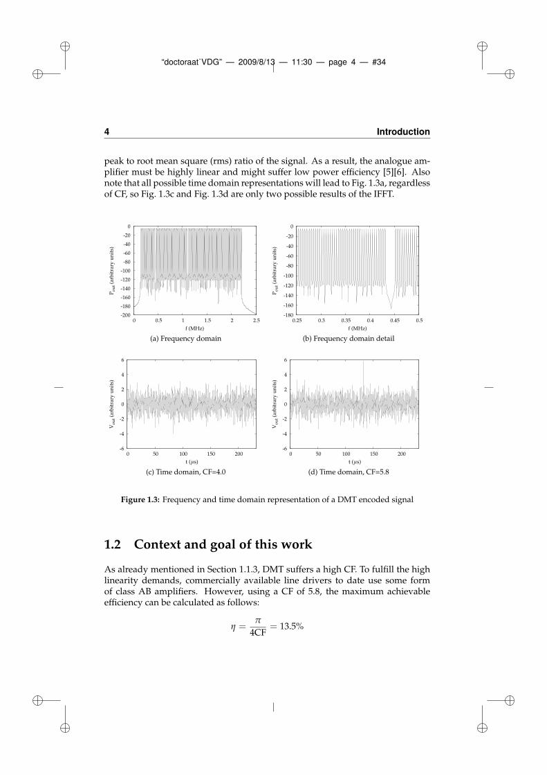
However, this digital efficiency is not entirely translated into the analogue do-main. Although the signal has a clean frequency domain representation as shownin Fig. 1.3a, the time domain can exhibit a high crest factor (CF), defined as the
“doctoraat˙VDG” — 2009/8/13 — 11:30 — page 3 — #33
1.1 Wire line communication 3
LPF
HPF
f
f f
A
A
A
Twisted pairPOTS
xDSL
CO
LINEPOTS
xDSL
SPLITTER
Figure 1.1: Simplified diagram of telephone interconnection
Constellation
mapping
IFFT DAC
Line
Driverdata Line
Figure 1.2: Principle of DMT encoding
“doctoraat˙VDG” — 2009/8/13 — 11:30 — page 4 — #34
4 Introduction
peak to root mean square (rms) ratio of the signal. As a result, the analogue am-plifier must be highly linear and might suffer low power efficiency [5][6]. Alsonote that all possible time domain representations will lead to Fig. 1.3a, regardlessof CF, so Fig. 1.3c and Fig. 1.3d are only two possible results of the IFFT.
-200
-180
-160
-140
-120
-100
-80
-60
-40
-20
0
0 0.5 1 1.5 2 2.5
Po
ut
(arb
itra
ry u
nit
s)
f (MHz)
(a) Frequency domain
-180
-160
-140
-120
-100
-80
-60
-40
-20
0
0.25 0.3 0.35 0.4 0.45 0.5
Po
ut
(arb
itra
ry u
nit
s)
f (MHz)
(b) Frequency domain detail
-6
-4
-2
0
2
4
6
0 50 100 150 200
Vo
ut
(arb
itra
ry u
nit
s)
t (µs)
(c) Time domain, CF=4.0
-6
-4
-2
0
2
4
6
0 50 100 150 200
Vo
ut
(arb
itra
ry u
nit
s)
t (µs)
(d) Time domain, CF=5.8
Figure 1.3: Frequency and time domain representation of a DMT encoded signal
1.2 Context and goal of this work
As already mentioned in Section 1.1.3, DMT suffers a high CF. To fulfill the highlinearity demands, commercially available line drivers to date use some formof class AB amplifiers. However, using a CF of 5.8, the maximum achievableefficiency can be calculated as follows:
η =π
4CF= 13.5%
“doctoraat˙VDG” — 2009/8/13 — 11:30 — page 5 — #35
1.2 Context and goal of this work 5
The result is a tremendous amount of power being dissipated at the CO, whichlimits the number of lines that can be served due to thermal and power require-ments. As such, it might be interesting to investigate the applicability of lesslinear amplifiers. Although their frequency range is much lower, audio ampli-fiers form an excellent source of inspiration, because they have an even worse CF[7].
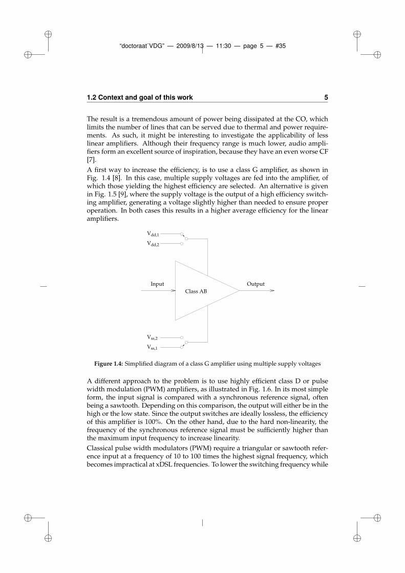
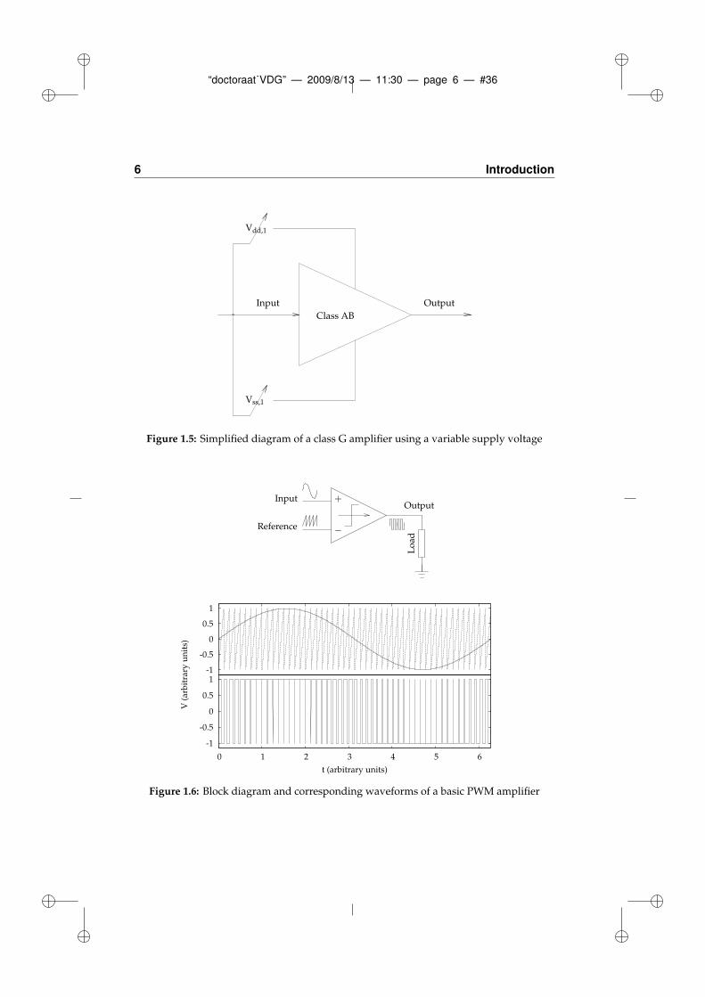
A first way to increase the efficiency, is to use a class G amplifier, as shown inFig. 1.4 [8]. In this case, multiple supply voltages are fed into the amplifier, ofwhich those yielding the highest efficiency are selected. An alternative is givenin Fig. 1.5 [9], where the supply voltage is the output of a high efficiency switch-ing amplifier, generating a voltage slightly higher than needed to ensure properoperation. In both cases this results in a higher average efficiency for the linearamplifiers.
Class AB
Input Output
Vdd,1
Vdd,2
Vss,2
Vss,1
Figure 1.4: Simplified diagram of a class G amplifier using multiple supply voltages
A different approach to the problem is to use highly efficient class D or pulsewidth modulation (PWM) amplifiers, as illustrated in Fig. 1.6. In its most simpleform, the input signal is compared with a synchronous reference signal, oftenbeing a sawtooth. Depending on this comparison, the output will either be in thehigh or the low state. Since the output switches are ideally lossless, the efficiencyof this amplifier is 100%. On the other hand, due to the hard non-linearity, thefrequency of the synchronous reference signal must be sufficiently higher thanthe maximum input frequency to increase linearity.
Classical pulse width modulators (PWM) require a triangular or sawtooth refer-ence input at a frequency of 10 to 100 times the highest signal frequency, whichbecomes impractical at xDSL frequencies. To lower the switching frequency while
“doctoraat˙VDG” — 2009/8/13 — 11:30 — page 6 — #36
6 Introduction
Vdd,1
Vss,1
Class AB
Input Output
Figure 1.5: Simplified diagram of a class G amplifier using a variable supply voltage
+
−
Input
Reference
Lo
ad
Output
-1
-0.5
0
0.5
1
0 1 2 3 4 5 6
t (arbitrary units)
V (
arb
itra
ry u
nit
s)
-1
-0.5
0
0.5
1
Figure 1.6: Block diagram and corresponding waveforms of a basic PWM amplifier

“doctoraat˙VDG” — 2009/8/13 — 11:30 — page 7 — #37
1.3 Outline 7
maintaining an acceptable level of distortion, a suitable feedback scheme has tobe adopted, an example of which is given in Fig. 1.7 [10] for audio amplifiers.In this case, the main output power is delivered by a switching amplifier andswitching is controlled by the error current delivered by a parallel class AB am-plifier. When this current exceeds its threshold in any of both directions, the stateof the class D output stage is changed accordingly. As a result, this amplifieris self-oscillating, at a frequency determined by the current threshold, with theoutput linearized by the class AB amplifier.
AClass AB
Input Output
Vdd
Class D
Lo
ad
Vss
Figure 1.7: Example of an asynchronous mixed class AB and D amplifier
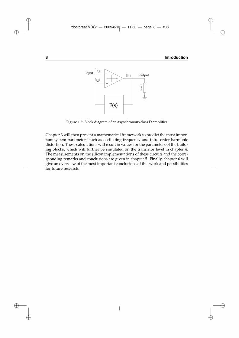
An alternative solution is to drop the external, synchronized reference input anduse a filtered version of the output. By choosing an appropriate filter transferfunction, the broad spectral content of the square wave output will be reduced,resulting in a more triangular signal that can be used as reference as depicted inFig. 1.8 [11]. Basically, this amplifier is an oscillator, due to positive feedback, thushaving the efficiency advantage of PWM circuits, but it should also be possible toachieve a comparable linearity at lower switching frequencies. On the other hand,the non-linearity and the asynchronous nature will complicate the mathematicaldescription and performance prediction of the system.
1.3 Outline
This work is further organized as follows. In chapter 2, the concept from Fig.1.8 is further developed and simulated, finally resulting in the demonstration ofthe feasibility of the basic idea and the presentation of measurement results on asilicon integration of the circuits studied.
“doctoraat˙VDG” — 2009/8/13 — 11:30 — page 8 — #38
8 Introduction
+
−
Lo
ad
OutputInput
F(s)
Figure 1.8: Block diagram of an asynchronous class D amplifier
Chapter 3 will then present a mathematical framework to predict the most impor-tant system parameters such as oscillating frequency and third order harmonicdistortion. These calculations will result in values for the parameters of the build-ing blocks, which will further be simulated on the transistor level in chapter 4.The measurements on the silicon implementations of these circuits and the corre-sponding remarks and conclusions are given in chapter 5. Finally, chapter 6 willgive an overview of the most important conclusions of this work and possibilitiesfor future research.
“doctoraat˙VDG” — 2009/8/13 — 11:30 — page 9 — #39
References
[1] Wikipedia. (2008, Jul.) Telegraphy. [Online]. Available: http://en.wikipedia.org/wiki/Telegraph
[2] Wikipedia. (2008, Jul.) Telephone. [Online]. Available: http://en.wikipedia.org/wiki/Telephone
[3] K. P. Ho, “Broadcast digital subscriber lines using discrete multitone forbroadband access,” Microprocessors and Microsystems, vol. 22, no. 10, pp. 605–610, May 1999.
[4] F. Sjoberg, M. Isaksson, R. Nilsson, P. Odling, S. K. Wilson, and R. O. Borjes-son, “Zipper: a duplex method for VDSL based on DMT,” IEEE Trans. Com-mun., vol. 47, no. 8, pp. 1245–1252, Aug. 1999.
[5] D. J. G. Mestdagh, P. M. P. Spruyt, and B. Biran, “Effect of amplitude clippingin DMT-ADSL transceivers,” Electronics Letters, vol. 29, no. 15, pp. 1354–1355,July 22 1993.
[6] Wikipedia. (2008, Jul.) Orthogonal frequency-division multiplexing.[Online]. Available: http://en.wikipedia.org/wiki/Discrete multitonemodulation
[7] Wikipedia. (2009, Jan.) Crest factor. [Online]. Available: http://en.wikipedia.org/wiki/Crest factor
[8] F. H. Raab, “Average efficiency of class-G power amplifiers,” IEEE Trans.Consum. Electron., vol. CE-32, no. 2, pp. 145–150, May 1986.
[9] H. Nakagaki, N. Amada, and S. Inoue, “A high-efficiency audio poweramplifier,” Journal of the Audio Engineering Society, vol. 31, no. 6, pp. 430–436,Jun. 1983.
[10] R. A. R. van der Zee and E. A. J. M. van Tuijl, “A power efficient audioamplifier combining switching and linear techniques,” IEEE J. Solid-StateCircuits, vol. 34, no. 7, pp. 985–991, Jul. 1999.
“doctoraat˙VDG” — 2009/8/13 — 11:30 — page 10 — #40
10 REFERENCES
[11] J. Vanderkooy, “Comments on ’design parameters important for the opti-mization of very-high-fidelity PWM (class D) audio amplifiers’,” Journal ofthe Audio Engineering Society, vol. 33, no. 10, pp. 809–811, Oct. 1985.
“doctoraat˙VDG” — 2009/8/13 — 11:30 — page 11 — #41
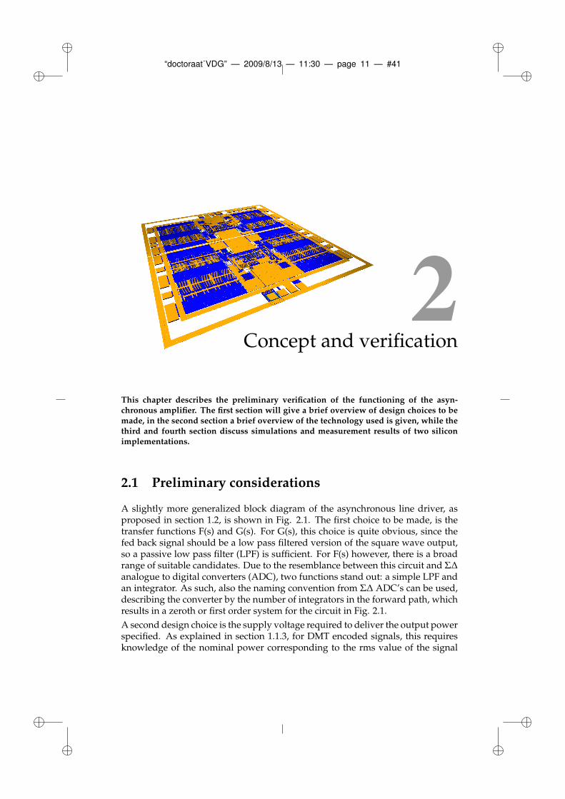
2Concept and verification
This chapter describes the preliminary verification of the functioning of the asyn-chronous amplifier. The first section will give a brief overview of design choices to bemade, in the second section a brief overview of the technology used is given, while thethird and fourth section discuss simulations and measurement results of two siliconimplementations.
2.1 Preliminary considerations
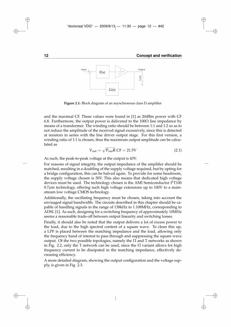
A slightly more generalized block diagram of the asynchronous line driver, asproposed in section 1.2, is shown in Fig. 2.1. The first choice to be made, is thetransfer functions F(s) and G(s). For G(s), this choice is quite obvious, since thefed back signal should be a low pass filtered version of the square wave output,so a passive low pass filter (LPF) is sufficient. For F(s) however, there is a broadrange of suitable candidates. Due to the resemblance between this circuit and Σ∆
analogue to digital converters (ADC), two functions stand out: a simple LPF andan integrator. As such, also the naming convention from Σ∆ ADC’s can be used,describing the converter by the number of integrators in the forward path, whichresults in a zeroth or first order system for the circuit in Fig. 2.1.
A second design choice is the supply voltage required to deliver the output powerspecified. As explained in section 1.1.3, for DMT encoded signals, this requiresknowledge of the nominal power corresponding to the rms value of the signal
“doctoraat˙VDG” — 2009/8/13 — 11:30 — page 12 — #42
12 Concept and verification
F(s)
G(s)
Input Output
Lo
ad
+
−
Figure 2.1: Block diagram of an asynchronous class D amplifier
and the maximal CF. These values were found in [1] as 20dBm power with CF6.8. Furthermore, the output power is delivered to the 100Ω line impedance bymeans of a transformer. The winding ratio should be between 1:1 and 1:2 so as tonot reduce the amplitude of the received signal excessively, since this is detectedat resistors in series with the line driver output stage. For this first version, awinding ratio of 1:1 is chosen, thus the maximum output amplitude can be calcu-lated as
Vout =√
PoutR CF = 21.5V (2.1)
As such, the peak-to-peak voltage at the output is 43V.
For reasons of signal integrity, the output impedance of the amplifier should bematched, resulting in a doubling of the supply voltage required, but by opting fora bridge configuration, this can be halved again. To provide for some headroom,the supply voltage chosen is 50V. This also means that dedicated high voltagedevices must be used. The technology chosen is the AMI Semiconductor I2T1000.7µm technology, offering such high voltage extensions up to 100V to a main-stream low voltage CMOS technology.
Additionally, the oscillating frequency must be chosen, taking into account theenvisaged signal bandwidth. The circuits described in this chapter should be ca-pable of handling signals in the range of 138kHz to 1.108MHz, corresponding toADSL [1]. As such, designing for a switching frequency of approximately 10MHzseems a reasonable trade-off between output linearity and switching losses.
Finally, it should also be noted that the output delivers a lot of excess power tothe load, due to the high spectral content of a square wave. To clean this up,a LPF is placed between the matching impedance and the load, allowing onlythe frequency band of interest to pass through and suppressing the square waveoutput. Of the two possible topologies, namely the Π and T networks as shownin Fig. 2.2, only the T network can be used, since the Π variant allows for highfrequency current to be dissipated in the matching impedance, effectively de-creasing efficiency.
A more detailed diagram, showing the output configuration and the voltage sup-ply, is given in Fig. 2.3.
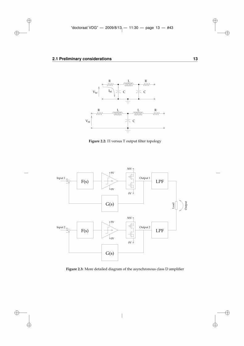
“doctoraat˙VDG” — 2009/8/13 — 11:30 — page 13 — #43
2.1 Preliminary considerations 13
RR
R R
C C
C
L L
L
IhfVhf
Vhf
Figure 2.2: Π versus T output filter topology
F(s)
F(s)
G(s)
G(s)
LPF
LPF
Lo
ad
+
−
+
−
Output 1
Output 2
5V
0V
50V
0V
0V
50V
0V
5V
Input 1
Input 2
Ou
tpu
t
Figure 2.3: More detailed diagram of the asynchronous class D amplifier
“doctoraat˙VDG” — 2009/8/13 — 11:30 — page 14 — #44
14 Concept and verification
Table 2.1: Key characteristics of I2T100 DMOS devices [2]
Device Type Floating Breakdown RDS @ Width perbulk |VDS| = 0.2V mm2
NDMOS N No 100V 70kΩ*µm 48309µmFNDMOS N 100V 100V 33.6kΩ*µm 67568µmPDMOS P 100V -100V 176kΩ*µm 41322µmFPDMOS P 60V -75V 55kΩ*µm 99010µm
This chapter is further organized as follows. Section 2.2 gives a brief overviewof the AMIS I2T100 technology. In section 2.3, simulations on the sub blocks andthe full circuit of the zeroth order system are discussed and compared with mea-surements on a silicon implementation of the circuit. Section 2.4 then describessimulation and measurement results of the first order system.
2.2 Technology overview
The AMI Semiconductor I2T100 technology is a high voltage extension to thestandard 0.7µm CMOS technology, enabling special devices and structures to op-erate at voltages up to 100V, while the low voltage CMOS devices remain thesame as in the 5V technology. Further on, this rather complex technology alsoprovides high voltage DMOS devices, several types of bipolar transistors, in ad-dition to the resistors and capacitors.
DMOS transistors
As the amplifier has a switching output, only the DMOS devices are to be consid-ered, since they show far superior switching behaviour compared with bipolartransistors. Opposed to the low voltage CMOS, the DMOS devices are not sym-metrical. They also have a different gate oxide thickness, allowing for gate-sourcevoltages of up to 12V. The targeted supply voltage of 50V puts a lower limit on thebreakdown voltage, so only four devices are withheld, of which the key charac-teristics are summarized in table 2.1. From this table it is clear that the FNDMOSand FPDMOS are the best choice, since they both have a lower on resistance anda higher area efficiency.
MOS transistors
Table 2.2 gives an overview of the available MOS transistors. Since the processingstarts from a P-doped substrate, the bulk of the PMOS transistors is floating up
“doctoraat˙VDG” — 2009/8/13 — 11:30 — page 15 — #45
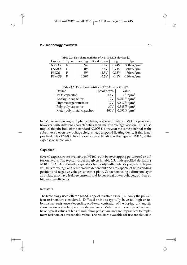
2.2 Technology overview 15
Table 2.2: Key characteristics of I2T100 MOS devices [2]
Device Type Floating Breakdown VT0 IDS
NMOS N No 5.5V 0.74V 358µA/µmFNMOS N 100V 5.5V 0.74V 358µA/µmPMOS P 5V -5.5V -0.95V -176µA/µmFPMOS P 100V -5.5V -1.1V -160µA/µm
Table 2.3: Key characteristics of I2T100 capacitors [2]
Device Breakdown Value
MOS capacitor 5.5V 2fF/µm2
Analogue capacitor 12V 0.750fF/µm2
High voltage transistor 12V 0.812fF/µm2
Poly-poly capacitor 30V 0.345fF/µm2
Metal-poly-metal capacitor 100V 0.091fF/µm2
to 5V. For referencing at higher voltages, a special floating PMOS is provided,however with different characteristics than the low voltage version. This alsoimplies that the bulk of the standard NMOS is always at the same potential as thesubstrate, so even low voltage circuits need a special floating device if this is notpractical. This FNMOS has the same characteristics as the regular NMOS, at theexpense of silicon area.
Capacitors
Several capacitors are available in I2T100, built by overlapping poly, metal or dif-fusion layers. The typical values are given in table 2.3, with specified deviationsof 10 to 15%. Additionally, capacitors built only with metal or polysilicon layerswill be less voltage and temperature dependent and are capable of withstandingpositive and negative voltages on either plate. Capacitors using a diffusion layeras a plate also have leakage currents and lower breakdown voltages, but have ahigher area efficiency.
Resistors
The technology used offers a broad range of resistors as well, but only the polysil-icon resistors are considered. Diffused resistors typically have too high or toolow a sheet resistance, depending on the concentration of the doping, and mostlyshow an excessive temperature dependency. Metal resistors on the other handhave typical values of tens of milliohms per square and are impractical to imple-ment resistors of a reasonable value. The resistors available for use are shown in
“doctoraat˙VDG” — 2009/8/13 — 11:30 — page 16 — #46
16 Concept and verification
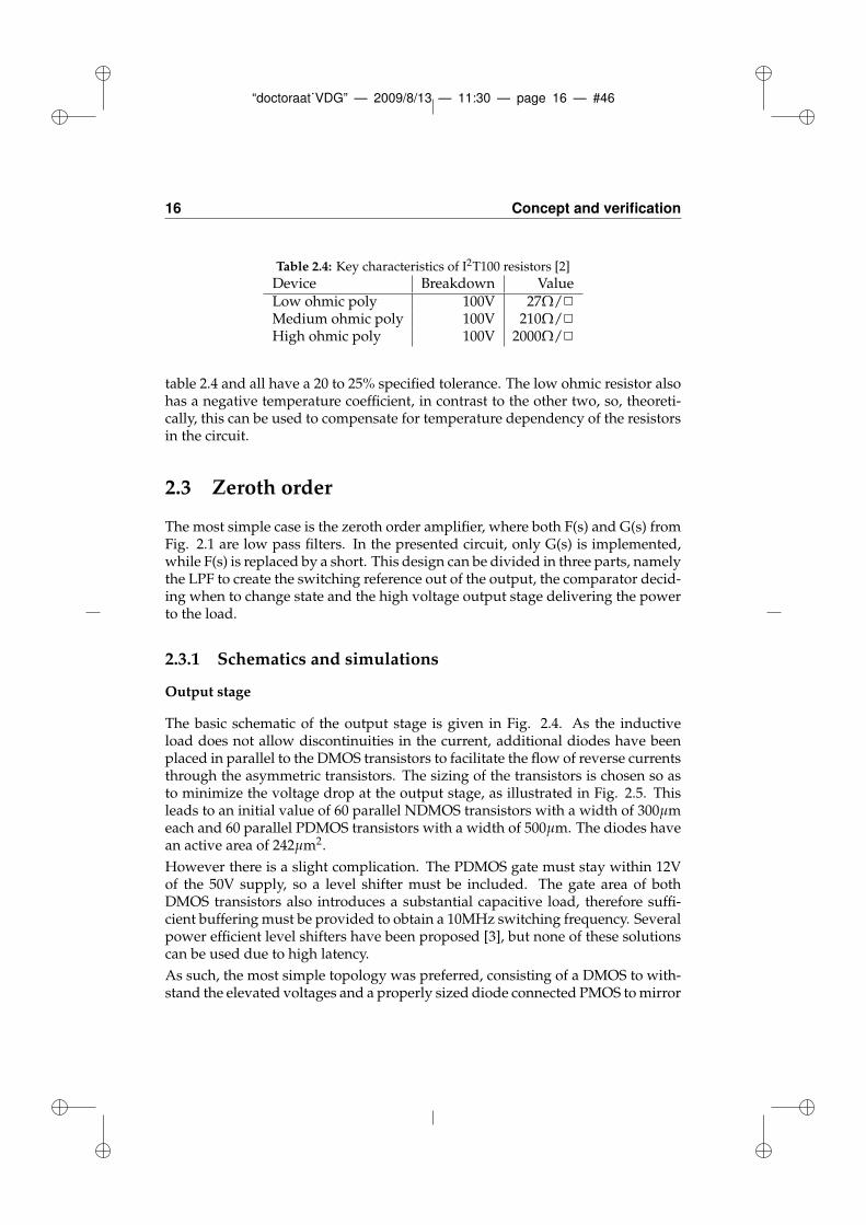
Table 2.4: Key characteristics of I2T100 resistors [2]
Device Breakdown ValueLow ohmic poly 100V 27Ω/2
Medium ohmic poly 100V 210Ω/2
High ohmic poly 100V 2000Ω/2
table 2.4 and all have a 20 to 25% specified tolerance. The low ohmic resistor alsohas a negative temperature coefficient, in contrast to the other two, so, theoreti-cally, this can be used to compensate for temperature dependency of the resistorsin the circuit.
2.3 Zeroth order
The most simple case is the zeroth order amplifier, where both F(s) and G(s) fromFig. 2.1 are low pass filters. In the presented circuit, only G(s) is implemented,while F(s) is replaced by a short. This design can be divided in three parts, namelythe LPF to create the switching reference out of the output, the comparator decid-ing when to change state and the high voltage output stage delivering the powerto the load.
2.3.1 Schematics and simulations
Output stage
The basic schematic of the output stage is given in Fig. 2.4. As the inductiveload does not allow discontinuities in the current, additional diodes have beenplaced in parallel to the DMOS transistors to facilitate the flow of reverse currentsthrough the asymmetric transistors. The sizing of the transistors is chosen so asto minimize the voltage drop at the output stage, as illustrated in Fig. 2.5. Thisleads to an initial value of 60 parallel NDMOS transistors with a width of 300µmeach and 60 parallel PDMOS transistors with a width of 500µm. The diodes havean active area of 242µm2.
However there is a slight complication. The PDMOS gate must stay within 12Vof the 50V supply, so a level shifter must be included. The gate area of bothDMOS transistors also introduces a substantial capacitive load, therefore suffi-cient buffering must be provided to obtain a 10MHz switching frequency. Severalpower efficient level shifters have been proposed [3], but none of these solutionscan be used due to high latency.
As such, the most simple topology was preferred, consisting of a DMOS to with-stand the elevated voltages and a properly sized diode connected PMOS to mirror
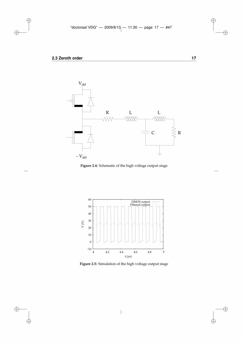
“doctoraat˙VDG” — 2009/8/13 — 11:30 — page 17 — #47
2.3 Zeroth order 17
Vdd
R L L
RC
−Vdd
Figure 2.4: Schematic of the high voltage output stage
-10
0
10
20
30
40
50
60
4 4.2 4.4 4.6 4.8 5
V (
V)
DMOS outputFiltered output
t (µs)
Figure 2.5: Simulation of the high voltage output stage
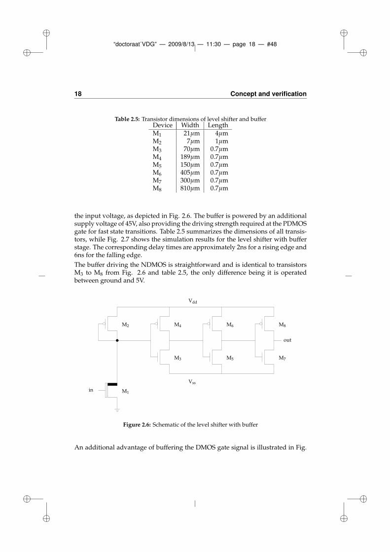
“doctoraat˙VDG” — 2009/8/13 — 11:30 — page 18 — #48
18 Concept and verification
Table 2.5: Transistor dimensions of level shifter and bufferDevice Width LengthM1 21µm 4µmM2 7µm 1µmM3 70µm 0.7µmM4 189µm 0.7µmM5 150µm 0.7µmM6 405µm 0.7µmM7 300µm 0.7µmM8 810µm 0.7µm
the input voltage, as depicted in Fig. 2.6. The buffer is powered by an additionalsupply voltage of 45V, also providing the driving strength required at the PDMOSgate for fast state transitions. Table 2.5 summarizes the dimensions of all transis-tors, while Fig. 2.7 shows the simulation results for the level shifter with bufferstage. The corresponding delay times are approximately 2ns for a rising edge and6ns for the falling edge.
The buffer driving the NDMOS is straightforward and is identical to transistorsM3 to M8 from Fig. 2.6 and table 2.5, the only difference being it is operatedbetween ground and 5V.
Vss
Vdd
M1
M2
M3 M5 M7
M4 M6 M8
out
in
Figure 2.6: Schematic of the level shifter with buffer
An additional advantage of buffering the DMOS gate signal is illustrated in Fig.
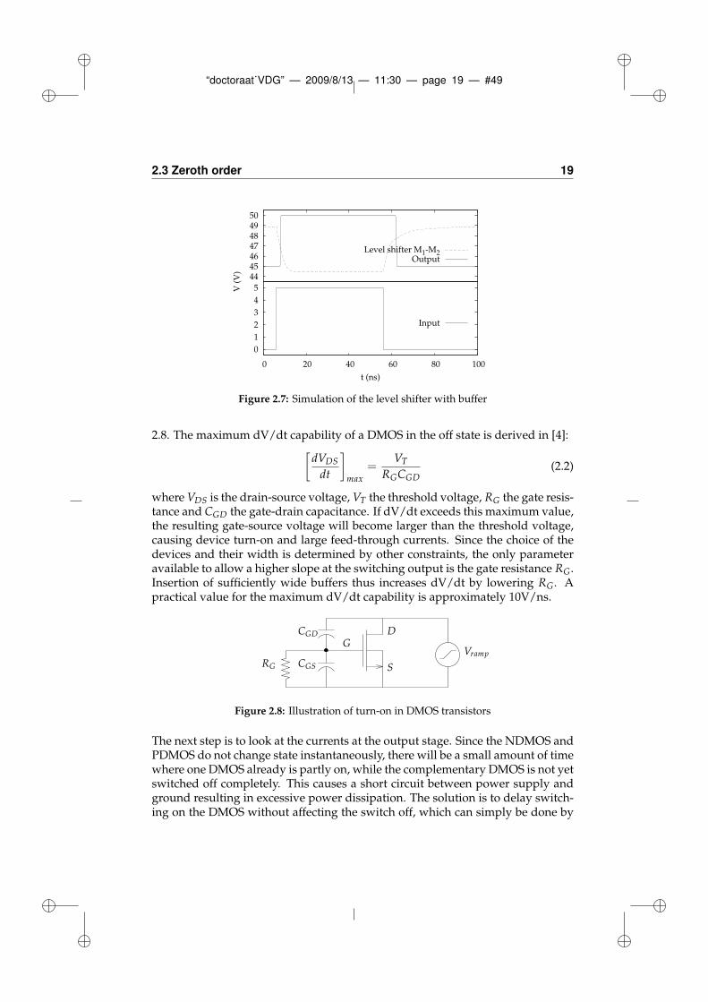
“doctoraat˙VDG” — 2009/8/13 — 11:30 — page 19 — #49
2.3 Zeroth order 19
0
1
2
3
4
5
0 20 40 60 80 100
t (ns)
Input
44 45 46 47 48 49 50
V (
V)
Level shifter M1-M2Output
Figure 2.7: Simulation of the level shifter with buffer
2.8. The maximum dV/dt capability of a DMOS in the off state is derived in [4]:[
dVDS
dt
]
max
=VT
RGCGD(2.2)
where VDS is the drain-source voltage, VT the threshold voltage, RG the gate resis-tance and CGD the gate-drain capacitance. If dV/dt exceeds this maximum value,the resulting gate-source voltage will become larger than the threshold voltage,causing device turn-on and large feed-through currents. Since the choice of thedevices and their width is determined by other constraints, the only parameteravailable to allow a higher slope at the switching output is the gate resistance RG.Insertion of sufficiently wide buffers thus increases dV/dt by lowering RG. Apractical value for the maximum dV/dt capability is approximately 10V/ns.
G
S
Vramp
DCGD
RG CGS
Figure 2.8: Illustration of turn-on in DMOS transistors
The next step is to look at the currents at the output stage. Since the NDMOS andPDMOS do not change state instantaneously, there will be a small amount of timewhere one DMOS already is partly on, while the complementary DMOS is not yetswitched off completely. This causes a short circuit between power supply andground resulting in excessive power dissipation. The solution is to delay switch-ing on the DMOS without affecting the switch off, which can simply be done by
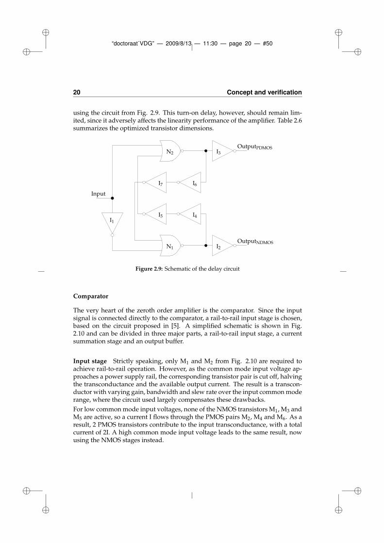
“doctoraat˙VDG” — 2009/8/13 — 11:30 — page 20 — #50
20 Concept and verification
using the circuit from Fig. 2.9. This turn-on delay, however, should remain lim-ited, since it adversely affects the linearity performance of the amplifier. Table 2.6summarizes the optimized transistor dimensions.
OutputNDMOS
OutputPDMOS
Input
N2
N1
I1
I2
I3
I4I5
I6I7
Figure 2.9: Schematic of the delay circuit
Comparator
The very heart of the zeroth order amplifier is the comparator. Since the inputsignal is connected directly to the comparator, a rail-to-rail input stage is chosen,based on the circuit proposed in [5]. A simplified schematic is shown in Fig.2.10 and can be divided in three major parts, a rail-to-rail input stage, a currentsummation stage and an output buffer.
Input stage Strictly speaking, only M1 and M2 from Fig. 2.10 are required toachieve rail-to-rail operation. However, as the common mode input voltage ap-proaches a power supply rail, the corresponding transistor pair is cut off, halvingthe transconductance and the available output current. The result is a transcon-ductor with varying gain, bandwidth and slew rate over the input common moderange, where the circuit used largely compensates these drawbacks.
For low common mode input voltages, none of the NMOS transistors M1, M3 andM5 are active, so a current I flows through the PMOS pairs M2, M4 and M6. As aresult, 2 PMOS transistors contribute to the input transconductance, with a totalcurrent of 2I. A high common mode input voltage leads to the same result, nowusing the NMOS stages instead.
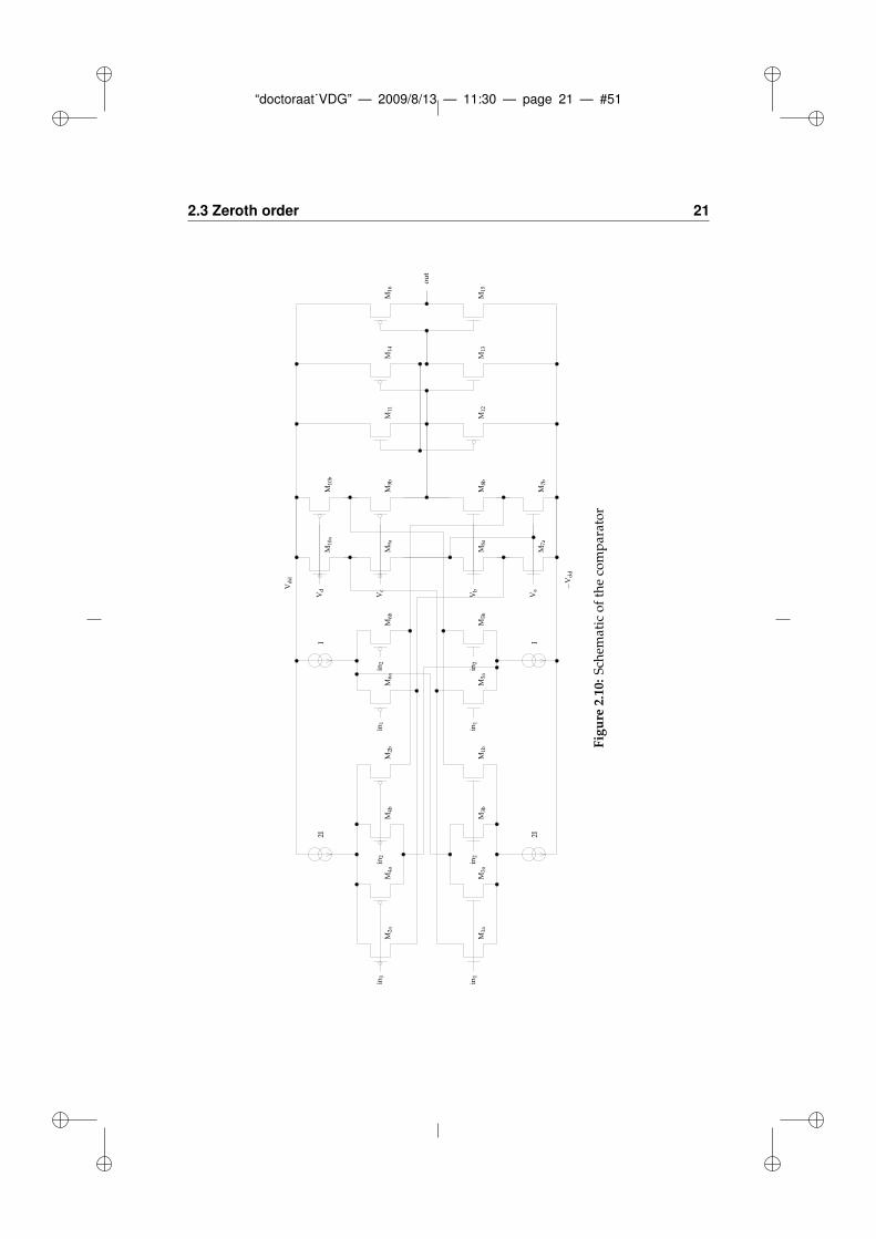
“doctoraat˙VDG” — 2009/8/13 — 11:30 — page 21 — #51
2.3 Zeroth order 21
2I 2III
M2a
M2b
M1a
M1b
M3a
M4a
M4b
M5a
M5b
M6a
M6b
M7b
M8b
M9a
M9b
M10
aM
10b
M11
M12
M13
M14
M15
M16
M3b
M7a
M8a
ou
t
Vd
d
−V
dd
in1
in1
in2
in2
in1
in1
in2
in2
Va
Vb
Vc
Vd
Figure
2.10:
Sch
emat
ico
fth
eco
mp
arat
or
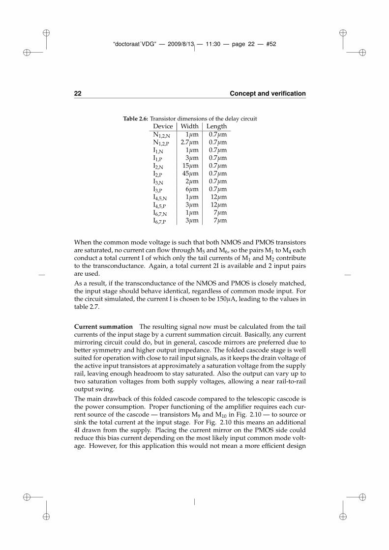
“doctoraat˙VDG” — 2009/8/13 — 11:30 — page 22 — #52
22 Concept and verification
Table 2.6: Transistor dimensions of the delay circuit
Device Width LengthN1,2,N 1µm 0.7µmN1,2,P 2.7µm 0.7µmI1,N 1µm 0.7µmI1,P 3µm 0.7µmI2,N 15µm 0.7µmI2,P 45µm 0.7µmI3,N 2µm 0.7µmI3,P 6µm 0.7µmI4,5,N 1µm 12µmI4,5,P 3µm 12µmI6,7,N 1µm 7µmI6,7,P 3µm 7µm
When the common mode voltage is such that both NMOS and PMOS transistorsare saturated, no current can flow through M5 and M6, so the pairs M1 to M4 eachconduct a total current I of which only the tail currents of M1 and M2 contributeto the transconductance. Again, a total current 2I is available and 2 input pairsare used.
As a result, if the transconductance of the NMOS and PMOS is closely matched,the input stage should behave identical, regardless of common mode input. Forthe circuit simulated, the current I is chosen to be 150µA, leading to the values intable 2.7.
Current summation The resulting signal now must be calculated from the tailcurrents of the input stage by a current summation circuit. Basically, any currentmirroring circuit could do, but in general, cascode mirrors are preferred due tobetter symmetry and higher output impedance. The folded cascode stage is wellsuited for operation with close to rail input signals, as it keeps the drain voltage ofthe active input transistors at approximately a saturation voltage from the supplyrail, leaving enough headroom to stay saturated. Also the output can vary up totwo saturation voltages from both supply voltages, allowing a near rail-to-railoutput swing.
The main drawback of this folded cascode compared to the telescopic cascode isthe power consumption. Proper functioning of the amplifier requires each cur-rent source of the cascode — transistors M9 and M10 in Fig. 2.10 — to source orsink the total current at the input stage. For Fig. 2.10 this means an additional4I drawn from the supply. Placing the current mirror on the PMOS side couldreduce this bias current depending on the most likely input common mode volt-age. However, for this application this would not mean a more efficient design
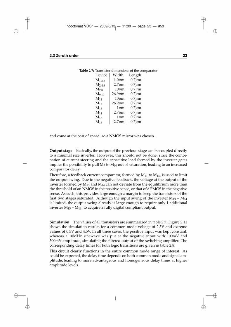
“doctoraat˙VDG” — 2009/8/13 — 11:30 — page 23 — #53
2.3 Zeroth order 23
Table 2.7: Transistor dimensions of the comparator
Device Width LengthM1,3,5 1.0µm 0.7µmM2,4,6 2.7µm 0.7µmM7,8 10µm 0.7µmM9,10 26.9µm 0.7µmM11 10µm 0.7µmM12 26.9µm 0.7µmM13 1µm 0.7µmM14 2.7µm 0.7µmM15 1µm 0.7µmM16 2.7µm 0.7µm
and come at the cost of speed, so a NMOS mirror was chosen.
Output stage Basically, the output of the previous stage can be coupled directlyto a minimal size inverter. However, this should not be done, since the combi-nation of current steering and the capacitive load formed by the inverter gatesimplies the possibility to pull M7 to M10 out of saturation, leading to an increasedcomparator delay.
Therefore, a feedback current comparator, formed by M11 to M14, is used to limitthe output swing. Due to the negative feedback, the voltage at the output of theinverter formed by M13 and M14 can not deviate from the equilibrium more thanthe threshold of an NMOS in the positive sense, or that of a PMOS in the negativesense. As such, this provides large enough a margin to keep the transistors of thefirst two stages saturated. Although the input swing of the inverter M13 – M14
is limited, the output swing already is large enough to require only 1 additionalinverter M15 – M16, to acquire a fully digital compliant output.
Simulation The values of all transistors are summarized in table 2.7. Figure 2.11shows the simulation results for a common mode voltage of 2.5V and extremevalues of 0.5V and 4.5V. In all three cases, the positive input was kept constant,whereas a 10MHz sinewave was put at the negative input with 100mV and500mV amplitude, simulating the filtered output of the switching amplifier. Thecorresponding delay times for both logic transitions are given in table 2.8.
This circuit clearly functions in the entire common mode range of interest. Ascould be expected, the delay time depends on both common mode and signal am-plitude, leading to more advantageous and homogeneous delay times at higheramplitude levels.
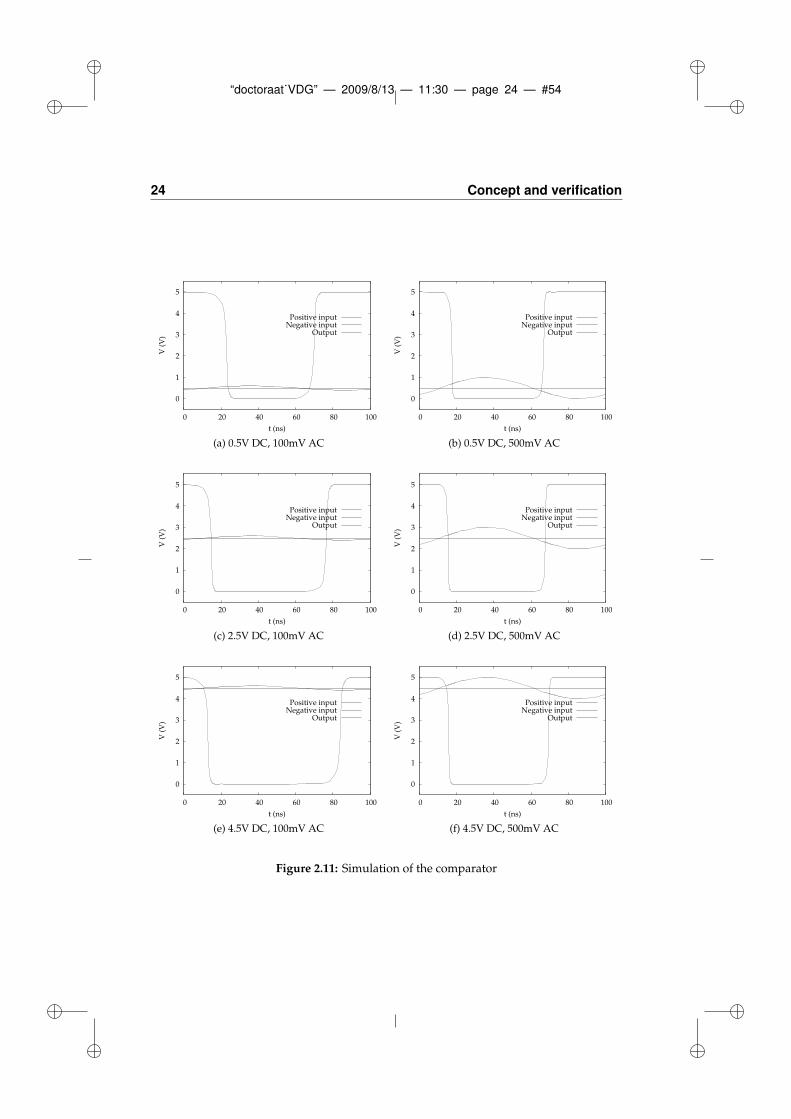
“doctoraat˙VDG” — 2009/8/13 — 11:30 — page 24 — #54
24 Concept and verification
0
1
2
3
4
5
0 20 40 60 80 100
V (
V)
t (ns)
Positive inputNegative input
Output
(a) 0.5V DC, 100mV AC
0
1
2
3
4
5
0 20 40 60 80 100
V (
V)
t (ns)
Positive inputNegative input
Output
(b) 0.5V DC, 500mV AC
0
1
2
3
4
5
0 20 40 60 80 100
V (
V)
t (ns)
Positive inputNegative input
Output
(c) 2.5V DC, 100mV AC
0
1
2
3
4
5
0 20 40 60 80 100
V (
V)
t (ns)
Positive inputNegative input
Output
(d) 2.5V DC, 500mV AC
0
1
2
3
4
5
0 20 40 60 80 100
V (
V)
t (ns)
Positive inputNegative input
Output
(e) 4.5V DC, 100mV AC
0
1
2
3
4
5
0 20 40 60 80 100
V (
V)
t (ns)
Positive inputNegative input
Output
(f) 4.5V DC, 500mV AC
Figure 2.11: Simulation of the comparator
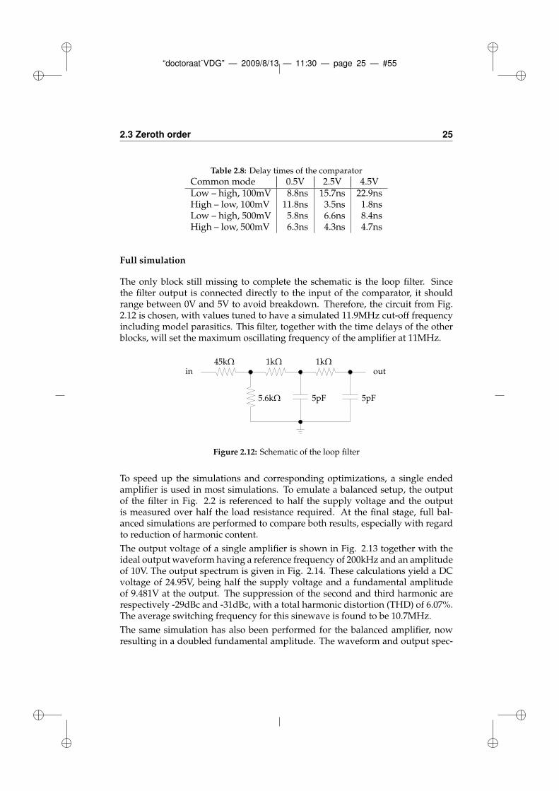
“doctoraat˙VDG” — 2009/8/13 — 11:30 — page 25 — #55
2.3 Zeroth order 25
Table 2.8: Delay times of the comparator
Common mode 0.5V 2.5V 4.5VLow – high, 100mV 8.8ns 15.7ns 22.9nsHigh – low, 100mV 11.8ns 3.5ns 1.8nsLow – high, 500mV 5.8ns 6.6ns 8.4nsHigh – low, 500mV 6.3ns 4.3ns 4.7ns
Full simulation
The only block still missing to complete the schematic is the loop filter. Sincethe filter output is connected directly to the input of the comparator, it shouldrange between 0V and 5V to avoid breakdown. Therefore, the circuit from Fig.2.12 is chosen, with values tuned to have a simulated 11.9MHz cut-off frequencyincluding model parasitics. This filter, together with the time delays of the otherblocks, will set the maximum oscillating frequency of the amplifier at 11MHz.
in out
5pF 5pF
1kΩ1kΩ45kΩ
5.6kΩ
Figure 2.12: Schematic of the loop filter
To speed up the simulations and corresponding optimizations, a single endedamplifier is used in most simulations. To emulate a balanced setup, the outputof the filter in Fig. 2.2 is referenced to half the supply voltage and the outputis measured over half the load resistance required. At the final stage, full bal-anced simulations are performed to compare both results, especially with regardto reduction of harmonic content.
The output voltage of a single amplifier is shown in Fig. 2.13 together with theideal output waveform having a reference frequency of 200kHz and an amplitudeof 10V. The output spectrum is given in Fig. 2.14. These calculations yield a DCvoltage of 24.95V, being half the supply voltage and a fundamental amplitudeof 9.481V at the output. The suppression of the second and third harmonic arerespectively -29dBc and -31dBc, with a total harmonic distortion (THD) of 6.07%.The average switching frequency for this sinewave is found to be 10.7MHz.
The same simulation has also been performed for the balanced amplifier, nowresulting in a doubled fundamental amplitude. The waveform and output spec-
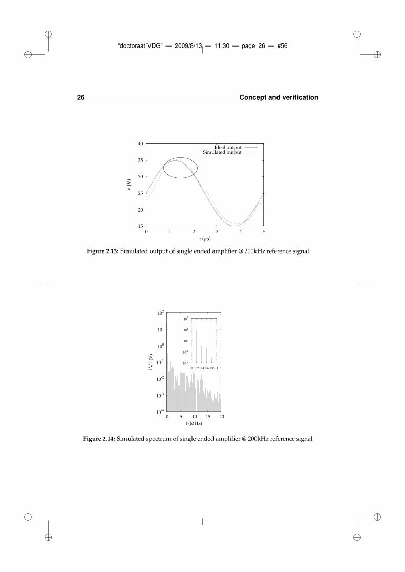
“doctoraat˙VDG” — 2009/8/13 — 11:30 — page 26 — #56
26 Concept and verification
15
20
25
30
35
40
0 1 2 3 4 5
V (
V)
Ideal outputSimulated output
t (µs)
Figure 2.13: Simulated output of single ended amplifier @ 200kHz reference signal
10-4
10-3
10-2
10-1
100
101
102
0 5 10 15 20
|V
| (
V)
f (MHz)
10-2
10-1
100
101
102
0 0.2 0.4 0.6 0.8 1
Figure 2.14: Simulated spectrum of single ended amplifier @ 200kHz reference signal
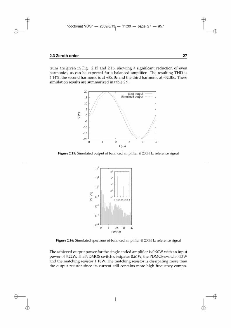
“doctoraat˙VDG” — 2009/8/13 — 11:30 — page 27 — #57
2.3 Zeroth order 27
trum are given in Fig. 2.15 and 2.16, showing a significant reduction of evenharmonics, as can be expected for a balanced amplifier. The resulting THD is4.14%, the second harmonic is at -60dBc and the third harmonic at -32dBc. Thesesimulation results are summarized in table 2.9.
-20
-15
-10
-5
0
5
10
15
20
0 1 2 3 4 5
V (
V)
Ideal outputSimulated output
t (µs)
Figure 2.15: Simulated output of balanced amplifier @ 200kHz reference signal
10-4
10-3
10-2
10-1
100
101
102
0 5 10 15 20
|V
| (
V)
f (MHz)
10-2
10-1
100
101
102
0 0.2 0.4 0.6 0.8 1
Figure 2.16: Simulated spectrum of balanced amplifier @ 200kHz reference signal
The achieved output power for the single ended amplifier is 0.90W with an inputpower of 3.22W. The NDMOS switch dissipates 0.61W, the PDMOS switch 0.53Wand the matching resistor 1.18W. The matching resistor is dissipating more thanthe output resistor since its current still contains more high frequency compo-
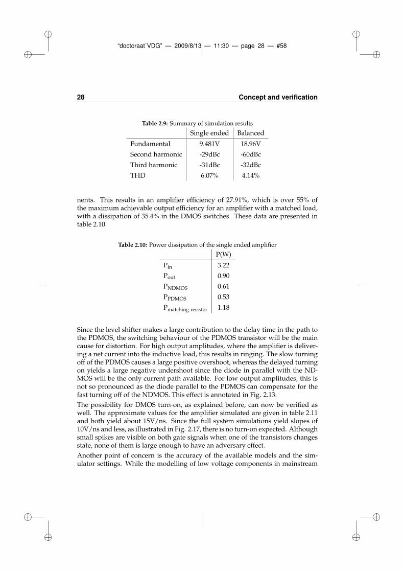
“doctoraat˙VDG” — 2009/8/13 — 11:30 — page 28 — #58
28 Concept and verification
Table 2.9: Summary of simulation results
Single ended Balanced
Fundamental 9.481V 18.96V
Second harmonic -29dBc -60dBc
Third harmonic -31dBc -32dBc
THD 6.07% 4.14%
nents. This results in an amplifier efficiency of 27.91%, which is over 55% ofthe maximum achievable output efficiency for an amplifier with a matched load,with a dissipation of 35.4% in the DMOS switches. These data are presented intable 2.10.
Table 2.10: Power dissipation of the single ended amplifier
P(W)
Pin 3.22
Pout 0.90
PNDMOS 0.61
PPDMOS 0.53
Pmatching resistor 1.18
Since the level shifter makes a large contribution to the delay time in the path tothe PDMOS, the switching behaviour of the PDMOS transistor will be the maincause for distortion. For high output amplitudes, where the amplifier is deliver-ing a net current into the inductive load, this results in ringing. The slow turningoff of the PDMOS causes a large positive overshoot, whereas the delayed turningon yields a large negative undershoot since the diode in parallel with the ND-MOS will be the only current path available. For low output amplitudes, this isnot so pronounced as the diode parallel to the PDMOS can compensate for thefast turning off of the NDMOS. This effect is annotated in Fig. 2.13.
The possibility for DMOS turn-on, as explained before, can now be verified aswell. The approximate values for the amplifier simulated are given in table 2.11and both yield about 15V/ns. Since the full system simulations yield slopes of10V/ns and less, as illustrated in Fig. 2.17, there is no turn-on expected. Althoughsmall spikes are visible on both gate signals when one of the transistors changesstate, none of them is large enough to have an adversary effect.
Another point of concern is the accuracy of the available models and the sim-ulator settings. While the modelling of low voltage components in mainstream
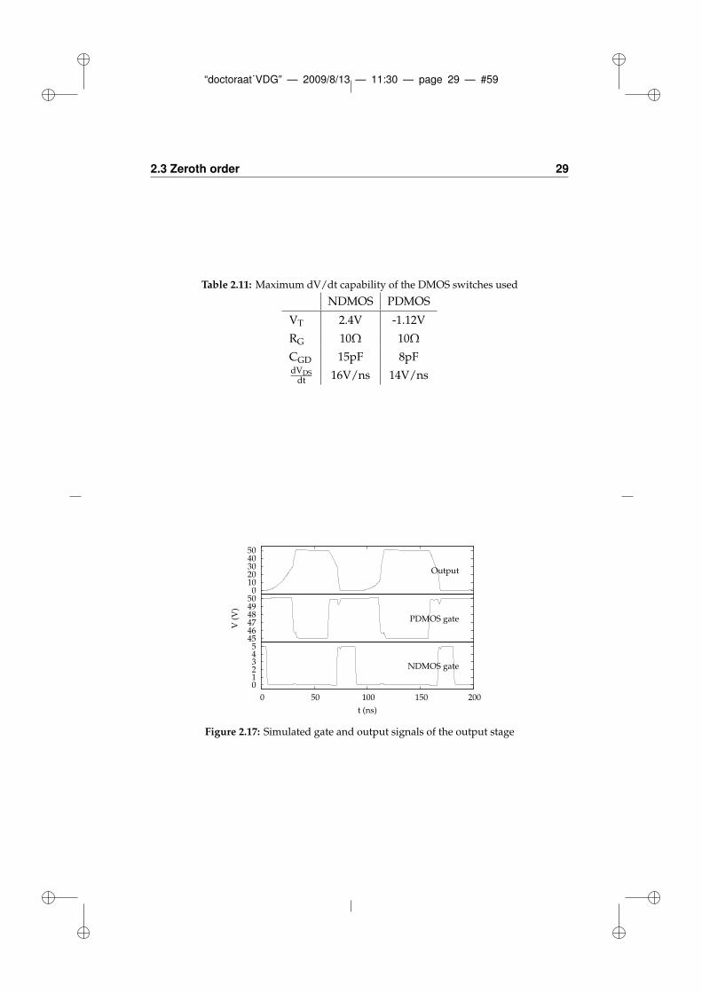
“doctoraat˙VDG” — 2009/8/13 — 11:30 — page 29 — #59
2.3 Zeroth order 29
Table 2.11: Maximum dV/dt capability of the DMOS switches used
NDMOS PDMOS
VT 2.4V -1.12V
RG 10Ω 10Ω
CGD 15pF 8pFdVDS
dt 16V/ns 14V/ns
0 1 2 3 4 5
0 50 100 150 200
t (ns)
NDMOS gate
45 46 47 48 49 50
V (
V)
PDMOS gate
0 10 20 30 40 50
Output
Figure 2.17: Simulated gate and output signals of the output stage
“doctoraat˙VDG” — 2009/8/13 — 11:30 — page 30 — #60
30 Concept and verification
technologies is quite accurate, this is not really the case for high voltage DMOStransistors. Because of their complex, non-symmetric structure, these compo-nents are modelled by a circuit of active and passive components. However thishas serious implications on the fitting of model parameters, causing the modelsof several active subcomponents to be limited to a level 2 or even a level 1 Spicemodel.
Furthermore these models are only valid for a limited transistor width. Since theDMOS transistors must be able to deliver enough power to the load, they haveto be very wide. Therefore they have to be divided in several parallel transistors,as will be the case on the layout too, significantly increasing the simulation time.One also has to adjust the tolerance settings of the simulator to let the simulationconverge, although this might cause some numerical oscillations, especially onsignal currents, decreasing the accuracy.
2.3.2 Layout and measurement results
The simulated amplifier is processed in the AMIS I2T100 high voltage 0.7µmCMOS technology. Since the supply voltage used is 50V and slopes of 10V/nsare expected, special care must be taken while placing and routing the compo-nents, to avoid triggering of parasitic transistors and latch-up. Also EMC-issuesmust be taken into account to avoid excessive coupling of digitized signals intothe analogue building blocks.
A die micrograph of the processed amplifier is shown in Fig. 2.18, where alldifferent parts are annotated. The total area consumption of the chip is 3.3mm2.However, the circuit processed is not completely identical to the simulated one,since multiple measurement pads were inserted, increasing parasitic capaci-tances. Because of this, the circuit was expected to operate at a lower switchingfrequency, causing both a higher THD and efficiency. The measured output sig-nal at a reference frequency of 200kHz and an output amplitude of 10V is givenin Fig. 2.19. The THD was 7.49% with an efficiency of 31% at an average switch-ing frequency of 8MHz, as opposed to the simulation results of Fig. 2.13, wherethe THD equaled 6.07%, with an efficiency of 27.91% at an average switchingfrequency of 10.7MHz.
In Fig. 2.20, both simulated and measured efficiencies are plotted versus fre-quency, while Fig. 2.21 shows the THD. The measured efficiency and distortionare both higher than the simulated ones, as expected. These figures also illustratethe impact of several design choices, for example there is a clear correspondencebetween efficiency and THD, as already mentioned before. Besides this, the THDis also influenced by the cut-off frequency of the output filter. Since this frequencyis 2MHz, it will decrease the THD for higher frequencies by reducing harmoniccontent, while maintaining high efficiency.
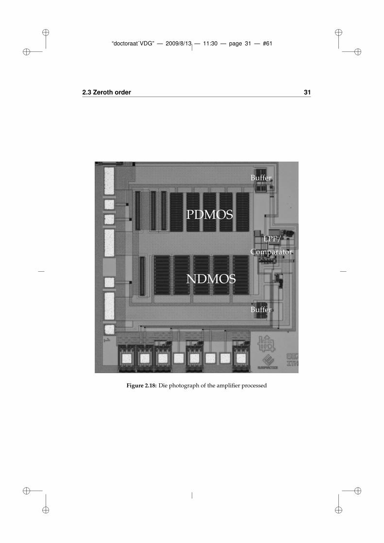
“doctoraat˙VDG” — 2009/8/13 — 11:30 — page 31 — #61
2.3 Zeroth order 31
Buffer
Buffer
LPF/
Comparator
NDMOS
PDMOS
Figure 2.18: Die photograph of the amplifier processed
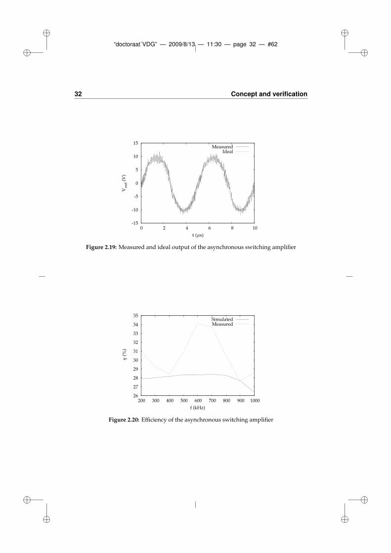
“doctoraat˙VDG” — 2009/8/13 — 11:30 — page 32 — #62
32 Concept and verification
-15
-10
-5
0
5
10
15
0 2 4 6 8 10
Vo
ut
(V)
MeasuredIdeal
t (µs)
Figure 2.19: Measured and ideal output of the asynchronous switching amplifier
26
27
28
29
30
31
32
33
34
35
200 300 400 500 600 700 800 900 1000
f (kHz)
SimulatedMeasured
η(%
)
Figure 2.20: Efficiency of the asynchronous switching amplifier
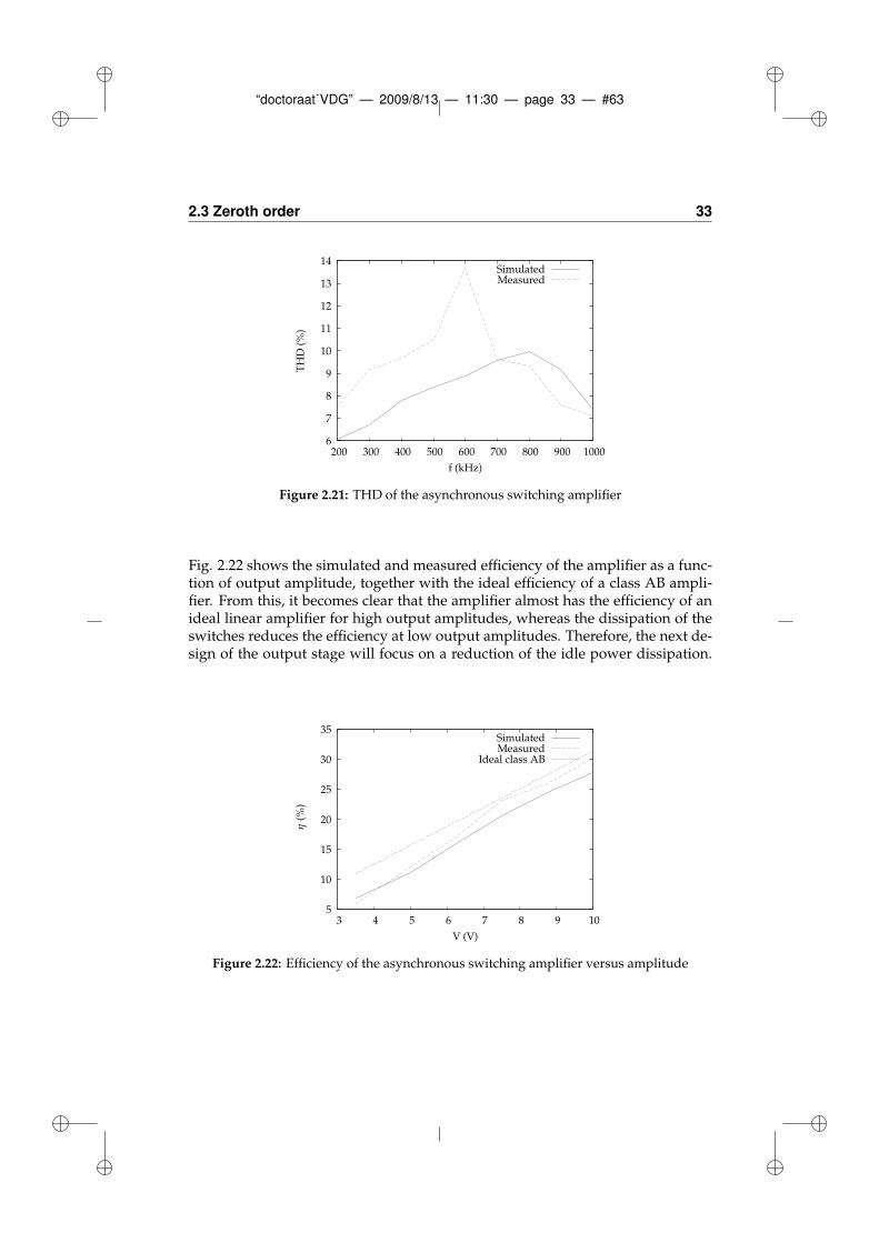
“doctoraat˙VDG” — 2009/8/13 — 11:30 — page 33 — #63
2.3 Zeroth order 33
6
7
8
9
10
11
12
13
14
200 300 400 500 600 700 800 900 1000
TH
D (
%)
f (kHz)
SimulatedMeasured
Figure 2.21: THD of the asynchronous switching amplifier
Fig. 2.22 shows the simulated and measured efficiency of the amplifier as a func-tion of output amplitude, together with the ideal efficiency of a class AB ampli-fier. From this, it becomes clear that the amplifier almost has the efficiency of anideal linear amplifier for high output amplitudes, whereas the dissipation of theswitches reduces the efficiency at low output amplitudes. Therefore, the next de-sign of the output stage will focus on a reduction of the idle power dissipation.
5
10
15
20
25
30
35
3 4 5 6 7 8 9 10
V (V)
SimulatedMeasured
Ideal class AB
η(%
)
Figure 2.22: Efficiency of the asynchronous switching amplifier versus amplitude
“doctoraat˙VDG” — 2009/8/13 — 11:30 — page 34 — #64
34 Concept and verification
2.4 First order
The next test case is the first order amplifier, where F(s) is an integrator and G(s)again is a low pass filter, using the same notations as in Fig. 2.1. The presenceof the integrator in the circuit requires some additional building blocks, such asan operational amplifier and a biasing circuit, but the need for a rail-to-rail com-parator vanishes. Also, the amplifier output now is made fully balanced by usingtwo output stages, steered in counterphase, as shown in Fig. 2.23. The resultingsubcircuits that will be discussed, are the integrator, the comparator, the biasingcircuit and finally the new output stage.
Input
Lo
ad
LPF
LPF
Ou
tpu
t
Output 1
Output 2
Figure 2.23: Block diagram of the modified balanced asynchronous class D amplifier
2.4.1 Schematics and simulations
Opamp and integrator
The integrator as used in Fig. 2.23 has three inputs, thus before designing theopamp itself, a suitable circuit must be selected. Using the nullator hypothesis, itis easily derived that the circuit from Fig. 2.24 has the following transfer function:
Vout =(Vi1 −Vi2) −Vin
sRC(2.3)
where Vin is the reference input, Vout the opamp output and Vi1 and Vi2 the inphase respectively counter phase filtered output signals of the line driver. Thisalso implies an additional halving of the output signal by the loop filter, to mapthe balanced output range to the single ended input.
Since the fed back signals Vi1 and Vi2 will span a limited voltage range and are
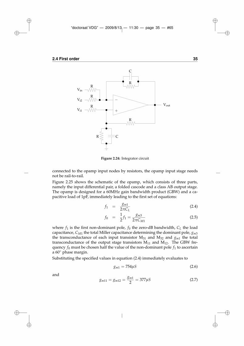
“doctoraat˙VDG” — 2009/8/13 — 11:30 — page 35 — #65
2.4 First order 35
+
−
R
R
R
R
R
R
C
C
Vout
Vin
Vi2
Vi1
Figure 2.24: Integrator circuit
connected to the opamp input nodes by resistors, the opamp input stage needsnot be rail-to-rail.
Figure 2.25 shows the schematic of the opamp, which consists of three parts,namely the input differential pair, a folded cascode and a class AB output stage.The opamp is designed for a 60MHz gain bandwidth product (GBW) and a ca-pacitive load of 1pF, immediately leading to the first set of equations:
f1 =gm1
2πCL(2.4)
f0 =1
2f1 =
gm3
2πCM1(2.5)
where f1 is the first non-dominant pole, f0 the zero-dB bandwidth, CL the loadcapacitance, CM1 the total Miller capacitance determining the dominant pole, gm3
the transconductance of each input transistor M31 and M32 and gm1 the totaltransconductance of the output stage transistors M11 and M12. The GBW fre-quency f0 must be chosen half the value of the non-dominant pole f1 to ascertaina 60 phase margin.
Substituting the specified values in equation (2.4) immediately evaluates to
gm1 = 754µS (2.6)
andgm11 = gm12 =
gm1
2= 377µS (2.7)
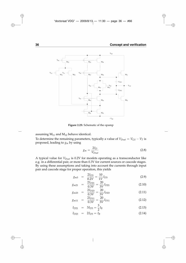
“doctoraat˙VDG” — 2009/8/13 — 11:30 — page 36 — #66
36 Concept and verification
Vdd
−Vdd
M31 M32
M21 M22
M23 M24
M25 M26
M27 M28
M13 M14
M11
M12
CM11
CM12
Vout
Vin+ Vin−
M33
Vb2
Vb1
Vb6 Vb5
Vb4
Figure 2.25: Schematic of the opamp
assuming M11 and M12 behave identical.
To determine the remaining parameters, typically a value of VDsat = VGS −VT isproposed, leading to gm by using
gm =2IDVDsat
(2.8)
A typical value for VDsat is 0.2V for mosfets operating as a transconductor likee.g. in a differential pair, or more than 0.3V for current sources or cascode stages.By using these assumptions and taking into account the currents through inputpair and cascode stage for proper operation, this yields
gm3 =2ID3
0.2V=
10
1VID3 (2.9)
gm21 =2ID21
0.3V=
20
3VID21 (2.10)
gm23 =2ID23
0.3V=
20
3VID23 (2.11)
gm11 =2ID11
0.3V=
20
3VID11 (2.12)
ID21 = 3ID3 =3
2IB (2.13)
ID23 = 2ID3 = IB (2.14)
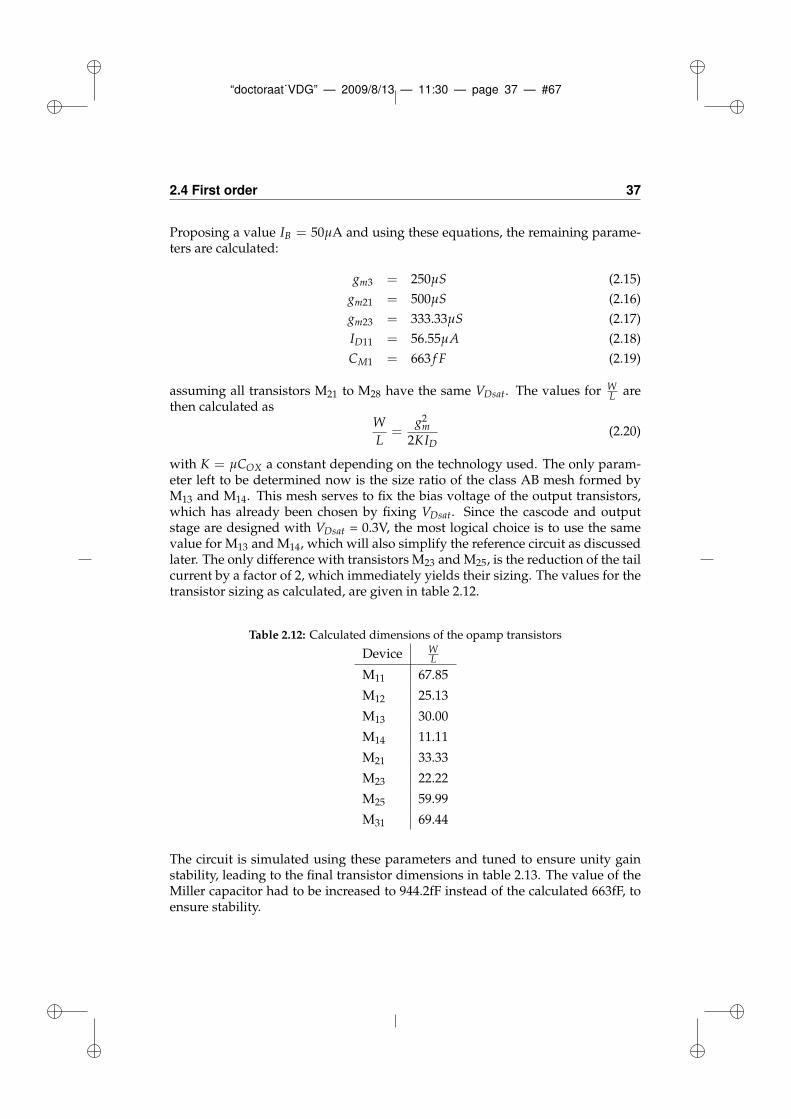
“doctoraat˙VDG” — 2009/8/13 — 11:30 — page 37 — #67
2.4 First order 37
Proposing a value IB = 50µA and using these equations, the remaining parame-ters are calculated:
gm3 = 250µS (2.15)
gm21 = 500µS (2.16)
gm23 = 333.33µS (2.17)
ID11 = 56.55µA (2.18)
CM1 = 663 f F (2.19)
assuming all transistors M21 to M28 have the same VDsat. The values for WL are
then calculated asW
L=
g2m
2KID(2.20)
with K = µCOX a constant depending on the technology used. The only param-eter left to be determined now is the size ratio of the class AB mesh formed byM13 and M14. This mesh serves to fix the bias voltage of the output transistors,which has already been chosen by fixing VDsat. Since the cascode and outputstage are designed with VDsat = 0.3V, the most logical choice is to use the samevalue for M13 and M14, which will also simplify the reference circuit as discussedlater. The only difference with transistors M23 and M25, is the reduction of the tailcurrent by a factor of 2, which immediately yields their sizing. The values for thetransistor sizing as calculated, are given in table 2.12.
Table 2.12: Calculated dimensions of the opamp transistors
Device WL
M11 67.85
M12 25.13
M13 30.00
M14 11.11
M21 33.33
M23 22.22
M25 59.99
M31 69.44
The circuit is simulated using these parameters and tuned to ensure unity gainstability, leading to the final transistor dimensions in table 2.13. The value of theMiller capacitor had to be increased to 944.2fF instead of the calculated 663fF, toensure stability.
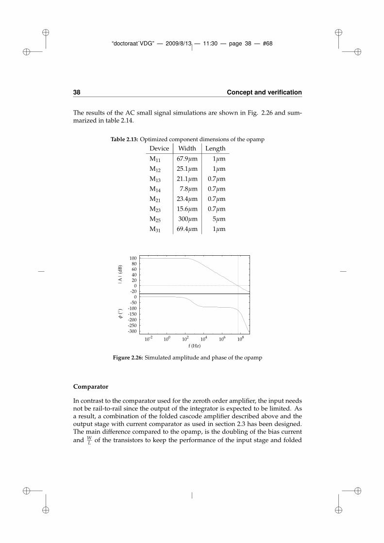
“doctoraat˙VDG” — 2009/8/13 — 11:30 — page 38 — #68
38 Concept and verification
The results of the AC small signal simulations are shown in Fig. 2.26 and sum-marized in table 2.14.
Table 2.13: Optimized component dimensions of the opamp
Device Width Length
M11 67.9µm 1µm
M12 25.1µm 1µm
M13 21.1µm 0.7µm
M14 7.8µm 0.7µm
M21 23.4µm 0.7µm
M23 15.6µm 0.7µm
M25 300µm 5µm
M31 69.4µm 1µm
-300-250-200-150-100
-50 0
10-2 100 102 104 106 108
f (Hz)
-20 0
20 40 60 80
100
|A
| (
dB
)φ
()
Figure 2.26: Simulated amplitude and phase of the opamp
Comparator
In contrast to the comparator used for the zeroth order amplifier, the input needsnot be rail-to-rail since the output of the integrator is expected to be limited. Asa result, a combination of the folded cascode amplifier described above and theoutput stage with current comparator as used in section 2.3 has been designed.The main difference compared to the opamp, is the doubling of the bias current
and WL of the transistors to keep the performance of the input stage and folded
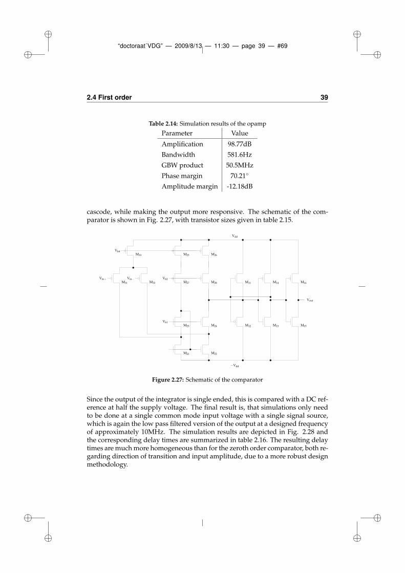
“doctoraat˙VDG” — 2009/8/13 — 11:30 — page 39 — #69
2.4 First order 39
Table 2.14: Simulation results of the opamp
Parameter Value
Amplification 98.77dB
Bandwidth 581.6Hz
GBW product 50.5MHz
Phase margin 70.21
Amplitude margin -12.18dB
cascode, while making the output more responsive. The schematic of the com-parator is shown in Fig. 2.27, with transistor sizes given in table 2.15.
M31 M32
M25 M26
M27 M28
Vin+ Vin−
M21 M22
M23 M24
M11
M12 M13
M14
M15
M16
M33
Vout
−Vdd
Vdd
Vb2
Vb1
Vb4
Figure 2.27: Schematic of the comparator
Since the output of the integrator is single ended, this is compared with a DC ref-erence at half the supply voltage. The final result is, that simulations only needto be done at a single common mode input voltage with a single signal source,which is again the low pass filtered version of the output at a designed frequencyof approximately 10MHz. The simulation results are depicted in Fig. 2.28 andthe corresponding delay times are summarized in table 2.16. The resulting delaytimes are much more homogeneous than for the zeroth order comparator, both re-garding direction of transition and input amplitude, due to a more robust designmethodology.
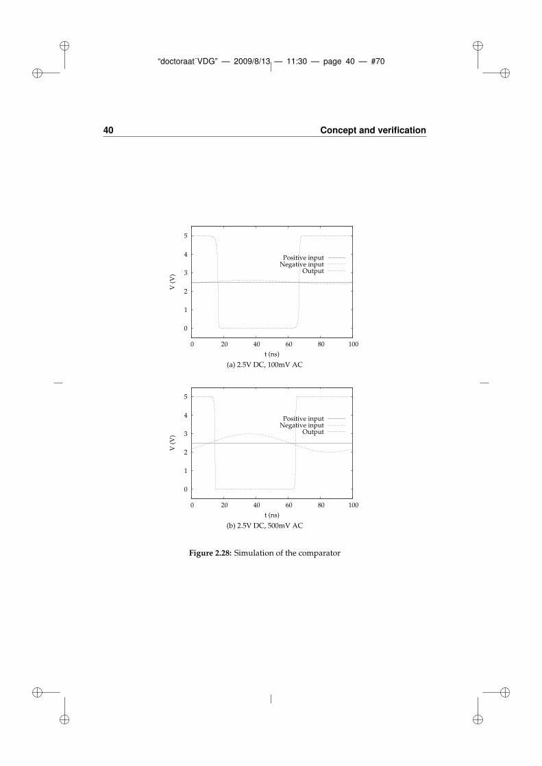
“doctoraat˙VDG” — 2009/8/13 — 11:30 — page 40 — #70
40 Concept and verification
0
1
2
3
4
5
0 20 40 60 80 100
V (
V)
t (ns)
Positive inputNegative input
Output
(a) 2.5V DC, 100mV AC
0
1
2
3
4
5
0 20 40 60 80 100
V (
V)
t (ns)
Positive inputNegative input
Output
(b) 2.5V DC, 500mV AC
Figure 2.28: Simulation of the comparator
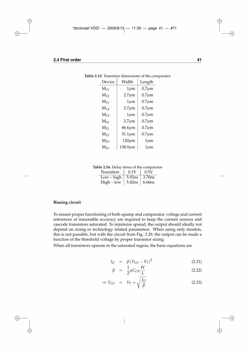
“doctoraat˙VDG” — 2009/8/13 — 11:30 — page 41 — #71
2.4 First order 41
Table 2.15: Transistor dimensions of the comparator
Device Width Length
M11 1µm 0.7µm
M12 2.7µm 0.7µm
M13 1µm 0.7µm
M14 2.7µm 0.7µm
M15 1µm 0.7µm
M16 2.7µm 0.7µm
M21 46.6µm 0.7µm
M23 31.1µm 0.7µm
M25 120µm 1µm
M31 138.9µm 1µm
Table 2.16: Delay times of the comparator
Transition 0.1V 0.5VLow – high 5.92ns 3.70nsHigh – low 5.42ns 6.66ns
Biasing circuit
To ensure proper functioning of both opamp and comparator, voltage and currentreferences of reasonable accuracy are required to keep the current sources andcascode transistors saturated. To minimize spread, the output should ideally notdepend on sizing or technology related parameters. When using only mosfets,this is not possible, but with the circuit from Fig. 2.29, the output can be made afunction of the threshold voltage by proper transistor sizing.
When all transistors operate in the saturated region, the basic equations are
ID = β (VGS −VT)2 (2.21)
β =1
2µCOX
W
L(2.22)
⇒ VGS = VT +
√
IDβ
(2.23)
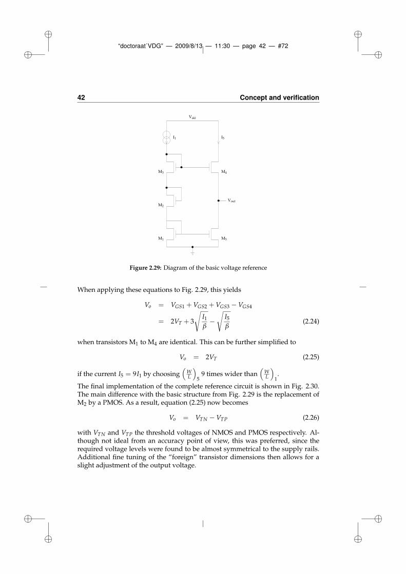
“doctoraat˙VDG” — 2009/8/13 — 11:30 — page 42 — #72
42 Concept and verification
M5M1
M2
M3 M4
I1 I5
Vdd
Vout
Figure 2.29: Diagram of the basic voltage reference
When applying these equations to Fig. 2.29, this yields
Vo = VGS1 +VGS2 +VGS3 −VGS4
= 2VT + 3
√
I1β−√
I5β
(2.24)
when transistors M1 to M4 are identical. This can be further simplified to
Vo = 2VT (2.25)
if the current I5 = 9I1 by choosing(
WL
)
59 times wider than
(
WL
)
1.
The final implementation of the complete reference circuit is shown in Fig. 2.30.The main difference with the basic structure from Fig. 2.29 is the replacement ofM2 by a PMOS. As a result, equation (2.25) now becomes
Vo = VTN −VTP (2.26)
with VTN and VTP the threshold voltages of NMOS and PMOS respectively. Al-though not ideal from an accuracy point of view, this was preferred, since therequired voltage levels were found to be almost symmetrical to the supply rails.Additional fine tuning of the “foreign” transistor dimensions then allows for aslight adjustment of the output voltage.
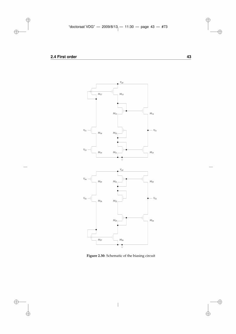
“doctoraat˙VDG” — 2009/8/13 — 11:30 — page 43 — #73
2.4 First order 43
M11
M12
M13 M14
M15
M13M17
M18
M19
Vb1
Vb3
Vb1
Vdd
M21
M22
M23 M24
M25
M26
M29
M28
M27
Vb2Vb2
Vb4
Vdd
Figure 2.30: Schematic of the biasing circuit
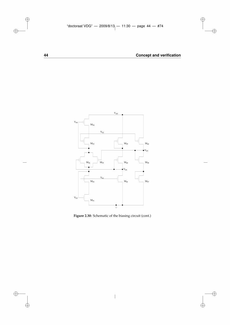
“doctoraat˙VDG” — 2009/8/13 — 11:30 — page 44 — #74
44 Concept and verification
M31
M32
M35M36
M33
M34
M37
M38
M39
M40
M41
M42
Vb5
Vb6
Vb2
Vb1
Vb3
Vb4
Vdd
Figure 2.30: Schematic of the biasing circuit (cont.)

“doctoraat˙VDG” — 2009/8/13 — 11:30 — page 45 — #75
2.4 First order 45
The additional circuitry from Fig. 2.30 implements the remaining biasing of thecurrent sources and the class AB mesh. Since the cascode, the output and themesh transistors from the opamp in Fig. 2.25 were designed with identical VDsat,M37 to M40 can have the same dimensions as M31 and M33 if they conduct thesame current. The reference current is chosen 5 times smaller than for the opampcircuit, so the size ratio must be 5 times smaller as well. Table 2.17 gives a sum-mary of all transistor dimensions, table 2.18 shows the resulting output voltagesand currents.
Table 2.17: Transistor dimensions of the reference circuit
Device Width Length
M11,13,14 1.6µm 1µm
M12 4.3µm 1µm
M15 14.4µm 1µm
M16,17 4.4µm 1µm
M18,19 22.2µm 5µm
M21,23,24 3.1µm 0.7µm
M22 1.1µm 0.7µm
M25 27.9µm 0.7µm
M26,27 1.6µm 1µm
M28,29 60µm 5µm
M31,32,37,38 22.2µm 5µm
M33,34,39,40 60µm 5µm
M35 11.1µm 5µm
M36 30µm 5µm
M41 1µm 2µm
M42 2.2µm 1µm
Output stage
The output stage has undergone a major revision, not so much in basic structureas in sizing, to decrease overall power consumption. First of all, the size of theoutput transistors is drastically reduced to 60 parallel NDMOS transistors with awidth of 100µm and 60 parallel PDMOS transistors with a width of 150µm each,to reduce the parasitic capacitances and the feed-through currents. Additionally,the parallel diodes were removed, since they did not seem to significantly affect
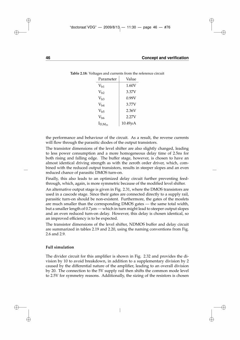
“doctoraat˙VDG” — 2009/8/13 — 11:30 — page 46 — #76
46 Concept and verification
Table 2.18: Voltages and currents from the reference circuit
Parameter Value
Vb1 1.60V
Vb2 3.37V
Vb3 0.99V
Vb4 3.77V
Vb5 2.36V
Vb6 2.27V
ID,M3110.49µA
the performance and behaviour of the circuit. As a result, the reverse currentswill flow through the parasitic diodes of the output transistors.
The transistor dimensions of the level shifter are also slightly changed, leadingto less power consumption and a more homogeneous delay time of 2.5ns forboth rising and falling edge. The buffer stage, however, is chosen to have analmost identical driving strength as with the zeroth order driver, which, com-bined with the reduced output transistors, results in steeper slopes and an evenreduced chance of parasitic DMOS turn-on.
Finally, this also leads to an optimized delay circuit further preventing feed-through, which, again, is more symmetric because of the modified level shifter.
An alternative output stage is given in Fig. 2.31, where the DMOS transistors areused in a cascode stage. Since their gates are connected directly to a supply rail,parasitic turn-on should be non-existent. Furthermore, the gates of the mosfetsare much smaller than the corresponding DMOS gates — the same total width,but a smaller length of 0.7µm — which in turn might lead to steeper output slopesand an even reduced turn-on delay. However, this delay is chosen identical, soan improved efficiency is to be expected.
The transistor dimensions of the level shifter, NDMOS buffer and delay circuitare summarized in tables 2.19 and 2.20, using the naming conventions from Fig.2.6 and 2.9.
Full simulation
The divider circuit for this amplifier is shown in Fig. 2.32 and provides the di-vision by 10 to avoid breakdown, in addition to a supplementary division by 2caused by the differential nature of the amplifier, leading to an overall divisionby 20. The connection to the 5V supply rail then shifts the common mode levelto 2.5V for symmetry reasons. Additionally, the sizing of the resistors is chosen
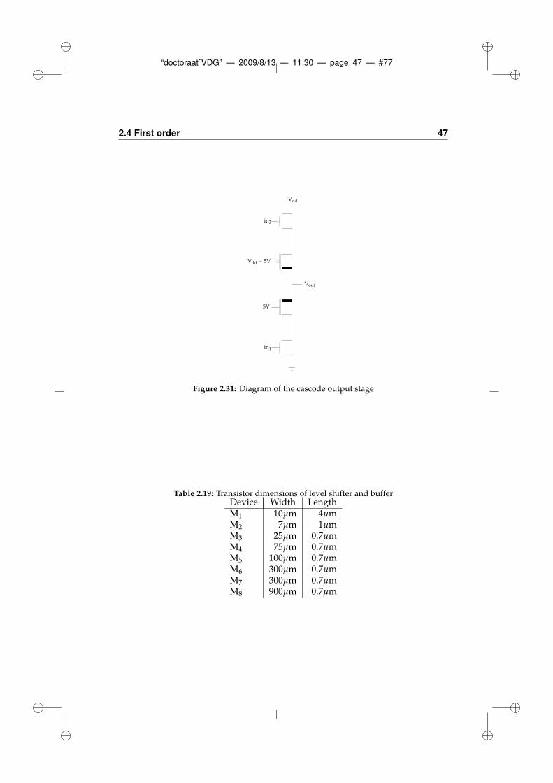
“doctoraat˙VDG” — 2009/8/13 — 11:30 — page 47 — #77
2.4 First order 47
5V
Vdd − 5V
Vdd
in2
in1
Vout
Figure 2.31: Diagram of the cascode output stage
Table 2.19: Transistor dimensions of level shifter and bufferDevice Width LengthM1 10µm 4µmM2 7µm 1µmM3 25µm 0.7µmM4 75µm 0.7µmM5 100µm 0.7µmM6 300µm 0.7µmM7 300µm 0.7µmM8 900µm 0.7µm
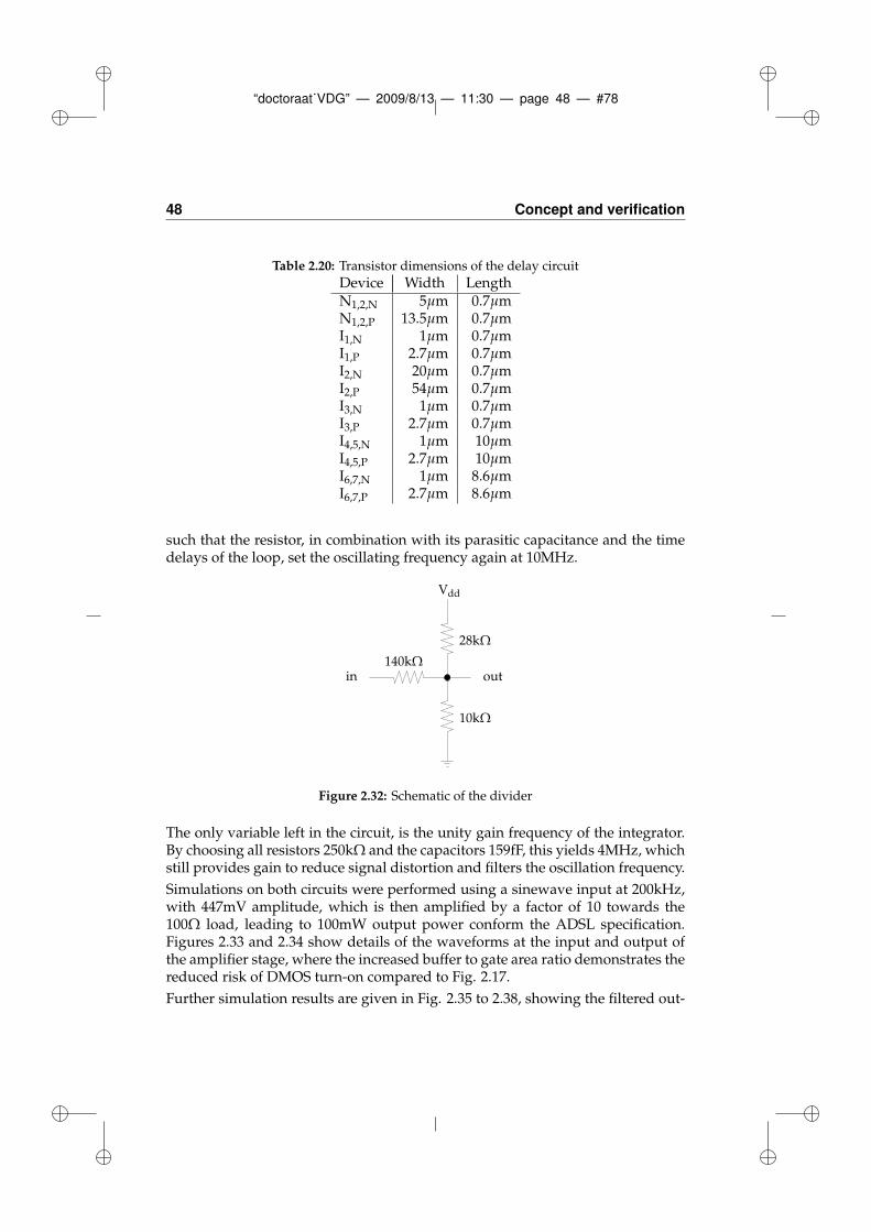
“doctoraat˙VDG” — 2009/8/13 — 11:30 — page 48 — #78
48 Concept and verification
Table 2.20: Transistor dimensions of the delay circuit
Device Width LengthN1,2,N 5µm 0.7µmN1,2,P 13.5µm 0.7µmI1,N 1µm 0.7µmI1,P 2.7µm 0.7µmI2,N 20µm 0.7µmI2,P 54µm 0.7µmI3,N 1µm 0.7µmI3,P 2.7µm 0.7µmI4,5,N 1µm 10µmI4,5,P 2.7µm 10µmI6,7,N 1µm 8.6µmI6,7,P 2.7µm 8.6µm
such that the resistor, in combination with its parasitic capacitance and the timedelays of the loop, set the oscillating frequency again at 10MHz.
in out140kΩ
28kΩ
10kΩ
Vdd
Figure 2.32: Schematic of the divider
The only variable left in the circuit, is the unity gain frequency of the integrator.By choosing all resistors 250kΩ and the capacitors 159fF, this yields 4MHz, whichstill provides gain to reduce signal distortion and filters the oscillation frequency.
Simulations on both circuits were performed using a sinewave input at 200kHz,with 447mV amplitude, which is then amplified by a factor of 10 towards the100Ω load, leading to 100mW output power conform the ADSL specification.Figures 2.33 and 2.34 show details of the waveforms at the input and output ofthe amplifier stage, where the increased buffer to gate area ratio demonstrates thereduced risk of DMOS turn-on compared to Fig. 2.17.
Further simulation results are given in Fig. 2.35 to 2.38, showing the filtered out-
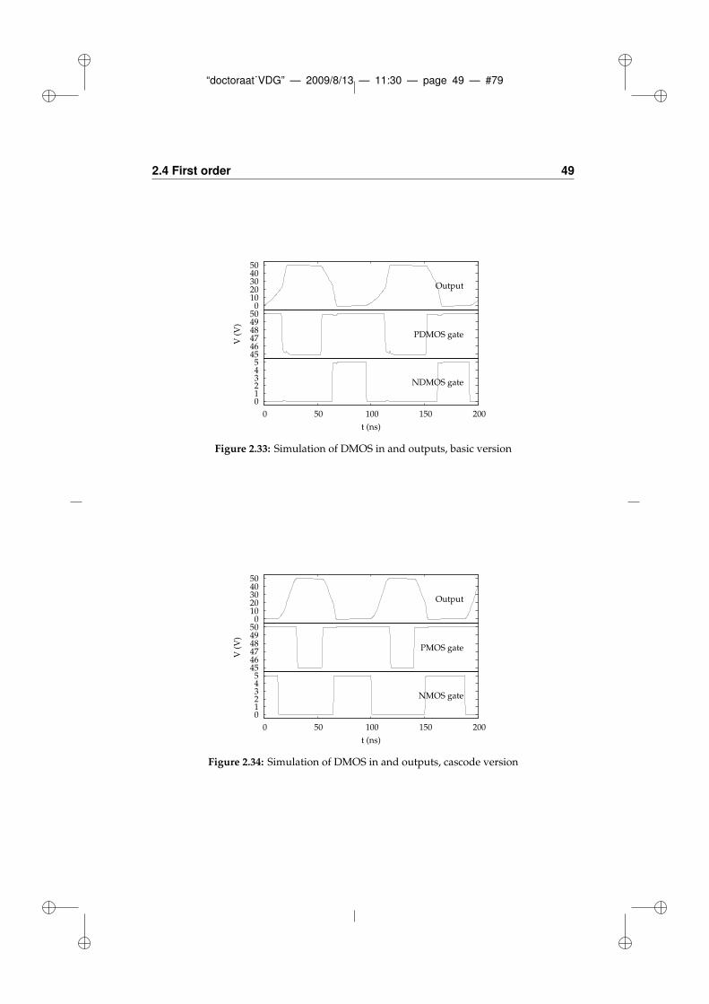
“doctoraat˙VDG” — 2009/8/13 — 11:30 — page 49 — #79
2.4 First order 49
0 1 2 3 4 5
0 50 100 150 200
t (ns)
NDMOS gate
45 46 47 48 49 50
V (
V)
PDMOS gate
0 10 20 30 40 50
Output
Figure 2.33: Simulation of DMOS in and outputs, basic version
0 1 2 3 4 5
0 50 100 150 200
t (ns)
NMOS gate
45 46 47 48 49 50
V (
V)
PMOS gate
0 10 20 30 40 50
Output
Figure 2.34: Simulation of DMOS in and outputs, cascode version
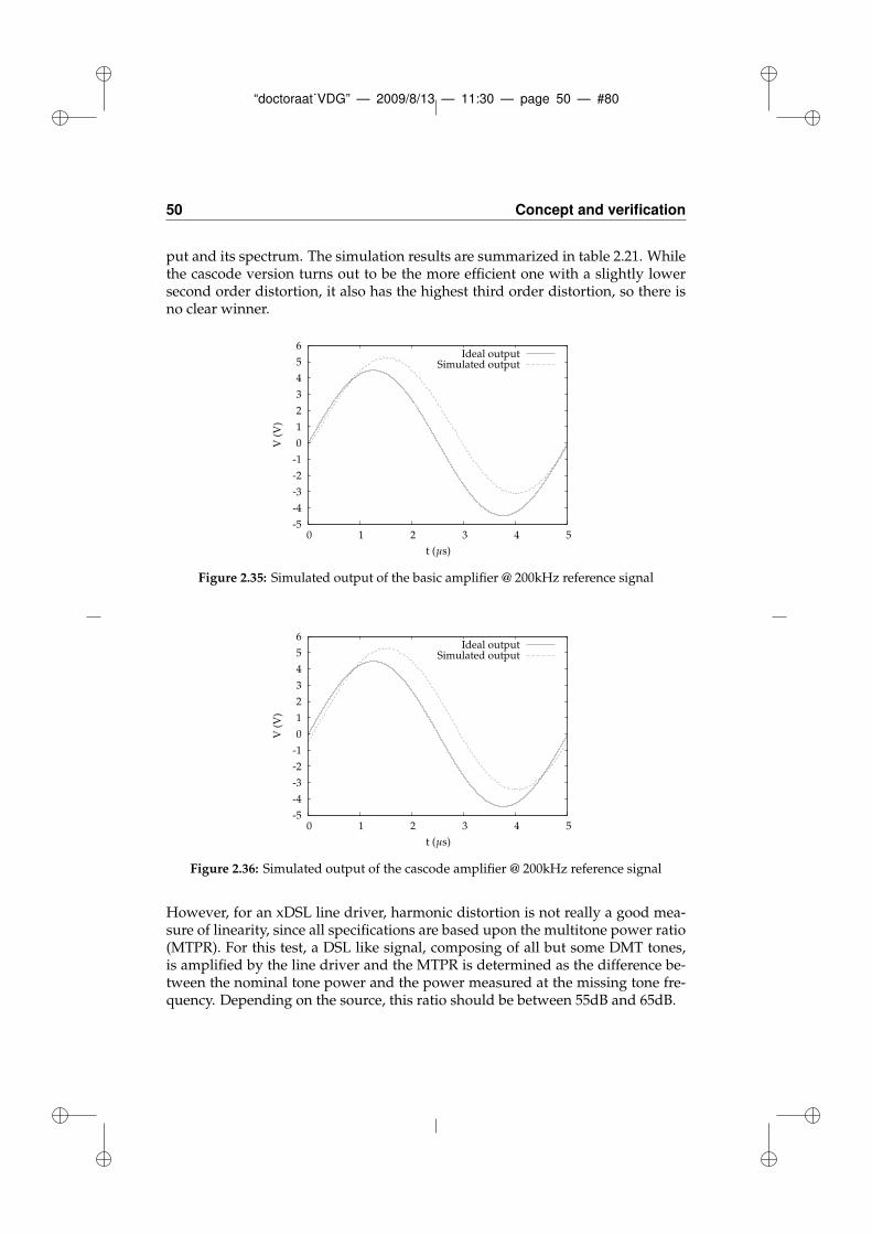
“doctoraat˙VDG” — 2009/8/13 — 11:30 — page 50 — #80
50 Concept and verification
put and its spectrum. The simulation results are summarized in table 2.21. Whilethe cascode version turns out to be the more efficient one with a slightly lowersecond order distortion, it also has the highest third order distortion, so there isno clear winner.
-5
-4
-3
-2
-1
0
1
2
3
4
5
6
0 1 2 3 4 5
V (
V)
Ideal outputSimulated output
t (µs)
Figure 2.35: Simulated output of the basic amplifier @ 200kHz reference signal
-5
-4
-3
-2
-1
0
1
2
3
4
5
6
0 1 2 3 4 5
V (
V)
Ideal outputSimulated output
t (µs)
Figure 2.36: Simulated output of the cascode amplifier @ 200kHz reference signal
However, for an xDSL line driver, harmonic distortion is not really a good mea-sure of linearity, since all specifications are based upon the multitone power ratio(MTPR). For this test, a DSL like signal, composing of all but some DMT tones,is amplified by the line driver and the MTPR is determined as the difference be-tween the nominal tone power and the power measured at the missing tone fre-quency. Depending on the source, this ratio should be between 55dB and 65dB.
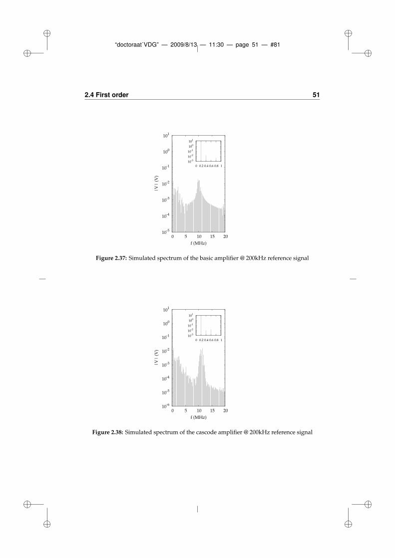
“doctoraat˙VDG” — 2009/8/13 — 11:30 — page 51 — #81
2.4 First order 51
10-5
10-4
10-3
10-2
10-1
100
101
0 5 10 15 20
|V
| (
V)
f (MHz)
10-3
10-2
10-1
100
101
0 0.2 0.4 0.6 0.8 1
Figure 2.37: Simulated spectrum of the basic amplifier @ 200kHz reference signal
10-6
10-5
10-4
10-3
10-2
10-1
100
101
0 5 10 15 20
|V
| (
V)
f (MHz)
10-3
10-2
10-1
100
101
0 0.2 0.4 0.6 0.8 1
Figure 2.38: Simulated spectrum of the cascode amplifier @ 200kHz reference signal
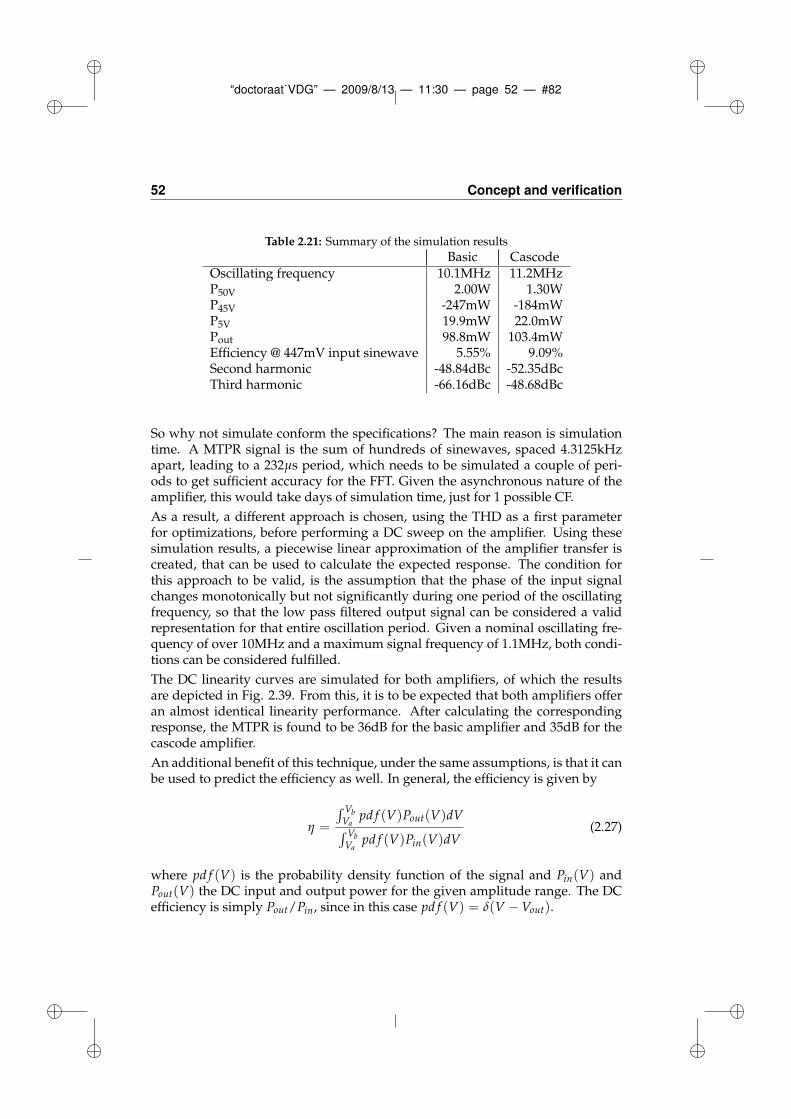
“doctoraat˙VDG” — 2009/8/13 — 11:30 — page 52 — #82
52 Concept and verification
Table 2.21: Summary of the simulation results
Basic CascodeOscillating frequency 10.1MHz 11.2MHzP50V 2.00W 1.30WP45V -247mW -184mWP5V 19.9mW 22.0mWPout 98.8mW 103.4mWEfficiency @ 447mV input sinewave 5.55% 9.09%Second harmonic -48.84dBc -52.35dBcThird harmonic -66.16dBc -48.68dBc
So why not simulate conform the specifications? The main reason is simulationtime. A MTPR signal is the sum of hundreds of sinewaves, spaced 4.3125kHzapart, leading to a 232µs period, which needs to be simulated a couple of peri-ods to get sufficient accuracy for the FFT. Given the asynchronous nature of theamplifier, this would take days of simulation time, just for 1 possible CF.
As a result, a different approach is chosen, using the THD as a first parameterfor optimizations, before performing a DC sweep on the amplifier. Using thesesimulation results, a piecewise linear approximation of the amplifier transfer iscreated, that can be used to calculate the expected response. The condition forthis approach to be valid, is the assumption that the phase of the input signalchanges monotonically but not significantly during one period of the oscillatingfrequency, so that the low pass filtered output signal can be considered a validrepresentation for that entire oscillation period. Given a nominal oscillating fre-quency of over 10MHz and a maximum signal frequency of 1.1MHz, both condi-tions can be considered fulfilled.
The DC linearity curves are simulated for both amplifiers, of which the resultsare depicted in Fig. 2.39. From this, it is to be expected that both amplifiers offeran almost identical linearity performance. After calculating the correspondingresponse, the MTPR is found to be 36dB for the basic amplifier and 35dB for thecascode amplifier.
An additional benefit of this technique, under the same assumptions, is that it canbe used to predict the efficiency as well. In general, the efficiency is given by
η =
∫ VbVa
pd f (V)Pout(V)dV∫ VbVa
pd f (V)Pin(V)dV(2.27)
where pd f (V) is the probability density function of the signal and Pin(V) andPout(V) the DC input and output power for the given amplitude range. The DCefficiency is simply Pout/Pin, since in this case pd f (V) = δ(V −Vout).
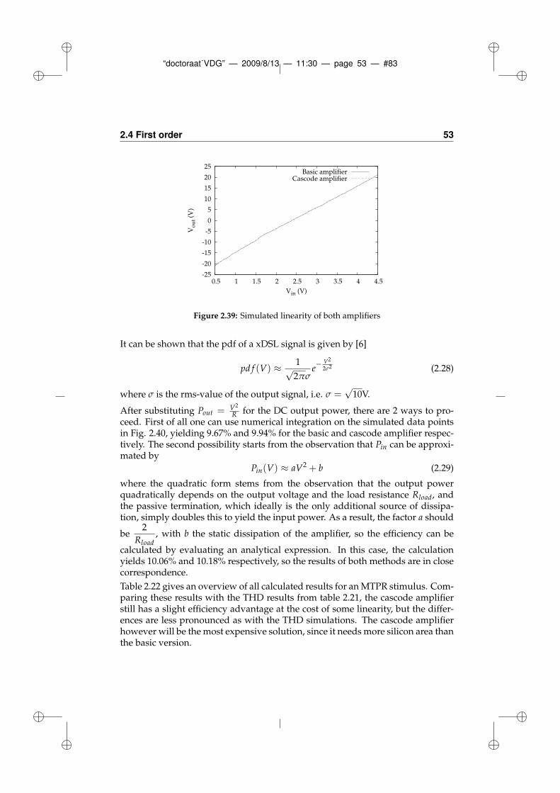
“doctoraat˙VDG” — 2009/8/13 — 11:30 — page 53 — #83
2.4 First order 53
-25
-20
-15
-10
-5
0
5
10
15
20
25
0.5 1 1.5 2 2.5 3 3.5 4 4.5
Vo
ut
(V)
Vin (V)
Basic amplifierCascode amplifier
Figure 2.39: Simulated linearity of both amplifiers
It can be shown that the pdf of a xDSL signal is given by [6]
pd f (V) ≈ 1√2πσ
e− V2
2σ2 (2.28)
where σ is the rms-value of the output signal, i.e. σ =√
10V.
After substituting Pout = V2
R for the DC output power, there are 2 ways to pro-ceed. First of all one can use numerical integration on the simulated data pointsin Fig. 2.40, yielding 9.67% and 9.94% for the basic and cascode amplifier respec-tively. The second possibility starts from the observation that Pin can be approxi-mated by
Pin(V) ≈ aV2 + b (2.29)
where the quadratic form stems from the observation that the output powerquadratically depends on the output voltage and the load resistance Rload, andthe passive termination, which ideally is the only additional source of dissipa-tion, simply doubles this to yield the input power. As a result, the factor a should
be2
Rload, with b the static dissipation of the amplifier, so the efficiency can be
calculated by evaluating an analytical expression. In this case, the calculationyields 10.06% and 10.18% respectively, so the results of both methods are in closecorrespondence.
Table 2.22 gives an overview of all calculated results for an MTPR stimulus. Com-paring these results with the THD results from table 2.21, the cascode amplifierstill has a slight efficiency advantage at the cost of some linearity, but the differ-ences are less pronounced as with the THD simulations. The cascode amplifierhowever will be the most expensive solution, since it needs more silicon area thanthe basic version.
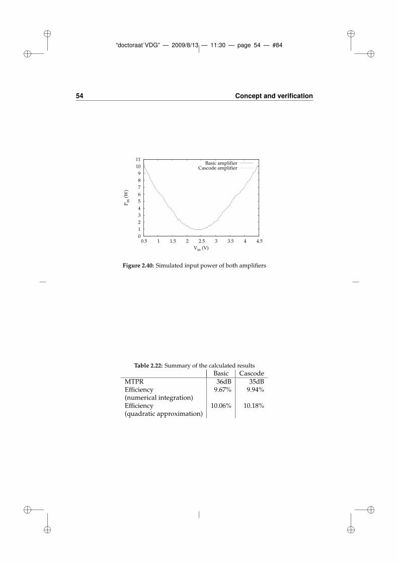
“doctoraat˙VDG” — 2009/8/13 — 11:30 — page 54 — #84
54 Concept and verification
0
1
2
3
4
5
6
7
8
9
10
11
0.5 1 1.5 2 2.5 3 3.5 4 4.5
Pin
(W
)
Vin (V)
Basic amplifierCascode amplifier
Figure 2.40: Simulated input power of both amplifiers
Table 2.22: Summary of the calculated results
Basic CascodeMTPR 36dB 35dBEfficiency 9.67% 9.94%(numerical integration)Efficiency 10.06% 10.18%(quadratic approximation)
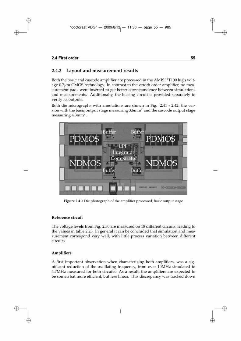
“doctoraat˙VDG” — 2009/8/13 — 11:30 — page 55 — #85
2.4 First order 55
2.4.2 Layout and measurement results
Both the basic and cascode amplifier are processed in the AMIS I2T100 high volt-age 0.7µm CMOS technology. In contrast to the zeroth order amplifier, no mea-surement pads were inserted to get better correspondence between simulationsand measurements. Additionally, the biasing circuit is provided separately toverify its outputs.
Both die micrographs with annotations are shown in Fig. 2.41 - 2.42, the ver-sion with the basic output stage measuring 3.6mm2 and the cascode output stagemeasuring 4.3mm2.
Buffer
BufferBuffer
Buffer
LPFIntegrator
ComparatorNDMOS NDMOS
PDMOS PDMOS
Figure 2.41: Die photograph of the amplifier processed, basic output stage
Reference circuit
The voltage levels from Fig. 2.30 are measured on 18 different circuits, leading tothe values in table 2.23. In general it can be concluded that simulation and mea-surement correspond very well, with little process variation between differentcircuits.
Amplifiers
A first important observation when characterizing both amplifiers, was a sig-nificant reduction of the oscillating frequency, from over 10MHz simulated to4.7MHz measured for both circuits. As a result, the amplifiers are expected tobe somewhat more efficient, but less linear. This discrepancy was tracked down
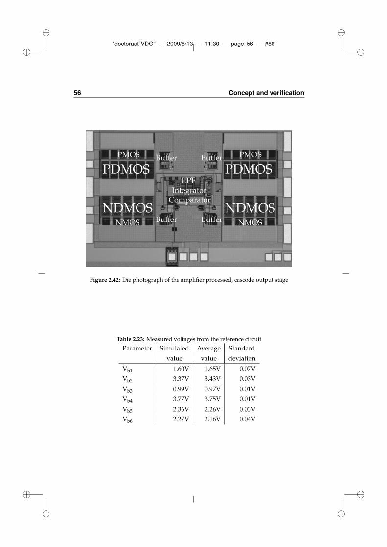
“doctoraat˙VDG” — 2009/8/13 — 11:30 — page 56 — #86
56 Concept and verification
Buffer
BufferBuffer
Buffer
LPFIntegrator
ComparatorNDMOS NDMOS
PDMOS PDMOS
NMOS NMOS
PMOS PMOS
Figure 2.42: Die photograph of the amplifier processed, cascode output stage
Table 2.23: Measured voltages from the reference circuit
Parameter Simulated Average Standard
value value deviation
Vb1 1.60V 1.65V 0.07V
Vb2 3.37V 3.43V 0.03V
Vb3 0.99V 0.97V 0.01V
Vb4 3.77V 3.75V 0.01V
Vb5 2.36V 2.26V 0.03V
Vb6 2.27V 2.16V 0.04V
“doctoraat˙VDG” — 2009/8/13 — 11:30 — page 57 — #87
2.4 First order 57
to extra parasitics introduced by the layout and missing modelling of parasiticcapacitances in certain components. A post layout simulation including theseparasitics showed a reduction to 6MHz, in close correspondence with the mea-surements.
Extensive linearity and efficiency measurements were performed on both am-plifiers. Figures 2.43 and 2.44 show the simulated and measured curves of thelinearity of both amplifiers and Fig. 2.45 depicts the measured results together.
-25
-20
-15
-10
-5
0
5
10
15
20
25
0 0.5 1 1.5 2 2.5 3 3.5 4 4.5 5
Vo
ut
(V)
Vin (V)
SimulatedMeasured
Figure 2.43: Simulated and measured linearity of the basic amplifier
-25
-20
-15
-10
-5
0
5
10
15
20
25
0 0.5 1 1.5 2 2.5 3 3.5 4 4.5 5
Vo
ut
(V)
Vin (V)
SimulatedMeasured
Figure 2.44: Simulated and measured linearity of the cascode amplifier
When comparing simulations and measurements of both amplifiers, two com-mon differences can be observed. First of all, the measurements show a reducedamplification for the middle voltage range, which first diminishes even further
“doctoraat˙VDG” — 2009/8/13 — 11:30 — page 58 — #88
58 Concept and verification
-20
-15
-10
-5
0
5
10
15
20
0 0.5 1 1.5 2 2.5 3 3.5 4 4.5 5
Vo
ut
(V)
Vin (V)
Basic amplifierCascode amplifier
Figure 2.45: Measured linearity of both amplifiers
and then increases when approaching the supply rails. This can be explained bythe inherent reduction of the switching frequency at increasing amplitudes, com-bined with the time delays introduced by the control loop. Second, the responseseems to be less linear than simulated, but on the other hand, there is no twistanymore around the input voltage of 1.5V. Besides these effects, the cascode am-plifier also saturates earlier due to the additional voltage drop over the cascodetransistors, while the basic version seems less linear in general. As a result, it isnot immediately clear which amplifier is the most linear.
The power consumption for these DC measurements is given in Figures 2.46 to2.48. The measurements yield favourable results, due to the lower switching fre-quency, as expected. Again, there is no significant difference between both ver-sions of the amplifier, so the final MTPR measurements will be decisive.
The full downstream spectrum as measured is shown in Fig. 2.49. The minimumMTPR was 40dB for the basic version and 39dB for the cascode amplifier, wherethe basic version reaches values of over 45dB as in Fig. 2.50. The power con-sumption was 765mW and 778mW respectively, so the basic amplifier turns outto be the best solution.
In general, this means that the calculated values for linearity and efficiencyslightly underestimate the measured performance, illustrating the usefulness ofthis technique.
Table 2.24 summarizes the measurement results and compares with references[7] and [8]. While it is much harder to reach the linearity achieved by a class ABamplifier, the efficiencies of both amplifiers are comparable. It should be notedhowever, that while class AB amplifiers can use active termination, switchingamplifiers are stuck with passive termination and filtering, due to the absence ofan appropriate feedback path. As a result, the matching and filtering circuit will
“doctoraat˙VDG” — 2009/8/13 — 11:30 — page 59 — #89
2.4 First order 59
0
2
4
6
8
10
12
0 0.5 1 1.5 2 2.5 3 3.5 4 4.5 5
Pin
(V
)
Vin (V)
SimulatedMeasured
Figure 2.46: Simulated and measured input power of the basic amplifier
0
2
4
6
8
10
12
0 0.5 1 1.5 2 2.5 3 3.5 4 4.5 5
Pin
(V
)
Vin (V)
SimulatedMeasured
Figure 2.47: Simulated and measured input power of the cascode amplifier
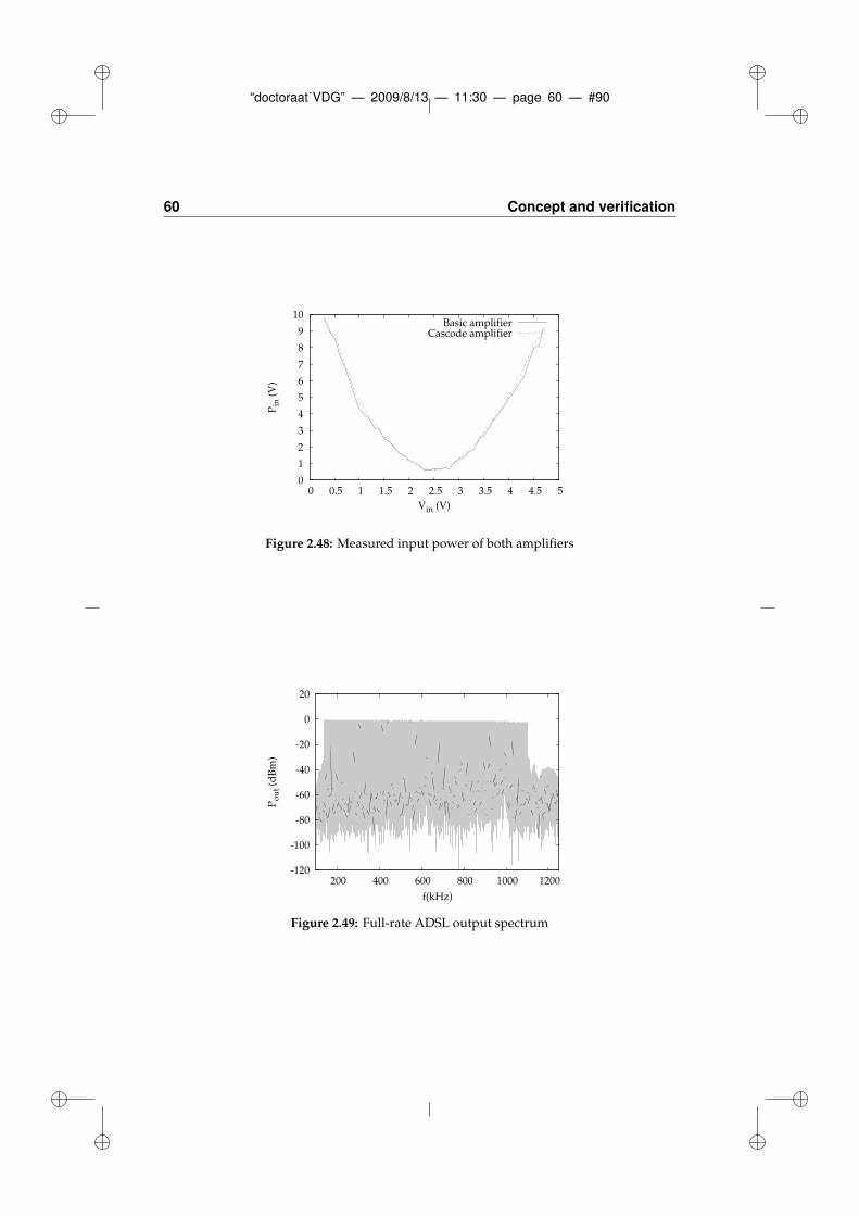
“doctoraat˙VDG” — 2009/8/13 — 11:30 — page 60 — #90
60 Concept and verification
0
1
2
3
4
5
6
7
8
9
10
0 0.5 1 1.5 2 2.5 3 3.5 4 4.5 5
Pin
(V
)
Vin (V)
Basic amplifierCascode amplifier
Figure 2.48: Measured input power of both amplifiers
-120
-100
-80
-60
-40
-20
0
20
200 400 600 800 1000 1200
Po
ut
(dB
m)
f(kHz)
Figure 2.49: Full-rate ADSL output spectrum
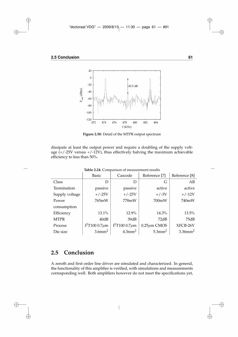
“doctoraat˙VDG” — 2009/8/13 — 11:30 — page 61 — #91
2.5 Conclusion 61
-120
-100
-80
-60
-40
-20
0
20
472 474 476 478 480 482 484
Po
ut
(dB
m)
f (kHz)
45.5 dB
Figure 2.50: Detail of the MTPR output spectrum
dissipate at least the output power and require a doubling of the supply volt-age (+/-25V versus +/-12V), thus effectively halving the maximum achievableefficiency to less than 50%.
Table 2.24: Comparison of measurement results
Basic Cascode Reference [7] Reference [8]
Class D D G AB
Termination passive passive active active
Supply voltage +/-25V +/-25V +/-3V +/-12V
Power 765mW 778mW 700mW 740mW
consumption
Efficiency 13.1% 12.9% 14.3% 13.5%
MTPR 40dB 39dB 72dB 75dB
Process I2T100 0.7µm I2T100 0.7µm 0.25µm CMOS XFCB-26V
Die size 3.6mm2 4.3mm2 5.3mm2 3.36mm2
2.5 Conclusion
A zeroth and first order line driver are simulated and characterized. In general,the functionality of this amplifier is verified, with simulations and measurementscorresponding well. Both amplifiers however do not meet the specifications yet,
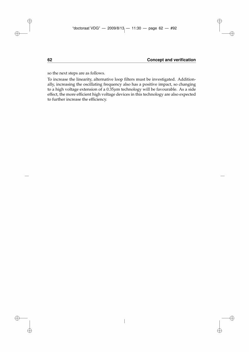
“doctoraat˙VDG” — 2009/8/13 — 11:30 — page 62 — #92
62 Concept and verification
so the next steps are as follows.
To increase the linearity, alternative loop filters must be investigated. Addition-ally, increasing the oscillating frequency also has a positive impact, so changingto a high voltage extension of a 0.35µm technology will be favourable. As a sideeffect, the more efficient high voltage devices in this technology are also expectedto further increase the efficiency.
“doctoraat˙VDG” — 2009/8/13 — 11:30 — page 63 — #93
References
[1] Asymmetric digital subscriber line (ADSL) transceivers, ITU-T RecommendationG.992.1, Jul. 1999.
[2] Europractice IC service. (2007, Mar.) AMI Semiconductor I2T100technology. [Online]. Available: http://www.europractice-ic.com/docs/AMIS datasheets/AMIS I2T100 v8.pdf
[3] J. Doutreloigne, H. De Smet, J. Van den Steen, and G. Van Doorselaer, “Low-power high-voltage CMOS level-shifters for liquid crystal display drivers,”in Proceedings of the 11th international conference on microelectronics, State ofKuwait, Nov. 1999, pp. 213–216.
[4] B. J. Baliga, Modern Power Devices. Malabar, Florida: Krieger PublishingCompany, 1992.
[5] W. Redman-White, “A high bandwidth constant gm and slew-rate rail-to-railCMOS input circuit and its application to analog cells for low voltage VLSIsystems,” IEEE J. Solid-State Circuits, vol. 32, no. 5, pp. 701–712, May 1997.
[6] D. J. G. Mestdagh, P. M. P. Spruyt, and B. Biran, “Effect of amplitude clippingin DMT-ADSL transceivers,” Electronics Letters, vol. 29, no. 15, pp. 1354–1355,July 22 1993.
[7] A. Bicakci, C.-S. Kim, and S.-S. Lee, “A CMOS line driver for ADSL centraloffice applications,” IEEE J. Solid-State Circuits, vol. 38, no. 12, pp. 2201–2208,Dec. 2003.
[8] F. Sabouri and R. Shariatdoust, “A 740mW ADSL line driver for central officewith 75dB MTPR,” in ISSCC Digest of Technical Papers, San Francisco, USA,Feb. 2002, pp. 322–323.

“doctoraat˙VDG” — 2009/8/13 — 11:30 — page 64 — #94
64 REFERENCES
“doctoraat˙VDG” — 2009/8/13 — 11:30 — page 65 — #95
3Theory of operation
This chapter provides a numerical framework, to predict the most important proper-ties of an asynchronous amplifier, being its oscillating frequency and distortion. Theformulæ will first be derived and later verified by block level simulations.
3.1 Introduction
In chapter 2, two different silicon implementations of the basic principle aredemonstrated. However, the design path followed merely consists of a trial-and-error method, so the question arises if there is a way to more systematicallydescribe the functioning and performance of the circuit. Since there is a plethoraof methods for describing linear circuits, the main challenge is to accuratelymodel the non-linearity introduced into the system by the comparator.
Existing techniques, such as direct time domain response calculation as utilizedwith classical PWM and the z-domain representation adopted with Σ∆ convert-ers, are not readily available for the asynchronous amplifier. The main differenceis the absence of a fixed time base, such as a clock or sawtooth, in favour of theoutput square wave, filtered to a sawtooth like reference with an input dependentperiod.
As such, a different approach will be followed, describing the non-linearity in alinearized way, combined with a direct time domain description to predict the
“doctoraat˙VDG” — 2009/8/13 — 11:30 — page 66 — #96
66 Theory of operation
linearity performance of the system.
In section 3.2, the technique used to linearize a non-linearity will be discussed.Section 3.3 will further expand the behavioural description of the system to lin-earity prediction and in section 3.4 both techniques will be verified using blocklevel numerical simulations.
3.2 Describing functions linearization
3.2.1 Small and large signals
The main objective of this section is to derive a suitable linear approximation ofa non-linear component and calculate the resulting transfer function in the caseof an ideal comparator without hysteresis. A first source of inspiration is thetechnique used in the small signal analysis of non-linear systems. In this case, thenon-linearity is a smooth function where both this function and its first derivativeare continuous in a given interval and the input signal is considered sufficientlysmall so as to not have a significantly distorted output response. To calculate theresulting small signal output, the input signal is simply multiplied by the firstderivative of the non-linearity at the DC working point. The resulting outputsignal then is the superposition of this small signal output and the DC response.This method is illustrated in Fig. 3.1 in the simple case of an exponential transferfunction, as used frequently to model bipolar components.
0
1
2
3
4
5
6
7
8
0 0.5 1 1.5 2
y
x
ExponentialLinearization
InputOutput
Figure 3.1: Exponential transfer function with small signal parameters
However, as already mentioned before, the input signal to the non-linearity willbe a low-pass filtered square wave with significant amplitude, rendering theabove method invalid. This can be demonstrated using the exponential function
“doctoraat˙VDG” — 2009/8/13 — 11:30 — page 67 — #97
3.2 Describing functions linearization 67
from Fig. 3.1:
Vout = eVin (3.1)
For a small signal analysis, the resulting output simply is
eA + eAB sin(2π f t) (3.2)
for a sinusoidal input signal Vin = A + B sin(2π f t) with offset A, amplitudeB and frequency f . This linearized output and the exact output from equation(3.1) are shown in Fig. 3.2 for an input signal Vin = 1 + sin(2πt). Besides thenoticeable distortion from the exponential function causing an increased peak-to-peak value, there also is a significant difference in average value, increasingfrom 2.72 for the linearized version to 3.44 for the exact response.
0
1
2
3
4
5
6
7
8
0 0.5 1 1.5 2
V (
arb
itra
ry u
nit
s)
t (arbitrary units)
ExactSmall signal
Figure 3.2: Exact and small signal output response
As a result, for larger signals, the linearized description of the circuit involvesthe construction of a linear approximator for each input signal instead of a singlefunction for all inputs as with linear systems. This corresponds with the obser-vation that the goal is not to derive a “one function always describes” technique,but a means to accurately and systematically describe a system in a strictly de-fined environment. A general block level diagram of this non-linear componentis shown in Fig. 3.3, together with a representation of its linear approximation.
3.2.2 Large signal approximation
The outcome of the previous section now leads to the starting point of the de-scribing function theory, where a set of functions wi(t) needs to be found, possi-bly depending on all input variables and minimizing the mean squared error ofthe output signal:
e(t) = ya(t) − y(t) (3.3)
“doctoraat˙VDG” — 2009/8/13 — 11:30 — page 68 — #98
68 Theory of operation
+ +
+
x(t) y(t)
ya(t)
+ +
+
x1(t)
x2(t)
xn(t)
...
w1(t)
w2(t)
wn(t)
...
Non-linearity N
Figure 3.3: Block diagram of non-linearity and approximation
where y(t) is the ideal output signal, ya(t) the approximated output and e(t) theerror signal, with a mean squared value
e(t)2 = ya(t)2 − 2ya(t)y(t) + y(t)2 (3.4)
Further using the notations from Fig. 3.3, ya(t) can be written as
ya(t) =n
∑i=1
∫ ∞
0wi(τ)xi(t− τ) dτ (3.5)
and
ya(t)2 =n
∑i=1
n
∑j=1
∫ ∞
0dτ1
∫ ∞
0dτ2 wi(τ1)wj(τ2)ϕij(τ1 − τ2) (3.6)
where
ϕij(τ) = xi(t)xj(t + τ) (3.7)
After assuming a small variation on the optimal value of the approximator wi(t)
wi(t) = woi(t) + δwi(t) (3.8)
equation (3.4) can be further rewritten as
e(t)2 = e(t)20 + δe(t)2 + δ2e(t)2 (3.9)
“doctoraat˙VDG” — 2009/8/13 — 11:30 — page 69 — #99
3.2 Describing functions linearization 69
where
e(t)20 =
n
∑i=1
n
∑j=1
∫ ∞
0dτ1
∫ ∞
0dτ2 woi(τ1)woj(τ2)ϕij(τ1 − τ2)
−2n
∑i=1
∫ ∞
0dτ1 woi(τ1)y(t)xi(t− τ1) + y(t)2 (3.10)
δe(t)2 = 2n
∑i=1
∫ ∞
0dτ1 δwi(τ1)
[
n
∑j=1
∫ ∞
0dτ2 woj(τ2)ϕij(τ1 − τ2) − y(t)xi(t− τ1)
]
(3.11)
δ2e(t)2 =n
∑i=1
n
∑j=1
∫ ∞
0dτ1
∫ ∞
0dτ2 δwi(τ1)δwj(τ2)ϕij(τ1 − τ2) (3.12)
For the solution woi(t) to be a minimum, the first order error from equation (3.11)should be zero for every δwi(τ1), which holds if for every possible i
n
∑j=1
∫ ∞
0dτ2 woj(τ2)ϕij(τ1 − τ2) − y(t)xi(t− τ1) = 0 (3.13)
which leads to the conclusion that the input-output cross-correlations of the idealresult and the approximation must be equal:
xi(t)y(t + τ1) = xi(t)ya(t + τ1) (3.14)
When combining these equations with the observation that the input and errorsignal are not correlated and the cross-correlation between the ideal and approx-imated outputs equals the autocorrelation of the approximated output, equation(3.13) can be rewritten as
∫ ∞
0woi(τ2)ϕii(τ1 − τ2) dτ2 = y(t)xi(t− τ1) (3.15)
under the assumption that all input signals are uncorrelated.
From this it can be concluded that, although the input signals are statisticallyindependent and the resulting signals for every approximator are uncorrelated,the approximator parameters will still depend on the nature of every input signal,due to the dependency of equation (3.15) on the exact output y(t). This, of course,corresponds to the absence of superposition in non-linear circuits.
Furthermore, since equations (3.6) and (3.12) have the same form, the second or-der term of the error will always be positive, thus the solution will be a minimum.
“doctoraat˙VDG” — 2009/8/13 — 11:30 — page 70 — #100
70 Theory of operation
3.2.3 An example
This theory can now be applied to the exponential transfer function from Fig.3.1. From Fig. 3.2 it became clear that the small signal approximation failed toaccurately predict both the offset and amplitude, so now the question arises ifand to which extent the result from equation (3.15) is the better method.
Offset
Using equation (3.15) directly on the transfer from equation (3.1), with an inputsignal
Vin = A + B sin(2π f t) (3.16)
this immediately leads to
∫ ∞
0wA(τ2)A
2 dτ2 = Ay(t) (3.17)
which is fulfilled if
wA(τ2) =1
Ay(t)δ(τ2) (3.18)
with δ(τ) the impulse function. As a result, in this case a suitable approximatorfor the DC component is a static gain block with value
NA(A, B) =1
Ay(A, B, t) (3.19)
which is called the describing function for the bias component A. This leads toexactly the average value of the analytical solution, as calculated in section 3.2.1.Thus, from a bias point of view, the describing function approximation is thebetter technique.
Sinewave
The bias response however is only part of the solution, so the AC response needsto be calculated as well. In this case, the autocorrelation is readily calculated as
ϕii(τ) =1
2B2 cos(2π f τ) (3.20)
“doctoraat˙VDG” — 2009/8/13 — 11:30 — page 71 — #101
3.2 Describing functions linearization 71
leading to
∫ ∞
0woi(τ2)ϕii(τ1 − τ2) dτ2 =
∫ ∞
0woi(τ2)
B2
2cos(2π f (τ1 − tau2)) dτ2
=B2
2cos(2π f τ1)
∫ ∞
0woi(τ2) cos(2π f τ2) dτ2
+B2
2sin(2π f τ1)
∫ ∞
0woi(τ2) sin(2π f τ2) dτ2
(3.21)
for the left hand side of equation (3.15) and
y(t)xi(t− τ1) = B f∫ 1
f
0eA+B sin(2π f t) sin(2π f (t− τ1)) dt
= eAB f cos(2π f τ1)∫ 1
f
0eB sin(2π f t) sin(2π f t) dt
−eAB f sin(2π f τ1)∫ 1
f
0eB sin(2π f t) cos(2π f t) dt
=eAB
2πcos(2π f τ1)
∫ 2π
0eB sin(x) sin(x) dx
−eAB f∫ 1
f
0
eB sin(2π f t)
2π f Bd(B sin(2π f t))
=eAB
2πcos(2π f τ1)
∫ 2π
0eB sin(x) sin(x) dx (3.22)
for the right hand side.
Since equations (3.21) and (3.22) must be equal, regardless the value of τ1, iden-tification of the terms cos(2π f τ1) and sin(2π f τ1) yields the following possiblesolution:
woi(τ2) =eA
πB
∫ 2π
0eB sin(x) sin(x) dxδ(τ2) (3.23)
leading to a describing function
NB(A, B) =eA
πB
∫ 2π
0eB sin(x) sin(x) dx (3.24)
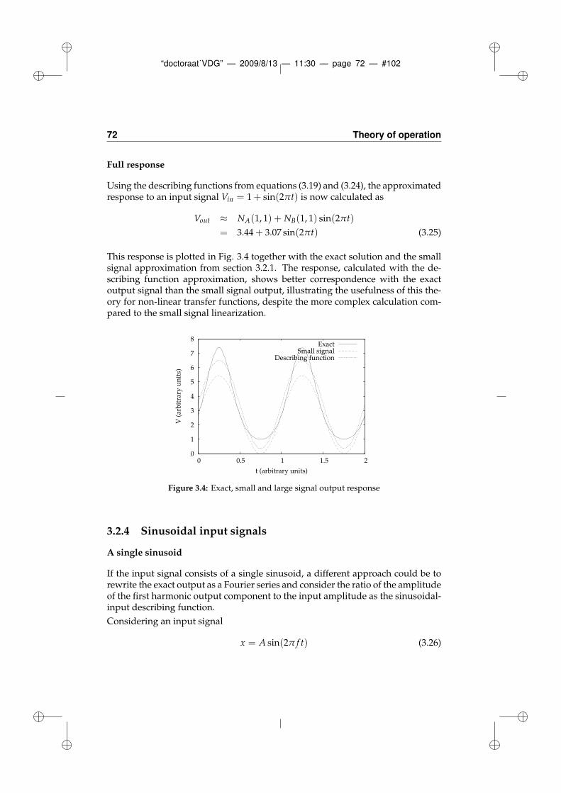
“doctoraat˙VDG” — 2009/8/13 — 11:30 — page 72 — #102
72 Theory of operation
Full response
Using the describing functions from equations (3.19) and (3.24), the approximatedresponse to an input signal Vin = 1 + sin(2πt) is now calculated as
Vout ≈ NA(1, 1) + NB(1, 1) sin(2πt)
= 3.44 + 3.07 sin(2πt) (3.25)
This response is plotted in Fig. 3.4 together with the exact solution and the smallsignal approximation from section 3.2.1. The response, calculated with the de-scribing function approximation, shows better correspondence with the exactoutput signal than the small signal output, illustrating the usefulness of this the-ory for non-linear transfer functions, despite the more complex calculation com-pared to the small signal linearization.
0
1
2
3
4
5
6
7
8
0 0.5 1 1.5 2
V (
arb
itra
ry u
nit
s)
t (arbitrary units)
ExactSmall signal
Describing function
Figure 3.4: Exact, small and large signal output response
3.2.4 Sinusoidal input signals
A single sinusoid
If the input signal consists of a single sinusoid, a different approach could be torewrite the exact output as a Fourier series and consider the ratio of the amplitudeof the first harmonic output component to the input amplitude as the sinusoidal-input describing function.
Considering an input signal
x = A sin(2π f t) (3.26)
“doctoraat˙VDG” — 2009/8/13 — 11:30 — page 73 — #103
3.2 Describing functions linearization 73
without offset and an odd non-linearity given by y(x, x), the exact output can bewritten as
y(A sin(2π f t), A2π f cos(2π f t)) =∞
∑n=1
An(A, f ) sin(n2π f t + ϕn(A, f )) (3.27)
The sinusoidal-input describing function then is given by
N(A, f ) =phasor representation of the output at frequency f
phasor representation of the input at frequency f
=A1(A, f )
Aejϕ1(A, f ) (3.28)
As such, in the limit of a linear system, the describing function is exactly whatwould be considered the gain of this linear system. The main differences betweenlinear and non-linear systems are the principle of superposition which only holdsfor linear systems and the fact that knowledge of the response to an infinite spec-trum of sinusoids also describes the response of a linear system to every possibleinput while this is not the case for non-linear systems.
Further evaluation of the response from equation (3.27) and identification of thecorresponding terms now leads to
A1 cos(ϕ1) =1
π
∫ 2π
0y(A sin(2π f t), A2π f cos(2π f t)) sin(2π f t) d(2π f t)
(3.29)
A1 sin(ϕ1) =1
π
∫ 2π
0y(A sin(2π f t), A2π f cos(2π f t)) cos(2π f t) d(2π f t)
(3.30)
for the fundamental harmonic coefficients. When using the phasor notation
ejϕ = cos(ϕ) + j sin(ϕ) (3.31)
equations (3.29) and (3.30) can be combined to
A1ejϕ1
A=
j
πA
∫ 2π
0y(A sin(2π f t), A2π f cos(2π f t))e−j2π f t d(2π f t) (3.32)
which has the form of equation (3.28).
The only thing left to prove, is the equivalence between the Fourier series ap-proximation from equation (3.32) and the mean-squared approximation as usedin section 3.2.2. Writing the describing function as ρNejθN , the error signal can bewritten as
e2 = f∫ 1
f
0e2(t) dt (3.33)
“doctoraat˙VDG” — 2009/8/13 — 11:30 — page 74 — #104
74 Theory of operation
with
e(t) = y(A sin(2π f t), A2π f cos(2π f t))− AρNsin(2π f t + θN) (3.34)
The proposed solution is a least mean-squared solution if
∂e2
∂ρN= 0
∂e2
∂θN= 0
(3.35)
Evaluating these partial derivatives using equations (3.33) and (3.34), leads to
ρN =2 f
A
∫ 1f
0y(A sin(2π f t), A2π f cos(2π f t))sin(2π f t + θN) dt (3.36)
0 =2 f
A
∫ 1f
0y(A sin(2π f t), A2π f cos(2π f t))sin(2π f t + θN) dt (3.37)
which can be rewritten in complex form as
ρNejθN =j
πA
∫ 2π
0y(A sin(2π f t), A2π f cos(2π f t))e−j2π f t d(2π f t) (3.38)
This is identical to equation (3.32), so it can be concluded that the Fourier seriesexpansion is a least mean-squares method and thus also leads to the describingfunction of the non-linearity.
A sinusoid with other signals
It can also be shown [1] that the Fourier series expansion technique also yieldsvalid results in the case of multiple sinusoidal inputs with an offset. This is animportant result, since many analogue electronic systems are characterized us-ing periodical input signals, that can be decomposed as a sum of sinewaves. Theresponse can than simply be approximated using a familiar mathematical tech-nique.
Exponential transfer revisited
As an illustration, the response to the exponential transfer used throughout thissection can be calculated again. Using the definition of the Fourier series expan-sion, this yields
a0 = f∫ 1
f
0eA+B sin(2π f t) dt (3.39)
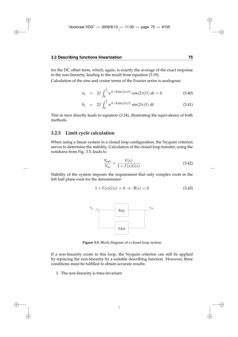
“doctoraat˙VDG” — 2009/8/13 — 11:30 — page 75 — #105
3.2 Describing functions linearization 75
for the DC offset term, which, again, is exactly the average of the exact responseto the non-linearity, leading to the result from equation (3.19).
Calculation of the sine and cosine terms of the Fourier series is analogous:
a1 = 2 f∫ 1
f
0eA+B sin(2π f t) cos(2π f t) dt = 0 (3.40)
b1 = 2 f∫ 1
f
0eA+B sin(2π f t) sin(2π f t) dt (3.41)
This in turn directly leads to equation (3.24), illustrating the equivalence of bothmethods.
3.2.5 Limit cycle calculation
When using a linear system in a closed loop configuration, the Nyquist criterionserves to determine the stability. Calculation of the closed loop transfer, using thenotations from Fig. 3.5, leads to
Vout
Vin=
F(s)
1 + F(s)G(s)(3.42)
Stability of the system imposes the requirement that only complex roots in theleft half plane exist for the denominator:
1 + F(s)G(s) = 0 ⇒ ℜ(s) < 0 (3.43)
F(s)+
-
G(s)
Vin Vout
Figure 3.5: Block diagram of a closed loop system
If a non-linearity exists in this loop, the Nyquist criterion can still be appliedby replacing the non-linearity by a suitable describing function. However, threeconditions must be fulfilled to obtain accurate results:
1. The non-linearity is time-invariant
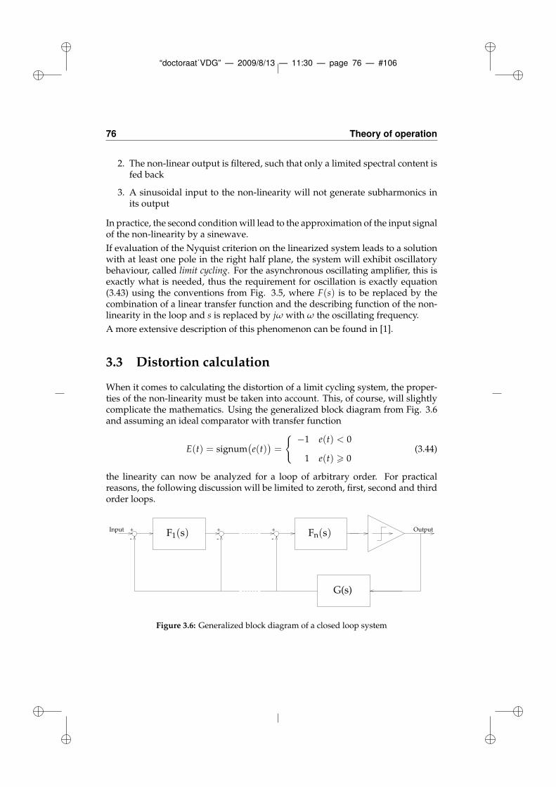
“doctoraat˙VDG” — 2009/8/13 — 11:30 — page 76 — #106
76 Theory of operation
2. The non-linear output is filtered, such that only a limited spectral content isfed back
3. A sinusoidal input to the non-linearity will not generate subharmonics inits output
In practice, the second condition will lead to the approximation of the input signalof the non-linearity by a sinewave.
If evaluation of the Nyquist criterion on the linearized system leads to a solutionwith at least one pole in the right half plane, the system will exhibit oscillatorybehaviour, called limit cycling. For the asynchronous oscillating amplifier, this isexactly what is needed, thus the requirement for oscillation is exactly equation(3.43) using the conventions from Fig. 3.5, where F(s) is to be replaced by thecombination of a linear transfer function and the describing function of the non-linearity in the loop and s is replaced by jω with ω the oscillating frequency.
A more extensive description of this phenomenon can be found in [1].
3.3 Distortion calculation
When it comes to calculating the distortion of a limit cycling system, the proper-ties of the non-linearity must be taken into account. This, of course, will slightlycomplicate the mathematics. Using the generalized block diagram from Fig. 3.6and assuming an ideal comparator with transfer function
E(t) = signum(
e(t))
=
−1 e(t) < 0
1 e(t) > 0(3.44)
the linearity can now be analyzed for a loop of arbitrary order. For practicalreasons, the following discussion will be limited to zeroth, first, second and thirdorder loops.
Output++
- -
+
-
Input F1(s) Fn(s)
G(s)
Figure 3.6: Generalized block diagram of a closed loop system
“doctoraat˙VDG” — 2009/8/13 — 11:30 — page 77 — #107
3.3 Distortion calculation 77
3.3.1 Zeroth and first order loop
From a block level point of view, the zeroth and first order loops are equivalent,since the only difference is the exact implementation of the blocks. The mathe-matical derivation will thus hold for both cases up to the point where the transferfunctions are chosen. The numerical evaluation however is done only for the firstorder loop, since it is expected to yield better performance.
The basis of the entire analysis is the time domain description of the system inFig. 3.6, where n = 1:
v(t) = vm cos(µt)e(t) = v(t) ∗ f1(t) − signum(e(t)) ∗ f1(t) ∗ g(t)
(3.45)
where v(t) is the input signal with amplitude vm and pulsation µ = 2π f , e(t) isthe error signal at the comparator input, f1(t) and g(t) are the impulse responseof F1(s) and G(s) respectively and “∗” denotes a convolution. If signum(e(t)) iswritten as a Fourier series, with duty cycle DC and oscillating pulsation ωk, thisfinally yields [2]
vkF1(µ) − (2DC− 1)F1(µ)G(µ)
=2
π
∞
∑n=1
sin(2πnDC)
nℜ(F1(nωk)G(nωk)) (3.46)
The subscript k is used to indicate the value of the parameter during a single pe-riod of oscillation. Due to the asynchronous behaviour of the amplifier, a changein the input signal will also alter the oscillating frequency in addition to the dutycycle. For a sinusoidal input, this means a constantly changing period, wheresubscript k is used to attract attention to this fact. However, it can be shown [2]that the final results are still valid under following assumptions:
1. A monotonic phase behaviour during each period of the oscillator
2. The in-band signal frequency must be sufficiently lower than the oscillatingfrequency
The relation between oscillating frequency with a sinusoidal input fk and thelimit cycle f0 is given by [2]
fk =
(
1 − v2k
2
)
f0 (3.47)
Since it can also be proven [2] that in the ideal case
DC =vk + 1
2(3.48)
“doctoraat˙VDG” — 2009/8/13 — 11:30 — page 78 — #108
78 Theory of operation
it is obvious that the infinite sum on the right-hand side of equation (3.46) de-scribes the distortion. Further simplification of this sum requires knowledge ofthe order of the transfer functions.
This does not refrain us however from making some qualitative observationsregarding the eventual form of the required transfer functions F1(s) and G(s).Minimizing the right-hand side of equation (3.46) can be achieved by choosingF1(s)G(s) a low pass filter at oscillating frequency and higher. Comparing theleft-hand side of equation (3.46) with the ideal transfer from equation (3.48) leadsto the conclusion that F1(s) can be chosen freely at signal frequency, while G(s)should be constant over the frequency range of interest and close to unity to mapthe entire input voltage range onto the duty cycle space.
Additionally, equation (3.46) also suggests an interesting class of candidates forF1(s). Since the system under consideration is not a classical PWM, comparinginput signal with a fixed clock reference to determine duty cycle, but has to regu-late both duty cycle and oscillating frequency asynchronously in the loop, smalldeviations of the duty cycle from its ideal value can be detected more easily byamplifying their values before comparison.
This finally leads to the conclusion that F1(s) should amplify at the signal bandand suppress high frequency out of band signals and G(s) should be a low passfilter. An appropriate choice for F1(s) thus could be an integrator, as used in thefirst order system from section 2.4.
The analysis of the distortion can now be completed for the first order system byassuming following transfer functions for F1(s) and G(s):
F1(s) =1
sτf1
G(s) =1
(1 + sτg)2(3.49)
Taking into account the approximation
ℜ(F1(nωk)G(nωk)) ≈ℜ(F1(ωk)G(ωk))
n4(3.50)
the right-hand side of equation (3.46) can now further be evaluated:
2
π
∞
∑n=1
sin(2πnDC)
nℜ(F1(nωk)G(nωk))≈
2
πℜ(F1(ωk)G(ωk))
∞
∑n=1
sin(2πnDC)
n5
=2
πℜ(F1(ωk)G(ωk))
−(2π)5
240B5(DC)
(3.51)
“doctoraat˙VDG” — 2009/8/13 — 11:30 — page 79 — #109
3.3 Distortion calculation 79
Table 3.1: Bernoulli numbersNumber Value
B11
6
B21
30
B31
42
B41
30
B55
66
B6691
2730
B77
6
The last step uses the equality [3]
∞
∑m=1
sin(mθ)
m2n+1=
(−1)n+1(2π)2n+1
2(2n + 1)!B2n+1
(
θ
2π
)
(3.52)
with n = 0, 1, 2, . . . ; 0 6 θ 6 2π and where Bn(x) is a Bernoulli polynomial, givenby
Bn(x) = xn − 1
2nxn−1 +
6 12 n
∑m=1
(
n
2m
)
Bmxn−2m (3.53)
The Bernoulli numbers Bk are then calculated as
Bk = (−1)k+1B2k(1) = (−1)k+1B2k(0) =2(2k)!
(2π)2k
∞
∑m=1
1
m2k(3.54)
A list of relevant Bernoulli numbers is given in table 3.1
After replacing the duty cycle DC by its ideal value from equation (3.48), thisleads to
V F1(µ) − (2DC− 1)F1(µ)G(µ)
= −4π4
15ℜ(F1(ωk)G(ωk))
(
V5
32− 5V3
48+
23V
96+
1
6
)
(3.55)
where the instantaneous amplitude vk is replaced by the frequency domain rep-resentation V of the input signal v(t).
“doctoraat˙VDG” — 2009/8/13 — 11:30 — page 80 — #110
80 Theory of operation
Since 2DC− 1 can be considered the low pass filtered output voltage Vout, the lastequation (3.55) can be rewritten as
Vout =2π4ℜ(F1(ωk)G(ωk))
45F1(µ)G(µ)
+360F1(µ) + 23π4ℜ(F1(ωk)G(ωk))
360F1(µ)G(µ)V
− π4ℜ(F1(ωk)G(ωk))
36F1(µ)G(µ)V3
+π4ℜ(F1(ωk)G(ωk))
120F1(µ)G(µ)V5 (3.56)
After substituting
V = vm cos(µt) (3.57)
into equation (3.56) and expanding the powers of the cosine function, this finallyleads to the amplitudes of the components at fundamental frequency and oddmultiples thereof. The third order harmonic distortion then simply is
HD3 =5π4ℜ(F1(ωk)G(ωk))v
2m(3v2
m − 8)
5760F1(µ) + 2π4ℜ(F1(ωk)G(ωk))(15v4m − 60v2
m + 184)(3.58)
This confirms the qualitative observations made on page 78, namely a large F1(µ)and small F1(ωk)G(ωk) minimize the distortion. Also note that equation (3.58)does not depend on the exact transfer functions F1(s) and G(s), but only on theorder of their real part. It is also obvious that this derivation can be repeated forany exotic transfer function, which, again, should lead to this very conclusion.
3.3.2 Second order loop
For the second order loop, the analysis is completely equivalent. In this case,n = 2, leading to a loop transfer
e(t) = ((v(t) − signum(e(t)) ∗ g(t)) ∗ f1(t)) ∗ f2(t) − signum(e(t)) ∗ g(t) ∗ f2(t)(3.59)
By defining
a(t) = f1(t) ∗ f2(t)b(t) = g(t) ∗ f1(t) ∗ f2(t) + g(t) ∗ f2(t)
(3.60)
equation (3.59) can be written as
e(t) = v(t) ∗ a(t) − signum(e(t)) ∗ b(t) (3.61)
“doctoraat˙VDG” — 2009/8/13 — 11:30 — page 81 — #111
3.3 Distortion calculation 81
which is equivalent to equation (3.45). By choosing
F1(s) =1
sτf1
F2(s) =1
sτf2
(3.62)
G(s) =1
(1 + sτg)2
the calculation of third order harmonic distortion is completely analogous to the
first order case, since again ℜ(B(nωk)) ∼ 1n4 . The final expression is given by
HD3 =5π4ℜ(B(ωk))v
2m(3v2
m − 8)
5760A(µ) + 2π4ℜ(B(ωk))(15v4m − 60v2
m + 184)(3.63)
with A(µ) and B(ωk) the Laplace transform of equation (3.60) evaluated at theirrespective frequencies.
Equation (3.63) turns out to be similar to equation (3.58). However a suitablechoice of the time constants in the transfer functions in equation (3.62) will leadto lower distortion levels, due to the higher value of A(µ) compared to F1(µ) andthe lower value of ℜ(B(ωk)) with respect to ℜ(F1(ωk)G(ωk)).
3.3.3 Third order loop
For the third order loop, n = 3, the transfer function can also be written as equa-tion (3.61), where
a(t) = f1(t) ∗ f2(t) ∗ f3(t)b(t) = g(t) ∗ f1(t) ∗ f2(t) ∗ f3(t) + g(t) ∗ f2(t) ∗ f3(t) + g(t) ∗ f3(t)
(3.64)After choosing the transfer functions as in equation (3.62)
F1(s) =1
sτf1
F2(s) =1
sτf2
(3.65)
F3(s) =1
sτf3
G(s) =1
(1 + sτg)2
“doctoraat˙VDG” — 2009/8/13 — 11:30 — page 82 — #112
82 Theory of operation
this yields following expression for the third order harmonic:
HD3 =7π6ℜ(B(ωk))v
2m(9v4
m − 60v2m + 368)
−967680A(µ) + π6ℜ(B(ωk))C(vm)(3.66)
where
C(vm) = 105v6m − 840v4
m + 7728v2m + 19520 (3.67)
In this case sixth order terms appear since ℜ(B(nωk)) ∼ 1n6 for the transfer func-
tions chosen.
When comparing equations (3.66) and (3.63), it is immediately clear that the scal-ing factor of A(µ) is drastically increased. This, combined with a significant in-crease of the out of band suppression B(ωk), leads to the conclusion that increas-ing the loop order is advantageous for the system linearity.
This also once more confirms the validity of the qualitative observations made onpage 78.
3.4 Numerical verification
For all calculations made in this section, the non-linearity is supposed to be anideal comparator with symmetric saturation levels ±D. Using the describingfunction theory from section 3.2, the corresponding transfer function is foundto be
N(A, ω) =4D
πA(3.68)
This describing function N(A, ω) only depends on the input amplitude A relativeto the saturation level D and is independent of the phase of the input sinewave.
3.4.1 First order loop
Oscillating frequency
For a first order loop, using the transfer functions from equation (3.49) and anideal comparator, the oscillating frequency can be calculated by evaluating equa-tion (3.43)
1 + F1(jω)G(jω)N(A, ω) = 0 (3.69)
leading to
2ω2τf1 τg = N(A, ω) (3.70)
ωτf1(1 − ω2τ2g ) = 0 (3.71)
“doctoraat˙VDG” — 2009/8/13 — 11:30 — page 83 — #113
3.4 Numerical verification 83
since N(A, ω) is real and independent of frequency. Equation (3.71) now yieldsthe oscillating frequency
f0 =ω0
2π=
1
2πτg(3.72)
while equation (3.70) then leads to the amplitude A of the limit cycle componentat the comparator input.
When choosing an oscillating frequency of 6MHz, corresponding to the systemfrom section 2.4, this immediately leads to
τg =1
2π · 6 · 106Hz(3.73)
Third order harmonic distortion
Evaluation of equation (3.58) using the transfer functions from equation (3.49)leads to
HD3 =10π4τgv
2m
(
3v2m − 8
)
(
(
1 − ω2kτ2
g
)2+ 4ω2
kτ2g
)
5760jµ +
4π4τg(
15v4m − 60v2
m + 184)
(
1 − ω2kτ2
g
)2+ 4ω2
kτ2g
(3.74)This equation only depends on the parameter τg, which already has been chosen.Taking into account the considerations regarding the integrator time constants, asuitable choice would be a value between the maximum signal frequency and theoscillating frequency. A possible value for τf1 then would be
τf1 =1
20 · 106Hz≈ 1
2π · 3.2 · 106Hz(3.75)
since ADSL2 contains tones up to 1.104MHz.
The resulting distortion for the values chosen in equations (3.73) and (3.75) isshown in Fig. 3.7 for a fixed oscillating frequency and in Fig. 3.8 for an oscillatingfrequency compensated according to equation (3.47).
In general, there is a tendency of decreasing linearity with increasing input am-plitude vm and signal frequency f . The main difference between both results, isthe increased distortion level at higher values of vm for the compensated oscil-lating frequency. This is to be expected, since higher input amplitudes lead to alower oscillating frequency, which in turn further impairs the distortion levels.
Simulation
Block level simulations in Matlab Simulink, using the time constants from equa-tions (3.73) and (3.75) lead to a limit cycle of 5810662.5Hz, close to the calculated
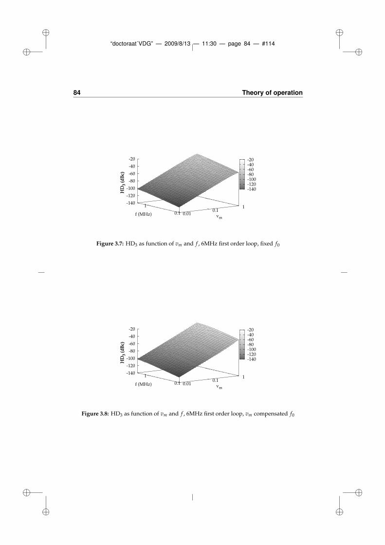
“doctoraat˙VDG” — 2009/8/13 — 11:30 — page 84 — #114
84 Theory of operation
-140-120-100-80-60-40-20
0.01 0.1
1
0.1
1-140
-120
-100
-80
-60
-40
-20
HD
3 (d
Bc)
vmf (MHz)
HD
3 (d
Bc)
Figure 3.7: HD3 as function of vm and f , 6MHz first order loop, fixed f0
-140-120-100-80-60-40-20
0.01 0.1
1
0.1
1-140
-120
-100
-80
-60
-40
-20
HD
3 (d
Bc)
vmf (MHz)
HD
3 (d
Bc)
Figure 3.8: HD3 as function of vm and f , 6MHz first order loop, vm compensated f0
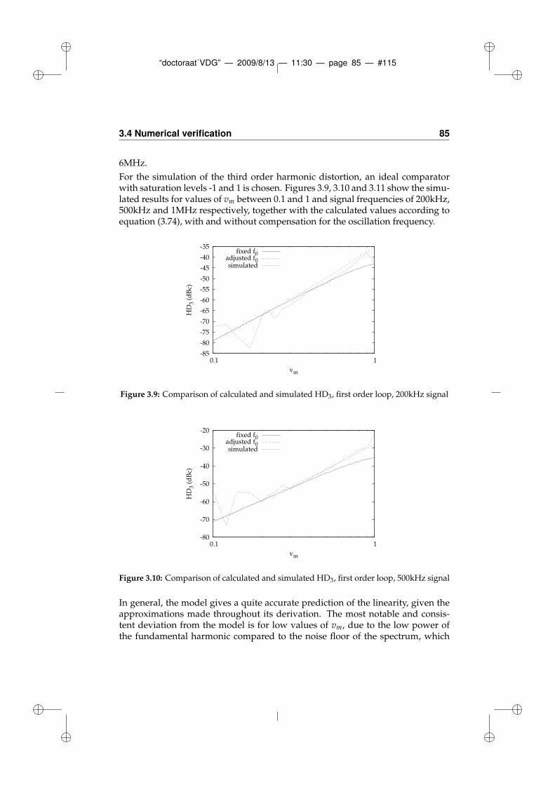
“doctoraat˙VDG” — 2009/8/13 — 11:30 — page 85 — #115
3.4 Numerical verification 85
6MHz.
For the simulation of the third order harmonic distortion, an ideal comparatorwith saturation levels -1 and 1 is chosen. Figures 3.9, 3.10 and 3.11 show the simu-lated results for values of vm between 0.1 and 1 and signal frequencies of 200kHz,500kHz and 1MHz respectively, together with the calculated values according toequation (3.74), with and without compensation for the oscillation frequency.
-85
-80
-75
-70
-65
-60
-55
-50
-45
-40
-35
0.1 1
HD
3 (d
Bc)
vm
fixed f0adjusted f0simulated
Figure 3.9: Comparison of calculated and simulated HD3, first order loop, 200kHz signal
-80
-70
-60
-50
-40
-30
-20
0.1 1
HD
3 (d
Bc)
vm
fixed f0adjusted f0simulated
Figure 3.10: Comparison of calculated and simulated HD3, first order loop, 500kHz signal
In general, the model gives a quite accurate prediction of the linearity, given theapproximations made throughout its derivation. The most notable and consis-tent deviation from the model is for low values of vm, due to the low power ofthe fundamental harmonic compared to the noise floor of the spectrum, which
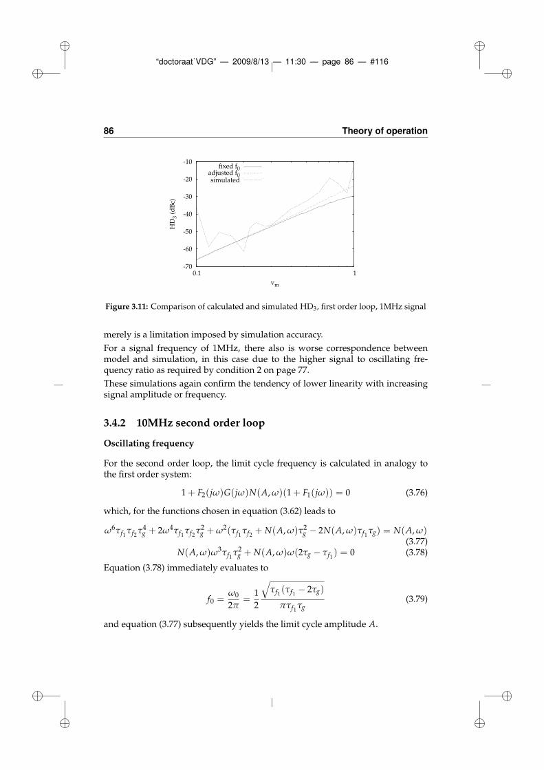
“doctoraat˙VDG” — 2009/8/13 — 11:30 — page 86 — #116
86 Theory of operation
-70
-60
-50
-40
-30
-20
-10
0.1 1
HD
3 (d
Bc)
vm
fixed f0adjusted f0simulated
Figure 3.11: Comparison of calculated and simulated HD3, first order loop, 1MHz signal
merely is a limitation imposed by simulation accuracy.
For a signal frequency of 1MHz, there also is worse correspondence betweenmodel and simulation, in this case due to the higher signal to oscillating fre-quency ratio as required by condition 2 on page 77.
These simulations again confirm the tendency of lower linearity with increasingsignal amplitude or frequency.
3.4.2 10MHz second order loop
Oscillating frequency
For the second order loop, the limit cycle frequency is calculated in analogy tothe first order system:
1 + F2(jω)G(jω)N(A, ω)(1 + F1(jω)) = 0 (3.76)
which, for the functions chosen in equation (3.62) leads to
ω6τf1 τf2 τ4g + 2ω4τf1 τf2 τ2
g + ω2(τf1 τf2 + N(A, ω)τ2g − 2N(A, ω)τf1 τg) = N(A, ω)
(3.77)N(A, ω)ω3τf1 τ2
g + N(A, ω)ω(2τg − τf1) = 0 (3.78)
Equation (3.78) immediately evaluates to
f0 =ω0
2π=
1
2
√
τf1(τf1 − 2τg)
πτf1 τg(3.79)
and equation (3.77) subsequently yields the limit cycle amplitude A.
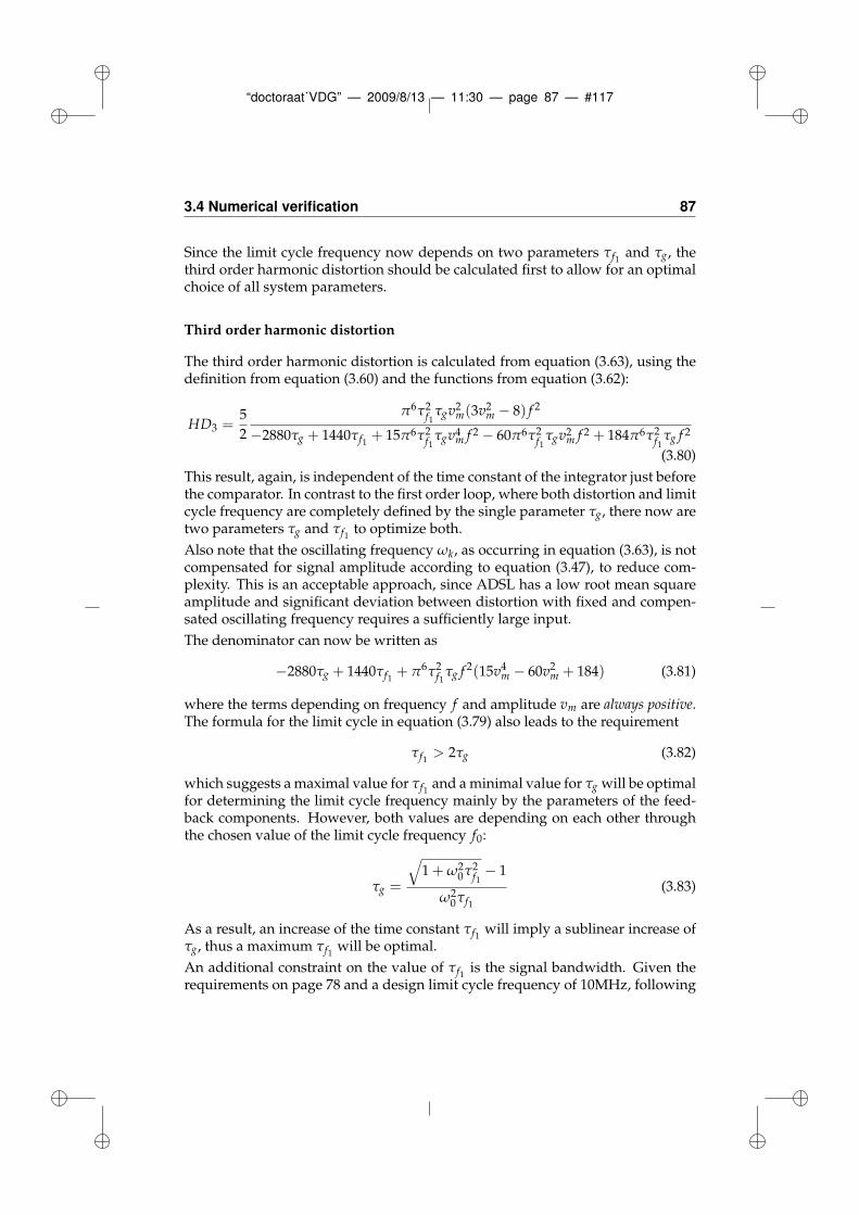
“doctoraat˙VDG” — 2009/8/13 — 11:30 — page 87 — #117
3.4 Numerical verification 87
Since the limit cycle frequency now depends on two parameters τf1 and τg, thethird order harmonic distortion should be calculated first to allow for an optimalchoice of all system parameters.
Third order harmonic distortion
The third order harmonic distortion is calculated from equation (3.63), using thedefinition from equation (3.60) and the functions from equation (3.62):
HD3 =5
2
π6τ2f1
τgv2m(3v2
m − 8) f 2
−2880τg + 1440τf1 + 15π6τ2f1
τgv4m f 2 − 60π6τ2
f1τgv2
m f 2 + 184π6τ2f1
τg f 2
(3.80)
This result, again, is independent of the time constant of the integrator just beforethe comparator. In contrast to the first order loop, where both distortion and limitcycle frequency are completely defined by the single parameter τg, there now aretwo parameters τg and τf1 to optimize both.
Also note that the oscillating frequency ωk, as occurring in equation (3.63), is notcompensated for signal amplitude according to equation (3.47), to reduce com-plexity. This is an acceptable approach, since ADSL has a low root mean squareamplitude and significant deviation between distortion with fixed and compen-sated oscillating frequency requires a sufficiently large input.
The denominator can now be written as
−2880τg + 1440τf1 + π6τ2f1
τg f2(15v4
m − 60v2m + 184) (3.81)
where the terms depending on frequency f and amplitude vm are always positive.The formula for the limit cycle in equation (3.79) also leads to the requirement
τf1 > 2τg (3.82)
which suggests a maximal value for τf1 and a minimal value for τg will be optimalfor determining the limit cycle frequency mainly by the parameters of the feed-back components. However, both values are depending on each other throughthe chosen value of the limit cycle frequency f0:
τg =
√
1 + ω20τ2
f1− 1
ω20τf1
(3.83)
As a result, an increase of the time constant τf1 will imply a sublinear increase ofτg, thus a maximum τf1 will be optimal.
An additional constraint on the value of τf1 is the signal bandwidth. Given therequirements on page 78 and a design limit cycle frequency of 10MHz, following
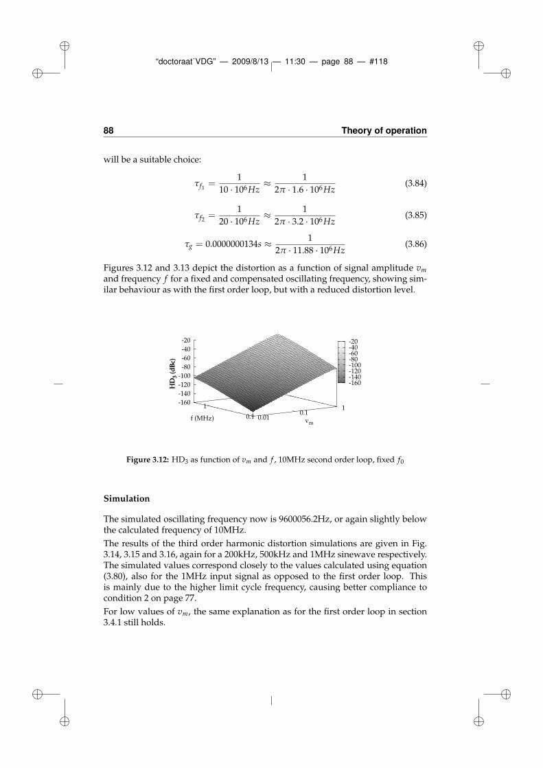
“doctoraat˙VDG” — 2009/8/13 — 11:30 — page 88 — #118
88 Theory of operation
will be a suitable choice:
τf1 =1
10 · 106Hz≈ 1
2π · 1.6 · 106Hz(3.84)
τf2 =1
20 · 106Hz≈ 1
2π · 3.2 · 106Hz(3.85)
τg = 0.0000000134s ≈ 1
2π · 11.88 · 106Hz(3.86)
Figures 3.12 and 3.13 depict the distortion as a function of signal amplitude vmand frequency f for a fixed and compensated oscillating frequency, showing sim-ilar behaviour as with the first order loop, but with a reduced distortion level.
-160-140-120-100-80-60-40-20
0.01 0.1
1
0.1
1-160
-140
-120
-100
-80
-60
-40
-20
HD
3 (d
Bc)
vmf (MHz)
HD
3 (d
Bc)
Figure 3.12: HD3 as function of vm and f , 10MHz second order loop, fixed f0
Simulation
The simulated oscillating frequency now is 9600056.2Hz, or again slightly belowthe calculated frequency of 10MHz.
The results of the third order harmonic distortion simulations are given in Fig.3.14, 3.15 and 3.16, again for a 200kHz, 500kHz and 1MHz sinewave respectively.The simulated values correspond closely to the values calculated using equation(3.80), also for the 1MHz input signal as opposed to the first order loop. Thisis mainly due to the higher limit cycle frequency, causing better compliance tocondition 2 on page 77.
For low values of vm, the same explanation as for the first order loop in section3.4.1 still holds.
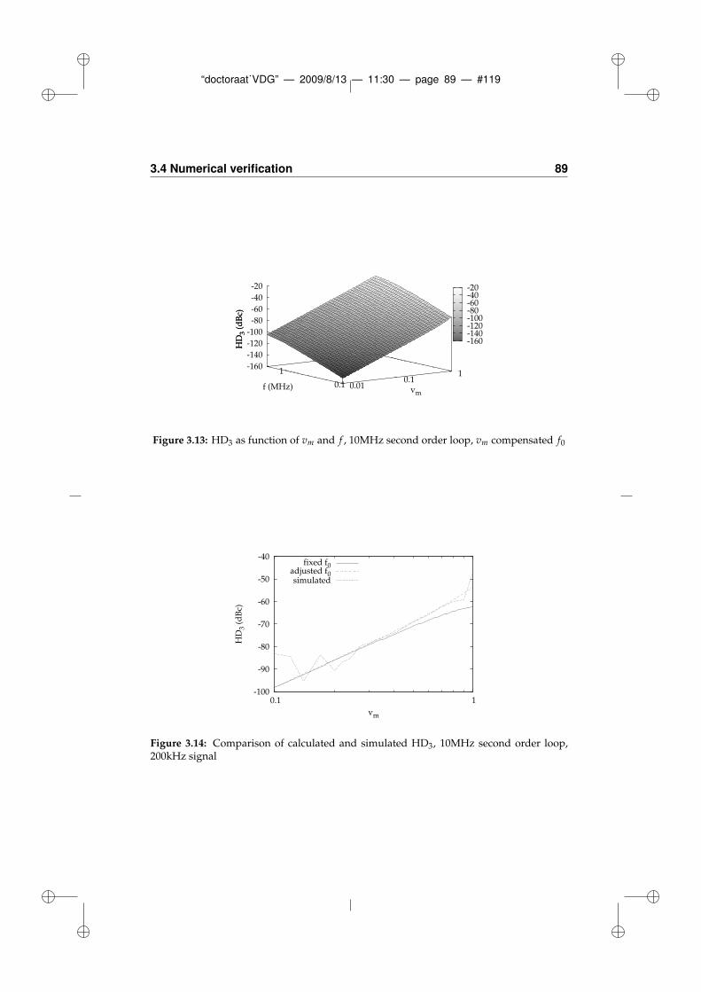
“doctoraat˙VDG” — 2009/8/13 — 11:30 — page 89 — #119
3.4 Numerical verification 89
-160-140-120-100-80-60-40-20
0.01 0.1
1
0.1
1-160
-140
-120
-100
-80
-60
-40
-20
HD
3 (d
Bc)
vmf (MHz)
HD
3 (d
Bc)
Figure 3.13: HD3 as function of vm and f , 10MHz second order loop, vm compensated f0
-100
-90
-80
-70
-60
-50
-40
0.1 1
HD
3 (d
Bc)
vm
fixed f0adjusted f0simulated
Figure 3.14: Comparison of calculated and simulated HD3, 10MHz second order loop,200kHz signal
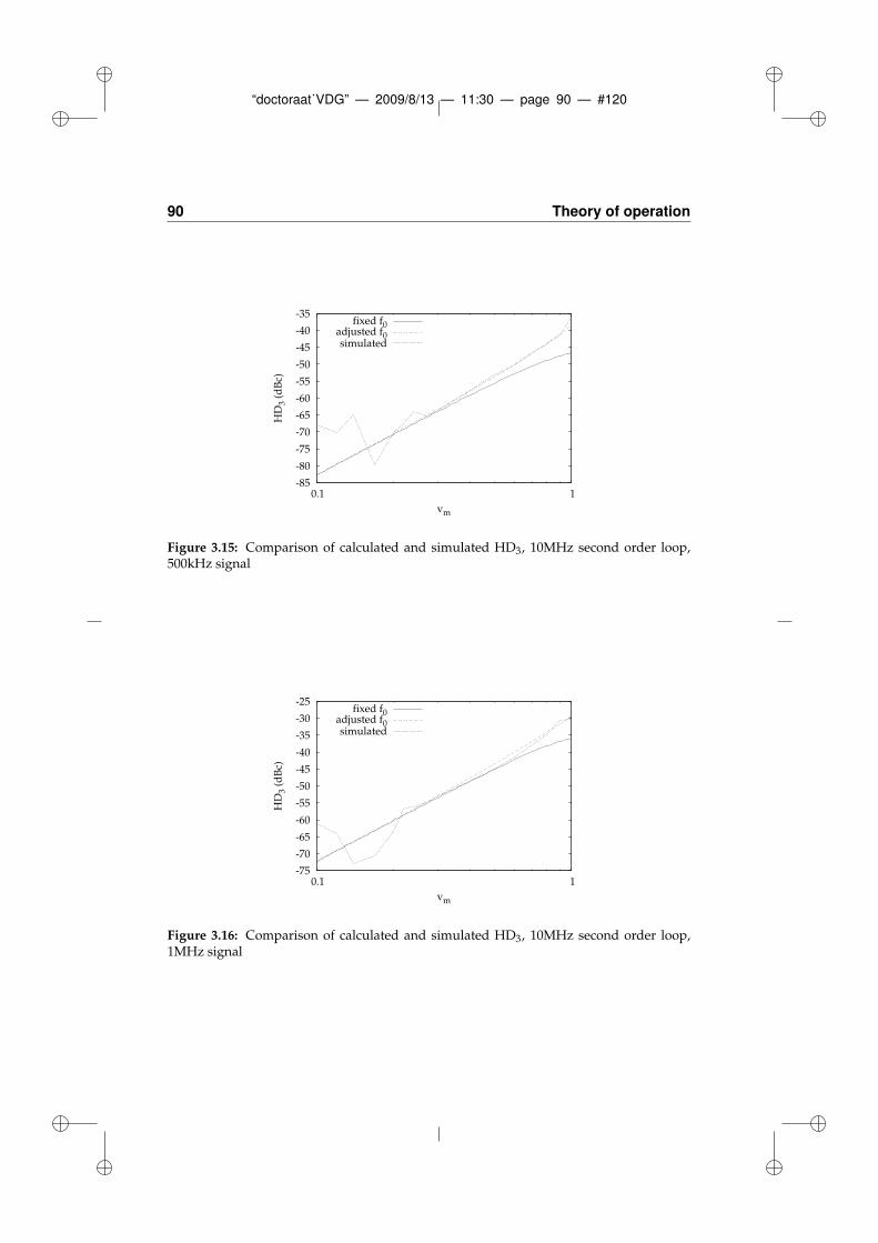
“doctoraat˙VDG” — 2009/8/13 — 11:30 — page 90 — #120
90 Theory of operation
-85
-80
-75
-70
-65
-60
-55
-50
-45
-40
-35
0.1 1
HD
3 (d
Bc)
vm
fixed f0adjusted f0simulated
Figure 3.15: Comparison of calculated and simulated HD3, 10MHz second order loop,500kHz signal
-75
-70
-65
-60
-55
-50
-45
-40
-35
-30
-25
0.1 1
HD
3 (d
Bc)
vm
fixed f0adjusted f0simulated
Figure 3.16: Comparison of calculated and simulated HD3, 10MHz second order loop,1MHz signal
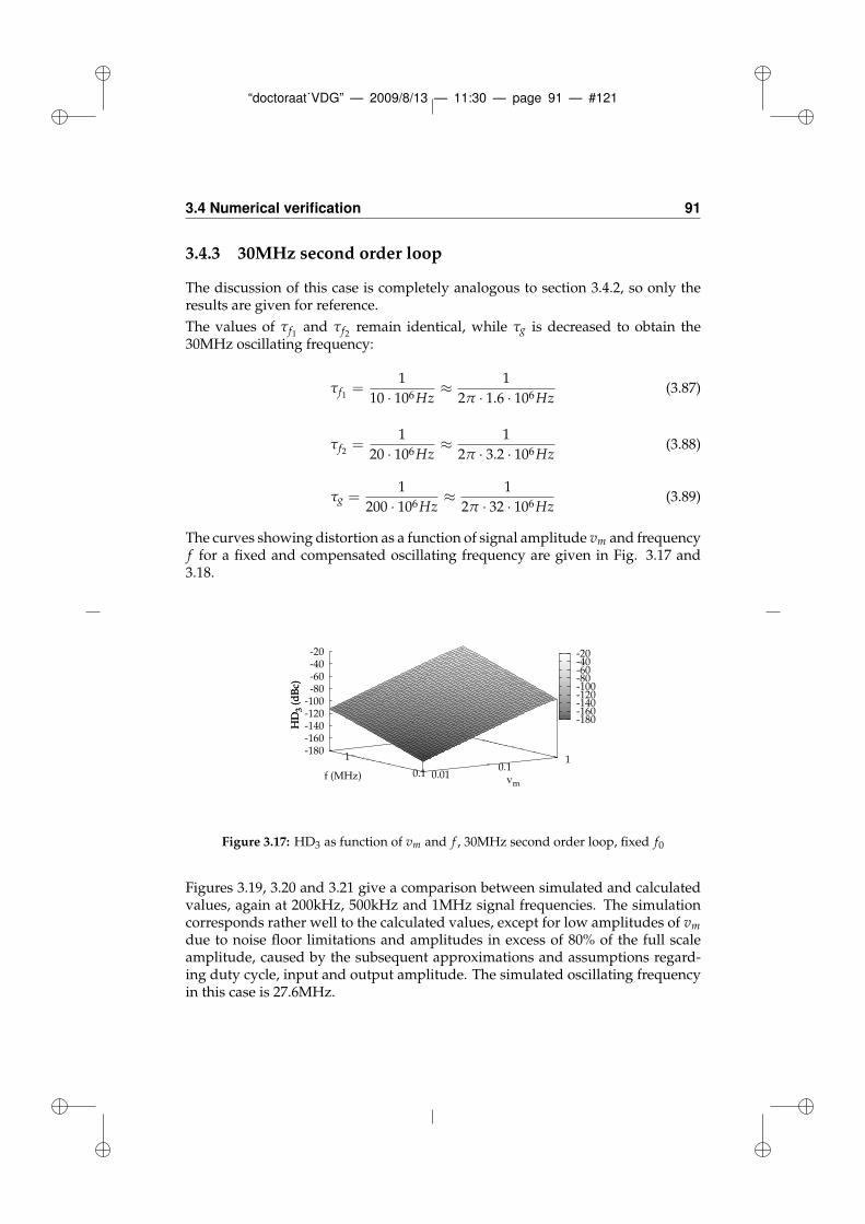
“doctoraat˙VDG” — 2009/8/13 — 11:30 — page 91 — #121
3.4 Numerical verification 91
3.4.3 30MHz second order loop
The discussion of this case is completely analogous to section 3.4.2, so only theresults are given for reference.
The values of τf1 and τf2 remain identical, while τg is decreased to obtain the30MHz oscillating frequency:
τf1 =1
10 · 106Hz≈ 1
2π · 1.6 · 106Hz(3.87)
τf2 =1
20 · 106Hz≈ 1
2π · 3.2 · 106Hz(3.88)
τg =1
200 · 106Hz≈ 1
2π · 32 · 106Hz(3.89)
The curves showing distortion as a function of signal amplitude vm and frequencyf for a fixed and compensated oscillating frequency are given in Fig. 3.17 and3.18.
-180-160-140-120-100-80-60-40-20
0.01 0.1
1
0.1
1-180-160-140-120-100
-80-60-40-20
HD
3 (d
Bc)
vmf (MHz)
HD
3 (d
Bc)
Figure 3.17: HD3 as function of vm and f , 30MHz second order loop, fixed f0
Figures 3.19, 3.20 and 3.21 give a comparison between simulated and calculatedvalues, again at 200kHz, 500kHz and 1MHz signal frequencies. The simulationcorresponds rather well to the calculated values, except for low amplitudes of vmdue to noise floor limitations and amplitudes in excess of 80% of the full scaleamplitude, caused by the subsequent approximations and assumptions regard-ing duty cycle, input and output amplitude. The simulated oscillating frequencyin this case is 27.6MHz.
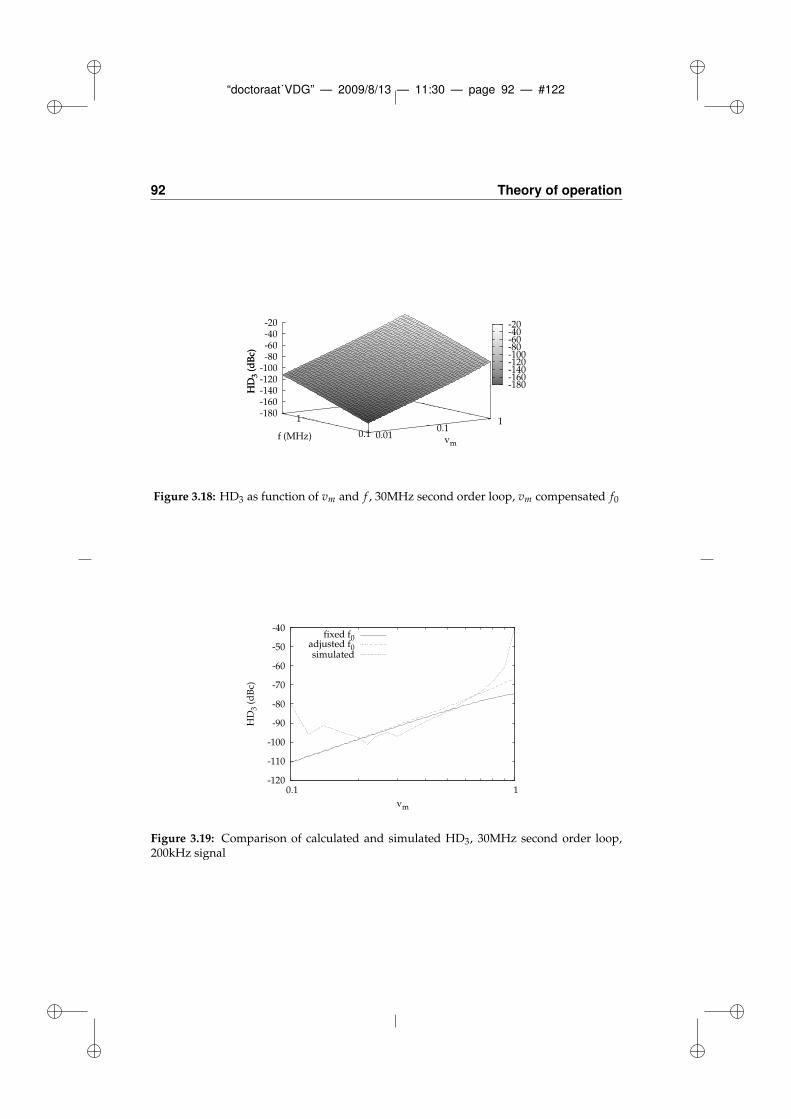
“doctoraat˙VDG” — 2009/8/13 — 11:30 — page 92 — #122
92 Theory of operation
-180-160-140-120-100-80-60-40-20
0.01 0.1
1
0.1
1-180-160-140-120-100
-80-60-40-20
HD
3 (d
Bc)
vmf (MHz)
HD
3 (d
Bc)
Figure 3.18: HD3 as function of vm and f , 30MHz second order loop, vm compensated f0
-120
-110
-100
-90
-80
-70
-60
-50
-40
0.1 1
HD
3 (d
Bc)
vm
fixed f0adjusted f0simulated
Figure 3.19: Comparison of calculated and simulated HD3, 30MHz second order loop,200kHz signal
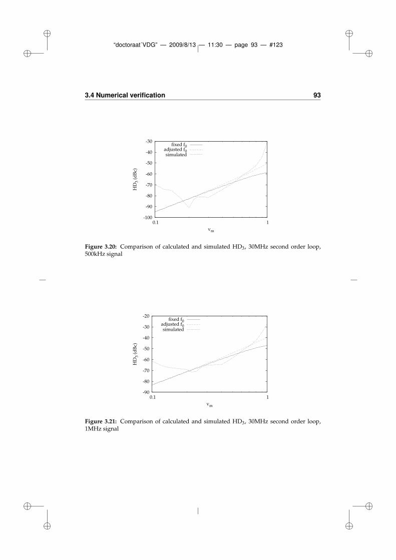
“doctoraat˙VDG” — 2009/8/13 — 11:30 — page 93 — #123
3.4 Numerical verification 93
-100
-90
-80
-70
-60
-50
-40
-30
0.1 1
HD
3 (d
Bc)
vm
fixed f0adjusted f0simulated
Figure 3.20: Comparison of calculated and simulated HD3, 30MHz second order loop,500kHz signal
-90
-80
-70
-60
-50
-40
-30
-20
0.1 1
HD
3 (d
Bc)
vm
fixed f0adjusted f0simulated
Figure 3.21: Comparison of calculated and simulated HD3, 30MHz second order loop,1MHz signal
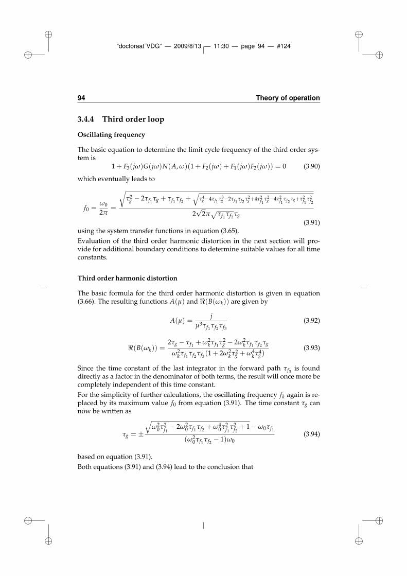
“doctoraat˙VDG” — 2009/8/13 — 11:30 — page 94 — #124
94 Theory of operation
3.4.4 Third order loop
Oscillating frequency
The basic equation to determine the limit cycle frequency of the third order sys-tem is
1 + F3(jω)G(jω)N(A, ω)(1 + F2(jω) + F1(jω)F2(jω)) = 0 (3.90)
which eventually leads to
f0 =ω0
2π=
√
τ2g − 2τf1 τg + τf1 τf2 +
√
τ4g−4τf1
τ3g−2τf1
τf2τ2g+4τ2
f1τ2g−4τ2
f1τf2
τg+τ2f1
τ2f2
2√
2π√
τf1 τf2 τg(3.91)
using the system transfer functions in equation (3.65).
Evaluation of the third order harmonic distortion in the next section will pro-vide for additional boundary conditions to determine suitable values for all timeconstants.
Third order harmonic distortion
The basic formula for the third order harmonic distortion is given in equation(3.66). The resulting functions A(µ) and ℜ(B(ωk)) are given by
A(µ) =j
µ3τf1 τf2 τf3
(3.92)
ℜ(B(ωk)) =2τg − τf1 + ω2
kτf1 τ2g − 2ω2
kτf1 τf2 τg
ω2kτf1 τf2 τf3(1 + 2ω2
kτ2g + ω4
kτ4g )
(3.93)
Since the time constant of the last integrator in the forward path τf3 is founddirectly as a factor in the denominator of both terms, the result will once more becompletely independent of this time constant.
For the simplicity of further calculations, the oscillating frequency fk again is re-placed by its maximum value f0 from equation (3.91). The time constant τg cannow be written as
τg = ±
√
ω20τ2
f1− 2ω2
0τf1 τf2 + ω40τ2
f1τ2f2
+ 1 − ω0τf1
(ω20τf1 τf2 − 1)ω0
(3.94)
based on equation (3.91).
Both equations (3.91) and (3.94) lead to the conclusion that
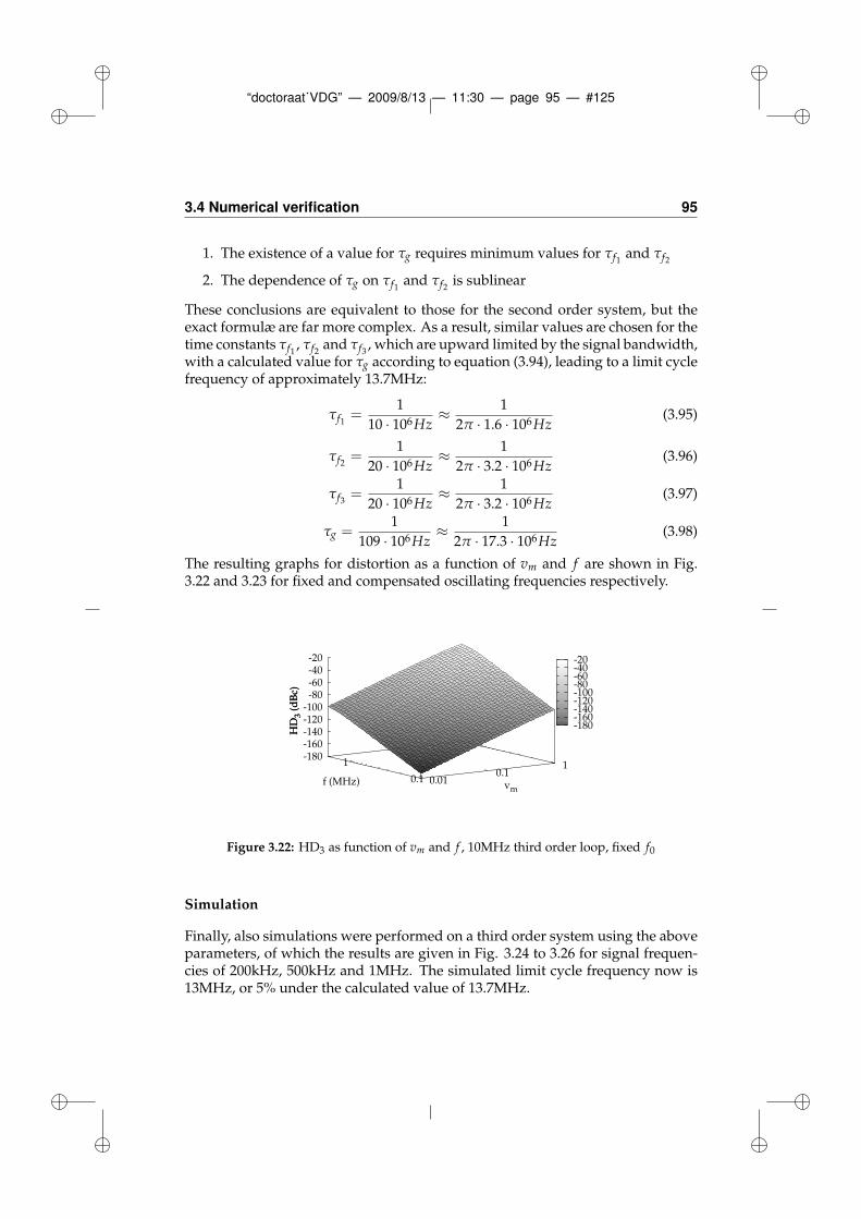
“doctoraat˙VDG” — 2009/8/13 — 11:30 — page 95 — #125
3.4 Numerical verification 95
1. The existence of a value for τg requires minimum values for τf1 and τf2
2. The dependence of τg on τf1 and τf2 is sublinear
These conclusions are equivalent to those for the second order system, but theexact formulæ are far more complex. As a result, similar values are chosen for thetime constants τf1 , τf2 and τf3 , which are upward limited by the signal bandwidth,with a calculated value for τg according to equation (3.94), leading to a limit cyclefrequency of approximately 13.7MHz:
τf1 =1
10 · 106Hz≈ 1
2π · 1.6 · 106Hz(3.95)
τf2 =1
20 · 106Hz≈ 1
2π · 3.2 · 106Hz(3.96)
τf3 =1
20 · 106Hz≈ 1
2π · 3.2 · 106Hz(3.97)
τg =1
109 · 106Hz≈ 1
2π · 17.3 · 106Hz(3.98)
The resulting graphs for distortion as a function of vm and f are shown in Fig.3.22 and 3.23 for fixed and compensated oscillating frequencies respectively.
-180-160-140-120-100-80-60-40-20
0.01 0.1
1
0.1
1-180-160-140-120-100
-80-60-40-20
HD
3 (d
Bc)
vmf (MHz)
HD
3 (d
Bc)
Figure 3.22: HD3 as function of vm and f , 10MHz third order loop, fixed f0
Simulation
Finally, also simulations were performed on a third order system using the aboveparameters, of which the results are given in Fig. 3.24 to 3.26 for signal frequen-cies of 200kHz, 500kHz and 1MHz. The simulated limit cycle frequency now is13MHz, or 5% under the calculated value of 13.7MHz.
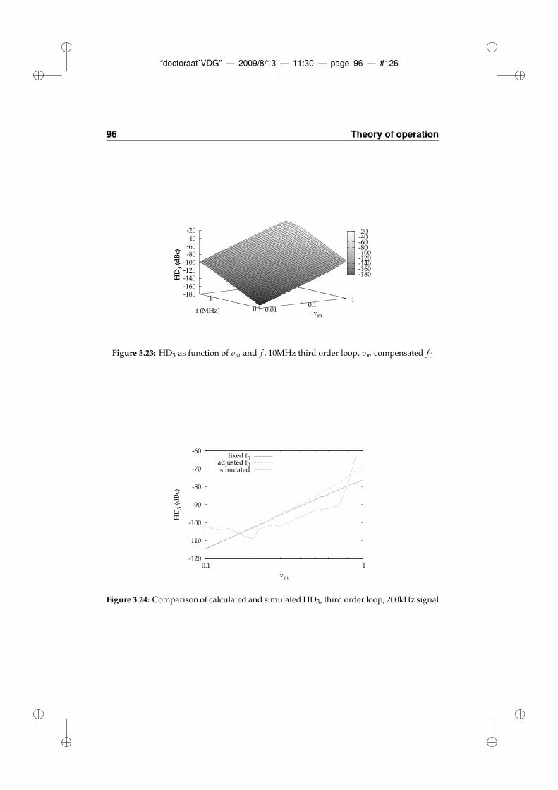
“doctoraat˙VDG” — 2009/8/13 — 11:30 — page 96 — #126
96 Theory of operation
-180-160-140-120-100-80-60-40-20
0.01 0.1
1
0.1
1-180-160-140-120-100
-80-60-40-20
HD
3 (d
Bc)
vmf (MHz)
HD
3 (d
Bc)
Figure 3.23: HD3 as function of vm and f , 10MHz third order loop, vm compensated f0
-120
-110
-100
-90
-80
-70
-60
0.1 1
HD
3 (d
Bc)
vm
fixed f0adjusted f0simulated
Figure 3.24: Comparison of calculated and simulated HD3, third order loop, 200kHz signal
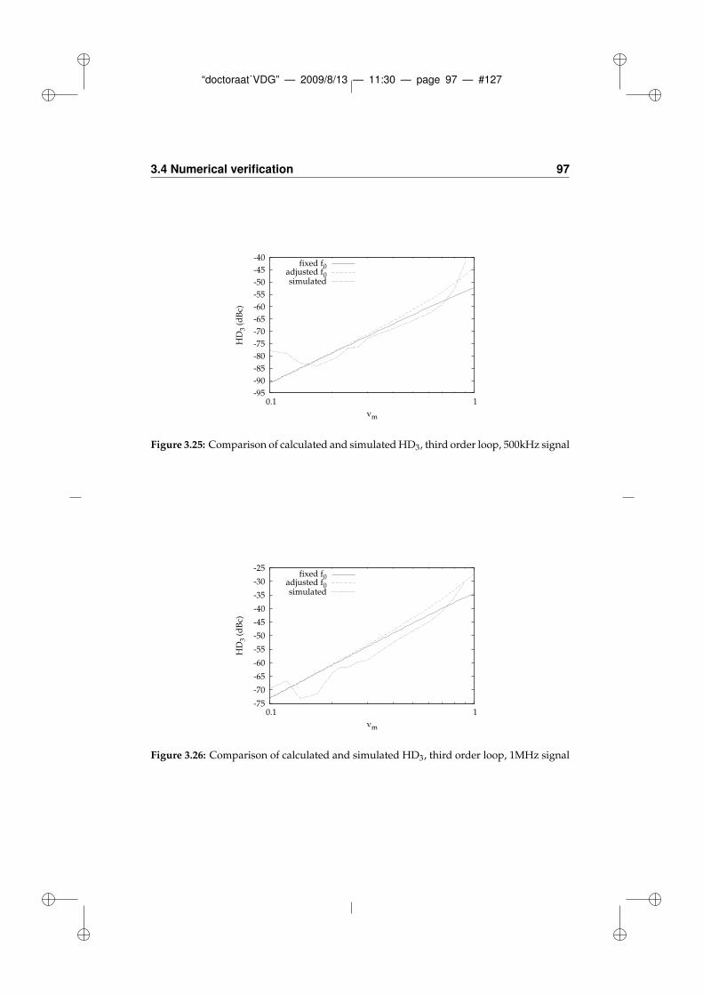
“doctoraat˙VDG” — 2009/8/13 — 11:30 — page 97 — #127
3.4 Numerical verification 97
-95
-90
-85
-80
-75
-70
-65
-60
-55
-50
-45
-40
0.1 1
HD
3 (d
Bc)
vm
fixed f0adjusted f0simulated
Figure 3.25: Comparison of calculated and simulated HD3, third order loop, 500kHz signal
-75
-70
-65
-60
-55
-50
-45
-40
-35
-30
-25
0.1 1
HD
3 (d
Bc)
vm
fixed f0adjusted f0simulated
Figure 3.26: Comparison of calculated and simulated HD3, third order loop, 1MHz signal
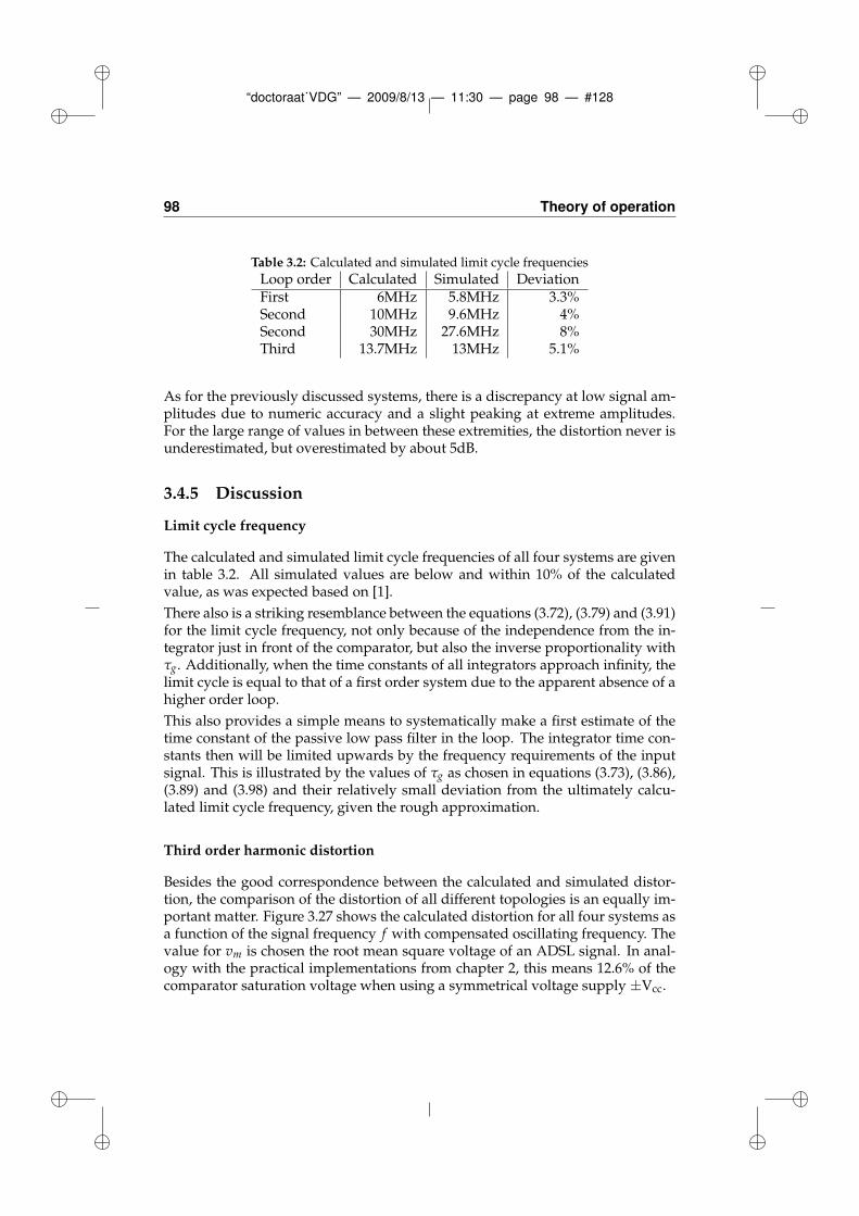
“doctoraat˙VDG” — 2009/8/13 — 11:30 — page 98 — #128
98 Theory of operation
Table 3.2: Calculated and simulated limit cycle frequencies
Loop order Calculated Simulated DeviationFirst 6MHz 5.8MHz 3.3%Second 10MHz 9.6MHz 4%Second 30MHz 27.6MHz 8%Third 13.7MHz 13MHz 5.1%
As for the previously discussed systems, there is a discrepancy at low signal am-plitudes due to numeric accuracy and a slight peaking at extreme amplitudes.For the large range of values in between these extremities, the distortion never isunderestimated, but overestimated by about 5dB.
3.4.5 Discussion
Limit cycle frequency
The calculated and simulated limit cycle frequencies of all four systems are givenin table 3.2. All simulated values are below and within 10% of the calculatedvalue, as was expected based on [1].
There also is a striking resemblance between the equations (3.72), (3.79) and (3.91)for the limit cycle frequency, not only because of the independence from the in-tegrator just in front of the comparator, but also the inverse proportionality withτg. Additionally, when the time constants of all integrators approach infinity, thelimit cycle is equal to that of a first order system due to the apparent absence of ahigher order loop.
This also provides a simple means to systematically make a first estimate of thetime constant of the passive low pass filter in the loop. The integrator time con-stants then will be limited upwards by the frequency requirements of the inputsignal. This is illustrated by the values of τg as chosen in equations (3.73), (3.86),(3.89) and (3.98) and their relatively small deviation from the ultimately calcu-lated limit cycle frequency, given the rough approximation.
Third order harmonic distortion
Besides the good correspondence between the calculated and simulated distor-tion, the comparison of the distortion of all different topologies is an equally im-portant matter. Figure 3.27 shows the calculated distortion for all four systems asa function of the signal frequency f with compensated oscillating frequency. Thevalue for vm is chosen the root mean square voltage of an ADSL signal. In anal-ogy with the practical implementations from chapter 2, this means 12.6% of thecomparator saturation voltage when using a symmetrical voltage supply ±Vcc.
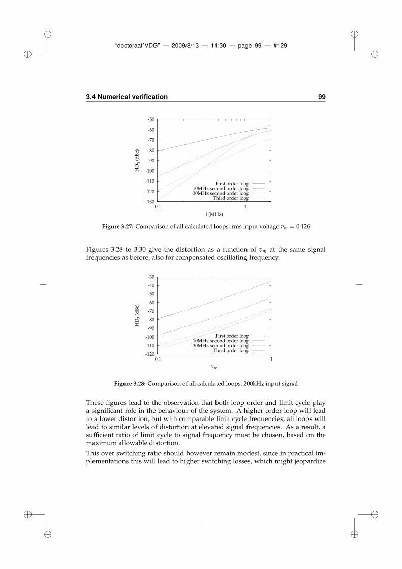
“doctoraat˙VDG” — 2009/8/13 — 11:30 — page 99 — #129
3.4 Numerical verification 99
-130
-120
-110
-100
-90
-80
-70
-60
-50
0.1 1
HD
3 (d
Bc)
f (MHz)
First order loop10MHz second order loop30MHz second order loop
Third order loop
Figure 3.27: Comparison of all calculated loops, rms input voltage vm = 0.126
Figures 3.28 to 3.30 give the distortion as a function of vm at the same signalfrequencies as before, also for compensated oscillating frequency.
-120
-110
-100
-90
-80
-70
-60
-50
-40
-30
0.1 1
HD
3 (d
Bc)
vm
First order loop10MHz second order loop30MHz second order loop
Third order loop
Figure 3.28: Comparison of all calculated loops, 200kHz input signal
These figures lead to the observation that both loop order and limit cycle playa significant role in the behaviour of the system. A higher order loop will leadto a lower distortion, but with comparable limit cycle frequencies, all loops willlead to similar levels of distortion at elevated signal frequencies. As a result, asufficient ratio of limit cycle to signal frequency must be chosen, based on themaximum allowable distortion.
This over switching ratio should however remain modest, since in practical im-plementations this will lead to higher switching losses, which might jeopardize
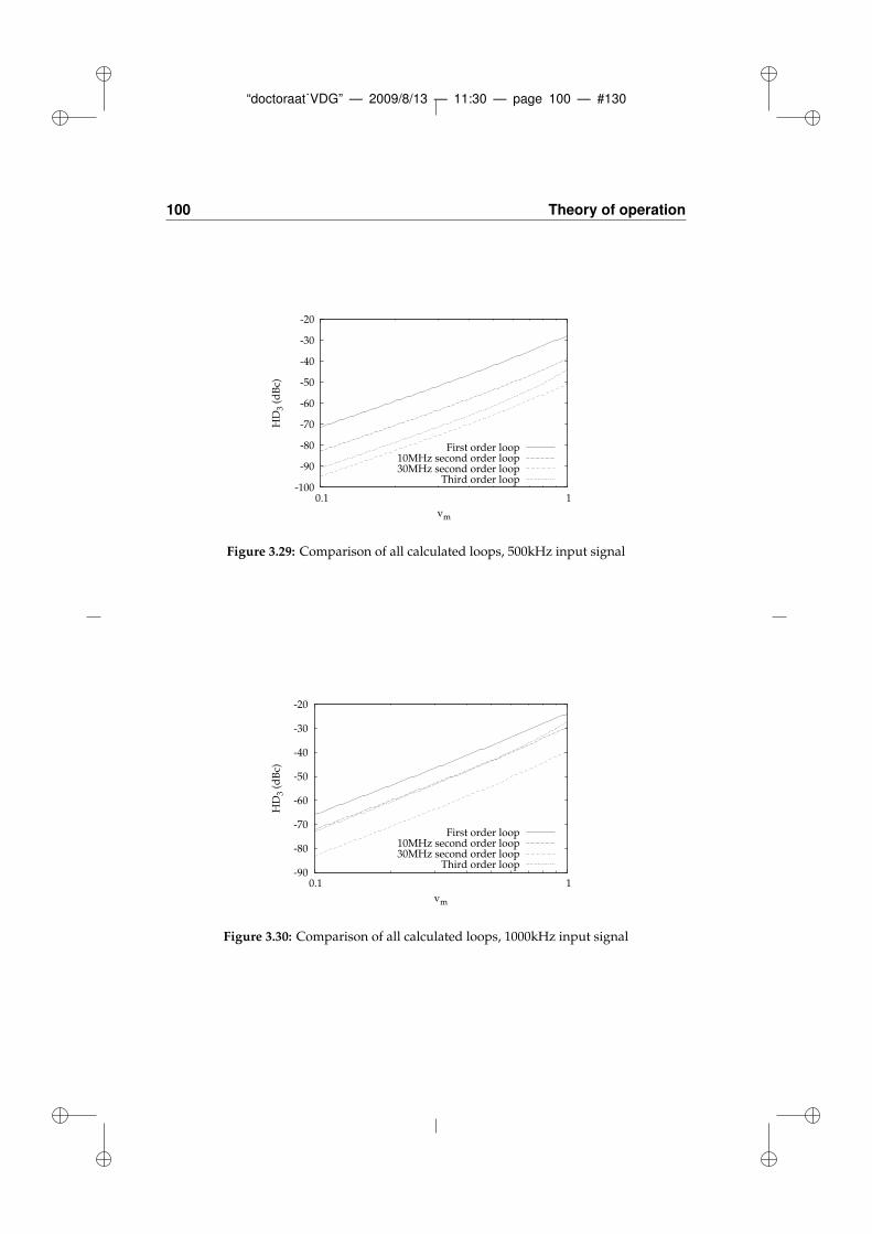
“doctoraat˙VDG” — 2009/8/13 — 11:30 — page 100 — #130
100 Theory of operation
-100
-90
-80
-70
-60
-50
-40
-30
-20
0.1 1
HD
3 (d
Bc)
vm
First order loop10MHz second order loop30MHz second order loop
Third order loop
Figure 3.29: Comparison of all calculated loops, 500kHz input signal
-90
-80
-70
-60
-50
-40
-30
-20
0.1 1
HD
3 (d
Bc)
vm
First order loop10MHz second order loop30MHz second order loop
Third order loop
Figure 3.30: Comparison of all calculated loops, 1000kHz input signal
“doctoraat˙VDG” — 2009/8/13 — 11:30 — page 101 — #131
3.5 Conclusion 101
Table 3.3: Simulated MTPRLoop order Limit cycle MTPRFirst 6MHz 42.5dBSecond 10MHz 52dBSecond 30MHz 54dBThird 13.7MHz 57dB
the advantage of a switching amplifier over its linear counterpart.
What about MTPR?
With regard to the final goal being the processing of ADSL signals, one questionstill remains. How does this translate into MTPR? Several numerical simulationsin Matlab with MTPR test signals were performed, leading to the results fromtable 3.3. Note that for the first order loop the input used is an ADSL2 signal withfrequencies up to 1.1MHz, while the other loops were simulated using a 2.2MHzADSL2+ signal.
As a result, at least a 30MHz second order loop or a 10MHz third order loop willbe required to reach the specification of 55dB.
3.5 Conclusion
A mathematical description of the system is given, to predict both the oscillatingfrequency and the third order harmonic distortion. This theory is verified byseveral numerical simulations, leading to the following observations:
1. An increase of the loop order lowers the distortion
2. A higher limit cycle also decreases distortion
With regard to MTPR, the over switching ratio should be at least 5 for a thirdorder loop.

“doctoraat˙VDG” — 2009/8/13 — 11:30 — page 102 — #132
102 Theory of operation
“doctoraat˙VDG” — 2009/8/13 — 11:30 — page 103 — #133
References
[1] A. Gelb and W. E. Vander Velde, Multiple-input Describing Functions and Non-linear System Design. McGraw-Hill Book Company, 1968.
[2] E. Roza, “Analog-to-digital conversion via duty-cycle modulation,” IEEETrans. Circuits Syst. II, vol. 44, no. 11, pp. 907–914, Nov. 1997.
[3] V. Mangulis, Handbook of Series for Scientists and Engineers. New York: Aca-demic Press Inc., 1965.

“doctoraat˙VDG” — 2009/8/13 — 11:30 — page 104 — #134
104 REFERENCES
“doctoraat˙VDG” — 2009/8/13 — 11:30 — page 105 — #135
4Designing the loop
In this chapter, an overview is given of the different building blocks required to imple-ment the final circuit, in accordance with the results from chapter 3. Simulation resultsare then presented for both the building blocks and the full asynchronous amplifier,with some additional recommendations for the final layout.
4.1 Introduction
The system parameters, as proposed in chapter 3, can now be used in a practi-cal implementation, to further verify the theory and identify the potential bot-tlenecks for future designs. All four different loops will be implemented as adifferential input, differential output amplifier, with the outputs in forced coun-terphase as already demonstrated in section 2.4. In addition, also a version withtwo independent single input, single output 10MHz loops with counterphase in-puts will be tested.
The technology chosen for this design, is the AMI Semiconductor I3T80 0.35µmtechnology, offering devices with breakdown voltages of up to 80V. In addition,the transformer ratio is chosen 1:2 to further reduce the supply voltage to 25V,which also means a doubling of the rms output current to deliver the 20dBmnominal power. From a line driver point of view, the 100Ω line impedance istransformed down to 25Ω.
“doctoraat˙VDG” — 2009/8/13 — 11:30 — page 106 — #136
106 Designing the loop
Table 4.1: Key characteristics of I3T80 DMOS devices [1]
Device Type Floating Breakdown Ron ∗ Area
VFNDM80 N 80V 70V 0.26Ω∗mm2
VFNDM80a N 80V 70V 0.325Ω∗mm2
LFPDM80 P 80V -70V 0.28Ω∗mm2
Section 4.2 gives an overview of the most important I3T80 device parameters,which will be used in the different building blocks in section 4.3. Sections 4.4to 4.7 give the implementation of the first, second and third order systems asdimensioned in sections 3.4.1 to 3.4.4 and section 4.8 explores the functioning of asecond order system with two independent loops. The layout of these amplifiersthen is discussed in section 4.9.
4.2 Technology overview
Analogous to the I2T100 0.7µm technology, the I3T80 0.35µm technology is astandard 3.3V, 0.35µm CMOS process with high voltage extensions, allowing forbreakdown voltages of up to 80V. Again, the only components of interest are thehigh voltage DMOS structures, the MOS transistors, resistors and capacitors.
4.2.1 DMOS transistors
Of all DMOS transistors offered by the technology, only two N-type and one P-type DMOS are withheld based on supply voltage constraints, some importantparameters of which are given in table 4.1. The NDMOS transistors are a digital(VFNDM80) and an analogue (VFNDM80a) variant of the same basic structure.The main difference between both is the lower on-resistance of the analogue de-vice at identical conditions and channel width, while the digital device is morearea efficient. The final choice between both candidates will be based on simula-tions of the output stage.
4.2.2 MOS transistors
For the MOS transistors, the situation is slightly different from I2T100. Again,both the “classical” low voltage mosfets and their floating counterparts exist, butthis time they behave completely identical. This is caused by a particularity ofthe technology. Since the processing starts from a wafer with a N-type epitaxiallayer on top of a P-type substrate, the devices can be isolated from one anotherby implanting P-type dopants around the structure, which is done automatically
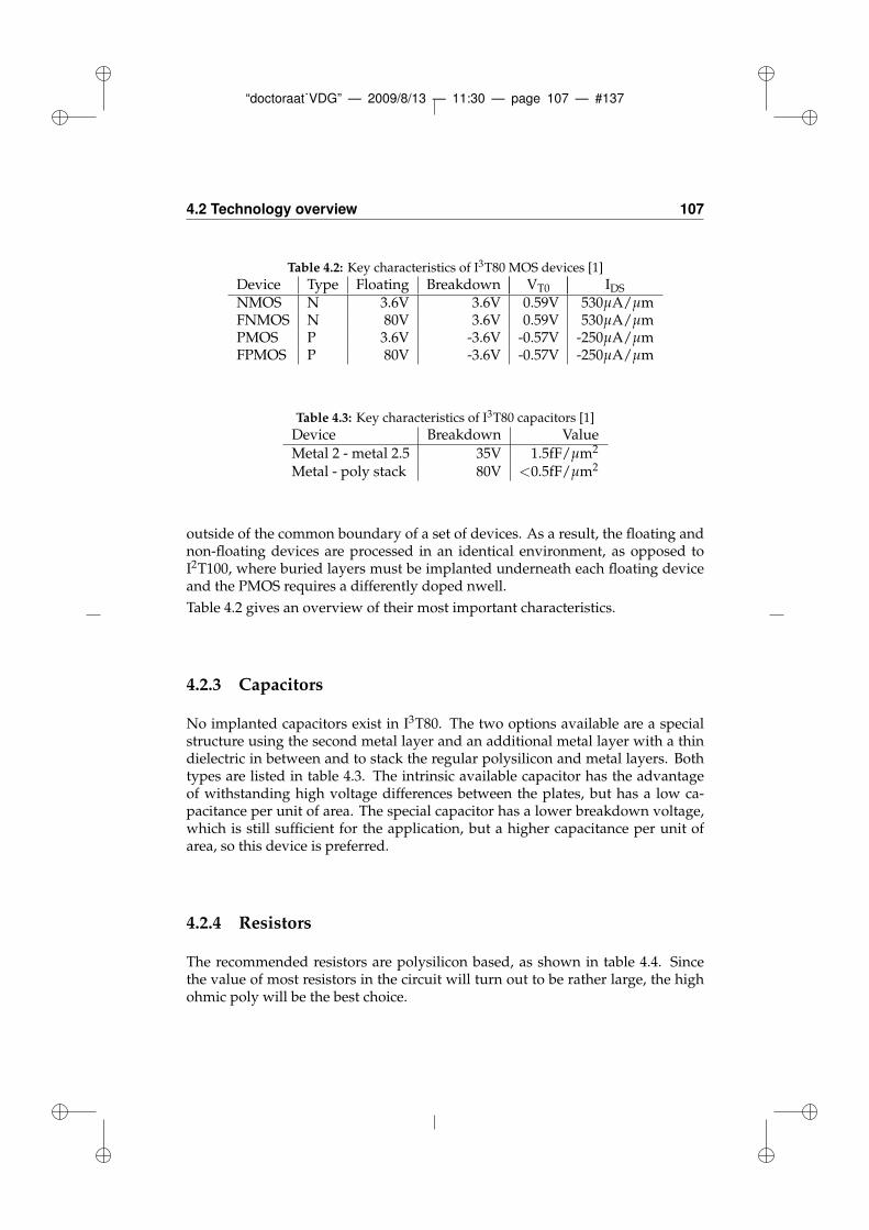
“doctoraat˙VDG” — 2009/8/13 — 11:30 — page 107 — #137
4.2 Technology overview 107
Table 4.2: Key characteristics of I3T80 MOS devices [1]
Device Type Floating Breakdown VT0 IDS
NMOS N 3.6V 3.6V 0.59V 530µA/µmFNMOS N 80V 3.6V 0.59V 530µA/µmPMOS P 3.6V -3.6V -0.57V -250µA/µmFPMOS P 80V -3.6V -0.57V -250µA/µm
Table 4.3: Key characteristics of I3T80 capacitors [1]
Device Breakdown Value
Metal 2 - metal 2.5 35V 1.5fF/µm2
Metal - poly stack 80V <0.5fF/µm2
outside of the common boundary of a set of devices. As a result, the floating andnon-floating devices are processed in an identical environment, as opposed toI2T100, where buried layers must be implanted underneath each floating deviceand the PMOS requires a differently doped nwell.
Table 4.2 gives an overview of their most important characteristics.
4.2.3 Capacitors
No implanted capacitors exist in I3T80. The two options available are a specialstructure using the second metal layer and an additional metal layer with a thindielectric in between and to stack the regular polysilicon and metal layers. Bothtypes are listed in table 4.3. The intrinsic available capacitor has the advantageof withstanding high voltage differences between the plates, but has a low ca-pacitance per unit of area. The special capacitor has a lower breakdown voltage,which is still sufficient for the application, but a higher capacitance per unit ofarea, so this device is preferred.
4.2.4 Resistors
The recommended resistors are polysilicon based, as shown in table 4.4. Sincethe value of most resistors in the circuit will turn out to be rather large, the highohmic poly will be the best choice.

“doctoraat˙VDG” — 2009/8/13 — 11:30 — page 108 — #138
108 Designing the loop
Table 4.4: Key characteristics of I3T80 resistors [1]
Device Breakdown ValueHigh ohmic poly 80V 975Ω/2
Unsalicide P+ poly 80V 240Ω/2
Unsalicide N+ poly 80V 292Ω/2
4.3 Building blocks
This section will list the basic blocks used in the amplifiers, which, again, areopamps for the integrator and voltage follower, a comparator, a turn-on delay,level shifter and buffers, the output stage and the passive voltage divider andfeedback filter.
4.3.1 Opamps
Two opamps are to be designed, namely a single ended opamp to buffer the di-vided output signal and provide a strong signal to the integrators and a differen-tial input, differential output opamp for the integrators.
Integrator
Opamp design For the integrator, an opamp with differential input and differ-ential output is chosen, since for higher order loops this will lead to a cleanerand more natural circuit, as opposed to the asymmetrical circuit from Fig. 2.24.Furthermore, two design parameters should be determined in advance, namelythe gain bandwidth product and the load capacitance, the first depending on thesignal properties, the latter merely on the final layout.
To be on the safe side, the load capacitance is chosen
CL = 1pF (4.1)
The gain bandwidth product will also have a direct impact on the distortion of theintegrator, since this is affected by the return difference or amount-of-feedback[2]. As a result, choosing the gain bandwidth product sufficiently high comparedto the unity gain bandwidth of the closed loop circuit will be beneficial.
The integrator time constants in sections 3.4.1 to 3.4.4 are set at frequencies of1.6MHz and 3.2MHz, so a gain bandwidth product of 275MHz is chosen, leadingto approximately 40dB of excess opamp gain capability. This relatively high fre-quency and the minimum signal frequency of 138kHz finally lead to a preferencefor a two stage folded cascode topology, the basic schematic of which is given inFig. 4.1.
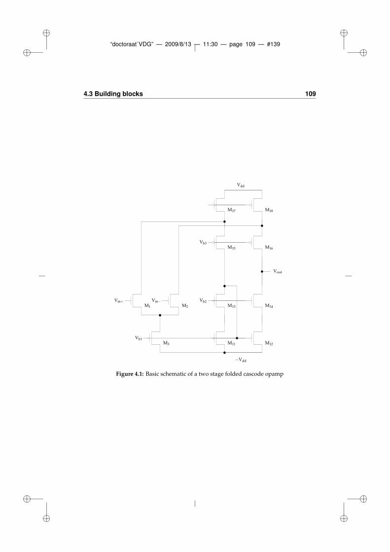
“doctoraat˙VDG” — 2009/8/13 — 11:30 — page 109 — #139
4.3 Building blocks 109
M11 M12
M13 M14
M15 M16
M3
M1 M2
M17 M18
Vin+ Vin− Vb2
Vout
−Vdd
Vdd
Vb1
Vb3
Figure 4.1: Basic schematic of a two stage folded cascode opamp
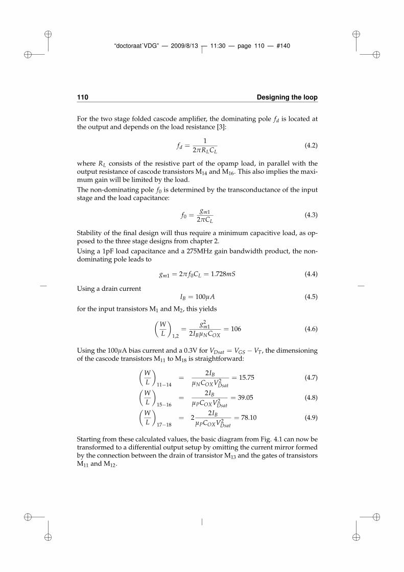
“doctoraat˙VDG” — 2009/8/13 — 11:30 — page 110 — #140
110 Designing the loop
For the two stage folded cascode amplifier, the dominating pole fd is located atthe output and depends on the load resistance [3]:
fd =1
2πRLCL(4.2)
where RL consists of the resistive part of the opamp load, in parallel with theoutput resistance of cascode transistors M14 and M16. This also implies the maxi-mum gain will be limited by the load.
The non-dominating pole f0 is determined by the transconductance of the inputstage and the load capacitance:
f0 =gm1
2πCL(4.3)
Stability of the final design will thus require a minimum capacitive load, as op-posed to the three stage designs from chapter 2.
Using a 1pF load capacitance and a 275MHz gain bandwidth product, the non-dominating pole leads to
gm1 = 2π f0CL = 1.728mS (4.4)
Using a drain currentIB = 100µA (4.5)
for the input transistors M1 and M2, this yields
(
W
L
)
1,2
=g2m1
2IBµNCOX= 106 (4.6)
Using the 100µA bias current and a 0.3V for VDsat = VGS −VT , the dimensioningof the cascode transistors M11 to M18 is straightforward:
(
W
L
)
11−14
=2IB
µNCOXV2Dsat
= 15.75 (4.7)
(
W
L
)
15−16
=2IB
µPCOXV2Dsat
= 39.05 (4.8)
(
W
L
)
17−18
= 22IB
µPCOXV2Dsat
= 78.10 (4.9)
Starting from these calculated values, the basic diagram from Fig. 4.1 can now betransformed to a differential output setup by omitting the current mirror formedby the connection between the drain of transistor M13 and the gates of transistorsM11 and M12.
“doctoraat˙VDG” — 2009/8/13 — 11:30 — page 111 — #141
4.3 Building blocks 111
This, however, means there is no direct coupling of the common mode compo-nent of both output voltages any more. Since the components in the loop shouldcompensate for a common mode difference generated by the output stage andnot the other way around, a so called long tail pair is included to compensate fora common mode difference [3][4][5]. By using the output of this long tail pairto determine the current on the folded cascode side of the opamp, the outputcommon mode will be adjusted such that
VG21 +VG24 = VG22 +VG23 = 2VCM,out (4.10)
using the conventions from Fig. 4.2. This means both output signals must havethe same common mode voltage VCM,out as applied to the input of the long tailpair and be in counterphase.
To simplify the design, the dimensions from the folded cascode opamp are usedas a reference, but to limit the current consumption, the dimensions of transistorsM21 to M28 are halved, which still allows for reliable current mirroring if usingmultiples of the same basic transistors.
Table 4.5 gives an overview of the final optimized dimensions of all transistors.
Table 4.5: Final dimensions of the opamp
Device Width Length
M1,2 35.50µm 0.35µm
M3 15.80µm 0.35µm
M11,12,13,14 7.90µm 0.5µm
M15,16 19.55µm 0.5µm
M17,18 39.10µm 0.5µm
M21,22,23,24 17.80µm 0.5µm
M25,26 19.55µm 0.5µm
M27,28 7.90µm 0.5µm
The simulated Bode transfer of the opamp, with common mode output voltage1.65V, is given in Fig. 4.3, resulting in a 339.87MHz gain bandwidth product anda 61.27 phase margin. The DC gain is 842 or 58.5dB, leading to a bandwidth of400kHz.
Integrator circuit The realized integrating circuit, using the differential input,differential output amplifier is shown in Fig. 4.4. This circuit is simulated usinga fixed feedback capacitance of 500fF and a resistor depending on the integra-tor time constant, 199kΩ for the 1.6MHz integrator and 99.5kΩ for the 3.2MHzintegrator, as determined in section 3.4.
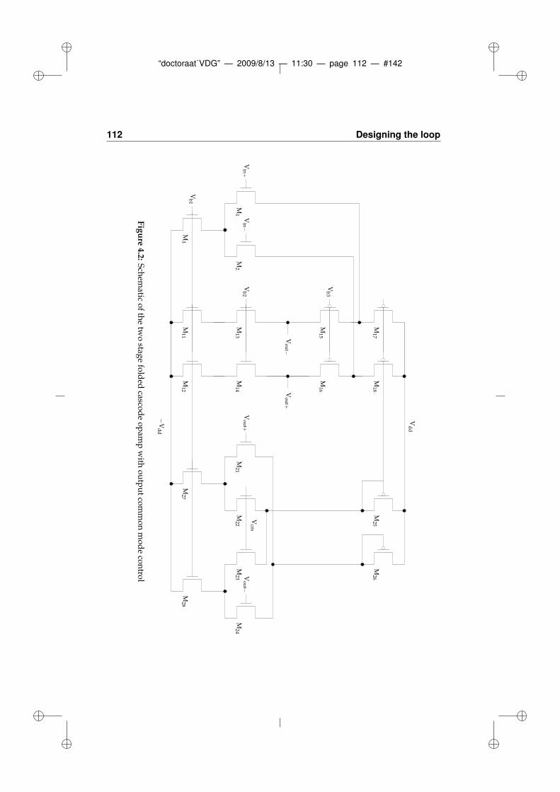
“doctoraat˙VDG” — 2009/8/13 — 11:30 — page 112 — #142
112 Designing the loop
M3
M1
M2
Vin
+V
in−
Vb
1M
11M
12
M13
M14
M15
M16
M17
M18
Vb
2
Vb
3
M27
M28
M21
M22
M23
M24
M26
M25
Vcm
Vo
ut−
Vo
ut+
−V
dd
Vd
d
Vo
ut+
Vo
ut−
Figure
4.2:
Sch
ematic
of
the
two
stage
fold
edcasco
de
op
amp
with
ou
tpu
tco
mm
on
mo
de
con
trol
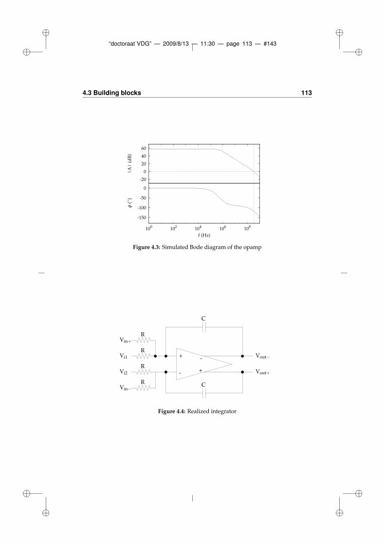
“doctoraat˙VDG” — 2009/8/13 — 11:30 — page 113 — #143
4.3 Building blocks 113
-150
-100
-50
0
100 102 104 106 108
f (Hz)
-20
0
20
40
60
|A
| (
dB
)φ
()
Figure 4.3: Simulated Bode diagram of the opamp
R
R
R
C
CR
+
-
-
+
Vin+
Vin−
Vout+
Vi1
Vi2
Vout−
Figure 4.4: Realized integrator
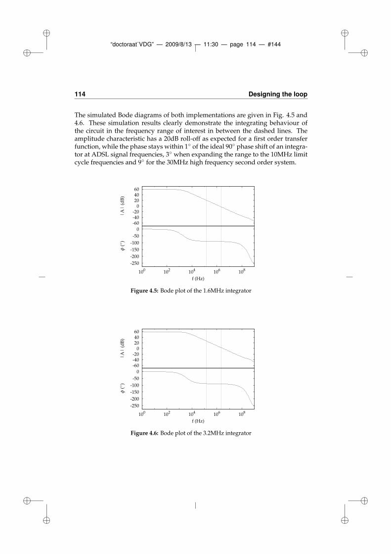
“doctoraat˙VDG” — 2009/8/13 — 11:30 — page 114 — #144
114 Designing the loop
The simulated Bode diagrams of both implementations are given in Fig. 4.5 and4.6. These simulation results clearly demonstrate the integrating behaviour ofthe circuit in the frequency range of interest in between the dashed lines. Theamplitude characteristic has a 20dB roll-off as expected for a first order transferfunction, while the phase stays within 1 of the ideal 90 phase shift of an integra-tor at ADSL signal frequencies, 3 when expanding the range to the 10MHz limitcycle frequencies and 9 for the 30MHz high frequency second order system.
-250
-200
-150
-100
-50
0
100 102 104 106 108
f (Hz)
-60-40-20
0 20 40 60
|A
| (
dB
)φ
()
Figure 4.5: Bode plot of the 1.6MHz integrator
-250
-200
-150
-100
-50
0
100 102 104 106 108
f (Hz)
-60-40-20
0 20 40 60
|A
| (
dB
)φ
()
Figure 4.6: Bode plot of the 3.2MHz integrator
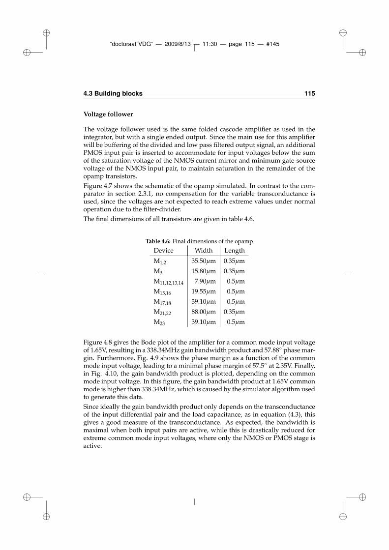
“doctoraat˙VDG” — 2009/8/13 — 11:30 — page 115 — #145
4.3 Building blocks 115
Voltage follower
The voltage follower used is the same folded cascode amplifier as used in theintegrator, but with a single ended output. Since the main use for this amplifierwill be buffering of the divided and low pass filtered output signal, an additionalPMOS input pair is inserted to accommodate for input voltages below the sumof the saturation voltage of the NMOS current mirror and minimum gate-sourcevoltage of the NMOS input pair, to maintain saturation in the remainder of theopamp transistors.
Figure 4.7 shows the schematic of the opamp simulated. In contrast to the com-parator in section 2.3.1, no compensation for the variable transconductance isused, since the voltages are not expected to reach extreme values under normaloperation due to the filter-divider.
The final dimensions of all transistors are given in table 4.6.
Table 4.6: Final dimensions of the opamp
Device Width Length
M1,2 35.50µm 0.35µm
M3 15.80µm 0.35µm
M11,12,13,14 7.90µm 0.5µm
M15,16 19.55µm 0.5µm
M17,18 39.10µm 0.5µm
M21,22 88.00µm 0.35µm
M23 39.10µm 0.5µm
Figure 4.8 gives the Bode plot of the amplifier for a common mode input voltageof 1.65V, resulting in a 338.34MHz gain bandwidth product and 57.88 phase mar-gin. Furthermore, Fig. 4.9 shows the phase margin as a function of the commonmode input voltage, leading to a minimal phase margin of 57.5 at 2.35V. Finally,in Fig. 4.10, the gain bandwidth product is plotted, depending on the commonmode input voltage. In this figure, the gain bandwidth product at 1.65V commonmode is higher than 338.34MHz, which is caused by the simulator algorithm usedto generate this data.
Since ideally the gain bandwidth product only depends on the transconductanceof the input differential pair and the load capacitance, as in equation (4.3), thisgives a good measure of the transconductance. As expected, the bandwidth ismaximal when both input pairs are active, while this is drastically reduced forextreme common mode input voltages, where only the NMOS or PMOS stage isactive.
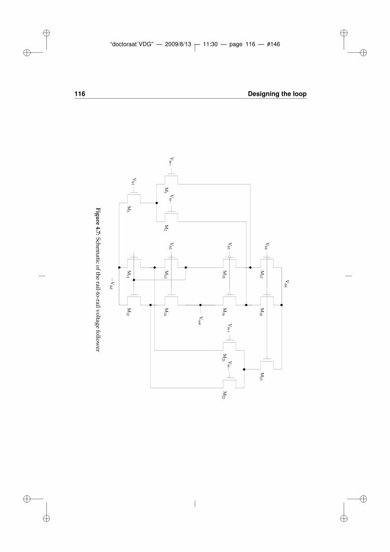
“doctoraat˙VDG” — 2009/8/13 — 11:30 — page 116 — #146
116 Designing the loop
M11
M12
M13
M14
M15
M16
M17
M18
Vb
2
Vo
ut
−V
dd
Vd
d
Vb
3
M3
M1
M2
Vin
+V
in−
Vb
1
Vin
+V
in−M
21M
22
M23
Vb
4
Figure
4.7:
Sch
ematic
of
the
rail-to-rail
vo
ltage
follo
wer
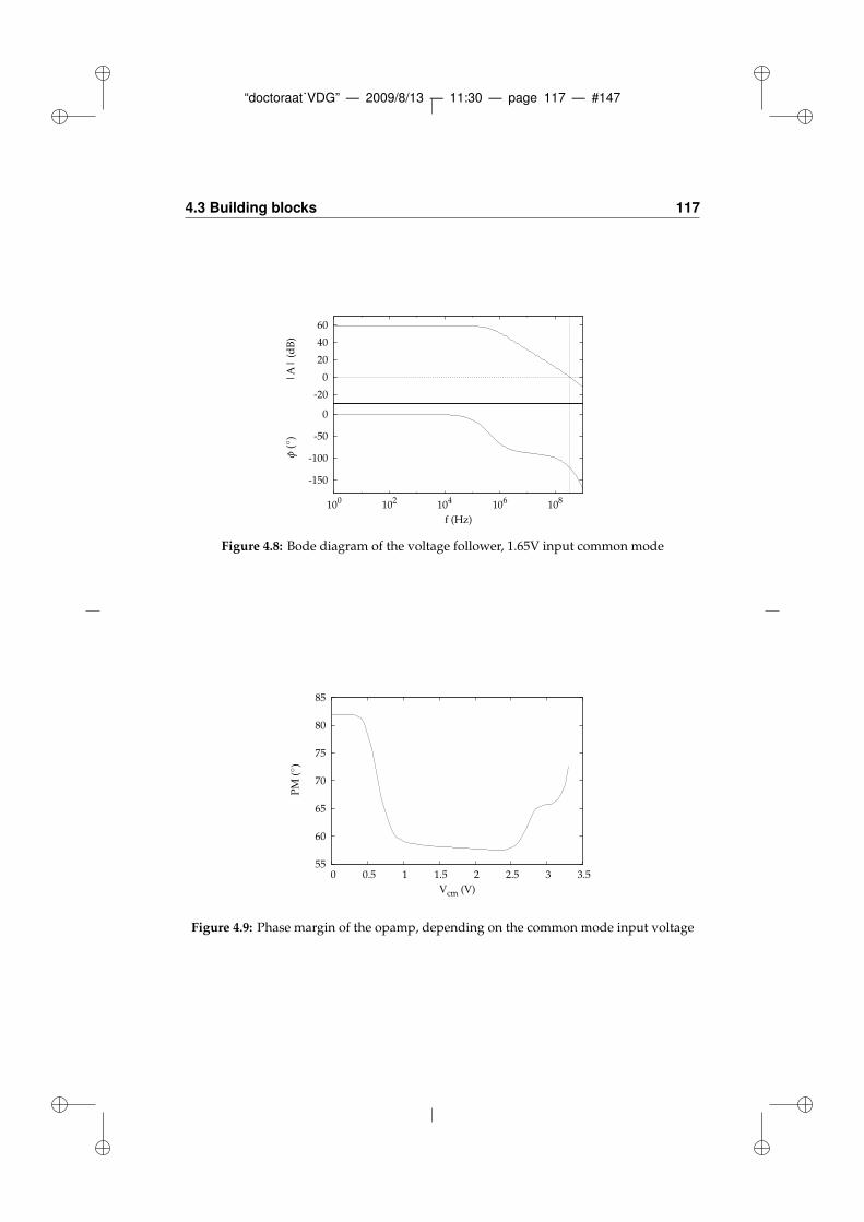
“doctoraat˙VDG” — 2009/8/13 — 11:30 — page 117 — #147
4.3 Building blocks 117
-150
-100
-50
0
100 102 104 106 108
f (Hz)
-20
0
20
40
60
|A
| (
dB
)φ
()
Figure 4.8: Bode diagram of the voltage follower, 1.65V input common mode
55
60
65
70
75
80
85
0 0.5 1 1.5 2 2.5 3 3.5
Vcm (V)
PM
()
Figure 4.9: Phase margin of the opamp, depending on the common mode input voltage
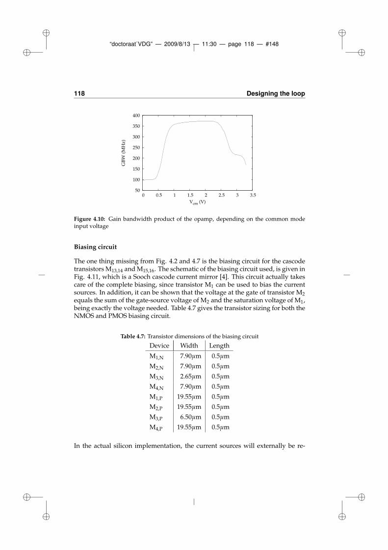
“doctoraat˙VDG” — 2009/8/13 — 11:30 — page 118 — #148
118 Designing the loop
50
100
150
200
250
300
350
400
0 0.5 1 1.5 2 2.5 3 3.5
GB
W (
MH
z)
Vcm (V)
Figure 4.10: Gain bandwidth product of the opamp, depending on the common modeinput voltage
Biasing circuit
The one thing missing from Fig. 4.2 and 4.7 is the biasing circuit for the cascodetransistors M13,14 and M15,16. The schematic of the biasing circuit used, is given inFig. 4.11, which is a Sooch cascode current mirror [4]. This circuit actually takescare of the complete biasing, since transistor M1 can be used to bias the currentsources. In addition, it can be shown that the voltage at the gate of transistor M2
equals the sum of the gate-source voltage of M2 and the saturation voltage of M1,being exactly the voltage needed. Table 4.7 gives the transistor sizing for both theNMOS and PMOS biasing circuit.
Table 4.7: Transistor dimensions of the biasing circuit
Device Width Length
M1,N 7.90µm 0.5µm
M2,N 7.90µm 0.5µm
M3,N 2.65µm 0.5µm
M4,N 7.90µm 0.5µm
M1,P 19.55µm 0.5µm
M2,P 19.55µm 0.5µm
M3,P 6.50µm 0.5µm
M4,P 19.55µm 0.5µm
In the actual silicon implementation, the current sources will externally be re-
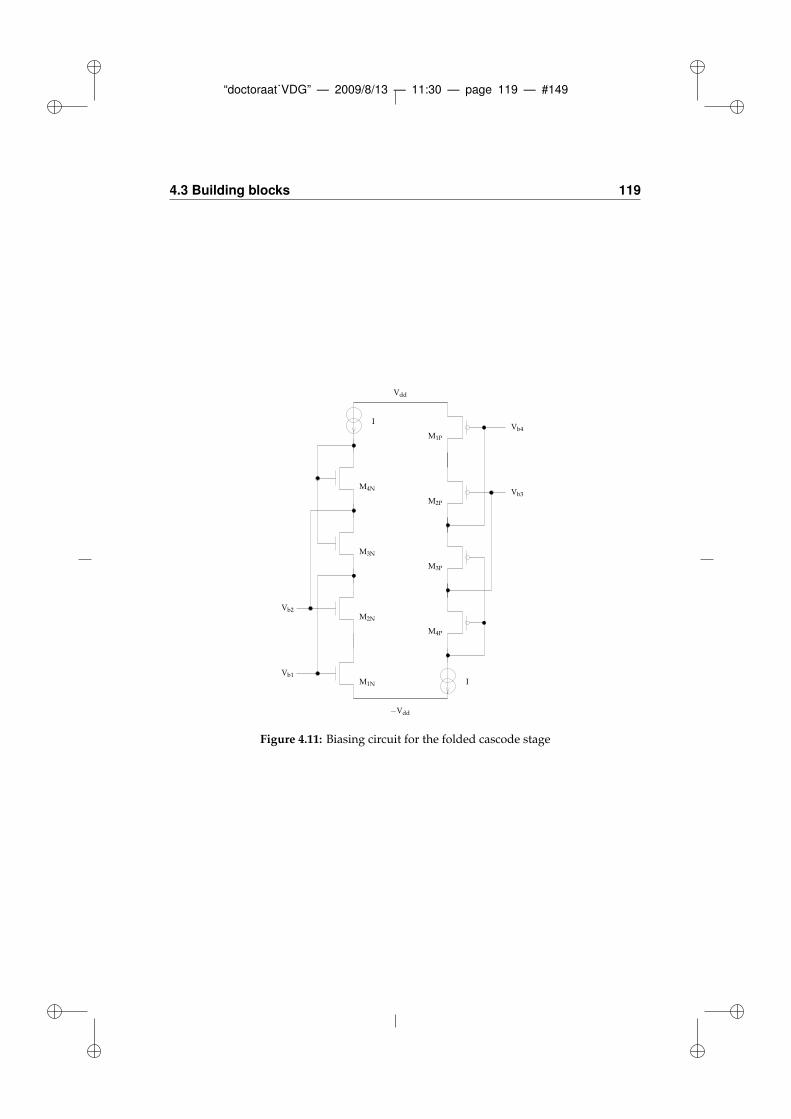
“doctoraat˙VDG” — 2009/8/13 — 11:30 — page 119 — #149
4.3 Building blocks 119
M2P
M1P
M3P
M4P
−Vdd
M2N
M1N
M4N
M3N
I
Vdd
I
Vb1
Vb2
Vb3
Vb4
Figure 4.11: Biasing circuit for the folded cascode stage
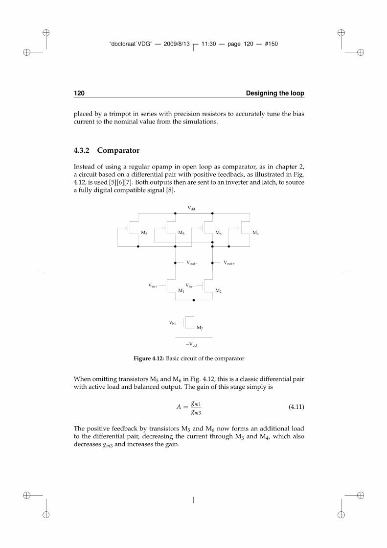
“doctoraat˙VDG” — 2009/8/13 — 11:30 — page 120 — #150
120 Designing the loop
placed by a trimpot in series with precision resistors to accurately tune the biascurrent to the nominal value from the simulations.
4.3.2 Comparator
Instead of using a regular opamp in open loop as comparator, as in chapter 2,a circuit based on a differential pair with positive feedback, as illustrated in Fig.4.12, is used [5][6][7]. Both outputs then are sent to an inverter and latch, to sourcea fully digital compatible signal [8].
−Vdd
M1 M2
Vin+ Vin−
Vb1
Vdd
M7
M3 M4M5 M6
Vout− Vout+
Figure 4.12: Basic circuit of the comparator
When omitting transistors M5 and M6 in Fig. 4.12, this is a classic differential pairwith active load and balanced output. The gain of this stage simply is
A =gm1
gm3(4.11)
The positive feedback by transistors M5 and M6 now forms an additional loadto the differential pair, decreasing the current through M3 and M4, which alsodecreases gm3 and increases the gain.
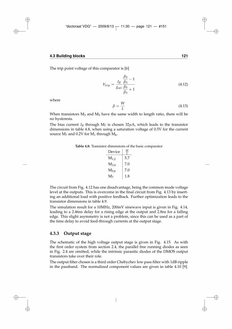
“doctoraat˙VDG” — 2009/8/13 — 11:30 — page 121 — #151
4.3 Building blocks 121
The trip point voltage of this comparator is [6]
Vtrip =IBgm1
β5
β3− 1
β5
β3+ 1
(4.12)
where
β =W
L(4.13)
When transistors M3 and M5 have the same width to length ratio, there will beno hysteresis.
The bias current IB through M7 is chosen 32µA, which leads to the transistordimensions in table 4.8, when using a saturation voltage of 0.5V for the currentsource M7 and 0.2V for M1 through M6.
Table 4.8: Transistor dimensions of the basic comparator
Device WL
M1,2 5.7
M3,4 7.0
M5,6 7.0
M7 1.8
The circuit from Fig. 4.12 has one disadvantage, being the common mode voltagelevel at the outputs. This is overcome in the final circuit from Fig. 4.13 by insert-ing an additional load with positive feedback. Further optimization leads to thetransistor dimensions in table 4.9.
The simulation result for a 10MHz, 200mV sinewave input is given in Fig. 4.14,leading to a 2.46ns delay for a rising edge at the output and 2.8ns for a fallingedge. This slight asymmetry is not a problem, since this can be used as a part ofthe time delay to avoid feed-through currents at the output stage.
4.3.3 Output stage
The schematic of the high voltage output stage is given in Fig. 4.15. As withthe first order system from section 2.4, the parallel free running diodes as seenin Fig. 2.4 are omitted, while the intrinsic parasitic diodes of the DMOS outputtransistors take over their role.
The output filter chosen is a third order Chebychev low pass filter with 1dB ripplein the passband. The normalized component values are given in table 4.10 [9].
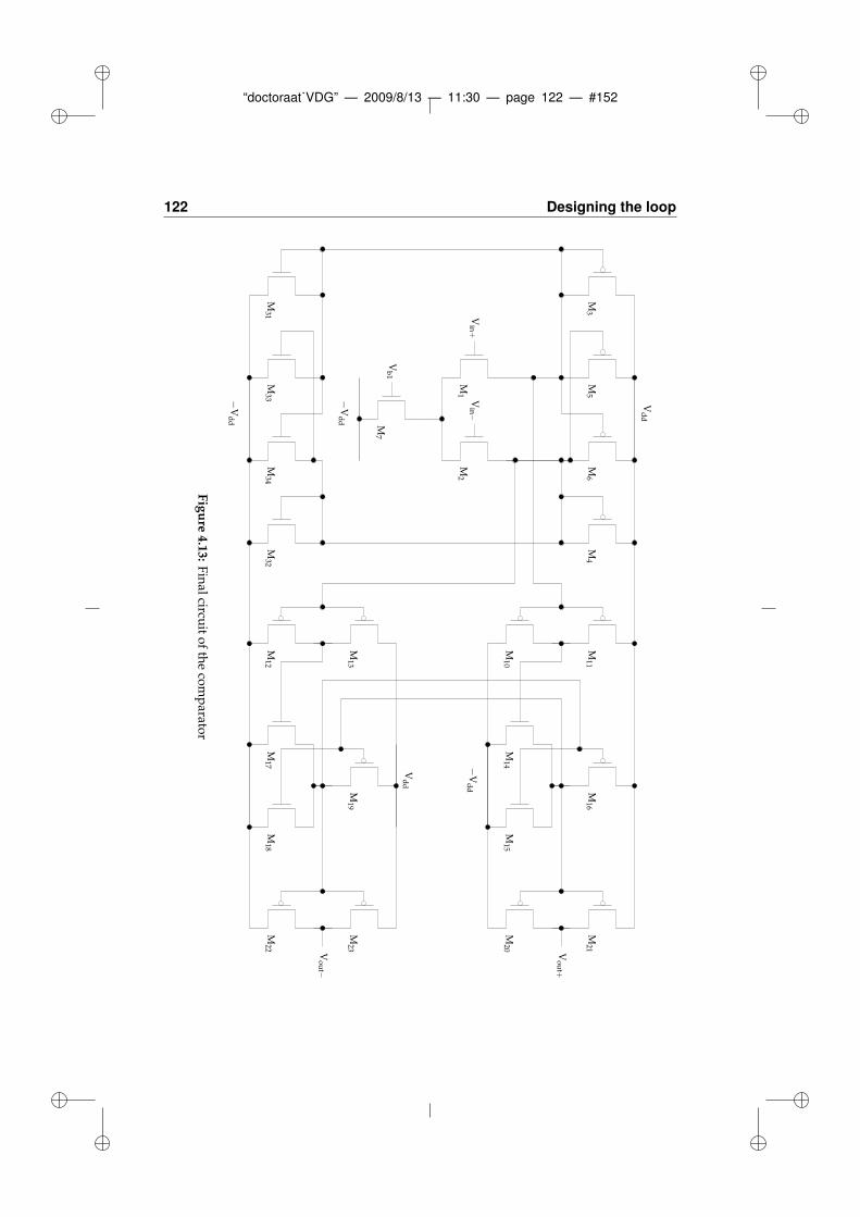
“doctoraat˙VDG” — 2009/8/13 — 11:30 — page 122 — #152
122 Designing the loop
−V
dd
−V
dd
M12
M13
M10
M11
M17
M18
M19
M14
M15
M16
M22
M23
M20
M21
−V
dd
Vd
d
Vd
d
Vo
ut+
Vo
ut−
Vin
+
Vb
1M
7
M3
M4
M5
M6
M31
M33
M34
M32
M1
M2
Vin−
Figure
4.13:
Fin
alcircu
ito
fth
eco
mp
arator
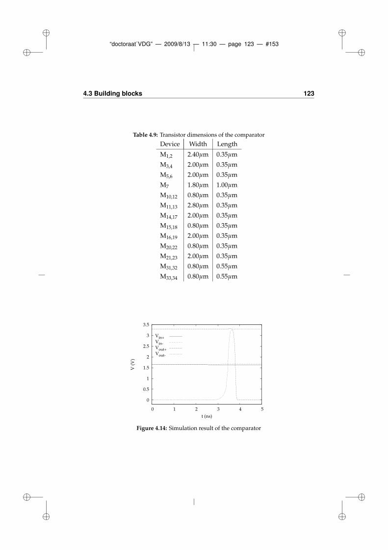
“doctoraat˙VDG” — 2009/8/13 — 11:30 — page 123 — #153
4.3 Building blocks 123
Table 4.9: Transistor dimensions of the comparator
Device Width Length
M1,2 2.40µm 0.35µm
M3,4 2.00µm 0.35µm
M5,6 2.00µm 0.35µm
M7 1.80µm 1.00µm
M10,12 0.80µm 0.35µm
M11,13 2.80µm 0.35µm
M14,17 2.00µm 0.35µm
M15,18 0.80µm 0.35µm
M16,19 2.00µm 0.35µm
M20,22 0.80µm 0.35µm
M21,23 2.00µm 0.35µm
M31,32 0.80µm 0.55µm
M33,34 0.80µm 0.55µm
0
0.5
1
1.5
2
2.5
3
3.5
0 1 2 3 4 5
V (
V)
t (ns)
Vin+ Vin- Vout+Vout-
Figure 4.14: Simulation result of the comparator
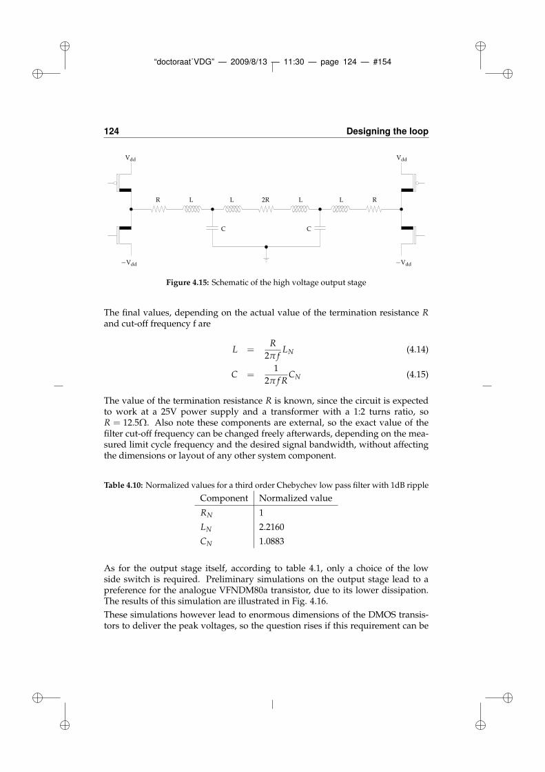
“doctoraat˙VDG” — 2009/8/13 — 11:30 — page 124 — #154
124 Designing the loop
LL
C
R
Vdd
−Vdd
L L
C
R
Vdd
−Vdd
2R
Figure 4.15: Schematic of the high voltage output stage
The final values, depending on the actual value of the termination resistance Rand cut-off frequency f are
L =R
2π fLN (4.14)
C =1
2π f RCN (4.15)
The value of the termination resistance R is known, since the circuit is expectedto work at a 25V power supply and a transformer with a 1:2 turns ratio, soR = 12.5Ω. Also note these components are external, so the exact value of thefilter cut-off frequency can be changed freely afterwards, depending on the mea-sured limit cycle frequency and the desired signal bandwidth, without affectingthe dimensions or layout of any other system component.
Table 4.10: Normalized values for a third order Chebychev low pass filter with 1dB ripple
Component Normalized value
RN 1
LN 2.2160
CN 1.0883
As for the output stage itself, according to table 4.1, only a choice of the lowside switch is required. Preliminary simulations on the output stage lead to apreference for the analogue VFNDM80a transistor, due to its lower dissipation.The results of this simulation are illustrated in Fig. 4.16.
These simulations however lead to enormous dimensions of the DMOS transis-tors to deliver the peak voltages, so the question rises if this requirement can be
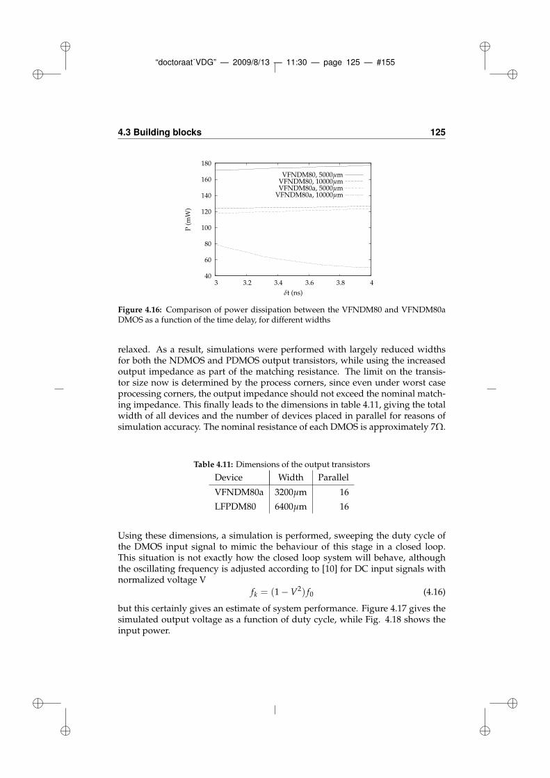
“doctoraat˙VDG” — 2009/8/13 — 11:30 — page 125 — #155
4.3 Building blocks 125
40
60
80
100
120
140
160
180
3 3.2 3.4 3.6 3.8 4
P (
mW
)
δt (ns)
VFNDM80, 5000µmVFNDM80, 10000µmVFNDM80a, 5000µm
VFNDM80a, 10000µm
Figure 4.16: Comparison of power dissipation between the VFNDM80 and VFNDM80aDMOS as a function of the time delay, for different widths
relaxed. As a result, simulations were performed with largely reduced widthsfor both the NDMOS and PDMOS output transistors, while using the increasedoutput impedance as part of the matching resistance. The limit on the transis-tor size now is determined by the process corners, since even under worst caseprocessing corners, the output impedance should not exceed the nominal match-ing impedance. This finally leads to the dimensions in table 4.11, giving the totalwidth of all devices and the number of devices placed in parallel for reasons ofsimulation accuracy. The nominal resistance of each DMOS is approximately 7Ω.
Table 4.11: Dimensions of the output transistors
Device Width Parallel
VFNDM80a 3200µm 16
LFPDM80 6400µm 16
Using these dimensions, a simulation is performed, sweeping the duty cycle ofthe DMOS input signal to mimic the behaviour of this stage in a closed loop.This situation is not exactly how the closed loop system will behave, althoughthe oscillating frequency is adjusted according to [10] for DC input signals withnormalized voltage V
fk = (1 −V2) f0 (4.16)
but this certainly gives an estimate of system performance. Figure 4.17 gives thesimulated output voltage as a function of duty cycle, while Fig. 4.18 shows theinput power.
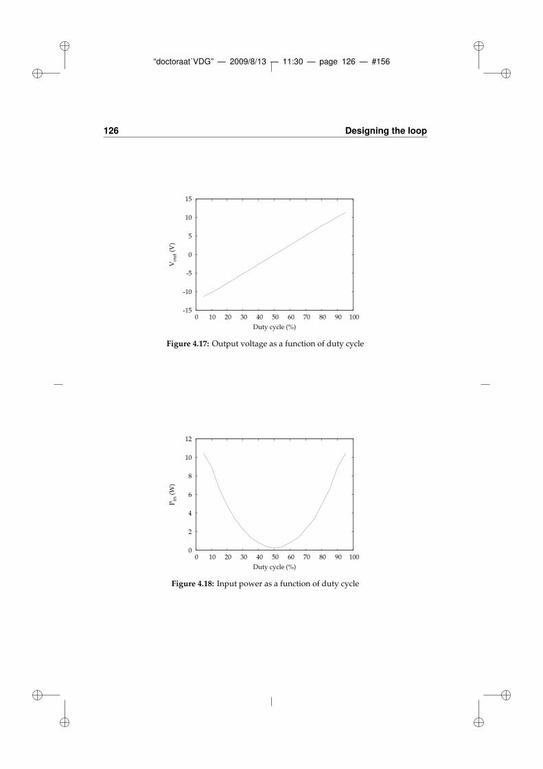
“doctoraat˙VDG” — 2009/8/13 — 11:30 — page 126 — #156
126 Designing the loop
-15
-10
-5
0
5
10
15
0 10 20 30 40 50 60 70 80 90 100
Vo
ut
(V)
Duty cycle (%)
Figure 4.17: Output voltage as a function of duty cycle
0
2
4
6
8
10
12
0 10 20 30 40 50 60 70 80 90 100
Pin
(W
)
Duty cycle (%)
Figure 4.18: Input power as a function of duty cycle
“doctoraat˙VDG” — 2009/8/13 — 11:30 — page 127 — #157
4.3 Building blocks 127
Table 4.12: Transistor dimensions of the delay circuit
Device Width LengthN1,2,N 0.8µm 0.35µmN1,2,P 8.0µm 0.35µmI2,3,N 0.8µm 0.35µmI2,3,P 2.0µm 0.35µmI4,5,6,7,N 0.8µm 1.20µmI4,5,6,7,P 2.0µm 1.20µm
When assuming a linear relation between input voltage and duty cycle, the tech-nique from section 2.4.1 can be used to estimate the efficiency of the system witha xDSL signal, leading to an efficiency estimate of about 20%.
4.3.4 Time delay, level shifter and buffers
The schematic of the delay circuit, again, is the simple circuit from Fig. 2.9, butsince the output of the comparator is balanced, there is no need for the inverterI1. The optimized dimensions of the transistors, taking into account the slightunbalance between rising and falling edge of the comparator output, are given intable 4.12.
The level shifter was changed significantly compared to the one in Fig. 2.6 and isgiven in Fig. 4.19.
The low side of the level shifter again is a NMOS switch with a cascode NDMOS.The high side now is formed by a flip-flop, increasing the level shifter speed com-pared to the basic version used throughout chapter 2 and ensuring both PDMOStransistors are steered in counterphase. Additionally, this also means the highside contains a bi-stable memory cell, so the level shifter can be turned off toreduce power consumption. Therefore, a basic level shifter as in Fig. 4.20 is in-serted at both outputs, switching off the level shifter transistors M1 and M2 withthe NOR gates formed by M17 to M24. This ensures the proper functioning of thelow to high level shifter, while the dimensions on the high to low level shifter arenot determined based on speed but power and can thus be reduced. As a result,the lower mobility µ0 of the PMOS will be beneficial to this end.
The optimized transistor dimensions are given in tables 4.13 and 4.14 for the lowto high and high to low level shifter respectively. The delay times are 0.78ns forthe falling edge and 1.57ns for the rising edge, as illustrated in Fig. 4.21. Thepower consumption is 2.2mW, so the circuit is both more efficient and faster thanthe level shifters from chapter 2.
Due to the large size of the DMOS output transistors, the signals from the delaycircuits need to be buffered. In [8] and [11] a simple formula is given to properly
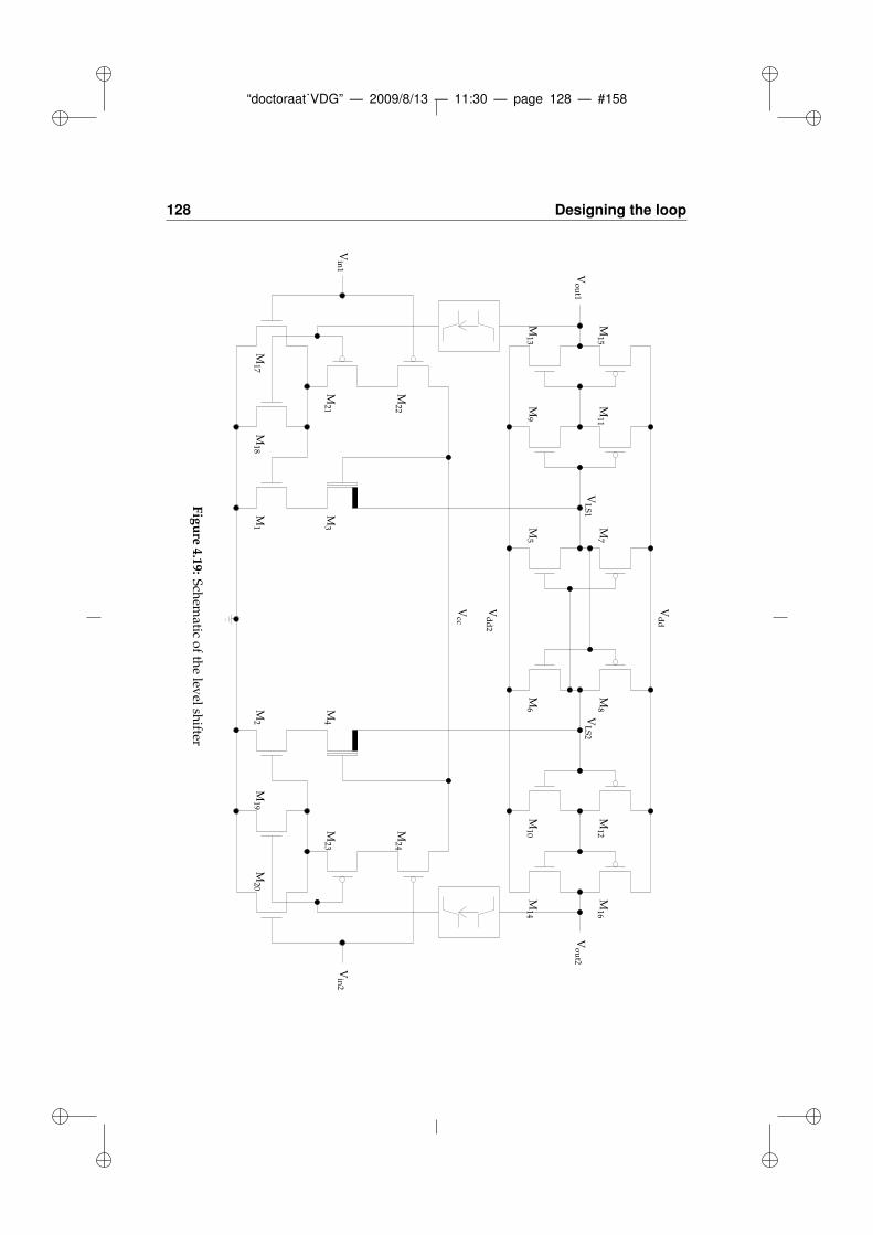
“doctoraat˙VDG” — 2009/8/13 — 11:30 — page 128 — #158
128 Designing the loopV
dd
Vd
d2
Vcc
M3
M1
M6
M8
M10
M12
M14
M16
M2
M4
M5
M7
M9
M11
M15
M13
M17
M18
M21
M22
M19
M20
M23
M24
Vo
ut2
Vo
ut1
VL
S1
VL
S2
Vin
1V
in2
Figure
4.19:
Sch
ematic
of
the
level
shifter
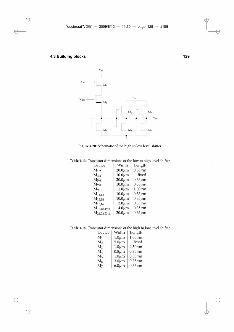
“doctoraat˙VDG” — 2009/8/13 — 11:30 — page 129 — #159
4.3 Building blocks 129
Vout
Vdd
VccVdd2
M1
M2
M3
M5
M6M4
M7
Vin
Figure 4.20: Schematic of the high to low level shifter
Table 4.13: Transistor dimensions of the low to high level shifter
Device Width LengthM1,2 20.0µm 0.35µmM3,4 10.0µm fixedM5,6 20.0µm 0.35µmM7,8 10.0µm 0.35µmM9,10 1.0µm 1.00µmM11,12 10.0µm 0.35µmM13,14 10.0µm 0.35µmM15,16 2.0µm 0.35µmM17,18,19,20 4.0µm 0.35µmM21,22,23,24 20.0µm 0.35µm
Table 4.14: Transistor dimensions of the high to low level shifter
Device Width LengthM1 1.0µm 1.00µmM2 5.0µm fixedM3 1.0µm 4.50µmM4 0.8µm 0.35µmM5 1.0µm 0.35µmM6 3.0µm 0.35µmM7 6.0µm 0.35µm
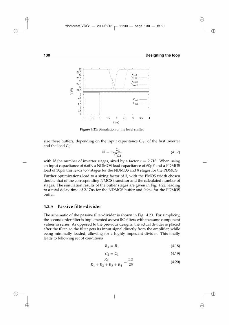
“doctoraat˙VDG” — 2009/8/13 — 11:30 — page 130 — #160
130 Designing the loop
0 0.5
1 1.5
2 2.5
3
0 0.5 1 1.5 2 2.5 3 3.5 4
t (ns)
Vin1Vin2
21.5 22
22.5 23
23.5 24
24.5 25
V (
V)
VLS1 VLS2 Vout1Vout2
Figure 4.21: Simulation of the level shifter
size these buffers, depending on the input capacitance CG,1 of the first inverterand the load CL:
N = lnCL
CG,1(4.17)
with N the number of inverter stages, sized by a factor e = 2.718. When usingan input capacitance of 6.6fF, a NDMOS load capacitance of 60pF and a PDMOSload of 30pF, this leads to 9 stages for the NDMOS and 8 stages for the PDMOS.
Further optimizations lead to a sizing factor of 3, with the PMOS width chosendouble that of the corresponding NMOS transistor and the calculated number ofstages. The simulation results of the buffer stages are given in Fig. 4.22, leadingto a total delay time of 2.17ns for the NDMOS buffer and 0.9ns for the PDMOSbuffer.
4.3.5 Passive filter-divider
The schematic of the passive filter-divider is shown in Fig. 4.23. For simplicity,the second order filter is implemented as two RC-filters with the same componentvalues in series. As opposed to the previous designs, the actual divider is placedafter the filter, so the filter gets its input signal directly from the amplifier, whilebeing minimally loaded, allowing for a highly impedant divider. This finallyleads to following set of conditions
R2 = R1 (4.18)
C2 = C1 (4.19)
R4
R1 + R2 + R3 + R4=
3.3
25(4.20)
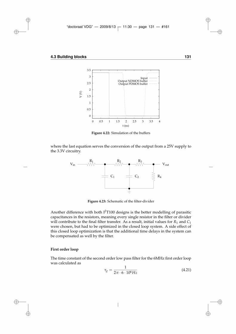
“doctoraat˙VDG” — 2009/8/13 — 11:30 — page 131 — #161
4.3 Building blocks 131
0
0.5
1
1.5
2
2.5
3
3.5
0 0.5 1 1.5 2 2.5 3 3.5 4
V (
V)
t (ns)
InputOutput NDMOS bufferOutput PDMOS buffer
Figure 4.22: Simulation of the buffers
where the last equation serves the conversion of the output from a 25V supply tothe 3.3V circuitry.
Vout
R1 R2 R3
R4C1 C2
Vin
Figure 4.23: Schematic of the filter-divider
Another difference with both I2T100 designs is the better modelling of parasiticcapacitances in the resistors, meaning every single resistor in the filter or dividerwill contribute to the final filter transfer. As a result, initial values for R1 and C1
were chosen, but had to be optimized in the closed loop system. A side effect ofthis closed loop optimization is that the additional time delays in the system canbe compensated as well by the filter.
First order loop
The time constant of the second order low pass filter for the 6MHz first order loopwas calculated as
τg =1
2π · 6 · 106Hz(4.21)
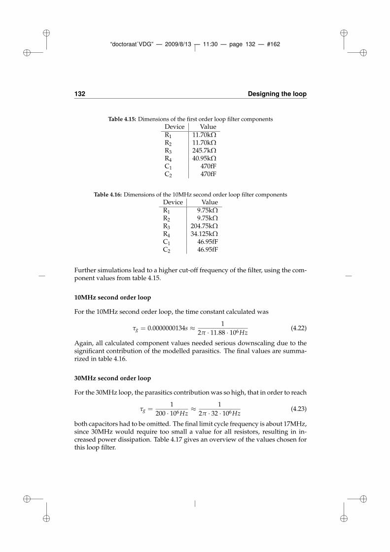
“doctoraat˙VDG” — 2009/8/13 — 11:30 — page 132 — #162
132 Designing the loop
Table 4.15: Dimensions of the first order loop filter components
Device ValueR1 11.70kΩ
R2 11.70kΩ
R3 245.7kΩ
R4 40.95kΩ
C1 470fFC2 470fF
Table 4.16: Dimensions of the 10MHz second order loop filter components
Device ValueR1 9.75kΩ
R2 9.75kΩ
R3 204.75kΩ
R4 34.125kΩ
C1 46.95fFC2 46.95fF
Further simulations lead to a higher cut-off frequency of the filter, using the com-ponent values from table 4.15.
10MHz second order loop
For the 10MHz second order loop, the time constant calculated was
τg = 0.0000000134s ≈ 1
2π · 11.88 · 106Hz(4.22)
Again, all calculated component values needed serious downscaling due to thesignificant contribution of the modelled parasitics. The final values are summa-rized in table 4.16.
30MHz second order loop
For the 30MHz loop, the parasitics contribution was so high, that in order to reach
τg =1
200 · 106Hz≈ 1
2π · 32 · 106Hz(4.23)
both capacitors had to be omitted. The final limit cycle frequency is about 17MHz,since 30MHz would require too small a value for all resistors, resulting in in-creased power dissipation. Table 4.17 gives an overview of the values chosen forthis loop filter.

“doctoraat˙VDG” — 2009/8/13 — 11:30 — page 133 — #163
4.4 First order system 133
Table 4.17: Dimensions of the 30MHz second order loop filter components
Device ValueR1 5.85kΩ
R2 5.85kΩ
R3 122.85kΩ
R4 20.475kΩ
C1 omittedC2 omitted
Table 4.18: Dimensions of the third order loop filter components
Device ValueR1 9.75kΩ
R2 9.75kΩ
R3 204.75kΩ
R4 34.125kΩ
C1 omittedC2 omitted
Third order loop
The time constant of the third order system suffers a similar problem as the highfrequent second order loop, due to the smaller time constant to reach a similarlimit cycle frequency:
τg =1
109 · 106Hz≈ 1
2π · 17.3 · 106Hz(4.24)
Using the same resistor values as the 10MHz second order loop, but omittingthe capacitors yields the desired limit cycle frequency. The values of all filtercomponents are given in table 4.18 for reference.
4.4 First order system
In analogy with the simulations in chapter 2, DC simulations are performed onthe full circuit, leading to the input output transfer from Fig. 4.24a and the powercurves in Fig. 4.24b. This finally leads to the DC efficiency in Fig. 4.24c, showingthe steep increase towards the maximum of 50%, before saturation kicks in. Thisfigure of 50% is caused by the dissipation in the required matching resistors andDMOS output stage.
Using equation (2.27), this allows for calculation of the efficiency when amplify-ing a MTPR signal, resulting in an estimate of 22.98%.

“doctoraat˙VDG” — 2009/8/13 — 11:30 — page 134 — #164
134 Designing the loop
-15
-10
-5
0
5
10
15
-3 -2 -1 0 1 2 3
Vo
ut
(V)
Vin (V)
(a) DC transfer
0
2
4
6
8
10
12
14
-3 -2 -1 0 1 2 3
P (
W)
Vin (V)
PinPout
(b) Input and output power
0
10
20
30
40
50
60
-3 -2 -1 0 1 2 3
Vin (V)
η(%
)
(c) DC efficiency
Figure 4.24: DC simulation of the first order system
“doctoraat˙VDG” — 2009/8/13 — 11:30 — page 135 — #165
4.5 10MHz second order system 135
In addition to the DC simulations, also the response to several sinewave inputswas generated to compare the simulations to the calculations from chapter 3. Forcomparison, frequencies of 200kHz, 500kHz and 1MHz were chosen, of which theresulting third order harmonic distortion is given in Fig. 4.25, together with thecalculated, limit cycle compensated curve. The sinewave amplitudes are scaledaccording to the DC transfer from Fig. 4.24a to the corresponding relative am-plitude, mapping the DC full scale to a nominal value of 1, as used throughoutchapter 3.
For the 200kHz signal, the simulated curve coincides perfectly with the calcula-tions, as for the 500kHz and 1MHz inputs, the simulated distortion is lower. Itshould however be noted that the calculations do not take the influence of anyoutput filter whatsoever into account, so due to the 1.5MHz low pass filter, thereis an additional reduction of 3dB and 25dB for the respective curves. After cor-rection, this again leads to an excellent correspondence.
4.5 10MHz second order system
The results of the DC simulations on the 10MHz second order amplifier are givenin Fig. 4.26, showing similar behaviour as the first order system. In this case, thecalculated MTPR efficiency is 23.18%.
For the sinewave simulations, the cut-off frequency of the output filter is 2.5MHz,so only the result at 1MHz should be increased by 9dB, due to the filter contri-bution. The results are given in Fig. 4.27. For the 500kHz and the 1MHz, thereis good correspondence between calculations and simulations, or an even bettersimulated result, whereas the 200kHz simulation is 10dB off.
It should however be noted that the curve at 200kHz starts at an already lowvalue of -77dBc and due to the lower frequency, there will be less periods simu-lated, meaning reduced averaging by the Fourier transform. There will also be anadditional contribution by the opamp circuits and the modelled non-linearities ofthe passive components, further increasing the simulated distortion.
Furthermore, inclusion of a time delay into the model, while decreasing the filtertime constants to maintain the same limit cycle frequency, is expected to increasedistortion. Since the time delays of all five circuits are about equal, this effect willbe more pronounced at higher limit cycle frequencies. As a result, the model forthe first order system will be more accurate than those for the higher order loopscompared to their respective implementations.
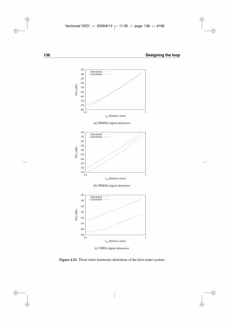
“doctoraat˙VDG” — 2009/8/13 — 11:30 — page 136 — #166
136 Designing the loop
-80
-75
-70
-65
-60
-55
-50
-45
-40
-35
0.1 1
HD
3 (d
Bc)
vm (Relative units)
SimulatedCalculated
(a) 200kHz input sinewave
-75
-70
-65
-60
-55
-50
-45
-40
-35
-30
0.1 1
HD
3 (d
Bc)
vm (Relative units)
SimulatedCalculated
(b) 500kHz input sinewave
-90
-80
-70
-60
-50
-40
-30
-20
0.1 1
HD
3 (d
Bc)
vm (Relative units)
SimulatedCalculated
(c) 1MHz input sinewave
Figure 4.25: Third order harmonic distortion of the first order system
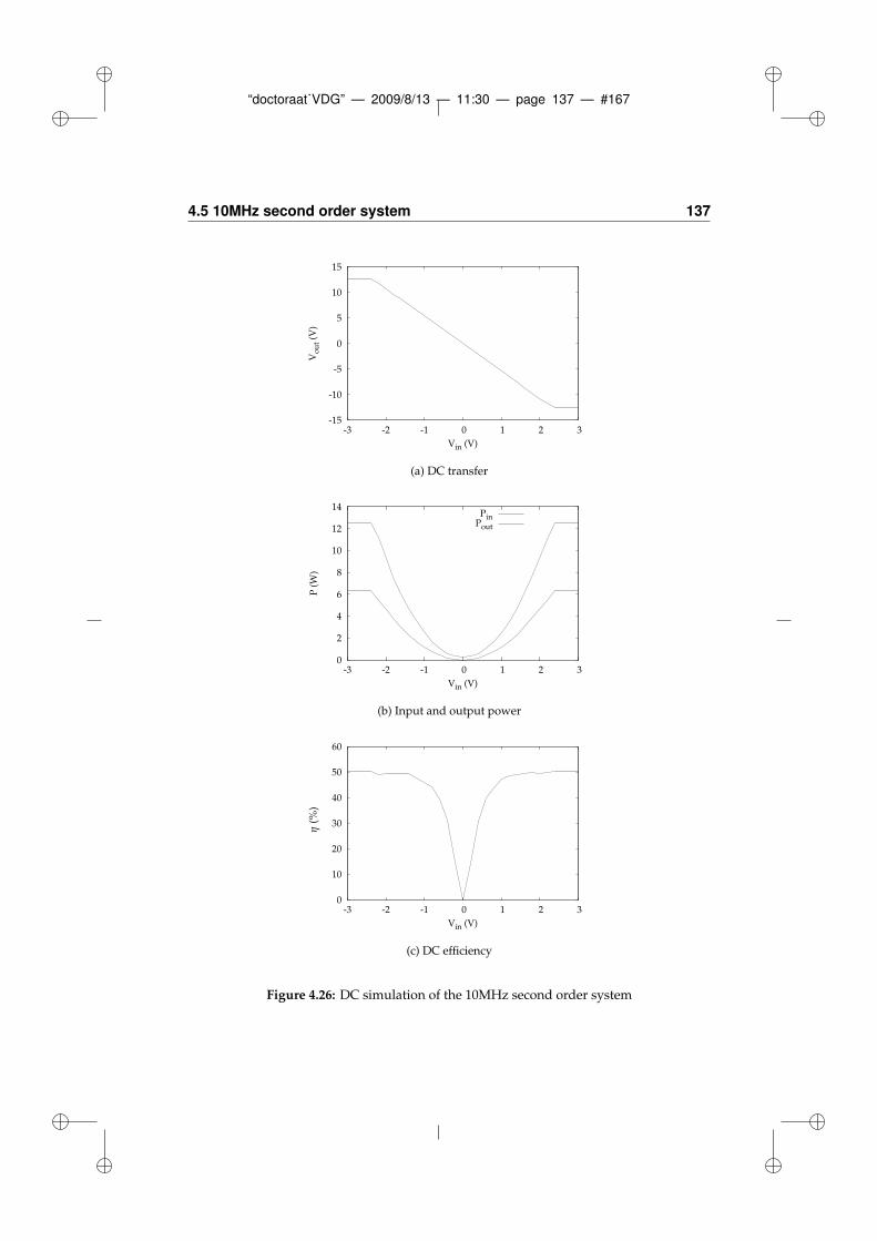
“doctoraat˙VDG” — 2009/8/13 — 11:30 — page 137 — #167
4.5 10MHz second order system 137
-15
-10
-5
0
5
10
15
-3 -2 -1 0 1 2 3
Vo
ut
(V)
Vin (V)
(a) DC transfer
0
2
4
6
8
10
12
14
-3 -2 -1 0 1 2 3
P (
W)
Vin (V)
PinPout
(b) Input and output power
0
10
20
30
40
50
60
-3 -2 -1 0 1 2 3
Vin (V)
η(%
)
(c) DC efficiency
Figure 4.26: DC simulation of the 10MHz second order system
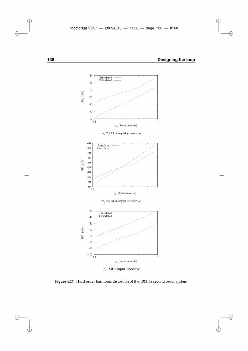
“doctoraat˙VDG” — 2009/8/13 — 11:30 — page 138 — #168
138 Designing the loop
-100
-90
-80
-70
-60
-50
-40
0.1 1
HD
3 (d
Bc)
vm (Relative units)
SimulatedCalculated
(a) 200kHz input sinewave
-85
-80
-75
-70
-65
-60
-55
-50
-45
-40
0.1 1
HD
3 (d
Bc)
vm (Relative units)
SimulatedCalculated
(b) 500kHz input sinewave
-100
-90
-80
-70
-60
-50
-40
-30
0.1 1
HD
3 (d
Bc)
vm (Relative units)
SimulatedCalculated
(c) 1MHz input sinewave
Figure 4.27: Third order harmonic distortion of the 10MHz second order system
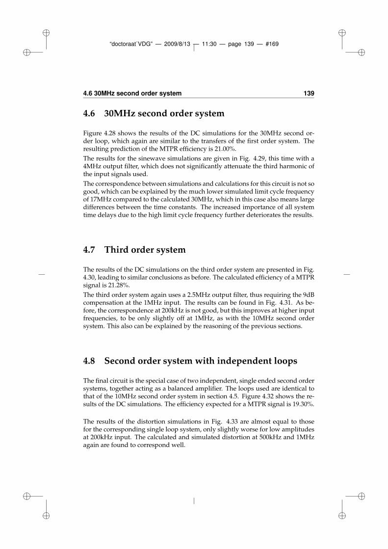
“doctoraat˙VDG” — 2009/8/13 — 11:30 — page 139 — #169
4.6 30MHz second order system 139
4.6 30MHz second order system
Figure 4.28 shows the results of the DC simulations for the 30MHz second or-der loop, which again are similar to the transfers of the first order system. Theresulting prediction of the MTPR efficiency is 21.00%.
The results for the sinewave simulations are given in Fig. 4.29, this time with a4MHz output filter, which does not significantly attenuate the third harmonic ofthe input signals used.
The correspondence between simulations and calculations for this circuit is not sogood, which can be explained by the much lower simulated limit cycle frequencyof 17MHz compared to the calculated 30MHz, which in this case also means largedifferences between the time constants. The increased importance of all systemtime delays due to the high limit cycle frequency further deteriorates the results.
4.7 Third order system
The results of the DC simulations on the third order system are presented in Fig.4.30, leading to similar conclusions as before. The calculated efficiency of a MTPRsignal is 21.28%.
The third order system again uses a 2.5MHz output filter, thus requiring the 9dBcompensation at the 1MHz input. The results can be found in Fig. 4.31. As be-fore, the correspondence at 200kHz is not good, but this improves at higher inputfrequencies, to be only slightly off at 1MHz, as with the 10MHz second ordersystem. This also can be explained by the reasoning of the previous sections.
4.8 Second order system with independent loops
The final circuit is the special case of two independent, single ended second ordersystems, together acting as a balanced amplifier. The loops used are identical tothat of the 10MHz second order system in section 4.5. Figure 4.32 shows the re-sults of the DC simulations. The efficiency expected for a MTPR signal is 19.30%.
The results of the distortion simulations in Fig. 4.33 are almost equal to thosefor the corresponding single loop system, only slightly worse for low amplitudesat 200kHz input. The calculated and simulated distortion at 500kHz and 1MHzagain are found to correspond well.
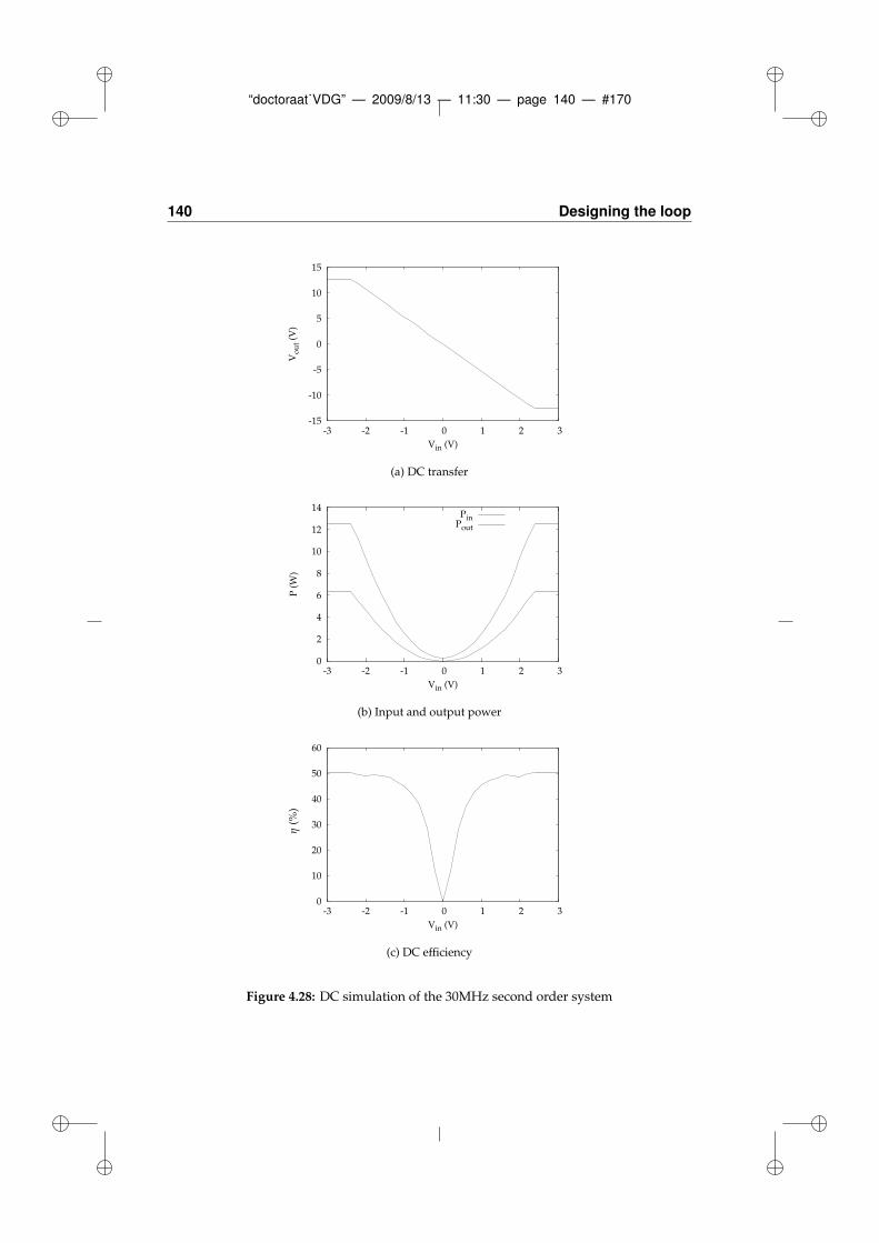
“doctoraat˙VDG” — 2009/8/13 — 11:30 — page 140 — #170
140 Designing the loop
-15
-10
-5
0
5
10
15
-3 -2 -1 0 1 2 3
Vo
ut
(V)
Vin (V)
(a) DC transfer
0
2
4
6
8
10
12
14
-3 -2 -1 0 1 2 3
P (
W)
Vin (V)
PinPout
(b) Input and output power
0
10
20
30
40
50
60
-3 -2 -1 0 1 2 3
Vin (V)
η(%
)
(c) DC efficiency
Figure 4.28: DC simulation of the 30MHz second order system
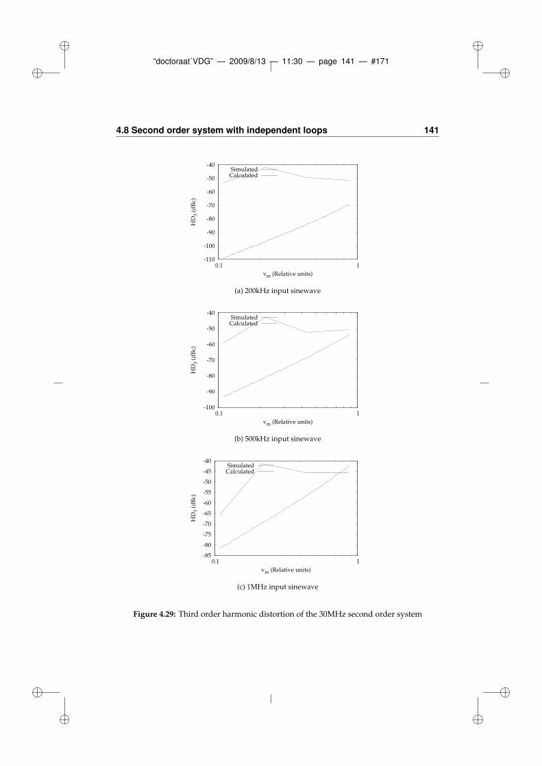
“doctoraat˙VDG” — 2009/8/13 — 11:30 — page 141 — #171
4.8 Second order system with independent loops 141
-110
-100
-90
-80
-70
-60
-50
-40
0.1 1
HD
3 (d
Bc)
vm (Relative units)
SimulatedCalculated
(a) 200kHz input sinewave
-100
-90
-80
-70
-60
-50
-40
0.1 1
HD
3 (d
Bc)
vm (Relative units)
SimulatedCalculated
(b) 500kHz input sinewave
-85
-80
-75
-70
-65
-60
-55
-50
-45
-40
0.1 1
HD
3 (d
Bc)
vm (Relative units)
SimulatedCalculated
(c) 1MHz input sinewave
Figure 4.29: Third order harmonic distortion of the 30MHz second order system
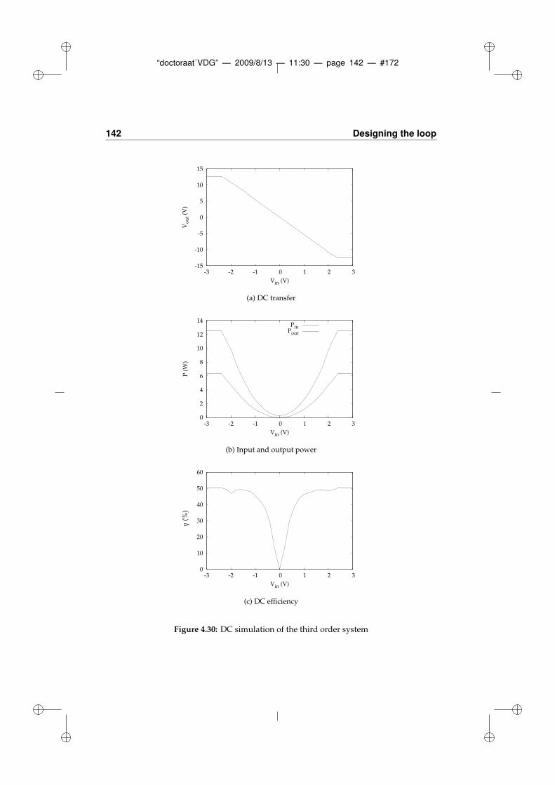
“doctoraat˙VDG” — 2009/8/13 — 11:30 — page 142 — #172
142 Designing the loop
-15
-10
-5
0
5
10
15
-3 -2 -1 0 1 2 3
Vo
ut
(V)
Vin (V)
(a) DC transfer
0
2
4
6
8
10
12
14
-3 -2 -1 0 1 2 3
P (
W)
Vin (V)
PinPout
(b) Input and output power
0
10
20
30
40
50
60
-3 -2 -1 0 1 2 3
Vin (V)
η(%
)
(c) DC efficiency
Figure 4.30: DC simulation of the third order system
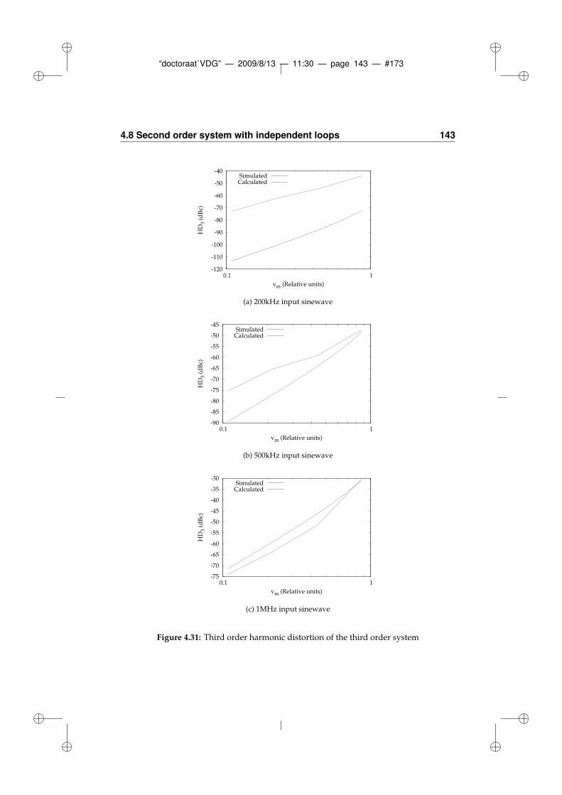
“doctoraat˙VDG” — 2009/8/13 — 11:30 — page 143 — #173
4.8 Second order system with independent loops 143
-120
-110
-100
-90
-80
-70
-60
-50
-40
0.1 1
HD
3 (d
Bc)
vm (Relative units)
SimulatedCalculated
(a) 200kHz input sinewave
-90
-85
-80
-75
-70
-65
-60
-55
-50
-45
0.1 1
HD
3 (d
Bc)
vm (Relative units)
SimulatedCalculated
(b) 500kHz input sinewave
-75
-70
-65
-60
-55
-50
-45
-40
-35
-30
0.1 1
HD
3 (d
Bc)
vm (Relative units)
SimulatedCalculated
(c) 1MHz input sinewave
Figure 4.31: Third order harmonic distortion of the third order system
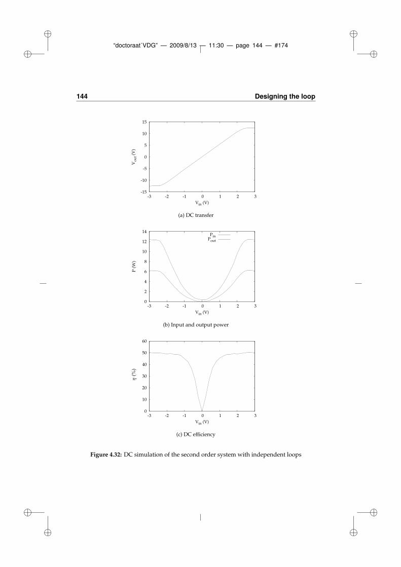
“doctoraat˙VDG” — 2009/8/13 — 11:30 — page 144 — #174
144 Designing the loop
-15
-10
-5
0
5
10
15
-3 -2 -1 0 1 2 3
Vo
ut
(V)
Vin (V)
(a) DC transfer
0
2
4
6
8
10
12
14
-3 -2 -1 0 1 2 3
P (
W)
Vin (V)
PinPout
(b) Input and output power
0
10
20
30
40
50
60
-3 -2 -1 0 1 2 3
Vin (V)
η(%
)
(c) DC efficiency
Figure 4.32: DC simulation of the second order system with independent loops
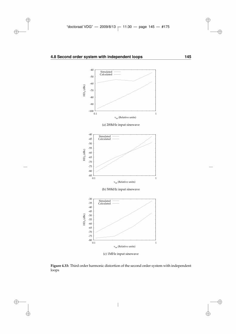
“doctoraat˙VDG” — 2009/8/13 — 11:30 — page 145 — #175
4.8 Second order system with independent loops 145
-100
-90
-80
-70
-60
-50
-40
0.1 1
HD
3 (d
Bc)
vm (Relative units)
SimulatedCalculated
(a) 200kHz input sinewave
-85
-80
-75
-70
-65
-60
-55
-50
-45
-40
0.1 1
HD
3 (d
Bc)
vm (Relative units)
SimulatedCalculated
(b) 500kHz input sinewave
-80
-75
-70
-65
-60
-55
-50
-45
-40
-35
-30
0.1 1
HD
3 (d
Bc)
vm (Relative units)
SimulatedCalculated
(c) 1MHz input sinewave
Figure 4.33: Third order harmonic distortion of the second order system with independentloops
“doctoraat˙VDG” — 2009/8/13 — 11:30 — page 146 — #176
146 Designing the loop
4.9 Layout considerations
To finally verify the preliminary calculations and full circuit simulations, a sili-con implementation is required. Due to the presence of quite sensitive analoguecircuits in combination with both the high voltage and digital parts, special caremust be taken to avoid or suppress their harmful contribution.
4.9.1 Interconnection
A first elementary option is the use of separate supply lines for analogue anddigital circuits [12], [13]. The specificity of the I3T80 technology is of great impor-tance in this regard, since all processing starts from a N-type epitaxial layer ontop of a P-type substrate. On the one hand, this means there still is an ohmic con-tact between eventual separated ground supply lines, but on the other hand, theimpedance is a lot higher than with a simple metallic connection. The technologyalso uses pockets with a N-type substrate, that are trivial to separate from eachother by inserting a deep P-type implant in between, connecting to the P-typesubstrate.
This finally leads to two separate inputs for the 25V supply, being one for theswitching output and one for the level shifter, an analogue and a digital 3.3Vsupply and three ground connections for analogue, low voltage digital and thehigh voltage output stage.
The one component falling between the cracks, is the comparator, which convertsthe analoguely processed signals into digital form. The supply chosen for thiscomponent is the analogue one, with as big a decoupling capacitor as possiblebetween the supply lines, close to the component.
This suggests a further optimization in the form of decoupling capacitances forall DC signals, such as the voltage references for the integrator common modeloop, the current reference input and the power supply lines. Since capacitors ofsignificant value are expensive to implement, the metal tracks can be stacked tocreate additional capacitance and must be combined with off chip components.
Additionally, the resistance of the power tracks must be controlled, since puttingall components in series will create a gradual voltage shift, such that the imme-diate power consumption of all components will influence all other componentson the same branch. The solution to this problem is to create a wide, low ohmicbase track and feed all components in parallel.
As for the reference input signals, the capacitive coupling of harmful signals canalso be reduced by shielding the tracks with the analogue ground supply, placingtracks above, below and beside and interconnecting all with vias.
To improve the symmetry, the length of tracks with complementary signalsshould also be as equal as possible to reduce unbalance.
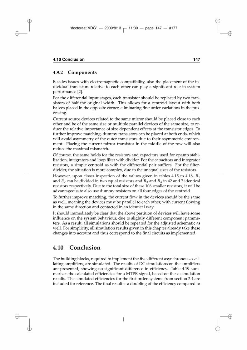
“doctoraat˙VDG” — 2009/8/13 — 11:30 — page 147 — #177
4.10 Conclusion 147
4.9.2 Components
Besides issues with electromagnetic compatibility, also the placement of the in-dividual transistors relative to each other can play a significant role in systemperformance [2].
For the differential input stages, each transistor should be replaced by two tran-sistors of half the original width. This allows for a centroid layout with bothhalves placed in the opposite corner, eliminating first order variations in the pro-cessing.
Current source devices related to the same mirror should be placed close to eachother and be of the same size or multiple parallel devices of the same size, to re-duce the relative importance of size dependent effects at the transistor edges. Tofurther improve matching, dummy transistors can be placed at both ends, whichwill avoid asymmetry of the outer transistors due to their asymmetric environ-ment. Placing the current mirror transistor in the middle of the row will alsoreduce the maximal mismatch.
Of course, the same holds for the resistors and capacitors used for opamp stabi-lization, integrators and loop filter with divider. For the capacitors and integratorresistors, a simple centroid as with the differential pair suffices. For the filter-divider, the situation is more complex, due to the unequal sizes of the resistors.
However, upon closer inspection of the values given in tables 4.15 to 4.18, R1
and R2 can be divided in two equal resistors and R3 and R4 in 42 and 7 identicalresistors respectively. Due to the total size of these 106 smaller resistors, it will beadvantageous to also use dummy resistors on all four edges of the centroid.
To further improve matching, the current flow in the devices should be the sameas well, meaning the devices must be parallel to each other, with current flowingin the same direction and contacted in an identical way.
It should immediately be clear that the above partition of devices will have someinfluence on the system behaviour, due to slightly different component parame-ters. As a result, all simulations should be repeated for the adjusted schematic aswell. For simplicity, all simulation results given in this chapter already take thesechanges into account and thus correspond to the final circuits as implemented.
4.10 Conclusion
The building blocks, required to implement the five different asynchronous oscil-lating amplifiers, are simulated. The results of DC simulations on the amplifiersare presented, showing no significant difference in efficiency. Table 4.19 sum-marizes the calculated efficiencies for a MTPR signal, based on these simulationresults. The simulated efficiencies for the first order systems from section 2.4 areincluded for reference. The final result is a doubling of the efficiency compared to
“doctoraat˙VDG” — 2009/8/13 — 11:30 — page 148 — #178
148 Designing the loop
Table 4.19: Summary of the calculated efficiencies
Amplifier EfficiencyFirst order 22.98%Second order 10MHz 23.18%Second order 30MHz 21.00%Second order, independent loops 19.30%Third order 21.28%Basic first order (I2T100) 9.67%Cascode first order (I2T100) 9.94%Reference [14] (measured) 14.3%Reference [15] (measured) 13.5%
the previous designs and a significant increase compared to references [14] and[15].
Simulations using a sinewave input further serve to validate the calculations fromchapter 3, showing good correspondence when additional time delays in the cir-cuit are small compared to the limit cycle period. For lower input frequencies andamplitudes, the accuracy of the model also gets worse for numerical reasons andbecause the system performance also is limited by the linearity of the componentsin the loop, both active and passive.
Hence, the formulæ for limit cycle determination and distortion prediction can beused to gain additional insight in the functioning of the circuit, depending on thenature of the loop components used and as a first guesstimate of the system pa-rameters to reduce design time. This will not however obsolete the need for timeconsuming simulations on the device level for further optimization. It shouldalso be noted that backannotation of the design parameters might lead to moreaccurate calculation results, although that should not be required anymore in anadvanced design stage.
“doctoraat˙VDG” — 2009/8/13 — 11:30 — page 149 — #179
References
[1] Europractice IC service. (2007, Mar.) AMI Semiconductor I3T80technology. [Online]. Available: http://www.europractice-ic.com/docs/AMIS datasheets/AMIS I3T80U V7.pdf
[2] K. R. Laker and W. M. C. Sansen, Design of Analog Integrated Circuits andSystems. McGraw-Hill, Inc., 1994.
[3] J. Huijsing, Operational Amplifiers, Theory and Design. Kluwer AcademicPublishers, 2001.
[4] P. R. Gray, P. J. Hurst, S. H. Lewis, and R. G. Meyer, Analysis and Design ofAnalog Integrated Circuits, 4th ed. John Wiley & Sons, Inc., 2001.
[5] R. Gregorian, Introduction to CMOS OP-AMPs and Comparators. John Wiley& Sons, Inc., 1999.
[6] R. J. Baker, H. W. Li, and D. E. Boyce, CMOS Circuit Design, Layout, andSimulation. Wiley-IEEE Press, 1998.
[7] P. E. Allen and D. R. Holberg, CMOS Analog Circuit Design, 2nd ed. OxfordUniversity Press, 2002.
[8] J. M. Rabaey, A. Chandrakasan, and B. Nikolic, Digital Integrated Circuits: aDesign Perspective, 2nd ed., C. G. Sodini, Ed. Prentice Hall, 2003.
[9] A. B. Williams and F. J. Taylor, Electronic Filter Design Handbook: LC, Active,and Digital Filters, 2nd ed. McGraw-Hill, Inc., 1988.
[10] E. Roza, “Analog-to-digital conversion via duty-cycle modulation,” IEEETrans. Circuits Syst. II, vol. 44, no. 11, pp. 907–914, Nov. 1997.
[11] S.-M. Kang and Y. Leblebici, CMOS Digital Integrated Circuits: Analysis andDesign, 3rd ed. McGraw-Hill, Inc., 2003.
[12] J. J. Goedbloed, Elektromagnetische Compatibiliteit: Analyse en Onderdrukkingvan Stoorproblemen, 2nd ed. Ten Hagen Stam, 2000, in Dutch.
“doctoraat˙VDG” — 2009/8/13 — 11:30 — page 150 — #180
150 REFERENCES
[13] R. Morrison, Grounding and Shielding Techniques in Instrumentation. JohnWiley & Sons, Inc., 1967.
[14] A. Bicakci, C.-S. Kim, and S.-S. Lee, “A CMOS line driver for ADSL centraloffice applications,” IEEE J. Solid-State Circuits, vol. 38, no. 12, pp. 2201–2208,Dec. 2003.
[15] F. Sabouri and R. Shariatdoust, “A 740mW ADSL line driver for central officewith 75dB MTPR,” in ISSCC Digest of Technical Papers, San Francisco, USA,Feb. 2002, pp. 322–323.

“doctoraat˙VDG” — 2009/8/13 — 11:30 — page 151 — #181
5Measurements
This chapter first describes some features of the chip layout and the test board to in-crease signal integrity. After these initial remarks, a first batch of measurement resultsis presented, together with the observed phenomena and the possible causes. In a nextsection, additional measurements are presented, resulting in some final recommenda-tions.
5.1 Introduction
The circuit, as discussed in chapter 4, is processed in the I3T80 technology. Figure5.1 gives the die photograph of this silicon implementation, where the five differ-ent implementations are easily distinguishable. The top circuit is the first ordersystem, followed by the 10MHz second order amplifier, a highly symmetric sec-ond order system with independent loops, the 30MHz second order system andat the bottom the third order amplifier, each measuring approximately 2mm2.
Several blocks can be identified on the photograph. The rasterized structures atboth sides are the DMOS output transistors, of which the widest on top is thePDMOS and the bottom one is the NDMOS. These are interconnected by widemetallic stripes with their respective bonding paths, being the 25V supply ontop, the output in the middle and ground at the bottom. The interconnection ischosen that wide for electromigration reasons, since some measurements requirelarge DC currents to flow through the output stage.
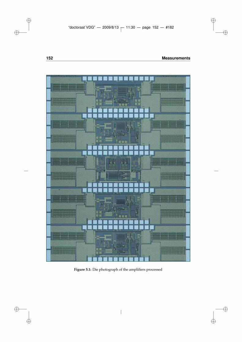
“doctoraat˙VDG” — 2009/8/13 — 11:30 — page 152 — #182
152 Measurements
Figure 5.1: Die photograph of the amplifiers processed
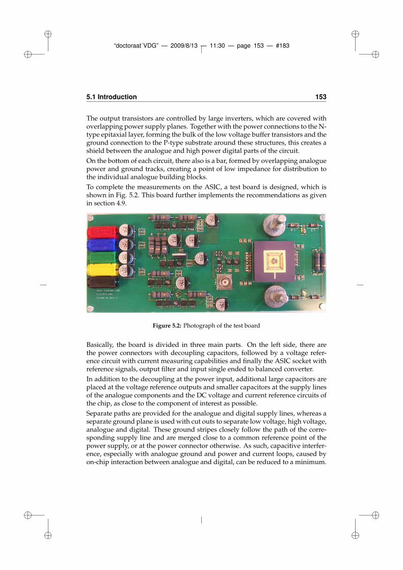
“doctoraat˙VDG” — 2009/8/13 — 11:30 — page 153 — #183
5.1 Introduction 153
The output transistors are controlled by large inverters, which are covered withoverlapping power supply planes. Together with the power connections to the N-type epitaxial layer, forming the bulk of the low voltage buffer transistors and theground connection to the P-type substrate around these structures, this creates ashield between the analogue and high power digital parts of the circuit.
On the bottom of each circuit, there also is a bar, formed by overlapping analoguepower and ground tracks, creating a point of low impedance for distribution tothe individual analogue building blocks.
To complete the measurements on the ASIC, a test board is designed, which isshown in Fig. 5.2. This board further implements the recommendations as givenin section 4.9.
Figure 5.2: Photograph of the test board
Basically, the board is divided in three main parts. On the left side, there arethe power connectors with decoupling capacitors, followed by a voltage refer-ence circuit with current measuring capabilities and finally the ASIC socket withreference signals, output filter and input single ended to balanced converter.
In addition to the decoupling at the power input, additional large capacitors areplaced at the voltage reference outputs and smaller capacitors at the supply linesof the analogue components and the DC voltage and current reference circuits ofthe chip, as close to the component of interest as possible.
Separate paths are provided for the analogue and digital supply lines, whereas aseparate ground plane is used with cut outs to separate low voltage, high voltage,analogue and digital. These ground stripes closely follow the path of the corre-sponding supply line and are merged close to a common reference point of thepower supply, or at the power connector otherwise. As such, capacitive interfer-ence, especially with analogue ground and power and current loops, caused byon-chip interaction between analogue and digital, can be reduced to a minimum.
“doctoraat˙VDG” — 2009/8/13 — 11:30 — page 154 — #184
154 Measurements
The result is a design, where the components should not interfere significantlywith each other or the environment in general. As an interesting side effect, thiswill automatically reduce the effect of environmental disturbances on the testcircuit as well.
This chapter is further organized as follows. Section 5.2 gives the results of thefirst set of measurements performed on all five circuits. In section 5.3, the prob-lems with the initial measurements are identified and explained and section 5.4then presents the final measurements on the adjusted circuit.
5.2 Initial measurements
To characterize the circuits, several measurements need to be performed. Analo-gous to the simulations from chapter 4, the DC response will give a first impres-sion of both linearity and power consumption. The next step are AC measure-ments, to compare the third order harmonic distortion with the predicted valuesfrom chapter 3 and the simulated values from chapter 4. The final step then is afull MTPR test, including measurement of the noise level without input signal.
5.2.1 First order system
DC response
The simulated and measured response of the first order loop to a DC input volt-age is given in Fig. 5.3. The transfer in Fig. 5.3a already shows reduced linearitycompared to the simulations. Additionally, the output voltage saturates at ±9Vinstead of the simulated ±12.5V, even when the external matching resistor is com-pletely shorted.
Due to the early saturation, the maximum output power is about half the sim-ulated value. The minimum input power is found to be 670mW, which also issignificantly higher than the 245mW simulated. Since xDSL signals have a Gaus-sian distribution (2.28), this elevated idle power will drastically reduce the overallefficiency. The final result is an amplifier with an estimated efficiency of 12.82%according to equation (2.27).
AC response
The results of the distortion measurements are shown in Fig. 5.4, again at 200kHz,500kHz and 1MHz, together with the calculated and simulated results. As withthe DC measurements, there is a significant difference between simulation andmeasurements, except at higher signal amplitudes.
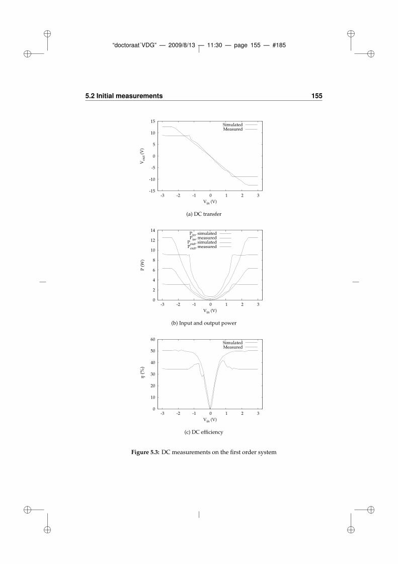
“doctoraat˙VDG” — 2009/8/13 — 11:30 — page 155 — #185
5.2 Initial measurements 155
-15
-10
-5
0
5
10
15
-3 -2 -1 0 1 2 3
Vo
ut
(V)
Vin (V)
SimulatedMeasured
(a) DC transfer
0
2
4
6
8
10
12
14
-3 -2 -1 0 1 2 3
P (
W)
Vin (V)
Pin, simulatedPin, measured
Pout, simulatedPout, measured
(b) Input and output power
0
10
20
30
40
50
60
-3 -2 -1 0 1 2 3
Vin (V)
SimulatedMeasured
η(%
)
(c) DC efficiency
Figure 5.3: DC measurements on the first order system
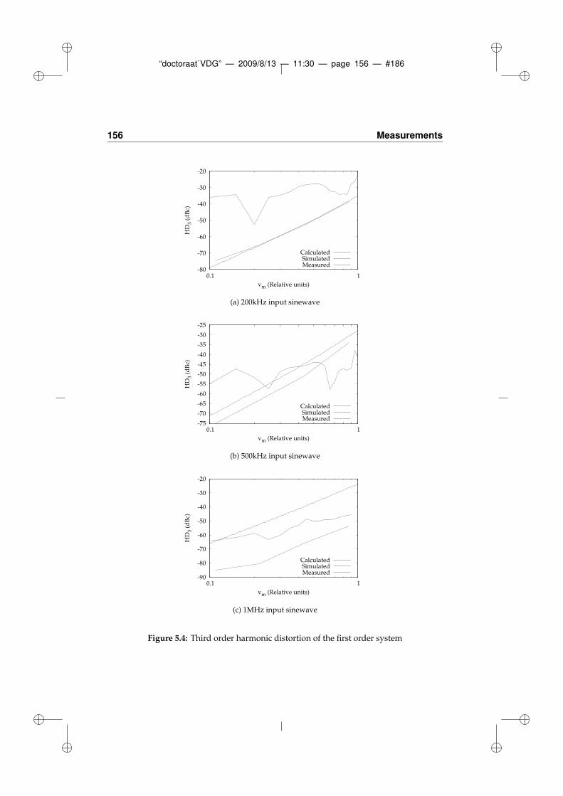
“doctoraat˙VDG” — 2009/8/13 — 11:30 — page 156 — #186
156 Measurements
-80
-70
-60
-50
-40
-30
-20
0.1 1
HD
3 (d
Bc)
vm (Relative units)
CalculatedSimulatedMeasured
(a) 200kHz input sinewave
-75
-70
-65
-60
-55
-50
-45
-40
-35
-30
-25
0.1 1
HD
3 (d
Bc)
vm (Relative units)
CalculatedSimulatedMeasured
(b) 500kHz input sinewave
-90
-80
-70
-60
-50
-40
-30
-20
0.1 1
HD
3 (d
Bc)
vm (Relative units)
CalculatedSimulatedMeasured
(c) 1MHz input sinewave
Figure 5.4: Third order harmonic distortion of the first order system
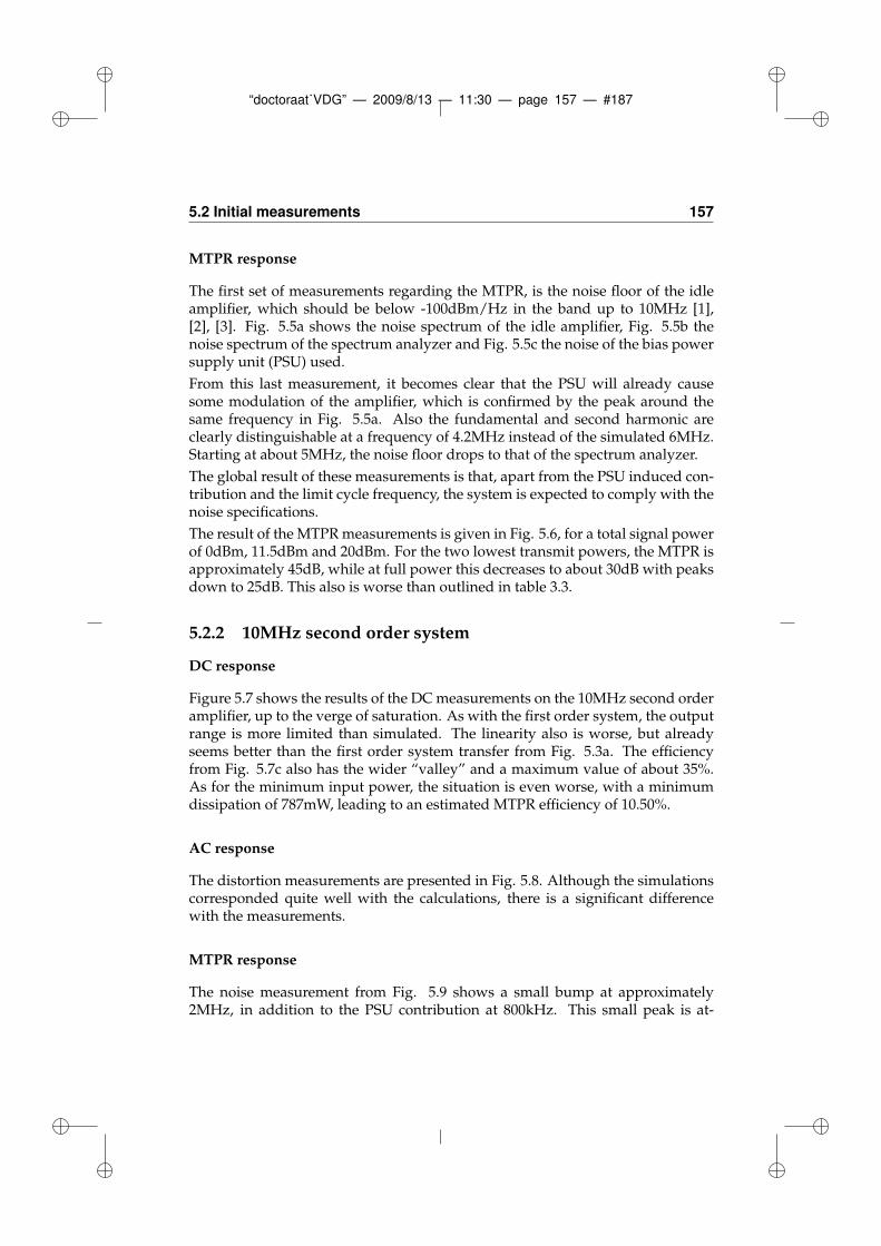
“doctoraat˙VDG” — 2009/8/13 — 11:30 — page 157 — #187
5.2 Initial measurements 157
MTPR response
The first set of measurements regarding the MTPR, is the noise floor of the idleamplifier, which should be below -100dBm/Hz in the band up to 10MHz [1],[2], [3]. Fig. 5.5a shows the noise spectrum of the idle amplifier, Fig. 5.5b thenoise spectrum of the spectrum analyzer and Fig. 5.5c the noise of the bias powersupply unit (PSU) used.
From this last measurement, it becomes clear that the PSU will already causesome modulation of the amplifier, which is confirmed by the peak around thesame frequency in Fig. 5.5a. Also the fundamental and second harmonic areclearly distinguishable at a frequency of 4.2MHz instead of the simulated 6MHz.Starting at about 5MHz, the noise floor drops to that of the spectrum analyzer.
The global result of these measurements is that, apart from the PSU induced con-tribution and the limit cycle frequency, the system is expected to comply with thenoise specifications.
The result of the MTPR measurements is given in Fig. 5.6, for a total signal powerof 0dBm, 11.5dBm and 20dBm. For the two lowest transmit powers, the MTPR isapproximately 45dB, while at full power this decreases to about 30dB with peaksdown to 25dB. This also is worse than outlined in table 3.3.
5.2.2 10MHz second order system
DC response
Figure 5.7 shows the results of the DC measurements on the 10MHz second orderamplifier, up to the verge of saturation. As with the first order system, the outputrange is more limited than simulated. The linearity also is worse, but alreadyseems better than the first order system transfer from Fig. 5.3a. The efficiencyfrom Fig. 5.7c also has the wider “valley” and a maximum value of about 35%.As for the minimum input power, the situation is even worse, with a minimumdissipation of 787mW, leading to an estimated MTPR efficiency of 10.50%.
AC response
The distortion measurements are presented in Fig. 5.8. Although the simulationscorresponded quite well with the calculations, there is a significant differencewith the measurements.
MTPR response
The noise measurement from Fig. 5.9 shows a small bump at approximately2MHz, in addition to the PSU contribution at 800kHz. This small peak is at-
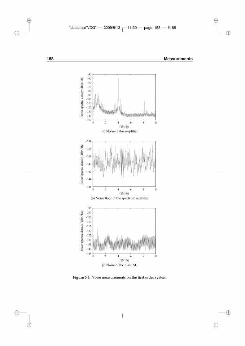
“doctoraat˙VDG” — 2009/8/13 — 11:30 — page 158 — #188
158 Measurements
-150
-140
-130
-120
-110
-100
-90
-80
-70
-60
-50
-40
0 2 4 6 8 10
Po
wer
sp
ectr
al d
ensi
ty (
dB
m/
Hz)
f (MHz)
(a) Noise of the amplifier
-146
-144
-142
-140
-138
-136
-134
0 2 4 6 8 10
Po
wer
sp
ectr
al d
ensi
ty (
dB
m/
Hz)
f (MHz)
(b) Noise floor of the spectrum analyzer
-145
-140
-135
-130
-125
-120
-115
-110
-105
-100
-95
0 2 4 6 8 10
Po
wer
sp
ectr
al d
ensi
ty (
dB
m/
Hz)
f (MHz)
(c) Noise of the bias PSU
Figure 5.5: Noise measurements on the first order system

“doctoraat˙VDG” — 2009/8/13 — 11:30 — page 159 — #189
5.2 Initial measurements 159
20
25
30
35
40
45
50
55
60
0 0.2 0.4 0.6 0.8 1
MT
PR
(d
B)
f (MHz)
20dBm11.5dBm
0dBm
Figure 5.6: MTPR measurements on the first order system
tributed to the ripple in the transfer characteristic of the third order Chebychevoutput filter. This was not visible with the first order loop, due to the PSU contri-bution, being close to the lower filter cut-off frequency of 1.5MHz.
The limit cycle frequency is 5.8MHz instead of the simulated 10MHz. Starting atabout 3MHz and making abstraction of the peak at the oscillating frequency, thenoise contribution stays well below the specified -100dBm/Hz.
Due to the increased limit cycle frequency and cut-off frequency of the outputfilter, the MTPR measurements are performed with a full rate ADSL2+ input sig-nal, spanning the band from 138kHz to 2.208MHz. The resulting MTPR figure isgiven in Fig. 5.10, showing 45dB for the 0dBm signal, decreasing to 25dB for the11.5dBm signal and 20dB for the full power output. This again is not the expectedvalue of 52dB from table 3.3.
5.2.3 30MHz second order system
DC response
The DC response is shown in Fig. 5.11, again until saturation sets in. Whencomparing the linearity measurements from Fig. 5.11a with those for the 10MHzsecond order system in Fig. 5.7a, the distortion is expected to be worse due tothe more pronounced non-linearity. The minimum output power, however, isslightly lower at 725mW, leading to an efficiency estimate of 10.38%. The maxi-mum DC efficiency is limited to about 37%.

“doctoraat˙VDG” — 2009/8/13 — 11:30 — page 160 — #190
160 Measurements
-15
-10
-5
0
5
10
15
-3 -2 -1 0 1 2 3
Vo
ut
(V)
Vin (V)
SimulatedMeasured
(a) DC transfer
0
2
4
6
8
10
12
14
-3 -2 -1 0 1 2 3
P (
W)
Vin (V)
Pin, simulatedPin, measured
Pout, simulatedPout, measured
(b) Input and output power
0
10
20
30
40
50
60
-3 -2 -1 0 1 2 3
Vin (V)
SimulatedMeasured
η(%
)
(c) DC efficiency
Figure 5.7: DC measurements on the 10MHz second order system

“doctoraat˙VDG” — 2009/8/13 — 11:30 — page 161 — #191
5.2 Initial measurements 161
-100
-90
-80
-70
-60
-50
-40
-30
-20
-10
0.1 1
HD
3 (d
Bc)
vm (Relative units)
CalculatedSimulatedMeasured
(a) 200kHz input sinewave
-90
-80
-70
-60
-50
-40
-30
-20
-10
0.1 1
HD
3 (d
Bc)
vm (Relative units)
CalculatedSimulatedMeasured
(b) 500kHz input sinewave
-100
-90
-80
-70
-60
-50
-40
-30
-20
0.1 1
HD
3 (d
Bc)
vm (Relative units)
CalculatedSimulatedMeasured
(c) 1MHz input sinewave
Figure 5.8: Third order harmonic distortion of the 10MHz second order system

“doctoraat˙VDG” — 2009/8/13 — 11:30 — page 162 — #192
162 Measurements
-130
-120
-110
-100
-90
-80
-70
-60
-50
-40
-30
0 2 4 6 8 10
Po
wer
sp
ectr
al d
ensi
ty (
dB
m/
Hz)
f (MHz)
Figure 5.9: Noise measurement on the 10MHz second order system
10
15
20
25
30
35
40
45
50
55
0 0.5 1 1.5 2 2.5
MT
PR
(d
B)
f (MHz)
20dBm11.5dBm
0dBm
Figure 5.10: MTPR measurements on the 10MHz second order system
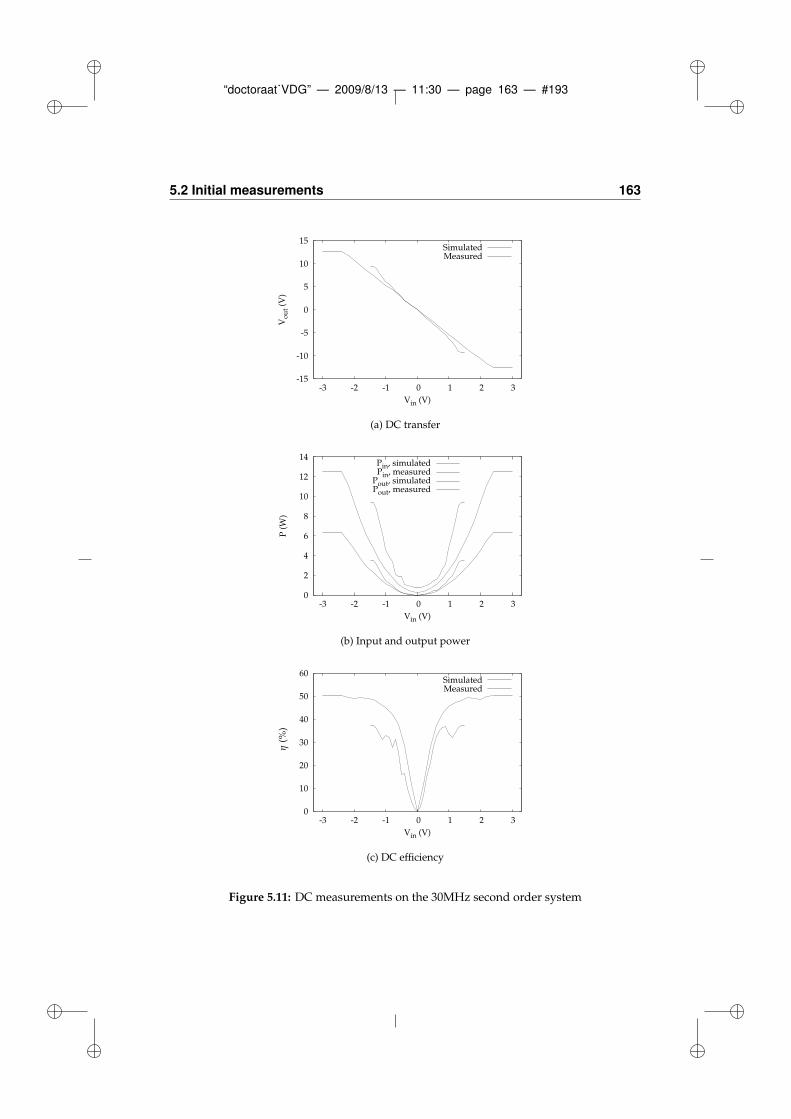
“doctoraat˙VDG” — 2009/8/13 — 11:30 — page 163 — #193
5.2 Initial measurements 163
-15
-10
-5
0
5
10
15
-3 -2 -1 0 1 2 3
Vo
ut
(V)
Vin (V)
SimulatedMeasured
(a) DC transfer
0
2
4
6
8
10
12
14
-3 -2 -1 0 1 2 3
P (
W)
Vin (V)
Pin, simulatedPin, measured
Pout, simulatedPout, measured
(b) Input and output power
0
10
20
30
40
50
60
-3 -2 -1 0 1 2 3
Vin (V)
SimulatedMeasured
η(%
)
(c) DC efficiency
Figure 5.11: DC measurements on the 30MHz second order system
“doctoraat˙VDG” — 2009/8/13 — 11:30 — page 164 — #194
164 Measurements
AC response
The distortion, as illustrated in Fig. 5.12, in general is higher than simulated, asalready deduced from the DC linearity measurements. The only correspondencewith the simulations is at high input frequencies with a low amplitude.
MTPR response
The noise measurement in Fig. 5.13 exhibits similar behaviour as before, showingthe PSU contribution and the output filter transfer characteristic. The limit cyclefrequency is about 9.6MHz instead of the simulated 17MHz.
The corresponding MTPR measurements are given in Fig. 5.14, leading to about30dB overall, compared to the simulated 54dB.
5.2.4 Third order system
DC response
The results from the DC measurements, as given in Fig. 5.15, are not complete,due to destructive overheating of the output stage at higher output amplitudes.The minimum input power is 1.31W, which explains the overheating. Due tothe limited measurement, only a rough estimate of the MTPR efficiency is made,leading to 6.75%.
AC response
The linearity of the third order system is measured with the 1.5MHz output filterfor reasons that will be explained in the next section. The results are given inFig. 5.16, leading to a higher distortion at low frequencies, but converging to thesimulation results at higher frequencies.
MTPR response
The noise measurements are presented in Fig. 5.17, for both a 2.5MHz and1.5MHz output filter cut-off frequency. This clearly shows the existence of asubharmonic frequency of the 4.7MHz limit cycle frequency. Using the 1.5MHzoutput filter, the subharmonic is removed, but there still are a lot of spuriouscomponents around the 4.1MHz oscillating frequency. This change in limit cyclefrequency is caused by the increased influence of the output transistors on the en-tire loop, due to their higher output impedance. Both values also are significantlylower than the simulated 10MHz.
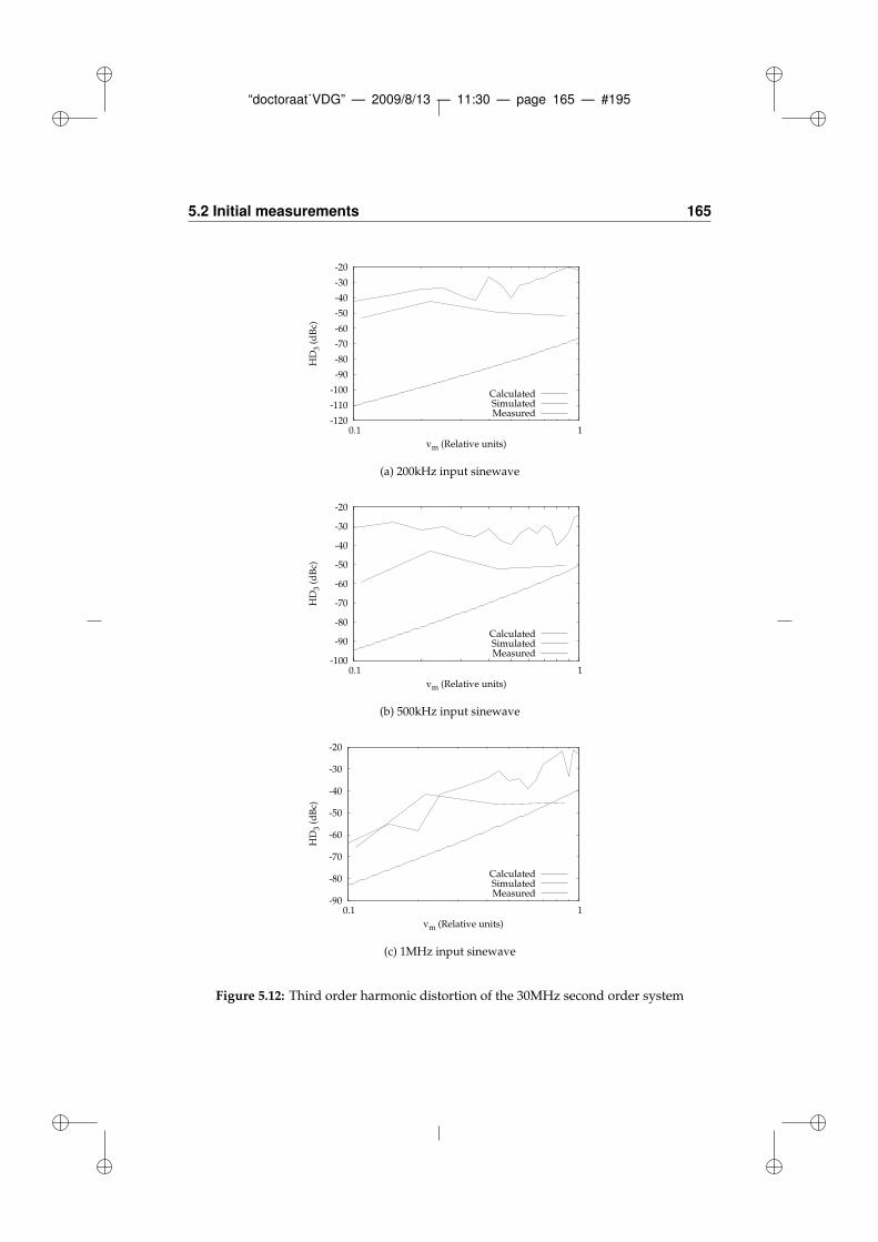
“doctoraat˙VDG” — 2009/8/13 — 11:30 — page 165 — #195
5.2 Initial measurements 165
-120
-110
-100
-90
-80
-70
-60
-50
-40
-30
-20
0.1 1
HD
3 (d
Bc)
vm (Relative units)
CalculatedSimulatedMeasured
(a) 200kHz input sinewave
-100
-90
-80
-70
-60
-50
-40
-30
-20
0.1 1
HD
3 (d
Bc)
vm (Relative units)
CalculatedSimulatedMeasured
(b) 500kHz input sinewave
-90
-80
-70
-60
-50
-40
-30
-20
0.1 1
HD
3 (d
Bc)
vm (Relative units)
CalculatedSimulatedMeasured
(c) 1MHz input sinewave
Figure 5.12: Third order harmonic distortion of the 30MHz second order system
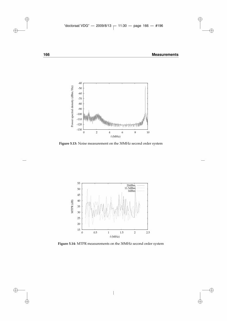
“doctoraat˙VDG” — 2009/8/13 — 11:30 — page 166 — #196
166 Measurements
-130
-120
-110
-100
-90
-80
-70
-60
-50
-40
0 2 4 6 8 10
Po
wer
sp
ectr
al d
ensi
ty (
dB
m/
Hz)
f (MHz)
Figure 5.13: Noise measurement on the 30MHz second order system
15
20
25
30
35
40
45
50
55
0 0.5 1 1.5 2 2.5
MT
PR
(d
B)
f (MHz)
20dBm11.5dBm
0dBm
Figure 5.14: MTPR measurements on the 30MHz second order system
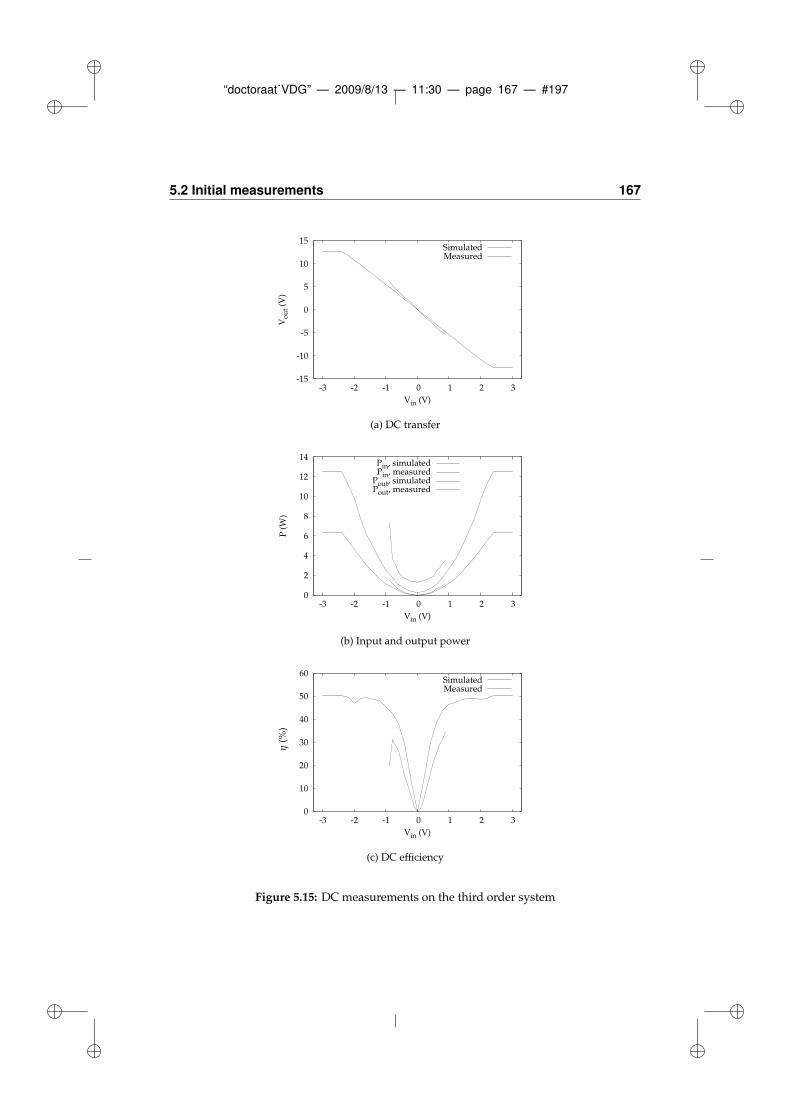
“doctoraat˙VDG” — 2009/8/13 — 11:30 — page 167 — #197
5.2 Initial measurements 167
-15
-10
-5
0
5
10
15
-3 -2 -1 0 1 2 3
Vo
ut
(V)
Vin (V)
SimulatedMeasured
(a) DC transfer
0
2
4
6
8
10
12
14
-3 -2 -1 0 1 2 3
P (
W)
Vin (V)
Pin, simulatedPin, measured
Pout, simulatedPout, measured
(b) Input and output power
0
10
20
30
40
50
60
-3 -2 -1 0 1 2 3
Vin (V)
SimulatedMeasured
η(%
)
(c) DC efficiency
Figure 5.15: DC measurements on the third order system
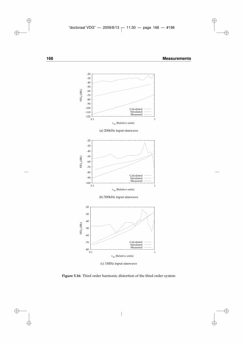
“doctoraat˙VDG” — 2009/8/13 — 11:30 — page 168 — #198
168 Measurements
-120
-110
-100
-90
-80
-70
-60
-50
-40
-30
-20
0.1 1
HD
3 (d
Bc)
vm (Relative units)
CalculatedSimulatedMeasured
(a) 200kHz input sinewave
-100
-90
-80
-70
-60
-50
-40
-30
-20
0.1 1
HD
3 (d
Bc)
vm (Relative units)
CalculatedSimulatedMeasured
(b) 500kHz input sinewave
-80
-70
-60
-50
-40
-30
-20
0.1 1
HD
3 (d
Bc)
vm (Relative units)
CalculatedSimulatedMeasured
(c) 1MHz input sinewave
Figure 5.16: Third order harmonic distortion of the third order system
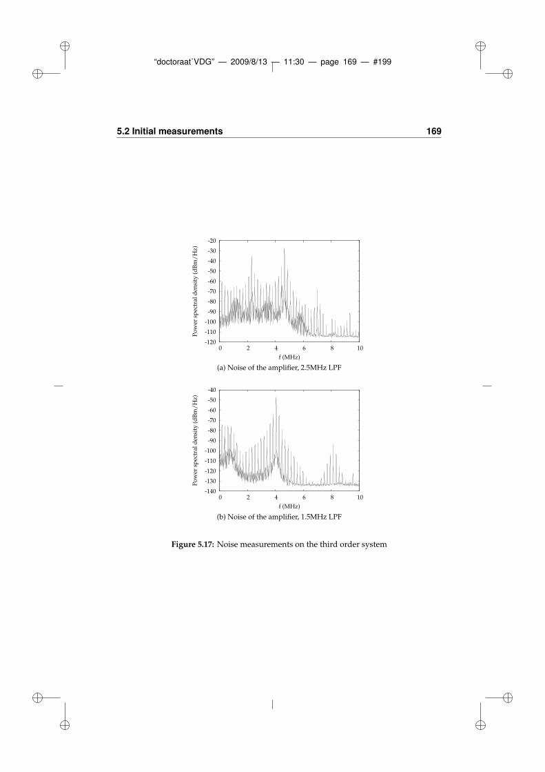
“doctoraat˙VDG” — 2009/8/13 — 11:30 — page 169 — #199
5.2 Initial measurements 169
-120
-110
-100
-90
-80
-70
-60
-50
-40
-30
-20
0 2 4 6 8 10
Po
wer
sp
ectr
al d
ensi
ty (
dB
m/
Hz)
f (MHz)
(a) Noise of the amplifier, 2.5MHz LPF
-140
-130
-120
-110
-100
-90
-80
-70
-60
-50
-40
0 2 4 6 8 10
Po
wer
sp
ectr
al d
ensi
ty (
dB
m/
Hz)
f (MHz)
(b) Noise of the amplifier, 1.5MHz LPF
Figure 5.17: Noise measurements on the third order system
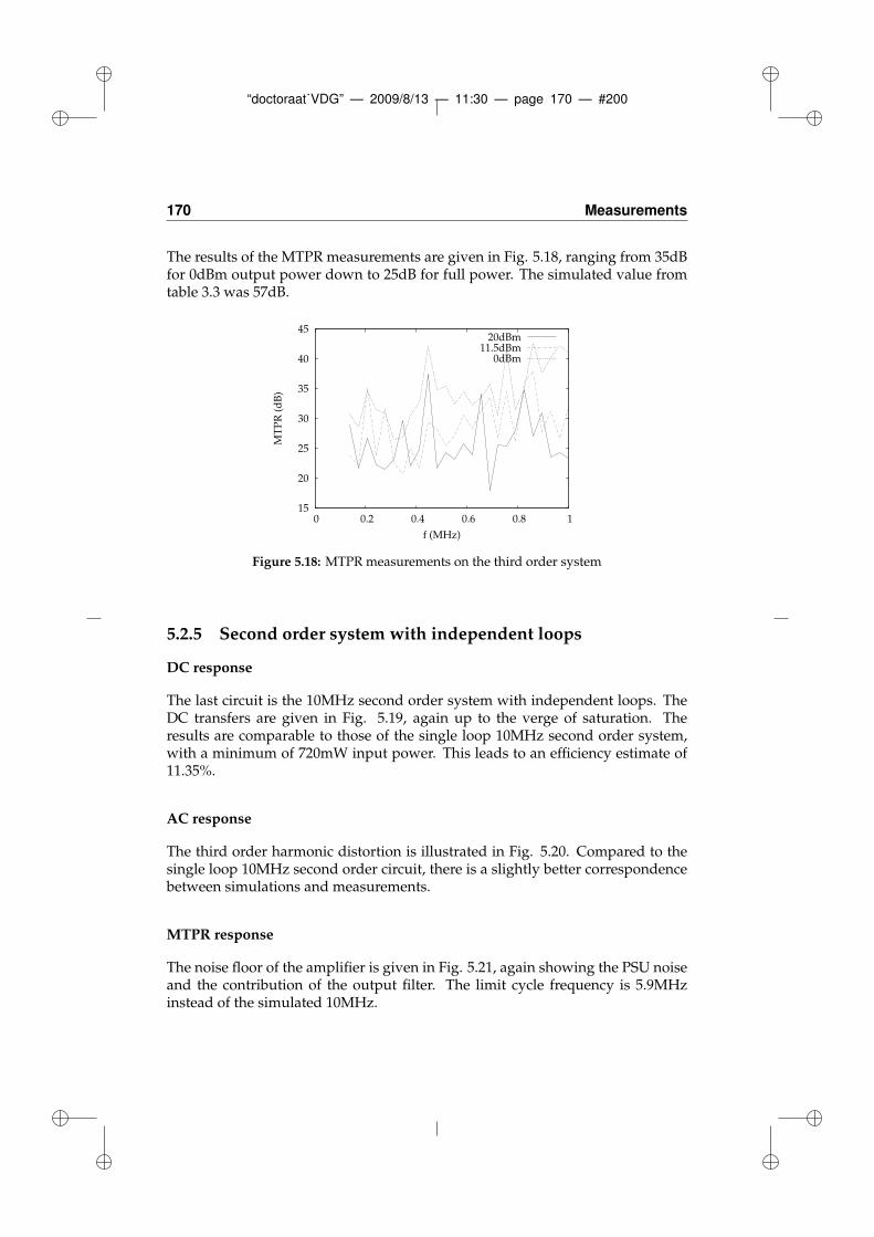
“doctoraat˙VDG” — 2009/8/13 — 11:30 — page 170 — #200
170 Measurements
The results of the MTPR measurements are given in Fig. 5.18, ranging from 35dBfor 0dBm output power down to 25dB for full power. The simulated value fromtable 3.3 was 57dB.
15
20
25
30
35
40
45
0 0.2 0.4 0.6 0.8 1
MT
PR
(d
B)
f (MHz)
20dBm11.5dBm
0dBm
Figure 5.18: MTPR measurements on the third order system
5.2.5 Second order system with independent loops
DC response
The last circuit is the 10MHz second order system with independent loops. TheDC transfers are given in Fig. 5.19, again up to the verge of saturation. Theresults are comparable to those of the single loop 10MHz second order system,with a minimum of 720mW input power. This leads to an efficiency estimate of11.35%.
AC response
The third order harmonic distortion is illustrated in Fig. 5.20. Compared to thesingle loop 10MHz second order circuit, there is a slightly better correspondencebetween simulations and measurements.
MTPR response
The noise floor of the amplifier is given in Fig. 5.21, again showing the PSU noiseand the contribution of the output filter. The limit cycle frequency is 5.9MHzinstead of the simulated 10MHz.
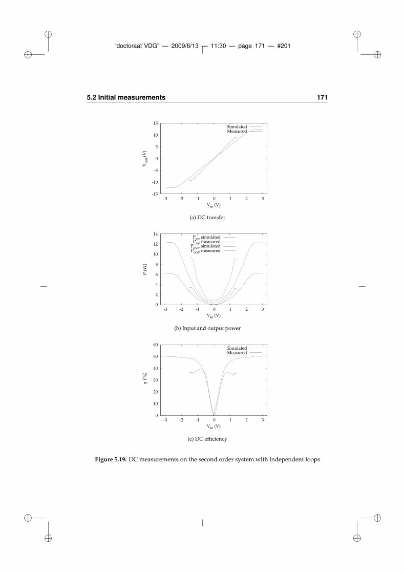
“doctoraat˙VDG” — 2009/8/13 — 11:30 — page 171 — #201
5.2 Initial measurements 171
-15
-10
-5
0
5
10
15
-3 -2 -1 0 1 2 3
Vo
ut
(V)
Vin (V)
SimulatedMeasured
(a) DC transfer
0
2
4
6
8
10
12
14
-3 -2 -1 0 1 2 3
P (
W)
Vin (V)
Pin, simulatedPin, measured
Pout, simulatedPout, measured
(b) Input and output power
0
10
20
30
40
50
60
-3 -2 -1 0 1 2 3
Vin (V)
SimulatedMeasured
η(%
)
(c) DC efficiency
Figure 5.19: DC measurements on the second order system with independent loops
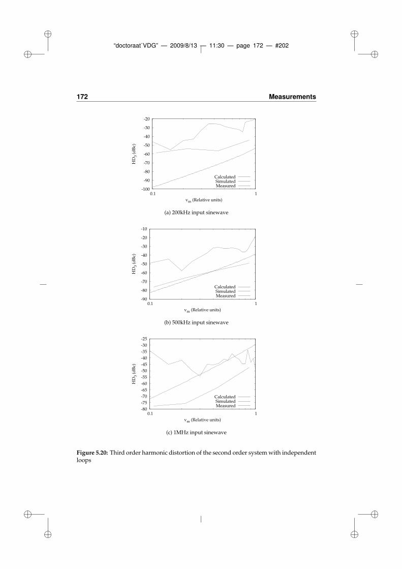
“doctoraat˙VDG” — 2009/8/13 — 11:30 — page 172 — #202
172 Measurements
-100
-90
-80
-70
-60
-50
-40
-30
-20
0.1 1
HD
3 (d
Bc)
vm (Relative units)
CalculatedSimulatedMeasured
(a) 200kHz input sinewave
-90
-80
-70
-60
-50
-40
-30
-20
-10
0.1 1
HD
3 (d
Bc)
vm (Relative units)
CalculatedSimulatedMeasured
(b) 500kHz input sinewave
-80
-75
-70
-65
-60
-55
-50
-45
-40
-35
-30
-25
0.1 1
HD
3 (d
Bc)
vm (Relative units)
CalculatedSimulatedMeasured
(c) 1MHz input sinewave
Figure 5.20: Third order harmonic distortion of the second order system with independentloops
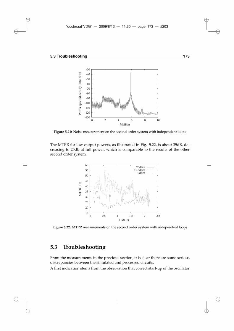
“doctoraat˙VDG” — 2009/8/13 — 11:30 — page 173 — #203
5.3 Troubleshooting 173
-130
-120
-110
-100
-90
-80
-70
-60
-50
-40
-30
0 2 4 6 8 10
Po
wer
sp
ectr
al d
ensi
ty (
dB
m/
Hz)
f (MHz)
Figure 5.21: Noise measurement on the second order system with independent loops
The MTPR for low output powers, as illustrated in Fig. 5.22, is about 35dB, de-creasing to 25dB at full power, which is comparable to the results of the othersecond order system.
15
20
25
30
35
40
45
50
55
60
0 0.5 1 1.5 2 2.5
MT
PR
(d
B)
f (MHz)
20dBm11.5dBm
0dBm
Figure 5.22: MTPR measurements on the second order system with independent loops
5.3 Troubleshooting
From the measurements in the previous section, it is clear there are some seriousdiscrepancies between the simulated and processed circuits.
A first indication stems from the observation that correct start-up of the oscillator
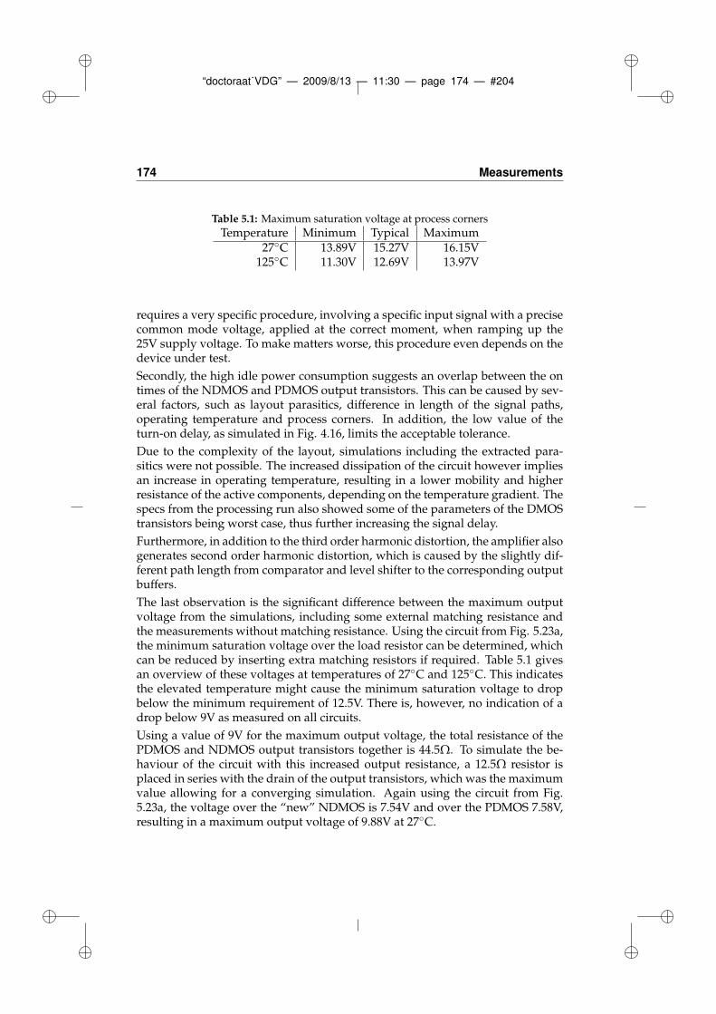
“doctoraat˙VDG” — 2009/8/13 — 11:30 — page 174 — #204
174 Measurements
Table 5.1: Maximum saturation voltage at process corners
Temperature Minimum Typical Maximum27C 13.89V 15.27V 16.15V
125C 11.30V 12.69V 13.97V
requires a very specific procedure, involving a specific input signal with a precisecommon mode voltage, applied at the correct moment, when ramping up the25V supply voltage. To make matters worse, this procedure even depends on thedevice under test.
Secondly, the high idle power consumption suggests an overlap between the ontimes of the NDMOS and PDMOS output transistors. This can be caused by sev-eral factors, such as layout parasitics, difference in length of the signal paths,operating temperature and process corners. In addition, the low value of theturn-on delay, as simulated in Fig. 4.16, limits the acceptable tolerance.
Due to the complexity of the layout, simulations including the extracted para-sitics were not possible. The increased dissipation of the circuit however impliesan increase in operating temperature, resulting in a lower mobility and higherresistance of the active components, depending on the temperature gradient. Thespecs from the processing run also showed some of the parameters of the DMOStransistors being worst case, thus further increasing the signal delay.
Furthermore, in addition to the third order harmonic distortion, the amplifier alsogenerates second order harmonic distortion, which is caused by the slightly dif-ferent path length from comparator and level shifter to the corresponding outputbuffers.
The last observation is the significant difference between the maximum outputvoltage from the simulations, including some external matching resistance andthe measurements without matching resistance. Using the circuit from Fig. 5.23a,the minimum saturation voltage over the load resistor can be determined, whichcan be reduced by inserting extra matching resistors if required. Table 5.1 givesan overview of these voltages at temperatures of 27C and 125C. This indicatesthe elevated temperature might cause the minimum saturation voltage to dropbelow the minimum requirement of 12.5V. There is, however, no indication of adrop below 9V as measured on all circuits.
Using a value of 9V for the maximum output voltage, the total resistance of thePDMOS and NDMOS output transistors together is 44.5Ω. To simulate the be-haviour of the circuit with this increased output resistance, a 12.5Ω resistor isplaced in series with the drain of the output transistors, which was the maximumvalue allowing for a converging simulation. Again using the circuit from Fig.5.23a, the voltage over the “new” NDMOS is 7.54V and over the PDMOS 7.58V,resulting in a maximum output voltage of 9.88V at 27C.

“doctoraat˙VDG” — 2009/8/13 — 11:30 — page 175 — #205
5.3 Troubleshooting 175
3.3V
3.3V
25Ω
25V
(a) Output stage
3.3V
RL
25V
Vin
(b) PDMOS with resistor
Figure 5.23: Schematics for worst case simulations and PDMOS transistor measurements
Distortion simulations on the 10MHz second order system using this series resis-tor also suggest this results in an increase of the third order harmonic distortionof about 20dB. As a result, at least part of the discrepancy between simulated andmeasured distortion levels can be attributed to the increased output resistance.
The primordial question now is the origin of this increased resistance. Usingthe circuit from Fig. 5.23b, this resistance can be simulated as a function of thedrain-source voltage and temperature. The resistor RL is included to limit thisdrain-source voltage to the maximum achievable in the full circuit when suppos-ing an ideal, lossless NDMOS transistor.
Figures 5.24, 5.25 and 5.26 show the resulting curves for a typical and two worstcase simulations at 27C and 125C for the full 6400µm wide PDMOS with 25Ω
load and the 50µm wide reference transistor, which is to be repeated 128 times inparallel to form this full output PDMOS. To keep both simulations equivalent, RL
is scaled up according to the ratio of the total width of both devices. The resultingdifference in resistance scale then again is compensated according to this ratio.
As could be expected from the previous simulations on the full output stage, theresults of the 6400µm wide PDMOS do not suggest a significant difference in out-put resistance as compared with the 50µm reference PDMOS, except for the worstcase corner in Fig. 5.25. However, the results in Fig. 5.27 of TCAD simulationson the device level under nominal processing conditions, using the 50µm device,already point in the direction of an underestimation of this resistance.
To finally confirm these simulations, the results of measurements on discrete tran-sistors, processed in the same AMIS I3T80 0.35µm technology, are presented inFig. 5.28 for a 80µm wide PDMOS and Fig. 5.29 for a 4818µm wide PDMOS. The
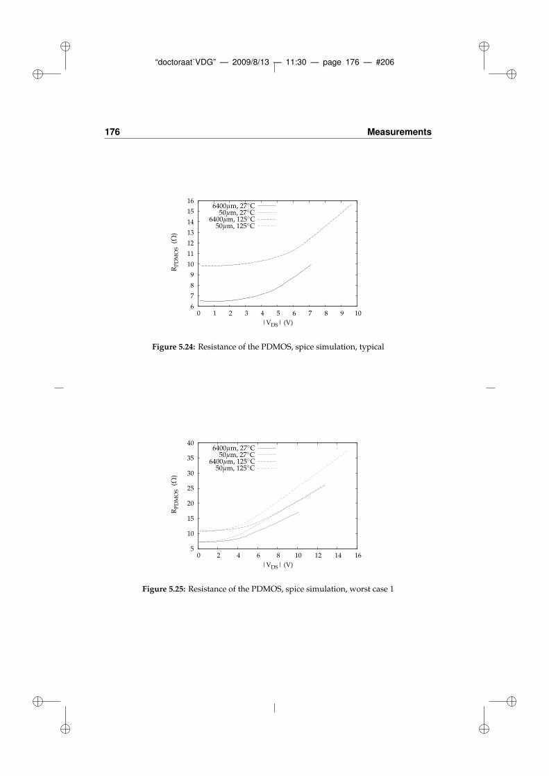
“doctoraat˙VDG” — 2009/8/13 — 11:30 — page 176 — #206
176 Measurements
6
7
8
9
10
11
12
13
14
15
16
0 1 2 3 4 5 6 7 8 9 10
RP
DM
OS
|VDS| (V)
(Ω)
6400µm, 27C50µm, 27C
6400µm, 125C50µm, 125C
Figure 5.24: Resistance of the PDMOS, spice simulation, typical
5
10
15
20
25
30
35
40
0 2 4 6 8 10 12 14 16
RP
DM
OS
|VDS| (V)
(Ω)
6400µm, 27C50µm, 27C
6400µm, 125C50µm, 125C
Figure 5.25: Resistance of the PDMOS, spice simulation, worst case 1
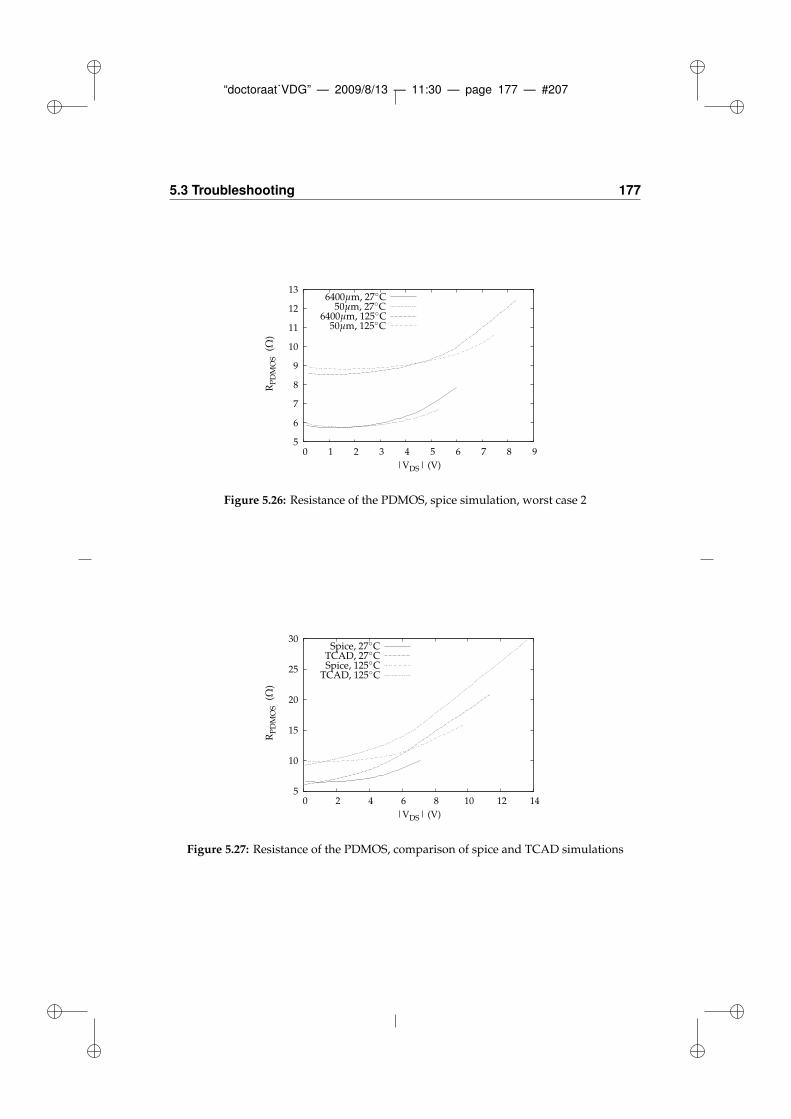
“doctoraat˙VDG” — 2009/8/13 — 11:30 — page 177 — #207
5.3 Troubleshooting 177
5
6
7
8
9
10
11
12
13
0 1 2 3 4 5 6 7 8 9
RP
DM
OS
|VDS| (V)
(Ω)
6400µm, 27C50µm, 27C
6400µm, 125C50µm, 125C
Figure 5.26: Resistance of the PDMOS, spice simulation, worst case 2
5
10
15
20
25
30
0 2 4 6 8 10 12 14
RP
DM
OS
|VDS| (V)
(Ω)
Spice, 27CTCAD, 27CSpice, 125C
TCAD, 125C
Figure 5.27: Resistance of the PDMOS, comparison of spice and TCAD simulations
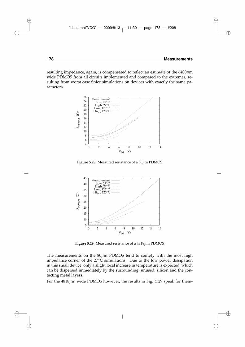
“doctoraat˙VDG” — 2009/8/13 — 11:30 — page 178 — #208
178 Measurements
resulting impedance, again, is compensated to reflect an estimate of the 6400µmwide PDMOS from all circuits implemented and compared to the extremes, re-sulting from worst case Spice simulations on devices with exactly the same pa-rameters.
4
6
8
10
12
14
16
18
20
22
24
26
0 2 4 6 8 10 12 14
RP
DM
OS
|VDS| (V)
Measurement
(Ω)
Low, 27CHigh, 27CLow, 125C
High, 125C
Figure 5.28: Measured resistance of a 80µm PDMOS
5
10
15
20
25
30
35
40
45
0 2 4 6 8 10 12 14 16
RP
DM
OS
|VDS| (V)
Measurement
(Ω)
Low, 27CHigh, 27CLow, 125C
High, 125C
Figure 5.29: Measured resistance of a 4818µm PDMOS
The measurements on the 80µm PDMOS tend to comply with the most highimpedance corner of the 27C simulations. Due to the low power dissipationin this small device, only a slight local increase in temperature is expected, whichcan be dispersed immediately by the surrounding, unused, silicon and the con-tacting metal layers.
For the 4818µm wide PDMOS however, the results in Fig. 5.29 speak for them-
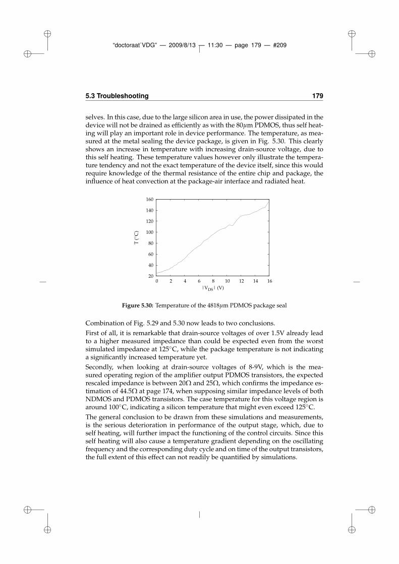
“doctoraat˙VDG” — 2009/8/13 — 11:30 — page 179 — #209
5.3 Troubleshooting 179
selves. In this case, due to the large silicon area in use, the power dissipated in thedevice will not be drained as efficiently as with the 80µm PDMOS, thus self heat-ing will play an important role in device performance. The temperature, as mea-sured at the metal sealing the device package, is given in Fig. 5.30. This clearlyshows an increase in temperature with increasing drain-source voltage, due tothis self heating. These temperature values however only illustrate the tempera-ture tendency and not the exact temperature of the device itself, since this wouldrequire knowledge of the thermal resistance of the entire chip and package, theinfluence of heat convection at the package-air interface and radiated heat.
20
40
60
80
100
120
140
160
0 2 4 6 8 10 12 14 16
|VDS| (V)
T(
C)
Figure 5.30: Temperature of the 4818µm PDMOS package seal
Combination of Fig. 5.29 and 5.30 now leads to two conclusions.
First of all, it is remarkable that drain-source voltages of over 1.5V already leadto a higher measured impedance than could be expected even from the worstsimulated impedance at 125C, while the package temperature is not indicatinga significantly increased temperature yet.
Secondly, when looking at drain-source voltages of 8-9V, which is the mea-sured operating region of the amplifier output PDMOS transistors, the expectedrescaled impedance is between 20Ω and 25Ω, which confirms the impedance es-timation of 44.5Ω at page 174, when supposing similar impedance levels of bothNDMOS and PDMOS transistors. The case temperature for this voltage region isaround 100C, indicating a silicon temperature that might even exceed 125C.
The general conclusion to be drawn from these simulations and measurements,is the serious deterioration in performance of the output stage, which, due toself heating, will further impact the functioning of the control circuits. Since thisself heating will also cause a temperature gradient depending on the oscillatingfrequency and the corresponding duty cycle and on time of the output transistors,the full extent of this effect can not readily be quantified by simulations.
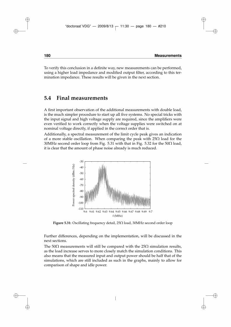
“doctoraat˙VDG” — 2009/8/13 — 11:30 — page 180 — #210
180 Measurements
To verify this conclusion in a definite way, new measurements can be performed,using a higher load impedance and modified output filter, according to this ter-mination impedance. These results will be given in the next section.
5.4 Final measurements
A first important observation of the additional measurements with double load,is the much simpler procedure to start up all five systems. No special tricks withthe input signal and high voltage supply are required, since the amplifiers wereeven verified to work correctly when the voltage supplies were switched on atnominal voltage directly, if applied in the correct order that is.
Additionally, a spectral measurement of the limit cycle peak gives an indicationof a more stable oscillation. When comparing the peak with 25Ω load for the30MHz second order loop from Fig. 5.31 with that in Fig. 5.32 for the 50Ω load,it is clear that the amount of phase noise already is much reduced.
-110
-100
-90
-80
-70
-60
-50
-40
-30
9.6 9.61 9.62 9.63 9.64 9.65 9.66 9.67 9.68 9.69 9.7
Po
wer
sp
ectr
al d
ensi
ty (
dB
m/
Hz)
f (MHz)
Figure 5.31: Oscillating frequency detail, 25Ω load, 30MHz second order loop
Further differences, depending on the implementation, will be discussed in thenext sections.
The 50Ω measurements will still be compared with the 25Ω simulation results,as the load increase serves to more closely match the simulation conditions. Thisalso means that the measured input and output power should be half that of thesimulations, which are still included as such in the graphs, mainly to allow forcomparison of shape and idle power.
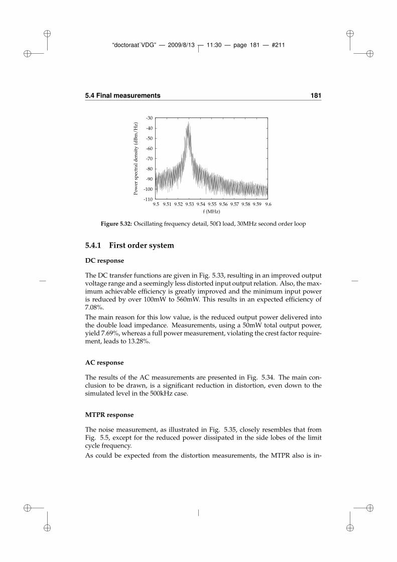
“doctoraat˙VDG” — 2009/8/13 — 11:30 — page 181 — #211
5.4 Final measurements 181
-110
-100
-90
-80
-70
-60
-50
-40
-30
9.5 9.51 9.52 9.53 9.54 9.55 9.56 9.57 9.58 9.59 9.6
Po
wer
sp
ectr
al d
ensi
ty (
dB
m/
Hz)
f (MHz)
Figure 5.32: Oscillating frequency detail, 50Ω load, 30MHz second order loop
5.4.1 First order system
DC response
The DC transfer functions are given in Fig. 5.33, resulting in an improved outputvoltage range and a seemingly less distorted input output relation. Also, the max-imum achievable efficiency is greatly improved and the minimum input poweris reduced by over 100mW to 560mW. This results in an expected efficiency of7.08%.
The main reason for this low value, is the reduced output power delivered intothe double load impedance. Measurements, using a 50mW total output power,yield 7.69%, whereas a full power measurement, violating the crest factor require-ment, leads to 13.28%.
AC response
The results of the AC measurements are presented in Fig. 5.34. The main con-clusion to be drawn, is a significant reduction in distortion, even down to thesimulated level in the 500kHz case.
MTPR response
The noise measurement, as illustrated in Fig. 5.35, closely resembles that fromFig. 5.5, except for the reduced power dissipated in the side lobes of the limitcycle frequency.
As could be expected from the distortion measurements, the MTPR also is in-
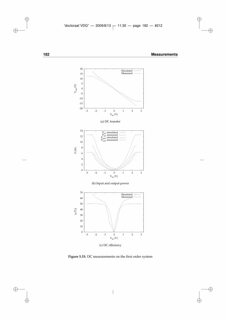
“doctoraat˙VDG” — 2009/8/13 — 11:30 — page 182 — #212
182 Measurements
-20
-15
-10
-5
0
5
10
15
20
-3 -2 -1 0 1 2 3
Vo
ut
(V)
Vin (V)
SimulatedMeasured
(a) DC transfer
0
2
4
6
8
10
12
14
-3 -2 -1 0 1 2 3
P (
W)
Vin (V)
Pin, simulatedPin, measured
Pout, simulatedPout, measured
(b) Input and output power
0
10
20
30
40
50
60
70
-3 -2 -1 0 1 2 3
Vin (V)
SimulatedMeasured
η(%
)
(c) DC efficiency
Figure 5.33: DC measurements on the first order system
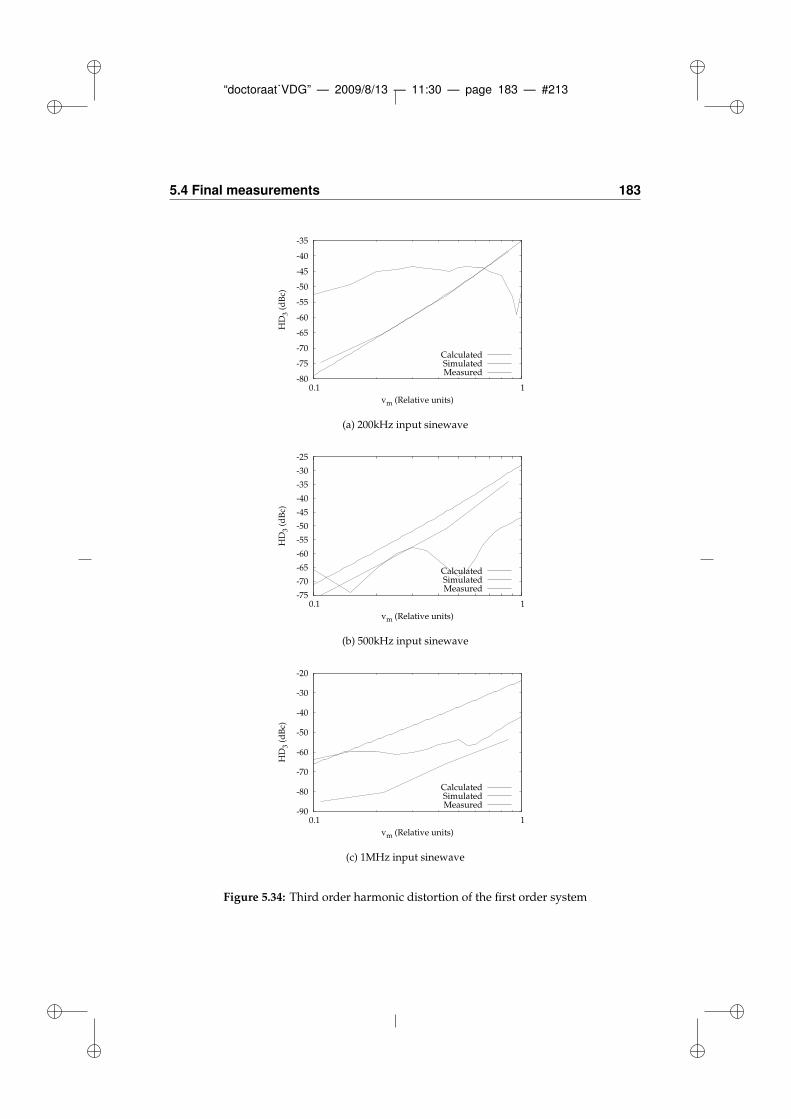
“doctoraat˙VDG” — 2009/8/13 — 11:30 — page 183 — #213
5.4 Final measurements 183
-80
-75
-70
-65
-60
-55
-50
-45
-40
-35
0.1 1
HD
3 (d
Bc)
vm (Relative units)
CalculatedSimulatedMeasured
(a) 200kHz input sinewave
-75
-70
-65
-60
-55
-50
-45
-40
-35
-30
-25
0.1 1
HD
3 (d
Bc)
vm (Relative units)
CalculatedSimulatedMeasured
(b) 500kHz input sinewave
-90
-80
-70
-60
-50
-40
-30
-20
0.1 1
HD
3 (d
Bc)
vm (Relative units)
CalculatedSimulatedMeasured
(c) 1MHz input sinewave
Figure 5.34: Third order harmonic distortion of the first order system
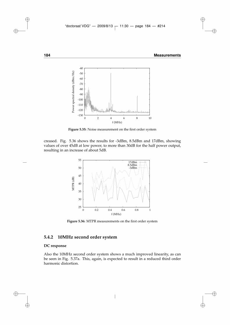
“doctoraat˙VDG” — 2009/8/13 — 11:30 — page 184 — #214
184 Measurements
-130
-120
-110
-100
-90
-80
-70
-60
-50
-40
0 2 4 6 8 10
Po
wer
sp
ectr
al d
ensi
ty (
dB
m/
Hz)
f (MHz)
Figure 5.35: Noise measurement on the first order system
creased. Fig. 5.36 shows the results for -3dBm, 8.5dBm and 17dBm, showingvalues of over 45dB at low power, to more than 30dB for the half power output,resulting in an increase of about 5dB.
25
30
35
40
45
50
55
0 0.2 0.4 0.6 0.8 1
MT
PR
(d
B)
f (MHz)
17dBm8.5dBm-3dBm
Figure 5.36: MTPR measurements on the first order system
5.4.2 10MHz second order system
DC response
Also the 10MHz second order system shows a much improved linearity, as canbe seen in Fig. 5.37a. This, again, is expected to result in a reduced third orderharmonic distortion.

“doctoraat˙VDG” — 2009/8/13 — 11:30 — page 185 — #215
5.4 Final measurements 185
The minimum power dissipation, however, is increased to 900mW, resulting inan estimated 4.98% efficiency. This is verified by a measured 5.22% efficiency,increasing to 9.01% for a 20dBm output signal.
AC response
As with the first order system, the distortion is found to be 10 to 20dB lower thanwith the original full load circuit, although this is still higher than simulated. Allresults are shown in Fig. 5.38.
MTPR response
The noise, as given in Fig. 5.39, is comparable to the initial measurements, show-ing the PSU and filter contributions. The side lobes can be attributed to a lowfrequency disturbance, picked up at the input of the amplifier.
The results of the MTPR measurements are shown in Fig. 5.40. At -3dBm outputpower, this is comparable to the 0dBm curve from Fig. 5.10. However, at 8.5dBmand 17dBm, there is an increase of about 10dB.
5.4.3 30MHz second order system
DC response
Figure 5.41 gives the results of the DC measurements on the high frequent secondorder loop. Again, there is better correspondence with the simulated transfer,although this seems less linear in general.
The minimum measured input power is 950mW, again an increase compared tothe first set of measurements. This results in an estimated 4.16% efficiency, whichis verified to be 4.08% at 17dBm output power. The full 20dBm leads to 7.62%.
AC response
The third order harmonic distortion, as illustrated in Fig. 5.42, shows a slightincrease of linearity of up to 10dB as compared to Fig. 5.12. Due to the “bumps”,visible in Fig. 5.41a, this confirms the expectations.
MTPR response
The noise floor from Fig. 5.43 again shows the PSU contribution and the outputfilter transfer and is otherwise equivalent to Fig. 5.13.
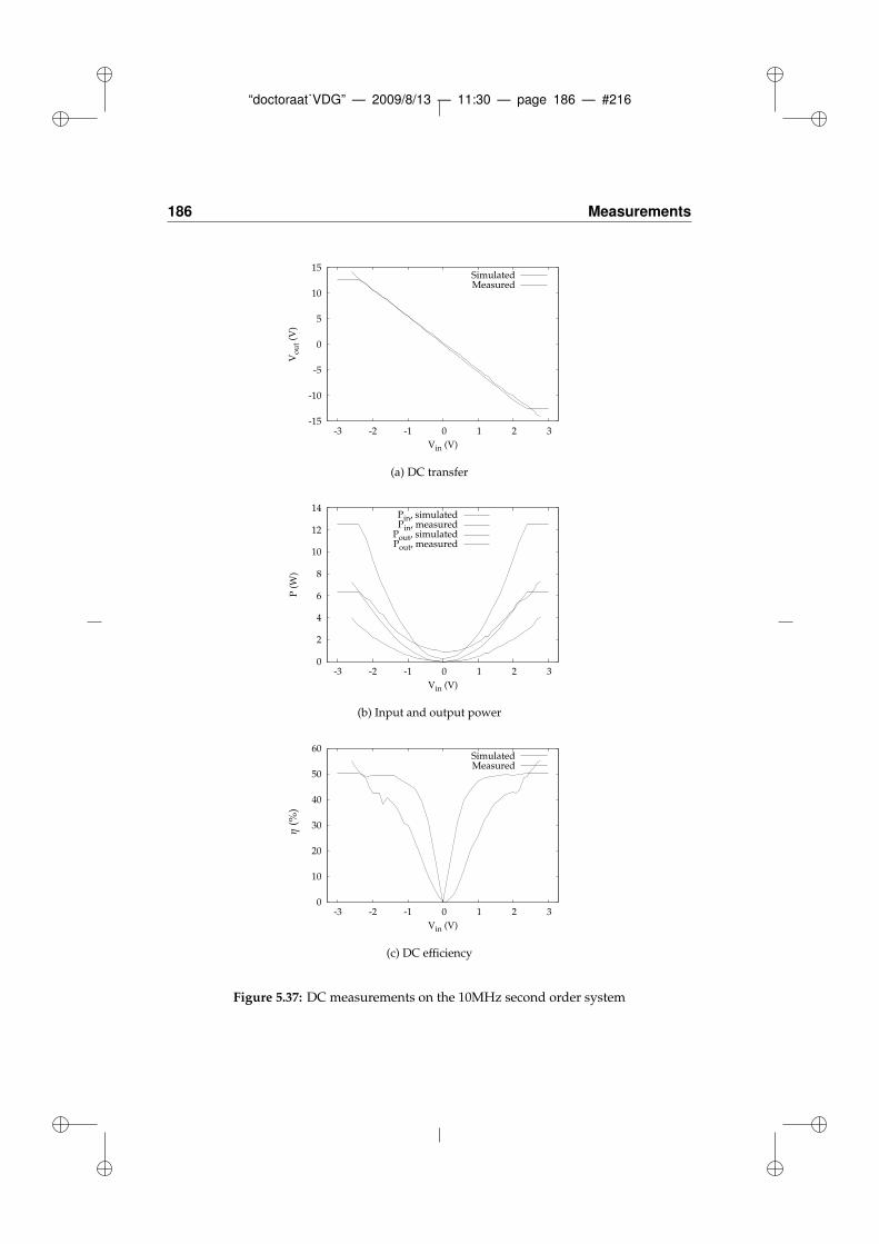
“doctoraat˙VDG” — 2009/8/13 — 11:30 — page 186 — #216
186 Measurements
-15
-10
-5
0
5
10
15
-3 -2 -1 0 1 2 3
Vo
ut
(V)
Vin (V)
SimulatedMeasured
(a) DC transfer
0
2
4
6
8
10
12
14
-3 -2 -1 0 1 2 3
P (
W)
Vin (V)
Pin, simulatedPin, measured
Pout, simulatedPout, measured
(b) Input and output power
0
10
20
30
40
50
60
-3 -2 -1 0 1 2 3
Vin (V)
SimulatedMeasured
η(%
)
(c) DC efficiency
Figure 5.37: DC measurements on the 10MHz second order system
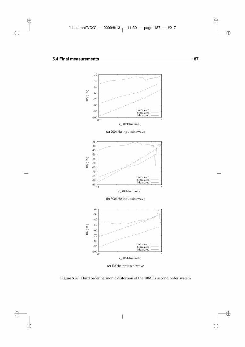
“doctoraat˙VDG” — 2009/8/13 — 11:30 — page 187 — #217
5.4 Final measurements 187
-100
-90
-80
-70
-60
-50
-40
-30
0.1 1
HD
3 (d
Bc)
vm (Relative units)
CalculatedSimulatedMeasured
(a) 200kHz input sinewave
-85
-80
-75
-70
-65
-60
-55
-50
-45
-40
-35
0.1 1
HD
3 (d
Bc)
vm (Relative units)
CalculatedSimulatedMeasured
(b) 500kHz input sinewave
-100
-90
-80
-70
-60
-50
-40
-30
-20
0.1 1
HD
3 (d
Bc)
vm (Relative units)
CalculatedSimulatedMeasured
(c) 1MHz input sinewave
Figure 5.38: Third order harmonic distortion of the 10MHz second order system
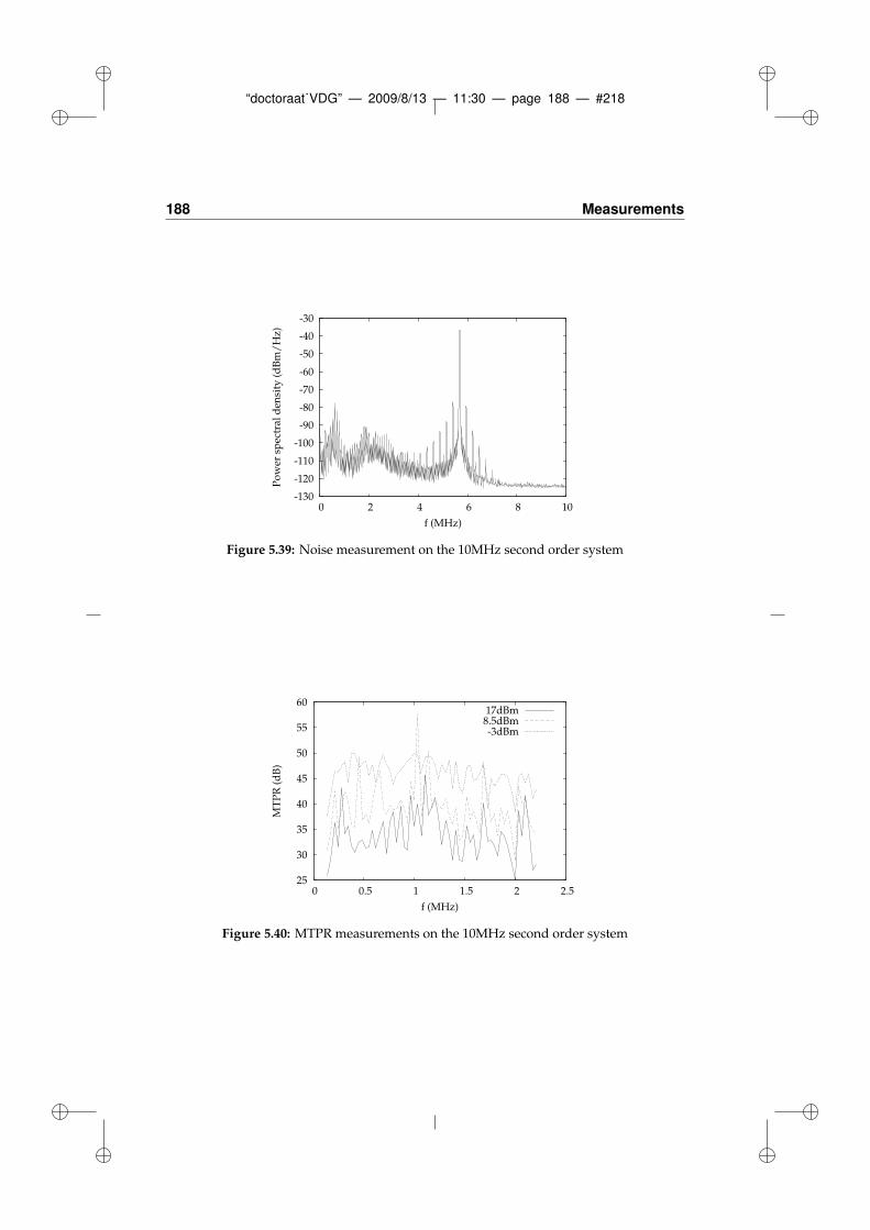
“doctoraat˙VDG” — 2009/8/13 — 11:30 — page 188 — #218
188 Measurements
-130
-120
-110
-100
-90
-80
-70
-60
-50
-40
-30
0 2 4 6 8 10
Po
wer
sp
ectr
al d
ensi
ty (
dB
m/
Hz)
f (MHz)
Figure 5.39: Noise measurement on the 10MHz second order system
25
30
35
40
45
50
55
60
0 0.5 1 1.5 2 2.5
MT
PR
(d
B)
f (MHz)
17dBm8.5dBm-3dBm
Figure 5.40: MTPR measurements on the 10MHz second order system
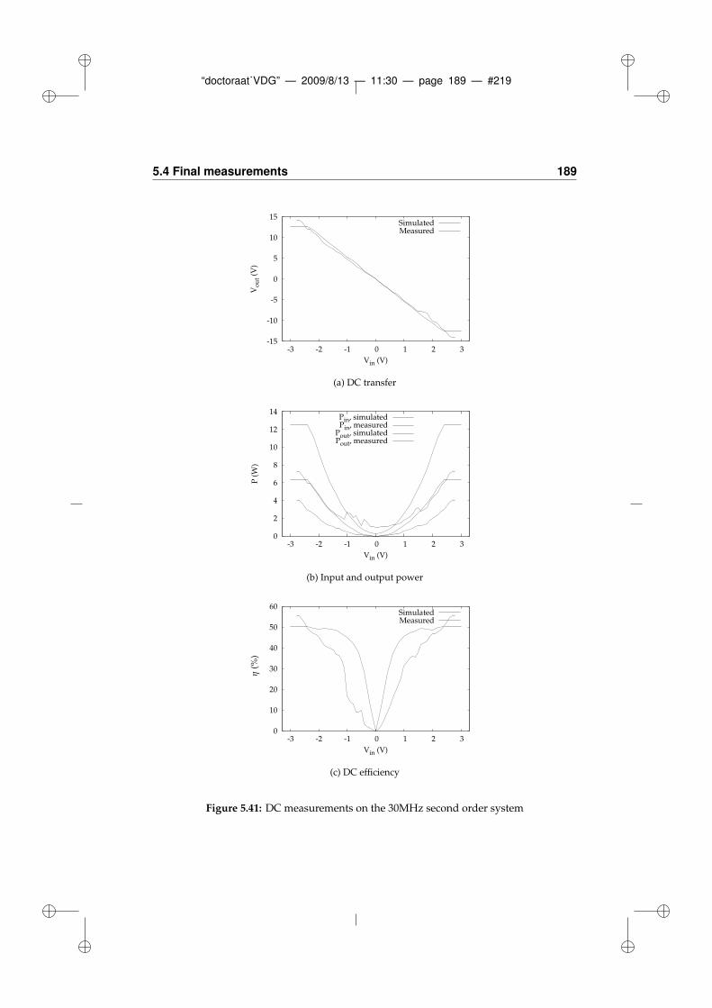
“doctoraat˙VDG” — 2009/8/13 — 11:30 — page 189 — #219
5.4 Final measurements 189
-15
-10
-5
0
5
10
15
-3 -2 -1 0 1 2 3
Vo
ut
(V)
Vin (V)
SimulatedMeasured
(a) DC transfer
0
2
4
6
8
10
12
14
-3 -2 -1 0 1 2 3
P (
W)
Vin (V)
Pin, simulatedPin, measured
Pout, simulatedPout, measured
(b) Input and output power
0
10
20
30
40
50
60
-3 -2 -1 0 1 2 3
Vin (V)
SimulatedMeasured
η(%
)
(c) DC efficiency
Figure 5.41: DC measurements on the 30MHz second order system
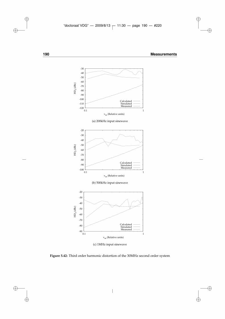
“doctoraat˙VDG” — 2009/8/13 — 11:30 — page 190 — #220
190 Measurements
-120
-110
-100
-90
-80
-70
-60
-50
-40
-30
0.1 1
HD
3 (d
Bc)
vm (Relative units)
CalculatedSimulatedMeasured
(a) 200kHz input sinewave
-100
-90
-80
-70
-60
-50
-40
-30
-20
0.1 1
HD
3 (d
Bc)
vm (Relative units)
CalculatedSimulatedMeasured
(b) 500kHz input sinewave
-90
-80
-70
-60
-50
-40
-30
-20
0.1 1
HD
3 (d
Bc)
vm (Relative units)
CalculatedSimulatedMeasured
(c) 1MHz input sinewave
Figure 5.42: Third order harmonic distortion of the 30MHz second order system

“doctoraat˙VDG” — 2009/8/13 — 11:30 — page 191 — #221
5.4 Final measurements 191
-130
-120
-110
-100
-90
-80
-70
-60
-50
-40
0 2 4 6 8 10
Po
wer
sp
ectr
al d
ensi
ty (
dB
m/
Hz)
f (MHz)
Figure 5.43: Noise measurement on the 30MHz second order system
The MTPR, as shown in Fig. 5.44, is more or less the same as Fig. 5.14, which alsocould be expected because of the similar DC transfer from Fig. 5.11a and 5.41a.
5
10
15
20
25
30
35
40
45
50
0 0.5 1 1.5 2 2.5
MT
PR
(d
B)
f (MHz)
17dBm8.5dBm-3dBm
Figure 5.44: MTPR measurements on the 30MHz second order system
5.4.4 Third order system
DC response
With the load doubled, this time, the third order system could be measured com-pletely. There is however a large offset and a strong non-linearity in the DC trans-fer from fig. 5.45a, which could not be removed by adjusting the external biasing.
“doctoraat˙VDG” — 2009/8/13 — 11:30 — page 192 — #222
192 Measurements
As a consequence, the slight instability, which is still present in this set up, mightbe the culprit. The minimum input power is significantly lower at 665mW, result-ing in a 7.30% efficiency estimate. The measurements lead to 7.20% for half theoutput power and 11.86% at 20dBm.
AC response
Surprisingly, the third order harmonic distortion as shown in Fig. 5.46, is reducedby up to 10dB compared to Fig. 5.16. These results are even comparable to, orbetter than those for the second order system, whereas comparison of the DCtransfer would have lead to the opposite conclusion.
MTPR response
The noise measurement from Fig. 5.47 still demonstrates the instability of theimplemented third order loop. For this reason, all measurements again were per-formed with a 1.5MHz output filter and the MTPR measurements from Fig. 5.48range up to 1MHz. The result is an overall increase of about 10dB compared toFig. 5.18.
5.4.5 Second order system with independent loops
DC response
Finally, the DC response of the second order system with independent loops isgiven in Fig. 5.49. As with the regular second order system, the DC transfercorresponds really well with the simulated curve.
The minimum input power however is increased by almost 200mW, reaching905mW, which is almost the same as in section 5.4.2. This result leads to a cal-culated efficiency of 4.91% and measured as 5.40% for 17dBm output power and9.26% for the full power output.
AC response
Figure 5.50 shows a slightly decreased third order harmonic content at 200kHzand 500kHz compared to Fig. 5.20, whereas the 1MHz result remains about thesame.
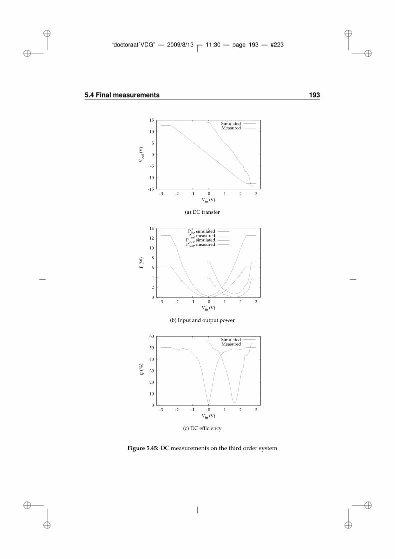
“doctoraat˙VDG” — 2009/8/13 — 11:30 — page 193 — #223
5.4 Final measurements 193
-15
-10
-5
0
5
10
15
-3 -2 -1 0 1 2 3
Vo
ut
(V)
Vin (V)
SimulatedMeasured
(a) DC transfer
0
2
4
6
8
10
12
14
-3 -2 -1 0 1 2 3
P (
W)
Vin (V)
Pin, simulatedPin, measured
Pout, simulatedPout, measured
(b) Input and output power
0
10
20
30
40
50
60
-3 -2 -1 0 1 2 3
Vin (V)
SimulatedMeasured
η(%
)
(c) DC efficiency
Figure 5.45: DC measurements on the third order system

“doctoraat˙VDG” — 2009/8/13 — 11:30 — page 194 — #224
194 Measurements
-120
-110
-100
-90
-80
-70
-60
-50
-40
-30
-20
0.1 1
HD
3 (d
Bc)
vm (Relative units)
CalculatedSimulatedMeasured
(a) 200kHz input sinewave
-95
-90
-85
-80
-75
-70
-65
-60
-55
-50
-45
-40
0.1 1
HD
3 (d
Bc)
vm (Relative units)
CalculatedSimulatedMeasured
(b) 500kHz input sinewave
-75
-70
-65
-60
-55
-50
-45
-40
-35
-30
-25
0.1 1
HD
3 (d
Bc)
vm (Relative units)
CalculatedSimulatedMeasured
(c) 1MHz input sinewave
Figure 5.46: Third order harmonic distortion of the third order system
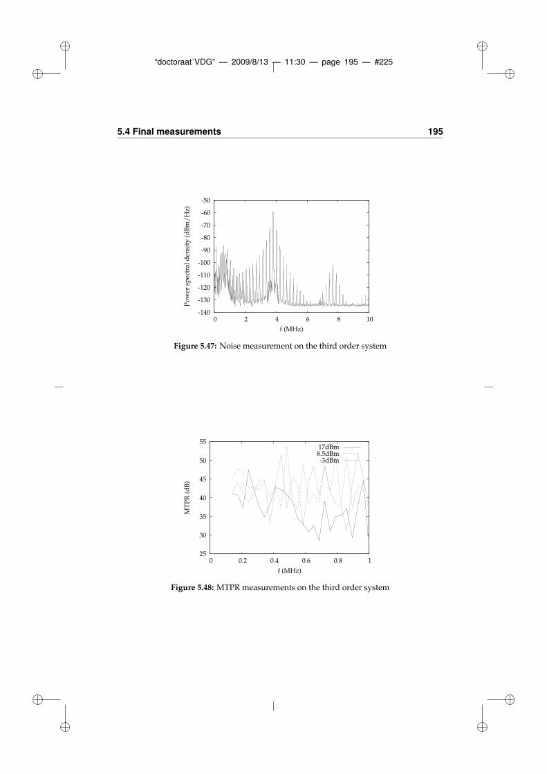
“doctoraat˙VDG” — 2009/8/13 — 11:30 — page 195 — #225
5.4 Final measurements 195
-140
-130
-120
-110
-100
-90
-80
-70
-60
-50
0 2 4 6 8 10
Po
wer
sp
ectr
al d
ensi
ty (
dB
m/
Hz)
f (MHz)
Figure 5.47: Noise measurement on the third order system
25
30
35
40
45
50
55
0 0.2 0.4 0.6 0.8 1
MT
PR
(d
B)
f (MHz)
17dBm8.5dBm-3dBm
Figure 5.48: MTPR measurements on the third order system
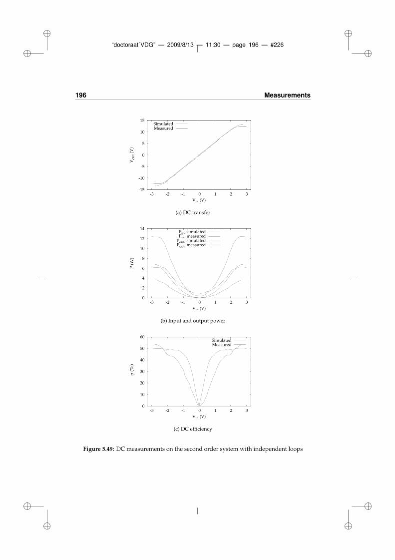
“doctoraat˙VDG” — 2009/8/13 — 11:30 — page 196 — #226
196 Measurements
-15
-10
-5
0
5
10
15
-3 -2 -1 0 1 2 3
Vo
ut
(V)
Vin (V)
SimulatedMeasured
(a) DC transfer
0
2
4
6
8
10
12
14
-3 -2 -1 0 1 2 3
P (
W)
Vin (V)
Pin, simulatedPin, measured
Pout, simulatedPout, measured
(b) Input and output power
0
10
20
30
40
50
60
-3 -2 -1 0 1 2 3
Vin (V)
SimulatedMeasured
η(%
)
(c) DC efficiency
Figure 5.49: DC measurements on the second order system with independent loops
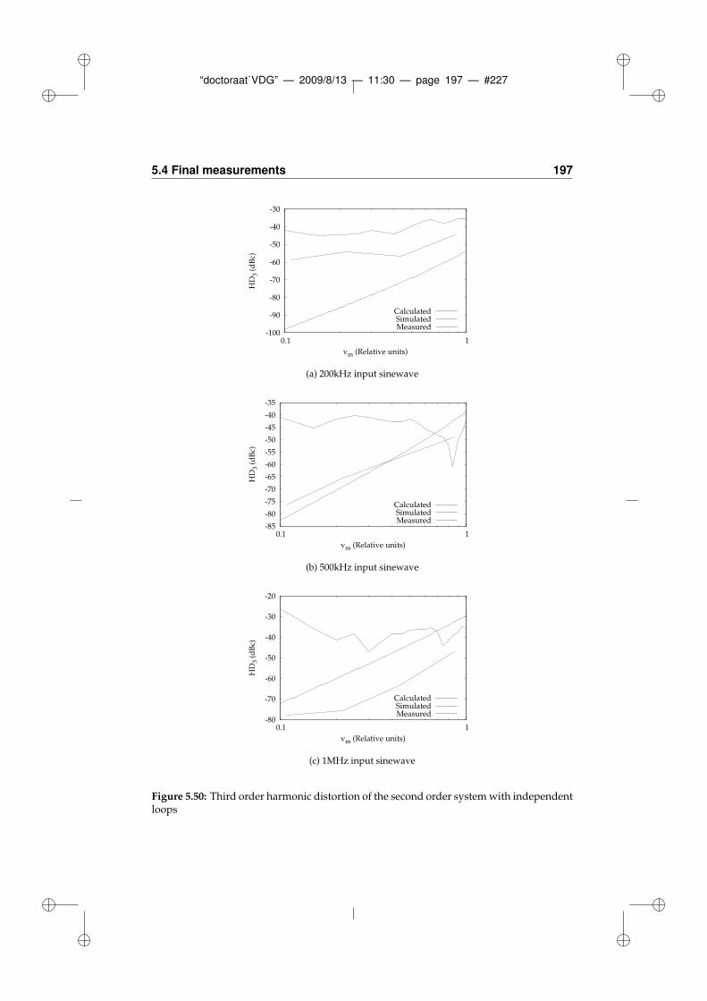
“doctoraat˙VDG” — 2009/8/13 — 11:30 — page 197 — #227
5.4 Final measurements 197
-100
-90
-80
-70
-60
-50
-40
-30
0.1 1
HD
3 (d
Bc)
vm (Relative units)
CalculatedSimulatedMeasured
(a) 200kHz input sinewave
-85
-80
-75
-70
-65
-60
-55
-50
-45
-40
-35
0.1 1
HD
3 (d
Bc)
vm (Relative units)
CalculatedSimulatedMeasured
(b) 500kHz input sinewave
-80
-70
-60
-50
-40
-30
-20
0.1 1
HD
3 (d
Bc)
vm (Relative units)
CalculatedSimulatedMeasured
(c) 1MHz input sinewave
Figure 5.50: Third order harmonic distortion of the second order system with independentloops
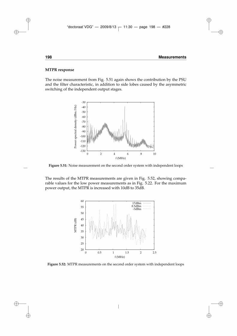
“doctoraat˙VDG” — 2009/8/13 — 11:30 — page 198 — #228
198 Measurements
MTPR response
The noise measurement from Fig. 5.51 again shows the contribution by the PSUand the filter characteristic, in addition to side lobes caused by the asymmetricswitching of the independent output stages.
-130
-120
-110
-100
-90
-80
-70
-60
-50
-40
-30
0 2 4 6 8 10
Po
wer
sp
ectr
al d
ensi
ty (
dB
m/
Hz)
f (MHz)
Figure 5.51: Noise measurement on the second order system with independent loops
The results of the MTPR measurements are given in Fig. 5.52, showing compa-rable values for the low power measurements as in Fig. 5.22. For the maximumpower output, the MTPR is increased with 10dB to 35dB.
20
25
30
35
40
45
50
55
60
0 0.5 1 1.5 2 2.5
MT
PR
(d
B)
f (MHz)
17dBm8.5dBm-3dBm
Figure 5.52: MTPR measurements on the second order system with independent loops

“doctoraat˙VDG” — 2009/8/13 — 11:30 — page 199 — #229
5.5 Conclusion 199
5.5 Conclusion
The circuits simulated in chapter 4, using the system parameters from chapter 3,are implemented in silicon. A first set of measurements was performed on all cir-cuits, showing a significant discrepancy between simulations and measurements.
The main reason for this difference is identified as the result of self-heating ofthe DMOS output stage, due to the inclusion of part of the matching resistanceof the output filter in the devices. This self-heating further results in a largelyincreased output impedance as compared with the simulations, leading to an ex-cessively high impedant output of the amplifier, directly influencing the feed-back filter characteristics. The resulting time dependent temperature gradientalso is expected to have a negative influence on the remainder of the circuits.The impedance and self-heating hypothesis is confirmed by measurements ondiscrete PDMOS transistors, processed in the same technology, suggesting addi-tional measurements on the amplifiers with an increased load impedance.
The results of these measurements with double load impedance are also pre-sented, already showing better linearity. Additionally, also the oscillating fre-quency is much more stable and system start up is much easier and reliable. Themost important measurement results are summarized in table 5.2.
Additional causes of distortion equally comprise the non-linearity of integratedresistors, capacitors and the opamp circuits, which could not be verified as thosesignals remain internal to the circuit and their influence is masked by the outputstage.
This all leads to the final conclusion that the output stage should be made aslow impedant as possible to increase correspondence between simulations andmeasurements, as suggested by Fig. 5.29.
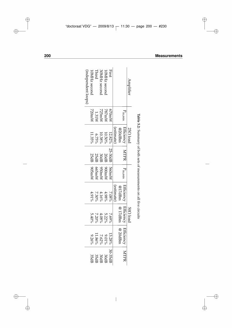
“doctoraat˙VDG” — 2009/8/13 — 11:30 — page 200 — #230
200 Measurements
Table
5.2:
Su
mm
aryo
fb
oth
setso
fm
easurem
ents
on
allfi
ve
circuits
Am
plifi
er25
Ωlo
ad50
Ωlo
adP
in,m
inE
fficien
cyM
TP
RP
in,m
inE
fficien
cyE
fficien
cyE
fficien
cyM
TP
R@
20dB
m@
17dB
m@
17dB
m@
20dB
m(estim
ate)(estim
ate)F
irst670m
W12.82%
25-30dB
560mW
7.08%7.69%
13.28%30-35d
B10M
Hz
secon
d787m
W10.50%
20dB
900mW
4.98%5.22%
9.01%30d
B30M
Hz
secon
d725m
W10.38%
30dB
950mW
4.16%4.08%
7.62%30d
BT
hird
1.31W6.75%
25dB
665mW
7.30%7.20%
11.86%35d
B10M
Hz
secon
d720m
W11.35%
25dB
905mW
4.91%5.40%
9.26%35d
B(in
dep
end
ent
loo
ps)
“doctoraat˙VDG” — 2009/8/13 — 11:30 — page 201 — #231
References
[1] Asymmetric digital subscriber line (ADSL) transceivers, ITU-T RecommendationG.992.1, Jul. 1999.
[2] Asymmetric digital subscriber line transceivers 2 (ADSL2), ITU-T Recommenda-tion G.992.3, Jan. 2005.
[3] Asymmetric Digital Subscriber Line (ADSL) transceivers - Extended bandwidthADSL2 (ADSL2plus), ITU-T Recommendation G.992.5, Jan. 2005.

“doctoraat˙VDG” — 2009/8/13 — 11:30 — page 202 — #232
202 REFERENCES
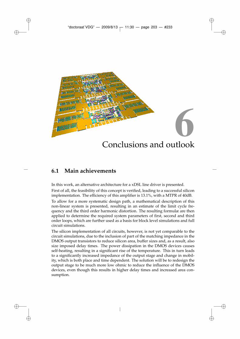
“doctoraat˙VDG” — 2009/8/13 — 11:30 — page 203 — #233
6Conclusions and outlook
6.1 Main achievements
In this work, an alternative architecture for a xDSL line driver is presented.
First of all, the feasibility of this concept is verified, leading to a successful siliconimplementation. The efficiency of this amplifier is 13.1%, with a MTPR of 40dB.
To allow for a more systematic design path, a mathematical description of thisnon-linear system is presented, resulting in an estimate of the limit cycle fre-quency and the third order harmonic distortion. The resulting formulæ are thenapplied to determine the required system parameters of first, second and thirdorder loops, which are further used as a basis for block level simulations and fullcircuit simulations.
The silicon implementation of all circuits, however, is not yet comparable to thecircuit simulations, due to the inclusion of part of the matching impedance in theDMOS output transistors to reduce silicon area, buffer sizes and, as a result, alsosize imposed delay times. The power dissipation in the DMOS devices causesself-heating, resulting in a significant rise of the temperature. This in turn leadsto a significantly increased impedance of the output stage and change in mobil-ity, which is both place and time dependent. The solution will be to redesign theoutput stage to be much more low ohmic to reduce the influence of the DMOSdevices, even though this results in higher delay times and increased area con-sumption.
“doctoraat˙VDG” — 2009/8/13 — 11:30 — page 204 — #234
204 Conclusions and outlook
This work resulted in several contributions to journals and conference proceed-ings [1], [2], [3], [4], [5], [6], [7]. Involvement in additional projects also led to [8],[9] and [10].
6.2 Future work
In addition to a version with a low ohmic output stage, there are several addi-tional improvements possible.
A first improvement, limiting the number of power supplies required, would beto change the architecture of the level shifter, such that only the high voltagesupply is required as an input. Care must however be taken, that the gate signalfor the PDMOS output transistors still is strong enough to maintain the requiredspeed, without a disproportional increase of the power consumption of the levelshifter.
An additional architectural change to increase the efficiency, would be a similarapproach as in [11], where multiple supply voltages are used, allowing the ampli-fier to work at the smallest power supply capable of generating the instantaneousamplitude level. While a reduced supply voltage, sourcing an identical outputcurrent, would mean higher efficiency, this will also reduce the linearity, sincethe distortion increases and the oscillating frequency decreases with the relativeamplitude as explained in chapter 3.
This, however, also makes it possible to take advantage of smaller output DMOStransistors due to the limited output currents for the smallest output voltagerange, implying smaller sizes of buffer stages and faster operation at a higherlimit cycle. As such, this requires an optimization of the additional voltage sup-ply levels, transistor sizing and, possibly, loop filter dimensioning, to balanceefficiency and linearity.
Furthermore, as active termination, which is used with linear line drivers, is notreadily applicable, the need for impedance matching can be questioned, since thishas no direct influence on the final performance of the system, except for halvingthe maximum achievable efficiency.
6.3 Feasibility and extensibility
The main question remaining now, is the feasibility of asynchronous switchingamplifiers as a xDSL line driver, since no compliant system could be demon-strated, in part for the reasons given in the previous chapter.
Based on the results of the Matlab simulations in chapter 3, however, it should bepossible to tune the filter order and parameters to reach the MTPR spec, at least
“doctoraat˙VDG” — 2009/8/13 — 11:30 — page 205 — #235
6.3 Feasibility and extensibility 205
for ADSL and ADSL2+ that is. For the more high frequent VDSL variants, thisis much more questionable, since the requirement for high voltage devices withcorresponding level shifters most probably will introduce too high a delay timein the loop to allow functioning at even more elevated limit cycles.
This last remark leads to following conclusion with regard to the extensibility ofthe technique used throughout this work. The three main parameters influencingthe applicability of an asynchronous amplifier are
• Output voltage range
• Output power
• Limit cycle imposed by signal frequency band
which basically boils down to the classical frequency versus parasitics trade-off.
Additional applications thus could be found in the domain of low frequent, highpower audio amplifiers, as briefly mentioned in chapter 1 and the area of PWMapplications such as power conversion. Since the amplifier architecture is verysimilar to that of synchronous Σ∆ converters, it can also be used to that extent athigher operating frequencies.
“doctoraat˙VDG” — 2009/8/13 — 11:30 — page 206 — #236
206 Conclusions and outlook
“doctoraat˙VDG” — 2009/8/13 — 11:30 — page 207 — #237
References
[1] V. De Gezelle, J. Doutreloigne, and A. Van Calster, “A 765 mW high-voltageswitching ADSL line-driver,” Solid-State Electronics, vol. 49, no. 12, pp. 1947–1950, Dec. 2005.
[2] J. Doutreloigne, J. Buyle, and V. De Gezelle, “A multi-level switching am-plifier with improved power efficiency for analog signals with high crestfactor,” in Proceedings of the 8th WSEAS International Conference on Microelec-tronics, Nanoelectronics, and Optoelectronics, Istanbul, Turkey, May 2009, pp.47–52.
[3] J. Buyle, V. De Gezelle, B. Bakeroot, and J. Doutreloigne, “A new type oflevel-shifter for n-type high side switches used in high-voltage switchingADSL line-drivers,” in Proceedings of the 15th IEEE International ConferenceOn Electronics, Circuits and Systems, Malta, Sep. 2008, pp. 954–957.
[4] J. Buyle, V. De Gezelle, B. Bakeroot, and J. Doutreloigne, “A high-voltageswitching ADSL line-driver, with an n-type output stage,” in Proceedings ofthe 12th WSEAS International Conference on CIRCUITS, Rodos, Greece, Jul.2008, pp. 60–64.
[5] V. De Gezelle, J. Buyle, and J. Doutreloigne, “Distortion calculation of anasynchronous switching xDSL line-driver,” in Proceedings of the InternationalSymposium on Circuits and Systems, Seattle, USA, May 2008, pp. 2386–2389.
[6] V. De Gezelle, “On the design of a switching xDSL line-driver,” in Proceedingsof the 8th FirW PhD Symposium, Ghent, Belgium, Dec. 2007.
[7] V. De Gezelle, J. Doutreloigne, and A. Van Calster, “A high-voltage, 765mWswitching ADSL line-driver,” in Proceedings of the 17th International Conferenceon Microelectronics, Islamabad, Pakistan, Dec. 2005, pp. 213–217.
[8] H. De Pauw, V. De Gezelle, J. Doutreloigne, A. Van Calster, E. Op de Beeck,R. Van Bolderik, and J. Content, “Development of the area-reducing ac-tive ‘coil enhancement’ principle, practised onto an adsl-pots splitter,” IEEETrans. Circuits Syst. I, accepted for publication.
“doctoraat˙VDG” — 2009/8/13 — 11:30 — page 208 — #238
208 REFERENCES
[9] H. De Pauw, V. De Gezelle, J. Doutreloigne, E. Op de Beeck, R. Van Bolderik,and J. Content, “Active-tunable inductor effected by a novel impedance syn-thesis circuit,” in Proceedings of the 8th WSEAS International Conference onInstrumentation, Measurement, Circuits and Systems, Hangzhou, China, May2009, pp. 95–100.
[10] T. Bert, V. De Gezelle, G. Van Steenberge, S. Van Put, P. Geerinck, andH. De Smet, “Model for the properties and behavior of electronic paper,” inAbstracts of the SID-MEC Spring 2006 Meeting, H. De Smet and P. Van Daele,Eds., Mar. 2006.
[11] F. H. Raab, “Average efficiency of class-G power amplifiers,” IEEE Trans.Consum. Electron., vol. CE-32, no. 2, pp. 145–150, May 1986.


![AUDIO/VIDEO CONTROL RECEIVERlvt1170-004a [e] rx-7042s instructions audio/video control receiver geintegreerde audio/video-versterker gebruiksaanwijzing cover_7040[e]_nl 1 04.2.10,](https://static.fdocuments.nl/doc/165x107/5ff8542ffdb3712a9e06d9be/audiovideo-control-lvt1170-004a-e-rx-7042s-instructions-audiovideo-control-receiver.jpg)