High fill factor and open circuit ... - uni-augsburg.de
32
Advanced Functional Materials 20 (2010) 4295-4303 1 1 DOI: 10.1002/adfm.201001028 High fill factor and open circuit voltage in organic photovoltaic cells with diindenoperylene as donor material By Julia Wagner, Mark Gruber, Alexander Hinderhofer, Andreas Wilke, Benjamin Bröker, Johannes Frisch, Patrick Amsalem, Antje Vollmer, Andreas Opitz, Norbert Koch, Frank Schreiber and Wolfgang Brütting* [*] Prof. Wolfgang Brütting, Julia Wagner, Mark Gruber, Dr. Andreas Opitz Institut für Physik Universität Augsburg Universitätsstr. 1, 86135 Augsburg (Germany) E-mail: [email protected] Prof. Frank Schreiber, Alexander Hinderhofer Institut für Angewandte Physik Universität Tübingen Auf der Morgenstelle 10, 72076 Tübingen (Germany) Prof. Norbert Koch, Andreas Wilke, Benjamin Bröker, Johannes Frisch, Patrick Amsalem Institut für Physik Humboldt-Universität zu Berlin Newtonstr. 15, 12489 Berlin (Germany) Dr. Antje Vollmer Helmholtz-Zentrum Berlin für Materialien und Energie GmbH - BESSYII Albert-Einstein-Straße 15, 12489 Berlin (Germany) Keywords: Organic Solar Cell, Thin Films, Diindenoperylene Abstract Small-molecule photovoltaic cells using diindenoperylene (DIP) as new donor material in combination with the fullerene C60 as electron acceptor are demonstrated. In addition to the successful application in planar and bulk heterojunction devices a comprehensive analysis including structural studies, the determination of the energy level alignment and electrical transport investigations is given, stressing the correlation between growth conditions, film morphology and device performance. Due to pronounced crystallinity and large surface area of DIP films grown at elevated temperature exceptionally high fill factors of almost 75 % are
Transcript of High fill factor and open circuit ... - uni-augsburg.de
Advanced Functional Materials 20 (2010) 4295-4303
1 1
DOI: 10.1002/adfm.201001028
High fill factor and open circuit voltage in organic photovoltaic cells with
diindenoperylene as donor material
By Julia Wagner, Mark Gruber, Alexander Hinderhofer, Andreas Wilke, Benjamin Bröker,
Johannes Frisch, Patrick Amsalem, Antje Vollmer, Andreas Opitz, Norbert Koch, Frank
Schreiber and Wolfgang Brütting*
[*] Prof. Wolfgang Brütting, Julia Wagner, Mark Gruber, Dr. Andreas Opitz
Institut für Physik
Universität Augsburg
Universitätsstr. 1, 86135 Augsburg (Germany)
E-mail: [email protected]
Prof. Frank Schreiber, Alexander Hinderhofer
Institut für Angewandte Physik
Universität Tübingen
Auf der Morgenstelle 10, 72076 Tübingen (Germany)
Prof. Norbert Koch, Andreas Wilke, Benjamin Bröker, Johannes Frisch, Patrick
Amsalem
Institut für Physik
Humboldt-Universität zu Berlin
Newtonstr. 15, 12489 Berlin (Germany)
Dr. Antje Vollmer
Helmholtz-Zentrum Berlin für Materialien und Energie GmbH - BESSYII
Albert-Einstein-Straße 15, 12489 Berlin (Germany)
Keywords: Organic Solar Cell, Thin Films, Diindenoperylene
Abstract
Small-molecule photovoltaic cells using diindenoperylene (DIP) as new donor material in
combination with the fullerene C60 as electron acceptor are demonstrated. In addition to the
successful application in planar and bulk heterojunction devices a comprehensive analysis
including structural studies, the determination of the energy level alignment and electrical
transport investigations is given, stressing the correlation between growth conditions, film
morphology and device performance. Due to pronounced crystallinity and large surface area
of DIP films grown at elevated temperature exceptionally high fill factors of almost 75 % are
Advanced Functional Materials 20 (2010) 4295-4303
2 2
achieved in planar heterojunction cells. Bulk-heterojunctions exhibit large-scale phase
separation forming to a bicontinuous network of both molecular species which enables
efficient exciton dissociation and charge carrier transport. The high ionization potential of
DIP and the favorable energy level alignment with the fullerene C60 yield large open circuit
voltages close to 1 V and comparable power conversion efficiencies of about 4 % in both cell
architectures.
1. Introduction
Energy conversion utilizing organic semiconductors in photovoltaic cells has been under
investigation since the 1970s.[1] After poor success with metal-organic Schottky junctions, a
seminal step towards more efficient organic photovoltaic cells (OPVC) was made by Tang in
1986,[2] who laid the foundation for effective exciton-dissociation with the invention of the
donor-acceptor heterojunction concept. Since then, many different approaches for increasing
the power conversion efficiency have been proposed: Amongst others, the realization of bulk
heterojunctions (BHJ) from solution processed polymer-fullerene mixtures,[3,4] which reduces
the exciton diffusion bottleneck by creating an interpenetrating network of donor and acceptor
materials, has proven extremely successful. In recent years power conversion efficiencies
under simulated sunlight conditions exceeding 7 % have been achieved.[5, 6, 7] In spite of its
obvious advantage to facilitate exciton dissociation and charge carrier generation, which is
otherwise limited by small exciton diffusion length in organic semiconductors, the BHJ
concept, however, also has some disadvantages: Blends of electronically different materials
often show reduced charge carrier mobility, as compared to the neat electron and hole
transporting materials[8,9], and enhanced recombination losses, leading to reduced fill factor
(FF) and open circuit voltage (VOC) in solar cells.[10, 11]

Advanced Functional Materials 20 (2010) 4295-4303
3 3
In the area of molecular OPVC materials, which are in the focus of this work, bulk-
heterojunctions have been realized with a number of different donor-acceptor combinations.
Classical examples are the metal-phthalocyanines (Pc), such as CuPc or ZnPc, pentacene or
oligothiophenes as donors in combination with C60 as acceptor or perfluorinated analogues of
these donor molecules.[12,13,14,15] However, due to the afore mentioned limitations regarding
charge transport in organic semiconductor blends (see e.g. the detailed studies on CuPc:C60
mixtures in field-effect transistors[9] and diodes[8,16]), molecular BHJ cells usually exhibit
significantly smaller layer thickness and thus less light absorption as compared to their
polymeric counterparts. Consequently, the planar heterojunction (PHJ) remains a viable
alternative in the context of small molecule OPVCs, in particular, since these materials are
deposited from the vapor phase which allows for preparing well-defined multilayer structures.
The optimization of deposition parameters, like substrate temperature and evaporation rate,
allows growing films with higher crystallinity, resulting in better transport of both charge
carriers and excitons, which in turn is the prerequisite for utilizing larger layer thickness for
improved light harvesting. Additionally, since recombination in PHJ is limited to the narrow
interfacial region (or the contacts), these cells have the potential for higher fill factors in
comparison to BHJ solar cells.
Besides optical absorption as well as transport and recombination properties, a decisive
parameter is the open circuit voltage (VOC) of a solar cell, which is given by the splitting of
the quasi-Fermi levels of electrons and holes under illumination. It has been shown
convincingly for polymeric solar cells that there is a direct relation between VOC and the
energy-level offset at the donor-acceptor heterojunction, i.e. in first order approximation the
difference between the highest occupied molecular orbital (HOMO) level of the donor and the
lowest unoccupied molecular orbital (LUMO) level of the acceptor or, if the exciton binding
energy is considered, the energy of the intermolecular charge transfer state resulting from
Advanced Functional Materials 20 (2010) 4295-4303
4 4
exciton dissociation.[17] The importance of this restrictive aspect can be demonstrated using
the example of the wide-spread material system C60/CuPc, where many of the traditional
small molecule solar cells are based on. In spite of advantages such as efficient light
harvesting due to the high absorption coefficient of CuPc over a broad spectral range, as well
as the large acceptor strength of the fullerene[18], the overall quantum efficiency is to some
extend limited by the low open circuit voltage not exceeding 0.6 V.[19,20,21,22] The reason for
this limitation can be found in the small intermolecular HOMO-LUMO gap of only
ca. 1eV.[23]
In this paper we present photovoltaic cells based on the new donor material diindenoperylene
(DIP) in combination with the fullerene C60 as acceptor. The chemical structure of DIP and
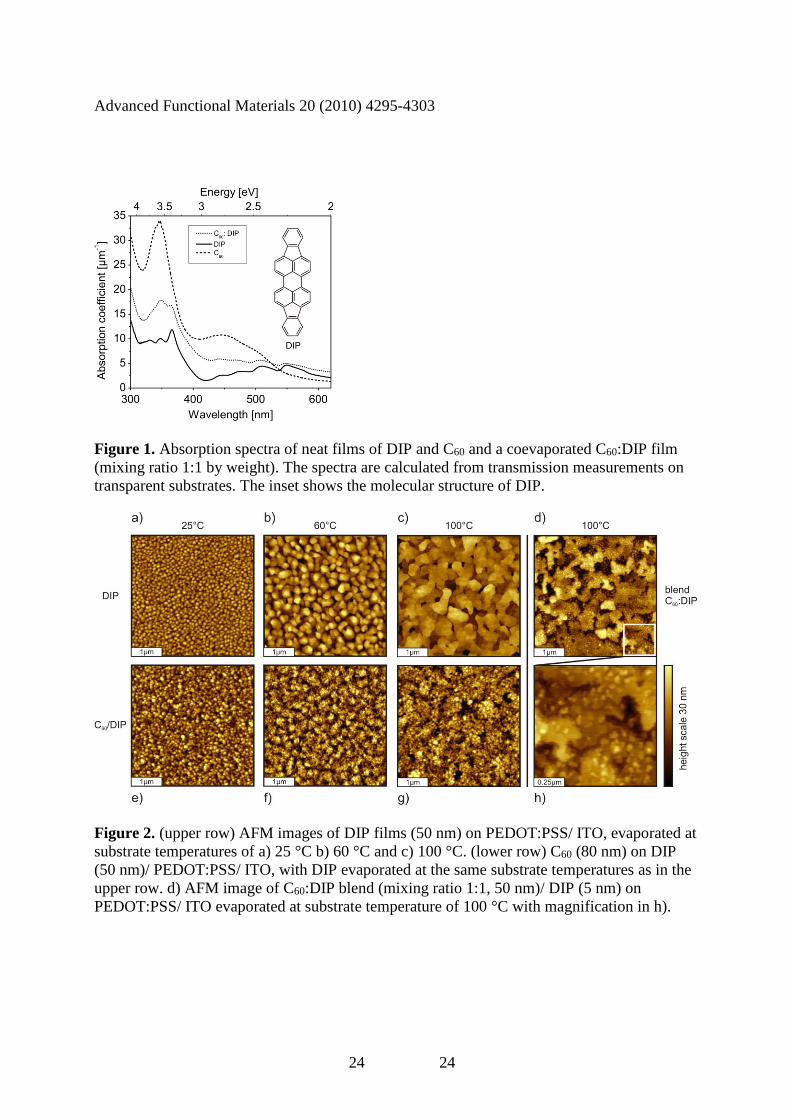
the absorption spectra of DIP and C60 are depicted in Fig. 1. DIP has been shown to exhibit
almost balanced transport of electrons and holes along the c' direction in single crystals[24] and
remarkably high exciton diffusion lengths of up to 100 nm[25] – although the magnitude of the
exciton diffusion length and its unique determination in thin films is still under
discussion.[26,27,28] It was further reported that DIP exhibits exceptionally high structural order
in evaporated thin films, with molecules standing almost upright with their long axis aligned
parallel to the surface normal on inert substrates.[29] This, in turn, confirms the large exciton
diffusion length as there is a correlation between structural coherence length and exciton
diffusion length.[30] Moreover, it was shown that these films exhibit a high hole mobility of up
to 0.1 cm2 V-1s-1 in field-effect transistor geometry, i.e., parallel to the substrate surface.[31] To
our knowledge, however, DIP has not yet been investigated in photovoltaic cells. Only
recently, a similarly constructed aromatic molecule, tetraphenyldibenzoperiflanthene (DBP),
was used in planar heterojunction OPVCs exhibiting an open-circuit voltage of 0.9 V and
power conversion efficiencies of up to 3.6 %,[32] but no correlations to film morphology,
energy level alignment and transport properties are available for this material. High values for

Advanced Functional Materials 20 (2010) 4295-4303
5 5
VOC (close to 1 eV) were also achieved using low bandgap oligothiophenes (DCVnT) as
donor material when combined with C60 as acceptor.[33,34] Even higher open circuit voltages
reaching 1.5 V have been obtained when blending suitable electron-donating and accepting
polymers, however, often showing low fill factors.[35,36,37, 38]
In the following we will discuss the influence of the substrate temperature during film growth
on the morphology and structural ordering of DIP films on solar cell relevant substrates.
Thereafter, we will present results on the energy level alignment in photovoltaic cells with C60
as acceptor and demonstrate how this affects the electrical characteristics of single junctions
both in the dark and under illumination before comparing the performance of planar and bulk
heterojunction cells under simulated sunlight conditions.
2. Morphological and structural investigation
For materials with short exciton diffusion length the morphology is a crucial parameter as it
determines on the one hand the magnitude of the photoactive volume where excitons can be
efficiently dissociated. On the other hand, even in a blend with large interfacial area the
successful formation of percolation paths in the donor and acceptor material is a prerequisite
for efficient charge carrier collection towards the electrodes.[39] Furthermore, transport
properties of both excitons and charges are strongly correlated to the crystalline order of the
involved materials. We have therefore grown DIP films at different substrate temperatures
and investigated their morphological and structural properties in neat films as well as in
heterostructures covered with C60 and in blends where DIP and C60 were coevaporated.
Figure 2 shows the surface topography (from atomic force microscopy (AFM)) of 50 nm
thick DIP films evaporated on tin-doped indium oxide (ITO)-coated glass substrates covered
with a hole injection layer of poly(3,4-ethylenedioxythiophene):poly(styrenesulfonate)
(PEDOT:PSS), which were heated to different temperatures during evaporation. We note that
all PEDOT:PSS films heated to different temperatures showed smooth, featureless topography
Advanced Functional Materials 20 (2010) 4295-4303
6 6
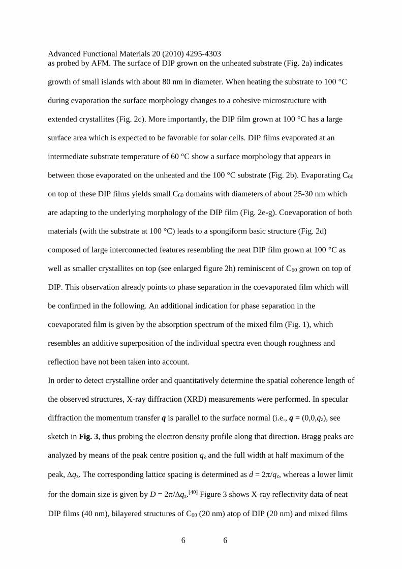
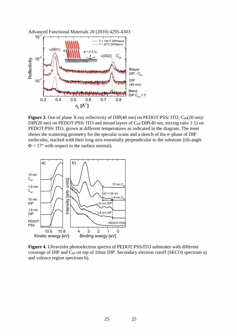
as probed by AFM. The surface of DIP grown on the unheated substrate (Fig. 2a) indicates
growth of small islands with about 80 nm in diameter. When heating the substrate to 100 °C
during evaporation the surface morphology changes to a cohesive microstructure with
extended crystallites (Fig. 2c). More importantly, the DIP film grown at 100 °C has a large
surface area which is expected to be favorable for solar cells. DIP films evaporated at an
intermediate substrate temperature of 60 °C show a surface morphology that appears in
between those evaporated on the unheated and the 100 °C substrate (Fig. 2b). Evaporating C60
on top of these DIP films yields small C60 domains with diameters of about 25-30 nm which
are adapting to the underlying morphology of the DIP film (Fig. 2e-g). Coevaporation of both
materials (with the substrate at 100 °C) leads to a spongiform basic structure (Fig. 2d)
composed of large interconnected features resembling the neat DIP film grown at 100 °C as
well as smaller crystallites on top (see enlarged figure 2h) reminiscent of C60 grown on top of
DIP. This observation already points to phase separation in the coevaporated film which will
be confirmed in the following. An additional indication for phase separation in the
coevaporated film is given by the absorption spectrum of the mixed film (Fig. 1), which
resembles an additive superposition of the individual spectra even though roughness and
reflection have not been taken into account.
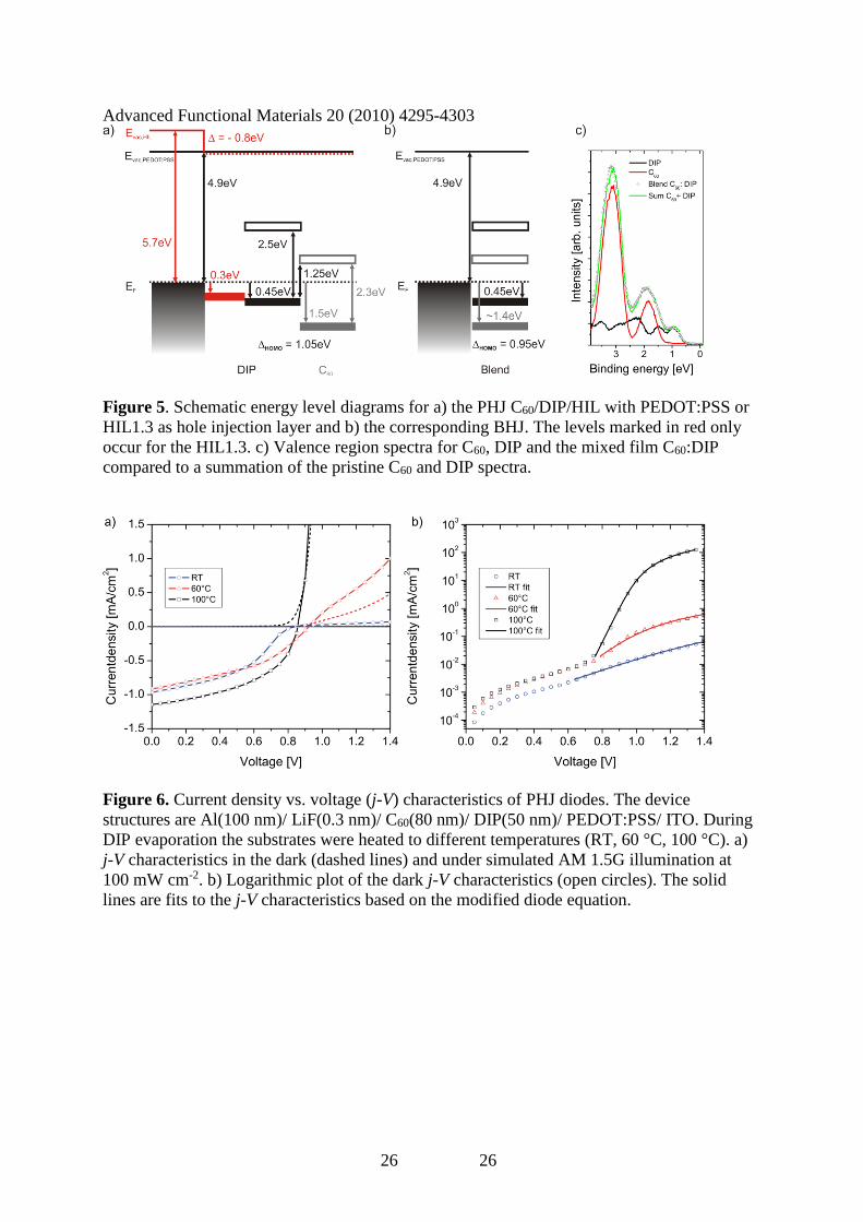
In order to detect crystalline order and quantitatively determine the spatial coherence length of
the observed structures, X-ray diffraction (XRD) measurements were performed. In specular
diffraction the momentum transfer q is parallel to the surface normal (i.e., q = (0,0,qz), see
sketch in Fig. 3, thus probing the electron density profile along that direction. Bragg peaks are
analyzed by means of the peak centre position qz and the full width at half maximum of the
peak, qz. The corresponding lattice spacing is determined as d = 2/qz, whereas a lower limit
for the domain size is given by D = 2/qz.[40] Figure 3 shows X-ray reflectivity data of neat
DIP films (40 nm), bilayered structures of C60 (20 nm) atop of DIP (20 nm) and mixed films

Advanced Functional Materials 20 (2010) 4295-4303
7 7
of DIP and C60 (40 nm, mixing ratio 1:1 by weight), all evaporated on PEDOT:PSS/ITO
substrates. The DIP films and the mixed C60:DIP layers were deposited at substrate
temperatures of 25 °C and 100 °C, respectively. For all samples, Bragg reflections at
qz = 0.378 Å-1 associated with a DIP lattice plane spacing of dDIP = 16.6 Å are observed. From
this it is deduced that crystalline domains with DIP molecules standing almost upright are
formed on PEDOT:PSS/ITO (tilt angle ≈ 17°,[41] denoted as -phase[29,40]) as schematically
sketched in Fig. 3. The upright standing arrangement of the DIP molecules is consistent with
the low absorption coefficient of neat DIP films (see Fig.1), as the transition dipole moment
of the fundamental molecular absorption is aligned along the long molecular axis and thus
unfavorably oriented for efficient absorption of light under normal incidence. DIP Bragg
reflections from films evaporated at 100 °C are more intense compared with films grown at
room temperature, which is a clear evidence for higher crystallinity.
In contrast to previous studies on neat C60 films evaporated on PEDOT:PSS/ITO[16] the XRD
spectra of C60 evaporated on DIP (grown at substrate temperatures of 25 °C and 100 °C) show
comparatively pronounced Bragg reflections of C60 at qz ≈ 0.775 Å-1 superimposed with the
DIP(002) reflection. This exceptional behavior may be attributed to improved growth
properties of C60 on top of the well ordered DIP structure. Laue oscillations around the
DIP(001) Bragg reflections of the neat DIP film and the C60/DIP bilayer structure are clear
evidence for coherently ordered domains, whose magnitude correspond to the whole DIP
layer thickness in both cases. Mixed DIP:C60 layers show the same DIP Bragg peak positions
as neat DIP, which confirms the appearance of phase separation in coevaporated films.
However, there is no measurable C60 Bragg reflection in the blends, which indicates low out-
of-plane order for C60 crystallites. Nevertheless, the comparably narrow width qz of the
DIP(001) Bragg peak in the mixture corresponds to a coherence length of D ≈ 45 nm, which
is approximately equal to the entire layer thickness, indicating that crystalline DIP domains
Advanced Functional Materials 20 (2010) 4295-4303
8 8
extend throughout the whole film. This is in full agreement with AFM measurements (cf.
Fig. 2) depicting the blend of DIP and C60 as cohesive structures of DIP with small C60
crystallites in between. Further details including grazing incidence X-ray diffraction data are
given in section A of the Supporting Information.
3. Electronic structure
DIP and C60 thickness dependent UPS (ultraviolet photoelectron spectroscopy) investigations
of sample structures as they are used in OPVCs were performed in order to assess the energy
level alignment in these devices. Two different commercially available PEDOT:PSS
containing formulations were used: Clevios™ P AI4083 (designated as PEDOT:PSS) and
Clevios™ HIL1.3 (designated as HIL1.3) providing two hole injection layers (HIL) with
different work functions (see below). Specifically, the material sequences (i)
C60/DIP/PEDOT:PSS, (ii) C60/DIP/HIL1.3 and (iii) C60:DIP(codeposited)/PEDOT:PSS were
chosen. While (i) and (iii) allow to compare energy levels in PHJ and BHJ structure, (ii)
allows the determination of the positive pinning level of DIP and the electronic structure at
the interface to the hole extracting electrode in the pinning regime,[42] because HIL1.3 has a
higher work function as compared to the standard PEDOT:PSS (see also section B of the
Supporting Information).
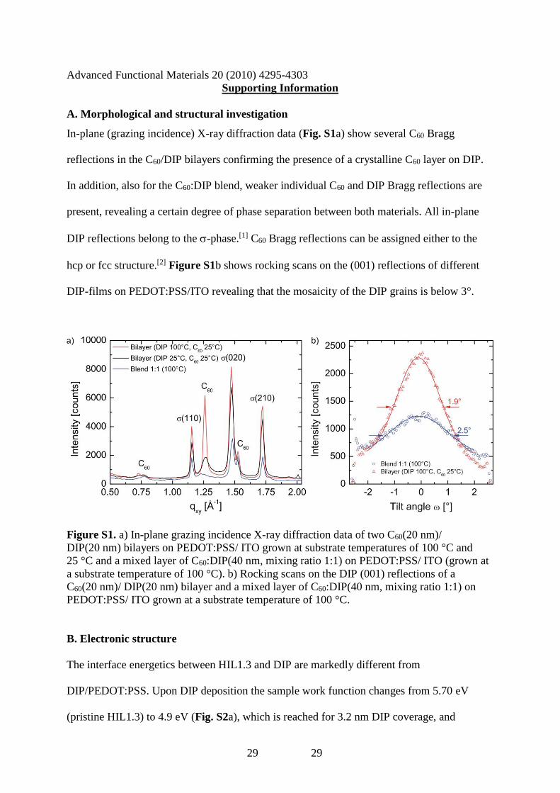
Fig. 4a and b show thickness dependent UPS spectra (only one monolayer and one multilayer
spectrum are shown for clarity) of the planar heterojunction (PHJ) interface of C60/DIP
formed on PEDOT:PSS, with an initial conducting polymer work function of 4.9 eV
(secondary electron cut-off (SECO) spectra in Fig. 4a). The deposition of DIP on
PEDOT:PSS does not change the sample work function, i.e., no interfacial dipole is formed,
indicating that energy level pinning of DIP does not yet occur at this electrode work function.
No sample work function change is observed at the C60/DIP interface as well, i.e., vacuum
level alignment at this donor/acceptor interface is valid. From the valence region spectra

Advanced Functional Materials 20 (2010) 4295-4303
9 9
(Fig. 4b) we infer that the low binding energy (BE) onset of the DIP HOMO directly at the
interface (1.6 nm coverage) to PEDOT:PSS and for the multilayer (10 nm coverage) is at the
same distance from the Fermi-Energy EF, with a value of 0.45 eV. This value corresponds to
the hole injection barrier at the electrode-donor interface and, adding the sample work
function of 4.9 eV, yields a DIP ionization energy of 5.35 eV. The valence spectra for C60 on
10 nm DIP/PEDOT:PSS show that the low BE onset of the acceptor HOMO is at 1.50 eV,
both for the C60 mono- and multi-layer. Consequently, the HOMO offset between the donor
DIP and the acceptor C60 at this interface is 1.05 eV.
The energy level alignment at the C60/DIP interface is unchanged when using the high work
function HIL1.3 as electrode, i.e., vacuum level alignment prevails and the HOMO offset is
1.05 eV (see section B of the Supporting Information). However, the interface energetics
between HIL1.3 and DIP are markedly different from DIP/PEDOT:PSS. Upon DIP deposition
the sample work function changes from 5.70 eV (pristine HIL1.3) to 4.9 eV (see Supporting
Information). This observation is consistent with pinning of the DIP energy levels due to the
high initial work function of HIL1.3. Because the work function of multilayer DIP on both
PEDOT:PSS and HIL1.3 is identical (4.9 eV), we can conclude that this is the critical
substrate work function for energy level pinning of DIP.[42] We note that the work function of
both HILs, in particular PEDOT:PSS, depends critically on the residual water content in the
conductive polymer film; with decreasing water content, e.g., induced by film annealing in
vacuum, the work function increases up to 5.6 eV.[43] Therefore, it is reasonable to argue that
DIP/PEDOT:PSS contacts in devices fabricated at elevated substrate temperatures exhibit
lower contact resistance. The energy level structure at C60/DIP/HIL interfaces is schematically
summarized in Fig. 5a, where the energy levels highlighted in red only occur when HIL1.3 is
used. The C60/DIP interface energetics relevant for PHJ devices are identical for both
PEDOT:PSS formulations. Assuming a transport gap for C60 of 2.3 eV[44] and for DIP of
Advanced Functional Materials 20 (2010) 4295-4303
10 10
2.5 eV[45], the offset between the DIP HOMO and the C60 LUMO is 1.25 eV, which is an
estimate of the maximum achievable open circuit voltage in OPVCs.[46]
In Fig. 5b we show the energy level alignment for bulk heterojunction C60:DIP, obtained by
co-deposition of donor and acceptor material (1:1 ratio) on PEDOT:PSS. The energy levels
are almost identical to the PHJ case, only the low BE onset of the HOMO level of C60 is
found 0.1 eV closer to EF, as inferred from a fitting routine of the mixed film UPS spectra by
summation of pristine C60 and DIP spectra (Fig. 5c). Consequently, the HOMO offset for the
BHJ is 0.95 eV, and the offset between the DIP HOMO and the C60 LUMO is 1.35 eV. Thus,
compared to the intermolecular HOMO-LUMO gap of the planar configuration (1.25 eV)
similar values for VOC are expected in PHJ and BHJ solar cells.
4. Electrical characterization - dependence on growth conditions
To demonstrate the importance of film growth conditions, we investigated the current-voltage
(j-V) characteristics of nominally planar heterojunctions between DIP (grown at different
substrate temperature) and C60 evaporated on top (with the underlying DIP film then kept at
room temperature). This allows for a direct comparison between film morphology and the
resulting electrical properties in a solar cell architecture. The structure of the investigated PHJ
cells is Al(100nm)/ LiF (lithium fluoride, 0.5nm)/ C60(80nm)/ DIP(50nm)/ PEDOT:PSS/ ITO,
with DIP evaporated at substrate temperatures of 25 °C, 60 °C, and 100 °C.
Figure 6 shows the j-V characteristics for the cells in dark (dashed lines) and under one sun
simulated AM1.5G solar illumination (solid lines). In the following discussion we focus on
the shape of the j-V characteristics in the forward bias regime. A detailed analysis with regard
to photovoltaic properties of planar and bulk heterojunction solar cells will be the subject of
section 5. All different substrate temperatures yield short circuit current densities (jSC) in the
range between -0.8 and -1.2 mA cm-2 and VOC between 0.85 V and 0.92 V. The j-V
characteristics of the device where DIP was grown at room temperature are strongly affected

Advanced Functional Materials 20 (2010) 4295-4303
11 11
by an S-shape behavior, i.e. they show a decrease of the current close to the open-circuit
voltage, which will reduce the fill factor in a solar cell, and also very low current above VOC.
This feature decreases continuously when heating the substrate to higher temperatures during
DIP deposition and vanishes completely for the device with DIP grown at 100 °C.
The occurrence of the undesired S-shape in the current-voltage characteristics under
illumination is correlated to suppressed forward currents being apparent already in the dark
j-V characteristics, as displayed in Fig 6b on a semi-logarithmic scale.
The forward-bias characteristics can be fitted (solid lines) using the modified Shockley
equation:[47]
( )
−
−= 1exp
nkT
jRVejj SS , (1)
where jS is the reverse-bias saturation current density, n the ideality factor, e the electron
charge, RS a series resistance, k Boltzmann’s constant, and T the temperature. The slope of the
j-V characteristics in the exponential regime depends on jS and the ideality factor n. In our
devices we find an ideality factor of about 1.5 for the planar heterojunction diode with DIP
evaporated at a substrate temperature of 100 °C. For the other substrate temperatures the
determination of n is difficult due to the presence of the leakage currents. The most noticeable
difference in the dark j-V characteristics, however, is the continuous decrease of the series
resistance RS when the substrate temperature during DIP evaporation is raised. Thus, RS
decreases by almost three orders of magnitude from 42 k at room temperature to 55 at
100 °C substrate temperature, causing the systematic decline of the S-shape in the j-V curves
until complete vanishing at 100 °C.
S-shaped solar cell characteristics have recently gained more and more attention in the
literature and are commonly ascribed to energetic injection and extraction barriers between
the photoactive layer system and the electrodes.[48,49,50] In the present case, the S-shaped
Advanced Functional Materials 20 (2010) 4295-4303
12 12
characteristics are clearly connected to the growth temperature of the DIP layer. Together
with the arguments given in the previous section for a reduction of the hole injection barrier
on heated PEDOT:PSS and DIP layer thickness variations (not shown here) it indicates the
decisive role of charge carrier injection and transport in DIP, which are both drastically
improved when the substrate is heated to 100 °C.
5. Application of DIP in solar cells
The applicability of DIP as donor material has already been demonstrated in the previous
section, although the focus was more on the transport behavior of DIP films evaporated at
different substrate temperatures. For a detailed analysis of photovoltaic properties the device
stack using DIP and C60 as photoactive materials was extended by an additional exciton
blocking material bathocuproine (BCP). The beneficial effect of BCP on solar cell
performance has been demonstrated by various studies, all describing its property to prohibit
quenching of excitons at the electrode and to act as diffusion barrier for Al and as protection
layer to eliminate the creation of Al-induced defect states in C60.[51,52,53]
Planar as well as planar-mixed heterojunction (PM-HJ) devices with different thicknesses of
the organic layers have been fabricated and compared to each other. The PM-HJ is a
combination of a strict planar heterojunction and a mixed layer bulk-heterojunction within the
same structure and is known to unify the benefits of both concepts.[54] Thus, it takes maximum
advantage of the unhindered charge carrier collection properties of neat organic layers, and
the improved exciton dissociation properties of films consisting of a mixture of donor and
acceptor materials. The exact layer sequences of the investigated PHJ solar cells (device A
and C) and the PM-HJ cells (device B and D) are given in Fig. 7a. According to the above
discussed electrical properties of C60/DIP heterojunctions dependent on different substrate
temperatures, the investigation of photovoltaic properties is restricted to cells where DIP and
mixed C60:DIP films were deposited on substrates heated to 100 °C.

Advanced Functional Materials 20 (2010) 4295-4303
13 13
The obtained current density-voltage (j-V) characteristics under one sun simulated AM1.5
illumination are shown in Fig. 7b and the corresponding photovoltaic parameters are
summarized in Table 1. In general, all four devices show almost identical open-circuit voltage
VOC slightly above 0.9 V and differ only in their short-circuit currents jSC and fill factors (FF).
The short-circuit currents are considerably higher in the PM-HJ solar cells (devices B and D)
as compared to the corresponding PHJ structures (devices A and C). Excitons which are
created in the mixed layer are always in proximity of a donor-acceptor interface and can thus
easily be dissociated. Furthermore, excitons created in the adjacent layer of neat DIP may also
contribute to the photocurrent, as the layer thicknesses of 5 and 15 nm are well below the
exciton diffusion length.[25]
Successful realization of the bulk heterojunction concept requires the formation of percolation
pathways inside the mixed film, which is necessary for efficient charge carrier transport. From
the morphological and structural analysis of mixed C60:DIP films (see section 2) it can be
deduced that both materials exhibit phase separation in the blend and form percolation paths
for both carrier types. However, the decrease in jSC from device B to D demonstrates the
limits of the bulk heterojunction concept: with the increase in layer thickness, recombination
losses due to the presence of both phases in close proximity exceed the gain in absorption
efficiency and finally reduce jSC.[55,56]
Comparing the PHJ devices A and C, jSC is markedly increased from device A to device C
due to the larger film thicknesses of DIP and C60 in device C, leading to improved absorption
of incoming light and exciton generation. The essential requirement for this enhancement is
the high crystallinity and the concomitant large exciton diffusion length of DIP, facilitating
efficient charge carrier dissociation and collection, respectively, even for enlarged film
thickness.

Advanced Functional Materials 20 (2010) 4295-4303
14 14
The second parameter, in which the investigated cells differ in a characteristic way, is the fill
factor. Both PHJ cells have a higher FF than the PM-HJ devices, at least at high light
intensities (further details are given in section C of the Supporting Information) and in
particular for the thick PHJ device C it reaches exceptionally high values exceeding 74 % at
one sun. This is - to the best of our knowledge - one of the highest fill factors observed for
organic small molecule solar cells. It indicates highly efficient charge carrier transport
towards the electrical contacts with little recombination losses[56] - despite of comparatively
thick layers - as well as unhindered charge carrier extraction without energetic barriers.[12,48]
The fill factors of both PM-HJ cells are significantly below the values of device C, peaking at
light intensities of about10 mW cm-2 (device B: 58 %, device D: 55 %). Inherently higher
bulk recombination and lower carrier mobility in the mixed layer probably limit charge
collection efficiency and thereby the FF of these devices.[10,11]
As already mentioned, all devices reach open circuit voltages in excess of 0.9 V at one sun
simulated AM1.5 illumination (see also section C of the Supporting Information). Thereby the
VOC of device C is slightly higher than for the other three devices. It is remarkable that the
PM-HJ devices B and D reach almost the same values as the best PHJ device, while pure
bulk-heterojunction devices (not shown here) have lower VOC (0.6 - 0.7 V). This can be seen
as a further advantage of the hybrid PM-HJ concept over the BHJ device: in the latter VOC
may be limited by the built-in voltage VBI, because recombination of charge carriers at the
interface between an electrode and the mixed layer immediately sets in as soon as the applied
voltage exceeds VBI.[48] The neat donor and acceptor layers encompassing the mixed layer in
the PM-HJ cell suppress this direct recombination and thus enable VOC to reach values as high
as for PHJ devices.
The comparison of different device architectures shows that power conversion efficiency
around PCE ≈ 4 % can be reached with a hybrid planar-mixed heterojunction structure with
Advanced Functional Materials 20 (2010) 4295-4303
15 15
BCP as exciton blocking layer. Nevertheless, the hybrid PM-HJ cell suffers from transport
losses in the mixed layer, which limit the FF to values not exceeding 53 % at one sun. As
compared to this PM-HJ structure, the lower current in the planar heterojunction cells is
almost completely compensated by their extremely high FF achieving equally high power
conversion efficiency.
Finally, we would like to discuss the performance of the investigated cells in comparison to
C60/CuPc, which is a widely used prototype small molecule OPVC system.[20,45,57,58,59] For
that purpose we have put together solar cell parameters obtained by us on C60/CuPc devices
fabricated and measured under comparable conditions (see Table 1, lines 5 and 6).
The most prominent difference is the open-circuit voltage being only about 0.5 V for
C60/CuPc cells. Theoretically the maximum value of VOC is related to the difference between
the HOMO energy of the donor and the LUMO level of the acceptor, minus the binding
energy of the dissociated, geminate electron-hole pair.[46] Comparing the energy level
alignment for C60/DIP cells as discussed in section 3 and as reported by us in Ref. [23] for
C60/CuPc one comes to the conclusion that both from the point of view of the HOMO-LUMO
gap at the DA interface as well as the built-in voltage, resulting from the differences in the
effective electrode work functions, C60/DIP cells are expected to have an open-circuit voltage
that is approximately larger by 0.5 V – fully consistent with the experimentally observed
numbers.
Regarding the short-circuit currents both types of C60/CuPc cells are clearly ahead of the
corresponding DIP based devices, however, this is simply related to the larger absorption
coefficient of CuPc (peak value 20.6 µm-1[45]) and the better spectral coverage in the long
wavelength range (bands in the range 550-780 nm[45]). Given the fact that the maximum
absorption coefficient of DIP in the visible spectral range (420-580 nm) is about four times

Advanced Functional Materials 20 (2010) 4295-4303
16 16
lower than for CuPc, the reduction of the photocurrent (by only about 25 %) for DIP cells is
remarkably small and points towards very good carrier collection.
The lower fill factors for C60/CuPc are indicative for stronger recombination losses in this
material system. This can be ascribed to a significantly lower hole mobility in neat CuPc as
compared to DIP[31,60] and to a further reduction of the mobility in C60:CuPc blends due to the
small scale phase separation (see Ref. [45]). By contrast, the morphology of the DIP phase in
both architectures (PHJ and PM-HJ) is characterized by large, cohesive crystalline structures,
allowing for favorable transport properties and thus less recombination losses.[61]
6. Conclusions
In conclusion, we have presented a comprehensive analysis of the new donor material
diindenoperylene (DIP) in combination with the fullerene C60 ranging from growth studies
and energy level alignment via electrical transport properties and finally to its successful
application in organic solar cells. Our studies emphasize the crucial influence of the substrate
temperature during DIP film growth on the morphology and thus the overall performance of
DIP based photovoltaic cells. Growth at elevated temperature leads to the formation of a
cohesive network of crystalline DIP domains, yielding a large surface area that can be covered
with C60 molecules in planar heterojunctions, or to a phase separated bicontinuous network in
bulk-heterojunctions when DIP and C60 are coevaporated. Favorable film morphology
together with high crystalline order allows for improved transport properties of both excitons
and charges in photovoltaic cells. The main advantage of DIP can be found in its high
ionization potential and the favorable energy level alignment with both the PEDOT:PSS
electrode and the C60 acceptor leading to high open circuit voltages of up to 0.93 V under
100 mW cm-2 simulated AM1.5G illumination. Simply stacked PHJ devices – devoid of
doped transport layers - yield remarkably high fill factors up to 74 % and a power conversion
efficiency close to 4 %.
Advanced Functional Materials 20 (2010) 4295-4303
17 17
For future work, it will be important to improve the absorption properties of films
incorporating DIP as donor material while keeping its good transport properties and favorable
energy level alignment with C60. One promising strategy might be found in modifying the
orientation of the molecules: Achieving flat lying DIP molecules (so-called -phase[40]) could
yield an increase in the absorption coefficient by a factor of ~ 6[62] holding a large potential
for further increasing solar cell efficiencies. Furthermore, the combination with a second
donor-acceptor system absorbing in the longer wavelength range in a tandem cell could boost
power conversion efficiencies to application relevant values.[63,64,65,66]
7. Experimental
Photovoltaic cells were fabricated on commercially available photolithographically structured
tin-doped indium oxide (ITO)-coated glass substrates (Merck, sheet resistance per
square < 10 ) which were subsequently cleaned in ultra sonic bath with acetone and
isopropanol prior to processing. An oxygen plasma treatment was implemented to improve
wetability for the aqueous suspension of the intrinsically conducting polymer poly(3,4-
ethylenedioxythiophene):poly(styrenesulfonate) (PEDOT:PSS in a ratio of 1:6 by weight,
purchased from H.C. Starck as Clevios™ P AI4083). The polymer was deposited via spin
coating, and annealed at 125 °C for 45 minutes under ambient conditions.
DIP (purchased from W. Schmidt Institut für PAH-Forschung) and C60 (purchased from
Creaphys) have been twice purified by vacuum gradient sublimation prior to use, while BCP
(purchased from Acros Organics) was used as-received. Materials were sequentially grown by
vacuum thermal evaporation at base pressures of 10-6 - 10-7 mbar with the following rates:
DIP (0.5 Ås-1 in neat film, 0.3 Ås-1 in blend), C60 (0.5 Ås-1 in neat film, 0.3 Ås-1 in blend),
BCP (0.2 Ås-1), LiF (0.2 Ås-1), and Al (1 Ås-1). The metal cathodes (typically 1000 Å thick)
were evaporated through a shadow mask resulting in solar cells with an area of 4 mm2. The
Advanced Functional Materials 20 (2010) 4295-4303
18 18
entire cell preparation as well as the electrical measurements has been performed without air
exposure; i.e. under inert gas atmosphere or in vacuum.
Current-voltage characteristics were recorded using a source measure unit (Keithley 236
SMU) in dark and under illumination with a solar simulator (Oriel 150W with AM 1.5G
filters). The illumination intensity was approved by a calibrated silicon reference cell (RERA
systems, PV Measurement Facility, Radboud University Nijmegen, area 1×1 cm2).
Nevertheless, as the perfect homogeneity of the light beam cannot be guaranteed, the power
conversion efficiency of our OPVCs with an area smaller than the reference cell might be
slightly overestimated. Furthermore, the measured photocurrents have not been corrected for
spectral mismatch.
Absorption spectra were obtained from transmission measurements of organic films grown on
transparent substrates using a Varian Cary 50 UV-Vis spectrophotometer with a spectral
range from 280 to 1000 nm. AFM measurements were performed using a Thermo
Microscopes Autoprobe CP-Research in non-contact mode. X-ray reflectivity measurements
were conducted on a GE/Seifert X-ray diffractometer (Cu K1 radiation, multilayer mirror,
and double bounce compressor monochromator). Grazing incidence X-ray diffraction
measurements were performed on the X04SA beamline at the Swiss Light Source, Paul
Scherrer Institut, Villigen, Switzerland (12 keV photon energy). X-ray scattering, AFM, and
optical absorption measurements were performed under ambient conditions on solar cell
relevant substrates.
Ultraviolet photoelectron spectroscopy (UPS) measurements were performed at the endstation
SurICat at the synchrotron radiation source BESSY II - HZB. Spectra were recorded with a
hemispherical energy analyzer (resolution set to 100 meV) with 35 eV photon energy. The
secondary electron cut-off (SECO) was recorded with the sample biased at -10 V to clear the
analyzer work function. By repeated measurements performed with the samples kept in dark
Advanced Functional Materials 20 (2010) 4295-4303
19 19
and with additional visible light illumination we established that sample charging did not
occur. Two different hole injection layers were used in the UPS experiments: Clevios™ P
AI4083 (designated as PEDOT:PSS) and Clevios™ HIL1.3 (designated as HIL1.3) as a
PEDOT-containing dispersion for HILs provided by H.C. Starck [67]. Both hole injection
layers were deposited on cleaned ITO via spin coating, and annealed at 200 °C for 5 minutes
under ambient conditions. Samples were introduced subsequently into UHV conditions where
deposition of C60 and DIP followed (substrates at room temperature), from resistively heated
crucibles with evaporation rates of ca. 1 Å min-1. The film thickness was monitored with a
quartz crystal microbalance. Sample transfer between preparation chamber (base
pressure < 3×10⁻⁸ mbar) and analysis chamber (base pressure 1×10⁻¹⁰ mbar) was done without
breaking UHV conditions.
Acknowledgements
We thank Steven Leake for technical support at the Swiss Light Source and Jens Pflaum at the
University of Würzburg for fruitful discussions. This work was supported by the Deutsche
Forschungsgemeinschaft (DFG) within the Priority Program 1355 (”Elementary Processes of
Organic Photovoltaics”). Supporting Information is available online from Wiley InterScience
or from the author.
Received: ((will be filled in by the editorial staff))
Revised: ((will be filled in by the editorial staff))
Published online: ((will be filled in by the editorial staff))
_[1] A. K. Ghosh and T. Feng, J. Appl. Phys. 1973, 44, 2781.
_[2] C. W. Tang, Appl. Phys. Lett. 1986, 48, 183.
_[3] J. J. M. Halls, C. A. Walsh, N. C. Greenham, E. A. Marseglia, R. H.
Friend, S. C. Moratti, and A. B. Holmes, Nature 1995, 376, 498.
_[4] G. Yu, J. Gao, J. C. Hummelen, F. Wudl, and A. J. Heeger, Science 1995, 270, 1789.
_[5] M. A. Green, K. Emery, Y. Hishikawa, and W. Warta, Prog. Photovolt: Res. Appl.
2010, 18, 346.

Advanced Functional Materials 20 (2010) 4295-4303
20 20
_[6] See http://www.solarmer.com.
_[7] See http://www.heliatek.com.
_[8] B. P. Rand, J. G. Xue, S. Uchida, and S. R. Forrest, J. Appl. Phys. 2005, 98, 124902.
_[9] A. Opitz, M. Bronner, and W. Brütting, J. Appl. Phys. 2007, 101, 063709.
_[10] M. M. Mandoc, W. Veurman, L. J. A. Koster, B. Boer, and P. W. M. Blom, Adv.
Funct. Mater. 2007, 17, 2167.
_[11] M. Schubert, C. Yin, M. Castellani, S. Bange, T. L. Tam, A. Sellinger, H. -H. Hörhold,
T. Kietzke, and D. Neher, J. Chem. Phys. 2009, 130, 094703.
_[12] B. P. Rand, J. Genoe, P. Heremans, and J. Poortmans, Prog. Photovolt: Res. Appl.
2007, 15, 659.
_[13] P. Peumans, S. Uchida and S. R. Forrest, Nature 2003, 425, 158.
_[14] S. Yoo, B. Domercq and B. Kippelen, Appl. Phys. Lett. 2004, 85, 5427.
_[15] K. Schulze, C. Uhrich, R. Schüppel, K. Leo, M. Pfeiffer, P. Bäuerle, E. Brier, and E.
Reinold, Adv. Mater. 2006, 18, 2872.
_[16] A. Opitz, J. Wagner, M. Bronner, W. Brütting, A. Hinderhofer, and F. Schreiber, Phys.
Status Solidi A 2009, 206, 2683.
_[17] K. Vandewal, K. Tvingstedt, A. Gadisa, O. Inganäs, J.V. Manca, Nat. Mater. 2009, 8,
904.
_[18] P. A. van Hal, R. A. J. Janssen, G. Lanzani, G. Cerullo, M. Zavelani-Rossi, and S. D.
Silvestri, Chem. Phys. Lett. 2001, 345, 33.
_[19] P. Peumans and S. R. Forrest, Appl. Phys. Lett. 2001, 79, 126.
_[20] S. M. Schultes, P. Sullivan, S. Heutz, B. M. Sanderson, T. S. Jones, Mat. Sci. Eng. C -
Biomim. 2005, 25, 858.
_[21] W. J. Potscavage, S. Yoo, and B. Kippelen, Appl. Phys. Lett. 2008, 93, 193308.

Advanced Functional Materials 20 (2010) 4295-4303
21 21
_[22] M. F. Lo, T. W. Ng, T. Z. Liu, V. A. L. Roy, S. L. Lai, M. K. Fung, C. S. Lee, and S.
T. Lee, Appl. Phys. Lett. 2010, 96, 113303.
_[23] A. Wilke, T. Mizokuro, R.-P. Blum, J. P. Rabe, and N. Koch, IEEE J. Sel. Top. Quant.
2010, in press.
_[24] A. K. Tripathi and J. Pflaum, Appl. Phys. Lett. 2006, 89, 082103.
_[25] D. Kurrle and J. Pflaum, Appl. Phys. Lett. 2008, 92, 133306.
_[26] S. B. Rim and P. Peumans, J. Appl. Phys. 2008, 103, 124515.
_[27] R. R. Lunt, N. C. Giebink, A. A. Belak, J. B. Benziger, S. R. Forrest, J. Appl. Phys.
2009, 105, 053711.
_[28] S. Banerjee, A. P. Parhi, S. S. K. Iyer, and S. Kumar Appl. Phys. Lett. 2009, 94,
223303.
_[29] C. Dürr, F. Schreiber, M. Münch, N. Karl, B. Krause, V. Kruppa, and H. Dosch, Appl.
Phys. Lett. 2002, 81, 2276.
_[30] R. R. Lunt, J. B. Benziger, S. R. Forrest, Adv. Mater. 2010, 22, 1233.
_[31] N. Karl, Synth. Met. 2003, 133–134, 649.
_[32] D. Fujishima, H. Kanno, T. Kinoshita, E. Maruyama, M. Tanaka,
M. Shirakawa, and K. Shibata, Sol. Ener. Mater. Sol. Cell. 2009, 93, 1029.
_[33] R. Schueppel, K. Schmidt, C. Uhrich, K. Schulze, D. Wynands, J. L. Bredas, E. Brier,
E. Reinold, H. B. Bu, P. Bäuerle, B. Männig, M. Pfeiffer, and K. Leo, Phys. Rev. B 2008, 77,
085311.
_[34] D. Wynands, B. Männig, M. Riede, K. Leo, E. Brier, E. Reinold, and P. Bäuerle, J.
Appl. Phys. 2009, 106, 054509.
_[35] C. M. Ramsdale, J. A. Barker, A. C. Arias, J. D. MacKenzie, R. H. Friend, and N. C.
Greenham, J. Appl. Phys. 2002, 92, 4266.

Advanced Functional Materials 20 (2010) 4295-4303
22 22
_[36] M. Svensson, F. Zhang, S. C. Veenstra, W. J. H. Verhees, J. C. Hummelen, J. M.
Kroon, O. Inganäs, and M. R. Andersson, Adv. Mater. 2003, 15, 988.
_[37] T. Kietzke, D. A. M. Egbe, H.-H. Hörhold, and D. Neher, Macromolecules 2006, 39,
4018.
_[38] Z. E. Ooi, T. L. Tam, R. Y. C. Shin, Z.-K. Chen, T. Kietzke, A. Sellinger, M.
Baumgarten, K. Muellen and J. C. deMello, J. Mater. Chem. 2008, 18, 4619.
_[39] R.A. Marsh, C. Groves, N.C. Greenham, J. Appl. Phys. 2007, 101, 083509.
_[40] A. C. Dürr, N. Koch, M. Kelsch, A. Rühm, J. Ghijsen, R. L. Johnson, J.-J. Pireaux, J.
Schwartz, F. Schreiber, H. Dosch, and A. Kahn, Phys. Rev. B 2003, 68, 115428.
_[41] A. C. Dürr, F. Schreiber, K. A. Ritley, V. Kruppa, J. Krug, H. Dosch, and B. Struth,
Phys. Rev. Lett. 2003, 90, 016104.
_[42] N. Koch, ChemPhysChem 2007, 8, 1438.
_[43] N. Koch, A. Vollmer, A. Elschner, Appl. Phys. Lett. 2007, 90, 043512.
_[44] R. W. Lof, M. A. Vanveenendaal, B. Koopmans, H. T. Jonkman, and G. A. Sawatzky,
Phys. Rev. Lett. 1992, 68, 3924.
_[45] A. Opitz, J. Wagner, W. Brütting, I. Salzmann, N. Koch, J. Manara, J. Pflaum, A.
Hinderhofer, F. Schreiber, IEEE J. Sel. Top. Quant. 2010, in press.
_[46] B. P. Rand, D. P. Burk, and S. R. Forrest, Phys. Rev. B 2007, 75, 115327.
_[47] S. M. Sze, Physics of Semiconductor Devices, 3rd ed., John Wiley & Sons, New York,
1981.
_[48] Uhrich, D. Wynands, S. Olthof, M. K. Riede, K. Leo, S. Sonntag, B. Maennig, and M.
Pfeiffer, J. Appl. Phys. 2008, 104, 043107.
_[49] J. Nelson, J. Kirkpatrick, and P. Ravirajan, Phys. Rev. B 2004, 69, 035337.
_[50] A. Kumar, S. Sista, and Y. Yang, J. Appl. Phys. 2009, 105, 094512.
_[51] P. Peumans, V. Bulović, and S. R. Forrest, Appl. Phys. Lett. 2000, 76, 2650.

Advanced Functional Materials 20 (2010) 4295-4303
23 23
_[52] N. Li, B. E. Lassiter, R. R. Lunt, G. Wei, and S. R. Forrest, Appl. Phys. Lett. 2009, 94,
023307.
_[53] H. Gommans, B. Verreet, B. P. Rand, R. Muller, J. Poortmans, P. Heremans, and J.
Genoe, Adv. Funct. Mater. 2008, 18, 3686.
_[54] J. G. Xue, B. P. Rand, S. Uchida, S. R. Forrest, Adv. Mater. 2005, 17, 66.
_[55] J. G. Xue, B. P. Rand, S. Uchida, and S. R. Forrest, J. Appl. Phys. 2005, 98, 124903.
_[56] T. Kirchartz, K. Taretto, and U. Rau, J. Phys. Chem. C 2009, 113, 17958.
_[57] P. Sullivan, S. Heutz, S. M. Schultes, and T. S. Jones, Appl. Phys. Lett. 2004, 84, 1210.
_[58] S. Heutz, P. Sullivan, B. M. Sanderson, S. M. Schultes, and T. S.
Jones, Sol. Ener. Mater. Sol. Cell. 2004, 83, 229.
_[59] P. Peumans and S. R. Forrest, Appl. Phys. Lett. 2001, 79, 126.
_[60] R. W. I. de Boer, A. F. Stassen, M. F. Craciun, C. L. Mulder, A. Molinari, S. Rogge, A.
F. Morpurgo, Appl. Phys. Lett. 2005, 86, 262109.
_[61] C. Deibel, Phys. Status Solidi A 2009, 206, 2731.
_[62] U. Heinemeyer, R. Scholz, L. Gisslén, M. I. Alonso, J. O. Ossó, M. Garriga, A.
Hinderhofer, M. Kytka, S. Kowarik, A. Gerlach, and F. Schreiber, Phys. Rev. B 2008, 78,
085210.
_[63] J. Y. Kim, K. Lee, N. E. Coates, D. Moses, T. Q. Nguyen, M. Dante, and A. J. Heeger,
Science 2007, 317, 222.
_[64] T. Ameri, G. Dennler, C. Lungenschmied and C. J. Brabec, Energy
Environ. Sci. 2009, 2, 347.
_[65] P. Peumans, A. Yakimov and S. R. Forrest, J. Appl. Phys. 2003, 93, 3693.
_[66] R. Timmreck, J. Meiss, A. Merten, R. Schueppel, M. Furno, C. Uhrich, W.-M. Gnehr,
M. Pfeiffer, M. Riede, and K. Leo, Proc. EU PVSEC 24, 2009, 89.
_[67] Product datasheet available at http://www.clevios.com.
Advanced Functional Materials 20 (2010) 4295-4303
24 24
Figure 1. Absorption spectra of neat films of DIP and C60 and a coevaporated C60:DIP film
(mixing ratio 1:1 by weight). The spectra are calculated from transmission measurements on
transparent substrates. The inset shows the molecular structure of DIP.
Figure 2. (upper row) AFM images of DIP films (50 nm) on PEDOT:PSS/ ITO, evaporated at
substrate temperatures of a) 25 °C b) 60 °C and c) 100 °C. (lower row) C60 (80 nm) on DIP
(50 nm)/ PEDOT:PSS/ ITO, with DIP evaporated at the same substrate temperatures as in the
upper row. d) AFM image of C60:DIP blend (mixing ratio 1:1, 50 nm)/ DIP (5 nm) on
PEDOT:PSS/ ITO evaporated at substrate temperature of 100 °C with magnification in h).
Advanced Functional Materials 20 (2010) 4295-4303
25 25
Figure 3. Out-of plane X-ray reflectivity of DIP(40 nm) on PEDOT:PSS/ ITO, C60(20 nm)/
DIP(20 nm) on PEDOT:PSS/ ITO and mixed layers of C60:DIP(40 nm, mixing ratio 1:1) on
PEDOT:PSS/ ITO, grown at different temperatures as indicated in the diagram. The inset
shows the scattering geometry for the specular scans and a sketch of the -phase of DIP
molecules, stacked with their long axis essentially perpendicular to the substrate (tilt-angle
≈ 17° with respect to the surface normal).
Figure 4. Ultraviolet photoelectron spectra of PEDOT:PSS/ITO substrates with different
coverage of DIP and C60 on top of 10nm DIP. Secondary electron cutoff (SECO) spectrum a)
and valence region spectrum b).
Advanced Functional Materials 20 (2010) 4295-4303
26 26
Figure 5. Schematic energy level diagrams for a) the PHJ C60/DIP/HIL with PEDOT:PSS or
HIL1.3 as hole injection layer and b) the corresponding BHJ. The levels marked in red only
occur for the HIL1.3. c) Valence region spectra for C60, DIP and the mixed film C60:DIP
compared to a summation of the pristine C60 and DIP spectra.
Figure 6. Current density vs. voltage (j-V) characteristics of PHJ diodes. The device
structures are Al(100 nm)/ LiF(0.3 nm)/ C60(80 nm)/ DIP(50 nm)/ PEDOT:PSS/ ITO. During
DIP evaporation the substrates were heated to different temperatures (RT, 60 °C, 100 °C). a)
j-V characteristics in the dark (dashed lines) and under simulated AM 1.5G illumination at
100 mW cm-2. b) Logarithmic plot of the dark j-V characteristics (open circles). The solid
lines are fits to the j-V characteristics based on the modified diode equation.

Advanced Functional Materials 20 (2010) 4295-4303
27 27
Figure 7. a) PHJ solar cell architecture of samples A and C, and PM-HJ architecture of
samples B and D. b) Current density vs. voltage (j-V) characteristics of devices with different
architecture (see a) measured under AM 1.5G illumination. During DIP evaporation (as neat
or blended film) the substrates were heated to 100 °C.
Table 1. Solar cell parameters of devices with different architecture as obtained from the j-V
characteristics shown in Fig. 7. VOC: open circuit voltage, jSC: short circuit current density, FF:
fill factor, PCE: power conversion efficiency. For comparison, characteristic values for
C60/CuPc cells taken from Ref. [45] are given.
Device Architecture VOC
[V]
jSC
[mA cm-2]
FF
[%]
PCE
[%]
Reference
A PHJ 0.91 -4.8 60.4 2.7 This work
B PM-HJ 0.91 -8.4 51.9 4.1 This work
C PHJ 0.93 -5.7 74.3 3.9 This work
D PM-HJ 0.91 -7.5 53.1 3.7 This work
CuPc/C60 PHJ 0.54 -7.3 52.6 2.3 [45]
CuPc/C60 PM-HJ 0.49 -10.6 33.4 1.8 [45]

Advanced Functional Materials 20 (2010) 4295-4303
28 28
Small-molecule solar cells are demonstrated using diindenoperylene as new donor
material. Due to high crystallinity and large surface area of DIP films grown at elevated
temperature as well as favorable energy level alignment with the fullerene C60 as acceptor,
large open circuit voltage close to 1 Volt and exceptionally high fill factors of almost 75 %
are achieved, leading to power conversion efficiencies of 4 %.
Organic Solar Cell, Thin Films, Diindenoperylene
Julia Wagner, Mark Gruber, Alexander Hinderhofer, Andreas Wilke, Benjamin Bröker,
Johannes Frisch, Patrick Amsalem, Antje Vollmer, Andreas Opitz, Norbert Koch, Frank
Schreiber, Wolfgang Brütting*
High fill factor and open circuit voltage in organic photovoltaic cells with diindenoperylene as
donor material
Advanced Functional Materials 20 (2010) 4295-4303
29 29
Supporting Information
A. Morphological and structural investigation
In-plane (grazing incidence) X-ray diffraction data (Fig. S1a) show several C60 Bragg
reflections in the C60/DIP bilayers confirming the presence of a crystalline C60 layer on DIP.
In addition, also for the C60:DIP blend, weaker individual C60 and DIP Bragg reflections are
present, revealing a certain degree of phase separation between both materials. All in-plane
DIP reflections belong to the -phase.[1] C60 Bragg reflections can be assigned either to the
hcp or fcc structure.[2] Figure S1b shows rocking scans on the (001) reflections of different
DIP-films on PEDOT:PSS/ITO revealing that the mosaicity of the DIP grains is below 3°.
Figure S1. a) In-plane grazing incidence X-ray diffraction data of two C60(20 nm)/
DIP(20 nm) bilayers on PEDOT:PSS/ ITO grown at substrate temperatures of 100 °C and
25 °C and a mixed layer of C60:DIP(40 nm, mixing ratio 1:1) on PEDOT:PSS/ ITO (grown at
a substrate temperature of 100 °C). b) Rocking scans on the DIP (001) reflections of a
C60(20 nm)/ DIP(20 nm) bilayer and a mixed layer of C60:DIP(40 nm, mixing ratio 1:1) on
PEDOT:PSS/ ITO grown at a substrate temperature of 100 °C.
B. Electronic structure
The interface energetics between HIL1.3 and DIP are markedly different from
DIP/PEDOT:PSS. Upon DIP deposition the sample work function changes from 5.70 eV
(pristine HIL1.3) to 4.9 eV (Fig. S2a), which is reached for 3.2 nm DIP coverage, and

Advanced Functional Materials 20 (2010) 4295-4303
30 30
remains constant for higher DIP coverage. This observation is consistent with pinning of the
DIP energy levels due to the high initial work function of HIL1.3.[3] The work function
reduction saturates after completion of the first two DIP monolayers, and the interface dipole
of -0.8 eV is caused by positive charges residing on interfacial DIP molecules.[4] The charge
transfer at the interface directly impacts the position of the low BE onset of the HOMO level.
For 1.6 nm DIP coverage it is 0.30 eV below EF, and for multilayers it is constant at 0.45 eV
(see inset in Fig. S2b). This can be assigned to the presence of DIP cationic species (positive
polarons) at the interface to HIL1.3, i.e., the DIP/HIL1.3 contact can be considered as ohmic
due to charge transfer doping of DIP. In spite of the differences at the hole injecting contact,
the energy level alignment at the C60/DIP interface is unchanged when using the high work
function HIL1.3 as electrode (Fig. S2b), i.e., vacuum level alignment prevails and the HOMO
offset is 1.05 eV.
Figure S2. Secondary electron cutoff (SECO) spectrum a) and valence region spectrum b) for
C60/DIP/HIL1.3.
C. Application of DIP in solar cells
In addition to the data presented in the main text, we have also investigated solar cell
characteristics of different device structures as function of light intensity. The PHJ cell
incorporating thin photoactive layers (device A) starts with very poor FF (see Fig. S3a) at low
Advanced Functional Materials 20 (2010) 4295-4303
31 31
light intensity and is increasing towards higher illumination – but stays markedly below the
values obtained for the thicker PHJ device C. According to the previously discussed rough
morphology of DIP evaporated on a heated PEDOT:PSS/ITO substrate, a thin film of 30 nm
DIP will be composed of isolated crystallites which might not be well connected. This
assumption is based on growth studies by other groups,[5] reporting on two-dimensional island
growth and non-closed DIP films up to thicknesses in between 10 and 20 nm. Evaporating a
thin layer of C60 (35 nm) on top might result in incomplete coverage of DIP by C60 and thus
continuous pathways of both materials between the electrodes, which manifests itself in
transport losses and reduced FF. Increasing both layer thicknesses in device C yields
complete coverage of the rough DIP underlayer with a relatively smooth C60 layer (cf. Fig. 2
in main text) thus avoiding these losses. The short circuit currents (see Fig. S3b) follow a
power law jsc I with an exponent very close to one, indicating monomolecular
recombination kinetics. The light intensity dependence of the open circuit voltage is expected
to show a weak (logarithmic) light intensity dependence which is indeed observed for all
devices, except for the thin PHJ (see Fig. S3c). As discussed above, unfavorable morphology
may be the reason for the low Voc at low illumination in the latter case.

Advanced Functional Materials 20 (2010) 4295-4303
32 32
Figure S3. Development of a) the fill factor (FF), b) the short circuit current density (jsc) and
c) the open circuit voltage (Voc) with intensity for devices A-D.
References
[1] C. Dürr, F. Schreiber, M. Münch, N. Karl, B. Krause, V. Kruppa, and H. Dosch, Appl.
Phys. Lett. 2002, 81, 2276.
[2] J. L. de Boer, S. van Smaalen, V. Petricek, M. Dusek, M. A. Verheijen and G. Meijer,
Chem. Phys. Lett. 1994, 219, 469.
[3] N. Koch, ChemPhysChem 2007, 8, 1438.
[4] S. Braun, W. R. Salaneck and M. Fahlman, Adv. Mater. 2009, 21, 1450.
[5] A. C. Dürr, F. Schreiber, K. A. Ritley, V. Kruppa, J. Krug, H. Dosch, and B. Struth,
Phys. Rev. Lett. 2003, 90, 016104.