
Concepts for Smart AD and DA Converters - Technische Universiteit
188
Concepts for Smart AD and DA Converters Pieter Harpe
Transcript of Concepts for Smart AD and DA Converters - Technische Universiteit

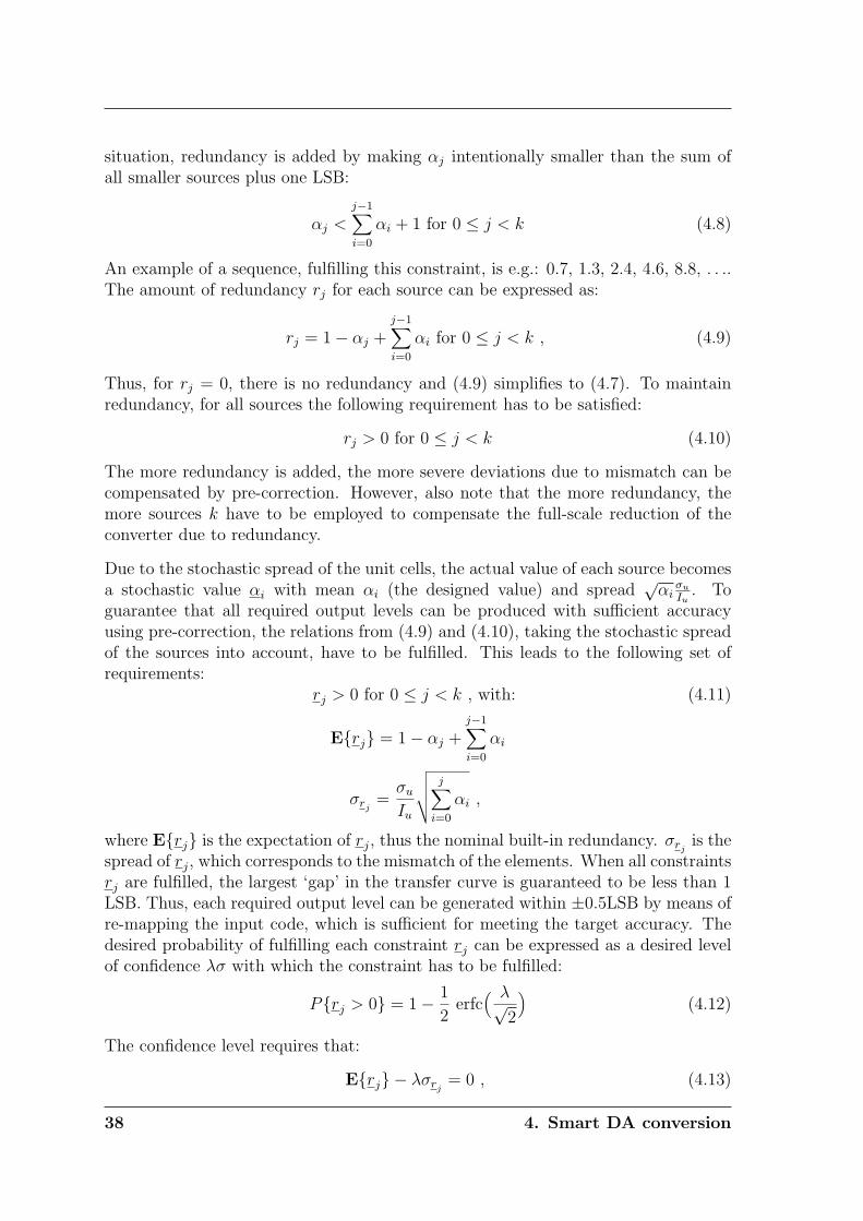
Concepts for SmartAD and DA Converters
Pieter Harpe


Concepts for Smart AD and DA Converters
Pieter Harpe

This work was supported by the Foundation for Technical Sciences (STW) underproject 06655.
Cover design by Xiaoyan Wang, Cui Zhou and Pieter Harpe.
Harpe, P.J.A.Concepts for Smart AD and DA ConvertersProefschrift Technische Universiteit Eindhoven, 2010.A catalogue record is available from the Eindhoven University of Technology LibraryISBN 978-90-386-2120-3NUR 959Trefw.: analog-to-digital conversion, digital-to-analog conversion, correction, calibra-tion.
c©P.J.A. Harpe 2010All rights reserved.
Reproduction in whole or in part is prohibitedwithout the written consent of the copyright owner.

Concepts for Smart AD and DA Converters
PROEFSCHRIFT
ter verkrijging van de graad van doctor aan de
Technische Universiteit Eindhoven, op gezag van de
rector magnificus, prof.dr.ir. C.J. van Duijn, voor een
commissie aangewezen door het College voor
Promoties in het openbaar te verdedigen
op woensdag 27 januari 2010 om 16.00 uur
door
Pieter Joost Adriaan Harpe
geboren te Middelburg

Dit proefschrift is goedgekeurd door de promotor:
prof.dr.ir A.H.M. van Roermund
Copromotor:dr.ir. J.A. Hegt

Contents
List of symbols and abbreviations 9
1 Introduction 11
1.1 Background . . . . . . . . . . . . . . . . . . . . . . . . . . . . . . . . 11
1.2 Aim of the thesis . . . . . . . . . . . . . . . . . . . . . . . . . . . . . 12
1.3 Scope of the thesis . . . . . . . . . . . . . . . . . . . . . . . . . . . . 12
1.4 Outline of the thesis . . . . . . . . . . . . . . . . . . . . . . . . . . . 13
2 AD and DA conversion 15
2.1 Introduction . . . . . . . . . . . . . . . . . . . . . . . . . . . . . . . . 15
2.2 Trends in applications . . . . . . . . . . . . . . . . . . . . . . . . . . 16
2.3 Trends in technology . . . . . . . . . . . . . . . . . . . . . . . . . . . 17
2.4 Trends in system design . . . . . . . . . . . . . . . . . . . . . . . . . 18
2.5 Performance criteria . . . . . . . . . . . . . . . . . . . . . . . . . . . 20
2.6 Conclusion . . . . . . . . . . . . . . . . . . . . . . . . . . . . . . . . . 20
3 Smart conversion 21
3.1 Introduction . . . . . . . . . . . . . . . . . . . . . . . . . . . . . . . . 21
3.2 Smart concept . . . . . . . . . . . . . . . . . . . . . . . . . . . . . . . 22
3.3 Application of the smart concept . . . . . . . . . . . . . . . . . . . . 25
3.4 Focus in this work . . . . . . . . . . . . . . . . . . . . . . . . . . . . 26
3.5 Conclusion . . . . . . . . . . . . . . . . . . . . . . . . . . . . . . . . . 27
Contents 5
4 Smart DA conversion 29
4.1 Introduction . . . . . . . . . . . . . . . . . . . . . . . . . . . . . . . . 29
4.2 Area of current-steering DACs . . . . . . . . . . . . . . . . . . . . . . 31
4.3 Correction of mismatch errors . . . . . . . . . . . . . . . . . . . . . . 33
4.4 Sub-binary variable-radix DAC . . . . . . . . . . . . . . . . . . . . . 35
4.5 Design example . . . . . . . . . . . . . . . . . . . . . . . . . . . . . . 43
4.6 Conclusion . . . . . . . . . . . . . . . . . . . . . . . . . . . . . . . . . 49
5 Design of a sub-binary variable-radix DAC 51
5.1 Schematic design . . . . . . . . . . . . . . . . . . . . . . . . . . . . . 51
5.2 Layout . . . . . . . . . . . . . . . . . . . . . . . . . . . . . . . . . . . 55
5.3 Self-measurement-circuit implementation . . . . . . . . . . . . . . . . 56
5.4 Experimental results . . . . . . . . . . . . . . . . . . . . . . . . . . . 57
5.5 Conclusion . . . . . . . . . . . . . . . . . . . . . . . . . . . . . . . . . 64
6 Smart AD conversion 67
6.1 Introduction . . . . . . . . . . . . . . . . . . . . . . . . . . . . . . . . 67
6.2 Literature review . . . . . . . . . . . . . . . . . . . . . . . . . . . . . 68
6.3 High-speed high-resolution AD conversion . . . . . . . . . . . . . . . 71
6.4 Smart calibration . . . . . . . . . . . . . . . . . . . . . . . . . . . . . 77
6.5 Conclusion . . . . . . . . . . . . . . . . . . . . . . . . . . . . . . . . . 80
7 Design of an open-loop T&H circuit 81
7.1 Literature review . . . . . . . . . . . . . . . . . . . . . . . . . . . . . 81
7.2 Design goal . . . . . . . . . . . . . . . . . . . . . . . . . . . . . . . . 83
7.3 T&H architecture . . . . . . . . . . . . . . . . . . . . . . . . . . . . . 83
7.4 Sampling core architecture . . . . . . . . . . . . . . . . . . . . . . . . 85
7.5 Output buffer architecture . . . . . . . . . . . . . . . . . . . . . . . . 86
7.6 T&H design . . . . . . . . . . . . . . . . . . . . . . . . . . . . . . . . 97
7.7 Experimental results . . . . . . . . . . . . . . . . . . . . . . . . . . . 100
7.8 Conclusion . . . . . . . . . . . . . . . . . . . . . . . . . . . . . . . . . 110
6 Contents
8 T&H calibration 111
8.1 Introduction . . . . . . . . . . . . . . . . . . . . . . . . . . . . . . . . 111
8.2 T&H accuracy . . . . . . . . . . . . . . . . . . . . . . . . . . . . . . . 112
8.3 T&H calibration method . . . . . . . . . . . . . . . . . . . . . . . . . 113
8.4 Analog correction parameters . . . . . . . . . . . . . . . . . . . . . . 114
8.5 Digitally assisted analog correction . . . . . . . . . . . . . . . . . . . 121
8.6 Simulation results . . . . . . . . . . . . . . . . . . . . . . . . . . . . . 124
8.7 Implementation of the calibration method and layout . . . . . . . . . 127
8.8 Experimental results . . . . . . . . . . . . . . . . . . . . . . . . . . . 128
8.9 Conclusion . . . . . . . . . . . . . . . . . . . . . . . . . . . . . . . . . 132
9 T&H calibration for time-interleaved ADCs 133
9.1 Introduction . . . . . . . . . . . . . . . . . . . . . . . . . . . . . . . . 133
9.2 Channel matching in time-interleaved T&H’s . . . . . . . . . . . . . . 136
9.3 Channel mismatch calibration . . . . . . . . . . . . . . . . . . . . . . 137
9.4 Channel mismatch detection . . . . . . . . . . . . . . . . . . . . . . . 140
9.5 Channel mismatch correction . . . . . . . . . . . . . . . . . . . . . . 153
9.6 Simulation results . . . . . . . . . . . . . . . . . . . . . . . . . . . . . 155
9.7 Implementation of the calibration method and layout . . . . . . . . . 156
9.8 Experimental results . . . . . . . . . . . . . . . . . . . . . . . . . . . 157
9.9 Conclusion . . . . . . . . . . . . . . . . . . . . . . . . . . . . . . . . . 161
10 Conclusions 163
References 165
Original contributions 171
List of publications 173
Summary 177
Samenvatting 179
Word of thanks 181
Biography 183
Contents 7

List of symbols and abbreviations
Symbol Description Unit
ADC Analog to digital converterCSA Current source arrayDa R1,a −R1,1
DAC Digital to analog converterDNL Differential non-linearity LSB∆ Time-skew error sENOB Effective number of bits bitERBW Effective resolution bandwidth HzFoM Figure of merit J/conversion-stepFS Digital full scale amplitudefs Sampling frequency HzGe Gain errorINL Integral non-linearity LSBLSB Least significant bitM MLS orderm MLS lengthMLS Maximum length sequenceMSB Most significant bitN Resolution bitOe Offset error V, LSBRa,b Discrete cross-correlation of a and bRs Discrete auto-correlation of s[n]r[n] Single-bit MLSs[n] Multi-bit MLSSFDR Spurious free dynamic rangeSNDR Signal to noise and distortion ratioSNR Signal to noise ratioTHD Total harmonic distortionT&H Track and holdu[n] Response to a multi-bit MLSVCM Common-mode voltage VVfs Analog full scale amplitude V
List of symbols and abbreviations 9

Chapter 1
Introduction
1.1 Background
The history of the application of semiconductors for controlling currents goes backall the way to 1926, in which Julius Lilienfeld filed a patent for a “Method andapparatus for controlling electric currents” [1], which is considered the first work onmetal/semiconductor field-effect transistors. More well-known is the work of WilliamShockley, John Bardeen and Walter Brattain in the 1940s [2, 3], after which thedevelopment of semiconductor devices commenced. In 1958, independent work fromJack Kilby and Robert Noyce led to the invention of integrated circuits. A fewmilestones in IC design are the first monolithic operational amplifier in 1963 (FairchildµA702, Bob Widlar) and the first one-chip 4-bit microprocessor in 1971 (Intel 4004).
Ever since the start of the semiconductor history, integration plays an important role:starting from single devices, ICs with basic functions were developed (e.g. opamps,logic gates), followed by ICs that integrate larger parts of a system (e.g. micropro-cessors, radio tuners, audio amplifiers). Following this trend of system integration,this eventually leads to the integration of analog and digital components in one chip,resulting in mixed-signal ICs: digital components are required because signal process-ing is preferably done in the digital domain; analog components are required becausephysical signals are analog by nature. Mixed-signal ICs are already widespread inmany applications (e.g. audio, video); for the future, it is expected that this trendwill continue, leading to a larger scale of integration.
Given the trend of mixed-signal integration, this leads to both new challenges andnew opportunities with respect to the integrated analog components. Challenges arefor example testing of the performance of analog components that are embeddedinside a large system, or the fact that the IC technology is optimized for digitalcircuitry, which can be disadvantageous for analog components. On the other hand,the mixed-signal integration also gives opportunities, like the possibility to shift partsof the system from the analog to the digital domain, or vice versa. From this point
1. Introduction 11
of view, the aim of this work is to investigate concepts to improve the performanceof analog components by making use of the opportunities that are offered by mixed-signal system integration. This ‘smart’ concept will be applied to analog-to-digitaland digital-to-analog converters, as these components are essential in mixed-signalsystems.
1.2 Aim of the thesis
The aim of this thesis is to investigate the feasibility of relevant smart AD and DAconverter concepts to improve their performance1. For both AD and DA converters,the following aspects will be taken into account:
• Selection of relevant performance criteria.
• Evaluation of prior-art and identifying their limitations.
• Selection of relevant smart concepts to improve the performance.
• Development and analysis of the selected smart concepts, including methodsfor detection, processing and correction.
• Implementation and evaluation of the selected smart concepts.
1.3 Scope of the thesis
Some limitations on the scope of the thesis are explained below:
• Current-steering DAC architectureThe current-steering DAC architecture will be studied for the smart DA con-cepts. This is motivated by the fact that for high-speed DA conversion, thistype is predominantly used.
• (Time-interleaved) pipelined ADC architecture, focus on Track&HoldThe (time-interleaved) pipelined ADC architecture will be studied for the smartAD concepts. Moreover, most of the work is limited to the front-end track-and-hold, in the context of a (time-interleaved) pipelined ADC. The limitation toa (time-interleaved) pipelined ADC architecture is motivated by the fact thatfor high-speed, high-resolution AD conversion, this is a commonly used andreasonable solution. The limitation to the track-and-hold is motivated by thefact that it is sufficient for the demonstration of the proposed smart concepts.
1In this work, performance is defined in a wide sense, including e.g.: speed, accuracy, powerconsumption, area, yield, reliability, portability, etc.
12 1. Introduction
• CMOS technologyCMOS is the preferred technology choice for the implementation of digital cir-cuits. As the smart concept implies analog circuits integrated in large digitalsystems, the limitation to CMOS technology is a logical choice. Because of lim-ited technology availability, all simulations, calculations and implementationsare limited to a 0.18µm CMOS technology. However, the proposed conceptscould be implemented in other technologies as well.
• General purposeThe proposed solutions do not aim for a specific target application. Becauseof that, the concepts and designs are ‘general purpose’ in the sense that theydo not pose any constraints on the input signal, nor do they take advantage ofcertain assumptions on the input signal.
1.4 Outline of the thesis
The outline of this thesis is briefly explained below.
Chapter 2 studies trends and expectations in converter design with respect to ap-plications, technology evolution and system design. Problems and opportunities areidentified, and an overview of performance criteria is given. In chapter 3, the smartconcept is introduced that takes advantage of the expected opportunities (describedin chapter 2) in order to solve the anticipated problems.
Chapters 4 and 5 apply the smart concept to digital-to-analog converters. In thediscussed example, the concept is applied to reduce the area of the analog core of acurrent-steering DAC. In chapter 4, the theory is presented while chapter 5 discussesthe implementation and experimental results.
Chapter 6 up to chapter 9 focus on the application of the smart concept to analog-to-digital converters. The main goal here is to improve the performance in termsof speed/power/accuracy. Chapter 6 introduces the general concept and defines keyfactors for the analog design and the smart approach in order to achieve the targetedhigh performance. Then, chapter 7 deals with the analog design of an open-loop track-and-hold circuit. Experimental results are presented and compared against prior art.In chapters 8 and 9, two calibration techniques are presented and experimentallyverified by using the track-and-hold from chapter 7.
Finally, conclusions are drawn in chapter 10.
1. Introduction 13

Chapter 2
AD and DA conversion
This chapter studies trends and expectations in converter design with respect to ap-plications, technology evolution and system design. Problems and opportunities areidentified, and an overview of performance criteria is given. In chapter 3, the smartconcept is introduced that takes advantage of the expected opportunities in order tosolve the anticipated problems.
2.1 Introduction
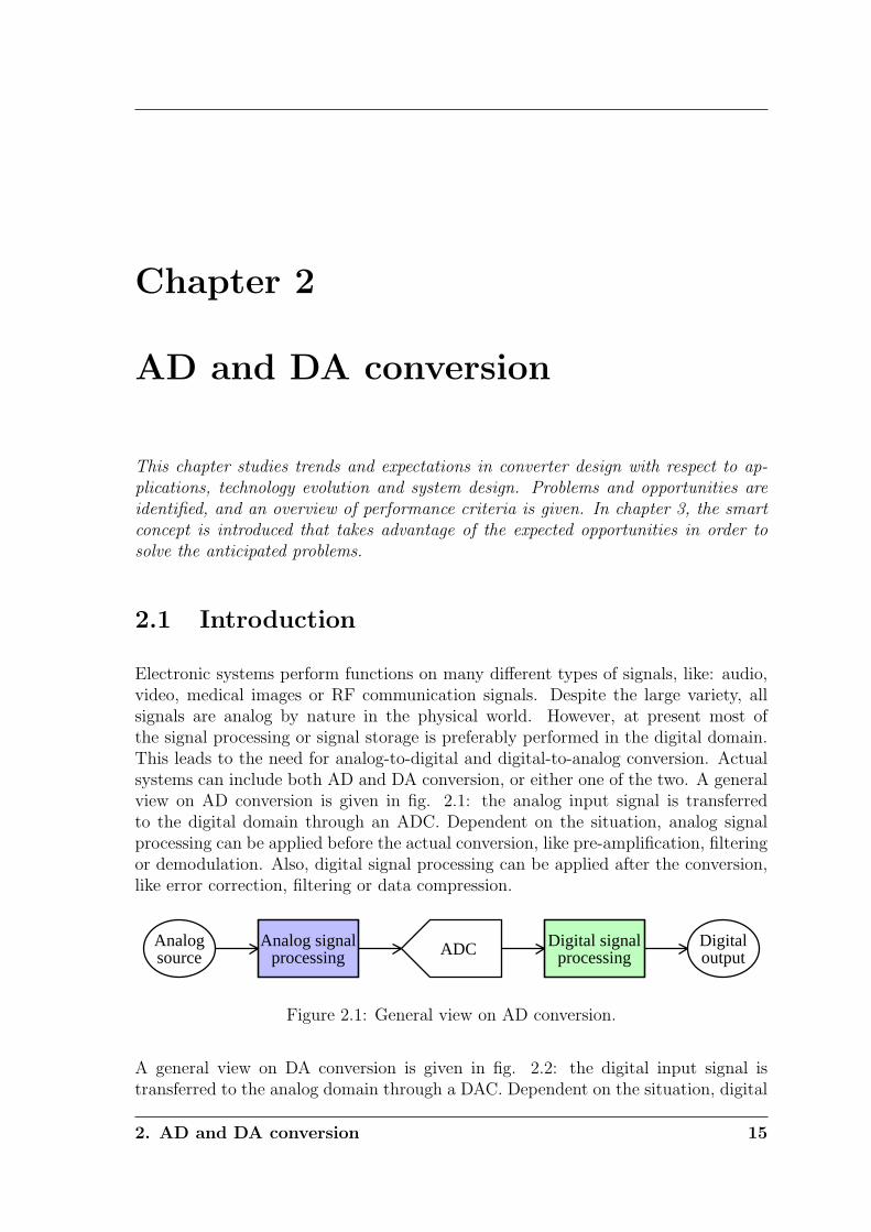
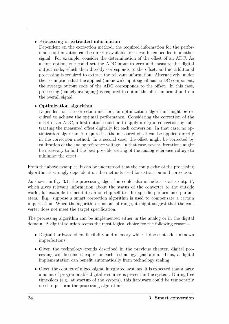
Electronic systems perform functions on many different types of signals, like: audio,video, medical images or RF communication signals. Despite the large variety, allsignals are analog by nature in the physical world. However, at present most ofthe signal processing or signal storage is preferably performed in the digital domain.This leads to the need for analog-to-digital and digital-to-analog conversion. Actualsystems can include both AD and DA conversion, or either one of the two. A generalview on AD conversion is given in fig. 2.1: the analog input signal is transferredto the digital domain through an ADC. Dependent on the situation, analog signalprocessing can be applied before the actual conversion, like pre-amplification, filteringor demodulation. Also, digital signal processing can be applied after the conversion,like error correction, filtering or data compression.
sourceAnalog
processingAnalog signal ADC processing
Digital signaloutputDigital
Figure 2.1: General view on AD conversion.
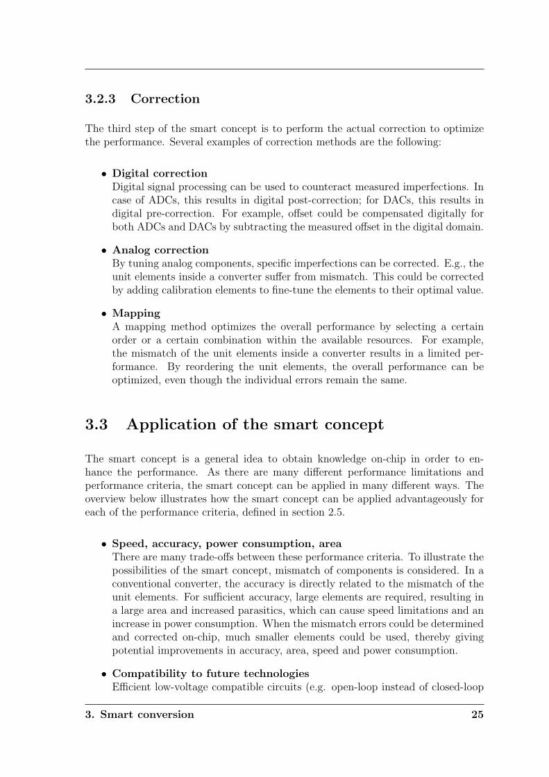
A general view on DA conversion is given in fig. 2.2: the digital input signal istransferred to the analog domain through a DAC. Dependent on the situation, digital
2. AD and DA conversion 15
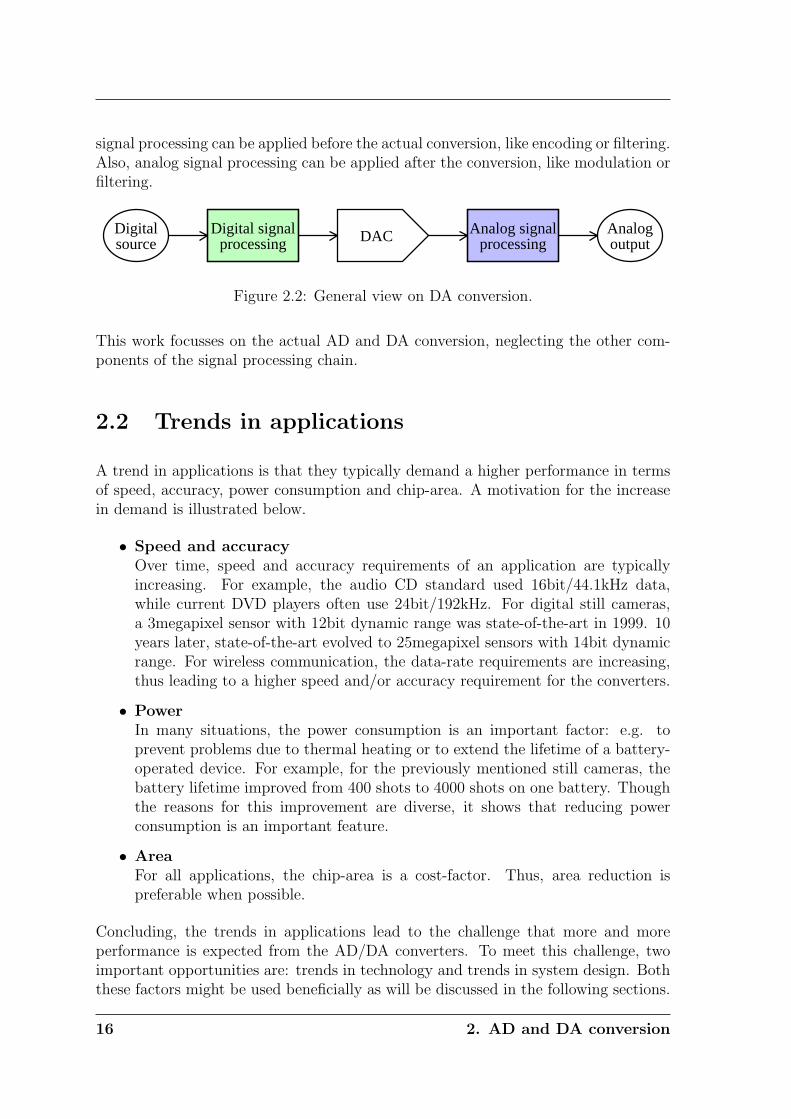
signal processing can be applied before the actual conversion, like encoding or filtering.Also, analog signal processing can be applied after the conversion, like modulation orfiltering.
sourceDigital
processingDigital signal DAC processing
Analog signaloutputAnalog
Figure 2.2: General view on DA conversion.
This work focusses on the actual AD and DA conversion, neglecting the other com-ponents of the signal processing chain.
2.2 Trends in applications
A trend in applications is that they typically demand a higher performance in termsof speed, accuracy, power consumption and chip-area. A motivation for the increasein demand is illustrated below.
• Speed and accuracyOver time, speed and accuracy requirements of an application are typicallyincreasing. For example, the audio CD standard used 16bit/44.1kHz data,while current DVD players often use 24bit/192kHz. For digital still cameras,a 3megapixel sensor with 12bit dynamic range was state-of-the-art in 1999. 10years later, state-of-the-art evolved to 25megapixel sensors with 14bit dynamicrange. For wireless communication, the data-rate requirements are increasing,thus leading to a higher speed and/or accuracy requirement for the converters.
• PowerIn many situations, the power consumption is an important factor: e.g. toprevent problems due to thermal heating or to extend the lifetime of a battery-operated device. For example, for the previously mentioned still cameras, thebattery lifetime improved from 400 shots to 4000 shots on one battery. Thoughthe reasons for this improvement are diverse, it shows that reducing powerconsumption is an important feature.
• AreaFor all applications, the chip-area is a cost-factor. Thus, area reduction ispreferable when possible.
Concluding, the trends in applications lead to the challenge that more and moreperformance is expected from the AD/DA converters. To meet this challenge, twoimportant opportunities are: trends in technology and trends in system design. Boththese factors might be used beneficially as will be discussed in the following sections.
16 2. AD and DA conversion
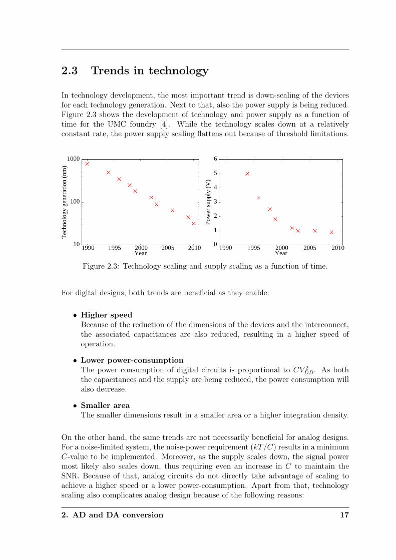
2.3 Trends in technology
In technology development, the most important trend is down-scaling of the devicesfor each technology generation. Next to that, also the power supply is being reduced.Figure 2.3 shows the development of technology and power supply as a function oftime for the UMC foundry [4]. While the technology scales down at a relativelyconstant rate, the power supply scaling flattens out because of threshold limitations.
10
100
1000
1990 1995 2000 2005 2010
Tec
hnol
ogy
gene
ratio
n (n
m)
Year
0
1
2
3
4
5
6
1990 1995 2000 2005 2010
Pow
er s
uppl
y (V
)
Year
Figure 2.3: Technology scaling and supply scaling as a function of time.
For digital designs, both trends are beneficial as they enable:
• Higher speedBecause of the reduction of the dimensions of the devices and the interconnect,the associated capacitances are also reduced, resulting in a higher speed ofoperation.
• Lower power-consumptionThe power consumption of digital circuits is proportional to CV 2
DD. As boththe capacitances and the supply are being reduced, the power consumption willalso decrease.
• Smaller areaThe smaller dimensions result in a smaller area or a higher integration density.
On the other hand, the same trends are not necessarily beneficial for analog designs.For a noise-limited system, the noise-power requirement (kT/C) results in a minimumC-value to be implemented. Moreover, as the supply scales down, the signal powermost likely also scales down, thus requiring even an increase in C to maintain theSNR. Because of that, analog circuits do not directly take advantage of scaling toachieve a higher speed or a lower power-consumption. Apart from that, technologyscaling also complicates analog design because of the following reasons:
2. AD and DA conversion 17

• Short channel effectsFor smaller transistor geometries, secondary effects become more and more im-portant. Because of that, the complexity of the transistor behavior increases,which complicates accurate circuit design.
• Low voltage operationThe reduced supply voltage limits the number of transistors that can be stacked,which complicates the implementation of certain circuit topologies.
While digital circuit design benefits from technology scaling, analog circuit design isgetting more complicated. For mixed-signal designs, like AD and DA converters, itseems a logical option to shift some of the analog problems to the digital domain tobe able to benefit from technology scaling.
2.4 Trends in system design
As mentioned previously in chapter 1, there is a tendency to integrate more and morecomponents of a system into a single chip. As signal processing is predominantlyperformed in the digital domain while physical signals are analog by nature, this leadsto the integration of analog and digital components in one chip, resulting in mixed-signal ICs. For the integrated analog components, the system integration offers bothnew challenges and new opportunities. Some of the challenges that become moreimportant because of the mixed-signal integration are the following:
• Hostile environmentDigital circuits create a hostile environment for the analog circuits by causinginterference, which potentially reduces the performance of the analog circuits.
• TestingA stand-alone analog component can be tested directly for functionality orperformance. On the other hand, analog components embedded in a large inte-grated system can not be accessed directly, thus complicating test methodolo-gies. A dedicated test-mode or an internal self-test strategy might be necessaryto facilitate testing.
• YieldEspecially when combining many different components into one integrated chip,the overall yield might be affected adversely by critical components. Also, whena single component has an unsatisfactory performance, the total system mightfail. In general, design for high yield becomes more important for integratedcomponents when compared to stand-alone components.
• Technology portabilityThough technology portability is a general issue, it becomes more relevant for
18 2. AD and DA conversion

mixed-signal ICs. For stand-alone analog components, a suitable technologymight be selected by the designer. However, for integrated mixed-signal designs,the technology is most likely determined by the digital part and the analogcircuits have to adopt this technology. Thus, analog designs are required thatperform well in digital technologies. Moreover, they should be portable to futuretechnologies as well, as the digital part of the system benefits from scaling. Asecond issue with respect to portability is the fact that expertise on analogdesign is required to transfer an existing design to a new technology.
• FlexibilityMany digital systems are flexible by using programmable hardware like micro-processors or FPGAs. Flexibility in mixed-signal integrated systems can be auseful aspect as it widens the application range for a single design and it allowssoftware updates to accommodate post-production modifications. To achieve ahigher level of flexibility, also the analog components need to be flexible (e.g.speed, power, accuracy), while maintaining an appropriate performance level.
• Design time and riskThe digital design flow is highly automated, which reduces the design timeand risk, especially when porting an existing design to a new technology. Onthe other hand, analog circuit design, simulation and layout are mainly manualtasks with a potentially longer design time and a higher risk. Even when portingan existing design to a new technology, schematics, simulations and layout needto be redone to a large extent. Techniques to reduce the design time and riskof analog components are required to suit better to the digital design flow, andto prevent that analog design becomes the overall design bottleneck.
Apart from these challenges, mixed-signal integration also gives opportunities foranalog circuit design:
• Reuse of resourcesIn a large integrated system, not all components will be actively used at alltimes. Especially the digital hardware might have free time-slots in which it canbe used for other purposes like self-test or calibration of analog components. Thefreedom to use these already available resources can enhance the overall systemperformance. Particularly in case of flexible digital platforms like FPGAs ormicroprocessors, hardware reuse can be implemented in a relatively simple way.
• System optimizationIn integrated systems, the main goal is not to optimize the individual com-ponents, but to optimize the overall system. Then, the components can beoptimized given the specific task inside the larger system. Taking this approachinto account, a better optimization might be possible when compared to stan-dard stand-alone circuit design. Also, in a system-level approach, problems canbe shifted from the analog to the digital domain whenever this is beneficial forthe overall performance.
2. AD and DA conversion 19

2.5 Performance criteria
From the described trends and requirements with respect to applications, technologyand system design, a set of relevant performance criteria for AD and DA converterscan be identified. Classified into these three trends, the following list of performancecriteria is obtained:
• Application driven criteria
– Speed
– Accuracy
– Power consumption
– Area
• Technology driven criteria
– Short-channel effect compatibility
– Low-voltage compatibility
• System driven criteria
– Interference compatibility
– Testability
– Yield
– Portability
– Flexibility
– Design time and risk
Typically, the application driven performance criteria are the most important ones;these are also the most widely used performance criteria for the evaluation of con-verters. However, in view of technology development and system integration, it willbecome necessary to achieve sufficient performance for the other criteria as well.
2.6 Conclusion
In this chapter, it was shown that trends in applications, technology and system designcomplicate analog circuit design. It was also shown that apart from these challenges,technology scaling and system integration offer new opportunities to improve theperformance of analog circuits. In the next chapter, a concept is introduced thattakes advantage of these opportunities in order to solve the anticipated problems.
20 2. AD and DA conversion
Chapter 3
Smart conversion
This chapter introduces the smart concept for AD/DA converters, that aims at im-proving performance in a way that suits to the trends in technology and system designas described in chapter 2. First, the smart concept (as published in [5]) will be defined.Then, various applications of the concept will be discussed and the main focus of thiswork will be explained.
3.1 Introduction
In the previous chapter, several challenges in AD/DA converter design were identified,namely:
• The performance in terms of speed/accuracy/power-consumption/area shouldimprove because of the increasing demand from the applications.
• Technology properties limit the achievable performance. Moreover, the achiev-able performance range might be reduced for future technologies because ofprocess down-scaling.
• Mixed-signal system integration introduces new challenges with respect to e.g.testing, yield, portability, interference.
Especially the first two trends are contradictory: the performance demand increaseswhile for some situations, the intrinsically achievable performance decreases. Becauseof that, a solution is required that can overcome the intrinsic limitations.
3. Smart conversion 21
3.2 Smart concept
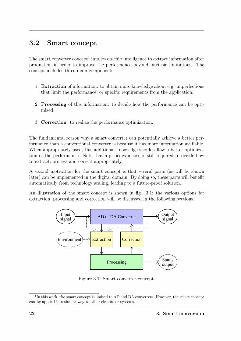
The smart converter concept1 implies on-chip intelligence to extract information afterproduction in order to improve the performance beyond intrinsic limitations. Theconcept includes three main components:
1. Extraction of information: to obtain more knowledge about e.g. imperfectionsthat limit the performance, or specific requirements from the application.
2. Processing of this information: to decide how the performance can be opti-mized.
3. Correction: to realize the performance optimization.
The fundamental reason why a smart converter can potentially achieve a better per-formance than a conventional converter is because it has more information available.When appropriately used, this additional knowledge should allow a better optimiza-tion of the performance. Note that a-priori expertise is still required to decide howto extract, process and correct appropriately.
A second motivation for the smart concept is that several parts (as will be shownlater) can be implemented in the digital domain. By doing so, these parts will benefitautomatically from technology scaling, leading to a future-proof solution.
An illustration of the smart concept is shown in fig. 3.1; the various options forextraction, processing and correction will be discussed in the following sections.
AD or DA ConvertersignalInput
Extraction Correction
Processing
signalOutput
Environment
outputStatus
Figure 3.1: Smart converter concept.
1In this work, the smart concept is limited to AD and DA converters. However, the smart conceptcan be applied in a similar way to other circuits or systems.
22 3. Smart conversion
3.2.1 Extraction
The first step of the smart concept is the extraction of performance-relevant informa-tion. Three different information sources can be distinguished: system information,signal information and environmental information:
• System informationIn this case, that is information from the ADC or DAC, like: functionality,mismatch of components (random or due to process-spread), non-linearity, fre-quency dependent behavior. As an example, consider the mismatch of compo-nents: before production only the statistics of the mismatch are known. Afterproduction, for a specific chip, the mismatch has a deterministic value. Whenthis value can be measured on-chip it gives more precise knowledge on the mis-match compared to the pre-production statistical information. With this addi-tional information and an appropriate correction technique, this imperfectioncould be counteracted to improve the performance.
• Signal informationInformation from signals at the input, output or at an intermediate stage, like:amplitude, bandwidth, probability density function, spectral properties. For ex-ample, when the input signal has a limited amplitude, the converter’s resourcescould be optimized for that specific amplitude instead of being optimized forthe full-scale range of the converter.
• Environmental informationEnvironmental information includes information from the ambience (e.g. tem-perature, supply voltage), the user and the application. For example, dependenton the user/application requirements, the relevant performance criteria mightchange, and thus require a different optimization goal of the smart converter.
When considering mixed-signal circuits like AD and DA converters, part of the infor-mation to be extracted will be available in the digital domain and part of it will beavailable in the analog domain. In both cases, additional hardware might be requiredto extract the information.
3.2.2 Processing
The second step of the smart concept is to process the extracted information tooptimize the performance. Two parts can be distinguished in the processing block:a first part in which the relevant information is extracted from the raw data anda second part where the information is processed to achieve a suitable correction.Whether these parts are necessary depends on the methods used for extraction andcorrection:
3. Smart conversion 23
• Processing of extracted informationDependent on the extraction method, the required information for the perfor-mance optimization can be directly available, or it can be embedded in anothersignal. For example, consider the determination of the offset of an ADC. Asa first option, one could set the ADC-input to zero and measure the digitaloutput code, which then directly corresponds to the offset, and no additionalprocessing is required to extract the relevant information. Alternatively, underthe assumption that the applied (unknown) input signal has no DC component,the average output code of the ADC corresponds to the offset. In this case,processing (namely averaging) is required to obtain the offset information fromthe overall signal.
• Optimization algorithmDependent on the correction method, an optimization algorithm might be re-quired to achieve the optimal performance. Considering the correction of theoffset of an ADC, a first option could be to apply a digital correction by sub-tracting the measured offset digitally for each conversion. In that case, no op-timization algorithm is required as the measured offset can be applied directlyin the correction method. In a second case, the offset might be corrected bycalibration of the analog reference voltage. In that case, several iterations mightbe necessary to find the best possible setting of the analog reference voltage tominimize the offset.
From the above examples, it can be understood that the complexity of the processingalgorithm is strongly dependent on the methods used for extraction and correction.
As shown in fig. 3.1, the processing algorithm could also include a ‘status output’,which gives relevant information about the status of the converter to the outsideworld, for example to facilitate an on-chip self-test for specific performance param-eters. E.g., suppose a smart correction algorithm is used to compensate a certainimperfection. When the algorithm runs out of range, it might suggest that the con-verter does not meet the target specification.
The processing algorithm can be implemented either in the analog or in the digitaldomain. A digital solution seems the most logical choice for the following reasons:
• Digital hardware offers flexibility and memory while it does not add unknownimperfections.
• Given the technology trends described in the previous chapter, digital pro-cessing will become cheaper for each technology generation. Thus, a digitalimplementation can benefit automatically from technology scaling.
• Given the context of mixed-signal integrated systems, it is expected that a largeamount of programmable digital resources is present in the system. During freetime-slots (e.g. at startup of the system), this hardware could be temporarilyused to perform the processing algorithm.
24 3. Smart conversion
3.2.3 Correction
The third step of the smart concept is to perform the actual correction to optimizethe performance. Several examples of correction methods are the following:
• Digital correctionDigital signal processing can be used to counteract measured imperfections. Incase of ADCs, this results in digital post-correction; for DACs, this results indigital pre-correction. For example, offset could be compensated digitally forboth ADCs and DACs by subtracting the measured offset in the digital domain.
• Analog correctionBy tuning analog components, specific imperfections can be corrected. E.g., theunit elements inside a converter suffer from mismatch. This could be correctedby adding calibration elements to fine-tune the elements to their optimal value.
• MappingA mapping method optimizes the overall performance by selecting a certainorder or a certain combination within the available resources. For example,the mismatch of the unit elements inside a converter results in a limited per-formance. By reordering the unit elements, the overall performance can beoptimized, even though the individual errors remain the same.
3.3 Application of the smart concept
The smart concept is a general idea to obtain knowledge on-chip in order to en-hance the performance. As there are many different performance limitations andperformance criteria, the smart concept can be applied in many different ways. Theoverview below illustrates how the smart concept can be applied advantageously foreach of the performance criteria, defined in section 2.5.
• Speed, accuracy, power consumption, areaThere are many trade-offs between these performance criteria. To illustrate thepossibilities of the smart concept, mismatch of components is considered. In aconventional converter, the accuracy is directly related to the mismatch of theunit elements. For sufficient accuracy, large elements are required, resulting ina large area and increased parasitics, which can cause speed limitations and anincrease in power consumption. When the mismatch errors could be determinedand corrected on-chip, much smaller elements could be used, thereby givingpotential improvements in accuracy, area, speed and power consumption.
• Compatibility to future technologiesEfficient low-voltage compatible circuits (e.g. open-loop instead of closed-loop
3. Smart conversion 25

amplifiers) often do not meet the performance requirements (e.g. because ofnon-linearity). The smart concept allows the use of these circuits as their asso-ciated limitations can now be overcome by a smart correction.
• Interference compatibilityOn-chip sensors could be implemented to measure the interference. Based onthat, a mapping method for both analog and digital hardware could be used toreduce the interference for the most critical analog blocks.
• TestabilityThe extracted information in a smart converter can be used to enable on-chipself-test by measuring relevant test parameters like functionality or accuracy.
• YieldInstead of relying on intrinsic performance, additional correction resources canbe built into a smart converter to allow compensation of a larger performancespread, which can improve the yield.
• Portability, design time and riskIn an intrinsic design, the performance is determined by the technology, therebycomplicating portability as the performance has to be verified again in the newtechnology. In a smart approach, the technology limitations can be overcome.Because of that, the technology has less influence on the performance whichsimplifies portability and reduces design time and risk.
• FlexibilityAs a large part of the smart circuitry can be implemented with programmablelogic, the smart concept allows optimization of a specific converter for variousrequirements, thereby adding flexibility to the design.
While the list illustrates the versatility of the smart concept, it should not be expectedthat all smart designs improve all these parameters at once. For example, in [6]a smart redesign of a conventional pipelined ADC [7] is proposed: an open-loopamplifier is used instead of a closed-loop amplifier to reduce the power consumption.Then, the non-linearity of the open-loop structure is corrected by a smart approach.Nonetheless, the FoM of the smart converter (2.3pJ/conv.step) is worse than the FoMof the original design (1.3pJ/conv.step) 2. However, the smart design performs betterwith respect to technology compatibility, which makes it an attractive solution forfuture technologies.
3.4 Focus in this work
The aim of this work is to investigate the feasibility of relevant smart AD and DA con-verter concepts. The main focus will be on the application driven performance criteria
2The FoM definition is given in chapter 6.
26 3. Smart conversion
(speed, accuracy, power consumption and area), while the technology compatibility isalso taken into account. In chapter 4, a smart concept for DA converters is proposedto improve the performance with respect to area; the chip implementation of this con-cept will be discussed in chapter 5. In chapter 6, a smart concept for AD convertersis proposed to improve the performance with respect to the speed/power/accuracytrade-off; the chip implementation is shown in chapters 7 up to 9.
3.5 Conclusion
In this chapter, the smart converter concept was proposed. It was shown that thisconcept can overcome some important technology limitations, thereby improving theperformance and the compatibility to future technologies. As the concept is imple-mented on-chip, it is also compatible with mixed-signal integrated systems. Becauseof these reasons, the smart concept suits to the trends in applications, technology andsystem design.
3. Smart conversion 27

Chapter 4
Smart DA conversion
This chapter applies the previously presented smart concept to digital-to-analog con-verters. In the proposed scenario, the smart concept will be used to reduce the chip-area of a current-steering DAC while maintaining overall accuracy. In this chapter,the theory of the approach will be studied, while the actual proof-of-concept by meansof a chip implementation will be given in chapter 5. Parts of this chapter have beenpublished previously in [8, 9, 10].
4.1 Introduction
In the previous chapter, the versatility of the smart concept was explained. Compre-hensibly, in reality one can only demonstrate the feasibility of a limited part of theoverall concept. In this chapter, one relevant item from the smart concept will beselected for further investigation and actual chip implementation. In chapter 6, wherethe smart concept will be applied to AD converters, different items will be chosen toshow another view of the possibilities of the smart concept.
Existing work that includes some of the aspects of the smart concept aims for improv-ing performance by means of correction, calibration or mapping. Typically, the mostimportant goal is to improve the accuracy by counteracting the effect of a certainerror (or a set of errors). An overview of error mechanisms and correction methodsis described in [11]; the enumeration below gives a summary of the described errormechanisms and examples of work that counteract the errors by means of correction.
• Amplitude mismatch, e.g. [12, 13]
• Timing mismatch, e.g. [14]
• Harmonic distortion, e.g. [11]
• Data-switching errors, e.g. [15]
4. Smart DA conversion 29
Apart from improving accuracy, the methods can also have other benefits. For ex-ample, when timing mismatch can be corrected, it does not only improve accuracy,it can also extend the usable frequency range, thus increase the speed of operation.Or, when amplitude mismatch can be corrected, one might use smaller (and thus lessaccurate) elements to reduce the area, and still meet the accuracy requirements.
In this work, the smart concept will be applied with as main goal to reduce the area ofthe analog part of a DAC as much as possible. Because of the area reduction, a largeamount of amplitude mismatch can be expected. Thus, a digitally-implemented smartsolution will be applied to maintain high accuracy. The motivation for this goal is thatcurrently, DAC designs do not scale down in size as fast as technology-scaling wouldpermit, because of accuracy requirements. At the same time, digital components doscale down with technology. As a consequence, in mixed analog/digital systems, theDAC becomes relatively larger in size compared to the digital hardware. Because ofthat, it is worthwhile to investigate solutions to reduce the area of the DAC.
When the area of the DAC is considered, one can refer to either the overall DAC areaor the analog-core area:
• Overall DAC areaComplete area of the DAC (analog and digital parts) and area of the add-ondigital circuitry for the smart solution.
• Analog core areaArea of the analog parts of the DAC only, excluding digital parts inside theDAC or digital parts added to the DAC.
In situations where the DAC is a stand-alone device, the most relevant goal wouldbe to minimize the overall DAC area instead of minimizing the analog core area.However, the goal in this case is to minimize the analog core area, even when itcomes at the cost of an increased area of the digital part. This is motivated by thefollowing reasons:
• Application in large-scale mixed-signal ICsA first motivation is that the smart concept envisions large-scale mixed-signalintegrated systems. In these systems, there are applications for which the ana-log core area is more important than the overall area; two examples where theanalog core area is the most relevant area to be optimized are given here:A first example is when the DAC is used as an accurate on-chip test-signalgenerator during calibration of another on-chip component. After calibration,the digital hardware required for the DAC can be reprogrammed for anothertask. Then, because of the flexibility of the digital hardware, the only overheadin terms of area is coming from the analog DAC core.Another example is a general-purpose digital chip in which, for a few applica-tions, a DAC is required. As the chip is a general-purpose IC and the DAC is
30 4. Smart DA conversion
only used for a few applications, it would be expensive to implement a large-sizeDAC on all these devices. On the other hand, when the DAC area would be verysmall, the overhead would be acceptable to implement the DAC on all chips.Then, only for the few applications that actually use the DAC, digital resourceshave to be allocated to control the DAC. Even when a substantial amount ofdigital resources would be required, this can still be the most effective solutionon the average, as most application do not use the DAC.
• Different scaling for analog and digitalA second motivation, as explained before, is that digital scales down with tech-nology much faster than analog. Thus, reducing the area of the analog core willalso reduce the overall area on the long term.
Given this background, the aim of area reduction will be limited to the analog corearea in this work.
This chapter starts with a discussion on area constraints of DA converters in section4.2. Existing approaches to reduce the area are reviewed in section 4.3, and a newconcept for area reduction is introduced in section 4.4. A design example is shown insection 4.5 and conclusions are drawn in section 4.6.
4.2 Area of current-steering DACs
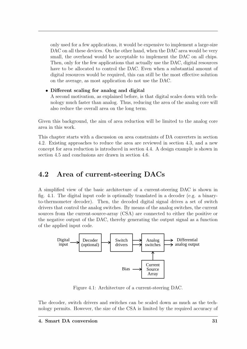
A simplified view of the basic architecture of a current-steering DAC is shown infig. 4.1. The digital input code is optionally translated in a decoder (e.g. a binary-to-thermometer decoder). Then, the decoded digital signal drives a set of switchdrivers that control the analog switches. By means of the analog switches, the currentsources from the current-source-array (CSA) are connected to either the positive orthe negative output of the DAC, thereby generating the output signal as a functionof the applied input code.
Decoder(optional)
Switchdrivers
Analogswitches
CurrentSourceArray
Digitalinput
Bias
Differentialanalog output
Figure 4.1: Architecture of a current-steering DAC.
The decoder, switch drivers and switches can be scaled down as much as the tech-nology permits. However, the size of the CSA is limited by the required accuracy of
4. Smart DA conversion 31
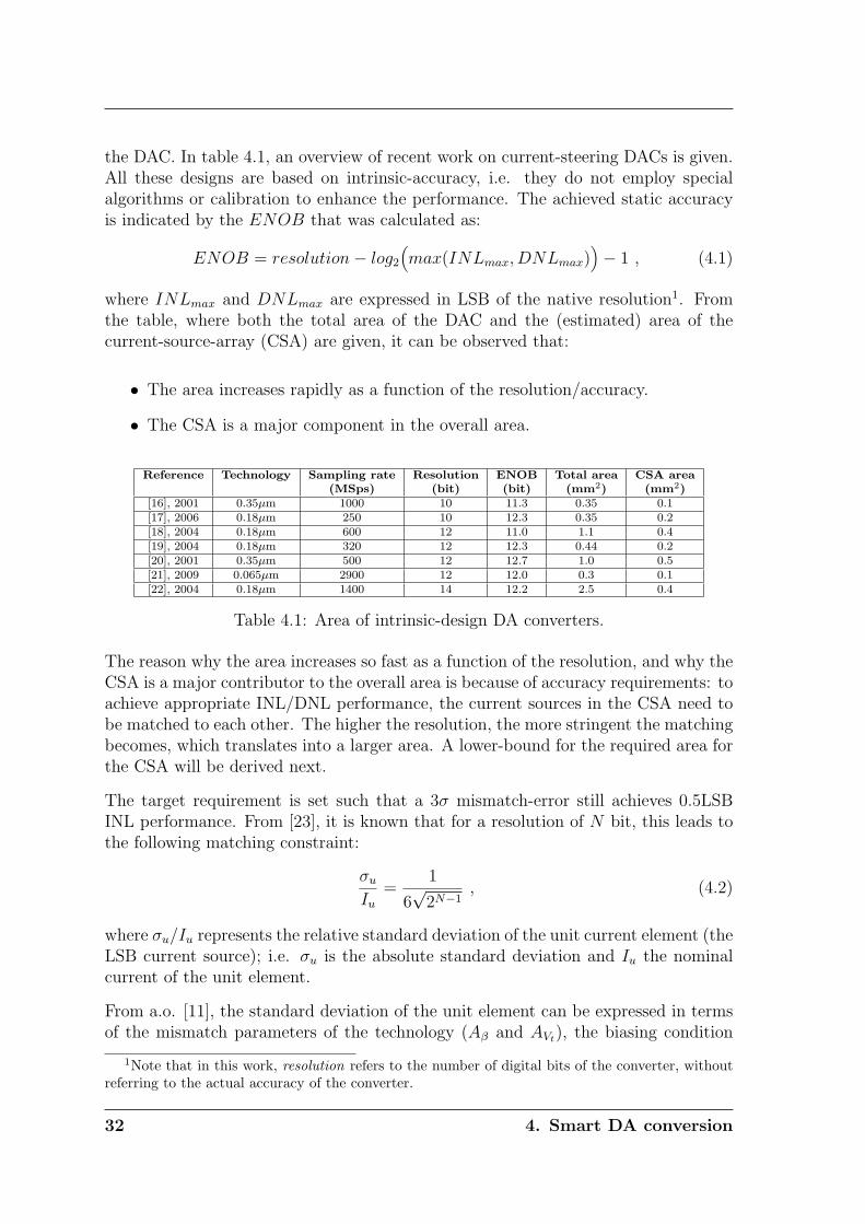
the DAC. In table 4.1, an overview of recent work on current-steering DACs is given.All these designs are based on intrinsic-accuracy, i.e. they do not employ specialalgorithms or calibration to enhance the performance. The achieved static accuracyis indicated by the ENOB that was calculated as:
ENOB = resolution− log2
(max(INLmax, DNLmax)
)− 1 , (4.1)
where INLmax and DNLmax are expressed in LSB of the native resolution1. Fromthe table, where both the total area of the DAC and the (estimated) area of thecurrent-source-array (CSA) are given, it can be observed that:
• The area increases rapidly as a function of the resolution/accuracy.
• The CSA is a major component in the overall area.
Reference Technology Sampling rate Resolution ENOB Total area CSA area(MSps) (bit) (bit) (mm2) (mm2)
[16], 2001 0.35µm 1000 10 11.3 0.35 0.1[17], 2006 0.18µm 250 10 12.3 0.35 0.2[18], 2004 0.18µm 600 12 11.0 1.1 0.4[19], 2004 0.18µm 320 12 12.3 0.44 0.2[20], 2001 0.35µm 500 12 12.7 1.0 0.5[21], 2009 0.065µm 2900 12 12.0 0.3 0.1[22], 2004 0.18µm 1400 14 12.2 2.5 0.4
Table 4.1: Area of intrinsic-design DA converters.
The reason why the area increases so fast as a function of the resolution, and why theCSA is a major contributor to the overall area is because of accuracy requirements: toachieve appropriate INL/DNL performance, the current sources in the CSA need tobe matched to each other. The higher the resolution, the more stringent the matchingbecomes, which translates into a larger area. A lower-bound for the required area forthe CSA will be derived next.
The target requirement is set such that a 3σ mismatch-error still achieves 0.5LSBINL performance. From [23], it is known that for a resolution of N bit, this leads tothe following matching constraint:
σu
Iu
=1
6√
2N−1, (4.2)
where σu/Iu represents the relative standard deviation of the unit current element (theLSB current source); i.e. σu is the absolute standard deviation and Iu the nominalcurrent of the unit element.
From a.o. [11], the standard deviation of the unit element can be expressed in termsof the mismatch parameters of the technology (Aβ and AVt), the biasing condition
1Note that in this work, resolution refers to the number of digital bits of the converter, withoutreferring to the actual accuracy of the converter.
32 4. Smart DA conversion
(Vgs − Vt) and the dimensions of the unit element (Wu and Lu):
σu
Iu
=
√√√√A2β + 4A2
Vt/(Vgs − Vt)2
2WuLu
(4.3)
For a given technology (e.g. a 0.18µm CMOS technology: Aβ = 2%µm and AVt =4mVµm), and an estimate of the biasing condition (e.g. Vgs − Vt = 0.5V), (4.3)simplifies to:
σu
Iu
=0.018√WuLu
(4.4)
Note that for newer technologies, Aβ and AVt are typically improving slightly, therebyimproving the matching. However, at the same time, new technologies allow lessvoltage-headroom, such that the loss of Vgs − Vt counteracts the improved matchingproperties. As a consequence, little improvement of the relation given by (4.4) isexpected for DACs designed in newer technologies.
Combining equations (4.2) and (4.4) yields a relation between the resolution and thearea of the unit element:
WuLu = 0.006 · 2N (4.5)
As the DAC is composed of a total of 2N unit elements, the total gate-area becomes:
Adac = 0.006 · 4N [µm2] (4.6)
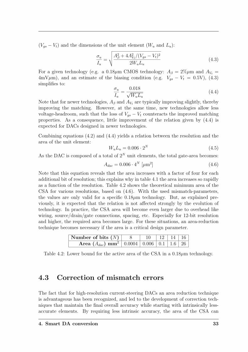
Note that this equation reveals that the area increases with a factor of four for eachadditional bit of resolution; this explains why in table 4.1 the area increases so rapidlyas a function of the resolution. Table 4.2 shows the theoretical minimum area of theCSA for various resolutions, based on (4.6). With the used mismatch-parameters,the values are only valid for a specific 0.18µm technology. But, as explained pre-viously, it is expected that the relation is not affected strongly by the evolution oftechnology. In practice, the CSA area will become even larger due to overhead likewiring, source/drain/gate connections, spacing, etc. Especially for 12-bit resolutionand higher, the required area becomes large. For these situations, an area-reductiontechnique becomes necessary if the area is a critical design parameter.
Number of bits (N) 8 10 12 14 16Area (Adac) mm2 0.0004 0.006 0.1 1.6 26
Table 4.2: Lower bound for the active area of the CSA in a 0.18µm technology.
4.3 Correction of mismatch errors
The fact that for high-resolution current-steering DACs an area reduction techniqueis advantageous has been recognized, and led to the development of correction tech-niques that maintain the final overall accuracy while starting with intrinsically less-accurate elements. By requiring less intrinsic accuracy, the area of the CSA can
4. Smart DA conversion 33
be reduced. A classification and an explanation of the existing methods for areareduction can be found in [11].
Table 4.3 gives an overview of recent work on designs that include some form ofmismatch-correction to achieve area-reduction. In [24], a reshuffling method is used toorder the elements in such a way that the accuracy improves. In the other approaches,the main current sources are calibrated by trimming or by adding a calibration currentto compensate for the mismatch. In the table, the CSA area includes the area of thenominal current sources plus the area of the calibration sources.
Reference Technology Sampling rate Resolution ENOB Total area CSA area(MSps) (bit) (bit) (mm2) (mm2)
[13], 2005 0.25µm 50 12 11.7 1.1 0.3[25], 2008 0.18µm 100 12 13.3 0.8 0.2[24], 2007 0.18µm 200 14 12.5 3 0.28[26], 2004 0.18µm 200 14 13.6 1 0.5[27], 2001 0.18µm 100 14 14 1 0.3[28], 2003 0.13µm 100 14 14.2 0.1 0.05[29], 2000 0.35µm 100 14 14.5 11.8 1.8[12], 2003 0.25µm 400 16 16 2 0.8
Table 4.3: Area of corrected DA converters.
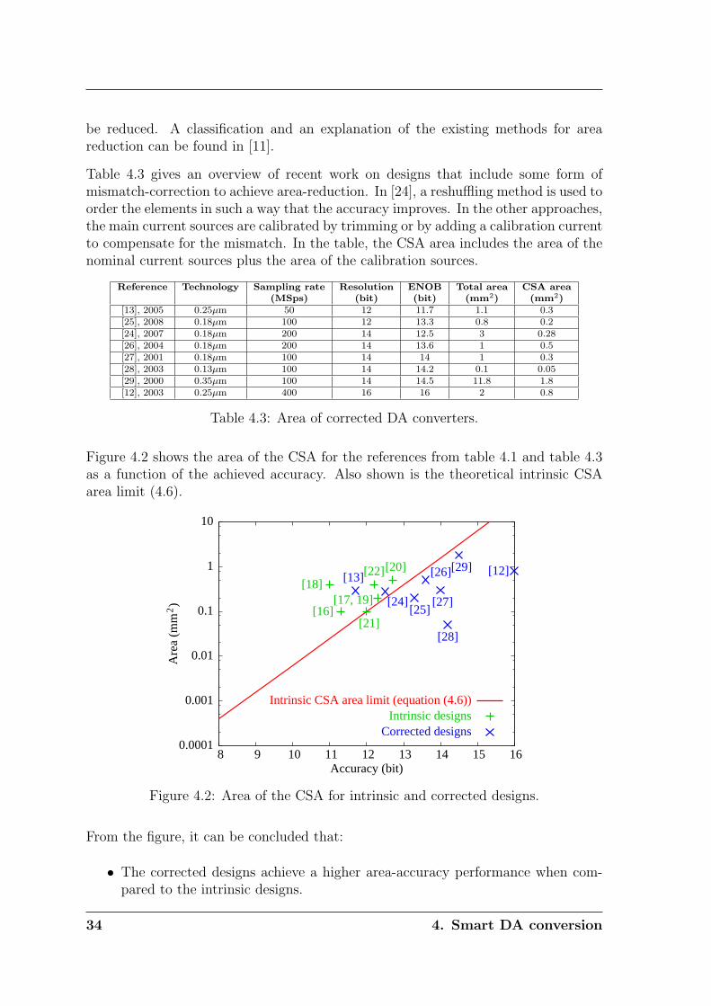
Figure 4.2 shows the area of the CSA for the references from table 4.1 and table 4.3as a function of the achieved accuracy. Also shown is the theoretical intrinsic CSAarea limit (4.6).
0.0001
0.001
0.01
0.1
1
10
8 9 10 11 12 13 14 15 16
Are
a (m
m )2
Accuracy (bit)
Intrinsic CSA area limit (equation (4.6))Intrinsic designs
[16][17, 19]
[18][20]
[21]
[22]
Corrected designs
[13]
[25][24]
[26]
[27]
[28]
[29] [12]
Figure 4.2: Area of the CSA for intrinsic and corrected designs.
From the figure, it can be concluded that:
• The corrected designs achieve a higher area-accuracy performance when com-pared to the intrinsic designs.
34 4. Smart DA conversion
• The intrinsic designs can never achieve an area below the intrinsic CSA-limit;the corrected designs can achieve an area around or below the CSA-limit.
• In most cases, the corrected designs aim for a higher resolution and a higheraccuracy than the intrinsic designs.
Though the calibration methods can overcome the intrinsic CSA area limitation, thearea improvement is practically limited as the number of current elements increasesto facilitate calibration: next to the main current sources, also calibration sources arerequired. As soon as the area of the unit elements becomes substantially reduced, itis not the area of the elements but simply the amount of elements that determinesthe overall CSA area. This is because the overhead caused by e.g. wiring and spacingwill increase as a function of the number of elements, such that the overhead-areawill become dominant.
Concluding from the results of intrinsic and corrected designs, there are two factorsthat determine the CSA area; and both should be minimized in order to minimizethe CSA area:
• The area of the current-source elements.
• The number of current-source elements.
In the following section, an approach is proposed that aims at minimizing both thesefactors to achieve a further reduction of the CSA area.
4.4 Sub-binary variable-radix DAC
4.4.1 System overview
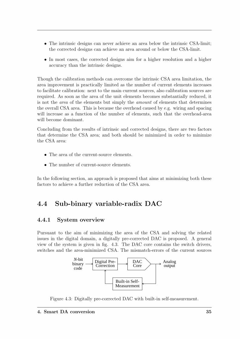
Pursuant to the aim of minimizing the area of the CSA and solving the relatedissues in the digital domain, a digitally pre-corrected DAC is proposed. A generalview of the system is given in fig. 4.3. The DAC core contains the switch drivers,switches and the area-minimized CSA. The mismatch-errors of the current sources
N-bitbinarycode
Digital Pre-Correction
DACCore
Built-in Self-Measurement
Analogoutput
Figure 4.3: Digitally pre-corrected DAC with built-in self-measurement.
4. Smart DA conversion 35
are corrected by the digital pre-correction block that re-maps the binary input codesto appropriate combinations of current sources. A built-in measurement algorithmis used to measure the actual deviations of the individual current sources, such thatthe digital pre-correction algorithm can determine a suitable combination of currentsources for each input code.
As a starting point for minimizing the CSA area, a first consideration is the segmenta-tion of the current sources. The segmentation determines the number of independentcurrent sources within the CSA. The three common options are:
• Binary architecture; composed of N binary-scaled current sources.
• Thermometer architecture; composed of 2N − 1 unary-scaled current sources.
• Segmented architecture; composed of a M binary-scaled and 2N−M − 1 unary-scaled current sources, with 1 ≤ M < N .
From these options, the binary architecture has the least number of independentsources. As a consequence, according to the conclusion from the previous section, thebinary architecture should have the potential to achieve the smallest CSA area.
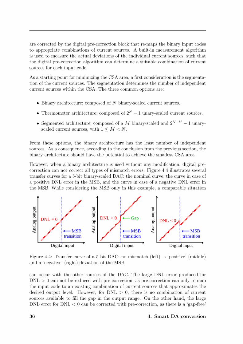
However, when a binary architecture is used without any modification, digital pre-correction can not correct all types of mismatch errors. Figure 4.4 illustrates severaltransfer curves for a 5-bit binary-scaled DAC: the nominal curve, the curve in case ofa positive DNL error in the MSB, and the curve in case of a negative DNL error inthe MSB. While considering the MSB only in this example, a comparable situation
Digital input
Ana
log
outp
ut
DNL = 0
MSBtransition
Digital input
Ana
log
outp
ut
DNL > 0 Gap
MSBtransition
Digital input
Ana
log
outp
ut
DNL < 0
MSBtransition
Figure 4.4: Transfer curve of a 5-bit DAC: no mismatch (left), a ‘positive’ (middle)and a ‘negative’ (right) deviation of the MSB.
can occur with the other sources of the DAC. The large DNL error produced forDNL > 0 can not be reduced with pre-correction, as pre-correction can only re-mapthe input code to an existing combination of current sources that approximates thedesired output level. However, for DNL > 0, there is no combination of currentsources available to fill the gap in the output range. On the other hand, the largeDNL error for DNL < 0 can be corrected with pre-correction, as there is a ‘gap-free’
36 4. Smart DA conversion
continuum of output levels. By digital re-mapping, the overlap (or non-monotonicity)of the curve can be removed to obtain a smooth transfer curve. However, as a sideeffect of the overlap, the full-scale range of this converter will be slightly smaller thanusual.
In short, for the digital pre-correction to operate properly, ‘gaps’ (DNL > 0) arenot allowed but ‘overlap’ (DNL < 0) is allowed. As the nominal transfer curve of anormal DAC is designed for DNL = 0, there is a 50% probability that a ‘gap’ willoccur in reality. By means of redundancy, the probability of a ‘gap’ can be reducedto an arbitrary low value by design: instead of designing the nominal transfer curveas in fig. 4.4 (left), it is designed as in fig. 4.4 (right). Thus, redundancy introducesintentional overlap (DNL < 0) of the nominal transfer curve to guarantee that thecontinuum of the output range remains, also in case of mismatch. While the figureillustrates redundancy for the MSB only, in reality this redundancy requirement needsto be implemented for each bit of the converter. In a certain way, adding calibrationcurrent sources (as in a.o. [11]) adds redundancy. However, that approach also leadsto a substantial increase of the amount of current sources; which is undesirable asexplained in the previous section. Therefore, in this work, the use of a sub-binaryradix is proposed to introduce redundancy while limiting the total number of currentsources.
Note that the fundamental principle of a sub-binary radix for DACs is equivalent tothe principle of a sub-binary radix for ADCs (as explained in e.g. [30]): in ADCs theredundancy is used to alleviate the effect of comparator mismatch, whereas in DACs,the redundancy is used to alleviate the effect of current source mismatch. Also notethat, independently from this work, prior art on sub-binary radix DACs exists [31],but that work does not mathematically optimize the redundancy, uses a fixed insteadof a variable radix, and requires a more complex measurement method.
In the following sections, the design of the DAC core with redundancy, the self-measurement structure and the digital pre-correction algorithm will be explained.
4.4.2 Redundancy
A normal N -bit binary converter is composed of k = N current sources. Thesesources I0 (LSB) up to Ik−1 (MSB) are chosen relatively to the unit element Iu usingthe ratios α0 up to αk−1. The ratios αi are chosen such that each source is exactly 1LSB larger than the sum of all smaller sources:
αj =j−1∑
i=0
αi + 1 for 0 ≤ j < k , (4.7)
leading to the binary-scaled sequence of α’s: 1, 2, 4, 8, 16, · · ·. However, when dueto mismatch one of the current sources is actually larger than expected, a ‘gap’ (asin fig. 4.4) arises, that can not be corrected with digital pre-correction. To avoid this
4. Smart DA conversion 37
situation, redundancy is added by making αj intentionally smaller than the sum ofall smaller sources plus one LSB:
αj <j−1∑
i=0
αi + 1 for 0 ≤ j < k (4.8)
An example of a sequence, fulfilling this constraint, is e.g.: 0.7, 1.3, 2.4, 4.6, 8.8, . . ..The amount of redundancy rj for each source can be expressed as:
rj = 1− αj +j−1∑
i=0
αi for 0 ≤ j < k , (4.9)
Thus, for rj = 0, there is no redundancy and (4.9) simplifies to (4.7). To maintainredundancy, for all sources the following requirement has to be satisfied:
rj > 0 for 0 ≤ j < k (4.10)
The more redundancy is added, the more severe deviations due to mismatch can becompensated by pre-correction. However, also note that the more redundancy, themore sources k have to be employed to compensate the full-scale reduction of theconverter due to redundancy.
Due to the stochastic spread of the unit cells, the actual value of each source becomesa stochastic value αi with mean αi (the designed value) and spread
√αi
σu
Iu. To
guarantee that all required output levels can be produced with sufficient accuracyusing pre-correction, the relations from (4.9) and (4.10), taking the stochastic spreadof the sources into account, have to be fulfilled. This leads to the following set ofrequirements:
rj > 0 for 0 ≤ j < k , with: (4.11)
Erj = 1− αj +j−1∑
i=0
αi
σrj=
σu
Iu
√√√√j∑
i=0
αi ,
where Erj is the expectation of rj, thus the nominal built-in redundancy. σrjis the
spread of rj, which corresponds to the mismatch of the elements. When all constraintsrj are fulfilled, the largest ‘gap’ in the transfer curve is guaranteed to be less than 1LSB. Thus, each required output level can be generated within ±0.5LSB by means ofre-mapping the input code, which is sufficient for meeting the target accuracy. Thedesired probability of fulfilling each constraint rj can be expressed as a desired levelof confidence λσ with which the constraint has to be fulfilled:
Prj > 0 = 1− 1
2erfc
( λ√2
)(4.12)
The confidence level requires that:
Erj − λσrj= 0 , (4.13)
38 4. Smart DA conversion
i.e.: a λσ deviation from the nominal value E· is still marginally acceptable for thetarget requirement (4.11). Using equation (4.11), (4.13) can be rewritten as:
Erj = λσrj(4.14)
1− αj +j−1∑
i=0
αi = λσu
Iu
√√√√j∑
i=0
αi
(1 +
j−1∑
i=0
αi
)2
+ α2j − 2αj
(1 +
j−1∑
i=0
αi
)=
(λσu
Iu
)2 j∑
i=0
αi
⇒α2
j − bjαj + cj = 0, with
bj = 2
(1 +
j−1∑
i=0
αi
)+
(λσu
Iu
)2
cj =
(1 +
j−1∑
i=0
αi
)2
−(
λσu
Iu
)2 j−1∑
i=0
αi
From this quadratic function of αj, the values of αj can be derived recursively giventhe relative spread of the unit cells and a desired confidence level:
αj =bj −
√b2j − 4cj
2, with bj and cj as in (4.14). (4.15)
As opposed to previous work [31], where a fixed sub-binary radix was used, thepresented approach utilizes a variable radix ρj. The radix is the ratio between twosubsequent current sources:
ρj =αj
αj−1
(4.16)
The variable radix stems from the design procedure equalizing the error probabilityfor each constraint (4.15). By equalizing the error probability and adapting the radix,instead of equalizing the radix and adapting the error probability as in [31], the sameyield can be achieved with less redundancy and hence less current sources. Moreover,as in the presented approach, ρj approximates 2 for j →∞, the amount of sources krequired for a converter with redundancy comes close to the minimal value N as usedin a binary-weighted converter without redundancy. Simulation results to confirmthe advantages of the variable-radix over the fixed-radix will be shown in section 4.5.
4.4.3 Self-measurement
Before being able to pre-correct the mismatch errors of the current sources, a mea-surement procedure, measuring the actual values of the current sources, is required.After performing the self-measurement procedure at power-up, the actual values ofthe current sources are known in the digital domain, and the converter can start itsnormal ADC operation.
4. Smart DA conversion 39
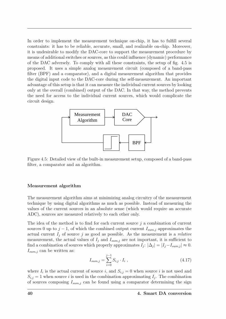
In order to implement the measurement technique on-chip, it has to fulfill severalconstraints: it has to be reliable, accurate, small, and realizable on-chip. Moreover,it is undesirable to modify the DAC-core to support the measurement procedure bymeans of additional switches or sources, as this could influence (dynamic) performanceof the DAC adversely. To comply with all these constraints, the setup of fig. 4.5 isproposed. It uses a simple analog measurement circuit (composed of a band-passfilter (BPF) and a comparator), and a digital measurement algorithm that providesthe digital input code to the DAC-core during the self-measurement. An importantadvantage of this setup is that it can measure the individual current sources by lookingonly at the overall (combined) output of the DAC. In that way, the method preventsthe need for access to the individual current sources, which would complicate thecircuit design.
MeasurementAlgorithm
DACCore
BPF
Figure 4.5: Detailed view of the built-in measurement setup, composed of a band-passfilter, a comparator and an algorithm.
Measurement algorithm
The measurement algorithm aims at minimizing analog circuitry of the measurementtechnique by using digital algorithms as much as possible. Instead of measuring thevalues of the current sources in an absolute sense (which would require an accurateADC), sources are measured relatively to each other only.
The idea of the method is to find for each current source j a combination of currentsources 0 up to j − 1, of which the combined output current Isum,j approximates theactual current Ij of source j as good as possible. As the measurement is a relativemeasurement, the actual values of Ij and Isum,j are not important, it is sufficient tofind a combination of sources which properly approximates Ij: |∆j| = |Ij−Isum,j| ≈ 0.Isum,j can be written as:
Isum,j =j−1∑
i=0
Si,j · Ii , (4.17)
where Ii is the actual current of source i, and Si,j = 0 when source i is not used andSi,j = 1 when source i is used in the combination approximating Ij. The combinationof sources composing Isum,j can be found using a comparator determining the sign
40 4. Smart DA conversion
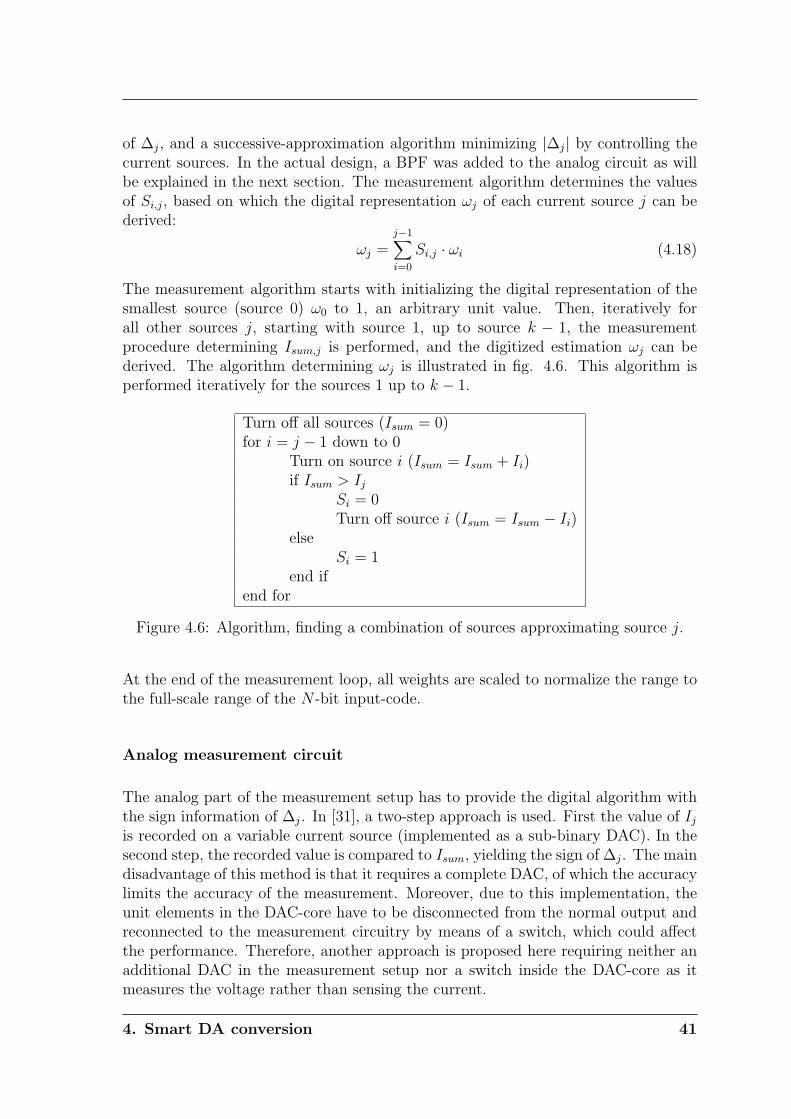
of ∆j, and a successive-approximation algorithm minimizing |∆j| by controlling thecurrent sources. In the actual design, a BPF was added to the analog circuit as willbe explained in the next section. The measurement algorithm determines the valuesof Si,j, based on which the digital representation ωj of each current source j can bederived:
ωj =j−1∑
i=0
Si,j · ωi (4.18)
The measurement algorithm starts with initializing the digital representation of thesmallest source (source 0) ω0 to 1, an arbitrary unit value. Then, iteratively forall other sources j, starting with source 1, up to source k − 1, the measurementprocedure determining Isum,j is performed, and the digitized estimation ωj can bederived. The algorithm determining ωj is illustrated in fig. 4.6. This algorithm isperformed iteratively for the sources 1 up to k − 1.
Turn off all sources (Isum = 0)for i = j − 1 down to 0
Turn on source i (Isum = Isum + Ii)if Isum > Ij
Si = 0Turn off source i (Isum = Isum − Ii)
elseSi = 1
end ifend for
Figure 4.6: Algorithm, finding a combination of sources approximating source j.
At the end of the measurement loop, all weights are scaled to normalize the range tothe full-scale range of the N -bit input-code.
Analog measurement circuit
The analog part of the measurement setup has to provide the digital algorithm withthe sign information of ∆j. In [31], a two-step approach is used. First the value of Ij
is recorded on a variable current source (implemented as a sub-binary DAC). In thesecond step, the recorded value is compared to Isum, yielding the sign of ∆j. The maindisadvantage of this method is that it requires a complete DAC, of which the accuracylimits the accuracy of the measurement. Moreover, due to this implementation, theunit elements in the DAC-core have to be disconnected from the normal output andreconnected to the measurement circuitry by means of a switch, which could affectthe performance. Therefore, another approach is proposed here requiring neither anadditional DAC in the measurement setup nor a switch inside the DAC-core as itmeasures the voltage rather than sensing the current.
4. Smart DA conversion 41
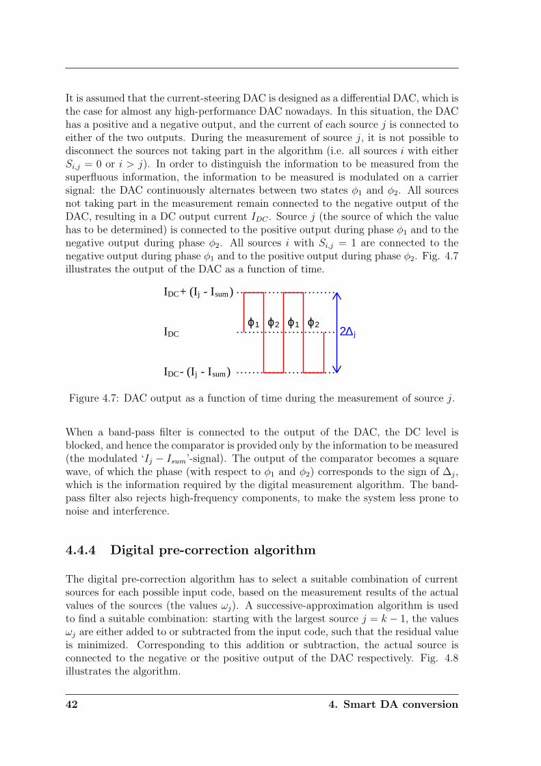
It is assumed that the current-steering DAC is designed as a differential DAC, which isthe case for almost any high-performance DAC nowadays. In this situation, the DAChas a positive and a negative output, and the current of each source j is connected toeither of the two outputs. During the measurement of source j, it is not possible todisconnect the sources not taking part in the algorithm (i.e. all sources i with eitherSi,j = 0 or i > j). In order to distinguish the information to be measured from thesuperfluous information, the information to be measured is modulated on a carriersignal: the DAC continuously alternates between two states φ1 and φ2. All sourcesnot taking part in the measurement remain connected to the negative output of theDAC, resulting in a DC output current IDC . Source j (the source of which the valuehas to be determined) is connected to the positive output during phase φ1 and to thenegative output during phase φ2. All sources i with Si,j = 1 are connected to thenegative output during phase φ1 and to the positive output during phase φ2. Fig. 4.7illustrates the output of the DAC as a function of time.
I - (I - I )
I
I + (I - I )
DC
DC
DC
j
j
sum
sum
j2∆ϕ ϕ ϕ ϕ1 2 1 2
Figure 4.7: DAC output as a function of time during the measurement of source j.
When a band-pass filter is connected to the output of the DAC, the DC level isblocked, and hence the comparator is provided only by the information to be measured(the modulated ‘Ij − Isum’-signal). The output of the comparator becomes a squarewave, of which the phase (with respect to φ1 and φ2) corresponds to the sign of ∆j,which is the information required by the digital measurement algorithm. The band-pass filter also rejects high-frequency components, to make the system less prone tonoise and interference.
4.4.4 Digital pre-correction algorithm
The digital pre-correction algorithm has to select a suitable combination of currentsources for each possible input code, based on the measurement results of the actualvalues of the sources (the values ωj). A successive-approximation algorithm is usedto find a suitable combination: starting with the largest source j = k − 1, the valuesωj are either added to or subtracted from the input code, such that the residual valueis minimized. Corresponding to this addition or subtraction, the actual source isconnected to the negative or the positive output of the DAC respectively. Fig. 4.8illustrates the algorithm.
42 4. Smart DA conversion
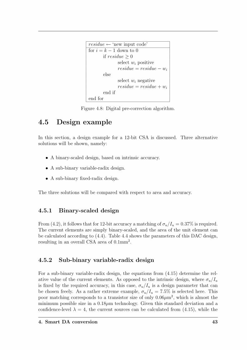
residue ← ‘new input code’for i = k − 1 down to 0
if residue ≥ 0select wi positiveresidue = residue− wi
elseselect wi negativeresidue = residue + wi
end ifend for
Figure 4.8: Digital pre-correction algorithm.
4.5 Design example
In this section, a design example for a 12-bit CSA is discussed. Three alternativesolutions will be shown, namely:
• A binary-scaled design, based on intrinsic accuracy.
• A sub-binary variable-radix design.
• A sub-binary fixed-radix design.
The three solutions will be compared with respect to area and accuracy.
4.5.1 Binary-scaled design
From (4.2), it follows that for 12-bit accuracy a matching of σu/Iu = 0.37% is required.The current elements are simply binary-scaled, and the area of the unit element canbe calculated according to (4.4). Table 4.4 shows the parameters of this DAC design,resulting in an overall CSA area of 0.1mm2.
4.5.2 Sub-binary variable-radix design
For a sub-binary variable-radix design, the equations from (4.15) determine the rel-ative value of the current elements. As opposed to the intrinsic design, where σu/Iu
is fixed by the required accuracy, in this case, σu/Iu is a design parameter that canbe chosen freely. As a rather extreme example, σu/Iu = 7.5% is selected here. Thispoor matching corresponds to a transistor size of only 0.06µm2, which is almost theminimum possible size in a 0.18µm technology. Given this standard deviation and aconfidence-level λ = 4, the current sources can be calculated from (4.15), while the
4. Smart DA conversion 43
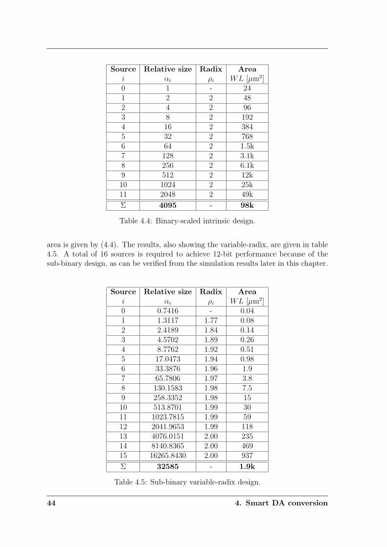
Source Relative size Radix Areai αi ρi WL [µm2]0 1 - 241 2 2 482 4 2 963 8 2 1924 16 2 3845 32 2 7686 64 2 1.5k7 128 2 3.1k8 256 2 6.1k9 512 2 12k10 1024 2 25k11 2048 2 49k
Σ 4095 - 98k
Table 4.4: Binary-scaled intrinsic design.
area is given by (4.4). The results, also showing the variable-radix, are given in table4.5. A total of 16 sources is required to achieve 12-bit performance because of thesub-binary design, as can be verified from the simulation results later in this chapter.
Source Relative size Radix Areai αi ρi WL [µm2]0 0.7416 - 0.041 1.3117 1.77 0.082 2.4189 1.84 0.143 4.5702 1.89 0.264 8.7762 1.92 0.515 17.0473 1.94 0.986 33.3876 1.96 1.97 65.7806 1.97 3.88 130.1583 1.98 7.59 258.3352 1.98 1510 513.8701 1.99 3011 1023.7815 1.99 5912 2041.9653 1.99 11813 4076.0151 2.00 23514 8140.8365 2.00 46915 16265.8430 2.00 937
Σ 32585 - 1.9k
Table 4.5: Sub-binary variable-radix design.
44 4. Smart DA conversion
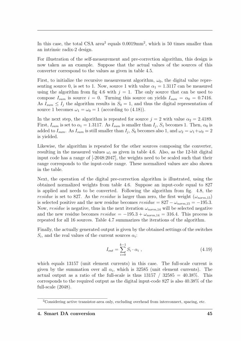
In this case, the total CSA area2 equals 0.0019mm2, which is 50 times smaller thanan intrinsic radix-2 design.
For illustration of the self-measurement and pre-correction algorithm, this design isnow taken as an example. Suppose that the actual values of the sources of thisconverter correspond to the values as given in table 4.5.
First, to initialize the recursive measurement algorithm, ω0, the digital value repre-senting source 0, is set to 1. Now, source 1 with value α1 = 1.3117 can be measuredusing the algorithm from fig 4.6 with j = 1. The only source that can be used tocompose Isum is source i = 0. Turning this source on yields Isum = α0 = 0.7416.As Isum ≤ Ij the algorithm results in S0 = 1, and thus the digital representation ofsource 1 becomes ω1 = ω0 = 1 (according to (4.18)).
In the next step, the algorithm is repeated for source j = 2 with value α2 = 2.4189.First, Isum is set to α1 = 1.3117. As Isum is smaller than Ij, S1 becomes 1. Then, α0 isadded to Isum. As Isum is still smaller than Ij, S0 becomes also 1, and ω2 = ω1+ω0 = 2is yielded.
Likewise, the algorithm is repeated for the other sources composing the converter,resulting in the measured values ωi as given in table 4.6. Also, as the 12-bit digitalinput code has a range of [-2048:2047], the weights need to be scaled such that theirrange corresponds to the input-code range. These normalized values are also shownin the table.
Next, the operation of the digital pre-correction algorithm is illustrated, using theobtained normalized weights from table 4.6. Suppose an input-code equal to 827is applied and needs to be converted. Following the algorithm from fig. 4.8, theresidue is set to 827. As the residue is larger than zero, the first weight (ωnorm,15)is selected positive and the new residue becomes residue = 827− ωnorm,15 = −195.3.Now, residue is negative, thus in the next iteration ωnorm,14 will be selected negativeand the new residue becomes residue = −195.3 + ωnorm,14 = 316.4. This process isrepeated for all 16 sources. Table 4.7 summarizes the iterations of the algorithm.
Finally, the actually generated output is given by the obtained settings of the switchesSi, and the real values of the current sources αi:
Iout =k−1∑
i=0
Si · αi , (4.19)
which equals 13157 (unit element currents) in this case. The full-scale current isgiven by the summation over all αi, which is 32585 (unit element currents). Theactual output as a ratio of the full-scale is thus 13157 / 32585 = 40.38%. Thiscorresponds to the required output as the digital input-code 827 is also 40.38% of thefull-scale (2048).
2Considering active transistor-area only, excluding overhead from interconnect, spacing, etc.
4. Smart DA conversion 45
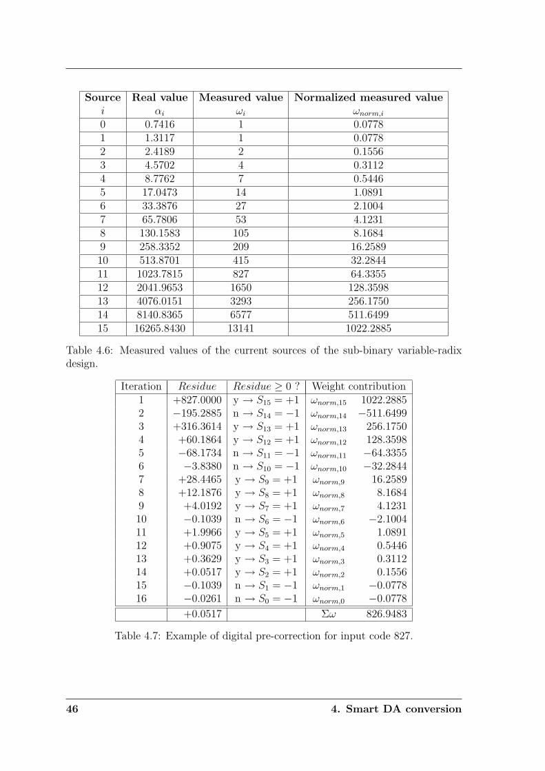
Source Real value Measured value Normalized measured valuei αi ωi ωnorm,i
0 0.7416 1 0.07781 1.3117 1 0.07782 2.4189 2 0.15563 4.5702 4 0.31124 8.7762 7 0.54465 17.0473 14 1.08916 33.3876 27 2.10047 65.7806 53 4.12318 130.1583 105 8.16849 258.3352 209 16.258910 513.8701 415 32.284411 1023.7815 827 64.335512 2041.9653 1650 128.359813 4076.0151 3293 256.175014 8140.8365 6577 511.649915 16265.8430 13141 1022.2885
Table 4.6: Measured values of the current sources of the sub-binary variable-radixdesign.
Iteration Residue Residue ≥ 0 ? Weight contribution1 +827.0000 y → S15 = +1 ωnorm,15 1022.28852 −195.2885 n → S14 = −1 ωnorm,14 −511.64993 +316.3614 y → S13 = +1 ωnorm,13 256.17504 +60.1864 y → S12 = +1 ωnorm,12 128.35985 −68.1734 n → S11 = −1 ωnorm,11 −64.33556 −3.8380 n → S10 = −1 ωnorm,10 −32.28447 +28.4465 y → S9 = +1 ωnorm,9 16.25898 +12.1876 y → S8 = +1 ωnorm,8 8.16849 +4.0192 y → S7 = +1 ωnorm,7 4.123110 −0.1039 n → S6 = −1 ωnorm,6 −2.100411 +1.9966 y → S5 = +1 ωnorm,5 1.089112 +0.9075 y → S4 = +1 ωnorm,4 0.544613 +0.3629 y → S3 = +1 ωnorm,3 0.311214 +0.0517 y → S2 = +1 ωnorm,2 0.155615 −0.1039 n → S1 = −1 ωnorm,1 −0.077816 −0.0261 n → S0 = −1 ωnorm,0 −0.0778
+0.0517 Σω 826.9483
Table 4.7: Example of digital pre-correction for input code 827.
46 4. Smart DA conversion
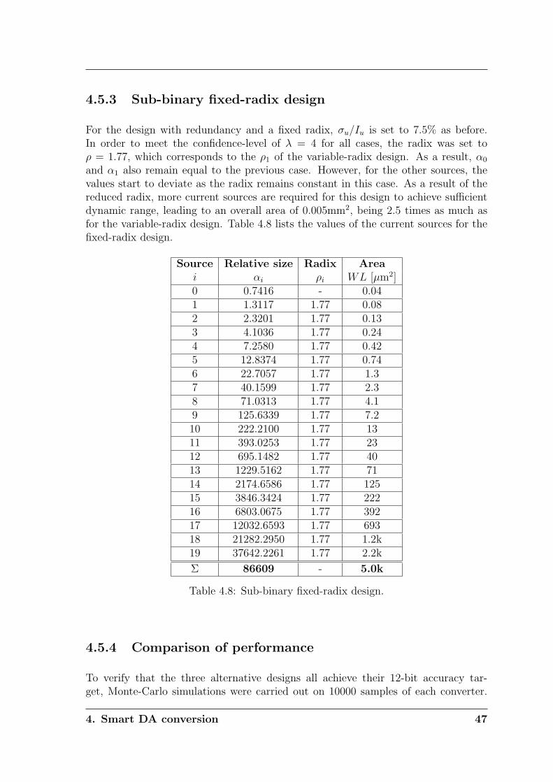
4.5.3 Sub-binary fixed-radix design
For the design with redundancy and a fixed radix, σu/Iu is set to 7.5% as before.In order to meet the confidence-level of λ = 4 for all cases, the radix was set toρ = 1.77, which corresponds to the ρ1 of the variable-radix design. As a result, α0
and α1 also remain equal to the previous case. However, for the other sources, thevalues start to deviate as the radix remains constant in this case. As a result of thereduced radix, more current sources are required for this design to achieve sufficientdynamic range, leading to an overall area of 0.005mm2, being 2.5 times as much asfor the variable-radix design. Table 4.8 lists the values of the current sources for thefixed-radix design.
Source Relative size Radix Areai αi ρi WL [µm2]0 0.7416 - 0.041 1.3117 1.77 0.082 2.3201 1.77 0.133 4.1036 1.77 0.244 7.2580 1.77 0.425 12.8374 1.77 0.746 22.7057 1.77 1.37 40.1599 1.77 2.38 71.0313 1.77 4.19 125.6339 1.77 7.210 222.2100 1.77 1311 393.0253 1.77 2312 695.1482 1.77 4013 1229.5162 1.77 7114 2174.6586 1.77 12515 3846.3424 1.77 22216 6803.0675 1.77 39217 12032.6593 1.77 69318 21282.2950 1.77 1.2k19 37642.2261 1.77 2.2k
Σ 86609 - 5.0k
Table 4.8: Sub-binary fixed-radix design.
4.5.4 Comparison of performance
To verify that the three alternative designs all achieve their 12-bit accuracy tar-get, Monte-Carlo simulations were carried out on 10000 samples of each converter.
4. Smart DA conversion 47

Mismatch was added to each unit-source, corresponding to σu
Iu= 0.37% for the in-
trinsic design and σu
Iu= 7.5% for the other two designs. For the two sub-binary
designs, an implemented measurement algorithm was used to determine the digitalcoefficients representing the values of the current sources, based on which the digitalpre-correction algorithm was applied. Fig. 4.9 shows the achieved INL and DNL forall converters. Most converters achieve the 0.5LSB target for INL and DNL. Thevariable-radix design achieves the best performance, revealing that it is somewhatoverdesigned compared to the other designs, i.e. the area of the variable-radix couldbe further reduced while maintaining 12-bit accuracy.
An overview of the specifications, including the CSA area and the required numberof independent current sources is given in table 4.9.
Accuracy Transistor Number ofarea sources
Binary intrinsic design 12bit 0.1mm2 12Sub-binary variable-radix design 12bit 0.0019mm2 16Sub-binary fixed-radix design 12bit 0.005mm2 20
Table 4.9: Comparison of DAC performances.
From the table, the following conclusions can be drawn for this 12-bit example:
• The variable-radix design achieves the smallest area, about 50x smaller com-pared to the intrinsic design and also substantially smaller than the fixed-radixdesign.
• The variable-radix design requires only 16 sources, which is 4 more comparedto an intrinsic design and 4 less compared to the fixed-radix design. None ofthe current-source calibration methods from section 4.3 can achieve this smalloverhead in number of elements.
For higher resolutions, there is even more advantage for a sub-binary variable-radixdesign. For example, consider a 13-bit DAC design: in case of an intrinsic-design,the area will increase with a factor of four compared to the 12-bit design. For thesub-binary variable-radix design, as the same 7.5% unit mismatch can be tolerated,one only needs to add more sources to achieve the new full-scale range. As for thelargest sources the radix approximates two, one additional source will be sufficient.Thus, the area increase is a factor of two in this situation. The same reasoning holdsfor the sub-binary fixed-radix design. However, as the radix remains smaller thantwo in that case, one might need to add more than one source to achieve the requiredfull-scale range, thus achieving on the average an area increase of somewhat morethan a factor of two.
48 4. Smart DA conversion
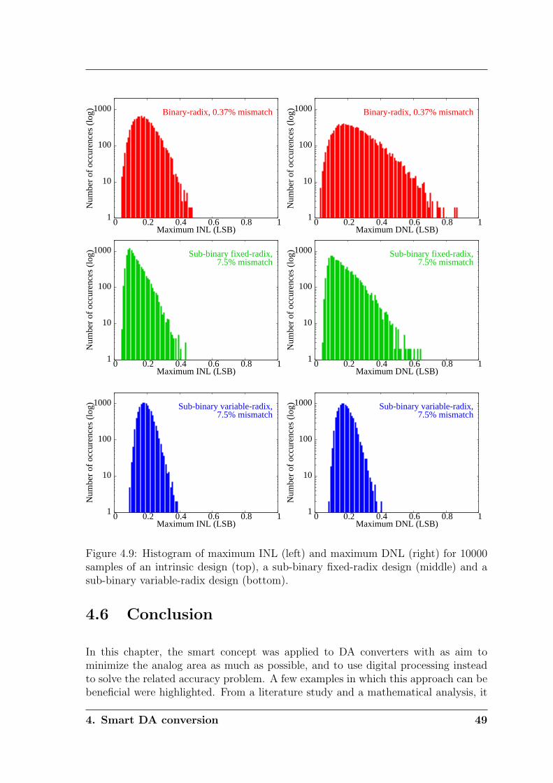
1
10
100
1000
0 0.2 0.4 0.6 0.8 1
Num
ber
of o
ccur
ence
s (l
og)
Maximum INL (LSB)
Binary-radix, 0.37% mismatch
1
10
100
1000
0 0.2 0.4 0.6 0.8 1
Num
ber
of o
ccur
ence
s (l
og)
Maximum DNL (LSB)
Binary-radix, 0.37% mismatch
1
10
100
1000
0 0.2 0.4 0.6 0.8 1
Num
ber
of o
ccur
ence
s (l
og)
Maximum INL (LSB)
Sub-binary fixed-radix,7.5% mismatch
1
10
100
1000
0 0.2 0.4 0.6 0.8 1
Num
ber
of o
ccur
ence
s (l
og)
Maximum DNL (LSB)
Sub-binary fixed-radix,7.5% mismatch
1
10
100
1000
0 0.2 0.4 0.6 0.8 1
Num
ber
of o
ccur
ence
s (l
og)
Maximum INL (LSB)
Sub-binary variable-radix,7.5% mismatch
1
10
100
1000
0 0.2 0.4 0.6 0.8 1
Num
ber
of o
ccur
ence
s (l
og)
Maximum DNL (LSB)
Sub-binary variable-radix,7.5% mismatch
Figure 4.9: Histogram of maximum INL (left) and maximum DNL (right) for 10000samples of an intrinsic design (top), a sub-binary fixed-radix design (middle) and asub-binary variable-radix design (bottom).
4.6 Conclusion
In this chapter, the smart concept was applied to DA converters with as aim tominimize the analog area as much as possible, and to use digital processing insteadto solve the related accuracy problem. A few examples in which this approach can bebeneficial were highlighted. From a literature study and a mathematical analysis, it
4. Smart DA conversion 49

was shown that area is an issue for high-resolution DAC design. In order to reduce theoverall area both the area of the unit elements and the number of unit elements haveto be minimized. A new concept, based on a sub-binary variable-radix current-source-array was developed that can achieve both targets. The required self-measurementand self-correction technique were explained and verified with a design example. Inthe next chapter, the theory of a sub-binary variable-radix design will be verified witha chip implementation.
50 4. Smart DA conversion
Chapter 5
Design of a sub-binaryvariable-radix DAC
This chapter discusses the chip-implementation and experimental verification of asub-binary variable-radix DAC, according to the theory presented in chapter 4. Thecircuit-level design is described in section 5.1 and the layout in section 5.2. The off-chip implementation of the self-measurement circuit is shown in section 5.3. Then,experimental results and conclusions are given in section 5.4 and section 5.5, respec-tively.
5.1 Schematic design
In this section, the circuit-level design of the DAC in a 0.18µm CMOS technologyis reviewed. Corresponding to the architecture from fig. 4.1, the schematic wasimplemented as shown in fig. 5.1. For this design, the digital pre-processor andthe measurement circuitry were implemented off-chip. The main components (serial-in/parallel-out register, switch driver, switches and CSA) will be discussed next. Theserial-in/parallel-out register operates at 1.8V to comply with the external interface,but the DAC itself is designed to operate at a supply of 1.4V only. The selection ofthe low supply has two reasons: first, it will prove that the DAC design allows low-voltage operation while maintaining sufficient linearity, which is a necessity for futurelow-voltage technologies. Secondly, the DAC will be used as an on-chip test-signalgenerator for the T&H (see chapter 7). With the selected supply, the DAC generatesa differential voltage swing of 1Vpp around a common-mode level of 1.15V, which issuitable for the T&H.
5. Design of a sub-binary variable-radix DAC 51
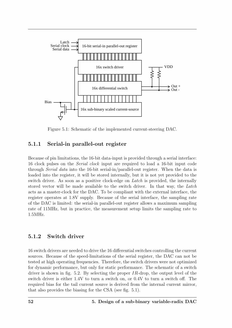
16-bit serial-in parallel-out register
16x switch driver
16x differential switch
16x sub-binary scaled current-source
Bias
Serial dataSerial clock
Latch
VDD
Out -Out +
Figure 5.1: Schematic of the implemented current-steering DAC.
5.1.1 Serial-in parallel-out register
Because of pin limitations, the 16-bit data-input is provided through a serial interface:16 clock pulses on the Serial clock input are required to load a 16-bit input codethrough Serial data into the 16-bit serial-in/parallel-out register. When the data isloaded into the register, it will be stored internally, but it is not yet provided to theswitch driver. As soon as a positive clock-edge on Latch is provided, the internallystored vector will be made available to the switch driver. In that way, the Latchacts as a master-clock for the DAC. To be compliant with the external interface, theregister operates at 1.8V supply. Because of the serial interface, the sampling rateof the DAC is limited: the serial-in parallel-out register allows a maximum samplingrate of 11MHz, but in practice, the measurement setup limits the sampling rate to1.5MHz.
5.1.2 Switch driver
16 switch drivers are needed to drive the 16 differential switches controlling the currentsources. Because of the speed-limitations of the serial register, the DAC can not betested at high operating frequencies. Therefore, the switch drivers were not optimizedfor dynamic performance, but only for static performance. The schematic of a switchdriver is shown in fig. 5.2. By selecting the proper IR-drop, the output level of theswitch driver is either 1.4V to turn a switch on, or 0.4V to turn a switch off. Therequired bias for the tail current source is derived from the internal current mirror,that also provides the biasing for the CSA (see fig. 5.1).
52 5. Design of a sub-binary variable-radix DAC
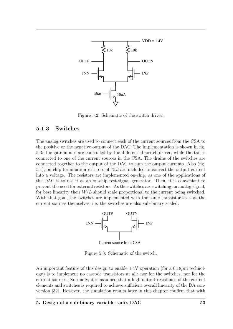
10uABias
10k
VDD = 1.4V
10k
INPINN
OUTNOUTP
Figure 5.2: Schematic of the switch driver.
5.1.3 Switches
The analog switches are used to connect each of the current sources from the CSA tothe positive or the negative output of the DAC. The implementation is shown in fig.5.3: the gate-inputs are controlled by the differential switch-driver, while the tail isconnected to one of the current sources in the CSA. The drains of the switches areconnected together to the output of the DAC to sum the output currents. Also (fig.5.1), on-chip termination resistors of 75Ω are included to convert the output currentinto a voltage. The resistors are implemented on-chip, as one of the applications ofthe DAC is to use it as an on-chip test-signal generator. Then, it is convenient toprevent the need for external resistors. As the switches are switching an analog signal,for best linearity their W/L should scale proportional to the current being switched.With that goal, the switches are implemented with the same transistor sizes as thecurrent sources themselves; i.e. the switches are also sub-binary scaled.
INPINN
OUTNOUTP
Current source from CSA
Figure 5.3: Schematic of the switch.
An important feature of this design to enable 1.4V operation (for a 0.18µm technol-ogy) is to implement no cascode transistors at all: nor for the switches, nor for thecurrent sources. Normally, it is assumed that a high output resistance of the currentelements and switches is required to achieve sufficient overall linearity of the DA con-version [32]. However, the simulation results later in this chapter confirm that with
5. Design of a sub-binary variable-radix DAC 53
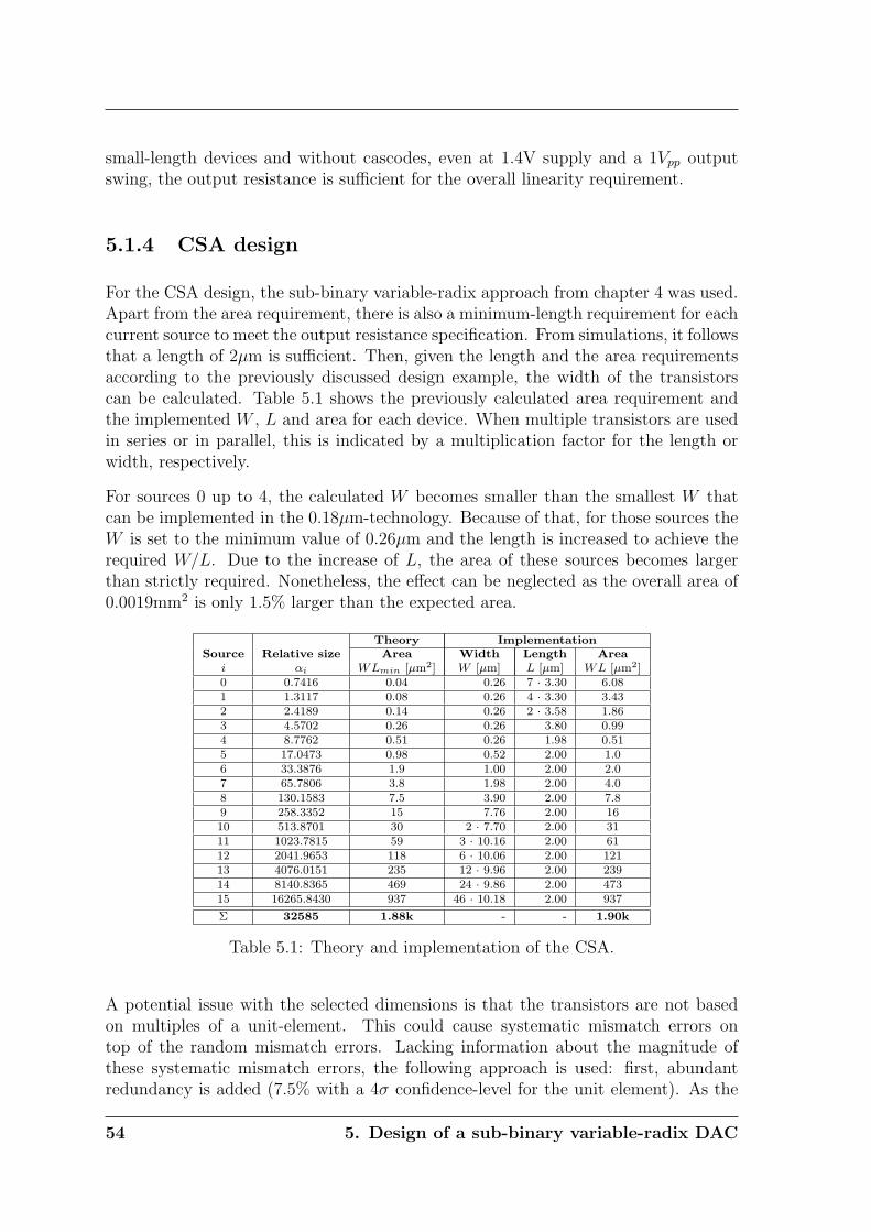
small-length devices and without cascodes, even at 1.4V supply and a 1Vpp outputswing, the output resistance is sufficient for the overall linearity requirement.
5.1.4 CSA design
For the CSA design, the sub-binary variable-radix approach from chapter 4 was used.Apart from the area requirement, there is also a minimum-length requirement for eachcurrent source to meet the output resistance specification. From simulations, it followsthat a length of 2µm is sufficient. Then, given the length and the area requirementsaccording to the previously discussed design example, the width of the transistorscan be calculated. Table 5.1 shows the previously calculated area requirement andthe implemented W , L and area for each device. When multiple transistors are usedin series or in parallel, this is indicated by a multiplication factor for the length orwidth, respectively.
For sources 0 up to 4, the calculated W becomes smaller than the smallest W thatcan be implemented in the 0.18µm-technology. Because of that, for those sources theW is set to the minimum value of 0.26µm and the length is increased to achieve therequired W/L. Due to the increase of L, the area of these sources becomes largerthan strictly required. Nonetheless, the effect can be neglected as the overall area of0.0019mm2 is only 1.5% larger than the expected area.
Theory ImplementationSource Relative size Area Width Length Area
i αi WLmin [µm2] W [µm] L [µm] WL [µm2]0 0.7416 0.04 0.26 7 · 3.30 6.081 1.3117 0.08 0.26 4 · 3.30 3.432 2.4189 0.14 0.26 2 · 3.58 1.863 4.5702 0.26 0.26 3.80 0.994 8.7762 0.51 0.26 1.98 0.515 17.0473 0.98 0.52 2.00 1.06 33.3876 1.9 1.00 2.00 2.07 65.7806 3.8 1.98 2.00 4.08 130.1583 7.5 3.90 2.00 7.89 258.3352 15 7.76 2.00 1610 513.8701 30 2 · 7.70 2.00 3111 1023.7815 59 3 · 10.16 2.00 6112 2041.9653 118 6 · 10.06 2.00 12113 4076.0151 235 12 · 9.96 2.00 23914 8140.8365 469 24 · 9.86 2.00 47315 16265.8430 937 46 · 10.18 2.00 937
Σ 32585 1.88k - - 1.90k
Table 5.1: Theory and implementation of the CSA.
A potential issue with the selected dimensions is that the transistors are not basedon multiples of a unit-element. This could cause systematic mismatch errors ontop of the random mismatch errors. Lacking information about the magnitude ofthese systematic mismatch errors, the following approach is used: first, abundantredundancy is added (7.5% with a 4σ confidence-level for the unit element). As the
54 5. Design of a sub-binary variable-radix DAC
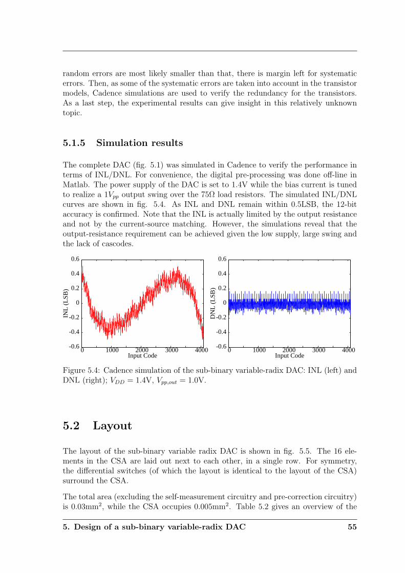
random errors are most likely smaller than that, there is margin left for systematicerrors. Then, as some of the systematic errors are taken into account in the transistormodels, Cadence simulations are used to verify the redundancy for the transistors.As a last step, the experimental results can give insight in this relatively unknowntopic.
5.1.5 Simulation results
The complete DAC (fig. 5.1) was simulated in Cadence to verify the performance interms of INL/DNL. For convenience, the digital pre-processing was done off-line inMatlab. The power supply of the DAC is set to 1.4V while the bias current is tunedto realize a 1Vpp output swing over the 75Ω load resistors. The simulated INL/DNLcurves are shown in fig. 5.4. As INL and DNL remain within 0.5LSB, the 12-bitaccuracy is confirmed. Note that the INL is actually limited by the output resistanceand not by the current-source matching. However, the simulations reveal that theoutput-resistance requirement can be achieved given the low supply, large swing andthe lack of cascodes.
-0.6
-0.4
-0.2
0
0.2
0.4
0.6
0 1000 2000 3000 4000
INL
(L
SB)
Input Code
-0.6
-0.4
-0.2
0
0.2
0.4
0.6
0 1000 2000 3000 4000
DN
L (
LSB
)
Input Code
Figure 5.4: Cadence simulation of the sub-binary variable-radix DAC: INL (left) andDNL (right); VDD = 1.4V, Vpp,out = 1.0V.
5.2 Layout
The layout of the sub-binary variable radix DAC is shown in fig. 5.5. The 16 ele-ments in the CSA are laid out next to each other, in a single row. For symmetry,the differential switches (of which the layout is identical to the layout of the CSA)surround the CSA.
The total area (excluding the self-measurement circuitry and pre-correction circuitry)is 0.03mm2, while the CSA occupies 0.005mm2. Table 5.2 gives an overview of the
5. Design of a sub-binary variable-radix DAC 55
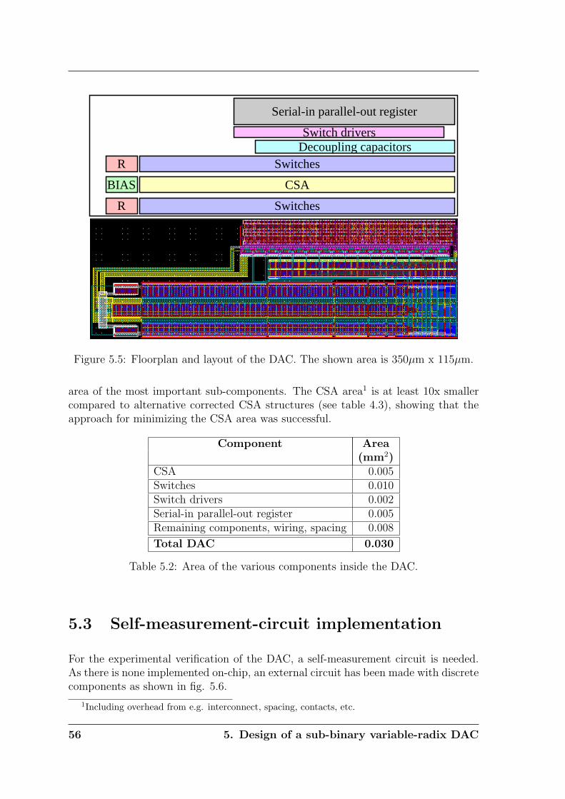
R
BIAS
R
Switches
CSA
SwitchesDecoupling capacitorsSwitch drivers
Serial-in parallel-out register
Figure 5.5: Floorplan and layout of the DAC. The shown area is 350µm x 115µm.
area of the most important sub-components. The CSA area1 is at least 10x smallercompared to alternative corrected CSA structures (see table 4.3), showing that theapproach for minimizing the CSA area was successful.
Component Area(mm2)
CSA 0.005Switches 0.010Switch drivers 0.002Serial-in parallel-out register 0.005Remaining components, wiring, spacing 0.008
Total DAC 0.030
Table 5.2: Area of the various components inside the DAC.
5.3 Self-measurement-circuit implementation
For the experimental verification of the DAC, a self-measurement circuit is needed.As there is none implemented on-chip, an external circuit has been made with discretecomponents as shown in fig. 5.6.
1Including overhead from e.g. interconnect, spacing, contacts, etc.
56 5. Design of a sub-binary variable-radix DAC
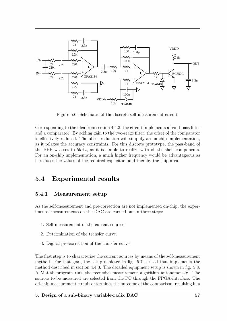
IN+
IN-
220n
24
24
2.2u
2.2u
220
220
2.2k
2.2k
24
24
3.3n
3.3n
2.2u
-
+
U
OPA2134
100
1k
1k
100k
100 100p
100u
VDDA
TS414810k
-
+
U
OPA2134
1k
TS41483.3n
1k
OUT
VDDD
BC550C
Figure 5.6: Schematic of the discrete self-measurement circuit.
Corresponding to the idea from section 4.4.3, the circuit implements a band-pass filterand a comparator. By adding gain to the two-stage filter, the offset of the comparatoris effectively reduced. The offset reduction will simplify an on-chip implementation,as it relaxes the accuracy constraints. For this discrete prototype, the pass-band ofthe BPF was set to 5kHz, as it is simple to realize with off-the-shelf components.For an on-chip implementation, a much higher frequency would be advantageous asit reduces the values of the required capacitors and thereby the chip area.
5.4 Experimental results
5.4.1 Measurement setup
As the self-measurement and pre-correction are not implemented on-chip, the exper-imental measurements on the DAC are carried out in three steps:
1. Self-measurement of the current sources.
2. Determination of the transfer curve.
3. Digital pre-correction of the transfer curve.
The first step is to characterize the current sources by means of the self-measurementmethod. For that goal, the setup depicted in fig. 5.7 is used that implements themethod described in section 4.4.3. The detailed equipment setup is shown in fig. 5.8.A Matlab program runs the recursive measurement algorithm autonomously. Thesources to be measured are selected from the PC through the FPGA-interface. Theoff-chip measurement circuit determines the outcome of the comparison, resulting in a
5. Design of a sub-binary variable-radix DAC 57
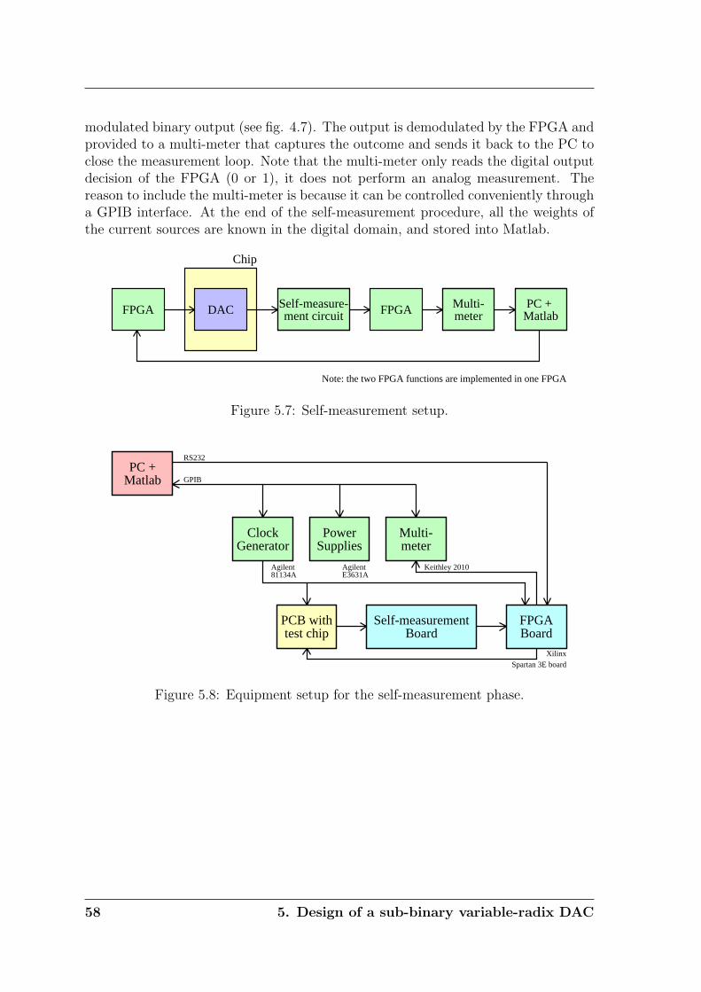
modulated binary output (see fig. 4.7). The output is demodulated by the FPGA andprovided to a multi-meter that captures the outcome and sends it back to the PC toclose the measurement loop. Note that the multi-meter only reads the digital outputdecision of the FPGA (0 or 1), it does not perform an analog measurement. Thereason to include the multi-meter is because it can be controlled conveniently througha GPIB interface. At the end of the self-measurement procedure, all the weights ofthe current sources are known in the digital domain, and stored into Matlab.
FPGA DAC ment circuitSelf-measure- FPGA meter
Multi-MatlabPC +
Chip
Note: the two FPGA functions are implemented in one FPGA
Figure 5.7: Self-measurement setup.
MatlabPC +
GeneratorClock
SuppliesPower
meterMulti-
test chipPCB with
BoardSelf-measurement
BoardFPGA
GPIB
RS232
Agilent81134A
AgilentE3631A
Keithley 2010
XilinxSpartan 3E board
Figure 5.8: Equipment setup for the self-measurement phase.
58 5. Design of a sub-binary variable-radix DAC
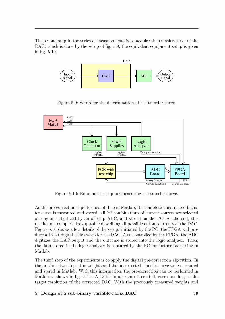
The second step in the series of measurements is to acquire the transfer-curve of theDAC, which is done by the setup of fig. 5.9; the equivalent equipment setup is givenin fig. 5.10.
signalInput DAC ADC signal
Output
Chip
Figure 5.9: Setup for the determination of the transfer-curve.
MatlabPC +
GeneratorClock
SuppliesPower
AnalyzerLogic
test chipPCB with
BoardADC
BoardFPGA
GPIBLANRS232
Agilent81134A
AgilentE3631A
Agilent 16700A
Analog DevicesAD7688 eval. board
XilinxSpartan 3E board
Figure 5.10: Equipment setup for measuring the transfer curve.
As the pre-correction is performed off-line in Matlab, the complete uncorrected trans-fer curve is measured and stored: all 216 combinations of current sources are selectedone by one, digitized by an off-chip ADC, and stored on the PC. At the end, thisresults in a complete lookup-table describing all possible output currents of the DAC.Figure 5.10 shows a few details of the setup: initiated by the PC, the FPGA will pro-duce a 16-bit digital code-sweep for the DAC. Also controlled by the FPGA, the ADCdigitizes the DAC output and the outcome is stored into the logic analyzer. Then,the data stored in the logic analyzer is captured by the PC for further processing inMatlab.
The third step of the experiments is to apply the digital pre-correction algorithm. Inthe previous two steps, the weights and the uncorrected transfer curve were measuredand stored in Matlab. With this information, the pre-correction can be performed inMatlab as shown in fig. 5.11. A 12-bit input ramp is created, corresponding to thetarget resolution of the corrected DAC. With the previously measured weights and
5. Design of a sub-binary variable-radix DAC 59
the pre-correction algorithm from section 4.4.4, the 12-bit ramp is mapped to a 16-bitpre-corrected signal. As the actual transfer curve of the DAC is already stored in alookup-table, the 16-bit pre-corrected signal simply indexes the lookup-table to findthe corresponding output levels of the DAC. In the end, this part of the experimentsyields the 12-bit digitally pre-corrected transfer curve of the DAC, from which theINL and DNL can be calculated.
input12-bit
correctionDigital pre-
rected signal16-bit pre-cor
signalOutput
Weights tableLookup
Figure 5.11: Digital pre-correction setup (software).
5.4.2 Measurement results
As a first verification of the self-measurement method, two current sources (A and B)are compared to each other, and the output signals are observed on an oscilloscope.Fig. 5.12 shows the obtained results for two situations: in case 1 A > B, and incase 2 A < B. As can be seen, the modulated comparator output is a square waveof which the phase changes with 180 when the outcome of the comparison changes.Thus, the demodulated output gives a logical one for A > B and a logical zero forA < B.
Figure 5.12: Example of the self-measurement of two sources.
As a next step, the autonomous self-measurement loop from fig. 5.7 was initiated.Table 5.3 shows the decisions made by the comparator and the obtained weights forthe first 10 sources of a test-chip. The measurement of source 9 indicates a problem inthe chip: all comparator decisions are 1 in this case, which means that the summation
60 5. Design of a sub-binary variable-radix DAC
of the sources 0 up to 8 is still less than the value of source 9. This implies that thereis no redundancy at this transition and thus there will be a gap in the transfer curvebetween binary code 01.1111.1111 and 10.0000.0000. As the gap cannot be correctedby means of digital pre-correction, this test-chip is not suitable to demonstrate themethod. Three other chips were also tested, all showing the same issue with current
Source Decisions Weighti S8 S7 S6 S5 S4 S3 S2 S1 S0 ωi
0 11 1 12 1 1 23 1 1 1 44 1 0 1 1 65 1 0 1 1 1 106 1 1 0 0 1 1 187 1 1 0 1 1 0 1 358 1 1 0 1 1 0 0 1 749 1 1 1 1 1 1 1 1 1 151
Table 5.3: Self-measurement of a single DAC.
source 9. As the redundancy was designed for a 4σ confidence level, and the sameproblem occurs for four devices, there has to be a dominant systematic mismatcherror that causes the gap for source 9. As explained in section 5.1.4, it is obvious thatsystematic errors can be expected: the transistors are not based on unit cells. Thus,because of a.o. corner, edge and well-proximity effects, the intended ratio betweentwo devices can be substantially different from the effective ratio. Unfortunately,these effects are not modeled for the given technology and can be known only aftercharacterization of the devices. On the other hand, with the information that is nowavailable, this issue can be prevented by one of the following solutions:
• As a first solution, the unit-cell approach could be included in the design ofthe current sources to prevent systematic errors. That means that the αi-ratiosshould become integer multiples of a unit-size. As for the smallest currentsources the random mismatch will be dominant over the systematic mismatch,the unit-element approach is only necessary for the larger sources. The unit-element approach can be included in the design phase of the αi-ratios by trun-cating each calculated αi-value to the nearest multiple of unit-elements. Then,sufficient redundancy for each step is still guaranteed while systematic errorsare prevented by the unit-element approach.
• As a second solution, the systematic mismatch errors can be modeled and takeninto account in the design procedure. At the moment, the design procedure(equation (4.11)) takes only random mismatch into account. A second mis-match term for systematic errors could be added to these equations. Then,
5. Design of a sub-binary variable-radix DAC 61
the obtained αi-values will exhibit more redundancy to cover both types ofmismatch.
To verify the digital pre-correction method with the existing chips, a work-aroundusing two DACs is used here. Figure 5.13 shows how two DACs from two differentchips are connected to effectively compose a single DAC: the outputs of the DACsare tied together to sum their individual output currents. The 16-bit input coded<15:0> is split in two parts: bits d<15:9> are applied to the corresponding bits ofthe first DAC, and bits d<8:0> are applied to the corresponding bits of the secondDAC. The remaining inputs (bit <8:0> of DAC 1 and bit <15:9> of DAC 2) are tiedto a constant logical level. Table 5.4 lists an overview of the connections, showingfor each source αi of each DAC whether it is connected to the digital input (di) or aconstant logical level (0 or 1).
DAC 2
DAC 1
bit 8-0
bit 15-9
bit 8-0
bit 15-9
Analog output
bit 15-0
Chip 2
Chip 1
Figure 5.13: A DAC composed of two sub-DACs.
Sourceα15 α14 α13 α12 α11 α10 α9 α8 α7 α6 α5 α4 α3 α2 α1 α0
DAC 1 d15 d14 d13 d12 d11 d10 d9 1 0 0 0 0 0 0 0 0DAC 2 1 0 0 0 0 0 0 d8 d7 d6 d5 d4 d3 d2 d1 d0
Table 5.4: Input mapping for the DAC composed of two sub-DACs.
As the two DACs are identical (except for random mismatch), the output currentgenerated by this system is equivalent to the output current generated by a singleDAC. However, as there are now two sets of load resistors connected in parallel, theoutput voltage swing is reduced by a factor of two in this dual-DAC design. Themajor advantage of the combination of two DACs is that each CSA has a separatebias current. Thus, the current sources of DAC 1 can be scaled relative to the currentsources of DAC 2, i.e.: the ratio of α15 - α9 versus α8 - α0 can be manually controlledby tuning the bias currents of the two DACs. From the previous self-measurement,it appeared that α9 is too large compared to α8 - α0. Now, by slightly increasing the
62 5. Design of a sub-binary variable-radix DAC
bias current of α8 - α0, the redundancy can be manually restored such that the pre-correction algorithm can be verified. Despite the unpleasant setup, this verification isstill valuable as it will prove that 12-bit accuracy can be achieved using 16 inaccuratelymatched current sources. The fact that out of these 16 sources, 9 are located in onechip and 7 in another chip does not impede with that conclusion.
After connecting the two DACs together and tuning the bias to achieve redundancyfor all sources, the self-measurement algorithm was executed again. The results ofthe self-measurement are shown in table 5.5. For all sources (except source 1 and2), there is at least one comparison that results in a zero. Thus, for all sourcesthere is redundancy available. For sources 1 and 2 there is also redundancy, but theredundancy is smaller than 1 LSB. As a consequence, the converter is still monotonousbut the steps are smaller than 1 LSB. Because of the monotonicity the redundancycannot be verified by the outcome of the self-measurement algorithm for these sources.From source 3 onwards, the redundancy results in non-monotonicity, which is reflectedby the zero-decisions in the comparisons.
Source Decisions Weighti S14 S13 S12 S11 S10 S9 S8 S7 S6 S5 S4 S3 S2 S1 S0 ωi
0 11 1 12 1 1 23 1 1 0 34 1 1 0 0 55 1 1 0 0 0 86 1 1 0 1 0 1 167 1 1 1 0 1 0 0 318 1 1 1 1 1 0 0 1 649 1 0 0 0 1 1 0 0 0 7210 1 1 0 1 0 0 0 0 0 0 15211 1 1 1 0 1 0 0 1 0 1 1 30912 1 1 1 1 1 0 0 0 1 0 0 0 63113 1 1 1 1 1 1 0 1 0 0 0 0 1 126814 1 1 1 1 1 1 1 0 0 0 1 1 1 0 253315 1 1 1 1 1 1 1 0 0 1 0 1 0 0 0 5040
Table 5.5: Self-measurement of a DAC, composed of two sub-DACs.
Having obtained the values of the weights, the next step is to determine the uncor-rected transfer curve using the setup described in fig. 5.9. Then, after storing thedata to a lookup-table, the pre-correction is applied in Matlab as explained in fig.5.11 to obtain the corrected 12-bit transfer curve. For each point of the curve, 4measurements are taken and averaged to reduce noise. From the corrected, averaged12-bit transfer curve, the INL and DNL were derived, giving the results in fig. 5.14.Both INLmax and DNLmax are around 0.4LSB, yielding a 12.3bit post-correction
5. Design of a sub-binary variable-radix DAC 63
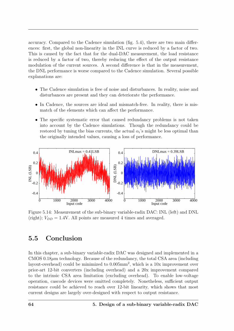
accuracy. Compared to the Cadence simulation (fig. 5.4), there are two main differ-ences: first, the global non-linearity in the INL curve is reduced by a factor of two.This is caused by the fact that for the dual-DAC measurement, the load resistanceis reduced by a factor of two, thereby reducing the effect of the output resistancemodulation of the current sources. A second difference is that in the measurement,the DNL performance is worse compared to the Cadence simulation. Several possibleexplanations are:
• The Cadence simulation is free of noise and disturbances. In reality, noise anddisturbances are present and they can deteriorate the performance.
• In Cadence, the sources are ideal and mismatch-free. In reality, there is mis-match of the elements which can affect the performance.
• The specific systematic error that caused redundancy problems is not takeninto account by the Cadence simulations. Though the redundancy could berestored by tuning the bias currents, the actual αi’s might be less optimal thanthe originally intended values, causing a loss of performance.
INLmax = 0.41LSB
-0.4
-0.2
0
0.2
0.4
0 1000 2000 3000 4000
INL
(L
SB)
Input code
DNLmax = 0.39LSB
-0.4
-0.2
0
0.2
0.4
0 1000 2000 3000 4000
DN
L (
LSB
)
Input code
Figure 5.14: Measurement of the sub-binary variable-radix DAC: INL (left) and DNL(right); VDD = 1.4V. All points are measured 4 times and averaged.
5.5 Conclusion
In this chapter, a sub-binary variable-radix DAC was designed and implemented in aCMOS 0.18µm technology. Because of the redundancy, the total CSA area (includinglayout-overhead) could be minimized to 0.005mm2, which is a 10x improvement overprior-art 12-bit converters (including overhead) and a 20x improvement comparedto the intrinsic CSA area limitation (excluding overhead). To enable low-voltageoperation, cascode devices were omitted completely. Nonetheless, sufficient outputresistance could be achieved to reach over 12-bit linearity, which shows that mostcurrent designs are largely over-designed with respect to output resistance.
64 5. Design of a sub-binary variable-radix DAC
Because of systematic mismatch, the implemented DAC did not have sufficient redun-dancy to enable digital pre-correction of the imperfections. For future implementa-tions, it is recommended to take the effect of systematic mismatch into account whendesigning the current elements. By doing so, sufficient redundancy for both ran-dom mismatch and systematic mismatch can be provided to ensure that the digitalpre-correction can compensate for all the errors.
As a work-around, two DACs were connected together to validate the principle ofoperation and the achievable performance. The functionality of the self-measurementalgorithm and pre-correction method was shown, and a final accuracy of 12.3bit wasmeasured.
5. Design of a sub-binary variable-radix DAC 65

Chapter 6
Smart AD conversion
This chapter applies the previously presented smart concept to analog-to-digital con-verters. A relevant overview of current state-of-the-art smart ADCs is given, and anapproach is proposed how to apply the smart concept beneficially in this case. Theactual proof-of-concept will be given in chapters 7, 8 and 9, where the chip implemen-tation is discussed.
6.1 Introduction
In chapter 3, many different aspects and possible benefits of the smart concept wereintroduced. Concepts like e.g. self-test and correction were introduced and possiblebenefits with respect to e.g. performance, yield and portability were mentioned. Inthis chapter, a limited range within the smart concept will be selected for furtherinvestigation and actual chip implementation.
First of all, this project is focussing at high-speed, high-resolution AD converters,with pipelined converters in particular. Corresponding to the smart concept, it isassumed that the ADC is part of a mixed analog/digital system, such that, whenevernecessary, the digital part can be used for processing of information. Nonetheless, itis recognized that the digital part does not come for free and has to be taken intoaccount when evaluating the overall performance.
In this work, the smart concept will be applied with as main goal to improve theperformance of a high-speed, high-resolution ADC. The performance is evaluated bymeans of a widely accepted figure-of-merit (FoM) that includes speed, accuracy andpower consumption. The reason to focus on the FoM is because it is an importantproperty of each ADC, independent on the application or situation where the ADC isused. Also, when the smart concept is able to improve the FoM, it inherently provesthat the smart concept can be beneficial in a wide range of situations. As a secondgoal, this work aims at using circuit solutions that are portable to future technologies
6. Smart AD conversion 67
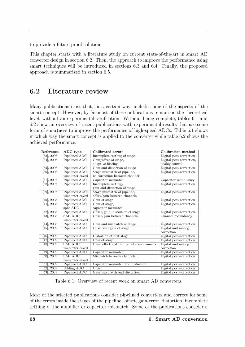
to provide a future-proof solution.
This chapter starts with a literature study on current state-of-the-art in smart ADconverter design in section 6.2. Then, the approach to improve the performance usingsmart techniques will be introduced in sections 6.3 and 6.4. Finally, the proposedapproach is summarized in section 6.5.
6.2 Literature review
Many publications exist that, in a certain way, include some of the aspects of thesmart concept. However, by far most of these publications remain on the theoreticallevel, without an experimental verification. Without being complete, tables 6.1 and6.2 show an overview of recent publications with experimental results that use someform of smartness to improve the performance of high-speed ADCs. Table 6.1 showsin which way the smart concept is applied to the converter while table 6.2 shows theachieved performance.
Reference ADC type Calibrated errors Calibration method[33], 2006 Pipelined ADC Incomplete settling of stage Digital post-correction[34], 2006 Pipelined ADC Gain/offset of stage, Digital post-correction,
adaptive biasing analog control[35], 2006 Pipelined ADC Gain and distortion of stage Digital post-correction[36], 2006 Pipelined ADC, Stage mismatch of pipeline, Digital post-correction
time-interleaved no correction between channels[37], 2007 Pipelined ADC Capacitor mismatch Capacitor redundancy[38], 2007 Pipelined ADC Incomplete settling, Digital post-correction
gain and distortion of stage[39], 2007 Pipelined ADC, Stage mismatch of pipeline, Digital post-correction
time-interleaved offset/gain between channels[40], 2008 Pipelined ADC Gain of stage Digital post-correction[41], 2008 Pipelined ADC, Gain of stage, Digital post-correction
split ADC capacitor mismatch[42], 2008 Pipelined ADC Offset, gain, distortion of stage Digital post-correction[43], 2008 SAR ADC, Offset/gain between channels Channel redundancy
time-interleaved[44], 2008 Pipelined ADC Gain and mismatch of stage Digital post-correction[45], 2009 Pipelined ADC Offset and gain of stage Digital and analog
correction[46], 2009 Pipelined ADC Distortion of first stage Digital post-correction[47], 2009 Pipelined ADC Gain of stage Digital post-correction[48], 2009 SAR ADC, Gain, offset and timing between channels Digital and analog
time-interleaved correction[49], 2009 Pipelined ADC Capacitor mismatch Digital post-correction[50], 2009 SAR ADC, Mismatch between channels Digital post-correction
time-interleaved[51], 2009 Pipelined ADC Capacitor mismatch and distortion Digital post-correction[52], 2009 Folding ADC Offset Digital post-correction[53], 2009 Pipelined ADC Gain, mismatch and distortion Digital post-correction
Table 6.1: Overview of recent work on smart AD converters.
Most of the selected publications consider pipelined converters and correct for someof the errors inside the stages of the pipeline: offset, gain-error, distortion, incompletesettling of the amplifier or capacitor mismatch. Some of the publications consider a
68 6. Smart AD conversion
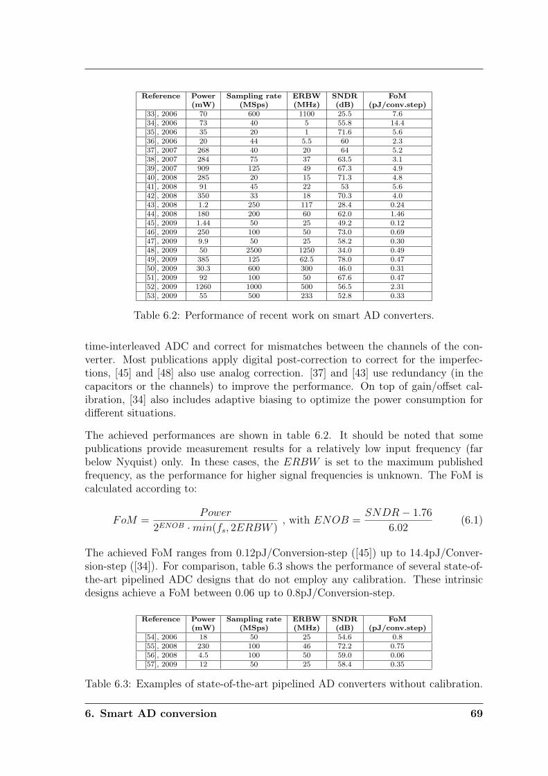
Reference Power Sampling rate ERBW SNDR FoM(mW) (MSps) (MHz) (dB) (pJ/conv.step)
[33], 2006 70 600 1100 25.5 7.6[34], 2006 73 40 5 55.8 14.4[35], 2006 35 20 1 71.6 5.6[36], 2006 20 44 5.5 60 2.3[37], 2007 268 40 20 64 5.2[38], 2007 284 75 37 63.5 3.1[39], 2007 909 125 49 67.3 4.9[40], 2008 285 20 15 71.3 4.8[41], 2008 91 45 22 53 5.6[42], 2008 350 33 18 70.3 4.0[43], 2008 1.2 250 117 28.4 0.24[44], 2008 180 200 60 62.0 1.46[45], 2009 1.44 50 25 49.2 0.12[46], 2009 250 100 50 73.0 0.69[47], 2009 9.9 50 25 58.2 0.30[48], 2009 50 2500 1250 34.0 0.49[49], 2009 385 125 62.5 78.0 0.47[50], 2009 30.3 600 300 46.0 0.31[51], 2009 92 100 50 67.6 0.47[52], 2009 1260 1000 500 56.5 2.31[53], 2009 55 500 233 52.8 0.33
Table 6.2: Performance of recent work on smart AD converters.
time-interleaved ADC and correct for mismatches between the channels of the con-verter. Most publications apply digital post-correction to correct for the imperfec-tions, [45] and [48] also use analog correction. [37] and [43] use redundancy (in thecapacitors or the channels) to improve the performance. On top of gain/offset cal-ibration, [34] also includes adaptive biasing to optimize the power consumption fordifferent situations.
The achieved performances are shown in table 6.2. It should be noted that somepublications provide measurement results for a relatively low input frequency (farbelow Nyquist) only. In these cases, the ERBW is set to the maximum publishedfrequency, as the performance for higher signal frequencies is unknown. The FoM iscalculated according to:
FoM =Power
2ENOB ·min(fs, 2ERBW ), with ENOB =
SNDR− 1.76
6.02(6.1)
The achieved FoM ranges from 0.12pJ/Conversion-step ([45]) up to 14.4pJ/Conver-sion-step ([34]). For comparison, table 6.3 shows the performance of several state-of-the-art pipelined ADC designs that do not employ any calibration. These intrinsicdesigns achieve a FoM between 0.06 up to 0.8pJ/Conversion-step.
Reference Power Sampling rate ERBW SNDR FoM(mW) (MSps) (MHz) (dB) (pJ/conv.step)
[54], 2006 18 50 25 54.6 0.8[55], 2008 230 100 46 72.2 0.75[56], 2008 4.5 100 50 59.0 0.06[57], 2009 12 50 25 58.4 0.35
Table 6.3: Examples of state-of-the-art pipelined AD converters without calibration.
6. Smart AD conversion 69
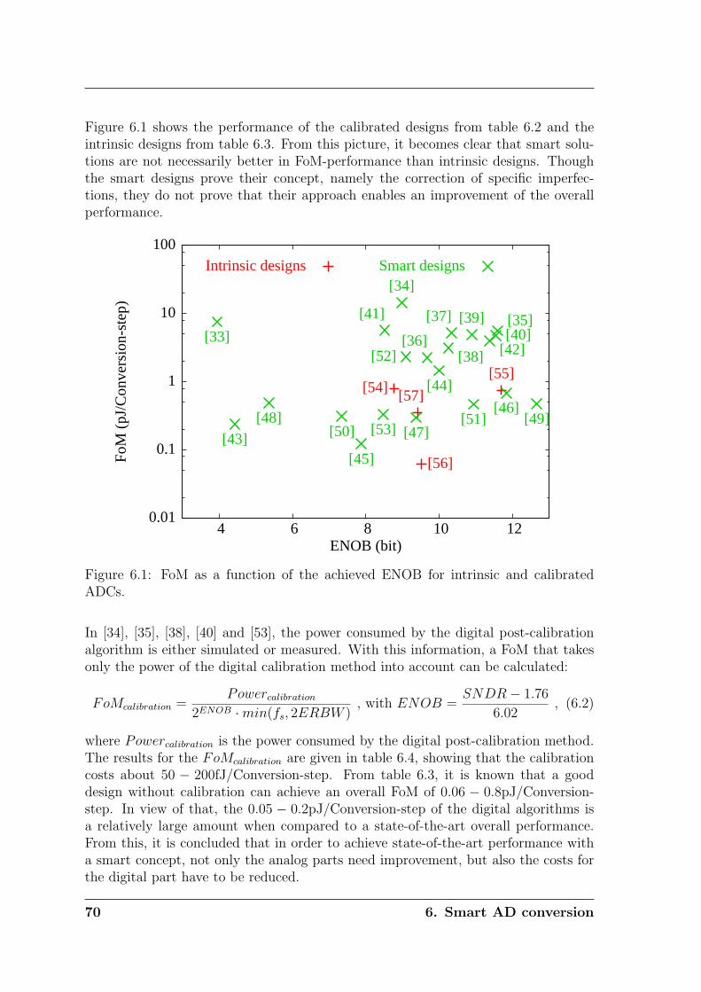
Figure 6.1 shows the performance of the calibrated designs from table 6.2 and theintrinsic designs from table 6.3. From this picture, it becomes clear that smart solu-tions are not necessarily better in FoM-performance than intrinsic designs. Thoughthe smart designs prove their concept, namely the correction of specific imperfec-tions, they do not prove that their approach enables an improvement of the overallperformance.
0.01
0.1
1
10
100
4 6 8 10 12
FoM
(pJ
/Con
vers
ion-
step
)
ENOB (bit)
Intrinsic designs
[54][55]
[56]
[57]
Smart designs
[33]
[34]
[35][36]
[37]
[38]
[39][40]
[41]
[42]
[43]
[44]
[45]
[46]
[47][48] [49]
[50][51]
[52]
[53]
Figure 6.1: FoM as a function of the achieved ENOB for intrinsic and calibratedADCs.
In [34], [35], [38], [40] and [53], the power consumed by the digital post-calibrationalgorithm is either simulated or measured. With this information, a FoM that takesonly the power of the digital calibration method into account can be calculated:
FoMcalibration =Powercalibration
2ENOB ·min(fs, 2ERBW ), with ENOB =
SNDR− 1.76
6.02, (6.2)
where Powercalibration is the power consumed by the digital post-calibration method.The results for the FoMcalibration are given in table 6.4, showing that the calibrationcosts about 50 − 200fJ/Conversion-step. From table 6.3, it is known that a gooddesign without calibration can achieve an overall FoM of 0.06 − 0.8pJ/Conversion-step. In view of that, the 0.05 − 0.2pJ/Conversion-step of the digital algorithms isa relatively large amount when compared to a state-of-the-art overall performance.From this, it is concluded that in order to achieve state-of-the-art performance witha smart concept, not only the analog parts need improvement, but also the costs forthe digital part have to be reduced.
70 6. Smart AD conversion
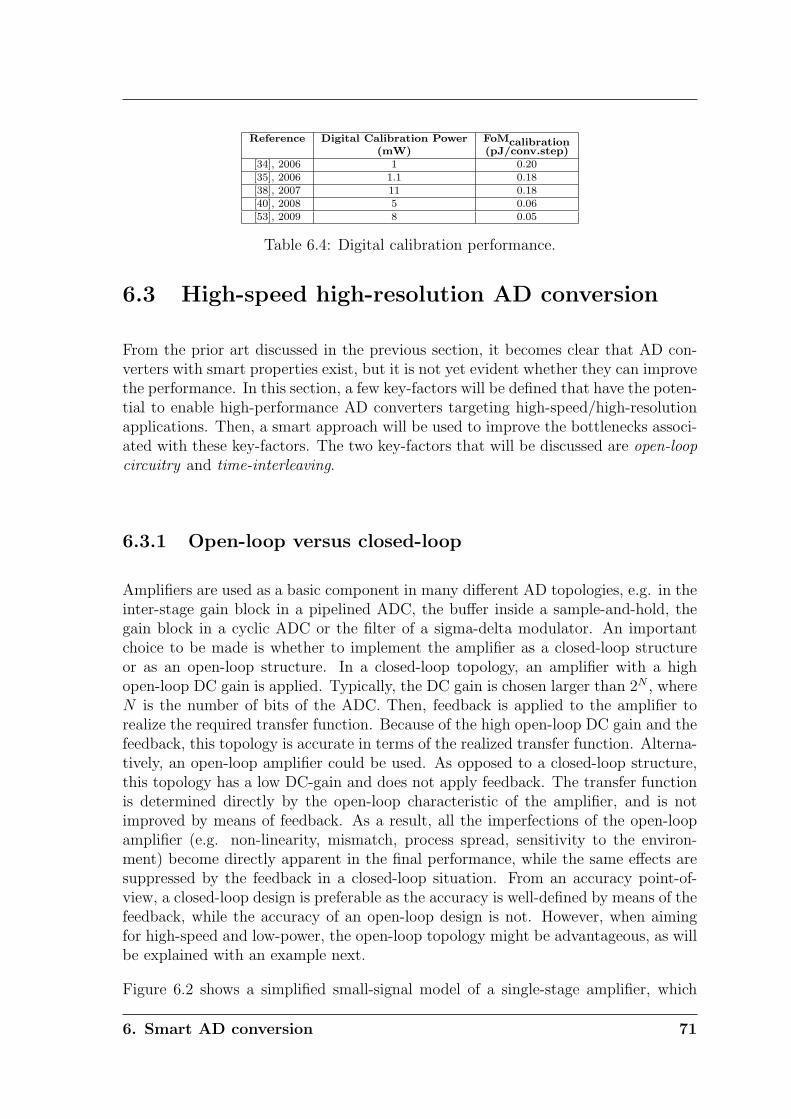
Reference Digital Calibration Power FoMcalibration(mW) (pJ/conv.step)
[34], 2006 1 0.20[35], 2006 1.1 0.18[38], 2007 11 0.18[40], 2008 5 0.06[53], 2009 8 0.05
Table 6.4: Digital calibration performance.
6.3 High-speed high-resolution AD conversion
From the prior art discussed in the previous section, it becomes clear that AD con-verters with smart properties exist, but it is not yet evident whether they can improvethe performance. In this section, a few key-factors will be defined that have the poten-tial to enable high-performance AD converters targeting high-speed/high-resolutionapplications. Then, a smart approach will be used to improve the bottlenecks associ-ated with these key-factors. The two key-factors that will be discussed are open-loopcircuitry and time-interleaving.
6.3.1 Open-loop versus closed-loop
Amplifiers are used as a basic component in many different AD topologies, e.g. in theinter-stage gain block in a pipelined ADC, the buffer inside a sample-and-hold, thegain block in a cyclic ADC or the filter of a sigma-delta modulator. An importantchoice to be made is whether to implement the amplifier as a closed-loop structureor as an open-loop structure. In a closed-loop topology, an amplifier with a highopen-loop DC gain is applied. Typically, the DC gain is chosen larger than 2N , whereN is the number of bits of the ADC. Then, feedback is applied to the amplifier torealize the required transfer function. Because of the high open-loop DC gain and thefeedback, this topology is accurate in terms of the realized transfer function. Alterna-tively, an open-loop amplifier could be used. As opposed to a closed-loop structure,this topology has a low DC-gain and does not apply feedback. The transfer functionis determined directly by the open-loop characteristic of the amplifier, and is notimproved by means of feedback. As a result, all the imperfections of the open-loopamplifier (e.g. non-linearity, mismatch, process spread, sensitivity to the environ-ment) become directly apparent in the final performance, while the same effects aresuppressed by the feedback in a closed-loop situation. From an accuracy point-of-view, a closed-loop design is preferable as the accuracy is well-defined by means of thefeedback, while the accuracy of an open-loop design is not. However, when aimingfor high-speed and low-power, the open-loop topology might be advantageous, as willbe explained with an example next.
Figure 6.2 shows a simplified small-signal model of a single-stage amplifier, which
6. Smart AD conversion 71
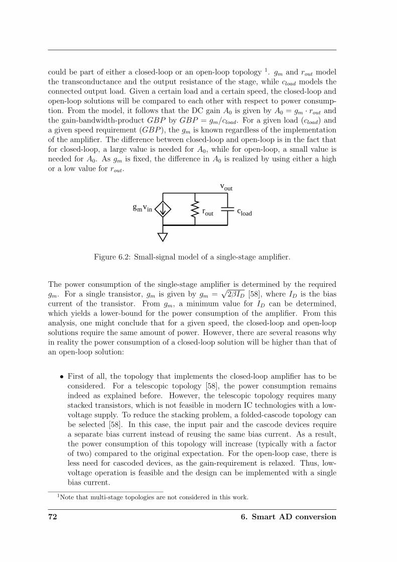
could be part of either a closed-loop or an open-loop topology 1. gm and rout modelthe transconductance and the output resistance of the stage, while cload models theconnected output load. Given a certain load and a certain speed, the closed-loop andopen-loop solutions will be compared to each other with respect to power consump-tion. From the model, it follows that the DC gain A0 is given by A0 = gm · rout andthe gain-bandwidth-product GBP by GBP = gm/cload. For a given load (cload) anda given speed requirement (GBP ), the gm is known regardless of the implementationof the amplifier. The difference between closed-loop and open-loop is in the fact thatfor closed-loop, a large value is needed for A0, while for open-loop, a small value isneeded for A0. As gm is fixed, the difference in A0 is realized by using either a highor a low value for rout.
g vm in rout cload
vout
Figure 6.2: Small-signal model of a single-stage amplifier.
The power consumption of the single-stage amplifier is determined by the requiredgm. For a single transistor, gm is given by gm =
√2βID [58], where ID is the bias
current of the transistor. From gm, a minimum value for ID can be determined,which yields a lower-bound for the power consumption of the amplifier. From thisanalysis, one might conclude that for a given speed, the closed-loop and open-loopsolutions require the same amount of power. However, there are several reasons whyin reality the power consumption of a closed-loop solution will be higher than that ofan open-loop solution:
• First of all, the topology that implements the closed-loop amplifier has to beconsidered. For a telescopic topology [58], the power consumption remainsindeed as explained before. However, the telescopic topology requires manystacked transistors, which is not feasible in modern IC technologies with a low-voltage supply. To reduce the stacking problem, a folded-cascode topology canbe selected [58]. In this case, the input pair and the cascode devices requirea separate bias current instead of reusing the same bias current. As a result,the power consumption of this topology will increase (typically with a factorof two) compared to the original expectation. For the open-loop case, there isless need for cascoded devices, as the gain-requirement is relaxed. Thus, low-voltage operation is feasible and the design can be implemented with a singlebias current.
1Note that multi-stage topologies are not considered in this work.
72 6. Smart AD conversion
• A second reason for increased power consumption of a closed-loop solution isthat, because of the high rout requirement, transistors with a large L are needed.As a side-effect of increasing the transistor’s L, the parasitic capacitances ofthese devices will also increase. In turn, this leads to either an increased powerconsumption or a reduced speed. In an open-loop solution, there is no needfor transistors with a large L as the gain requirement is relaxed. As such, theparasitics in an open-loop solution can be smaller, resulting in a faster and morepower-efficient design.
• A third issue with closed-loop designs is that, especially for higher resolutions,the required open-loop gain cannot be achieved with a standard low-voltagesingle-stage design [58]. Additional circuits (like gain-boosting circuits or atwo-stage amplifier design) will be necessary to achieve the gain-requirement.As explained in [58], both these techniques result in a reduced speed and/or anincreased power consumption.
From the previous analysis, it follows that the high DC gain of a closed-loop solutionenables the high accuracy of such a design. However, at the same time, it is exactlythe high DC gain that results in issues with respect to speed, power consumptionand low-voltage operation. Table 6.5 summarizes the comparison between closed-loop and open-loop solutions. In view of a smart approach, the open-loop amplifieris selected for further implementation as it enables high-speed low-power operationwith good portability to future technologies. Then, the smart concept will be appliedto overcome the accuracy limitations. The implementation of the open-loop amplifierwill be discussed in chapter 7, while chapter 8 deals with the smart solution forenhanced accuracy.
Closed-loop Open-loopAccuracy + -
Speed - +Power - +
Low-voltage operation - +
Table 6.5: Comparison of open-loop and closed-loop topologies.
6.3.2 Time-interleaving
A second key-factor in high-speed ADC design is the principle of time-interleaving[59]: instead of using one converter operating at a sampling rate fs, a number ofconverters (p) is used in parallel in a time-interleaved mode of operation: each channeloperates at fs/p only, but the combination of converters acts as a single converteroperating at fs. By doing so, the overall speed (fs) can be much higher than thespeed of a single converter (fs/p). Dependent on the situation, there are at least tworeasons why time-interleaving can be a useful approach:
6. Smart AD conversion 73
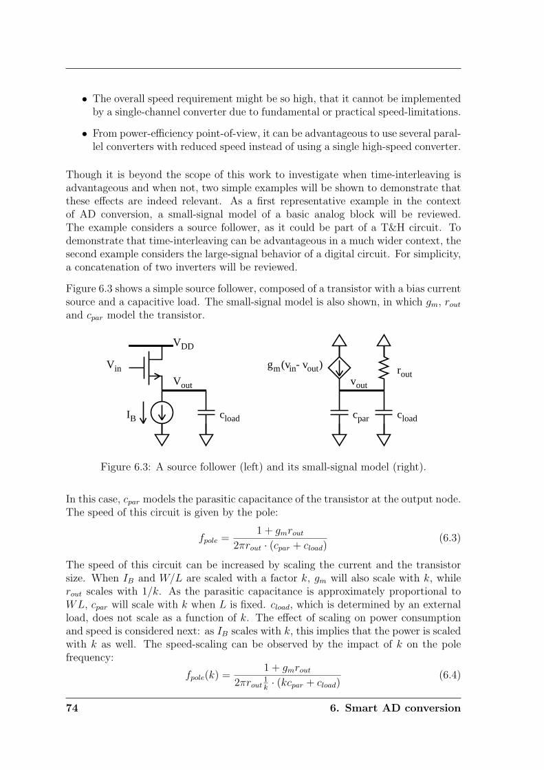
• The overall speed requirement might be so high, that it cannot be implementedby a single-channel converter due to fundamental or practical speed-limitations.
• From power-efficiency point-of-view, it can be advantageous to use several paral-lel converters with reduced speed instead of using a single high-speed converter.
Though it is beyond the scope of this work to investigate when time-interleaving isadvantageous and when not, two simple examples will be shown to demonstrate thatthese effects are indeed relevant. As a first representative example in the contextof AD conversion, a small-signal model of a basic analog block will be reviewed.The example considers a source follower, as it could be part of a T&H circuit. Todemonstrate that time-interleaving can be advantageous in a much wider context, thesecond example considers the large-signal behavior of a digital circuit. For simplicity,a concatenation of two inverters will be reviewed.
Figure 6.3 shows a simple source follower, composed of a transistor with a bias currentsource and a capacitive load. The small-signal model is also shown, in which gm, rout
and cpar model the transistor.
IB
Vin
Vout
cload
VDD
cpar
g (v - v )m in out
vout
cload
rout
Figure 6.3: A source follower (left) and its small-signal model (right).
In this case, cpar models the parasitic capacitance of the transistor at the output node.The speed of this circuit is given by the pole:
fpole =1 + gmrout
2πrout · (cpar + cload)(6.3)
The speed of this circuit can be increased by scaling the current and the transistorsize. When IB and W/L are scaled with a factor k, gm will also scale with k, whilerout scales with 1/k. As the parasitic capacitance is approximately proportional toWL, cpar will scale with k when L is fixed. cload, which is determined by an externalload, does not scale as a function of k. The effect of scaling on power consumptionand speed is considered next: as IB scales with k, this implies that the power is scaledwith k as well. The speed-scaling can be observed by the impact of k on the polefrequency:
fpole(k) =1 + gmrout
2πrout1k· (kcpar + cload)
(6.4)
74 6. Smart AD conversion
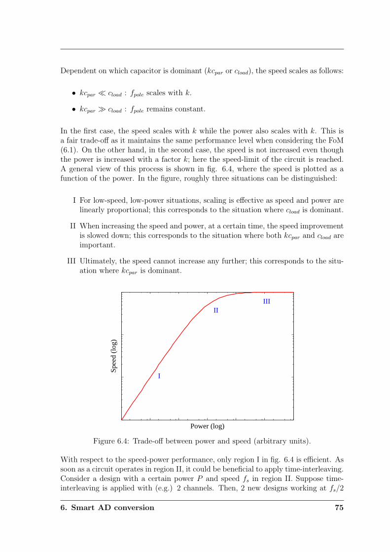
Dependent on which capacitor is dominant (kcpar or cload), the speed scales as follows:
• kcpar ¿ cload : fpole scales with k.
• kcpar À cload : fpole remains constant.
In the first case, the speed scales with k while the power also scales with k. This isa fair trade-off as it maintains the same performance level when considering the FoM(6.1). On the other hand, in the second case, the speed is not increased even thoughthe power is increased with a factor k; here the speed-limit of the circuit is reached.A general view of this process is shown in fig. 6.4, where the speed is plotted as afunction of the power. In the figure, roughly three situations can be distinguished:
I For low-speed, low-power situations, scaling is effective as speed and power arelinearly proportional; this corresponds to the situation where cload is dominant.
II When increasing the speed and power, at a certain time, the speed improvementis slowed down; this corresponds to the situation where both kcpar and cload areimportant.
III Ultimately, the speed cannot increase any further; this corresponds to the situ-ation where kcpar is dominant.
Spee
d (l
og)
Power (log)
I
IIIII
Figure 6.4: Trade-off between power and speed (arbitrary units).
With respect to the speed-power performance, only region I in fig. 6.4 is efficient. Assoon as a circuit operates in region II, it could be beneficial to apply time-interleaving.Consider a design with a certain power P and speed fs in region II. Suppose time-interleaving is applied with (e.g.) 2 channels. Then, 2 new designs working at fs/2
6. Smart AD conversion 75
each are necessary. Because of the curvature of the speed-power relation in region II,each of these designs would consume less than P/2. Overall, these 2 channels stillachieve the original speed fs, but now at a power consumption which is less than theoriginal P . As such, the 2-channel solution achieves a more power-efficient solution.However, it should also be noted that there will be additional circuit overhead whenimplementing a time-interleaved system: at the input, the signals should be splitto the different channels, and at the output, the signals should be combined again.Time-interleaving will be advantageous only if the power reduction of the ADC corecircuitry is higher than the added consumption of the overhead circuitry. In the lastcase, when a circuit is working in region III and it is necessary to further increasespeed, again this could be done by means of time-interleaving.
From the above considerations, it can be concluded that in some situations time-inter-leaving improves the speed-power performance or it can increase the speed beyonda fundamental or practical speed limit. To show that this observation is not onlyvalid for the presented analog block, a similar analysis is repeated for a digital block.Figure 6.5 shows a chain of two inverters, in which the wire capacitance is taken intoaccount as it is often the dominant capacitance. A large-signal model is also shown,where the inverters are modeled by a controlled current source Iout and an inputcapacitance Cin. Note that Iout and Cin are large-signal parameters. When scaling isapplied, similar to the previous example, again the power, Iout and Cin scale with kwhile cwire remains constant. Effectively, the dV
dtas a function of k for this example
is given by:dV
dt=
kIout
kCin + cwire
(6.5)
Note the similarity to the previous example: in this case speed-power scaling is ef-ficient as long as cwire dominates the overall capacitance, while the speed is limitedwhen kCin becomes dominant. Here, time-interleaving or parallelism becomes benefi-cial as soon as kCin is not negligible compared to cwire. In digital designs, parallelismis actually a well-known method to increase speed or efficiency.
cwire
Iout cwire Cin
Figure 6.5: An inverter chain (left) and its large-signal model (right).
From the discussed examples, it can be understood that for specific situations, time-interleaving can improve the speed-power performance (by moving designs from regionII to region I), or it enables the operation at a higher overall speed (by moving designsfrom region III to region I or II). In general, time-interleaving is a relevant option for
76 6. Smart AD conversion
high-speed AD converters. However, there is an issue with time-interleaved systemsas they require proper matching between the individual channels. When mismatch ispresent, the overall performance can be degraded, as described in a.o. [60]. Becauseof the general usefulness of time-interleaving, a smart approach for the correctionof channel-mismatch will be developed. The problem of channel-mismatch and thesmart solution will be discussed in chapter 9.
6.4 Smart calibration
In the previous section, two relevant factors that enable low-power, high-speed op-eration were determined: open-loop amplification and time-interleaving. However,open-loop structures have a limited accuracy, while time-interleaved structures aresensitive to channel mismatch. Because of that, a smart approach will be used toreduce the impact of these limitations. In this section, the global approach will bedecided upon, while the actual implementations will be discussed in chapters 8 and9.
In line with the general view on smart conversion from chapter 3, three componentsare required to reduce the effect of the imperfections of open-loop and time-interleavedstructures:
1. Detection of the imperfections.
2. Processing of this information by means of an algorithm.
3. Correction of the effects of the imperfections.
Moreover, aiming for maximum performance, it is important that the additions forthe smart solution (detection, processing and correction) improve the performancewhile using only limited resources; i.e. when adding the smart solution on top of theanalog core, it should:
• Improve the overall accuracy.
• Reduce the speed as little as possible.
• Increase the power consumption as little as possible.
With these requirements in mind, a coarse decision can be made on how to implementthe different parts of the smart solution. Several alternatives with respect to detection,processing and correction will be discussed next.
As will become clear in the following chapters, the imperfections of open-loop andtime-interleaved structures are mainly dependent on random mismatch and process
6. Smart AD conversion 77
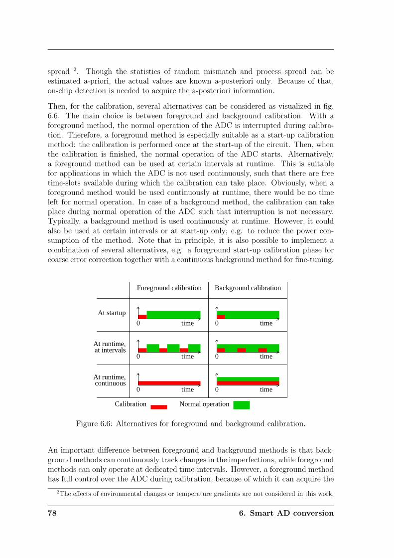
spread 2. Though the statistics of random mismatch and process spread can beestimated a-priori, the actual values are known a-posteriori only. Because of that,on-chip detection is needed to acquire the a-posteriori information.
Then, for the calibration, several alternatives can be considered as visualized in fig.6.6. The main choice is between foreground and background calibration. With aforeground method, the normal operation of the ADC is interrupted during calibra-tion. Therefore, a foreground method is especially suitable as a start-up calibrationmethod: the calibration is performed once at the start-up of the circuit. Then, whenthe calibration is finished, the normal operation of the ADC starts. Alternatively,a foreground method can be used at certain intervals at runtime. This is suitablefor applications in which the ADC is not used continuously, such that there are freetime-slots available during which the calibration can take place. Obviously, when aforeground method would be used continuously at runtime, there would be no timeleft for normal operation. In case of a background method, the calibration can takeplace during normal operation of the ADC such that interruption is not necessary.Typically, a background method is used continuously at runtime. However, it couldalso be used at certain intervals or at start-up only; e.g. to reduce the power con-sumption of the method. Note that in principle, it is also possible to implement acombination of several alternatives, e.g. a foreground start-up calibration phase forcoarse error correction together with a continuous background method for fine-tuning.
Foreground calibration Background calibration
At startup
At runtime,at intervals
At runtime,continuous
Calibration Normal operation
0 time 0 time
0 time 0 time
0 time 0 time
Figure 6.6: Alternatives for foreground and background calibration.
An important difference between foreground and background methods is that back-ground methods can continuously track changes in the imperfections, while foregroundmethods can only operate at dedicated time-intervals. However, a foreground methodhas full control over the ADC during calibration, because of which it can acquire the
2The effects of environmental changes or temperature gradients are not considered in this work.
78 6. Smart AD conversion
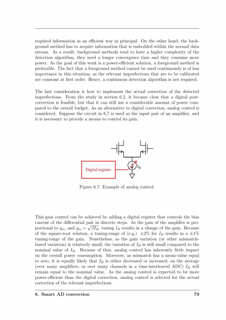
required information in an efficient way in principal. On the other hand, the back-ground method has to acquire information that is embedded within the normal datastream. As a result, background methods tend to have a higher complexity of thedetection algorithm, they need a longer convergence time and they consume morepower. As the goal of this work is a power-efficient solution, a foreground method ispreferable. The fact that a foreground method cannot be used continuously is of lessimportance in this situation, as the relevant imperfections that are to be calibratedare constant at first order. Hence, a continuous detection algorithm is not required.
The last consideration is how to implement the actual correction of the detectedimperfections. From the study in section 6.2, it became clear that a digital post-correction is feasible, but that it can still use a considerable amount of power com-pared to the overall budget. As an alternative to digital correction, analog control isconsidered. Suppose the circuit in 6.7 is used as the input pair of an amplifier, andit is necessary to provide a means to control its gain.
IBDigital register
Figure 6.7: Example of analog control.
This gain control can be achieved by adding a digital register that controls the biascurrent of the differential pair in discrete steps. As the gain of the amplifier is pro-portional to gm, and gm =
√βIB, tuning IB results in a change of the gain. Because
of the square-root relation, a tuning-range of (e.g.) ±2% for IB results in a ±1%tuning-range of the gain. Nonetheless, as the gain variation (or other mismatch-based variation) is relatively small, the variation of IB is still small compared to thenominal value of IB. Because of that, analog control has inherently little impacton the overall power consumption. Moreover, as mismatch has a mean-value equalto zero, it is equally likely that IB is either decreased or increased; on the average(over many amplifiers, or over many channels in a time-interleaved ADC) IB willremain equal to the nominal value. As the analog control is expected to be morepower-efficient than the digital correction, analog control is selected for the actualcorrection of the relevant imperfections.
6. Smart AD conversion 79
6.5 Conclusion
In this chapter, the general smart concept was narrowed down to a specific goal:to improve the performance of a high-speed, high-resolution ADC in terms of thespeed/power/accuracy trade-off. From a literature study, it can be concluded thatprior art in this direction exists, but most of the concepts are still lacking in absoluteterms of performance. In order to improve upon the prior art, two key-factors wereinvestigated that have the potential to enable high-performance AD converters forhigh-speed/high-resolution applications, namely:
• Open-loop circuitry.
• Time-interleaving.
Open-loop circuits can achieve higher speed and lower power consumption comparedto closed-loop solutions. Besides, they are more suitable for new-generation low-voltage technologies. Currently, the limited accuracy of open-loop circuits is a mainbottleneck. It was shown that the second factor, time-interleaving, enables a higherspeed of operation and a higher power-efficiency for high-speed designs. However,time-interleaved circuits are prone to channel-mismatch errors. Though these twokey-factors enable high performance in theory, their associated limitations (accuracyand channel-mismatch) need to be resolved. In order to reach that goal, the smartconcept will be applied. To realize a power-efficient smart calibration method for thepreviously mentioned issues, the following approach was selected:
• Foreground calibration method, performed at start-up.
• Digital processing of the information.
• Analog correction of the imperfections.
For a proof-of-concept, instead of designing a complete ADC, an open-loop Track-and-Hold circuit will be designed as a test-case in chapter 7. Even though it isnot a complete ADC, it is sufficient to demonstrate the effectiveness of an open-loop design. Also, it enables the verification of the smart approach to resolve boththe accuracy limitations of an open-loop T&H and the channel-mismatch of a time-interleaved T&H. These two smart solutions will be discussed in chapter 8 and chapter9, respectively.
80 6. Smart AD conversion
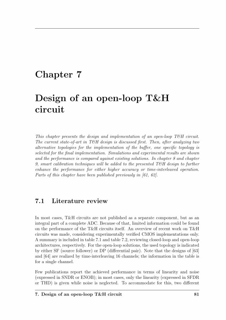
Chapter 7
Design of an open-loop T&Hcircuit
This chapter presents the design and implementation of an open-loop T&H circuit.The current state-of-art in T&H design is discussed first. Then, after analyzing twoalternative topologies for the implementation of the buffer, one specific topology isselected for the final implementation. Simulations and experimental results are shownand the performance is compared against existing solutions. In chapter 8 and chapter9, smart calibration techniques will be added to the presented T&H design to furtherenhance the performance for either higher accuracy or time-interleaved operation.Parts of this chapter have been published previously in [61, 62].
7.1 Literature review
In most cases, T&H circuits are not published as a separate component, but as anintegral part of a complete ADC. Because of that, limited information could be foundon the performance of the T&H circuits itself. An overview of recent work on T&Hcircuits was made, considering experimentally verified CMOS implementations only.A summary is included in table 7.1 and table 7.2, reviewing closed-loop and open-looparchitectures, respectively. For the open-loop solutions, the used topology is indicatedby either SF (source follower) or DP (differential pair). Note that the designs of [63]and [64] are realized by time-interleaving 16 channels; the information in the table isfor a single channel.
Few publications report the achieved performance in terms of linearity and noise(expressed in SNDR or ENOB); in most cases, only the linearity (expressed in SFDRor THD) is given while noise is neglected. To accommodate for this, two different
7. Design of an open-loop T&H circuit 81
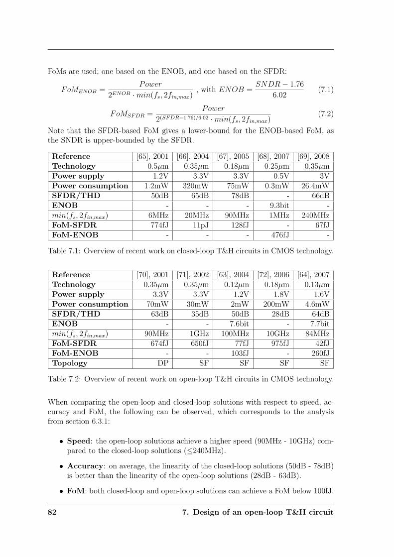
FoMs are used; one based on the ENOB, and one based on the SFDR:
FoMENOB =Power
2ENOB ·min(fs, 2fin,max), with ENOB =
SNDR− 1.76
6.02(7.1)
FoMSFDR =Power
2(SFDR−1.76)/6.02 ·min(fs, 2fin,max)(7.2)
Note that the SFDR-based FoM gives a lower-bound for the ENOB-based FoM, asthe SNDR is upper-bounded by the SFDR.
Reference [65], 2001 [66], 2004 [67], 2005 [68], 2007 [69], 2008Technology 0.5µm 0.35µm 0.18µm 0.25µm 0.35µmPower supply 1.2V 3.3V 3.3V 0.5V 3VPower consumption 1.2mW 320mW 75mW 0.3mW 26.4mWSFDR/THD 50dB 65dB 78dB - 66dBENOB - - - 9.3bit -min(fs, 2fin,max) 6MHz 20MHz 90MHz 1MHz 240MHzFoM-SFDR 774fJ 11pJ 128fJ - 67fJFoM-ENOB - - - 476fJ -
Table 7.1: Overview of recent work on closed-loop T&H circuits in CMOS technology.
Reference [70], 2001 [71], 2002 [63], 2004 [72], 2006 [64], 2007Technology 0.35µm 0.35µm 0.12µm 0.18µm 0.13µmPower supply 3.3V 3.3V 1.2V 1.8V 1.6VPower consumption 70mW 30mW 2mW 200mW 4.6mWSFDR/THD 63dB 35dB 50dB 28dB 64dBENOB - - 7.6bit - 7.7bitmin(fs, 2fin,max) 90MHz 1GHz 100MHz 10GHz 84MHzFoM-SFDR 674fJ 650fJ 77fJ 975fJ 42fJFoM-ENOB - - 103fJ - 260fJTopology DP SF SF SF SF
Table 7.2: Overview of recent work on open-loop T&H circuits in CMOS technology.
When comparing the open-loop and closed-loop solutions with respect to speed, ac-curacy and FoM, the following can be observed, which corresponds to the analysisfrom section 6.3.1:
• Speed: the open-loop solutions achieve a higher speed (90MHz - 10GHz) com-pared to the closed-loop solutions (≤240MHz).
• Accuracy: on average, the linearity of the closed-loop solutions (50dB - 78dB)is better than the linearity of the open-loop solutions (28dB - 63dB).
• FoM: both closed-loop and open-loop solutions can achieve a FoM below 100fJ.
82 7. Design of an open-loop T&H circuit
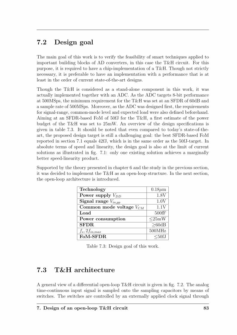
7.2 Design goal
The main goal of this work is to verify the feasibility of smart techniques applied toimportant building blocks of AD converters, in this case the T&H circuit. For thispurpose, it is required to have a chip-implementation of a T&H. Though not strictlynecessary, it is preferable to have an implementation with a performance that is atleast in the order of current state-of-the-art designs.
Though the T&H is considered as a stand-alone component in this work, it wasactually implemented together with an ADC. As the ADC targets 8-bit performanceat 500MSps, the minimum requirement for the T&H was set at an SFDR of 60dB anda sample rate of 500MSps. Moreover, as the ADC was designed first, the requirementsfor signal-range, common-mode level and expected load were also defined beforehand.Aiming at an SFDR-based FoM of 50fJ for the T&H, a first estimate of the powerbudget of the T&H was set to 25mW. An overview of the design specifications isgiven in table 7.3. It should be noted that even compared to today’s state-of-the-art, the proposed design target is still a challenging goal: the best SFDR-based FoMreported in section 7.1 equals 42fJ, which is in the same order as the 50fJ-target. Inabsolute terms of speed and linearity, the design goal is also at the limit of currentsolutions as illustrated in fig. 7.1: only one existing solution achieves a marginallybetter speed-linearity product.
Supported by the theory presented in chapter 6 and the study in the previous section,it was decided to implement the T&H as an open-loop structure. In the next section,the open-loop architecture is introduced.
Technology 0.18µmPower supply VDD 1.8VSignal range Vin,pp 1.0VCommon mode voltage VCM 1.1VLoad 500fFPower consumption ≤25mWSFDR ≥60dBfs, 2fin,max 500MHzFoM-SFDR ≤50fJ
Table 7.3: Design goal of this work.
7.3 T&H architecture
A general view of a differential open-loop T&H circuit is given in fig. 7.2. The analogtime-continuous input signal is sampled onto the sampling capacitors by means ofswitches. The switches are controlled by an externally applied clock signal through
7. Design of an open-loop T&H circuit 83
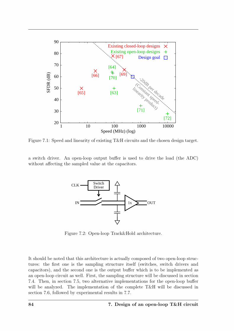
20
30
40
50
60
70
80
90
1 10 100 1000 10000
SFD
R (
dB)
Speed (MHz) (log)
-20dB per decade
(Constant speed-
linearity product)
Existing closed-loop designs
[65]
[66]
[67]
[69]
Existing open-loop designs
[70]
[71]
[63]
[72]
[64]
Design goal
Figure 7.1: Speed and linearity of existing T&H circuits and the chosen design target.
a switch driver. An open-loop output buffer is used to drive the load (the ADC)without affecting the sampled value at the capacitors.
SwitchDriverCLK
IN 1x OUT
Figure 7.2: Open-loop Track&Hold architecture.
It should be noted that this architecture is actually composed of two open-loop struc-tures: the first one is the sampling structure itself (switches, switch drivers andcapacitors), and the second one is the output buffer which is to be implemented asan open-loop circuit as well. First, the sampling structure will be discussed in section7.4. Then, in section 7.5, two alternative implementations for the open-loop bufferwill be analyzed. The implementation of the complete T&H will be discussed insection 7.6, followed by experimental results in 7.7.
84 7. Design of an open-loop T&H circuit
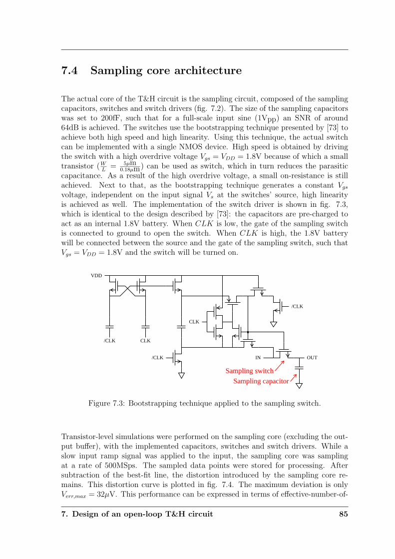
7.4 Sampling core architecture
The actual core of the T&H circuit is the sampling circuit, composed of the samplingcapacitors, switches and switch drivers (fig. 7.2). The size of the sampling capacitorswas set to 200fF, such that for a full-scale input sine (1Vpp) an SNR of around64dB is achieved. The switches use the bootstrapping technique presented by [73] toachieve both high speed and high linearity. Using this technique, the actual switchcan be implemented with a single NMOS device. High speed is obtained by drivingthe switch with a high overdrive voltage Vgs = VDD = 1.8V because of which a smalltransistor (W
L= 5µm
0.18µm) can be used as switch, which in turn reduces the parasiticcapacitance. As a result of the high overdrive voltage, a small on-resistance is stillachieved. Next to that, as the bootstrapping technique generates a constant Vgs
voltage, independent on the input signal Vs at the switches’ source, high linearityis achieved as well. The implementation of the switch driver is shown in fig. 7.3,which is identical to the design described by [73]: the capacitors are pre-charged toact as an internal 1.8V battery. When CLK is low, the gate of the sampling switchis connected to ground to open the switch. When CLK is high, the 1.8V batterywill be connected between the source and the gate of the sampling switch, such thatVgs = VDD = 1.8V and the switch will be turned on.
/CLK CLK
/CLK
CLK
/CLK
VDD
IN OUT
Sampling switch
Sampling capacitor
Figure 7.3: Bootstrapping technique applied to the sampling switch.
Transistor-level simulations were performed on the sampling core (excluding the out-put buffer), with the implemented capacitors, switches and switch drivers. While aslow input ramp signal was applied to the input, the sampling core was samplingat a rate of 500MSps. The sampled data points were stored for processing. Aftersubtraction of the best-fit line, the distortion introduced by the sampling core re-mains. This distortion curve is plotted in fig. 7.4. The maximum deviation is onlyVerr,max = 32µV. This performance can be expressed in terms of effective-number-of-
7. Design of an open-loop T&H circuit 85
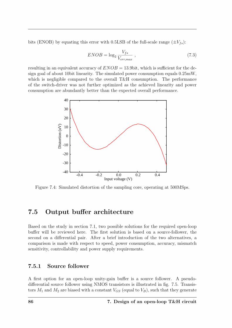
bits (ENOB) by equating this error with 0.5LSB of the full-scale range (±Vfs):
ENOB = log2
Vfs
Verr,max
, (7.3)
resulting in an equivalent accuracy of ENOB = 13.9bit, which is sufficient for the de-sign goal of about 10bit linearity. The simulated power consumption equals 0.25mW,which is negligible compared to the overall T&H consumption. The performanceof the switch-driver was not further optimized as the achieved linearity and powerconsumption are abundantly better than the expected overall performance.
-40
-30
-20
-10
0
10
20
30
40
-0.4 -0.2 0.0 0.2 0.4
Dis
tort
ion
(uV
)
Input voltage (V)
Figure 7.4: Simulated distortion of the sampling core, operating at 500MSps.
7.5 Output buffer architecture
Based on the study in section 7.1, two possible solutions for the required open-loopbuffer will be reviewed here. The first solution is based on a source-follower, thesecond on a differential pair. After a brief introduction of the two alternatives, acomparison is made with respect to speed, power consumption, accuracy, mismatchsensitivity, controllability and power supply requirements.
7.5.1 Source follower
A first option for an open-loop unity-gain buffer is a source follower. A pseudo-differential source follower using NMOS transistors is illustrated in fig. 7.5. Transis-tors M1 and M2 are biased with a constant VGS (equal to VB), such that they generate
86 7. Design of an open-loop T&H circuit
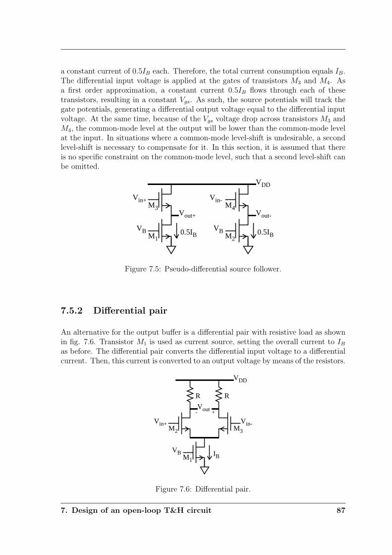
a constant current of 0.5IB each. Therefore, the total current consumption equals IB.The differential input voltage is applied at the gates of transistors M3 and M4. Asa first order approximation, a constant current 0.5IB flows through each of thesetransistors, resulting in a constant Vgs. As such, the source potentials will track thegate potentials, generating a differential output voltage equal to the differential inputvoltage. At the same time, because of the Vgs voltage drop across transistors M3 andM4, the common-mode level at the output will be lower than the common-mode levelat the input. In situations where a common-mode level-shift is undesirable, a secondlevel-shift is necessary to compensate for it. In this section, it is assumed that thereis no specific constraint on the common-mode level, such that a second level-shift canbe omitted.
0.5IBVB
Vin+
Vout+
VDD
0.5IBVB
Vin-
Vout-
M1 M2
M3 M4
Figure 7.5: Pseudo-differential source follower.
7.5.2 Differential pair
An alternative for the output buffer is a differential pair with resistive load as shownin fig. 7.6. Transistor M1 is used as current source, setting the overall current to IB
as before. The differential pair converts the differential input voltage to a differentialcurrent. Then, this current is converted to an output voltage by means of the resistors.
Vin+ Vin-
+
R
Vout-
R
VDD
IBVB
M1
M2 M3
Figure 7.6: Differential pair.
7. Design of an open-loop T&H circuit 87
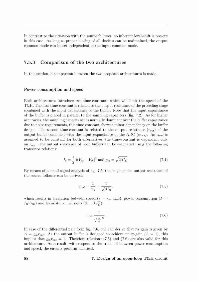
In contrast to the situation with the source follower, no inherent level-shift is presentin this case. As long as proper biasing of all devices can be maintained, the outputcommon-mode can be set independent of the input common-mode.
7.5.3 Comparison of the two architectures
In this section, a comparison between the two proposed architectures is made.
Power consumption and speed
Both architectures introduce two time-constants which will limit the speed of theT&H. The first time-constant is related to the output resistance of the preceding stagecombined with the input capacitance of the buffer. Note that the input capacitanceof the buffer is placed in parallel to the sampling capacitors (fig. 7.2). As for higheraccuracies, the sampling capacitance is normally dominant over the buffer capacitancedue to noise requirements, this time-constant shows a minor dependency on the bufferdesign. The second time-constant is related to the output resistance (rout) of theoutput buffer combined with the input capacitance of the ADC (cload). As cload isassumed to be constant for both alternatives, the time-constant is dependent onlyon rout. The output resistance of both buffers can be estimated using the followingtransistor relations:
Id =1
2β(Vgs − Vth)
2 and gm =√
2βID. (7.4)
By means of a small-signal analysis of fig. 7.5, the single-ended output resistance ofthe source follower can be derived:
rout =1
gm
=1√βIB
, (7.5)
which results in a relation between speed (τ = routcload), power consumption (P =IBVDD) and transistor dimensions (β = β2
WL
):
τ ∝ 1√WL
P. (7.6)
In case of the differential pair from fig. 7.6, one can derive that its gain is given byA = gmrout. As the output buffer is designed to achieve unity-gain (A = 1), thisimplies that gmrout = 1. Therefore relations (7.5) and (7.6) are also valid for thisarchitecture. As a result, with respect to the trade-off between power consumptionand speed, the circuits perform identical.
88 7. Design of an open-loop T&H circuit
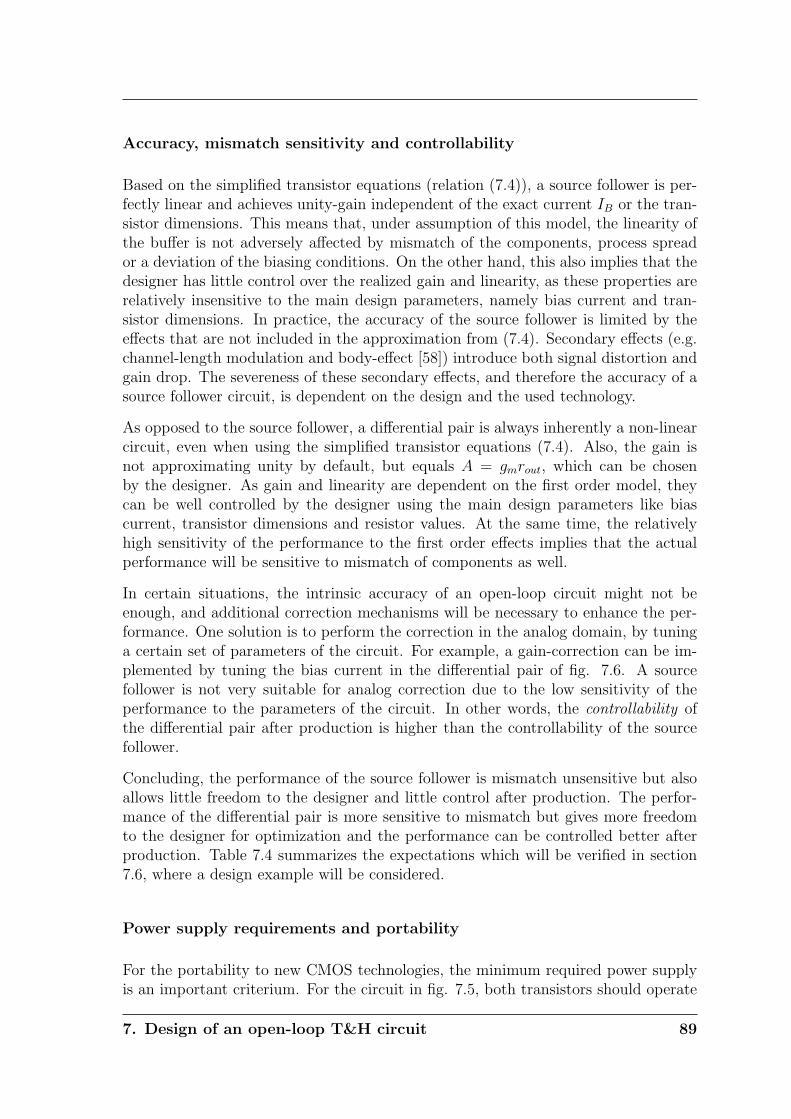
Accuracy, mismatch sensitivity and controllability
Based on the simplified transistor equations (relation (7.4)), a source follower is per-fectly linear and achieves unity-gain independent of the exact current IB or the tran-sistor dimensions. This means that, under assumption of this model, the linearity ofthe buffer is not adversely affected by mismatch of the components, process spreador a deviation of the biasing conditions. On the other hand, this also implies that thedesigner has little control over the realized gain and linearity, as these properties arerelatively insensitive to the main design parameters, namely bias current and tran-sistor dimensions. In practice, the accuracy of the source follower is limited by theeffects that are not included in the approximation from (7.4). Secondary effects (e.g.channel-length modulation and body-effect [58]) introduce both signal distortion andgain drop. The severeness of these secondary effects, and therefore the accuracy of asource follower circuit, is dependent on the design and the used technology.
As opposed to the source follower, a differential pair is always inherently a non-linearcircuit, even when using the simplified transistor equations (7.4). Also, the gain isnot approximating unity by default, but equals A = gmrout, which can be chosenby the designer. As gain and linearity are dependent on the first order model, theycan be well controlled by the designer using the main design parameters like biascurrent, transistor dimensions and resistor values. At the same time, the relativelyhigh sensitivity of the performance to the first order effects implies that the actualperformance will be sensitive to mismatch of components as well.
In certain situations, the intrinsic accuracy of an open-loop circuit might not beenough, and additional correction mechanisms will be necessary to enhance the per-formance. One solution is to perform the correction in the analog domain, by tuninga certain set of parameters of the circuit. For example, a gain-correction can be im-plemented by tuning the bias current in the differential pair of fig. 7.6. A sourcefollower is not very suitable for analog correction due to the low sensitivity of theperformance to the parameters of the circuit. In other words, the controllability ofthe differential pair after production is higher than the controllability of the sourcefollower.
Concluding, the performance of the source follower is mismatch unsensitive but alsoallows little freedom to the designer and little control after production. The perfor-mance of the differential pair is more sensitive to mismatch but gives more freedomto the designer for optimization and the performance can be controlled better afterproduction. Table 7.4 summarizes the expectations which will be verified in section7.6, where a design example will be considered.
Power supply requirements and portability
For the portability to new CMOS technologies, the minimum required power supplyis an important criterium. For the circuit in fig. 7.5, both transistors should operate
7. Design of an open-loop T&H circuit 89
Source follower Differential pairGain Determined by Determined byLinearity secondary effects first order effectsMismatch sensitivityDesign freedom Low HighControllability
Table 7.4: Comparison of accuracy, mismatch sensitivity and controllability.
in pinch-off mode (Vds ≥ Vgs − Vth) for the full range of input signals. It is assumedthat all transistors need a certain overdrive voltage (Vgs ≥ Vth + Vov) to operateproperly, that the maximum differential input signal equals ±Vfs, and that all signallevels should remain between 0V and VDD. In that case, a lower bound for the powersupply can be derived:
VDD,min = 2Vov + Vth + Vfs (7.7)
Using the same assumptions for the differential pair yields as lower bound for thepower supply:
VDD,min = 2Vov + 2Vfs , (7.8)
which means that the source follower is preferable when Vth < Vfs, and the differentialpair is preferable otherwise. In reality, Vth will be in the order of 0.2V up to 0.5V(dependent on the technology), while typical values of Vfs are also chosen in thisrange (note that Vpp = 2Vfs). Therefore, in most cases this difference will be small.In general, both topologies will remain applicable with scaling of technology as Vfs
can be adjusted by the designer and the remaining term (2Vov + Vth in case of thesource follower) is small enough to fit into VDD.
Conclusion
From the above, one can conclude that the two alternatives show identical perfor-mance with respect to speed and power consumption. Also, both architectures aresuitable for low-voltage operation, allowing portability to future technology gener-ations. The main difference between the architectures is the accuracy. Most im-portantly, the non-linearity of a source follower is determined by secondary effects,whereas the non-linearity of a differential pair is determined by primary effects. Assuch, it can be expected that the non-linearity of a differential pair is its most im-portant drawback compared to a source follower. In the following section, the non-linearity of a differential pair will be studied in detail and several solutions are pro-posed to enhance the performance. Then, in section 7.6, the enhanced differentialpair will be compared against the source follower using a design example.
90 7. Design of an open-loop T&H circuit
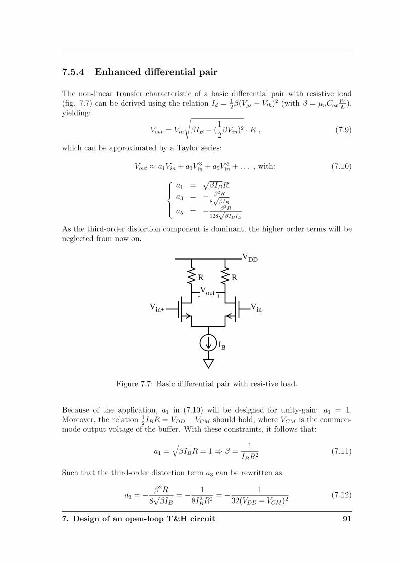
7.5.4 Enhanced differential pair
The non-linear transfer characteristic of a basic differential pair with resistive load(fig. 7.7) can be derived using the relation Id = 1
2β(Vgs − Vth)
2 (with β = µnCoxWL
),yielding:
Vout = Vin
√βIB − (
1
2βVin)2 ·R , (7.9)
which can be approximated by a Taylor series:
Vout ≈ a1Vin + a3V3in + a5V
5in + . . . , with: (7.10)
a1 =√
βIBR
a3 = − β2R
8√
βIB
a5 = − β3R
128√
βIBIB
As the third-order distortion component is dominant, the higher order terms will beneglected from now on.
IB
Vin+ Vin-
+
R
Vout-
R
VDD
Figure 7.7: Basic differential pair with resistive load.
Because of the application, a1 in (7.10) will be designed for unity-gain: a1 = 1.Moreover, the relation 1
2IBR = VDD − VCM should hold, where VCM is the common-
mode output voltage of the buffer. With these constraints, it follows that:
a1 =√
βIBR = 1 ⇒ β =1
IBR2(7.11)
Such that the third-order distortion term a3 can be rewritten as:
a3 = − β2R
8√
βIB
= − 1
8I2BR2
= − 1
32(VDD − VCM)2(7.12)
7. Design of an open-loop T&H circuit 91
As a result, (7.10) simplifies into:
Vout ≈ Vin + a3V3in , with: a3 = − 1
32(VDD − VCM)2(7.13)
The third-order term a3V3in expresses the dominant non-linearity component of the
differential pair, used as unity-gain buffer. The maximum deviation Verr,max withrespect to the linear term is achieved for a full scale input signal Vin = Vfs:
Verr,max = |a3V3in| =
V 3fs
32(VDD − VCM)2. (7.14)
Note that this result implies that when the voltage levels of the buffer are given, thelinearity is also known. It is not possible to improve the linearity by e.g. alteringthe bias current or the transistor dimensions. For the given design goal (describedbefore in table 7.3) VDD = 1.8V, VCM = 1.1V and Vfs = 0.5V, which results inVerr,max = 8mV. In terms of effective-bits, this deviation translates to an ENOBestimation of:
ENOB = log2
Vfs
Verr,max
, (7.15)
yielding for the basic differential pair a maximum accuracy:
ENOB = log2
32(VDD − VCM)2
V 2fs
= 6.0bit. (7.16)
The circuit of fig. 7.7 was simulated with Cadence using the UMC CMOS 0.18µmtechnology. The resistors were set to R = 175Ω to achieve a pole-frequency of almost1GHz with a load of 500fF, the tail current source was set to 8mA to ensure the correctVCM of 1.1V. Then, the transistor dimensions were adjusted in order to achieve again of one, resulting in W
L= 11.64µm
0.18µm . From a DC analysis, the parameters of the
polynomial function (7.10) can be estimated, yielding a1 = 1.00 and a3 = −0.05.From this, it follows that Verr,max = 6.3mV and ENOB = 6.3bit, which is close tothe expected value of 6.0bit.
In order to improve the linearity beyond the 6-bit level, two linearization techniques(known from a.o. [74]) will be applied: source degeneration and cross coupling. Thefirst step is to add a source-degeneration resistor to the differential pair (fig. 7.8).The resistor linearizes the transfer characteristic but it also reduces the gain of thedifferential pair. To maintain unity-gain, the transistors’ W
Lhas to increase compared
to the basic differential pair.
As a second modification, cross-coupling has been applied. Fig. 7.9 shows the finalimplementation: a first differential pair (composed of transistors M1, M2, M3, M4
and source degeneration resistor Rs1) is connected as usual. A second differentialpair (composed of transistors M5, M6, M7, M8 and source degeneration resistor Rs2)is cross-coupled to the first pair, in other words: the input is in parallel to the input
92 7. Design of an open-loop T&H circuit
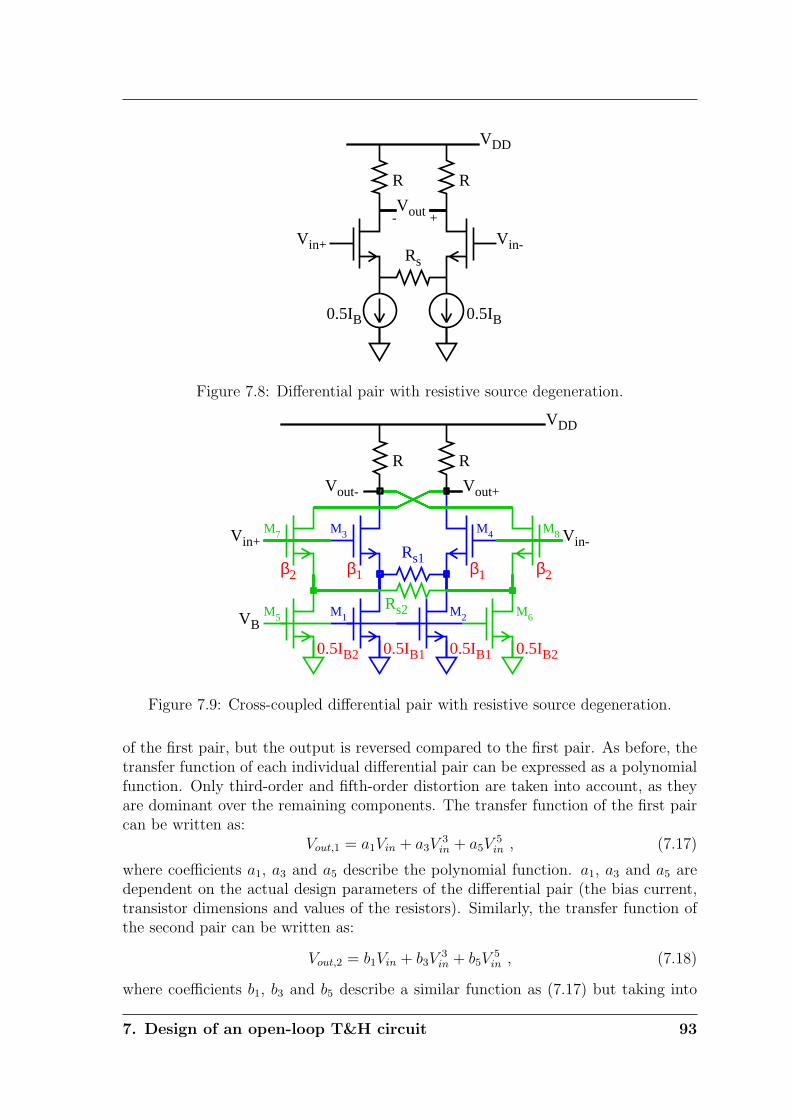
0.5IB 0.5IB
Rs
Vin+ Vin-
+
R
Vout-
R
VDD
Figure 7.8: Differential pair with resistive source degeneration.
Rs1
Rs2M5 M6
M7 M8
M1 M2
M3 M4
β2 β1 β1 β2
0.5IB2 0.5IB1 0.5IB1 0.5IB2
Vin+ Vin-
Vout- Vout+
VB
RR
VDD
Figure 7.9: Cross-coupled differential pair with resistive source degeneration.
of the first pair, but the output is reversed compared to the first pair. As before, thetransfer function of each individual differential pair can be expressed as a polynomialfunction. Only third-order and fifth-order distortion are taken into account, as theyare dominant over the remaining components. The transfer function of the first paircan be written as:
Vout,1 = a1Vin + a3V3in + a5V
5in , (7.17)
where coefficients a1, a3 and a5 describe the polynomial function. a1, a3 and a5 aredependent on the actual design parameters of the differential pair (the bias current,transistor dimensions and values of the resistors). Similarly, the transfer function ofthe second pair can be written as:
Vout,2 = b1Vin + b3V3in + b5V
5in , (7.18)
where coefficients b1, b3 and b5 describe a similar function as (7.17) but taking into
7. Design of an open-loop T&H circuit 93
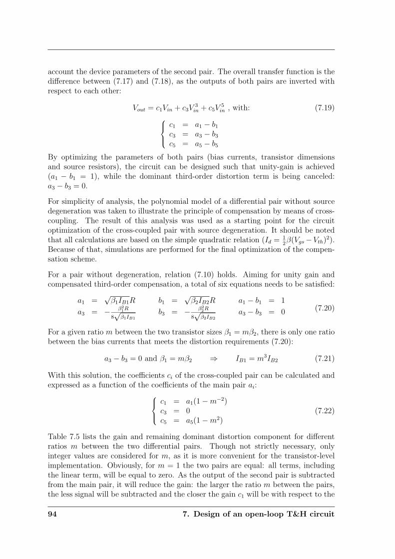
account the device parameters of the second pair. The overall transfer function is thedifference between (7.17) and (7.18), as the outputs of both pairs are inverted withrespect to each other:
Vout = c1Vin + c3V3in + c5V
5in , with: (7.19)
c1 = a1 − b1
c3 = a3 − b3
c5 = a5 − b5
By optimizing the parameters of both pairs (bias currents, transistor dimensionsand source resistors), the circuit can be designed such that unity-gain is achieved(a1 − b1 = 1), while the dominant third-order distortion term is being canceled:a3 − b3 = 0.
For simplicity of analysis, the polynomial model of a differential pair without sourcedegeneration was taken to illustrate the principle of compensation by means of cross-coupling. The result of this analysis was used as a starting point for the circuitoptimization of the cross-coupled pair with source degeneration. It should be notedthat all calculations are based on the simple quadratic relation (Id = 1
2β(Vgs−Vth)
2).Because of that, simulations are performed for the final optimization of the compen-sation scheme.
For a pair without degeneration, relation (7.10) holds. Aiming for unity gain andcompensated third-order compensation, a total of six equations needs to be satisfied:
a1 =√
β1IB1R b1 =√
β2IB2R a1 − b1 = 1
a3 = − β21R
8√
β1IB1
b3 = − β22R
8√
β2IB2
a3 − b3 = 0 (7.20)
For a given ratio m between the two transistor sizes β1 = mβ2, there is only one ratiobetween the bias currents that meets the distortion requirements (7.20):
a3 − b3 = 0 and β1 = mβ2 ⇒ IB1 = m3IB2 (7.21)
With this solution, the coefficients ci of the cross-coupled pair can be calculated andexpressed as a function of the coefficients of the main pair ai:
c1 = a1(1−m−2)c3 = 0c5 = a5(1−m2)
(7.22)
Table 7.5 lists the gain and remaining dominant distortion component for differentratios m between the two differential pairs. Though not strictly necessary, onlyinteger values are considered for m, as it is more convenient for the transistor-levelimplementation. Obviously, for m = 1 the two pairs are equal: all terms, includingthe linear term, will be equal to zero. As the output of the second pair is subtractedfrom the main pair, it will reduce the gain: the larger the ratio m between the pairs,the less signal will be subtracted and the closer the gain c1 will be with respect to the
94 7. Design of an open-loop T&H circuit
original gain a1: for m = 2, a gain-loss of 25% is introduced, but e.g. for m = 4, thegain-loss is reduced to 6%. Note that for all m (except for m = 1), a gain of one canbe realized after cross-coupling by increasing the gain a1 of the original pair. Eventhough a gain-loss might not be that critical from a function point of view, indirectlyit does degrade the power-efficiency of the circuit. Because of that, a smaller gain-lossis preferable.
Ratio Gain 5th-order distortionm c1 c5
1 0 0
2 34a1 −3a5
3 89a1 −8a5
4 1516
a1 −15a5
Table 7.5: Gain and 5th-order distortion for various cross-coupled pairs.
With respect to gain, it is best to maximize m as it reduces the gain-loss. On theother hand, increasing m also increases the amplitude of the remaining distortioncomponent c5 as illustrated in table 7.5. On top of that one should note that forhigher m, the current densities of the two pairs deviate more: as β1 = mβ2 andIB1 = m3IB2, the current density will differ by a factor of m2. As such, the assumptionthat both pairs can be modeled by the same polynomial function (7.10) will be lessplausible for higher m. As a compromise, m was set to 3 to limit the gain-loss to about10%. With this starting point, the source degeneration resistors were optimized forlinearity. The parameters in the final design are summarized in table 7.6, while thesimulated performance is visualized in fig. 7.10. This figure shows the DC transferfunction of the differential pair after subtraction of the linear term, such that only thedistortion components remain. Also, a polynomial approximation is shown, which iscomposed of a third-order and a fifth-order term. As the polynomial approximationmatches the simulated curve closely, it can be concluded that the third-order andfifth-order distortion are still dominating the overall linearity. The simulation resultsreveal that the maximum deviation was reduced to Verr,max = 0.57mV, resulting inENOB = 9.8bit, which suits the 60dB SFDR-goal. More precise linearity simulationswill be presented later in this chapter, when the sampling core and output buffer willbe simulated together.
Parameter Value Parameter ValueIB1 7.8mA IB2 0.3mARs1 307Ω Rs2 1.7kΩ
W/L M1,M2 45.0µm/0.18µm W/L M5,M6 1.2µm/0.18µmW/L M3,M4 39.6µm/0.18µm W/L M7,M8 13.2µm/0.18µm
R 167.5Ω
Table 7.6: Parameters of the output buffer.
7. Design of an open-loop T&H circuit 95
-0.6
-0.4
-0.2
0.0
0.2
0.4
0.6
-0.4 -0.2 0.0 0.2 0.4
Dis
tort
ion
(mV
)
Input voltage (V)
Simulated distortion5th order polynomial fit
Figure 7.10: Simulated distortion of the output buffer.
Finally, noise simulations were performed to estimate the SNR of the output buffer.Results are shown in fig 7.11, yielding a noise power of Pn = 50 · 10−9V2. With asignal power of Ps = 1
2V 2
fs = 0.125V2, this gives an SNR of 64dB.
10z
1a
0.1f
10f
1p
0.1n
10n
1u
1 10 100 1k 10k 100k 1M 10M 100M 1G
Inte
grat
ed n
oise
pow
er (
V )2
Noi
se p
ower
den
sity
(V
/Hz)
2
Frequency (Hz)
Noise Power Density
Integrated Noise Power
Figure 7.11: Simulated noise power of the output buffer.
7.5.5 Conclusion
In this section, two alternative architectures for the buffer were reviewed: a source-follower and a cross-coupled differential pair with source degeneration. Both archi-tectures can meet the requirements of the design goal set previously. Therefore, both
96 7. Design of an open-loop T&H circuit
alternatives will be considered in the following section, where the complete T&H willbe designed on transistor-level.
7.6 T&H design
In this section, two transistor-level implementations of an open-loop T&H circuit willbe presented, both aiming for the design goal as proposed in section 7.2. The outputbuffer was implemented with either a source follower or an enhanced differentialpair, while the sampling core (see section 7.4) remained identical in both cases. Fora fair comparison, the current consumption of the output buffer was set to IB =8mA in both cases. As such, the achievable gain, linearity and bandwidth of bothoutput buffers can be compared for constant sampling speed and constant powerconsumption.
7.6.1 Source follower based architecture
The source follower was implemented according to fig. 7.5. As the bias-current IB wasfixed, the only remaining design-parameter is the size of the transistors. Minimum-length transistors (L = 0.18µm) were chosen to minimize the parasitic capacitances.For the width, two options will be verified: a small width (W = 40µm, the same valueas used in the differential pair) and a large width (W = 320µm). These two widthswere selected as they give a clear impression of the effect of the size of the transistorson the performance of the source follower, as shown later by the simulation results.
7.6.2 Differential pair based architecture
For the differential pair, the enhanced structure from section 7.5.4 was used. Basedon the selected bias current and the sizes of the transistors composing the main dif-ferential pair (W = 40µm, L = 0.18µm), the remaining components were optimized.The precise design approach can be found in section 7.5.4.
7.6.3 Simulation Results
Transistor-level simulations were carried out in the time-domain to analyze the prop-erties of the presented circuits. In all cases, a 500MHz sampling clock was applied tothe T&H, while sinusoids of various frequencies were applied as an input signal. FourT&H configurations were tested (summarized in table 7.7): two configurations basedon a source follower, one on a differential pair and one on an ideal buffer with zeroinput capacitance, zero output resistance and unity-gain. The ideal configuration
7. Design of an open-loop T&H circuit 97
determines the performance of the sampling structure (switches, switch-drivers andsampling capacitors), giving an upper-limit of the performance of the whole T&H.
Configuration DescriptionSF1 Source Follower with W = 40µm, L = 0.18µmSF2 Source Follower with W = 320µm, L = 0.18µmDP Differential pair with W = 40µm, L = 0.18µmID Ideal output buffer
Table 7.7: Simulated configurations.
The frequency response of the complete T&H for input frequencies between 3MHzand 2GHz is given in fig. 7.12. It can be seen that mainly the source followerstructures deviate from unity-gain. Increasing the transistors’ W
L-ratio reduces the
loss, but is not effective because of the low sensitivity. Next to that, the sourcefollower architectures show a peak in their response due to parasitic coupling frominput to output. In case of the differential pair, the response behaves more smoothly.Nonetheless, all responses remain flat within ±0.1dB up to the Nyquist frequency(250MHz).
-1.5
-1.0
-0.5
0.0
10 100 1000 250
Gai
n (d
B)
Input Frequency (MHz)
DP (differential pair)
SF2 (large source follower)
SF1 (small source follower)
ID (ideal buffer)
Figure 7.12: Response as a function of the input frequency.
The static linearity (fig. 7.13 and 7.14) is limited by the output buffer (62dB for theDP configuration, 68dB for SF1 and 77dB for SF2), as the linearity of the samplingstructure (86dB) is far better. The dynamic linearity was determined by means ofthe achieved SFDR (Spurious-Free-Dynamic-Range) as a function of fin (fig. 7.15).Clearly, the selection of the transistor size in the source follower has a dominanteffect on its linearity: large transistors (SF2 compared to SF1) improve the staticperformance, but they degrade the dynamic performance for higher input frequencies.One can also observe that for high input frequencies, the linearity of the source-follower remains the bottleneck for the overall linearity. Opposed to this, the linearityof the differential pair degrades more slowly as a function of the applied frequency,such that for high frequencies the sampling core instead of the output buffer becomesthe dominant source of distortion. Even though the source follower is superior for
98 7. Design of an open-loop T&H circuit
static linearity, the differential pair can be superior for high input frequencies (inthis case far beyond Nyquist). Despite the differences, both architectures achieve thetarget of 60dB SFDR for the Nyquist band.
-150
-100
-50
0
0 50 100 150 200 250
Rel
ativ
e Po
wer
(dB
)
Frequency (MHz)
f = 500 MSpsf = 3 MHzsin
Figure 7.13: Output spectrum of the differential-pair based architecture.
-100
-80
-60
-40
-20
0
0 10 20 30 40
Rel
ativ
e Po
wer
(dB
)
Frequency (MHz)
ID (ideal buffer)
f = 500 MSpsf = 3 MHzsin
-100
-80
-60
-40
-20
0
0 10 20 30 40
Rel
ativ
e Po
wer
(dB
)
Frequency (MHz)
DP (differential pair)
f = 500 MSpsf = 3 MHzsin
-100
-80
-60
-40
-20
0
0 10 20 30 40
Rel
ativ
e Po
wer
(dB
)
Frequency (MHz)
SF1 (small source follower)
f = 500 MSpsf = 3 MHzsin
-100
-80
-60
-40
-20
0
0 10 20 30 40
Rel
ativ
e Po
wer
(dB
)
Frequency (MHz)
SF2 (large source follower)
f = 500 MSpsf = 3 MHzsin
Figure 7.14: Partial output spectrums of the four architectures of table 7.7.
Table 7.8 summarizes the simulated features of both T&H architectures, showing thatboth designs achieve the intended design goal. Even though the source follower basedarchitecture achieves a better linearity, it was decided to implement the differential
7. Design of an open-loop T&H circuit 99
40
50
60
70
80
90
10 100 1000 250
SFD
R (
dB)
Input Frequency (MHz)
DP (differential pair)
SF2 (large source follower)
SF1 (small source follower)
ID (ideal buffer)
Figure 7.15: SFDR (linearity) as a function of the input frequency.
pair based design in a test chip as it is more suitable for the calibration methods thatwill be introduced in chapters 8 and 9. Fig. 7.16 shows the layout of the implementedT&H, measuring 90µm x 90µm.
Source Follower Differential PairSampling speed 500MSpsStatic accuracy 68 - 77dB 62dBDynamic accuracy (1GHz) 44 - 53dB 52dBPower consumption 14.4mW
Table 7.8: Features of the open-loop T&H circuits.
7.7 Experimental results
7.7.1 Measurement setup
When measuring the output of a T&H circuit, it is important to realize that thefunction of a T&H is to convert a continuous-time input signal into a sampled (ordiscrete-time) output signal. An illustration of this process is given in fig. 7.17:during the track phase, the output of the T&H follows the input signal, which is asinusoid in this example. Then, during the hold phase, the output of the T&H is heldat the value which was sampled at the beginning of the hold phase. The series ofheld values compose the discrete-time signal generated by the T&H, as indicated bythe samples in the figure. As the output information is fully contained within the
100 7. Design of an open-loop T&H circuit
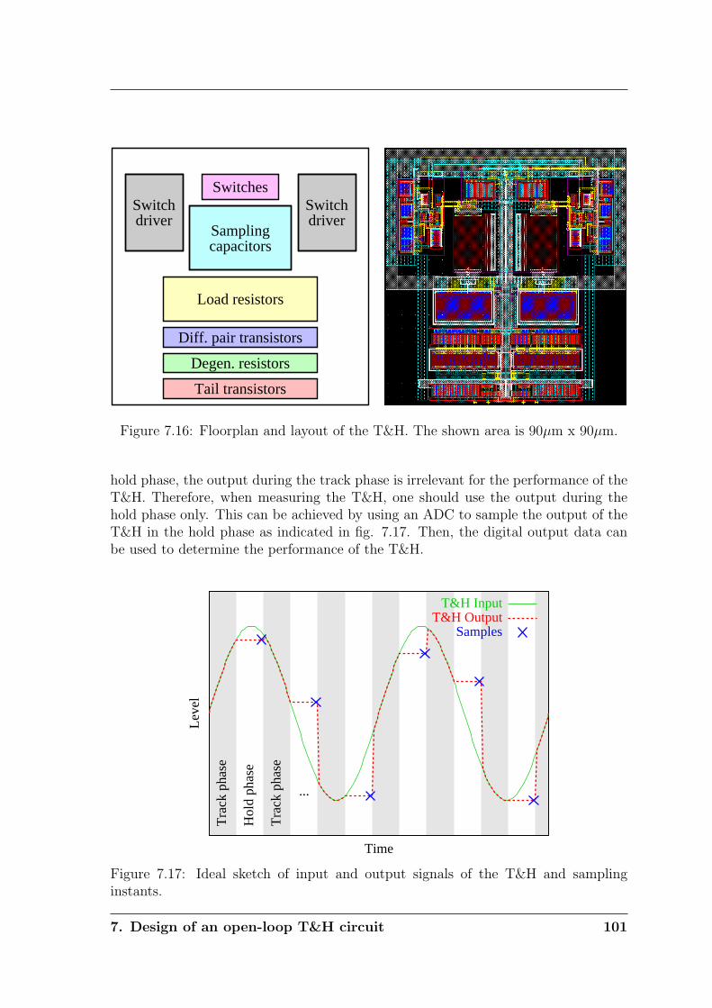
Tail transistors
Degen. resistors
Diff. pair transistors
Load resistors
capacitorsSampling
Switches
driverSwitch
driverSwitch
Figure 7.16: Floorplan and layout of the T&H. The shown area is 90µm x 90µm.
hold phase, the output during the track phase is irrelevant for the performance of theT&H. Therefore, when measuring the T&H, one should use the output during thehold phase only. This can be achieved by using an ADC to sample the output of theT&H in the hold phase as indicated in fig. 7.17. Then, the digital output data canbe used to determine the performance of the T&H.
Tra
ck p
hase
Hol
d ph
ase
Tra
ck p
hase
...
Lev
el
Time
T&H InputT&H Output
Samples
Figure 7.17: Ideal sketch of input and output signals of the T&H and samplinginstants.
7. Design of an open-loop T&H circuit 101
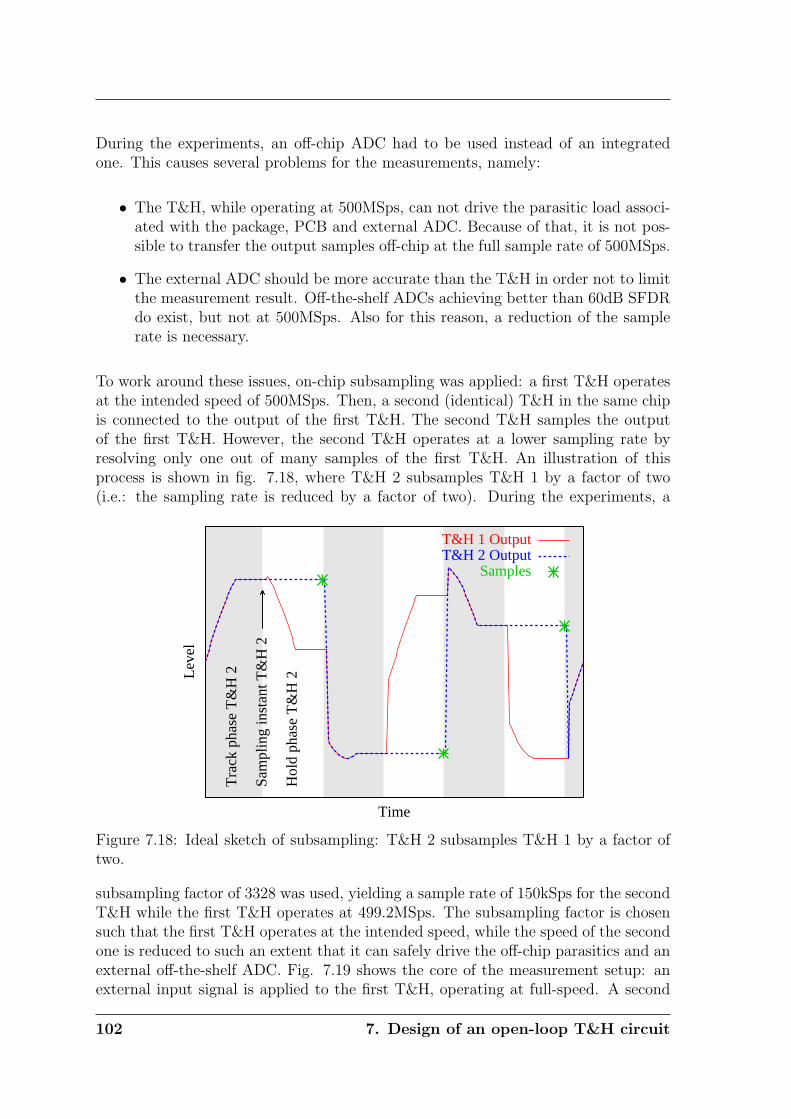
During the experiments, an off-chip ADC had to be used instead of an integratedone. This causes several problems for the measurements, namely:
• The T&H, while operating at 500MSps, can not drive the parasitic load associ-ated with the package, PCB and external ADC. Because of that, it is not pos-sible to transfer the output samples off-chip at the full sample rate of 500MSps.
• The external ADC should be more accurate than the T&H in order not to limitthe measurement result. Off-the-shelf ADCs achieving better than 60dB SFDRdo exist, but not at 500MSps. Also for this reason, a reduction of the samplerate is necessary.
To work around these issues, on-chip subsampling was applied: a first T&H operatesat the intended speed of 500MSps. Then, a second (identical) T&H in the same chipis connected to the output of the first T&H. The second T&H samples the outputof the first T&H. However, the second T&H operates at a lower sampling rate byresolving only one out of many samples of the first T&H. An illustration of thisprocess is shown in fig. 7.18, where T&H 2 subsamples T&H 1 by a factor of two(i.e.: the sampling rate is reduced by a factor of two). During the experiments, a
Tra
ck p
hase
T&
H 2
Sam
plin
g in
stan
t T&
H 2
Hol
d ph
ase
T&
H 2L
evel
Time
T&H 1 OutputT&H 2 Output
Samples
Figure 7.18: Ideal sketch of subsampling: T&H 2 subsamples T&H 1 by a factor oftwo.
subsampling factor of 3328 was used, yielding a sample rate of 150kSps for the secondT&H while the first T&H operates at 499.2MSps. The subsampling factor is chosensuch that the first T&H operates at the intended speed, while the speed of the secondone is reduced to such an extent that it can safely drive the off-chip parasitics and anexternal off-the-shelf ADC. Fig. 7.19 shows the core of the measurement setup: anexternal input signal is applied to the first T&H, operating at full-speed. A second
102 7. Design of an open-loop T&H circuit
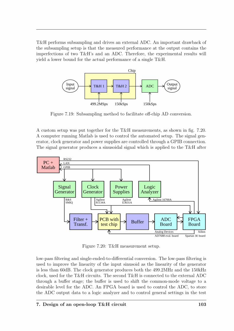
T&H performs subsampling and drives an external ADC. An important drawback ofthe subsampling setup is that the measured performance at the output contains theimperfections of two T&H’s and an ADC. Therefore, the experimental results willyield a lower bound for the actual performance of a single T&H.
signalInput T&H 1 T&H 2 ADC signal
Output
499.2MSps 150kSps 150kSps
Chip
Figure 7.19: Subsampling method to facilitate off-chip AD conversion.
A custom setup was put together for the T&H measurements, as shown in fig. 7.20.A computer running Matlab is used to control the automated setup. The signal gen-erator, clock generator and power supplies are controlled through a GPIB connection.The signal generator produces a sinusoidal signal which is applied to the T&H after
MatlabPC +
GeneratorSignal
GeneratorClock
SuppliesPower
AnalyzerLogic
Transf.Filter +
test chipPCB with Buffer Board
ADCBoardFPGA
GPIBLANRS232
R&SSMIQ
Agilent81134A
AgilentE3631A
Agilent 16700A
Analog DevicesAD7688 eval. board
XilinxSpartan 3E board
Figure 7.20: T&H measurement setup.
low-pass filtering and single-ended-to-differential conversion. The low-pass filtering isused to improve the linearity of the input sinusoid as the linearity of the generatoris less than 60dB. The clock generator produces both the 499.2MHz and the 150kHzclock, used for the T&H circuits. The second T&H is connected to the external ADCthrough a buffer stage; the buffer is used to shift the common-mode voltage to adesirable level for the ADC. An FPGA board is used to control the ADC, to storethe ADC output data to a logic analyzer and to control general settings in the test
7. Design of an open-loop T&H circuit 103
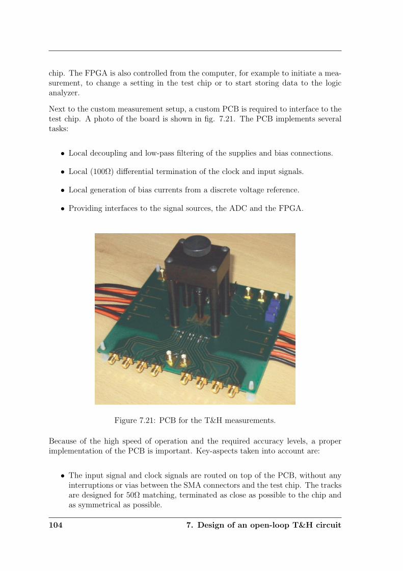
chip. The FPGA is also controlled from the computer, for example to initiate a mea-surement, to change a setting in the test chip or to start storing data to the logicanalyzer.
Next to the custom measurement setup, a custom PCB is required to interface to thetest chip. A photo of the board is shown in fig. 7.21. The PCB implements severaltasks:
• Local decoupling and low-pass filtering of the supplies and bias connections.
• Local (100Ω) differential termination of the clock and input signals.
• Local generation of bias currents from a discrete voltage reference.
• Providing interfaces to the signal sources, the ADC and the FPGA.
Figure 7.21: PCB for the T&H measurements.
Because of the high speed of operation and the required accuracy levels, a properimplementation of the PCB is important. Key-aspects taken into account are:
• The input signal and clock signals are routed on top of the PCB, without anyinterruptions or vias between the SMA connectors and the test chip. The tracksare designed for 50Ω matching, terminated as close as possible to the chip andas symmetrical as possible.
104 7. Design of an open-loop T&H circuit
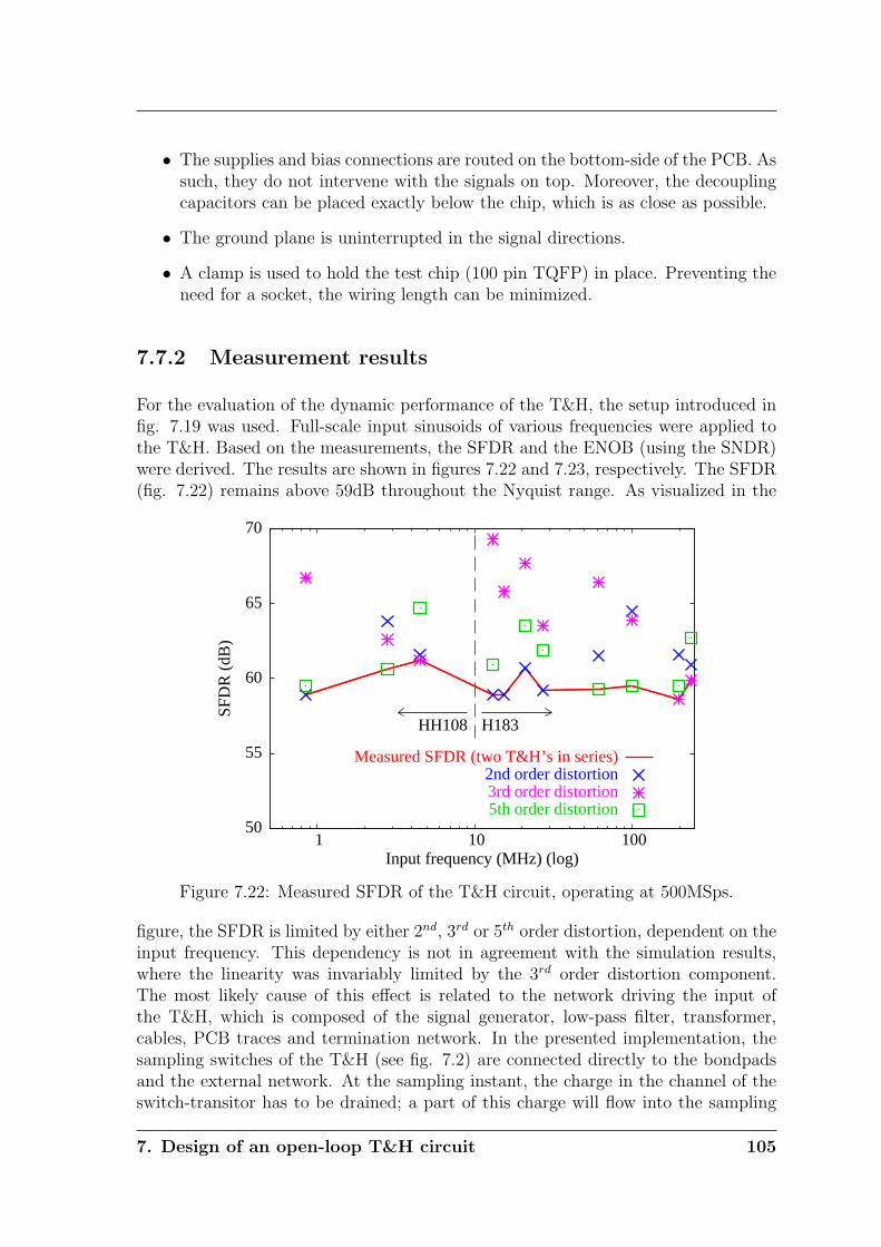
• The supplies and bias connections are routed on the bottom-side of the PCB. Assuch, they do not intervene with the signals on top. Moreover, the decouplingcapacitors can be placed exactly below the chip, which is as close as possible.
• The ground plane is uninterrupted in the signal directions.
• A clamp is used to hold the test chip (100 pin TQFP) in place. Preventing theneed for a socket, the wiring length can be minimized.
7.7.2 Measurement results
For the evaluation of the dynamic performance of the T&H, the setup introduced infig. 7.19 was used. Full-scale input sinusoids of various frequencies were applied tothe T&H. Based on the measurements, the SFDR and the ENOB (using the SNDR)were derived. The results are shown in figures 7.22 and 7.23, respectively. The SFDR(fig. 7.22) remains above 59dB throughout the Nyquist range. As visualized in the
50
55
60
65
70
1 10
HH108 H183
100
SFD
R (
dB)
Input frequency (MHz) (log)
Measured SFDR (two T&H’s in series)2nd order distortion3rd order distortion5th order distortion
Figure 7.22: Measured SFDR of the T&H circuit, operating at 500MSps.
figure, the SFDR is limited by either 2nd, 3rd or 5th order distortion, dependent on theinput frequency. This dependency is not in agreement with the simulation results,where the linearity was invariably limited by the 3rd order distortion component.The most likely cause of this effect is related to the network driving the input ofthe T&H, which is composed of the signal generator, low-pass filter, transformer,cables, PCB traces and termination network. In the presented implementation, thesampling switches of the T&H (see fig. 7.2) are connected directly to the bondpadsand the external network. At the sampling instant, the charge in the channel of theswitch-transitor has to be drained; a part of this charge will flow into the sampling
7. Design of an open-loop T&H circuit 105
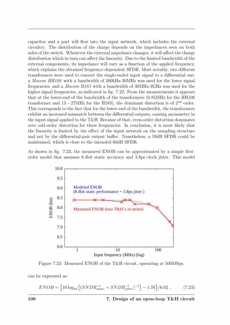
capacitor and a part will flow into the input network, which includes the externalcircuitry. The distribution of the charge depends on the impedances seen on bothsides of the switch. Whenever the external impedance changes, it will affect the chargedistribution which in turn can affect the linearity. Due to the limited bandwidth of theexternal components, its impedance will vary as a function of the applied frequency,which explains the obtained frequency-dependent SFDR. Most notably, two differenttransformers were used to convert the single-ended input signal to a differential one:a Macom HH108 with a bandwidth of 200kHz-30MHz was used for the lower signalfrequencies, and a Macom H183 with a bandwidth of 30MHz-3GHz was used for thehigher signal frequencies, as indicated in fig. 7.22. From the measurements it appearsthat at the lower-end of the bandwidth of the transformers (0.85MHz for the HH108transformer and 13 - 27MHz for the H183), the dominant distortion is of 2nd order.This corresponds to the fact that for the lower-end of the bandwidth, the transformersexhibit an increased mismatch between the differential outputs, causing asymmetry inthe input signal applied to the T&H. Because of that, even-order distortion dominatesover odd-order distortion for these frequencies. In conclusion, it is most likely thatthe linearity is limited by the effect of the input network on the sampling structureand not by the differential-pair output buffer. Nonetheless, a 59dB SFDR could bemaintained, which is close to the intended 60dB SFDR.
As shown in fig. 7.23, the measured ENOB can be approximated by a simple first-order model that assumes 8.4bit static accuracy and 3.8ps clock jitter. This model
6.0
6.5
7.0
7.5
8.0
8.5
9.0
9.5
10.0
1 10 100
EN
OB
(bi
t)
Input frequency (MHz) (log)
Modeled ENOB(8.4bit static performance + 3.8ps jitter )
Measured ENOB (two T&H’s in series)
Figure 7.23: Measured ENOB of the T&H circuit, operating at 500MSps.
can be expressed as:
ENOB =10 log10
((SNDR−1
static + SNDR−1jitter)
−1)− 1.76
/6.02 , (7.23)
106 7. Design of an open-loop T&H circuit
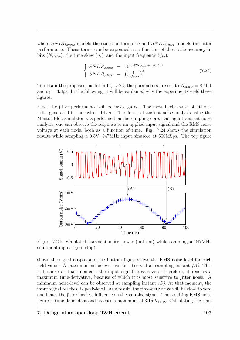
where SNDRstatic models the static performance and SNDRjitter models the jitterperformance. These terms can be expressed as a function of the static accuracy inbits (Nstatic), the time-skew (σt), and the input frequency (fin):
SNDRstatic = 10(6.02Nstatic+1.76)/10
SNDRjitter =(
12πfinσt
)2 (7.24)
To obtain the proposed model in fig. 7.23, the parameters are set to Nstatic = 8.4bitand σt = 3.8ps. In the following, it will be explained why the experiments yield thesefigures.
First, the jitter performance will be investigated. The most likely cause of jitter isnoise generated in the switch driver. Therefore, a transient noise analysis using theMentor Eldo simulator was performed on the sampling core. During a transient noiseanalysis, one can observe the response to an applied input signal and the RMS noisevoltage at each node, both as a function of time. Fig. 7.24 shows the simulationresults while sampling a 0.5V, 247MHz input sinusoid at 500MSps. The top figure
0mV
2mV
4mV
-0.5
0
0.5
0 20 40 60 80 100
Sign
al o
utpu
t (V
)O
utpu
t noi
se (
Vrm
s)
Time (ns)
(A) (B)
Figure 7.24: Simulated transient noise power (bottom) while sampling a 247MHzsinusoidal input signal (top).
shows the signal output and the bottom figure shows the RMS noise level for eachheld value. A maximum noise-level can be observed at sampling instant (A). Thisis because at that moment, the input signal crosses zero; therefore, it reaches amaximum time-derivative, because of which it is most sensitive to jitter noise. Aminimum noise-level can be observed at sampling instant (B). At that moment, theinput signal reaches its peak-level. As a result, the time-derivative will be close to zeroand hence the jitter has less influence on the sampled signal. The resulting RMS noisefigure is time-dependent and reaches a maximum of 3.1mVrms. Calculating the time
7. Design of an open-loop T&H circuit 107
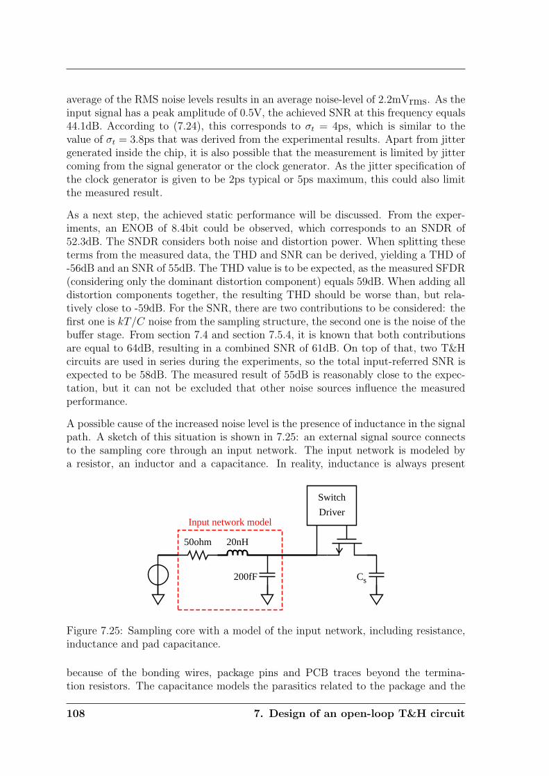
average of the RMS noise levels results in an average noise-level of 2.2mVrms. As theinput signal has a peak amplitude of 0.5V, the achieved SNR at this frequency equals44.1dB. According to (7.24), this corresponds to σt = 4ps, which is similar to thevalue of σt = 3.8ps that was derived from the experimental results. Apart from jittergenerated inside the chip, it is also possible that the measurement is limited by jittercoming from the signal generator or the clock generator. As the jitter specification ofthe clock generator is given to be 2ps typical or 5ps maximum, this could also limitthe measured result.
As a next step, the achieved static performance will be discussed. From the exper-iments, an ENOB of 8.4bit could be observed, which corresponds to an SNDR of52.3dB. The SNDR considers both noise and distortion power. When splitting theseterms from the measured data, the THD and SNR can be derived, yielding a THD of-56dB and an SNR of 55dB. The THD value is to be expected, as the measured SFDR(considering only the dominant distortion component) equals 59dB. When adding alldistortion components together, the resulting THD should be worse than, but rela-tively close to -59dB. For the SNR, there are two contributions to be considered: thefirst one is kT/C noise from the sampling structure, the second one is the noise of thebuffer stage. From section 7.4 and section 7.5.4, it is known that both contributionsare equal to 64dB, resulting in a combined SNR of 61dB. On top of that, two T&Hcircuits are used in series during the experiments, so the total input-referred SNR isexpected to be 58dB. The measured result of 55dB is reasonably close to the expec-tation, but it can not be excluded that other noise sources influence the measuredperformance.
A possible cause of the increased noise level is the presence of inductance in the signalpath. A sketch of this situation is shown in 7.25: an external signal source connectsto the sampling core through an input network. The input network is modeled bya resistor, an inductor and a capacitance. In reality, inductance is always present
Input network modelDriver
Switch
Cs200fF
50ohm 20nH
Figure 7.25: Sampling core with a model of the input network, including resistance,inductance and pad capacitance.
because of the bonding wires, package pins and PCB traces beyond the termina-tion resistors. The capacitance models the parasitics related to the package and the
108 7. Design of an open-loop T&H circuit
bonding pad. It should be noted that the values of the components given in thefigure are not based on a physical extraction of the implemented circuit; their onlypurpose is to show the principal behavior of the circuit. Because of the presence ofthe inductance, a ringing effect can be observed at the moment the switch samplesthe input signal. The characteristic frequency of the oscillation is dependent on theparasitics; as they are typically small, the oscillation will have a high frequency. Forexample, for L = 20nH and C = 200fF, the oscillation frequency is 2.5GHz. Notethat an inductance of 20nH is relatively large, however, this value is selected to obtaina clear simulation result to illustrate the behavior of the circuit. The ringing effectintroduces a high-frequency signal component at the sampling instant, even when theapplied signal itself is of a low frequency. Now, the jitter of the clock signal, whichhas normally negligible effect at low signal frequencies, becomes important again: itwill modulate with the oscillation of the input network and add noise to the sampleddata. Transient noise simulations were carried out on the circuit of fig. 7.25 to verifythis principle. A low-frequency input signal of 4.3MHz was used, which is normallyinsensitive to jitter noise. Fig. 7.26 shows the applied signal and the simulated RMSnoise. For comparison, the noise-plot is shown for a system with an inductance of20nH, and a system without inductance. Without inductance, an RMS noise-level of0.18mVrms is achieved, which corresponds to the expected kT/C-noise level. How-ever, when an inductance of 20nH is present, there is a significant increase of thenoise-level. The shown example reaches an average RMS noise-level of 0.7mVrms,which would produce an SNR of 54dB.
-0.6
-0.4
-0.2
0.0
0.2
0.4
0.6
0 50 100 150 200
Out
put s
igna
l (V
)
Time (ns)
4.3MHz, 0dBFS input
0
0.2
0.4
0.6
0.8
1.0
1.2
0 50 100 150 200
Out
put n
oise
(m
Vrm
s)
Time (ns)
L = 20nH
L = 0nH
Figure 7.26: Simulated transient noise power (right) while sampling a 4.3MHz si-nusoidal input signal (left). Results are shown for a source inductance of 0nH and20nH.
A summary of the measured performance is included in table 7.9. For comparisonwith prior art, the FoM-SFDR and FoM-ENOB are also calculated. As the T&His designed for Nyquist operation, the ERBW should be equal to 250MHz. At thisfrequency, the measured ENOB equals 7.1bit. As a 0.5bit performance-loss is typicallyallowed at the ERBW, an ENOB of 7.6bit can be claimed in combination with a250MHz ERBW. For the calculation of the FoM-ENOB, the latter ENOB is used as
7. Design of an open-loop T&H circuit 109
well. When comparing the measured result with the original design goal (table 7.3),it appears that all requirements could be fulfilled except for the linearity which is 1dBless compared to the target. However, the SFDR-based FoM of 37fJ is still betterthan expected as the achieved power consumption of 13.5mW is substantially betterthan the goal of 25mW. Also, as explained previously, the most likely cause of thelimited linearity is because of the measurement setup, and not because of the T&Hitself.
Power supply VDD 1.8VSignal range Vin,pp 1.0VPower consumption 13.5mWfs, 2fin,max 500MHzSFDR (DC - Nyquist) 59dBLow-frequency ENOB 8.4bitENOB at Nyquist 7.1bitENOB for ERBW equal to Nyquist 7.6bitFoM-SFDR 37fJFoM-ENOB 139fJ
Table 7.9: Measured performance of the T&H.
7.8 Conclusion
In this chapter, an open-loop Track-and-Hold circuit designed in a CMOS 0.18µmtechnology was presented. Because of the open-loop architecture, a high speed of500MSps could be achieved. At the same time, by introducing a cross-coupled sourcedegenerated differential pair, a high-linearity of 59dB SFDR could be realized.
The experimentally verified performance in terms of the FoM-ENOB, the FoM-SFDRor the speed-linearity product is comparable to the current state-of-the-art. As such,the presented design provides a decent test-circuit for the calibration methods thatwill be presented in the following chapters.
The main performance limitation of the current implementation is due to jitter noiseof the switch driver. This limits the ENOB at Nyquist to 7.1bit, which is a loss of1.3bit compared to the static ENOB. By increasing the power consumption of thedriver, the jitter noise could be reduced in order to improve the ENOB at Nyquist.As the power consumption of the driver (0.25mW) is small compared to the overallconsumption (13.5mW), reducing the jitter would have little impact on the powerbudget. Therefore, it is expected that a further improvement of the FoM-ENOB ispossible.
110 7. Design of an open-loop T&H circuit
Chapter 8
T&H calibration
This chapter presents a method to enhance the accuracy of the open-loop T&H circuit,introduced in chapter 7. The approach is able to measure offset, gain-error and non-linearity on-chip, and to correct for these imperfections by means of analog calibration.The calibration method will be discussed, and both simulation results and experimentalresults will be shown. Parts of this chapter have been published previously in [75, 76].
8.1 Introduction
In chapter 7, a 500MSps open-loop T&H was presented. The linearity of the proposedenhanced differential pair (section 7.5.4) relies on the non-linearity of one differentialpair compensating the non-linearity of another differential pair. Because of imperfec-tions, the non-linearity compensation might not be exploited to the full extent. Eventhough a linearity of 59dB could be verified experimentally, there are several issueswhich could result in a sub-optimal accuracy in practice:
• The transistor models might deviate from the actual transistor behavior.
• Because of process-spread, the nominal values of the components can deviatefrom the intended values.
• Random mismatch and systematic mismatch (e.g. die gradients or asymmetryin the layout) causes an additional variation of the values of the components.
• Environmental changes (temperature, bias current, etc.) modify the transfercharacteristic.
As a result of these effects, the optimum solution according to simulations will notcorrespond exactly to the optimum solution in reality. In order to optimize theaccuracy of the T&H given these unknown imperfections, a calibration method is
8. T&H calibration 111
proposed: iteratively, the calibration method measures the performance and optimizesit by tuning a set of parameters. Apart from optimizing the non-linearity, the methodalso optimizes the gain error and the offset.
In section 8.2, the accuracy requirements for the T&H are discussed. Section 8.3shows an overview of the calibration method, after which the details will be discussedin sections 8.4 and 8.5. Simulation results and experimental results are shown insections 8.6 and 8.8, respectively, followed by conclusions in section 8.9.
8.2 T&H accuracy
Apart from noise, the accuracy of a T&H is limited by non-linearity, gain error,and offset. The importance of these errors is dependent on the application of theT&H. For example, in time-interleaved ADCs gain and offset errors are important asthey introduce unwanted spurious components. As another example, in a non time-interleaved ADC used in a low-IF receiver, offset and gain errors are not directlycritical: the offset does not interfere with the signal, as there is no signal informationat DC, and the gain error is typically compensated by an automatic gain-control loop.
As this concept study does not target a specific application, and it is desirable toprovide a general method, all three imperfections will be taken into account. First ofall, a set of relations is proposed to express the individual imperfections in terms of aneffective number of bits. For the linearity, the effective number of bits (ENOBSFDR)follows from the spurious free dynamic range (SFDR), as in chapter 7:
ENOBSFDR = (SFDR− 1.76)/6.02 (8.1)
Assuming a nominal situation of zero offset and unity gain, the offset and gain erroraffect the transfer function as follows:
Vout = Oe + (1 + Ge)Vin = Vin + (Oe + Ge · Vin) , (8.2)
where Oe equals the offset, Ge equals the gain-error and Vin and Vout represent theinput and output voltage, respectively. The offset results in a constant deviation ofthe output, equal to Oe. On the other hand, the gain-error is multiplied by the inputsignal. For a given full-scale signal ±Vfs, a maximum deviation of Ge ·Vfs is realized.In this study, a maximum error equal to 1
2LSB of the ENOB is tolerated1. As the
LSB equals 2Vfs/2ENOB, the ENOBoffset and ENOBgain can be derived:
ENOBoffset = log2
(Vfs
|Oe|
)(8.3)
1Note that this is a rather arbitrary choice to demonstrate the concept; in practice, the require-ment should be set dependent on the target application.
112 8. T&H calibration
ENOBgain = log2
(1
|Ge|
)(8.4)
In the end, the overall ENOB is determined by the combined effect of all imperfec-tions. Therefore, in line with the design goal from 7.2, the individual requirementsare set to 10-bit, even though the overall ADC target is only 8-bit. Using relations(8.1), (8.3) and (8.4), the following set of constraints needs to be fulfilled in order toachieve 10-bit performance for a full-scale range of Vfs = 0.5V:
|Oe| ≤ 0.5mV|Ge| ≤ 0.1%
SFDR ≥ 62dB(8.5)
When the issues described in section 8.1 (e.g. mismatch and process spread) are takeninto account, these constraints can not be met for the T&H presented in chapter 7.For example, consider the effect of random mismatch of the transistors composingthe differential pair (fig. 8.2) on the offset. Given an Avt of 5mV/µm2, the standarddeviation of the offset of the differential pair becomes: σ =
√2Avt/
√WL. In order to
meet the offset requirement (8.5) with a 3σ margin, the area of the input transistorsshould be 1800µm2 (instead of the implemented 7µm2). First of all, this would have aserious impact on the total area of the T&H as these two devices alone would alreadyoccupy about half of the size of the current layout (fig. 7.16). More important,for the intended speed of operation, it is not realistic to use such large devices asthe parasitic Cgs equals 12pF. This would give both speed and power issues in thepreceding stage that has to drive the T&H. With the implemented small transistors,the parasitic load is reduced to 100fF, which is smaller then the sampling capacitor.As such, the load for the previous stage is not limited by the T&H design, but by thesampling capacitor requirements. However, in case of these small devices, calibrationof the offset (as well as the gain and the non-linearity) will be required. Therefore,a calibration method is presented to improve the intrinsic performance to the goalgiven in (8.5).
8.3 T&H calibration method
In line with the proposal in chapter 6, the calibration method complies with thefollowing properties:
• Foreground calibration method, performed at start-up.
• Digital processing of the information.
• Analog correction of the imperfections.
8. T&H calibration 113
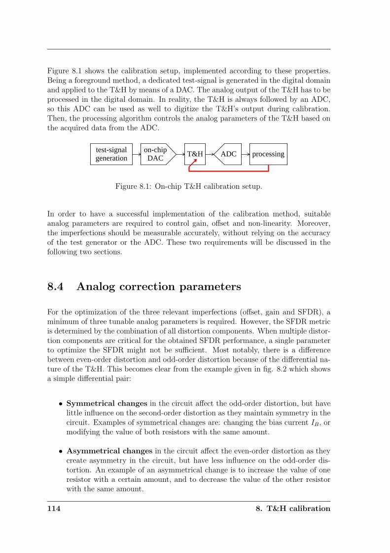
Figure 8.1 shows the calibration setup, implemented according to these properties.Being a foreground method, a dedicated test-signal is generated in the digital domainand applied to the T&H by means of a DAC. The analog output of the T&H has to beprocessed in the digital domain. In reality, the T&H is always followed by an ADC,so this ADC can be used as well to digitize the T&H’s output during calibration.Then, the processing algorithm controls the analog parameters of the T&H based onthe acquired data from the ADC.
test-signalgeneration
on-chipDAC T&H ADC processing
Figure 8.1: On-chip T&H calibration setup.
In order to have a successful implementation of the calibration method, suitableanalog parameters are required to control gain, offset and non-linearity. Moreover,the imperfections should be measurable accurately, without relying on the accuracyof the test generator or the ADC. These two requirements will be discussed in thefollowing two sections.
8.4 Analog correction parameters
For the optimization of the three relevant imperfections (offset, gain and SFDR), aminimum of three tunable analog parameters is required. However, the SFDR metricis determined by the combination of all distortion components. When multiple distor-tion components are critical for the obtained SFDR performance, a single parameterto optimize the SFDR might not be sufficient. Most notably, there is a differencebetween even-order distortion and odd-order distortion because of the differential na-ture of the T&H. This becomes clear from the example given in fig. 8.2 which showsa simple differential pair:
• Symmetrical changes in the circuit affect the odd-order distortion, but havelittle influence on the second-order distortion as they maintain symmetry in thecircuit. Examples of symmetrical changes are: changing the bias current IB, ormodifying the value of both resistors with the same amount.
• Asymmetrical changes in the circuit affect the even-order distortion as theycreate asymmetry in the circuit, but have less influence on the odd-order dis-tortion. An example of an asymmetrical change is to increase the value of oneresistor with a certain amount, and to decrease the value of the other resistorwith the same amount.
114 8. T&H calibration
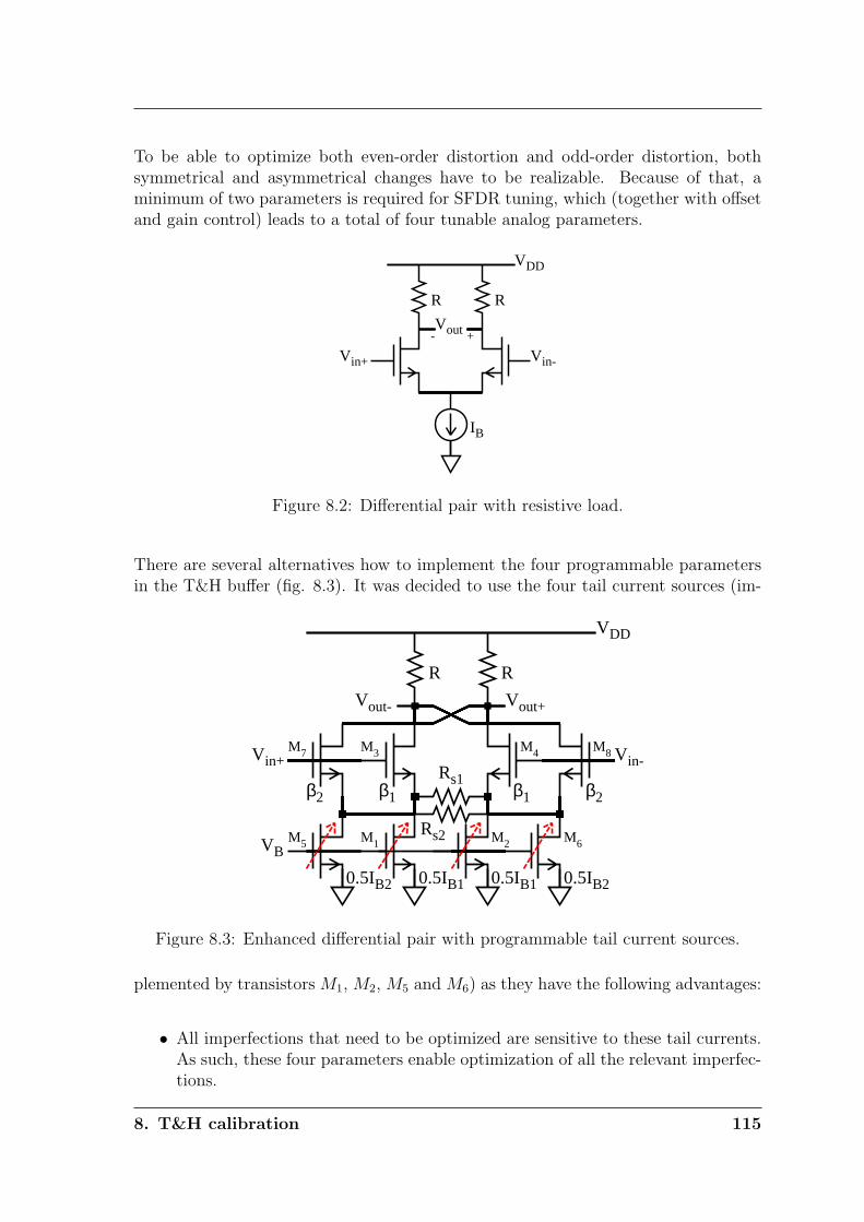
To be able to optimize both even-order distortion and odd-order distortion, bothsymmetrical and asymmetrical changes have to be realizable. Because of that, aminimum of two parameters is required for SFDR tuning, which (together with offsetand gain control) leads to a total of four tunable analog parameters.
IB
Vin+ Vin-
+
R
Vout-
R
VDD
Figure 8.2: Differential pair with resistive load.
There are several alternatives how to implement the four programmable parametersin the T&H buffer (fig. 8.3). It was decided to use the four tail current sources (im-
Rs1
Rs2M5 M6
M7 M8
M1 M2
M3 M4
β2 β1 β1 β2
0.5IB2 0.5IB1 0.5IB1 0.5IB2
Vin+ Vin-
Vout- Vout+
VB
RR
VDD
Figure 8.3: Enhanced differential pair with programmable tail current sources.
plemented by transistors M1, M2, M5 and M6) as they have the following advantages:
• All imperfections that need to be optimized are sensitive to these tail currents.As such, these four parameters enable optimization of all the relevant imperfec-tions.
8. T&H calibration 115
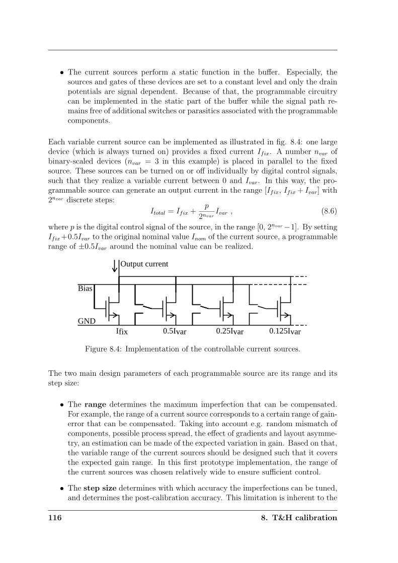
• The current sources perform a static function in the buffer. Especially, thesources and gates of these devices are set to a constant level and only the drainpotentials are signal dependent. Because of that, the programmable circuitrycan be implemented in the static part of the buffer while the signal path re-mains free of additional switches or parasitics associated with the programmablecomponents.
Each variable current source can be implemented as illustrated in fig. 8.4: one largedevice (which is always turned on) provides a fixed current Ifix. A number nvar ofbinary-scaled devices (nvar = 3 in this example) is placed in parallel to the fixedsource. These sources can be turned on or off individually by digital control signals,such that they realize a variable current between 0 and Ivar. In this way, the pro-grammable source can generate an output current in the range [Ifix, Ifix + Ivar] with2nvar discrete steps:
Itotal = Ifix +p
2nvarIvar , (8.6)
where p is the digital control signal of the source, in the range [0, 2nvar−1]. By settingIfix+0.5Ivar to the original nominal value Inom of the current source, a programmablerange of ±0.5Ivar around the nominal value can be realized.
GND
Bias
Output current
I 0.5I 0.25I 0.125Ifix var var var
Figure 8.4: Implementation of the controllable current sources.
The two main design parameters of each programmable source are its range and itsstep size:
• The range determines the maximum imperfection that can be compensated.For example, the range of a current source corresponds to a certain range of gain-error that can be compensated. Taking into account e.g. random mismatch ofcomponents, possible process spread, the effect of gradients and layout asymme-try, an estimation can be made of the expected variation in gain. Based on that,the variable range of the current sources should be designed such that it coversthe expected gain range. In this first prototype implementation, the range ofthe current sources was chosen relatively wide to ensure sufficient control.
• The step size determines with which accuracy the imperfections can be tuned,and determines the post-calibration accuracy. This limitation is inherent to the
116 8. T&H calibration
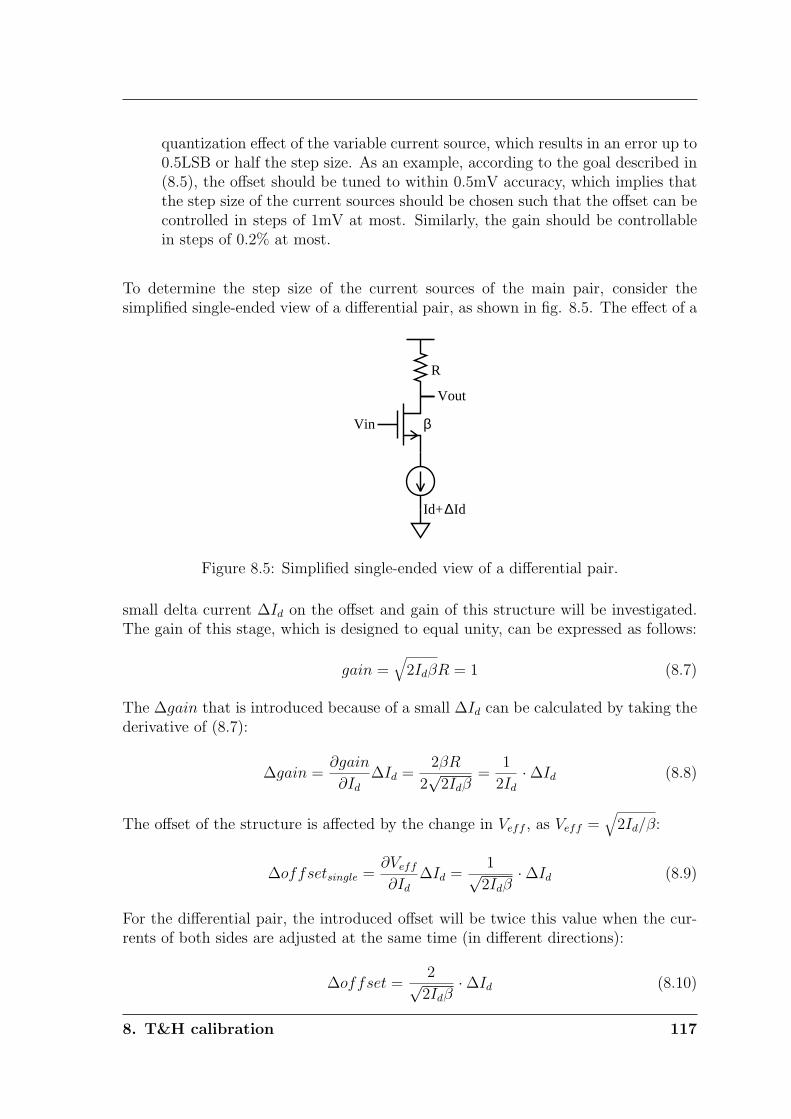
quantization effect of the variable current source, which results in an error up to0.5LSB or half the step size. As an example, according to the goal described in(8.5), the offset should be tuned to within 0.5mV accuracy, which implies thatthe step size of the current sources should be chosen such that the offset can becontrolled in steps of 1mV at most. Similarly, the gain should be controllablein steps of 0.2% at most.
To determine the step size of the current sources of the main pair, consider thesimplified single-ended view of a differential pair, as shown in fig. 8.5. The effect of a
Id+ Id ∆
βVin
R
Vout
Figure 8.5: Simplified single-ended view of a differential pair.
small delta current ∆Id on the offset and gain of this structure will be investigated.The gain of this stage, which is designed to equal unity, can be expressed as follows:
gain =√
2IdβR = 1 (8.7)
The ∆gain that is introduced because of a small ∆Id can be calculated by taking thederivative of (8.7):
∆gain =∂gain
∂Id
∆Id =2βR
2√
2Idβ=
1
2Id
·∆Id (8.8)
The offset of the structure is affected by the change in Veff , as Veff =√
2Id/β:
∆offsetsingle =∂Veff
∂Id
∆Id =1√2Idβ
·∆Id (8.9)
For the differential pair, the introduced offset will be twice this value when the cur-rents of both sides are adjusted at the same time (in different directions):
∆offset =2√2Idβ
·∆Id (8.10)
8. T&H calibration 117
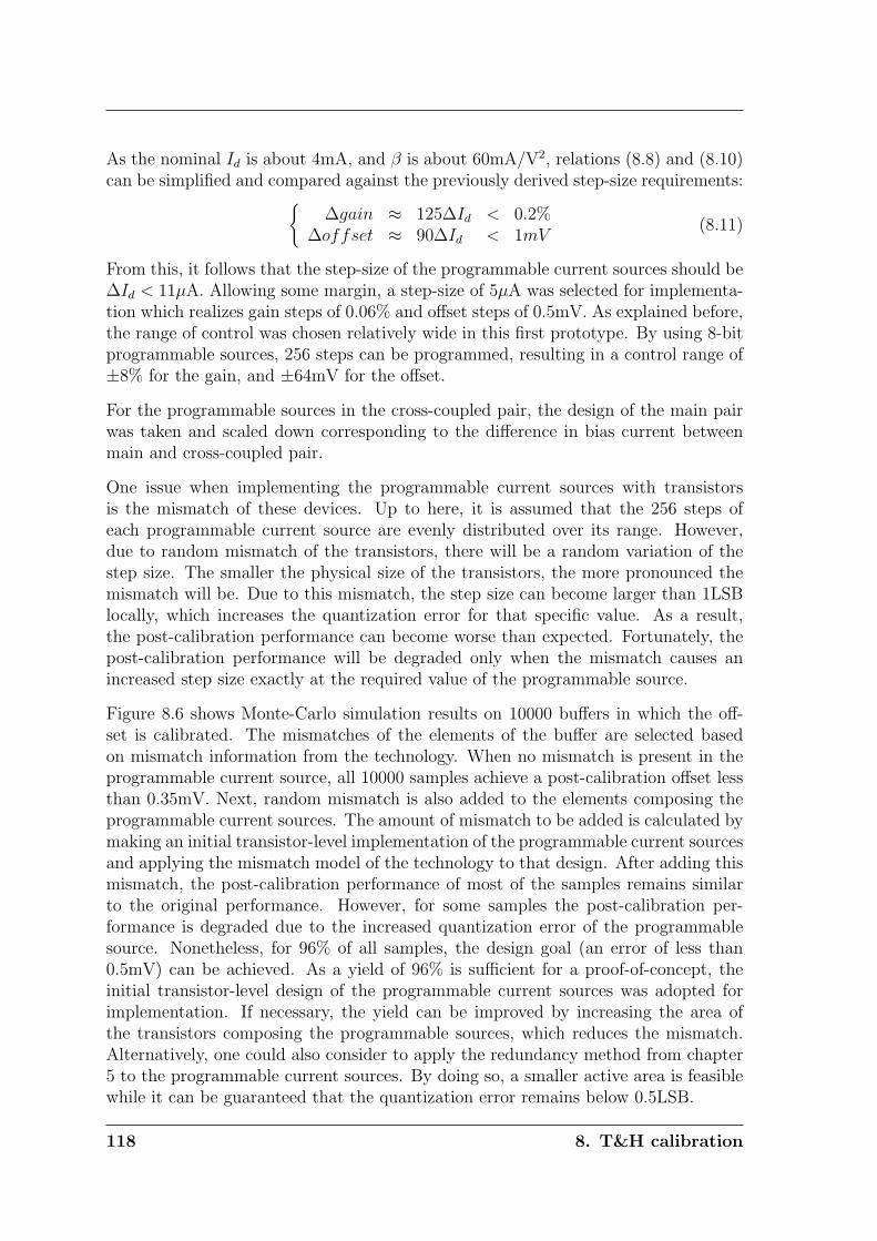
As the nominal Id is about 4mA, and β is about 60mA/V2, relations (8.8) and (8.10)can be simplified and compared against the previously derived step-size requirements:
∆gain ≈ 125∆Id < 0.2%
∆offset ≈ 90∆Id < 1mV(8.11)
From this, it follows that the step-size of the programmable current sources should be∆Id < 11µA. Allowing some margin, a step-size of 5µA was selected for implementa-tion which realizes gain steps of 0.06% and offset steps of 0.5mV. As explained before,the range of control was chosen relatively wide in this first prototype. By using 8-bitprogrammable sources, 256 steps can be programmed, resulting in a control range of±8% for the gain, and ±64mV for the offset.
For the programmable sources in the cross-coupled pair, the design of the main pairwas taken and scaled down corresponding to the difference in bias current betweenmain and cross-coupled pair.
One issue when implementing the programmable current sources with transistorsis the mismatch of these devices. Up to here, it is assumed that the 256 steps ofeach programmable current source are evenly distributed over its range. However,due to random mismatch of the transistors, there will be a random variation of thestep size. The smaller the physical size of the transistors, the more pronounced themismatch will be. Due to this mismatch, the step size can become larger than 1LSBlocally, which increases the quantization error for that specific value. As a result,the post-calibration performance can become worse than expected. Fortunately, thepost-calibration performance will be degraded only when the mismatch causes anincreased step size exactly at the required value of the programmable source.
Figure 8.6 shows Monte-Carlo simulation results on 10000 buffers in which the off-set is calibrated. The mismatches of the elements of the buffer are selected basedon mismatch information from the technology. When no mismatch is present in theprogrammable current source, all 10000 samples achieve a post-calibration offset lessthan 0.35mV. Next, random mismatch is also added to the elements composing theprogrammable current sources. The amount of mismatch to be added is calculated bymaking an initial transistor-level implementation of the programmable current sourcesand applying the mismatch model of the technology to that design. After adding thismismatch, the post-calibration performance of most of the samples remains similarto the original performance. However, for some samples the post-calibration per-formance is degraded due to the increased quantization error of the programmablesource. Nonetheless, for 96% of all samples, the design goal (an error of less than0.5mV) can be achieved. As a yield of 96% is sufficient for a proof-of-concept, theinitial transistor-level design of the programmable current sources was adopted forimplementation. If necessary, the yield can be improved by increasing the area ofthe transistors composing the programmable sources, which reduces the mismatch.Alternatively, one could also consider to apply the redundancy method from chapter5 to the programmable current sources. By doing so, a smaller active area is feasiblewhile it can be guaranteed that the quantization error remains below 0.5LSB.
118 8. T&H calibration
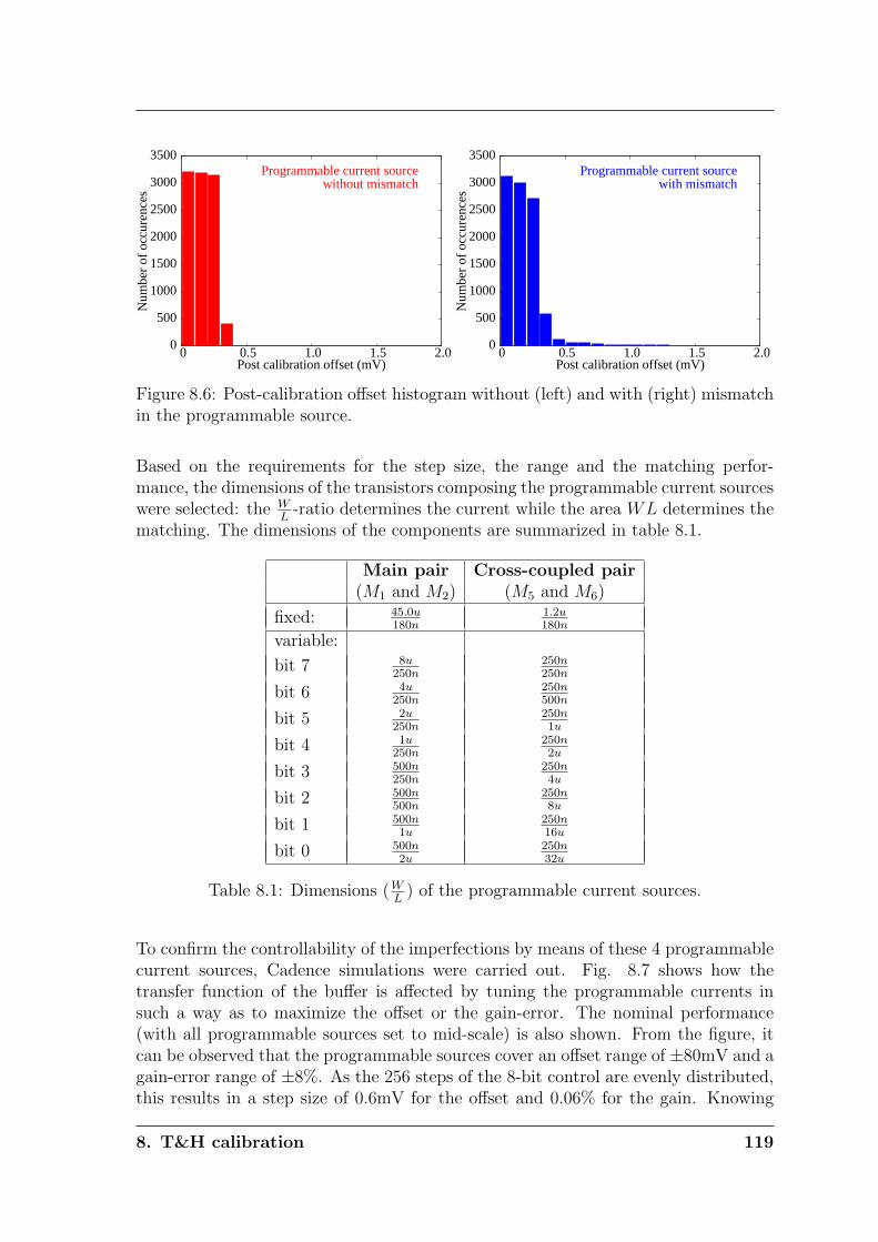
0
500
1000
1500
2000
2500
3000
3500
0 0.5 1.0 1.5 2.0
Num
ber
of o
ccur
ence
s
Post calibration offset (mV)
Programmable current sourcewithout mismatch
0
500
1000
1500
2000
2500
3000
3500
0 0.5 1.0 1.5 2.0
Num
ber
of o
ccur
ence
s
Post calibration offset (mV)
Programmable current sourcewith mismatch
Figure 8.6: Post-calibration offset histogram without (left) and with (right) mismatchin the programmable source.
Based on the requirements for the step size, the range and the matching perfor-mance, the dimensions of the transistors composing the programmable current sourceswere selected: the W
L-ratio determines the current while the area WL determines the
matching. The dimensions of the components are summarized in table 8.1.
Main pair Cross-coupled pair(M1 and M2) (M5 and M6)
fixed: 45.0u180n
1.2u180n
variable:
bit 7 8u250n
250n250n
bit 6 4u250n
250n500n
bit 5 2u250n
250n1u
bit 4 1u250n
250n2u
bit 3 500n250n
250n4u
bit 2 500n500n
250n8u
bit 1 500n1u
250n16u
bit 0 500n2u
250n32u
Table 8.1: Dimensions (WL
) of the programmable current sources.
To confirm the controllability of the imperfections by means of these 4 programmablecurrent sources, Cadence simulations were carried out. Fig. 8.7 shows how thetransfer function of the buffer is affected by tuning the programmable currents insuch a way as to maximize the offset or the gain-error. The nominal performance(with all programmable sources set to mid-scale) is also shown. From the figure, itcan be observed that the programmable sources cover an offset range of ±80mV and again-error range of ±8%. As the 256 steps of the 8-bit control are evenly distributed,this results in a step size of 0.6mV for the offset and 0.06% for the gain. Knowing
8. T&H calibration 119
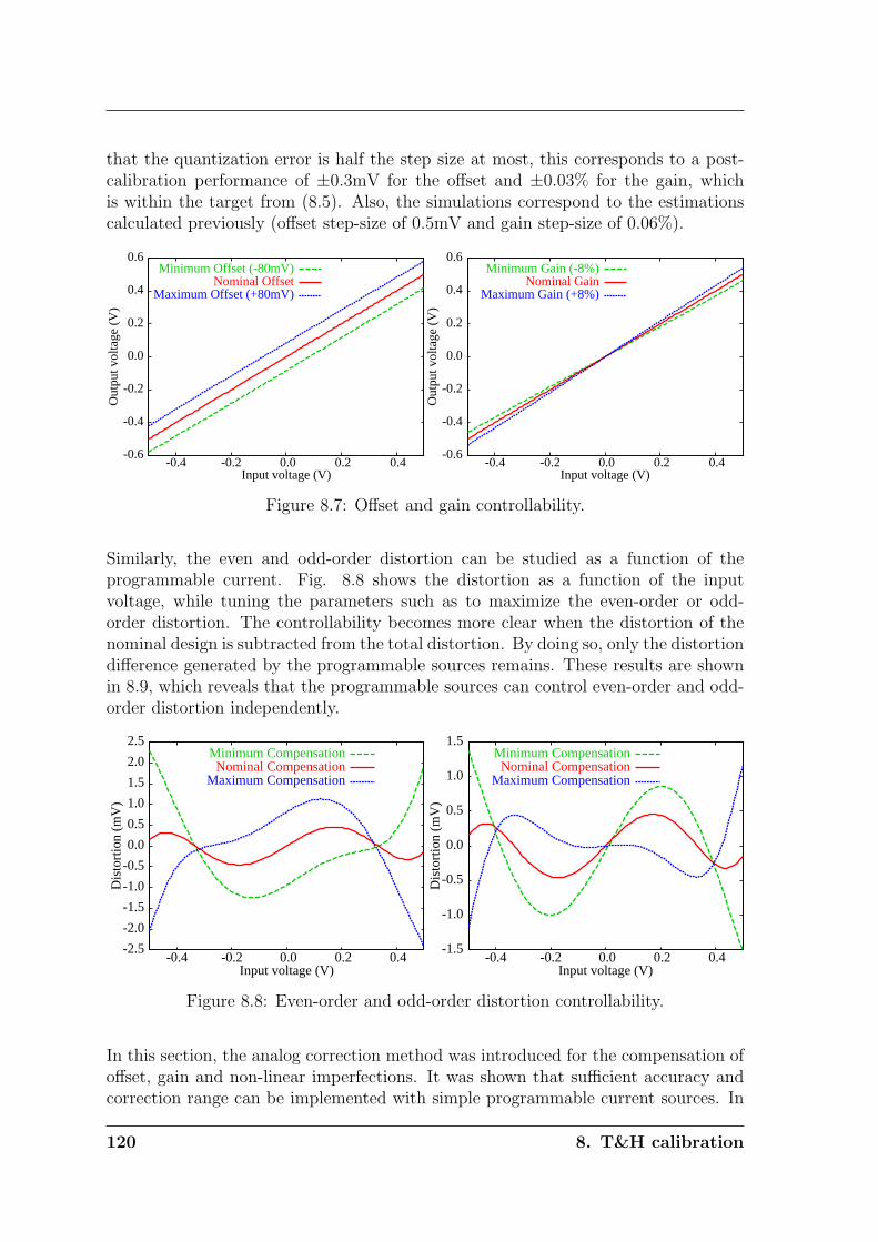
that the quantization error is half the step size at most, this corresponds to a post-calibration performance of ±0.3mV for the offset and ±0.03% for the gain, whichis within the target from (8.5). Also, the simulations correspond to the estimationscalculated previously (offset step-size of 0.5mV and gain step-size of 0.06%).
-0.6
-0.4
-0.2
0.0
0.2
0.4
0.6
-0.4 -0.2 0.0 0.2 0.4
Out
put v
olta
ge (
V)
Input voltage (V)
Minimum Offset (-80mV)Nominal Offset
Maximum Offset (+80mV)
-0.6
-0.4
-0.2
0.0
0.2
0.4
0.6
-0.4 -0.2 0.0 0.2 0.4
Out
put v
olta
ge (
V)
Input voltage (V)
Minimum Gain (-8%)Nominal Gain
Maximum Gain (+8%)
Figure 8.7: Offset and gain controllability.
Similarly, the even and odd-order distortion can be studied as a function of theprogrammable current. Fig. 8.8 shows the distortion as a function of the inputvoltage, while tuning the parameters such as to maximize the even-order or odd-order distortion. The controllability becomes more clear when the distortion of thenominal design is subtracted from the total distortion. By doing so, only the distortiondifference generated by the programmable sources remains. These results are shownin 8.9, which reveals that the programmable sources can control even-order and odd-order distortion independently.
-2.5
-2.0
-1.5
-1.0
-0.5
0.0
0.5
1.0
1.5
2.0
2.5
-0.4 -0.2 0.0 0.2 0.4
Dis
tort
ion
(mV
)
Input voltage (V)
Minimum CompensationNominal Compensation
Maximum Compensation
-1.5
-1.0
-0.5
0.0
0.5
1.0
1.5
-0.4 -0.2 0.0 0.2 0.4
Dis
tort
ion
(mV
)
Input voltage (V)
Minimum CompensationNominal Compensation
Maximum Compensation
Figure 8.8: Even-order and odd-order distortion controllability.
In this section, the analog correction method was introduced for the compensation ofoffset, gain and non-linear imperfections. It was shown that sufficient accuracy andcorrection range can be implemented with simple programmable current sources. In
120 8. T&H calibration
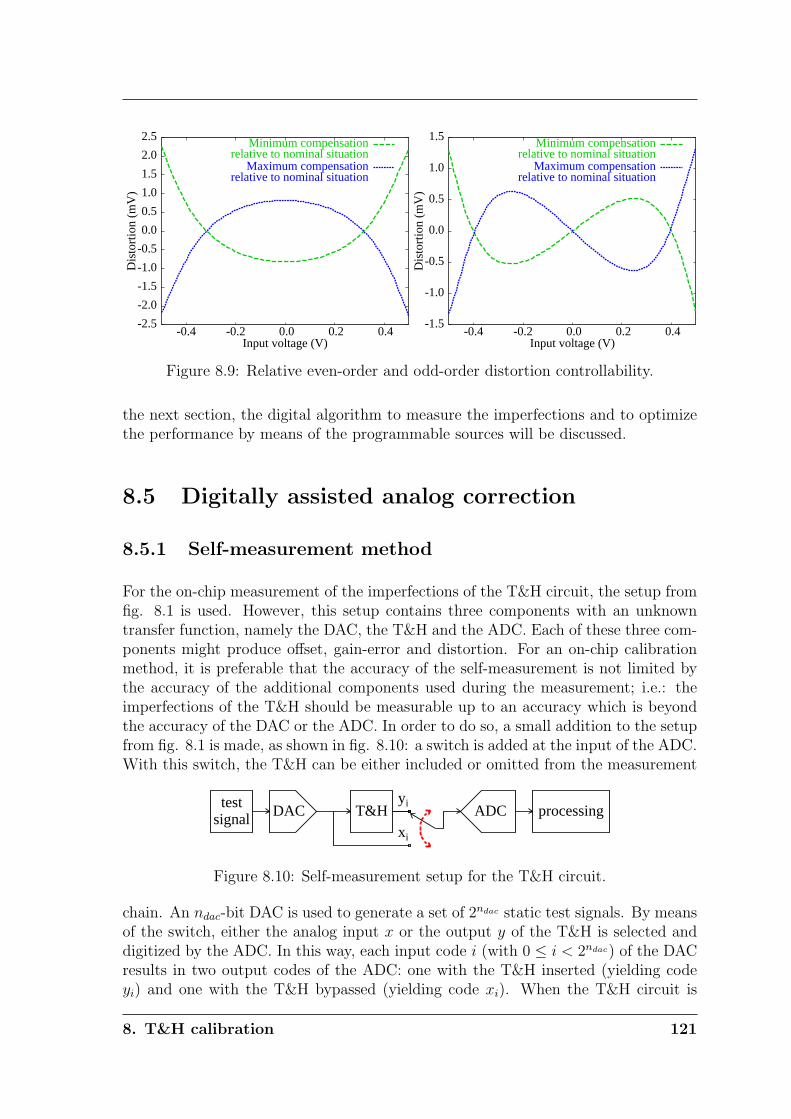
-2.5
-2.0
-1.5
-1.0
-0.5
0.0
0.5
1.0
1.5
2.0
2.5
-0.4 -0.2 0.0 0.2 0.4
Dis
tort
ion
(mV
)
Input voltage (V)
Minimum compensationrelative to nominal situation
Maximum compensationrelative to nominal situation
-1.5
-1.0
-0.5
0.0
0.5
1.0
1.5
-0.4 -0.2 0.0 0.2 0.4
Dis
tort
ion
(mV
)
Input voltage (V)
Minimum compensationrelative to nominal situation
Maximum compensationrelative to nominal situation
Figure 8.9: Relative even-order and odd-order distortion controllability.
the next section, the digital algorithm to measure the imperfections and to optimizethe performance by means of the programmable sources will be discussed.
8.5 Digitally assisted analog correction
8.5.1 Self-measurement method
For the on-chip measurement of the imperfections of the T&H circuit, the setup fromfig. 8.1 is used. However, this setup contains three components with an unknowntransfer function, namely the DAC, the T&H and the ADC. Each of these three com-ponents might produce offset, gain-error and distortion. For an on-chip calibrationmethod, it is preferable that the accuracy of the self-measurement is not limited bythe accuracy of the additional components used during the measurement; i.e.: theimperfections of the T&H should be measurable up to an accuracy which is beyondthe accuracy of the DAC or the ADC. In order to do so, a small addition to the setupfrom fig. 8.1 is made, as shown in fig. 8.10: a switch is added at the input of the ADC.With this switch, the T&H can be either included or omitted from the measurement
testsignal DAC T&H ADC processing
yi
xi
Figure 8.10: Self-measurement setup for the T&H circuit.
chain. An ndac-bit DAC is used to generate a set of 2ndac static test signals. By meansof the switch, either the analog input x or the output y of the T&H is selected anddigitized by the ADC. In this way, each input code i (with 0 ≤ i < 2ndac) of the DACresults in two output codes of the ADC: one with the T&H inserted (yielding codeyi) and one with the T&H bypassed (yielding code xi). When the T&H circuit is
8. T&H calibration 121
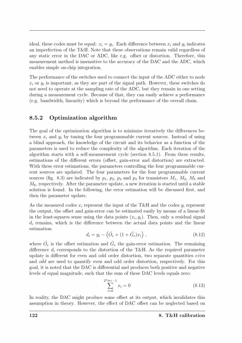
ideal, these codes must be equal: xi = yi. Each difference between xi and yi indicatesan imperfection of the T&H. Note that these observations remain valid regardless ofany static error in the DAC or ADC, like e.g. offset or distortion. Therefore, thismeasurement method is insensitive to the accuracy of the DAC and the ADC, whichenables simple on-chip integration.
The performance of the switches used to connect the input of the ADC either to nodexi or yi is important, as they are part of the signal path. However, these switches donot need to operate at the sampling rate of the ADC, but they remain in one settingduring a measurement cycle. Because of that, they can easily achieve a performance(e.g. bandwidth, linearity) which is beyond the performance of the overall chain.
8.5.2 Optimization algorithm
The goal of the optimization algorithm is to minimize iteratively the differences be-tween xi and yi by tuning the four programmable current sources. Instead of usinga blind approach, the knowledge of the circuit and its behavior as a function of theparameters is used to reduce the complexity of the algorithm. Each iteration of thealgorithm starts with a self-measurement cycle (section 8.5.1). From these results,estimations of the different errors (offset, gain-error and distortion) are extracted.With these error estimations, the parameters controlling the four programmable cur-rent sources are updated. The four parameters for the four programmable currentsources (fig. 8.3) are indicated by p1, p2, p3 and p4 for transistors M1, M2, M5 andM6, respectively. After the parameter update, a new iteration is started until a stablesolution is found. In the following, the error estimation will be discussed first, andthen the parameter update.
As the measured codes xi represent the input of the T&H and the codes yi representthe output, the offset and gain-error can be estimated easily by means of a linear-fitin the least-squares sense using the data points (xi, yi). Then, only a residual signaldi remains, which is the difference between the actual data points and the linearestimation:
di = yi −(Oe + (1 + Ge)xi
), (8.12)
where Oe is the offset estimation and Ge the gain-error estimation. The remainingdifference di corresponds to the distortion of the T&H. As the required parameterupdate is different for even and odd order distortion, two separate quantities ˆevenand ˆodd are used to quantify even and odd order distortion, respectively. For thisgoal, it is noted that the DAC is differential and produces both positive and negativelevels of equal magnitude, such that the sum of these DAC levels equals zero:
2ndac−1∑
i=0
xi = 0 (8.13)
In reality, the DAC might produce some offset at its output, which invalidates thisassumption in theory. However, the effect of DAC offset can be neglected based on
122 8. T&H calibration
the following arguments: first, the main cause of offset in the DAC (implemented asdescribed in chapter 5), is mismatch in the output resistors. The specified resistormatching is better than 0.1%, which results in a 3σ output offset of less than 1mV forthe DAC, assuming a Vfs of 0.5V. Assuming that a worst-case offset of 1mV wouldoccur, this means that the DAC output range changes from [-0.500V, 0.500V] to [-0.499V, 0.501V]. Because of that, the non-linearity measurement and optimizationwill now be done for the [-0.499V, 0.501V]-range instead of the [-0.500V, 0.500V]-range. In practice, as the distortion is a smooth function across the entire signalrange, this has no impact on the method.
Similar to the fact that (8.13) adds up to zero, all odd harmonic functions of xi alsoadd up to zero because of their symmetry. On the other hand, all even order harmonicfunctions of xi add up to a non-zero value. The estimations ˆeven and ˆodd are definedsuch that even order distortion contributes only to ˆeven, and odd order distortiononly to ˆodd:
ˆodd =2ndac−1∑
i=0
dix3i (8.14)
ˆeven =2ndac−1∑
i=0
dix2i (8.15)
To understand the functionality of these estimations, the following situation is consid-ered: suppose that the residual signal di contains an odd-order distortion componentCax
ai (with a an odd number and Ca a constant). In (8.14) this term is multiplied
by x3i , yielding Cax
(a+3)i , where (a + 3) is even. Therefore, the summation adds up
to a non-zero value and contributes to ˆodd. On the other hand, the same componentCax
ai in (8.15) will be multiplied by x2
i , yielding an odd-order term Cax(a+2)i , which
will add up to zero and therefore does not contribute to ˆeven. In a similar way,even order distortion components in di will contribute to ˆeven only. In summary,with relations (8.14) and (8.15), it is possible to split the even-order and odd-orderdistortion components, which is necessary for the optimization algorithm that will bediscussed next.
The final step of the optimization algorithm is to translate the extracted error es-timations to updates of the parameters controlling the variable current sources. Toreduce the complexity of this multidimensional problem (there are both four inputsignals (Oe, Ge, ˆeven and ˆodd) and four output signals (p1 up to p4)), availableknowledge of the circuit is exploited. First of all, it is known that the T&H circuitis composed of two differential pairs (fig. 8.3): one main pair (controlled by p1 andp2), which is responsible for the basic functionality of the buffer, and a much smallercross coupled pair (controlled by p3 and p4), which has the task to compensate thedistortion of the main pair. Consistent with this difference in functionality, the offsetand gain errors (Oe and Ge) are used only to update parameters p1 and p2, while thedistortion estimations ( ˆeven and ˆodd) are used only to update p3 and p4. In otherwords, the basic errors of gain and offset control the main differential pair and thenon-linearity errors control the cross-coupled pair. With this procedure, the origi-
8. T&H calibration 123
nal four-dimensional problem is reduced to two two-dimensional problems. However,these two two-dimensional problems are not independent from each other. Becauseof that, the final solution found by the calibration method could be sub-optimal.Nonetheless, as shown later by simulation results, this simplified approach is able tofind an optimum with sufficient performance.
Next to knowledge about the functionality of the circuit, knowledge about the rela-tions between the parameters and the errors was taken into account. Based on circuitsimulations, it can be concluded that the error estimations (Oe, Ge, ˆeven and ˆodd) aremonotonous functions of the parameters p1 up to p4. In practice, as the mismatchesare relatively small, these functions can be approximated by linear functions. Fur-thermore, the optimum solution is the solution where all error estimations are equal tozero. This means that in all cases, the sign of the error determines in which direction(positive or negative) the parameters should be updated. Under the assumption thatthe functions are linear, the magnitude of the update is automatically proportional tothe error itself. Overall, this leads to the following update algorithm, where px[k + 1]is the new parameter, px[k] the old parameter and ∆x[k] the parameter update:
px[k + 1] = px[k] + ∆x[k] , with: (8.16)
∆1[k] = − c1 · Ge[k] − c2 · Oe[k]
∆2[k] = − c1 · Ge[k] + c2 · Oe[k]
∆3[k] = + c3 · ˆodd[k] − c4 · ˆeven[k]
∆4[k] = + c3 · ˆodd[k] + c4 · ˆeven[k]
(8.17)
One can see that in these equations, the gain and offset errors control p1 and p2 whilethe distortion errors control p3 and p4. The proportionality constants c1 up to c4 arechosen such that a fast and stable settling of the parameters can be achieved.
8.6 Simulation results
In this section, simulation results of the calibration method are presented. To verifythe functionality of the calibration algorithm, Monte Carlo simulations were done ona behavioral model of the T&H. Next to that, simulations on transistor-level wereperformed to verify the achievable performance more accurately.
8.6.1 Behavioral-level simulations
In order to be able to run Monte Carlo simulations, a behavioral model of the open-loop amplifier from fig. 8.3 was developed in Matlab. Most importantly, the fourcontrollable current sources were modeled as (8.6). The four transistors composingthe two differential pairs were modeled by the relation Id = 1
2β(Vgs − Vth)
2. Therequired measurement DAC was modeled as a 6-bit binary DAC, including a mismatch
124 8. T&H calibration
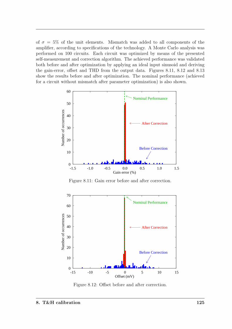
of σ = 5% of the unit elements. Mismatch was added to all components of theamplifier, according to specifications of the technology. A Monte Carlo analysis wasperformed on 100 circuits. Each circuit was optimized by means of the presentedself-measurement and correction algorithm. The achieved performance was validatedboth before and after optimization by applying an ideal input sinusoid and derivingthe gain-error, offset and THD from the output data. Figures 8.11, 8.12 and 8.13show the results before and after optimization. The nominal performance (achievedfor a circuit without mismatch after parameter optimization) is also shown.
0
10
20
30
40
50
60
-1.5 -1.0 -0.5 0.0 0.5 1.0 1.5
Num
ber
of o
ccur
renc
es
Gain error (%)
After Correction
Before Correction
Nominal Performance
Figure 8.11: Gain error before and after correction.
0
10
20
30
40
50
60
70
-15 -10 -5 0 5 10 15
Num
ber
of o
ccur
renc
es
Offset (mV)
After Correction
Before Correction
Nominal Performance
Figure 8.12: Offset before and after correction.
8. T&H calibration 125
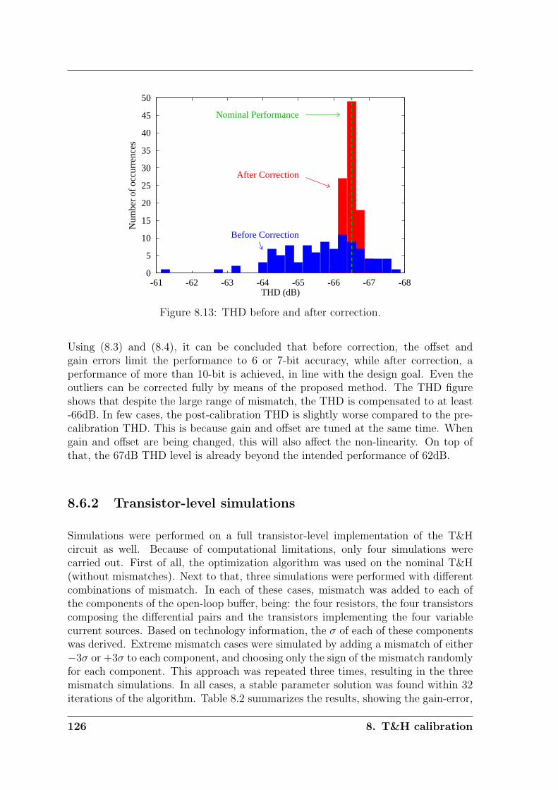
0
5
10
15
20
25
30
35
40
45
50
-61 -62 -63 -64 -65 -66 -67 -68
Num
ber
of o
ccur
renc
es
THD (dB)
After Correction
Before Correction
Nominal Performance
Figure 8.13: THD before and after correction.
Using (8.3) and (8.4), it can be concluded that before correction, the offset andgain errors limit the performance to 6 or 7-bit accuracy, while after correction, aperformance of more than 10-bit is achieved, in line with the design goal. Even theoutliers can be corrected fully by means of the proposed method. The THD figureshows that despite the large range of mismatch, the THD is compensated to at least-66dB. In few cases, the post-calibration THD is slightly worse compared to the pre-calibration THD. This is because gain and offset are tuned at the same time. Whengain and offset are being changed, this will also affect the non-linearity. On top ofthat, the 67dB THD level is already beyond the intended performance of 62dB.
8.6.2 Transistor-level simulations
Simulations were performed on a full transistor-level implementation of the T&Hcircuit as well. Because of computational limitations, only four simulations werecarried out. First of all, the optimization algorithm was used on the nominal T&H(without mismatches). Next to that, three simulations were performed with differentcombinations of mismatch. In each of these cases, mismatch was added to each ofthe components of the open-loop buffer, being: the four resistors, the four transistorscomposing the differential pairs and the transistors implementing the four variablecurrent sources. Based on technology information, the σ of each of these componentswas derived. Extreme mismatch cases were simulated by adding a mismatch of either−3σ or +3σ to each component, and choosing only the sign of the mismatch randomlyfor each component. This approach was repeated three times, resulting in the threemismatch simulations. In all cases, a stable parameter solution was found within 32iterations of the algorithm. Table 8.2 summarizes the results, showing the gain-error,
126 8. T&H calibration
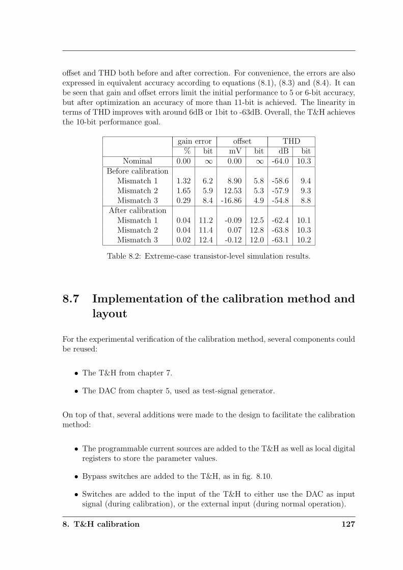
offset and THD both before and after correction. For convenience, the errors are alsoexpressed in equivalent accuracy according to equations (8.1), (8.3) and (8.4). It canbe seen that gain and offset errors limit the initial performance to 5 or 6-bit accuracy,but after optimization an accuracy of more than 11-bit is achieved. The linearity interms of THD improves with around 6dB or 1bit to -63dB. Overall, the T&H achievesthe 10-bit performance goal.
gain error offset THD% bit mV bit dB bit
Nominal 0.00 ∞ 0.00 ∞ -64.0 10.3Before calibration
Mismatch 1 1.32 6.2 8.90 5.8 -58.6 9.4Mismatch 2 1.65 5.9 12.53 5.3 -57.9 9.3Mismatch 3 0.29 8.4 -16.86 4.9 -54.8 8.8
After calibrationMismatch 1 0.04 11.2 -0.09 12.5 -62.4 10.1Mismatch 2 0.04 11.4 0.07 12.8 -63.8 10.3Mismatch 3 0.02 12.4 -0.12 12.0 -63.1 10.2
Table 8.2: Extreme-case transistor-level simulation results.
8.7 Implementation of the calibration method and
layout
For the experimental verification of the calibration method, several components couldbe reused:
• The T&H from chapter 7.
• The DAC from chapter 5, used as test-signal generator.
On top of that, several additions were made to the design to facilitate the calibrationmethod:
• The programmable current sources are added to the T&H as well as local digitalregisters to store the parameter values.
• Bypass switches are added to the T&H, as in fig. 8.10.
• Switches are added to the input of the T&H to either use the DAC as inputsignal (during calibration), or the external input (during normal operation).
8. T&H calibration 127
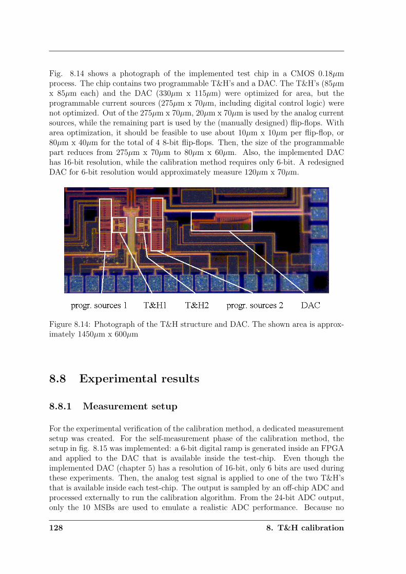
Fig. 8.14 shows a photograph of the implemented test chip in a CMOS 0.18µmprocess. The chip contains two programmable T&H’s and a DAC. The T&H’s (85µmx 85µm each) and the DAC (330µm x 115µm) were optimized for area, but theprogrammable current sources (275µm x 70µm, including digital control logic) werenot optimized. Out of the 275µm x 70µm, 20µm x 70µm is used by the analog currentsources, while the remaining part is used by the (manually designed) flip-flops. Witharea optimization, it should be feasible to use about 10µm x 10µm per flip-flop, or80µm x 40µm for the total of 4 8-bit flip-flops. Then, the size of the programmablepart reduces from 275µm x 70µm to 80µm x 60µm. Also, the implemented DAChas 16-bit resolution, while the calibration method requires only 6-bit. A redesignedDAC for 6-bit resolution would approximately measure 120µm x 70µm.
Figure 8.14: Photograph of the T&H structure and DAC. The shown area is approx-imately 1450µm x 600µm
8.8 Experimental results
8.8.1 Measurement setup
For the experimental verification of the calibration method, a dedicated measurementsetup was created. For the self-measurement phase of the calibration method, thesetup in fig. 8.15 was implemented: a 6-bit digital ramp is generated inside an FPGAand applied to the DAC that is available inside the test-chip. Even though theimplemented DAC (chapter 5) has a resolution of 16-bit, only 6 bits are used duringthese experiments. Then, the analog test signal is applied to one of the two T&H’sthat is available inside each test-chip. The output is sampled by an off-chip ADC andprocessed externally to run the calibration algorithm. From the 24-bit ADC output,only the 10 MSBs are used to emulate a realistic ADC performance. Because no
128 8. T&H calibration
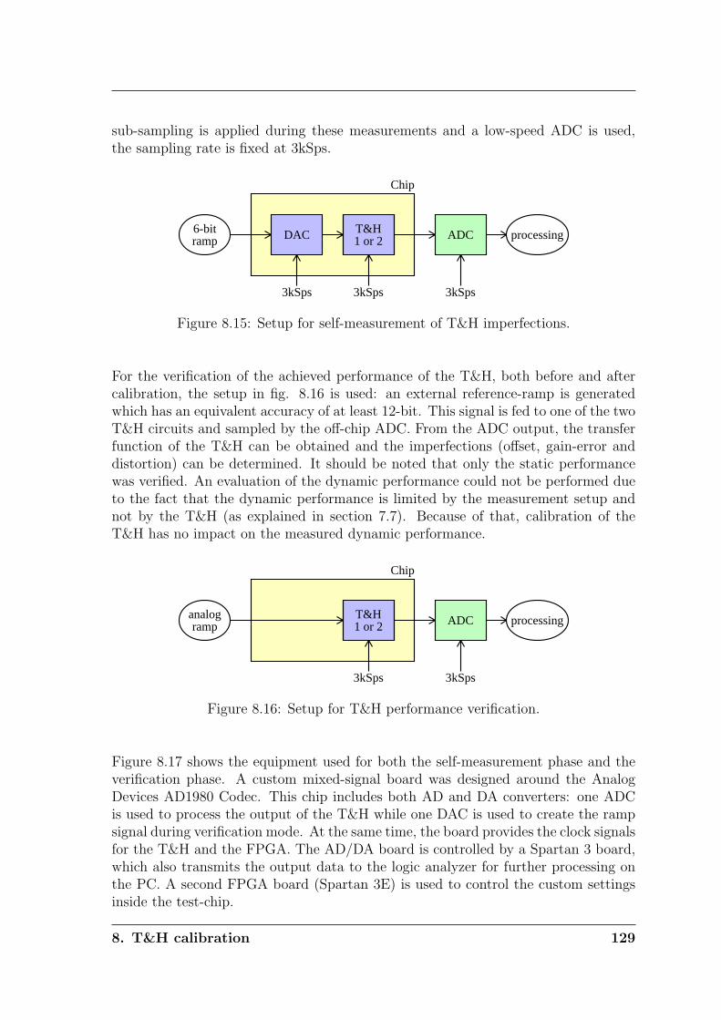
sub-sampling is applied during these measurements and a low-speed ADC is used,the sampling rate is fixed at 3kSps.
ramp6-bit DAC 1 or 2
T&H ADC processing
3kSps 3kSps 3kSps
Chip
Figure 8.15: Setup for self-measurement of T&H imperfections.
For the verification of the achieved performance of the T&H, both before and aftercalibration, the setup in fig. 8.16 is used: an external reference-ramp is generatedwhich has an equivalent accuracy of at least 12-bit. This signal is fed to one of the twoT&H circuits and sampled by the off-chip ADC. From the ADC output, the transferfunction of the T&H can be obtained and the imperfections (offset, gain-error anddistortion) can be determined. It should be noted that only the static performancewas verified. An evaluation of the dynamic performance could not be performed dueto the fact that the dynamic performance is limited by the measurement setup andnot by the T&H (as explained in section 7.7). Because of that, calibration of theT&H has no impact on the measured dynamic performance.
rampanalog
1 or 2T&H ADC processing
3kSps 3kSps
Chip
Figure 8.16: Setup for T&H performance verification.
Figure 8.17 shows the equipment used for both the self-measurement phase and theverification phase. A custom mixed-signal board was designed around the AnalogDevices AD1980 Codec. This chip includes both AD and DA converters: one ADCis used to process the output of the T&H while one DAC is used to create the rampsignal during verification mode. At the same time, the board provides the clock signalsfor the T&H and the FPGA. The AD/DA board is controlled by a Spartan 3 board,which also transmits the output data to the logic analyzer for further processing onthe PC. A second FPGA board (Spartan 3E) is used to control the custom settingsinside the test-chip.
8. T&H calibration 129
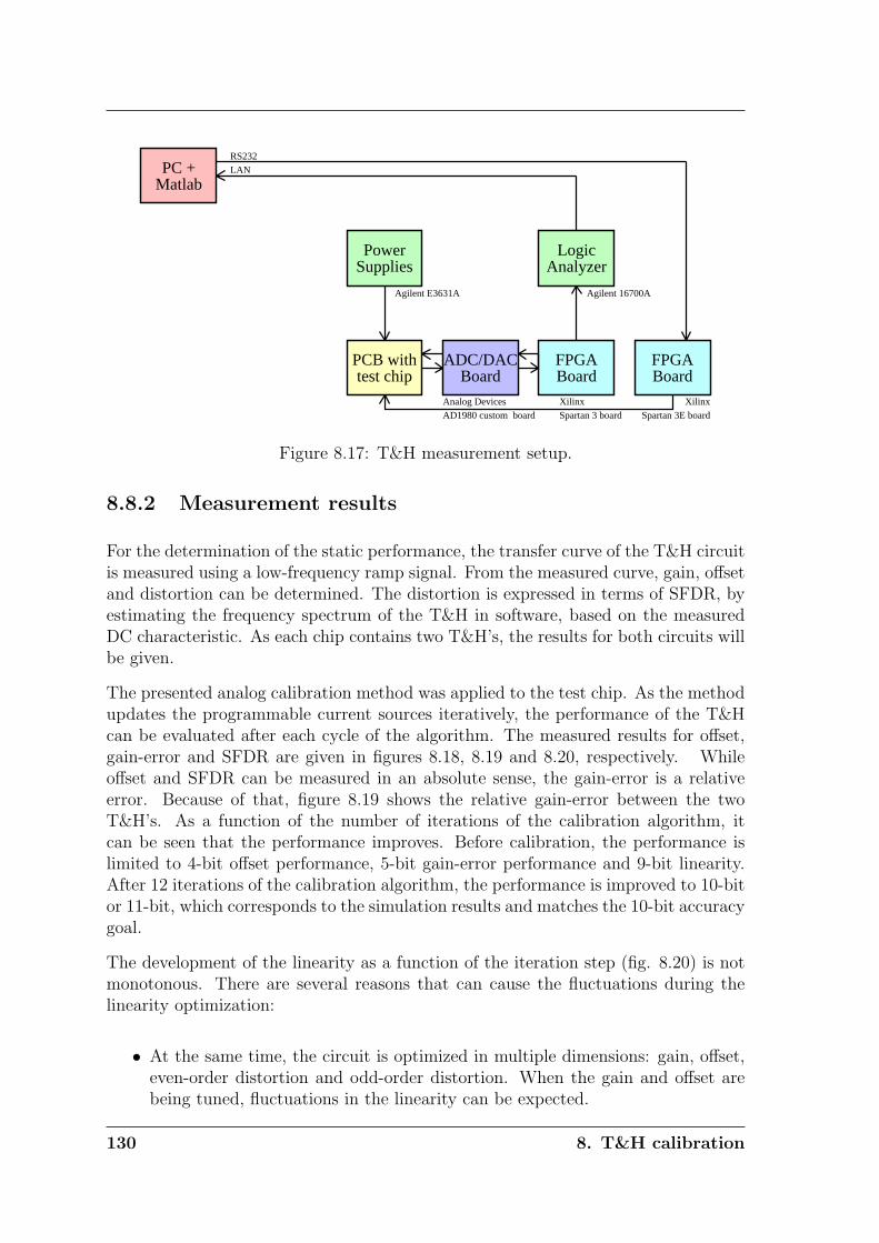
MatlabPC +
SuppliesPower
AnalyzerLogic
test chipPCB with
BoardADC/DAC
BoardFPGA
BoardFPGA
LANRS232
Agilent E3631A Agilent 16700A
Analog DevicesAD1980 custom board
XilinxSpartan 3 board
XilinxSpartan 3E board
Figure 8.17: T&H measurement setup.
8.8.2 Measurement results
For the determination of the static performance, the transfer curve of the T&H circuitis measured using a low-frequency ramp signal. From the measured curve, gain, offsetand distortion can be determined. The distortion is expressed in terms of SFDR, byestimating the frequency spectrum of the T&H in software, based on the measuredDC characteristic. As each chip contains two T&H’s, the results for both circuits willbe given.
The presented analog calibration method was applied to the test chip. As the methodupdates the programmable current sources iteratively, the performance of the T&Hcan be evaluated after each cycle of the algorithm. The measured results for offset,gain-error and SFDR are given in figures 8.18, 8.19 and 8.20, respectively. Whileoffset and SFDR can be measured in an absolute sense, the gain-error is a relativeerror. Because of that, figure 8.19 shows the relative gain-error between the twoT&H’s. As a function of the number of iterations of the calibration algorithm, itcan be seen that the performance improves. Before calibration, the performance islimited to 4-bit offset performance, 5-bit gain-error performance and 9-bit linearity.After 12 iterations of the calibration algorithm, the performance is improved to 10-bitor 11-bit, which corresponds to the simulation results and matches the 10-bit accuracygoal.
The development of the linearity as a function of the iteration step (fig. 8.20) is notmonotonous. There are several reasons that can cause the fluctuations during thelinearity optimization:
• At the same time, the circuit is optimized in multiple dimensions: gain, offset,even-order distortion and odd-order distortion. When the gain and offset arebeing tuned, fluctuations in the linearity can be expected.
130 8. T&H calibration
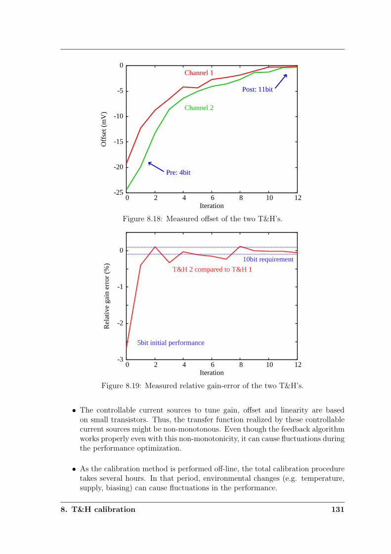
-25
-20
-15
-10
-5
0
0 2 4 6 8 10 12
Off
set (
mV
)
Iteration
Channel 1
Channel 2
Pre: 4bit
Post: 11bit
Figure 8.18: Measured offset of the two T&H’s.
-3
-2
-1
0
0 2 4 6 8 10 12
Rel
ativ
e ga
in e
rror
(%
)
Iteration
T&H 2 compared to T&H 1
10bit requirement
5bit initial performance
Figure 8.19: Measured relative gain-error of the two T&H’s.
• The controllable current sources to tune gain, offset and linearity are basedon small transistors. Thus, the transfer function realized by these controllablecurrent sources might be non-monotonous. Even though the feedback algorithmworks properly even with this non-monotonicity, it can cause fluctuations duringthe performance optimization.
• As the calibration method is performed off-line, the total calibration proceduretakes several hours. In that period, environmental changes (e.g. temperature,supply, biasing) can cause fluctuations in the performance.
8. T&H calibration 131
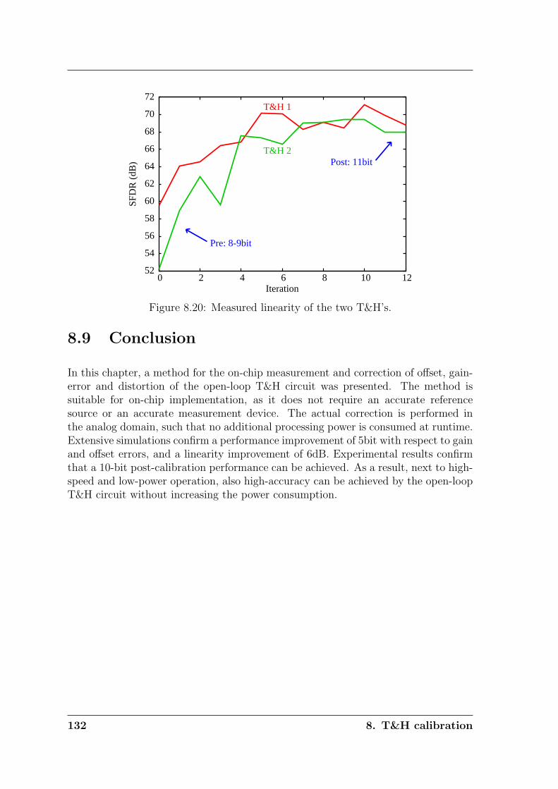
52
54
56
58
60
62
64
66
68
70
72
0 2 4 6 8 10 12
SFD
R (
dB)
Iteration
T&H 1
T&H 2
Pre: 8-9bit
Post: 11bit
Figure 8.20: Measured linearity of the two T&H’s.
8.9 Conclusion
In this chapter, a method for the on-chip measurement and correction of offset, gain-error and distortion of the open-loop T&H circuit was presented. The method issuitable for on-chip implementation, as it does not require an accurate referencesource or an accurate measurement device. The actual correction is performed inthe analog domain, such that no additional processing power is consumed at runtime.Extensive simulations confirm a performance improvement of 5bit with respect to gainand offset errors, and a linearity improvement of 6dB. Experimental results confirmthat a 10-bit post-calibration performance can be achieved. As a result, next to high-speed and low-power operation, also high-accuracy can be achieved by the open-loopT&H circuit without increasing the power consumption.
132 8. T&H calibration
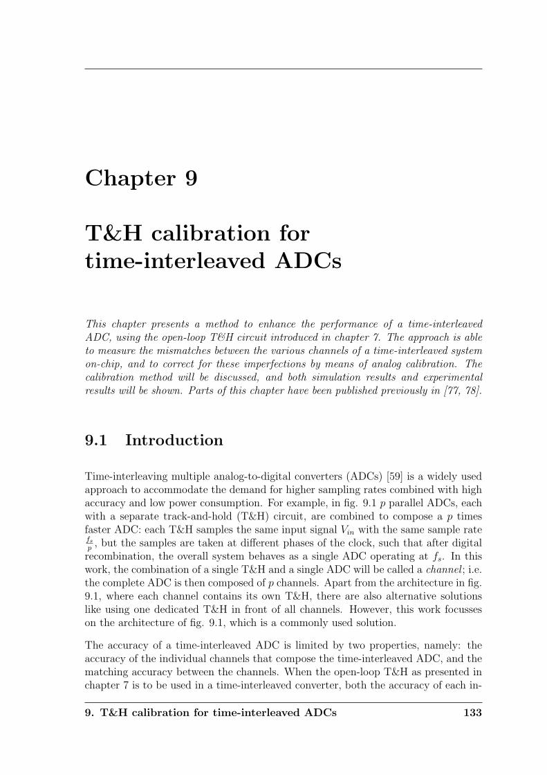
Chapter 9
T&H calibration fortime-interleaved ADCs
This chapter presents a method to enhance the performance of a time-interleavedADC, using the open-loop T&H circuit introduced in chapter 7. The approach is ableto measure the mismatches between the various channels of a time-interleaved systemon-chip, and to correct for these imperfections by means of analog calibration. Thecalibration method will be discussed, and both simulation results and experimentalresults will be shown. Parts of this chapter have been published previously in [77, 78].
9.1 Introduction
Time-interleaving multiple analog-to-digital converters (ADCs) [59] is a widely usedapproach to accommodate the demand for higher sampling rates combined with highaccuracy and low power consumption. For example, in fig. 9.1 p parallel ADCs, eachwith a separate track-and-hold (T&H) circuit, are combined to compose a p timesfaster ADC: each T&H samples the same input signal Vin with the same sample ratefs
p, but the samples are taken at different phases of the clock, such that after digital
recombination, the overall system behaves as a single ADC operating at fs. In thiswork, the combination of a single T&H and a single ADC will be called a channel ; i.e.the complete ADC is then composed of p channels. Apart from the architecture in fig.9.1, where each channel contains its own T&H, there are also alternative solutionslike using one dedicated T&H in front of all channels. However, this work focusseson the architecture of fig. 9.1, which is a commonly used solution.
The accuracy of a time-interleaved ADC is limited by two properties, namely: theaccuracy of the individual channels that compose the time-interleaved ADC, and thematching accuracy between the channels. When the open-loop T&H as presented inchapter 7 is to be used in a time-interleaved converter, both the accuracy of each in-
9. T&H calibration for time-interleaved ADCs 133
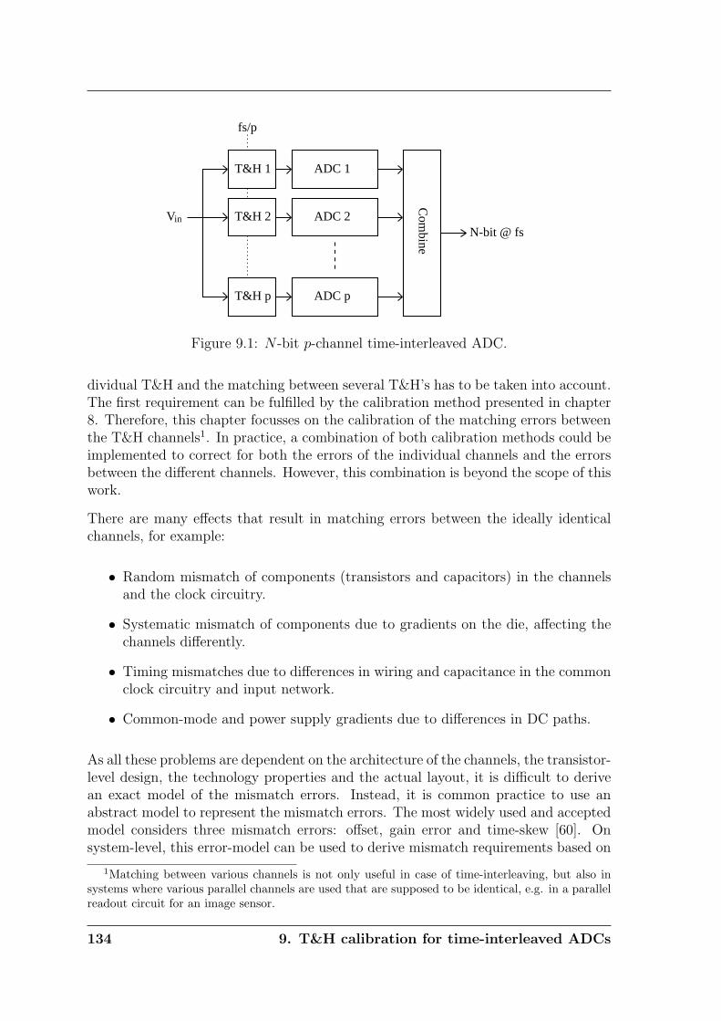
Vin
T&H 1
T&H 2
T&H p
ADC 1
ADC 2
ADC pC
ombine
N-bit @ fs
fs/p
Figure 9.1: N -bit p-channel time-interleaved ADC.
dividual T&H and the matching between several T&H’s has to be taken into account.The first requirement can be fulfilled by the calibration method presented in chapter8. Therefore, this chapter focusses on the calibration of the matching errors betweenthe T&H channels1. In practice, a combination of both calibration methods could beimplemented to correct for both the errors of the individual channels and the errorsbetween the different channels. However, this combination is beyond the scope of thiswork.
There are many effects that result in matching errors between the ideally identicalchannels, for example:
• Random mismatch of components (transistors and capacitors) in the channelsand the clock circuitry.
• Systematic mismatch of components due to gradients on the die, affecting thechannels differently.
• Timing mismatches due to differences in wiring and capacitance in the commonclock circuitry and input network.
• Common-mode and power supply gradients due to differences in DC paths.
As all these problems are dependent on the architecture of the channels, the transistor-level design, the technology properties and the actual layout, it is difficult to derivean exact model of the mismatch errors. Instead, it is common practice to use anabstract model to represent the mismatch errors. The most widely used and acceptedmodel considers three mismatch errors: offset, gain error and time-skew [60]. Onsystem-level, this error-model can be used to derive mismatch requirements based on
1Matching between various channels is not only useful in case of time-interleaving, but also insystems where various parallel channels are used that are supposed to be identical, e.g. in a parallelreadout circuit for an image sensor.
134 9. T&H calibration for time-interleaved ADCs
the final accuracy target. Then, during the design and implementation of the ADC,the actual errors can be translated to this simplified model and verified accordingly.
Normally, the mismatch errors (offset, gain error and time-skew) directly limit theperformance of the overall ADC, and should be small enough to achieve the finalspeed/accuracy target. However, especially for high sampling rates and a largeamount of channels p, it is difficult to achieve sufficient matching by design alone.Therefore, solutions were developed that can improve the channel-matching by mea-suring and correcting the actual errors on-chip (e.g. [79, 80, 81, 82, 83]). Severaldistinct properties can be found within the currently available techniques, but mostof them share one or more of the following disadvantages or limitations:
• The method works only for a subset of the three types of mismatch (offsets,gain errors and time-skew errors).
• The method puts constraints on the input signal (background techniques), orrequires input signals with specific accuracy requirements (foreground tech-niques).
• The method works only for a 2-channel ADC, or the complexity increasesstrongly (i.e. faster than a linear increase) as a function of the number ofchannels.
• The complexity (and hence the power consumption) of the correction methodis such that it becomes unattractive for a power-efficient implementation.
• The method is based on a stochastic process and therefore requires a largeamount of observations or iterations to achieve a certain level of accuracy.
Because of these drawbacks, a new method is proposed here that has the followingproperties:
• It measures and corrects for offsets, gain errors and time-skew errors.
• The foreground method uses a deterministic test-signal, of which the accuracyand dynamic performance are unimportant, as long as the signal is periodic.The low constraints enable a simple on-chip implementation.
• Because of the deterministic nature, the algorithm converges fast.
• The implementation is such that it can be applied to any number p of parallelchannels, while the complexity grows only linear with p.
• The actual correction is performed by means of analog calibration to minimizethe additional power consumption.
9. T&H calibration for time-interleaved ADCs 135
Section 9.2 reviews the requirements on channel matching for time-interleaved T&H’s.In section 9.3, the time-interleaved calibration system is presented, including the test-signal generator and a model of the error mechanisms. Sections 9.4 and 9.5 discussthe error detection and error correction schemes, respectively. Simulation resultsare given in section 9.6. The hardware implementation is reviewed in section 9.7and experimental results are shown in section 9.8. Finally, conclusions are drawn insection 9.9.
9.2 Channel matching in time-interleaved T&H’s
The effect of channel mismatch in time-interleaved ADCs has been described ex-tensively in literature, a.o. [60]. For the specific design in this work (a 2-channeltime-interleaved system, operating at 1GSps, 1Vpp signal range), the effect of offset,gain-error and time-skew was investigated. The two channels were modeled accordingto (9.1), assuming that the input signal is a sinusoid with amplitude A and frequencyf . Moreover, Oe, Ge and ∆ model the offset, gain-error and time-skew, respectively.
y1 = A · sin(2πft)y2 = Oe + (1 + Ge) · A · sin(2πf(t + ∆))
(9.1)
As a function of the applied mismatches (either offset, gain-error or time-skew), theENOB of the converter can be determined as shown in fig. 9.2, using A = 0.5V andf = 487MHz. By using a full-scale input signal and a frequency close to Nyquist,these results correspond to a worst-case scenario. For a 10-bit accuracy goal, thisresults in the following set of requirements on channel matching, when the errors areconsidered individually:
|Oe| ≤ 0.5mV|Ge| ≤ 0.2%|∆| ≥ 0.5ps
(9.2)
6
8
10
12
14
16
0.01 0.1 1 10
EN
OB
(bi
t)
Offset (mV)
8
10
12
14
16
18
0.001 0.01 0.1 1
EN
OB
(bi
t)
Gain-error (%)
6
8
10
12
14
16
0.01 0.1 1 10
EN
OB
(bi
t)
Time-skew (ps)
Figure 9.2: ENOB limitation due to mismatch (offset, gain-error and time-skew).
136 9. T&H calibration for time-interleaved ADCs
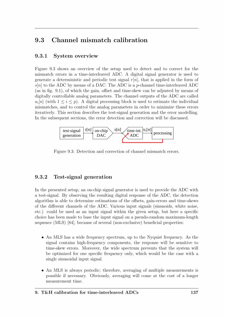
9.3 Channel mismatch calibration
9.3.1 System overview
Figure 9.3 shows an overview of the setup used to detect and to correct for themismatch errors in a time-interleaved ADC. A digital signal generator is used togenerate a deterministic and periodic test signal r[n], that is applied in the form ofs[n] to the ADC by means of a DAC. The ADC is a p-channel time-interleaved ADC(as in fig. 9.1), of which the gain, offset and time-skew can be adjusted by means ofdigitally controllable analog parameters. The channel outputs of the ADC are calledui[n] (with 1 ≤ i ≤ p). A digital processing block is used to estimate the individualmismatches, and to control the analog parameters in order to minimize these errorsiteratively. This section describes the test-signal generation and the error modelling.In the subsequent sections, the error detection and correction will be discussed.
test-signalgeneration
on-chipDAC
time-int.ADC processing
r[n] s[n] u [n]i
Figure 9.3: Detection and correction of channel mismatch errors.
9.3.2 Test-signal generation
In the presented setup, an on-chip signal generator is used to provide the ADC witha test-signal. By observing the resulting digital response of the ADC, the detectionalgorithm is able to determine estimations of the offsets, gain-errors and time-skewsof the different channels of the ADC. Various input signals (sinusoids, white noise,etc.) could be used as an input signal within the given setup, but here a specificchoice has been made to base the input signal on a pseudo-random maximum-lengthsequence (MLS) [84], because of several (non-exclusive) beneficial properties:
• An MLS has a wide frequency spectrum, up to the Nyquist frequency. As thesignal contains high-frequency components, the response will be sensitive totime-skew errors. Moreover, the wide spectrum prevents that the system willbe optimized for one specific frequency only, which would be the case with asingle sinusoidal input signal.
• An MLS is always periodic; therefore, averaging of multiple measurements ispossible if necessary. Obviously, averaging will come at the cost of a longermeasurement time.
9. T&H calibration for time-interleaved ADCs 137
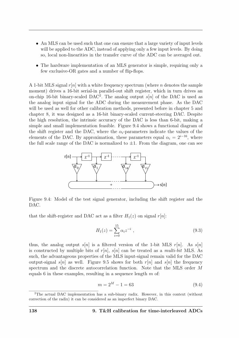
• An MLS can be used such that one can ensure that a large variety of input levelswill be applied to the ADC, instead of applying only a few input levels. By doingso, local non-linearities in the transfer curve of the ADC can be averaged out.
• The hardware implementation of an MLS generator is simple, requiring only afew exclusive-OR gates and a number of flip-flops.
A 1-bit MLS signal r[n] with a white frequency spectrum (where n denotes the samplemoment) drives a 16-bit serial-in parallel-out shift register, which in turn drives anon-chip 16-bit binary-scaled DAC2. The analog output s[n] of the DAC is used asthe analog input signal for the ADC during the measurement phase. As the DACwill be used as well for other calibration methods, presented before in chapter 5 andchapter 8, it was designed as a 16-bit binary-scaled current-steering DAC. Despitethe high resolution, the intrinsic accuracy of the DAC is less than 6-bit, making asimple and small implementation feasible. Figure 9.4 shows a functional diagram ofthe shift register and the DAC, where the αi-parameters indicate the values of theelements of the DAC. By approximation, these parameters equal αi = 2i−16, wherethe full scale range of the DAC is normalized to ±1. From the diagram, one can see
r[n] Z-1 Z-1 Z-1
α0 α1 α14 α15
+ s[n]
Figure 9.4: Model of the test signal generator, including the shift register and theDAC.
that the shift-register and DAC act as a filter H1(z) on signal r[n]:
H1(z) =15∑
i=0
αiz−i , (9.3)
thus, the analog output s[n] is a filtered version of the 1-bit MLS r[n]. As s[n]is constructed by multiple bits of r[n], s[n] can be treated as a multi-bit MLS. Assuch, the advantageous properties of the MLS input-signal remain valid for the DACoutput-signal s[n] as well. Figure 9.5 shows for both r[n] and s[n] the frequencyspectrum and the discrete autocorrelation function. Note that the MLS order Mequals 6 in these examples, resulting in a sequence length m of:
m = 2M − 1 = 63 (9.4)
2The actual DAC implementation has a sub-binary radix. However, in this context (withoutcorrection of the radix) it can be considered as an imperfect binary DAC.
138 9. T&H calibration for time-interleaved ADCs
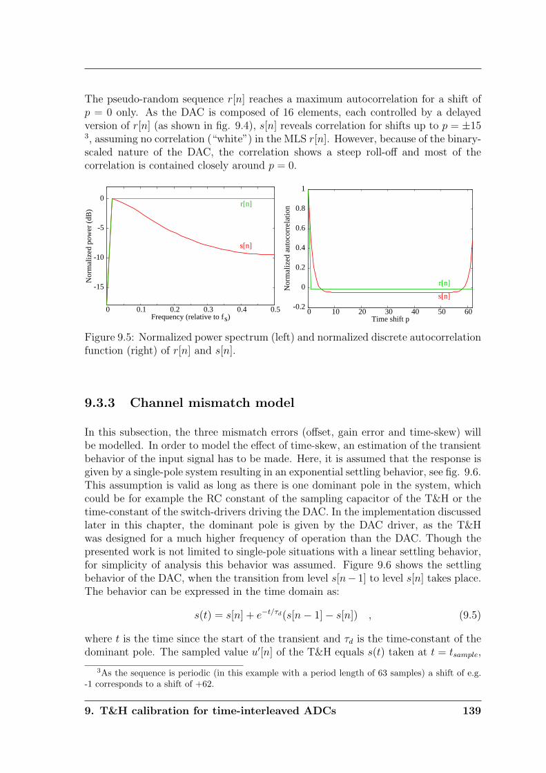
The pseudo-random sequence r[n] reaches a maximum autocorrelation for a shift ofp = 0 only. As the DAC is composed of 16 elements, each controlled by a delayedversion of r[n] (as shown in fig. 9.4), s[n] reveals correlation for shifts up to p = ±153, assuming no correlation (“white”) in the MLS r[n]. However, because of the binary-scaled nature of the DAC, the correlation shows a steep roll-off and most of thecorrelation is contained closely around p = 0.
-15
-10
-5
0
0 0.1 0.2 0.3 0.4 0.5
Nor
mal
ized
pow
er (
dB)
Frequency (relative to f )s
s[n]
r[n]
-0.2
0
0.2
0.4
0.6
0.8
1
0 10 20 30 40 50 60
Nor
mal
ized
aut
ocor
rela
tion
Time shift p
s[n]
r[n]
Figure 9.5: Normalized power spectrum (left) and normalized discrete autocorrelationfunction (right) of r[n] and s[n].
9.3.3 Channel mismatch model
In this subsection, the three mismatch errors (offset, gain error and time-skew) willbe modelled. In order to model the effect of time-skew, an estimation of the transientbehavior of the input signal has to be made. Here, it is assumed that the response isgiven by a single-pole system resulting in an exponential settling behavior, see fig. 9.6.This assumption is valid as long as there is one dominant pole in the system, whichcould be for example the RC constant of the sampling capacitor of the T&H or thetime-constant of the switch-drivers driving the DAC. In the implementation discussedlater in this chapter, the dominant pole is given by the DAC driver, as the T&Hwas designed for a much higher frequency of operation than the DAC. Though thepresented work is not limited to single-pole situations with a linear settling behavior,for simplicity of analysis this behavior was assumed. Figure 9.6 shows the settlingbehavior of the DAC, when the transition from level s[n− 1] to level s[n] takes place.The behavior can be expressed in the time domain as:
s(t) = s[n] + e−t/τd(s[n− 1]− s[n]) , (9.5)
where t is the time since the start of the transient and τd is the time-constant of thedominant pole. The sampled value u′[n] of the T&H equals s(t) taken at t = tsample,
3As the sequence is periodic (in this example with a period length of 63 samples) a shift of e.g.-1 corresponds to a shift of +62.
9. T&H calibration for time-interleaved ADCs 139
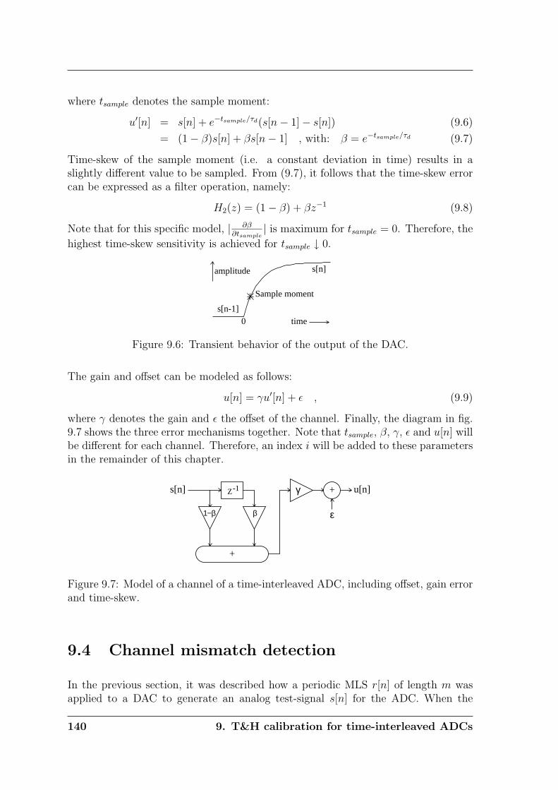
where tsample denotes the sample moment:
u′[n] = s[n] + e−tsample/τd(s[n− 1]− s[n]) (9.6)
= (1− β)s[n] + βs[n− 1] , with: β = e−tsample/τd (9.7)
Time-skew of the sample moment (i.e. a constant deviation in time) results in aslightly different value to be sampled. From (9.7), it follows that the time-skew errorcan be expressed as a filter operation, namely:
H2(z) = (1− β) + βz−1 (9.8)
Note that for this specific model, | ∂β∂tsample
| is maximum for tsample = 0. Therefore, the
highest time-skew sensitivity is achieved for tsample ↓ 0.
s[n-1]
s[n]
Sample moment
0 time
amplitude
Figure 9.6: Transient behavior of the output of the DAC.
The gain and offset can be modeled as follows:
u[n] = γu′[n] + ε , (9.9)
where γ denotes the gain and ε the offset of the channel. Finally, the diagram in fig.9.7 shows the three error mechanisms together. Note that tsample, β, γ, ε and u[n] willbe different for each channel. Therefore, an index i will be added to these parametersin the remainder of this chapter.
s[n] Z-1
+
1−β β
u[n]
ε
γ +
Figure 9.7: Model of a channel of a time-interleaved ADC, including offset, gain errorand time-skew.
9.4 Channel mismatch detection
In the previous section, it was described how a periodic MLS r[n] of length m wasapplied to a DAC to generate an analog test-signal s[n] for the ADC. When the
140 9. T&H calibration for time-interleaved ADCs
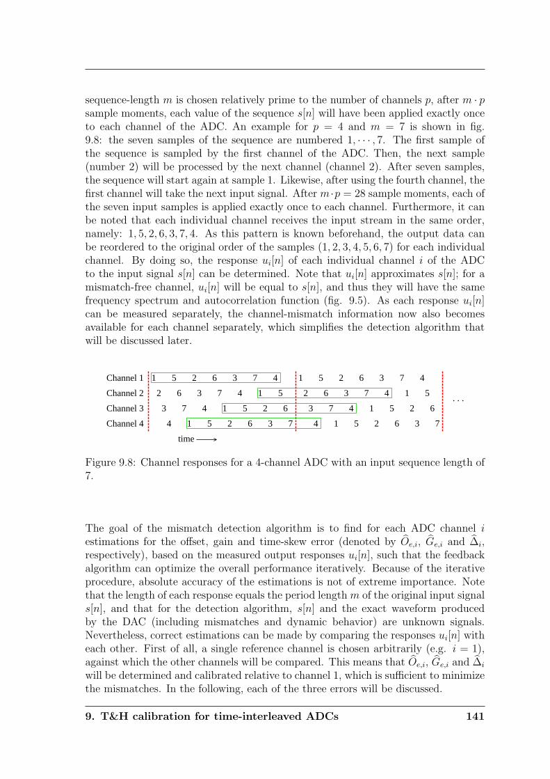
sequence-length m is chosen relatively prime to the number of channels p, after m · psample moments, each value of the sequence s[n] will have been applied exactly onceto each channel of the ADC. An example for p = 4 and m = 7 is shown in fig.9.8: the seven samples of the sequence are numbered 1, · · · , 7. The first sample ofthe sequence is sampled by the first channel of the ADC. Then, the next sample(number 2) will be processed by the next channel (channel 2). After seven samples,the sequence will start again at sample 1. Likewise, after using the fourth channel, thefirst channel will take the next input signal. After m ·p = 28 sample moments, each ofthe seven input samples is applied exactly once to each channel. Furthermore, it canbe noted that each individual channel receives the input stream in the same order,namely: 1, 5, 2, 6, 3, 7, 4. As this pattern is known beforehand, the output data canbe reordered to the original order of the samples (1, 2, 3, 4, 5, 6, 7) for each individualchannel. By doing so, the response ui[n] of each individual channel i of the ADCto the input signal s[n] can be determined. Note that ui[n] approximates s[n]; for amismatch-free channel, ui[n] will be equal to s[n], and thus they will have the samefrequency spectrum and autocorrelation function (fig. 9.5). As each response ui[n]can be measured separately, the channel-mismatch information now also becomesavailable for each channel separately, which simplifies the detection algorithm thatwill be discussed later.
time
Channel 1
Channel 2
Channel 3
Channel 4
1
2
3
4
5
6
7
1
2
3
4
5
6
7
1
2
3
4
5
6
7
1
2
3
4
5
6
7
1
2
3
4
5
6
7
1
2
3
4
5
6
7
1
2
3
4
5
6
7
1
2
3
4
5
6
7
. . .
Figure 9.8: Channel responses for a 4-channel ADC with an input sequence length of7.
The goal of the mismatch detection algorithm is to find for each ADC channel iestimations for the offset, gain and time-skew error (denoted by Oe,i, Ge,i and ∆i,respectively), based on the measured output responses ui[n], such that the feedbackalgorithm can optimize the overall performance iteratively. Because of the iterativeprocedure, absolute accuracy of the estimations is not of extreme importance. Notethat the length of each response equals the period length m of the original input signals[n], and that for the detection algorithm, s[n] and the exact waveform producedby the DAC (including mismatches and dynamic behavior) are unknown signals.Nevertheless, correct estimations can be made by comparing the responses ui[n] witheach other. First of all, a single reference channel is chosen arbitrarily (e.g. i = 1),against which the other channels will be compared. This means that Oe,i, Ge,i and ∆i
will be determined and calibrated relative to channel 1, which is sufficient to minimizethe mismatches. In the following, each of the three errors will be discussed.
9. T&H calibration for time-interleaved ADCs 141
9.4.1 Offset detection
The output offset of each channel of the ADC is composed of two components: acomponent which is common for all channels due to the generated input signal andimperfections in the DAC, and a second component which is different for each channeldue to imperfections in the T&H and ADC. By simply subtracting the average valueof u1[n] from the average value of ui[n], the common component will be canceled out,and the relative offset value of channel i compared to channel 1 remains:
Oe,i =1
m
(m−1∑
n=0
ui[n]−m−1∑
n=0
u1[n]
)(9.10)
The accuracy of the offset estimation process is dependent on the number of bits inthe ADC and the length of the MLS. Assuming an N -bit ADC, with a full-scale rangeof ±FS, the LSB of the converter equals:
LSB =2FS
2N(9.11)
From [30], it is known that the standard deviation of the quantization error will equal√112
LSB2. Assuming an equal amount of thermal noise, the total amount of noiseadded by the ADC becomes:
σADC =
√1
6LSB2 (9.12)
The offset estimation in (9.10) adds up a total of 2m values, and divides by m, suchthat the standard deviation of the offset estimation becomes:
σOe,i
=1
m·√
2m · σADC =
√1
3m· LSB ≈
√1
3 · 2M· LSB (9.13)
From this result, it becomes clear that the offset estimation can be more accuratethan the accuracy of the ADC. Therefore, it is possible to achieve a precision beyondthe requirement given in (9.2). Moreover, the measurement accuracy can be improvedfurther by increasing the MLS order M . The model derived in (9.13) was verifiedby simulations on a two-channel ADC using various number-of-bits in the ADC andvarious MLS orders. Offsets between 0 and 10mV were added to one channel ofthe ADC with a full-scale range of ±1V, and the actual σ
Oe,iwas derived from the
simulations. Figure 9.9 shows a good matching between the simulated and calculatedresults.
9.4.2 Gain error detection
The relative gain of channel i compared to channel 1 can be estimated by comparingthe energy of the two responses:
Ge,i =
√√√√m−1∑
n=0
(ui[n]
)2/
m−1∑
n=0
(u1[n]
)2(9.14)
142 9. T&H calibration for time-interleaved ADCs
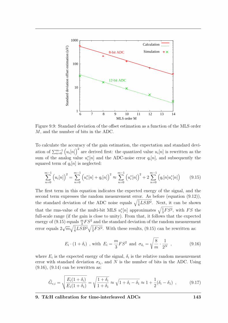
1
10
100
1000
6 7 8 9 10 11 12 13 14
Stan
dard
dev
iatio
n of
fset
est
imat
ion
(uV
)
MLS order M
Simulation
Calculation
8-bit ADC
12-bit ADC
Figure 9.9: Standard deviation of the offset estimation as a function of the MLS orderM , and the number of bits in the ADC.
To calculate the accuracy of the gain estimation, the expectation and standard devi-
ation of∑m−1
n=0
(ui[n]
)2are derived first: the quantized value ui[n] is rewritten as the
sum of the analog value u∗i [n] and the ADC-noise error qi[n], and subsequently thesquared term of qi[n] is neglected:
m−1∑
n=0
(ui[n]
)2=
m−1∑
n=0
(u∗i [n] + qi[n]
)2 ≈m−1∑
n=0
(u∗i [n]
)2+ 2
m−1∑
n=0
(qi[n]u∗i [n]
)(9.15)
The first term in this equation indicates the expected energy of the signal, and thesecond term expresses the random measurement error. As before (equation (9.12)),
the standard deviation of the ADC noise equals√
16LSB2. Next, it can be shown
that the rms-value of the multi-bit MLS u∗i [n] approximates√
13FS2, with FS the
full-scale range (if the gain is close to unity). From that, it follows that the expectedenergy of (9.15) equals m
3FS2 and the standard deviation of the random measurement
error equals 2√
m√
16LSB2
√13FS2. With these results, (9.15) can be rewritten as:
Ei · (1 + δi) , with Ei =m
3FS2 and σδi
=
√8
m· 1
2N, (9.16)
where Ei is the expected energy of the signal, δi is the relative random measurementerror with standard deviation σδi
, and N is the number of bits in the ADC. Using(9.16), (9.14) can be rewritten as:
Ge,i =
√√√√ Ei(1 + δi)
E1(1 + δ1)=
√1 + δi
1 + δ1
≈√
1 + δi − δ1 ≈ 1 +1
2(δi − δ1) , (9.17)
9. T&H calibration for time-interleaved ADCs 143
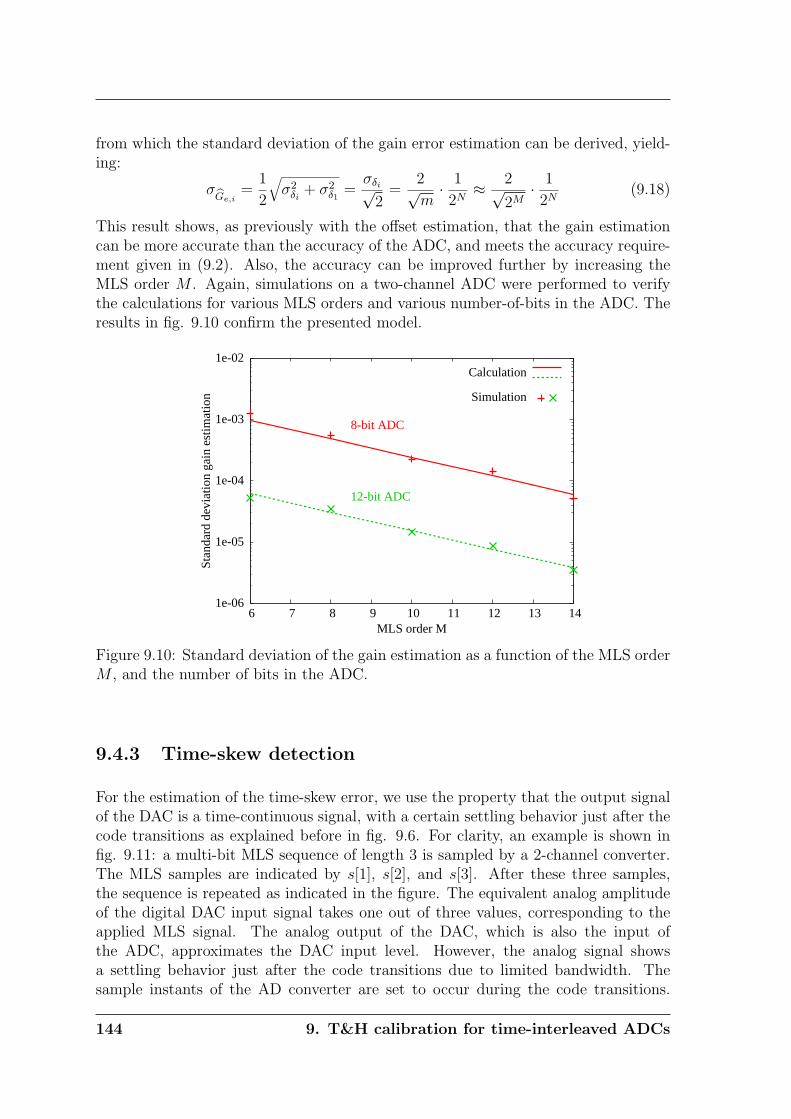
from which the standard deviation of the gain error estimation can be derived, yield-ing:
σGe,i
=1
2
√σ2
δi+ σ2
δ1=
σδi√2
=2√m· 1
2N≈ 2√
2M· 1
2N(9.18)
This result shows, as previously with the offset estimation, that the gain estimationcan be more accurate than the accuracy of the ADC, and meets the accuracy require-ment given in (9.2). Also, the accuracy can be improved further by increasing theMLS order M . Again, simulations on a two-channel ADC were performed to verifythe calculations for various MLS orders and various number-of-bits in the ADC. Theresults in fig. 9.10 confirm the presented model.
1e-06
1e-05
1e-04
1e-03
1e-02
6 7 8 9 10 11 12 13 14
Stan
dard
dev
iatio
n ga
in e
stim
atio
n
MLS order M
Calculation
Simulation
8-bit ADC
12-bit ADC
Figure 9.10: Standard deviation of the gain estimation as a function of the MLS orderM , and the number of bits in the ADC.
9.4.3 Time-skew detection
For the estimation of the time-skew error, we use the property that the output signalof the DAC is a time-continuous signal, with a certain settling behavior just after thecode transitions as explained before in fig. 9.6. For clarity, an example is shown infig. 9.11: a multi-bit MLS sequence of length 3 is sampled by a 2-channel converter.The MLS samples are indicated by s[1], s[2], and s[3]. After these three samples,the sequence is repeated as indicated in the figure. The equivalent analog amplitudeof the digital DAC input signal takes one out of three values, corresponding to theapplied MLS signal. The analog output of the DAC, which is also the input ofthe ADC, approximates the DAC input level. However, the analog signal showsa settling behavior just after the code transitions due to limited bandwidth. Thesample instants of the AD converter are set to occur during the code transitions.
144 9. T&H calibration for time-interleaved ADCs
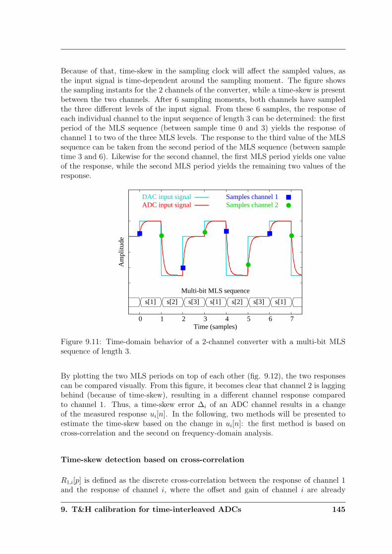
Because of that, time-skew in the sampling clock will affect the sampled values, asthe input signal is time-dependent around the sampling moment. The figure showsthe sampling instants for the 2 channels of the converter, while a time-skew is presentbetween the two channels. After 6 sampling moments, both channels have sampledthe three different levels of the input signal. From these 6 samples, the response ofeach individual channel to the input sequence of length 3 can be determined: the firstperiod of the MLS sequence (between sample time 0 and 3) yields the response ofchannel 1 to two of the three MLS levels. The response to the third value of the MLSsequence can be taken from the second period of the MLS sequence (between sampletime 3 and 6). Likewise for the second channel, the first MLS period yields one valueof the response, while the second MLS period yields the remaining two values of theresponse.
0 1 2 3 4 5 6 7
Am
plitu
de
Time (samples)
DAC input signalADC input signal
Samples channel 1Samples channel 2
s[1] s[2] s[3] s[1] s[2] s[3] s[1]
Multi-bit MLS sequence
Figure 9.11: Time-domain behavior of a 2-channel converter with a multi-bit MLSsequence of length 3.
By plotting the two MLS periods on top of each other (fig. 9.12), the two responsescan be compared visually. From this figure, it becomes clear that channel 2 is laggingbehind (because of time-skew), resulting in a different channel response comparedto channel 1. Thus, a time-skew error ∆i of an ADC channel results in a changeof the measured response ui[n]. In the following, two methods will be presented toestimate the time-skew based on the change in ui[n]: the first method is based oncross-correlation and the second on frequency-domain analysis.
Time-skew detection based on cross-correlation
R1,i[p] is defined as the discrete cross-correlation between the response of channel 1and the response of channel i, where the offset and gain of channel i are already
9. T&H calibration for time-interleaved ADCs 145
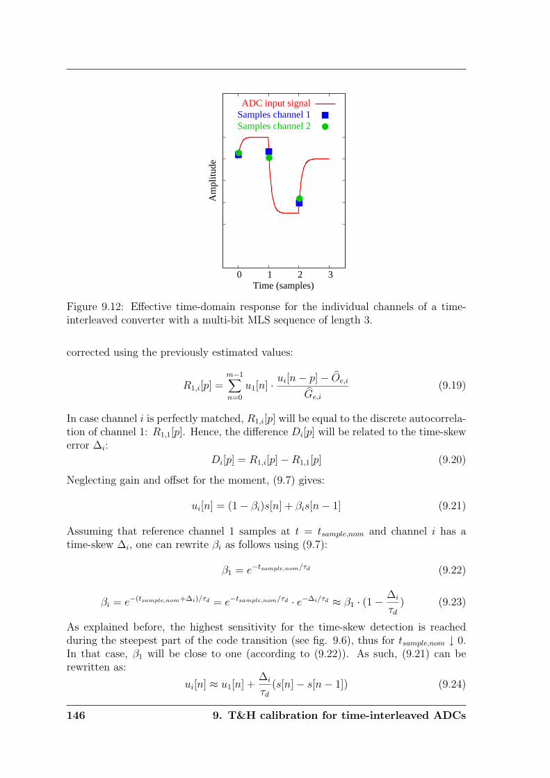
0 1 2 3
Am
plitu
de
Time (samples)
ADC input signalSamples channel 1Samples channel 2
Figure 9.12: Effective time-domain response for the individual channels of a time-interleaved converter with a multi-bit MLS sequence of length 3.
corrected using the previously estimated values:
R1,i[p] =m−1∑
n=0
u1[n] · ui[n− p]− Oe,i
Ge,i
(9.19)
In case channel i is perfectly matched, R1,i[p] will be equal to the discrete autocorrela-tion of channel 1: R1,1[p]. Hence, the difference Di[p] will be related to the time-skewerror ∆i:
Di[p] = R1,i[p]−R1,1[p] (9.20)
Neglecting gain and offset for the moment, (9.7) gives:
ui[n] = (1− βi)s[n] + βis[n− 1] (9.21)
Assuming that reference channel 1 samples at t = tsample,nom and channel i has atime-skew ∆i, one can rewrite βi as follows using (9.7):
β1 = e−tsample,nom/τd (9.22)
βi = e−(tsample,nom+∆i)/τd = e−tsample,nom/τd · e−∆i/τd ≈ β1 · (1− ∆i
τd
) (9.23)
As explained before, the highest sensitivity for the time-skew detection is reachedduring the steepest part of the code transition (see fig. 9.6), thus for tsample,nom ↓ 0.In that case, β1 will be close to one (according to (9.22)). As such, (9.21) can berewritten as:
ui[n] ≈ u1[n] +∆i
τd
(s[n]− s[n− 1]) (9.24)
146 9. T&H calibration for time-interleaved ADCs
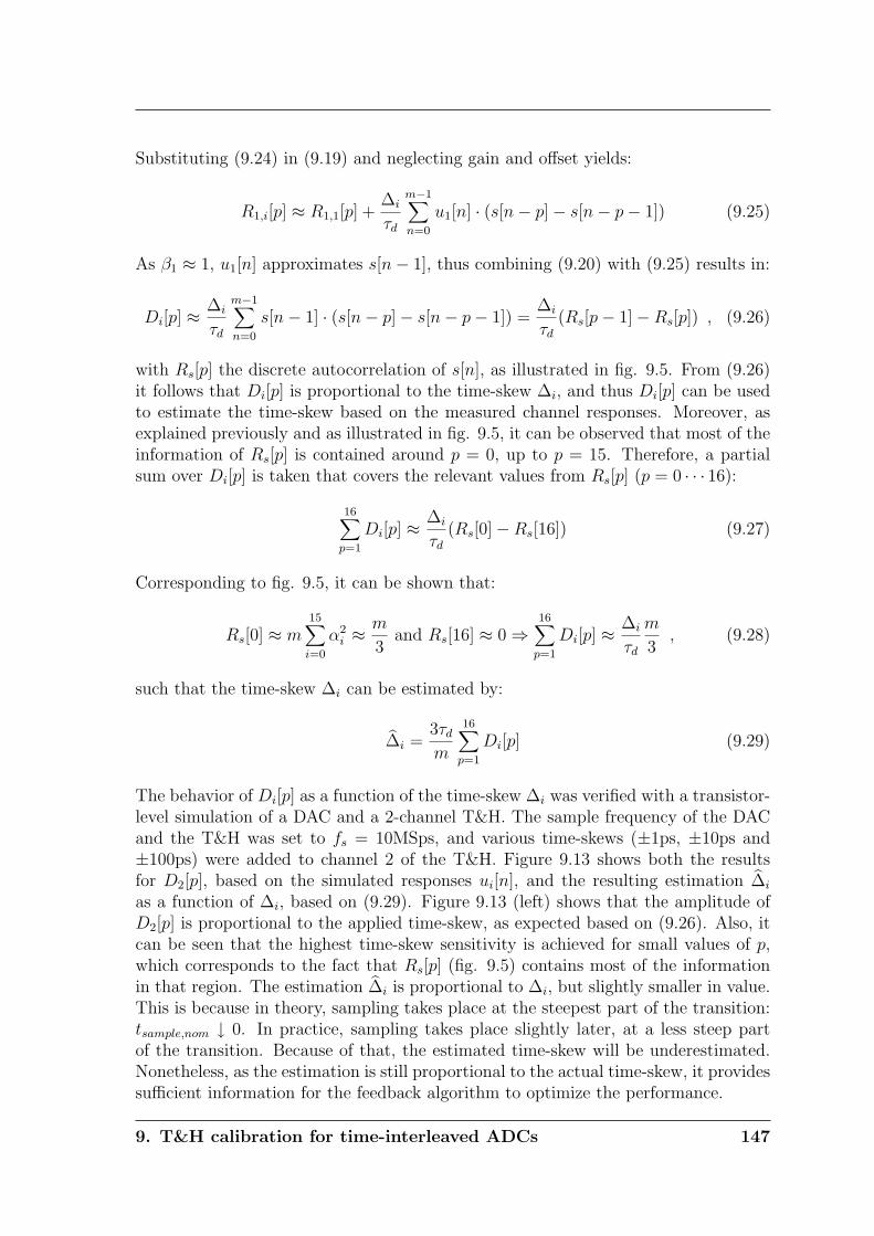
Substituting (9.24) in (9.19) and neglecting gain and offset yields:
R1,i[p] ≈ R1,1[p] +∆i
τd
m−1∑
n=0
u1[n] · (s[n− p]− s[n− p− 1]) (9.25)
As β1 ≈ 1, u1[n] approximates s[n− 1], thus combining (9.20) with (9.25) results in:
Di[p] ≈ ∆i
τd
m−1∑
n=0
s[n− 1] · (s[n− p]− s[n− p− 1]) =∆i
τd
(Rs[p− 1]−Rs[p]) , (9.26)
with Rs[p] the discrete autocorrelation of s[n], as illustrated in fig. 9.5. From (9.26)it follows that Di[p] is proportional to the time-skew ∆i, and thus Di[p] can be usedto estimate the time-skew based on the measured channel responses. Moreover, asexplained previously and as illustrated in fig. 9.5, it can be observed that most of theinformation of Rs[p] is contained around p = 0, up to p = 15. Therefore, a partialsum over Di[p] is taken that covers the relevant values from Rs[p] (p = 0 · · · 16):
16∑
p=1
Di[p] ≈ ∆i
τd
(Rs[0]−Rs[16]) (9.27)
Corresponding to fig. 9.5, it can be shown that:
Rs[0] ≈ m15∑
i=0
α2i ≈
m
3and Rs[16] ≈ 0 ⇒
16∑
p=1
Di[p] ≈ ∆i
τd
m
3, (9.28)
such that the time-skew ∆i can be estimated by:
∆i =3τd
m
16∑
p=1
Di[p] (9.29)
The behavior of Di[p] as a function of the time-skew ∆i was verified with a transistor-level simulation of a DAC and a 2-channel T&H. The sample frequency of the DACand the T&H was set to fs = 10MSps, and various time-skews (±1ps, ±10ps and±100ps) were added to channel 2 of the T&H. Figure 9.13 shows both the resultsfor D2[p], based on the simulated responses ui[n], and the resulting estimation ∆i
as a function of ∆i, based on (9.29). Figure 9.13 (left) shows that the amplitude ofD2[p] is proportional to the applied time-skew, as expected based on (9.26). Also, itcan be seen that the highest time-skew sensitivity is achieved for small values of p,which corresponds to the fact that Rs[p] (fig. 9.5) contains most of the informationin that region. The estimation ∆i is proportional to ∆i, but slightly smaller in value.This is because in theory, sampling takes place at the steepest part of the transition:tsample,nom ↓ 0. In practice, sampling takes place slightly later, at a less steep partof the transition. Because of that, the estimated time-skew will be underestimated.Nonetheless, as the estimation is still proportional to the actual time-skew, it providessufficient information for the feedback algorithm to optimize the performance.
9. T&H calibration for time-interleaved ADCs 147
-0.10
-0.05
0.00
0.05
0.10
0 10 20 30 40 50 60
D [
p]2
Discrete time shift p
-100ps-10ps-1ps
+1ps+10ps
+100ps-100
-50
0
50
100
-100 -50 0 50 100
Est
imat
ed ti
me-
skew
err
or (
ps)
Actual time-skew error (ps)
Figure 9.13: D2[p] for various time-skews (±1ps, ±10ps and ±100ps) (left), and theestimated time-skew (right).
Calculating the accuracy of the time-skew estimation is not so straightforward: (9.29)shows that σ
∆iwill be equal to 3τd
mtimes the standard deviation of the summation
over Di[p]. Ultimately, Di[p] is based on summations of m observations of ui[n].Assuming ADC noise as before (equations (9.11) and (9.12)), the standard deviationof Di[p] will be proportional to
√m/2N , thus:
σ∆i∝ 3τd
m
√m
2N∝ τd√
2M2N(9.30)
The validity of this equation will be verified later in this chapter (see page 151).
Time-skew detection based on frequency-domain analysis
As an alternative to cross-correlation in the time-domain, frequency analysis in the Z-domain can also be used to estimate the time-skew. Previously, the transfer functionsof the DAC and the ADC, including time-skew, were modeled as H1(z) and H2(z),respectively. Thus, the output of channel i of the ADC can be written as follows inthe Z-domain:
Ui(z) = H1(z) ·H2,i(z) ·R(z) , (9.31)
where R(z) is the Z-domain equivalent of the MLS sequence r[n]. Note that H1(z) andR(z) are common for all channels, but H2,i(z) (representing the time-skew) is differentfor each channel i. The relative frequency response of a channel now becomes:
Ui(z)
U1(z)=
H2,i(z)
H2,1(z)=
1− βi + βiz−1
1− β1 + β1z−1(9.32)
Using the same approximations for β1 and βi as before, this can be estimated asfollows:
Ui(z)
U1(z)=
1− βi + βiz−1
1− β1 + β1z−1≈ 1− β1 · (1− ∆i
τd) + β1 · (1− ∆i
τd)z−1
1− β1 + β1z−1
148 9. T&H calibration for time-interleaved ADCs
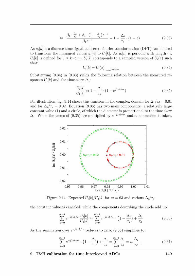
≈ β1 · ∆i
τd+ β1 · (1− ∆i
τd)z−1
β1z−1= 1− ∆i
τd
· (1− z) (9.33)
As ui[n] is a discrete-time signal, a discrete fourier transformation (DFT) can be usedto transform the measured values ui[n] to Ui[k]. As ui[n] is periodic with length m,Ui[k] is defined for 0 ≤ k < m. Ui[k] corresponds to a sampled version of Ui(z) suchthat:
Ui[k] = Ui(z)∣∣∣z=ej2πk/m
(9.34)
Substituting (9.34) in (9.33) yields the following relation between the measured re-sponses Ui[k] and the time-skew ∆i:
Ui[k]
U1[k]≈ 1− ∆i
τd
· (1− ej2πk/m) (9.35)
For illustration, fig. 9.14 shows this function in the complex domain for ∆i/τd = 0.01and for ∆i/τd = 0.02. Equation (9.35) has two main components: a relatively largeconstant value (1) and a circle, of which the diameter is proportional to the time skew∆i. When the terms of (9.35) are multiplied by e−j2πk/m and a summation is taken,
-0.02
-0.01
0.00
0.01
0.02
0.95 0.96 0.97 0.98 0.99 1.00 1.01
Im
U [
k] /
U [
k]
i
1
Re U [k] / U [k]i 1
∆ τ i d / = 0.01∆ τ i d / = 0.02
Figure 9.14: Expected Ui[k]/U1[k] for m = 63 and various ∆i/τd.
the constant value is canceled, while the components describing the circle add up:
m−1∑
k=0
e−j2πk/m Ui[k]
U1[k]≈
m−1∑
k=0
e−j2πk/m ·(1− ∆i
τd
)+
∆i
τd
(9.36)
As the summation over e−j2πk/m reduces to zero, (9.36) simplifies to:
m−1∑
k=0
e−j2πk/m ·(1− ∆i
τd
)+
∆i
τd
=m−1∑
k=0
∆i
τd
= m∆i
τd
, (9.37)
9. T&H calibration for time-interleaved ADCs 149
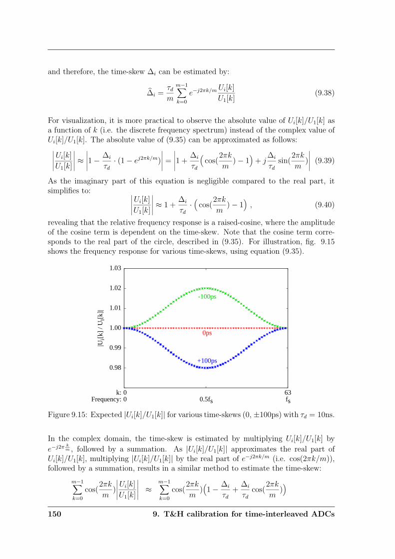
and therefore, the time-skew ∆i can be estimated by:
∆i =τd
m
m−1∑
k=0
e−j2πk/m Ui[k]
U1[k](9.38)
For visualization, it is more practical to observe the absolute value of Ui[k]/U1[k] asa function of k (i.e. the discrete frequency spectrum) instead of the complex value ofUi[k]/U1[k]. The absolute value of (9.35) can be approximated as follows:∣∣∣∣∣Ui[k]
U1[k]
∣∣∣∣∣ ≈∣∣∣∣∣1−
∆i
τd
· (1− ej2πk/m)
∣∣∣∣∣ =
∣∣∣∣∣1 +∆i
τd
(cos(
2πk
m)− 1
)+ j
∆i
τd
sin(2πk
m)
∣∣∣∣∣ (9.39)
As the imaginary part of this equation is negligible compared to the real part, itsimplifies to: ∣∣∣∣∣
Ui[k]
U1[k]
∣∣∣∣∣ ≈ 1 +∆i
τd
·(
cos(2πk
m)− 1
), (9.40)
revealing that the relative frequency response is a raised-cosine, where the amplitudeof the cosine term is dependent on the time-skew. Note that the cosine term corre-sponds to the real part of the circle, described in (9.35). For illustration, fig. 9.15shows the frequency response for various time-skews, using equation (9.35).
0.98
0.99
1.00
1.01
1.02
1.03
0 0 0.5fs
63fs
|U [
k] /
U [
k]|
i
1
k:Frequency:
0ps
-100ps
+100ps
Figure 9.15: Expected |Ui[k]/U1[k]| for various time-skews (0, ±100ps) with τd = 10ns.
In the complex domain, the time-skew is estimated by multiplying Ui[k]/U1[k] by
e−j2π km , followed by a summation. As |Ui[k]/U1[k]| approximates the real part of
Ui[k]/U1[k], multiplying |Ui[k]/U1[k]| by the real part of e−j2πk/m (i.e. cos(2πk/m)),followed by a summation, results in a similar method to estimate the time-skew:
m−1∑
k=0
cos(2πk
m)
∣∣∣∣∣Ui[k]
U1[k]
∣∣∣∣∣ ≈m−1∑
k=0
cos(2πk
m)(1− ∆i
τd
+∆i
τd
cos(2πk
m))
150 9. T&H calibration for time-interleaved ADCs
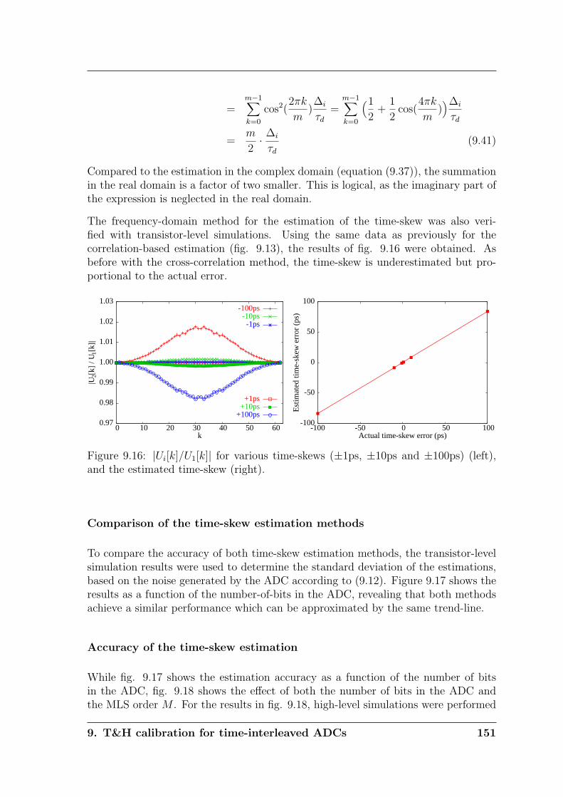
=m−1∑
k=0
cos2(2πk
m)∆i
τd
=m−1∑
k=0
(1
2+
1
2cos(
4πk
m))∆i
τd
=m
2· ∆i
τd
(9.41)
Compared to the estimation in the complex domain (equation (9.37)), the summationin the real domain is a factor of two smaller. This is logical, as the imaginary part ofthe expression is neglected in the real domain.
The frequency-domain method for the estimation of the time-skew was also veri-fied with transistor-level simulations. Using the same data as previously for thecorrelation-based estimation (fig. 9.13), the results of fig. 9.16 were obtained. Asbefore with the cross-correlation method, the time-skew is underestimated but pro-portional to the actual error.
0.97
0.98
0.99
1.00
1.01
1.02
1.03
0 10 20 30 40 50 60
|U [
k] /
U [
k]|
2
1
k
-100ps-10ps-1ps
+1ps+10ps
+100ps-100
-50
0
50
100
-100 -50 0 50 100
Est
imat
ed ti
me-
skew
err
or (
ps)
Actual time-skew error (ps)
Figure 9.16: |Ui[k]/U1[k]| for various time-skews (±1ps, ±10ps and ±100ps) (left),and the estimated time-skew (right).
Comparison of the time-skew estimation methods
To compare the accuracy of both time-skew estimation methods, the transistor-levelsimulation results were used to determine the standard deviation of the estimations,based on the noise generated by the ADC according to (9.12). Figure 9.17 shows theresults as a function of the number-of-bits in the ADC, revealing that both methodsachieve a similar performance which can be approximated by the same trend-line.
Accuracy of the time-skew estimation
While fig. 9.17 shows the estimation accuracy as a function of the number of bitsin the ADC, fig. 9.18 shows the effect of both the number of bits in the ADC andthe MLS order M . For the results in fig. 9.18, high-level simulations were performed
9. T&H calibration for time-interleaved ADCs 151
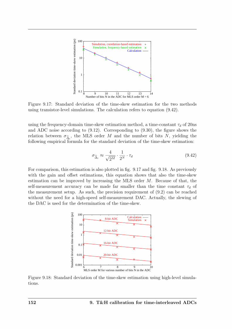
0.1
1
10
100
8 9 10 11 12 13 14Stan
dard
dev
iatio
n tim
e-sk
ew e
stim
atio
n (p
s)
Number of bits N in the ADC for MLS order M = 6
Simulation, correlation-based estimationSimulation, frequency-based estimation
Calculation
Figure 9.17: Standard deviation of the time-skew estimation for the two methodsusing transistor-level simulations. The calculation refers to equation (9.42).
using the frequency-domain time-skew estimation method, a time-constant τd of 20nsand ADC noise according to (9.12). Corresponding to (9.30), the figure shows therelation between σ
∆i, the MLS order M and the number of bits N , yielding the
following empirical formula for the standard deviation of the time-skew estimation:
σ∆i≈ 4√
2M· 1
2N· τd (9.42)
For comparison, this estimation is also plotted in fig. 9.17 and fig. 9.18. As previouslywith the gain and offset estimations, this equation shows that also the time-skewestimation can be improved by increasing the MLS order M . Because of that, theself-measurement accuracy can be made far smaller than the time constant τd ofthe measurement setup. As such, the precision requirement of (9.2) can be reachedwithout the need for a high-speed self-measurement DAC. Actually, the slewing ofthe DAC is used for the determination of the time-skew.
0.001
0.01
0.1
1
10
100
6 7 8 9 10Stan
dard
dev
iatio
n tim
e-sk
ew e
stim
atio
n (p
s)
MLS order M for various number of bits N in the ADC
8-bit ADC
12-bit ADC
16-bit ADC
20-bit ADC
CalculationSimulation
Figure 9.18: Standard deviation of the time-skew estimation using high-level simula-tions.
152 9. T&H calibration for time-interleaved ADCs
9.5 Channel mismatch correction
In the previous section, the methods to estimate the gain, offset and time-skew foreach ADC channel were discussed. The next step is to actually correct the errorsbased on the error estimations. First, the actual implementation of the correctionhardware will be discussed, and then the algorithm to control the correction circuitbased on the error estimations will be described.
9.5.1 Analog correction method
In reality, the channel mismatches that were modeled by offset, gain error and time-skew, originate from many different error sources within the channel. For example,mismatch of the components in the T&H, ADC or clock circuitry, mismatch in thereference levels for the different channels, mismatch in the layout, gradients due tolayout and gradients due to voltage drop. Even though the actual error sources mightbe unknown, they can be compensated together at a single location in the channel.In the presented solution, the actual correction takes place in the T&H circuit bytuning several analog components, such that no additional digital processing poweris required for the correction. For the correction of gain and offset errors, the sameimplementation as in chapter 8 will be used. On top of that, a programmable delay isadded to the switch-driver to provide a correction mechanism for the time-skew. Theimplementation of the controllable T&H is visualized in fig. 9.19, showing the three8-bit programmable parameters: the two current sources Ia and Ib of the differentialpair and the delay τ of the clock buffer.
IA IB
Rs
Vin+
T1
Vin-
T2
RR
VDD
Vout- Vout+
boosting
CLK
Cs
boosting
CLK
Cs
CLK τ
Figure 9.19: Implementation of the T&H with programmable gain, offset and time-skew.
As described in chapter 8, the gain can be controlled by changing Ia and Ib in the samedirection, while the offset can be controlled by changing Ia and Ib in opposite direc-tions. The time-skew can be controlled by changing the delay τ of the switch-driver.The transistor-level implementation of the programmable delay will be reviewed laterin section 9.7. Figure 9.20 shows the controllability of the three parameters based on
9. T&H calibration for time-interleaved ADCs 153
transistor-level simulations. The strong non-linear behavior of the time-skew correc-tion is not directly important as the algorithm is able to find the optimum regardlessof the non-linearity. However, the non-linearity also results in a variable step-sizeacross the tuning range. As such, part of the curve needs to be over-designed in orderto achieve sufficient performance throughout the complete range. The main causeof the strong non-linearity of this curve is due to the wide tuning range (250ps).When redesigning for a more realistic range (e.g. 50ps), the linearity will improveautomatically. For all three parameters, the 8-bit control allows enough range tocompensate worst-case mismatch situations while the step size is small enough toguarantee enough calibration accuracy to realize 10-bit post-calibration performancefor a 2-channel time-interleaved ADC operating at 1GSps.
0.92
1.00
1.08
0 255
Gai
n co
mpe
nsat
ion
Parameter Ia, Ib-80
0
80
0 255
255 0
Off
set c
ompe
nsat
ion
(mV
)
Parameter IaParameter Ib
0
250
0 255D
elay
com
pens
atio
n(p
s)Parameter τ
Figure 9.20: Analog controllability of gain, offset and time-skew.
9.5.2 Correction algorithm
The correction algorithm updates the parameter settings of each channel (Ia,i, Ib,i
and τi) based on the measured estimations of the errors (Oe,i, Ge,i and ∆i). After theupdate, a new measurement will be performed and the parameters will be updatedagain until a situation with sufficient performance is achieved. Because of the iterativeerror-optimization procedure, the absolute accuracy of the estimations given by (9.10),(9.14) and (9.29) or (9.38) is not of extreme importance, as long as the feedback-loop controls the errors towards zero. For the same reasons, the actual (non-linear)behavior of the analog correction circuit is not critical. As in chapter 8, the parameter-update functions are simple linear combinations of the error estimations:
Ia,i[k] = Ia,i[k − 1] − c1 · (Ge,i[k]− 1)− c2 · Oe,i[k]
Ib,i[k] = Ib,i[k − 1] − c1 · (Ge,i[k]− 1) + c2 · Oe,i[k]
τi[k] = τi[k − 1] + c3 · ∆i[k]
, (9.43)
where c1, c2 and c3 are constants, and k indicates the iteration of the feedback algo-rithm.
154 9. T&H calibration for time-interleaved ADCs
9.6 Simulation results
The calibration method was verified by means of transistor-level simulations on a2-channel time-interleaved ADC, operating at fs = 1GSps. The DAC, clock circuitryand T&H circuits were implemented fully on transistor-level in a CMOS 0.18µmtechnology. The quantizers were implemented with ideal 12-bit ADCs, having a full-scale range of Vpp = 1V. The SFDR of a single channel is around 65dB, limitingthe overall performance to 10-bit at most. The following combination of mismatcherrors was applied to one channel of the ADC: Oe,2 = 1.6mV, Ge,2 = 1.0064 and∆2 = 30ps. This set of errors was chosen as they correspond to 8-bit performancewhile operating at fs = 100MSps, which is a realistic performance for an intrinsiccircuit without calibration. Applying a sinusoid with frequency 347
1024fs
4 yields theoutput spectrum of fig. 9.21. The distortion components of the T&H (HD3 and HD5)can be seen as well as several components due to channel mismatch: a DC-level dueto offset mismatch, and a tone due to gain and time-skew mismatch. In this case, thetime-skew mismatch is dominant, limiting the SFDR of the ADC to 29.7dB.
-120
-100
-80
-60
-40
-20
0
0 0.1 0.2 0.3 0.4 0.5
Rel
ativ
e po
wer
(dB
)
Frequency (GHz)
Fundamentalsignal
-HD3 64.6dB -HD5 64.6dB
-Offset 49.9dB
-Gain/Time-skew 29.7dB
-120
-100
-80
-60
-40
-20
0
0 0.1 0.2 0.3 0.4 0.5
Rel
ativ
e po
wer
(dB
)
Frequency (GHz)
Fundamentalsignal
-HD3 62.2dB -HD5 64.6dB
-Offset 71.8dB
-Gain/Time-skew 62.5dB
Figure 9.21: Output power spectrum for the 2-channel ADC, before calibration (left)and after calibration (right).
Next, the self-measurement and self-correction algorithms were applied to the ADC.For this purpose, a transistor-level implementation of a DAC (with an intrinsic ac-curacy of only 6-bit) was used as a test-signal generator. As the sample frequencyof the DAC is limited to 100MSps, during this calibration phase the time-interleavedADC was also set to operate at fs = 100MSps. Also, due to simulation limitationsthe MLS-order was limited to M = 6. From equations (9.13), (9.18) and (9.42), theself-measurement accuracy can be estimated. Knowing that M = 6, LSB = 0.24mV,N = 12, τd = 3ns, it follows that: σ
Oe,i= 0.02mV, σ
Ge,i= 0.006% and ∆i = 0.4ps.
However, especially for gain and offset calibration, the post-calibration performanceis limited by the step-size of the analog correction elements: 0.6mV for the offset and
4This signal frequency is chosen as it is relative prime to the sample frequency and it is a relativelyhigh frequency, and thus sensitive to time-skew errors.
9. T&H calibration for time-interleaved ADCs 155
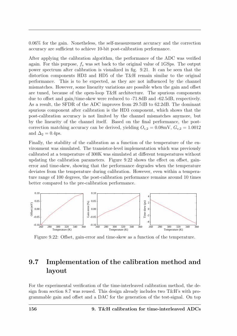
0.06% for the gain. Nonetheless, the self-measurement accuracy and the correctionaccuracy are sufficient to achieve 10-bit post-calibration performance.
After applying the calibration algorithm, the performance of the ADC was verifiedagain. For this purpose, fs was set back to the original value of 1GSps. The outputpower spectrum after calibration is visualized in fig. 9.21. It can be seen that thedistortion components HD3 and HD5 of the T&H remain similar to the originalperformance. This is to be expected, as they are not influenced by the channelmismatches. However, some linearity variations are possible when the gain and offsetare tuned, because of the open-loop T&H architecture. The spurious componentsdue to offset and gain/time-skew were reduced to -71.8dB and -62.5dB, respectively.As a result, the SFDR of the ADC improves from 29.7dB to 62.2dB. The dominantspurious component after calibration is the HD3 component, which shows that thepost-calibration accuracy is not limited by the channel mismatches anymore, butby the linearity of the channel itself. Based on the final performance, the post-correction matching accuracy can be derived, yielding Oe,2 = 0.08mV, Ge,2 = 1.0012and ∆2 = 0.4ps.
Finally, the stability of the calibration as a function of the temperature of the en-vironment was simulated. The transistor-level implementation which was previouslycalibrated at a temperature of 300K was simulated at different temperatures withoutupdating the calibration parameters. Figure 9.22 shows the effect on offset, gain-error and time-skew, showing that the performance degrades when the temperaturedeviates from the temperature during calibration. However, even within a tempera-ture range of 100 degrees, the post-calibration performance remains around 10 timesbetter compared to the pre-calibration performance.
-0.10
-0.05
0.00
0.05
0.10
260 280 300 320 340 360
Off
set (
mV
)
Temperature (K)
-0.10
-0.05
0.00
0.05
0.10
260 280 300 320 340 360
Gai
n er
ror
(%)
Temperature (K)
-4
-2
0
2
4
260 280 300 320 340 360
Tim
e sk
ew (
ps)
Temperature (K)
Figure 9.22: Offset, gain-error and time-skew as a function of the temperature.
9.7 Implementation of the calibration method and
layout
For the experimental verification of the time-interleaved calibration method, the de-sign from section 8.7 was reused. This design already includes two T&H’s with pro-grammable gain and offset and a DAC for the generation of the test-signal. On top
156 9. T&H calibration for time-interleaved ADCs
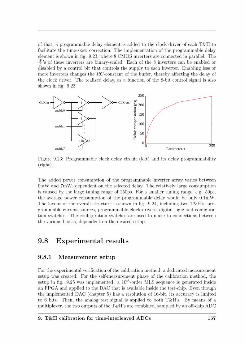
of that, a programmable delay element is added to the clock driver of each T&H tofacilitate the time-skew correction. The implementation of the programmable delayelement is shown in fig. 9.23, where 8 CMOS inverters are connected in parallel. TheWL
’s of these inverters are binary-scaled. Each of the 8 inverters can be enabled ordisabled by a control bit that controls the supply to each inverter. Enabling less ormore inverters changes the RC-constant of the buffer, thereby affecting the delay ofthe clock driver. The realized delay, as a function of the 8-bit control signal is alsoshown in fig. 9.23.
CLK in CLK out
128
2
1
enable0
enable1
enable7
0
50
100
150
200
250
0 255
Del
ay c
ompe
nsat
ion
(ps)
Parameter τ
Figure 9.23: Programmable clock delay circuit (left) and its delay programmability(right).
The added power consumption of the programmable inverter array varies between0mW and 7mW, dependent on the selected delay. The relatively large consumptionis caused by the large tuning range of 250ps. For a smaller tuning range, e.g. 50ps,the average power consumption of the programmable delay would be only 0.1mW.The layout of the overall structure is shown in fig. 9.24, including two T&H’s, pro-grammable current sources, programmable clock drivers, digital logic and configura-tion switches. The configuration switches are used to make to connections betweenthe various blocks, dependent on the desired setup.
9.8 Experimental results
9.8.1 Measurement setup
For the experimental verification of the calibration method, a dedicated measurementsetup was created. For the self-measurement phase of the calibration method, thesetup in fig. 9.25 was implemented: a 10th-order MLS sequence is generated insidean FPGA and applied to the DAC that is available inside the test-chip. Even thoughthe implemented DAC (chapter 5) has a resolution of 16-bit, its accuracy is limitedto 6 bits. Then, the analog test signal is applied to both T&H’s. By means of amultiplexer, the two outputs of the T&H’s are combined, sampled by an off-chip ADC
9. T&H calibration for time-interleaved ADCs 157
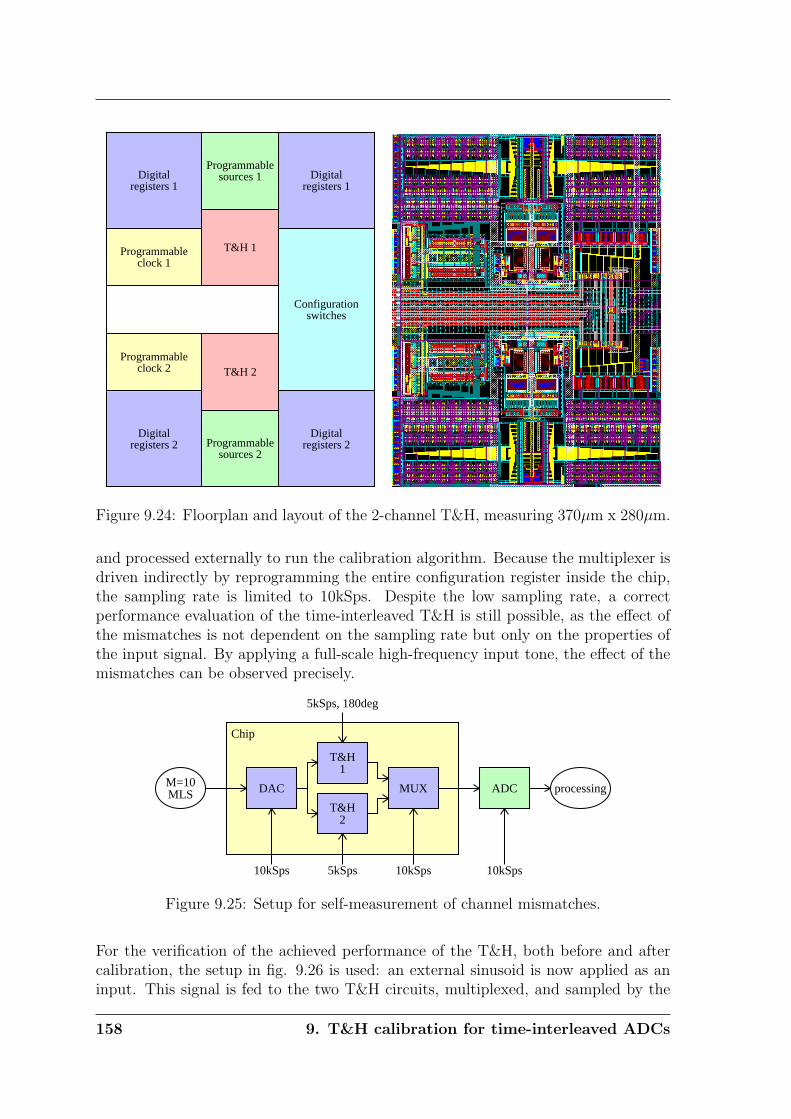
T&H 1
T&H 2
sources 1Programmable
sources 2Programmable
registers 1Digital
registers 1Digital
clock 1Programmable
registers 2Digital
registers 2Digital
clock 2Programmable
switchesConfiguration
Figure 9.24: Floorplan and layout of the 2-channel T&H, measuring 370µm x 280µm.
and processed externally to run the calibration algorithm. Because the multiplexer isdriven indirectly by reprogramming the entire configuration register inside the chip,the sampling rate is limited to 10kSps. Despite the low sampling rate, a correctperformance evaluation of the time-interleaved T&H is still possible, as the effect ofthe mismatches is not dependent on the sampling rate but only on the properties ofthe input signal. By applying a full-scale high-frequency input tone, the effect of themismatches can be observed precisely.
MLSM=10 DAC
2T&H
1T&H
MUX ADC processing
10kSps 5kSps
5kSps, 180deg
10kSps 10kSps
Chip
Figure 9.25: Setup for self-measurement of channel mismatches.
For the verification of the achieved performance of the T&H, both before and aftercalibration, the setup in fig. 9.26 is used: an external sinusoid is now applied as aninput. This signal is fed to the two T&H circuits, multiplexed, and sampled by the
158 9. T&H calibration for time-interleaved ADCs
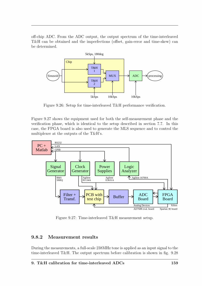
off-chip ADC. From the ADC output, the output spectrum of the time-interleavedT&H can be obtained and the imperfections (offset, gain-error and time-skew) canbe determined.
Sinusoid
2T&H
1T&H
MUX ADC processing
5kSps
5kSps, 180deg
10kSps 10kSps
Chip
Figure 9.26: Setup for time-interleaved T&H performance verification.
Figure 9.27 shows the equipment used for both the self-measurement phase and theverification phase, which is identical to the setup described in section 7.7. In thiscase, the FPGA board is also used to generate the MLS sequence and to control themultiplexer at the outputs of the T&H’s.
MatlabPC +
GeneratorSignal
GeneratorClock
SuppliesPower
AnalyzerLogic
Transf.Filter +
test chipPCB with Buffer Board
ADCBoardFPGA
GPIBLANRS232
R&SSMIQ
Agilent81134A
AgilentE3631A
Agilent 16700A
Analog DevicesAD7688 eval. board
XilinxSpartan 3E board
Figure 9.27: Time-interleaved T&H measurement setup.
9.8.2 Measurement results
During the measurements, a full-scale 238MHz tone is applied as an input signal to thetime-interleaved T&H. The output spectrum before calibration is shown in fig. 9.28
9. T&H calibration for time-interleaved ADCs 159
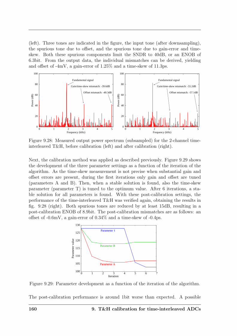
(left). Three tones are indicated in the figure, the input tone (after downsampling),the spurious tone due to offset, and the spurious tone due to gain-error and time-skew. Both these spurious components limit the SNDR to 40dB, or an ENOB of6.3bit. From the output data, the individual mismatches can be derived, yieldingand offset of -4mV, a gain-error of 1.25% and a time-skew of 11.3ps.
0
20
40
60
80
100
0 1 2 3 4 5
Pow
er (
dB)
Frequency (kHz)
Fundamental signal
Gain/time-skew mismatch: -39.6dB
Offset mismatch: -40.3dB
0
20
40
60
80
100
0 1 2 3 4 5
Pow
er (
dB)
Frequency (kHz)
Fundamental signal
Gain/time-skew mismatch: -55.2dB
Offset mismatch: -57.1dB
Figure 9.28: Measured output power spectrum (subsampled) for the 2-channel time-interleaved T&H, before calibration (left) and after calibration (right).
Next, the calibration method was applied as described previously. Figure 9.29 showsthe development of the three parameter settings as a function of the iteration of thealgorithm. As the time-skew measurement is not precise when substantial gain andoffset errors are present, during the first iterations only gain and offset are tuned(parameters A and B). Then, when a stable solution is found, also the time-skewparameter (parameter T) is tuned to the optimum value. After 6 iterations, a sta-ble solution for all parameters is found. With these post-calibration settings, theperformance of the time-interleaved T&H was verified again, obtaining the results infig. 9.28 (right). Both spurious tones are reduced by at least 15dB, resulting in apost-calibration ENOB of 8.9bit. The post-calibration mismatches are as follows: anoffset of -0.6mV, a gain-error of 0.34% and a time-skew of -0.4ps.
100
105
110
115
120
125
130
0 1 2 3 4 5 6 7
Para
met
er v
alue
Iteration
Parameter A
Parameter B
τParameter
Figure 9.29: Parameter development as a function of the iteration of the algorithm.
The post-calibration performance is around 1bit worse than expected. A possible
160 9. T&H calibration for time-interleaved ADCs
reason is that during calibration and during verification, a slightly different setup isused. During calibration (fig. 9.25), the inputs of the T&H’s are connected togetherinside the chip, and then connected to the DAC. During verification (fig. 9.26), theinputs of the T&H’s are connected together outside the chip, and then connected tothe signal source. As a result, during verification there is additional channel mismatchbecause of the separate traces on the PCB and the separate cables, which is not takeninto account by the calibration method. For an improved implementation, the T&Hinputs should be connected on-chip during the verification mode as well.
9.9 Conclusion
In this chapter, a method was presented to measure and correct for offset, gain andtime-skew errors in time-interleaved ADCs using a single integrated algorithm. Theapplied test signal is a repetitive pseudo-random noise sequence, which can be easilygenerated on-chip. Because of the repetitive nature, each channel will receive exactlythe same sequence, ensuring a fast and accurate measurement. At the same time, thebroad frequency range of the generated test signal prevents over-optimization for aspecific frequency. Furthermore, it was shown that the accuracy and the speed of theDAC, used to generate the analog test signal, can be much lower than the intendedaccuracy and speed of the ADC. Because of that, the DAC can be integrated easilyon chip without too much overhead. A further advantage of the presented method isthat it measures the response of each individual channel as opposed to measuring thecombined response of all channels. As a result, the complexity of the error detectionalgorithm remains proportional to the number of channels. Mathematical analysisproves that the resolution of the ADC is not limiting the accuracy of the measurementof the channel mismatches. Moreover, the measurement accuracy can be improvedby increasing the length of the test-vector. As such, after calibration the overallperformance will not be limited by the channel mismatches but by the performanceof the individual channels. The actual correction is performed in the analog domainin such a way that little additional power is consumed. Chip measurements on a2-channel time-interleaved T&H confirm that the calibration method can measurethe channel mismatches and correct for them. In this specific implementation, theimprovement is limited to 15dB due to external imperfections, yielding a 9-bit post-calibration performance. However, this is not a general limitation as the analysis andsimulation results prove that the channel-mismatches can be measured and correctedbeyond the performance of the individual channels.
9. T&H calibration for time-interleaved ADCs 161

Chapter 10
Conclusions
While technology evolution is beneficial for digital designs, it can cause problemsor performance limitations for analog circuits. The smart concept can improve theperformance of analog circuits by using on-chip intelligence to detect imperfectionsand to correct for them.
In a first example, considering a 12-bit DAC design, it is shown that a new smartapproach can reduce the DAC area by a factor of ten compared to existing state-of-the-art. For intrinsic designs, the minimum core area is determined by a limitationdue to accuracy requirements, because of which the area increases with a factor offour for each additional bit. The presented approach, using a sub-binary variable-radix, overcomes the intrinsic limitation, because of which the area increases with afactor of two only for each additional bit. Thus, for higher resolutions, the approachbecomes more and more attractive. Experimental results based on an implementedsub-binary variable-radix DAC prove the feasibility of the self-measurement methodand the pre-correction algorithm.
In a second example, high-speed ADCs are considered. Smart approaches exist tocorrect for specific imperfections in ADCs. Even though they prove that these imper-fections can be compensated, their overall performance (in terms of speed/accuracy/-power) is not provably better compared to intrinsic designs. A limitation of mostof the existing smart solutions is that their digital calibration hardware contributessignificantly to the overall power consumption. In this work, start-up calibrationmethods are used in combination with analog correction circuits to maintain overallpower-efficiency. Experimental results prove that analog correction of various imper-fections is achievable in a power-efficient way.
In this work, two key-factors are perceived that enable high-performance: open-loopcircuitry and time-interleaving. It is shown that open-loop circuits are able to achievehigher speed and lower power-consumption compared to closed-loop alternatives.However, a drawback of open-loop circuits is their limited accuracy. Mathematicalanalysis, simulations and experiments verify that the limited accuracy of open-loop
10. Conclusions 163

circuits can be overcome by smart calibration. As such, the smart approach widensthe application range of high-speed, power-efficient open-loop circuits towards higheraccuracies. It is illustrated that the second key-factor, time-interleaving, enables ahigher absolute speed of operation as well as a higher power-efficiency for specific sit-uations. However, time-interleaving also introduces channel mismatch errors, whichlimit the final accuracy. A smart solution is proposed that can correct for thesechannel mismatches. Analysis and simulations prove that these mismatches can bemeasured and corrected accurately enough to ensure that the final post-calibrationperformance is not limited by the channel mismatches anymore, but by the perfor-mance of the individual channels. Experimental results verify the feasibility of theproposed methods for self-measurement and self-correction.
164 10. Conclusions
References
[1] J. E. Lilienfeld, “Method and apparatus for controlling electric currents,” US Patent 1,745,175,filed Oct. 8, 1926.
[2] J. Bardeen and W. H. Brattain, “Three-electrode circuit element utilizing semiconductive ma-terials,” US Patent 2,524,035, filed June 17, 1948.
[3] W. Shockley, “Circuit element utilizing semiconductive material,” US Patent 2,569,347, filedJune 26, 1948.
[4] “UMC (United Microelectronics Corporation) - 2009,” from www.umc.com.
[5] A. van Roermund, H. Hegt, P. Harpe, G. Radulov, A. Zanikopoulos, K. Doris, and P. Quinn,“Smart AD and DA converters,” in proc. IEEE ISCAS 2005, Kobe, Japan, May 23 – 26, 2005.
[6] B. Murmann and B. E. Boser, “A 12-bit 75-MS/s pipelined ADC using open-loop residueamplification,” IEEE J. Solid-State Circuits, vol. 38, no. 12, pp. 2040 – 2050, Dec. 2003.
[7] W. Yang, D. Kelly, I. Mehr, M. T. Sayuk, and L. Singer, “A 3-V 340-mW 14-b 75-MSample/sCMOS ADC with 85-dB SFDR at Nyquist input,” IEEE J. Solid-State Circuits, vol. 36, no. 12,pp. 1931 – 1936, Dec. 2001.
[8] P. J. A. Harpe, J. M. de Meulmeester, J. A. Hegt, and A. H. M. van Roermund, “Novel digitalpre-correction method for mismatch in DACs with built-in self-measurement,” in proc. IEEADDA 2005, July 25 – 27, 2005, pp. 25 – 30.
[9] P. Harpe, J. de Meulmeester, H. Hegt, and A. van Roermund, “Reliable design of digital-to-analog converters using pre-correction and embedded self-test,” in proc. IEEE 11th Int.Mixed-Signals Testing Workshop, June 27 – 29, 2005, pp. 84 – 89.
[10] P. Harpe, J. de Meulmeester, H. Hegt, and A. van Roermund, “Digital pre-correction methodfor mismatch in DACs with built-in self-measurement,” in proc. ProRISC 2005, Veldhoven, TheNetherlands, Nov. 17 – 18, 2005, pp. 209 – 216.
[11] G. I. Radulov, “Flexible and self-calibrating current-steering digital-to-analog converters: Anal-ysis, classification and design,” Ph.D. dissertation, Eindhoven Univ. of Technology, Jan. 2010.
[12] W. Schofield, D. Mercer, and L. S. Onge, “A 16b 400MS/s DAC with <-80dBc IMD to 300MHzand <-160dBm/Hz noise power spectral density,” in proc. IEEE ISSCC 2003, 2003.
[13] G. I. Radulov, P. J. Quinn, H. Hegt, and A. van Roermund, “An on-chip self-calibration methodfor current mismatch in D/A converters,” in proc. ESSCIRC 2005, Sept. 12 – 16, 2005, pp. 169– 172.
[14] Y. Tang, H. Hegt, and A. van Roermund, “Predictive timing error calibration technique for RFcurrent-steering DACs,” in proc. IEEE ISCAS 2008, May 18 – 21, 2008, pp. 228 – 231.
[15] A. R. Bugeja, B.-S. Song, P. L. Rakers, and S. F. Gillig, “A 14-b, 100-MS/s CMOS DACdesigned for spectral performance,” IEEE J. Solid-State Circuits, vol. 34, no. 12, pp. 1719 –1732, Dec. 1999.
References 165
[16] A. V. den Bosch, M. A. F. Borremans, M. S. J. Steyaert, and W. Sansen, “A 10-bit 1-GSample/sNyquist current-steering CMOS D/A converter,” IEEE J. Solid-State Circuits, vol. 36, no. 3,pp. 315 – 324, Mar. 2001.
[17] J. Deveugele and M. S. J. Steyaert, “A 10-bit 250-MS/s binary-weighted current-steering DAC,”IEEE J. Solid-State Circuits, vol. 41, no. 2, pp. 320 – 329, Feb. 2006.
[18] K. Doris, “High-speed D/A converters: from analysis and synthesis concepts to IC implemen-tation,” Ph.D. dissertation, Eindhoven Univ. of Technology, Sept. 2004.
[19] K. O’Sullivan, C. Gorman, M. Hennessy, and V. Callaghan, “A 12-bit 320-MSample/s current-steering CMOS D/A converter in 0.44 mm2,” IEEE J. Solid-State Circuits, vol. 39, no. 7, pp.1064 – 1072, July 2004.
[20] A. V. den Bosch, M. A. F. Borremans, M. S. J. Steyaert, and W. Sansen, “A 12-bit500-MSample/s current-steering CMOS D/A converter,” in proc. IEEE ISSCC 2001, 2001.
[21] C.-H. Lin, F. van der Goes, J. Westra, J. Mulder, Y. Lin, E. Arslan, E. Ayranci, X. Liu, andK. Bult, “A 12b 2.9GS/s DAC with IM3 ¿-60dBc beyond 1GHz in 65nm CMOS,” in proc.IEEE ISSCC 2009, 2009, pp. 74 – 75.
[22] B. Schafferer and R. Adams, “A 3V CMOS 400mW 14b 1.4GS/s DAC for multi-carrier appli-cations,” in proc. IEEE ISSCC 2004, 2004, pp. 360 – 532.
[23] J. Bastos, “Characterization of MOS transistor mismatch for analog design,” Ph.D. dissertation,Katholieke Universiteit Leuven, 1998.
[24] T. Chen and G. G. E. Gielen, “A 14-bit 200-MHz current-steering DAC with switching-sequencepost-adjustment calibration,” IEEE J. Solid-State Circuits, vol. 42, no. 11, pp. 2386 – 2394,Nov. 2007.
[25] G. I. Radulov, P. J. Quinn, J. A. Hegt, and A. H. M. van Roermund, “A flexible 12-bit self-calibrated quad-core current-steering DAC,” in proc. IEEE APPCAS 2008, Nov. 30, 2008, pp.25 – 28.
[26] Q. Huang, P. A. Francese, C. Martelli, and J. Nielsen, “A 200MS/s 14b 97mW DAC in 0.18µmCMOS,” in proc. IEEE ISSCC 2004, 2004.
[27] M. P. Tiilikainen, “A 14-bit 1.8-V 20-mW 1-mm2 CMOS DAC,” IEEE J. Solid-State Circuits,vol. 36, no. 7, pp. 1144 – 1147, July 2001.
[28] Y. Cong and R. L. Geiger, “A 1.5V 14b 100MS/s self-calibrated DAC,” in proc. IEEE ISSCC2003, vol. 1, 2003, pp. 128 – 482.
[29] A. R. Bugeja and B.-S. Song, “A self-trimming 14b 100MSample/s CMOS DAC,” in proc. IEEEISSCC 2000, 2000.
[30] P. G. A. Jespers, Integrated Converters. Oxford: Oxford University Press, 2001,ISBN 0 19 856446 5.
[31] M. Pastre and M. Kayal, “High-precision DAC based on a self-calibrated sub-binary radixconverter,” in proc. IEEE ISCAS 2004, May 23 – 26, 2004, pp. 341 – 344.
[32] J. J. Wikner, “Studies on CMOS digital-to-analog converters,” Ph.D. dissertation, LinkopingsUniversitet, Sweden, 2001.
[33] A. Varzaghani and C.-K. K. Yang, “A 600-MS/s 5-bit pipeline A/D converter using digitalreference calibration,” IEEE J. Solid-State Circuits, vol. 41, no. 2, pp. 310 – 319, Feb. 2006.
[34] K. Iizuka, H. Matsui, M. Ueda, and M. Daito, “A 14-bit digitally self-calibrated pipelinedADC with adaptive bias optimization for arbitrary speeds up to 40 MS/s,” IEEE J. Solid-StateCircuits, vol. 41, no. 4, pp. 883 – 890, Apr. 2006.
166 References
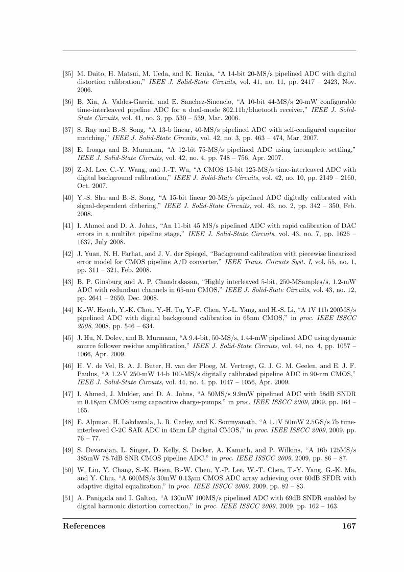
[35] M. Daito, H. Matsui, M. Ueda, and K. Iizuka, “A 14-bit 20-MS/s pipelined ADC with digitaldistortion calibration,” IEEE J. Solid-State Circuits, vol. 41, no. 11, pp. 2417 – 2423, Nov.2006.
[36] B. Xia, A. Valdes-Garcia, and E. Sanchez-Sinencio, “A 10-bit 44-MS/s 20-mW configurabletime-interleaved pipeline ADC for a dual-mode 802.11b/bluetooth receiver,” IEEE J. Solid-State Circuits, vol. 41, no. 3, pp. 530 – 539, Mar. 2006.
[37] S. Ray and B.-S. Song, “A 13-b linear, 40-MS/s pipelined ADC with self-configured capacitormatching,” IEEE J. Solid-State Circuits, vol. 42, no. 3, pp. 463 – 474, Mar. 2007.
[38] E. Iroaga and B. Murmann, “A 12-bit 75-MS/s pipelined ADC using incomplete settling,”IEEE J. Solid-State Circuits, vol. 42, no. 4, pp. 748 – 756, Apr. 2007.
[39] Z.-M. Lee, C.-Y. Wang, and J.-T. Wu, “A CMOS 15-bit 125-MS/s time-interleaved ADC withdigital background calibration,” IEEE J. Solid-State Circuits, vol. 42, no. 10, pp. 2149 – 2160,Oct. 2007.
[40] Y.-S. Shu and B.-S. Song, “A 15-bit linear 20-MS/s pipelined ADC digitally calibrated withsignal-dependent dithering,” IEEE J. Solid-State Circuits, vol. 43, no. 2, pp. 342 – 350, Feb.2008.
[41] I. Ahmed and D. A. Johns, “An 11-bit 45 MS/s pipelined ADC with rapid calibration of DACerrors in a multibit pipeline stage,” IEEE J. Solid-State Circuits, vol. 43, no. 7, pp. 1626 –1637, July 2008.
[42] J. Yuan, N. H. Farhat, and J. V. der Spiegel, “Background calibration with piecewise linearizederror model for CMOS pipeline A/D converter,” IEEE Trans. Circuits Syst. I, vol. 55, no. 1,pp. 311 – 321, Feb. 2008.
[43] B. P. Ginsburg and A. P. Chandrakasan, “Highly interleaved 5-bit, 250-MSamples/s, 1.2-mWADC with redundant channels in 65-nm CMOS,” IEEE J. Solid-State Circuits, vol. 43, no. 12,pp. 2641 – 2650, Dec. 2008.
[44] K.-W. Hsueh, Y.-K. Chou, Y.-H. Tu, Y.-F. Chen, Y.-L. Yang, and H.-S. Li, “A 1V 11b 200MS/spipelined ADC with digital background calibration in 65nm CMOS,” in proc. IEEE ISSCC2008, 2008, pp. 546 – 634.
[45] J. Hu, N. Dolev, and B. Murmann, “A 9.4-bit, 50-MS/s, 1.44-mW pipelined ADC using dynamicsource follower residue amplification,” IEEE J. Solid-State Circuits, vol. 44, no. 4, pp. 1057 –1066, Apr. 2009.
[46] H. V. de Vel, B. A. J. Buter, H. van der Ploeg, M. Vertregt, G. J. G. M. Geelen, and E. J. F.Paulus, “A 1.2-V 250-mW 14-b 100-MS/s digitally calibrated pipeline ADC in 90-nm CMOS,”IEEE J. Solid-State Circuits, vol. 44, no. 4, pp. 1047 – 1056, Apr. 2009.
[47] I. Ahmed, J. Mulder, and D. A. Johns, “A 50MS/s 9.9mW pipelined ADC with 58dB SNDRin 0.18µm CMOS using capacitive charge-pumps,” in proc. IEEE ISSCC 2009, 2009, pp. 164 –165.
[48] E. Alpman, H. Lakdawala, L. R. Carley, and K. Soumyanath, “A 1.1V 50mW 2.5GS/s 7b time-interleaved C-2C SAR ADC in 45nm LP digital CMOS,” in proc. IEEE ISSCC 2009, 2009, pp.76 – 77.
[49] S. Devarajan, L. Singer, D. Kelly, S. Decker, A. Kamath, and P. Wilkins, “A 16b 125MS/s385mW 78.7dB SNR CMOS pipeline ADC,” in proc. IEEE ISSCC 2009, 2009, pp. 86 – 87.
[50] W. Liu, Y. Chang, S.-K. Hsien, B.-W. Chen, Y.-P. Lee, W.-T. Chen, T.-Y. Yang, G.-K. Ma,and Y. Chiu, “A 600MS/s 30mW 0.13µm CMOS ADC array achieving over 60dB SFDR withadaptive digital equalization,” in proc. IEEE ISSCC 2009, 2009, pp. 82 – 83.
[51] A. Panigada and I. Galton, “A 130mW 100MS/s pipelined ADC with 69dB SNDR enabled bydigital harmonic distortion correction,” in proc. IEEE ISSCC 2009, 2009, pp. 162 – 163.
References 167
[52] R. C. Taft, P. A. Francese, M. R. Tursi, O. Hidri, A. Mackenzie, T. Hoehn, P. Schmitz,H. Werker, and A. Glenny, “A 1.8V 1.0GS/s 10b self-calibrating unified-folding-interpolatingADC with 9.1 ENOB at Nyquist frequency,” in proc. IEEE ISSCC 2009, 2009, pp. 78 – 79.
[53] A. Verma and B. Razavi, “A 10b 500MHz 55mW CMOS ADC,” in proc. IEEE ISSCC 2009,2009, pp. 84 – 85.
[54] S.-T. Ryu, B.-S. Song, and K. Bacrania, “A 10b 50MS/s pipelined ADC with opamp currentreuse,” in proc. IEEE ISSCC 2006, 2006.
[55] B.-G. Lee, B.-M. Min, G. Manganaro, and J. W. Valvano, “A 14b 100MS/s pipelined ADCwith a merged active S/H and first MDAC,” in proc. IEEE ISSCC 2008, 2008, pp. 248 – 611.
[56] M. Boulemnakher, E. Andre, J. Roux, and F. Paillardet, “A 1.2V 4.5mW 10b 100MS/s pipelineADC in a 65nm CMOS,” in proc. IEEE ISSCC 2008, 2008, pp. 250 – 251.
[57] B.-G. Lee and R. M. Tsang, “A 10-bit 50 MS/s pipelined ADC with capacitor-sharing andvariable-gm opamp,” IEEE J. Solid-State Circuits, vol. 44, no. 3, pp. 883 – 890, Mar. 2009.
[58] B. Razavi, Design of Analog CMOS Integrated Circuits. New York: McGraw-Hill, 2001,ISBN 0-07-118815-0.
[59] W. C. Black and D. A. Hodges, “Time interleaved converter arrays,” IEEE J. Solid-StateCircuits, vol. 15, no. 12, pp. 1022 – 1029, Dec. 1980.
[60] C. Vogel and H. Johansson, “Time-interleaved analog-to-digital converters: Status and futuredirections,” in proc. IEEE ISCAS 2006, May 21 – 24, 2006, pp. 3386 – 3389.
[61] P. Harpe, A. Zanikopoulos, H. Hegt, and A. van Roermund, “A 62dB SFDR, 500MSPS, 15mWopen-loop track-and-hold circuit,” in proc. 24th Norchip 2006, Linkoping, Sweden, Nov. 20 –21, 2006, pp. 103 – 106.
[62] P. Harpe, H. Hegt, and A. van Roermund, “Analysis of open-loop track-and-hold circuits,” inproc. IEEE ICECS 2007, Dec. 11 – 14, 2007, pp. 1236 – 1239.
[63] S. M. Louwsma, E. J. M. van Tuijl, M. Vertregt, P. C. S. Scholtens, and B. Nauta, “A 1.6GS/s, 16 times interleaved track&hold with 7.6 ENOB in 0.12µm CMOS,” in proc. ESSCIRC2004, Sept. 2004, pp. 343 – 346.
[64] S. M. Louwsma, E. J. M. van Tuijl, M. Vertregt, and B. Nauta, “A time-interleaved track&holdin 0.13µm CMOS sub-sampling a 4 GHz signal with 43dB SNDR,” in proc. IEEE CICC 2007,Sept. 16 – 19, 2007, pp. 329 – 332.
[65] A. Baschirotto, “A low-voltage sample-and-hold circuit in standard CMOS technology operatingat 40MS/s,” IEEE Trans. Circuits Syst. II, vol. 48, pp. 394 – 399, Apr. 2001.
[66] M. Chennam and T. S. Fiez, “A 0.35µm current-mode T&H with -81dB THD,” in proc. IEEEISCAS 2004, May 23 – 26, 2004, pp. 1112 – 1115.
[67] D. Vecchi, C. Azzolini, A. Boni, F. Chaahoub, and L. Crespi, “100-MS/s 14-b track-and-holdamplifier in 0.18-µm CMOS,” in proc. ESSCIRC 2005, Sept. 2005, pp. 259 – 262.
[68] S. Chatterjee and P. R. Kinget, “A 0.5-V 1-MSps track-and-hold circuit with 60-dB SNDR,”IEEE J. Solid-State Circuits, vol. 42, pp. 722 – 729, Apr. 2007.
[69] T.-S. Lee, C.-C. Lu, and C.-C. Ho, “A 330MHz 11bit 26.4mW CMOS low-hold-pedestal fullydifferential track-and-hold circuit,” in proc. IEEE VLSI-DAT Symposium 2008, Apr. 23 – 25,2008, pp. 144 – 147.
[70] A. Boni, A. Pierazzi, and C. Morandi, “A 10-b 185-MS/s track-and-hold in 0.35µm CMOS,”IEEE J. Solid-State Circuits, vol. 36, pp. 195 – 203, Feb. 2001.
[71] D. Jakonis and C. Svensson, “A 1GHz linearized CMOS track-and-hold circuit,” in proc. IEEEISCAS 2002, May 26 – 29, 2002, pp. 577 – 580.
168 References
[72] I. H. Wang, J. L. Lin, and S. I. Liu, “5-bit, 10 Gsamples/s track-and-hold circuit with inputfeedthrough cancellation,” Electronics Letters, vol. 42, pp. 457 – 459, Apr. 2006.
[73] A. M. Abo and P. R. Gray, “A 1.5-V, 10-bit, 14.3-MS/s CMOS pipeline analog-to-digitalconverter,” IEEE J. Solid-State Circuits, vol. 34, no. 5, pp. 599 – 606, May 1999.
[74] S. Ouzounov, E. Roza, J. A. Hegt, G. van der Weide, and A. H. M. van Roermund, “A CMOSV-I converter with 75-dB SFDR and 360-µW power consumption,” IEEE J. Solid-State Circuits,vol. 40, no. 7, pp. 1527 – 1532, July 2005.
[75] P. Harpe, A. Zanikopoulos, H. Hegt, and A. van Roermund, “Analog calibration of mismatchesin an open-loop track-and-hold circuit for time-interleaved ADCs,” in proc. IEEE ISCAS 2007,May 27 – 30, 2007, pp. 1951 – 1954.
[76] P. Harpe, A. Zanikopoulos, H. Hegt, and A. van Roermund, “Analog calibration of an open-loop track-and-hold circuit,” in proc. ProRISC 2007, Veldhoven, The Netherlands, Nov. 29 –30, 2007.
[77] P. Harpe, H. Hegt, and A. van Roermund, “Analog calibration of channel mismatches in time-interleaved ADCs,” in proc. IEEE ECCTD 2007, Aug. 26 – 30, 2007, pp. 236 – 239.
[78] P. J. A. Harpe, J. A. Hegt, and A. H. M. van Roermund, “Analog calibration of channelmismatches in time-interleaved ADCs,” Int. J. Circ. Theor. Appl., vol. 37, no. 2, pp. 301 – 318,Mar. 2009.
[79] K. C. Dyer et al., “An analog background calibration technique for time-interleaved analog-to-digital converters,” IEEE J. Solid-State Circuits, vol. 33, no. 12, pp. 1912 – 1919, Dec. 1998.
[80] H. Johansson and P. Lowenborg, “Reconstruction of nonuniformly sampled bandlimited signalsby means of digital fractional delay filters,” IEEE Trans. Signal Processing, vol. 50, no. 11, pp.2757 – 2767, Nov. 2002.
[81] S. M. Jamal et al., “Calibration of sample-time error in a two-channel time-interleaved analog-to-digital converter,” IEEE Trans. Circuits Syst. I, vol. 51, no. 1, pp. 130 – 139, Jan. 2004.
[82] C. Vogel, D. Draxelmayr, and F. Kuttner, “Compensation of timing mismatches in time-interleaved analog-to-digital converters through transfer characteristics tuning,” in proc. IEEEMWSCAS 2004, 2004, pp. 341 – 344.
[83] C. Vogel, D. Draxelmayr, and G. Kubin, “Spectral shaping of timing mismatches in time-interleaved analog-to-digital converters,” in proc. IEEE ISCAS 2005, 2005, pp. 1394 – 1397.
[84] S. W. Golomb, Shift Register Sequences. Holden-Day, Inc., 1967.
References 169

Original contributions
• Analysis of the area-accuracy trade-off for intrinsic DAC designs.
• Introduction and analysis of a sub-binary variable-radix DAC. An approach isproposed to optimize the variable-radix for small area while maintaining accu-racy.
• Implementation and experimental evaluation of a sub-binary variable-radix DAC.
• Analysis of the benefits of open-loop and time-interleaved structures for high-speed, low-power ADCs.
• Introduction and analysis of an alternative open-loop track-and-hold circuitbased on a cross-coupled differential pair with source degeneration.
• Introduction and analysis of a power-efficient calibration method for offset, gainand non-linear imperfections in the proposed T&H. An on-chip measurementalgorithm is proposed as well as an analog correction method.
• Introduction and analysis of a power-efficient calibration method for offset,gain and time-skew imperfections in the proposed T&H, when used for time-interleaved applications. An on-chip measurement algorithm is proposed as wellas an analog correction method.
• Implementation and experimental evaluation of the open-loop T&H and thetwo related calibration methods.
Original contributions 171

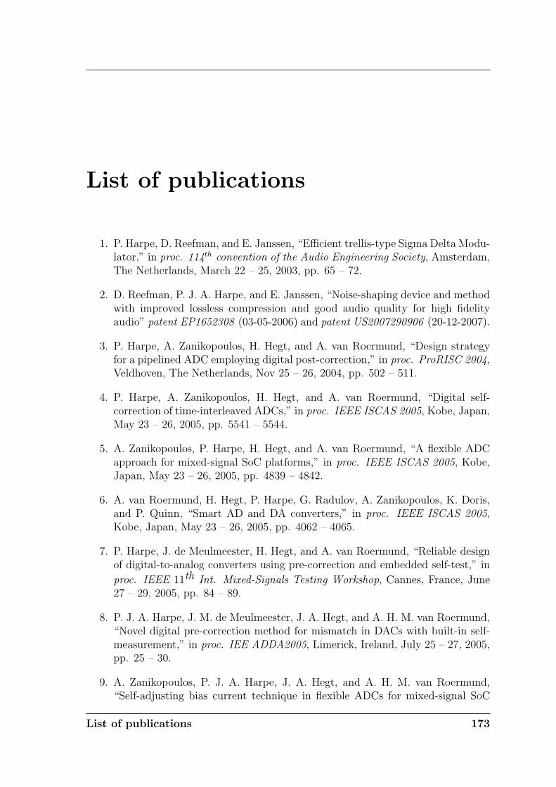
List of publications
1. P. Harpe, D. Reefman, and E. Janssen, “Efficient trellis-type Sigma Delta Modu-lator,” in proc. 114th convention of the Audio Engineering Society, Amsterdam,The Netherlands, March 22 – 25, 2003, pp. 65 – 72.
2. D. Reefman, P. J. A. Harpe, and E. Janssen, “Noise-shaping device and methodwith improved lossless compression and good audio quality for high fidelityaudio” patent EP1652308 (03-05-2006) and patent US2007290906 (20-12-2007).
3. P. Harpe, A. Zanikopoulos, H. Hegt, and A. van Roermund, “Design strategyfor a pipelined ADC employing digital post-correction,” in proc. ProRISC 2004,Veldhoven, The Netherlands, Nov 25 – 26, 2004, pp. 502 – 511.
4. P. Harpe, A. Zanikopoulos, H. Hegt, and A. van Roermund, “Digital self-correction of time-interleaved ADCs,” in proc. IEEE ISCAS 2005, Kobe, Japan,May 23 – 26, 2005, pp. 5541 – 5544.
5. A. Zanikopoulos, P. Harpe, H. Hegt, and A. van Roermund, “A flexible ADCapproach for mixed-signal SoC platforms,” in proc. IEEE ISCAS 2005, Kobe,Japan, May 23 – 26, 2005, pp. 4839 – 4842.
6. A. van Roermund, H. Hegt, P. Harpe, G. Radulov, A. Zanikopoulos, K. Doris,and P. Quinn, “Smart AD and DA converters,” in proc. IEEE ISCAS 2005,Kobe, Japan, May 23 – 26, 2005, pp. 4062 – 4065.
7. P. Harpe, J. de Meulmeester, H. Hegt, and A. van Roermund, “Reliable designof digital-to-analog converters using pre-correction and embedded self-test,” in
proc. IEEE 11th Int. Mixed-Signals Testing Workshop, Cannes, France, June27 – 29, 2005, pp. 84 – 89.
8. P. J. A. Harpe, J. M. de Meulmeester, J. A. Hegt, and A. H. M. van Roermund,“Novel digital pre-correction method for mismatch in DACs with built-in self-measurement,” in proc. IEE ADDA2005, Limerick, Ireland, July 25 – 27, 2005,pp. 25 – 30.
9. A. Zanikopoulos, P. J. A. Harpe, J. A. Hegt, and A. H. M. van Roermund,“Self-adjusting bias current technique in flexible ADCs for mixed-signal SoC
List of publications 173
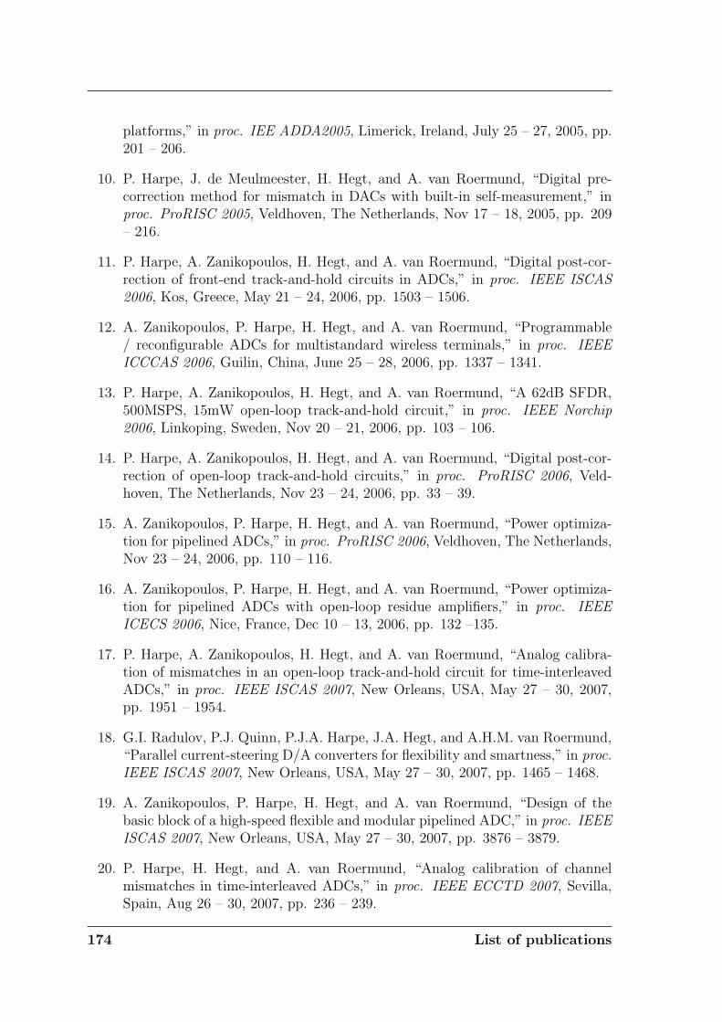
platforms,” in proc. IEE ADDA2005, Limerick, Ireland, July 25 – 27, 2005, pp.201 – 206.
10. P. Harpe, J. de Meulmeester, H. Hegt, and A. van Roermund, “Digital pre-correction method for mismatch in DACs with built-in self-measurement,” inproc. ProRISC 2005, Veldhoven, The Netherlands, Nov 17 – 18, 2005, pp. 209– 216.
11. P. Harpe, A. Zanikopoulos, H. Hegt, and A. van Roermund, “Digital post-cor-rection of front-end track-and-hold circuits in ADCs,” in proc. IEEE ISCAS2006, Kos, Greece, May 21 – 24, 2006, pp. 1503 – 1506.
12. A. Zanikopoulos, P. Harpe, H. Hegt, and A. van Roermund, “Programmable/ reconfigurable ADCs for multistandard wireless terminals,” in proc. IEEEICCCAS 2006, Guilin, China, June 25 – 28, 2006, pp. 1337 – 1341.
13. P. Harpe, A. Zanikopoulos, H. Hegt, and A. van Roermund, “A 62dB SFDR,500MSPS, 15mW open-loop track-and-hold circuit,” in proc. IEEE Norchip2006, Linkoping, Sweden, Nov 20 – 21, 2006, pp. 103 – 106.
14. P. Harpe, A. Zanikopoulos, H. Hegt, and A. van Roermund, “Digital post-cor-rection of open-loop track-and-hold circuits,” in proc. ProRISC 2006, Veld-hoven, The Netherlands, Nov 23 – 24, 2006, pp. 33 – 39.
15. A. Zanikopoulos, P. Harpe, H. Hegt, and A. van Roermund, “Power optimiza-tion for pipelined ADCs,” in proc. ProRISC 2006, Veldhoven, The Netherlands,Nov 23 – 24, 2006, pp. 110 – 116.
16. A. Zanikopoulos, P. Harpe, H. Hegt, and A. van Roermund, “Power optimiza-tion for pipelined ADCs with open-loop residue amplifiers,” in proc. IEEEICECS 2006, Nice, France, Dec 10 – 13, 2006, pp. 132 –135.
17. P. Harpe, A. Zanikopoulos, H. Hegt, and A. van Roermund, “Analog calibra-tion of mismatches in an open-loop track-and-hold circuit for time-interleavedADCs,” in proc. IEEE ISCAS 2007, New Orleans, USA, May 27 – 30, 2007,pp. 1951 – 1954.
18. G.I. Radulov, P.J. Quinn, P.J.A. Harpe, J.A. Hegt, and A.H.M. van Roermund,“Parallel current-steering D/A converters for flexibility and smartness,” in proc.IEEE ISCAS 2007, New Orleans, USA, May 27 – 30, 2007, pp. 1465 – 1468.
19. A. Zanikopoulos, P. Harpe, H. Hegt, and A. van Roermund, “Design of thebasic block of a high-speed flexible and modular pipelined ADC,” in proc. IEEEISCAS 2007, New Orleans, USA, May 27 – 30, 2007, pp. 3876 – 3879.
20. P. Harpe, H. Hegt, and A. van Roermund, “Analog calibration of channelmismatches in time-interleaved ADCs,” in proc. IEEE ECCTD 2007, Sevilla,Spain, Aug 26 – 30, 2007, pp. 236 – 239.
174 List of publications
21. P. Harpe, A. Zanikopoulos, H. Hegt, and A. van Roermund, “Analog calibrationof an open-loop track-and-hold circuit,” in proc. ProRISC 2007, Veldhoven, TheNetherlands, Nov 29 – 30, 2007.
22. G.I. Radulov, P.J. Quinn, P. Harpe, H. Hegt, and A. van Roermund, “Par-allel current-steering D/A Converters for flexibility and smartness,” in proc.ProRISC 2007, Veldhoven, The Netherlands, Nov 29 – 30, 2007.
23. P. Harpe, H. Hegt, and A. van Roermund, “Analysis of open-loop track-and-hold circuits,” in proc. IEEE ICECS 2007, Marrakech, Morocco, Dec 11 – 14,2007, pp. 1236 – 1239.
24. W. Deng, R. Mahmoudi, P. Harpe, and A. van Roermund, “An alternativedesign flow for receiver performance optimization through a trade-off betweenRF and ADC,” in proc. IEEE RWS 2008, Orlando, USA, Jan 22 – 24, 2008,pp. 699 – 702.
25. W. Deng, R. Mahmoudi, P. Harpe, and A. van Roermund, “A new design flowfor receiver performance optimization,” in proc. ProRISC 2008, Veldhoven, TheNetherlands, Nov 27 – 28, 2008, pp. 171 – 174.
26. P. Harpe, H. Hegt, and A. van Roermund, “Analog calibration of channel mis-matches in time-interleaved ADCs,” (invited paper), in International Journalof Circuit Theory and Applications, vol. 37, no. 2, pp. 301 – 318, March 2009.Published online on August 11, 2008.
27. P. Harpe, H. Hegt, and A. van Roermund, “A 14mW 500MSPS 59dB SFDROpen-Loop Track-and-Hold Circuit,” in proc. ProRISC 2009, Veldhoven, TheNetherlands, Nov 26 – 27, 2009.
28. P. Harpe, C. Zhou, X. Wang, G. Dolmans, and H. de Groot, “A 30fJ/Conver-sion-Step 8b 0-to-10MS/s Asynchronous SAR ADC in 90nm CMOS,” in proc.IEEE ISSCC2010, San Francisco, USA, Feb 7 – 11, 2010.
List of publications 175

SummaryConcepts for Smart AD and DAConverters
This thesis studies the ‘smart’ concept for application to analog-to-digital and digital-to-analog converters. The smart concept aims at improving performance - in a widesense - of AD/DA converters by adding on-chip intelligence to extract imperfectionsand to correct for them. As the smart concept can correct for certain imperfections,it can also enable the use of more efficient architectures, thus yielding an additionalperformance boost.
Chapter 2 studies trends and expectations in converter design with respect to ap-plications, circuit design and technology evolution. Problems and opportunities areidentified, and an overview of performance criteria is given.
Chapter 3 introduces the smart concept that takes advantage of the expected oppor-tunities (described in chapter 2) in order to solve the anticipated problems.
Chapter 4 applies the smart concept to digital-to-analog converters. In the discussedexample, the concept is applied to reduce the area of the analog core of a current-steering DAC. It is shown that a sub-binary variable-radix approach reduces the areaof the current-source elements substantially (10x compared to state-of-the-art), whilemaintaining accuracy by a self-measurement and digital pre-correction scheme.
Chapter 5 describes the chip implementation of the sub-binary variable-radix DACand discusses the experimental results. The results confirm that the sub-binaryvariable-radix design can achieve the smallest published current-source-array areafor the given accuracy (12bit).
Chapter 6 applies the smart concept to analog-to-digital converters, with as main goalthe improvement of the overall performance in terms of a widely used figure-of-merit.Open-loop circuitry and time interleaving are shown to be key to achieve high-speedlow-power solutions. It is suggested to apply a smart approach to reduce the effectof the imperfections, unintentionally caused by these key factors. On high-level, aglobal picture of the smart solution is proposed that can solve the problems whilestill maintaining power-efficiency.
Summary 177
Chapter 7 deals with the design of a 500MSps open-loop track-and-hold circuit. Thiscircuit is used as a test case to demonstrate the proposed smart approaches. Experi-mental results are presented and compared against prior art. Though there are severallimitations in the design and the measurement setup, the measured performance iscomparable to existing state-of-the-art.
Chapter 8 introduces the first calibration method that counteracts the accuracy is-sues of the open-loop track-and-hold. A description of the method is given, and theimplementation of the detection algorithm and correction circuitry is discussed. Thechapter concludes with experimental measurement results.
Chapter 9 introduces the second calibration method that targets the accuracy is-sues of time-interleaved circuits, in this case a 2-channel version of the implementedtrack-and-hold. The detection method, processing algorithm and correction circuitryare analyzed and their implementation is explained. Experimental results verify theusefulness of the method.
178 Summary
Samenvatting
Dit proefschrift bestudeert het smart-concept voor toepassing in analoog-digitaal-en digitaal-analoogomzetters. Het smart-concept heeft als doel het verbeteren vande prestaties - in brede zin - van AD/DA-omzetters door op de chip intelligentietoe te voegen om fouten te extraheren en te corrigeren. Omdat het smart-conceptbepaalde fouten kan corrigeren wordt het ook mogelijk om efficientere architecturente gebruiken, waardoor de prestaties nog verder verbeterd kunnen worden.
Hoofdstuk 2 bestudeert trends en verwachtingen in ADC/DAC-ontwerp, waarbij toe-passingen, circuitontwerp en technologie-evolutie in beschouwing worden genomen.Problemen en mogelijkheden worden geıdentificeerd, en een overzicht van prestatiecri-teria wordt gegeven.
Hoofdstuk 3 introduceert het smart-concept, dat de mogelijkheden (beschreven inhoofdstuk 2) benut om de voorziene problemen op te lossen.
Hoofdstuk 4 past het smart-concept toe op digitaal-analoogomzetters. In het gekozenvoorbeeld wordt het concept toegepast om de oppervlakte van de analoge kern vaneen stroomgestuurde DAC te minimaliseren. Het blijkt dat de voorgestelde sub-binaryvariable-radix -aanpak de oppervlakte van deze kern substantieel (10x t.o.v. state-of-the-art) kan verkleinen, terwijl de nauwkeurigheid behouden blijft dankzij zelfmetingen digitale foutcorrectie.
Hoofdstuk 5 beschrijft de chipimplementatie van de sub-binary variable-radix DACen bespreekt de experimentele resultaten. De resultaten tonen aan dat het gekozenontwerp de kleinst gepubliceerde oppervlakte behaalt van de stroombronnen voor degegeven nauwkeurigheid (12bit).
Hoofdstuk 6 past het smart-concept toe op analoog-digitaalomzetters, met als belang-rijkste doel de verbetering van de algehele prestatie, uitgedrukt in een algemeen ge-bruikte prestatiemaat. Aangetoond wordt dat open-loop-circuits en time-interleavingvan primair belang kunnen zijn om een snelle, vermogensefficiente oplossing te be-halen. Een smart-aanpak wordt voorgesteld om de effecten van de tekortkomingente verminderen, die onbedoeld veroorzaakt worden door deze factoren. Op globaalniveau wordt deze smart-aanpak, die de problemen kan oplossen zonder de vermo-gensefficientie aan te tasten, uitgewerkt.
Samenvatting 179

Hoofdstuk 7 behandelt het ontwerp van een 500MSps open-loop track-and-hold -circuit.Dit wordt als een testcircuit gebruikt om de voorgestelde smart-oplossingen te demon-streren. Experimentele resultaten worden gepresenteerd en vergeleken met bestaandwerk. Hoewel er verschillende beperkingen in het ontwerp en de meetopstelling zijn,is de gemeten prestatie gelijkwaardig aan bestaand werk van topniveau.
Hoofdstuk 8 introduceert de eerste calibratiemethode die de nauwkeurigheidsproble-men van de open-loop track-and-hold tegengaat. Een omschrijving van de methodewordt gegeven en de implementaties van het detectie-algoritme en het correctiecircuitworden besproken. Het hoofdstuk sluit af met experimentele resultaten.
Hoofdstuk 9 introduceert de tweede calibratiemethode, bedoeld om nauwkeurigheids-problemen van time-interleaved -circuits op te lossen, in dit geval toegepast op degerealiseerde tweekanaals track-and-hold. De detectiemethode, het verwerkingsalgo-ritme en het correctiecircuit worden geanalyseerd en de implementatie wordt uitge-werkt. Experimentele resultaten bevestigen de bruikbaarheid van de methode.
180 Samenvatting
Word of thanks
Many persons contributed directly or indirectly to this thesis. Only with their sup-port, this work could be accomplished.
First of all, I’d like to thank my promotor, Arthur, for giving me the opportunityto do this work. Thank you for your enthusiasm, your dedication, your time, yourcomments and suggestions and the pleasant way of working together. I owe manythanks to my copromotor and daily supervisor, Hans: for always making time (evenwhen there was none) for discussions, reviews and support. For his interest and trustin my work, his exactness and his clarity. Thank you for your time, and for being avery pleasant supervisor to work with. Also, I’d like to thank all the members of thecommittee for their time and interest to review this work.
I’d like to thank STW for the funding of the project, and the members of the STWuser committee for their time and interest in our work. Especially, I’d like to thankPatrick (Xilinx) and Kostas (NXP) for their involvement in the project. Also, aspecial thanks to Xilinx for supporting and funding the tape-out and PCB.
Most of all, I’d like to thank all my colleagues and friends at the MsM-group andat the Holst Centre for helping me out in many ways. Your presence and friendshipis what made doing a PhD worthwhile. Thanks for all the technical discussions andeven more for the non-technical ones. Thanks for the enjoyable trips together, be itto Japan, Veldhoven or the local coffee machine. Thanks for the vlaai and the recipesfor lentil soup, dumplings, zong zı and many more. Thanks for exchanging photos,music and movies. Thanks for the fun and the crazy things. Thanks for exchanginglunch-boxes and accepting the risk to be poisoned by my cooking. Thanks for thealways open door, the shared sadness and the shared smiles. Thanks for alwaysshowing interest in my work, and thanks for not always asking about the progress ofit. Thanks for all the good things that still have to come. Thanks, for simply havinga great time together!
Several students participated in my work by doing an internship. Thank you Jacobus,Bert, Ruud, Joep, Raymon and Julia: for your contributions to my work and for thepleasant cooperation.
Last but not least, I want to thank my family and friends for their support, theirinterest and their presence.
Word of thanks 181


Biography
Pieter Harpe was born in 1980, in Middelburg, The Netherlands. In 2004, he receivedthe M.Sc. degree at the Faculty of Electrical Engineering at the Eindhoven Univer-sity of Technology, The Netherlands. The graduation project was on the design ofa high-speed, high-resolution calibrated pipelined ADC. In 2002, he did an intern-ship on trellis-type sigma-delta modulators for audio applications at Philips ResearchLaboratories, Eindhoven, The Netherlands.
In 2004, he started a PhD-student position at the Eindhoven University of Technologyon “Smart AD and DA Converters”.
Since 2008, he started a job as research scientist in the wireless-group at the HolstCentre (IMEC-NL), Eindhoven, The Netherlands. Since then, he has been workingon ultra low-power wireless transceivers for medical applications, with a main focuson ADC research and design.
Biography 183


![01-1981 [E-4701] Applied Concepts - Morphy Edition Master ... · 01-1981 [E-4701] Applied Concepts - Morphy Edition Master Chess (module) Begin 1981 verscheen het moduul Morphy Edition](https://static.fdocuments.nl/doc/165x107/5e7a7feadce0823c13394410/01-1981-e-4701-applied-concepts-morphy-edition-master-01-1981-e-4701-applied.jpg)