
1/f Noise in Permalloy - TU/e
151
1/f Noise in Permalloy Proefschrift ter verkrijging van de graad van doctor aan de Technische Universiteit Eindhoven, op gezag van de Rector Magnificus, prof.dr. M. Rem, voor een commissie aangewezen door het College voor Promoties in het openbaar te verdedigen op donderdag 5 oktober 2000 om 16.00 uur door Joseph Briaire geboren te Breda
Transcript of 1/f Noise in Permalloy - TU/e
1/f Noise in Permalloy
Proefschrift
ter verkrijging van de graad van doctor
aan de Technische Universiteit Eindhoven,
op gezag van de Rector Magnificus, prof.dr. M. Rem,
voor een commissie aangewezen door het College voor Promoties
in het openbaar te verdedigen op
donderdag 5 oktober 2000 om 16.00 uur
door
Joseph Briaire
geboren te Breda
Dit proefschrift is goedgekeurd door de promotoren:
prof.dr.ir. W.M.G. van Bokhoven
en
prof.dr. M.A.M. Gijs
Copromotor:
dr.ir. L.K.J. Vandamme
CIP-DATA LIBRARY TECHNISCHE UNIVERSITEIT EINDHOVEN
Briaire, Joseph
1/f Noise in Permalloy / by Joseph Briaire. - Eindhoven : TechnischeUniversiteit Eindhoven, 2000.Proefschrift. - ISBN 90-386-1770-4NUGI 812Trefw.: 1/f ruis / ferromagnetisme / magnetoweerstand.Subject headings: 1/f noise / ferromagnetism / magnetoresistance.

- iii -
Contents
Contents . . . . . . . . . . . . . . . . . . . . . . . . . . . . . . . . . . . . . . . . . . . . . . . . . . . . iii
1. Introduction . . . . . . . . . . . . . . . . . . . . . . . . . . . . . . . . . . . . . . . . . . . . . . . 11.1 Overview of thesis . . . . . . . . . . . . . . . . . . . . . . . . . . . . . . . . . . . . . . . 1
1.2 Interpretation of voltage fluctuations
as magnetization fluctuations . . . . . . . . . . . . . . . . . . . . . . . . . . . . . . 4
1.3 Ferromagnetism . . . . . . . . . . . . . . . . . . . . . . . . . . . . . . . . . . . . . . . . . 7
1.4 The anisotropic magneto-resistance effect . . . . . . . . . . . . . . . . . . . 14
1.5 The fluctuation-dissipation theorem for magnetization fluctuations 16
2. Uncertainty in Gaussian noisegeneralized for cross-correlation spectra. . . . . . . . . . . . . . . . . . . . . . . 212.1 Introduction. . . . . . . . . . . . . . . . . . . . . . . . . . . . . . . . . . . . . . . . . . . 21
2.2 The uncertainty of spectral noise with a Gaussian distribution . . . . 23
2.3 Experimental results using the cross-correlation analysis . . . . . . . . 28
2.4 Conclusions . . . . . . . . . . . . . . . . . . . . . . . . . . . . . . . . . . . . . . . . . . . 30
3. The influence of a digital spectrum analyzeron the uncertainty in 1/f noise parameters. . . . . . . . . . . . . . . . . . . . . 323.1 Introduction. . . . . . . . . . . . . . . . . . . . . . . . . . . . . . . . . . . . . . . . . . . 32
3.2 Parameter errors in a fitted spectrum. . . . . . . . . . . . . . . . . . . . . . . 33
3.3 Simulation of additional errors
due to A/D conversion and windowing. . . . . . . . . . . . . . . . . . . . . . 39
3.4 Conclusions . . . . . . . . . . . . . . . . . . . . . . . . . . . . . . . . . . . . . . . . . . . 44
- iv -
4. Automated system for noise measurementson low-Ohmic samples and magnetic sensors . . . . . . . . . . . . . . . . . . . 454.1 Introduction. . . . . . . . . . . . . . . . . . . . . . . . . . . . . . . . . . . . . . . . . . . 45
4.2 System specifications . . . . . . . . . . . . . . . . . . . . . . . . . . . . . . . . . . . 46
4.3 System design . . . . . . . . . . . . . . . . . . . . . . . . . . . . . . . . . . . . . . . . . 49
4.4 Comparison of low-noise amplifiers . . . . . . . . . . . . . . . . . . . . . . . . 56
4.5 Conclusions . . . . . . . . . . . . . . . . . . . . . . . . . . . . . . . . . . . . . . . . . . . 58
5. Evidence for a new source of 1/f noisein single-domain Ni Fe films . . . . . . . . . . . . . . . . . . . . . . . . . . . . . . . 6080 20
5.1 Introduction. . . . . . . . . . . . . . . . . . . . . . . . . . . . . . . . . . . . . . . . . . . 60
5.2 Measurement setup and sample preparation . . . . . . . . . . . . . . . . . . 61
5.3 Measurements as a function of magnetic field . . . . . . . . . . . . . . . . 65
5.4 Interpretation of results . . . . . . . . . . . . . . . . . . . . . . . . . . . . . . . . . . 69
5.5 Temperature dependence . . . . . . . . . . . . . . . . . . . . . . . . . . . . . . . . . 71
5.6 Conclusions . . . . . . . . . . . . . . . . . . . . . . . . . . . . . . . . . . . . . . . . . . . 74
6. 1/f Noise in multi-domain Ni Fe films . . . . . . . . . . . . . . . . . . . . . . . . 7580 20
6.1 Introduction. . . . . . . . . . . . . . . . . . . . . . . . . . . . . . . . . . . . . . . . . . . 75
6.2 Single-layered multi-domain films. . . . . . . . . . . . . . . . . . . . . . . . . 77
6.3 Multi-layered multi-domain films. . . . . . . . . . . . . . . . . . . . . . . . . . 80
6.4 Conclusions . . . . . . . . . . . . . . . . . . . . . . . . . . . . . . . . . . . . . . . . . . . 82
7. Principles of substrate crosstalk generation in CMOS circuits . . . . . 837.1 Introduction. . . . . . . . . . . . . . . . . . . . . . . . . . . . . . . . . . . . . . . . . . . 83
7.2 Injection mechanisms . . . . . . . . . . . . . . . . . . . . . . . . . . . . . . . . . . . 85
7.3 Substrate fluctuations in a circuit . . . . . . . . . . . . . . . . . . . . . . . . . . 95
7.4 Substrate voltages due to a large circuit . . . . . . . . . . . . . . . . . . . . 103
7.5 Conclusions . . . . . . . . . . . . . . . . . . . . . . . . . . . . . . . . . . . . . . . . . . 106
- v -
AppendixA1 Definitions in the frequency domain . . . . . . . . . . . . . . . . . . . . . . . 107
A2 The potential energy of a stationary magnetic system . . . . . . . . . 109
A3 A causal system: the Kramers-Kronig dispersion relations . . . . . 111
A4 The variance in 3 . . . . . . . . . . . . . . . . . . . . . . . . . . . . . . . . . . . . . 1132
A5 Copy of the original publication:
"Uncertainty in Gaussian noise generalized for
cross-correlation spectra" . . . . . . . . . . . . . . . . . . . . . . . . . . . . . . . 116
A6 Copy of the original publication:
"Automated system for noise measurements
on low-Ohmic samples and magnetic sensors" . . . . . . . . . . . . . . 122
Summary and Conclusions . . . . . . . . . . . . . . . . . . . . . . . . . . . . . . . . . . . 129
Samenvatting en Conclusies . . . . . . . . . . . . . . . . . . . . . . . . . . . . . . . . . . 132
References. . . . . . . . . . . . . . . . . . . . . . . . . . . . . . . . . . . . . . . . . . . . . . . . . 136
Bibliography of author . . . . . . . . . . . . . . . . . . . . . . . . . . . . . . . . . . . . . . 143
Curriculum vitae . . . . . . . . . . . . . . . . . . . . . . . . . . . . . . . . . . . . . . . . . . . 145
Acknowledgments . . . . . . . . . . . . . . . . . . . . . . . . . . . . . . . . . . . . . . . . . . 146
&KDSWHU,QWURGXFWLRQ
- 1 -
1. Introduction
1.1 Overview of thesisWith the increasing need for magnetic storage of information as a driving force,
every aspect of this storage and retrieval has seen substantial improvements
during recent decades. For instance, the dramatic increases in magnetic data
density makes it impossible to use a conventional pickup coil to sensor the
information.
The replacement was found in anisotropic magneto-resistive (AMR) materials
[1], with Permalloy (Ni Fe ) as a good example. The interesting aspect of these80 20
ferromagnetic materials is that their electric resistance depends on the orientation
of the internal magnetization. Hence, if the orientation is influenced by an
external magnetic field, the resistance changes: the AMR effect can be used as a
sensor. The advantage of AMR sensors is that they can be very small. However,
the disadvantage is that the maximum resistance change of thin film AMR
sensors typically is 2-3% at room temperature.
Another breakthrough came with the discovery of the giant magneto-resistive
(GMR) effect [2]. As the name already suggests, this magneto-resistive effect is
significantly larger than the AMR effect. Compared to AMR, the effect is
approximately ten times larger at room temperature. Although the reason for this
resistance change is completely different, the general idea is equal to the AMR
effect: an external magnetic field influences the internal magnetization and this
leads to a change in the electric resistance of the material.
This breakthrough triggered a widespread effort to optimize the GMR effect.
Essentially a GMR sensor consists of alternating ferromagnetic and nonmagnetic
layers and each individual layer only is a few atoms thick. A significant portion
of the work concentrated on finding the optimal ferromagnetic and nonmagnetic
materials, their thicknesses, etc.

&KDSWHU,QWURGXFWLRQ
- 2 -
An aspect that was also investigated was the resistance noise of GMR sensors.
One investigation [3] revealed that, if the resistance change can be called giant,
the change in 1/f noise power should be called fantastic. Obviously this result
deteriorates the all-important signal-to-noise ratio of GMR sensors and can
seriously limit the practical usage of such sensors.
This result triggered an investigation into the 1/f noise aspects of GMR sensors at
Philips Research. However, because a GMR sensor consists of individual
ferromagnetic layers, the AMR effect is also present. And because the noise
aspects of AMR sensors were also not well understood, these were included in
the investigation.
Primarily the results of the AMR sensors can be found in this thesis. But because
the AMR effect itself is only used to sensor the magnetization noise we will not
discuss the magneto-resistance effects in detail.
We focused our attention on Permalloy for a two reasons. First, Permalloy has
received a significant amount of attention in the past. Hence, several important
aspects of this alloy are well understood and can facilitate the research in the 1/f
noise of this alloy. And secondly, Permalloy is a very soft ferromagnet: it does
not require large external fields to rotate the internal magnetization. As a result, it
is a sensitive sensor that does not require strong, yet noise free external fields to
investigate it. And this eases the measurement setup requirements.
In this first chapter some basic concepts will be introduced to familiarize the
reader with the essentials of the rest of the thesis. First, the basics of noise
measurements will be introduced. Afterwards, a (historical) overview of the
different theories for ferromagnetism are given and these are followed by the
essentials of the AMR effect. Finally, the fluctuation-dissipation theorem will be
introduced. This theorem explains thermal noise in a general sense. In the
previously mentioned article in which 1/f noise of a GMR sensor [3] was studied,
it was shown that the measured 1/f noise can be explained with this theorem.
&KDSWHU,QWURGXFWLRQ
- 3 -
However, this is not true for Permalloy and this will be shown in this thesis.
Before this will be shown, the statistical aspects of the measured 1/f noise will be
investigated. The reason for this is that the noise does not have to be true noise:
there can be some information left in this signal from the original deterministic
sources. Essentially, every event that takes place inside a material can lead to a
measurable signal. If many similar yet independent events take place at the same
time, the central limit theorem applies. Hence, one is left with Gaussian noise.
But this situation does not always apply! For instance, if the measured signal is
dominated by a few local effects that originate from impurities in the material,
edges or electric contacts, the signal might be non-Gaussian. Hence, if the
measured noise signal is non-Gaussian, this is a strong indicator that the noise
does not originate from many independent sources: probably it is not a bulk
effect.
In chapter two, the statistics for Gaussian noise will be developed for our
particular noise measurement technique: cross-correlation measurements. The
statistics of the measured noise can now be compared to this reference, to
investigate if the measured noise signal is true noise.
Chapter three focuses on the practical aspects of the uncertainty in Gaussian
noise. First the conversion of a noise spectrum into noise parameters will be
examined and as an example the uncertainty in the frequency index of 1/f noise
will be calculated under various conditions. Afterwards, the influence of the
digital spectrum analyzer that converts the noise signal into a noise spectrum will
be simulated. In particular the influence of the non-linearities on the noise
uncertainty will receive attention.
In chapter four, the focus will shift towards the noise measurement setup. The 1/f
noise is measured as a function of the current through the sample, the
temperature of the sample and external magnetic fields, both DC and AC. All
&KDSWHU,QWURGXFWLRQ
- 4 -
these aspects have been automated and are discussed in this chapter.
In chapter 5 the measurement results on single-domain Permalloy films will be
presented. As said before, we will show that the 1/f noise in Permalloy originates
from a new source and can not be explained with the fluctuation-dissipation
theorem. These conclusions can be drawn from a comparison of the 1/f noise
results with the small-signal dynamic response, both as a function of DC
magnetic fields. Furthermore, measurements as a function of temperature will
also be presented.
In the next chapter the results for multi-domain Permalloy are discussed. We will
present results both on single films (AMR) and multi-layer films (AMR+GMR)
in this chapter. However, because of the presence of the domain walls, no hard
conclusions can be made about the origin of the 1/f noise in these samples but it
seems very likely that the origin of the 1/f noise does not differ from the one in
single-domain films.
Finally, as an example of how individual events can lead to noise, in chapter 7
substrate crosstalk injection in CMOS circuits will be discussed. This injection
leads to switching noise in a substrate and is especially unwanted in the field of
mixed-signal design. The different types of substrate injection will be compared
in this section.
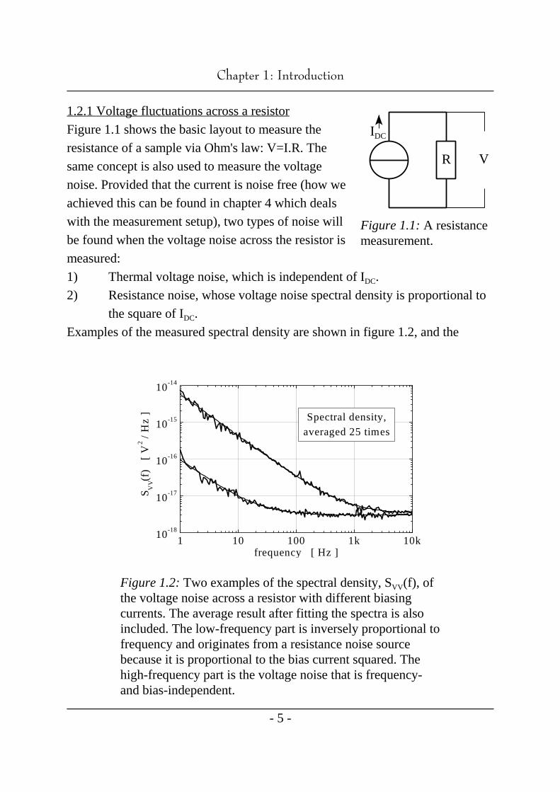
1.2 Interpretation of voltage fluctuations as magnetization fluctuationsThe main part of this thesis deals with magnetization fluctuations. These are not
measured as such, but as voltage fluctuations across a resistor. In this section we
will give an overview of this measurement concept.
IDC
R V
1 10 100 1k 10k10
-18
10-17
10-16
10-15
10-14
Spectral density,averaged 25 times
S VV(f
)
[ V
2 / H
z ]
frequency [ Hz ]
&KDSWHU,QWURGXFWLRQ
- 5 -
Figure 1.1: A resistancemeasurement.
Figure 1.2: Two examples of the spectral density, S (f), ofVV
the voltage noise across a resistor with different biasingcurrents. The average result after fitting the spectra is alsoincluded. The low-frequency part is inversely proportional tofrequency and originates from a resistance noise sourcebecause it is proportional to the bias current squared. Thehigh-frequency part is the voltage noise that is frequency-and bias-independent.
1.2.1 Voltage fluctuations across a resistor
Figure 1.1 shows the basic layout to measure the
resistance of a sample via Ohm's law: V=I.R. The
same concept is also used to measure the voltage
noise. Provided that the current is noise free (how we
achieved this can be found in chapter 4 which deals
with the measurement setup), two types of noise will
be found when the voltage noise across the resistor is
measured:
1) Thermal voltage noise, which is independent of I .DC
2) Resistance noise, whose voltage noise spectral density is proportional to
the square of I .DC
Examples of the measured spectral density are shown in figure 1.2, and the
SVV( f ) 4kBTR,
0.0 0.2 0.4 0.6 0.8 1.00
1
2
3
4
5
6
7
SV
V(1
Hz)
[
10 -
15
V 2 /
Hz
]
J2 [ ( MA / cm
2 )
2 ]
&KDSWHU,QWURGXFWLRQ
- 6 -
(1.1)
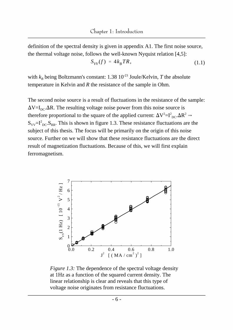
Figure 1.3: The dependence of the spectral voltage densityat 1Hz as a function of the squared current density. Thelinear relationship is clear and reveals that this type ofvoltage noise originates from resistance fluctuations.
definition of the spectral density is given in appendix A1. The first noise source,
the thermal voltage noise, follows the well-known Nyquist relation [4,5]:
with k being Boltzmann's constant: 1.38 10 Joule/Kelvin, T the absoluteB-23
temperature in Kelvin and R the resistance of the sample in Ohm.
The second noise source is a result of fluctuations in the resistance of the sample:
V=I .R. The resulting voltage noise power from this noise source isDC
therefore proportional to the square of the applied current: V =I .R <2 2 2DC
S =I .S . This is shown in figure 1.3. These resistance fluctuations are theVV DC RR2
subject of this thesis. The focus will be primarily on the origin of this noise
source. Further on we will show that these resistance fluctuations are the direct
result of magnetization fluctuations. Because of this, we will first explain
ferromagnetism.
&KDSWHU,QWURGXFWLRQ
- 7 -
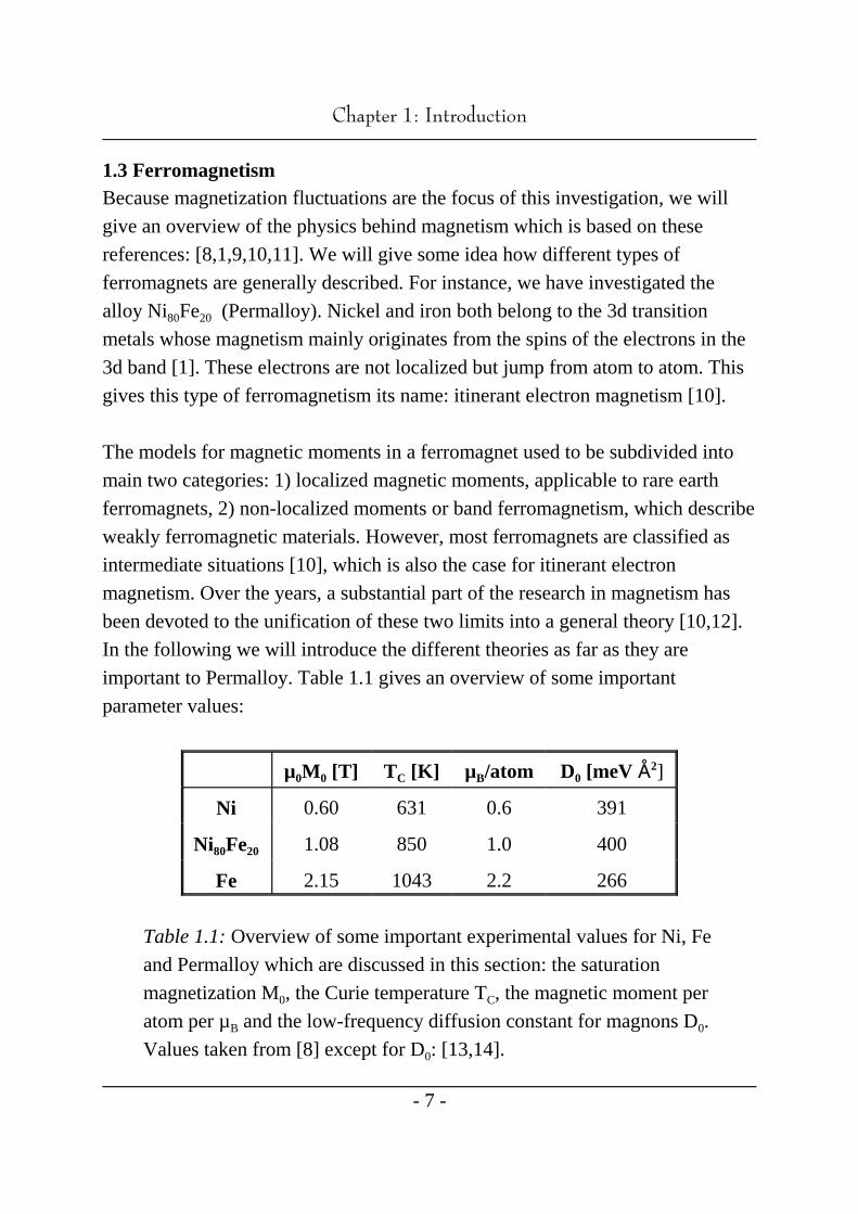
1.3 FerromagnetismBecause magnetization fluctuations are the focus of this investigation, we will
give an overview of the physics behind magnetism which is based on these
references: [8,1,9,10,11]. We will give some idea how different types of
ferromagnets are generally described. For instance, we have investigated the
alloy Ni Fe (Permalloy). Nickel and iron both belong to the 3d transition80 20
metals whose magnetism mainly originates from the spins of the electrons in the
3d band [1]. These electrons are not localized but jump from atom to atom. This
gives this type of ferromagnetism its name: itinerant electron magnetism [10].
The models for magnetic moments in a ferromagnet used to be subdivided into
main two categories: 1) localized magnetic moments, applicable to rare earth
ferromagnets, 2) non-localized moments or band ferromagnetism, which describe
weakly ferromagnetic materials. However, most ferromagnets are classified as
intermediate situations [10], which is also the case for itinerant electron
magnetism. Over the years, a substantial part of the research in magnetism has
been devoted to the unification of these two limits into a general theory [10,12].
In the following we will introduce the different theories as far as they are
important to Permalloy. Table 1.1 gives an overview of some important
parameter values:
µ M [T] T [K] µ /atom D [meV ' ]0 0 C B 02
Ni 0.60 631 0.6 391
Ni Fe80 20 1.08 850 1.0 400
Fe 2.15 1043 2.2 266
Table 1.1: Overview of some important experimental values for Ni, Fe
and Permalloy which are discussed in this section: the saturation
magnetization M , the Curie temperature T , the magnetic moment per0 C
atom per µ and the low-frequency diffusion constant for magnons D .B 0
Values taken from [8] except for D : [13,14].0

0.00 0.25 0.50 0.75 1.000.00
0.25
0.50
0.75
1.00
Brillouin
Langevin
MS /
M0
T / TC
&KDSWHU,QWURGXFWLRQ
- 8 -
Figure 1.4: Normalized magnetization curves of aferromagnet as a function of the normalized temperatureaccording to the modified Langevin and Brillouin theories(spin flips only).
1.3.1 Localized magnetic moments
Langevin assumed that a paramagnet consists of local magnetic moments or
spins whose spatial directions follow a Boltzmann probability density function:
exp(U/k T), with the potential energy U equal to µ .µ .H and with H anB 0 B EXT EXT
externally applied magnetic field [8,1]. For ferromagnets Weiss modified this
concept by adding an uniform internal magnetic field H to the external field.INT
Weiss assumed that this field is proportional to the magnetization: H =w.M ,INT S
with w the Weiss factor.
Brillouin modified the Langevin concept for paramagnets by taking into account
that a magnetic moment cannot rotate freely and that its expectation value is
spatially quantized within an atom. For instance, an electron spin has two
possible directions: parallel or anti-parallel to the local magnetic field. Therefore
it can only flip. Also this theorem was modified with a Weiss-field to explain
ferromagnetism as a function of temperature and external field. Examples of the
magnetization vs. temperature curves can be seen in figure 1.4. Although it is
generally accepted that the physics involved in the local magnetic moment
UEX 2JSi#S
j,
&KDSWHU,QWURGXFWLRQ
- 9 -
(1.2)
theories is not dominant in for instance Ni an Fe, the Brillouin curve is in
reasonable agreement with experimental results (see [1]) when both the
saturation magnetization, M , and the Curie temperature T are used as fitting0 C
parameters (experimental values are shown in table 1.1). This also means that the
Weiss factor, w, is a fitting parameter. The resulting Weiss-field, H , isINT
unrealistically large if explained with these classical theories.
Note that the decrease of the magnetization curve essentially is a result of noise.
As the temperature increases, the chance that a magnetic moment deviates from
perfect alignment increases. As a result the average magnetization decreases as
temperature increases. These type of statistical concepts are common in
magnetism. Hence, noise can be an important tool for studying magnetism.
The first physically plausible model for ferromagnetism was given by
Heisenberg. In this model H is replaced by an exchange interaction that resultsINT
from the close proximity between moments in combination with the Pauli
exclusion principle [1]. So, there only is a short-range interaction, for instance
only between nearest neighbors, but this leads to a long-range ordering. In the
Heisenberg model the exchange energy between two magnetic moments i and j is
equal to:
with J the exchange integral and S the angular momentum of the magnetic
moment. Strictly speaking J depends on the distance between the moments.
However, in most cases one only takes the nearest neighbors into account.
Therefore, J is treated as a constant (and zero for moments further away).
Heisenberg did not take spatial quantization of S into account in his model but
used an electron gas configuration. The Ising model is the one which also
assumed spatial quantization.
1.3.2 Spin waves and magnons [11]
The concept of spin waves has been developed by Bloch. The classic explanation
0S
0 t
4%JhP
S×Mi
Si,
hP f 2JSa20 k2
³ D0k2,
NDOS( f ) 1
8%3
hP
D0
3/2
f .
&KDSWHU,QWURGXFWLRQ
- 10 -
(1.3)
(1.4)
(1.5)
uses the Heisenberg model and combines it with the spatial freedom of the spins.
Bloch started with the following differential equation:
which states that the change of angular momentum is equal to the torque that
results from the interactions with the neighboring rotating spins. In the equation
we use S for the nearest neighbors and h is Plank's constant: 6.63 10 Js. Thisi P-34
relation leads to a correlated precession of spins in the plane perpendicular to the
average magnetization.
For small spin-wave amplitudes these equations can be linearized and lead in the
reciprocal lattice and frequency domain to a solution: the spin wave dispersion
relation. At low frequencies the dispersion relation can be simplified to:
for all three cubic lattices, with a the lattice constant, D the spin wave diffusion0 0
constant and k the reciprocal lattice vector. Measured values of the diffusion
constant are given in table 1.1.
Magnons, the quantized spin waves, follow the Bose-Einstein or more
specifically the Planck distribution. Based on the dispersion relation the three-
dimensional density of states (DOS) of magnon modes is equal to:
Note that the density of states of lattice vibration modes (phonons) is
proportional to f [11] and therefore differs from the magnon density of states,2
which is proportional to f. It is also straightforward to calculate the relation
between the magnetization and temperature based on magnon fluctuations.
Based on this, a change in magnetization proportional to T is expected for low3/2
2EH
EFEH
3P 2µ0µ2B NDOS(EF ) .
&KDSWHU,QWURGXFWLRQ
- 11 -
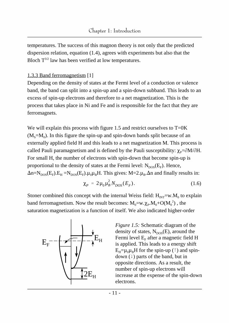
Figure 1.5: Schematic diagram of thedensity of states, N (E), around theDOS
Fermi level E after a magnetic field HF
is applied. This leads to a energy shiftE =µ µ H for the spin-up () and spin-H 0 B
down () parts of the band, but inopposite directions. As a result, thenumber of spin-up electrons willincrease at the expense of the spin-downelectrons.
(1.6)
temperatures. The success of this magnon theory is not only that the predicted
dispersion relation, equation (1.4), agrees with experiments but also that the
Bloch T law has been verified at low temperatures.3/2
1.3.3 Band ferromagnetism [1]
Depending on the density of states at the Fermi level of a conduction or valence
band, the band can split into a spin-up and a spin-down subband. This leads to an
excess of spin-up electrons and therefore to a net magnetization. This is the
process that takes place in Ni and Fe and is responsible for the fact that they are
ferromagnets.
We will explain this process with figure 1.5 and restrict ourselves to T=0K
(M =M ). In this figure the spin-up and spin-down bands split because of anS 0
externally applied field H and this leads to a net magnetization M. This process is
called Pauli paramagnetism and is defined by the Pauli susceptibility: 3 =0M/0H.P
For small H, the number of electrons with spin-down that become spin-up is
proportional to the density of states at the Fermi level: N (E ). Hence,DOS F
n=N (E ).E =N (E ).µ µ H. This gives: M=2.µ .n and finally results in:DOS F H DOS F 0 B B
Stoner combined this concept with the internal Weiss field: H =w.M to explainINT 0
band ferromagnetism. Now the result becomes: M =w.3 .M +O(M ) , the0 P 0 02
saturation magnetization is a function of itself. We also indicated higher-order
w.3P > 1
Electron wave number
E0
EF
k0Excitation wave vector of spin
k0
E0
Stoner excitations
Magnons
(b)(a)
&KDSWHU,QWURGXFWLRQ
- 12 -
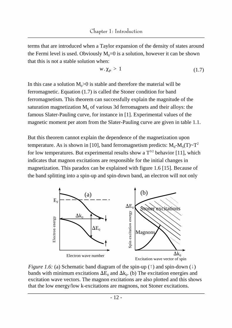
(1.7)
Figure 1.6: (a) Schematic band diagram of the spin-up () and spin-down ()bands with minimum excitations E and k . (b) The excitation energies and0 0
excitation wave vectors. The magnon excitations are also plotted and this showsthat the low energy/low k-excitations are magnons, not Stoner excitations.
terms that are introduced when a Taylor expansion of the density of states around
the Fermi level is used. Obviously M =0 is a solution, however it can be shown0
that this is not a stable solution when:
In this case a solution M >0 is stable and therefore the material will be0
ferromagnetic. Equation (1.7) is called the Stoner condition for band
ferromagnetism. This theorem can successfully explain the magnitude of the
saturation magnetization M of various 3d ferromagnets and their alloys: the0
famous Slater-Pauling curve, for instance in [1]. Experimental values of the
magnetic moment per atom from the Slater-Pauling curve are given in table 1.1.
But this theorem cannot explain the dependence of the magnetization upon
temperature. As is shown in [10], band ferromagnetism predicts: M -M (T)~T0 S2
for low temperatures. But experimental results show a T behavior [11], which3/2
indicates that magnon excitations are responsible for the initial changes in
magnetization. This paradox can be explained with figure 1.6 [15]. Because of
the band splitting into a spin-up and spin-down band, an electron will not only
&KDSWHU,QWURGXFWLRQ
- 13 -
require a spin flip but also a certain impulse and/or energy for a transition from
one band to the other. In the low-temperature regime such transfers will be rare.
But magnon excitations within a band are also present and require less energy
and no spin flip; hence they will dominate in the low-temperature regime. For
our investigation a different version of this concept is important: ferromagnetic
excitations in the low-frequency and long-range regime will be magnon
excitations, regardless of temperature!
1.3.4 Advanced theories
Stoner excitations are based on the uniform Weiss field and therefore on
excitations in reciprocal space with k=0. Attempts to generalize these spin
fluctuations in reciprocal space seem obvious and are discussed in [10].
Generalized theories essentially have the Stoner theory and local-moment
theories (such as the Heisenberg model) as their limiting cases.
The Stoner theory starts with a non-magnetic bandstructure. It is therefore no
surprise that this theory can be best applied to materials for which the Stoner
condition, equation (1.7), is barely satisfied (w.3 1): the weakly ferromagneticP
materials. More advanced theories take the deformation of the bands due to band
splitting into account in an attempt to get better agreement with experimental
observations. However, since such theories are well beyond the scope of this
introduction, we will not explain them in more detail.
Q
JDC MS
E//M
'//M']M
E]M
R(Q ) R0 Rcos2Q ,
&KDSWHU,QWURGXFWLRQ
- 14 -
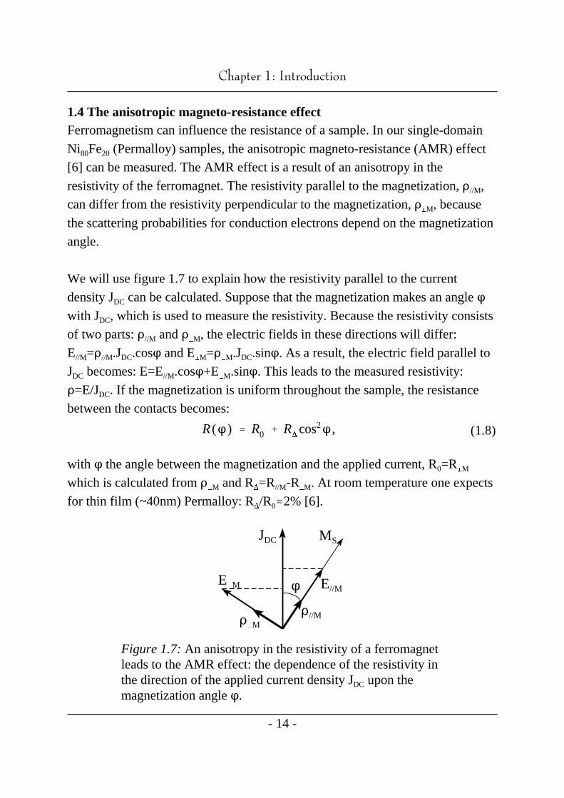
Figure 1.7: An anisotropy in the resistivity of a ferromagnetleads to the AMR effect: the dependence of the resistivity inthe direction of the applied current density J upon theDC
magnetization angle Q.
(1.8)
1.4 The anisotropic magneto-resistance effectFerromagnetism can influence the resistance of a sample. In our single-domain
Ni Fe (Permalloy) samples, the anisotropic magneto-resistance (AMR) effect80 20
[6] can be measured. The AMR effect is a result of an anisotropy in the
resistivity of the ferromagnet. The resistivity parallel to the magnetization, ' ,//M
can differ from the resistivity perpendicular to the magnetization, ' , because]M
the scattering probabilities for conduction electrons depend on the magnetization
angle.
We will use figure 1.7 to explain how the resistivity parallel to the current
density J can be calculated. Suppose that the magnetization makes an angle QDC
with J , which is used to measure the resistivity. Because the resistivity consistsDC
of two parts: ' and ' , the electric fields in these directions will differ://M ]M
E =' .J .cosQ and E =' .J .sinQ. As a result, the electric field parallel to//M //M DC ]M ]M DC
J becomes: E=E .cosQ+E .sinQ. This leads to the measured resistivity:DC //M ]M
'=E/J . If the magnetization is uniform throughout the sample, the resistanceDC
between the contacts becomes:
with Q the angle between the magnetization and the applied current, R =R0 ]M
which is calculated from ' and R =R -R . At room temperature one expects]M //M ]M
for thin film (~40nm) Permalloy: R /R2% [6]. 0

SRR( f ) 0R(Q )0Q
2
SQQ
( f ) .
&KDSWHU,QWURGXFWLRQ
- 15 -
(1.9)
There are fluctuations in the magnetization angle Q which we will call angular
noise with a spectral density S (f). With equation (1.8) the fluctuations in theQQ
resistance due to these angular fluctuations can be calculated. For small angular
fluctuations, and when 0R/0Q differs from zero (not at Q=0 , 90 etc.), theo o
dependence of R on Q is in good approximation linear. In this case the spectral
resistance noise due to angular noise is:
S (f) is the main noise source of interest in this thesis. However, apart from theQQ
contribution S (f) we also observed a resistance noise with a 1/f spectrum thatQQ
was independent of the magnetization angle. Hence equation (1.9) should be
extended with an additional noise source. This noise source is very small
compared to the angular noise source: less then a factor of 0.01 for large angular
fluctuations. Therefore we will not further investigate this background resistance
noise.
3(f)H(f) M(f)
3( f ) M( f )H ( f )
.
02U (H ,M ,f )
0M 2
µ0Vol
3 ( f ),
&KDSWHU,QWURGXFWLRQ
- 16 -
Figure 1.8: 3(f) is the transfer function of a real, linearand causal system with input H(f) and output M(f).
(1.10)
(1.11)
1.5 The fluctuation-dissipation theorem for magnetization fluctuationsThe fluctuation-dissipation theorem (FDT) [5,16,17] gives a general treatment of
thermal fluctuations in equilibrium. The Nyquist theorem, equation (1.1), is a
specific example of this theorem. Here we will explain the theorem for
magnetization fluctuations in the classic regime only: room temperature, low
frequencies and large volumes. At the end of this paragraph we will indicate the
limitations of these results and for a more advanced treatment we refer to for
instance [17].
With the fluctuation-dissipation theorem, the thermal noise in an output variable
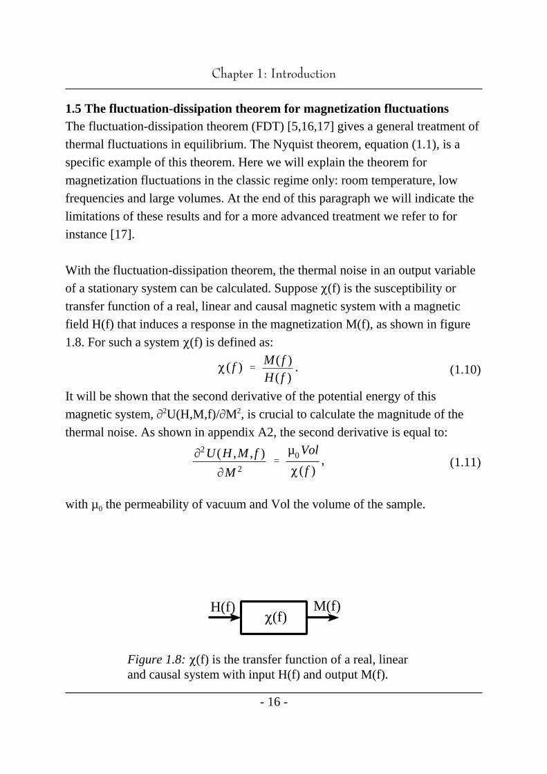
of a stationary system can be calculated. Suppose 3(f) is the susceptibility or
transfer function of a real, linear and causal magnetic system with a magnetic
field H(f) that induces a response in the magnetization M(f), as shown in figure
1.8. For such a system 3(f) is defined as:
It will be shown that the second derivative of the potential energy of this
magnetic system, 0 U(H,M,f)/0M , is crucial to calculate the magnitude of the2 2
thermal noise. As shown in appendix A2, the second derivative is equal to:
with µ the permeability of vacuum and Vol the volume of the sample.0

u 1/Znorm P
u(h0,m) exp
u(h0,m)
kBTdm,
u(h0,m) m2
2
02u(h0,m)
0m2mm0
,
m2 1/Znorm P
m2 exp m2
2kBT
02u(h0,m)
0m2mm0
dm
kBT 0
2u(h0,m)
0m2mm0
1
.
m2 kBT
3(0)µ0Vol
.
&KDSWHU,QWURGXFWLRQ
- 17 -
(1.12)
(1.13)
(1.14)
(1.15)
1.5.1 Magnetization fluctuations around equilibrium
Following classical statistical mechanics, the ensemble average of the
fluctuations in the potential energy of a stationary system, as given in figure 1.8,
can be calculated with a Boltzmann probability density function [18]. As an
example, the ensemble average of the stationary potential energy is calculated in
the time domain, with a constant excitation h and average response m :0 0
with Z a normalization factor to make the total probability equal to one. Thenorm
Taylor expansion for u around m will now be used. With 0u/0m=0 and0
neglecting all terms higher than the second order, one is left with:
In this situation the average fluctuation in the in potential energy is ½k T, whichB
is to be expected. The same principle can be used to calculate the average
variance in the magnetization:
Because the system is stationary we only investigate the DC component. The
stationary second derivative is therefore equal to the DC component in the
frequency domain. Combined with equation (1.11), the result becomes:
This is the ensemble average of the variance of the magnetization. The variance

P
0
SMM( f ) df kBT3 (0)µ0Vol
.
P
0
SMM( f ) df 4kBT
µ0Vol P
0
Im 3( f )2% f
df.
M(f)H(f) MBF(f)3(f)
SMM ( f )
4kBT
µ0VolIm 3( f )
2% f.
&KDSWHU,QWURGXFWLRQ
- 18 -
(1.16)
(1.17)
Figure 1.9: As a thought experiment, a causalband filter is added behind the susceptibility 3(f).
(1.18)
is equal to the integrated noise spectrum [4] and can, therefore, be rewritten as a
relation in the frequency domain:
In appendix A3, the Kramers-Kronig dispersion relations are used to rewrite a
general causal transfer function G(0). This also applies to the susceptibility 3(0),
the relation can therefore be rewritten as:
The equality does not only apply to the integrated relations in the frequency
domain, it also applies to the relations itself. This can be explained with figure
1.9, in which a narrow band-filter with a frequency band f around a frequency f 0
has been added behind the original susceptibility 3(f). The only purpose of this
filter is that the band filtered (BF) output, M (t), only contains the frequenciesBF
of M(f) around f . For this new system, 3(f)+band filter, a relation almost like0
equation (1.17) applies. The only difference will be that the integrands will
basically be zero for fÄf . As f is reduced, equation (1.17) will increasingly rely0
on the integrands at f=f and this is only possible if the integrands are equal at f0 0
and therefore at every frequency. Hence, the original output noise spectrum,
S (f), is equal to:MM
hP f
2coth
hP f
2kBT,
&KDSWHU,QWURGXFWLRQ
- 19 -
(1.19)
These are the thermal magnetization fluctuations that result from the fluctuation-
dissipation theorem. Note that when the imaginary part of the susceptibility is
frequency independent in a limited frequency range, the magnetization noise
spectrum will be inversely proportional to frequency in that range. Hence, this
leads to a 1/f magnetization noise from a thermal origin. Experimentally, this
type of 1/f noise is frequently found, e.g. [3,7], and this concept is well
established and generally referred to as the fluctuation-dissipation theorem for
magnetization fluctuations. The essence of chapter 5 is that magnetization
fluctuations in Permalloy cannot be explained with this relation. To the best of
the authors knowledge, it is the first time that such experimental results are
reported.
1.5.2 Limitations of the classic fluctuation-dissipation theorem
The essence of the fluctuation-dissipation theorem is that output variables
fluctuate around the minimum in the potential energy landscape which remains
constant. Fluctuations in an input variable can mean that the minima in the
potential energy landscape fluctuate. The fluctuation-dissipation theorem does
not apply for input fluctuations. In chapter 5 it will become clear that this concept
has broader implications that are less obvious.
Although the fluctuation-dissipation theorem is very general, there are limits to
the use of this theorem. First of all the system under consideration has to be
linear and stationary. It is also essential that the second derivative of the potential
energy is sufficient to define the potential energy in the range of interest.
A second requirement is the classical regime. When the Boltzmann statistics in
equation (1.14) have to be replaced by Bose-Einstein statistics, equation (1.18)
will change. In practice this means that k T must be replaced by [5]:B
which reduces to k T only if h f«k T, so at room temperature: f«THz.B P B
&KDSWHU,QWURGXFWLRQ
- 20 -
A third, and probably more important requirement which we did not specifically
mention is that the system must be a Markov system [5,17]. This means that the
future of the system is completely determined by the present and the past is
irrelevant. This can only be true up to a certain frequency, or better, after a
certain time interval t after the excitation. The system starts to react*
immediately, but the response needs some time to reach the equilibrium value.
As long as no scattering has taken place, the system partly remains in the initial
state and does not fully correspond to the changed circumstances. In this regime
linear relations like: M=3.H or V=I.R are not valid yet and therefore the classic
fluctuation-dissipation theorem is not valid.
In conclusion, as long as the system is linear and is only evaluated in the low
frequency/large temperature/large volume regime, the classic fluctuation-
dissipation theorem applies to the output variables under the condition that the
input variables are constant.
&KDSWHU8QFHUWDLQW\LQ*DXVVLDQQRLVHJHQHUDOL]HGIRUFURVVFRUUHODWLRQVSHFWUD
- 21 -
2.Uncertainty in Gaussian noisegeneralized for cross-correlation spectra
Published in Journal of Applied Physics [19].
To improve the readability, minor changes were made
in this chapter compared to [19], see appendix A5.
AbstractThe ensemble average and variance of Gaussian noise, measured as cross-
correlation spectra, are calculated as a function of the number of time
averages. The calculations are based on the Carson-Campbell theorem
which treats noise spectra as a collection of individual deterministic
pulses transformed into the frequency domain. We have compared our
calculations with experimental results on metal film resistors. There is an
excellent agreement between the predicted and the measured statistical
behavior.
2.1 IntroductionPower density spectra of stationary noise become more precise and hence
smoother both through time and frequency averaging. The averaged spectrum
will become constant as a function of frequency for thermal noise or shot noise
and inversely proportional to frequency for the so-called 1/f noise. For
Lorentzian noise the spectrum becomes flat for low frequencies and, beyond a
characteristic frequency, proportional to 1/f [4].2
An observed spectrum often is a combination of the above mentioned spectra.
Owing to the finite average time, only an approximation of the spectrum is
obtained with a statistical error. Our study concentrates on this uncertainty,
especially for cross-correlation spectra. The uncertainty will be represented by
the variance. The results are independent of the frequency dependence of the
spectra.
Detailed knowledge of the uncertainty in noise spectra can help to identify the
&KDSWHU8QFHUWDLQW\LQ*DXVVLDQQRLVHJHQHUDOL]HGIRUFURVVFRUUHODWLRQVSHFWUD
- 22 -
physical origin of noise sources in a sample. This is possible when statistical
analysis shows that the probability density function of the noise is not Gaussian.
A number of groups have published work concerning non-Gaussian noise in
specific situations, e.g. [20,21].
So far, all publications were based on auto-correlation spectra in which the
uncertainty in the noise spectra was compared with the expected uncertainty for
Gaussian noise. In this chapter we will calculate and measure the uncertainty of
Gaussian noise in cross-correlation spectra. In this situation the measured
variance in a Gaussian noise signal can differ significantly from the same
measurement performed with an auto-correlation if both noise sources are rather
uncorrelated.
The basis of non-Gaussian noise is included in the Carson-Campbell theorem. In
1909 Campbell wrote a series of articles in which he explained the variance in a
time signal that consisted of a series of individual deterministic pulses randomly
distributed in time [22-24]. In 1925 Carson extended this theorem to the
frequency domain [25,26]. At that time Carson was only interested in the
ensemble average of the auto-correlation spectral value.
If the probability density of the magnitude of these individual pulses is Gaussian,
the spectrum S (f), which is a result of these pulses, will also be Gaussian [27].FF
Saying that S (f) is Gaussian means that both the real and the imaginary part ofFF
the Fourier transform, F(f), have an independent Gaussian probability density
distribution. The spectrum S (f) is calculated directly from F(f) and because F(f)FF
has a Gaussian distribution, S (f) will be called Gaussian.FF
If the amplitude of the individual pulses does not have a Gaussian distribution,
one can still get a Gaussian spectrum if the starting times of these pulses is
randomly distributed and the number of pulses captured in a time block is large
enough. If the observed noise is non-Gaussian, it is possible to verify whether the
number of pulses is too low by increasing the time window [28]. The noise will

&KDSWHU8QFHUWDLQW\LQ*DXVVLDQQRLVHJHQHUDOL]HGIRUFURVVFRUUHODWLRQVSHFWUD
- 23 -
already appear to be Gaussian when the number of equally shaped pulses, of
which the starting times have a Poisson distribution function, are on average ten
or more within one single time block.
It is also possible to find deviations from Gaussianity when the number of pulses
generated per second significantly fluctuates in time. This should be called
nonstationary noise. In this case the average spectrum will typically increase and
decrease over the whole frequency range from one time block to another. The
fluctuations of this average power became known as variance noise when the
uncertainty in the variance of a band filtered time signal was measured. Stoisiek
and Wolf investigated what these variance noise levels should be if a stationary
1/f noise signal is measured [29].
Strictly spoken, a real noise signal will never be a truly Gaussian signal because
the average noise power is determined by physical parameters which are also
fluctuating. For instance, resistance and temperature will determine the level of
the average thermal noise spectrum. This type of effect was exploited to show
that 1/f noise is an equilibrium phenomenon that can be measured in the
uncertainty of white noise [30-32]. These type of measurements became known
as second spectra. Second spectra are also used for materials showing a coherent
or hierarchical behavior such as ferromagnetic systems [33] and spin glasses
[34,35]. Furthermore, it was used to extract Lorentzian shapes from 1/f-like noise
[36,37].
2.2 The uncertainty of spectral noise with a Gaussian distributionTo introduce the main ideas concerning the calculation of the variance of a
spectral density, we will first repeat the results given by Restle et al. for an auto-
correlation spectral measurement [36].
2.2.1 The variance of a spectral value from an auto-correlation measurement
If both the real and the imaginary part of the original signal F(f) have a Gaussian
probability density function, the probability density (pd) will be: pd(x)exp(-x )2

RF5(( H
5(( H
#XI #XI #XI
#XI
5(( H
5(( H
#XI
G
#XI5((
H
5((
H
5((
H
5(( H
P
5(( H
5(( H
RF5(( H
5(( H
#XI F5(( H
#XI
5
(( H #XI
#XI5
(( H
&KDSWHU8QFHUWDLQW\LQ*DXVVLDQQRLVHJHQHUDOL]HGIRUFURVVFRUUHODWLRQVSHFWUD
- 24 -
(2.1)
(2.2)
(2.3)
exp(-P), where x represents the magnitude of the signal and Px the squared2
signal. The distribution function of an individual spectrum which is proportional
to the signal power is therefore exponential, or, more generally speaking, after
averaging individual spectra, a Gamma or Erlang distribution function [38]. Note
that this is not a Gaussian distribution function, but because of the central limit
theorem it will start to resemble a Gaussian distribution function as the number
of averages increases. The normalized Gamma distribution function of a
spectrum after averaging Avg time blocks is:
Based on this distribution function the relative variance in a spectral value can be
calculated:
A Gaussian distribution function will give the same result. The relative fourth-
order moment of the spectrum can be calculated in the same way as the variance:
Relations (2.2) and (2.3) are also valid when the total spectrum is the result of
two or more uncorrelated sub-spectra: for instance 1/f noise and thermal noise. It
would seem that the variance in the total spectrum is equal to the variance in the
individual parts without any cross terms, but this is not true. This only holds for
the ensemble average. In this case the total spectrum is a result of a
multiplication of two types of Fourier-transformed signals, which brings about
that all individual pulses will be mixed regardless of whether they originate from
the one or the other noise source, as shown by the result of the Carson-Campbell
theorem. This gives the uncertainty correlation of the spectrum between all
individual pulses, and hence also between two sub-spectra of which the average

F
A B
X Y
5:; H#XI
#XIM#XI
K
5((
K
H 5#(
K
H 5($
K
H 5#$
K
H
5:; H #XI
#XI
#XI5(( H
57P%QT
H
#XI
&KDSWHU8QFHUWDLQW\LQ*DXVVLDQQRLVHJHQHUDOL]HGIRUFURVVFRUUHODWLRQVSHFWUD
- 25 -
Figure 2.1: Schematic setup of a cross-
correlation measurement where the
signals X and Y are measured. F
represents the common signal, and A
and B are added to F to give X and Y.
(2.4)
(2.5)
spectra are uncorrelated.
2.2.2 Cross-correlation measurements
A cross-correlation spectrum is measured through two different noise channels
and only the common noise of the channels is extracted through averaging of the
spectra. Suppose, as is shown in figure 2.1, that the signal in the first channel is
called X and consists of the signal of the sample (F) and an extra signal (A), for
example, due to an amplifier. So: X=F+A. In the same way the signal of the other
channel is called Y=F+B, where B is the signal of another amplifier. The cross-
correlation spectrum based on the signals X and Y after averaging Avg time
blocks, will then be:
The first part, S (f), is the real signal we want. The other parts have both a realFF
and an imaginary component whose ensemble averages are zero if A, B, and F
are uncorrelated. So, after sufficient averaging one is left with the real function
S (f), because the other parts average out.FF
We want to calculate the ensemble average and the relative variance of this
spectrum as a function of the number of averaged time blocks. To calculate the
variance we need both the average value and the power of S . The ensembleXY
average of the power can be calculated with the probability density function of
the individual noise sources, eq. (2.1). The result is:
57P%QT
H ³ 5(( H 5
## H 5
(( H 5
$$ H 5
## H 5
$$ H
5:; H#XI 5
(( H
57P%QT
H
#XI
5:; H#XI 5
(( H
%)#XI
#XI57P%QT
H
&KDSWHU8QFHUWDLQW\LQ*DXVVLDQQRLVHJHQHUDOL]HGIRUFURVVFRUUHODWLRQVSHFWUD
- 26 -
(2.6)
(2.7)
(2.8)
with:
Note that the over lines represent an ensemble average and not a time average of
different spectra.
Due to the fact that the magnitude of S is the square root of the real and theXY
imaginary power, which are different due to S , we are not able to calculate theFF
ensemble average directly. Therefore we have to examine two limiting cases: the
correlated case where the influence of the signals A and B on S has becomeXY
very small and the opposite situation where the signal F has little influence on
S , this case gives two uncorrelated channels.XY
In the first situation, S dominates S so one can eliminate the square root termFF XY
with a Taylor-series approximation around S . The average values of the realFF
and imaginary part can now be determined individually. The resulting ensemble
average of S can be approximated as:XY
In this equation we disregarded higher order terms than 1/Avg under the square
root because we are only interested in a first-order approximation in 1/Avg for
the variance of S .XY
In the second situation where S is a minor contribution to S , we calculate theFF XY
ensemble average of each of the four terms individually as if the other three are
zero and combine the four results. This is a good approximation if one of the four
terms dominates. In general S S will be the dominating term if S S .AA BB FF XY
Combining the individual terms gives an ensemble average of:

)#XI ³
#XI
#XI
#XI
5:; H #XI 5
(( H
#XI57P%QT
H
³%
#XI
#XI
#XI
5(( H
5(( H #XI
5(( H
5(( H#XI
5:; H#XI
5:; H #XI
5(( H
5
7P%QT H
#XI 5(( H
5
7P%QT H
&KDSWHU8QFHUWDLQW\LQ*DXVVLDQQRLVHJHQHUDOL]HGIRUFURVVFRUUHODWLRQVSHFWUD
- 27 -
(2.9)
(2.10)
(2.11)
(2.12)
with:
G(1)=%/4 and G(Avg) rises quickly to 1 as Avg increases. For instance,
G(10)0.975 and generally Avg>10 so G(Avg) is, for practical purposes, 1.
The ensemble average of the magnitude of S in the two limiting situations, eqs.XY
(2.7) and (2.8), can be combined with a mathematical smoothing function . The
result is:
where the mathematical smoothing function is equal to:
If, after a certain amount of averaging, S approaches S , will become 1/2. InXY FF
general, will always be between 1/2 and %/4.
Based on relations (2.5) and (2.10) the ensemble average of the relative variance
in a spectral value can be calculated. The result is:
The number of averages needed to measure S can be estimated with Eq. (2.10),FF
under the assumption that S , S S . The number of averages needed to get toAA BB FF
the point where S changes from being dominated by S and S to beingXY AA BB
#XI
5## H 5
$$ H
5(( H
EQJ
EQJ
5(( H
5:: H 5
;; H
5:; H
%
5(( H 5
(( H
EQJ
EQJ
EQJ
&KDSWHU8QFHUWDLQW\LQ*DXVVLDQQRLVHJHQHUDOL]HGIRUFURVVFRUUHODWLRQVSHFWUD
- 28 -
(2.13)
(2.14)
(2.15)
dominated by S , is equal to:FF
With as the coherence function, defined as:
Avg=l/ is the minimum amount of averages needed to estimate S from S .FF XY
The level of S , when Avg=l/ and S ,SS , is:XY AA BB FF
2.3 Experimental results using the cross-correlation analysisThe measurements were done using three 1 % metal film resistors which are
sources of Gaussian thermal noise. We retrieved both the ensemble average and
the relative variance of S as a function of the number of averages Avg.XY
One 1006 and two 1 k6 resistors were used as the correlated signal F and the
uncorrelated signals A and B respectively. The amplifiers we used had an
equivalent thermal voltage noise at the inputs. Converting this voltage noise to an
extra resistor at the inputs of a noise free amplifier gives an extra uncorrelated
resistance of roughly 906 for each amplifier. The measurement was done using a
T-network, as shown in figure 2.1. We measured the frequency independent
spectrum in the range of 1-10 kHz using the 721 spectral values in this region to
estimate the ensemble average and the variance of the noise.
100
101
102
103
10410
-19
10-18
10-17 5
4
32
1
S XY(A
vg)
[ V
2 / H
z ]
Avg
5:;#XI
&KDSWHU8QFHUWDLQW\LQ*DXVVLDQQRLVHJHQHUDOL]HGIRUFURVVFRUUHODWLRQVSHFWUD
- 29 -
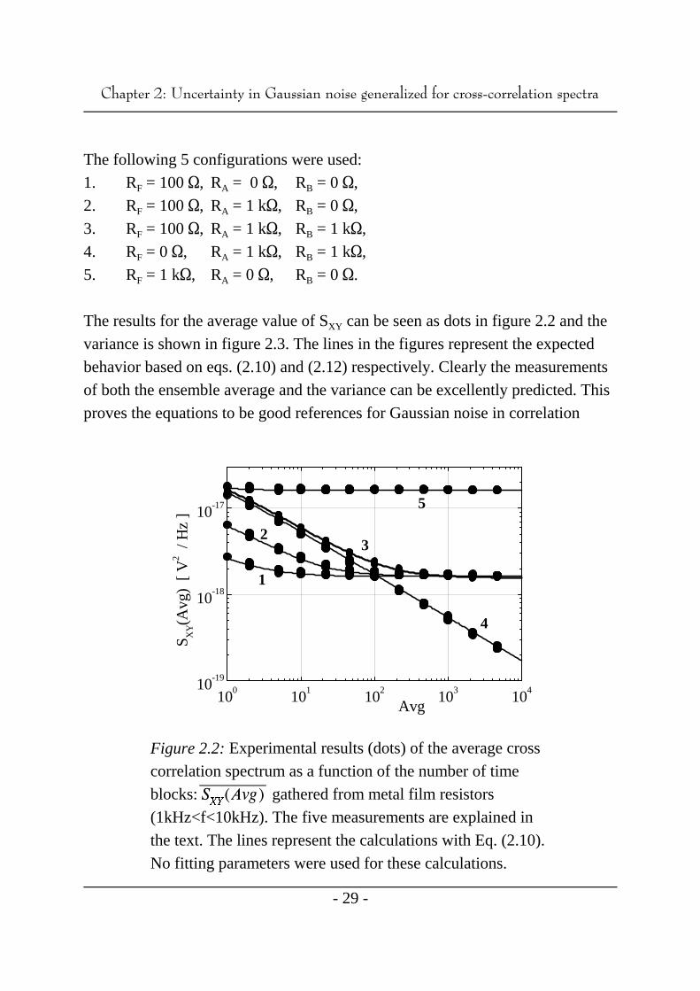
Figure 2.2: Experimental results (dots) of the average cross
correlation spectrum as a function of the number of time
blocks: gathered from metal film resistors
(1kHz<f<10kHz). The five measurements are explained in
the text. The lines represent the calculations with Eq. (2.10).
No fitting parameters were used for these calculations.
The following 5 configurations were used:
1. R = 100 6, R = 0 6, R = 0 6,F A B
2. R = 100 6, R = 1 k6, R = 0 6,F A B
3. R = 100 6, R = 1 k6, R = 1 k6,F A B
4. R = 0 6, R = 1 k6, R = 1 k6,F A B
5. R = 1 k6, R = 0 6, R = 0 6.F A B
The results for the average value of S can be seen as dots in figure 2.2 and theXY
variance is shown in figure 2.3. The lines in the figures represent the expected
behavior based on eqs. (2.10) and (2.12) respectively. Clearly the measurements
of both the ensemble average and the variance can be excellently predicted. This
proves the equations to be good references for Gaussian noise in correlation
100
101
102
103
10410
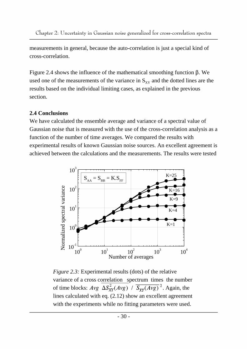
-1
100
101
102
103
K=25
K=16
K=9
K=4
K=1
SAA = SBB = K.SFF
Nor
mal
ized
spe
ctra
l var
ianc
e
Number of averages
#XI 5
:;#XI 5
:;#XI
&KDSWHU8QFHUWDLQW\LQ*DXVVLDQQRLVHJHQHUDOL]HGIRUFURVVFRUUHODWLRQVSHFWUD
- 30 -
Figure 2.3: Experimental results (dots) of the relative
variance of a cross correlation spectrum times the number
of time blocks: . Again, the
lines calculated with eq. (2.12) show an excellent agreement
with the experiments while no fitting parameters were used.
measurements in general, because the auto-correlation is just a special kind of
cross-correlation.
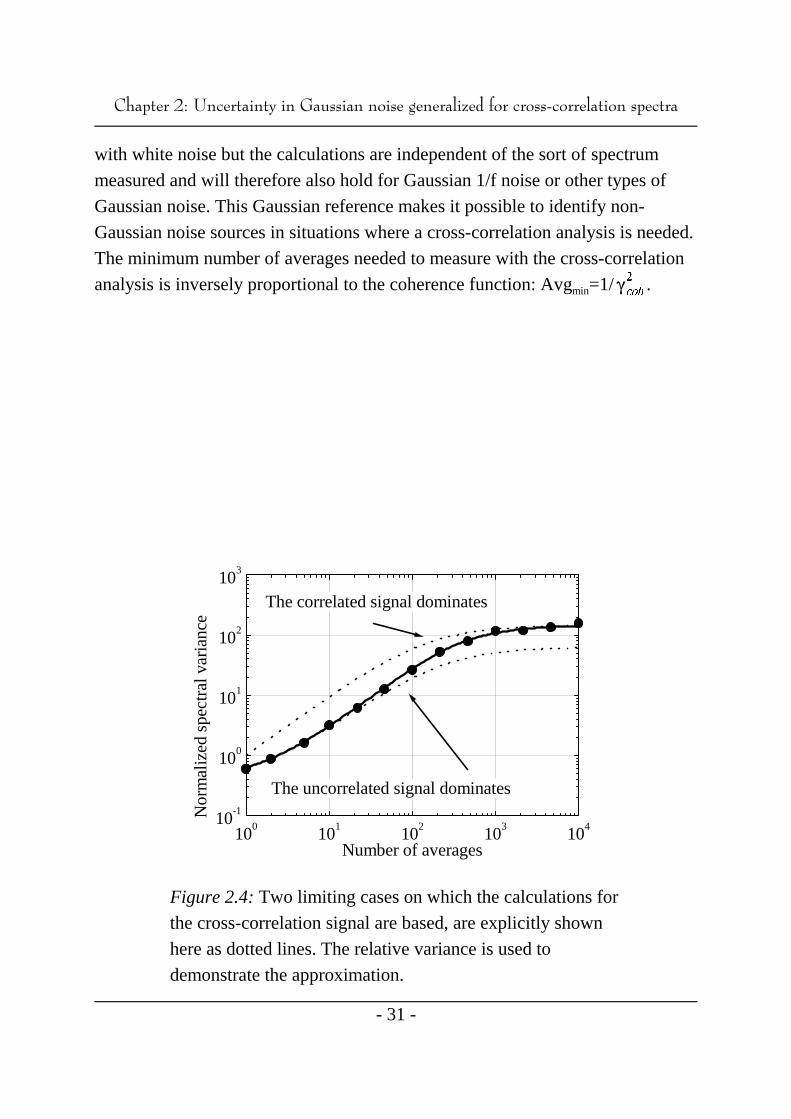
Figure 2.4 shows the influence of the mathematical smoothing function . We
used one of the measurements of the variance in S and the dotted lines are theXY
results based on the individual limiting cases, as explained in the previous
section.
2.4 ConclusionsWe have calculated the ensemble average and variance of a spectral value of
Gaussian noise that is measured with the use of the cross-correlation analysis as a
function of the number of time averages. We compared the results with
experimental results of known Gaussian noise sources. An excellent agreement is
achieved between the calculations and the measurements. The results were tested
100
101
102
103
10410
-1
100
101
102
103
The correlated signal dominates
The uncorrelated signal dominates
Number of averages
Nor
mal
ized
spe
ctra
l var
ianc
e
EQJ
&KDSWHU8QFHUWDLQW\LQ*DXVVLDQQRLVHJHQHUDOL]HGIRUFURVVFRUUHODWLRQVSHFWUD
- 31 -
Figure 2.4: Two limiting cases on which the calculations for
the cross-correlation signal are based, are explicitly shown
here as dotted lines. The relative variance is used to
demonstrate the approximation.
with white noise but the calculations are independent of the sort of spectrum
measured and will therefore also hold for Gaussian 1/f noise or other types of
Gaussian noise. This Gaussian reference makes it possible to identify non-
Gaussian noise sources in situations where a cross-correlation analysis is needed.
The minimum number of averages needed to measure with the cross-correlation
analysis is inversely proportional to the coherence function: Avg =1/ .min
&KDSWHU7KHLQIOXHQFHRIDGLJLWDOVSHFWUXPDQDO\]HURQIQRLVHSDUDPHWHUV
- 32 -
3.The influence of a digital spectrum analyzeron the uncertainty in 1/f noise parameters
Accepted for publication in Microelectronics Reliability [39].
However, the evaluation between eq. (3.8) and eq. (3.13) has changed.
AbstractWhen noise is used as a diagnostic tool to determine the reliability of a
device, not only the noise parameters itself, but also the uncertainty in
these noise parameters are important. For good devices this uncertainty
will be Gaussian. However, because of non-linear measurement errors
caused by a digital spectrum analyzer this uncertainty might deviate from
Gaussianity. We have estimated this additional error through simulations.
We conclude that this error can often be ignored.
3.1 IntroductionThe uncertainty in noise spectra introduces an error in the parameters that specify
the average shape of the spectrum. This can be important for the exact frequency
index of 1/f noise. The uncertainty of a noise parameter is often not given
because a good understanding of the uncertainty in a spectral value involves a
detailed knowledge of the dynamics of a sample. This detailed knowledge is not
needed when the noise can be statistically classified as Gaussian [19].
First we will estimate the uncertainty in noise parameters for Gaussian noise
where we will use the frequency index of 1/f noise as an example. But non-linear
measurement errors can cause the noise to appear non-Gaussian. It is therefore
important to quantify their influence when for instance a deviation from the
Gaussian distribution of noise is used to study device reliability. Non-linear
errors are mainly introduced by the spectrum analyzer. The two most important
sources of error in a commercial low-frequency spectrum analyzer are
quantization and windowing. With the use of pure 1/f noise simulations we will
show the influence of these errors on the total uncertainty.

32(p) MM
f
Smeas( f ) Sfit ( f ,p) 2
MFP S2( f).
S2meas( f)
Smeas( f) 2
Avg,
Sfit ( f0) k( f0) . Smeas( f0) .
Smeas( f0) Sfit( f0) 2
Smeas( f0) k( f0) . Smeas( f0) 2
S2meas( f0) k( f0)1 2 Smeas( f0) 2
1
Avg k2( f0)
k( f0)1
k( f0)
2
S2fit ( f0)
&KDSWHU7KHLQIOXHQFHRIDGLJLWDOVSHFWUXPDQDO\]HURQIQRLVHSDUDPHWHUV
- 33 -
(3.1)
(3.2)
(3.3)
(3.4)
3.2 Parameter errors in a fitted spectrumThe 3 - or least squares method [40] is the most general way to fit a model to a2
discrete data set, such as a spectrum measured with the use of a FFT. We define:
Where M is the number of frequency points and FP is the number of fit
parameters, hence: M-FP is the number of degrees of freedom. S (f) is themeas
measured spectrum, S (f,p) the fitted spectrum as a function of the fit-parameterfit
set p and S (f) the variance of the measured spectrum, which is equal to [19]:2
where Avg is the number of averages. But the variance of the measured spectrum
is unknown since the ensemble average of the measurement is the quantity that
we try to find via the fit procedure. For Gaussian noise the variance can be
approximated by making the right-hand side proportional to the square of S . Infit
this way an error is introduced. Let us assume that after approximating the
variance with the square of S and minimizing 3 , the error at a frequency f isfit 02
equal to:
With k(f ) an equalizing function. This gives that the ensemble average of the0
uncertainty at f is equal to:0

S2( f )
S2fit ( f )
Avg1
Smeas( f) Avg
Avg1Sfit ( f )
32 1
32 2
2MFP
1 3Avg
32 2
&KDSWHU7KHLQIOXHQFHRIDGLJLWDOVSHFWUXPDQDO\]HURQIQRLVHSDUDPHWHUV
- 34 -
(3.5)
(3.6)
(3.7)
In the last step we used eq. (3.2) in the first part and eq. (3.3) for both parts. It is
important to realize that this final function is already minimized for a parameter
set p. In general this can only be done properly when this function also is
minimal as a function of k(f ). Therefore, k(f ) must be equal to (Avg+1)/Avg,0 0
which is independent of f . Using this relation and realizing that eq. (3.4) is the0
definition of the uncertainty, one is left with:
Using eq. (3.3) and the relation for k gives the relation between the actual
ensemble average and the fit:
In conclusion, when using the least squares method as defined in eq. (3.1) to fit
Gaussian noise spectra, eq. (3.5) has to be used in eq. (3.1) to find the optimal
parameter set p. Afterwards, eq. (3.6) must be used to retrieve the actual
parameter set.
Based on the statistical information of a spectral value the variance of 3 can also2
be calculated. When the number of spectral values is much larger than the
number of fit parameters, and the number of individual pulses is large, one finds:
The derivation of is given in appendix A4.
3.2.1 The parameter errors
The uncertainty in a fitted spectrum will translate into an uncertainty in the fit
parameters called p. To estimate this uncertainty we develop a Taylor series of
the error 3 as a function of the parameter set p = p + p, around the minimum 2min

32FP dTp
12
pT D p
∆p2
∆p1
∆q = D ∆p∆q2
∆q1
∆pT D ∆p = 2 ∆ χ
FP
2
q Dp .
32FP
32FP
&KDSWHU7KHLQIOXHQFHRIDGLJLWDOVSHFWUXPDQDO\]HURQIQRLVHSDUDPHWHUV
- 35 -
(3.8)
Figure 3.1: 2D example of the solutions p for the relation
p Dp=23 . Such an ellipse encloses the error spaceT 2FP
around the optimal p. The axes of q-space, with q=Dp, are
also given. Note that the q-axes intersect with the ellipse at
the maxima of p and p .1 2
(3.9)
p . Only going up to the second order we are left with: min
with the change in 3 due to changes in the parameters, p the change in2i
the parameter p , d =03 (p)/0p and D =0 3 (p)/0p0p . The matrix D is thereforei i i ij i j2 2 2
symmetrical and the vector d is by definition 0 since 3 is minimized as a2
function of the parameter set p. Figure 3.1 shows an example of the solutions for
p for a given .
We will now define the components of the uncertainty vector p as theRMS,
positive maxima of the ellipse in each direction. Figure 3.1 indicates that these
solutions are given by the axes of q-space, with q defined as:
0pTDp
0py
2qy ,
232FP pTDp pTq qTD1q .
q2RMS x
232FP
D1xx
.
p2RMS x 23
2FP D1
xx .
S1/f( f) Cf0
f0f
32FP
32FP
32FP
&KDSWHU7KHLQIOXHQFHRIDGLJLWDOVSHFWUXPDQDO\]HURQIQRLVHSDUDPHWHUV
- 36 -
(3.10)
(3.11)
(3.12)
(3.13)
(3.14)
To show that these maxima always intersect with the axes of q-space we use:
which follows directly from an evaluation of the left-hand side. For the
maximum of p , the derivative in eq. (3.10) is zero for all ygx. Hence, q =0x y
for all ygx so the axis of q crosses the ellipse at the maximum of p . As anx x
example, the rms value of p is therefore equal to: p =(D ) q . It isx RMS x xx RMS x-1
straightforward to calculate the value of q with:RMS x
Hence, on the q -axis one is left with:x
This gives via p =(D ) q the variance in the original parameter:RMS x xx RMS x-1
So, the diagonal of the inverse matrix gives the variance of each parameter p .x
The value of depends on the number of fit parameters FP. Because there
are generally only a limited amount of fit parameters, the value of needs to
be calculated from the incomplete Gamma function. When the number of fit
parameters equals 1, 2 or 3, respectively is: 1, 2.296 and 3.527 in the
68.3% confidence region of a Gaussian distribution function.
Therefore, if the uncertainty in the noise spectrum is known, the parameter errors
can be calculated. For Gaussian noise we calculated the error in the frequency
index of the 1/f noise with white noise present. The model we used for the 1/f
noise is the following:
1 10 100 1k 10k 100k1
10
100
The total number of decades of the spectrum2 3 4
γ = 1.1
γ = 0.9
γ = 1
No
rma
lize
d r
ms-
err
or
in γ
[ %
]
Normalized corner frequency
f0 fmin fmax
&KDSWHU7KHLQIOXHQFHRIDGLJLWDOVSHFWUXPDQDO\]HURQIQRLVHSDUDPHWHUV
- 37 -
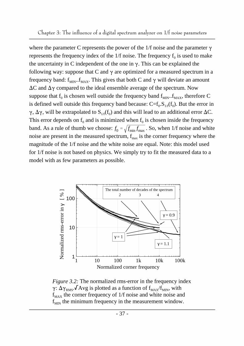
Figure 3.2: The normalized rms-error in the frequency index: .Avg is plotted as a function of f /f , withRMS MAX MIN
f the corner frequency of 1/f noise and white noise andMAX
f the minimum frequency in the measurement window.MIN
where the parameter C represents the power of the 1/f noise and the parameter
represents the frequency index of the 1/f noise. The frequency f is used to make0
the uncertainty in C independent of the one in . This can be explained the
following way: suppose that C and are optimized for a measured spectrum in a
frequency band: f ..f . This gives that both C and will deviate an amountMIN MAX
C and compared to the ideal ensemble average of the spectrum. Now
suppose that f is chosen well outside the frequency band f ..f , therefore C0 MIN MAX
is defined well outside this frequency band because: C=f .S (f ). But the error in0 1/f 0
, , will be extrapolated to S (f ) and this will lead to an additional error C.1/f 0
This error depends on f and is minimized when f is chosen inside the frequency0 0
band. As a rule of thumb we choose: . So, when 1/f noise and white
noise are present in the measured spectrum, f is the corner frequency where themax
magnitude of the 1/f noise and the white noise are equal. Note: this model used
for 1/f noise is not based on physics. We simply try to fit the measured data to a
model with as few parameters as possible.
&KDSWHU7KHLQIOXHQFHRIDGLJLWDOVSHFWUXPDQDO\]HURQIQRLVHSDUDPHWHUV
- 38 -
Figure 3.2 shows the root-mean-square (rms) error in the frequency index of
the 1/f noise as a function of the corner frequency f normalized for f . Wec min
calculated the error for a spectrum as it is often measured: we assumed that a
spectrum is measured at 100 linearly distributed frequencies between a
fundamental frequency f and a maximum frequency f . This gives a spectrum1 100
with a length of 2 decades. If an extra decade is needed at the high frequency
side, one increases the fundamental frequency by a factor 10 and forms the same
measurement. The first decade of this new measurement was already measured
and is therefore disregarded and the second decade of this measurement is added
to the original spectrum, giving it a length of 3 decades, etc.
Figure 3.2 shows the rms-error in the frequency index when 2, 3 and 4 decades
are measured with an average slope of the 1/f noise equal to -1 (=1). When 3
decades are measured, the error for an average equal to 0.9 and 1.1, is also
given. The rms-error in the slope when one measures with for instance 800
frequency-lines instead of 100, will roughly be a factor square root 8 less.

G( f ) 1
1 j ffmax
gH
j ffmin
1 j ffmin
12
1j f
2 t
1 j f
&KDSWHU7KHLQIOXHQFHRIDGLJLWDOVSHFWUXPDQDO\]HURQIQRLVHSDUDPHWHUV
- 39 -
(3.15)
3.3 Simulation of additional errors due to A/D conversion and windowingWhen a low frequency spectrum is measured with a spectrum analyzer two
additional sources of error are added. First of all the analog to digital (A/D)
conversion leads to an additional error. To simulate this error we generated a
noise signal on which we performed a frequently used 12 bit A/D conversion.
Secondly we investigated the windowing effect. We will compare the rectangular
window with the Hanning window. As a reference, these two basic types of
windows will be compared with a spectrum of a noise signal that is constructed
such that it naturally starts and dies within the measured time window.
3.3.1 A deterministic time signal that gives an ideal 1/f spectrum
In order to simulate the A/D and windowing errors we choose a deterministic
time signal that has a pure 1/f spectrum in the frequency domain. We designed a
noise signal with these individual pulses by giving each individual pulse a
random starting point, hence the distribution function is uniform or time
independent. We used a 1024 point FFT to generate the spectrum of this signal.
The use of a deterministic time signal with an exact 1/f spectrum is necessary to
avoid extra errors.
We used the time signal proposed in 1955 by Schönfeld to simulate 1/f noise
[41]. This signal is: and the frequency response (in a limiting case) is
equal to when f is defined for positive frequencies only. A spectrum
analyzer has an anti-aliasing filter. To simulate this, we have to filter the signal
with a high-order low-pass filter. Furthermore, for reference purposes, we must
limit the time length of the signal to the length of the window. To achieve this we
added a high-pass filter that causes the spectrum to level off to a non-zero DC
value. The resulting signal in the frequency domain that will give a filtered 1/f
power density spectrum is now defined as:
g( t)
4% fmaxtgH
N
gH1
i0(12i )
e2% fmaxt
× 1M
i1
2%( fmax fmin) t i
i !
× Ni1
j0
2j12j2gH1
2t
( t )
100µ 1m 10m 100m 10
10
20
30
40
50
Filtered sqrt( 2 / t )
sqrt( 2 / t )Sig
nal
ma
gn
itud
e
time [ sec ]
&KDSWHU7KHLQIOXHQFHRIDGLJLWDOVSHFWUXPDQDO\]HURQIQRLVHSDUDPHWHUV
- 40 -
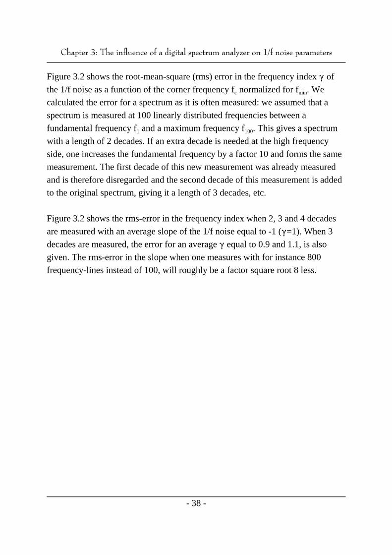
(3.16)
Figure 3.3: In the time-domain, the original and the filtered
signals are shown. The corner frequencies of the filtered
signal are: 2 and 400 Hz and the filter order g is 5.H
where the first part represents the low pass anti-aliasing filter of a selectable
order g and corner frequency f . The second part represents the high-pass filterH max
with corner frequency f which causes the 1/f signal to level off. The last part ismin
the original, ideal signal. This signal can be transformed to the time domain when
g is an integer and f >0. The filtered signal in the time domain then becomes:H min
with (t)=0 for t<0 and (t)=1 for t0.
1 10 100 1k10
-5
10-4
10-3
10-2
10-1
100
ideal1/f - line
The spectrum after a 1024-point FFT,and after correction for the band-pass filter
Sp
ectr
al d
ensi
ty
frequency [ Hz ]
&KDSWHU7KHLQIOXHQFHRIDGLJLWDOVSHFWUXPDQDO\]HURQIQRLVHSDUDPHWHUV
- 41 -
Figure 3.4: The spectral density of the filtered signal of
figure 3.3 both before and after correcting for the filter. The
ideal 1/f line is given as a reference.
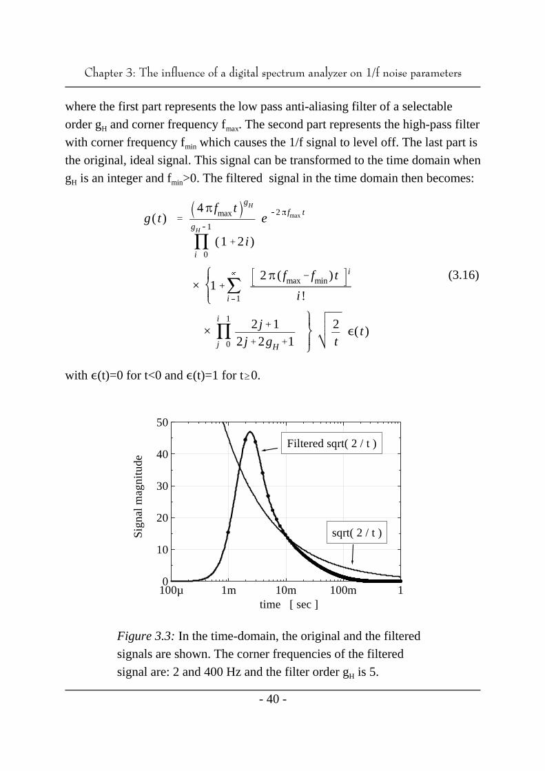
Figure 3.3 shows an example of this filtered time signal with g =5, f =2 Hz andH min
f =400 Hz. The result after conversion to the frequency domain with the use ofmax
an 1024-point FFT is given in figure 3.4. Since the used band pass filter is
known we can divide the resulting spectrum by the magnitude of this filter to get
the result before filtering. This operation is also performed in figure 3.4 and the
result shows that the spectrum only deviates slightly from the ideal 1/f line after
300 Hz. This is probably due to the fact that the anti-aliasing filter is not
infinitely sharp.
&KDSWHU7KHLQIOXHQFHRIDGLJLWDOVSHFWUXPDQDO\]HURQIQRLVHSDUDPHWHUV
- 42 -
3.3.2 Simulations of 1/f noise
We performed five types of simulations. Each time we used the parameters:
g =5, f =2 Hz and f =400 Hz and a time frame of 1 second. The differentH min max
simulations are:
1. First our reference simulation. We generated a set of pulses at random
instants in time but the complete pulse had to be captured by the time
window. Furthermore we gave each pulse a constant amplitude of either
+1 or -1 with 50% probability each. No A/D quantization was performed.
2. We took the exact same signal as the first simulation but the magnitude
distribution became normalized Gaussian.
3. The same signal as the second simulation was used but a 12 bit A/D
conversion was added. The maximum range is set to be about 10 times
higher than a typical maximum peak.
4. The previous situation was used but we also included all the pulses that are
partly outside the measurement window. No corrections were performed
(rectangular window).
5. This simulation is the same as the fourth but in this case a Hanning
window was used.
And the following averaging schemes were used:
A. 10 individual pulses, Avg=25, statistics on 1252 spectra.3
B. 10 individual pulses, Avg=25, statistics on 200 spectra.4
C. 10 individual pulses, Avg=100, statistics on 574 spectra.3
D. 10 individual pulses, Avg=100, statistics on 101 spectra.4
E. 10 individual pulses, Avg=1000, statistics on 109 spectra.3
So, we used either 10 or 10 individual pulses to construct a noise signal in the3 4
time-domain and 25, 100 or 1000 averages to generate a single spectrum. These
averaged spectra were used for the statistical analysis. Within these spectra, the
window between 1 and 300 Hz (M=300 points) was used to fit the data to the 1/f
model of eq. (3.14), with the power C and the frequency index of the 1/f noise
as fit parameters (FP=2). Each fit gave a normalized error 3 . The average and2
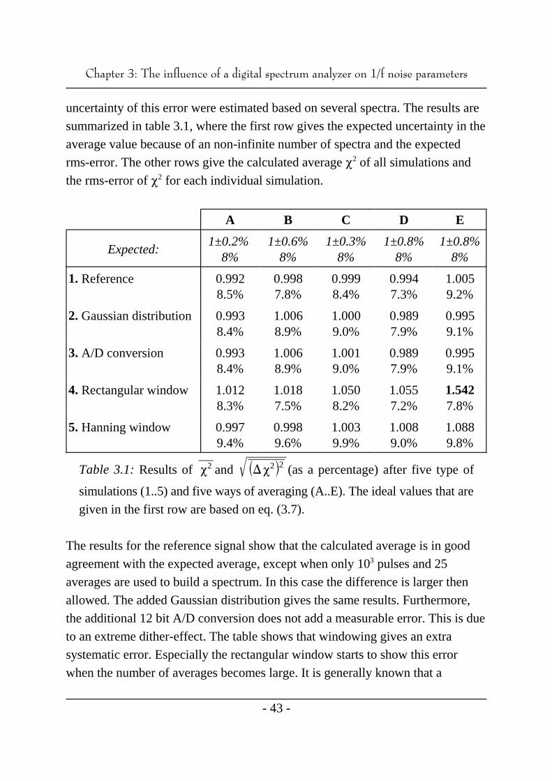
32 32 2
&KDSWHU7KHLQIOXHQFHRIDGLJLWDOVSHFWUXPDQDO\]HURQIQRLVHSDUDPHWHUV
- 43 -
uncertainty of this error were estimated based on several spectra. The results are
summarized in table 3.1, where the first row gives the expected uncertainty in the
average value because of an non-infinite number of spectra and the expected
rms-error. The other rows give the calculated average 3 of all simulations and2
the rms-error of 3 for each individual simulation.2
A B C D E
Expected:1±0.2% 1±0.6% 1±0.3% 1±0.8% 1±0.8%
8% 8% 8% 8% 8%
1. Reference 0.992 0.998 0.999 0.994 1.0058.5% 7.8% 8.4% 7.3% 9.2%
2. Gaussian distribution 0.993 1.006 1.000 0.989 0.9958.4% 8.9% 9.0% 7.9% 9.1%
3. A/D conversion 0.993 1.006 1.001 0.989 0.9958.4% 8.9% 9.0% 7.9% 9.1%
4. Rectangular window 1.012 1.018 1.050 1.055 1.5428.3% 7.5% 8.2% 7.2% 7.8%
5. Hanning window 0.997 0.998 1.003 1.008 1.0889.4% 9.6% 9.9% 9.0% 9.8%
Table 3.1: Results of and (as a percentage) after five type of
simulations (1..5) and five ways of averaging (A..E). The ideal values that are
given in the first row are based on eq. (3.7).
The results for the reference signal show that the calculated average is in good
agreement with the expected average, except when only 10 pulses and 253
averages are used to build a spectrum. In this case the difference is larger then
allowed. The added Gaussian distribution gives the same results. Furthermore,
the additional 12 bit A/D conversion does not add a measurable error. This is due
to an extreme dither-effect. The table shows that windowing gives an extra
systematic error. Especially the rectangular window starts to show this error
when the number of averages becomes large. It is generally known that a
&KDSWHU7KHLQIOXHQFHRIDGLJLWDOVSHFWUXPDQDO\]HURQIQRLVHSDUDPHWHUV
- 44 -
Hanning window is better then a rectangular window which is also confirmed by
the results. From the table one can conclude that a Hanning window does not add
a significant systematic error when the number of averages is less then thousand.
3.4 ConclusionsThe uncertainty in noise parameters is an important tool for device reliability
measurements when the uncertainty deviates from the Gaussian expectation. For
Gaussian 1/f noise we calculated the error in the frequency index. We analyzed
the additional non-Gaussian error caused by the spectrum analyzer. This
additional error is negligible up to the averaging of a thousand spectra if a non-
rectangular window is used, such as a Hanning window.
&KDSWHU$XWRPDWHG6\VWHPIRU1RLVH0HDVXUHPHQWV
- 45 -
4. Automated System for Noise Measurementson Low-Ohmic Samples and Magnetic Sensors
The essential parts of this chapter are published in
IEEE Transactions on Instrumentation and Measurement [42].
The original paper is included in appendix A6.
This chapter is not identical to the published version
because of some improvements of the measurement setup.
AbstractAn automated system for electronic noise measurements on metal films
is presented. This new system, controlled by a personal computer which
utilizes National Instruments' LabVIEW software, is designed to measure
low-frequency noise as a function of an externally imposed magnetic field
and as a function of a DC bias current in low-ohmic samples and
magnetic sensors. With this system we are able to measure continuously
for several days, during which measured spectra are collected, processed
and stored for further analysis.
4.1 IntroductionWe are investigating the low-frequency noise in metal layers as a function of a
DC bias current, in metal lines, and as a function of an externally imposed
magnetic field in magnetic resistors. In a conventional noise measurement
system, a constant DC current, obtained by the use of batteries and a metal film
bias resistor, is applied to the sample. For ohmic samples, the measured spectrum
S (f) is proportional to the square of the applied bias current [43]. Recently,VV
Yassine and Chen [44] discussed the limitations of this DC noise measurement
system and introduced a novel AC/DC noise measurement system for
electromigration studies. Another AC excitation approach for measuring noise on
low-ohmic samples was introduced by Verbruggen et al [45]. Their system uses a
single carrier frequency in a balanced bridge and two phase-sensitive detectors
which operate in quadrature. With this system it is possible to measure the
spectral density of the resistance fluctuations with strongly reduced background
&KDSWHU$XWRPDWHG6\VWHPIRU1RLVH0HDVXUHPHQWV
- 46 -
noise. In our system, we only use DC bias currents and the system noise is
strongly reduced by using ultra low-noise amplifiers in combination with the
cross-correlation technique.
Ciofi et al [46] presented a measurement system based on a Personal Computer
(PC) and a data acquisition system. In addition, others have used a PC to
automate their measuring system [47,48]. Although we too use a PC, in our
system the data acquisition and Fourier analysis are performed by a separate
spectrum analyzer. In addition to automating the measurements, we would also
like to automate the variation of the bias conditions and the amplitude and
orientation of the externally applied magnetic field.
Sherry and Lord [49] demonstrated the applicability of National Instruments'
LabVIEW in an educational environment. They describe the advantages of
LabVIEWs' graphical programming language over the traditional text-based
languages in automating a laboratory measurement setup. We also use LabVIEW
to drive and control the system and to collect the data.
This paper describes an automated system for low-frequency noise measurements
on low-ohmic samples and magnetic sensors as a function of an externally
imposed magnetic field and a DC bias current. The paper is structured as follows:
Section 2 presents the system specifications and requirements. In section 3, the
measurement setup and system control are presented. The custom-made, ultra
low-noise amplifier is also introduced in this section. In section 4, this amplifier
is compared to the Brookdeal 5004 ultra low-noise amplifier. Finally, in section
5, summarizing conclusions are drawn.
4.2 System specificationsThe samples under study are low-ohmic (100 6) magneto-resistors and metal
lines, known to have low-noise levels. Investigating these samples requires a
very sensitive measuring setup, which makes the measuring system susceptible to
disturbance. Therefore, special attention has to be paid to the design of the setup

&KDSWHU$XWRPDWHG6\VWHPIRU1RLVH0HDVXUHPHQWV
- 47 -
in order to cope with the disturbance.
The resistivities of both metal lines and magnetic sensors depend on temperature.
Hence, measures have to be taken to guarantee temperature stability. Noise in
magnetic sensors depends on the imposed magnetic field [50]. The investigation
of this relationship demands the ability to manipulate the imposed magnetic field.
For magnetic field sensors, special precautions have to be taken with respect to
the pickup of spurious magnetic fields.
In order to avoid uncontrolled changes of the domain wall pattern, the orientation
of the magnetic field should not be changed instantaneously. Noise in magneto-
resistors is very sensitive to the disturbance of domain walls. The manipulation
of the magnetic field should be controlled automatically.
The resistance and the noise of the magnetic sensors is a function of the imposed
magnetic field. Hence, each measurement should be preceded by an accurate
resistance measurement. There is a relationship between the derivative, 0R/0H,
and the low-frequency noise [50,51]. Although it is possible to calculate the
derivative of the magneto-resistor, it is preferable to measure this derivative
directly with a small AC field. Another parameter is the bias current, which
should therefore be adjustable.
We do not use any magnetic shielding to suppress the pickup of magnetic fields
other then the ones we generate. The reason for this is three-fold. First of all, we
never experienced the need for magnetic shielding. Additional AC fields never
influenced the measurements. For instance, two-point and bridge measurements
give identical results. Additional DC fields are also negligible because rotating
the measurement setup does not lead to changes in the measured results.
Secondly, it would take an exceptionally thick case to suppress frequencies as
low as 1 Hertz. And finally, enclosing the measurement setup also means that the
Helmholtz coils have to be enclosed. This leads to an unwanted temperature drift
in the case due to heating, because the DC currents that flow through the coils
&KDSWHU$XWRPDWHG6\VWHPIRU1RLVH0HDVXUHPHQWV
- 48 -
(R~10 6) vary periodically between 0 and ±1.5A.
In order to guarantee amplifier stability, we have to use a stabilized power
supply. Since the measurements extend over several days, it is not possible to use
a battery power supply. For instance, measuring metal lines, in order to
investigate degradation in time by electromigration, requires repeated noise
measurements over longer time spans. Consequently, measuring conditions
should be stable for a long period (hours or even days). A high degree of
automation is required, not only because the measurements are time-consuming,
but also because measuring an entire magneto-resistance curve requires many
measurements. In order to measure automatically, software is needed to control
the measurement setup. A PC has to be used to drive the instrumentation and to
control the sample and magnetic field biasing. All data should be directed to the
PC, where it can be processed and stored for data analysis.
Summarizing the system requirements:
& Ability to measure low-ohmic (100 6) magneto-resistors and metal-lines.
& Stability of the sample temperature.
& Capability of manipulating both orientation and amplitude of imposed
magnetic field in case of magnetic sensors.
& Magnetic field should be stabilized to guarantee stationary conditions.
& Measure the derivative 0R/0H of the sensor directly by AC technique.
& High degree of automation, i.e. the system should be able to measure
continuously for several days.
& Drive/control instrumentation (spectrum analyzer, lock-in amplifier and
function generator) via GPIB.
& Capability to control the bias circuitry (Bias current through sample.
magnetic field orientation and amplitude).
& Data processing and storage facilities.
& Additional noise introduced by instrumentation and circuitry should be
negligible.
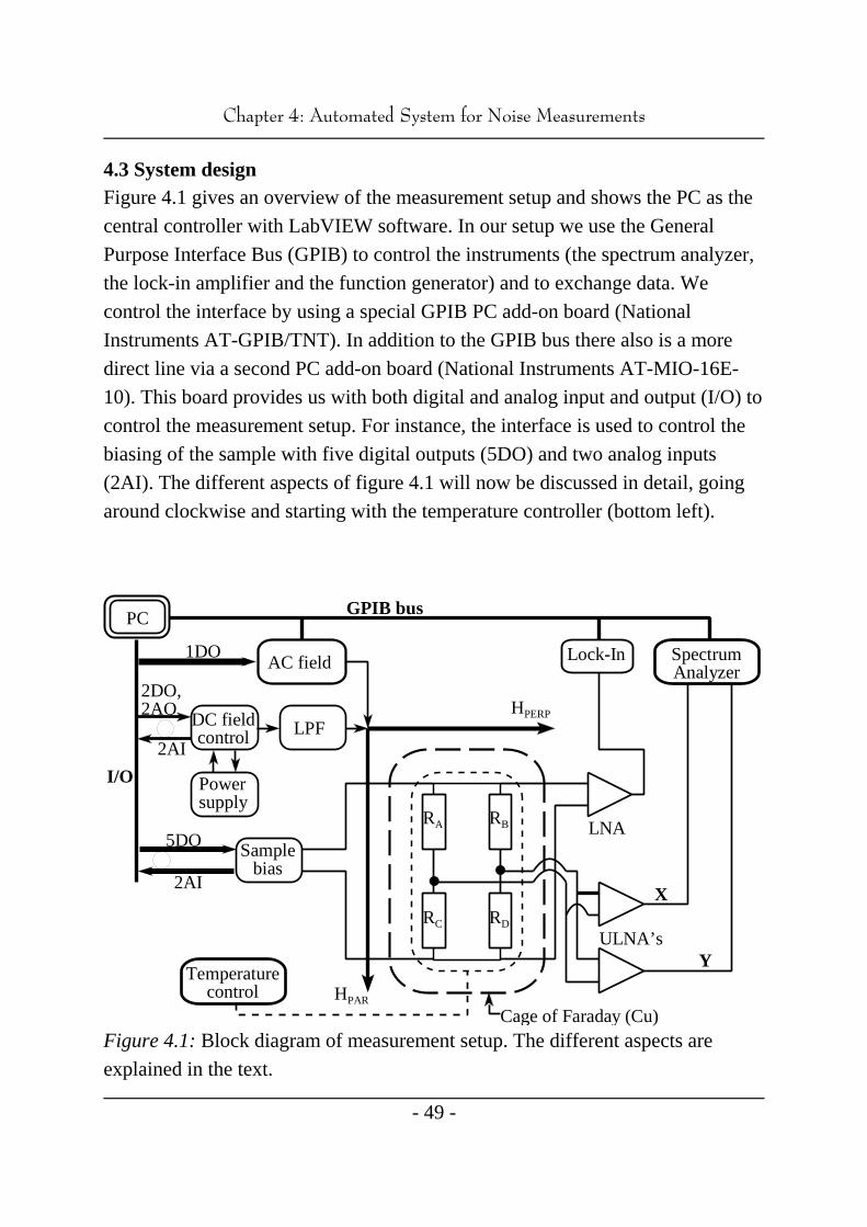
HPAR
RA
RC RD
Samplebias
Cage of Faraday (Cu)
PC
Powersupply
DC fieldcontrol
5DO
Temperaturecontrol
AC field
RB
HPERP
I/O
YULNA’s
LPF
2AI
2DO,2AO
2AI
GPIB bus
1DO Lock-In SpectrumAnalyzer
LNA
X
&KDSWHU$XWRPDWHG6\VWHPIRU1RLVH0HDVXUHPHQWV
- 49 -
Figure 4.1: Block diagram of measurement setup. The different aspects are
explained in the text.
4.3 System designFigure 4.1 gives an overview of the measurement setup and shows the PC as the
central controller with LabVIEW software. In our setup we use the General
Purpose Interface Bus (GPIB) to control the instruments (the spectrum analyzer,
the lock-in amplifier and the function generator) and to exchange data. We
control the interface by using a special GPIB PC add-on board (National
Instruments AT-GPIB/TNT). In addition to the GPIB bus there also is a more
direct line via a second PC add-on board (National Instruments AT-MIO-16E-
10). This board provides us with both digital and analog input and output (I/O) to
control the measurement setup. For instance, the interface is used to control the
biasing of the sample with five digital outputs (5DO) and two analog inputs
(2AI). The different aspects of figure 4.1 will now be discussed in detail, going
around clockwise and starting with the temperature controller (bottom left).
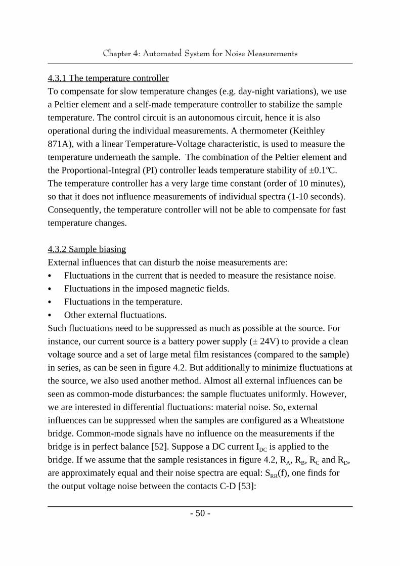
&KDSWHU$XWRPDWHG6\VWHPIRU1RLVH0HDVXUHPHQWV
- 50 -
4.3.1 The temperature controller
To compensate for slow temperature changes (e.g. day-night variations), we use
a Peltier element and a self-made temperature controller to stabilize the sample
temperature. The control circuit is an autonomous circuit, hence it is also
operational during the individual measurements. A thermometer (Keithley
871A), with a linear Temperature-Voltage characteristic, is used to measure the
temperature underneath the sample. The combination of the Peltier element and
the Proportional-Integral (PI) controller leads temperature stability of ±0.1 C.o
The temperature controller has a very large time constant (order of 10 minutes),
so that it does not influence measurements of individual spectra (1-10 seconds).
Consequently, the temperature controller will not be able to compensate for fast
temperature changes.
4.3.2 Sample biasing
External influences that can disturb the noise measurements are:
& Fluctuations in the current that is needed to measure the resistance noise.
& Fluctuations in the imposed magnetic fields.
& Fluctuations in the temperature.
& Other external fluctuations.
Such fluctuations need to be suppressed as much as possible at the source. For
instance, our current source is a battery power supply (± 24V) to provide a clean
voltage source and a set of large metal film resistances (compared to the sample)
in series, as can be seen in figure 4.2. But additionally to minimize fluctuations at
the source, we also used another method. Almost all external influences can be
seen as common-mode disturbances: the sample fluctuates uniformly. However,
we are interested in differential fluctuations: material noise. So, external
influences can be suppressed when the samples are configured as a Wheatstone
bridge. Common-mode signals have no influence on the measurements if the
bridge is in perfect balance [52]. Suppose a DC current I is applied to theDC
bridge. If we assume that the sample resistances in figure 4.2, R , R , R and R ,A B C D
are approximately equal and their noise spectra are equal: S (f), one finds forRR
the output voltage noise between the contacts C-D [53]:

SVCDVCD
14
I 2DC SRR
+12V+12V
+12V+12V
+12V+12V
+12V
V
+12V
Relays
R1..R4
Samplecurrent
IDC
V
RBRA
RC RD
A
To ULNA’s
R1..R4
B
C D
106
106
&KDSWHU$XWRPDWHG6\VWHPIRU1RLVH0HDVXUHPHQWV
- 51 -
(4.1)
Figure 4.2: Diagram of the electric bias circuit and the sample in a balanced
Wheatstone configuration.
Besides the Wheatstone bridge we also designed the circuit symmetrically around
the ground point in the battery pack so that both V and V will be a virtualC D
ground. Further on, one can see that the ultra-low-noise amplifiers (ULNA's) are
designed in the same way and also have their reference at the same ground. As a
result, our measurement setup is also non-sensitive to fluctuations in the
reference voltage.
Figure 4.2 shows two sets of metal film resistors (RR ) in parallel. The1 4
resistance values in each set are: 1 k6, 2 k6, 4 k6 and 8 k6. These resistors can
be selected individually with relays controlled by 4 digital outputs of the PC.
This provides the selection of 16 (2 ) different bias currents, the resulting4
currents typically are: 045mA in 3mA steps. To measure the current through,
and the voltage across the bridge, two analog PC inputs have been included to
measure the signals. The obtained values are stored for analysis. During the noise
measurements these meters are automatically disconnected with additional relays.

&KDSWHU$XWRPDWHG6\VWHPIRU1RLVH0HDVXUHPHQWV
- 52 -
4.3.3 DC magnetic fields
In our setup we use a set of Helmholtz coils in order to vary both orientation and
amplitude of the applied DC magnetic field by controlling H and HPAR PERP
separately, see figure 4.1. The maximal achievable magnitudes are 1.5 and 3
kA/m, respectively. The names, parallel and perpendicular are with reference to
the current I that flows through the sample. We use a programmable DC powerDC
supply (Delta E030-3) to drive each coil and we measure the actual current. By
providing this information to the software, a controlled system is realized which
keeps the current constant and is able to compensate for drift in the magnetic
fields due to temperature drift. The software-based controller is a Proportional-
Integral-Differential (PID) controller to ensure smooth and slow field changes
with no discontinuities in the derivatives. This could be important when
measuring samples with domain walls. The controller only operates in between
measurements, during a measurement the signals are kept constant.
The DC power supply introduces disturbance: 50 Hz and higher harmonics.
Consequently, a low-ohmic low-pass filter (LPF) is required. We use a third-
order LCL Tfilter (L=1H, C=0.15F) for each field direction. This filter provides
a cut-off frequency of 0.4 Hz without a large dissipation and is shown as 'LPF' in
figure 4.1. Additionally, it eliminates the discrete steps that are introduced by the
digital-to-analog (D/A) converter in the control circuit.
A disadvantage of the used power supplies is that they are not able to generate
inverse or negative voltages. Negative magnetic fields are necessary to provide
360 field manipulation instead of 90 . To overcome this limitation, twoo o
additional digital outputs are used to control the polarity of the magnetic fields
via relays.
4.3.4 AC magnetic fields
To determine the derivative, 0R/0H, of the magneto-resistance, we also record
the small-signal behavior. We make use of an ultra-low distortion function
generator (Stanford Research System DS360) to generate an additional AC

&KDSWHU$XWRPDWHG6\VWHPIRU1RLVH0HDVXUHPHQWV
- 53 -
magnetic field. Typically, the frequency is chosen as 25Hz to avoid inductive
pickup of the signal. The resulting AC field has a magnitude of ±1A/m.
Obviously this signal is only switched on when no other measurements are taking
place.
Each set of the Helmholtz coils contains two separately accessible coils: an inner
coil, with a slightly smaller impedance, and an outer coil. We use the inner coils,
in both directions, for the DC field and the outer coils for the AC field. The AC
response is measured separately in the parallel and perpendicular directions. A
relay is used to switch between the two directions so that the same equipment can
be used for both measurements.
The resulting resistance changes are common-mode changes and should therefore
be measured in common-mode via a Brookdeal 5001 low-noise differential
amplifier (LNA) as can be seen in figures 4.1 and 4.2. The amplified signal is fed
to a lock-in amplifier (Stanford Research System SR830 DSP) to measure the
change in resistance due to the change in magnetic field. Then the sensitivity
coefficient or derivative 0R/0H of the magneto-resistance is calculated. With the
lock-in amplifier locked at the AC frequency, we can now measure the small-
signal characteristic R without problems caused by noise and pick up ofAC
spurious magnetic fields.
4.3.5 Ultra low-noise amplifier
In the setup we use two custom made ultra low-noise differential voltage
amplifiers (ULNA's) that amplify the same noise signal, as can be seen in figure
4.1. Via cross-correlation measurements on the output signals X and Y, the
additional noise introduced by the ULNA's is suppressed. In section 4.4 the
background noise of this amplifier will be shown and compared to other
amplifiers. Here we will limit ourselves to the layout of the amplifier.
The first stage of each amplifier is based on the Burr-Brown INA1O3 low-noise,
low-distortion instrumentation amplifier as is shown in figure 4.3. Note that the
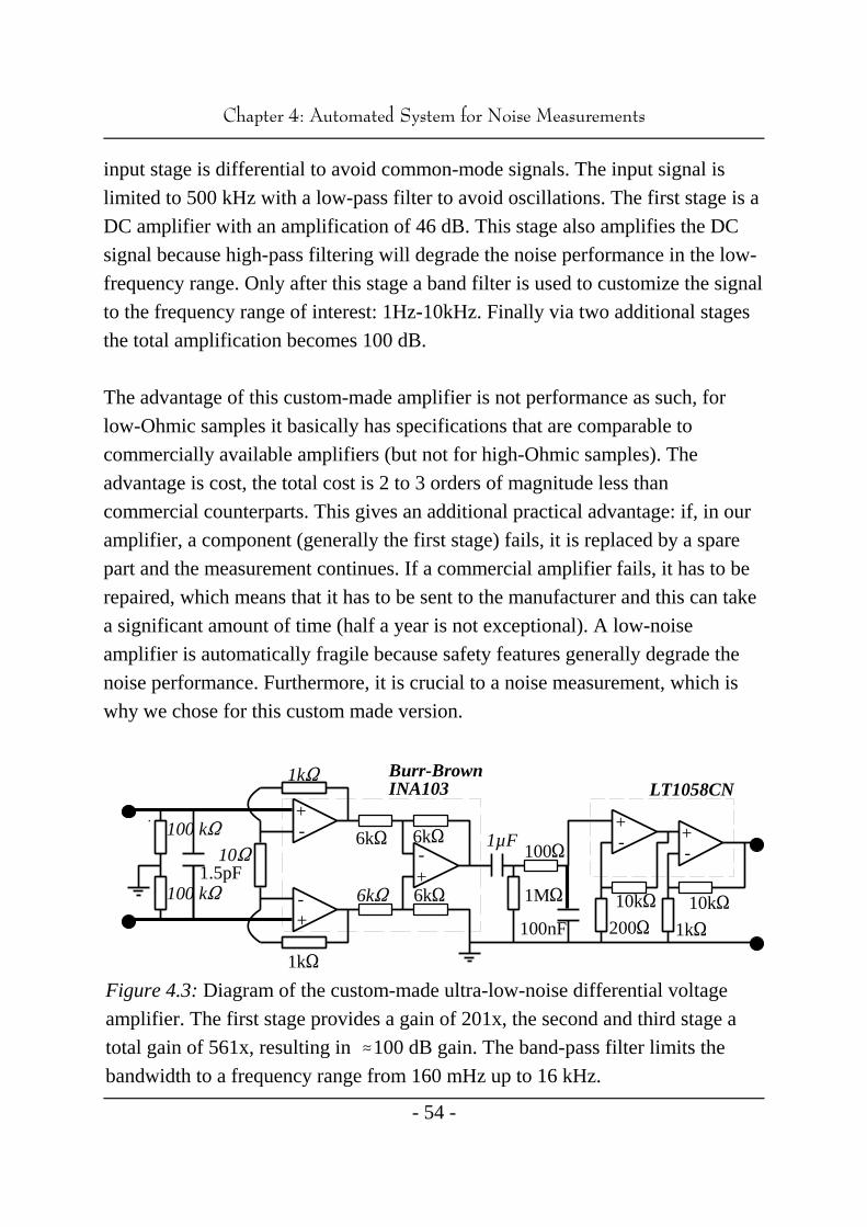
100 k6
1µF
1k6
100 k6
106
6k6
LT1058CN
2006
6k6 6k6+-
+
+-
-
1k6
1.5pF
100nF
6k6 1M6
+- +
-1006
1k6
10k610k6
Burr-BrownINA103
&KDSWHU$XWRPDWHG6\VWHPIRU1RLVH0HDVXUHPHQWV
- 54 -
Figure 4.3: Diagram of the custom-made ultra-low-noise differential voltage
amplifier. The first stage provides a gain of 201x, the second and third stage a
total gain of 561x, resulting in 100 dB gain. The band-pass filter limits the
bandwidth to a frequency range from 160 mHz up to 16 kHz.
input stage is differential to avoid common-mode signals. The input signal is
limited to 500 kHz with a low-pass filter to avoid oscillations. The first stage is a
DC amplifier with an amplification of 46 dB. This stage also amplifies the DC
signal because high-pass filtering will degrade the noise performance in the low-
frequency range. Only after this stage a band filter is used to customize the signal
to the frequency range of interest: 1Hz-10kHz. Finally via two additional stages
the total amplification becomes 100 dB.
The advantage of this custom-made amplifier is not performance as such, for
low-Ohmic samples it basically has specifications that are comparable to
commercially available amplifiers (but not for high-Ohmic samples). The
advantage is cost, the total cost is 2 to 3 orders of magnitude less than
commercial counterparts. This gives an additional practical advantage: if, in our
amplifier, a component (generally the first stage) fails, it is replaced by a spare
part and the measurement continues. If a commercial amplifier fails, it has to be
repaired, which means that it has to be sent to the manufacturer and this can take
a significant amount of time (half a year is not exceptional). A low-noise
amplifier is automatically fragile because safety features generally degrade the
noise performance. Furthermore, it is crucial to a noise measurement, which is
why we chose for this custom made version.

&KDSWHU$XWRPDWHG6\VWHPIRU1RLVH0HDVXUHPHQWV
- 55 -
4.3.6 Measurement and analysis of noise spectra
To measure the spectrum we use a digital spectrum analyzer (Advantest
R9211E), which is based on the Fast Fourier Transformation (FFT). The analyzer
can be programmed remotely. The analyzer is equipped with a cross-correlation
algorithm, has a wide frequency range (10 mHz- 100 kHz) and an input
sensitivity ranging from -60 dBV (1 mV ) up to +30 dBV (31.6 V ) , whichRMS RMS
makes this analyzer suitable for our application.
The easy access to the GPIB-bus, as well as the extended analysis features, make
LabVIEW suitable for the type of application under discussion. To increase the
resolution, the spectrum is measured in successive frequency spans. In the first
stage we collect the data in the frequency range 1 Hz - 100 Hz. In each
successive stage we measure an additional decade. If the process is stationary, it
is allowed to combine the spectra.
After a spectrum is collected it should be processed before it is stored on disk.
Although the setup is differential configured and a Wheatstone bridge is used,
the environment introduces peaks in the spectrum, e.g. 50 Hz and higher
harmonics. An algorithm is used to eliminate these peaks.
The data processing consists of two steps. In the first step we exclude all
unwanted peaks in the frequency spectrum and in the second step we reduce the
number of data points. In the first step, we have to filter out all spectral
components that can be regarded as man-made noise, e.g. peaks in the spectrum
due to 50 Hz. Manually, these peaks are easy to detect, but in order to automate
the filtering of the data, a criterion has to be defined to distinguish the these
peaks from the signal. We have implemented this criterion as follows:
First we use the analysis package of LabVIEW to fit a curve through the
measurement points. Then, we define the deviation of the obtained curve as our
relative error. If the relative error of a spectral component is larger than a
threshold value, this component will be excluded from further analysis. The
&KDSWHU$XWRPDWHG6\VWHPIRU1RLVH0HDVXUHPHQWV
- 56 -
threshold value depends mainly on the number of averages, since the relative
variance of a spectral value is inversely proportional to the number of averages,
and on the power of the uncorrelated background noise relative to the correlated
noise since we are measuring in cross correlation [19]. Increasing the number of
averages will result in a more accurate approximation of the spectral value. This
allows a more stringent threshold value. With this algorithm we are able to
eliminate all disturbance peaks in our measured spectra.
The second data processing step comprises the reduction of the number of data
points. The FFT spectrum analyzer measures spectral values, equidistant on a
linear frequency scale. However, we prefer a reduced number of equidistant
points on a logarithmic scale. This is obtained by averaging all frequency
components in a sub-band and assigning this sub-band to a single central
frequency in the chosen band. Suppose we would like to have a pre-specified
number of points per decade: K, we therefore define K sub-bands in the nth
decade, defined by 10 upto 10 . The values of the low and high frequency ofn n+1
the sub-bands are denoted by 10 ,10 upto 10 , with 1iK indicatingn+i/K n+(i+1)/K n+1
the i sub-band of the n decade. Then we average all power spectral values inth th
the sub-band, and assign this average value to a specific central frequency:
exp(1/M.(ln f ), the average of the M frequencies in the sub-band. We now havej
a reduced set of spectral values.
4.4 Comparison of low-noise amplifiersHere we will compare the results of our custom made low-noise amplifier with
other amplifiers. The Brookdeal 5004 ultra low-noise pre-amplifier is a
frequently used, commercially available amplifier, capable of measuring in a
wide frequency range (0.5 Hz - 1 MHz).
In order to make a comparison we qualify the amplifier with two parameters: fC
and R . When measuring the equivalent input noise spectrum SEQ VV
(1Hz10kHz), the spectrum will show a flat part at higher frequencies, and an
increasing spectrum below a certain corner frequency (f ). From the flat part weC
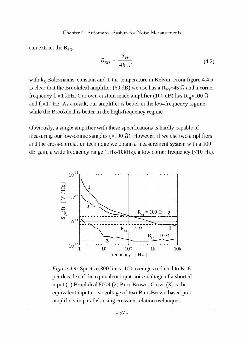
REQ
SVV
4kBT
1 10 100 1k 10k10-19
10-18
10-17
10-16
Req = 10 ΩReq = 45 Ω
Req = 100 Ω
3
22
1
1
S VV(f
) [
V2 /
Hz
]
frequency [ Hz ]
&KDSWHU$XWRPDWHG6\VWHPIRU1RLVH0HDVXUHPHQWV
- 57 -
(4.2)
Figure 4.4: Spectra (800 lines, 100 averages reduced to K=6
per decade) of the equivalent input noise voltage of a shorted
input (1) Brookdeal 5004 (2) Burr-Brown. Curve (3) is the
equivalent input noise voltage of two Burr-Brown based pre-
amplifiers in parallel, using cross-correlation techniques.
can extract the R :EQ
with k Boltzmanns' constant and T the temperature in Kelvin. From figure 4.4 itB
is clear that the Brookdeal amplifier (60 dB) we use has a R45 6 and a cornerEQ
frequency f1 kHz. Our own custom made amplifier (100 dB) has R100 6C eq
and f10 Hz. As a result, our amplifier is better in the low-frequency regimec
while the Brookdeal is better in the high-frequency regime.
Obviously, a single amplifier with these specifications is hardly capable of
measuring our low-ohmic samples (100 6). However, if we use two amplifiers
and the cross-correlation technique we obtain a measurement system with a 100
dB gain, a wide frequency range (1Hz-10kHz), a low corner frequency (<10 Hz),
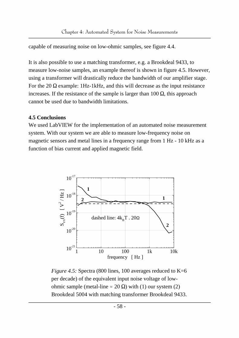
1 10 100 1k 10k10-21
10-20
10-19
10-18
10-17
dashed line: 4kBT . 20Ω
2
2 1
1
S VV(f
) [
V2 /
Hz
]
frequency [ Hz ]
&KDSWHU$XWRPDWHG6\VWHPIRU1RLVH0HDVXUHPHQWV
- 58 -
Figure 4.5: Spectra (800 lines, 100 averages reduced to K=6
per decade) of the equivalent input noise voltage of low-
ohmic sample (metal-line 20 6) with (1) our system (2)
Brookdeal 5004 with matching transformer Brookdeal 9433.
capable of measuring noise on low-ohmic samples, see figure 4.4.
It is also possible to use a matching transformer, e.g. a Brookdeal 9433, to
measure low-noise samples, an example thereof is shown in figure 4.5. However,
using a transformer will drastically reduce the bandwidth of our amplifier stage.
For the 20 6 example: 1Hz-1kHz, and this will decrease as the input resistance
increases. If the resistance of the sample is larger than 100 6, this approach
cannot be used due to bandwidth limitations.
4.5 ConclusionsWe used LabVIEW for the implementation of an automated noise measurement
system. With our system we are able to measure low-frequency noise on
magnetic sensors and metal lines in a frequency range from 1 Hz - 10 kHz as a
function of bias current and applied magnetic field.

&KDSWHU$XWRPDWHG6\VWHPIRU1RLVH0HDVXUHPHQWV
- 59 -
By using a bridge configuration we reduced the influence of: (1) the introduced
current noise in the bias circuit; (2) noise due to coherent temperature
fluctuations; and (3) noise introduced by the external magnetic field.
We have demonstrated that it is possible to use a custom-made amplifier, based
on a low-cost Burr-Brown INA1O3, to measure noise on low-ohmic samples
using cross-correlation techniques. We have also illustrated that it is possible to
measure noise on low-ohmic samples using a Brookdeal 5004 amplifier in
addition to a Brookdeal 9433 matching transformer, although the bandwidth of
this configuration is limited.
&KDSWHU(YLGHQFHIRUDQHZVRXUFHRIIQRLVHLQVLQJOHGRPDLQ1L )H ILOPV
- 60 -
5. Evidence for a new source of 1/f noisein single-domain Ni Fe films80 20
Submitted to Physical Review Letters [54].
This chapter contains an additional section 5.5
in which the temperature dependence is discussed.
AbstractWe have investigated the room-temperature 1/f noise and magneto-
resistance of single-domain Ni Fe films as a function of an in-plane80 20
magnetic field and as a function of the film volume. We introduce a
theoretical model which allows to determine the equilibrium angle of
magnetization Q of the sample directly from AC magnetoresistance data.0
Comparison of a plot of the 1/f noise power density versus Q with the0
susceptibility permits, for the first time, the observation of 1/f noise that
cannot be explained by the simple fluctuation-dissipation theorem for the
magnetization. An additional term in the magnetization noise is needed.
This term has its origin in the coupling between the magnetization and an
internal, non-magnetic fluctuator with a long-range character. We
speculate that lattice vibrations lead to these magnetization fluctuations.
Section 5.5 shows that the dependence of this noise source upon
temperature does not follow the Dutta, Dimon and Horn model [64].
5.1 IntroductionThe electrical resistance of magnetic films, showing the anisotropic magneto-
resistance (AMR) effect [6] and the giant magnetoresistance (GMR) effect [2], is
known to depend on the internal magnetization configuration of the sample.
Therefore, fluctuations in the magnetization can lead to fluctuations in the
resistance, a phenomenon used to explain the strong magnetic field dependence
of 1/f resistance noise found in GMR Co/Cu multi layers [3]. It was shown that
the fluctuation-dissipation theorem (FDT) [16] for the average magnetization
correctly explains the magnitude of the measured 1/f noise. A different
formulation of the FDT was used to explain the 1/f resistance noise in GMR and
&KDSWHU(YLGHQFHIRUDQHZVRXUFHRIIQRLVHLQVLQJOHGRPDLQ1L )H ILOPV
- 61 -
single-domain AMR films [55]. Another model uses fluctuating spin clusters of
varying sizes to explain the magnetic after effect and the 1/f noise for several
types of magnetic materials [56]. So far, the experimental 1/f noise of
ferromagnetic samples has not been compared to this model. Magnetic
fluctuations have been measured on a wide collection of magnetic systems, most
without using a magnetoresistance effect to probe the 1/f noise [7,57-61]. All
results agree with the FDT for the magnetic system, but these samples had
complicated magnetic structures.
In this chapter we will show for the first time that the 1/f noise of high-quality
single-domain ferromagnetic films cannot be explained by the FDT alone. Its
explanation needs an additional noise term, describing the coupling between
magnetization fluctuations and internal, non-magnetic fluctuations. We analyze
this new noise source, after the introduction of a model. This model explains the
dependence of the measured 1/f resistance noise on DC magnetic fields from the
response of the magnetoresistance upon AC magnetic fields. The great
significance of our result is the demonstration of the dominant character of this
new type of noise in our very pure and single-domain samples.
5.2 Measurement setup and sample preparationWe have grown Permalloy (Ni Fe ) films by high-vacuum magnetron sputtering80 20
on a Si (100) substrate in an applied magnetic field to induce an uniaxial
magneto-crystalline anisotropy parallel to the long axis of the samples. Two
parallel films are interconnected with patterned Au contacts to form Wheatstone
bridges. The electric contacts are placed at some distance from the ends of the
films to avoid the effects of closure domains in the resistive response. The
effective single-domain configuration between the contacts has been checked
with Bitter fluid and is electrically verified both by the absence of any discrete
jumps or hysteresis effects in the resistance and by the absence of Barkhausen
jumps in the noise. The width of the individual films varies from 2 to 70 µm. The
length of a sample in the bridge ranges from 7 to 22 times the width. The films
are either 35 or 40 nm thick. The resistivity of the Permalloy films is 38 µ6cm,
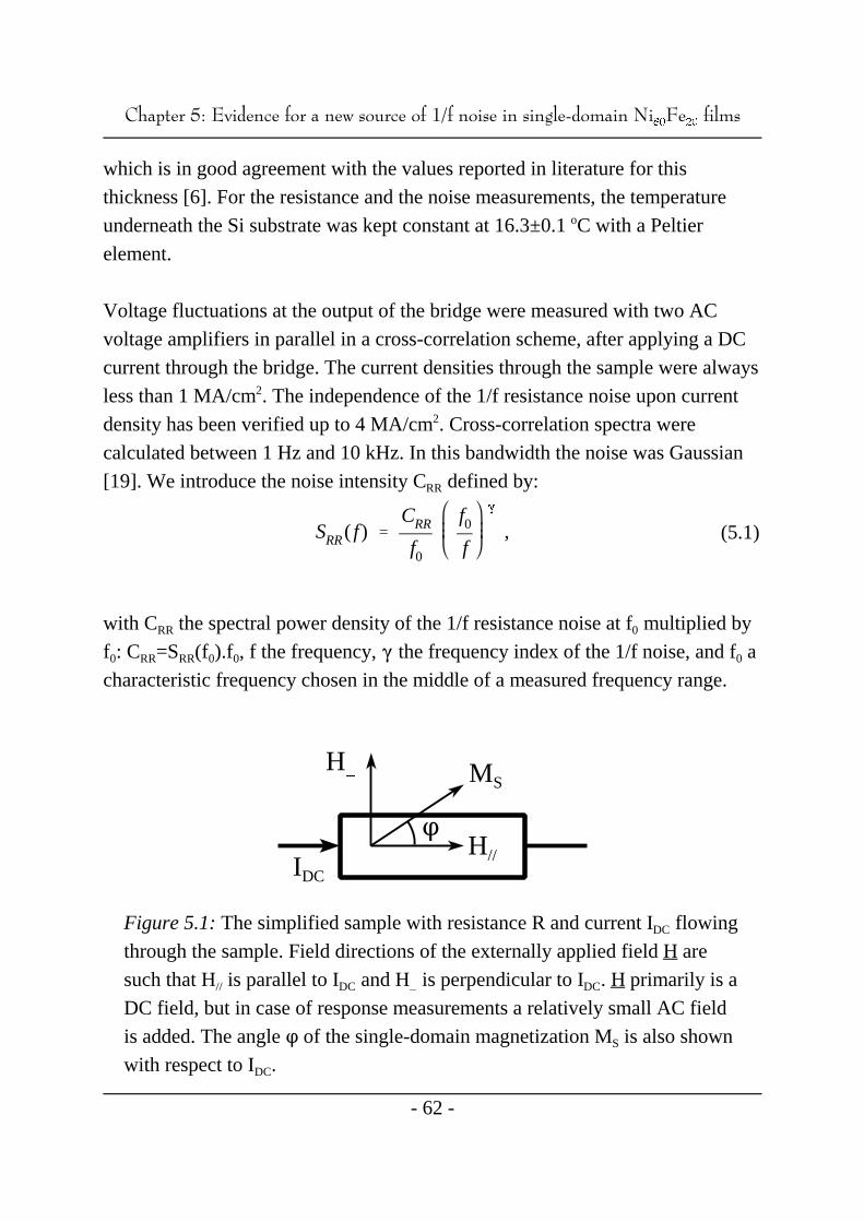
SRR( f)
CRR
f0
f0f
,
H//IDC
Q
H] MS
&KDSWHU(YLGHQFHIRUDQHZVRXUFHRIIQRLVHLQVLQJOHGRPDLQ1L )H ILOPV
- 62 -
(5.1)
Figure 5.1: The simplified sample with resistance R and current I flowingDC
through the sample. Field directions of the externally applied field H are
such that H is parallel to I and H is perpendicular to I . H primarily is a// DC ] DC
DC field, but in case of response measurements a relatively small AC field
is added. The angle Q of the single-domain magnetization M is also shownS
with respect to I .DC
which is in good agreement with the values reported in literature for this
thickness [6]. For the resistance and the noise measurements, the temperature
underneath the Si substrate was kept constant at 16.3±0.1 C with a Peltiero
element.
Voltage fluctuations at the output of the bridge were measured with two AC
voltage amplifiers in parallel in a cross-correlation scheme, after applying a DC
current through the bridge. The current densities through the sample were always
less than 1 MA/cm . The independence of the 1/f resistance noise upon current2
density has been verified up to 4 MA/cm . Cross-correlation spectra were2
calculated between 1 Hz and 10 kHz. In this bandwidth the noise was Gaussian
[19]. We introduce the noise intensity C defined by:RR
with C the spectral power density of the 1/f resistance noise at f multiplied byRR 0
f : C =S (f ).f , f the frequency, the frequency index of the 1/f noise, and f a0 RR RR 0 0 0
characteristic frequency chosen in the middle of a measured frequency range.
&KDSWHU(YLGHQFHIRUDQHZVRXUFHRIIQRLVHLQVLQJOHGRPDLQ1L )H ILOPV
- 63 -
The spectra were measured as function of a DC magnetic field H that wasDC
generated through a Helmholtz coil set with one field direction parallel and the
other perpendicular to the longitudinal direction of the films, which is
schematically shown in fig. 5.1. The outputs of the power supplies that generated
H were filtered with third order low-pass filters. These filters had a significantDC
effect on the reduction of 50 Hz and the higher harmonics in the spectra but did
not influence the 1/f noise component of the spectrum. Therefore, the measured
1/f noise did not originate from fluctuations in H.DC
The Helmholtz coil set was constructed such that each coil consisted of two
individual sub-coils. One was used to generate H, the other one to generate anDC
AC magnetic field H to measure the dynamic derivative of the resistance:AC
0R/0H. To do this, we applied 25 Hz, 1 A/m H fields. The linearity of theAC
magnetic response to external AC fields was verified up to a magnitude of 10
A/m. A more extensive description of the measurement setup can be found
elsewhere [42].
The field dependence of the resistance of a single domain AMR film can be
described as [6]: R(Q)=R +R .cos (Q), with Q the angle between the current0
2
through the sample and the internal magnetization M, R the field independentS 0
resistance component and R the maximum change in resistance due to magnetic
fields.
The low-frequency AC response of the magnetoresistance is used to extract the
equilibrium magnetization angle Q of the magnetization for a given applied0
magnetic field. First we measure 0R/0H with a small additional AC field parallel//
to the long axis of the sample. This response is proportional to 0Q/0H and can be//
evaluated with a first-order Taylor expansion of the derivative of the magnetic
potential energy density, 0E/0Q, in both Q and H . The response Q to H// //
will be such that 0E/0Q remains zero. The term 0 E/0Q0H is equal to µ M .sinQ2// 0 S
[1]. Hence, we obtain:
0Q
0H//Q Q0
H// H//0
µ0MSsin(Q)
02E(Q,H//0,H
]0) /0Q2
Q Q0
,
3Q
0Q
0H]M
µ0 MS
02E(Q) /0Q2
,
&KDSWHU(YLGHQFHIRUDQHZVRXUFHRIIQRLVHLQVLQJOHGRPDLQ1L )H ILOPV
- 64 -
(5.2)
(5.3)
with µ the permeability of vacuum, M and Q the magnitude and angle of the0 S 0
spontaneous magnetization and H and H are the DC magnetic fields parallel//0 ]0
and perpendicular to the sample.
A similar expression can be derived for 0Q/0H , the relation being almost]
identical except for the sign and a cosine term instead of a sine term in the
nominator. With these two relations, each multiplied by 0R/0Q, the equilibrium
angle of the magnetization (Q ) can be directly derived from the AC0
measurements: Q =arctan(0R/0H / 0R/0H ).0 // ]
From the measured response to the AC fields of H and H , also the angular// ]
susceptibility for magnetic fields perpendicular to the magnetization (H ) can]M
be calculated. We will call this quantity the angular susceptibility 3 . ConformQ
eq. (5.2), 3 is defined as:Q
and 3 can be experimentally determined based on the relation:Q
(0R/0H ) = (0R/0H ) + (0R/0H ) .]M // ]
2 2 2
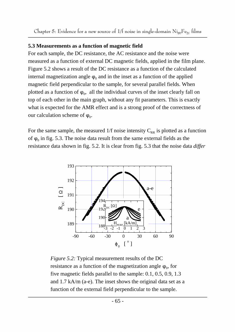
-90 -60 -30 0 30 60 90
189
190
191
192
193
a-e
RD
C
[ Ω
]
ϕ0 [ o ]
-3 -2 -1 0 1 2 3188
190
192
194
e
a
HPERP
[kA/m]
RDC
[Ω]
&KDSWHU(YLGHQFHIRUDQHZVRXUFHRIIQRLVHLQVLQJOHGRPDLQ1L )H ILOPV
- 65 -
Figure 5.2: Typical measurement results of the DC
resistance as a function of the magnetization angle Q , for0
five magnetic fields parallel to the sample: 0.1, 0.5, 0.9, 1.3
and 1.7 kA/m (a-e). The inset shows the original data set as a
function of the external field perpendicular to the sample.
5.3 Measurements as a function of magnetic fieldFor each sample, the DC resistance, the AC resistance and the noise were
measured as a function of external DC magnetic fields, applied in the film plane.
Figure 5.2 shows a result of the DC resistance as a function of the calculated
internal magnetization angle Q and in the inset as a function of the applied0
magnetic field perpendicular to the sample, for several parallel fields. When
plotted as a function of Q , all the individual curves of the inset clearly fall on0
top of each other in the main graph, without any fit parameters. This is exactly
what is expected for the AMR effect and is a strong proof of the correctness of
our calculation scheme of Q .0
For the same sample, the measured 1/f noise intensity C is plotted as a functionRR
of Q in fig. 5.3. The noise data result from the same external fields as the0
resistance data shown in fig. 5.2. It is clear from fig. 5.3 that the noise data differ
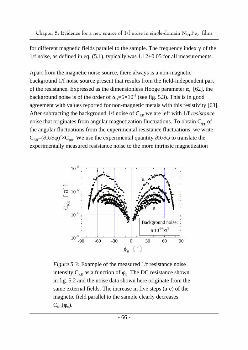
-90 -60 -30 0 30 60 9010
-14
10-13
10-12
10-11
a
e
Background noise:
6 10-14
Ω2
CR
R
[ Ω
2 ]
ϕ0 [ o ]
&KDSWHU(YLGHQFHIRUDQHZVRXUFHRIIQRLVHLQVLQJOHGRPDLQ1L )H ILOPV
- 66 -
Figure 5.3: Example of the measured 1/f resistance noise
intensity C as a function of Q . The DC resistance shownRR 0
in fig. 5.2 and the noise data shown here originate from the
same external fields. The increase in five steps (a-e) of the
magnetic field parallel to the sample clearly decreases
C (Q ).RR 0
for different magnetic fields parallel to the sample. The frequency index of the
1/f noise, as defined in eq. (5.1), typically was 1.12±0.05 for all measurements.
Apart from the magnetic noise source, there always is a non-magnetic
background 1/f noise source present that results from the field-independent part
of the resistance. Expressed as the dimensionless Hooge parameter [62], theH
background noise is of the order of =5×10 (see fig. 5.3). This is in goodH-4
agreement with values reported for non-magnetic metals with this resistivity [63].
After subtracting the background 1/f noise of C we are left with 1/f resistanceRR
noise that originates from angular magnetization fluctuations. To obtain C ofQQ
the angular fluctuations from the experimental resistance fluctuations, we write:
C =(0R/0Q) ×C . We use the experimental quantity 0R/0Q to translate theRR QQ
2
experimentally measured resistance noise to the more intrinsic magnetization
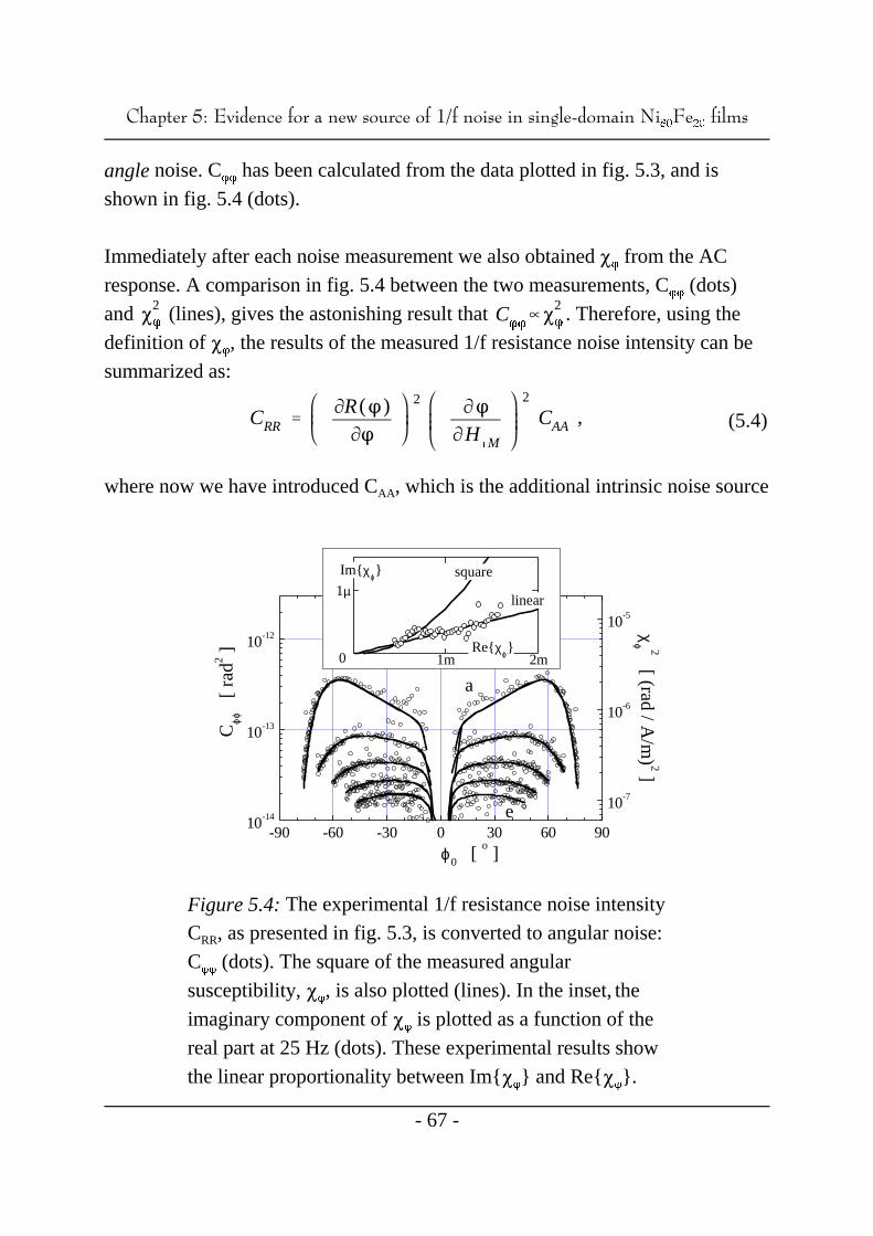
-90 -60 -30 0 30 60 9010-14
10-13
10-12
Cϕϕ
[
rad2 ]
ϕ0 [ o ]
10-7
10-6
10-5
e
a
χϕ 2 [ (ra
d / A/m
) 2 ]
1m 2m
1µlinear
square
0
Imχϕ
Reχϕ
CRR 0R(Q )0Q
20Q
0H]M
2
CAA ,
32Q
CQQ3
2Q
&KDSWHU(YLGHQFHIRUDQHZVRXUFHRIIQRLVHLQVLQJOHGRPDLQ1L )H ILOPV
- 67 -
Figure 5.4: The experimental 1/f resistance noise intensity
C , as presented in fig. 5.3, is converted to angular noise:RR
C (dots). The square of the measured angularQQ
susceptibility, 3 , is also plotted (lines). In the inset, theQ
imaginary component of 3 is plotted as a function of theQ
real part at 25 Hz (dots). These experimental results show
the linear proportionality between Im3 and Re3 .Q Q
(5.4)
angle noise. C has been calculated from the data plotted in fig. 5.3, and isQQ
shown in fig. 5.4 (dots).
Immediately after each noise measurement we also obtained 3 from the ACQ
response. A comparison in fig. 5.4 between the two measurements, C (dots)QQ
and (lines), gives the astonishing result that . Therefore, using the
definition of 3 , the results of the measured 1/f resistance noise intensity can beQ
summarized as:
where now we have introduced C , which is the additional intrinsic noise sourceAA
&KDSWHU(YLGHQFHIRUDQHZVRXUFHRIIQRLVHLQVLQJOHGRPDLQ1L )H ILOPV
- 68 -
that is independent of the applied magnetic fields and looks like an external
magnetic noise source.
However, we will argue now that this noise source is not external, but generated
internally in the sample itself. Indeed, the noise intensity C has been measuredAA
for several samples with volumes between 10 and 10 m . In this range, C is-17 -14 3AA
inversely proportional to the volume: 1.6×10 /Vol ±20% (A/m) with Vol the-21 2
volume of the sample in m . If this 1/f noise intensity is normalized per spin,3
similar to the normalization per electron [62], the dimensionless 1/f noise
parameter becomes: 2×10 . The noise intensity C is not generated externally-4AA
because of its inverse volume dependence and because two-point measurements
gave the same results.
Furthermore, the noise cannot be explained by a large collection of individually
fluctuating spins or spin clusters as suggested in [56] because it has a long-range
character. This can be concluded from the dependence upon 3 : in case ofQ
individual fluctuators, the dynamics would depend on the local susceptibility
which is dominated by exchange interactions and therefore the resulting noise
would be independent of the global susceptibility 3 .Q
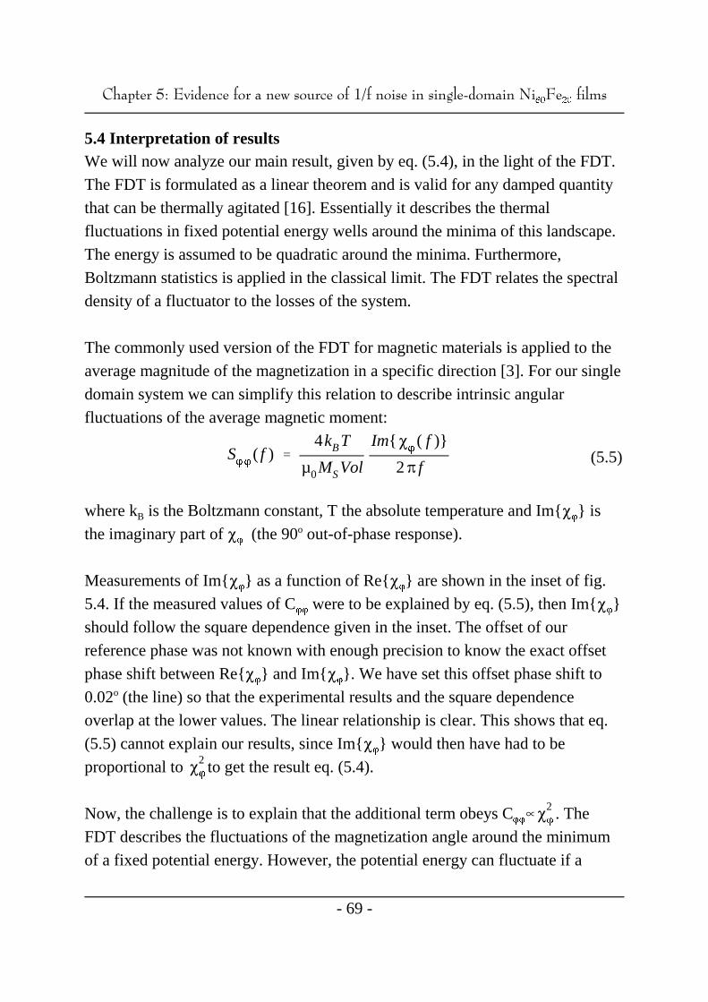
SQQ
( f )
4kBT
µ0MSVol
Im 3Q( f )
2% f
32Q
32Q
&KDSWHU(YLGHQFHIRUDQHZVRXUFHRIIQRLVHLQVLQJOHGRPDLQ1L )H ILOPV
- 69 -
(5.5)
5.4 Interpretation of resultsWe will now analyze our main result, given by eq. (5.4), in the light of the FDT.
The FDT is formulated as a linear theorem and is valid for any damped quantity
that can be thermally agitated [16]. Essentially it describes the thermal
fluctuations in fixed potential energy wells around the minima of this landscape.
The energy is assumed to be quadratic around the minima. Furthermore,
Boltzmann statistics is applied in the classical limit. The FDT relates the spectral
density of a fluctuator to the losses of the system.
The commonly used version of the FDT for magnetic materials is applied to the
average magnitude of the magnetization in a specific direction [3]. For our single
domain system we can simplify this relation to describe intrinsic angular
fluctuations of the average magnetic moment:
where k is the Boltzmann constant, T the absolute temperature and Im3 isB Q
the imaginary part of 3 (the 90 out-of-phase response).Q
o
Measurements of Im3 as a function of Re3 are shown in the inset of fig.Q Q
5.4. If the measured values of C were to be explained by eq. (5.5), then Im3 QQ Q
should follow the square dependence given in the inset. The offset of our
reference phase was not known with enough precision to know the exact offset
phase shift between Re3 and Im3 . We have set this offset phase shift toQ Q
0.02 (the line) so that the experimental results and the square dependenceo
overlap at the lower values. The linear relationship is clear. This shows that eq.
(5.5) cannot explain our results, since Im3 would then have had to beQ
proportional to to get the result eq. (5.4).
Now, the challenge is to explain that the additional term obeys C . TheQQ
FDT describes the fluctuations of the magnetization angle around the minimum
of a fixed potential energy. However, the potential energy can fluctuate if a
SQQ
( f )
4kBT
µ0MSVol
Im 3Q( f )
2% f 3
2Q( f )
CAA
f0
f0f
,
32Q
&KDSWHU(YLGHQFHIRUDQHZVRXUFHRIIQRLVHLQVLQJOHGRPDLQ1L )H ILOPV
- 70 -
(5.6)
different, non-magnetic, parameter fluctuates and thereby fluctuations in its
minimum will occur. As a result, the magnetization angle Q will respond to these
fluctuations, which results in C .QQ
Therefore, our experimental results suggest that there must be an additional noise
source present that causes the minimum of the magnetic energy to fluctuate. The
resulting fluctuations in Q are larger than the simultaneously present fluctuations
from the FDT. This noise source is non-magnetic, otherwise it would influence
the magnetization directly. It interacts with the magnetization on a long-range
scale. We speculate that this 1/f noise source is in the lattice vibrations. The
coupling of phonons and magnons then leads to long-range magnetic
fluctuations.
We propose the complete expression for magnetization noise to be:
where the first term on the right-hand side is a result of the magnetic FDT and
the second term results from a source external to the magnetic system. C isAA
inversely proportional to the sample volume.
In the first place, it is clear from this relation that when the magnetic losses are
increased, the FDT type of noise is more likely to dominate. A good example of
such a situation is a magnetic system with a complicated domain structure.
Secondly, if one assumes that Im3 is proportional to 3, which is approximately
correct, then S has a linear and a quadratic term in 3. Hence, for very pureQQ
samples with a large 3 it is more likely that the second term dominates.
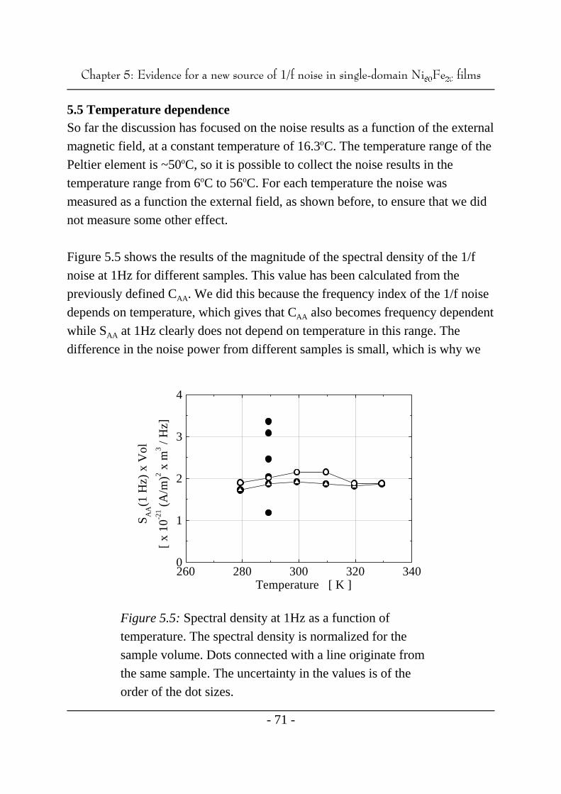
260 280 300 320 3400
1
2
3
4
S AA(1
Hz)
x V
ol
[ x
10-2
1 (A
/m)2 x
m3 /
Hz]
Temperature [ K ]
&KDSWHU(YLGHQFHIRUDQHZVRXUFHRIIQRLVHLQVLQJOHGRPDLQ1L )H ILOPV
- 71 -
Figure 5.5: Spectral density at 1Hz as a function of
temperature. The spectral density is normalized for the
sample volume. Dots connected with a line originate from
the same sample. The uncertainty in the values is of the
order of the dot sizes.
5.5 Temperature dependenceSo far the discussion has focused on the noise results as a function of the external
magnetic field, at a constant temperature of 16.3 C. The temperature range of theo
Peltier element is ~50 C, so it is possible to collect the noise results in theo
temperature range from 6 C to 56 C. For each temperature the noise waso o
measured as a function the external field, as shown before, to ensure that we did
not measure some other effect.
Figure 5.5 shows the results of the magnitude of the spectral density of the 1/f
noise at 1Hz for different samples. This value has been calculated from the
previously defined C . We did this because the frequency index of the 1/f noiseAA
depends on temperature, which gives that C also becomes frequency dependentAA
while S at 1Hz clearly does not depend on temperature in this range. TheAA
difference in the noise power from different samples is small, which is why we
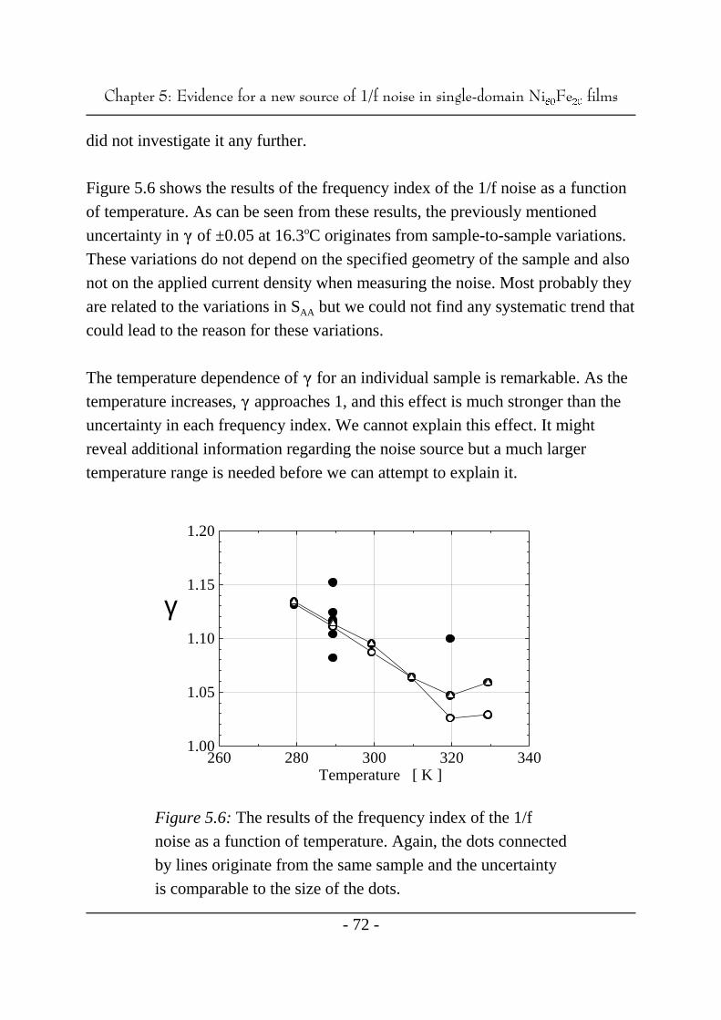
260 280 300 320 3401.00
1.05
1.10
1.15
1.20
γ
Temperature [ K ]
&KDSWHU(YLGHQFHIRUDQHZVRXUFHRIIQRLVHLQVLQJOHGRPDLQ1L )H ILOPV
- 72 -
Figure 5.6: The results of the frequency index of the 1/f
noise as a function of temperature. Again, the dots connected
by lines originate from the same sample and the uncertainty
is comparable to the size of the dots.
did not investigate it any further.
Figure 5.6 shows the results of the frequency index of the 1/f noise as a function
of temperature. As can be seen from these results, the previously mentioned
uncertainty in of ±0.05 at 16.3 C originates from sample-to-sample variations.o
These variations do not depend on the specified geometry of the sample and also
not on the applied current density when measuring the noise. Most probably they
are related to the variations in S but we could not find any systematic trend thatAA
could lead to the reason for these variations.
The temperature dependence of for an individual sample is remarkable. As the
temperature increases, approaches 1, and this effect is much stronger than the
uncertainty in each frequency index. We cannot explain this effect. It might
reveal additional information regarding the noise source but a much larger
temperature range is needed before we can attempt to explain it.

DDH( f ,T) 1 1
ln 2% f-0
1 0 lnS( f ,T)
0 lnT,
&KDSWHU(YLGHQFHIRUDQHZVRXUFHRIIQRLVHLQVLQJOHGRPDLQ1L )H ILOPV
- 73 -
(5.7)
We can compare the temperature dependence of with the famous Dutta, Dimon
and Horn (DDH) model for 1/f noise in metals that relates (T) to S(T) [64].
Here we will not discuss the details of this model, for reviews see [65,66]. The
result of their successful model is:
with - the characteristic attempt time of a thermally activated process, which is0
assumed to be temperature independent. Generally - is of the order of 10 sec.0-13
Note that in this model the frequency index of the 1/f noise, , depends onDDH
frequency.
At 1Hz we have shown that S is temperature independent and we have alsoAA
shown that the measured is larger than 1 at all temperatures. Hence, if = ,DDH
- must be larger than 1/2%0.16 seconds to explain >1. For instance, from0
figure 5.6 we have at 6 C: ~1.135<- ~260 sec., which is a ridiculous resulto0
when compared to the expected 10 sec.-13
Furthermore, at 1Hz S is temperature independent hence should alsoLL DDH
temperature independent in the measured temperature range. Clearly our results
contradict this and therefore we have to dismiss the DDH-model for our noise
source.

&KDSWHU(YLGHQFHIRUDQHZVRXUFHRIIQRLVHLQVLQJOHGRPDLQ1L )H ILOPV
- 74 -
5.6 ConclusionsWe have investigated the room-temperature 1/f noise of single-domain Ni Fe80 20
films as a function of an in-plane magnetic field. By combining these noise
measurements with AC magnetoresistance measurements, we proved the
correctness of a theoretical model, which allowed the determination of the
equilibrium angle of the magnetization Q and the susceptibility. The comparison0
of the plot of 1/f noise power versus Q with the results of the susceptibility0
showed that magnetic fluctuations cannot be explained by the fluctuation-
dissipation theorem. We suggest that the origin for this new type of
magnetization noise is in the lattice vibrations. Measurements around room
temperature show that this noise source is not consistent with the Dutta, Dimon
and Horn model.
&KDSWHUI1RLVHLQPXOWLGRPDLQ1L )H ILOPV
- 75 -
6. 1/f Noise in multi-domain Ni Fe films80 20
The results on single layer films were presented in 1997 at the
International Conference on Noise in physical systems and 1/f Fluctuations [50].
Results on multi-layer films were published in Journal of Applied Physics [67].
These publications are not reproduced here as such. Not because of errors in the
publications, but because these papers were written before we knew the results
on single domain films, as presented in chapter 5.
AbstractWe investigated the room-temperature 1/f noise of soft magnetic Ni Fe80 20
films with a few domain walls, and of Ni Fe /Cu magnetic multi-layers80 20
with a complicated domain-wall structure. The results suggest that
domain walls do not directly contribute to the noise, they only influence
the dependence of the noise upon external fields.
6.1 IntroductionThe previous chapter showed that for single-domain films there is a clear relation
between the anisotropic magneto resistance (AMR) effect [6] and the measured
1/f noise because the magnetization noise modulates the resistance. This effect is
already visible in a direct comparison of a resistance curve with noise. This
behavior will also be present within a each domain of multi-domain Ni Fe . But80 20
the position of a domain wall could also fluctuate, which may lead to additional
noise.
We will investigate this possibility of fluctuating walls with two kinds of
previously published results on multi-domain samples [50,67]. The first kind
consists of results on single film Ni Fe and the second consists of results on80 20
layered Ni Fe films with Cu-layers in between. The multi-layer samples give80 20
rise to a giant magneto resistance (GMR) effect [2] in addition to the AMR
effect. In case of magnetization noise the difference between the two effects is

&KDSWHUI1RLVHLQPXOWLGRPDLQ1L )H ILOPV
- 76 -
Figure 6.1: Pictures of Bitter patterns of single-film
permalloy samples. As indicated the width of the film at the
top is 30µm, while the one on the bottom is 50µm.
not that important: in both cases the magnetization modulates the resistance, only
the exact transfer function differs.
In this chapter, the 1/f noise power will only be given as C because it is notRR
possible to do any further normalization in a magnetically inhomogeneous
sample. The frequency index of the 1/f noise for the single layers is
approximately 1.1, for multi layers it is about 0.9 but we did not investigate this
any further.
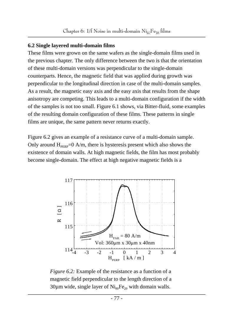
-4 -3 -2 -1 0 1 2 3 4114
115
116
117
HPAR
= 80 A/mVol: 360µm x 30µm x 40nm
R
[ Ω
]
HPERP
[ kA / m ]
&KDSWHUI1RLVHLQPXOWLGRPDLQ1L )H ILOPV
- 77 -
Figure 6.2: Example of the resistance as a function of a
magnetic field perpendicular to the length direction of a
30µm wide, single layer of Ni Fe with domain walls.80 20
6.2 Single layered multi-domain filmsThese films were grown on the same wafers as the single-domain films used in
the previous chapter. The only difference between the two is that the orientation
of these multi-domain versions was perpendicular to the single-domain
counterparts. Hence, the magnetic field that was applied during growth was
perpendicular to the longitudinal direction in case of the multi-domain samples.
As a result, the magnetic easy axis and the easy axis that results from the shape
anisotropy are competing. This leads to a multi-domain configuration if the width
of the samples is not too small. Figure 6.1 shows, via Bitter-fluid, some examples
of the resulting domain configuration of these films. These patterns in single
films are unique, the same pattern never returns exactly.
Figure 6.2 gives an example of a resistance curve of a multi-domain sample.
Only around H =0 A/m, there is hysteresis present which also shows thePERP
existence of domain walls. At high magnetic fields, the film has most probably
become single-domain. The effect at high negative magnetic fields is a
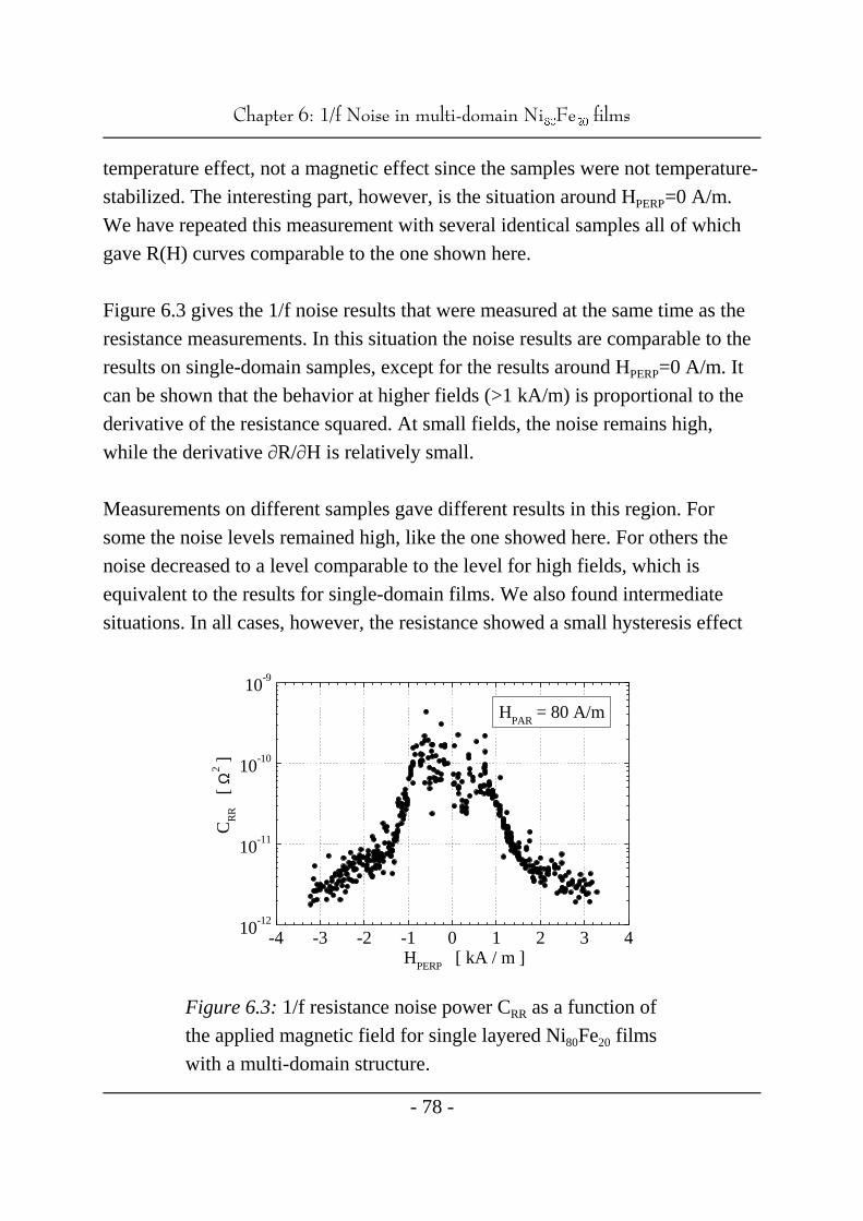
-4 -3 -2 -1 0 1 2 3 410-12
10-11
10-10
10-9
HPAR
= 80 A/m
CR
R
[ Ω2 ]
HPERP
[ kA / m ]
&KDSWHUI1RLVHLQPXOWLGRPDLQ1L )H ILOPV
- 78 -
Figure 6.3: 1/f resistance noise power C as a function ofRR
the applied magnetic field for single layered Ni Fe films80 20
with a multi-domain structure.
temperature effect, not a magnetic effect since the samples were not temperature-
stabilized. The interesting part, however, is the situation around H =0 A/m.PERP
We have repeated this measurement with several identical samples all of which
gave R(H) curves comparable to the one shown here.
Figure 6.3 gives the 1/f noise results that were measured at the same time as the
resistance measurements. In this situation the noise results are comparable to the
results on single-domain samples, except for the results around H =0 A/m. ItPERP
can be shown that the behavior at higher fields (>1 kA/m) is proportional to the
derivative of the resistance squared. At small fields, the noise remains high,
while the derivative 0R/0H is relatively small.
Measurements on different samples gave different results in this region. For
some the noise levels remained high, like the one showed here. For others the
noise decreased to a level comparable to the level for high fields, which is
equivalent to the results for single-domain films. We also found intermediate
situations. In all cases, however, the resistance showed a small hysteresis effect
&KDSWHUI1RLVHLQPXOWLGRPDLQ1L )H ILOPV
- 79 -
as in figure 6.2, which indicates the presence of domain walls.
It is unlikely that this spread in the noise results of two orders in magnitude can
be explained with fluctuating domain walls, because the walls were present in all
cases. Most probably the exact amount and configuration will differ each time
but these changes in itself are minor compared to the significant differences in
noise levels.
Furthermore, within the magnetic field range of -1 kA/m to 1 kA/m, the noise
does not change significantly in figure 6.3 although the resistance change is
substantial. We can explain this the following way: suppose that H isPERP
increased from 0 to 1 kA/m. Due to domain-wall movement, the areas with a
high resistivity (Q0 ) decrease in favor of areas with a low resistivity (Q90 ).o o
But for both type of areas the noise contribution is minimal, as was shown in the
previous chapter. This could explain why the noise remains constant: the noisy
islands (e.g. Q45 ) that are responsible for the 1/f noise measured are noto
influenced during the domain-wall movement. Only when the samples starts to
enter a single-domain phase, they are influenced as well.
This behavior can also explain the large sample-to-sample differences in noise
levels. As can be concluded from the relatively large resistance changes in this
field range while the noise does not change, these noisy islands can only occupy
a small fraction of the total volume. Furthermore, the amount of domain walls is
limited, see figure 6.1. Hence, both the number and size of the noisy islands is
small. Statistically, these small numbers can strongly vary from sample to
sample, which can explain the large differences in the individual noise levels.
-150 -100 -50 0 50 100 15059.2
59.4
59.6
59.8
60.0
60.2
R
[ Ω ]
HPERP [ kA / m ]
&KDSWHUI1RLVHLQPXOWLGRPDLQ1L )H ILOPV
- 80 -
Figure 6.4: Magneto resistance curve of a 2µm×100µm
micro-structured 60×[1.6nm Ni Fe +1.9nm Cu] multi-80 20
layer.
6.3 Multi-layered multi-domain samplesThese samples consist of individual layers of Ni Fe with a thickness of 1.6 nm80 20
with a non-magnetic Cu-layer with a thickness of 1.9 nm in between two
permalloy layers. A stack can consist of 20 up to 100 individual Ni Fe layers.80 20
Details of the sample manufacturing are given in [67]. This reference also gives a
Bitter-fluid picture of the dense, and complex domain wall pattern on top of a
sample. Because the sample has a layered structure, this domain wall pattern on
top does not have to be representative for the entire sample but it seems likely
that it is.
Figure 6.4 shows an example of the magneto-resistance curve of a multi-layer
structure. The hysteresis effect is clear, hence the complex domain-wall pattern
persists over a substantial part of the sample and remains present even in high
magnetic fields. Measurements with a vibrating sample magneto-meter showed
that about 1/3 of the volume fraction of this particular sample was coupled anti-
ferromagnetically, which leads to the GMR effect.
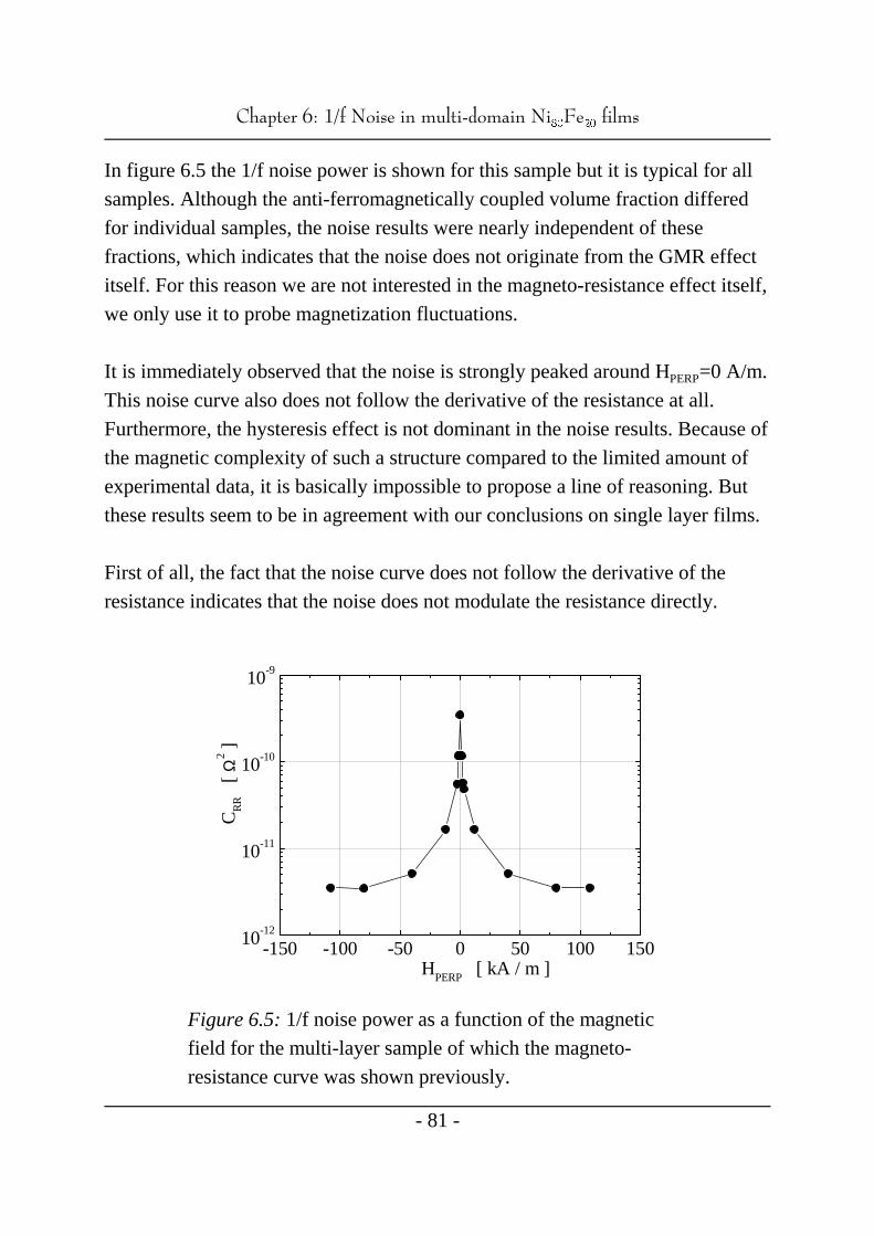
-150 -100 -50 0 50 100 15010-12
10-11
10-10
10-9
CR
R
[ Ω2 ]
HPERP
[ kA / m ]
&KDSWHUI1RLVHLQPXOWLGRPDLQ1L )H ILOPV
- 81 -
Figure 6.5: 1/f noise power as a function of the magnetic
field for the multi-layer sample of which the magneto-
resistance curve was shown previously.
In figure 6.5 the 1/f noise power is shown for this sample but it is typical for all
samples. Although the anti-ferromagnetically coupled volume fraction differed
for individual samples, the noise results were nearly independent of these
fractions, which indicates that the noise does not originate from the GMR effect
itself. For this reason we are not interested in the magneto-resistance effect itself,
we only use it to probe magnetization fluctuations.
It is immediately observed that the noise is strongly peaked around H =0 A/m.PERP
This noise curve also does not follow the derivative of the resistance at all.
Furthermore, the hysteresis effect is not dominant in the noise results. Because of
the magnetic complexity of such a structure compared to the limited amount of
experimental data, it is basically impossible to propose a line of reasoning. But
these results seem to be in agreement with our conclusions on single layer films.
First of all, the fact that the noise curve does not follow the derivative of the
resistance indicates that the noise does not modulate the resistance directly.
&KDSWHUI1RLVHLQPXOWLGRPDLQ1L )H ILOPV
- 82 -
Hence, the mechanism that leads to changes in the resistance (domain wall
movement) cannot be identified as the mechanism responsible for the dynamics
of the magnetization.
The rapid decrease of the noise with an increasing magnitude of H also showsPERP
that the domain walls itself cannot be responsible. For the relatively small fields
in which the noise already drops more then a factor 10, the domain walls do not
significancy decrease in number or length. Therefore, only the areas they enclose
change. This behavior can be explained with noisy islands: domain-wall
movement strongly influences the volume-fraction of the noisy islands in this
situation and therefore the total noise.
We cannot explain the fact that the noise curve does not show any significant
hysteresis effect. One might think that the volume-fraction that leads to resistance
changes could differ from the part that is responsible for the noise. However, we
have too little information, to speculate at this point.
6.4 ConclusionsThe study of multi-domain samples supports the concept that the 1/f noise
originates only within the sub-domains, just as in single-domain samples. 1/f
Noise is due to fluctuations in the magnetization angle of each sub-domain. As a
result, the contribution of individual sub-domains to the total noise can differ
significantly: there are noisy islands.

&KDSWHU3ULQFLSOHVRIVXEVWUDWHFURVVWDONJHQHUDWLRQLQ&026FLUFXLWV
- 83 -
7. Principles of substrate crosstalk generation in CMOS circuitsAccepted for publication in IEEE Transactions on
Computer-Aided Design of Integrated Circuits and Systems [68].
AbstractSubstrate noise injection was evaluated for a 0.25µm CMOS technology,
to determine the mechanisms that contribute to substrate crosstalk. At the
transistor level, we found that impact ionization current and capacitive
coupling from the junctions are the most significant contributors to
substrate current injection. Our investigation of substrate fluctuations at
a circuit level included switching transients, capacitive damping, and
separate substrate biasing. This investigation revealed that voltage
transients on power supply lines can be the dominant source of substrate
fluctuations. Finally, a statistical analysis of signal cancellation in an IC
was performed. The results indicate that more cancellation will take place
for the high-frequency noise components than for the DC and low-
frequency components. As a consequence, the DC and low frequency
components of the transient that results from an individual switching
event cannot be neglected even if they are a small fraction of the single
transient.
7.1 IntroductionAnalog circuits are integrated with large digital circuits to form high-
performance mixed-signal chips. This aggressive integration places new demands
on on-chip electrical isolation. Noise due to switching of digital circuitry can
couple to the sensitive analog circuits and degrade overall performance. One
significant path for this noise coupling is through the common silicon substrate.
In order to correctly model and predict substrate crosstalk, and to develop
techniques to minimize it, a detailed understanding is required of how the
coupling occurs.
Substrate crosstalk can be broken down into three parts, as illustrated
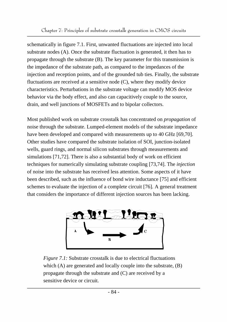
#
$
%
&KDSWHU3ULQFLSOHVRIVXEVWUDWHFURVVWDONJHQHUDWLRQLQ&026FLUFXLWV
- 84 -
Figure 7.1: Substrate crosstalk is due to electrical fluctuations
which (A) are generated and locally couple into the substrate, (B)
propagate through the substrate and (C) are received by a
sensitive device or circuit.
schematically in figure 7.1. First, unwanted fluctuations are injected into local
substrate nodes (A). Once the substrate fluctuation is generated, it then has to
propagate through the substrate (B). The key parameter for this transmission is
the impedance of the substrate path, as compared to the impedances of the
injection and reception points, and of the grounded tub ties. Finally, the substrate
fluctuations are received at a sensitive node (C), where they modify device
characteristics. Perturbations in the substrate voltage can modify MOS device
behavior via the body effect, and also can capacitively couple to the source,
drain, and well junctions of MOSFETs and to bipolar collectors.
Most published work on substrate crosstalk has concentrated on propagation of
noise through the substrate. Lumped-element models of the substrate impedance
have been developed and compared with measurements up to 40 GHz [69,70].
Other studies have compared the substrate isolation of SOI, junction-isolated
wells, guard rings, and normal silicon substrates through measurements and
simulations [71,72]. There is also a substantial body of work on efficient
techniques for numerically simulating substrate coupling [73,74]. The injection
of noise into the substrate has received less attention. Some aspects of it have
been described, such as the influence of bond wire inductance [75] and efficient
schemes to evaluate the injection of a complete circuit [76]. A general treatment
that considers the importance of different injection sources has been lacking.
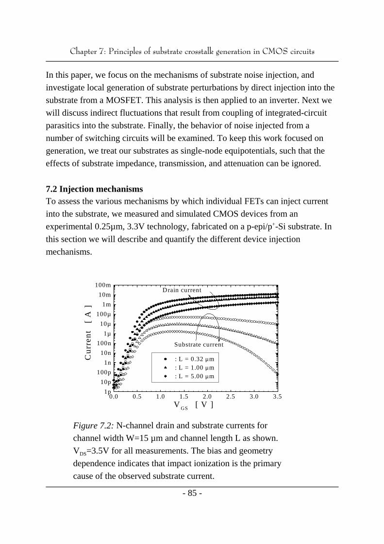
0.0 0.5 1.0 1.5 2.0 2.5 3.0 3.51p
10p
100p
1n
10n
100n
1µ
10µ
100µ
1m
10m
100m
Substrate current
Drain current
: L = 0.32 µm: L = 1.00 µm: L = 5.00 µm
Cu
rre
nt
[
A ]
V GS [ V ]
&KDSWHU3ULQFLSOHVRIVXEVWUDWHFURVVWDONJHQHUDWLRQLQ&026FLUFXLWV
- 85 -
Figure 7.2: N-channel drain and substrate currents for
channel width W=15 µm and channel length L as shown.
V =3.5V for all measurements. The bias and geometryDS
dependence indicates that impact ionization is the primary
cause of the observed substrate current.
In this paper, we focus on the mechanisms of substrate noise injection, and
investigate local generation of substrate perturbations by direct injection into the
substrate from a MOSFET. This analysis is then applied to an inverter. Next we
will discuss indirect fluctuations that result from coupling of integrated-circuit
parasitics into the substrate. Finally, the behavior of noise injected from a
number of switching circuits will be examined. To keep this work focused on
generation, we treat our substrates as single-node equipotentials, such that the
effects of substrate impedance, transmission, and attenuation can be ignored.
7.2 Injection mechanismsTo assess the various mechanisms by which individual FETs can inject current
into the substrate, we measured and simulated CMOS devices from an
experimental 0.25µm, 3.3V technology, fabricated on a p-epi/p -Si substrate. In+
this section we will describe and quantify the different device injection
mechanisms.

0.0 0.5 1.0 1.5 2.0 2.5 3.0 3.51p
10p
100p
1n
10n
100n
1µ
10µ
100µ
1m
10m
100m
Substrate current
Drain current
: L = 0.32 µm: L = 1.00 µm: L = 5.00 µm
Cu
rre
nt
[
-A ]
VSG
[ V ]
&KDSWHU3ULQFLSOHVRIVXEVWUDWHFURVVWDONJHQHUDWLRQLQ&026FLUFXLWV
- 86 -
Figure 7.3: P-channel drain and substrate currents for
channel width W=15 µm and channel length L as shown.
V =3.5 V for all measurements. For low source-gateSD
voltages gate induced drain leakage (GIDL) is the dominant
substrate contribution, for higher voltages impact ionization
current dominates.
7.2.1 Impact ionization current
When a MOS transistor is biased in the saturation regime, a high electric field
develops in the depleted region of the channel near the drain. Some fraction of
the carriers in this region will gain enough energy to become "hot" [77,78].
When these hot carriers do eventually scatter, they can dissipate their excess
energy by creating additional electron-hole pairs, in a process known as impact
ionization. For an NMOS transistor, the holes created by impact ionization are
swept to the substrate, such that the transistor has current flowing from the drain
into the substrate. In studies addressing the damaging effects of hot electrons,
this substrate current is often examined, because it is an easily measurable
quantity that is correlated to the hot carriers of interest. In contrast, the focus of
this work is the substrate current itself, since it can lead to fluctuations in bulk
potential as it flows through the resistive substrate.
0.0 0.5 1.0 1.5 2.0 2.5 3.0 3.510
-8
10-7
10-6
10-5
10-4
10-3
10-2
10-1
100
closed: n-mosfetopen: p-mosfet
V DS or VSD = 3.5 V
: L = 0.32 µ m: L = 1.00 µ m: L = 5.00 µ m
I SU
BS
TR
AT
E / I D
RA
IN
V GS or VSG [ V ]
&KDSWHU3ULQFLSOHVRIVXEVWUDWHFURVVWDONJHQHUDWLRQLQ&026FLUFXLWV
- 87 -
Figure 7.4: Normalized substrate currents for n-channel and
p-channel MOS transistors. The relative n-channel impact
ionization current is seen to be at least a factor of ten higher
than for the p-channel devices.
Figure 7.2 shows the drain and substrate currents measured on NMOS transistors
with three different channel lengths, as a function of the gate-source voltage V .GS
The observed substrate current is due to impact ionization over this entire range
of bias conditions. Figure 7.3 shows the same currents measured on PMOS
transistors. For these p-channel devices, gate induced drain leakage (GIDL) also
causes significant substrate currents at low values of V .SG
The proportionality between I and I is shown in Figure 7.4, for both NMOSSUB D
and PMOS transistors. The relative level of impact ionization current is seen to
depend exponentially on V At low gate voltages, where the transistors are inGS.
deep saturation, the impact ionization current is independent of channel length.
At higher gate voltages, the behavior of different channel-length devices
diverges, reflecting differences in how the channel electric field evolves as a
function of voltage. It is clear that the relative impact ionization current in our
PMOSFETs is about an order of magnitude less than in the NMOSFETs. This
lower substrate current, in combination with capacitive shielding from the n-well
II 0e
E ,
&KDSWHU3ULQFLSOHVRIVXEVWUDWHFURVVWDONJHQHUDWLRQLQ&026FLUFXLWV
- 88 -
(7.1)
junction, makes the PMOSFET contribution to impact-ionization current in the
common substrate negligible. Thus, we will model the impact-ionization
component of substrate crosstalk using only the n-channel substrate current.
Simple models have been used to describe the relationship between the drain
current and substrate current with an impact-ionization coefficient , whichII
depends on the local electric field E:
where and are positive parameters [79]. For long channel devices, it is0
straightforward to relate this electric field to the applied terminal voltages
[76,80]. However, for smaller geometries, the channel electric field in saturation
is affected by velocity saturation, such that carrier behavior depends on the non-
local electric field [81]. Thus, recent work in this area relies on Monte Carlo
simulations [82], and no robust compact models exist to describe impact-
ionization currents in submicron MOSFETs [83].
We require a predictive description of the impact-ionization substrate current to
allow quantitative comparisons to other substrate injection mechanisms within
the framework of a circuit simulator. As expected from the previous discussion,
existing long-channel substrate current models were not successful in describing
our measured short-channel results. Instead, we fit our measured results to an
empirical function, based on the long channel model, over the entire range of VDS
and V . The function was created by changing the constant parameters in theGS
long channel model to depend weakly on the bias voltages, thereby introducing a
number of fitting parameters.
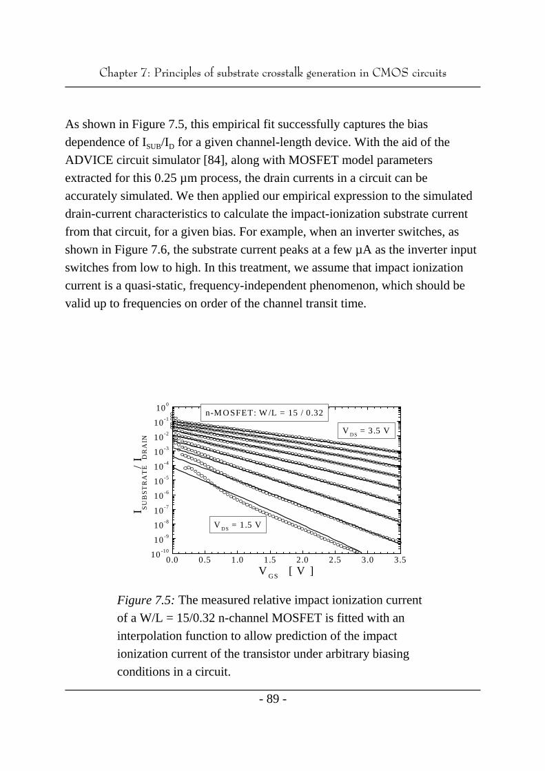
0.0 0.5 1.0 1.5 2.0 2.5 3.0 3.510-10
10-9
10-8
10-7
10-6
10-5
10-4
10-3
10-2
10-1
100
n-MOSFET: W /L = 15 / 0.32
VDS
= 3.5 V
V DS = 1.5 V
I SU
BS
TR
AT
E / I D
RA
IN
VGS
[ V ]
&KDSWHU3ULQFLSOHVRIVXEVWUDWHFURVVWDONJHQHUDWLRQLQ&026FLUFXLWV
- 89 -
Figure 7.5: The measured relative impact ionization current
of a W/L = 15/0.32 n-channel MOSFET is fitted with an
interpolation function to allow prediction of the impact
ionization current of the transistor under arbitrary biasing
conditions in a circuit.
As shown in Figure 7.5, this empirical fit successfully captures the bias
dependence of I /I for a given channel-length device. With the aid of theSUB D
ADVICE circuit simulator [84], along with MOSFET model parameters
extracted for this 0.25 µm process, the drain currents in a circuit can be
accurately simulated. We then applied our empirical expression to the simulated
drain-current characteristics to calculate the impact-ionization substrate current
from that circuit, for a given bias. For example, when an inverter switches, as
shown in Figure 7.6, the substrate current peaks at a few µA as the inverter input
switches from low to high. In this treatment, we assume that impact ionization
current is a quasi-static, frequency-independent phenomenon, which should be
valid up to frequencies on order of the channel transit time.
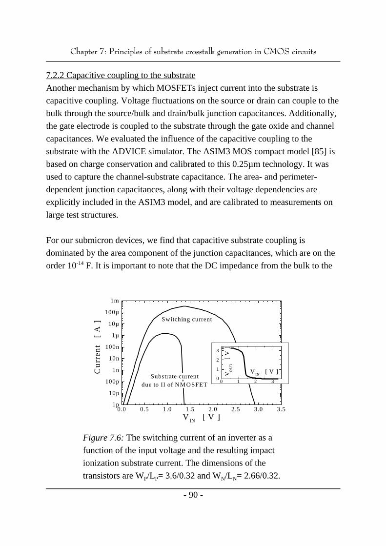
0.0 0.5 1.0 1.5 2.0 2.5 3.0 3.51p
10p
100p
1n
10n
100n
1µ
10µ
100µ
1m
Substrate currentdue to II of NMOSFET
Switching current
Cu
rre
nt
[
A ]
V IN [ V ]
0 1 2 30
1
2
3
VO
UT
[ V
]
VIN
[ V ]
&KDSWHU3ULQFLSOHVRIVXEVWUDWHFURVVWDONJHQHUDWLRQLQ&026FLUFXLWV
- 90 -
Figure 7.6: The switching current of an inverter as a
function of the input voltage and the resulting impact
ionization substrate current. The dimensions of the
transistors are W /L = 3.6/0.32 and W /L = 2.66/0.32.P P N N
7.2.2 Capacitive coupling to the substrate
Another mechanism by which MOSFETs inject current into the substrate is
capacitive coupling. Voltage fluctuations on the source or drain can couple to the
bulk through the source/bulk and drain/bulk junction capacitances. Additionally,
the gate electrode is coupled to the substrate through the gate oxide and channel
capacitances. We evaluated the influence of the capacitive coupling to the
substrate with the ADVICE simulator. The ASIM3 MOS compact model [85] is
based on charge conservation and calibrated to this 0.25µm technology. It was
used to capture the channel-substrate capacitance. The area- and perimeter-
dependent junction capacitances, along with their voltage dependencies are
explicitly included in the ASIM3 model, and are calibrated to measurements on
large test structures.
For our submicron devices, we find that capacitive substrate coupling is
dominated by the area component of the junction capacitances, which are on the
order 10 F. It is important to note that the DC impedance from the bulk to the-14
&KDSWHU3ULQFLSOHVRIVXEVWUDWHFURVVWDONJHQHUDWLRQLQ&026FLUFXLWV
- 91 -
tub ties (typically on order of 10 6 per tub tie) is low when compared to the2
impedance from these capacitances over the range of device operating
frequencies. Thus, capacitive coupling to the substrate can be modeled as a
current injection mechanism.
7.2.3 Gate induced drain leakage (GIDL)
Gate-induced drain leakage occurs when high fields across the drain/gate overlap
region form a deep-depletion layer in the drain. When the voltage drop across
this layer is sufficient, band-to-band tunneling of valence electrons results in the
creation of holes, which are then swept into the substrate [86]. GIDL depends
exponentially on the gate-drain voltage, and also depends significantly on the
details of drain doping and gate overlap. The characteristic behavior of GIDL
could only be observed in our NMOS devices when they were biased at negative
gate-source voltages (not shown); under normal bias conditions, no gate-induced
drain leakage was observed (figure 7.2). In general, the substrate current level at
low gate biases is negligible compared to the impact-ionization current at higher
gate biases, and thus GIDL will have no effect on the overall current injected into
the substrate during NMOS device switching.
In our PMOS devices, the characteristic behavior of GIDL is observed from
V =0 to 0.5V, and it dominates the drain and well currents in this low gate-SG
voltage bias regime (figure 7.3). However, the p-channel GIDL current in this
range is still small relative to the impact ionization current at higher gate
voltages, and thus makes a negligible contribution to the total substrate current
during switching of the gate voltage. So, while the off-state current flow due to
PMOS gate-induced drain leakage may increase the power dissipation, it will not
lead to significant substrate crosstalk. Overall, for the 0.25-µm devices studied
here, GIDL substrate current does not have an impact on substrate crosstalk, and
we do not consider it further.
7.2.4 Photon induced current (PIC)
In addition to impact ionization, another way that channel hot electrons can
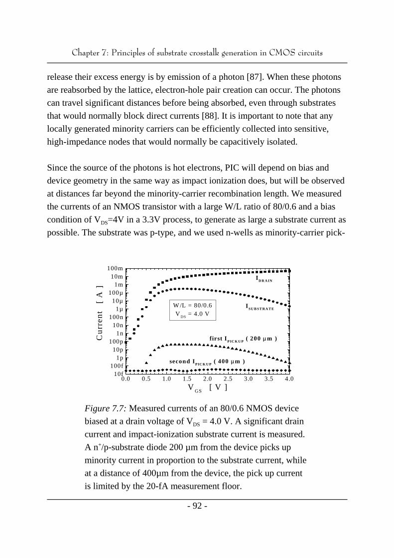
0.0 0.5 1.0 1.5 2.0 2.5 3.0 3.5 4.010f
100f1p
10p100p
1n10n
100n1µ
10µ100µ
1m10m
100m
W /L = 80/0.6V
DS = 4.0 V
f irst IPIC K U P
( 200 µµ m )
second IPIC K U P
( 400 µµ m )
ISU B ST R A T E
ID R A IN
Cu
rre
nt
[
A ]
VGS
[ V ]
&KDSWHU3ULQFLSOHVRIVXEVWUDWHFURVVWDONJHQHUDWLRQLQ&026FLUFXLWV
- 92 -
Figure 7.7: Measured currents of an 80/0.6 NMOS device
biased at a drain voltage of V = 4.0 V. A significant drainDS
current and impact-ionization substrate current is measured.
A n /p-substrate diode 200 µm from the device picks up+
minority current in proportion to the substrate current, while
at a distance of 400µm from the device, the pick up current
is limited by the 20-fA measurement floor.
release their excess energy is by emission of a photon [87]. When these photons
are reabsorbed by the lattice, electron-hole pair creation can occur. The photons
can travel significant distances before being absorbed, even through substrates
that would normally block direct currents [88]. It is important to note that any
locally generated minority carriers can be efficiently collected into sensitive,
high-impedance nodes that would normally be capacitively isolated.
Since the source of the photons is hot electrons, PIC will depend on bias and
device geometry in the same way as impact ionization does, but will be observed
at distances far beyond the minority-carrier recombination length. We measured
the currents of an NMOS transistor with a large W/L ratio of 80/0.6 and a bias
condition of V =4V in a 3.3V process, to generate as large a substrate current asDS
possible. The substrate was p-type, and we used n-wells as minority-carrier pick-
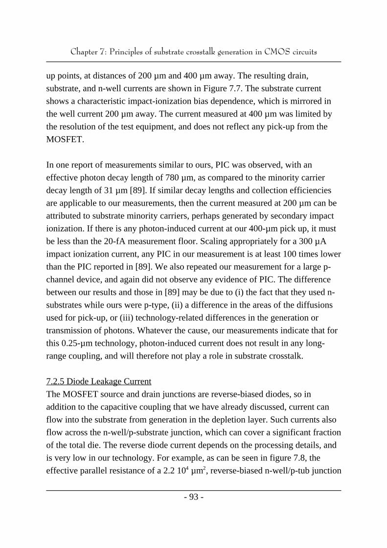
&KDSWHU3ULQFLSOHVRIVXEVWUDWHFURVVWDONJHQHUDWLRQLQ&026FLUFXLWV
- 93 -
up points, at distances of 200 µm and 400 µm away. The resulting drain,
substrate, and n-well currents are shown in Figure 7.7. The substrate current
shows a characteristic impact-ionization bias dependence, which is mirrored in
the well current 200 µm away. The current measured at 400 µm was limited by
the resolution of the test equipment, and does not reflect any pick-up from the
MOSFET.
In one report of measurements similar to ours, PIC was observed, with an
effective photon decay length of 780 µm, as compared to the minority carrier
decay length of 31 µm [89]. If similar decay lengths and collection efficiencies
are applicable to our measurements, then the current measured at 200 µm can be
attributed to substrate minority carriers, perhaps generated by secondary impact
ionization. If there is any photon-induced current at our 400-µm pick up, it must
be less than the 20-fA measurement floor. Scaling appropriately for a 300 µA
impact ionization current, any PIC in our measurement is at least 100 times lower
than the PIC reported in [89]. We also repeated our measurement for a large p-
channel device, and again did not observe any evidence of PIC. The difference
between our results and those in [89] may be due to (i) the fact that they used n-
substrates while ours were p-type, (ii) a difference in the areas of the diffusions
used for pick-up, or (iii) technology-related differences in the generation or
transmission of photons. Whatever the cause, our measurements indicate that for
this 0.25-µm technology, photon-induced current does not result in any long-
range coupling, and will therefore not play a role in substrate crosstalk.
7.2.5 Diode Leakage Current
The MOSFET source and drain junctions are reverse-biased diodes, so in
addition to the capacitive coupling that we have already discussed, current can
flow into the substrate from generation in the depletion layer. Such currents also
flow across the n-well/p-substrate junction, which can cover a significant fraction
of the total die. The reverse diode current depends on the processing details, and
is very low in our technology. For example, as can be seen in figure 7.8, the
effective parallel resistance of a 2.2 10 µm , reverse-biased n-well/p-tub junction4 2
-3.5 -3.0 -2.5 -2.0 -1.5 -1.0 -0.5 0.0-5.0p
-4.0p
-3.0p
-2.0p
-1.0p
0.0
ID = 1.1 V
PN - 0.9 [ pA ]
dio
de
cu
rre
nt
[
A ]
V PN [ V ]
&KDSWHU3ULQFLSOHVRIVXEVWUDWHFURVVWDONJHQHUDWLRQLQ&026FLUFXLWV
- 94 -
Figure 7.8: The measured reverse-bias leakage current of an
n-well/p-substrate diode, as a function of the diode voltage.
This reversed biased diode has a minimum effective
resistance of 1 T6 (line), in parallel with the diode
capacitance. The well area is approximately 2.2 10 µm .4 2
is 1T6 or larger, at the voltages of interest. Thus, fluctuations on one side of the
diode will not strongly couple to the other side via reverse leakage current. A
substantial current could, however, flow into the substrate if any of the junctions
becomes forward biased. Such forward-biased transients depend on the circuit
design and operation, and must be prevented by suitable design.
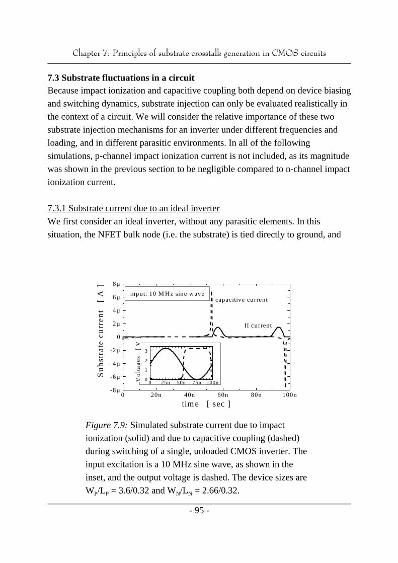
0 20n 40n 60n 80n 100n-8µ
-6µ
-4µ
-2µ
0
2µ
4µ
6µ
8µ
II current
capacitive currentinput: 10 M Hz sine wave
Su
bs
tra
te c
urr
en
t
[ A
]
time [ sec ]
0 25n 50n 75n 100n0
1
2
3
Vo
lta
ge
s
[ V
]
&KDSWHU3ULQFLSOHVRIVXEVWUDWHFURVVWDONJHQHUDWLRQLQ&026FLUFXLWV
- 95 -
Figure 7.9: Simulated substrate current due to impact
ionization (solid) and due to capacitive coupling (dashed)
during switching of a single, unloaded CMOS inverter. The
input excitation is a 10 MHz sine wave, as shown in the
inset, and the output voltage is dashed. The device sizes are
W /L = 3.6/0.32 and W /L = 2.66/0.32.P P N N
7.3 Substrate fluctuations in a circuitBecause impact ionization and capacitive coupling both depend on device biasing
and switching dynamics, substrate injection can only be evaluated realistically in
the context of a circuit. We will consider the relative importance of these two
substrate injection mechanisms for an inverter under different frequencies and
loading, and in different parasitic environments. In all of the following
simulations, p-channel impact ionization current is not included, as its magnitude
was shown in the previous section to be negligible compared to n-channel impact
ionization current.
7.3.1 Substrate current due to an ideal inverter
We first consider an ideal inverter, without any parasitic elements. In this
situation, the NFET bulk node (i.e. the substrate) is tied directly to ground, and
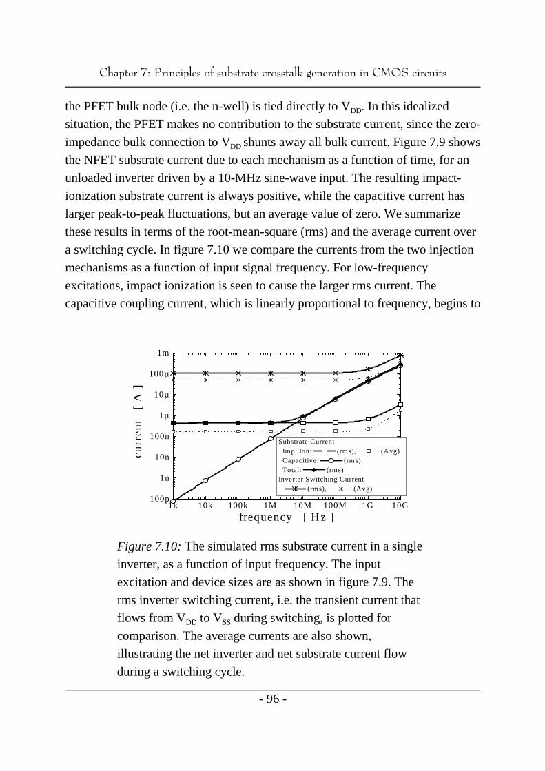
1k 10k 100k 1M 10M 100M 1G 10G100p
1n
10n
100n
1µ
10µ
100µ
1m
Substrate Current Imp. Ion: (rms), (Avg) Capacitive: (rms) Total: (rms)Inverter Switching Current (rms), (Avg)
cu
rre
nt
[
A ]
frequency [ Hz ]
&KDSWHU3ULQFLSOHVRIVXEVWUDWHFURVVWDONJHQHUDWLRQLQ&026FLUFXLWV
- 96 -
Figure 7.10: The simulated rms substrate current in a single
inverter, as a function of input frequency. The input
excitation and device sizes are as shown in figure 7.9. The
rms inverter switching current, i.e. the transient current that
flows from V to V during switching, is plotted forDD SS
comparison. The average currents are also shown,
illustrating the net inverter and net substrate current flow
during a switching cycle.
the PFET bulk node (i.e. the n-well) is tied directly to V . In this idealizedDD
situation, the PFET makes no contribution to the substrate current, since the zero-
impedance bulk connection to V shunts away all bulk current. Figure 7.9 showsDD
the NFET substrate current due to each mechanism as a function of time, for an
unloaded inverter driven by a 10-MHz sine-wave input. The resulting impact-
ionization substrate current is always positive, while the capacitive current has
larger peak-to-peak fluctuations, but an average value of zero. We summarize
these results in terms of the root-mean-square (rms) and the average current over
a switching cycle. In figure 7.10 we compare the currents from the two injection
mechanisms as a function of input signal frequency. For low-frequency
excitations, impact ionization is seen to cause the larger rms current. The
capacitive coupling current, which is linearly proportional to frequency, begins to

0 1n 2n 3n 4n 5n-25µ
-20µ
-15µ
-10µ
-5µ
0
5µ
10µ
15µ
20µ
25µ
II current
capacitive current
Su
bs
tra
te c
urr
en
t
[ A
]
time [ sec ]
0 1n 2n 3n 4n 5n0
1
2
3
Vo
lta
ge
[
V ]
&KDSWHU3ULQFLSOHVRIVXEVWUDWHFURVVWDONJHQHUDWLRQLQ&026FLUFXLWV
- 97 -
Figure 7.11: Simulated substrate current due to impact
ionization (solid) and due to capacitive coupling (dashed)
during switching of a single inverter. The input excitation is
a square wave with a 0.2-nsec rise time, as shown in the
inset. The output voltage is also shown (dashed). The device
sizes are W /L = 3.6 µm/0.32 µm and W /L = 2.66P P N N
µm/0.32 µm, and 100-fF load capacitors are connected from
the inverter output to V and from the inverter output toDD
V .SS
dominate around 10 MHz.
Similarly, we also simulated substrate injection from an inverter as a function of
the output load. In this case we applied a square wave to the input with rise and
fall times of about 0.2 nsec. The time response of the substrate currents, for a
100-fF load, is shown in figure 7.11. The rms and average values of the currents
as a function of the load are given in figure 7.12. It is clear from these
simulations that, for typical internal loads, impact ionization currents are about
an order of magnitude smaller than capacitive currents, which are in turn an order
of magnitude smaller than the switching current through the inverter.
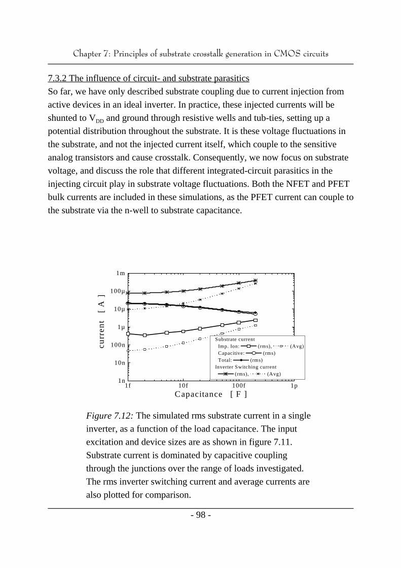
1f 10f 100f 1p1n
10n
100n
1µ
10µ
100µ
1m
Substrate current Imp. Ion: (rms), (Avg) Capacitive: (rms) Total: (rms)Inverter Switching current (rms), (Avg)
cu
rre
nt
[
A ]
Capacitance [ F ]
&KDSWHU3ULQFLSOHVRIVXEVWUDWHFURVVWDONJHQHUDWLRQLQ&026FLUFXLWV
- 98 -
Figure 7.12: The simulated rms substrate current in a single
inverter, as a function of the load capacitance. The input
excitation and device sizes are as shown in figure 7.11.
Substrate current is dominated by capacitive coupling
through the junctions over the range of loads investigated.
The rms inverter switching current and average currents are
also plotted for comparison.
7.3.2 The influence of circuit- and substrate parasitics
So far, we have only described substrate coupling due to current injection from
active devices in an ideal inverter. In practice, these injected currents will be
shunted to V and ground through resistive wells and tub-ties, setting up aDD
potential distribution throughout the substrate. It is these voltage fluctuations in
the substrate, and not the injected current itself, which couple to the sensitive
analog transistors and cause crosstalk. Consequently, we now focus on substrate
voltage, and discuss the role that different integrated-circuit parasitics in the
injecting circuit play in substrate voltage fluctuations. Both the NFET and PFET
bulk currents are included in these simulations, as the PFET current can couple to
the substrate via the n-well to substrate capacitance.

VSS
VDD
LBW
LBW
LBW
LBW
RBW
RBW
RBW
RBW
RTUB
RTUB
Rsource
Rsource
Csource
CsourceCL
CWELL
CL
VIN
VSUB
VWELL
&KDSWHU3ULQFLSOHVRIVXEVWUDWHFURVVWDONJHQHUDWLRQLQ&026FLUFXLWV
- 99 -
Figure 7.13: Circuit model of a single inverter stage, with
the associated substrate- and power-supply paracitics that
influence the substrate.
7.3.2.1 Substrate-V impedance and the bond wire impedanceSS
A schematic of the parasitic circuit environment for a single inverter is shown in
figure 7.13. For now, we assume that the dotted lines in figure 7.13 are solid,
such that the substrate node V is resistively connected, via R , to the V railSUB TUB SS
of the circuit. The substrate is also capacitively connected to V , through theSS
capacitance between the metal lines and the substrate, and more significantly,
through all the NMOSFET source junctions connected to V . We previouslySS
noted that an individual FET has a capacitance to the substrate in the range of
10 F. If there are 10 such devices, then the total capacitance (C ) that14 5SOURCE
each device sees is already is above 1 nF. At 1 GHz, which is a typical frequency
for switching of submicron MOSFETs, C has an impedance of less than 1SOURCE
6, such that it is effectively shorted out. There is also a series resistance, R ,SOURCE
in this path, due to wiring, contact resistance and the substrate resistance of the
source diffusion and substrate. Finally, a voltage can develop between V andSS
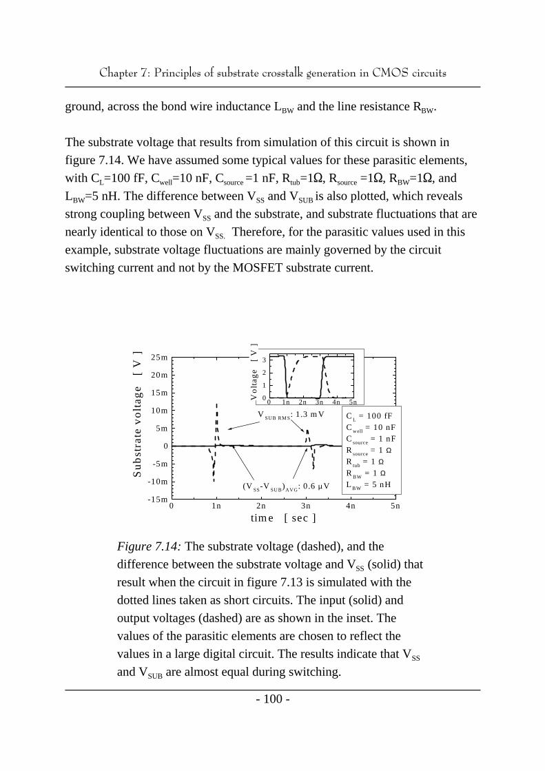
0 1n 2n 3n 4n 5n-15m
-10m
-5m
0
5m
10m
15m
20m
25m
CL = 100 fFCwell = 10 nFC
source = 1 nF
Rsource = 1 ΩR
tub = 1 Ω
RBW = 1 ΩL BW = 5 nH(V SS-V SUB)AVG: 0.6 µ V
V SUB RM S: 1.3 m V
Su
bs
tra
te v
olt
ag
e
[ V
]
time [ sec ]
0 1n 2n 3n 4n 5n0
1
2
3
Vo
lta
ge
[
V ]
&KDSWHU3ULQFLSOHVRIVXEVWUDWHFURVVWDONJHQHUDWLRQLQ&026FLUFXLWV
- 100 -
Figure 7.14: The substrate voltage (dashed), and the
difference between the substrate voltage and V (solid) thatSS
result when the circuit in figure 7.13 is simulated with the
dotted lines taken as short circuits. The input (solid) and
output voltages (dashed) are as shown in the inset. The
values of the parasitic elements are chosen to reflect the
values in a large digital circuit. The results indicate that VSS
and V are almost equal during switching.SUB
ground, across the bond wire inductance L and the line resistance R .BW BW
The substrate voltage that results from simulation of this circuit is shown in
figure 7.14. We have assumed some typical values for these parasitic elements,
with C =100 fF, C =10 nF, C =1 nF, R =16, R =16, R =16, andL well source tub source BW
L =5 nH. The difference between V and V is also plotted, which revealsBW SS SUB
strong coupling between V and the substrate, and substrate fluctuations that areSS
nearly identical to those on V Therefore, for the parasitic values used in thisSS.
example, substrate voltage fluctuations are mainly governed by the circuit
switching current and not by the MOSFET substrate current.

0 1n 2n 3n 4n 5n-15m
-10m
-5m
0
5m
10m
15m
20m
25m
CL = 100 fFCwell = 10 nFCsource = 1 nFRsource = 1 ΩRtub = 1 ΩRBW = 1 ΩL BW = 5 nH(V SS-V SUB)AVG : 138 µ V
V SUB RM S: 1.3 m V
Su
bs
tra
te v
olt
ag
e
[ V
]
time [ sec ]
0 1n 2n 3n 4n 5n0
1
2
3
vo
lta
ge
[
V ]
&KDSWHU3ULQFLSOHVRIVXEVWUDWHFURVVWDONJHQHUDWLRQLQ&026FLUFXLWV
- 101 -
Figure 7.15: The substrate voltage (dashed), and the
difference between the substrate voltage and V (solid) thatSS
result when the circuit in figure 7.13 is simulated with the
dotted lines taken as open circuits. The input (solid) and
output voltages (dashed) are as shown in the inset. The result
is that V and V have an equivalent high frequencySS SUB
behavior to the previous case, but V has additional lowSS
frequency fluctuations, and a non-zero average component.
7.3.2.2 Separate connection of the substrate to the power supply
If separate bias connections are used for the V and V nodes, the dotted linesSS SUB
in figure 7.13 are open circuits and there will only be capacitive coupling left
between V and V . To examine this scenario, this modified circuit was re-SS SUB
simulated with the same parameter values used in figure 7.14. As shown in figure
7.15, V is still seen to follow the high-frequency behavior of V , due toSUB SS
coupling via the source diodes. The difference between the two node voltages
reveals that the current at V has an additional low-frequency component with aSS
non-zero average, which does not couple to the substrate. When the substrate was
resistively connected to the V line, this small average component of theSS
switching current was transmitted to the substrate. Overall, this result suggests
that separate connections of V and V to ground will not result in significantSUB SS

&KDSWHU3ULQFLSOHVRIVXEVWUDWHFURVVWDONJHQHUDWLRQLQ&026FLUFXLWV
- 102 -
improvements in substrate isolation. While this is true for a single inverter, we
will describe in section 7.4 how the low frequency components can play a
significant role in a complete IC, such that separate power supply connections are
advantageous.
7.3.2.3 Parasitic decoupling capacitance
The discussions in the previous sections are based on a model in which there is a
low-impedance connection between the substrate and V , in combination with aSS
relatively small current flowing between the two. The latter assumption is not
necessarily true. In addition to the fact that there is a large capacitance between
V and the substrate, there also is a large capacitance between V and all the n-SS DD
wells combined. Furthermore, the junction capacitance between these n-wells
and the substrate, C , can be very large, due to the large n-well area. TheWELL
combination of these three capacitances leads to a parasitic decoupling
capacitance between V and V with small series impedance, as shown inDD SS
figure 7.13.
At the first moments of a switching transient, it is possible that this decoupling
capacitance will supply the switching current instead of the power supply itself,
because of the bond wire inductances. While all of these terms were included in
our simulations, it is complicated to determine the net effect of this decoupling
capacitance on substrate crosstalk in a general sense. On the one hand, it will
damp fluctuations due to the fact that the collective well-substrate capacitor acts
as a battery during the first moments of a switching transient, thereby decreasing
the V and V voltage transients. On the other hand, when this damping occurs,DD SS
more current will flow via the substrate, which will increase substrate voltage
fluctuations. The final outcome will depend on the relative values of these
parasitic elements, and on the presence of other decoupling capacitors. What is
most important to recognize is that decoupling capacitances can significantly
alter the substrate fluctuations and must be taken into account.
&KDSWHU3ULQFLSOHVRIVXEVWUDWHFURVVWDONJHQHUDWLRQLQ&026FLUFXLWV
- 103 -
Finally, it is important to note that the presence of both capacitances and
inductances in the same packaged integrated circuit can lead to resonances and
oscillations and significant transient signals after switching. These are unwanted
because they can amplify substrate voltage fluctuations by orders of magnitude in
a frequency range in which the analog circuit operates. Modeling and damping of
several forms of resonance have already been well discussed in the crosstalk
literature [69,75,90], and should not be neglected when analyzing the coupling of
a specific circuit.
7.4 Substrate voltages due to a large circuitSo far, we have only discussed how the switching of a single inverter or a cluster
of identical inverters can affect the substrate voltage. The transients that result
from a large clocked circuit will not necessarily be the same as the transient of an
individual element multiplied by the number of elements that switch. For
instance, if two elements switch at approximately the same moment in opposite
directions, partial cancellation of the resulting substrate transients can occur. In
the same way, noise reduction can also take place if all elements switch in the
same direction but not at exactly the same time. In this section, we examine an
idealized switching circuit, to examine how the statistics of large numbers of
devices can affect the conclusions drawn in previous sections about dominant
substrate injection mechanisms.
In the following example, we examine how the cancellation of transients takes
place when all elements switch in the same direction. Let us assume that element
1 switches at time instant t , element 2 at time instant t , etc. We will assume that1 2
the distribution of each switching moment t is symmetric around the averageX
switching moment and follows, as an example, a Gaussian distribution. Figures
7.14 and 7.15 showed the transients due to the switching of one inverter and each
such transient can be described as a sum of sine waves. For illustration purposes,
we will consider just the fundamental sine wave period and the sine-wave period
with the double frequency.

&KDSWHU3ULQFLSOHVRIVXEVWUDWHFURVVWDONJHQHUDWLRQLQ&026FLUFXLWV
- 104 -
To analyze this scenario we simulated N=10 individual, single sine wave periods5
at the fundamental frequency, with a Gaussian distribution of starting moments.
The total rms signal of this ensemble of pulses was calculated over different
uncertainties (2) ) in the Gaussian distribution. The results, shown in figureT
7.16, indicate that if the uncertainty in the starting time is within 10% of the sine
wave period, then the total rms signal is simply N times the rms signal of a single
switching event. However, if the uncertainty becomes ten times larger than the
total switching time, the rms value of the total noise due to N switches will be
proportional to N. In this case, there is significant cancellation of the total rms
signal, and the ensemble of switching events can be treated as a source of random
noise.
Figure 7.16 also shows the normalized rms signal calculated when the signal
consists of two sine wave periods at twice the frequency. This curve is shifted by
a factor of two compared to the original curve, because the relative uncertainty is
twice as large at double the frequency. Therefore, for a fixed uncertainty ) , theT
x-axis of figure 7.16 can also be interpreted as the frequency axis. As a
consequence, high-frequency components will be statistically canceled more than
those at lower frequencies. The value of the corner frequency will be determined
by the switching uncertainty, relative to the switching period of a single element.
Since this noise cancellation is less effective for the low-frequency and DC
components, it is important to reconsider the results of section 7.3, which were
performed for a single device. While the noise of a large circuit will certainly be
larger than that of an individual device, the total high frequency component of
the fluctuations can increase by up to N less than the low-frequency and DC
component of the noise. Therefore, low-frequency noise injection mechanisms
such as impact ionization may still play an important role in large circuits. From
this perspective, it may be better if V and the substrate are not coupled together,SS
because the relatively small average fluctuation shown in figure 7.15 could
become dominant in larger circuits.
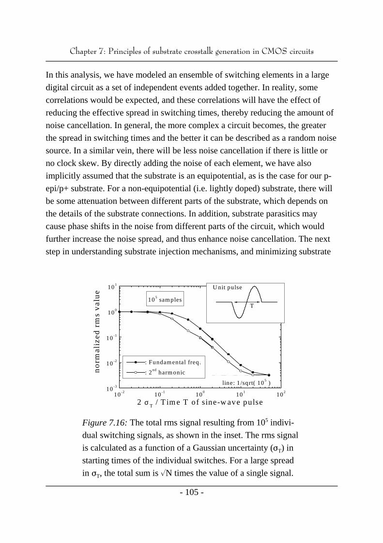
10-2
10-1
100
101
102
10-3
10-2
10-1
100
101
line: 1/sqrt( 105 )
105 samples
: Fundamental freq.
: 2nd
harmonic
no
rma
liz
ed
rm
s v
alu
e
2 σ T / T ime T of sine-w ave pulse
T
U nit pulse
&KDSWHU3ULQFLSOHVRIVXEVWUDWHFURVVWDONJHQHUDWLRQLQ&026FLUFXLWV
- 105 -
Figure 7.16: The total rms signal resulting from 10 indivi-5
dual switching signals, as shown in the inset. The rms signal
is calculated as a function of a Gaussian uncertainty () ) inT
starting times of the individual switches. For a large spread
in ) , the total sum is N times the value of a single signal.T
In this analysis, we have modeled an ensemble of switching elements in a large
digital circuit as a set of independent events added together. In reality, some
correlations would be expected, and these correlations will have the effect of
reducing the effective spread in switching times, thereby reducing the amount of
noise cancellation. In general, the more complex a circuit becomes, the greater
the spread in switching times and the better it can be described as a random noise
source. In a similar vein, there will be less noise cancellation if there is little or
no clock skew. By directly adding the noise of each element, we have also
implicitly assumed that the substrate is an equipotential, as is the case for our p-
epi/p+ substrate. For a non-equipotential (i.e. lightly doped) substrate, there will
be some attenuation between different parts of the substrate, which depends on
the details of the substrate connections. In addition, substrate parasitics may
cause phase shifts in the noise from different parts of the circuit, which would
further increase the noise spread, and thus enhance noise cancellation. The next
step in understanding substrate injection mechanisms, and minimizing substrate
&KDSWHU3ULQFLSOHVRIVXEVWUDWHFURVVWDONJHQHUDWLRQLQ&026FLUFXLWV
- 106 -
coupling, is to perform simulations and measurements on specific circuits of
different sizes, topologies, and functionality. The framework we have described
here provides a useful foundation for such investigations, and also provides
insight into ways that substrate injection and the resulting noise can be
minimized at a device and at a circuit level.
7.5 ConclusionsOn a device level, currents due to the capacitive coupling and impact ionization
effects dominate injection into the substrate. This is valid for both n-channel and
p-channel MOSFETs. On a circuit level, parasitics such as the bond wire
inductance and the capacitive coupling of the V node to the substrate will causeSS
additional, and probably dominating, substrate voltage fluctuations. Additional
factors like the parasitic n-well decoupling capacitance between V and V , andDD SS
oscillations due to the inductances in combination with the capacitances will also
influence the substrate signal.
Within a complex circuit, a significant amount of switching takes place during a
clock cycle. As a consequence some signal cancellation can take place. For
simplicity, we have treated this switching activity as a random process. Our
evaluation has shown that partial noise cancellation will mainly occur at higher
frequencies, while average components of signals can never be canceled. So, the
average and low frequency components of the switching signal, which are
relatively unimportant for an individual inverter, can become more significant as
the total circuit becomes more complex.
Xn 1
TMP
½TM
½TM
x( t) e j
2%ntTM dt,
x( t) M
nXn e
j2%ntTM ,
X( f ) Xn,
p( t ) x( t ) .y( t)
M
fX( f ) e j 2% f t M
f
Y( f ) e j 2% f t
M
fM
f
X( f ) Y( f ) e j 2% ( f f ) t
M
fX( f ) Y( f )
$SSHQGL[
- 107 -
(A1.1)
(A1.2)
(A1.3)
A1. Definitions in the frequency domain
In this thesis we are primarily interested in stationary situations. These can be
described in the frequency domain with the Fourier series:
where T is the duration of a measurement. Note that the dimensions of x(t) andM
X are the same. Essentially n/T is a frequency. Because T could be, in theoryn M M
at least, infinitely large and because it can vary from measurement to
measurement, we will not write the signals in the frequency domain as a function
of the parameter n, but as a function of frequency:
with f=n/T .M
The ensemble averages of products that are defined in the time domain can be
presented as frequency components as well. For instance, let us transform that
the ensemble average of the product p(t)=x(t).y(t):
P( f ) ³ X( f ) .Y( f ) .
SXY( f ) 2 TM X( f ) .Y( f ) ,
$SSHQGL[
- 108 -
(A1.4)
(A1.5)
where we used the fact that all terms average out except those with f+f'=0.
Because y(t) is real-valued, the complex conjugate of Y(f) is equal to Y(-f):
Y (f)=Y(-f). This relation is also used. The components of p(t) in the frequency*
domain are now defined as:
From now on we will not explicitly show the over lines anymore, unless it is the
subject under discussion.
In case of a spectral density we use the following relation:
with S (f) the cross-correlation spectral density of the noise between the timeXY
signals x(t) and y(t). The cross-correlation spectral density will reduce to the
auto-correlation spectral density when the time signals x(t) and y(t) are identical,
which generally is the case. The extra factor T is added because the spectralM
density is normalized over the bandwidth 1/T in which 'f' is defined.M
Because we only look at real signals in the time domain, the magnitudes of a
positive frequency component of S and its negative counterpart are equal inXY
case of an auto-correlation spectral density. Hence, as a convention, a factor two
is added in equation (A1.5) to take into account the negative frequencies when
the spectral density is defined for positive frequencies only. For cross-correlation
spectral densities this is not always correct. However, to be consistent in the
notation, the additional factor of two is also added in case of a cross correlation.

U(H0,M,f)
U(H1,M,f)
U(H2,M,f)
M(f)
U(H,M,f)
H(f)
$SSHQGL[
- 109 -
Figure A2.1: The potential energy U of the system at a frequency f as afunction of the output Y for three different magnetic fields: H , H and0 1
H . The dotted line represents the minimum of the potential energy as a2
function of the input H(f). The values U, H and M are complex, but wedid not show this explicitly.
A2. The potential energy of a stationary magnetic system
Suppose the susceptibility 3(f) is the transfer function of a real, linear and causal
magnetic system with the magnetic field H(f) as the input and the magnetization
M(f) as the output. The transfer function 3(f) defines the response M(f) to
excitations H(f). However, this magnetic system can also be described in terms
of energy. As shown in the introduction of this thesis, the energy can be
calculated for each frequency component individually.
Figure A2.1 shows examples of a frequency component of the potential energy
U(H,M,f) as a function M(f) for different inputs H(f). Essentially the response
M(f) is given by the minimum of the potential energy for each excitation: the
dotted line.
On this line 0U(H,M,f)/0M is by definition zero. So, if we develop a Taylor
series expansion of this derivative on the line, the derivative remains zero.
0U (H ,M ,f )
0M HH0HMM0M
0U (H ,M ,f )
0M HH0MM0
H 02U (H ,M ,f )
0H 0M HH0MM0
M 02U (H ,M ,f )
0M 2 HH0MM0
.
02U (H ,M,f )
0M 2 HH0MM0
µ0Vol
3( f ),
02U(H ,M ,f )
0H 0M HH0MM0
µ0Vol.
$SSHQGL[
- 110 -
(A2.1)
(A2.2)
(A2.3)
Suppose we are at a point (H ,M ) on the line, then the resulting derivative at0 0
(H +H,M +M) becomes:0 0
As said before, the first derivatives in this expansion are by definition zero. In the
limit for H0, the second derivative, 0 U(H,M,f)/0M , is equal to:2 2
where we used M/H=0M(f)/0H(f)=3(f). We also used the fact that the
component of the potential energy that depends on H(f) is equal to:
µ .Vol.H(f)#M(f) [1], hence:0
y( t ) P
g( t ) x( t t ) dt .
g( t) g( t ) ( t ) ,
G( f ) P
G( f ) 1
j 2% ( f f )
1
2 ( f f ) df
2P
G( f )
j 2%( f f )df .
$SSHQGL[
- 111 -
(A3.1)
(A3.2)
(A3.3)
A3. A causal system: the Kramers-Kronig dispersion relations
Suppose g(t) is a linear and causal system with input x(t) and output y(t). In
general this can be written as:
But because the system is causal the response y(t) is independent of the
excitation x(t'') when t''>t. This means that g(t')³0 for t'<0 and therefore that the
lower limit of the integral effectively is zero. This condition upon g(t) leads to
the Kramers-Kronig dispersion relations which we will derive now because they
are essential for the fluctuation-dissipation theorem.
The condition g(t)³0 for t<0 can be rewritten as:
with (t)=1 for t0 and zero otherwise. The transformation of this relation to the
frequency domain via Fourier integrals gives:
In case of a singularity at f'=f, this integral should be treated as a limiting
situation at the singularity. The important part of this relation shows when G(f) is
expanded into a real and imaginary part: G(f)³ReG(f)j.ImG(f). After
splitting equation (A3.3) into an equation for real values and one for imaginary
values, it becomes clear that ReG(f) and ImG(f) are related. For
ReG(0)³G(0), the relation becomes:
G(0) ³ 4P
0
Im G( f ) 2% f
df,
$SSHQGL[
- 112 -
(A3.4)
where we also used the fact that g(t) is real-valued, hence: ImG(f)=-ImG(-f)
to change the integration range to f0 only. This is the relation the fluctuation-
dissipation theorem depends on.
In this thesis we use the Fourier series, see appendix A1. However, in the limit
T the results will become equal to the one shown here. Only the definition ofM
G(f) differs, but this if of no consequence because in this relation we only define
G(f) as a function of itself.
32 2 32
1 2
34 1
1
(MFP)2 MM
f
S2( f )
S( f) 2
2
1
MM
f
S40 ( f)
S0( f) 4 3 1 2
AvgMFP
32 2
3MFP
1 2Avg
1
2
(MFP)2 MM
i2Mi1
j1
S2( fi )
S( fi )2
S2( fj )
S( fj )2
$SSHQGL[
- 113 -
(A4.1)
(A4.2)
(A4.3)
A4. The variance in 332
The calculation of the variance of 3 for Gaussian noise starts as follows:2
The square of the summation: (...) can be expanded in a summation of the2
squares: (...) plus cross terms. The evaluation of the first part, the summation2
of the squares, is known [19]:
Applying this relation gives:
To develop this relation further, the general result of the Carson-Campbell
theorem is needed [4]. For clarity we will develop the Carson-Campbell theorem:
Suppose that f(t) is a signal that consists of N individual pulses g(t') within a
limited time-period T. The distribution of the starting point of each g(t') is
f( t) MN
i1Ai g( t ti )
F ( f ) MN
i1Ai e
j 2% f ti G( f )
SFF( f ) ³ 2TM F( f )F ( f )
N A2 SGG( f ) 1
2N M
N
i2Mi1
k1
Ai Ak
A2cos2% f ti tk
S2( f )
S( f ) 2
2N M
N2
(N1)
p1
sp A2p
A2cos(2% f-p)
2
$SSHQGL[
- 114 -
(A4.4)
(A4.5)
(A4.6)
(A4.7)
random in time. Each pulse g(t') has an arbitrary weighing factor A . The signali
f(t) can be represented as:
The Fourier transform of this signal is:
The spectral density of f(t), measured over the time-period T , is (the frequency fM
is only defined for f0 Hz) [4]:
The first part is gives the ensemble average of S (f) and also is the conventionalFF
result of the Carson-Campbell theorem. But the second part gives information
regarding the uncertainty in a spectral density:
with s a random sign: 1 or -1 and - a random time difference. This relation canp p
be used in eq. (A4.3). It is straightforward to see that all cross terms will become

cos2(1i ) cos2(1j ) ¼
32 2 2
MFP1 3
Avg
$SSHQGL[
- 115 -
(A4.8)
(A4.9)
zero and that the only ensemble average that has to be calculated is:
Summing all the terms and assuming that N»1 and M»FP finally results in the
simplification of eq. (A4.3) into:

$SSHQGL[
- 116 -
A5
The following pages contain the original version of the text of chapter 2, as it is
published in Journal of Applied Physics [19].
JOURNAL OF APPLIED PHYSICS VOLUME 84, NUMBER 8 15 OCTOBER 1998
Uncertainty in Gaussian noise generalized for cross-correlation spectraJ. Briaire and L. K. J. Vandammea)
Department of Electrical Engineering, Eindhoven University of Technology, 5600MB Eindhoven,The Netherlands
~Received 13 April 1998; accepted for publication 20 July 1998!
The ensemble average and variance of Gaussian noise measured as cross-correlation spectra arecalculated as a function of the number of time averages. The calculations are based on the Carson–Campbell theorem which treats noise spectra as a collection of individual deterministic pulsestransformed into the frequency domain. We have compared our calculations with experimentalresults on metal film resistors. There is an excellent agreement between the predicted and themeasured statistical behavior. ©1998 American Institute of Physics.@S0021-8979~98!07820-7#
oenmhleaccon-it
neu
fof t
trplroas
ificorctsiaun.se
thrinased
co
i-
the
ibu-
e arumtedrgesiblein-otheon
itynifi-aryin-fromgeinty
red.ise
ueeter-Forevelect-hite
ashow-ro-
I. INTRODUCTION
Power density spectra of stationary noise become mprecise and hence smoother both through time and frequaveraging. The averaged spectrum will, for instance, becoconstant as a function of frequency for thermal noise or snoise, inversely proportional to frequency for the so-cal1/f noise or flat for low frequencies and, beyond a charteristic frequency, inversely proportional to the frequensquared for Lorentzian noise such as generatirecombination noise.1 An observed spectrum often is a combination of these types of subspectra. Owing to the finaverage time, an approximation of the spectrum is obtaiand the spectrum is always corrupt with an uncertainty. Ostudy will concentrate on this uncertainty, especiallycross-correlation spectra. The results are independent ofrequency dependance of spectra.
Detailed knowledge of the uncertainty in noise speccan pinpoint the physical origin of noise sources in a samThis is possible when statistical analysis shows that the pability density function of the spectral noise can not be clsified as Gaussian. A number of groups have published aof work concerning non-Gaussian noise in specsituations.2,3 So far, all publications were based on autocrelation spectra in which the uncertainty in the noise spewas compared with the expected uncertainty for Gausnoise. In this article we will calculate and measure thecertainty of Gaussian noise in cross-correlation spectrathis situation the measured variance in a Gaussian noisenal can differ significantly from the same measurement pformed with an autocorrelation.
The basis of non-Gaussian noise is included inCarson–Campbell theorem. In 1909 Campbell wrote a seof articles in which he explained the variance in a time sigthat consisted of a series of individual deterministic pulrandomly distributed in time.4–6 In 1925 Carson extendethis theorem to the frequency domain.7,8 At that time Carsonwas only interested in the ensemble average of the autorelation spectral value.
If the probability density of the magnitude of these indvidual pulses is Gaussian, the spectrumSFF( f ), which is a
a!Electronic mail: [email protected]
4370021-8979/98/84(8)/4370/5/$15.00
recye
otd-
y-
edr
rhe
ae.b--
lot
-ran-Inig-r-
eesls
r-
result of these pulses, will also be Gaussian.9 Saying thatSFF( f ) is Gaussian actually means that both the real andimaginary part of the Fourier integral of the signalF( f )have an independent Gaussian probability density distrtion. The spectrumSFF( f ) is calculated directly fromF( f )and becauseF( f ) has a Gaussian distributionSFF( f ) willbe called Gaussian.
If the magnitude of the individual pulses does not havGaussian distribution, one can still get a Gaussian spectif the starting times of these pulses is randomly distribuand the number of pulses captured in a time block is laenough. If the noise seems to be non-Gaussian, it is posto verify whether the number of pulses is causing it bycreasing the time window.10 The noise will already appear tbe Gaussian when the number of equal pulses, of whichstarting times have a Poisson distribution function, areaverage ten or more within one time block.
It is also possible to obtain deviations from Gaussianwhen the number of pulses generated per second sigcantly fluctuates in time. This should be called nonstationnoise. In this case the average spectrum will typicallycrease and decrease over the whole frequency rangeone time block to another. The fluctuations of this averapower became known as variance noise when the uncertain the variance of a band filtered time signal was measuStoisiek and Wolf investigated what these variance nolevels should be if a stationary 1/f noise signal ismeasured.11
Strictly spoken, a real noise signal will never be a trGaussian signal because the average noise power is dmined by physical parameters which are also fluctuating.instance, resistance and temperature will determine the lof the average thermal noise spectrum. This type of effwas exploited to show that 1/f noise is an equilibrium phenomenon that can be measured in the uncertainty of wnoise.12–14 These type of measurements became knownsecond spectra. Second spectra are used for materials sing a coherent or hierarchical behavior such as fermagnetic systems15 and spin glasses.16,17Further more it wasused to extract Lorentzian shapes from 1/f noise.18,19
0 © 1998 American Institute of Physics
iohl
aln
mod.u
blgf
ce
e-alt
-forhethee.
aseesalleyn bythedi-a of
re-redon
pec-nel
l is.
eent
tr-
ela-r ofe
thes,
4371J. Appl. Phys., Vol. 84, No. 8, 15 October 1998 J. Briaire and L. K. J. Vandamme
II. THE UNCERTAINTY OF SPECTRAL NOISE WITH AGAUSSIAN DISTRIBUTION
To introduce the main ideas concerning the calculatof the variance of a spectral value, we will first repeat tresults given by Restleet al. for an autocorrelation spectrameasurement.18
A. The variance of a spectral value obtained fromautocorrelation measurements
If both the real and the imaginary part of the originsignal F( f ) have a Gaussian probability density functiothe probability density~pd! will be: pd(x);e2x2
;e2P,wherex represents the magnitude of the signal andpx2 thepower. The distribution function of an individual spectruwhich is proportional to the signal power is therefore expnential, or, more generally speaking, after averaging invidual spectra, a Gamma or Erlang distribution function20
Note that this is not a Gaussian distribution function, bbecause of the central limit theorem it will start to resema Gaussian distribution function as the number of averaincreases. The normalized Gamma distribution function ospectrum after averagingNAvg time blocks is:
pdS SFF~ f !
SFF~ f !,NAvgD 5
1
~NAvg21!!SFF~ f !
3S NAvg
SFF~ f !
SFF~ f !D NAvg
3e2NAvg
SFF~ f !
SFF~ f !. ~1!
Based on this distribution function the relative varianin a spectral value can be calculated:
DSFF2 ~ f !
SFF~ f !25E
0
`S SFF~ f !
SFF~ f !21D 2
pdS SFF~ f !
SFF~ f !,NAvgD
3dSFF~ f !51
NAvg
. ~2!
A Gaussian distribution function will give the same rsult. The relative fourth-order moment of the spectrum cbe calculated in the same way as the variance. The resu
DSFF4 ~ f !53
NAvg12
NAvgDSFF
2 ~ f !2. ~3!
ne
,
-i-
teesa
nis
Relations~2! and ~3! are also valid when a total spectrum is the result of two or more uncorrelated subspectrainstance 1/f noise and thermal noise. It would seem that tvariance in the total spectrum is equal to the variance inindividual parts without any cross terms, but this is not truThe latter only holds for the ensemble average. In this cthe total spectrum is a result of a multiplication of two typof Fourier-transformed signals, which brings about thatindividual pulses will be mixed regardless of whether thoriginate from the one or the other noise source, as showthe result of the Carson–Campbell theorem. This givesuncertainty correlation of the spectrum between all invidual pulses, and hence also between two subspectrwhich the average spectra are uncorrelated.
B. Cross-correlation measurements
The principle of a cross-correlation spectral measument lies in the fact that the noise of a sample is measuthrough two different noise channels and only the commnoise of the channels is extracted through averaging of stra. Suppose, for instance, that the signal in the first chanis calledX and consists of the signal of the sample~F! and anextra signal~A!, for example, due to an amplifier. So:X5F1A. In the same way the signal of the other channecalledY5F1B, whereB is the signal of another amplifierThe cross-correlation spectrum based on the signalsX andYafter averagingNavg time blocks, will then be
SXY~ f ,NAvg!51
NAvg(i 51
NAvg
SFFi~ f !
1SAFi~ f !1SFBi
~ f !1SABi~ f !. ~4!
The first part,SFF( f ), is the real signal we want. Thother parts have both a real and an imaginary componwhose ensemble averages are zero ifA, B, andF are uncor-related. So when enoughSXY( f ) are averaged one is lefwith the real functionSFF( f ), because the other parts aveage out.
We want to calculate the ensemble average and the rtive variance of this spectrum as a function of the numbeaveraged time blocksNAvg . To calculate the variance wneed both the average value and the power ofSXY . Theensemble average of the power can be calculated withprobability density function of the individual noise sourceEq. ~1!. The result is
dueses: thethe
ation
uSXY~ f ,NAvg!u25NAvg11
NAvgSFF~ f !21
SFF~ f ! SAA~ f !1SFF~ f ! SBB~ f !1SAA~ f ! SBB~ f !
NAvg. ~5!
Note that the over lines represent anensembleaverage and not a time average of different spectra as represented byNavg.Due to the fact that the magnitude ofSXY is the square root of the real and the imaginary power, which are different
to SFF , we are not able to calculate the ensemble average directly. Therefore have to examine two limiting cacorrelated case where the influence of the signalsA andB on SXY has become very small and the opposite situation wheresignalF has little influence onSXY , this case gives two uncorrelated channels.
In the first situation,SFF dominatesSXY so one can eliminate the square root term with a Taylor-series approxim
emble
in a
fourthe fourn
d. The
4372 J. Appl. Phys., Vol. 84, No. 8, 15 October 1998 J. Briaire and L. K. J. Vandamme
roundSFF . The average values of the real and imaginary part can now be determined individually. The resulting ensaverage ofSXY can be approximated as
uSXY~ f ,NAvg!u'ASFF~ f !211
2NAvg~SFF~ f ! SAA~ f !1SFF~ f ! SBB~ f !1SAA~ f ! SBB~ f !!. ~6!
In this equation we disregarded higher order terms than 1/NAvg under the square root because we are only interestedfirst-order approximation in 1/NAvg for the variance ofSXY .
In the second situation whereSFF is a minor contribution toSXY , we calculate the ensemble average of each of theterms individually as if the other three are zero and combine the four results. This is a good approximation if one ofterms dominates. In generalSAASBB will be the dominating term ifSFF!SXY . Combining the individual terms gives aensemble average of
uSXY~ f ,NAvg!u'ASFF~ f !21pG~NAvg!
4NAvg~SFF~ f ! SAA~ f !1SFF~ f ! SBB~ f !1SAA~ f ! SBB~ f !!. ~7!
With
G~NAvg!51
NAvg
S GS NAvg11
2DG~NAvg!
D 2
, ~8!
G(1)5p/4 and rises quickly to 1 asNAvg increases. For instance,G(10)'0.975 and generallyNAvg.10 soG(NAvg) is, forpractical purposes, 1.
The ensemble average of the magnitude ofSXY in the two limiting situations@Eqs.~6! and ~7!# can be combined with amathematical smoothing functionb. The result is
uSXY~ f ,NAvg!u'ASFF~ f !21b
NAvg~SFF~ f ! SAA~ f !1SFF~ f ! SBB~ f !1SAA~ f ! SBB~ f !!, ~9!
where the mathematical smoothing functionb is equal to.
b5p
4
1
NAvg
S GS NAvg11
2D
G~NAvg!D 2
S 12SFF~ f !2
uSXY~ f ,NAvg!u2D 11
2
SFF~ f !2
uSXY~ f ,NAvg!u2. ~10!
If the number of averages is high enough for the average value ofSXY to be roughly equal toSFF , b will become 1/2. Ingeneral,b will always be between 1/2 andp/4.
Based on relations~5! and ~9! the ensemble average of the relative variance in a spectral value can be calculateresult is:
DuSXY~ f ,NAvg!u2
uSXY~ f ,NAvg!u2'
SFF~ f !21b~SFF~ f ! SAA~ f !1SFF~ f ! SBB~ f !1SAA~ f ! SBB~ f !!
NAvgSFF~ f !21b~SFF~ f ! SAA~ f !1SFF~ f ! SBB~ f !1SAA~ f ! SBB~ f !!. ~11!
oi
to
The number of averages needed to measureSFF can beestimated with Eq.~9!, under the assumption thatSAA , SBB
@SFF . The number of averages needed to get to the pwhereSXY changes from being dominated bySAA andSBB tobeing dominated bySFF , is equal to
NAvg5SAA~ f ! SBB~ f !
SFF~ f !2'
1
g2. ~12!
With g2 as the coherence function, defined as
nt
g25SFF~ f !2
SXX~ f ! SYY~ f !, ~13!
NAvg51/g2 is the minimum amount of averages neededestimate SFF from SXY . The level of SXY , when NAvg
51/g2 andSAA , SBB@SFF , is
SXY~ f !5A2012p
4SFF~ f !'1.28SFF~ f !. ~14!

filrn
uu
sintr
hiteluva
Wkoaregl
i-t
the
n beoodts ind of
calndsestion.
s-
amthtrer
m
rlcuula
-s:
ecan
ters
s-lative
the
n
4373J. Appl. Phys., Vol. 84, No. 8, 15 October 1998 J. Briaire and L. K. J. Vandamme
III. EXPERIMENTAL RESULTS USING THE CROSS-CORRELATION ANALYSIS
The measurements were done using three 1% metalresistors which are Gaussian white noise sources. Wetrieved both the ensemble average and the relative variaof SXY as a function of the number of averagesNAvg .
A 100 V resistor was used as the correlated signalF wewished to measure and the other two were 1 kV resistors,used for the uncorrelated signalsA andB. The amplifiers weused had an equivalent thermal voltage noise at the inpConverting this voltage noise to an extra resistor at the inpof a noise free amplifier gives an extra uncorrelated retance of roughly 90V for each amplifier. The measuremewas done using aT structure, where each amplifier was shocircuited through one of the 1 kV resistances and botthrough the same 100V resistance. We measured the whnoise in the range of 1–10 kHz using the 721 spectral vain this region to estimate the ensemble average and theance of the white noise.
The results can be seen as dots in Figs. 1 and 2.performed different measurements by first leaving both 1Vresistors in the circuit as described above, then removingof the two resistors to create an imbalance, and finally leing both 1 kV resistors out of the setup. We also measuthe two limiting cases. First, the uncorrelated noise is negible. This was done by measuring the same 1 kV resistancewith the two amplifiers directly in parallel, thereby approxmating an autocorrelation measurement. And second:noise is fully uncorrelated. We used the sameT structure as
FIG. 1. Experimental results~dots! of the ensemble average of a croscorrelation spectrum as a function of the number of time blocks:SXY(NAvg)gathered from metal film resistors. All results were measured with twoplifiers that had equivalent uncorrelated thermal noise resistances ainputs of 87 and 97V. The amplifiers are connected to the left and righand inputs of the test setup shown in the inset. We tried to measucommon correlated resistanceRF of 100V in measurements 1–3. The otheresistances for measurements 1–3 are~1! RA5RB50 V, ~2! RA51 kVRB50 V, ~3! RA5RB51 kV. Measurements 4 and 5 represent the extrecases: measurement 4 is the uncorrelated case whereRA5RB51 kV andRF50 V. Measurement 5 is the opposite case:RA5RB50 V and RF
51 kV, leading to a mainly correlated signal. Each measurement waspeated ten times and all results are given. The lines represent the cations with Eq.~9!. Note that no fit parameters were used for these calctions.
me-ce
ts.tss-
t
esri-
e
nev-di-
he
described above, but instead of the 100V resistance weadded a short circuit. The lines in the figures representexpected behavior based on Eqs.~9! and~12!. The measure-ments of both the ensemble average and the variance caexcellently predicted. This proves the equations to be greferences for Gaussian noise in correlation measuremengeneral, because the autocorrelation is just a special kincross correlation.
Figure 3 shows the influence of the mathematismoothing functionb. We used one of the measurements aalso plotted the results based on the individual limiting caof the average spectrum as explained in the previous sec
-the
a
e
e-la--
FIG. 2. Experimental results~dots! of the relative variance of a crosscorrelation spectrum times the number of time block
NAvgDSXY2 (NAvg)/SXY(NAvg)
2. These results were calculated from the samdata that were used for Fig. 1. The explanation of measurements 1–5therefore be found with Fig. 1. Again, the lines calculated with Eq.~11!show an excellent agreement with the experiments while no fit paramewere used.
FIG. 3. Two limiting cases on which the calculations for the croscorrelation signal are based, are plotted here as dotted lines. The revariance is used to demonstrate the approximation. The solid line isresulting approximation of the variance@Eq. ~11!# based on these two lim-iting cases and the mathematical smoothing functionb, given in Eq.~10!.The measured variance~dots! used for comparison are from condition 3 iFig. 2.
anwtheeaoru
nsTth
co
ev.
er.
, J.
B
h,
u-
4374 J. Appl. Phys., Vol. 84, No. 8, 15 October 1998 J. Briaire and L. K. J. Vandamme
IV. CONCLUSIONS
We have calculated the ensemble average and variof a spectral value of Gaussian noise that is measuredthe use of the cross-correlation analysis as a function ofnumber of time averages. We compared the results withperimental results of known Gaussian noise sources. Ancellent agreement is achieved between the calculationsthe measurements. The results were tested with white nbut the calculations are independent of the sort of spectmeasured and will therefore also hold for Gaussian 1/f noiseor other types of Gaussian noise. This Gaussian referemakes it possible to identify non-Gaussian noise sourcesituations where a cross-correlation analysis is needed.minimum number of averages needed to measure withcross-correlation analysis is inversely proportional to theherence function:Navg min51/g2.
1A. van der Ziel,Noise in Solid State Devices and Circuits~Wiley, NewYork, 1986!.
2M. B. Weissman, Annu. Rev. Mater. Sci.26, 395 ~1996!.3G. M. Khera and J. Kakalios, Phys. Rev. B56, 1918~1997!.
ceithe
x-x-ndisem
ceinhee-
4N. Campbell, Proc. Cambridge Philos. Soc.15, 117 ~1909!.5N. Campbell, Proc. Cambridge Philos. Soc.15, 310 ~1909!.6N. Campbell, Proc. Cambridge Philos. Soc.15, 513 ~1909!.7J. R. Carson, Bell Syst. Tech. J.4, 265 ~1925!.8J. R. Carson, Bell Syst. Tech. J.4, 374 ~1925!.9M. Nelkin and A.-M. S. Tremblay, J. Stat. Phys.25, 253 ~1981!.
10P. J. Restle, R. J. Hamilton, M. B. Weissman, and M. S. Love, Phys. RB 31, 2254~1985!.
11M. Stoisiek and D. Wolf, J. Appl. Phys.47, 362 ~1976!.12R. F. Voss and J. Clarke, Phys. Rev. Lett.30, 42 ~1976!.13R. F. Voss and J. Clarke, Phys. Rev. B13, 556 ~1976!.14H. G. E. Beck and W. P. Spruit, J. Appl. Phys.49, 3384~1978!.15M. B. Weissman, N. E. Israeloff, and G. B. Alers, J. Magn. Magn. Mat
114, 87 ~1992!.16H. T. Hardner, M. B. Weissman, M. Jaime, R. E. Treece, P. C. Dorsey
S. Horwitz, and D. B. Chrisey, J. Appl. Phys.81, 272 ~1997!.17G. B. Alers, M. B. Weissman, A. Kinzig, and N. Israeloff, Phys. Rev.
36, 8429~1987!.18P. J. Restle, M. B. Weissman, and R. D. Black, J. Appl. Phys.54, 5844
~1983!.19G. B. Alers, S. Martin, R. A. Hamm, A. Feygenson, and R. D. Yadvis
Appl. Phys. Lett.66, 198 ~1995!.20Any book that introduces probability distributions, for example, A. Papo
lis, Probability, Random Variables and Stochastic Processes, 3rd ed.~McGraw–Hill, New York, 1991!.
$SSHQGL[
- 122 -
A6
The following pages contain the original version of the text of chapter 4, as it is
published in IEEE Transactions on Instrumentation and Measurement [42].
730 IEEE TRANSACTIONS ON INSTRUMENTATION AND MEASUREMENT, VOL. 48, NO. 3, JUNE 1999
Automated System for Noise-Measurements onLow-Ohmic Samples and Magnetic Sensors
R. J. W. Jonker, J. Briaire, and L. K. J. Vandamme
Abstract—An automated system for electronic noise measure-ments on metal films is presented. This new system, controlledby a personal computer which utilizes National Instruments’LabVIEW software, is designed to measure low frequency noiseas a function of an externally imposed magnetic field and as afunction of a dc bias current in low-ohmic samples and magneticsensors. With this system we are able to measure continuously forseveral days, during which the measured spectra are collected,processed and stored for further analysis.
Index Terms—Automatic test equipment, digital control, elec-tric variables measurement, noise measurement.
I. INTRODUCTION
W E ARE investigating the low-frequency noise in metallayers as a function of a dc bias current, in metal-lines,
and as a function of an externally imposed magnetic field inmagnetic resistors.
In a conventional noise measurement system, a constant dccurrent, obtained by the use of batteries and a metal filmbias resistor, is applied to the sample. For ohmic samples,the measured spectrum is proportional to the appliedbias current squared [1]. Recently, Yassine and Chen [2]discussed the limitations of this dc noise measurement systemand introduced a novel ac/dc noise measurement system forelectromigration studies. Another ac exitation approach formeasuring noise on low-ohmic samples was introduced byVerbruggenet al. [3]. Their system uses a single carrier fre-quency in a balanced bridge and two phase-sensitive detectorswhich operate in quadrature. With this system it is possible tomeasure the spectral density of the resistance fluctuations withstrongly reduced background noise. In our system, we onlyuse dc bias currents and the system noise is strongly reducedby using an ultralow-noise amplifier and cross correlationtechniques.
Ciofi et al. [4] presented a measurement system based ona personal computer (PC) and a data acquisition system. Inaddition, others have used a PC to automate their measuringsystem [5], [6]. Although we also use a PC, in our systemthe data acquisition and Fourier analysis are performed by aseparate spectrum analyzer. Besides automating the measure-ments, we would also like to automate the variation of the biasconditions and the amplitude and orientation of the externallyapplied magnetic field.
Manuscript received August 26, 1998.The authors are with Eindhoven University of Technology, Eindhoven, The
Netherlands.Publisher Item Identifier S 0018-9456(99)04989-X.
Sherry and Lord [7] demonstrated the applicability of Na-tional Instruments’ LabVIEW in an educational environment.They describe the advantages of LabVIEWs’ graphical pro-gramming language over the traditional text based languagesin automating a laboratory measurement setup. We also useLabVIEW to drive and control the system and to collect thedata.
This paper describes an automated system for low frequencynoise measurements on low-ohmic samples and magneticsensors as a function of an externally imposed magnetic fieldand a dc bias current. The paper is structured as follows.Section II presents the system specifications and requirements.In Section III, the measurement setup and system control arepresented. The custom made, ultralow-noise amplifier is alsointroduced in this section. Finally, in Section IV, conclusionsare drawn.
II. SYSTEM SPECIFICATIONS
The samples under study are low-ohmic ( ) magneto-resistors and metal-lines, known to have low-noise levels.Investigating these samples requires a very sensitive measuringset-up, which makes the measuring system susceptible todisturbance. Therefore, special attention has to be paid to thedesign of the set-up in order to cope with the disturbance.
The resistivity of both metal-lines and magnetic sensors area function of temperature. Accordingly, measures have to betaken to guarantee temperature stability.
Noise in magnetic sensors depends on the imposed magneticfield [8]. The investigation of this relationship demands theability to manipulate the imposed magnetic field. For magneticfield sensors, special precautions have to be taken with respectto the pick up of spurious magnetic fields.
In order to avoid uncontrolled changes of the domain wallpattern, the orientation of the magnetic field should not bechanged instantaneously. Noise in magneto-resistors is verysensitive to the disturbance of domain walls. The manipulationof the magnetic field should be controlled automatically.
The resistance and the noise of the magnetic-sensors is afunction of the imposed magnetic field. Hence, each measure-ment should be preceded by an accurate resistance measure-ment. There is a relationship between the derivative,, andthe low-frequency noise [8], [9]. Although it is possible tocalculate the derivative of the magneto-resistor, it is preferableto measure this derivative directly with a small ac field.
Another parameter is the bias current, which should there-fore be adjustable.
There are two reasons why we do not use a Faraday cageto suppress the pickup of 50 Hz parasitic fields. First, a too
0018–9456/99$10.00 1999 IEEE
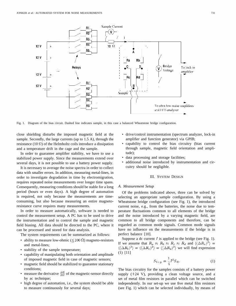
JONKER et al.: AUTOMATED SYSTEM FOR NOISE MEASUREMENTS 731
Fig. 1. Diagram of the bias circuit. Dashed line indicates sample, in this case a balanced Wheatstone bridge configuration.
close shielding disturbs the imposed magnetic field at thesample. Secondly, the large currents (up to 1.5 A), through theresistance (10 ) of the Helmholtz coils introduce a dissipationand a temperature drift in the cage and the sample.
In order to guarantee amplifier stability, we have to use astabilized power supply. Since the measurements extend overseveral days, it is not possible to use a battery power supply.
It is necessary to average the noise spectra in order to collectdata with smaller errors. In addition, measuring metal-lines, inorder to investigate degradation in time by electromigration,requires repeated noise measurements over longer time spans.Consequently, measuring conditions should be stable for a longperiod (hours or even days). A high degree of automationis required, not only because the measurements are time-consuming, but also because measuring an entire magneto-resistance curve requires many measurements.
In order to measure automatically, software is needed tocontrol the measurement setup. A PC has to be used to drivethe instrumentation and to control the sample and magneticfield biasing. All data should be directed to the PC, where itcan be processed and stored for data analysis.
The system requirements can be summarized as follows:
• ability to measure low-ohmic ( ) magneto-resistorsand metal-lines;
• stability of the sample temperature;• capability of manipulating both orientation and amplitude
of imposed magnetic field in case of magnetic sensors;• magnetic field should be stabilized to guarantee stationary
conditions;• measure the derivative of the magnetic-sensor directly
by ac technique;• high degree of automation, i.e., the system should be able
to measure continuously for several days;
• drive/control instrumentation (spectrum analyzer, lock-inamplifier and function generator) via GPIB;
• capability to control the bias circuitry (bias currentthrough sample, magnetic field orientation and ampli-tude);
• data processing and storage facilities;• additional noise introduced by instrumentation and cir-
cuitry should be negligible.
III. SYSTEM DESIGN
A. Measurement Setup
Of the problems indicated above, three can be solved byselecting an appropriate sample configuration. By using aWheatstone bridge configuration (see Fig. 1), the introducedcurrent noise, e.g., from the batteries, the noise due to tem-perature fluctuations common to all elements of the bridgeand the noise introduced by a varying magnetic field, arecommon to all bridge components and therefore, can beregarded as common mode signals. Common mode signalshave no influence on the measurements if the bridge is inperfect balance [10].
Suppose a dc currentis applied to the bridge (see Fig. 1).If we assume that and
we will find expression(1) [11]
(1)
The bias circuitry for the samples consists of a battery powersupply ( 24 V), providing a clean voltage source, and aset of metal film resistors in parallel which can be switchedindependently. In our set-up we use five metal film resistors(see Fig. 1) which can be selected individually, by means of
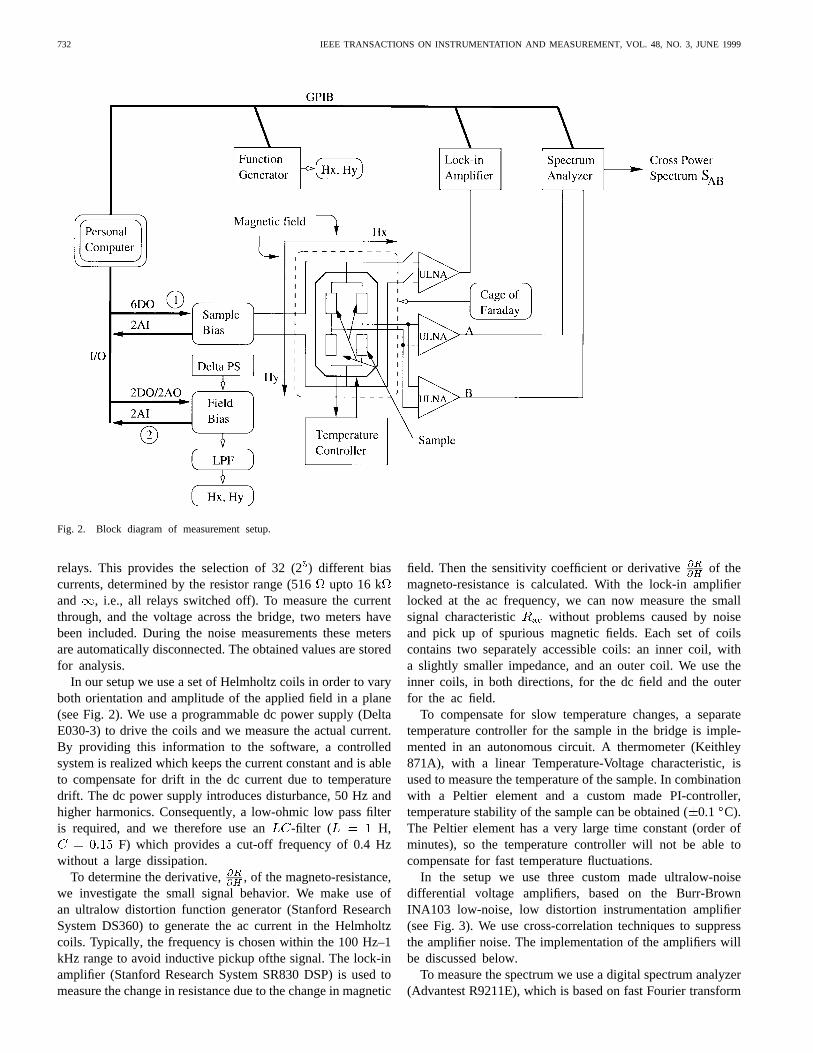
732 IEEE TRANSACTIONS ON INSTRUMENTATION AND MEASUREMENT, VOL. 48, NO. 3, JUNE 1999
Fig. 2. Block diagram of measurement setup.
relays. This provides the selection of 32 (2) different biascurrents, determined by the resistor range (516upto 16 kand , i.e., all relays switched off). To measure the currentthrough, and the voltage across the bridge, two meters havebeen included. During the noise measurements these metersare automatically disconnected. The obtained values are storedfor analysis.
In our setup we use a set of Helmholtz coils in order to varyboth orientation and amplitude of the applied field in a plane(see Fig. 2). We use a programmable dc power supply (DeltaE030-3) to drive the coils and we measure the actual current.By providing this information to the software, a controlledsystem is realized which keeps the current constant and is ableto compensate for drift in the dc current due to temperaturedrift. The dc power supply introduces disturbance, 50 Hz andhigher harmonics. Consequently, a low-ohmic low pass filteris required, and we therefore use an -filter ( H,
F) which provides a cut-off frequency of 0.4 Hzwithout a large dissipation.
To determine the derivative, , of the magneto-resistance,we investigate the small signal behavior. We make use ofan ultralow distortion function generator (Stanford ResearchSystem DS360) to generate the ac current in the Helmholtzcoils. Typically, the frequency is chosen within the 100 Hz–1kHz range to avoid inductive pickup ofthe signal. The lock-inamplifier (Stanford Research System SR830 DSP) is used tomeasure the change in resistance due to the change in magnetic
field. Then the sensitivity coefficient or derivative of themagneto-resistance is calculated. With the lock-in amplifierlocked at the ac frequency, we can now measure the smallsignal characteristic without problems caused by noiseand pick up of spurious magnetic fields. Each set of coilscontains two separately accessible coils: an inner coil, witha slightly smaller impedance, and an outer coil. We use theinner coils, in both directions, for the dc field and the outerfor the ac field.
To compensate for slow temperature changes, a separatetemperature controller for the sample in the bridge is imple-mented in an autonomous circuit. A thermometer (Keithley871A), with a linear Temperature-Voltage characteristic, isused to measure the temperature of the sample. In combinationwith a Peltier element and a custom made PI-controller,temperature stability of the sample can be obtained (0.1 C).The Peltier element has a very large time constant (order ofminutes), so the temperature controller will not be able tocompensate for fast temperature fluctuations.
In the setup we use three custom made ultralow-noisedifferential voltage amplifiers, based on the Burr-BrownINA103 low-noise, low distortion instrumentation amplifier(see Fig. 3). We use cross-correlation techniques to suppressthe amplifier noise. The implementation of the amplifiers willbe discussed below.
To measure the spectrum we use a digital spectrum analyzer(Advantest R9211E), which is based on fast Fourier transform
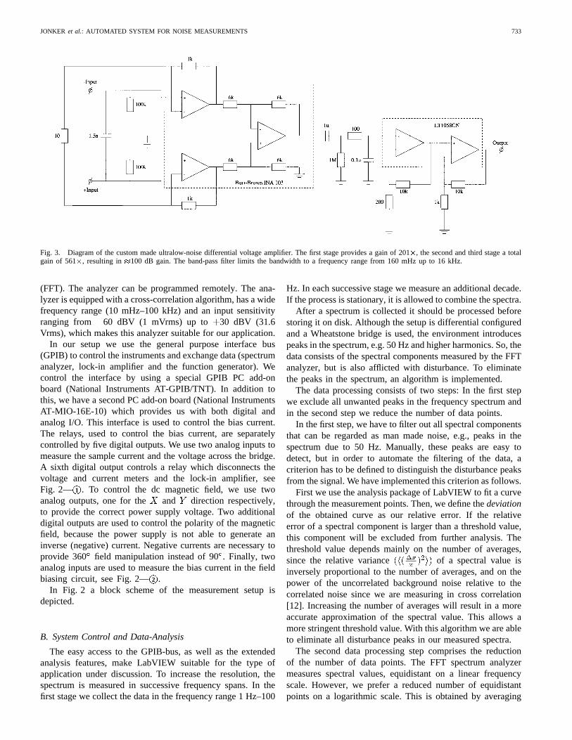
JONKER et al.: AUTOMATED SYSTEM FOR NOISE MEASUREMENTS 733
Fig. 3. Diagram of the custom made ultralow-noise differential voltage amplifier. The first stage provides a gain of 201, the second and third stage a totalgain of 561, resulting in100 dB gain. The band-pass filter limits the bandwidth to a frequency range from 160 mHz up to 16 kHz.
(FFT). The analyzer can be programmed remotely. The ana-lyzer is equipped with a cross-correlation algorithm, has a widefrequency range (10 mHz–100 kHz) and an input sensitivityranging from 60 dBV (1 mVrms) up to 30 dBV (31.6Vrms), which makes this analyzer suitable for our application.
In our setup we use the general purpose interface bus(GPIB) to control the instruments and exchange data (spectrumanalyzer, lock-in amplifier and the function generator). Wecontrol the interface by using a special GPIB PC add-onboard (National Instruments AT-GPIB/TNT). In addition tothis, we have a second PC add-on board (National InstrumentsAT-MIO-16E-10) which provides us with both digital andanalog I/O. This interface is used to control the bias current.The relays, used to control the bias current, are separatelycontrolled by five digital outputs. We use two analog inputs tomeasure the sample current and the voltage across the bridge.A sixth digital output controls a relay which disconnects thevoltage and current meters and the lock-in amplifier, seeFig. 2— 1 . To control the dc magnetic field, we use twoanalog outputs, one for the and direction respectively,to provide the correct power supply voltage. Two additionaldigital outputs are used to control the polarity of the magneticfield, because the power supply is not able to generate aninverse (negative) current. Negative currents are necessary toprovide 360 field manipulation instead of 90. Finally, twoanalog inputs are used to measure the bias current in the fieldbiasing circuit, see Fig. 2—2 .
In Fig. 2 a block scheme of the measurement setup isdepicted.
B. System Control and Data-Analysis
The easy access to the GPIB-bus, as well as the extendedanalysis features, make LabVIEW suitable for the type ofapplication under discussion. To increase the resolution, thespectrum is measured in successive frequency spans. In thefirst stage we collect the data in the frequency range 1 Hz–100
Hz. In each successive stage we measure an additional decade.If the process is stationary, it is allowed to combine the spectra.
After a spectrum is collected it should be processed beforestoring it on disk. Although the setup is differential configuredand a Wheatstone bridge is used, the environment introducespeaks in the spectrum, e.g. 50 Hz and higher harmonics. So, thedata consists of the spectral components measured by the FFTanalyzer, but is also afflicted with disturbance. To eliminatethe peaks in the spectrum, an algorithm is implemented.
The data processing consists of two steps: In the first stepwe exclude all unwanted peaks in the frequency spectrum andin the second step we reduce the number of data points.
In the first step, we have to filter out all spectral componentsthat can be regarded as man made noise, e.g., peaks in thespectrum due to 50 Hz. Manually, these peaks are easy todetect, but in order to automate the filtering of the data, acriterion has to be defined to distinguish the disturbance peaksfrom the signal. We have implemented this criterion as follows.
First we use the analysis package of LabVIEW to fit a curvethrough the measurement points. Then, we define thedeviationof the obtained curve as our relative error. If the relativeerror of a spectral component is larger than a threshold value,this component will be excluded from further analysis. Thethreshold value depends mainly on the number of averages,since the relative variance of a spectral value isinversely proportional to the number of averages, and on thepower of the uncorrelated background noise relative to thecorrelated noise since we are measuring in cross correlation[12]. Increasing the number of averages will result in a moreaccurate approximation of the spectral value. This allows amore stringent threshold value. With this algorithm we are ableto eliminate all disturbance peaks in our measured spectra.
The second data processing step comprises the reductionof the number of data points. The FFT spectrum analyzermeasures spectral values, equidistant on a linear frequencyscale. However, we prefer a reduced number of equidistantpoints on a logarithmic scale. This is obtained by averaging
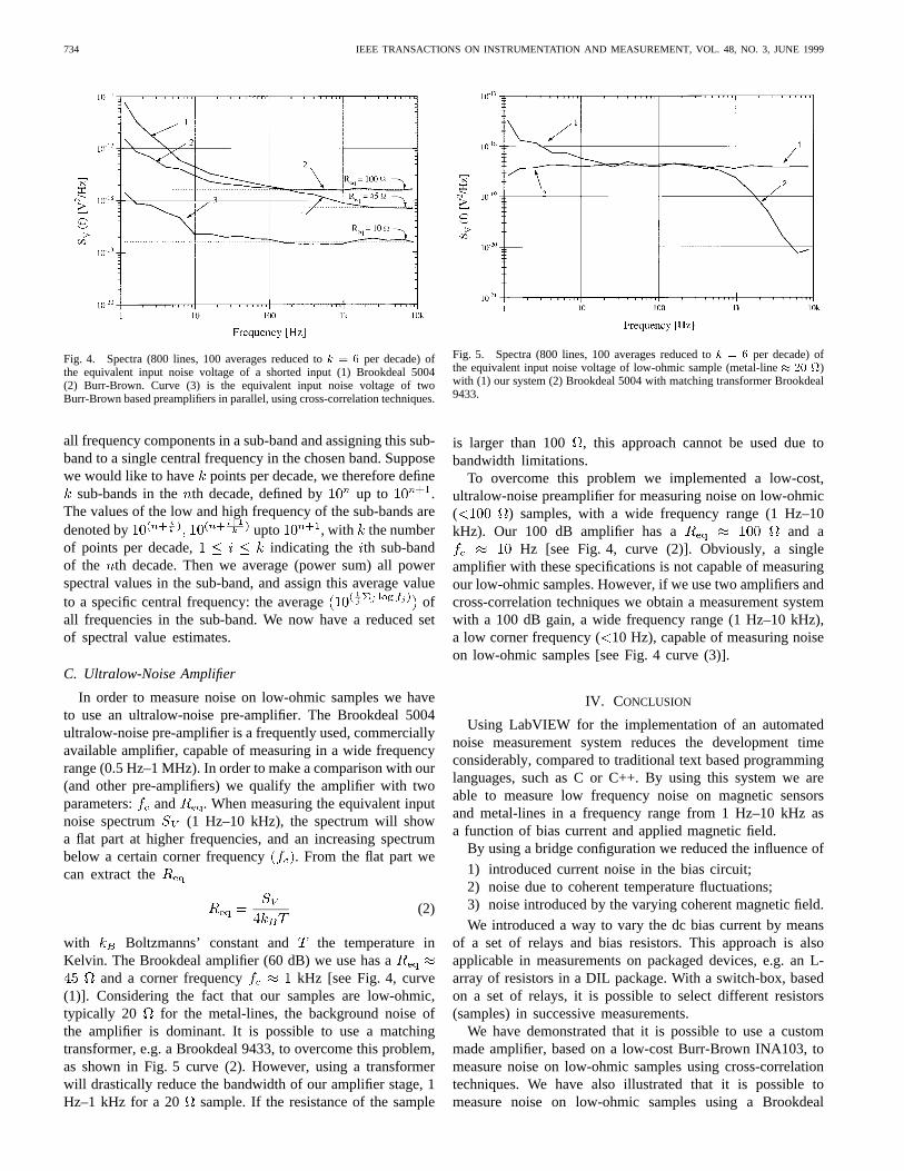
734 IEEE TRANSACTIONS ON INSTRUMENTATION AND MEASUREMENT, VOL. 48, NO. 3, JUNE 1999
Fig. 4. Spectra (800 lines, 100 averages reduced tok = 6 per decade) ofthe equivalent input noise voltage of a shorted input (1) Brookdeal 5004(2) Burr-Brown. Curve (3) is the equivalent input noise voltage of twoBurr-Brown based preamplifiers in parallel, using cross-correlation techniques.
all frequency components in a sub-band and assigning this sub-band to a single central frequency in the chosen band. Supposewe would like to have points per decade, we therefore define
sub-bands in the th decade, defined by up to .The values of the low and high frequency of the sub-bands aredenoted by upto , with the numberof points per decade, indicating the th sub-bandof the th decade. Then we average (power sum) all powerspectral values in the sub-band, and assign this average valueto a specific central frequency: the average ofall frequencies in the sub-band. We now have a reduced setof spectral value estimates.
C. Ultralow-Noise Amplifier
In order to measure noise on low-ohmic samples we haveto use an ultralow-noise pre-amplifier. The Brookdeal 5004ultralow-noise pre-amplifier is a frequently used, commerciallyavailable amplifier, capable of measuring in a wide frequencyrange (0.5 Hz–1 MHz). In order to make a comparison with our(and other pre-amplifiers) we qualify the amplifier with twoparameters: and . When measuring the equivalent inputnoise spectrum (1 Hz–10 kHz), the spectrum will showa flat part at higher frequencies, and an increasing spectrumbelow a certain corner frequency . From the flat part wecan extract the
(2)
with Boltzmanns’ constant and the temperature inKelvin. The Brookdeal amplifier (60 dB) we use has a
and a corner frequency kHz [see Fig. 4, curve(1)]. Considering the fact that our samples are low-ohmic,typically 20 for the metal-lines, the background noise ofthe amplifier is dominant. It is possible to use a matchingtransformer, e.g. a Brookdeal 9433, to overcome this problem,as shown in Fig. 5 curve (2). However, using a transformerwill drastically reduce the bandwidth of our amplifier stage, 1Hz–1 kHz for a 20 sample. If the resistance of the sample
Fig. 5. Spectra (800 lines, 100 averages reduced tok = 6 per decade) ofthe equivalent input noise voltage of low-ohmic sample (metal-line 20 )with (1) our system (2) Brookdeal 5004 with matching transformer Brookdeal9433.
is larger than 100 , this approach cannot be used due tobandwidth limitations.
To overcome this problem we implemented a low-cost,ultralow-noise preamplifier for measuring noise on low-ohmic( ) samples, with a wide frequency range (1 Hz–10kHz). Our 100 dB amplifier has a and a
Hz [see Fig. 4, curve (2)]. Obviously, a singleamplifier with these specifications is not capable of measuringour low-ohmic samples. However, if we use two amplifiers andcross-correlation techniques we obtain a measurement systemwith a 100 dB gain, a wide frequency range (1 Hz–10 kHz),a low corner frequency (10 Hz), capable of measuring noiseon low-ohmic samples [see Fig. 4 curve (3)].
IV. CONCLUSION
Using LabVIEW for the implementation of an automatednoise measurement system reduces the development timeconsiderably, compared to traditional text based programminglanguages, such as C or C++. By using this system we areable to measure low frequency noise on magnetic sensorsand metal-lines in a frequency range from 1 Hz–10 kHz asa function of bias current and applied magnetic field.
By using a bridge configuration we reduced the influence of
1) introduced current noise in the bias circuit;2) noise due to coherent temperature fluctuations;3) noise introduced by the varying coherent magnetic field.
We introduced a way to vary the dc bias current by meansof a set of relays and bias resistors. This approach is alsoapplicable in measurements on packaged devices, e.g. an L-array of resistors in a DIL package. With a switch-box, basedon a set of relays, it is possible to select different resistors(samples) in successive measurements.
We have demonstrated that it is possible to use a custommade amplifier, based on a low-cost Burr-Brown INA103, tomeasure noise on low-ohmic samples using cross-correlationtechniques. We have also illustrated that it is possible tomeasure noise on low-ohmic samples using a Brookdeal
JONKER et al.: AUTOMATED SYSTEM FOR NOISE MEASUREMENTS 735
5004 amplifier in addition to a Brookdeal 9433 matchingtransformer, although the bandwidth of this configuration islimited.
ACKNOWLEDGMENT
The authors wish to thank M. El Haddouchi for his contribu-tion in the hardware implementation and R. R. M Vermeulenand P. N. Wouters for the development of the LabVIEW devicedriver for the Advantest R9211E spectrum analyzer.
REFERENCES
[1] F. N. Hooge, T. G. M. Kleinpenning, and L. K. J. Vandamme, “Experi-mental studies on1=f noise,” Rep. Progr. Phys., vol. 44, pp. 479–532,1981.
[2] A. M. Yassine and T. M. Chen, “Electromigration noise measurementsusing a novel ac/dc wafer-level noise measurement system,”IEEE Trans.Electron Devices, vol. 44, pp. 180–184, Jan. 1997.
[3] A. Verbruggen, H. Stoll, K. Heeck, and R. H. Koch, “A novel tech-nique for measuring resistance fluctuations independently of backgroundnoise,” Appl. Phys. A, vol. 48, pp. 233–236, 1989.
[4] C. Ciofi, M. De Marinis, and B. Neri, “Ultralow-noise PC-basedmeasurement system for the characterization of the metallizations ofintegrated circuits,”IEEE Trans. Instrum. Meas., vol. 46, pp. 789–793,Aug. 1997.
[5] T. Luo, Y. S. Dai, and Z. He, “Automatic measuring system forelectronic noise and its performance,”IEEE Trans. Instrum. Meas., vol.41, pp. 942–945, Dec. 1992.
[6] R. Saletti and B. Neri, “Low-noise automated measurement systemfor low-frequency current fluctuations in thin-oxide silicon structures,”IEEE Trans. Instrum. Meas., vol. 41, pp. 123–127, Feb. 1992.
[7] R. A. Sherry and S. M. Lord, “LabVIEW as an effective enhancement toan optoelectronics laboratory experiment,” inProc. Frontiers Education1997, 27th Annu. Conf. Teaching Learning Era Change, 1997, vol. 2,pp. 897–900.
[8] J. Briaire, L. K. J. Vandamme, and M. A. M. Gijs, “Resistance and1=f noise dependence on magnetic field in single Ni80Fe20 layersand Ni80Fe20/Cu multilayers,” inProc. 14th Int. Conf. Noise PhysicalSystems1=f Fluctuations, C. Claeys and E. Simoen, Eds. Singapore:World Scientific, 1997, pp. 587–590.
[9] R. J. M. van Veerdonket al., “1=f noise in anisotropic and giantmagnetoresistive elements,”J. Appl. Phys., vol. 82, pp. 6152–6164,Dec. 1997.
[10] J. H. Scofield, “AC method for measuring low-frequency resistancefluctuation spectra,”Rev. Sci. Instrum., vol. 58, pp. 985–993, Feb. 1987.
[11] L. K. J. Vandamme and W. M. G. van Bokhoven, “Conductance noiseinvestigations with four arbitrarily shaped and placed electrodes,”Appl.Phys., vol. 14, pp. 205–215, 1977.
[12] J. Briaire and L. K. J. Vandamme, “The uncertainty in Gaussian noisegeneralized for cross-correlation spectra,” submitted for publication.
R. J. W. Jonker, photograph and biography not available at the time ofpublication.
J. Briaire , photograph and biography not available at the time of publication.
L. K. J. Vandamme, photograph and biography not available at the time ofpublication.

6XPPDU\DQG&RQFOXVLRQV
- 129 -
Summary and Conclusions
This dissertation focuses on the 1/f noise in the thin film ferromagnet Permalloy.
As reference for the uncertainty in the measured noise, the uncertainty for
Gaussian noise spectra has also been calculated. As an example of how
individual events can lead to noise, substrate injection of CMOS circuits has been
investigated. A comparison has been made of the different substrate injection
mechanisms.
The calculations of the ensemble average and variance of Gaussian noise
measured as cross-correlation spectra were performed as a function of the
number of time averages. The calculations are based on the Carson-Campbell
theorem which treats noise spectra as a collection of individual deterministic
pulses transformed into the frequency domain.
We compared our calculations with experimental results of known Gaussian
noise sources: metal film resistors. An excellent agreement is achieved between
the calculations and the measurements. The results were tested with white
thermal noise but the calculations are independent of the sort of spectrum
measured and will therefore also hold for Gaussian 1/f noise or other types of
Gaussian noise. This Gaussian reference makes it possible to identify non-
Gaussian noise sources in situations where a cross-correlation analysis is needed.
The minimum number of averages needed to measure with the cross-correlation
analysis is inversely proportional to the coherence function.
When noise is used as a diagnostic tool to determine the reliability of a device,
not only the noise parameters itself, but also the uncertainty in these noise
parameters are important. For good devices this uncertainty will be Gaussian. As
an example, we calculated the error in the frequency index of Gaussian 1/f noise.
However, because of non-linear measurement errors caused by a digital spectrum
analyzer this uncertainty might deviate from Gaussianity. We analyzed the
additional non-Gaussian error caused by the spectrum analyzer through

6XPPDU\DQG&RQFOXVLRQV
- 130 -
simulations. The results show that the influence of a 12 bit analog-to-digital
converter is negligible. Furthermore, when a Hanning window is used, the
additional error is negligible up to the averaging of a thousand spectra.
We presented an automated system for electronic noise measurements on metal
films such as Permalloy. This new system is controlled by a personal computer
that utilizes National Instruments' LabVIEW software.
The setup is designed to measure the DC resistance, the low-frequency noise
(1Hz - 10kHz) and the small signal AC response. Each as a function of an
externally imposed magnetic DC field and as a function of the DC bias current
through the magnetic sensors. With this system we are able to measure
continuously for several days, during which measured spectra are collected,
processed and stored for further analysis.
We also demonstrated that it is possible to use a custom-made amplifier, based
on a low-cost Burr-Brown INA1O3, to measure noise on low-ohmic samples
using cross-correlation techniques. Furthermore, we have shown that it is
possible to measure noise on low-ohmic samples using a Brookdeal 5004
amplifier in addition to a Brookdeal 9433 matching transformer, although the
bandwidth of this configuration is limited.
The investigation of the room-temperature 1/f noise and magneto-resistance of
single-domain Ni Fe films is performed as a function of an in-plane magnetic80 20
field and as a function of the film volume. We introduced a theoretical model to
determine the equilibrium angle of magnetization Q directly from AC magneto-0
resistance data. A comparison of a plot of the 1/f noise power density versus Q0
with the susceptibility permits, for the first time, the observation of 1/f noise that
cannot be explained by the simple fluctuation-dissipation theorem for the
magnetization. An additional term in the magnetization noise is needed. This
term has its origin in the coupling between the magnetization and an internal,
non-magnetic fluctuator with a long-range character. We speculate that lattice

6XPPDU\DQG&RQFOXVLRQV
- 131 -
vibrations lead to these magnetization fluctuations. We also showed that the
temperature dependence of this noise source is not consistent with the Dutta,
Dimon and Horn model for 1/f noise.
We also investigated the room-temperature 1/f noise of soft magnetic Ni Fe80 20
films with a few domain walls, and of Ni Fe /Cu magnetic multi-layers with a80 20
complicated domain-wall structure. These results on multi-domain samples
support the concept that the 1/f noise originates within the sub-domains, just as in
single-domain samples where the noise is due to fluctuations in the
magnetization angle of each sub-domain. As a result, the contribution of
individual sub-domains to the total noise can differ significantly: there are noisy
islands.
To determine the mechanisms that contribute to substrate crosstalk, substrate
noise injection is evaluated for a 0.25µm CMOS technology. On a device level,
currents due to the capacitive coupling and impact ionization effects dominate
injection into the substrate. This is valid for both n-channel and p-channel
MOSFETs. On a circuit level, parasitics such as the bond wire inductance and
the capacitive coupling of the V node to the substrate will cause additional, andSS
probably dominating, substrate voltage fluctuations. Additional factors like the
parasitic n-well decoupling capacitance between V and V , and oscillationsDD SS
due to the inductances in combination with the capacitances will also influence
the substrate signal.
Within a complex circuit, a significant amount of switching takes place during a
clock cycle. As a consequence some signal cancellation can take place. For
simplicity, we have treated this switching activity as a random process. Our
evaluation has shown that partial noise cancellation will mainly occur at higher
frequencies, while for instance DC components of signals can never be canceled.
So, the DC and low-frequency components of the switching signal, which are
relatively unimportant for an individual inverter, can become more significant as
the total circuit becomes more complex.
6DPHQYDWWLQJHQ&RQFOXVLHV
- 132 -
Samenvatting en Conclusies
In dit proefschrift is de 1/f ruis van de ferromagneet Permalloy onderzocht. Om
een referentie voor de onzekerheid in de ruis spectra te hebben, is de onzekerheid
voor Gaussische ruis spectra ook berekend. Ter illustratie hoe individuele
gebeurtenissen tot ruis kunnen leiden, is de substraat injectie van CMOS circuits
ook onderzocht. Er is een vergelijking gemaakt tussen de verschillende substraat
injectie bronnen.
De berekening van het ensemble gemiddelde en de variantie van Gaussische ruis,
gemeten als kruis-correlatie spectra, is gemaakt als een functie van het aantal
middelingen in de tijd. Deze berekeningen zijn gebaseerd op het Carson-
Campbell theorema dat ruis spectra beschouwd als een collectie van individuele
deterministische pulsen die getransformeerd zijn naar het frequentie domein.
We hebben onze berekeningen vergeleken met experimentele resultaten van
bekende bronnen van Gaussische ruis: metaal-film weerstanden. De theorie en de
resultaten bleken zeer goed overeen te komen. De berekeningen zijn vergeleken
met witte thermische ruis maar zijn onafhankelijk van het gemeten type ruis en
zullen dus ook van toepassing zijn voor Gaussische 1/f ruis of andere Gaussische
ruis. Deze Gaussische referentie biedt de mogelijkheid om niet Gaussische
ruisbronnen te kunnen identificeren in situaties waar een kruis-correlatie meting
noodzakelijk is. Het minimum aantal middelingen dat nodig is voor een kruis-
correlatie analyse is omgekeerd evenredig met de coherentie functie.
Als ruis gebruikt wordt om de betrouwbaarheid te bepalen van bijvoorbeeld een
materiaal, zijn niet alleen de ruisparameters van belang maar ook de onzekerheid
in elke parameter. Voor een goed materiaal zal deze onzekerheid een Gaussisch
karakter hebben. Ter illustratie hebben wij de fout in de frequentie index van
Gaussische 1/f ruis bepaald. Maar als gevolg van niet-lineare meetfouten die
veroorzaakt worden door een digitale spectrum analyser zou de onzekerheid
kunnen gaan afwijken van zijn Gaussisch karakter. Via simulaties hebben we de
6DPHQYDWWLQJHQ&RQFOXVLHV
- 133 -
additionele, niet-Gaussische onzekerheid onderzocht zoals die veroorzaakt wordt
door een spectrum analyser. De resultaten tonen aan dat de invloed van een 12-
bit analoog naar digitaal omzetter verwaarloosbaar is. Tevens blijkt dat, wanneer
een Hanning window gebruikt wordt, de additionele fout verwaarloosbaar is als
er minder dan duizend spectra gemiddeld worden.
Gepresenteerd is een geautomatiseerde meetopstelling voor ruismetingen aan
metaal filmen zoals Permalloy. Dit nieuwe systeem wordt gestuurd door een PC
die gebruik maakt van LabVIEW software van National Instruments.
De opstelling is ontworpen om de DC weerstand, de laag-frequente ruis en de
klein-signaal AC respons te meten. Elk als een functie van een uitwendig
aangebracht DC magneet veld en als een functie van een DC stroom door de
magnetische sensoren. Met dit nieuwe systeem zijn we in staat om verscheidene
dagen lang continu te meten waarbij de gemeten spectra verwerkt en opgeslagen
worden voor verdere analyse.
Tevens hebben we laten zien dat het mogelijk is om een specifiek voor dit doel
gemaakte versterker te gebruiken die gebaseerd is op de goedkope Burr-Brown
INA103. Deze wordt gebruikt om de ruis van laag ruisende metaal films te meten
met behulp van de kruis-correlatie techniek. Ook hebben we laten zien dat het
mogelijk is om lage ruis niveau's te meten met behulp van een Brookdeal 5004
versterker in combinatie met een Brookdeal 9433 transformator, hoewel de
bandbreedte van deze laatste configuratie gelimiteerd is.
Het onderzoek bij kamertemperatuur naar de 1/f ruis en magnetoweerstand van
één domeins Ni Fe is gedaan als een functie van een magneetveld in het film80 20
vlak en als een functie van het film volume. We hebben een theoretisch model
geïntroduceerd waarmee de evenwichtshoek Q van de magnetisatie direct0
bepaald kan worden uit AC magnetoweerstands data. Een grafisch vergelijk van
de vermogensdichtheid van de 1/f ruis met susceptibiliteit, beide als functie van
Q , toont voor het eerst aan dat de geobserveerde 1/f ruis niet verklaard kan0
6DPHQYDWWLQJHQ&RQFOXVLHV
- 134 -
worden met het fluctuatie-dissipatie theorema.
Een additionele term in de magnetisatie ruis is noodzakelijk. Deze term ontstaat
uit een koppeling tussen de magnetisatie en een niet-magnetische fluctuator met
een globaal karakter. We speculeren dat rooster trillingen leiden tot deze
magnetisatie fluctuaties. Verder hebben we laten zien dat het gedrag van deze
ruisbron als functie van de temperatuur niet consistent is met het Dutta, Dimon
en Horn model voor 1/f ruis.
Tevens is bij kamertemperatuur de 1/f ruis van Ni Fe films met enkele domein80 20
wanden onderzocht en ook die van Ni Fe /Cu magnetische multilagen met een80 20
gecompliceerde domein wand structuur. Deze resultaten, behaald aan
multidomein monsters, bevestigen het concept dat de 1/f ruis alleen zijn
oorsprong vindt binnen een domein, net zoals in één domeins films waar de 1/f
ruis het resultaat is van fluctuaties in de magnetisatie hoek binnen het domein.
Dit resulteert bij multidomeins magneten in sterk verschillende ruis niveaus van
de individuele domeinen: er zijn ruiserige eilanden.
Om de mechanismen te bepalen die bijdragen aan substraat overspraak is de
substraat ruis injectie voor een 0.25µm CMOS technologie geëvalueerd. De
injectie in het substraat wordt op het transistor niveau gedomineerd door stromen
die, of een gevolg zijn van capacitieve koppelingen, of een gevolg zijn van
ioniserende botsingen. Dit geldt voor zowel n-kanaals als p-kanaals MOSFETs.
Op een circuit niveau zorgen parasieten zoals de bond-draad inductie en de
capacitieve koppeling van V met het substraat voor additionele, enSS
waarschijnlijk dominerende, spannings fluctuaties in het substraat. Andere
factoren zoals de parasitaire ontkoppelings capaciteit tussen V en V enDD SS
oscillaties als gevolg van inducties in combinatie met capaciteiten zullen het
substraat signaal ook beïnvloeden.
Binnen een complex circuit vinden een groot aantal schakelingen plaats
gedurende een klok cyclus. Een consequentie hiervan is dat sommige
6DPHQYDWWLQJHQ&RQFOXVLHV
- 135 -
schakelpulsen tegen elkaar zullen wegvallen. In een eenvoudige benadering
hebben we de schakelactiviteiten als een willekeurig proces behandelt. Dit laat
zien dat het tegen elkaar wegvallen van schakelpulsen voornamelijk in de hoge
frequenties zal plaatsvinden terwijl bijvoorbeeld DC componenten van signalen
nooit zullen wegvallen. Dus, de DC en laagfrequente componenten van
schakelsignalen, die relatief onbelangrijk zijn tijdens een individuele schakeling,
kunnen belangrijker worden naar mate het circuit complexer wordt.
5HIHUHQFHV
- 136 -
References
[1] Sóshin Chikazumi, Physics of Ferromagnetism, 2 ed. (Oxford universitynd
press, Oxford, 1997).
[2] M.N. Baibich et al., Phys. Rev. Lett. 61, 2472 (1988).
[3] H.T. Hardner, M.B. Weissman, M.B. Salamon and S.S.P. Parkin, Phys.
Rev. B. 48, 21, pp. 16156-16159 (1993).
[4] Aldert van der Ziel, Noise in Solid State Devices and Circuits (John Wiley
& sons, New York, 1986).
[5] Melvin Lax, Rev. Mod. Phys. 32, 1, pp. 25-64 (1960).
[6] T.R. McGuire and R.I. Potter, IEEE Trans. on Magn. 11, 4, pp. 1018-1038
(1975).
[7] S. Vitale, A. Cavalleri, M. Cerdonio, A. Maraner and G.A. Prodi, J. Appl.
Phys. 76, 10, pp. 6332-6334 (1994).
[8] David Jiles, Introduction to Magnetism and Magnetic Materials (Chapman
& Hall, London, 1991).
[9] Robert M. White, Quantum Theory of Magnetism, 2 ed. (Springer-Verlag,nd
Berlin, 1983).
[10] Tôru Moriya, Spin Fluctuations in Itinerant Electron Magnetism (Springer-
Verlag, Berlin, 1985).
[11] Charles Kittel, Introduction to Solid State Physics, 6 ed. (John Wiley &th
sons, New York, 1986).
[12] Henri J.F. Jansen, Physics Today, april 1995, pp. 50-55.
[13] C.G. Windsor, Physica 91B, pp. 119-129 (1977).
5HIHUHQFHV
- 137 -
[14] M. Hatherly, K. Hirakawa, R.D. Lowde, J.F. Mallett, M.W. Stringfellow,
B.H. Torrie, Proc. Phys. Soc. 84, pp. 55-62 (1964).
[15] F.J. Himpsel, J.E. Ortega, G.J. Mankey and R.F. Willes, Adv. in Phys. 47,
4, pp. 511-597 (1998)
[16] Herbert B. Callen and Theodore A. Welton, Phys. Rev. 83, 1, pp. 34-40
(1951).
[17] R. Kubo, Rep. Prog. Phys. 19 part 1, pp. 255-284 (1966).
[18] Frederick Reif, Fundamentals of Statistical and Thermal Physics, int. ed.
(McGraw-Hill, Singapore, 1985).
[19] J. Briaire and L.K.J. Vandamme, J. Appl. Phys. 84, 8, 4370-4374 (1998).
Appendix A5, chapter 2.
[20] M.B. Weissman, Annu. Rev. Mater. Sci. 26, 395 (1996).
[21] G. M. Khera and J. Kakalios, Phys. Rev. B 56, 1918 (1997).
[22] N.Campbell, Proc. Cambridge Philos. Soc. 15, 117 (1909).
[23] N.Campbell, Proc. Cambridge Philos. Soc. 15, 310 (1909).
[24] N.Campbell, Proc. Cambridge Philos. Soc. 15, 513 (1909).
[25] J.R. Carson, Bell Syst. Tech. J. 4, 265 (1925).
[26] J.R. Carson, Bell Syst. Tech. J. 4, 374 (1925).
[27] M. Nelkin and A.-M. S. Tremblay, J. Stat. Phys. 25, 253 (1981).
[28] P. J. Restle, R. J. Hamilton, M. B. Weissman, and M. S. Love, Phys. Rev. B
31, 2254 (1985).
[29] M. Stoisiek and D. Wolf, J. Appl. Phys. 47, 362 (1976).
[30] R. F. Voss and J. Clarke, Phys. Rev. Lett. 30, 42 (1976).

5HIHUHQFHV
- 138 -
[31] R. F. Voss and I. Clarke, Phys. Rev. B 13, 556 (1976).
[32] H. G.E. Beck and W. P. Spruit, J. AppI. Phys. 49, 3384 (1978).
[33] M. B. Weissman, N.E. Israeloff, and G. B. Alers, J. Magn. Magn. Mater.
114, 87 (1992).
[34] H. T. Hardner, M. B. Weissman, M. Jaime, R. E. Treece, P. C. Dorsey, J. S.
Horwitz, and D. B. Chrisey, J. Appl. Phys. 81, 272 (1997).
[35] G.B. Alers, M. B. Weissman, A. Kartig, and N. Israeloff, Phys. Rev. B 36,
8429 (1987).
[36] P.J. Restle, M. B. Weissman, and R. D. Black, J. Appl. Phys. 54, 5844
(1983).
[37] G.B. Alers, S. Martin, R. A. Haram, A. Feygenson, and R. D. Yadvish,
Appl. Phys. Lett. 66, 198 (1995).
[38] Any book that introduces probability distributions, for example:
A. Papoulis, Probability, Random Variables and Stochastic Processes, 3rd
ed. (McGraw-Hill, New York, 1991).
[39] J. Briaire and L.K.J. Vandamme, accepted for publication in
Microelectronics Reliability. Chapter 3.
[40] Julius S. Bendat and Allan G. Piersol, Random Data: Analysis and
Measurement Procedures (Wiley-interscience, New York, 1971).
[41] H. Schönfeld, Z. Naturforschg. 10a, pp. 291-300 (1955)
[42] R.J.W. Jonker, J. Briaire and L.K.J. Vandamme, IEEE Trans. on Instr. and
Meas. 48, 730 (1999). Appendix A6, chapter 4.
[43] F. N. Hooge, T. G. M. Kleinpenning, and L. K. J. Vandamme, Rep. Prog.
Phys. 44, pp. 479-532 (1981).

5HIHUHQFHV
- 139 -
[44] A. M. Yassine and T. M. Chen, IEEE Trans. Electron Devices 44, pp. 180-
184 (1997).
[45] A. Verbruggen, H. Stoll, K. Heeck, and R. H. Koch, Appl. Phys. A 48, pp.
233-236 (1989).
[46] C. Ciofi, M. De Marinis, and B. Neri, IEEE Trans. Instrum. Meas. 46, pp.
789-793 (1997).
[47] T. Luo, Y. S. Dai, and Z. He, IEEE Trans. Instrum. Meas. 41, pp. 942-945
(1992).
[48] R. Saletti and B. Neri, IEEE Trans. Instrum. Meas. 41, pp. 123-127 (1992).
[49] R. A. Sherry and S. M. Lord, in Proc. Frontiers in Education 1997, 27th
Annual Conf. Teaching and Learning in an Era of Change 2, pp. 897-900
(1997).
[50] J. Briaire, L. K. J. Vandamme and M. A. M. Gijs, Proc. 14 Int. Conf.th
Noise in Physical Systems and 1/f Fluctuations (C. Claeys and E. Simoen,
eds.), pp. 587-590 (World Scientific, Singapore, 1997). (Chapter 6)
[51] R. J. M. van Veerdonk et al., J. Appl. Phys. 82, pp. 6152-6164 (1997).
[52] J. H. Scofield, Rev. Sci. Instrum. 58, pp. 985-993 (1987).
[53] L. K. J. Vandamme and W. M. G. van Bokhoven, Appl. Phys. 14, pp. 205-
215 (1977).
[54] J. Briaire, L. K. J. Vandamme and M. A. M. Gijs, submitted to Phys. Rev.
Lett. Chapter 5.
[55] R.J.M. van de Veerdonk et al, J. Appl. Phys. 82, 6152 (1997).
[56] R.V. Chamberlin, J. Appl. Phys. 76, 6401 (1994).
[57] J.J. Brophy, Chapter 1 in Fluctuation Phenomena in Solids, edited by R.E.
Burgess (Academic, New York, 1965).

5HIHUHQFHV
- 140 -
[58] W. Reim et al, Phys. Rev. Lett. 57, 905 (1986).
[59] M.B. Weissman, Rev. Mod. Phys. 65, 829 (1993).
[60] G.A. Prodi et al., J. Appl. Phys. 66, 5984 (1989).
[61] B. Barbara et al, J. Appl. Phys. 75, 5634 (1994).
[62] F.N. Hooge, Phys. Lett. 29A, 139 (1969).
[63] D. Fleetwood and N. Giordano, Phys. Rev. B 27, 667 (1983).
[64] P. Dutta, P. Dimon and P.M. Horn, Phys. Rev. Lett. 43, 9, pp. 646-649
(1979).
[65] P. Dutta and P.M. Horn, Rev. Mod. Phys. 53, 3, pp. 497-516 (1981).
[66] M.B. Weissman, Rev. Mod. Phys. 60, 2, pp. 537-571 (1988).
[67] M.A.M. Gijs, J.B. Giesbers, J.W. van Est, J. Briaire, L.K.J. Vandamme and
P. Beliën, J. Appl. Phys. 80, 4, pp. 2539-2541 (1996). (Chapter 6)
[68] J. Briaire and K.S. Krisch, accepted for publication in IEEE Trans. on
CAD. Chapter 7.
[69] D.K. Su, M.J. Loinaz, S. Masui and B.A.Wooley, IEEE Journal of Solid-
State Circuits 28, 4, pp. 420-429 (1993).
[70] M. Pfost and H.-M. Rein, IEEE Journal of Solid-State Circuits 33, 4, pp.
582-591 (1998).
[71] J.-P. Raskin, A. Viviani, D. Flandre and J.-P. Colinge, IEEE Transactions
on Electron Devices 44, 12, pp. 2252-2261 (1997).
[72] K. Joardar, Solid-State Electronics 39, 4, pp. 511-516 (1996).
[73] B.R. Stanisic, N.K. Verghese, R.A. Rutenbar, L.R. Carley, and D.J. Allstot,
IEEE Journal of Solid-State Circuits 29, 3, pp. 226-237 (1994).
5HIHUHQFHV
- 141 -
[74] R. Gharpurey and R.G. Meyer, IEEE Journal of Solid-State Circuits 31, 3,
pp. 344-353 (1996).
[75] P. Larsson, Analog Integrated Circuits and Signal Processing 14, pp. 113-
129 (1997).
[76] E. Charbon, P. Miliozzi, L.P. Carloni, A. Ferrari, A. Sangiovianni-
Vincentelli, IEEE Transactions on Computer-Aided Design of Integrated
Circuits and Systems 18, no. 3, pp. 301-310 (1999).
[77] J. R. Brews, Chap. 3 of High-Speed Semiconductor Devices, ed. S. M. Sze
(J.Wiley&Sons, New York, 1990).
[78] S. J. Hillenius, Chap. 3 of Modern Semiconductor Devices, ed. S. M. Sze,
(J.Wiley&Sons, New York, 1998).
[79] A. G. Chynoweth, Phys. Review 109, 5, pp. 1537 (1958).
[80] T.Y. Chan, P.K. Ko and C. Hu, IEEE Electron Device Letters 5, 12, pp.
505-507 (1984).
[81] M.-C. Hu and S.-L. Jang, Int. Journal of Electronics 83, 2, pp. 159-176
(1997).
[82] J. D. Bude and M. Mastrapasqua, IEEE Electron Device Letters 16, 10, pp.
439-441 (1995).
[83] C. Jungemann, B. Meinerzhagen, S. Decker, S. Keith, S. Yamaguchi and H.
Goto, Solid-State Electronics 42, 4, pp. 647-655 (1998).
[84] ADVICE – Accurate Design Verification for Electronic Circuits, User's
Guide, Release 4.0, AT&T Design Automation, 1994.
[85] C.C. McAndrew, B.K. Bhattacharyya, B.K. Wing, AT&T Technical
Memorandum 52864-910201-01TM (1991).
[86] T.Y. Chan, J. Chen, P.K. Ko and C. Hu, IEDM Technical Digest 1997, p.
718-721.
5HIHUHQFHV
- 142 -
[87] A. Toriumi, M. Yoshima, M. Iwase, Y. Akiyama and K. Taniguchi, IEEE
Transactions on Electron Devices 34, 7, pp. 1501-1508 (1987).
[88] K. Sakui, S.S. Wong, and B.A Wooley, IEEE Transactions on Electron
Devices 41, 9, pp. 1603-1607 (1994).
[89] S. Tam and C. Hu, IEEE Transactions on Electron Devices 31, 9, pp. 1264-
1273 (1984).
[90] T.J. Gabara, W.C. Fischer, J. Harrington, and W.W. Troutman, IEEE
Journal of Solid-State Circuits 32, 3, pp. 407-418 (1997).

%LEOLRJUDSK\RIDXWKRU
- 143 -
Bibliography of author
Publications in International Journals
Evidence for a new source of 1/f noise in single domain Ni Fe films80 20
J. Briaire, L.K.J. Vandamme and M.A.M. Gijs,Submitted to Physical Review Letters.
Principles of Substrate Crosstalk Generation in CMOS circuits.J. Briaire and K.S. Krisch,Accepted for publication in IEEE Transactions on CAD of IC’s and systems.
The influence of the digital spectrum analyzeron the uncertainty in 1/f noise parameters.J. Briaire and L.K.J. Vandamme,Accepted for publication in Microelectronics Reliability.
Automated System for Noise-Measurements onLow-Ohmic Samples and Magnetic Sensors.R.J.W. Jonker, J. Briaire and L.K.J. Vandamme,IEEE Transactions on Instrumentation and Measurement 48 (3),June 1999, pp. 730-735.
Uncertainty in Gaussian noise generalized for cross-correlation spectra.J. Briaire and L.K.J. Vandamme,Journal of Applied Physics 84 (8), 15 of October 1998, pp. 4370-4374.th
1/f Noise in magnetic Ni Fe single layers and Ni Fe / Cu multilayers.80 20 80 20
M.A.M. Gijs, J.B. Giesbers, P. Beliën, J.W. van Est,J. Briaire and L.K.J. Vandamme,Journal of Magnetism and Magnetic Materials 165, January 1997, pp. 360-362.
1/f Noise in magnetic Ni Fe single layers and Ni Fe / Cu multilayers.80 20 80 20
M.A.M. Gijs, J.B. Giesbers, J.W. van Est,J. Briaire, L.K.J. Vandamme and P. Beliën,Journal of Applied Physics 80 (4), 15 of August 1996, pp. 2539-2541.th

%LEOLRJUDSK\RIDXWKRU
- 144 -
Contributions to International Conferences
15 Int. Conference on Noise in physical systems and 1/f Fluctuationsth
(ICNF '99), Hong Kong, China, August 1999.Errors in the uncertainty of 1/f noise due to the spectrum analyzer.J. Briaire and L.K.J. Vandamme,Proceedings of ICNF '99, ed. C. Surya, pp. 435-438.
Custom Integrated Circuits Conference (CICC '99),San Diego, USA, May 1999.Substrate Injection and Crosstalk in CMOS Circuits.J. Briaire and K.S. Krisch,Proceedings of CICC’99, pp. 483-486.
14 Int. Conference on Noise in physical systems and 1/f Fluctuationsth
(ICNF '97), Leuven, Belgium, July 1997.Resistance and 1/f Noise dependence on magnetic field insingle Ni Fe and Ni Fe / Cu multilayers.80 20 80 20
J. Briaire, L.K.J. Vandamme, and M.A.M. Gijs,Proceedings of ICNF '97, eds. C. Claeys and E. Simoen, pp. 587-590.
3 European Laboratory for Electronic Noise (ELEN) Workshop,rd
Leuven, Belgium, Nov. 1996.1/f Noise dependence on magnetic field insingle Ni Fe and Ni Fe / Cu multilayers.80 20 80 20
J. Briaire, L.K.J. Vandamme and M.A.M. Gijs,Proceedings of the third ELEN workshop,eds. C. Claeys and E. Simoen, pp. 39-44.
1 Int. conference on Unsolved Problems Of Noise (UPON '96),st
Szeged, Hungary, Sept. 1996.Noise and magnetic domain structure in NiFe thin films.J.Briaire, L.K.J. Vandamme, K.M. Schep, J.B. Giesbers and M.A.M. Gijs,Proceedings of UPON '96, eds. Ch. R. Doering, L.B. Kiss and M.F. Shlesinger,World Scientific Singapore, pp. 157-161.
&XUULFXOXP9LWDH
- 145 -
Curriculum Vitae
Joseph Briaire (Joost) was born in Breda, the Netherlands on May 30 1969.th
After a happy childhood in Surinam (South America) from 1972 until 1981, he
returned to the Netherlands to start secondary school at the Mencia de Mendoza
College in Breda. Without being bothered about the contents of this education he
managed to finish the HAVO level in 1987.
Immediately afterwards he started at the Hoge School West-Brabant (HTS
Breda) at the faculty of electrical engineering. Specializing in high-voltage
engineering he received his ingenieur (ing.) or B.Sc. degree in 1991. To gain
practical experience during this study, he worked in South Africa for the energy
supply company Eskom for a year.
After this study he returned to South Africa to work for an engineering firm. This
lasted less then a year and led to a return in the Netherlands which was followed
by a joyful embrace of the Dutch army. He served for a year in the Garde
Fuseliers Prinses Irene, an infantry battalion stationed in Oirschot.
This educational year was followed by the start of a more conventional education
at the faculty of electrical engineering of the Technische Universiteit Eindhoven
in 1993. In 1996 he received his ingenieur (ir.) or M.Sc. degree. The final project
of this study was carried out at Philips Research in Eindhoven where he worked
on 1/f noise in ferromagnetic sensors.
Now a graduate student, this project was continued at the university from 1996
onwards. During this period he also visited Bell Labs, Lucent Technologies in
the USA, where he worked on substrate crosstalk for seven months. The result of
these projects is this thesis which, provided it will be officially accepted, will
lead to a Ph.D. degree.
$FNQRZOHGJPHQWV
- 146 -
Acknowledgments
First of all I thank my parents and brother for their love, understanding and
support. My friends are acknowledged for their attempts to divert my attention
from my work. Especially Rob Kerste managed to keep everything in
perspective.
Acknowledgments go to my promotors, prof.dr.ir. W.M.G. van Bokhoven,
prof.dr. M.A.M. Gijs and my co-promotor dr.ir. L.K.J. Vandamme. Especially
Lode must be mentioned. His support and patience was invaluable. Appreciation
also goes to the other members of the promotion committee for their time and
effort. In particular prof.dr. F.N. Hooge and prof.dr. A.G. Tijhuis are thanked for
reviewing an earlier version of this document.
The bulk part of this work was performed in the Mixed-signal Microelectronics
group of the Eindhoven University of Technology. I thank all members of this
group for the pleasant atmosphere. Especially my roommates, Philippe Hervé and
Huub Bonnee, contributed to this working environment.
The remainder of the work was done in the Silicon lab of Bell Labs, Lucent
Technologies. I want to thank every one involved for making this stay possible,
pleasant and fruitful. In particular Kathy Krisch deserves a big thanks for all she
did. Glenn Alers started this foreign affair and his efforts are well appreciated.
The students M. El Haddouchi, R.R.M. Vermeulen and P.N. Wouters are
acknowledged for their work on different parts of the measurement setup.
And finally, I like to thank prof.dr. F.N. Hooge, Kees Schep, Glenn Alers,
Laszlo Kish, Nathan Israeloff, Sam Martin, Don Monroe and last but not least
Lode Vandamme and Kathy Krisch for the fruitful discussions we had.