
Vermogenstransistoren in een Submicron Digitale CMOS ... · Universiteit Gent Faculteit Toegepaste...
252
Universiteit Gent Faculteit Toegepaste Wetenschappen Vakgroep Elektronica en Informatiesystemen Vermogenstransistoren in een Submicron Digitale CMOS-Technologie Power Transistors in a Submicron Digital CMOS Technology Benoit Bakeroot Proefschrift tot het verkrijgen van de graad van Doctor in de Toegepaste Wetenschappen Elektrotechniek Academiejaar 2003–2004
Transcript of Vermogenstransistoren in een Submicron Digitale CMOS ... · Universiteit Gent Faculteit Toegepaste...

Universiteit GentFaculteit Toegepaste Wetenschappen
Vakgroep Elektronica en Informatiesystemen
Vermogenstransistoren in een Submicron
Digitale CMOS-Technologie
Power Transistors in a Submicron Digital CMOS Technology
Benoit Bakeroot
Proefschrift tot het verkrijgen van de graad vanDoctor in de Toegepaste Wetenschappen
ElektrotechniekAcademiejaar 2003–2004

Promotoren: Prof. Andre Van Calster en Prof. Jan Doutreloigne
Universiteit GentVakgroep Elektronica en InformatiesystemenTFCG/IMECSint-Pietersnieuwstraat 41B-9000 GentBelgie

Picture on the front cover shows a lateral IGBT device with double buried layer struc-ture (containing a patterned BLN) at on-state breakdown (red represents the highestelectric fields). The black lines show how the hole current is flowing at that stage.

Dankwoord
Dit manuscript mag dan wel door mezelf geschreven zijn, het zou niettot stand gekomen zijn zonder de liefde en de steun van Vanessa, zonderde zorg van mijn ouders of zonder het vertrouwen van prof. Van Calster.
Het werk dat hier beschreven wordt, kon enkel verwezenlijkt wordenmet hulp van de eerste zorgen van Miguel, van het immer luisterendoor van prof. Jan Doutreloigne, van het wetenschappelijk aanstekelijkenthousiasme van Peter Moens. Dank aan AMIS en de technologiegroepvan Marnix Tack voor het realiseren van de chips, in het bijzonderaan Davide Bolognesi en zijn (ex-)collega’s Davy Villanueva, DominiqueWojciechowski en Henri-Xavier Delecourt. Ook Ronny Blomme, diesteeds paraat stond bij het oplossen van de software- en hardwarepro-blemen, Peter Sebrechts voor de vele pc-hulp en de ganse TFCG-groepkon ik niet missen. Dank aan mijn lotgenoten uit Lausanne, CostinAnghel en Nasser Hefyene; aan Guido Groeseneken, Geert Van denBosch en Brahim Elattari uit IMEC, Leuven voor de verhelderende dis-cussies.
Niet in het minst zou ik mijn vrienden willen danken, vooral deeetmakkers die sinds het begin van mijn verblijf in de TFCG-groepelk middagmaal tot een rustpunt konden scheppen; Youri voor de velelevenswijsheden, Jurgen de oeverloze verteller; Michiel, Ewout, Piere enJohannes. Bedankt !
Benoit Bakeroot
Gent, 13 april 2004.


Inhoudsopgave — Contents vii
Inhoudsopgave — Contents
Nederlandstalige Samenvatting (Dutch Summary) 1
1 Inleiding . . . . . . . . . . . . . . . . . . . . . . . . . . . . 1Een beetje geschiedenis . . . . . . . . . . . . . . . 1Hoeveel vermogen? Welke technologie? Welkebouwstenen? . . . . . . . . . . . . . . . . . . . . . 2Waarom TCAD? . . . . . . . . . . . . . . . . . . . 4Doelstelling . . . . . . . . . . . . . . . . . . . . . . 5Overzicht . . . . . . . . . . . . . . . . . . . . . . . 5
2 Fundamentele Beschouwingen . . . . . . . . . . . . . . . . 62.1 Inleiding . . . . . . . . . . . . . . . . . . . . . . . . 62.2 De fysica . . . . . . . . . . . . . . . . . . . . . . . 72.3 Wat is een vermogensbouwsteen ? . . . . . . . . . 82.4 Gelijkrichters . . . . . . . . . . . . . . . . . . . . . 8
De ideale gelijkrichter . . . . . . . . . . . . . . . . 9De pn-diode . . . . . . . . . . . . . . . . . . . . . . 9De PT-diode . . . . . . . . . . . . . . . . . . . . . 10
2.5 Schakelaars . . . . . . . . . . . . . . . . . . . . . . 11Stroomgecontroleerde schakelaars . . . . . . . . . . 11Spanningsgecontroleerde schakelaars . . . . . . . . 12
2.6 Fundamentele concepten omtrent geıntegreerde ver-mogensschakelaars . . . . . . . . . . . . . . . . . . 12De siliciumlimiet . . . . . . . . . . . . . . . . . . . 12RESURF-effect . . . . . . . . . . . . . . . . . . . . 13PT- en RT-doorslag . . . . . . . . . . . . . . . . . 13Tweede doorslag, terugslag en thermische instabi-
liteit . . . . . . . . . . . . . . . . . . . . . 13Kirk-effect en adaptieve RESURF . . . . . . . . . 13SOA . . . . . . . . . . . . . . . . . . . . . . . . . . 14Hoge injectie en geleidingsmodulatie . . . . . . . . 15Isolatie . . . . . . . . . . . . . . . . . . . . . . . . 15
3 TCAD-Simulatie en -IJking . . . . . . . . . . . . . . . . . 153.1 Inleiding . . . . . . . . . . . . . . . . . . . . . . . . 153.2 Processimulatie en -ijking . . . . . . . . . . . . . . 15
Het raster . . . . . . . . . . . . . . . . . . . . . . . 15Simulatie en ijking . . . . . . . . . . . . . . . . . . 17
3.3 Bouwsteensimulatie en -ijking . . . . . . . . . . . . 18
viii Inhoudsopgave — Contents
Van proces- naar transistorsimulatie . . . . . . . . 18Transistorsimulatie en -ijking . . . . . . . . . . . . 19
3.4 Besluit . . . . . . . . . . . . . . . . . . . . . . . . . 204 Vermogen-MOS . . . . . . . . . . . . . . . . . . . . . . . . 20
4.1 Inleiding . . . . . . . . . . . . . . . . . . . . . . . . 204.2 RESURF-effect . . . . . . . . . . . . . . . . . . . . 214.3 De Siliciumlimiet . . . . . . . . . . . . . . . . . . . 224.4 Welke DMOS: n of p, lateraal of verticaal, RESURF
of niet ? . . . . . . . . . . . . . . . . . . . . . . . . 23N- of p-type ? . . . . . . . . . . . . . . . . . . . . . 23Lateraal of verticaal ? . . . . . . . . . . . . . . . . 24RESURF of niet ? . . . . . . . . . . . . . . . . . . 25
4.5 Niet-zwevende, laterale, RESURF nDEMOS zon-der begraven lagen . . . . . . . . . . . . . . . . . . 25
4.6 Niet-zwevende, laterale RESURF nDEMOS op eenp-type begraven laag . . . . . . . . . . . . . . . . . 26
4.7 Zwevende, laterale, niet-RESURF nDEMOS opeen n-type begraven laag . . . . . . . . . . . . . . 27
4.8 Zwevende, laterale, RESURF nDEMOS op tweebegraven lagen . . . . . . . . . . . . . . . . . . . . 28
4.9 Zwevende, geıntegreerde, verticale nDEMOS . . . 294.10 Zwevende, laterale RESURF pDEMOS . . . . . . 30
Waarom lateraal ? . . . . . . . . . . . . . . . . . . 304.11 Besluit . . . . . . . . . . . . . . . . . . . . . . . . . 32
5 IGBT . . . . . . . . . . . . . . . . . . . . . . . . . . . . . 335.1 Inleiding . . . . . . . . . . . . . . . . . . . . . . . . 335.2 Doorslag in een nLIGBT zonder begraven lagen . . 345.3 Zwevende nLIGBT met BLN . . . . . . . . . . . . 34
Zwevende nLIGBT met BLN en een toegevoegdenbuffer . . . . . . . . . . . . . . . . . . . 35
5.4 Niet-zwevende nLIGBT met BLP . . . . . . . . . . 375.5 Zwevende nLIGBT met BLN en BLP . . . . . . . 385.6 P-type LIGBTs . . . . . . . . . . . . . . . . . . . . 405.7 Besluit . . . . . . . . . . . . . . . . . . . . . . . . . 41
6 Synopsis . . . . . . . . . . . . . . . . . . . . . . . . . . . . 42Bibliografie . . . . . . . . . . . . . . . . . . . . . . . . . . . . . 43

Inhoudsopgave — Contents ix
Engelstalige tekst — Full version 45
1 Introduction 45Some History . . . . . . . . . . . . . . . . . . . . . . . . . 45How much power ? Which technology ? Which devices ? . 46Why TCAD ? . . . . . . . . . . . . . . . . . . . . . . . . . 48Objective . . . . . . . . . . . . . . . . . . . . . . . . . . . 49Outline . . . . . . . . . . . . . . . . . . . . . . . . . . . . 50References . . . . . . . . . . . . . . . . . . . . . . . . . . . 50
2 Fundamental Considerations 512.1 Introduction . . . . . . . . . . . . . . . . . . . . . . . . . . 512.2 The Physics . . . . . . . . . . . . . . . . . . . . . . . . . . 52
2.2.1 Process, semiconductor and device physics . . . . . 522.2.2 General framework for device simulation . . . . . . 52
Example: a silicon bar . . . . . . . . . . . . . . . . 582.3 What is a power device ? . . . . . . . . . . . . . . . . . . 612.4 Rectifiers . . . . . . . . . . . . . . . . . . . . . . . . . . . 62
2.4.1 The ideal rectifier . . . . . . . . . . . . . . . . . . 622.4.2 Junction diode . . . . . . . . . . . . . . . . . . . . 632.4.3 Punch-through diode . . . . . . . . . . . . . . . . . 642.4.4 P-i-N rectifier . . . . . . . . . . . . . . . . . . . . . 652.4.5 Other power rectifiers . . . . . . . . . . . . . . . . 65
2.5 Switches . . . . . . . . . . . . . . . . . . . . . . . . . . . . 662.5.1 The ideal switch . . . . . . . . . . . . . . . . . . . 662.5.2 Current controlled switches . . . . . . . . . . . . . 66
Power bipolar transistor . . . . . . . . . . . . . . . 66Power thyristors . . . . . . . . . . . . . . . . . . . 67
2.5.3 Voltage controlled switches . . . . . . . . . . . . . 68Power junction field-effect devices . . . . . . . . . 68Power MOSFET . . . . . . . . . . . . . . . . . . . 68Insulated gate bipolar transistor . . . . . . . . . . 69MOS-controlled thyristors . . . . . . . . . . . . . . 69
2.6 Fundamental Concepts ConcerningIntegrated Power Switches . . . . . . . . . . . . . . . . . . 702.6.1 The silicon limit . . . . . . . . . . . . . . . . . . . 702.6.2 RESURF effect . . . . . . . . . . . . . . . . . . . . 702.6.3 Punch-through and reach-through . . . . . . . . . 712.6.4 Second breakdown, snapback and thermal runaway 712.6.5 Kirk effect and adaptive RESURF . . . . . . . . . 72
x Inhoudsopgave — Contents
2.6.6 Safe operating area . . . . . . . . . . . . . . . . . . 72Electrical safe operating area and ESD . . . . . . . 73Thermal safe operating area and energy capability 73Hot carrier safe operating area and degradation . . 73
2.6.7 High level injection and conductivity modulation . 742.6.8 Isolation . . . . . . . . . . . . . . . . . . . . . . . . 74
Low side and high side (or floating) devices . . . . 74Latch-up, cross-talk and substrate currents . . . . 75
References . . . . . . . . . . . . . . . . . . . . . . . . . . . . . . 75
3 TCAD Simulation and Calibration 773.1 Introduction . . . . . . . . . . . . . . . . . . . . . . . . . . 773.2 Process Simulation and Calibration . . . . . . . . . . . . . 78
3.2.1 The mesh . . . . . . . . . . . . . . . . . . . . . . . 783.2.2 Simulation and calibration . . . . . . . . . . . . . . 82
The epi growth . . . . . . . . . . . . . . . . . . . . 831D Oxidation . . . . . . . . . . . . . . . . . . . . . 84Deposition . . . . . . . . . . . . . . . . . . . . . . 85Lithography process . . . . . . . . . . . . . . . . . 86Etching . . . . . . . . . . . . . . . . . . . . . . . . 872D Oxidation . . . . . . . . . . . . . . . . . . . . . 87Implantation, anneal and oxidation . . . . . . . . . 89
3.2.3 The end of the process flow . . . . . . . . . . . . . 923.2.4 Performing layout variations . . . . . . . . . . . . 933.2.5 Simulation of power devices . . . . . . . . . . . . . 95
3.3 Device Simulation and Calibration . . . . . . . . . . . . . 953.3.1 From process to device simulation . . . . . . . . . 963.3.2 Device simulation and calibration . . . . . . . . . . 100
3.4 Conclusion . . . . . . . . . . . . . . . . . . . . . . . . . . 103References . . . . . . . . . . . . . . . . . . . . . . . . . . . . . . 104
4 Power MOS 1054.1 Introduction . . . . . . . . . . . . . . . . . . . . . . . . . . 1054.2 Reduced Surface Field Effect (RESURF) . . . . . . . . . . 106
Analytical expressions . . . . . . . . . . . . . . . . 106Numerical verification . . . . . . . . . . . . . . . . 117
4.3 The Silicon Limit . . . . . . . . . . . . . . . . . . . . . . . 1204.4 Which DMOS: n or p, lateral or vertical, RESURF or not?126
N or p-type? . . . . . . . . . . . . . . . . . . . . . 126Lateral or vertical? . . . . . . . . . . . . . . . . . . 127
Inhoudsopgave — Contents xi
RESURF or not? . . . . . . . . . . . . . . . . . . . 1284.5 Low-Side, RESURF, n-Type Lateral Drain Extended MOS
(nLDEMOS) without Buried Layers . . . . . . . . . . . . 1304.5.1 The “true” RESURF effect at work . . . . . . . . 1304.5.2 Is there a limit to the n-epi doping level ? . . . . . 1344.5.3 Using a ndrift ? . . . . . . . . . . . . . . . . . . . . 135
4.6 Low-Side RESURF nLDEMOS with BLP . . . . . . . . . 1364.6.1 Vbr −Ron,sp trade-off . . . . . . . . . . . . . . . . . 136
Optimizing the n-epi . . . . . . . . . . . . . . . . . 136Optimizing the layout . . . . . . . . . . . . . . . . 137
4.6.2 nLDEMOS with BLP versus Free nLDEMOS . . . 139Optimal RESURF doses . . . . . . . . . . . . . . . 139Safe operating area . . . . . . . . . . . . . . . . . . 140
4.7 High-Side Non-RESURF nLDEMOS with BLN . . . . . . 1444.8 High-Side RESURF nLDEMOS with BLN and BLP . . . 1474.9 High-Side Integrated Vertical nDEMOS . . . . . . . . . . 149
4.9.1 Vbr −Ron,sp trade-off . . . . . . . . . . . . . . . . . 149Optimizing the n-epi . . . . . . . . . . . . . . . . . 149Optimizing the layout . . . . . . . . . . . . . . . . 151
4.9.2 Safe operating area . . . . . . . . . . . . . . . . . . 1534.10 High-Side RESURF pLDEMOS . . . . . . . . . . . . . . . 154
4.10.1 Why lateral ? . . . . . . . . . . . . . . . . . . . . . 1544.10.2 Conditions sine qua non on the n-epi . . . . . . . . 1554.10.3 pLDEMOS with pwell as pdrift layer . . . . . . . . 157
Feasibility of the pwell as pdrift layer . . . . . . . 157Layout variations and main measurement results . 158
4.10.4 pLDEMOS with a dedicated pdrift layer . . . . . . 159Introduction of the pdrift layer in the I3T80H pro-
cess flow . . . . . . . . . . . . . . . . . . 159Determining the pdrift implant conditions . . . . . 159Layout variations and main measurement results . 161Safe operating area . . . . . . . . . . . . . . . . . . 165Degradation . . . . . . . . . . . . . . . . . . . . . . 166
4.11 Conclusions . . . . . . . . . . . . . . . . . . . . . . . . . . 167References . . . . . . . . . . . . . . . . . . . . . . . . . . . . . . 169
5 The IGBT 1755.1 Introduction . . . . . . . . . . . . . . . . . . . . . . . . . . 1755.2 Breakdown in a nLIGBT without Buried Layers . . . . . 1775.3 High-Side nLIGBTs with BLN . . . . . . . . . . . . . . . 180

xii Inhoudsopgave — Contents
5.3.1 A nLIGBT with a Dedicated nbuffer . . . . . . . . 181Breakdown . . . . . . . . . . . . . . . . . . . . . . 181Forward conduction state . . . . . . . . . . . . . . 182Latch-up . . . . . . . . . . . . . . . . . . . . . . . 183Substrate current . . . . . . . . . . . . . . . . . . . 187
5.3.2 A nLIGBT with BLN, psinker, pdrift and nwell . . 188Power dissipation . . . . . . . . . . . . . . . . . . . 191Turn-off . . . . . . . . . . . . . . . . . . . . . . . . 193
5.4 A Low-Side nLIGBT with BLP (standard nLIGBT) . . . 1955.5 A High-Side nLIGBT with BLP and BLN . . . . . . . . . 198
5.5.1 The standard process flow . . . . . . . . . . . . . . 198Substrate current behaviour . . . . . . . . . . . . . 200Contacting the BLN . . . . . . . . . . . . . . . . . 203
5.5.2 Changing the BLN layer . . . . . . . . . . . . . . . 204Breakdown and on-state . . . . . . . . . . . . . . . 205Substrate current . . . . . . . . . . . . . . . . . . . 206Substrate current with a biased BLN . . . . . . . . 208
5.5.3 Patterning of the BLN masker . . . . . . . . . . . 2105.6 P-type LIGBTs . . . . . . . . . . . . . . . . . . . . . . . . 211
5.6.1 Blocking capability . . . . . . . . . . . . . . . . . . 2115.6.2 On-state . . . . . . . . . . . . . . . . . . . . . . . . 212
Power dissipation . . . . . . . . . . . . . . . . . . . 2135.6.3 Substrate current . . . . . . . . . . . . . . . . . . . 214
5.7 Integrated Vertical IGBTs . . . . . . . . . . . . . . . . . . 2165.8 nVDEMOS versus standard nLIGBT versus nLIGBT with
BLN and BLP: measurements . . . . . . . . . . . . . . . . 2185.8.1 Breakdown . . . . . . . . . . . . . . . . . . . . . . 2185.8.2 On-state, saturation and latch-up . . . . . . . . . . 2195.8.3 Substrate current behaviour . . . . . . . . . . . . . 221
5.9 Conclusions . . . . . . . . . . . . . . . . . . . . . . . . . . 221References . . . . . . . . . . . . . . . . . . . . . . . . . . . . . . 222
6 Synopsis 2236.1 Overview Main Results . . . . . . . . . . . . . . . . . . . . 2236.2 Future Research . . . . . . . . . . . . . . . . . . . . . . . 224References . . . . . . . . . . . . . . . . . . . . . . . . . . . . . . 225
A List of Basic Symbols 229
B List of Abbreviations 231
Inhoudsopgave — Contents xiii
C Calculating Breakdown and Punch-through 233C.1 Breakdown of an abrupt n–p+ diode . . . . . . . . . . . . 233C.2 Punch-through of an abrupt n+–n–p+ diode . . . . . . . . 235C.3 Breakdown of an abrupt n–p diode . . . . . . . . . . . . . 236C.4 Punch-through of an abrupt n+–n–p diode . . . . . . . . . 238

NederlandstaligeSamenvatting (DutchSummary)
1 Inleiding
Een beetje geschiedenis
Alhoewel de eerste patenten op de veldeffecttransistor (of MOSFET)reeds in de jaren 30 van de vorige eeuw verschenen, toch was het paskort na de tweede wereldoorlog dat de eerste bipolaire siliciumtransistorook echt werd gemaakt. Sommigen noemen deze gebeurtenis de eersteelektronische revolutie, daarbij veronderstellen ze stilzwijgend dat ernog een tweede is. Dit is misschien wat overdreven en de term evolutieis meer gepast. De grootste stappen tijdens deze evolutie waren—vanons perspectief uit gezien—de uitvinding van de thyristor in 1956, deontwikkeling van de eerste MOS transistor in de jaren 60 (dus het duurdeongeveer 30 jaar om de technische problemen te overwinnen) en van deeerste vermogen-MOS in de jaren 70 en de uitvinding van de IGBT inde jaren 80.
Deze elektronische evolutie heeft twee wegen bewandeld: langs de enekant de informatieverwerkende technologie met haar typische, constantafnemende transistordimensies. Als gevolg is deze technologie op ditmoment in staat om miljarden (!) transistoren op een chip van enkelevierkante centimeter groot te integreren. De snelheid van deze evolutie isverbazingwekkend, de eerste transistor (gefabriceerd in 1947) was enkelevierkante centimeters groot op zich. Maar wat meer is, wie zou nu nogeen wereld kunnen voorstellen zonder computers, zonder GSM, zondersatellieten. . .
Zoals gezegd, de elektronische evolutie volgt ook nog een tweede
2 Nederlandstalige Samenvatting (Dutch Summary)
spoor die misschien minder zichtbaar is, maar daarom niet minder be-langrijk. Het is het ontstaan van de vermogenelektronica die het moge-lijk maakt de elektrische energie te controleren en te converteren. Hetbegon in de jaren 50 met de ontwikkeling van de bipolaire vermogen-stransistor. Alhoewel deze vermogentechnologie bijna gelijktijdig metde informatieverwerkende technologie startte, is ze sindsdien er dooroverschaduwd. Niettemin heeft ze haar eigen weg gevolgd en is ze of zalze in de nabije toekomst uit de schaduw treden.
Dit is wat sommigen de tweede elektronische revolutie noemen, hetontstaan van de intelligente vermogentechnologie. Het is in feite hetsamenkomen van beide wegen—de controle van energie met vermoge-nelektronica en de informatieverwerkende elektronica met de CMOS-technologie. Deze intelligente vermogentechnologieen bestaan reeds enworden gebruikt in talloze toepassingen waar controle op elektrische mo-toren belangrijk is (van printers tot auto’s). De verwachting is dat dezeintelligente vermogentechnologieen een even grote maatschappelijke im-pact zullen hebben als de informatieverwerkende technologieen. Om nogmaar te zwijgen over de impact op het milieu, aangezien ongeveer 70 %van alle elektriciteit door 1 of meerdere vermogenstransistoren stroomt.Welk een besparing van elektrisch vermogen is er niet mogelijk indiendeze gigantische hoeveelheid energie op een efficientere manier kan wor-den beheerst?
Hoeveel vermogen? Welke technologie? Welke bouwste-nen?
De vorige paragraaf werpt een blik op wat er bestaat in de elektronica:van de CMOS-technologie met de kleine, extreem vlugge transistor totde vermogenelektronica met de thyristor, traag en extreem groot, maarin staat om duizenden volts te blokkeren en duizenden amperes te con-troleren. Het spreekt voor zich dat de vermogentechnologie een bredewaaier van toepassingen heeft.
Net als de meeste doctoraten, situeert ook dit werk zich in een kleindeel van deze brede waaier, namelijk op de grens tussen de CMOS-technologie en de vermogentechnologie; de intelligente vermogentechno-logie. In deze vermogentechnologie zullen we ons richten op 1 van detwee klassen van vermogensbouwstenen: de verschillende schakelaars enniet op de klasse van de gelijkrichters (zie Hoofdstuk 2). Natuurlijk ishet absurd te spreken over de integratie op chip van bv. de extreemgrote thyristor zoals eerder vermeld, die op zich een volledige wafer in
1 Inleiding 3
beslag neemt (het is onvermijdelijk een discrete bouwsteen, d.w.z. eenbouwsteen die niet met andere bouwstenen op een chip is geıntegreerd).Het is duidelijk dat die bouwstenen die geıntegreerd worden op chip eenbeperkende blokkeerspanning en stroomniveau hebben en dat niet allebestaande bouwstenen in aanmerking komen voor integratie omdat zevoor welbepaalde, extreme toepassingen werden bedacht.
Dit brengt ons bij het probleem van de vergelijkbaarheid van deverschillende vermogenstransistoren. Dit is belangrijk omdat er eenmaatstaf nodig is om de efficientste transistor te bepalen. Deze maat-staf zal niet enkel afhangen van de spannings- en stroomniveaus, maarook andere criteria zijn mogelijk. De kwaliteit van de MOS-vermogens-transistoren wordt meestal bepaald door de specifieke aan-weerstandversus de doorslagspanning. Maar wanneer MOS-vermogenstransistorenvergeleken worden met IGBTs dan zullen andere parameters genomenmoeten worden aangezien de IGBT een exponentiele stijging van destroom kent nadat een drempelspanning wordt overschreden. Bovendienzijn er soms andere criteria van tel zoals het bereik van de transistor inde aan-toestand, de afhankelijkheid van de temperatuur, het verval (de-gradation in het Engels) van de transistor. . . Deze bouwstenen kunnenook gebruikt worden om speciale redenen (bv. als zekeringen tegen elek-trostatische ontlading) met specifieke eigenschappen en kwaliteiten alsgevolg.
Soms bepalen de toepassingen de eigenschappen van de technologie;bv. wanneer chips in een omgeving met hoge temperaturen dienen te wer-ken, zal de silicium op isolator (SOI) technologie verkozen worden. Ditheeft een belangrijk gevolg voor het ontwerp van de vermogenstransisto-ren aangezien de isolatie nu dielektrisch i.p.v. met behulp van sperlagengebeurt. In een junctiegeısoleerde technologie (zoals in dit werk) gebeurtde isolatie van de verschillende transistoren van elkaar namelijk door hethandig gebruik van deze sperlagen. Sommige van de transistoren moe-ten op een potentiaal staan die hoger is dan die in de omgeving (opde chip). Deze zogenaamde zwevende transistoren hebben extra isolatielagen nodig die soms moeilijk te realiseren zijn. Dit is trouwens een vande redenen waarom IGBT-transistoren moeilijk te integreren zijn in eenjunctiegeısoleerde CMOS-technologie, maar daarover later meer.
Het is dus duidelijk dat een volledig overzicht nodig is van wat erprecies nodig is voordat de CMOS-technologie wordt uitgebreid met ex-tra processtappen om de vermogenstransistoren te maken. Niet alleende verschillende beoogde toepassingen moeten gekend zijn, ook de fac-tor kost kan een rol spelen daar voor sommige applicaties verschillende

4 Nederlandstalige Samenvatting (Dutch Summary)
realisaties mogelijk zijn. Dit is echter iets dat hier niet zal worden be-studeerd. We beperken ons tot het vermelden van het feit dat de basis-technologie waarop verder gewerkt moet worden, een 0.35µm standaard-CMOS, junctiegeısoleerde technologie is, dat het toepassingsgebied voor-namelijk de auto industrie is, dat het spanningsbereik ruwweg tussen de10 en de 100 V ligt, dat het stroombereik alles onder de 1 A is en datde schakeltijden zelden sneller dan 10 ns zijn. Dit beperkt het aantalvermogenstransistoren die in aanmerking komen voor integratie tot deMOS-vermogenstransistoren (zie onder andere [Bal96], Hoofdstuk 10).Niettemin zal ook de integratie van de IGBT worden onderzocht.
Waarom TCAD?
Het grootste voordeel van Technologie CAD (TCAD) is dat men eenbouwsteen kan creeren zonder het ook effectief te moeten maken. Menkan verschillende concepten uitproberen en TCAD voorspelt welke ideeenhaalbaar zijn en welke niet. Een ander groot voordeel van TCAD is dathet inzicht geeft in de 2D-distributie (zelfs in 3D) van fysische groothe-den. Men kan effectief in een bouwsteen kijken en zien wat er gebeurtwanneer deze of gene spanning aangelegd wordt. Dit heeft reeds meerdan eens geholpen bij het oplossen van problemen in bestaande tran-sistoren. TCAD wordt vaak gebruikt in de literatuur om problemenvan allerlei aard uit te leggen, te analyseren en te begrijpen. Een an-der voordeel van TCAD is kost. Eens het standaardproces gekalibreerdis in TCAD, kan men met grote betrouwbaarheid nieuwe transistorenontwikkelen, zelfs indien een of meerdere nieuwe procesmodules gedefi-nieerd moeten worden. Transistoren kunnen worden ontwikkeld zondereen dure tweede of derde poging, wat de ontwikkelingskosten sterk redu-ceert. Zelfs de extractie van SPICE-parameters kan al gebeuren voordatde echte transistoren er zijn (wat effectief ook gebeurd is voor de pLDE-MOS, die besproken wordt in dit werk).
Een conditie sine qua non is dat de TCAD-simulaties betrouwbaarzijn. Het nog bestaande scepticisme in de industrie jegens TCAD ishoofdzakelijk tweeledig. Het eerste probleem is de simulatie van 2D-doperingsprofielen wegens het gebrek aan 2D-ijkmateriaal. Het tweedeprobleem is de constante evolutie van de transistoren naar kleinere di-mensies, waardoor de fysische modellen ook dienen mee te evolueren,wat niet altijd het geval is. Beide bezwaren zijn echter niet van toepas-sing op het werk dat in dit boek wordt gepresenteerd. Eerst en vooralgebeurt de integratie van vermogenstransistoren in een technologie die
1 Inleiding 5
reeds goed gekend is (de intelligente vermogentechnologie hinkt verschil-lende generaties achter op de informatieverwerkende technologie). Tentweede zijn de vermogenstransistoren van nature groter in dimensie danhun digitale tegenhangers, waardoor de nood aan fijne 2D-ijking niet zohoog is. Niettemin blijven ijking en de verwante numerieke problemeneen belangrijk punt. Daarom wordt er ook een volledig hoofdstuk aangewijd (Hoofdstuk 3).
Doelstelling
Het doel van dit werk is vermogenstransistoren te ontwerpen en te inte-greren in een bestaande standaard-CMOS-technologie en nieuwe concep-ten te bedenken om de efficientie van deze transistoren te optimaliseren.De criteria die gebruikt worden, zullen te zijner tijd worden verklaarden zijn hoofdzakelijk heel eenvoudig: de doorslagspanning versus de spe-cifieke aan-weerstand of versus gedissipeerd vermogen. Een belangrijkgegeven dat telkens voorkomt in deze parameters is oppervlakte, welkeopnieuw de factor kost is die meespeelt. Hoe kleiner een bouwsteen, hoeminder silicium er wordt gebruikt, hoe kleiner en goedkoper de chip. Omdit te bekomen, moet de vermogensdissipatie tot een minimum wordenherleid anders zou te veel warmte op een te kleine oppervlakte gegene-reerd worden, wat onherroepelijk tot schade leidt. Indien we de vermo-gensdissipatie verminderen, wil dit ook zeggen dat we het verlies vanenergie inperken. Aangezien 60 tot 70 % van alle energie door een ofmeerdere vermogenstransistoren stroomt, betekent dit een efficienterecontrole over de elektrische energie. Of hoe een hoofdzakelijk door kostgedreven motivatie kan leiden tot een ecologisch verantwoorde trend. . .
Overzicht
Aangezien de focus van dit werk is het begrijpen, analyseren en ont-werpen van vermogenstransistoren met behulp van TCAD, zullen weons het meest concentreren op de simulatie van de werking van de ver-schillende bouwstenen. Daarom geeft Hoofdstuk 2 een overzicht van defysica nodig voor deze simulaties. Voor een behandeling van de proces-en halfgeleidersfysica wordt verwezen naar standaardwerken. Er wordtin Hoofdstuk 2 echter een overzicht gegeven van deze fenomenen die zobelangrijk zijn dat ze niet kunnen ontbreken in een werk over vermogens-transistoren. Over deze vermogenstransistoren bestaan enkele uitste-kende werken die de belangrijkste werkingsprincipes en eigenschappen

6 Nederlandstalige Samenvatting (Dutch Summary)
verklaren aan de hand van analytische modellen. Maar, zoals is geschre-ven in [Bal96, Voorwoord, p. viii] (eigen vertaling):
“Voor een volledig karakterisering van de elektrische eigen-schappen van transistoren zijn numerieke technieken die ge-bruik maken van computerprogramma’s broodnodig. Dezeprogramma’s kunnen de fundamentele transportvergelijkin-gen oplossen in 2 dimensies (en soms in 3 dimensies), mettijdsafhankelijkheid indien nodig.”
Dit is in een notendop wat gedaan zal worden in de overige hoofd-stukken. Maar vooraleer we daarmee beginnen, moeten we het belang-rijk punt van de TCAD-simulatie en -ijking behandelen (Hoofdstuk 3).Hoofdstuk 4 en 5 bestuderen dan respectievelijk de vermogen-MOS ende IGBT. Conclusies worden genomen in Hoofdstuk 6 door het vergelij-ken van de verschillende transistoren met elkaar en met voorbeelden uitde literatuur.
2 Fundamentele Beschouwingen
2.1 Inleiding
Het is niet de bedoeling van dit boek om een overzicht te geven van alleproces-, halfgeleiders- en transistorfysica nodig voor TCAD-simulaties.We beperken ons tot een verwijzing naar de belangrijkste standaardwer-ken. Niettemin wordt er een korte schets gegeven van de fysica nodigvoor de simulatie van de werking van de bouwstenen. Dit wordt nietgedaan voor de procesfysica daar de klemtoon in dit boek op de werkingvan de transitoren wordt gelegd.
Vooraleer we beginnen te werken op vermogenstransistoren, wordter een definitie gegeven van de vermogensbouwsteen, die in 2 klassenwordt opgedeeld: de gelijkrichters en de schakelaars. De gelijkrichtersworden slechts kort behandeld met de nadruk op hun doorslagspanningversus doperingsniveau. Dit o.w.v. het feit dat deze eigenschappen ge-bruikt zullen worden bij het ontwerp van vermogenstransistoren. Danworden de schakelaars besproken, bestaande uit een classificatie op basisvan het type gate. De laatste paragraaf somt een aantal minder bekendefenomenen op die voorkomen bij de studie van geıntegreerde schakelin-gen. De meeste van deze onderwerpen komen uitgebreid aan bod in deverschillende hoofdstukken over de vermogenstransistoren.
2 Fundamentele Beschouwingen 7
2.2 De fysica
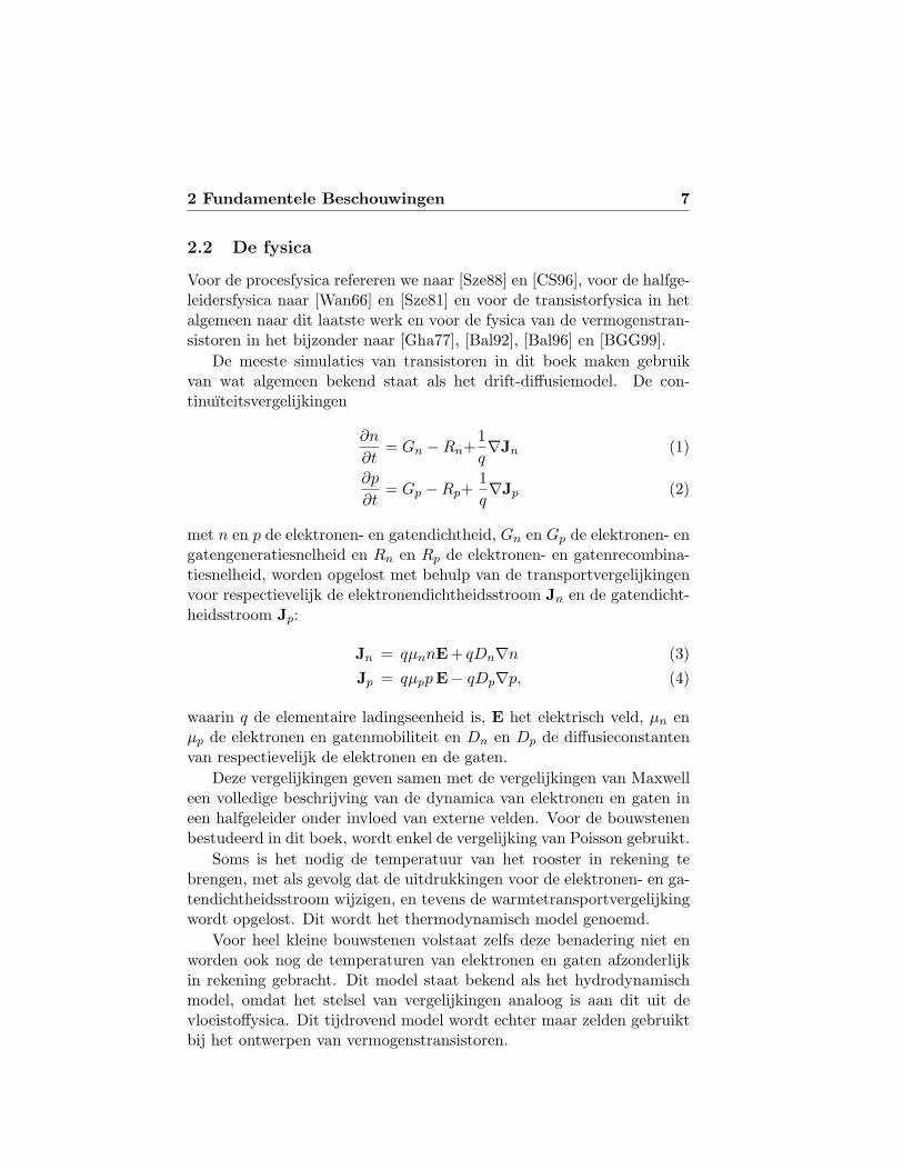
Voor de procesfysica refereren we naar [Sze88] en [CS96], voor de halfge-leidersfysica naar [Wan66] en [Sze81] en voor de transistorfysica in hetalgemeen naar dit laatste werk en voor de fysica van de vermogenstran-sistoren in het bijzonder naar [Gha77], [Bal92], [Bal96] en [BGG99].
De meeste simulaties van transistoren in dit boek maken gebruikvan wat algemeen bekend staat als het drift-diffusiemodel. De con-tinuıteitsvergelijkingen
∂n
∂t= Gn −Rn+
1q∇Jn (1)
∂p
∂t= Gp −Rp+
1q∇Jp (2)
met n en p de elektronen- en gatendichtheid, Gn en Gp de elektronen- engatengeneratiesnelheid en Rn en Rp de elektronen- en gatenrecombina-tiesnelheid, worden opgelost met behulp van de transportvergelijkingenvoor respectievelijk de elektronendichtheidsstroom Jn en de gatendicht-heidsstroom Jp:
Jn = qµnnE+ qDn∇n (3)Jp = qµppE− qDp∇p, (4)
waarin q de elementaire ladingseenheid is, E het elektrisch veld, µn enµp de elektronen en gatenmobiliteit en Dn en Dp de diffusieconstantenvan respectievelijk de elektronen en de gaten.
Deze vergelijkingen geven samen met de vergelijkingen van Maxwelleen volledige beschrijving van de dynamica van elektronen en gaten ineen halfgeleider onder invloed van externe velden. Voor de bouwstenenbestudeerd in dit boek, wordt enkel de vergelijking van Poisson gebruikt.
Soms is het nodig de temperatuur van het rooster in rekening tebrengen, met als gevolg dat de uitdrukkingen voor de elektronen- en ga-tendichtheidsstroom wijzigen, en tevens de warmtetransportvergelijkingwordt opgelost. Dit wordt het thermodynamisch model genoemd.
Voor heel kleine bouwstenen volstaat zelfs deze benadering niet enworden ook nog de temperaturen van elektronen en gaten afzonderlijkin rekening gebracht. Dit model staat bekend als het hydrodynamischmodel, omdat het stelsel van vergelijkingen analoog is aan dit uit devloeistoffysica. Dit tijdrovend model wordt echter maar zelden gebruiktbij het ontwerpen van vermogenstransistoren.
8 Nederlandstalige Samenvatting (Dutch Summary)
2.3 Wat is een vermogensbouwsteen ?
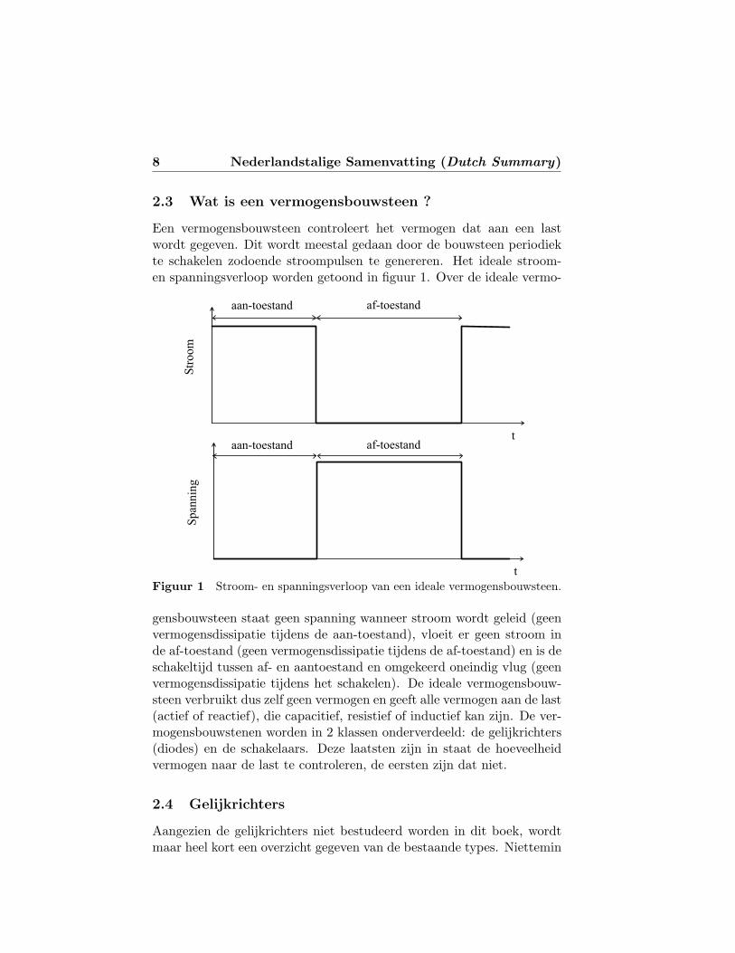
Een vermogensbouwsteen controleert het vermogen dat aan een lastwordt gegeven. Dit wordt meestal gedaan door de bouwsteen periodiekte schakelen zodoende stroompulsen te genereren. Het ideale stroom-en spanningsverloop worden getoond in figuur 1. Over de ideale vermo-
Str
oo
mS
pan
nin
g
t
t
aan-toestand af-toestand
aan-toestand af-toestand
Figuur 1 Stroom- en spanningsverloop van een ideale vermogensbouwsteen.
gensbouwsteen staat geen spanning wanneer stroom wordt geleid (geenvermogensdissipatie tijdens de aan-toestand), vloeit er geen stroom inde af-toestand (geen vermogensdissipatie tijdens de af-toestand) en is deschakeltijd tussen af- en aantoestand en omgekeerd oneindig vlug (geenvermogensdissipatie tijdens het schakelen). De ideale vermogensbouw-steen verbruikt dus zelf geen vermogen en geeft alle vermogen aan de last(actief of reactief), die capacitief, resistief of inductief kan zijn. De ver-mogensbouwstenen worden in 2 klassen onderverdeeld: de gelijkrichters(diodes) en de schakelaars. Deze laatsten zijn in staat de hoeveelheidvermogen naar de last te controleren, de eersten zijn dat niet.
2.4 Gelijkrichters
Aangezien de gelijkrichters niet bestudeerd worden in dit boek, wordtmaar heel kort een overzicht gegeven van de bestaande types. Niettemin
2 Fundamentele Beschouwingen 9
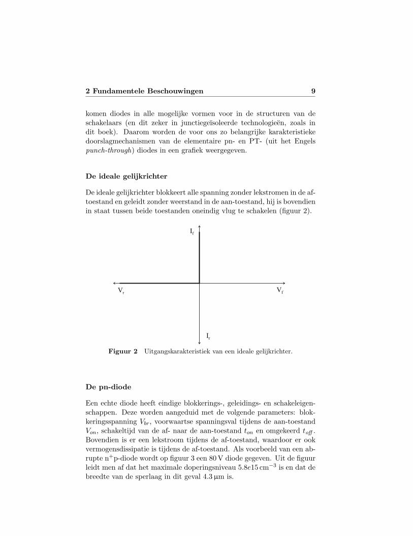
komen diodes in alle mogelijke vormen voor in de structuren van deschakelaars (en dit zeker in junctiegeısoleerde technologieen, zoals indit boek). Daarom worden de voor ons zo belangrijke karakteristiekedoorslagmechanismen van de elementaire pn- en PT- (uit het Engelspunch-through) diodes in een grafiek weergegeven.
De ideale gelijkrichter
De ideale gelijkrichter blokkeert alle spanning zonder lekstromen in de af-toestand en geleidt zonder weerstand in de aan-toestand, hij is bovendienin staat tussen beide toestanden oneindig vlug te schakelen (figuur 2).
Vf
Ir
If
Vr
Figuur 2 Uitgangskarakteristiek van een ideale gelijkrichter.
De pn-diode
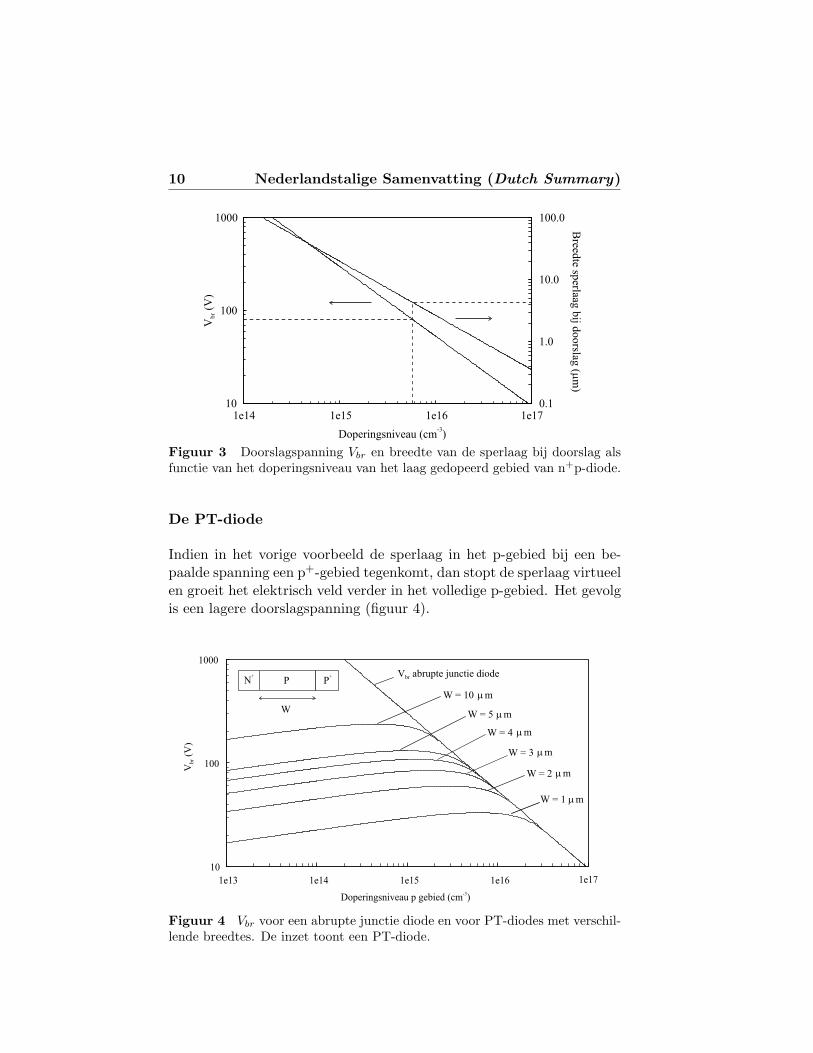
Een echte diode heeft eindige blokkerings-, geleidings- en schakeleigen-schappen. Deze worden aangeduid met de volgende parameters: blok-keringsspanning Vbr, voorwaartse spanningsval tijdens de aan-toestandVon, schakeltijd van de af- naar de aan-toestand ton en omgekeerd toff .Bovendien is er een lekstroom tijdens de af-toestand, waardoor er ookvermogensdissipatie is tijdens de af-toestand. Als voorbeeld van een ab-rupte n+p-diode wordt op figuur 3 een 80 V diode gegeven. Uit de figuurleidt men af dat het maximale doperingsniveau 5.8e15 cm−3 is en dat debreedte van de sperlaag in dit geval 4.3µm is.
10 Nederlandstalige Samenvatting (Dutch Summary)
10
100
1000
1e14 1e15 1e16 1e17
Doperingsniveau (cm )-3
V(V
)br
0.1
1.0
10.0
100.0
Breed
te sperlaag
bij d
oo
rslag (
m)
m
Figuur 3 Doorslagspanning Vbr en breedte van de sperlaag bij doorslag alsfunctie van het doperingsniveau van het laag gedopeerd gebied van n+p-diode.
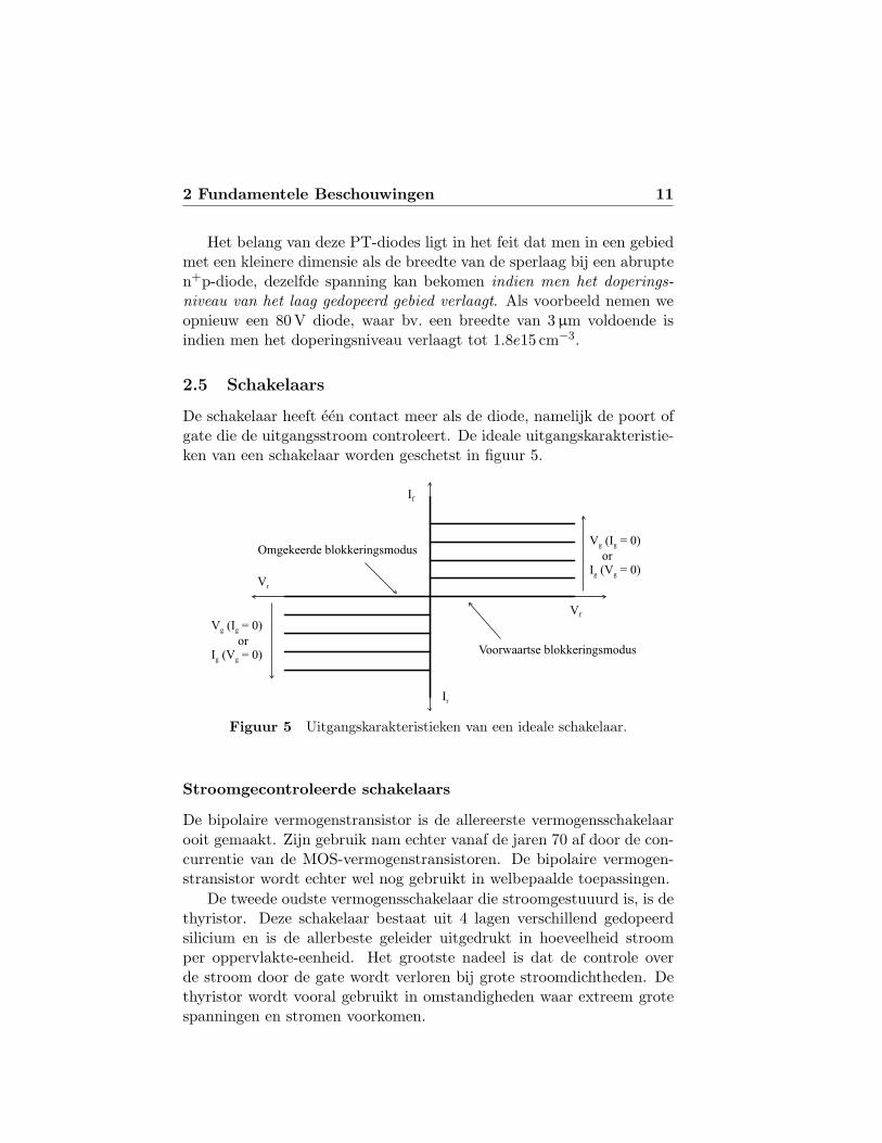
De PT-diode
Indien in het vorige voorbeeld de sperlaag in het p-gebied bij een be-paalde spanning een p+-gebied tegenkomt, dan stopt de sperlaag virtueelen groeit het elektrisch veld verder in het volledige p-gebied. Het gevolgis een lagere doorslagspanning (figuur 4).
10
100
1000
1e13 1e14 1e15 1e16 1e17
Doperingsniveau p gebied (cm )-3
V(V
)b
r
N+
P+
P
W
V abrupte junctie diodebr
W = 1 m m
W = 2 m m
W = 3 m m
W = 4 m m
W = 5 m m
W = 10 m m
Figuur 4 Vbr voor een abrupte junctie diode en voor PT-diodes met verschil-lende breedtes. De inzet toont een PT-diode.
2 Fundamentele Beschouwingen 11
Het belang van deze PT-diodes ligt in het feit dat men in een gebiedmet een kleinere dimensie als de breedte van de sperlaag bij een abrupten+p-diode, dezelfde spanning kan bekomen indien men het doperings-niveau van het laag gedopeerd gebied verlaagt. Als voorbeeld nemen weopnieuw een 80 V diode, waar bv. een breedte van 3µm voldoende isindien men het doperingsniveau verlaagt tot 1.8e15 cm−3.
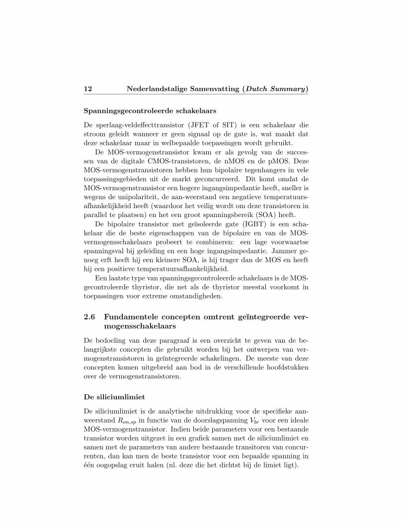
2.5 Schakelaars
De schakelaar heeft een contact meer als de diode, namelijk de poort ofgate die de uitgangsstroom controleert. De ideale uitgangskarakteristie-ken van een schakelaar worden geschetst in figuur 5.
Vf
Ir
If
V (I = 0)
orI (V = 0)
g g
g g
Vr
V (I = 0)
orI (V = 0)
g g
g g
Omgekeerde blokkeringsmodus
Voorwaartse blokkeringsmodus
Figuur 5 Uitgangskarakteristieken van een ideale schakelaar.
Stroomgecontroleerde schakelaars
De bipolaire vermogenstransistor is de allereerste vermogensschakelaarooit gemaakt. Zijn gebruik nam echter vanaf de jaren 70 af door de con-currentie van de MOS-vermogenstransistoren. De bipolaire vermogen-stransistor wordt echter wel nog gebruikt in welbepaalde toepassingen.
De tweede oudste vermogensschakelaar die stroomgestuuurd is, is dethyristor. Deze schakelaar bestaat uit 4 lagen verschillend gedopeerdsilicium en is de allerbeste geleider uitgedrukt in hoeveelheid stroomper oppervlakte-eenheid. Het grootste nadeel is dat de controle overde stroom door de gate wordt verloren bij grote stroomdichtheden. Dethyristor wordt vooral gebruikt in omstandigheden waar extreem grotespanningen en stromen voorkomen.
12 Nederlandstalige Samenvatting (Dutch Summary)
Spanningsgecontroleerde schakelaars
De sperlaag-veldeffecttransistor (JFET of SIT) is een schakelaar diestroom geleidt wanneer er geen signaal op de gate is, wat maakt datdeze schakelaar maar in welbepaalde toepassingen wordt gebruikt.
De MOS-vermogenstransistor kwam er als gevolg van de succes-sen van de digitale CMOS-transistoren, de nMOS en de pMOS. DezeMOS-vermogenstransistoren hebben hun bipolaire tegenhangers in veletoepassingsgebieden uit de markt geconcurreerd. Dit komt omdat deMOS-vermogenstransistor een hogere ingangsimpedantie heeft, sneller iswegens de unipolariteit, de aan-weerstand een negatieve temperatuurs-afhankelijkheid heeft (waardoor het veilig wordt om deze transistoren inparallel te plaatsen) en het een groot spanningsbereik (SOA) heeft.
De bipolaire transistor met geısoleerde gate (IGBT) is een scha-kelaar die de beste eigenschappen van de bipolaire en van de MOS-vermogensschakelaars probeert te combineren: een lage voorwaartsespanningsval bij geleiding en een hoge ingangsimpedantie. Jammer ge-noeg erft heeft hij een kleinere SOA, is hij trager dan de MOS en heefthij een positieve temperatuursafhankelijkheid.
Een laatste type van spanningsgecontroleerde schakelaars is de MOS-gecontroleerde thyristor, die net als de thyristor meestal voorkomt intoepassingen voor extreme omstandigheden.
2.6 Fundamentele concepten omtrent geıntegreerde ver-mogensschakelaars
De bedoeling van deze paragraaf is een overzicht te geven van de be-langrijkste concepten die gebruikt worden bij het ontwerpen van ver-mogenstransistoren in geıntegreerde schakelingen. De meeste van dezeconcepten komen uitgebreid aan bod in de verschillende hoofdstukkenover de vermogenstransistoren.
De siliciumlimiet
De siliciumlimiet is de analytische uitdrukking voor de specifieke aan-weerstand Ron,sp in functie van de doorslagspanning Vbr voor een idealeMOS-vermogenstransistor. Indien beide parameters voor een bestaandetransistor worden uitgezet in een grafiek samen met de siliciumlimiet ensamen met de parameters van andere bestaande transitoren van concur-renten, dan kan men de beste transistor voor een bepaalde spanning ineen oogopslag eruit halen (nl. deze die het dichtst bij de limiet ligt).
2 Fundamentele Beschouwingen 13
Het dient vermeld te worden dat er verschillende siliciumlimieten be-staan, nl. voor de verschillende vormen van de MOS-vermogenstransistor(verticaal, lateraal, RESURF, SOI, superjunctie of COOLMOSTM . . . ).
RESURF-effect
Het RESURF-effect (uit het Engels REduced SURface F ield) is een 2D-techniek waarbij de distributie van de elektrische velden op een optimalemanier gespreid worden. Het is een van de meest gebruikte techniekenbij het ontwerp van vermogensbouwstenen. Aanvankelijk werd het ge-bruikt in diodes, maar tegenwoordig wordt het in bijna elke vermogen-stransistor en op verschillende manieren (met verschillende lagen in dezogenaamde superjunctietransistoren, op SOI, in 3D. . . ) toegepast.
PT- en RT-doorslag
PT- en RT- (uit het Engels Reach-Through) doorslag zijn verschillendefenomenen. PT-doorslag komt voor in een PT-diode wanneer het kri-tische elektrische veld wordt bereikt aan de pn-junctie. RT-doorslagdaarentegen komt voor in een pnp- of npn-structuur, waarbij de sperlaagkomende van een van de juncties de andere raakt. Dan wordt een pad ge-creeerd die geleiding veroorzaakt. Dit mechanisme kan dus voorkomenlang voor dat het kritische elektrische veld wordt bereikt. Nietteminworden beide termen in de literatuur vaak door elkaar gebruikt.
Tweede doorslag, terugslag en thermische instabiliteit
Vroeger gebruikte men de term tweede doorslag wanneer men thermi-sche instabiliteit beschreef (bv. in [Gha77]), maar tegenwoordig wordtde term meestal gebruikt om een plotse reductie van de doorslag in deaan-toestand (i.v.m. de doorslag in de af-toestand) aan te duiden. Dezetweede doorslag kan gepaard gaan met een terugval in de spanning, meteen negatieve weerstand als gevolg. Dit is wat men in het Engels snap-back (terugslag) noemt. De term thermische instabiliteit wordt enkelnog gebruikt bij temperatuursfenomenen van destructieve aard.
Kirk-effect en adaptieve RESURF
Het Kirk-effect wordt normaal beschreven in een bipolaire transistor[Sze81, p.145]. Het komt echter ook voor in MOS-vermogenstransistoren,en in het bijzonder in laterale structuren die gebruik maken van hetRESURF-effect. Het gevolg is een afname van het spanningsbereik in
14 Nederlandstalige Samenvatting (Dutch Summary)
de aan-toestand. Een mogelijke oplossing is wat men noemt “adaptieveRESURF”, waarmee de verschuiving van het elektrisch veld naar dedrain toe wordt verholpen door een verhoging van het doperingsniveauin de buurt van het draincontact.
SOA
De SOA (staat voor Safe Operating Area) is gedefinieerd als het span-ningsgebied waarbinnen de schakelaar op een veilige manier kan gebruiktworden. Dit is een vage definitie en men onderscheidt dan ook drie ver-schillende SOAs:
• Elektrische SOA en ESD
Een schakelaar kan gedurende een heel korte tijd (ns tot µs) ge-bruikt worden in het bereik van de uitgangskarakteristiek na dedoorslag en na de terugslag. Bepaalde schakelaars worden zelfsspeciaal ontworpen om deze eigenschap te benadrukken. Dezeworden bijvoorbeeld gebruikt in ESD (ElectroStatic Discharge)protectiecircuits. Deze bouwstenen worden hier niet besproken.
• Thermische SOA en energetisch opvangvermogen
Wanneer de stroompulsen langer duren (µs tot ms) dan wordentemperatuurseffecten belangrijk, waardoor er gevaar op thermi-sche instabiliteit ontstaat. Sommige bouwstenen worden speciaalontworpen om een zo groot mogelijke energiestoot op te vangen,bv. bij het uitschakelen van een inductieve last. Ook dit soort vanbouwstenen wordt niet besproken in dit boek.
• Hetelading-SOA en degradatie
Wanneer een schakelaar niet wordt gebruikt in de extreme om-standigheden zoals in beide bovenstaande voorbeelden, dan is deSOA meestal nog kleiner dan de elektrische en thermische SOA.Zeker in schakelaars met een MOS-gate is dit het geval, waar deladingen die door het kanaal stromen na verloop van tijd het oxide-laagje vervuilen. Deze vervuiling veroorzaakt verschuivingen in deelektrische eigenschappen van de transistor. Dit is wat men noemtdegradatie, die gekarakteriseerd wordt op basis van stressmetin-gen. Het toegelaten spanningsbereik wordt dan bepaald aan dehand van extrapolatie van de meest verslechterende parameter (endit kan verschillend zijn naargelang de spanningen op de verschil-lende contacten).
3 TCAD-Simulatie en -IJking 15
Hoge injectie en geleidingsmodulatie
Injectie van minoritairen in een laag gedopeerd p- of n-gebied kan zohoog zijn dat de elektronen en gaten in een hogere concentratie aanwezigzijn dan het oorspronkelijk doperingsniveau. De weerstand in dit gebiedvermindert dan aanzienlijk, i.e. geleidingsmodulatie. Dit fenomeen zorgtervoor dat in vele vermogensbouwstenen een lage voorwaartse spannings-val in de aan-toestand leidt tot hoge stroomniveaus.
Isolatie
Het is goed mogelijk dat men een geıntegreerde vermogensbouwsteenontwerpt met een interne doorslagspanning van bijvoorbeeld meer dan80V, maar dat er toch problemen optreden bij lagere spanningen. Ditkomt omdat men ervoor moet zorgen dat de elektrische isolatie van dezegeıntegreerde bouwsteen op zijn minst de doorslagspanning ervan moetaankunnen. Verder moeten sommigen geıntegreerde bouwstenen in hungeheel (d.w.z. op alle contacten tegelijkertijd) op een spanning staan diehoger is dan de spanningen in de directe omgeving. Dit noemt men dezwevende bouwstenen en deze hebben vaak een isolatiestructuur die heelwat uitgebreider is dan die van hun niet-zwevende tegenhangers.
3 TCAD-Simulatie en -IJking
3.1 Inleiding
Technologie-CAD (TCAD) gebruikt fysische modellen ten einde een vol-ledig productieproces stap voor stap, en daarna de werking van de gesi-muleerde bouwstenen, te simuleren. Deze proces- en bouwsteensimulato-ren brengen de eigenschappen van deze bouwstenen op een niet-uniform,discreet raster van punten aan (in 1, 2 of zelfs 3 dimensies) om de diffe-rentiaalvergelijkingen die de verschillende fysische processen beschrijvennumeriek op te lossen. Dit hoofdstuk bestaat uit twee delen, het eer-ste beschrijft de ijking en rasterproblematiek in de processimulator, hettweede doet dit voor de bouwsteensimulator.
3.2 Processimulatie en -ijking
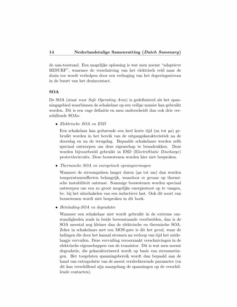
Het raster
Het raster zorgt voor het grootste deel van de problemen gedurendeTCAD-werk. De gebruiker wil een raster dat zo ruw mogelijk is om
16 Nederlandstalige Samenvatting (Dutch Summary)
(a) (b)
Veldoxide
(c)
Poly
Verfijning op nldd en N+
(d)
GateSource
Figuur 6 Evolutie van het raster doorheen de simulatie: (a) 1D in processimulatie, (b) eerste proces stap in 2D, (c) op het einde van het proces en (d)nieuw raster voor simulatie van de werking van de transistor.
de simulatietijd te beperken, maar het moet wel fijn genoeg blijven omcorrecte resultaten af te leveren.
Ter illustratie van deze problematiek zal een simpele nMOS gesimu-leerd worden als leidraad doorheen dit hoofdstuk. Omdat de simula-ties gebaseerd zijn op het bestaande 0.35µm CMOS proces van AMIS,worden de assen van vele figuren weggelaten door de confidentiele aardervan. Deze werkwijze ondermijnt het doel van deze discussie geenszins.
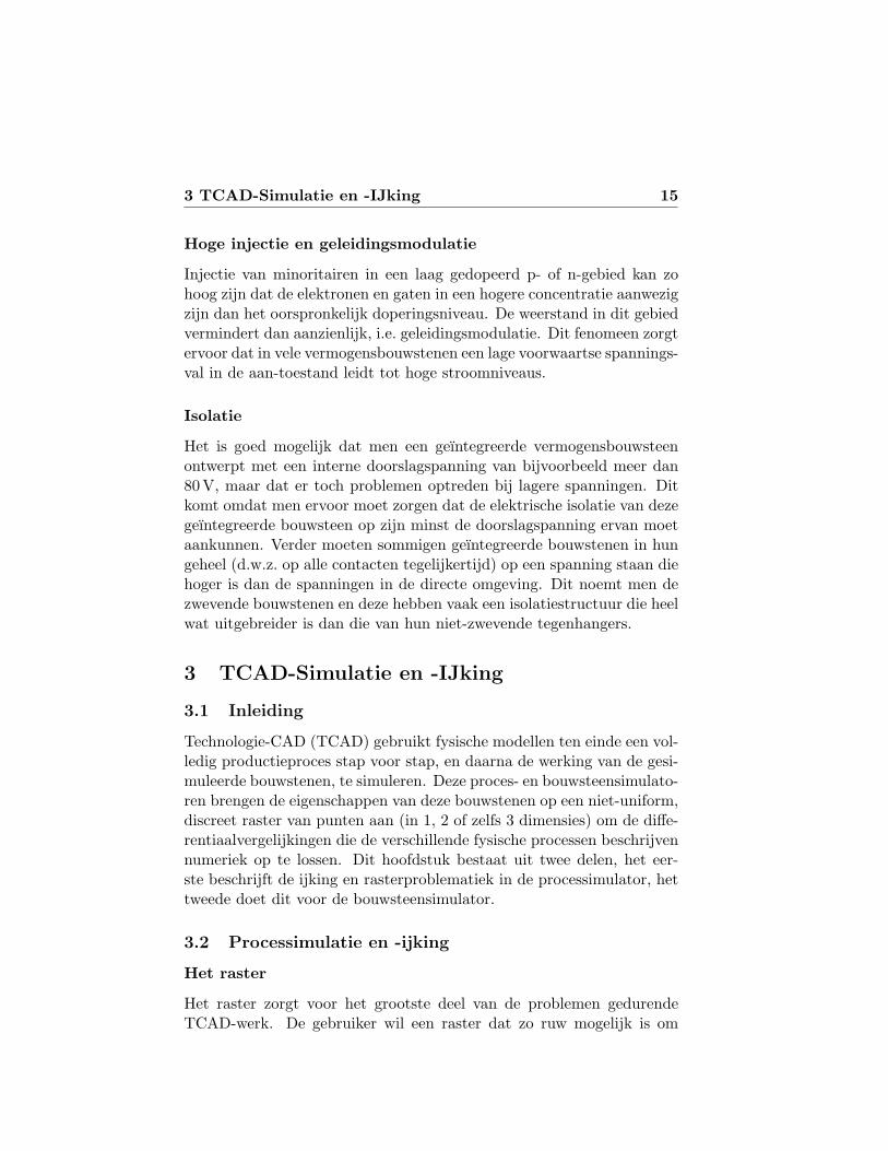
In het begin van de simulatie is het raster nog in 1 dimensie (d.w.z.een verzameling lijnen in een rechthoek). Wanneer het nodig wordt detweede dimensie mee in rekening te brengen (bij de definitie van een mas-ker), dan schakelt de simulator automatisch over op 2 dimensies. Hetraster wordt enkel verfijnd daar waar nodig (aan een junctie, gradientin doperingsniveau, oneffenheden op de Si/SiO2 grens. . . ) met be-hulp van welbepaalde parameters (Refinejunction, RefineGradient,RefineBoundary. . . ) uit de ISE-software. Deze verfijning gebeurt doorde definitie van rechthoeken in het simulatiedomein gedurende de si-mulatie (bijvoorbeeld net voor een implantatie), zie figuur 6 voor enkelevoorbeelden. Een voorbeeld van de invloed van een dergelijke parameterop het simulatieresultaat wordt gegeven in figuur 7.
3 TCAD-Simulatie en -IJking 17
Diepte (µm)
Net
toD
oper
ings
nive
au(/
cm3 )
ref_grad = 4
ref_grad = 5
ref_grad = 7
ref_grad = 6
ref_grad = 8
Figuur 7 Invloed van de verfijning van het raster (Refgrad) op een dope-ringsprofiel.
Stress Dependent Model Af
SEM
Standaardmodel (Stress Dependent Model Aan)
Standaardmodel, maar met anderediffusieconstante voor de oxidant
Figuur 8 Vergelijking van verschillende oxidatiemodellen met een SEM-foto.
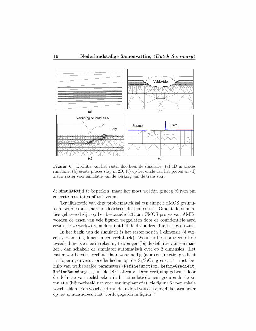
Simulatie en ijking
Het zou ideaal zijn indien we zouden beschikken over ijkmateriaal (SIMS,SEM. . . ) na elke gesimuleerde processtap. Jammer genoeg is dit niethaalbaar vanwege de kost en moeten we ons beperken tot enkele be-langrijke stappen. Zoals gezegd in het inleidend hoofdstuk, beschikkenwe niet over 2D-doperingsprofielen en werken we dus steeds met SIMS-profielen in 1D. De veldoxidatie kunnen we wel kalibreren met behulpvan SEM-foto’s in 2D. Daartoe zijn verschillende oxidatiemodellen in desoftware opgenomen (met elk hun eigen verzameling modelparameters).In figuur 8 kan men zien dat het standaardmodel het veldoxide nagenoegcorrect simuleert.
18 Nederlandstalige Samenvatting (Dutch Summary)
Diepte
Bor
onco
ncen
trat
ie(c
m3 )
Optimale verfijning,Monte Carlo, Damage=+1,Amorphization=+1, enModDiff=PairDiffusion
Standaard modellenen extreme verfijning
SIMS
Optimale verfijningen ModDiff = PairDiffusion
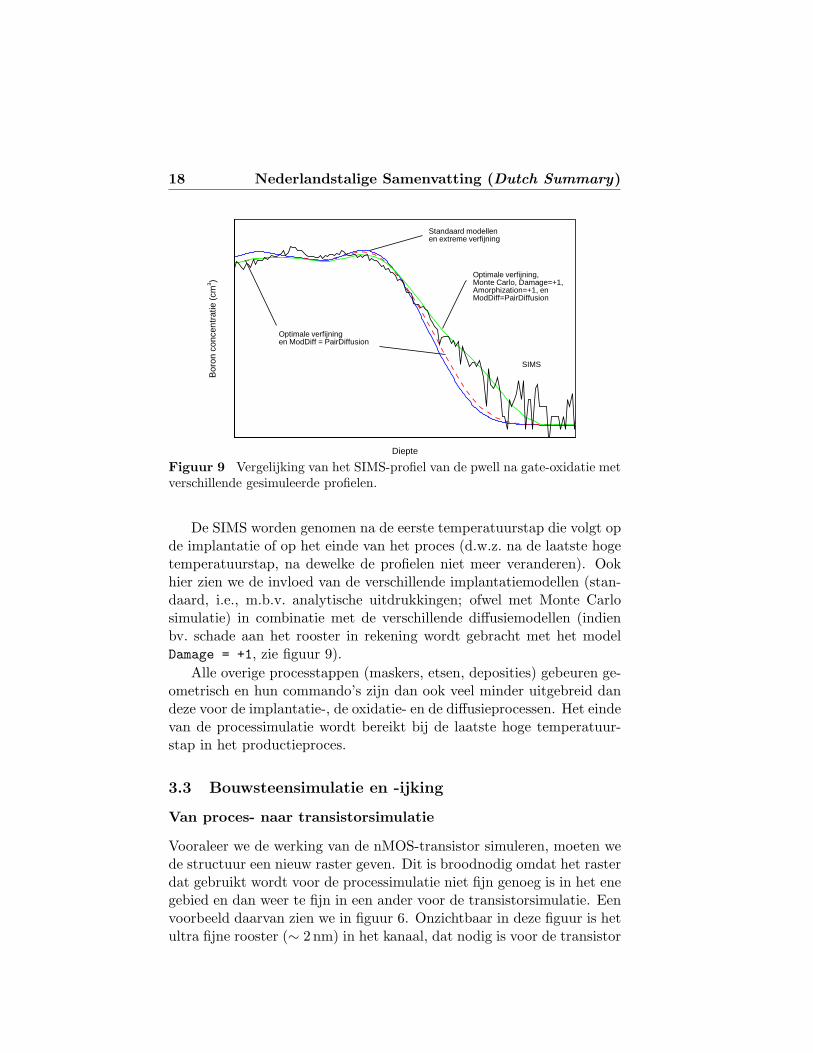
Figuur 9 Vergelijking van het SIMS-profiel van de pwell na gate-oxidatie metverschillende gesimuleerde profielen.
De SIMS worden genomen na de eerste temperatuurstap die volgt opde implantatie of op het einde van het proces (d.w.z. na de laatste hogetemperatuurstap, na dewelke de profielen niet meer veranderen). Ookhier zien we de invloed van de verschillende implantatiemodellen (stan-daard, i.e., m.b.v. analytische uitdrukkingen; ofwel met Monte Carlosimulatie) in combinatie met de verschillende diffusiemodellen (indienbv. schade aan het rooster in rekening wordt gebracht met het modelDamage = +1, zie figuur 9).
Alle overige processtappen (maskers, etsen, deposities) gebeuren ge-ometrisch en hun commando’s zijn dan ook veel minder uitgebreid dandeze voor de implantatie-, de oxidatie- en de diffusieprocessen. Het eindevan de processimulatie wordt bereikt bij de laatste hoge temperatuur-stap in het productieproces.
3.3 Bouwsteensimulatie en -ijking
Van proces- naar transistorsimulatie
Vooraleer we de werking van de nMOS-transistor simuleren, moeten wede structuur een nieuw raster geven. Dit is broodnodig omdat het rasterdat gebruikt wordt voor de processimulatie niet fijn genoeg is in het enegebied en dan weer te fijn in een ander voor de transistorsimulatie. Eenvoorbeeld daarvan zien we in figuur 6. Onzichtbaar in deze figuur is hetultra fijne rooster (∼ 2 nm) in het kanaal, dat nodig is voor de transistor
3 TCAD-Simulatie en -IJking 19
Vgs (V)
Id(A
/µm
)
0 1 2 30
2E-06
4E-06
6E-06
8E-06
1E-05
1.2E-05
1.4E-05
1.6E-05 SPICE (vlug)
SPICE (traag)
SPICE (typisch)
zonder PairDiffusionvoor de gate-oxidatie
met PairDiffusionvoor de gate-oxidatie
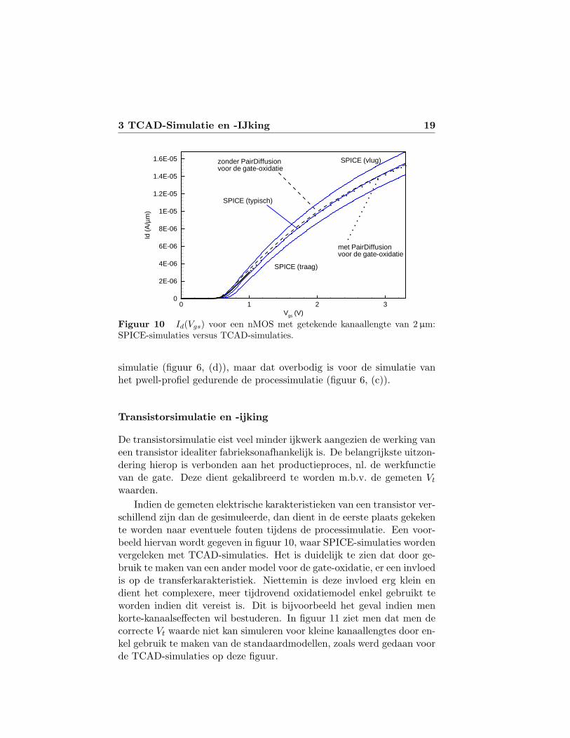
Figuur 10 Id(Vgs) voor een nMOS met getekende kanaallengte van 2 µm:SPICE-simulaties versus TCAD-simulaties.
simulatie (figuur 6, (d)), maar dat overbodig is voor de simulatie vanhet pwell-profiel gedurende de processimulatie (figuur 6, (c)).
Transistorsimulatie en -ijking
De transistorsimulatie eist veel minder ijkwerk aangezien de werking vaneen transistor idealiter fabrieksonafhankelijk is. De belangrijkste uitzon-dering hierop is verbonden aan het productieproces, nl. de werkfunctievan de gate. Deze dient gekalibreerd te worden m.b.v. de gemeten Vt
waarden.Indien de gemeten elektrische karakteristieken van een transistor ver-
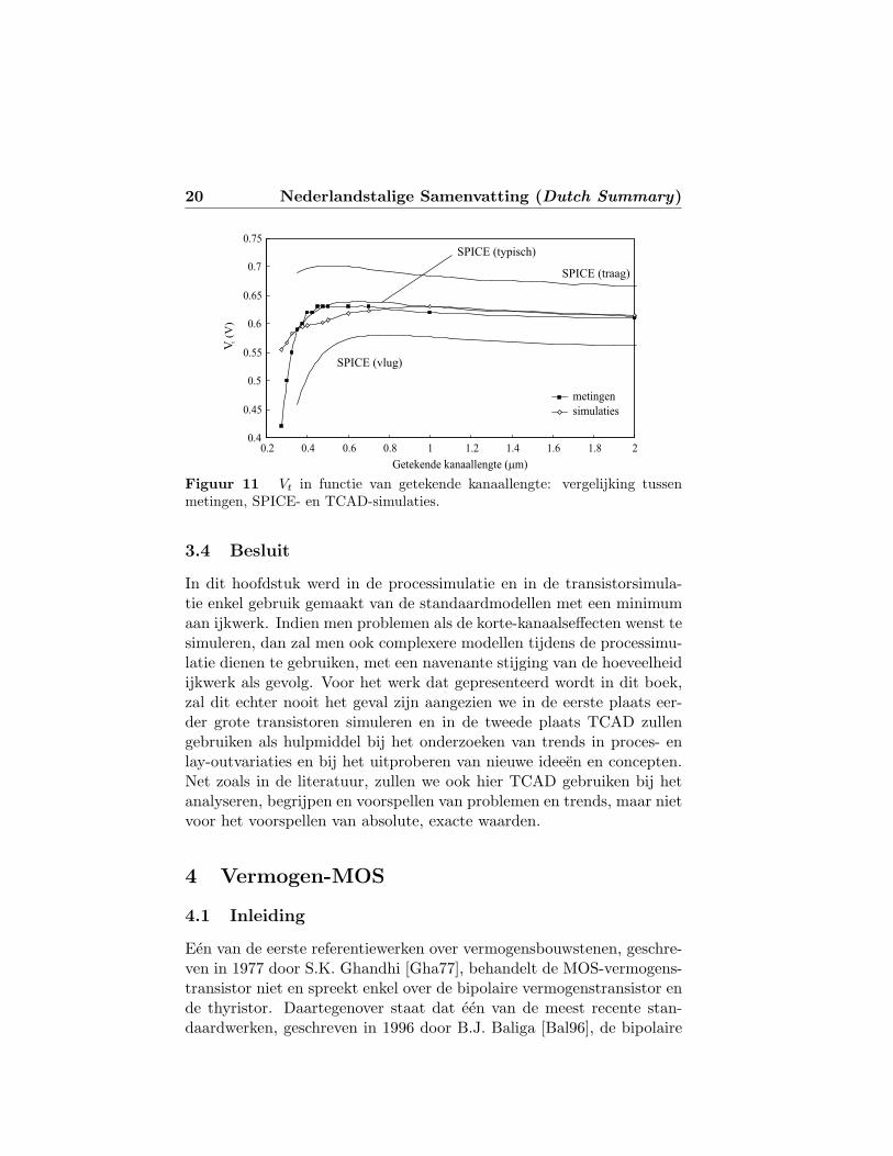
schillend zijn dan de gesimuleerde, dan dient in de eerste plaats gekekente worden naar eventuele fouten tijdens de processimulatie. Een voor-beeld hiervan wordt gegeven in figuur 10, waar SPICE-simulaties wordenvergeleken met TCAD-simulaties. Het is duidelijk te zien dat door ge-bruik te maken van een ander model voor de gate-oxidatie, er een invloedis op de transferkarakteristiek. Niettemin is deze invloed erg klein endient het complexere, meer tijdrovend oxidatiemodel enkel gebruikt teworden indien dit vereist is. Dit is bijvoorbeeld het geval indien menkorte-kanaalseffecten wil bestuderen. In figuur 11 ziet men dat men decorrecte Vt waarde niet kan simuleren voor kleine kanaallengtes door en-kel gebruik te maken van de standaardmodellen, zoals werd gedaan voorde TCAD-simulaties op deze figuur.
20 Nederlandstalige Samenvatting (Dutch Summary)
0.4
0.45
0.5
0.55
0.6
0.65
0.7
0.75
0.2 0.4 0.6 0.8 1 1.2 1.4 1.6 1.8 2
Getekende kanaallengte ( m)m
Vt(V
)
metingen
simulaties
SPICE (vlug)
SPICE (traag)
SPICE (typisch)
Figuur 11 Vt in functie van getekende kanaallengte: vergelijking tussenmetingen, SPICE- en TCAD-simulaties.
3.4 Besluit
In dit hoofdstuk werd in de processimulatie en in de transistorsimula-tie enkel gebruik gemaakt van de standaardmodellen met een minimumaan ijkwerk. Indien men problemen als de korte-kanaalseffecten wenst tesimuleren, dan zal men ook complexere modellen tijdens de processimu-latie dienen te gebruiken, met een navenante stijging van de hoeveelheidijkwerk als gevolg. Voor het werk dat gepresenteerd wordt in dit boek,zal dit echter nooit het geval zijn aangezien we in de eerste plaats eer-der grote transistoren simuleren en in de tweede plaats TCAD zullengebruiken als hulpmiddel bij het onderzoeken van trends in proces- enlay-outvariaties en bij het uitproberen van nieuwe ideeen en concepten.Net zoals in de literatuur, zullen we ook hier TCAD gebruiken bij hetanalyseren, begrijpen en voorspellen van problemen en trends, maar nietvoor het voorspellen van absolute, exacte waarden.
4 Vermogen-MOS
4.1 Inleiding
Een van de eerste referentiewerken over vermogensbouwstenen, geschre-ven in 1977 door S.K. Ghandhi [Gha77], behandelt de MOS-vermogens-transistor niet en spreekt enkel over de bipolaire vermogenstransistor ende thyristor. Daartegenover staat dat een van de meest recente stan-daardwerken, geschreven in 1996 door B.J. Baliga [Bal96], de bipolaire
4 Vermogen-MOS 21
vermogenstransistor enkel behandelt als inleiding tot een bepaald typeMOS-vermogenstransistor, nl. de IGBT. Dit illustreert de evolutie vande vermogenstransistoren over een tijdspanne van 20 jaar en toont hetbelang aan van de introductie van de MOS-gate in deze bouwstenen.De stroomgestuurde gate en bijhorende complexe ingangscircuiten voorde bipolaire transistoren werd vervangen door een spanningsgestuurdegate met een veel eenvoudiger ingangscircuit. De MOS-transistor heeftbovendien een veel vluggere schakelsnelheid (wegens zijn unipolariteit),heeft een negatieve temperatuursafhankelijkheid (hoe warmer, hoe min-der stroom wordt geleid, wat ideaal is om deze transistoren in parallelte plaatsen), en is veel minder onderhevig aan tweede doorslag.
Omdat de MOS-gate zijn oorsprong kent in de digitale CMOS-techno-logieen, is de eerste MOS-vermogenstransistor, een soort van uitgebreideMOS of DEMOS (Drain Extended MOS). Daarna werd de dubbelediffusie-MOS (DMOS) uitgevonden, zo genoemd omdat het kanaal samen metde source-gebieden worden geımplanteerd en gediffundeerd na de depo-sitie van de poly-gate. De volgende belangrijke stap was de introductievan het RESURF-effect, dat behandeld wordt in de volgende paragraaf.Het is een van de meest belangrijke technieken voor het ontwerpen vanvermogensbouwstenen geworden (niet enkel MOS-transistoren).
De zeer belangrijk siliciumlimiet, die dient als een waardemeter voorde MOS-vermogenstransistoren wordt besproken in het volgende luik.Hierop volgt een korte uiteenzetting over de verschillende vormen en ty-pes van de MOS-vermogenstransistoren, die daarna elk op hun beurt be-studeerd worden. De conclusie vergelijkt de bekomen MOS-vermogens-transistoren met deze gevonden in de literatuur.
4.2 RESURF-effect
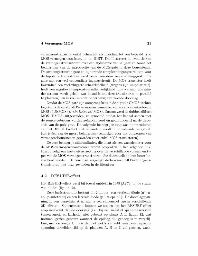
Het RESURF-effect werd bij toeval ontdekt in 1979 [AV79] bij de studievan diodes (figuur 12).
Deze basisstructuur bestaat uit 2 diodes: een verticale diode (n+–n-epi–p-substraat) en een laterale diode (p+–n-epi–n+). De doorslagspan-ning in een dergelijke structuur is een samenspel tussen verschillende2D-effecten. Samenvattend kunnen we stellen dat het RESURF-effecterop neerkomt dat de doorslag (i.e., bij een negatief spanningsverschiltussen anode en kathode) niet gebeurt op plaats A in figuur 12, watnormaal gezien gebeurt wanneer de epilaag dik genoeg is in vergelij-king met de lengte l; maar dat het elektrisch veld vanaf een bepaaldespanning terzelfder tijd op de plaatsen A, B en C zal groeien, waar-
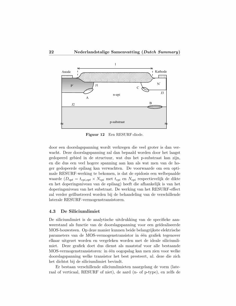
22 Nederlandstalige Samenvatting (Dutch Summary)
P+
n-epi
KathodeAnode
p-substraat
N+
»»
l
psinker
J1
J3
J2
A
B
C
Figuur 12 Een RESURF-diode.
door een doorslagspanning wordt verkregen die veel groter is dan ver-wacht. Deze doorslagspanning zal dan bepaald worden door het laagstgedopeerd gebied in de structuur, wat dus het p-substraat kan zijn,en die dus een veel hogere spanning aan kan als wat men van de ho-ger gedopeerde epilaag kan verwachten. De voorwaarde om een opti-male RESURF-werking te bekomen, is dat de epidosis een welbepaaldewaarde (Dopt = tepi,opt × Nepi met tepi en Nepi respectievelijk de dikteen het doperingsniveau van de epilaag) heeft die afhankelijk is van hetdoperingsniveau van het substraat. De werking van het RESURF-effectzal verder geıllustreerd worden bij de behandeling van de verschillendelaterale RESURF-vermogenstransistoren.
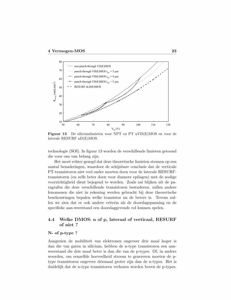
4.3 De Siliciumlimiet
De siliciumlimiet is de analytische uitdrukking van de specifieke aan-weerstand als functie van de doorslagspanning voor een geıdealiseerdeMOS-bouwsteen. Op deze manier kunnen beide belangrijkste elektrischeparameters van de MOS-vermogenstransistor in een grafiek tegenoverelkaar uitgezet worden en vergeleken worden met de ideale siliciumli-miet. Deze grafiek doet dus dienst als maatstaf voor alle bestaandeMOS-vermogenstransistoren: in een oogopslag kan men zien voor welkedoorslagspanning welke transistor het best presteert, nl. deze die zichhet dichtst bij de siliciumlimiet bevindt.
Er bestaan verschillende siliciumlimieten naargelang de vorm (late-raal of verticaal, RESURF of niet), de aard (n- of p-type), en zelfs de
4 Vermogen-MOS 23
10
20
30
40
50
60
70
80
50 60 70 80 90 100 110 120
Vbr (V)
Ron,s
p(m
W.m
m2)
non punch-through VD(E)MOS
punch-through VD(E)MOS t = 5 mepi m
punch-through VD(E)MOS t = 4 mepi m
punch-through VD(E)MOS t = 3 mepi m
RESURF nLD(E)MOS
Figuur 13 De siliciumlimieten voor NPT en PT nVD(E)MOS en voor delaterale RESURF nD(E)MOS.
technologie (SOI). In figuur 13 worden de verschillende limieten getoonddie voor ons van belang zijn.
Het moet echter gezegd dat deze theoretische limieten steunen op eenaantal benaderingen, waardoor de schijnbare conclusie dat de verticalePT-transistoren niet veel onder moeten doen voor de laterale RESURF-transistoren (en zelfs beter doen voor dunnere epilagen) met de nodigevoorzichtigheid dient bejegend te worden. Zoals zal blijken uit de pa-ragrafen die deze verschillende transistoren bestuderen, zullen anderefenomenen die niet in rekening werden gebracht bij deze theoretischebeschouwingen bepalen welke transistor nu de betere is. Tevens zul-len we zien dat er ook andere criteria als de doorslagspanning en despecifieke aan-weerstand een doorslaggevende rol kunnen spelen.
4.4 Welke DMOS: n of p, lateraal of verticaal, RESURFof niet ?
N- of p-type ?
Aangezien de mobiliteit van elektronen ongeveer drie maal hoger isdan die van gaten in silicium, hebben de n-type transistoren een aan-weerstand die drie maal beter is dan die van de p-types. Of, in anderewoorden, om eenzelfde hoeveelheid stroom te genereren moeten de p-type transistoren ongeveer driemaal groter zijn dan de n-types. Het isduidelijk dat de n-type transistoren verkozen worden boven de p-types.
24 Nederlandstalige Samenvatting (Dutch Summary)
Niettemin zijn de p-type transistoren belangrijk voor circuitontwer-pers daar ze een oplossing bieden voor sommige circuitproblemen waaranders 2, 3, of meerdere n-type transistoren voor nodig zijn (dit komtdoor het feit dat p-type transistoren zich in de aan-toestand bevindenwanneer Vgs < Vt < 0V). Het verlies aan siliciumoppervlakte wordtdan grotendeels (zo niet volledig) gecompenseerd. De pDMOS wordtnormaal gezien als zwevende transistor gebruikt, wat betekent dat hetvolledige gebied waarin de transistor zich bevindt op een hogere poten-tiaal staat dan de omliggende gebieden.
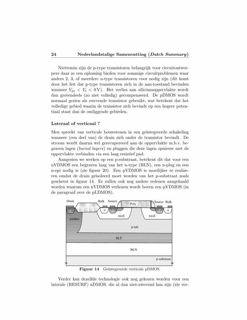
Lateraal of verticaal ?
Men spreekt van verticale bouwstenen in een geıntegreerde schakelingwanneer (een deel van) de drain zich onder de transistor bevindt. Destroom wordt daarna wel gerecupereerd aan de oppervlakte m.b.v. be-graven lagen (buried layers) en pluggen die deze lagen opnieuw met deoppervlakte verbinden via een laag resistief pad.
Aangezien we werken op een p-substraat, betekent dit dat voor eennVDMOS een begraven laag van het n-type (BLN), een n-plug en eenn-epi nodig is (zie figuur 20). Een pVDMOS is moeilijker te realise-ren omdat de drain geısoleerd moet worden van het p-substraat zoalsgeschetst in figuur 14. Er zullen ook nog andere redenen aangehaaldworden waarom een nVDMOS verkozen wordt boven een pVDMOS (inde paragraaf over de pLDMOS).
p+
n+
nwell
n+
p+
Bulk SourceDrain Source Bulk
BLN
p-substraat
p-tub
Poly
nwell
p+
BLP
psinker
»»
Figuur 14 Geıntegreerde verticale pDMOS.
Verder kan dezelfde technologie ook nog gekozen worden voor eenlaterale (RESURF) nDMOS, die al dan niet-zwevend kan zijn (zie ver-

4 Vermogen-MOS 25
der). Merk op dat de nVDMOS van nature uit zwevend is, wat een grootvoordeel is. Een interessante vraag—die in de loop van dit hoofdstukwordt beantwoord—is of de laterale (RESURF) nDMOS nu werkelijkbeter presteert dan de verticale nDMOS.
RESURF of niet ?
Het is duidelijk dat de nVDMOS geen gebruik maakt van het RESURF-effect. De pLDMOS daarentegen zal dit wel doen (zie onder). We kun-nen ook nog een laterale RESURF nDMOS ontwerpen die zowel zwevendals niet-zwevend kan zijn (zie onder).
4.5 Niet-zwevende, laterale, RESURF nDEMOS zonderbegraven lagen
De zwevende, laterale RESURF nDEMOS wordt getoond in figuur 15 sa-men met de belangrijkste lay-outparameters die deze transistor beschrij-ven. Het p-substraat is lager gedopeerd dan de n-epilaag en dus kan hierhet “ware” RESURF-effect optreden. Daarmee wordt bedoeld dat bijoptimale RESURF-condities (in de eerste plaats een optimale n-epidosisen in de tweede plaats een t > tepi) het p-substraat de doorslagspanningzal bepalen. Deze ligt ver boven de 80V die door de I3T80-technologiewordt opgelegd vanwege het lage doperingsniveau van het substraat endit voor een groot bereik van epidiktes en -concentraties.
pwell
P+
n-epi
SourceGate
Drain
p-substraat
N+
»»
x t
z
y
Enkel dit gedeelte wordt gesimuleerd.
Bulk
nwell
N+
nw
Figuur 15 De niet-zwevende, laterale RESURF nDEMOS met belangrijkstelay-outparameters.
Wanneer deze transistor geschaald moet worden naar 80 V, dan is deenige oplossing een verkleining van de lay-outparameter t. Wanneer we
26 Nederlandstalige Samenvatting (Dutch Summary)
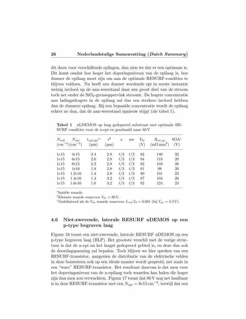
dit doen voor verschillende epilagen, dan zien we dat er een optimum is.Dit komt omdat hoe hoger het doperingsniveau van de epilaag is, hoedunner de epilaag moet zijn om aan de optimale RESURF-condities teblijven voldoen. Nu heeft een dunner wordende epi in eerste instantieweinig invloed op de aan-weerstand daar een groot deel van de stroomtoch net onder de SiO2-grensoppervlak stroomt. De hogere concentratieaan ladingsdragers in de epilaag zal dus een sterkere invloed hebbendan de dunnere epilaag. Bij een bepaalde concentratie wordt de epilaagechter zo dun, dat de aan-weerstand opnieuw stijgt (zie tabel 1).
Tabel 1 nLDEMOS op laag gedopeerd substraat met optimale RE-SURF condities voor de n-epi en geschaald naar 80V
Nsub Nepi tepi,opta tb z nw Vbr Ron,sp SOAc
(cm−3)(cm−3) (µm) (µm) (V) (mΩ.mm2) (V)
1e15 4e15 3.4 2.8 t/3 t/3 82 140 321e15 6e15 2.6 2.8 t/3 t/3 84 118 261e15 8e15 2.2 2.8 t/3 t/3 82 103 261e15 1e16 1.8 2.8 t/3 t/3 81 98 261e15 1.2e16 1.4 2.8 t/3 t/3 80 101 231e15 1.4e16 1.4 3.2 t/3 t/3 87 104 261e15 1.6e16 1.0 3.2 t/3 t/3 82 124 23
aInitiele waarde.bKleinste waarde waarvoor Vbr > 80 V.cGedefinieerd als de Vds waarde waarvoor Isub/Id = 0.001 (bij Vgs = 3.3V).
4.6 Niet-zwevende, laterale RESURF nDEMOS op eenp-type begraven laag
Figuur 16 toont een niet-zwevende, laterale RESURF nDEMOS op eenp-type begraven laag (BLP). Het grootste verschil met de vorige struc-tuur is dat de n-epi nu het laagst gedopeerd gebied is, en deze dus ookde doorslagspanning zal bepalen. Toch blijven we hier spreken van eenRESURF-transistor, aangezien de distributie van de elektrische veldenin deze bouwsteen ook op een ideale manier wordt gespreid, net zoals ineen “ware” RESURF-transistor. Het resultaat daarvan is dat men voorhet doperingsniveau van de n-epilaag toch waarden kan halen die hogerzijn dan men zou verwachten. Figuur 17 toont dat 80 V nog net haalbaaris in deze RESURF-transistor met een Nepi = 8e15 cm−3, terwijl dat een
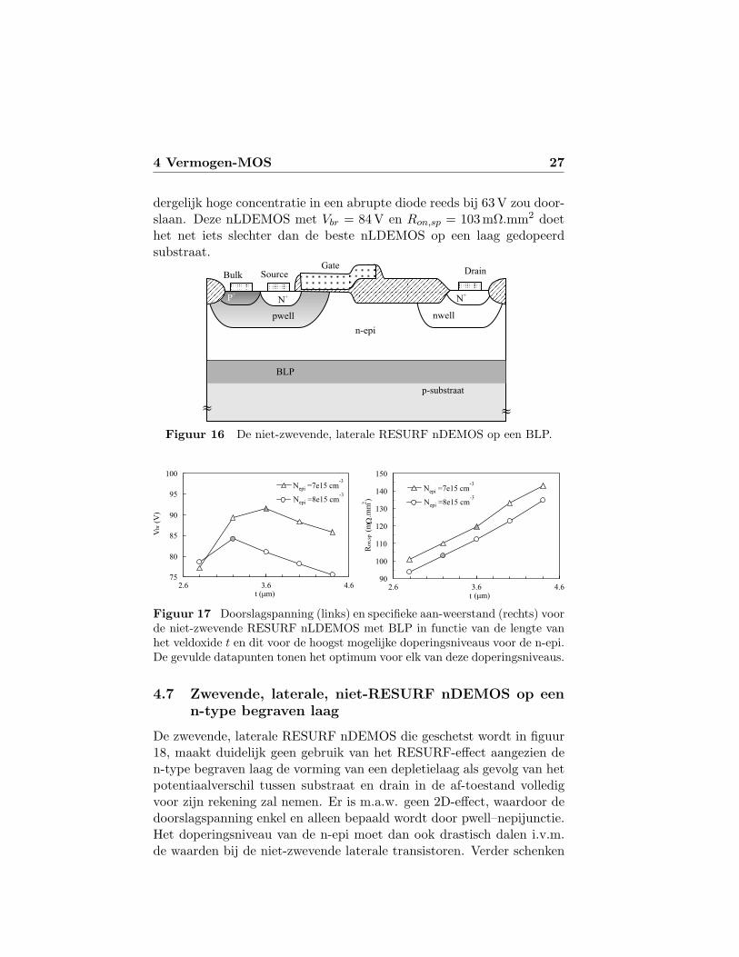
4 Vermogen-MOS 27
dergelijk hoge concentratie in een abrupte diode reeds bij 63V zou door-slaan. Deze nLDEMOS met Vbr = 84 V en Ron,sp = 103 mΩ.mm2 doethet net iets slechter dan de beste nLDEMOS op een laag gedopeerdsubstraat.
pwell
P+
n-epi
SourceGate
Drain
p-substraat
N+
»»
Bulk
nwell
N+
BLP
Figuur 16 De niet-zwevende, laterale RESURF nDEMOS op een BLP.
75
80
85
90
95
100
2.6 3.6 4.6t (mm)
Vb
r(V
)
(mm)
N =7e15 cmepi
-3
N =8e15 cmepi
-3
90
100
110
120
130
140
150
2.6 3.6 4.6t
Ron,s
p(m
W.m
m2)
N =7e15 cmepi
-3
N =8e15 cmepi
-3
Figuur 17 Doorslagspanning (links) en specifieke aan-weerstand (rechts) voorde niet-zwevende RESURF nLDEMOS met BLP in functie van de lengte vanhet veldoxide t en dit voor de hoogst mogelijke doperingsniveaus voor de n-epi.De gevulde datapunten tonen het optimum voor elk van deze doperingsniveaus.
4.7 Zwevende, laterale, niet-RESURF nDEMOS op eenn-type begraven laag
De zwevende, laterale RESURF nDEMOS die geschetst wordt in figuur18, maakt duidelijk geen gebruik van het RESURF-effect aangezien den-type begraven laag de vorming van een depletielaag als gevolg van hetpotentiaalverschil tussen substraat en drain in de af-toestand volledigvoor zijn rekening zal nemen. Er is m.a.w. geen 2D-effect, waardoor dedoorslagspanning enkel en alleen bepaald wordt door pwell–nepijunctie.Het doperingsniveau van de n-epi moet dan ook drastisch dalen i.v.m.de waarden bij de niet-zwevende laterale transistoren. Verder schenken
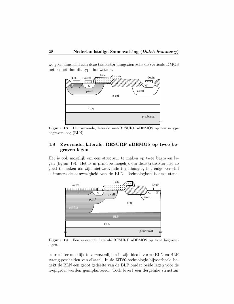
28 Nederlandstalige Samenvatting (Dutch Summary)
we geen aandacht aan deze transistor aangezien zelfs de verticale DMOSbeter doet dan dit type bouwsteen.
pwell
P+
n-epi
SourceGate
Drain
N+
»»
Bulk
nwell
N+
BLN
p-substraat
Figuur 18 De zwevende, laterale niet-RESURF nDEMOS op een n-typebegraven laag (BLN).
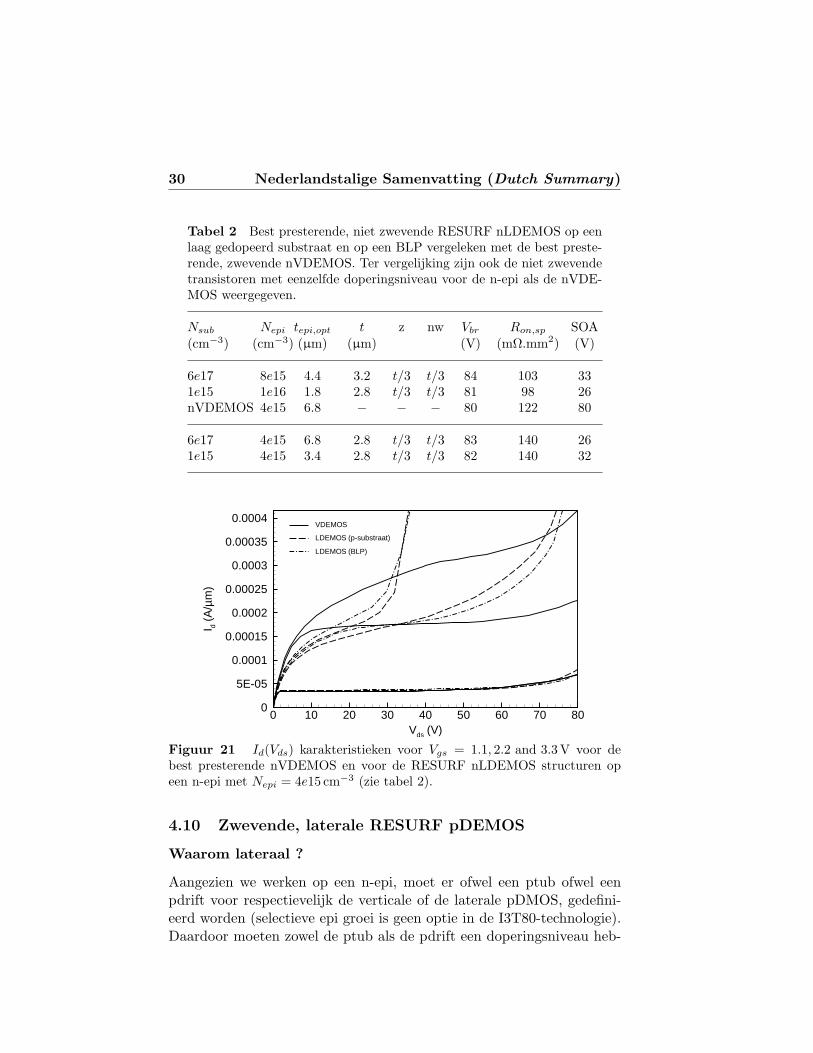
4.8 Zwevende, laterale, RESURF nDEMOS op twee be-graven lagen
Het is ook mogelijk om een structuur te maken op twee begraven la-gen (figuur 19). Het is in principe mogelijk om deze transistor net zogoed te maken als zijn niet-zwevende tegenhanger, het enige verschilis immers de aanwezigheid van de BLN. Technologisch is deze struc-
pwellP+
n-epi
Gate
p-substraat
N+
N+
»»
nwellpdrift
psinker
BLP
BLN
Source Drain
Figuur 19 Een zwevende, laterale RESURF nDEMOS op twee begravenlagen.
tuur echter moeilijk te verwezenlijken in zijn ideale vorm (BLN en BLPstreng gescheiden van elkaar). In de I3T80-technologie bijvoorbeeld be-dekt de BLN een groot gedeelte van de BLP omdat beide lagen voor den-epigroei worden geımplanteerd. Toch levert een dergelijke structuur

4 Vermogen-MOS 29
in deze technologie een transistor op met een hoge doorslagspanning (nl.103V), maar wel met een specifieke aan-weerstand die ongeveer twee-maal zo groot is als deze van de verticale nDEMOS.
4.9 Zwevende, geıntegreerde, verticale nDEMOS
De zwevende, geıntegreerde, verticale nDEMOS heeft in wezen een een-voudige structuur (figuur 20).
pwell
n+ p
+n
+
pwell
n+
p+
Bulk SourceDrain Source Bulk
BLN
p-substraat
n-epi
Gate
nsinker
»»
Figuur 20 De zwevende, geıntegreerde, verticale nDEMOS.
Een variatie van de n-epidikte voor verschillende doperingsniveausvan de epilaag, leert ons dat Nepi = 4e15 cm−3 het maximum niveauhaalbaar is, met de beste resultaten wat betreft Ron,sp. Deze weer-standswaarden zijn afhankelijk van de afstand tussen beide pwells, aan-gezien een te kleine afstand de stroom zal afsnijden. Er is echter eenoptimum daar een te breed pad de lengte van de transistor te veel doettoenemen, en daardoor Ron,sp opnieuw stijgt. Dit optimum wordt samenmet de optima voor de niet-zwevende, laterale RESURF-transistoren opp-substraat enerzijds en op BLP anderzijds, in tabel 2 opgenomen.
Het valt onmiddellijk op in deze tabel dat de nVDEMOS welis-waar slechtere Vbr en Ron,sp waarden heeft dan de laterale RESURF-transistoren, maar dat de SOA voor deze transistor veel groter is danvoor de andere. Dit komt omdat de laterale RESURF-transistoren tekampen hebben met het Kirk-effect, die heel sterk aanwezig is in lateraleRESURF-structuren van het n-type. Dit is niet het geval in de verti-cale DMOS, die daardoor een veel groter spanningsbereik heeft (zie ookfiguur 21).
30 Nederlandstalige Samenvatting (Dutch Summary)
Tabel 2 Best presterende, niet zwevende RESURF nLDEMOS op eenlaag gedopeerd substraat en op een BLP vergeleken met de best preste-rende, zwevende nVDEMOS. Ter vergelijking zijn ook de niet zwevendetransistoren met eenzelfde doperingsniveau voor de n-epi als de nVDE-MOS weergegeven.
Nsub Nepi tepi,opt t z nw Vbr Ron,sp SOA(cm−3) (cm−3) (µm) (µm) (V) (mΩ.mm2) (V)
6e17 8e15 4.4 3.2 t/3 t/3 84 103 331e15 1e16 1.8 2.8 t/3 t/3 81 98 26nVDEMOS 4e15 6.8 − − − 80 122 80
6e17 4e15 6.8 2.8 t/3 t/3 83 140 261e15 4e15 3.4 2.8 t/3 t/3 82 140 32
Vds (V)
I d(A
/µm
)
0 10 20 30 40 50 60 70 800
5E-05
0.0001
0.00015
0.0002
0.00025
0.0003
0.00035
0.0004VDEMOS
LDEMOS (p-substraat)
LDEMOS (BLP)
Figuur 21 Id(Vds) karakteristieken voor Vgs = 1.1, 2.2 and 3.3V voor debest presterende nVDEMOS en voor de RESURF nLDEMOS structuren opeen n-epi met Nepi = 4e15 cm−3 (zie tabel 2).
4.10 Zwevende, laterale RESURF pDEMOS
Waarom lateraal ?
Aangezien we werken op een n-epi, moet er ofwel een ptub ofwel eenpdrift voor respectievelijk de verticale of de laterale pDMOS, gedefini-eerd worden (selectieve epi groei is geen optie in de I3T80-technologie).Daardoor moeten zowel de ptub als de pdrift een doperingsniveau heb-
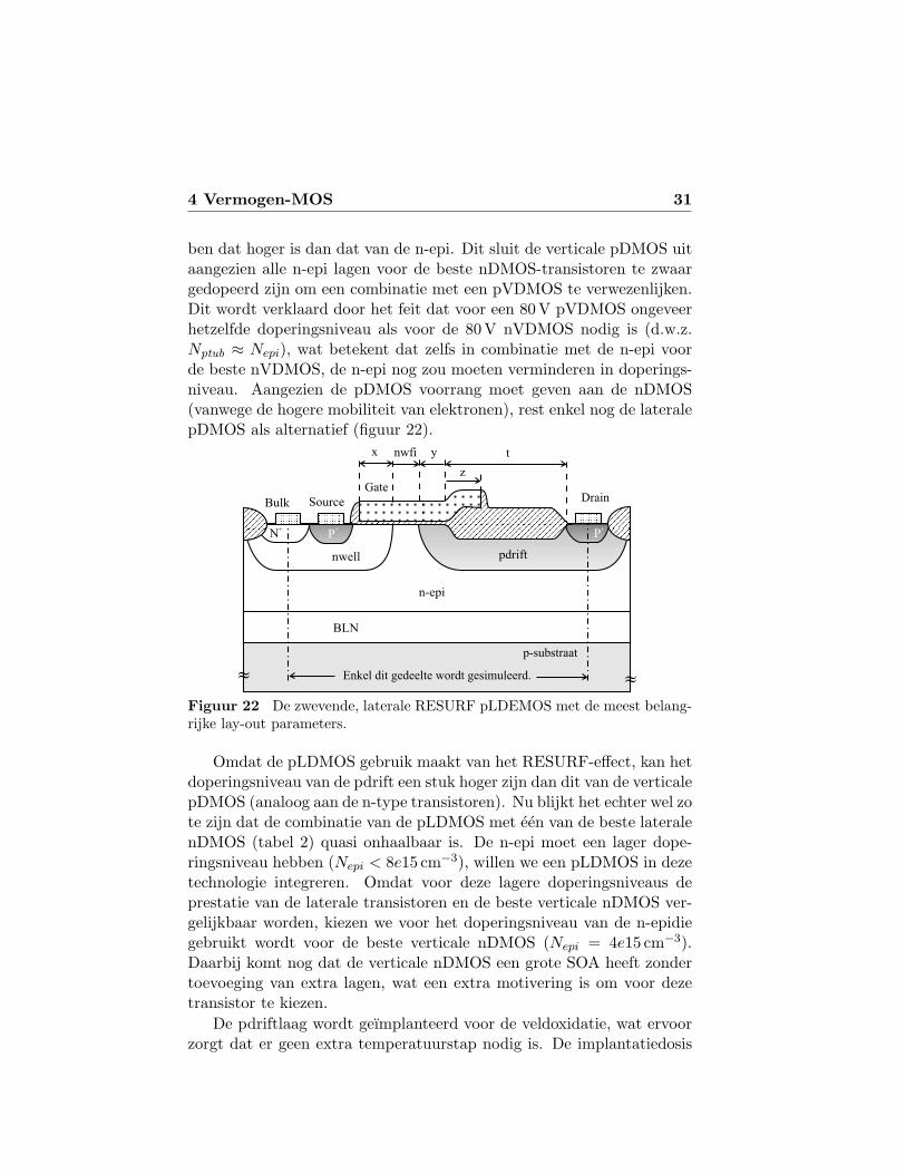
4 Vermogen-MOS 31
ben dat hoger is dan dat van de n-epi. Dit sluit de verticale pDMOS uitaangezien alle n-epi lagen voor de beste nDMOS-transistoren te zwaargedopeerd zijn om een combinatie met een pVDMOS te verwezenlijken.Dit wordt verklaard door het feit dat voor een 80 V pVDMOS ongeveerhetzelfde doperingsniveau als voor de 80 V nVDMOS nodig is (d.w.z.Nptub ≈ Nepi), wat betekent dat zelfs in combinatie met de n-epi voorde beste nVDMOS, de n-epi nog zou moeten verminderen in doperings-niveau. Aangezien de pDMOS voorrang moet geven aan de nDMOS(vanwege de hogere mobiliteit van elektronen), rest enkel nog de lateralepDMOS als alternatief (figuur 22).
pdrift
n-epi
Source
GateDrain
N+
»»
x t
z
y
Bulk
nwell
BLN
P+
P+
nwfi
p-substraat
Enkel dit gedeelte wordt gesimuleerd.
Figuur 22 De zwevende, laterale RESURF pLDEMOS met de meest belang-rijke lay-out parameters.
Omdat de pLDMOS gebruik maakt van het RESURF-effect, kan hetdoperingsniveau van de pdrift een stuk hoger zijn dan dit van de verticalepDMOS (analoog aan de n-type transistoren). Nu blijkt het echter wel zote zijn dat de combinatie van de pLDMOS met een van de beste lateralenDMOS (tabel 2) quasi onhaalbaar is. De n-epi moet een lager dope-ringsniveau hebben (Nepi < 8e15 cm−3), willen we een pLDMOS in dezetechnologie integreren. Omdat voor deze lagere doperingsniveaus deprestatie van de laterale transistoren en de beste verticale nDMOS ver-gelijkbaar worden, kiezen we voor het doperingsniveau van de n-epidiegebruikt wordt voor de beste verticale nDMOS (Nepi = 4e15 cm−3).Daarbij komt nog dat de verticale nDMOS een grote SOA heeft zondertoevoeging van extra lagen, wat een extra motivering is om voor dezetransistor te kiezen.
De pdriftlaag wordt geımplanteerd voor de veldoxidatie, wat ervoorzorgt dat er geen extra temperatuurstap nodig is. De implantatiedosis
32 Nederlandstalige Samenvatting (Dutch Summary)
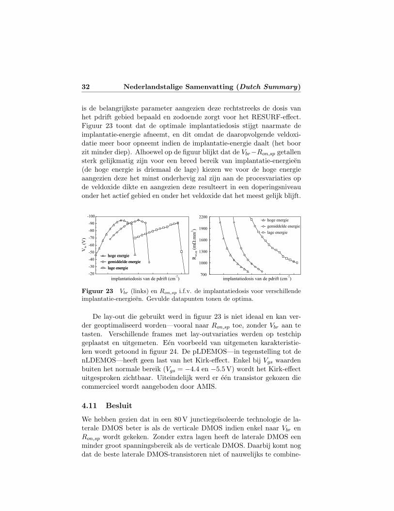
is de belangrijkste parameter aangezien deze rechtstreeks de dosis vanhet pdrift gebied bepaald en zodoende zorgt voor het RESURF-effect.Figuur 23 toont dat de optimale implantatiedosis stijgt naarmate deimplantatie-energie afneemt, en dit omdat de daaropvolgende veldoxi-datie meer boor opneemt indien de implantatie-energie daalt (het boorzit minder diep). Alhoewel op de figuur blijkt dat de Vbr−Ron,sp getallensterk gelijkmatig zijn voor een breed bereik van implantatie-energieen(de hoge energie is driemaal de lage) kiezen we voor de hoge energieaangezien deze het minst onderhevig zal zijn aan de procesvariaties opde veldoxide dikte en aangezien deze resulteert in een doperingsniveauonder het actief gebied en onder het veldoxide dat het meest gelijk blijft.
-100
-90
-80
-70
-60
-50
-40
-30
-20
implantatiedosis van de pdrift (cm )-2
V(V
)br
hoge energie
gemiddelde energie
lage energie
700
1000
1300
1600
1900
2200
R(m
.mm
)o
n,s
pW
2
hoge energie
gemiddelde energie
lage energie
hoge energie
gemiddelde energie
lage energie
implantatiedosis van de pdrift (cm )-2
Figuur 23 Vbr (links) en Ron,sp i.f.v. de implantatiedosis voor verschillendeimplantatie-energieen. Gevulde datapunten tonen de optima.
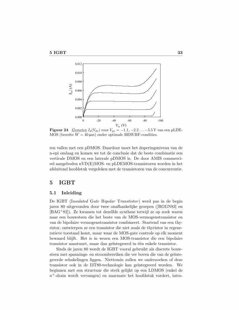
De lay-out die gebruikt werd in figuur 23 is niet ideaal en kan ver-der geoptimaliseerd worden—vooral naar Ron,sp toe, zonder Vbr aan tetasten. Verschillende frames met lay-outvariaties werden op testchipgeplaatst en uitgemeten. Een voorbeeld van uitgemeten karakteristie-ken wordt getoond in figuur 24. De pLDEMOS—in tegenstelling tot denLDEMOS—heeft geen last van het Kirk-effect. Enkel bij Vgs waardenbuiten het normale bereik (Vgs = −4.4 en −5.5V) wordt het Kirk-effectuitgesproken zichtbaar. Uiteindelijk werd er een transistor gekozen diecommercieel wordt aangeboden door AMIS.
4.11 Besluit
We hebben gezien dat in een 80 V junctiegeısoleerde technologie de la-terale DMOS beter is als de verticale DMOS indien enkel naar Vbr enRon,sp wordt gekeken. Zonder extra lagen heeft de laterale DMOS eenminder groot spanningsbereik als de verticale DMOS. Daarbij komt nogdat de beste laterale DMOS-transistoren niet of nauwelijks te combine-
5 IGBT 33
0.000
0.002
0.004
0.006
0.008
0.010
0.012
-100-80-60-40-200
|Ids| (
A)
Vds (V)
Figuur 24 Gemeten Id(Vds) voor Vgs = −1.1, −2.2 . . .−5.5V van een pLDE-MOS (breedte W = 40 µm) onder optimale RESURF-condities.
ren vallen met een pDMOS. Daardoor moet het doperingsniveau van den-epi omlaag en komen we tot de conclusie dat de beste combinatie eenverticale DMOS en een laterale pDMOS is. De door AMIS commerci-eel aangeboden nVD(E)MOS- en pLDEMOS-transistoren worden in hetafsluitend hoofdstuk vergeleken met de transistoren van de concurrentie.
5 IGBT
5.1 Inleiding
De IGBT (Insulated Gate Bipolar Transtistor) werd pas in de beginjaren 80 uitgevonden door twee onafhankelijke groepen ([RGGN83] en[BAG+82]). Ze kwamen tot dezelfde synthese terwijl ze op zoek warennaar een bouwsteen die het beste van de MOS-vermogenstransistor envan de bipolaire vermogenstransistor combineert. Startend van een thy-ristor, ontwierpen ze een transistor die niet zoals de thyristor in regene-ratieve toestand komt, maar waar de MOS-gate controle op elk momentbewaard blijft. Het is in wezen een MOS-transistor die een bipolairetransistor aanstuurt, maar dan geıntegreerd in een enkele transistor.
Sinds de jaren 80 wordt de IGBT vooral gebruikt als discrete bouw-steen met spannings- en stroombereiken die ver boven die van de geınte-greerde schakelingen liggen. Niettemin zullen we onderzoeken of dezetransistor ook in de I3T80-technologie kan geıntegreerd worden. Webeginnen met een structuur die sterk gelijkt op een LDMOS (enkel den+-drain wordt vervangen) en naarmate het hoofdstuk vordert, intro-

34 Nederlandstalige Samenvatting (Dutch Summary)
duceren we al dan niet bestaande lagen ten einde de werking van degeıntegreerde IGBT te verbeteren.
5.2 Doorslag in een nLIGBT zonder begraven lagen
Figuur 25 schetst een laterale IGBT zonder begraven lagen. Het enigeverschil met de laterale RESURF nDEMOS is het p+-draincontact, datwe vanaf nu de anode noemen. Deze schijnbaar kleine aanpassing maakteen wereld van verschil aangezien we nu een bipolaire bouwsteen heb-ben die pas stroom zal leveren wanneer de p+–nepi-junctie voorwaartsgepolariseerd wordt. Merk op dat de n-epi zwevend is.
pwell
P+
n-epi
KathodeGate
Anode
p-substraat
P+
N+
»»
J1
J4
J3
J2
Figuur 25 Een laterale IGBT zonder begraven lagen.
Wanneer er een positieve spanning staat op de anode i.v.m. de an-dere contacten, dan is het meteen duidelijk dat deze transistor een lagedoorslag zal hebben doordat de depletielagen komende van beide junc-ties J2 en J4, de junctie J3 zal bereiken. Dit is wat we RT-doorslaggenoemd hebben en wordt geıllustreerd in figuur 26. Dit fenomeen gaatniet gepaard met impactionisatie en wordt enkel veroorzaakt door hetfeit dat er een stroompad ontstaat voor de gaten. Het is duidelijk datdeze vorm niet kan worden behouden en dat verhinderd moet wordendat er een RT-doorslag ontstaat. Dit kan op een eenvoudige manier ge-beuren door de introductie van bestaande lagen, zoals in de volgendeparagraaf wordt verduidelijkt.
5.3 Zwevende nLIGBT met BLN
De introductie van de BLN, zoals in figuur 27, verslechtert aanzienlijkde parasitaire bipolaire transistor naar het substraat toe, maar verhoogtde doorslagspanning niet aangezien de RT tussen pwell en p+ blijft be-staan. Daartoe is een n-type buffer nodig, waarvoor we in eerste in-
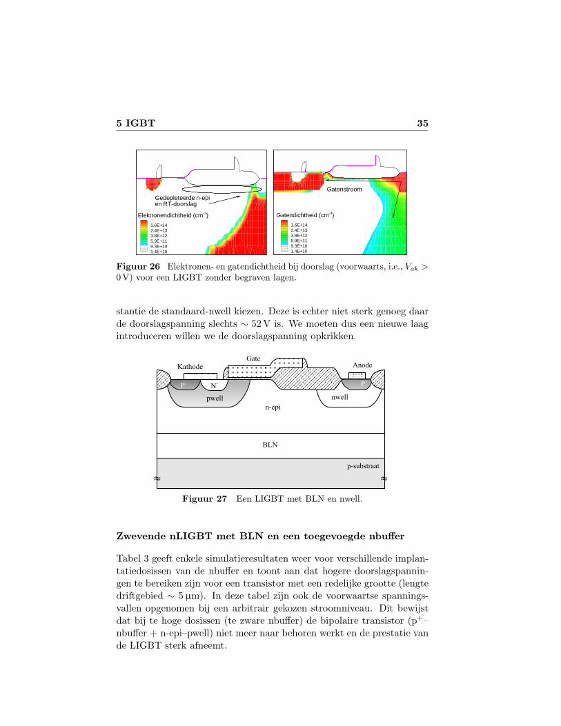
5 IGBT 35
Electron density (/cm3)
1.6E+142.4E+133.8E+125.9E+119.3E+101.4E+10
Gedepleteerde n-epien RT-doorslag
Elektronendichtheid (cm-3) Hole density (/cm3)
1.6E+142.4E+133.8E+125.9E+119.3E+101.4E+10
Gatenstroom
Gatendichtheid (cm-3)
Figuur 26 Elektronen- en gatendichtheid bij doorslag (voorwaarts, i.e., Vak >0 V) voor een LIGBT zonder begraven lagen.
stantie de standaard-nwell kiezen. Deze is echter niet sterk genoeg daarde doorslagspanning slechts ∼ 52V is. We moeten dus een nieuwe laagintroduceren willen we de doorslagspanning opkrikken.
pwell
P+
n-epi
KathodeGate
Anode
p-substraat
P+
N+
»»
nwell
BLN
Figuur 27 Een LIGBT met BLN en nwell.
Zwevende nLIGBT met BLN en een toegevoegde nbuffer
Tabel 3 geeft enkele simulatieresultaten weer voor verschillende implan-tatiedosissen van de nbuffer en toont aan dat hogere doorslagspannin-gen te bereiken zijn voor een transistor met een redelijke grootte (lengtedriftgebied ∼ 5µm). In deze tabel zijn ook de voorwaartse spannings-vallen opgenomen bij een arbitrair gekozen stroomniveau. Dit bewijstdat bij te hoge dosissen (te zware nbuffer) de bipolaire transistor (p+–nbuffer + n-epi–pwell) niet meer naar behoren werkt en de prestatie vande LIGBT sterk afneemt.
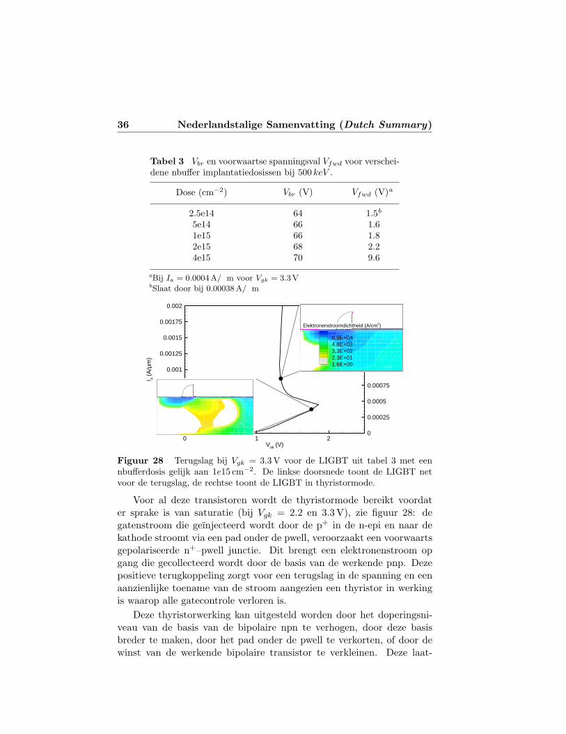
36 Nederlandstalige Samenvatting (Dutch Summary)
Tabel 3 Vbr en voorwaartse spanningsval Vfwd voor verschei-dene nbuffer implantatiedosissen bij 500 keV .
Dose (cm−2) Vbr (V) Vfwd (V)a
2.5e14 64 1.5b
5e14 66 1.61e15 66 1.82e15 68 2.24e15 70 9.6
aBij Ia = 0.0004A/m voor Vgk = 3.3VbSlaat door bij 0.00038A/m
Vak (V)
I a(A
/µm
)
0 1 20
0.00025
0.0005
0.00075
0.001
0.00125
0.0015
0.00175
0.002
0
0.00025
0.0005
0.00075
0.001
0.00125
0.0015
0.00175
0.002
Electron current density (A/cm2)
6.9E+044.8E+033.3E+022.3E+011.6E+00
Elektronenstroomdichtheid (A/cm2)
Figuur 28 Terugslag bij Vgk = 3.3 V voor de LIGBT uit tabel 3 met eennbufferdosis gelijk aan 1e15 cm−2. De linkse doorsnede toont de LIGBT netvoor de terugslag, de rechtse toont de LIGBT in thyristormode.
Voor al deze transistoren wordt de thyristormode bereikt voordater sprake is van saturatie (bij Vgk = 2.2 en 3.3V), zie figuur 28: degatenstroom die geınjecteerd wordt door de p+ in de n-epi en naar dekathode stroomt via een pad onder de pwell, veroorzaakt een voorwaartsgepolariseerde n+–pwell junctie. Dit brengt een elektronenstroom opgang die gecollecteerd wordt door de basis van de werkende pnp. Dezepositieve terugkoppeling zorgt voor een terugslag in de spanning en eenaanzienlijke toename van de stroom aangezien een thyristor in werkingis waarop alle gatecontrole verloren is.
Deze thyristorwerking kan uitgesteld worden door het doperingsni-veau van de basis van de bipolaire npn te verhogen, door deze basisbreder te maken, door het pad onder de pwell te verkorten, of door dewinst van de werkende bipolaire transistor te verkleinen. Deze laat-
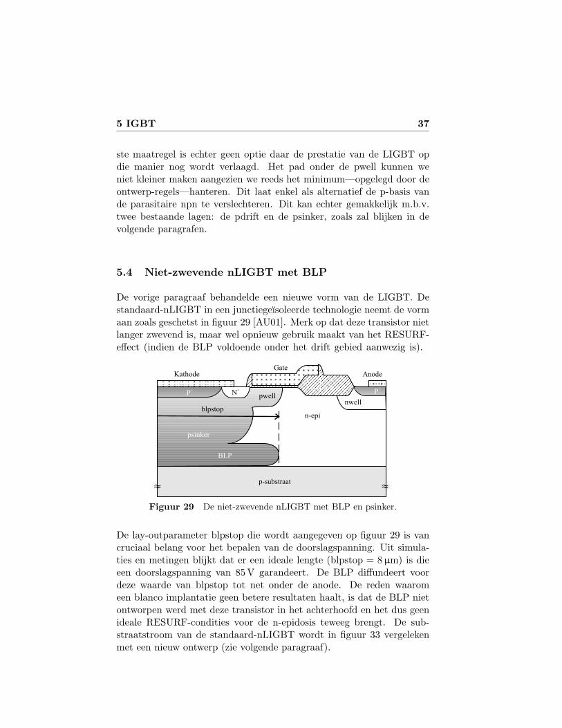
5 IGBT 37
ste maatregel is echter geen optie daar de prestatie van de LIGBT opdie manier nog wordt verlaagd. Het pad onder de pwell kunnen weniet kleiner maken aangezien we reeds het minimum—opgelegd door deontwerp-regels—hanteren. Dit laat enkel als alternatief de p-basis vande parasitaire npn te verslechteren. Dit kan echter gemakkelijk m.b.v.twee bestaande lagen: de pdrift en de psinker, zoals zal blijken in devolgende paragrafen.
5.4 Niet-zwevende nLIGBT met BLP
De vorige paragraaf behandelde een nieuwe vorm van de LIGBT. Destandaard-nLIGBT in een junctiegeısoleerde technologie neemt de vormaan zoals geschetst in figuur 29 [AU01]. Merk op dat deze transistor nietlanger zwevend is, maar wel opnieuw gebruik maakt van het RESURF-effect (indien de BLP voldoende onder het drift gebied aanwezig is).
pwellP+
n-epi
KathodeGate
Anode
p-substraat
P+
N+
»»
nwell
psinker
BLP
blpstop
Figuur 29 De niet-zwevende nLIGBT met BLP en psinker.
De lay-outparameter blpstop die wordt aangegeven op figuur 29 is vancruciaal belang voor het bepalen van de doorslagspanning. Uit simula-ties en metingen blijkt dat er een ideale lengte (blpstop = 8µm) is dieeen doorslagspanning van 85 V garandeert. De BLP diffundeert voordeze waarde van blpstop tot net onder de anode. De reden waaromeen blanco implantatie geen betere resultaten haalt, is dat de BLP nietontworpen werd met deze transistor in het achterhoofd en het dus geenideale RESURF-condities voor de n-epidosis teweeg brengt. De sub-straatstroom van de standaard-nLIGBT wordt in figuur 33 vergelekenmet een nieuw ontwerp (zie volgende paragraaf).
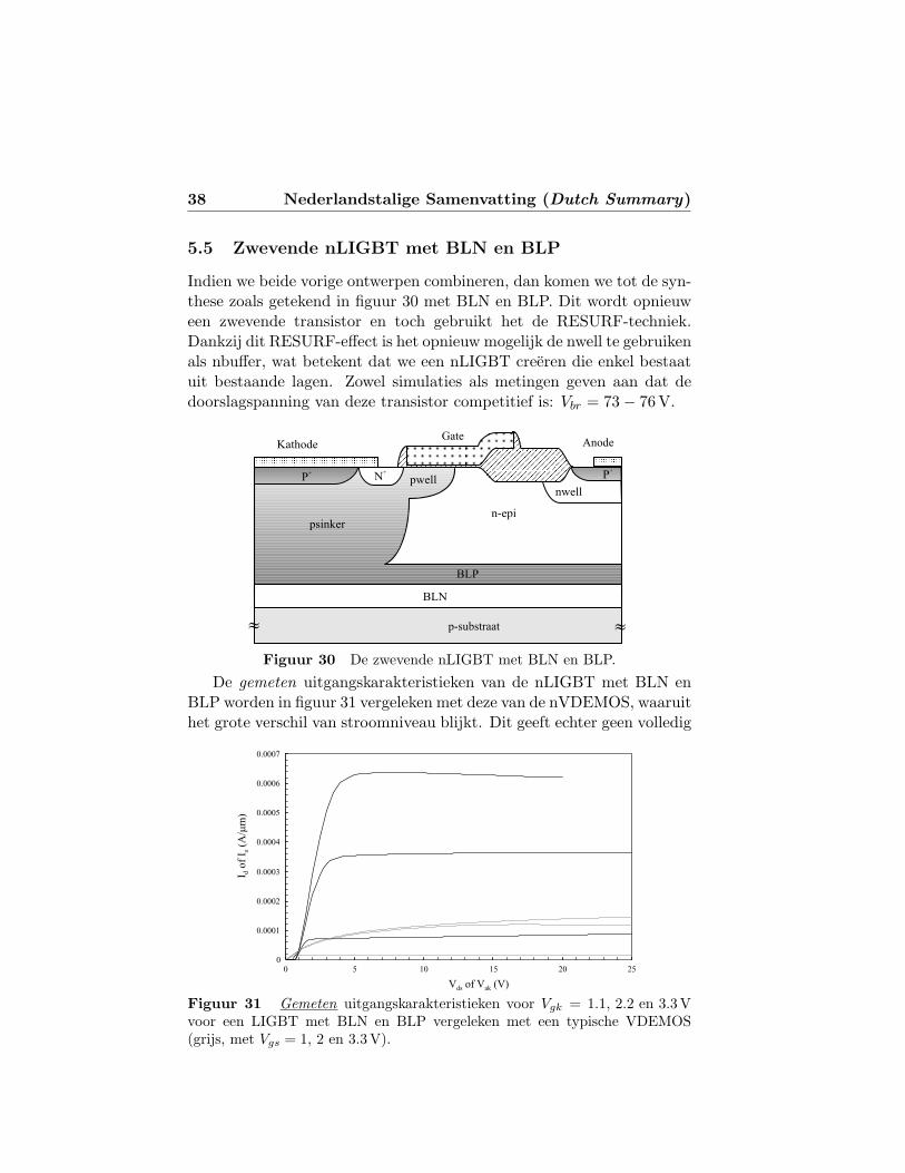
38 Nederlandstalige Samenvatting (Dutch Summary)
5.5 Zwevende nLIGBT met BLN en BLP
Indien we beide vorige ontwerpen combineren, dan komen we tot de syn-these zoals getekend in figuur 30 met BLN en BLP. Dit wordt opnieuween zwevende transistor en toch gebruikt het de RESURF-techniek.Dankzij dit RESURF-effect is het opnieuw mogelijk de nwell te gebruikenals nbuffer, wat betekent dat we een nLIGBT creeren die enkel bestaatuit bestaande lagen. Zowel simulaties als metingen geven aan dat dedoorslagspanning van deze transistor competitief is: Vbr = 73− 76V.
pwellP+
n-epi
KathodeGate
Anode
p-substraat
P+
N+
»
nwell
psinker
BLP
BLN
»
Figuur 30 De zwevende nLIGBT met BLN en BLP.
De gemeten uitgangskarakteristieken van de nLIGBT met BLN enBLP worden in figuur 31 vergeleken met deze van de nVDEMOS, waaruithet grote verschil van stroomniveau blijkt. Dit geeft echter geen volledig
0
0.0001
0.0002
0.0003
0.0004
0.0005
0.0006
0.0007
0 5 10 15 20 25
V (V)ds of Vak
Io
f I
(A/
m)
da
m
Figuur 31 Gemeten uitgangskarakteristieken voor Vgk = 1.1, 2.2 en 3.3 Vvoor een LIGBT met BLN en BLP vergeleken met een typische VDEMOS(grijs, met Vgs = 1, 2 en 3.3 V).
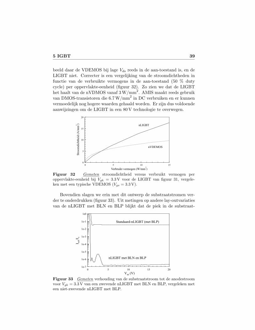
5 IGBT 39
beeld daar de VDEMOS bij lage Vds reeds in de aan-toestand is, en deLIGBT niet. Correcter is een vergelijking van de stroomdichtheden infunctie van de verbruikte vermogens in de aan-toestand (50 % dutycycle) per oppervlakte-eenheid (figuur 32). Zo zien we dat de LIGBThet haalt van de nVDMOS vanaf 3 W/mm2. AMIS maakt reeds gebruikvan DMOS-transistoren die 6.7W/mm2 in DC verbruiken en er kunnenvermoedelijk nog hogere waarden gehaald worden. Er zijn dus voldoendeaanwijzingen om de LIGBT in een 80 V technologie te overwegen.
0
5
10
15
20
0 5 10 15
Verbruikt vermogen (W/mm )2
Str
oom
dic
hth
eid (
A/m
m)
2 nLIGBT
nVDEMOS
Figuur 32 Gemeten stroomdichtheid versus verbruikt vermogen peroppervlakte-eenheid bij Vgk = 3.3V voor de LIGBT van figuur 31, vergele-ken met een typische VDEMOS (Vgs = 3.3V).
Bovendien slagen we erin met dit ontwerp de substraatstromen ver-der te onderdrukken (figuur 33). Uit metingen op andere lay-outvariatiesvan de nLIGBT met BLN en BLP blijkt dat de piek in de substraat-
1e-7
1e-6
1e-5
1e-4
1e-3
1e-2
1e-1
1e0
0 5 10 15 20
V (V)ak
I/I
sub
a
Standaard-nLIGBT (met BLP)
nLIGBT met BLN en BLP
Figuur 33 Gemeten verhouding van de substraatstroom tot de anodestroomvoor Vgk = 3.3V van een zwevende nLIGBT met BLN en BLP, vergeleken meteen niet-zwevende nLIGBT met BLP.
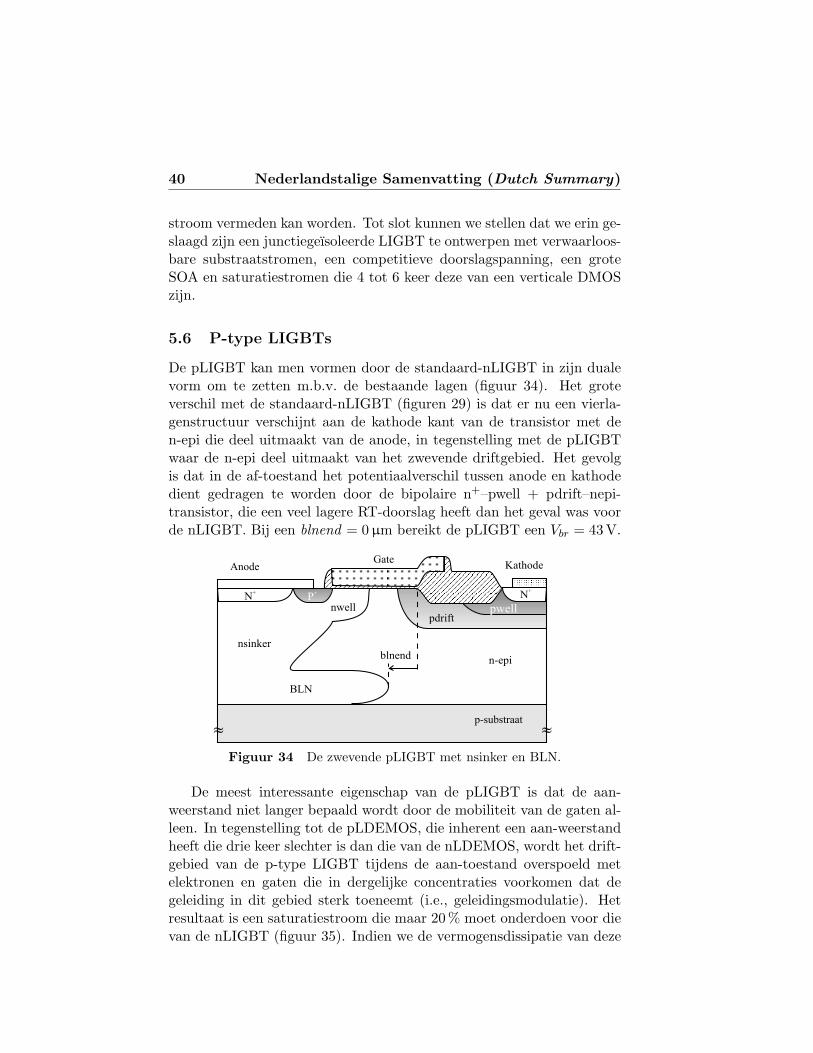
40 Nederlandstalige Samenvatting (Dutch Summary)
stroom vermeden kan worden. Tot slot kunnen we stellen dat we erin ge-slaagd zijn een junctiegeısoleerde LIGBT te ontwerpen met verwaarloos-bare substraatstromen, een competitieve doorslagspanning, een groteSOA en saturatiestromen die 4 tot 6 keer deze van een verticale DMOSzijn.
5.6 P-type LIGBTs
De pLIGBT kan men vormen door de standaard-nLIGBT in zijn dualevorm om te zetten m.b.v. de bestaande lagen (figuur 34). Het groteverschil met de standaard-nLIGBT (figuren 29) is dat er nu een vierla-genstructuur verschijnt aan de kathode kant van de transistor met den-epi die deel uitmaakt van de anode, in tegenstelling met de pLIGBTwaar de n-epi deel uitmaakt van het zwevende driftgebied. Het gevolgis dat in de af-toestand het potentiaalverschil tussen anode en kathodedient gedragen te worden door de bipolaire n+–pwell + pdrift–nepi-transistor, die een veel lagere RT-doorslag heeft dan het geval was voorde nLIGBT. Bij een blnend = 0 µm bereikt de pLIGBT een Vbr = 43 V.
pdrift
P+
n-epi
KathodeGate
Anode
p-substraat
N+
»»
N+
nwell
BLN
nsinker
pwell
blnend
Figuur 34 De zwevende pLIGBT met nsinker en BLN.
De meest interessante eigenschap van de pLIGBT is dat de aan-weerstand niet langer bepaald wordt door de mobiliteit van de gaten al-leen. In tegenstelling tot de pLDEMOS, die inherent een aan-weerstandheeft die drie keer slechter is dan die van de nLDEMOS, wordt het drift-gebied van de p-type LIGBT tijdens de aan-toestand overspoeld metelektronen en gaten die in dergelijke concentraties voorkomen dat degeleiding in dit gebied sterk toeneemt (i.e., geleidingsmodulatie). Hetresultaat is een saturatiestroom die maar 20% moet onderdoen voor dievan de nLIGBT (figuur 35). Indien we de vermogensdissipatie van deze
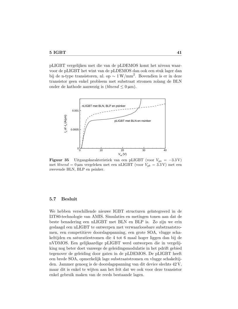
5 IGBT 41
pLIGBT vergelijken met die van de pLDEMOS komt het niveau waar-voor de pLIGBT het wint van de pLDEMOS dan ook een stuk lager danbij de n-type transistoren, nl. op ∼ 1 W/mm2. Bovendien is er in dezetransistor geen enkel probleem met substraat stromen zolang de BLNonder de kathode aanwezig is (blnend ≤ 0µm).
Vak (V)
I aof
-Ik(A
/µm
)
0 10 20 30 400
0.0005
0.001
nLIGBT met BLN, BLP en psinker
pLIGBT met BLN en nsinker
Figuur 35 Uitgangskarakteristiek van een pLIGBT (voor Vga = −3.3V)met blnend = 0 µm vergeleken met een nLIGBT (voor Vgk = 3.3V) met eenzwevende BLN, BLP en psinker.
5.7 Besluit
We hebben verschillende nieuwe IGBT structuren geıntegreerd in deI3T80-technologie van AMIS. Simulaties en metingen tonen aan dat debeste benadering een nLIGBT met BLN en BLP is. Zo zijn we eringeslaagd een nLIGBT te ontwerpen met verwaarloosbare substraatstro-men, een competitieve doorslagspanning, een grote SOA, vlugge scha-keltijden en saturatiestromen die 4 tot 6 maal hoger liggen dan bij denVDMOS. Een gelijkaardige pLIGBT werd ontworpen die in vergelij-king nog beter doet vanwege de geleidingsmodulatie in het pdrift gebiedtegenover de geleiding door gaten in de pLDEMOS. De pLIGBT heefteen brede SOA, opmerkelijk lage substraatstromen en vlugge schakeltij-den. Jammer genoeg is de doorslagspanning van dit device slechts 42 V,maar dit is enkel te wijten aan het feit dat we ook voor deze transistorenkel gebruik maken van de reeds bestaande lagen.

42 Nederlandstalige Samenvatting (Dutch Summary)
6 Synopsis
Na twee korte, algemeen inleidende hoofdstukken en een hoofdstuk terintroductie van het TCAD-simulatiewerk, hebben we zowel de inte-gratie van de MOS-vermogenstransistor als van de IGBT in een junc-tiegeısoleerde standaard-CMOS-technologie onderzocht.
We zijn tot de conclusie gekomen dat in de junctiegeısoleerde, 80 Vtechnologie van AMIS, de beste combinatie van complementaire MOS-vermogenstransistoren de nVDMOS en de pLDMOS is. Alhoewel delaterale nDMOS beter presteert wat betreft de Vbr versus Ron,sp dande verticale transistor, wordt toch gekozen voor de laatste en dit omdrie redenen. Ten eerste heeft deze transistor een groot stroom- enspanningsbereik en dat zonder gebruik te maken van extra (dure) la-gen, die wel nodig zijn indien we met de laterale RESURF nDMOS eeneven groot bereik zouden willen bereiken. Ten tweede is deze transistorzwevend van nature uit. De nLDMOS kan in theorie ook zwevend ge-maakt worden zonder verlies van prestatie van de transistor, maar dit istechnologisch moeilijk realiseerbaar. Ten derde is de verticale nDMOSgemakkelijk te combineren met een laterale pDMOS, wat voor de bestenLDMOS-transistoren moeilijker is.
Omdat de ontwikkeling en het ontwerp van de pLDEMOS gebeurdein de TFCG-groep en die van de nVD(E)MOS bij AMIS, wordt in dezesamenvatting enkel de grafiek met de siliciumlimiet en de transistorenvan de concurrenten voor de pLDEMOS opgenomen (figuur 36). Hetanalogon voor de nVDEMOS vindt men terug in de Engelstalige versie.Uit deze figuur leiden we af dat de I3T80 pLDEMOS een van de bestehuidige pLDEMOS-transistoren is.
Wat betreft IGBT-transistoren, zijn we erin geslaagd zowel een n-als een pLIGBT te ontwerpen die—naar wij weten—nooit eerder inde literatuur werden beschreven. Voor beide transistoren zijn de sub-straatstromen onderdrukt, is er een groot spannings- en stroombereik,en zijn er vlugge schakeltijden. Bovendien zijn beide zwevend, makenze enkel gebruik van bestaande lagen en hebben we aangetoond dat destroomdichtheid (per oppervlakte-eenheid) de concurrentie aan kan metde DMOS-transistoren.
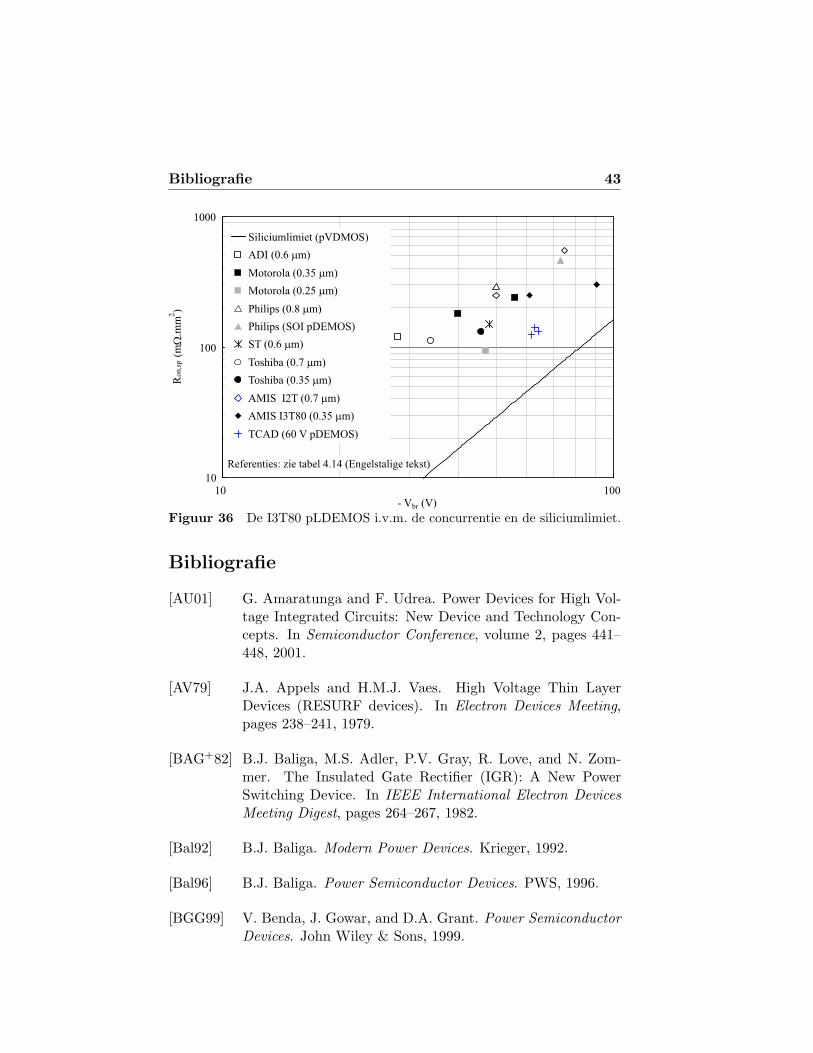
Bibliografie 43
10
100
1000
10 100- Vbr (V)
Ron,s
p(m
W.m
m2)
Siliciumlimiet (pVDMOS)
ADI (0.6 m)m
Motorola (0.35 m)m
Motorola (0.25 m)m
Philips (0.8 m)m
Philips (SOI pDEMOS)
ST (0.6 m)m
Toshiba (0.7 m)m
Toshiba (0.35 m)m
AMIS I2T ( )0.7 mm
AMIS I3T80 (0.35 m)m
TCAD (60 V pDEMOS)
Referenties: zie tabel 4.14 (Engelstalige tekst)
Figuur 36 De I3T80 pLDEMOS i.v.m. de concurrentie en de siliciumlimiet.
Bibliografie
[AU01] G. Amaratunga and F. Udrea. Power Devices for High Vol-tage Integrated Circuits: New Device and Technology Con-cepts. In Semiconductor Conference, volume 2, pages 441–448, 2001.
[AV79] J.A. Appels and H.M.J. Vaes. High Voltage Thin LayerDevices (RESURF devices). In Electron Devices Meeting,pages 238–241, 1979.
[BAG+82] B.J. Baliga, M.S. Adler, P.V. Gray, R. Love, and N. Zom-mer. The Insulated Gate Rectifier (IGR): A New PowerSwitching Device. In IEEE International Electron DevicesMeeting Digest, pages 264–267, 1982.
[Bal92] B.J. Baliga. Modern Power Devices. Krieger, 1992.
[Bal96] B.J. Baliga. Power Semiconductor Devices. PWS, 1996.
[BGG99] V. Benda, J. Gowar, and D.A. Grant. Power SemiconductorDevices. John Wiley & Sons, 1999.
44 Nederlandstalige Samenvatting (Dutch Summary)
[CS96] C.Y. Chang and S.M. Sze, editors. ULSI Technology.McGraw-Hill, 1996.
[Gha77] S.K. Ghandhi. Semiconductor Power Devices. John Wiley& Sons, 1977.
[RGGN83] J.P. Russell, A.M. Goodman, L.A. Goodman, and J.M. Neil-son. The COMFET — A New High Conductance MOS-Gated Device. IEEE Electron Device Letters, EDL-4(3):63–65, March 1983.
[Sze81] S.M. Sze. Physics of Semiconductor Devices. John Wiley &Sons, 1981.
[Sze88] S.M. Sze, editor. VLSI Technology. McGraw-Hill, 1988.
[Wan66] S. Wang, editor. Solid-State Electronics. McGraw-Hill, 1966.
1 Introduction
Some History
Although the first patents on the principle of the field effect transistor(FET) appeared in the early 30s of the previous century, it was not untilshortly after the second world war that the first silicon bipolar transistorwas actually made. Some people refer to this event as the start of thefirst electronic revolution, thereby tacitly assuming that there is a secondone too. This might be somewhat exaggerated, and the term evolutionmight be more appropriate. The major steps during this evolution are—from our point of view—the announcement of the thyristor in 1956, thefabrication of the first metal-oxide-semiconductor FET (MOSFET) in1960 (so it took about 30 years to overcome technical problems), thedevelopment of the power MOSFET in the 70s and of the insulated gatebipolar transistor (IGBT) in the 80s.
This electronic evolution has two faces: on the one hand there is theinformation processing electronics with its typical constantly decreasingtransistor dimensions (also referred to as the complementary MOS orCMOS technology). As a result, this technology is now capable of in-tegrating billions (yes, billions) of transistors in one chip of only a fewsquare centimeters large. The sheer pace of this electronic evolution isthe more striking if we realize that the first bipolar transistor ever made(in 1947) was actually a few square centimeters large all by its own. Butwhat is more, after half a century of industrial evolution, the face of theworld is still inevitably changing: who could nowadays imagine a worldwithout computers, mobile phones, satellites. . .
On the other hand, there is the power electronics, albeit less apparentat first sight, therefore not less important. The emergence of the powersemiconductor technology enables the efficient control and conversion ofelectrical energy. The power semiconductor technology started in theearly 50s with the development of the power bipolar transistor. Even
46 Introduction
though this is almost simultaneously with the information processingtechnology, the power semiconductor technology has been outshined bythe impressive CMOS technology ever since. Nevertheless, it has some-what followed its own way, by the development of the various powerdevices and has recently, or will in the near future (depending on theviewpoints) come out of the shadows.
This is what some call the second electronic revolution: the advent ofsmart power technology. It is, in fact, the merging of control of energy—the power semiconductor technology—with the information processingcapabilities—the CMOS technology. These smart power technologiesdo already exist and are used in countless applications where motorcontrol is important (from printers to car engines). It is expected thatthis smart power technology will have the same social impact as CMOStechnology. Moreover, its environmental impact can be huge, as it hasbeen documented that over 70 % of all electricity used in the worldflows through one or more power semiconductor devices. Imagine theenormous savings in power losses when this huge flow of power could becontrolled more efficiently.
How much power ? Which technology ? Whichdevices ?
The previous section took a quick glance at what exists in electronics:from the CMOS technology with its tiny, extremely fast transistor tothe power technology with its thyristor, slow and extremely big, butcapable of blocking thousands of volts and conducting thousands of am-peres. The power technology itself again consists of a vast domain ofapplications (see figure 1.1).
Like most Ph.D.s, this work will be situated in a small part of thisbroad spectrum, at the frontier of CMOS technology with the powertechnology: the smart power technology. In this smart power technology,we will only focus on one of the two classes of power devices: the variousswitches—and we will not focus on the rectifiers (see Chapter 2). Ofcourse, one realizes that it is absurd to speak about integration on chipof the example of the extremely big thyristor given above, which on itselfsometimes takes up a whole wafer (it is then inevitably a discrete device;that is, a device that is not integrated on chip with other devices). It isobvious that the devices qualifying for integration in a CMOS technologyare limited in blocking voltage and current capability. It is also clear
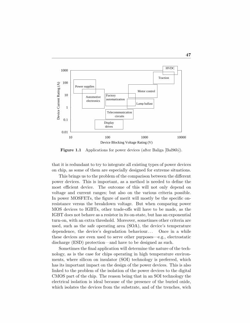
47
0.01
0.1
1
10
100
1000
10 100 1000 10000
Device Blocking Voltage Rating (V)
Dev
ice
Cur
rent
Rat
ing
(A)
Display drives
Telecommunication circuits
Lamp ballast
Factory automatization
Motor control
HVDC
Traction
Automotive electronics
Power supplies
Figure 1.1 Applications for power devices (after Baliga [Bal96b]).
that it is redundant to try to integrate all existing types of power deviceson chip, as some of them are especially designed for extreme situations.
This brings us to the problem of the comparison between the differentpower devices. This is important, as a method is needed to define themost efficient device. The outcome of this will not only depend onvoltage and current ranges; but also on the various criteria possible.In power MOSFETs, the figure of merit will mostly be the specific on-resistance versus the breakdown voltage. But when comparing powerMOS devices to IGBTs, other trade-offs will have to be made, as theIGBT does not behave as a resistor in its on-state, but has an exponentialturn-on, with an extra threshold. Moreover, sometimes other criteria areused, such as the safe operating area (SOA), the device’s temperaturedependence, the device’s degradation behaviour. . . Once in a whilethese devices are even used to serve other purposes—e.g., electrostaticdischarge (ESD) protection—and have to be designed as such.
Sometimes the final application will determine the nature of the tech-nology, as is the case for chips operating in high temperature environ-ments, where silicon on insulator (SOI) technology is preferred, whichhas its important impact on the design of the power devices. This is alsolinked to the problem of the isolation of the power devices to the digitalCMOS part of the chip. The reason being that in an SOI technology theelectrical isolation is ideal because of the presence of the buried oxide,which isolates the devices from the substrate, and of the trenches, wich
48 Introduction
isolate devices from each other. However, other problems, mostly tem-perature related, do arise. In a junction isolation (JI) technology (as inthis work), the electrical isolation is provided through the use of reversebiased pn junctions, and is a possible cause of latch-up and cross-talk.It is often necessary that the entire power device is lifted in potentialin comparison with the immediate surroundings. These floating devicesneed extra isolation when compared to their non-floating counterparts.These extra necessities are sometimes difficult to fullfill, and is one ofthe reasons why IGBT devices are seldom integrated in CMOS JI tech-nologies.
One understands that a complete picture is needed before the CMOStechnology is extended with process modules for power devices. Oneneeds to know the different applications that will be targeted for, andthe various needs for each of these applications. Not to mention the issuecost, as some applications have several possible realizations, but then thecost will be the decisive factor. This is however not a matter that willbe discussed here, and we will limit ourselves to the statement thatthe technology is based on a 0.35µm standard, junction isolated CMOStechnology, that the field of applications is the automotive and consumerelectronics, that the voltage range is roughly between 10 and 100 V, thatthe current range is anything below 10A and that the switching timesare seldom faster than 10 ns. This limits the number of power switchesavailable, and based on what is given in [Bal96a, Chapter 10] (see alsoconclusion of this work) the power MOS devices are the most efficientdevices in these ranges. Nevertheless, the possibility of integrating theIGBT will be studied as well.
Why TCAD ?
The major advantage of technology computer aided design (TCAD) isthat one can create single devices without the costly need to actuallymake the devices. One can try out different concepts and TCAD anti-cipates on which options are feasible and which are not before any realsilicon is out. Another major advantage of TCAD is that it gives insightin the distribution of the physical quantities on a 2D plot. One can actu-ally see what is happening in the device when such and such biases areapplied. This helped more than once to solve problems encountered inexisting devices. TCAD is often used in literature to discuss, understandand analyze problems of all kind. Yet another advantage of TCAD isagain cost driven. Once the core process flow is known and calibrated in
49
TCAD, one can develop new devices with great reliability, even if one ortwo new process modules have to be defined. Devices can be developedwithout the need for a second or third try; in other words, the chance ofbeing first time right greatly increases. Even the extraction of SPICEparameters can be done before any real device is measured (which actu-ally happened on the pLDEMOS in I3T80 presented in this work). Allof this results in a drastic decrease of the time to market, and thus ofthe cost.
A condition sine qua non is that TCAD simulations are reliable. Theremaining scepticism in industry is due to this calibration issue, the rea-son being twofold. The first problem is the adequate determination of2D dopant profiles because of the lack of 2D calibration material (SIMS).The second problem is the constant evolution of technology (new mate-rials and new physical phenomena as the scaling towards smaller dimen-sions goes on). However, both objections do not longer hold in our case.The integration of power devices happens in a technology that is al-ready well-known, and—due to the nature of power devices (their largerdimensions)—the need for very fine calibration of 2D dopant profileshardly ever occurs. Nevertheless, calibration, and the related meshingproblems, need to be addressed. Therefore, one chapter in this work(Chapter 3) will be entirely dedicated to this.
Objective
The ojective of this work is to design and develop power devices as anextension to a standard CMOS technology and to think up new conceptsameliorating the performance of these devices. The criteria used will beexplained in due course and are mainly very simple: the breakdownvoltage versus specific on-resistance or versus dissipated power. Oneimportant figure that appears in all these trade-offs is area—which isagain the factor cost showing up. The smaller the device, the less siliconis used, the cheaper the chip. To achieve this, the power dissipation hasto be decreased as much as possible. Otherwise, with decreasing area,one would generate too much power on a too small area, which inevitablyresults in breakdown. Decreasing the power dissipated means that wedecrease the power loss in the switch. As 60 to 70% of all electricitypasses through one or more power devices, this means a more efficientcontrol of electrical energy. Or how a basically cost driven motive canresult in an ecologically favourable trend. . .
50 Introduction
Outline
Since the focus in this work is on the understanding and the design ofthe power switch using TCAD simulations, most of the time we will con-centrate on device simulation. Therefore, Chapter 2 gives an overviewof the general physical framework for numerical TCAD device simula-tions. For a treatment of the process, the semiconductor physics, andthe basic device physics, we refer to textbooks. Chapter 2 gives, how-ever, a short reminder of some topics that are so important for powerdevices, that they can not be omitted; as well as an overview of somephenomena that might be lesser known (punch-through, reach-through,second breakdown, conductivity modulation, RESURF effect, Kirk ef-fect. . . ). Concerning the power devices, many excellent textbooks existthat explain their operation principles through analytical expressions(see Chapter 2: the books on power devices by S.K. Ghandi and B.J.Baliga). But, as is written in [Bal96a, Preface, p. viii]:
“For a complete characterization of the electrical propertiesof devices, it is necessary to resort to numerical techniquesusing computer programs that solve the fundamental semi-conductor transport equation in two dimensions (and some-times in three dimensions), with time dependence includedfor the transient case.”
This is in a nutshell what will be done in the core chapters of this book.But before we embark on this, the important matter of TCAD simulationand calibration needs to be treated (Chapter 3). The following chap-ters deal with the actual simulation, design, and measurement of powerdevices: Chapter 4 on the power MOS and Chapter 5 on the IGBT.Finally conclusions are made in Chapter 6 by comparing the differentdevices with each other and with devices described in literature.
References
[Bal96a] B.J. Baliga. Power Semiconductor Devices. PWS, 1996.
[Bal96b] B.J. Baliga. Trends in Power Semiconductor Devices. IEEETransactions on Electron Devices, 43(10):1717–1731, October1996.

2 Fundamental Considerations
2.1 Introduction
It is not the intention of this book to serve as an overview for all pro-cess, semiconductor and device physics needed for TCAD simulations.Therefore, the next section refers to books where all subjects related tothis work are treated in various ways. We will, however, give a shortoverview on the general framework of device simulation as it is impor-tant to have an idea about the physical framework we are working inwhile performing device simulations. It is considered less suitable forthis work to do the same for the process simulations, since most of ourattention will go to device operation and not to process related physics.As a simple and maybe a little odd example of device simulation, a sil-icon bar is treated. At first sight this seems a trivial case, but no suchthing. It introduces some of the major basic topics when dealing withpower devices: velocity saturation, avalanche generation, conductivitymodulation. . .
After this non-device, a definition of the power device and the char-acteristics of the ideal power device is given. Then, the two classesof power devices are presented: the rectifiers and the switches. Lessthought is given to the rectifiers, as this is not the subject of this work.Although they are important because they show up as integrated inpower switches. Therefore, only some very important plots with basiccharacteristics as breakdown voltage versus doping level are given; fordetails about their working, we refer to the textbooks on power devices.Then, the power switches are discussed, consisting of a classification onthe type of gate control. For each device, a brief summary on when,why, and where it is used is given. The last section gives an overviewof the basic concepts encountered when dealing with integrated powerdevices. It is solely intended as an introduction to some topics thatmight be lesser known, a sort of synopsis of designing concepts and offundamental (power) device physics. Most of these issues will be treatedin detail in the different chapters on power devices.
52 Fundamental Considerations
2.2 The Physics
2.2.1 Process, semiconductor and device physics
As has been mentioned above, we refer to the different books that servedus well during the course of the work presented in this book. For the pro-cess related physics, these are VLSI Technology by S.M. Sze [Sze88] andULSI Technology by C.Y. Chang and S.M. Sze [CS96]. For the semicon-ductor physics in general and the physics of the semiconductor devices,Solid-State Electronics by S. Wang [Wan66] and Physics of Semicon-ductor Devices by S.M. Sze [Sze81] are the reference works. The entireModular Series on Solid-State Devices edited by R.F. Pierret and G.W.Neudeck is also recommended, as it treats some of the subjects in greatdetail, e.g., Volume X on the Fundamentals of Carrier Transport by M.Lundstrom [Lun92], which served as a basis for the next section. AlsoKano’s Semiconductor Devices [Kan98], as well as some books in theModular Series on Solid-State Devices ([Neu89b], [Neu89a], and [Pie90])can be used as an introduction to device physics. For details aboutthe various models used in process and device simulation (e.g., for themobility models), we refer to the manuals of the ISE software [ISE00].
For the physics of semiconductor power devices in particular, we re-fer to such excellent textbooks as Semiconductor Power Devices by S.K.Ghandhi [Gha77], Modern Power Devices [Bal92] and Power Semicon-ductor Devices [Bal96] by B.J. Baliga, and Power Semiconductor Devicesby V. Benda, J. Gowar and D.A. Grant [BGG99].
2.2.2 General framework for device simulation
A fundamental way of treating carrier transport in a semiconductormaterial is by solving the Schrodinger Equation
i~∂Ψ∂t
= − ~2
2m0∇2Ψ +
[EC0(r) + UC(r) + Us(r, t)
]Ψ(r, t) (2.1)
which describes the electron by its wave function Ψ(r, t) propagatingthrough the material under the influence of the built in or applied(EC0), the crystal (UC), and scattering potentials (Us). The quantityΨ∗(r, t)Ψ(r, t)dr then gives the probability of finding the electron be-tween r and r + dr. Solving equation (2.1), which is already a “simpli-fication” of the many-body problem, is not an easy task and thereforefurther assumptions are needed for practical device simulation.
2.2 The Physics 53
When the size of the device is large enough (as will certainly be thecase for the devices described in this book), the various electron wavesdon’t interfere and a classical approach is appropriate. The quantummechanics is treated indirectly by the use of an effective mass or an en-ergy band structure; carrier scattering is treated quantum mechanically.This is known as the semiclassical treatment, where carriers behave asparticles, moving under influence of a force F (a combination of ap-plied or built in forces and random forces due to impurities and latticevibrations); and obey Newton’s laws
dpi
dt= F(r,p, t) (2.2)
dri
dt= vi(t). (2.3)
Each of the i = 1, . . . , N carriers has a position ri and a momentumpi, which are known by solving the previous equations. Alternatively,we could ask: what is the probability of finding an electron with crystalmomentum p at position r, at time t ? The answer is given by thedistribution function f(r,p, t), determined by the famous BoltzmannTransport Equation:
∂f
∂t+ v · ∇rf + F · ∇pf = s(r,p, t) +
∂f
∂t
∣∣∣∣coll
. (2.4)
The quantum mechanics enters via the evaluation of the E(p) rela-tion, which is used to calculate the carrier velocity v = ∇pE(p); andin the scattering rates s(r,p, t), which represents the actual carriergeneration-recombination processes such as impact ionization and re-combination through defects (Shockley-Read-Hall recombination) and∂f/∂t|coll , which represents collisions sending carriers from one momen-tum state to another.
Solving the Boltzmann Transport Equation directly is still extremelydifficult and further assumptions are needed to move on. One way tosolve the Boltzmann Transport Equation is by using the Monte Carlonumerical technique. This technique directly mimics the physical pro-cesses that occur during carrier transport by simulating individual par-ticle trajectories, determined by choosing random numbers (properlydistributed to reflect the probabilities of the various scattering effects).If the number of simulated trajectories is large enough, then the averageresults provide a good approximation of the behaviour of the carrierswithin a real device. Although this method has its limitations (of which
54 Fundamental Considerations
statistical noise is the most important one), it is most often the stan-dard against which the validity of simpler approaches to solving theBoltzmann Transport Equation is gauged.
The simplest way for solving the Boltzmann Transport Equationis by generating balance or conservation equations, which are directlyderived from it. These balance or conservation equations are derived byintroducing one unknown at a time, beginning with the electron density:
n(r, t) ≡ 1Ω
∑p
φ(p)f(r,p, t) with φ(p) = 1. (2.5)
Using (2.5), one can derive the first balance equations (two equations ifthe same is done for holes), better known as the continuity equations:
∂n
∂t= Gn −Rn+
1q∇Jn (2.6)
∂p
∂t= Gp −Rp+
1q∇Jp (2.7)
where Gn and Gp are the electron and hole generation rates and Rn andRp are the electron and hole recombination rates for n-type and p-typesemiconductors, respectively. Each of these balance equations intro-duces another unknown, the electron and hole current densities Jn andJp, for which a new balance equation can be sought. However, the bal-ance equation for the current density (the momentum balance equation)introduces on its turn another unknown, the tensor
←→W , whose trace can
be interpreted as the kinetic energy density. The balance equation forthe carrier energy (the energy balance equation) introduces the energyflux, and so forth. No matter how many balance equations are derived,they always contain one more unknown than the number of equations.The only way out is by introducing simplifications that truncate the setof equations. The best known example is an extremely rough trunca-tion of the momentum balance equations, the well-known drift-diffusionequations (or current density equations or transport equations), see e.g.,[Sze81, chapter 1]:
Jn = qµnnE+ qDn∇n (2.8)Jp = qµppE− qDp∇p (2.9)
for electrons and holes, respectively. The first term accounts for thedrift, caused by the electric field E and the second term accounts for thediffusion caused by the carrier concentration gradient (∇n and∇p). The
2.2 The Physics 55
electron and hole mobilities (µn and µp) values are given by means ofvarious models (depending on the situation under study), and determinethe diffusion constants (Dn and Dp) for nondegenerate semiconductorsthrough the Einstein relationship (Dn = (kT/q)µn, etc.).
These balance equations (the continuity and current density equa-tions), together with the Maxwell equations, give a complete descriptionof the dynamics of electrons and holes in a semiconductor under the in-fluence of external fields. For the devices presented in this book, onlyone Maxwell equation is needed, the Poisson equation:
∇(εs ·E
)= ∇(
εs · (−∇ψ))
= ρ = q (p− n + ND+ −NA−) (2.10)
where εs is the semiconductor permittivity, ψ is the electrical potential,ρ is the space charge density, and ND+ and NA− are the densities ofionized donors and acceptors, respectively.
A complete description of the problem is obtained by using only 3independent variables (the electron concentration n, the hole concen-tration p and the potential ψ), by introducing “secondary” models forthe mobility, generation and recombination; and by defining the neces-sary boundary conditions. These “secondary” models, based on quan-tum mechanical calculations or experiments, only use the 3 independentvariables.
The major part of the device simulations takes place within thisframework, wich will be referred to as the drift-diffusion model. Smalleror larger variations to the set of equations as discussed above can beintroduced by truncating the sequence of balance equations in a differentway.
A simple variation to the current density equations (2.8) and (2.9)is easily presented through the use of the electron and hole quasi-Fermipotentials, φn and φp, which are linked to the carrier concentrations andthe potential by the Boltzmann statistics:
n = ni,eff exp[q(ψ − φn)
kTL
](2.11)
p = ni,eff exp[−q(ψ − φp)
kTL
](2.12)
where ni,eff is the effective intrinsic density and TL is the lattice tem-perature. The current densities are then given by:
Jn = −qµnn∇φn (2.13)Jp = −qµpp ∇φp (2.14)

56 Fundamental Considerations
as one can easily verify by substituting φn and φp, using the equations(2.11) and (2.12) in (2.13) and (2.14), respectively. If ∇ni,eff 6= 0, an ex-tra term in the current densities is introduced that accounts for the gra-dient in the effective intrinsic carrier concentration (bandgap narrowingeffects). Still further, in a more general consideration, the Fermi-Diracdistribution function can be used instead of the Boltzmann function.This introduces important changes to the current density equations (andthe energy flux equations, see below).
Yet another approach, which is a less rough truncation of the mo-mentum balance equation, has to be discussed as it will be used in asmall part of the device simulations presented in this book. In the trun-cation as presented above, it has been assumed that the carrier tempera-tures, Tn and Tp, are given by TL and that this temperature is constant.A straightforward extension is to assume that the carriers are still inthermal equilibrium with the lattice, but the latter’s temperature isno longer constant. Hence the name thermodynamic or non-isothermalmodel, which extents the drift-diffusion approach to account for elec-trothermal effects. The result of this different truncation of the currentdensity equations is an extra term, which accounts for the flow of currentdue to the gradient of temperature:
Jn = −qµnn(∇φn +Pn∇TL
)(2.15)
Jp = −qµpp(∇φp +Pp∇TL
)(2.16)
with Pn and Pp as the absolute thermoelectric powers and the latticetemperature given by the lattice heat flow equation:
c∂TL
∂t= ∇(
κ∇TL
)+ H (2.17)
where c is the heat capacitance per unit volume, κ is the thermal con-ductivity and H is the heat generation given by [Wac90] (steady-statecase, without electromagnetic radiation):
H =
∣∣Jn
∣∣2qµnn
+
∣∣Jp
∣∣2qµpp
+ q(R − G)[φp − φn + TL(Pp − Pn)
]
− TL
(Jn · ∇Pn + Jp · ∇Pp
)(2.18)
where the first two terms are the Joule heat of electron and holes, thethird term is the recombination and generation heating and cooling, andthe last term accounts for the Peltier and Thomson effects.
2.2 The Physics 57
The extra driving terms for the current densities in equations (2.15)and (2.16) have to be included when accurate simulation for self-heatingeffects is desired. A simplified model of the thermodynamic model isdefined when both the thermoelectric powers are set to zero. Then, thelattice heat flow equation is still solved and the lattice temperature isstill used in the various “secondary” models.
With ever decreasing device dimensions, even this thermodynamicmodel does no longer suffice for deep submicron device simulations. Asthe thermodynamic model already makes fully use of the momentumbalance equation, the third moment of the Boltzmann Transport equa-tion, the energy balance equation, has to be introduced. As this setof equations is similar to that which describes the flow of fluids, thisapproach is often referred to as the hydrodynamic model. We do notenter into the details of this approach, as this model will be rarely usedin this book. We simply mention that the current density equationsare no longer truncated and thus each of them (for electrons and holes)introduces a new unknown, the tensor
←→W , for which we write down two
new balance equations (the energy balance equations). These two newbalance equations on their turn introduce two new unknowns and thesystem has to be truncated as has been done for the momentum balanceequations.
One understands that many variations of this truncation (and thus ofthe hydrodynamic model) exist. The version included in the device sim-ulator used in this book exists of 6 partial differential equations [Str62].In this case, the new unknown tensor in the current density equations isreduced to an isotropic tensor, represented by the carrier temperatureas unknown (for both electrons and holes). These carrier temperatures(Tn and Tp) are directly related to the carrier kinetic energy densities,for which two new energy balance equations are written down, bothcontaining a new unknown, the electron and hole energy (or heat) flux.To close the system, these energy fluxes are approximated in terms al-ready known (Jn, Tn, Jp and Tp). The energy balance or conservationequations for the electron and hole temperature are accompanied by theenergy conservation equation for the lattice temperature (actually thelattice heat flow equation (2.17)). These 3 equations together with thePoisson equation and the electron and hole continuity equations makeup the whole set of 6 partial differential equations.
58 Fundamental Considerations
Example: a silicon bar
The different models as described above are now applied to the mostsimple of structures conceivable, the silicon bar. This example mightseem to be too obvious at first sight. However, the non-linear behaviourof figure 2.1 does call for some more explanation. This simple exampleintroduces already quite some subjects that are vital for the understand-ing of the operation of power devices.
Consider a silicon bar, doped with phosphor (ND+ = 1e15 cm−3),with a length l = 10µm. A potential difference Vak is applied be-tween the top (anode) and bottom (cathode) contact, both of which areohmic. The current density versus applied voltage is simulated usingthe drift-diffusion model together with the doping-dependent, high-fieldsaturation model for the mobility, the Shockley-Read-Hall and Auger re-combination models, and the avalanche generation model according tovan Overstraeten - de Man. These are the so-called “secondary” modelsmentioned in the previous section. Figure 2.1 shows the current densityversus Vak and this may seem odd at first sight. However, some basicobservations clarify a great deal of it. In the beginning, the current flowhas to be ohmic, as given by (2.8) (no diffusion and ‖E‖ = E = Vak/las there is no net space charge, since n = ND+):
‖Jn‖ = J = qµnND+Vak/l = 224Vak A/cm2. (2.19)
With increasing Vak, E increases and the mobility becomes inversionallyproportional to the electric field. This is known as the velocity saturation(since vn = µnE) and occurs at vn,sat = 107 cm/s, or at a current density
Jsat = qvn,satND+ = 1600 A/cm2. (2.20)
Eventually, ohmic behaviour changes to velocity saturation behaviourwhen J = Jsat; that is, at Vak = 7 V. This is confirmed by Figure 2.1,which indicates saturation over a large voltage range. At some point,the electric field is so strong in the silicon bar that impact ionizationoccurs. This onset of avalanche generation can be calculated quite eas-ily when the following assumptions are made: the total current densityis only due to drift, which happens at the saturation velocity for bothcarriers (diffusion is negligible), the recombination rate is negligible incomparison with the generation rate and the space charge is also negligi-ble. Using the expressions for the electron current density (2.8) withoutthe diffusion term and with the saturation velocity, and the continu-ity equation (2.6) with the assumptions made above, results in a linear
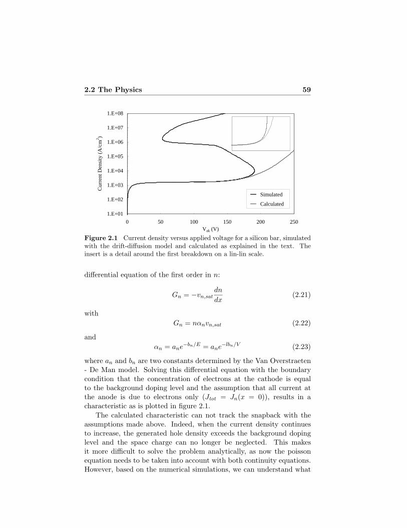
2.2 The Physics 59
1.E+01
1.E+02
1.E+03
1.E+04
1.E+05
1.E+06
1.E+07
1.E+08
0 50 100 150 200 250Vak (V)
Cur
rent
Den
sity
(A
/cm
2 )
Simulated
Calculated
Figure 2.1 Current density versus applied voltage for a silicon bar, simulatedwith the drift-diffusion model and calculated as explained in the text. Theinsert is a detail around the first breakdown on a lin-lin scale.
differential equation of the first order in n:
Gn = −vn,satdn
dx(2.21)
withGn = nαnvn,sat (2.22)
andαn = ane−bn/E = ane−lbn/V (2.23)
where an and bn are two constants determined by the Van Overstraeten- De Man model. Solving this differential equation with the boundarycondition that the concentration of electrons at the cathode is equalto the background doping level and the assumption that all current atthe anode is due to electrons only (Jtot = Jn(x = 0)), results in acharacteristic as is plotted in figure 2.1.
The calculated characteristic can not track the snapback with theassumptions made above. Indeed, when the current density continuesto increase, the generated hole density exceeds the background dopinglevel and the space charge can no longer be neglected. This makesit more difficult to solve the problem analytically, as now the poissonequation needs to be taken into account with both continuity equations.However, based on the numerical simulations, we can understand what
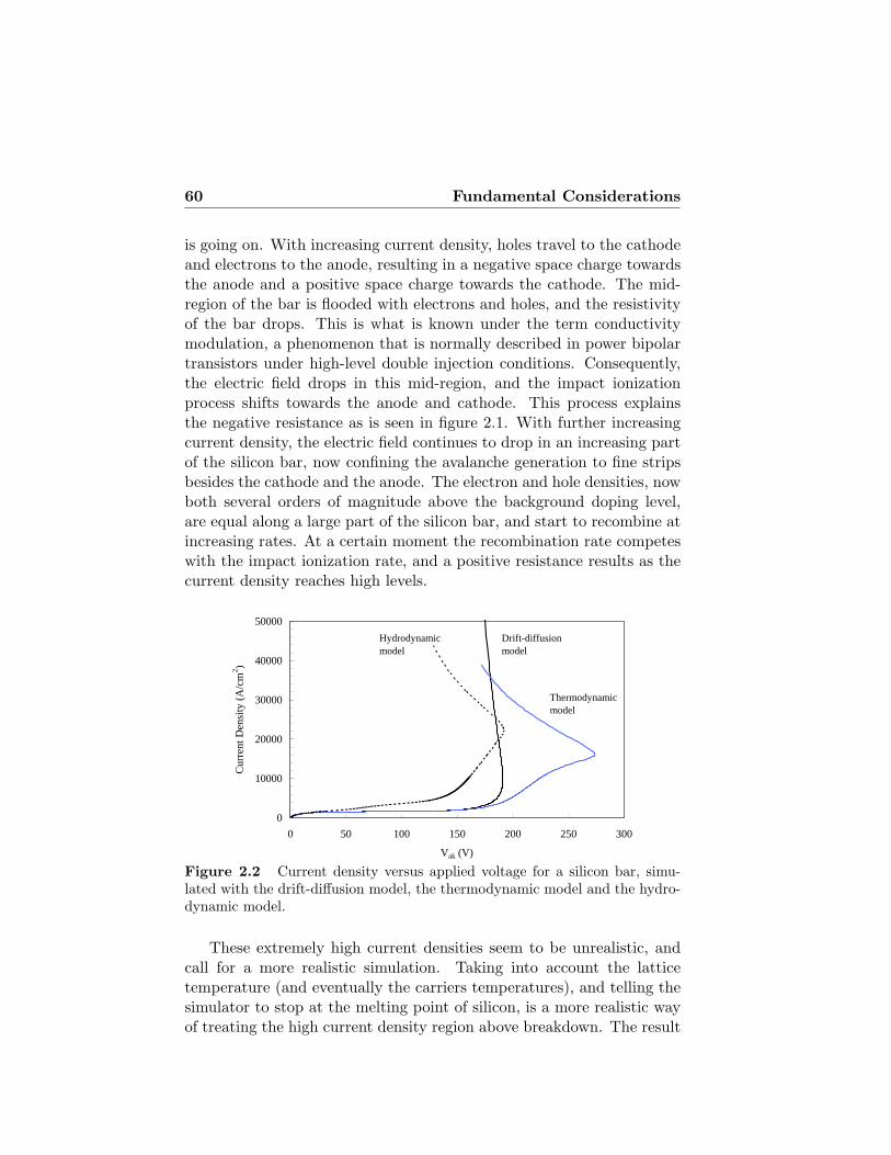
60 Fundamental Considerations
is going on. With increasing current density, holes travel to the cathodeand electrons to the anode, resulting in a negative space charge towardsthe anode and a positive space charge towards the cathode. The mid-region of the bar is flooded with electrons and holes, and the resistivityof the bar drops. This is what is known under the term conductivitymodulation, a phenomenon that is normally described in power bipolartransistors under high-level double injection conditions. Consequently,the electric field drops in this mid-region, and the impact ionizationprocess shifts towards the anode and cathode. This process explainsthe negative resistance as is seen in figure 2.1. With further increasingcurrent density, the electric field continues to drop in an increasing partof the silicon bar, now confining the avalanche generation to fine stripsbesides the cathode and the anode. The electron and hole densities, nowboth several orders of magnitude above the background doping level,are equal along a large part of the silicon bar, and start to recombine atincreasing rates. At a certain moment the recombination rate competeswith the impact ionization rate, and a positive resistance results as thecurrent density reaches high levels.
0
10000
20000
30000
40000
50000
0 50 100 150 200 250 300
Vak (V)
Cur
rent
Den
sity
(A
/cm
2 )
Drift-diffusion model
Thermodynamic model
Hydrodynamic model
Figure 2.2 Current density versus applied voltage for a silicon bar, simu-lated with the drift-diffusion model, the thermodynamic model and the hydro-dynamic model.
These extremely high current densities seem to be unrealistic, andcall for a more realistic simulation. Taking into account the latticetemperature (and eventually the carriers temperatures), and telling thesimulator to stop at the melting point of silicon, is a more realistic wayof treating the high current density region above breakdown. The result

2.3 What is a power device ? 61
is shown in figure 2.2, where the output characteristic of the siliconbar, simulated with the three different models based on the momentsof the Boltzmann transport equation are plotted against each other.Unfortunately, the real output characteristic is not at our disposal, butthis will be the case when the same models will be applied on severalpower devices. Here, it is only our intention to illustrate the influenceof the temperature on the output characteristics.
2.3 What is a power device ?
A power device controls the flow of power to a load. This is most oftendone by switching the device on a periodic basis to generate pulses ofcurrent through the device. The current and voltage waveforms areshown in figure 2.3 for the ideal case.
Cu
rren
tV
olt
age
t
t
on-state off-state
on-state off-state
Figure 2.3 Current and voltage waveforms of an ideal power device.
The ideal power device thus has no voltage drop when the deviceis conducting current (no on-state power dissipation), has no currentflowing through the device when it is supporting voltage (no off-statepower dissipation), and can switch between the on- and off-state in-stantaneously (no power dissipation during switching). The ideal power
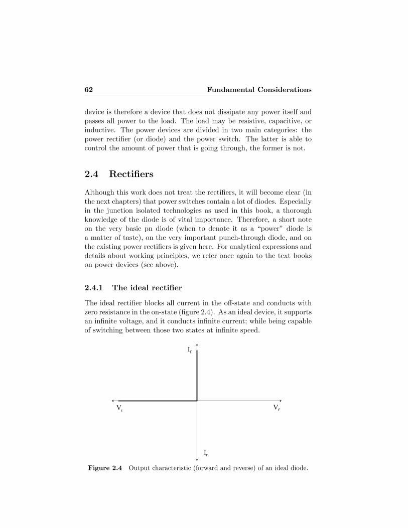
62 Fundamental Considerations
device is therefore a device that does not dissipate any power itself andpasses all power to the load. The load may be resistive, capacitive, orinductive. The power devices are divided in two main categories: thepower rectifier (or diode) and the power switch. The latter is able tocontrol the amount of power that is going through, the former is not.
2.4 Rectifiers
Although this work does not treat the rectifiers, it will become clear (inthe next chapters) that power switches contain a lot of diodes. Especiallyin the junction isolated technologies as used in this book, a thoroughknowledge of the diode is of vital importance. Therefore, a short noteon the very basic pn diode (when to denote it as a “power” diode isa matter of taste), on the very important punch-through diode, and onthe existing power rectifiers is given here. For analytical expressions anddetails about working principles, we refer once again to the text bookson power devices (see above).
2.4.1 The ideal rectifier
The ideal rectifier blocks all current in the off-state and conducts withzero resistance in the on-state (figure 2.4). As an ideal device, it supportsan infinite voltage, and it conducts infinite current; while being capableof switching between those two states at infinite speed.
Vf
Ir
If
Vr
Figure 2.4 Output characteristic (forward and reverse) of an ideal diode.
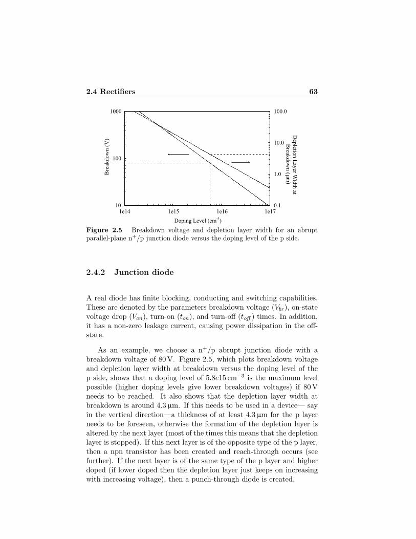
2.4 Rectifiers 63
10
100
1000
1e14 1e15 1e16 1e17
Doping Level (cm-3
)
Bre
akd
ow
n (
V)
0.1
1.0
10.0
100.0
Dep
letion
Lay
erW
idth
at
Break
do
wn
(m
m)
Figure 2.5 Breakdown voltage and depletion layer width for an abruptparallel-plane n+/p junction diode versus the doping level of the p side.
2.4.2 Junction diode
A real diode has finite blocking, conducting and switching capabilities.These are denoted by the parameters breakdown voltage (Vbr), on-statevoltage drop (Von), turn-on (ton), and turn-off (toff ) times. In addition,it has a non-zero leakage current, causing power dissipation in the off-state.
As an example, we choose a n+/p abrupt junction diode with abreakdown voltage of 80V. Figure 2.5, which plots breakdown voltageand depletion layer width at breakdown versus the doping level of thep side, shows that a doping level of 5.8e15 cm−3 is the maximum levelpossible (higher doping levels give lower breakdown voltages) if 80 Vneeds to be reached. It also shows that the depletion layer width atbreakdown is around 4.3µm. If this needs to be used in a device— sayin the vertical direction—a thickness of at least 4.3µm for the p layerneeds to be foreseen, otherwise the formation of the depletion layer isaltered by the next layer (most of the times this means that the depletionlayer is stopped). If this next layer is of the opposite type of the p layer,then a npn transistor has been created and reach-through occurs (seefurther). If the next layer is of the same type of the p layer and higherdoped (if lower doped then the depletion layer just keeps on increasingwith increasing voltage), then a punch-through diode is created.

64 Fundamental Considerations
2.4.3 Punch-through diode
The very important plots for the breakdown voltage of the abrupt pnjunction diode and of punch-through diodes of various widths are shownin figure 2.6. A punch-through diode is a junction diode where thedepletion layer at reverse bias is stopped at one side (might also bestopped at both sides) by a higher doped region of the same type (p+ orn+) of that side of the diode, with a decrease of the breakdown voltageas a consequence.
10
100
1000
1e13 1e14 1e15 1e16 1e17
Background Doping Concentration (cm )-3
Bre
akdow
nV
olt
age
(V)
N+
P+
P
W
Breakdown abrupt junction diode
W = 1 m m
W = 2 m m
W = 3 m m
W = 4 m m
W = 5 m m
W = 10 m m
Figure 2.6 Breakdown voltage for an abrupt junction diode and for a punch-through diode of several widths. The insert shows a punch-through diode.
The importance being that if one aims for a blocking voltage, differ-ent punch-through diodes can be made with different widths, dependingon the background doping concentration. This is a principle that will beused many times while designing power devices. In the example of 80 V,a p layer thickness of 3µm can be used if the doping level is decreased to1.8e15 cm−3 in comparison with the doping level needed (5.8e15 cm−3)when a non-punch-through diode (with a minimum thickness of 4.3µm)is used.
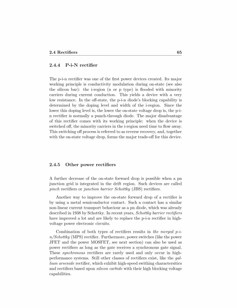
2.4 Rectifiers 65
2.4.4 P-i-N rectifier
The p-i-n rectifier was one of the first power devices created. Its majorworking principle is conductivity modulation during on-state (see alsothe silicon bar): the i-region (n or p type) is flooded with minoritycarriers during current conduction. This yields a device with a verylow resistance. In the off-state, the p-i-n diode’s blocking capability isdetermined by the doping level and width of the i-region. Since thelower this doping level is, the lower the on-state voltage drop is, the p-i-n rectifier is normally a punch-through diode. The major disadvantageof this rectifier comes with its working principle: when the device isswitched off, the minority carriers in the i-region need time to flow away.This switching off process is referred to as reverse recovery, and, togetherwith the on-state voltage drop, forms the major trade-off for this device.
2.4.5 Other power rectifiers
A further decrease of the on-state forward drop is possible when a pnjunction grid is integrated in the drift region. Such devices are calledpinch rectifiers or junction barrier Schottky (JBS) rectifiers.
Another way to improve the on-state forward drop of a rectifier isby using a metal semiconductor contact. Such a contact has a similarnon-linear current transport behaviour as a pn diode, which was alreadydescribed in 1938 by Schottky. In recent years, Schottky barrier rectifiershave improved a lot and are likely to replace the p-i-n rectifier in high-voltage power electronic circuits.
Combination of both types of rectifiers results in the merged p-i-n/Schottky (MPS) rectifier. Furthermore, power switches (like the powerJFET and the power MOSFET, see next section) can also be used aspower rectifiers as long as the gate receives a synchronous gate signal.These synchronous rectifiers are rarely used and only occur in high-performance systems. Still other classes of rectifiers exist, like the gal-lium arsenide rectifier, which exhibit high-speed swithing charactersiticsand rectifiers based upon silicon carbide with their high blocking voltagecapabilities.
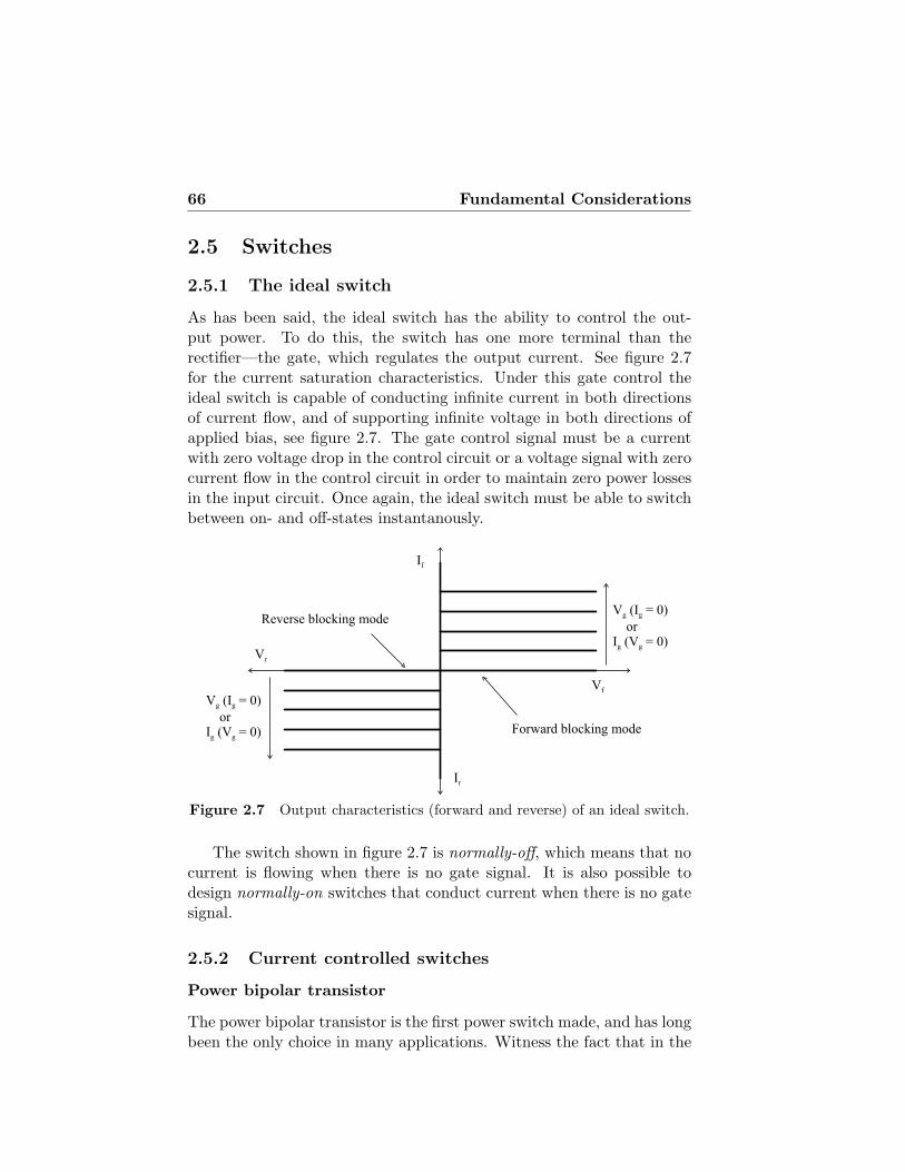
66 Fundamental Considerations
2.5 Switches
2.5.1 The ideal switch
As has been said, the ideal switch has the ability to control the out-put power. To do this, the switch has one more terminal than therectifier—the gate, which regulates the output current. See figure 2.7for the current saturation characteristics. Under this gate control theideal switch is capable of conducting infinite current in both directionsof current flow, and of supporting infinite voltage in both directions ofapplied bias, see figure 2.7. The gate control signal must be a currentwith zero voltage drop in the control circuit or a voltage signal with zerocurrent flow in the control circuit in order to maintain zero power lossesin the input circuit. Once again, the ideal switch must be able to switchbetween on- and off-states instantanously.
Vf
Ir
If
V (I = 0)
orI (V = 0)
g g
g g
Vr
V (I = 0)
orI (V = 0)
g g
g g
Reverse blocking mode
Forward blocking mode
Figure 2.7 Output characteristics (forward and reverse) of an ideal switch.
The switch shown in figure 2.7 is normally-off, which means that nocurrent is flowing when there is no gate signal. It is also possible todesign normally-on switches that conduct current when there is no gatesignal.
2.5.2 Current controlled switches
Power bipolar transistor
The power bipolar transistor is the first power switch made, and has longbeen the only choice in many applications. Witness the fact that in the
2.5 Switches 67
book by S.K. Ghandhi [Gha77], written in 1977, only two power switchesare described: the power bipolar and the power thyristor. However, fromthe 70s on, the power bipolar transistor has been gradually replaced bythe power MOSFET, the IGBT and the GTO (see further). The mainreason for this decline in popularity is the low current gain of the powerbipolar transistor due to the large base drive current needed and thecomplex input circuitry. Other drawbacks are its small safe operatingarea due to second breakdown, the decrease of the forward voltage dropwith increasing temperature (which makes it difficult to parallel thesedevices), and its slow speed due to its bipolar nature. Therefore, thebook on power devices written by B.J. Baliga in 1996 [Bal96] treats thepower bipolar only as an introduction to the IGBT.
The only ratings where the power bipolar still holds an advantageis in applications working from (relatively) low voltages (240 V) andrequiring switching frequencies in excess of 75 kHz. A recent articleon power bipolar transistors claims that the arrival of wide bandgapmaterials (SiC, GaN. . . ) will reintroduce the bipolar as a power device[HZ01].
Power thyristors
The second oldest power switch is the power thyristor, developed in the50s and consisting of 4 layers of semiconductor of alternating dopant type(npnp). These devices are unmatched when it comes to current carryingcapability per unit area. The price to pay is the loss of gate controlwhen current conduction is at its best—the major difference with thetransistors. Many variants of the basic thyristor structure (also calledthe silicon controlled rectifier (SCR)) exist and a lot of them are designedto improve the regain of the gate control when the device is switched off:the gate-assisted turn-off thyristor (GATT), the gate turn-off thyristor(GTO). . . Another popular, related device is the triac, consisting of a5 layer structure (npnpn, actually two anti-parallel thyristors). It is abidirectional switch, meaning that is not only capable of blocking currentflow in both directions, it is also capable of conducting current in bothdirections, depending on the gate signal.
Thyristors are mainly used in applications demanding extreme highcurrent conduction and voltage supporting capabilities. They actuallydetermine the outer limits of what is possible with solid-state powerelectronics.
68 Fundamental Considerations
2.5.3 Voltage controlled switches
Power junction field-effect devices
Although the principle of the JFET (junction field effect transistor, alsoknown as the static induction transistor (SIT)) was described in 1952 byShockley, it took until the 70s before the first power JFET was made,mainly due to technological problems. The main advantages of thisdevice over the power bipolar transistor are its higher input impedance,its negative temperature coefficent for the drain current that preventsthermal runaway and a higher switching speed because of the absenceof minority carrier recombination.
The major disadvantage of the JFET is that it is a normally-on de-vice. This is the reason why it is relegated to only a few applicationwhere its unique characteristics (e.g., the very high dV/dt) are neces-sary. The same holds for the static induction thyristor (SITh) or fieldcontrolled diode (FCD) or field controlled thyristor (FCT), a device de-rived from the JFET.
Power MOSFET
Built on the successes of the digital technology, the nMOS and thepMOS, the power MOS devices have pushed aside the power bipolartransistors in many applications from the 70s on. Their major advan-tages are the MOS controlled gate, the unipolarity, the negative tem-perature dependence and the excellent safe operating area. The powerMOS does not need the large base drive current and the complex gatedrive circuitry of the power bipolar, due to its voltage controlled MOSgate. This actually means that voltage controlled switches are foundto be closer to the ideal situation than current controlled switches. Thepower MOSFET is not as vulnerable to a second breakdown mode and ithas a switching speed that is orders of magnitude faster than for powerbipolar devices (because of the unipolarity). Furthermore, power MOS-FETs can be easily paralleled as their forward voltage drop increaseswith increasing temperature.
Due to these 4 main advantages, the power MOSFET has replacedthe power bipolar in all applications with low operating voltages (com-puter peripherals, automotive electronics. . . ). This has not occurred forsystems above 200 volts, mainly because of the increasing on-resistanceof the power MOSFET with increasing blocking voltage.
2.5 Switches 69
Insulated gate bipolar transistor
In search for the ideal power device, the IGBT was invented some 20years ago and has ever since been used in an increasing number of appli-cations. It combines the best of both the power bipolar and the powerMOS devices: high on-state current conduction with low on-state voltagedrop and a voltage controlled gate. Unfortunately, this device also in-herits some of the drawbacks: its safe operating area is relatively smalldue to the presence of an inherent parasitic thyristor, it has a slowerswitching speed than the power MOS (it is a bipolar device !) and itson-state forward voltage drop decreases with increasing temperature.
The IGBT has replaced the power bipolar device in many applica-tions (adjustable speed motor control for air conditioning, numericalcontrols for factory automation and robotics, and appliance controls)and is recently threatening the GTO thyristor, as the voltage and cur-rent ratings of the IGBT keep scaling up.
MOS-controlled thyristors
Yet another class of power switches that tries to combine the advan-tages of two of the most successful devices: the power MOS and thethyristor. Since the IGBT’s on-state forward voltage increases with in-creasing blocking voltage, these MOS-gated thyristors try to make use ofthe lower on-state voltage observed in thyristors. They are thus mainlyused in very high voltage power switching applications.
One of the main difficulties in creating this device, is the MOS-controlled turn-off of the thyristor once it has entered into its regenera-tive current conduction mode. Therefore, the most important figure forthese devices is the maximum controllable current density, above whichthe gate can no longer turn-off the thyristor. The MOS-controlled turn-on does not seem to be a problem and it has even been demonstratedthat it was superior when compared to a conventional thyristor.
Many different MOS controlled devices have been created to im-prove the MOS-gated turn-off of the thyristor. The first one was theMOS-controlled Thyristor (MCT) or the MOS-controlled Gate Turn-OffThyristor (MOS-GTO). Another structure—the Base Resistance Con-trolled Thyristor (BRT) uses a diverter contact that creates an alterna-tive path for the holes from the base. These two devices offer a lower on-state voltage drop and a higher surge current capability than the IGBT,but they lack the controlled turn-on and current saturation capability.But there is another gate-controlled structure that does offer these last

70 Fundamental Considerations
two features—the emitter switched thyristor (EST). However, it remainsdifficult to match the fully gate-controlled output of the IGBT with itswide safe operating area. Therefore, the EST, as the other MOS-gatedthyristors, are likely to replace the GTO rather than the IGBT.
2.6 Fundamental Concepts ConcerningIntegrated Power Switches
The purpose of this section is to provide some kind of overview of the im-portant concepts concerning power switches in integrated circuits. Mostof these topics are found in the text books on power devices. Never-theless, they are introduced and summarized here, as they are key fea-tures for understanding the work presented in this book. Most of thesesubjects will be treated in more detail in the chapters on the differentdevices.
2.6.1 The silicon limit
In the previous section, we introduced some of the different trade-offsand figures of merit for the different devices. This is what the siliconlimit is about, but then for the power MOS devices. As has been pointedout, the most important trade-off for these devices is the blocking voltage(Vbr) versus the (specific) on-resistance (for a definition, see the chapteron power MOS devices), which actually gives an idea of the power lossduring the on-state (compared to the forward voltage drop of the otherpower devices). If those two figures are plotted against each other, thena universal tool is at hand to compare all power MOSFET devices. Foran example, see figure 4.12. One understands that there is a theoreticallimit that cannot be crossed. This limit, however, depends on the formof the power MOSFET (vertical DMOS, LDMOS, RESURF LDMOS,DMOS on SOI, super junction DMOS or COOLMOSTM . . . ). Not tomention the difference if another material (e.g., SiC) comes into play.For silicon, these limits are therefore referred to as the silicon limit.
2.6.2 RESURF effect
The REduced SURface F ield effect is one of the most important design-ing techniques for power devices. The effect was discovered by accidentwhile experimenting on power diode structures [AV79]. The abstract ofthat article defines the effect as follows

2.6 Fundamental Concepts ConcerningIntegrated Power Switches 71
“The application of a somewhat unusual diode structureopens the possibility to make novel kinds of high voltage de-vices even with very thin epitaxial or implanted layers. Inthe new structures crucial changes in the electric field distri-bution take place at or at least near the surface.”
Since then, it has been used in virtually all power devices (RESURFbipolar, JFET, DMOS, IGBT. . . ), as well as in vertical, discrete devicesas in lateral, integrated devices. It has been extended with double,triple and multi layer acting RESURF structures (e.g., the COOLMOSstructure); with 3D acting RESURF; and towards other technologies(e.g., SOI). An excellent overview of the RESURF technology is givenin [Lud00]. The RESURF effect and its drawbacks will be treated indetail in the chapter on power MOS devices.
2.6.3 Punch-through and reach-through
In literature, it is not always obvious at first sight which phenomenonis referred to when one of the above terms is used. In the book bySze [Sze81], for instance, the terms punch-through and reach-through areused as synonyms. In the book by Benda [BGG99], only the term punch-through occurs; and in one of the books by Baliga [Bal96] reach-throughis defined as open base bipolar transistor breakdown and punch-throughis only used when referring to punch-through diodes (see above). Thislast approach seems to be the most correct one as now punch-throughrefers to a structure with two different layers of dopants, and reach-through to a structure with three different layers of dopants. Moreover,the terms refer to two distinct physical phenomena as punch-through isbreakdown caused by impact ionization (see the section on the punch-through diode); where reach-through is breakdown caused by a depletionlayer reaching a region of opposite dopant type, thereby creating a cur-rent path for one type of carriers (electrons or holes). Both phenomenawill be encountered many times during this work.
2.6.4 Second breakdown, snapback and thermal runaway
The term second breakdown refers to breakdown during current conduc-tion. At high current levels and high voltage, a positive feedback loopcan cause breakdown at much lower voltages than in the off-state. Thiscan happen in a power bipolar device, but also in any power devicecontaining a parasitic bipolar (so, virtually every power device) with a
72 Fundamental Considerations
decrease of the blocking voltage as a consequence (when compared tothe breakdown voltage in the off-state).
This second breakdown effect can also be accompanied with snap-back, which denotes a sudden reduction in blocking voltage when thecurrent is further increased during conduction. For instance, supposethat at first impact ionization is occurring, with consequently a largeincrease of the current level, when suddenly the blocking voltage is nolonger hold due to a second breakdown effect.
When a pn junction has reached locally a critical temperature, thelocal current density increases and the current is drawn to the regionwhere the temperature is the highest. The pn junction is then effectivelyshunted by a small filament of highly conducting intrinsic semiconduc-tor known as mesoplasma. This phenomenon used to be called secondbreakdown (e.g., in the book by Ghandhi [Gha77]), but is more andmore called thermal runaway. This phenomenon is always destructive,in contradiction with second breakdown and snapback, which can besustained by a device during a short period of time.
The different forms of second breakdown and snapback will be treatedfor each device in the corresponding chapter.
2.6.5 Kirk effect and adaptive RESURF
The Kirk effect is normally described when treating high-injection con-ditions in a bipolar transistor (e.g., [Sze81, p.145]). Under these highcurrent conditions, the electric field peak is relocated from the the base-collector junction towards the collector contact region, which greatlyaffects the transistor’s performance. An analogue relocation of the elec-tric field peak can occur in other power devices, especially in RESURFtype structures. It is actually one of the drawbacks of the RESURFeffect, and is the cause for introducing an extra layer in the process flowthat needs to increase the doping level towards the place where the elec-tric field is shifting. This technique is called adaptive RESURF. Onceagain, these subjects will be dealt with in detail in the chapter on thepower MOS.
2.6.6 Safe operating area
The safe operating area of a device is the working region beyond whichthe transistor should not be used. This is a very rough definition, andhow the limit is determined depends on the criteria used, classified in 3groups:
2.6 Fundamental Concepts ConcerningIntegrated Power Switches 73
Electrical safe operating area and ESD
We have already introduced terms as breakdown (in the off-state) andsecond breakdown (in the on-state). These are voltages that—at firstsight—define the absolute outer limits of the device’s operating region,above which a device can no longer be used. However, when very shortpulses are used (ns to µs), the devices can be used beyond second break-down and snapback. A method called T ransmission Line Pulsing candetermine how far the device can go under these short pulses. Devicescan be specially made to handle such short, heavy pulses to serve spe-cial purposes. The most common purpose being ESD (E lectroS taticD ischarge) protection. ESD protection devices and ESD measurementson power devices are not treated in this work.
Thermal safe operating area and energy capability
When the pulses are longer (µs to ms), temperature related phenomenacome into play and reduce the safe operating area further when thermalbreakdown or thermal runaway is reached. These type of pulses are usedin energy capability measurements in order to know the amount of energya device can take, during, e.g., an inductive turn-off. It is outside thescope of this book to perform energy capability measurements on powerdevices.
Hot carrier safe operating area and degradation
When a device is not used for very demanding purposes (ESD protection,inductive turn-off) and is used as a switch—that is, it is mostly on oroff, and switches very fast between those two states—it still can havea safe operating area that is smaller than the thermal safe operatingarea. Especially in MOS-gated devices during the on-state, when currentis flowing, some of the carriers have enough energy to surmount theSi/SiO2 barrier (hence hot carriers) and cause damage to the oxide.This damage induces shifts in the important electrical parameters ofthe device. This is called device degradation and is a very complexphenomenon. The limits of the safe operating area are normally definedby the most degrading electrical parameter (measured by the fab) for aspecific set of biasing conditions. It is based on a simple extrapolationof the most degrading parameter after some initial stress measurements.The stronger the criterion (e.g., 5 % degradation after 25 years insteadof 10 %), the smaller is the safe operating area.
74 Fundamental Considerations
Things get even more complicated when the switching of the deviceis taken into account. Indeed, a device can switch very fast between theon- and off-state, but not infinitely fast. This means that when a deviceis meant to have a long life (e.g., 25 years) and it is switched on and off alot during its life, it has spent a long net time between on- and off-state.Not to mention the type of load the device has to control ! Dependingon whether it is a resistive, a capacitive or an inductive load, the devicedegrades faster or not.
ESD, as well as energy capability can not be simulated with thesimple drift-diffusion model and they actually take TCAD to its utterpossibilities. Furthermore, the very complex issue of degradation is notalways possible to simulate. Although we will mention some hot carriermeasurements on power devices, it is not the purpose of this work to gointo great detail about the various degradation phenomena.
2.6.7 High level injection and conductivity modulation
Conductivity modulation is one of the reasons why a p-i-n rectifier canconduct current with a very small forward voltage drop, while blockinghigh voltage in the off-state. Most books on power devices thereforeintroduce the concept conductivity modulation while treating the p-i-nrectifier under high level injection conditions. Namely, during on-stateat high current density values, the amount of minority carriers injectedin the i-base exceeds the background doping concentration. Charge neu-trality requires that the amount of minority and majority carriers areequal. These concentrations can become several orders of magnitudelarger than the background doping concentration, with a considerabledecrease of the resistance of the i-base as a result. One can prove thatthis low on-state voltage drop is maintained even at very high currentdensities because the voltage drop across the i-base region is indepen-dent of the current through it (e.g., [Gha77, p. 110]). This conductivitymodulation can take place in any device where a junction is forwardbiased during the on-state (bipolars, IGBTs, thyristors. . . ).
2.6.8 Isolation
Low side and high side (or floating) devices
One can design a device with an internal breakdown voltage of e.g., 80 V,but still have a device that is not able to work at this voltage. The reasonis—contrary to a discrete device—that the integrated device needs to
References 75
be isolated vertically towards the substrate and laterally towards otherdevices on the chip. Furthermore, some devices have stronger needs forisolation: the high-side or so-called floating devices.
Latch-up, cross-talk and substrate currents
Some devices need to be able to float above (and in a very few occasionseven below) the substrate potential during on- and off-state. To achievethis in a junction isolated technology, they are put in a well or tubsurrounded by buried layers and plugs (or sinkers) to provide electricalisolation from the substrate and the other devices on the chip. In aSOI technology, the devices are dielectrically isolated by the use of theburied oxide layer and oxide trenches. These major differences have asevere impact on the design of power devices in a SOI technology. Usingjunction isolation, as in this book, there is always the potential dangerof latch-up between power devices or cross-talk of the power device withnearby CMOS circuitry caused by substrate currents.
References
[AV79] J.A. Appels and H.M.J. Vaes. High Voltage Thin Layer Devices(RESURF devices). In Electron Devices Meeting, pages 238–241, 1979.
[Bal92] B.J. Baliga. Modern Power Devices. Krieger, 1992.
[Bal96] B.J. Baliga. Power Semiconductor Devices. PWS, 1996.
[BGG99] V. Benda, J. Gowar, and D.A. Grant. Power SemiconductorDevices. John Wiley & Sons, 1999.
[CS96] C.Y. Chang and S.M. Sze, editors. ULSI Technology. McGraw-Hill, 1996.
[Gha77] S.K. Ghandhi. Semiconductor Power Devices. John Wiley &Sons, 1977.
[HZ01] A.Q. Huang and B. Zhang. The Future of Bipolar Power Tran-sistors. IEEE Transactions on Electron Devices, 48(11):2535–2543, November 2001.
[ISE00] ISE Integrated Systems Engineering. Manual, Release 7.0, 2000.
76 Fundamental Considerations
[Kan98] K. Kano. Semiconductor Devices. Prentice Hall, 1998.
[Lud00] A.W. Ludikhuize. A Review of RESURF Technology. In Sym-posium on Power Semiconductor Devices & ICs, pages 11–18,2000.
[Lun92] M. Lundstrom. Volume X Fundamentals of Carrier Transport.Modular Series on Solid State Devices. Addison-Wesley, 1992.
[Neu89a] G.W. Neudeck. Volume II The PN Junction Diode. ModularSeries on Solid State Devices. Addison-Wesley, 1989.
[Neu89b] G.W. Neudeck. Volume III The Bipolar Junction Transistor.Modular Series on Solid State Devices. Addison-Wesley, 1989.
[Pie90] R.F. Pierret. Volume IV Field Effect Devices. Modular Serieson Solid State Devices. Addison-Wesley, 1990.
[Str62] R. Stratton. Diffusion of Hot and Cold Electrons in Semicon-ductor Barriers. Physical Review, 126(6):2002–2014, June 1962.
[Sze81] S.M. Sze. Physics of Semiconductor Devices. John Wiley &Sons, 1981.
[Sze88] S.M. Sze, editor. VLSI Technology. McGraw-Hill, 1988.
[Wac90] G.K. Wachutka. Rigorous Thermodynamic Treatment of HeatGeneration and Conduction in Semonductor Device Modeling.IEEE Transactions on Computer-Aided Design, 9(11):1141–1149, November 1990.
[Wan66] S. Wang, editor. Solid-State Electronics. McGraw-Hill, 1966.
3 TCAD Simulation andCalibration
3.1 Introduction
Technology Computer Aided Design (TCAD) uses physical models tosimulate an entire process flow, process step by process step, and to sim-ulate the working of the device. The so-called process and device sim-ulators discretize the properties of a real structure onto a non-uniformgrid or ‘mesh’ (in 1, 2 or even 3 space dimensions) to solve the differen-tial equations describing the various physical phenomena. Thus, whensimulating device structures using TCAD, one needs a translation of thereal process flow into the software code used by the process simulator.Ideally, this translation would be trivial. The process simulator wouldthen interpret each process step and use the relevant models: simplemodels when applicable and complex models when necessary. Ideally,the grid would be generated by the process simulator: refining wherenecessary and relaxing where possible. Once the structure has gonethrough the process simulator, it passes to the device simulator that—ideally—would generate its own grid (or several grids depending on thedesired simulation) and that on its turn would use the correct models.
Unfortunately (or fortunately, depending on your politics), this idealsimulator does not exist. Although the simulators do get more intelligentover the years, the user still has to intervene at each step described aboveand this for several reasons. First of all, there is the physics: someprocess related physics and some device physics are still research topics.Secondly, some model parameters are inherently fab related. The thirdreason is CPU time related: the simulator can not know what degreeof accuracy is desired and therefore the user has to define what modelshave to be used and how fine the mesh must be. These problems call forcalibration. The process calibration is treated in the next section, whilethe device calibration is treated in the last one. Both sections deal withthe problems and difficulties associated with the models and with themeshing.
78 TCAD Simulation and Calibration
3.2 Process Simulation and Calibration
One needs to calibrate the process flow (doping profiles, oxide thick-nesses, bird’s beaks. . . ). It is obvious that the more measured materialis available, the better the simulations. Ideally one should have a SEMpicture and/or SIMS or SRP measurements after each relevant processstep. But this is not always possible: there is the problem of cost andsometimes the measurement techniques are just not available yet (e.g.,2D SIMS). So, on the one hand one is bounded by the limited measure-ment data, and, on the other hand by the limitations inherent to TCAD(the meshing and the models). Depending on the structure and the tech-nology one wants to simulate, the available TCAD tools can or can notbe sufficient. For the work presented in this book, process simulation isadequate and even more physical models are at one’s disposal than ac-tually necessary. An example is the simulation of the ldd implantationsand the subsequent anneal. Present TCAD tools make it possible tosimulate the damage and amorphization associated with these implan-tations and to take into account these damage distributions in order tosimulate transient enhanced diffusion (TED). This is necessary for deepsubmicron CMOS simulation and demands a lot of calibration work.But is it relevant for large structures like DMOS devices ? One under-stands that TCAD simulation translates the process flow (the so-called‘input deck’) depending on the device structure under study. But beforewe embark on the translation of the process flow, the important matterof meshing needs to be dealt with.
3.2.1 The mesh
The great majority of problems encountered during TCAD work is meshrelated. The user wants a mesh that is as coarse as possible to reduce theCPU time. This is a possible dangerous situation, as one easily intro-duces faults during simulation when the mesh is not adequate enough.
The purpose of this section is to introduce the reader into the TCADwork, with its typical meshing and calibration problems, using the ISEsoftware. We will not go into too much details about the ISE softwarelanguage itself, but focus on how we procede. Some extracts of the inputdeck will be given in typed text style. The reader who is interested indoing simulations can use this information together with the ISE manu-als [ISE00] to get started. The correct use of the TCAD tools is mainlya process of a lot of trial and error and of gaining practical experience.To illustrate this process of meshing and calibration, an existing stan-
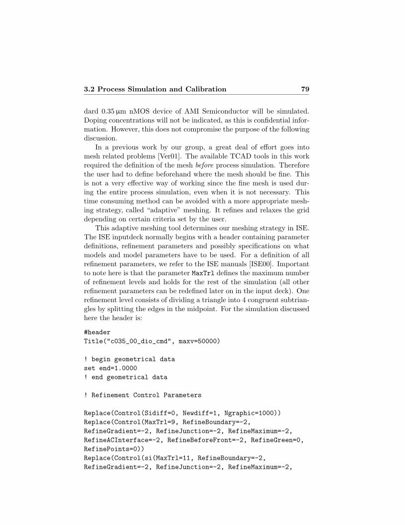
3.2 Process Simulation and Calibration 79
dard 0.35 µm nMOS device of AMI Semiconductor will be simulated.Doping concentrations will not be indicated, as this is confidential infor-mation. However, this does not compromise the purpose of the followingdiscussion.
In a previous work by our group, a great deal of effort goes intomesh related problems [Ver01]. The available TCAD tools in this workrequired the definition of the mesh before process simulation. Thereforethe user had to define beforehand where the mesh should be fine. Thisis not a very effective way of working since the fine mesh is used dur-ing the entire process simulation, even when it is not necessary. Thistime consuming method can be avoided with a more appropriate mesh-ing strategy, called “adaptive” meshing. It refines and relaxes the griddepending on certain criteria set by the user.
This adaptive meshing tool determines our meshing strategy in ISE.The ISE inputdeck normally begins with a header containing parameterdefinitions, refinement parameters and possibly specifications on whatmodels and model parameters have to be used. For a definition of allrefinement parameters, we refer to the ISE manuals [ISE00]. Importantto note here is that the parameter MaxTrl defines the maximum numberof refinement levels and holds for the rest of the simulation (all otherrefinement parameters can be redefined later on in the input deck). Onerefinement level consists of dividing a triangle into 4 congruent subtrian-gles by splitting the edges in the midpoint. For the simulation discussedhere the header is:
#headerTitle("c035_00_dio_cmd", maxv=50000)
! begin geometrical dataset end=1.0000! end geometrical data
! Refinement Control Parameters
Replace(Control(Sidiff=0, Newdiff=1, Ngraphic=1000))Replace(Control(MaxTrl=9, RefineBoundary=-2,RefineGradient=-2, RefineJunction=-2, RefineMaximum=-2,RefineACInterface=-2, RefineBeforeFront=-2, RefineGreen=0,RefinePoints=0))Replace(Control(si(MaxTrl=11, RefineBoundary=-2,RefineGradient=-2, RefineJunction=-2, RefineMaximum=-2,
80 TCAD Simulation and Calibration
RefineACInterface=-2, RefineBeforeFront=-2)))#endheader
All refinement parameters are set to -2, which means that 1 subdi-vision of the starting grid is allowed (as -1 means no refinement at all).Note that the MaxTrl parameter has been set to -11, which means thatthe possibility of refining 10 times (in silicon) has been given !
The next step to take is to define a rectangle (i.e., the 2D simulationdomain) and the number of initial grid triangles, which tessellate thisdomain:
! PROCESS FLOW - C035M-D
!1 LOT STARTgrid(X(0.0, $end), Y (-20.0,0), nx=1)
Since nx has been set to one, and since the length of the simulationdomain is one (see the parameter end in the header), the length of theedges of the triangles at the beginning of this simulation is 1µm. Withall refinement parameters set to -2 in the header, this means that thesmallest edge possible is 0.5µm. In other words, we start with a verycoarse grid, and a very coarse grid will be used throughout the simulationas long as we do not redefine the refinement parameters. This is ourmeshing strategy using the adaptive meshing tool: refinement will onlybe used when and where it is necessary by means of boxes (see further).
After the definition of the grid, the user has to the define the startingmaterial:
! 1A Select starting materialsubstrate(Element=B, Orientation=100, Conc=$sub_conc)
with the necessary specifications. Now the simulation of the processflow can begin. The first important process step is the epi growth.
Here, the importance of the mesh is illustrated with this first hightemperature step. Therefore, we have defined a box just before the n-epigrowth, that tells the simulator to refine the grid when the gradient ofthe doping profile is larger than a specified value (default value taken):
# postheaderReplace(Control(Rec1(Refinegradient=@<-1*ref_grad>@,Xleft=0, Xright=$end, Ytop=1, Ybot=-1)))
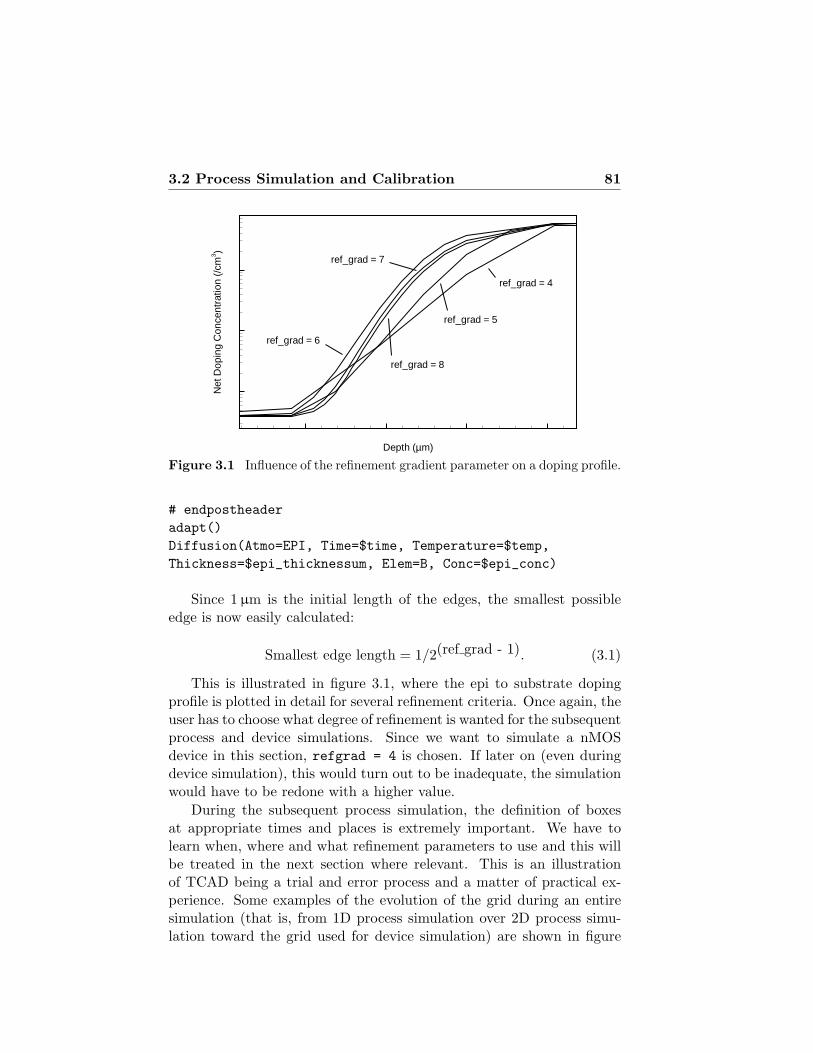
3.2 Process Simulation and Calibration 81
Depth (µm)
Net
Dop
ing
Con
cent
ratio
n(/
cm3 )
ref_grad = 4
ref_grad = 5
ref_grad = 7
ref_grad = 6
ref_grad = 8
Figure 3.1 Influence of the refinement gradient parameter on a doping profile.
# endpostheaderadapt()Diffusion(Atmo=EPI, Time=$time, Temperature=$temp,Thickness=$epi_thicknessum, Elem=B, Conc=$epi_conc)
Since 1µm is the initial length of the edges, the smallest possibleedge is now easily calculated:
Smallest edge length = 1/2(ref grad - 1). (3.1)
This is illustrated in figure 3.1, where the epi to substrate dopingprofile is plotted in detail for several refinement criteria. Once again, theuser has to choose what degree of refinement is wanted for the subsequentprocess and device simulations. Since we want to simulate a nMOSdevice in this section, refgrad = 4 is chosen. If later on (even duringdevice simulation), this would turn out to be inadequate, the simulationwould have to be redone with a higher value.
During the subsequent process simulation, the definition of boxesat appropriate times and places is extremely important. We have tolearn when, where and what refinement parameters to use and this willbe treated in the next section where relevant. This is an illustrationof TCAD being a trial and error process and a matter of practical ex-perience. Some examples of the evolution of the grid during an entiresimulation (that is, from 1D process simulation over 2D process simu-lation toward the grid used for device simulation) are shown in figure

82 TCAD Simulation and Calibration
(a)
(d)
Gate contactSource contact
(b)
Field oxide
(c)
Poly
Refinement at nldd and N+
Figure 3.2 Evolution of the mesh during simulation: (a) 1D in processsimulation, (b) first process step in 2D, (c) at the end of the process flow, and(d) regridding before device simulation.
3.2 (only the mesh in the silicon is shown): (a) shows the grid at the1D stage of the process simulation, (b) is just after the first process stepthat was simulated in 2D, (c) is at the end of the process flow, whereone clearly can see the refinements in the grid around the nldd and N+
region (i.e., where the gradient of the net doping profile is the largest),and (d) gives an example of the regridding that happens just before de-vice simulation (discussed below), where the very fine grid following thenet doping profile is no longer necessary, but where a very fine grid inthe channel is present (not visible), which was not the case after processsimulation.
Now, we will move on to process calibration, as the epi to substrateprofile could already have been subject to calibration.
3.2.2 Simulation and calibration
The process simulation remains a 1D problem as long as there is nomask definition. This means that the simulations are carried out in onedimension (refining only in the y direction; that is, the direction per-pindicular to the wafer). The process simulator switches automatically
3.2 Process Simulation and Calibration 83
to 2D simulation when necessary, which depends on the intended devicestructure.
The epi growth
We have stated in the previous section that “the first important processstep is the epi growth”. But is this true ? What is important ? Toanswer these questions, we take a look at the real process flow and askourselves what would be really important to simulate and especiallywhen would that be.
The actual process flow begins with an RCA clean. It is obvious thatit is not necessary to simulate this in our virtual process flow. This isthe first and most trivial example of how the translation of the actualprocess flow into the TCAD input deck omits or simplifies process steps.
The next process step is the epi growth. At first sight, this hasto be simulated, as it is a high temperature step and thus induces agradient in the doping profiles. But what if we do not simulate thisprocess step and define the epi as starting material ? Would this becorrect ? The answer depends on the desired simulation, and, especiallyon the subsequent device simulation. If one only wants to simulate on-state DC characteristics of a nMOS, it will probably not be necessaryto simulate the extra doping profile well underneath the silicon surface.However, for power devices, it will be of utmost importance to simulatethis process step as often buried layers are defined before the epi growth.This epi growth changes the profile of the buried layer and plays a majorrole in most of the subsequent device simulations (breakdown !). Thisis a first important example of how the translation of the input deckdepends on the intended device and its subsequent device simulation.Note, however, that at all times the simulation domain has to be deepenough if one wants to exclude errors due to boundary effects. One canfor example define an arbitrary epi depth, disregarding the actual epidepth and epi to substrate junction.
There is yet another way to translate the epi growth: define thesubstrate as is, but then deposit the epi ! As simulation of depositionis based on purely geometrical models in ISE, this demands less CPUtime than several diffusion steps. Although this is negligible in the caseconsidered here, as the simulation is still a 1D problem at this point.Therefore we choose to simulate it with the diffusion steps, since it isprobably more correct. But what is correct ? Don’t we have to calibratethis profile ? The answer is yes. . . but we have a limited choice as to
84 TCAD Simulation and Calibration
when in the process flow and where on the wafer a SIMS is taken, mainlybecause of cost. Since it is believed that other profiles (the wells, theldds. . . ) are of greater importance, it is chosen not to take a SIMS ofthe epi to substrate profile.
1D Oxidation
The following process step is a pad oxidation. This step is easy tocalibrate, as it still is a 1D simulation and there is a lot of informationcoming from the fab: ramp up and down times, oxidation time and gasflows, and, of course, the statistical data on the thickness. This step istranslated in the following way (process data are left out for confidentialreasons):
!2 PAD OXIDATION
! 2A RCA clean! nothing simulated here
! 2B Pad oxidationDiffusion(Time=($t1, $t2, $t3), Temperature=($te1, $te1,
$te2,$te2), Flow(N2=$flow1, O2=$flow2))Diffusion(Time=$t_ox, Temperature=$te2, Flow(O2=$flow_ox))Diffusion(Time=($t4, $t5), Temperature=($te2,
$te2, $te1), Flow(N2=$flow3))
This literal translation gives an oxide thickness that is 11 % higherthan the actual one. In ISE, refining at the boundary (RefineBoundary),which results in a finer grid in both the silicon and the oxide, does nothave an impact on the simulated thickness. This was verified with verycoarse and fine grids, both giving the same 11 % discrepancy.
So calibration is needed for this step. We remark here that thediffusion command is by far physically the most elaborate command,compared to the simulation of other process steps (deposition, etching,implantation). This is comprehendable, as it serves for all temperaturesteps (oxidations, anneals, epi growth. . . ).
During such a step, dopant redistribution has to be simulated andtherefore the correct model needs to be chosen. In ISE, 5 different mod-els can be chosen. Actually, they are basically the same model withdifferent levels of simplification. The most complex model fully couples

3.2 Process Simulation and Calibration 85
the dopant and point defect diffusions. Additional modelling of cluster-ing and trapping reactions is also possible. This most complex model isneeded when one wants to simulate transient diffusion effects, causinge.g., the reverse short channel effect. The default model can not sim-ulate such effects as it does not solve point defect equations and as itassumes no point defect assisted diffusion. For a first calibration cycle,this default model is chosen for every temperature step. If it turns outto be inadequate, complex models can be used for the important tem-perature steps. However, for the simulation of a simple pad oxidation,the use of the default model is sufficient.
And this is only half of the story for the simulation of a thermal pro-cess that changes the layer structure (oxidation, but also silicidation).In addition to the diffusion, the simulator has to take into account thechemical reactions and the segregation at interfaces, the diffusion andconvection of dissolved particles, the screening property of some inter-faces or layers for particle fluxes, mechanical deformation of the entirelayer structure. . . Several oxidation models are possible, with differentdegrees of complexity and coupling of the physical models.
We choose the default model for almost all oxidation steps and willverify when doing device simulations whether we should redo some ox-idation steps with a more complex oxidation model or not. As in thecase of the epi, we could even choose to deposit the oxide as this doesnot induce great differences here. However, since CPU time is still notan issue here, we stick to the simulation of the diffusion steps.
There still is the issue of the calibration, the correct way would beto look for a model parameter that can be tuned and to use this tosimulate the correct thickness. But since we are dealing with a simplepad oxidation and since we don’t want to loose too much time on thisrelatively unimportant process step, we choose a more arbitrary way ofcalibrating this oxidation. It is possible to specify the intended oxidethickness instead of the time in the diffusion command. This has beendone for this process step (in the diffusion command where the actualoxidation takes place).
Deposition
Simulation of deposition is not physically based and is modelled in ageometrical way with the aid of local depositon rates that mimic thegeometry observed in reality.
For the simulation of a 1D deposition it is trivial that an isotropic
86 TCAD Simulation and Calibration
deposition suffices (default). The next 2 process steps are such deposi-tions:
! 3A Amorphous silicon depositionDeposit(Material=Po, Thickness=$poly_buffer)
! 4B Nitride depositionDeposit(Material=Ni, Thickness=$nitr_thick)
Lithography process
The same as for the simulation of deposition holds here: the lithographyprocess is not simulated physically, but purely geometrical, using thecommand Mask.
The simulator changes from one dimension to two dimensions withthe introduction of a mask that is not covering the entire simulationdomain length.
Since no field oxide is grown during the simulation of a nMOS device,our simulation domain is entirely covered with the photoresist:
5 ACTIVE AREA MASKMask(Material=Resist, Thickness=2.0)
If one wants to open a window where the field oxide should be grown,the command would look like:
Mask(X(0,$aa_begin+$aa_bias,$aa_begin+$t-$aa_bias,$end))
This brings us to the issue of the mask biases. It is not the casefor the simple example of a nMOS device, but it is vital to take intoaccount the mask bias values if one wants to compare measured datawith simulated ones.
Take e.g., the simple case of a field oxide length t. If one choosesnot to simulate with these mask biases, a field oxide length of 1µm inthe simulation has to be compared with a drawn field oxide length of1µm + 2 ∗mask bias. Because, in reality, one can only draw this gap inthe active area mask, after which the photoresist is generated using themask biases. Therefore we choose to take into account these biases asin the previous command, in order to ease the process of comparison.

3.2 Process Simulation and Calibration 87
Etching
Etching is the last example of a process step that is not physically, butgeometrically (by the means of local etch rates) simulated in ISE.
In our example, the following process steps (3 consecutive etches:the nitride, the poly and a tiny part of the pad oxide) need not tobe simulated as the simulation domain is completely covered with aphotoresist. But suppose we have left a gap in the photoresist, then thecommands look like:
!6 ACTIVE AREA NITRIDE ETCH
! 6A Nitride etchEtch(Material=Ni, Remove=$R1, Rate(Aniso=280))
! 6B Amorphous silicon etchEtch(Material=Po, Remove=$R2, Rate(Aniso=275))Etch(Material=Ox, Remove=$R3, Rate(Aniso=100))
Note that all 3 etches are supposed to be purely directional etchingin the direction of the incident “etching beam”.
Before field oxidation, whether or not there is a window in the aamask, the photoresist has to be removed. This is done with an isotropicetch:
! 6C Resist stripEtch(Material=Resist)
For the field oxidation simulation, we could just simulate the thermalbudgets as long as the entire simulation domain is covered with nitride(as in the case of a nMOS).
We will however simulate the field oxidation, because it is importantfor the power devices presented in this work.
2D Oxidation
Not only the thickness of the field oxide needs to be calibrated, but it isof utmost importance in power devices with a field oxide in the devicestructure to simulate the so-called bird’s beaks correctly. In order to beable to verify the shape of the bird’s beaks in reality, SEM pictures havebeen taken.
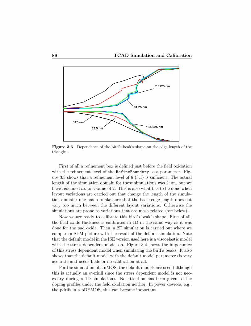
88 TCAD Simulation and Calibration
62.5 nm
125 nm
31.25 nm
15.625 nm
7.8125 nm
Figure 3.3 Dependence of the bird’s beak’s shape on the edge length of thetriangles.
First of all a refinement box is defined just before the field oxidationwith the refinement level of the RefineBoundary as a parameter. Fig-ure 3.3 shows that a refinement level of 6 (3.1) is sufficient. The actuallength of the simulation domain for these simulations was 2µm, but wehave redefined nx to a value of 2. This is also what has to be done whenlayout variations are carried out that change the length of the simula-tion domain: one has to make sure that the basic edge length does notvary too much between the different layout variations. Otherwise thesimulations are prone to variations that are mesh related (see below).
Now we are ready to calibrate this bird’s beak’s shape. First of all,the field oxide thickness is calibrated in 1D in the same way as it wasdone for the pad oxide. Then, a 2D simulation is carried out where wecompare a SEM picture with the result of the default simulation. Notethat the default model in the ISE version used here is a viscoelastic modelwith the stress dependent model on. Figure 3.4 shows the importanceof this stress dependent model when simulating the bird’s beaks. It alsoshows that the default model with the default model parameters is veryaccurate and needs little or no calibration at all.
For the simulation of a nMOS, the default models are used (althoughthis is actually an overkill since the stress dependent model is not nec-essary during a 1D simulation). No attention has been given to thedoping profiles under the field oxidation neither. In power devices, e.g.,the pdrift in a pDEMOS, this can become important.
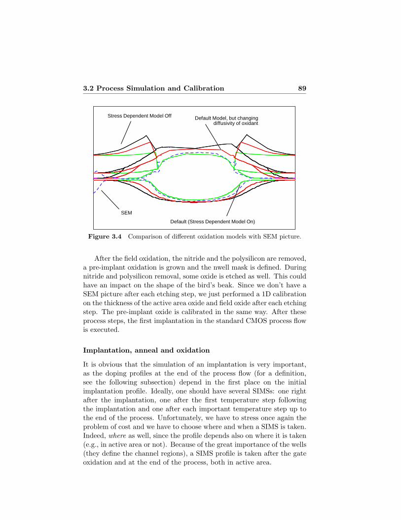
3.2 Process Simulation and Calibration 89
Stress Dependent Model Off
SEM
Default (Stress Dependent Model On)
Default Model, but changingdiffusivity of oxidant
Figure 3.4 Comparison of different oxidation models with SEM picture.
After the field oxidation, the nitride and the polysilicon are removed,a pre-implant oxidation is grown and the nwell mask is defined. Duringnitride and polysilicon removal, some oxide is etched as well. This couldhave an impact on the shape of the bird’s beak. Since we don’t have aSEM picture after each etching step, we just performed a 1D calibrationon the thickness of the active area oxide and field oxide after each etchingstep. The pre-implant oxide is calibrated in the same way. After theseprocess steps, the first implantation in the standard CMOS process flowis executed.
Implantation, anneal and oxidation
It is obvious that the simulation of an implantation is very important,as the doping profiles at the end of the process flow (for a definition,see the following subsection) depend in the first place on the initialimplantation profile. Ideally, one should have several SIMSs: one rightafter the implantation, one after the first temperature step followingthe implantation and one after each important temperature step up tothe end of the process. Unfortunately, we have to stress once again theproblem of cost and we have to choose where and when a SIMS is taken.Indeed, where as well, since the profile depends also on where it is taken(e.g., in active area or not). Because of the great importance of the wells(they define the channel regions), a SIMS profile is taken after the gateoxidation and at the end of the process, both in active area.
90 TCAD Simulation and Calibration
Simulation of the distribution of the implanted ions and of the im-plantation damage is done by either using analytical distribution func-tions or Monte Carlo computations. The moments used for the ana-lytical distribution functions are looked up in tables, which are basedon experimental data. If the subsequent anneal or oxidation step doesnot take into account point defect assisted diffusion, then the damageprofile should not be simulated during the implantation. If transientdiffusion effects are likely to occur, then the damage profile should besimulated, for which several models are available. This is an illustrationthat the simulation and calibration of process steps can not be treatedindependently of each other, hence the title of this subsection.
Depending on whether a nMOS or a pMOS is envisaged, a pwell ora nwell has to be simulated and calibrated. Since we are focusing ona nMOS, the pwell is treated here. First of all, a refinement box hasto be defined before the pwell is implanted. In order to have an ideaabout the level of refinement needed, one reference simulation is carriedout where RefineAll = -8 is specified. This means that all trianglesare subdivided 7 times before the pwell is implanted. Then, simulationsare carried out with different refinement levels for several refinementparameters. It turns out that the following box gives satisfying resultswithout taking too much CPU time:
# postheaderReplace(Control(Rec3(RefineGradient=-5, RefineMax=-8,Xleft=0, Xright=$end, Ytop=$surface, Ybot=$surface-1.2)))# endpostheaderadapt()
This box is sufficient for both the simulation of the implantation andthe subsequent anneal. The pwell is annealed with the gate oxidation,which has been calibrated without the presence of the pwell. For thesake of completeness, the refinement box needed for nwell implantationand anneal is
# postheaderReplace(Control(Rec3(RefineGradient=-4, RefineJunction=-8,Xleft=0, Xright=$end, Ytop=$surface, Ybot=$surface-1.2)))# endpostheaderadapt()
Note that here a refinement was carried out on the junction, whichis justified by the fact that the background dopant is boron.
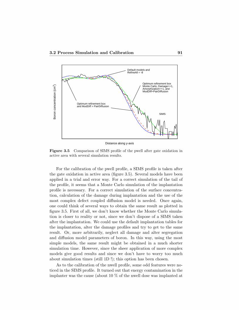
3.2 Process Simulation and Calibration 91
Distance along y-axis
Bor
onco
ncen
trat
ion
(cm
3 ) Optimum refinement boxMonte Carlo, Damage=+1,Amorphization=+1, andModDiff=PairDiffusion
Default models andRefineAll = -8
SIMS
Optimum refinement boxand ModDiff = PairDiffusion
Figure 3.5 Comparison of SIMS profile of the pwell after gate oxidation inactive area with several simulation results.
For the calibration of the pwell profile, a SIMS profile is taken afterthe gate oxidation in active area (figure 3.5). Several models have beenapplied in a trial and error way. For a correct simulation of the tail ofthe profile, it seems that a Monte Carlo simulation of the implantationprofile is necessary. For a correct simulation of the surface concentra-tion, calculation of the damage during implantation and the use of themost complex defect coupled diffusion model is needed. Once again,one could think of several ways to obtain the same result as plotted infigure 3.5. First of all, we don’t know whether the Monte Carlo simula-tion is closer to reality or not, since we don’t dispose of a SIMS takenafter the implantation. We could use the default implantation tables forthe implantation, alter the damage profiles and try to get to the sameresult. Or, more arbitrarily, neglect all damage and alter segregationand diffusion model parameters of boron. In this way, using the mostsimple models, the same result might be obtained in a much shortersimulation time. However, since the sheer application of more complexmodels give good results and since we don’t have to worry too muchabout simulation times (still 1D !); this option has been chosen.
As to the calibration of the nwell profile, some odd features were no-ticed in the SIMS profile. It turned out that energy contamination in theimplanter was the cause (about 10 % of the nwell dose was implanted at
92 TCAD Simulation and Calibration
1/3 or 2/3 of the intented energy). This illustrates that a close coopera-tion with the fab and a full access to all process flow details is necessaryfor the calibration of the TCAD input deck.
By now, the simulation and calibration of all possible process steps(except for the salicidation) have been illustrated. Since we are in thefirst place interested in a correct simulation of the basic DC electricalparameters (Vt, β. . . ), the rest of the process flow is simulated in arather arbitrary, almost generic way: no calibration is carried out what-soever and some process steps are literally left out. The salicidation, forexample, which will only have a negligible effect on DC characteristicsis not simulated. The damage introduced by nldd and nplus implants,and their influence on the pwell profile, is not simulated. This will onlybe important if one wants to simulate short channel or reverse shortchannel effects. But since we will use the input deck to simulate powerdevices, it will not be necessary to simulate such effects.
3.2.3 The end of the process flow
For the work presented in this book, the end of the process flow is definedas the last important thermal step. From this point on, doping profilesand the device itself will no longer change. For most simulations, it willsuffice to define the electrodes in a rather arbitrary way (by depositionof aluminium). These aluminium regions are replaced by equipotentiallines where they touch another material in the subsequent device simu-lations anyway. The poly too will be treated in this way, since the polyis identified as a metal by us. One can however simulate for examplepoly depletion effects by defining an aluminium electrode on top of thepoly. The device simulator will then recognize the poly as a semicon-ductor region with its own physical properties. The following text givesan example of the end of an input deck. An example of a definition ofa thermode is given in comment (sometimes needed for specific devicesimulations of power devices):
!43 ILD THERMIC BUDGETcomment(’dio_02: ILD Thermic Budget’)
Diffusion(Time=$time, Temperature=$temp, Flow(N2=15))
! END OF FRONT-END SIMULATION

3.2 Process Simulation and Calibration 93
! etching possible rests of oxide on polyMask (X(0, $ref01+0.5, $ref02-0.5, $ref04))Etch(Material=Ox, Remove=100nm)Etch(re)
! Metal Contact DefinitionMask(Material=Al, Thick=0.01, x(0, $ref01, $ref02, $end))
! Thermal resistance oxide! Deposit(material=Ox,thickness=3um)
! Thermode! Deposit(material=Al, thickness=0.5um)
#set Y_SI 1.0Print(x=$ref01+0.250, layers)Measure(Template=msr1.tmpl, LabelAndName("y_si","Y_SI"))
Save(File=n@node@,type=Mdraw,synonyms(Po=metal,Al=metal),contacts(
contact1(name=’source’, 0, 8.005)contact2(name=’gate’, $end/2, 8.005)contact3(name=’drain’, $end, 8.005)contact4(name=’substrate’, location=bottom))! contact5(name=’thermo_top’, 1, 20)
)
end
The extraction of the parameter Y_SI gives the exact value of thethickness of the silicon located under the channel (due to oxidations thisvalue is less than the initial thickness of the epi and substrate together).This value will be used later on while remeshing between process anddevice simulations (see below).
3.2.4 Performing layout variations
TCAD is often used to investigate the influence of layout parameters onthe device’s performance. For a correct simulation, one must realize that
94 TCAD Simulation and Calibration
the device length (or ‘pitch’) can alter by performing layout variations.So, if the pitch gets larger, one must ensure that the used grid doesnot get to coarse and alter the grid specifications accordingly to pitchvariations.
One way to do this is by changing the initial number of triangles ofthe grid (nx in the command grid). An important disadvantage of suchan approach is that for large devices, a large number of gridpoints canalready be present at the start of the process simulation.
Another way to solve the problem of the varying pitch is by changingthe refinement level in each box used before an important process step.The big advantages are that even for large structures one starts with anequal number of mesh points, reaching the finest mesh only there whereneeded. Thus, the same header as given above is used, together withnx = 2. But now, a refinement_level parameter is defined, which willdetermine the level of refinement depending on the pitch of the device(sw, x, y, t and dw being the layout parameters defining the pitch):
#postheader#if (@<sw+x+y+t+dw>@ < 4.6)set refinement_level=-8#elif (@<sw+x+y+t+dw>@ < 9.2)set refinement_level=-9#elif (@<sw+x+y+t+dw>@ < 18.4)set refinement_level=-10#elif (@<sw+x+y+t+dw>@ < 36.8)set refinement_level=-11#elif (@<sw+x+y+t+dw>@ < 73.6)set refinement_level=-12#endif#endpostheader
Then, this refinement_level parameter is used in each box to set theneeded level for that specific box, i.e., by adding 1, 2, 3. . . (since therefinement_level parameter defines the finest level needed for the en-tire simulation, determined by trial and error for the largest pitch usingthis level):
#postheaderReplace(Control(Rec3(RefineGradient=$refinement_level+4,Xleft=0, Xright=$ref01, Ytop=8, Ybot=6.5)))# endpostheaderadapt()

3.3 Device Simulation and Calibration 95
3.2.5 Simulation of power devices
One important issue, concerning the mesh, which will prove to be handyfor the simulation of power devices, is further discussed here. Since thesepower devices are integrated in a CMOS process, one does need to simu-late the typical power modules (buried layers, sinkers. . . ) together withthe entire CMOS process flow. These so-called smart power technolo-gies therefore tend to have a large process flow, and, what is importantfor TCAD, these power modules are mostly situated before the CMOSprocess flow. This means that, if one of the first masks is used (e.g., adevice that is only partly situated on top of a buried layer), the rest ofthe simulation is carried out in 2D. This in contrast with the nMOS ex-ample given above, where 2D simulation only starts with the definitionof the poly gate.
In order to save CPU time, it is therefore vital that an efficient mesh-ing is used throughout the simulation of power devices. To that end itis important to know that the refinement boxes are numbered and thatone can redefine each box at any given time. Take for example the simu-lation of a n-type buried layer, which typically is formed with antimony(Sb). This heavy atom is concentrated in a very shallow region underthe surface right after implantation. This means that one needs a veryfine grid in a small region in order to be able to track the sharp profileright after implantation (the same can be said for ldd implantations,where the dopants are lighter but implanted with a very low energy).The subsequent anneal smoothens the profile and diffuse the dopantoutside this refinement box. Therefore a second box is needed that isbigger than the first one, but with refinement specifications that mightbe looser than the ones needed for the implantation. After the anneal,the first box with its stringent refinement might not be needed anymore.Therefore it is vital that one can redefine the box that has been usedfor the implantation; i.e., one can coarsen the grid again.
3.3 Device Simulation and Calibration
Device simulation differs from process simulation in that the physicalmodels are less fab dependent and much better known (at least for ‘nor-mal’ device working). Device simulation usually demands much lesscalibration effort and device calibration is therefore normally only usedas a final ‘fine tuning’. Important exception is the work function of thepoly, which is fab related and needs to be calibrated. The same holds for
96 TCAD Simulation and Calibration
the fixed gate oxide charges, but is less important for DC characteristics.In order to have an idea about the correctness of the simulations
performed this far, we will compare the TCAD simulation results withSPICE simulations. The used SPICE models are provided by the fab andare confidential. Important here is to realize that this way of workingis actually putting things on their heads. Indeed, TCAD simulationresults are compared with existing SPICE models, which means that thedevices are already characterized and understood (at least to the extentthat is important for designers). Normally, TCAD is used to anticipateproblems, to understand and to create optimized devices before anyactual silicon has been processed. TCAD simulation results can evenbe used as a basis for extraction of SPICE model parameters before anydevice has been measured (this was actually the case for the pDEMOSpresented in this book). The reader has thus to be warned that thecomparison made here is not the usual way of working, but it will givean idea about how close (or how far) TCAD simulations are from reality.
But before this is done, we do need to think about the mesh onceagain.
3.3.1 From process to device simulation
The mesh that has been used for process simulation is no longer appro-priate for device simulation. The best example is the channel region,where in the process simulation it suffices to keep track of the pwell pro-file, which results in a spacing of 50 nm between the mesh lines under thegate oxide (at the end of the process simulation). During device simula-tion, however, one must take into account the thickness of the inversionlayer to assure correct simulation of e.g., an Id(Vgs) characteristic.
The remeshing of the structure is done through an extra tool avail-able in TCAD software. One defines several regions (rectangular boxes),and specifies for each region the spacing between mesh lines in the x andy directions (and possibly a dopant serving as a refinement criterion).An example of such a remeshing ‘input deck’ is given below. Note thatthe parameter Y_SI, extracted from process simulation, is used to define,among others, the channel region. This channel refinement box has athickness of 4 nm (2 nm above and 2 nm below the oxide/silicon inter-face) and the spacing between the horizontal mesh lines is fixed by theparameter spacing. The result of varying this parameter on a Id(Vgs)characteristic is shown in figure 3.6.
A spacing of 2 A is adequate and has been used in all simulations
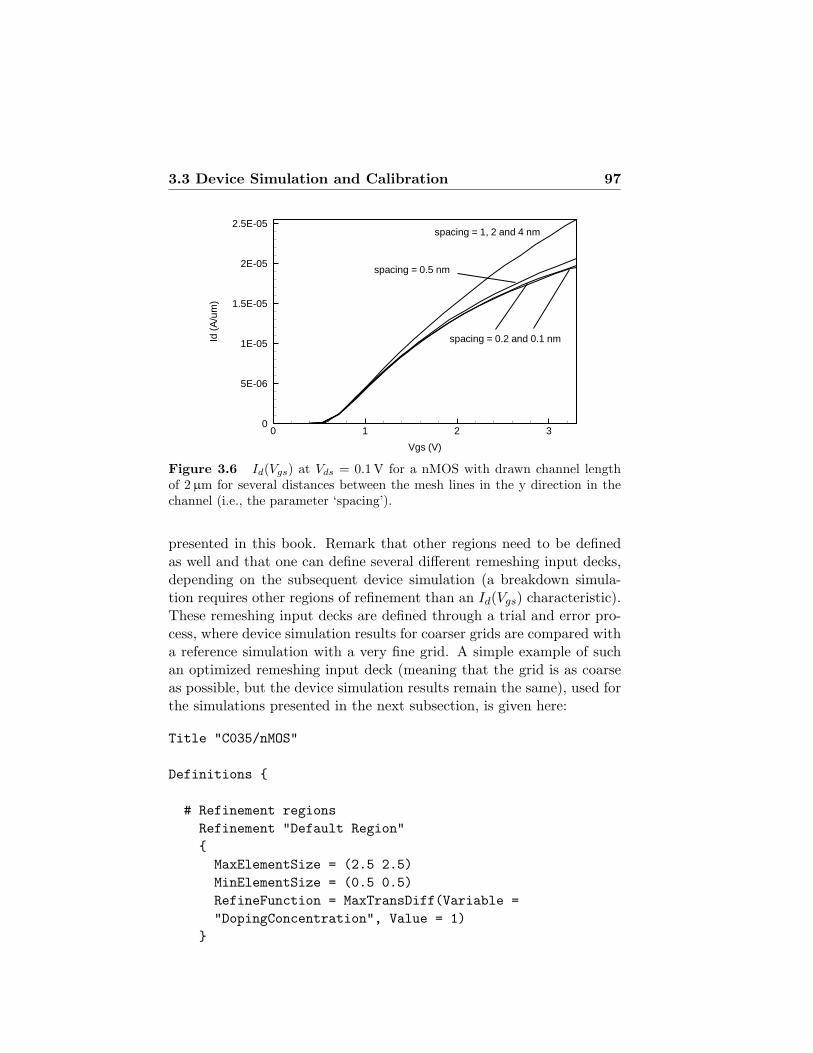
3.3 Device Simulation and Calibration 97
Vgs (V)
Id(A
/um
)
0 1 2 30
5E-06
1E-05
1.5E-05
2E-05
2.5E-05spacing = 1, 2 and 4 nm
spacing = 0.2 and 0.1 nm
spacing = 0.5 nm
Figure 3.6 Id(Vgs) at Vds = 0.1V for a nMOS with drawn channel lengthof 2 µm for several distances between the mesh lines in the y direction in thechannel (i.e., the parameter ‘spacing’).
presented in this book. Remark that other regions need to be definedas well and that one can define several different remeshing input decks,depending on the subsequent device simulation (a breakdown simula-tion requires other regions of refinement than an Id(Vgs) characteristic).These remeshing input decks are defined through a trial and error pro-cess, where device simulation results for coarser grids are compared witha reference simulation with a very fine grid. A simple example of suchan optimized remeshing input deck (meaning that the grid is as coarseas possible, but the device simulation results remain the same), used forthe simulations presented in the next subsection, is given here:
Title "C035/nMOS"
Definitions
# Refinement regionsRefinement "Default Region"MaxElementSize = (2.5 2.5)MinElementSize = (0.5 0.5)RefineFunction = MaxTransDiff(Variable ="DopingConcentration", Value = 1)
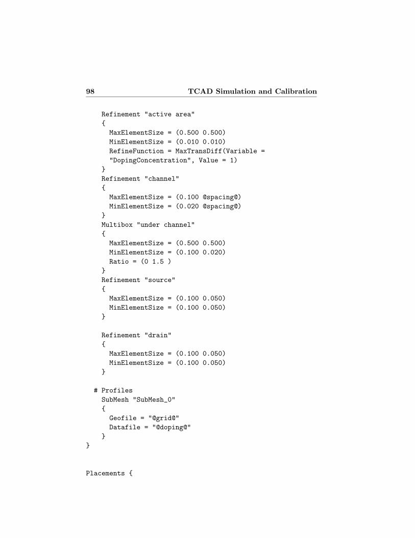
98 TCAD Simulation and Calibration
Refinement "active area"MaxElementSize = (0.500 0.500)MinElementSize = (0.010 0.010)RefineFunction = MaxTransDiff(Variable ="DopingConcentration", Value = 1)
Refinement "channel"MaxElementSize = (0.100 @spacing@)MinElementSize = (0.020 @spacing@)
Multibox "under channel"MaxElementSize = (0.500 0.500)MinElementSize = (0.100 0.020)Ratio = (0 1.5 )
Refinement "source"MaxElementSize = (0.100 0.050)MinElementSize = (0.100 0.050)
Refinement "drain"MaxElementSize = (0.100 0.050)MinElementSize = (0.100 0.050)
# ProfilesSubMesh "SubMesh_0"Geofile = "@grid@"Datafile = "@doping@"
Placements
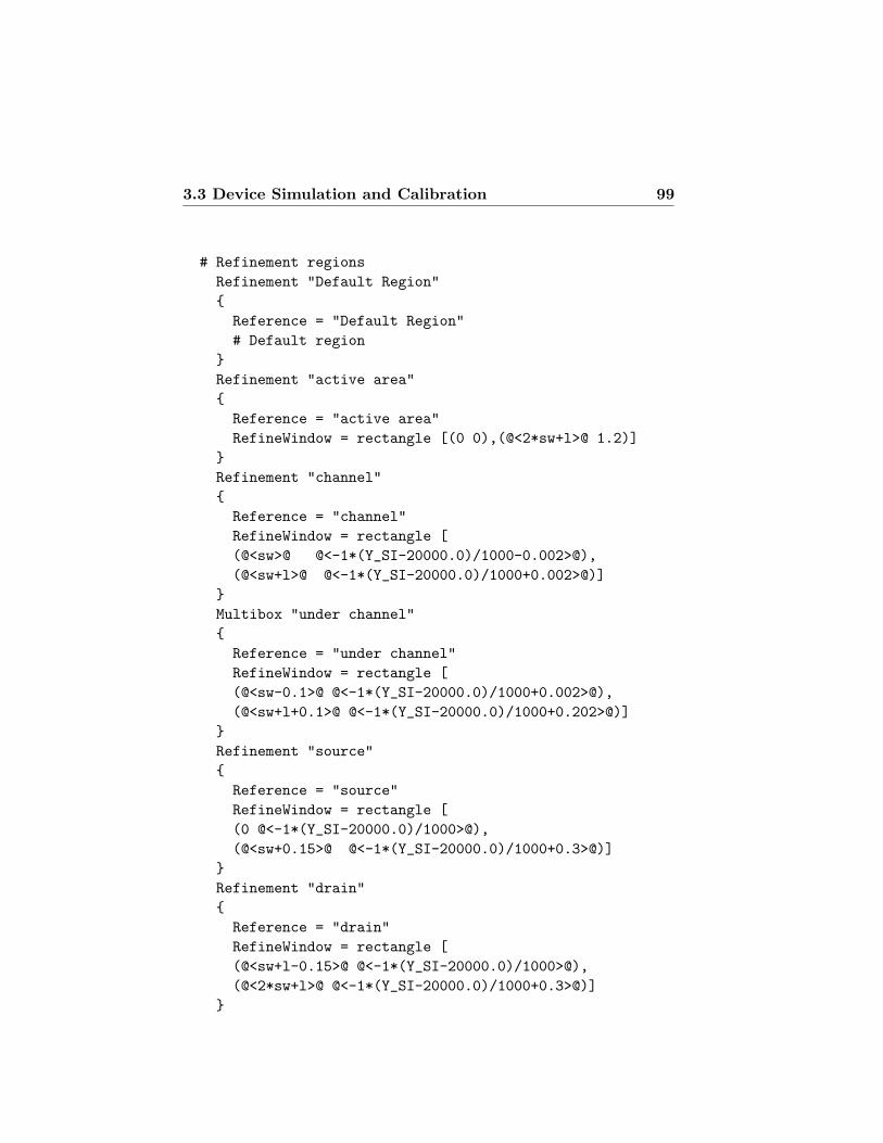
3.3 Device Simulation and Calibration 99
# Refinement regionsRefinement "Default Region"Reference = "Default Region"# Default region
Refinement "active area"Reference = "active area"RefineWindow = rectangle [(0 0),(@<2*sw+l>@ 1.2)]
Refinement "channel"Reference = "channel"RefineWindow = rectangle [(@<sw>@ @<-1*(Y_SI-20000.0)/1000-0.002>@),(@<sw+l>@ @<-1*(Y_SI-20000.0)/1000+0.002>@)]
Multibox "under channel"Reference = "under channel"RefineWindow = rectangle [(@<sw-0.1>@ @<-1*(Y_SI-20000.0)/1000+0.002>@),(@<sw+l+0.1>@ @<-1*(Y_SI-20000.0)/1000+0.202>@)]
Refinement "source"Reference = "source"RefineWindow = rectangle [(0 @<-1*(Y_SI-20000.0)/1000>@),(@<sw+0.15>@ @<-1*(Y_SI-20000.0)/1000+0.3>@)]
Refinement "drain"Reference = "drain"RefineWindow = rectangle [(@<sw+l-0.15>@ @<-1*(Y_SI-20000.0)/1000>@),(@<2*sw+l>@ @<-1*(Y_SI-20000.0)/1000+0.3>@)]

100 TCAD Simulation and Calibration
# ProfilesSubMesh "SubMesh_0"Reference = "SubMesh_0"Replace
3.3.2 Device simulation and calibration
As has been pointed out in the beginning of this section, SPICE simu-lations are compared with TCAD simulations, although this is a ratherunusual way of working. It will, however, demonstrate what degree ofprecision TCAD can yield. We have chosen to simulate an Id(Vgs) char-acteristic for the nMOS presented this far with a drawn gate length of2µm. The device input deck needed for this simulation is given belowand uses only default physical models: the drift-diffusion model in com-bination with Boltzmann statistics, a basic mobility model includingdoping depence, high field saturation and transverse field dependenceand a definition of the band gap (and, therefore, the intrinsic carrierdensity). The work function of the poly has been calibrated to a valueof 4.26 eV.
Figure 3.7 compares the slow, typical and fast SPICE models with2 TCAD simulations. The only difference between both TCAD simu-lations is that one uses the pair diffusion model for the gate oxidation,and the other one does not. Note how small the differences are betweenthe TCAD and the typical SPICE simulations and both TCAD char-acteristics. Although the one with the pair diffusion model takes moreCPU time; especially in power devices where the simulation of the gateoxidation is already in 2D mode. An important conclusion is that forthis device and for this device simulation, the use of the pair diffusionmodel is redundant. It will, however, sometimes be necessary to use thismodel, as is shown in simulations where the drawn gate length is varied.For these simulations, the pair diffusion model has not been used andthe work function has been recalibrated to a value of 4.28 eV. Otherwisethe same device input deck has been used as for the simulations shownin figure 3.7:
* des.cmd dessis input deck for Id-Vg characteristic

3.3 Device Simulation and Calibration 101
Vgs (V)
Id(A
/µm
)
0 1 2 30
2E-06
4E-06
6E-06
8E-06
1E-05
1.2E-05
1.4E-05
1.6E-05 spice (fast)
spice (slow)
spice (typical)
without Pair Diffusionfor gate oxidation
with Pair Diffusionfor gate oxidation
Figure 3.7 Id(Vgs) for a nMOS with drawn channel length of 2 µm: SPICEsimulations versus TCAD simulations.
* of a nMOS using default models
File Grid = "@grid@"Doping = "@doping@"Current = "@plot@"Plot = "@dat@"
Electrode name = "drain" voltage=0.0 name = "substrate" voltage=0.0 name = "source" voltage=0.0 name = "gate" voltage=0.0 Workfunction=4.28
Physics Mobility ( DopingDependence
HighFieldSaturationEnormal )
EffectiveIntrinsicDensity ( BandGapNarrowing (OldSlotboom ) )
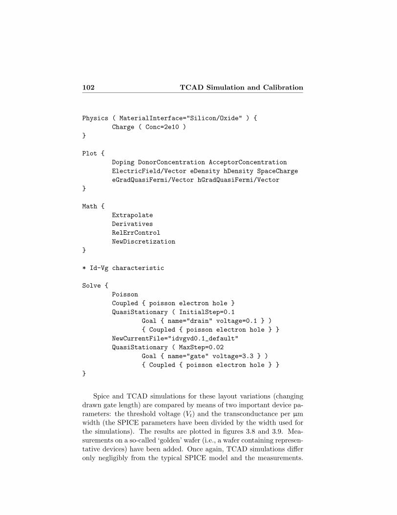
102 TCAD Simulation and Calibration
Physics ( MaterialInterface="Silicon/Oxide" ) Charge ( Conc=2e10 )
Plot Doping DonorConcentration AcceptorConcentrationElectricField/Vector eDensity hDensity SpaceChargeeGradQuasiFermi/Vector hGradQuasiFermi/Vector
Math ExtrapolateDerivativesRelErrControlNewDiscretization
* Id-Vg characteristic
Solve PoissonCoupled poisson electron hole QuasiStationary ( InitialStep=0.1
Goal name="drain" voltage=0.1 ) Coupled poisson electron hole
NewCurrentFile="idvgvd0.1_default"QuasiStationary ( MaxStep=0.02
Goal name="gate" voltage=3.3 ) Coupled poisson electron hole
Spice and TCAD simulations for these layout variations (changingdrawn gate length) are compared by means of two important device pa-rameters: the threshold voltage (Vt) and the transconductance per µmwidth (the SPICE parameters have been divided by the width used forthe simulations). The results are plotted in figures 3.8 and 3.9. Mea-surements on a so-called ‘golden’ wafer (i.e., a wafer containing represen-tative devices) have been added. Once again, TCAD simulations differonly negligibly from the typical SPICE model and the measurements.
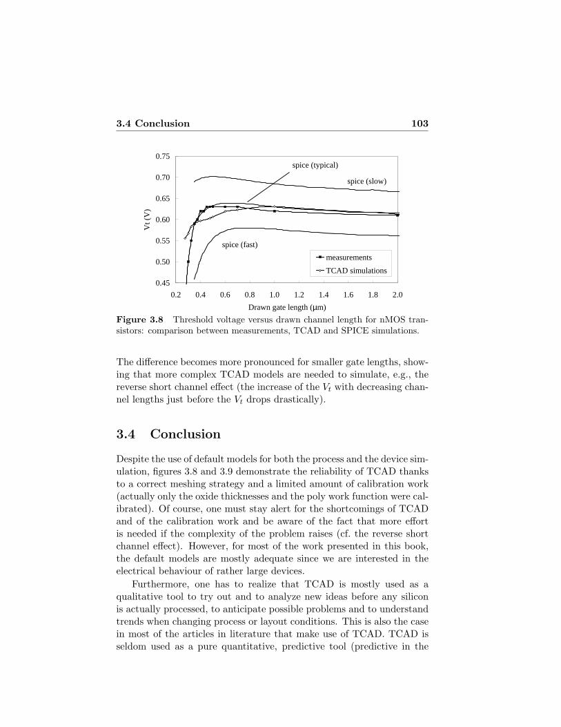
3.4 Conclusion 103
0.45
0.50
0.55
0.60
0.65
0.70
0.75
0.2 0.4 0.6 0.8 1.0 1.2 1.4 1.6 1.8 2.0
Drawn gate length (µm)
Vt (
V)
measurements
TCAD simulations
spice (typical)
spice (slow)
spice (fast)
Figure 3.8 Threshold voltage versus drawn channel length for nMOS tran-sistors: comparison between measurements, TCAD and SPICE simulations.
The difference becomes more pronounced for smaller gate lengths, show-ing that more complex TCAD models are needed to simulate, e.g., thereverse short channel effect (the increase of the Vt with decreasing chan-nel lengths just before the Vt drops drastically).
3.4 Conclusion
Despite the use of default models for both the process and the device sim-ulation, figures 3.8 and 3.9 demonstrate the reliability of TCAD thanksto a correct meshing strategy and a limited amount of calibration work(actually only the oxide thicknesses and the poly work function were cal-ibrated). Of course, one must stay alert for the shortcomings of TCADand of the calibration work and be aware of the fact that more effortis needed if the complexity of the problem raises (cf. the reverse shortchannel effect). However, for most of the work presented in this book,the default models are mostly adequate since we are interested in theelectrical behaviour of rather large devices.
Furthermore, one has to realize that TCAD is mostly used as aqualitative tool to try out and to analyze new ideas before any siliconis actually processed, to anticipate possible problems and to understandtrends when changing process or layout conditions. This is also the casein most of the articles in literature that make use of TCAD. TCAD isseldom used as a pure quantitative, predictive tool (predictive in the

104 TCAD Simulation and Calibration
50
150
250
350
450
550
0.2 0.4 0.6 0.8 1.0 1.2 1.4 1.6 1.8 2.0
Drawn gate length (µm)
Tra
nsco
nduc
tanc
e ( µ
A/V
2 / µm
) measurements
TCAD simulations
spice (typical)
spice (slow)
spice (fast)
Figure 3.9 Transconductance per µm width versus drawn channel lengthfor nMOS transistors: comparison between measurements, TCAD and SPICEsimulations.
sense that such and such process condition together with such and suchlayout parameter will give such and such electrical parameter). Thisis understandable, since it takes a lot of effort to calibrate all TCADresults quantitatively and it will only be certain that the correct param-eter set has been found (the sheer amount of process and device modelparameters makes the calibration work an extremely difficult task) if onedisposes of a huge (unrealistic ?) amount of calibration material. And,what’s more, there will be no gain in the understanding of the devices,rather only a gain in the percentage of deviation between TCAD sim-ulations and real measurements. A job, actually, that has to be donefor SPICE simulators rather than for TCAD simulators (the only andmaybe important difference being that process conditions could be in-cluded in TCAD predictions). Therefore, like in literature, in this book,TCAD is used as a tool to understand rather than to predict (in thesense described above).
References
[ISE00] ISE Integrated Systems Engineering. Manual, Release 7.0, 2000.
[Ver01] M. Vermandel. Integration of p-type High-Voltage Devices in aSub-µm CMOS Technology using TCAD. PhD thesis, Universityof Gent, 2001.
4 Power MOS
4.1 Introduction
One of the first reference works on power devices, written in 1977 by S.K.Ghandhi [Gha77] does not mention the power MOS devices, and onlytreats the bipolar transistor and thyristor as power switches. On theother hand, one of the latest works on power devices, written in 1996 byB.J. Baliga [Bal96], only treats the bipolar transistor as an introductionto the IGBT. This illustrates the evolution of power devices over a periodof 20 years, and proves the importance of the introduction of the MOSgate in power devices. From the 70s on, the MOS gate became availablein power devices. The current controlled gate used in power bipolartransistors and thyristors, and demanding complex gate drive circuitry,was now being replaced with a voltage controlled gate with a muchsimpler input circuitry. Except for some specific applications and for thevery high end of power electronics, the voltage controlled gate provedto be much closer to the ideal case than the current controlled gate.Furthermore, the power MOS device has a faster switching speed (dueto its unipolarity), a forward voltage drop that increases with increasingtemperature (which makes it much easier to parallel these devices), andit is less vulnerable to second breakdown.
Since the MOS gate originates from the digital CMOS technology,it is obvious that the first “power” (a better denomination here is highvoltage) MOS device is some kind of an extended MOS transistor, withthe ability to sustain higher voltages than a normal n or pMOS tran-sistor. In literature, these structures are referred to as drain extendedMOS transistors: DEMOS (nDEMOS or pDEMOS) or simply as EMOS(EnMOS or EpMOS). The next step was the introduction of the double-diffusion process, where the p-base region and the n+ source regions arediffused through a common window defined by the edge of the polysilicongate, which enables to define channel lenths that are much smaller than
106 Power MOS
the limitation imposed by the lithography. Unfortunately, these deviceshave the acronym DMOS, which might be a little confusing. The nextmajor improvement of the DMOS’ performance came with the introduc-tion of the RESURF technique. The next section treats this matter, asit has become one of the most important techniques for designing powerdevices (not only DMOS devices).
The third section deals with the ideal silicon limit and the mostimportant plot used when comparing power MOS devices with eachother: specific on-resistance versus breakdown voltage. The silicon limitalso shows that the on-resistance of the power MOS increases fast withincreasing breakdown voltage, which explains the use of the power MOSdevice in the lower power ratings.
The fourth section sketches all possible forms of the DMOS device:the n versus the p type device, the low-side versus the high-side device,the lateral versus the integrated vertical device, and the RESURF versusthe non-RESURF device. It gives an overview of which devices are mostfeasible in the I3T0 technology.
These devices are treated in the following sections. First of all thelow-side or non-floating RESURF n-type devices are discussed: one on alowly doped substrate and one on a highly doped substrate, representinga BLP. Secondly the high-side or floating devices are studied: one lateralnon-RESURF n-type device on a BLN, a lateral RESURF nDMOS on adouble buried layer structure, the vertically integrated nDMOS, and fi-nally, the lateral RESURF pDMOS. The conclusions compare the I3T80devices with the competitor’s devices in the form of tables, whereas theVbr −Ron,sp plot of the silicon limit together with all these DMOS tran-sistors, both for the n-type and the p-type devices, can be found in theconcluding chapter of this book.
4.2 Reduced Surface Field Effect (RESURF)
Analytical expressions
The RESURF effect was discovered by coincidence in 1979 [AV79]. Whenmeasuring a high voltage diode with an expected breakdown voltage of400V, the actual value of more than 1000 V could not be measured untilnew measuring equipment arrived.
Since then, the RESURF technique has been used in virtually allpower devices (e.g., in bipolars [CSN00], in DMOS devices [MBC+99],[HLMP00] and [ZPB+00]), an excellent overview can be found in [Lud00a].

4.2 Reduced Surface Field Effect (RESURF) 107
P+
n-epi
CathodeAnode
p-substrate
N+
»»
l
psinker
J1
J3
J2
A
B
C
Figure 4.1 A RESURF diode.
It has been extended to other technologies (mainly SOI, e.g., [HB91],[MAB+91] and [vdPLH+00]), towards multiple layers of RESURF lay-ers (e.g., [KPZB02], [HIFT02]), and towards 3D RESURF (the so-calledCOOLMOSTM or superjunction devices [LDKM99], for an overview see[Udr02]).
Analytical expressions for the breakdown voltage in RESURF struc-tures can be found in [KCA96] (2D analytical model for RESURF struc-tures as in figure 4.1), [MAB+91] and [Chu00] (SOI), and [Fuj97] (su-perjunction devices).
The basic RESURF diode structure (figure 4.1) consists of two diodes:a vertical (n+–n-epi–p-substrate) and a lateral (p+–n-epi–n+) one. Break-down can occur at three different places in such a structure (see figure4.1):
1. Region A: Corner breakdown at the curvature of the p+–n-epijunction. This can be punch-through (laterally towards n+) ornon punch-through breakdown: Vbr,lat|npt or Vbr,lat|pt, respectively.
2. Region B: Breakdown at the p-substrate–n-epi junction. Thiscan only be punch-through (vertically towards n+) breakdown:Vbr,vert|pt. It will be explained in due course why non punch-through can not happen at this place.
3. Region C: Corner breakdown at the curvature of the n+–n-epijunction. This is corner breakdown due to a depletion layer either
108 Power MOS
coming from the lateral p+–n-epi or the vertical p-substrate–n-epijunction, or coming from both junctions at the same time. Thisbreakdown voltage strongly depends on the degree of curvature.
Important to explain is what is meant by the expression breakdownat a place. It is defined as the region where the highest impact ionizationrate G is observed. Since G = nαnvn + pαpvp and since αn ≈ αp ≈ α =A |E|7 (see equation (C.8)), the impact ionization rate can be writtenas:
G ≈ A |E|7 (nvn + pvp) ≈ A/q |E|7 J, (4.1)
with J being the current density. So, when only leakage currents arepresent in a device (as is the case in the RESURF diode prior to break-down), the place with the highest impact ionization rate is also theplace with the highest electrical fields. Therefore, when plotting 2Dcross-sections in order to illustrate where breakdown occurs, most of thetimes the electric field is plotted. However, in some occasions, break-down can occur (i.e., highest impact ionization rate) at a different placethan where the highest electrical fields are located. This can happen,for example, at on-state breakdown in a power device. If, along thecurrentpath, there is a place with high electric fields (but therefore notnecessarily the highest electric fields in the whole structure), the break-down is likely to occur along this current path as the impact ionizationrate not only depends on the local electric field strength, but also on thelocal current density.
Breakdown in the RESURF diode can happen at three different lo-cations depending on 4 vital parameters: l (the length of the diode, seefigure 4.1), tepi (the thickness of the n-epi), Nepi (the doping level ofthe n-epi), and Nsub (the doping level of the p-substrate). Secondaryparameters are, for example, the curvature of the n+–n-epi junction.To get an idea of the dominant breakdown mechanism for the differentranges of these 4 parameters, a rough classification based on comparisonbetween l and tepi on the one hand and between Nepi and Nsub on theother hand is made.
1. l << tepi: breakdown at A
(a) Nsub << Nepi: breakdown at A: Vbr,lat|npt or Vbr,lat|pt
When there is no punch-through (that is, both l and tepi arelarge enough to sustain at breakdown both depletion layerscoming from the lateral and the vertical diode respectively),the lateral diode breaks down first because it has the highest
4.2 Reduced Surface Field Effect (RESURF) 109
lowly doped region (n-epi in comparison with p-substrate inthe vertical diode). Breakdown occurs at A: Vbr,lat|npt. Whenpunch-through occurs, it firstly happens in the lateral diode.Breakdown occurs at A: Vbr,lat|pt.
(b) Nsub ≈ Nepi: breakdown at A: Vbr,lat|npt or Vbr,lat|pt
When there is no punch-through, the lateral diode breaksdown first because it has the highest highly doped region (p+
in comparison with p-substrate in the vertical diode, where anequal part of the potential drop in the vertical diode is held bythe p-substrate as is held by the n-epi). Breakdown occurs atA: Vbr,lat|npt. When punch-through occurs, it firstly happensin the lateral diode. Breakdown occurs at A: Vbr,lat|pt.
(c) Nsub >> Nepi: breakdown at A: Vbr,lat|npt or Vbr,lat|pt
When there is no punch-through, the lateral diode breaksdown first because it has the highest curvature in its junc-tion (the p-substrate and the p+ doping level are assumed tobe approximately equal). Breakdown occurs at A: Vbr,lat|npt.When punch-through occurs, it firstly happens in the lateraldiode. Breakdown occurs at A: Vbr,lat|pt.
2. l ≈ tepi: breakdown at A or C
(a) Nsub << Nepi: breakdown at A: Vbr,lat|npt or Vbr,lat|pt
The same reasoning holds as in case 1 (a).
(b) Nsub ≈ Nepi: breakdown at A: Vbr,lat|npt or Vbr,lat|pt
The same reasoning holds as in case 1 (b).
(c) Nsub >> Nepi: breakdown at A: Vbr,lat|npt or Vbr,lat|pt, or at CWhen there is no punch-through, the same reasoning holdsas in case 1 (c): breakdown occurs at A: Vbr,lat|npt. Whenpunch-through occurs, both depletion layer coming from thelateral and the vertical diode reach the n+–n-epi junction atthe same time. Depending on the curvature of the n+–n-epijunction, breakdown can occur at A: Vbr,lat|pt, or C.
3. l >> tepi: breakdown at A, B or C
(a) Nsub << Nepi: breakdown at A: Vbr,lat|npt or Vbr,lat|pt, at B:Vbr,vert|pt, or at CWhen there is no punch-through, the same reasoning holds asin case 1 (a): breakdown occurs at A: Vbr,lat|npt. When punch-through occurs, it either occurs first in the lateral diode or in
110 Power MOS
the vertical diode depending on which of both depletion layershits the n+–n-epi junction first. Breakdown at A: Vbr,lat|pt, atB: Vbr,vert|pt. Breakdown occurs at C when both depletionlayers reach the n+–n-epi junction at the same moment andwhen the curvature of this junction is strong enough.
(b) Nsub ≈ Nepi: breakdown at A: Vbr,lat|npt or Vbr,lat|pt, at B:Vbr,vert|pt, or at CWhen there is no punch-through, the same reasoning holdsas in case 1 (b): breakdown occurs at A: Vbr,lat|npt. Whenpunch-through occurs, the same reasoning holds as in case 3(a): breakdown at A: Vbr,lat|pt, at B: Vbr,vert|pt, or at C.
(c) Nsub >> Nepi: breakdown at A: Vbr,lat|npt or at B: Vbr,vert|pt
When there is no punch-through, the same reasoning holdsas in case 1 (c): breakdown occurs at A: Vbr,lat|npt. Whenpunch-through occurs, it firstly happens in the vertical diode:breakdown at B: Vbr,vert|pt.
So, non punch-through at place B can not occur, as mentioned above.Furthermore, when there is no punch-through (in both the vertical andthe lateral diode), then breakdown always happens at A. Only in thecase where l ≈ tepi and Nsub >> Nepi and the cases with l >> tepi,breakdown can happen at another place than A when there is punch-through.
When several breakdown places are possible for the same case, itis likely that electric fields build up at all places. Breakdown thus canhappen at two or even at all three places nearly at the same time. Itis obvious that in such a case the electrostatic potential is spread overthe entire device and that the breakdown voltage can be higher thanthe lateral diode breakdown. The RESURF case as was first describedin [AV79] where the breakdown voltage is much higher than the lateraldiode breakdown can only occur when l >> tepi and Nsub << Nepi.
Then and only then can the larger part of the voltage be sustainedby the substrate and can the breakdown voltage be determined by thelower doping level of the substrate, and it can thus be much higherthan lateral diode breakdown. The condition being that the depletionlayer in the n-epi, coming from the vertical junction, reaches the siliconsurface just before lateral diode breakdown occurs. The electric fieldis then almost at its critical value at A, but stops building up as thevertical diode punches through and the electric field now builds up atB and C. It is clear that the number of charges present in the n-epi
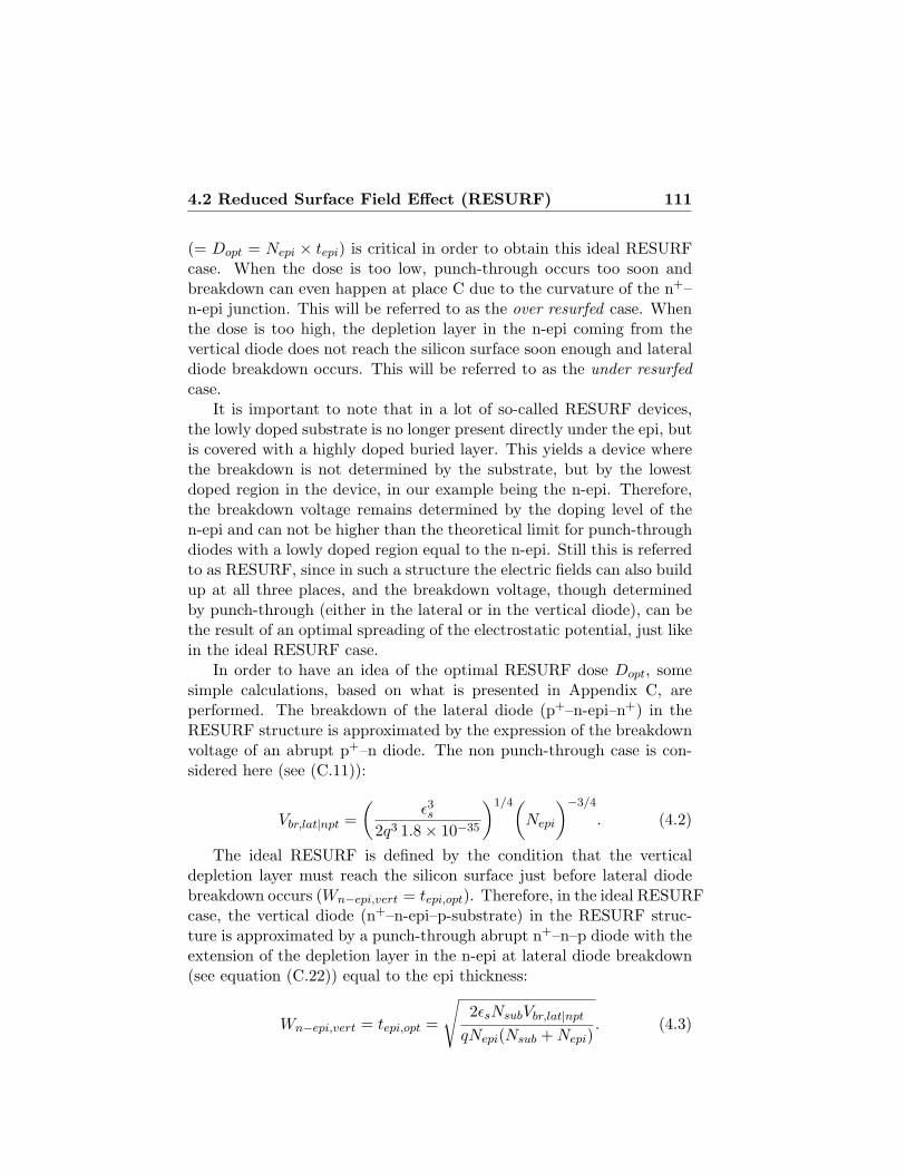
4.2 Reduced Surface Field Effect (RESURF) 111
(= Dopt = Nepi × tepi) is critical in order to obtain this ideal RESURFcase. When the dose is too low, punch-through occurs too soon andbreakdown can even happen at place C due to the curvature of the n+–n-epi junction. This will be referred to as the over resurfed case. Whenthe dose is too high, the depletion layer in the n-epi coming from thevertical diode does not reach the silicon surface soon enough and lateraldiode breakdown occurs. This will be referred to as the under resurfedcase.
It is important to note that in a lot of so-called RESURF devices,the lowly doped substrate is no longer present directly under the epi, butis covered with a highly doped buried layer. This yields a device wherethe breakdown is not determined by the substrate, but by the lowestdoped region in the device, in our example being the n-epi. Therefore,the breakdown voltage remains determined by the doping level of then-epi and can not be higher than the theoretical limit for punch-throughdiodes with a lowly doped region equal to the n-epi. Still this is referredto as RESURF, since in such a structure the electric fields can also buildup at all three places, and the breakdown voltage, though determinedby punch-through (either in the lateral or in the vertical diode), can bethe result of an optimal spreading of the electrostatic potential, just likein the ideal RESURF case.
In order to have an idea of the optimal RESURF dose Dopt, somesimple calculations, based on what is presented in Appendix C, areperformed. The breakdown of the lateral diode (p+–n-epi–n+) in theRESURF structure is approximated by the expression of the breakdownvoltage of an abrupt p+–n diode. The non punch-through case is con-sidered here (see (C.11)):
Vbr,lat|npt =(
ε3s2q3 1.8× 10⁻³⁵
)1/4(Nepi
)−3/4
. (4.2)
The ideal RESURF is defined by the condition that the verticaldepletion layer must reach the silicon surface just before lateral diodebreakdown occurs (Wn−epi,vert = tepi,opt). Therefore, in the ideal RESURFcase, the vertical diode (n+–n-epi–p-substrate) in the RESURF struc-ture is approximated by a punch-through abrupt n+–n–p diode with theextension of the depletion layer in the n-epi at lateral diode breakdown(see equation (C.22)) equal to the epi thickness:
Wn−epi,vert = tepi,opt =
√2εsNsubVbr,lat|npt
qNepi(Nsub + Nepi). (4.3)
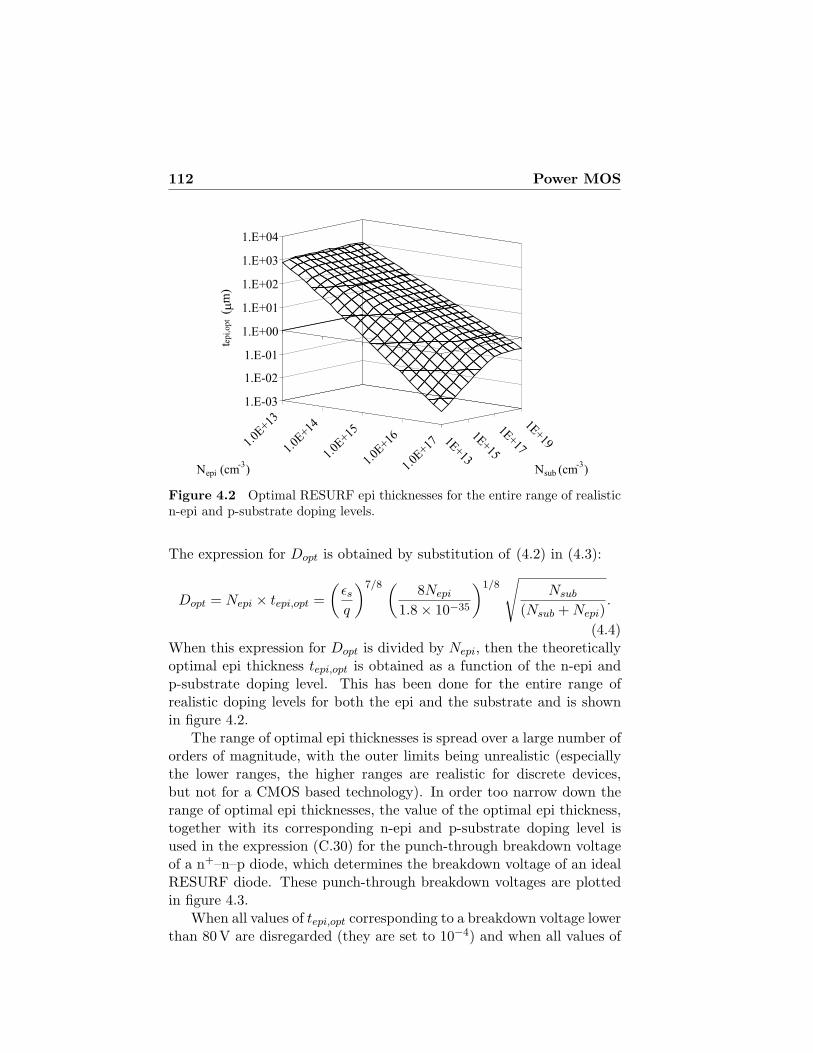
112 Power MOS
1.0E
+13
1.0E
+14
1.0E
+15
1.0E
+16
1.0E
+171E+13
1E+15
1E+17
1E+19
1.E-03
1.E-02
1.E-01
1.E+00
1.E+01
1.E+02
1.E+03
1.E+04te
pi,
opt
( mm
)
Nepi (cm-3
) Nsub (cm-3
)
Figure 4.2 Optimal RESURF epi thicknesses for the entire range of realisticn-epi and p-substrate doping levels.
The expression for Dopt is obtained by substitution of (4.2) in (4.3):
Dopt = Nepi × tepi,opt =(
εs
q
)7/8 (8Nepi
1.8× 10⁻³⁵
)1/8√
Nsub
(Nsub + Nepi).
(4.4)When this expression for Dopt is divided by Nepi, then the theoreticallyoptimal epi thickness tepi,opt is obtained as a function of the n-epi andp-substrate doping level. This has been done for the entire range ofrealistic doping levels for both the epi and the substrate and is shownin figure 4.2.
The range of optimal epi thicknesses is spread over a large number oforders of magnitude, with the outer limits being unrealistic (especiallythe lower ranges, the higher ranges are realistic for discrete devices,but not for a CMOS based technology). In order too narrow down therange of optimal epi thicknesses, the value of the optimal epi thickness,together with its corresponding n-epi and p-substrate doping level isused in the expression (C.30) for the punch-through breakdown voltageof a n+–n–p diode, which determines the breakdown voltage of an idealRESURF diode. These punch-through breakdown voltages are plottedin figure 4.3.
When all values of tepi,opt corresponding to a breakdown voltage lowerthan 80 V are disregarded (they are set to 10−4) and when all values of
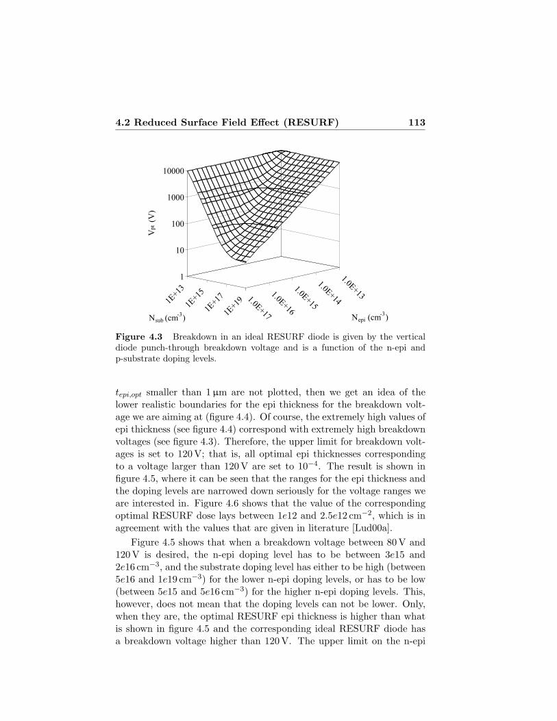
4.2 Reduced Surface Field Effect (RESURF) 113
1.0E+13
1.0E+14
1.0E+15
1.0E+16
1.0E+17
1E+13
1E+15
1E+17
1E+19
1
10
100
1000
10000
Vp
t(V
)
Nepi (cm-3
)Nsub (cm-3
)
Figure 4.3 Breakdown in an ideal RESURF diode is given by the verticaldiode punch-through breakdown voltage and is a function of the n-epi andp-substrate doping levels.
tepi,opt smaller than 1µm are not plotted, then we get an idea of thelower realistic boundaries for the epi thickness for the breakdown volt-age we are aiming at (figure 4.4). Of course, the extremely high values ofepi thickness (see figure 4.4) correspond with extremely high breakdownvoltages (see figure 4.3). Therefore, the upper limit for breakdown volt-ages is set to 120 V; that is, all optimal epi thicknesses correspondingto a voltage larger than 120 V are set to 10−4. The result is shown infigure 4.5, where it can be seen that the ranges for the epi thickness andthe doping levels are narrowed down seriously for the voltage ranges weare interested in. Figure 4.6 shows that the value of the correspondingoptimal RESURF dose lays between 1e12 and 2.5e12 cm−2, which is inagreement with the values that are given in literature [Lud00a].
Figure 4.5 shows that when a breakdown voltage between 80V and120V is desired, the n-epi doping level has to be between 3e15 and2e16 cm−3, and the substrate doping level has either to be high (between5e16 and 1e19 cm−3) for the lower n-epi doping levels, or has to be low(between 5e15 and 5e16 cm−3) for the higher n-epi doping levels. This,however, does not mean that the doping levels can not be lower. Only,when they are, the optimal RESURF epi thickness is higher than whatis shown in figure 4.5 and the corresponding ideal RESURF diode hasa breakdown voltage higher than 120V. The upper limit on the n-epi
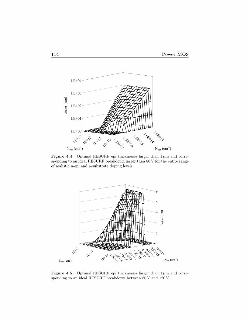
114 Power MOS
1.0E+13
1.0E+14
1.0E+15
1.0E+16
1.0E+17
1E+13
1E+15
1E+17
1E+19
1.E+00
1.E+01
1.E+02
1.E+03
1.E+04
tepi,
opt
( mm
)
Nepi (cm-3
)Nsub (cm-3
)
Figure 4.4 Optimal RESURF epi thicknesses larger than 1 µm and corre-sponding to an ideal RESURF breakdown larger than 80V for the entire rangeof realistic n-epi and p-substrate doping levels.
2.0E+15
2.5E+15
3.2E+15
4.0E+15
5.0E+15
6.3E+15
7.9E+15
1.0E+16
1.3E+16
1.6E+16
2.0E+16
1E+15
1E+17
1E+19
1
2
3
4
5
6
tepi,
opt
( mm
)
Nepi (cm-3
)Nsub (cm3)
Figure 4.5 Optimal RESURF epi thicknesses larger than 1 µm and corre-sponding to an ideal RESURF breakdown between 80 V and 120V.

4.2 Reduced Surface Field Effect (RESURF) 115
2.0E+15
2.5E+15
3.2E+15
4.0E+15
5.0E+15
6.3E+15
7.9E+15
1.0E+16
1.3E+16
1.6E+16
2.0E+16
1.0E
+15
1.0E
+17
1.0E
+19
5.0E+11
1.0E+12
1.5E+12
2.0E+12
2.5E+12
3.0E+12
Dopt
(cm
-2)
Nepi (cm-3
)Nsub (cm3)
Figure 4.6 Optimal RESURF epi dose Dopt for a corresponding idealRESURF breakdown between 80 V and 120V, and tepi,opt > 1 µm.
doping level (2e16 cm−3), on the other hand, can not be crossed, as thenthe breakdown voltage drops below 80 V or the optimal RESURF epithickness has an unrealistic low value (< 1µm, see figure 4.4).
Another observation in figure 4.5 is that for a punch-through break-down voltage between 80V and 120 V, the p-substrate doping level ishigher than the n-epi doping level in virtually all cases. In view of whathas been said before, this means that lateral breakdown is likely to occurfirst in such a structure. When the p+–n-epi junction curvature (placeA in figure 4.1) is very gentle, the punch-through almost happens atthe same time at place A and place C when l ≈ tepi. This leads to thevery important conclusion that increasing l to values larger than tepi
for RESURF structures that have a punch-through breakdown voltagebetween 80V and 120 V makes no sense (as it does not increase thebreakdown voltage, and thus only increases the distance between cath-ode and anode; that is, the on-state resistance in a power device usingsuch a RESURF structure as drift region).
Let us consider two examples of different substrate doping level inmore detail: the first case having a Nsub = 1e15 cm−3, which is typi-cally a p-substrate doping level, and the second case having a Nsub =6e17 cm−3, which is typically the doping level of a p-type buried layer(BLP). The optimal RESURF punch-through breakdown voltage, as wellas the optimal epi thickness are plotted against the entire range of realis-

116 Power MOS
1
10
100
1000
1.E+13 1.E+14 1.E+15 1.E+16 1.E+17
Nepi (cm-3
)
tepi;
opt
( mm
)
2.6 mm
Nsub = 6e17 cm-3
Nsub = 1e15 cm-3
5.9 mm
10
100
1000
10000
1.E+13 1.E+14 1.E+15 1.E+16 1.E+17
Nepi (cm-3
)
Vpt
(V) Nsub = 1e15 cm
-3
Nsub = 6e17 cm-3
336 V
106 V
Figure 4.7 The optimal RESURF punch-through breakdown voltage (left),and the optimal epi thickness as a function of the entire range of realistic n-epidoping levels for the cases with Nsub = 1e15 cm−3 and Nsub = 6e17 cm−3.
tic n-epi doping levels for both cases in figure 4.7. For Nsub = 1e15 cm−3,the optimal RESURF breakdown voltage is higher than 300V for theentire range of n-epi doping levels. This is understandable because ofthe very low substrate doping level. This substrate can be used to designan 80 V RESURF structure, if the length of the structure is decreasedin orde to obtain premature punch-through along the length. Figure 4.7also shows that the optimal epi thickness varies for the p-substrate andthe BLP if the same n-epi doping level is present, which is inevitableat first sight. Yet it could be possible to use both the p-substrate andthe BLP as a basis of RESURF structures in the same technology, e.g.,by introducing an extra n-type implantation to increase the epi dopinglevel. One could choose an epi thickness and doping level for the n-epi that gives an optimal RESURF structure upon a Nsub = 1e15 cm−3
(e.g., 5.9µm and ∼ 2e15 cm−3, see figure 4.7) and increase the net epidoping level (to 4e15 cm−3, determined by the optimal epi thickness)for an optimal RESURF structure upon the BLP. This would resultin two RESURF structures: one capable of blocking more than 300 V(p-substrate based) and one capable of blocking 100 V (BLP based).
So, the second example with the higher substrate doping level, rep-resenting a BLP, can make an optimal RESURF diode in the desiredvoltage range. If Nepi = 4e15 cm−3, the optimal epi thickness is 5.9µmwith a corresponding punch-through breakdown equal to 106 V (see fig-ure 4.7). Note again that in this case Nsub > Nepi, which means thatwhen a BLP is chosen to create an 80 V RESURF structure, the lengthof the drift region (l) is ideally equal to the epi thickness (same reasoningas above).
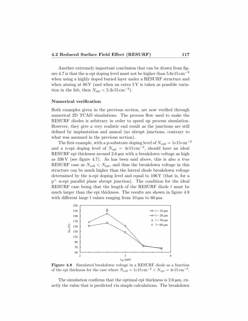
4.2 Reduced Surface Field Effect (RESURF) 117
Another extremely important conclusion that can be drawn from fig-ure 4.7 is that the n-epi doping level must not be higher than 5.6e15 cm−3
when using a highly doped buried layer under a RESURF structure andwhen aiming at 80 V (and when an extra 5V is taken as possible varia-tion in the fab, then Nepi < 5.3e15 cm−3).
Numerical verification
Both examples given in the previous section, are now verified throughnumerical 2D TCAD simulations. The process flow used to make theRESURF diodes is arbitrary in order to speed up process simulation.However, they give a very realistic end result as the junctions are stilldefined by implantation and anneal (no abrupt junctions, contrary towhat was assumed in the previous section).
The first example, with a p-substrate doping level of Nsub = 1e15 cm−3
and a n-epi doping level of Nepi = 4e15 cm−3, should have an idealRESURF epi thickness around 2.6µm with a breakdown voltage as highas 336 V (see figure 4.7). As has been said above, this is also a trueRESURF case as Nsub < Nepi, and thus the breakdown voltage in thisstructure can be much higher than the lateral diode breakdown voltagedetermined by the n-epi doping level and equal to 106 V (that is, for ap+–n-epi parallel plane abrupt junction). The condition for the idealRESURF case being that the length of the RESURF diode l must bemuch larger than the epi thickness. The results are shown in figure 4.8with different large l values ranging from 10µm to 60µm.
50
70
90
110
130
150
170
190
210
230
2 3 4
tepi (mm)
Vbr(V
)
l = 10 mm
l = 20 mm
l = 30 mm
l = 60 mm
Figure 4.8 Simulated breakdown voltage in a RESURF diode as a functionof the epi thickness for the case where Nsub = 1e15 cm−3 < Nepi = 4e15 cm−3.
The simulation confirms that the optimal epi thickness is 2.6µm, ex-actly the value that is predicted via simple calculations. The breakdown

118 Power MOS
voltage, unfortunately, is lower that what is predicted (around 200 V in-stead of 336V). However, the breakdown voltage is almost double thatof the lateral diode and thus proves that the RESURF effect is acting.The reason why the breakdown voltage is lower that the ideal RESURFvalue is twofold. First of all, there is the depth of the n+ region, whichwas not taken into account in the previous section. As the optimal epithickness is as low is 2.6µm in this example, the thickness of the n+
region, which is about 0.5µm, can not be neglected. This has a se-rious effect on the punch-through voltage of the vertical diode, whichdetermines the breakdown of the ideal RESURF structure. Secondly,the curvature of the n+–n-epi junction also lowers the theoretically cal-culated breakdown voltage. Furthermore, the simulation also confirmsthat when the epi thickness is lower than the optimal value, prematurepunch-through happens in the vertical diode (the so-called over-resurfedcase). When the epi thickness is higher than the optimal value, lateraldiode breakdown occurs, which is —due to the curvature in the p+–n-epi junction— lower than the 106 V calculated for the case of an abruptparallel plane junction.
The second example treats the case of a highly doped p-substrateNsub = 6e17 cm−3, with the same n-epi doping level as above (Nepi =4e15 cm−3). Since Nsub > Nepi, lateral and vertical diode punch-throughbreakdown happen virtually at the same moment (depending on thecurvatures in the junctions). As is explained above, there is no sense intaking a RESURF diode length much larger than the optimal epi thick-ness, which is calculated to be 5.9µm. The results of the simulationsare shown in figure 4.9.
40
50
60
70
80
90
100
110
3 4 5 6 7
tepi (mm)
Vbr(V
)
l = 3 mm
l = 6 mm
l = 6.6 mm
l = 12 mm
Figure 4.9 Simulated breakdown voltage in a RESURF diode as a functionof the epi thickness for the case where Nsub = 6e17 cm−3 > Nepi = 4e15 cm−3.
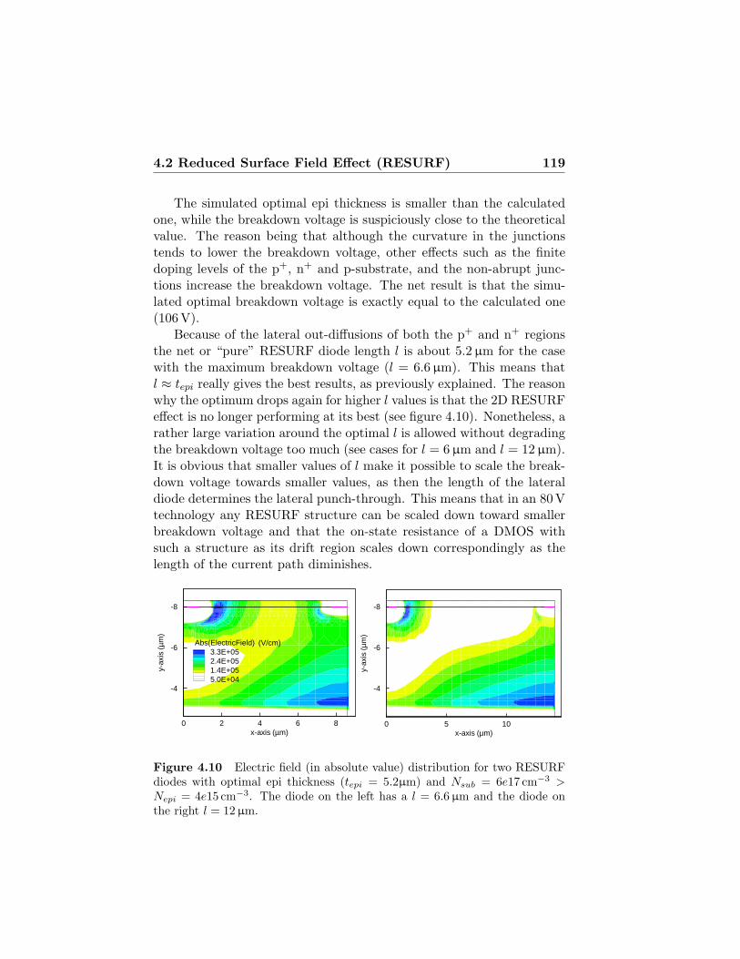
4.2 Reduced Surface Field Effect (RESURF) 119
The simulated optimal epi thickness is smaller than the calculatedone, while the breakdown voltage is suspiciously close to the theoreticalvalue. The reason being that although the curvature in the junctionstends to lower the breakdown voltage, other effects such as the finitedoping levels of the p+, n+ and p-substrate, and the non-abrupt junc-tions increase the breakdown voltage. The net result is that the simu-lated optimal breakdown voltage is exactly equal to the calculated one(106V).
Because of the lateral out-diffusions of both the p+ and n+ regionsthe net or “pure” RESURF diode length l is about 5.2µm for the casewith the maximum breakdown voltage (l = 6.6µm). This means thatl ≈ tepi really gives the best results, as previously explained. The reasonwhy the optimum drops again for higher l values is that the 2D RESURFeffect is no longer performing at its best (see figure 4.10). Nonetheless, arather large variation around the optimal l is allowed without degradingthe breakdown voltage too much (see cases for l = 6 µm and l = 12µm).It is obvious that smaller values of l make it possible to scale the break-down voltage towards smaller values, as then the length of the lateraldiode determines the lateral punch-through. This means that in an 80 Vtechnology any RESURF structure can be scaled down toward smallerbreakdown voltage and that the on-state resistance of a DMOS withsuch a structure as its drift region scales down correspondingly as thelength of the current path diminishes.
x-axis (µm)
y-ax
is(µ
m)
0 5 10
-8
-6
-4
x-axis (µm)
y-ax
is(µ
m)
0 2 4 6 8
-8
-6
-4
Abs(ElectricField)3.3E+052.4E+051.4E+055.0E+04
(V/cm)
(V/cm)
Figure 4.10 Electric field (in absolute value) distribution for two RESURFdiodes with optimal epi thickness (tepi = 5.2µm) and Nsub = 6e17 cm−3 >Nepi = 4e15 cm−3. The diode on the left has a l = 6.6 µm and the diode onthe right l = 12 µm.
120 Power MOS
4.3 The Silicon Limit
The silicon limit is the analytical expression of the specific on-resistanceas a function of the breakdown voltage for an idealized DMOS device.Hence the trade-off between those two most important electrical param-eters for power DMOS devices can be visualized in one single plot. It isused as a bench-mark, since all power DMOS devices can be representedby one point on this graph. The closer this point is to the ideal siliconlimit, the better the performance of the device. Of course, dependingon the form of the power DMOS, the silicon limit—i.e., the analyticalexpression Ron,sp(Vbr)—changes as well. Here, we will present the siliconlimits that are important for the I3T80 technology and desired voltagerange.
The specific on-resistance (Ron,sp) is defined as the on-state (gatefully open, e.g., Vgs = 3.3V and typically Vds = 0.1V, where the Id
characteristic is linearly dependent on Vds) resistance multiplied by thearea (factor cost actually enters into this figure of merit). The area is thewidth times the pitch. The width is the extension of the device in thethird space dimension (that is, the dimension absent in the typical 2Dcross-sections, e.g., figure 4.11). The pitch is the total device’s length.Note that for instance in figure 4.11 the device is not entirely shown,as this would include several more gates (there is actually an optimalnumber of gates, but this will be disregarded in the present discussion),and a drain region at the right hand side as well. The pitch is then thetotal distance between both drain contacts (measured from half drain tohalf drain contact). The breakdown voltage is defined as the Vds voltageat which current starts to flow (measured at a certain current level)when the gate is closed (Vgs = 0V).
The most cited limit is the one of the vertical DMOS (VDMOS)device. Since we are not working on discrete devices, a VDMOS is inte-grated on chip as shown in figure 4.11. As it is not a real vertical device(the current is flowing through the buried layer and the sinker towardsthe surface again), this device is sometimes called the quasi VDMOS orQVDMOS. When calculating the theoretical, ideal relationship betweenthe breakdown voltage and the specific on-resistance of this device, thefollowing assumptions are made:
1. The breakdown between the source and drain of this device ismodelled as a parallel-plane, abrupt, p+/n junction breakdown. Inother words, the finite doping level of the pbody and the curvatureof the pbody/n-epi junction are neglected. The punch-through

4.3 The Silicon Limit 121
pbodyn
+ p+
n+
pbody
n+
p+
n sinker+
Rn+
RS
Ra
Rsub Repi
Rch
Bulk
Source
DrainSource Bulk
buried n+
p-substrate
n-epi
Field oxidePoly
Figure 4.11 Integrated vertical nDMOS.
effect (towards the buried layer) can be included if necessary.
2. The contribution of the drift region to the on-state resistance (infigure 4.11 this is Repi) is considered to be the most importantone. Therefore, the contributions of the other regions (see figure4.11) are neglected. This assumption is inaccurate for low voltagedevices (i.e., devices with a small drift region length), but is reliablefor higher voltage ranges (table 4.1).
3. Because of the last assumption, the on-resistance is proportional tothe drift region’s length and inversionally proportional to the driftregion’s area that is perpendicular to the current flow. Note thatin the vertical case the current flow in the device is perpendicularto the axis on which the pitch is defined, whereas in a lateraldevice the current flow is parallel to the axis on which the pitch isdefined. In order to simplify the calculations, in the (integrated)vertical DMOS, the length of the drift region is set equal to theepi thickness and the area through which the current flows is setequal to the pitch times the width of the device. In the lateralDMOS, the drift region’s length is set equal to the pitch and thearea through which the current flows is set equal to the widthtimes the epi thickness.
Using these assumptions, together with Poisson’s equation in the n-epi region, and the resistivity of the n-epi region, a relationship between
122 Power MOS
Table 4.1 Percentage of the on-resistancethat each region of the vertical DMOS takesup (taken from [LDKM99]).
Part Vbr ≈ 30V Vbr ≈ 600V
RS 7% 0.5%Rn+ 6% 0.5%Rch 28% 1.5%Ra 23% 0.5%Repi 29% 96.5%Rsub 7% 0.5%
the breakdown voltage and the specific on-resistance can be derived.A general expression of the specific on-resistance, using the second
assumption made above, is thus
Ron,sp = Ron ×Area
=lengthdrift
areadrift
1qµdriftNdrift
× pitch× width (4.5)
For a vertical device with the drift region being the n-epi and with thethird assumption, this results in
Ron,sp =tepi
pitch× width1
qµnNepi× pitch× width
=tepi
qµnNepi(4.6)
where tepi is the epi thickness and Nepi is the epi doping level. Importantto note is that the pitch of the device disappears in (4.6) (a result ofthe third assumption). For an ideal, non-punch-through device the epithickness is equal to the depletion layer width at breakdown. Thus, thespecific on-resistance (4.6) can be written as a function of Vbr, eliminat-ing tepi = Wbr and Nepi by using the expressions (C.10) and (C.11):
Ron,sp =2√
1.8× 10⁻³⁵
εsµnV
5/2br
= 5.93× 10⁻⁹ V5/2br . (4.7)
4.3 The Silicon Limit 123
10
20
30
40
50
60
70
80
50 60 70 80 90 100 110 120
Vbr (V)
Ro
n,s
p(m
W.m
m2)
non punch-through VD(E)MOS
punch-through VD(E)MOS t = 5 mepi m
punch-through VD(E)MOS t = 4 mepi m
punch-through VD(E)MOS t = 3 mepi m
RESURF nLD(E)MOS
Figure 4.12 Silicon limits for non punch-through and punch-through verticalnD(E)MOS devices, and for a lateral RESURF nD(E)MOS.
This is the well-known ideal silicon limit for non punch-through verticalnD(E)MOS devices, shown in figure 4.12, where the range of breakdownvoltages is plotted, which is aimed for in the technology we are interestedin. It is also clearly seen that the specific on-resistance increases rapidlywith growing breakdown voltage. This proves our previously mentionedstatement that the power MOS devices become worse with increasingbreakdown voltage, and thus are likely to be replaced by other deviceswhen high breakdown voltages are targeted for (> 200V).
Figure 4.12 also shows several other silicon limits, all for differenttypes of D(E)MOS devices. First of all, there are the punch-throughVD(E)MOS devices, where the electric field distribution (C.2) is stoppedat the buried layer before breakdown occurs.
The relationship (C.15) is used in figure 4.12 to show the smallgain a punch-through VD(E)MOS has over a non punch-through de-vice. The n-epi thicknesses are choses arbitrarily—in the range that isinteresting for us. The specific on-resistance (4.7), which is determinedby an arbitrarily chosen epi thickness and doping level Nepi (which, ofcourse, must be such that the depletion layer width at breakdown neverbecomes smaller than the chosen epi thickness) is plotted against thepunch-through breakdown voltage, which on its turn is determined bythe chosen epi thickness and doping level Nepi through (C.15). Further-more, the values of the punch-through breakdown that are higher than

124 Power MOS
in the non punch-through case are not plotted in figure 4.12.One more silicon limit—that is important for us—is plotted in figure
4.12: the one for lateral RESURF D(E)MOS devices. From the previoussection, it is easily understood that a first approximation of the electricalfield in the drift region of a RESURF device is given by
|Econst| = Vbr
pitch. (4.8)
Using (C.7) and (C.8) together with (4.8) yields
1.8× 10⁻³⁵
∫ pitch
0|Econst|7 dx = 1
1.8× 10⁻³⁵ V 7br
pitch6 = 1
pitch =(
1.8× 10⁻³⁵
)1/6
V7/6br . (4.9)
This result is used to eliminate the pitch in the expression of the specificon-resistance, all by introducing the breakdown voltage:
Ron,sp = Ron ×Area
=pitch
tepi × width1
qµnNepi× pitch× width
=1
qµnNepi× pitch2
tepi
=(
1.8× 10⁻³⁵
)1/3 1qµn
1Nepitepi
V7/3br
=(
1.8× 10⁻³⁵
)1/3 1qµn
1Dopt
V7/3br , (4.10)
with Dopt the optimal RESURF dose as presented in the previous sec-tion, for which a constant value of 1e12 cm−2 was chosen. As in the casefor vertical devices, the pitch disappears in (4.10). And, once again, thisis the result of the third assumption made above.
Interesting to see in figure 4.12 is that the minimum relative differ-ence between the punch-through vertical and the non punch-through ver-tical devices remains constant, while the minimum relative difference be-tween the punch-through vertical and lateral RESURF devices increaseswith increasing breakdown voltage (figure 4.13). Of course, the lower the
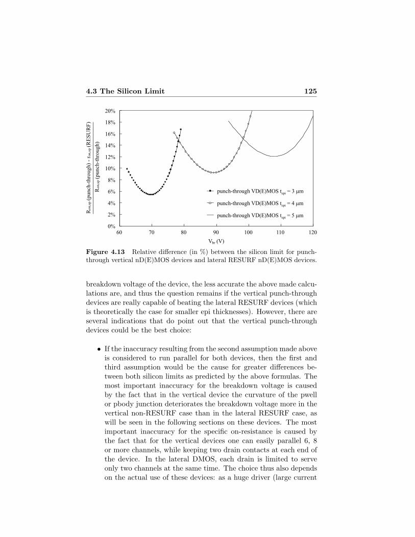
4.3 The Silicon Limit 125
0%
2%
4%
6%
8%
10%
12%
14%
16%
18%
20%
60 70 80 90 100 110 120
Vbr (V)
Ro
n,s
p(p
unch
-thro
ugh)
- r o
n,s
p(R
ES
UR
F)
Ro
n,s
p(p
unch
-thro
ugh)
punch-through VD(E)MOS t = 3 mepi m
punch-through VD(E)MOS t = 4 mepi m
punch-through VD(E)MOS t = 5 mepi m
Figure 4.13 Relative difference (in %) between the silicon limit for punch-through vertical nD(E)MOS devices and lateral RESURF nD(E)MOS devices.
breakdown voltage of the device, the less accurate the above made calcu-lations are, and thus the question remains if the vertical punch-throughdevices are really capable of beating the lateral RESURF devices (whichis theoretically the case for smaller epi thicknesses). However, there areseveral indications that do point out that the vertical punch-throughdevices could be the best choice:
• If the inaccuracy resulting from the second assumption made aboveis considered to run parallel for both devices, then the first andthird assumption would be the cause for greater differences be-tween both silicon limits as predicted by the above formulas. Themost important inaccuracy for the breakdown voltage is causedby the fact that in the vertical device the curvature of the pwellor pbody junction deteriorates the breakdown voltage more in thevertical non-RESURF case than in the lateral RESURF case, aswill be seen in the following sections on these devices. The mostimportant inaccuracy for the specific on-resistance is caused bythe fact that for the vertical devices one can easily parallel 6, 8or more channels, while keeping two drain contacts at each end ofthe device. In the lateral DMOS, each drain is limited to serveonly two channels at the same time. The choice thus also dependson the actual use of these devices: as a huge driver (large current
126 Power MOS
control) or a small switch (smaller current control).
• Moreover, since the theoretical differences are so small, the choicecould also be based on other considerations such as the device’srobustness or reliability. These are likely to be better in the ver-tical device, where the current is flowing well under the siliconsurface; whereas the current is flowing near the surface for thelateral devices.
So, although the theoretical silicon limit yields the lateral RESURF de-vice as the best choice (at least above 70 V), the practical development ofDMOS devices should also consider the vertical device. This discussionsolely serves as an illustration of the difficulty when choosing a devicein a certain voltage and current range and will be continued in the nextsections on the different types of DMOS devices.
We have only discussed the silicon limits of the types of devices in thetechnology, and the voltage and current ratings we are interested in. Ofcourse, other silicon limits—for other technologies (SOI, see e.g., [HB91]and [Chu00]) and for other types of DMOS devices (e.g., superjuncion[Fuj97])—exist (for a comparison, see [Zin01]).
4.4 Which DMOS: n or p, lateral or vertical,RESURF or not?
N or p-type?
Since the mobility of electrons in silicon is about three times higher thanthe one of holes in the drift region and since this drift region determinesthe larger part of the on-state resistance, the n-type DMOS deviceshave an on-state current level that is three times higher than the p-typedevices. Or, in other words, for the same silicon area, the p-type devicegenerates three times less current than the n-type devices. It is clearthat the n-type DMOS is preferred to the p-type DMOS.
Yet p-type devices are important for designers as they are the answerto some circuit related problems where otherwise two, three or even moren-type devices are needed. This is because the p-type transistors are inthe on-state when Vgs < Vt < 0V. The fact that the pDMOS needsmore area to produce the same current as the nDMOS is then largelycompensated for. The pDMOS is normally used as a high-side switch,which means that the source (and bulk) of the device are tight to thesupply voltage, while the gate and drain are below source potential,
4.4 Which DMOS: n or p, lateral or vertical, RESURF ornot? 127
but above substrate potential. Therefore these devices are referred to asfloating devices, since the entire device is lifted above substrate potential.The non-floating devices (used as low-side switch) are then devices wheresource (and bulk) and substrate can not be put at a potential differenceequal to the supply voltage.
Lateral or vertical?
When the term vertical is used for devices that are designed in a VLSItechnology, what is really meant is that these devices are vertically in-tegrated (or “quasi” vertical). The current path is eventually flowingperpendicular to the silicon in a vertical direction but is redirected andcollected at the surface afterwards. For the DMOS devices, this meansthat the drain is situated under the silicon surface in the form of a buriedlayer and that this buried layer is contacted with the metal via a sinkeror plug (a highly doped region in the epi).
If we start from a p-substrate, the n-type device needs a highly dopednsinker, a BLN (buried layer of n-type), and a n-epi (see figure 4.11),with a doping level and thickness that are determined by the blockingvoltage requirements, as explained above. For a p-type device a psinker,BLP and p-epi is required. The different types of epi can be obtainedby selective epi growth, which is technologically difficult. A simplersolution is the introduction of a p-tub layer, which can be implantedand annealed. But this is not all for the p-type device: since we areworking on p-substrate and the pDMOS should be a floating device,the drain (BLP) needs to be isolated from the p-substrate. The onlypossible way to do this in a junction isolated technology is to make useof the BLN (figure 4.14). This results in a rather difficult to realizep-type device, while the lateral pDMOS is much simpler to realize, asonly the definition of a pdrift region is needed (see below).
Furthermore, let us recall why these integrated vertical devices shouldbe considered in the first place. It has been proven in the previous sec-tion that the breakdown versus on-state trade-off is approximately thesame for both the lateral and the vertical device. Therefore, other crite-ria come into play. First of all, these vertical devices can be parallelledin such a way that the silicon area is used in a very efficient manner:the poly (with two channels) can be repeated without the need to re-peat the drain region as well. It suffices to provide the structure with adrain at the left hand side and at the right hand side. The number ofgates that can serve the same drain is then determined by the current
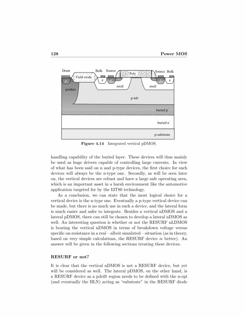
128 Power MOS
p+
n+
nwell
n+
p+
Bulk SourceDrain Source Bulk
buried n+
p-substrate
p-tub
Field oxidePoly
nwell
p+
buried p+
psinker
Figure 4.14 Integrated vertical pDMOS.
handling capability of the buried layer. These devices will thus mainlybe used as huge drivers capable of controlling large currents. In viewof what has been said on n and p-type devices, the first choice for suchdevices will always be the n-type one. Secondly, as will be seen lateron, the vertical devices are robust and have a large safe operating area,which is an important asset in a harsh environment like the automotiveapplication targeted for by the I3T80 technology.
As a conclusion, we can state that the most logical choice for avertical device is the n-type one. Eventually a p-type vertical device canbe made, but there is no much use in such a device, and the lateral formis much easier and safer to integrate. Besides a vertical nDMOS and alateral pDMOS, there can still be chosen to develop a lateral nDMOS aswell. An interesting question is whether or not the RESURF nLDMOSis beating the vertical nDMOS in terms of breakdown voltage versusspecific on-resistance in a real—albeit simulated—situation (as in theory,based on very simple calculations, the RESURF device is better). Ananswer will be given in the following sections treating these devices.
RESURF or not?
It is clear that the vertical nDMOS is not a RESURF device, but yetwill be considered as well. The lateral pDMOS, on the other hand, isa RESURF device as a pdrift region needs to be defined with the n-epi(and eventually the BLN) acting as “substrate” in the RESURF diode
4.4 Which DMOS: n or p, lateral or vertical, RESURF ornot? 129
made this way. A nLDMOS can be made as well, with the p-substrateor the BLP acting as “substrate” and a n-epi, ndrift and/or nwell asRESURF layer. Note, however, that this device is non-floating as it hasa parasitic pnp between source and substrate (see figures 4.15 and 4.19).
To make the lateral nDMOS floating a n-type buried layer has to beintroduced in this structure, which kills completely the RESURF effect,and leaves the possibity of making a punch-through diode in the driftregion of this device. The question is if this drift region is thereforeless performant than a drift region of a RESURF device on top of ahighly doped p-substrate; as it has been seen that such a RESURFstructure has a breakdown voltage determined by punch-through of thelowly doped region as well (in casu the n-epi).
Yet another solution is possible with two buried layers on top of eachother. The first buried layer is needed to provide for the RESURF effect(so, a BLP), and the second one is needed to isolate the device from thesubstrate (so, a BLN). This solution was first proposed in [KPB03], buthas been studied simultaneously in the work presented in this book. Hereit was first applied on the nLIGBT, and only after noticing [KPB03],this concept was also applied to the DMOS. However, in the DMOS itis used as a method to make the device floating and to achieve a higherbreakdown voltage; a technique that actually had already been used in[Lud00b] (with a BLN shorted to the source and bulk of the nLDMOS)and [TYH00]. In the nLIGBT, on the other hand, it is mainly used asa method to suppress substrate currents (see Chapter 5).
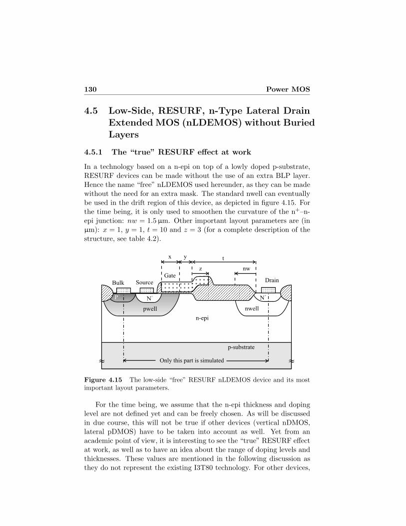
130 Power MOS
4.5 Low-Side, RESURF, n-Type Lateral DrainExtended MOS (nLDEMOS) without BuriedLayers
4.5.1 The “true” RESURF effect at work
In a technology based on a n-epi on top of a lowly doped p-substrate,RESURF devices can be made without the use of an extra BLP layer.Hence the name “free” nLDEMOS used hereunder, as they can be madewithout the need for an extra mask. The standard nwell can eventuallybe used in the drift region of this device, as depicted in figure 4.15. Forthe time being, it is only used to smoothen the curvature of the n+–n-epi junction: nw = 1.5µm. Other important layout parameters are (inµm): x = 1, y = 1, t = 10 and z = 3 (for a complete description of thestructure, see table 4.2).
pwell
P+
n-epi
SourceGate
Drain
p-substrate
N+
»»
x t
z
y
Only this part is simulated
Bulk
nwell
N+
nw
Figure 4.15 The low-side “free” RESURF nLDEMOS device and its mostimportant layout parameters.
For the time being, we assume that the n-epi thickness and dopinglevel are not defined yet and can be freely chosen. As will be discussedin due course, this will not be true if other devices (vertical nDMOS,lateral pDMOS) have to be taken into account as well. Yet from anacademic point of view, it is interesting to see the “true” RESURF effectat work, as well as to have an idea about the range of doping levels andthicknesses. These values are mentioned in the following discussion asthey do not represent the existing I3T80 technology. For other devices,
4.5 Low-Side, RESURF, n-Type Lateral Drain ExtendedMOS (nLDEMOS) without Buried Layers 131
Table 4.2 Layout parameters of the “free” RESURF nLDEMOS
Parameter Description Value (µm)
c0∗ p+ aa width as bulk region 1.1c1∗ n+ aa width as source region 1.3x∗ channel length variedy∗ distance between end of channel and start field oxide variedt∗ length of field oxide on drift region variedc2∗ n+ aa width as drain region 0.8z poly overlap on field oxide variednw nwell overlap on field oxide varied
Parameters indicated with (∗) define the pitch of the device (distance from half-bulk to half-drain): pitch = (1.1/2) + 1.3 + x + y + t + (0.8/2) = 2.25 + x + y + t.
the real I3T80 processing conditions (e.g., the n-epi for the nVDMOS,the pdrift for the pLDMOS) need to be used and will not be mentionedbecause of confidentiality.
In the section on the RESURF effect, it was shown that the optimalepi thickness is around 2.6µm for Nepi = 4e15 cm−3. As this is a realisticepi thickness, a variation around this epi doping level is carried out.Since Nsub < Nepi, a true RESURF effect can occur here, provided thatthe length of the drift region (≈ y + t− nw) is larger than the net n-epithickness, as explained above. Therefore t is rather large to start withand variations on this parameter are given below.
Figure 4.16 shows that the breakdown voltage clearly has an opti-mum as a function of the epi thickness for each Nepi. Furthermore, thisoptimum is constant (Vbr = 175 V) for all n-epi doping levels (only thehighest doping level has a slightly lower breakdown voltage). As this op-timum is 175V, it is comparable to what was simulated for the RESURFdiode with a comparable length (l ≈ y + t−nw = 9.5µm). The optimalepi thickness is higher than what was simulated for the RESURF diode.This is caused by the change in the process flow between the simulationof the RESURF diode (arbitrary flow) and the simulation of the nLD-MOS (the I3T80 process flow of AMI Semiconductor), as well as by thechange in the RESURF structure (the poly field plate).
Figure 4.17 plots the specific on-resistance versus the epi-thicknessfor the cases considered above. The filled data points show the optimathat are reached for the breakdown voltage. Interesting to observe is that
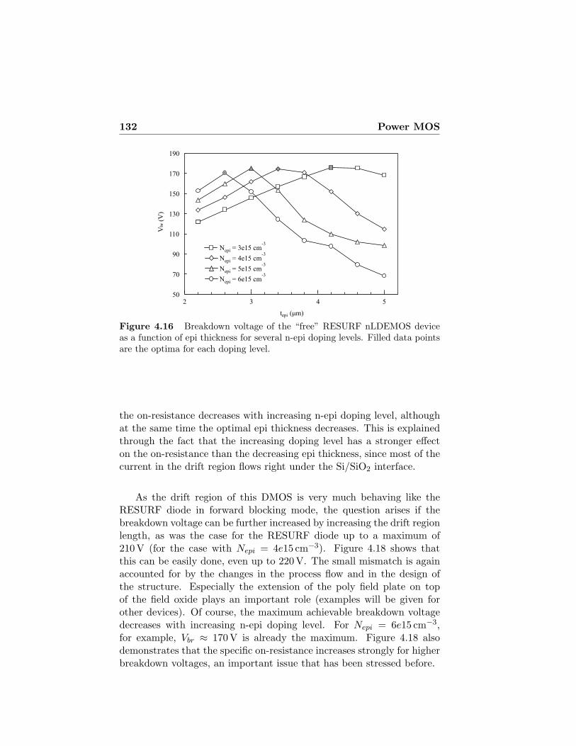
132 Power MOS
50
70
90
110
130
150
170
190
2 3 4 5
tepi (mm)
Vbr(V
)
N = 3e15 cmepi
-3
N = 4e15 cmepi
-3
N = 5e15 cmepi
-3
N = 6e15 cmepi
-3
Figure 4.16 Breakdown voltage of the “free” RESURF nLDEMOS deviceas a function of epi thickness for several n-epi doping levels. Filled data pointsare the optima for each doping level.
the on-resistance decreases with increasing n-epi doping level, althoughat the same time the optimal epi thickness decreases. This is explainedthrough the fact that the increasing doping level has a stronger effecton the on-resistance than the decreasing epi thickness, since most of thecurrent in the drift region flows right under the Si/SiO2 interface.
As the drift region of this DMOS is very much behaving like theRESURF diode in forward blocking mode, the question arises if thebreakdown voltage can be further increased by increasing the drift regionlength, as was the case for the RESURF diode up to a maximum of210V (for the case with Nepi = 4e15 cm−3). Figure 4.18 shows thatthis can be easily done, even up to 220 V. The small mismatch is againaccounted for by the changes in the process flow and in the design ofthe structure. Especially the extension of the poly field plate on topof the field oxide plays an important role (examples will be given forother devices). Of course, the maximum achievable breakdown voltagedecreases with increasing n-epi doping level. For Nepi = 6e15 cm−3,for example, Vbr ≈ 170V is already the maximum. Figure 4.18 alsodemonstrates that the specific on-resistance increases strongly for higherbreakdown voltages, an important issue that has been stressed before.
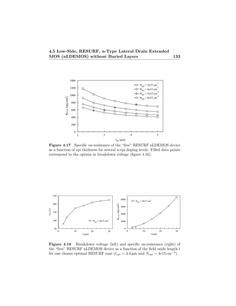
4.5 Low-Side, RESURF, n-Type Lateral Drain ExtendedMOS (nLDEMOS) without Buried Layers 133
0
200
400
600
800
1000
1200
1400
2 3 4 5
tepi (mm)
Ron,s
p(m
W.m
m2)
N = 3e15 cmepi
-3
N = 4e15 cmepi
-3
N = 5e15 cmepi
-3
N = 6e15 cmepi
-3
Figure 4.17 Specific on-resistance of the “free” RESURF nLDEMOS deviceas a function of epi thickness for several n-epi doping levels. Filled data pointscorrespond to the optima in breakdown voltage (figure 4.16).
50
100
150
200
250
0 10 20 30
t (mm)
Vbr(V
)
N = 4e15 cmepi-3
0
1000
2000
3000
4000
0 10 20 30
t (mm)
Ron,s
p(m
W.m
m2)
N = 4e15 cmepi-3
Figure 4.18 Breakdown voltage (left) and specific on-resistance (right) ofthe “free” RESURF nLDEMOS device as a function of the field oxide length tfor one chosen optimal RESURF case (tepi = 3.4 µm and Nepi = 4e15 cm−3).
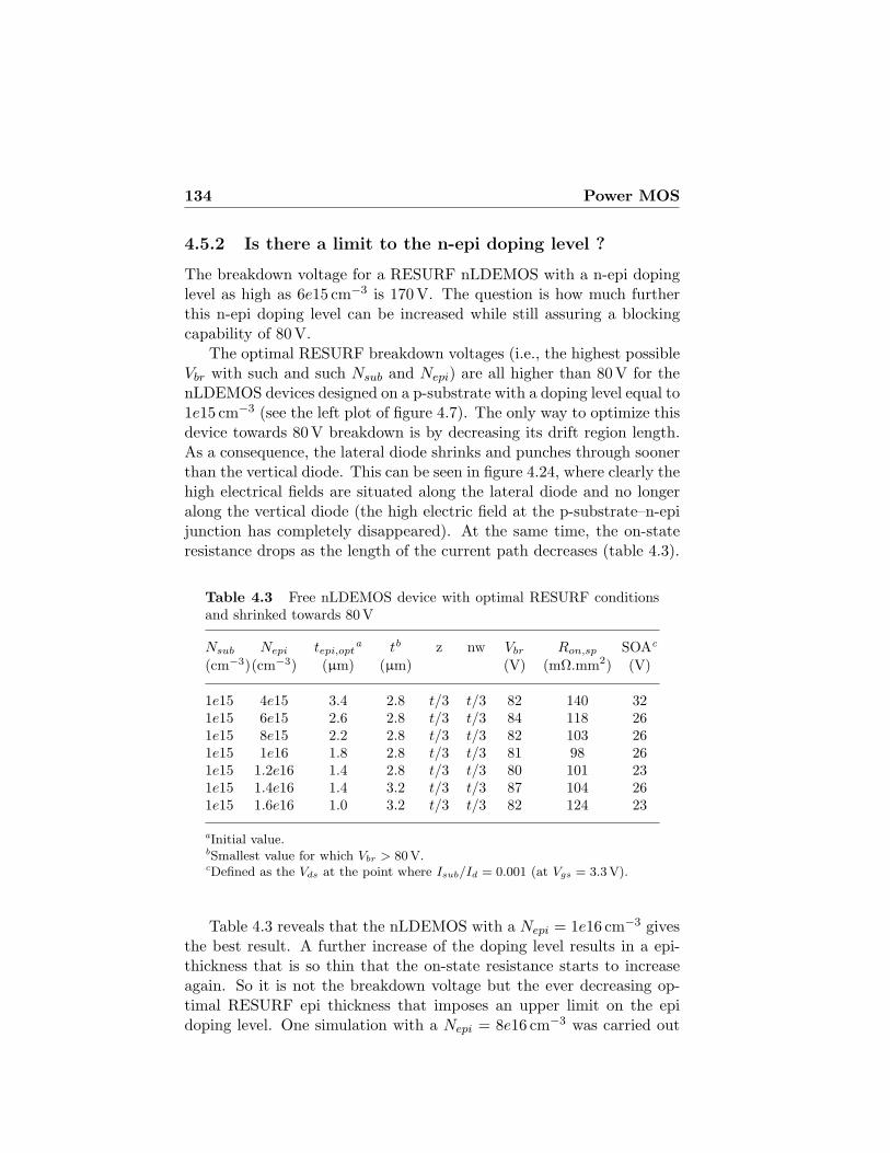
134 Power MOS
4.5.2 Is there a limit to the n-epi doping level ?
The breakdown voltage for a RESURF nLDEMOS with a n-epi dopinglevel as high as 6e15 cm−3 is 170 V. The question is how much furtherthis n-epi doping level can be increased while still assuring a blockingcapability of 80V.
The optimal RESURF breakdown voltages (i.e., the highest possibleVbr with such and such Nsub and Nepi) are all higher than 80 V for thenLDEMOS devices designed on a p-substrate with a doping level equal to1e15 cm−3 (see the left plot of figure 4.7). The only way to optimize thisdevice towards 80V breakdown is by decreasing its drift region length.As a consequence, the lateral diode shrinks and punches through soonerthan the vertical diode. This can be seen in figure 4.24, where clearly thehigh electrical fields are situated along the lateral diode and no longeralong the vertical diode (the high electric field at the p-substrate–n-epijunction has completely disappeared). At the same time, the on-stateresistance drops as the length of the current path decreases (table 4.3).
Table 4.3 Free nLDEMOS device with optimal RESURF conditionsand shrinked towards 80 V
Nsub Nepi tepi,opta tb z nw Vbr Ron,sp SOAc
(cm−3)(cm−3) (µm) (µm) (V) (mΩ.mm2) (V)
1e15 4e15 3.4 2.8 t/3 t/3 82 140 321e15 6e15 2.6 2.8 t/3 t/3 84 118 261e15 8e15 2.2 2.8 t/3 t/3 82 103 261e15 1e16 1.8 2.8 t/3 t/3 81 98 261e15 1.2e16 1.4 2.8 t/3 t/3 80 101 231e15 1.4e16 1.4 3.2 t/3 t/3 87 104 261e15 1.6e16 1.0 3.2 t/3 t/3 82 124 23
aInitial value.bSmallest value for which Vbr > 80V.cDefined as the Vds at the point where Isub/Id = 0.001 (at Vgs = 3.3V).
Table 4.3 reveals that the nLDEMOS with a Nepi = 1e16 cm−3 givesthe best result. A further increase of the doping level results in a epi-thickness that is so thin that the on-state resistance starts to increaseagain. So it is not the breakdown voltage but the ever decreasing op-timal RESURF epi thickness that imposes an upper limit on the epidoping level. One simulation with a Nepi = 8e16 cm−3 was carried out
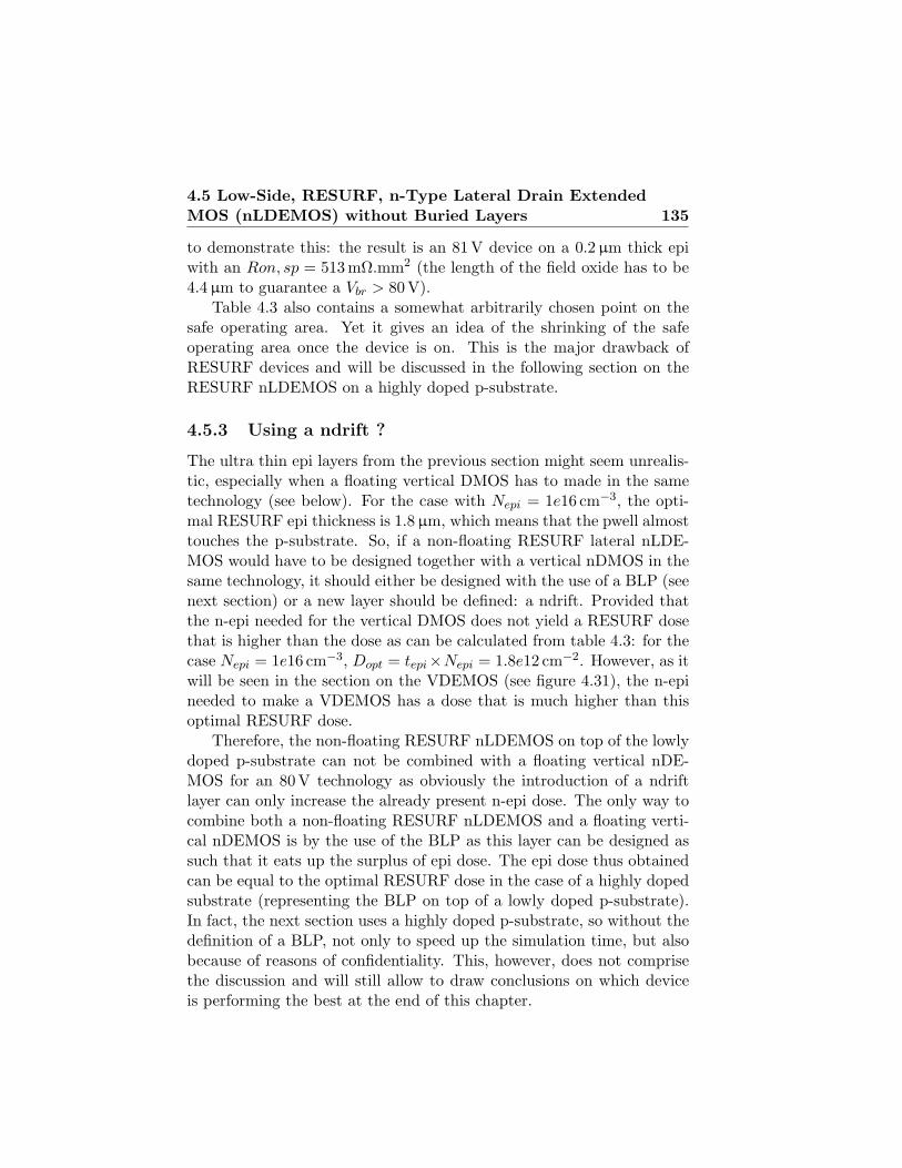
4.5 Low-Side, RESURF, n-Type Lateral Drain ExtendedMOS (nLDEMOS) without Buried Layers 135
to demonstrate this: the result is an 81V device on a 0.2µm thick epiwith an Ron, sp = 513 mΩ.mm2 (the length of the field oxide has to be4.4µm to guarantee a Vbr > 80V).
Table 4.3 also contains a somewhat arbitrarily chosen point on thesafe operating area. Yet it gives an idea of the shrinking of the safeoperating area once the device is on. This is the major drawback ofRESURF devices and will be discussed in the following section on theRESURF nLDEMOS on a highly doped p-substrate.
4.5.3 Using a ndrift ?
The ultra thin epi layers from the previous section might seem unrealis-tic, especially when a floating vertical DMOS has to made in the sametechnology (see below). For the case with Nepi = 1e16 cm−3, the opti-mal RESURF epi thickness is 1.8µm, which means that the pwell almosttouches the p-substrate. So, if a non-floating RESURF lateral nLDE-MOS would have to be designed together with a vertical nDMOS in thesame technology, it should either be designed with the use of a BLP (seenext section) or a new layer should be defined: a ndrift. Provided thatthe n-epi needed for the vertical DMOS does not yield a RESURF dosethat is higher than the dose as can be calculated from table 4.3: for thecase Nepi = 1e16 cm−3, Dopt = tepi×Nepi = 1.8e12 cm−2. However, as itwill be seen in the section on the VDEMOS (see figure 4.31), the n-epineeded to make a VDEMOS has a dose that is much higher than thisoptimal RESURF dose.
Therefore, the non-floating RESURF nLDEMOS on top of the lowlydoped p-substrate can not be combined with a floating vertical nDE-MOS for an 80 V technology as obviously the introduction of a ndriftlayer can only increase the already present n-epi dose. The only way tocombine both a non-floating RESURF nLDEMOS and a floating verti-cal nDEMOS is by the use of the BLP as this layer can be designed assuch that it eats up the surplus of epi dose. The epi dose thus obtainedcan be equal to the optimal RESURF dose in the case of a highly dopedsubstrate (representing the BLP on top of a lowly doped p-substrate).In fact, the next section uses a highly doped p-substrate, so without thedefinition of a BLP, not only to speed up the simulation time, but alsobecause of reasons of confidentiality. This, however, does not comprisethe discussion and will still allow to draw conclusions on which deviceis performing the best at the end of this chapter.
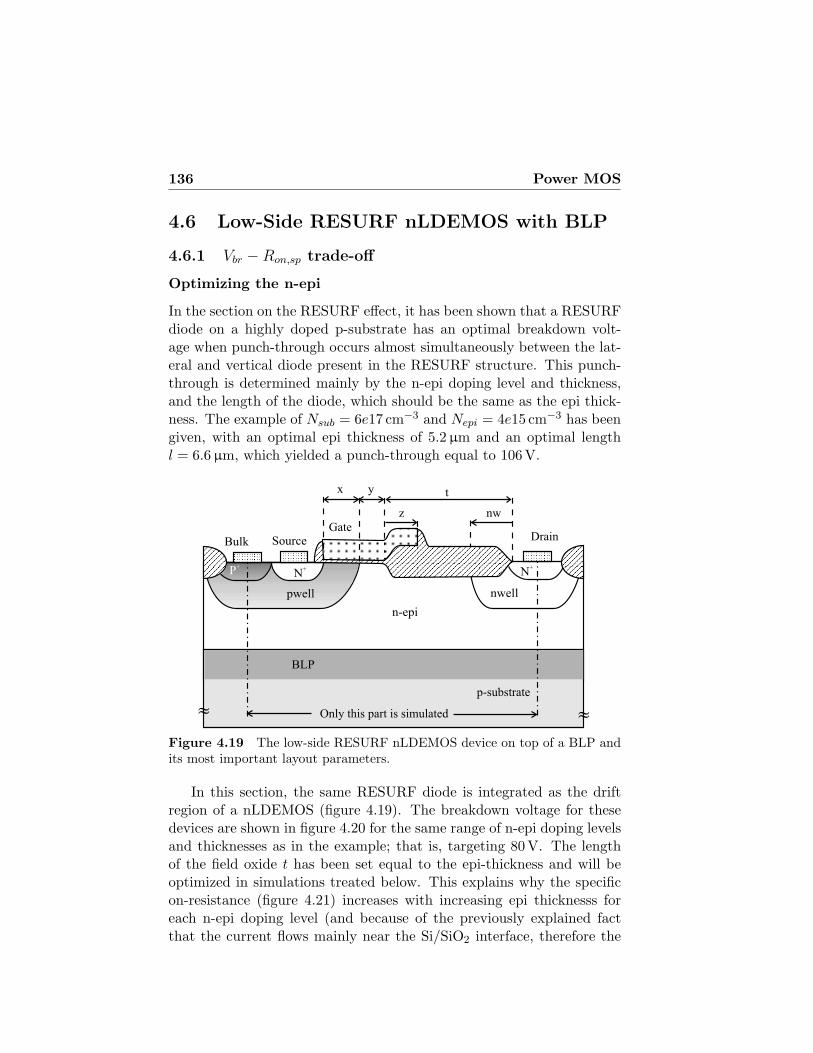
136 Power MOS
4.6 Low-Side RESURF nLDEMOS with BLP
4.6.1 Vbr −Ron,sp trade-off
Optimizing the n-epi
In the section on the RESURF effect, it has been shown that a RESURFdiode on a highly doped p-substrate has an optimal breakdown volt-age when punch-through occurs almost simultaneously between the lat-eral and vertical diode present in the RESURF structure. This punch-through is determined mainly by the n-epi doping level and thickness,and the length of the diode, which should be the same as the epi thick-ness. The example of Nsub = 6e17 cm−3 and Nepi = 4e15 cm−3 has beengiven, with an optimal epi thickness of 5.2µm and an optimal lengthl = 6.6µm, which yielded a punch-through equal to 106V.
pwell
P+
n-epi
SourceGate
Drain
p-substrate
N+
»»
x t
z
y
Only this part is simulated
Bulk
nwell
N+
nw
BLP
Figure 4.19 The low-side RESURF nLDEMOS device on top of a BLP andits most important layout parameters.
In this section, the same RESURF diode is integrated as the driftregion of a nLDEMOS (figure 4.19). The breakdown voltage for thesedevices are shown in figure 4.20 for the same range of n-epi doping levelsand thicknesses as in the example; that is, targeting 80 V. The lengthof the field oxide t has been set equal to the epi-thickness and will beoptimized in simulations treated below. This explains why the specificon-resistance (figure 4.21) increases with increasing epi thicknesss foreach n-epi doping level (and because of the previously explained factthat the current flows mainly near the Si/SiO2 interface, therefore the
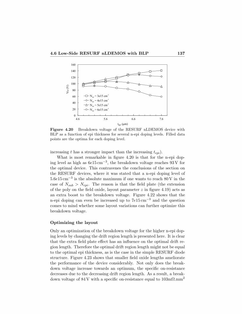
4.6 Low-Side RESURF nLDEMOS with BLP 137
0
20
40
60
80
100
120
140
160
4.6 5.6 6.6 7.6
tepi (mm)
Vb
r(V
)
N = 3e15 cmepi
-3
N = 4e15 cmepi
-3
N = 5e15 cmepi
-3
N = 6e15 cmepi
-3
Figure 4.20 Breakdown voltage of the RESURF nLDEMOS device withBLP as a function of epi thickness for several n-epi doping levels. Filled datapoints are the optima for each doping level.
increasing t has a stronger impact than the increasing tepi).What is most remarkable in figure 4.20 is that for the n-epi dop-
ing level as high as 6e15 cm−3, the breakdown voltage reaches 93V forthe optimal device. This contravenes the conclusions of the section onthe RESURF devices, where it was stated that a n-epi doping level of5.6e15 cm−3 is the absolute maximum if one wants to reach 80 V in thecase of Nsub > Nepi. The reason is that the field plate (the extensionof the poly on the field oxide, layout parameter z in figure 4.19) acts asan extra boost to the breakdown voltage. Figure 4.22 shows that then-epi doping can even be increased up to 7e15 cm−3 and the questioncomes to mind whether some layout variations can further optimize thisbreakdown voltage.
Optimizing the layout
Only an optimization of the breakdown voltage for the higher n-epi dop-ing levels by changing the drift region length is presented here. It is clearthat the extra field plate effect has an influence on the optimal drift re-gion length. Therefore the optimal drift region length might not be equalto the optimal epi thickness, as is the case in the simple RESURF diodestructure. Figure 4.23 shows that smaller field oxide lengths amelioratethe performance of the device considerably. Not only does the break-down voltage increase towards an optimum, the specific on-resistancedecreases due to the decreasing drift region length. As a result, a break-down voltage of 84 V with a specific on-resistance equal to 103mΩ.mm2
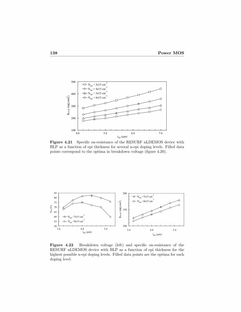
138 Power MOS
100
200
300
400
500
4.6 5.6 6.6 7.6tepi (mm)
Ro
n,s
p(m
W.m
m2)
N = 3e15 cmepi
-3
N = 4e15 cmepi
-3
N = 5e15 cmepi
-3
N = 6e15 cmepi
-3
Figure 4.21 Specific on-resistance of the RESURF nLDEMOS device withBLP as a function of epi thickness for several n-epi doping levels. Filled datapoints correspond to the optima in breakdown voltage (figure 4.20).
50
55
60
65
70
75
80
85
3.4 4.4 5.4tepi (mm)
Vb
r(V
)
N =7e15 cmepi
-3
N =8e15 cmepi
-3
100
150
200
3.4 4.4 5.4
tepi (mm)
Ro
n,s
p(m
W.m
m2)
N =7e15 cmepi
-3
N =8e15 cmepi
-3
Figure 4.22 Breakdown voltage (left) and specific on-resistance of theRESURF nLDEMOS device with BLP as a function of epi thickness for thehighest possible n-epi doping levels. Filled data points are the optima for eachdoping level.
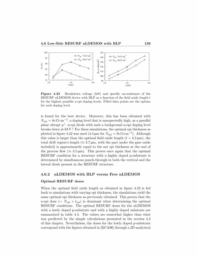
4.6 Low-Side RESURF nLDEMOS with BLP 139
75
80
85
90
95
100
2.6 3.6 4.6t (mm)
Vb
r(V
)
(mm)
N =7e15 cmepi
-3
N =8e15 cmepi
-3
90
100
110
120
130
140
150
2.6 3.6 4.6t
Ron,s
p(m
W.m
m2)
N =7e15 cmepi
-3
N =8e15 cmepi
-3
Figure 4.23 Breakdown voltage (left) and specific on-resistance of theRESURF nLDEMOS device with BLP as a function of the field oxide length tfor the highest possible n-epi doping levels. Filled data points are the optimafor each doping level.
is found for the best device. Moreover, this has been obtained withNepi = 8e15 cm−3, a doping level that is unexpectedly high, as a parallelplane abrupt p+–n-epi diode with such a background n-epi doping levelbreaks down at 63 V ! For these simulations, the optimal epi thickness asplotted in figure 4.22 was used (4.4µm for Nepi = 8e15 cm−3). Althoughthis value is larger than the optimal field oxide length (t = 3.2 µm), thetotal drift region’s length (≈ 3.7µm, with the part under the gate oxideincluded) is approximately equal to the net epi thickness at the end ofthe process flow (≈ 3.5µm). This proves once again that the optimalRESURF condition for a structure with a highly doped p-substrate isdetermined by simultaneous punch-through in both the vertical and thelateral diode present in the RESURF structure.
4.6.2 nLDEMOS with BLP versus Free nLDEMOS
Optimal RESURF doses
When the optimal field oxide length as obtained in figure 4.23 is fedback to simulations with varying epi thickness, the simulations yield thesame optimal epi thickness as previously obtained. This proves that then-epi dose (= Nepi × tepi) is dominant when determining the optimalRESURF conditions. The optimal RESURF doses for the nLDEMOSwith a lowly doped p-substrate and with a highly doped substrate aresummarized in table 4.4. The values are somewhat higher than whatwas predicted by the simple calculations presented in the section 4.2of this chapter. Nevertheless, the doses for the lowly doped p-substratecorrespond with the figures obtained in [KCA96] through a 2D analytical
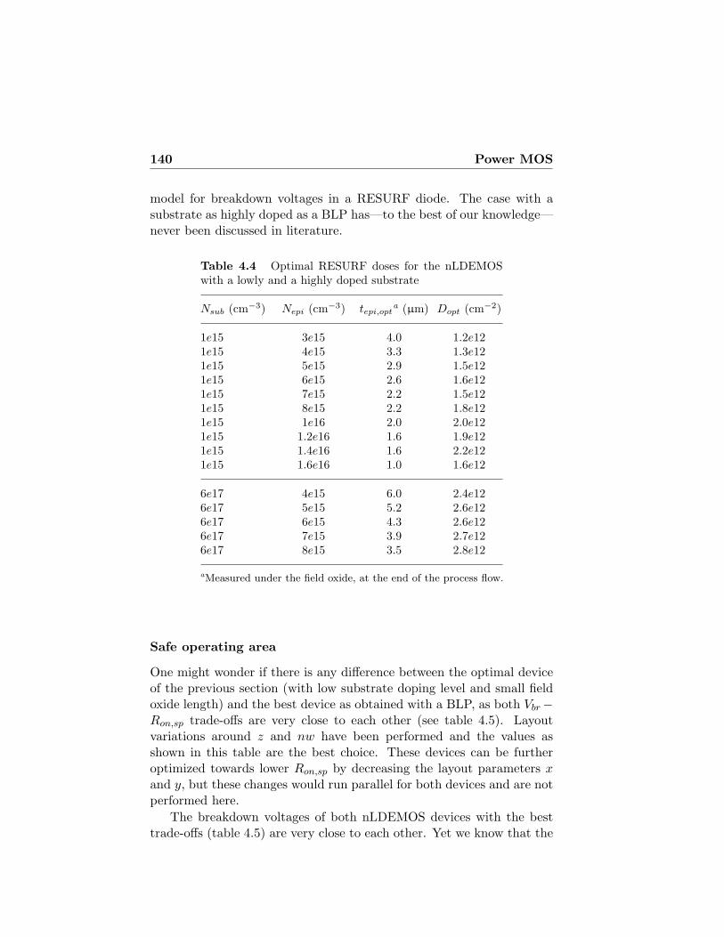
140 Power MOS
model for breakdown voltages in a RESURF diode. The case with asubstrate as highly doped as a BLP has—to the best of our knowledge—never been discussed in literature.
Table 4.4 Optimal RESURF doses for the nLDEMOSwith a lowly and a highly doped substrate
Nsub (cm−3) Nepi (cm−3) tepi,opta (µm) Dopt (cm−2)
1e15 3e15 4.0 1.2e121e15 4e15 3.3 1.3e121e15 5e15 2.9 1.5e121e15 6e15 2.6 1.6e121e15 7e15 2.2 1.5e121e15 8e15 2.2 1.8e121e15 1e16 2.0 2.0e121e15 1.2e16 1.6 1.9e121e15 1.4e16 1.6 2.2e121e15 1.6e16 1.0 1.6e12
6e17 4e15 6.0 2.4e126e17 5e15 5.2 2.6e126e17 6e15 4.3 2.6e126e17 7e15 3.9 2.7e126e17 8e15 3.5 2.8e12
aMeasured under the field oxide, at the end of the process flow.
Safe operating area
One might wonder if there is any difference between the optimal deviceof the previous section (with low substrate doping level and small fieldoxide length) and the best device as obtained with a BLP, as both Vbr−Ron,sp trade-offs are very close to each other (see table 4.5). Layoutvariations around z and nw have been performed and the values asshown in this table are the best choice. These devices can be furtheroptimized towards lower Ron,sp by decreasing the layout parameters xand y, but these changes would run parallel for both devices and are notperformed here.
The breakdown voltages of both nLDEMOS devices with the besttrade-offs (table 4.5) are very close to each other. Yet we know that the
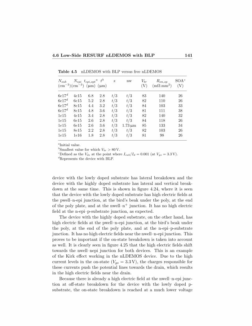
4.6 Low-Side RESURF nLDEMOS with BLP 141
Table 4.5 nLDEMOS with BLP versus free nLDEMOS
Nsub Nepi tepi,opta tb z nw Vbr Ron,sp SOAc
(cm−3)(cm−3) (µm) (µm) (V) (mΩ.mm2) (V)
6e17d 4e15 6.8 2.8 t/3 t/3 83 140 266e17d 6e15 5.2 2.8 t/3 t/3 82 110 266e17d 8e15 4.4 3.2 t/3 t/3 84 103 336e17d 8e15 4.8 3.6 t/3 t/3 81 111 381e15 4e15 3.4 2.8 t/3 t/3 82 140 321e15 6e15 2.6 2.8 t/3 t/3 84 118 261e15 6e15 2.6 3.6 t/3 1.73µm 85 133 341e15 8e15 2.2 2.8 t/3 t/3 82 103 261e15 1e16 1.8 2.8 t/3 t/3 81 98 26
aInitial value.bSmallest value for which Vbr > 80V.cDefined as the Vds at the point where Isub/Id = 0.001 (at Vgs = 3.3V).dRepresents the device with BLP.
device with the lowly doped substrate has lateral breakdown and thedevice with the highly doped substrate has lateral and vertical break-down at the same time. This is shown in figure 4.24, where it is seenthat the device with the lowly doped substrate has high electric fields atthe pwell–n-epi junction, at the bird’s beak under the poly, at the endof the poly plate, and at the nwell–n+ junction. It has no high electricfield at the n-epi–p-substrate junction, as expected.
The device with the highly doped substrate, on the other hand, hashigh electric fields at the pwell–n-epi junction, at the bird’s beak underthe poly, at the end of the poly plate, and at the n-epi–p-substratejunction. It has no high electric fields near the nwell–n-epi junction. Thisproves to be important if the on-state breakdown is taken into accountas well. It is clearly seen in figure 4.25 that the high electric fields shifttowards the nwell–nepi junction for both devices. This is an exampleof the Kirk effect working in the nLDEMOS device. Due to the highcurrent levels in the on-state (Vgs = 3.3 V), the charges responsible forthese currents push the potential lines towards the drain, which resultsin the high electric fields near the drain.
Because there is already a high electric field at the nwell–n-epi junc-tion at off-state breakdown for the device with the lowly doped p-substrate, the on-state breakdown is reached at a much lower voltage
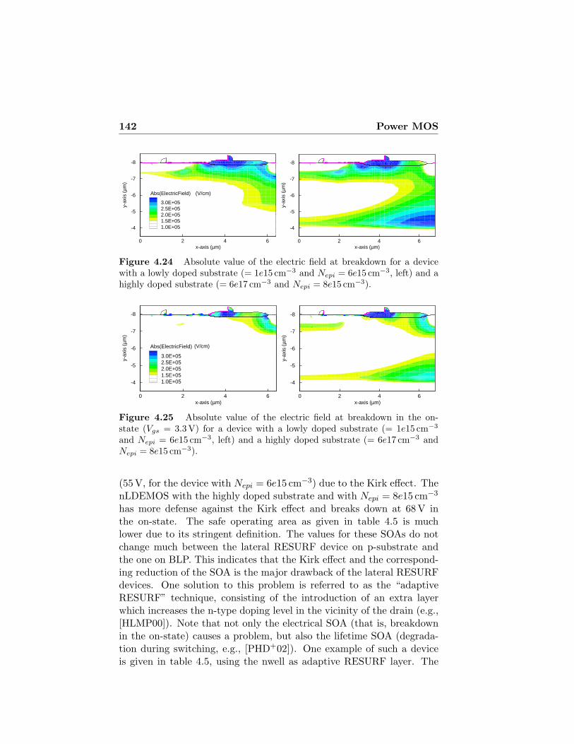
142 Power MOS
x-axis (µm)
y-ax
is(µ
m)
0 2 4 6
-8
-7
-6
-5
-4
Abs(ElectricField)
3.0E+052.5E+052.0E+051.5E+051.0E+05
(V/cm)
x-axis (µm)
y-ax
is(µ
m)
0 2 4 6
-8
-7
-6
-5
-4
Figure 4.24 Absolute value of the electric field at breakdown for a devicewith a lowly doped substrate (= 1e15 cm−3 and Nepi = 6e15 cm−3, left) and ahighly doped substrate (= 6e17 cm−3 and Nepi = 8e15 cm−3).
x-axis (µm)
y-ax
is(µ
m)
0 2 4 6
-8
-7
-6
-5
-4
Abs(ElectricField)
3.0E+052.5E+052.0E+051.5E+051.0E+05
(V/cm)
x-axis (µm)
y-ax
is(µ
m)
0 2 4 6
-8
-7
-6
-5
-4
Figure 4.25 Absolute value of the electric field at breakdown in the on-state (Vgs = 3.3V) for a device with a lowly doped substrate (= 1e15 cm−3
and Nepi = 6e15 cm−3, left) and a highly doped substrate (= 6e17 cm−3 andNepi = 8e15 cm−3).
(55V, for the device with Nepi = 6e15 cm−3) due to the Kirk effect. ThenLDEMOS with the highly doped substrate and with Nepi = 8e15 cm−3
has more defense against the Kirk effect and breaks down at 68 V inthe on-state. The safe operating area as given in table 4.5 is muchlower due to its stringent definition. The values for these SOAs do notchange much between the lateral RESURF device on p-substrate andthe one on BLP. This indicates that the Kirk effect and the correspond-ing reduction of the SOA is the major drawback of the lateral RESURFdevices. One solution to this problem is referred to as the “adaptiveRESURF” technique, consisting of the introduction of an extra layerwhich increases the n-type doping level in the vicinity of the drain (e.g.,[HLMP00]). Note that not only the electrical SOA (that is, breakdownin the on-state) causes a problem, but also the lifetime SOA (degrada-tion during switching, e.g., [PHD+02]). One example of such a deviceis given in table 4.5, using the nwell as adaptive RESURF layer. The
4.6 Low-Side RESURF nLDEMOS with BLP 143
layout parameter nw has been increased to 1.73µm for the device withNsub = 1e15 cm−3 and Nepi = 6e15 cm−3, while the length of the fieldoxide has been increased in order to guarantee a breakdown voltage of85V. The result is a device with a larger SOA, but with a lower spe-cific on-resistance, thereby illustrating the extra trade-off that has to bemade. The poor increase of the SOA is due to the use of the standardnwell as adaptive RESURF layer. Better results can be obtained if adedicated implant is defined. This is not discussed here, because thevertical DMOS will prove to have a larger SOA (see the correspondingsection).
Another, more drastic, less elegant, but also less expensive way out,is to increase the optimal RESURF dose, thereby creating a slightly“under-resurfed” device in the off-state, but a larger SOA in the on-state (one example of such a device is given in table 4.5 for the casewith Nsub = 6e17 cm−3 and Nepi = 8e15 cm−3). A drift region lengthof 3.6µm has to be foreseen to guarantee 80V, with a higher Ron,sp asa consequence, but also with a larger SOA. The lower the n-epi dopinglevel is made, the more “under-resurfed” the device can be made whilestill assuring 80V, and thus the larger the SOA, the worser the specificon-resistance. The question is whether these RESURF devices can beatthe vertical devices when this triple trade-off is taken into account. Theanswer will be given in the section on the vertical nDMOS.
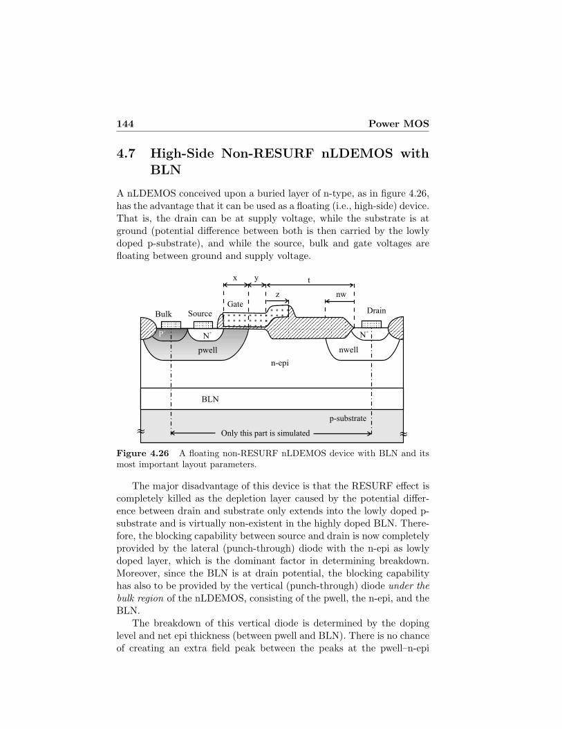
144 Power MOS
4.7 High-Side Non-RESURF nLDEMOS withBLN
A nLDEMOS conceived upon a buried layer of n-type, as in figure 4.26,has the advantage that it can be used as a floating (i.e., high-side) device.That is, the drain can be at supply voltage, while the substrate is atground (potential difference between both is then carried by the lowlydoped p-substrate), and while the source, bulk and gate voltages arefloating between ground and supply voltage.
pwell
P+
n-epi
SourceGate
Drain
p-substrate
N+
»»
x t
z
y
Only this part is simulated
Bulk
nwell
N+
nw
BLN
Figure 4.26 A floating non-RESURF nLDEMOS device with BLN and itsmost important layout parameters.
The major disadvantage of this device is that the RESURF effect iscompletely killed as the depletion layer caused by the potential differ-ence between drain and substrate only extends into the lowly doped p-substrate and is virtually non-existent in the highly doped BLN. There-fore, the blocking capability between source and drain is now completelyprovided by the lateral (punch-through) diode with the n-epi as lowlydoped layer, which is the dominant factor in determining breakdown.Moreover, since the BLN is at drain potential, the blocking capabilityhas also to be provided by the vertical (punch-through) diode under thebulk region of the nLDEMOS, consisting of the pwell, the n-epi, and theBLN.
The breakdown of this vertical diode is determined by the dopinglevel and net epi thickness (between pwell and BLN). There is no chanceof creating an extra field peak between the peaks at the pwell–n-epi
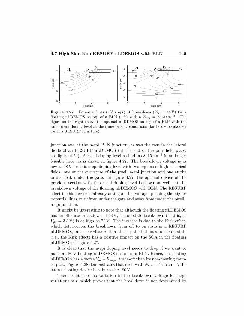
4.7 High-Side Non-RESURF nLDEMOS with BLN 145
00
0
10
10
20
20
20
30
30
40
40
10 40
x-axis (µm)
y-ax
is(µ
m)
0 2 4 6
-8
-7
-6
-5
-4
0
10
20
20
30
30
40
40
x-axis (µm)
y-ax
is(µ
m)
0 2 4 6
-8
-7
-6
-5
Figure 4.27 Potential lines (5 V steps) at breakdown (Vbr = 48V) for afloating nLDEMOS on top of a BLN (left) with a Nepi = 8e15 cm−3. Thefigure on the right shows the optimal nLDEMOS on top of a BLP with thesame n-epi doping level at the same biasing conditions (far below breakdownfor this RESURF structure).
junction and at the n-epi–BLN junction, as was the case in the lateraldiode of an RESURF nLDEMOS (at the end of the poly field plate,see figure 4.24). A n-epi doping level as high as 8e15 cm−3 is no longerfeasible here, as is shown in figure 4.27. The breakdown voltage is aslow as 48V for this n-epi doping level with two regions of high electricalfields: one at the curvature of the pwell–n-epi junction and one at thebird’s beak under the gate. In figure 4.27, the optimal device of theprevious section with this n-epi doping level is shown as well—at thebreakdown voltage of the floating nLDEMOS with BLN. The RESURFeffect in this device is already acting at this voltage, pushing the higherpotential lines away from under the gate and away from under the pwell–n-epi junction.
It might be interesting to note that although the floating nLDEMOShas an off-state breakdown of 48 V, the on-state breakdown (that is, atVgs = 3.3V) is as high as 70 V. The increase is due to the Kirk effect,which deteriorates the breakdown from off to on-state in a RESURFnLDEMOS, but the redistribution of the potential lines in the on-state(i.e., the Kirk effect) has a positive impact on the SOA in the floatingnLDEMOS of figure 4.27.
It is clear that the n-epi doping level needs to drop if we want tomake an 80 V floating nLDEMOS on top of a BLN. Hence, the floatingnLDEMOS has a worse Vbr−Ron,sp trade-off than its non-floating coun-terpart. Figure 4.28 demonstrates that even with Nepi = 4e15 cm−3, thelateral floating device hardly reaches 80V.
There is little or no variation in the breakdown voltage for largevariations of t, which proves that the breakdown is not determined by
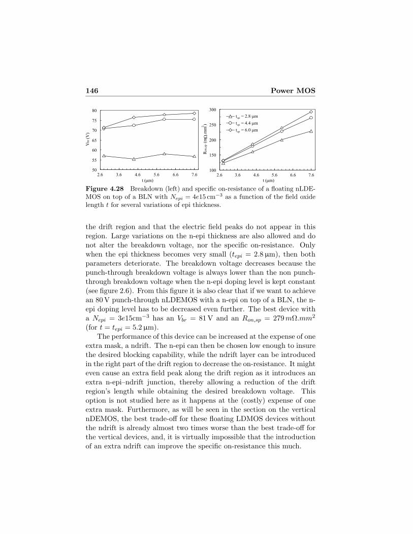
146 Power MOS
50
55
60
65
70
75
80
2.6 3.6 4.6 5.6 6.6 7.6
t (mm)
Vb
r(V
)
100
150
200
250
300
2.6 3.6 4.6 5.6 6.6 7.6
t (mm)
Ro
n,s
p(m
W.m
m2)
t = 2.8 mepi m
t = 4.4 mepi m
t = 6.0 mepi m
Figure 4.28 Breakdown (left) and specific on-resistance of a floating nLDE-MOS on top of a BLN with Nepi = 4e15 cm−3 as a function of the field oxidelength t for several variations of epi thickness.
the drift region and that the electric field peaks do not appear in thisregion. Large variations on the n-epi thickness are also allowed and donot alter the breakdown voltage, nor the specific on-resistance. Onlywhen the epi thickness becomes very small (tepi = 2.8µm), then bothparameters deteriorate. The breakdown voltage decreases because thepunch-through breakdown voltage is always lower than the non punch-through breakdown voltage when the n-epi doping level is kept constant(see figure 2.6). From this figure it is also clear that if we want to achievean 80V punch-through nLDEMOS with a n-epi on top of a BLN, the n-epi doping level has to be decreased even further. The best device witha Nepi = 3e15cm−3 has an Vbr = 81V and an Ron,sp = 279mΩ.mm2
(for t = tepi = 5.2µm).The performance of this device can be increased at the expense of one
extra mask, a ndrift. The n-epi can then be chosen low enough to insurethe desired blocking capability, while the ndrift layer can be introducedin the right part of the drift region to decrease the on-resistance. It mighteven cause an extra field peak along the drift region as it introduces anextra n-epi–ndrift junction, thereby allowing a reduction of the driftregion’s length while obtaining the desired breakdown voltage. Thisoption is not studied here as it happens at the (costly) expense of oneextra mask. Furthermore, as will be seen in the section on the verticalnDEMOS, the best trade-off for these floating LDMOS devices withoutthe ndrift is already almost two times worse than the best trade-off forthe vertical devices, and, it is virtually impossible that the introductionof an extra ndrift can improve the specific on-resistance this much.
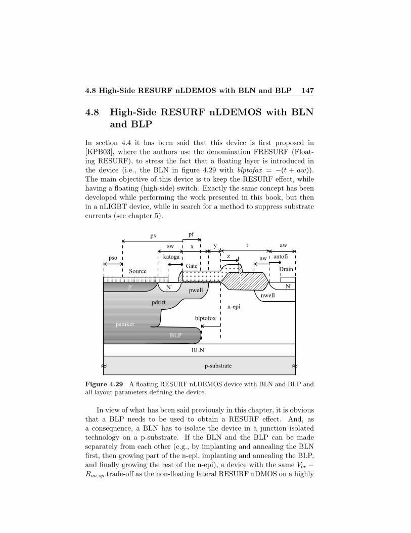
4.8 High-Side RESURF nLDEMOS with BLN and BLP 147
4.8 High-Side RESURF nLDEMOS with BLNand BLP
In section 4.4 it has been said that this device is first proposed in[KPB03], where the authors use the denomination FRESURF (Float-ing RESURF), to stress the fact that a floating layer is introduced inthe device (i.e., the BLN in figure 4.29 with blptofox = −(t + aw)).The main objective of this device is to keep the RESURF effect, whilehaving a floating (high-side) switch. Exactly the same concept has beendeveloped while performing the work presented in this book, but thenin a nLIGBT device, while in search for a method to suppress substratecurrents (see chapter 5).
pwellP+
n-epi
Gate
p-substrate
N+
N+
»»
x t
z
y
nwell
nw
pdrift
pf
psinker
BLP
sw
katoga
ps
pso
BLN
aw
antofi
blptofox
Source Drain
Figure 4.29 A floating RESURF nLDEMOS device with BLN and BLP andall layout parameters defining the device.
In view of what has been said previously in this chapter, it is obviousthat a BLP needs to be used to obtain a RESURF effect. And, asa consequence, a BLN has to isolate the device in a junction isolatedtechnology on a p-substrate. If the BLN and the BLP can be madeseparately from each other (e.g., by implanting and annealing the BLNfirst, then growing part of the n-epi, implanting and annealing the BLP,and finally growing the rest of the n-epi), a device with the same Vbr −Ron,sp trade-off as the non-floating lateral RESURF nDMOS on a highly
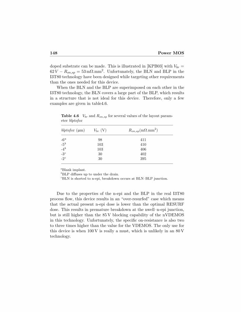
148 Power MOS
doped substrate can be made. This is illustrated in [KPB03] with Vbr =62 V − Ron,sp = 53 mΩ.mm2. Unfortunately, the BLN and BLP in theI3T80 technology have been designed while targeting other requirementsthan the ones needed for this device.
When the BLN and the BLP are superimposed on each other in theI3T80 technology, the BLN covers a large part of the BLP, which resultsin a structure that is not ideal for this device. Therefore, only a fewexamples are given in table4.6.
Table 4.6 Vbr and Ron,sp for several values of the layout param-eter blptofox
blptofox (µm) Vbr (V) Ron,sp(mΩ.mm2)
-6a 98 411-5b 103 410-4b 103 406-3c 30 402-2c 30 395
aBlank implant.bBLP diffuses up to under the drain.cBLN is shorted to n-epi, breakdown occurs at BLN–BLP junction.
Due to the properties of the n-epi and the BLP in the real I3T80process flow, this device results in an “over-resurfed” case which meansthat the actual present n-epi dose is lower than the optimal RESURFdose. This results in premature breakdown at the nwell–n-epi junction,but is still higher than the 85V blocking capability of the nVDEMOSin this technology. Unfortunately, the specific on-resistance is also twoto three times higher than the value for the VDEMOS. The only use forthis device is when 100V is really a must, which is unlikely in an 80 Vtechnology.
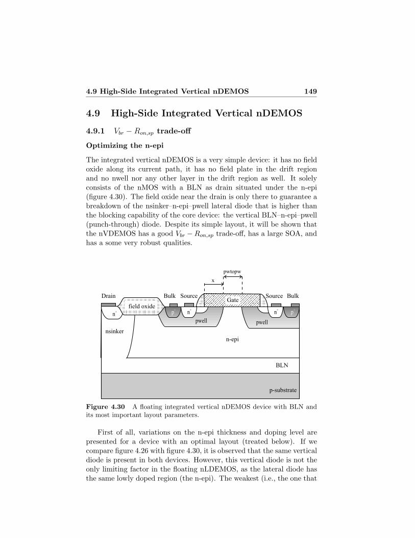
4.9 High-Side Integrated Vertical nDEMOS 149
4.9 High-Side Integrated Vertical nDEMOS
4.9.1 Vbr −Ron,sp trade-off
Optimizing the n-epi
The integrated vertical nDEMOS is a very simple device: it has no fieldoxide along its current path, it has no field plate in the drift regionand no nwell nor any other layer in the drift region as well. It solelyconsists of the nMOS with a BLN as drain situated under the n-epi(figure 4.30). The field oxide near the drain is only there to guarantee abreakdown of the nsinker–n-epi–pwell lateral diode that is higher thanthe blocking capability of the core device: the vertical BLN–n-epi–pwell(punch-through) diode. Despite its simple layout, it will be shown thatthe nVDEMOS has a good Vbr −Ron,sp trade-off, has a large SOA, andhas a some very robust qualities.
pwelln
+ p+
n+
pwell
n+
p+
Bulk SourceDrain Source Bulk
BLN
p-substrate
n-epi
field oxideGate
nsinker
x
pwtopw
Figure 4.30 A floating integrated vertical nDEMOS device with BLN andits most important layout parameters.
First of all, variations on the n-epi thickness and doping level arepresented for a device with an optimal layout (treated below). If wecompare figure 4.26 with figure 4.30, it is observed that the same verticaldiode is present in both devices. However, this vertical diode is not theonly limiting factor in the floating nLDEMOS, as the lateral diode hasthe same lowly doped region (the n-epi). The weakest (i.e., the one that
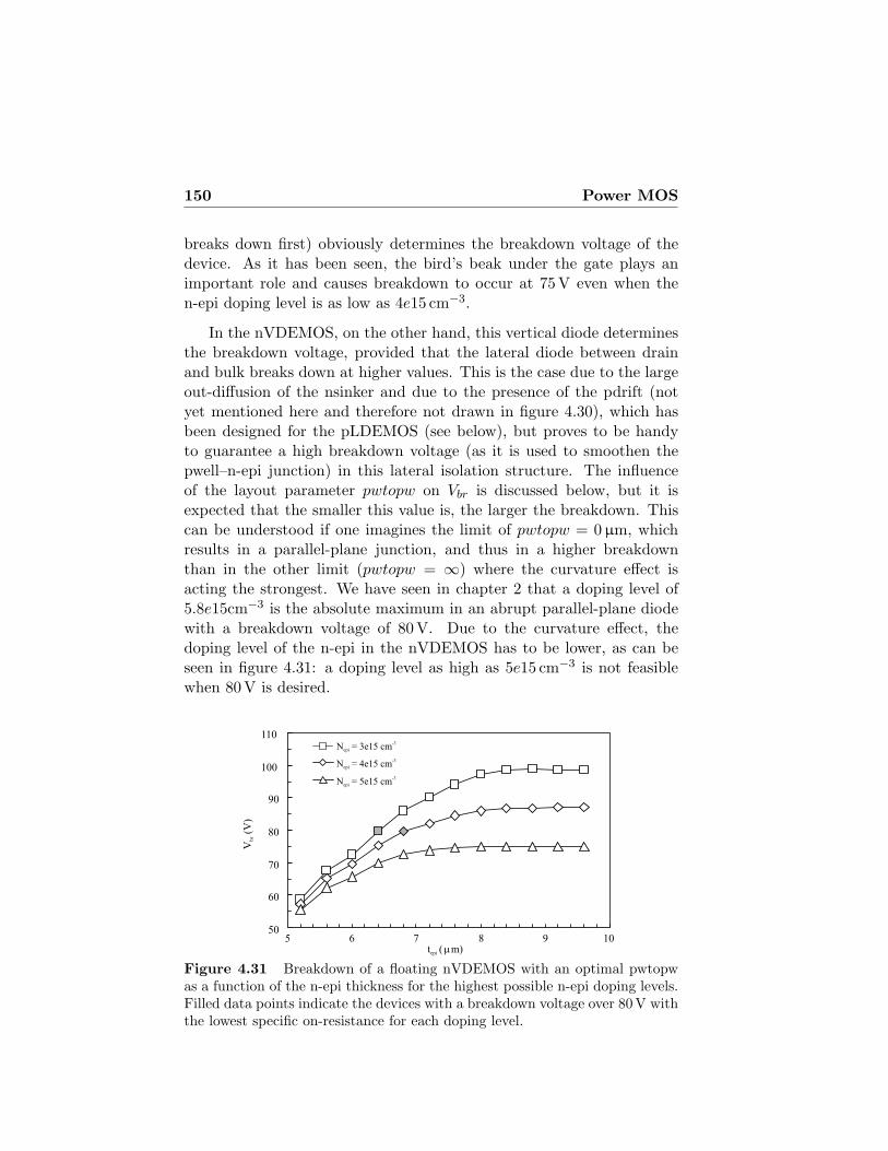
150 Power MOS
breaks down first) obviously determines the breakdown voltage of thedevice. As it has been seen, the bird’s beak under the gate plays animportant role and causes breakdown to occur at 75 V even when then-epi doping level is as low as 4e15 cm−3.
In the nVDEMOS, on the other hand, this vertical diode determinesthe breakdown voltage, provided that the lateral diode between drainand bulk breaks down at higher values. This is the case due to the largeout-diffusion of the nsinker and due to the presence of the pdrift (notyet mentioned here and therefore not drawn in figure 4.30), which hasbeen designed for the pLDEMOS (see below), but proves to be handyto guarantee a high breakdown voltage (as it is used to smoothen thepwell–n-epi junction) in this lateral isolation structure. The influenceof the layout parameter pwtopw on Vbr is discussed below, but it isexpected that the smaller this value is, the larger the breakdown. Thiscan be understood if one imagines the limit of pwtopw = 0µm, whichresults in a parallel-plane junction, and thus in a higher breakdownthan in the other limit (pwtopw = ∞) where the curvature effect isacting the strongest. We have seen in chapter 2 that a doping level of5.8e15cm−3 is the absolute maximum in an abrupt parallel-plane diodewith a breakdown voltage of 80 V. Due to the curvature effect, thedoping level of the n-epi in the nVDEMOS has to be lower, as can beseen in figure 4.31: a doping level as high as 5e15 cm−3 is not feasiblewhen 80 V is desired.
50
60
70
80
90
100
110
5 6 7 8 9 10
Vbr(V
)
tepi (mm)
N = 4e15 cmpi
-3
e
N = 5e15 cmpi
-3
e
N = 3e15 cmpi
-3
e
Figure 4.31 Breakdown of a floating nVDEMOS with an optimal pwtopwas a function of the n-epi thickness for the highest possible n-epi doping levels.Filled data points indicate the devices with a breakdown voltage over 80 V withthe lowest specific on-resistance for each doping level.
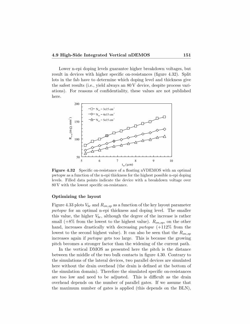
4.9 High-Side Integrated Vertical nDEMOS 151
Lower n-epi doping levels guarantee higher breakdown voltages, butresult in devices with higher specific on-resistances (figure 4.32). Splitlots in the fab have to determine which doping level and thickness givethe safest results (i.e., yield always an 80 V device, despite process vari-ations). For reasons of confidentiality, these values are not publishedhere.
50
100
150
200
5 6 7 8 9 10tepi (mm)
Ron,s
p(m
W.m
m2)
N = 4e15 cmpi
-3
e
N = 5e15 cmpi
-3
e
N = 3e15 cmpi
-3
e
Figure 4.32 Specific on-resistance of a floating nVDEMOS with an optimalpwtopw as a function of the n-epi thickness for the highest possible n-epi dopinglevels. Filled data points indicate the device with a breakdown voltage over80 V with the lowest specific on-resistance.
Optimizing the layout
Figure 4.33 plots Vbr and Ron,sp as a function of the key layout parameterpwtopw for an optimal n-epi thickness and doping level. The smallerthis value, the higher Vbr, although the degree of the increase is rathersmall (+8% from the lowest to the highest value). Ron,sp, on the otherhand, increases drastically with decreasing pwtopw (+112% from thelowest to the second highest value). It can also be seen that the Ron,sp
increases again if pwtopw gets too large. This is because the growingpitch becomes a stronger factor than the widening of the current path.
In the vertical DMOS as presented here the pitch is the distancebetween the middle of the two bulk contacts in figure 4.30. Contrary tothe simulations of the lateral devices, two parallel devices are simulatedhere without the drain overhead (the drain is defined at the bottom ofthe simulation domain). Therefore the simulated specific on-resistancesare too low and need to be adjusted. This is difficult as the drainoverhead depends on the number of parallel gates. If we assume thatthe maximum number of gates is applied (this depends on the BLN),
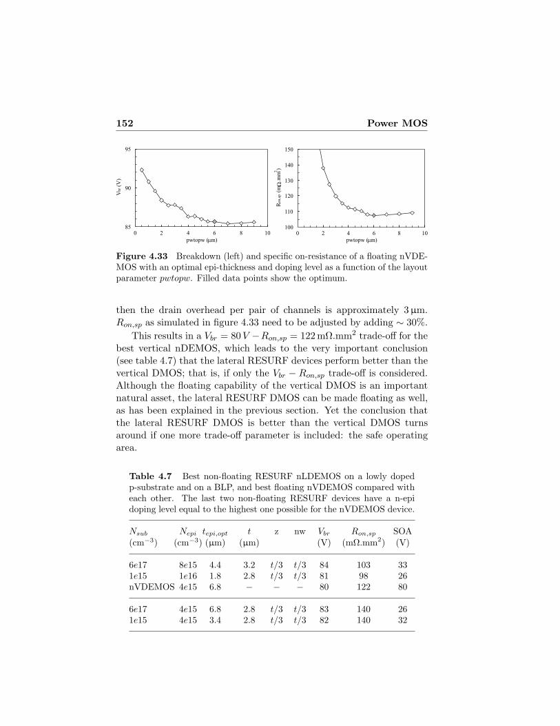
152 Power MOS
85
90
95
0 2 4 6 8 10
pwtopw (mm)
Vb
r(V
)
pwtopw (mm)
100
110
120
130
140
150
0 2 4 6 8 10
Ro
n,s
p(m
W.m
m2)
Figure 4.33 Breakdown (left) and specific on-resistance of a floating nVDE-MOS with an optimal epi-thickness and doping level as a function of the layoutparameter pwtopw. Filled data points show the optimum.
then the drain overhead per pair of channels is approximately 3µm.Ron,sp as simulated in figure 4.33 need to be adjusted by adding ∼ 30%.
This results in a Vbr = 80V −Ron,sp = 122 mΩ.mm2 trade-off for thebest vertical nDEMOS, which leads to the very important conclusion(see table 4.7) that the lateral RESURF devices perform better than thevertical DMOS; that is, if only the Vbr − Ron,sp trade-off is considered.Although the floating capability of the vertical DMOS is an importantnatural asset, the lateral RESURF DMOS can be made floating as well,as has been explained in the previous section. Yet the conclusion thatthe lateral RESURF DMOS is better than the vertical DMOS turnsaround if one more trade-off parameter is included: the safe operatingarea.
Table 4.7 Best non-floating RESURF nLDEMOS on a lowly dopedp-substrate and on a BLP, and best floating nVDEMOS compared witheach other. The last two non-floating RESURF devices have a n-epidoping level equal to the highest one possible for the nVDEMOS device.
Nsub Nepi tepi,opt t z nw Vbr Ron,sp SOA(cm−3) (cm−3) (µm) (µm) (V) (mΩ.mm2) (V)
6e17 8e15 4.4 3.2 t/3 t/3 84 103 331e15 1e16 1.8 2.8 t/3 t/3 81 98 26nVDEMOS 4e15 6.8 − − − 80 122 80
6e17 4e15 6.8 2.8 t/3 t/3 83 140 261e15 4e15 3.4 2.8 t/3 t/3 82 140 32
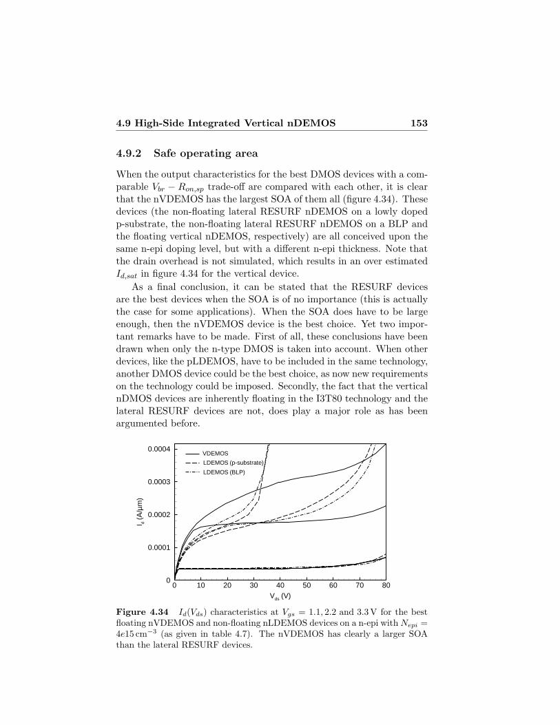
4.9 High-Side Integrated Vertical nDEMOS 153
4.9.2 Safe operating area
When the output characteristics for the best DMOS devices with a com-parable Vbr − Ron,sp trade-off are compared with each other, it is clearthat the nVDEMOS has the largest SOA of them all (figure 4.34). Thesedevices (the non-floating lateral RESURF nDEMOS on a lowly dopedp-substrate, the non-floating lateral RESURF nDEMOS on a BLP andthe floating vertical nDEMOS, respectively) are all conceived upon thesame n-epi doping level, but with a different n-epi thickness. Note thatthe drain overhead is not simulated, which results in an over estimatedId,sat in figure 4.34 for the vertical device.
As a final conclusion, it can be stated that the RESURF devicesare the best devices when the SOA is of no importance (this is actuallythe case for some applications). When the SOA does have to be largeenough, then the nVDEMOS device is the best choice. Yet two impor-tant remarks have to be made. First of all, these conclusions have beendrawn when only the n-type DMOS is taken into account. When otherdevices, like the pLDEMOS, have to be included in the same technology,another DMOS device could be the best choice, as now new requirementson the technology could be imposed. Secondly, the fact that the verticalnDMOS devices are inherently floating in the I3T80 technology and thelateral RESURF devices are not, does play a major role as has beenargumented before.
Vds (V)
I d(A
/µm
)
0 10 20 30 40 50 60 70 800
0.0001
0.0002
0.0003
0.0004VDEMOS
LDEMOS (p-substrate)
LDEMOS (BLP)
Figure 4.34 Id(Vds) characteristics at Vgs = 1.1, 2.2 and 3.3V for the bestfloating nVDEMOS and non-floating nLDEMOS devices on a n-epi with Nepi =4e15 cm−3 (as given in table 4.7). The nVDEMOS has clearly a larger SOAthan the lateral RESURF devices.
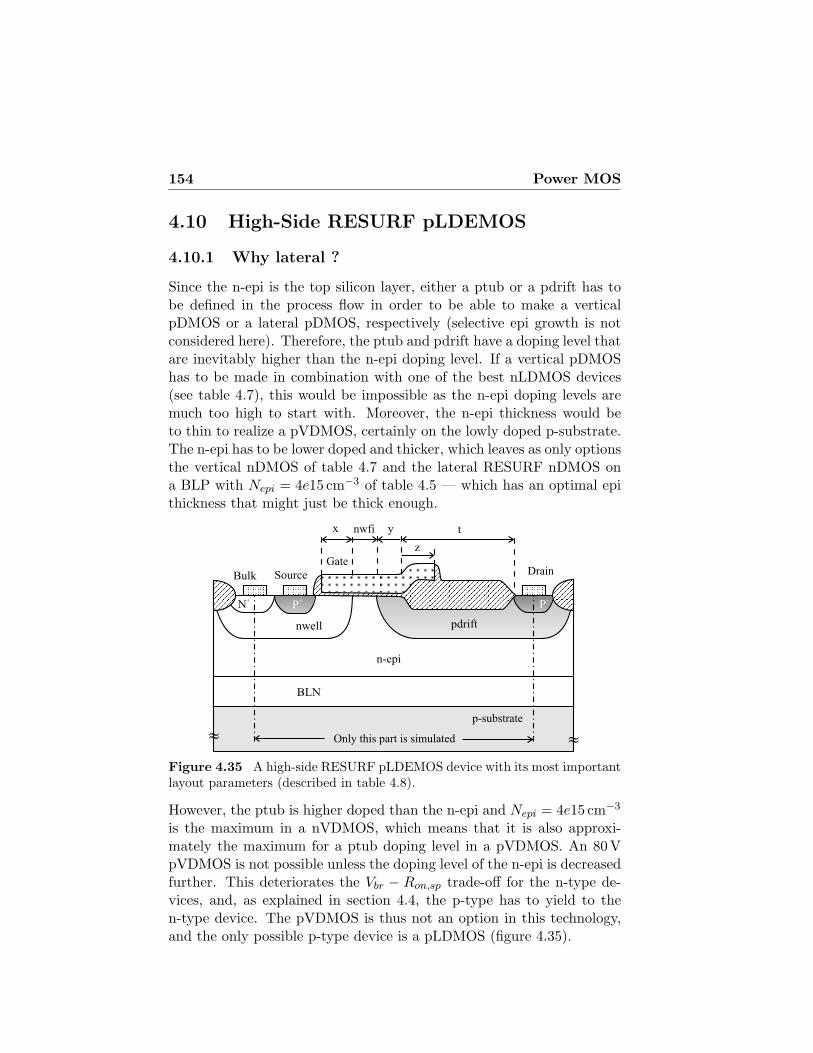
154 Power MOS
4.10 High-Side RESURF pLDEMOS
4.10.1 Why lateral ?
Since the n-epi is the top silicon layer, either a ptub or a pdrift has tobe defined in the process flow in order to be able to make a verticalpDMOS or a lateral pDMOS, respectively (selective epi growth is notconsidered here). Therefore, the ptub and pdrift have a doping level thatare inevitably higher than the n-epi doping level. If a vertical pDMOShas to be made in combination with one of the best nLDMOS devices(see table 4.7), this would be impossible as the n-epi doping levels aremuch too high to start with. Moreover, the n-epi thickness would beto thin to realize a pVDMOS, certainly on the lowly doped p-substrate.The n-epi has to be lower doped and thicker, which leaves as only optionsthe vertical nDMOS of table 4.7 and the lateral RESURF nDMOS ona BLP with Nepi = 4e15 cm−3 of table 4.5 — which has an optimal epithickness that might just be thick enough.
pdrift
n-epi
Source
GateDrain
p-substrate
N+
»»
x t
z
y
Only this part is simulated
Bulk
nwell
BLN
P+
P+
nwfi
Figure 4.35 A high-side RESURF pLDEMOS device with its most importantlayout parameters (described in table 4.8).
However, the ptub is higher doped than the n-epi and Nepi = 4e15 cm−3
is the maximum in a nVDMOS, which means that it is also approxi-mately the maximum for a ptub doping level in a pVDMOS. An 80VpVDMOS is not possible unless the doping level of the n-epi is decreasedfurther. This deteriorates the Vbr − Ron,sp trade-off for the n-type de-vices, and, as explained in section 4.4, the p-type has to yield to then-type device. The pVDMOS is thus not an option in this technology,and the only possible p-type device is a pLDMOS (figure 4.35).

4.10 High-Side RESURF pLDEMOS 155
Table 4.8 Layout parameters of the pLDEMOS with pdrift
Parameter Description Value (µm)
c0∗ n+ aa width as bulk region 1.1c1∗ p+ aa width as source region 1.3x∗ channel length variednwfi∗ nwell spacing to pdrift region variedy∗ pdrift overlap on active area variedt∗ length of field oxide on drift region variedc2∗ p+ aa width as drain region 0.8z poly overlap on field oxide varied
Parameters indicated with (∗) define the pitch of the device (distance from half-bulk to half-drain): pitch = (1.1/2) + 1.3 + x + y + t + (0.8/2) = 2.25 + x + y + t.
4.10.2 Conditions sine qua non on the n-epi
What holds for the ptub also holds for the pdrift: it has inevitably ahigher doping level than the n-epi. Yet in the lateral case this is not aproblem, since the blocking capability is also determined by the n-epi.A “true” RESURF effect is now at hand, and, as was the case for thenon-floating nLDEMOS on a lowly doped p-substrate, the pdrift dopinglevel can be a lot higher than the n-epi doping level, as long as thepdrift dose fulfils the optimal RESURF conditions. A translation of theexpression for the optimal RESURF dose for a n-type structure can beobtained if the Nsub and the Nepi in equation (4.4) are replaced by Nepi
and Npdrift , respectively:
Dopt ,pdrift = Npdrift × tpdrift ,opt
=(
εs
q
)7/8 (8Npdrift
1.8× 10⁻³⁵
)1/8√
Nepi
(Nepi + Npdrift). (4.11)
This expression serves as a tool to investigate the possible conflictsthat can arise if the pLDMOS is combined with each of the nDMOSdevices as given in table 4.7. Each of the n-epi doping levels in thistable are used in the expression (C.30) for the punch-through breakdownvoltage of a n+–n–p diode, which also determines the breakdown voltageof the ideal RESURF diode present in the pLDMOS (it is actually ap+–p–n diode, but this leads to the same expression). These valuesare plotted in figure 4.36 for all Npdrift > Nepi. It is observed that the
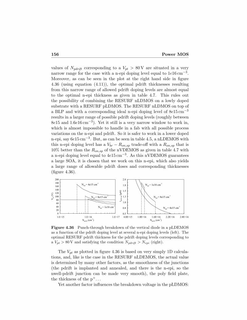
156 Power MOS
values of Npdrift corresponding to a Vpt > 80V are situated in a verynarrow range for the case with a n-epi doping level equal to 1e16 cm−3.Moreover, as can be seen in the plot at the right hand side in figure4.36 (using equation (4.11)), the optimal pdrift thicknesses resultingfrom this narrow range of allowed pdrift doping levels are almost equalto the optimal n-epi thickness as given in table 4.7. This rules outthe possibility of combining the RESURF nLDMOS on a lowly dopedsubstrate with a RESURF pLDMOS. The RESURF nLDMOS on top ofa BLP and with a corresponding ideal n-epi doping level of 8e15 cm−3
results in a larger range of possible pdrift doping levels (roughly between8e15 and 1.6e16 cm−3). Yet it still is a very narrow window to work in,which is almost impossible to handle in a fab with all possible processvariations on the n-epi and pdrift. So it is safer to work in a lower dopedn-epi, say 6e15 cm−3. But, as can be seen in table 4.5, a nLDEMOS withthis n-epi doping level has a Vbr −Ron,sp trade-off with a Ron,sp that is10% better than the Ron,sp of the nVDEMOS as given in table 4.7 witha n-epi doping level equal to 4e15 cm−3. As this nVDEMOS guaranteesa large SOA, it is chosen that we work on this n-epi, which also yieldsa large range of allowable pdrift doses and corresponding thicknesses(figure 4.36).
0
20
40
60
80
100
120
140
160
180
200
1.E+15 1.E+16 1.E+17
N (cm )pdrift
-3
Vpt(V
)
N = 4e15 cmepi
-3
N = 8e15 cmepi
-3
N = 1e16 cmepi
-3
0.5
0.8
1.0
1.3
1.5
1.8
2.0
4.0E+15 1.0E+16 1.6E+16 2.2E+16 2.8E+16
t pdri
ft,o
pt( m
m)
N = 1e16 cmepi
-3
N = 8e15 cmepi
-3
N = 4e15 cmepi
-3
N (cm )pdrift
-3
Figure 4.36 Punch-through breakdown of the vertical diode in a pLDEMOSas a function of the pdrift doping level at several n-epi doping levels (left). Theoptimal RESURF pdrift thickness for the pdrift doping levels corresponding toa Vpt > 80V and satisfying the condition Npdrift > Nepi (right).
The Vpt as plotted in figure 4.36 is based on very simply 1D calcula-tions, and, like is the case in the RESURF nLDEMOS, the actual valueis determined by many other factors, as the smoothness of the junctions(the pdrift is implanted and annealed, and there is the n-epi, so thenwell-pdrift junction can be made very smooth), the poly field plate,the thickness of the p+. . .
Yet another factor influences the breakdown voltage in the pLDMOS:
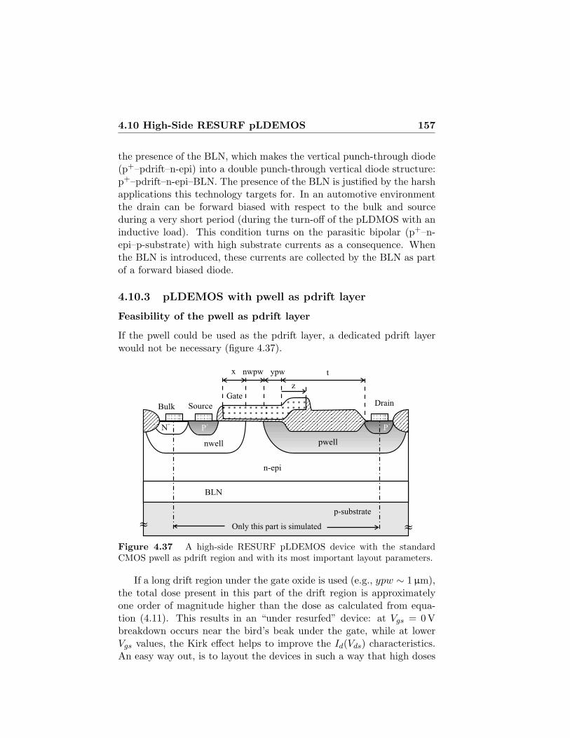
4.10 High-Side RESURF pLDEMOS 157
the presence of the BLN, which makes the vertical punch-through diode(p+–pdrift–n-epi) into a double punch-through vertical diode structure:p+–pdrift–n-epi–BLN. The presence of the BLN is justified by the harshapplications this technology targets for. In an automotive environmentthe drain can be forward biased with respect to the bulk and sourceduring a very short period (during the turn-off of the pLDMOS with aninductive load). This condition turns on the parasitic bipolar (p+–n-epi–p-substrate) with high substrate currents as a consequence. Whenthe BLN is introduced, these currents are collected by the BLN as partof a forward biased diode.
4.10.3 pLDEMOS with pwell as pdrift layer
Feasibility of the pwell as pdrift layer
If the pwell could be used as the pdrift layer, a dedicated pdrift layerwould not be necessary (figure 4.37).
pwell
n-epi
Source
GateDrain
p-substrate
N+
»»
x t
z
ypw
Only this part is simulated
Bulk
nwell
BLN
P+
P+
nwpw
Figure 4.37 A high-side RESURF pLDEMOS device with the standardCMOS pwell as pdrift region and with its most important layout parameters.
If a long drift region under the gate oxide is used (e.g., ypw ∼ 1µm),the total dose present in this part of the drift region is approximatelyone order of magnitude higher than the dose as calculated from equa-tion (4.11). This results in an “under resurfed” device: at Vgs = 0Vbreakdown occurs near the bird’s beak under the gate, while at lowerVgs values, the Kirk effect helps to improve the Id(Vds) characteristics.An easy way out, is to layout the devices in such a way that high doses
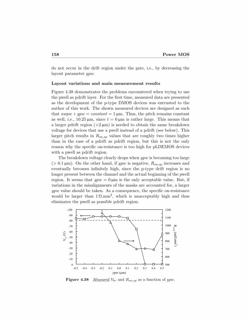
158 Power MOS
do not occur in the drift region under the gate, i.e., by decreasing thelayout parameter ypw.
Layout variations and main measurement results
Figure 4.38 demonstrates the problems encountered when trying to usethe pwell as pdrift layer. For the first time, measured data are presentedas the development of the p-type DMOS devices was entrusted to theauthor of this work. The shown measured devices are designed as suchthat nwpw + ypw = constant = 1µm. Thus, the pitch remains constantas well, i.e., 10.25µm, since t = 6µm is rather large. This means thata larger pdrift region (+2µm) is needed to obtain the same breakdownvoltage for devices that use a pwell instead of a pdrift (see below). Thislarger pitch results in Ron,sp values that are roughly two times higherthan in the case of a pdrift as pdrift region, but this is not the onlyreason why the specific on-resistance is too high for pLDEMOS deviceswith a pwell as pdrift region.
The breakdown voltage clearly drops when ypw is becoming too large(> 0.1µm). On the other hand, if ypw is negative, Ron,sp increases andeventually becomes infinitely high, since the p-type drift region is nolonger present between the channel and the actual beginning of the pwellregion. It seems that ypw = 0µm is the only acceptable value. But, ifvariations in the misalignments of the masks are accounted for, a largerypw value should be taken. As a consequence, the specific on-resistancewould be larger than 1Ω.mm2, which is unacceptably high and thuseliminates the pwell as possible pdrift region.
-100
-90
-80
-70
-60
-50
-40
-30
-20
-10
0
-0.5 -0.4 -0.3 -0.2 -0.1 0.0 0.1 0.2 0.3 0.4 0.5
500
600
700
800
900
1000
1100
1200
ypw ( m)m
R(m
.mm
)on,sp
W2
V(V
)b
r
Figure 4.38 Measured Vbr and Ron,sp as a function of ypw.
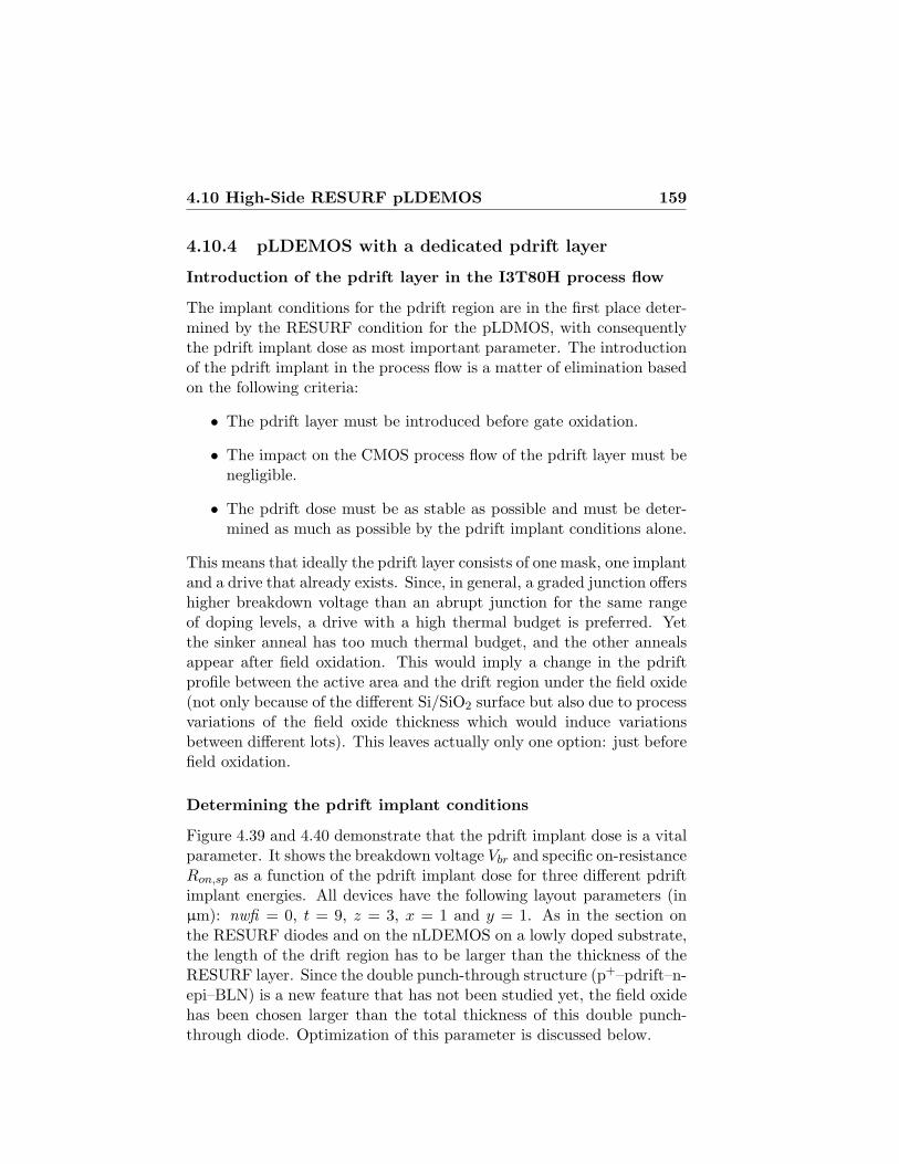
4.10 High-Side RESURF pLDEMOS 159
4.10.4 pLDEMOS with a dedicated pdrift layer
Introduction of the pdrift layer in the I3T80H process flow
The implant conditions for the pdrift region are in the first place deter-mined by the RESURF condition for the pLDMOS, with consequentlythe pdrift implant dose as most important parameter. The introductionof the pdrift implant in the process flow is a matter of elimination basedon the following criteria:
• The pdrift layer must be introduced before gate oxidation.
• The impact on the CMOS process flow of the pdrift layer must benegligible.
• The pdrift dose must be as stable as possible and must be deter-mined as much as possible by the pdrift implant conditions alone.
This means that ideally the pdrift layer consists of one mask, one implantand a drive that already exists. Since, in general, a graded junction offershigher breakdown voltage than an abrupt junction for the same rangeof doping levels, a drive with a high thermal budget is preferred. Yetthe sinker anneal has too much thermal budget, and the other annealsappear after field oxidation. This would imply a change in the pdriftprofile between the active area and the drift region under the field oxide(not only because of the different Si/SiO2 surface but also due to processvariations of the field oxide thickness which would induce variationsbetween different lots). This leaves actually only one option: just beforefield oxidation.
Determining the pdrift implant conditions
Figure 4.39 and 4.40 demonstrate that the pdrift implant dose is a vitalparameter. It shows the breakdown voltage Vbr and specific on-resistanceRon,sp as a function of the pdrift implant dose for three different pdriftimplant energies. All devices have the following layout parameters (inµm): nwfi = 0, t = 9, z = 3, x = 1 and y = 1. As in the section onthe RESURF diodes and on the nLDEMOS on a lowly doped substrate,the length of the drift region has to be larger than the thickness of theRESURF layer. Since the double punch-through structure (p+–pdrift–n-epi–BLN) is a new feature that has not been studied yet, the field oxidehas been chosen larger than the total thickness of this double punch-through diode. Optimization of this parameter is discussed below.
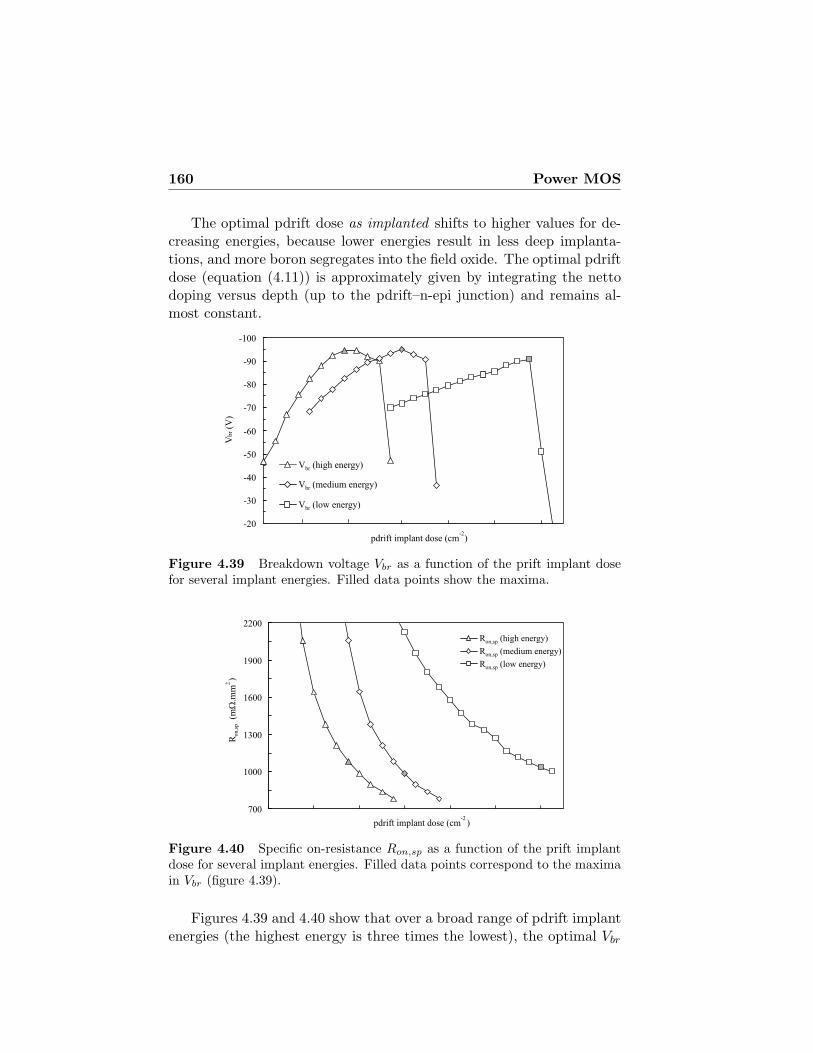
160 Power MOS
The optimal pdrift dose as implanted shifts to higher values for de-creasing energies, because lower energies result in less deep implanta-tions, and more boron segregates into the field oxide. The optimal pdriftdose (equation (4.11)) is approximately given by integrating the nettodoping versus depth (up to the pdrift–n-epi junction) and remains al-most constant.
-100
-90
-80
-70
-60
-50
-40
-30
-20
pdrift implant dose (cm-2
)
Vbr(V
)
V (high energy)br
V (medium energy)br
V (low energy)br
Figure 4.39 Breakdown voltage Vbr as a function of the prift implant dosefor several implant energies. Filled data points show the maxima.
700
1000
1300
1600
1900
2200
pdrift implant dose (cm-2
)
Ro
n,s
p(m
.mm
W2)
R (high energy)on,sp
R (medium energy)on,sp
R (low energy)on,sp
Figure 4.40 Specific on-resistance Ron,sp as a function of the prift implantdose for several implant energies. Filled data points correspond to the maximain Vbr (figure 4.39).
Figures 4.39 and 4.40 show that over a broad range of pdrift implantenergies (the highest energy is three times the lowest), the optimal Vbr
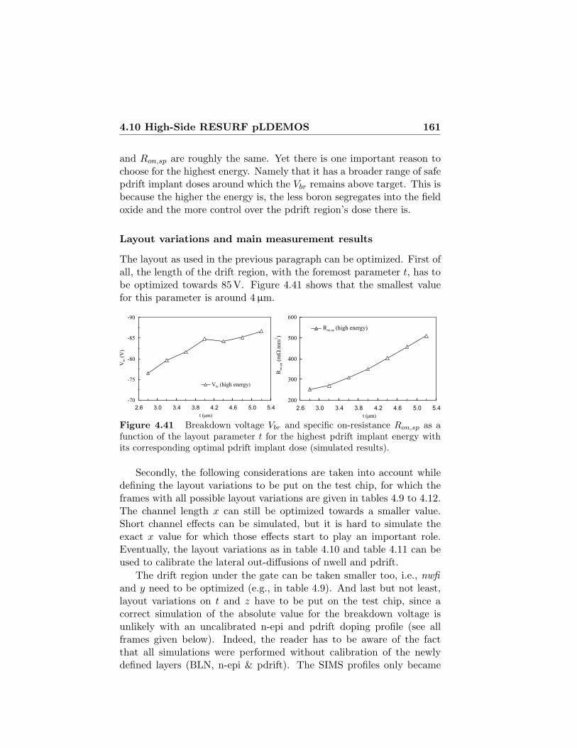
4.10 High-Side RESURF pLDEMOS 161
and Ron,sp are roughly the same. Yet there is one important reason tochoose for the highest energy. Namely that it has a broader range of safepdrift implant doses around which the Vbr remains above target. This isbecause the higher the energy is, the less boron segregates into the fieldoxide and the more control over the pdrift region’s dose there is.
Layout variations and main measurement results
The layout as used in the previous paragraph can be optimized. First ofall, the length of the drift region, with the foremost parameter t, has tobe optimized towards 85 V. Figure 4.41 shows that the smallest valuefor this parameter is around 4µm.
200
300
400
500
600
2.6 3.0 3.4 3.8 4.2 4.6 5.0 5.4
t (mm)
R(m
.mm
)o
n,s
pW
2
R (high energy)on,sp
-90
-85
-80
-75
-70
2.6 3.0 3.4 3.8 4.2 4.6 5.0 5.4
t (mm)
Vb
r(V
)
V (high energybr )
Figure 4.41 Breakdown voltage Vbr and specific on-resistance Ron,sp as afunction of the layout parameter t for the highest pdrift implant energy withits corresponding optimal pdrift implant dose (simulated results).
Secondly, the following considerations are taken into account whiledefining the layout variations to be put on the test chip, for which theframes with all possible layout variations are given in tables 4.9 to 4.12.The channel length x can still be optimized towards a smaller value.Short channel effects can be simulated, but it is hard to simulate theexact x value for which those effects start to play an important role.Eventually, the layout variations as in table 4.10 and table 4.11 can beused to calibrate the lateral out-diffusions of nwell and pdrift.
The drift region under the gate can be taken smaller too, i.e., nwfiand y need to be optimized (e.g., in table 4.9). And last but not least,layout variations on t and z have to be put on the test chip, since acorrect simulation of the absolute value for the breakdown voltage isunlikely with an uncalibrated n-epi and pdrift doping profile (see allframes given below). Indeed, the reader has to be aware of the factthat all simulations were performed without calibration of the newlydefined layers (BLN, n-epi & pdrift). The SIMS profiles only became
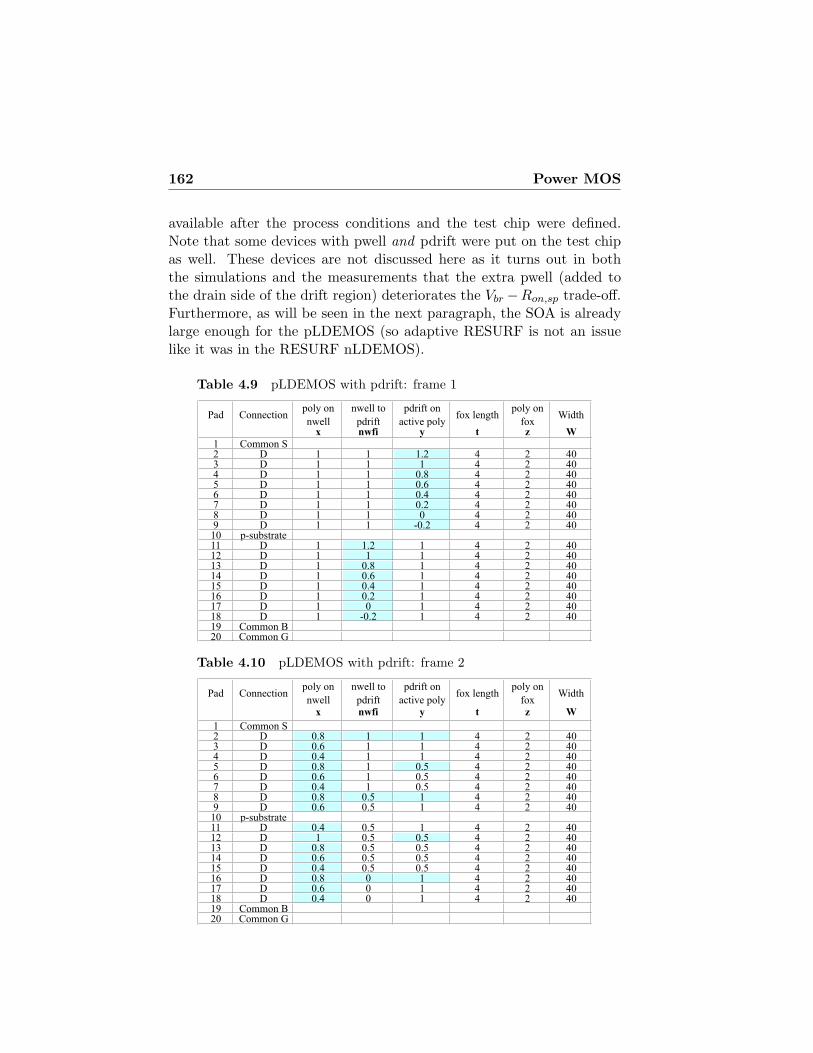
162 Power MOS
available after the process conditions and the test chip were defined.Note that some devices with pwell and pdrift were put on the test chipas well. These devices are not discussed here as it turns out in boththe simulations and the measurements that the extra pwell (added tothe drain side of the drift region) deteriorates the Vbr −Ron,sp trade-off.Furthermore, as will be seen in the next paragraph, the SOA is alreadylarge enough for the pLDEMOS (so adaptive RESURF is not an issuelike it was in the RESURF nLDEMOS).
Table 4.9 pLDEMOS with pdrift: frame 1
Pad Connectionpoly on
nwell
nwell to
pdrift
pdrift on
active polyfox length
poly on
foxWidth
x nwfi y t z W
1 Common S2 D 1 1 1.2 4 2 403 D 1 1 1 4 2 404 D 1 1 0.8 4 2 405 D 1 1 0.6 4 2 406 D 1 1 0.4 4 2 407 D 1 1 0.2 4 2 408 D 1 1 0 4 2 409 D 1 1 -0.2 4 2 40
10 p-substrate11 D 1 1.2 1 4 2 4012 D 1 1 1 4 2 4013 D 1 0.8 1 4 2 4014 D 1 0.6 1 4 2 4015 D 1 0.4 1 4 2 4016 D 1 0.2 1 4 2 4017 D 1 0 1 4 2 4018 D 1 -0.2 1 4 2 4019 Common B20 Common G
Table 4.10 pLDEMOS with pdrift: frame 2
Pad Connectionpoly on
nwell
nwell to
pdrift
pdrift on
active polyfox length
poly on
foxWidth
x nwfi y t z W
1 Common S2 D 0.8 1 1 4 2 403 D 0.6 1 1 4 2 404 D 0.4 1 1 4 2 405 D 0.8 1 0.5 4 2 406 D 0.6 1 0.5 4 2 407 D 0.4 1 0.5 4 2 408 D 0.8 0.5 1 4 2 409 D 0.6 0.5 1 4 2 40
10 p-substrate11 D 0.4 0.5 1 4 2 4012 D 1 0.5 0.5 4 2 4013 D 0.8 0.5 0.5 4 2 4014 D 0.6 0.5 0.5 4 2 4015 D 0.4 0.5 0.5 4 2 4016 D 0.8 0 1 4 2 4017 D 0.6 0 1 4 2 4018 D 0.4 0 1 4 2 4019 Common B20 Common G
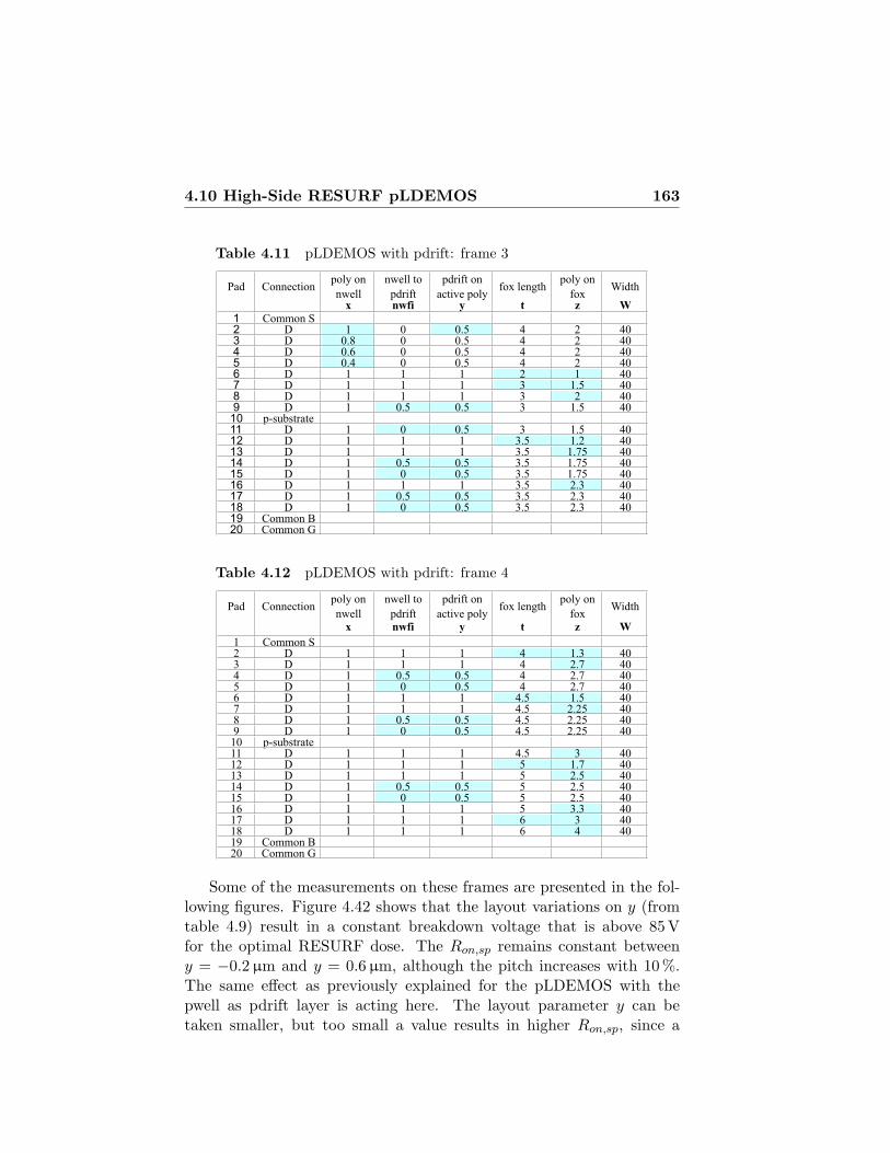
4.10 High-Side RESURF pLDEMOS 163
Table 4.11 pLDEMOS with pdrift: frame 3
Pad Connectionpoly on
nwell
nwell to
pdrift
pdrift on
active polyfox length
poly on
foxWidth
x nwfi y t z W
1 Common S2 D 1 0 0.5 4 2 403 D 0.8 0 0.5 4 2 404 D 0.6 0 0.5 4 2 405 D 0.4 0 0.5 4 2 406 D 1 1 1 2 1 407 D 1 1 1 3 1.5 408 D 1 1 1 3 2 409 D 1 0.5 0.5 3 1.5 4010 p-substrate11 D 1 0 0.5 3 1.5 4012 D 1 1 1 3.5 1.2 4013 D 1 1 1 3.5 1.75 4014 D 1 0.5 0.5 3.5 1.75 4015 D 1 0 0.5 3.5 1.75 4016 D 1 1 1 3.5 2.3 4017 D 1 0.5 0.5 3.5 2.3 4018 D 1 0 0.5 3.5 2.3 4019 Common B20 Common G
Table 4.12 pLDEMOS with pdrift: frame 4
Pad Connectionpoly on
nwell
nwell to
pdrift
pdrift on
active polyfox length
poly on
foxWidth
x nwfi y t z W
1 Common S2 D 1 1 1 4 1.3 403 D 1 1 1 4 2.7 404 D 1 0.5 0.5 4 2.7 405 D 1 0 0.5 4 2.7 406 D 1 1 1 4.5 1.5 407 D 1 1 1 4.5 2.25 408 D 1 0.5 0.5 4.5 2.25 409 D 1 0 0.5 4.5 2.25 40
10 p-substrate11 D 1 1 1 4.5 3 4012 D 1 1 1 5 1.7 4013 D 1 1 1 5 2.5 4014 D 1 0.5 0.5 5 2.5 4015 D 1 0 0.5 5 2.5 4016 D 1 1 1 5 3.3 4017 D 1 1 1 6 3 4018 D 1 1 1 6 4 4019 Common B20 Common G
Some of the measurements on these frames are presented in the fol-lowing figures. Figure 4.42 shows that the layout variations on y (fromtable 4.9) result in a constant breakdown voltage that is above 85 Vfor the optimal RESURF dose. The Ron,sp remains constant betweeny = −0.2µm and y = 0.6 µm, although the pitch increases with 10%.The same effect as previously explained for the pLDEMOS with thepwell as pdrift layer is acting here. The layout parameter y can betaken smaller, but too small a value results in higher Ron,sp, since a
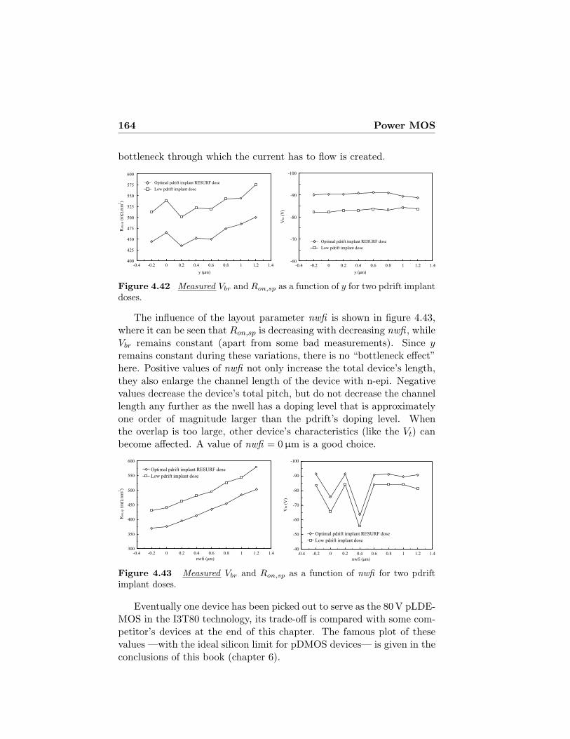
164 Power MOS
bottleneck through which the current has to flow is created.-100
-90
-80
-70
-60-0.4 -0.2 0 0.2 0.4 0.6 0.8 1 1.2 1.4
y (mm)
Vb
r(V
)
Optimal pdrift implant RESURF dose
Low pdrift implant dose
400
425
450
475
500
525
550
575
600
-0.4 -0.2 0 0.2 0.4 0.6 0.8 1 1.2 1.4
y (mm)
Ro
n,s
p(m
W.m
m2)
Optimal pdrift implant RESURF dose
Low pdrift implant dose
Figure 4.42 Measured Vbr and Ron,sp as a function of y for two pdrift implantdoses.
The influence of the layout parameter nwfi is shown in figure 4.43,where it can be seen that Ron,sp is decreasing with decreasing nwfi , whileVbr remains constant (apart from some bad measurements). Since yremains constant during these variations, there is no “bottleneck effect”here. Positive values of nwfi not only increase the total device’s length,they also enlarge the channel length of the device with n-epi. Negativevalues decrease the device’s total pitch, but do not decrease the channellength any further as the nwell has a doping level that is approximatelyone order of magnitude larger than the pdrift’s doping level. Whenthe overlap is too large, other device’s characteristics (like the Vt) canbecome affected. A value of nwfi = 0µm is a good choice.
Optimal pdrift implant RESURF dose
Low pdrift implant dose
300
350
400
450
500
550
600
-0.4 -0.2 0 0.2 0.4 0.6 0.8 1 1.2 1.4
nwfi (mm)
Ro
n,s
p(m
W.m
m2)
-100
-90
-80
-70
-60
-50
-40-0.4 -0.2 0 0.2 0.4 0.6 0.8 1 1.2 1.4
nwfi (mm)
Vb
r(V
)
Optimal pdrift implant RESURF dose
Low pdrift implant dose
Figure 4.43 Measured Vbr and Ron,sp as a function of nwfi for two pdriftimplant doses.
Eventually one device has been picked out to serve as the 80 V pLDE-MOS in the I3T80 technology, its trade-off is compared with some com-petitor’s devices at the end of this chapter. The famous plot of thesevalues —with the ideal silicon limit for pDMOS devices— is given in theconclusions of this book (chapter 6).
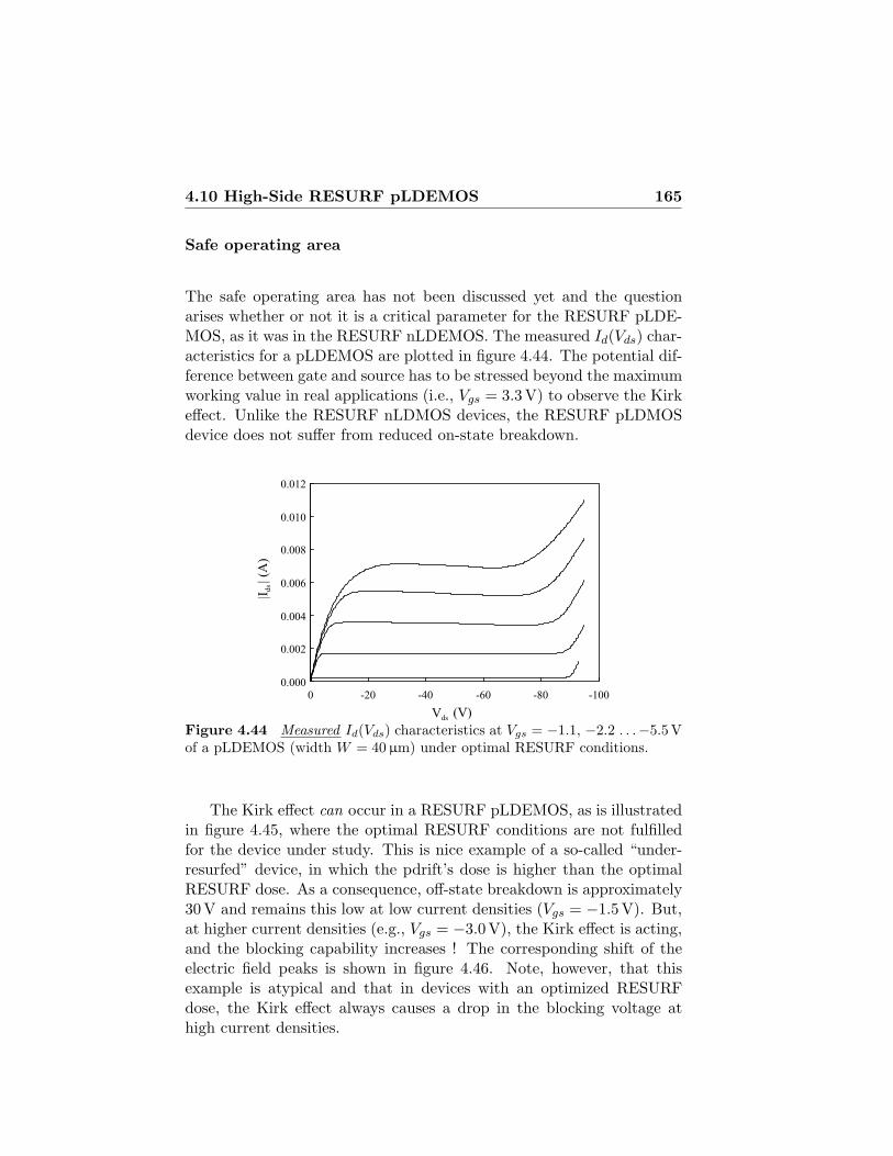
4.10 High-Side RESURF pLDEMOS 165
Safe operating area
The safe operating area has not been discussed yet and the questionarises whether or not it is a critical parameter for the RESURF pLDE-MOS, as it was in the RESURF nLDEMOS. The measured Id(Vds) char-acteristics for a pLDEMOS are plotted in figure 4.44. The potential dif-ference between gate and source has to be stressed beyond the maximumworking value in real applications (i.e., Vgs = 3.3 V) to observe the Kirkeffect. Unlike the RESURF nLDMOS devices, the RESURF pLDMOSdevice does not suffer from reduced on-state breakdown.
0.000
0.002
0.004
0.006
0.008
0.010
0.012
-100-80-60-40-200
|Ids| (
A)
Vds (V)
Figure 4.44 Measured Id(Vds) characteristics at Vgs = −1.1, −2.2 . . .−5.5Vof a pLDEMOS (width W = 40 µm) under optimal RESURF conditions.
The Kirk effect can occur in a RESURF pLDEMOS, as is illustratedin figure 4.45, where the optimal RESURF conditions are not fulfilledfor the device under study. This is nice example of a so-called “under-resurfed” device, in which the pdrift’s dose is higher than the optimalRESURF dose. As a consequence, off-state breakdown is approximately30V and remains this low at low current densities (Vgs = −1.5V). But,at higher current densities (e.g., Vgs = −3.0V), the Kirk effect is acting,and the blocking capability increases ! The corresponding shift of theelectric field peaks is shown in figure 4.46. Note, however, that thisexample is atypical and that in devices with an optimized RESURFdose, the Kirk effect always causes a drop in the blocking voltage athigh current densities.
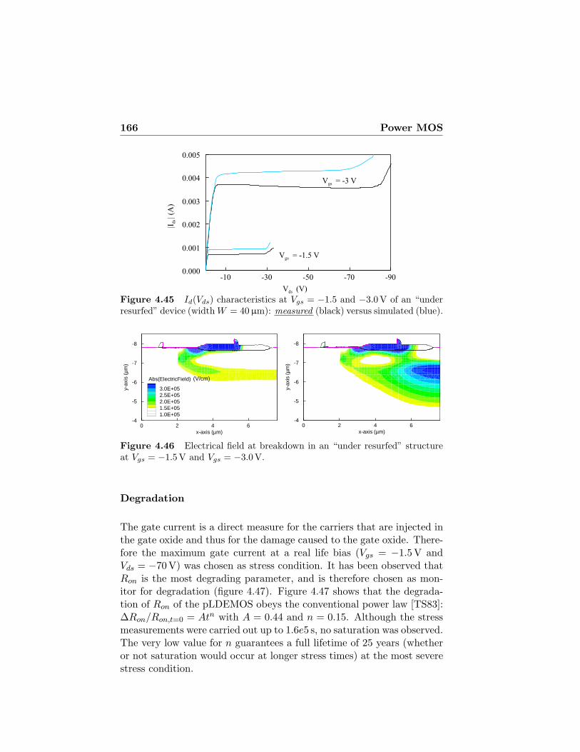
166 Power MOS
0.000
0.001
0.002
0.003
0.004
0.005
-90-70-50-30-10
Vds (V)
|Id
s| (
A)
Vgs = -1.5 V
Vgs = -3 V
Figure 4.45 Id(Vds) characteristics at Vgs = −1.5 and −3.0 V of an “underresurfed” device (width W = 40 µm): measured (black) versus simulated (blue).
x-axis (µm)
y-ax
is(µ
m)
0 2 4 6
-8
-7
-6
-5
-4
x-axis (µm)
y-ax
is(µ
m)
0 2 4 6
-8
-7
-6
-5
-4
Abs(ElectricField)
3.0E+052.5E+052.0E+051.5E+051.0E+05
(V/cm)
Figure 4.46 Electrical field at breakdown in an “under resurfed” structureat Vgs = −1.5V and Vgs = −3.0V.
Degradation
The gate current is a direct measure for the carriers that are injected inthe gate oxide and thus for the damage caused to the gate oxide. There-fore the maximum gate current at a real life bias (Vgs = −1.5V andVds = −70V) was chosen as stress condition. It has been observed thatRon is the most degrading parameter, and is therefore chosen as mon-itor for degradation (figure 4.47). Figure 4.47 shows that the degrada-tion of Ron of the pLDEMOS obeys the conventional power law [TS83]:∆Ron/Ron,t=0 = Atn with A = 0.44 and n = 0.15. Although the stressmeasurements were carried out up to 1.6e5 s, no saturation was observed.The very low value for n guarantees a full lifetime of 25 years (whetheror not saturation would occur at longer stress times) at the most severestress condition.
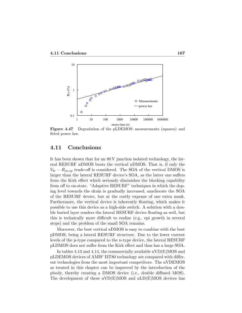
4.11 Conclusions 167
0.1
1
10
1 10 100 1000 10000 100000 1000000
stress time (s)
Ron
(%)
Measurements
power law
Figure 4.47 Degradation of the pLDEMOS: measurements (squares) andfitted power law.
4.11 Conclusions
It has been shown that for an 80V junction isolated technology, the lat-eral RESURF nDMOS beats the vertical nDMOS. That is, if only theVbr − Ron,sp trade-off is considered. The SOA of the vertical DMOS islarger than the lateral RESURF device’s SOA, as the latter one suffersfrom the Kirk effect which seriously diminishes the blocking capabilityfrom off to on-state. “Adaptive RESURF” techniques in which the dop-ing level towards the drain is gradually increased, ameliorate the SOAof the RESURF device, but at the costly expense of one extra mask.Furthermore, the vertical device is inherently floating, which makes itpossible to use this device as a high-side switch. A solution with a dou-ble buried layer renders the lateral RESURF device floating as well, butthis is technically more difficult to realize (e.g., epi growth in severalsteps) and the problem of the small SOA remains.
Moreover, the best vertical nDMOS is easy to combine with the bestpDMOS, being a lateral RESURF structure. Due to the lower currentlevels of the p-type compared to the n-type device, the lateral RESURFpLDMOS does not suffer from the Kirk effect and thus has a large SOA.
In tables 4.13 and 4.14, the commercially available nVD(E)MOS andpLDEMOS devices of AMIS’ I3T80 technology are compared with differ-ent technologies from the most important competitors. The nVDEMOSas treated in this chapter can be improved by the introduction of thepbody, thereby creating a DMOS device (i.e., double diffused MOS).The development of these nVD(E)MOS and nLD(E)MOS devices has

168 Power MOS
been done at AMIS. As can be seen from table 4.13, the choice forthe VDMOS is exceptional, but is nevertheless justified by the harshrequirements (ESD, energy capability. . . ) imposed by the automotiveapplications this technology aims for. An overview of these trade-offs is
Table 4.13 Benchmarking of the nLD(E)MOS and nVD(E)MOS.
Competitor Technology Device Vbr Ron,sp ReferenceType (V) (mΩ.mm2)
ADI 0.6 µm LDMOS 22 23 [WBD+00]ADI 0.6 µm LDMOS 25 28 [WBD+00]ADI 0.6 µm LDMOS 36 43 [WBD+00]Mitsubishi 0.5 µm LDMOS 33 60 [TYH00]Mitsubishi 0.5 µm LDMOS 74 127 [TYH00]Mitsubishi 0.5 µm LDMOS 94 230 [TYH00]Mitsubishi 0.35 µm Trench Gate 32 18 [NMK+00]Motorola 0.8 µm LDMOS 60 70 [MBC+99]Motorola 0.8 µm LDMOS 70 110 [MBC+99]Motorola 0.8 µm LDMOS 80 130 [MBC+99]Motorola 0.35 µm LDMOS 65 56 [ZPB+00]Motorola 0.35 µm LDMOSa 62 53 [KPB03]Motorola 0.25 µm LDEMOS 47 36 [dFSM+02]Philips 0.8 µm LDMOS 50 110 [NLBN97]Philips SOI, 1.2 µm LDMOS 29 43 [vdPLH+00]Philips SOI, 1.2 µm LDMOS 79 135 [vdPLH+00]Philips SOI, 1.2 µm LDMOS 86 170 [vdPLH+00]ST BCD6, 0.35 µm LDMOS 27 20 [MMC+00]ST BCD6, 0.35 µm LDMOS 38 45 [MMC+00]ST BCD6, 0.35 µm LDMOS 48 62 [MMC+00]ST BCD6, 0.35 µm LDMOS 70 92 [MMC+00]TI SOI LDMOS 55 90 [MEH+02]TI SOI LDMOS 68 100 [MEH+02]TI SOI LDMOS 80 120 [MEH+02]Toshiba 0.35 µm Trench Gate 25 13 [NK00]Toshiba 0.35 µm LDMOS 49 54 [KWK+03]Toshiba 0.35 µm LDMOS 59 70 [KWK+03]AMIS I3T80, 0.35 µm VDMOS 89 165 [MBD+02a]AMIS I3T80, 0.35 µm VDMOS 84 155 [MBD+02a]AMIS I3T80, 0.35 µm LDMOS 84 183 [MBD+02a]AMIS I3T80, 0.35 µm LDMOS 65 100 [MBD+02a]AMIS I3T80, 0.35 µm LDEMOS 17 36 [MBD+02a]
aFRESURF device with floating capabilities
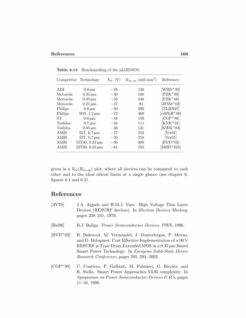
References 169
Table 4.14 Benchmarking of the pLDEMOS.
Competitor Technology Vbr (V) Ron,sp (mΩ.mm2) Reference
ADI 0.6 µm −28 120 [WBD+00]Motorola 0.35 µm −40 180 [PZK+00]Motorola 0.35 µm −56 240 [PZK+00]Motorola 0.25 µm −47 94 [dFSM+02]Philips 0.8 µm −50 290 [NLBN97]Philips SOI, 1.2 µm −73 460 [vdPLH+00]ST 0.6 µm −48 150 [CGP+98]Toshiba 0.7 µm −34 111 [KNK+01]Toshiba 0.35 µm −46 131 [KWK+03]AMIS I2T, 0.7 µm −75 553 [Ver01]AMIS I2T, 0.7 µm −50 250 [Ver01]AMIS I3T80, 0.35 µm −90 300 [BVD+02]AMIS I3T80, 0.35 µm −61 250 [MBD+02b]
given in a Vbr(Ron,sp) plot, where all devices can be compared to eachother and to the ideal silicon limits at a single glance (see chapter 6,figures 6.1 and 6.2).
References
[AV79] J.A. Appels and H.M.J. Vaes. High Voltage Thin LayerDevices (RESURF devices). In Electron Devices Meeting,pages 238–241, 1979.
[Bal96] B.J. Baliga. Power Semiconductor Devices. PWS, 1996.
[BVD+02] B. Bakeroot, M. Vermandel, J. Doutreloigne, P. Moens,and D. Bolognesi. Cost Effective Implementation of a 90 VRESURF p-Type Drain Extended MOS in a 0.35µm BasedSmart Power Technology. In European Solid-State DeviceResearch Conference, pages 291–294, 2002.
[CGP+98] C. Contiero, P. Galbiati, M. Palmieri, G. Ricotti, andR. Stella. Smart Power Approaches VLSI complexity. InSymposium on Power Semiconductor Devices & ICs, pages11–16, 1998.
170 Power MOS
[Chu00] S.-K. Chung. An Analytical Model for Breakdown Voltageof Surface Implanted SOI RESURF LDMOS. IEEE Trans-actions on electron devices, 47(5):1006–1009, May 2000.
[CSN00] G.J. Cao, M.M. De Souza, and E.M.S. Narayanan.Resurfed Lateral Bipolar Transistors for High-Voltage,High-Frequency Applications. In Symposium on PowerSemiconductor Devices & ICs, pages 185–188, 2000.
[dFSM+02] E. de Fresart, R. De Souza, J. Morrison, P. Parris, andJ. Heddleson an V. Venkatesan et al. Integration of Multi-Voltage Analog and Power Devices in a 0.25µm CMOS +Flash Memory Process. In Symposium on Power Semicon-ductor Devices & ICs, pages 305–308, 2002.
[Fuj97] T. Fujihira. Theory of Semiconductor Superjunction De-vices. Japanese Journal of Applied Physics, 36(10):6254–6262, October 1997.
[Gha77] S.K. Ghandhi. Semiconductor Power Devices. John Wiley& Sons, 1977.
[HB91] Y.S. Huang and B.J. Baliga. Extension of RESURF Prin-ciple to Dielectrically Isolated Power Devices. In Sympo-sium on Power Semiconductor Devices & ICs, pages 27–30,1991.
[HIFT02] Z. Hossain, M. Imam, J. Fulton, and M. Tanaka. Double-Resurf 700 V N-Channel LDMOS with Best-in-Class On-Resistance. In Symposium on Power Semiconductor De-vices & ICs, pages 137–140, 2002.
[HLMP00] P. Hower, J. Lin, S. Merchant, and S. Paiva. Using ”Adap-tive Resurf”to Improve the SOA of LDMOS Transistors. InSymposium on Power Semiconductor Devices & ICs, pages345–348, 2000.
[KCA96] D. Krizaj, G. Charitat, and S. Amon. A New Analyt-ical Model for Determination of Breakdown Voltage ofRESURF Structures. Solid-State Electronics, 39(9):1353–1358, 1996.
[KNK+01] Y. Kawaguchi, K. Nakamura, K. Karouji, K. Watanabe,Y. Yamaguchi, and A. Nakagawa. 0.6µm BiCMOS Based

References 171
15 and 25 V LDMOS for Analog Applications. In Sympo-sium on Power Semiconductor Devices & ICs, pages 169–172, 2001.
[KPB03] V. Khemka, V. Parthasarathy, and A. Bose. A Float-ing RESURF (FRESURF) LD-MOSFET Device Concept.IEEE Electron Device Letters, 24(10):664–666, October2003.
[KPZB02] V. Khemka, V. Parthasarathy, R. Zhu, and A. Bose. Cor-relation Between Static and Dynamic SOA (Energy Capa-bility) of RESURF LDMOS Devices in Smart Power Tech-nologies. In Symposium on Power Semiconductor Devices& ICs, pages 125–128, 2002.
[KWK+03] T. Kubota, K. Watanabe, K. Karouji, M. Ueno, Y. Anai,and Y. Kawaguchi et al. Cost-Effective Approach in LD-MOS with Partial 0.35µm Design into Convetional 0.6µmProcess. In Symposium on Power Semiconductor Devices& ICs, pages 245–248, 2003.
[LDKM99] L. Lorenz, G. Deboy, A. Knapp, and M. Marz.COOLMOSTM - A New Milestone in High Voltage PowerMOS. In Symposium on Power Semiconductor Devices &ICs, pages 3–10, 1999.
[Lud00a] A.W. Ludikhuize. A Review of RESURF Technology. InSymposium on Power Semiconductor Devices & ICs, pages11–18, 2000.
[Lud00b] A.W. Ludikhuize. Self-aligned and Shielded-Resurf LD-MOS for dense 20V Power IC’s. In Symposium on PowerSemiconductor Devices & ICs, pages 81–84, 2000.
[MAB+91] S. Merchant, E. Arnold, H. Baumgart, S. Mukherjee,H. Pein, and R. Pinker. Realization of High BreakdownVoltage (> 700V) in thin SOI Devices. In Symposium onPower Semiconductor Devices & ICs, pages 31–35, 1991.
[MBC+99] S. Merchant, R. Baird, S. Chang, P. Hui, V. Macary, andM.G. Neaves. High-Performance 13 – 65 V Rated LDMOSTransistors in an Advanced Smart Power Technology. InSymposium on Power Semiconductor Devices & ICs, pages225–228, 1999.

172 Power MOS
[MBD+02a] P. Moens, D. Bolognesi, L. Delobel, D. Villanueva,H. Hakim, and S.C. Trinh et al. I3T80: A 0.35µm BasedSystem-on-Chip Technology for 42 V Battery AutomotiveApplications. In Symposium on Power Semiconductor De-vices & ICs, pages 225–228, 2002.
[MBD+02b] P. Moens, D. Bolognesi, L. Delobel, D. Villanueva,K. Reynders, A. Lowe, G. Van Herzeele, M. Tack, andB. Bakeroot. Future Trends in Intelligent Interface Tech-nologies for 42 V Battery Automotive Applications. In Eu-ropean Solid-State Device Research Conference, pages 287–290, 2002.
[MEH+02] S. Merchant, T. Efland, S. Haynie, W.Headen, K. Ka-jiyama, and S. Paiva et al. Robust 80 V LDMOS and 100VDECMOS in a Streamlined SOI Technology for AnalogPower Applications. In Symposium on Power Semicon-ductor Devices & ICs, pages 185–188, 2002.
[MMC+00] A. Moscatelli, A. Merlini, G. Croce, P. Galbiati, andC. Contiero. LDMOS Implementation in a 0.35µm BCDTechnology (BCD6). In Symposium on Power Semicon-ductor Devices & ICs, pages 323–326, 2000.
[NK00] A. Nakagawa and Y. Kawaguchi. Improved 20 V Lat-eral Trench Gate Power MOSFETs with Very Low On-Resistance of 7.8 mΩ.mm2. In Symposium on Power Semi-conductor Devices & ICs, pages 47–50, 2000.
[NLBN97] A. Nezar, A.W. Ludikhuize, R. Brock, and N. Nowlin. ASubmicron Bi-CMOS-DMOS Process for 20-30 and 50VApplications. In Symposium on Power Semiconductor De-vices & ICs, pages 333–336, 1997.
[NMK+00] A. Narazaki, J. Maruyama, T. Kayumi, H. Hamachi,J. Moritani, and S. Hine. A 0.35µm Trench Gate MOS-FET with an Ultra Low On-State Resistance and a HighDestruction Immunity During the Inductive Switching. InSymposium on Power Semiconductor Devices & ICs, pages377–380, 2000.
[PHD+02] S. Pendharkar, R. Higgins, T. Debolske, T. Efland, andB. Nehrer. Optimization of Low Voltage N-Channel LD-

References 173
MOS Devices to Achieve Required Electrical and LifetimeSOA. In Symposium on Power Semiconductor Devices &ICs, 2002.
[PZK+00] V. Parthasarathy, R. Zhu, V. Khemka, M.L. Ger, T. Bet-tinger, S. Chang, P. Hui, and A. Bose. Integration ofHigh-Voltage Bipolars into a 0.35 µm CMOS based smartpower platform. In Bipolar/BiCMOS Circuits and Tech-nology Meeting, pages 32–35, 2000.
[TS83] E. Takeda and N. Suzuki. An Empirical Model for DeviceDegradation Due to Hot-Carrier Injection. IEEE ElectronDevice Letters, EDL-4(4):111–113, April 1983.
[TYH00] T. Terashima, F. Yamamoto, and K. Hatasako. Multi-Voltage Device Integration Technique for 0.5µm BiCMOS& DMOS Process. In Symposium on Power SemiconductorDevices & ICs, pages 331–334, 2000.
[Udr02] F. Udrea. Advanced 3D RESURF Devices for Power Inte-grated Circuits. In Semiconductor Conference, pages 229–238, 2002.
[vdPLH+00] J.A. van der Pol, A.W. Ludikhuize, H.G.A. Huizing, B. vanVelzen, R.J.E. Hueting, and J.F. Mom et al. A-BCD: AnEconomic 100V RESURF Silicon-On-Insulator BCD Tech-nology for Consumer and Automotive Applications. InSymposium on Power Semiconductor Devices & ICs, pages327–330, 2000.
[Ver01] M. Vermandel. Integration of p-type High-Voltage Devicesin a Sub-µm CMOS Technology using TCAD. PhD thesis,University of Gent, 2001.
[WBD+00] S. Whiston, D. Bain, A. Deignan, J. Pollard, C. NiChleirigh, and C. Musgrave et al. Complementary LD-MOS Transistors for a CMOS/BICMOS Process. In Sym-posium on Power Semiconductor Devices & ICs, pages 51–54, 2000.
[Zin01] R.P. Zingg. New Benchmark for RESURF, SOI and Super-Junction Power Devices. In Symposium on Power Semi-conductor Devices & ICs, pages 343–346, 2001.
174 Power MOS
[ZPB+00] R. Zhu, V. Parthasarathy, A. Bose, R. Baird, V. Khemka,and T. Roggenbauer et al. A 65V, 0.56mΩ.cm2 ResurfLDMOS in a 0.35 µm CMOS Process. In Symposium onPower Semiconductor Devices & ICs, pages 335–338, 2000.

5 The IGBT
5.1 Introduction
In december 1982, two independent groups proposed a device capable ofhandling large currents in the on-state, with low on-state voltage drop(low power loss), while keeping high input impedance and a voltagecontrolled gate. They came to this synthesis while in search of a devicecombining the best features of two existing power transistors. On the onehand, the bipolar power transistor, capable of handling large currentsin the on-state with low forward voltage drop. The major drawbacksbeing the current controlled gate (complex gate control circuit requiresa lot of space), the relatively small current gain due to the large basewidth needed for these power devices and the slow switching speed.On the other hand, the power MOSFET, which is a voltage controlleddevice (simple gate control circuit), is fast and has a large safe operatingarea. Unfortunately, this device has an increasing on-resistance when itsbreakdown voltage is increased. Therefore, this device is not suitable forapplications with high DC supply voltages (over 200 V).
One way to combine the best of both devices is in a Darlington con-figuration where the DMOS device drives the power bipolar transistor.This circuit solution gives good results but an even more elegant wayout was to look for one single device combining the physics of both thebipolar and the MOS power transistors. The first breakthrough camewith the study of the thyristors. These devices are unmatched when itcomes to current-carrying capability per unit area because of the con-ductivity modulation of lightly doped regions due to minority injection.But then again, these devices are current controlled, induce substratecurrents and are difficult to switch off. In search for an improved ver-sion of these devices, different researchers ([Bal79], [Tih80] and [PS80])proposed a planar thyristor with an insulated gate. This device had im-proved isolation, had a voltage controlled gate, but still behaved like athyristor once it was triggered, requiring current interruption to shut itoff. The final step towards the currently called IGBT (Insulated GateB ipolar T ranstistor) was taken simultaneously by the two groups men-
176 The IGBT
tioned above when they realized a device that remains gate controlledover a wide range of anode current and voltage. The first group called itthe COMFET (COnductivity Modulated FET [RGGN83]), the secondgroup called it the IGR (Insulated Gate Rectifier [BAG+82]). Thesedevices look exactly the same as the insulated gate thyristor, but aredifferent in a fundamental way: it is designed not to go into regenera-tive action, or, in other words, not to latch like a conventional thyristor;thereby avoiding the positive feedback and the loss of the voltage con-trolled gate. Inevitably, the device inherited some of the properties ofthe thyristor, it is prone to latch and it is difficult to switch off. To date,these topics remain research topics.
Since its invention in the 80s, the IGBT is used in a growing numberof applications, especially in the higher voltage ranges (up to severalthousands of volts). Thus, the main occurrence of the IGBT is as adiscrete device, and rarely as an integrated device. The reason beingtwofold: first of all, devices that are integrated in a technology based ona standard CMOS platform have inherently limited voltage and currentranges. In these limited voltage ranges, they compete with power DMOSdevices, which have superior characteristics in the low voltage range(< 200V). Secondly, lateral IGBTs are difficult to integrate as theyproduce large substrate currents. A problem that is normally solved withthe introduction of huge isolation structures, which kills the eventualadvantage the device had over a DMOS. This is also the reason why theLIGBT shows up in SOI technologies, where problems with substratecurrents are avoided due to the dielectric isolation of the devices.
Yet the possibility of integrating an IGBT in the I3T80H technologyof AMIS is investigated. First of all, a straightforward adaptation of anDMOS device is carried out. The n+ drain region is simply replacedby a p+ anode region. Using this structure, the next section discussesthe device’s operation. Albeit not an optimized example, it gives anoverview of the basic operation of the lateral IGBT and the problemsencountered. In the following sections, we gradually introduce morelayers so as to improve the device’s performance.
Using the existing, calibrated TCAD input decks, several ideas aretried out and the most appealing ones have been put on testchip. Alot of effort went into the suppression of the substrate current, althougha lot of other issues need to be studied as well: breakdown, on-stateforward voltage drop, SOA, turn-off, latch-up. . . . At the end of thechapter, a comparison is made between the different nLIGBT devicesand a nVDEMOS based on measurements.
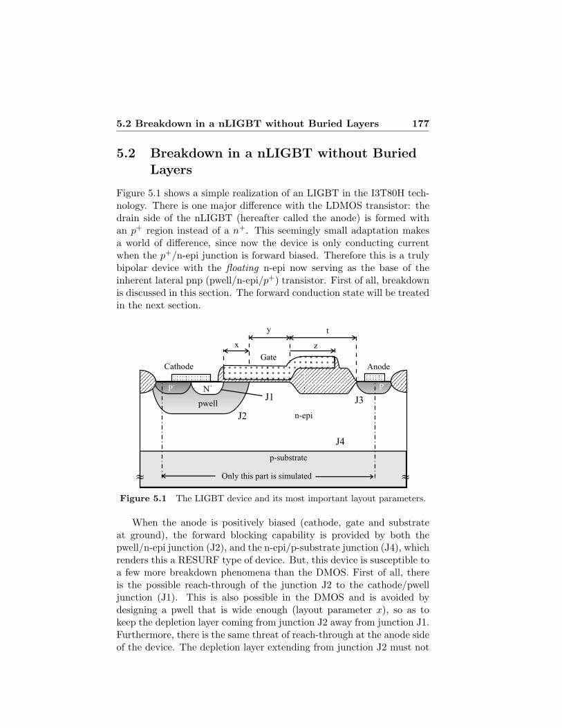
5.2 Breakdown in a nLIGBT without Buried Layers 177
5.2 Breakdown in a nLIGBT without BuriedLayers
Figure 5.1 shows a simple realization of an LIGBT in the I3T80H tech-nology. There is one major difference with the LDMOS transistor: thedrain side of the nLIGBT (hereafter called the anode) is formed withan p+ region instead of a n+. This seemingly small adaptation makesa world of difference, since now the device is only conducting currentwhen the p+/n-epi junction is forward biased. Therefore this is a trulybipolar device with the floating n-epi now serving as the base of theinherent lateral pnp (pwell/n-epi/p+) transistor. First of all, breakdownis discussed in this section. The forward conduction state will be treatedin the next section.
pwell
P+
n-epi
CathodeGate
Anode
p-substrate
P+
N+
»»
x
t
z
y
Only this part is simulated
J1
J4
J3
J2
Figure 5.1 The LIGBT device and its most important layout parameters.
When the anode is positively biased (cathode, gate and substrateat ground), the forward blocking capability is provided by both thepwell/n-epi junction (J2), and the n-epi/p-substrate junction (J4), whichrenders this a RESURF type of device. But, this device is susceptible toa few more breakdown phenomena than the DMOS. First of all, thereis the possible reach-through of the junction J2 to the cathode/pwelljunction (J1). This is also possible in the DMOS and is avoided bydesigning a pwell that is wide enough (layout parameter x), so as tokeep the depletion layer coming from junction J2 away from junction J1.Furthermore, there is the same threat of reach-through at the anode sideof the device. The depletion layer extending from junction J2 must not
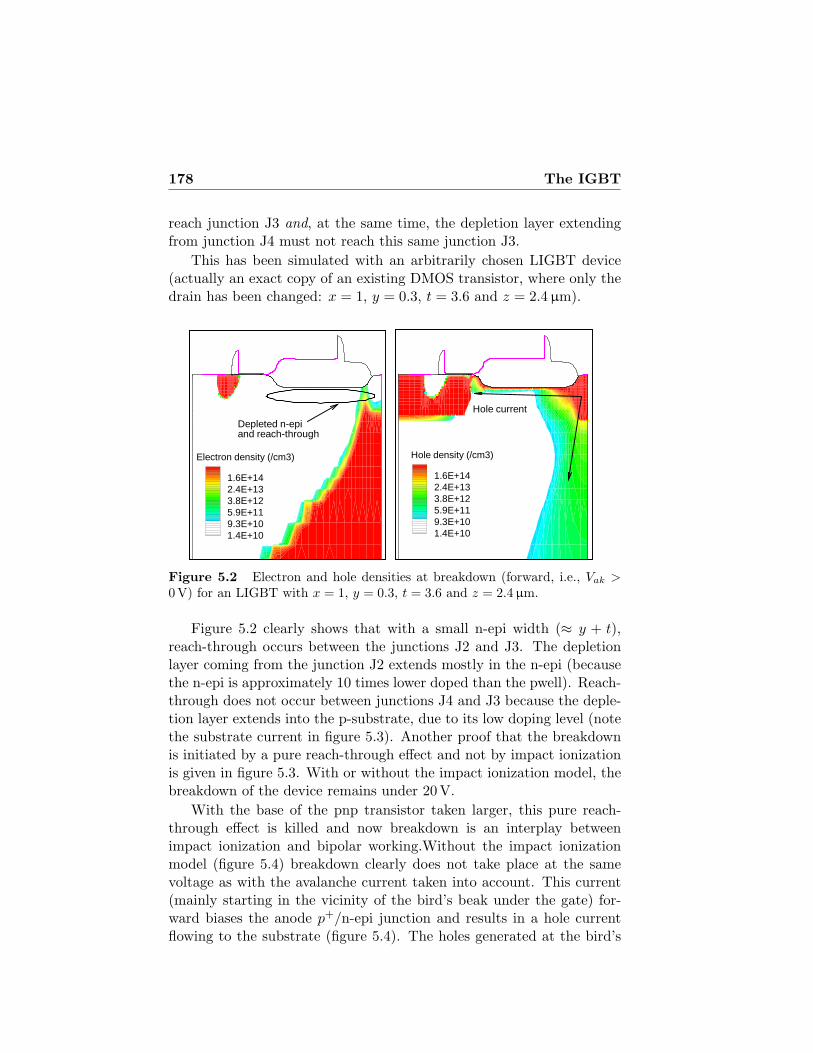
178 The IGBT
reach junction J3 and, at the same time, the depletion layer extendingfrom junction J4 must not reach this same junction J3.
This has been simulated with an arbitrarily chosen LIGBT device(actually an exact copy of an existing DMOS transistor, where only thedrain has been changed: x = 1, y = 0.3, t = 3.6 and z = 2.4µm).
Electron density (/cm3)
1.6E+142.4E+133.8E+125.9E+119.3E+101.4E+10
Depleted n-epiand reach-through
Hole density (/cm3)
1.6E+142.4E+133.8E+125.9E+119.3E+101.4E+10
Hole current
Figure 5.2 Electron and hole densities at breakdown (forward, i.e., Vak >0 V) for an LIGBT with x = 1, y = 0.3, t = 3.6 and z = 2.4 µm.
Figure 5.2 clearly shows that with a small n-epi width (≈ y + t),reach-through occurs between the junctions J2 and J3. The depletionlayer coming from the junction J2 extends mostly in the n-epi (becausethe n-epi is approximately 10 times lower doped than the pwell). Reach-through does not occur between junctions J4 and J3 because the deple-tion layer extends into the p-substrate, due to its low doping level (notethe substrate current in figure 5.3). Another proof that the breakdownis initiated by a pure reach-through effect and not by impact ionizationis given in figure 5.3. With or without the impact ionization model, thebreakdown of the device remains under 20 V.
With the base of the pnp transistor taken larger, this pure reach-through effect is killed and now breakdown is an interplay betweenimpact ionization and bipolar working.Without the impact ionizationmodel (figure 5.4) breakdown clearly does not take place at the samevoltage as with the avalanche current taken into account. This current(mainly starting in the vicinity of the bird’s beak under the gate) for-ward biases the anode p+/n-epi junction and results in a hole currentflowing to the substrate (figure 5.4). The holes generated at the bird’s
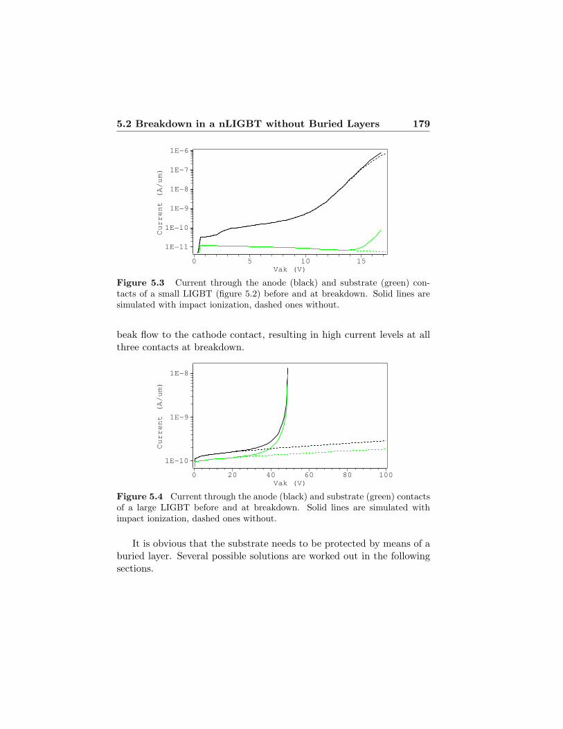
5.2 Breakdown in a nLIGBT without Buried Layers 179
Vak (V)0 5 10 15
Current (A/um)
1E−11
1E−10
1E−9
1E−8
1E−7
1E−6
Figure 5.3 Current through the anode (black) and substrate (green) con-tacts of a small LIGBT (figure 5.2) before and at breakdown. Solid lines aresimulated with impact ionization, dashed ones without.
beak flow to the cathode contact, resulting in high current levels at allthree contacts at breakdown.
Vak (V)0 20 40 60 80 100
Current (A/um)
1E−10
1E−9
1E−8
Figure 5.4 Current through the anode (black) and substrate (green) contactsof a large LIGBT before and at breakdown. Solid lines are simulated withimpact ionization, dashed ones without.
It is obvious that the substrate needs to be protected by means of aburied layer. Several possible solutions are worked out in the followingsections.
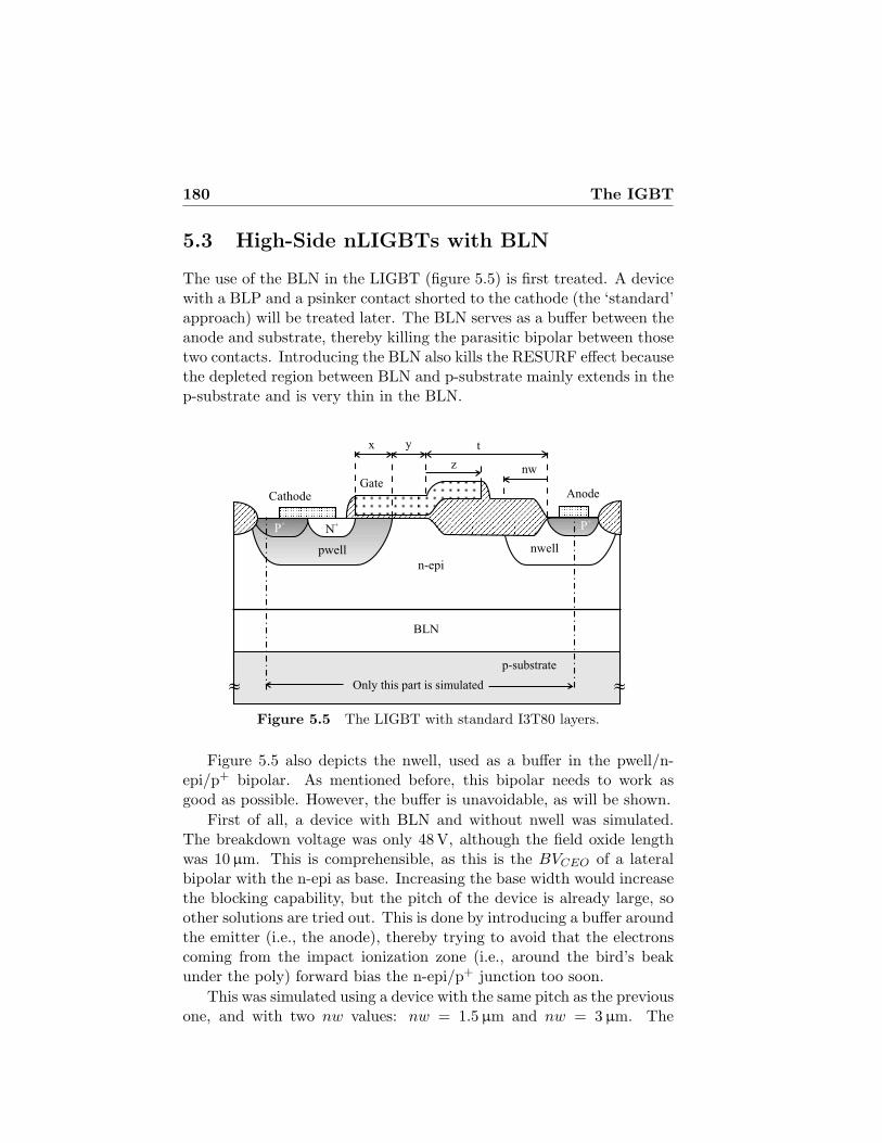
180 The IGBT
5.3 High-Side nLIGBTs with BLN
The use of the BLN in the LIGBT (figure 5.5) is first treated. A devicewith a BLP and a psinker contact shorted to the cathode (the ‘standard’approach) will be treated later. The BLN serves as a buffer between theanode and substrate, thereby killing the parasitic bipolar between thosetwo contacts. Introducing the BLN also kills the RESURF effect becausethe depleted region between BLN and p-substrate mainly extends in thep-substrate and is very thin in the BLN.
pwell
P+
n-epi
CathodeGate
Anode
p-substrate
P+
N+
»»
x t
z
y
Only this part is simulated
nwell
nw
BLN
Figure 5.5 The LIGBT with standard I3T80 layers.
Figure 5.5 also depicts the nwell, used as a buffer in the pwell/n-epi/p+ bipolar. As mentioned before, this bipolar needs to work asgood as possible. However, the buffer is unavoidable, as will be shown.
First of all, a device with BLN and without nwell was simulated.The breakdown voltage was only 48 V, although the field oxide lengthwas 10µm. This is comprehensible, as this is the BVCEO of a lateralbipolar with the n-epi as base. Increasing the base width would increasethe blocking capability, but the pitch of the device is already large, soother solutions are tried out. This is done by introducing a buffer aroundthe emitter (i.e., the anode), thereby trying to avoid that the electronscoming from the impact ionization zone (i.e., around the bird’s beakunder the poly) forward bias the n-epi/p+ junction too soon.
This was simulated using a device with the same pitch as the previousone, and with two nw values: nw = 1.5µm and nw = 3µm. The
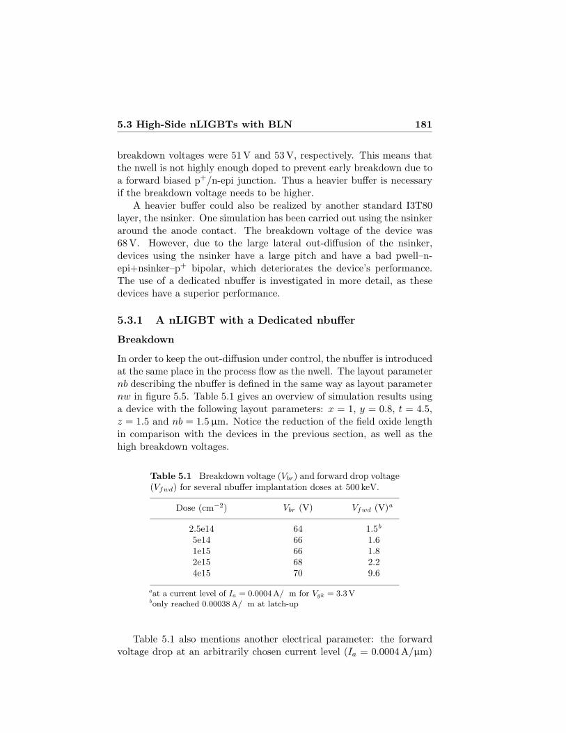
5.3 High-Side nLIGBTs with BLN 181
breakdown voltages were 51V and 53 V, respectively. This means thatthe nwell is not highly enough doped to prevent early breakdown due toa forward biased p+/n-epi junction. Thus a heavier buffer is necessaryif the breakdown voltage needs to be higher.
A heavier buffer could also be realized by another standard I3T80layer, the nsinker. One simulation has been carried out using the nsinkeraround the anode contact. The breakdown voltage of the device was68V. However, due to the large lateral out-diffusion of the nsinker,devices using the nsinker have a large pitch and have a bad pwell–n-epi+nsinker–p+ bipolar, which deteriorates the device’s performance.The use of a dedicated nbuffer is investigated in more detail, as thesedevices have a superior performance.
5.3.1 A nLIGBT with a Dedicated nbuffer
Breakdown
In order to keep the out-diffusion under control, the nbuffer is introducedat the same place in the process flow as the nwell. The layout parameternb describing the nbuffer is defined in the same way as layout parameternw in figure 5.5. Table 5.1 gives an overview of simulation results usinga device with the following layout parameters: x = 1, y = 0.8, t = 4.5,z = 1.5 and nb = 1.5µm. Notice the reduction of the field oxide lengthin comparison with the devices in the previous section, as well as thehigh breakdown voltages.
Table 5.1 Breakdown voltage (Vbr) and forward drop voltage(Vfwd) for several nbuffer implantation doses at 500 keV.
Dose (cm−2) Vbr (V) Vfwd (V)a
2.5e14 64 1.5b
5e14 66 1.61e15 66 1.82e15 68 2.24e15 70 9.6
aat a current level of Ia = 0.0004A/m for Vgk = 3.3Vbonly reached 0.00038A/m at latch-up
Table 5.1 also mentions another electrical parameter: the forwardvoltage drop at an arbitrarily chosen current level (Ia = 0.0004A/µm)
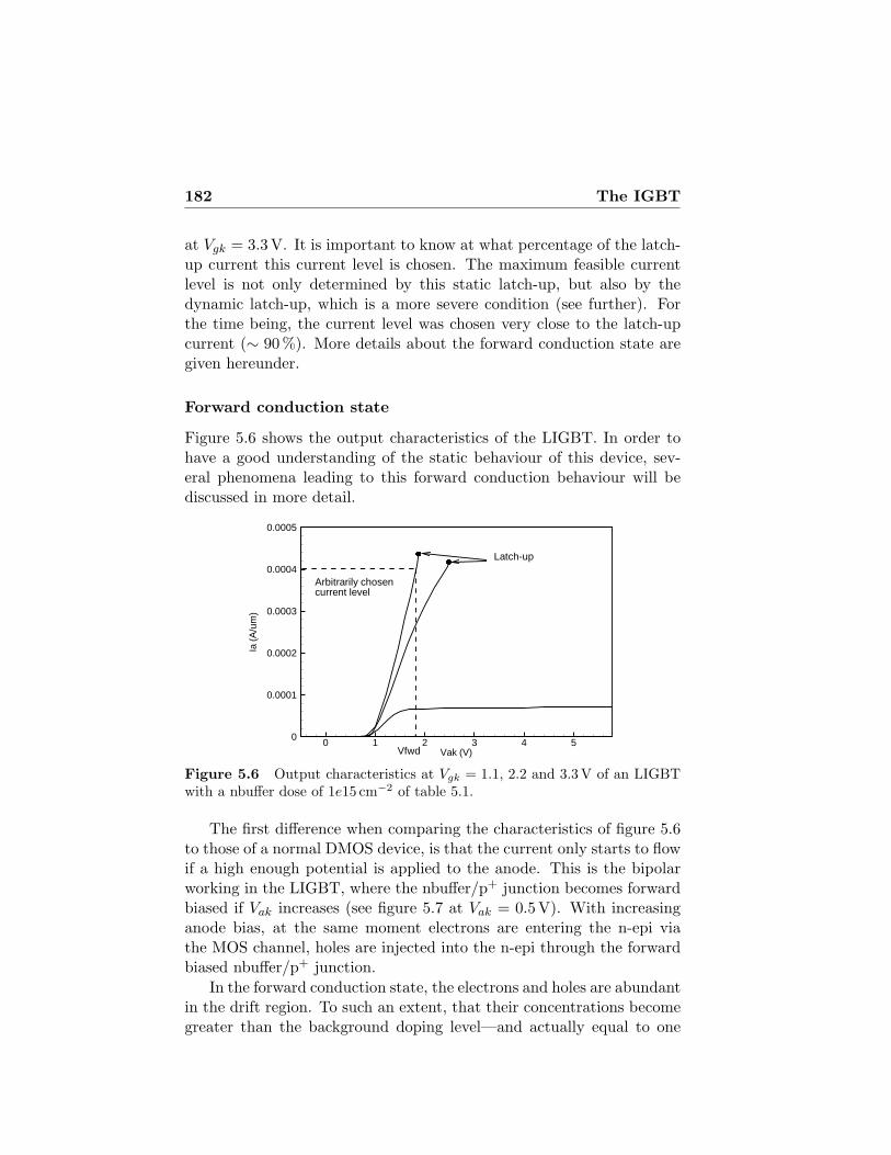
182 The IGBT
at Vgk = 3.3V. It is important to know at what percentage of the latch-up current this current level is chosen. The maximum feasible currentlevel is not only determined by this static latch-up, but also by thedynamic latch-up, which is a more severe condition (see further). Forthe time being, the current level was chosen very close to the latch-upcurrent (∼ 90%). More details about the forward conduction state aregiven hereunder.
Forward conduction state
Figure 5.6 shows the output characteristics of the LIGBT. In order tohave a good understanding of the static behaviour of this device, sev-eral phenomena leading to this forward conduction behaviour will bediscussed in more detail.
Vak (V)
Ia(A
/um
)
0 1 2 3 4 50
0.0001
0.0002
0.0003
0.0004
0.0005
Latch-up
Vfwd
Arbitrarily chosencurrent level
Figure 5.6 Output characteristics at Vgk = 1.1, 2.2 and 3.3 V of an LIGBTwith a nbuffer dose of 1e15 cm−2 of table 5.1.
The first difference when comparing the characteristics of figure 5.6to those of a normal DMOS device, is that the current only starts to flowif a high enough potential is applied to the anode. This is the bipolarworking in the LIGBT, where the nbuffer/p+ junction becomes forwardbiased if Vak increases (see figure 5.7 at Vak = 0.5V). With increasinganode bias, at the same moment electrons are entering the n-epi viathe MOS channel, holes are injected into the n-epi through the forwardbiased nbuffer/p+ junction.
In the forward conduction state, the electrons and holes are abundantin the drift region. To such an extent, that their concentrations becomegreater than the background doping level—and actually equal to one
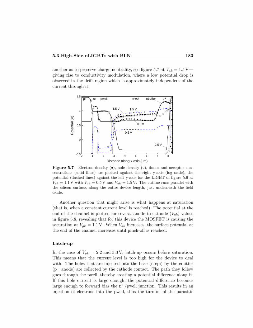
5.3 High-Side nLIGBTs with BLN 183
another as to preserve charge neutrality, see figure 5.7 at Vak = 1.5V—giving rise to conductivity modulation, where a low potential drop isobserved in the drift region which is approximately independent of thecurrent through it.
Distance along x-axis (um)
Pot
entia
l(V
)
0 1 2 3 4 5 6 7 8-0.5
0
0.5
1
1.5p+ n+ pwell n-epi nbuffer p+
0.5 V
0.5 V
0.5 V
1.5 V1.5 V
Figure 5.7 Electron density (•), hole density (), donor and acceptor con-centrations (solid lines) are plotted against the right y-axis (log scale), thepotential (dashed lines) against the left y-axis for the LIGBT of figure 5.6 atVgk = 1.1V with Vak = 0.5V and Vak = 1.5V. The cutline runs parallel withthe silicon surface, along the entire device length, just underneath the fieldoxide.
Another question that might arise is what happens at saturation(that is, when a constant current level is reached). The potential at theend of the channel is plotted for several anode to cathode (Vak) valuesin figure 5.8, revealing that for this device the MOSFET is causing thesaturation at Vgk = 1.1V. When Vak increases, the surface potential atthe end of the channel increases until pinch-off is reached.
Latch-up
In the case of Vgk = 2.2 and 3.3V, latch-up occurs before saturation.This means that the current level is too high for the device to dealwith. The holes that are injected into the base (n-epi) by the emitter(p+ anode) are collected by the cathode contact. The path they followgoes through the pwell, thereby creating a potential difference along it.If this hole current is large enough, the potential difference becomeslarge enough to forward bias the n+/pwell junction. This results in aninjection of electrons into the pwell, thus the turn-on of the parasitic
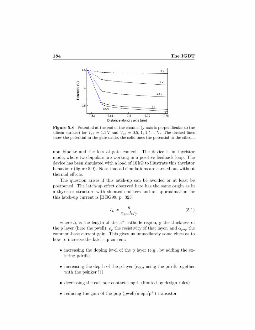
184 The IGBT
Distance along y axis (um)
Pot
entia
l(V
)
-7.82 -7.81 -7.8 -7.79 -7.78
0.5
1
1.5
0.5 V1 V
8 V
2 V
1.5 V
Figure 5.8 Potential at the end of the channel (y-axis is perpendicular to thesilicon surface) for Vgk = 1.1V and Vak = 0.5, 1, 1.5. . . V. The dashed linesshow the potential in the gate oxide, the solid ones the potential in the silicon.
npn bipolar and the loss of gate control. The device is in thyristormode, where two bipolars are working in a positive feedback loop. Thedevice has been simulated with a load of 10 kΩ to illustrate this thyristorbehaviour (figure 5.9). Note that all simulations are carried out withoutthermal effects.
The question arises if this latch-up can be avoided or at least bepostponed. The latch-up effect observed here has the same origin as ina thyristor structure with shunted emitters and an approximation forthis latch-up current is [BGG99, p. 323]
IL ≈ g
αpnplkρp(5.1)
where lk is the length of the n+ cathode region, g the thickness ofthe p layer (here the pwell), ρp the resistivity of that layer, and αpnp thecommon-base current gain. This gives us immediately some clues as tohow to increase the latch-up current:
• increasing the doping level of the p layer (e.g., by adding the ex-isting pdrift)
• increasing the depth of the p layer (e.g., using the pdrift togetherwith the psinker !?)
• decreasing the cathode contact length (limited by design rules)
• reducing the gain of the pnp (pwell/n-epi/p+) transistor
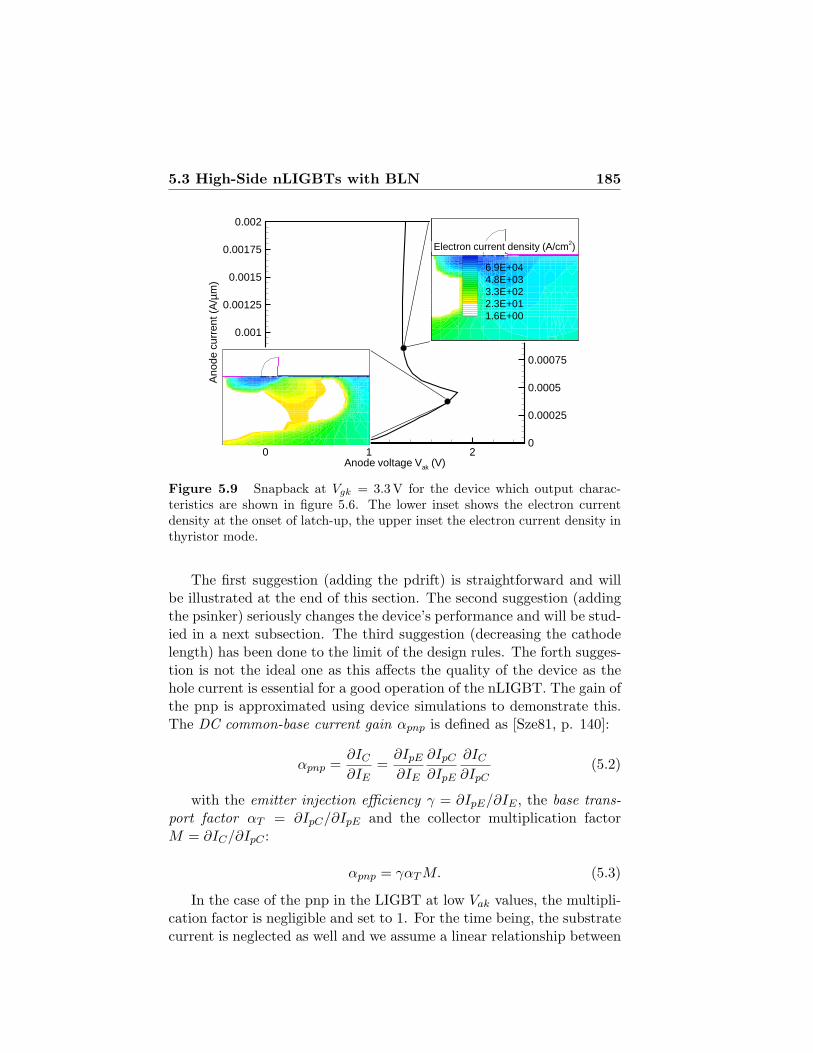
5.3 High-Side nLIGBTs with BLN 185
Anode voltage Vak (V)
Ano
decu
rren
t(A
/µm
)
0 1 20
0.00025
0.0005
0.00075
0.001
0.00125
0.0015
0.00175
0.002
0
0.00025
0.0005
0.00075
0.001
0.00125
0.0015
0.00175
0.002
Electron current density (A/cm2)
6.9E+044.8E+033.3E+022.3E+011.6E+00
Electron current density (A/cm2)
Figure 5.9 Snapback at Vgk = 3.3V for the device which output charac-teristics are shown in figure 5.6. The lower inset shows the electron currentdensity at the onset of latch-up, the upper inset the electron current density inthyristor mode.
The first suggestion (adding the pdrift) is straightforward and willbe illustrated at the end of this section. The second suggestion (addingthe psinker) seriously changes the device’s performance and will be stud-ied in a next subsection. The third suggestion (decreasing the cathodelength) has been done to the limit of the design rules. The forth sugges-tion is not the ideal one as this affects the quality of the device as thehole current is essential for a good operation of the nLIGBT. The gain ofthe pnp is approximated using device simulations to demonstrate this.The DC common-base current gain αpnp is defined as [Sze81, p. 140]:
αpnp =∂IC
∂IE=
∂IpE
∂IE
∂IpC
∂IpE
∂IC
∂IpC(5.2)
with the emitter injection efficiency γ = ∂IpE/∂IE , the base trans-port factor αT = ∂IpC/∂IpE and the collector multiplication factorM = ∂IC/∂IpC :
αpnp = γαT M. (5.3)
In the case of the pnp in the LIGBT at low Vak values, the multipli-cation factor is negligible and set to 1. For the time being, the substratecurrent is neglected as well and we assume a linear relationship between
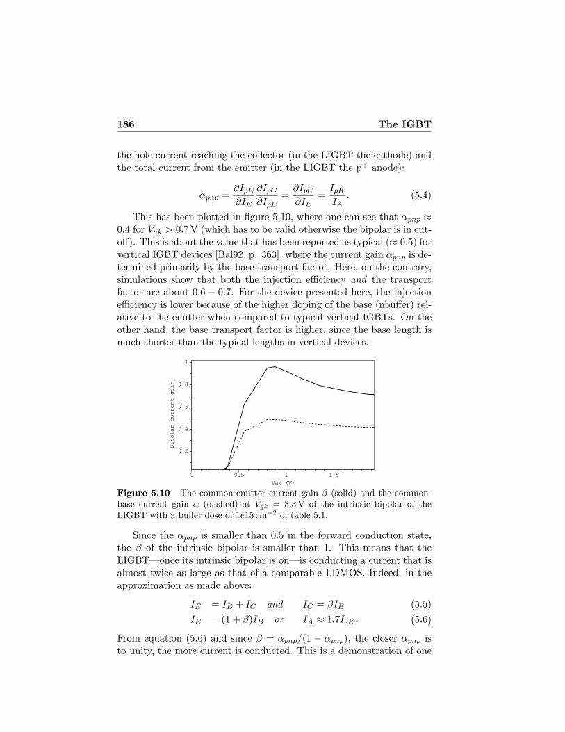
186 The IGBT
the hole current reaching the collector (in the LIGBT the cathode) andthe total current from the emitter (in the LIGBT the p+ anode):
αpnp =∂IpE
∂IE
∂IpC
∂IpE=
∂IpC
∂IE=
IpK
IA. (5.4)
This has been plotted in figure 5.10, where one can see that αpnp ≈0.4 for Vak > 0.7V (which has to be valid otherwise the bipolar is in cut-off). This is about the value that has been reported as typical (≈ 0.5) forvertical IGBT devices [Bal92, p. 363], where the current gain αpnp is de-termined primarily by the base transport factor. Here, on the contrary,simulations show that both the injection efficiency and the transportfactor are about 0.6 − 0.7. For the device presented here, the injectionefficiency is lower because of the higher doping of the base (nbuffer) rel-ative to the emitter when compared to typical vertical IGBTs. On theother hand, the base transport factor is higher, since the base length ismuch shorter than the typical lengths in vertical devices.
Vak (V)0 0.5 1 1.5
Bipolar current gain
0.2
0.4
0.6
0.8
1
Figure 5.10 The common-emitter current gain β (solid) and the common-base current gain α (dashed) at Vgk = 3.3V of the intrinsic bipolar of theLIGBT with a buffer dose of 1e15 cm−2 of table 5.1.
Since the αpnp is smaller than 0.5 in the forward conduction state,the β of the intrinsic bipolar is smaller than 1. This means that theLIGBT—once its intrinsic bipolar is on—is conducting a current that isalmost twice as large as that of a comparable LDMOS. Indeed, in theapproximation as made above:
IE = IB + IC and IC = βIB (5.5)IE = (1 + β)IB or IA ≈ 1.7IeK . (5.6)
From equation (5.6) and since β = αpnp/(1 − αpnp), the closer αpnp isto unity, the more current is conducted. This is a demonstration of one
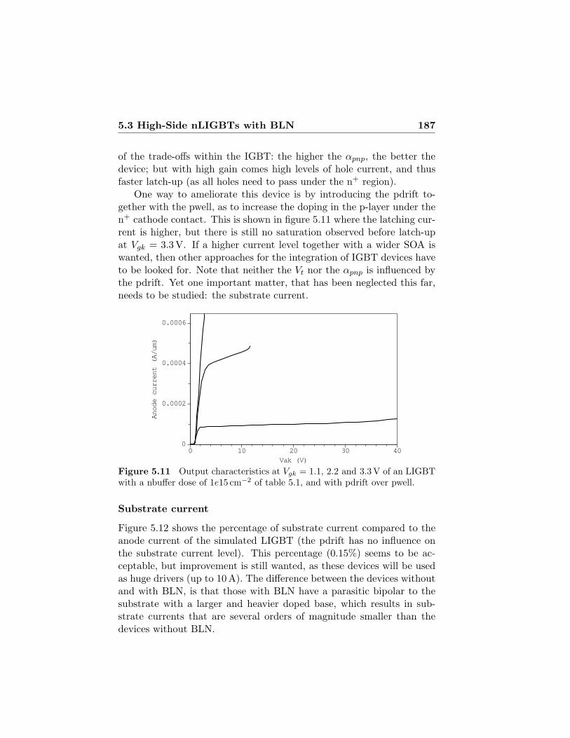
5.3 High-Side nLIGBTs with BLN 187
of the trade-offs within the IGBT: the higher the αpnp, the better thedevice; but with high gain comes high levels of hole current, and thusfaster latch-up (as all holes need to pass under the n+ region).
One way to ameliorate this device is by introducing the pdrift to-gether with the pwell, as to increase the doping in the p-layer under then+ cathode contact. This is shown in figure 5.11 where the latching cur-rent is higher, but there is still no saturation observed before latch-upat Vgk = 3.3V. If a higher current level together with a wider SOA iswanted, then other approaches for the integration of IGBT devices haveto be looked for. Note that neither the Vt nor the αpnp is influenced bythe pdrift. Yet one important matter, that has been neglected this far,needs to be studied: the substrate current.
Vak (V)0 10 20 30 40
Anode current (A/um)
0
0.0002
0.0004
0.0006
Figure 5.11 Output characteristics at Vgk = 1.1, 2.2 and 3.3 V of an LIGBTwith a nbuffer dose of 1e15 cm−2 of table 5.1, and with pdrift over pwell.
Substrate current
Figure 5.12 shows the percentage of substrate current compared to theanode current of the simulated LIGBT (the pdrift has no influence onthe substrate current level). This percentage (0.15%) seems to be ac-ceptable, but improvement is still wanted, as these devices will be usedas huge drivers (up to 10 A). The difference between the devices withoutand with BLN, is that those with BLN have a parasitic bipolar to thesubstrate with a larger and heavier doped base, which results in sub-strate currents that are several orders of magnitude smaller than thedevices without BLN.
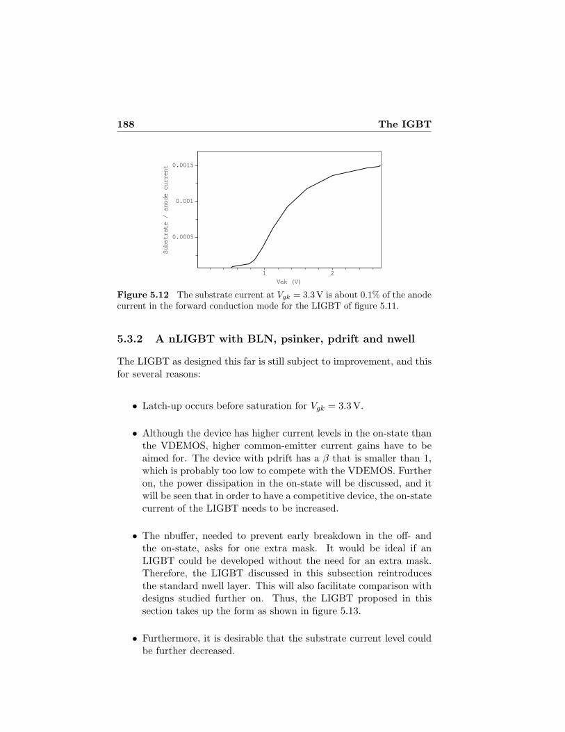
188 The IGBT
Vak (V)1 2
Substrate / anode current
0.0005
0.001
0.0015
Figure 5.12 The substrate current at Vgk = 3.3V is about 0.1% of the anodecurrent in the forward conduction mode for the LIGBT of figure 5.11.
5.3.2 A nLIGBT with BLN, psinker, pdrift and nwell
The LIGBT as designed this far is still subject to improvement, and thisfor several reasons:
• Latch-up occurs before saturation for Vgk = 3.3V.
• Although the device has higher current levels in the on-state thanthe VDEMOS, higher common-emitter current gains have to beaimed for. The device with pdrift has a β that is smaller than 1,which is probably too low to compete with the VDEMOS. Furtheron, the power dissipation in the on-state will be discussed, and itwill be seen that in order to have a competitive device, the on-statecurrent of the LIGBT needs to be increased.
• The nbuffer, needed to prevent early breakdown in the off- andthe on-state, asks for one extra mask. It would be ideal if anLIGBT could be developed without the need for an extra mask.Therefore, the LIGBT discussed in this subsection reintroducesthe standard nwell layer. This will also facilitate comparison withdesigns studied further on. Thus, the LIGBT proposed in thissection takes up the form as shown in figure 5.13.
• Furthermore, it is desirable that the substrate current level couldbe further decreased.
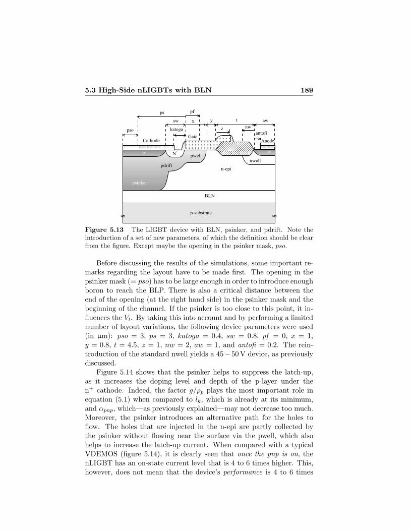
5.3 High-Side nLIGBTs with BLN 189
pwellP+
n-epi
CathodeGate
Anode
p-substrate
P+
N+
»»
x t
z
y
nwell
nw
pdrift
pf
psinker
BLN
sw
katoga
ps
pso
aw
antofi
Figure 5.13 The LIGBT device with BLN, psinker, and pdrift. Note theintroduction of a set of new parameters, of which the definition should be clearfrom the figure. Except maybe the opening in the psinker mask, pso.
Before discussing the results of the simulations, some important re-marks regarding the layout have to be made first. The opening in thepsinker mask (= pso) has to be large enough in order to introduce enoughboron to reach the BLP. There is also a critical distance between theend of the opening (at the right hand side) in the psinker mask and thebeginning of the channel. If the psinker is too close to this point, it in-fluences the Vt. By taking this into account and by performing a limitednumber of layout variations, the following device parameters were used(in µm): pso = 3, ps = 3, katoga = 0.4, sw = 0.8, pf = 0, x = 1,y = 0.8, t = 4.5, z = 1, nw = 2, aw = 1, and antofi = 0.2. The rein-troduction of the standard nwell yields a 45− 50V device, as previouslydiscussed.
Figure 5.14 shows that the psinker helps to suppress the latch-up,as it increases the doping level and depth of the p-layer under then+ cathode. Indeed, the factor g/ρp plays the most important role inequation (5.1) when compared to lk, which is already at its minimum,and αpnp, which—as previously explained—may not decrease too much.Moreover, the psinker introduces an alternative path for the holes toflow. The holes that are injected in the n-epi are partly collected bythe psinker without flowing near the surface via the pwell, which alsohelps to increase the latch-up current. When compared with a typicalVDEMOS (figure 5.14), it is clearly seen that once the pnp is on, thenLIGBT has an on-state current level that is 4 to 6 times higher. This,however, does not mean that the device’s performance is 4 to 6 times

190 The IGBT
better as will be explained in the paragraph on power dissipation.
Vak or Vds (V)
I aor
I d(A
/µm
)
0 20 40 60 800
0.0002
0.0004
0.0006
0.0008
0.001
Figure 5.14 Output characteristics at Vgk = 1.1, 2.2 and 3.3 V of an LIGBTas shown in figure 5.13 (black) compared with a typical VDEMOS (grey). Theinset shows the important region at low Vak (or Vds) values.
The reintroduction of the nwell, and the psinker helping to collectholes have their positive impact on the performance of this device: theβ is slightly higher than 1, whereas the β of the device of the previoussection was lower than 1 (figure 5.15). The substrate current level isalmost unaffected by the introduction of the psinker. (figure 5.16).
Vak (V)0 1 2
Bipolar current gain
1E0
1E1
Figure 5.15 The common-emitter current gain β at Vgk = 3.3V of an LIGBTas shown in figure 5.13 (solid line) compared with an LIGBT of the previoussection (with pdrift).
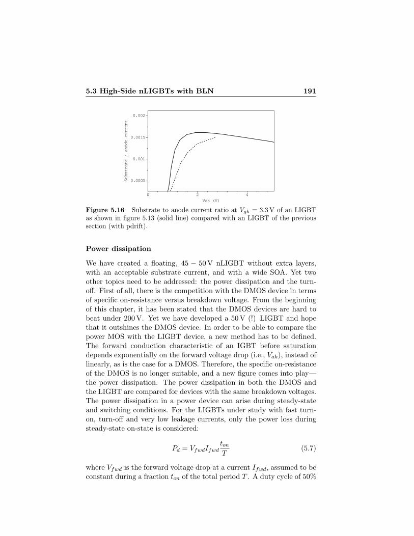
5.3 High-Side nLIGBTs with BLN 191
Vak (V)0 2 4
Substrate / anode current
0.0005
0.001
0.0015
0.002
Figure 5.16 Substrate to anode current ratio at Vgk = 3.3V of an LIGBTas shown in figure 5.13 (solid line) compared with an LIGBT of the previoussection (with pdrift).
Power dissipation
We have created a floating, 45 − 50V nLIGBT without extra layers,with an acceptable substrate current, and with a wide SOA. Yet twoother topics need to be addressed: the power dissipation and the turn-off. First of all, there is the competition with the DMOS device in termsof specific on-resistance versus breakdown voltage. From the beginningof this chapter, it has been stated that the DMOS devices are hard tobeat under 200V. Yet we have developed a 50 V (!) LIGBT and hopethat it outshines the DMOS device. In order to be able to compare thepower MOS with the LIGBT device, a new method has to be defined.The forward conduction characteristic of an IGBT before saturationdepends exponentially on the forward voltage drop (i.e., Vak), instead oflinearly, as is the case for a DMOS. Therefore, the specific on-resistanceof the DMOS is no longer suitable, and a new figure comes into play—the power dissipation. The power dissipation in both the DMOS andthe LIGBT are compared for devices with the same breakdown voltages.The power dissipation in a power device can arise during steady-stateand switching conditions. For the LIGBTs under study with fast turn-on, turn-off and very low leakage currents, only the power loss duringsteady-state on-state is considered:
Pd = VfwdIfwdton
T(5.7)
where Vfwd is the forward voltage drop at a current Ifwd, assumed to beconstant during a fraction ton of the total period T . A duty cycle of 50%
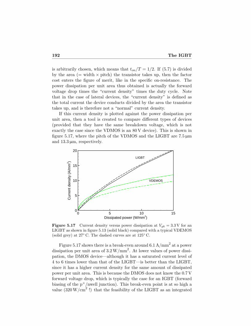
192 The IGBT
is arbitrarily chosen, which means that ton/T = 1/2. If (5.7) is dividedby the area (= width × pitch) the transistor takes up, then the factorcost enters the figure of merit, like in the specific on-resistance. Thepower dissipation per unit area thus obtained is actually the forwardvoltage drop times the “current density” times the duty cycle. Notethat in the case of lateral devices, the “current density” is defined asthe total current the device conducts divided by the area the transistortakes up, and is therefore not a “normal” current density.
If this current density is plotted against the power dissipation perunit area, then a tool is created to compare different types of devices(provided that they have the same breakdown voltage, which is notexactly the case since the VDMOS is an 80 V device). This is shown infigure 5.17, where the pitch of the VDMOS and the LIGBT are 7.5µmand 13.3µm, respectively.
Dissipated power (W/mm2)
Cur
rent
dens
ity(A
/mm
2 )
0 5 10 150
5
10
15
20
LIGBT
VDEMOS
Figure 5.17 Current density versus power dissipation at Vgk = 3.3V for anLIGBT as shown in figure 5.13 (solid black) compared with a typical VDEMOS(solid grey) at 27 C. The dashed curves are at 125 C.
Figure 5.17 shows there is a break-even around 6.1A/mm2 at a powerdissipation per unit area of 3.2W/mm2. At lower values of power dissi-pation, the DMOS device—although it has a saturated current level of4 to 6 times lower than that of the LIGBT—is better than the LIGBT,since it has a higher current density for the same amount of dissipatedpower per unit area. This is because the DMOS does not know the 0.7Vforward voltage drop, which is typically the case for an IGBT (forwardbiasing of the p+/nwell junction). This break-even point is at so high avalue (320W/cm2 !) that the feasibility of the LIGBT as an integrated

5.3 High-Side nLIGBTs with BLN 193
medium voltage device becomes questionable. However, it was reportedby AMIS that in a similar technology a 0.15mm2 DMOS driver dissi-pated approximately 1W in DC (i.e., 6.7W/mm2), and no problemswere observed whatsoever. It is even assumed that higher power dissi-pation values are possible. So with a duty cycle of 50 % in AC modemuch higher power dissipation per unit area than the break-even pointat 3.2W/mm2 is possible.
The power dissipation in a power device is limited due to the tem-perature rise it causes:
∆T = Tj − Ta = PdRθ (5.8)
where Rθ is the thermal resistance, and Tj and Ta are the junction andambient temperatures, respectively. The power device should actuallybe simulated at the maximum allowable temperature (generally Tj =125C). Therefore, isothermal simulations (non-isothermal effects areneglected since the on-state voltage is rather low) at this temperaturegive a better idea of the power dissipation per unit area. This hasbeen done in figure 5.17, where it can be seen that due to the drop ofthe mobility in the DMOS device (which is not the case for the IGBTbecause of the conductivity modulation) the break-even point drops to3A/mm2 at a power dissipation per unit area of 1.2W/mm2. This leadsto the conclusion that the LIGBT devices as drivers are likely to beatthe DMOS devices, even at medium voltage ranges (50− 80V).
Turn-off
It has been assumed in the previous paragraph that the turn-off of theLIGBT is fast enough to assure negligible power loss during turn-off.In literature, the turn-off of the IGBT is treated as one of the criticaltrade-off parameters. The holes that are injected in the drift region needtime to recombine after gate turn-off, and this becomes critical in large,discrete IGBT devices. However, in 50 − 80V lateral integrated IGBTdevices this is not a problem, as is shown below.
The gate has been turned off from Vgk = 3.3 V to Vgk = 0 V in10 ns with a resistive load of 10 kΩ and an off-state voltage of 40 V.The result of this set-up is that the initial steady on-state current isequal to the static latch-up onset current. Figure 5.18 shows that theanode current decreases fast as the gate voltage drops from 3.3V to thethreshold voltage because of the reduction of the channel current to zero(demonstrated by the electron cathode current). After this point, the
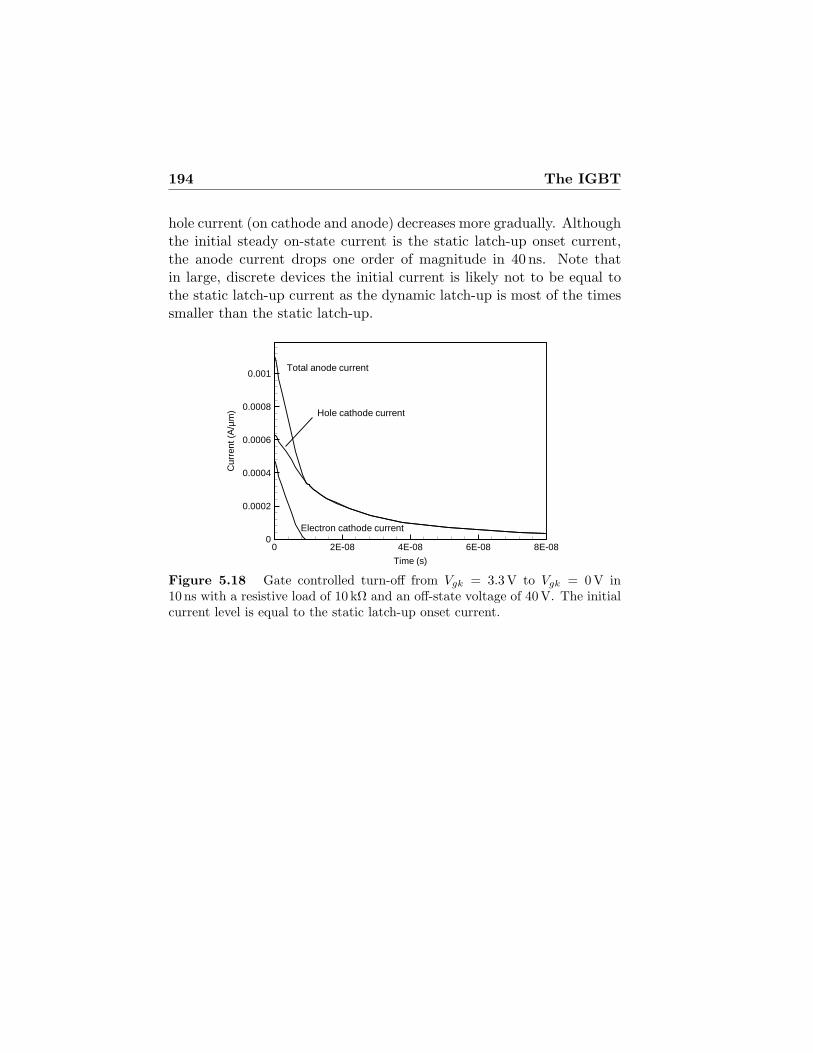
194 The IGBT
hole current (on cathode and anode) decreases more gradually. Althoughthe initial steady on-state current is the static latch-up onset current,the anode current drops one order of magnitude in 40 ns. Note thatin large, discrete devices the initial current is likely not to be equal tothe static latch-up current as the dynamic latch-up is most of the timessmaller than the static latch-up.
Time (s)
Cur
rent
(A/µ
m)
0 2E-08 4E-08 6E-08 8E-080
0.0002
0.0004
0.0006
0.0008
0.001Total anode current
Hole cathode current
Electron cathode current
Figure 5.18 Gate controlled turn-off from Vgk = 3.3V to Vgk = 0V in10 ns with a resistive load of 10 kΩ and an off-state voltage of 40V. The initialcurrent level is equal to the static latch-up onset current.
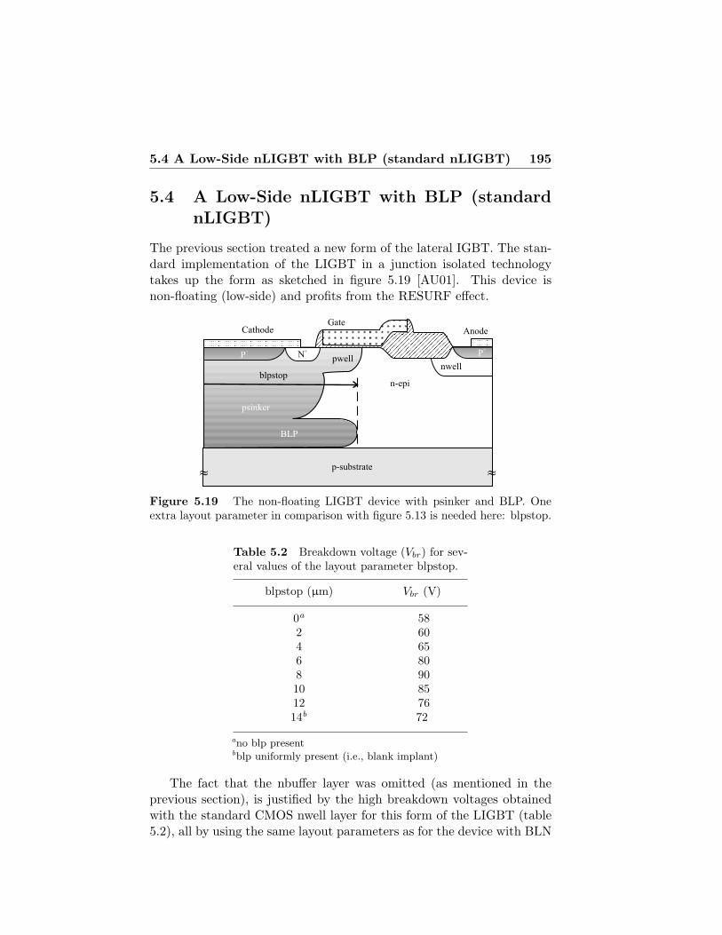
5.4 A Low-Side nLIGBT with BLP (standard nLIGBT) 195
5.4 A Low-Side nLIGBT with BLP (standardnLIGBT)
The previous section treated a new form of the lateral IGBT. The stan-dard implementation of the LIGBT in a junction isolated technologytakes up the form as sketched in figure 5.19 [AU01]. This device isnon-floating (low-side) and profits from the RESURF effect.
pwellP+
n-epi
CathodeGate
Anode
p-substrate
P+
N+
»»
nwell
psinker
BLP
blpstop
Figure 5.19 The non-floating LIGBT device with psinker and BLP. Oneextra layout parameter in comparison with figure 5.13 is needed here: blpstop.
Table 5.2 Breakdown voltage (Vbr) for sev-eral values of the layout parameter blpstop.
blpstop (µm) Vbr (V)
0a 582 604 656 808 9010 8512 7614b 72
ano blp presentbblp uniformly present (i.e., blank implant)
The fact that the nbuffer layer was omitted (as mentioned in theprevious section), is justified by the high breakdown voltages obtainedwith the standard CMOS nwell layer for this form of the LIGBT (table5.2), all by using the same layout parameters as for the device with BLN
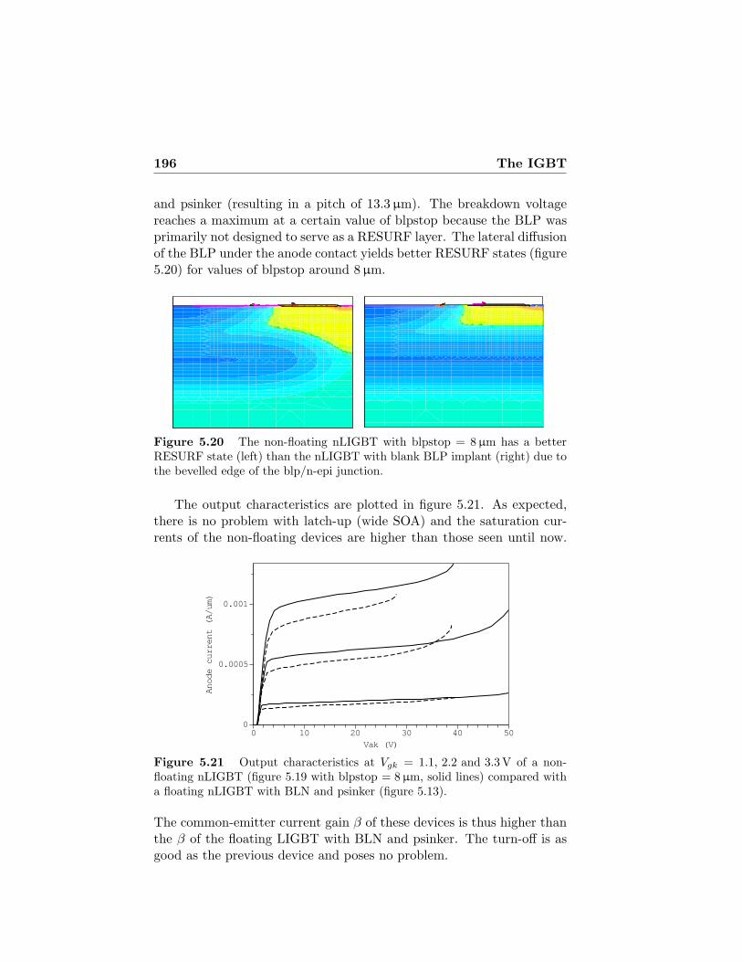
196 The IGBT
and psinker (resulting in a pitch of 13.3µm). The breakdown voltagereaches a maximum at a certain value of blpstop because the BLP wasprimarily not designed to serve as a RESURF layer. The lateral diffusionof the BLP under the anode contact yields better RESURF states (figure5.20) for values of blpstop around 8µm.
Figure 5.20 The non-floating nLIGBT with blpstop = 8 µm has a betterRESURF state (left) than the nLIGBT with blank BLP implant (right) due tothe bevelled edge of the blp/n-epi junction.
The output characteristics are plotted in figure 5.21. As expected,there is no problem with latch-up (wide SOA) and the saturation cur-rents of the non-floating devices are higher than those seen until now.
Vak (V)0 10 20 30 40 50
Anode current (A/um)
0
0.0005
0.001
Figure 5.21 Output characteristics at Vgk = 1.1, 2.2 and 3.3 V of a non-floating nLIGBT (figure 5.19 with blpstop = 8 µm, solid lines) compared witha floating nLIGBT with BLN and psinker (figure 5.13).
The common-emitter current gain β of these devices is thus higher thanthe β of the floating LIGBT with BLN and psinker. The turn-off is asgood as the previous device and poses no problem.
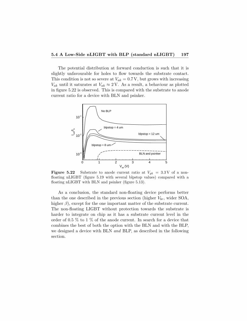
5.4 A Low-Side nLIGBT with BLP (standard nLIGBT) 197
The potential distribution at forward conduction is such that it isslightly unfavourable for holes to flow towards the substrate contact.This condition is not so severe at Vak = 0.7V, but grows with increasingVak until it saturates at Vak ≈ 2V. As a result, a behaviour as plottedin figure 5.22 is observed. This is compared with the substrate to anodecurrent ratio for a device with BLN and psinker.
Vak (V)
I sub/
I a
0 1 2 3 4 5
10-3
10-2
10-1
No BLP
blpstop = 4 um
blpstop = 8 um
blpstop = 12 um
BLN and psinker
Figure 5.22 Substrate to anode current ratio at Vgk = 3.3V of a non-floating nLIGBT (figure 5.19 with several blpstop values) compared with afloating nLIGBT with BLN and psinker (figure 5.13).
As a conclusion, the standard non-floating device performs betterthan the one described in the previous section (higher Vbr, wider SOA,higher β), except for the one important matter of the substrate current.The non-floating LIGBT without protection towards the substrate isharder to integrate on chip as it has a substrate current level in theorder of 0.5 % to 1 % of the anode current. In search for a device thatcombines the best of both the option with the BLN and with the BLP,we designed a device with BLN and BLP, as described in the followingsection.

198 The IGBT
5.5 A High-Side nLIGBT with BLP and BLN
5.5.1 The standard process flow
The approach discussed in the previous section could no longer be usedas a floating device since the p-substrate and the cathode are shorted.It is possible, however, to use the BLN together with the BLP in theI3T80 technology, which results in a situation as shown in figure 5.23.Again, the same layout has been used for this device as for the deviceswith BLN and psinker, and BLP and psinker (in µm): pso = 3, ps = 3,katoga = 0.4, sw = 0.8, pf = 0, x = 1, y = 0.8, t = 4.5, z = 1,nw = 1.5, aw = 1, and antofi = 0.2 (only nw is 0.5µm smaller, butmost important is that the pitch remains the same: pitch = 13.3µm).
pwellP+
n-epi
Cathode
Gate
Anode
p-substrate
P+
N+
»
nwell
psinker
BLP
BLN
»
Figure 5.23 The LIGBT device with psinker, BLP and BLN.
This is a floating device, as the eventual potential difference betweencathode and substrate is held by the BLN/p-substrate junction. Thisis the case whether the BLN is contacted and shorted to the cathode,or not. When it is shorted to the cathode, the potential difference isclearly sustained by the substrate for a large part as the BLN is muchhigher doped than the substrate. When the BLN is not contacted via ansinker, then it floats between the cathode and substrate, and behavesas the open base of a pnp transistor. If the cathode potential becomeshigher than the substrate potential, the BLN/substrate junction sustainsthe potential difference. Yet there is an important difference betweenan LIGBT with contacted BLN and an LIGBT with floating BLN, aswill be explained later.
This device is designed as an alternative for the non-floating standard
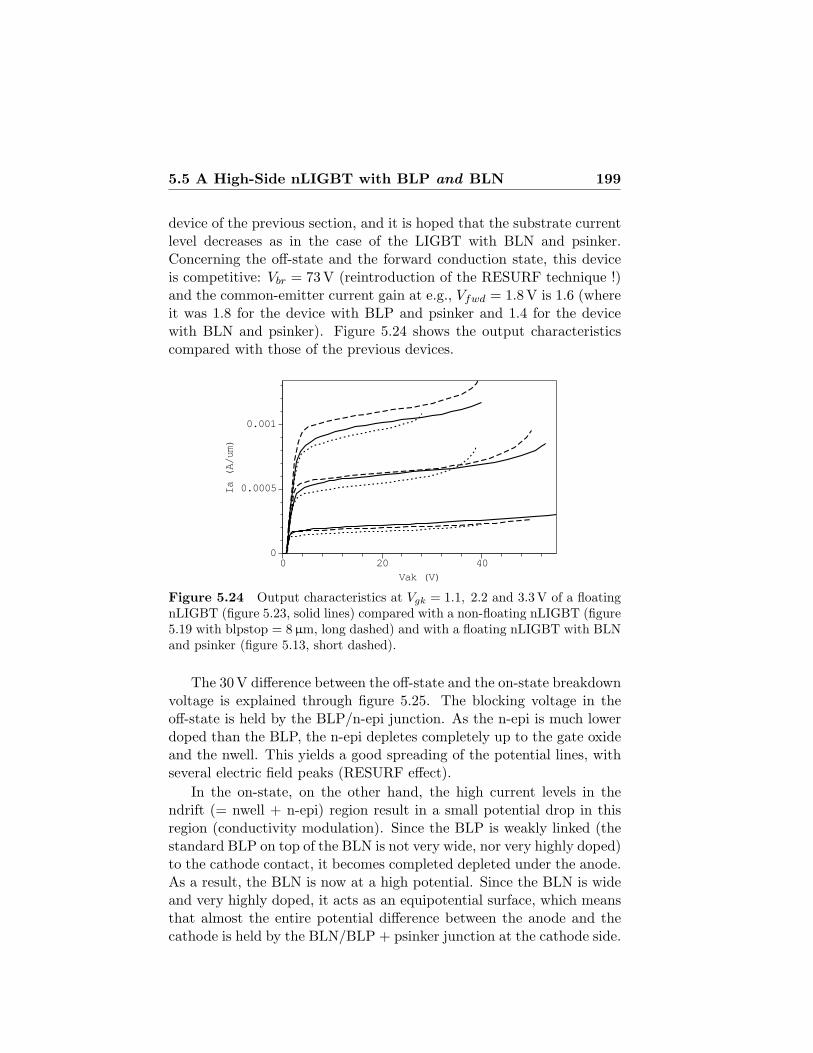
5.5 A High-Side nLIGBT with BLP and BLN 199
device of the previous section, and it is hoped that the substrate currentlevel decreases as in the case of the LIGBT with BLN and psinker.Concerning the off-state and the forward conduction state, this deviceis competitive: Vbr = 73 V (reintroduction of the RESURF technique !)and the common-emitter current gain at e.g., Vfwd = 1.8V is 1.6 (whereit was 1.8 for the device with BLP and psinker and 1.4 for the devicewith BLN and psinker). Figure 5.24 shows the output characteristicscompared with those of the previous devices.
Vak (V)0 20 40
Ia (A/um)
0
0.0005
0.001
Figure 5.24 Output characteristics at Vgk = 1.1, 2.2 and 3.3 V of a floatingnLIGBT (figure 5.23, solid lines) compared with a non-floating nLIGBT (figure5.19 with blpstop = 8 µm, long dashed) and with a floating nLIGBT with BLNand psinker (figure 5.13, short dashed).
The 30 V difference between the off-state and the on-state breakdownvoltage is explained through figure 5.25. The blocking voltage in theoff-state is held by the BLP/n-epi junction. As the n-epi is much lowerdoped than the BLP, the n-epi depletes completely up to the gate oxideand the nwell. This yields a good spreading of the potential lines, withseveral electric field peaks (RESURF effect).
In the on-state, on the other hand, the high current levels in thendrift (= nwell + n-epi) region result in a small potential drop in thisregion (conductivity modulation). Since the BLP is weakly linked (thestandard BLP on top of the BLN is not very wide, nor very highly doped)to the cathode contact, it becomes completed depleted under the anode.As a result, the BLN is now at a high potential. Since the BLN is wideand very highly doped, it acts as an equipotential surface, which meansthat almost the entire potential difference between the anode and thecathode is held by the BLN/BLP + psinker junction at the cathode side.

200 The IGBT
However, impact ionisation mostly occurs under the bird’s beak situatedunder the gate, as this is the region where both high current levels andhigh electric fields occur (although the electric fields at the BLN/BLPjunction are higher, almost no current is passing, so almost no impactionization is taking place there).
0
0
0
0 0
20
20
40
60
x-axis (µm)
y-ax
is(µ
m)
5 10
-8
-7
-6
-5
-4
-3
-2
-1
0
0
10
10
20
20
30
x-axis (µm)
y-ax
is(µ
m)
5 10
-8
-7
-6
-5
-4
-3
-2
-1
0
Figure 5.25 Electrostatic potential distribution (V) in the off-state (left)and the on-state (right) for a nLIGBT with psinker, BLP and BLN.
Substrate current behaviour
Figure 5.26 plots the ratio of substrate to anode current for the devicewith a floating BLN, compared with the LIGBTs discussed this far. Theratio is the smallest for this new device and remarkable is the decreasingratio with increasing Vak. These results open new perspectives as towhether or not the lateral IGBT is feasible for an 80 V junction isolatedtechnology. The question arises if the behaviour as seen in figure 5.26can be further improved by altering some process or layout conditions.
To answer this question, the particular behaviour of the substratecurrent needs to be explained. First of all, 2D plots at several Vak valueshelp to gain insight into the physical processes at stake. And secondly,an equivalent circuit will help to understand which parameters have tobe varied in order to reduce the substrate current.
Figure 5.27 shows that at Vak = 2 V the potential differences insidethe device between BLP and BLN are not yet pronounced, while the
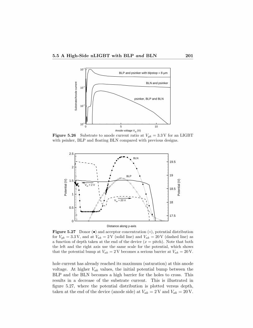
5.5 A High-Side nLIGBT with BLP and BLN 201
Anode voltage Vak (V)
Sub
stra
te/A
node
curr
ent
0 5 1010-5
10-4
10-3
10-2
BLP and psinker with blpstop = 8 µm
BLN and psinker
psinker, BLP and BLN
Figure 5.26 Substrate to anode current ratio at Vgk = 3.3V for an LIGBTwith psinker, BLP and floating BLN compared with previous designs.
Distance along y-axis
Pot
entia
l(V
)
Pot
entia
l(V
)
0
0.5
1
1.5
2
2.5
17.5
18
18.5
19
19.5
Vak = 2 V
Vak = 20 V
BLN
BLP
Figure 5.27 Donor (•) and acceptor concentration (), potential distributionfor Vgk = 3.3V, and at Vak = 2 V (solid line) and Vak = 20V (dashed line) asa function of depth taken at the end of the device (x = pitch). Note that boththe left and the right axis use the same scale for the potential, which showsthat the potential bump at Vak = 2 V becomes a serious barrier at Vak = 20 V.
hole current has already reached its maximum (saturation) at this anodevoltage. At higher Vak values, the initial potential bump between theBLP and the BLN becomes a high barrier for the holes to cross. Thisresults in a decrease of the substrate current. This is illustrated infigure 5.27, where the potential distribution is plotted versus depth,taken at the end of the device (anode side) at Vak = 2 V and Vak = 20 V.
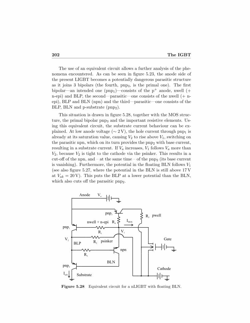
202 The IGBT
The use of an equivalent circuit allows a further analysis of the phe-nomena encountered. As can be seen in figure 5.23, the anode side ofthe present LIGBT becomes a potentially dangerous parasitic structureas it joins 3 bipolars (the fourth, pnp3, is the primal one). The firstbipolar—an intended one (pnp1)—consists of the p+ anode, nwell (+n-epi) and BLP, the second—parasitic—one consists of the nwell (+ n-epi), BLP and BLN (npn) and the third—parasitic—one consists of theBLP, BLN and p-substrate (pnp2).
This situation is drawn in figure 5.28, together with the MOS struc-ture, the primal bipolar pnp3 and the important resistive elements. Us-ing this equivalent circuit, the substrate current behaviour can be ex-plained. At low anode voltage (∼ 2V), the hole current through pnp1 isalready at its saturation value, causing V2 to rise above V1, switching onthe parasitic npn, which on its turn provides the pnp2 with base current,resulting in a substrate current. If Va increases, V1 follows Va more thanV2, because V2 is tight to the cathode via the psinker. This results in acut-off of the npn, and – at the same time – of the pnp2 (its base currentis vanishing). Furthermore, the potential in the floating BLN follows V1
(see also figure 5.27, where the potential in the BLN is still above 17Vat Vak = 20 V). This puts the BLP at a lower potential than the BLN,which also cuts off the parasitic pnp2.
Anode
Gate
Cathode
Substrate
BLN
BLP
nwell + n-epi
psinker
pnp1
pnp2
npn
V1
V2
R3
R2
R1
IMOS
Isub
Va
R4
pwellR5
pnp3
Figure 5.28 Equivalent circuit for a nLIGBT with floating BLN.
5.5 A High-Side nLIGBT with BLP and BLN 203
Using figure 5.28, assuming a constant MOS current IMOS (con-trolled by the gate voltage) and assuming ideal bipolar transistors (IC =βIB and VBEpnp/npn = –/+ 0.7V), one can calculate the substrate cur-rent Isub as a function of the anode voltage Va, IMOS , the common emit-ter current gains of the bipolar transistors (β1 for pnp1, β2 for pnp2, β3
for pnp3, and βn for the npn), and the resistors R1, R2, R3 and R4:
Isub =1δ
(γIMOS − Va
)(5.9)
with
γ =1κ
(R1 + β1R2
)and (5.10)
δ =(
1κβ2
+1
κβ2βn
)R1 +
(1 +
1β2
+β1
κβ2(5.11)
+1
β2βn+
β1
κβ2βn
)R2 +
1β2βn
R3 and
κ = 1 +R1
R4. (5.12)
This means that Isub = 0 if Va > γIMOS (Va > 0V!), that Isub
decreases with increasing Va/δ, and thus decreases faster for smallervalues of δ. Furthermore, the maximum Isub (i.e., for the smallest Va
for which the assumptions are still valid) decreases with decreasing γ/δ.These results will be demonstrated in the section discussing the processand layout variations of the BLN.
Contacting the BLN
Using the equivalent circuit approach also explains what happens whenthe BLN is contacted via the nsinker. The equivalent circuit for thissituation is shown in figure 5.29. The npn is no longer conducting currenttowards V1, but away from V1; that is, if the nsinker is at a low enoughvoltage. The npn is then part of a thyristor (together with pnp1), whichlatches as soon as the npn is on. Gate control is lost as a huge electroncurrent flows towards the nsinker contact. This current provides basecurrent for pnp2, yielding substantial substrate currents. This behaviourhas been confirmed by TCAD simulation, see figures 5.30 and 5.31 fore.g., a nsinker to cathode voltage Vns = 0 V.
If the nsinker is put on a higher voltage, the current changes signand flows away from the nsinker. This means that the collector and
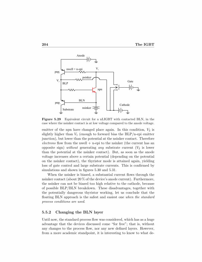
204 The IGBT
Anode
Gate
Cathode
Substrate
BLN
BLP
nwell + n-epi
nsinker
psinker
pnp1
pnp2
npn
V1
V2
Figure 5.29 Equivalent circuit for a nLIGBT with contacted BLN, in thecase where the nsinker contact is at low voltage compared to the anode voltage.
emitter of the npn have changed place again. In this condition, V2 isslightly higher than V1 (enough to forward bias the BLP/n-epi emitterjunction), but lower than the potential at the nsinker contact. Thereforeelectrons flow from the nwell + n-epi to the nsinker (the current has anopposite sign) without generating any substrate current (V2 is lowerthan the potential at the nsinker contact). But, as soon as the anodevoltage increases above a certain potential (depending on the potentialon the nsinker contact), the thyristor mode is attained again, yieldingloss of gate control and large substrate currents. This is confirmed bysimulations and shown in figures 5.30 and 5.31.
When the nsinker is biased, a substantial current flows through thensinker contact (about 20 % of the device’s anode current). Furthermore,the nsinker can not be biased too high relative to the cathode, becauseof possible BLP/BLN breakdown. These disadvantages, together withthe potentially dangerous thyristor working, let us conclude that thefloating BLN approach is the safest and easiest one when the standardprocess conditions are used.
5.5.2 Changing the BLN layer
Until now, the standard process flow was considered, which has as a hugeadvantage that the devices discussed come “for free”; that is, withoutany changes to the process flow, nor any new defined layers. However,from a more academic standpoint, it is interesting to know to what de-
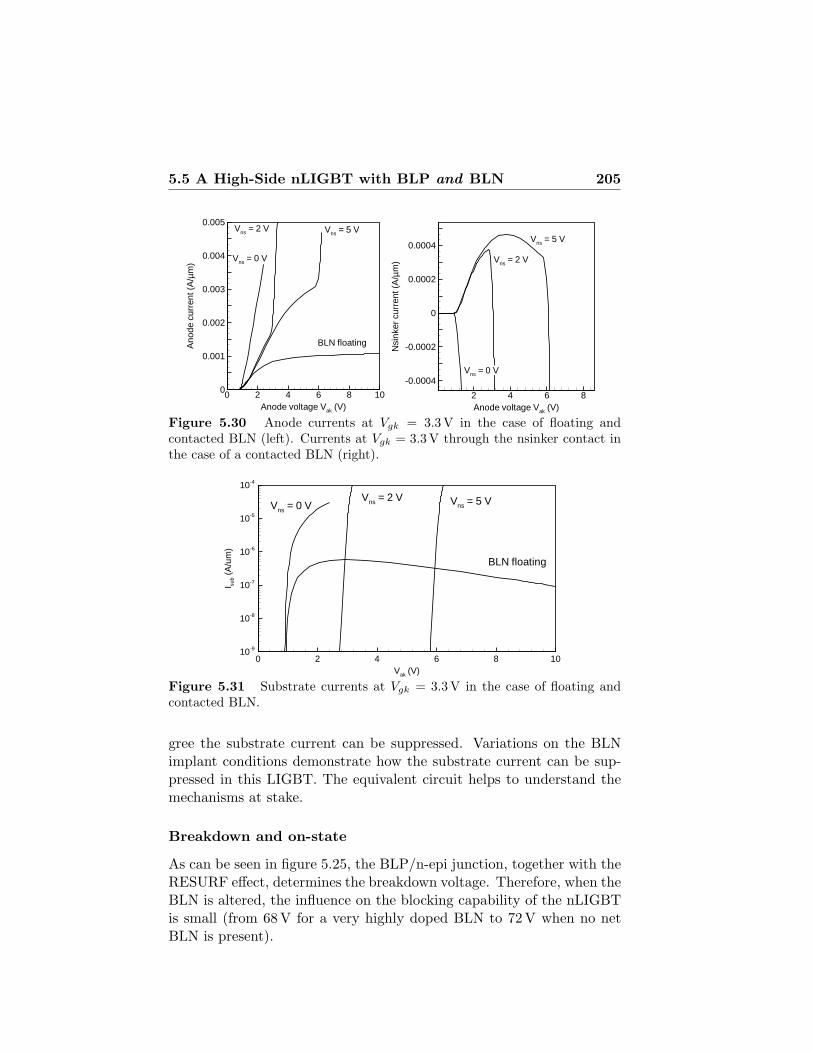
5.5 A High-Side nLIGBT with BLP and BLN 205
Anode voltage Vak (V)N
sink
ercu
rren
t(A
/µm
)2 4 6 8
-0.0004
-0.0002
0
0.0002
0.0004
Vns = 0 V
Vns = 2 V
Vns = 5 V
Anode voltage Vak (V)
Ano
decu
rren
t(A
/µm
)
0 2 4 6 8 100
0.001
0.002
0.003
0.004
0.005
BLN floating
Vns = 0 V
Vns = 2 V Vns = 5 V
Figure 5.30 Anode currents at Vgk = 3.3V in the case of floating andcontacted BLN (left). Currents at Vgk = 3.3V through the nsinker contact inthe case of a contacted BLN (right).
Vak (V)
I sub
(A/u
m)
0 2 4 6 8 1010-9
10-8
10-7
10-6
10-5
10-4
BLN floating
Vns = 0 VVns = 2 V Vns = 5 V
Figure 5.31 Substrate currents at Vgk = 3.3V in the case of floating andcontacted BLN.
gree the substrate current can be suppressed. Variations on the BLNimplant conditions demonstrate how the substrate current can be sup-pressed in this LIGBT. The equivalent circuit helps to understand themechanisms at stake.
Breakdown and on-state
As can be seen in figure 5.25, the BLP/n-epi junction, together with theRESURF effect, determines the breakdown voltage. Therefore, when theBLN is altered, the influence on the blocking capability of the nLIGBTis small (from 68V for a very highly doped BLN to 72V when no netBLN is present).
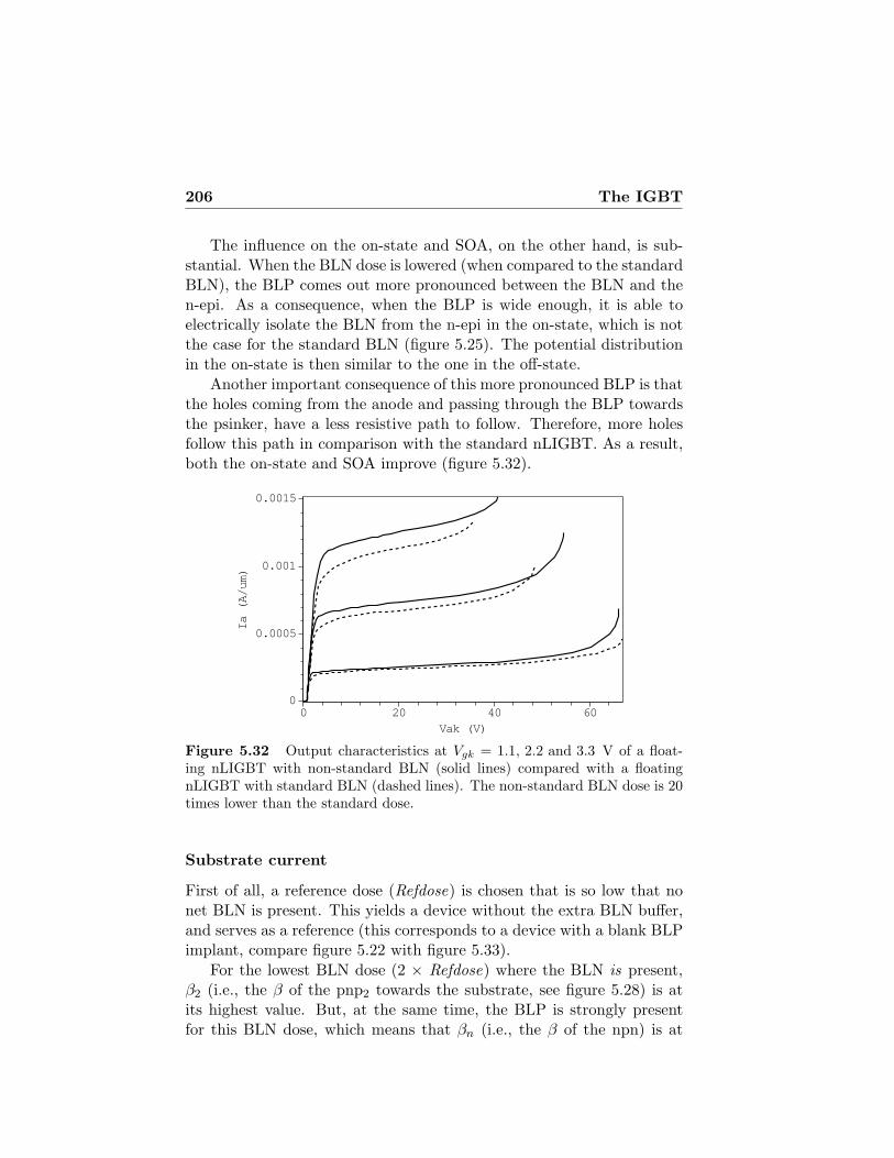
206 The IGBT
The influence on the on-state and SOA, on the other hand, is sub-stantial. When the BLN dose is lowered (when compared to the standardBLN), the BLP comes out more pronounced between the BLN and then-epi. As a consequence, when the BLP is wide enough, it is able toelectrically isolate the BLN from the n-epi in the on-state, which is notthe case for the standard BLN (figure 5.25). The potential distributionin the on-state is then similar to the one in the off-state.
Another important consequence of this more pronounced BLP is thatthe holes coming from the anode and passing through the BLP towardsthe psinker, have a less resistive path to follow. Therefore, more holesfollow this path in comparison with the standard nLIGBT. As a result,both the on-state and SOA improve (figure 5.32).
Vak (V)0 20 40 60
Ia (A/um)
0
0.0005
0.001
0.0015
Figure 5.32 Output characteristics at Vgk = 1.1, 2.2 and 3.3 V of a float-ing nLIGBT with non-standard BLN (solid lines) compared with a floatingnLIGBT with standard BLN (dashed lines). The non-standard BLN dose is 20times lower than the standard dose.
Substrate current
First of all, a reference dose (Refdose) is chosen that is so low that nonet BLN is present. This yields a device without the extra BLN buffer,and serves as a reference (this corresponds to a device with a blank BLPimplant, compare figure 5.22 with figure 5.33).
For the lowest BLN dose (2 × Refdose) where the BLN is present,β2 (i.e., the β of the pnp2 towards the substrate, see figure 5.28) is atits highest value. But, at the same time, the BLP is strongly presentfor this BLN dose, which means that βn (i.e., the β of the npn) is at

5.5 A High-Side nLIGBT with BLP and BLN 207
Vak (V)
I sub/
I a
0 5 10 15 2010-6
10-5
10-4
10-3
10-2
10-1
Refdose2*Refdose5*Refdose10*Refdose20*Refdose40*Refdose
Figure 5.33 Substrate to anode current ratio at Vgk = 3.3V for severalLIGBTs with different BLN doses. Note that the lowest dose yields a devicewithout BLN and that the highest dose is the standard dose.
its lowest value, as well as R2 and R3. This means that although thepnp towards the substrate is most effective for this low BLN dose, thesubstrate to anode current ratio is the lowest (see figure 5.33) becauseof the highly conductive path towards the psinker and because of thevery bad npn that provides the base current for the pnp towards thesubstrate.
When the BLN dose is increased, β2 decreases as its base (= BLN)not only increases in dose but also widens. As a result of this growingBLN, the BLP shrinks, which on its turn yields a increasing βn, R2 andR3. This explains the growing substrate to anode current ratio for theBLN doses = 2 ×, 5 × and 10 × Refdose.
When the BLN dose is yet further increased, the β2 becomes so smallthat it is the dominant factor. As a consequence, the substrate currentdecreases again. For the highest BLN dose (= 40 × Refdose), it is alsoobserved that the decrease of the substrate to anode current ratio withincreasing Vak is the slowest. As the BLP is the smallest for this BLNdose (highest R2 value), the npn stays on even with high Vak, becauseV2 remains larger than V1 even for the higher Vak values. Whereas forthe smaller BLN doses, the BLP is more conductive (smaller R2), whichshuts off the npn faster because V2 becomes smaller than V1 at lower Vak
values. This also explains why for all BLN doses the substrate to anodecurrent ratio vanishes completely when Vak is large enough.
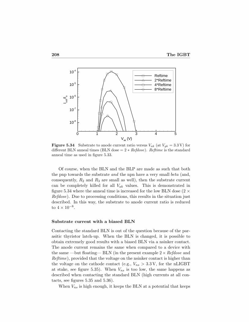
208 The IGBT
Vak (V)
I sub/
I a
0 1 2 3 4 5
10-8
10-7
10-6
10-5
10-4
Reftime2*Reftime4*Reftime8*Reftime
Figure 5.34 Substrate to anode current ratio versus Vak (at Vgk = 3.3V) fordifferent BLN anneal times (BLN dose = 2 ∗ Refdose). Reftime is the standardanneal time as used in figure 5.33.
Of course, when the BLN and the BLP are made as such that boththe pnp towards the substrate and the npn have a very small beta (and,consequently, R2 and R3 are small as well), then the substrate currentcan be completely killed for all Vak values. This is demonstrated infigure 5.34 where the anneal time is increased for the low BLN dose (2 ×Refdose). Due to processing conditions, this results in the situation justdescribed. In this way, the substrate to anode current ratio is reducedto 4× 10⁻⁸.
Substrate current with a biased BLN
Contacting the standard BLN is out of the question because of the par-asitic thyristor latch-up. When the BLN is changed, it is possible toobtain extremely good results with a biased BLN via a nsinker contact.The anode current remains the same when compared to a device withthe same —but floating— BLN (in the present example 2×Refdose andReftime), provided that the voltage on the nsinker contact is higher thanthe voltage on the cathode contact (e.g., Vns > 3.3V, for the nLIGBTat stake, see figure 5.35). When Vns is too low, the same happens asdescribed when contacting the standard BLN (high currents at all con-tacts, see figures 5.35 and 5.36).
When Vns is high enough, it keeps the BLN at a potential that keeps
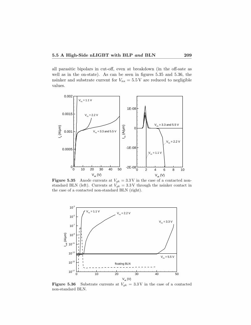
5.5 A High-Side nLIGBT with BLP and BLN 209
all parasitic bipolars in cut-off, even at breakdown (in the off-sate aswell as in the on-state). As can be seen in figures 5.35 and 5.36, thensinker and substrate current for Vns = 5.5V are reduced to negligiblevalues.
Vak (V)
I a(A
/µm
)
0 10 20 30 40 500
0.0005
0.001
0.0015
0.002Vns = 1.1 V
Vns = 3.3 and 5.5 V
Vns = 2.2 V
Vak (V)
I ns(A
/µm
)
0 2 4 6 8 10-2E-08
-1E-08
0
1E-08
Vns = 1.1 V
Vns = 2.2 V
Vns = 3.3 and 5.5 V
Figure 5.35 Anode currents at Vgk = 3.3V in the case of a contacted non-standard BLN (left). Currents at Vgk = 3.3V through the nsinker contact inthe case of a contacted non-standard BLN (right).
Vak (V)
I sub
(A/µ
m)
0 10 20 30 40 5010-17
10-15
10-13
10-11
10-9
10-7
10-5
10-3
floating BLN
Vns = 1.1 VVns = 2.2 V
Vns = 3.3 V
Vns = 5.5 V
Figure 5.36 Substrate currents at Vgk = 3.3 V in the case of a contactednon-standard BLN.
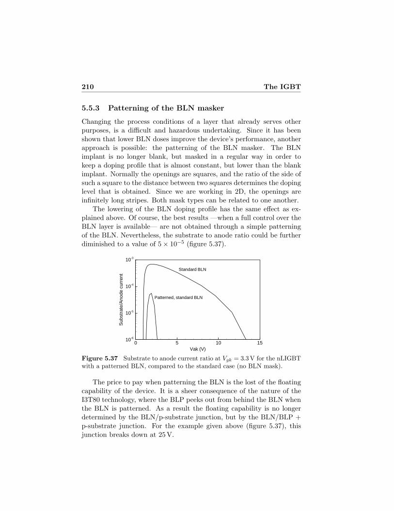
210 The IGBT
5.5.3 Patterning of the BLN masker
Changing the process conditions of a layer that already serves otherpurposes, is a difficult and hazardous undertaking. Since it has beenshown that lower BLN doses improve the device’s performance, anotherapproach is possible: the patterning of the BLN masker. The BLNimplant is no longer blank, but masked in a regular way in order tokeep a doping profile that is almost constant, but lower than the blankimplant. Normally the openings are squares, and the ratio of the side ofsuch a square to the distance between two squares determines the dopinglevel that is obtained. Since we are working in 2D, the openings areinfinitely long stripes. Both mask types can be related to one another.
The lowering of the BLN doping profile has the same effect as ex-plained above. Of course, the best results —when a full control over theBLN layer is available— are not obtained through a simple patterningof the BLN. Nevertheless, the substrate to anode ratio could be furtherdiminished to a value of 5× 10⁻⁵ (figure 5.37).
Vak (V)
Sub
stra
te/A
node
curr
ent
0 5 10 1510-6
10-5
10-4
10-3
Standard BLN
Patterned, standard BLN
Figure 5.37 Substrate to anode current ratio at Vgk = 3.3 V for the nLIGBTwith a patterned BLN, compared to the standard case (no BLN mask).
The price to pay when patterning the BLN is the lost of the floatingcapability of the device. It is a sheer consequence of the nature of theI3T80 technology, where the BLP peeks out from behind the BLN whenthe BLN is patterned. As a result the floating capability is no longerdetermined by the BLN/p-substrate junction, but by the BLN/BLP +p-substrate junction. For the example given above (figure 5.37), thisjunction breaks down at 25 V.
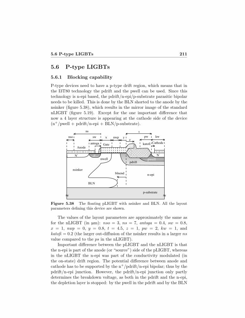
5.6 P-type LIGBTs 211
5.6 P-type LIGBTs
5.6.1 Blocking capability
P-type devices need to have a p-type drift region, which means that inthe I3T80 technology the pdrift and the pwell can be used. Since thistechnology is n-epi based, the pdrift/n-epi/p-substrate parasitic bipolarneeds to be killed. This is done by the BLN shorted to the anode by thensinker (figure 5.38), which results in the mirror image of the standardnLIGBT (figure 5.19). Except for the one important difference thatnow a 4 layer structure is appearing at the cathode side of the device(n+/pwell + pdrift/n-epi + BLN/p-substrate).
pdrift
P+
n-epi
CathodeGate
Anode
p-substrate
N+
»»
x
t
zy
N+
nwell
BLN
nsinker
pwell
pwsw
antoga
ns
nso kw
katofi
nwp
blnend
Figure 5.38 The floating pLIGBT with nsinker and BLN. All the layoutparameters defining this device are shown.
The values of the layout parameters are approximately the same asfor the nLIGBT (in µm): nso = 3, ns = 7, antoga = 0.4, sw = 0.8,x = 1, nwp = 0, y = 0.8, t = 4.5, z = 1, pw = 2, kw = 1, andkatofi = 0.2 (the larger out-diffusion of the nsinker results in a larger nsvalue compared to the ps in the nLIGBT).
Important difference between the pLIGBT and the nLIGBT is thatthe n-epi is part of the anode (or “source”) side of the pLIGBT, whereasin the nLIGBT the n-epi was part of the conductivity modulated (inthe on-state) drift region. The potential difference between anode andcathode has to be supported by the n+/pdrift/n-epi bipolar; thus by thepdrift/n-epi junction. However, the pdrift/n-epi junction only partlydetermines the breakdown voltage, as both in the pdrift and the n-epi,the depletion layer is stopped: by the pwell in the pdrift and by the BLN
212 The IGBT
in the n-epi. This explains the influence of the layout parameter blnendon the breakdown voltage (table 5.3). Furthermore, the breakdown iscaused by a reach-through of the depletion layer in the pdrift + pwellto the n+/pwell junction, creating a current path for the electrons fromcathode to anode. Hence the occurrence of the pwell, without which thereach-through happens at even lower voltages. One could try to increasethis reach-through voltage by introducing a new pbuffer layer.
Table 5.3 Breakdown voltage (Vbr) for sev-eral values of the layout parameter blnend.
blnend (µm) Vbr (V)
-1.5a 310 43
1.5 403 37
aBLN diffuses up to under the cathode
5.6.2 On-state
The most interesting characteristic of the pLIGBT is that the on-stateresistance is no longer determined by the mobility of the holes alone.Contrary to pDMOS devices —which have inherently an on-state resis-tance that is three times lower than that of nDMOS devices with thesame breakdown voltage— pLIGBTs have a conductivity modulatedpdrift region during forward conduction. This means that the resistiv-ity of the pdrift region is no longer determined by the doping level ofthe holes. As a consequence, the on-state resistance is comparable tothat of a nLIGBT since the total resistance of a high-voltage device isfor a great part determined by the resistivity of the drift region.
Figure 5.39 plots the output characteristics of both a nLIGBT and anpLIGBT, showing that the current level of the pLIGBT is approximately20 – 25 % lower than that of the nLIGBT for the entire Vak range. Notethat for the pLIGBT, the simulation is carried out with Vsuba = −80V(substrate to anode voltage), Vga = −3.3V (gate to anode voltage),and a cathode voltage Vka that is swept between 0 and −28V. Thiscorresponds to a real situation where Vasub = 80 V, Vgsub = 76.7 V, andVksub is swept between 80 and 52 V.
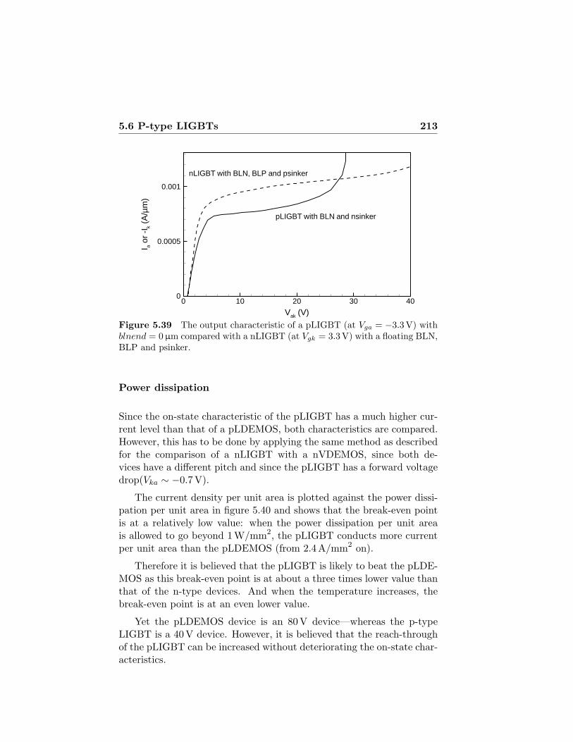
5.6 P-type LIGBTs 213
Vak (V)
I aor
-Ik(A
/µm
)
0 10 20 30 400
0.0005
0.001
nLIGBT with BLN, BLP and psinker
pLIGBT with BLN and nsinker
Figure 5.39 The output characteristic of a pLIGBT (at Vga = −3.3V) withblnend = 0 µm compared with a nLIGBT (at Vgk = 3.3V) with a floating BLN,BLP and psinker.
Power dissipation
Since the on-state characteristic of the pLIGBT has a much higher cur-rent level than that of a pLDEMOS, both characteristics are compared.However, this has to be done by applying the same method as describedfor the comparison of a nLIGBT with a nVDEMOS, since both de-vices have a different pitch and since the pLIGBT has a forward voltagedrop(Vka ∼ −0.7V).
The current density per unit area is plotted against the power dissi-pation per unit area in figure 5.40 and shows that the break-even pointis at a relatively low value: when the power dissipation per unit areais allowed to go beyond 1W/mm2, the pLIGBT conducts more currentper unit area than the pLDEMOS (from 2.4A/mm2 on).
Therefore it is believed that the pLIGBT is likely to beat the pLDE-MOS as this break-even point is at about a three times lower value thanthat of the n-type devices. And when the temperature increases, thebreak-even point is at an even lower value.
Yet the pLDEMOS device is an 80 V device—whereas the p-typeLIGBT is a 40 V device. However, it is believed that the reach-throughof the pLIGBT can be increased without deteriorating the on-state char-acteristics.

214 The IGBT
Dissipated power (W/mm2)
Cur
rent
dens
ity(A
/mm
2)
0 5 10 150
5
10
15
20
pLIGBT (pitch = 15.8 um)
pLDEMOS (pitch = 7.25 um)
Figure 5.40 Current density versus power dissipation (at Vga = −3.3V)for an pLIGBT with blnend = 0µm compared with a typical pLDEMOS (atVgs = −3.3V).
5.6.3 Substrate current
Another distinguishing feature of the pLIGBT is the extremely low sub-strate to anode current ratio. Figure 5.41 plots this ratio at Vga = −3.3Vas a function of Vak for several values of blnend. As long as the BLN ispresent under the cathode drift region (blnend = 1.5 and 0µm), thereis no problem with substrate current whatsoever as the BLN is still bigenough to kill the parasitic pnp towards the psubstrate. When the BLNis pushed away from under the pdrift region, the doping level of thebase of this parasitic bipolar decreases drastically (from the BLN dop-ing level to the n-epi), resulting in a rapid increase of the substrate toanode current ratio.
The substrate current behaviour of the pLIGBT can also be ex-plained through the use of an equivalent circuit. In figure 5.42, it isclearly seen that the four layer structure at the cathode side can notwork as a thyristor, since the psubstrate is always at the lowest poten-tial. The pnp can however conduct current as soon as Vxy ≈ −0.7V.This happens in the case of large blnend values, as then R1 increases,with a potential drop at x as a consequence. In the other cases (smalland negative blnend values), the pnp remains in cut-off, which explainsthe extremely low substrate currents in figure 5.41.
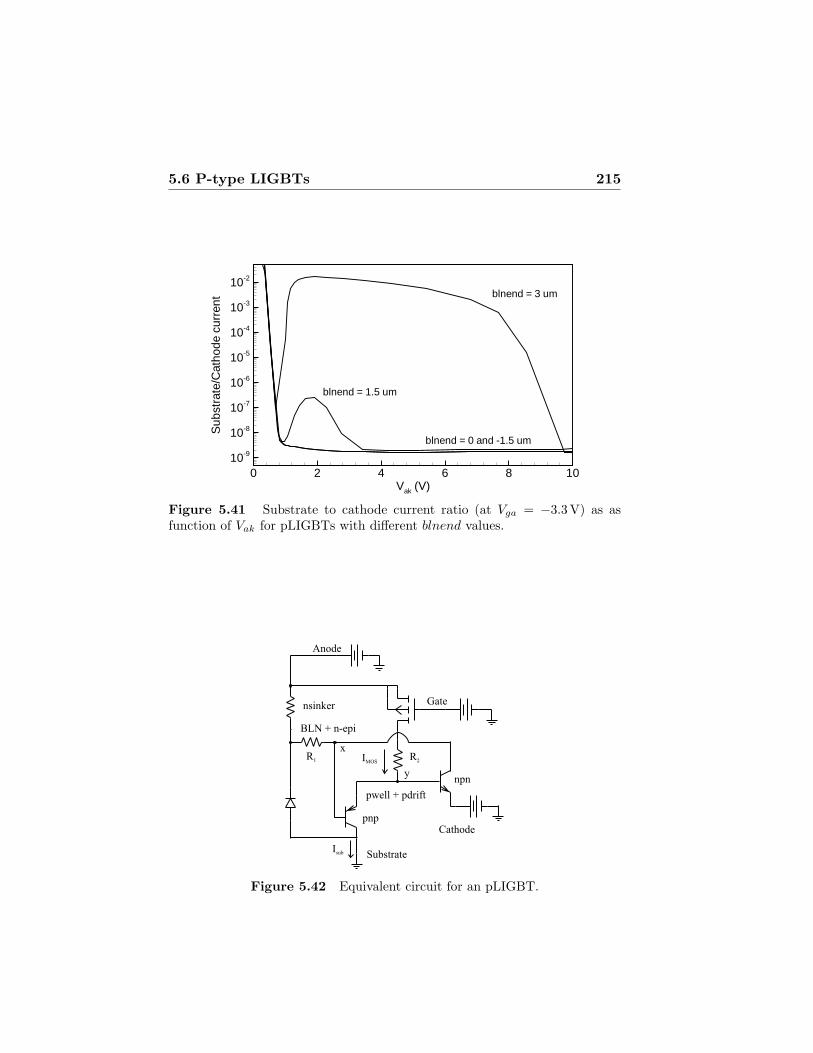
5.6 P-type LIGBTs 215
Vak (V)
Sub
stra
te/C
atho
decu
rren
t
0 2 4 6 8 1010-9
10-8
10-7
10-6
10-5
10-4
10-3
10-2
blnend = 3 um
blnend = 0 and -1.5 um
blnend = 1.5 um
Figure 5.41 Substrate to cathode current ratio (at Vga = −3.3V) as asfunction of Vak for pLIGBTs with different blnend values.
Anode
Gate
Cathode
Substrate
BLN + n-epi
pwell + pdrift
nsinker
npn
IMOS
Isub
pnp
y
xR2
R1
Figure 5.42 Equivalent circuit for an pLIGBT.

216 The IGBT
5.7 Integrated Vertical IGBTs
This section studies the possibility of integrating vertical IGBTs. Tothat end, a highly doped buried layer—serving as the anode contactsituated under the device instead of next to it—and a highly dopedsinker linking this “buried” contact back to the surface, are needed.For the n-type IGBT, this means a BLP with psinker; for the p-typeIGBT, a BLN with nsinker. Since we are working on a p-type substrate,isolation is needed between the BLP and the substrate for the n-typeIGBT. Fortunately, the BLN has been designed in such a way that itcan serve this purpose. Keeping this in mind, 2 of the most commonapproaches used for the vertical IGBT—the punch-through (PT) andthe non punch-through (NPT) IGBT—are presented in this section.
pwell
P+
n-epi
Cathode
Gate
p-substrate
N+
»»
BLP
BLN
Figure 5.43 An integrated non punch-through IGBT.
Figure 5.43 depicts the non punch-through IGBT device. A non-punch-through vertical device should be designed as such that at for-ward blocking, the pwell/n-epi depletion region does not punch throughto the n-epi/BLP junction. For discretes, the n-epi thickness can be sev-eral hundred micrometers. In the I3T80 technology, however, the freeepi thickness (i.e., the net n-epi thickness between the pwell and BLPjunctions) is in the order of a few micrometers. This means that thistype of IGBT almost immediately reaches through (at Vak ≈ 10−20V).
Since the n-epi thickness can not be changed in the I3T80 technol-ogy, other approaches are needed. A solution might be the so-calledpunch-through devices, as shown in figure 5.44, where the depletion re-gion coming from the n-epi/pwell junction at forward blocking is stoppedat the nbuffer. A new layer would be needed, implanted after the BLP
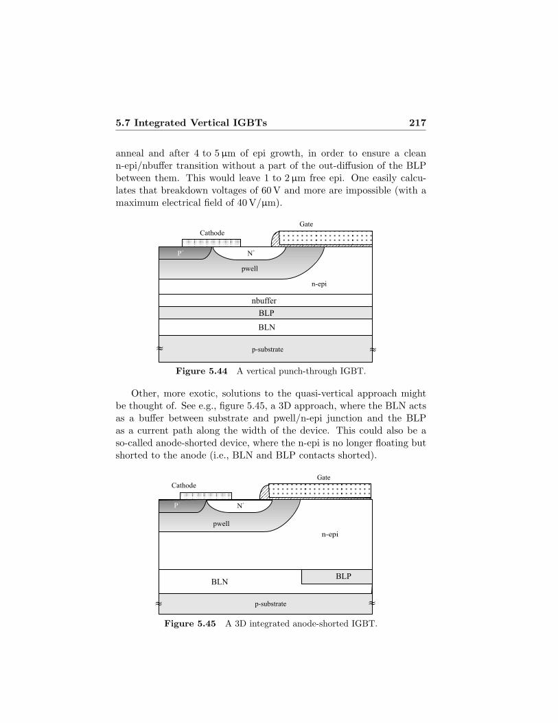
5.7 Integrated Vertical IGBTs 217
anneal and after 4 to 5µm of epi growth, in order to ensure a cleann-epi/nbuffer transition without a part of the out-diffusion of the BLPbetween them. This would leave 1 to 2µm free epi. One easily calcu-lates that breakdown voltages of 60 V and more are impossible (with amaximum electrical field of 40 V/µm).
pwell
P+
n-epi
Cathode
Gate
p-substrate
N+
»»
BLP
nbuffer
BLN
Figure 5.44 A vertical punch-through IGBT.
Other, more exotic, solutions to the quasi-vertical approach mightbe thought of. See e.g., figure 5.45, a 3D approach, where the BLN actsas a buffer between substrate and pwell/n-epi junction and the BLPas a current path along the width of the device. This could also be aso-called anode-shorted device, where the n-epi is no longer floating butshorted to the anode (i.e., BLN and BLP contacts shorted).
pwell
P+
n-epi
CathodeGate
p-substrate
N+
»»
BLPBLN
Figure 5.45 A 3D integrated anode-shorted IGBT.
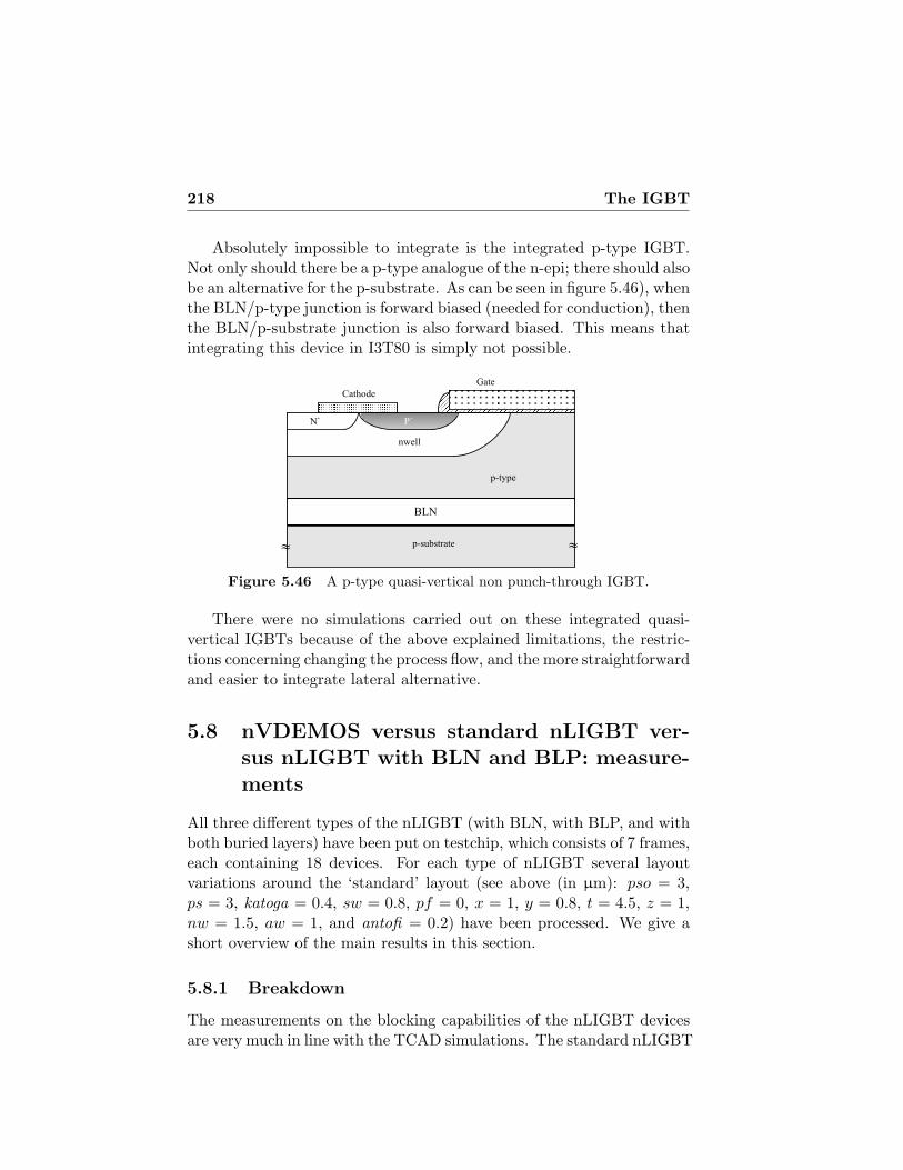
218 The IGBT
Absolutely impossible to integrate is the integrated p-type IGBT.Not only should there be a p-type analogue of the n-epi; there should alsobe an alternative for the p-substrate. As can be seen in figure 5.46), whenthe BLN/p-type junction is forward biased (needed for conduction), thenthe BLN/p-substrate junction is also forward biased. This means thatintegrating this device in I3T80 is simply not possible.
nwell
P+
p-type
Cathode
Gate
p-substrate
N+
»»
BLN
Figure 5.46 A p-type quasi-vertical non punch-through IGBT.
There were no simulations carried out on these integrated quasi-vertical IGBTs because of the above explained limitations, the restric-tions concerning changing the process flow, and the more straightforwardand easier to integrate lateral alternative.
5.8 nVDEMOS versus standard nLIGBT ver-sus nLIGBT with BLN and BLP: measure-ments
All three different types of the nLIGBT (with BLN, with BLP, and withboth buried layers) have been put on testchip, which consists of 7 frames,each containing 18 devices. For each type of nLIGBT several layoutvariations around the ‘standard’ layout (see above (in µm): pso = 3,ps = 3, katoga = 0.4, sw = 0.8, pf = 0, x = 1, y = 0.8, t = 4.5, z = 1,nw = 1.5, aw = 1, and antofi = 0.2) have been processed. We give ashort overview of the main results in this section.
5.8.1 Breakdown
The measurements on the blocking capabilities of the nLIGBT devicesare very much in line with the TCAD simulations. The standard nLIGBT
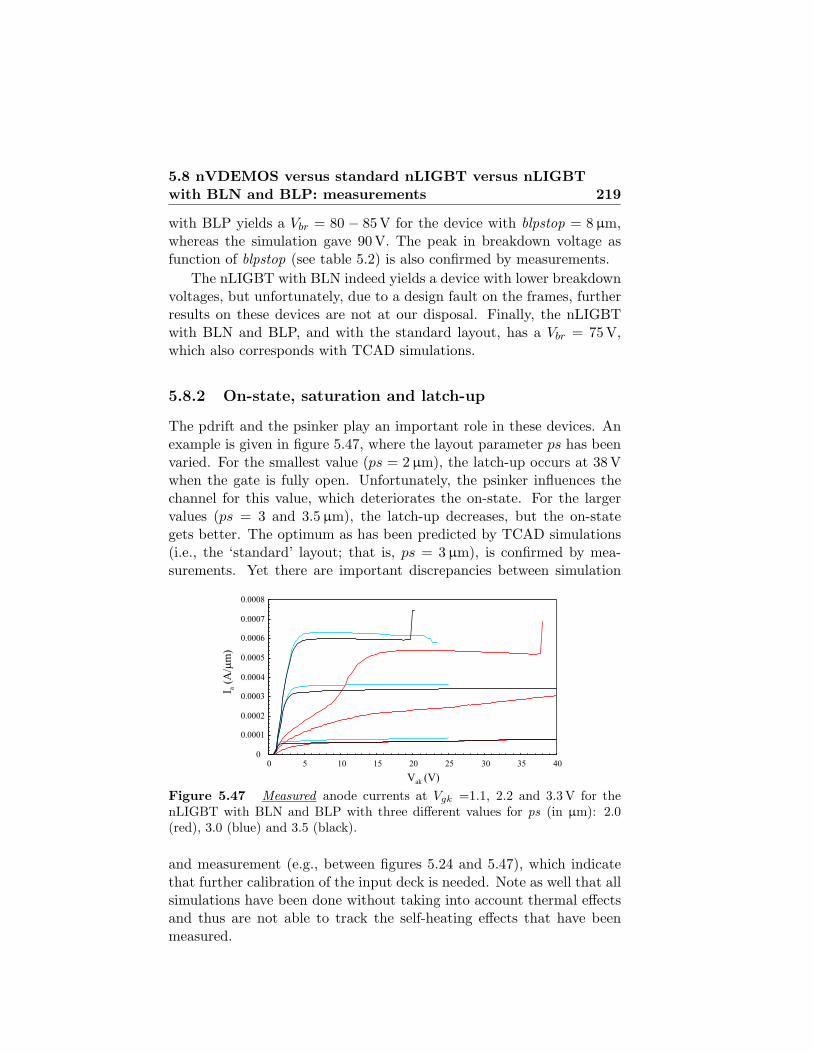
5.8 nVDEMOS versus standard nLIGBT versus nLIGBTwith BLN and BLP: measurements 219
with BLP yields a Vbr = 80 − 85V for the device with blpstop = 8 µm,whereas the simulation gave 90V. The peak in breakdown voltage asfunction of blpstop (see table 5.2) is also confirmed by measurements.
The nLIGBT with BLN indeed yields a device with lower breakdownvoltages, but unfortunately, due to a design fault on the frames, furtherresults on these devices are not at our disposal. Finally, the nLIGBTwith BLN and BLP, and with the standard layout, has a Vbr = 75 V,which also corresponds with TCAD simulations.
5.8.2 On-state, saturation and latch-up
The pdrift and the psinker play an important role in these devices. Anexample is given in figure 5.47, where the layout parameter ps has beenvaried. For the smallest value (ps = 2 µm), the latch-up occurs at 38Vwhen the gate is fully open. Unfortunately, the psinker influences thechannel for this value, which deteriorates the on-state. For the largervalues (ps = 3 and 3.5µm), the latch-up decreases, but the on-stategets better. The optimum as has been predicted by TCAD simulations(i.e., the ‘standard’ layout; that is, ps = 3 µm), is confirmed by mea-surements. Yet there are important discrepancies between simulation
0
0.0001
0.0002
0.0003
0.0004
0.0005
0.0006
0.0007
0.0008
0 5 10 15 20 25 30 35 40
V (V)ak
I(A
/m
)a
m
Figure 5.47 Measured anode currents at Vgk =1.1, 2.2 and 3.3 V for thenLIGBT with BLN and BLP with three different values for ps (in µm): 2.0(red), 3.0 (blue) and 3.5 (black).
and measurement (e.g., between figures 5.24 and 5.47), which indicatethat further calibration of the input deck is needed. Note as well that allsimulations have been done without taking into account thermal effectsand thus are not able to track the self-heating effects that have beenmeasured.

220 The IGBT
Figure 5.48 plots the measured output characteristics of the nVDE-MOS and the nLIGBT with BLN and BLP (and with the standardlayout). The large values for the saturation currents of the nLIGBTcompared to the nVDEMOS are striking, yet do not give a completepicture. As has been explained above, the comparison of the power
0
0.0001
0.0002
0.0003
0.0004
0.0005
0.0006
0.0007
0 5 10 15 20 25
V (V)ds of Vak
Io
f I
(A/
m)
da
m
Figure 5.48 Measured output characteristics at Vgk =1.1, 2.2 and 3.3V forthe nLIGBT with BLN and BLP compared with a typical nVDEMOS (blue,at Vgk =1, 2 and 3.3 V).
dissipation per unit area at a certain current density is a more correctcriterion (figure 5.49). Again the measurements are very much in linewith the simulations and reveal that the nLIGBT can beat the nVDE-MOS if a power dissipation of 3 W/mm2 is allowed.
0
5
10
15
20
0 5 10 15
Dissipated power (W/mm )2
Curr
ent
den
sity
(A
/mm
)2
nLIGBT
nVDEMOS
Figure 5.49 Measured current density versus power dissipation at Vgk =3.3 Vfor the nLIGBT with BLN and BLP compared with a typical nVDEMOS (atVgs =3.3V).
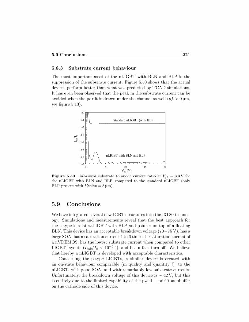
5.9 Conclusions 221
5.8.3 Substrate current behaviour
The most important asset of the nLIGBT with BLN and BLP is thesuppression of the substrate current. Figure 5.50 shows that the actualdevices perform better than what was predicted by TCAD simulations.It has even been observed that the peak in the substrate current can beavoided when the pdrift is drawn under the channel as well (pf > 0µm,see figure 5.13).
1e-7
1e-6
1e-5
1e-4
1e-3
1e-2
1e-1
1e0
0 5 10 15 20
V (V)ak
I/I
sub
a
Standard nLIGBT (with BLP)
nLIGBT with BLN and BLP
Figure 5.50 Measured substrate to anode current ratio at Vgk = 3.3V forthe nLIGBT with BLN and BLP, compared to the standard nLIGBT (onlyBLP present with blpstop = 8 µm).
5.9 Conclusions
We have integrated several new IGBT structures into the I3T80 technol-ogy. Simulations and measurements reveal that the best approach forthe n-type is a lateral IGBT with BLP and psinker on top of a floatingBLN. This device has an acceptable breakdown voltage (70−75V), has alarge SOA, has a saturation current 4 to 6 times the saturation current ofa nVDEMOS, has the lowest substrate current when compared to otherLIGBT layouts (Isub/Ia < 10−6 !), and has a fast turn-off. We believethat hereby a nLIGBT is developed with acceptable characteristics.
Concerning the p-type LIGBTs, a similar device is created withan on-state behaviour comparable (in quality and quantity !) to thenLIGBT, with good SOA, and with remarkably low substrate currents.Unfortunately, the breakdown voltage of this device is ∼ 42V, but thisis entirely due to the limited capability of the pwell + pdrift as pbufferon the cathode side of this device.
222 The IGBT
Any comparison with LIGBTs presented in literature is difficult, formost recent articles on LIGBTs work in an SOI technology with forwardblocking voltages of several hundred volts. However, we have comparedthe LIGBTs with the existing I3T80 integrated nVDEMOS devices. TheLIGBT can beat the nVDEMOS in terms of current per unit area if thepower dissipation per unit area is allowed to reach ∼ 1− 3W/mm2 forthe n-type devices and ∼ 1W/mm2 for the p-type devices.
References
[AU01] G. Amaratunga and F. Udrea. Power Devices for High Volt-age Integrated Circuits: New Device and Technology Con-cepts. In Semiconductor Conference, volume 2, pages 441–448, 2001.
[BAG+82] B.J. Baliga, M.S. Adler, P.V. Gray, R. Love, and N. Zommer.The Insulated Gate Rectifier (IGR): A New Power Switch-ing Device. In IEEE International Electron Devices MeetingDigest, pages 264–267, 1982.
[Bal79] B.J. Baliga. Enhancement- and Depletion Mode Vertical-Channel MOS Gated Thyristors. Electronics Letters,15(20):645–647, September 1979.
[Bal92] B.J. Baliga. Modern Power Devices. Krieger, 1992.
[BGG99] V. Benda, J. Gowar, and D.A. Grant. Power SemiconductorDevices. John Wiley & Sons, 1999.
[PS80] J. D. Plummer and B.W. Scharf. Insulated-Gate PlanarThyristors: I—Structure and Basic Operation. IEEE Trans-actions on Electron Devices, 27(2):380–387, February 1980.
[RGGN83] J.P. Russell, A.M. Goodman, L.A. Goodman, and J.M. Neil-son. The COMFET — A New High Conductance MOS-Gated Device. IEEE Electron Device Letters, EDL-4(3):63–65, March 1983.
[Sze81] S.M. Sze. Physics of Semiconductor Devices. John Wiley &Sons, 1981.
[Tih80] J. Tihaji. Functional Integration of Power MOS and BipolarDevices. In IEEE International Electron Devices Meeting,pages 75–78, 1980.
6 Synopsis
6.1 Overview Main Results
After two short general introductory chapters and a quick survey ofthe TCAD simulation and calibration work, we have integrated boththe power MOS and IGBT into an existing, standard CMOS, junctionisolated technology.
We concluded that the best combination of a n-type and a p-typepower MOS in an 80− 100V technology (e.g., the I3T80 technology ofAMIS) is a nVDMOS and a pLDMOS. Although the nLDMOS has abetter Vbr−Ron,sp trade-off than the nVDMOS, we chose the latter, andthis for three reasons. First of all, the vertical device has a large SOAwithout using (costly) new layers, which are needed when the same SOAshould have to be obtained in the nLDMOS. Secondly, the nVDEMOSis by nature a floating device. In theory, the nLDEMOS can be madefloating without loss of performance as well, but this is technically harderto realize. Thirdly, the nVDMOS is easy to combine with the pLDMOS,which is not possible for the best RESURF nLDMOS devices.
Figures 6.1 and 6.2 show the existing nVD(E)MOS and pLDMOSdevices together with the competitor’s transistors and with the siliconlimits. The nVD(E)MOS was developed at AMIS, while the pLDE-MOS was developed at TFCG. Although the n-type device in the I3T80technology is a vertical device, whereas all the competitor’s devices arelateral, it has a competitive Vbr −Ron,sp. Note that the best devices onfigure 6.1 are non-floating, with the one important exception of the 63 V“FRESURF” device by Motorola (0.35µm). Figure 6.2 shows that theI3T80 pLDEMOS is amongst the best p-type devices ever made.
For the IGBT devices, we have succeeded in integrating both a n-typeand a p-type LIGBT, which have—to the best of our knowledge—neverbeen described in literature before. We managed to suppress the sub-strate currents in both devices, to create a large SOA, and to guarantee
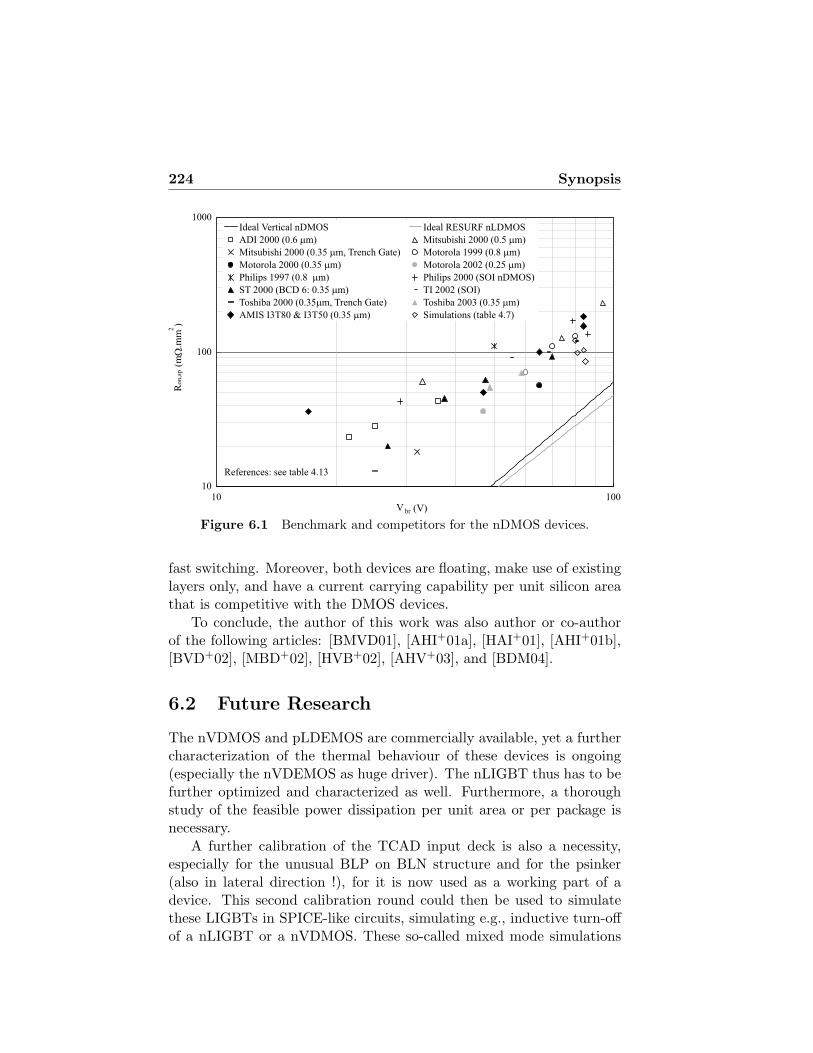
224 Synopsis
10
100
1000
10 100
Ideal Vertical nDMOS Ideal RESURF nLDMOS
ADI 2000 (0.6 m)m Mitsubishi 2000 (0.5 m)m
Mitsubishi 2000 (0.35 m, Trench Gate)m Motorola 1999 (0.8 m)m
Motorola 2000 (0.35 m)m Motorola 2002 (0.25 m)m
Philips 1997 (0.8 m)m Philips 2000 (SOI nDMOS)
ST 2000 (BCD 6: 0.35 m)m TI 2002 (SOI)
Toshiba 2000 (0.35 m, Trench Gate)m Toshiba 2003 (0.35 m)m
AMIS I3T80 & I3T50 (0.35 m)m Simulations (table 4.7)
Ron,s
p(m
W.m
m2
)
V br (V)
References: see table 4.13
Figure 6.1 Benchmark and competitors for the nDMOS devices.
fast switching. Moreover, both devices are floating, make use of existinglayers only, and have a current carrying capability per unit silicon areathat is competitive with the DMOS devices.
To conclude, the author of this work was also author or co-authorof the following articles: [BMVD01], [AHI+01a], [HAI+01], [AHI+01b],[BVD+02], [MBD+02], [HVB+02], [AHV+03], and [BDM04].
6.2 Future Research
The nVDMOS and pLDEMOS are commercially available, yet a furthercharacterization of the thermal behaviour of these devices is ongoing(especially the nVDEMOS as huge driver). The nLIGBT thus has to befurther optimized and characterized as well. Furthermore, a thoroughstudy of the feasible power dissipation per unit area or per package isnecessary.
A further calibration of the TCAD input deck is also a necessity,especially for the unusual BLP on BLN structure and for the psinker(also in lateral direction !), for it is now used as a working part of adevice. This second calibration round could then be used to simulatethese LIGBTs in SPICE-like circuits, simulating e.g., inductive turn-offof a nLIGBT or a nVDMOS. These so-called mixed mode simulations

References 225
10
100
1000
10 100- Vbr (V)
Ron,s
p(m
W.m
m2)
Ideal Silicon Limit (pVDMOS)
ADI (0.6 m)m
Motorola (0.35 m)m
Motorola (0.25 m)m
Philips (0.8 m)m
Philips (SOI pDEMOS)
ST (0.6 m)m
Toshiba (0.7 m)m
Toshiba (0.35 m)m
Previous AMIS I2T ( )0.7 mm
I3T80 pDEMOS (0.35 m)m
TCAD (60 V pDEMOS)
References: see table 4.14
Figure 6.2 Benchmark and competitors for the pDMOS devices.
could also be applied to energy capability simulations or ESD simula-tions, thereby trying to design robust devices. These simulations shoulduse the thermodynamical or hydrodynamical models, or even be per-formed in 3D (which is still in the future), in order to be able to trackthe self-heating effects. Recent device simulators make it even possi-ble to simulate hot carrier degradation, which could be linked to stressmeasurements, something that has not yet been done for LIGBTs.
On the device side, new types of power devices could be thought upand tried out (e.g., the Insulated Base T ransistor [PMS86], the LateralInsulated Gate p-i-n T ransistor [Hua96], the Lateral Inversion LayerEmitter T ransistor [UAH+96], . . . ), one could try to integrate thyristors(e.g., the Lateral Conductivity M odulated Thyristor [LKO+02]), super-junctions and/or trench gates, and power devices in smaller technologies(to date, the smallest smart power technology is 0.25µm [ZPK+03]) ordevices on SOI could be considered. In the distant future, new materials(SiC, GaP. . . ) could be tried out on smart power technologies.
References
[AHI+01a] C. Anghel, N. Hefyene, A.M. Ionescu, M. Vermandel,B. Bakeroot, and J. Doutreloigne. Investigations and Phys-
226 Synopsis
ical Modelling of Saturation Effects in Lateral DMOS Tran-sistor Architectures Based on the Concept of Intrinsic DrainVoltage. In European Solid-State Device Research Confer-ence, pages 399–402, 2001.
[AHI+01b] C. Anghel, N. Hefyene, A.M. Ionescu, M. Vermandel,B. Bakeroot, and J. Doutreloigne et al. Physical ModellingStrategy for (Quasi-)Saturation Effects in Lateral DMOSTransistor Based on the Concept of Intrinsic Drain Voltage.In Semiconductor Conference, pages 417–420, 2001.
[AHV+03] C. Anghel, N. Hefyene, M. Vermandel, B. Bakeroot,J. Doutreloigne, and R. Gillon et al. Electrical Character-ization of High Voltage MOSFETs Using MESDRIFT. InSemiconductor Conference, pages 257–260, 2003.
[BDM04] B. Bakeroot, J. Doutreloigne, and P. Moens. A New Sub-strate Current Free nLIGBT for Junction Isolated Technolo-gies. In European Solid-State Device Research Conference,2004, accepted for publication.
[BMVD01] B. Bakeroot, P. Moens, M. Vermandel, and J. Doutreloigne.Using Adaptive RESURF Technique and Field Plate Work-ing to Improve the Safe Operating Area of n-type DrainExtended MOS. In Conference on Modeling and Simulationof Microsystems, pages 468–501, 2001.
[BVD+02] B. Bakeroot, M. Vermandel, J. Doutreloigne, P. Moens,and D. Bolognesi. Cost Effective Implementation of a 90 VRESURF p-Type Drain Extended MOS in a 0.35µm BasedSmart Power Technology. In European Solid-State DeviceResearch Conference, pages 291–294, 2002.
[HAI+01] N. Hefyene, C. Anghel, A.M. Ionescu, M. Vermandel,B. Bakeroot, and J. Doutreloigne et al. An Experimental Ap-proach for Bias-Dependent Drain Series Resistances Evalua-tion in Asymmetric HV MOSFETs. In European Solid-StateDevice Research Conference, pages 403–406, 2001.
[Hua96] A.Q. Huang. Lateral Insulated Gate p-i-n Transistor(LIGPT)—A New MOS Gate Lateral Power Device. IEEEElectron Device Letters, 17(6):297–299, June 1996.
References 227
[HVB+02] N. Hefyene, E. Vestiel, B. Bakeroot, C. Anghel, A.M.Ionescu, and R. Gillon. Bias-Dependent Drift ResistanceModelling for Accurate DC and AC Simulation of Asymmet-ric HV-MOSFET. In Simulation of Semiconductor Processesand Devices, pages 203–206, 2002.
[LKO+02] Y.-S. Lee, S.-S. Kim, J.-K. Oh, Y.I. Choi, and M.-K. Han. ANew Lateral Conductivity Modulated Thyristor With Cur-rent Saturation and Low Turn-off Time. In Symposium onPower Semiconductor Devices & ICs, pages 113–116, 2002.
[MBD+02] P. Moens, D. Bolognesi, L. Delobel, D. Villanueva, K. Reyn-ders, A. Lowe, G. Van Herzeele, M. Tack, and B. Bakeroot.Future Trends in Intelligent Interface Technologies for 42 VBattery Automotive Applications. In European Solid-StateDevice Research Conference, pages 287–290, 2002.
[PMS86] Z. Parpia, J.G. Mena, and C.A.T. Salama. A Novel CMOS-Compatible High-Voltage Transistor Structure. IEEE Trans-actions on Electron Devices, 33(12):1948–1952, December1986.
[UAH+96] F. Udrea, G.A.J. Amarantunga, J. Humphrey, J. Clark, andA.G.R. Evans. The MOS Inversion Layer as a Minority Car-rier Injector. IEEE Electron Device Letters, 17(9):425–427,September 1996.
[ZPK+03] R. Zhu, V. Parthasarathy, V. Khemka, A. Bose, T. Roggen-bauer, and G. Lee et al. A 0.25 Micron Smart Power Technol-ogy Optimized For Wireless and Consumer Applications. InSymposium on Power Semiconductor Devices & ICs, pages178–181, 2003.


A List of Basic Symbols
Symbol Despcription Unit
c Heat capacity J/(K cm3)C Capacitance FD Diffusion constant cm2/sDn Electron diffusion constant cm2/sDp Hole diffusion constant cm2/sE Electric field V/cmF Force N~ Planck constant J sGn Electron generation rate per unit volume cm−3/sGp Hole generation rate per unit volume cm−3/sH Heat generation per unit volume J/(s cm3)I Current AJ Current density A/cm2
Jn Electron current density A/cm2
Jp Hole current density A/cm2
k Boltzmann constant J/Kl Length cmm0 Electron rest mass kgn Density of free electrons cm−3
ni,eff Effective intrinsic density cm−3
NA− Acceptor impurity density cm−3
ND+ Donor impurity density cm−3
p Density of free holes cm−3
p Carrier momentum kg cm/sPn Absolute electron thermoelectric power V/KPp Absolute hole thermoelectric power V/Kq Magnitude of electronic charge Cr Carrier position cm
230 List of Basic Symbols
Symbol Despcription Unit
Rn Electron recombination rate per unit volume cm−3/sRp Hole recombination rate per unit volume cm−3/st Time sT Absolute temperature KTL Absolute lattice temperature KTn Absolute electron temperature KTp Absolute hole temperature Kv Carrier velocity cm/svn,sat Electron saturation velocity cm/sV Voltage Vεs Semiconductor permittivity F/cmκ Thermal conductivity W/(mK)µn Electron mobility cm2/(V s)µp Hole mobility cm2/(V s)ρ Space charge density C/cm3
φn Electron quasi-Fermi potential Vφp Hole quasi-Fermi potential Vψ Potential VΨ Wave functionΩ Ohm Ω

B List of Abbreviations
1D, 2D or 3D One, Two or Three Dimension(s)
AMIS American MIcroelectronics Semiconductor
BLN Buried Layer of N-type
BLP Buried Layer of P-type
BRT Base Resistance controlled Thyristor
CMOS Complementary MOS (see MOSFET)
CPU Central Processing Unit
DEMOS Drain Extended MOS (see MOSFET)
DMOS Double diffused MOS (see MOSFET)
ESD ElectroStatic Discharge
EST Emitter Switched Thyristor
FCD Field Controlled Diode
FCT Field Controlled Thyristor
GATT Gate-Assisted Turn-off Thyristor
GTO Gate Turn-Off thyristor
IBT Insulated Base Transistor
IGBT Insulated Gate Bipolar Transistor
ISE Integrated Systems Engineering
JBS Junction Barrier Schottky rectifier

232 List of Abbreviations
JFET Junction Field Effect Transistor
LCMT Lateral Conductivity Modulated Thyristor
LDD Lightly Doped Drain
LDEMOS Lateral Drain Extended MOS (see MOSFET)
LDMOS Lateral Double diffused MOS (see MOSFET)
LIGBT Lateral IGBT (see IGBT)
LILET Lateral Inversion Layer Emitter Transistor
MOSFET Metal-Oxide-Semiconductor Field Effect Transistor
MPS Merged p-i-n/Schottky rectifier
QVDEMOS Quasi-Vertical Drain Extended MOS (see MOSFET)
QVDMOS Quasi-Vertical Double diffused MOS (see MOSFET)
RESURF REduced SURface Field
SCR Silicon Controlled Rectifier
SEM Scanning Electron Microscopy
SIMS Secondary-Ion Mass Spectroscopy
SIT Static Induction Transistor
SITh Static Induction Thyristor
SOA Safe Operating Area
SOI Silicon On Insulator
SPICE Simulation Program with Integrated Circuit Emphasis
SRP Spreading Resistance Profiling
TCAD Technology Computer Aided Design
TED Transient Enhanced Diffusion
TLP Transmission Line Pulsing
VDEMOS Vertical Drain Extended MOS (see MOSFET)
VDMOS Vertical Double diffused MOS (see MOSFET)

C Calculating Breakdown andPunch-through
C.1 Breakdown of an abrupt n–p+ diode
Consider an abrupt, parallel-plane n–p+ junction in which the n-typedoping level (Nepi) is very low compared to the p-type doping level(Nsub). When a reverse bias voltage is applied to such a diode, thedepletion layer extends only into the n side as a result of the very highdoping level on the p side. Therefore, Poisson’s equation needs to besolved only for the n side:
dE
dx=
ρ(x)εs
=qNepi
εsfor 0 ≤ x ≤ Wn (C.1)
where ρ(x) is the charge in the depletion layer on the n side due toionized donors, εs is the dielectric constant of silicon, q is the electroniccharge, and Wn is the end of the depletion layer in the n side region.Integration of (C.1) and use of the boundary conditon that the electricfield at the end of the depletion layer is zero (E(x = Wn) = 0) resultsin the electric field distribution:
∫ E(x)
0dE =
∫ x
Wn
qNepi
εsdx′
E(x) =qNepi
εs(x−Wn). (C.2)

234 Calculating Breakdown and Punch-through
Integration of (C.2) with the boundary condition that V (x = Wn) = Va
gives the voltage distribution:
−dV
dx= E(x) =
qNepi
εs(x−W )
−∫ Va
V (x)dV =
qNepi
εs
∫ Wn
x(x′ −Wn)dx′
V (x) = Va − qNepi
2εs(Wn − x)2 . (C.3)
Substituting the values at breakdown Va = Vbr and Wn = Wbr in (C.3)and solving for x = 0 yields
Vbr =qNepi
2εsW 2
br. (C.4)
From (C.2), it is clear that the maximum absolute value of the electricfield (Em) occurs at x = 0. At breakdown, this value is therefore calledthe critical electric field Ecrit:
Ecrit = |E(x = 0)| = qNepi
εsWbr. (C.5)
Combining (C.5) and (C.4) gives an expression of the breakdown voltageas a function of the critical electric field:
Vbr =εs
2qNepiE2
crit. (C.6)
From the theory of impact ionization, it is known that breakdownoccurs as soon as the ionization integral is equal to 1 (e.g., [Bal92, pp.63–66]): ∫ Wbr
0α dx = 1 (C.7)
where Wbr is the depletion layer width at breakdown, and α an approx-imation of the impact ionization coefficient of both the electrons andholes (see also (2.23)):
αn ≈ αp ≈ α = A |E|7 (C.8)
where A is Fulop’s ionization rate [Ful67] equal to 1.8× 10⁻³⁵ cm6V−7.Substituting (C.8) in (C.7) gives:
1.8× 10⁻³⁵
∫ Wbr
0|E(x)|7 dx = 1 (C.9)
C.2 Punch-through of an abrupt n+–n–p+ diode 235
from which, using (C.2), the following expression for the depletion layerwidth at breakdown Wbr can be found:
Wbr =(
8ε7s1.8× 10−35q7
)1/8(Nepi
)−7/8
. (C.10)
A similar expression for the depletion layer width at breakdown for aparallel-plane n+/p junction has been used in figure 2.5. In the samefigure, the breakdown voltage is also given as a function of the dopinglevel, which can be easily obtained by substituting (C.10) in (C.4):
Vbr =(
ε3s2q3 1.8× 10⁻³⁵
)1/4(Nepi
)−3/4
. (C.11)
C.2 Punch-through of an abrupt n+–n–p+ diode
When the doping level in the n side of the abrupt n–p+ diode suddenlyincreases to a very high value, then the extension of the depletion layerwith increasing reverse bias is stopped at the n–n+ junction. Of course,provided that the depletion layer width at breakdown of the n–p+ diodeis larger than the thickness of the low doped n region (tepi). For thisso-called punch-through diode, Poisson’s equation is only solved in thelightly doped n region.
When the critical electric field is reached at x = 0, breakdown occursin the punch-through diode. At that moment, the electric field at then–n+ junction is not zero, but given by (C.2) with x = tepi:
Etepi =qNepi
εs(tepi −Wbr), (C.12)
where Wbr is the depletion layer thickness as defined in the previoussection and given by (C.10). The punch-through breakdown voltage canbe calculated using (C.12) and the fact that the potential drops in boththe p+ and the n+ regions are neglected:
Vpt =12
(|Etepi |+ Ecrit
)× tepi. (C.13)
Using (C.12) and (C.5) in (C.13) results in
Vpt =12
(qNepi
εsWbr +
qNepi
εsWbr − qNepi
εstepi
)tepi
=qNepi
εsWbrtepi − qNepi
2εst2epi. (C.14)
236 Calculating Breakdown and Punch-through
Using (C.10) gives an expression of Vpt as a function of the n-epi dopinglevel and thickness:
Vpt =(
8q
1.8× 10⁻³⁵εs
)1/8(Nepi
)1/8
tepi − q
2εsNepit
2epi. (C.15)
A similar expression has been used in figure 2.6, where the punch-through breakdown of a n+–p–p+ diode is plotted as a function of boththe doping level and the thickness of the lightly doped region.
C.3 Breakdown of an abrupt n–p diode
When the doping levels of each side of a diode are comparable to oneanother, then the depletion layers extend into both the n and p side,and therefore Poisson’s equation should be solved in both regions:
dE
dx=−qNsub
εsfor Wp ≤ x ≤ 0 (C.16)
dE
dx=
qNepi
εsfor 0 ≤ x ≤ Wn. (C.17)
Equation (C.16) has been solved in the first section and with the bound-ary conditions that E(x = Wp) = 0 (Wp is the end of the depletion layerin the p side) and V (x = Wn) = 0, equation (C.17) yields the followingelectric field and voltage distributions:
E(x) =−qNsub
εs(x−Wp) (C.18)
V (x) =qNsub
2εs(x−Wp)
2 . (C.19)
As both distributions should be continuous at x = 0, (C.2) and (C.18),and (C.3) and (C.19) have to be equal at x = 0. This results in thefollowing relationships:
Wn
Wp= −Nsub
Nepi(C.20)
Va =q
2εs
(NsubW
2p + NepiW
2n
). (C.21)
C.3 Breakdown of an abrupt n–p diode 237
Substituting (C.20) in (C.21) and solving for Wn and Wp results in:
Wn =
√2εsNsubVa
qNepi(Nsub + Nepi)(C.22)
Wp = −√
2εsNepiVa
qNsub(Nsub + Nepi). (C.23)
The depletion layer widths at breakdown can be written as functionof Nepi and Nsub alone when solving the ionization integral with Fulop’sionization rate, analogous to what has been done for an abrupt n–p+
diode:∫ 0
Wbr,p
A
(qNsub
εs
)7
(x−Wbr,p)7dx+∫ Wbr,n
0A
(qNepi
εs
)7
(Wbr,n−x)7dx = 1
with Wbr,p and Wbr,n the depletion layer widths at breakdown for thep side and the n side of the junction, respectively. Using (C.20) andsolving for Wbr,p and Wbr,n yields:
Wbr,n =(
Nsub
Nepi + Nsub
8A
)1/8( εs
qNepi
)7/8
(C.25)
Wbr,p = −(
Nepi
Nepi + Nsub
8A
)1/8( εs
qNsub
)7/8
. (C.26)
An expression of the breakdown voltage for this non punch-throughabrupt pn junction is obtained by substituting equations (C.25) and(C.26) in (C.21):
Vbr =(
ε3s2q3 1.8× 10⁻³⁵
)1/4(Nepi + Nsub
NepiNsub
)3/4
. (C.27)
238 Calculating Breakdown and Punch-through
C.4 Punch-through of an abrupt n+–n–p diode
The last example is important for calculating the breakdown voltagein an ideal RESURF diode, determined by the vertical punch-throughdiode present in the RESURF structure (see section 4.2). The thicknessof the lowly doped region is defined as the thickness of the total n-epi layer (tepi) thickness minus the thickness of the n+ region (tn+).Analogous with the case of the abrupt punch-through n+–n–p+ diode,the electric field at the n+–n junction En+ is given by
Etn+ =qNepi
εs
((tepi − tn+)−Wbr,n
), (C.28)
where Wbr,n is the depletion layer thickness as defined in the previoussection. The punch-through breakdown voltage is now given by the sumof the potential drop in both the n side and the p side region:
Vpt =12
(|Etn+ |+ Ecrit
)×
(tepi − tn+
)+
12Ecrit|Wbr,p|. (C.29)
Eliminating Ecrit = qNsubεs
|Wbr,p| and Etn+ in this equation, and assum-ing charge equality (Wbr,nNepi = |Wbr,p|Nsub) yields:
Vpt =qNsub
εs
((tepi − tn+)|Wbr,p|+
|Wbr,p|22
)− qNepi
2εs(tepi − tn+)2.
(C.30)
Vpt can thus be written as a function of the net epi thickness (tepi− tn+),Nepi and Nsub, by using this equation together with the expression (C.26)for Wbr,p.
References
[Bal92] B.J. Baliga. Modern Power Devices. Krieger, 1992.
[Ful67] W. Fulop. Calculation of Avalanche Breakdown Voltages of Sil-icon p–n Junctions. Solid-State Electronics, 10:39–43, 1967.


![Cursus Digitale Elektronica en Processoren [Work in Progress]](https://static.fdocuments.nl/doc/165x107/55cf9c8c550346d033aa358b/cursus-digitale-elektronica-en-processoren-work-in-progress.jpg)