
Microcontrollers 8051 based microcontroller ADuC832 from Analog Devices 12/2011 Roggemans M. (MGM)
SoC Implementation of OpenMSP430 Microcontroller inUMC 130nm
Paulo João Temoteo Rito
Thesis to obtain the Master of Science Degree in
Electrical and Computer Engineering
Supervisor: Prof. Paulo Ferreira Godinho Flores
Examination Committee
Chairperson: Prof. Gonçalo Nuno Gomes TavaresSupervisor: Prof. Paulo Ferreira Godinho Flores
Member of the Committee: Prof. João Pedro Oliveira
June 2018

ii

Declaration
I declare that this document is an original work of my own authorship and that it fulfills all the require-
ments of the Code of Conduct and Good Practices of the Universidade de Lisboa.
iii

iv

Acknowledgments
I would like to firstly express my gratitude to my supervisor, Prof. Paulo Flores, for all of his work,
effort and suggestions that made this work possible, and the large amount of time spent reviewing and
discussing this dissertation.
I would also like to thank the project PROTEUS team that allowed my access to the tools used in the
project, that without them, this work wouldn’t be possible.
Finally, I would like to thank my family and close friends for their support, patience and understanding
throughout this entire work and especially during the last couple of months.
v

vi
Resumo
A necessidade crescente de unidades de processamento com sensores incorporados, dedicadas e de-
scentralizadas, no âmbito de redes da Internet das Coisas, cria uma procura por micro controladores
integrados. O openMSP430 é um micro controlador de 16 bits de código aberto escrito em Verilog que é
compatível com a família de microcontroladores MSP430 da Texas Instruments. Pelas suas caracterís-
ticas, o openMSP430 foi selecionado para integrar o Sistema-em-um-Chip do projeto PROTEUS. Este
circuito, que será implementado em Circuito Integrado de Aplicação Especifica (CIAE), foi previamente
sintetizado numa tecnologia alvo UMC CMOS 130nm.
Nesta tese, estruturas de teste dedicadas foram adicionadas à descrição estrutural do circuito per-
mitindo a verificação do mesmo pós manufatura. Quatro cadeias de scan foram resintetizadas no
circuito, uma técnica de Design For Testability (DFT), que permite um aumento da cobertura de falhas,
possibilitando a entrada de vectores de teste, de maneira eficiente, que verificam o correto funciona-
mento da lógica interna do circuito. Um processo de ATPG foi configurado para gerar vetores de teste
para cada cadeia.
O layout final do circuito, através de um processo de back-end apresentado, foi obtido usando ferra-
mentas de EDA que executam as tarefas de Place&Route necessárias para atingir um circuito funcional.
O circuito final, openMSP430 com memórias de dados e programa e cadeias de scan, ocupa uma
área de 1050x2800µm, com uma cobertura de falhas de 94.9% e um consumo de 1.99mW a funcionar
a 16 MHz.
Antes deste trabalho, duas versões do openMSP430 foram implementadas, no projeto PROTEUS,
e enviadas para fabricação.
Palavras-chave: Circuito Integrado de Aplicação Especifica, Design For Testability, Auto-
matic Test Pattern Generation (ATPG), Fluxo de Projeto Place&Route
vii

viii

Abstract
The increasing need for decentralised, dedicated, sensoring and processing units on the scope of In-
ternet of Things (IoT) networking creates demand for embedded low-power microcontrollers. The open-
MSP430 is an open-source 16-bit microcontroller core written in Verilog, that is compatible with the
Texas Instruments’ MSP430 microcontroller family. Due to its characteristics, the openMSP430 was
selected to integrate the System on Chip (SOC) of the PROTEUS project. This open-core, that will
be implemented as an Application Specific Integrated Circuit (ASIC), was previously synthesised, for a
UMC CMOS 130nm target technology process.
In this thesis, dedicated test structures were added to the structural circuit description that allow
the post-manufacture verification of the circuit. Four scan chains were resynthesised into the circuit, a
Design For Testability (DFT) technique, to increase fault coverage and provide an efficient way to input
test vectors that will verify the correct operation of the circuit’s internal logic. An Automatic Test Pattern
Generation (ATPG) was configured to generate the test vector for each scan chain.
Through a back-end process presented, the final layout of the circuit was obtained using EDA tools
that execute Place&Route steps, required to achieve a fully functional layout.
The final microcontroller circuit, the openMSP430 with Program and Data memories and scan chains
occupies and area of 1050x2800µm, with a fault coverage of 94.9% and a power consumption of 1.99mW
when run at 16 MHz.
Two versions of the openMSP430 were implemented, under the PROTEUS project, and sent to
fabrication prior to this work.
Keywords: ASIC Implementation, Design for Test (DFT), Automatic Test Pattern Generation
(ATPG), Cadence Place&Route Design Flow
ix

x
Contents
Acknowledgments . . . . . . . . . . . . . . . . . . . . . . . . . . . . . . . . . . . . . . . . . . . . . . v
Resumo . . . . . . . . . . . . . . . . . . . . . . . . . . . . . . . . . . . . . . . . . . . . . . . . . . . . vii
Abstract . . . . . . . . . . . . . . . . . . . . . . . . . . . . . . . . . . . . . . . . . . . . . . . . . . . . ix
List of Tables . . . . . . . . . . . . . . . . . . . . . . . . . . . . . . . . . . . . . . . . . . . . . . . . . xiii
List of Figures . . . . . . . . . . . . . . . . . . . . . . . . . . . . . . . . . . . . . . . . . . . . . . . . . xv
Nomenclature . . . . . . . . . . . . . . . . . . . . . . . . . . . . . . . . . . . . . . . . . . . . . . . . . xvii
1 Introduction 1
1.1 Motivation . . . . . . . . . . . . . . . . . . . . . . . . . . . . . . . . . . . . . . . . . . . . . . . . 2
1.2 Objectives . . . . . . . . . . . . . . . . . . . . . . . . . . . . . . . . . . . . . . . . . . . . . . . . 2
1.3 Thesis Outline . . . . . . . . . . . . . . . . . . . . . . . . . . . . . . . . . . . . . . . . . . . . . 3
2 MSP Controller 5
2.1 MSP430x1xx Family . . . . . . . . . . . . . . . . . . . . . . . . . . . . . . . . . . . . . . . . . . 5
2.1.1 Architecture . . . . . . . . . . . . . . . . . . . . . . . . . . . . . . . . . . . . . . . . . . 5
2.1.2 Memory Organisation . . . . . . . . . . . . . . . . . . . . . . . . . . . . . . . . . . . . . 6
2.1.3 RISC 16-Bit CPU . . . . . . . . . . . . . . . . . . . . . . . . . . . . . . . . . . . . . . . 8
2.1.4 Basic Clock Module . . . . . . . . . . . . . . . . . . . . . . . . . . . . . . . . . . . . . . 10
2.1.5 Hardware Multiplier . . . . . . . . . . . . . . . . . . . . . . . . . . . . . . . . . . . . . . 11
2.1.6 USART Peripheral Interface . . . . . . . . . . . . . . . . . . . . . . . . . . . . . . . . . 11
2.1.7 Timers . . . . . . . . . . . . . . . . . . . . . . . . . . . . . . . . . . . . . . . . . . . . . . 11
2.1.8 General-purpose input/output - GPIO . . . . . . . . . . . . . . . . . . . . . . . . . . . 13
2.1.9 DMA . . . . . . . . . . . . . . . . . . . . . . . . . . . . . . . . . . . . . . . . . . . . . . . 13
2.1.10 Other modules . . . . . . . . . . . . . . . . . . . . . . . . . . . . . . . . . . . . . . . . . 13
2.2 openMSP430 . . . . . . . . . . . . . . . . . . . . . . . . . . . . . . . . . . . . . . . . . . . . . . 14
2.2.1 Core Architecture . . . . . . . . . . . . . . . . . . . . . . . . . . . . . . . . . . . . . . . 14
2.2.2 Memory mapping . . . . . . . . . . . . . . . . . . . . . . . . . . . . . . . . . . . . . . . 14
2.2.3 Basic Clock Module . . . . . . . . . . . . . . . . . . . . . . . . . . . . . . . . . . . . . . 16
2.2.4 Watchdog timer . . . . . . . . . . . . . . . . . . . . . . . . . . . . . . . . . . . . . . . . 16
2.2.5 16-bit Hardware Multiplier . . . . . . . . . . . . . . . . . . . . . . . . . . . . . . . . . . 16
2.2.6 DMA Interface . . . . . . . . . . . . . . . . . . . . . . . . . . . . . . . . . . . . . . . . . 16
xi
2.2.7 Serial Debug Interface . . . . . . . . . . . . . . . . . . . . . . . . . . . . . . . . . . . . 17
2.3 Microcontrollers and openMSP430 Applications . . . . . . . . . . . . . . . . . . . . . . . . . 18
3 Design For Testability (DFT) 20
3.1 Structured DFT Testing Introduction . . . . . . . . . . . . . . . . . . . . . . . . . . . . . . . . 20
3.2 Full Serial Integrated Scan . . . . . . . . . . . . . . . . . . . . . . . . . . . . . . . . . . . . . . 21
3.2.1 Scan Chain Synthesis Flow Using Cadence Encounter RTL Compiler . . . . . . . . 23
3.3 Automatic Test Pattern Generation for Testing of SSFs . . . . . . . . . . . . . . . . . . . . . 24
3.3.1 ATPG Flow Using Cadence Modus DFT . . . . . . . . . . . . . . . . . . . . . . . . . 26
4 Layout Implementation 29
4.1 Tools . . . . . . . . . . . . . . . . . . . . . . . . . . . . . . . . . . . . . . . . . . . . . . . . . . . 29
4.2 Design Flow . . . . . . . . . . . . . . . . . . . . . . . . . . . . . . . . . . . . . . . . . . . . . . . 30
5 Results 35
5.1 OpenMSP430 Configuration . . . . . . . . . . . . . . . . . . . . . . . . . . . . . . . . . . . . . 35
5.2 Full Serial Integrated Scan . . . . . . . . . . . . . . . . . . . . . . . . . . . . . . . . . . . . . . 36
5.3 ATPG & Test Experiments . . . . . . . . . . . . . . . . . . . . . . . . . . . . . . . . . . . . . . 37
5.4 openMSP430 Layout . . . . . . . . . . . . . . . . . . . . . . . . . . . . . . . . . . . . . . . . . 38
6 Conclusion and Future Work 43
Bibliography 44
A MSP430 Instruction set and Addressing Modes 47
B Cadence RTL Compiler Files 49
B.1 RTL Compiler Scan Chain Synthesis Script . . . . . . . . . . . . . . . . . . . . . . . . . . . . 49
B.2 Pin Assignment File . . . . . . . . . . . . . . . . . . . . . . . . . . . . . . . . . . . . . . . . . . 50
C Modus DFT Files 51
C.1 Modus DFT ATPG Script . . . . . . . . . . . . . . . . . . . . . . . . . . . . . . . . . . . . . . . 51
C.2 Partial Test Vector File . . . . . . . . . . . . . . . . . . . . . . . . . . . . . . . . . . . . . . . . . 52
D Cadence Encounter Files 53
D.1 Cadence Encounter Back-End Script . . . . . . . . . . . . . . . . . . . . . . . . . . . . . . . . 53
D.2 Top Module . . . . . . . . . . . . . . . . . . . . . . . . . . . . . . . . . . . . . . . . . . . . . . . 57
D.3 Constraints File . . . . . . . . . . . . . . . . . . . . . . . . . . . . . . . . . . . . . . . . . . . . . 60
D.4 Multi-Mode Multi Corner File . . . . . . . . . . . . . . . . . . . . . . . . . . . . . . . . . . . . . 60
D.5 Floorplan File . . . . . . . . . . . . . . . . . . . . . . . . . . . . . . . . . . . . . . . . . . . . . . 61
D.6 Clock Tree Synthesis File . . . . . . . . . . . . . . . . . . . . . . . . . . . . . . . . . . . . . . . 63
E PROTEUS openMSP430 Runs 65
xii
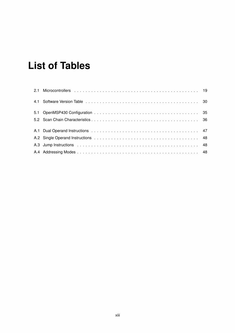
List of Tables
2.1 Microcontrollers . . . . . . . . . . . . . . . . . . . . . . . . . . . . . . . . . . . . . . . . . . . . 19
4.1 Software Version Table . . . . . . . . . . . . . . . . . . . . . . . . . . . . . . . . . . . . . . . . 30
5.1 OpenMSP430 Configuration . . . . . . . . . . . . . . . . . . . . . . . . . . . . . . . . . . . . . 35
5.2 Scan Chain Characteristics . . . . . . . . . . . . . . . . . . . . . . . . . . . . . . . . . . . . . . 36
A.1 Dual Operand Instructions . . . . . . . . . . . . . . . . . . . . . . . . . . . . . . . . . . . . . . 47
A.2 Single Operand Instructions . . . . . . . . . . . . . . . . . . . . . . . . . . . . . . . . . . . . . 48
A.3 Jump Instructions . . . . . . . . . . . . . . . . . . . . . . . . . . . . . . . . . . . . . . . . . . . 48
A.4 Addressing Modes . . . . . . . . . . . . . . . . . . . . . . . . . . . . . . . . . . . . . . . . . . . 48
xiii

xiv

List of Figures
2.1 MSP430 Architecture [7] . . . . . . . . . . . . . . . . . . . . . . . . . . . . . . . . . . . . . . . 6
2.2 Memory Byte-Organization [7] . . . . . . . . . . . . . . . . . . . . . . . . . . . . . . . . . . . . 7
2.3 Memory Map [7] . . . . . . . . . . . . . . . . . . . . . . . . . . . . . . . . . . . . . . . . . . . . 8
2.4 Block Diagram of the Register file and ALU [7] . . . . . . . . . . . . . . . . . . . . . . . . . . 9
2.5 MSP430 Basic Clock Module [7] . . . . . . . . . . . . . . . . . . . . . . . . . . . . . . . . . . 11
2.6 Timer_A Structure [7] . . . . . . . . . . . . . . . . . . . . . . . . . . . . . . . . . . . . . . . . . 12
2.7 openMSP430 Design Structure [4] . . . . . . . . . . . . . . . . . . . . . . . . . . . . . . . . . 15
2.8 openMSP430 Memory Mapping [4] . . . . . . . . . . . . . . . . . . . . . . . . . . . . . . . . . 15
2.9 openMSP430 Basic Clock Module [4] . . . . . . . . . . . . . . . . . . . . . . . . . . . . . . . 16
2.10 Example of an Connection via the DMA interface [4] . . . . . . . . . . . . . . . . . . . . . . . 17
3.1 Scan Chain Example . . . . . . . . . . . . . . . . . . . . . . . . . . . . . . . . . . . . . . . . . 22
3.2 Scan Chain Synthesis Flow for Cadence RTL Compiler . . . . . . . . . . . . . . . . . . . . . 23
3.3 ATPG flow for Modus DFT . . . . . . . . . . . . . . . . . . . . . . . . . . . . . . . . . . . . . . 26
4.1 Design flow for SoC Encounter . . . . . . . . . . . . . . . . . . . . . . . . . . . . . . . . . . . 31
4.2 Floorplan Schematic . . . . . . . . . . . . . . . . . . . . . . . . . . . . . . . . . . . . . . . . . . 32
5.1 ATPG Test Coverage results . . . . . . . . . . . . . . . . . . . . . . . . . . . . . . . . . . . . . 37
5.2 Final Layout . . . . . . . . . . . . . . . . . . . . . . . . . . . . . . . . . . . . . . . . . . . . . . . 38
5.3 Physical view of the openMSP430 . . . . . . . . . . . . . . . . . . . . . . . . . . . . . . . . . 39
5.4 Amoeba View of the openMSP430 . . . . . . . . . . . . . . . . . . . . . . . . . . . . . . . . . 39
5.5 Pins Highlight . . . . . . . . . . . . . . . . . . . . . . . . . . . . . . . . . . . . . . . . . . . . . . 40
5.6 Corner Close-up . . . . . . . . . . . . . . . . . . . . . . . . . . . . . . . . . . . . . . . . . . . . 41
5.7 Memory and Vertical Power Structures . . . . . . . . . . . . . . . . . . . . . . . . . . . . . . . 42
E.1 PROTEUS openMSP430 First Run . . . . . . . . . . . . . . . . . . . . . . . . . . . . . . . . . 65
E.2 PROTEUS openMSP430 Second Run . . . . . . . . . . . . . . . . . . . . . . . . . . . . . . . 66
xv

xvi
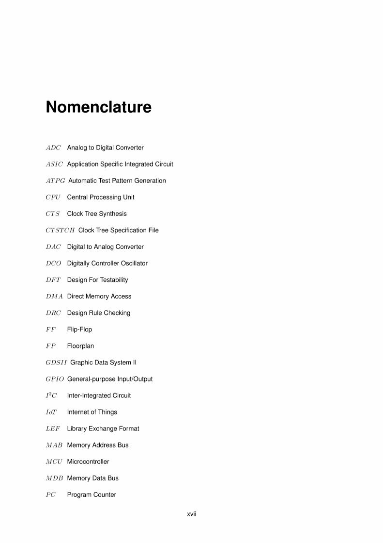
Nomenclature
ADC Analog to Digital Converter
ASIC Application Specific Integrated Circuit
ATPG Automatic Test Pattern Generation
CPU Central Processing Unit
CTS Clock Tree Synthesis
CTSTCH Clock Tree Specification File
DAC Digital to Analog Converter
DCO Digitally Controller Oscillator
DFT Design For Testability
DMA Direct Memory Access
DRC Design Rule Checking
FF Flip-Flop
FP Floorplan
GDSII Graphic Data System II
GPIO General-purpose Input/Output
I2C Inter-Integrated Circuit
IoT Internet of Things
LEF Library Exchange Format
MAB Memory Address Bus
MCU Microcontroller
MDB Memory Data Bus
PC Program Counter
xvii

SFR Special Function Register
SOC System on Chip
SPI Serial Peripheral Interface
SSF Single Stuck-Fault
STIL Standard Test Interface Language
TCL Tool Command Language
UART Universal Asynchronous Receiver/Transmitter
WGL Waveform Generation Language
xviii
Chapter 1
Introduction
In recent years with the rise of in popularity of the Internet of Things (IoT), a concept which refers to
the networking of physical objects through the use of embedded sensors, actuators that can collect or
transmit data about the themselves. This collected data can then be amassed and analyzed to optimize
products, operations and services. A concept which seduces hobbyists and commercial developers
alike that the McKinsey Global Institute predicts might have an overall economic impact as high as $6.2
trillion by 2025 [1]. This concept, as mentioned before, relies on numerous, mainly wireless, low-power
sensor endpoints which creates a higher demand of highly integrated microchip designs creating a high
demand for microcontrollers [2].
Microcontrollers are often confused for microprocessors. Microcontrollers are designed to perform
specific tasks and are often integrated with their own RAM, ROM, I/O ports and peripherals [3] which
might be integrated with analog circuits such as high precision low power sensors which can be embed-
ded on a single chip creating a so called System on Chip (SOC).
Microprocessors on the other hand are used to run applications where tasks are unspecific like
developing software, games, websites, creating documents etc. needing alot more resources mainly
memory, which is not integrated in the chip, and able to me connected to a much higher range of
peripherals which are also not integrated. They are also able to run at a much higher clock speed of
the compared to the microcontroller. Whereas the microcontrollers operate from a few MHz to 30 to 50
MHz, microprocessor usually operate above the GHz requiring alot more energy in the process [3].
In this Thesis it is going to be studied the implementation and integration of a synthesized configu-
ration of the openMSP430 [4]. This core is an open-source 16bit microcontroller core written in Verilog,
that is compatible with Texas Instruments’ MSP430 microcontroller family and can execute the code
generated by an MSP430 toolchain in an accurate way [4]. Furthermore, Scan Chain structures and test
generation will be studied and introduced to the openMSP430 to bring Design For Testability (DFT) to
the final circuit in order to expand the openMSP430 test capabilities.
1

1.1 Motivation
The IoT concept revolutionizes the way people interact with the technology. Projects in the scope of the
IoT use extensive environment/system and connectivity between nodes/things enable the construction
of large grids of devices to establish advanced cutting-edge services.
The increasing need for decentralized, dedicated, sensoring and processing units on the scope of
IoT networking creates demand for embedded microcontrollers whose CPUs are able to be integrated
with their own RAM, ROM and analog and digital peripherals creating a dedicated monolithic System of
Chip (SOC) oriented for low power consumption. The openMSP430 is one of such controllers that was
selected for its low power modes to integrate the SOC in the PROTEUS1 research project under which
a part this work was developed.
The PROTEUS is European research project that will develop and deliver a reconfigurable sensor
platform for water quality monitoring [5]. Reconfigurable microfluidic-and nano-enabled sensors and
an innovative embedded software will provide reconfigurability of the sensing board to support several
differentiated applicative goals.
1.2 Objectives
The principal objective of this work is to study the openMSP capabilities and investigate a solution for the
integration of a openMSP430 configuration along with its corresponding memories accordingly with the
PROTEUS requirements of area and performance while keeping a low power consumption, creating an
embedded system which is going to be integrated with other components related to the project creating
a monolithic SOC.
In order to create a circuit layout from the gate-level synthesised openMSP430 CPU, along with
memory and DFT structures, a well defined design flow is required. In this work this design flow is
researched, not only for the implementation and test of the openMSP430, but also to provide a basis
methodology for the design flow for other future digital circuit implementations.
Therefore, in this work we will present all the necessary procedures to implement the design flow
using the Cadence Encounter, Cadence Encounter RTL Compiler and Cadence Modus DFT tools tar-
geting the UMC 130nm component libraries/memories distributed by Faraday Technology Corporation
through Europractice. At a point in this work, the first two tools enumerated above were discontinued
by Cadence and were replaced and re-branded by Cadence Innovus and Cadence Genus respectively.
Through the use of the respective legacy modes, it is possible to run most of the previous tool’s code
and use the same Design Flows.
1Proteus - AdaPtive micROfluidic- and nano-enabled smart systems for waTEr qUality Sensing, is an ICT H2020 EurpeanProject targeting a low-cost monitoring water management in which the main challenge relates to the heterogeneous integrationinto a monolithic, sensing chip of a set of sensors (of microfluidic sensing chip of carbon-nanotubes-based resistive chemicalsensors, MEMS physical and rheological resistive sensors) and a CMOS system on chip with a microcontroller. (Project ID:644852)
2

1.3 Thesis Outline
Aside for this Introduction chapter this work is divided in five more chapters.
In Chapter 2 the architecture and characteristics of the MSP430 and openMSP430 will be sum-
marised and compared. A process which reveals their main features and characteristics.
Next, in Chapter 3, an introduction to Design For Testability (DFT) techniques and Automatic Test
Pattern Generation (ATPG) are presented. The flow to resynthesise scan chains into a pre-synthesised
openMSP430 verilog netlist and how to generate test vectors are explained.
Chapter 4 presents the back-end design flow and the procedure of Cadence tools for its implemen-
tation. The flow begins with the synthesised description of the core circuit with integrated scan chains,
and ends in its final layout, ready to send for fabrication or integration in a larger SOC.
In Chapter 5, the results and design options for the execution of the flows are presented, including
the characteristics of the scan chains resynthesised for the openMSP430, the fault coverages of the
generated test vectors and the openMSP430 final layout.
Finally, in Chapter 6 are presented the conclusions of thew thesis and given suggestion about future
work.
3

4

Chapter 2
MSP Controller
The openMSP430 is a synthesizable 16bit microcontroller core written in Verilog. It is compatible with
Texas Instruments’ MSP430 microcontroller family that can execute the code generated by the MSP430
toolchains. The MSP430 microcontroller boards, built around a 16-bit CPU are designed for low cost
and low power consumption embedded mixed signal applications [6]. In this section, it is briefly pre-
sented the specifications of the MSP430x1xx microcontroller family and then describe and compare the
openMSP430.
2.1 MSP430x1xx Family
In this section it is described the modules and peripherals of the MSP430x1xx family of microcontroller
circuit boards.
2.1.1 Architecture
The MSP430 circuit boards incorporate a 16-bit RISC CPU, peripherals, and a flexible clock system that
interconnect using a common memory address bus (MAB) and memory data bus (MDB). Partnering a
modern CPU with modular memory-mapped analog and digital peripherals, the MSP430 offers solutions
for demanding mixed-signal applications, Figure 2.1 illustrates the general MSP430x1xx microcontroller
architecture.
The key features of the family include [7]:
• Ultralow-power architecture specifications.
– 0.1 µA RAM retention.
– 250 µA MIPS active.
• High-performance analog ideal for precision measurement.
– 12-bit or 10-bit ADC — 200 ksps, temperature sensor, VRef.
– 12-bit dual-DAC.
5
– Supply voltage supervisor.
• 16-bit RISC CPU enables new applications at a fraction of the code size.
– Large register file eliminates working file bottleneck.
– Compact core design reduces power consumption and cost.
– Optimized for modern high-level programming.
– Only 27 core instructions and 7 addressing modes.
– Extensive vectored-interrupt capability.
• In-system programmable Flash permits flexible code changes, field upgrades and data logging.
Figure 2.1: MSP430 Architecture [7]
2.1.2 Memory Organisation
The MSP430 has a von-Neumann common memory address bus (MAB) and memory data bus (MDB),
which are shared with special function registers (SFRs), peripherals, RAM, and Flash/ROM memory
[7]. The size of different regions of the address space are version specific however only a maximum
of 64kB of memory can be addressed. Code access are always performed on even addresses, data
can be accessed as bytes or words. Bytes are located at all addresses. Words are only located at
even addresses as illustrated by Figure 2.2. When using word instructions, only even addresses may be
used. The memory data is organized in little Endian, which means, the low byte of a word is always an
even address and the high byte is at the next odd address [7].
The memory map organization used by the MSP micocontroller family is shown in Figure 2.3. At the
bottom addresses, in the lower 16 bytes of the address space, the SFRs are located.
6
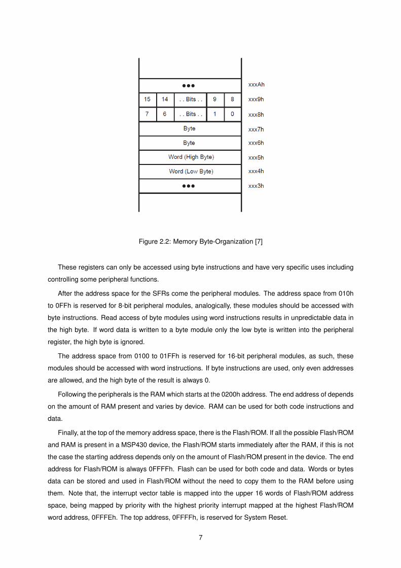
Figure 2.2: Memory Byte-Organization [7]
These registers can only be accessed using byte instructions and have very specific uses including
controlling some peripheral functions.
After the address space for the SFRs come the peripheral modules. The address space from 010h
to 0FFh is reserved for 8-bit peripheral modules, analogically, these modules should be accessed with
byte instructions. Read access of byte modules using word instructions results in unpredictable data in
the high byte. If word data is written to a byte module only the low byte is written into the peripheral
register, the high byte is ignored.
The address space from 0100 to 01FFh is reserved for 16-bit peripheral modules, as such, these
modules should be accessed with word instructions. If byte instructions are used, only even addresses
are allowed, and the high byte of the result is always 0.
Following the peripherals is the RAM which starts at the 0200h address. The end address of depends
on the amount of RAM present and varies by device. RAM can be used for both code instructions and
data.
Finally, at the top of the memory address space, there is the Flash/ROM. If all the possible Flash/ROM
and RAM is present in a MSP430 device, the Flash/ROM starts immediately after the RAM, if this is not
the case the starting address depends only on the amount of Flash/ROM present in the device. The end
address for Flash/ROM is always 0FFFFh. Flash can be used for both code and data. Words or bytes
data can be stored and used in Flash/ROM without the need to copy them to the RAM before using
them. Note that, the interrupt vector table is mapped into the upper 16 words of Flash/ROM address
space, being mapped by priority with the highest priority interrupt mapped at the highest Flash/ROM
word address, 0FFFEh. The top address, 0FFFFh, is reserved for System Reset.
7
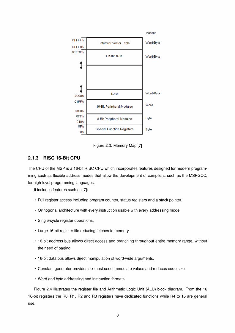
Figure 2.3: Memory Map [7]
2.1.3 RISC 16-Bit CPU
The CPU of the MSP is a 16-bit RISC CPU which incorporates features designed for modern program-
ming such as flexible address modes that allow the development of compilers, such as the MSPGCC,
for high-level programming languages.
It includes features such as [7]:
• Full register access including program counter, status registers and a stack pointer.
• Orthogonal architecture with every instruction usable with every addressing mode.
• Single-cycle register operations.
• Large 16-bit register file reducing fetches to memory.
• 16-bit address bus allows direct access and branching throughout entire memory range, without
the need of paging.
• 16-bit data bus allows direct manipulation of word-wide arguments.
• Constant generator provides six most used immediate values and reduces code size.
• Word and byte addressing and instruction formats.
Figure 2.4 illustrates the register file and Arithmetic Logic Unit (ALU) block diagram. From the 16
16-bit registers the R0, R1, R2 and R3 registers have dedicated functions while R4 to 15 are general
use.
8
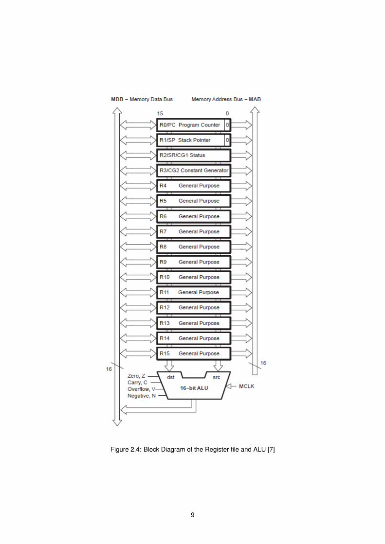
Figure 2.4: Block Diagram of the Register file and ALU [7]
9

The MSP430 provides an instruction set consisting of 27 core instructions and 24 emulated instruc-
tions. The core instructions are instructions that have unique op-codes decoded by the CPU. The emu-
lated instructions are instructions that make code easier to write, but do not have op-codes themselves,
instead they are replaced automatically by the assembler with an equivalent core instruction. There are 3
core-instruction formats, Dual-operand, Single-operand and Jump. All single-operand and dual-operand
instructions can be byte or word instructions by using .B or .W extensions respectively.
In the tables on the Appendix A it is shown the instruction set available to the user. The source
(src) operand can be expressed in any of the 7 addressing modes, while the destination (dst) can
only be expressed in the first 4 addressing modes [7]. All of the address space can be accessed with no
exceptions. However, when using an instruction that modifies the contents an address that is not writable
the results of the instruction would be lost. For example, a ROM location would be a valid destination
address, but as this memory is Read-Only, a write instruction would have no effect on the destination.
2.1.4 Basic Clock Module
One of the most important components of the MSP430 is its basic clock module described in Figure 2.5.
It makes use of a maximum of 3 externally generated clock signals, enabling the user several options in
balancing performance and power consumption. The inputs and outputs of the basic clock module are
[7]:
• 3 clock sources:
– DCOCLK: Digitally controlled oscillator (DCO).
– LFXT1CLK: Low-frequency/high-frequency oscillator that can be used either with low-frequency
32768-Hz watch crystals, or standard crystals or resonators in the 450-kHz to 8-MHz range.
– XT2CLK: Optional high-frequency oscillator that can be used with standard crystals, res-
onators, or external clock sources in the 450-kHz to 8-MHz range.
• 3 clock output signals:
– MCLK: Master clock, can be software select-able as LFXT1CLK, XT2CLK or DCOCLK, can
be divided by 1, 2, 4, or 8. It is used by the CPU and system.
– SMCLK: Sub-main clock. SMCLK is software select-able as LFXT1CLK, XT2CLK or DCOCLK,
can also be divided. It is software select-able for individual peripheral modules.
– ACLK: Auxiliary clock. The ACLK is the buffered LFXT1CLK, can also de divided and is
software select-able for individual peripheral modules.
It is by the configuration of the Basic Clock Module that the user can control the controllers perfor-
mance and power consumption. Most of the energy spent by a digital circuit comes from signal tran-
sitions. Therefore, if the user selects a lower frequency oscillator as its master clock the computation
would be slower but the power required would also be much lower.
10
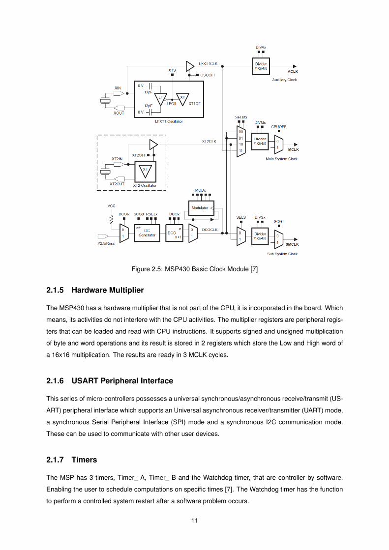
Figure 2.5: MSP430 Basic Clock Module [7]
2.1.5 Hardware Multiplier
The MSP430 has a hardware multiplier that is not part of the CPU, it is incorporated in the board. Which
means, its activities do not interfere with the CPU activities. The multiplier registers are peripheral regis-
ters that can be loaded and read with CPU instructions. It supports signed and unsigned multiplication
of byte and word operations and its result is stored in 2 registers which store the Low and High word of
a 16x16 multiplication. The results are ready in 3 MCLK cycles.
2.1.6 USART Peripheral Interface
This series of micro-controllers possesses a universal synchronous/asynchronous receive/transmit (US-
ART) peripheral interface which supports an Universal asynchronous receiver/transmitter (UART) mode,
a synchronous Serial Peripheral Interface (SPI) mode and a synchronous I2C communication mode.
These can be used to communicate with other user devices.
2.1.7 Timers
The MSP has 3 timers, Timer_ A, Timer_ B and the Watchdog timer, that are controller by software.
Enabling the user to schedule computations on specific times [7]. The Watchdog timer has the function
to perform a controlled system restart after a software problem occurs.
11
If the watchdog selected time interval expires, a system reset is generated. If the watchdog function
is not needed in an application, the module can be configured as an interval timer and can generate
interrupts at selected time intervals like the other timers.
Timer A and B are very similar, both are 16-bit timers/counters with 3 compare registers for Timer_A
and 3 or 7 (depending on version) compare registers for Timer_B. Both can support multiple capture/-
compares, PWM outputs, and interval timing. They also have extensive interrupt capabilities, that may
be generated from the counter overflow conditions or from each of the capture/compare registers. The
Timer_ B has the following extra capabilities:
• The length of Timer_B is programmable to be 8, 10, 12, or 16 bits.
• All Timer_B outputs can be put into a high-impedance state.
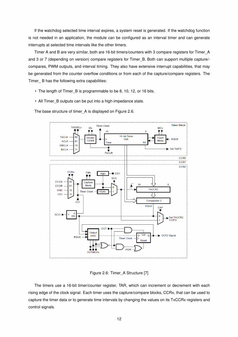
The base structure of timer_A is displayed on Figure 2.6.
Figure 2.6: Timer_A Structure [7]
The timers use a 16-bit timer/counter register, TAR, which can increment or decrement with each
rising edge of the clock signal. Each timer uses the capture/compare blocks, CCRx, that can be used to
capture the timer data or to generate time intervals by changing the values on its TxCCRx registers and
control signals.
12

2.1.8 General-purpose input/output - GPIO
A majority of modern of microcontrollers have several General-purpose input/output (GPIO) pins which
gives the user freedom to connect the controller to other digital or analog components. The MSP430 is
no exception. MSP430 circuit boards have up to 6 digital, software controlled, I/O ports implemented.
Each port has eight I/O pins which can be individually configurable as input or output, and each I/O line
can be individually read or written.The digital I/O has features such as [7]:
• Any combination of input or output (no dedicated input or output pins).
• 2 individually configurable interrupt ports (up to 16 interrupts), enabled by software.
• Independent input and output data registers.
2.1.9 DMA
The MSP430 also has a direct memory access (DMA) controller a device that allows certain hardware
subsystems to access the system memory (RAM), independent of the (CPU) [7]. For instance the DMA
controller can move data from an Analog to Digital Converter (ADC) memory to RAM.
2.1.10 Other modules
Aside from the modules already discussed the MSP430 features a few other modules in its circuit boards.
Modules to help manage the boards resources. A Flash Memory Controller which can be used
to mass load and erase the core’s memories. And a Supply Voltage Supervisor used to monitor the
microcontroller’s supply voltage.
As the MSP430 devices are designed to be a mixed signal microcontrollers they also feature 2
Analog-to-Digital Converters (ADCs), a 10-bit and a 12-bit, as well as a 12-bit Digital to Analog Converter
(DAC) which able the boards to interact with other pieces of analog circuitry.
13

2.2 openMSP430
The openMSP430 an open source version of the main core of the MSP430x1xx microcontroller family
available in the OpenCores online platform [8]. The openMSP430 is a synthesizable 16bit microcontroller
core written in Verilog that can execute the code generated by an MSP430 toolchain provided by Texas
Instruments without any additional linker files [4].
The core is advertised with interesting features such as Low area (around 8k-gates), good perfor-
mances, built-in power and clock management and being multiple time Silicon Proven by other develop-
ers [9 - 14]. Templates for user created peripherals are also available. In this Section the capabilities of
the openMSP will be studied in comparison with its commercial counterparts studied in Section 2.1.
2.2.1 Core Architecture
Like the MSP430, the openMSP430 is based on a Von Neumann architecture, with a single address
space for instructions and data. However, unlike the versions of the MSP430, it is fully customizable by
editing its verilog configuration files, that defines the possible configurations. Depending on the selected
configuration the user design can either be [4]:
• FGPA friendly : the core doesn’t contain any clock gate and has only a single clock domain. As a
consequence, its clock management capabilities are very limited.
• ASIC friendly: the core contains up to all clock management options. And capabilities to interrupts
the clock distribution, a feature not available in the commercial MSP430 microcontrollers.
As the objective of this thesis is to achieve the implementation and integration of this core in ASIC
technology, it is only studied suitable configurations based on ASIC.
The design structure of the openMSP430, shown in Figure 2.7 [4], is very similar to the original
MSP430.
Comparing the MSP430 architecture, Figure 2.1, with the openMSP430 design structure (Figure
2.7), similarities between the two can be observed: the Frontend and Execution Unit is equivalent to the
RISC CPU, the Memory backbone to the MAB and MDB buses, the Serial Debug Interface (SDI) to the
JTAG/Debug module, the clock module is also present although displayed as a peripheral, memories,
watchdog timer, etc.
2.2.2 Memory mapping
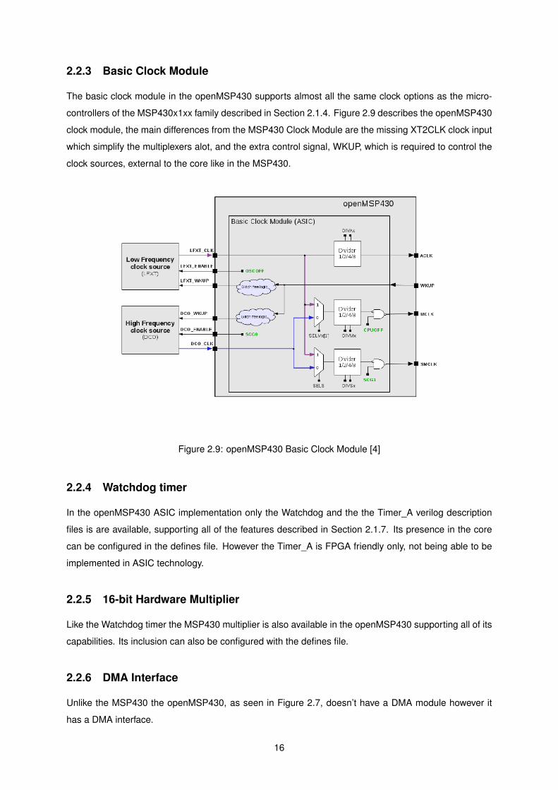
The openMSP430 memory mapping follows the same structure and byte organisation as the MSP430
(discussed in Section 2.1.2), illustrated in Figure 2.8. However, code can only be executed from the
Program Memory part of the addressable space (the equivalent to the Flash/ROM space in Figure 2.3),
nonetheless the memory mapping can be fully customizable.
14
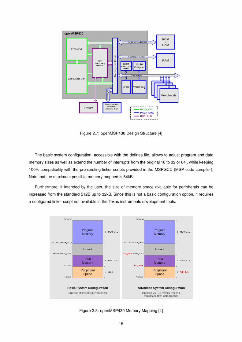
Figure 2.7: openMSP430 Design Structure [4]
The basic system configuration, accessible with the defines file, allows to adjust program and data
memory sizes as well as extend the number of interrupts from the original 16 to 32 or 64 , while keeping
100% compatibility with the pre-existing linker scripts provided in the MSPGCC (MSP code compiler).
Note that the maximum possible memory mapped is 64kB.
Furthermore, if intended by the user, the size of memory space available for peripherals can be
increased from the standard 512B up to 32kB. Since this is not a basic configuration option, it requires
a configured linker script not available in the Texas instruments development tools.
Figure 2.8: openMSP430 Memory Mapping [4]
15
2.2.3 Basic Clock Module
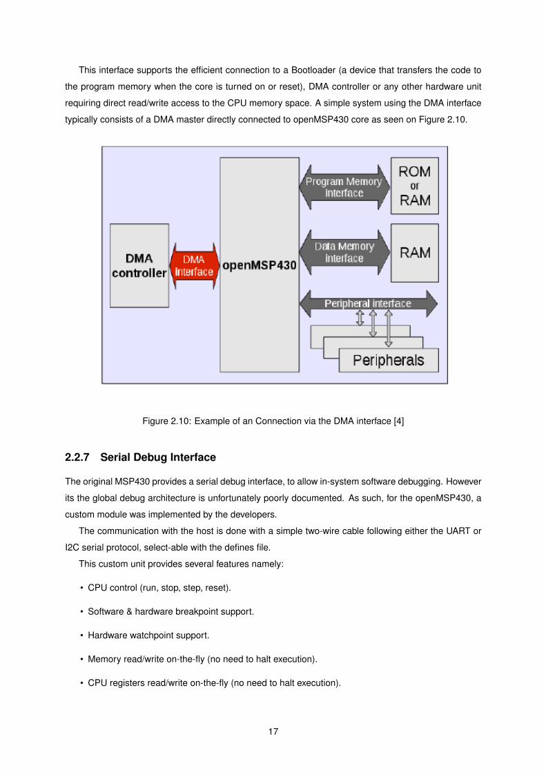
The basic clock module in the openMSP430 supports almost all the same clock options as the micro-
controllers of the MSP430x1xx family described in Section 2.1.4. Figure 2.9 describes the openMSP430
clock module, the main differences from the MSP430 Clock Module are the missing XT2CLK clock input
which simplify the multiplexers alot, and the extra control signal, WKUP, which is required to control the
clock sources, external to the core like in the MSP430.
Figure 2.9: openMSP430 Basic Clock Module [4]
2.2.4 Watchdog timer
In the openMSP430 ASIC implementation only the Watchdog and the the Timer_A verilog description
files is are available, supporting all of the features described in Section 2.1.7. Its presence in the core
can be configured in the defines file. However the Timer_A is FPGA friendly only, not being able to be
implemented in ASIC technology.
2.2.5 16-bit Hardware Multiplier
Like the Watchdog timer the MSP430 multiplier is also available in the openMSP430 supporting all of its
capabilities. Its inclusion can also be configured with the defines file.
2.2.6 DMA Interface
Unlike the MSP430 the openMSP430, as seen in Figure 2.7, doesn’t have a DMA module however it
has a DMA interface.
16
This interface supports the efficient connection to a Bootloader (a device that transfers the code to
the program memory when the core is turned on or reset), DMA controller or any other hardware unit
requiring direct read/write access to the CPU memory space. A simple system using the DMA interface
typically consists of a DMA master directly connected to openMSP430 core as seen on Figure 2.10.
Figure 2.10: Example of an Connection via the DMA interface [4]
2.2.7 Serial Debug Interface
The original MSP430 provides a serial debug interface, to allow in-system software debugging. However
its the global debug architecture is unfortunately poorly documented. As such, for the openMSP430, a
custom module was implemented by the developers.
The communication with the host is done with a simple two-wire cable following either the UART or
I2C serial protocol, select-able with the defines file.
This custom unit provides several features namely:
• CPU control (run, stop, step, reset).
• Software & hardware breakpoint support.
• Hardware watchpoint support.
• Memory read/write on-the-fly (no need to halt execution).
• CPU registers read/write on-the-fly (no need to halt execution).
17

2.3 Microcontrollers and openMSP430 Applications
The Microcontroller (MCU) market is vast and there are MCUs targetting a wide range of areas such as:
data processing, consumer electronics, communication, IoT, etc.
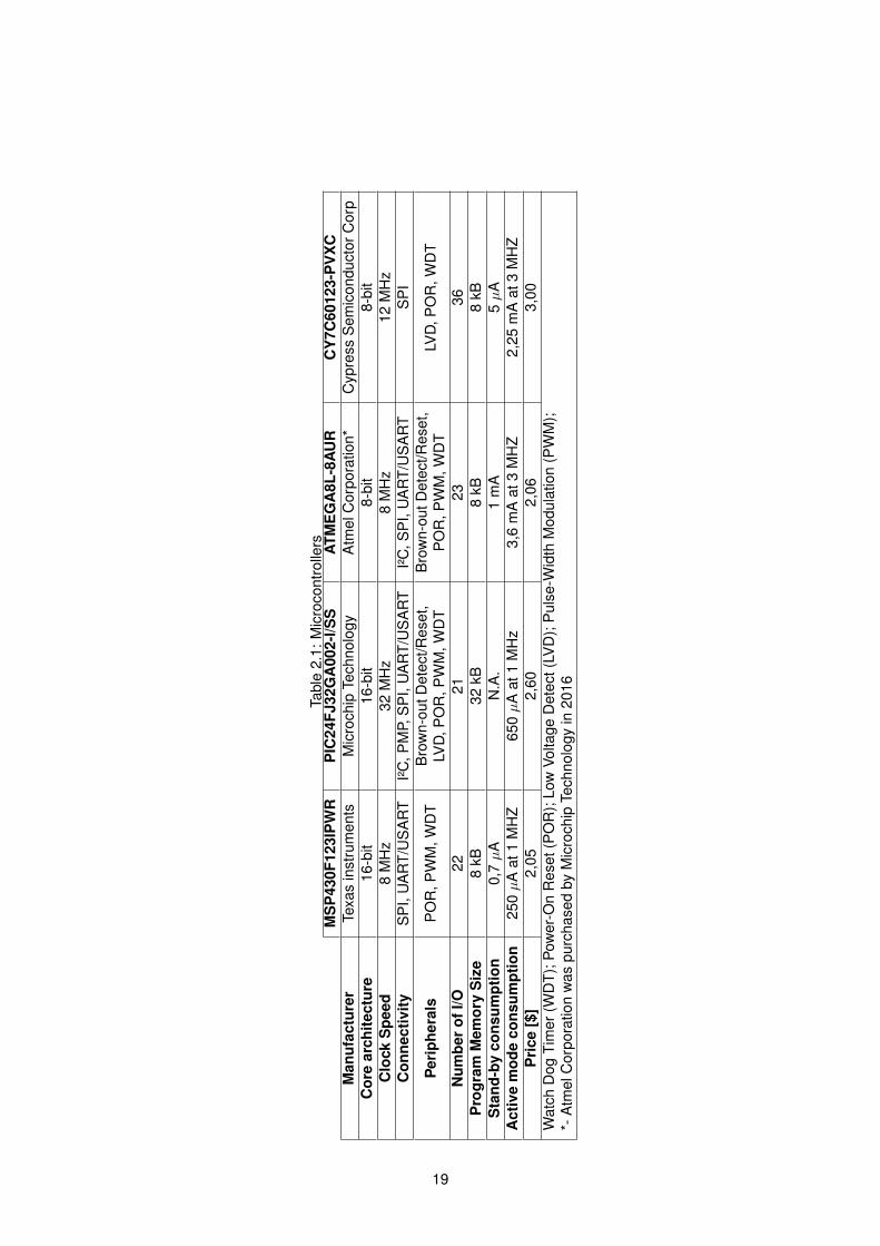
In table 2.1 a version of the MSP430 is compared to other microcontrollers with similar properties
and price, produced from other prominent manufacturers.
By observing Table 2.1, we can concluded that the MSP430 has less connectivity options and pe-
ripherals, in particular when comparing to the PIC24. However, the ratio between the stand-by and
active mode power consumption, and the instruction throughput of the MSP430 is the best among this
samples. This indicates the MSP430 has the capability to deliver computational solutions for low-power
applications, like in the IoT field.
The different versions of the MSP430 supported by a commercial company like Texas Instruments
and its open-source version, the openMSP430 have been used by developers, reshearchers and hob-
byists, in particular the openMSP430 has been used for research in high reliable multi core low power
microcontrollers [9], as a starting point for research in ultra-low-power processors [10] and highly in-
tegrated self powered SOCs for the IoT field [11]. Furthermore it has been used for the study of multi
voltage methodology for power optimization [12], influence of different workloads on the degradation and
ageing of the critical path [13] and reliability of power estimation tools for FPGAs [14].
Additionally, open-source electronics prototyping platforms like Energia [15] that offer a framework
similar to the Texas Instruments MSP430 LaunchPad, allows a more intuitive interaction with the MSP430
series of microcontrollers and prototyped implementations of the openMSP430, which is useful for de-
velopers and researchers that use the MSP430 development tools.
18
Tabl
e2.
1:M
icro
cont
rolle
rsM
SP
430F
123I
PW
RP
IC24
FJ32
GA
002-
I/SS
ATM
EG
A8L
-8A
UR
CY
7C60
123-
PV
XC
Man
ufac
ture
rTe
xas
inst
rum
ents
Mic
roch
ipTe
chno
logy
Atm
elC
orpo
ratio
n*C
ypre
ssS
emic
ondu
ctor
Cor
pC
ore
arch
itect
ure
16-b
it16
-bit
8-bi
t8-
bit
Clo
ckS
peed
8M
Hz
32M
Hz
8M
Hz
12M
Hz
Con
nect
ivity
SP
I,U
AR
T/U
SA
RT
I²C,P
MP,
SP
I,U
AR
T/U
SA
RT
I²C,S
PI,
UA
RT/
US
AR
TS
PI
Per
iphe
rals
PO
R,P
WM
,WD
TB
row
n-ou
tDet
ect/R
eset
,LV
D,P
OR
,PW
M,W
DT
Bro
wn-
outD
etec
t/Res
et,
PO
R,P
WM
,WD
TLV
D,P
OR
,WD
T
Num
ber
ofI/O
2221
2336
Pro
gram
Mem
ory
Siz
e8
kB32
kB8
kB8
kBS
tand
-by
cons
umpt
ion
0,7µ
AN
.A.
1m
A5µ
AA
ctiv
em
ode
cons
umpt
ion
250µ
Aat
1M
HZ
650µ
Aat
1M
Hz
3,6
mA
at3
MH
Z2,
25m
Aat
3M
HZ
Pri
ce[$
]2,
052,
602,
063,
00W
atch
Dog
Tim
er(W
DT)
;Pow
er-O
nR
eset
(PO
R);
Low
Volta
geD
etec
t(LV
D);
Pul
se-W
idth
Mod
ulat
ion
(PW
M);
*-A
tmel
Cor
pora
tion
was
purc
hase
dby
Mic
roch
ipTe
chno
logy
in20
16
19

Chapter 3
Design For Testability (DFT)
Because of the fast increase in the complexity of integrated digital circuits the issues of testing and
design-for-test are becoming crucial when manufacturing a chip. A faulty component in a SOC could
render the system unusable and the cost of replacing, repairing and/or redesigning a component can be
many times over the cost of testing the individual components before integrating it in the SOC. Testing
of a system is an experiment in which the system is exercised and its results are analysed to detect any
incorrect behaviour. If this happens the second objective of the testing experiment is to detect, or locate,
the cause of the misbehaviour.
3.1 Structured DFT Testing Introduction
Errors in the behaviour of a circuit, wrong values in the output of a circuit, are the consequence of one
or more faults, which can only be observable by the errors they cause [16]. However, one or more faults
may never cause errors due to undetectability or redundancy [16], i.e. a fault may cause a change in a
logic node that doesn’t propagate the output the circuit and two different faults might "cancel" each other
that prevents errors.
When integrated circuits were small and with a reduced level of complexity testing was relatively
simple as almost every internal circuit nodes could be easily controlled by simply changing the primary
inputs of the circuit, and the propagated logic value of a certain node could also be observed through
the primary outputs. As circuits became more complex, a complete test that would verify the outputs of
every input combinations, and for sequential circuits, an analysis for all internal states, would be very
impractical and would take, non justifiable, amount of time with an enormous amount of effort.
As such new techniques were developed in which dedicated test structures are introduced to the
circuit in order to increase the controllabillity and observability. These techniques have the advantage
of increasing the fault coverage and greatly reduce the test time and complexity. However, adding new
hardware for testing a circuit presents disadvantages namely, increased I/O pin count, power consump-
tion, chip area, development time, introduce more more potential faults due to the increased amount of
logic and marginally reduce the circuit performance due to extra circuitry on the datapath.
20
In this thesis it is employed one of the most popular structured DFT technique, a Scan-Based Design
[16], more specifically a Full Serial Integrated Design. This type of techniques use a scan register which
adds controllability and observability points throughout the circuit allowing a simpler testing of the inner
nodes of the chip, facilitating the detection of faults during test experiments [16].
The test vectors, sequences of input values to be shifted to the scan registers, are generated by
Automatic Test Pattern Generation (ATPG) tools in a way, that will enable the detection of a given faults
based on the differences between the scan registers outputs and the outputs predicted by the ATPG tool
considering a good circuit.
To create the test vectors the ATPG tool uses fault modelling by representing the many possible
physical faults as logical faults. This reduces the complexity of the analysis of the logic faults as several
physical faults/defects can be modelled by the same logic fault [16]. The most used fault model is the
Single Stuck-Fault (SSF) model as it offers several advantages, for example, represents many different
physical faults and is technology independent [16]. This model assumes that only one fault exists in the
portion of circuit under test and the faulty node is either stuck at the logical value ’0’ or ’1’. If there are n
lines on which SSFs can be defined, the number of possible faults is 2n [16]. This faults are often called
Static Faults by the tools.
Apart from this model, other fault models exist. For example, the delay fault model is used for
detection of single node slow-to-rise or slow-to-fall timing faults. This model is used to detect timing
erros in the circuit’s critical paths, at the nominal working frequency, and is thus used to detect defects
or variations that have a negative impact on the circuit’s timing performance [16]. This faults are often
called Dynamic Faults by the tools. As the openMSP430 is of relative small size and operates at a low
frequency (16MHz), they were not considered in this thesis.
3.2 Full Serial Integrated Scan
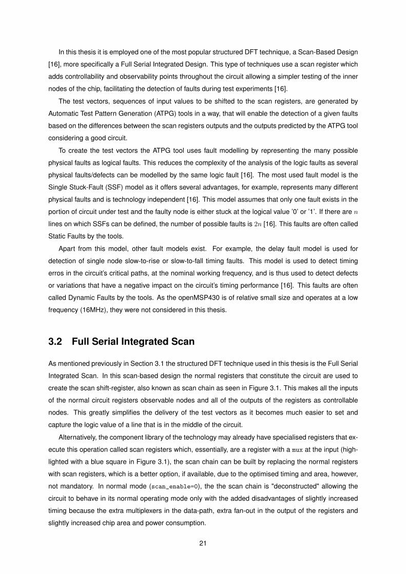
As mentioned previously in Section 3.1 the structured DFT technique used in this thesis is the Full Serial
Integrated Scan. In this scan-based design the normal registers that constitute the circuit are used to
create the scan shift-register, also known as scan chain as seen in Figure 3.1. This makes all the inputs
of the normal circuit registers observable nodes and all of the outputs of the registers as controllable
nodes. This greatly simplifies the delivery of the test vectors as it becomes much easier to set and
capture the logic value of a line that is in the middle of the circuit.
Alternatively, the component library of the technology may already have specialised registers that ex-
ecute this operation called scan registers which, essentially, are a register with a mux at the input (high-
lighted with a blue square in Figure 3.1), the scan chain can be built by replacing the normal registers
with scan registers, which is a better option, if available, due to the optimised timing and area, however,
not mandatory. In normal mode (scan_enable=0), the the scan chain is "deconstructed" allowing the
circuit to behave in its normal operating mode only with the added disadvantages of slightly increased
timing because the extra multiplexers in the data-path, extra fan-out in the output of the registers and
slightly increased chip area and power consumption.
21

Figure 3.1: Scan Chain Example
The scan chain is used to shift in the test vectors (generated by the ATPG tools), through the scan_in,
into the circuit, and after one or more clock cycles to allow the propagation of the values through the
circuit combinational logic. Afterwards, it is used to capture the resulting values by shifting them out
through the scan_out. During these shift operations, data propagates through the flip-flops that form
the scan chain (scan shift-register). To capture the values of the combinational logic, the normal inputs
of the flip-flops are selected (scan_enable = 0) and then the Flip-Flops are set back to scan mode
(scan_enable = 1) to allow shifting out of the captured values.
There are other scan-based designs like the Isolated Serial Scan or the Non-serial Scan that could
be used. However, the former requires the scan shift-register hardware to be added to the circuit (i.e.
extra Flip-Flops are added to the design) which enables the designer to, more freely, choose the length
of the chain (which would determine the simplicity of the test experiments, more Flip-Flops simpler test
experiments and more accurate tests) at the cost of the increased area and power consumption (relative
to the Full Serial Integrated). The latter, Non-serial Scan, similarly to the Full Integrated Scan, uses the
normal Flip-Flops of the circuit however not by creating a scan shift-register but arranging the scan cells
as a random access bit-addressable memory. This facilitates the individual testing of each observable
node and overall easier test experiment saving the need to scan the data through the entire register, and
the expense of the greatly increased overhead associated with the storing the addresses of the cells to
be set and/or read [16]. Because of this, the Full Serial Integrated Scan using multiplexed flip-flops is
the most popular kind of structured DFT design and is supported by the most of the ATPG tools.
22
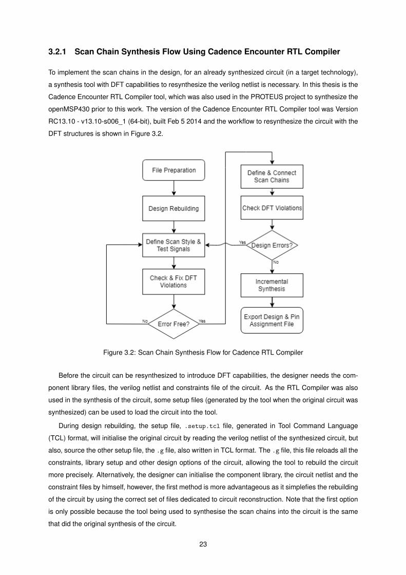
3.2.1 Scan Chain Synthesis Flow Using Cadence Encounter RTL Compiler
To implement the scan chains in the design, for an already synthesized circuit (in a target technology),
a synthesis tool with DFT capabilities to resynthesize the verilog netlist is necessary. In this thesis is the
Cadence Encounter RTL Compiler tool, which was also used in the PROTEUS project to synthesize the
openMSP430 prior to this work. The version of the Cadence Encounter RTL Compiler tool was Version
RC13.10 - v13.10-s006_1 (64-bit), built Feb 5 2014 and the workflow to resynthesize the circuit with the
DFT structures is shown in Figure 3.2.
Figure 3.2: Scan Chain Synthesis Flow for Cadence RTL Compiler
Before the circuit can be resynthesized to introduce DFT capabilities, the designer needs the com-
ponent library files, the verilog netlist and constraints file of the circuit. As the RTL Compiler was also
used in the synthesis of the circuit, some setup files (generated by the tool when the original circuit was
synthesized) can be used to load the circuit into the tool.
During design rebuilding, the setup file, .setup.tcl file, generated in Tool Command Language
(TCL) format, will initialise the original circuit by reading the verilog netlist of the synthesized circuit, but
also, source the other setup file, the .g file, also written in TCL format. The .g file, this file reloads all the
constraints, library setup and other design options of the circuit, allowing the tool to rebuild the circuit
more precisely. Alternatively, the designer can initialise the component library, the circuit netlist and the
constraint files by himself, however, the first method is more advantageous as it simplefies the rebuilding
of the circuit by using the correct set of files dedicated to circuit reconstruction. Note that the first option
is only possible because the tool being used to synthesise the scan chains into the circuit is the same
that did the original synthesis of the circuit.
23
The second step is to define the scan style and the test signals of the circuit. Its in this step the
multiplexed flip-flop scan style is selectted in order to use the full serial integrated scan DFT technique
referenced in Section 3.2. Afterwards, the primary test pins that are used by the scan structures were
set. This instructs the DFT Compiler to use the specified pins for the test signals. The required signals
are the scan clocks (usually the system clocks), the test mode signal (which disables other synchronous
components during test experiments, like memories), the scan enable signals and any set or reset
signals that should be set/reset during the test experiments.
The next step is the DFT Design Rule Check (DRC) that detects DFT violations, these should be an-
alyzed to determine if they should be corrected. This violations usually involve incorrect test signal/clock
declaration and uncontrolable reset/set of flip-flops (rendering those flip flops to unscannable), ultimately
reducing the test coverage of the experiments.The unscannable flip-flops can be easily fixed by the tool’s
auto-fix feature that redesigns the logic around the affected flip-flops to enable them to be used in the
scan chains. The test signal violations may involve a test signal redesign and reinstantiation of the target
signals. When no major violations are left to be resolved, the desinger can proceed with the flow.
At this stage the scan chains can now be defined and built/connected. The designer assigns names
to each scan chain, informing the tool which scan enable and scan clock to use, if the scan flip flops are
rising-edge, falling-edge or mixed edge and the scan in and out I/O pins to use (if the scan I/O pins are
not present in the top-level circuit ports the tool will instantiate them automatically). After this, the scan
chains can be built, the tool will make the required connections in order to create the scan chains. If long
chains are created, the designer can introduce that the tool will use to balance the number of Flip-Flops
per chain, which greatly reduces the test times, at the cost of more I/O pins in the circuit.
A second DFT DRC should be preformed which may result in the detection of violations that would
require a redesign of the scan chains. If no critical violations are found, the workflow can continue.
Finally an incremental synthesis should be preformed. In this synthesis step the tool will analyse the
altered components of the circuit and only change/optimise the logic of those sections of the circuit in
order to re-validate the circuit constraints. This finishes the resynthesis of the circuit with test capabilities.
Now, the new verilog netlist of the circuit with the DFT structures inserted in the design can now be
exported and the pin assignment file can be automatically written. This file will indicated to the ATPG
tool what are the test signals of the circuit, the scan clocks, etc. allowing the ATPG tool to locate the
scan chains.
3.3 Automatic Test Pattern Generation for Testing of SSFs
Automatic Test Pattern Generation, like mentioned in Section 3.1, is a method to automatically generate
test vectors that will enable the detection of a given fault based on errors in circuit outputs. Test Gener-
ation (TG) is a complex problem with many interacting aspects, the most important being the cost, the
quality of the generated test and the cost of applying the test [16].
This aspects of the TG depends on the complexity of the of the TG method, which can be either
random or deterministic.
24

Random TG is a simple and easy process to create only random generated vectors that gener-
ally don’t take into account the function or the structure of the circuit. However, in order to achieve
a high-quality test, measured by its fault coverage, a large amount of random vectors are necessary.
Furthermore, longer tests will take longer to execute the test experiment and will increase the mem-
ory requirements of the tester [16]. Consequently, this TG methods have seen far less use that their
deterministic counter-parts.
Deterministic TG, on the other hand, generates tests based on a model of the circuit and a given
fault model (in this thesis the SSF model referenced in 3.1).This TG can either be fault-oriented or
fault-independent. Fault-oriented algorithms aim to generate a test for a specific fault. The most used
algorithms are the D-algorithm [17], the 9-V algorithm [18], the Fan-out Oriented algorithm [19] and the
Path Oriented Decision Making (PODEM) algorithm [20], also briefly explained in [16]. These algorithms
need to determine an initial group of faults, select the target fault to be tested and to maintain a set
of remaining undetected faults [16]. Fault-independent algorithms, contrarily compute test vectors that
detect a large set of of faults, without focusing of any individual fault. According to [16], the only algorithm
that does this is the critical-path TG algorithm.
This TG methods are only used for combinational circuits, nonetheless, they can be extended to
sequential circuits. Test vector generation for sequential circuits is significantly more difficult because
the test of a certain fault may require the input of various test vectors in sequential order. The extenstion
is based on transforming a synchronous sequential circuit into an iterative combinational array, each
entry of this array is called a time frame that represents input sequence for the sequential circuit. This
reduces the sequential circuit in several combinational circuits at each time frame, allowing the usage of
the algorithms [16].
Fault coverage, is the most important factor when evaluating the quality of a test. The definitions of
fault coverage vary slightly between author/tool. In [16], the fault coverage for detectable faults is the
ratio between the number detected faults and the number of detectable faults (difference between the
number of possible faults in the design subtracted by the number of undetectable faults), for the given
used fault model. However, for the Cadence Modus DFT tool, the fault coverage is divided between
adjusted testmode coverage and adjusted global coverage, that are computed using 3.1 and 3.2.
Adjusted_testmode_coverage =#detected_faults
#total_faults −#undetectable_faults −#redundant_faults(3.1)
Adjusted_global_coverage =#detected_faults
#total_faults −#redundant_faults(3.2)
Where undetectable faults (also called aborted faults), are defined by the Modus DFT tools, as faults
that aren’t considered during test vector generation due to limitations enforced by the ATPG tool. The
adjusted characteristics of the coverages is defined by considering the redundant faults. These faults,
caused by redundant logic, can’t be tested because no test that activates them can create a path that
propagates the node value to an output.
25
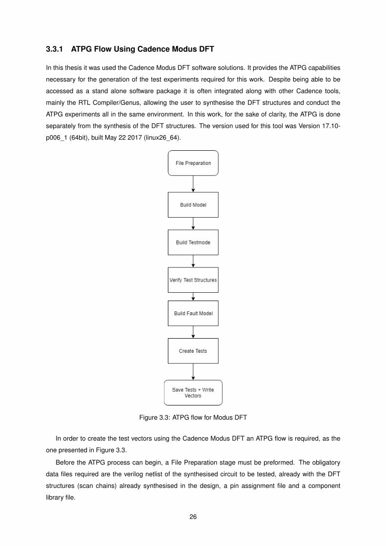
3.3.1 ATPG Flow Using Cadence Modus DFT
In this thesis it was used the Cadence Modus DFT software solutions. It provides the ATPG capabilities
necessary for the generation of the test experiments required for this work. Despite being able to be
accessed as a stand alone software package it is often integrated along with other Cadence tools,
mainly the RTL Compiler/Genus, allowing the user to synthesise the DFT structures and conduct the
ATPG experiments all in the same environment. In this work, for the sake of clarity, the ATPG is done
separately from the synthesis of the DFT structures. The version used for this tool was Version 17.10-
p006_1 (64bit), built May 22 2017 (linux26_64).
Figure 3.3: ATPG flow for Modus DFT
In order to create the test vectors using the Cadence Modus DFT an ATPG flow is required, as the
one presented in Figure 3.3.
Before the ATPG process can begin, a File Preparation stage must be preformed. The obligatory
data files required are the verilog netlist of the synthesised circuit to be tested, already with the DFT
structures (scan chains) already synthesised in the design, a pin assignment file and a component
library file.
26

The pin assignment file, as referenced in Section 3.2.1, informs the tool about the scan structures
interface and contains the data about the I/O pins of the circuit and their roles in the test experiments,
i.e., the data in and out of the scan chains, the scan enables, the test mode signals, test clocks and
system sets and resets.
The component library file is provided by technology providers (Faraday technology solutions in this
project), however, unlike the other library files used in this thesis, it does not contain any information
about timing or physical characteristics of the components. This scan test specialised library file only
contains the ports of the components and information about the inner connections of the components.
The First step in the ATPG flow is the Build Model. In this step it is loaded the verilog netlist of the
synthesised DFT ready circuit and the library file which are subsequently used by the tool to build a
model of the inner logic cells and connections of the circuit.
The second step is the building of the testmode. In this step the pin assignment file is read, allowing
the tool to know where are the scan structures and it is chosen the testmode to be conducted. The selec-
tion of the testmode allows the designer to choose if any of test/diagnostics compression methodologies
is to be used. This methodologies are used to compress the test vectors size with the objective of trying
to reduce the required memory storage during the test experiments. However, as the circuit used in this
thesis is relatively small, the testmode used is the FULLSCAN mode, meaning that no compression is
used.
The next step is to verify the test structures. At this point in the flow the tool will analyse the circuit to
try to find error in the circuit design, errors can compromise not only the viability of the test experiments
but the whole circuit normal functions. It is the most crucial step as even any warning can jeopardise
the test generation by rendering a majority of the faults as undetectable, thus leading to very poor fault
coverages. Design problems in this phase might require a complete redesign, which may lead to the
re-synthesis of the entire circuit.
We can proceed in the flow by building of the fault model. In this stage of the flow, the tool will use (for
this project) the SSF model and all the circuit information available (the circuit, the scan chains interface
pins, etc.) in order to identify all of the total faults and already identify all the undetectable faults. Since
static tests based on the SSF model for physical fault modelling can test a small percentage of delay
faults (see Section 3.1) the tool will also identify them. However, these will not be considered for our
tests.
For the final step, the tool can now conduct the test experiments. The tool will use a combination of
the TG methodologies (referenced in Section 3.3) iteratively until it reaches an optimal static fault test-
mode coverage, creating the test vectors in the process. Many other test experiments can be preformed
in this stage, for example, delay tests to increase the dynamic fault test coverage.
Finally it is possible to save the results of the experiments for eventual further use and to export
the test vectors by writing them out in the desired converted pattern language format, Verilog, Stan-
dard Test Interface Language (STIL), Waveform Generation Language (WGL) or TBD (Cadence Modus
proprietary format). If the Verilog format is selected the tool writes two types of files: The verilog "task
definition" file and one or more Verilog "vector" files.
27

The former contains the Verilog task definitions which describe the application of the test vectors.
This file is a testbench that reads the vector files, containing information about test initialisation and test
procedures (including the test vectors) effectively conducting the test of the circuit.
28
Chapter 4
Layout Implementation
As mentioned before, the objective of this work to reach a core layout, described in Graphic Data System
II (GDSII) format, of an implementation of the openMSP430 along side its memories and DFT structures
after a process called Place&Route. To obtain the circuit layout, a verilog netlist with a gate level de-
scription of the circuit in the target ASIC technology is necessary (not to be confused with the behavioral
verilog netlist). The configured openMSP430 was synthesized a priori to the work done in this project.
To obtain the core layout it is used the Cadence Encounter set of tools and a design flow, that will be
described briefly in this section.
4.1 Tools
The Cadence Encounter family of products is largely used in the industry as the reference software
for placement and routing of digital circuits. As so, it is supported by major foundries and technology
suppliers which distribute libraries and other files for this software platform.
Out of the several Cadence Encounter packages the SoC Encounter, that has a hierarchical RTL-
to-GDSII physical implementation solution, was selected. It provides a broad spectrum of features,
including placement, timing optimization, power routing, clock tree synthesis, geometry, connectivity
and antenna verification, and GDSII generation.
The SoC Encounter software has a graphical interface which is used to access not only its functions,
but also functions from other tools, like the NanoRoute, which may or may not have a graphical interface
of there own, aside from the command line batch mode. SoC Encounter is able to preform circuit place-
ment providing quick feedback on the design performance. Hierarchical design consisting of a top-level
floorplan containing blocks that can be implemented separately. It also provides in-place optimization,
which improves timing by inserting buffers and re-sizing gates, without changing the design’s logic.
NanoRoute is one of Cadence’s most prominent routing tools and is available through SoC En-
counter. It performs concurrent signal integrity, timing/area-driven, and manufacturing aware routing
of cell, block, or mixed cell and block level designs with a 180nm or smaller process technology [21].
Despite being able to work in stand-alone mode, it is invoked from the Encounter interface.
29
The NanoRoute tool preforms routing in two stages: global and detailed [21]. The global routing
stage minimises congestion by partitioning the routing design in global routing cells and preforming
interconnection planning of these cells creating paths that are used as guidelines for the detailed routing.
The detailed routing stage follows this global routing plan and lays down actual wires that connect the
pins to their corresponding nets [21]. Its preforms search-and-repair routing automatically in order to
locate short circuit and spacing violations according to the design rules and, by rerouting these areas,
eliminate violations as much as possible. The SoC Encounter and NanoRoute versions used are shown
on Table 4.1.
Table 4.1: Software Version TableEncounter v14.13-s036_1 (64bit) 08/14/2014 18:19 (Linux 2.6)
NanoRoute v14.13-s019 NR140805-0429/14_13-UB (database version 2.30, 237.6.1)
4.2 Design Flow
To produce the layout from, a synthesized verilog netlist, a design flow identifying the sequences of
required steps to be preformed has to be established. Each of the necessary steps correspond to a set
of Cadence Encounter tool commands. The design flow used for the Cadence Encounter is presented
in Figure 4.1.
Before the first step for creating a circuit layout using Encounter, is the File Preparation task [21]. In
this task the files that contain required data are defined. The capacitance table, standard cell and timing
library, synthesized modules or component description files (e.g. memories, which are not described
with standard cells but described as a custom cell) are required, and optionally, I/O assignment file.
The capacitance table is required for accurate results in the extraction of RC parameters of the layout
allowing a better quality of reports and simulations. This file contains information on the resistance and
capacitance values of the technology, which can be used for all designs that share the same technology
process. The elaboration of this file is a one-time operation based on the technology description file
which describes the process parameters (eg. thickness of conducting layers).
The standard cell and Timing library files are provided by technology providers (Faraday technology
solutions in this project) and are written in the Library Exchange Format (LEF) and LIB format, respec-
tively. The LEF contain cell descriptions, dimensions, layout of pins, blockages and layer capacitance.
The LIB file has the cell functionality and timing description. These technology libraries need to be
the same that were used when the circuit was the synthesized to obtain the verilog netlist in order to
achieve design coherence. Memories are also described using these LEF and LIB files and must also
be provided to the tool if used.
The I/O assignment file defines the rules that determine how the I/O pad cells (which are used to
connect with the outside world via bonding pads) and pins are organised. The file defines a set of
rules to specify location, global spacing, individual spacing, skip, offset, and corner information. This
information is optional and, if it is absent, the placing of the I/O cells and pins is done randomly.
30
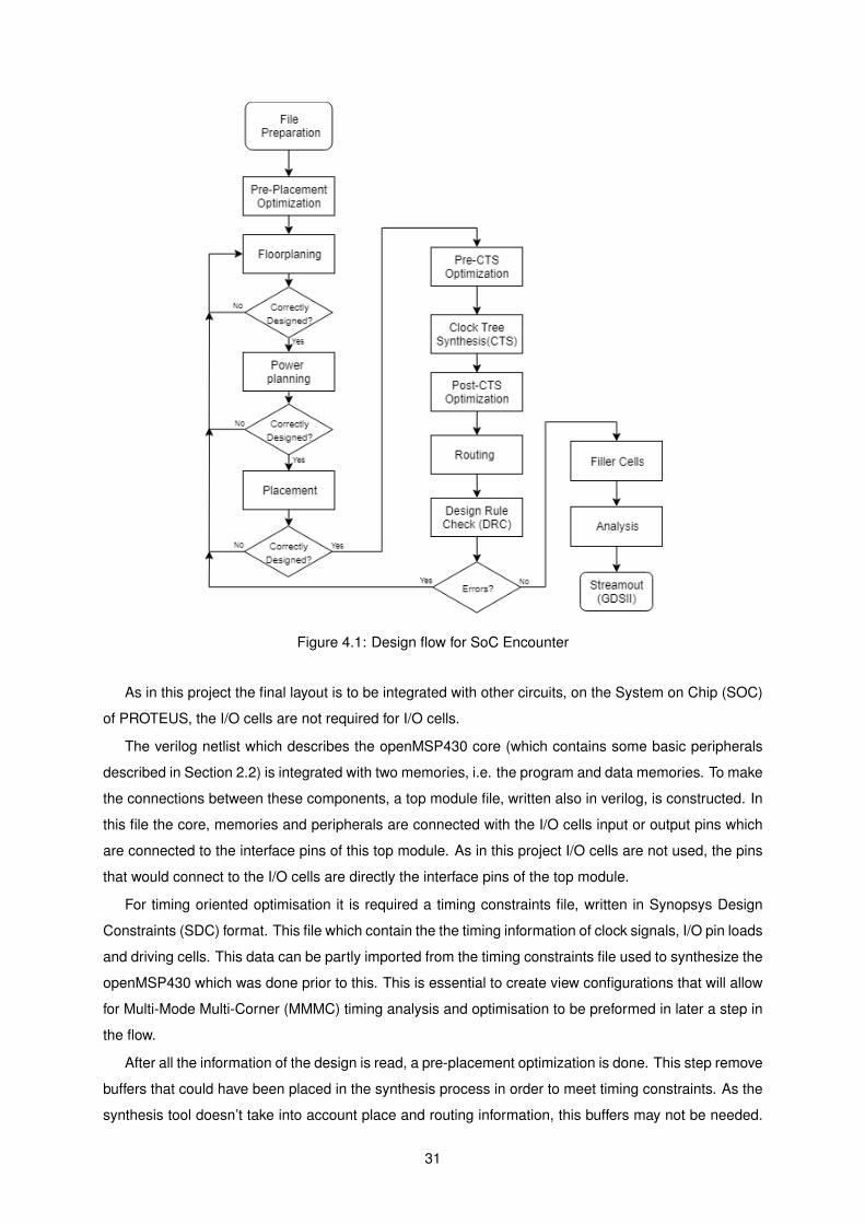
Figure 4.1: Design flow for SoC Encounter
As in this project the final layout is to be integrated with other circuits, on the System on Chip (SOC)
of PROTEUS, the I/O cells are not required for I/O cells.
The verilog netlist which describes the openMSP430 core (which contains some basic peripherals
described in Section 2.2) is integrated with two memories, i.e. the program and data memories. To make
the connections between these components, a top module file, written also in verilog, is constructed. In
this file the core, memories and peripherals are connected with the I/O cells input or output pins which
are connected to the interface pins of this top module. As in this project I/O cells are not used, the pins
that would connect to the I/O cells are directly the interface pins of the top module.
For timing oriented optimisation it is required a timing constraints file, written in Synopsys Design
Constraints (SDC) format. This file which contain the the timing information of clock signals, I/O pin loads
and driving cells. This data can be partly imported from the timing constraints file used to synthesize the
openMSP430 which was done prior to this. This is essential to create view configurations that will allow
for Multi-Mode Multi-Corner (MMMC) timing analysis and optimisation to be preformed in later a step in
the flow.
After all the information of the design is read, a pre-placement optimization is done. This step remove
buffers that could have been placed in the synthesis process in order to meet timing constraints. As the
synthesis tool doesn’t take into account place and routing information, this buffers may not be needed.
31
However, if the Encounter timing optimization function detects the need of this or other buffers they will
be added taking into account this new information.
The floorplaning is the next step in the design flow. In this step the circuit size (called die area) and
pre-placing of blocks, modules, submodules and pins are defined.
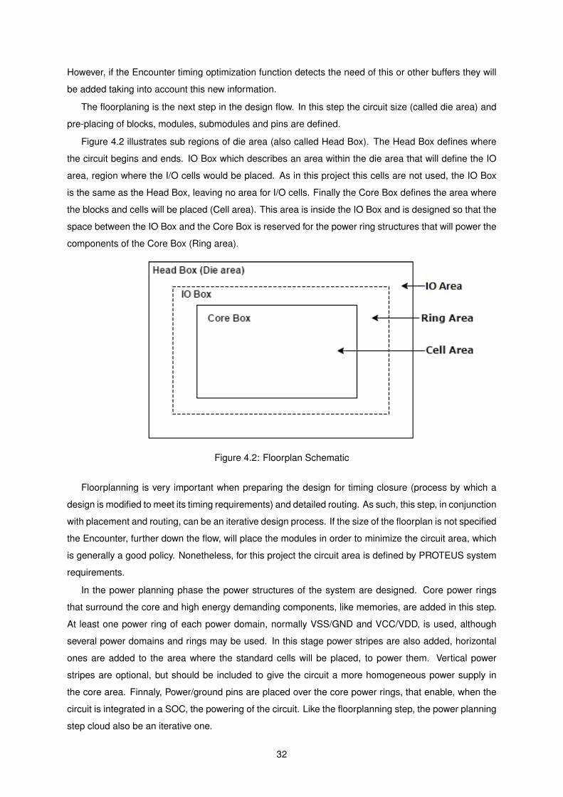
Figure 4.2 illustrates sub regions of die area (also called Head Box). The Head Box defines where
the circuit begins and ends. IO Box which describes an area within the die area that will define the IO
area, region where the I/O cells would be placed. As in this project this cells are not used, the IO Box
is the same as the Head Box, leaving no area for I/O cells. Finally the Core Box defines the area where
the blocks and cells will be placed (Cell area). This area is inside the IO Box and is designed so that the
space between the IO Box and the Core Box is reserved for the power ring structures that will power the
components of the Core Box (Ring area).
Figure 4.2: Floorplan Schematic
Floorplanning is very important when preparing the design for timing closure (process by which a
design is modified to meet its timing requirements) and detailed routing. As such, this step, in conjunction
with placement and routing, can be an iterative design process. If the size of the floorplan is not specified
the Encounter, further down the flow, will place the modules in order to minimize the circuit area, which
is generally a good policy. Nonetheless, for this project the circuit area is defined by PROTEUS system
requirements.
In the power planning phase the power structures of the system are designed. Core power rings
that surround the core and high energy demanding components, like memories, are added in this step.
At least one power ring of each power domain, normally VSS/GND and VCC/VDD, is used, although
several power domains and rings may be used. In this stage power stripes are also added, horizontal
ones are added to the area where the standard cells will be placed, to power them. Vertical power
stripes are optional, but should be included to give the circuit a more homogeneous power supply in
the core area. Finnaly, Power/ground pins are placed over the core power rings, that enable, when the
circuit is integrated in a SOC, the powering of the circuit. Like the floorplanning step, the power planning
step cloud also be an iterative one.
32

After the design of the power structures a timing driven placement is preformed. Multiple placing
strategies may be employed, however the most common is the timing driven one which places the
standard cells and blocks that are not pre-placed during the floorplanning (e.g. memories), in order to
reach the best timing. If necessary the standard cells position can be guided during the floorplaning
stage, e.g. the cells from the different modules can be confined in an area without being able to be
distributed through the entire core area. The process of placement is also an iterative one, if the solution
found by the tool is not satisfactory it may be necessary to redesign the floorplan, the repeating the
floorplanning step.
With all the circuit components placed a clock tree must be synthesized. This process intents to
minimizes the clock skew between sequential cells which is vital to maintain a synchronism. Before
synthesizing the clock tree a pre-CTS (Clock Tree Synthesis) optimization may be preformed. In this
phase the software replaces cells with other equivalent ones (available in the cell library) but with different
driving capacities in a process called gate resizing [21].
The synthesis of a clock tree should be done for each clock domain can now be preformed. Before
starting this process a Clock Tree Synthesis (CTS) configuration file must be prepared. This file includes
information about the maximum clock skew, maximum and minimum delays of the clock paths, the
shielding net and the maximum logic depth in the clock tree (maximum number of buffer levels of a tree).
After the CTS, an optional post-CTS optimization can be preformed. Like the pre-CTS optimization,
the cells are replaced in order to further improve the final clock skew.
For the routing stage the NanoRoute with the global and detailed routing options mentioned in Sec-
tion 4.1 is used. The routing process is selected as timing driven which minimizes the delays in order to
meet the design timing constraints. If problems in routability are an issue Cadence recommends a global
and detailed route after each of the major design flow step. This facilitates the checking for localized and
global congestion, allowing problems to be resolved early before proceeding down the flow. However,
due to the relative low complexity of the core (about 8k-Gates), it is expected not to be necessary to
check for congestion after each major design flow step.
The flow step to follow is Design Rule Check (DRC) verifications are preformed with the purpose
to detect rule violations (eg. short circuits, dangling wires, antenna effects and geometric violations).
If violations are detected some of the previous step of the flow must be repeated, this may include re-
position of pins or modules to facilitate the routing process, or completely change the initial floorplanning.
When a error free layout is reached, filler cells on the core may be added. This cells fills the leftover
space of the core area with this special cells whose purpose is to give the die area a better metal density
in the most critical layers (i.e. the bottom layers where the standard cells are) making the circuit surface
more even. Depending on technology, these cells can also act as capacitances on the power stripes
reducing power supply variations (spikes).
At this stage, with the layout finished, power grid analysis may be made to validate the systems power
constraints (which are not taken into account by the Encounter software in place and route engines) and
correct planning of power structures. If power constraints violations are found in this stage, a complete
redesign of the power planning and power structures, as well as the floorplan may be necessary.
33

The circuit design can now be exported to GDSII format. This file contains the geometrical dimen-
sions of the metal layers, used in routing, as well as the position of all the cells in the layout. To generate
this file, a mapping file and GDS descriptions of the memories have to be supplied. The mapping file
makes the correspondence between the layer names used in the Encounter software (e.g. metal1,
metal2) and the corresponding GDS layout layer number according to the UMC rules.
The GDSII file is sent to be integrated with other components of the PROTEUS system on chip, which
can be sent to the foundry to be fabricated.
34

Chapter 5
Results
After the implementation of the scan chain structures into the verilog netlist of the previously synthesized
openMSP430 Automatic Test Pattern Generation is preformed to generate test vectors which can be
used to test the fabricatied the circuit. Place and routing steps are then preformed on the verilog netlist
to complete the implementation of the design. In this chapter the characteristics of the, previously
synthesised, openMSP430 configuration is presented. The introduced scan chains are presented and
the result coverage of the ATPG process for the circuit is shown. Finally the implemented circuit layout is
shown. The most critical design choices of this process will be examined in more detail. As mentioned
in Section 1.2 the design tools Cadence RTL Compiler and Cadence Encounter (used in the PROTEUS
project), whose design flows are used in this thesis, were discontinued and replaced by Cadence Genus
and Cadence Innovus, respectively. Although, the new tools were used in legacy modes, not all of the
commands which were used with the former tools are supported. Therefore, a few commands had to be
replaced by non-legacy ones, or on a specific case, the function of the command must be applied to the
design manually, all of this situations are explained in this section.
5.1 OpenMSP430 Configuration
The configuration of the synthesised openMSP430, the starting point of this thesis work, with the added
integrated scan structures, is shown in Table 5.1
Table 5.1: OpenMSP430 ConfigurationHigh Frequency Clock Source (DCO) 16 MHzLow Frequency Clock Source (LFXT) 32,768 kHz
Program Memory Size 55 kBData Memory Size 8 kBPeripheral Space 512 B
16-bit Hardware Multiplier 3
DMA Interface 7
Watchdog Timer 7
UART Serial Debug Interface 3
I2C Serial Debug Interface 7
35

No extra peripherals are used in this thesis, however, to add custom extra peripherals the designer
must synthesize them using the openMSP430 peripheral’s template (that contains the compatible port
and communication protocol with the openMSP430) available in [8] and use the the high frequency
clock source as the peripheral clock constraint during synthesis process of the peripheral. Synthesising
the peripheral with the openMSP430 has the advantage of only requiring a set of scan chains to scan
both the peripherals and the core. Alternatively, the designer could synthesize the custom peripheral
separately the openMSP430 creating an additional verilog netlist. In this case the core and peripherals
would require separate sets of scan chains, inflating the number I/O pins required.
5.2 Full Serial Integrated Scan
The full script, containing the commands, used to obtain the resynthesis of verilog netlist integrated with
the scan chains, according to the design flow presented in Section 3.2.1 is shown in Appendix B.1.
Running the script on the RTL Compiler Tool leads to the creation of 4 scan chains, using all of the
circuits Flip-Flops, whose characteristics are shown in Table 5.2.
Table 5.2: Scan Chain CharacteristicsScan chain name Test clock domain Edge-trigger # of elements
chain1_rise DCO Rise 680chain2_fall DCO Fall 6chain3_rise LFXT Rise 15chain4_fall LFXT Fall 6
As a majority of the openMSP430 Flip-Flops are rising-edge triggered and were designed to operate
with the DCO clock, these Flip-Flops create the longest scan chain in the design. Nevertheless there
are Flip-Flops, in the circuit clock module, that operate with the LFXT clock. Therefore this clock domain
is used in separate chains as the test clock for this Flip-Flops. The four scan chains could be collapsed
in two, one for each test clock domain, creating mixed edge scan chains. However, this would require
a more complex test experiment and more precise instruments (wave generators, etc.) at the eventual
physical test of the circuit. Due to the large number of Flip-Flops on the chain1_rise chain it could be
divided in several other smaller and more balanced chains, reducing the test experiment time at the cost
of more I/O pins in the circuit port.
With the integration of the scan chains completed, the pin assignment file can be written. This file
used to give information about the test signals to the ATPG tool, and can be inspected in Appendix B.2.
After the scan chain flow ended, it was detected that, after the incremental synthesis, the input con-
stants of the openMSP430 submodels were not present in the final output verilog netlist. For example,
the AND gate instantiated as AND a1(A(1’b1),...) would be re-synthesised as
AND a1(A(UNCONNECTED),...). This was due to some commands present in the .g (generated by the
Cadence RTL Compiler) were not supported by the updated Cadence Genus tool in legacy mode. There-
fore, as the openMSP430 is of relatively small, this connections were re-made manually after the flow
was done. A translation/substitution of these commands would be necessary for a more robust solution.
36
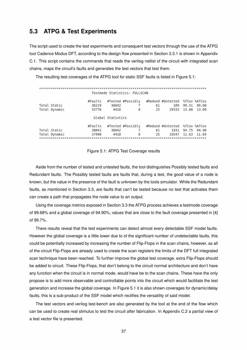
5.3 ATPG & Test Experiments
The script used to create the test experiments and consequent test vectors through the use of the ATPG
tool Cadence Modus DFT, according to the design flow presented in Section 3.3.1 is shown in Appendix
C.1. This script contains the commands that reads the verilog netlist of the circuit with integrated scan
chains, maps the circuit’s faults and generates the test vectors that test them.
The resulting test coverages of the ATPG tool for static SSF faults is listed in Figure 5.1:
Figure 5.1: ATPG Test Coverage results
Aside from the number of tested and untested faults, the tool distinguishes Possibly tested faults and
Redundant faults. The Possibly tested faults are faults that, during a test, the good value of a node is
known, but the value in the presence of the fault is unknown by the tools simulator. While the Redundant
faults, as mentioned in Section 3.3, are faults that can’t be tested because no test that activates them
can create a path that propagates the node value to an output.
Using the coverage metrics exposed in Section 3.3 the ATPG process achieves a testmode coverage
of 99.68% and a global coverage of 94.90%, values that are close to the fault coverage presented in [4]
of 99.7%.
There results reveal that the test experiments can detect almost every detectable SSF model faults.
However the global coverage is a little lower due to of the significant number of undetectable faults, this
could be potentially increased by increasing the number of Flip-Flops in the scan chains, however, as all
of the circuit Flip-Flops are already used to create the scan registers the limits of the DFT full integrated
scan technique have been reached. To further improve the global test coverage, extra Flip-Flops should
be added to circuit. These Flip-Flops, that don’t belong to the circuit normal architecture and don’t have
any function when the circuit is in normal mode, would have be to the scan chains. These have the only
propose is to add more observable and controllable points into the circuit which would facilitate the test
generation and increase the global coverage. In Figure 5.1 it is also shown coverages for dynamic/delay
faults, this is a sub-product of the SSF model which rectifies the versatility of said model.
The test vectors and verilog test-bench are also generated by the tool at the end of the flow which
can be used to create real stimulus to test the circuit after fabrication. In Appendix C.2 a partial view of
a test vector file is presented.
37
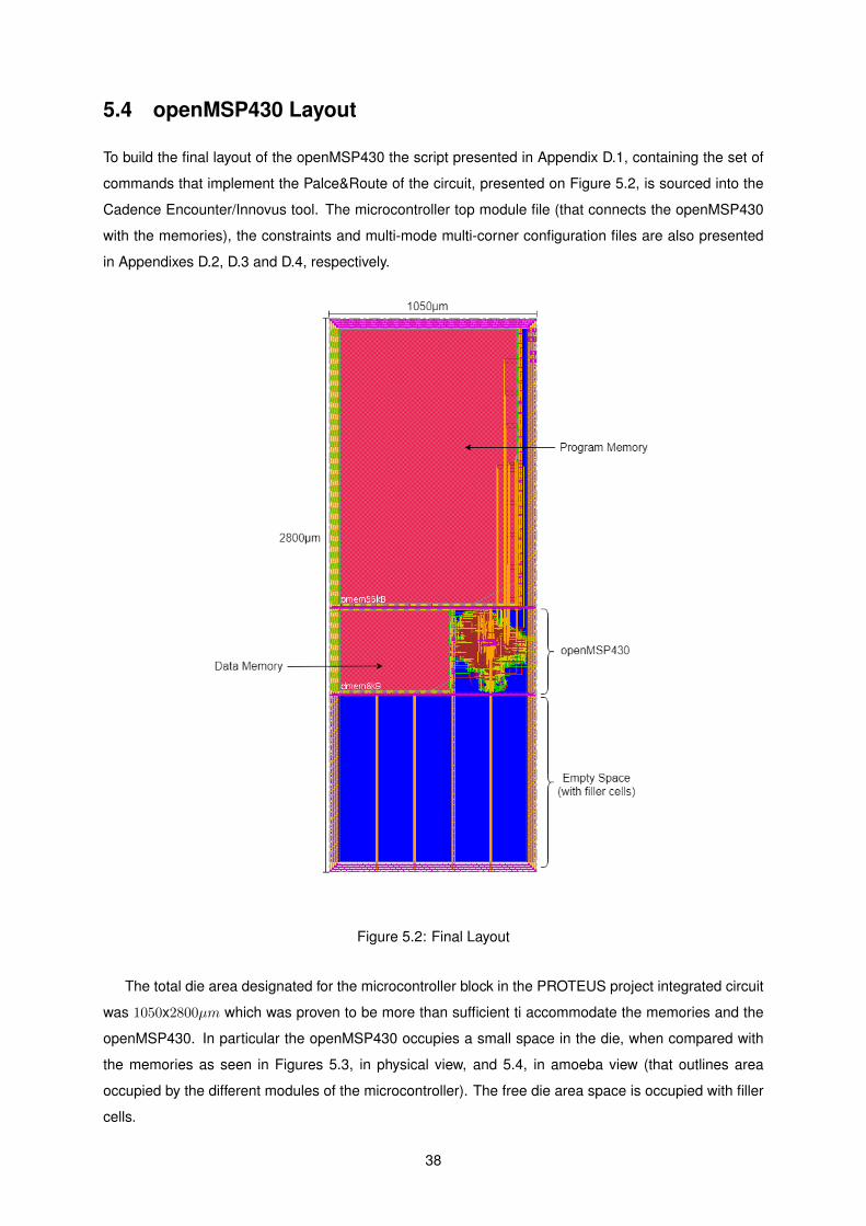
5.4 openMSP430 Layout
To build the final layout of the openMSP430 the script presented in Appendix D.1, containing the set of
commands that implement the Palce&Route of the circuit, presented on Figure 5.2, is sourced into the
Cadence Encounter/Innovus tool. The microcontroller top module file (that connects the openMSP430
with the memories), the constraints and multi-mode multi-corner configuration files are also presented
in Appendixes D.2, D.3 and D.4, respectively.
Figure 5.2: Final Layout
The total die area designated for the microcontroller block in the PROTEUS project integrated circuit
was 1050x2800µm which was proven to be more than sufficient ti accommodate the memories and the
openMSP430. In particular the openMSP430 occupies a small space in the die, when compared with
the memories as seen in Figures 5.3, in physical view, and 5.4, in amoeba view (that outlines area
occupied by the different modules of the microcontroller). The free die area space is occupied with filler
cells.
38
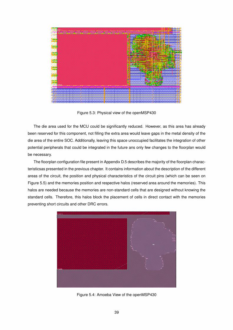
Figure 5.3: Physical view of the openMSP430
The die area used for the MCU could be significantly reduced. However, as this area has already
been reserved for this component, not filling the extra area would leave gaps in the metal density of the
die area of the entire SOC. Additionally, leaving this space unoccupied facilitates the integration of other
potential peripherals that could be integrated in the future ans only few changes to the floorplan would
be necessary.
The floorplan configuration file present in Appendix D.5 describes the majority of the floorplan charac-
teristicsas presented in the previous chapter. It contains information about the description of the different
areas of the circuit, the position and physical characteristics of the circuit pins (which can be seen on
Figure 5.5) and the memories position and respective halos (reserved area around the memories). This
halos are needed because the memories are non-standard cells that are designed without knowing the
standard cells. Therefore, this halos block the placement of cells in direct contact with the memories
preventing short circuits and other DRC errors.
Figure 5.4: Amoeba View of the openMSP430
39

Figure 5.5: Pins Highlight
The floorplan configuration file also reserves an area of 50µm around the core area for the power
structures of the circuit. The power structures implemented in the layout were four power rings around
the core alternating VDD and VSS power domains with 8µm of width and 3µm of spacing between them.
It is also important to define the layers of metal used to build the rings. In this case, layers 6 and 7 were
used to construct the rings since the top layers are usually the less resistive. The top right corners of the
resulting rings can be seen in detail in Figure 5.6. Three Power/Ground pins, that allow the powering of
the circuit when integrating the MCU in the an integrated circuit can also be seen in in Figure 5.6.
Since different technologies use different names to describe the power domains of the cells e.g,
VSS/GND and/or VCC/GND, it is necessary to identify these names so that the cell power pins get
connected to the correct power lines of the circuit. Therefore, a simple process called Gobal Net Connect
is preformed to assign any pin in the standard cells named GND/VSS or VCC/VDD to be connected to
the power domains of the design VSS and VDD, respectively.
Aside from the power rings and the horizontal power stripes that power the standard cells, power
structures around the memory blocks were also added as can be seen in Figure 5.7. The memories are
not powered like the standard cells, they have specific power ports around them. This isolates the power
delivery of the memories from the rest of the circuit and facilitates power distribution homogenisation in
the middle of the circuit area. Note that this dedicated power lines occupy the halo space, defined during
the floorplanning step, that also block the placing of horizontal power stripes on top of the memories.
To make the the power supply to the cells the most even possible and to avoid power drops, vertical
power stripes were also be added in the core area. This stripes, with the same physical characteristics
as the memory rings, can be also be seen at the bottom of Figure 5.7.
To create the clock tree system of a circuit on the CTS step of the design flow, a Clock Tree Spec-
ification file (CTSTCH) was written (available in Appendix D.6) which contains the information to guide
the tool to create the clock trees of both the DCO clock source (starting at the MCU_MAIN_CLOCK pin)
and the LFXT clock (starting at the MCU_MAIN_CLOCK pin). Note that the main clock domain of the
MCU, the mclk, is sourced by both the DCO and the LFXT and the tool is able to detect this and handle
it as such when creating the clock trees.
40
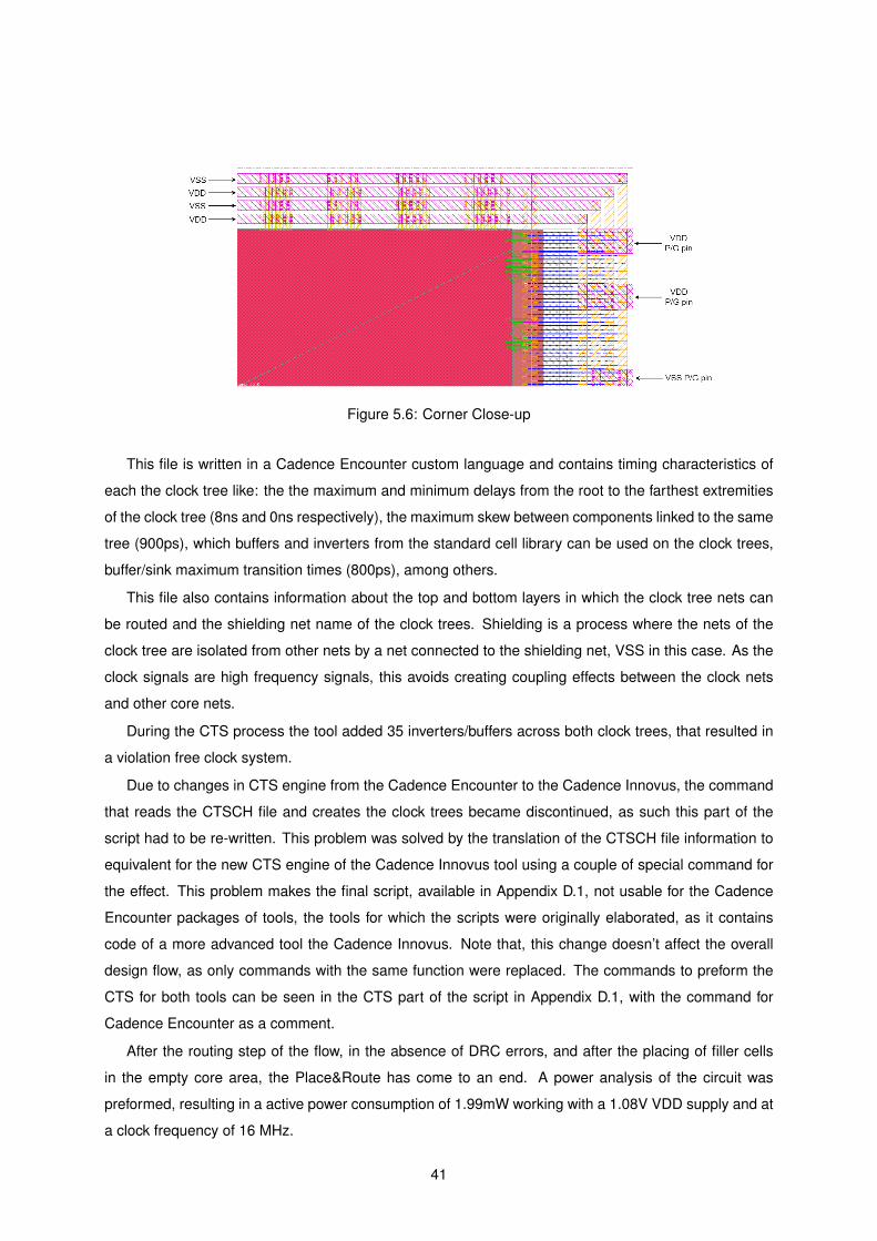
Figure 5.6: Corner Close-up
This file is written in a Cadence Encounter custom language and contains timing characteristics of
each the clock tree like: the the maximum and minimum delays from the root to the farthest extremities
of the clock tree (8ns and 0ns respectively), the maximum skew between components linked to the same
tree (900ps), which buffers and inverters from the standard cell library can be used on the clock trees,
buffer/sink maximum transition times (800ps), among others.
This file also contains information about the top and bottom layers in which the clock tree nets can
be routed and the shielding net name of the clock trees. Shielding is a process where the nets of the
clock tree are isolated from other nets by a net connected to the shielding net, VSS in this case. As the
clock signals are high frequency signals, this avoids creating coupling effects between the clock nets
and other core nets.
During the CTS process the tool added 35 inverters/buffers across both clock trees, that resulted in
a violation free clock system.
Due to changes in CTS engine from the Cadence Encounter to the Cadence Innovus, the command
that reads the CTSCH file and creates the clock trees became discontinued, as such this part of the
script had to be re-written. This problem was solved by the translation of the CTSCH file information to
equivalent for the new CTS engine of the Cadence Innovus tool using a couple of special command for
the effect. This problem makes the final script, available in Appendix D.1, not usable for the Cadence
Encounter packages of tools, the tools for which the scripts were originally elaborated, as it contains
code of a more advanced tool the Cadence Innovus. Note that, this change doesn’t affect the overall
design flow, as only commands with the same function were replaced. The commands to preform the
CTS for both tools can be seen in the CTS part of the script in Appendix D.1, with the command for
Cadence Encounter as a comment.
After the routing step of the flow, in the absence of DRC errors, and after the placing of filler cells
in the empty core area, the Place&Route has come to an end. A power analysis of the circuit was
preformed, resulting in a active power consumption of 1.99mW working with a 1.08V VDD supply and at
a clock frequency of 16 MHz.
41
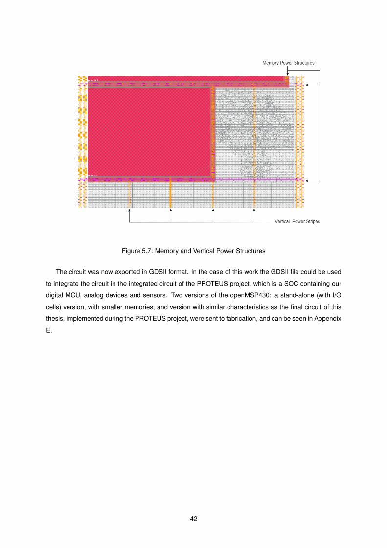
Figure 5.7: Memory and Vertical Power Structures
The circuit was now exported in GDSII format. In the case of this work the GDSII file could be used
to integrate the circuit in the integrated circuit of the PROTEUS project, which is a SOC containing our
digital MCU, analog devices and sensors. Two versions of the openMSP430: a stand-alone (with I/O
cells) version, with smaller memories, and version with similar characteristics as the final circuit of this
thesis, implemented during the PROTEUS project, were sent to fabrication, and can be seen in Appendix
E.
42

Chapter 6
Conclusion and Future Work
The openMSP430 is a small 16bit low-power microcontroller that was selected to be in the SOC that will
be developed in the PROTREUS project.
The characteristics of the original Texas Instruments MPS430 circuit board, in which openMSP430 is
based on, were described and compared with available open source verilog description of openMSP430.
To increase the circuit testability, a design flow, using Cadence RTL Compiler, was presented and
executed in order to introduce DFT scan chains structures to an already synthesised, in a target technol-
ogy, version of the openMSP430. Structures tha allow the shifting of test vectors that verify the correct
behaviour of a fabricated circuit. Applying the flow resulted in the synthesis of four scan chains in the
circuit, formed a total of the 707 circuit Flip-Flops, all of the circuits Flip-Flops.
The DFT structures were then used in conjunction with a, also presented, ATPG flow for Modus DFT
EDA tool. Test vectors were generated, that along with an also written verilog task file, are able to test
the fabricated circuit, achieving a global fault-coverage of 94.9%, a value similar as the value available
in the openMSP430 guide.
Finally, in order to implement and fabricate the a design flow for the back-end was presented. This
flow described floorplanning, power planning, placement, Clock Tree Synthesis and routing that were
followed, achieving the final layout of the openMSP430 integrated with the Data and Program memories
and scan chains, implemented in the UMC 130nm target technology. The resulting circuit layout occu-
pies and area of 1050x2800µm and a power consumption of 1.99mW when operating at 16 MHz clock
frequency.
As future work, I/O cells could be added to the final layout could be later sent to for manufacture.
Afterwards, it could be encapsulated and, mounting it in a Printed Circuit Board (PCB) with a FGPA
(generate stimulus), execute the testing of the circuit using the vectors and task manager test-bench
file. Additionally, extra peripherals could developed, be synthesised and implemented in the same target
technology and according to the openMSP430 peripheral protocol, in order to increase the circuit’s
capabilities and interface.
43

Bibliography
[1] H. Bauer, M. Patel, and J. Veira, “The internet of things: Sizing up the opportunity,” December
2014 (accessed on April 2017). [Online]. Available: http://www.mckinsey.com/industries/high-tech/
our-insights/the-internet-of-things-sizing-up-the-opportunity
[2] G. Pitcher, “Things worthy of consideration,” New Electronics, 28 January 2014. [Online]. Available:
http://www.newelectronics.co.uk/article-images/59112/P22-23.pdf
[3] A. Rajput and A. Jain, “Basic introduction to microcontroller and its features,” IJETSR, April 2015.
[Online]. Available: http://www.ijetsr.com/images/short_pdf/1428729554_arjun_ijetsr.pdf
[4] O. GIRARD, openMSP430, OpenCores.org, May 19,2015, rev 1.15.
[5] AdaPtive micROfluidic- and nano-enabled smart systems for waTEr qUality Sensing (PROTEUS),
H2020 European Union research project No 644852, 2015 (accessed on May 2017). [Online].
Available: http://www.proteus-sensor.eu/
[6] T. I. Incorporated, “Msp430™ ultra-low-power microcontrollers,” 2016 (accessed on May 2017).
[Online]. Available: http://www.ti.com/lsds/ti/microcontrollers-16-bit-32-bit/msp/overview.page
[7] SLAU049F - MSP430x1xx Family User Guide, Texas Instruments Incorporated, Post Office Box
655303 Dallas, Texas 75265, 2006.
[8] "OpenCores.org, “openmsp430 :: Overview,” 28 January 2014. [Online]. Available: https:
//opencores.org/project,openmsp430
[9] S. Sondon, P. Mandolesi, F. Masson, P. Julián, and F. Palumbo, A Dual Core Low Power Micro-
controller with openMSP430 Architecture for High Reliability Lockstep Applications Using a 180 nm
High Voltage Technology Node, 2013.
[10] A. Roy, P. J. Grossmann, S. A. Vitale, and B. H. Calhoun, A 1.3µW, 5pJ/cycle Sub-threshold
MSP430 Processor in 90nm xLP FDSOI for Energy-efficient loT Applications, 2016.
[11] A. Roy, A. Klinefelter, F. B. Yahya, X. Chen, L. P. Gonzalez-Guerrero, C. J. Lukas, D. A. Kamakshi,
J. Boley, K. Craig, M. Faisal, S. Oh, N. E. Roberts, Y. Shakhsheer, A. Shrivastava, D. P. Vasude-
van, D. D. Wentzloff, and B. H. Calhoun, A 6.45 µW Self-Powered SoC With Integrated Energy-
Harvesting Power Management and ULP Asymmetric Radios for Portable Biomedical Systems,
December 2015.
44

[12] D. prasad B C and N. V. R. Krishna, Synthesis of a TI MSP430 Microcontroller Core using Multi-
Voltage Methodology, 2010.
[13] A. Sivadasan, F. Cacho, S. A. Benhassain, and V. Huard, Study of Workload Impact on BTI HCI
Induced Aging of Digital Circuits, 2016.
[14] J. P. Oliver, J. P. Acle, and E. Boemo, Power Estimations Vs Power Measurements in Spartan-6
Devices, 2014.
[15] Energia, “Prototyping software to make things easy.” [Online]. Available: http://energia.nu/
[16] M. Abramovic, M. A. Breuer, and A. D. Friedman, Digital Systems Testing And Testable Design.
Revised Printing. Wiley-IEEE Press, 1990.
[17] J. P. Roth, “Diagnosis of automata failures: A calculus and a method,” IBM Journal of Research and
Development, vol. 10, no. 4, pp. 278–291, July 1966.
[18] C. W. Cha, W. E. Donath, and F. Özgüner, “9-v algorithm for test pattern generation of combinational
digital circuits,” IEEE Transactions on Computers, vol. 27, no. 3, pp. 193–200, March 1978.
[19] H. Fujiwara and T. Shimono, “On the acceleration of test generation algorithms,” IEEE Transactions
on Computers, vol. 32, no. 12, pp. 1137–1144, December 1983.
[20] P. Goel, “An implicit enumeration algorithm to generate tests for combinational logic circuits,” IEEE
Transactions on Computers, vol. 30, no. 3, pp. 215–222, March 1981.
[21] Encounter™ User Guide, Cadence Design Systems, Inc, 555 River Oaks Parkway, San Jose, CA
95134, USA, May 2005, version 4.1.5.
45

46
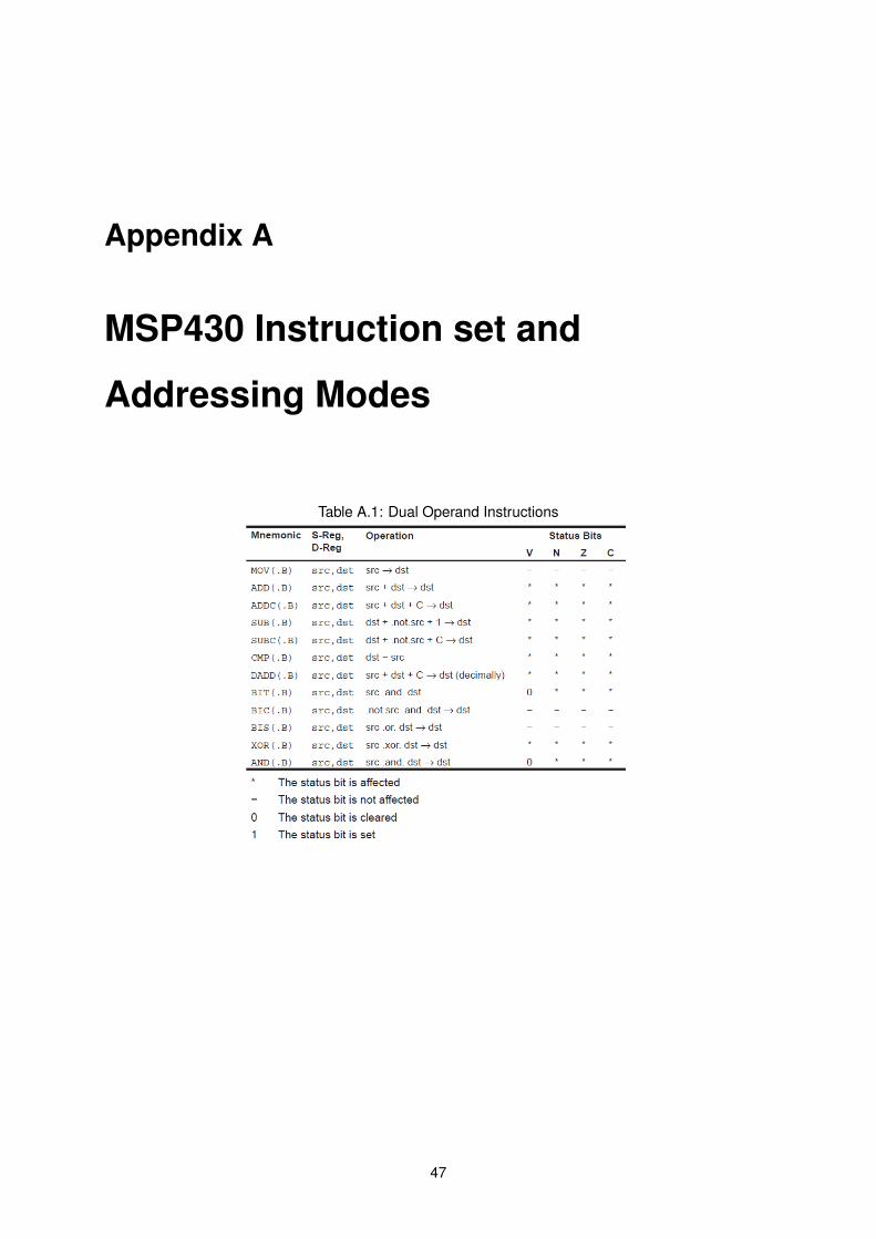
Appendix A
MSP430 Instruction set and
Addressing Modes
Table A.1: Dual Operand Instructions
47
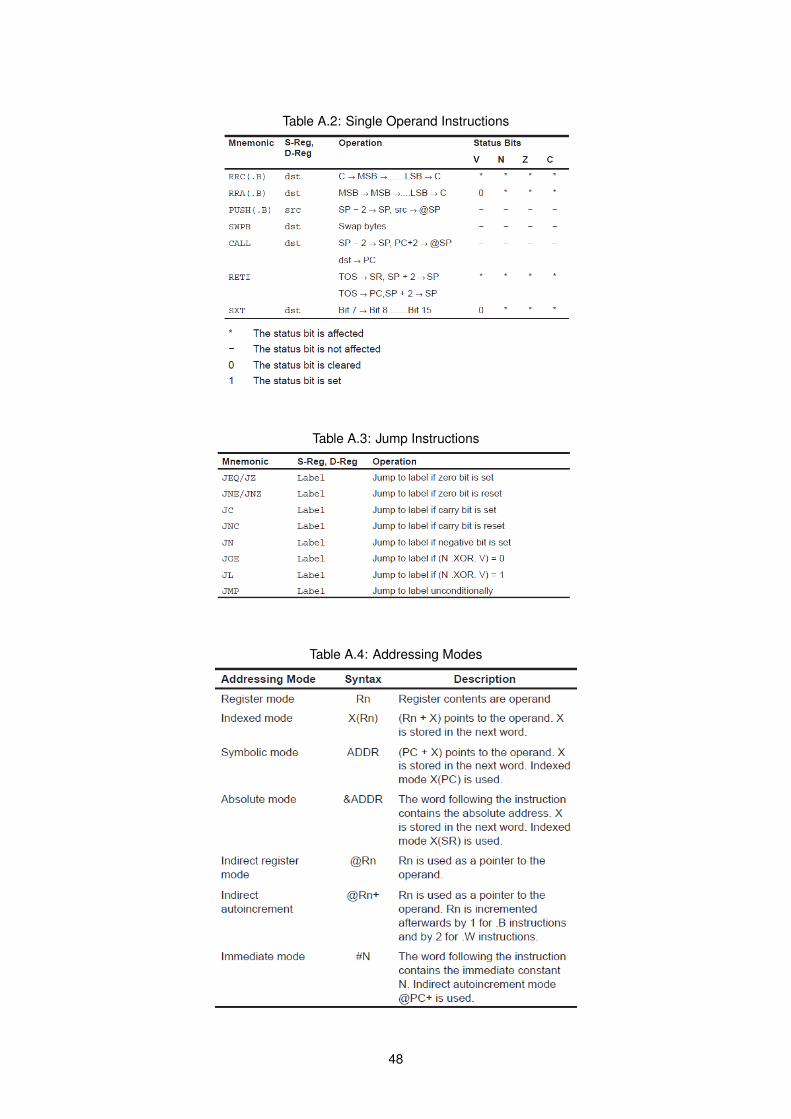
Table A.2: Single Operand Instructions
Table A.3: Jump Instructions
Table A.4: Addressing Modes
48
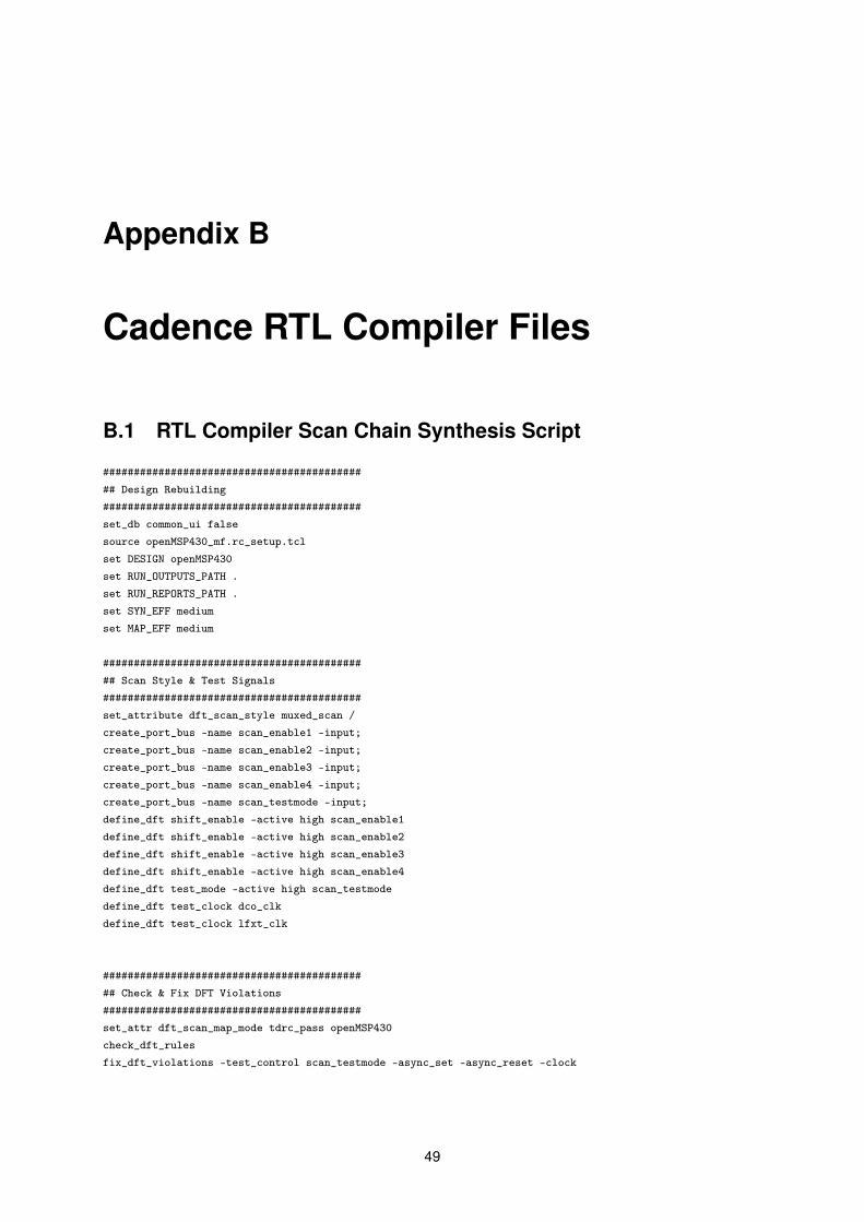
Appendix B
Cadence RTL Compiler Files
B.1 RTL Compiler Scan Chain Synthesis Script
############################################ Design Rebuilding##########################################set_db common_ui falsesource openMSP430_mf.rc_setup.tclset DESIGN openMSP430set RUN_OUTPUTS_PATH .set RUN_REPORTS_PATH .set SYN_EFF mediumset MAP_EFF medium
############################################ Scan Style & Test Signals##########################################set_attribute dft_scan_style muxed_scan /create_port_bus -name scan_enable1 -input;create_port_bus -name scan_enable2 -input;create_port_bus -name scan_enable3 -input;create_port_bus -name scan_enable4 -input;create_port_bus -name scan_testmode -input;define_dft shift_enable -active high scan_enable1define_dft shift_enable -active high scan_enable2define_dft shift_enable -active high scan_enable3define_dft shift_enable -active high scan_enable4define_dft test_mode -active high scan_testmodedefine_dft test_clock dco_clkdefine_dft test_clock lfxt_clk
############################################ Check & Fix DFT Violations##########################################set_attr dft_scan_map_mode tdrc_pass openMSP430check_dft_rulesfix_dft_violations -test_control scan_testmode -async_set -async_reset -clock
49

############################################ Define & Connect Scan Chains##########################################define_dft scan_chain -name chain1_rise -create_ports -sdi scan_di1 -sdo scan_do1 \
-shift_enable scan_enable1 -domain dco_clk -edge risedefine_dft scan_chain -name chain2_fall -create_ports -sdi scan_di2 -sdo scan_do2 \
-shift_enable scan_enable2 -domain dco_clk -edge falldefine_dft scan_chain -name chain3_rise -create_ports -sdi scan_di3 -sdo scan_do3 \
-shift_enable scan_enable3 -domain lfxt_clk -edge risedefine_dft scan_chain -name chain4_fall -create_ports -sdi scan_di4 -sdo scan_do4 \
-shift_enable scan_enable4 -domain lfxt_clk -edge fallreplace_scan openMSP430connect_scan_chains -auto_create_chains
############################################ Check DFT Violations##########################################check_dft_rules
############################################ Incremental Synthesis##########################################synthesize -to_mapped -eff $MAP_EFF -incrgenerate_reports -outdir $RUN_REPORTS_PATH -tag incrementalwrite_hdl -mapped > ${RUN_OUTPUTS_PATH}/${DESIGN}_m_chains.vsummary_table -outdir $RUN_REPORTS_PATHputs "Runtime & Memory after incremental synthesis"timestat INCREMENTAL
######################################### Export Design & Pin Assigment File######################################write_design -encounter -basename ${RUN_OUTPUTS_PATH}/${DESIGN}_mff_chainswrite_atpg -cadence >Test_Pins.file
B.2 Pin Assignment File
assign pin=scan_testmode test_function= +TI; # test_modeassign pin=reset_n test_function= +SC; # test_modeassign pin=scan_enable1 test_function= +SE; # shift_enableassign pin=scan_enable2 test_function= +SE; # shift_enableassign pin=scan_enable3 test_function= +SE; # shift_enableassign pin=scan_enable4 test_function= +SE; # shift_enableassign pin=dco_clk test_function= -ES;assign pin=lfxt_clk test_function= -ES;assign pin=scan_di1 test_function= SI0;assign pin=scan_do1 test_function= SO0;assign pin=scan_di2 test_function= SI1;assign pin=scan_do2 test_function= SO1;assign pin=scan_di3 test_function= SI2;assign pin=scan_do3 test_function= SO2;assign pin=scan_di4 test_function= SI3;assign pin=scan_do4 test_function= SO3;
50
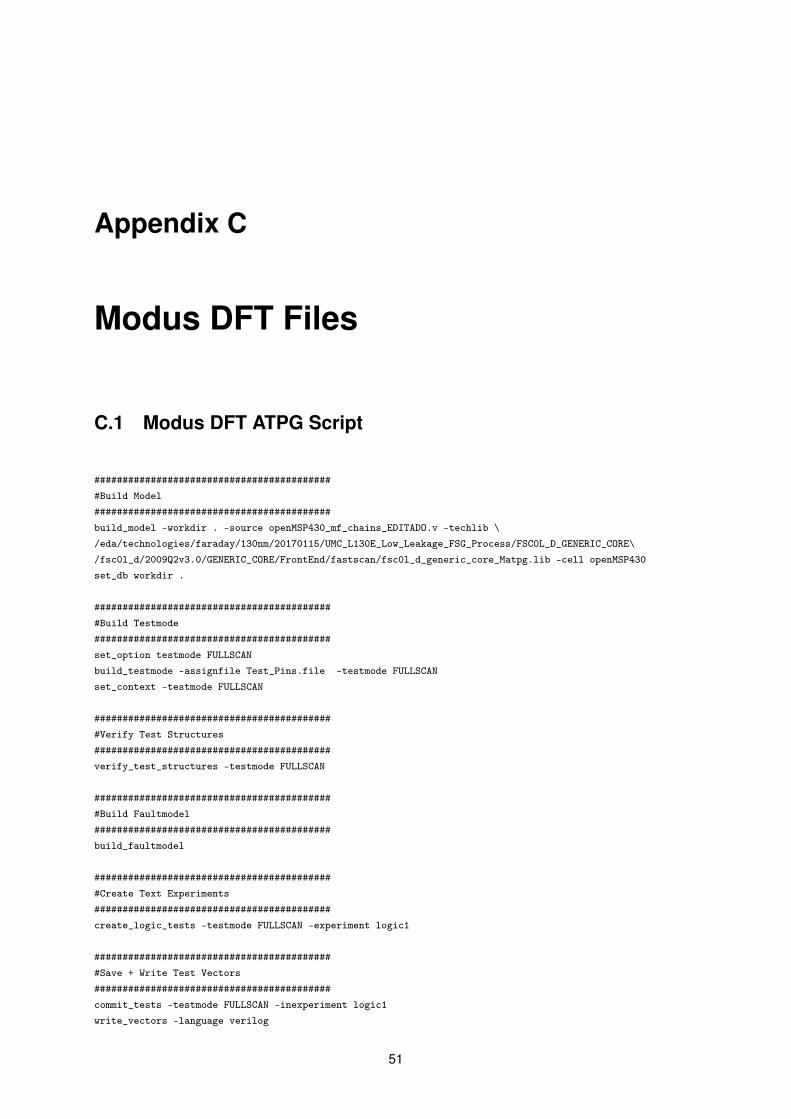
Appendix C
Modus DFT Files
C.1 Modus DFT ATPG Script
###########################################Build Model##########################################build_model -workdir . -source openMSP430_mf_chains_EDITADO.v -techlib \/eda/technologies/faraday/130nm/20170115/UMC_L130E_Low_Leakage_FSG_Process/FSC0L_D_GENERIC_CORE\/fsc0l_d/2009Q2v3.0/GENERIC_CORE/FrontEnd/fastscan/fsc0l_d_generic_core_Matpg.lib -cell openMSP430set_db workdir .
###########################################Build Testmode##########################################set_option testmode FULLSCANbuild_testmode -assignfile Test_Pins.file -testmode FULLSCANset_context -testmode FULLSCAN
###########################################Verify Test Structures##########################################verify_test_structures -testmode FULLSCAN
###########################################Build Faultmodel##########################################build_faultmodel
###########################################Create Text Experiments##########################################create_logic_tests -testmode FULLSCAN -experiment logic1
###########################################Save + Write Test Vectors##########################################commit_tests -testmode FULLSCAN -inexperiment logic1write_vectors -language verilog
51

C.2 Partial Test Vector File
100 Cadence(R) Modus(TM) Test Solution100 FILE CREATED..............April 30, 2018 at 22:02:42203 Z104 MODEINIT900 1.1.1.1.1.1200 XXXXXXXXX0XXXXXXXX0XXXXXXXXXX1XXXXX1111X1XXXXXXXXXXXXXXX1XXXXX1111X1XXXXXXXXXXXXXXXX ...201 XXXXX0XXXXXXXXXXXXXX0XXXXXXXXXXX1XXXXXXXXXXXX001XXXXXXXX1XXXXX111XX1XXXXXXXXXXXXXXXX ...400104900 1.1.1.2.1.1600 1 1 1300 1 1 00111100011110001111000111100011110001111000111100111000111100011110000000111010 ...300 1 3 001111000111100300 1 4 111100600 1 2 680905 1.1.1.2.1.1.1900 1.1.1.2.1.2900 1.1.1.3.1.1901 1.1.1.2.1.2904 1.1.1.2.1.2.1600 1 1 1301 1 1 001111000111100011110001111000111100011110001111000111100011110001111000111100011 ...301 1 2 111100301 1 3 001111000111100301 1 4 111100300 1 1 001110010001000011100000101011111101110100001101001110100101101010011110000010111 ...300 1 2 101110300 1 3 011110111101110300 1 4 011010600 1 2 680905 1.1.1.3.1.1.1900 1.1.1.3.1.2900 1.1.1.3.2.1901 1.1.1.3.1.2904 1.1.1.3.1.2.1600 1 1 1301 1 1 001110010001000011100000101011111101110100001101001110100101101010011110000010111 ...301 1 2 101110301 1 3 011110111101110301 1 4 011010...
52
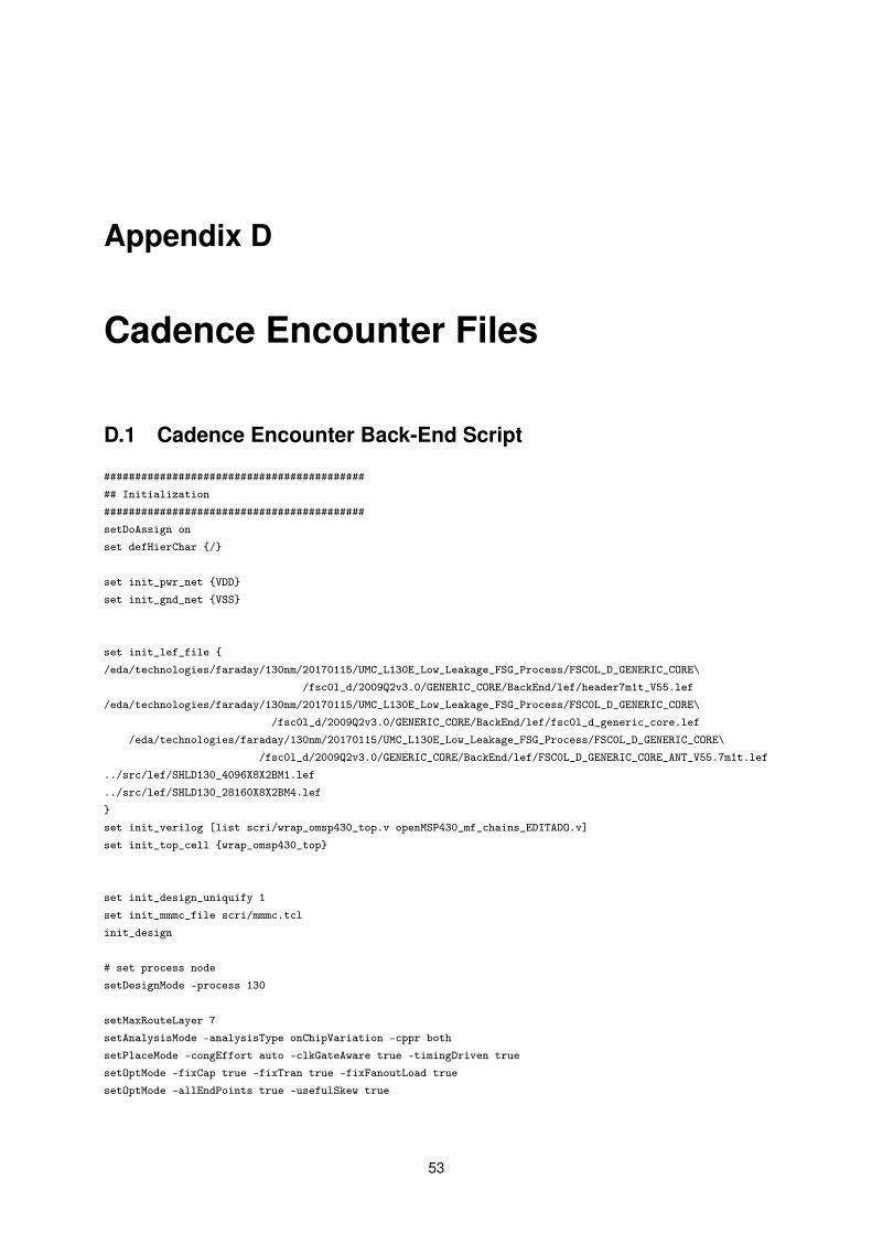
Appendix D
Cadence Encounter Files
D.1 Cadence Encounter Back-End Script
############################################ Initialization##########################################setDoAssign onset defHierChar {/}
set init_pwr_net {VDD}set init_gnd_net {VSS}
set init_lef_file {/eda/technologies/faraday/130nm/20170115/UMC_L130E_Low_Leakage_FSG_Process/FSC0L_D_GENERIC_CORE\
/fsc0l_d/2009Q2v3.0/GENERIC_CORE/BackEnd/lef/header7m1t_V55.lef/eda/technologies/faraday/130nm/20170115/UMC_L130E_Low_Leakage_FSG_Process/FSC0L_D_GENERIC_CORE\
/fsc0l_d/2009Q2v3.0/GENERIC_CORE/BackEnd/lef/fsc0l_d_generic_core.lef/eda/technologies/faraday/130nm/20170115/UMC_L130E_Low_Leakage_FSG_Process/FSC0L_D_GENERIC_CORE\
/fsc0l_d/2009Q2v3.0/GENERIC_CORE/BackEnd/lef/FSC0L_D_GENERIC_CORE_ANT_V55.7m1t.lef../src/lef/SHLD130_4096X8X2BM1.lef../src/lef/SHLD130_28160X8X2BM4.lef}set init_verilog [list scri/wrap_omsp430_top.v openMSP430_mf_chains_EDITADO.v]set init_top_cell {wrap_omsp430_top}
set init_design_uniquify 1set init_mmmc_file scri/mmmc.tclinit_design
# set process nodesetDesignMode -process 130
setMaxRouteLayer 7setAnalysisMode -analysisType onChipVariation -cppr bothsetPlaceMode -congEffort auto -clkGateAware true -timingDriven truesetOptMode -fixCap true -fixTran true -fixFanoutLoad truesetOptMode -allEndPoints true -usefulSkew true
53
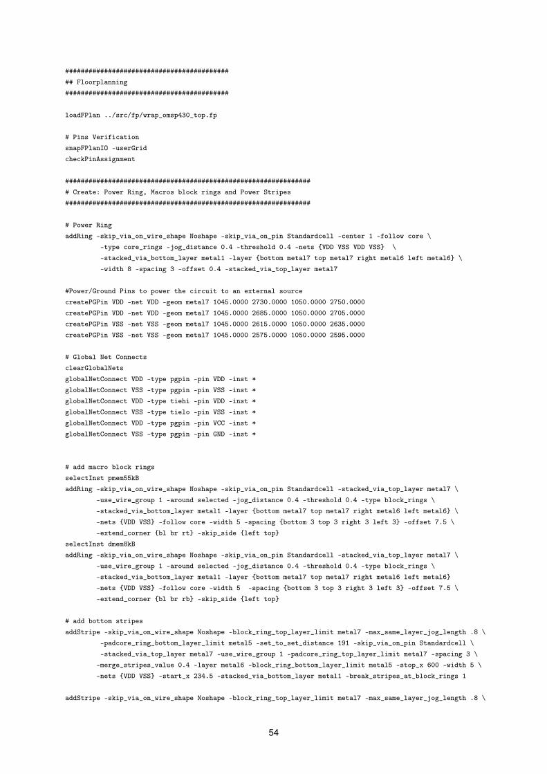
############################################ Floorplanning##########################################
loadFPlan ../src/fp/wrap_omsp430_top.fp
# Pins VerificationsnapFPlanIO -userGridcheckPinAssignment
################################################################ Create: Power Ring, Macros block rings and Power Stripes###############################################################
# Power RingaddRing -skip_via_on_wire_shape Noshape -skip_via_on_pin Standardcell -center 1 -follow core \
-type core_rings -jog_distance 0.4 -threshold 0.4 -nets {VDD VSS VDD VSS} \-stacked_via_bottom_layer metal1 -layer {bottom metal7 top metal7 right metal6 left metal6} \-width 8 -spacing 3 -offset 0.4 -stacked_via_top_layer metal7
#Power/Ground Pins to power the circuit to an external sourcecreatePGPin VDD -net VDD -geom metal7 1045.0000 2730.0000 1050.0000 2750.0000createPGPin VDD -net VDD -geom metal7 1045.0000 2685.0000 1050.0000 2705.0000createPGPin VSS -net VSS -geom metal7 1045.0000 2615.0000 1050.0000 2635.0000createPGPin VSS -net VSS -geom metal7 1045.0000 2575.0000 1050.0000 2595.0000
# Global Net ConnectsclearGlobalNetsglobalNetConnect VDD -type pgpin -pin VDD -inst *globalNetConnect VSS -type pgpin -pin VSS -inst *globalNetConnect VDD -type tiehi -pin VDD -inst *globalNetConnect VSS -type tielo -pin VSS -inst *globalNetConnect VDD -type pgpin -pin VCC -inst *globalNetConnect VSS -type pgpin -pin GND -inst *
# add macro block ringsselectInst pmem55kBaddRing -skip_via_on_wire_shape Noshape -skip_via_on_pin Standardcell -stacked_via_top_layer metal7 \
-use_wire_group 1 -around selected -jog_distance 0.4 -threshold 0.4 -type block_rings \-stacked_via_bottom_layer metal1 -layer {bottom metal7 top metal7 right metal6 left metal6} \-nets {VDD VSS} -follow core -width 5 -spacing {bottom 3 top 3 right 3 left 3} -offset 7.5 \-extend_corner {bl br rt} -skip_side {left top}
selectInst dmem8kBaddRing -skip_via_on_wire_shape Noshape -skip_via_on_pin Standardcell -stacked_via_top_layer metal7 \
-use_wire_group 1 -around selected -jog_distance 0.4 -threshold 0.4 -type block_rings \-stacked_via_bottom_layer metal1 -layer {bottom metal7 top metal7 right metal6 left metal6}-nets {VDD VSS} -follow core -width 5 -spacing {bottom 3 top 3 right 3 left 3} -offset 7.5 \-extend_corner {bl br rb} -skip_side {left top}
# add bottom stripesaddStripe -skip_via_on_wire_shape Noshape -block_ring_top_layer_limit metal7 -max_same_layer_jog_length .8 \
-padcore_ring_bottom_layer_limit metal5 -set_to_set_distance 191 -skip_via_on_pin Standardcell \-stacked_via_top_layer metal7 -use_wire_group 1 -padcore_ring_top_layer_limit metal7 -spacing 3 \
-merge_stripes_value 0.4 -layer metal6 -block_ring_bottom_layer_limit metal5 -stop_x 600 -width 5 \-nets {VDD VSS} -start_x 234.5 -stacked_via_bottom_layer metal1 -break_stripes_at_block_rings 1
addStripe -skip_via_on_wire_shape Noshape -block_ring_top_layer_limit metal7 -max_same_layer_jog_length .8 \
54
-padcore_ring_bottom_layer_limit metal5 -set_to_set_distance 168 -skip_via_on_pin Standardcell \-stacked_via_top_layer metal7 -use_wire_group 1 -padcore_ring_top_layer_limit metal7 -spacing 3 \-merge_stripes_value 0.4 -layer metal6 -block_ring_bottom_layer_limit metal5 -stop_x 830 -width 5\-nets {VDD VSS} -start_x 810.15 -stacked_via_bottom_layer metal1 -break_stripes_at_block_rings 1
# Connect all the power structures using Special Routesroute -connect { blockPin padPin corePin floatingStripe } -layerChangeRange { metal1 metal7 } \
-blockPinTarget { nearestTarget } -padPinPortConnect { allPort oneGeom } \-padPinTarget { nearestTarget } -corePinTarget { firstAfterRowEnd } \-floatingStripeTarget { blockring padring ring stripe ringpin blockpin followpin } \-allowJogging 1 -crossoverViaLayerRange {metal1 metal7}-allowLayerChange 1 -nets {VDD VSS} -blockPin useLef -targetViaLayerRange {metal1 metal7}
############################################ Placement###########################################Specify Scan ChainsspecifyScanChain chain1_rise -start DFT_DI1 -stop DFT_DO1specifyScanChain chain2_fall -start DFT_DI2 -stop DFT_DO2specifyScanChain chain3_rise -start DFT_DI3 -stop DFT_DO3specifyScanChain chain4_fall -start DFT_DI4 -stop DFT_DO4
#PlacesetPlanDesignMode -effort high -congAware false -keepGuide false -useSdpGroup false -boundaryPlace true \
-fixPlacedMacros false -noColorize falseplanDesignsetPlaceMode -prerouteAsObs {1 2 3 4 5 6 7}setPlaceMode -resetsetPlaceMode -fp falseplaceDesign
############################################ Pre-CTS Optimization##########################################buildTimingGraphtimeDesign -preCTS -idealClock -prefix preCTS
############################################ Clock Tree Synthesis (CTS)##########################################
#Translation of the CTSTCH filespecifyClockTree -clkfile ../../script/clk.ctstchcreate_ccopt_clock_tree_spec -file ccopt.spec -from_fects_spec
#CTSfor Cadence Innovussource ccopt.specccopt_design -cts
#CTS for Cadence Encounter#clockDesign -specFile ../../script/clk.ctstch -outDir clock_report -fixedInstBeforeCTS
############################################ Post-CTS Optimization##########################################setAnalysisMode -checkType setup -asyncChecks async -skew true -clockPropagation sdcControl
55
buildTimingGraphtimeDesign -postCTS -numPaths 10 -prefix postCTS
############################################ Routing##########################################setNanoRouteMode -quiet -timingEngine {}setNanoRouteMode -quiet -routeWithSiPostRouteFix 0setNanoRouteMode -quiet -drouteStartIteration defaultsetNanoRouteMode -quiet -routeTopRoutingLayer defaultsetNanoRouteMode -quiet -routeBottomRoutingLayer defaultsetNanoRouteMode -quiet -drouteEndIteration defaultsetNanoRouteMode -quiet -routeWithTimingDriven falsesetNanoRouteMode -quiet -routeWithSiDriven falserouteDesign -globalDetailredraw
############################################ Design Rule Checking##########################################set_verify_drc_mode -disable_rules {} -check_implant true -check_implant_across_rows false \
-check_ndr_spacing false -check_same_via_cell false -exclude_pg_net false \-ignore_trial_route false -report wrap_omsp430_top.drc.rpt -limit 1000
verify_drc
############################################ Filler Cells##########################################setDrawView placegetFillerMode -quietaddFiller -cell FILLER8ELD FILLER64ELD FILLER4ELD FILLER3LD FILLER32ELD \
FILLER2LD FILLER1LD FILLER16ELD -prefix FILLERecoRoute -target
############################################ Power Analysis##########################################set_power_analysis_mode -resetset_power_analysis_mode -method static -analysis_view view_fast_mission -corner max \
-create_binary_db true -write_static_currents true \-honor_negative_energy true -ignore_control_signals true
set_power_output_dir -resetset_power_output_dir powerset_default_switching_activity -reset
set_default_switching_activity -input_activity 0.2 -period 62.5 -seq_activity 0.85read_activity_file -resetset_power -resetset_powerup_analysis -reset
set_dynamic_power_simulation -resetreport_power -rail_analysis_format VS -outfile power/wrap_omsp430_top.rpt
############################################ Stream Out##########################################streamOut wrap_omsp430_top_final_pnr.gds -mapFile \/eda/technologies/faraday/130nm/20170115/UMC_L130E_Low_Leakage_FSG_Process/FSC0L_D_GENERIC_CORE\
56
fsc0l_d/2009Q2v3.0/GENERIC_CORE/TECH/dfii/streamOut.map -libName DesignLib -merge { \/eda/technologies/faraday/130nm/20170115/UMC_L130E_Low_Leakage_FSG_Process/FSC0L_D_GENERIC_CORE\/fsc0l_d/2009Q2v3.0/GENERIC_CORE/BackEnd/gdsii/FSC0L_D_GENERIC_CORE.all.gds \../src/gds/SHLD130_4096X8X2BM1.gds \../src/gds/SHLD130_28160X8X2BM4.gds \} -uniquifyCellNames -outputMacros -dieAreaAsBoundary -units 1000 -mode ALL
D.2 Top Module
module wrap_omsp430_top ( MCU_EN, MCU_RESET_N, MCU_NMI, MCU_DBG_EN, MCU_DBG_UART_RXD,MCU_DBG_UART_TXD, MCU_MAIN_CLK, MCU_LFXT_CLK, DFT_DI1, DFT_DI2, DFT_DO1, DFT_DO2,DFT_DI3, DFT_DI4, DFT_DO3, DFT_DO4, DFT_EN1, DFT_EN2, DFT_EN3, DFT_EN4, DFT_TESTMODE
);
input MCU_EN; // CPU Enableinput MCU_RESET_N; // Active-Low resetinput MCU_NMI; // Non-Maskable Interrupt// Clocksinput MCU_MAIN_CLK; // Main clockinput MCU_LFXT_CLK; // Low frequency clock// Debug Interfaceinput MCU_DBG_EN; // Debug Enableinput MCU_DBG_UART_RXD; // Debug UART RX signaloutput MCU_DBG_UART_TXD; // Debug UART TX signal//DFT Signalsinput DFT_DI1;input DFT_DI2;output DFT_DO1;output DFT_DO2;input DFT_EN1;input DFT_EN2;input DFT_DI3;input DFT_DI4;output DFT_DO3;output DFT_DO4;input DFT_EN3;input DFT_EN4;input DFT_TESTMODE;
////////////////////////////////////////////////////////////////////////////
// MCU controlswire MCU_EN;wire MCU_RESET_N;wire MCU_NMI;
// Clockswire MCU_MAIN_CLK;wire MCU_LFXT_CLK;
// Debug Interfacewire MCU_DBG_EN;wire MCU_DBG_UART_RXD;wire MCU_DBG_UART_TXD;//DFT signalswire DFT_DI1;
57

wire DFT_DI2;wire DFT_DO1;wire DFT_DO2;wire DFT_EN1;wire DFT_EN2;wire DFT_DI3;wire DFT_DI4;wire DFT_DO3;wire DFT_DO4;wire DFT_EN3;wire DFT_EN4;wire DFT_TESTMODE;
//WIRESwire [9:0] dmem_addr; // Data Memory addresswire dmem_cen; // Data Memory chip enablewire [15:0] dmem_din; // Data Memory data inputwire [1:0] dmem_wen; // Data Memory write byte enablewire [14:0] pmem_addr; // Program Memory addresswire pmem_cen; // Program Memory chip enablewire [15:0] pmem_din; // Program Memory data inputwire [1:0] pmem_wen; // Program Memory write enablewire [15:0] dmem_dout; // Data Memory data outputwire [15:0] pmem_dout; // Program Memory data outputwire mclk;
//////////////////////////////////////////////////////////////////////////////// Instantiate memoriesSHLD130_4096X8X2BM1 dmem8kB(.A0(dmem_addr[0]), .A1(dmem_addr[1]),
.A2(dmem_addr[2]), .A3(dmem_addr[3]),
.A4(dmem_addr[4]), .A5(dmem_addr[5]),
.A6(dmem_addr[6]), .A7(dmem_addr[7]),
.A8(dmem_addr[8]), .A9(dmem_addr[9]),
.A10(dmem_addr[10]), .A11(dmem_addr[11]),.DO0(dmem_dout[0]), .DO1(dmem_dout[1]),.DO2(dmem_dout[2]),.DO3(dmem_dout[3]),.DO4(dmem_dout[4]),.DO5(dmem_dout[5]),.DO6(dmem_dout[6]),.DO7(dmem_dout[7]),.DO8(dmem_dout[8]), .DO9(dmem_dout[9]),.DO10(dmem_dout[10]), .DO11(dmem_dout[11]),.DO12(dmem_dout[12]), .DO13(dmem_dout[13]),.DO14(dmem_dout[14]), .DO15(dmem_dout[15]),.DI0(dmem_din[0]), .DI1(dmem_din[1]),.DI2(dmem_din[2]), .DI3(dmem_din[3]),.DI4(dmem_din[4]), .DI5(dmem_din[5]),.DI6(dmem_din[6]), .DI7(dmem_din[7]),.DI8(dmem_din[8]), .DI9(dmem_din[9]),.DI10(dmem_din[10]), .DI11(dmem_din[11]),.DI12(dmem_din[12]), .DI13(dmem_din[13]),.DI14(dmem_din[14]), .DI15(dmem_din[15]),
.CK(mclk),.WEB0(dmem_wen[0]),.WEB1(dmem_wen[1]),
.OE(dmem_cen),.CS(1’b1)
);SHLD130_28160X8X2BM4 pmem55kB(.A0(pmem_addr[0]), .A1(pmem_addr[1]),
58

.A2(pmem_addr[2]), .A3(pmem_addr[3]),
.A4(pmem_addr[4]), .A5(pmem_addr[5]),
.A6(pmem_addr[6]), .A7(pmem_addr[7]),
.A8(pmem_addr[8]), .A9(pmem_addr[9]),
.A10(pmem_addr[10]), .A11(pmem_addr[11]),.DO0(pmem_dout[0]), .DO1(pmem_dout[1]),
.DO2(pmem_dout[2]),.DO3(pmem_dout[3]),
.DO4(pmem_dout[4]),.DO5(pmem_dout[5]),
.DO6(pmem_dout[6]),.DO7(pmem_dout[7]),
.DO8(pmem_dout[8]), .DO9(pmem_dout[9]),
.DO10(pmem_dout[10]), .DO11(pmem_dout[11]),
.DO12(pmem_dout[12]), .DO13(pmem_dout[13]),
.DO14(pmem_dout[14]), .DO15(pmem_dout[15]),
.DI0(pmem_din[0]), .DI1(pmem_din[1]),
.DI2(pmem_din[2]), .DI3(pmem_din[3]),
.DI4(pmem_din[4]), .DI5(pmem_din[5]),
.DI6(pmem_din[6]), .DI7(pmem_din[7]),
.DI8(pmem_din[8]), .DI9(pmem_din[9]),
.DI10(pmem_din[10]), .DI11(pmem_din[11]),
.DI12(pmem_din[12]), .DI13(pmem_din[13]),
.DI14(pmem_din[14]), .DI15(pmem_din[15]),.CK(mclk),.WEB0(pmem_wen[0]),.WEB1(pmem_wen[1]),
.OE(pmem_cen),.CS(1’b1)
);
// original partsopenMSP430 msp(// OUTPUTs.aclk(), .aclk_en(), .dbg_freeze(), .dbg_i2c_sda_out(), .dbg_uart_txd(MCU_DBG_UART_TXD),.dco_enable(), .dco_wkup(), .dmem_addr(dmem_addr), .dmem_cen(dmem_cen), .dmem_din(dmem_din),.dmem_wen(dmem_wen), .irq_acc(), .lfxt_enable(), .lfxt_wkup(), .mclk(mclk), .dma_dout(),.dma_ready(), .dma_resp(), .per_addr(), .per_din(), .per_en(), .per_we(), .pmem_addr(pmem_addr),.pmem_cen(pmem_cen), .pmem_din(pmem_din), .pmem_wen(pmem_wen), .puc_rst(), .smclk(), .smclk_en(),.scan_do2(DFT_DO2) .scan_do1(DFT_DO1), .scan_do3(DFT_DO3), .scan_do4(DFT_DO4),
// INPUTs.cpu_en(MCU_EN), .dbg_en(MCU_DBG_EN), .dbg_i2c_addr(7’b0000000), .dbg_i2c_broadcast(7’b0000000),.dbg_i2c_scl(1’b0), .dbg_i2c_sda_in(1’b0), .dco_clk(MCU_MAIN_CLK), .lfxt_clk(MCU_LFXT_CLK),.dbg_uart_rxd(MCU_DBG_UART_RXD), .dmem_dout(dmem_dout), .wkup(1’b0).irq(30’b000000000000000000000000000000), .dma_addr(15’b00000000000000),.dma_din(16’h0000), .dma_en(1’b0), .dma_priority(1’b0), .dma_we(2’b00),.dma_wkup(1’b0), .nmi(MCU_NMI), .per_dout(16’h0000),.pmem_dout(14’b0000000000000), .reset_n(MCU_RESET_N),.scan_enable1(DFT_EN1), .scan_enable2(DFT_EN2), .scan_enable3(DFT_EN3),.scan_enable4(DFT_EN4), .scan_testmode(DFT_TESTMODE),.scan_di1(DFT_DI1), .scan_di2(DFT_DI2),.scan_di3(DFT_DI3), .scan_di4(DFT_DI4),.scan_enable(1’b0), .scan_mode(1’b0)
);
endmodule
59

D.3 Constraints File
# ##################################################################### Encounter(R) SDC File# ####################################################################
set sdc_version 1.7
# Set the current designcurrent_design openMSP430
set_driving_cell -lib_cell BUFCKELD -library fsc0l_d_generic_core_ss1p08v125c \-pin "O" [get_ports {MCU_DBG_UART_TXD} {MCU_EN} {MCU_RESET_N}\{MCU_NMI} {MCU_DBG_EN} {MCU_DBG_UART_RXD} {MCU_MAIN_CLK} \{MCU_LFXT_CLK} {DFT_DI1} {DFT_DI2} {DFT_DI3} {DFT_DI4} {DFT_EN1} \{DFT_EN2} {DFT_EN3} {DFT_TESTMODE}]
set_load -pin_load -max 0.01 [get_ports {MCU_DBG_UART_TXD} {MCU_EN} {MCU_RESET_N}\{MCU_NMI} {MCU_DBG_EN} {MCU_DBG_UART_RXD} {MCU_MAIN_CLK} \{MCU_LFXT_CLK} {DFT_DI1} {DFT_DI2} {DFT_DI3} {DFT_DI4} {DFT_EN1} \{DFT_EN2} {DFT_EN3} {DFT_TESTMODE}]
create_clock -name "MCU_MAIN_CLK" -add -period 62.5 -waveform {0 31.25} [get_ports MCU_MAIN_CLK]create_clock -name "MCU_LFXT_CLK" -add -period 31250 -waveform {0 15625} [get_ports MCU_LFXT_CLK]create_clock -name "mclk" -add -period 62.5 -waveform {0 31.25} [get_pins {msp/clock_module_0/cpu_mclk}]
set_propagated_clock mclkset_clock_gating_check -setup 0.1set_clock_latency -source 0.1 [get_clocks mclk]
set_input_delay -clock [get_clocks MCU_LFXT_CLK] -add_delay 10.0 [get_ports {MCU_EN} \{MCU_DBG_EN} {MCU_DBG_UART_RXD} {MCU_RESET_N} {MCU_NMI} {MCU_MAIN_CLK}\{MCU_LFXT_CLK} {DFT_EN1}{DFT_EN2} {DFT_EN3} {DFT_EN4} {DFT_DI1} \{DFT_DI2} {DFT_DI3} {DFT_DI4}{DFT_TESTMODE}]
set_output_delay -clock [get_clocks mclk] -add_delay 0.01 [get_ports {MCU_DBG_UART_TXD} \{DFT_DO1} {DFT_DO2} {DFT_DO3} {DFT_DO4}]
set_wire_load_mode "enclosed"set_wire_load_selection_group "DEFAULT" -library "fsc0l_d_generic_core_ss1p08v125c"set_dont_use [get_lib_cells fsc0l_d_generic_core_ss1p08v125c/CKLDLD]
D.4 Multi-Mode Multi Corner File
create_library_set -name lib_slow -timing {/eda/technologies/faraday/130nm/20170115\/UMC_L130E_Low_Leakage_FSG_Process/FSC0L_D_GENERIC_CORE/fsc0l_d/2009Q2v3.0/GENERIC_CORE\/FrontEnd/synopsys/fsc0l_d_generic_core_ss1p08v125c.lib ../src/lef/SHLD130_4096X8X2BM1_TC.lib \../src/lef/SHLD130_28160X8X2BM4_TC.lib}
create_constraint_mode -name mode_mission -sdc_files {scri/a.sdc}create_rc_corner -name rc_slow -cap_table {../../script/header7m1t.capTbl}create_rc_corner -name rc_fast -cap_table {../../script/header7m1t.capTbl}
create_delay_corner -name dc_slow -library_set lib_slow -opcond WCCOM -rc_corner rc_slow \-opcond_library fsc0l_d_generic_core_ss1p08v125c.lib
60

create_delay_corner -name dc_fast -library_set lib_slow -opcond WCCOM -rc_corner rc_fast \-opcond_library fsc0l_d_generic_core_ss1p08v125c.lib
create_analysis_view -name view_slow_mission -constraint_mode mode_mission -delay_corner dc_slowcreate_analysis_view -name view_fast_mission -constraint_mode mode_mission -delay_corner dc_fastset_analysis_view -setup {view_slow_mission} -hold {view_fast_mission}
D.5 Floorplan File
################################################################ Generated for: Cadence Encounter 14.13-s036_1 ################################################################Version: 8
Head Box: 0.0000 0.0000 1050.0000 2800.0000IO Box: 0.0000 0.0000 1050.0000 2800.0000Core Box: 50.0000 50.0000 1000.0000 2750.0000UseStdUtil: false
################################################################## Blocks ##################################################################Block: dmem8kB R90 50.0000 914.4000 0.0000 25.0000 25.0000 28.0000 0 01Block: pmem55kB R90 50.0000 1353.2000 0.0000 28.0000 25.0000 0.0000 0 01
<Properties><inst name="dmem8kB">
<prop name="InstHalo" type=Box llx=25.0000 lly=25.0000 urx=28.0000 ury=0.0000 /><Attr name="instHaloType" type=Int value=0 />
</inst><inst name="pmem55kB">
<prop name="InstHalo" type=Box llx=28.0000 lly=25.0000 urx=0.0000 ury=0.0000 /><Attr name="instHaloType" type=Int value=0 /></inst>############################################################################### <IOPins> ###############################################################################
<IOPins><Pin name="MCU_EN" status="placed" >
<Port><Pref x=1050.0000 y=1171.8000 side=E width=0.2000 depth=0.6400 orientation=R90 /><Layer id=3 > <Box llx=1049.3600 lly=1171.7000 urx=1050.0000 ury=1171.9000 /> </Layer>
</Port> </Pin><Pin name="MCU_RESET_N" status="placed" ><Port>
<Pref x=1050.0000 y=1172.8000 side=E width=0.2000 depth=0.6400 orientation=R90 /><Layer id=3 > <Box llx=1049.3600 lly=1172.7000 urx=1050.0000 ury=1172.9000 /> </Layer>
</Port> </Pin><Pin name="MCU_NMI" status="placed" >
<Port><Pref x=1050.0000 y=1173.8000 side=E width=0.2000 depth=0.6400 orientation=R90 /><Layer id=3 > <Box llx=1049.3600 lly=1173.7000 urx=1050.0000 ury=1173.9000 /> </Layer>
</Port> </Pin><Pin name="MCU_DBG_EN" status="placed" >
<Port>
61

<Pref x=1050.0000 y=1174.8000 side=E width=0.2000 depth=0.6400 orientation=R90 /><Layer id=3 > <Box llx=1049.3600 lly=1174.7000 urx=1050.0000 ury=1174.9000 /> </Layer>
</Port> </Pin><Pin name="MCU_DBG_UART_RXD" status="placed" ><Port>
<Pref x=1050.0000 y=1175.8000 side=E width=0.2000 depth=0.6400 orientation=R90 /><Layer id=3 > <Box llx=1049.3600 lly=1175.7000 urx=1050.0000 ury=1175.9000 /> </Layer>
</Port> </Pin><Pin name="MCU_DBG_UART_TXD" status="placed" >
<Port><Pref x=1050.0000 y=1177.8000 side=E width=0.2000 depth=0.6400 orientation=R90 /><Layer id=3 > <Box llx=1049.3600 lly=1177.7000 urx=1050.0000 ury=1177.9000 /> </Layer>
</Port> </Pin><Pin name="MCU_MAIN_CLK" status="placed" >
<Port><Pref x=1050.0000 y=1176.8000 side=E width=0.2000 depth=0.6400 orientation=R90 /><Layer id=3 > <Box llx=1049.3600 lly=1176.7000 urx=1050.0000 ury=1176.9000 /> </Layer>
</Port> </Pin><Pin name="MCU_LFXT_CLK" status="placed" >
<Port><Pref x=1050.0000 y=1191.8000 side=E width=0.2000 depth=0.6400 orientation=R90 /><Layer id=3 > <Box llx=1049.3600 lly=1191.7000 urx=1050.0000 ury=1191.9000 /> </Layer>
</Port> </Pin><Pin name="DFT_DI1" status="placed" >
<Port><Pref x=1050.0000 y=1178.8000 side=E width=0.2000 depth=0.6400 orientation=R90 /><Layer id=3 > <Box llx=1049.3600 lly=1178.7000 urx=1050.0000 ury=1178.9000 /> </Layer>
</Port> </Pin><Pin name="DFT_DI2" status="placed" >
<Port><Pref x=1050.0000 y=1179.8000 side=E width=0.2000 depth=0.6400 orientation=R90 /><Layer id=3 > <Box llx=1049.3600 lly=1179.7000 urx=1050.0000 ury=1179.9000 /> </Layer>
</Port> </Pin><Pin name="DFT_DI3" status="placed" >
<Port><Pref x=1050.0000 y=1180.8000 side=E width=0.2000 depth=0.6400 orientation=R90 /><Layer id=3 > <Box llx=1049.3600 lly=1180.7000 urx=1050.0000 ury=1180.9000 /> </Layer>
</Port> </Pin><Pin name="DFT_DI4" status="placed" >
<Port><Pref x=1050.0000 y=1181.8000 side=E width=0.2000 depth=0.6400 orientation=R90 /><Layer id=3 ><Box llx=1049.3600 lly=1181.7000 urx=1050.0000 ury=1181.9000 /> </Layer>
</Port> </Pin><Pin name="DFT_DO1" status="placed" >
<Port><Pref x=1050.0000 y=1182.8000 side=E width=0.2000 depth=0.6400 orientation=R90 /><Layer id=3 > <Box llx=1049.3600 lly=1182.7000 urx=1050.0000 ury=1182.9000 /> </Layer>
</Port> </Pin><Pin name="DFT_DO2" status="placed" >
<Port><Pref x=1050.0000 y=1183.8000 side=E width=0.2000 depth=0.6400 orientation=R90 /><Layer id=3 > <Box llx=1049.3600 lly=1183.7000 urx=1050.0000 ury=1183.9000 /> </Layer>
</Port> </Pin><Pin name="DFT_DO3" status="placed" >
<Port><Pref x=1050.0000 y=1185.8000 side=E width=0.2000 depth=0.6400 orientation=R90 /><Layer id=3 > <Box llx=1049.3600 lly=1185.7000 urx=1050.0000 ury=1185.9000 /> </Layer>
</Port></Pin>
62
<Pin name="DFT_DO4" status="placed" ><Port>
<Pref x=1050.0000 y=1186.8000 side=E width=0.2000 depth=0.6400 orientation=R90 /><Layer id=3 > <Box llx=1049.3600 lly=1186.7000 urx=1050.0000 ury=1186.9000 /> </Layer>
</Port> </Pin><Pin name="DFT_EN1" status="placed" >
<Port><Pref x=1050.0000 y=1187.8000 side=E width=0.2000 depth=0.6400 orientation=R90 /><Layer id=3 > <Box llx=1049.3600 lly=1187.7000 urx=1050.0000 ury=1187.9000 /> </Layer>
</Port></Pin><Pin name="DFT_EN2" status="placed" >
<Port><Pref x=1050.0000 y=1188.8000 side=E width=0.2000 depth=0.6400 orientation=R90 /><Layer id=3 > <Box llx=1049.3600 lly=1188.7000 urx=1050.0000 ury=1188.9000 /> </Layer>
</Port> </Pin><Pin name="DFT_EN3" status="placed" >
<Port><Pref x=1050.0000 y=1189.8000 side=E width=0.2000 depth=0.6400 orientation=R90 /><Layer id=3 ><Box llx=1049.3600 lly=1189.7000 urx=1050.0000 ury=1189.9000 /> </Layer>
</Port> </Pin><Pin name="DFT_EN4" status="placed" >
<Port><Pref x=1050.0000 y=1190.8000 side=E width=0.2000 depth=0.6400 orientation=R90 /><Layer id=3 > <Box llx=1049.3600 lly=1190.7000 urx=1050.0000 ury=1190.9000 /> </Layer>
</Port> </Pin><Pin name="DFT_TESTMODE" status="placed" >
<Port><Pref x=1050.0000 y=1184.8000 side=E width=0.2000 depth=0.6400 orientation=R90 /><Layer id=3 > <Box llx=1049.3600 lly=1184.7000 urx=1050.0000 ury=1184.9000 /> </Layer>
</Port> </Pin>
D.6 Clock Tree Synthesis File
#--------------------------------------------------------------------------------------------# CLOCK TREE SPECIFICATION FILE THAT DEALS WITH ATTRIBUTES THAT CTS PASSES TO NANOROUTE ULTRA#--------------------------------------------------------------------------------------------#--Specifies the routing type for which you are defining routing attributes--RouteTypeName CLK_ROUTE#--Specifies the top-most preferred routing layer--TopPreferredLayer 5#--Specifies the bottom-most preferred routing layer--BottomPreferredLayer 2#--Specifies the spacing attribute, with which to add space around clock wires--PreferredExtraSpace 0#--Defines the ground net name--Shielding VSSEnd
#------------------------------------------------------------#--Specifies the name of the clock root pin name from which to start tracing--AutoCTSRootPin MCU_MAIN_CLKPeriod 62.5nsMaxDelay 8nsMinDelay 0nsMaxSkew 900ps
63

SinkMaxTran 800psBufMaxTran 800psMaxDepth 8
AddDriverCell BUFCKGLDBuffer BUFCKELD BUFCKHLD BUFCKILD BUFCKJLD BUFCKKLD BUFCKLLD BUFCKMLD BUFCKNLD BUFCKQLD \
INVCKDLD INVCKGLD INVCKHLD INVCKILD INVCKJLD INVCKKLD INVCKLLD INVCKMLD INVCKNLD INVCKQLDOptAddBuffer YES#--Determines whether CTS automatically treats the Data pins of flip-flops as synchronous pinsSetDPinAsSync YES#--Determines whether CTS automatically treats I/O pins as synchronous pinsSetIoPinAsSync YES#--Post-Route Timing Analysis,RouteClkNet YESPostOpt YESRouteType CLK_ROUTEEND
#------------------------------------------------------------#--Specifies the name of the clock root pin name from which to start tracing--AutoCTSRootPin MCU_LFXT_CLKPeriod 31.25usMaxDelay 8nsMinDelay 0nsMaxSkew 900psSinkMaxTran 800psBufMaxTran 800psMaxDepth 8
AddDriverCell BUFCKGLDBuffer BUFCKELD BUFCKHLD BUFCKILD BUFCKJLD BUFCKKLD BUFCKLLD BUFCKMLD BUFCKNLD BUFCKQLD \
INVCKDLD INVCKGLD INVCKHLD INVCKILD INVCKJLD INVCKKLD INVCKLLD INVCKMLD INVCKNLD INVCKQLDOptAddBuffer YES#--Determines whether CTS automatically treats the Data pins of flip-flops as synchronous pinsSetDPinAsSync YES#--Determines whether CTS automatically treats I/O pins as synchronous pinsSetIoPinAsSync YES#--Post-Route Timing Analysis,RouteClkNet YESPostOpt YESRouteType CLK_ROUTEEND
64
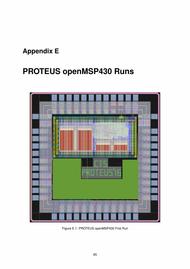
Appendix E
PROTEUS openMSP430 Runs
Figure E.1: PROTEUS openMSP430 First Run
65
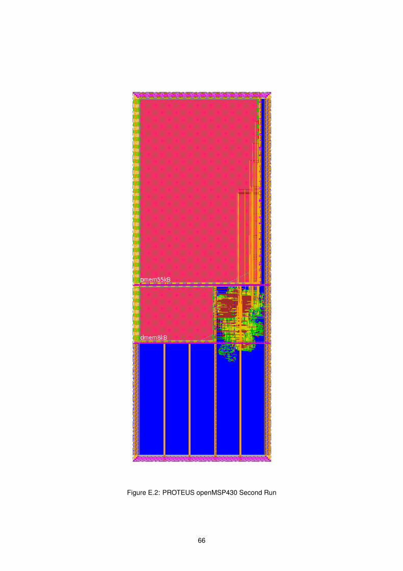
Figure E.2: PROTEUS openMSP430 Second Run
66