Operating the A/D Converter of the MSP430 Microcontroller
13
lektronik abor Laboratory Operating the A/D Converter of the MSP430 Microcontroller Marco Romminger, Martin J. W. Schubert Electronics Laboratory Ostbayerische Technische Hochschule Regensburg
Transcript of Operating the A/D Converter of the MSP430 Microcontroller

lektronikabor
Laboratory
Operating the A/D Converter of the MSP430 Microcontroller
Marco Romminger, Martin J. W. Schubert
Electronics Laboratory
Ostbayerische Technische Hochschule Regensburg

M. Romminger, M. Schubert Operating the A/D Converter of the MSP430 C Ostbayerische TH Regensburg
- 2 -
Abstract. The A/D converter within the MSP430 microcontroller of Texas Instruments is operated to read both single and multiple voltages.
1 Introduction The MSP430 is a 16-bit microcontroller offered by Texas Instruments. As it features different power down modes to reduce the current consumption to a minimum of about 2 µA it is suitable for battery-powered data acquisition. Here we use the MSPF2274 having an on-board 10-bit analog-to-digital converter (ADC) and two analog operational amplifiers. The employed MSP430F2274 can be operated with different clock sources and frequencies up to 5 MHz. The ADC module is on the same chip as the microcontroller's CPU and uses an architecture with successive approximation register (SAR). The conversion time is 13 ADC clock cycles. Considering a sample and hold time of at least 4 ADC clock cycles, the converter can be used at data rates up to 200 Kilo Samples per Second (KSPS). The MSP430 offers a data transfer controller (DTC) to store the A/D converted digital values in the microcomputer's memory without interrupting the CPU. This allows the CPU to be operated at a power saving mode during data acquisition. In addition, two interrupt sources are reserved for the MSP430's ADC, that can either indicate that the conversion is done or that the DTC has transferred all the converted data to the memory [1], [2], [3]. The organization of this document is as follows:
Section 1 is this introduction. Section 2 offers some theoretical background to understand the matter. Section 3 teaches how to start the CCS-v5 (Code Composer Studio) Software environment. Section 4 supports you to start TI’s eZ430-RF2500 kit [4] used for this lab exercises. Section 5 offers some information about the Hardware of the MSP430 ADC10. Section 6 uses this hardware to read a single voltage. Section 7 extends your knowledge to read multiple voltages, i.e. a waveform. Section 8 presents some advanced options. Section 9 draws relevant conclusion. Section 10 acknowledgments. Section 11 offers some references.
M. Romminger, M. Schubert Operating the A/D Converter of the MSP430 C Ostbayerische TH Regensburg
- 3 -
2 Theoretical Background 2.1 Correlating integers and voltages
2.1.1 Formula
A M-bit ADC delivers integer values in the range of 0…2M-1 corresponding to the reference voltages Vref- and Vref+, respectively. Using NADC as the ADC´s integer output with a maximum value of NADCmax = 2M - 1 (1) we get
refref
refADCinADCADC VV
VUNN max (2)
corresponding to the input voltage, UADCin, which can be computed from
refADC
ADCrefrefADCin V
N
NVVU
max
)( (3)
2.1.2 Exercises
Given is a M-bit A/D converter that translates voltage Vref- to 0V and Vref+ to NADCmax. Compute NADCmax as formula and for M = 10. NADCmax = 2M – 1 = 1023 Write the formula to compute the digital integer output value NADC as a function of input voltage UADCin for a given input voltage range Vref- … Vref+, where the latter corresponds to Vref+. NADC = NADCmax (UADCin – Vref-) / (Vref+ - Vref-) The ADC converts UADCin to the integer number NADC=322. Given: Vref-=0.7V, Vref+=2.7V, NADCmax=1023. Compute UADCin (formula and value). Formula: UADCin = (Vref+ - Vref-)NADC/NADCmax + Vref- Value: UADCin = 1,3295 V We want to measure the microcontroller's VCC. The ADC converts UADCin = VCC/2 to NADC = 422. Given: Vref- = 0.7V, Vref+ = 2.7V, NADCmax = 1023. Compute VCC. Formula: VCC = 2UADCin Value: VCC = 3,05 V

M. Romminger, M. Schubert Operating the A/D Converter of the MSP430 C Ostbayerische TH Regensburg
- 4 -
2.2 Correlating Light Intensity to Voltages Fig. 2.2: Light sensor model
ID
47KR
ADC
light UD
N10UD
The photo diode can be modeled as current source delivering current ID with brightness
010 I
I D
B lx (3) with an approximate value of I0 = 10A and lx standing for lux.
Consequently, we have in the circuit above RI
U
RI
RI DD
B 00 1010 . (4) We have Vref+=2.5V, Vref-=0V, NADCmax=1023. Consequently,
maxADC
refADCinD N
VNUU . (5)
Combining (4) and (5) UD delivers
00max0 101010 N
N
RIN
VN
RI
U
ADC
refD
B
with
ref
ADC
V
RINN 0max
0 = ...192............ (6)
PS: The program hal_cc2530znp_target_board.c contains the function convertAdcToLux(). To realize 10x in C, the function double pow(double x, double y) from math.h is used, which increases the compiled code size enormously.
M. Romminger, M. Schubert Operating the A/D Converter of the MSP430 C Ostbayerische TH Regensburg
- 5 -
3 Starting the CCS-v5 Software environment Start TI´s CCS-v5 (e.g. search for Code Composer). CCS proposes to define workspace: C:\Users\…..\Documents\workspace_v5_5. Use it or browse to your own workspace path. Click File → New → CCS Project. If there is no such option click New → Project → Code
Composer Studio → CCS Project. A window (New CCS Project) appears. Name your project (e.g. Lab_AD) and save it to your workspace. Choose “Executable” as “Output Type”. In the Device settings you choose “MSP430” as “Family” and “MSP430F2274” as your
“Variant”. Under menu “Project templates and examples” use a “Empty Project”, then click finish [5]. After you have created your project use Microsoft Explorer to copy the files main_single_conversion.c hal_cc2530znp_target_board.h, hal_cc2530znp_target_board.c located in the auxiliary_files_4_student\C_files folder to your project folder. Only make changes in the main_single_conversion.c file and leave the other files untouched! There are 2 possibilities:
(1) Copy the three files to the folder …\workspace\<project_name> (2) In the CCS Select View → Project Explorer. You should see your project as top-level
directory. Press the right mouse button on your project name and choose then "Add Files”

M. Romminger, M. Schubert Operating the A/D Converter of the MSP430 C Ostbayerische TH Regensburg
- 6 -
4 Starting the Board with the eZ430-RF2500 Hardware
Figure 4.1: MSP430 board for this lab, components labeled To demonstrate the MSP430´s ADC we use TI’s eZ430-RF2500 kit (2 red boards in Fig. 4.1). It consists of a programmer board with USB-connector and the RF2500 target board [4]. The latter contains a MSP430F2274 microcontroller (big black rectangle on RF2500 target board). Connect the eZ430 USB Socket of your board to your computer via USB. Observe this connection in the “Device Manager*)” of cour computer under “Ports (COM <P)”. *) To get this information at the computer system of OTH Regensburg click
Systemsteuerung → System und Sicherheit→ System → Gerätemenager → OK → Anschlüsse (COM & LPT) → look for „MSP430 Application UART (COMx)
or search for „Geräte-Manager“ under Windows → OK → Anschlüsse (COM & LPT) → look for „MSP430 Application UART (COMx)
Which COM Port does your computer create? ...COMx with x depending on the PC... You can use this boards to create a “Wireless Sensor Network (WSN)”. For now we are only interested in using the MSP's ADC and not in creating a WSN. The Board further comes with an on-board light sensor (see Figure 4.2). To read the light sensor we want to use the MSP430´s 10 Bit Analog-to-Digital converter. In Figure 4.3 you see the MSP430´s device pinout configuration. The ADC-Inputs are named A0…15. Some ADC channels are only device intern. Which ADC channel is connected to the Light Sensor? A0 (channel 0) .........................

M. Romminger, M. Schubert Operating the A/D Converter of the MSP430 C Ostbayerische TH Regensburg
- 7 -
Figure 4.2: Light Sensor Pinout
Figure 4.3: MSP430 device pinout
M. Romminger, M. Schubert Operating the A/D Converter of the MSP430 C Ostbayerische TH Regensburg
- 8 -
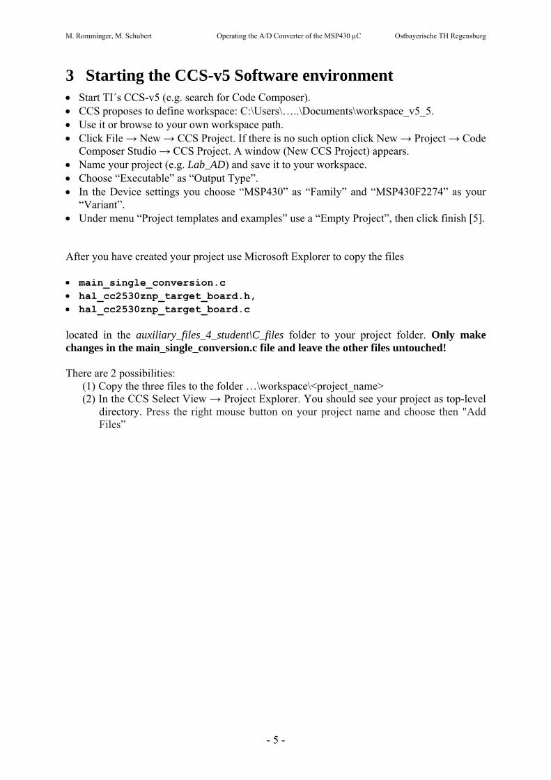
5 Understanding the MSP430 ADC10 Hardware It is important to understand the schematics of the A/D converter considered. It is shown in Fig. 5, a copy from TI documentation [3], p. 535.
Figure 5: A/D converter schematics copied from TI’s MSP430x2xx ADC10 User Guide [3]
M. Romminger, M. Schubert Operating the A/D Converter of the MSP430 C Ostbayerische TH Regensburg
- 9 -
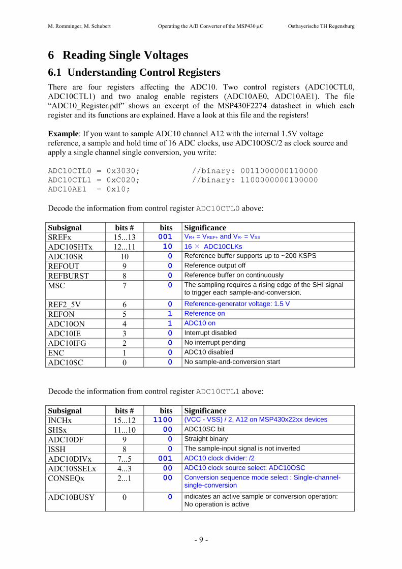
6 Reading Single Voltages 6.1 Understanding Control Registers There are four registers affecting the ADC10. Two control registers (ADC10CTL0, ADC10CTL1) and two analog enable registers (ADC10AE0, ADC10AE1). The file “ADC10_Register.pdf” shows an excerpt of the MSP430F2274 datasheet in which each register and its functions are explained. Have a look at this file and the registers! Example: If you want to sample ADC10 channel A12 with the internal 1.5V voltage reference, a sample and hold time of 16 ADC clocks, use ADC10OSC/2 as clock source and apply a single channel single conversion, you write: ADC10CTL0 = 0x3030; //binary: 0011000000110000 ADC10CTL1 = 0xC020; //binary: 1100000000100000 ADC10AE1 = 0x10; Decode the information from control register ADC10CTL0 above: Subsignal bits # bits Significance SREFx 15...13 001 VR+ = VREF+ and VR- = VSS
ADC10SHTx 12...11 10 16 × ADC10CLKs
ADC10SR 10 0 Reference buffer supports up to ~200 KSPS
REFOUT 9 0 Reference output off
REFBURST 8 0 Reference buffer on continuously
MSC
7 0 The sampling requires a rising edge of the SHI signal to trigger each sample-and-conversion.
REF2_5V 6 0 Reference-generator voltage: 1.5 V
REFON 5 1 Reference on
ADC10ON 4 1 ADC10 on
ADC10IE 3 0 Interrupt disabled
ADC10IFG 2 0 No interrupt pending
ENC 1 0 ADC10 disabled
ADC10SC 0 0 No sample-and-conversion start
Decode the information from control register ADC10CTL1 above: Subsignal bits # bits Significance INCHx 15...12 1100 (VCC - VSS) / 2, A12 on MSP430x22xx devices
SHSx 11...10 00 ADC10SC bit
ADC10DF 9 0 Straight binary
ISSH 8 0 The sample-input signal is not inverted
ADC10DIVx 7...5 001 ADC10 clock divider: /2
ADC10SSELx 4...3 00 ADC10 clock source select: ADC10OSC
CONSEQx
2...1 00 Conversion sequence mode select : Single-channel-single-conversion
ADC10BUSY
0 0 indicates an active sample or conversion operation: No operation is active
M. Romminger, M. Schubert Operating the A/D Converter of the MSP430 C Ostbayerische TH Regensburg
- 10 -
Decode the information from control register ADC10AE1 above: Subsignal bits # bits Significance ADC10AE1x 7...4 0001 Analog input (A12) enabled
Reserved 3...0 0000 Reserved
You don’t have to start and enable the conversion during the configuration, as the voltage reference and also the clock source need some time to stabilize, therefore ADC10SC and ENC are left “0”. Normally you would not use hexadecimal numbers, as they are difficult to read. Instead you use predefined bitmasks. Using bitmasks, you could write for the example above: ADC10CTL0 = REFON + SREF_1 + ADC10SHT_2 + ADC10ON; ADC10CTL1 = ADC10DIV_1 + INCH_12; ADC10AE1 = 0x10; The bitmasks are defined in the MSP430 header. The file “msp430_ADC_bitmasks.h” is an excerpt of the header and shows all bitmasks usable for the 10 Bit ADC. Have a look at it!
6.2 Set Control Registers to Read the Light Sensor Fill in the bits in the registers below. Use the “ADC10_Register.pdf” file and start with the ADC10CTL1 register.
ADC10CTL1: - Adjust the appropriate channel to read data from the light sensor (see chapter 4). - Use the internal Oscillator ADC10OSC as ADC clock source: - The clock divider (prescaler) should be “2” - The conversion sequence should be “Single-channel-single-conversion” - Set the other parameters of the register to zero
ADC10CTL1 according to [3], p. 555:
0 0 0 0 0 0 0 0 0 0 1 0 0 0 0 0 15 14 13 12 11 10 9 8 7 6 5 4 3 2 1 0
Between which frequency range does the internal Oscillator vary and on what parameter does it depend? (Look for fADC10OSC in the MSP430F2274 datasheet) : Frequency range: 3.7 – 6.3 MHz depending on VCC ..............................................................
M. Romminger, M. Schubert Operating the A/D Converter of the MSP430 C Ostbayerische TH Regensburg
- 11 -
ADC10CTL0: - Use the internal 2.5V voltage reference - Turn reference generator on - Define VR+ = VREF+ and VR- = VSS - Turn on the ADC - Don’t use the ADC interrupt - Don’t enable the ADC10 conversion - Don’t start the ADC10 conversion, as the voltage reference needs some time to settle - Set the other parameters of the register to zero - The sample and hold time for a correct measurement should be at least 2µs. This value
derives from the light sensor and ADC impedance. What is the minimum sample and hold time you can use, when the ADC clock is approx 5 MHz and the prescaler is 2. Compute the exact value and then set the Bits 12-11 for a sufficient S&H time.
tSH,min(ADC10 clocks) = 2μs/(1/(5MHz/2) = 5 → 8 x ADC10CLKs.
ADC10CTL0 according to [3], p. 553:
0 0 1 0 1 0 0 0 0 1 1 1 0 0 0 0 15 14 13 12 11 10 9 8 7 6 5 4 3 2 1 0
Complete lines 43, 44, 45 in the “main_single_conversion.c” file! Complete line 36 for the right ADC10 clock division. Use hexadecimal notation. (43) ADC10CTL1 = 0x20;
............................................. Complete line 37, use hexadecimal notation! (44) ADC10CTL0 = 0x2870; ............................................. The General Purpose IOs of the MSP430 are CMOS gates. To reduce the parasitic current flow you have to enable the analog input (A0) of the input channel selected above. (45) ADC10AE0 = 0x01; ............................................. After you have finished to set up the ADC Registers, be sure that the device is connected to your computer via USB. Program the device after following instructions:
- Press on the green bug on the top toolbar of the CCS (debug perspective) - A window (ULP Advisor) appears. Just click the button “Proceed”. - Wait a few seconds while CCS compiles, links and downloads the program - Press on the red Stop button on the top toolbar of CCS (C/C++ perspective) - Press the RESET button on the WSN Board and the program is running.
You should now see that LED1 is slowly blinking and the other LED’s are ON. To view measured results, use the Terminal Program Hterm.exe, supplied to you in the folder auxiliary_files_4_student/read_serial_interface_files: Start HTerm.exe. Enter in the top-menu bar the port # (COM#) you found in chapter 4 and press connect (defaults: Baud(9600), Data(8), Stop(1), Parity(none)). The program is now connected to the MSP430 via a serial port and you can observe the measured results.
After you are done, press disconnect and close HTerm!

M. Romminger, M. Schubert Operating the A/D Converter of the MSP430 C Ostbayerische TH Regensburg
- 12 -
7 Reading Multiple Voltages (Waveforms) For this exercise you must change the C file in the actual project Exchange the main C file in the actual project: Replace the main_single_conversion.c by the main_multiple_conversion.c file, both supplied to you in folder auxiliary_files_4_student/C_files. Therefore right click on the First of all copy it into your working library. Then within CCS click right on main_single_conversion.c and press delete. Afterwards right click on the project and choose add files. There you take the main_multiple_conversion.c file. After that the replacement is done. Compile and download the program to the MSP430 by pressing the debug button. Press the RESET button to get the program running. Now multiple values of a single channel are read. Which parameter (bitmask) is set in the program, that applies a single channel multiple conversion? CONSEQ_2 ......................................... Connect the waveform generator to the oscilloscope and check the voltage from the waveform generator (see below). After that connect the waveform generator and the BNC jack named SIGNAL IN LINE in figure 4.1
Only apply voltages between 0-3 V!!! Set: VP = 0…3V, Frequency = 1…50 kHz ! Getting the data from the Microcontroller on your Computer: To visualize the waveforms, use the MATLAB script Read_Serial.m supplied to you in the auxiliary_files_4_student/read_serial_interface_files folder. Please note that HTerm is disconnect and close. Start MATLAB and follow the instructions given in the MATLAB main window (Enter number # of the port (COM#), to which your device is connected.) You should see a figure consisting of 512 data points. Apply different signals with the waveform generator and start over the Matlab program.
If MATLAB does not work: Close all programs on your computer including Matlab. Disconnect your board from the computer and then connect the board against with your computer. After this push the “Reset Button” on your board. Open the Read_Serial.m Matlab script, but do not press start. Type in the MATLAB main window (not the script window): delete(instrfindall) %This will erase all existing COM Ports After that start the script by pressing run.

M. Romminger, M. Schubert Operating the A/D Converter of the MSP430 C Ostbayerische TH Regensburg
- 13 -
8 Advanced Options Reducing the current consumption of the MSP430´s ADC:
The MSP430 has several build in power saving mechanisms, such as: - Turning off the voltage reference automatically, when not needed - Turning off the ADC core automatically, when not needed
Furthermore the user has some options to reduce the power consumption, such as:
- Limiting the sampling rate to 50ksps (reduces the current consumption of the reference buffer about 50 %)
- Using the ADC interrupt to turn down the MSP430´s CPU and send it to sleep mode during the conversion time.
Which bitmask is set in the program to limit the sampling rate? ADC10SR Which bitmask is set in the program to enable the interrupt? ADC10IE What is the name of the ADC10 interrupt function? void ADC10_ISR(void)
9 Conclusions This laboratory details how to read out the 10 bit A/D converter which is on board of TI’s MSP430F2274 microcontroller. This requires some fundamental knowledge of the hardware as well as installation and usage of the appropriate software. Register setting is demonstrated for both single-voltage and waveform measurements.
10 Acknowldegements This Laboratory is based on the idea of Stefan Vogl, who prepared its first draft. Some years later it was improved by Marco Romminger. At the end, some editorial improvements were made by Martin Schubert.
11 References [1] Available April 19, 2015: http://en.wikipedia.org/wiki/TI_MSP430 , [2] Available April 19, 2015: http://de.wikipedia.org/wiki/TI_MSP430 [3] MSP430x2xx Family User’s Guide, available Apr. 2015: http://www.ti.com/lit/ug/slau144j/slau144j.pdf [4] MSP430 Wireless Development Tool, available at April 19, 2015: http://www.ti.com/tool/ez430-rf2500 [5] Available at April 19, 2015: http://processors.wiki.ti.com/index.php/CCSv5_Getting_Started_Guide