
An ac-dc PFC single-stage Dual Inductor Current-Fed Push ... · by means of its control, is the...
12
An ac-dc PFC single-stage Dual Inductor Current-Fed Push- Pull for HB-LED lighting applications Ignacio Castro, Student Member, IEEE, Kevin Martin, Student Member, IEEE, Aitor Vazquez, Member, IEEE, Manuel Arias, Member, IEEE, Diego G. Lamar, Member, IEEE, and Javier Sebastian, Senior Member, IEEE. Departamento de Ingeniería Eléctrica, Electrónica, de Computadores y Sistemas, Gijón 33204, Spain (e-mail: [email protected]) Abstract— An ac-dc single-stage driver for High Brightness Light-Emitting Diodes with galvanic isolation is presented in this paper. The driver is based on a Dual Inductor Current-Fed Push-Pull converter with each inductor operating in Boundary Conduction Mode. The interleaving between the two inductors enables the converter to reduce the high input current ripple inherent to a BCM. Moreover, it is fully compliant with IEC 1000-3-2 Class C and it is able to achieve a high Power Factor. Its low component count, simplicity and overall outstanding characteristics make this current-fed topology suitable for medium power range HB-LED drivers in low cost applications. The proposed topology has been tested on a 100W prototype for the full range of the US single-phase line voltage, feeding several HB-LED strings, with an output voltage equivalent to 48V at full load. The prototype achieves a maximum efficiency of 92% with a 0.99 power factor, 8% THD at full load while guaranteeing good quality light. Keywords— Single phase, ac-dc power conversion, Power Factor Correction, HB-LED driver I. INTRODUCTION High-Brightness Light-Emitting Diodes (HB-LEDs) are increasingly becoming the main source of artificial light in homes, offices and streets due to their reliability, long life, energy efficiency and low maintenance requirements. However, the driving of HB-LEDs with primary access to single-phase AC requires the use of a converter that is able to achieve high efficiency, a long lifespan comparable to that of the HB-LEDs and Power Factor Correction (PFC) in order to comply with the regulation for both residential and commercial lighting. A high Power Factor (PF) is required to maximize the power transferred from the grid. This is the reason why, Energy Star® [1] requires an 0.7 PF for residential lighting and an 0.9 PF for commercial lighting. Furthermore, the low-frequency harmonic content of the line current must comply with IEC 1000-3-2 Class C [2]-[4], which establishes a very strict harmonic content for the line current in lighting equipment of more than 25 W. Therefore, the line current needs to have a sinusoidal shape following that of the input voltage. Traditionally, HB-LED drivers are based on a high- performance ac-dc PFC converter, followed by a dc-dc converter, which in most situations has galvanic isolation and provides a constant current to the HB-LEDs in order to comply with the aforementioned regulations. In most scenarios, however, the cost of the HB-LED driver is the main concern and a single-stage needs to be used to reduce the amount of components and complexity of the HB-LED driver. This is particularly important in low to medium power range HB-LED drivers, where galvanic isolation is recommended for safety requirements. Accordingly, isolated buck-boost topologies like the flyback working in Discontinuous Conduction Mode (DCM), which achieves unity PF naturally, are widely used in this application [5]-[10]. Although these topologies have a low component count, they suffer from low efficiencies (<90%) and the inability to remove the bulk capacitor required in PFC. However, the removal of the bulk capacitor is not always possible in a single-stage without including more active components [10]-[14] or distorting the input current [15] [16]. This occurs due to the pulsating input power of the grid, which must be decoupled from the HB-LEDs in order to avoid the well-known flicker phenomenon. Another topology that is able to achieve unity PF naturally, by means of its control, is the boost converter. The boost converter is normally used as a front-end, ac-dc, PFC, converter operating either in Boundary Conduction Mode (BCM) or employing a Multiplier-Based Control (MBC) [17] [18] with a cascaded step-down converter. Hence, the isolated variations of the boost converter family are suitable to be used as a single- stage PFC, (i.e. current-fed based isolated converters). However, current-fed based isolated converters are rarely used in PFC due to the drawbacks they present. For instance, they have a complex transformer design, which may hinder the efficiency of the single stage, and require a demagnetizing path for the main inductance, as reported in previous literature [19]. Nevertheless, previous literature does include some papers on single-stage, ac-dc, PFC, current-fed based, isolated, converters, such as the push-pull [20] or the full-bridge [21] This work was supported in part by the Spanish Government under Project MINECO-13-DPI2013-47176-C2-2-R, in part by the Principality of Asturias under Severo Ochoa Grant BP14-140 and BP14-085, and Project FC-15- GRUPIN14-143, and in part by the European Regional Development Fund grants. is attributed.
Transcript of An ac-dc PFC single-stage Dual Inductor Current-Fed Push ... · by means of its control, is the...
An ac-dc PFC single-stage Dual Inductor Current-Fed Push-Pull for HB-LED lighting applications
Ignacio Castro, Student Member, IEEE, Kevin Martin, Student Member, IEEE, Aitor Vazquez, Member, IEEE, Manuel Arias, Member, IEEE, Diego G. Lamar, Member, IEEE, and Javier Sebastian, Senior Member, IEEE.
Departamento de Ingeniería Eléctrica, Electrónica, de Computadores y Sistemas, Gijón 33204, Spain (e-mail: [email protected])
Abstract— An ac-dc single-stage driver for High Brightness Light-Emitting Diodes with galvanic isolation is presented in this paper. The driver is based on a Dual Inductor Current-Fed Push-Pull converter with each inductor operating in Boundary Conduction Mode. The interleaving between the two inductors enables the converter to reduce the high input current ripple inherent to a BCM. Moreover, it is fully compliant with IEC 1000-3-2 Class C and it is able to achieve a high Power Factor. Its low component count, simplicity and overall outstanding characteristics make this current-fed topology suitable for medium power range HB-LED drivers in low cost applications. The proposed topology has been tested on a 100W prototype for the full range of the US single-phase line voltage, feeding several HB-LED strings, with an output voltage equivalent to 48V at full load. The prototype achieves a maximum efficiency of 92% with a 0.99 power factor, 8% THD at full load while guaranteeing good quality light.
Keywords— Single phase, ac-dc power conversion, Power Factor Correction, HB-LED driver
I. INTRODUCTION High-Brightness Light-Emitting Diodes (HB-LEDs) are
increasingly becoming the main source of artificial light in homes, offices and streets due to their reliability, long life, energy efficiency and low maintenance requirements. However, the driving of HB-LEDs with primary access to single-phase AC requires the use of a converter that is able to achieve high efficiency, a long lifespan comparable to that of the HB-LEDs and Power Factor Correction (PFC) in order to comply with the regulation for both residential and commercial lighting. A high Power Factor (PF) is required to maximize the power transferred from the grid. This is the reason why, Energy Star® [1] requires an 0.7 PF for residential lighting and an 0.9 PF for commercial lighting. Furthermore, the low-frequency harmonic content of the line current must comply with IEC 1000-3-2 Class C [2]-[4], which establishes a very strict harmonic content for the line current in lighting equipment of
more than 25 W. Therefore, the line current needs to have a sinusoidal shape following that of the input voltage.
Traditionally, HB-LED drivers are based on a high-performance ac-dc PFC converter, followed by a dc-dc converter, which in most situations has galvanic isolation and provides a constant current to the HB-LEDs in order to comply with the aforementioned regulations. In most scenarios, however, the cost of the HB-LED driver is the main concern and a single-stage needs to be used to reduce the amount of components and complexity of the HB-LED driver. This is particularly important in low to medium power range HB-LED drivers, where galvanic isolation is recommended for safety requirements. Accordingly, isolated buck-boost topologies like the flyback working in Discontinuous Conduction Mode (DCM), which achieves unity PF naturally, are widely used in this application [5]-[10]. Although these topologies have a low component count, they suffer from low efficiencies (<90%) and the inability to remove the bulk capacitor required in PFC. However, the removal of the bulk capacitor is not always possible in a single-stage without including more active components [10]-[14] or distorting the input current [15] [16]. This occurs due to the pulsating input power of the grid, which must be decoupled from the HB-LEDs in order to avoid the well-known flicker phenomenon.
Another topology that is able to achieve unity PF naturally, by means of its control, is the boost converter. The boost converter is normally used as a front-end, ac-dc, PFC, converter operating either in Boundary Conduction Mode (BCM) or employing a Multiplier-Based Control (MBC) [17] [18] with a cascaded step-down converter. Hence, the isolated variations of the boost converter family are suitable to be used as a single-stage PFC, (i.e. current-fed based isolated converters). However, current-fed based isolated converters are rarely used in PFC due to the drawbacks they present. For instance, they have a complex transformer design, which may hinder the efficiency of the single stage, and require a demagnetizing path for the main inductance, as reported in previous literature [19]. Nevertheless, previous literature does include some papers on single-stage, ac-dc, PFC, current-fed based, isolated, converters, such as the push-pull [20] or the full-bridge [21]
This work was supported in part by the Spanish Government under Project MINECO-13-DPI2013-47176-C2-2-R, in part by the Principality of Asturias under Severo Ochoa Grant BP14-140 and BP14-085, and Project FC-15-GRUPIN14-143, and in part by the European Regional Development Fund grants. is attributed.
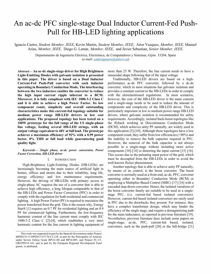
both working in CCM with a MBC. Among the current-fed push-pull topologies, the Dual Inductor Current-fed Push-Pull (DICPP), see Fig. 1, proposed in [22], [23] as a dc-dc converter can deal with the efficiency issues intrinsic to current-fed topologies due to complex transformer design, thanks to its simpler transformer (i.e. two windings one for the primary side and the other for the secondary side), while employing two MOSFET referenced to the same ground. In fact, the DICPP uses the same amount of switches as the classic Current-Fed Push-Pull (CPP) [23] whole only adding one more magnetic component. Furthermore, the switches used in the DICPP (S1, S2) withstand half the voltage when compared to those in the CPP, therefore the switches can be downsized in terms of voltage and the transformer requires less isolation, so its complexity is decreased even further. These facts are particularly important to reduce the parasitic components that may cause the topology to behave inappropriately due to resonances that will impact both the output current or the losses in the passive snubbers, which will decrease the efficiency of the single-stage.
The proposal of this work is to revise the DICPP topology, which has been widely used in dc-dc, high power, low input voltage, high input current, step-up applications (i.e. fuel cells, battery storage and photovoltaic applications) [24]-[26] and has never been proposed as an ac-dc PFC [27]. Hence, the aim is to study its feasibility as an ac-dc, single-stage, converter with PF close to unity to be used in HB-LED lighting applications. The working principle of the DICPP Adapted for PFC (DICPP-APFC) carried out in Section II, shows that each switch controls the magnetization of the inductor in its branch. This feature makes suitable the operation of each inductor in BCM while demanding a sinusoidal current at each branch. In fact, this behaviour leads to a reduced ripple at the input current due to the sum of the input currents of each branch, which are phase shifted 180º in terms of switching frequency. Furthermore, Section III shows the proposed control based on only sensing the information of the output current before being filtered by the bulk capacitor (io(t)) in order to maintain the simplicity of the solution. Finally, Section IV will show the experimental results, making the DICPP-APFC a plausible solution for single-stage PFC in HB-LED drivers since the DICPP- APFC is able to achieve higher efficiency and lower input current ripple than traditional AC-DC single-stage converters.
II. WORKING PRINCIPLE
A. Static Analysis The concept of the HB-LED driver presented in this paper
(i.e., the DICPP) is based on [22], where it was proposed as a dc-dc converter working in CCM. Moreover, current-fed push-pull topologies are normally used with low input voltages (i.e. 0-50V) and high currents in power conversion for fuel cells [24], battery storage [25], photovoltaic [26] and electric vehicle applications [28], due to their transformer limitations and voltage stress on the main switches. The present paper proposes to increase the scope of the topology to work as an ac-dc PFC by operating in BCM in the range of hundreds of watts to increase the efficiency by applying well-known control methods used in interleaved PFC boost rectifiers. Hence, increasing the input voltage range of the topology.
In order to achieve good quality rectification at the input current, a Loss Free Resistor (LFR) [30] behavior is required. It is well known that a boost converter operating in BCM (i.e. constant on-time and variable frequency) can achieve an LFR behavior naturally. Therefore, the DICPP should also be able to work as a PFC by operating in BCM since it is a converter from the boost family. In order to verify its operation as an ac-dc PFC, the converter behaviour is going to be analyzed in terms of switching and line frequency.
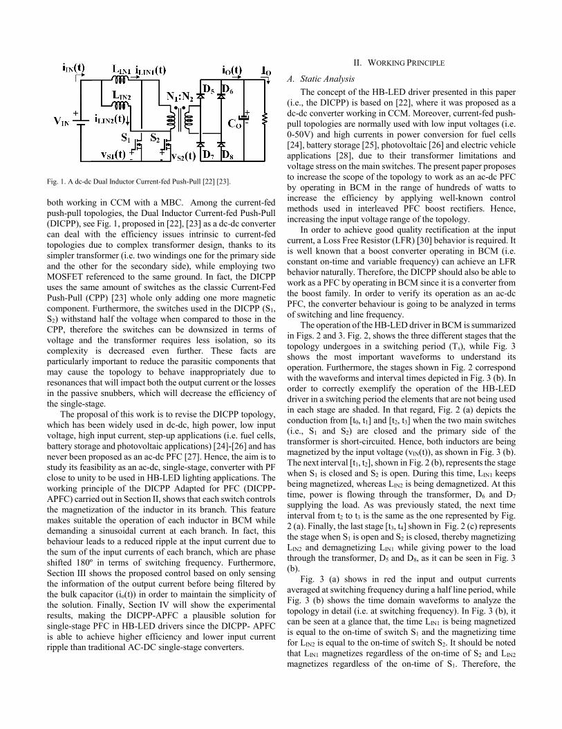
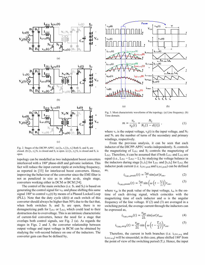
The operation of the HB-LED driver in BCM is summarized in Figs. 2 and 3. Fig. 2, shows the three different stages that the topology undergoes in a switching period (Ts), while Fig. 3 shows the most important waveforms to understand its operation. Furthermore, the stages shown in Fig. 2 correspond with the waveforms and interval times depicted in Fig. 3 (b). In order to correctly exemplify the operation of the HB-LED driver in a switching period the elements that are not being used in each stage are shaded. In that regard, Fig. 2 (a) depicts the conduction from [t0, t1] and [t2, t3] when the two main switches (i.e., S1 and S2) are closed and the primary side of the transformer is short-circuited. Hence, both inductors are being magnetized by the input voltage (vIN(t)), as shown in Fig. 3 (b). The next interval [t1, t2], shown in Fig. 2 (b), represents the stage when S1 is closed and S2 is open. During this time, LIN1 keeps being magnetized, whereas LIN2 is being demagnetized. At this time, power is flowing through the transformer, D6 and D7 supplying the load. As was previously stated, the next time interval from t2 to t3 is the same as the one represented by Fig. 2 (a). Finally, the last stage [t3, t4] shown in Fig. 2 (c) represents the stage when S1 is open and S2 is closed, thereby magnetizing LIN2 and demagnetizing LIN1 while giving power to the load through the transformer, D5 and D8, as it can be seen in Fig. 3 (b).
Fig. 3 (a) shows in red the input and output currents averaged at switching frequency during a half line period, while Fig. 3 (b) shows the time domain waveforms to analyze the topology in detail (i.e. at switching frequency). In Fig. 3 (b), it can be seen at a glance that, the time LIN1 is being magnetized is equal to the on-time of switch S1 and the magnetizing time for LIN2 is equal to the on-time of switch S2. It should be noted that LIN1 magnetizes regardless of the on-time of S2 and LIN2 magnetizes regardless of the on-time of S1. Therefore, the
Fig. 1. A dc-dc Dual Inductor Current-fed Push-Pull [22] [23].
topology can be modelled as two independent boost converters interleaved with a 180º phase-shift and galvanic isolation. This fact will reduce the input current ripple at switching frequency, as reported in [33] for interleaved boost converters. Hence, improving the behaviour of the converter since the EMI filter is not as penalized in size as in other ac-dc, single stage, converters working either in DCM or BCM [34].
The control of the main switches (i.e. S1 and S2) is based on generating the control signal for vS1 and phase shifting this same signal 180º to control vS2(t) by means of a Phased Locked Loop (PLL). Note that the duty cycle (d(t)) at each switch of this converter should always be higher than 50% due to the fact that, when both switches S1 and S2 are open, there is no demagnetizing path for LIN1 or LIN2, which could lead to their destruction due to overvoltage. This is an intrinsic characteristic of current-fed converters, hence the need for a stage that overlaps both control signals, see Fig. 2 (a). As regards the stages in Figs. 2 and 3, the converter relationship between output voltage and input voltage in BCM can be obtained by studying the volt-second balance on one of the inductors. The converter gain can thus be defined by,
𝑚𝑚 =𝑣𝑣𝑜𝑜
𝑣𝑣𝑔𝑔(𝑡𝑡)=
𝑁𝑁2𝑁𝑁1(1 − 𝑑𝑑(𝑡𝑡)) , (1)
where vo is the output voltage, vg(t) is the input voltage, and N2 and N1 are the number of turns of the secondary and primary windings, respectively.
From the previous analysis, it can be seen that each inductor of the DICPP-APFC works independently. S1 controls the magnetizing of LIN1 and S2 controls the magnetizing of LIN2. Therefore, it can be assumed that if both LIN1 and LIN2 are equal (i.e., LIN1 = LIN2 = L), by studying the voltage balance in the inductors during stage [t1,t2] for LIN1 and [t3,t4] for LIN2, the inductor peak current (i.e. iLIN1,peak and iLIN2,peak) can be defined as,
𝑖𝑖𝐿𝐿𝐼𝐼𝐼𝐼1,𝑝𝑝𝑝𝑝𝑝𝑝𝑝𝑝(𝑡𝑡) = 𝑣𝑣𝑔𝑔𝑔𝑔𝐿𝐿
sin (𝜔𝜔𝑡𝑡)𝑡𝑡𝑜𝑜𝑜𝑜, (2)
𝑖𝑖𝐿𝐿𝐼𝐼𝐼𝐼2,𝑝𝑝𝑝𝑝𝑝𝑝𝑝𝑝(𝑡𝑡) = 𝑣𝑣𝑔𝑔𝑔𝑔𝐿𝐿
sin �𝜔𝜔 �𝑡𝑡 − 𝑇𝑇𝑠𝑠2�� 𝑡𝑡𝑜𝑜𝑜𝑜, (3)
where vgp is the peak value of the input voltage, ton is the on-time of each driving signal, which coincides with the magnetizing time of each inductor and ω is the angular frequency of the line voltage. If (2) and (3) are averaged in a switching period, the average current through the inductors can be expressed as,
𝑖𝑖𝐿𝐿𝐼𝐼𝐼𝐼1,𝑝𝑝𝑣𝑣𝑔𝑔(𝑡𝑡) =𝑣𝑣𝑔𝑔𝑝𝑝2𝐿𝐿
sin (𝜔𝜔𝑡𝑡)𝑡𝑡𝑜𝑜𝑜𝑜, (4)
𝑖𝑖𝐿𝐿𝐼𝐼𝐼𝐼2,𝑝𝑝𝑣𝑣𝑔𝑔(𝑡𝑡) =
𝑣𝑣𝑔𝑔𝑝𝑝2𝐿𝐿
sin�𝜔𝜔 �𝑡𝑡 −𝑇𝑇𝑠𝑠2�� 𝑡𝑡𝑜𝑜𝑜𝑜 .
(5)
Therefore, the current in both branches (i.e. iLIN1,avg and iLIN2,avg) will be sinusoidal; in this case, phase shifted 180º from the point of view of the switching period (Ts). Hence, the input
(a) (b)
Fig. 3. Most characteristic waveforms of the topology. (a) Line frequency. (b) Time domain.
(a)
(b)
(c)
Fig. 2. Stages of the DICPP-APFC. (a) [t0, t1] [t2, t3] Both S1 and S2 are closed. (b) [t1, t2] S1 is closed and S2 is open. (c) [t1, t2] S2 is closed and S1 is open.
current demanded by the HB-LED driver will be sinusoidal, as it is the sum of the two sinusoidal waveforms, given that the delay between them (i.e., TS/2) is negligible from the point of view of the line period, as can be seen in Fig. 3 (a). Therefore, the average input current at switching frequency (iIN,avg) can be expressed as
𝑖𝑖𝐼𝐼𝐼𝐼,𝑝𝑝𝑣𝑣𝑔𝑔(𝑡𝑡) = 𝑖𝑖𝐿𝐿𝐼𝐼𝐼𝐼1,𝑎𝑎𝑎𝑎𝑔𝑔(𝑡𝑡) + 𝑖𝑖𝐿𝐿𝐼𝐼𝐼𝐼2,𝑎𝑎𝑎𝑎𝑔𝑔(𝑡𝑡) =
=𝑣𝑣𝑔𝑔𝑝𝑝2𝐿𝐿
𝑡𝑡𝑜𝑜𝑜𝑜𝑠𝑠𝑖𝑖𝑠𝑠(𝜔𝜔𝑡𝑡) +𝑣𝑣𝑔𝑔𝑝𝑝2𝐿𝐿
𝑡𝑡𝑜𝑜𝑜𝑜𝑠𝑠𝑖𝑖𝑠𝑠 �𝜔𝜔 �𝑡𝑡 −𝑇𝑇𝑠𝑠2�� ≅
≅ 𝑣𝑣𝑔𝑔𝑝𝑝𝐿𝐿𝑡𝑡𝑜𝑜𝑜𝑜𝑠𝑠𝑖𝑖𝑠𝑠(𝜔𝜔𝑡𝑡) .
(6)
For a correct operation in BCM, ton needs to be kept constant at a certain value guaranteeing that the converter will demand a certain amount of power and that the off-time of the driving signal (toff) will vary depending on the demagnetizing time of each of the inductors until reaching the zero current value. The zero current value must be detected by a Zero Current Detection (ZCD) circuit based on a comparator.
Given that the average input current will be a sine wave, as stated in (6), by multiplying it by the input voltage, the instantaneous input power can thus be defined by,
𝑝𝑝𝑔𝑔(𝑡𝑡) = 𝑣𝑣𝑔𝑔𝑝𝑝2
𝐿𝐿𝑡𝑡𝑜𝑜𝑜𝑜𝑠𝑠𝑖𝑖𝑠𝑠2(𝜔𝜔𝑡𝑡) . (7)
By averaging (7) at line frequency, the following relationship between ton and several well-known design parameters can be formulated as,
𝑡𝑡𝑜𝑜𝑜𝑜 = 2𝑃𝑃𝐺𝐺𝐿𝐿𝑣𝑣𝑔𝑔𝑝𝑝2
, (8)
where PG is the averaged input power processed by the HB-LED driver in a line period. From (8), the LFR behaviour and value can be obtained by considering the input power as a relation between vgp and a resistor that models the input impedance of the converter (RLFR),
𝑅𝑅𝐿𝐿𝐿𝐿𝐿𝐿 = 𝐿𝐿𝑡𝑡𝑜𝑜𝑜𝑜
, (9)
Eq. (9) shows that by applying the correct control method to operate in BCM the converter is going to behave as resistor. Therefore, the input current will follow the input voltage which will result in achieving almost unity PF. Moreover, by applying voltage balance to one of the inductors, (10) can be obtained as,
𝑣𝑣𝑔𝑔𝑝𝑝𝐿𝐿𝑡𝑡𝑜𝑜𝑜𝑜 =
𝑁𝑁1𝑁𝑁2
𝑣𝑣𝑜𝑜 − 𝑣𝑣𝑔𝑔(𝑡𝑡)
𝐿𝐿𝑡𝑡𝑜𝑜𝑜𝑜𝑜𝑜(𝑡𝑡), (10)
where toff is the off-time of the control signal of the switches. From this equation, the variation in the switching period
over time and the switching frequency can be obtained as, 𝑇𝑇𝑠𝑠(𝑡𝑡) = 𝑡𝑡𝑜𝑜𝑜𝑜 + 𝑡𝑡𝑜𝑜𝑜𝑜𝑜𝑜(𝑡𝑡) =
=
𝑁𝑁1𝑁𝑁2
𝑣𝑣𝑂𝑂𝑁𝑁1𝑁𝑁2
𝑣𝑣𝑂𝑂 − 𝑣𝑣𝑔𝑔𝑝𝑝|𝑠𝑠𝑖𝑖𝑠𝑠(𝜔𝜔𝑡𝑡)|𝑡𝑡𝑜𝑜𝑜𝑜 ,
(11)
From (11), the maximum and minimum frequency values can be obtained. These frequency values are of importance for the correct design of the topology: selection of the main switches, magnetics and ton. Hence, yielding,
𝑓𝑓𝑠𝑠(𝑡𝑡) =
𝑁𝑁1𝑁𝑁2
𝑣𝑣𝑂𝑂 − 𝑣𝑣𝑔𝑔𝑝𝑝|𝑠𝑠𝑖𝑖𝑠𝑠(𝜔𝜔𝑡𝑡)|
𝑁𝑁1𝑁𝑁2
𝑣𝑣𝑂𝑂
1𝑡𝑡𝑜𝑜𝑜𝑜
. (12)
B. Design criteria of the HB-LED driver In order to correctly design for the HB-LED driver, some
steps need to be followed, and are summarized below. First of all, the transformer relationship needs to be
obtained from (1), considering vgp as the maximum value of the input voltage (i.e., Vgpmax), vo as the output voltage at the full dimming point, and dmin as the minimum duty cycle acceptable, which should be around 55% to avoid periods where the control signals do not overlap.
After obtaining the transformer relationship, the duty cycle needs to be calculated under nominal conditions. The duty cycle and the desired switching frequency can then be used to obtain the required inductance from (8). If the calculated inductance has an acceptable value, (12) should be used to check whether the frequency range is as well. If not, then the inductance value needs to be adjusted to suit design specifications. Guaranteeing that the lowest frequency value is higher than 20 kHz constitutes a good practice to avoid any audible noise in the converter. Having calculated all the above parameters, the next step will be to select the main switches. It is hence necessary to know the maximum current and voltage that they will have to withstand. From (1) and (7),
𝑉𝑉𝑆𝑆𝑆𝑆𝑝𝑝𝑆𝑆 =
𝑉𝑉𝑔𝑔𝑝𝑝𝑆𝑆𝑝𝑝𝑆𝑆1 − 𝑑𝑑𝑆𝑆𝑚𝑚𝑜𝑜
, (13)
𝐼𝐼𝑆𝑆𝑆𝑆𝑝𝑝𝑆𝑆 =
𝑃𝑃𝑔𝑔𝑉𝑉𝑔𝑔𝑝𝑝𝑆𝑆𝑚𝑚𝑜𝑜
, (14)
where Vgpmin is the voltage peak of the minimum voltage in the range. As can be seen, the maximum voltage withstood by the switches relies entirely on the maximum input voltage and the minimum duty cycle. Considering that the minimum duty cycle is not allowed to go lower than 55%, the maximum voltage withstood by the switches will increase linearly with the input voltage. Therefore, the European/Universal input voltage range would require the use of switches with a higher breakdown voltage (i.e. 900/1200 V), which would mean the use of Silicon Carbide (SiC). In the present work, a prototype will be constructed for US range in order to validate the idea. Although it is not shown in Fig. 2, the HB-LED driver also includes a clamping snubber to protect both switches from overvoltage. A passive snubber is added to the circuit to protect the switches from voltage spikes that can occur due to the leakage inductance of the transformer. An active clamp can also be used for this matter [24] to further improve the efficiency of the HB-LED driver.
To select the high frequency diodes (D5-D8), the maximum values that need to be taken into account are:
𝑉𝑉𝐷𝐷𝑆𝑆𝑝𝑝𝑆𝑆 = 𝑉𝑉𝑜𝑜 −𝑁𝑁2𝑁𝑁1
𝑉𝑉𝑔𝑔𝑝𝑝𝑆𝑆𝑚𝑚𝑜𝑜 , (15)
𝐼𝐼𝐷𝐷𝑆𝑆𝑝𝑝𝑆𝑆 =𝑁𝑁1𝑁𝑁2
𝐼𝐼𝐿𝐿𝐼𝐼𝐼𝐼1,𝑝𝑝𝑝𝑝𝑝𝑝𝑝𝑝,𝑆𝑆𝑝𝑝𝑆𝑆 , (16)
where ILIN1,peak,max is the maximum input current of the HB-LED driver. As can be seen, the breakdown voltage of the high frequency diode bridge can be low enough to guarantee the use of a very low forward voltage diode to improve the efficiency of the driver.
Finally, in order to be able to demagnetize both inductors, in a case were the HB-LED driver needs to be shut down, another winding is added to provide a path for the demagnetization to occur, as has been previously reported in [18][19]. This demagnetization path, will work also as a protection in case of failure of the driving of the active switches.
C. Transformer design In push-pull converters, where the current through the
primary transformer winding is abruptly changed whenever a transistor switches, the leakage inductance of the transformer should be as low as possible. Otherwise, each switching instant will produce a significant voltage spike, making the use of higher voltage rated transistors or protective devices such as snubbers necessary.
Winding interleaving is a well-known procedure for reducing leakage inductance. However, as a side effect of adding a high number of thinner sub-windings, a really low leakage inductance can only be obtained at the cost of a higher parasitic capacitance. This has proved to be troublesome when voltage spikes due to leakage inductances are close to non-existent, but the transformer resonates due to its stray capacitances similarly to those of the transistor, Coss. These recirculating currents not only hinder the efficiency of the converter, but they also make it more difficult to implement the control to detect certain events needed to properly operate in BCM, requiring complex filters to be introduced in the topology.
The transformer resonance in a CPP has been studied in [35], where it is shown that both leakage inductance and stray capacitance play an important role in improving the efficiency of the converter. An empiric rule developed for a well-designed transformer is a leakage inductance at least thousand times lower than the transformer magnetizing inductance. It needs to be taken into account that lowering the parasitic capacitor is in no way as critical as a low leakage inductance. Nevertheless, it should be studied when designing the transformer.
Using planar magnetic technologies is a feasible option, the main advantages of which are the ease of implementation of interleaved windings and the predictability and repeatability of the process [36]. However, in order to attain a low leakage inductance, a large amount of PCB layers is required, rapidly increasing both the complexity and the winding capacitance. Although some techniques to reduce parasitic capacitances in planar transformers have been presented [36] [37], some traditional transformer options will be studied in order to simplify its design.
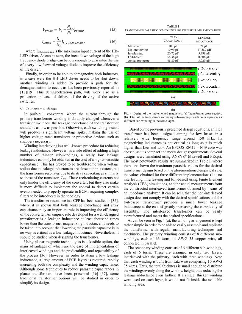
Based on the previously presented design equations, an 11:1 transformer has been designed aiming for low losses in a relatively wide frequency range around 150 kHz. Its magnetizing inductance is not critical as long as it is much higher than LIN1 and LIN2. An EPCOS RM12 – N49 core was chosen, as it is compact and meets design requirements. Several designs were simulated using ANSYS® Maxwell and PExprt. The most noteworthy results are summarized in Table I, where there are shown the maximum parasitic values for the desired transformer design based on the aforementioned empirical rule, the values obtained for three different implementations (i.e., no interleaving, interleaving and foil-based) using Finite Element Analysis (FEA) simulations, and the actual measurements from the constructed interleaved transformer obtained by means of an impedance analyzer. It can be seen that the non-interleaved design does not comply with the desired specifications and the foil-based transformer provides a much lower leakage inductance at the cost of greatly increasing the complexity of assembly. The interleaved transformer can be easily manufactured and meets the desired specifications.
As can be seen in Fig. 4 (a), the winding arrangement is kept rather simple in order to be able to easily assemble and replicate the transformer with regular manufacturing techniques and machinery. The primary winding consists of 8 different sub-windings, each of 66 turns, of AWG 35 copper wire, all connected in parallel.
The secondary winding consists of 6 different sub-windings, each of 6 turns. These are arranged in only two layers, interleaved with the primary, each with three windings. Note that each winding is built from Litz wire comprising 10 AWG 35 wires. Thus, the total thickness is small enough to distribute the windings evenly along the window height, thus reducing the leakage inductance even further. If a single, thicker winding were used on each layer, it would not fit inside the available winding area.
(a)
(b)
Fig. 4. Design of the implemented magnetics. (a) Transformer cross section. (b) Detail of the transformer secondary sub-windings, each color represents a different sub-winding in the same layer.
TABLE I TRANSFORMER PARASITIC COMPONENTS FOR DIFFERENT IMPLEMENTATIONS
STRAY
CAPACITANCE LEAKAGE
INDUCTANCE Maximum 100 pF 21 µH No interleaving 10.99 pF 47.589 µH Interleaving 20.73 pF 5.498 µH Foil-based 58.36 pF 0.606 µH Actual prototype 45.80 pF 3.020 µH
Different implementation options were also considered for the secondary winding, see Table I. The use of copper foil is an interesting alternative, although the benefit does not justify the increase in manufacturing difficulty, requiring custom foil thicknesses or even laser cutting machinery for fitting the required turns in just one layer. Simulations did not show significant advantages over the preferred simple designs, so this approach was discarded.
As the copper windings do not fill the winding area completely, PET insulating tape layers are added between them. This serves a dual purpose: fixing and insulating the primary and secondary layers, and creating wider spaces between them, thus lowering the stray capacitance.
The design of the input inductors is not as critical as that of the transformer, but a custom design was also used for this prototype. Even though, there is a wide range of commercial inductors that meet the inductance value and frequency requirements with small form factors, they have higher losses. An EPCOS RM8 – N97 core was chosen, with two AWG 29 22-turn windings connected in parallel. The design thus obtained is only slightly bigger than equivalent commercial inductances, but reduces conduction losses by more than half.
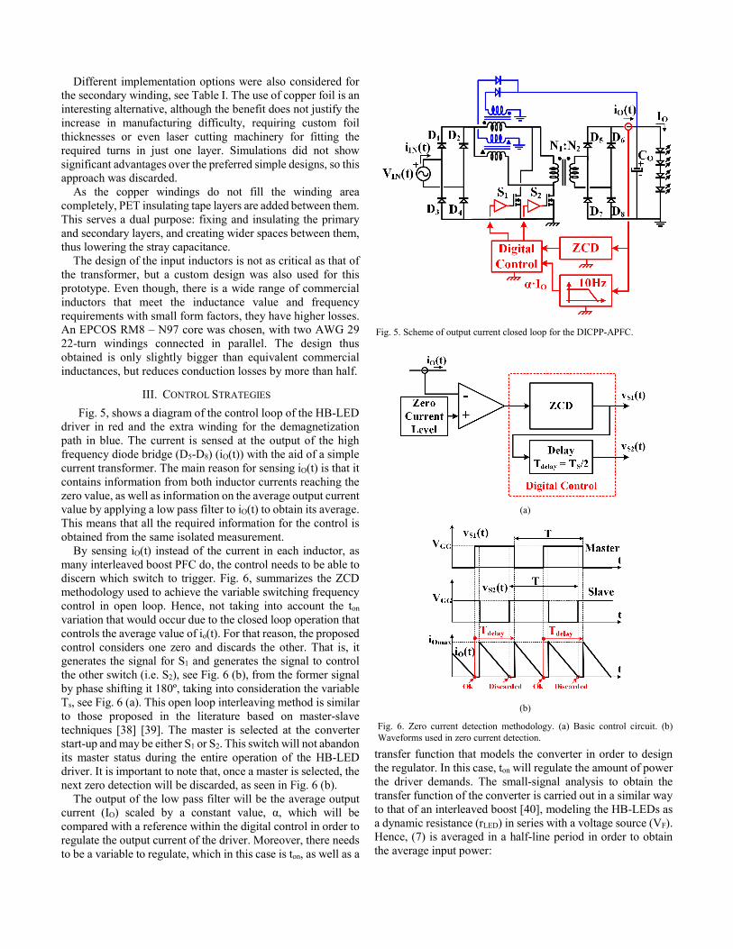
III. CONTROL STRATEGIES Fig. 5, shows a diagram of the control loop of the HB-LED
driver in red and the extra winding for the demagnetization path in blue. The current is sensed at the output of the high frequency diode bridge (D5-D8) (iO(t)) with the aid of a simple current transformer. The main reason for sensing iO(t) is that it contains information from both inductor currents reaching the zero value, as well as information on the average output current value by applying a low pass filter to iO(t) to obtain its average. This means that all the required information for the control is obtained from the same isolated measurement.
By sensing iO(t) instead of the current in each inductor, as many interleaved boost PFC do, the control needs to be able to discern which switch to trigger. Fig. 6, summarizes the ZCD methodology used to achieve the variable switching frequency control in open loop. Hence, not taking into account the ton variation that would occur due to the closed loop operation that controls the average value of io(t). For that reason, the proposed control considers one zero and discards the other. That is, it generates the signal for S1 and generates the signal to control the other switch (i.e. S2), see Fig. 6 (b), from the former signal by phase shifting it 180º, taking into consideration the variable Ts, see Fig. 6 (a). This open loop interleaving method is similar to those proposed in the literature based on master-slave techniques [38] [39]. The master is selected at the converter start-up and may be either S1 or S2. This switch will not abandon its master status during the entire operation of the HB-LED driver. It is important to note that, once a master is selected, the next zero detection will be discarded, as seen in Fig. 6 (b).
The output of the low pass filter will be the average output current (IO) scaled by a constant value, α, which will be compared with a reference within the digital control in order to regulate the output current of the driver. Moreover, there needs to be a variable to regulate, which in this case is ton, as well as a
transfer function that models the converter in order to design the regulator. In this case, ton will regulate the amount of power the driver demands. The small-signal analysis to obtain the transfer function of the converter is carried out in a similar way to that of an interleaved boost [40], modeling the HB-LEDs as a dynamic resistance (rLED) in series with a voltage source (VF). Hence, (7) is averaged in a half-line period in order to obtain the average input power:
(a)
(b)
Fig. 6. Zero current detection methodology. (a) Basic control circuit. (b) Waveforms used in zero current detection.
Fig. 5. Scheme of output current closed loop for the DICPP-APFC.
𝑃𝑃𝑔𝑔 = 𝑣𝑣𝑔𝑔𝑝𝑝2
2𝐿𝐿𝑡𝑡𝑜𝑜𝑜𝑜, (17)
Relating (17) with the average output power, we can thus obtain (18)
𝑖𝑖𝑜𝑜 =𝑣𝑣𝑔𝑔𝑝𝑝2
2𝐿𝐿𝑣𝑣𝑜𝑜𝑡𝑡𝑜𝑜𝑜𝑜 . (18)
(18) can be linearized and particularized at a point in order to obtain the small-signal model:
𝜕𝜕𝑖𝑖𝑜𝑜𝜕𝜕𝑡𝑡𝑜𝑜𝑜𝑜
�𝑃𝑃
=𝑉𝑉𝑔𝑔𝑝𝑝2
2𝐿𝐿𝑉𝑉𝑜𝑜= 𝑔𝑔𝑚𝑚𝑜𝑜𝑜𝑜𝑜𝑜 , (19)
𝜕𝜕𝑖𝑖𝑜𝑜𝜕𝜕𝑣𝑣𝑔𝑔𝑝𝑝
�𝑃𝑃
=𝑉𝑉𝑔𝑔𝑝𝑝
2𝐿𝐿𝑉𝑉𝑜𝑜𝑇𝑇𝑜𝑜𝑜𝑜 = 𝑔𝑔𝑚𝑚𝑜𝑜𝑔𝑔𝑝𝑝, (20)
𝜕𝜕𝑖𝑖𝑜𝑜𝜕𝜕𝑣𝑣𝑜𝑜
�𝑃𝑃
= −𝑉𝑉𝑔𝑔𝑝𝑝2
2𝐿𝐿𝑉𝑉𝑜𝑜2𝑇𝑇𝑜𝑜𝑜𝑜 = −
𝐼𝐼𝑜𝑜𝑉𝑉𝑜𝑜
=1𝑟𝑟𝑜𝑜
, (21)
where gioon, giogp and ro are depicted in Fig. 7. In order to complete the small-signal analysis, the input
current in a half-line period must be averaged. Thus, from (6) we obtain
𝑖𝑖𝐼𝐼𝐼𝐼 =2𝑣𝑣𝑔𝑔𝑝𝑝𝜋𝜋𝐿𝐿
𝑡𝑡𝑜𝑜𝑜𝑜. (22)
After linearizing and particularizing as done previously for the input current, the following relationships are obtained:
𝜕𝜕𝑖𝑖𝐼𝐼𝐼𝐼𝜕𝜕𝑣𝑣𝑔𝑔𝑝𝑝
�𝑃𝑃
=2𝑇𝑇𝑜𝑜𝑜𝑜𝜋𝜋𝐿𝐿
=1𝑟𝑟𝑚𝑚
, (23)
𝜕𝜕𝑖𝑖𝑜𝑜𝜕𝜕𝑡𝑡𝑜𝑜𝑜𝑜
�𝑃𝑃
=2𝑉𝑉𝑔𝑔𝑝𝑝𝜋𝜋𝐿𝐿
= 𝑔𝑔𝑚𝑚𝑔𝑔𝑜𝑜𝑜𝑜 . (24)
Fig. 7 shows the equivalent small-signal whose transfer function relating io and ton can be obtained:
𝚤𝚤̂𝑂𝑂�̂�𝑡𝑜𝑜𝑜𝑜
�𝑣𝑣�𝑔𝑔𝑔𝑔=0
=
𝑔𝑔𝑚𝑚𝑜𝑜𝑜𝑜𝑜𝑜𝑟𝑟𝑜𝑜𝑟𝑟𝐿𝐿𝐿𝐿𝐷𝐷+𝑟𝑟𝑜𝑜
1 + 𝑠𝑠𝐶𝐶𝑂𝑂𝑟𝑟𝐿𝐿𝐿𝐿𝐷𝐷𝑟𝑟𝑜𝑜𝑟𝑟𝐿𝐿𝐿𝐿𝐷𝐷+𝑟𝑟𝑜𝑜
. (25)
After obtaining (25), the compensator can be designed. For this particular case, which is a PFC, the bandwidth of the compensator needs to be sufficiently low to filter the low frequency component of twice the line frequency, that appears at the output due to the pulsating power as has been mentioned before.
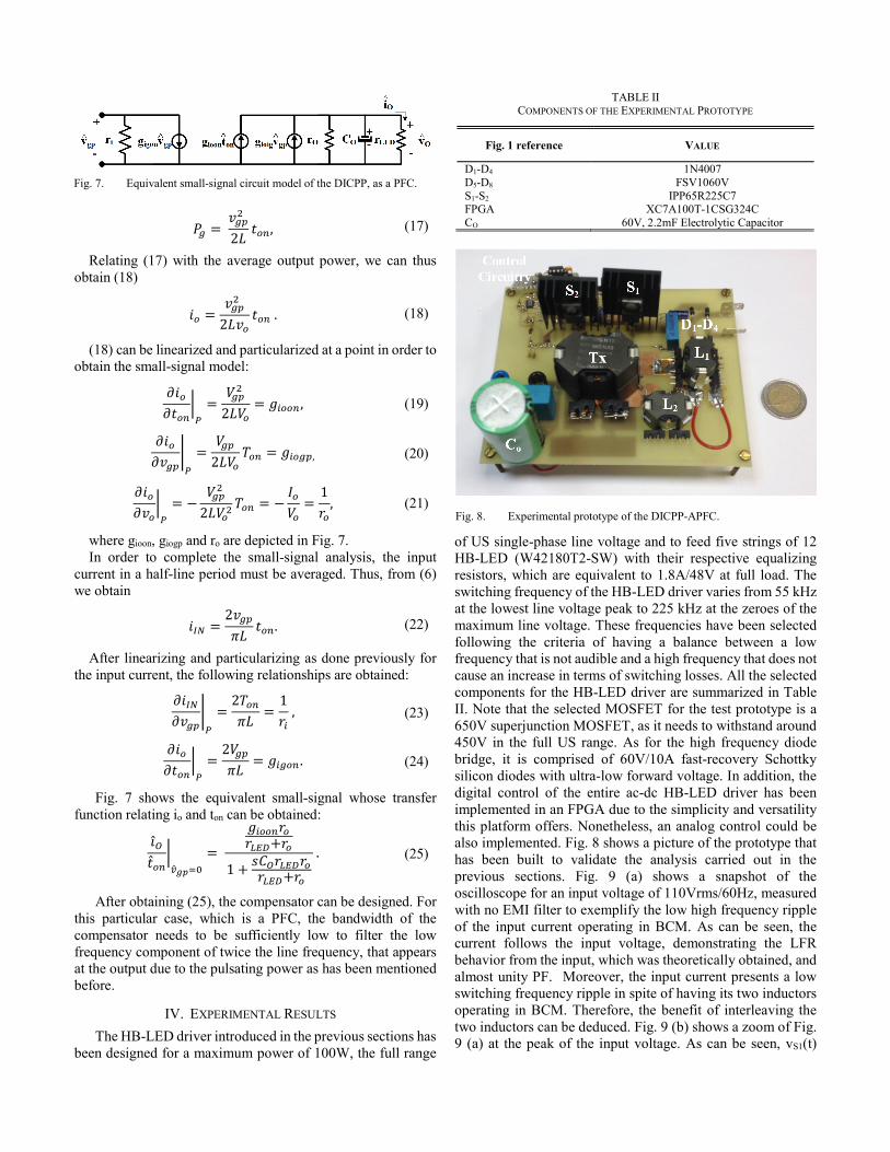
IV. EXPERIMENTAL RESULTS The HB-LED driver introduced in the previous sections has
been designed for a maximum power of 100W, the full range
of US single-phase line voltage and to feed five strings of 12 HB-LED (W42180T2-SW) with their respective equalizing resistors, which are equivalent to 1.8A/48V at full load. The switching frequency of the HB-LED driver varies from 55 kHz at the lowest line voltage peak to 225 kHz at the zeroes of the maximum line voltage. These frequencies have been selected following the criteria of having a balance between a low frequency that is not audible and a high frequency that does not cause an increase in terms of switching losses. All the selected components for the HB-LED driver are summarized in Table II. Note that the selected MOSFET for the test prototype is a 650V superjunction MOSFET, as it needs to withstand around 450V in the full US range. As for the high frequency diode bridge, it is comprised of 60V/10A fast-recovery Schottky silicon diodes with ultra-low forward voltage. In addition, the digital control of the entire ac-dc HB-LED driver has been implemented in an FPGA due to the simplicity and versatility this platform offers. Nonetheless, an analog control could be also implemented. Fig. 8 shows a picture of the prototype that has been built to validate the analysis carried out in the previous sections. Fig. 9 (a) shows a snapshot of the oscilloscope for an input voltage of 110Vrms/60Hz, measured with no EMI filter to exemplify the low high frequency ripple of the input current operating in BCM. As can be seen, the current follows the input voltage, demonstrating the LFR behavior from the input, which was theoretically obtained, and almost unity PF. Moreover, the input current presents a low switching frequency ripple in spite of having its two inductors operating in BCM. Therefore, the benefit of interleaving the two inductors can be deduced. Fig. 9 (b) shows a zoom of Fig. 9 (a) at the peak of the input voltage. As can be seen, vS1(t)
TABLE II COMPONENTS OF THE EXPERIMENTAL PROTOTYPE
Fig. 1 reference VALUE
D1-D4 1N4007 D5-D8 FSV1060V S1-S2 IPP65R225C7
FPGA XC7A100T-1CSG324C CO 60V, 2.2mF Electrolytic Capacitor
Fig. 7. Equivalent small-signal circuit model of the DICPP, as a PFC.
Fig. 8. Experimental prototype of the DICPP-APFC.
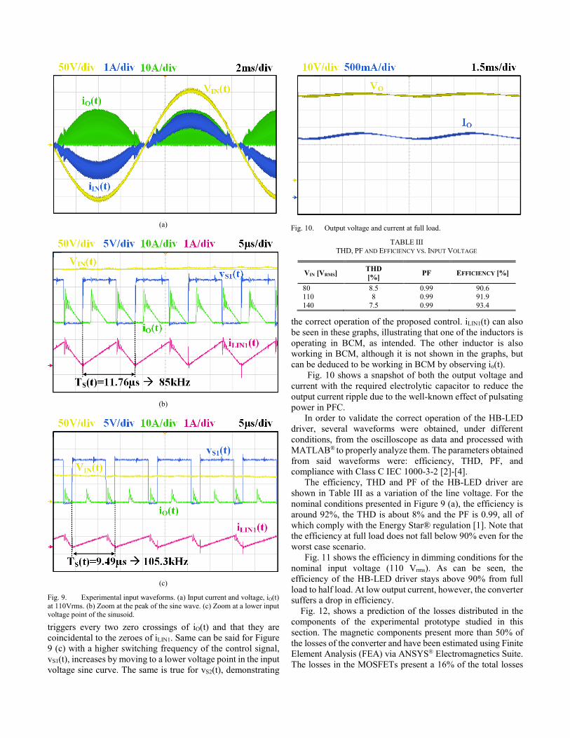
triggers every two zero crossings of iO(t) and that they are coincidental to the zeroes of iLIN1. Same can be said for Figure 9 (c) with a higher switching frequency of the control signal, vS1(t), increases by moving to a lower voltage point in the input voltage sine curve. The same is true for vS2(t), demonstrating
the correct operation of the proposed control. iLIN1(t) can also be seen in these graphs, illustrating that one of the inductors is operating in BCM, as intended. The other inductor is also working in BCM, although it is not shown in the graphs, but can be deduced to be working in BCM by observing io(t).
Fig. 10 shows a snapshot of both the output voltage and current with the required electrolytic capacitor to reduce the output current ripple due to the well-known effect of pulsating power in PFC.
In order to validate the correct operation of the HB-LED driver, several waveforms were obtained, under different conditions, from the oscilloscope as data and processed with MATLAB® to properly analyze them. The parameters obtained from said waveforms were: efficiency, THD, PF, and compliance with Class C IEC 1000-3-2 [2]-[4].
The efficiency, THD and PF of the HB-LED driver are shown in Table III as a variation of the line voltage. For the nominal conditions presented in Figure 9 (a), the efficiency is around 92%, the THD is about 8% and the PF is 0.99, all of which comply with the Energy Star® regulation [1]. Note that the efficiency at full load does not fall below 90% even for the worst case scenario.
Fig. 11 shows the efficiency in dimming conditions for the nominal input voltage (110 Vrms). As can be seen, the efficiency of the HB-LED driver stays above 90% from full load to half load. At low output current, however, the converter suffers a drop in efficiency.
Fig. 12, shows a prediction of the losses distributed in the components of the experimental prototype studied in this section. The magnetic components present more than 50% of the losses of the converter and have been estimated using Finite Element Analysis (FEA) via ANSYS® Electromagnetics Suite. The losses in the MOSFETs present a 16% of the total losses
Fig. 10. Output voltage and current at full load.
TABLE III THD, PF AND EFFICIENCY VS. INPUT VOLTAGE
VIN [VRMS] THD [%] PF EFFICIENCY [%]
80 8.5 0.99 90.6 110 8 0.99 91.9 140 7.5 0.99 93.4
(a)
(b)
(c)
Fig. 9. Experimental input waveforms. (a) Input current and voltage, iO(t) at 110Vrms. (b) Zoom at the peak of the sine wave. (c) Zoom at a lower input voltage point of the sinusoid.

and have been estimated using an analytical model for superjunction MOSFETs [41].
The input waveforms were also used to extract the harmonics using the Fourier series. These measurements were then compared with Class C IEC 1000-3-2 harmonic limits. As can be seen in Fig. 13, the HB-LED driver complies with the regulation.
To limit the biological effects and detection of flicker in general illumination, the Modulation (%) should be kept within the shaded region defined in [31], [32], where the Modulation (%) calculation can be defined as follows:
𝑀𝑀𝑀𝑀𝑑𝑑𝑀𝑀𝑀𝑀𝑀𝑀𝑡𝑡𝑖𝑖𝑀𝑀𝑠𝑠 (%) = 100 ∙(𝐿𝐿𝑆𝑆𝑝𝑝𝑆𝑆 − 𝐿𝐿𝑆𝑆𝑚𝑚𝑜𝑜)
(𝐿𝐿𝑆𝑆𝑝𝑝𝑆𝑆 + 𝐿𝐿𝑆𝑆𝑚𝑚𝑜𝑜 + 𝐿𝐿𝐷𝐷𝐷𝐷), (26)
where Lmax and Lmin correspond to the maximum and minimum luminance of each harmonic of the ac component of the light output respectively, and LDC corresponds to the average of the light output.
The luminance of the HB-LEDs was measured for the driver under study by using a transimpedance amplifier (TSL-257) with a bandwidth of 10 kHz to measure the light output waveform. After obtaining the luminance waveform, all the
harmonics were obtained from 60Hz (the frequency of the fundamental harmonic) to 3 kHz and compared with the standard, see Fig. 14, by means of applying the Fourier series to luminance waveform. As can be seen, all the harmonic content falls within the shaded region, even in those frequencies below 90Hz, which are the ones humans are more sensitive to. Therefore, good light quality and non-harmful effects can be assumed from the proposed HB-LED driver topology.
Table IV, shows a brief comparison of the experimental prototype studied in this work with state of the art, single-stage, ac-dc, LED drivers, in which several important parameters are compared, such as, output power, efficiency, THD, etc. As can be seen, the DICPP-APFC shows an outstanding performance with its biggest disavantage being the size of the output capacitor. This is the price to pay to achieve good light quality in this AC-DC single stage. In this respect, an active filter [7] [8] or a high efficiency post-regulator stage [43]- [45], to diminish the low frequency component and thus can be used to remove the bulk capacitor and control each HB-LED string individually. However, this is at the cost of adding more components and increasing the complexity of the DICPP-APFC.
Fig. 13. Harmonic content of the input current for the topology under study and compliance with Class C.
Fig. 14. Recommended flicker operation at full load for both drivers, P1789 [31].
Fig. 12. Distribution of losses in the experimental prototype of the DICPP-APFC under nominal conditions.
Fig. 11. Efficiency at 110 Vrms versus output power.

All the results that have been shown in this section, have been measured in closed loop by controlling the output current of the HB-LED driver and allowing ton to vary. In order to design the compensator, the open loop response of the converter relating the output current of the DICPP- APFC to variations of ton has been measured by using a Venable® 6320. This response is represented in Fig. 15 and compared with its theoretical counterpart (25), showing that the theoretical analysis matches the experimental results. The values used to obtain the theoretical curve of (25) are calculated by using the design criteria introduced in Section II and are summarized in Table V. Considering the results shown in Fig. 15, the
compensator design is straightforward and is extremely similar to any other PFC output loop, which can be accomplished with a simple PI [17].
IV. CONCLUSIONS A simple, current-fed, ac-dc, single-stage, single-phase,
isolated, high PF, HB-LED driver with two switches referenced to the same ground has been reported and experimentally tested in this paper. The DICPP-APFC is able to deal with most of the issues that made current-fed AC-DC converters not suitable for power factor correction: switches withstanding high voltage, complex transformer design and low performance at low power. Moreover, the advantages of using the DICPP-APFC against some of the conventional single-stage topologies, from Table IV, are that is able to achieve high efficiency and reduce the traditional switching frequency ripple of BCM operation with a single transformer, by using the inbuilt interleaving method between the two branches that comprise the push-pull topology, at the price of including one more magnetic component and one more active switch. It should be noted that, the adding of more branches is not scalable, hence it is not a possibility to reduce even more the input ripple with a single converter. However, the DICPP-APFC does come with some drawbacks: the first drawback comes from the need to use a demagnetization circuit to prevent the switches from destruction in case of a control failure, which is intrinsic to current-fed topologies, the second one comes from the inability to dispose of the bulk capacitor present in single-stage ac-dc converters which require a high PF and the third drawback is related to the voltages stress that the switches are withstanding, which at this point makes this topology not suitable to achieve universal input voltage range with silicon technology. In fact, not being able to dispose of the electrolytic capacitor may be troublesome for some LED drivers that require long lifespans. However, this is the price to pay for a simple, cost efficient, ac-dc single-stage solution at these power levels.
REFERENCES [1] Revised ENERGY STAR Program Requirements for Solid-State
Lighting Luminaires: Eligibility Criteria—Version 1.1, Dec. 2008. [2] Draft of the Proposed CLC Common Modification to IEC 61000-3-2
Document, 2006.
TABLE IV COMPARISON OF STATE OF THE ART SINGLE-STAGE AC-DC LED DRIVERS
REFERENCES
DICPP-APFC [7] [13] [46] [47] [48]
Output Power [W] 100 35 35 81 100 12 Efficiency [%] 91.5 87 90.5 90.69 91.7 86.1 THD [%] 8 - - 3.32 5.7 - Switching frequency [kHz] 55-225 - 140 67 90 100 Output capacitor [µF] 2200 470 4.7 - 220 2 Output current ripple [%] 10 10 20 20 10 17.85 Output capacitor reduction No Yes Yes No Yes Yes Reduced input cur. ripple Yes No No Yes No No Number of MOSFETs 2 3 3 2 2 1 Number of transformers 1 1 1 2 1 1 Number of inductances 2 1 2 0 3 1
Fig. 15. Comparison of the theoretical and experimental measurements of the ton to io transfer function (25).
TABLE V VALUES USED TO OBTAIN THE THEORETICAL WAVEFORM OF (25)
VALUE
Vgp 110 Vrms L 860 µH Ton 7.1 µs Co 2.2 mF rLED 5.5 Ω Vo 48 V

[3] Draft of the Proposed CLC Common Modification to IEC 61000-3-2/A2 Document, 2010.
[4] Electromagnetic Compatibility (EMC)-Part 3: Limits-Section 2: Limits for Harmonic Current Emissions (Equipment Input current < 16 A per Phase), IEC1000-3-2, 1995.
[5] X. Xie, J. Wang, C. Zhao, Q. Lu and S. Liu, "A Novel Output Current Estimation and Regulation Circuit for Primary Side Controlled High Power Factor Single-Stage Flyback LED Driver," in IEEE Transactions on Power Electronics, vol. 27, no. 11, pp. 4602-4612, Nov. 2012.
[6] M. Arias, A. Vazquez, and J. Sebastian, “An overview of the AC-DC and DC-DC converters for LED lighting applications,” Automatika—J. Control, Measure., Electr., Comput. Commun., vol. 53, pp. 156–172, 2012
[7] P. Fang, Y. F. Liu and P. C. Sen, "A Flicker-Free Single-Stage Offline LED Driver With High Power Factor," in IEEE Journal of Emerging and Selected Topics in Power Electronics, vol. 3, no. 3, pp. 654-665, Sept. 2015.
[8] P. Fang, Y. j. Qiu, H. Wang and Y. F. Liu, "A Single-Stage Primary-Side-Controlled Off-line Flyback LED Driver With Ripple Cancellation," in IEEE Transactions on Power Electronics, vol. 32, no. 6, pp. 4700-4715, June 2017.
[9] L. Jia, Y. F. Liu and D. Fang, "High power factor single stage flyback converter for dimmable LED driver," 2015 IEEE Energy Conversion Congress and Exposition (ECCE), Montreal, QC, 2015, pp. 3231-3238.
[10] H. Ma, C. Zheng, W. Yu, B. Gu, J. D. Lai and Q. Feng, "Bridgeless electrolytic capacitor-less valley-fill AC/DC converter for offline twin-bus light-emitting diode lighting application," in IET Power Electronics, vol. 6, no. 6, pp. 1132-1141, July 2013.
[11] Y. Zhang and K. Jin, "A single-stage electrolytic capacitor-less AC/DC LED driver," 2014 International Power Electronics and Application Conference and Exposition, Shanghai, 2014, pp. 881-886.
[12] S. Wang, X. Ruan, K. Yao, S. C. Tan, Y. Yang and Z. Ye, "A Flicker-Free Electrolytic Capacitor-Less AC–DC LED Driver," in IEEE Transactions on Power Electronics, vol. 27, no. 11, pp. 4540-4548, Nov. 2012.
[13] Y. Yang, X. Ruan, L. Zhang, J. He and Z. Ye, "Feed-Forward Scheme for an Electrolytic Capacitor-Less AC/DC LED Driver to Reduce Output Current Ripple," in IEEE Transactions on Power Electronics, vol. 29, no. 10, pp. 5508-5517, Oct. 2014.
[14] M. Arias, M. F. Diaz, J. E. R. Cadierno, D. G. Lamar and J. Sebastián, "Digital Implementation of the Feedforward Loop of the Asymmetrical Half-Bridge Converter for LED Lighting Applications," in IEEE Journal of Emerging and Selected Topics in Power Electronics, vol. 3, no. 3, pp. 642-653, Sept. 2015.
[15] L. Gu, X. Ruan, M. Xu and K. Yao, "Means of Eliminating Electrolytic Capacitor in AC/DC Power Supplies for LED Lightings," in IEEE Transactions on Power Electronics, vol. 24, no. 5, pp. 1399-1408, May 2009.
[16] D. G. Lamar, J. Sebastian, M. Arias and A. Fernandez, "On the Limit of the Output Capacitor Reduction in Power-Factor Correctors by Distorting the Line Input Current," in IEEE Transactions on Power Electronics, vol. 27, no. 3, pp. 1168-1176, March 2012.
[17] L. H. Dixon, "High power factor preregulators for off-line power supplies", Unitrode Power Supply Design Seminar, 1988, pp. 6.1-6.16.
[18] M. J. Kocher and R. L. Steigerwald, "An AC-to-DC Converter with High Quality Input Waveforms," in IEEE Transactions on Industry Applications, vol. IA-19, no. 4, pp. 586-599, July 1983.
[19] V. J. Thottuvelil, T. G. Wilson and H. A. Owen, "Analysis and design of a push-pull current-fed converter," 1981 IEEE Power Electronics Specialists Conference, Boulder, Colorado, USA, 1981, pp. 192-203.
[20] E. X. Yang, Y. Jiang, G. Hua and F. C. Lee, "Isolated boost circuit for power factor correction," Proceedings Eighth Annual Applied Power Electronics Conference and Exposition, San Diego, CA, 1993, pp. 196-203.
[21] N. Q. Trong, H. j. Chiu, Y. k. Lo, C. y. Lin and M. M. Alam, "Modified current-fed full-bridge isolated power factor correction converter with
low-voltage stress," in IET Power Electronics, vol. 7, no. 4, pp. 861-867, April 2014.
[22] P. J. Wolfs, "A current-sourced DC-DC converter derived via the duality principle from the half-bridge converter," in IEEE Transactions on Industrial Electronics, vol. 40, no. 1, pp. 139-144, Feb 1993.
[23] W. C. P. De Aragao Filho and I. Barbi, "A comparison between two current-fed push-pull DC-DC converters-analysis, design and experimentation," Telecommunications Energy Conference, 1996. INTELEC '96., 18th International, Boston, MA, 1996, pp. 313-320.
[24] A. Andreiciks, I. Steiks, O. Krievs and L. Ribickis, "Current-fed DC/DC converter for fuel cell applications," Power Electronics and Motion Control Conference (EPE/PEMC), 2010 14th International, Ohrid, 2010, pp. T2-210-T2-214.
[25] R. Kosenko, J. Zakis, A. Blinov, A. Chub and O. Veligorskyi, "Full soft-switching bidirectional isolated current-fed dual inductor push-pull DC-DC converter for battery energy storage applications," 2016 57th International Scientific Conference on Power and Electrical Engineering of Riga Technical University (RTUCON), Riga, 2016, pp. 1-8.
[26] D. R. Nayanasiri, G. H. B. Foo, D. M. Vilathgamuwa and D. L. Maskell, "A Switching Control Strategy for Single- and Dual-Inductor Current-Fed Push–Pull Converters," in IEEE Transactions on Power Electronics, vol. 30, no. 7, pp. 3761-3771, July 2015.
[27] I. Castro, K. Martin, D. G. Lamar, M. Arias, M. M. Hernando and J. Sebastian, "Single-stage AC/DC Dual Inductor BCM Current-Fed Push-Pull for HB-LED lighting applications," 2016 IEEE Energy Conversion Congress and Exposition (ECCE), Milwaukee, WI, 2016.
[28] Q. Wu; Q. Wang; J. Xu; H. Li; L. Xiao, "A High Efficiency Step-up Current-fed Push-pull Quasi-resonant Converter with Fewer Components for Fuel Cell Application," in IEEE Transactions on Industrial Electronics , vol.PP, no.99, pp.1-1
[29] Hao Ma, Longyu Chen and Zhihong Bai, "An active-clamping current-fed push-pull converter for vehicle inverter application and resonance analysis," 2012 IEEE International Symposium on Industrial Electronics, Hangzhou, 2012, pp. 160-165.
[30] S. Singer, "The application of 'loss-free resistors' in power processing circuits," Power Electronics Specialists Conference, 1989. PESC '89 Record., 20th Annual IEEE, Milwaukee, WI, 1989, pp. 843-846 vol.2.
[31] IEEE Recommended Practices for Modulating Current in High-Brightness LEDs for Mitigating Health Risks to Viewers," in IEEE Std 1789-2015 , vol., no., pp.1-80, June 5 2015.
[32] "RP-16-10, Nomenclature and Definitions for Illuminating Engineering", Illuminating Engineering Society.
[33] Z. Wang, S. Wang, P. Kong and F. C. Lee, "DM EMI Noise Prediction for Constant On-Time, Critical Mode Power Factor Correction Converters," in IEEE Transactions on Power Electronics, vol. 27, no. 7, pp. 3150-3157, July 2012.
[34] Z. Liu, Z. Huang, F. C. Lee and Q. Li, "Digital-Based Interleaving Control for GaN-Based MHz CRM Totem-Pole PFC," in IEEE Journal of Emerging and Selected Topics in Power Electronics, vol. 4, no. 3, pp. 808-814, Sept. 2016.
[35] J. M. Kwon, E. H. Kim, B. H. Kwon and K. H. Nam, "High-Efficiency Fuel Cell Power Conditioning System With Input Current Ripple Reduction," in IEEE Transactions on Industrial Electronics, vol. 56, no. 3, pp. 826-834, March 2009.
[36] Z. Ouyang and M. A. E. Andersen, "Overview of Planar Magnetic Technology—Fundamental Properties," in IEEE Transactions on Power Electronics, vol. 29, no. 9, pp. 4888-4900, Sept. 2014.
[37] M. A. Saket, N. Shafiei and M. Ordonez, "LLC Converters With Planar Transformers: Issues and Mitigation," in IEEE Transactions on Power Electronics, vol. 32, no. 6, pp. 4524-4542, June 2017.
[38] L. Huber, B. T. Irving and M. M. Jovanovic, "Review and Stability Analysis of PLL-Based Interleaving Control of DCM/CCM Boundary Boost PFC Converters," in IEEE Transactions on Power Electronics, vol. 24, no. 8, pp. 1992-1999, Aug. 2009.
[39] L. Huber, B. T. Irving and M. M. Jovanovic, "Open-Loop Control Methods for Interleaved DCM/CCM Boundary Boost PFC Converters,"
in IEEE Transactions on Power Electronics, vol. 23, no. 4, pp. 1649-1657, July 2008.
[40] H. Y. Kanaan, G. Sauriol and K. Al-Haddad, "Small-signal modelling and linear control of a high efficiency dual boost single-phase power factor correction circuit," in IET Power Electronics, vol. 2, no. 6, pp. 665-674, Nov. 2009.
[41] I. Castro et al., "Analytical Switching Loss Model for Superjunction MOSFET With Capacitive Nonlinearities and Displacement Currents for DC–DC Power Converters," in IEEE Transactions on Power Electronics, vol. 31, no. 3, pp. 2485-2495, March 2016.
[42] J. Sebastian, P. J. Villegas, M. Hernando, F. Nuno and F. Fernandez-Linera, "Average-current-mode control of two-input buck postregulators used in power-factor correctors," in IEEE Transactions on Industrial Electronics, vol. 46, no. 3, pp. 569-576, Jun 1999.
[43] S. G. Park, S. H. Ryu, K. S. Cho and B. K. Lee, "An improved single switched post regulator for multiple output isolated converters," 2015 9th International Conference on Power Electronics and ECCE Asia (ICPE-ECCE Asia), Seoul, 2015, pp. 2403-2408.
[44] J. Sebastian, P. J. Villegas, F. Nuno and M. M. Hernando, "High-efficiency and wide-bandwidth performance obtainable from a two-input buck converter," in IEEE Transactions on Power Electronics, vol. 13, no. 4, pp. 706-717, Jul 1998.
[45] M. Arias, D. G. Lamar, J. Sebastian, D. Balocco and A. A. Diallo, "High-Efficiency LED Driver Without Electrolytic Capacitor for Street Lighting," in IEEE Transactions on Industry Applications, vol. 49, no. 1, pp. 127-137, Jan.-Feb. 2013.
[46] S. Moon, G. B. Koo and G. W. Moon, "A New Control Method of Interleaved Single-Stage Flyback AC–DC Converter for Outdoor LED Lighting Systems," in IEEE Transactions on Power Electronics, vol. 28, no. 8, pp. 4051-4062, Aug. 2013.
[47] Y. Wang, Y. Guan, J. Huang, W. Wang and D. Xu, "A Single-Stage LED Driver Based on Interleaved Buck–Boost Circuit and LLC Resonant Converter," in IEEE Journal of Emerging and Selected Topics in Power Electronics, vol. 3, no. 3, pp. 732-741, Sept. 2015.
[48] J. C. W. Lam and P. K. Jain, "Isolated AC/DC Offline High Power Factor Single-Switch LED Drivers Without Electrolytic Capacitors," in IEEE Journal of Emerging and Selected Topics in Power Electronics, vol. 3, no. 3, pp. 679-690, Sept. 2015.
Ignacio Castro (S’14) was born in Gijón, Spain, in
1989. He received the M.Sc. degree in telecommunication engineering from the University of Oviedo, Gijón, Spain, in 2014, and he is currently pursuing the Ph.D. degree in electrical engineering at the same university. His research interests include low and medium power dc–dc converters, modeling, simulation and control of dc-dc converters, power-factor correction ac–dc converters and LED drivers.
Kevin Martín was born in Gijón, Spain, in 1990. He received the M.Sc. degree in Telecommunication Engineering from the University in Oviedo in 2014. He is currently pursuing the Ph.D. degree in Electrical Engineering at the same university about DC-DC power converters optimization and integration within DC microgrids. Since 2014, he has been a researcher with the Power Supply System Group. His research interests include DC-DC power supplies, modelling, simulation and control of DC-DC power converters and
the use of Wide Band Gap semiconductor devices.
Aitor Vazquez (S'2010, M'2015) was born in Oviedo, Spain, in 1984. He received the M.Sc. degree in telecommunication engineering, in 2009, and the PhD. degree in electrical engineering in 2016, from the University of Oviedo, Gijon, Spain. He became a Member of the Power Supply System Group, University of Oviedo, in 2010. His current research interests include modularization techniques applied to bidirectional dc–dc converters for HEV, battery
management power supplies, DC distribution grids, powerfactor corrector ac–dc converters and energy recovery systems.
Manuel Arias (s’05 M'10) received the M. Sc. degree in electrical engineering from the University of Oviedo, Spain, in 2005 and the Ph. D. degree from the same university in 2010. In 2007 he joined the University of Oviedo as an Assistant Professor and since 2016 he is an Associate Professor at the same university. His research interests include ac-dc and dc-dc power converters, battery-cell equalizers and LED lighting.
Diego G. Lamar (M’08) was born in Zaragoza, Spain, in 1974. He received the M.Sc. degree, and the Ph.D. degree in Electrical Engineering from the University of Oviedo, Spain, in 2003 and 2008, respectively. In 2003 and 2005 he became a Research Engineer and an Assistant Professor respectively at the University of Oviedo. Since September 2011, he has been an Associate Professor. His research interests are focused in switching-mode power supplies, converter modelling, and power-factor-correction converters.
Javier Sebastián (M’87-SM’11) was born in Madrid, Spain, in 1958. He received the M.Sc. degree from the Technical University of Madrid (UPM), and the Ph.D. degree in electrical engineering from the University of Oviedo, Spain, in 1981 and 1985, respectively. He was an Assistant Professor and an Associate Professor at both the UPM and the University of Oviedo. Since 1992, he has been with the University of Oviedo, where he is currently a Professor. His research interests are switching-mode power supplies,
modeling of dc-to-dc converters, low output voltage dc-to-dc converters, high power factor rectifiers, LED drivers, dc-to-dc converters for envelope tracking techniques and the use of wide band-gap semiconductors in power supplies.