Research Review 2003 - ETH Z
168
Integrated Systems Laboratory Microelectronics Design Center Research Review 2003 W. Fichtner Q. Huang H. Kaeslin N. Felber D. Aemmer Eidgenössische Technische Hochschule Zürich Swiss Federal Institute of Technology Zurich
Transcript of Research Review 2003 - ETH Z
Integrated Systems Laboratory
Microelectronics Design Center
Research Review 2003
W. Fichtner Q. Huang H. Kaeslin N. Felber D. Aemmer
Eidgenössische Technische Hochschule Zürich
Swiss Federal Institute of Technology Zurich
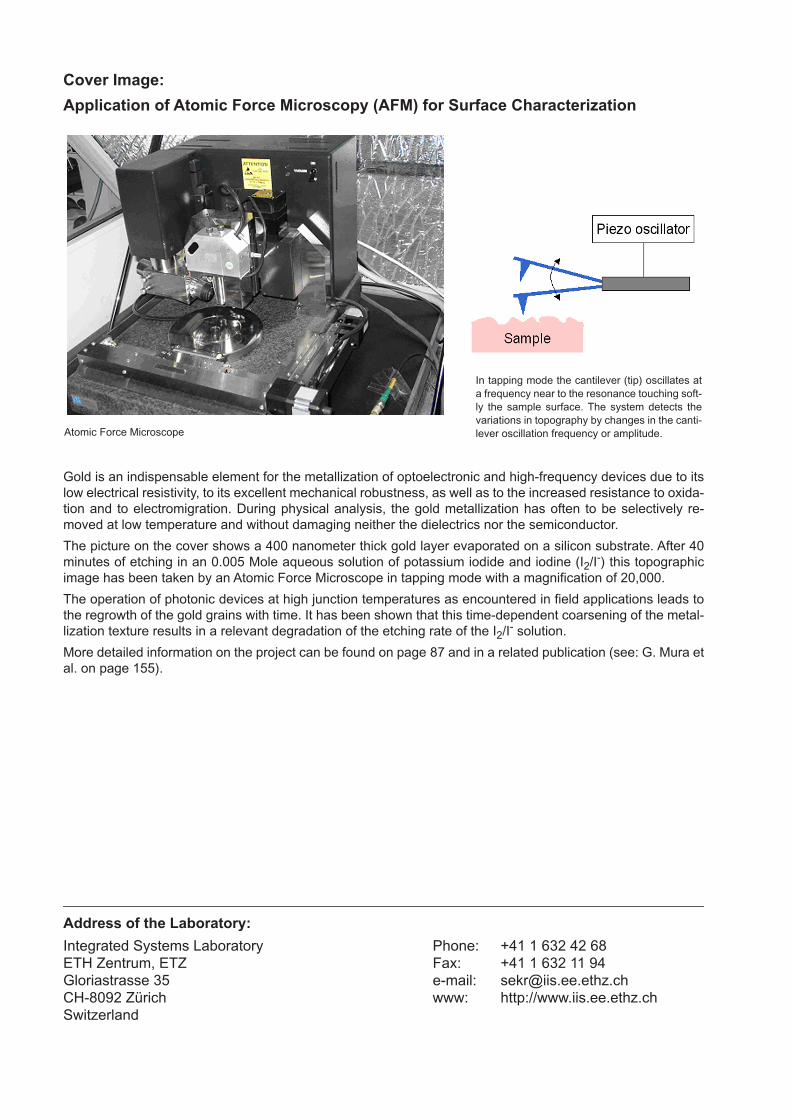
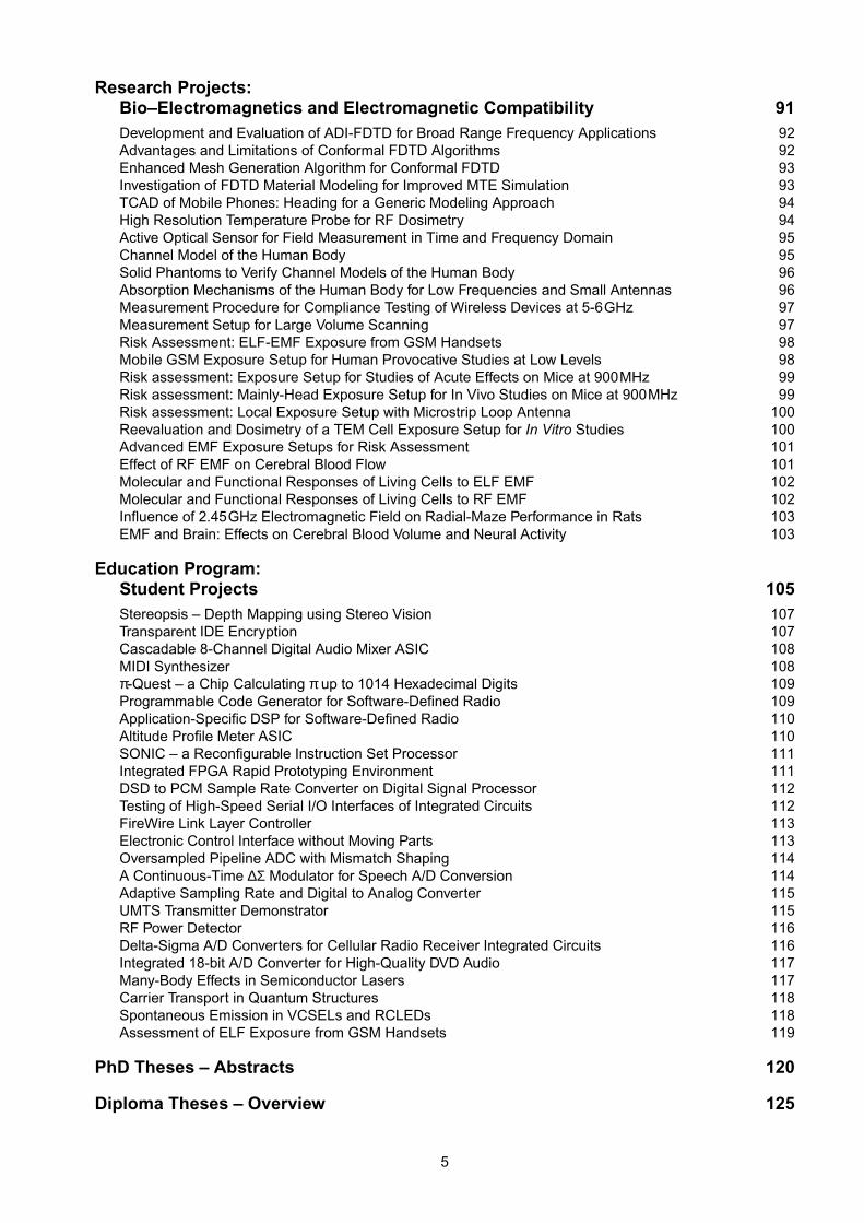
Cover Image:
Application of Atomic Force Microscopy (AFM) for Surface Characterization
Gold is an indispensable element for the metallization of optoelectronic and high-frequency devices due to itslow electrical resistivity, to its excellent mechanical robustness, as well as to the increased resistance to oxida-tion and to electromigration. During physical analysis, the gold metallization has often to be selectively re-moved at low temperature and without damaging neither the dielectrics nor the semiconductor.
The picture on the cover shows a 400 nanometer thick gold layer evaporated on a silicon substrate. After 40minutes of etching in an 0.005 Mole aqueous solution of potassium iodide and iodine (I
2
/I
-
) this topographicimage has been taken by an Atomic Force Microscope in tapping mode with a magnification of 20,000.
The operation of photonic devices at high junction temperatures as encountered in field applications leads tothe regrowth of the gold grains with time. It has been shown that this time-dependent coarsening of the metal-lization texture results in a relevant degradation of the etching rate of the I
2
/I
-
solution.
More detailed information on the project can be found on page 87 and in a related publication (see: G. Mura etal. on page 155).
Address of the Laboratory:
Integrated Systems Laboratory Phone: +41 1 632 42 68ETH Zentrum, ETZ Fax: +41 1 632 11 94Gloriastrasse 35 e-mail: [email protected] Zürich www: http://www.iis.ee.ethz.chSwitzerland
In tapping mode the cantilever (tip) oscillates ata frequency near to the resonance touching soft-ly the sample surface. The system detects thevariations in topography by changes in the canti-lever oscillation frequency or amplitude.Atomic Force Microscope
Integrated Systems LaboratoryEidgenössische Technische Hochschule Zürich
Microelectronics Design CenterSwiss Federal Institute of Technology Zurich
Research Review 2003
W. Fichtner Q. Huang H. Kaeslin N. Felber D. Aemmer
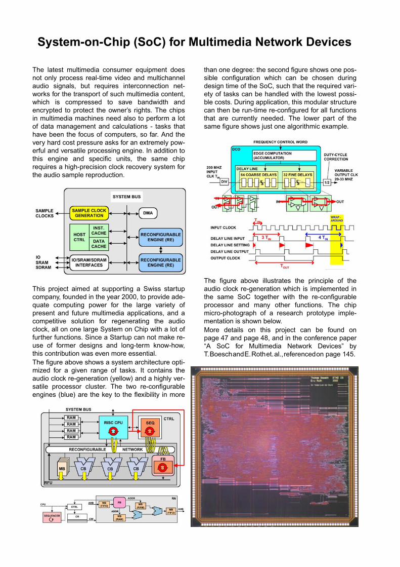
System-on-Chip (SoC) for Multimedia Network Devices
The latest multimedia consumer equipment doesnot only process real-time video and multichannelaudio signals, but requires interconnection net-works for the transport of such multimedia content,which is compressed to save bandwidth andencrypted to protect the owner’s rights. The chipsin multimedia machines need also to perform a lotof data management and calculations - tasks thathave been the focus of computers, so far. And thevery hard cost pressure asks for an extremely pow-erful and versatile processing engine. In addition tothis engine and specific units, the same chiprequires a high-precision clock recovery system forthe audio sample reproduction.
This project aimed at supporting a Swiss startupcompany, founded in the year 2000, to provide ade-quate computing power for the large variety ofpresent and future multimedia applications, and acompetitive solution for regenerating the audioclock, all on one large System on Chip with a lot offurther functions. Since a Startup can not make re-use of former designs and long-term know-how,this contribution was even more essential.The figure above shows a system architecture opti-mized for a given range of tasks. It contains theaudio clock re-generation (yellow) and a highly ver-satile processor cluster. The two re-configurableengines (blue) are the key to the flexibility in more
than one degree: the second figure shows one pos-sible configuration which can be chosen duringdesign time of the SoC, such that the required vari-ety of tasks can be handled with the lowest possi-ble costs. During application, this modular structurecan then be run-time re-configured for all functionsthat are currently needed. The lower part of thesame figure shows just one algorithmic example.
The figure above illustrates the principle of theaudio clock re-generation which is implemented inthe same SoC together with the re-configurableprocessor and many other functions. The chipmicro-photograph of a research prototype imple-mentation is shown below.More details on this project can be found onpage 47 and page 48, and in the conference paper“A SoC for Multimedia Network Devices” byT.BoeschandE.Rothet.al.,referencedon page 145.
Contents
Preface 7
Announcement Assistant Professor Bernd Witzigmann 10
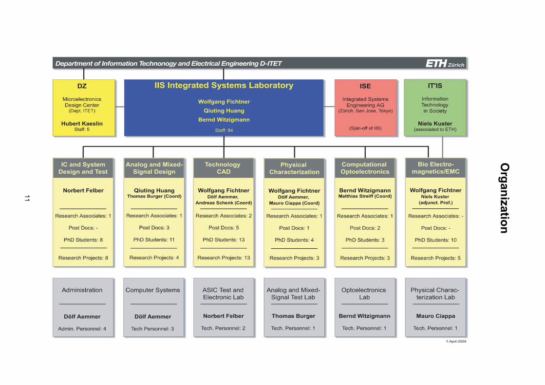
Organization 11
Representative Figures 12
Staff 15
Former PhD Students 17
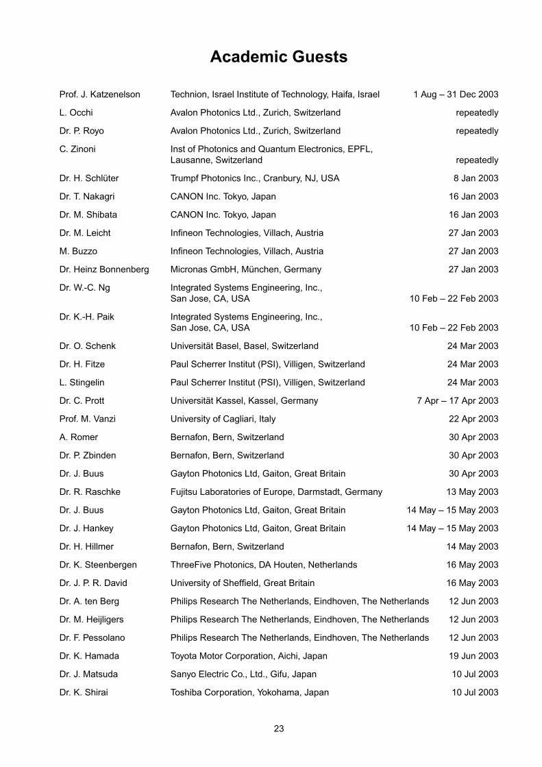
Academic Guests 23
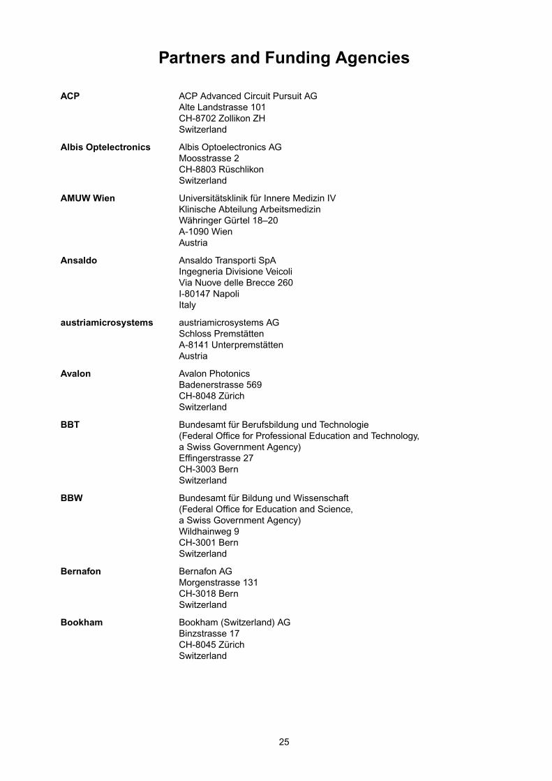
Partners and Funding Agencies 25
Awards and Patents 36
History of the Integrated Systems Laboratory (IIS) 37
Research Projects:IC and System Design and Test 43Multi-Point Interconnects for Globally-Asynchronous Locally-Synchronous Systems 44Shir-Khan – a Testbed for GALS Multi-Point Interconnect 44Testability of GALS Modules 45OSCAR – GALS Oscillators: Measurements 45A Self-Calibrating Oscillator for GALS 46Real-Time MIMO OFDM Testbed 46Equalization for MIMO-CDMA and MIMO-HSDPA Systems 47All-Digital Standardcell-Based Audio Sample Clock Synthesis 47Adaptive Stream Processing for Networked Multimedia Devices 48Power Dissipation in Microelectronics: from Estimations to Experimental Results 48Power Saving in Filters for Audio Applications 49Fastcore – AES Crypto Chip 49DPA Attacks on AES Crypto Chip 50Prototyping Platform for Coprocessors in SoCs 50IRRQ Testing of Deep-Submicron CMOS Chips 51
Research Projects:Analog and Mixed-Signal Design 53200MSPS 14bit DAC with Background Calibration 54Sigma-Delta DAC with Semi-digital Reconstruction Filtering 54A 25MS/s 14bit Sigma-Delta Modulator for VDSL Communications Application 55Oversampled A/D-Conversion for Multi-Standard Wireless Receivers 55A High-Speed Folding and Interpolation A/D-Converter 56Folding and Interpolating A/D Converters in Deep-Submicron CMOS Technology 56High-speed Pipelined A/D Converters in Deep-Submicron CMOS Technology 57Design and Optimization of a Direct-Conversion Receiver for WCDMA Down-Link 57I/Q-Demodulation for a WCDMA Receiver 58WCDMA Transmitter Design in 0.13µm CMOS 58Mobile Transmitter Architectures in Deep-Submicron CMOS 594 GHz Frequency Synthesizer for a UMTS Receiver 5910 GHz Voltage-Controlled Oscillator and Prescaler 60
3
Research Projects:Technology CAD 61QDD Modeling of Lateral Quantum Effects in Nanoscale MOSFETs 62Mobility Model for DGSOI MOSFETs 62Leakage Currents and Charging Effects in SOI Devices 63Simulation of Nanoscale Double-Gate MOSFETs 63Double-Gate Versus Strained-Si MOSFETs 64Influence of Carrier-Carrier Scattering on the Bulk Mobility 64Injection Dependence of Spontaneous Radiative Recombination in Crystalline Silicon 65A Coupled Kohn-Sham / Drift-Diffusion Simulation Framework 65Quantum Ballistic Transport in Nanoscale MOSFETs 66Quantum Corrected Transport Coefficients for Device Simulation 66Direct Computation of Noise Figures Using 2D Transient MC Simulations 67Harmonic Balance Analysis for Semiconductor Devices 67Physics-Based Simulations of HEMT Devices and Systems for Microwave Applications 68Locally Structured 3D Anisotropic Meshes 68MAGIC_FEAT Project: Meshing Towards Full 3D Process Simulation 69Vertical-Cavity Surface-Emitting Lasers: Single Mode Control and Self Heating Effects 69Calibration of Vertical-Cavity Surface-Emitting Laser Simulation 70Calculation of Optical Mode Density in VCSELs 70Optimization of Optical Leakage in Edge-Emitting Lasers 71Simulation of Light-Emitting Diodes 71Full 3D Simulation of Tunable Sampled-Grating DBR Laser 72Full 3D Simulation of a Semiconductor Optical Amplifier 72TCAD Calibration Methodology for an Edge Emitting Laser 73Better Quantum Well Capture Time Evaluation by AC Small Signal Analysis 73Transient Simulation of High-Speed Photodetectors 74Self-Consistent Numerical Solution of the System of Equations in Laser Simulations 74Multi-Grid Scheme for the Simulation of Optoelectronic Devices 75Multimode Optical Small Signal Analysis 75Bandstructure Calculation for Arbitrarily Shaped Quantum Wells 76Simulation of Carrier Transport in the Active Region of Semiconductor Lasers 76Microscopic Gain Calculation: Influence of the Coulomb-Induced Subband Coupling 77Self-Consistent 8-band k•p Schroedinger-Poisson Solver for Wurtzite Crystals 77Electronic Structure of Co-Dopants in GaN 78Atomistic Strain in GaN 78Development of a Kinetic Monte Carlo Drift-Diffusion Solver 79Dopant Deactivation in n-Type Silicon 79Co-Doping in Silicon: An Ab Initio Study 80The Configuration of the Self-Interstitial in Silicon 80Large Scale Eigenvalue Problems in Optoelectronic Semiconductor Lasers 81Nonsymmetric Permutations for Iterative Methods in Semiconductor Device Simulation 81
Research Projects:Physical Characterization 83Fast 3D Transient Thermal Simulation of Converters for Automotive Applications 84Electro-Thermal Characterization and Simulation of Converters for Automotive Applications 84Pulsed Current Characterization of Power MOSFET and IGBT Devices 85A New Procedure to Delineate Electrical Junctions by Scanning Capacitance Microscopy 85Scanning Capacitance Microscopy Imaging for Characterization of Power DMOSTransistors 86Assessing the Performances of Two-Dimensional Dopant Profiling Techniques 86Selective Iodine-Based Gold Etch for Aged Optoelectronics Devices Failure Analysis 87Feasibility Study of a Ti/TiN Metalization for High-Temperature Bulk Mobility Extraction 87Automatic Experimental Setup for Semiconductor Characterization at High Temperatures 88High-Temperature Impact Ionization Measurements in Static Induction Transistors 88Full 3D Simulation of Van der Pauw Resistors for Very High Temperatures 89Preventing Parasitic ESD Failure Modes Utilising TCAD Device Simulations 89CDM Circuit Simulation for Charged Device Model (CDM) ESD Events 90
4
Research Projects:Bio–Electromagnetics and Electromagnetic Compatibility 91Development and Evaluation of ADI-FDTD for Broad Range Frequency Applications 92Advantages and Limitations of Conformal FDTD Algorithms 92Enhanced Mesh Generation Algorithm for Conformal FDTD 93Investigation of FDTD Material Modeling for Improved MTE Simulation 93TCAD of Mobile Phones: Heading for a Generic Modeling Approach 94High Resolution Temperature Probe for RF Dosimetry 94Active Optical Sensor for Field Measurement in Time and Frequency Domain 95Channel Model of the Human Body 95Solid Phantoms to Verify Channel Models of the Human Body 96Absorption Mechanisms of the Human Body for Low Frequencies and Small Antennas 96Measurement Procedure for Compliance Testing of Wireless Devices at 5-6GHz 97Measurement Setup for Large Volume Scanning 97Risk Assessment: ELF-EMF Exposure from GSM Handsets 98Mobile GSM Exposure Setup for Human Provocative Studies at Low Levels 98Risk assessment: Exposure Setup for Studies of Acute Effects on Mice at 900MHz 99Risk assessment: Mainly-Head Exposure Setup for In Vivo Studies on Mice at 900MHz 99Risk assessment: Local Exposure Setup with Microstrip Loop Antenna 100Reevaluation and Dosimetry of a TEM Cell Exposure Setup for In Vitro Studies 100Advanced EMF Exposure Setups for Risk Assessment 101Effect of RF EMF on Cerebral Blood Flow 101Molecular and Functional Responses of Living Cells to ELF EMF 102Molecular and Functional Responses of Living Cells to RF EMF 102Influence of 2.45GHz Electromagnetic Field on Radial-Maze Performance in Rats 103EMF and Brain: Effects on Cerebral Blood Volume and Neural Activity 103
Education Program:Student Projects 105Stereopsis – Depth Mapping using Stereo Vision 107Transparent IDE Encryption 107Cascadable 8-Channel Digital Audio Mixer ASIC 108MIDI Synthesizer 108π-Quest – a Chip Calculating π up to 1014 Hexadecimal Digits 109Programmable Code Generator for Software-Defined Radio 109Application-Specific DSP for Software-Defined Radio 110Altitude Profile Meter ASIC 110SONIC – a Reconfigurable Instruction Set Processor 111Integrated FPGA Rapid Prototyping Environment 111DSD to PCM Sample Rate Converter on Digital Signal Processor 112Testing of High-Speed Serial I/O Interfaces of Integrated Circuits 112FireWire Link Layer Controller 113Electronic Control Interface without Moving Parts 113Oversampled Pipeline ADC with Mismatch Shaping 114A Continuous-Time ∆Σ Modulator for Speech A/D Conversion 114Adaptive Sampling Rate and Digital to Analog Converter 115UMTS Transmitter Demonstrator 115RF Power Detector 116Delta-Sigma A/D Converters for Cellular Radio Receiver Integrated Circuits 116Integrated 18-bit A/D Converter for High-Quality DVD Audio 117Many-Body Effects in Semiconductor Lasers 117Carrier Transport in Quantum Structures 118Spontaneous Emission in VCSELs and RCLEDs 118Assessment of ELF Exposure from GSM Handsets 119
PhD Theses – Abstracts 120
Diploma Theses – Overview 125
5
Student Projects – Overview 126
Microelectronics Design Center (DZ) 127
Joint Research Cooperation with IT’IS 128
Workshops and Courses 129
Education at IIS – Overview 130
Lectures 132
IC Design Projects – Overview 136
Research Projects – Overview 138
Presentations 145
Publications 151
Technical Reports 158
Design, Electronic Test, and Physical Characterization Equipment 160
Computer Equipment 165
6
Preface
Introduction
This is a report on the academic and researchactivities of the Integrated Systems Laboratory (IIS)and the Microelectronics Design Center (DZ) at theDepartment of Information Technology and Electri-cal Engineering (D-ITET) of the Swiss Federal Insti-tute of Technology in Zurich (ETH Zurich) for theyear 2003.
The IIS staff includes three professors, fiveresearch associates, eleven post docs, forty nine(49) PhD students, three computer system adminis-trators, three secretaries, and five technicians.
Research topics in digital, mixed, and analog inte-grated circuit (IC) design range from sensitive sen-sor interfaces to GHz RF circuits on the analogside, over analog-to-digital converters to the digitalfield covering projects from low-power design meth-odologies to complex systems-on-a-chip (SoC).Technology CAD (TCAD), technology and devicedevelopment, characterization, and bio-electro-magnetics complement the research fields of IIStowards professional tools for modeling and opti-mizing micro-electronic and opto-electronic devicesin the deep-submicron and nanometer range aswell as micro-systems and bio-electromagneticsystems.
Microelectronics Design Center
The Microelectronics Design Center, headed byDr. H. Kaeslin, with four staff members, is a serviceorganization of the Department of InformationTechnology and Electrical Engineering. It is closelyco-operating with IIS and other D-ITET and ETHZurich laboratories in their design research andteaching activities for VLSI, analog, and systemelectronics (see page 127).
Research Projects and Funding
Following the trends of earlier years, our co-opera-tion with national and international partners is at thecenter of our activities. In 2003, eight new KTI(Swiss Commission for Technology and Innova-tion), one new industrial, and one new researchprojects funded by ETH Zurich have started in thefields of semiconductor process and device devel-opment and simulation, complex digital systems onchip, and sensitive analog circuits. Overall, IIS wasinvolved in a total of 36 research projects. Seven ofthem were EU projects funded by BBW, fourteen byKTI, three by ETH Zurich, two by SNF, four by TOPNANO 21, and six by industry in Switzerland,Europe, USA, and Japan.
A total of 47 job positions at IIS was financed bythird-party projects, which, in relation to the 21 ETH
positions, and in comparison with other laboratoriesof ETH Zurich, is a sign of the quality of researchperformed by our staff.
PhD Students and Lecturers
In 2003, five PhD students finished their doctoralthesis successfully. IIS offers an excellent andhighly stimulating research environment that per-mits PhD students to work on very attractive topicsand, nevertheless, to finish their thesis in a compar-atively short time. However, it is still an ambitiouschallenge to find very qualified PhD students fromall over the world. We try the best to overcome thissituation by an appropriate salary policy and byfocusing the student activities on scientific work inorder to reduce the administrative and educationaloverhead.
During 2003, Dr. Fabian Bufler became lecturer(Provatdozent) of ETH Zurich. His postdoctoral the-sis (Habilitation) “Full-Band Monte Carlo Simulationof Nanoscale Strained-Silicon MOSFETs” (seepage 120) is published as book in the Hartung-Gorre printing house.
Analog and Mixed Signal Group
For the Analog and Mixed Signal Integrated CircuitDesign (AMIC) Group of Prof. Huang, the year2003 has shown a continuation of work around thegroup’s focus in the field of RF and base-band cir-cuit design for telecommunications applications.The results from the international, EU-fundedproject on the realization of UMTS transceivers inmost advanced CMOS technology have found theirway to publication at ISSCC. One paper treats thecarrier leakage problem and its solution for directup-conversion transmitters. The second contribu-tion discusses the implementation of the directdown-conversion receiver, consuming very lowpower. Another focus which led to publications atISSCC'04 was on analog-to-digital and digital-to-analog converter design, all based on 1.8V CMOStechnology . On the ADC side, a delta-sigma modu-lator has been implemented that offers 10 MHz(VDSL compatible) bandwidth at very high resolu-tion. On the DAC side both the delta-sigma tech-nique with semi-digital postfiltering leading toexcellent resolution and linearity at moderate band-width as well as a high-speed technique based oncurrent sources with background calibration havebeen successfully realized and tested. In 2003 theAMIC group became partner in several new Swissand international projects. A new MEDEA+ projectinvestigates the recent CMOS-SOI technologies at130 nm nodes and below for usage in low powerwireless circuit design.
7
IC and System Design and Test Group
The close research collaboration between theCommunication Theory Group (Prof. HelmutBölcskei) of the Communication Technology Labo-ratory (IKT-ETHZ) in the field of multiple-antenna(MIMO) mobile communications systems showedfirst important results. A MIMO-OFDM Testbedworking in real-time could be demonstrated whichwill be heavily used for the joint development ofnew algorithms. This activity funded by ETHalready triggered a new industrial project with aEuropean company. The efficient processor withrealtime-reconfigurable hardware and a novel digi-tally controllable oscillator for precise audio clockrecovery, both results of our VLSI research for mul-timedia systems, found their way into the new chipsof out partner Bridgeco AG. The design methodol-ogy for Globally-Asynchronous Locally-Synchro-nous (GALS) systems on chips developed by IISresearchers woke up great interest for industrializa-tion by one of our partner companies. First contactsto the Crypto group of Uni Leuven with their exper-tise in Differential Power Attacks (DPA) applied tocipher chips developed by our graduate studentsconstituted a new collaboration.
Technology CAD Group
The activities in the Device Physics Group focusedon the study of quantum and ballistic effects inultra-small electronic devices, on the rigid modelingof noise sources far from thermodynamic equilib-rium, on correlation effects on the carrier mobility,and on the impact of 1D quantum confinement onShockley-Read-Hall lifetimes. Our single-particleMonte Carlo simulator SPARTA was applied tonovel device structures such as double-gate MOS-FETs and fully-depleted strained-silicon SOI-MOS-FETs. Contrary to a widely used and often citedmodel, where the on-current is determined by theinjection of thermal electrons into the channel, itwas shown that the high velocities and strong fieldswhich are also present in heavily doped regions ofthese structures, result in a quasi-ballistic enhance-ment of the on-current. A multiplication schemewas implemented in SPARTA allowing to gatherenhanced statistics in regions of low carrier density.The SIMNAD quantum mechanics simulator wasextended by adding a facility for the simulation ofcoherent quantum transport. For this transportmodel, the Schrödinger equation is solved withopen boundary conditions by means of a multi-sub-band scattering matrix code. In order to enable thesimulation of devices that comprise both regions ofmulti-dimensional carrier confinement and regionsin which classical dissipative transport occurs, SIM-NAD was coupled with the device simulator DES-SIS to form a self-consistent joint simulationframework. A new Monte Carlo simulator NOISE(NOIse Simulation Environment) has been devel-oped to enable the computation of any moment of
the inverse scattering operator of the Boltzmannequation, of transport parameters for the drift-diffu-sion and energy-balance models in a given point of1D or 2D devices, of bulk noise sources, and ofLangevin noise sources for electrons and holes atall relevant temperatures and frequencies. NOISEcan be applied for bulk, for 1D and 2D devices, andfor a 3D bulk interface, both for electrons and holesin the temperature range from 77K to 500K, eitherin self-consistent single-particle or ensemble mode.
Activities in process simulation included the elabo-ration of a complete deactivation model for group Vdonors, and a thorough analysis of the migrationmechanisms and energetics of the self-interstitialatom in silicon. Both investigations were conductedmaking use of static and dynamic ab initio simula-tions, respectively. In addition, a kinetic MonteCarlo drift-diffusion solver with charged defects andFermi level effects was developed.
The mesh generator "noffset3d" evolved into a ver-satile and industriallly used mesh generator. Itoffers many configurable algorithms, like normaloffsetting (from which it inherits the name) for lay-ered anisotropic meshes, isotropic refinement,anisotropic refinement along isosurfaces, and theinclusion axis aligned mesh points. The mesh gen-erator is verified on a large set of cases for use insemiconductor process and device simulators.
The parallel iterative linear solver has been fullyintegrated into the device simulator for large scale3D problems. Especially for optoelectronic devicesthe computational costs reduce dramatically com-pared to preliminary used linear solvers.
A novel project has been started to extend thedevice simulator to special requirements for nonlin-ear small and large signal RF applications. To thispurpose the harmonic balance analysis method -well known in RF circuit simulation - will be imple-mented for the mixed mode device simulatorenabling physical understanding of harmonic andintermodulation distortion phenomena in nonlineardevices.
Assistant Professorship in ComputationalOptoelectronics
ETH Zurich established the assistant professorshipComputational Optoelectronics. Dr. Bernd Witzig-mann was elected and has taken up this positionon 1 March 2004 (further information on page 10).
The Computational Optoelectronics Group workson various microscopic models for accurate simula-tion of semiconductor optoelectronic devices. Mod-eling of optical gain is a central activity due to itsimportance in all active devices such as lasers andlight emitting diodes. Starting with a bandstructurerepresentation from a kp method, gain is derivedfrom first principle methods of different complexity.The method is integrated into the multi-dimensionaldevice simulator using a flexible library architecture
8
that allows for inclusion of measured gain data aswell as calculated ones. Another focal point is thedevelopment of a novel noise model for optoelec-tronic devices, which will allow TCAD based simu-lation of noise properties in lasers. In order tovalidate the simulation models, a device character-ization laboratory is built. In addition to the charac-terization data from our partners, optical andelectronic measurements are performed which spe-cifically calibrate the simulation models.
Physical Characterization Group
In the physical characterization group furtherprogress has been made in the characterization ofpn junctions by Scanning Capacitance Microscopy(SCM). The interpretation and the quantification ofcomplex SCM spectra has been assisted by exten-sive physical simulation of the measurement pro-cess in 2D and 3D. The atomic force microscopehas been upgraded to enable Scanning SpreadingResistance Microscopy mapping. Innovative self-heating and optically heated test structures havebeen designed and integrated to characterize thefundamental physical parameters of silicon at tem-peratures up to 1000K. The design has been opti-mized by physical simulation with the scope toreduce the impact of spurious effects such as thethermal carrier generation. Considerable progresshas been made in the field of the reliability assess-ment and prediction of power devices for automo-tive applications. New physical models and newextraction procedures have been successfullydeveloped in conjunction with major car manufac-turers worldwide.
Bio-Electromagnetics Group
IT’IS, the “Foundation for Research on InformationTechnologies in Society” (headed by ETH adjunctProf. Niels Kuster), a non-profit research institutionsupported by ETH Zurich, established its scientificand technical work in close collaboration with ourlaboratory. The research activities of IT’IS are in thedomain of the interaction of electromagnetic radia-tion with biological organisms, and in advancedmeasurement equipment for electromagnetic radia-tion. A growing number of research projects andPhD students at IIS is funded by the global wirelesscommunications industry, several governmentalagencies, and the Commission of the EuropeanUnion. It turned out that this collaboration with IT’ISis very fruitful and a benefit for both institutions (seepage 128).
Education
Next to research, teaching occupies a central rolein our activities. Our staff is responsible for severalcore lectures in the Electrical Engineering and
other departments (see page 132). The chapter onstudent projects (page 105) gives an overview onthe manifold diploma theses and semesterprojects. While most of this student work is in the-field of IC design, some hardware and softwareprojects are included as well. The outstandingsemester projects on page 49 (right), page 107(left), page 109 (right) and the excellent DiplomaThesis on page 110 (left) have been presented atinternational conferences by the students them-selves (see Presentations, page 145).
Department of Information Technology andElectrical Engineering
Prof. Fichtner is currently Head of the Departmentof Information Technology and Electrical Engineer-ing, and he was reelected to hold this position untilthe end of September 2005.
Partners and Funding Agencies
The activities of our laboratory were only possiblethrough the support from the governing board ofour university, and several national and interna-tional institutions and industrial parties. Specialthanks go to our school, to the computing servicesof ETH Zurich, as well as to the Department ofInformation Technology and Electrical Engineeringand its services and administration.
Finally, we would like to express our gratitude to theSwiss Commission for Technology and Innovation(KTI), the Swiss National Science Foundation(SNF), the Swiss Federal Office for Education andScience (BBW), the Swiss program TOP NANO 21,and the Commission of the European Union fortheir financial support. Just as much we would liketo thank our partners ACP, Albis Optoelectronics,austriamicrosystems Austria, Avalon PhotonicsSwitzerland, Bernafon Switzerland, Bookham Swit-zerland, Bosch Germany, BridgeCo Switzerland,EPFL Switzerland, Exalos AG Switzerland, FNMSwitzerland, Fraunhofer-Gesellschaft Germany,Fujitsu Japan, German Government, IBM ResearchSwitzerland, IMEC Belgium, Infineon Germany,INRIA France, ISE Integrated Systems EngineeringAG Switzerland, IT’IS Foundation Switzerland,Lucent Technologies USA, Miromico AG Switzer-land, Philips Semiconductors Zurich Switzerland,Siemens Germany, SIGMA-C Germany, SPEAGSwitzerland, STMicroelectronics Italy and France,Toshiba Japan, Toyota Japan, Technical UniversityWien Austria, University of Bologna Italy, Universityof California Santa Barbara USA, University of Kas-sel Germany, University of Linz Austria, Universityof Pisa Italy, WIAS Germany, and the ETH Zurichlaboratories IBT, IfE, IFH, IKT, IWR, and TIK for thefruitful cooperation in research projects as well asfor their financial support.
9
10
Announcement Assistant Professor Bernd Witzigmann
Head of the Computational Optoelectronics GroupIt is a great pleasure for the Integrated Systems Laboratory to announce the election of Dr. Bernd Witzigmannas Assistant Professor in Computational Optoelectronics of ETH Zurich as of 1 March 2004.
Prof. Witzigmann is well known in optoelectronics and in particular in physics based simulations of optoelec-tronic devices. He received the Dr. sc. tech. from ETH Zurich in 2000, where he developed a novel full 3-dimensional microscopic simulation tool for semiconductor lasers. His PhD thesis was awarded with theMedal of the ETH Zurich. Afterwards, he worked at Bell Laboratories, Lucent Technologies, in Murray Hill, US,as Postdoctoral Member of Technical Staff, where his main focus was on simulation and design of directlymodulated lasers, optical amplifiers and all-optical networks. In September 2001, he joined Ortel, a Division ofEmcore, in California, US, where he was the scientific leader responsible for the design and process develop-ment of uncooled, directly modulated laser sources, and was further involved in the design of long-wavelengthVCSELs and analog lasers.
Bernd Witzigmann is the head of the "Computational Optoelectronics" group (COE) at our laboratory, furthermembers are Dr. Matthias Streiff (COE deputy), Dr. Biju Jacob, and the PhD students Lutz Schneider, ValerioLaino, and Stefan Odermatt. Besides the research activities in optoelectronics, Prof. Witzigmann is alsoresponsible for the lecture "Advanced Optoelectronics" and the optoelectronic measurement facilities at ourlaboratory.
The Computational Optoelectronics group aims to develop models and advanced simulation tools for opto-electronic devices and systems. Present commercial grade devices routinely draw on material propertiesengineered on an atomic scale, utilizing advanced physics concepts such as quantum effects in electronicsand optics. Novel applications in lighting, optical sensing and processing technologies drive the developmentof composite materials and system integration. Detailed, predictive computer simulations allow to study theoptical, electronic and thermal mechanisms systematically and to investigate their interplay in the device orsystem. The models are numerically robust, calibrated with measurements and the simulation tools are vali-dated by real world examples. Large computational resources and a device characterization laboratory consti-tute the infrastructure that is available in the research projects of the group.
For the industrial partners, our activities help to shorten design cycles and enable foundry-based device orsystem development. In the research domain, simulation reveals the key physics of novel structures andallows exploring the future potential of technologies. It is the clear intention of the Computational Optoelec-tronics group to continue and intensify the scientific and technical cooperation with industrial and academicpartners in Switzerland, Europe, and all over the world.
Dr. Andreas Witzig, former coordinator of the optoelectronic activities at our laboratory, is now with ISE Inte-grated Systems Engineering AG Zurich (ISE AG). He is in the position of the product manager optoelectron-ics. This will guarantee the continuation of the close and successful cooperation in the various researchprojects with our laboratory.
11
Org
anizatio
n
Representative Figures
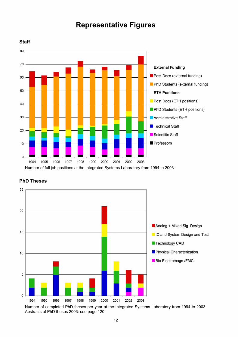
Staff
Number of full job positions at the Integrated Systems Laboratory from 1994 to 2003.
PhD Theses
Number of completed PhD theses per year at the Integrated Systems Laboratory from 1994 to 2003.Abstracts of PhD theses 2003: see page 120.
12
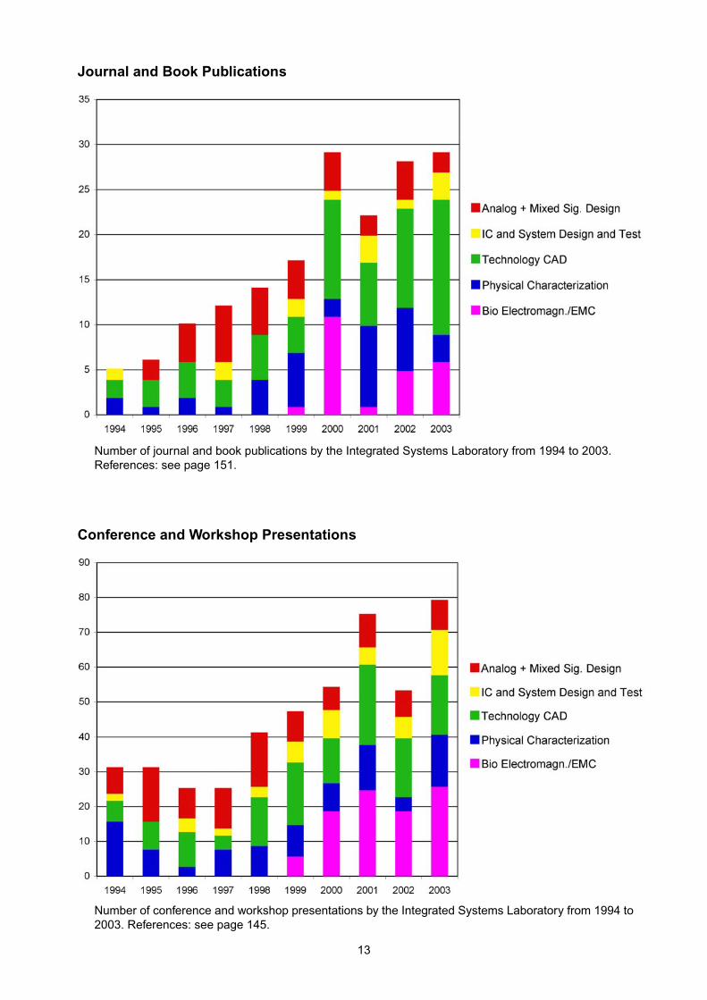
Journal and Book Publications
Number of journal and book publications by the Integrated Systems Laboratory from 1994 to 2003.References: see page 151.
Conference and Workshop Presentations
Number of conference and workshop presentations by the Integrated Systems Laboratory from 1994 to2003. References: see page 145.
13
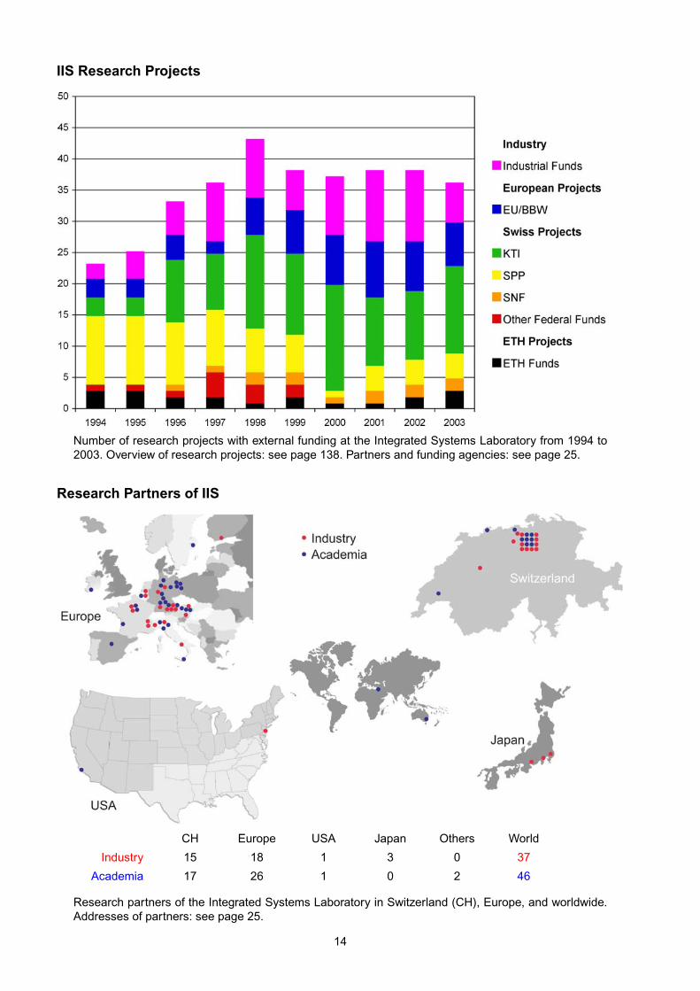
IIS Research Projects
Number of research projects with external funding at the Integrated Systems Laboratory from 1994 to2003. Overview of research projects: see page 138. Partners and funding agencies: see page 25.
Research Partners of IIS
CH Europe USA Japan Others World
Industry 15 18 1 3 0 37
Academia 17 26 1 0 2 46
Research partners of the Integrated Systems Laboratory in Switzerland (CH), Europe, and worldwide.Addresses of partners: see page 25.
14
Staff
ProfessorsFichtner Wolfgang, Dr., Professor for Electronics, Head since 1 Sept 1985Huang Qiuting, Dr., Professor for Electronics since 1 Jan 1993
Microelectronics Design CenterKaeslin Hubert, Dr., Dipl. El.-Ing. ETH, Head since 1 Jan 1986Brändli Matthias, Dipl. El.-Ing. ETH since 1 May 2001Camarero Francisco, Dipl. Ing. since 12 June 2002Köppel Rudolf, FEAM since 1 Apr 1995
Scientific StaffAemmer Dölf, Dr., Dipl. Phys. ETH, Senior Scientist since 1 Sept 1985Alonso Eduardo, Dr., Industrial Engineer since 1 July 2000Balmelli Pio, Dr., Dipl. El.-Ing. ETH since 1 Apr 1998Barlini Davide, Electronic Eng. since 1 Oct 2002Benkler Stefan, Dipl. Rech. Wiss. ETH since 15 Oct 2002Bösch Thomas, Dipl. El.-Ing. ETH since 1 Apr 2000Brenna Gabriel, Dipl. El.-Ing. ETH since 1 Mar 2000Brugger Simon, Dipl. El.-Ing. ETH since 17 Jan 2001Bufler Fabian, PD, Dr., Dipl.-Phys 1 Nov 1997 – 31 Dec 2003Burg Andreas, Dipl. El.-Ing. ETH since 6 Nov 2000Burger Thomas, Dr., Dipl. El.-Ing. ETH since 1 Oct 1994Bürgin Felix, Dipl. El.-Ing. ETH since 1 Jun 2003Carbognani Flavio, Telecommunications Eng. since 1 Dec 2002Centoni Scott, Dr., Materials Science since 1 May 2003Chen Xinhua, M. Sc. EE since 1 Sept 2001Chen Yihui, M. Sc. EE since 1 Aug 2003Christen Thomas, Dipl. El.-Ing. ETH since 1 Oct 2003Ciappa Mauro, Dr., Dipl.-Phys. since 1 Jan 1998Corvasce Chiara, Dipl.-Phys. since 8 Apr 2002Dellsperger Thomas, Dipl. El.-Ing. ETH since 1 Dec 2003Eberli Stefan, dipl. El.-Ing. ETH since 1 Dec 2003Ebert Sven, Dipl.-Phys. since 15 May 2000Eom Sang Jin, M. Sc. EE since 3 July 2002Felber Norbert, Dr., Dipl. Phys. ETH, Senior Scientist since 1 July 1987Francese Pier-Andrea, Dipl. El.-Ing. since 1 Sept 2000Futter Peter, M. Sc. EE 26 Aug 2002 – 31 Dec 2003Geelhaar Frank, Dipl.-Phys. since 1 Oct 1998Glaser Ulrich, Dipl.-Phys. since 1 Oct 2002Gürkaynak Frank, Dipl. El.-Ing. since 15 Sept 2000Häne Simon, Dipl. El.-Ing. ETH since 1 June 2002Hammerschmied Clemens, Dr., Dipl. El.-Ing. ETH 1 June 1994 – 30 Apr 2003Heinz Frederik, Dipl. Phys. ETH since 25 Apr 2000Hertle Jürgen, Dipl. Ing. Elektrotechnik since 2 Mar 1998Höhr Tim, Dipl.-Phys. since 15 Mar 2001Jacob Biju, Dr., MTech. since 1 Sept 2002Kaplan Vassili, M. Sc. Mathematics since 1 Dez 2003Kouchev Ilian, M. of Science since 1 Sept 2000Krause Jens, Dr., Dipl.-Phys. 1 Nov 1997 – 31 Dec 2003Laino Valerio, Electrical Eng. since 1 Oct 2002Loeser Martin, Dipl. Ing. since 1 Sept 2003Luisier Mathieu, Dipl. El.-Ing. ETH since 1 Apr 2003Lüthi Peter, Dipl. El.-Ing. ETH since 1 Nov 2003Martelli Chiara, Dipl. El.-Ing. since 17 Jan 2001Müller Christoph, Dipl. Phys. ETH since 1 June 2000
15

Nikoloski Neviana, M. Sc. Engineering Physics since 15 Nov 2002Odermatt Stefan, Dipl. El.-Ing. ETH since 15 Mar 2003Oesch Walter, Dipl. Natw. ETH since 15 Aug 2000Oetiker Stephan, Dipl. Informatik-Ing. ETH since 1 May 2001Oila Kari, M. Sc. (Mech. Eng.) 13 Aug 2001 – 31 Oct 2003Olszewska Joanna, Dipl. El.-Ing. EPFL since 1 Dec 2003Papadopulos Dimitris, M. Sc. EE since 1 July 2003Perels, Dipl. El.-Ing. ETH since 1 Feb 2001Pfaff Dirk, Dr. Dipl. El.-Ing. ETH 1 Mar 1997 – 28 Feb 2003Pfeiffer Michael, Dipl.-Phys. since 1 Oct 1999Pontarolo Gianpaolo, Dipl. El.-Ing. ETH 1 Mar 2002 – 31 Dec 2003Reutemann Robert, Dipl. El.-Ing. ETH 15 Jan 1998 – 31 Jan 2003Rogin Jürgen, Dipl. El.-Ing. ETH since 1 Apr 1999Röllin Stefan, Dipl. Math. ETH since 1 Apr 2000Roth Eric, Dipl. El.-Ing. ETH since 5 Apr 2000Ruiz Gallego Ivan, Dipl. El.-Ing. ETH since 15 Nov 2003Sahli Beat, Dipl.-Phys. since 1 June 2000Schaldach Markus, Dipl.-Ing. since 1 Mar 2000Schenk Andreas, PD, Dr., Dipl.-Phys., Senior Scientist since 1 Aug 1991Schmithüsen Bernhard, Dr., Dipl.-Mathematiker since 27 May 1996Schneider Lutz, Dipl. Phys. ETH since 7 May 2001Schuderer Jürgen Rudolf, Dr., Dipl.-Phys. 1 Oct 1999 – 15 Nov 2003Stangoni Maria, Dipl. El.-Ing. since 15 Feb 2001Streiff Matthias, Dr., Dipl. El.-Ing. ETH since 7 Feb 2000Treichler Jürg, Dipl. El.-Ing. ETH since 1 May 2003Tschopp David, Dipl. El.-Ing. ETH since 1 May 1999Villiger Thomas, Dipl. El.-Ing. ETH since 1 May 1998Wegmüller Marc, Dipl. El.-Ing. ETH since 1 Oct 2003Witzig Andreas, Dr., Dipl. El.-Ing. ETH since 1 Aug 1997Yuan Chenghao, Dr., M. Sc. EE since 15 Nov 2003Zehnder Oliver, Dipl. Phys. ETH 1 Nov 2002 – 31 Aug 2003
Computer StaffBöhm Anja, Dipl. Geologin since 1 Apr 2001Richardet Christoph, Oberstufenlehrer since 10 May 2000Wicki Christoph, Dipl. El.-Ing. ETH since 1 Oct 1985
Technical StaffBalmer Christoph, Dipl. El.-Ing. HTL since 1 Aug 1989Gisler Hansjörg, Industriespengler (80%) since 1 Sept 1989Illien Fritz, Dipl. El.-Ing. HTL since 1 May 1998Mathys Hanspeter, Elektromonteur since 15 Dec 1991Rheiner Rudi, Dipl. El.-Ing. HTL since 15 Nov 1996
Administrative StaffBoksberger Margit (60%) since 1 Jan 2000Bucher Gina-Lisa (30%) since 15 Nov 2003Fischer Bruno, Dipl. El.-Ing. HTL since 14 Apr 1992Haller Christine, Betriebsökonom HWV (95%) since 8 Mar 1993Plank Eva (50%) since 1 July 1998Roffler Verena (50%) since 1 Sept 1999
16
Former PhD Students
Name Degree Now withreceived
Bach Carlo 1993 Interstaatliche Hochschule für Technik (NTB)Werdenbergstrasse 4CH-9470 Buchs, Switzerland
Balmelli Pio 2003 Integrated Systems LaboratoryETH ZürichCH-8092 Zürich, Switzerland
Basedau Philipp 1999 Philips Semiconductors AGBinzstrasse 44CH-8045 Zürich, Switzerland
Bonnenberg Heinz 1993 Micronas Munich GmbHFrankenthalerstrasse 2D-81539 München, Germany
Bürgler Josef 1990 Hochschule Technik+Architektur LuzernTechnikumstrasse 21CH-6048 Horw, Switzerland
Burger Thomas 2002 Integrated Systems LaboratoryETH ZürichCH-8092 Zürich, Switzerland
Chavannes Nicolas 2002 IT’IS FoundationZeughausstrasse 43CH-8004 Zürich, Switzerland
Christ Andreas 2003 IT’IS FoundationZeughausstrasse 43CH-8004 Zürich, Switzerland
Ciampolini Lorenzo 2001 9, Rue de Dr. MazetF-38000 Grenoble, France
Ciappa Mauro 2000 Integrated Systems LaboratoryETH ZürichCH-8092 Zürich, Switzerland
Conti Paolo 1991 Glasmalergasse 2CH-8004 Zürich, Switzerland
Curiger Andreas 1993 Omnisec AGRietstrasse 14CH-8108 Dällikon, Switzerland
Deiss Armin 2002 Microtune, Inc.2201 10th StreetPlano, TX 75074, USA
Dettmer Hartmut 1994 Infineon TechnologiesAI IP DD LV 1Balanstrasse 73D-81541 München, Germany
Doswald Daniel 2000 ATI Research GmbHMoosstrasse 18BD-82319 Starnberg, Germany
17
Eicher Simon 1996 ABB Semiconductors AGR&D Lb2Fabrikstrasse 3CH-5600 Lenzburg, Switzerland
Esmark Kai 2001 Infineon TechnologiesDAT LIB TI-ESD/Latch-upPostfach 80 17 09D-81609 München, Germany
Fillo Marco 1993 Quadrics Supercomputers World Ltd.Via Marcellina 11I-00131 Roma, Italy
Gappisch Steffen 1996 Philips Semiconductors AGBinzstrasse 44CH-8045 Zürich, Switzerland
Garreton Gilda 1998 UBS AG, Stamford BranchWashington Boulevard 677Stamford, CT 06901, USA
Gull Ronald 1996 BridgeCo AGRingstrasse 14CH-8600 Dübendorf, Switzerland
Hager Christian 2000 McKinsey & CompanyAlpenstrasse 3CH-8065 Zürich, Switzerland
Hammerschmied Clemens 2000 Maxim Integrated ProductsSignal Processing & Conversion120 San Gabriel DriveSunnyvale, CA 94086, USA
Heeb Hansruedi 1989 esmertec agCEOLagerstrasse 14CH-8600 Dübendorf, Switzerland
Heiser Gernot 1991 School of Computer Science & EngineeringUniversity of New South WalesP.O. Box 1Sydney, 2052 NSW, Australia
Herkersdorf Andreas 1991 Institute for Integrated SystemsTechnische Universität MünchenArcisstrasse 21D-80290 München, Germany
Herrigel Alexander 1990 R3 Security Engineering AGZürichstrasse 151CH-8607 Aathal-Seegräben, Switzerland
Heusler Lucas 1990 IBM Zurich Research LaboratorySäumerstrasse 4CH-8803 Rüschlikon, Switzerland
Hitschfeld Nancy 1993 Departamento de Ciencias de la ComputaciónUniversidad de ChileBlanco Encalada 2120Santiago, Chile
18
Höfler Alexander 1997 Motorola, Inc.6501 West William Cannon DriveMail Drop OE341Austin, TX 78735, USA
Humbel Oliver 2000 ABB Semiconductors AGProduktion Lb2Fabrikstrasse 3CH-5600 Lenzburg, Switzerland
Kells Kevin 1994 Integrated Systems Engineering, Inc.111 North Market Street, Suite 710San Jose, CA 95113, USA
Körner Thomas 1999 ABB Business Services Ltd.SLE-I Intellectual PropertyBrown Boveri Strasse 6CH-5400 Baden, Switzerland
Krause Jens 2001 Integrated Systems LaboratoryETH ZürichCH-8092 Zürich, Switzerland
Krumbein Ulrich 1996 Infineon TechnologiesWS SD D TrMOSPostfach 80 09 49D-81609 München, Germany
Kuratli Christoph 1999 Bernafon Ltd.IC-DesignMorgenstrasse 131CH-3018 Bern, Switzerland
Lamb Peter 1990 55 Gilbert STHackett 2602Canberra, Australia
Lendenmann Heinz 1994 ABB Corporate ResearchDept. GSE-721 78 Västerås, Sweden
Leonhardt Götz 2000 Sun Microsystems, Inc.901 San Antonio RoadM/S USUN02-301Palo Alto, CA 94303-4900, USA
Liegmann Arno 1995 Rüti 18CH-8357 Guntershausen, Switzerland
Litsios James 1996 Actant AGBahnhofstrasse 10CH-6300 Zug, Switzerland
Menolfi Christian 2000 IBM Zurich Research LaboratorySäumerstrasse 4CH-8803 Rüschlikon, Switzerland
Mergens Markus 2001 Sarnoff EuropeBrugse Baan 188AB-8470 Gistel, Belgium
Müller Stephan 1994 371 Maeve CourtSan Jose, CA 95136, USA
19
Muttersbach Jens 2001 Philips Semiconductors AGRäffelstrasse 298045 Zürich, Switzerland
Neeracher Matthias 1998 Apple Computer, Inc.MS 301-3KM1 Infinite LoopCupertino, CA 95014, USA
Nussbaum Miguel 1988 Departamento de Ciencia de la ComputaciónEscuela de IngenieríaUniversidad Católica de ChileSantiago, Chile
Oberle Michael 2002 miromico agTechnoparkstrasse 1CH-8005 Zürich, Switzerland
Omura Ichiro 2001 Toshiba Corp. Semiconductor Comp.Discrete Semiconductor Division1, Komukai Toshiba-cho, Saiwai-kuKawasaki 212-8583, Japan
Orsatti Paolo 2000 NemeriX SAStabile Gerre 2000Casella postale 425CH-6928 Manno, Switzerland
Pfaff Dirk 2003 Landis&Gyr AGFeldstrasse 1, PostfachCH-6301 Zug, Switzerland
Pfäffli Paul 1999 ISE Integrated Systems Engineering AGAffolternstrasse 52CH-8050 Zürich, Switzerland
Piazza Francesco 2000 NemeriX SAStabile Gerre 2000Casella postale 425CH-6928 Manno, Switzerland
Pommerell Claude 1992 CH-I Information TechnologyABB (Switzerland) Ltd.Brown Boveri Strasse 6CH-5400 Baden, Switzerland
Röwer Thomas 2000 IBM T. J. Watson Research CenterP.O. Box 218Yorktown Heights, NY 10598, USA
Rogenmoser Robert 1996 Broadcom CorporationBroadband Processor Business Unit2451 Mission College BoulevardSanta Clara, CA 95054, USA
Rothacher Fritz 1995 Infineon TechnologiesWS BB D CR FE2P.O. Box 80 09 49D-81609 München, Germany
Rühl Roland 1992 PDF Solutions, Inc.333 West San Carlos StreetSan Jose, CA 95110, USA
20
Ryter Roland 1996 Philips Semiconductors AGBinzstrasse 44CH-8045 Zürich, Switzerland
Schenk Olaf 2000 University BaselDepartment of Computer ScienceKlingelbergstrasse 50CH-4056 Basel, Switzerland
Schenkel Michael 2002 Integrated Systems Engineering, Inc.111 North Market Street, Suite 710San Jose, CA 95113, USA
Schmithüsen Bernhard 2001 Integrated Systems LaboratoryETH ZürichCH-8092 Zürich, Switzerland
Schönbächler Edgar 1998 Wallsten Medical SAAvenue Riond-Bosson 14CH-1110 Morges, Switzerland
Scholze Andreas 2000 Integrated Systems Engineering, Inc.111 North Market Street, Suite 710San Jose, CA 95113, USA
Schuderer Jürgen 2003 IT’IS FoundationZeughausstrasse 43CH-8004 Zürich, Switzerland
Schuster Christian 2000 IBM T. J. Watson Research CenterP.O. Box 218Yorktown Heights, NY 10598, USA
Seda Steven 1993 Zurich Financial ServicesMythenquai 2CH-8022 Zürich, Switzerland
Stadler Manfred 2000 BridgeCo AGRingstrasse 14CH-8600 Dübendorf, Switzerland
Stricker Andreas 2000 IBM MicroelectronicsMS 972C, 1000 RiverstreetEssex Junction, VT 05452, USA
Thalheim Jan 2003 CT-Concept Technologie AGJ. Renfer-Strasse 15CH-2504 Biel, Switzerland
Thalmann Markus 2000 BridgeCo AGRingstrasse 14CH-8600 Dübendorf, Switzerland
Villablanca Luis 2000 Avant Corp.FremontCA 94538, USA
von Arx Christoph 1996 cva technical consulting agGeissfluhweg 30CH-4600 Olten, Switzerland
Wassner Jürgen 2001 Schmid Telecom AGBinzstrasse 35CH-8045 Zürich, Switzerland
21

Westermann Marc 1995 Logismata AGHardturmstrasse 76CH-8005 Zürich, Switzerland
Wettstein Andreas 2000 ISE Integrated Systems Engineering AGAffolternstrasse 52CH-8050 Zürich, Switzerland
Wikström Tobias 2000 ABB Corporate Research ABDept. DS-721 78 Västerås, Sweden
Witzig Andreas 2002 ISE Integrated Systems Engineering AGAffolternstrasse 52CH-8050 Zürich, Switzerland
Witzigmann Bernd 2000 Integrated Systems LaboratoryETH ZürichCH-8092 Zürich, Switzerland
Yun Chan-Su 2000 Integrated Systems Engineering, Inc.111 North Market Street, Suite 710San Jose, CA 95113, USA
Zahir Rumi 1991 428 Glenwood AvenueMenlo Park, CA 94025, USA
Zelenka Stefan 2001 Integrated Systems Engineering, Inc.111 North Market Street, Suite 710San Jose, CA 95113, USA
Zimmermann Reto 1997 Synopsys, Inc.2025 NW Cornelius Pass RoadHillsboro, OR 97124, USA
22
Academic Guests
Prof. J. Katzenelson Technion, Israel Institute of Technology, Haifa, Israel 1 Aug – 31 Dec 2003
L. Occhi Avalon Photonics Ltd., Zurich, Switzerland repeatedly
Dr. P. Royo Avalon Photonics Ltd., Zurich, Switzerland repeatedly
C. Zinoni Inst of Photonics and Quantum Electronics, EPFL,Lausanne, Switzerland repeatedly
Dr. H. Schlüter Trumpf Photonics Inc., Cranbury, NJ, USA 8 Jan 2003
Dr. T. Nakagri CANON Inc. Tokyo, Japan 16 Jan 2003
Dr. M. Shibata CANON Inc. Tokyo, Japan 16 Jan 2003
Dr. M. Leicht Infineon Technologies, Villach, Austria 27 Jan 2003
M. Buzzo Infineon Technologies, Villach, Austria 27 Jan 2003
Dr. Heinz Bonnenberg Micronas GmbH, München, Germany 27 Jan 2003
Dr. W.-C. Ng Integrated Systems Engineering, Inc.,San Jose, CA, USA 10 Feb – 22 Feb 2003
Dr. K.-H. Paik Integrated Systems Engineering, Inc.,San Jose, CA, USA 10 Feb – 22 Feb 2003
Dr. O. Schenk Universität Basel, Basel, Switzerland 24 Mar 2003
Dr. H. Fitze Paul Scherrer Institut (PSI), Villigen, Switzerland 24 Mar 2003
L. Stingelin Paul Scherrer Institut (PSI), Villigen, Switzerland 24 Mar 2003
Dr. C. Prott Universität Kassel, Kassel, Germany 7 Apr – 17 Apr 2003
Prof. M. Vanzi University of Cagliari, Italy 22 Apr 2003
A. Romer Bernafon, Bern, Switzerland 30 Apr 2003
Dr. P. Zbinden Bernafon, Bern, Switzerland 30 Apr 2003
Dr. J. Buus Gayton Photonics Ltd, Gaiton, Great Britain 30 Apr 2003
Dr. R. Raschke Fujitsu Laboratories of Europe, Darmstadt, Germany 13 May 2003
Dr. J. Buus Gayton Photonics Ltd, Gaiton, Great Britain 14 May – 15 May 2003
Dr. J. Hankey Gayton Photonics Ltd, Gaiton, Great Britain 14 May – 15 May 2003
Dr. H. Hillmer Bernafon, Bern, Switzerland 14 May 2003
Dr. K. Steenbergen ThreeFive Photonics, DA Houten, Netherlands 16 May 2003
Dr. J. P. R. David University of Sheffield, Great Britain 16 May 2003
Dr. A. ten Berg Philips Research The Netherlands, Eindhoven, The Netherlands 12 Jun 2003
Dr. M. Heijligers Philips Research The Netherlands, Eindhoven, The Netherlands 12 Jun 2003
Dr. F. Pessolano Philips Research The Netherlands, Eindhoven, The Netherlands 12 Jun 2003
Dr. K. Hamada Toyota Motor Corporation, Aichi, Japan 19 Jun 2003
Dr. J. Matsuda Sanyo Electric Co., Ltd., Gifu, Japan 10 Jul 2003
Dr. K. Shirai Toshiba Corporation, Yokohama, Japan 10 Jul 2003
23
K. Kimura Hitachi Ltd., Tokyo, Japan 18 Jul 2003
Dr. O. Takahiro Hitachi Ltd., Tokyo, Japan 18 Jul 2003
Dr. K. Yano Hitachi Ltd., Tokyo, Japan 18 Jul 2003
Prof. G.-Q. Gu Southeast University, Nanjing, China 21 Jul 2003
D. Huang Southeast University, Nanjing, China 21 Jul 2003
Dr. C. Goiceanu Occupational Health Department, Institute of Public Health,Iasi, Romania 1 Jun – 14 Nov 2003
Dr. G. Jamshid Integrated Systems Engineering, Inc.,San Jose, CA, USA 11 Aug – 30 Aug 2003
H. Yabuhara Toshiba Corporation, Yokohama, Japan 15 Aug – 18 Aug 2003
Dr. G. Dunn University of Aberdeen, Great Britain 8 Sep – 10 Sep 2003
J. Gharib Integrated Systems Engineering, Inc.,San Jose, CA, USA 12 Sep – 29 Sep 2003
Prof. Dr. I. Kaplan Universidad Nacional Autonomo de Mexico, Mexico 18 Sep 2003
Dr. Keiichiro Shimizu Matsushita Ltd., Kyoto, Japan 24 Sep 2003
Dr. K. Esmark Infineon Technologies, Munich, Germany 7 Oct 2003
H. Oyamatsu Toshiba Corporation, Yokohama, Japan 5 Nov 2003
Dr. R. Raschke Fujitsu Laboratories of Europe, Darmstadt, Germany 17 Nov 2003
H. Oka Fujitsu Laboratories LTD, Tokyo, Japan 17 Nov 2003
Dr. T. Kuhn University of Münster, Germany 4 Dec 2003
Dr. C. Vélez Exalos AG, Zurich, Switzerland 4 Dec 2003
Dr. L. Occhi Exalos AG, Zurich, Switzerland 4 Dec 2003
24
Partners and Funding Agencies
ACP ACP Advanced Circuit Pursuit AGAlte Landstrasse 101CH-8702 Zollikon ZHSwitzerland
Albis Optelectronics Albis Optoelectronics AGMoosstrasse 2CH-8803 RüschlikonSwitzerland
AMUW Wien Universitätsklinik für Innere Medizin IVKlinische Abteilung ArbeitsmedizinWähringer Gürtel 18–20A-1090 WienAustria
Ansaldo Ansaldo Transporti SpAIngegneria Divisione VeicoliVia Nuove delle Brecce 260I-80147 NapoliItaly
austriamicrosystems austriamicrosystems AGSchloss PremstättenA-8141 UnterpremstättenAustria
Avalon Avalon PhotonicsBadenerstrasse 569CH-8048 ZürichSwitzerland
BBT Bundesamt für Berufsbildung und Technologie(Federal Office for Professional Education and Technology,a Swiss Government Agency)Effingerstrasse 27CH-3003 BernSwitzerland
BBW Bundesamt für Bildung und Wissenschaft(Federal Office for Education and Science,a Swiss Government Agency)Wildhainweg 9CH-3001 BernSwitzerland
Bernafon Bernafon AGMorgenstrasse 131CH-3018 BernSwitzerland
Bookham Bookham (Switzerland) AGBinzstrasse 17CH-8045 ZürichSwitzerland
25
Bosch Robert Bosch GmbHTübingerstrasse 123D-72703 ReutlingenGermany
and
Robert Bosch GmbHWernerstrasse 1D-70442 StuttgartGermany
BridgeCo BridgeCo AGRingstrasse 14CH-8600 DübendorfSwitzerland
CNR-IMETEM Consiglio Nationale di Metodologie e Tecnologie per la Microelettronica(IMETEM)Stradale Primosole 50I-95121 CataniaItaly
CRF Centro Ricerche Fiat SCpAStrada Torino 50I-10043 OrbassanoItaly
Elektrovac Electrovac Fabrikation Elektrotechnischer Spezialartikel GmbHZentrale Forschung und EntwicklungAufeldgasse 37–39A-3400 KlosterneuburgAustria
ENSCPB Talence Ecole Nationale Supérieure de Chimie et de Physique de BordeauxAvenue Pey BerlandF-33405 TalenceFrance
EPFL Ecole Polytechnique Fédéral Lausanne(Swiss Federal Institute of Technology Lausanne)CH-1002 LausanneSwitzerland
ETHZ Eidgenössische Technische Hochschule Zürich(Swiss Federal Institute of Technology Zürich)ETH ZentrumCH-8092 ZürichSwitzerland
EU-GROWTH Community Research in the Fifth Framework Programme“Competitive and sustainable growth (GROWTH)” of the European Union.
EU-IST Community Research in the Fifth Framework Programme“User-friendly information society (IST)” of the European Union.
EU-QUAL Community Research in the Fifth Framework Programme“Quality of life and management of living resources” of the European Union.
EU-RTN Community Research in the Fifth Framework Programme“Improving human research potential and the socio-economic knowledgebase: Research Training Networks (RTN)” of the European Union.
26
EUPEC EUPEC GmbHMax-Planck-Strasse 5D-59581 WarsteinGermany
Exalos Exalos AGTechnoparkstrasse 1CH-8005 ZürichSwitzerland
Ferraz Ferraz Date Industries S.A.Les Revoulin Route de St-HonoreF-38350 La MureFrance
FhG-IIS-B Fraunhofer-Institut für Integrierte SchaltungenBauelementetechnologieSchottkystrasse 10D-91058 ErlangenGermany
FNM Forschungskoperation Mobilkommunikationc/o Institut für Feldtheorie und Höchstfrequenztechnik(Laboratory for Electromagnetic Fields and Waves)ETH ZürichGloriastrasse 35CH-8092 ZürichSwitzerland
Fujitsu Fujitsu Laboratories Ltd10-1, Morinosato-WakamiyaAtsugi 243-01Japan
and
Fujitsu Laboratories of Europe LtdHayes Park CentralHayes End Road, HayesMiddlesex UB4 8FEUnited Kingdom
HERCULAS Consortium CNR-IMETEM, Catania (Italy)HMI, Berlin (Germany)IHP, Frankfurt (Germany)IMEC, Leuven (Belgium)KTH, Kista (Sweden)Philips Nederland, Eindhooven (The Netherlands)ST Crolles, Crolles (France)TAU, Ramat Aviv (Israel)Uni Hamburg, Hamburg (Germany)
HIMRATE Consortium Ansaldo, Napoli (Italy)CRF, Orbassano (Italy)Electrovac, Klosterneuburg (Austria)EUPEC, Warstein (Germany)Ferraz, La Mure (France)INTRETS, Arcueil (France)Regienov, Guyancourt (France)Siemens München, München (Germany)TU München, München (Germany)TU Wien, Wien (Austria)
27
HMI Hahn-Meitner-Institut Berlin GmbHGlienicker Strasse 100D-14019 BerlinGermany
IBM Research IBM Research GmbHSäumerstrasse 4CH-8803 RüschlikonSwitzerland
IfE-ETHZ Institut für Elektronik(Laboratory for Electronics)ETH ZürichGloriastrasse 35CH-8092 ZürichSwitzerland
IFH-ETHZ Institut für Feldtheorie und Höchstfrequenztechnik(Laboratory for Electromagnetic Fields and Waves)ETH ZürichGloriastrasse 35CH-8092 ZürichSwitzerland
IFBH Hannover Institut für BiophysikUniversität HannoverHerrenhäuserstrasse 2D-30419 HannoverGermany
IHP Institute for Semiconductor Physics (IHP)Walter-Korsing-Strasse 2D-15230 Frankfurt (Oder)Germany
IIS-ETHZ Integrated Systems LaboratoryETH ZürichGloriastrasse 35CH-8092 ZürichSwitzerland(i.e. the publisher of this “Research Review 2003”)
IKT-ETHZ Institut für Kommunikationstechnik(Laboratory for Communication Technology)ETH ZürichSternwartstrasse 7CH-8092 ZürichSwitzerland
IMEC Interuniversity Microelectronics CentreKapeldreef 75B-3001 LeuvenBelgium
Infineon Infineon Technologies AGOtto-Hahn-Ring 6D-81730 MünchenGermany
and
Infineon Technologies AGBalanstrasse 73D-81609 MünchenGermany
28
INRETS Institut National de Recherche sur les Transport et leur Sécuruité2, Avenue du Général Malleret-JoinvilleF-94114 ArcueilFrance
INRIA Institute Natinal de Recherche en Informatique et AutomatiqueBP 105 Domaine de VoluceauF-78153 Le ChesnayFrance
IPK Gatersleben Institut für Pflanzengenetik und Kulturpflanzenforschung GaterslebenCorrenstrasse 3D-06466 GaterslebenGermany
ISE AG ISE Integrated Sysems Engineering AGAffolternstrasse 52CH-8050 ZürichSwitzerland
and
ISE Integrated Systems Engineering Inc.111 North Market StreetSuite 710San Jose CA 95113USA
and
ISE Integrated Systems Engineering Japan Ltd.Yaesu Daibiru 2F1-1, Kyobashi 1-chome, Chuo-kuTokyo, 104-0031Japan
IT’IS IT’IS Foundation for Research on Information Technologies in SocietyETH ZürichETH Zentrum, ETZCH-8092 ZürichSwitzerland
and
Zeughausstrasse 43CH-8004 ZürichSwitzerland
29
IT’IS Partners ARCS, Seibersdorf (Austria)BAG, Bern (Switzerland)BfS, Salzgitter (Germany)BORL-USZ, Zürich (Switzerland)EMPA, Dübendorf (Switzerland)Exponent, Bellevue (USA)GSM-Association, Genève (Switzerland)IfW, St. Gallen (Switzerland)IMTEK, Freiburg (Germany)INTEC, Gent (Belgium)IPT-UNIZH, Zürich (Switzerland)IZT, Berlin ( Germany)Karolinska Institute, Huddinge (Sweden)KIST, Saarbrücken (Germany)MCL, London (Great Britain)MMF, Brussels (Belgium)Motorola, Ft. Lauderdale (USA)NIEHS, Research Triangle Park (USA)NIST, Gaithersburg (USA)NOKIA NRC, Helsinki (Finland)RCL, Thessaloniki (Greece)TA SWISS, Bern (Switzerland)TDC, Zürich (Switzerland)Uni Uppsala, Uppsala (Sweden)Zejiang University, Hangzhou (China)
IWR-ETHZ Institut für Wissenschaftliches Rechnen(Institute for Scientific Computing)ETH ZürichHaldeneggsteig 4CH-8092 ZürichSwitzerland
KTH Kungl Tekniska HögskolanDepartment of Electronics – Laboratory of Semiconductor MaterialsIsafjordsgatan 22–26S-16440 KistaSweden
KTI Kommission für Technologie und Innovation(Commission for Technology and Innovation,a Swiss Government Agency)Effingerstrasse 27CH-3003 BernSwitzerland
Lucent Lucent TechnologiesWireless Research Department791 Holmdel-Keyport RoadHolmdel, NJ 07733-400USA
MATH-ETHZ Forschungsinstitut für Mathematik(Research Institute for Mathematics)ETH ZürichRämistrasse 101CH-8092 ZürichSwitzerland
Miromico Miromico AGTechnoparkstrasse 1CH-8005 ZürichSwitzerland
30

MPG Stuttgart Max-Planck-Institut für FestkörperforschungHeisenbergstasse 1D-70565 StuttgartGermany
NTT Nippon Telegraph and Telephone Corporation3-1, Otemachi 2-Chome, Chiyoda-KuTokyoJapan
Perform A Consortium Partners of the Eureopean research project “PERFORM A – In vivo Research onpossible Health Effects related to Mobile Telephones and Base Stations”FhG-ITA, Hannover (Germany)RCC, Ittingen (Switzerland)ARCS, Seibersdorf (Austria)RBM, Colleretto Giacosa (Italy)IT’IS, Zürich (Switzerland)RCL/AUTH, Thessaloniki (Greece)
Perform B Consortium PIOM, Bordeaux (France)ENEA, Cassacia (Italy)NRPB (CYTO), Oxon (United Kingdom)NRPB (NIR), Oxon (United Kingdom)UKU, Kuopio (Finland)ULP, Strasbourg (France)
Perform B Consortium Karolinska Institute, Huddinge (Sweden)Uni Uppsala, Uppsala (Sweden)IT’IS, Zürich (Switzerland)
Philips Belgium Philips Research LeuvenB-3001 LeuvenBelgium
Philips ED&T Philips Electronic Design & ToolsProf. Holstlaan 4, WAY-31NL-5656 AA EindhovenThe Netherland
Philips Nederland Philips Electronics Nederland B.V.Professor Holstlaan 4NL-5656 AA EindhovenThe Netherlands
Philips Zürich Philips Zürich AG, SemiconductorsBinzstrasse 44CH-8045 ZürichSwitzerland
PSI PSI Paul Scherrer InstitutCH-5332 VilllingenSwitzerland
REFLEX Consortium AMUW Wien, Wien (Austria)ENSCPB Talence, Talence (Belgium)IFBH Hannover, Hannover (Germany)IPK Gatersleben, Gatersleben (Germany)STUK Helsinki, Helsinki (Finland)UKFB Berlin, Berlin (Germany)UMIL Milano, Milano (Italy)Uni Bologna, Bologna (Italy)VERUM, München (Germany)VERYC Madrid, Madrid (Spain)
31
Regienov Regienov – Renault Recherche et Innovation1, Avenue du GolfF-78288 GuyancourtFrance
Siemens München Siemens AGOtto Hahn-Ring 6D-81730 MünchenGermany
SIGMA-C SIGMA-C GmbHRosenheimer Landstrasse 74D-85521 OttobrunnGermany
SNF Swiss National Science FoundationWildhainweg 20CH-3012 BernSwitzerland
Sony UK Sony Semiconductor EuropeAdvanced Products GroupBasingstoke RG22 4SBUnited Kingdom
SPEAG Schmid & Partner Engineering AGZeughausstrasse 43CH-8004 ZürichSwitzerland
ST Agrate ST MicroelectronicsVia Carlo Olivetti 2I-20041 Agrate Brianza (MI)Italy
ST Crolles ST Microelectronics850 rue Jean MonnetF-38921 CrollesFrance
ST Gentilly ST Microelectronics937 Avenue GallieniF-94253 GentillyFrance
STUK Helsinki STUK – Radiation and Nuclear Safety AuthorityLaippatie 4FIN-00880 HelsinkiFinland
TAU Tel-Aviv University (TAU)Department of Physical ElectronicsTel-Aviv University, Ramat AvivIL-69978 Israel
TDC TDC Switzerland AGThurgauerstrasse 60CH-8050 ZürichSwitzerland
32

TIK-ETHZ Institut für Technische Informatik(Computer Engineering and Network Laboratory)ETH ZürichGloriastrasse 35CH-8092 ZürichSwitzerland
TOP NANO 21 Swiss Technology Oriented Program NANO 21(a Swiss Government Agency)Universität BaselInstitut für PhysikKlingelbergstrasse 82CH-4056 BaselSwitzerland
and
Themas AGEgnacherstrasse 69CH-9320 ArbonSwitzerland
Toshiba Toshiba Corporation1-1. Shibaura 1-chome, Minato-kuTokyo 105-8001Japan
and
Toshiba Corporation2-5-1, Kasama, Sakae-kuYokohama 247-8585Japan
and
Toshiba Corporation1, Komukai, Toshibacho, Saiwai-kuKawasaki 210Japan
Toyota Toyota Central R&D Labs. Inc.Nagakute-cho, Aichi-gunAichi 480-1192Japan
TU München Technische Universität MünchenLehrstuhl für Technische ElektrophysikArcisstrasse 21D-80290 MünchenGermany
and
Technische Universität MünchenWalter Schottky Institut E26Am CoulombwallD-85748 GarchingGermany
33

TU Wien Technical University ViennaInstitute for MicroelectronicsGusshausstrasse 27–29A-1040 WienAustria
and
Technical University ViennaDepartment of Materials Science and TestingKarlsplatz 13A-1040 WienAustria
UCSB University of CaliforniaECE DepartmentSanta Barbara, CA 93106-9560USA
UKBF Berlin Universitätsklinikum Benjamin Franklin der freien Universität BerlinInstitut für klinische Chemie und PathobiochemieHindenburgdamm 30D-12200 BerlinGermany
UMIL Milano Universita degli Studi di MilanoDipartimento di FarmacologiaVia Vanvitelli 32I-20129 MilanoItaly
Uni Basel Universität BaselDepartement für Computer WissenschaftenCH-4000 BaselSwitzerland
Uni Bern Universität BernUniversitätsklinik InselspitalCH-3010 BernSwitzerland
Uni Bologna Universita degli Studi di BolognaDipartimento di Elettronica Informatica e SistemisticaVia Zamboni 33I-40126 BolognaItaly
and
Universita degli Studi di BolognaDipartimento di FisicaViale Berti Pichart 6/2I-40127 BolognaItaly
Uni Cagliari Universita degli Studi di´CagliariDipartimento di Ingegneria Elletricae et ElettronicaPiazza D’armiI-09123 CagliariItaly
Uni Canberra Australien National UniversityEngineeringCanberra 0200 ACTAustralia
34

Uni Cork University College CorkNational Microelectronics Research CentreLee Maltings, Prospect RowCorkIreland
Uni Hamburg Universität HamburgInstitut für Angewandte PhysikJungius-Strasse 11D-20335 HamburgGermany
Uni Kassel Universität KasselFachbereich Elektrotechnik/InformatikHeinrich-Plett-Strasse 40D-34132 KasselGermany
Uni Leuven Katolieke Universiteit LeuvenESAT/COSICKasteelpark Arenberg 10B-3001 HeverleeBelgium
Uni Pisa Universita degli studi di PisaDipartimento di Ingegneria della Informazione:Elettronica, Informatica, TelecomunicazioniLungarno Pacinotti 43/44I-56126 PisaItaly
Uni Würzburg Bayerische Julius-Maximilians Universität WürzburgSanderring 2D-97070 WürzburgGermany
VERUM Stiftung für Verhalten und UmweltPettenkoferstr. 33D-80336 MünchenGermany
VERYC Madrid Investigacion BioelectromagnetismoHospital Ramon y CajalCarretara de Colmenar km.9E-28034 MadridSpain
Weiss Digital Audio Weiss Engineering Ltd.Florastrasse 42CH-8610 UsterSwitzerland
WIAS Weierstrass-Institut für Angewandte Analysis und StochastikMohrenstrasse 39D-10117 BerlinGermany
35
36
Awards and Patents
Awards
Qiuting Huang
has received admittance to the
50-Year Anniversary Author Honor Roll
of the International Conference of Solid-State Circuits (ISSCC) for the contribution of more than 10 regularpublications (actualy 14) in the time frame from 1995 to 2003
Neviana Nikoloski
received the
Curtis Carl Johnson Memorial Award
for best student platform presentation“Design & Dosimetry of a TEM Cell Exposure Setup for an In Vitro Replication Study”
at the5th Annual Meeting of the Bioelectromagnetics Society, Maui, HI, USA, June 2003
Patents
Title: Digital gesteuerter OszillatorDigitally Controlled Oscillator
Owner: BridgeCo AG
Inventors: Eric Roth
Patent No.: PCT/CH2003/000405
Title: Prozessor mit verschiedenartigen Steuerwerken für gemeinsam genutzteRessourcenProcessor with Diversified Controllers for Commonly Used Resources
Owner: BridgeCo AG
Inventors: Thomas Boesch, Markus Thalmann, Matthias Tramm
Patent No.: PCT/CH2004/00106
History of the Integrated Systems Laboratory (IIS)
1985 Appointment of Wolfgang Fichtner, Professor for Electronics, Department of Electrical Engineer-ing, ETH Zurich.
Formation of the research group “VLSI” in the Electronics Laboratory.
First research project (2D device simulation, funded by KTI).
Installation of 3 minicomputer DEC VAX-11/785 (1 CPU, 16 MBytes memory).
1986 Foundation of the “Integrated Systems Laboratory” by merging of the research groups ofProf. Wolfgang Fichtner (Department of Electrical Engineering) and Prof. Martin Morf (Depart-ment of Computer Science).
Start of the lecture “Electronics Systems” (undergraduate EE students).
Start of the lecture series “Design of Integrated Circuits I, II, III” (graduate EE, CS, and physicsstudents).
Summer school “VLSI Design” in Beatenberg/Switzerland (2 weeks, 85 participants from Europeand Switzerland), organization as well as scientific and technical responsibility by IIS. 15 invitedtalks by well known experts from USA, Europe, and Switzerland, presentations and hands-onexperience on workstations.
1987 Leaving of Prof. Martin Morf.
Appointment of Marco Annaratone, assistant professor for Parallel Computing, Department ofComputer Science, ETH Zurich.
Start of the lecture “Digital Design and Processor Structures” (undergraduate CS students).
Design and integration of the first student ICs (20MHz, 7000 transistors).
Installation of the HILEVEL TOPAZ 50 ASIC test system (50MHz, 96 I/O channels).
Installation of a mini-supercomputer Alliant FX/80 (6 CPUs, 112 MBytes shared memory).
Introduction of the first professional CAD tool for IC design in teaching and research (VLSI Tech-nology Inc., later Compass Design Automation Inc.).
Installation of the parallel computer Sequent Symmetry (26 CPUs, 160 MBytes shared memory).
1988 Foundation of the Microelectronics Design Center (Department of Electrical Engineering, associ-ated to the Integrated Systems Laboratory).
First PhD thesis of a computer science student at IIS.
Design and integration of the first VLSI chip (Viterbi decoder, 35000 transistors).
1989 First European research project (parallel computer architecture).
First PhD thesis of a physics student at IIS.
2nd prize “Seymour Cray Competition” Switzerland for “Multi-Dimensional SemiconductorDevice Simulation” to members of scientific staff of IIS.
First “Intensive Course on ASIC Design and Test” with ETH-internal and -external participants.
First functional 2D simulation program for semiconductor devices developed by IIS scientificstaff.
1990 First PhD thesis of an electrical engineering student at IIS.
Start of the lecture “Semiconductor Devices: Technology and Modeling”.
CEI-Europe Elsevier course “VLSI Process and Device Simulation” in Davos/Switzerland. Orga-nization as well as scientific and technical responsibility by IIS (1 week, 35 participants).
Start of the project “Education and Research in Microelectronics”, generous funding by the boardof ETH Zurich for IC integration and measurement equipment.
37
Evaluation of the Department of Electrical Engineering of ETH Zurich and the laboratories of thedepartment by a group of international experts. Qualification of the research at the IntegratedSystems Laboratory compared at the international level:
• process and device simulation: outstanding.
• VLSI design: very efficient.
• parallel computer architectures: very good ideas, realization has to be proven.
Prof. Wolfgang Fichtner elected IEEE Fellow for the “application of numerical modeling to devicescaling and submicron transistor optimization”.
1991 Leaving of Prof. Marco Annaratone.
4th International Conference on “Simulation of Semiconductor Devices and Processes –SISDEP’91”, ETH Zurich/Switzerland (3 days, 200 participants), organization by IIS, ConferenceCo-Chairman Prof. Wolfgang Fichtner, 3 invited papers, 44 regular papers, 18 poster presenta-tions.
Start of the national program “Microswiss” to support microelectronics in Swiss SMEs and edu-cation. Microelectronics Design Center acts as a support center.
Presentation of the IIS activities in “Modeling of Microelectronic Devices” at CEBIT’91 exhibitionHannover/Germany, as a winner of the competition “Technology Location Switzerland 1991”.
Installation of the IMS XL60 Mixed Signal ASIC Verification System (60MHz, 96 I/O channels).
1992 Start of the Swiss priority program “LESIT – Power Electronics, Systems, Information Technol-ogy”, 11 research projects in the module “Silicon Power Device Technology” (module coordinatedby Prof. Wolfgang Fichtner).
Start of the first European ESPRIT project (“DESSIS – Device Simulation for Smart IntegratedSystems”).
Start of a European JESSI project (Circuits for Communication Technology).
Design and integration of a high-speed data encryption IC (177Mbit/s, 250000 transistors).
First functional 3D grid generation program developed by IIS scientific staff.
1993 Appointment of Qiuting Huang, assistant professor for Analog Integrated Circuits, Department ofElectrical Engineering, ETH Zurich.
Foundation of the IIS spin-off “ISE Integrated Systems Engineering AG” Zurich by IIS members(scope of business: software and application support in Technology CAD). Location for the firstone and a half years at IIS with support of ETH Zurich.
Start of the lecture “Analog Integrated Circuits” (graduate EE students).
First functional 3D simulation program for semiconductor devices developed by IIS scientificstaff.
1994 “6th International Symposium of Power Semiconductor Devices & ICs – ISPSD’94”,Davos/Switzerland (3 days, 195 participants), organization by IIS, symposium chairmanProf. Wolfgang Fichtner, 3 invited presentations, 29 regular papers, 41 poster presentations.
Planning phase of the Swiss priority program MINAST, designated program directorProf. Wolfgang Fichtner (1994/95), provisional program direction established at IIS.
Installation of the HP83000 ASIC Verification System (660MHz, 128 I/O channels).
Microelectronics Design Center also assumes responsibility for PCB support.
1995 Completion of the Swiss priority program LESIT with outstanding scientific results and efficienttransfer of research to industry.
First functional simulation program for semiconductor processes developed by IIS scientific staff.
Move of spin-off ISE AG from ETH Zurich location to Technopark Zurich.
First course “Getting started with VHDL Synthesis” with ETH-internal and -external participants.
Installation of the parallel computer IBM SP2 (6 CPUs, 4.5 GBytes distributed memory).
38
1996 Start of the Swiss priority program “MINAST – Micro and Nano System Technology”, programdirector Prof. Wolfgang Fichtner (1996–1997), program direction established at IIS, total 56 MioCHF granted by Swiss authorities and more than 60 Mio CHF contributions from Swiss industrialenterprises; IIS research projects: two in the module “Integrated Microsystems Technology”, fourin the module “Design, Simulation and Engineering of Microsystems”, and one in the module“Microsystems Applications”.
1997 Postdoctoral thesis (habilitation) of PD Dr. Andreas Schenk for the subject “Advanced PhysicalModels for Silicon Device Simulation”.
Public workshop “3D Semiconductor Simulation” of the European ESPRIT Project “PROMPT II –Process Optimization in Multiple Simulations for Semiconductor Technology II” (3 days, 56 partic-ipants), Monte Verità Ascona/Switzerland, 8 presentations as well as demonstrations and hands-on experience, organization by IIS and spin-off ISE AG.
Installation of the first parallel computer DEC Alphaserver (4 CPUs, 2 GBytes shared memory).
1998 Promotion of Qiuting Huang to Professor for Electronics, Department of Electrical Engineering,ETH Zurich.
Accommodation of the research group “Physical Characterization”, including well known expertsand advanced equipment from the former Reliability Laboratory at the Department of ElectricalEngineering, ETH Zurich.
Start of three new European research projects.
Two patents on telecommunication ICs, inventors: IIS scientific staff, owner: Siemens SchweizAG.
Migration to Synopsys and Cadence EDA systems for IC design in teaching and research.
First functional simulation program for electromagnetic fields developed by IIS scientific staff.
1999 Accommodation of the research group “Bioelectromagnetics/EMC” from the ElectromagneticFields and Microwave Electronics Laboratory at the Department of Electrical Engineering, ETHZurich.
Election of Prof. Wolfgang Fichtner as head of the Department of Electrical EngineeringOct 1999 – Sept 2001.
Start of the lecture “Electrical Engineering I” (undergraduate mechanical and process engineer-ing students).
Completion of the Swiss priority program MINAST with outstanding scientific results and efficienttransfer of research to industry.
Public workshop “ESD Protection Design Methodology” of the ESPRIT Project ESDEM as anopen meeting of the “EMC ’99 Zurich Symposium”, (1 day, 86 participants), ETH Zurich/Switzer-land, 5 invited talks by well known experts from USA and Europe, demonstrations of the method-ology, organization by IIS and spin-off ISE AG.
Design and integration of a high-quality video image processor (100MHz, 1.8Giga Ops/s,2.7 Mio transistors).
Establishment of the “Foundation for Research on Information Technologies in Society IT’IS”(Zurich, director Dr. Niels Kuster). Associated to ETH Zurich and a close research partner of theIIS research group Bio Electromagnetics/EMC.
2000 Graduation of no less than 21 PhD students at IIS due the conclusion of the 4th framework pro-gram of the European Union as well as the Swiss priority program MINAST.
IEEE Andrew S. Grove Award of the Year 2000 to Prof. Wolfgang Fichtner “for outstanding contri-butions to semiconductor device simulations”.
World’s first chip of relevant complexity in GALS (Globally Asynchronous Locally Synchronous)technique, a SAFER SK-128 cipher implementation.
Ultra low offset (200nV) chopper amplifier.
First functional simulation program for semiconductor lasers by IIS scientific staff.
39
Simulation platform SEMCAD for design and optimization of antennas in complex environmentsby IIS and IT’IS scientific staff.
Evaluation of the Department of Electrical Engineering ETH Zurich by a group of internationalexperts with high scientific reputation. Overall qualification: “The international standing of Inte-grated Systems Laboratory regarding its core activities is definitely among the best of the world.”
Introduction of a new organization structure of ETH Zurich with autonomous departments andglobal budget.
2001 Prof. Qiuting Huang elected IEEE Fellow for outstanding contributions to integrated circuits forwireless communications.
Re-election of Prof. Wolfgang Fichtner as head of the Department of Information Technology andElectrical Engineering Oct 2001 – Sept 2003.
Start of the lecture “Semiconductor Devices” (undergraduate EE students).
Start of the lecture “Communications Electronics” (undergraduate EE students).
Start of the lecture series “Optoelectronic Devices” (graduate EE students).
Three contributions from IIS to the new Project Oriented Work program (undergraduate EE stu-dents).
Configurable hardware optimization and timing recovery for the first multimedia chip of theresearch partner company BridgeCo AG.
13.5mW 185MSample/s Delta-Sigma Modulator for UMTS/GSM Dual-Standard IF Reception.
Completion of the European research project SUBSAFE with excellent review results.
First functional optical eigenmodes solver for Vertical-Cavity Surface-Emitting Lasers (VCSELs).
ESPRIT-Project MADBRIC One-Day “Workshop on A/D Converters for Telecommunication” inPfäffikon, Switzerland with 42 participants from 12 different countries.
Pilot User Workshop “Simulation of Semiconductor Laser Devices” at ETH Zurich/Switzerland (2days, 29 participants from Europe, USA, and Japan), 3 invited talks by well known experts fromUSA and Europe, 5 talks, 1 tutorial, computer lab, organization by IIS.
2002 Start of a close collaboration with the new Communication Theory Group of Prof. HelmutBölcskei (Communication Technology Laboratory, IKT) in the field of multiple-antenna (MIMO)research. A large, ETH-funded project on MIMO research has been approved by the board ofETH.
Successful completion of the European project LEMON on the design and implementation of aUMTS transceiver in deep sub-micron CMOS technology.
14bit, 1MHz Bandwidth Delta-Sigma A/D converter with lowest power consumption published sofar.
The new Monte Carlo simulator SPARTA for stable and efficient self-consistent simulations ofcontemporary MOSFETs was included in the release 8.0 of ISE Integrated Systems EngineeringAG.
Self-consistent coupling of opto-electro-thermal equations in device simulation of Vertical-CavitySurface-Emitting Lasers (VCSEL).
Three accepted papers resulting from Master student theses to international conferences werepresented by the students.
First Linux-cluster for physical simulations in Technology CAD (22 PCs with 2.2GHz CPUs).
“International Conference on Numerical Simulation of Semiconductor Optoelectronic DevicesNUSOD-02”, 25–27 September 2002, organized by IIS at ETH Zurich, 111 participants fromEurope, USA, and Japan, 13 invited talks by well known experts from USA and Europe, 19 talks,10 posters, and 5 company presentations.
40

2003 ETH Zurich established the assistant professorship Computational Optoelectronics. Dr. BerndWitzigmann was elected and has taken up this position at the Integrated Systems Laboratory on1 March 2004.
Re-election of Prof. Wolfgang Fichtner as head of the Department of Information Technology andElectrical Engineering Oct 2003 – Sept 2005.
Audio clock recovery circuit and reconfigurable processor resulting from PhD theses are inte-grated into an industrial Multimedia chip.
First 10 MHz bandwidth delta-sigma modulator with more than 80 dB signal to noise ratio, pub-lished at ISSCC‘04.
The new Monte Carlo simulator NOISE has been developed to enable the computation of noisephenomena in microelectronic device simulation.
41

42
43
Research Projects
IC and System Design and Test
Coordinator:
Norbert Felber
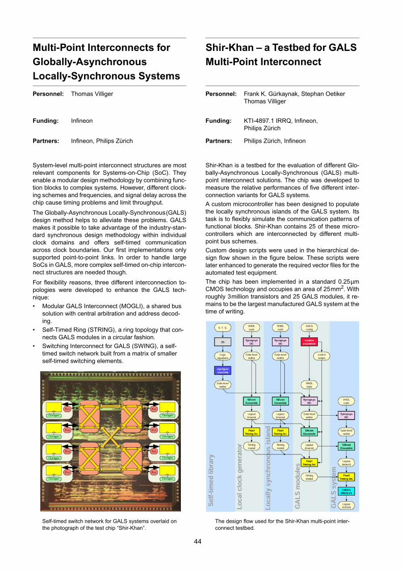
Multi-Point Interconnects forGlobally-AsynchronousLocally-Synchronous Systems
Personnel: Thomas Villiger
Funding: Infineon
Partners: Infineon, Philips Zürich
System-level multi-point interconnect structures are mostrelevant components for Systems-on-Chip (SoC). Theyenable a modular design methodology by combining func-tion blocks to complex systems. However, different clock-ing schemes and frequencies, and signal delay across thechip cause timing problems and limit throughput.
The Globally-Asynchronous Locally-Synchronous(GALS)design method helps to alleviate these problems. GALSmakes it possible to take advantage of the industry-stan-dard synchronous design methodology within individualclock domains and offers self-timed communicationacross clock boundaries. Our first implementations onlysupported point-to-point links. In order to handle largeSoCs in GALS, more complex self-timed on-chip intercon-nect structures are needed though.
For flexibility reasons, three different interconnection to-pologies were developed to enhance the GALS tech-nique:• Modular GALS Interconnect (MOGLI), a shared bus
solution with central arbitration and address decod-ing.
• Self-Timed Ring (STRING), a ring topology that con-nects GALS modules in a circular fashion.
• Switching Interconnect for GALS (SWING), a self-timed switch network built from a matrix of smallerself-timed switching elements.
Self-timed switch network for GALS systems overlaid onthe photograph of the test chip “Shir-Khan”.
44
Shir-Khan – a Testbed for GALSMulti-Point Interconnect
Personnel: Frank K. Gürkaynak, Stephan OetikerThomas Villiger
Funding: KTI-4897.1 IRRQ, Infineon,Philips Zürich
Partners: Philips Zürich, Infineon
Shir-Khan is a testbed for the evaluation of different Glo-bally-Asynchronous Locally-Synchronous (GALS) multi-point interconnect solutions. The chip was developed tomeasure the relative performances of five different inter-connection variants for GALS systems.
A custom microcontroller has been designed to populatethe locally synchronous islands of the GALS system. Itstask is to flexibly simulate the communication patterns offunctional blocks. Shir-Khan contains 25 of these micro-controllers which are interconnected by different multi-point bus schemes.
Custom design scripts were used in the hierarchical de-sign flow shown in the figure below. These scripts werelater enhanced to generate the required vector files for theautomated test equipment.
The chip has been implemented in a standard 0.25µmCMOS technology and occupies an area of 25mm2. Withroughly 3million transistors and 25 GALS modules, it re-mains to be the largest manufactured GALS system at thetime of writing.
The design flow used for the Shir-Khan multi-point inter-connect testbed.
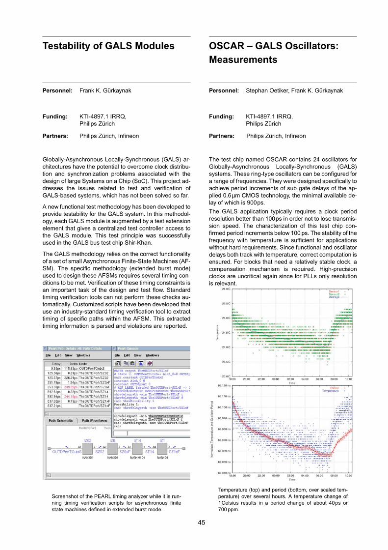
Testability of GALS Modules
Personnel: Frank K. Gürkaynak
Funding: KTI-4897.1 IRRQ,Philips Zürich
Partners: Philips Zürich, Infineon
Globally-Asynchronous Locally-Synchronous (GALS) ar-chitectures have the potential to overcome clock distribu-tion and synchronization problems associated with thedesign of large Systems on a Chip (SoC). This project ad-dresses the issues related to test and verification ofGALS-based systems, which has not been solved so far.
A new functional test methodology has been developed toprovide testability for the GALS system. In this methodol-ogy, each GALS module is augmented by a test extensionelement that gives a centralized test controller access tothe GALS module. This test principle was successfullyused in the GALS bus test chip Shir-Khan.
The GALS methodology relies on the correct functionalityof a set of small Asynchronous Finite-State Machines (AF-SM). The specific methodology (extended burst mode)used to design these AFSMs requires several timing con-ditions to be met. Verification of these timing constraints isan important task of the design and test flow. Standardtiming verification tools can not perform these checks au-tomatically. Customized scripts have been developed thatuse an industry-standard timing verification tool to extracttiming of specific paths within the AFSM. This extractedtiming information is parsed and violations are reported.
Screenshot of the PEARL timing analyzer while it is run-ning timing verification scripts for asynchronous finitestate machines defined in extended burst mode.
45
OSCAR – GALS Oscillators:Measurements
Personnel: Stephan Oetiker, Frank K. Gürkaynak
Funding: KTI-4897.1 IRRQ,Philips Zürich
Partners: Philips Zürich, Infineon
The test chip named OSCAR contains 24 oscillators forGlobally-Asynchronous Locally-Synchronous (GALS)systems. These ring-type oscillators can be configured fora range of frequencies. They were designed specifically toachieve period increments of sub gate delays of the ap-plied 0.6µm CMOS technology, the minimal available de-lay of which is 900ps.
The GALS application typically requires a clock periodresolution better than 100ps in order not to lose transmis-sion speed. The characterization of this test chip con-firmed period increments below 100 ps. The stability of thefrequency with temperature is sufficient for applicationswithout hard requirements. Since functional and oscillatordelays both track with temperature, correct computation isensured. For blocks that need a relatively stable clock, acompensation mechanism is required. High-precisionclocks are uncritical again since for PLLs only resolutionis relevant.
Temperature (top) and period (bottom, over scaled tem-perature) over several hours. A temperature change of1Celsius results in a period change of about 40ps or700 ppm.
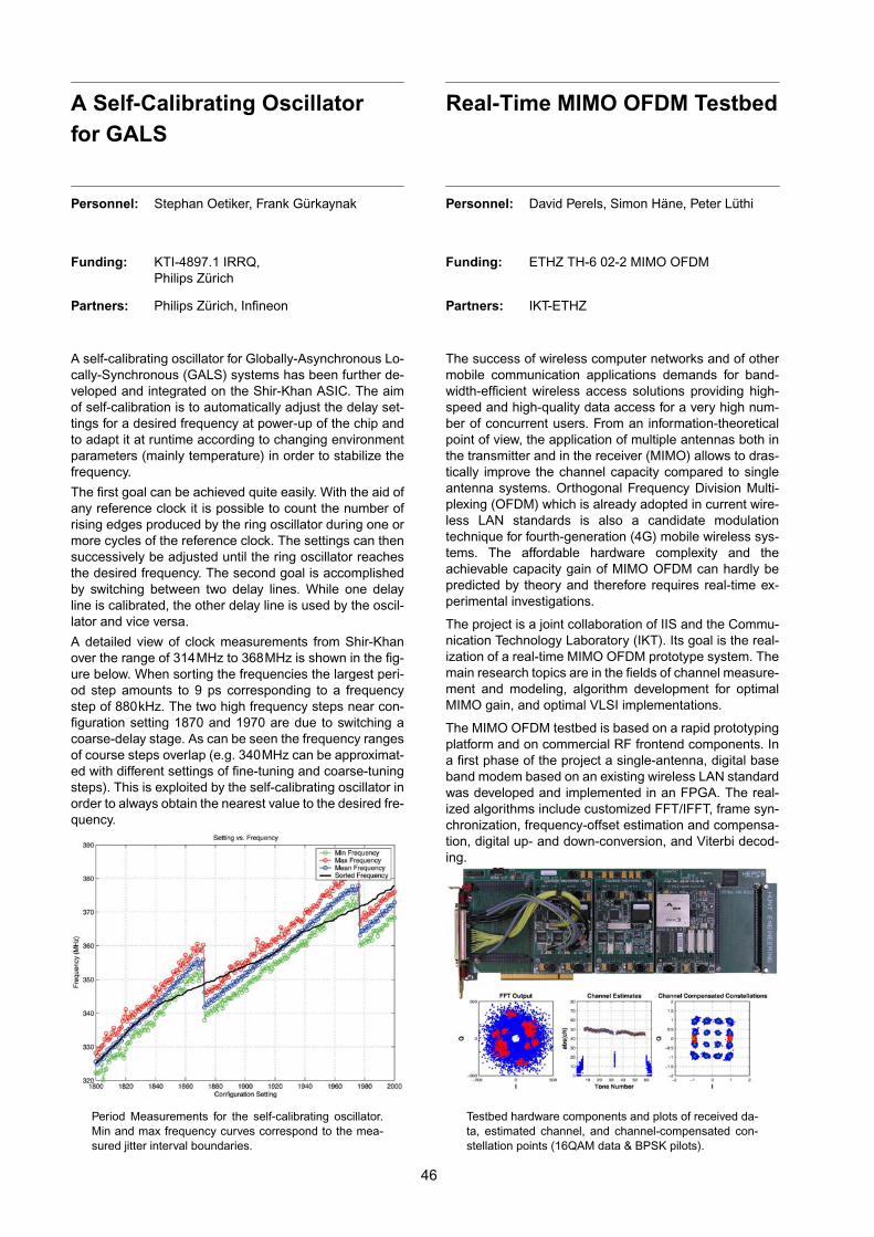
A Self-Calibrating Oscillatorfor GALS
Personnel: Stephan Oetiker, Frank Gürkaynak
Funding: KTI-4897.1 IRRQ,Philips Zürich
Partners: Philips Zürich, Infineon
A self-calibrating oscillator for Globally-Asynchronous Lo-cally-Synchronous (GALS) systems has been further de-veloped and integrated on the Shir-Khan ASIC. The aimof self-calibration is to automatically adjust the delay set-tings for a desired frequency at power-up of the chip andto adapt it at runtime according to changing environmentparameters (mainly temperature) in order to stabilize thefrequency.
The first goal can be achieved quite easily. With the aid ofany reference clock it is possible to count the number ofrising edges produced by the ring oscillator during one ormore cycles of the reference clock. The settings can thensuccessively be adjusted until the ring oscillator reachesthe desired frequency. The second goal is accomplishedby switching between two delay lines. While one delayline is calibrated, the other delay line is used by the oscil-lator and vice versa.
A detailed view of clock measurements from Shir-Khanover the range of 314MHz to 368MHz is shown in the fig-ure below. When sorting the frequencies the largest peri-od step amounts to 9 ps corresponding to a frequencystep of 880kHz. The two high frequency steps near con-figuration setting 1870 and 1970 are due to switching acoarse-delay stage. As can be seen the frequency rangesof course steps overlap (e.g. 340MHz can be approximat-ed with different settings of fine-tuning and coarse-tuningsteps). This is exploited by the self-calibrating oscillator inorder to always obtain the nearest value to the desired fre-quency.
Period Measurements for the self-calibrating oscillator.Min and max frequency curves correspond to the mea-sured jitter interval boundaries.
46
Real-Time MIMO OFDM Testbed
Personnel: David Perels, Simon Häne, Peter Lüthi
Funding: ETHZ TH-6 02-2 MIMO OFDM
Partners: IKT-ETHZ
The success of wireless computer networks and of othermobile communication applications demands for band-width-efficient wireless access solutions providing high-speed and high-quality data access for a very high num-ber of concurrent users. From an information-theoreticalpoint of view, the application of multiple antennas both inthe transmitter and in the receiver (MIMO) allows to dras-tically improve the channel capacity compared to singleantenna systems. Orthogonal Frequency Division Multi-plexing (OFDM) which is already adopted in current wire-less LAN standards is also a candidate modulationtechnique for fourth-generation (4G) mobile wireless sys-tems. The affordable hardware complexity and theachievable capacity gain of MIMO OFDM can hardly bepredicted by theory and therefore requires real-time ex-perimental investigations.
The project is a joint collaboration of IIS and the Commu-nication Technology Laboratory (IKT). Its goal is the real-ization of a real-time MIMO OFDM prototype system. Themain research topics are in the fields of channel measure-ment and modeling, algorithm development for optimalMIMO gain, and optimal VLSI implementations.
The MIMO OFDM testbed is based on a rapid prototypingplatform and on commercial RF frontend components. Ina first phase of the project a single-antenna, digital baseband modem based on an existing wireless LAN standardwas developed and implemented in an FPGA. The real-ized algorithms include customized FFT/IFFT, frame syn-chronization, frequency-offset estimation and compensa-tion, digital up- and down-conversion, and Viterbi decod-ing.
Testbed hardware components and plots of received da-ta, estimated channel, and channel-compensated con-stellation points (16QAM data & BPSK pilots).

Equalization for MIMO-CDMAand MIMO-HSDPA Systems
Personnel: Andreas Burg, Simon Häne, David Perels
Funding: ETHZ, Lucent
Partners: Lucent
Multiple-Input-Multiple-Output (MIMO) communicationsystems have attracted significant attention in recentyears. The use of multiple antennas at the transmitter andat the receiver allows the application of a large number ofdifferent algorithms to improve the link reliability and toachieve higher data rates through spacial multiplexing.MIMO concepts are currently also being applied to the re-cently established CDMA-based UMTS standard and toits data-mode extension HSDPA. Unfortunately in prac-tice, the performance of such systems is heavily limitedthrough self- and multiple-access interference.
This interference can be removed through linear equaliza-tion techniques. Unfortunately, a straight-forward imple-mentation becomes prohibitively complex. In this worklow-complexity equalization techniques based on fre-quency-domain methods are studied and their VLSI im-plementation is considered. Simulations and an initialrealization show that by accepting a minor performancepenalty a significant complexity reduction is possible. Thisis especially true in the MIMO case. Special attention waspaid to the optimization of a block that inverts small un-structured matrices using a Riccati recursion approach.
MIMO-HSDPA receiver with a linear frequency-domainequalizer. The simulations compare the bit-error rateswithout equalization (∆) to the performance of a conven-tional time-domain equalizer (o) and of the novel low-complexity frequency-domain equalizer (x), with K users.
47
All-Digital Standardcell-BasedAudio Sample Clock Synthesis
Personnel: Eric Roth, Thomas Bösch
Funding: KTI-5845.1 LANWAN2,BridgeCo
Partners: BridgeCo, TIK-ETHZ
Transmission of real-time audio data over a network re-quires synchronization of data rates between the senderand the receiver. The goal of this project is the realizationof an all-digital Phase-Locked Loop (PLL) which gener-ates accurate audio sample clocks based on jittered tim-ing information from the network. As a key element of thePLL, a Digitally Controlled Oscillator (DCO) consisting ofdigital standard cells only has been developed.
Based on a fixed input clock, the position of every DCOoutput clock edge is pre-calculated by a phase accumula-tor. A high-resolution control word specifies the output fre-quency as an offset from the input clock. The mostsignificant bits are used to control a delay line that shiftsthe edge to the predetermined position. To provide highdelay resolution with minimum chip area occupation, thedelay line consists of coarse- and fine-delay cells. A De-lay-Locked Loop (DLL) with two identical reference delaylines serves for calibration. It adjusts the delay line to theactual process, temperature, and voltage conditions.
Illustration of the operation principle and block diagram ofthe phase-shift DCO (top). Test board with the prototypechip (bottom).
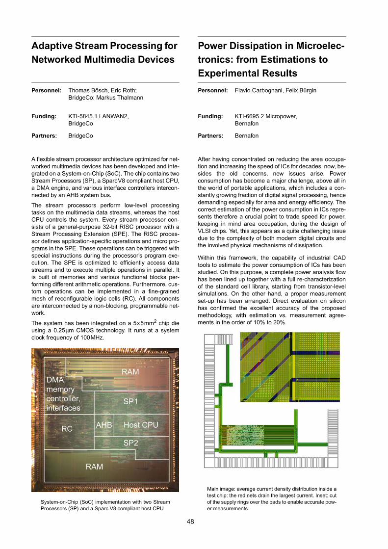
Adaptive Stream Processing forNetworked Multimedia Devices
Personnel: Thomas Bösch, Eric Roth;BridgeCo: Markus Thalmann
Funding: KTI-5845.1 LANWAN2,BridgeCo
Partners: BridgeCo
A flexible stream processor architecture optimized for net-worked multimedia devices has been developed and inte-grated on a System-on-Chip (SoC). The chip contains twoStream Processors (SP), a SparcV8 compliant host CPU,a DMA engine, and various interface controllers intercon-nected by an AHB system bus.
The stream processors perform low-level processingtasks on the multimedia data streams, whereas the hostCPU controls the system. Every stream processor con-sists of a general-purpose 32-bit RISC processor with aStream Processing Extension (SPE). The RISC proces-sor defines application-specific operations and micro pro-grams in the SPE. These operations can be triggered withspecial instructions during the processor’s program exe-cution. The SPE is optimized to efficiently access datastreams and to execute multiple operations in parallel. Itis built of memories and various functional blocks per-forming different arithmetic operations. Furthermore, cus-tom operations can be implemented in a fine-grainedmesh of reconfigurable logic cells (RC). All componentsare interconnected by a non-blocking, programmable net-work.
The system has been integrated on a 5x5mm2 chip dieusing a 0.25µm CMOS technology. It runs at a systemclock frequency of 100MHz.
System-on-Chip (SoC) implementation with two StreamProcessors (SP) and a Sparc V8 compliant host CPU.
48
Power Dissipation in Microelec-tronics: from Estimations toExperimental Results
Personnel: Flavio Carbognani, Felix Bürgin
Funding: KTI-6695.2 Micropower,Bernafon
Partners: Bernafon
After having concentrated on reducing the area occupa-tion and increasing the speed of ICs for decades, now, be-sides the old concerns, new issues arise. Powerconsumption has become a major challenge, above all inthe world of portable applications, which includes a con-stantly growing fraction of digital signal processing, hencedemanding especially for area and energy efficiency. Thecorrect estimation of the power consumption in ICs repre-sents therefore a crucial point to trade speed for power,keeping in mind area occupation, during the design ofVLSI chips. Yet, this appears as a quite challenging issuedue to the complexity of both modern digital circuits andthe involved physical mechanisms of dissipation.
Within this framework, the capability of industrial CADtools to estimate the power consumption of ICs has beenstudied. On this purpose, a complete power analysis flowhas been lined up together with a full re-characterizationof the standard cell library, starting from transistor-levelsimulations. On the other hand, a proper measurementset-up has been arranged. Direct evaluation on siliconhas confirmed the excellent accuracy of the proposedmethodology, with estimation vs. measurement agree-ments in the order of 10% to 20%.
Main image: average current density distribution inside atest chip: the red nets drain the largest current. Inset: cutof the supply rings over the pads to enable accurate pow-er measurements.
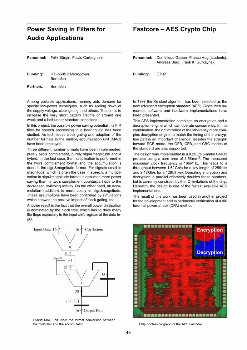
Power Saving in Filters forAudio Applications
Personnel: Felix Bürgin, Flavio Carbognani
Funding: KTI-6695.2 Micropower,Bernafon
Partners: Bernafon
Among portable applications, hearing aids demand forspecial low-power techniques, such as scaling down ofthe supply voltage, clock gating, and others. The aim is toincrease the very short battery lifetime of around oneweek and a half under standard conditions.
In this project, the possible power saving potential in a FIRfilter for speech processing in a hearing aid has beenstudied. As techniques clock gating and adaption of thenumber formats in the multiply-accumulation unit (MAC)have been employed.
Three different number formats have been implemented:purely two’s complement, purely sign&magnitude and ahybrid. In the last case, the multiplication is performed inthe two’s complement format and the accumulation isdone in the sign&magnitude format. For signals small inmagnitude, which is often the case in speech, a multipli-cation in sign&magnitude format is assumed more powersaving than its two’s complement counterpart due to thedecreased switching activity. On the other hand, an accu-mulation (addition) is more costly in sign&magnitude.These assumptions have been confirmed by simulationswhich showed the positive impact of clock gating, too.
Another result is the fact that the overall power dissipationis dominated by the clock tree, which has to drive manyflip-flops especially in the input shift register at the data in-put.
Hybrid MAC unit. Note the format conversion betweenthe multiplier and the accumulator.
49
Fastcore – AES Crypto Chip
Personnel: Dominique Gasser, Franco Hug (students);Andreas Burg, Frank K. Gürkaynak
Funding: ETHZ
In 1997 the Rijndael algorithm has been selected as thenew advanced encryption standard (AES). Since then nu-merous software and hardware implementations havebeen presented.
This AES implementation combines an encryption and adecryption engine which can operate concurrently. In thiscombination, the optimization of the inherently more com-plex decryption engine to match the timing of the encryp-tion part is an important challenge. Besides the straight-forward ECB mode, the OFB, CFB, and CBC modes ofthe standard are also supported.
The design was implemented in a 0.25µm 5-metal CMOSprocess using a core area of 3.56mm2. The measuredmaximum clock frequency is 166MHz. This leads to athroughput between 1.52Gb/s for a key length of 256bitsand 2.12Gb/s for a 128bit key. Operating encryption anddecryption in parallel effectively doubles these numbers,but is currently constraint by the IO limitations of the chip.Herewith, the design is one of the fastest available AESimplementations.
The result of this work has been used in another projectfor the development and experimental verification of a dif-ferential power attack (DPA) method.
Chip photomicrograph of the AES Fastcore.

DPA Attacks onAES Crypto Chip
Personnel: Frank K. Gürkaynak
Funding: ETHZ
Partners: Uni Leuven
In order to develop secure systems, it is important to in-vestigate its weaknesses against various attacks. Ratherthan attacking the output of a crypto system, so calledside-channel attacks try to extract the secret key of a se-cure system by observing different physical characteris-tics such as temperature, operation time, electromagneticradiation and power consumption of a system under oper-ation. The Differential Power Analysis (DPA) is a side-channel attack that is based on observing the power con-sumption of the crypto system during operation. If a suffi-cient number of operations are observed, statisticalmethods can be used to find correlation between the pow-er consumption and the secret key used in the operation.In this project a DPA attack is performed to an AES chipdeveloped at the IIS.
In this attack, 8 bits of the 128 bit key are targeted. To pre-pare for the attack, a simulated power consumption file isgenerated for each of the 256 variations of the attackedkey bits. The current consumption of the AES chip wasmeasured while it encrypted 10,000 different 128-bit datapackets using the same encryption key. The measured re-sult was then correlated against the simulated power con-sumption file. The correct 8-bit partial key exhibited thehighest correlation to the measurement results in two in-dependent measurements with separate data sets. This isthe first published successful DPA attack on an actualAES ASIC.
A close-up of the digital oscilloscope sampling the supplycurrent (green trace) during the DPA attack.
50
Prototyping Platform forCoprocessors in SoCs
Personnel: Silvio Dragone
Funding: IBM Research GmbH
Partners: IBM Research GmbH
Configurable and extendable processor architectures of-ten offer the capability of extending their basic InstructionSet Architecture (ISA) with application-specific instruc-tions. Hardware emulators are often used to verify thenew functionality of the hardware and software and toquantify the performance gain. Since the entire processoris either implemented in an FPGA or emulated on a differ-ent processor, either the processor architecture is simpli-fied or only the instruction set is emulated. However,these methods cannot indicate the actual performance ofthe future implementation.A novel approach is to use the actual processor chip withthe basic ISA and an FPGA board to emulate the ISA ex-tension. The application-specific execution unit of the ISAextension is implemented in the FPGA. A generic wrapperhas been developed that stimulates the execution unit.Together with synchronization software running on theprocessor itself, the prototyping platform allows the userto emulate the ISA extension. Moreover, the genericwrapper and the synchronization software enable the ac-tual performance of the future architecture to be mea-sured.An additional option of the platform is to emulate the co-processor not only as a synchronous data-path extensionof the processor, but also as an asynchronous looselycoupled coprocessor. The wrapper and the synchroniza-tion software emulate the behavior of any bus system ex-isting in SoC designs. Thus, the same platform allows oneto verify and quantify loosely and tightly coupled copro-cessors of a SoC design with an actual processor.
The picture shows the hardware of the prototyping plat-form (processor and FPGA board) with a diagram of theemulator functionality.
IRRQ Testing ofDeep-Submicron CMOS Chips
Personnel: Gianpaolo Pontarolo
Funding: KTI-4897.1 IRRQ,Philips Zürich
Partners: Philips Zürich
Millions of transistors with gate length below 100nm andlow threshold voltage cause an exponential increase ofthe total leakage current in ICs. Besides high static powerdissipation, CMOS tests relying on quiescent-currentmeasurements (IDDQ) become infeasible. IRRQ is a pat-ented method which helps to overcome this problem in acertain class of integrated circuits.
IRRQ standard cells consist of common CMOS logic cir-cuits supplemented by four additional transistors, two so-called sleep transistors in the VDD and VSS power con-nections and two pull-up/down transistors from output toVDD and VSS. Besides of switching off the leakage cur-rent during standby time intervals, they enable IRRQ test-ing: Separate application of test vectors to the N or the Pnetworks of the whole chip eliminates the CMOS testingproblems which were addressed by IDDQ tests in thepast.
The enhanced testability comes at the cost of a large areaoverhead which is dominated by the wide sleep transis-tors. It should be noticed however that almost half of theoverhead will be required for the sleep option alone whichwill be mandatory in many low-power applications.
Silicon area requirement of a NAND gate (top left) and aflip-flop with and without power-down and IRRQ.
51


53
Research Projects
Analog and Mixed-Signal Design
Coordinator:
Qiuting Huang
200MSPS 14bit DAC withBackground Calibration
Personnel: Pier Andrea Francese, Chiara Martelli
Funding: ETHZ
Very high speed and high resolution D/A converters arerequired in many applications such as VDSL broadbandmodems or direct digital frequency synthesizers. Currentsteering D/A converters are excellent candidates becauseof their intrinsic high speed characteristics. In order to ob-tain accuracies in the 14b range, special layout tech-niques or calibration methods must be adopted.
A solution using background calibration has been chosenin this work, because it offers the advantage of constantlycorrecting for slow varying errors, such as the ones in-duced by temperature changes. The calibration of the fivemost significant bits (MSBs) is done with a fully analogtrimming loop that works sequentially on the tail current ofeach MSB current source, while the MSB head is keptconnected to the output through the data switches.
Excellent static linearity is achieved by this technique. At200MHz update rate a peak spurious-free-dynamic-range(SFDR) of 85dBc has been measured.
Top: Plots of the measured integral non linearity (INL)and the differential non linearity (DNL) always below 0.65and 0.55LSB respectively.Bottom: Chip micrograph of the circuit implemented inCMOS 0.18µm, operating at 1.8V.
54
Sigma-Delta DAC withSemi-digital ReconstructionFiltering
Personnel: Pier Andrea Francese
Funding: KTI-5731.1 OTRACOM,Philips Zürich
Partners: Philips Zürich
The demand for high data rate communication systemshas pushed the linearity requirements of A/D and D/A con-verters in a range where it is necessary to use special de-sign techniques and architectures. Only in this way it ispossible to exceed the raw limit of the present CMOStechnologies that is in the range of 10 bits.
D/A converters using single-bit Σ∆ modulators are well ap-preciated architectures that offer excellent linearity perfor-mances due to the inherent linearity of the two levelquantizer at the modulator output. The semidigital filter isthen an elegant way to preserve this linearity while atten-uating the out-of-band quantization noise. At low over-sampling ratios, nevertheless, very high signal-to-noiseratios cannot be achieved without multi-bit quantizers.
The D/A converter developed in this project uses a cas-caded Σ∆ modulator with a dual truncation architecture inwhich the advantages of a semi-digital reconstruction fil-tering are combined with the necessity of using multi-bitmodulators.
Top: Plot of the measured ADSL Multi Tone Power Ratio(MTPR).Bottom: Chip micrograph of the circuit implemented inCMOS 0.18µm, operating at 1.8V.
A 25MS/s 14bit Sigma-DeltaModulator for VDSLCommunications Application
Personnel: Pio Balmelli
Funding: ETHZ
The increasing demand for broadband Internet accessand the growing use of digital processing forsters the im-plementation of communications standards employing so-phisticated decoding methods capable of achieving highdata rates using existing communications media. Howev-er, the trend towards higher data rates and digital signalprocessing increases the dynamic range and the band-width required at the A/D interface. VDSL is one of thesestandards, it uses the plain old telephone services fortransmitting data at a maximum rate of 30Mbps.
Oversampled Σ∆ ADCs are highly suited for high resolu-tion integrated circuit implementations since they do notneed a precision S/H stage, have relaxed requirementsfor the anti-aliasing filter, and achieve very good linearitydespite the use of imprecise building blocks. However, theneed of oversampling reduces the achievable conversionrate.
The designed Σ∆ modulator has a discrete-time, single-loop architecture. The loop filter has a feed-forward topol-ogy and employs a 4bit quantizer. The oversampling ratiois 8. To linearize the 16 level feedback DAC, dynamic el-ement matching is used. The circuit has been implement-ed in a mainstream 0.18µm digital CMOS technology with1 poly and 6 metals. The supply voltage is 1.8V. The corearea is 0.95mm2. The power consumption is 203mW.
With 25MS/s conversion rate and 82dB signal-to-noise,this circuit outperforms in speed and resolution combina-tion any previously published Σ∆ modulator.
Micrograph of the implemented modulator.
55
Oversampled A/D-Conversionfor Multi-Standard WirelessReceivers
Personnel: Thomas Burger, Robert Reutemann
Funding: ETHZ
For new generations of mobile communications devices,multiple standards will have to be incorporated. For exam-ple, UMTS will allow wide-area medium speed data con-nections, while GSM will provide speech and lower-ratedata coverage in remote areas. For in-house, and increas-ingly also open-air use, the addition of WLAN compatibil-ity will add high-speed data connections to the mix.
The A/D converter in the receive path is one of the key el-ements in such a device. A Σ∆ converter is an attractivechoice for a multi-standard solution, since speed can betraded for resolution. Nevertheless, covering multiple cel-lular and WLAN standards is a challenge, since thespread of bandwidth and resolution is very high. Withthese widely varying requirements, the digital decimationfilter also has to provide a wide range of possible settings,while still achieving high performance and low power con-sumption. In the decimation filter, a maximum of flexibilityis highly desirable, at least in the last stages, to allow fordifferent post-processing approaches or to adapt to evolv-ing standards.
In this project, a Σ∆ converter covering GSM, UMTS andWLAN standards has been developed. Optimization op-tions for maximum resource sharing and low power con-sumption are realized. The converter has been implemen-ted in 0.18µm CMOS to be compatible with fully integrat-ed transceiver developments in mainstream technologies.
Chip photomicrograph of implemented A/D-converter.
A High-Speed Folding andInterpolation A/D-Converter
Personnel: Jürgen Hertle
Funding: ETHZ
Generally folding and interpolating analog-to-digital con-verters are capable of providing high conversion rates atreasonable power consumption. The main drawback ofthis architecture is the limited accuracy, which is dominat-ed by the high mismatch of fast differential pairs in CMOStechnology.
The scope of this project was to demonstrate the feasibil-ity of folding and interpolation analog-to-digital convertersfor higher than 7..8bit accuracy. In order to achieve thisgoal, a calibration scheme, which eliminates the offsetvoltages of the differential pairs, has been developed andembedded into a 10bit, 125MSamples/s ADC.ADCs are usually integrated together with a substantialpart of the digital back-end. Therefore a mainstream0.18 µm digital CMOS technology with one poly layer, sixmetal layers, high ohmic resistors and metal-insulator-metal capacitors has been used for this design.
Chip photograph of a 10Bit, 125MSamples/s folding andinterpolating analog-to-digital converter with embeddedcalibration.
56
Folding and Interpolating A/DConverters in Deep-SubmicronCMOS Technology
Personnel: Yihui Chen
Funding: KTI-6171.2 CITE,Philips Zürich
Partners: Philips Zürich
In this project, a high-speed medium-resolution foldingand interpolating analog-to-digital converter is investigat-ed in the context of implementation in an advanced 90nmCMOS technology. Such converters have applications indigital communication, HDTV, medical imagers, and soon. In comparison with fully parallel (flash) architectures,folding A/D converters require fewer pre-amplifiers andcomparators while maintaining the advantages of highspeed and low latency.
Although advanced CMOS technologies offer smaller andfaster transistors, they do pose some challenges in thedesign of analog and mixed-signal circuits. For the rea-sons of low power and reliability, the supply voltage ofCMOS technology is reduced substantially recently.Some basic functional components such as switches, op-erational amplifiers become more difficult to implement.New circuit techniques and architectures must be devel-oped to overcome this limitation. The second challenge isrelated to high offset voltages of CMOS differential pairswhich limits the resolution of folding A/D converters to 6-8bits. This problem can be overcome by offset averagingand/or digital calibration, but this will increase the circuitcomplexity.
Architecture of a folding and interpolating A/D converter.
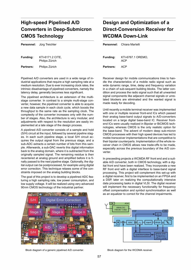
High-speed Pipelined A/DConverters in Deep-SubmicronCMOS Technology
Personnel: Jürg Treichler
Funding: KTI-6171.2 CITE,Philips Zürich
Partners: Philips Zürich
Pipelined A/D converters are used in a wide range of in-dustrial applications that require a high sampling rate at amedium resolution. Due to ever increasing clock rates, theintrinsic disadvantage of pipelined converters, namely thelatency delay, generally becomes less significant.
The pipelined architecture is an extension of the multi-stage converter. In contrast to a simple multi-stage con-verter, however, the pipelined converter is able to acquirea new data sample in each clock cycle, which boosts thethroughput to the same rate as the sampling clock. Thecomplexity of the converter increases only with the num-ber of stages. Also, the architecture is very modular, andadjustments with respect to the resolution are easily im-plemented at a late stage of the design process.
A pipelined A/D converter consists of a sample and hold(S/H) circuit at the input, followed by several pipeline stag-es. In each such pipeline stage, a local S/H circuit ac-quires the output signal from the previous stage, and asub-ADC extracts a certain number of bits from this sam-ple. Afterwards, a sub-DAC reverts this digital informationback to the analog domain, where it is subtracted from theoriginally sampled signal. The remaining residue is thenrecentered at analog ground and amplified before it is fi-nally passed to the next pipeline stage. Optionally, the dig-ital output can be postprocessed, for example using digitalerror correction. This technique relaxes some of the con-straints imposed on the analog building blocks.
The goal of this project is to develop a pipelined ADC fea-turing a high sampling rate, low power consumption, andlow supply voltage. It will be realized using very advanced90nm CMOS technology of the industrial partner.
Block diagram of a generic pipelined A/D converter.
57
Design and Optimization of aDirect-Conversion Receiver forWCDMA Down-Link
Personnel: Chiara Martelli
Funding: KTI-6767.1 OREMO,ACP
Partners: ACP
Receiver design for mobile communications tries to han-dle the characteristics of a mobile radio signal such aswide dynamic range, time, delay and frequency variationin a chain of sub-sequent building blocks. The latter con-dition and process the radio signal such that all unwantedsignal components like adjacent channel signals or unre-lated blockers are eliminated and the wanted signal ismade ready for decoding.
Until recently a mobile terminal receiver was implementedwith one or multiple receiver front-end ICs which passedtheir analog base-band output signals to A/D-converterslocated on a large digital base-band IC. Receiver front-end ICs were usually realized in Bipolar or BiCMOS tech-nologies, whereas CMOS is the only realistic option forthe base-band. The advent of modern deep sub-micronCMOS processes with their high speed devices has led tomoble transceiver implementations that are competitive totheir bipolar counterparts. Implementation of the whole re-ceiver chain in CMOS allows new trade-offs to be made,especially across the previous boundary of the A/D con-verter.
In preceeding projects a WCMDA RF front end and a suit-able A/D converter, both in CMOS technology, with a dig-ital front end have been realized. They incorporate a newRF front end with a digital interface to base-band signalprocessing. This project will complement this set-up witha digital receiver, first to be implemented on an FPGA anda DSP, later on realizing the computiationally intensivedata processing tasks in digital VLSI. The digital receiverwill implement the necessary functionality for frequencyoffset compensation and symbol synchronisation as wellas an equalizer to correct for the channel impairments.
Block diagram for the WCDMA receiver.
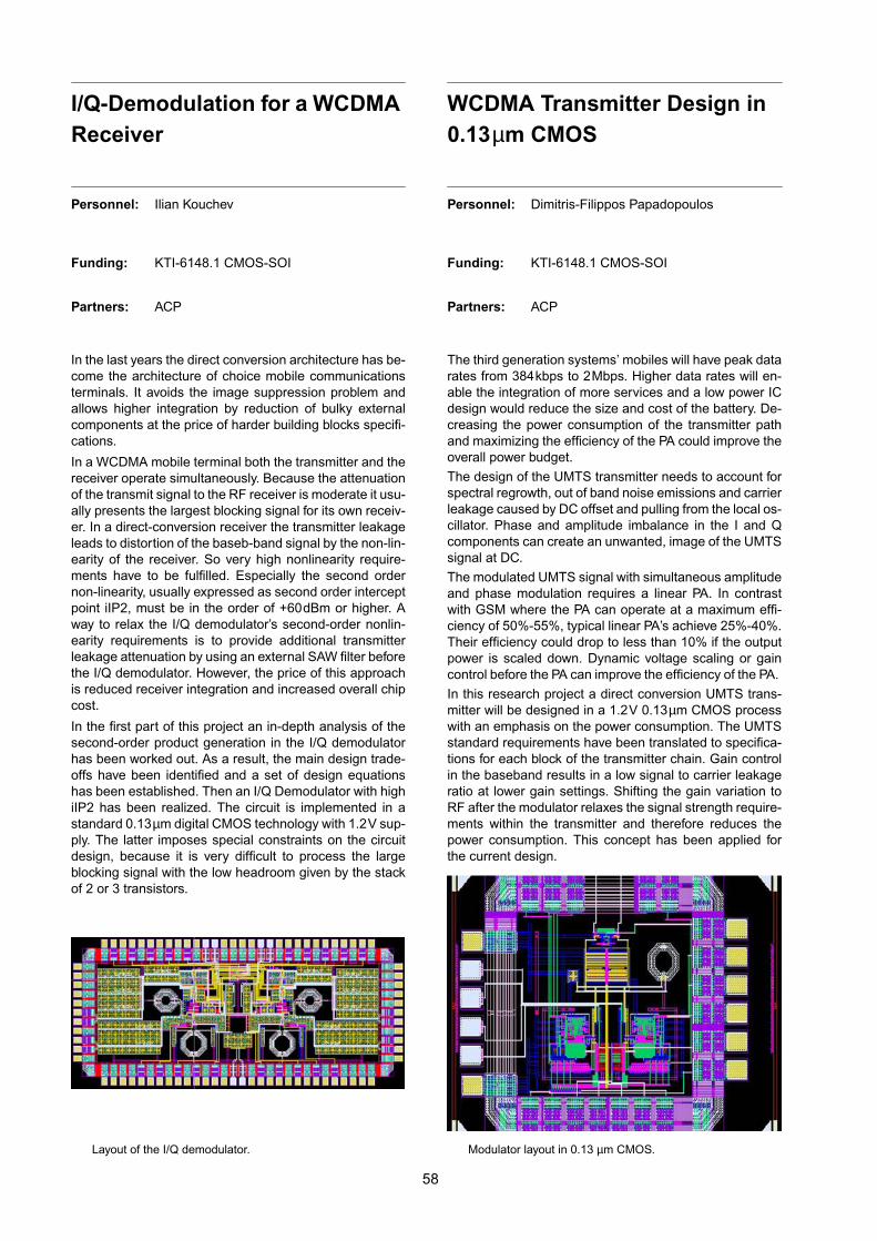
I/Q-Demodulation for a WCDMAReceiver
Personnel: Ilian Kouchev
Funding: KTI-6148.1 CMOS-SOI
Partners: ACP
In the last years the direct conversion architecture has be-come the architecture of choice mobile communicationsterminals. It avoids the image suppression problem andallows higher integration by reduction of bulky externalcomponents at the price of harder building blocks specifi-cations.
In a WCDMA mobile terminal both the transmitter and thereceiver operate simultaneously. Because the attenuationof the transmit signal to the RF receiver is moderate it usu-ally presents the largest blocking signal for its own receiv-er. In a direct-conversion receiver the transmitter leakageleads to distortion of the baseb-band signal by the non-lin-earity of the receiver. So very high nonlinearity require-ments have to be fulfilled. Especially the second ordernon-linearity, usually expressed as second order interceptpoint iIP2, must be in the order of +60dBm or higher. Away to relax the I/Q demodulator’s second-order nonlin-earity requirements is to provide additional transmitterleakage attenuation by using an external SAW filter beforethe I/Q demodulator. However, the price of this approachis reduced receiver integration and increased overall chipcost.
In the first part of this project an in-depth analysis of thesecond-order product generation in the I/Q demodulatorhas been worked out. As a result, the main design trade-offs have been identified and a set of design equationshas been established. Then an I/Q Demodulator with highiIP2 has been realized. The circuit is implemented in astandard 0.13µm digital CMOS technology with 1.2V sup-ply. The latter imposes special constraints on the circuitdesign, because it is very difficult to process the largeblocking signal with the low headroom given by the stackof 2 or 3 transistors.
Layout of the I/Q demodulator.
58
WCDMA Transmitter Design in0.13µm CMOS
Personnel: Dimitris-Filippos Papadopoulos
Funding: KTI-6148.1 CMOS-SOI
Partners: ACP
The third generation systems’ mobiles will have peak datarates from 384kbps to 2Mbps. Higher data rates will en-able the integration of more services and a low power ICdesign would reduce the size and cost of the battery. De-creasing the power consumption of the transmitter pathand maximizing the efficiency of the PA could improve theoverall power budget.The design of the UMTS transmitter needs to account forspectral regrowth, out of band noise emissions and carrierleakage caused by DC offset and pulling from the local os-cillator. Phase and amplitude imbalance in the I and Qcomponents can create an unwanted, image of the UMTSsignal at DC.The modulated UMTS signal with simultaneous amplitudeand phase modulation requires a linear PA. In contrastwith GSM where the PA can operate at a maximum effi-ciency of 50%-55%, typical linear PA’s achieve 25%-40%.Their efficiency could drop to less than 10% if the outputpower is scaled down. Dynamic voltage scaling or gaincontrol before the PA can improve the efficiency of the PA.In this research project a direct conversion UMTS trans-mitter will be designed in a 1.2V 0.13µm CMOS processwith an emphasis on the power consumption. The UMTSstandard requirements have been translated to specifica-tions for each block of the transmitter chain. Gain controlin the baseband results in a low signal to carrier leakageratio at lower gain settings. Shifting the gain variation toRF after the modulator relaxes the signal strength require-ments within the transmitter and therefore reduces thepower consumption. This concept has been applied forthe current design.
Modulator layout in 0.13 µm CMOS.
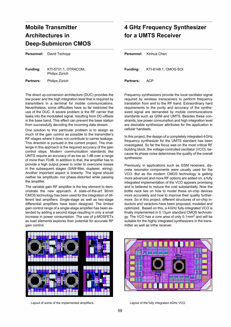
Mobile TransmitterArchitectures inDeep-Submicron CMOS
Personnel: David Tschopp
Funding: KTI-5731.1, OTRACOM,Philips Zürich
Partners: Philips Zürich
The direct up-conversion architecture (DUC) provides thelow power and the high integration level that is required bytransmitters in a terminal for mobile communications.Nevertheless, some difficulties have so far restricted theuse of the DUC. A severe problem is the RF carrier thatleaks into the modulated signal, resulting from DC-offsetsin the base band. This effect can prevent the base stationfrom successfully decoding the incoming data stream.
One solution to this particular problem is to assign asmuch of the gain control as possible to the transmitter’sRF-stages where it does not contribute to carrier leakage.This direction is pursued in the current project. The chal-lenge in this approach is the required accuracy of the gaincontrol steps. Modern communication standards likeUMTS require an accuracy of as low as 1 dB over a rangeof more than 70dB. In addition to that, the amplifier has toprovide a high output power in order to overcome lossesin the subsequent stages (SAW-filter, duplexer, wiring).Another important aspect is linearity: The signal shouldneither be amplitude- nor phase-distorted while passingthe amplifier.
The variable gain RF amplifier is the key element to dem-onstrate the new approach. A state-of-the-art 90nmCMOS technology has been used for the integration of dif-ferent test amplifiers. Single-stage as well as two-stagedifferential amplifiers have been designed. The limitedgain control range of a single-stage amplifier has been ex-tended by adding a second stage resulting in only a smallincrease in power consumption. The use of p-MOSFETsas load elements explores their potential for accurate RFgain control.
Layout of some of the implemented amplifiers.
59
4 GHz Frequency Synthesizerfor a UMTS Receiver
Personnel: Xinhua Chen
Funding: KTI-6148.1, CMOS-SOI
Partners: ACP
Frequency synthesizers provide the local oscillator signalrequired by wireless transceivers to perform frequencytranslation from and to the RF band. Extraordinary hardrequirements to the purity and accuracy of the synthe-sized signal are demanded by mobile communicationsstandards such as GSM and UMTS. Besides these con-straints, low power consumption and high integration levelare desirable synthesizer attiributes for the application incellular handsets.
In this project, the design of a completely integrated 4GHzfrequency synthesizer for the UMTS standard has beeninvestigated. So far the focus was on the most critical RFbuilding block, the voltage-controlled oscillator (VCO), be-cause its phase noise determines the quality of the overallsynthesizer.
Previously, in applications such as GSM receivers, dis-crete resonator components were usually used for theVCO. But as the modern CMOS technology is gettingmore advanced and more RF options are added on, a fullyintegrated implementation of the VCO appears promisingand is believed to reduce the cost substantially. Now thebottle neck lies on how to model these on-chip devicesmore accurately and how to improve their quality further-more. So in this project, different structures of on-chip in-ductors and varactors have been proposed, modeled andoptimized . Based on this, a 4GHz fully-integrated VCO isfinally implemented in 0.13µm standard CMOS technolo-gy. The VCO has a core area of only 0.1mm2 and will besuitable for the highly integrated synthesizers in the trans-mitter as well as inthe receiver.
Layout of the fully integrated 4GHz VCO.
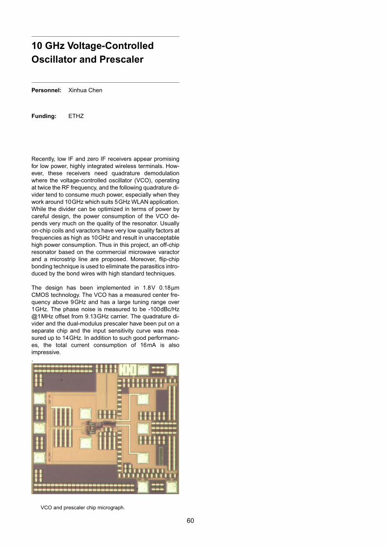
10 GHz Voltage-ControlledOscillator and Prescaler
Personnel: Xinhua Chen
Funding: ETHZ
Recently, low IF and zero IF receivers appear promisingfor low power, highly integrated wireless terminals. How-ever, these receivers need quadrature demodulationwhere the voltage-controlled oscillator (VCO), operatingat twice the RF frequency, and the following quadrature di-vider tend to consume much power, especially when theywork around 10GHz which suits 5GHz WLAN application.While the divider can be optimized in terms of power bycareful design, the power consumption of the VCO de-pends very much on the quality of the resonator. Usuallyon-chip coils and varactors have very low quality factors atfrequencies as high as 10GHz and result in unacceptablehigh power consumption. Thus in this project, an off-chipresonator based on the commercial microwave varactorand a microstrip line are proposed. Moreover, flip-chipbonding technique is used to eliminate the parasitics intro-duced by the bond wires with high standard techniques.
The design has been implemented in 1.8V 0.18µmCMOS technology. The VCO has a measured center fre-quency above 9GHz and has a large tuning range over1GHz. The phase noise is measured to be -100dBc/Hz@1MHz offset from 9.13GHz carrier. The quadrature di-vider and the dual-modulus prescaler have been put on aseparate chip and the input sensitivity curve was mea-sured up to 14GHz. In addition to such good performanc-es, the total current consumption of 16mA is alsoimpressive..
VCO and prescaler chip micrograph.
60
61
Research Projects
Technology CAD
Coordinators:
Wolfgang FichtnerAndreas Schenk
Dölf Aemmer
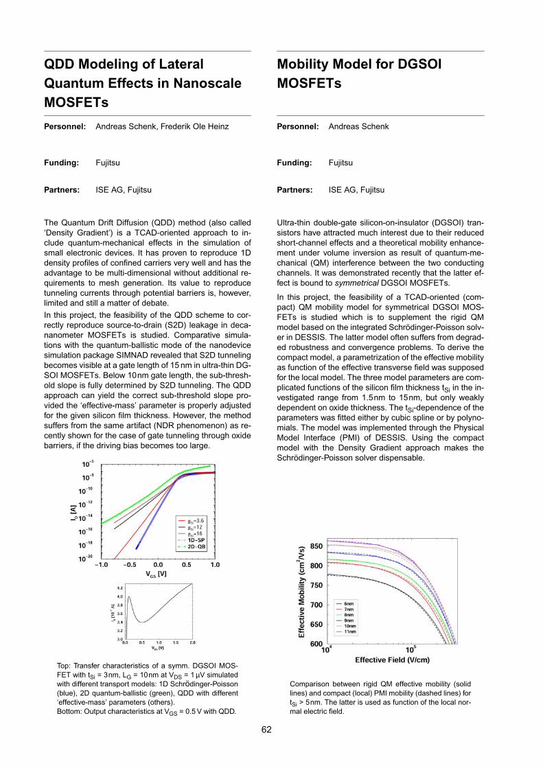
QDD Modeling of LateralQuantum Effects in NanoscaleMOSFETs
Personnel: Andreas Schenk, Frederik Ole Heinz
Funding: Fujitsu
Partners: ISE AG, Fujitsu
The Quantum Drift Diffusion (QDD) method (also called‘Density Gradient’) is a TCAD-oriented approach to in-clude quantum-mechanical effects in the simulation ofsmall electronic devices. It has proven to reproduce 1Ddensity profiles of confined carriers very well and has theadvantage to be multi-dimensional without additional re-quirements to mesh generation. Its value to reproducetunneling currents through potential barriers is, however,limited and still a matter of debate.In this project, the feasibility of the QDD scheme to cor-rectly reproduce source-to-drain (S2D) leakage in deca-nanometer MOSFETs is studied. Comparative simula-tions with the quantum-ballistic mode of the nanodevicesimulation package SIMNAD revealed that S2D tunnelingbecomes visible at a gate length of 15 nm in ultra-thin DG-SOI MOSFETs. Below 10nm gate length, the sub-thresh-old slope is fully determined by S2D tunneling. The QDDapproach can yield the correct sub-threshold slope pro-vided the ‘effective-mass’ parameter is properly adjustedfor the given silicon film thickness. However, the methodsuffers from the same artifact (NDR phenomenon) as re-cently shown for the case of gate tunneling through oxidebarriers, if the driving bias becomes too large.
Top: Transfer characteristics of a symm. DGSOI MOS-FET with tSi = 3nm, LG = 10nm at VDS = 1 µV simulatedwith different transport models: 1D Schrödinger-Poisson(blue), 2D quantum-ballistic (green), QDD with different‘effective-mass’ parameters (others).Bottom: Output characteristics at VGS = 0.5 V with QDD.
62
Mobility Model for DGSOIMOSFETs
Personnel: Andreas Schenk
Funding: Fujitsu
Partners: ISE AG, Fujitsu
Ultra-thin double-gate silicon-on-insulator (DGSOI) tran-sistors have attracted much interest due to their reducedshort-channel effects and a theoretical mobility enhance-ment under volume inversion as result of quantum-me-chanical (QM) interference between the two conductingchannels. It was demonstrated recently that the latter ef-fect is bound to symmetrical DGSOI MOSFETs.
In this project, the feasibility of a TCAD-oriented (com-pact) QM mobility model for symmetrical DGSOI MOS-FETs is studied which is to supplement the rigid QMmodel based on the integrated Schrödinger-Poisson solv-er in DESSIS. The latter model often suffers from degrad-ed robustness and convergence problems. To derive thecompact model, a parametrization of the effective mobilityas function of the effective transverse field was supposedfor the local model. The three model parameters are com-plicated functions of the silicon film thickness tSi in the in-vestigated range from 1.5nm to 15nm, but only weaklydependent on oxide thickness. The tSi-dependence of theparameters was fitted either by cubic spline or by polyno-mials. The model was implemented through the PhysicalModel Interface (PMI) of DESSIS. Using the compactmodel with the Density Gradient approach makes theSchrödinger-Poisson solver dispensable.
Comparison between rigid QM effective mobility (solidlines) and compact (local) PMI mobility (dashed lines) fortSi > 5nm. The latter is used as function of the local nor-mal electric field.
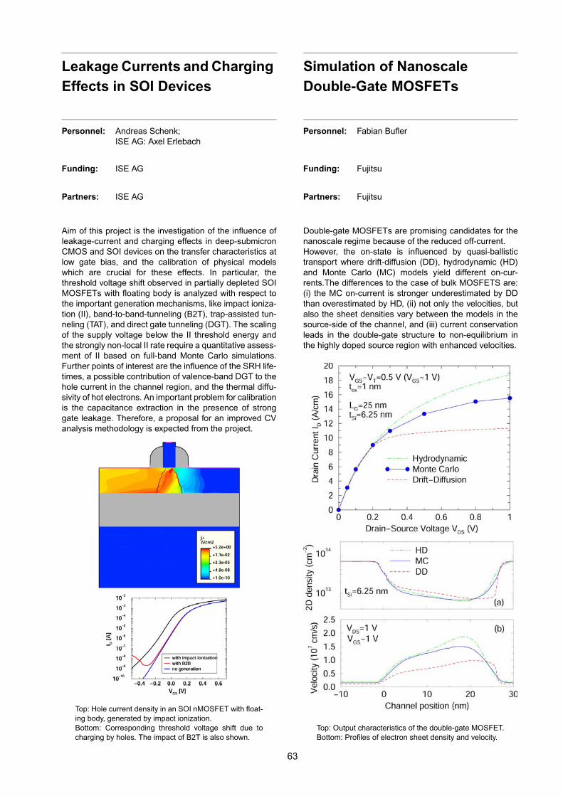
Leakage Currents and ChargingEffects in SOI Devices
Personnel: Andreas Schenk;ISE AG: Axel Erlebach
Funding: ISE AG
Partners: ISE AG
Aim of this project is the investigation of the influence ofleakage-current and charging effects in deep-submicronCMOS and SOI devices on the transfer characteristics atlow gate bias, and the calibration of physical modelswhich are crucial for these effects. In particular, thethreshold voltage shift observed in partially depleted SOIMOSFETs with floating body is analyzed with respect tothe important generation mechanisms, like impact ioniza-tion (II), band-to-band-tunneling (B2T), trap-assisted tun-neling (TAT), and direct gate tunneling (DGT). The scalingof the supply voltage below the II threshold energy andthe strongly non-local II rate require a quantitative assess-ment of II based on full-band Monte Carlo simulations.Further points of interest are the influence of the SRH life-times, a possible contribution of valence-band DGT to thehole current in the channel region, and the thermal diffu-sivity of hot electrons. An important problem for calibrationis the capacitance extraction in the presence of stronggate leakage. Therefore, a proposal for an improved CVanalysis methodology is expected from the project.
Top: Hole current density in an SOI nMOSFET with float-ing body, generated by impact ionization.Bottom: Corresponding threshold voltage shift due tocharging by holes. The impact of B2T is also shown.
63
Simulation of NanoscaleDouble-Gate MOSFETs
Personnel: Fabian Bufler
Funding: Fujitsu
Partners: Fujitsu
Double-gate MOSFETs are promising candidates for thenanoscale regime because of the reduced off-current.However, the on-state is influenced by quasi-ballistictransport where drift-diffusion (DD), hydrodynamic (HD)and Monte Carlo (MC) models yield different on-cur-rents.The differences to the case of bulk MOSFETS are:(i) the MC on-current is stronger underestimated by DDthan overestimated by HD, (ii) not only the velocities, butalso the sheet densities vary between the models in thesource-side of the channel, and (iii) current conservationleads in the double-gate structure to non-equilibrium inthe highly doped source region with enhanced velocities.
Top: Output characteristics of the double-gate MOSFET.Bottom: Profiles of electron sheet density and velocity.
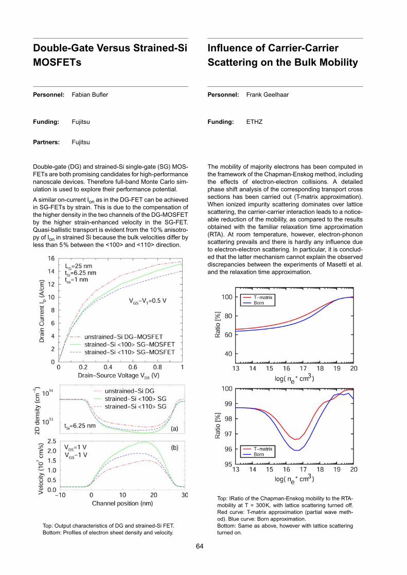
Double-Gate Versus Strained-SiMOSFETs
Personnel: Fabian Bufler
Funding: Fujitsu
Partners: Fujitsu
Double-gate (DG) and strained-Si single-gate (SG) MOS-FETs are both promising candidates for high-performancenanoscale devices. Therefore full-band Monte Carlo sim-ulation is used to explore their performance potential.
A similar on-current Ion as in the DG-FET can be achievedin SG-FETs by strain. This is due to the compensation ofthe higher density in the two channels of the DG-MOSFETby the higher strain-enhanced velocity in the SG-FET.Quasi-ballistic transport is evident from the 10% anisotro-py of Ion in strained Si because the bulk velocities differ byless than 5% between the <100> and <110> direction.
Top: Output characteristics of DG and strained-Si FET.Bottom: Profiles of electron sheet density and velocity.
64
Influence of Carrier-CarrierScattering on the Bulk Mobility
Personnel: Frank Geelhaar
Funding: ETHZ
The mobility of majority electrons has been computed inthe framework of the Chapman-Enskog method, includingthe effects of electron-electron collisions. A detailedphase shift analysis of the corresponding transport crosssections has been carried out (T-matrix approximation).When ionized impurity scattering dominates over latticescattering, the carrier-carrier interaction leads to a notice-able reduction of the mobility, as compared to the resultsobtained with the familiar relaxation time approximation(RTA). At room temperature, however, electron-phononscattering prevails and there is hardly any influence dueto electron-electron scattering. In particular, it is conclud-ed that the latter mechanism cannot explain the observeddiscrepancies between the experiments of Masetti et al.and the relaxation time approximation.
Top: IRatio of the Chapman-Enskog mobility to the RTA-mobility at T = 300K, with lattice scattering turned off.Red curve: T-matrix approximation (partial wave meth-od). Blue curve: Born approximation.Bottom: Same as above, however with lattice scatteringturned on.
Injection Dependence of Spon-taneous Radiative Recombina-tion in Crystalline Silicon
Personnel: Frank Geelhaar;Uni Canberra: Pietro P. Altermatt
Funding: ETHZ, Uni Canberra
The quantification of the radiative recombination rate hasbecome a crucial part in the development of efficient lightemitting devices based on crystalline silicon. The recom-bination is enhanced by the long-range Coulomb interac-tion between the electrons and holes, leading to anincreased hole density in the vicinity of an electron, andvice versa. In this project, the injection dependence of theenhancement has been calculated numerically and com-pared with photo- as well as electroluminescence mea-surements. A good overall agreement between theory andexperiment has been found.
Comparison between numerical calculations and photo-as well as electroluminescence measurements of the en-hancement of the radiative recombination coefficient.(Measurements: E. Daub, A. Neisser; H. Schlangenotto).
65
A Coupled Kohn-Sham /Drift-DiffusionSimulation Framework
Personnel: Frederik Heinz, Bernhard Schmithüsen
Funding: BBW, EU-IST-10828 NANOTCAD
Partners: Uni Pisa, Uni Cork, MPG Stuttgart,TUWien, Uni Würzburg
Among the candidate structures that have been proposedfor future ultra-large scale integrated circuits are devices,such as quantum-dot FLASH memory, that comprise bothregions of multi-dimensional carrier confinement and re-gions inside which classical dissipative transport (possiblywith quantum corrections) occurs. Such devices are inac-cessible to traditional device simulators. The DESSIS de-vice simulator provides a 1D Schrödinger solver and aquantum drift-diffusion facility, but it can not rigorouslyhandle multi-dimensional confinement. The SIMNADquantum mechanics simulator is capable of computingthe correct charge density in a multi-dimensional confine-ment situation, but it lacks (semi-)classical transport mod-els.
Therefore, a self-consistent coupling strategy betweenDESSIS and SIMNAD has been devised and implement-ed. This coupling allows the two simulators to combinetheir strengths and enables simulation of devices that fea-ture both classical channels and quantum dots. In coupledsimulation mode DESSIS will run a master simulation thatcalls upon SIMNAD to perform quantum mechanicalcharge density computations as necessary.This affords toa separation of length-scales: only the local SIMNADgrids in the QM regions need to be refined down to thescale of the individual wave functions; the global mesh ap-plied by DESSIS may be coarser – it need only resolve thetotal QM charge density. Data is automatically interpolat-ed between the DESSIS and the SIMNAD grids.By this co-operative approach the user gains full accessto the device modelling capacities of DESSIS while main-taining the ability to use full 3D quantum mechanics re-sults where necessary.
The quantum mechanical charge density computed bySIMNAD has been transferred to DESSIS.
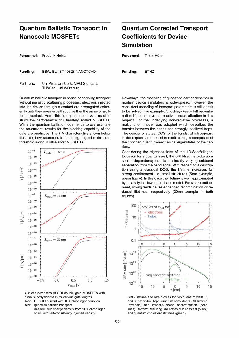
Quantum Ballistic Transport inNanoscale MOSFETs
Personnel: Frederik Heinz
Funding: BBW, EU-IST-10828 NANOTCAD
Partners: Uni Pisa, Uni Cork, MPG Stuttgart,TUWien, Uni Würzburg
Quantum ballistic transport is phase conserving transportwithout inelastic scattering processes: electrons injectedinto the device through a contact are propagated coher-ently until they re-emerge through either the same or a dif-ferent contact. Here, this transport model was used tostudy the performance of ultimately scaled MOSFETs.While the quantum ballistic model tends to overestimatethe on-current, results for the blocking capability of thegate are predictive. The I–V characteristics shown belowillustrate, how source-drain tunneling degrades the sub-threshold swing in ultra-short MOSFETs.
I–V characteristics of SOI double gate MOSFETs with1 nm Si body thickness for various gate lengths.black: DESSIS current with 1D Schrödinger equationred: quantum ballistic transport
dashed: with charge density from 1D Schrödingersolid: with self-consistently injected density.
66
Quantum Corrected TransportCoefficients for DeviceSimulation
Personnel: Timm Höhr
Funding: ETHZ
Nowadays, the modeling of quantized carrier densities inmodern device simulators is wide-spread. However, theconsistent modeling of transport parameters is still a taskto be solved. For example, Shockley-Read-Hall recombi-nation lifetimes have not received much attention in thisrespect. For the underlying non-radiative processes, amultiphonon model was adopted which describes thetransfer between the bands and strongly localized traps.The density of states (DOS) of the bands, which appearsin the capture and emission coefficients, is composed ofthe confined quantum-mechanical eigenstates of the car-riers.Considering the eigensolutions of the 1D-Schrödinger-Equation for a quantum well, the SRH-lifetime picks up aspatial dependency due to the locally varying subbandseparation from the band edge. With respect to a descrip-tion using a classical DOS, the lifetime increases forstrong confinement, i.e. small structures (5nm example,upper figure). In this case the lifetime is well approximatedby an analytical lowest-subband model. For weak confine-ment, strong fields cause enhanced recombination or re-duced lifetimes, respectively (30nm-example in bothfigures).
SRH-Lifetime and rate profiles for two quantum wells (5and 30nm wide). Top: Quantum consistent SRH-lifetime(symbols) and lowest-subband approximation (solidlines). Bottom: Resulting SRH-rates with constant (black)and quantum consistent lifetimes (green).
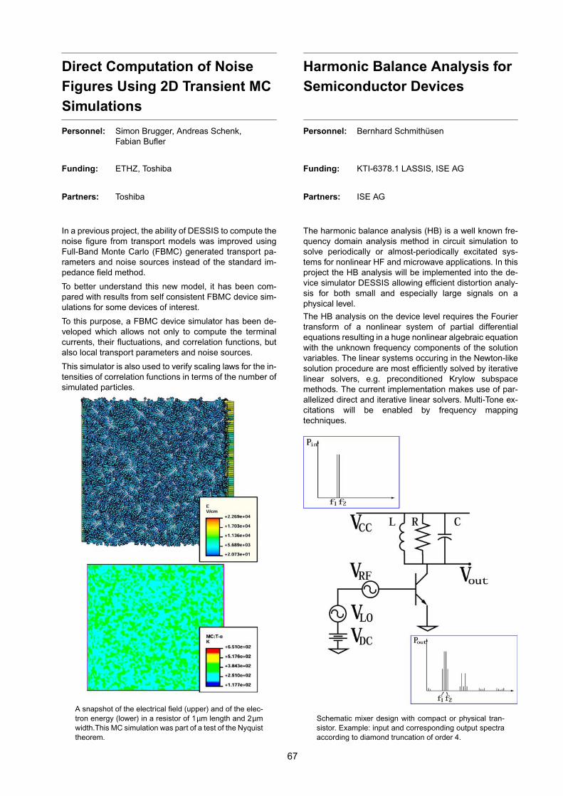
Direct Computation of NoiseFigures Using 2D Transient MCSimulations
Personnel: Simon Brugger, Andreas Schenk,Fabian Bufler
Funding: ETHZ, Toshiba
Partners: Toshiba
In a previous project, the ability of DESSIS to compute thenoise figure from transport models was improved usingFull-Band Monte Carlo (FBMC) generated transport pa-rameters and noise sources instead of the standard im-pedance field method.
To better understand this new model, it has been com-pared with results from self consistent FBMC device sim-ulations for some devices of interest.
To this purpose, a FBMC device simulator has been de-veloped which allows not only to compute the terminalcurrents, their fluctuations, and correlation functions, butalso local transport parameters and noise sources.
This simulator is also used to verify scaling laws for the in-tensities of correlation functions in terms of the number ofsimulated particles.
A snapshot of the electrical field (upper) and of the elec-tron energy (lower) in a resistor of 1µm length and 2µmwidth.This MC simulation was part of a test of the Nyquisttheorem.
67
Harmonic Balance Analysis forSemiconductor Devices
Personnel: Bernhard Schmithüsen
Funding: KTI-6378.1 LASSIS, ISE AG
Partners: ISE AG
The harmonic balance analysis (HB) is a well known fre-quency domain analysis method in circuit simulation tosolve periodically or almost-periodically excitated sys-tems for nonlinear HF and microwave applications. In thisproject the HB analysis will be implemented into the de-vice simulator DESSIS allowing efficient distortion analy-sis for both small and especially large signals on aphysical level.
The HB analysis on the device level requires the Fouriertransform of a nonlinear system of partial differentialequations resulting in a huge nonlinear algebraic equationwith the unknown frequency components of the solutionvariables. The linear systems occuring in the Newton-likesolution procedure are most efficiently solved by iterativelinear solvers, e.g. preconditioned Krylow subspacemethods. The current implementation makes use of par-allelized direct and iterative linear solvers. Multi-Tone ex-citations will be enabled by frequency mappingtechniques.
Schematic mixer design with compact or physical tran-sistor. Example: input and corresponding output spectraaccording to diamond truncation of order 4.
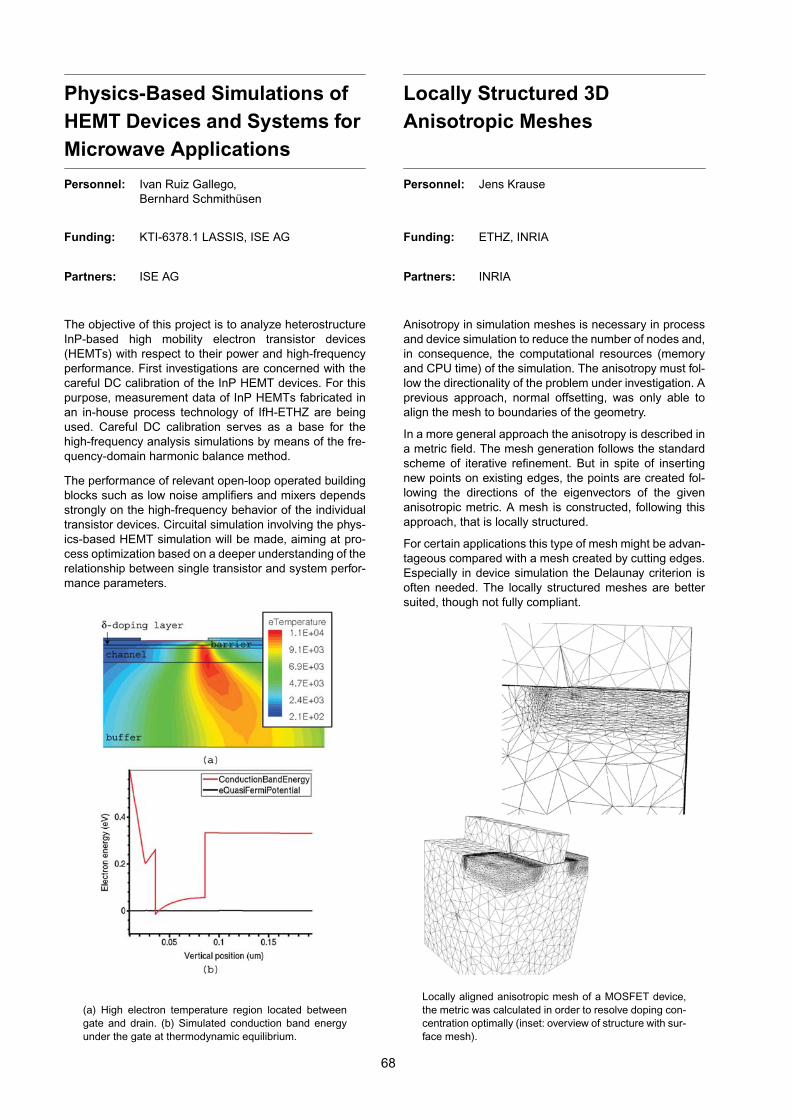
Physics-Based Simulations ofHEMT Devices and Systems forMicrowave Applications
Personnel: Ivan Ruiz Gallego,Bernhard Schmithüsen
Funding: KTI-6378.1 LASSIS, ISE AG
Partners: ISE AG
The objective of this project is to analyze heterostructureInP-based high mobility electron transistor devices(HEMTs) with respect to their power and high-frequencyperformance. First investigations are concerned with thecareful DC calibration of the InP HEMT devices. For thispurpose, measurement data of InP HEMTs fabricated inan in-house process technology of IfH-ETHZ are beingused. Careful DC calibration serves as a base for thehigh-frequency analysis simulations by means of the fre-quency-domain harmonic balance method.
The performance of relevant open-loop operated buildingblocks such as low noise amplifiers and mixers dependsstrongly on the high-frequency behavior of the individualtransistor devices. Circuital simulation involving the phys-ics-based HEMT simulation will be made, aiming at pro-cess optimization based on a deeper understanding of therelationship between single transistor and system perfor-mance parameters.
(a) High electron temperature region located betweengate and drain. (b) Simulated conduction band energyunder the gate at thermodynamic equilibrium.
68
Locally Structured 3DAnisotropic Meshes
Personnel: Jens Krause
Funding: ETHZ, INRIA
Partners: INRIA
Anisotropy in simulation meshes is necessary in processand device simulation to reduce the number of nodes and,in consequence, the computational resources (memoryand CPU time) of the simulation. The anisotropy must fol-low the directionality of the problem under investigation. Aprevious approach, normal offsetting, was only able toalign the mesh to boundaries of the geometry.
In a more general approach the anisotropy is described ina metric field. The mesh generation follows the standardscheme of iterative refinement. But in spite of insertingnew points on existing edges, the points are created fol-lowing the directions of the eigenvectors of the givenanisotropic metric. A mesh is constructed, following thisapproach, that is locally structured.
For certain applications this type of mesh might be advan-tageous compared with a mesh created by cutting edges.Especially in device simulation the Delaunay criterion isoften needed. The locally structured meshes are bettersuited, though not fully compliant.
Locally aligned anisotropic mesh of a MOSFET device,the metric was calculated in order to resolve doping con-centration optimally (inset: overview of structure with sur-face mesh).
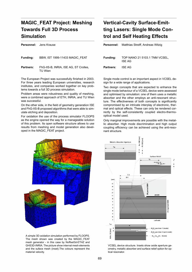
MAGIC_FEAT Project: MeshingTowards Full 3D ProcessSimulation
Personnel: Jens Krause
Funding: BBW, IST 1999-11433 MAGIC_FEAT
Partners: FhG-IIS-B, INRIA, ISE AG, ST Crolles,TU Wien
The European Project was successfully finished in 2003.For three years leading European universities, researchinstitutes, and companies worked together on key prob-lems towards a full 3D process simulation.Problem areas were robustness and quality of meshing,were a combined approach of ETH, INRIA, and TU Wienwas successful.On the other side, in the field of geometry generation ISEand FhG-IIS-B proposed algorithms that were able to sim-ulate etching and deposition.For oxidation the use of the process simulator FLOOPSas the engine opened the way for a manageable solutionof this problem. Its open software structure allows to useresults from meshing and model generation also devel-oped in the MAGIC_FEAT project.
A simple 3D oxidation simulation performed by FLOOPS.The mesh shown was created by the MAGIC_FEATmesh generator - in this case by Noffset3d-ETHZ andGHS3D-INRIA. The picture show internal mesh elementsand the suface mesh (inset).The colours represent thematerial velocity.
69
Vertical-Cavity Surface-Emit-ting Lasers: Single Mode Con-trol and Self Heating Effects
Personnel: Matthias Streiff, Andreas Witzig
Funding: TOP NANO 21 5103.1 TNM VCSEL,ISE AG
Partners: ISE AG
Single mode control is an important aspect in VCSEL de-sign for a wide range of applications.
Two design concepts that are expected to enhance thesingle mode behaviour of a VCSEL device were assessedand optimised by simulation: one of them uses a metallicabsorber and the other employs an anti-resonant struc-ture. The effectiveness of both concepts is significantlycompromised by an intricate interplay of electronic, ther-mal and optical effects. These can only be rendered cor-rectly by the self-consistently coupled electro-thermo-optical model used.
Only marginal improvements are possible with the metal-lic absorber. High mode discrimination and high outputcoupling efficiency can be achieved using the anti-reso-nant structure.
VCSEL device structure. Insets show oxide aperture ge-ometry, metallic absorber and surface relief option for op-tical resonator.
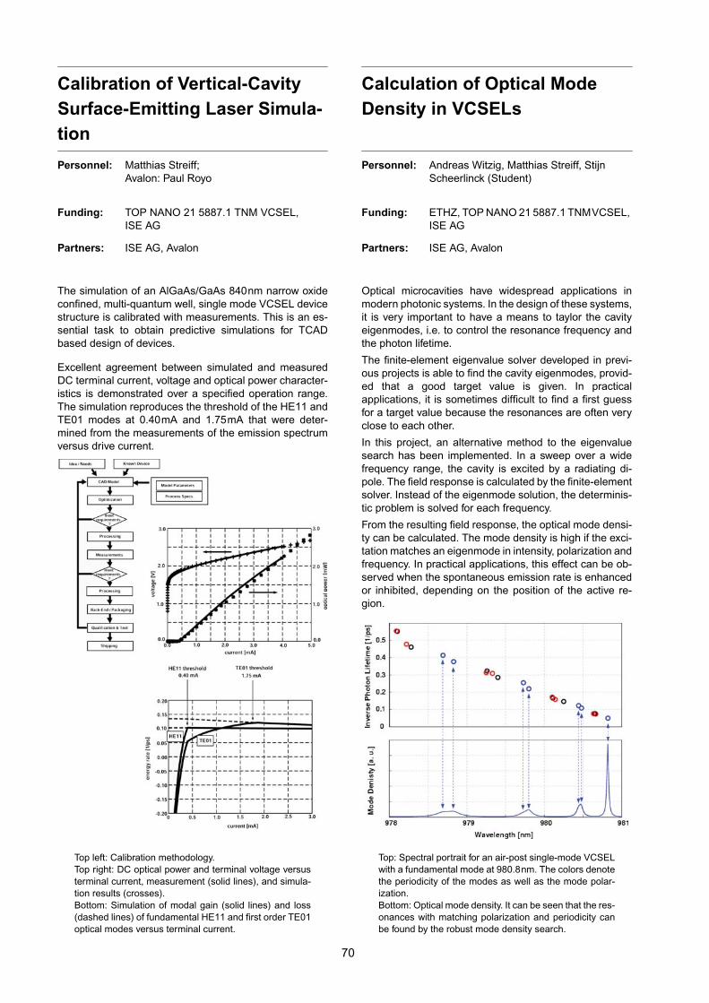
Calibration of Vertical-CavitySurface-Emitting Laser Simula-tion
Personnel: Matthias Streiff;Avalon: Paul Royo
Funding: TOP NANO 21 5887.1 TNM VCSEL,ISE AG
Partners: ISE AG, Avalon
The simulation of an AlGaAs/GaAs 840nm narrow oxideconfined, multi-quantum well, single mode VCSEL devicestructure is calibrated with measurements. This is an es-sential task to obtain predictive simulations for TCADbased design of devices.
Excellent agreement between simulated and measuredDC terminal current, voltage and optical power character-istics is demonstrated over a specified operation range.The simulation reproduces the threshold of the HE11 andTE01 modes at 0.40mA and 1.75mA that were deter-mined from the measurements of the emission spectrumversus drive current.
Top left: Calibration methodology.Top right: DC optical power and terminal voltage versusterminal current, measurement (solid lines), and simula-tion results (crosses).Bottom: Simulation of modal gain (solid lines) and loss(dashed lines) of fundamental HE11 and first order TE01optical modes versus terminal current.
70
Calculation of Optical ModeDensity in VCSELs
Personnel: Andreas Witzig, Matthias Streiff, StijnScheerlinck (Student)
Funding: ETHZ, TOP NANO 21 5887.1 TNMVCSEL,ISE AG
Partners: ISE AG, Avalon
Optical microcavities have widespread applications inmodern photonic systems. In the design of these systems,it is very important to have a means to taylor the cavityeigenmodes, i.e. to control the resonance frequency andthe photon lifetime.
The finite-element eigenvalue solver developed in previ-ous projects is able to find the cavity eigenmodes, provid-ed that a good target value is given. In practicalapplications, it is sometimes difficult to find a first guessfor a target value because the resonances are often veryclose to each other.
In this project, an alternative method to the eigenvaluesearch has been implemented. In a sweep over a widefrequency range, the cavity is excited by a radiating di-pole. The field response is calculated by the finite-elementsolver. Instead of the eigenmode solution, the determinis-tic problem is solved for each frequency.
From the resulting field response, the optical mode densi-ty can be calculated. The mode density is high if the exci-tation matches an eigenmode in intensity, polarization andfrequency. In practical applications, this effect can be ob-served when the spontaneous emission rate is enhancedor inhibited, depending on the position of the active re-gion.
Top: Spectral portrait for an air-post single-mode VCSELwith a fundamental mode at 980.8nm. The colors denotethe periodicity of the modes as well as the mode polar-ization.Bottom: Optical mode density. It can be seen that the res-onances with matching polarization and periodicity canbe found by the robust mode density search.
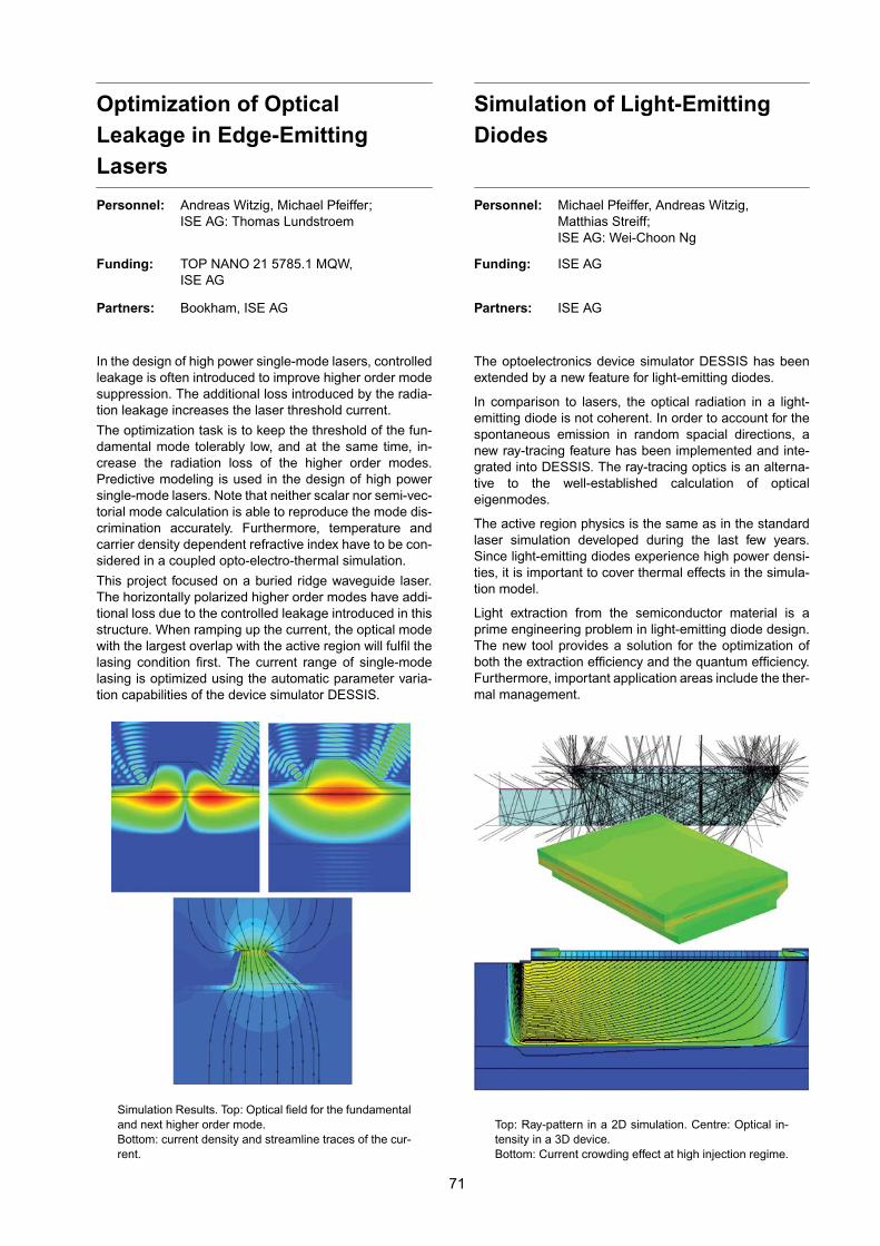
Optimization of OpticalLeakage in Edge-EmittingLasers
Personnel: Andreas Witzig, Michael Pfeiffer;ISE AG: Thomas Lundstroem
Funding: TOP NANO 21 5785.1 MQW,ISE AG
Partners: Bookham, ISE AG
In the design of high power single-mode lasers, controlledleakage is often introduced to improve higher order modesuppression. The additional loss introduced by the radia-tion leakage increases the laser threshold current.
The optimization task is to keep the threshold of the fun-damental mode tolerably low, and at the same time, in-crease the radiation loss of the higher order modes.Predictive modeling is used in the design of high powersingle-mode lasers. Note that neither scalar nor semi-vec-torial mode calculation is able to reproduce the mode dis-crimination accurately. Furthermore, temperature andcarrier density dependent refractive index have to be con-sidered in a coupled opto-electro-thermal simulation.
This project focused on a buried ridge waveguide laser.The horizontally polarized higher order modes have addi-tional loss due to the controlled leakage introduced in thisstructure. When ramping up the current, the optical modewith the largest overlap with the active region will fulfil thelasing condition first. The current range of single-modelasing is optimized using the automatic parameter varia-tion capabilities of the device simulator DESSIS.
Simulation Results. Top: Optical field for the fundamentaland next higher order mode.Bottom: current density and streamline traces of the cur-rent.
71
Simulation of Light-EmittingDiodes
Personnel: Michael Pfeiffer, Andreas Witzig,Matthias Streiff;ISE AG: Wei-Choon Ng
Funding: ISE AG
Partners: ISE AG
The optoelectronics device simulator DESSIS has beenextended by a new feature for light-emitting diodes.
In comparison to lasers, the optical radiation in a light-emitting diode is not coherent. In order to account for thespontaneous emission in random spacial directions, anew ray-tracing feature has been implemented and inte-grated into DESSIS. The ray-tracing optics is an alterna-tive to the well-established calculation of opticaleigenmodes.
The active region physics is the same as in the standardlaser simulation developed during the last few years.Since light-emitting diodes experience high power densi-ties, it is important to cover thermal effects in the simula-tion model.
Light extraction from the semiconductor material is aprime engineering problem in light-emitting diode design.The new tool provides a solution for the optimization ofboth the extraction efficiency and the quantum efficiency.Furthermore, important application areas include the ther-mal management.
Top: Ray-pattern in a 2D simulation. Centre: Optical in-tensity in a 3D device.Bottom: Current crowding effect at high injection regime.

Full 3D Simulation of TunableSampled-Grating DBR Laser
Personnel: Lutz Schneider, Michael Pfeiffer, MatthiasStreiff, Andreas Witzig
Funding: TOP NANO 21 5785.1 MQW,ISE AG
Partners: ISE AG, UCSB
Widely-tunable sampled-grating distributed Bragg reflec-tor (SGDBR) lasers can be used for present WDM com-munication networks. They are also a basic building blockfor developing high functionality photonic integrated cir-cuits (PICs) which have a great potential in future fiber op-tical networking architectures.
In this project, our approach to full 3D simulation of multi-section DBR lasers has been extended to accommodatefor SGDBR type structures. Both the front and the rearmirror show a comb-like mirror spectrum. Shifting the mir-ror spectra relative to each other by inducing a refractiveindex change through current injection into either section,different reflectivity peaks overlap. Together with a phasecontrol section this allows to quasi-continuously tune thelaser wavelength over a range of up to 100nm.
Top: Front and rear mirror reflectivity spectra of a buried-heterostructure SGDBR laser indicating a maximumoverall reflectivity of the structure at a wavelength of1.55µm. Bottom: Longitudinally varying optical intensitydistribution due to SGDBR mirrors.
72
Full 3D Simulation of aSemiconductor OpticalAmplifier
Personnel: Lutz Schneider, Michael Pfeiffer, MatthiasStreiff, Andreas Witzig
Funding: TOP NANO 21 5785.1 MQW,ISE AG
Partners: ISE AG, UCSB
Semiconductor Optical Amplifiers (SOA) technology is ca-pable of realizing many of the all-optical functions re-quired in emerging optical networks. As optoelectronicintegrated circuit technology advances and manufactur-ing costs fall, the use of SOAs as basic amplifiers and aswell as components in functional subsystems will expand.Widely-tunable lasers often lack sufficiently high outputpower required for commercial applications. This limita-tion can be overcome by monolithically integrating themwith a SOA.In this project, our framework for full 3D laser simulationhas been extended in order to perform fully self-consistentelectro-optical simulations of SOAs. A robust couplingscheme ensures good overall convergence despite thestrong variation of the optical field with respect to injectioncurrent. This lays the foundation for comprehensive simu-lation of a tunable DBR laser integrated with a SOA tostudy crosstalk effects between the two devices.
Top: Output power vs. SOA injection current for differentinput signal powers and wavelengths as obtained fromfull 3D simulations. Bottom: Optical intensity distributionof the SOA close to saturation of the amplifier gain.
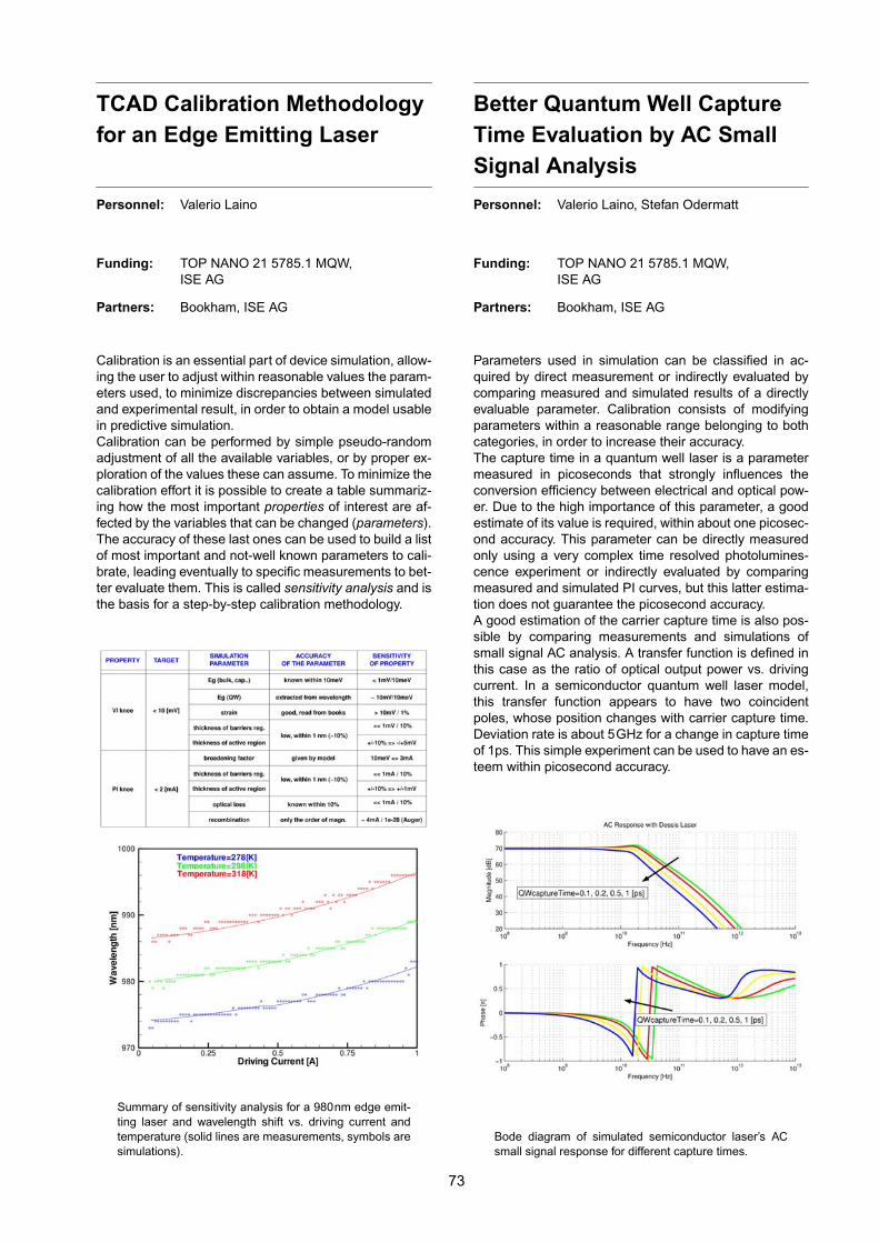
TCAD Calibration Methodologyfor an Edge Emitting Laser
Personnel: Valerio Laino
Funding: TOP NANO 21 5785.1 MQW,ISE AG
Partners: Bookham, ISE AG
Calibration is an essential part of device simulation, allow-ing the user to adjust within reasonable values the param-eters used, to minimize discrepancies between simulatedand experimental result, in order to obtain a model usablein predictive simulation.Calibration can be performed by simple pseudo-randomadjustment of all the available variables, or by proper ex-ploration of the values these can assume. To minimize thecalibration effort it is possible to create a table summariz-ing how the most important properties of interest are af-fected by the variables that can be changed (parameters).The accuracy of these last ones can be used to build a listof most important and not-well known parameters to cali-brate, leading eventually to specific measurements to bet-ter evaluate them. This is called sensitivity analysis and isthe basis for a step-by-step calibration methodology.
Summary of sensitivity analysis for a 980nm edge emit-ting laser and wavelength shift vs. driving current andtemperature (solid lines are measurements, symbols aresimulations).
73
Better Quantum Well CaptureTime Evaluation by AC SmallSignal Analysis
Personnel: Valerio Laino, Stefan Odermatt
Funding: TOP NANO 21 5785.1 MQW,ISE AG
Partners: Bookham, ISE AG
Parameters used in simulation can be classified in ac-quired by direct measurement or indirectly evaluated bycomparing measured and simulated results of a directlyevaluable parameter. Calibration consists of modifyingparameters within a reasonable range belonging to bothcategories, in order to increase their accuracy.The capture time in a quantum well laser is a parametermeasured in picoseconds that strongly influences theconversion efficiency between electrical and optical pow-er. Due to the high importance of this parameter, a goodestimate of its value is required, within about one picosec-ond accuracy. This parameter can be directly measuredonly using a very complex time resolved photolumines-cence experiment or indirectly evaluated by comparingmeasured and simulated PI curves, but this latter estima-tion does not guarantee the picosecond accuracy.A good estimation of the carrier capture time is also pos-sible by comparing measurements and simulations ofsmall signal AC analysis. A transfer function is defined inthis case as the ratio of optical output power vs. drivingcurrent. In a semiconductor quantum well laser model,this transfer function appears to have two coincidentpoles, whose position changes with carrier capture time.Deviation rate is about 5GHz for a change in capture timeof 1ps. This simple experiment can be used to have an es-teem within picosecond accuracy.
Bode diagram of simulated semiconductor laser’s ACsmall signal response for different capture times.
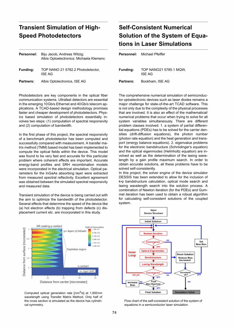
Transient Simulation of High-Speed Photodetectors
Personnel: Biju Jacob, Andreas Witzig;Albis Optoelectronics: Michaela Klemenc
Funding: TOP NANO 21 5782.2 Photodetector,ISE AG
Partners: Albis Optolectronics, ISE AG
Photodetectors are key components in the optical fibercommunication systems. Ultrafast detectors are essentialin the emerging 10Gb/s Ethernet and 40Gb/s telecom ap-plications. A TCAD-based design methodology promisesfaster and cheaper development of photodetectors. Phys-ics based simulation of photodetectors essentially in-volves two steps: (1) computation of spectral responsivityand (2) computation of bandwidth.
In the first phase of this project, the spectral responsivityof a benchmark photodetector has been computed andsuccessfully compared with measurement. A transfer ma-trix method (TMM) based model has been implemented tocompute the optical fields within the device. This modelwas found to be very fast and accurate for this particularproblem where coherent effects are important. Accurateenergy-band profiles and SRH recombination modelswere incorporated in the electrical simulation. Optical pa-rameters for the InGaAs absorbing layer were extractedfrom measured spectral reflectivity. Excellent agreementwas obtained between the simulated spectral responsivityand measured data.
Transient simulation of the device is being carried out withthe aim to optimize the bandwidth of the photodetector.Several effects that determine the speed of the device like(a) hot electron effects (b) trapping from defects (c) dis-placement current etc. are incorporated in this study.
Computed optical generation rate [/cm3/s] at 1,600nmwavelength using Transfer Matrix Method. Only half ofthe cross section is simulated as the device has cylindri-cal symmetry.
74
Self-Consistent NumericalSolution of the System of Equa-tions in Laser Simulations
Personnel: Michael Pfeiffer
Funding: TOP NANO21 5785.1 MQW,ISE AG
Partners: Bookham, ISE AG
The comprehensive numerical simulation of semiconduc-tor optoelectronic devices such as laser diodes remains amajor challenge for state-of-the-art TCAD software. Thisis not only due to the complexity of the physical processesthat are involved. It is also an effect of the mathematical/numerical problems that occur when trying to solve for allsystem variables simultaneously. There are differentproblem classes involved: 1. a system of partial differen-tial equations (PDEs) has to be solved for the carrier den-sities (drift-diffusion equations), the photon number(photon rate equation) and the heat generation and trans-port (energy balance equations). 2. eigenvalue problemsfor the electronic bandstructure (Schrödinger’s equation)and the optical eigenmodes (Helmholtz equation) are in-volved as well as the determination of the lasing wave-length by a gain profile maximum search. In order toobtain accurate solutions, all these problems have to besolved self-consistently.In this project, the solver engine of the device simulatorDESSIS has been extended to allow for the inclusion ofk•p bandstructure calculation, optical mode search andlasing wavelength search into the solution process. Acombination of Newton iteration (for the PDEs) and Gum-mel iteration has been used to obtain a robust algorithmfor calculating self-consistent solutions of the coupledsystem.
Flow chart of the self-consistent solution of the system ofequations in a semiconductor laser simulation.
Multi-Grid Scheme for theSimulation of OptoelectronicDevices
Personnel: Michael Pfeiffer, Matthias Streiff;ISE AG: Peter Regli
Funding: TOP NANO21 5103.1 TMN VCSEL,ISE AG
Partners: ISE AG
Numerical simulations of optoelectronic devices usuallyconsist of an electro-thermal part and an optical partwhich impose different constraints on the discretization tobe used for the simulation domain. This might includespecial boundary conditions for one part of the simulation(e.g. Perfectly Matched Layer boundary conditions for op-tical solvers) or different numbers of mesh points due tocomputational constraints (e.g. VCSEL simulations whereoptically active Bragg mirror stacks can not be resolved inthe electro-thermal simulation part).In this project, a fully automatic multi-grid scheme hasbeen implemented in the semiconductor device simulatorDESSIS. It allows to run self-consistent optoelectronicsimulations using different grids for optics and electronics.Grid processing, data interpolation and error estimationare self-consistently integrated into the solution cycle.
The upper picture shows the optical intensity and the fineoptical grid that resolves the top and bottom Braggstacks of the VCSEL. The lower picture shows the coars-er electro-thermal grid, where the Bragg-stacks are notresolved, but are replaced by an effective material withsimilar electrical properties that can be discretized withmuch less points. The colors show the distribution of thecurrent density.The optical grid contains about 90,000mesh vertices, whereas the electrical grid consists ofonly 8,000 vertices.
75
Multimode Optical Small SignalAnalysis
Personnel: Stefan Odermatt, Matthias Streiff,Bernhard Schmithüsen
Funding: ETHZ, TOP NANO21 5103.1 TMN VCSEL,ISE AG
Partners: ISE AG
Modern communication systems often require high-speedsemiconductor lasers. In order to enhance the data ratesin such a system, the modulation response of the laser isof particular importance. In this project, DESSIS has beenextended to allow multimode optical small signal simula-tion using the field impedance method.
As an example, the small signal characteristics of an ox-ide confined vertical-cavity surface-emitting laser (VC-SEL) is simulated. The transfer characteristics areobtained by evaluating the normalized frequency-depen-dent ratio between the modal optical output power andterminal current.
Top: Optical Intensity in a VCSEL for the first two modes(left: HE11, right: TE01) on a logarithmic scale.Bottom: Normalized small signal response due to a cur-rent modulation at three different bias points (red curve:first mode, blue curve: second mode).
Bandstructure Calculation forArbitrarily Shaped QuantumWells
Personnel: Stefan Odermatt, Mathieu Luisier
Funding: TOP NANO 21 5785.1 MQW,ISE AG
Partners: ISE AG
Thinking towards predictive optoelectronics device simu-lation, it is crucial that the bandstructure is accuratelymodeled, at least in the active region.
In common devices, only the bandstructure in the centerof the first Brillouin zone, where recombination processestake place, is important. Therefore, a perturbation tech-nique can be applied to save computational resources.
In order to meet these requirements, a 8-band k•p methodfor arbitrary one-dimensional potential shapes has beenimplemented in this project. The finite difference methodwas chosen to describe the heterostructure potential.
Quasi bound states occurring in non-flat band regions aretreated by using absorbing boundary conditions, resultingin complex eigenenergies, whereas the imaginary part ofthe eigenenergies is related to the energy state lifetime.The real part determines the density of state and the car-rier distribution in the active zone of the laser. The calcu-lated wave functions are used to compute the matrixelements between conduction and valence subbands,necessary to obtain the optical gain.
Left: The valence band of a InGaAs-GaAs double QWsemiconductor laser is shown (black line). The red linesrepresent the heavy-hole wave functions at k=0 whereasthe blue lines denote the light-hole wave functions. Thedotted levels represent the eigenenergies.Right: The bandstructure is calculated using a 8-band k•pmethod (including strain). It is obvious that the bandsshow strong nonparabolicites so that the effective massapproximation leads to wrong results.
76
Simulation of Carrier Transportin the Active Region ofSemiconductor Lasers
Personnel: Stefan Odermatt
Funding: TOP NANO 21 5785.1 MQW,ISE AG
Partners: ISE AG
Modeling and simulation of semiconductor lasers contain-ing multiple quantum wells (MQWs) is playing an increas-ingly important rule. Most of the models developed andimplemented to date were based on the drift-diffusion ap-proach, which require a huge number of input parameterswhich must be carefully selected.
In order to determine these input parameters, carriertransport can be simulated on a microscopic approach,i.e. using transport equations based on the non-equilibri-um Green’s function (NEGF) formalism.
This microscopic approach has been followed in thisproject to gain understanding about the physical phenom-ena occurring during the capture processes in MQWsemiconductor laser diodes.
Top: Two-dimensional carrier densities along the MQWregion. The carriers are injected from the right side.Bottom: Energy resolved carrier densities. Bright regionsdenote high carrier concentration.
Microscopic Gain Calculation:Influence of the Coulomb-Induced Subband Coupling
Personnel: Mathieu Luisier
Funding: TOP NANO21 5785.1 MQW,ISE AG
Partners: ISE AG
In this project, the optical gain and absorption of a semi-conductor quantum well laser were studied, includingmany-body effects treated on the level of the Second BornApproximation and the Coulomb induced coupling be-tween different conduction or valence subbands.Instead of solving one equation of motion for each micro-scopic interband polarization, a system of equationswhere all the optical transitions are coupled by the Cou-lomb potential is solved.At low carrier densities, where exciton absorption lines oc-cur, the Coulomb induced subband coupling shifts the os-cillator strength of the exciton peaks towards lowertransition energies (red shift). Increasing the quantum wellwidth, the bulk case limit with a single exciton line can onlybe reached with the Coulomb coupling of the subbands.At high carrier densities, the Coulomb subband couplingincreases the amplitude of the gain, shifts its maximum to-wards lower frequencies and leads to a steeper transitionbetween gain and absorption.
Absorption spectrum at low (top figure) and high (bottomfigure) carrier densities for an InGaAs-AlGaAs quantumwell. Red: with Coulomb coupling. Blue: without. Thebandstructure was obtained by a 8-band k•p calculation.
77
Self-Consistent 8-band k•pSchroedinger-Poisson Solverfor Wurtzite Crystals
Personnel: Mathieu Luisier
Funding: ETHZ
Wurtzite nitrides, like GaN or InN, have an important mac-roscopic polarization, including a spontaneous (causedby the symmetry of the crystal) and a piezoelectric (in-duced by strain) component. In nitride quantum wells, thespontaneous and piezoelectric polarizations create alarge built-in electrostatic field, due to the polarizationchange at the heterointerface.
As consequence, the electrons and holes in the quantumwell are spatially separated and cause a second electro-static field, which screens the first one (free-carrierscreening). Therefore, a self-consistent solution is re-quired: the Schroedinger and Poisson equations must besolved iteratively until convergence. For the bandstruc-ture calculation, the 8-band k•p method was chosen.
At low carrier density, free-carrier screening has a smallinfluence but, by increasing the carrier density, thescreening will compensate the spontaneous and piezo-electric polarization and a nearly “field-free” quantum wellprofile is obtained.
Top: InGaN-GaN quantum well profile for different carrierdensities. The black line is without the piezoelectric andspontaneous fields. The colored ones take into accountthe build-in and screened fields caused by the electron-hole spatial separation.Bottom: Many-Body Gain with the self-consistent poten-tial (colored lines) and without piezoelectric fields (black-dashed lines) for different carrier densities.
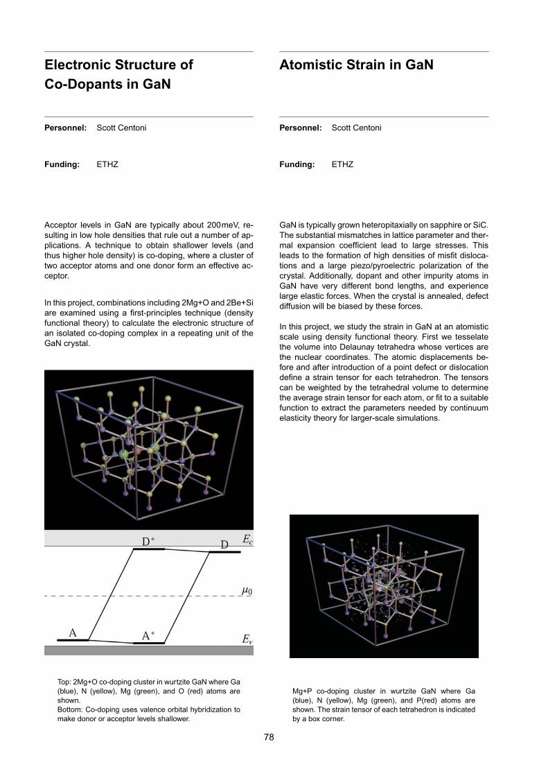
Electronic Structure ofCo-Dopants in GaN
Personnel: Scott Centoni
Funding: ETHZ
Acceptor levels in GaN are typically about 200meV, re-sulting in low hole densities that rule out a number of ap-plications. A technique to obtain shallower levels (andthus higher hole density) is co-doping, where a cluster oftwo acceptor atoms and one donor form an effective ac-ceptor.
In this project, combinations including 2Mg+O and 2Be+Siare examined using a first-principles technique (densityfunctional theory) to calculate the electronic structure ofan isolated co-doping complex in a repeating unit of theGaN crystal.
Top: 2Mg+O co-doping cluster in wurtzite GaN where Ga(blue), N (yellow), Mg (green), and O (red) atoms areshown.Bottom: Co-doping uses valence orbital hybridization tomake donor or acceptor levels shallower.
78
Atomistic Strain in GaN
Personnel: Scott Centoni
Funding: ETHZ
GaN is typically grown heteropitaxially on sapphire or SiC.The substantial mismatches in lattice parameter and ther-mal expansion coefficient lead to large stresses. Thisleads to the formation of high densities of misfit disloca-tions and a large piezo/pyroelectric polarization of thecrystal. Additionally, dopant and other impurity atoms inGaN have very different bond lengths, and experiencelarge elastic forces. When the crystal is annealed, defectdiffusion will be biased by these forces.
In this project, we study the strain in GaN at an atomisticscale using density functional theory. First we tesselatethe volume into Delaunay tetrahedra whose vertices arethe nuclear coordinates. The atomic displacements be-fore and after introduction of a point defect or dislocationdefine a strain tensor for each tetrahedron. The tensorscan be weighted by the tetrahedral volume to determinethe average strain tensor for each atom, or fit to a suitablefunction to extract the parameters needed by continuumelasticity theory for larger-scale simulations.
Mg+P co-doping cluster in wurtzite GaN where Ga(blue), N (yellow), Mg (green), and P(red) atoms areshown. The strain tensor of each tetrahedron is indicatedby a box corner.
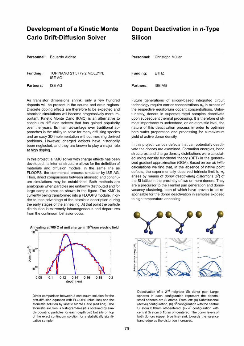
Development of a Kinetic MonteCarlo Drift-Diffusion Solver
Personnel: Eduardo Alonso
Funding: TOP NANO 21 5779.2 MOLDYN,ISE AG
Partners: ISE AG
As transistor dimensions shrink, only a few hundreddopants will be present in the source and drain regions.Discrete doping effects are therefore to be expected andatomistic simulations will become progressively more im-portant. Kinetic Monte Carlo (KMC) is an alternative tocontinuum diffusion solvers that has gained popularityover the years. Its main advantage over traditional ap-proaches is the ability to solve for many diffusing speciesand an easy 3D implementation without meshing derivedproblems. However, charged defects have historicallybeen neglected, and they are known to play a major roleat high doping.
In this project, a KMC solver with charge effects has beendeveloped. Its internal structure allows for the definition ofmaterials and diffusion models, in the same line asFLOOPS, the commercial process simulator by ISE AG.Thus, direct comparisons between atomistic and continu-um simulations may be established. Both methods areanalogous when particles are uniformly distributed and forlarge sample sizes as shown in the figure. The KMC iscurrently being transformed into a FLOOPS module, in or-der to take advantage of the atomistic description duringthe early stages of the annealing. At that point the particledistribution is extremely inhomogeneous and departuresfrom the continuum behavior occur.
Direct comparison between a continuum solution for thedrift-diffusion equation with FLOOPS (blue line) and theatomistic solution by kinetic Monte Carlo (red line). Theatomistic solution is histogram-like (it is obtained by sim-ply counting particles for each depth bin) but sits on topof the exact continuum solution for a statistically signifi-cative sample.
79
Dopant Deactivation in n-TypeSilicon
Personnel: Christoph Müller
Funding: ETHZ
Partners: ISE AG
Future generations of silicon-based integrated circuittechnology require carrier concentrations ne in excess ofthe respective equilibrium dopant concentrations. Unfor-tunately, donors in supersaturated samples deactivateupon subsequent thermal processing. It is therefore of ut-most importance to understand, on an atomistic level, thenature of this deactivation process in order to optimizeboth wafer preparation and processing for a maximumyield of active donor density.
In this project, various defects that can potentially deacti-vate the donors are examined. Formation energies, bandstructures, and charge density distributions were calculat-ed using density funcitonal theory (DFT) in the general-ized gradient approximation (GGA). Based on our ab initiocalculations we find that, in the absence of native pointdefects, the experimentally observed intrinsic limit to nearises by means of donor deactivating distortions (δ3) ofthe Si lattice in the proximity of two or more donors. Theyare a precursor to the Frenkel pair generation and donor-vacancy clustering, both of which have proven to be re-sponsable for the donor deactivation in samples exposedto high temperature annealing.
Deactivation of a 2nd neighbor Sb donor pair: Largespheres in each configuration represent the donors,small spheres are Si atoms. From left: (a) Substitutional(active) configuration, (b) δ3 configuration with the centralSi atom 0.08nm off-centered, (c) δ3 configuration withcentral Si atom 0.15nm off-centered. The donor levels ofboth donors (upper blue line) sink towards the valenceband edge as the distortion increases.
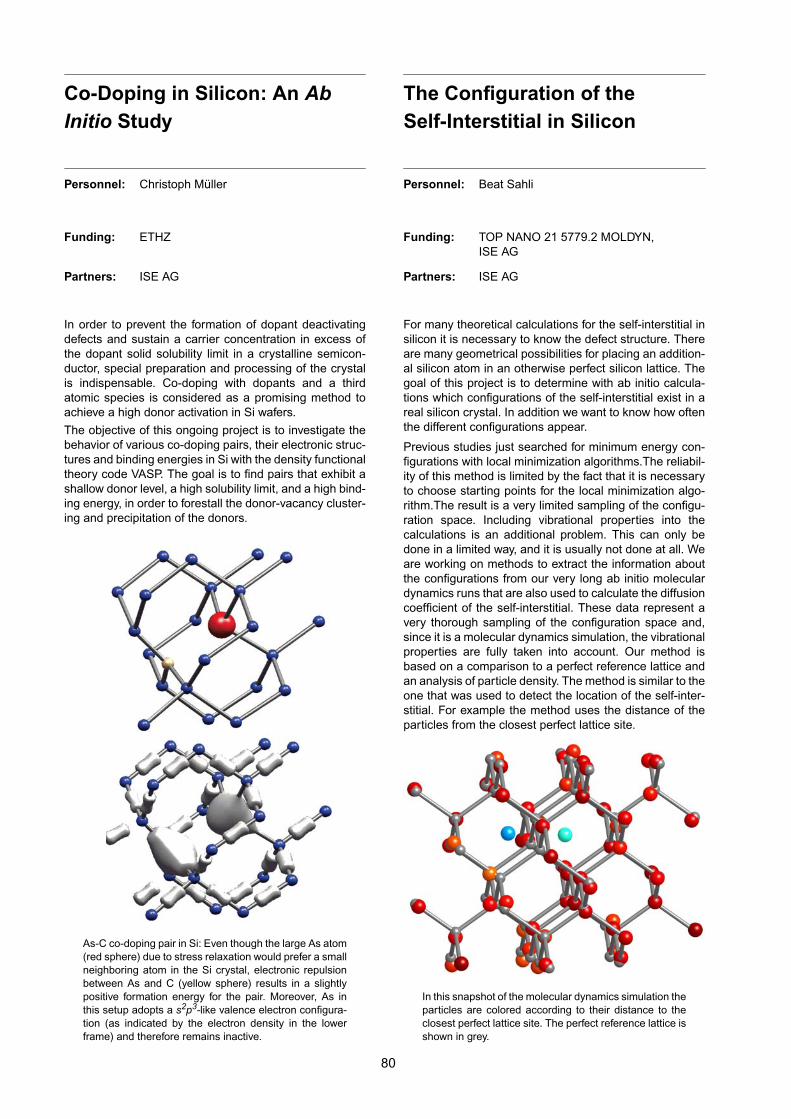
Co-Doping in Silicon: An AbInitio Study
Personnel: Christoph Müller
Funding: ETHZ
Partners: ISE AG
In order to prevent the formation of dopant deactivatingdefects and sustain a carrier concentration in excess ofthe dopant solid solubility limit in a crystalline semicon-ductor, special preparation and processing of the crystalis indispensable. Co-doping with dopants and a thirdatomic species is considered as a promising method toachieve a high donor activation in Si wafers.
The objective of this ongoing project is to investigate thebehavior of various co-doping pairs, their electronic struc-tures and binding energies in Si with the density functionaltheory code VASP. The goal is to find pairs that exhibit ashallow donor level, a high solubility limit, and a high bind-ing energy, in order to forestall the donor-vacancy cluster-ing and precipitation of the donors.
As-C co-doping pair in Si: Even though the large As atom(red sphere) due to stress relaxation would prefer a smallneighboring atom in the Si crystal, electronic repulsionbetween As and C (yellow sphere) results in a slightlypositive formation energy for the pair. Moreover, As inthis setup adopts a s2p3-like valence electron configura-tion (as indicated by the electron density in the lowerframe) and therefore remains inactive.
80
The Configuration of theSelf-Interstitial in Silicon
Personnel: Beat Sahli
Funding: TOP NANO 21 5779.2 MOLDYN,ISE AG
Partners: ISE AG
For many theoretical calculations for the self-interstitial insilicon it is necessary to know the defect structure. Thereare many geometrical possibilities for placing an addition-al silicon atom in an otherwise perfect silicon lattice. Thegoal of this project is to determine with ab initio calcula-tions which configurations of the self-interstitial exist in areal silicon crystal. In addition we want to know how oftenthe different configurations appear.
Previous studies just searched for minimum energy con-figurations with local minimization algorithms.The reliabil-ity of this method is limited by the fact that it is necessaryto choose starting points for the local minimization algo-rithm.The result is a very limited sampling of the configu-ration space. Including vibrational properties into thecalculations is an additional problem. This can only bedone in a limited way, and it is usually not done at all. Weare working on methods to extract the information aboutthe configurations from our very long ab initio moleculardynamics runs that are also used to calculate the diffusioncoefficient of the self-interstitial. These data represent avery thorough sampling of the configuration space and,since it is a molecular dynamics simulation, the vibrationalproperties are fully taken into account. Our method isbased on a comparison to a perfect reference lattice andan analysis of particle density. The method is similar to theone that was used to detect the location of the self-inter-stitial. For example the method uses the distance of theparticles from the closest perfect lattice site.
In this snapshot of the molecular dynamics simulation theparticles are colored according to their distance to theclosest perfect lattice site. The perfect reference lattice isshown in grey.

Large Scale Eigenvalue Prob-lems in OptoelectronicSemiconductor Lasers
Personnel: S. Röllin, M. Streiff, B. Schmithüsen,A. Witzig; IWR-ETHZ: P. Arbenz, M. Becka;Uni Basel: O. Schenk
Funding: CSE-SEP ETHZ
Partners: IWR-ETHZ, Uni Basel, PSI
The numerical simulation of semiconductor laser devices- as well as accelerator cavities - lead to huge eigenvalueproblems for the discretized homogeneous Maxwellequation. At present the resulting eigenvalue problemsyield system sizes up to 1’000’000 complex unknowns foraxis-symmetric 3D laser device structures. The aim of thisproject is to improve the performance of the eigensolverwith respect to both speed and memory. To this purposethe actual two-level hierachical preconditioner will be ex-tended to a multilevel method tightly coupled to the Nede-lec finite element method used. The Jacobi-Davidsoneigensolver will be parallelized for shared as well as dis-tributed processor architectures.
The increasing complexity of modern laser devices withmulti-layer structures of different materials require evenfor the electronic part faster solutions times. Upcoming la-ser designs require full 3D electrical characterizationswith tremendously increasing problem sizes. The secondpart of the project addresses memory, parallelization, androbustness issues concerning the iterative solution proce-dure of linear systems. Experiments with nonsymmetricpermutations have shown promising results concerningstandard Krylov subspace methods. The parallelization ofan incomplete LU-factorization based on dropping toler-ances scales well with a low number of processors.
The setup time for an incomplete LU-factorization isshown for two typical matrices extracted from 3D DES-SIS simulations. The results were carried out on the IBMSP4 at the Swiss Center for Scientific Computing.
81
Nonsymmetric Permutationsfor Iterative Methods in Semi-conductor Device Simulation
Personnel: Stefan Röllin
Funding: CSE-SEP ETHZ
Partners: ISE AG
The sparse linear systems arising in semiconductor de-vice simulation are known to be highly ill-conditioned andthus quite challenging for iterative methods. The reliabilityof preconditioned iterative methods can greatly be im-proved by using algorithms to place large entries on thediagonal using nonsymmetric permutations and scalings.These algorithms are used as a preprocessing step be-fore a preconditioner is computed. A previous project hasproven the usefulness of this strategy for semiconductordevice simulations.
At our laboratory, a parallel iterative solver for sharedmemory multiprocessors is currently being developed. Toachieve good speedups, it is mandatory to run most stepsof the solver in parallel. Thus, the main aspect of thisproject was the parallel implementation of the mentionednonsymmetric permutations and scalings with OpenMP.
On eight CPUs of an IBM p690, speedups up to 7.4 couldbe reached with the realized parallelisation. The reasonfor these good results are twofold and can be explainedby looking at the algorithms. The idea is to find a permu-tation of the rows of a matrix, such that the product of thediagonal elements is maximal. Two different steps arecarried out to find the permutation: first, the problem is re-written into an equivalent problem, which is known as bi-partite matching and which is solved in a second step. Ithas been shown, that nesting both steps gives betterspeedups than the separate treatment. Additionally, alarge part of step two can be carried out concurrently,since most of the matching is done within the variables ofa physical point, which explains further the good speed-ups.
Graphical depiction of the magnitude of the elements ina matrix from semiconductor device simulation.Left: original coefficient matrix. Indicated with blue are50% of the largest absolute values, in red, the largest10%. Right: scaled matrix. In contrary to the original ma-trix, the largest values are now located on the diagonal.

83
Research Projects
Physical Characterization
Coordinators:
Wolfgang FichtnerMauro Ciappa

Fast 3D Transient ThermalSimulation of Converters forAutomotive Applications
Personnel: Kari Oila, Mauro Ciappa
Funding: BBW, EU-GROWTH-00275 HIMRATE
Partners: Siemens München
Transient thermal 3D simulation of complex objects as aconverter for automotive applications operated under re-alistic mission profiles is almost impossible by using tradi-tional strategies, since it would require computationaltimes in the order of weeks. The procedure we have de-veloped, enables to simulate within seconds the time evo-lution of the local temperature in an arbitrary location ofthe converter as operated in a hybrid vehicle. The startingpoint of the procedure is a static 3D finite element modelof the converter including the module and the heatsink,which is firstly calibrated by experimental data acquiredeither by infrared thermography or by internal thermome-try techniques. The 3D finite element model is used to ex-tract the thermal impedance of the system, while the timedependency is computed by an optimized convolution al-gorithm. This procedure represents a very efficient way toreduce the development cycle of a converter by the quan-titative use of CAD tools and it enables at the same timean implementation of a built-in reliability program.
3D finite element model with about 90,000 nodes for theextraction of the thermal impedance curve. The 3-phaseconverter includes 24 power MOSFETs.
84
Electro-Thermal Characteriza-tion and Simulation of Convert-ers for Automotive Applications
Personnel: Mauro Ciappa, Kari Oila;CRF: Alessandro Pincetti;Matteo Ferrari (student)
Funding: BBW, EU-GROWTH-00275 HIMRATE
Partners: CRF
Optimum thermal management is of paramount relevancewhen developing efficient and reliable power inverters forhybrid vehicles. A fundamental component of thermal de-signs based on CAD tools is the experimental validationof the models by the use of real heatsinks. Of particular in-terest in this field is the benchmarking of discrete versusintegrated forced convection cooling solutions. In thiswork, the efficiency of the discrete CRF and of the inte-grated HIMRATE approach has been characterized atbench under realistic vehicle operation conditions. It hasbeen shown that the reduction of the thermal resistancealone is not sufficient to realize the specified thermal re-quirements. In fact, due to the complex power switchingregimes and to the relatively low duty cycles encounteredin automotive applications, local temperature peaks canbe more conveniently smoothed by distributed thermal ca-pacitances.
Discrete (top) and integrated (bottom) cooling solutionsused for hybrid vehicle converters.
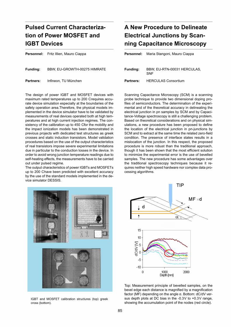
Pulsed Current Characteriza-tion of Power MOSFET andIGBT Devices
Personnel: Fritz Illien, Mauro Ciappa
Funding: BBW, EU-GROWTH-00275 HIMRATE
Partners: Infineon, TU München
The design of power IGBT and MOSFET devices withmaximum rated temperatures up to 200 Crequires accu-rate device simulation especially at the boundaries of thesafety operation area.Therefore, the physical models im-plemented in the device simulator have to be validated bymeasurements of real devices operated both at high tem-peratures and at high current injection regimes. The con-sistency of the calibration up to 450 Cfor the mobility andthe impact ionization models has been demonstrated inprevious projects with dedicated test structures as greekcrosses and static induction transistors. Model validationprocedures based on the use of the output characteristicsof real transistors impose severe experimental limitationsdue in particular to the conduction losses in the device. Inorder to avoid wrong junction temperature readings due toself-heating effects, the measurements have to be carriedout under pulsed regime.The output characteristics of power IGBTs and MOSFETsup to 200 Chave been predicted with excellent accuracyby the use of the standard models implemented in the de-vice simulator DESSIS.
IGBT and MOSFET calibration structures (top) greekcross (bottom).
85
A New Procedure to DelineateElectrical Junctions by Scan-ning Capacitance Microscopy
Personnel: Maria Stangoni, Mauro Ciappa
Funding: BBW, EU-RTN-00031 HERCULAS,SNF
Partners: HERCULAS Consortium
Scanning Capacitance Microscopy (SCM) is a scanningprobe technique to provide two dimensional doping pro-files of semiconductors. The determination of the experi-mental and of the theoretical accuracy in delineating theelectrical junction in pn samples by SCM and by Capaci-tance-Voltage spectroscopy is still a challenging problem.Based on theoretical considerations and on physical sim-ulations, a new procedure has been proposed to definethe location of the electrical junction in pn-junctions bySCM and to extract al the same time the related zero-fieldcondition. The presence of interface states results in amislocation of the junction. In this respect, the proposedprocedure is more robust than the traditional approach,though it has been shown that the most efficient solutionto minimize the experimental error is the use of bevelledsamples. The new procedure has some advantages overthe traditional spectroscopy techniques because it re-quires neither high speed hardware nor complex data pro-cessing algorithms.
Top: Measurement principle of bevelled samples, on thebevel edge each distance is magnified by a magnificationfactor (MF) depending on the angle α. Bottom: dC/dV ver-sus depth plots at DC bias in the -0.3V to +0.3V range,showing the accumulation point of the nodes (red circle).
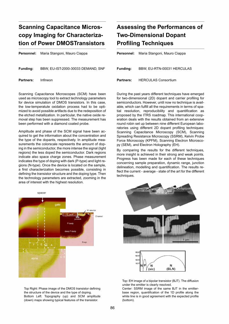
Scanning Capacitance Micros-copy Imaging for Characteriza-tion of Power DMOSTransistors
Personnel: Maria Stangoni, Mauro Ciappa
Funding: BBW, EU-IST-2000-30033 DEMAND, SNF
Partners: Infineon
Scanning Capacitance Microscopes (SCM) have beenused as microscopy tool to extract technology parametersfor device simulation of DMOS transistors. In this case,the low-temperatute oxidation process had to be opti-mized to avoid possible artifacts due to the redeposition ofthe etched metallization. In particular, the native oxide re-moval step has been suppressed. The measurement hasbeen performed with a diamond coated probe.
Amplitude and phase of the SCM signal have been ac-quired to get the information about the concentration andthe type of the dopants, respectively. In amplitude mea-surements the colorscale represents the amount of dop-ing in the semiconductor, the more intense the signal (lightregions) the less doped the semiconductor. Dark regionsindicate also space charge zones. Phase measurementindicates the type of doping with dark (P-type) and light re-gions (N-type). Once the device is located on the sample,a first characterization becomes possible, consisting indefining the transistor structure and the doping type. Thenthe technology parameters are extracted, zooming in thearea of interest with the highest resolution.
Top Right: Phase image of the DMOS transistor definingthe structure of the device and the type of doping.Bottom Left: Topography (up) and SCM amplitude(down) maps showing typical features of the transistor.
86
Assessing the Performances ofTwo-Dimensional DopantProfiling Techniques
Personnel: Maria Stangoni, Mauro Ciappa
Funding: BBW, EU-RTN-00031 HERCULAS
Partners: HERCULAS Consortium
During the past years different techniques have emergedfor two-dimensional (2D) dopant and carrier profiling forsemiconductors. However, until now no technique is avail-able, which can fulfill all the requirements in terms of spa-tial resolution, reproducibility and quantification asproposed by the ITRS roadmap. This international coop-eration deals with the results obtained from an extensiveround robin set up between nine different European labo-ratories using different 2D dopant profiling techniques:Scanning Capacitance Microscopy (SCM), ScanningSpreading Resistance Microscopy (SSRM), Kelvin ProbeForce Microscopy (KPFM), Scanning Electron Microsco-py (SEM), and Electron Holography (EH).
By comparing the results for the different techniques,more insight is achieved in their strong and weak points.Progress has been made for each of these techniquesconcerning sample preparation, dynamic range, junctiondelineation, modelling and quantification. The results re-flect the current - average - state of the art for the differenttechniques.
Top: EH image of a bipolar transistor (BJT). The diffusionunder the emitter is clearly resolved.Center: SSRM image of the same BJT in the emitter-base region, quantification of the 1D profile along thewhite line is in good agreement with the expected profile(bottom).

Selective Iodine-Based GoldEtch for Aged OptoelectronicsDevices Failure Analysis
Personnel: Maria Stangoni, Mauro Ciappa;Uni Cagliari: Giovanna Mura
Funding: SNF
Partners: Uni Cagliari
A growing number of modern devices like laser diodesand RF power transistors utilize Au-based metallizationschemes because of their low electrical resistivity andtheir excellent resistance to electromigration. Au is an in-dispensable element for nanoscale electronic compo-nents due to its resistance to oxidation and its mechanicalrobustness. During failure analysis of laser diodes, the Aumetallization has to be often removed from the top surface(either totally or just partially) at low temperatures andwithout damaging the device under test.
The usual Au etches based on hydrochloric and nitric acidsolutions (aqua regia) do not provide the required selec-tivity especially towards GaAs and its compounds. In thiswork the degradation of the etching properties of the I/KIaqueous solutions when applied to aged samples hasbeen investigated. In particular, by Atomic Force Micros-copy it is shown how the reduction in the etching rate iscorrelated with a change in the micro-texture of the Aumetallization due to the regrowth of the Au grains as aconsequence of the thermal load during operation.
Topography of virgin and aged samples after differentetching times (from the top: 10, 30, 40 minutes) with I/KIat 0.005 M as measured by Atomic Force Microscopy.
87
Feasibility Study of a Ti/TiNMetalization for High-Tempera-ture Bulk Mobility Extraction
Personnel: Davide Barlini, Chiara Corvasce,Mauro Ciappa
Funding: BBW, EU-IST-2000-30033 DEMAND
Partners: TU Wien, Infineon, ISE AG, Uni Bologna
The maximum temperature for measuring bulk mobility inSilicon samples is severely limited by the performances ofthe standard Aluminium metalization. An alternative sim-plified metal scheme using Titanium/Titanium Nitride (Ti/TiN) layer is proposed for reliable measurements at tem-perature higher than 500˚C.
In order to test the physical limits of the Ti/ TiN stack asinterconnecting layer, an extensive electrical and morpho-logical characterization of Kelvin resistors deposited onthick oxide has been performed up to 700˚C. A metalloaded epoxy resin has been used to improve the adhe-sion of the Gold bond wires on the TiN surface. The resis-tivity of the metalization increases linearly up to 400˚C. Achange of the slope is observed at higher temperatures,mainly due to due to onset of internal thermo-mechanicalstresses. The apparent resistivity decreases again be-yond 600˚C. However, the complex temperature behav-iour of the metalization is not a major experimental issue,since all devices are characterized in the Kelvin configu-ration, which purges the contributions of the parasitic se-ries resistances.
Top: SEM image of degraded Al contact pad after a tem-perature bake at 550˚C and basic scheme of the pro-posed metalization.Bottom: Apparent resistivity of the Ti/TiN layer as a func-tion of the temperature.
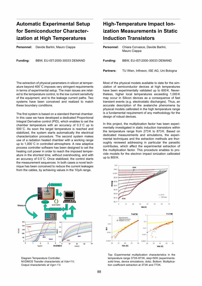
Automatic Experimental Setupfor Semiconductor Character-ization at High Temperatures
Personnel: Davide Barlini, Mauro Ciappa
Funding: BBW, EU-IST-2000-30033 DEMAND
The extraction of physical parameters in silicon at temper-ature beyond 400˚C imposes very stringent requirementsin terms of experimental setup. The main issues are relat-ed to the temperature control, to the low current sensitivityof the equipment, and to the leakage current paths. Twosystems have been conceived and realized to matchthese boundary conditions.
The first system is based on a standard thermal chamber.In this case we have developed a dedicated ProportionalIntegral Derivative control (PID), which enables to set thechamber temperature with an accuracy of 0.3˚C up to500˚C. As soon the target temperature is reached andstabilized, the system starts automatically the electricalcharacterization procedure. The second system makesuse of a radiation heated chamber with a working rangeup to 1,000˚C in controlled atmosphere. A new adaptiveprocess controller software has been designed to set theheating coil power in order to reach the imposed temper-ature in the shortest time, without overshooting, and withan accuracy of 0.5˚C. Once stabilized, the control startsthe measurement sequences. In both cases a novel tech-nique has been conceived to reduce the current leakagesfrom the cables, by achieving values in the 10pA range.
Diagram Temperature Controller.NVDMOS Transfer characteristic at Vds=1V;Output characteristic at Vgs=-1V.
88
High-Temperature Impact Ion-ization Measurements in StaticInduction Transistors
Personnel: Chiara Corvasce, Davide Barlini,Mauro Ciappa
Funding: BBW, EU-IST-2000-30033 DEMAND
Partners: TU Wien, Infineon, ISE AG, Uni Bologna
Most of the physical models available to date for the sim-ulation of semiconductor devices at high temperatureshave been experimentally validated up to 600 K. Never-theless, higher local temperatures exceeding 1,000 Kmay occur in Silicon devices as a consequence of fasttransient events (e.g. electrostatic discharges). Thus, anaccurate description of the avalanche phenomena byphysical models calibrated in the high temperature rangeis a fundamental requirement of any methodology for thedesign of robust devices.
In this project, the multiplication factor has been experi-mentally investigated in static induction transistors withinthe temperature range from 273 K to 873 K. Based ondedicated measurements and simulations, the experi-mental techniques and the extraction methods are thor-oughly reviewed addressing in particular the parasiticcontributes, which affect the experimental extraction ofthe multiplication factor. This procedure enables to pro-vide models for the electron impact ionization calibratedup to 800 K.
Top: Experimental multiplication characteristics in thetemperature range 373K-873K, step=50K (experiments:solid lines, device simulations: dots). Bottom: Multiplica-tion coefficient extraction at 373K and 773K.

Full 3D Simulation of Van derPauw Resistors for Very HighTemperatures
Personnel: Chiara Corvasce, Mauro Ciappa
Funding: BBW, EU-IST-2000-30033 DEMAND
Partners: TU Wien, Infineon, ISE AG, Uni Bologna
The use of the traditional four probes Van der Pauw (VdP)technique for extracting resistivity in the temperaturerange above 350˚C requires a critical evaluation of themeasured data. As the temperature increases, the ther-mal carriers generation starts to impact the local poten-tials, and as a consequence the experimental resistivitycurve drops down largely before the sample becomes in-trinsic. This behavior is not due to a physical decrease ofresistivity but it has to be attributed to the structure of thejunction isolated Van der Pauw resistor.
In this study, the error sources in sheet resistance evalu-ation at high temperature are specifically addressed. Full3D device simulations with different doping profiles andgeometries in the temperature range 25˚C-500˚C havebeen compared with experimental results. A proper sam-ple geometry, optimum doping profile of the different lay-ers, and current confinement by appropriate biasing of thesample have been proven to be effective in order to in-crease the maximum operating temperature of 125˚C.
Thermally activated parasitic path in greek-cross VdPand resistivity vs temperature behaviour, demonstratingthe effectiveness of substrate bias.
89
Preventing Parasitic ESDFailure Modes UtilisingTCAD Device Simulations
Personnel: Ulrich Glaser
Funding: ETHZ, Infineon
Partners: Infineon
From an ESD (ElectroStatic Discharge) point of view, theincreasing density of devices in modern integrated circuitsand the integration of several functional blocks on a singlechip lead to an increasing number of parasitic structuressusceptible to breakdown. TCAD device simulations en-able the study of such parasitic structures providing adeeper insight in the internal device behaviour and the in-volved snapback mechanisms during an ESD event. Fur-thermore, the impact of design changes (on device andcircuit level) on the ESD performance of the parasiticstructures can be explored silicon-less. These cognitionshelp to prevent parasitic ESD failure modes.
In this project, a failure mode occurring in a parasitic bipo-lar npn-transistor in an actual 0.13 µm p-substrate CMOStechnology was investigated employing thermo-electricaldevice simulations. The two snapbacks were identified tobe of pure electrical nature respectively to be caused by athermally driven base pushout. The trigger voltage of thesecond snapback marks the onset of the device destruc-tion. Its dependence on process and circuit variations wasexamined by device simulations leading to effective coun-termeasures against damage during ESD events.
I(U)-characteristics of the parasitic bipolar transistor: forgrounded base, A and B denote measurement and sim-ulation, respectively. For the external control of the basevoltage by resistors R1 = 50Ω and R2 = 10Ω as shown inthe lower part of the figure, C and D represent measure-ment resp. simulation. In the latter case, the electricalsnapback is missing and the trigger voltage of the sec-ond snapback is lower than in the former case.
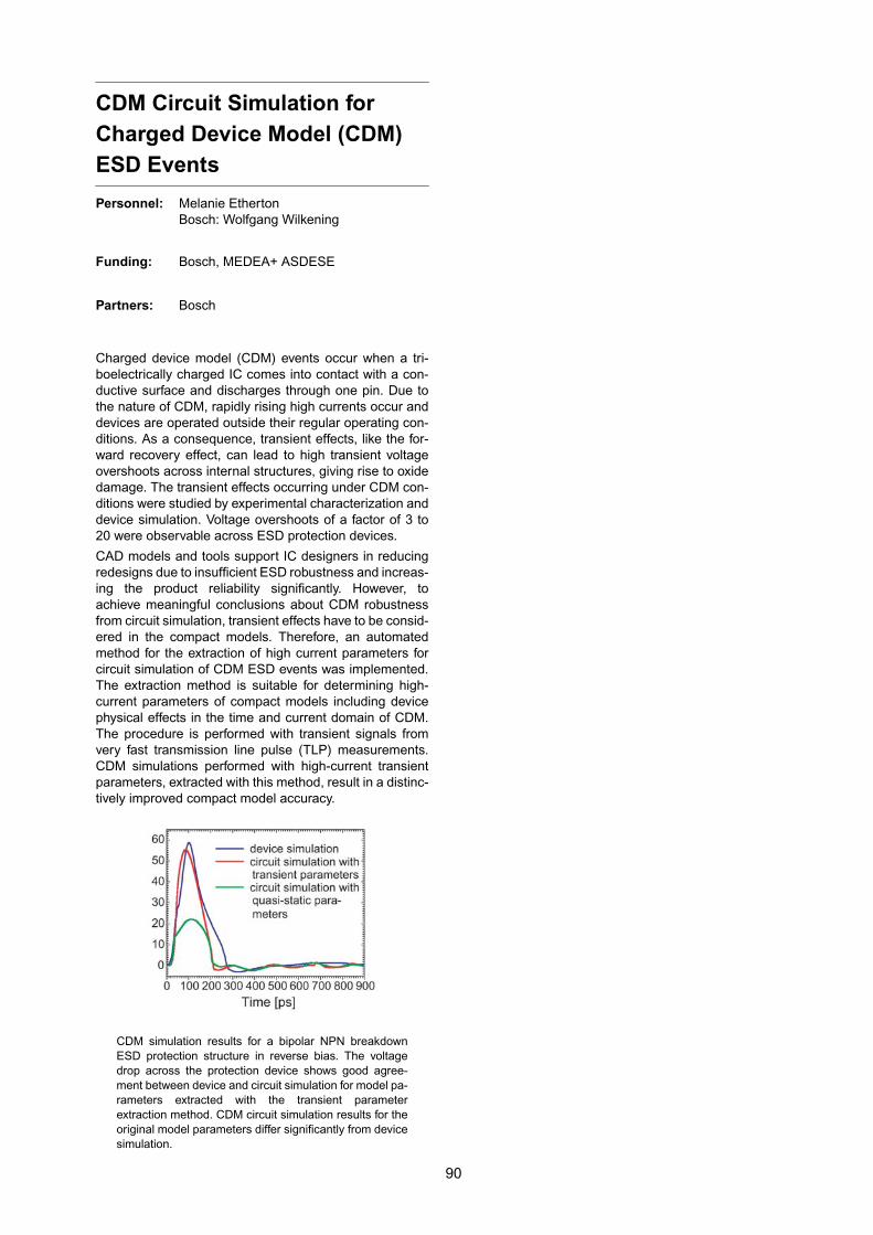
CDM Circuit Simulation forCharged Device Model (CDM)ESD Events
Personnel: Melanie EthertonBosch: Wolfgang Wilkening
Funding: Bosch, MEDEA+ ASDESE
Partners: Bosch
Charged device model (CDM) events occur when a tri-boelectrically charged IC comes into contact with a con-ductive surface and discharges through one pin. Due tothe nature of CDM, rapidly rising high currents occur anddevices are operated outside their regular operating con-ditions. As a consequence, transient effects, like the for-ward recovery effect, can lead to high transient voltageovershoots across internal structures, giving rise to oxidedamage. The transient effects occurring under CDM con-ditions were studied by experimental characterization anddevice simulation. Voltage overshoots of a factor of 3 to20 were observable across ESD protection devices.
CAD models and tools support IC designers in reducingredesigns due to insufficient ESD robustness and increas-ing the product reliability significantly. However, toachieve meaningful conclusions about CDM robustnessfrom circuit simulation, transient effects have to be consid-ered in the compact models. Therefore, an automatedmethod for the extraction of high current parameters forcircuit simulation of CDM ESD events was implemented.The extraction method is suitable for determining high-current parameters of compact models including devicephysical effects in the time and current domain of CDM.The procedure is performed with transient signals fromvery fast transmission line pulse (TLP) measurements.CDM simulations performed with high-current transientparameters, extracted with this method, result in a distinc-tively improved compact model accuracy.
CDM simulation results for a bipolar NPN breakdownESD protection structure in reverse bias. The voltagedrop across the protection device shows good agree-ment between device and circuit simulation for model pa-rameters extracted with the transient parameterextraction method. CDM circuit simulation results for theoriginal model parameters differ significantly from devicesimulation.
90
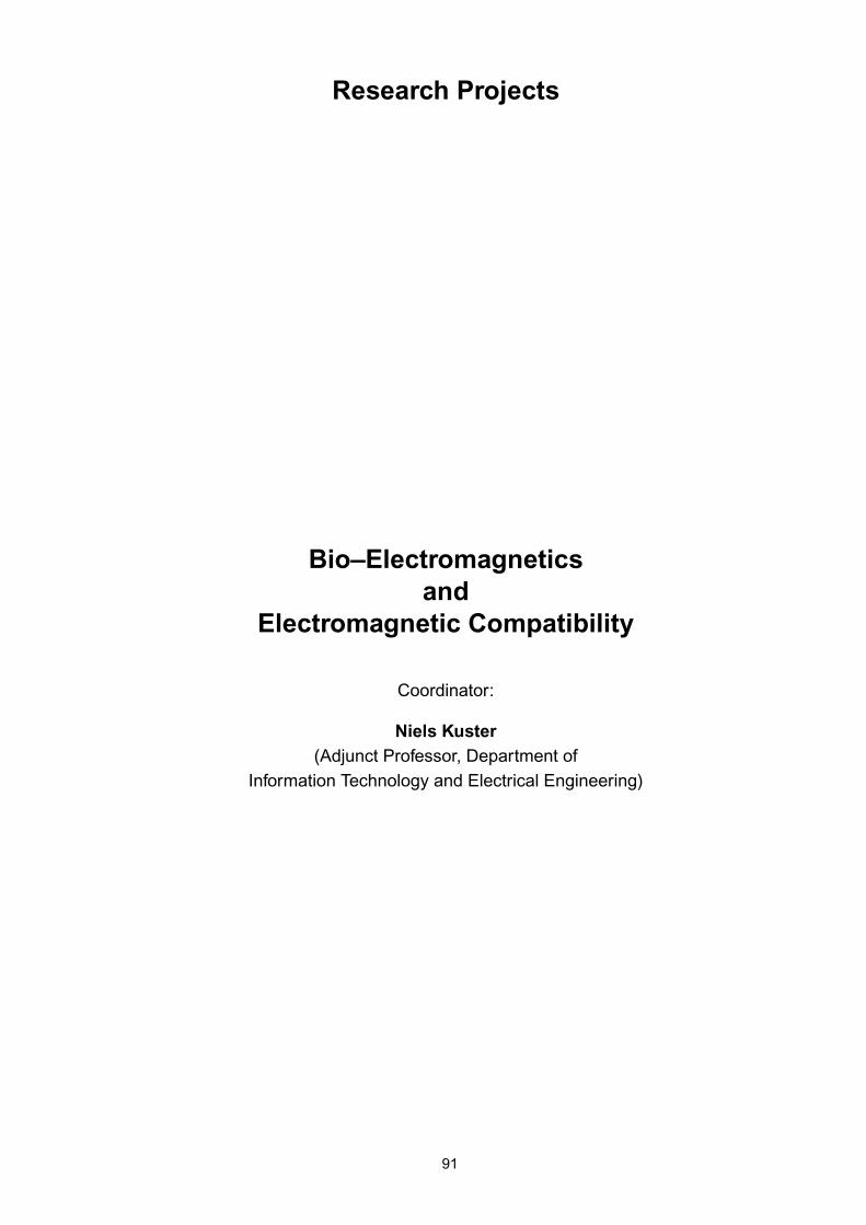
91
Research Projects
Bio–Electromagneticsand
Electromagnetic Compatibility
Coordinator:
Niels Kuster(Adjunct Professor, Department of
Information Technology and Electrical Engineering)
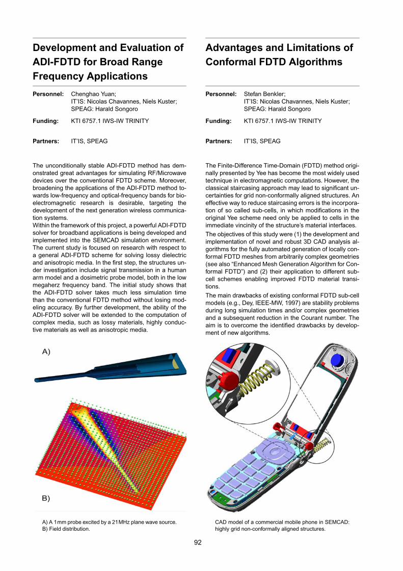
Development and Evaluation ofADI-FDTD for Broad RangeFrequency Applications
Personnel: Chenghao Yuan;IT’IS: Nicolas Chavannes, Niels Kuster;SPEAG: Harald Songoro
Funding: KTI 6757.1 IWS-IW TRINITY
Partners: IT’IS, SPEAG
The unconditionally stable ADI-FDTD method has dem-onstrated great advantages for simulating RF/Microwavedevices over the conventional FDTD scheme. Moreover,broadening the applications of the ADI-FDTD method to-wards low-frequency and optical-frequency bands for bio-electromagnetic research is desirable, targeting thedevelopment of the next generation wireless communica-tion systems.Within the framework of this project, a powerful ADI-FDTDsolver for broadband applications is being developed andimplemented into the SEMCAD simulation environment.The current study is focused on research with respect toa general ADI-FDTD scheme for solving lossy dielectricand anisotropic media. In the first step, the structures un-der investigation include signal transmission in a humanarm model and a dosimetric probe model, both in the lowmegaherz frequency band. The initial study shows thatthe ADI-FDTD solver takes much less simulation timethan the conventional FDTD method without losing mod-eling accuracy. By further development, the ability of theADI-FDTD solver will be extended to the computation ofcomplex media, such as lossy materials, highly conduc-tive materials as well as anisotropic media.
A) A 1mm probe excited by a 21MHz plane wave source.B) Field distribution.
92
Advantages and Limitations ofConformal FDTD Algorithms
Personnel: Stefan Benkler;IT’IS: Nicolas Chavannes, Niels Kuster;SPEAG: Harald Songoro
Funding: KTI 6757.1 IWS-IW TRINITY
Partners: IT’IS, SPEAG
The Finite-Difference Time-Domain (FDTD) method origi-nally presented by Yee has become the most widely usedtechnique in electromagnetic computations. However, theclassical staircasing approach may lead to significant un-certainties for grid non-conformally aligned structures. Aneffective way to reduce staircasing errors is the incorpora-tion of so called sub-cells, in which modifications in theoriginal Yee scheme need only be applied to cells in theimmediate vincinity of the structure’s material interfaces.The objectives of this study were (1) the development andimplementation of novel and robust 3D CAD analysis al-gorithms for the fully automated generation of locally con-formal FDTD meshes from arbitrarily complex geometries(see also “Enhanced Mesh Generation Algorithm for Con-formal FDTD”) and (2) their application to different sub-cell schemes enabling improved FDTD material transi-tions.The main drawbacks of existing conformal FDTD sub-cellmodels (e.g., Dey, IEEE-MW, 1997) are stability problemsduring long simulation times and/or complex geometriesand a subsequent reduction in the Courant number. Theaim is to overcome the identified drawbacks by develop-ment of new algorithms.
CAD model of a commercial mobile phone in SEMCAD:highly grid non-conformally aligned structures.
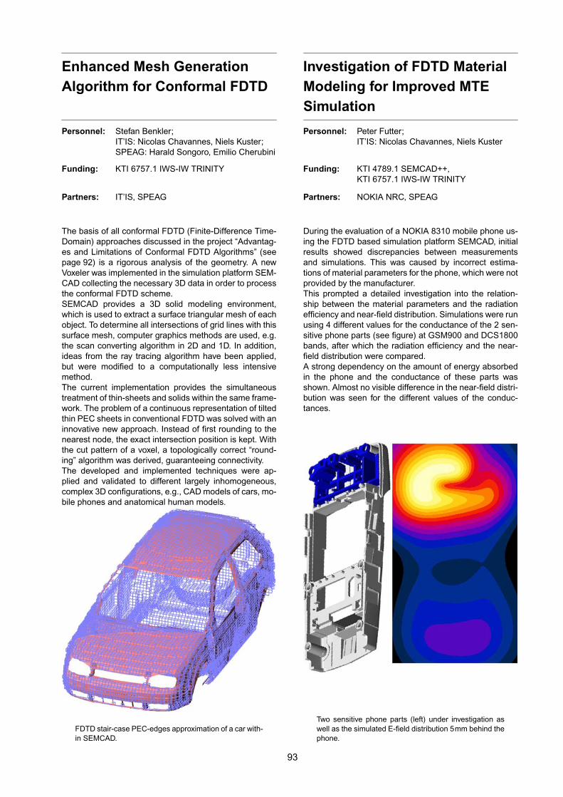
Enhanced Mesh GenerationAlgorithm for Conformal FDTD
Personnel: Stefan Benkler;IT’IS: Nicolas Chavannes, Niels Kuster;SPEAG: Harald Songoro, Emilio Cherubini
Funding: KTI 6757.1 IWS-IW TRINITY
Partners: IT’IS, SPEAG
The basis of all conformal FDTD (Finite-Difference Time-Domain) approaches discussed in the project “Advantag-es and Limitations of Conformal FDTD Algorithms” (seepage 92) is a rigorous analysis of the geometry. A newVoxeler was implemented in the simulation platform SEM-CAD collecting the necessary 3D data in order to processthe conformal FDTD scheme.SEMCAD provides a 3D solid modeling environment,which is used to extract a surface triangular mesh of eachobject. To determine all intersections of grid lines with thissurface mesh, computer graphics methods are used, e.g.the scan converting algorithm in 2D and 1D. In addition,ideas from the ray tracing algorithm have been applied,but were modified to a computationally less intensivemethod.The current implementation provides the simultaneoustreatment of thin-sheets and solids within the same frame-work. The problem of a continuous representation of tiltedthin PEC sheets in conventional FDTD was solved with aninnovative new approach. Instead of first rounding to thenearest node, the exact intersection position is kept. Withthe cut pattern of a voxel, a topologically correct “round-ing” algorithm was derived, guaranteeing connectivity.The developed and implemented techniques were ap-plied and validated to different largely inhomogeneous,complex 3D configurations, e.g., CAD models of cars, mo-bile phones and anatomical human models.
FDTD stair-case PEC-edges approximation of a car with-in SEMCAD.
93
Investigation of FDTD MaterialModeling for Improved MTESimulation
Personnel: Peter Futter;IT’IS: Nicolas Chavannes, Niels Kuster
Funding: KTI 4789.1 SEMCAD++,KTI 6757.1 IWS-IW TRINITY
Partners: NOKIA NRC, SPEAG
During the evaluation of a NOKIA 8310 mobile phone us-ing the FDTD based simulation platform SEMCAD, initialresults showed discrepancies between measurementsand simulations. This was caused by incorrect estima-tions of material parameters for the phone, which were notprovided by the manufacturer.This prompted a detailed investigation into the relation-ship between the material parameters and the radiationefficiency and near-field distribution. Simulations were runusing 4 different values for the conductance of the 2 sen-sitive phone parts (see figure) at GSM900 and DCS1800bands, after which the radiation efficiency and the near-field distribution were compared.A strong dependency on the amount of energy absorbedin the phone and the conductance of these parts wasshown. Almost no visible difference in the near-field distri-bution was seen for the different values of the conduc-tances.
Two sensitive phone parts (left) under investigation aswell as the simulated E-field distribution 5mm behind thephone.
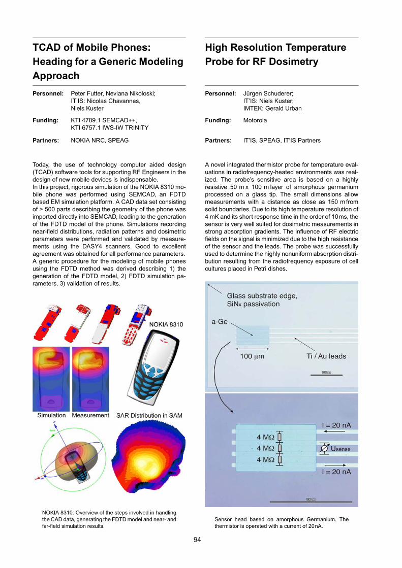
TCAD of Mobile Phones:Heading for a Generic ModelingApproach
Personnel: Peter Futter, Neviana Nikoloski;IT’IS: Nicolas Chavannes,Niels Kuster
Funding: KTI 4789.1 SEMCAD++,KTI 6757.1 IWS-IW TRINITY
Partners: NOKIA NRC, SPEAG
Today, the use of technology computer aided design(TCAD) software tools for supporting RF Engineers in thedesign of new mobile devices is indispensable.In this project, rigorous simulation of the NOKIA 8310 mo-bile phone was performed using SEMCAD, an FDTDbased EM simulation platform. A CAD data set consistingof > 500 parts describing the geometry of the phone wasimported directly into SEMCAD, leading to the generationof the FDTD model of the phone. Simulations recordingnear-field distributions, radiation patterns and dosimetricparameters were performed and validated by measure-ments using the DASY4 scanners. Good to excellentagreement was obtained for all performance parameters.A generic procedure for the modeling of mobile phonesusing the FDTD method was derived describing 1) thegeneration of the FDTD model, 2) FDTD simulation pa-rameters, 3) validation of results.
NOKIA 8310: Overview of the steps involved in handlingthe CAD data, generating the FDTD model and near- andfar-field simulation results.
94
High Resolution TemperatureProbe for RF Dosimetry
Personnel: Jürgen Schuderer;IT’IS: Niels Kuster;IMTEK: Gerald Urban
Funding: Motorola
Partners: IT’IS, SPEAG, IT’IS Partners
A novel integrated thermistor probe for temperature eval-uations in radiofrequency-heated environments was real-ized. The probe’s sensitive area is based on a highlyresistive 50 m x 100 m layer of amorphous germaniumprocessed on a glass tip. The small dimensions allowmeasurements with a distance as close as 150 m fromsolid boundaries. Due to its high temperature resolution of4 mK and its short response time in the order of 10ms, thesensor is very well suited for dosimetric measurements instrong absorption gradients. The influence of RF electricfields on the signal is minimized due to the high resistanceof the sensor and the leads. The probe was successfullyused to determine the highly nonuniform absorption distri-bution resulting from the radiofrequency exposure of cellcultures placed in Petri dishes.
Sensor head based on amorphous Germanium. Thethermistor is operated with a current of 20nA.
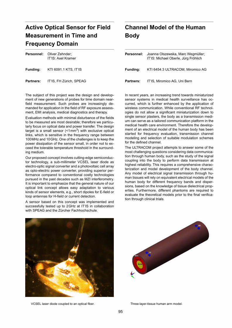
Active Optical Sensor for FieldMeasurement in Time andFrequency Domain
Personnel: Oliver Zehnder;IT’IS: Axel Kramer
Funding: KTI 6091.1 KTS, IT’IS
Partners: IT’IS, FH Zürich, SPEAG
The subject of this project was the design and develop-ment of new generations of probes for time domain near-field measurement. Such probes are increasingly de-manded for application in the field of RF exposure assess-ment, EMI analysis, medical diagnostics and therapy.
Evaluation methods with minimal disturbance of the fieldsto be measured are most desirable; therefore we particu-larly focus on optical data and power transfer. The designtarget is a small sensor (<1mm3) with exclusive opticallinks, which is sensitive in the frequency range between100MHz and 10GHz. One of the challenges is to keep thepower dissipation of the sensor small, in order not to ex-ceed the tolerable temperature threshold in the surround-ing medium.
Our proposed concept involves cutting-edge semiconduc-tor technology, a sub-millimeter VCSEL laser diode aselectro-optic signal converter and a photovoltaic cell arrayas opto-electric power converter, providing superior per-formance compared to conventional costly technologiespursued in the past decades such as MZI interferometry.It is important to emphasize that the general nature of ouroptical link concept allows easy adaptation to variouskinds of sensor elements, e.g., short dipoles for E-field orloop antennas for H-field or current detection.
A sensor based on this concept was implemented andsuccessfully tested up to 2GHz at IT’IS in collaborationwith SPEAG and the Zürcher Fachhochschule.
VCSEL laser diode coupled to an optical fiber.
95
Channel Model of the HumanBody
Personnel: Joanna Olszewska, Marc Wegmüller;IT’IS: Michael Oberle, Jürg Fröhlich
Funding: KTI 6454.3 ULTRACOM, Miromico AG
Partners: IT’IS, Miromico AG, Uni Bern
In recent years, an increasing trend towards miniaturizedsensor systems in medical health surveillance has oc-curred, which is further enhanced by the application ofwireless communication. While conventional RF technol-ogies do not allow a significant miniaturization down tosingle sensor plasters, the body as a transmission medi-um can serve as a tailored communication platform in themedical health care environment. Therefore the develop-ment of an electrical model of the human body has beenstarted for frequency evaluation, transmission channelmodeling and selection of suitable modulation schemesfor the defined channel.
The ULTRACOM project attempts to answer some of themost challenging questions considering data communica-tion through human body, such as the study of the signalcoupling into the body to perform data transmission athighest reliability. This requires a comprehensive charac-terization and model development of the body channel.Any model of electrical signal transmission through hu-man tissues will rely on equivalent electrical models of thehuman body for different frequency bands and disper-sions, based on the knowledge of tissue dielectrical prop-erties. Furthermore, different phantoms are required toevaluate the theoretical models prior to the final verifica-tion through clinical trials.
Three-layer-tissue human arm model.
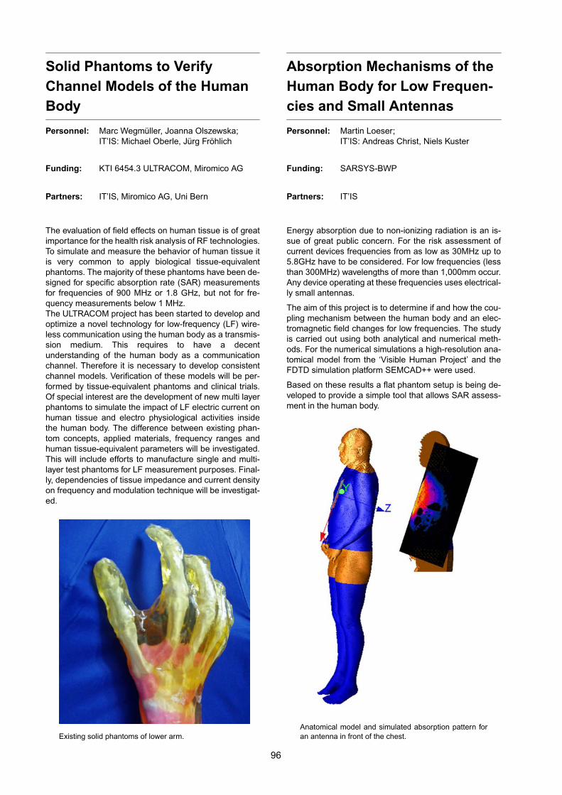
Solid Phantoms to VerifyChannel Models of the HumanBody
Personnel: Marc Wegmüller, Joanna Olszewska;IT’IS: Michael Oberle, Jürg Fröhlich
Funding: KTI 6454.3 ULTRACOM, Miromico AG
Partners: IT’IS, Miromico AG, Uni Bern
The evaluation of field effects on human tissue is of greatimportance for the health risk analysis of RF technologies.To simulate and measure the behavior of human tissue itis very common to apply biological tissue-equivalentphantoms. The majority of these phantoms have been de-signed for specific absorption rate (SAR) measurementsfor frequencies of 900 MHz or 1.8 GHz, but not for fre-quency measurements below 1 MHz.The ULTRACOM project has been started to develop andoptimize a novel technology for low-frequency (LF) wire-less communication using the human body as a transmis-sion medium. This requires to have a decentunderstanding of the human body as a communicationchannel. Therefore it is necessary to develop consistentchannel models. Verification of these models will be per-formed by tissue-equivalent phantoms and clinical trials.Of special interest are the development of new multi layerphantoms to simulate the impact of LF electric current onhuman tissue and electro physiological activities insidethe human body. The difference between existing phan-tom concepts, applied materials, frequency ranges andhuman tissue-equivalent parameters will be investigated.This will include efforts to manufacture single and multi-layer test phantoms for LF measurement purposes. Final-ly, dependencies of tissue impedance and current densityon frequency and modulation technique will be investigat-ed.
Existing solid phantoms of lower arm.
96
Absorption Mechanisms of theHuman Body for Low Frequen-cies and Small Antennas
Personnel: Martin Loeser;IT’IS: Andreas Christ, Niels Kuster
Funding: SARSYS-BWP
Partners: IT’IS
Energy absorption due to non-ionizing radiation is an is-sue of great public concern. For the risk assessment ofcurrent devices frequencies from as low as 30MHz up to5.8GHz have to be considered. For low frequencies (lessthan 300MHz) wavelengths of more than 1,000mm occur.Any device operating at these frequencies uses electrical-ly small antennas.
The aim of this project is to determine if and how the cou-pling mechanism between the human body and an elec-tromagnetic field changes for low frequencies. The studyis carried out using both analytical and numerical meth-ods. For the numerical simulations a high-resolution ana-tomical model from the ‘Visible Human Project’ and theFDTD simulation platform SEMCAD++ were used.
Based on these results a flat phantom setup is being de-veloped to provide a simple tool that allows SAR assess-ment in the human body.
Anatomical model and simulated absorption pattern foran antenna in front of the chest.
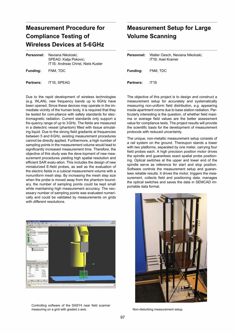
Measurement Procedure forCompliance Testing ofWireless Devices at 5-6GHz
Personnel: Neviana Nikoloski;SPEAG: Katja Pokovic;IT’IS: Andreas Christ, Niels Kuster
Funding: FNM, TDC
Partners: IT’IS, SPEAG
Due to the rapid development of wireless technologies(e.g. WLAN), new frequency bands up to 6GHz havebeen opened. Since these devices may operate in the im-mediate vicinity of the human body, it is required that theybe tested for com-pliance with safety standards for elec-tromagnetic radiation. Current standards only support afre-quency range of up to 3GHz. The fields are measuredin a dielectric vessel (phantom) filled with tissue simulat-ing liquid. Due to the strong field gradients at frequenciesbetween 5 and 6GHz, existing measurement procedurescannot be directly applied. Furthermore, a high number ofsampling points in the measurement volume would lead tosignificantly increased measurement time. Therefore, theobjective of this study was the deve-lopment of new mea-surement procedures yielding high spatial resolution andefficient SAR evalu-ation. This includes the design of newminiaturized E-field probes, as well as the evaluation ofthe electric fields in a cubical measurement volume with anonuniform mesh step. By increasing the mesh step sizewhen the probe is moved away from the phantom bound-ary, the number of sampling points could be kept smallwhile maintaining high measurement accuracy. The nec-essary number of sampling points was evaluated numeri-cally and could be validated by measurements on gridswith different resolutions.
Controlling software of the DASY4 near field scannermeasuring on a grid with graded z-axis.
97
Measurement Setup for LargeVolume Scanning
Personnel: Walter Oesch, Neviana Nikoloski;IT'IS: Axel Kramer
Funding: FNM, TDC
Partners: IT’IS
The objective of this project is to design and construct ameasurement setup for accurately and systematicallymeasuring non-uniform field distribution, e.g. appearinginside apartment rooms due to base station radiation. Par-ticularly interesting is the question, of whether field maxi-ma or average field values are the better assessmentvalue for compliance tests. The project results will providethe scientific basis for the development of measurementprotocols with reduced uncertainty.
The unique, non-metallic measurement setup consists ofa rail system on the ground. Thereupon stands a towerwith two platforms, separated by one meter, carrying fourfield probes each. A high precision position motor drivesthe spindle and guarantees exact spatial probe position-ing. Optical switches at the upper and lower end of thespindle serve as reference for start and stop position.Software controls the measurement setup and guaran-tees reliable results. It drives the motor, triggers the mea-surement, collects field and positioning data, managesthe optical switches and saves the data in SEMCAD im-portable data format.
Non-disturbing measurement setup.
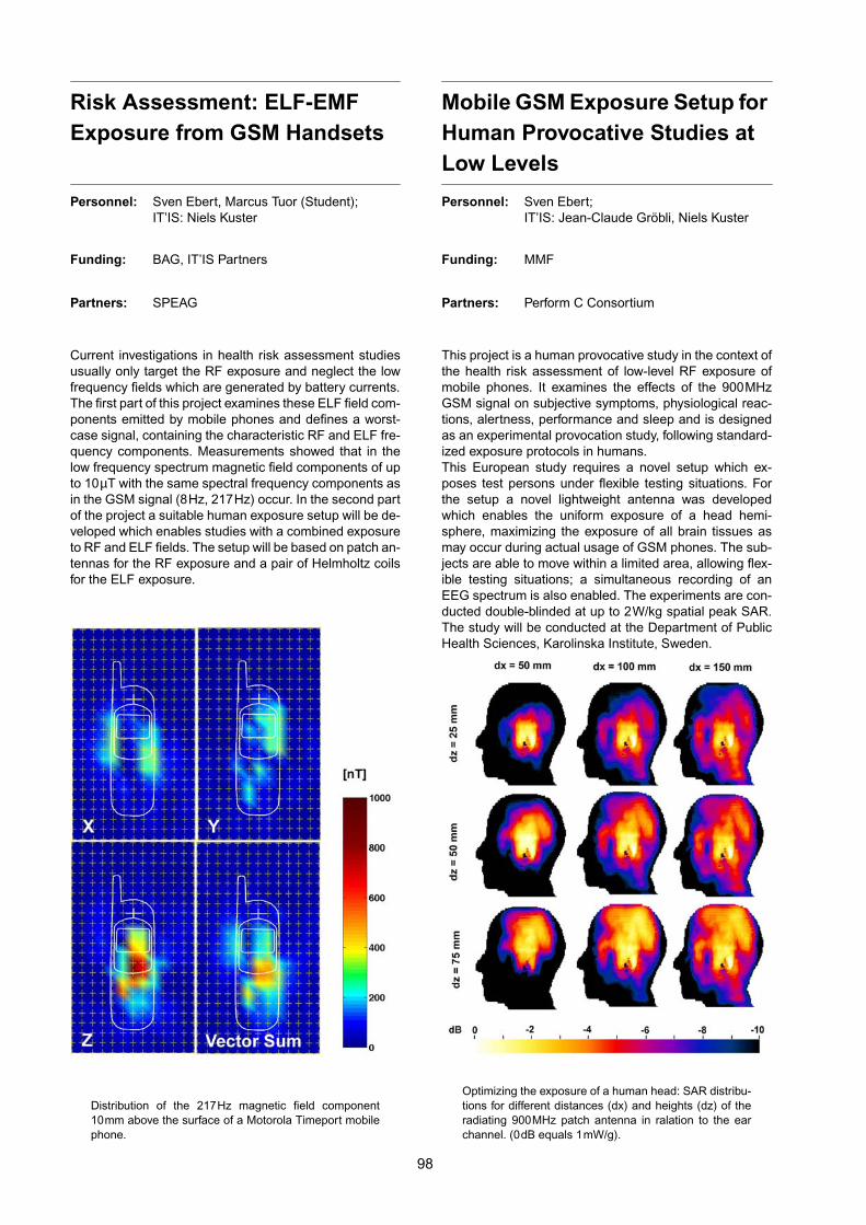
Risk Assessment: ELF-EMFExposure from GSM Handsets
Personnel: Sven Ebert, Marcus Tuor (Student);IT’IS: Niels Kuster
Funding: BAG, IT’IS Partners
Partners: SPEAG
Current investigations in health risk assessment studiesusually only target the RF exposure and neglect the lowfrequency fields which are generated by battery currents.The first part of this project examines these ELF field com-ponents emitted by mobile phones and defines a worst-case signal, containing the characteristic RF and ELF fre-quency components. Measurements showed that in thelow frequency spectrum magnetic field components of upto 10µT with the same spectral frequency components asin the GSM signal (8Hz, 217Hz) occur. In the second partof the project a suitable human exposure setup will be de-veloped which enables studies with a combined exposureto RF and ELF fields. The setup will be based on patch an-tennas for the RF exposure and a pair of Helmholtz coilsfor the ELF exposure.
Distribution of the 217Hz magnetic field component10mm above the surface of a Motorola Timeport mobilephone.
98
Mobile GSM Exposure Setup forHuman Provocative Studies atLow Levels
Personnel: Sven Ebert;IT’IS: Jean-Claude Gröbli, Niels Kuster
Funding: MMF
Partners: Perform C Consortium
This project is a human provocative study in the context ofthe health risk assessment of low-level RF exposure ofmobile phones. It examines the effects of the 900MHzGSM signal on subjective symptoms, physiological reac-tions, alertness, performance and sleep and is designedas an experimental provocation study, following standard-ized exposure protocols in humans.This European study requires a novel setup which ex-poses test persons under flexible testing situations. Forthe setup a novel lightweight antenna was developedwhich enables the uniform exposure of a head hemi-sphere, maximizing the exposure of all brain tissues asmay occur during actual usage of GSM phones. The sub-jects are able to move within a limited area, allowing flex-ible testing situations; a simultaneous recording of anEEG spectrum is also enabled. The experiments are con-ducted double-blinded at up to 2W/kg spatial peak SAR.The study will be conducted at the Department of PublicHealth Sciences, Karolinska Institute, Sweden.
Optimizing the exposure of a human head: SAR distribu-tions for different distances (dx) and heights (dz) of theradiating 900MHz patch antenna in ralation to the earchannel. (0dB equals 1mW/g).
Risk assessment: ExposureSetup for Studies of AcuteEffects on Mice at 900MHz
Personnel: Sang Jin Eom, Neviana Nikoloski,Walter Oesch;IT’IS: Jürg Fröhlich, Niels Kuster
Funding: MMF, GSM-Association, IT’IS
Partners: Perform B Consortium
The objective of this study was the developement of anexposure setup for whole-body exposure of mice. Theevaluation and optimization of the setup was performedusing the advanced Finite-Difference Time-Domain(FDTD) simulation platform SEMCAD and the near-fieldscanner DASY4. The specific absorption rate (SAR) as-sessment with a temperature method was performed us-ing a highly resistive thermister probe. The radius of thewheel was optimized to house at least four mice and max-imize suppression of higher modes. The location of theanimals was optimized to achieve similar exposure condi-tions as in the PERFORM A mouse studies. Good perfor-mance was achieved for a wheel radius of 166.5mm,housing eight mice. The exposure is controlled using cal-ibrated E-field sensors located near the antenna in thebottom plate. Radial isotropy was assessed using temper-ature measurements to be within 0.2dB. Simulation andmeasurement results were compared with respect to fielddistribution and whole-body SAR. Furthermore, four highresolution anatomical mouse models together with fourdummies were simulated, representing the final arrange-ment used for the experiments. The whole-body exposurewas assessed, as well as organ and tissue specific SARvalues.
The installed exposure system, the numerical model andthe E-field distribution of the exposure setup.
99
Risk assessment: Mainly-HeadExposure Setup for In VivoStudies on Mice at 900MHz
Personnel: Sang Jin Eom, Neviana Nikoloski,Walter Oesch;IT’IS: Jürg Fröhlich, Niels Kuster
Funding: MMF, GSM-Association, IT’IS
Partners: Perform B Consortium
Within this study, an exposure setup was developed main-ly for the head exposure of a small number of mice at900MHz for behavioral studies. The 900MHz rectangularwaveguide was adopted for the mono-mode excitation(TE10) and symmetric exposure of two mice. For stableand reproducible results of mouse movements with higherefficiency, the H-field plane (wide wall) was chosen formice insertion. Good performance of the mainly-head ex-posure setup was achieved when the numerical mousemodel was located at a distance of 112.5mm from theshortcut with an insertion depth of 34mm from the innermetal surface of the waveguide. The stopper for restrain-ing the mouse or liquid dummy consists of electricallylossless material. The exposure is controlled using a cali-brated H-field sensor located at the maximum H-field onthe shortcut. The setup was numerically and experimen-tally evaluated using the advanced FDTD platform SEM-CAD and DASY4, respectively. The numerical dosimetrywas conducted with two high resolution anatomicalmouse models of 25g and represents the arrangement forthe clinical experiments. The thermal load of the animalsand the phantoms was numerically assessed and verifiedexperimentally using a high resistive thermistor probe.
Mainly-head exposure setup and the energy absorptionin tissue simulating liquid; numerical mouse model.

Risk assessment: LocalExposure Setup withMicrostrip Loop Antenna
Personnel: Sang Jin Eom, Neviana Nikoloski,Walter Oesch;IT’IS: Juerg Froehlich, Niels Kuster
Funding: MMF, IT’IS, TDC
Partners: IT’IS
The aim of this study is to analyze the dosimetric assess-ment of the local exposure system of P. Leveque, consist-ing of a rectangular loop antenna, and to compare theresults with other local exposure setups, as well as to de-fine the feasible antennas for animal mainly-head expo-sure. These mentioned exposure setups were developedfor the study of potential biological effects of radio fre-quency fields from handheld wireless telephones and toextrapolate animal observations to humans. In order toachieve more credible and reproducible results from thevariable experimental status, especially with measure-ments of living animals, an uncertainty analysis has to becarried out in advance. This study is particularly focusedon the uncertainty of the electromagnetic interaction be-tween the exciter and biological tissues. The main uncer-tainty is expected to be caused by factors such as theexposure distance, setup alignment, shape and volume ofthe animals, as well as the antenna characteristics. Addi-tionally, the performance of these local exposure setups iscompared with the waveguide-type mainly-head expo-sure setup.
Rectangular microstrip loop antenna for a local exposuresetup at 900MHz and the energy distribution in tissuesimulating liquid: simulated and experimental results.
10
Reevaluation and Dosimetry ofa TEM Cell Exposure Setup forIn Vitro Studies
Personnel: Neviana Nikoloski, Jürgen Schuderer;IT’IS: Jürg Fröhlich, Niels Kuster
Funding: IT’IS Partners
Partners: PERFORM B Consortium
The transverse electromagnetic (TEM) cell system uti-lized by Penafiel et al. [Bioelectromagnetics 18(2):132-141,1997] for the exposure of cells in T25 flasks at 835MHz has been reevaluated for the purpose of replicatingthe reported results. The original setup had been recon-structed as closely as possible with the improvement ofenabling blinded exposures, forced cooling and better re-peatable positioning of the flasks, as well as tight expo-sure and environmental parameter control. The signal unitcan simulate the original signal but also enables variousother exposure schemes. The setup has been evaluatedfor four T25 flasks filled with 5ml and 10ml cell medium byexperimental and numerical means. Comparing E-field,SAR and temperature measurements resulted in goodagreement: < 0.4dB for E-field and 0.5dB for SAR. Theoverall average SAR within the medium is 6.0 W/kg 0.5dB at an input power of 1W. The temperature increasewas determined to be 0.13 C/(W/kg). This can be re-duced to 0.045 C/(W/kg)by applying active air flow cool-ing. The comparison of SAR values from temperaturemeasurements with the corresponding simulated valuesresulted in excellent agreement. These results do not cor-respond to a previous study reporting an average SARwithin the medium of 2.5W/kg at an input power of 0.96W.
SAR distribution at 1mm above the bottom of the fourflasks each containing 5ml DMEM medium at 37 C.
0
Advanced EMF ExposureSetups for Risk Assessment
Personnel: Jürgen Schuderer, Walter Oesch;IT’IS: Denis Spät, Niels Kuster
Funding: BBW , EU-QUAL CT-1999-01574 REFLEXIT’IS Partners
Partners: REFLEX & PERFORM B Consortia
The objective of this study is to design, optimize and buildflexible exposure setups for biological studies focussingon the health risk assessment of radiofrequency electro-magnetic field exposures. The setups need to providemaximum field homogeneity in multiple Petri dishes, a dy-namic range from less than 1mW/kg to over 20W/kg, andamplitude and frequency modulation schemes as emittedby mobile phones operating within a GSM, NADC orUMTS communication network (frequency bands of 900,1,800 and 1,950MHz). The exposure systems are basedon two rectangular waveguide resonators and permit thecontrolled exposition of monolayer or suspended cells in35mm Petri dishes. Each waveguide is equipped with afan for rapid environmental atmospheric exchange,whereby the air flow temperature is monitored with accu-rate Pt100 probes. In order to ensure stable exposure in-dependent of the loading, E-field or H-field sensors basedon monopole or loop antennas were developed to regu-late the incident fields. The evaluation, optimization andfine-tuning of the setup was performed using the FDTDsimulation platform SEMCAD. The numerical evaluationcontained a detailed electromagnetic and thermodynamicanalysis. The results were carefully verified by field andtemperature measurements using the near-field scannerDASY4.
Simulated SAR and staedy state temperature distribu-tions inside a Petri dish exposed at 900MHz.
10
Effect of RF EMF on CerebralBlood Flow
Personnel: Jürgen Schuderer;IT’IS: Niels Kuster;IPT-UNIZH: Peter Achermann
Funding: FNM, TDC
Partners: IT’IS, IT’IS Partners
In this study the effect of radio frequency electromagneticfield (RF-EMF) exposure on waking regional cerebralblood flow (rCBF) in 12 healthy young men was investi-gated. Two types of RF-EMF exposure were applied: a'base-station-like' and a 'handset-like' signal. Positronemission tomography (PET) scans were taken after uni-lateral head exposure to 30 minutes pulse-modulated900MHz RF-EMF (10 g tissue-averaged spatial peak spe-cific absorption rate (SAR) of 1W/kg for both conditions)and sham control. An increase in relative rCBF in the dor-solateral prefrontal cortex on the side of exposure was ob-served. The effect depended on the modulation paradigm,such that 'handset-like' RF-EMF exposure affected rCBF.Furthermore, changes in rCBF did not reflect the simulat-ed distribution of the SAR. Together with previous obser-vations that pulse modulation of RF-EMF is necessary toinduce changes in the waking and sleep EEG, the presentresults provide further evidence that pulse modulation iscrucial for RF-EMF induced alterations in brain physiolo-gy.
Distribution of SAR: Computed distribution of the specificabsorption rate (SAR).Changes in rCBF after RF-EMF exposure: Regionsshowing higher (handset-bstat, handset-sham, bstat-sham) and lower (bstat-handset) relative regional cere-bral blood flow (rCBF) after RF-EMF exposure assessedby statistical parametric mapping (z-values correspondto different axial sections).
1
Molecular and FunctionalResponses of Living Cells toELF EMF
Personnel: Jürgen Schuderer, Walter Oesch;IT’IS: Niels Kuster;REFLEX Consortium
Funding: BBW , EU-QUAL CT-1999-01574 REFLEX
Partners: IT’IS, IT’IS Partners
Based on data relating to extremely low frequency elec-tromagnetic fields (ELF-EMF) obtained in the course ofthe REFLEX project, a strong case for the assumption hasbeen established that ELF-EMF are genotoxic to primarycell cultures of human fibroblasts as well as other celllines. ELF-EMF generate DNA strand breaks at a signifi-cant level at a flux density as low as 35µT. There is astrong positive correlation between the field strength ofand the duration of exposure to ELF-EMF and the in-crease in single and double strand DNA breaks and mi-cronuclei frequencies. The genotoxic response to ELF-EMF differs from cell system to cell system and even with-in the same cell system, suggesting that the genetic back-ground plays a major role in how cells react to EMFexposure. DNA repair in human fibroblasts after ELF-EMFexposure is not error-free, as demonstrated by chromo-somal aberrations following exposure. Besides the obser-vation in one of the REFLEX laboratories that ELF-EMFmay increase the proliferation rate of neuroblastoma cellsand in a second REFLEX laboratory that ELF-EMF mayenhance the differentiation of cardiomyocytes, no clear-cut and unequivocal effects of ELF-EMF on DNA synthe-sis, cell cycle, cell differentiation, cell proliferation and ap-optosis were found. However, ELF-EMF at a flux densityof about 2 mT upregulates the expression of early genes,such as p21, c-jun and egr-1, in p53-deficient embryonicstem cells, but not in healthy wildtype cells, and in addi-tion, may affect the expression of genes and proteins in avariety of other cell systems.
ELF power line exposure signal used in the REFLEX ex-periments.
10
Molecular and FunctionalResponses of Living Cells toRF EMF
Personnel: Jürgen Schuderer, Walter Oesch;IT’IS: Niels Kuster;REFLEX Consortium
Funding: BBW, EU-QUAL CT-1999-01574 REFLEX
Partners: IT’IS, IT’IS Partners
The REFLEX project has derived indications that radio-frequency electromagnetic fields (RF-EMF) can producegenotoxic effects in living cells. HL60 cells, a human pro-myelocytic cell line, respond to RF-EMF exposure at aSAR below 2W/kg with a significant increase in single anddouble strand DNA breaks and in micronuclei frequency.A comparable increase in DNA breaks was found with hu-man fibroblasts and granulosa cells of rats. There is noevidence that RF-EMF affect processes such as cell pro-liferation, apoptosis and immunological defence. Howev-er, RF-EMF at a SAR of 1.5W/kg upregulate theexpression of early genes in p53-deficient embryonicstem cells, but not in healthy wildtype cells, and of neu-ronal genes in neuronal precursor cells. Whether or notembryonic stem cells respond to RF-EMF seems to bedependent on the strength of the electromagnetic field,the cell system and the genetic background of the cells.Studies on human endothelial cell lines show that expo-sure to RF-EMF changes the protein expression of nu-merous, yet largely unidentified proteins. Among theseproteins is the heat shock protein hsp27, which may - be-sides mostly positive effects - increase the permeability ofthe blood/brain barrier and inhibit apoptosis and contrib-ute (theoetically) to the development of brain tumours.
RF exposure system, developed by IIS and used in theREFLEX project to investigate biological effects of RF-EMF on cellular and molecular level.
2
Influence of 2.45GHz Electro-magnetic Field on Radial-MazePerformance in Rats
Personnel: Neviana Nikoloski;IT'IS: Verónica Berdiñas Torres, JürgFröhlich, Niels Kuster
Funding: MMF
Partners: Perform B Consortium
Mobile communication is based on utilization of electro-magnetic fields (EMFs) in the microwave range (0.3-300GHz). Human and animal studies suggest that radiof-requencies radiations, which are in the 0.1MHz-300GHzrange, might interfere with cognitive processes. In 1994,a report by Lai and colleagues (Bioelectromagnetics 15,95-104) showed that whole-body exposure of rats topulsed 2.45GHz microwaves (500pps, SAR 0.6W/kg) for45 minutes resulted in altered spatial working memory as-sessed in a 12-arm radial-maze task. Surprisingly, therehas been no published attempt to replicate this experi-ment so far. The present study used conditions as closeas possible to those used by Lai et al. in order to replicatetheir findings. Rats were tested in a 12-arm radial mazesubsequently to a daily exposure to 2.45 GHz microwaves(2 spulse width, 500pps, SAR 0.6W/kg) for 45min. Theperformance of exposed rats was comparable to thatfound in sham-exposed or in naïve rats (no contact withthe exposure system). Regarding the methodological de-tails provided by Lai et al. on their testing protocol, the re-sults might suggest that the microwave-inducedbehavioural alterations measured by these authors mighthave had more to do with factors liable to bias perfor-mance than with spatial working memory per se.
E-field distribution in the center of the circular waveguide,including the animal and its corresponding SAR distribu-tion.
10
EMF and Brain: Effects onCerebral Blood Volume andNeural Activity
Personnel: Jürgen Schuderer;IT’IS: Jürg Fröhlich, Niels Kuster
Partners: BORL USZ
Recent studies have shown that pulsed high-frequencyelectromagnetic fields (EMF) affect human sleep andsleep electroencephalogram (EEG). Effects on regionalcerebral blood flow (CBF) using positron emission tomog-raphy (PET) and weak effects on the heart rate were ob-served. These findings encourage further investigationsusing a higher time resolution and simultaneously record-ing of the CBF and the neuronal signal. In order to be ableto detect immediate changes in CB and cerebral bloodvolume (CBV) with a high spatial and time resolution near-infrared spectrophotometry (NIRS) will be used. Thistechnique has already been successfully applied to recordchanges in CBF and CBV in the visual and motor corticesduring functionalhome stimulation, as well as for the de-tection of the fast neuronal signal. In a pilot study the fea-sibility of this technique with respect to electromagneticinterference (EMI) and to the change in the absorptionpattern due to the placement of the NIRS sensor was test-ed. It was shown that EMI with the NIRS equipment canbe eliminated by applying a median filter or by an evalu-ation of optical data during RF off phases. An initial studywith five subjects showed some evidence for effects onblood flow. A larger study includes to confirm these find-ings and to extend the number of investigated parame-ters, e.g., varying modulation and varying dose.
Experimental setup including exposure system andNIRS equipment.
3


105
Education Program
Student Projects
Coordinator:
Norbert Felber
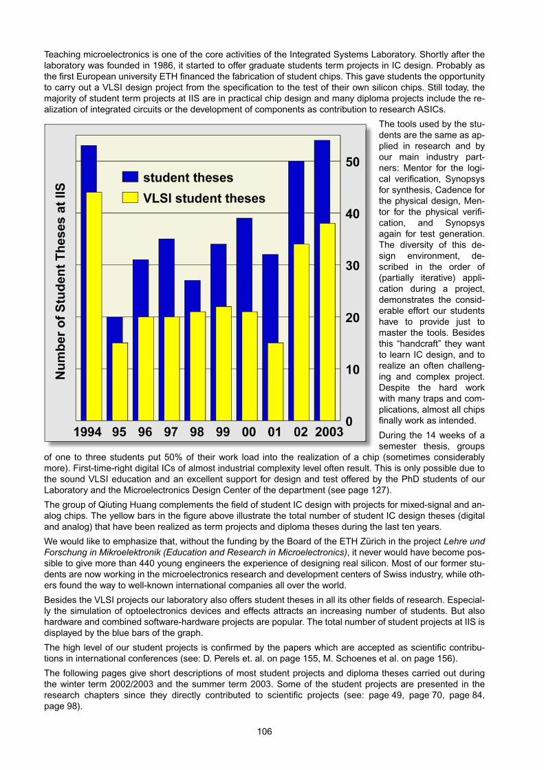
Teaching microelectronics is one of the core activities of the Integrated Systems Laboratory. Shortly after thelaboratory was founded in 1986, it started to offer graduate students term projects in IC design. Probably asthe first European university ETH financed the fabrication of student chips. This gave students the opportunityto carry out a VLSI design project from the specification to the test of their own silicon chips. Still today, themajority of student term projects at IIS are in practical chip design and many diploma projects include the re-alization of integrated circuits or the development of components as contribution to research ASICs.
The tools used by the stu-dents are the same as ap-plied in research and byour main industry part-ners: Mentor for the logi-cal verification, Synopsysfor synthesis, Cadence forthe physical design, Men-tor for the physical verifi-cation, and Synopsysagain for test generation.The diversity of this de-sign environment, de-scribed in the order of(partially iterative) appli-cation during a project,demonstrates the consid-erable effort our studentshave to provide just tomaster the tools. Besidesthis “handcraft” they wantto learn IC design, and torealize an often challeng-ing and complex project.Despite the hard workwith many traps and com-plications, almost all chipsfinally work as intended.
During the 14 weeks of asemester thesis, groups
of one to three students put 50% of their work load into the realization of a chip (sometimes considerablymore). First-time-right digital ICs of almost industrial complexity level often result. This is only possible due tothe sound VLSI education and an excellent support for design and test offered by the PhD students of ourLaboratory and the Microelectronics Design Center of the department (see page 127).
The group of Qiuting Huang complements the field of student IC design with projects for mixed-signal and an-alog chips. The yellow bars in the figure above illustrate the total number of student IC design theses (digitaland analog) that have been realized as term projects and diploma theses during the last ten years.
We would like to emphasize that, without the funding by the Board of the ETH Zürich in the project Lehre undForschung in Mikroelektronik (Education and Research in Microelectronics), it never would have become pos-sible to give more than 440 young engineers the experience of designing real silicon. Most of our former stu-dents are now working in the microelectronics research and development centers of Swiss industry, while oth-ers found the way to well-known international companies all over the world.
Besides the VLSI projects our laboratory also offers student theses in all its other fields of research. Especial-ly the simulation of optoelectronics devices and effects attracts an increasing number of students. But alsohardware and combined software-hardware projects are popular. The total number of student projects at IIS isdisplayed by the blue bars of the graph.
The high level of our student projects is confirmed by the papers which are accepted as scientific contribu-tions in international conferences (see: D. Perels et. al. on page 155, M. Schoenes et al. on page 156).
The following pages give short descriptions of most student projects and diploma theses carried out duringthe winter term 2002/2003 and the summer term 2003. Some of the student projects are presented in theresearch chapters since they directly contributed to scientific projects (see: page 49, page 70, page 84,page 98).
106
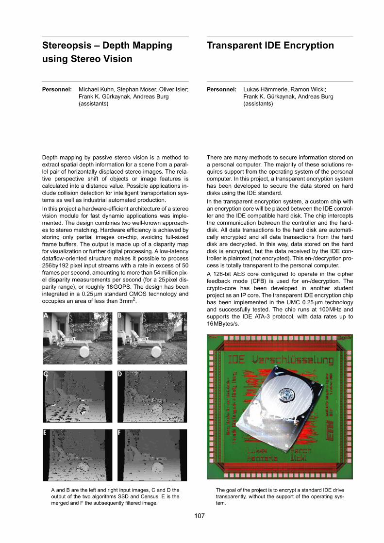
Stereopsis – Depth Mappingusing Stereo Vision
Personnel: Michael Kuhn, Stephan Moser, Oliver Isler;Frank K. Gürkaynak, Andreas Burg(assistants)
Depth mapping by passive stereo vision is a method toextract spatial depth information for a scene from a paral-lel pair of horizontally displaced stereo images. The rela-tive perspective shift of objects or image features iscalculated into a distance value. Possible applications in-clude collision detection for intelligent transportation sys-tems as well as industrial automated production.
In this project a hardware-efficient architecture of a stereovision module for fast dynamic applications was imple-mented. The design combines two well-known approach-es to stereo matching. Hardware efficiency is achieved bystoring only partial images on-chip, avoiding full-sizedframe buffers. The output is made up of a disparity mapfor visualization or further digital processing. A low-latencydataflow-oriented structure makes it possible to process256by192 pixel input streams with a rate in excess of 50frames per second, amounting to more than 54 million pix-el disparity measurements per second (for a 25pixel dis-parity range), or roughly 18GOPS. The design has beenintegrated in a 0.25 µm standard CMOS technology andoccupies an area of less than 3mm2.
A and B are the left and right input images, C and D theoutput of the two algorithms SSD and Census. E is themerged and F the subsequently filtered image.
10
Transparent IDE Encryption
Personnel: Lukas Hämmerle, Ramon Wicki;Frank K. Gürkaynak, Andreas Burg(assistants)
There are many methods to secure information stored ona personal computer. The majority of these solutions re-quires support from the operating system of the personalcomputer. In this project, a transparent encryption systemhas been developed to secure the data stored on harddisks using the IDE standard.
In the transparent encryption system, a custom chip withan encryption core will be placed between the IDE control-ler and the IDE compatible hard disk. The chip interceptsthe communication between the controller and the hard-disk. All data transactions to the hard disk are automati-cally encrypted and all data transactions from the harddisk are decrypted. In this way, data stored on the harddisk is encrypted, but the data received by the IDE con-troller is plaintext (not encrypted). This en-/decryption pro-cess is totally transparent to the personal computer.
A 128-bit AES core configured to operate in the cipherfeedback mode (CFB) is used for en-/decryption. Thecrypto-core has been developed in another studentproject as an IP core. The transparent IDE encryption chiphas been implemented in the UMC 0.25 µm technologyand successfully tested. The chip runs at 100MHz andsupports the IDE ATA-3 protocol, with data rates up to16MBytes/s.
The goal of the project is to encrypt a standard IDE drivetransparently, without the support of the operating sys-tem.
7
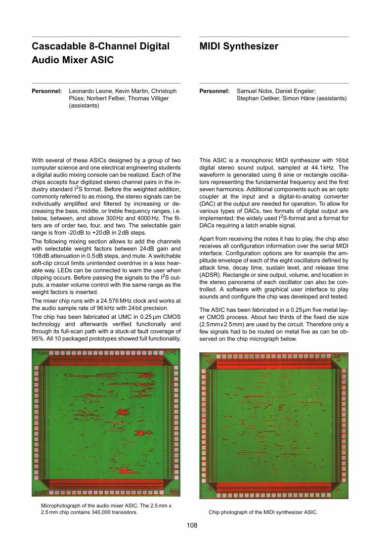
Cascadable 8-Channel DigitalAudio Mixer ASIC
Personnel: Leonardo Leone, Kevin Martin, ChristophPlüss; Norbert Felber, Thomas Villiger(assistants)
With several of these ASICs designed by a group of twocomputer science and one electrical engineering studentsa digital audio mixing console can be realized. Each of thechips accepts four digitized stereo channel pairs in the in-dustry standard I2S format. Before the weighted addition,commonly referred to as mixing, the stereo signals can beindividually amplified and filtered by increasing or de-creasing the bass, middle, or treble frequency ranges, i.e.below, between, and above 300Hz and 4000 Hz. The fil-ters are of order two, four, and two. The selectable gainrange is from -20dB to +20dB in 2dB steps.
The following mixing section allows to add the channelswith selectable weight factors between 24dB gain and108dB attenuation in 0.5dB steps, and mute. A switchablesoft-clip circuit limits unintended overdrive in a less hear-able way. LEDs can be connected to warn the user whenclipping occurs. Before passing the signals to the I2S out-puts, a master volume control with the same range as theweight factors is inserted.
The mixer chip runs with a 24.576 MHz clock and works atthe audio sample rate of 96 kHz with 24bit precision.
The chip has been fabricated at UMC in 0.25 µm CMOStechnology and afterwards verified functionally andthrough its full-scan path with a stuck-at fault coverage of95%. All 10 packaged prototypes showed full functionality.
Microphotograph of the audio mixer ASIC. The 2.5 mm x2.5 mm chip contains 340,000 transistors.
10
MIDI Synthesizer
Personnel: Samuel Nobs, Daniel Engeler;Stephan Oetiker, Simon Häne (assistants)
This ASIC is a monophonic MIDI synthesizer with 16bitdigital stereo sound output, sampled at 44.1kHz. Thewaveform is generated using 8 sine or rectangle oscilla-tors representing the fundamental frequency and the firstseven harmonics. Additional components such as an optocoupler at the input and a digital-to-analog converter(DAC) at the output are needed for operation. To allow forvarious types of DACs, two formats of digital output areimplemented: the widely used I2S-format and a format forDACs requiring a latch enable signal.
Apart from receiving the notes it has to play, the chip alsoreceives all configuration information over the serial MIDIinterface. Configuration options are for example the am-plitude envelope of each of the eight oscillators defined byattack time, decay time, sustain level, and release time(ADSR). Rectangle or sine output, volume, and location inthe stereo panorama of each oscillator can also be con-trolled. A software with graphical user interface to playsounds and configure the chip was developed and tested.
The ASIC has been fabricated in a 0.25µm five metal lay-er CMOS process. About two thirds of the fixed die size(2.5mmx2.5mm) are used by the circuit. Therefore only afew signals had to be routed on metal five as can be ob-served on the chip micrograph below.
Chip photograph of the MIDI synthesizer ASIC.
8

π-Quest – a Chip Calculating πup to 1014 Hexadecimal Digits
Personnel: Lukas Walter, Robert Hunger;David Perels, Stephan Oetiker (assistants)
πhas a long history spanning from the Babylonians (about2000BC) until today. Until recently it was believed to beimpossible to calculate a new digit of πwithout knowledgeof all preceding digits. This changed in 1996 whenD.Bailey, P.Borwein and S.Plouffe published a new classof algorithms that make it possible to focus all computa-tional power on the calculation of a single digit of π. Be-sides π, it is also possible to calculate π2, ln(3) and ln(5).
The most complex function of the algorithm implementedby the students is the computation of a modular exponen-tiation. Since there is no data dependency between the in-dividual function calls, the algorithm can be parallelized.Therefore, three instances of this functional block havebeen implemented.The results of these functions are pro-cessed further in a separate block. The design includes aserial interface that is compatible to the well-known RS-232 protocol. An adjustable and stoppable on-chip oscilla-tor is integrated. The generated frequency can be con-trolled over the RS-232 interface. This allows to run eachchip at its maximum clock speed.
The ASIC has been implemented on a CMOS 0.25µm fivemetal-layer process from UMC. The maximum operatingfrequency of the tested chips at 2.5V core voltage and3.3V pad supply is 292MHz.
Photograph of the πchip. The inset shows the layout plotwith color-coded functions.
10
Programmable Code Generatorfor Software-Defined Radio
Personnel: Reinhard Bischof, Jonas Biveroni, MarkusBrühwiler;Andreas Burg, David Perels (assistants)
Many communication standards require the generation ofpseudo-random sequences (e.g. Gold codes) or struc-tured binary codes (e.g. Walsh codes). This task is veryeasy to implement in dedicated hardware as only bit oper-ations are required. Unfortunately such dedicated solu-tions do not offer enough flexibility to adapt to majorchanges in a standard. In software-defined-radio architec-tures the code generation is therefore often done on aconventional DSP. However, as its instruction set is notdesigned to modify individual bits this is very inefficient.
In this project a dedicated processor was developed forthis task. Its ALU consists of four parallel bit ALUs and aword ALU. The former can carry out simple boolean oper-ations on individual bits and is controlled by a very long in-struction word (VLIW). The latter supports a basicinstruction set which is similar to a conventional proces-sor. Additionally, it provides three instructions that greatlyimprove the performance for some frequently used typesof codes. As opposed to the bit-ALU instructions the word-ALU instructions are significantly shorter. An instruction-packing mechanism allows the two instruction formats tocoexist efficiently.
The design was implemented in 0.25µm 5-metal CMOSon a core area of only 0.42mm2. It operates at 160MHz.An assembler and a simulator were also implemented.
Chip photomicrograph of the Triple-B programmablecode generator processor with overlaid layout plot.
9
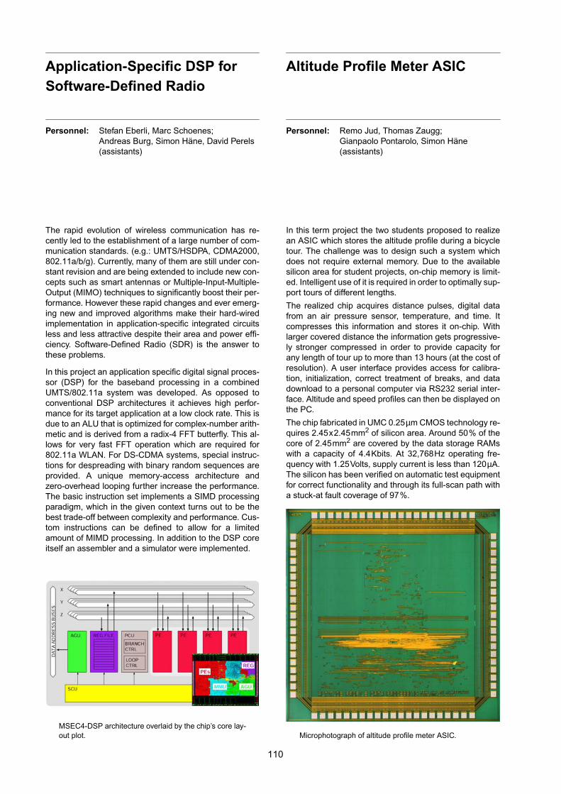
Application-Specific DSP forSoftware-Defined Radio
Personnel: Stefan Eberli, Marc Schoenes;Andreas Burg, Simon Häne, David Perels(assistants)
The rapid evolution of wireless communication has re-cently led to the establishment of a large number of com-munication standards. (e.g.: UMTS/HSDPA, CDMA2000,802.11a/b/g). Currently, many of them are still under con-stant revision and are being extended to include new con-cepts such as smart antennas or Multiple-Input-Multiple-Output (MIMO) techniques to significantly boost their per-formance. However these rapid changes and ever emerg-ing new and improved algorithms make their hard-wiredimplementation in application-specific integrated circuitsless and less attractive despite their area and power effi-ciency. Software-Defined Radio (SDR) is the answer tothese problems.
In this project an application specific digital signal proces-sor (DSP) for the baseband processing in a combinedUMTS/802.11a system was developed. As opposed toconventional DSP architectures it achieves high perfor-mance for its target application at a low clock rate. This isdue to an ALU that is optimized for complex-number arith-metic and is derived from a radix-4 FFT butterfly. This al-lows for very fast FFT operation which are required for802.11a WLAN. For DS-CDMA systems, special instruc-tions for despreading with binary random sequences areprovided. A unique memory-access architecture andzero-overhead looping further increase the performance.The basic instruction set implements a SIMD processingparadigm, which in the given context turns out to be thebest trade-off between complexity and performance. Cus-tom instructions can be defined to allow for a limitedamount of MIMD processing. In addition to the DSP coreitself an assembler and a simulator were implemented.
MSEC4-DSP architecture overlaid by the chip’s core lay-out plot.
11
Altitude Profile Meter ASIC
Personnel: Remo Jud, Thomas Zaugg;Gianpaolo Pontarolo, Simon Häne(assistants)
In this term project the two students proposed to realizean ASIC which stores the altitude profile during a bicycletour. The challenge was to design such a system whichdoes not require external memory. Due to the availablesilicon area for student projects, on-chip memory is limit-ed. Intelligent use of it is required in order to optimally sup-port tours of different lengths.
The realized chip acquires distance pulses, digital datafrom an air pressure sensor, temperature, and time. Itcompresses this information and stores it on-chip. Withlarger covered distance the information gets progressive-ly stronger compressed in order to provide capacity forany length of tour up to more than 13 hours (at the cost ofresolution). A user interface provides access for calibra-tion, initialization, correct treatment of breaks, and datadownload to a personal computer via RS232 serial inter-face. Altitude and speed profiles can then be displayed onthe PC.
The chip fabricated in UMC 0.25µm CMOS technology re-quires 2.45x2.45mm2 of silicon area. Around 50% of thecore of 2.45mm2 are covered by the data storage RAMswith a capacity of 4.4Kbits. At 32,768Hz operating fre-quency with 1.25Volts, supply current is less than 120µA.The silicon has been verified on automatic test equipmentfor correct functionality and through its full-scan path witha stuck-at fault coverage of 97%.
Microphotograph of altitude profile meter ASIC.
0
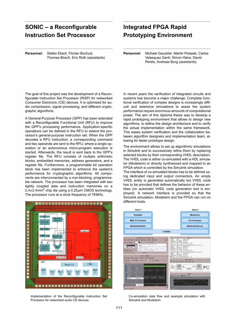
SONIC – a ReconfigurableInstruction Set Processor
Personnel: Stefan Eberli, Florian Bochud;Thomas Bösch, Eric Roth (assistants)
The goal of this project was the development of a Recon-figurable Instruction Set Processor (RISP) for networkedConsumer Electronic (CE) devices. It is optimized for au-dio compression, signal processing, and different crypto-graphic algorithms.
A General-Purpose Processor (GPP) has been extendedwith a Reconfigurable Functional Unit (RFU) to improvethe GPP’s processing performance. Application-specificoperations can be defined in the RFU to extend the pro-cessor’s general-purpose instruction set. When the GPPdecodes a RFU instruction, a corresponding commandand two operands are sent to the RFU, where a single op-eration or an autonomous micro-program execution isstarted. Afterwards, the result is sent back to the GPP’sregister file. The RFU consists of multiple arithmeticblocks, embedded memories, address generators, and aregister file. Furthermore, a programmable bit operationblock has been implemented to enhance the system’sperformance for cryptographic algorithms. All compo-nents are interconnected by a non-blocking, programma-ble network. The processor has been integrated with twotightly coupled data and instruction memories on a2.4x2.4mm2 chip die using a 0.25µm CMOS technology.The processor runs at a clock frequency of 78MHz.
Implementation of the Reconfigurable Instruction SetProcessor for networked audio CE devices.
11
Integrated FPGA RapidPrototyping Environment
Personnel: Michael Gauckler, Martin Polasek, CarlosVelasquez Santi; Simon Häne, DavidPerels, Andreas Burg (assistants)
In recent years the verification of integrated circuits andsystems has become a major challenge. Complete func-tional verification of complex designs is increasingly diffi-cult and extensive simulations to asses the systemperformance require enormous amounts of computationalpower. The aim of this diploma thesis was to develop arapid prototyping environment that allows to design newalgorithms, to define the design architecture and to verifythe actual implementation within the same framework.This eases system verification and the collaboration be-tween algorithm designers and implementation team, al-lowing for faster prototype design.
The environment allows to set up algorithmic simulationsin Simulink and to successively refine them by replacingselected blocks by their corresponding VHDL description.The VHDL code is either co-simulated with a HDL simula-tor (Modelsim) or directly synthesized and mapped to anFPGA which is controlled by the Simulink simulation.The interface of co-simulated blocks has to be defined us-ing dedicated input and output connectors. An emptyVHDL entity is generated automatically but VHDL codehas to be provided that defines the behavior of these en-tities (no automatic VHDL code generation tool is em-ployed). A network interface is provided so that theSimulink simulation, Modelsim and the FPGA can run ondifferent hosts.
Co-simulation data flow and example simulation withSimulink and Modelsim.
1
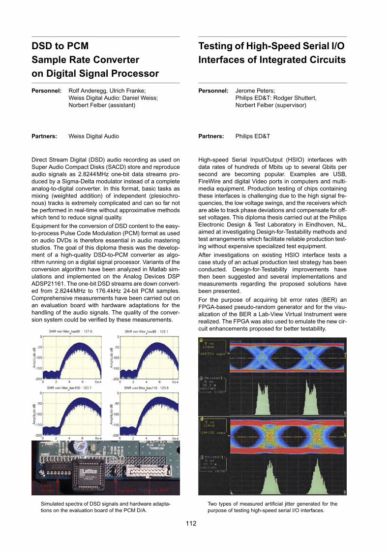
DSD to PCMSample Rate Converteron Digital Signal Processor
Personnel: Rolf Anderegg, Ulrich Franke;Weiss Digital Audio: Daniel Weiss;Norbert Felber (assistant)
Partners: Weiss Digital Audio
Direct Stream Digital (DSD) audio recording as used onSuper Audio Compact Disks (SACD) store and reproduceaudio signals as 2.8244MHz one-bit data streams pro-duced by a Sigma-Delta modulator instead of a completeanalog-to-digital converter. In this format, basic tasks asmixing (weighted addition) of independent (plesiochro-nous) tracks is extremely complicated and can so far notbe performed in real-time without approximative methodswhich tend to reduce signal quality.
Equipment for the conversion of DSD content to the easy-to-process Pulse Code Modulation (PCM) format as usedon audio DVDs is therefore essential in audio masteringstudios. The goal of this diploma thesis was the develop-ment of a high-quality DSD-to-PCM converter as algo-rithm running on a digital signal processor. Variants of theconversion algorithm have been analyzed in Matlab sim-ulations and implemented on the Analog Devices DSPADSP21161. The one-bit DSD streams are down convert-ed from 2.8244MHz to 176.4kHz 24-bit PCM samples.Comprehensive measurements have been carried out onan evaluation board with hardware adaptations for thehandling of the audio signals. The quality of the conver-sion system could be verified by these measurements.
Simulated spectra of DSD signals and hardware adapta-tions on the evaluation board of the PCM D/A.
11
Testing of High-Speed Serial I/OInterfaces of Integrated Circuits
Personnel: Jerome Peters;Philips ED&T: Rodger Shuttert,Norbert Felber (supervisor)
Partners: Philips ED&T
High-speed Serial Input/Output (HSIO) interfaces withdata rates of hundreds of Mbits up to several Gbits persecond are becoming popular. Examples are USB,FireWire and digital Video ports in computers and multi-media equipment. Production testing of chips containingthese interfaces is challenging due to the high signal fre-quencies, the low voltage swings, and the receivers whichare able to track phase deviations and compensate for off-set voltages. This diploma thesis carried out at the PhilipsElectronic Design & Test Laboratory in Eindhoven, NL,aimed at investigating Design-for-Testability methods andtest arrangements which facilitate reliable production test-ing without expensive specialized test equipment.
After investigations on existing HSIO interface tests acase study of an actual production test strategy has beenconducted. Design-for-Testability improvements havethen been suggested and several implementations andmeasurements regarding the proposed solutions havebeen presented.
For the purpose of acquiring bit error rates (BER) anFPGA-based pseudo-random generator and for the visu-alization of the BER a Lab-View Virtual Instrument wererealized. The FPGA was also used to emulate the new cir-cuit enhancements proposed for better testability.
Two types of measured artificial jitter generated for thepurpose of testing high-speed serial I/O interfaces.
2

FireWire Link LayerController
Personnel: Nicole Hediger, Reto Höpli, SimonSteinegger;Eric Roth, Thomas Bösch (assistants)
The goal of this student project was to implement anIEEE1394 compliant FireWire Link Layer Controller(LLC). The ASIC supports asynchronous transfers of up to400Mbps and can be connected to any commercialIEEE1394 physical layer device (PHY). Receive andtransmit data paths are strictly separated. The receiverblock accepts data from the bus, reassembles the 32-bitwords and performs a Cyclic Redundancy Check (CRC).Packets are then transferred to the 1kByte receive FIFO,where a controller can access the data via an asynchro-nous host interface. An additional 1kByte FIFO is locatedin the transmission path. The memory management of theFIFOs allows efficient communication with the host con-troller. Transmit operations include generation of arbitra-tion requests and CRC calculation.
An important task of the LLC is the generation and evalu-ation of acknowledge packets. Missing acknowledge re-sponses or erroneous packet formats are detected andreported. A set of control and status registers (CSR) al-lows configuration and control through the host interface.The CSR accepts commands for the PHY, which aretransmitted as a special PHY configuration packet.
A verification environment was developed for automatictraffic generation and analysis. The chip is fabricated in a0.25µm CMOS process on 5.8mm2 chip die area.
Micrograph and block diagram of the FireWire LLC.
11
Electronic Control Interfacewithout Moving Parts
Personnel: Martin Flubacher, Michel Wagner;Norbert Felber (assistant)
The goal of this project was the investigation of a replace-ment for mechanical controls as potentiometers andswitches for applications where components with movingparts are not suitable.
The students have realized several samples of sensorboards with electrodes and acquisition circuitry for capac-itive touch detection or position detection. For implemen-tation in an FPGA the circuit for the interpretation andconditioning of the signals has been designed in VHDL.To enable visual indication of the detected position, inter-faces for LED bars have been added.
The students could demonstrate that such robust compo-nents are feasible, although for the original goal of a com-plete specification for the later implementation of thecontrol electronics in an ASIC, the principle has to be en-hanced and refined.
Prototype of a slider control sensor board and four 16-LED bars with serial interface.
3
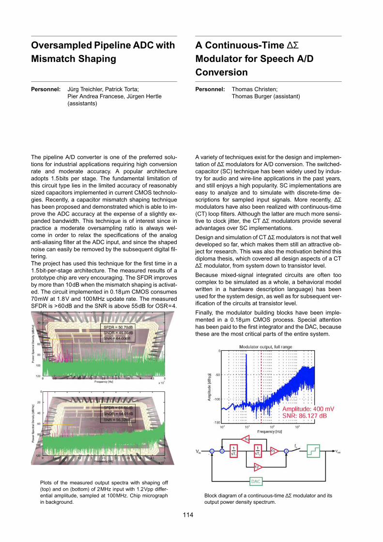
Oversampled Pipeline ADC withMismatch Shaping
Personnel: Jürg Treichler, Patrick Torta;Pier Andrea Francese, Jürgen Hertle(assistants)
The pipeline A/D converter is one of the preferred solu-tions for industrial applications requiring high conversionrate and moderate accuracy. A popular architectureadopts 1.5bits per stage. The fundamental limitation ofthis circuit type lies in the limited accuracy of reasonablysized capacitors implemented in current CMOS technolo-gies. Recently, a capacitor mismatch shaping techniquehas been proposed and demonstrated which is able to im-prove the ADC accuracy at the expense of a slightly ex-panded bandwidth. This technique is of interest since inpractice a moderate oversampling ratio is always wel-come in order to relax the specifications of the analoganti-aliasing filter at the ADC input, and since the shapednoise can easily be removed by the subsequent digital fil-tering.The project has used this technique for the first time in a1.5bit-per-stage architecture. The measured results of aprototype chip are very encouraging. The SFDR improvesby more than 10dB when the mismatch shaping is activat-ed. The circuit implemented in 0.18µm CMOS consumes70mW at 1.8V and 100MHz update rate. The measuredSFDR is >60dB and the SNR is above 55dB for OSR=4.
Plots of the measured output spectra with shaping off(top) and on (bottom) of 2MHz input with 1.2Vpp differ-ential amplitude, sampled at 100MHz. Chip micrographin background.
11
A Continuous-Time ∆ΣModulator for Speech A/DConversion
Personnel: Thomas Christen;Thomas Burger (assistant)
A variety of techniques exist for the design and implemen-tation of ∆Σ modulators for A/D conversion. The switched-capacitor (SC) technique has been widely used by indus-try for audio and wire-line applications in the past years,and still enjoys a high popularity. SC implementations areeasy to analyze and to simulate with discrete-time de-scriptions for sampled input signals. More recently, ∆Σmodulators have also been realized with continuous-time(CT) loop filters. Although the latter are much more sensi-tive to clock jitter, the CT ∆Σ modulators provide severaladvantages over SC implementations.
Design and simulation of CT ∆Σ modulators is not that welldeveloped so far, which makes them still an attractive ob-ject for research. This was also the motivation behind thisdiploma thesis, which covered all design aspects of a CT∆Σ modulator, from system down to transistor level.
Because mixed-signal integrated circuits are often toocomplex to be simulated as a whole, a behavioral modelwritten in a hardware description language) has beenused for the system design, as well as for subsequent ver-ification of the circuits at transistor level.
Finally, the modulator building blocks have been imple-mented in a 0.18µm CMOS process. Special attentionhas been paid to the first integrator and the DAC, becausethese are the most critical parts of the entire system.
Block diagram of a continuous-time ∆Σ modulator and itsoutput power density spectrum.
4
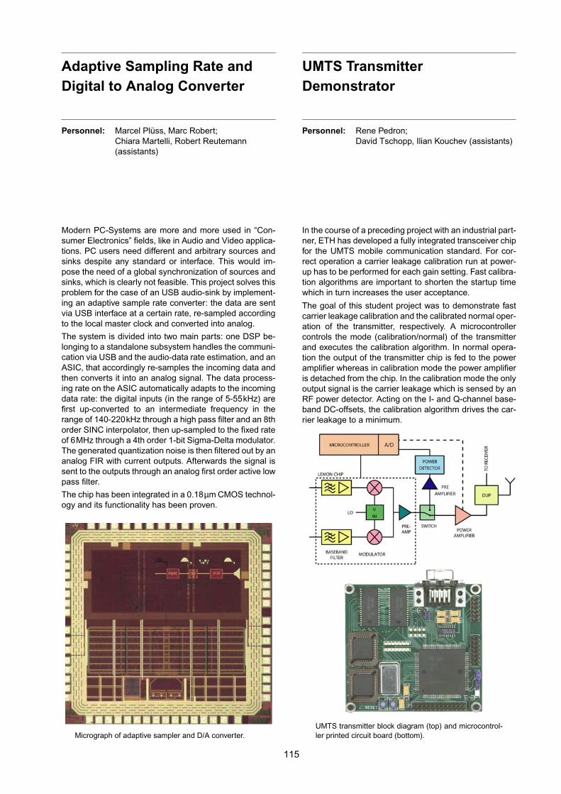
Adaptive Sampling Rate andDigital to Analog Converter
Personnel: Marcel Plüss, Marc Robert;Chiara Martelli, Robert Reutemann(assistants)
Modern PC-Systems are more and more used in “Con-sumer Electronics” fields, like in Audio and Video applica-tions. PC users need different and arbitrary sources andsinks despite any standard or interface. This would im-pose the need of a global synchronization of sources andsinks, which is clearly not feasible. This project solves thisproblem for the case of an USB audio-sink by implement-ing an adaptive sample rate converter: the data are sentvia USB interface at a certain rate, re-sampled accordingto the local master clock and converted into analog.
The system is divided into two main parts: one DSP be-longing to a standalone subsystem handles the communi-cation via USB and the audio-data rate estimation, and anASIC, that accordingly re-samples the incoming data andthen converts it into an analog signal. The data process-ing rate on the ASIC automatically adapts to the incomingdata rate: the digital inputs (in the range of 5-55kHz) arefirst up-converted to an intermediate frequency in therange of 140-220kHz through a high pass filter and an 8thorder SINC interpolator, then up-sampled to the fixed rateof 6MHz through a 4th order 1-bit Sigma-Delta modulator.The generated quantization noise is then filtered out by ananalog FIR with current outputs. Afterwards the signal issent to the outputs through an analog first order active lowpass filter.
The chip has been integrated in a 0.18µm CMOS technol-ogy and its functionality has been proven.
Micrograph of adaptive sampler and D/A converter.
11
UMTS TransmitterDemonstrator
Personnel: Rene Pedron;David Tschopp, Ilian Kouchev (assistants)
In the course of a preceding project with an industrial part-ner, ETH has developed a fully integrated transceiver chipfor the UMTS mobile communication standard. For cor-rect operation a carrier leakage calibration run at power-up has to be performed for each gain setting. Fast calibra-tion algorithms are important to shorten the startup timewhich in turn increases the user acceptance.
The goal of this student project was to demonstrate fastcarrier leakage calibration and the calibrated normal oper-ation of the transmitter, respectively. A microcontrollercontrols the mode (calibration/normal) of the transmitterand executes the calibration algorithm. In normal opera-tion the output of the transmitter chip is fed to the poweramplifier whereas in calibration mode the power amplifieris detached from the chip. In the calibration mode the onlyoutput signal is the carrier leakage which is sensed by anRF power detector. Acting on the I- and Q-channel base-band DC-offsets, the calibration algorithm drives the car-rier leakage to a minimum.
UMTS transmitter block diagram (top) and microcontrol-ler printed circuit board (bottom).
5
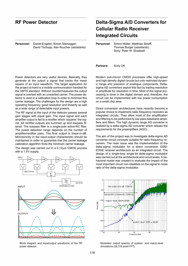
RF Power Detector
Personnel: Daniel Engeler, Simon Steinegger;David Tschopp, Ilian Kouchev (assistants)
Power detectors are very useful devices. Basically, theygenerate at the output a signal that tracks the meansquare of an input waveform. The target application forthe project at hand is a mobile communication handset forthe UMTS standard. Without countermeasures the outputsignal is overlaid with an unwanted carrier. The power de-tector is used in a calibration loop in order to minimize thiscarrier leakage. The challenges for the design are a highoperating frequency, good resolution and linearity as wellas a wide range of detectable input powers.
The RF signal at the input of the detector passes severalgain stages with equal gain. The input signal and eachamplifier output is fed to a rectifier which ‘squares’ the sig-nal. All rectifier outputs are summed up and lowpass fil-tered. The lowpass filter is a single-pole active-RC filter.The power detection range depends on the number ofamplifier/rectifier pairs. The final output is linear-in-dB.Monotonicity in the input-output characteristic should bemaintained in order to guarantee that the carrier leakagecalibration algorithm finds the minimum carrier leakage.
The design was carried out in a 0.12µm CMOS processwith a 1.5V supply.
Block diagram and input/output waveforms of the RFpower detector.
11
Delta-Sigma A/D Converters forCellular Radio ReceiverIntegrated Circuits
Personnel: Simon Müller; Matthias Streiff,Thomas Burger (assistants);Sony: Peter W. Shadwell
Partners: Sony UK
Modern sub-micron CMOS processes offer high-speedand high-density digital circuits but only restricted dynam-ic range and precision of analogue components. Delta-sigma AD converters exploit this fact by trading resolutionin amplitude for resolution in time. Most of the signal pro-cessing is done in the digital domain and, therefore, thecircuit can be implemented with low power consumptionon a small chip area.
Direct conversion architectures have recently become apopular choice to implement radio frequency receivers asintegrated circuits. They allow most of the amplificationand filtering to be performed by low pass baseband ampli-fiers and filters. The high dynamic range AD converter isrealized by a delta-sigma AD converter which relaxes therequirements for the preamplifiers (AGC).
The aim of the project was to investigate delta-sigma ADconverter circuit concepts suitable for radio frequency re-ceivers. The main issue was the implementation of thedelta-sigma modulator for a direct conversion GSM-EDGE receiver architecture as an integrated circuit. Thedesign of a single-loop single-bit delta-sigma modulatorwas carried out at the architectural and circuit levels. A be-havioral model was created to evaluate the impact of themost important circuit non-idealities on the signal to noiseratio of the delta-sigma modulator.
Modulator output spectra of system- and macro-levelsimulations (26,316 point FFT).
6
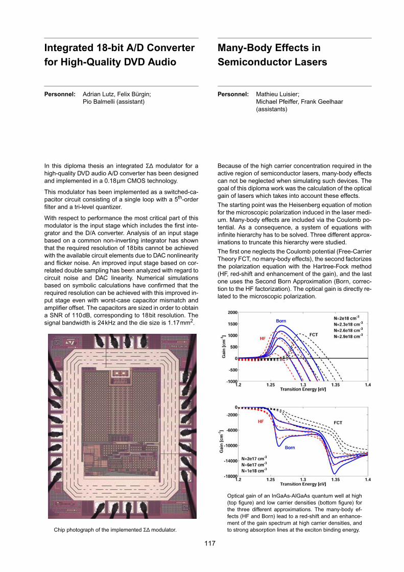
Integrated 18-bit A/D Converterfor High-Quality DVD Audio
Personnel: Adrian Lutz, Felix Bürgin;Pio Balmelli (assistant)
In this diploma thesis an integrated Σ∆ modulator for ahigh-quality DVD audio A/D converter has been designedand implemented in a 0.18µm CMOS technology.
This modulator has been implemented as a switched-ca-pacitor circuit consisting of a single loop with a 5th-orderfilter and a tri-level quantizer.
With respect to performance the most critical part of thismodulator is the input stage which includes the first inte-grator and the D/A converter. Analysis of an input stagebased on a common non-inverting integrator has shownthat the required resolution of 18bits cannot be achievedwith the available circuit elements due to DAC nonlinearityand flicker noise. An improved input stage based on cor-related double sampling has been analyzed with regard tocircuit noise and DAC linearity. Numerical simulationsbased on symbolic calculations have confirmed that therequired resolution can be achieved with this improved in-put stage even with worst-case capacitor mismatch andamplifier offset. The capacitors are sized in order to obtaina SNR of 110dB, corresponding to 18bit resolution. Thesignal bandwidth is 24kHz and the die size is 1.17mm2.
Chip photograph of the implemented Σ∆ modulator.
11
Many-Body Effects inSemiconductor Lasers
Personnel: Mathieu Luisier;Michael Pfeiffer, Frank Geelhaar(assistants)
Because of the high carrier concentration required in theactive region of semiconductor lasers, many-body effectscan not be neglected when simulating such devices. Thegoal of this diploma work was the calculation of the opticalgain of lasers which takes into account these effects.
The starting point was the Heisenberg equation of motionfor the microscopic polarization induced in the laser medi-um. Many-body effects are included via the Coulomb po-tential. As a consequence, a system of equations withinfinite hierarchy has to be solved. Three different approx-imations to truncate this hierarchy were studied.
The first one neglects the Coulomb potential (Free-CarrierTheory FCT, no many-body effects), the second factorizesthe polarization equation with the Hartree-Fock method(HF, red-shift and enhancement of the gain), and the lastone uses the Second Born Approximation (Born, correc-tion to the HF factorization). The optical gain is directly re-lated to the microscopic polarization.
Optical gain of an InGaAs-AlGaAs quantum well at high(top figure) and low carrier densities (bottom figure) forthe three different approximations. The many-body ef-fects (HF and Born) lead to a red-shift and an enhance-ment of the gain spectrum at high carrier densities, andto strong absorption lines at the exciton binding energy.
7
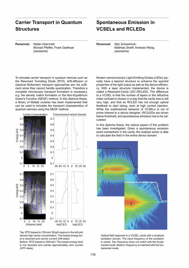
Carrier Transport in QuantumStructures
Personnel: Stefan Odermatt;Michael Pfeiffer, Frank Geelhaar(assistants)
To simulate carrier transport in quantum devices such asthe Resonant Tunneling Diode (RTD), drift-diffusion orclassical Boltzmann transport approaches are not suffi-cient since they cannot handle quantization. Therefore acomplete microscopic transport formalism is necessary,e.g. the density matrix formalism or the Non-EquilibriumGreen’s Function (NEGF) method. In this diploma thesis,a library of Matlab routines has been implemented thatcan be used to simulate the transport characteristics ofquantum devices using the NEGF method.
Top: RTD biased to 150meV. Bright regions in the left plotdenote high carrier concentration. The lowest energy lev-el is resonant and carries current (ON-state).Bottom: RTD biased to 200meV. The lowest energy levelis not resonant and carries approximately zero current(OFF-state).
11
Spontaneous Emission inVCSELs and RCLEDs
Personnel: Stijn Scheerlinck;Matthias Streiff, Andreas Witzig(assistants)
Modern semiconductor Light-Emitting Diodes (LEDs) typ-ically have a layered structure to enhance the spectralproperties of the light output as well as the device efficien-cy. With a layer structure implemented, the device iscalled a Resonant-Cavity LED (RCLED). The differenceto a VCSEL is that the number of layers or the refractiveindex contrast is chosen in a way that the cavity loss is stillvery high, and that an RCLED has not enough opticalfeedback to start lasing, even at high current injection.While the subthreshold behavior of VCSELs is not ofprime interest to a device designer, (RC)LEDs are drivenbelow threshold, and spontaneous emission has to be cal-culated.
In this diploma thesis, the optical aspect of this problemhas been investigated. Given a spontaneous emissionevent somewhere in the cavity, the realized solver is ableto calculate the field in the entire device domain.
Optical field response in a VCSEL cavity with a localizedexcitation (arrow). The input frequency of the excitationis varied. Top: frequency does not match with the funda-mental mode. Bottom: frequency is matched with the fun-damental mode.
8

Assessment of ELF Exposurefrom GSM Handsets
Personnel: Markus Tuor;Sven Ebert (assistant)
Partners: SPEAG
The aim and focus of this semester thesis was the scien-tific analysis of Extremely Low-Frequency (ELF) magneticfield components emitted by GSM handsets.
To perform the analysis of the magnetic field componentsemitted by a GSM handset, a suitable measurement sys-tem was developed, based on a Hall sensor and of com-ponents of the DASY4 Dosimetric Assessment System(SPEAG). Using this measurement system, the low-fre-quency exposure (<250 Hz) of three different GSMphones (Motorola Timeport, Nokia3310, Sony EricssonP800) were examined.
The results of the measurements showed the same fre-quency components for the magnetic field as they occurin the RF of the GSM signal (8.3Hz, 217Hz). The magnet-ic field magnitudes measured were between 50nT and3µT at a distance of 10mm from the phone surface. Theachieved results contribute to the definition of a worst-case exposure signal for health risk assessment studies.
Measurement setup for ELF magnetic fields of mobilephones.
119
PhD Theses – Abstracts
POSTDOCTORAL THESIS (HABILITATION):
Full-Band Monte Carlo Simulation of Nanoscale Strained-Silicon MOSFETs
Fabian M. Bufler
A full-band Monte Carlo simulator for the simulation ofnanoscale metal-oxide-semiconductor field-effect transis-tors (MOSFETs) has been developed and applied tostate-of-the-art as well as to strained-silicon devices. Thesimulator named SPARTA is based on a Single-PARTicleApproach to self-consistent Monte Carlo device simula-tion and was in June 2002 included in the release 8.0 ofthe technology computer-aided design (TCAD) companyISE Integrated Systems Engineering in Zürich.
Monte Carlo simulation is a stochastic method for thesolution of the Boltzmann equation governing quasi-bal-listic and hot-electron transport which is crucial for theoperation of nanoscale MOSFETs. The Monte Carlomethod monitors the histories of the electrons which con-sist of accelerations by the electric field and scatteringsdue to imperfections of the silicon (Si) lattice such asimpurities. As result, terminal currents and internal quan-tities such as density, drift velocity or electron tempera-ture are computed.
In the present work, a robust and efficient Monte Carloalgorithm was developed. The algorithm is based on astep-by-step propagation of the electrons in the phase-space, i.e. the two-dimensional (2D) real space and thethree-dimensional (3D) momentum-space. While the realspace is discretized by an unstructured grid for each dif-ferent device geometry, the Brillouin zone of Si is meshedby an equidistant tensor grid in momentum space. Ineach momentum-space element, the band energies ofthree valence and four conduction bands are storedwhich are obtained from nonlocal empirical pseudopoten-tial calculations including spin-orbit interaction. The ten-sor grid greatly facilitates the frequent computations ofthe intersections of the electron trajectories with the 3Dcubes in momentum space. On the other hand, the step-by-step propagation approach allows one within the self-scattering scheme to minimize fictitious scattering byusing upper estimates of the real scattering rate in eachphase-space element. This led - together with a selectionof the after-scattering-states via linked lists and anapproximation for impurity scattering - to a very efficientsimulation. The Boltzmann equation has to be solvedself-consistently with the Poisson equation. The commonapproach is a Monte Carlo simulation of a particleensemble where the linear Poisson equation is updatedon a femtosecond scale. However, this involves stabilityproblems at the increasing doping levels in MOSFETs asthey are further scaled down. Therefore, an alternativeconcept was adopted where single-particle frozen-fieldMonte Carlo simulations are iterated with solutions of thenonlinear Poisson equation until convergence isachieved. Due to the absence of stability problems, thisapproach made the simulation of real state-of-the artdevices possible.
The Monte Carlo model was validated by a comprehen-sive comparison with measurements of low-field mobility,
drift velocity and diffusivity in bulk silicon over a widerange of lattice temperatures and electric fields as well asfor different crystallographic field orientations. Then n-MOSFETs of the company Toshiba Corporation witheffective gate lengths down to Leff = 40 nm were simu-lated. Without any parameter adjustment the transfer andoutput characteristics could be accurately reproduced,whereas the classical device simulation based on thedrift-diffusion or the hydrodynamic model showed signifi-cant deviations.
When a thin Si layer is grown on top of a silicon-germa-nium Si1-x Gex substrate, its in-plane lattice constantadopts the larger value of Si1-x Gex. This leads to biaxialtensile strain in Si. The strain shifts four of the six con-duction band valleys upwards in energy and moves theheavy-hole band away from the valence-band edge.Therefore charge transport is - in addition to reducedintervalley or interband scattering - mainly determined bythe small transverse electron mass and the light-holemass. The resulting improved transport properties havemade strained-Si one of the most promising ways toincrease device performance beyond traditional scaling.In order to estimate the performance improvement forfuture technology generations, the on-currents ofstrained-Si n-type and p-type MOSFETs were simulateddown to Leff = 25 nm. The improvement saturates for n-MOSFETs above x = 0.2 and attains despite a modesttendency to decrease with scaling still more than 30% forthe smallest gate length. For Leff = 70 nm, the simulatedstrain-induced improvement was also in good agreementwith recently published measurements by IBM. In con-trast, appreciable improvements for nanoscale p-MOS-FETs require higher strain levels of up to x = 0.4, but theon-current still remains below that of correspondingunstrained-Si n-MOSFETs.
However, the strong strain-induced performanceenhancement in n-MOSFETs is surprising for small gatelengths and hence high longitudinal channel fields,because the improvement of the bulk drift velocity van-ishes in the high-field limit where the higher-lying valleysare being populated. In this respect, a physical interpre-tation of the origin of the on-current could be found byinvestigating transport along two different crystallo-graphic directions within a plane parallel to the interfaceto the virtual SiGe substrate, which were directed alongthe <100> and <110> orientation, respectively. In thestrained-Si n-MOSFET, the drain current was the same inthe linear regime, but the on-current was 10% larger in<100> direction. On the bulk level, the low-field mobilityand the saturation velocity are the same in both direc-tions. Only at medium field strengths is the stationary driftvelocity at maximum 4% larger in the <100> direction. Bycontrast, the overshoot peak, emerging on a short timescale after applying a strong field to an ensemble of elec-trons at equilibrium, was found to be more than 30%
120

stronger in <100> direction and was in contrast to thesaturation velocity always larger than in unstrained Si.The overshoot peak is due to quasi-ballistic transport,when on a short time scale only few scattering eventshappen. It is therefore mainly determined by the curva-ture of the band structure which differs in fact stronglyabove 100 meV between both directions. The situation inthe device at a high drain voltage is similar. The electronscoming from the source are near equilibrium and sud-denly experience a very strong field when entering thechannel. On a short distance they suffer only few scatter-ing events and were indeed found to have acquired avelocity which is already at the beginning of the channel
above the saturation velocity and different for both direc-tions. In conclusion, a robust and efficient Monte Carlodevice simulator was developed. The simulation resultscompare favorably with measurements of state-of-the-artnanoscale MOSFETs and the improvement to beexpected in future technologies by strained-Si deviceswas estimated. The most important result was the expla-nation of the on-current in terms of quasi-ballistic trans-port, which is in particular the reason for the continuingperformance improvement by strain in the sub 0.1micrometer regime and was so far not understood in theliterature.
Prof. Dr. W. Fichtner, ETH Zürich, examiner ISSN 0936-5362ISBN 3-89649-898-3
PhD THESES:
Frequency Synthesis for Wireless Transceivers
Dirk Pfaff
Frequency synthesizers are indispensable to any wire-less transceiver to accommodate frequency translationfrom the radio frequency (RF) band to baseband and viceversa. This work describes analysis, integrated circuitimplementation and experimental characterization of fre-quency synthesizers for GSM-type mobile stations. Botharchitectural and circuit level issues are considered. Aftera review of GSM/DCS/PCS frequency synthesizer speci-fications, which reveal the stiff requirements on accuracyand purity of the synthesized signal as well as on thedynamic behavior, the systematic design of phase lockedloops is presented. Particular attention receives the opti-mum choice of loop filter singularities of a third orderloop. Besides this, undesired effects of charge pumpphase locked loops, such as the generation of spurioustones in the spectrum of the synthesized signal, are con-sidered.
A large fraction of the presented work is dedicated to cir-cuit design. Low power consumption, which is among themost important performance parameters of wireless ter-minals where the available power is limited, is targetedbesides low cost. All proposed circuits are realized withcost effective standard CMOS technologies, instead ofmore suited, but more expensive bipolar technologies.Low power consumption is achieved by rigorous re-think-ing of the building blocks which dominate the consump-tion. Application of discrete resonator devices, which areeither surface mounted devices in the 1GHz range orprinted circuit board based planar transmission lines inthe 4GHz range, are found to be extremely useful tolower the consumption of RF oscillators. The design of alow power 1GHz voltage controlled oscillator using only0.25mA is presented. A 3.6GHz oscillator providing
quadrature outputs at half the frequency, accommodatingreceivers with low or zero intermediate frequency, is pre-sented as well. A quadrature demodulator includinghighly linear downconversion mixers exhibits excellent40dB of unwanted sideband rejection despite the lowconsumption of only 10mA.
Besides the oscillator, programmable dividers tend toconsume considerable amount of power due to the highinput frequency. While these blocks are often realizedwith bipolar technologies to benefit from the largetransconductance to current ratio, the design of CMOSprogrammable dividers is more demanding.
Nevertheless, competitive CMOS dual modulus prescal-ers are presented which even outperform bipolar solu-tions. While a 0.25µm 1GHz prescaler dissipates 0.9mA,a 0.18µm 4GHz prescaler consumes 2.5mA. Beyondexperimental results, some low power design guidelinesfor current mode logic circuits are proposed.
Frequency synthesizer design involves circuits with oper-ating frequencies ranging from several GHz to some hun-dred kHz. While the design of the high frequency part isin performance and consumption critical, the low fre-quency section is challenging as well. Reduction of spuri-ous tones requires careful design of the charge pump. Anovel charge pump topology is proposed to lower thespurious tones level of integer-N frequency synthesizers.The capability of the novel charge pump is verified by a4GHz frequency synthesizer realized in 0.18µm CMOS.The third order loop with a loop bandwidth of 40kHzexhibits a reference frequency spurious tone, 400kHzaway from the carrier, of only -68dBc.
Prof. Dr. W. Fichtner, ETH Zürich, examiner Diss. ETH-Nr. 15234Dr. Roland Best, Best Engineering, co-examiner ISBN 3-89649-879-7
121
Control Strategies for Balancing of Series and Parallel Connected IGBT/Diode Modules
Jan Thalheim
For high-voltage or high-power applications, it may benecessary to realize a logical switch by connectingsmaller units in parallel and series to achieve high avail-ability, high-frequency operation, and low cost due tobuild-in redundancy, reduced dynamic losses, and modu-lar use of standardized units, respectively. IGBTs arevery convenient to realize such units, because of quasi-linear controllability via a gate terminal.
This thesis investigates control methodologies for powerMOS semiconductor switches with focus on combinedparallel and series connection of IGBT/diode modules. Itis proposed to provide each IGBT with primary local con-trol to monitor and adjust the IGBT's static and dynamicbehavior. Secondary (global) control synchronizes theoperation of multiple IGBTs. A globally synchronousclock can also be derived locally. This makes it possible
to use low-cost low-bandwidth data links between series-connected units. Thereby, a flexible master-slaveapproach can avoid the need of dedicated global control.That is, the entire system is manageable by the localgate drive circuitry.
A prototype ASIC has been fabricated in CMOS technol-ogy with high-voltage extension. The driver is partitionedinto fourteen clusters with a measured gate current capa-bility of one Ampere each. A classification of the IGBT'scollector-emitter voltage and collector current signalsallows for real-time reconfiguration of the controller struc-ture to optimize the dynamic response of the system. Theconduction state and the recovery speed of freewheelingdiodes are controlled by the voltage drop across the DClink inductance, which is locally estimated at each IGBT.
Prof. Dr. W. Fichtner, ETH Zürich, examiner Diss. ETH-Nr. 15232Prof. Dr. J. W. Kolar, ETH Zürich, co-examiner ISBN 3-89649-890-8
Analysis and Improvement of the Numerical Properties of the FDTD Algorithm
Andreas Christ
Recent years have seen a steady miniaturization of elec-tronic devices, together with the opening of frequencyranges in the Gigahertz domain to the consumer elec-tronics market. The number of wireless applications hasbeen continuously increasing, and wireless local areanetworks as well as on- and in-body mounted devices forcommunications or life support point out the latest trends.The development of these devices stringently requiresthe application of numerical simulation tools to determinehigh frequency characteristics and interaction with theuser in order to optimize performance and minimizeexposure. Among the many different numerical electro-magnetics solvers, the finite-difference time-domain(FDTD) method has attracted the most interest amongresearchers and application engineers both for develop-ment and compliance testing purposes.
In spite of the prominent role of FDTD, several aspects ofits numerical properties have not yet rigorously beenstudied. The influences of nonuniform mesh spacing,which is indispensable for the treatment of real-worldproblems, have so far only been assessed experimen-tally, and guidelines for the generation of nonuniformmeshes merely exist as rules of thumb. Therefore, one ofthe main objectives of this work is to rigorously analyzethe numerical properties of the nonuniform FDTD algo-rithm and to propose efficient methods for its optimiza-tion.
The introductory part of this thesis gives a brief overviewof the FDTD theory and the current state of researchregarding the numerical properties of the algorithm isreviewed. In Chapters 2 and 3, different - classical andnovel - mesh discretization techniques are compared anddiscussed, and open issues are identified. As a basis forfurther studies of the FDTD algorithm, a nonuniformmesh generator is developed in Chapter 4. The meshgenerator is interfaced to the CAD environment of theintegrated simulation platform SEMCAD. The theoreticalpart presents a detailed analysis of the dispersion prop-
erties of the nonuniform FDTD algorithm in Chapters 5and 6. The mesh grading not only leads to increasedphase velocity errors but also to spurious attenuation oramplification. Further, it is shown that the grid dispersionerrors affect the reflection at planar material interfaces. Inthis connection, it is shown that the FDTD algorithm doesnot implicitly fulfill the boundary conditions for the conti-nuity of the electric and magnetic fields. The error of thenumerical reflection coefficient is calculated, and discreti-zation influences on total reflection, Brewster angle andSAR assessment are discussed. Approximations of thediscretization errors are given such that they can be eas-ily considered when generating the grid for a numericalmodel.
Based on these theoretical findings, Chapters 7 and 8propose novel methods to correct the numerical phasevelocity errors introduced by the mesh grading and tominimize the inaccuracies for the modelling of materialinterfaces. These methods use update equations withsplit coefficients for the finite difference terms, but retainthe original structure of the FDTD grid. They allow theaccurate compensation of the numerical errors of theFDTD algorithm for a frequency and direction of optimi-zation and improve its properties over a large bandwidth.
The application part presents several examples from thearea of antenna design, optics and numerical dosimetrywhich demonstrate the developments achieved within theframework of this thesis. All results were validated withmeasurements or different numerical techniques. InChapter 9, a commercial mobile phone base stationantenna is analyzed experimentally and numerically, con-sidering the influences of the mesh grading.
The capabilities of the correction techniques introducedin Chapters 10 are demonstrated by the full-wave analy-sis of a vertical-cavity surface-emitting laser in a three-dimensional cartesian mesh in Chapter 11. Using thesenew techniques, the grid resolution can be significantlyincreased, while keeping the grid dispersion errors in suf-
122

ficiently small. This reduces the problem size to such anextent that the laser characteristics can be calculated ona 32bit computer.
In Chapter 12, a numerical model of a dosimetricnearfield probe is developed and used to assess theinteraction between the probe material and the fields tobe measured. The accuracy of the model proves to behigh enough to apply the simulations for the assessmentof the change of the probe calibration factor when usedin media different from tissue simulating liquid.
This thesis concludes with an extensive study about ana-
tomical and homogeneous head phantoms for the com-pliance testing of mobile telecommunications equipment.The recently proposed Specific Anthropomorphic Manne-quin (SAM) is benchmarked against several high-resolu-tion anatomical head models. The results confirm that theliquid-filled phantom model as proposed in the standardsrepresents a conservative approach for the compliancetesting of mobile telephone equipment for the phonemodels and testing positions under investigation. Furtherstudies will be necessary for different telephone designsand enhanced frequency ranges.
Prof. Dr. W. Fichtner, ETH Zürich, examiner Diss. ETH-Nr. 15057Prof. Dr. Niels Kuster, ETH Zürich, and ISBN 3-89649-925-4Per-Simon Kildal, co-examiners
Broadband Sigma-Delta A/D Converters
Pio Balmelli
This thesis describes the design of two integrated broad-band sigma-delta (Σ∆) modulators implemented inCMOS technology.
The speed and resolution of A/D converters mustadvance before the signal bandwidth, the modulationdepth, and the resilience to interference of digital com-munications receivers can improve. Hence, the data rateachievable by a communications standard is inextricablylinked to the performance of the A/D converter. Sigma-delta A/D converters have demonstrated to achieve veryhigh resolutions (>13bit) without the need of expensivepost-processing techniques, like laser trimming or cali-bration. Nevertheless, Σ∆ A/D converters have generallya limited signal bandwidth because they need oversam-pling.
The basic requirement for a broadband Σ∆ A/D converteris then low oversampling ratio and high sampling fre-quency. Hence, an architecture with very good noiseshaping capability which puts minimal speed and accu-racy specifications on the constituting analog buildingblocks is needed. Furthermore, the selected architecturemust be implementable in fast CMOS technologies withreduced voltage supply. The discrete-time, single-loop,multibit, feedforward architecture is found to be the besttrade off with respect to the above mentioned require-ments.
The linearity of the DAC represents an important subjectin a multibit architecture. A non-linear DAC generates anintermodulation of the signal and of the ideal shapedquantization noise considerably deteriorating the final
converter resolution. Thus this problem has been accu-rately analyzed.
The first implemented circuit is a low-power Σ∆ modulatorfor ADSL standard; it performs 14bit of resolution at aconversion rate of 2.5MSPS. The modulator employs a5th order feedforward switched-capacitor loopfilter withtwo internal feedback loops and a 1.5bit quantizer. Theoversampling ratio is 32. The circuit is implemented in a 1polysilicon, 6 metal, 0.25µm CMOS technology andoccupies an area of 0.5mm2 (core only). The measureddynamic range, peak signal-to-noise ratio and peak sig-nal-to-noise-and-distortion ratio are 89dB, 85dB, and79dB, respectively. The power consumption is 24mWwhich is very low.
The second circuit is a Σ∆ modulator for VDSL standard;it performs 14bit of resolution at a conversion rate of25MSPS, which is ten times higher than in the ADSL con-verter. The circuit employs also a 5th order feedforwardswitch-capacitor loopfilter with two internal feedbacks,but uses a 4bit instead of a 1.5bit quantizer. The over-sampling ratio is as low as 8. The data weighted averag-ing algorithm (DWA) is utilized to randomize and shapethe error power generated by the non-ideal 4bit DAC.The circuit is implemented in a 1 polysilicon, 7 metal,0.18µm CMOS technology and occupies an area of0.95mm2 (core only). The measured dynamic range,peak signal-to-noise ratio and peak signal-to-noise-and-distortion ratio are 84dB, 82dB, and 72dB, respectively.The conversion rate of this converter is very high for theachieved resolution.
Prof. Dr. Q. Huang, ETH Zürich, examiner Diss. ETH-Nr. 15392Prof. Hans-Andrea Löliger, ETH Zürich, co-examiner ISBN 3-89649-921-1
EMF Risk Assessment: "In Vitro" Research and Sleep Studies
Jürgen Schuderer
Mobile communication systems have experienced aspectacular growth in use during the last decade.According to recent estimations, the population base ofdaily users will soon exceed the billion threshold. In addi-tion to mobile phones, a wide market penetration is alsoprognosticated for new applications of wireless in- andon-body communications.
Long-term exposure to any environmental factor capableof tissue interaction needs to be analyzed with respect topossible health risks. Therefore, it is reasonable that thepublic and health authorities demand a careful riskassessment of this new technology. However, lookingback to 10 years of research with cell, animal and humanexposure experiments, different findings have emerged
123
and no clear scientific evidence could be provided. Theconflicting data may have resulted from poorly definedexposure scenarios.
This thesis deals with the development and characteriza-tion of optimized exposure systems for in vitro andhuman laboratory studies. For this purpose the newestnumerical and experimental methods have been used;these methods were largely unavailable in the past, par-ticularly a key feature like electro-thermal field simulation.
Until present, the experimental exposure characterizationin vitro could not be performed sufficiently, because oflarge dimensions and low sensitivity of the probes. In thisthesis a novel ultra-small temperature probe wasdesigned and fully characterized. The probe consists of athermistor sensor, based on a 50mm x 100mm layer ofamorphous Germanium. RF immunity is reached byusing high resistivity for the sensor and leads. As a resultof the short response time and the high sensitivity of theprobe, the strong absorption gradients within RFexposed cell medium were successfully resolved.
It has been discussed in the framework of in vitro labora-tory studies, whether the meniscus, as occurring at theinterfaces between cell medium and Petri dish, may havean effect on the absorption distribution. This issue wassolved in this thesis by a detailed numerical analysis. It isshown that a numerical dosimetry based on a flat modelof the cell medium surface as it is widely used, can leadto a significant underestimation of the actual absorbedpower within in the entire volume.
Three novel in vitro exposure systems were realized forthe mobile communication frequency bands of GSM 900MHz, DCS 1800 MHz and UMTS 1950 MHz. Further-more, an additional system for extremely low frequencymagnetic fields was developed in order to analyze thefield exposures resulting from electrical power-supplysystems. The advantages of the setups presented in thisthesis compared to their predecessors are: (1) uniformfield distribution at high power efficiency, (2) realistic
numerical modeling, (3) comprehensive numerical andexperimental analysis of the field distribution, uncertain-ties, variations and all sorts of artifacts, (4) monitoringand control of exposure and environmental parameters,(5) complex signal schemes with high relevance forhealth risk assessment and (6) easy handling.
Because of these properties, the new exposure systemshave emerged to become standard for the Europeanresearch programs (REFLEX, PERFORM B, etc.). Withinthese research activities, previously unknown effects ofnon-ionizing radiation have been discovered and are cur-rently widely discussed (e.g., DNA strand breaks andchanges in gene and protein expression).
The last part of this thesis is dedicated to human studies,especially to the effects of GSM exposure on humansleep. For that purpose a novel exposure system hasbeen developed and dosimetrically analyzed. The setupinduces a defined unilateral field distribution inside thehead that (1) covers all brain regions which can beexposed by mobile phones, (2) has only low sensitivity tohead movements or anatomical variations between sub-jects and (3) was comprehensively analyzed by numeri-cal and experimental dosimetry (absorption for functionalsub-regions of the brain are distinguished).
The experiments with the human exposure setupresulted in novel, reproducible findings: It was shown thatGSM exposure leads to changes in sleep EEG spectrumwith an effect outlasting the exposure and dependentupon the low frequency pulse modulation. Additionally,for the first time, effects of RF exposure on the cerebralblood flow in the brain were shown.
Based on the present results as derived from the in vitroand human studies, it would be premature to draw con-clusions about health consequences of EMF exposure.The findings need to be independently replicated and theinteraction mechanisms must be isolated for clarifyingthe relevance of the issues.
Prof. Dr. W. Fichtner, ETH Zürich, examiner Diss. ETH-Nr. 15347Prof. Dr. Niels Kuster, ETH Zürich, and ISBN 3-89649-926-2Prof. Dr. T. Nojima, co-examiners
Postdoctoral and PhD theses can be ordered from:
Hartung-Gorre Publisher Phone: +49 7533 97227Säntisblick 26 Fax: +49 7533 97228D-78465 Konstanz E-mail: [email protected] Web: http://home.t-online.de/home/hartung.gorre
124
Diploma Theses – Overview
Summer Semester 2003
Matteo Ferrari Automotive Power Semiconductor Devices
Jerome Peeters Method for Production Testing of High-Speed Serial I/Os of Integrated Circuits
Stijn Scheerlinck Simulation of Spontaneous Emission in Resonant-Cavity Light-Emitting Diodes
Stefan Eberli A SIMD DSP for Multi-Standard Software Defined Radio:Marc Schoenes Specification and Architecture
Winter Semester 2003/2004
Marco Chicherio Soft Viterbi Decoder and Metric Computation Unit for Bit-Interleaved CodedModulation
Norbert Pramstaller DPA-Resistant AES Crypto Chip Realization
Simone Sponton Analysis of Transient Self-Heating Effects in Silicon Devices underTLP Operation
Daniel Engeler Coprocessor Evaluation Environment for PowerPCs
Elisa Ricci Use of Neural Networks to Solve the Reverse Modeling Problemfor Scanning Capacitance Microscopy
Mauro Chiappini Physical Modeling of Scanning Spreading Resistance MicroscopyMeasurements
Anderegg Rolf SOLARIS: A High-Order, Low-Latency Convolution Processor ASICFranke Ulrich
125

Student Projects – Overview
Summer Semester 2003
Markus Tuor Assessment of ELF Exposure from GSM Handsets
Daniel Engeler ASIC Design: RF Power DetectorSimon Steinegger
Samuel Fuhrer Design of a Programmable Bandpass Filter for aMulti-Standard Wireless Receiver
Winter Semester 2003/2004
Reto Stalder System Design: USB Audio SystemTareq Hossain
Zhen Xiao ASIC Design: 14-bit Current-Steering DA Converter
Manuel Aschwanden Nonequilibirum Model for Semiconductor Laser Modulation Response
Oliver Isler ASIC Design of a Programmable Base-Band Filter for a Multi-StandardWireless Receiver
Beat Hangartner Simulation of Semiconductor Multi-Quantum-Well Laser Diodes
Zoltan Schlegel Simulation of Scattering Processes in Quantum-Well Lasers
Markus Wenk ASIC Design: VLSI Implementation of a Sphere Decoder Core forMartin Zellweger MIMO Detection
David Stadelmann ASIC Design: Digital Audio Stereo PreamplifierThomas Zurbrügg
Jean-Daniel Merkli CohereChip: Coprocessor for Virtual 3D AudioThomas Frech
Conradin Merk ASIC Design: Power and Performance Optimization of a Complex-NumberChristoph Studer Arithmetic ALU
Clemens Lombriser ASIC Design: Viterbi Decoder for Wireless LanCarl Spörri
Christof Küng ASIC Design: Digital Noise Generator for Audio ApplicationsBlaise Lovisa
Thomas Helbling ASIC Design: Complex Matrix QR Decomposition for InversionLivia Seemann
Thierry Gschwind ASIC Design: Video Blue/Green Compositing Chip
David Grünert ASIC Design: 192kHz Asynchronous Sample Rate ConverterRoman Kappeler with B-Spline Interpolation
Samuel Fuhrer ASIC Design: Multi-Channel Digital Audio Preamplifier
126
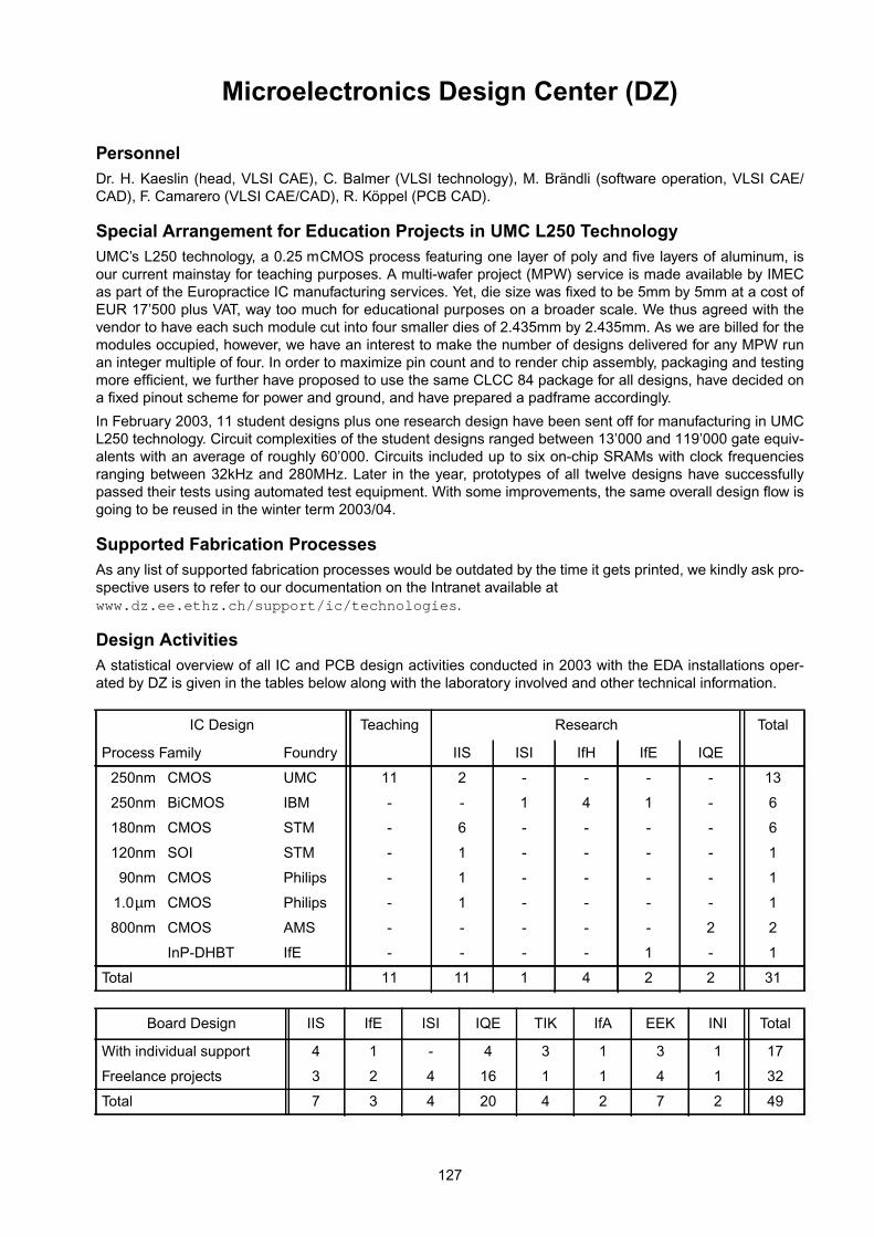
127
Microelectronics Design Center (DZ)
PersonnelDr. H. Kaeslin (head, VLSI CAE), C. Balmer (VLSI technology), M. Brändli (software operation, VLSI CAE/CAD), F. Camarero (VLSI CAE/CAD), R. Köppel (PCB CAD).
Special Arrangement for Education Projects in UMC L250 TechnologyUMC’s L250 technology, a 0.25 mCMOS process featuring one layer of poly and five layers of aluminum, isour current mainstay for teaching purposes. A multi-wafer project (MPW) service is made available by IMECas part of the Europractice IC manufacturing services. Yet, die size was fixed to be 5mm by 5mm at a cost ofEUR 17’500 plus VAT, way too much for educational purposes on a broader scale. We thus agreed with thevendor to have each such module cut into four smaller dies of 2.435mm by 2.435mm. As we are billed for themodules occupied, however, we have an interest to make the number of designs delivered for any MPW runan integer multiple of four. In order to maximize pin count and to render chip assembly, packaging and testingmore efficient, we further have proposed to use the same CLCC 84 package for all designs, have decided ona fixed pinout scheme for power and ground, and have prepared a padframe accordingly.
In February 2003, 11 student designs plus one research design have been sent off for manufacturing in UMCL250 technology. Circuit complexities of the student designs ranged between 13’000 and 119’000 gate equiv-alents with an average of roughly 60’000. Circuits included up to six on-chip SRAMs with clock frequenciesranging between 32kHz and 280MHz. Later in the year, prototypes of all twelve designs have successfullypassed their tests using automated test equipment. With some improvements, the same overall design flow isgoing to be reused in the winter term 2003/04.
Supported Fabrication ProcessesAs any list of supported fabrication processes would be outdated by the time it gets printed, we kindly ask pro-spective users to refer to our documentation on the Intranet available atwww.dz.ee.ethz.ch/support/ic/technologies.
Design ActivitiesA statistical overview of all IC and PCB design activities conducted in 2003 with the EDA installations oper-ated by DZ is given in the tables below along with the laboratory involved and other technical information.
IC Design Teaching Research Total
Process Family Foundry IIS ISI IfH IfE IQE
250nm CMOS UMC 11 2 - - - - 13
250nm BiCMOS IBM - - 1 4 1 - 6
180nm CMOS STM - 6 - - - - 6
120nm SOI STM - 1 - - - - 1
90nm CMOS Philips - 1 - - - - 1
1.0µm CMOS Philips - 1 - - - - 1
800nm CMOS AMS - - - - - 2 2
InP-DHBT IfE - - - - 1 - 1
Total 11 11 1 4 2 2 31
Board Design IIS IfE ISI IQE TIK IfA EEK INI Total
With individual support 4 1 - 4 3 1 3 1 17
Freelance projects 3 2 4 16 1 1 4 1 32
Total 7 3 4 20 4 2 7 2 49
128
Joint Research Cooperation with IT’ISFoundation for Research on Information Technologies in Society IT’IS
ProfileThe Foundation for Research on Information Tech-nologies in Society (IT’IS) was founded on Novem-ber 15th, 1999 through the initiative and support ofthe Swiss Federal Institute of Technology in Zurich(ETHZ), the global wireless communications indus-try, and several governmental agencies. The aimwas to create a flexible and dynamic research insti-tution capable of addressing the research needs ofsociety in the explosively expanding field of infor-mation technologies. Some of the areas encom-passed are:
• evaluation of the safety and risks related to cur-rent and emerging information technologies
• exploration of information technologies for medi-cal, diagnostic, and life support systems
• improvement of the accessibility of informationtechnologies for all members of society includingdisabled persons.
IT’IS is committed to the advancement of sciencefor the benefit of society at large and to maintainingstrict independence from any particular interestgroups. These principles are reflected in the foun-dation’s charter as well as the balance of the com-position of its board with distinguished personalitiesfrom science, the public sector, and the global wire-less communications industry. IT’IS is a non-profittax-exempt research organization.
Infrastructure and CooperationIn the start-up phase of the Foundation the mainresearch unit of IT'IS was located in the VAW build-ing of ETH Zurich. In April 2000, IT’IS openedjointly with Schmid & Partner Engineering AG theworld’s most advanced near-field laboratory indowntown Zurich. During 2003, the facility of IT'ISat Zeughausstrasse 43 was more than doubledwith new offices and two new laboratories (a largesemi-anechonic chamber for general near-fieldmeasurements and a reverberation chamber).The closest and most important cooperative tiesthat IT’IS has are with ETH Zurich. An excellentrelationship has been established with the Inte-grated Systems Laboratory. In addition, the IT’ISteam has great experience in multi-disciplinarycooperation through a multitude of projects, result-ing in an international network of over 50 academicand industry research partners in Europe, the USA,and Asia.
Current Research Focus and ProjectsThe current research focus of IT’IS is in the threeareas 1) sensing and computational techniques for
electromagnetic analysis, 2) health risk assess-ment, and 3) health support systems.Area 1) consists of six projects dealing with newsensors and new measurement procedures fortesting the compliance of wireless devices andbase stations with safety limits. A large project con-centrates on extensions and improvements ofFDTD for near-field applications and optics. Thecurrently most important research area is HealthRisk Assessment. This mainly involves the devel-opment, provision, and maintenance of exposuresetups as well as the provision of detailed dosime-try for more than thirty experiments conducted incooperation with biological and medical researchgroups in Switzerland, Europe, USA, China, andJapan. These include in vitro, in vivo, and humanprovocation studies at different mobile communica-tions bands as well as some ELF experiments. Inaddition, IT’IS is conducting basic and review stud-ies for different agencies. In 2003, IT'IS acquiredthe first larger project in "Health Support Systems"and is currently seeking to further expand frontiersof cooperation with medical industry. Furthermore,IT’IS participates in various standardization com-mittees and provides near-field and dosimetricevaluations for governments and industries.In addition to providing research results for govern-mental agencies through participation in standard-ization bodies and providing consultation togovernments, IT’IS also provides courses to mem-bers of the public, industry, and universities.Current research projects are being supported bypublic funds such as those of NIEHS, the Quality ofLife Programme of the European Union, EUREKA,KTI, VERUM Foundation, health agencies, andother governmental institutions. Funding fromindustry comes from major mobile communicationsmanufacturers and service providers as well asfrom smaller companies (see page 25ff).
Foundation for Research on InformationTechnologies in Society IT’ISProf. Dr. Niels KusterDirector IT’IS & Associate Member of the Electrical Engineering Depart-ment of the Swiss Federal Institute of Technology ETH ZürichMail Address & IT'IS Laboratories:Zeughausstrasse 43CH-8004 Zurich, SwitzerlandIT'IS ETH Office:IT’ISETH Zentrum, ETZCH-8092 Zurich, SwitzerlandPhone: +41 1 245 9696, Fax: +41 1 245 9699www: http://www.itis.ethz.ch

129
Workshops and Courses
Schematic Entry and Physical Layout for PCBs
Organized by: Microelectronics Design CenterTrainer: R. KöppelDates: 4 days from April 12 to May 12, 2003Participants: 7
Schematic Entry and Physical Layout for PCBs
Organized by: Microelectronics Design CenterTrainer: R. KöppelDates: 4 days from October 30 to November 20, 2003Participants: 3
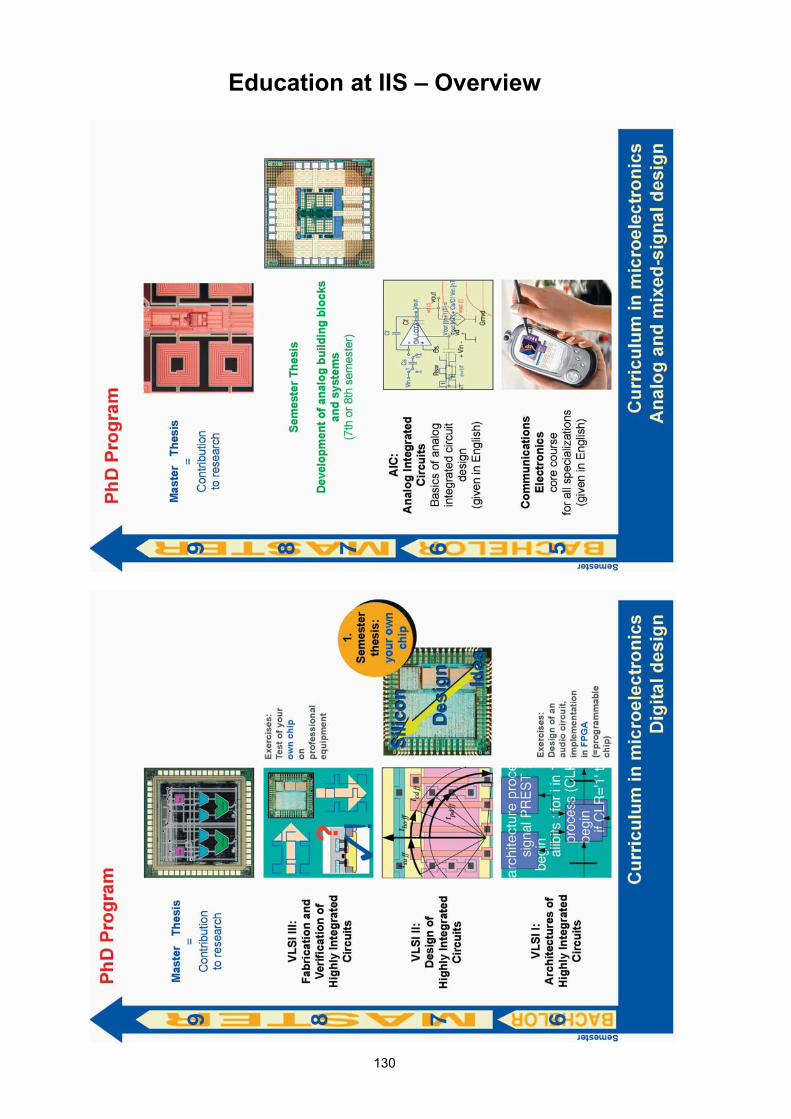
Education at IIS – Overview
130
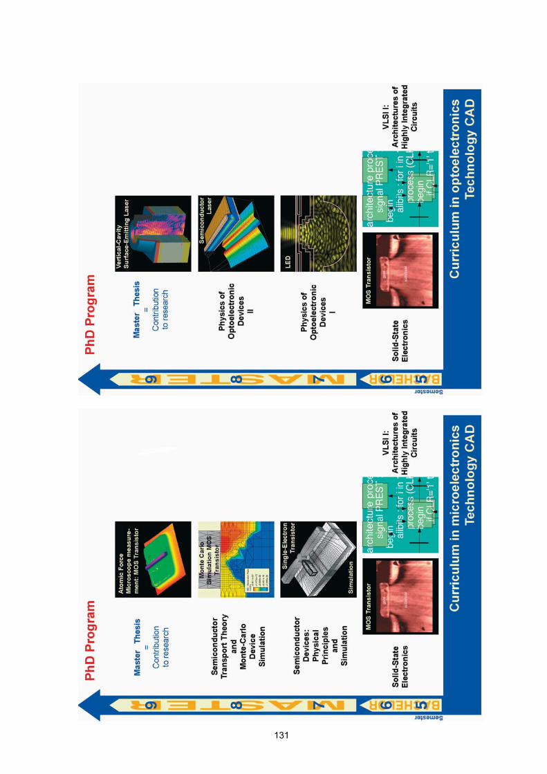
131
Lectures
Halbleiterbauelemente 4th Sem.Semiconductor Devices EE
W. Fichtner
This lecture gives an introduction to the basics of modern semiconductor devices for micro-, opto-, and power-electronics. It bases on semiconductor physics and covers band structures, band models, dispersion rela-tions, statistics, transport equations, macroscopic models, and the characteristics of silicon and other semi-conductors. An overview on device families is presented.
The part on technologies covers the properties of materials, and introduces the steps of modern processtechnologies as well as packaging. To understand the basic principles of devices, ohmic and rectifying con-tacts, physical and electrical characteristics of pn junctions, and types of diodes are explained. The lecturecontinues with the bipolar transistor’s function, working regions, characteristic diagrams, and its simulation.MOS devices are treated based on band diagrams, and the MOSFET behavior is deduced. Power devices,their working regions and static and dynamic behavior are followed by examples of optoelectronic devices asphoto conductor, photodiode, LED, and fiber. Semiconductor measurement and characterization methodsconclude the course.
Kommunikationselektronik 5th Sem.Communications Electronics EE
Q. Huang
This course provides basic design and circuit techniques for communications electronics. As a starting point,bipolar and MOS transistors are reviewed. The discussion of circuit design begins with basic amplifier topolo-gies, impedance matching concepts, and a bit of two-port theory. Important non-ideal aspects such as non-lin-earity and noise are discussed. This sets the ground for more involved topics. Important building blocks ofcommunications equipment, such as mixers and oscillators, are examined in detail. The discussions includethe basic topologies, mathematical descriptions, and a thorough analysis of non-ideal behavior, from whichfinally guidelines for the design can be derived.
The exercises form an integral part of this course. The definitions and concepts presented in the lecture will bereinforced by small design examples, therefore providing a link between the theoretical description and real-world problems.
VLSI I: Architektur von hochintegrierten Schaltungen 6th Sem.VLSI I: Architectures of Highly Integrated Circuits EE/CS/Phys/CSE
N. Felber, W. Fichtner, H. Kaeslin
As becomes clear from the subsequent list of topics, the first course in this series of three is mainly concernedwith system-level issues of VLSI. Terminology, overview on design methodologies and fabrication avenues,levels of abstraction used for circuit description and simulation, VLSI design flow, dedicated VLSI architec-tures, how to obtain an architecture for a given processing algorithm, architectural transformations for meetingthroughput, area, and power requirements. Hardware Description Languages (HDL) and their underlying con-cepts, VHDL for simulation and synthesis, the IEEE-1164 logic system, Register Transfer Level (RTL) synthe-sis. Timing models, Anceau diagrams, functional verification of digital circuits and systems, building blocks ofdigital VLSI circuits, case studies of actual circuits, comparison with microprocessors and DSPs.
During the exercises students learn how to model digital ICs with VHDL. They write testbenches for simulationpurposes and synthesize gate-level netlists for ASICs and FPGAs.
VLSI II: Entwurf von hochintegrierten Schaltungen 7th Sem.VLSI II: Design of Highly Integrated Circuits EE/CS/Phys/CSE
N. Felber, W. Fichtner, H. Kaeslin
The second course begins with a thorough discussion of various technical aspects at the circuit and layoutlevel. It then moves on to economic issues of VLSI. Topics include: limitations of functional design verification,
132

techniques for improving controllability and observability, design for test, block isolation, scan-path techniques,partial scan and its caveats. Evaluation of various synchronous clocking disciplines, skew margins, clock dis-tribution techniques. Asynchronous inputs, data inconsistency and metastability problems, synchronization.Cell libraries, Process-Temperature-Voltage (PTV) variations, transistor models, characteristics of CMOSinverters, complex gates. Power estimation and low-power design. Layout parasitics, transport delay, switch-ing currents, ground bounce, controlling noise problems, power distribution, floorplanning, chip assembly. Lay-out design at the mask level, symbolic layout. Timing verification, physical design verification. Cost structuresof microelectronics design and fabrication, avenues to low-volume fabrication, management of VLSI projects.
Exercises are concerned with physical design and sound engineering practices for avoiding timing, testability,and layout parasitics problems. Industrial CAD tools are being used for place and route, clock tree generation,chip assembly, and physical design verification. Students that elect to carry through a term project at the labo-ratory are offered the opportunity to complete a full IC design cycle on a circuit of their own which gets actuallyfabricated.
VLSI III: Fabrikation und Verifikation von hochintegrierten Schaltungen 8th Sem.VLSI III: Fabrication and Verification of Highly Integrated Circuits EE/CS/Phys/CSE
N. Felber, W. Fichtner, Kaeslin
Whereas the preceding courses deal with design aspects of VLSI circuits, this one addresses manufacturing,testing, physical analysis, and packaging issues, such as: Effects of fabrication defects, abstraction from phys-ical to transistor- and gate-level fault models, fault grading of large ASICs. Generation of efficient test vectorsets, enhancement of testability by built-in self-test techniques. Modern IC testers: Architectures and applica-tion. Deep-submicron CMOS fabrication processes with multi metal levels and the physical analysis of theirdevices. Packaging problems and solutions. Technology outlook.
Exercises teach students how to use CAE/CAD software and automatic test equipment for verifying ASICsafter fabrication. Students that submitted a design for manufacturing at the end of the 7th semester do so ontheir own circuits. Physical analysis methods with professional equipment (AFM, DLTS) complement this train-ing.
Analoge integrierte Schaltungen 6th Sem.Analog Integrated Circuits EE
Q. Huang
This course provides a foundation in analog integrated circuit design: After a review of bipolar and MOSdevices and their small-signal equivalent circuit models, building blocks in analog circuits such as currentsources, active load, current mirrors, supply independent biasing are presented. Other topics are differentialamplifiers, cascode amplifiers, high gain structures, and output stages, and comparators, gain bandwidthproduct and stability of op-amps. Second-order effects in analog circuits such as mismatch, noise, and offsetare investigated. More complex circuits such as A/D and D/A converters, analog multipliers and oscillators areanalyzed. An introduction to switched-capacitor circuits from an IC designer’s point of view is given.
The exercise sessions aim to reinforce the lecture material by well-guided step-by-step design tasks. Cadencedesign tools are used to facilitate the tasks. There is also an experimental session on op-amp measurements.
Festkörperelektronik 5th Sem.Solid State Electronics EE
W. Fichtner
This lecture presents important concepts of modern solid-state physics that form the foundation of today’sdevices, circuits and systems. Its goal is to relate the theoretical concepts to important practical applications.Detailed explanations of the electronic, vibrational, and optical properties of solids, and in particular semicon-ductors, are given. Phenomena related to electronic, optical, magnetic, and temperature effects are exploredin terms of their physical origin. The approach is “physical” and intuitive rather than mathematically formal andpedantic. Special emphasis is given to the physics of modern devices, e.g. optics and transport phenomena inlower dimensional structures. The course also contains several lectures on optical and electronic phenomenain organic materials.
133

Grundlagen der Optoelektronik I 7th Sem.Physics of Optoelectronic Devices I EE
W. Fichtner
This lecture gives an introduction to the physical principles of optoelectronic devices and circuits. An overviewof modern semiconductor devices and circuits, and important physical effects is presented. The physicalbackground on quantum mechanics, quantum electronics, and solid-state physics leads to the physics of het-erostructures. This first course on optoelectronic devices concludes with the interaction of light and matter, thegeneration and detection of photons, and the modulation of light in semiconductors.
Grundlagen der Optoelektronik II 8th Sem.Physics of Optoelectronic Devices II EE
W. Fichtner
This course presents the physical foundations of the operating principles of modern optoelectronic devices. Italso includes an in-depth survey of the material science and technology used today. All modern optoelectronicdevices are treated: photoconductors and -detectors, different photodiodes and avalanche devices, light-emit-ting diodes, members of the growing family of laser diodes (edge-emitting, VCSELs, DFBs, and quantum-cas-cade devices).
Halbleiter-Bauelemente: Physikalische Grundlagen und Simulation 7th Sem.Semiconductor Devices: Physical Principles and Simulation EE/Phys
A. Schenk
This course aims at understanding the principles behind the physics of modern electronic silicon semiconduc-tor devices and the foundations of physical modeling of transport and its numerical simulation. During thecourse basic knowledge on quantum mechanics, semiconductor physics, and device physics is also provided.The main topics are: Transport models for semiconductor devices (quantum transport, Boltzmann equation,drift-diffusion model, hydrodynamic model), physical characterization of silicon (intrinsic properties, band gapnarrowing, scattering processes), mobility of cold and hot carriers, recombination (SRH statistics, lifetimes fortunnel-assisted transitions), interband tunneling (Zener diode), impact ionization, metal-semiconductor con-tact, MIS structure, and heterojunctions.
The exercises focus on the theory and the basic understanding of special devices, such as pn-diodes, bipolartransistors, MOSFETs, and thyristors. Numerical simulations of these devices with an advanced simulationpackage are compared with corresponding measurements, which are also part of the exercises.
Halbleitertransporttheorie und Monte-Carlo Bauelementsimulation 8th Sem.Semiconductor Transport Theory and Monte-Carlo Device Simulation EE/CSE
F. Bufler, A. Schenk
The aim of the course is, on the one hand, to establish the link between microscopic physics and its concreteapplication in device simulation and, on the other hand, to introduce the numerical techniques involved. Thescope encompasses therefore the basics of quantum mechanics, transport theory, and the Monte-Carlomethod for the solution of the Boltzmann transport equation. The topics include second quantization, crystalsymmetries, band structure calculation, phonons, Boltzmann equation, probability calculus, Monte-Carlo tech-niques, and device simulation.
The exercises comprise problems to illustrate the contents of the lecture, simple Monte-Carlo related pro-gramming tasks as well as the application of various professional tools for device simulation.
Elektrotechnik I 3rd Sem.Electrical Engineering I MPE
Q. Huang
This course provides the basic foundation in the specific field of electrical engineering. Starting from the basicconcepts of voltage and currents, it covers the basic analyses of DC and AC networks. This includes seriesand parallel circuits, resistive circuits, circuits including capacitors and inductors, as well as the Kirchhoff’s
134
laws governing such circuits, and other network theorems. Transient response of RC-circuits, analysis of res-onant circuits, concept of filtering, and simple filter circuits are all among the subjects covered in this course.
The understanding of the basic concepts of electrical engineering, particularly of circuit theory, shall beadvanced. At the end of the course, the successful student knows the basic elements of electric circuits andthe basic laws and theorems for determining voltages and currents in circuits with such elements. He/she isalso familiar with basic circuit calculations.
Abbreviations:
CS Computer ScienceCSE Computational Science and EngineeringEE Electrical EngineeringMPE Mechanical and Process EngineeringPhys Physics
135

IC Design Projects – Overview
2003: Project: Status:
VLSI Implementation of a Sphere Decoder Core for MIMO Detection student project /
Viterbi Decoder for Wireless Lan student project /
Complex Matrix QR Decomposition for Inversion student project /
Power- and Performance-Optimized Complex-Number-Arithmentic ALU student project /
VLIW Complex DSP Specification and Architecture student project c
Video Blue/Green Compositing Chip student project /
CohereChip: Coprocessor ASIC for Virtual 3D Audio student project /
192kHz Asynchronous Sample Rate Converter student project /
Stereo Digital Audio Preamplifier student project /
Multichannel Digital Audio Preamplifier student project /
Digital Noise Generator for Audio Measurements student project /
18bit 48kHz Sigma-Delta Modulator for Audio student project t
Oversampled Pipeline ADC with Mismatch Shaping student project ~
14bit Current-Steering DA Converter student project c
Programmable Base-Band Filter I for Multistandard Wireless Receiver student project c
Programmable Base-Band Filter II for a Multi-Standard Wireless Receiver student project c
RF Power Detector student project c
SOLARIS: High-Order, Low-Latency Convolution Processor ASIC diploma project /
DPA-Resistant Crypto Chip Design diploma project /
Adaptive Sampling Rate and Digital to Analog Converter diploma project +
Linear RF Amplifier with Large Gain Control Range research project /
25Ms/s 14bit 200mW Sigma-Delta Modulator research project +
Resonant Clock Audio FIR Filter research project /
Clocking Schemes for Audio FIR Filter research project /
Sigma-Delta DAC with Semidigital Reconstruction Filtering research project +
200Ms/s 14bit DAC with Background Calibration research project +
Oversampled Sigma-Delta ADC for multistandard wireless research project ~
136

2002: Project: Status:
Reconfigurable Instruction Set Processor student project +
Calculation of π student project +
Digital Audio Mixer student project +
Stereopsis – Stereo Vision Based Depth Visualization student project ~
Area-Optimized AES Cipher student project +
Transparent IDE Encryption and Decryption student project +
Altitude Profile Meter student project +
Virtual Component for an 8-bit Microcontroller student project +
MIDI Synthesizer student project +
Programmable Code Generators for SW Radio student project +
FireWire Link Layer Controller student project +
Continuos-Time Σ∆ Modulator for GSM Speech Coding diploma project –
24-bit A/D Converter for High-Quality Audio diploma project t
Σ∆ A/D Converters for Cellular Radio Frequency diploma project /
USB Audio Sample Rate Converter and DAC with Clock Recovery diploma project ~
Oversampled Pipeline ADC with Mismatch Shaping for a MIMO Receiver diploma project ~
14-bit 200Msample/s D/A Converter with Background Calibration research project +
Broadband Sigma-Delta D/A Converter research project +
10GHz Voltage-Controlled Oscillator and Prescaler research project +
4GHz Integer-N Frequency Synthesizer research project ~
2GHz 0.12µm CMOS Transceiver for UMTS research project +
Electro Cardiogram ASIC research project +
Test Integration for GALS Pausable Oscillators: OSCAR research project +
GALS Bus Chip research project +
Digitally Controlled Oscillator research project +
Digitally Controlled Oscillator – Redesign research project +
Multimedia Network SoC research project +
Test Chip for Audio Applications research project +
Status Marks:
+ successfully tested design / chip in fabrication
~ functioning, but with minor bugs • design project in progress
– severe design errors t chip under test
n not submitted to integration (not implemented) T design for test structures
c contribution to research or industrial chip p process errors
137
Research Projects – Overview
IC and System Design and Test
Subject: Real-Time MIMO OFDM Systems for High Speed Broadband Wireless Access
Partner: Communication Technology Laboratory, ETH Zürich, Zürich (Switzerland)Period: July 02 – June 05Funding, Number: ETH Zürich, Zürich (Switzerland), TH-6 02-2
Subject: Lehre und Forschung in Mikroelektronik(Education and Research in Microelectronics)
Period: April 99 – April 04Funding, Number: ETH Zürich, Zürich (Switzerland), TH LF 99-01
Subject: Testable Low-Power Architectures for Multistandard Radio Systems
Partner: Philips Zürich AG Semiconductors, Zürich (Switzerland)Period: August 00 – June 03Funding, Number: KTI*, 4897.1 NMS
Philips Zürich AG Semiconductors, Zürich (Switzerland)
Subject: Energy-Efficient Processing of Speech Data
Partner: Bernafon AG, Bern (Switzerland)Period: August 00 – October 03Funding, Number: KTI*, 5025.1 NMS
Bernafon AG, Bern (Switzerland)
Subject: Netzwerkprozessor für LAN/WAN Bridging im Umfeld professionellerMultimedia Content Produktionen 2(Network Processor for LAN/WAN Bridging in the Environment ofProfessional Multimedia Content Productions 2)
Partner: BridgeCo AG, Dübendorf (Switzerland)Computer Engineering and Networks Laboratory, ETH Zürich, Zürich (Switzerland)
Period: May 02 – April 04Funding, Number: KTI*, 5845.1 NMS
BridgeCo AG, Dübendorf (Switzerland)
Subject: Micropower Circuits for Digital Hearing Aids
Partner: Bernafon AG, Bern (Switzerland)Period: November 03 – October 05Funding, Number: KTI*, 6695.2 NMS
Bernafon AG, Bern (Switzerland)
Subject: GALS 2 Towards Practical GALS Circuits
Partner: Infineon Technologies AG, München (Germany)Period: April 01 – April 04Funding, Number: Infineon Technologies AG, München (Germany), 401
138
Subject: An Integrated Wideband-MIMO Receiver for Wireless MultimediaCommunication 2
Partner: Lucent Technologies, Holmdel (USA)Period: March 02 – February 03Funding, Number: Lucent Technologies, Holmdel (USA), -
Analog and Mixed-Signal Design
Subject: OTRACOM – Optimization of Highly Linear Low-Power Transmitters forThird-Generation Mobile Communications
Partner: Philips Zürich AG Semiconductors, Zürich (Switzerland)Period: March 02 – August 04Funding, Number: KTI*, 5731.1 NMS
Philips Zürich AG Semiconductors, Zürich (Switzerland)
Subject: CMOS (SOI) for Low Power RF Wireless
Partner: ACP AG, Zürich (Switzerland)Period: January 03 – December 05Funding, Number: KTI*, 6148.1 NMS
Subject: CITE – Critical Circuit Technologies for Flexible Mobile Receivers
Partner: Philips Zürich AG Semiconductors, Zürich (Switzerland)Period: July 03 – June 05Funding, Number: KTI*, 6171.2 NMS
Subject: OREMO – Optimized Receivers for Mobile Communications
Partner: ACP AG, Zürich (Switzerland)Period: November 03 – April 06Funding, Number: KTI*, 6767.1 NMS
ACP AG, Zürich (Switzerland)
Technology CAD
Subject: MAGIC_FEAT – Meshes and Global Integration for SemiconductorFront-End Simulation(European IST Project)
Partner: Fraunhofer-Institut für Integrierte Schaltungen,Bauelementetechnologie, Erlangen (Germany)Institut National de Recherche en Informatique et Automatique (INRIA),Le Chesnay (France)ST Microelectronics, Gentilly (France)Technical University of Vienna, Wien (Austria)ISE Integrated Systems Engineering AG, Zürich (Switzerland)
Period: January 00 – March 03Funding, Number: BBW*, European Union, IST 1999-11433
139
Subject: NANOTCAD – Nanotechnology Computer Aided Design(European IST Project)
Partner: Universita degli studi di Pisa, Pisa (Italy)National Microelectronics Research Centre, Cork (Ireland)Max-Planck-Institut für Festkörperforschung, Stuttgart (Germany)Technical University Vienna, Institute for Microelectronics, Wien (Austria)Bayerische Julius-Maximilians-Universität Würzburg, Würzburg (Germany)
Period: April 00 – July 03Funding, Number: BBW*, European Union, IST 1999-10828
Subject: UPPER+ – User Group for Process Simulation European Research+ Device Simulation(European IST Project)
Partner: Fraunhofer-Institut für Integrierte Schaltungen, Erlangen (Germany)austriamicrosystems AG, Unterpremstätten (Austria)Infineon Technologies AG, München (Germany)Philips Research Leuven, Leuven (Belgium)STMicroelectronics SA, Crolles (France)STMicroelectronics Srl, Agrate Brianza (Italy)ISE Integrated Systems Engineering AG, Zürich (Switzerland)SIGMA-C, München (Germany)Institut für Microelektronik, Technische Universität Wien, Wien (Austria)
Period: July 02 – June 04Funding, Number: BBW*, European Union, IST 2001-37903
Subject: Large Scale Eigenvalue Problems in Opto-Electronic Semiconductor Lasersand Accelerator Cavities
Partner: Institute for Scientific Computing, ETH Zürich, Zürich (Switzerland)Department of Computer Science, University Basel, Basel (Switzerland)Paul Scherrer Institute, Villigen (Switzerland)
Period: January 2003 – December 2004Funding, Number: “Strategic Excellence Projects” (SEP): Computational Science and Engineering
(CSE)ETH Zürich, TH-1 02-4
Subject: Iterative Methoden zur parallelen Lösung grosser linearer Gleichungssystemeaus der Halbleiter-Simulation(Iterative Methods for Parallel Solving of Large Linear Systems fromSemiconductor Simulation)
Partner: ISE Integrated Systems Engineering AG, Zürich (Switzerland)Period: July 00 – January 03Funding, Number: KTI*, 4922.1
ISE Integrated Systems Engineering AG, Zürich (Switzerland)
Subject: VCSELs – Numerical Simulation of Vertical-Cavity Surface-Emitting LaserDiodes
Partner: ISE Integrated Systems Engineering AG, Zürich (Switzerland)Pilot User: Institute for Micro- and Nanoelectronics, EPF Lausanne, Lausanne (Switzerland)
Avalon Photonics AG, Zürich (Switzerland)Laboratory for Electromagnetic Fields and Waves, ETH Zürich, Zürich (Switzerland)Walter Schottky Institut, TU München, Garching (Germany)
Period: Oktober 00 – September 03Funding, Number: TOP NANO 21, 5103.1 TNS
ISE Integrated Systems Engineering AG, Zürich (Switzerland)
140

Subject: Large and Small Signal Analysis Methods for Physical SemiconductorDevices – Harmonic Balance and Optical AC Analysis (LASSIS)
Partner: ISE Integrated Systems Engineering AG, Zürich (Switzerland)Period: June 03 – Mai 06Funding, Number: KTI*, 6378.1 NMS
ISE Integrated Systems Engineering AG, Zürich (Switzerland)
Subject: Simulation and Design of High Performance Semiconductor OpticalAmplifiers and Superluminescent Light Emitting Diodes (SOA – SLED)
Partner: Exalos AG, Zürich (Switzerland)ISE Integrated Systems Engineering AG, Zürich (Switzerland)
Period: November 03 – October 06Funding, Number: KTI*, 6429.1 NMS
ISE Integrated Systems Engineering AG, Zürich (Switzerland)
Subject: Parametric Design and Analysis for Semiconductor Technology ComputerAided Design (PARA–TCAD)
Partner: ISE Integrated Systems Engineering AG, Zürich (Switzerland)Period: November 03 – October 05Funding, Number: KTI*, 6650.2 NMS
ISE Integrated Systems Engineering AG, Zürich (Switzerland)
Subject: Improvement of Semiconductor Process Simulator by Atomistic SimulationTechniques (MOLDYN)
Partner: ISE Integrated Systems Engineering AG, Zürich (Switzerland)Period: January 02 – December 04Funding, Number: TOP NANO 21, 5779.1 TNS
ISE Integrated Systems Engineering AG, Zürich (Switzerland)
Subject: High Speed and Quantum-Well Photodetectors
Partner: Albis Optoelectronics AG, Zürich (Switzerland)ISE Integrated Systems Engineering AG, Zürich (Switzerland)
Period: June 02 – Mai 05Funding, Number: TOP NANO 21, 5782.1 TNS
ISE Integrated Systems Engineering AG, Zürich (Switzerland)
Subject: Modeling of General Multi-Quantum-Well Structures Including Self-ConsistentCoupling to a Laser Simulator (MQW)
Partner: Bookham (Schweiz) AG, Zürich (Switzerland)ISE Integrated Systems Engineering AG, Zürich (Switzerland)
Period: January 02 – March 05Funding, Number: TOP NANO 21, 5785.1 TNS
ISE Integrated Systems Engineering AG, Zürich (Switzerland)
Subject: Analysis and Simulation of SOI MOSFET Semiconductor Technology
Partner: Fujitsu Laboratories Ltd., Tokyo (Japan)Period: October 02 – March 03Funding, Number: Fujitsu Laboratories Europe, Hayes (UK), -
Subject: Analysis and Simulation of SOI MOSFET Semiconductor Technology 2
Partner: Fujitsu Laboratories Ltd., Tokyo (Japan)Period: April 03 – March 04Funding, Number: Fujitsu Laboratories Europe, Hayes (UK), -
141
Physical Characterization and Technology Development
Subject: HERCULAS – High Resolution Electrical Characterization of ULSI andAdvanced Semiconductor Devices(European IHP–RTN Project)
Partner: Interuniversity Microelectronics Centre (IMEC), Leuven (Belgium)Hahn-Meitner-Institut Berlin GmbH, Berlin (Germany)STMicroelectronics SA, Crolles (France)Philips Electronics Nederland B.V., Eindhoven (The Netherlands)Universität Hamburg, Hamburg (Germany)Infineon Technologies AG, München (Germany)Consiglio Nationale di Metodolgie e Tecnologie per la Microelettronica(CNR-IMETEM), Catania (Italy)Kungl Tekniska Högskolan, Kista (Sweden)Institute for Semiconductor Physics, Frankfurt (Germany)Tel-Aviv University, Tel-Aviv (Israel)
Period: Oktober 00 – March 04Funding, Number: BBW*, European Union, RTN 1-1999-004
Subject: HIMRATE – High-Temperature IGBT- and MOSFET-Modules for RailwayTraction and Automotive Electronic Application(European GROWTH Project)
Partner: Siemens AG, München (Germany)Regienov – Renault Recherche et Innovation, Guyancourt (France)Institut National de Recherche sur les Transport et leur Sécuruité (INRETS),Arcueil (France)Centro Ricerche Fiat ScpA, Orbassano (Italy)EUPEC GmbH & Co. KG, Warstein (Germany)Ferraz Date Industries S.A., La Mure (France)Electrovac Fabrikation Elektrotechnischer Spezialartikel GmbH,Klosterneuburg (Germany)Infineon Technologies AG, München (Germany)Ansaldo Transporti SpA, Napoli (Italy)Technical University Vienna, Wien (Austria)Technische Universität München, München (Germany)
Period: November 00 – Oktober 03Funding, Number: BBW*, European Union, GRD 1-2000-25092
Subject: DEMAND – Integrated Design Methodology for Enhanced Device Robustness(European IST Project)
Partner: Infineon Technologies AG, München (Germany)Technical University of Vienna, Wien (Austria)Uni Bologna, Universita degli Studi di Bologna, Dipartimento di ElettronicaInformatica e Sistemistica, Bologna (Italy)ISE Integrated Systems Engineering AG, Zürich (Switzerland)
Period: September 01 – August 04Funding, Number: BBW*, European Union, IST-2000-37903
Subject: ASDESE – Application Specific Design for ESD and Substrate Effects
Partner: Robert Bosch GmbH, Reutlingen (Germany)Period: September 01 – February 03Funding, Number: Robert Bosch GmbH, Reutlingen (Germany), -
German Government, -
142
Subject: SP3M – Scanning Probe Microscopy Assisted Modeling in Microelectronics(Part 2)
Period: July 01 – June 03Funding, Number: SNF*, 2060-64539
Bio Electromagnetics and Electromagnetic Compatibility
Subject: REFLEX – Risk Evaluation of Potential Environmental Hazards from LowEnergy Electromagnetic Field Exposure Using Sensitive In Vitro Methods(European IST Project)
Partner: Stiftung für Verhalten und Umwelt (VERUM), München (Germany)Universitätsklinikum Benjamin Franklin der freien Universität Berlin,Berlin (Germany)Universitätsklinik für Innere Medizin IV Klinische Abteilung Arbeitsmedizin,Wien (Austria)Institut für Pflanzengenetik und Kulturpflanzenforschung Gatersleben,Gatersleben (Germany)Investigacion Bioelectromagnetismo Hospital Ramon y Cajal, Madrid (Spain)STUK Helsinki – Radiation and Nuclear Safety Authority, Helsinki (Finland)Institut für Biophysik Universität Hannover, Hannover (Germany)Universita degli Studi di Bologna Dipartimento di Fisica, Bologna (Italy)Ecole Nationale Supérieure de Chimie et de Physique de Bordeaux,Talence (France)Universita degli Studi di Milano, Milano (Italy)
Period: February 00 – August 03Funding, Number: BBW*, European Union, CT-1999-01574
Subject: SEMCAD++: Extension/Improvement of the TCAD Engine SEMCAD forAntenna/EMC
Partner: Foundation for Research on Information Technologies in Society (IT’IS),Zürich (Switzerland)Schmid & Partner Engineering AG, Zürich (Switzerland)ISE Integrated Systems Engineering AG, Zürich (Switzerland)
Period: April 00 – March 03Funding, Number: KTI*, 4789.1 KTS
IT’IS, Zürich (Switzerland)Schmid & Partner Engineering AG, Zürich (Switzerland)
Subject: TD Sensor
Partner: Foundation for Research on Information Technologies in Society (IT’IS),Zürich (Switzerland)Schmid & Partner Engineering AG, Zürich (Switzerland)
Period: November 02 – December 03Funding, Number: KTI*, 6091.1 KTS
Schmid & Partner Engineering AG, Zürich (Switzerland)
143
Subject: ULTRACOM: Channel Model of the Human Body for Medical MonitoringSystems
Partner: Miromico AG, Zürich (Switzerland)Foundation for Research on Information Technologies in Society (IT’IS),Zürich (Switzerland)University Hospital, University Bern , Bern (Switzerland)
Period: October 03 – March 05Funding, Number: KTI*, 6454.3 NMS
Miromico AG, Zürich (Switzerland)
Subject: Definieren der Messmethodik und Verkleinern der Messunsicherheit beiImmissionsmessungen in Wohn- und Geschäftshäusern(Definition of Measurement Methodology and Reduction of MeasurementUncertainty of Electromagnetic Field Measurements in Living and BusinessRooms)
Partner: Foundation for Research on Information Technologies in Society (IT’IS),Zürich (Switzerland)
Period: August 00 – March 04Funding, Number: FNM, Zürich (Switzerland), 1-00-4
Subject: Forschungskooperation IT’IS – ETH Zürich(Research Cooperation IT’IS – ETH Zürich)
Partner: Foundation for Research on Information Technologies in Society (IT’IS),Zürich (Switzerland)
Period: since January 00Funding, Number: IT’IS, Zürich (Switzerland), -
Abbreviations
BBT Federal Office for Professional Education and Technology(a Swiss Government Agency)
BBW Federal Office for Education and Science(a Swiss Government Agency)
KTI Commission for Technology and Innovation(a Swiss Government Agency)
SNF Swiss National Science Foundation
TOP NANO 21 Technology Oriented Program for Nano Sciences(Research and Technical Development Cooperations between Swiss Universities,Institutes, and Swiss Enterprises, funded by the Swiss Government)
144

Presentations
2003
P. Achermann, R. Huber, J. Schuderer, N. Kuster, A. Borbély“Effects of Exposure to Electromagnetic Fields of Type GSM on Sleep EEG and Regional Cerebral BloodFlow“,15th International Zurich Symposium and Technical Exhibition on Electromagnetic Compatibility, Supplement,Zurich, Switzerland, 2003.
F. Adlkofer, R. Tauber, H. W. Rüdiger, A. M. Wobus, A. Trillo, D. Leszczynski, H. A. Kolb, F. Bersani,O. Lagroye, N. Kuster, F. Clementi, C. Maercker“Risk Evaluation of Potential Environmental Hazards from Low Energy Electromagnetic Field Exposure UsingSensitive In Vitro Methods REFLEX“,International EMF Seminar in China: Electromagnetic Fields and Biological Effects, Guilin, China, Oct. 23,2003.
V. Berdiñas Torres, J. Fröhlich, A. Klingenböck, N. Nikoloski, N. Kuster“Relevant Exposure Parameters for the Comparison of Animal Studies“,International Congress of the European Bioelectromagnetics Association (EBEA), Budapest, Hungary, Nov.2003.
T. Boesch, E. Roth, M. Thalmann, N. Felber, W. Fichtner“A SoC for Multimedia Network Devices”,International Conference on Consumer Electronics, Los Angeles, CA, USA, June 17-19, 2003.
G. Brenna, D. Tschopp, Q. Huang“Carrier Leakage Suppression in Direct-Conversion WCDMA Transmitters”,2003 IEEE ISSCC Conference, Digest of Technical Papers, Feb. 2003.
F. M. Bufler, A. Schenk, W. Fichtner“Monte Carlo, Hydrodynamic and Drift-Diffusion Simulation of Scaled Double-Gate MOSFETs”,9th International Workshop on Computational Electronics (IWCE-9), Rome, Italy, May 26, 2003.
F. M. Bufler, A. Schenk, W. Fichtner“Strained-Si Single-Gate Versus Unstrained-Si Double-Gate MOSFETs”,13th International Conference on Nonequilibrium Carrier Dynamics in Semiconductors (HCIS-13),Modena, Italy, July 29, 2003.
F. M. Bufler“Monte Carlo Simulation as the Solution Method of the Boltzmann Transport Equation,SPARTA–Single-PARTicle Approach to Self-Consistent Monte Carlo Device Simulation andHow to Use SPARTA”,TSMC visit at ISE Integrated Systems Engineering AG, Zurich, Switzerland, Aug. 13, 2003.
F. M. Bufler“Strained Si”,TSMC visit at ISE Integrated Systems Engineering AG, Zurich, Switzerland, Aug.14, 2003.
A. Burg, F. Gürkaynak, H. Kaeslin, W. Fichtner“Variable Delay Ripple Carry Adder with Carry Chain Interrupt Detection”,IEEE ISCAS 2003, Bangkok, Thailand, 2003.
A. Burg, M. Rupp, D. Perels, S. Häne, N. Felber, W. Fichtner“Performance of MIMO-Extended UMTS-FDD Downlink Comparing Space-Time Rake and Linear Equalizer”,IEEE VTC-Fall 2003, Orlando, FL, USA, 2003.
A. Burg, M. Rupp, D. Perels, S. Häne, N. Felber, W. Fichtner“Low Complexity Frequency Domain Equalization of MIMO Channels with Applications to MIMO-CDMA Sys-tems”,IEEE VTC-Fall 2003, Orlando, FL, USA, 2003.
145

A. Burg, M. Rupp, N. Felber, W. Fichtner“Practical Low Complexity Linear Equalization for MIMO-CDMA Systems”,IEEE 35th Asilomar Conference on Signals,Systems and Computers, Pacific Grove, CA, USA, 2003.
A. Burg, N. Felber, W. Fichtner“A 50 Mbps Maximum Likelihood Decoder for Multiple-Input Multiple-Output Systems with QPSK Modulation”,IEEE ICECS 2003, Sharjah, U.A.E., 2003.
F. Carbognani“Lifetime Prediction and Design of Reliability Tests for High-Power Devices in Automotive Applications”,IEEE International Reliability Physics Symposium, Dallas, TX, USA, Apr. 3, 2003.
N. Chavannes“Latest RF Design Tools for Analysis and Design of Mobile Telecommunications Equipment”,Technical Seminar at Nokia Research Center (NRC), Helsinki, Finland, June 2, 2003.
A. Christ“Suitability and Limitations of Numerical Simulations for the Assessment of Probe Calibration Parameters”,25th Annual Meeting of the Bioelectromagnetics Society, Maui, HI, USA, June 2003.
A. Christ“EMF Exposure by On-Body Mounted Devices”,International Congress of the European Bioelectromagnetics Association (EBEA), Budapest, Hungary, 2003.
M. Ciappa“Reliability of High-Power Devices” (Invited Tutorial),European Conference on Power Electronics and Applications (EPE), Toulouse, France, Sept. 2, 2003.
M. Ciappa“Reliability of High-Power Devices” (Invited Tutorial),15th European Symposium on Reliability of Electron Devices Failure Physics and Analysis (ESREF), Bor-deaux, France, Oct. 7, 2003.
M. Ciappa, F. Carbognani, W. Fichtner“Lifetime Prediction and Design of Reliability Tests for High-Power Devices in Automotive Applications”,IEEE International Reliability Physics Symposium (IRPS), 2003.
M. Ciappa, F. Carbognani, W. Fichtner“Lifetime Modeling of Thermomechanics-Related Failure Mechanisms in High-Power IGBT Modules for Trac-tion Applications”,IEEE International Symposium on Power Semiconductor Devices & ICs (ISPSD), 2003.
C. Dasenbrock, P. Smith, N. Kuster“Carcinogenicity Studies in Rodents of Radiofrequency Related to Mobile Phones and Base Stations“,25th Annual Meeting of the Bioelectromagnetics Society, Maui, HI, USA, June 2003.
C. Dasenbrock, R. Hruby, G. Oberto, P. Smith, N. Kuster“Status of Perform-A: Co- and Carcinogenicity Studies in Rodents on Radiofrequency Related to Mobile Tele-phones and Base Stations“,International Congress of the European Bioelectromagnetics Association (EBEA), Budapest, Hungary, Nov.2003.
N. Duhayon, P. Eyben, M. Fouchier, T. Clarysse, W. Vandervorst, D. Alvarez, S. Schoemann, M. Ciappa,M. Stangoni, W. Fichtner, P. Formanek, V. Raineri, F. Giannazzo, D. Goghero, Y. Rosenwaks, R. Shikler,S. Saraf, S. Sadewasser, N. Barreau, T. Glatzel, M. Verheijen, S. A. M. Mentink, M. von Sprekelsen,T. Maltezopoulos, R. Wiesendanger, L. Hellemans“Assessing the Performance of Two Dimensional Dopant Profiling Techniques”,Ultra Shallow Junctions 2003, 2003.
S. Ebert, J.-C. Gröbli, N. Kuster“Mobile Exposure Setup for Human Provocative Studies at 900 MHz“,25th Annual Meeting of the Bioelectromagnetics Society, Maui, HI, USA, June 2003.
146
S. J. Eom, J. Fröhlich, N. Nikoloski, N. Kuster“An Exposure System for Behavioral Studies with a Small Number of Mice at 905 MHz“,25th Annual Meeting of the Bioelectromagnetics Society, Maui, HI, USA, June 2003.
M. Etherton, J. Willemen, W. Wilkening, S. Mettler, N. Qu, W. Fichtner“Parameter Extraction Method for ESD Protection Structures in the CDM Time and Current Domain“,ESD-Forum 2003, Munich, Germany, Dec. 9-10, 2003.
J. Fröhlich, V. Berdiñas Torres, J. M. Ladbury, P. F. Wilson, N. Kuster“In Vivo Exposure Systems for Use in Studies with Large Numbers of Rodents at Cellular Telephone Frequen-cies“,25th Annual Meeting of the Bioelectromagnetics Society, Maui, HI, June 2003.
P. Futter“Case Study: Nokia 8310 - NRC - IT'IS Joint Project”,Technical Seminar at Nokia Research Center (NRC), Helsinki, Finland, June 2nd, 2003.
P. Futter“TCAD of Mobile Phones: Heading for a Generic Modeling Approach”,International Congress of the European Bioelectromagnetics Association (EBEA), Budapest, Hungary, 2003.
F. Geelhaar“Coulomb-Korrelationen im Elektron-Loch Plasma: Anwendungen in der Bauelementmodellierung”,SFB-Seminar “Statistische Physik der Plasmen”, University of Rostock, Germany, Oct. 22, 2003.
F. K. Gürkaynak, S. Oetiker, T. Villiger, N. Felber, H. Kaeslin, W. Fichtner“On the GALS Design Methodology at ETH Zurich”,Formal Methods for GALS 2003, (FMGALS2003), Pisa, Italy, 2003.
F. O. Heinz“SIMNAD and the Simulation of Single Electron Devices - A Guided Tour”,12th MEL-ARI NID workshop, Cork, Ireland, June 23-24, 2003.
F. O. Heinz, B. Schmithüsen, A. Schenk, W. Fichtner“A Joint 3D Kohn-Sham / Drift-Diffusion Simulation Approach for Nano-Scale Semiconductor Devices” (InvitedTalk),Workshop on Computational Approaches Towards the Electronics Properties of Quantum Dots, Chicago, IL,USA, Sept. 22-24, 2003.
Q. Huang“System-on-a-Chip” Design Short Course”,Evening Discussion Panel on Fineline Prototyping ISSCC Conference 2003, San Francisco, CA, USA,February 10-13, 2003.
Q. Huang, G. Moschytz“Analog Signal Processing and Related Bipolar and CMOS Circuit Design”,CEI-Europe Short Course, Davos, Switzerland, Mar. 17-21, 2003.
Q. Huang“Transceiver Design for Cellular Wireless Applications”,Southeast University, Nanjing, China, Mar. 24, 2003.
Q. Huang“Phase Noise to Carrier Ratio in LC Oscillators”,National Taiwan University, Taipei, Taiwan, Mar. 26, 2003.
Q. Huang“Transceiver Design for Cellular Wireless Applications”,National Chiao Tung Universtiy, Hsinchu, Taiwan, Mar. 27, 2003.
B. Jacob, P. N. Robson, J. P. R. David and G. J. Rees“Nonlocal Impact Ionization in Submicron Avalanche Photodiodes”,WOCSDICE 2003, Furigen, Switzerland, May 26-28, 2003.
147
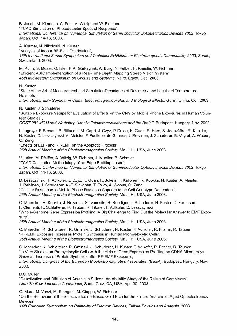
B. Jacob, M. Klemenc, C. Petit, A. Witzig and W. Fichtner“TCAD Simulation of Photodetector Spectral Response”,International Conference on Numerical Simulation of Semiconductor Optoelectronics Devices 2003, Tokyo,Japan, Oct. 14-16, 2003.
A. Kramer, N. Nikoloski, N. Kuster“Analysis of Indoor RF-Field Distribution“,15th International Zurich Symposium and Technical Exhibition on Electromagnetic Compatibility 2003, Zurich,Switzerland, 2003.
M. Kuhn, S. Moser, O. Isler, F. K. Gürkaynak, A. Burg, N. Felber, H. Kaeslin, W. Fichtner“Efficient ASIC Implementation of a Real-Time Depth Mapping Stereo Vision System”,46th Midwestern Symposium on Circuits and Systems, Kairo, Egypt, Dec. 2003.
N. Kuster“State of the Art of Measurement and SimulationTechniques of Dosimetry and Localized TemperatureHotspots“,International EMF Seminar in China: Electromagnetic Fields and Biological Effects, Guilin, China, Oct. 2003.
N. Kuster, J. Schuderer“Suitable Exposure Setups for Evaluation of Effects on the CNS by Mobile Phone Exposures in Human Volun-teer Studies“,COST 281 MCM and Workshop “Mobile Telecommunications and the Brain'”, Budapest, Hungary, Nov. 2003.
I. Lagroye, F. Bersani, B. Billaudel, M. Capri, J. Czyz, P. Dulou, K. Guan, E. Haro, S. Joenväärä, R. Kuokka,N. Kuster, D. Leszczynski, A. Meister, F. Poulletier de Gannes, J. Reivinen, J. Schuderer, B. Veyret, A. Wobus,Q. Zeng“Effects of ELF- and RF-EMF on the Apoptotic Process“,25th Annual Meeting of the Bioelectromagnetics Society, Maui, HI, USA, June 2003.
V. Laino, M. Pfeiffer, A. Witzig, W. Fichtner, J. Mueller, B. Schmidt“TCAD Calibration Methodology of an Edge Emitting Laser”,International Conference on Numerical Simulation of Semiconductor Optoelectronics Devices 2003, Tokyo,Japan, Oct. 14-16, 2003.
D. Leszczynski, F. Adlkofer, J. Czyz, K. Guan, K. Jokela, T. Kallonen, R. Kuokka, N. Kuster, A. Meister,J. Reivinen, J. Schuderer, A.-P. Sihvonen, T. Toivo, A. Wobus, Q. Zeng“Cellular Response to Mobile Phone Radiation Appears to be Cell Genotype Dependent“,25th Annual Meeting of the Bioelectromagnetics Society, Maui, HI, USA, June 2003.
C. Maercker, R. Kuokka, J. Reivinen, S. Ivancsits, H. Ruediger, J. Schuderer, N. Kuster, D. Fornasari,F. Clementi, K. Schlatterer, R. Tauber, R. Fitzner, F. Adlkofer, D. Leszczynski“Whole-Genome Gene Expression Profiling: A Big Challenge to Find Out the Molecular Answer to EMF Expo-sure“,25th Annual Meeting of the Bioelectromagnetics Society, Maui, HI, USA, June 2003.
C. Maercker, K. Schlatterer, R. Gminski, J. Schuderer, N. Kuster, F. Adlkofer, R. Fitzner, R. Tauber“RF-EMF Exposure Increases Protein Synthesis in Human Promyelocytic Cells“,25th Annual Meeting of the Bioelectromagnetics Society, Maui, HI, USA, June 2003.
C. Maercker, K. Schlatterer, R. Gminski, J. Schuderer, N. Kuster, F. Adlkofer, R. Fitzner, R. Tauber“In Vitro Studies on Promyelocytic Cells with the Help of Gene Expression Profiling on CDNA MicroarraysShow an Increase of Protein Synthesis after RF-EMF Exposure“,International Congress of the European Bioelectromagnetics Association (EBEA), Budapest, Hungary, Nov.2003.
D.C. Müller“Deactivation and Diffusion of Arsenic in Sililcon: An Ab Initio Study of the Relevant Complexes”,Ultra Shallow Junctions Conference, Santa Cruz, CA, USA, Apr. 30, 2003.
G. Mura, M. Vanzi, M. Stangoni, M. Ciappa, W. Fichtner“On the Behaviour of the Selective Iodine-Based Gold Etch for the Failure Analysis of Aged OptoelectronicsDevices”,14th European Symposium on Reliability of Electron Devices, Failure Physics and Analysis, 2003.
148
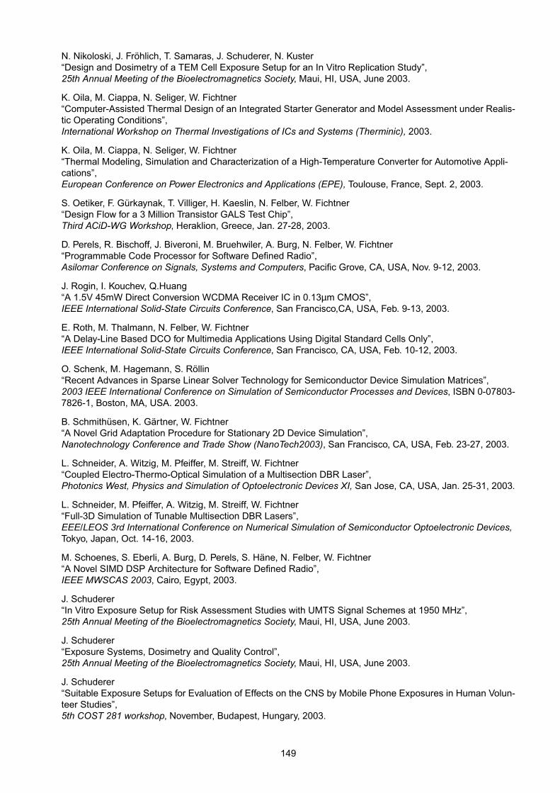
N. Nikoloski, J. Fröhlich, T. Samaras, J. Schuderer, N. Kuster“Design and Dosimetry of a TEM Cell Exposure Setup for an In Vitro Replication Study”,25th Annual Meeting of the Bioelectromagnetics Society, Maui, HI, USA, June 2003.
K. Oila, M. Ciappa, N. Seliger, W. Fichtner“Computer-Assisted Thermal Design of an Integrated Starter Generator and Model Assessment under Realis-tic Operating Conditions”,International Workshop on Thermal Investigations of ICs and Systems (Therminic), 2003.
K. Oila, M. Ciappa, N. Seliger, W. Fichtner“Thermal Modeling, Simulation and Characterization of a High-Temperature Converter for Automotive Appli-cations”,European Conference on Power Electronics and Applications (EPE), Toulouse, France, Sept. 2, 2003.
S. Oetiker, F. Gürkaynak, T. Villiger, H. Kaeslin, N. Felber, W. Fichtner“Design Flow for a 3 Million Transistor GALS Test Chip”,Third ACiD-WG Workshop, Heraklion, Greece, Jan. 27-28, 2003.
D. Perels, R. Bischoff, J. Biveroni, M. Bruehwiler, A. Burg, N. Felber, W. Fichtner“Programmable Code Processor for Software Defined Radio”,Asilomar Conference on Signals, Systems and Computers, Pacific Grove, CA, USA, Nov. 9-12, 2003.
J. Rogin, I. Kouchev, Q.Huang“A 1.5V 45mW Direct Conversion WCDMA Receiver IC in 0.13µm CMOS”,IEEE International Solid-State Circuits Conference, San Francisco,CA, USA, Feb. 9-13, 2003.
E. Roth, M. Thalmann, N. Felber, W. Fichtner“A Delay-Line Based DCO for Multimedia Applications Using Digital Standard Cells Only”,IEEE International Solid-State Circuits Conference, San Francisco, CA, USA, Feb. 10-12, 2003.
O. Schenk, M. Hagemann, S. Röllin“Recent Advances in Sparse Linear Solver Technology for Semiconductor Device Simulation Matrices”,2003 IEEE International Conference on Simulation of Semiconductor Processes and Devices, ISBN 0-07803-7826-1, Boston, MA, USA. 2003.
B. Schmithüsen, K. Gärtner, W. Fichtner“A Novel Grid Adaptation Procedure for Stationary 2D Device Simulation”,Nanotechnology Conference and Trade Show (NanoTech2003), San Francisco, CA, USA, Feb. 23-27, 2003.
L. Schneider, A. Witzig, M. Pfeiffer, M. Streiff, W. Fichtner“Coupled Electro-Thermo-Optical Simulation of a Multisection DBR Laser”,Photonics West, Physics and Simulation of Optoelectronic Devices XI, San Jose, CA, USA, Jan. 25-31, 2003.
L. Schneider, M. Pfeiffer, A. Witzig, M. Streiff, W. Fichtner“Full-3D Simulation of Tunable Multisection DBR Lasers”,EEE/LEOS 3rd International Conference on Numerical Simulation of Semiconductor Optoelectronic Devices,Tokyo, Japan, Oct. 14-16, 2003.
M. Schoenes, S. Eberli, A. Burg, D. Perels, S. Häne, N. Felber, W. Fichtner“A Novel SIMD DSP Architecture for Software Defined Radio”,IEEE MWSCAS 2003, Cairo, Egypt, 2003.
J. Schuderer“In Vitro Exposure Setup for Risk Assessment Studies with UMTS Signal Schemes at 1950 MHz”,25th Annual Meeting of the Bioelectromagnetics Society, Maui, HI, USA, June 2003.
J. Schuderer“Exposure Systems, Dosimetry and Quality Control”,25th Annual Meeting of the Bioelectromagnetics Society, Maui, HI, USA, June 2003.
J. Schuderer“Suitable Exposure Setups for Evaluation of Effects on the CNS by Mobile Phone Exposures in Human Volun-teer Studies”,5th COST 281 workshop, November, Budapest, Hungary, 2003.
149
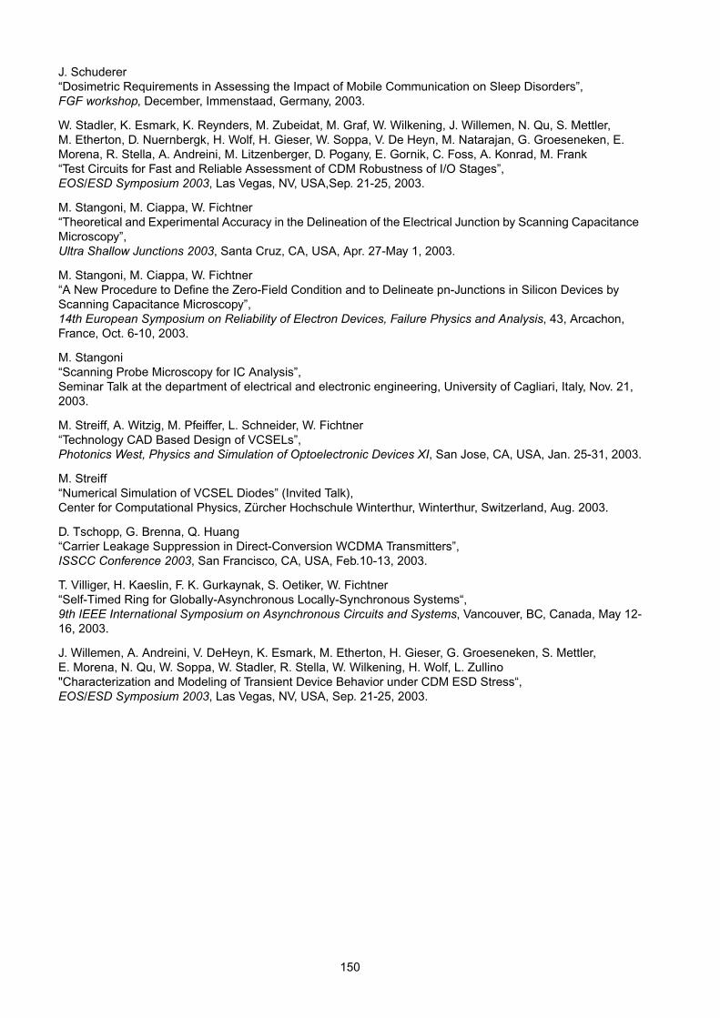
J. Schuderer“Dosimetric Requirements in Assessing the Impact of Mobile Communication on Sleep Disorders”,FGF workshop, December, Immenstaad, Germany, 2003.
W. Stadler, K. Esmark, K. Reynders, M. Zubeidat, M. Graf, W. Wilkening, J. Willemen, N. Qu, S. Mettler,M. Etherton, D. Nuernbergk, H. Wolf, H. Gieser, W. Soppa, V. De Heyn, M. Natarajan, G. Groeseneken, E.Morena, R. Stella, A. Andreini, M. Litzenberger, D. Pogany, E. Gornik, C. Foss, A. Konrad, M. Frank“Test Circuits for Fast and Reliable Assessment of CDM Robustness of I/O Stages”,EOS/ESD Symposium 2003, Las Vegas, NV, USA,Sep. 21-25, 2003.
M. Stangoni, M. Ciappa, W. Fichtner“Theoretical and Experimental Accuracy in the Delineation of the Electrical Junction by Scanning CapacitanceMicroscopy”,Ultra Shallow Junctions 2003, Santa Cruz, CA, USA, Apr. 27-May 1, 2003.
M. Stangoni, M. Ciappa, W. Fichtner“A New Procedure to Define the Zero-Field Condition and to Delineate pn-Junctions in Silicon Devices byScanning Capacitance Microscopy”,14th European Symposium on Reliability of Electron Devices, Failure Physics and Analysis, 43, Arcachon,France, Oct. 6-10, 2003.
M. Stangoni“Scanning Probe Microscopy for IC Analysis”,Seminar Talk at the department of electrical and electronic engineering, University of Cagliari, Italy, Nov. 21,2003.
M. Streiff, A. Witzig, M. Pfeiffer, L. Schneider, W. Fichtner“Technology CAD Based Design of VCSELs”,Photonics West, Physics and Simulation of Optoelectronic Devices XI, San Jose, CA, USA, Jan. 25-31, 2003.
M. Streiff“Numerical Simulation of VCSEL Diodes” (Invited Talk),Center for Computational Physics, Zürcher Hochschule Winterthur, Winterthur, Switzerland, Aug. 2003.
D. Tschopp, G. Brenna, Q. Huang“Carrier Leakage Suppression in Direct-Conversion WCDMA Transmitters”,ISSCC Conference 2003, San Francisco, CA, USA, Feb.10-13, 2003.
T. Villiger, H. Kaeslin, F. K. Gurkaynak, S. Oetiker, W. Fichtner“Self-Timed Ring for Globally-Asynchronous Locally-Synchronous Systems“,9th IEEE International Symposium on Asynchronous Circuits and Systems, Vancouver, BC, Canada, May 12-16, 2003.
J. Willemen, A. Andreini, V. DeHeyn, K. Esmark, M. Etherton, H. Gieser, G. Groeseneken, S. Mettler,E. Morena, N. Qu, W. Soppa, W. Stadler, R. Stella, W. Wilkening, H. Wolf, L. Zullino"Characterization and Modeling of Transient Device Behavior under CDM ESD Stress“,EOS/ESD Symposium 2003, Las Vegas, NV, USA, Sep. 21-25, 2003.
150
Publications
2003
P. Achermann, R. Huber, J. Schuderer, N. Kuster, A. Borbély“Effects of Exposure to Electromagnetic Fields of Type GSM on Sleep EEG and Regional Cerebral BloodFlow“,Proc. 15th International Zurich Symposium and Technical Exhibition on Electromagnetic Compatibility, Sup-plement, Zurich, Switzerland, pp. 289-292, 2003.
F. Adlkofer, R. Tauber, H. W. Rüdiger, A. M. Wobus, A. Trillo, D. Leszczynski, H. A. Kolb, F. Bersani,O. Lagroye, N. Kuster, F. Clementi, C. Maercker“Risk Evaluation of Potential Environmental Hazards from Low Energy Electromagnetic Field Exposure UsingSensitive In Vitro Methods REFLEX“,Proc. International EMF Seminar in China: Electromagnetic Fields and Biological Effects, Guilin, China, Oct.23, 2003.
A. Adjoudani, E. Beck, A. Burg, G. Djuknic, T. Gvoth, D. Haessig, S. Manji, M. Milbrodt, M. Rupp,D. Samardzija, A. Siegel, T. Sizer II, C. Tran, S. Walker, S. A. Wilkus, P. Wolniansky"Prototype Experience for MIMO BLAST over Third Generation Wireless System“,IEEE Journal on Selected Areas in Communication, vol. 21, no. 3, pp. 440-451, Apr. 2003.
P. P. Altermatt, A. Schenk, F. Geelhaar, G. Heiser“Reassessment of the Intrinsic Carrier Density in Crystalline Silicon in View of Band-Gap Narrowing”,Journal of Applied Physics, vol. 93, no. 3, pp. 1598–1604, 2003.
V. Berdiñas Torres, J. Fröhlich, A. Klingenböck, N. Nikoloski, N. Kuster“Relevant Exposure Parameters for the Comparison of Animal Studies“,Proc. International Congress of the European Bioelectromagnetics Association (EBEA), Budapest, Hungary,p. 69, Nov. 2003.
T. Boesch, E. Roth, M. Thalmann, N. Felber, W. Fichtner“A SoC for Multimedia Network Devices”,ICCE Digest of Technical Papers, Los Angeles, USA, pp. 310-311, June 17-19, 2003.
G. Brenna, D. Tschopp, Q. Huang“Carrier Leakage Suppression in Direct-Conversion WCDMA Transmitters”,2003 IEEE ISSCC Conference, Digest of Technical Papers, pp. 270-271, Feb. 2003.
F. M. Bufler, W. Fichtner“Scaling of Strained-Si n-MOSFETs into the Ballistic Regime and Associated Anisotropic Effects”,IEEE Transactions on Electron Devices, vol. 50, no. 2, pp. 278–284, Feb. 2003.
F. M. Bufler, Y. Asahi, H. Yoshimura, C. Zechner, A. Schenk, W. Fichtner“Monte Carlo Simulation, and Measurement of Nanoscale n-MOSFETs”,IEEE Transactions on Electron Devices, vol. 50, no. 2, pp. 418–424, Feb. 2003.
F. M. Bufler, A. Schenk, W. Fichtner“Proof of a Simple Time-Step Propagation Scheme for Monte Carlo Simulation”,Mathematics and Computers in Simulation, vol. 62, no. 3, pp. 323–326, Mar. 2003.
F. M. Bufler, C. Zechner, A. Schenk, W. Fichtner“Single-Particle Approach to Self-Consistent Monte Carlo Device Simulation”,IEICE Transactions on Electronics, vol. E86-C, no. 3, pp. 308–313, Mar. 2003.
F. M. Bufler, A. Schenk, W. Fichtner“Monte Carlo, Hydrodynamic, and Drift-Diffusion Simulation of Scaled Double-Gate MOSFETs”,Journal of Computational Electronics, vol. 2, no. 2, pp. 81–84, Dec. 2003.
F. M. Bufler, W. Fichtner“Scaling and Strain Dependence of Nanoscale Strained-Si p-MOSFET Performance”,IEEE Transactions on Electron Devices, vol. 50, no. 12, pp. 2461–2466, Dec. 2003.
151
F. M. Bufler“Full-Band Monte Carlo Simulation of Nanoscale Strained-Silicon MOSFETs“,Habilitation, Hartung-Gorre Printing House, Konstanz, Germany, 2003.
A. Burg, F. Gurkaynak, H. Kaeslin, W. Fichtner“Variable Delay Ripple Carry Adder with Carry Chain Interrupt Detection“,Proc. IEEE ISCAS 2003, Bangkok, Thailand, 2003.
A. Burg, M. Rupp, D. Perels, S. Häne, N. Felber, W. Fichtner“Performance of MIMO-extended UMTS-FDD Downlink Comparing Space-Time Rake and Linear Equalizer“,Proc. IEEE VTC-Fall 2003, Orlando, FL, USA, 2003.
A. Burg, M. Rupp, D. Perels, S. Häne, N. Felber, W. Fichtner“Low Complexity Frequency Domain Equalization of MIMO Channels with Applications to MIMO-CDMA Sys-tems“,Proc. IEEE VTC-Fall 2003, Orlando, FL, USA, 2003.
A. Burg, M. Rupp, N. Felber, W. Fichtner“Practical Low Complexity Linear Equalization for MIMO-CDMA Systems” (Invited Paper),Proc. IEEE 35th Asilomar Conference on Signals,Systems and Computers, Pacific Grove, CA, USA, 2003.
A. Burg, N. Felber, W. Fichtner“A 50 Mbps Maximum Likelihood Decoder for Multiple-Input Multiple-Output Systems with QPSK Modulation",Proc. IEEE ICECS 2003, Sharjah, U.A.E., 2003.
N. Chavannes, R. Tay, N. Nikoloski, N. Kuster“Suitability of FDTD Based TCAD Tools for RF Design of Mobile Phones“,IEEE Antennas and Propagation Magazine, vol. 45, Dec. 2003.
A. Christ, N. Kuster, M. Streiff, A. Witzig, W. Fichtner“Correction of the Numerical Reflection Coefficient of the Finite-Difference Time-Domain Method for EfficientSimulation of Vertical-Cavity Surface-Emitting Lasers”,Journal of the Optical Society of America B, vol. 20, no. 7, pp. 1401–1408, 2003.
A. Christ, K. Pokovic, N. Kuster“Suitability and Limitations of Numerical Simulations for the Assessment of Probe Calibration Parameters“,Proc. 25th Annual Meeting of the Bioelectromagnetics Society, Maui, HI, p. 53, June 2003.
A. Christ, J. Fröhlich, A. Klingenböck, N. Kuster“EMF Exposure by On-Body Mounted Devices“,Proc. International Congress of the European Bioelectromagnetics Association (EBEA), Budapest, Hungary,p. 35, Nov. 2003.
A. Christ“Analysis and Improvement of the Numerical Properties of the FDTD Algorithm“,PhD Thesis ETH-No. 15057, Hartung-Gorre Printing House, Konstanz, Germany, 2004.
M. Ciappa, F. Carbognani, W. Fichtner“Lifetime Prediction and Design of Reliability Tests for High-Power Devices in Automotive Applications”,Proc. IEEE International Reliability Physics Symposium (IRPS), vol. 41, pp. 523–528, 2003.
M. Ciappa, F. Carbognani, W. Fichtner“Lifetime Modeling of Thermomechanics-Related Failure Mechanisms in High-Power IGBT Modules for Trac-tion Applications”,Proc. IEEE International Symposium on Power Semiconductor Devices & ICs (ISPSD), vol. 15, pp. 295–298,2003.
M. Ciappa, F. Carbognani, W. Fichtner“Lifetime Prediction and Design of Reliability Tests for High-Power Devices in Automotive Applications”,IEEE Transactions on Device and Materials Reliability, vol. 3, no. 4, pp. 191–196, Dec. 2003.
C. Dasenbrock, P. Smith, N. Kuster“Carcinogenicity Studies in Rodents of Radiofrequency Related to Mobile Phones and Base Stations“,Proc. 25th Annual Meeting of the Bioelectromagnetics Society, Maui, HI, p. 148, June 2003.
152
C. Dasenbrock, R. Hruby, G. Oberto, P. Smith, N. Kuster“Status of Perform-A: Co- and Carcinogenicity Studies in Rodents on Radiofrequency Related to Mobile Tele-phones and Base Stations“,Proc. International Congress of the European Bioelectromagnetics Association (EBEA), Budapest, Hungary,p. 212, Nov. 2003.
A. Deiss, Q. Huang“A Low-Power 200MHz Receiver for Wireless Hearing Aid Devices”,IEEE Journal of Solid-State Circuits, vol. 38, no 5, pp. 793-804, 2003.
N. Duhayon, P. Eyben, M. Fouchier, T. Clarysse, W. Vandervorst, D. Alvarez, S. Schoemann, M. Ciappa,M. Stangoni, W. Fichtner, P. Formanek, V. Raineri, F. Giannazzo, D. Goghero, Y. Rosenwaks, R. Shikler,S. Saraf, S. Sadewasser, N. Barreau, T. Glatzel, M. Verheijen, S. A. M. Mentink, M. von Sprekelsen,T. Maltezopoulos, R. Wiesendanger, L. Hellemans“Assessing the Performance of Two Dimensional Dopant Profiling Techniques”,Proc. Ultra Shallow Junctions 2003, p. 215, 2003.
S. Ebert, J.-C. Gröbli, N. Kuster“Mobile Exposure Setup for Human Provocative Studies at 900 MHz“,Proc. 25th Annual Meeting of the Bioelectromagnetics Society, Maui, HI, p. 71, June 2003.
S. J. Eom, J. Fröhlich, N. Nikoloski, N. Kuster“An Exposure System for Behavioral Studies with a Small Number of Mice at 905 MHz“,Proc. 25th Annual Meeting of the Bioelectromagnetics Society, Maui, HI, p. 194, June 2003.
M. Etherton, J. Willemen, W. Wilkening, S. Mettler, N. Qu, W. Fichtner“Parameter Extraction Method for ESD Protection Structures in the CDM Time and Current Domain“,Proc. ESD-Forum 2003, Munich, Germany, pp. 109-116, Dec. 9-10, 2003.
J. Fröhlich, V. Berdiñas Torres, J. M. Ladbury, P. F. Wilson, N. Kuster“In Vivo Exposure Systems for Use in Studies with Large Numbers of Rodents at Cellular Telephone Frequen-cies“,Proc. 25th Annual Meeting of the Bioelectromagnetics Society, Maui, HI, p. 147, June 2003.
P. Futter, N. Chavannes, N. Nikoloski, N. Kuster, J. Keshvari, A. Toropainen“TCAD of Mobile Phones: Heading for a Generic Modeling Approach“,Proc. International Congress of the European Bioelectromagnetics Association (EBEA), Budapest, Hungary,p. 100, Nov. 2003.
U. Glaser, H. Büttner, H. Fehske“Entanglement and Correlation in Anisotropic Quantum Spin Systems”,Physical Review A 68, 032318, Sep. 2003.
F. K. Gürkaynak, S. Oetiker, T. Villiger, N. Felber, H. Kaeslin, W. Fichtner“On the GALS Design Methodology at ETH Zurich”,Proc. Formal Methods for GALS 2003, (FMGALS2003), pp. 32–41, Pisa, Italy, 2003.
F. O. Heinz, A. Schenk, W. Fichtner“Conductance in Single Electron Transistors with Quantum Confinement”,Physica status solidi (c), vol. 0, no. 4, pp. 1309-1312, 2003.
N. Hitschfeld, L. Villablanca, J. Krause, M. C. Rivara“Improving the Quality of Meshes for the Simulation of Semiconductor Devices Using Lepp-Based Algo-rithms”,International Journal for Numerical Methods in Engineering, vol. 58(2), pp. 333-347, July 2003.
T. Höhr, A. Schenk, A. Wettstein, W. Fichtner“On Density-Gradient Modeling of Tunneling Through Insulators”,IEICE Transactions on Electronics, vol. E86-C, no. 3, pp. 379-384, 2003.
R. Huber, J. Schuderer, T. Graf, K. Jütz, A. Borbély, N. Kuster, P. Achermann“Radio Frequency Electromagnetic Field Exposure in Humans: Estimation of SAR Distribution in the Brain,Effects on Sleep and Heart Rate“,Bioelectromagnetics, vol. 24, pp. 262-276, 2003.
153

A. Kramer, N. Nikoloski, N. Kuster“Analysis of Indoor RF-Field Distribution“,Proc.15th International Zurich Symposium and Technical Exhibition on Electromagnetic Compatibility 2003,Zurich, Switzerland, pp. 305-306, 2003.
J. Krause, P.-L. George“Construction d'un maillage 3-D anisotrope localement structuré“,INRIA-Research report RR-4834, Mai 2003.
M. Kuhn, S. Moser, O. Isler, F. K. Gürkaynak, A. Burg, N. Felber, H. Kaeslin, W. Fichtner“Efficient ASIC Implementation of a Real-Time Depth Mapping Stereo Vision System”,Proc. 46th Midwestern Symposium on Circuits and Systems, Kairo, Egypt, Dec. 2003.
N. Kuster“State of the Art of Measurement and SimulationTechniques of Dosimetry and Localized TemperatureHotspots“,Proc. International EMF Seminar in China: Electromagnetic Fields and Biological Effects, Guilin, China, p. 35,Oct. 2003.
N. Kuster, J. Schuderer“Suitable Exposure Setups for Evaluation of Effects on the CNS by Mobile Phone Exposures in Human Volun-teer Studies“,Proc. COST 281 MCM and Workshop “Mobile Telecommunications and the Brain'”, Budapest, Hungary, Nov.2003.
I. Lagroye, F. Bersani, B. Billaudel, M. Capri, J. Czyz, P. Dulou, K. Guan, E. Haro, S. Joenväärä, R. Kuokka,N. Kuster, D. Leszczynski, A. Meister, F. Poulletier de Gannes, J. Reivinen, J. Schuderer, B. Veyret, A. Wobus,Q. Zeng“Effects of ELF- and RF-EMF on the Apoptotic Process“,Proc. 25th Annual Meeting of the Bioelectromagnetics Society, Maui, HI, p. 134, June 2003.
V. Laino, M. Pfeiffer, A. Witzig, W. Fichtner, J. Mueller, B. Schmidt“TCAD Calibration Methodology of an Edge Emitting Laser”,Proc. International Conference on Numerical Simulation of Semiconductor Optoelectronics Devices 2003,Tokyo, Japan, Oct. 14-16, pp. 29-30, 2003.
D. Leszczynski, F. Adlkofer, J. Czyz, K. Guan, K. Jokela, T. Kallonen, R. Kuokka, N. Kuster, A. Meister,J. Reivinen, J. Schuderer, A.-P. Sihvonen, T. Toivo, A. Wobus, Q. Zeng“Cellular Response to Mobile Phone Radiation Appears to be Cell Genotype Dependent“,Proc. 25th Annual Meeting of the Bioelectromagnetics Society, Maui, HI, p. 132, June 2003.
E. Lyumkis, R. Mickevicius, O. Penzin, B. Polsky, E. El Sayed, A. Wettstein, W. Fichtner“TCAD Challenges for Heterostructure Microelectronics”,IEICE Transactions Electron, vol. E86-B, no 2, 2003, pp. 1060-1957, Oct. 2003.
C. Maercker, R. Kuokka, J. Reivinen, S. Ivancsits, H. Ruediger, J. Schuderer, N. Kuster, D. Fornasari,F. Clementi, K. Schlatterer, R. Tauber, R. Fitzner, F. Adlkofer, D. Leszczynski“Whole-Genome Gene Expression Profiling: A Big Challenge to Find Out the Molecular Answer to EMF Expo-sure“,Proc. 25th Annual Meeting of the Bioelectromagnetics Society, Maui, HI, p. 200, June 2003.
C. Maercker, K. Schlatterer, R. Gminski, J. Schuderer, N. Kuster, F. Adlkofer, R. Fitzner, R. Tauber“RF-EMF Exposure Increases Protein Synthesis in Human Promyelocytic Cells“,Proc. 25th Annual Meeting of the Bioelectromagnetics Society, Maui, HI, p. 8, June 2003.
C. Maercker, K. Schlatterer, R. Gminski, J. Schuderer, N. Kuster, F. Adlkofer, R. Fitzner, R. Tauber“In Vitro Studies on Promyelocytic Cells with the Help of Gene Expression Profiling on CDNA MicroarraysShow an Increase of Protein Synthesis after RF-EMF Exposure“,Proc. International Congress of the European Bioelectromagnetics Association (EBEA), Budapest, Hungary,p. 108, Nov. 2003.
D.C. Müller, E. Alonso, W. Fichtner“Arsenic Deactivation in Si: Electronic Structure and Charge States of Vacancy-Impurity Clusters”,Physical Review B, vol. 68, no. 4, pp. 045208-1–045208-8, 2003.
154
G. Mura, M. Vanzi, M. Stangoni, M. Ciappa, W. Fichtner“On the Behaviour of the Selective Iodine-Based Gold Etch for the Failure Analysis of Aged OptoelectronicsDevices”,Microelectronics Reliability, 43, pp.1771-1776, 2003.
G. Mura, M. Vanzi, M. Stangoni, M. Ciappa, W. Fichtner“On the Behaviour of the Selective Iodine-Based Gold Etch for the Failure Analysis of Aged OptoelectronicsDevices”,Proc. 14th European Symposium on Reliability of Electron Devices, Failure Physics and Analysis, 43, pp.1771-1776, 2003.
N. Nikoloski, J. Fröhlich, T. Samaras, J. Schuderer, N. Kuster“Design and Dosimetry of a TEM Cell Exposure Setup for an In Vitro Replication Study”,Proc. 25th Annual Meeting of The Bioelectromagnetics Society, Wailea, Maui, HI, p.52, 2003.
K. Oila, M. Ciappa, N. Seliger, W. Fichtner“Computer-Assisted Thermal Design of an Integrated Starter Generator and Model Assessment under Realis-tic Operating Conditions”,Proc. International Workshop on Thermal Investigations of ICs and Systems (Therminic), vol. 9, 2003.
K. Oila, M. Ciappa, N. Seliger, W. Fichtner“Thermal Modeling, Simulation and Characterization of a High-Temperature Converter for Automotive Appli-cations”,Proc. European Conference on Power Electronics and Applications (EPE), vol. 10, 2003.
S. Oetiker, F. Gürkaynak, T. Villiger, H. Kaeslin, N. Felber, W. Fichtner“Design Flow for a 3 Million Transistor GALS Test Chip”,Handouts of the Third ACiD-WG Workshop, Heraklion, Greece, Jan. 27-28, 2003.
D. Perels, R. Bischoff, J. Biveroni, M. Bruehwiler, A. Burg, N. Felber, W. Fichtner“Programmable Code Processor for Software Defined Radio”,Proc. Asilomar Conference on Signals, Systems and Computers, Pacific Grove, CA, USA, Nov. 9-12, 2003.
J. Rogin, I. Kouchev, G. Brenna, D. Tschopp, Q. Huang“A 1.5V 45mW Direct-Conversion WCDMA Receiver IC in 0.13µm CMOS”,IEEE Journal of Solid-State Circuits, vol. 38, no. 12, pp. 2239-2248, 2003.
J. Rogin, I. Kouchev, Q. Huang“A 1.5V 45mW Direct Conversion WCDMA Receiver IC in 0.13µm CMOS”,ISSCC Digest of Technical Papers, San Francisco, CA, USA, pp. 268-269, Feb. 10-12, 2003.
E. Roth, M. Thalmann, N. Felber, W. Fichtner“A Delay-line Based DCO for Multimedia Applications Using Digital Standard Cells Only”,IEEE ISSCC Conference, Digest of Technical Papers, San Francisco, CA, USA, pp. 432-433, Feb. 10-12,2003.
M. Rupp, A. Burg, E. Beck“Rapid Prototyping for Wireless Designs: The Five-Ones Approach“,EURASIP, Signal Processing Magazine, vol. 83, no. 7, pp. 1427-1444, July 2003.
A. Schenk, B. Schmithüsen, A. Wettstein, A. Erlebach, S. Brugger, F. M. Bufler, T. Feudel, W. Fichtner“Simulation of RF Noise in MOSFETs Using Different Transport Models”,IEICE Trans. Electron, vol. E86-C, no. 3, pp. 481-489, Mar., 2003.
O. Schenk, M. Hagemann, S. Röllin“Recent Advances in Sparse Linear Solver Technology for Semiconductor Device Simulation Matrices”(Invited Paper),Proc. 2003 IEEE International Conference on Simulation of Semiconductor Processes and Devices, pp. 103-108, ISBN 0-07803-7826-1, Boston, MA, USA. 2003.
B. Schmithüsen, K. Gärtner, W. Fichtner“A Novel Grid Adaptation Procedure for Stationary 2D Device Simulation”,Technical Proceedings of the 2003 Nanotechnology Conference and Trade Show (NanoTech2003), SanFrancisco, CA, USA, vol. 2, pp. 504-507, Feb. 23-27, 2003.
155

L. Schneider, A. Witzig, M. Pfeiffer, M. Streiff, W. Fichtner“Coupled Electro-Thermo-Optical Simulation of a Multisection DBR Laser”,Proc. Photonics West, Physics and Simulation of Optoelectronic Devices XI, San Jose, CA, USA, vol. 4986,pp. 100-110, Jan. 25-31, 2003.
L. Schneider, M. Pfeiffer, A. Witzig, M. Streiff, W. Fichtner“Full-3D Simulation of Tunable Multisection DBR Lasers”,Proc. International Conference on Numerical Simulation of Semiconductor Optoelectronics Devices 2003,Tokyo, Japan, pp. 92-93, Oct. 14-16, 2003.
M. Schoenes, S. Eberli, A. Burg, D. Perels, S. Häne, N. Felber, W. Fichtner"A Novel SIMD DSP Architecture for Software Defined Radio",Proc. IEEE MWSCAS 2003, Cairo, Egypt, 2003.
J. Schuderer and N. Kuster“The Effect of the Meniscus at the Solid/Liquid Interface on the SAR in Petri Dishes and Flasks'',Bioelectromagnetics, vol. 24, no. 2, pp. 103-108, Feb. 2003.
J. Schuderer, W. Oesch, U. Lott, N. Kuster“In Vitro Exposure Setup for Risk Assessment Studies with UMTS Signal Schemes at 1950 MHz“,Proc. 25th Annual Meeting of the Bioelectromagnetics Society, Maui, HI, p. 68, June 2003.
J. Schuderer, W. Oesch, R. Mertens, U. Frauenknecht, N. Kuster“Exposure Systems, Dosimetry and Quality Control“,Proc. 25th Annual Meeting of the Bioelectromagnetics Society, Maui, HI, pp. 127-128, June 2003.
J. Schuderer“EMF Risk Assessment: In Vitro Research and Sleep Studies“,PhD Thesis ETH-No. 15347, Hartung-Gorre Printing House, Konstanz, Germany, 2003.
W. Stadler, K. Esmark, K. Reynders, M. Zubeidat, M. Graf, W. Wilkening, J. Willemen, N. Qu, S. Mettler,M. Etherton, D. Nuernbergk, H. Wolf, H. Gieser, W. Soppa, V. De Heyn, M. Natarajan, G. Groeseneken, E.Morena, R. Stella, A. Andreini, M. Litzenberger, D. Pogany, E. Gornik, C. Foss, A. Konrad, M. Frank“Test Circuits for Fast and Reliable Assessment of CDM Robustness of I/O Stages”,Proc. EOS/ESD Symposium 2003, Las Vegas, NV, USA, pp. 4A2.1-4A2.9, Sep. 21-25, 2003.
M. Stangoni, M. Ciappa, W. Fichtner“A New Procedure to Define the Zero-Field Condition and to Delineate pn-Junctions in Silicon Devices byScanning Capacitance Microscopy”,Proc. 14th European Symposium on Reliability of Electron Devices, Failure Physics and Analysis, 43, pp.1651-1656, 2003.
M. Stangoni, M. Ciappa, W. Fichtner“Theoretical and Experimental Accuracy in the Delineation of the Electrical Junction by Scanning CapacitanceMicroscopy”,Proc. Ultra Shallow Junctions 2003, p. 190, 2003.
M. Streiff, A. Witzig, M. Pfeiffer, P. Royo, W. Fichtner“A Comprehensive VCSEL Device Simulator”,IEEE Journal of Selected Topics in Quantum Electronics, Special Issue on Optoelectronics Device Simulation,vol. 9, no. 3, pp. 879–891, 2003.
M. Streiff, A. Witzig, M. Pfeiffer, L. Schneider, W. Fichtner“Technology CAD Based Design of VCSELs”,Proc. SPIE, vol. 4986, pp. 313-322, 2003.
M. Streiff, A. Witzig, M. Pfeiffer, L. Schneider, W. Fichtner“Technology CAD Based Design of VCSELs”,Proc. Photonics West, Physics and Simulation of Optoelectronic Devices XI, San Jose, CA, USA, Jan. 25-31,2003.
T. Villiger, H. Kaeslin, F. K. Gurkaynak, S. Oetiker, W. Fichtner“Self-Timed Ring for Globally-Asynchronous Locally-Synchronous Systems“,Proc. 9th IEEE International Symposium on Asynchronous Circuits and Systems, Vancouver, BC, Canada,pp. 141-150, May 12-16, 2003.
156

J. Wassner, H. Kaeslin, N. Felber, W. Fichtner"Waveform Coding for Low-Power Digital Filtering of Speech Data“,IEEE Transacations on Signal Processing of Speech Data, vol. 51, no. 6, June 2003.
J. Willemen, A. Andreini, V. DeHeyn, K. Esmark, M. Etherton, H. Gieser, G. Groeseneken, S. Mettler,E. Morena, N. Qu, W. Soppa, W. Stadler, R. Stella, W. Wilkening, H. Wolf, L. Zullino"Characterization and Modeling of Transient Device Behavior under CDM ESD Stress“,Proc. EOS/ESD Symposium 2003, Las Vegas, NV, USA, pp. 2A4.1-2A4.10, Sep. 21-25, 2003.
157
Technical Reports
S.Röllin, W.FichtnerParallel Incomplete LU-Factorisation on Shared Memory Multiprocessors in Semiconductor Device SimulationTechnical Report 2003/1
D.C.Müller, E.Alonso, W.FichtnerArsenic Deactivation in Si: Electronic Structure and Charge States of Vacancy-Impurity ClustersTechnical Report 2003/2
F.M.Bufler, A.Schenk, W.FichtnerProof of a SimpleTime-Step Propagation Scheme for Monte Carlo SimulationTechnical Report 2003/3
F.M.Bufler, A.Schenk, C.Zechner, W.FichtnerSingle-Particle Approach to Self-Consistent Monte Carlo Device SimulationTechnical Report 2003/4
W.Stadler, K.Esmark, H.Gossner, M.Streibl, M.Wendel, W.Fichtner, D.Pogany, M.Litzenberger, E.GornikDevice Simulation and Backside Laser Interferometry-Powerful Tools for ESD Protection DevelopmentTechnical Report 2003/5
F.M.Bufler, W.FichtnerScaling of Strained-Si n-MOSFETs Into the Ballistic Regime and Associated Anisotropic EffectsTechnical Report 2003/6
F.M.Bufler, Y.Asahi, H.Yoshimura, C.Zechner, A.Schenk, W.FichtnerMonte Carlo Simulation and Measurement of Nanoscale N-MOSFETsTechnical Report 2003/7
T.Villiger, H.Kaeslin, F.K.Gürkaynak, St.Oetiker, W.FichtnerSelf-timed Ring for Globally-Asynchronous Locally-Synchronous SystemsTechnical Report 2003/8
O.Schenk, S.Röllin, A.GuptaThe Effects of Nonsymmetric Matrix Permutations and Scalings in Semiconductor Device and Circuit Simula-tionTechnical Report 2003/9
F.O. Heinz, A.Schenk, W.FichtnerConductance in Single Electron Transistors with Quantum ConfinementTechnical Report 2003/10
F.K.Gürkaynak, S.Oetiker, T.Villiger, H.Kaeslin, W.FichtnerOn the GALS Design Methodology of ETH ZuerichTechnical Report 2003/15
M.Streiff, A.Witzig, M.Pfeiffer, P. Royo, W.FichtnerA Comprehensive VCSEL Device SimulatorTechnical Report 2003/16
F.M.Bufler, W.FichtnerScaling and Strain Dependence of Nanoscale Strained-Si p-MOSFET PerformanceTechnical Report 2003/17
F.M.Bufler, W.FichtnerMonte Carlo, Hydrodynamic and Drift-Diffusion Simulation of Scaled Double-Gate MOSFETsTechnical Report 2003/18
158

Technical Reports can be ordered from:
Ms. Verena RofflerIntegrated Systems LaboratoryETH ZentrumCH-8092 Zürich/SwitzerlandFax: +41 1 632 11 94e-mail: [email protected]
159
Design, Electronic Test, and Physical CharacterizationEquipment
ECAD and TCAD Software
SYNOPSYS Simulation, Synthesis, and Test ToolsCADENCE Digital and Analog IC Design ToolsHEWLETT PACKARD IC-CAP Measurement Control and Parameter Extraction ToolsMENTOR GRAPHICS Modelsim HDL Simulation Package and Calibre Physical Design VerificationXILINX FGPA ToolsISE-TCAD Software for Process and Device Development
Equipment for Electronic Test
Verification Systems and Logic Analyzers Quantity
HP83000, ASIC Verification System, 660MHz 1IMS XL60, Mixed Signal ASIC Verification System, 60MHz 1
with 16 Output Switching Matrix and IEEE488 Test Control SWHP16702A, Logic Analysis System, IEEE 1Tektronix 1240, Logic Analyzer 1
Spectrum and Network Analyzers Quantity
Audio Precision System S1, Audio Analyzer 1Rhode & Schwarz FSIQ3 Signal Analyzer, 20Hz-3.5GHz 1Rhode & Schwarz FSP Spectrum Analyzer, 9Hz-7GHz 1Agilent 8591E, RF Spectrum Analyzer, 9kHz-1.8GHz 1HP35670A, Dynamic Signal Analyzer, DC-100kHz 1HP89441A, Vector Signal Analyzer, DC-2650MHz 1HP8563E, Spectrum Analyzer, 27GHz 1Digital Signal Analyzer IIS, 100MS/s, 24bit, 128K Samples 1Digital Signal Analyzer IIS, 1MS/s, 24bit, 96M Samples 1Stanford SR 785, 2-Channel Dynamic Signal Analyzer 1HP5501B, Phase Noise Measurement System 1.6GHz 1HP8720D, Network Analyzer, 50MHz-20GHz 1HP8751A, Network Analyzer, 5Hz-500MHz, with HP87511A S-Parameter Set 1HP8753E, Network Analyzer, 30kHz - 6GHz 1Rhode & Schwarz FSEB30, Spectrum Analyzer, 20Hz-7GHz 1Tektronix TLS216, 16-Channel Logic Scope, 500MHz 2GS/s, IEEE 1
Oscilloscopes Quantity
HP54601A, 4-Channel Digitizing Scope, 100MHz 1HP5460A, 2-Channel Digitizing Scope 1Tektronix 2440, 2-Channel Digitizing Scope, 300MHz 500MS/s, IEEE 1HP54510B, 2-Channel Digitizing Scope, 250MHz 1GS/s, IEEE 1HP54512B, 4-Channel Digitizing Scope, 300MHz 1GS/s, IEEE 2HP54542A, 4-Channel Digitizing Scope, 500MHz 2GS/s, IEEE 1HP54750A, 2-Channel Digitizing Scope, 50GHz, IEEE 1HP54754A, 2-Channel Differential TDR Module for HP54750A 1Tektronix TDS684A, 4-Channel Digitizing Scope, 1GHz 5GS/s, IEEE 1Tektronix TDS784, 4-Channel Digitizing Scope, 1GHz 4GS/s, IEEE 2Tektronix TDS794D, 4-Channel Digitizing Scope, 2GHz 8GS/s, IEEE 1
160
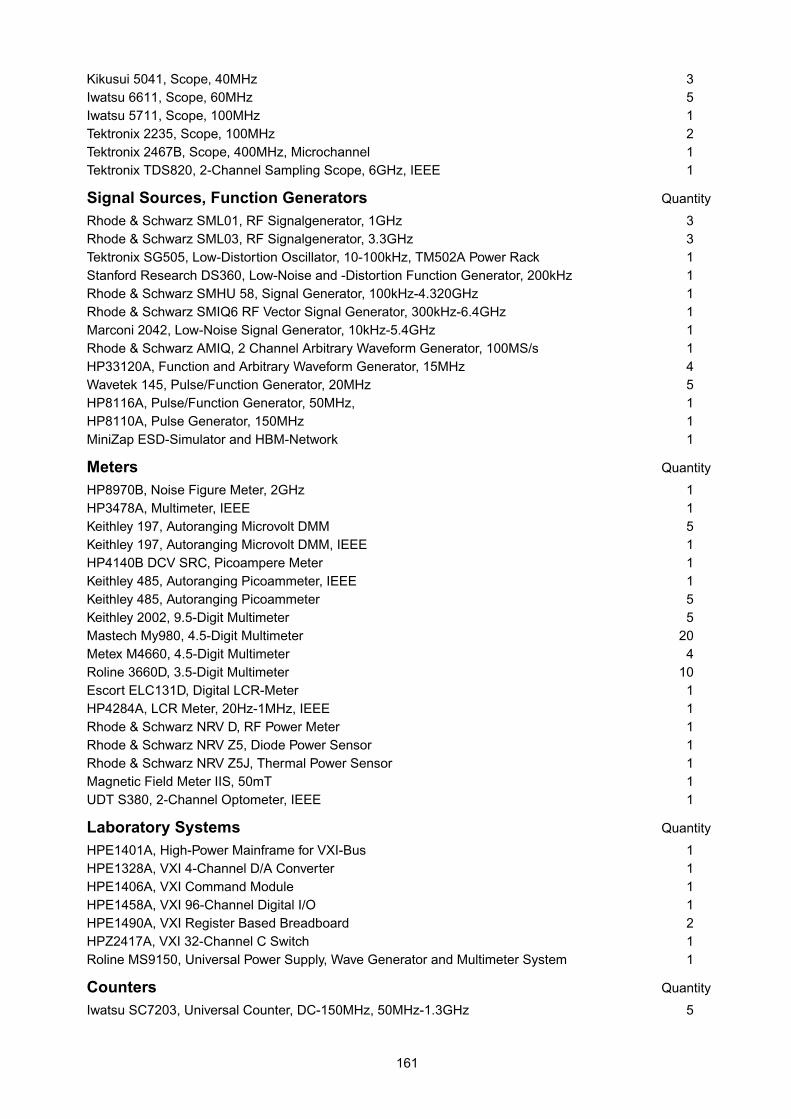
Kikusui 5041, Scope, 40MHz 3Iwatsu 6611, Scope, 60MHz 5Iwatsu 5711, Scope, 100MHz 1Tektronix 2235, Scope, 100MHz 2Tektronix 2467B, Scope, 400MHz, Microchannel 1Tektronix TDS820, 2-Channel Sampling Scope, 6GHz, IEEE 1
Signal Sources, Function Generators Quantity
Rhode & Schwarz SML01, RF Signalgenerator, 1GHz 3Rhode & Schwarz SML03, RF Signalgenerator, 3.3GHz 3Tektronix SG505, Low-Distortion Oscillator, 10-100kHz, TM502A Power Rack 1Stanford Research DS360, Low-Noise and -Distortion Function Generator, 200kHz 1Rhode & Schwarz SMHU 58, Signal Generator, 100kHz-4.320GHz 1Rhode & Schwarz SMIQ6 RF Vector Signal Generator, 300kHz-6.4GHz 1Marconi 2042, Low-Noise Signal Generator, 10kHz-5.4GHz 1Rhode & Schwarz AMIQ, 2 Channel Arbitrary Waveform Generator, 100MS/s 1HP33120A, Function and Arbitrary Waveform Generator, 15MHz 4Wavetek 145, Pulse/Function Generator, 20MHz 5HP8116A, Pulse/Function Generator, 50MHz, 1HP8110A, Pulse Generator, 150MHz 1MiniZap ESD-Simulator and HBM-Network 1
Meters Quantity
HP8970B, Noise Figure Meter, 2GHz 1HP3478A, Multimeter, IEEE 1Keithley 197, Autoranging Microvolt DMM 5Keithley 197, Autoranging Microvolt DMM, IEEE 1HP4140B DCV SRC, Picoampere Meter 1Keithley 485, Autoranging Picoammeter, IEEE 1Keithley 485, Autoranging Picoammeter 5Keithley 2002, 9.5-Digit Multimeter 5Mastech My980, 4.5-Digit Multimeter 20Metex M4660, 4.5-Digit Multimeter 4Roline 3660D, 3.5-Digit Multimeter 10Escort ELC131D, Digital LCR-Meter 1HP4284A, LCR Meter, 20Hz-1MHz, IEEE 1Rhode & Schwarz NRV D, RF Power Meter 1Rhode & Schwarz NRV Z5, Diode Power Sensor 1Rhode & Schwarz NRV Z5J, Thermal Power Sensor 1Magnetic Field Meter IIS, 50mT 1UDT S380, 2-Channel Optometer, IEEE 1
Laboratory Systems Quantity
HPE1401A, High-Power Mainframe for VXI-Bus 1HPE1328A, VXI 4-Channel D/A Converter 1HPE1406A, VXI Command Module 1HPE1458A, VXI 96-Channel Digital I/O 1HPE1490A, VXI Register Based Breadboard 2HPZ2417A, VXI 32-Channel C Switch 1Roline MS9150, Universal Power Supply, Wave Generator and Multimeter System 1
Counters Quantity
Iwatsu SC7203, Universal Counter, DC-150MHz, 50MHz-1.3GHz 5
161
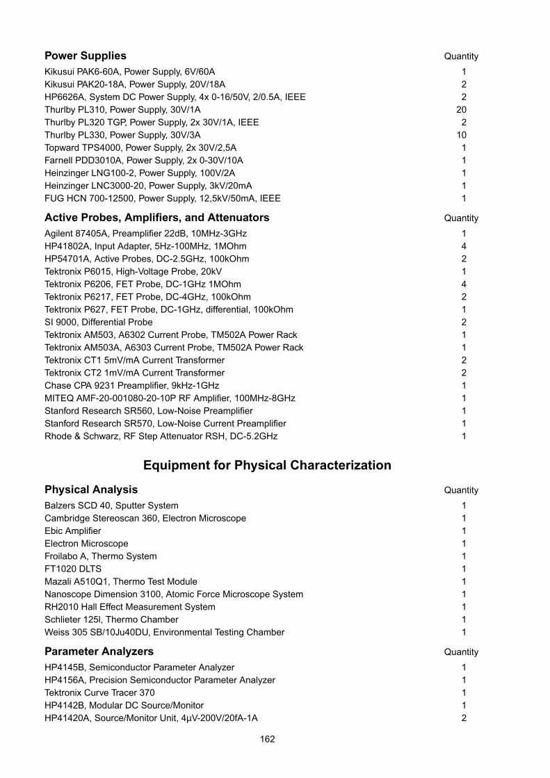
Power Supplies Quantity
Kikusui PAK6-60A, Power Supply, 6V/60A 1Kikusui PAK20-18A, Power Supply, 20V/18A 2HP6626A, System DC Power Supply, 4x 0-16/50V, 2/0.5A, IEEE 2Thurlby PL310, Power Supply, 30V/1A 20Thurlby PL320 TGP, Power Supply, 2x 30V/1A, IEEE 2Thurlby PL330, Power Supply, 30V/3A 10Topward TPS4000, Power Supply, 2x 30V/2,5A 1Farnell PDD3010A, Power Supply, 2x 0-30V/10A 1Heinzinger LNG100-2, Power Supply, 100V/2A 1Heinzinger LNC3000-20, Power Supply, 3kV/20mA 1FUG HCN 700-12500, Power Supply, 12,5kV/50mA, IEEE 1
Active Probes, Amplifiers, and Attenuators Quantity
Agilent 87405A, Preamplifier 22dB, 10MHz-3GHz 1HP41802A, Input Adapter, 5Hz-100MHz, 1MOhm 4HP54701A, Active Probes, DC-2.5GHz, 100kOhm 2Tektronix P6015, High-Voltage Probe, 20kV 1Tektronix P6206, FET Probe, DC-1GHz 1MOhm 4Tektronix P6217, FET Probe, DC-4GHz, 100kOhm 2Tektronix P627, FET Probe, DC-1GHz, differential, 100kOhm 1SI 9000, Differential Probe 2Tektronix AM503, A6302 Current Probe, TM502A Power Rack 1Tektronix AM503A, A6303 Current Probe, TM502A Power Rack 1Tektronix CT1 5mV/mA Current Transformer 2Tektronix CT2 1mV/mA Current Transformer 2Chase CPA 9231 Preamplifier, 9kHz-1GHz 1MITEQ AMF-20-001080-20-10P RF Amplifier, 100MHz-8GHz 1Stanford Research SR560, Low-Noise Preamplifier 1Stanford Research SR570, Low-Noise Current Preamplifier 1Rhode & Schwarz, RF Step Attenuator RSH, DC-5.2GHz 1
Equipment for Physical Characterization
Physical Analysis Quantity
Balzers SCD 40, Sputter System 1Cambridge Stereoscan 360, Electron Microscope 1Ebic Amplifier 1Electron Microscope 1Froilabo A, Thermo System 1FT1020 DLTS 1Mazali A510Q1, Thermo Test Module 1Nanoscope Dimension 3100, Atomic Force Microscope System 1RH2010 Hall Effect Measurement System 1Schlieter 125l, Thermo Chamber 1Weiss 305 SB/10Ju40DU, Environmental Testing Chamber 1
Parameter Analyzers Quantity
HP4145B, Semiconductor Parameter Analyzer 1HP4156A, Precision Semiconductor Parameter Analyzer 1Tektronix Curve Tracer 370 1HP4142B, Modular DC Source/Monitor 1HP41420A, Source/Monitor Unit, 4µV-200V/20fA-1A 2
162
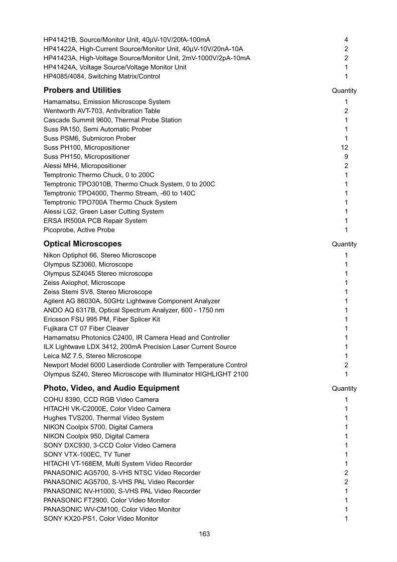
HP41421B, Source/Monitor Unit, 40µV-10V/20fA-100mA 4HP41422A, High-Current Source/Monitor Unit, 40µV-10V/20nA-10A 2HP41423A, High-Voltage Source/Monitor Unit, 2mV-1000V/2pA-10mA 2HP41424A, Voltage Source/Voltage Monitor Unit 1HP4085/4084, Switching Matrix/Control 1
Probers and Utilities Quantity
Hamamatsu, Emission Microscope System 1Wentworth AVT-703, Antivibration Table 2Cascade Summit 9600, Thermal Probe Station 1Suss PA150, Semi Automatic Prober 1Suss PSM6, Submicron Prober 1Suss PH100, Micropositioner 12Suss PH150, Micropositioner 9Alessi MH4, Micropositioner 2Temptronic Thermo Chuck, 0 to 200C 1Temptronic TPO3010B, Thermo Chuck System, 0 to 200C 1Temptronic TPO4000, Thermo Stream, -60 to 140C 1Temptronic TPO700A Thermo Chuck System 1Alessi LG2, Green Laser Cutting System 1ERSA IR500A PCB Repair System 1Picoprobe, Active Probe 1
Optical Microscopes Quantity
Nikon Optiphot 66, Stereo Microscope 1Olympus SZ3060, Microscope 1Olympus SZ4045 Stereo microscope 1Zeiss Axiophot, Microscope 1Zeiss Stemi SV8, Stereo Microscope 1Agilent AG 86030A, 50GHz Lightwave Component Analyzer 1ANDO AQ 6317B, Optical Spectrum Analyzer, 600 - 1750 nm 1Ericsson FSU 995 PM, Fiber Splicer Kit 1Fujikara CT 07 Fiber Cleaver 1Hamamatsu Photonics C2400, IR Camera Head and Controller 1ILX Lightwave LDX 3412, 200mA Precision Laser Current Source 1Leica MZ 7.5, Stereo Microscope 1Newport Model 6000 Laserdiode Controller with Temperature Control 2Olympus SZ40, Stereo Microscope with Illuminator HIGHLIGHT 2100 1
Photo, Video, and Audio Equipment Quantity
COHU 8390, CCD RGB Video Camera 1HITACHI VK-C2000E, Color Video Camera 1Hughes TVS200, Thermal Video System 1NIKON Coolpix 5700, Digital Camera 1NIKON Coolpix 950, Digital Camera 1SONY DXC930, 3-CCD Color Video Camera 1SONY VTX-100EC, TV Tuner 1HITACHI VT-168EM, Multi System Video Recorder 1PANASONIC AG5700, S-VHS NTSC Video Recorder 2PANASONIC AG5700, S-VHS PAL Video Recorder 2PANASONIC NV-H1000, S-VHS PAL Video Recorder 1PANASONIC FT2900, Color Video Monitor 1PANASONIC WV-CM100, Color Video Monitor 1SONY KX20-PS1, Color Video Monitor 1
163

SONY KX27-PS1, Color Video Monitor 1HITACHI VY300E, Color Video Printer 1Marantz PM7000 Audio Amplifier, 100W 1DENON DCD2560, CD-Player 1Infinity Reference 40 Loudspeaker 2
164
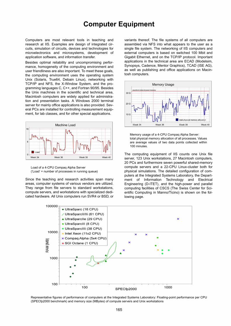
Computer Equipment
Computers are most relevant tools in teaching andresearch at IIS. Examples are design of integrated cir-cuits, simulation of circuits, devices and technologies formicroelectronics and microsystems, development ofapplication software, and information transfer.
Besides optimal reliability and uncompromising perfor-mance, homogeneity of the computing environment anduser friendliness are also important. To meet these goals,the computing environment uses the operating systemUnix (Solaris, True64, Debain Linux), networking withTCP/IP and NFS, the X-Window System, and the pro-gramming languages C, C++, and Fortran 90/95. Besidesthe Unix machines in the scientific and technical area,Macintosh computers are widely applied for administra-tion and presentation tasks. A Windows 2000 terminalserver for mainly office applications is also provided. Sev-eral PCs are installed for controlling measurement equip-ment, for lab classes, and for other special applications.
Load of a 4-CPU Compaq Alpha Server(‘Load’ = number of processes in running queue)
Since the teaching and research activities span manyareas, computer systems of various vendors are utilized.They range from file servers to standard workstations,compute servers, and workstations with specialized dedi-cated hardware. All Unix computers run SVR4 or BSD, or
variants thereof. The file systems of all computers areassembled via NFS into what appears to the user as asingle file system. The networking of IIS computers andexternal computers is based on switched 100 Mbit andGigabit Ethernet, and on the TCP/IP protocol. Importantapplications in the technical area are ECAD (Modelsim,Synopsys, Cadence, Mentor Graphics), TCAD (ISE AG),as well as publishing and office applications on Macin-tosh computers.
Memory usage of a 4-CPU Compaq Alpha Server:total physical memory allocation of all processes. Valuesare average values of two data points collected within100 minutes.
The computing equipment of IIS counts one Unix fileserver, 123 Unix workstations, 27 Macintosh computers,20 PCs and furthermore seven powerful shared-memorycompute servers and a 22-CPU Linux-cluster both forphysical simulations. The detailed configuration of com-puters at the Integrated Systems Laboratory, the Depart-ment of Information Technology and ElectricalEngineering (D-ITET), and the high-power and parallelcomputing facilities of CSCS (The Swiss Center for Sci-entific Computing in Manno/Ticino) is shown on the fol-lowing page.
Representative figures of performance of computers at the Integrated Systems Laboratory: Floating-point performance per CPU(SPECfp2000 benchmark) and memory size (MBytes) of compute servers and Unix workstations
165
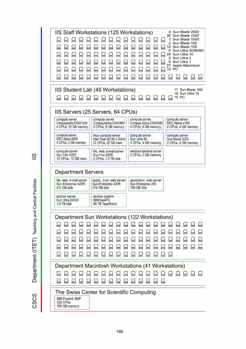
166