SistemaRFAudio - RF Wireless systems for data … receiver • RicevitoreFMsupereterodina audio...
21
Transcript of SistemaRFAudio - RF Wireless systems for data … receiver • RicevitoreFMsupereterodina audio...
I
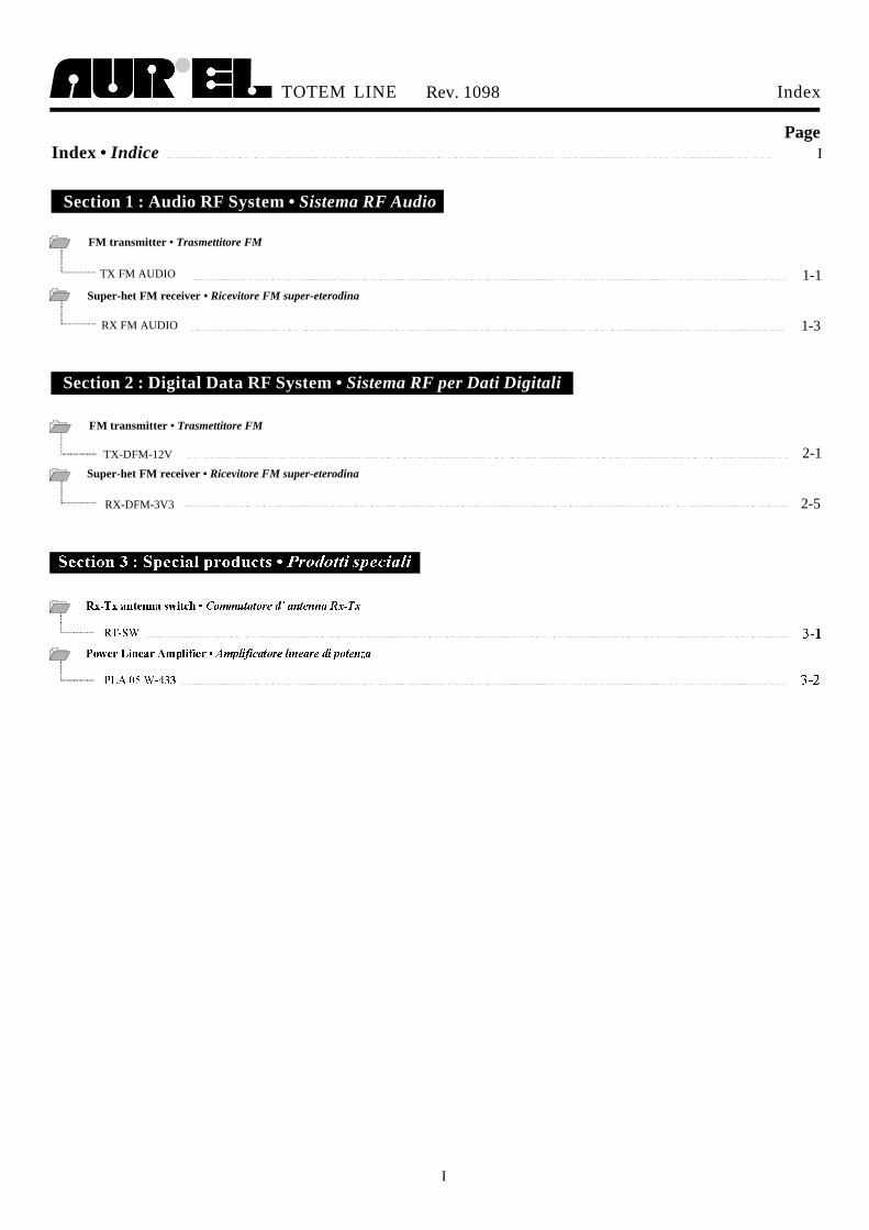
Section 1 : Audio RF System • Sistema RF Audio
Index • Indice
FM transmitter • Trasmettitore FM
Super-het FM receiver • Ricevitore FM super-eterodina
TX FM AUDIO
I
2-1
RX FM AUDIO
1-1
Page
Section 2 : Digital Data RF System • Sistema RF per Dati Digitali
TOTEM LINE Index
RX-DFM-3V3
1-3
TX-DFM-12V
2-5
Rev. 1098
FM transmitter • Trasmettitore FM
Super-het FM receiver • Ricevitore FM super-eterodina
FM audio transmit ter usable in conjunct ion withmod. receivermodule.Ideal for applications like audio HI-FI transmission, radio call alertand remote control (DTMF) systems. homologable.
RX FMAUDIO
ETS 300 220
Modulo trasmettitore FM audio abbinabile al modulo ricevitoremod. . Ideale per applicazioni quali trasmissioneaudio HI-FI, allarme via radio (telesoccorso) e controllo remoto(DTMF).Omologabile .
RX FM AUDIO
ETS 300 220
mod. TX FM AUDIO
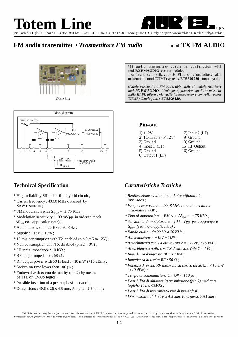
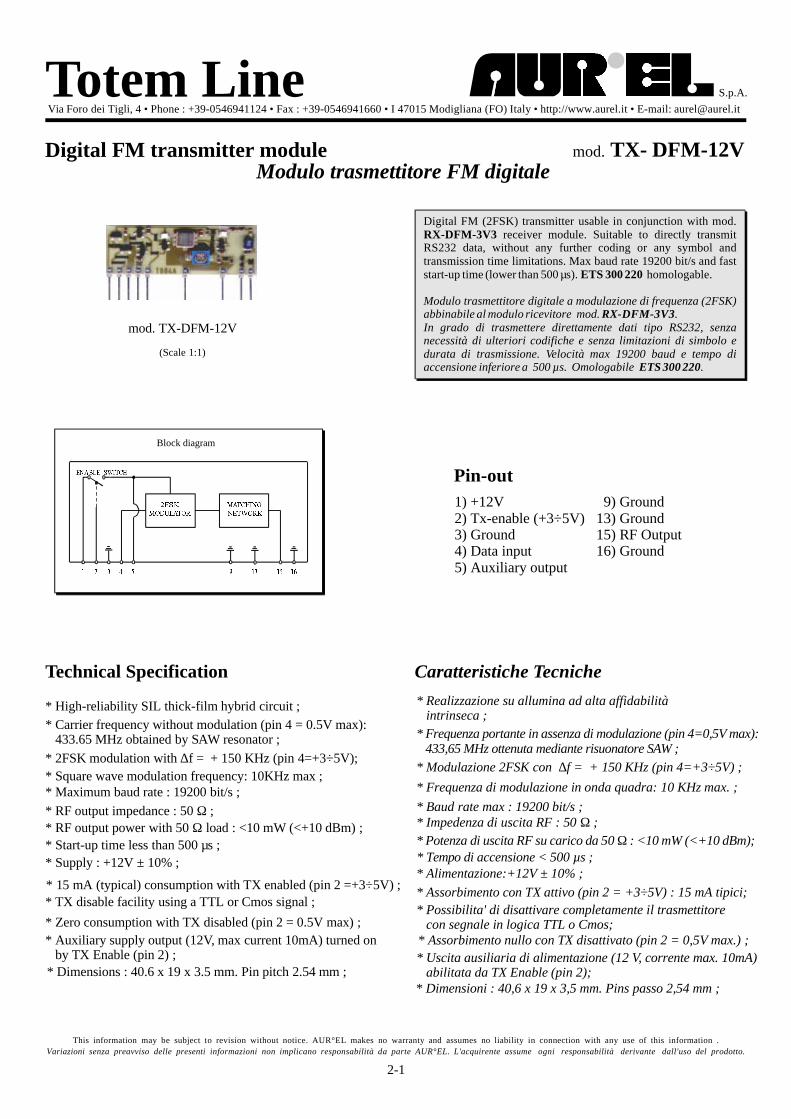
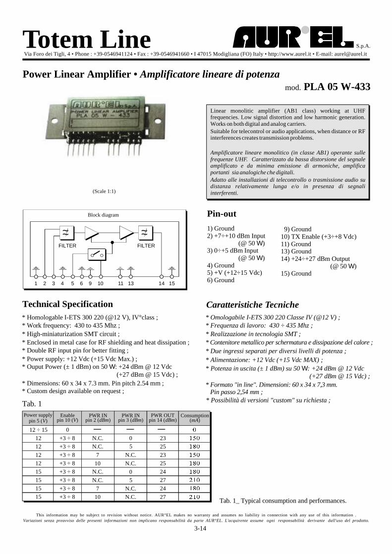
Pin-out1) +12V2) Tx-Enable (5÷12V)3) Ground4) Input 1 (LF)5) Ground6) Output 1 (LF)
7) Input 2 (LF)9) Ground
13) Ground15) RF Output16) Ground1 2 3 4 5 6 7 9 13 15 16
AMP 2
ENABLE SWITCH
AMP 1
5n6F
22K 4K7PRE-EMPHASIS
NETWORK
FMMODULATOR
MATCHINGNETWORK
Block diagram
(Scale 1:1)
Caratteristiche Tecniche
* Realizzazione su allumina ad alta affidabilitàintrinseca ;
* Frequenza portante : 433,8 MHz ottenuta medianterisuonatore SAW ;
* Tipo di modulazione : FM con f = ± 75 KHz ;∆ MAX
* Banda audio : da 20 Hz a 30 KHz ;* Alimentazione a +12V ± 10% ;* Assorbimento con TX attivo (pin 2 = 5÷12V) : 15 mA ;* Assorbimento nullo con TX disattivato (pin 2 = 0V) ;
* Sensibilità di modulazione : 100 mVpp per raggiungeref (vedi nota applicativa) ;∆ MAX
* Impedenza d'ingresso BF : 10 KΩ ;* Impedenza di uscita RF : 50 ;Ω
* Tempo di commutazione On-Off < 100 µs ;
* Potenza di uscita RF misurata su carico da 50 : <10 mW(+10 dBm) ;
Ω
* Possibilità di abilitare la trasmissione (pin 2) mediantelogiche TTL o CMOS ;
* Possibilità di inserimento rete di pre-enfasi ;* Dimensioni : 40,6 x 26 x 4,5 mm. Pins passo 2,54 mm ;
Technical Specification
* High-reliability SIL thick-film hybrid circuit ;* Carrier frequency : 433.8 MHz obtained by
SAW resonator ;
* FM modulation with f = ± 75 KHz ;∆ MAX
* Audio bandwidth : 20 Hz to 30 KHz ;
* LF input impedance : 10 KΩ ;* RF output impedance : 50 ;Ω* RF output power with 50 load : <10 mW (+10 dBm) ;Ω* Switch-on time lower than 100 µs ;
* Endowed with tx-enable facility (pin 2) by meansof TTL or CMOS logics ;
* Possible insertion of a pre-emphasis network ;
* Dimensions : 40.6 x 26 x 4.5 mm. Pin pitch 2.54 mm ;
* Supply : +12V ± 10% ;
* 15 mA consumption with TX enabled (pin 2 = 5 to 12V) ;* Null consumption with TX disabled (pin 2 = 0V) ;
* Modulation sensitivity : 100 mVpp in order to reachf (see application note) ;∆ MAX
x 20
Totem Line S.p.A.
Via Foro dei Tigli, 4 • Phone : +39-0546941124 • Fax : +39-0546941660 • I 47015 Modigliana (FO) Italy • http://www.aurel.it • E-mail: [email protected]
This information may be subject to revision without notice. AUR°EL makes no warranty and assumes no liability in connection with any use of this information .Variazioni senza preavviso delle presenti informazioni non implicano responsabilità da parte AUR°EL. L'acquirente assume ogni responsabilità derivante dall'uso del prodotto.
FM audio transmitter • Trasmettitore FM audio
1-1
x 5
Application note • Nota applicativa mod. TX FM AUDIO
Al fine di ottimizzare le prestazioni del moduloè necessario fare le seguenti considerazioni.
TX FM AUDIO
Sezione BF e modulatore
Rete di pre-enfasi
TX enable
La sezione di Bassa Frequenza è costituita da 2 amplificatoriaccoppiati in alternata, di guadagno in tensionerispettivamente AMP 1 = 20 e AMP 2 = 5 e bandapassante 20 Hz ÷ 30 KHz.Il modulatore FM è costituito da un oscillatore stabilizzatomediante risuonatore SAW e modulato in frequenza da undiodo varicap. Quest'ultimo è pilotabile da un segnale conV = 10V, perciò la massima V applicabile all'ingressodell' AMP 2 (pin 7) è 10V : 5 = 2V.Nel caso si decida di collegare direttamente gli stadi AMP 1e AMP 2 (cortocircuitando il pin 6 con il pin 7) peramplificare il più possibile il segnale in ingresso, lamassima V applicabile al pin 4 è 10V : (5 x 20) = 100 mV.
ppMAX pp
pp
Per migliorare il rapporto S/N e la dinamica del segnaledemodulato (vedi mod. RX FM AUDIO) è consigliabileinserire tra il 1° ed il 2° stadio di amplificazione B.F. una retedi pre-enfasi.Quella sopra illustrata, attenuando i toni bassi di un fattore
6 rispetto a quelli alti, rende approssimativamente costantel'indice di modulazione FM su tutta la banda audio edincrementa la dinamica a disposizione per i toni bassi.Anche in presenza della rete di pre-enfasi riportata in questanota, la massima V applicabile al pin 4 è circa 100 mV.
≈
pp
Tramite il pin 2 è possibile abilitare o disabilitare latrasmissione interfacciandosi con logiche TTL o CMOS cheforniscano in uscita livelli logici rispettivamente 0÷5V o0÷12V.È necessario che il pilotaggio garantisca un livello logicobasso di tensione inferiore a 0,5V per assicurare lospegnimento del trasmettitore.Il massimo tempo di commutazioneOff/On è di circa 100 µs.
In order to improve performance it's necessarytomakethefollowingremarks.
TX FMAUDIO
LF section and modulator
Pre-emphasis network
TX-enable
The Low Frequency section is made up by two AC-coupledamplifiers with voltage gain, respectively, AMP 1 = 20 andAMP 2 = 5, and LF bandwidth 20 Hz to 30KHz.The FM modulator is made up by an oscillator stabilized bymeans of a SAW resonator andmodulated by a varicap diode.This one can be driven by means of a signal having amaximum peak-to-peak voltage (V ) of 10V and, therefore,the maximum V that can be impressed to the AMP 2 input(pin 7) is 10V : 5 = 2V.In case the two stages AMP 1 and AMP 2 are directlyconnected (by short-circuiting pin 6 with pin 7) in order toamplify the LF input signal as much as possible, the max Vapplicable to pin 4 is 10V : (5 x 20) = 100mV.
pp
pp
pp
In order to improve the signal-to-noise ratio and thedynamics of the demodulated signal (see RX FM AUDIOapplication note) it's advisable to fit in between the 1 and2 LF amplifier stages a pre-emphasis network.The one above-shown, lowering the bass-tones by about 6times respect to the trebles makes the FM modulation indexapproximately constant over all the audio bandwidth andincreases the available dynamics for the bass-tones.Even if the pre-emphasis network is used, the max Vimpressable to pin 4 remains 100 mV.
ST
ND
pp
Pin 2 makes it possible to enable or disable the FMtransmitter simply by interfacing it with TTL or CMOS logicfamilies supplying output logic levels respectively of 0 to5V and 0 to 12V.It's necessary that pin 2 driving guarantees a 0 logic levellower than 0.5V in order to ensure the FMtransmitter switch-off.ThemaximumOff/On switching-time is about 100 µs.
Block diagram
1 2 3 4 5 6 7 9 13 15 16
AMP 2
AMP 1
22K
5n6F
4K7
x 20SAW
VARICAP
PRE-EMPHASISNETWORK
FM MODULATOR
ENABLE SWITCH
MATCHINGNETWORK
This information may be subject to revision without notice. AUR°EL makes no warranty and assumes no liability in connection with any use of this information .Variazioni senza preavviso delle presenti informazioni non implicano responsabilità da parte AUR°EL. L'acquirente assume ogni responsabilità derivante dall'uso del prodotto.
1-2
x 5 OSC.
FM super-het audioreceiver
• Ricevitore FM supereterodinaaudio
Frequency modulation super-het receiver usable in conjunctionwith mod. transmittermodule.The wide LF bandwidth and possible Litium battery (3V) supplyallow realization of audio HI-FI systems and portable receivers.
homologable.
TX FMAUDIO
ETS 300 220
Ricevitore supereterodina a modulazione di frequenza abbinabileal modulo trasmettitoremod. .L'ampia banda passante BF e la possibilità di utilizzare batterie alLitio (3V) lo rendono ideale per applicazioni in sistemi audio HI-FIe ricevitori portatili. Omologabile .
TXFMAUDIO
ETS 300 220
mod. RX FM AUDIO
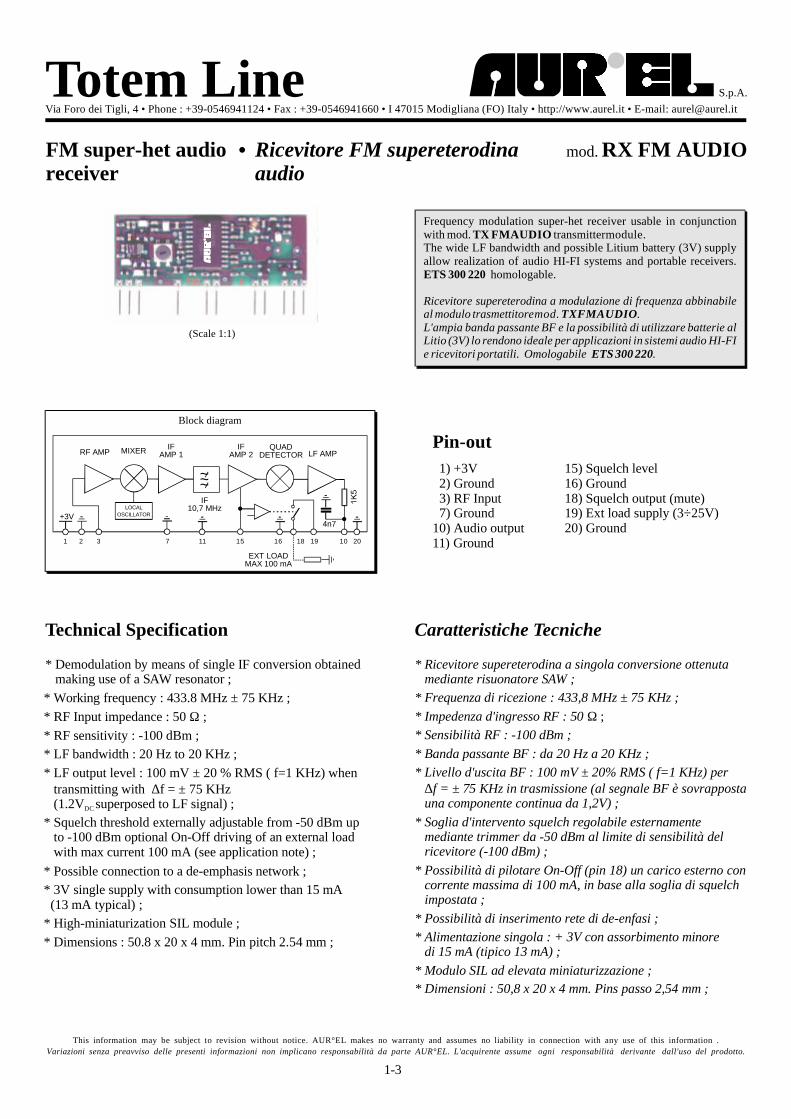
Pin-out1) +3V2) Ground3) RF Input7) Ground
10) Audio output11) Ground
15) Squelch level16) Ground18) Squelch output (mute)19) Ext load supply (3÷25V)20) Ground
Block diagram
1 2 3 7 11 15 16 18 19 10 20
RF AMP
IF10,7 MHz
IFAMP 1
IFAMP 2 LF AMPMIXER QUAD
DETECTOR
4n7
EXT LOADMAX 100 mA
+3V
~~~LOCAL
OSCILLATOR
Technical Specification
* Demodulation by means of single IF conversion obtainedmaking use of a SAW resonator ;
* Working frequency : 433.8 MHz ± 75 KHz ;
* RF Input impedance : 50 Ω ;* RF sensitivity : -100 dBm ;* LF bandwidth : 20 Hz to 20 KHz ;
* Possible connection to a de-emphasis network ;* 3V single supply with consumption lower than 15 mA
(13 mA typical) ;* High-miniaturization SIL module ;
* Dimensions : 50.8 x 20 x 4 mm. Pin pitch 2.54 mm ;
* LF output level : 100 mV ± 20 % RMS ( f=1 KHz) whentransmitting with f = ± 75 KHz(1.2V superposed to LF signal) ;
∆DC
* Squelch threshold externally adjustable from -50 dBm upto -100 dBm optional On-Off driving of an external loadwith max current 100 mA (see application note) ;
Caratteristiche Tecniche
* Ricevitore supereterodina a singola conversione ottenutamediante risuonatore SAW ;
* Frequenza di ricezione : 433,8 MHz ± 75 KHz ;* Impedenza d'ingresso RF : 50 Ω ;* Sensibilità RF : -100 dBm ;* Banda passante BF : da 20 Hz a 20 KHz ;
* Possibilità di inserimento rete di de-enfasi ;* Alimentazione singola : + 3V con assorbimento minore
di 15 mA (tipico 13 mA) ;* Modulo SIL ad elevata miniaturizzazione ;* Dimensioni : 50,8 x 20 x 4 mm. Pins passo 2,54 mm ;
* Livello d'uscita BF : 100 mV ± 20% RMS ( f=1 KHz) perf = ± 75 KHz in trasmissione (al segnale BF è sovrapposta
una componente continua da 1,2V) ;∆
* Soglia d'intervento squelch regolabile esternamentemediante trimmer da -50 dBm al limite di sensibilità delricevitore (-100 dBm) ;
* Possibilità di pilotare On-Off (pin 18) un carico esterno concorrente massima di 100 mA, in base alla soglia di squelchimpostata ;
(Scale 1:1)
Totem Line S.p.A.
Via Foro dei Tigli, 4 • Phone : +39-0546941124 • Fax : +39-0546941660 • I 47015 Modigliana (FO) Italy • http://www.aurel.it • E-mail: [email protected]
This information may be subject to revision without notice. AUR°EL makes no warranty and assumes no liability in connection with any use of this information .Variazioni senza preavviso delle presenti informazioni non implicano responsabilità da parte AUR°EL. L'acquirente assume ogni responsabilità derivante dall'uso del prodotto.
1-3
Application note • Nota applicativa mod. RX FM AUDIO
Rice-trasmissionediunsegnaleaudio musicale
Nello schema a blocchi sopra riportato l'uscita audio (pin 10)del mod. è collegata ad una rete di de-enfasi,nel caso particolare costituita da una capacità da 47 nFcollegata verso massa.Questa, abbinata alla rete di pre-enfasi della sezionetrasmittente, migliora la linearità della risposta in frequenza inbanda audio incrementando corrispondentemente il rapportoS/N.
In cascata alla rete di de-enfasi è collegato un amplificatoreaudio di potenza utilizzato per pilotare un altoparlante o cassaacustica.Poiché all'uscita audio (pin 10) del ricevitore è presente, oltre alsegnale demodulato, anche una componente continua da 1,2V ènecessario che l'ingresso dell'amplificatore di potenza siaaccoppiato in alternata.
L'alimentazione dell'amplificatore audio, supposta pari a 24V,viene fornita attraverso un relè pilotato dal circuito di squelchdel modulo : la max corrente erogabile dal pin18 (squelch output) è 100mA.Se il segnale RF ricevuto è di potenza inferiore alla soglia disquelch impostata, il circuito di squelch provoca l'apertura delrelè togliendo così alimentazione all'amplificatore di potenza esilenziando l'altoparlante.
Il valore della soglia d'intervento dello squelch è regolabileesternamente a seconda delle esigenze specifiche (mediante untrimmer di valore 10 K collegabile al pin 15 come da figura)da circa -50 dBm al limite di sensibilità del ricevitore(-100 dBm).
RX FM AUDIO
RX FM AUDIO
Ω
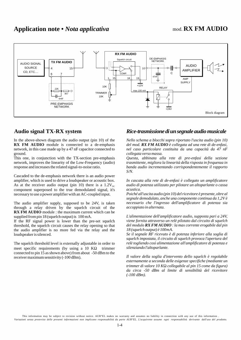
Audio signal TX-RX system
In the above-shown diagram the audio output (pin 10) of themodule is connected to a de-emphasis
network, in this case made up by a 47 nF capacitor connected toground.This one, in conjunction with the TX-section pre-emphasisnetwork, improves the linearity of the Low-Frequency (audio)response and increases the related signal-to-noise ratio.
Cascaded to the de-emphasis network there is an audio poweramplifier, which is used to drive a loudspeaker or acoustic box.As at the receiver audio output (pin 10) there is a 1.2Vcomponent superposed to the true demodulated signal, it'snecessary to use a power amplifier with an AC-coupled input.
The audio amplifier supply, supposed to be 24V, is takenthrough a relay driven by the squelch circuit of the
module : the maximum current which can besupplied from pin 18 (squelch output) is 100 mA.If the RF signal power is lower than the pre-set squelchthreshold, the squelch circuit causes the relay opening so thatthe audio amplifier is no more fed via the relay and theloudspeaker is silenced.
The squelch threshold level is externally adjustable in order tomeet specific requirements (by using a 10 K trimmerconnected to pin 15 as shown above) from about -50 dBm to thereceiver maximum sensitivity (-100 dBm).
RX FM AUDIO
RX FM AUDIO
DC
Ω
Block diagram
PRE-EMPHASISNETWORK
22K
5n6F
4K7
TX FM AUDIOAUDIO SIGNALSOURCE
CD, ETC....4
6 7
15
DE-EMPHASISNETWORK
C
TRIMMER10K
AMPSUPPLY
+12V
47nF
AUDIOAMPLIFIER
RELAYmax 100 mA
RX FM AUDIO
3
151 18
COMP.
Squelch circuit
19
10
+24V
This information may be subject to revision without notice. AUR°EL makes no warranty and assumes no liability in connection with any use of this information .Variazioni senza preavviso delle presenti informazioni non implicano responsabilità da parte AUR°EL. L'acquirente assume ogni responsabilità derivante dall'uso del prodotto.
1-4
10K
Modulo trasmettitore FM digitaleDigital FM transmitter module
Digital FM (2FSK) transmitter usable in conjunction with mod.receiver module. Suitable to directly transmit
RS232 data, without any further coding or any symbol andtransmission time limitations. Max baud rate 19200 bit/s and faststart-up time (lower than 500 µs). homologable.
RX-DFM-3V3
ETS 300 220
Modulo trasmettitore digitale a modulazione di frequenza (2FSK)abbinabile al modulo ricevitore mod. .In grado di trasmettere direttamente dati tipo RS232, senzanecessità di ulteriori codifiche e senza limitazioni di simbolo edurata di trasmissione. Velocità max 19200 baud e tempo diaccensione inferiore a 500 µs. Omologabile .
RX-DFM-3V3
ETS 300 220
mod. TX- DFM-12V
Pin-out1) +12V2) Tx-enable (+3÷5V)3) Ground4) Data input5) Auxiliary output
9) Ground13) Ground15) RF Output16) Ground
(Scale 1:1)
Caratteristiche TecnicheTechnical Specification
* High-reliability SIL thick-film hybrid circuit ;* Carrier frequency without modulation (pin 4 = 0.5V max):
433.65 MHz obtained by SAW resonator ;
* 2FSK modulation with f = + 150 KHz (pin 4=+3÷5V);∆
* Maximum baud rate : 19200 bit/s ;
Totem Line S.p.A.
Via Foro dei Tigli, 4 • Phone : +39-0546941124 • Fax : +39-0546941660 • I 47015 Modigliana (FO) Italy • http://www.aurel.it • E-mail: [email protected]
This information may be subject to revision without notice. AUR°EL makes no warranty and assumes no liability in connection with any use of this information .Variazioni senza preavviso delle presenti informazioni non implicano responsabilità da parte AUR°EL. L'acquirente assume ogni responsabilità derivante dall'uso del prodotto.
* Realizzazione su allumina ad alta affidabilitàintrinseca ;
* Frequenza portante in assenza di modulazione (pin 4=0,5V max):433,65 MHz ottenuta mediante risuonatore SAW ;
* Modulazione 2FSK con f = + 150 KHz (pin 4=+3÷5V) ;∆
* Baud rate max : 19200 bit/s ;* Frequenza di modulazione in onda quadra: 10 KHz max. ;
* Impedenza di uscita RF : 50 ;Ω* Potenza di uscita RF su carico da 50 : <10 mW (<+10 dBm);Ω* Tempo di accensione < 500 µs ;
* Dimensioni : 40,6 x 19 x 3,5 mm. Pins passo 2,54 mm ;
* Alimentazione:+12V ± 10% ;* Assorbimento con TX attivo (pin 2 = +3÷5V) : 15 mA tipici;
* Assorbimento nullo con TX disattivato (pin 2 = 0,5V max.) ;
* Possibilita' di disattivare completamente il trasmettitorecon segnale in logica TTL o Cmos;
* Uscita ausiliaria di alimentazione (12 V, corrente max. 10mA)abilitata da TX Enable (pin 2);
* Square wave modulation frequency: 10KHz max ;
* Dimensions : 40.6 x 19 x 3.5 mm. Pin pitch 2.54 mm ;
* Start-up time less than 500 µs ;
* RF output impedance : 50 ;Ω* RF output power with 50 load : <10 mW (<+10 dBm) ;Ω
* 15 mA (typical) consumption with TX enabled (pin 2 =+3÷5V) ;
* Supply : +12V ± 10% ;
* Zero consumption with TX disabled (pin 2 = 0.5V max) ;
* TX disable facility using a TTL or Cmos signal ;
* Auxiliary supply output (12V, max current 10mA) turned onby TX Enable (pin 2) ;
mod. TX-DFM-12V
Block diagram
2-1
Application note • Nota applicativa mod. TX-DFM-XX (*)
This information may be subject to revision without notice. AUR°EL makes no warranty and assumes no liability in connection with any use of this information .Variazioni senza preavviso delle presenti informazioni non implicano responsabilità da parte AUR°EL. L'acquirente assume ogni responsabilità derivante dall'uso del prodotto.
TRASMETTITORE DIGITALE2FSK
CARATTERISTICHE PRINCIPALImod. TX-DFM-12V
!
!
!
!
!
!
!
!
!
!
!
!
Frequenza di trasmissione portante 433,65 Mhz conmodulazione di frequenza 2FSK e deviazione nominalepari a + 150 Khz.
Potenza uscita RF:<10dBmsucaricoda50ohm.Frequenza di modulazione in onda quadra: min 0 Hz, max 10
Khz.Massimo bit rate fino a 19200 bit/s.Compatibilità diretta con il protocollo RS232 senza necessità
di codifiche intermedie e/o preamboli e senza limitazioni disimbolo e durata di trasmissione.
Massimo ritardo iniziale dall'istante di abilitazione deltrasmettitore (TX Enable ON) al primo bit trasmissibilecorrettamente : 500 µsec.
Possibilità di disabilitare completamente il trasmettitore(mediante logica TTL o CMOS) con conseguenteassorbimento nullo.
Uscita ausiliaria di alimentazione abilitata dal pin TX Enablecon corrente massima 10 mA: utilizzabile ad esempio perpilotare il commutatore d'antenna mod. , pensatoper combinare i moduli e inun efficiente rice-trasmettitore digitale 2FSK a singolaantenna.
Alimentazione a +12V ±10%.Assorbimento con TX abilitato (TX Enable = 3÷5V) : 15 mA
Tipico.Assorbimento con TX disabilitato (TX Enable = max 0,5V) :
nullo.Omologabile ETS 300-220.
RT-SWTX-DFM-XX RX-DFM-3V3
(*) Le ultime 2 lettere del modello, cioè , identificanoversioni del TX contraddistinte da una differentetensione di alimentazione. Queste note esplicativeriguardano l'intera famiglia di TX indipendentementedall'alimentazione.
…-XX
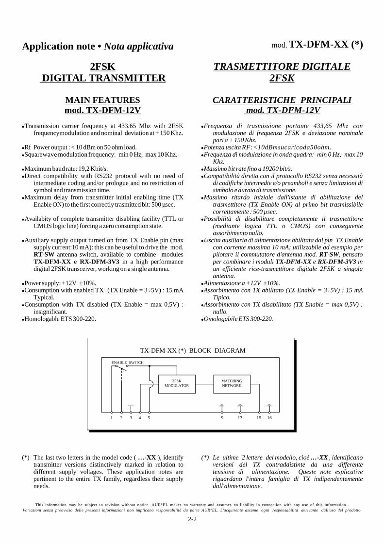
2FSKMODULATOR
MATCHINGNETWORK
ENABLE SWITCH
TX-DFM-XX (*) BLOCK DIAGRAM
1 2 3 4 5 9 13 15 16
2FSKDIGITAL TRANSMITTER
MAIN FEATURESmod. TX-DFM-12V
!
!
!
!
!
!
!
!
!
!
!
!
Transmission carrier frequency at 433.65 Mhz with 2FSKfrequencymodulation and nominal deviation at + 150 Khz.
Rf Power output : < 10 dBm on 50 ohm load.Squarewave modulation frequency: min 0 Hz, max 10 Khz.
Maximum baud rate: 19,2 Kbit/s.Direct compatibility with RS232 protocol with no need of
intermediate coding and/or prologue and no restriction ofsymbol and transmission time.
Maximum delay from transmitter initial enabling time (TXEnable ON) to the first correctly trasmitted bit: 500 µsec.
Availabity of complete transmitter disabling facility (TTL orCMOS logic line) forcing a zero consumption state.
Auxiliary supply output turned on from TX Enable pin (maxsupply current:10 mA): this can be useful to drive the mod.
antenna switch, available to combine modulese in a high performance
digital 2FSK transceiver, working on a single antenna.
Power supply: +12V ±10%.Consumption with enabled TX (TX Enable = 3÷5V) : 15 mA
Typical.Consumption with TX disabled (TX Enable = max 0,5V) :
insignificant.Homologable ETS 300-220.
RT-SWTX-DFM-XX RX-DFM-3V3
(*) The last two letters in the model code ( ), identifytransmitter versions distinctively marked in relation todifferent supply voltages. These application notes arepertinent to the entire TX family, regardless their supplyneeds.
…-XX
2-2
Application note • Nota applicativa Mod. TX-DFM-XX
This information may be subject to revision without notice. AUR°EL makes no warranty and assumes no liability in connection with any use of this information .Variazioni senza preavviso delle presenti informazioni non implicano responsabilità da parte AUR°EL. L'acquirente assume ogni responsabilità derivante dall'uso del prodotto.
PIN OUT
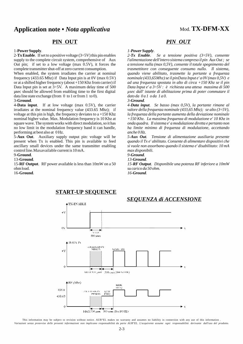
1- .2- . Se a tensione positiva (3÷5V), consentel'alimentazione dell'intero sistema compreso il pin Aux Out ; sea tensione nulla (max 0,5V), consente il totale spegnimento deltrasmettitore con conseguente consumo nullo. Il sistema,quando viene abilitato, trasmette la portante a frequenzanominale (433,65Mhz) se il pinData Input e' a 0V (max 0,5V) ead una frequenza spostata in alto di circa +150 Khz se il pinData Input e' a 3÷5V : è richiesta una attesa massima di 500µsec dall' istante di abilitazione prima di poter commutare ildato da 0 a 1 o da 1 a 0.3- .4- . Se basso (max 0,5V), la portante rimane alvalore della frequenza nominale (433,65 Mhz); se alto (3÷5V),la frequenza della portante aumenta della deviazione nominale+150 Khz. La massima frequenza di modulazione e' 10 Khz inonda quadra. Il sistema e' a modulazione diretta e pertanto nonha limite minimo di frequenza di modulazione, accettandoanche 0 Hz.5- . Tensione di alimentazione ausiliaria presentequando il Tx e' abilitato. Consente di alimentare dispositivi chesi vuole non assorbano quando il sistema e' disabilitato: 10 mAmax disponibili.9- .13- .15- . Disponibile una potenza RF inferiore a 10mWsu carico da 50 ohm.16- .
Power SupplyTx Enable
GroundData input
Aux Out
GroundGroundRF Output
Ground
SEQUENZA di ACCENSIONE
PIN OUT
1- .2- . If set to a positive voltage (3÷5V) this pin enablessupply to the complete circuit system, comprehensive of AuxOut pin; if set to a low voltage (max 0.5V), it forces thecomplete transmitter shut-off at zero current consumption.When enabled, the system irradiates the carrier at nominalfrequency (433.65 Mhz) if Data Input pin is at 0V (max 0.5V)or at a shifted higher frequency (about +150 Khz from carrier) ifData Input pin is set at 3÷5V. A maximum delay time of 500µsec should be allowed from enabling time to the first digitaldata line state exchange (from 0 to 1 or from 1 to 0).3- .4- . If at low voltage (max 0.5V), the carrierirradiates at the nominal frequency value (433.65 Mhz); ifvoltage at this pin is high, the frequency deviates to a +150 Khznominal higher value. Max. Modulation frequency is 10 Khz atsquare wave. The system works with direct modulation, so it hasno low limit in the modulation frequency band it can handle,performing at best also at 0 Hz.5- . Auxiliary supply output pin: voltage will bepresent when Tx is enabled. This pin is available to feedancillary small devices under the same transmitter enablingcontrol line.Maxavailable current is 10 mA.9- .13- .15- . RF power available is less than 10mW on a 50ohm load.16- .
Power SupplyTx Enable
GroundData input
Aux Out
GroundGroundRF Output
Ground
START-UP SEQUENCE
2-3
Application note • Nota applicativa mod. TX-DFM-XX
This information may be subject to revision without notice. AUR°EL makes no warranty and assumes no liability in connection with any use of this information .Variazioni senza preavviso delle presenti informazioni non implicano responsabilità da parte AUR°EL. L'acquirente assume ogni responsabilità derivante dall'uso del prodotto.
NOTA: Nel caso che il trasmettitore venga utilizzato inabbinamento al ricevitore , si deve attenderequesto intervallo di tempo prima di trasmettere lo start bit perpoter effettuare una corretta temporizzazione dei dati con ilricevitore. Nel diagramma si ipotizza che il trasmettitore vengaacceso a ricevitore già abilitato: i 500 µsec corrispondono almassimo tempo richiesto al Carrier Detect del ricevitore perstabilizzarsi al livello alto in presenza di segnale RF.
RX-DFM-3V3
NOTE ESPLICATIVE
Il trasmettitore mod. e' il complementodel ricevitore mod. e pertanto queste notecoprono la parte non illustrata nell' application note relativo alricevitore.
Sia l'ingresso TX enable che l'ingresso Data Input sono alogica positiva 3÷5V quando attivi e richiedono unicamenteuna corretta temporizzazione in apertura e chiusura dellestringhe da trasmettere ricavabile direttamente dalla sequenzadi accensione riportata per il ricevitore.
I diagrammi di tempificazione mostrano come si deveimpiegare il TX per poterlo interfacciare correttamente con ilRX; la sequenza di accensione del trasmettitore a ricevitore giàabilitato puo' essere così riassunta:
Abilitare il pin 2 (TX enable = 3÷5V).Attendere un tempo minimo di circa 1 msec dall'istantedi accensione prima di trasmettere lo Start Bit perconsentire al Carrier Detect del ricevitore distabilizzarsi al livello alto indicante la presenza disegnale RF. Come precisato nell'application note delricevitore, se e' possibile attendere un tempo diqualche msec prima di inviare dati e' anche possibilemigliorare l' immunita' ai transitori in ricezionemediante opportuni algoritmi software.Modulare il pin 4 (Data Input) con la sequenza ditrasmissione ed il bit rate richiesto.
Al termine della trasmissione lasciare il pin 4 (Data Input)a livello 0V (assenza modulazione) per un tempo di qualchemsec prima di disabilitare il pin 2 (TX enable). In questo modosi consente la corretta sequenza di chiusura per il ricevitoresenza eventuali perdite di dati.
I tempi specificati sono necessariamente indicativi (tranneil ritardo iniziale minimo di 1 msec che e' obbligatorio) inquanto dipendono dal bit rate impiegato nella trasmissione. E'ragionevole impiegare ritardi pari a 2 volte il tempo ditrasmissione di un singolo byte per cui a 9600 baud si puo'utilizzare un tempo pari a 2 msec.
TX-DFM-XXRX-DFM-3V3
!
!
!
NOTE: If the transmitter is used in conjunction with thereceiver, it is recommended to wait at least for the
specified interval time, prior to transmit the start bit: this willassure the best timing of data out of the receiver. The abovediagrams were put down with the assumption that the sequenceis started with a receiver already in enabled state: 500 µsec isthe maximum delay time required to the receiver Carrier Detectline to transfer to the upper logical level on presence of theappropriate RF signal.
RX-DFM-3V3
EXPLANATION NOTES
The mod. transmitter is complementingthe mod. receiver: these remarks relates to allaspects not completely covered up in the receiver applicationnote.
Both TXenable and Data Input input lines are working witha positive logic: 3÷5V are required to set them on active status,handled together with the correct On-Off timing of the datastrings to be trasmitted. Timing details are fully described in thereceiver application note.
Previous page timing diagrams show how to use thetransmitter to interafce it at best with a receiver; transmitterstart-up sequence (with a receiver already On) can besummarized:
Enable pin 2 (TX enable = 3÷5V).
Wait for a 1 msecminimum delay time prior to transmitthe data Start Bit: this is useful for the receiver CarrierDetect to stabilize at high logical state, with indicationthat the RF signal is perceived. As stated also in thereceiver application note, in addition to the fewmillisecond delay time, software algorithms can beimplemented to improve reception RFI immunity.
Modulate pin 4 (Data Input) with transmission datasequence at requested data rate.
At trasmission string end, leave pin 4 (Data Input) at 0Vlevel (No modulation) for few milliseconds prior to disable pin 2(TX enable).
This procedure helps the receiver to perform the correctclosing sequence with no loss of data.
Specified delays are just indicative (other then the start-updelay that must last at least 1 msec) as they are depending on thechoosen transmission baude rate. As a rule of thumb, delaysshould be at least twice the time used to transmit a single databyte: at a 9600 baud transmission rate, a 2 msec delay isacceptable.
TX-DFM-XXRX-DFM-3V3
!
!
!
2-4
Ricevitore FM supereterodina digitaleDigital FM super-het receiver
Frequency modulation (2FSK) super-het receiver usable inconjunctionwithmod. transmittermodule.Reception of RS232 digital data without any further coding needand any symbol and transmission time limitations.Max baud rate 19200 bit/s and fast start-up time(lower than 1 ms). homologable.
TX- DFM-12V
ETS 300 220
Ricevitore supereterodina a modulazione di frequenza (2FSK)abbinabile al modulo trasmettitoremod. .Ricezione dati tipo RS232 senza necessità di ulteriori codifiche esenza limitazioni di simbolo e durata di trasmissione. Velocità max19200 baud e tempo di accensione inferiore ad 1 ms.Omologabile .
TX- DFM-12V
ETS 300 220
mod. RX-DFM-3V3
Pin-out1) RF Input2) Ground7) Ground8) Squelch level
10) Auxiliary output11) Carrier detect
12) Ground14) Ground17) Ground18) Data output19) RX enable (+3 to 5V)20) +3.3V Supply
Caratteristiche TecnicheTechnical Specification
(Scale 1:1)
Totem Line S.p.A.
Via Foro dei Tigli, 4 • Phone : +39-0546941124 • Fax : +39-0546941660 • I 47015 Modigliana (FO) Italy • http://www.aurel.it • E-mail: [email protected]
This information may be subject to revision without notice. AUR°EL makes no warranty and assumes no liability in connection with any use of this information .Variazioni senza preavviso delle presenti informazioni non implicano responsabilità da parte AUR°EL. L'acquirente assume ogni responsabilità derivante dall'uso del prodotto.
* Livello logico in uscita normalmente basso (0V) in assenzadi modulazione;
* Tempo di accensione < 1 ms ;* Abilitazione della ricezione (pin 19) mediante logiche
TTL o CMOS: RX Enable= +3÷5 V;* Alimentazione singola : +3,3V ±200 mV con assorbimento
minore di 15 mA (tipico 13 mA) ;* Modulo SIL ad elevata miniaturizzazione ;* Dimensioni : 54,8 x 22 x 4,5 mm. Pins passo 2,54 mm.
* Ricevitore 2FSK supereterodina a singola conversioneottenuta mediante risuonatore SAW ;
* Frequenza di ricezione : 433,65 MHz + 150 KHz ;* Impedenza d'ingresso RF : 50 Ω ;* Sensibilità RF : -100 dBm ;* Baud rate: 2400÷19200 bit/sec ;* Rivelatore FM digitale pilotabile mediante circuito di squelch ;
* Uscita dati open collector (pin 18) con corrente max 5 mA ;
* Soglia d'intervento squelch regolabile esternamentemediante trimmer da ~-50 dBm al limite di sensibilitàdel ricevitore (-100 dBm) ;
* Uscita ausiliaria (pin 10) abilitata da RX Enable (pin 19):Corrente Max. 10mA;
* Super-het 2FSK Receiver with single IF conversion fromSAW resonator ;
* Low output logic level (0V) with no modulation;
* Start-up time lower than 1 ms ;
* Enabled to receive (pin 19) using a TTL or CMOS signal:RX Enable=+3÷5 V;
* 3.3V ±200 mV single supply with consumption lower than15 mA (13 mA typical) ;
* High-reliability PCB SIL module ;
* Dimensions : 54.8 x 22 x 4.5 mm. Pin pitch 2.54 mm.
* Working frequency : 433.65 MHz + 150 KHz ;* RF Input impedance : 50 Ω ;* RF sensitivity : -100 dBm ;
* Baud rate : 2400÷19200 baud ;
* Digital FM detector driven via squelch circuit ;
* Open collector data output (pin 18) with 5 mA max current ;
* Squelch threshold externally adjustable from ~-50 dBmup to the receiver max sensitivity (-100 dBm) ;
* Auxiliary output (pin 10) turned On from RX Enable (pin 19):max. current 10mA ;
mod. RX-DFM-3V3
Block diagram
2-5
Application note • Nota applicativa mod. RX-DFM-3V3
This information may be subject to revision without notice. AUR°EL makes no warranty and assumes no liability in connection with any use of this information .Variazioni senza preavviso delle presenti informazioni non implicano responsabilità da parte AUR°EL. L'acquirente assume ogni responsabilità derivante dall'uso del prodotto.
RICEVITORE DIGITALE 2FSK
CARATTERISTICHE PRINCIPALIMod. RX-DFM-3V3
!
!
!
!
!
!
!
!
!
!
!
!
!
!
Frequenza di ricezione portante 433,65 Mhz, demodulazionedi frequenza 2FSK con deviazione nominale pari a +150Khz.
Sensibilità RF : -100 dBm.Rivelatore di portante di tipo On-Off (Carrier Detector) con
soglia regolabile esternamente con continuità da circa -50dBm fino al limite di sensibilità (-100 dBm).
Bit rate : da 2400 a 19200 bit/s con formato 1 start bit, 8 databits, 1 stop bit.
Compatibilità diretta con il protocollo RS232 senza necessitàdi codifiche intermedie e/o preamboli e senza limitazioni disimbolo e durata di trasmissione.
Uscita dati disabilitata (0V) in assenza di portante (0V).Livello logico in uscita normalmente basso (0V) in assenza di
modulazione.Ritardo iniziale dalla presenza della portante (Carrier Detect
ON) al primo bit rivelabile correttamente inferiore a 500µsec.
Tempo complessivo richiesto dall'istante di accensione (RXEnable ON) per verificare la validità dei dati ricevutiinferiore a 1 ms.
Possibilità di disabilitare completamente il ricevitore(mediante logica TTL o CMOS) con conseguenteassorbimento nullo.
Uscita ausiliaria di alimentazione abilitata dal pin RX Enablecon corrente max 10 mA.
Uscita dati con pull-up esterno per ottenere la compatibilita'fra livelli di tensione differenti (open collector con correntemax 5 mA).
Alimentazione singola a +3.3V con tolleranza ±200mV eassorbimento minore di 15 mA (tipico 13 mA).
Omologabile ETS 300-220.
2FSK DIGITAL RECEIVER
MAIN FEATURESMod. RX-DFM-3V3
!
!
!
!
!
!
!
!
!
!
!
!
!
!
Reception carrier frequency at 433.65 Mhz, with 2FSKdemodulation and nominal deviation at +150 Khz
.RF sensitivity: -100dBm.Carrier On-Off detector with externally continous adjustable
threshold from -50dBm up to the receiver max sensitivity (-100dBm).
Bit rate from 2,400 to 19,200 baud with 1 start bit, 8 data bits, 1stop bit format.
Direct compatibility with RS232 protocol with no need ofintermediate coding and/or prologue and no restriction ofsymbol and transmission time.
Data output disabled (0V) when no carrier is present (0V).Low output logical level with no modulation.
Time delay from carrier detection (Carrier Detect output On) tothe first correctly detected bit less than 500µsec.
Time from receiver start-up (RX Enable On) to received datavalidity less than 1 msec.
Availability of complete receiver disabling facility (TTL orCMOS logic line) forcing a zero consumption state.
Auxiliary supply output turned on from RX Enable pin: maxsupply current 10 mA.
Data output with external push-pull to assure compatibilitywith different voltages (open collector with a 5 mA maxcurrent).
Single +3.3V ±200mV Power Supply with less than 15mAconsumption (13mA typical).
HomologableETS300-200.
2-6
Application note • Nota applicativa mod. RX-DFM-3V3
This information may be subject to revision without notice. AUR°EL makes no warranty and assumes no liability in connection with any use of this information .Variazioni senza preavviso delle presenti informazioni non implicano responsabilità da parte AUR°EL. L'acquirente assume ogni responsabilità derivante dall'uso del prodotto.
PIN OUT
1- . Richiesta un'antenna con 50 ohm di impedenza RF.2- .7- .8- . I seguenti schemi riportano comecollegare un potenziometro esterno per poter modificare illivello di squelch di default. Poiché il pin 8 e' al centro di unpartitore 100K / 6,8K direttamente collegato alla tensione dialimentazione, la tensione nominale di squelch senza taratureaggiuntive vale circa 210 mV.10- . Tensione di uscita ausiliaria presente quando ilricevitore e' attivo. Consente di alimentare dispositivi che sivuole non assorbano quando il sistema e' disattivo: 10 mA maxdisponibili.11- . Alto se il livello di segnale RF in ingressosupera la soglia impostata.12- .14- .17- .18- . Open collector da terminare al livello ditensione opportuno (max 5mA disponibili). Tipico valoreresistivo: 10Kohm.19- . Se a tensione positiva (3÷5V) abilita l' interoricevitore compreso Aux Out. Se basso (max 0,5V) consente iltotale spegnimento con consumo nullo.20- .
RF inputGroundGroundSet Squelch Level
Aux Out
Carrier Detect
GroundGroundGroundData Output
RX Enable
Power Supply
PIN OUT
1 A 50Ohm impedence antenna is required278 Following schematics show how toconnect an external potentiometer to modify the defaul squelchlevel. As pin 8 is at center of a 100K/6.8K resistor networkconnected to supply voltage, the squelch nominal voltage, withno added circuitry, is near to 210mV.
10 Auxiliary supply output, available as soon as thereceiver goes active. Available to supply extermal devices underthe same receiver enabling control line. Max available current is10mA.11 Pin at high level if the input RF signal levelexceedes the set threshold.12141718 Open collector line to be terminated to thesuitable voltage (5mA max drivable current). 10Kohm is thetypical resistor load..19 If at high voltage (3÷5V), enables the completereceiver (also Aux Out). If at low voltage (max 0.5V), totallydisables it, forcing a neglettible current consumption.20
- .- .- .- .
- .
- .
- .- .- .- .
- .
- .
RF inputGroundGroundSet Squelch Level
Aux Out
Carrier Detect
GroundGroundGroundData Output
RX Enable
Power Supply
ANTENNA
ANTENNA
2-7
Application note • Nota applicativa mod. RX-DFM-3V3
This information may be subject to revision without notice. AUR°EL makes no warranty and assumes no liability in connection with any use of this information .Variazioni senza preavviso delle presenti informazioni non implicano responsabilità da parte AUR°EL. L'acquirente assume ogni responsabilità derivante dall'uso del prodotto.
NOTE ESPLICATIVE
Le seguenti note esplicative si basano sul sistema ditrasmissione costituito dal ricevitore mod. e daltrasmettitore digitale mod. , operante allafrequenza 433,65 Mhz con deviazione nominale +150 Khz,potenza max di uscita 10 mW su carico 50 ohm e massimafrequenza di modulazione pari a 10 Khz (onda quadra)corrispondente a 19200 baud.
(
ALIMENTAZIONE RICEVITORE A +5VIl precedente schema 1) riporta un esempio di utilizzo del
ricevitore a +5V. La tensione di alimentazione di +3,3V e'ottenuta mediante la caduta di circa 1,7V ai capi di un led rossoo giallo, mentre la resistenza di pull-up (R ) in uscita e'collegata direttamente ai +5V per ottenere la correttainterfaccia elettrica. In questo caso, anche a ricevitoredisabilitato (RX Enable = 0V), si avra' assorbimento sulla Rin quanto l'uscita dati rimane a 0V.
Supponendo che i +5V non siano ottenuti da batteria cio'non comportera' problemi se non un assorbimento pari a5V/R . Se R = 10kOhm si avra' un assorbimento noneliminabile di 0,5 mA.
ALIMENTAZIONE RICEVITORE A +3,3VIl precedente schema 2) riporta un esempio di utilizzo del
ricevitore a +3,3V. Non ipotizzando problemi di interfacciaelettrica con i dispositivi a valle, la R viene collegata all'uscita Aux Out (pin 10) che viene abilitata solo quando ilricevitore e' operativo (RX Enable = 3÷5V).
In questo modo l' intero ricevitore non assorbira' nulla sedisabilitato consentendo di operare ad alimentazionebatterizzata con il massimo di efficenza.
SEQUENZA DI ACCENSIONE DEL RICEVITORE
RX-DFM-3V3TX-DFM-XX (*)
*) Le ultime 2 lettere del modello, cioè , identificanoversioni del TX contraddistinte da una differente tensionedi alimentazione. Queste note esplicative riguardano l'interafamiglia di TX, indipendentemente dall'alimentazione.
…-XX
!
!
!
pull-up
pull-up
pull-up pull-up
pull-up
EXPLANATION NOTES
Following explanation notes cover a radio systemcomposed of mod. receiver and mod.
transmitter, operating at 433.65Mhzfrequency at+150 Khz nominal deviation, 10mWmaxRFoutputpowerona50 Ohm load and 10KHz maximum modulation frequency,corresponding to 19200 baud data stream.
(
RECEIVER WITH +5V SUPPLYPrevious wiring diagram 1) shows an example of receiver
connection to a +5V supply. The +3,3V voltage is obtainedwith the 1,7V voltage drop across a red or yellow LED, whilethe output pull-up resistor (R ) is directly connected to the+5V supply to have the proper electrical interface. In this case,even with a disabled receiver (RX Enable = 0V), a small currentconsumption will be present, flowing thru R as the dataoutput will go to 0V.
We suppose that the +5V supply is not from a portablebattery; normally it will not be a big problem to have always acurrent consumption equal to a 5V/R . If R is kept in the10kOhm range, the consumption will be 0,5mA.
RECEIVERWITH +3,3V SUPPLYPrevious wiring diagram 2) shows an example of a receiver
connection to a +3,3V supply. If we do not foresee any electricalinterface problem with the circuit logically downstream, Ris connected to the Aux Out output (pin 10), normally enabledonly when the receiver is enabled (RX Enable pin = 3÷5V).
With this connection, the receiver will not use any supplycurrent, when disabled. This is a good feature for batteryoperated systems, that can work with maximum supplyefficency.
RECEIVER START-UP SEQUENCE
RX-DFM-3V3 TX-DFM-XX (*)
*) The last two letters in the model code, that is , identifytransmitter versions distinctively marked in relation to differentsupply voltages. This application notes are pertinent to the entireTXfamily, regardless their supply needs.
…-XX
!
!
!
pull-up
pull-up
pull-up pull-up
pull-up
2-8
Application note • Nota applicativa mod. RX-DFM-3V3
This information may be subject to revision without notice. AUR°EL makes no warranty and assumes no liability in connection with any use of this information .Variazioni senza preavviso delle presenti informazioni non implicano responsabilità da parte AUR°EL. L'acquirente assume ogni responsabilità derivante dall'uso del prodotto.
Il livello del pin 19 (RX Enable) determina se il ricevitore e'o no operativo. Un livello di 0V (max 0,5V) spegnecompletamente il ricevitore compresa l' uscita Aux Out (pin 10).Un livello compreso fra 3 e 5V abilita l'intero ricevitore erichiede che si segua la sequenza sopra schematizzata per unacorretta ricezione dei byte trasmessi (si suppone di essere inpresenza di segnale RF al momento dell'accensione e che vengaricevuta una sequenza di bit significativi tipo 1010…).
Si noti che viene indicato un periodo di incertezza, didurata max 1 msec dall'istante di accensione (RX Enable ON),trascorso il quale i segnali Carrier Detect e Data Output sonoda ritenersi validi.
E' possibile in questo modo utilizzare il ricevitore con unduty cycle di acceso-spento tale da minimizzare il consumocomplessivo, dovendo attendere solo 1 msec per decidere consicurezza se si e' o meno in presenza di segnale RFutile.
TARATURA DEL LIVELLO DI SQUELCHCon riferimento agli schemi di alimentazione si puo' notare
la presenza di una regolazione esterna (potenziometro 10k)preposta alla regolazione del livello di squelch.
L' uscita dati digitale e' disabilitata (0V) fino a che il livellodi segnale RF ricevuto non supera il livello impostato. Inassenza di strumentazione adeguata (generatore RF calibrato)procedere nel seguente modo per tarare il ricevitore allamassima sensibilita' possibile:
Verificare per quanto possibile che non vi sianotrasmettitori operanti alla frequenza di lavoro del ricevitore eporsi nelle condizioni operative reali del ricevitore (ad esempioutilizzare l'antenna reale e la corretta tensione dialimentazione).
Porre al massimo il potenziometro imponendo la massimatensione di comparazione. In questo modo si ha la sostanzialeimpossibilita' di ricevere segnali se non di livello molto elevato.Verificare che sia il pin 11 (Carrier Detect) che il pin 18 (DataOutput) siano bassi.
Ruotare il potenziometro verso la minima tensione fino allacomparsa di rumore digitale sul pin 18, indicante che il livellodi squelch coincide con il livello di rumore RF presente iningresso. Contemporaneamente il livello del pin 11 andra' altosegnalando la presenza di portante (in realtà si tratta del solorumore RF in ingresso). Questo livello identifica la massimasensibilita' del ricevitore che sara' pari ad almeno -100 dBm iningresso.
Ruotare leggermente il potenziometro verso la maxtensione fino ad ottenere un livello sicuramente basso sia sul pin11 che sul pin 18.
Il ricevitore e' ora operativo per tutti quei segnali RF chesuperino la soglia impostata, che e' comunque leggermentesuperiore al rumore proprio del sistema, consentendo di nonavere false informazioni in uscita pur con la massimasensibilita' possibile.
Se si necessita di una discriminazione superiore delsegnale utile rispetto ad eventuali segnali di livello piu' basso,considerati disturbo, e' sufficiente indurire progressivamente lasoglia di sensibilita'. In assenza di strumentazione pero' non e'possibile operare su parametri certi ma solo indicativi.
!
!
!
!
!
Pin 19 (RX Enable) logical level defines the receiveroperativity. A low voltage (0V) turns the receiver completelyoff, including the Aux Out output. A high voltage level (3 to 5V)enables the receiver and makes it ready to accept a commandsequence (see previous timing charts) to correctly receive thetransmitted data (the timing charts sequence assumes that atransmitter is already operational and modulating a binarysequence of 0’s and 1’s).
Please note that an uncertainty short time period, no morethan 1msec from start-up (Rx Enable ON), is pointed out.During this time both Carrier Detect and Data Output linescannot be trusted.
This makes possible to use the receiver with a power on-offduty cycle that minimize consumption, as only 1 msec is lostprior to safely decide on a valid RF signal presence.
SQUELCH LEVEL ADJUSTMENTWith reference to the supply diagrams, please note an
external regulation potentiometer (10K) connected to adjust thereceiver squelch level.
Digital data output is disabled (0V) for as long as the RFsignal level is under a preset reference level. Following find thecorrect procedure to adjust the receiver squelch circuitrykeeping the best sensibility:
Be sure that no interferring transmitter is operating on thereceiver frequency band. Put the receiver into the normaloperating conditions (i.e. Use the final product antenna, applythe right supply voltage, etc.)
Set to maximum the potentiometer, forcing the topreference level. This will block out all signals with RF levelbelow a rather high value. Please, check that both pin 11 (CarrierDetect) and pin 18 (Data Output) are at low level.
Move the potentiometer toward minimum, up to the pointwhere digital noise is detected and shown on pin 18: thisindicates that the squelch reference voltage is now of the samevalue of the RF noise from the antenna. This reference levelidentifies the best sensitivity available from the receiver. Itshould be better then -100dBm input.
Slowly turn again the potentiometer toward maximumvoltage, up to a reference level that assures a firm low logic levelboth on pin 11 and 18.
The receiver is now operating to detect all those RF signalshigher than the squelch preset level. This is anyway higher thanthe intrinsic system noise and prevents to obtain false data out ofthe receiver, keeping it at maximum sensitivity.
If further discrimination is needed between the real Rfsignal and other interferring ones, of lower magnitude, step bystep increase the squelch reference level theshold up to aconvenient level.
The above procedure, performed with no instrument, is safeand correctly performing: it cannot provide (or work on)numerical parameters.
"
"
"
"
"
2-9
Application note • Nota applicativa mod. RX-DFM-3V3
This information may be subject to revision without notice. AUR°EL makes no warranty and assumes no liability in connection with any use of this information .Variazioni senza preavviso delle presenti informazioni non implicano responsabilità da parte AUR°EL. L'acquirente assume ogni responsabilità derivante dall'uso del prodotto.
!
K
L
M
!
!
COMPATIBILITA' CON LO STANDARD RS232 EBAUD RATE 2400÷19200
Il ricevitore ha sia l'ingresso RX Enable che le usciteCarrier Detect e Data Output compatibili con livelli logici da0V al positivo e pertanto e' necessario interporre un'interfaccia(ad esempio verso un PC) che consenta di gestire direttamentedue ingressi ed un'uscita RS232 standard.
Si suppone che il circuito d'interfaccia impieghi uncomponente tipo MAX232 sia per la conversione dei livellilogici in uscita dal ricevitore (0/5V nei corrispondenti livellipropri del protocollo RS232 , ossia +12/-12V), sia per laconversione inversa del segnale richiesto in ingresso (3÷5Vcome livello alto e meno di 0,5V come livello basso).
Il livello normale dell'uscita dati del RX in assenza diportante od in presenza del livello inferiore di frequenza RF èbasso (0V) e questo livello dovra' essere considerato come stopbit dal protocollo RS232. E' necessaria pertanto una inversionelogica di livello prima di utilizzare un componente tipoMAX232.
Supponendo di voler ricevere una sequenza di daticonfigurati a parole di 10 bit (1 start bit, 8 bit di dati, 1 stop bit)procedere nel seguentemodo:
Attendere che il rivelatore di portante indichi la presenza diun segnale RF.
Scartare l' eventuale byte che puo' essere stato ricevutodurante l' attesa per l' eventuale presenza di spikes all' uscitadati.
Ricevere l' intera sequenza di dati caratterizzati dallo start bitcome inizio parola.
Il punto 2) e' una precauzione in quanto non e' escludibileche il transitorio durante la rivelazione della portante generiuno start bit falso e pertanto il trasmettitore dovra' lasciare laportante inserita senza iniziare la trasmissione almeno per untempo pari a 2 byte in modo che in ricezione si possa eliminarecomunque un byte senza perdita di informazione.
Non e' necessario prevedere nessun byte particolare perinizializzare il sistema e nella maggioranza dei casi anche laprecauzione illustrata si rivelera' eccessiva in quanto il sistemae' pensato per non generare falsi segnali che comunquedipenderanno da come il livello di squelch verra' predisposto.
Non vi sono limiti alla natura dei byte trasmessi in quantonon e' necessario costruire sequenze di dati che escludano lapresenza di sotto-sequenze di 00 o di FF, le quali vengonoregolarmente processate dal sistema.
Non vi sono neppure limiti sulla durata della sequenza chesi vuole trasmettere considerando che il sistema richiedesoltanto che venga rispettata una sequenza con almeno unostart bit e uno stop bit per byte trasmesso.
Alla fine della sequenza dei dati che si stanno trasmettendoosservare la seguente procedura:
prima di considerare valido un byte verificare che ilrivelatore di portante sia valido.
scartare l' eventuale byte ricevuto se la portante risulta nonvalida.
!
L
M
!
!
RS232 STANDARD COMPATIBILITY ANDBAUD RATE
The receiver RX Enable input and both Carrier Detect andData Out outputs are compatible with logical levels going from0V to positive voltages: this requires that an interface is usedbetween the receiver itself and any downstream unit ( forexample a Personal Computer) to directly handle two RS232standard inputs and one output.
A recommended interface circuit can be made around aMAX232 electronic component, with both logical levelconversion of the signals out of the receiver (0/5V converted inthe corresponding RS232 levels, that is +12/-12V) and thereverse conversion for the input requested signal (keeping inmind that 3÷5V is the upper level and less than 0.5V is the lowlevel).
The normal logical level of receiver data output, when nocarrier is present or it is just below squelch threshold, is at low(0V) and this has to be considered as a stop bit from the RS232protocol. This requires a logical inverter prior to feed the line toaMAX232 component.
Following please find a sequence of actions to beperformed to receive a data sequence composed of 10 bit bytes(1 start bit, 8 data bit, 1 stop bit):
Wait for a firm indication, from carrier detector, that anadeguateRFsignalisreceived.
Do not give any meaning on the data word received during thewaiting time, as noise spikes can corrupt it.
Start to receive the complete data string starting from the firstfollowing start bit.
Action at point 2) is required as it cannot be excluded thatthe transient signal during carrier detection is responsible ofgeneration of a false start bit. This requires that also thetransmitter must send out the unmodulated carrier for at least a 2bytes transmission period, to let the receiving system discard atleast one byte without loosing any part of the data.
The system does not require any special initialization stringor byte and, in the majority of applications, even the aboveprecaution could be not taken in consideration, as the systemdesign assures the best immunity from false signals, that,furthermore, can be excluded with a more restricted squelchlevel.
Please note that the system has no limitation in the bitscombination inside any byte; sequences as 00 or FF areprecessed with no problem and do not require built up of anystrange data sequence.
No limitation is required in the timing and duration of thetransmitted data. The system only requires that any byte isidentified from a start bit and ended with a stop bit.
To correctly end the data sequence broadcast and received,follow the procedure:
Check the Carrier Detector for valid logic level before toaccept a byte as good data.
Discard a received data byte if the Carrier is not validated.
2400÷19200
K
2-10
Application note • Nota applicativa mod. RX-DFM-3V3
This information may be subject to revision without notice. AUR°EL makes no warranty and assumes no liability in connection with any use of this information .Variazioni senza preavviso delle presenti informazioni non implicano responsabilità da parte AUR°EL. L'acquirente assume ogni responsabilità derivante dall'uso del prodotto.
La sequenza di chiusura e' indipendente dal contenuto deibyte per cui e' sicuramente possibile avere informazionipreventive sul termine della stringa trasmessa direttamente dalcontenuto dei byte, fermo restando che e' possibile che iltransitorio durante la perdita della portante origini falsi startbit eliminabili se necessario mediante la procedura indicata.
I limiti al baud rate specificati (2400 min, 19200 max) sonoindicativi per i seguenti motivi :
Limite minimo: e' necessario che il sistema veda unasequenza di livelli alti e bassi almeno ogni 10 msec per cui illimite indicato e' prudenziale. Si puo' trasmettere a velocita' piu'bassa con degrado delle prestazioni in termini di sensibilitàed immunita' ai disturbi.
Limite massimo: il sistema ha un filtro interno che limita lab a n d a p a s s a n t e p e r c u i v e l o c i t àdi trasmissione piu' elevate sono possibili in presenza di segnaliRF forti che consentano di ricostruire correttamente l'informazione.
La possibilita' di ricevere correttamente un baud rateelevato e' legata strettamente alla qualita' del formattatore dell'RS232 che segue. Se si utilizzano tecniche software confiltraggio supplementare dell'informazione si avranno risultatisuperiori al solo integrato standard che campiona il livello delsegnale ipotizzando il fronte dello start bit come elemento certoper l'inizio dell' operazione.
Le considerazioni svolte considerano l' RS232 qualestandard universale su cui e' possibile confrontare i risultati.Non esiste alcun limite all' impiego di altre tecniche a parte lanecessita' di ricevere entro 10msec almeno una sequenza alto-basso di durata per livello almeno 50 µsec.
CONSIDERAZIONI CONCLUSIVELa tecnica illustrata precedentemente utilizza sia il segnale
Carrier Detect che l' uscita dati vera e propria. E' auspicabileutilizzare entrambi i segnali in quanto l' affidabilita' dell' interatrasmissione-ricezione si migliora sfruttando al meglioentrambe le informazioni. Cio' implica che in caso dicollegamento con personal computer debbano essere utilizzati isegnali ausiliari leggibili e scrivibili dell' RS232 come elementidel protocollo. Questo e' possibile praticamente in qualsiasilinguaggio, per cui la velocita' di trasmissione e' ottimizzabilese si riesce a temporizzare correttamente la sequenza dati sia intrasmissione che in ricezione.
In caso di utilizzo di Visual Basic si raccomanda diverificare attentamente la sequenza temporale degli eventi inquanto e' difficile processare sequenze di dati ravvicinate concertezza dell' intervallo di tempo.
!
!
!
Closing sequence is not dependent from data byte contents,so it is possible to have previous information on the fact that thestring is ending directly from the byte contents themself. Thepossibility to have false start bit from carrier loss transient, ifnecessary, is overcome with the described procedure.
Low and high data rate limits (2400 baud, 19.2 Kbaud) arenot stringent and are coming out from following considerations:
Low limit: for best performance, the system should see asequence of high/low levels at least every 10 msec. The givenbaud rate low limit is therefore prudential. Lower transmissionspeeds are acceptable but they down-grade both sensitivity andnoise immunity.
Upper limit: the receiving systems has an internal filter thatlimits the frequency band passing thru it. Higher speeds aretherefore acceptable with strong Rf signals that allow safedetection of themodulating data.
Correct reception of data at high baud rate is anywaydepending from the RS232 data formatter connetteddownstream. If software filtering techniques are used, betterresults can be obtained in comparison to hardware systems thatmake signal sampling on the assumption that the start bit raiseslope is the only sure element to start operation.
Above comments consider RS232 protocol as the universalstandard used as a comparison base. The proposed system hasno usage limit other than the need to receive in a 10msec periodat least a low-to-high sequence, lasting no less than 50 µsec.
CLOSING CONSIDERATIONSData handlig technique above described employs both
Carrier Detect and Data Out outputs. Usage of both lines isrecommended as it gives better assurance of a correct datatransmission. This requires that, in the connection to dataprocessing units as a Personal Computer, also auxiliary RS232lines are used and handled by program. Most programminglanguages can help to write appropriate routines. Correctprogram execution timing, both in transmission and reception,can help to maximize data transfer speed.
If Visual Basic is the used programming language, it issuggested that timed event sequence is under control, as it isnormally difficult to process close data strings with a reliabletime interval between them.
!
!
!
2-11
Block diagram
1 2 3 4 5 6 7 8
50 Ohm Line
50 Ohm Line
50 Ohm Line RxTx
Ant
0 V - Receiving+ V -Transmitting
(see Table)
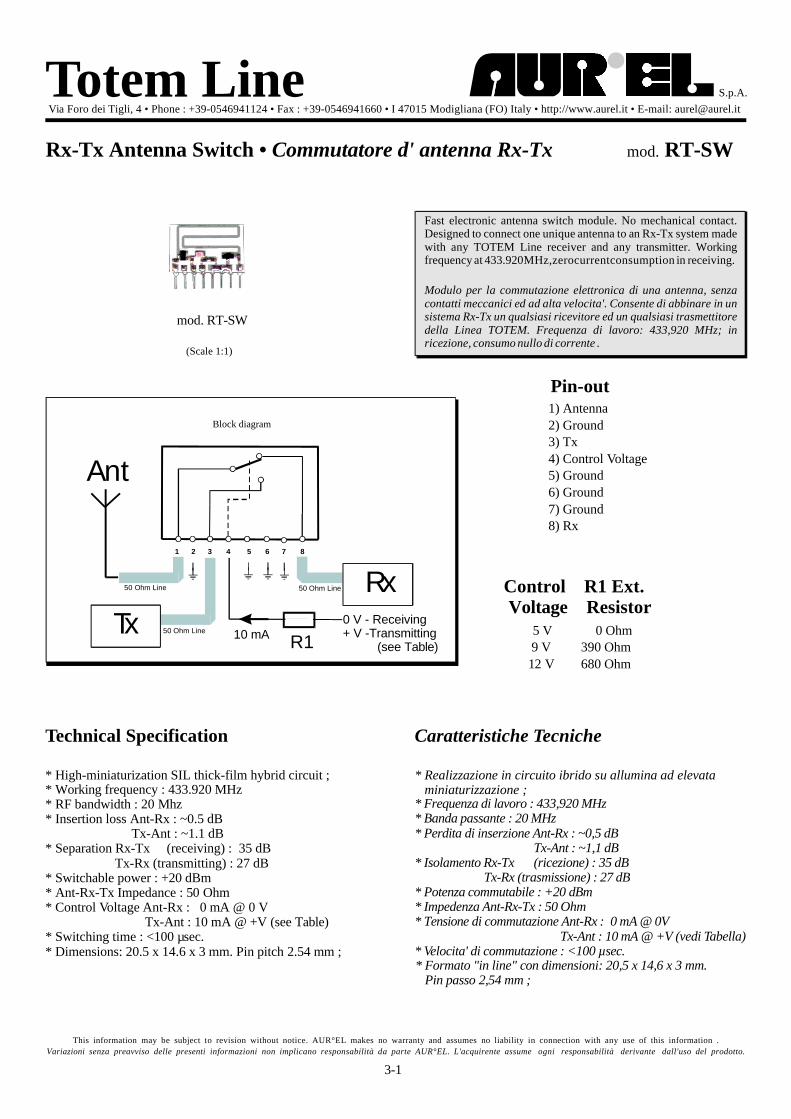
Fast electronic antenna switch module. No mechanical contact.Designed to connect one unique antenna to an Rx-Tx system madewith any TOTEM Line receiver and any transmitter. Workingfrequency at 433.920MHz,zerocurrentconsumption in receiving.
Modulo per la commutazione elettronica di una antenna, senzacontatti meccanici ed ad alta velocita'. Consente di abbinare in unsistema Rx-Tx un qualsiasi ricevitore ed un qualsiasi trasmettitoredella Linea TOTEM. Frequenza di lavoro: 433,920 MHz; inricezione, consumo nullo di corrente .
mod. RT-SW
Caratteristiche Tecniche
* Realizzazione in circuito ibrido su allumina ad elevataminiaturizzazione ;
* Frequenza di lavoro : 433,920 MHz* Banda passante : 20 MHz* Perdita di inserzione Ant-Rx : ~0,5 dB
Tx-Ant : ~1,1 dB* Isolamento Rx-Tx (ricezione) : 35 dB
Tx-Rx (trasmissione) : 27 dB* Potenza commutabile : +20 dBm* Impedenza Ant-Rx-Tx : 50 Ohm* Tensione di commutazione Ant-Rx : 0 mA @ 0V
Tx-Ant : 10 mA @ +V (vedi Tabella)* Velocita' di commutazione : <100 µsec.* Formato "in line" con dimensioni: 20,5 x 14,6 x 3 mm.
Pin passo 2,54 mm ;
Technical Specification
* High-miniaturization SIL thick-film hybrid circuit ;* Working frequency : 433.920 MHz* RF bandwidth : 20 Mhz* Insertion loss Ant-Rx : ~0.5 dB
Tx-Ant : ~1.1 dB* Separation Rx-Tx (receiving) : 35 dB
Tx-Rx (transmitting) : 27 dB* Switchable power : +20 dBm* Ant-Rx-Tx Impedance : 50 Ohm* Control Voltage Ant-Rx : 0 mA @ 0 V
Tx-Ant : 10 mA @ +V (see Table)* Switching time : <100 µsec.* Dimensions: 20.5 x 14.6 x 3 mm. Pin pitch 2.54 mm ;
Totem Line S.p.A.
Via Foro dei Tigli, 4 • Phone : +39-0546941124 • Fax : +39-0546941660 • I 47015 Modigliana (FO) Italy • http://www.aurel.it • E-mail: [email protected]
This information may be subject to revision without notice. AUR°EL makes no warranty and assumes no liability in connection with any use of this information .Variazioni senza preavviso delle presenti informazioni non implicano responsabilità da parte AUR°EL. L'acquirente assume ogni responsabilità derivante dall'uso del prodotto.
Rx-Tx Antenna Switch • Commutatore d' antenna Rx-Tx
(Scale 1:1)
mod. RT-SW
Pin-out
Control R1 Ext.Voltage Resistor
1) Antenna2) Ground3) Tx4) Control Voltage5) Ground6) Ground7) Ground8) Rx
5 V 0 Ohm9 V 390 Ohm12 V 680 Ohm
R110 mA
3-1
Linear monolitic amplifier (AB1 class) working at UHFfrequencies. Low signal distortion and low harmonic generation.Works on both digital and analog carriers.Suitable for telecontrol or audio applications, when distance or RFinterferences creates transmission problems.
Amplificatore lineare monolitico (in classe AB1) operante sullefrequenze UHF. Caratterizzato da bassa distorsione del segnaleamplificato e da minima emissione di armoniche, amplificaportanti sia analogiche che digitali.Adatto alle installazioni di telecontrollo o trasmissione audio sudistanza relativamente lunga e/o in presenza di segnaliinterferenti.
mod. PLA 05 W-433
Totem Line S.p.A.
Via Foro dei Tigli, 4 • Phone : +39-0546941124 • Fax : +39-0546941660 • I 47015 Modigliana (FO) Italy • http://www.aurel.it • E-mail: [email protected]
This information may be subject to revision without notice. AUR°EL makes no warranty and assumes no liability in connection with any use of this information .Variazioni senza preavviso delle presenti informazioni non implicano responsabilità da parte AUR°EL. L'acquirente assume ogni responsabilità derivante dall'uso del prodotto.
3-14
Caratteristiche Tecniche
* Frequenza di lavoro: 430 ÷ 435 Mhz ;
Technical Specification
* Work frequency: 430 to 435 Mhz ;
Power Linear Amplifier • Amplificatore lineare di potenza
Pin-out
1) Ground2) +7÷+10 dBm Input
(@ 50 )3) 0÷+5 dBm Input
(@ 50 )4) Ground5) +V (+12÷15 Vdc)6) Ground
W
W
9) Ground10) TX Enable (+3÷+8 Vdc)11) Ground13) Ground14) +24÷+27 dBm Output
(@ 50 )15) Ground
W
* High-miniaturization SMT circuit ; * Realizzazione in tecnologia SMT ;* Enclosed in metal case for RF shielding and heat dissipation ;
* Custom design available on request ;* Dimensions: 60 x 34 x 7.3 mm. Pin pitch 2.54 mm ;
Tab. 1_ Typical consumption and performances.
* Contenitore metallico per schermatura e dissipazione del calore ;
* Possibilità di versioni "custom" su richiesta ;
* Formato "in line". Dimensioni: 60 x 34 x 7,3 mm.Pin passo 2,54 mm ;
* Due ingressi separati per diversi livelli di potenza ;* Alimentazione: +12 Vdc (+15 Vdc MAX) ;
(+27 dBm @ 15 Vdc) ;* Potenza in uscita (± 1 dBm) su 50 : +24 dBm @ 12 VdcW
Block diagram
(Scale 1:1)
* Omologabile I-ETS 300 220 Classe IV (@12 V) ;* Homologable I-ETS 300 220 (@12 V), IV°class ;
* Double RF input pin for better fitting ;* Power supply: +12 Vdc (+15 Vdc Max.) ;
(+27 dBm @ 15 Vdc) ;* Ouput Power (± 1 dBm) on 50 : +24 dBm @ 12 VdcW
15
15
+3 ÷ 8
+3 ÷ 8
23
25
23
25
24
27
24
27
+3 ÷ 8
+3 ÷ 8
+3 ÷ 8
+3 ÷ 8
+3 ÷ 8
+3 ÷ 8
0
15
15
12
12
12
12
12 ÷ 15
Power supplypin 5 ( )V
Enablepin 10 ( )V
PWR OUTpin 14 ( )dBm
Consumption( )mA
N.C.
N.C.
5
5
0
0
N.C.
N.C.
PWR INpin 3 ( )dBm
N.C.
N.C.
7
7
10
10
N.C.
N.C.
PWR INpin 2 ( )dBm
FILTER FILTER
1 2 3 4 5 6 9 10 11 13 14 15
~~ ~~
Tab. 1
Application note • Nota applicativa mod. PLA 05 W-433
This information may be subject to revision without notice. AUR°EL makes no warranty and assumes no liability in connection with any use of this information .Variazioni senza preavviso delle presenti informazioni non implicano responsabilità da parte AUR°EL. L'acquirente assume ogni responsabilità derivante dall'uso del prodotto.
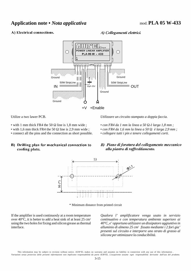
53
* Minimum distance from printed circuit
Qualora l’ amplificatore venga usato in serviziocontinuativo e con temperatura ambiente superiore ai40°C, e’ opportuno utilizzare un dissipatore aggiuntivo inalluminio di almeno 25 cm fissato mediante i 2 fori gia’presenti sul circuito e interporre uno strato di grasso alsilicone per ottimizzare la conducibilità.
2
Utilizzare un circuito stampato a doppia faccia.
• con FR4 da 1 mm la linea a 50 è larga 1,8 mm ;• con FR4 da 1,6 mm la linea a 50 è larga 2,9 mm ;• collegare tutti i pin e tenere collegamenti corti.
ΩΩ
Utilize a two lawer PCB.
• with 1 mm thick FR4 the 50 line is 1,8 mm wide ;• with 1,6 mm thick FR4 the 50 line is 2,9 mm wide ;• connect all the pins and the connection as short possible.
ΩΩ
If the amplifier is used continuosly at a room temperatureover 40°C, it is better to add a heat sink of at least 25 cmusing the two holes for fixing and silicon grease as thermalinterface.
2
POWER LINEAR AMPLIFIER
1
S.p.A.
50 StripLineW50 StripLineW
Ground
Ground
Ground
10µF-25V
Ground
IN OUT
+V +Enable
3-15
TOTEM LINE
THICK FILM TECHNOLOGYVia Foro dei Tigli, 4
47015 MODIGLIANA (FO) • ITALY
Tel. +39-0546941124 • Fax +39-0546941660
Home page: http://www.aurel.it • E-mail: [email protected]
Reproduction of this catalogue or part thereof is strictly prohibitedwithoutthewrittenconsent ofAUR°ELS.p.A.Thepresent cataloguecanbeexclusivelydisclosed, distributed and generallyusedforsalespurposes byofficialAUR°EL dealers, which have beendulyauthorized to thiseffect.
Nessuna partediquestocatalogopotràessereriprodotta senza l'autorizzazione scritta della AUR°EL S.p.A.Il presentecatalogo può venire divulgato,distribuito, utilizzato comeveicolo di tentata vendita esclusivamentedaorganizzazioni ufficialmente riconosciute da AUR°EL S.p.A.
Printed in Oct.1998 vm


![AIHP - LEERDOELSTELLINGEN website€¦ · $fdghplh yrru ,qwhjudwlhyh hq +xpdqlvwlvfkh 3v\fkrorjlh hq 3v\fkrwkhudslh y]z xsgdwh 3k 9udqfnhq 'h ddqsdn ydq khw rqehzxvwh . hq ,](https://static.fdocuments.nl/doc/165x107/5f7f0cc1b2a3067a4c6e213d/aihp-leerdoelstellingen-fdghplh-yrru-qwhjudwlhyh-hq-xpdqlvwlvfkh-3vfkrorjlh.jpg)