Datasheet 23
8
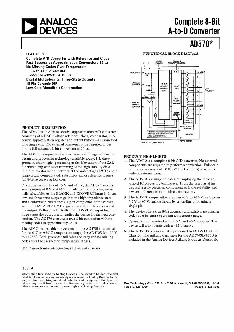
FUNCTIONAL BLOCK DIAGRAM a Complete 8-Bit A-to-D Converter AD570* FEATURES Complete A/D Converter with Reference and Clock Fast Successive Approximation Conversion: 25 s No Missing Codes Over Temperature 0C to +70C: AD570J –55C to +125C: AD570S Digital Multiplexi ng: Three-State Outputs 18-Pin Ceramic DIP Low Cost Monolithic Construction PRODUCT DESCRIPTION The AD570 is an 8-bit successive approximation A/D converter consisting of a DAC, voltage reference, clock, comparator, suc- cessive approximation register and output buffers—all fabricated on a single chip. No external components are required to per- form a full accuracy 8-bit conversion in 25 µ s. The AD570 incorporates the most advanced integrated circuit design and processing technology available today. I 2 L (inte- grated injection logic) processing in the fabrication of the SAR function along with laser trimming of the high stability SiCr thin-film resistor ladder network at the wafer stage (LWT) and a temperature compensated, subsurface Zener reference insures full 8-bit accuracy at low cost. Operating on supplies of +5 V and –15 V, the AD570 accepts analog inputs of 0 V to +10 V unipolar of ± 5 V bipolar, exter- nally selectable. As the BLANK and CONVERT input is driven low, the three-state outputs go into the high impedance state and a conversion commences. Upon completion of the conver- sion, the DATA READY line goes low and the data appears at the output. Pulling the BLANK and CONVERT input high three states the outputs and readies the device for the next con- version. The AD570 executes a true 8-bit conversion with no missing codes in approximately 25 µ s. The AD570 is available in two version; the AD570J is specified for the 0°C to +70°C temperature range, the AD570S for –55°C to +125°C. Both guarantee full 8-bit accuracy and no missing codes over their respective temperature ranges. *U.S. Patents Numbered: 3,940,760; 4,213,806 and 4,136,349. REV. A Information furnished by Analog Devices is believed to be accurate and reliable. However, no responsibility is assumed by Analog Devices for its use, nor for any infringements of patents or other rights of third parties which may result from its use. No license is granted by implication or otherwise under any patent or patent rights of Analog Devices. One Technology Way, P.O. Box 9106, Norwood, MA 02062-9106, U.S.A. Tel: 617/329-4700 Fax: 617/326-8703 PRODUCT HIGHLIGHTS 1. The AD570 is a compl ete 8-bit A/D con verte r. No extern al components are required to perform a conversion. Full-scale calibration accuracy of ± 0.8% (2 LSB of 8 bits) is achieved without external trims. 2. The AD570 is a singl e chip devic e employi ng the most ad- vanced IC processing techniques. Thus, the user has at his disposal a truly precision component with the reliability and low cost inherent in monolithic construction, 3. The AD570 acc epts eithe r unipol ar (0 V to +10 V) or bipolar (–5 V to +5 V) analog inputs by grounding or opening a single pin. 4. The devic e offers true 8-bi t accura cy and exhib its no missin g codes over its entire operating temperature range. 5. Opera tion is guar antee d with –15 V and +5 V supplie s. The device will also operate with a –12 V supply. 6. The AD570S is also av ailab le proces sed to MIL-STD-883C, Class B. The military data sheet for the AD570SD/883B is included in the Analog Devices Military Products Databook.
-
Upload
fida-pyrtuh -
Category
Documents
-
view
217 -
download
0
Transcript of Datasheet 23
8/2/2019 Datasheet 23
http://slidepdf.com/reader/full/datasheet-23 1/8
FUNCTIONAL BLOCK DIAGRAM
a Complete 8-BitA-to-D Converter
AD570*FEATURES
Complete A/D Converter with Reference and ClockFast Successive Approximation Conversion: 25s
No Missing Codes Over Temperature
0C to +70C: AD570J
–55C to +125C: AD570S
Digital Multiplexing: Three-State Outputs
18-Pin Ceramic DIP
Low Cost Monolithic Construction
PRODUCT DESCRIPTION
The AD570 is an 8-bit successive approximation A/D converter
consisting of a DAC, voltage reference, clock, comparator, suc-
cessive approximation register and output buffers—all fabricated
on a single chip. No external components are required to per-
form a full accuracy 8-bit conversion in 25 µs.
The AD570 incorporates the most advanced integrated circuit
design and processing technology available today. I2L (inte-
grated injection logic) processing in the fabrication of the SAR
function along with laser trimming of the high stability SiCr
thin-film resistor ladder network at the wafer stage (LWT) and a
temperature compensated, subsurface Zener reference insuresfull 8-bit accuracy at low cost.
Operating on supplies of +5 V and –15 V, the AD570 accepts
analog inputs of 0 V to +10 V unipolar of ±5 V bipolar, exter-
nally selectable. As the BLANK and CONVERT input is driven
low, the three-state outputs go into the high impedance state
and a conversion commences. Upon completion of the conver-
sion, the DATA READY line goes low and the data appears at
the output. Pulling the BLANK and CONVERT input high
three states the outputs and readies the device for the next con-
version. The AD570 executes a true 8-bit conversion with no
missing codes in approximately 25 µs.
The AD570 is available in two version; the AD570J is specified
for the 0°C to +70°C temperature range, the AD570S for –55°Cto +125°C. Both guarantee full 8-bit accuracy and no missing
codes over their respective temperature ranges.
*U.S. Patents Numbered: 3,940,760; 4,213,806 and 4,136,349.
REV. A
Information furnished by Analog Devices is believed to be accurate andreliable. However, no responsibility is assumed by Analog Devices for itsuse, nor for any infringements of patents or other rights of third partieswhich may result from its use. No license is granted by implication orotherwise under any patent or patent rights of Analog Devices.
One Technology Way, P.O. Box 9106, Norwood, MA 02062-9106, U.S.A
Tel: 617/329-4700 Fax: 617/326-8703
PRODUCT HIGHLIGHTS
1. The AD570 is a complete 8-bit A/D converter. No external
components are required to perform a conversion. Full-scale
calibration accuracy of ±0.8% (2 LSB of 8 bits) is achieved
without external trims.2. The AD570 is a single chip device employing the most ad-
vanced IC processing techniques. Thus, the user has at his
disposal a truly precision component with the reliability and
low cost inherent in monolithic construction,
3. The AD570 accepts either unipolar (0 V to +10 V) or bipola
(–5 V to +5 V) analog inputs by grounding or opening a
single pin.
4. The device offers true 8-bit accuracy and exhibits no missing
codes over its entire operating temperature range.
5. Operation is guaranteed with –15 V and +5 V supplies. The
device will also operate with a –12 V supply.
6. The AD570S is also available processed to MIL-STD-883C,Class B. The military data sheet for the AD570SD/883B is
included in the Analog Devices Military Products Databook.
8/2/2019 Datasheet 23
http://slidepdf.com/reader/full/datasheet-23 2/8
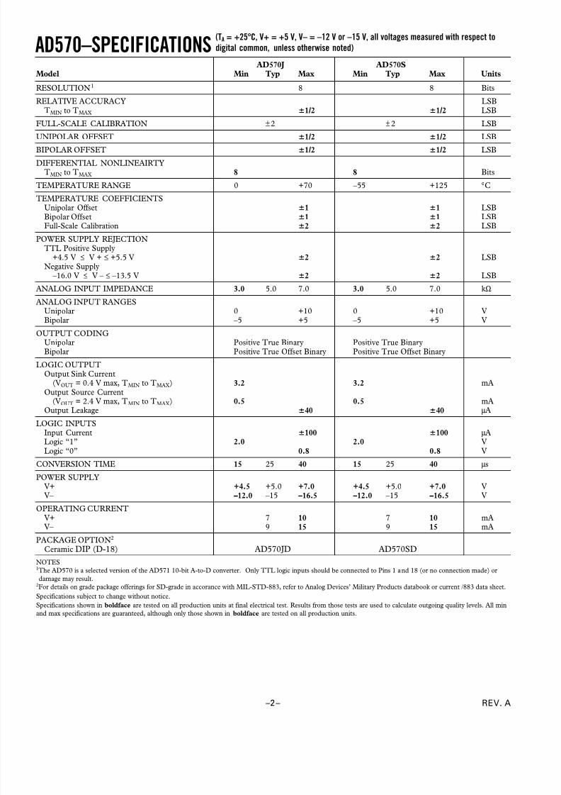
AD570–SPECIFICATIONS(TA = +25C, V+ = +5 V, V– = –12 V or –15 V, all voltages measured with respect to
digital common, unless otherwise noted)
REV. A–2–
AD570J AD570SModel Min Typ Max Min Typ Max Units
RESOLUTION1 8 8 Bits
RELATIVE ACCURACY LSB
TMIN to TMAX 1/2 1/2 LSB
FULL-SCALE CALIBRATION ±2 ±2 LSB
UNIPOLAR OFFSET 1/2 1/2 LSBBIPOLAR OFFSET 1/2 1/2 LSB
DIFFERENTIAL NONLINEAIRTYTMIN to TMAX 8 8 Bits
TEMPERATURE RANGE 0 +70 –55 +125 °C
TEMPERATURE COEFFICIENTS
Unipolar Offset 1 1 LSB
Bipolar Offset 1 1 LSBFull-Scale Calibration 2 2 LSB
POWER SUPPLY REJECTION
TTL Positive Supply+4.5 V ≤ V + ≤ +5.5 V 2 2 LSB
Negative Supply
–16.0 V ≤ V – ≤ –13.5 V 2 2 LSBANALOG INPUT IMPEDANCE 3.0 5.0 7.0 3.0 5.0 7.0 kΩ
ANALOG INPUT RANGESUnipolar 0 +10 0 +10 V
Bipolar –5 +5 –5 +5 V
OUTPUT CODINGUnipolar Positive True Binary Positive True Binary
Bipolar Positive True Offset Binary Positive True Offset Binary
LOGIC OUTPUTOutput Sink Current
(VOUT = 0.4 V max, TMIN to TMAX) 3.2 3.2 mA
Output Source Current(VOUT = 2.4 V max, TMIN to TMAX) 0.5 0.5 mA
Output Leakage 40 40 µA
LOGIC INPUTS
Input Current 100 100 µALogic “1” 2.0 2.0 V
Logic “0” 0.8 0.8 V
CONVERSION TIME 15 25 40 15 25 40 µs
POWER SUPPLYV+ +4.5 +5.0 +7.0 +4.5 +5.0 +7.0 VV– –12.0 –15 –16.5 –12.0 –15 –16.5 V
OPERATING CURRENT
V+ 7 10 7 10 mAV– 9 15 9 15 mA
PACKAGE OPTION2
Ceramic DIP (D-18) AD570JD AD570SD
NOTES1The AD570 is a selected version of the AD571 10-bit A-to-D converter. Only TTL logic inputs should be connected to Pins 1 and 18 (or no connection made) or
damage may result.2For details on grade package offerings for SD-grade in accorance with MIL-STD-883, refer to Analog Devices’ Military Products databook or current /883 data sheet.
Specifications subject to change without notice.
Specifications shown in boldface are tested on all production units at final electrical test. Results from those tests are used to calculate outgoing quality levels. All min
and max specifications are guaranteed, although only those shown in boldface are tested on all production units.
8/2/2019 Datasheet 23
http://slidepdf.com/reader/full/datasheet-23 3/8
AD570
REV. A –3–
signal, an input current will be generated which exactly matches
the DAC output with all bits on. (The input resistor is trimmed
slightly low to facilitate user trimming, as discussed on the next
page.)
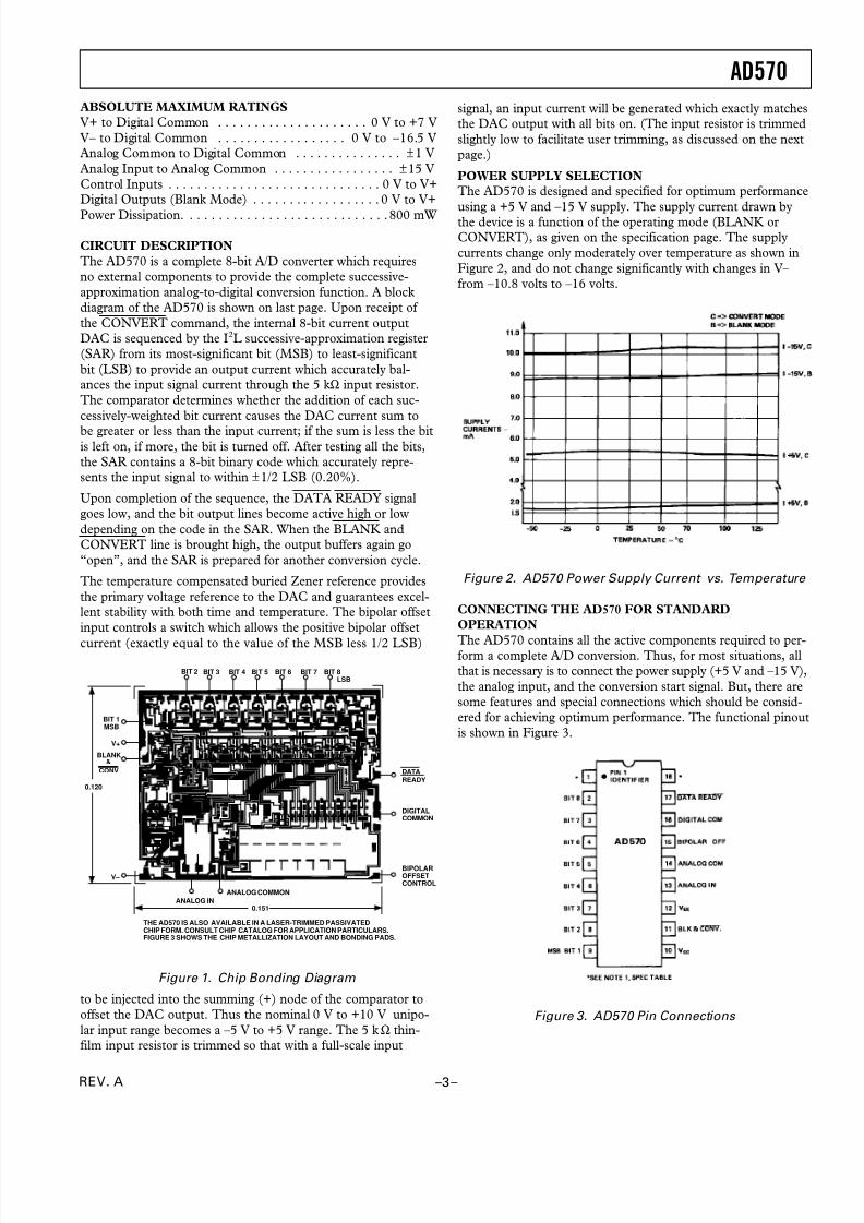
POWER SUPPLY SELECTION
The AD570 is designed and specified for optimum performance
using a +5 V and –15 V supply. The supply current drawn by
the device is a function of the operating mode (BLANK or
CONVERT), as given on the specification page. The supply
currents change only moderately over temperature as shown in
Figure 2, and do not change significantly with changes in V–
from –10.8 volts to –16 volts.
Figure 2. AD570 Power Supply Current vs. Temperature
CONNECTING THE AD570 FOR STANDARD
OPERATION
The AD570 contains all the active components required to per-form a complete A/D conversion. Thus, for most situations, all
that is necessary is to connect the power supply (+5 V and –15 V),
the analog input, and the conversion start signal. But, there are
some features and special connections which should be consid-
ered for achieving optimum performance. The functional pinout
is shown in Figure 3.
Figure 3. AD570 Pin Connections
ABSOLUTE MAXIMUM RATINGS
V+ to Digital Common . . . . . . . . . . . . . . . . . . . . . 0 V to +7 V
V– to Digital Common . . . . . . . . . . . . . . . . . . 0 V to –16.5 V
Analog Common to Digital Common . . . . . . . . . . . . . . . ±1 V
Analog Input to Analog Common . . . . . . . . . . . . . . . . . ±15 V
Control Inputs . . . . . . . . . . . . . . . . . . . . . . . . . . . . . . 0 V to V+
Digital Outputs (Blank Mode) . . . . . . . . . . . . . . . . . . 0 V to V+
Power Dissipation. . . . . . . . . . . . . . . . . . . . . . . . . . . . .800 mW
CIRCUIT DESCRIPTION
The AD570 is a complete 8-bit A/D converter which requires
no external components to provide the complete successive-
approximation analog-to-digital conversion function. A block
diagram of the AD570 is shown on last page. Upon receipt of
the CONVERT command, the internal 8-bit current output
DAC is sequenced by the I2L successive-approximation register
(SAR) from its most-significant bit (MSB) to least-significant
bit (LSB) to provide an output current which accurately bal-
ances the input signal current through the 5 kΩ input resistor.
The comparator determines whether the addition of each suc-
cessively-weighted bit current causes the DAC current sum to
be greater or less than the input current; if the sum is less the bitis left on, if more, the bit is turned off. After testing all the bits,
the SAR contains a 8-bit binary code which accurately repre-
sents the input signal to within ±1/2 LSB (0.20%).
Upon completion of the sequence, the DATA READY signal
goes low, and the bit output lines become active high or low
depending on the code in the SAR. When the BLANK and
CONVERT line is brought high, the output buffers again go
“open”, and the SAR is prepared for another conversion cycle.
The temperature compensated buried Zener reference provides
the primary voltage reference to the DAC and guarantees excel-
lent stability with both time and temperature. The bipolar offset
input controls a switch which allows the positive bipolar offset
current (exactly equal to the value of the MSB less 1/2 LSB)
DATA
READY
DIGITAL
COMMON
BIPOLAR
OFFSET
CONTROL
ANALOG IN
ANALOG COMMON
0.151
THE AD570 IS ALSO AVAILABLE IN A LASER-TRIMMED PASSIVATED
CHIP FORM. CONSULT CHIP CATALOG FOR APPLICATION PARTICULARS.
FIGURE 3 SHOWS THE CHIP METALLIZATION LAYOUT AND BONDING PADS.
BIT 1
MSB
V+
BLANK
&
CONV
V–
0.120
BIT 2 BIT 3 BIT 4 BIT 5 BIT 6 BIT 7 BIT 8
LSB
Figure 1. Chip Bonding Diagram
to be injected into the summing (+) node of the comparator to
offset the DAC output. Thus the nominal 0 V to +10 V unipo-
lar input range becomes a –5 V to +5 V range. The 5 kΩ thin-
film input resistor is trimmed so that with a full-scale input
8/2/2019 Datasheet 23
http://slidepdf.com/reader/full/datasheet-23 4/8
AD570
REV. A–4–
FULL-SCALE CALIBRATION
The 5 kΩ thin-film input resistor is laser trimmed to produce a
current which matches the full-scale current of the internal
DAC—plus about 0.3%—when a full-scale analog input voltage
of 9.961 volts (10 volts—1 LSB) is applied at the input. The in-
put resistor is trimmed in this way so that if a fine trimming
potentiometer is inserted in series with the input signal, the in-
put current at the full-scale input voltage can be trimmed downto match the DAC full-scale current as precisely as desired.
However, for many applications the nominal 9.961 volt full
scale can be achieved to sufficient accuracy by simply inserting a
15 Ω resistor in series with the analog input to Pin 13. Typical
full-scale calibration error will then be about ±2 LSB or ±0.8%.
If a more precise calibration is desired, a 200 Ω trimmer should
be used instead. Set the analog input at 9.961 volts, and set the
trimmer so that the output code is just at the transition between
11111110 and 11111111. Each LSB will then have a weight of
39.06 mV. If a nominal full scale of 10.24 volts is desired
(which makes the LSB have a value of exactly 40.00 mV), a
50 Ω resistor in series with a 200 Ω trimmer (or a 500 Ω trim-
mer with good resolution) should be used. Of course, larger full-
scale ranges can be arranged by using a larger input resistor, butlinearity and full-scale temperature coefficient may be compro-
mised if the external resistor becomes a sizable percentage of
5 kΩ.
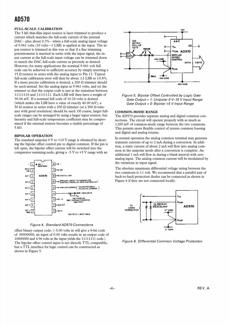
BIPOLAR OPERATION
The standard unipolar 0 V to +10 V range is obtained by short-
ing the bipolar offset control pin to digital common. If the pin is
left open, the bipolar offset current will be switched into the
comparator summing node, giving a –5 V to +5 V range with an
Figure 4. Standard AD570 Connections
offset binary output code. (–5.00 volts in will give a 8-bit code
of 00000000; an input of 0.00 volts results in an output code of
10000000 and 4.96 volts at the input yields the 11111111 code.)
The bipolar offset control input is not directly TTL compatible,
but a TTL interface for logic control can be constructed as
shown in Figure 5.
Figure 5. Bipolar Offset Controlled by Logic Gate
Gate Output = 1: Unipolar 0 V–10 V Input Range
Gate Output = 0: Bipolar ±5 V Input Range
COMMON-MODE RANGE
The AD570 provides separate analog and digital common con-
nections. The circuit will operate properly with as much as
±200 mV of common-mode range between the two commons.
This permits more flexible control of system common bussing
and digital and analog returns.
In normal operation the analog common terminal may generate
transient currents of up to 2 mA during a conversion. In addi-
tion, a static current of about 2 mA will flow into analog com-
mon in the unipolar mode after a conversion is complete. An
additional 1 mA will flow in during a blank interval with zero
analog input. The analog common current will be modulated by
the variations in input signal.
The absolute maximum differential voltage rating between the
two commons is ±1 volt. We recommend that a parallel pair of back-to-back protection diodes can be connected as shown in
Figure 6 if they are not connected locally.
Figure 6. Differential Common Voltage Protection
8/2/2019 Datasheet 23
http://slidepdf.com/reader/full/datasheet-23 5/8
AD570
REV. A –5–
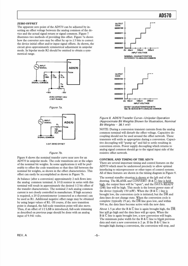
ZERO OFFSET
The apparent zero point of the AD570 can be adjusted by in-
serting an offset voltage between the analog common of the de-
vice and the actual signal return or signal common. Figure 7
illustrates two methods of providing this offset. Figure 7a shows
how the converter zero may be offset by up to ±3 bits to correct
the device initial offset and/or input signal offsets. As shown, the
circuit gives approximately symmetrical adjustment in unipolarmode. In bipolar mode R2 should be omitted to obtain a sym-
metrical range.
Figure 7a.
Figure 7b.
Figure 8 shows the nominal transfer curve near zero for an
AD570 in unipolar mode. The code transitions are at the edges
of the nominal bit weights. In some applications it will be pref-
erable to offset the code transitions so that they fall between the
nominal bit weights, as shown in the offset characteristics. This
offset can easily be accomplished as shown in Figure 7b.
At balance (after a conversion) approximately 2 mA flows into
the analog common terminal. A 10 Ω resistor in series with this
terminal will result in approximately the desired 1/2 bit offset of the transfer characteristics. The nominal 2 mA analog common
current is not closely controlled in manufacture. If high accuracy
is required, a 20 Ω potentiometer (connected as a rheostat) can
be used as R1. Additional negative offset range may be obtained
by using larger values of R1. Of course, if the zero transition
point is changed, the full-scale transition point will also move.
Thus, if an offset of 1/2 LSB is introduced, full-scale trimming
as described on previous page should be done with an analog
input of 9.941 volts.
Figure 8. AD570 Transfer Curve—Unipolar Operation
(Approximate Bit Weights Shown for Illustration, Nominal
Bit Weights 36.1 mV)
NOTE: During a conversion transient currents from the analog
common terminal will disturb the offset voltage. Capacitive de-
coupling should not be used around the offset network. These
transients will settle as appropriate during a conversion. Capaci-tive decoupling will “pump up” and fail to settle resulting in
conversion errors. Power supply decoupling which returns to
analog signal common should go to the signal input side of the
resistive offset network.
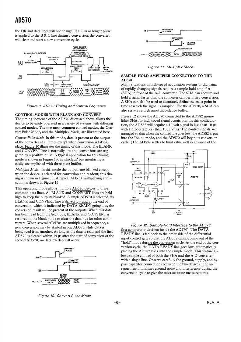
CONTROL AND TIMING OF THE AD570
There are several important timing and control features on the
AD570 which must be understood precisely to allow optimal
interfacing to microprocessor or other types of control systems.
All of these features are shown in the timing diagram in Figure 9
The normal standby situation is shown at the left end of the
drawing. The BLANK and CONVERT (B & C) line is held
high, the output lines will be “open”, and theDATA READY
(DR ) line will be high. This mode is the lowest power state of
the device (typically 150 mW). When the (B & C ) line is
brought low, the conversion cycle is initiated; but the DR and
data lines do not change state. When the conversion cycle is
complete (typically 25 µs), the DR line goes low, and within
500 ns, the data lines become active with the new data.
About 1.5 µs after the B & C line is again brought high, the DR
line will go high and the data lines will go open. When the
B & C line is again brought low, a new conversion will begin.
The minimum pulse width for the B & C line to blank previous
data and start a new conversion is 2 µs. If the B & C line is
brought high during a conversion, the conversion will stop, and
8/2/2019 Datasheet 23
http://slidepdf.com/reader/full/datasheet-23 6/8
AD570
REV. A–6–
the DR and data lines will not change. If a 2 µs or longer pulse
is applied to the B & C line during a conversion, the converter
will clear and start a new conversion cycle.
Figure 9. AD570 Timing and Control Sequence
CONTROL MODES WITH BLANK AND CONVERT
The timing sequence of the AD570 discussed above allows thedevice to be easily operated in a variety of systems with differing
control modes. The two most common control modes, the Con-
vert Pulse Mode, and the Multiplex Mode, are illustrated here.
Convert Pulse Mode– In this mode, data is present at the output
of the converter at all times except when conversion is taking
place. Figure 10 illustrates the timing of this mode. The BLANK
and CONVERT line is normally low and conversions are trig-
gered by a positive pulse. A typical application for this timing
mode is shown in Figure 13, in which µP bus interfacing is
easily accomplished with three-state buffers.
Multiplex Mode— In this mode the outputs are blanked except
when the device is selected for conversion and readout; this tim-
ing is shown in Figure 11. A typical AD570 multiplexing appli-cation is shown in Figure 14.
This operating mode allows multiple AD570 devices to drive
common data lines. All BLANK and CONVERT lines are held
high to keep the outputs blanked. A single AD570 is selected, its
BLANK and CONVERT line is driven low and at the end of
conversion, which is indicated by DATA READY going low, the
conversion result will be present at the outputs. When this data
has been read from the 8-bit bus, BLANK and CONVERT is
restored to the blank mode to clear the data bus for other con-
verters. When several AD570s are multiplexed in sequence, a
new conversion may be started in one AD570 while data is
being read from another. As long as the data is read and the first
AD570 is cleared within 15 µs after the start of conversion of the
second AD570, no data overlap will occur.
Figure 10. Convert Pulse Mode
Figure 11. Multiplex Mode
SAMPLE-HOLD AMPLIFIER CONNECTION TO THE
AD570
Many situations in high-speed acquisition systems or digitizing
of rapidly changing signals require a sample-hold amplifier
(SHA) in front of the A-D converter. The SHA can acquire and
hold a signal faster than the converter can perform a conversion.
A SHA can also be used to accurately define the exact point in
time at which the signal is sampled. For the AD570, a SHA can
also serve as a high input impedance buffer.
Figure 12 shows the AD570 connected to the AD582 mono-
lithic SHA for high speed signal acquisition. In this configura-tion, the AD582 will acquire a 10 volt signal in less than 10 µs
with a droop rate less than 100 µV/ms. The control signals are
arranged so that when the control line goes low, the AD582 is put
into the “hold” mode, and the AD570 will begin its conversion
cycle. (The AD582 settles to final value well in advance of the
Figure 12. Sample-Hold Interface to the AD570
first comparator decision inside the AD570). The DATA
READY line is fed back to the other side of the differential
input control gate so that the AD582 cannot come out of the“hold” mode during the conversion cycle. At the end of the con-
version cycle, the DATA READY line goes low, automatically
placing the AD582 back into the sample mode. This feature al-
lows simple control of both the SHA and the A-D converter
with a single line. Observe carefully the ground, supply, and by-
pass capacitor connections between the two devices. The ar-
rangement minimizes ground noise and interference during the
conversion cycle to give the most accurate measurements.
8/2/2019 Datasheet 23
http://slidepdf.com/reader/full/datasheet-23 7/8
AD570
REV. A –7–
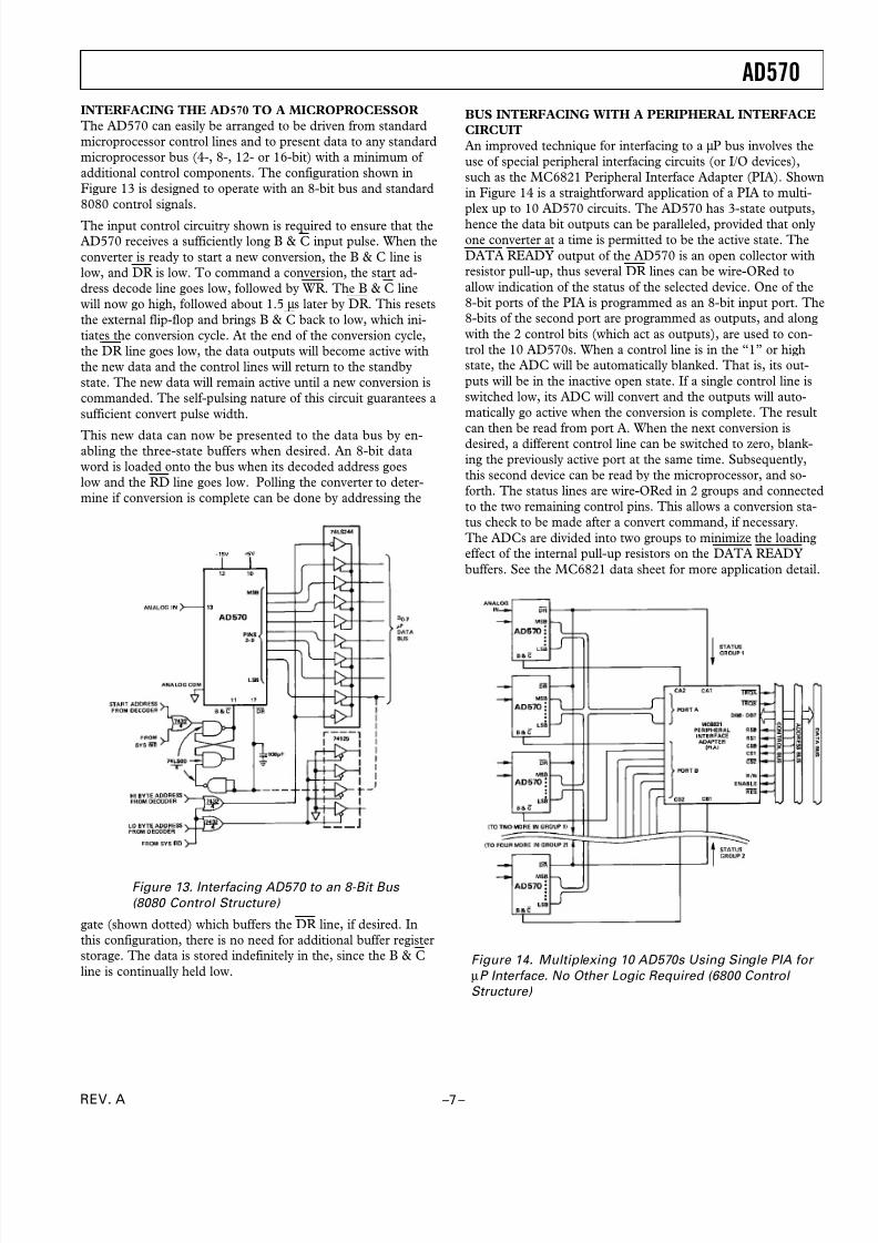
INTERFACING THE AD570 TO A MICROPROCESSOR
The AD570 can easily be arranged to be driven from standard
microprocessor control lines and to present data to any standard
microprocessor bus (4-, 8-, 12- or 16-bit) with a minimum of
additional control components. The configuration shown in
Figure 13 is designed to operate with an 8-bit bus and standard
8080 control signals.
The input control circuitry shown is required to ensure that the
AD570 receives a sufficiently long B & C input pulse. When the
converter is ready to start a new conversion, the B & C line is
low, and DR is low. To command a conversion, the start ad-
dress decode line goes low, followed by WR . The B & C line
will now go high, followed about 1.5 µs later by DR . This resets
the external flip-flop and brings B & C back to low, which ini-
tiates the conversion cycle. At the end of the conversion cycle,
the DR line goes low, the data outputs will become active with
the new data and the control lines will return to the standby
state. The new data will remain active until a new conversion is
commanded. The self-pulsing nature of this circuit guarantees a
sufficient convert pulse width.
This new data can now be presented to the data bus by en-abling the three-state buffers when desired. An 8-bit data
word is loaded onto the bus when its decoded address goes
low and the RD line goes low. Polling the converter to deter-
mine if conversion is complete can be done by addressing the
Figure 13. Interfacing AD570 to an 8-Bit Bus
(8080 Control Structure)
gate (shown dotted) which buffers the DR line, if desired. In
this configuration, there is no need for additional buffer register
storage. The data is stored indefinitely in the, since the B & C
line is continually held low.
BUS INTERFACING WITH A PERIPHERAL INTERFACE
CIRCUIT
An improved technique for interfacing to a µP bus involves the
use of special peripheral interfacing circuits (or I/O devices),
such as the MC6821 Peripheral Interface Adapter (PIA). Shown
in Figure 14 is a straightforward application of a PIA to multi-
plex up to 10 AD570 circuits. The AD570 has 3-state outputs,
hence the data bit outputs can be paralleled, provided that only
one converter at a time is permitted to be the active state. The
DATA READY output of the AD570 is an open collector with
resistor pull-up, thus several DR lines can be wire-ORed to
allow indication of the status of the selected device. One of the
8-bit ports of the PIA is programmed as an 8-bit input port. The
8-bits of the second port are programmed as outputs, and along
with the 2 control bits (which act as outputs), are used to con-
trol the 10 AD570s. When a control line is in the “1” or high
state, the ADC will be automatically blanked. That is, its out-
puts will be in the inactive open state. If a single control line is
switched low, its ADC will convert and the outputs will auto-
matically go active when the conversion is complete. The result
can then be read from port A. When the next conversion is
desired, a different control line can be switched to zero, blank-
ing the previously active port at the same time. Subsequently,
this second device can be read by the microprocessor, and so-
forth. The status lines are wire-ORed in 2 groups and connected
to the two remaining control pins. This allows a conversion sta-
tus check to be made after a convert command, if necessary.
The ADCs are divided into two groups to minimize the loading
effect of the internal pull-up resistors on the DATA READY
buffers. See the MC6821 data sheet for more application detail.
Figure 14. Multiplexing 10 AD570s Using Single PIA for
µP Interface. No Other Logic Required (6800 Control
Structure)
8/2/2019 Datasheet 23
http://slidepdf.com/reader/full/datasheet-23 8/8
AD570
REV. A–8–
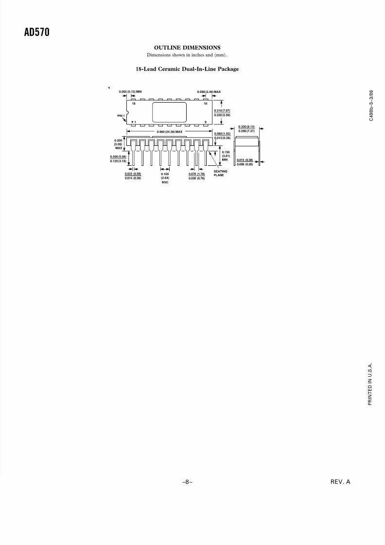
OUTLINE DIMENSIONS
Dimensions shown in inches and (mm).
18-Lead Ceramic Dual-In-Line Package
0.320 (8.13)
0.290 (7.37)
0.015 (0.38)
0.008 (0.20)
PIN 1
0.005 (0.13) MIN
18
1
0.310 (7.87)
0.220 (5.59)
0.098 (2.49) MAX
9
10
0.200
(5.08)
MAX
0.200 (5.08)
0.125 (3.18)
0.023 (0.58)
0.014 (0.36)
0.100
(2.54)
BSC
0.960 (24.38) MAX
0.070 (1.78)
0.030 (0.76)
0.060 (1.52)
0.015 (0.38)
0.150
(3.81)
MIN
SEATING
PLANE