Carbon Based High Speed 3D GaN Electronics System · 2016-03-15 · Michael Andersson, Samina...
23
Michael Andersson, Samina Bidmeshkipour, Marlene Bonmann, Andrei Vorobiev, Jan Stake Terahertz and Millimetre Wave Laboratory Department of Microtechnology and Nanoscience Chalmers University of Technology Göteborg, Sweden SSF project Carbon Based High Speed 3D GaN Electronics System Consortium meeting, 2015-03-24 1
Transcript of Carbon Based High Speed 3D GaN Electronics System · 2016-03-15 · Michael Andersson, Samina...
Michael Andersson, Samina Bidmeshkipour,
Marlene Bonmann, Andrei Vorobiev, Jan Stake
Terahertz and Millimetre Wave Laboratory
Department of Microtechnology and Nanoscience
Chalmers University of Technology
Göteborg, Sweden
SSF project
Carbon Based High Speed 3D GaN
Electronics System
Consortium meeting, 2015-03-24
1
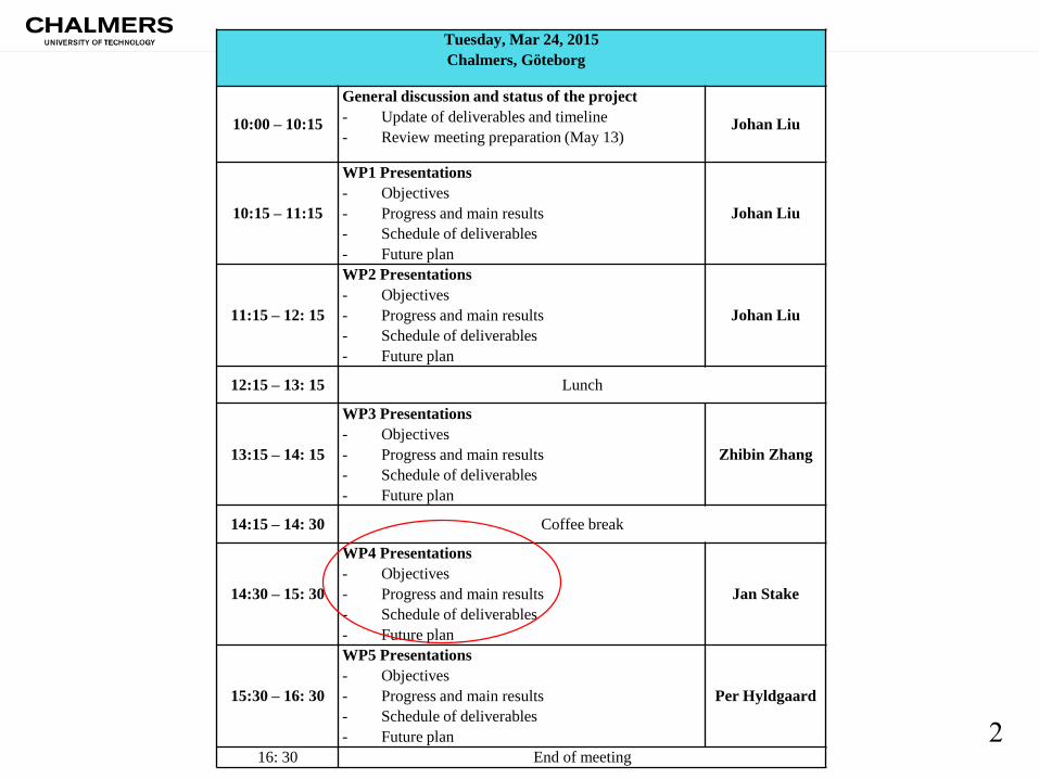
Tuesday, Mar 24, 2015
Chalmers, Göteborg
10:00 – 10:15
General discussion and status of the project
- Update of deliverables and timeline
- Review meeting preparation (May 13)Johan Liu
10:15 – 11:15
WP1 Presentations
- Objectives
- Progress and main results
- Schedule of deliverables
- Future plan
Johan Liu
11:15 – 12: 15
WP2 Presentations
- Objectives
- Progress and main results
- Schedule of deliverables
- Future plan
Johan Liu
12:15 – 13: 15 Lunch
13:15 – 14: 15
WP3 Presentations
- Objectives
- Progress and main results
- Schedule of deliverables
- Future plan
Zhibin Zhang
14:15 – 14: 30 Coffee break
14:30 – 15: 30
WP4 Presentations
- Objectives
- Progress and main results
- Schedule of deliverables
- Future plan
Jan Stake
15:30 – 16: 30
WP5 Presentations
- Objectives
- Progress and main results
- Schedule of deliverables
- Future plan
Per Hyldgaard
16: 30 End of meeting
2
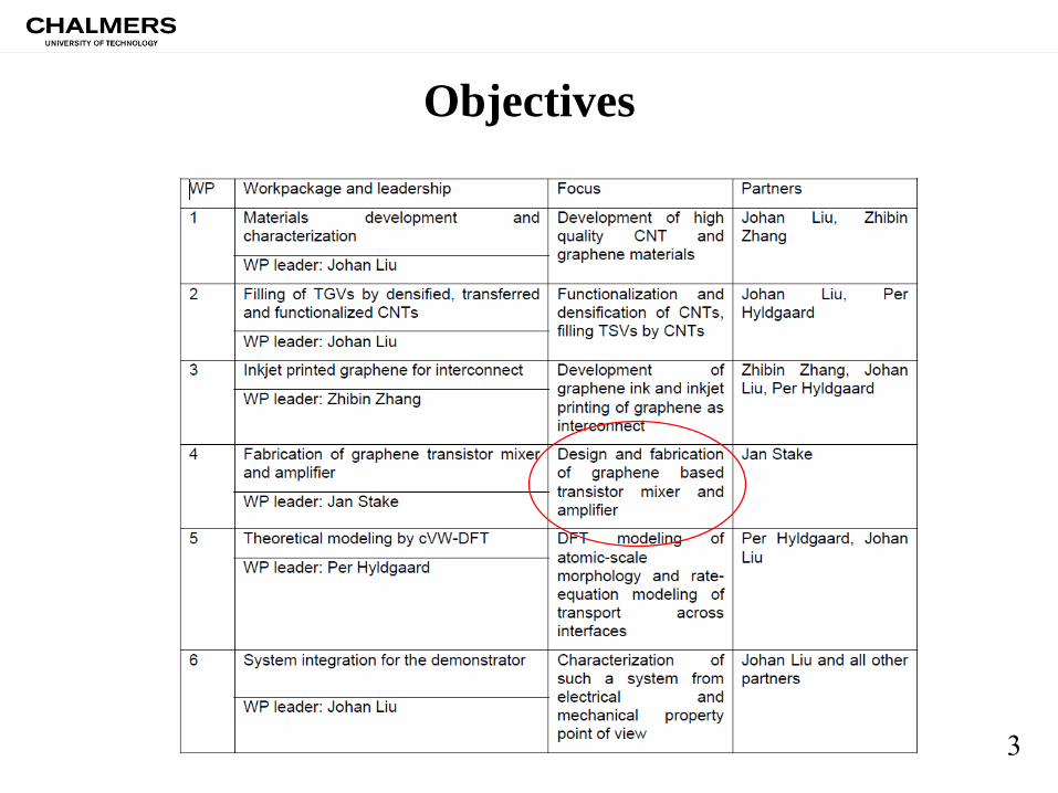
Objectives
3
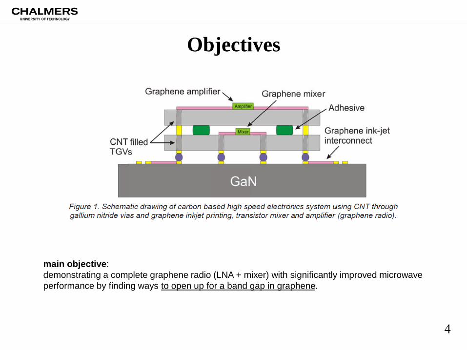
Objectives
main objective:
demonstrating a complete graphene radio (LNA + mixer) with significantly improved microwave
performance by finding ways to open up for a band gap in graphene.
4
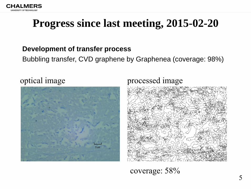
Progress since last meeting, 2015-02-20
Development of transfer process
Bubbling transfer, CVD graphene by Graphenea (coverage: 98%)
coverage: 58%
processed imageoptical image
5

Frame assisted H2 bubbling transfer
Adopted from M. Tanzid, Thesis for Master of Science, Chalmers, 2013.
6
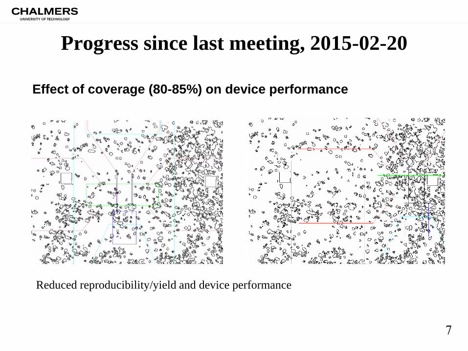
Progress since last meeting, 2015-02-20
Effect of coverage (80-85%) on device performance
Reduced reproducibility/yield and device performance
7

Copper APS etching transfer
Progress since last meeting, 2015-02-20
Ammonium persulfate
(NH4)2S2O8
8
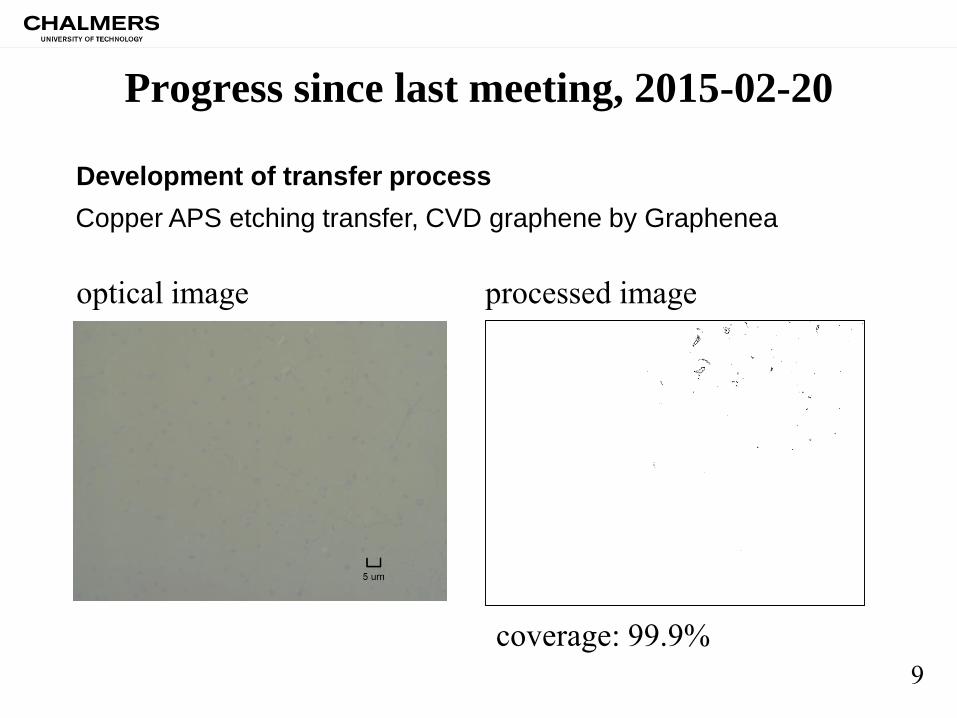
Progress since last meeting, 2015-02-20
Development of transfer process
Copper APS etching transfer, CVD graphene by Graphenea
coverage: 99.9%
processed imageoptical image
9
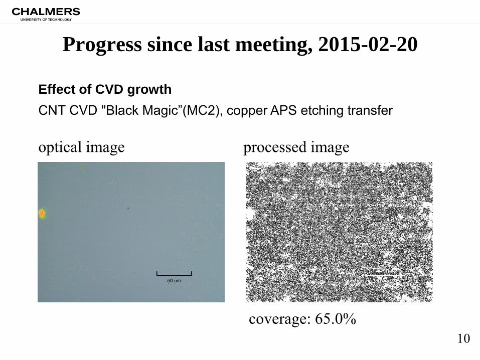
Progress since last meeting, 2015-02-20
Effect of CVD growth
CNT CVD "Black Magic”(MC2), copper APS etching transfer
coverage: 65.0%
processed imageoptical image
10
Progress since last meeting, 2015-02-20
Effect of CVD growth
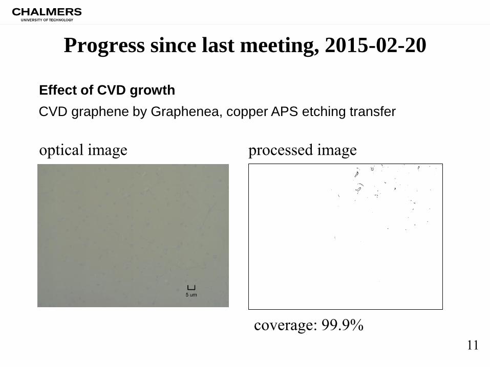
CVD graphene by Graphenea, copper APS etching transfer
coverage: 99.9%
processed imageoptical image
11
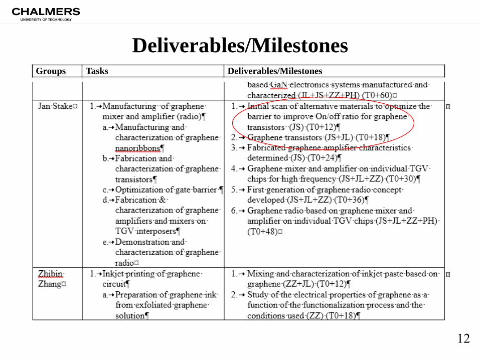
Deliverables/MilestonesGroups Tasks Deliverables/Milestones
12
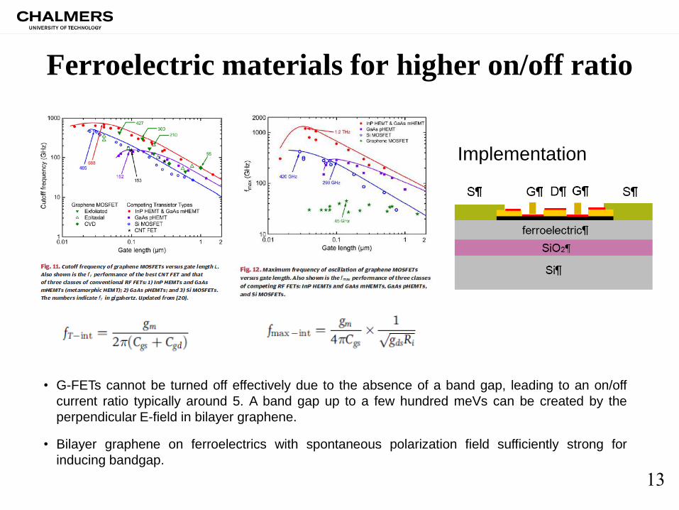
Ferroelectric materials for higher on/off ratio
• G-FETs cannot be turned off effectively due to the absence of a band gap, leading to an on/off
current ratio typically around 5. A band gap up to a few hundred meVs can be created by the
perpendicular E-field in bilayer graphene.
• Bilayer graphene on ferroelectrics with spontaneous polarization field sufficiently strong for
inducing bandgap.
Implementation
13
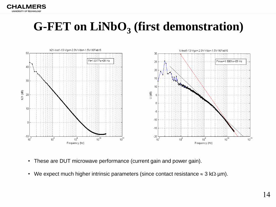
G-FET on LiNbO3 (first demonstration)
• These are DUT microwave performance (current gain and power gain).
• We expect much higher intrinsic parameters (since contact resistance 3 kµm).
14
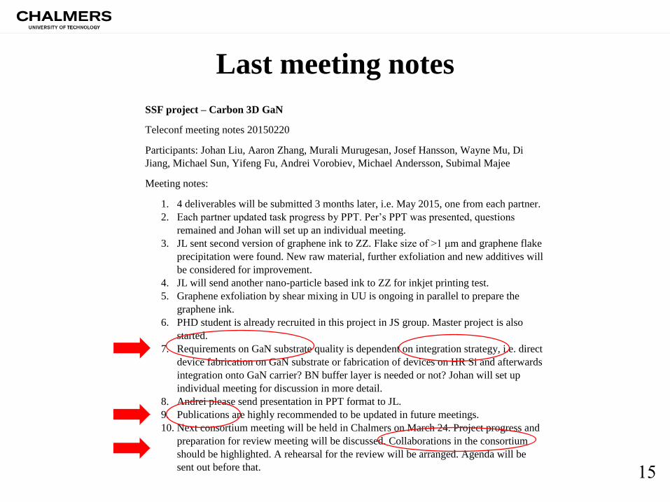
Last meeting notes
SSF project – Carbon 3D GaN
Teleconf meeting notes 20150220
Participants: Johan Liu, Aaron Zhang, Murali Murugesan, Josef Hansson, Wayne Mu, Di
Jiang, Michael Sun, Yifeng Fu, Andrei Vorobiev, Michael Andersson, Subimal Majee
Meeting notes:
1. 4 deliverables will be submitted 3 months later, i.e. May 2015, one from each partner.
2. Each partner updated task progress by PPT. Per’s PPT was presented, questions
remained and Johan will set up an individual meeting.
3. JL sent second version of graphene ink to ZZ. Flake size of >1 μm and graphene flake
precipitation were found. New raw material, further exfoliation and new additives will
be considered for improvement.
4. JL will send another nano-particle based ink to ZZ for inkjet printing test.
5. Graphene exfoliation by shear mixing in UU is ongoing in parallel to prepare the
graphene ink.
6. PHD student is already recruited in this project in JS group. Master project is also
started.
7. Requirements on GaN substrate quality is dependent on integration strategy, i.e. direct
device fabrication on GaN substrate or fabrication of devices on HR Si and afterwards
integration onto GaN carrier? BN buffer layer is needed or not? Johan will set up
individual meeting for discussion in more detail.
8. Andrei please send presentation in PPT format to JL.
9. Publications are highly recommended to be updated in future meetings.
10. Next consortium meeting will be held in Chalmers on March 24. Project progress and
preparation for review meeting will be discussed. Collaborations in the consortium
should be highlighted. A rehearsal for the review will be arranged. Agenda will be
sent out before that. 15
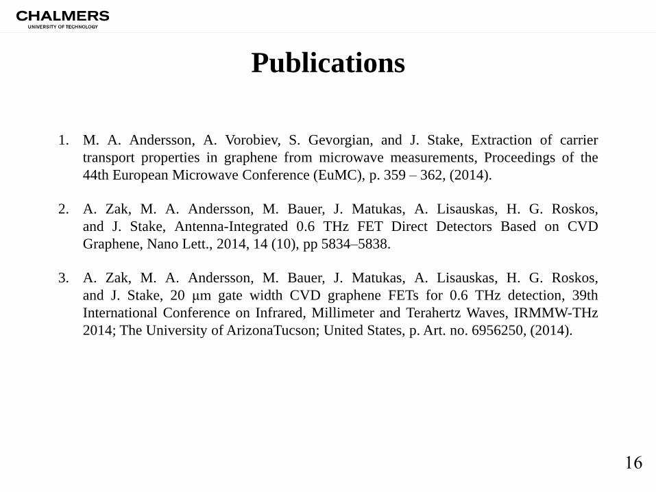
Publications
1. M. A. Andersson, A. Vorobiev, S. Gevorgian, and J. Stake, Extraction of carrier
transport properties in graphene from microwave measurements, Proceedings of the
44th European Microwave Conference (EuMC), p. 359 – 362, (2014).
2. A. Zak, M. A. Andersson, M. Bauer, J. Matukas, A. Lisauskas, H. G. Roskos,
and J. Stake, Antenna-Integrated 0.6 THz FET Direct Detectors Based on CVD
Graphene, Nano Lett., 2014, 14 (10), pp 5834–5838.
3. A. Zak, M. A. Andersson, M. Bauer, J. Matukas, A. Lisauskas, H. G. Roskos,
and J. Stake, 20 μm gate width CVD graphene FETs for 0.6 THz detection, 39th
International Conference on Infrared, Millimeter and Terahertz Waves, IRMMW-THz
2014; The University of ArizonaTucson; United States, p. Art. no. 6956250, (2014).
16
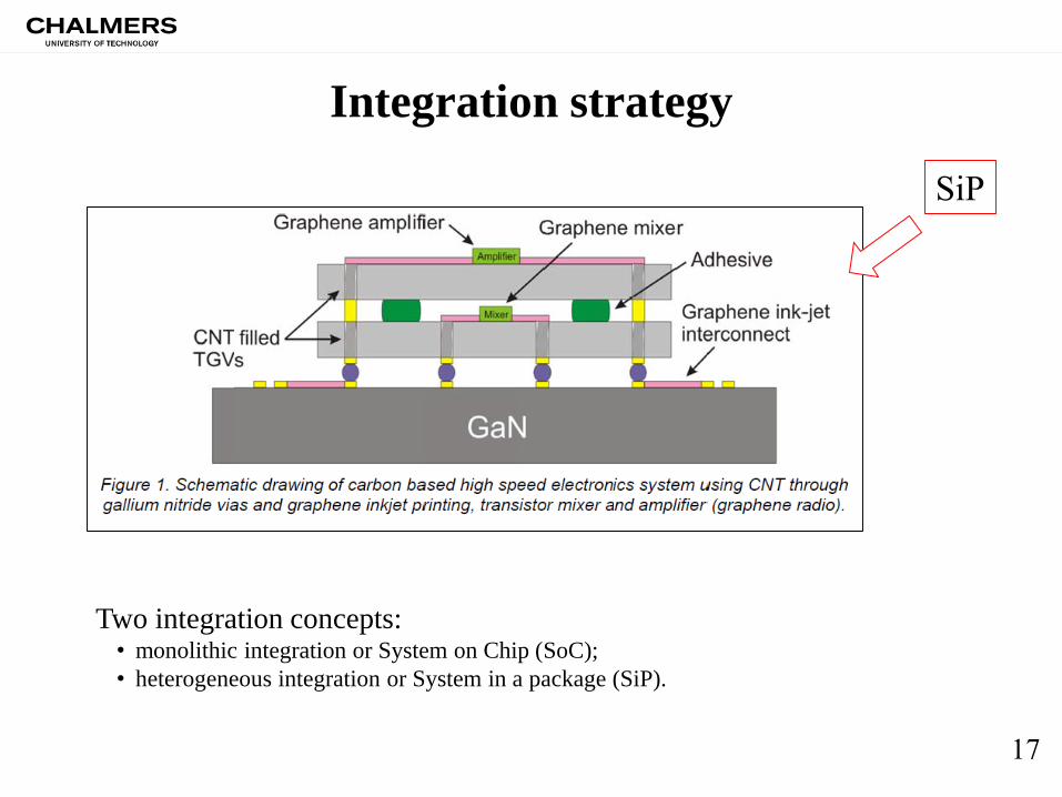
Integration strategy
Two integration concepts:• monolithic integration or System on Chip (SoC);
• heterogeneous integration or System in a package (SiP).
SiP
17
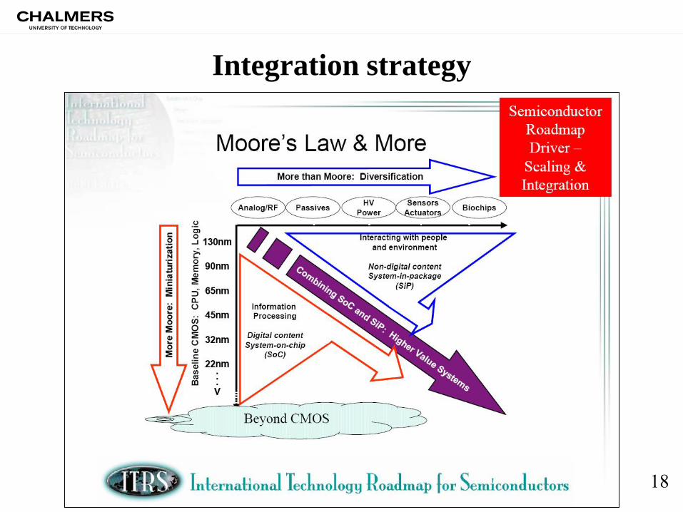
Integration strategy
18
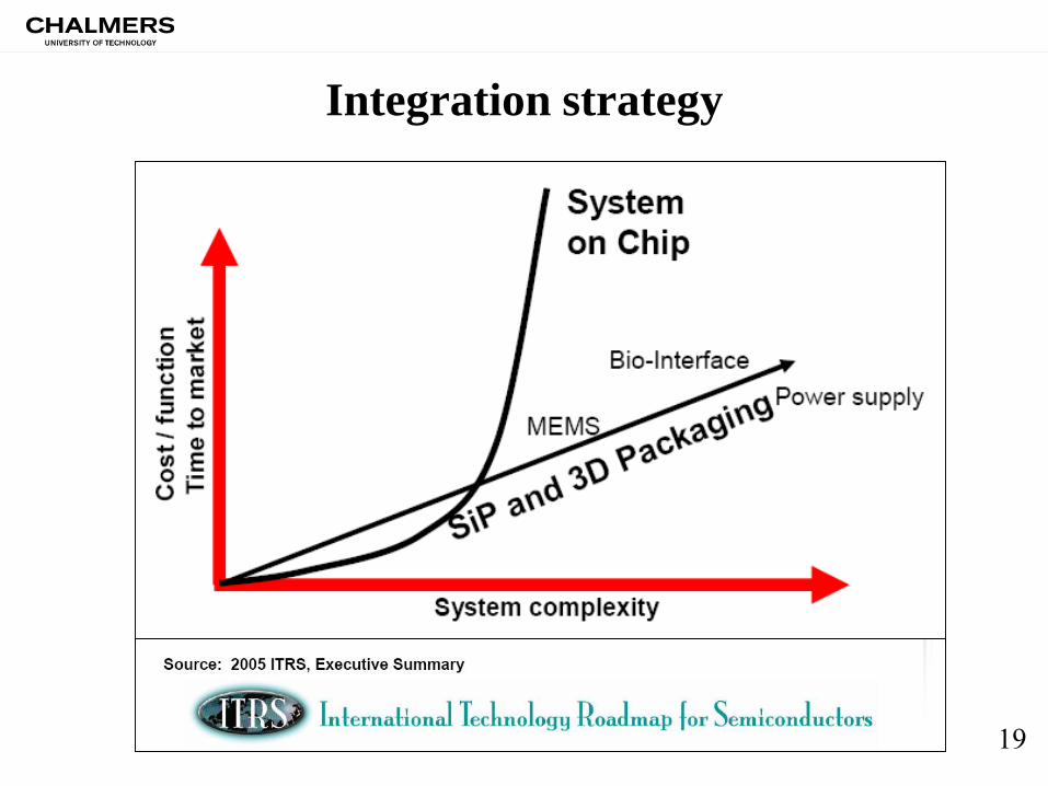
Integration strategy
19
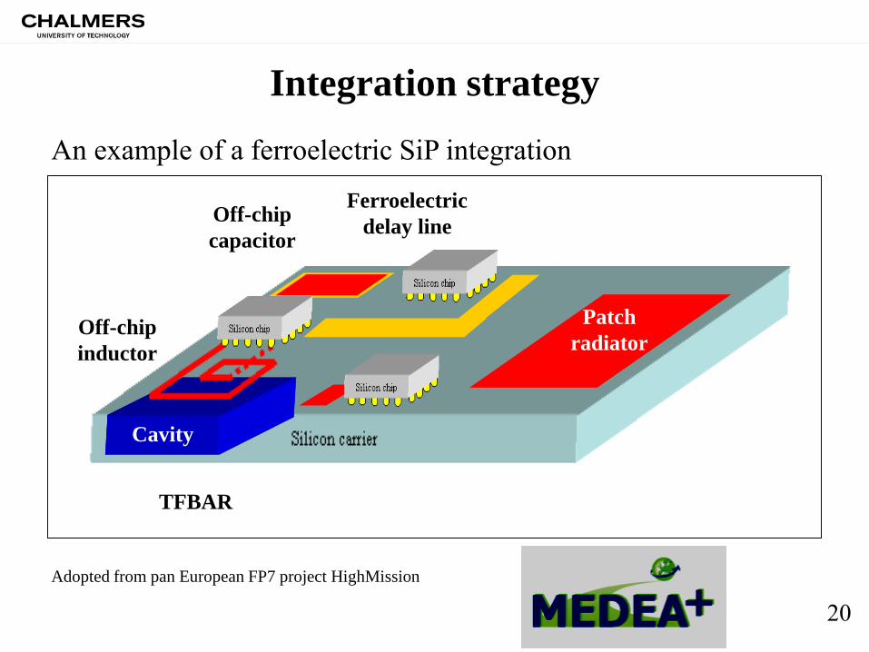
Integration strategy
TFBAR
Cavity
Patch
radiator
Off-chip
capacitor
Off-chip
inductor
Ferroelectric
delay line
Adopted from pan European FP7 project HighMission
An example of a ferroelectric SiP integration
20

Integration strategy
Heterogeneous integration (SiP) – multichip modulus on GaN-wafer carrier
GaN/wafer
carrier
chips on
Si/ferroelectric
substrates
21
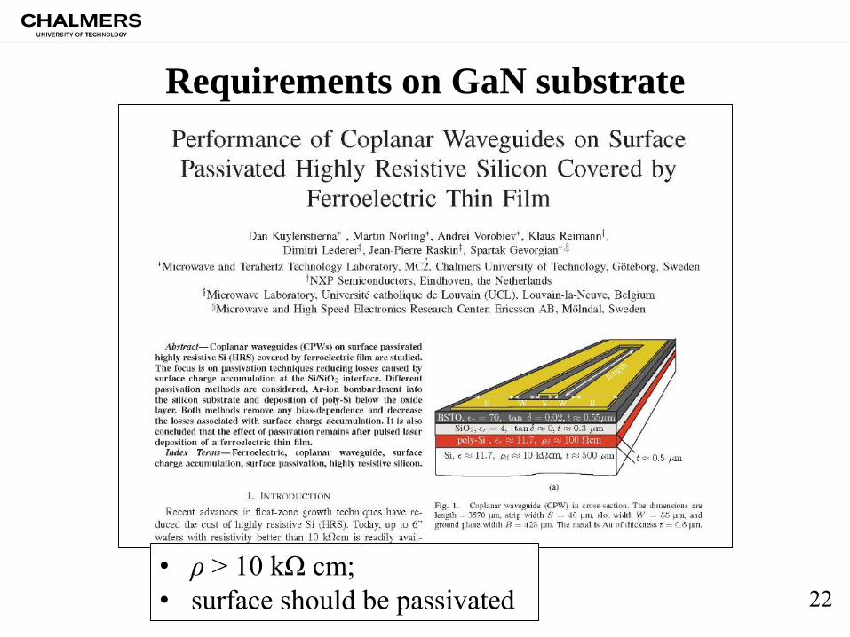
Requirements on GaN substrate
• ρ > 10 kΩ cm;
• surface should be passivated 22
Future plans
• Development of G-FET on LiNbO3 technology;
• bi-layer G-FET on Si with a band gap induced by a back gate;
• bi-layer G-FET on LiNbO3 with a band gap induced by spontaneous
polarization;
• Collaboration with Prof. Per Hyldgaard for modelling of
the bi-layer G-FET on LiNbO3 system;
• design and fabrication of G-FET based mixer and amplifier;
• Collaboration with other groups for the system integration.
23