Bc 4102392396
6
Dinesh. Badav ath et al Int. Journa l of Engineering R esearch and Applications www.ijera.com ISSN : 2248-9622, Vo l. 4, Issue 1( V ersion 2), January 2014, pp.392-3 96 www.ijera.com 392 | Page Design and Analysis of Multi Level D-STATCOM to Improve the Power Quality Dinesh. Badavath 1 , Mr. T. Subramanya Sastry 2 1 M.Tech Student, J.B Institute of Engineering & Technology (Autonomous), Hyderabad, India. 2 Assoc. Professor in J.B Institute of Engineering and Technology (Autonomous), Hyderabad, India. Abstract In the last decade, the electrical power quality issue has been the main concern of the power companies. Power quality is defined as the index which both the delivery and consumption of electric power affect on the performance of electrical apparatus. From a customer point o f view, a power quality problem can be defined as any problem is manifested on voltage, current, or frequency deviation that results in power failure. The power electronics progressive, especially in flexible alternating-current transmission system (FACTS) and custom power devices, affects power quality improvement. This paper presents an investigation of seven-Level Cascaded H - bridge (CHB) Inverter as Distribution Static Compensator (DSTATCOM) in Power System (PS) for compensation of reactive power and harmonics. The advantages of CHB inverter are low harmonic distortion, reduced number of switches and suppression of switching losses. The DSTATCOM helps to improve the power factor and eliminate the Total Harmonics Distortion (THD) drawn from a Non-Liner Diode Rectifier Load (NLDRL). The D-Q reference frame theory is used to generate the reference compensating currents for DSTATCOM while Proportional and Integral (PI) control is used for capacitor dc voltage regulation. A CHB Inverter is considered for shunt compensation of a 11 Kv distribution system. Finally a level shifted PWM (LSPWM) and phase shifted PWM (PSPWM) techniques are adopted to investigate the performance of CHB Inverter. The results are obtained through Matlab/Simulink software package. Keywords — FACTS, DSTATCOM, Cascaded H - bridge (CHB) Inverter, Total Harmonics Distortion (THD). I. Introduction A DSTATCOM is a device which is used in an AC distribution system where, harmonic current mitigation, reactive current compensation and load balancing are necessary. The building block of a DSTATCOM is a voltage source converter (VSC) consisting of self commutating semiconductor valves and a capacitor on the DC bus. The device is shunt connected to the power distribution network through a coupling inductance that is usually realized by the transformer leakage reactance. In general, the DSTATCOM can provide power factor correction, harmonics compensation and load balancing. The major advantages of DSTATCOM compared with a conventional static VAR compensator (SVC) include the ability to generate the rated current at virtually any network voltage, better dynamic response and the use of a relatively small capacitor on the DC bus. Fig. 1 shows the schematic diagram of a DSTATCOM connected to a three phase AC mains feeding three phase loads. Three phase loads may be a lagging power factor load or an unbalanced load or non-linear loads or mixed of these loads. For reducing ripple in compensating currents, interfacing inductors (Lf) are used at AC side of the voltage source converter (VSC). A small series connected capacitor (Cf) and resistor (Rf) represent the ripple filter installed at PCC in parallel with the loads and the compensator to filter the high frequency switching noise of the voltage at PCC. The STATCOM used in distribution systems is called DSTACOM (Distribution- STACOM) and its configuration is the same, but with small modifications. It can exchange both active and reactive power with the distribution system by varying the amplitude and phase angle of the converter voltage with respect to the line terminal voltage. A multilevel inverter can reduce the device voltage and the output harmonics by increasing the number of output voltage levels. There are several types of multilevel inverters: cascaded R-bridge (CRB), neutral point clamped, flying capacitor [2-5]. In particular, among these topologies, CRB inverters are being widely used because of their modularity and simplicity. RESEARCH ARTICLE OPEN ACCESS
-
Upload
anonymous-7vppkws8o -
Category
Documents
-
view
214 -
download
0
Transcript of Bc 4102392396

8/13/2019 Bc 4102392396
http://slidepdf.com/reader/full/bc-4102392396 1/5
8/13/2019 Bc 4102392396
http://slidepdf.com/reader/full/bc-4102392396 2/5
Dinesh. Badavath et al Int. Journal of Engineering Research and Applications www.ijera.com ISSN : 2248-9622, Vol. 4, Issue 1( Version 2), January 2014, pp.392-396
www.ijera.com 393 | P a g e
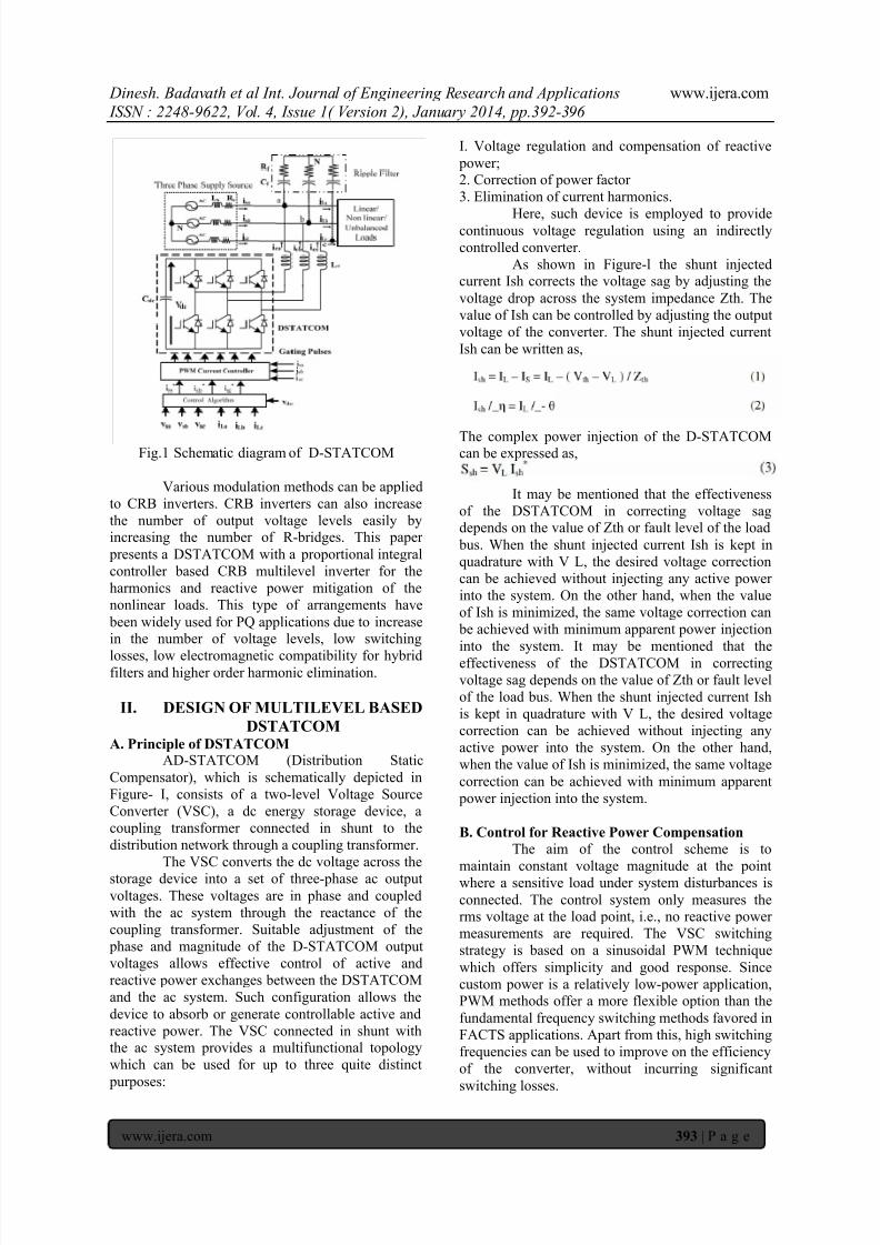
Fig.1 Schematic diagram of D-STATCOM
Various modulation methods can be appliedto CRB inverters. CRB inverters can also increasethe number of output voltage levels easily byincreasing the number of R-bridges. This paper
presents a DSTATCOM with a proportional integralcontroller based CRB multilevel inverter for theharmonics and reactive power mitigation of thenonlinear loads. This type of arrangements have
been widely used for PQ applications due to increasein the number of voltage levels, low switching
losses, low electromagnetic compatibility for hybridfilters and higher order harmonic elimination.
II. DESIGN OF MULTILEVEL BASEDDSTATCOM
A. Principle of DSTATCOMAD-STATCOM (Distribution Static
Compensator), which is schematically depicted inFigure- I, consists of a two-level Voltage SourceConverter (VSC), a dc energy storage device, acoupling transformer connected in shunt to thedistribution network through a coupling transformer.
The VSC converts the dc voltage across thestorage device into a set of three-phase ac outputvoltages. These voltages are in phase and coupledwith the ac system through the reactance of thecoupling transformer. Suitable adjustment of the
phase and magnitude of the D-STATCOM outputvoltages allows effective control of active andreactive power exchanges between the DSTATCOMand the ac system. Such configuration allows thedevice to absorb or generate controllable active andreactive power. The VSC connected in shunt withthe ac system provides a multifunctional topologywhich can be used for up to three quite distinct
purposes:
I. Voltage regulation and compensation of reactive power;2. Correction of power factor3. Elimination of current harmonics.
Here, such device is employed to providecontinuous voltage regulation using an indirectlycontrolled converter.
As shown in Figure-l the shunt injectedcurrent Ish corrects the voltage sag by adjusting thevoltage drop across the system impedance Zth. Thevalue of Ish can be controlled by adjusting the outputvoltage of the converter. The shunt injected currentIsh can be written as,
The complex power injection of the D-STATCOMcan be expressed as,
It may be mentioned that the effectivenessof the DSTATCOM in correcting voltage sagdepends on the value of Zth or fault level of the load
bus. When the shunt injected current Ish is kept inquadrature with V L, the desired voltage correctioncan be achieved without injecting any active powerinto the system. On the other hand, when the valueof Ish is minimized, the same voltage correction can
be achieved with minimum apparent power injectioninto the system. It may be mentioned that theeffectiveness of the DSTATCOM in correctingvoltage sag depends on the value of Zth or fault levelof the load bus. When the shunt injected current Ishis kept in quadrature with V L, the desired voltagecorrection can be achieved without injecting anyactive power into the system. On the other hand,when the value of Ish is minimized, the same voltagecorrection can be achieved with minimum apparent
power injection into the system.
B. Control for Reactive Power CompensationThe aim of the control scheme is to
maintain constant voltage magnitude at the pointwhere a sensitive load under system disturbances isconnected. The control system only measures therms voltage at the load point, i.e., no reactive powermeasurements are required. The VSC switchingstrategy is based on a sinusoidal PWM techniquewhich offers simplicity and good response. Sincecustom power is a relatively low-power application,PWM methods offer a more flexible option than thefundamental frequency switching methods favored inFACTS applications. Apart from this, high switchingfrequencies can be used to improve on the efficiencyof the converter, without incurring significant
switching losses.
8/13/2019 Bc 4102392396
http://slidepdf.com/reader/full/bc-4102392396 3/5
Dinesh. Badavath et al Int. Journal of Engineering Research and Applications www.ijera.com ISSN : 2248-9622, Vol. 4, Issue 1( Version 2), January 2014, pp.392-396
www.ijera.com 394 | P a g e
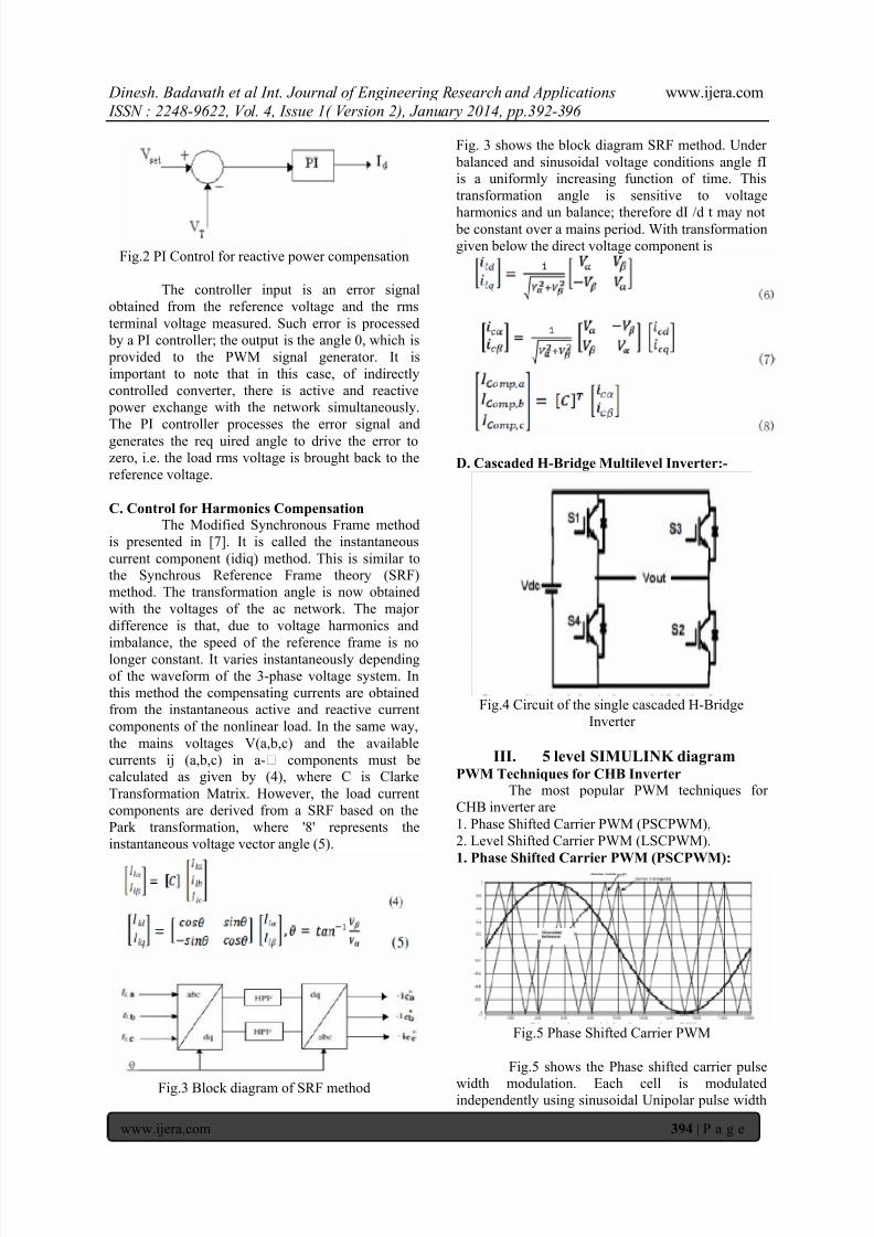
Fig.2 PI Control for reactive power compensation
The controller input is an error signalobtained from the reference voltage and the rmsterminal voltage measured. Such error is processed
by a PI controller; the output is the angle 0, which is provided to the PWM signal generator. It isimportant to note that in this case, of indirectlycontrolled converter, there is active and reactive
power exchange with the network simultaneously.The PI controller processes the error signal andgenerates the req uired angle to drive the error tozero, i.e. the load rms voltage is brought back to thereference voltage.
C. Control for Harmonics CompensationThe Modified Synchronous Frame method
is presented in [7]. It is called the instantaneouscurrent component (idiq) method. This is similar tothe Synchrous Reference Frame theory (SRF)method. The transformation angle is now obtainedwith the voltages of the ac network. The majordifference is that, due to voltage harmonics andimbalance, the speed of the reference frame is nolonger constant. It varies instantaneously dependingof the waveform of the 3-phase voltage system. Inthis method the compensating currents are obtainedfrom the instantaneous active and reactive currentcomponents of the nonlinear load. In the same way,the mains voltages V(a,b,c) and the availablecurrents ij (a,b,c) in a- components must becalculated as given by (4), where C is ClarkeTransformation Matrix. However, the load currentcomponents are derived from a SRF based on thePark transformation, where '8' represents theinstantaneous voltage vector angle (5).
Fig.3 Block diagram of SRF method
Fig. 3 shows the block diagram SRF method. Under balanced and sinusoidal voltage conditions angle fIis a uniformly increasing function of time. Thistransformation angle is sensitive to voltage
harmonics and un balance; therefore dI /d t may not be constant over a mains period. With transformationgiven below the direct voltage component is
D. Cascaded H-Bridge Multilevel Inverter:-
Fig.4 Circuit of the single cascaded H-BridgeInverter
III. 5 level SIMULINK diagramPWM Techniques for CHB Inverter
The most popular PWM techniques forCHB inverter are1. Phase Shifted Carrier PWM (PSCPWM),2. Level Shifted Carrier PWM (LSCPWM).1. Phase Shifted Carrier PWM (PSCPWM):
Fig.5 Phase Shifted Carrier PWM
Fig.5 shows the Phase shifted carrier pulse
width modulation. Each cell is modulatedindependently using sinusoidal Unipolar pulse width

8/13/2019 Bc 4102392396
http://slidepdf.com/reader/full/bc-4102392396 4/5
Dinesh. Badavath et al Int. Journal of Engineering Research and Applications www.ijera.com ISSN : 2248-9622, Vol. 4, Issue 1( Version 2), January 2014, pp.392-396
www.ijera.com 395 | P a g e
modulation and bipolar pulse width modulationrespectively, providing an even power distributionamong the cells. A carrier phase shift of 1800 1m(No. of levels) for cascaded inverter 1S introduced
across the cells to generate the stepped multi leveloutput waveform with lower distortion.
2. Level Shifted Carrier PWM (LSCPWM)
Fig.6 Level Shifted Carrier PWM
Fig.6 shows the Level shifted carrier pulsewidth modulation. Each cell is modulatedindependently using sinusoidal unipolar widthmodulation and bipolar pulse width modulationrespectively, providing an even power distributionamong the cells. A carrier Level shift by 11m (No. oflevels) for cascaded inverter 1S introduced across thecells to generate the stepped multilevel outputwaveform with lower distortion.
IV. MATLAB/SIMULINK MODELING
AND SIMULATION RESULTSFig.7 shows the Matab/Simulink power
circuit model of DSTATCOM. It consists of five blocks named as source block, non linear load block,control block, APF block and measurements block.The system parameters for simulation study aresource voltage of llkv, 50 hz AC supply, DC buscapacitance ISSOe-6 F, Inverter series inductance 10mH, Source resistance of 0.1 ohm and inductance of0.9 mHo Load resistance and inductance are chosenas 30mH and 60 ohms respectively.
Fig.7 Matab/Simulink power circuit model ofDSTATCOM.
V. SIMULATION RESULTS
Fig.8 source and load currents with D-STATCOM
Fig.9 Individual 5 level voltages
Fig.10 Source voltage and source current

8/13/2019 Bc 4102392396
http://slidepdf.com/reader/full/bc-4102392396 5/5
Dinesh. Badavath et al Int. Journal of Engineering Research and Applications www.ijera.com ISSN : 2248-9622, Vol. 4, Issue 1( Version 2), January 2014, pp.392-396
www.ijera.com 396 | P a g e
REFERENCES[I] K.A Corzine. and Y.L Familiant, "A New
Cascaded Multi-level HBridge Drive:' IEEETrans. Power.Electron .• vol. I 7. no. I. pp. I
25-I 3 I Jan 2002.[2] J.S.Lai. and F.Z.Peng "Multilevelconverters - A new bread of converters,"IEEE Trans. Ind.Appli .• vo1.32. no.3.
pp.S09-S17. May/ Jun. 1996.[3] T.A.Maynard. M.Fadel and N.Aouda.
"Modelling of multilevel converter:' IEEETrans. Ind.Electron .• vo1.44. pp.3S6 -364.Jun. I 997.
[4] P.Bhagwat. and V.R.Stefanovic."Generalized structure of a multilevel PWMInverter:' IEEE Trans. Ind. Appln, VoI.IA-19. no.6, pp. I OS7-1069, Nov.!Dec .. 1983.
[S] J.Rodriguez. Jih-sheng Lai, and F Zheng peng, "Multilevel Inverters; A Survey ofTopologies, Controls, and Applications,"IEEE Trans Ind. Electron., vol.49 , n04.,
pp.724-738. Aug.2002.[6] Roozbeh Naderi, and Abdolreza rahmati,
"Phase-shifted carrier PWM technique forgeneral cascaded inverters," IEEE Trans.Power.Electron., vo1.23, no.3, pp. I 257-I269. May.2008.
[7] Bhim Singh, Kamal AlHaddad & AmbrishChandra, 1999, A Review of Active Filterfor Power Quality Improvements, IEEE
Trans on Industrial Electronics, 46(S), pp.960970
[8] Mauricio Angulo, Pablo Lezana, SamirKouro, Jos'e Rodr'lguez and Bin Wu,"Level-shifted PWM for CascadedMultilevel Inverters with Even PowerDistribution" IEEE Power Electronicsspecialist conference, 17-21 june 2007,
pp.2373-2378.[9] B. P. McGrath and D. G. Holmes,
"Multicarrier PWM strategies for multilevelinverters," IEEE Trans. Ind. Electron., vol.49, no. 4, pp. 858- 867, August 2002.
AUTHORMr. Dinesh Badavath ReceivedB.Tech degree from JNTUH, INDIAand presently he is pursuing M.Techin ELECTRICAL POWERSYSTEMS from JBIET
(Autonomous), His areas of Interests are powerSystems, Machines.