AD-AI3 I PUA I/2 TME U .RIGHT PATER SON AF B OH SCHOOL OF … · 2014-09-27 · ad-ai3 i pua vkfiha...
112
AD-AI3 I PUA VKFIHA H AUN ANV U D;MENIA UN UF ULE AL HADIU I/2 923 TME SERIES SST EM( U A I FO RC E INS OF TECH .RIGHT PATER SON AF B OH SCHOOL OF E NO B A CASELLA UNCI!ASSFIED DEC 83 AFITGE/EE/83D,15 F/0 9/2 N
Transcript of AD-AI3 I PUA I/2 TME U .RIGHT PATER SON AF B OH SCHOOL OF … · 2014-09-27 · ad-ai3 i pua vkfiha...
AD-AI3 I PUA VKFIHA H AUN ANV U D;MENIA UN UF ULE AL HADIU I/2923 TME SERIES SST EM( U A I FO RC E INS OF TECH.RIGHT PATER SON AF B OH SCHOOL OF E NO B A CASELLA
UNCI!ASSFIED DEC 83 AFITGE/EE/83D,15 F/0 9/2 N
1.2521 12.2 _II, 1111IL25
MICROCOPY RESOLUTION TEST CHART
NAIK)NAL HUIR(A0 OtI S1ANPARDS Illbl A
1lie
VI 4
UPGRADE, VERIFICATION, AND DOCUMENTATION
OF GENERAL RADIO 1923 TIME SERIES SYSTEM
THESIS
AFIT/GE/EE/83D-15 Bruce A. CasellaCAPT USA
DT_.di :tnbu.ion.is ,nmitd. ! 22 3 o
DEPARTMENT OF THE AlR FORCE
_ AIR FORCE INSTITUTE OF TECHNOLOGY
Wright-Patterson Air Force ase, Ohio
8 4.02 22 07 8
AFITGEEE/83D- 15
UPGRADE, VERIFICATION, AND DOCUMENTATION
OF GENERAL RADIO 1923 TIME SERIES SYSTEM
THESIS
AFIT/GE/EE/83D-15 Bruce A. CasellaCAPT USA
2h 2 2184
A
- :Approved for public release; distribution unlimited.
- - *. ... . ..-- - * - -
U
AFIT/GE/EE/83D-15
UPGRADE, VERIFICATION, AND DOCUMENTATION
OF GENERAL RADIO 1923 TIME SERIES SYSTEM
THESIS
Presented to the Faculty of the School of Engineering
of the Air Force Institute of Technology
Air University
in Partial Fulfillment of the
Requirements for the Degree of
Master of Science Fr
by ,
Bruce A. Casella
CAPT USA
Graduate Electrical Engineering
December 1983 *fie
Approved for public release; distribution unlimited.
MO.O
Acknowledgements
I would like to thank my advisor, Major Kenneth G.
Castor of the Air Force Institute of Technology, for proposing
this thesis topic.
I am also grateful to Dr. Vaqar H. Syed for his
assistance on the thesis effort.
Special thanks is extended to Mr. Dan Zambon for his
continuing efforts to assist and advise on all facets of the
project.
A very strong debt of gratitude is also owed to Mr. Al
D. Luebbers, Senior Field Service Engineer, GENRAD Vibrations
Analysis Division, for his assistance and efforts to make the
thesis project a success.
Finally, I want to express my appreciation to my wife,
Cathie, for her encouragement throughout the thesis effort.
Bruce A. Casella
~ii
.. . .. . . I I, n , Im .
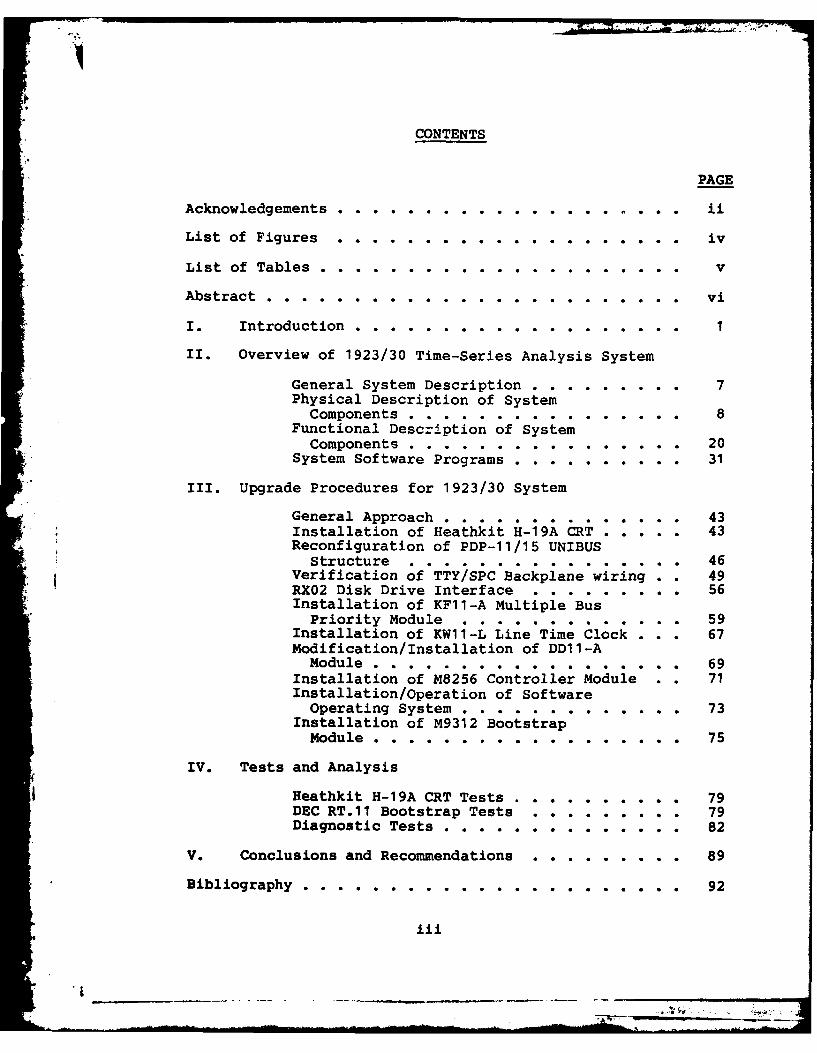
CONTENTS
PAGE
Acknowledgements. .. ... . . .. .. .. .. . . ..
List ofigures . . . . . . . . . . . . . . . . . . . . iv
List of Tables .............. . .. .. .. .. ... v
Abstract....... . . . . . . . . . . . . . . . . .* vi
I. Introduction .. ........ ... .. .. .......
Ii. Overview of 1923/30 Time-Series Analysis System
General System Description. ............ 7Physical Description of System
Components .. .. .. .. .. .. .. .. 8Functional Description of SystemComponents....................20
System Software Programs *.. .. .. .. .... 31
III. Upgrade Procedures for 1923/30 System
General Approach. ................. 43Installation of Heathkit H-19A CRT . . ... 43Reconfiguration of PDP-11/15 UNIBUSStructure................. 46
Verification ofTTY/SPCBackplane wiring . 49RX02 Disk Drive Interface......... 56Installation of KF11-A Multiple BusPriority Module ............... 59
Installation of KW11-L Line Time Clock . 67Modification/Installation of DD1 1-AModule .. .. .. .. .. .. ... .. .. 69
Installation of M8256 Controller Module . 71Installation/Operation of SoftwareOperating System. .............. 73
Installation of M9312 BootstrapModule . . . . . . . . . .. .. .. .. . 75
IV. Tests and Analysis
Heathkit H-19A CRT Tests ............ . 79DEC RT.11 Bootstrap Tests . . . . . . . . . 79Diagnosti T s . .. .. .. .. . . .. 82
V. Conclusions and Recommendations . . . . . . . . . 89
Bibliography . . . . . . . . . . . . . . . . . . . . . . 92
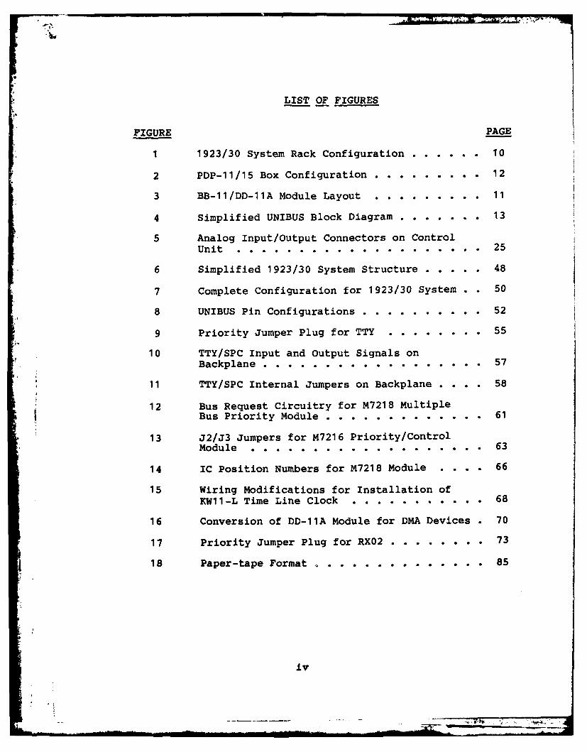
LIST OF FIGURES
FIGURE PAGE
1 1923/30 System Rack Configuration ....... . 10
2 PDP-11/15 Box Configuration ........... ... 12
3 BB-11/DD-11A Module Layout .. ........ . . 11
4 Simplified UNIBUS Block Diagram ....... 13
5 Analog Input/Output Connectors on ControlUnit . . . . . . ............ . . 25
6 Simplified 1923/30 System Structure . . ... 48
7 Complete Configuration for 1923/30 System . 50
8 UNIBUS Pin Configurations ... .......... . 52
9 Priority Jumper Plug for TTY .. ........ 55
10 TTY/SPC Input and Output Signals onBackplane........ . ......... 57
11 TTY/SPC Internal Jumpers on Backplane . ... 58
12 Bus Request Circuitry for M7218 MultipleBus Priority Module . . . . .......... 61
13 J2/J3 Jumpers for M7216 Priority/ControlModule ...... ................... . 63
14 IC Position Numbers for M7218 Module . . . . 66
15 Wiring Modifications for Installation ofKW11-L Time Line Clock ........... 68
16 Conversion of DD-11A Module for DMA Devices . 70
17 Priority Jumper Plug for RX02 . . . . . . . . 73
18 Paper-tape Format .............. 85
iv
85-
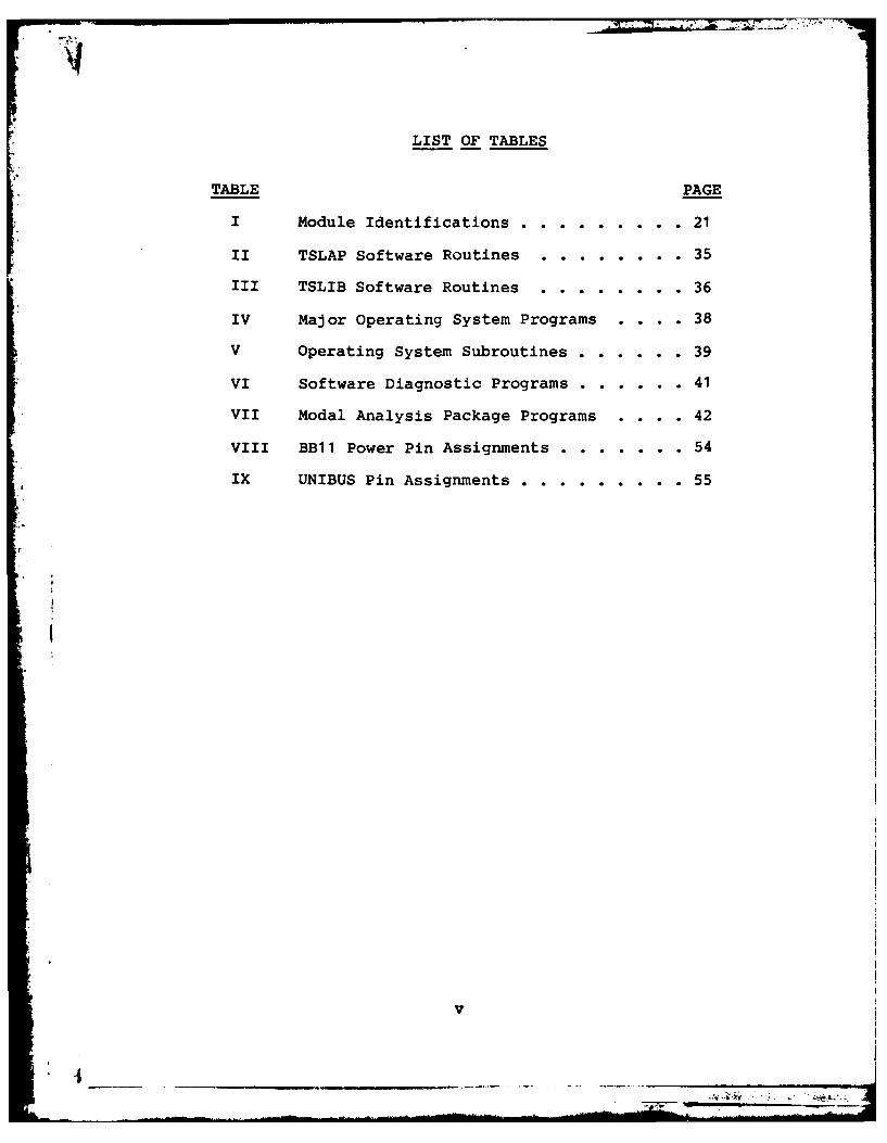
LIST OF TABLES
TABLE PAGE
I Module Identifications ... ......... .21
II TSLAP Software Routines .. ........ .35
III TSLIB Software Routines .. ........ .36
IV Major Operating System Programs . . . . 38
V Operating System Subroutines ....... .39
VI Software Diagnostic Programs ....... .41
VII Modal Analysis Package Programs . . . . 42
VIII BB11 Power Pin Assignments .. ....... .. 54
IX UNIBUS Pin Assignments. . . . . . . . .55
-
* 1.|. -
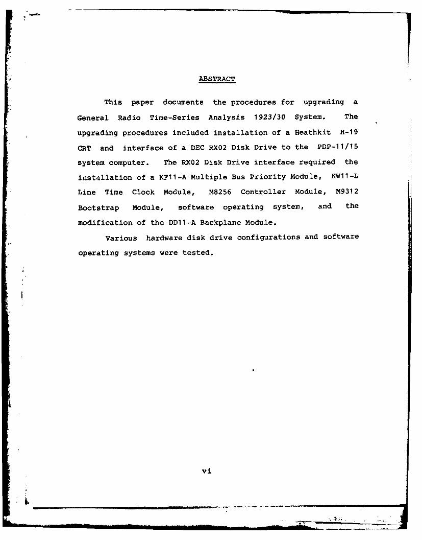
ABSTRACT
This paper documents the procedures for upgrading a
General Radio Time-Series Analysis 1923/30 System. The
upgrading procedures included installation of a Heathkit H-19
CRT and interface of a DEC RX02 Disk Drive to the PDP-11/15
system computer. The RX02 Disk Drive interface required the
installation of a KF11-A Multiple Bus Priority Module, KW11-L
Line Time Clock Module, M8256 Controller Module, M9312
Bootstrap Module, software operating system, and the
modification of the DD11-A Backplane Module.
Various hardware disk drive configurations and software
operating systems were tested.
vi
UPGRADE, VERIFICATION, AND DOCUMENTATIONOF GENERAL RADIO 1923 TIME SERIES SYSTEM
I. INTRODUCTION
BACKGROUND
Analyzing electrical signals is a fundamental problem in
the engineering field. Basic phenomena in any system can
usually be converted into electrical signals. These
electrical signals lend themselves to time-series analysis
techniques (Ref 15:3).
Some examples of the use of time-series analysis
include: vibration analysis in automobiles; determination of
* flutter characteristics in aircraft; analysis of
electrocardiographs (EKG) and electroencephalograms (EEG) in
* biomedicine research; and echo ranging in geophysical
exploration (Ref 15:3).
The term "time-series" means a succession of data values
resulting from a physical process. Successive data values are
related to previous data values in Time-Series Analysis.
Basic Time-Series Analysis procedures include: correlation
analysis, spectral analysis, filtering, ensemble averaging of
waveforms, and measurement of statistical distributions (Ref
15:4).
The General Radio 1923/30 Time-Series System is a
Digital Equipment Corporation (DEC) PDP-11/15 computer-based
1|
digital processing system for broadband, high resolution
analysis of analog input, and for general analysis, systhesis,
and array manipulations of time series data (Ref 24:1-1). The
system employs the fast fourier transform algorithm. This
algorithm enables the system to perform simultaneous two-
channel time-series analysis of data with bandwidths from zero
to fifty kilocycles (Ref 24:1-1). Panel controls provide
pushbutton selection of direct fourier transforms, signal
power spectrums, histograms, and similar related analysis
functions (Ref 24:1-1). Optional keyboard controls allow the
operator to access individual steps of pre-programmed panel
functions.
PROBLEM
The 1923/30 Time-Series System operates with a High-
* speed Paper Tape Reader. All of the problems generally
associated with paper tape based systems are applicable to
this system. The operator must overcome problems associated
with handling and feeding the tape into the High-speed Paper
Tape Reader. Additionally, paper tapes must be read into the
processor memory separately. This separate loading procedure
and the actual tape run-time greatly increase system set-up
time. A DEC RX02 dual eight inch disk drive unit will be
interfaced to the system computer in an effort to upgrade the
equipment. A disk based system will improve system
reliability, increase flexibility, and reduce the operational
steps necessary for analysis of functional data.
2
The purpose of this thesis effort will be to:
1. Upgrade ASR-33 Teletypewriter (TTY) to a
Heathkit H-19 Video Terminal (CRT).
2. Interface DEC RX02 Disk Drive Unit with PDP-
11/15 computer in the 1923/30 Time-Series System.
3. Verify operation of the new disk based
system.
4. Transfer existing paper tap. ased software
onto eight inch floppy disks.
SCOPE
The thesis effort will procede from a practical
viewpoint. Existing hardware and/or software support within
the Electrical Engineering Department will be used whenever
possible. The proposed objectives, previously mentioned, will
be covered with sufficient detail to ensure that the Time-
Series System is properly upgraded, verified and documented.
The DEC RT.11 software operating system and DEC diagnostic
monitor files will be used for bootstrapping the RX02 Disk
Drive Unit. The research effort will not include a rewrite of
the software information on existing paper tapes.
Hardware/software problem areas will be documented and
recommended for future system improvements.
SUMMARY OF CURRENT KNOWLEDGE
First Lieutenant (iLT) Robert Sudduth conducted a
thorough check of the 1923/30 Time-Series System during the
3S _____________________________________
month of March 1980. The system had been in storge for about
two years. Initially, ILT Sudduth was unable to access or
load portions of memory and unable to enter data via the ASR-
33 TTY. Likewise, the system experienced intermittent power
problems (Ref 20:1). The original PDP-11/15 was turned in for
repairs and all defective sections of core memory were
repaired on the original PDP-11/15 processor memory unit (Ref
20:4). Sudduth solved the problem of entering data via the
teletypewriter by moving the interconnection of a KL-11
interface board in the processor from the five through seven
priority slots to the one through four priority slots (Ref
20:4). The intermittent power problems were corrected by
cleaning the connector contacts to the system power supply
(Ref 20:6). The 1923/30 T'ime-Series System was declared fully
operational when ILT Sudduth conclueed his research in 1980
(Ref 21:8). Although he got the system workinj, he was unable
to replace the High-speed Paper Tape Reader with a disk unit
(Ref 20:8). All other knowledge of the system has been
obtained by a thorough review of the system
operating/maintenance manuals and consultation with computer
technicians familiar with the twelve year old DEC
computer/Time-Series Analysis equipment.
STANDARDS
The following criteria will be used to verify that all
objectives have been successfully completed:
1. The Heathkit H-19 CRT will successfully
4
perform I/O operations with disk based operating system.
2. The RX02 Disk Drive Unit will successfully
boot-up on a floppy disk operating system.
3. All existing paper tapes will be transferred
to floppy disks.
APPROACH
The following procedure was used in solving this
problem. The entire 1923/30 Time-Series System was activated
and checked for proper operation after a thorough study of the
system operating manuals. All operating system paper tapes
were checked for proper loading and operation.
The DEC RX02 Disk Drive Unit was connected to and
powered up on an operational LSI-11 computer system to ensure
proper operation and verification of boot-up procedures for
the unit. The RX02 disk controller module and disk hardware
bootstrap module were installed on the Time-Series System
UNIBUS located in the PDP-11/15 computer. After installation
of these modules, the RX02 disk unit was connected to the disk
controller module. Power was applied to the system in order
to check proper connections. The disk unit required an
operating system to interface with the PDP-11/15 computer
processor. A department RT.11 operating system disk was used.
The disk for this system was copied from another RT.11 disk
onto an eight inch standard floppy disk. Operating system
files not required for the Time-Series System were eliminated
by writing over memory locations. Additionally, a DEC XXDP.+
5
4.P
diagnostics floppy disk was used for boot-up procedures.
The system ASR-j3 TTY was replaced with a more reliable
video terminal (Heathkit H-19 CRT). Additionally, the
department LSI-11 computer system was used to determine the
capability and usefulness of the RT.11 operating system
utility programs for transferring data to and from different
storage medias.
6
II. OVERVIEW OF 1923/30 TIME-SERIES ANALYSIS SYSTEM
GENERAL SYSTEM DESCRIPTION
The 1923/30 Time-Series Analysis System ia a computer-
based digital processing system for broadband, high resolution
analysis of analog input signals, and for general signal
analysis of time series data. The system is capable of single
or simultaneous two-channel analysis of data with bandwidths
from d-c to 50KHZ. Spectral resolution is variable and ranges
from sixty-four to four thousand ninety-six lines of constant
filter bandwidth. Signal analysis is based primarily on the
Fast Fourier Transform (FFT) algorithm. Operator controlled
scaling of the FFT algorithm allows for optimum dynamic range
calculations for a variety of signals (Ref 24:1-1).
The system operates in one of three modes: panel
control; keyboard control; or learned program control.
Panel control is achieved by loading the appropriate software
panel control routine into the system PDP-11 computer core
memory. Control is provided by the appropriate selection of
pushbuttons on the Time-Series System front console. Commonly
used Time-Series Analysis functions are available on the front
console (Ref 24:1-1).
A separate software keyboard routine, loaded into
computer coze memory, provides the operator with keyboard
control. The keyboard operating program allows the operator
to control system operations by means of a high-level Time-
Series Programming Language (TSL). The keyboard program is
7
\I
accessed via the system teletype terminal or video terminal
(CRT). The program includes the pre-programmed panel
functions of the panel control program and provides more
advanced array processing functions for the operator (Ref
24:1-3).
Learned program control is a specialized keyboard
control mode. In the learned program control mode, relatively
short programs are stored in computer core memory for
execution at a later time (Ref 24:1-3).
PHYSICAL DESCRIPTION OF SYSTEM COMPONENTS
The 1923/30 Time-Series Analysis System consists of:
1. Digital Electronics Equipment (DEC) PDP-11/15computer
2. Display Unit
3. Control Unit
4. Analog-to Digital Converter Unit (ADC)
5. System Power Supply
6. Extended Arithmetic Element (EAE)
7. ASR-33 Teletypewriter (TTY)
8. Heathkit H-19A video terminal CRT (additionalmodification)
9. X-Y Recorder
10. High-speed Paper Tape Reader
11. DEC RX02 Floppy Disk Unit (additionalmodification)
12. RT.11SJ Software Operating System (additionalmodification)
13. 1923/30 System Software Package
8
DEC PDP-11/15 COMPUTER
The DEC PDP-11/15 is a 16 bit general purpose
computer with 32K of core memory. The basic PDP-1T/15
computer consists of a mounting box, tilt and lock chasis
slides, H720 power supply, fifteen feet of power cord with
ground wire, cooling fans, filter and programmer's console
with turn-key option. The unit is ten and a half inches high,
nineteen inches wide and twenty-three inches deep. The PDP-
11/15 weighs approximately ninety pounds and operates on
120/220 VAC, 50/60 hertz. The computer is mounted between the
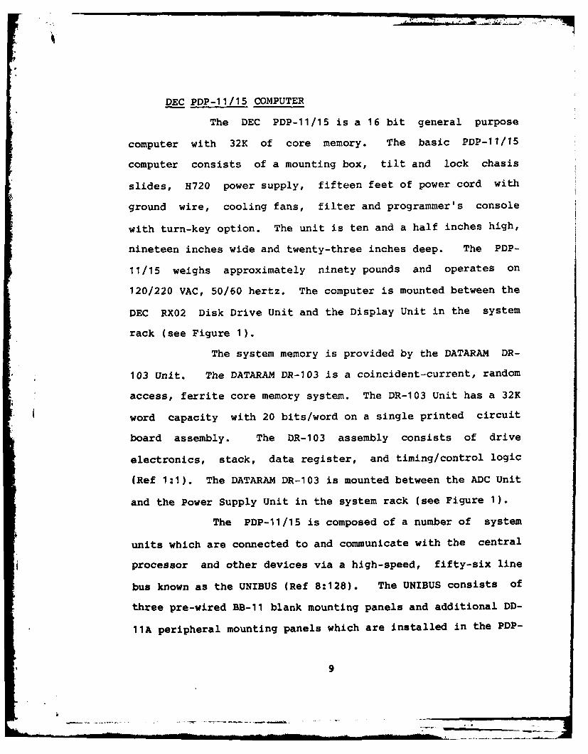
DEC RX02 Disk Drive Unit and the Display Unit in the system
rack (see Figure 1).
The system memory is provided by the DATARAM DR-
103 Unit. The DATARAM DR-103 is a coincident-current, random
access, ferrite core memory system. The DR-103 Unit has a 32K
word capacity with 20 bits/word on a single printed circuit
board assembly. The DR-103 assembly consists of drive
electronics, stack, data register, and timing/control logic
(Ref 1:1). The DATARAM DR-103 is mounted between the ADC Unit
and the Power Supply Unit in the system rack (see Figure 1).
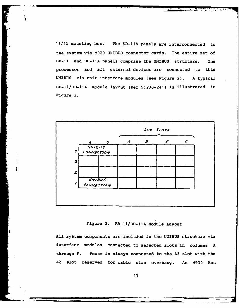
The PDP-11/15 is composed of a number of system
units which are connected to and communicate with the central
processor and other devices via a high-speed, fifty-six line
bus known as the UNIBUS (Ref 8:128). The UNIBUS consists of
three pre-wired BB-11 blank mounting panels and additional DD-
11A peripheral mounting panels which are installed in the PDP-
9
.
orAoNfr vlew op, SY.T7r 44c
D EC )COZ
DEC P.DDo ////-
CNoIVEUTER
1/ISplAY 4NIT
7/
7"RStE 7OP
' CoA'VEA TE/
cORe *,Emsoy 'bvir
Po 4 Si#Aiy
NOTE: Other peripheral devices (wired to powerdistribution panel on rear of system rack) are asfollows:
Heathkit H-19A Video Terminal CRTHigh-speed Paper Tape ReaderASR-33 TeletypewriterX-Y Recorder
Figure 1. 1923/30 System Rack Configuration
10
4m
11/15 mounting box. The DD-11A panels are interconnected to
the system via M920 UNIBUS connector cards. The entire set of
BB-11 and DD-11A panels comprise the UNIBUS structure. The
processor and all external devices are connected to this
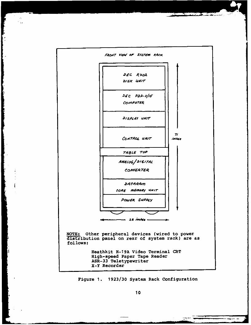
UNIBUS via unit interface modules (see Figure 2). A typical
BB-11/DD-11A module layout (Ref 9:238-241) is illustrated in
Figure 3.
$PC SzoTs
A 8 C __ __ F
CoNNcCrION
3
~CONecrldV
Figure 3. BB-11/DD-11A Module Layout
All system components are included in the UNIBUS structure via
interface modules connected to selected slots in columns A
through F. Power is always connected to the A3 slot with the
A2 slot reserved for cable wire overhang. An M930 Bus
11
FA'OA' PAP/el (Wlro/ CONJSOLE .5W~rCH'ES -
COMNOL(moiuL
A.,*44P M823 M 728
Mn 7.26F
Ml7218 M 72Y P1
BON/ 4172.f PROC(5MAwnL~ sn 0& AA20 SDUE
___w_.W At 710 A11675 MflhZ TTY
I 0ooL~0____ 27rosE
A2 0 i 7/0 2 7 1 1 V 0
U 4171uJs 21 ~O-62 ~0
123Y M31E
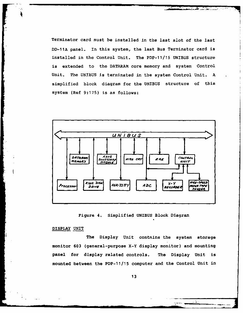
Terminator card must be installed in the last slot of the last
DD-11A panel. In this system, the last Bus Terminator card is
installed in the Control Unit. The PDP-11/15 UNIBUS structure
is extended to the DATARAM core memory and system Control
Unit. The UNIBUS is terminated in the system Control Unit. A
simplified block diagram for the UNIBUS structure of this
system (Ref 9:175) is as follows:
7L7A 7117
Figure 4. Simplified UNIBUS Block Diagram
DISPLAY UNIT
The Display Unit contains the system storage
monitor 603 (general-purpose X-Y display monitor) and mounting
panel for display related controls. The Display Unit is
mounted between the PDP-11/15 computer and the Control Unit in
13
---
the system rack (see Figure 1). The X-Y Display monitor is a
six and a half inch flat faceplate, electronic deflection CRTdisplay with stored resolution of 80 line pairs vertically and
100 line pairs horizontally. Stor-age time is one hour at full
stored brightness and erase time is about 250 milliseconds.
The panel controls and the CRT are interfaced to the Time-
Series System via cable connections to read-in and digital-to-
analog modules in the Control Unit (Ref 24:1-12). Connectors,
on the rear of the instrument, provide for application of
input signals to the X and Y deflection amplifiers and to the
Z-axis amplifiers which control beam intensity. The Display
Unit operates on 120/220 VAC and includes a pre-wired power
transformser which permits one of six regulatory ranges (Ref
21:1-3 and 1-4).
CONTROL UNIT
The Control Unit mounts the operator control
panel. The operator control panel consists of display,
output, averaging, system functions, display indicators, input
modifiers, acquisition mode, sequence, execution, input A,
input B, and input trigger control pushbuttons and/or
switches. The Control Unit contains a secondary system bus.The secondary system bus is interfaced to the PDP-11/15 UNIBUS
via a BC11A 120-conductor flexprint interface cable. The bus
contains circuit cards for the control panel, keyboard Display
Unit, programmable timing generator, optional filters, the X-Y
14
Recorder, and the High-speed Paper Tape Reader. The Control
Unit is installed between the Display Unit and Analog-to-
Digital converter in the system rack (see Figure 1). The unit
operates on 120/220 VAC (Ref 24:1-12).
ANALOG-TO-DIGITAL CONVERTER UNIT
The Analog-to-Digital Converter Unit (ADC)
contains two parallel analog-to-digital converters mounte-d in
a single container between the Control Unit and the DATARAM
core memory unit in the system rack (see Figure 1). Sample
clock signals from the timing generator in the Control Unit
and conditioned input signals from channel A and channel B in
the Control Unit are input to the ADC via an interface cable.
Ten bit digital outputs are cabled to the UNIBUS in the PDP-
11/15 mounting box. All module cards containing control and
interface logic for ADC operations are mounted on the UNIBUS
structure in the PDP-11/15 computer (see Figure 2). The ADC
operates on 120/220 VAC (Ref 24:1-14).
SYSTEM POWER SUPPLY
The System Power Supply Unit is mounted in the
lowest available location in the system rack (see Figure
1). Voltages of +5VAC, -15VAC, and +15VAC are wired directly
to the DC power distribution panel in the system rack (see
Figure 1). Likewise, the same voltages are wired to standard
three-prong power inlets along the system rack.
15
4
EXTENDED ARITHMETIC ELEMENT
The Extended Arithmetic Element (EAE) consists of
five modules mounted on the UNIBUS in the PDP-11/15 computer
(see Figure 2). The five modules in the EAE are as follows:
MODULE QUANTITY
M234 Register 2M827 Clock and Status 1M7210 Data Control 1M7211 Register Control 1
The EAE UNIBUS addresses are hardwired to addresses 777300
through 777316. The EAE has no interrupt system and no
interrupt vector address or priorities. The EAE is self-
contained in the five modules mentioned above. Power for the
EAE is provided by the PDP-11/15 UNIBUS structure (Ref 7:1-1).
ASR-TELETYPEWRITER
The ASR-33 Teletype (TTY) is used as an
input/output device for the PDP-11/15 computer system. The
TTY consists of a printer, keyboard, paper tape reader, and
paper tape punch. The TTY is interfaced directly to the PDP-
11/15 UNIBUS srtucture via three KL11 Teletype Control
modules. The three KL11 Teletype Control modules are as
follows:
MODULE QUANTITY
M105 Address Selector 1
M780 Receiver/Transmitter Timing 1M782 Interrupt Control 1
16
The KL11 modules are inserted on the UNIBUS in one entire row
behind the processor modules. The ASR-33 TTY is interfaced to
the PDP-11/15 computer by an interconnect cable installed from
the ASR-33 TTY to the M780 module. The ASR-33 TTY and the
KL11 Control modules are set to operate on 110 baud rate. The
ASR-33 TTY operates on 110/220 VAC from the system rack power
distribution panel. The KL11 TTY Control modules are powered
by the UNIBUS structure (Ref 24:1-12 and Ref 11:2-6). Either
the ASR-33 TTY or the Heathkit H-19A Video Terminal CRT can be
interfaced to the PDP-11/15 computer for input/output
operations.
HEATHKIT H-19A VIDEO TERMINAL CRT
The Heathkit H-19A Video Terminal (CRT) is a 25
line video terminal connected to the PDP-11/15 computer by an
RS-232C serial interface. The CRT consists of a twelve inch
diagonal high-quality, cathode-ray tube, standard-size
electronic keyboard (using standard typewriter format), logic
circuit boards, and a molded cabinet. A current loop
interface box is installed between the CRT terminal and the
PDP-11/15 computer. The interface box provides the proper
current and input/output serial interconnections for the CRT.
The interface cable from the current loop box to the PDP-11/15
UNIBUS is connected to the KL11 M780 TTY Control module
located on ther UNIBUS structure. Either the ASR-33 TTY or
the Heathkit H-19A CRT is connected to the KL11 M780 TTY
17
module for input/output operations. Both devices cannot be
operated simultaneously in the current hardware configuration.
The Heathkit H-19A CRT operates on 110/220 VAC (Ref 16:4).
X-Y RECORDER
The X-Y Recorder is a model 7034A Hewlett-Packard
X-Y plotter. The unit consists of the mainframe table-
type recorder, with front panel pushbutton controls, and
includes two plug-in input modules. The two input modules
are:
Model 17171A DC PreamplifierModel 17173A Null Detector
Slow varying DC signals are connected to the mainframe input
terminals via banana plugs or open wires. The X-Y Recorder is
connected to the Time-Series System as a peripheral device.
The unit is powered by 110/220 VAC (Ref 17:1-1).
HIGH-SPEED PAPER TAPE READER
The High-speed Paper Tape Reader is a model 2540
series perforated tape reader. The unit consists of a
readhead assembly (which includes an exciter lamp, collimating
lens, and readhead), drive motor, electronics unit printed
circuit board, power supply, capstans, rollers, and brake.
The paper tape reader is a unidirectional, 300 character per
second photoreader. The unit uses paper, paper-mylar,
aluminized mylar, or solid mylar tape with standard
perforations. The paper tape reader is interfaced to the PDP-
18
11/15 computer via interconnection cables, and is powered by
110 VAC, 60HZ (Ref 18:1-1 to 5-2).
DEC RX02 FLOPPY DISK UNIT
The Digital Equipment Corporation (DEC) RX02
Floppy Disk Unit is a low cost, random access mass storage
memory device. The disk unit consists of two flexible disk
drives, a single read/write electronics module (M7745), a
microprogrammed controller module (M7744), power supply, PDP-
11 Interface module (M8256), BC05L-15 standard interface
cable, and a rack-mountable ten and a half inch self-cooled
chassis. The media used with the RX02 unit is a flexible
(floppy) eight inch disk. A bootstrap terminator module
(M9312) is installed on the PDP-11/15 UNIBUS to provide a
hardware loading and start-up sequence for the disk operating
system. The disk unit is mounted directly above the PDP-11/15
computer in the system rack (see Figure 1). All disk
components are mounted in the RX02 chassis, with the exception
of the M8256 Interface module. The M8256 module is mounted
directly behind the PDP-11/15 processor modules on the UNIBUS
(see Figure 2). The RX02 unit is interfaced to the PDP-11/15
via the BC05L-15 interface cable. The cable is connected from
the M8256 module to the RX02 unit. The RX02 unit operates on
110/220 VAC, double density format (Ref 13:1-1 and 2-3).
19
---- ----. ..
FUNCTIONAL DESCRIPTION OF SYSTEM COMPONENTS
DEC PDP-11/15 COMPUTER
The PDP-11/15 computer consists of a KC-11
processor, a KY-11C Controller Console, a DATARAM DR-103 core
memory, a UNIBUS, and an H720 Power Supply (Ref 12:2-1).
The KC-11 processor is composed of several
modules (see Figure 2) which decode instructions, modify data,
make decisions, and control allocation of the UNIBUS among
external devices by means of eight hardware registers. These
registers are used as arithmetic accumulators, index,
autoincrement and autodecrement, stack pointer, and counter
registers (Ref 12:2-2). A complete listing and description of
all modules in the PDP-11/15 computer is outlined in Table I.
The KY-11C Controller Console is a front panel
console on the PDP-11/15 which provides the user with a direct
system interface by means of manually operated console
switches on the front console display. The console switches
allow the operator to start, stop, load, modify, continue,
and/or step through a user program one instruction at
at a time. The front console also indicates the current
machine state of the computer (i.e., run, fetch, bus, execute,
source, destination, address). Likewise, the console displays
address load locations and deposited data at selected
addresses. Console switch operating instructions are outlined
in the PDP-11/15 system manual (Ref 12:2-2 and 2-3).
20
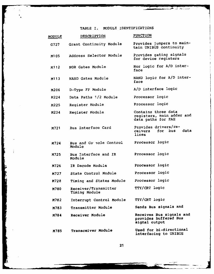
TABLE I. MODULE IDENTIFICATIONS
MODULE DESCRIPTION FUNCTION
G727 Grant Continuity Module Provides jumpers to main-tain UNIBUS continuity
M105 Address Selector Module Provides gating signalsfor device registers
M112 NOR Gates Module Nor logic for A/D inter-face
M113 NAND Gates Module NAND logic for A/D inter-face
M206 D-Type FF Module A/D interface logic
M224 Data Paths 1/2 Module Processor logic
M225 Register Module Processor logic
M234 Register Module Contains three dataregisters, main adder anddata paths for EAE
M721 Bus Interface Card Provides drivers/re-ceivers for bus datalines
M724 Bus and Co sole Control Processor logicModule
M725 Bus Interface and IR Processor logicModule
M726 IR Decode Module Processor logic
M727 State Control Module Processor logic
M728 Timing and States Module Processor logic
M780 Receiver/Transmitter TTY/RT logicTiming Module
M782 Interrupt Control Module TTY/RT logic
M783 Transmitter Module Sends Bus signals and
M784 Receiver Module Receives Bus signals andprovides buffered Bussignal output
M785 Transceiver Module Used for bi-directionalinterfacing to UNIBUS
21
VI
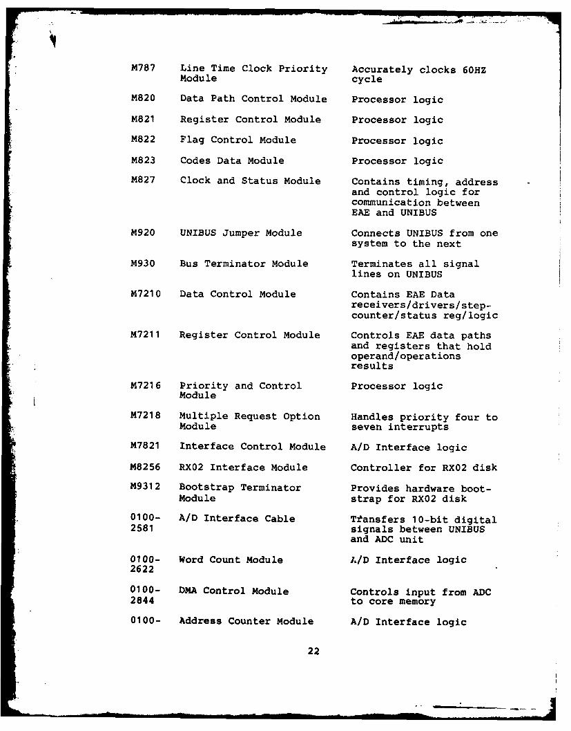
M787 Line Time Clock Priority Accurately clocks 60HZ
Module cycle
M820 Data Path Control Module Processor logic
M821 Register Control Module Processor logic
M822 Flag Control Module Processor logic
M823 Codes Data Module Processor logic
M827 Clock and Status Module Contains timing, addressand control logic forcommunication betweenEAE and UNIBUS
M920 UNIBUS Jumper Module Connects UNIBUS from onesystem to the next
M930 Bus Terminator Module Terminates all signallines on UNIBUS
M7210 Data Control Module Contains EAE Datareceivers/drivers/step-counter/status reg/logic
M7211 Register Control Module Controls EAE data pathsand registers that holdoperand/operationsresults
M7216 Priority and Control Processor logicModule
M7218 Multiple Request Option Handles priority four toModule seven interrupts
M7821 Interface Control Module A/D Interface logic
M8256 RX02 Interface Module Controller for RX02 disk
M9312 Bootstrap Terminator Provides hardware boot-Module strap for RX02 disk
0100- A/D Interface Cable Transfers 10-bit digital2581 signals between UNIBUS
and ADC unit
0100- Word Count Module A/D Interface logic2622
0100- DMA Control Module Controls input from ADC2844 to core memory
0100- Address Counter Module A/D Interface logic
22
The DATARAM DR-103 core memory is a random
access, magnetic core read/write memory which transfers data
to and from the processor and other devices by means of the
system UNIBUS. The memory has no priority structure.
Consequently, any master device can perform direct memory data
transfers without processor intervention (Ref 1:1).
The UNIBUS is a single, high-speed bus which
provides communication between system components by means of a
fifty-six line hardware bus configuration. Two devices on the
UNIBUS communicate via a master-slave relationship. The
device with control of the bus is called the "master". The
other device controlled by the "master" is referred to as the
"slave". All devices capable of becoming a master of the bus
are assigned a priority. The system priority structure
determines which device gains control of the UNIBUS. When two
devices have the same priority, the device electrically
closest to the processor is granted bus control. Direct
memory or data transfers between two peripheral devices can be
accomplished without involving the processor (Ref 9:175-176).
The H720 Power Supply is a mechanical device
which provides power for the PDP-11/15 computer by means of a
power bus. Additionally, the power supply provides DC LO and
AC LO logic signals which control DC and AC voltages in the
system (Ref 12:2-5).
DISPLAY UNIT
The 603 general purpose X-Y display monitor
23
display unit is a general purpose X-Y display monitor which
provides stored displays of analog data from Time-Series
calculations by means of a 603 Storage Monitor with associated
display related controls. Deflection amplifiers in the
display monitor process input signals and provide push-pull
outputs capable of driving the vertical and horizontal
deflection plates in the monitor. An internal CRT circuit
produces a high voltage potential and provides the control
circuits needed for CRT operation. A power supply circuit in
the monitor provides the necessary low-voltage power for the
603 monitor and stable regulation of output voltages. The 603
monitor manual describes in detail the functions of the panel
controls (Ref 21:1-2 to 1-6 and 2-1 to 2-3).
CONTROL UNIT
The Control Unit is an electrical device which
provides control and interfacing for keyboard and
control/display panels by means of read-in, lamp driver and
logic control circuits. The Control Unit scans all controls
while in an idle mode, interprets the settings, sets up
internal control parameters/programmable hardware and displays
appropriate control panel lights. Apalog inputs on the rear
external connectors of the Control Unit are attenuated to
appropriate signal levels via programmable attenuators on the
secondary Control Unit bus. The Control Unit also provides
internally generated 1KHZ square wave test signals on both
channels or external test signals which can be left
24
permanently connected to the rear of the Control Unit. Analog
input/output connections on the rear of the Control Unit are
displayed in Figure 5 (Ref 24:2-3).
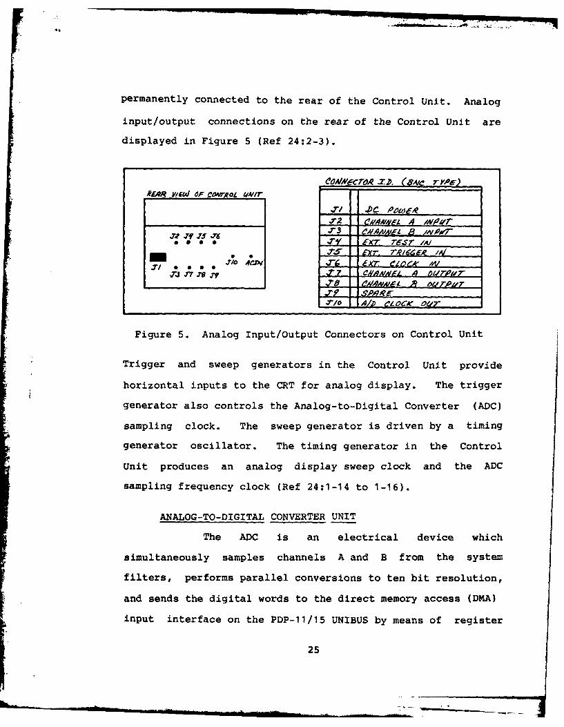
I&Q vit4oF coasreaz £aur.
____ ___ ___ ___ __r2 '4,boyl. 4 /N/'//" 3 lew',owNA i. INo Aara~X iq r XT reSr IAI
X/ A L.. £xr ezoe& *j J; J; Jr . C#lANNC -4 , W04W u7
,r/0 AID e oCK 017-
Figure 5. Analog Input/Output Connectors on Control Unit
Trigger and sweep generators in the Control Unit provide
horizontal inputs to the CRT for analog display. The trigger
generator also controls the Analog-to-Digital Converter (ADC)
sampling clock. The sweep generator is driven by a timing
generator oscillator. The timing generator in the Control
Unit produces an analog display sweep clock and the ADC
sampling frequency clock (Ref 24:1-14 to 1-16).
ANALOG-TO-DIGITAL CONVERTER UNIT
The ADC is an electrical device which
simultaneously samples channels A and B from the system
filters, performs parallel conversions to ten bit resolution,
and sends the digital words to the direct memory access (DMA)
input interface on the PDP-11/15 UNIBUS by means of register
25
I. ___
transfer operations. DMA input transfers do not interfere
with parallel processor operations. As a result, once
processing is started input transfers to core memory occur
without delay. For bandwidths greater than 50KHZ, the Analog-
to-Digital Converters can process 100K words per second per
channel (Ref 24:1-17).
SYSTEM POWER SUPPLY
The system power supply is an electrical device
which provides +5VDC, -15VDC, and +15VDC for the ADC and
Control Unit by means of a DC power distribution box mounted
on the system rack. Additionally, the system power supply
unit provides +5VDC to the system power distribution panel.
This +5VDC power is utilized by the system fans (Ref 24:1-17).
EXTENDED ARITHMETIC ELEMENT
The KE-1IA Extended Arithmetic Element (EAE) is a
device which performs multiplication, division, multiple
position shifts and normalization on numerical data by means
of clock and status (M827), register control (M7211), register
low byte (M234), register high byte (M234) and data control
(M7210) modules. The EAE performs arithmetic operations many
times faster than software routines (Ref 8:143).
The Clock and Status (M827) module enables the
EAE to communicate with the UNIBUS by means of basic timing
signals from a transfer clock, control circuits which start
and stop the clock, and address recognition logic (Ref 7:5-2).
26
The Register Control (M7211) module controls the data paths
and registers that hold the operands/operand results (Ref 7:5-
6). The Register High/Low Byte (M234) modules contain three
data registers, the main adder, and data paths which connect
these registers (Ref 7:5-10 and 5-11). The Data Control
(M7210) module contains the bus data receivers and drivers,
step counter, five bits of the status register and associated
logic which enables this module to control data transfers (Ref
7:5-12).
ASR-33 TELETYPEWRITER
The ASR-33 Teletypewriter (TTY) is a mechanical
device which performs input/output operations for the PDP-
11/15 computer by means of a printer, keyboard, paper tape
reader, and paper tape punch. The printer provides the user
with a hard copy of input/output. The keyboard of the ASR-33
TTY enables the user to input teletype commands and/or
programs. The paper tape reader reads pre-punched eight
channel perforated paper tape. The paper tape punch
perforates eight channel paper tape (Ref 9:5-6).
The ASR-33 TTY is interfaced to the PDP-11/15
UNIBUS via the address selector (M105), interrupt control
(M782), and receiver/transmitter timing (M780) modules. These
modules are referred to as the KL11 Teletype Control. The
KL11 Teletype Control assembles or disassembles serial
information for parallel transfer on the TTNIBUS. The address
selector module decodes the incoming address from the bus.
27
The interrupt control module generates an interrupt. The
receiver/transmitter module performs conversion and formatting
functions (Ref 12:2-6).
HEATHKIT H-19A VIDEO TERMINAL CRT
The Heathkit H-19A Video Terminal CRT is a device
which performs input/output operations for the PDP-11/15
computer by means of a high-quality keyboard, video display
CRT, and logic circuitry. The keyboard enables the user to
input keyboard commands/user programs. The CRT provides a
video display of the system input/output. The logic circuitry
consists of power supply, video, video driver, and terminal
logic circuit boards. The power supply circuit board
rectifies 115/230V input to provide 65VDC, 8.5VDC, -16VDC and
+16VDC input to the unit (Ref 16:32). The video and video
driver circuit boards provide logic circuitry for thm CRT (Ref
16:33-36). The terminal logic circuit board provides logic
circuitry for the H-19A processor/CPU, keyboard logic, master
clock and system logic, communications, CRT and memory
control, display memory, character generator and video control
logic (Ref 16:36-44).
X-Y RECORDER
The X-Y Recorder is a device which provides
graphic traces showing the relationship between two variable
functions by means of input modules, servomechanisms,
differential voltage comparators, high power DC motors, and a
pen arm assembly. The input module 17171A is a DC
28
preamplifier which increases the input voltages for fixed and
vernier range operations (Ref 17:4-1). The input module
17173A is a null detector which plots analog data in discrete
point form (Ref 17:1-1). The X-Y Recorder consists of the
servomechanisms. One servomechanism moves the pen carriage
vertically while the other moves the entire carriage arm
horizontally in response to input signals. The resulting
motions provide a cartesian trace of the data (Ref 17:4-1).
The differential voltage comparators provide a balancing
action in the system when the input signals may be continually
changing (Ref 17:4-1). The high power DC motors enable the
recorder to be highly responsive to data input (Ref 17:4-1).
The pen arm assembly houses the drawing pen and mechanical arm
required for X-Y plots (Ref 17:4-1).
HIGH-SPEED PAPER TAPE READER
The High-speed Paper Tape Reader (model 2540) is
a mechanical device which reads perforated tape and converts
information on punched tape into DC signal levels compatible
with circuit logic by means of a readhead assembly, driver
motor, electronics unit printed circuit board, power supply,
capstans, rollers, and brakes (Ref 18:1-1). The readhead
assembly converts the punched tape information into DC signal
levels. Holes in pre-punched tape pass over the readhead and
cause light to strike a photovoltaic cell in the readhead. As
a result, the cell produces a DC voltage. This signal level
is transmitted to the computer (Ref 18:4-4). The drive motor
29
. . . . . . , , . . -- - - f,," ,.
provides primary mechanical power for the tape drive system
(Ref 18:4-1). The electronics unit provides regulated 24VDC
for the readhead exciter lamp and controls tape motion/output
data (Ref 18:4-3). The power supply unit provides all of the
operating and drive voltages required by the reader and
electronics unit (Ref 18:1-1). The capstans, rollers and
brakes enable the paper tape to flow across the readhead
assembly at the proper speed and alignment.
DEC RX02 FLOPPY DISK UNIT
The DEC RX02 Floppy Disk Unit is an electronic
device which provides a mass storage software distribution
medium by means of two flexible disk drives, a single
read/write electronics module (M7745), a microprogrammed
controller module (M7744), power supply and PDP-11 Interface
module (M8256). The single read/write electronics (M7745) and
microprogrammed controller (M7744) modules provide all the
necessary control circuitry for the read and write operations
on the disk. Additionally, the modules calculate and verify
the cyclic redundancy check (CRC) at the end of the data field
for errors (Ref 13:4-34). The PDP-11/15 Interface module
(M8256) converts the RX02 input/output bus to a PDP-11 UNIBUS
structure. The module also controls interrupts to the CPU
initiated by the RX02, decodes UNIBUS addresses for register
selection and initiates non-priority requests (NPR) to
transfer data between the RX02 and the PDP-11/15 computer (Ref
13:1-7).
30
SYSTEM SOFTWARE PROGRAMS
Several software packages exist for the 1923/30 Time-
Series Analysis System. The DEC RT.11SJ Software Operating
System is copied onto the system eight inch floppy disk medias
in double density format. The RT.11SJ Operating System
consists of: a monitor/executive program for system control
and supervision; several device handler programs for each
hardware supported input/output device; and a variety of
utility programs for program and/or data creation and
manipulation (Ref 6:1-10). The following TSL software
packages exist on both eight inch floppy disks and paper tape:
1. TSL System Program for panel control
2. TSL System Program for keyboard control
3. TSL Analysis (TSLAP) and Library Utility (TSLIB)Programs
4. Core Memory Loading and Dumping Programs
5. Program Assembly Language (PAL-11)
6. Text Editor (ED-i)
7. On-Line Debugging Programs (ODT-11)
8. Linker Programs (LINK-11S)
9. Input/Output Executive Programs (IOX-11)
10. Floating-Point Math Package (FPMP-11)
11. Diagnostic Programs
12. X-Y Plotter Program
13. Modal Analysis Package (MAP)
The Time-Series Language (TSL) used in the system unit
~31:yr
.4. . . ..
rZ7
is a high-level computer programming language derived from
BASIC. TSL was designed specifically to be used with time-
series analysis and signal processing applications. TSL
provides: combinations of integer, floating point, real, and
complex arithmetic; Fourier transform operations; block
arithmetic functions for time-series signal analysis; Laplace
analysis functions; on-line debugging and editing commands;
and input/output instructions for various periph -al devices
(Ref 27:1-1). The TSL package was designed specifically for
operation with the PDP-11 computer. It supports all Time-
Series System two-channel analysis ADC operations (Ref 27:1-
6). TSL programs are written and/or executed by using the
ASR-33 Teletype or Heathkit H-19A CRT keyboard. The Time-
Series Language Programming Manual (see reference 27) explains
basic TSL programming commands and procedures. The following
analysis describes the major TSL software packages and their
key subroutines.
TSL SYSTEM PROGRAM FOR PANEL CONTROL
The PANEL-C and/or PANEL-30 System Programs
provide pushbutton selection of time-series analysis functions
from the Control Unit and Display Unit front consoles. PANEL-
30 is a second generation replacement program for the PANEL-C
Program. It uses a revised software Fast Fourier (FFT)
algorithm which provides a two-to-one improvement in Fourier
processing speed for averaged auto-spectra. PANEL-30 also
allows for greater range of absolute values and provides
32
better display calibration (Ref 26:1-5). The newer version
Panel Control Program (PANEL-30) is copied on the disk medias
for panel control utilization. The older version Panel
Control Program (PANEL-C) is available only on paper tape and
is intended for standby use only. A list of standard panel
program commands/functions are outlined in the Time-Series
Operating Manual (see reference 27), Table 1-1, page 1-5.
TSL SYSTEM PROGRAM FOR KEYBOARD CONTROL
Keyboard control, via the system TTY or CRT
keyboard, is achieved by use of the TSL-30 Program. The TSL-
30 Program allows the operator to use the pre-programmed panel
functions and provides access to individual processing steps
used in the final panel function results. In this manner, the
operator can perform processing modifications to block
arithmetic, differentiation, integration, complex functions,
and direct convolution calculations. Additionally, the user
can write subroutines using the TSL commands (Ref 24:1-3). A
list of standard keyboard program commands/functions are
outlined in the Time-Series Operating Manual (see reference
24), Table 1-2, page 1-9.
TSLAP AND TSLIB PROGRAMS
The TSL Analysis (TSLAP) Programs are pre-
programmed routines used for analysis of one or two channels
of analog input data. The TSLAP routines provide data
acquisition, spectral processing, averaging of successive
33
L.
results, final processing, and displays for the following
time-series analysis functions (Ref 25:12-1):
1. Fourier Transform
2. Auto and Cross Power Spectrum
3. Transfer and Coherence Function
4. Auto and Cross Correlation
5. Amplitude Histogram
6. Time Domain Waveform Averaging
A list of TSLAP routines for the Time-Series System is
outlined in Table II (Ref 25:12-3 to 12-5).
The TSL Library Utility (TSLIB) Programs are pre-
programmed routines which enable the user to create library
format routines, direct input/output of data blocks to/from
paper tape, and manipulate data via miscellaneous routines
which are not part of basic TSL (Ref 25:13-1). A list of
TSLIB routines for the Time-Series System is outlined in Table
III (Ref 25:13-2 to 13-3). The TSLAP and TSLIB routines are
located in the TSL applications #1, #2, #3 and TSL Amplitude
Histogram Files. Both the TSLAP and TSLIB routine operating
instructions are outlined in the TSL Programming Manual.
Quick reference start-up procedures and system error codes are
outlined in the TSL Reference Handbook.
CORE MEMORY LOADING PROGRAMS
The Bootstrap Loader is a program which instructs
the computer to load into core memory data which is punched on
tape in bootstrap format. The Bootstrap Loader is manually
34
TABLE II. TSLAP SOFTWARE ROUTINES
NAME OF ROUTINE DESCRIPTION
SETUP A dialog routine that prints a list ofrequired processing parameters and requestsentry of specifying codes
PARAM An echo routine that prints back thecurrent setup parameter codes
SAMP Routine continuously acquires and displaysblocks of sampled input data
FFT Forward Fourier Transform. Computes anddisplays the complex Fourier Coefficientsof input waveform
APS Auto Power Spectrum. Computes and displaysthe real power spectral coefficients
XPS Cross Power Spectrum. Computes and displaysthe complex common power coefficients andphase differences between two channels
TRAN Transfer Function. Computes and displayscomplex transfer function. Computescoherence function and retains channelauto-spectra and cross-spectrum
ACOR Auto-Correlation. Computes and displayscorrelation function of one or both inputwaveforms in time relative to themselves
XCOR Cross-Correlation. Computes and displayscorrelation function between inputwaveforms
HIST Amplitude Histogram. Computes and displaysamplitude distribution of input waveforms
WAVE Waveform averaging. Computes and displaystime-domain average- of one or both channels
DISPLY Routine draws a ten division by tendivision grid or -he CRT/X-Y Plotter,establishes a oiu..zontal zero referenceline, labels axes and sclaes, and thenpresents data on scale background.TheDISPLY routine is required by all TSLAPfunctions
35
TABLE III. TSLAB SOFTWARE ROUTINES
NAME OF ROUTINE DESCRIPTION
LIB Lists, searches, and loads routines fromlibrary format tapes
BTAP Converts tapes in PDP-11 load module formatto a format loadable by TSL
BLKIN, BLKOUT Routines to input and output TSL-defined
BLKINS, BLKOUS data blocks
COPY Routine to duplicate tapes
DATA Routine to load a string of data intosuccessive locations
DFLOAT Routine to convert a data block in doubleprecision format to floating point format
LIBC Routine to convert ordinary TSL tapes tolibrary format tapes
MEMAP Routine to print memory map of currentlydefined blocks
PBIB Similar to MEMAP. Prints single specifiedblock and gives complete block description
PUNCH Similar to SAVE routine of basic TSL.Routine prints routines in machinelanguage
ROTATE Performs end-around rotation of elementsof a TSL block
SAVE2, SAVE3 Similar to SAVE routine of Basic TSL.Routine punches a format which can beloaded regardless of prior loading ofsubroutine name
TSLAVG Machine language routine for high-speedaddition of one block to another
TSLHST Machine language routine to producehistogram
NOTE: Detailed operating instructions for each of theroutines listed above are outlined in the TSLProgramming Manual, pages 13-9 to 13-24.
36
loaded into the highest core memory location via the PDP-11/15
console switches (Ref 11:6-2).
The Absolute Binary Loader is a program which
enables the user to load paper tapes, punched in absolute
binary format, into any core memory location. The Absolute
Binary Loader is pre-programmed on paper tape in bootstrap
format. The Bootstrap Loader is used to load the Absolute
Binary Loader which, in turn, is used to load paper tapes
punched in absolute binary format (Ref 11:6-8).
CORE MEMORY DUMPING PROGRAMS
The paper tape software package includes two dump
programs called DUMPTT and DUMPAB. DUMPTT dumps octal
representations of core memory onto the system TTY/CRT, or
high-speed paper tape punch. The DUMPAB program dumps
absolute binary code from specified core locations onto the
high-speed paper tape punch. Both programs exist on paper
tape in bootstrap and absolute binary formats (Ref 11:6-12).
Operating procedures for both dump programs are outlined in
the PDP-11 Paper Tape Software Programming Handbook on page 6-
13.
OPERATING SYSTEM PROGRAMS
The following table outlines programs which allow
the user to assemble, edit, debug, link, and control program
input/output (Ref 8:155-159):
37
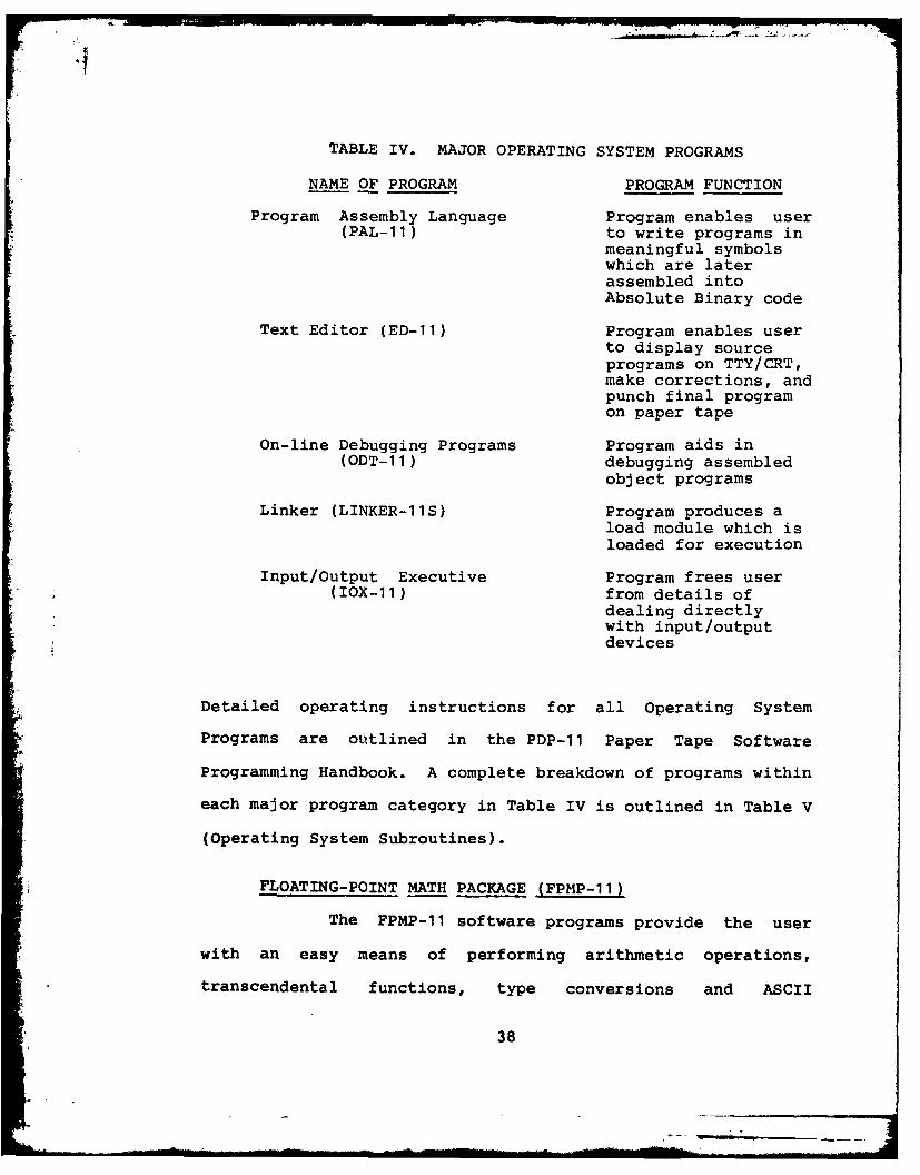
TABLE IV. MAJOR OPERATING SYSTEM PROGRAMS
NAME OF PROGRAM PROGRAM FUNCTION
Program Assembly Language Program enables user(PAL-i) to write programs in
meaningful symbolswhich are laterassembled intoAbsolute Binary code
Text Editor (ED-11) Program enables userto display sourceprograms on TTY/CRT,make corrections, andpunch final programon paper tape
On-line Debugging Programs Program aids in(ODT-11) debugging assembled
object programs
Linker (LINKER-11S) Program produces aload module which isloaded for execution
Input/Output Executive Program frees user(IOX-11) from details of
dealing directlywith input/outputdevices
Detailed operating instructions for all Operating System
Programs are outlined in the PDP-11 Paper Tape Software
Programming Handbook. A complete breakdown of programs within
each major program category in Table IV is outlined in Table V
(Operating System Subroutines).
FLOATING-POINT MATH PACKAGE (FPMP-11)
The FPMP-11 software programs provide the user
with an easy means of performing arithmetic operations,
transcendental functions, type conversions and ASCII
38
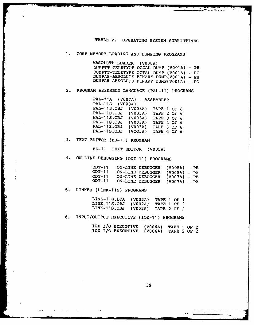
TABLE V. OPERATING SYSTEM SUBROUTINES
1. CORE MEMORY LOADING AND DUMPING PROGRAMS
ABSOLUTE LOADER (VOO6A)DUMPTT-TELETYPE OCTAL DUMP (VO0lA) - PBDUMPTT-TELETYPE OCTAL DUMP (VO0lA) - PODUMPAB-ABSOLUTE BINARY DUMP(VOO1A) - PBDUMPAB-ABSOLUTE BINARY DUMP(VO0iA) - PO
2. PROGRAM ASSEMBLY LANGUAGE (PAL-il) PROGRAMS
PAL-.11A (VOO7A) - ASSEMBLERPAL-11S (VOO3A)PAL-1iS.OBJ (VOO3A) TAPE 1 OF 6PAL-1iS.OBJ (V03A) TAPE 2 OF 6PAL-1iS.OBJ (VOO3A) TAPE 3 OF 6PAL-1iS.OBJ (VOO3A) TAPE 4 OF 6PAL-iiS.OBJ (VOO3A) TAPE 5 OF 6PAL-11S.OBJ (VOO3A) TAPE 6 OF 6
3. TEXT EDITOR (ED-li) PROGRAM
ED-li TEXT EDITOR (VOO5A)
4. ON-LINE DEBUGGING (ODT-1 1) PROGRAMS
ODT-11 ON-LINE DEBUGGER (VOOSA) - PBODT-11 ON-LINE DEBUGGER (VOOSA) - PAODT-11 ON-LINE DEBUGGER (VOO7A) - PBODT-11 ON-LINE DEBUGGER (VOO7A) - PA
5. LINKER (LINK-11S) PROGRAMS
LINK-11S.LDA (VOO2A) TAPE 1 OF 1LINK-11S.OBJ (VOO2A) TAPE 1 OF 2LINK-iiS.OBJ (VOO2A) TAPE 2 OF 2
6. INPUT/OUTPUT EXECUTIVE (IOX-li) PROGRAMS
IOX 1/O EXECUTIVE (VOO6A) TAPE 1 OF 2IOX 1/O EXECUTIVE (VOO6A) TAPE 2 OF 2
39
conversions. The FPMP-11 programs store very large and very
small numbers by retaining only significant digits in
computations. The floating-point notation makes calculations
easy. The FPMP-11 package consists of a single precision
program (Tape 1 of 2), a double precision program (Tape 1 of
2), and six source programs (Ref 2:1-1 and 1-2).
DIAGNOSTIC PROGRAMS
Table VI (Diagnostic Programs) lists all
diagnostic programs for the Time-Series System. The
diagnostic programs enable the user to check system
operations, paper tape functions, and specified processor
commands.
X-Y PLOTTER PROGRAM
The X-Y Plotter Program enables the system user
to obtain hard copy X-Y plots of signal analysis operations.
The X-Y Plotter Program is loaded into core memory as an
additional subroutine following the basic system program
loading procedures.
MODAL ANALYSIS PACKAGE (MP)
The MAP uses a Fourier Transform as a source in
order to develop a set of mode descriptors representing the
corresponding Laplace Transform. The descriptors used to
describe the Laplace Transform poles are frequency,
attenuation, amplitude and phase. The MAP consists of five
subroutines which are supplied as an integral part of the
40
TABLE VI. SOFTWARE DIAGNOSTIC PROGRAMS
1. Basic Address Test (UP)2. Basic Address Test (DOWN)3. Basic Memory Patterns Test4. Communication Test Program (CTP)5. Core Heating Test6. EAE Random Exerciser7. General Test Program8. KL-11/DL-11A TTY Tests9. Maintenance Loader
10. Memory Moving One's and Zero's Test11. No Dual Address Test12. One's and Zero's Test Tape13. PDP-11 Paper Tape System Checkout Package:
Test B Tape 1 of 2Test A Tape 2 of 2TAPDUP.ASC(2) Tape 1 of 2TAPDUP.ASC(1) Tape 2 of 2
14. Power Fail Diagnostic15. Randat16. Special Binary Count Pattern17. Test Programs:
#1 Branch Test#2 Con Branch Test#3 Unary Test#4 Unary and Binary Tests#5 Rotate/Shift Tests#6 Compare Test#7 Compare Not Test#8 Move Test#9 BIS, BIC, and BIT Tests
#10 Add Test#11 Substract Test#12 Jump Test#13 JSR, RTS, and RTI Tests#14 Trap Tests#15 Family Instruction Exerciser#17 4K System Exerciser
18. Up-down Address Test19. Worst Case Noise Test20. 1's Susceptability Test
41
=-F .
basic TSL program. The five subroutines used in the MAP
program (Ref 23:1-2) are outlined in Table VII (Modal Analysis
Package Programs):
TABLE VII. MODAL ANALYSIS PACKAGE PROGRAMS
NAME OF ROUTINE DESCRIPTION
Minimum Phase Routine Routines converts squared(MP) magnitudes of an auto
spectrum to a complexfunction of equivalentmagnitudes
Mode Separator Routine Routine operates on a(MS) complex Fourier Transform
to derive a peak locationfunction
Mode Detector Routine Routine finds, evaluates(MD) and records peaks that fall
within frequency, damping.and threshold specifiedlimits
Mode Evaluator Routine Routine produces the final(ME) Laplace Transform result in
the form of the four poledescriptors
Mode Generator Routine Routine regenerates a(MG) complex function of
frequency. It is usefulin comparisons withoriginal source function
42
III. UPGRADE PROCEDURES FOR 1923/30 SYSTEM
GENERAL APPROACH
The 1923/30 Time-Series Analysis System was upgraded by
means of the following procedures:
1. Installation of Heathkit H-19A CRT Terminal,
in place of ASR-33 TTY, to enhance I/O operations.
2. Reconfiguration of PDP-11/15 computer to
include only CPU processor modules, small peripheral
controller modules and core memory.
3. Interface of RX02 Disk Drive Unit to
reconfigured PDP-11/15 computer structure.
4. Bootstrap of RX02 Disk Drive Unit to PDP-
11/15 using existing floppy disk operating system.
INSTALLATION OF HEATHKIT H-19A CRT
The 1923/30 Time-Series Analysis System utilizes an ASR-
33 TTY for I/O terminal operations. An H-19A Heathkit CRT
terminal was interfaced to the system to enhance I/O
operations. Hard-copy output for I/O operations can still be
achieved by disconnecting the H-19A interface and
installing/operating from the ASR-33 TTY via simple cable
connections.
The Heathkit H-19A was interfaced to the PDP-11/15
system by means of an RS-232C interface unit. The RS-232C
unit was installed between the H-19A CRT and the TTY
Controller (M780) Module located in the processor. The TTY
43
interface cable from the M780 Controller Module was connected
to the Current-loop side of the RS-232C interface unit. The
25-pin "D" connector on the RS-232C interface unit output was
connected to the 25-pin "D" connector on the H-19 CRT. The
RS-232C interface unit is constructed to convert current-loop
output from the TTY Controller Module to RS-232C standard
signal levels. The Data Terminal Equipment inputs/outputs for
RS-232C standards (Ref 16:12) are as follows:
H-19 TERMINAL RS-232C INTERFACE BOX
PINCONNECTIONS
P GND 1 ----- I Protective GroundS OUT 2 ----- 2 RS-232C Serial OutputS IN 3 ----- 3 RS-232C Serial InputRTS 4 ----- 4 Request to Send OutputCTS 5 ----- 5 Clear to Send InputDSR 6 ----- 6 Data Set ReadyS GND 7 ----- 7 Signal GroundDTR 20 ----- 20 Data Terminal Ready Output
The RS-232C interface unit is not required when the ASR-33 TTY
is installed. The ASR-33 and TTY Controller Module cables
are constructed so direct interfacing is possible via cable
connections from the TTY Controller Module to the ASR-33 TTY.
The Heathkit H-19A CRT Terminal has two internal
switches (S401 and S402) which control various terminal
operations (Ref 16:10). The S401 switch descriptions are as
follows:
SWITCH NUMBER DESCRIPTION
0-3 Baud Rate
44
4 Parity Enable5 Odd/Even Parity6 Normal/Stick Parity7 Half/Full Duplex
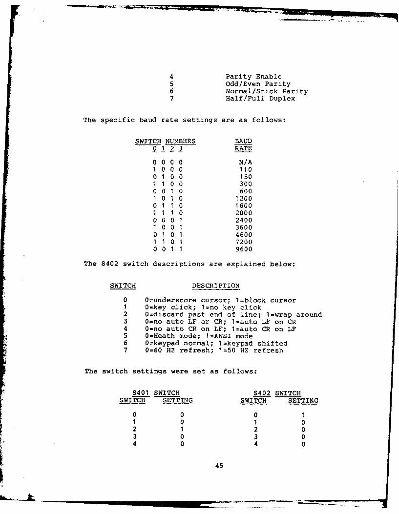
The specific baud rate settings are as follows:
SWITCH NUMBERS BAUD0 1 2 3 RATE
0 0 0 0 N/A1 0 0 0 11001 0 0 1501 1 0 0 3000 0 1 0 6001 0 1 0 12000 1 1 0 18001 1 1 0 20000 0 0 1 24001 0 0 1 36000 1 0 1 48001 1 0 1 72000 0 1 1 9600
The S402 switch descriptions are explained below:
SWITCH DESCRIPTION
0 0=underscore cursor; 1=block cursor1 0=key click; 1=no key click2 0=discard past end of line; 1=wrap around3 0=no auto LF or CR; 1=auto LF on CR4 0=no auto CR on LF; 1=auto CR on LF5 0=Heath mode; I=ANSI mode6 0=keypad normal; 1=keypad shifted7 0=60 HZ refresh; 1=50 HZ refresh
The switch settings were set as follows:
S401 SWITCH S402 SWITCH
SWITCH SETTING SWITCH SETTING
0 0 0 11 0 1 02 1 2 03 0 3 04 0 4 0
45
5 0 5 06 1 6 07 0 7 1
The Heathkit H-19A CRT was set on 110 baud rate (S402 setting
"1000") and 60 HZ refresh (S401 setting "0"). The 110 baud
rate is compatible to the TTY Controller Module output and the
60 HZ clock cycle conforms to the PDP-11/15 clock rate.
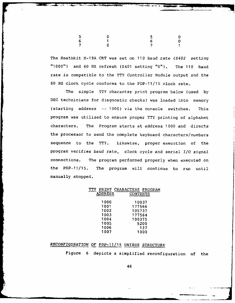
The simple TTY character print program below (used by
DEC technicians for diagnostic checks) was loaded into memory
(starting address -- 1000) via the console switches. This
program was utilized to ensure proper TTY printing of alphabet
characters. The Program starts at address 1000 and directs
the processor to send the complete keyboard characters/numbers
sequence to the TTY. Likewise, proper execution of the
program verifies baud rate, clock cycle and serial I/O signal
connections. The program performed properly when executed on
the PDP-11/15. The program will continue to run until
manually stopped.
TTY PRINT CHARACTERS PROGRAMADDRESS CONTENTS
1000 100371001 1775661002 1057371003 1775641004 1003751005 52001006 1371007 1000
RECONFIGURATION OF PDP-11/15 UNIBUS STRUCTURE
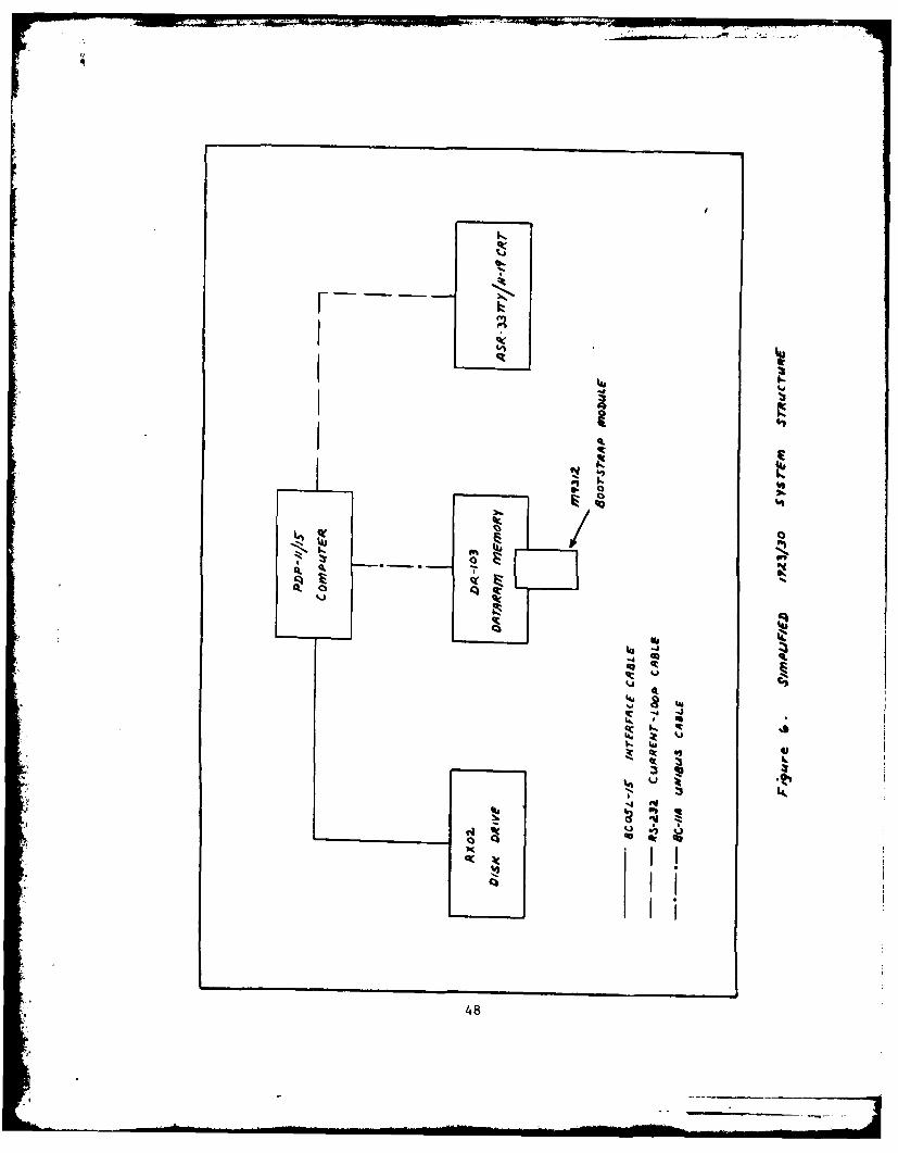
Figure 6 depicts a simplified reconfiguration of the
46
PDP-11/15 system. The M920 UNIBUS Connector was disconnected
from the modified DD11-A Module/EAE Module. The BC11-A cable
installed in the last slots (A4/B4) in the ADC module was
disconnected and inserted into slots (A4/B4) on the modified
DD11-A module. The BC11-A "out" cable from the Dataram DR-103
memory backplane to the control unit was disconnected. An
M930 terminator module was installed in the BC11-A "out" cable
position on the Dataram backplane. This PDP-11/15
configuration contains only the basic units required for
interfacing the RX02 Disk Drive to the system. These elements
include the PDP-11/15 processor, CRT/TTY, RX02 Interface
Controller and M9312 Hardware Bootstrap Modules, DR-103
Dataram Memory Unit, system power supply and RX02 Disk Drive
Unit. UNIBUS troubleshooting and system testing were greatly
enhanced with this simplified PDP-11/15 configuration.
Upon verification of a bootable RX02 Disk Drive to the
reconfigured PDP-11/15 system, the PDP-11/15 structure was
expanded to include the Control Unit, Display Unit, X-Y
Plotter and High-speed Paper Tape Reader.
The EAE and ADC modules were installed to the UNIBUS
structure via M920 UNIBUS Connector Modules. Power/ground
connections were installed on the modules via the power
modules on the system power harness. The BC11-A UNIBUS cable
was disconnected from the last slots on the modified DD11-A
module and installed on the last slots (A4/B4) on the ADC
Module. The BC11-A UNIBUS cable connected from the PDP-11/15
47
4
k
45-
1~~
L. I-
z ~1
Ik
N',
'II
/II 0
A,NU,
0.0. I N45.-.
0.0'-I
~04'.
-J
-4
~.1
0.
~ -4 -J
~ I- ~I' ~ U4.. Iu II
~ *10.
S. I'-4 ~1j
I II IIi
48
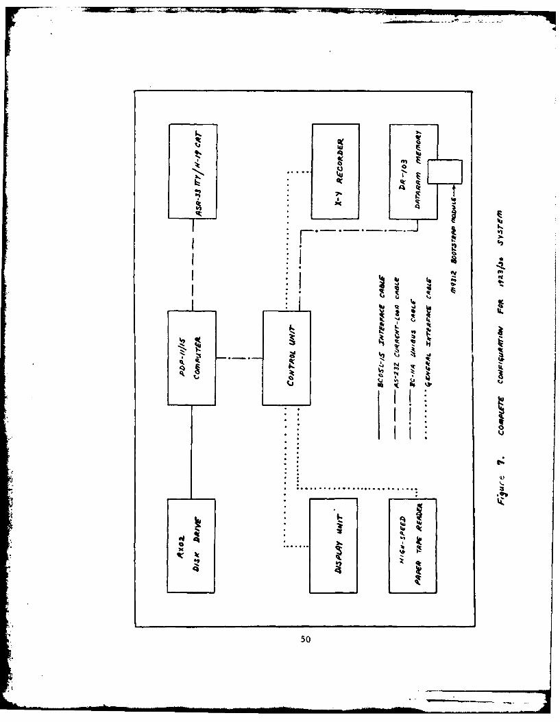
computer to the DATARAM Memory Unit was removed. The M930 Bus
Terminator card was removed from slots A4/B4 on the Control
Unit. The fifteen foot BC11-A cable from the Control Unit
(mounted in slots Al/B on the DEC UNIBUS bed) was connected
to the A4/B4 slots on the ADC module in the PDP-11/15
computer. The remaining BC11-A UNIBUS cable was installed
from slots A4/B4 on the DEC UNIBUS bed in the Control Unit to
slots Al/Bl on the backplane of the DATARAM Memory Unit. The
M9312 Bootstrap Module was left in blots A4/B4 on the Memory
Unit backplane. As a result of these changes, the UNIBUS was
extended to include all equipment in the 1923/30 system. This
enhanced configuration forms the complete system (see Figure
7).
The M9312 Bootstrap Module functions as a hardware
bootstrap for the RX02 Disk Drive and as a bus terminator card
for the UNIBUS. Consequently, the M9312 Module was inserted
in the last position on the UNIBUS (in place of the M930
Terminator Module in the Memory Unit).
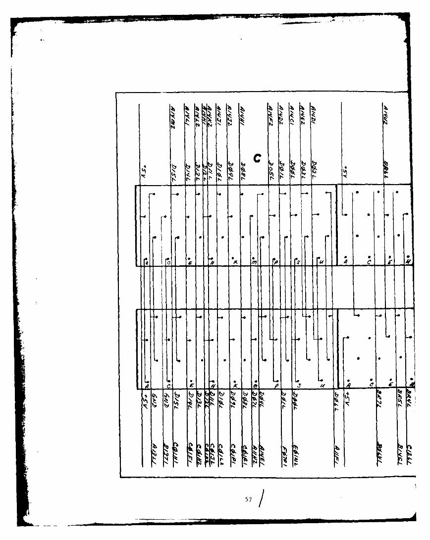
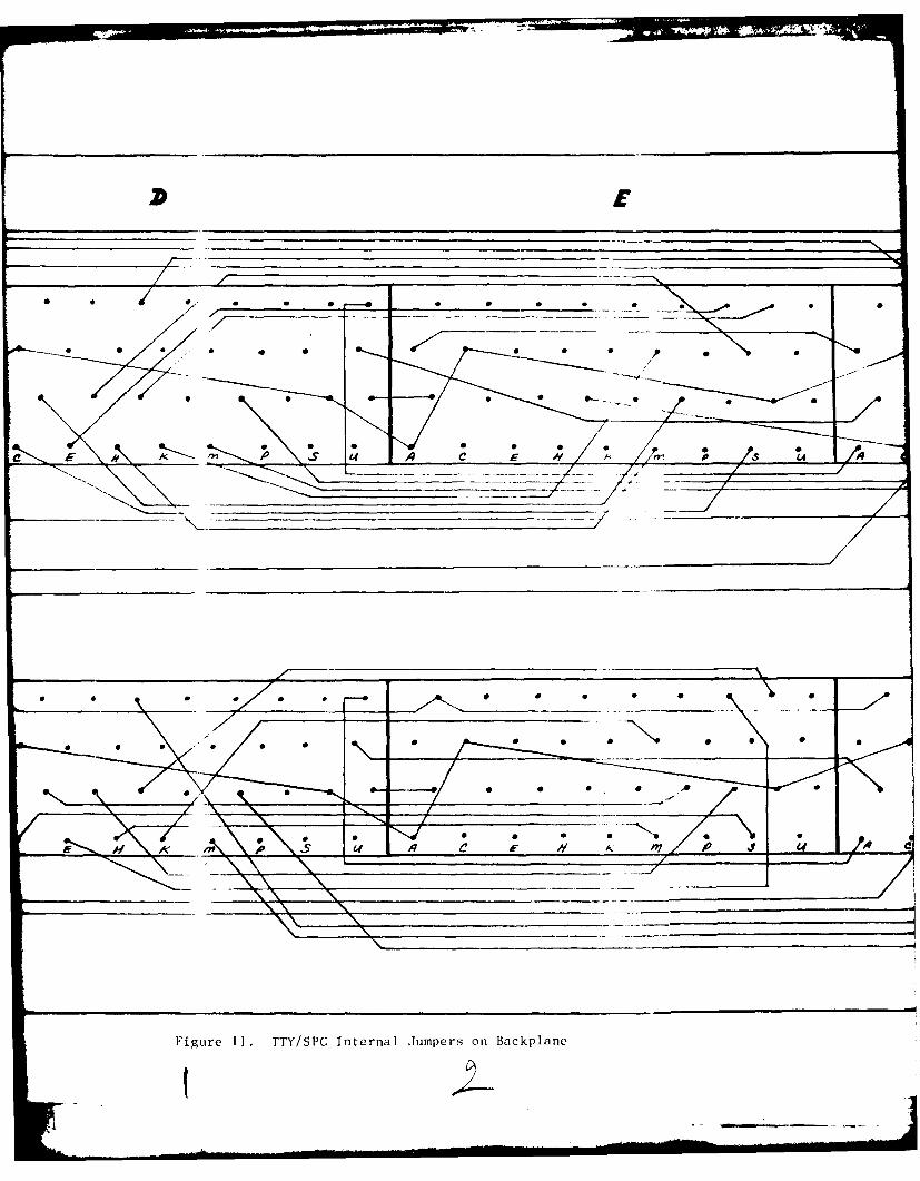
VERIFICATION OF TTY/SPC BACKPLANE WIRING
The RX02 Disk Drive interfaces to the PDP-11/15 UNIBUS
by means of the M8256 Controller Module. The M8256 Module is
a quad circuit board designed to be inserted into a single row
which includes columns C, D, E and F. The RX02 Disk Drive is
a Direct Memory Access (DMA) device. As a result, the
circuitry required for the RX02 UNIBUS interface will vary
from the standard SPC slots pre-wired to handle TTY and other
49
AJ
'4J2
* ..
50(5
Iiiprogrammable I/O devices. Consequently, wiring into available
optional SPC slots (TTY/small peripheral controller spare
slots) was verified. Verification of existing SPC slot wiring
was essential for future backplane modifications to
accommadate the M8256 Interface Module. Rows 13 and 14
(located on the third BB11 Module) in the PDP-11/15 backplane
were the only TTY/SPC slot available for verification. The
standard DEC UNIBUS wiring/pin configurations expedited
identification and verification of UNIBUS signals.
UNIBUS WIRING/PIN CONFIGURATIONS
The UNIBUS wiring/pin configurations are
identified by one of two methods. All processor modules, with
the exception of the KL11 Teletype Control Modules and other
device controller modules, are identified by means of a four-
character scheme. The following example represents the
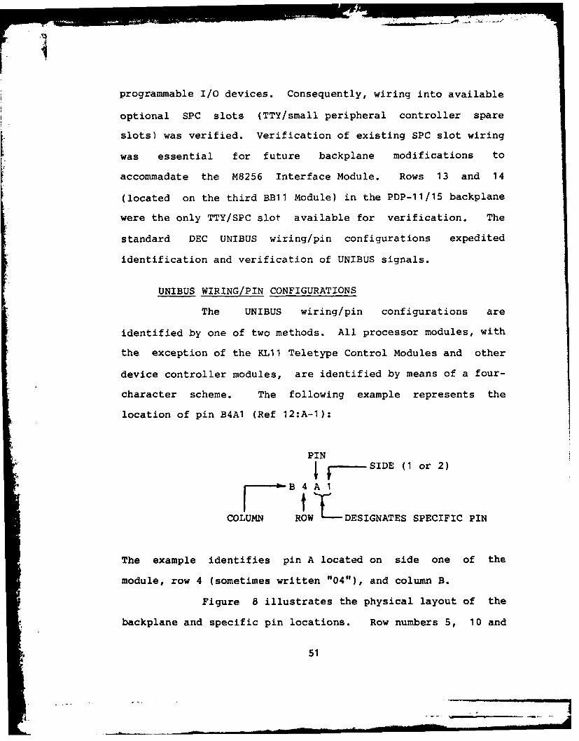
location of pin B4A1 (Ref 12:A-1):
~PIN •IN SIDE (1 or 2)
COLUMN R W DESIGNATES SPECIFIC PIN
The example identifies pin A located on side one of the
module, row 4 (sometimes written "04"), and column B.
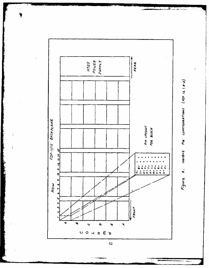
Figure 8 illustrates the physical layout of the
backplane and specific pin locations. Row numbers 5, 10 and
51
It
0
-- -t
r5
cz~ . j * ** *** 73
15 depicted in the figure are taken into account for the
numbering sequence but contain no modules or pins.
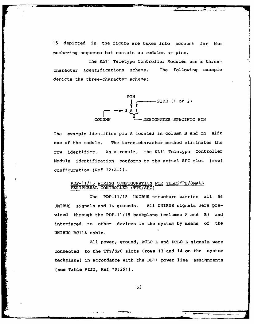
The KL11 Teletype Controller Modules use a three-
character identifications scheme. The following example
depicts the three-character scheme:
PINSSIDE (1 or 2)
-B BA 1COLUMN DESIGNATES SPECIFIC PIN
The example identifies pin A located in column B and on side
one of the module. The three-character method eliminates the
row identifier. As a result, the KL11 Teletype Controller
Module identification conforms to the actual SPC slot (row)
configuration (Ref 12:A-1).
PDP-11/15 WIRING CONFIGURATION FOR TELETYPE/SMALL
PERIPHERAL CONTROLLER (TTY/SPC)
The PDP-11/15 UNIBUS structure carries all 56
UNIBUS signals and 14 grounds. All UNIBUS signals were pre-
wired through the PDP-11/15 backplane (columns A and B) and
interfaced to other devices in the system by means of the
UNIBUS BC1iA cable.
All power, ground, ACLO L and DCLO L signals were
connected to the TTY/SPC slots (rows 13 and 14 on the system
backplane) in accordance with the BB11 power line assignments
(see Table VIII, Ref 10:291).
53
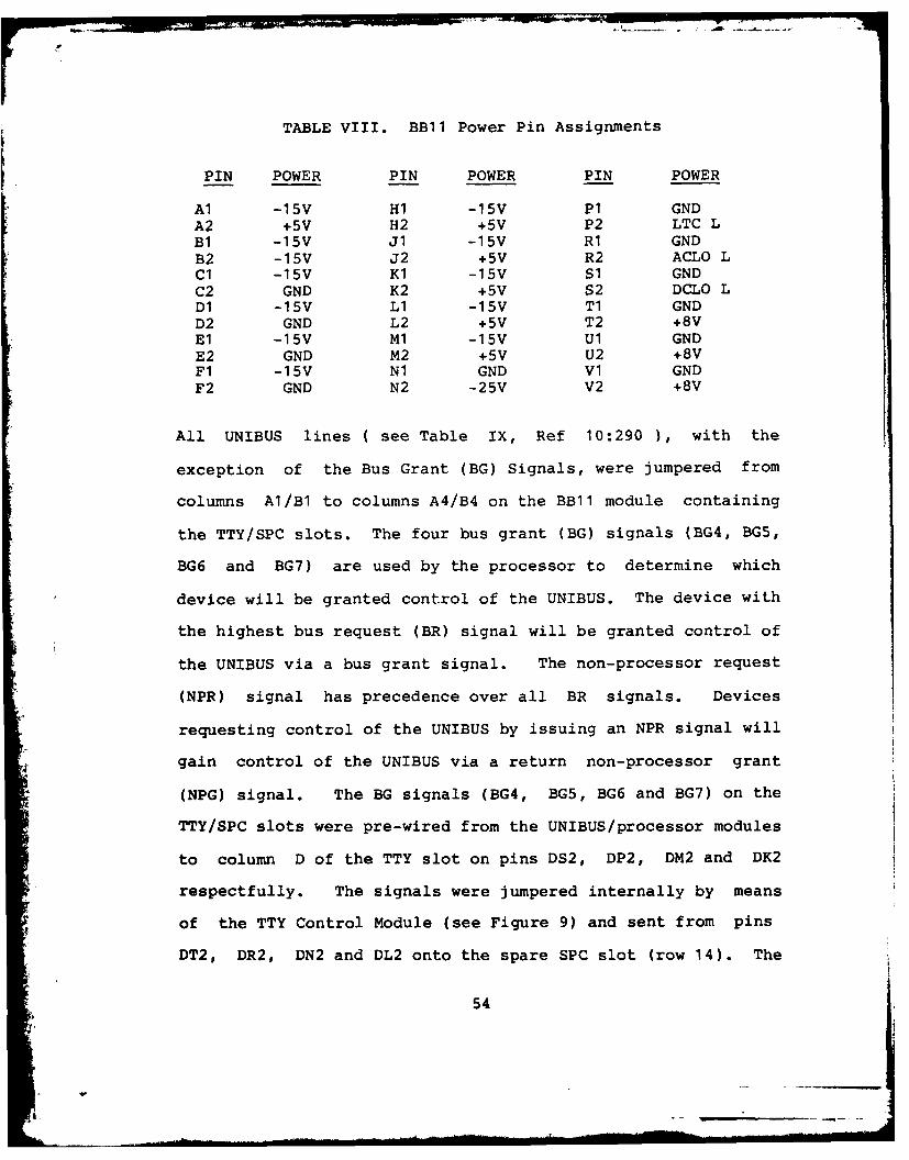
TABLE VIII. BB11 Power Pin Assignments
PIN POWER PIN POWER PIN POWER
Al -15V Hi -15V Pi GNDA2 +5V H2 +5V P2 LTC LBl -15V Ji -15V Ri GNDB2 -15V J2 +5V R2 ACLO LCl -15V K1 -15V Si GNDC2 GND K2 +5V S2 DCLO LD1 -15V Li -15V TI GNDD2 GND L2 +5V T2 +8VEl -15V Mi -15V U1 GNDE2 GND M2 +5V U2 +8VF1 -15V NI GND Vi GNDF2 GND N2 -25V V2 +8V
All UNIBUS lines ( see Table IX, Ref 10:290 ), with the
exception of the Bus Grant (BG) Signals, were jumpered from
columns Al/Bi to columns A4/B4 on the BB11 module containing
the TTY/SPC slots. The four bus grant (BG) signals (BG4, BG5,
BG6 and BG7) are used by the processor to determine which
device will be granted control of the UNIBUS. The device with
the highest bus request (BR) signal will be granted control of
the UNIBUS via a bus grant signal. The non-processor request
(NPR) signal has precedence over all BR signals. Devices
requesting control of the UNIBUS by issuing an NPR signal will
gain control of the UNIBUS via a return non-processor grant
(NPG) signal. The BG signals (BG4, BG5, BG6 and BG7) on the
TTY/SPC slots were pre-wired from the UNIBUS/processor modules
to column D of the TTY slot on pins DS2, DP2, DM2 and DK2
respectfully. The signals were Jumpered internally by means
of the TTY Control Module (see Figure 9) and sent from pins
DT2, DR2, DN2 and DL2 onto the spare SPC slot (row 14). The
54
. - . .
TABLE IX. UNIBUS Pin Assignments
PIN SIGNAL PIN SIGNAL PIN SIGNAL PIN SIGNAL
BH2 AOOL BF1 ACLOL AF1 D06L BB2 GNDBH1 A01L AP2 BBSYL AH2 D07L BC2 GND
BJ2 A02L BE2 BG4H AHI D08L BD1 GNDBJ1 A03L BB1 BG5H AJ2 D09L BEI GND
BK2 A04L BAI BG6H AJI DI0L BT1 GNDBK1 A05L AVI BG7H AK2 DI1L BV2 GND
BL2 A06L BD2 BR4L AKI D12L AA INITLBLI AO7L BC1 BR5L AL2 D13L ABI INTRL
BM2 A08L AU2 BR6L ALl D14L BV1 MSYNL
BM1 A09L AT2 BR7L AM2 D15L AUI NPGH
BN2 A10L BU2 COL AB2 GND AS2 NPRLBN1 A1IL BT2 CIL AC2 GND AMI PALBP2 A12L ACI DOOL ANI GND AN2 PBLBP1 A13L AD2 D01L API GND AA2 +5V
BR2 A14L ADI D02L ARI GND BA2 +5VBRI A15L AE2 D03L ASI GND AR2 SACKL
BS2 A16L AEl D04L ATI GND BF2 DCLOL
BS1 A17L AF2 D05L AV2 GND BUl SSYNL
signals entered the spare SPC slot on pins DS2, DP2, DM2 and
DK2, and were returned to the UNIBUS (Ref 8:16).
/ ze C// .16 .Da liS 6R7 L
S I; M I 1A 2 2 /- E Z a m a t * I
84A ¥ r P72 9 _j 13 J/N 8mS 8R' L
M 6 A?4' MI/A A(' b~ S' -22Js *EquEsr L
ams 06S OW7 N Ple (d -VVL S 8$~7 /AtH
ams 845'/oN l ,Z2 'A 7.P.4' 8s 8&4;? our#/
aaS 4846 00r# IA W_______9J~±A
Figure 9. Priority Jumper Plug for TTY
Figure 9 depicts the jumper wiring for a priority four (PR4)
device like the ASR-33 TTY. The jumper configuration sends
55
out a bus BR4 signal on the bus request line for the TTY
device. The priority plug accepts only bus BG4 signals for
the activation of TTY circuitry. All other Bus Grant (BG)
lines are sent to the next device on the UNIBUS.
Bus Grant Continuity (G727) cards were inserted
into column D of the spare SPC slot in order to continue the
daisy-chain of Bus Grant signals. The G727 card jumpers pins
DS2, DP2, DM2 and DK2 to pins DT2, DR2, DN2 and DL2 respect-
fully. As a result, Bus Grant signals pre-wired to empty SPC
slots will be returned to the UNIBUS without any disconti-
nuity. Failure to insert G727 cards in column D of empty SPC
slots will make the UNIBUS inoperative. Discontinuities in
the chain of UNIBUS signals will result in inoperative front
console controls and lights.
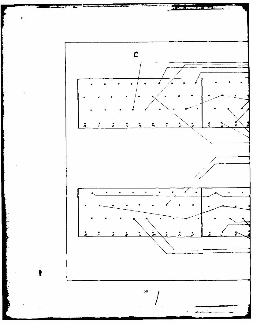
All UNIBUS signals (see Figures 10 and 11), with
the exception of the NPG signal, were pre-wired into their
appropriate pin locations on the TTY/SPC slots (rows 13 and
14). The PDP-11/15 was not pre-wired to handle devices that
require NPR/NPG signals. NPR/NPG devices normally have a
priority of five, six or seven. The TTY/SPC slots were pre-
wired to handle priority four devices. Consequently, the NPG
line on the TTY/SPC slots was not pre-wired to the UNIBUS
(see Figures 10 and 11).
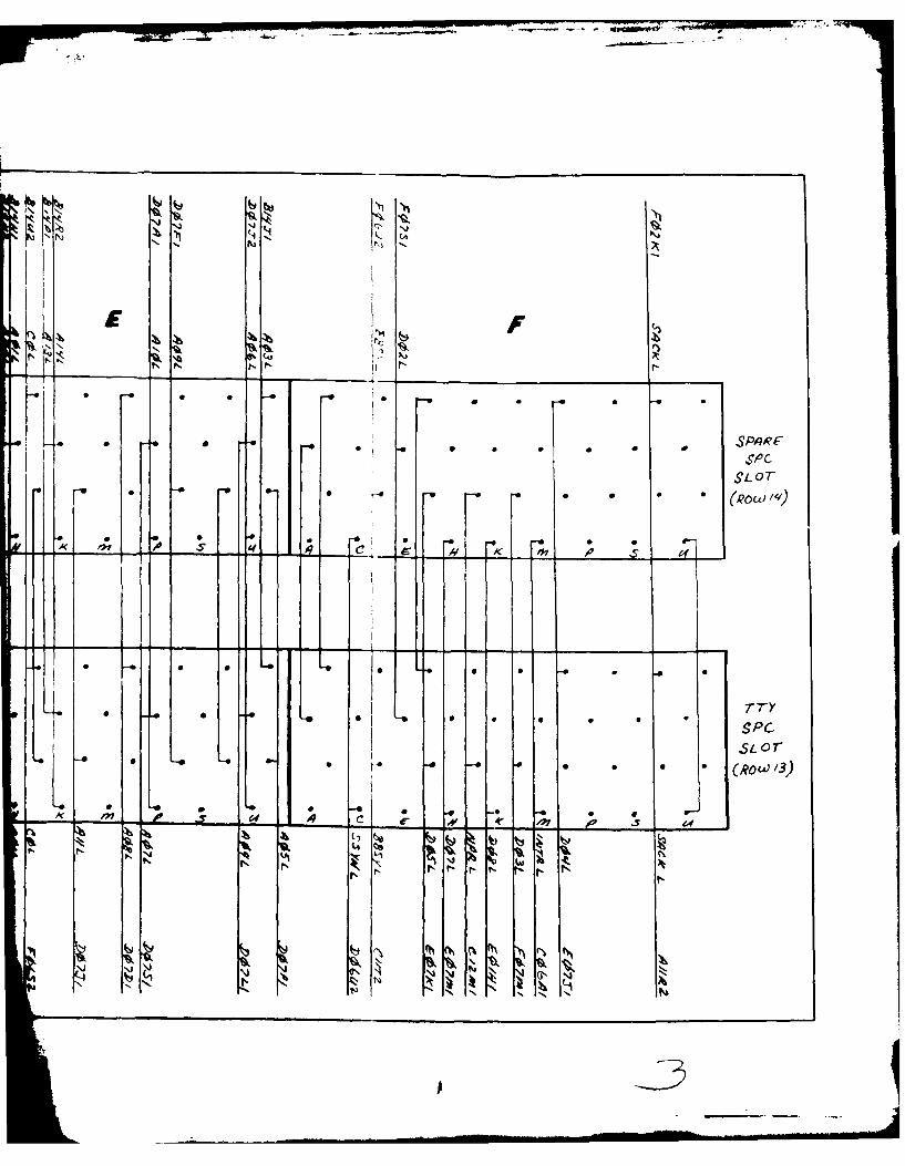
RX02 DISK DRIVE INTERFACE
INSTALLATION OF RX02 DISK DRIVE UNIT
The High-speed Paper Tape Reader, located
56
(41 i. I', i
. . p,0 , ,
r* . , . ,
0 0' 4 C - 4L...~ - - - - -
- - -
_ --- i.." - il-I3
lll il ] ,
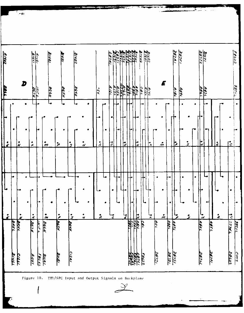
KAI
ItII
1 '4 le I .r
0 -C
.16~
P,.
Figure 10. TTY/SPC Input and Output Signals on Backplane
'.JV.0 aJ
SLO
4 10
4 aS7qq
fs~p)LO
- -~----~.- -
C
/
* d
/* S S * * S 0
* 0 0 0 5 0 0
* S * 0 * * 0 0 0
44 C g ~ in P 4' LA 4 ~2 E
/
/
0 0 0 * 0 0 *
/* 0 0 0 * S 0 5 0
C
9
58 / ______
0
h
4 4 c
Figure 11. TTY/SPC Internal Jumpers on Backplane
E Fwo
* (pqow 1,q)
* 0 0 0
-7 - _ _____ _7__Y
SLOT
directly above the PDP-11/15 computer, was removed and the
RX02 Disk Drive was mounted in the same location via the RX02
cabinet-mountable installation kit. The RX02 power cable was
installed on the 1923/30 power strip in the cabinet backplane.
The BC05L-15 standard interface cable was connected from the
M7744 CPU Controller Module in the RX02 to the M8256 Interface
Controller Module in the PDP-11/15 backplane. The BC05L-15
cable was connected to each module with the red stripe on the
cable toward the center of the card. This convention ensured
that signal continuity was maintained between modules (Ref
14:4).
The Si (controller configuration) switch on the
M7744 module in the RX02 Disk Drive has three modes of
operation. The three possible configurations for an RX02 Disk
Drive are (Ref 13:2-4):Si SETINGS
INTERFACE DESCRIPTION Si-I S1-2
RX211/RXV21 PDP-i1/LSI-11 Double Density OFF ONRX8E/RX11/RXV11 PDP-8/PDP-11/LSI-11 Single
Density ON OFFRX28 PDP-8 Double Density OFF OFF
INSTALLATION OF KFI1-A MULTIPLE BUS PRIORITY MODULE
The RX02 Disk Unit is a priority five (PR5) device. The
ASR-33 TTY/Heathkit H-19 CRT units are priority four (PR4)
devices. Multiple bus priority control logic is required to
properly allocate device control of the PDP-11/15 UNIBUS. The
KF11-A Multiple Bus Priority Module provides this control
logic.
59
W -a
GENERAL DESCRIPTION OF KF11-A
The KF-11A Multiple Bus Priority Option provides
four interrupt levels (4,5,6 and 7) for the PDP-11/15
processor. The system is pre-wired to service only Bus Grant
four (BG4) signals when the KF11-A option is not installed.
When the KF-11A option is installed, the KC11 processor in the
PDP-11/15 computer can service BG4 through BG7 and Bus
Request four (BR4) through BR7 signals. The console non-
processor request flag (CNPRF), console bus request flag
(CBRF) and non-processor request flag (NPRF) signals remain
under control of the M7216 Priority and Control Module. The
KC11 processor backplane is already pre-wired for installation
of the KF11-A option (Ref 4:3-1).
BASIC OPERATION OF KF11-A
All devices connected to the system UNIBUS
compete for use of the bus. When a device requires use of the
bus, it issues a bus request (BR) signal to the processor.
The processor converts all asynchronous device requests to
synchronous requests. The KF11-A accepts all four bus request
signals, determines which request has a higher priority, and
then issues a processor bus grant signal to the device with
the highest priority. Figure 12 depicts the control circuitry
on the M7218 Multiple Bus Priority Module. The figure traces
the flow of BR/BG signals for all controller devices. Bus
Request signals are channeled through a series of logic gates
in order to determine which device has the highest BR signal.
60
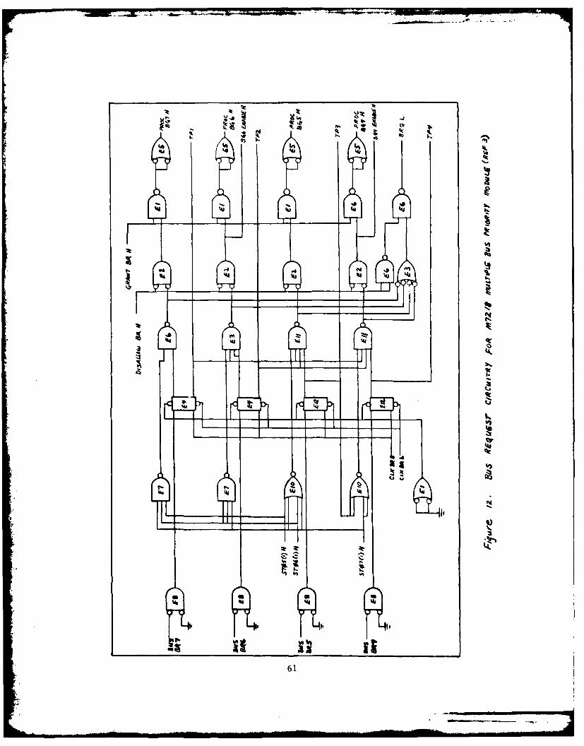
Itt
404
44.
Cd '4 N 'g
'4 '4 lii 4J I
61s
The following list (Ref 4:3-4) describes the general control
signals produced by the KF11-A option:
SIGNAL NAME DESCRIPTION
KBR-2 PROC BG7 H Bus signal indicating bus control is on
level sevenKBR-2 TP1 Test Point used to monitor BR7 flip-flopKBR-2 PROC BG6 H Bus signal indicating bus control is on
level sixKBR-2 BG6 Enable H Test Point indicates selection of BG6 for
bus releaseKBR-2 TP2 Test Point used to monitor state of BR6
Flip-FlopKBR-2 PROC BG5 H Bus signal indicating bus control is on
level fiveKBR-2 TP3 Test Point used to monitor state of BR5
flip-flopKBR-2 PROC BG4 H Bus signal indicating bus control is on
level fourKBR-2 BG4 Enable H Test Point indicating selection of BG4
for bus releaseKBR-2 TP4 Test Point used to monitor state of BR4
flip-flopKBR-2 BRQ L Signal indicating a bus request was
issued and that the bus request is of ahigher priority than ones currently inthe processor
PROCEDURES FOR KF-11A INSTALLATION
Two procedures were required to install the KF11-
A option. The M7218 Bus Request Module was inserted into the
pre-wired slot B6 of the KC11 processor unit (see Figure 2)
and the J2/J3 jumpers on the M7216 Priority/Control Module
were removed (see Figure 13). Removal of the J2 and J3
jumpers on the M7216 Module disabled the BRQ L and PROC BG4 H
signals generated on that module. The BRQ L and PROC BG4 H
signals were generated on the M7218 Module when it was
installed. The J1 and J4 jumpers on the M7216 Module are
62
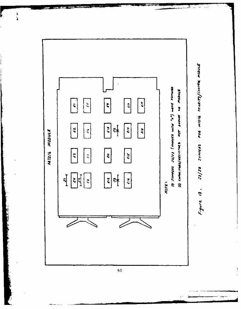
LiV
al
f3
I~~dv
63I
IN* . . .
removed when the power fail/restart KP11-A option is
installed. The KP11-A option was not required and
consequently not installed on this system (Ref 4:2-1). As a
result, tne J1 and J4 jumpers were left installed on the M7216
Module.
MODIFICATION OF KF11-A MODULE
The system M7218 Multiple Bus Priority Module was
built to conform to Digital Equipment specifications and
standards. The following list indicates DEC recommended IC
chips for the M7218 Module and those actually installed:
DEC IC CHIPS IC CHIPS INSTALLED
DEC 380 SP380ADEC 74H10N SN74H1ONDEC 74H00N SN74HOONDEC 7402N SN7402NDEC 74H20 SN74H20NDEC 74H74N SN74H74NDEC 8881 SN7401NDEC 74H50N SN74H50N
The SN7401N IC Chip used as a replacement for the
recommended DEC 8881 IC Chip contains quadruple 2-input
positive-nand gates with open collector-outputs (Ref 22:5-1).
In open-collector circuits a pull-up resistor is required to
bring the output to a high state (Ref 19:126). Pull-up
resistors for the SN7401N IC Chip were not installed on the
M7218 Module. As a result, low input signals to the SN7401N
IC Chip produced an output voltage that was neither high nor
low. To correct this problem, the SN7401N IC Chip in IC
64
position E5 (see Figure 14) was replaced with an SN74LSOON IC
Chip which contains quadruple 2-input positive-nand gates (Ref
22:5-6) and requires no pull-up resistors. This modification
corrected the high/low signal output problem without adding
any pull-up resistors to the module. The input/output pin
locations on the SN74LSOON IC Chip were different from the
original SN7401N IC Chip used. As a result, the following
changes were made to existing backplane wiring on the
M7218 Module IC bed containing the SN74LSOON IC Chip:
WIRING REMOVED
FROM IC POSITION TO IC POSITION
PIN 2 E5 PIN 3 E5PIN 2 E5 PIN 8 E6PIN 8 E5 PIN 9 E5PIN 8 E5 PIN 8 ElPIN 11 E5 PIN 12 ESPIN 11 E5 PIN 6 ElPIN 5 E5 PIN 6 E5PIN 5 E5 PIN 3 El
WIRING INSTALLED
FROM IC POSITION TO IC POSITION
PIN 8 E6 PIN 2 E5PIN 2 E5 PIN 1 E5PIN 8 El PIN 10 E5PIN 10 E5 PIN 9 E5PIN 6 El PIN 13 E5PIN 13 E5 PIN 12 E5PIN 3 El PIN 5 E5PIN 5 E5 PIN 4 E5
Figure 14 indicates the IC position numbers for each IC Chip
on the M7218 Module. The IC position numbers in Figure 14
65
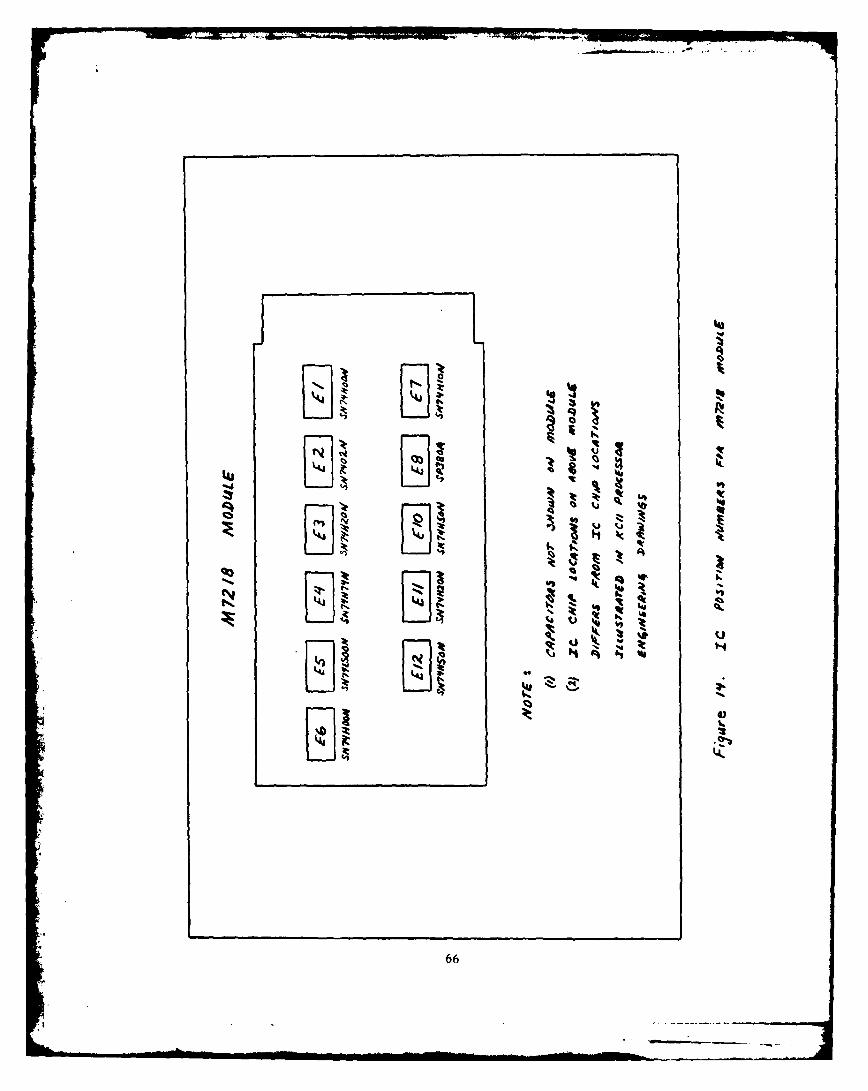
log, 'Pl
I',4.Jt00-h
Irat
4JI %ii
66
. . ...... .;:...-- -,---
"E-' ... . ,., - 0{
differ from the IC position numbers for the M7218 Module
listed in the KC11 processor engineering drawings. This
variation in chip position identification was a result of
different physical layouts for each module.
INSTALLATION OF KW11-L LINE TIME CLOCK
The KW11-L Line Time Clock is an option module
(M787) which is wired to column B, row twelve of the KC11
processor. The KW11-L accurately divides time into intervals
for more efficient use of the PDP-11/15 processing time. The
KW11-L option provides clocked intervals (50/60 HZ) for
various hardware/software equipment. The PDP-11/15 computer
operates on a line frequency of 60 HZ. The KW11-L clock
intervals are determined by the line frequency of the host
computer. Installation of the KW11-L clock elevates the line
time clock level of the PDP-11/15 to that of a PDP-11/20
system. The KW11-L clock has a BR6 priority level, vector
address of 100, 60 HZ clock interval rate (with 50 HZ
capability) and interrupt/noninterrupt operational modes (Ref
4:A-1).
The KW11-L Line Time Clock was installed in the PDP-
11/15 processor to provide the necessary 60 HZ clock intervals
required for operation of a floppy disk RT.11 software
operating system. Figure 15 depicts wiring modifications made
to the PDP-11/15 backplane (column B, rows 12 and 14, and
column D, row 14) for proper installation of the KW11-L Line
Time Clock. Installation of the KW11-L Clock (at priority
67
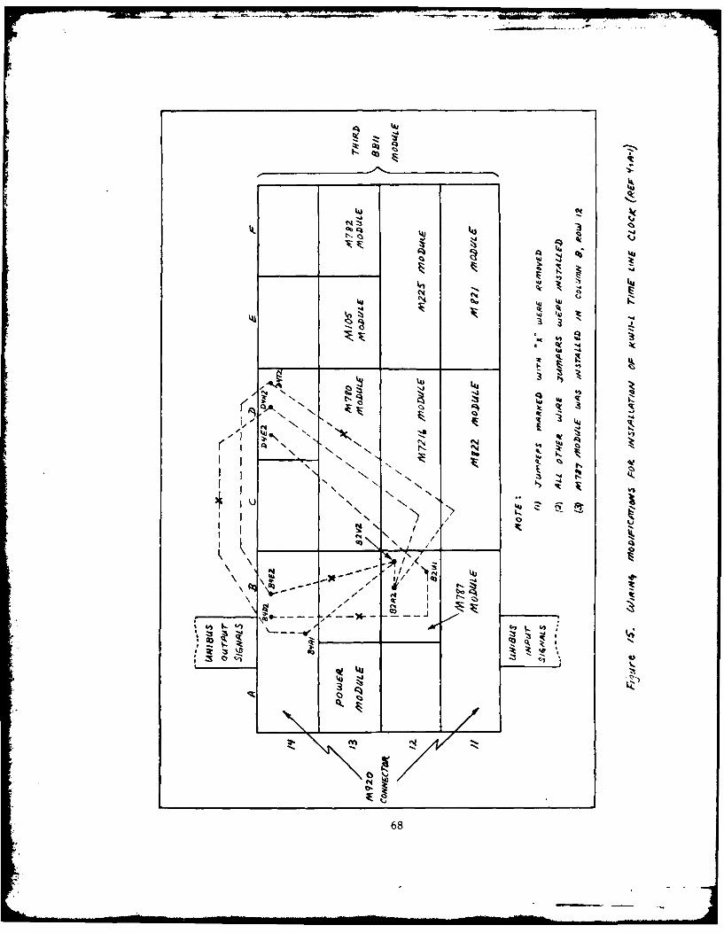
-..- -;i4.~ - - --. -.w----- -. - -
Q..
N NN,4
IN,(
Q41
N <
ell _ it -
ita
-zz
68U
BR6) had no effect on attempts to bootstrap the RT.11
operating system. The KW11-L Clock was rewired for a BR5
priority. Likewise, the clock (wired for BR5) did not effect
RT.11 floppy disk bootstrap operations.
MODIFICATION/INSTALLATION OF DD11-A MODULE
A DD11-A module is a pre-wired system unit designed for
mounting up to four small peripheral devices. The DD11-A is
similar in design to a BB11-A processor module. DD11-A and
BB11-A modules are installed in the PDP-11/15 backplane via
two mounting screws. All UNIBUS signals enter the DD11-
A/BB11-A modules in slots AI/BI and exit on slots A4/B4 via
M920 UNIBUS connector cards. Both modules are powered by the
system power harness installed in slot A3. The DD11-A module
is pre-wired differently from the BB11-A module.
The addition of a Direct Memory Access (DMA) device,
like the RX02 Disk Drive, requires that an SPC slot on the
DD11-A be modified prior to installation of the device. The
major wiring change required for this modification entailed
re-wiring the UNIBUS NPG signal. The NPG signal was jumpered
from column Al on the DD11-A module to column C1 on the DD11-A
module. The signal was daisy-chained from column C1 through
column C4 and then returned to the UNIBUS (see Figure 16).
The modification enables DMA devices to operate using the
NPG/NPR bus signals for DMA data transfers. The "NPG IN"
signal enters on pin CAl and the "NPG OUT" signal exits on pin
CBI for each SPC slot (row) of the DD11-A module. The "NPG
69
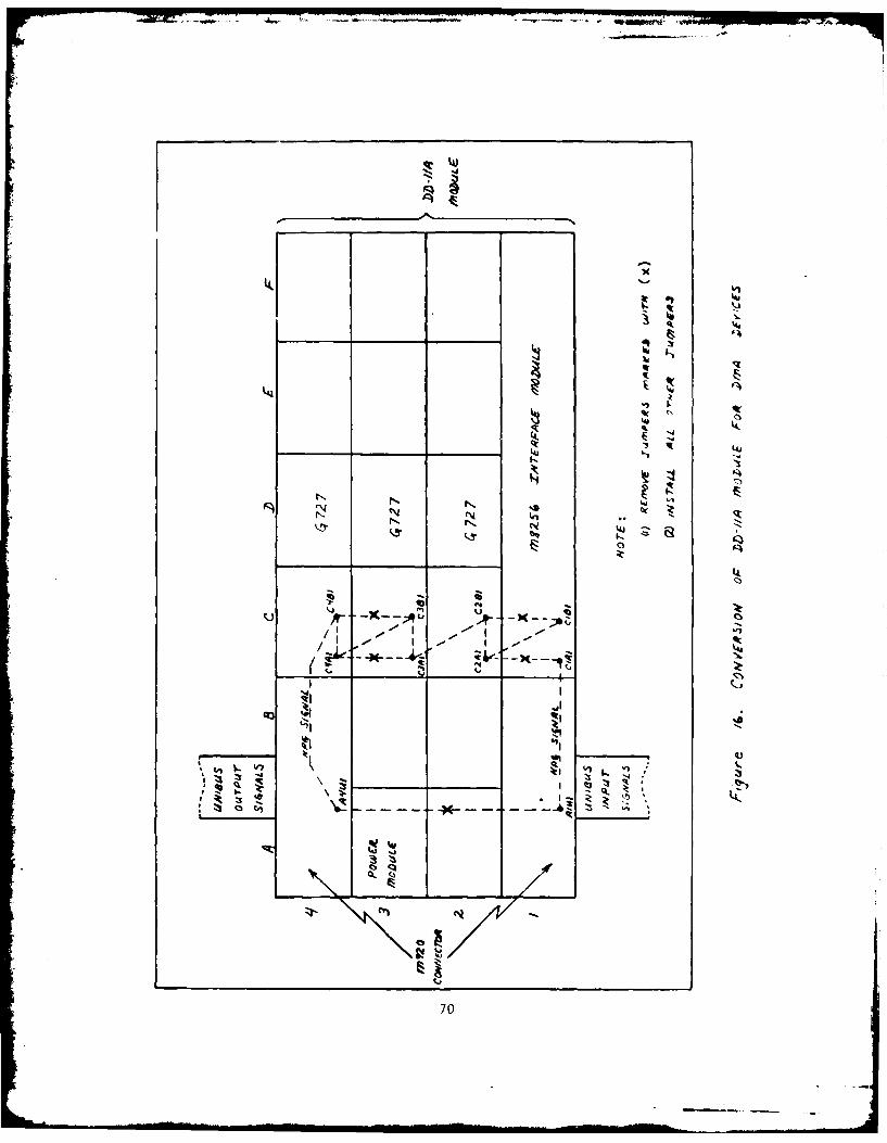
-- --- ~ --.-CIO
kuk
r*7Z-
700
-.... . . .. - -- - ". .. .
IN" and "NPG OUT" signals are internally junpered on the
device controller module inserted in the SPC slot.
Consequently, the CA1-CB1 jumper of column C1 was removed when
the M8256 RX02 Disk Controller Module was installed in that
particular SPC slot. The remaining jumpers from CAI to CBl in
columns C2, C3 and C4 were left installed to ensure NPG signal
continuity. Bus Grant Continuity Modules (G727) were
installed in column D of each spare row on the module to
ensure continuity of the BG signals. Additionally, pre-wired
jumpers connecting CAl and CBI pins in adjacent rows were
removed. Removal of these jumpers ensured proper flow of NPG
signals from one device to the next device along the module
column.
The modified DD11-A module was mounted between the third
processor BB11-A module and the pre-wired EAE module via two
mounting screws (see Figure 2). Connection to the UNIBUS was
achieved by installing two M920 connector modules in slots
A1/BI and A4/B4. Power to the module was achieved by
installing a power module (from the power harness) to slot A3.
Only four-wide modules (modules configured for entire SPC
slot) should be installed on this modified DD11-A module.
Wiring configurations may not be consistent with modules that
are not four-wide in design.
INSTALLATION OF M8256 CONTROLLER MODULE
The M8256 Interface Controller Module for the RX02 Disk
Drive was mounted on the modified DD11-A module (column C, D,
71
E and F, row 1) in the PDP-11/15 backplane. The M8256 Module
is designed for use with a double density formatted media.
Operation on single density formatted floppy disks would
require a different interface module (M7846) and different
M7744 module settings (for RX11 configuration) in the RX02
unit. The vector address (264 octal) and UNIBUS address
(177170 octal) for the RX02 were set via the 7952 and 7942
switches located on the module (Ref 13:2-4). The settings
were as follows:
7942 SWITCH 7952 SWITCH
V2 - SWI ON A3 - SW OFFV3 - SW2 OFF A4 - SW2 OFFV4 - SW3 ON A5 - SW3 OFFV5 - SW4 ON A6 - SW4 OFFV6 - SW5 OFF A7 - SW5 ON
V7 - SW6 ON A8 - SW6 ONV8 - SW7 OFF A9 - SW7 OFF
A10 - SW8 OFFAll - SW9 OFFA12 - SW10 OFF
The RX02 Disk Drive Unit is a priority five (PR5) device.
Consequently, the priority jumper plug (see Figure 17) on the
M8256 module is wired to produce a bus request five (BR5)
signal and gain control of the UNIBUS when a bus grant five
(BG5) signal is received from the processor. The pre-wiring
installation of the "NPG IN" signal to pin CAl and "NPG OUT"
signal to pin CBl on the modified DD11-A module ensures that
the RX02 will receive control of the UNIBUS when the device
issues an NPR signal, regardless of other BG signals at the
time of request.
72
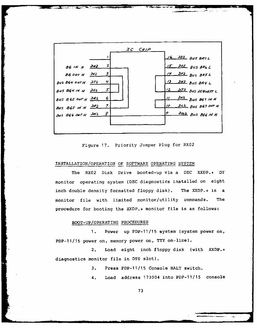
_ZC C//,,o
" .2_ 8S - &7 L
8*0'r N )2v 3 L. . Bs 8R5 L
bus8 rH .2T ae, y 9 /3 Vf2 W.5 B,/V L
JUS 8$4"# At 2'SS. S_ :1 J-.72 '8uW Re4FU&6STL
Bu5 85ur# 2 6 ,H 2~ gus 8?7/,oaI,-.s ,."Jw 22 ? L. /O .z Bus e4?oeur #
BJ6OWTH' -A4/2 . S_______ 5 LLI~ 8e,
Figure 17. Priority Jumper Plug for RX02
INSTALLATION/OPERATION OF SOFTWARE OPERATING SYSTEM
The RX02 Disk Drive booted-up via a DEC XXDP.+ DY
monitor operating system (DEC diagnostics installed on eight
inch double density formatted floppy disk). The XXDP.+ is a
monitor file with limited monitor/utility commands. The
procedure for booting the XXDP.+ monitor file is as follows:
BOOT-UP/OPERATING PROCEDURES
1. Power up PDP-11/15 system (system power on,
PDP-11/15 power on, memory power on, TTY on-line).
2. Load eight inch floppy disk (with XXDP.+
diagnostics monitor file in DYO slot).
3. Press PDP-11/15 Console HALT switch.
4. Load address 173004 into PDP-11/15 console
73
register.
5. Pull up ENABLE switch on console.
6. Press START switch on console.
7. TTY will print:
CHMDYB2 XXDP.+ DY MONITORBOOTED VIA UNIT 028K UNIBUS SYSTEM
8. Press carraige return on TTY when prompted
by the following questions:
a. ENTER DATE (DD-MMM-YY):b. 50 HZ?c. LSI?
9. TTY will print:
THIS IS XXDP.+ TYPE "H" OR "H/L" FOR DETAILS
10. Type in "H" and carraige return to enter the
HELP.TEXT file. All monitor commands/utility commands are
explained in detail.
The DEC RT.11 operating system offers adequate monitor
commands/utility programs to perform paper tape file transfers
to disk (via the PIP utility program) and LOAD/BOOT procedures
to enable operation of the system PANEL 30/ TSL 30 operating
systems, overlay programs and diagnostic routines. Transfer
of paper tape programs to a floppy disk media would
significantly upgrade the system. The DEC RT.11 operating
system being utilized was formatted double density on eight
inch floppy disk. The following files were required on the
disk for boot-up/file transfers/monitor commands (Ref 6:1-10):
74
FILENAME DESCRIPTION
RT.11SJ.SYS Operating SystemSWAP.SYS Buffer fileDY.SYS Device handler for RX02PR.SYS Device handler for High-
speed Paper Tape ReaderTT.SYS Device handler for TTY/CRTDIR.SAV Directory FileDUP.SAV Duplication FilePIP.SAV Peripheral Interchange
Program File
Under the current configuration of the 1923/30 Time-Series
Analysis System (including all hardware), the DEC RT.11
operating system would not boot-up. Upon completion of normal
start procedures, the system halted and the TTY was disabled.
INSTALLATION OF M9312 BOOTSTRAP MODULE
The M9312 hardware bootstrap module was installed on the
output (A4/B4) slots of the Dataram DR-103 memory unit for the
simplified PDP-11/15 system configuration and on the last
UNIBUS slot in the Control Unit. The M9312 module was
configured to mount in the UNIBUS in place of a M930 Bus
Terminator card. The UNIBUS signals on slots AI/BI or A4/B4
are compatible with the M9312 pin configuration. The M9312
and M930 perform the same function of terminating the UNIBUS
signals. The UNIBUS will not operate properly, however, with
the M9312 module installed in place of the first M930
Terminator card on the UNIBUS. Consequently, the only
position suitable for the M9312 module is at the end of the
UNIBUS.
* The M9312 has several jumpers which must be set for
754.
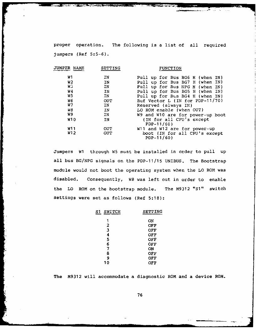
proper operation. The following is a list of all required
jumpers (Ref 5:5-6).
JUMPER NAME SETTING FUNCTION
WI IN Pull up for Bus BG6 H (when IN)W2 IN Pull up for Bus BG7 H (when IN)W3 IN Pull up for Bus NPG H (when IN)W4 IN Pull up for Bus BG5 H (when IN)W5 IN Pull up for Bus BG4 H (when IN)W6 OUT Buf Vector L (IN for PDP-11/70)W7 IN Reserved (always IN)W8 IN LO ROM enable (when OUT)W9 IN W9 and W10 are for power-up bootW10 IN (IN for all CPU's except
PDP-11/60)Wil OUT W11 and W12 are for power-upW12 OUT boot (IN for all CPU's except
PDP-11/60)
Jumpers W1 through W5 must be installed in order to pull up
all bus BG/NPG signals on the PDP-11/15 UNIBUS. The Bootstrap
module would not boot the operating system when the LO ROM was
disabled. Consequently, W8 was left out in order to enable
the LO ROM on the bootstrap module. The M9312 "SI" switch
settings were set as follows (Ref 5:18):
Si SWITCH SETTING
1 ON2 OFF3 OFF4 OFF5 OFF6 OFF7 ON8 OFF9 OFF
10 OFF
The M9312 will accommodate a diagnostic ROM and a device ROM.
76
Consequently, a diagnostic ROM (248F1) was installed in module
location E20 and the bootstrap ROM (811A9) was installed in
module location E35 (Ref 5:8). Device ROMs are matched to the
device handler they support. As a result, changes in system
disk drive units require that appropriate device ROMs
(corresponding to the installed disk drive units) be installed
on the M9312. The M9312 will accommodate ROMs for several
devices.
The Fast-on Tabs (TP1, TP2, TP3 and TP4) located on the
M9312 bootstrap module are not used by the PDP-11/15 computer.
The Fast-on tabs are used by PDP-11/34 computers for boot-up
procedures. Consequently, the Fast-on Tabs on the M9312 were
not installed in the PDP-11/15 computer (Ref 5:10).
The procedures for booting the system disk (without
diagnostic checks) were the same as those outlined under
installation procedures for the software operating system.
For diagnostic checks, the following procedures applied:
PROCEDURES
1. Power up all system components.
2. Load the XXDP.+ Diagnostics floppy disk into
slot DYO on the RX02 Disk Drive.
3. Load and start the PDP-11/15 computer at
address 165020.
4. TTY will respond with four, six-digit numbers
(indicating diagnostic checks of register contents), followed
by an "@" prompt.
*" 77
5. Type in "DY" and a carraige return.
6. The XXDP.+ monitor will automatically boot-
up after the carraige return in step 5.
" 7 8
IV. TESTS AND ANALYSIS
HEATHKIT H-19A CRT TESTS
The Heathkit H-19A was interfaced to the PDP-11/15 via
an RS-232C/Current-Loop Interface Unit. The TTY Controller
Modules operate at 110 baud rate and 60 HZ cycle rate. The H-
19A CRT performed all I/O operations successfully at 110 baud
rates. Baud rates of 150, 300 and higher resulted in garbled
character output on the CRT terminal. Any upgrade in baud
rates would require modifications on TTY Controller Interface
Modules.
DEC RT.11 BOOTSTRAP TESTS
The RX02 Disk Drive Unit was interfaced in an RX211
configuration (PDP-11 double density disk format). The RT.11
operating system would not boot in PDP-11/15 core memory via a
hardware bootstrap (M9312 Bootstrap Module loaded at 173004)
or a DEC RX02 software bootstrap instruction set for double
density formatted disks.
The RX02 was reconfigured into an RX11 system (PDP-11
single density disk format). This configuration required an
M7846 Interface Module to replace the M8256 Interface Module
required for the RX211 configuration. The switch
configurations on the M7744 Module in the RX02 were set to
(Si-i ON, S1--2 OFF) to conform to the new RX11 configuration.
For single density operation, an RT.11 operating system
formatted on a single density disk was utilized. The results
79
were the same as the RX211 configuration. The RT.11 operating
system would not boot in the RX11 configuration via the M9312
Hardware Bootstrap Module (loaded at 173004) or the DEC
software bootstrap instructions for single density operation.
The system was reconfigured again by installing an RX01
disk drive (with associated M7846 Interface Module). A single
density formatted disk with RT 11 operating system was
utilized as the software media. As with previous tests, the
RX01 system would not boot the operating system into core
memory via the DEC RX01 single density software bootstrap
instructions. A hardware bootstrap module for the RX01 was
not available for testing.
Foreground/Background (FB) and Single Job (SJ) RT.11
operating systems were tested in all three configurations with
no positive results. Configurations utilizing the M9312
Hardware Bootstrap Module were started at address 165020.
This address is the start address for activation of the
bootstrap diagnostics ROM and subsequent activation of the
device ROM on the Bootstrap Module. At start address 165020,
the TTY printed four, six-digit numbers (indicating
diagnostic checks of CPU registers, followed by an "@" prompt.
The TTY was enabled after the "@" prompt was printed. The
device mnuemonics "DY", "DYO", or "DY1" were the only inputs
accepted by the terminal. Correct bootstrap procedures
require that the operator type in the device mnuemonic (DY,
DYO or DYI) after the TTY prompt. The operating system should
80
44
immediately boot-up after the operator types in the device
mnuemonic and a carriage return. In the RX02 configurations
tested, the TTY would immediately lock-up (after the RX02 disk
heads reset to track zero) when DY, DYO or DY1 were entered
with a carriage return. The RX01 configuration (tested only
on a software bootstrap) locked-up immediately when the
bootstrap instructions were loaded and started. These tests
indicated that the M9312 Bootstrap Diagnostics ROM was working
properly (to include the device mnuemonic prompt). Likewise,
the RX02 disk head movement indicated that I/O instructions
were accessing the disk. An inability to boot the RT.11
(version four) operating system to core memory prevented
utilization of the RT.11 Peripheral Interchange Program (PIP)
for transfers of paper tape files to disk files.
GENRAD (producers of the 1923/30 system) indicated that
only an RT.11 (version two or older) operating system would be
compatible with the ADC equipment in the system. Records
indicate9I that in 1980 an AED 2500 Disk Drive Unit was
utilized to bootstrap an RT.11SJ.V02C (RT.11 version two)
floppy disk based operating system to the PDP-11/15 computer.
DEC device handler files (for I/O devices) are written to be
compatible with specific RT.11 operating system versions.
Device handlers for the same hardware differ for various RT.11
versions. The AED 2500 device handler program was written to
operate specifically with a version two RT.11 operating
system. The floppy disk based operating system tested with
81
the RX02 Drive Unit was a version four RT.11 operating system.
The RX02 Disk Drive was designed and built after the
development of the RT.11 version two operating system. As a
result, operation of an RT.11 version two operating system on
the 1923/30 system would require the addition of a DY.SYS
device handler program compatible with the RT.11 version two
operating system. An RX02 device handler for RT.11SJ.V02C
could be written by utilizing the AED 2500 version two device
handler program and a current listing of the version four
RT.11 device handler for the RX02 Disk Drive. A working RT.11
operating system (version two) could be produced by combining
a currently available RT.11SJ.V02C operating system with the
modified RX02 device handler.
DIAGNOSTIC TESTS
RX02 DISK DRIVE TESTS
The RX02 Disk Drive was configured in the RX211
mode for diagnostic testing. The RX02 Disk Drive properly
bootstrapped the XXDP.+ Diagnostic double density formatted
disk when the software media was loaded into disk slot DYO.
This successful bootstrap operation verified I/O operations
between the RX02 disk drive and the *H-19A CRT. Likewise,
successful diagnostic boot-up of the XXDI.+ monitor file
verified hardware modifications/installations on the UNIBUS
backplane structure.
A separate DEC diagnostics processor program was
loaded and tested via the XXDP.+ monitor program. The PDP-
82
bo
11/15 failed to successfully pass the processor diagnostics
check. Additionally, UPD2 Peripheral-Interchange-Program
(PIP) utility commands on the XXDP.+ monitor file were used to
transfer paper tape diagnostic programs from the High-speed
Paper Tape Reader to a floppy disk in the RX02 DYI slot. The
UPD2 PIP commands activated the High-speed Paper Tape Reader
and test tapes were read by the unit. Subsequent load and
start commands, via the XXDP.+ monitor file, failed to
activate the diagnostic programs transferred from paper tape
to disk. Likewise, XXDP.+ boot commands failed to boot a
floppy disk based RT.11SJ.V04 operating system in the RX02 DYl
unit slot. The RX02 floppy disk test failures indicated
possible hardware malfunctions in the CPU/Memory Unit and/or
software incompatibility problems with the RT.11SJ.V04 disk
based operating system.
Diagnostic tests for the system were run via the
XXDP.+ m rcor file floppy disk. The results from the test
runs were as follows:
FILENAME RESULTS
ZRXFA1.BIC Line frequency clock test - routine
ran with inconclusive results
DZKEDA.BIC EAE test - EAE passed test
ZM9BCO.BIC M9312 Boot Terminator test - routineran with inconclusive results
ZQMCFO.BIC Memory tests - routine did not run
83
F. 71
PAPER TAPE OPERATIONS
Paper tape operations on the 1923/30 system were
performed by means of a bootstrap loader, absolute binary
loader and system/diagnostic paper tapes.
Prior to loading/running any paper tapes, the
1923/30 system was powered-up. The Main 120V circuit breaker
switch, PDP-11/15 power switch, DATARAM memory power switch
and TTY/CRT power switch were turned on in that order. All
paper tapes were loaded into the right feed bin of the High-
speed Paper Tape unit and deposited into the left feed bin
after the completion of read operations (see Figure 18). The
High-speed Paper Tape Reader power switch was set to load
before loading any tapes. Each paper tape was placed under
the reader brake shoes, over the readhead assembly and between
the forward capstan and forward pinch roller. Upon completion
of tape loading, the tape guide was pulled down over each
loaded tape (see Ref 18:5-2).
LOADING BOOTSTRAP LOADER
After successful system power-up, the
following bootstrap loader instructions were loaded into core
memory via the PDP-11/15 front console control switches:
ADDRESS LOCATION INSTRUCTION
157744 016701157746 000026157750 012702157752 000352157754 005211157756 105711157760 100376
84
"AU AIJ II UPURAU YE A UUN UNU UU UMEN U UIUN Ut ULNtfHAL KAUUU l3923 TME SERESSSTEM(U )AR FRCE INSOF TECH I~
WRIGHT-PATTERSON AFB OH SCHOOL OF ERGI. A UCASELLA
UNCLASSIFIED DEC 83 AFITGE/EE/930 15 F/0 9/2 N
T EIChhiE
11I.0~. 11114E
S! ! 3. . . .
• 12.2L6
1.25 *ijj.4 1.
MICROCOPY RESOLUTION TEST CHART
NAIONAL RJAA -Of SIANDARDS A
III~l
-_-II----- __Iu
4
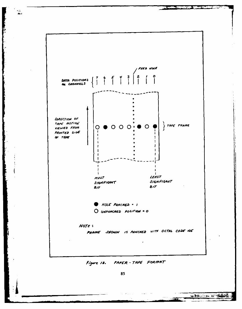
OR CANL
D/'ET/A'OF 1T,gPEC 100O 71OW IIP RA MfE
VIEw(Zp FROM 00 0 0 :00
OF /~rA 0S D
0 0 1pvcc
N07-W17# --
F,;w /S I~"9
I 85
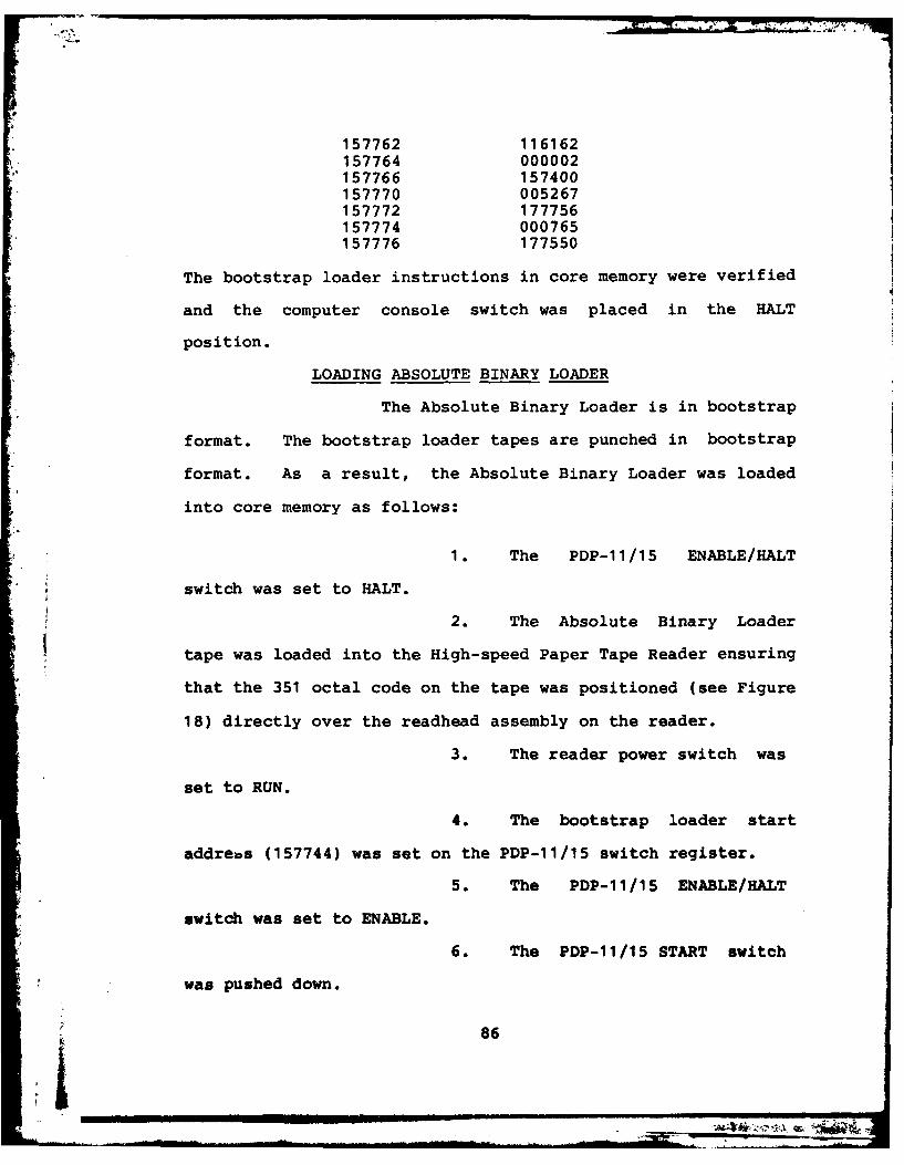
157762 116162157764 000002157766 157400157770 005267157772 177756157774 000765157776 177550
The bootstrap loader instructions in core memory were verified
and the computer console switch was placed in the HALT
position.
LOADING ABSOLUTE BINARY LOADER
The Absolute Binary Loader is in bootstrap
format. The bootstrap loader tapes are punched in bootstrap
format. As a result, the Absolute Binary Loader was loaded
into core memory as follows:
1. The PDP-11/15 ENABLE/HALT
switch was set to HALT.
2. The Absolute Binary Loader
tape was loaded into the High-speed Paper Tape Reader ensuring
that the 351 octal code on the tape was positioned (see Figure
18) directly over the readhead assembly on the reader.
3. The reader power switch was
set to RUN.
4. The bootstrap loader start
addrebs (157744) was set on the PDP-11/15 switch register.
5. The PDP-11/15 ENABLE/HALT
switch was set to ENABLE.
6. The PDP-11/15 START switch
was pushed down.
86
A_ i , ' ' ' . t. ,
7. The PDP-11/15 ENABLE/HALT
switch was set to HALT when the tape reading was complete.
LOADING SYSTEM/DIAGNOSTIC TAPES
The system/diagnostic tapes are punched in
absolute binary format. As a result, the system/diagnostic
tapes were loaded into core memory after the absolute binary
loader was loaded into memory via the bootstrap loader. The
system/diagnostic tapes were loaded as follows:
1. The system/diagnostic tapes
were loaded into the High-speed Paper Tape Reader with only
feedholes over the readhead assembly.
2. The reader power switch was
set to RUN.
3. The octal address 157500 was
set on the switch registers.
4. The PDP-11/15 START switch
was pushed down.
5. The PDP-11/15 ENABLE/HALT
switch was set to HALT when tape reading was complete.
6. Individual tapes read into
core memory were activated by starting them at their
respective start addresses. The TSL System Program requires
that the instruction (070707) be placed into switch register
000344 before the TSL system tape is read into core memory.
PAPER TAPE TESTS
Paper tape diagnostic tests for the system were
87
_ _ _ _ _ _ _ _ _ _ _ _ _ _ _ _ _ _,
run via the High-speed Paper Tape Reader. The results from
the test runs were as follows:
PAPER TAPE NAME RESULTS
General Test Program Program completed five tests(RANDAT, Worst Case Noise, Movingones and zeros,Memory disturbance,Basic memory patterns); rest ofprogram did not run; inconclusiveresults
Basic Memory Patterns Program did not runTest
Memory Moving One's Errors detected at address 160000and Zero's
No Dual Address Test Errors detected at numerousaddresses
11 Family Instruction Program did not runExerciser
T17-4K System Exerciser Program did not run
* Communications Test Program did not runProgram
Maintenance 1923 All ADC equipment lights werechecked out
Diagnostic tests on the floppy disk unit and the paper
tape unit were inconclusive. Important memory checkout
packages (floppy and paper tape based) failed to run on the
1923/30 system. As a result, the system CPU/Memory Unit
should be isolated and checked for malfunctions. All CPU
processor modules, with the exception of the KC11 front
console module, were checked for proper operation. Direct
substitution of each module with known good modules produced
.-. no positive results.
88
V. CONCLUSIONS AND RECOMMENDATIONS
CONCLUSIONS
The 1923/30 Time-Series System was upgraded by
interfacing an RX02 Disk Drive and a Heathkit H-19A CRT to the
PDP-11/15 system computer. The RX02 Disk Drive was
successfully interfaced to the PDP-11/15 computer by means of
a modified DD11-A Module, M8256 Interface Controller Module,
KF11-A Multiple Bus Priority Module and a KW11-L Line Time
Clock Module. The Heathkit H-19A CRT was successfully
interfaced to the PDP-11/15 computer by means of an RS-
232C/Current-Loop Interface Unit. The DEC XXDP. Diagnostics
disk media was successfully bootstrapped via the RX02 Disk
Drive Unit. The RX02 Disk Drive failed to bootstrap the DEC
RT.11 operating system into core memory. As a result,
existing paper tape programs were not transferred to disk
media via the RT.11 operating system.
RECOMMENDATIONS
The following recommendations are proposed for further
study:
1. The PDP-11/15 processor should be thoroughly
checked for processor malfunctions and'memory problems.
2. Upon successful operation of the PDP-11/15
processor/memory diagnostic routines, the DEC RT.11 operating
system should be bootstrapped into core memory via the RX02
Disk Drive configuration. The RT.11 bootstrap operation would
89
I
require utilization of available RT.11 (version two) operating
system. An RX02 device handler program should be written to
make the RT.11 (version two) operating system compatible to
the system configuration.
3. The RT.11 operating system utility programs
should be used to transfer existing paper tape programs to
eight inch floppy disks. Upon successful completion of file
transfers, the TSL 30/PANEL 30 operating systems, with
associated overlay programs, should be bootstrapped into core
memory and checked for proper operation.
4. A user's manual for disk/paper tape
operations should be written.
5. Procurement of state-of-the-art (SOA) GENRAD
2505 Time-Series Analysis System should be investigated.
The ADC equipment in the 1923/30 System (produced by GENRAD)
is no longer supported by GENRAD for parts or repair work.
The new 2505 GENRAD system offers increased
efficiency/capabilities and full hardware/software support.
The 2505 Signal Analysis Minisystem is the current Signal
Analysis System produced by GENRAD. The 2505 system consists
of the following:
1. Two Channel Analog-to-Digital Inputs (ADS)
2. PDP-11/04 Controller
3. 32K Core Memory
4. Dual 5-1/4 inch floppy disk media
5. Keyboard/Display/Pedestal
90
IB
6. 2501 Microprocessor
7. Firmware ZOOM
8. RT.11 Operation System
9. TSL/TSLAP
10. ISAP consisting of the following functions:
a. Sampled time data
b. Instantaneous input spectrum
c. Auto-and cross-spectrum
d. Auto-and cross-correlation
e. Amplitude probability density
f. Waveform averaging
g. Transfer function, impulse response,and coherence functions
91
Bibliography
1. Dataram Corporation. Core Memory System DR-103. Systembrochure. Cranbury, New Jersey: Dataram Corporation,1975.
2. Digital Equipment Corporation. Floating-Point MathPackage (FPMP-11) User's Manual. Maynard, Massachusetts:Digital Equipment Corporation, 1972.
3. Digital Equipment Corporation. KC11 Processor EngineeringDrawings. PDP-11 processor module schematics. Maynard,Massachusetts: Digital Equipment Corporatio., 1971.
4. Digital Equipment Corporation. KC11 Processor Manual.Maynard, Massachusetts: Digital Equipment Corporation,1971.
5. Digital Equipment Corporation. M9312 Field MaintenancePrint Set. M9312 Bootstrap Terminal technical drawings.Maynard, Massachusetts: Digital Equipment Corporation,1978.
6. Digital Equipment Corporation. PDP-11 Introduction toRT.11. PDP-11 operating system manual. Maynard,Massachusetts: Digital Equipment Corporation, 1977.
7. Digital Equipment Corporation. PDP-11 KE11-A ExtendedArithmetic Element. Operations manual. Maynard,Massachusetts: Digital Equipment Corporation, 1971.
8. Digital Equipment Corporation. PDP-11/15/20/r20Processor Handbook. Maynard, Massachusetts: DigitalEquipment Corporation, 1971.
9. Digital Equipment Corporation. PDP-11 Peripherals andInterfacing Handbook. Maynard, Massachusetts: DigitalEquipment Corporation, 1971.
10. Digital Equipment Corporation. PDP-11/15 PeripheralHandbook. Maynard, Massachusettsi Digital EquipmentCorporation, 1978.
11. Digital Equipment Corporation. PDP-11 Paper TapeSoftware Programming Handbook. Maynard, Massachusetts:Digital Equipment Corporation, 1970.
12. Digital Equipment Corporation. PDP-11/15 System Manual.Maynard, Massachusetts: Digital Equipment Corporation,1971.
92
k
13. Digital Equipment Corporation. RX02 User's Guide.Operation, service and programming manual for RX02 diskunit. Maynard, Massachusetts: Digital EquipmentCorporation, 1978.
14. Digital Equipment Corporation. RX211 Field MaintenancePrint Set. RX211 Floppy Disk schematic--awings.Maynard, Massachusetts: Digital Equipment Corporation,1978.
15. General Radio Company. "Signal Analysis with DigitalTime-Series Analyzers," The General Radio Experimenter,44: 3-7 (July 1970).
16. Heath Company. Heathkit Manual for the Video TerminalModel H-19A. Operations manual. Benton Harbor,Michigan: Heath Company, 1981.
17. Hewlett-Packard Company. X-Y Recorder 703A. Operatingand service manual. San Diego, California: Hewlett-Packard Company, 1971.
18. Iomec Inc. Digitronics Division. Model 2540 PerforatedTape Reader Operation and Maintenance Manual.Southboro, Massachusetts: Digitronics Division
*Publication Department, 1972.
19. Muchow, Kenneth. Microprocessors Principles,Programming and Interfacing. Reston, Virginia: RestonPublishing Company, Inc., 1983
20. Sudduth, Robert C. Evaluation of the Time/Data 1923/30System. Unpublished EE6.87 laboratory report. Wright-Patterson AFB, Ohio: School of Engineering, Air ForceInstitute of Technology, March 1980.
21. Tektronix, Inc. Instruction Manual 603/604 Monitor.Operating and service manual. Beaverton, Oregon:Tektronix, Inc., 1971.
22. Texas Instruments, Inc. The TTL Data Book. Dallas,Texas: Texas Instruments, Inc., 4981.
23. Time/Data Corporation. Modal Analysis Package for TSL.Software operating notes. Palo Alto, California: Time/Data Corporation, 1973.
24. Time/Data Corporation. Operating Manual, Time-SeriesSystem 1923/30. Palo Alto, California: Time/DataCorporation, 1973.
93
______
25. Time/Data Corporation. Programming Manual, Time-SeriesLanguage (TSL). Palo Alto, California: Time/DataCorporation, 1974.
26. Time/Data Corporation. 1923 "Superpanel" System ProgramsPANEL-30, PANEL-50. Software operating notes. PaloAlto, California: Time/Data Corporation, 1973.
27. Time/Data Corporation. 1923-5002A TSL ReferenceHandbook. Programming reference manual. Palo Alto,California: Time/Data Corporation, 1974.
9
947. ____
• p -I I . . .I I
VITA
Bruce Anthony Casella was born on 1 February 1953 in
Vallejo, California. He graduated as salutatorian of Colfax
High School in Colfax, California in 1971. Upon high school
graduation he accepted an appointment to the United States
Military Academy at West Point, New York. He graduated from
West Point in 1975 with a Bachelor of i-ence degree and
commission as a second lieutenant in the Lted States Army.
After attending the Army Signal Officers B, Course in 1975,
he served as a signal communications officer in South Korea,
Fort Polk, Louisiana, and the Federal Republic of Germany. He
received the degree of Master of Science in Systems Management
from the University of Southern California in Los Angeles,
California in 1981. Upon completing the Army Signal Officers
Advanced Course and Computer Systems Teleprocessing Program at
the Air Force Institute of Technology in 1982, he entered
graduate study in the School of Engineering at the Air Force
Institute of Technology.
Permanent address: 2948 Pasatiempo Place
Sacramento, California 95833
A _ __ _ _
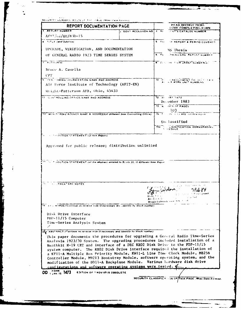
-a - ..-
€I
REPORT DOCUMENTATION PAGE 14FAD INSTRUCTIONS
I REPORT NUMBER * GOVI ACCLSSION NO. 3 R1 NT'S CATALOG NUMBER
AFVV'i]E/83D-I 5
4 , T L I (and Subt.tle) 5 T1 "1 REPORT I PERIOD COVfk| n
1JP(;ADE, VERIFICATION, AND DOCUMENTATION MS Thesis
oF GENERAL RADIO 1923 TIME SERIES SYSTEM 6 PL MING ORG REP(CNT N'jMUIN
C -I 8 " 1A 1 0 R GA ANT NLj'M F ,
BruIceJ A. Casella
C PT
1) .'tl-, "MINI, .)HUANIZATION NAME AND ADDRESS 10 P -AM I LFIM- NT ,I ' '
Air Force Institute of Technology (AFIT-EN) A. WORK UNIT NUMBEIS
wi ight-Patturson AFB, Ohio, 45433
It C- , ROLLING OFFICI- NAME AND ADDRESS 12. R, , RT -- ATE
Dvo mber 198313. N iEQ 3F PAGES
10314 M(,NITCRING A.6ENCY NAME A ADDRESS(tt different from Controlling Olfice) 15. -' I, I I L ASS 4 .ll .
Un, lassifled15. ASSIFICATION DO*NGRADIN/J
EDLILE
. ITION ST ATEMEN T (of ftfvi Report)
Approved for public release; distribution unlimited
T 1I11UTION STATEMIENT (of the abetract entered in B:,ck 20, Ii different from Rep.,r
FMLNTARY NOTES
D -" I'' 7 .:.I: .- r9
74- * RDS (C-irrinue .n re'erse ,'de It necessary arj.. dentify by block number)
Disk Drive InterfacePD'-11/15 Computer
'rime-Serles Analysis System
AV ABSTRACT (rontinue on reverse miSe If necesery end Identify h, block -umber)
This paper documents the procedures for upgrading a Ge, rat Radio Time-Series
Analvsis 1923/30 System. The upgrading procedures inclhded installation of a
Heathkit H-19 CRT and Interface of a DEC RX02 Disk Driv,, to the PDP-11/15
system computer. The RX02 Disk Drive interface requiredl the installation of
a KFII-A Multiple Hus Priority Module, KWII-L Line Timt Clock Module, M8256
Controller Module, M9213 Bootstrap Module, software opirating system, and the
modification of the DDII-A Backplane Module. Various hardware disk drive
confi~trations and software ooeratin systems were tested. i-
DO I ,N71 1473 E31TIONOF I NOV 6S IS OBSOLETE
SECURtITY CLASSIFICA ')N OFr HIS PAGE 'Whe Data FIerod,