TOSHIBA LED Lamps TLRV1034(T22, TLRMV1034(T22, … Sheets/Toshiba...
21
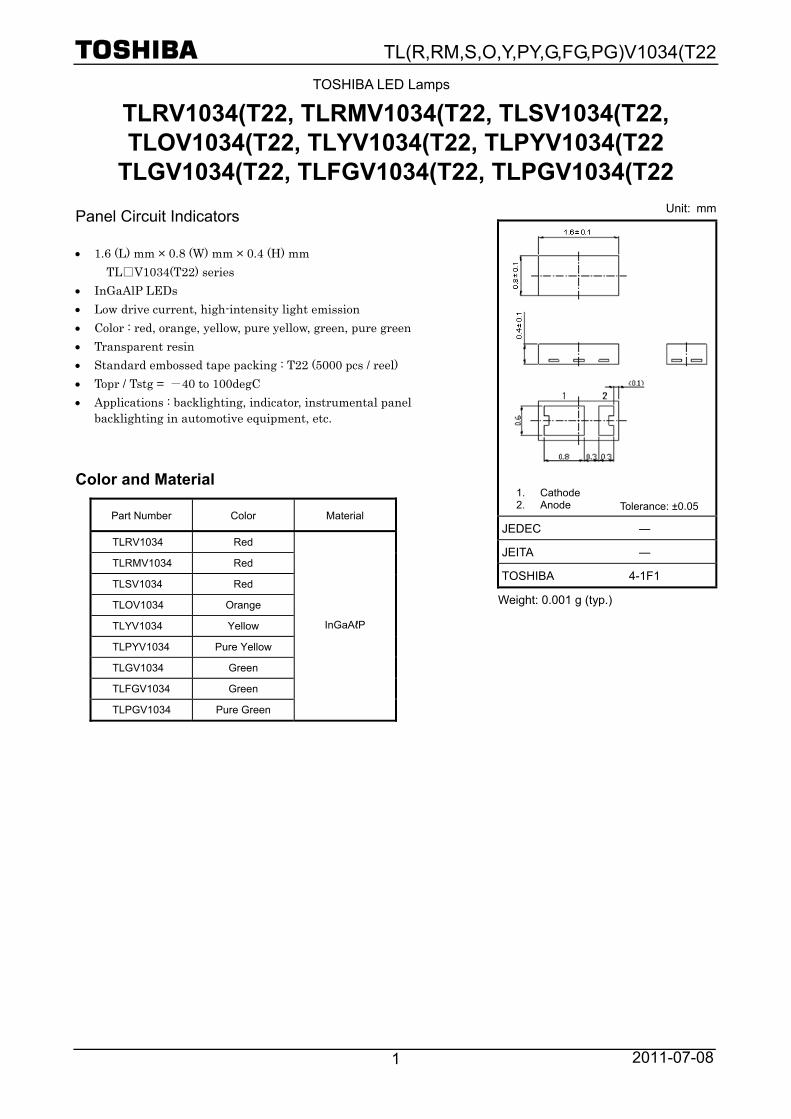
TL(R,RM,S,O,Y,PY,G,FG,PG)V1034(T22 2011-07-08 1 TOSHIBA LED Lamps TLRV1034(T22, TLRMV1034(T22, TLSV1034(T22, TLOV1034(T22, TLYV1034(T22, TLPYV1034(T22 TLGV1034(T22, TLFGV1034(T22, TLPGV1034(T22 Panel Circuit Indicators 1.6 (L) mm × 0.8 (W) mm × 0.4 (H) mm TL□V1034(T22) series InGaAlP LEDs Low drive current, high-intensity light emission Color : red, orange, yellow, pure yellow, green, pure green Transparent resin Standard embossed tape packing : T22 (5000 pcs / reel) Topr / Tstg = -40 to 100degC Applications : backlighting, indicator, instrumental panel backlighting in automotive equipment, etc. Color and Material Unit: mm JEDEC ― JEITA ― TOSHIBA 4-1F1 Weight: 0.001 g (typ.) Part Number Color Material TLRV1034 Red TLRMV1034 Red TLSV1034 Red TLOV1034 Orange TLYV1034 Yellow TLPYV1034 Pure Yellow TLGV1034 Green TLFGV1034 Green TLPGV1034 Pure Green InGaAℓP 1. Cathode 2. Anode Tolerance: ±0.05
Transcript of TOSHIBA LED Lamps TLRV1034(T22, TLRMV1034(T22, … Sheets/Toshiba...
TL(R,RM,S,O,Y,PY,G,FG,PG)V1034(T22
2011-07-08 1
TOSHIBA LED Lamps
TLRV1034(T22, TLRMV1034(T22, TLSV1034(T22, TLOV1034(T22, TLYV1034(T22, TLPYV1034(T22
TLGV1034(T22, TLFGV1034(T22, TLPGV1034(T22
Panel Circuit Indicators 1.6 (L) mm × 0.8 (W) mm × 0.4 (H) mm
TL□V1034(T22) series
InGaAlP LEDs
Low drive current, high-intensity light emission
Color : red, orange, yellow, pure yellow, green, pure green
Transparent resin
Standard embossed tape packing : T22 (5000 pcs / reel)
Topr / Tstg = -40 to 100degC
Applications : backlighting, indicator, instrumental panel backlighting in automotive equipment, etc.
Color and Material
Unit: mm
JEDEC ―
JEITA ―
TOSHIBA 4-1F1
Weight: 0.001 g (typ.)
Part Number Color Material
TLRV1034 Red
TLRMV1034 Red
TLSV1034 Red
TLOV1034 Orange
TLYV1034 Yellow
TLPYV1034 Pure Yellow
TLGV1034 Green
TLFGV1034 Green
TLPGV1034 Pure Green
InGaAℓP
1. Cathode 2. Anode Tolerance: ±0.05
TL(R,RM,S,O,Y,PY,G,FG,PG)V1034(T22
2011-07-08 2
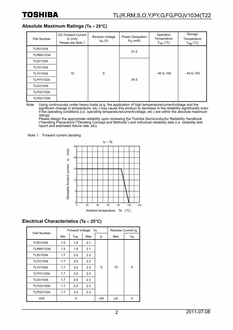
Absolute Maximum Ratings (Ta 25°C)
Part Number DC Forward Current
IF (mA) Please see Note 1
Reverse Voltage VR (V)
Power DissipationPD (mW)
Operation Temperature
Topr (°C)
Storage
Temperature Tstg (°C)
TLRV1034
TLRMV1034 31.5
TLSV1034
TLOV1034
TLYV1034
TLPYV1034
TLGV1034
TLFGV1034
TLPGV1034
15 5
34.5
40 to 100 40 to 100
Note: Using continuously under heavy loads (e.g. the application of high temperature/current/voltage and the significant change in temperature, etc.) may cause this product to decrease in the reliability significantly even if the operating conditions (i.e. operating temperature/current/voltage, etc.) are within the absolute maximum ratings. Please design the appropriate reliability upon reviewing the Toshiba Semiconductor Reliability Handbook (“Handling Precautions”/“Derating Concept and Methods”) and individual reliability data (i.e. reliability test report and estimated failure rate, etc).
Note 1: Forward current derating
Electrical Characteristics (Ta 25°C)
Forward Voltage VF Reverse Current IRPart Number
Min Typ. Max IF Max VR
TLRV1034 1.5 1.8 2.1
TLRMV1034 1.5 1.8 2.1
TLSV1034 1.7 2.0 2.3
TLOV1034 1.7 2.0 2.3
TLYV1034 1.7 2.0 2.3
TLPYV1034 1.7 2.0 2.3
TLGV1034 1.7 2.0 2.3
TLFGV1034 1.7 2.0 2.3
TLPGV1034 1.7 2.0 2.3
5 10 5
Unit V mA A V
A
llow
able
forw
ard
curr
ent
IF
(mA
)
Ambient temperature Ta (°C)
IF – Ta
0 0 20 40 60 80 100 120
20
25
5
10
15
TL(R,RM,S,O,Y,PY,G,FG,PG)V1034(T22
2011-07-08 3
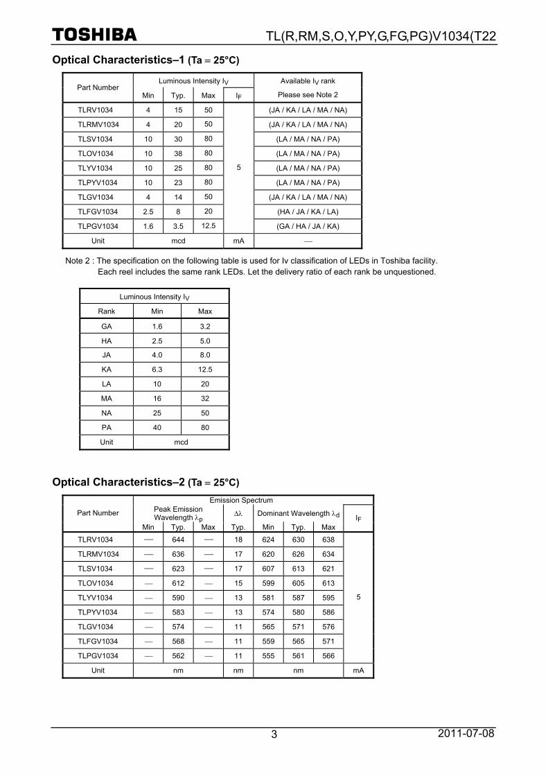
Optical Characteristics–1 (Ta 25°C)
Luminous Intensity IV Part Number
Min Typ. Max IF
Available IV rank
Please see Note 2
TLRV1034 4 15 50 (JA / KA / LA / MA / NA)
TLRMV1034 4 20 50 (JA / KA / LA / MA / NA)
TLSV1034 10 30 80 (LA / MA / NA / PA)
TLOV1034 10 38 80 (LA / MA / NA / PA)
TLYV1034 10 25 80 (LA / MA / NA / PA)
TLPYV1034 10 23 80 (LA / MA / NA / PA)
TLGV1034 4 14 50 (JA / KA / LA / MA / NA)
TLFGV1034 2.5 8 20 (HA / JA / KA / LA)
TLPGV1034 1.6 3.5 12.5
5
(GA / HA / JA / KA)
Unit mcd mA
Note 2 : The specification on the following table is used for Iv classification of LEDs in Toshiba facility. Each reel includes the same rank LEDs. Let the delivery ratio of each rank be unquestioned.
Luminous Intensity IV
Rank Min Max
GA 1.6 3.2
HA 2.5 5.0
JA 4.0 8.0
KA 6.3 12.5
LA 10 20
MA 16 32
NA 25 50
PA 40 80
Unit mcd
Optical Characteristics–2 (Ta 25°C)
Emission Spectrum Peak Emission Wavelength p
Dominant Wavelength dPart Number
Min Typ. Max Typ. Min Typ. MaxIF
TLRV1034 644 18 624 630 638
TLRMV1034 636 17 620 626 634
TLSV1034 623 17 607 613 621
TLOV1034 612 15 599 605 613
TLYV1034 590 13 581 587 595
TLPYV1034 583 13 574 580 586
TLGV1034 574 11 565 571 576
TLFGV1034 568 11 559 565 571
TLPGV1034 562 11 555 561 566
5
Unit nm nm nm mA
TL(R,RM,S,O,Y,PY,G,FG,PG)V1034(T22
2011-07-08 4
Cautions
This visible LED lamp also emits some IR light. If a photodetector is located near the LED lamp, please ensure that it will not be affected by the IR light.
This product is designed as a general display light source usage, and it has applied the measurement standard that matched with the sensitivity of human's eyes. Therefore, it is not intended for usage of functional application (ex. Light source for sensor, optical communication and etc) except general display light source.
If a voltage is applied in a high humidity environment, migration of electrode metal may occur and, consequently, there may be a short circuit of interelectrode metal.
Since such metal migration is particularly likely to occur if a reverse voltage is applied in conditions in which condensation occurs, please take preventive measures by providing a moisture-proof design, drive circuit design, etc. for customer products into which this product will be integrated.
TL(R,RM,S,O,Y,PY,G,FG,PG)V1034(T22
2011-07-08 5
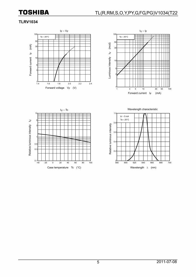
TLRV1034
IF – VF
IV – Tc
F
orw
ard
cur
rent
I F
(m
A)
Forward voltage VF (V)
Wavelength characteristic
Case temperature Tc (°C) Wavelength (nm)
R
elat
ive
lum
inou
s in
tens
ity
I V
R
elat
ive
lum
inou
s in
tens
ity
1 1.4
10
100
1.6 1.8 2.0 2.2 2.4
3
5
30
50
Ta 25°C
IV – IF
Forward current IF (mA)
Lu
min
ous
inte
nsity
I V
(m
cd)
11 10 100
10
100
3
5
30
50
3 5 30 50
Ta 25°C
0.1 40
1
10
20 0 20 40 60 80 100
0.3
0.5
3
5
0580 600 620 640 660 680 700
0.2
0.4
0.6
0.8
1.0
IF 5 mA
Ta 25°C
TL(R,RM,S,O,Y,PY,G,FG,PG)V1034(T22
2011-07-08 6
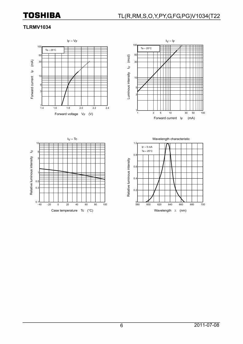
TLRMV1034
IF – VF
IV – IF
IV – Tc
F
orw
ard
cur
rent
I F
(m
A)
Forward voltage VF (V) Forward current IF (mA)
Wavelength characteristic
Lu
min
ous
inte
nsity
I V
(m
cd)
Case temperature Tc (°C) Wavelength (nm)
R
elat
ive
lum
inou
s in
tens
ity
I V
R
elat
ive
lum
inou
s in
tens
ity
1 1.4
10
100
1.6 1.8 2.0 2.2 2.4
3
5
30
50
Ta 25°C
11 10 100
10
100
3
5
30
50
3 5 30 50
Ta 25°C
0580 600 620 640 660 680 700
0.2
0.4
0.6
0.8
1.0
IF 5 mA
Ta 25°C
0.1 40
1
10
20 0 20 40 60 80 100
0.3
0.5
3
5
TL(R,RM,S,O,Y,PY,G,FG,PG)V1034(T22
2011-07-08 7
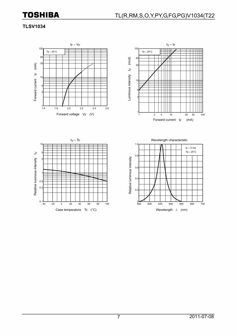
TLSV1034
IF – VF
IV – IF
IV – Tc
F
orw
ard
cur
rent
I F
(m
A)
Forward voltage VF (V)
Forward current IF (mA)
Wavelength characteristic
Lu
min
ous
inte
nsity
I V
(m
cd)
Case temperature Tc (°C) Wavelength (nm)
R
elat
ive
lum
inou
s in
tens
ity
I V
R
elat
ive
lum
inou
s in
tens
ity
0580 600 620 640 660 680 700
0.2
0.4
0.6
0.8
1.0
IF 5 mA
Ta 25°C
0.1 40
1
10
20 0 20 40 60 80 100
0.3
0.5
3
5
11 10 100
10
100
3
5
30
50
3 5 30 50
Ta 25°C
1 1.6
10
100
1.8 2.0 2.2 2.4 2.6
3
5
30
50
Ta 25°C
TL(R,RM,S,O,Y,PY,G,FG,PG)V1034(T22
2011-07-08 8
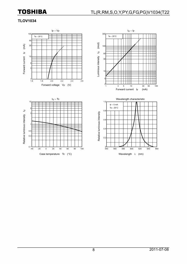
TLOV1034
IF – VF
IV – IF
IV – Tc
F
orw
ard
cur
rent
I F
(m
A)
Forward voltage VF (V)
Forward current IF (mA)
Wavelength characteristic
Lu
min
ous
inte
nsity
I V
(m
cd)
Case temperature Tc (°C) Wavelength (nm)
R
elat
ive
lum
inou
s in
tens
ity
I V
R
elat
ive
lum
inou
s in
tens
ity
0540 560 580 600 620 640 660
0.2
0.4
0.6
0.8
1.0
IF 5 mA
Ta 25°C
0.1 40
1
10
20 0 20 40 60 80 100
0.3
0.5
3
5
1 1.6
10
100
1.8 2.0 2.2 2.4 2.6
3
5
30
50
Ta 25°C
31 10 100
10
100
300
5
3 5 30 50
30
50
Ta 25°C
TL(R,RM,S,O,Y,PY,G,FG,PG)V1034(T22
2011-07-08 9
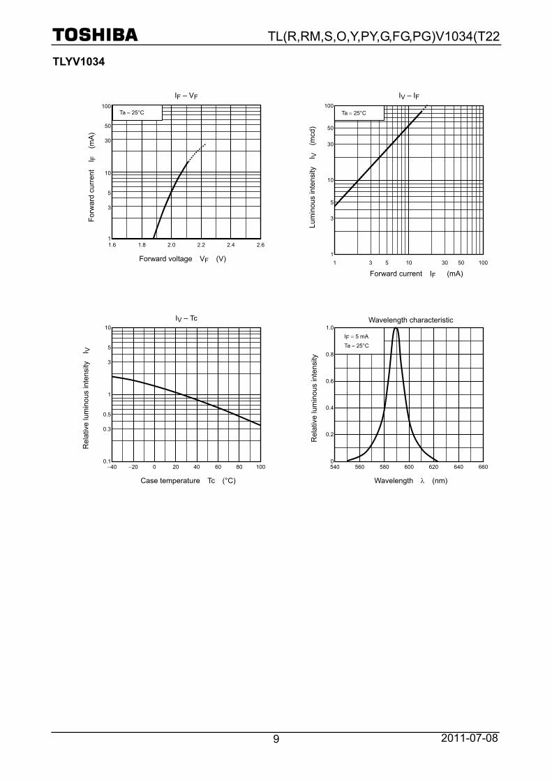
TLYV1034
IV – IF
IV – Tc
Forward current IF (mA)
Wavelength characteristic
Lu
min
ous
inte
nsity
I V
(m
cd)
Case temperature Tc (°C) Wavelength (nm)
R
elat
ive
lum
inou
s in
tens
ity
I V
R
elat
ive
lum
inou
s in
tens
ity
0540 560 580 600 620 640 660
0.2
0.4
0.6
0.8
1.0
IF 5 mA
Ta 25°C
0.1 40
1
10
20 0 20 40 60 80 100
0.3
0.5
3
5
IF – VF
F
orw
ard
cur
rent
I F
(m
A)
Forward voltage VF (V)
1 1.6
10
100
1.8 2.0 2.2 2.4 2.6
3
5
30
50
Ta 25°C
1
1 10 100
10
100
3
5
30
50
3 5 30 50
Ta 25°C
TL(R,RM,S,O,Y,PY,G,FG,PG)V1034(T22
2011-07-08 10
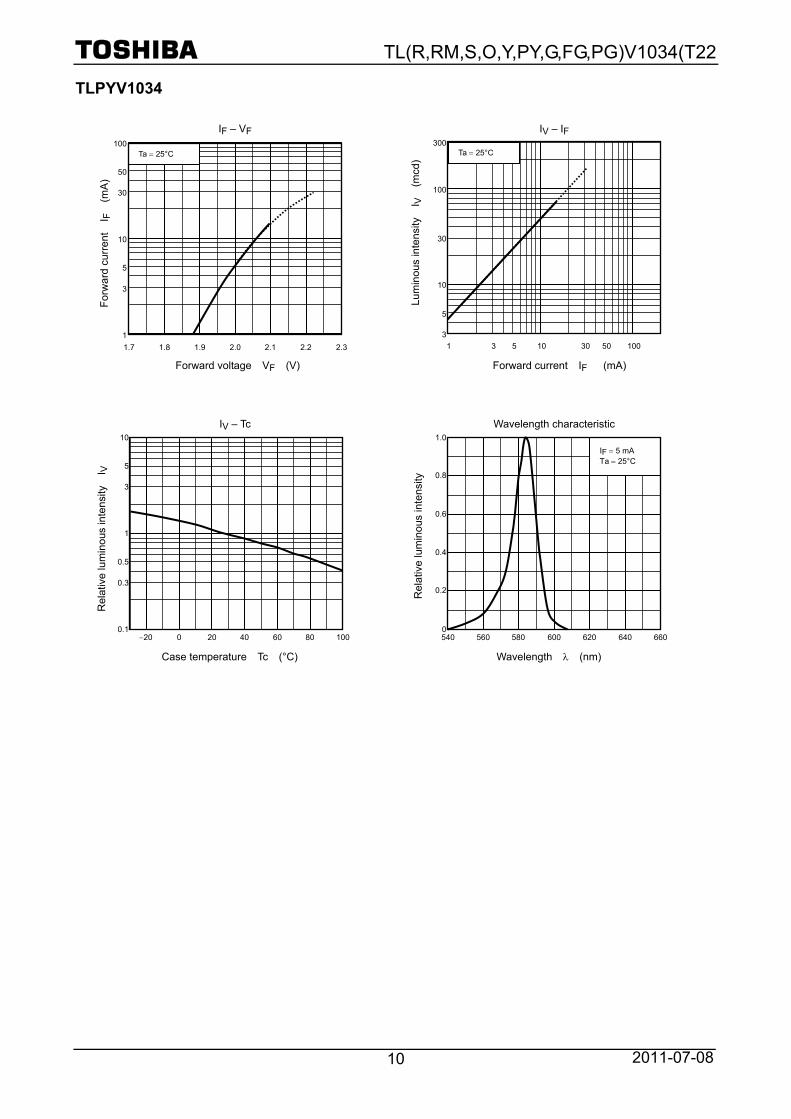
TLPYV1034
IF – VF
IV – IF
IV – Tc
F
orw
ard
cur
rent
I F
(m
A)
Forward voltage VF (V) Forward current IF (mA)
Wavelength characteristic
Lu
min
ous
inte
nsity
I V
(m
cd)
Case temperature Tc (°C) Wavelength (nm)
R
elat
ive
lum
inou
s in
tens
ity
I V
R
elat
ive
lum
inou
s in
tens
ity
IF 5 mA Ta 25°C
0600
0.4
1.0
0.8
540 640 620 580560 660
0.6
0.2
100
1 50
30
10
3
5
3 5 10 30 100
300Ta 25°C Ta 25°C
1
100
30
1.7 2.2 2.1 1.8 2.3
10
3
1.9
50
5
2.0
0.1
10
3
80 60 100
1
0.3
20
5
0.5
20 0 40
TL(R,RM,S,O,Y,PY,G,FG,PG)V1034(T22
2011-07-08 11
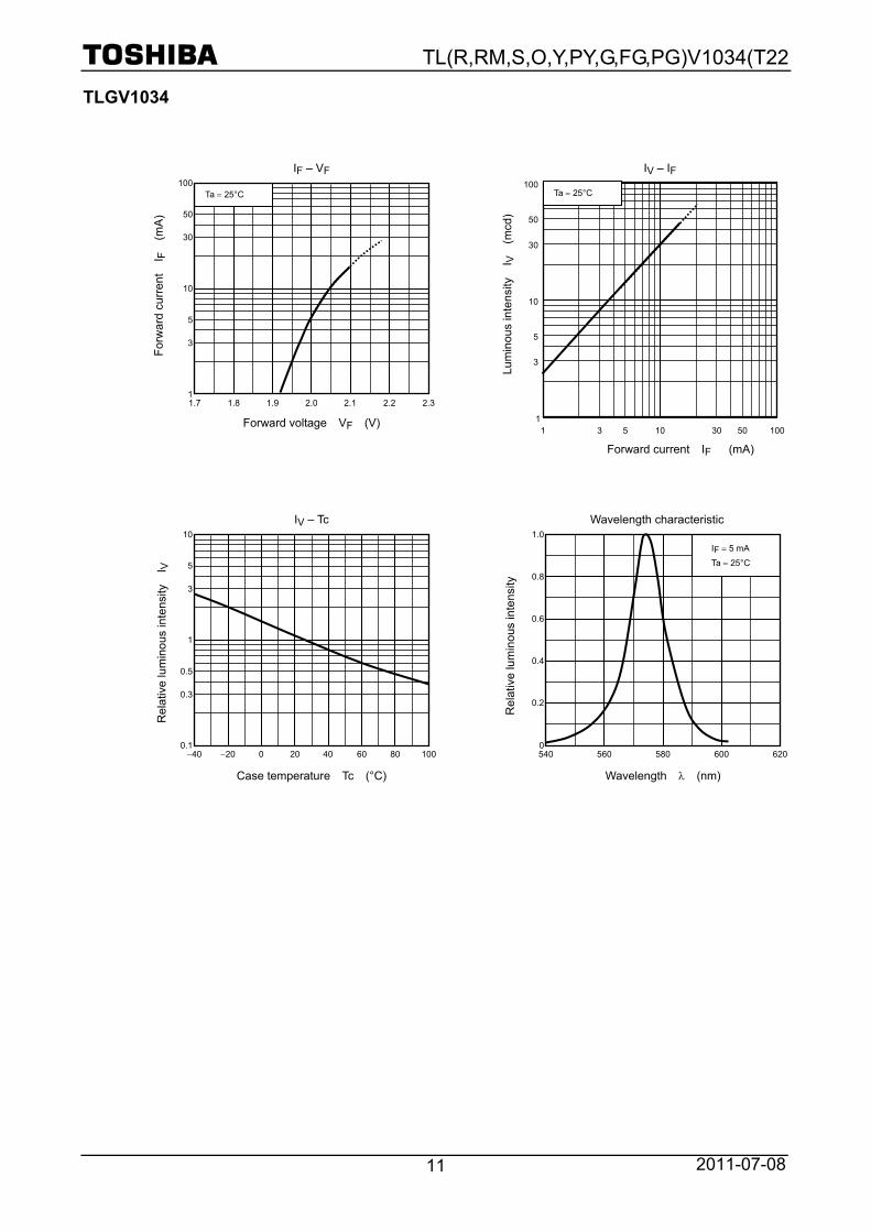
TLGV1034
IV – Tc
IV – IF
IF – VF
Forward voltage VF (V)
Forward current IF (mA)
Wavelength characteristic
Lu
min
ous
inte
nsity
I V
(m
cd)
Case temperature Tc (°C) Wavelength (nm)
R
elat
ive
lum
inou
s in
tens
ity
I V
R
elat
ive
lum
inou
s in
tens
ity
F
orw
ard
cur
rent
I F
(m
A)
0540 560 580 600 620
0.2
0.4
0.6
0.8
1.0
IF 5 mA
Ta 25°C
0.1 40
1
10
20 0 20 40 60 80 100
0.3
0.5
3
5
11 10 100 3 5 30 50
10
100
3
5
30
50
Ta 25°C Ta 25°C
1
100
30
1.7 2.2 2.1 1.8 2.3
10
3
1.9
50
5
2.0
TL(R,RM,S,O,Y,PY,G,FG,PG)V1034(T22
2011-07-08 12
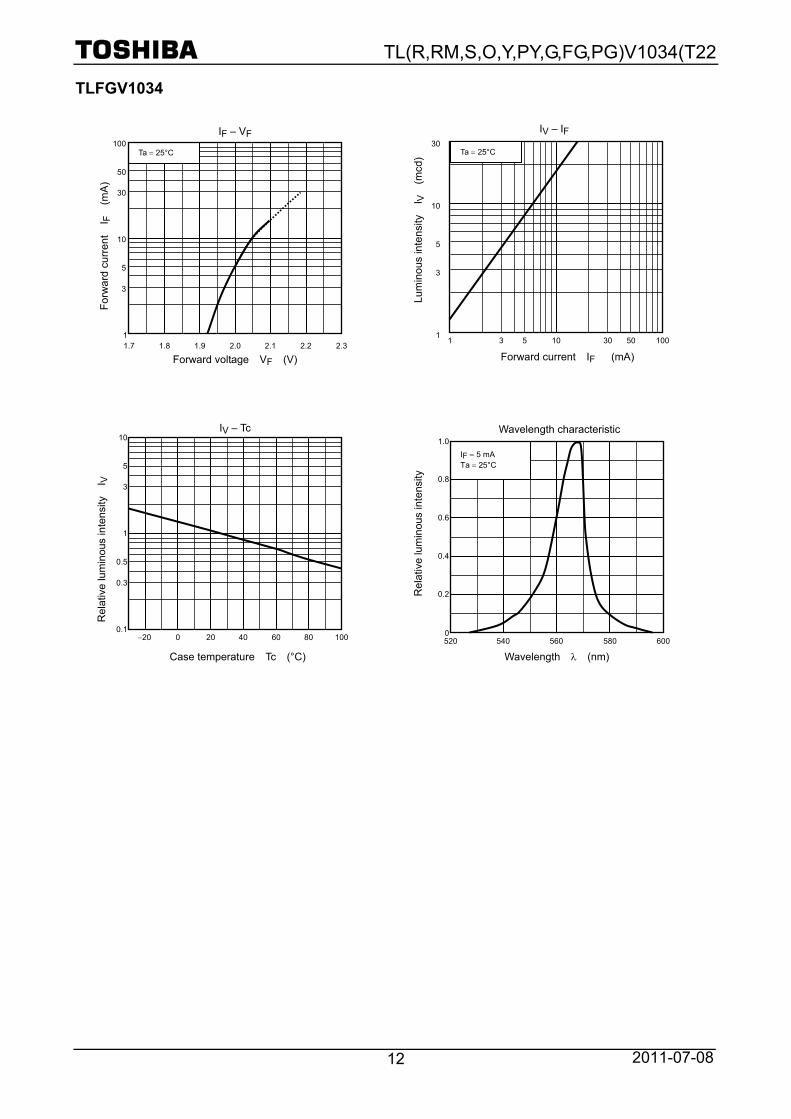
TLFGV1034
IV – Tc
IV – IF
IF – VF
F
orw
ard
cur
rent
I F
(m
A)
Forward voltage VF (V) Forward current IF (mA)
Wavelength characteristic
Lu
min
ous
inte
nsity
I V
(m
cd)
Case temperature Tc (°C) Wavelength (nm)
R
elat
ive
lum
inou
s in
tens
ity
I V
R
elat
ive
lum
inou
s in
tens
ity
IF 5 mA Ta 25°C
0
0.4
1.0
0.8
520
0.6
0.2
600580 560 540
1 10 100 3 5 30 50 1
10
3
5
30Ta 25°C Ta 25°C
1
100
30
1.7 2.2 2.1 1.8 2.3
10
3
1.9
50
5
2.0
0.1
10
3
80 60 100
1
0.3
20
5
0.5
20 0 40
TL(R,RM,S,O,Y,PY,G,FG,PG)V1034(T22
2011-07-08 13
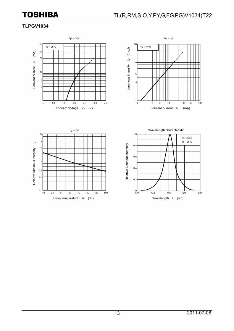
TLPGV1034
IV – Tc
IF – VF
IV – IF
F
orw
ard
cur
rent
I F
(m
A)
Forward voltage VF (V) Forward current IF (mA)
Wavelength characteristic
Lu
min
ous
inte
nsity
I V
(m
cd)
Case temperature Tc (°C) Wavelength (nm)
R
elat
ive
lum
inou
s in
tens
ity
I V
R
elat
ive
lum
inou
s in
tens
ity
0520 540 560 580 600
0.2
0.4
0.6
0.8
1.0
IF 5 mA
Ta 25°C
0.1 40
1
10
20 0 20 40 60 80 100
0.3
0.5
3
5
Ta 25°C
1
100
30
1.7 2.2 2.1 1.8 2.3
10
3
1.9
50
5
2.0 11 10 100
10
3
5
30
3 5 30 50
Ta 25°C
TL(R,RM,S,O,Y,PY,G,FG,PG)V1034(T22
2011-07-08 14
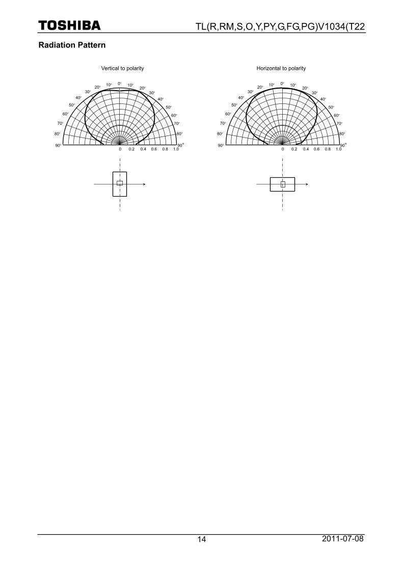
Radiation Pattern
Vertical to polarity Horizontal to polarity
30
0
60
90° 90
30
60
1.00.8 0.6 0.4 0.2 0
80
70
50
40
20 10
70
80
50
40
20 10
30
0
60
90° 90
30
60
1.00.80.6 0.4 0.2 0
80
70
50
40
20 10
70
80
50
40
20 10
TL(R,RM,S,O,Y,PY,G,FG,PG)V1034(T22
2011-07-08 15
Packaging
These LED devices are packed in an aluminum envelope with a silica gel and a moisture indicator to avoid moisture absorption. The optical characteristics of the devices may be affected by exposure to moisture in the air before soldering and they should therefore be stored under the following conditions:
1. This moisture proof bag may be stored unopened within 12 months at the following conditions. Temperature: 5C to 30C Humidity: 90% (max)
2. After opening the moisture proof bag, the devices should be assembled within 168 hours in an environment of 5°C to 30°C/60% RH or below.
3. If upon opening, the moisture indicator card shows humidity 30% or above (Color of indication changes to pink) or the expiration date has passed, the devices should be baked in taping with reel. After baking, use the baked devices within 72 hours, but perform baking only once. Baking conditions: 605°C, for 12 to 24 hours. Expiration date: 12 months from sealing date, which is imprinted on the same side as this label affixed.
4. Repeated baking can cause the peeling strength of the taping to change, then leads to trouble in mounting. Furthermore, prevent the devices from being destructed against static electricity for baking of it.
5. If the packing material of laminate would be broken, the hermeticity would deteriorate. Therefore, do not throw or drop the packed devices.
Attention of mounting method
Please note the handling of products during evaluation. 1. Please do not apply pressure to the upper surface of the product with fingers, tweezers, and others. Failure of
product to light up may occur due to package deformation, wire deformation and/or disconnection. 2. Please handle the product lengthwise. 3. Should tweezers be used in product handling, one with flat surfaces is recommended. 4. Please do not drop the product. There is a possibility for package transformation etc. to occur when the
product is dropped. 5. Please do not stack the Printed Circuit Boards on which the product is mounted to prevent damages to
product surface. Also, please note not to damage the surface of the product with cushioning material etc. Surface damage to the product may influence their optical characteristics.
TL(R,RM,S,O,Y,PY,G,FG,PG)V1034(T22
2011-07-08 16
Mounting Method
Soldering
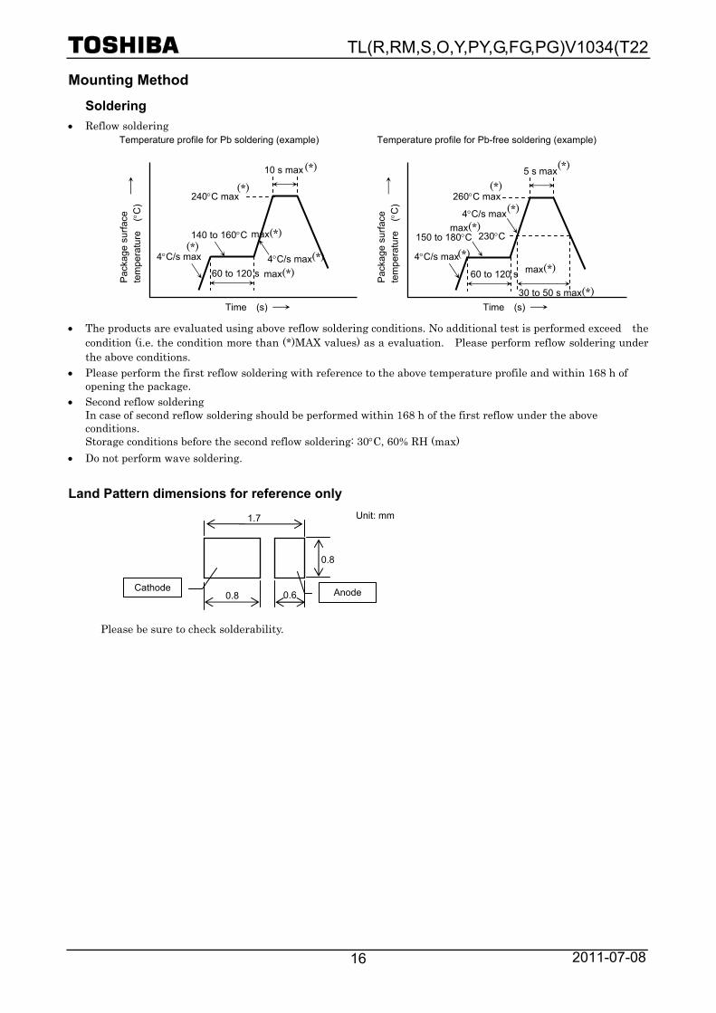
Reflow soldering
The products are evaluated using above reflow soldering conditions. No additional test is performed exceed the condition (i.e. the condition more than (*)MAX values) as a evaluation. Please perform reflow soldering under the above conditions.
Please perform the first reflow soldering with reference to the above temperature profile and within 168 h of opening the package.
Second reflow soldering In case of second reflow soldering should be performed within 168 h of the first reflow under the above conditions. Storage conditions before the second reflow soldering: 30C, 60% RH (max)
Do not perform wave soldering.
Land Pattern dimensions for reference only
Please be sure to check solderability.
60 to 120 s
10 s max
240C max
4C/s max
140 to 160C
4C/s max
Time (s)
Pac
kage
sur
face
te
mpe
ratu
re
(C
) Temperature profile for Pb soldering (example)
Time (s)
Pac
kage
sur
face
te
mpe
ratu
re
(C
)
Temperature profile for Pb-free soldering (example)
150 to 180C
4C/s max
5 s max
260C max
4C/s max
230C
60 to 120 s
(*)
(*)
(*)(*)
(*)
(*)
(*)
(*)
max(*)
max(*)
max(*)
30 to 50 s max(*)
max(*)
0.8 0.6
0.8
1.7 Unit: mm
Cathode Anode
TL(R,RM,S,O,Y,PY,G,FG,PG)V1034(T22
2011-07-08 17
Cleaning
When cleaning is required after soldering, Toshiba recommends the following cleaning solvents. It is confirmed that these solvents have no effect on semiconductor devices in our dipping test (under the recommended conditions). In selecting the one for your actual usage, please perform sufficient review on washing condition, using condition and etc.
ASAHI CLEAN AK-225AES: (made by ASAHI GLASS) KAO CLEAN THROUGH 750H: (made by KAO) PINE ALPHA ST-100S: (made by ARAKAWA CHEMICAL)
Precautions When Mounting
Do not apply force to the plastic part of the LED under high-temperature conditions. To avoid damaging the LED plastic, do not apply friction using a hard material. When installing the PCB in a product, ensure that the device does not come into contact with other components.
TL(R,RM,S,O,Y,PY,G,FG,PG)V1034(T22
2011-07-08 18
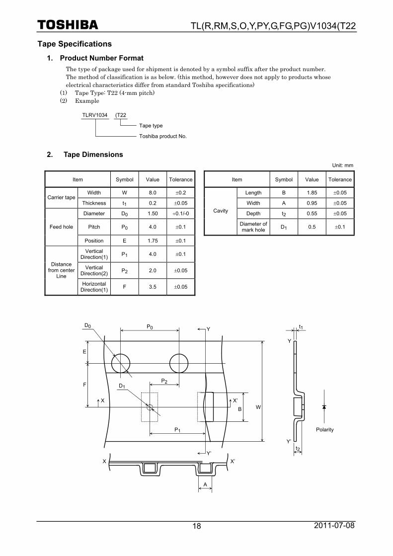
Tape Specifications
1. Product Number Format
The type of package used for shipment is denoted by a symbol suffix after the product number.
The method of classification is as below. (this method, however does not apply to products whose electrical characteristics differ from standard Toshiba specifications)
(1) Tape Type: T22 (4-mm pitch) (2) Example
2. Tape Dimensions
Unit: mm
Item Symbol Value Tolerance Item Symbol Value Tolerance
Width W 8.0 0.2 Length B 1.85 0.05 Carrier tape
Thickness t1 0.2 0.05 Width A 0.95 0.05
Diameter D0 1.50 0.1/-0 Depth t2 0.55 0.05
Pitch P0 4.0 0.1
Cavity
Diameter of mark hole
D1 0.5 0.1 Feed hole
Position E 1.75 0.1
Vertical Direction(1)
P1 4.0 0.1
Vertical Direction(2)
P2 2.0 0.05 Distance
from center Line
Horizontal Direction(1)
F 3.5 0.05
TLRV1034 (T22
Tape type
Toshiba product No.
P0 D0
X’
B W
P2 D1
P1
Y
Y’
X
E
F
X’X
A
Y
t1
Y’ t2
Polarity
TL(R,RM,S,O,Y,PY,G,FG,PG)V1034(T22
2011-07-08 19
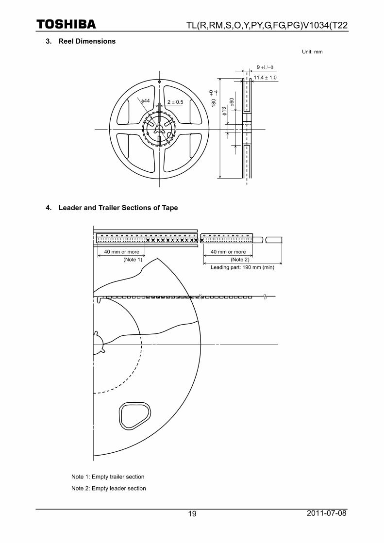
3. Reel Dimensions
Unit: mm
4. Leader and Trailer Sections of Tape
Note 1: Empty trailer section
Note 2: Empty leader section
9
180
0
4
60
13
11.4 1.0
2 0.544
(Note 1)
Leading part: 190 mm (min)
40 mm or more
(Note 2)
40 mm or more
TL(R,RM,S,O,Y,PY,G,FG,PG)V1034(T22
2011-07-08 20
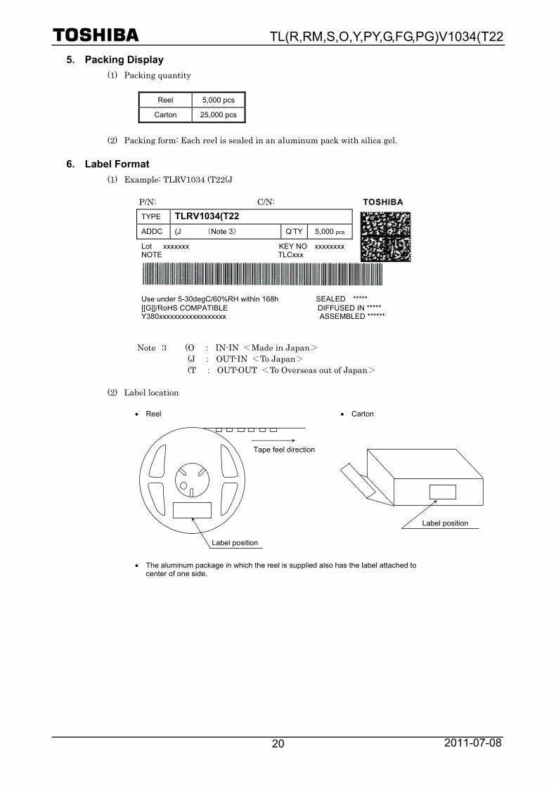
5. Packing Display
(1) Packing quantity
Reel 5,000 pcs
Carton 25,000 pcs
(2) Packing form: Each reel is sealed in an aluminum pack with silica gel.
6. Label Format
(1) Example: TLRV1034 (T22(J
P/N: C/N: TOSHIBA
Note 3 (O : IN-IN <Made in Japan> (J : OUT-IN <To Japan> (T : OUT-OUT <To Overseas out of Japan>
(2) Label location
TYPE TLRV1034(T22
ADDC (J (Note 3) Q’TY 5,000 pcs
Lot xxxxxxx KEY NO xxxxxxxx NOTE TLCxxx
Use under 5-30degC/60%RH within 168h SEALED ***** [[G]]/RoHS COMPATIBLE DIFFUSED IN ***** Y380xxxxxxxxxxxxxxxxxx ASSEMBLED ******
Tape feel direction
Label position
Label position
Reel Carton
The aluminum package in which the reel is supplied also has the label attached to center of one side.
TL(R,RM,S,O,Y,PY,G,FG,PG)V1034(T22
2011-07-08 21
RESTRICTIONS ON PRODUCT USE
Toshiba Corporation, and its subsidiaries and affiliates (collectively “TOSHIBA”), reserve the right to make changes to the information in this document, and related hardware, software and systems (collectively “Product”) without notice.
This document and any information herein may not be reproduced without prior written permission from TOSHIBA. Even with TOSHIBA’s written permission, reproduction is permissible only if reproduction is without alteration/omission.
Though TOSHIBA works continually to improve Product’s quality and reliability, Product can malfunction or fail. Customers are responsible for complying with safety standards and for providing adequate designs and safeguards for their hardware, software and systems which minimize risk and avoid situations in which a malfunction or failure of Product could cause loss of human life, bodily injury or damage to property, including data loss or corruption. Before customers use the Product, create designs including the Product, or incorporate the Product into their own applications, customers must also refer to and comply with (a) the latest versions of all relevant TOSHIBA information, including without limitation, this document, the specifications, the data sheets and application notes for Product and the precautions and conditions set forth in the “TOSHIBA Semiconductor Reliability Handbook” and (b) the instructions for the application with which the Product will be used with or for. Customers are solely responsible for all aspects of their own product design or applications, including but not limited to (a) determining the appropriateness of the use of this Product in such design or applications; (b) evaluating and determining the applicability of any information contained in this document, or in charts, diagrams, programs, algorithms, sample application circuits, or any other referenced documents; and (c) validating all operating parameters for such designs and applications. TOSHIBA ASSUMES NO LIABILITY FOR CUSTOMERS’ PRODUCT DESIGN OR APPLICATIONS.
Product is intended for use in general electronics applications (e.g., computers, personal equipment, office equipment, measuring equipment, industrial robots and home electronics appliances) or for specific applications as expressly stated in this document. Product is neither intended nor warranted for use in equipment or systems that require extraordinarily high levels of quality and/or reliability and/or a malfunction or failure of which may cause loss of human life, bodily injury, serious property damage or serious public impact (“Unintended Use”). Unintended Use includes, without limitation, equipment used in nuclear facilities, equipment used in the aerospace industry, medical equipment, equipment used for automobiles, trains, ships and other transportation, traffic signaling equipment, equipment used to control combustions or explosions, safety devices, elevators and escalators, devices related to electric power, and equipment used in finance-related fields. Do not use Product for Unintended Use unless specifically permitted in this document.
Do not disassemble, analyze, reverse-engineer, alter, modify, translate or copy Product, whether in whole or in part.
Product shall not be used for or incorporated into any products or systems whose manufacture, use, or sale is prohibited under any applicable laws or regulations.
The information contained herein is presented only as guidance for Product use. No responsibility is assumed by TOSHIBA for any infringement of patents or any other intellectual property rights of third parties that may result from the use of Product. No license to any intellectual property right is granted by this document, whether express or implied, by estoppel or otherwise.
ABSENT A WRITTEN SIGNED AGREEMENT, EXCEPT AS PROVIDED IN THE RELEVANT TERMS AND CONDITIONS OF SALE FOR PRODUCT, AND TO THE MAXIMUM EXTENT ALLOWABLE BY LAW, TOSHIBA (1) ASSUMES NO LIABILITY WHATSOEVER, INCLUDING WITHOUT LIMITATION, INDIRECT, CONSEQUENTIAL, SPECIAL, OR INCIDENTAL DAMAGES OR LOSS, INCLUDING WITHOUT LIMITATION, LOSS OF PROFITS, LOSS OF OPPORTUNITIES, BUSINESS INTERRUPTION AND LOSS OF DATA, AND (2) DISCLAIMS ANY AND ALL EXPRESS OR IMPLIED WARRANTIES AND CONDITIONS RELATED TO SALE, USE OF PRODUCT, OR INFORMATION, INCLUDING WARRANTIES OR CONDITIONS OF MERCHANTABILITY, FITNESS FOR A PARTICULAR PURPOSE, ACCURACY OF INFORMATION, OR NONINFRINGEMENT.
GaAs (Gallium Arsenide) is used in Product. GaAs is harmful to humans if consumed or absorbed, whether in the form of dust or vapor. Handle with care and do not break, cut, crush, grind, dissolve chemically or otherwise expose GaAs in Product.
Do not use or otherwise make available Product or related software or technology for any military purposes, including without limitation, for the design, development, use, stockpiling or manufacturing of nuclear, chemical, or biological weapons or missile technology products (mass destruction weapons). Product and related software and technology may be controlled under the Japanese Foreign Exchange and Foreign Trade Law and the U.S. Export Administration Regulations. Export and re-export of Product or related software or technology are strictly prohibited except in compliance with all applicable export laws and regulations.
Please contact your TOSHIBA sales representative for details as to environmental matters such as the RoHS compatibility of Product. Please use Product in compliance with all applicable laws and regulations that regulate the inclusion or use of controlled substances, including without limitation, the EU RoHS Directive. TOSHIBA assumes no liability for damages or losses occurring as a result of noncompliance with applicable laws and regulations.