Gallium nitride-based microwave high-power heterostructure field
256
Gallium Nitride-based Microwave High-Power Heterostructure Field-Effect Transistors design, technology, and characterization M.C.J.C.M. Krämer
Transcript of Gallium nitride-based microwave high-power heterostructure field

Gallium Nitride-based MicrowaveHigh-Power Heterostructure
Field-Effect Transistors
design, technology, and characterization
M.C.J.C.M. Krämer

Gallium Nitride-based MicrowaveHigh-Power Heterostructure
Field-Effect Transistors
design, technology, and characterization
PROEFSCHRIFT
ter verkrijging van de graad van doctor aan de
Technische Universiteit Eindhoven, op gezag van de
Rector Magnificus, prof.dr.ir. C.J. van Duijn, voor een
commissie aangewezen door het College voor
Promoties in het openbaar te verdedigen
op dinsdag 10 oktober 2006 om 16.00 uur
door
Mark Cornelia Johannes Carolus Maria Krämer
geboren te Sittard
Dit proefschrift is goedgekeurd door de promotoren:
prof.Dr.-Ing. L.M.F. Kaufmann
en
prof.Dr.-Ing. E. Kohn
Copromotor:dr. F. Karouta
This work was supported by the Dutch Technology Foundation STW.
Copyright c©2006 M.C.J.C.M. Krämer
Printed by Gildeprint B.V., Enschede, The Netherlands.Cover design by Paul Verspaget.
CIP-DATA LIBRARY TECHNISCHE UNIVERSITEIT EINDHOVEN
Krämer, Mark C.J.C.M.
Gallium nitride-based microwave high-power heterostructure field-effecttransistors : design, technology, and characterization / by Mark CorneliaJohannes Carolus Maria Krämer. - Eindhoven : Technische UniversiteitEindhoven, 2006.Proefschrift. - ISBN-10: 90-386-1893-XISBN-13: 978-90-386-1893-7NUR 959Trefw.: galliumnitridehalfgeleiders / veldeffecttransistoren /vermogenstransistoren / 3-5 verbindingen.Subject headings: wide band gap semiconductors / field effect transistors /microwave power transistors / III-V semiconductors.

“Waat er veur haet, haet er noch neit achter.”
Aan Petra
mijn ouders en Ralf


Contents
1 Introduction 11.1 Highlights of Gallium Nitride research history . . . . . . . . . . . . . . . . . 11.2 GaN put into perspective . . . . . . . . . . . . . . . . . . . . . . . . . . . . . 3
1.2.1 Advantages and disadvantages of GaN . . . . . . . . . . . . . . . . . 41.2.2 Application areas . . . . . . . . . . . . . . . . . . . . . . . . . . . . 7
1.2.2.1 Optical applications . . . . . . . . . . . . . . . . . . . . . . 81.2.2.2 Electronic applications . . . . . . . . . . . . . . . . . . . . 10
1.2.3 Costs and market . . . . . . . . . . . . . . . . . . . . . . . . . . . . . 131.3 State-of-the-art for GaN-based microwave high-power applications . . . . . . . 141.4 Objectives of this research . . . . . . . . . . . . . . . . . . . . . . . . . . . . 161.5 Thesis organization . . . . . . . . . . . . . . . . . . . . . . . . . . . . . . . . 18
2 GaN-based heterostructure field-effect transistors 192.1 Introduction . . . . . . . . . . . . . . . . . . . . . . . . . . . . . . . . . . . . 192.2 GaN material system . . . . . . . . . . . . . . . . . . . . . . . . . . . . . . . 21
2.2.1 Crystal structure . . . . . . . . . . . . . . . . . . . . . . . . . . . . . 212.2.2 Polarization effects in III-nitrides . . . . . . . . . . . . . . . . . . . . 21
2.3 Key topics concerning GaN-based HFETs . . . . . . . . . . . . . . . . . . . . 242.3.1 Growth techniques . . . . . . . . . . . . . . . . . . . . . . . . . . . . 242.3.2 GaN-based HFET layer structures . . . . . . . . . . . . . . . . . . . . 272.3.3 Theory of 2DEG formation in GaN-based HFETs . . . . . . . . . . . . 292.3.4 Trapping effects in AlGaN/GaN HFETs . . . . . . . . . . . . . . . . . 34
2.4 Conclusions . . . . . . . . . . . . . . . . . . . . . . . . . . . . . . . . . . . . 41
3 Design of GaN-based HFETs 433.1 Epitaxial device design . . . . . . . . . . . . . . . . . . . . . . . . . . . . . . 43
3.1.1 Requirements for AlGaN/GaN epilayers from a device perspective . . . 443.1.2 Initial AlGaN/GaN layer stack . . . . . . . . . . . . . . . . . . . . . . 453.1.3 GaN buffer layer . . . . . . . . . . . . . . . . . . . . . . . . . . . . . 453.1.4 AlGaN barrier layer . . . . . . . . . . . . . . . . . . . . . . . . . . . 513.1.5 Complete AlGaN/GaN epitaxial layer stack . . . . . . . . . . . . . . . 55
vii
viii Contents
3.2 Device layout and process flows . . . . . . . . . . . . . . . . . . . . . . . . . 563.2.1 Mask layout . . . . . . . . . . . . . . . . . . . . . . . . . . . . . . . . 573.2.2 Process flows . . . . . . . . . . . . . . . . . . . . . . . . . . . . . . . 63
3.3 Conclusions . . . . . . . . . . . . . . . . . . . . . . . . . . . . . . . . . . . . 63
4 Fabrication technology 674.1 Contact technology . . . . . . . . . . . . . . . . . . . . . . . . . . . . . . . . 67
4.1.1 Ohmic contacts . . . . . . . . . . . . . . . . . . . . . . . . . . . . . . 684.1.2 Schottky contacts . . . . . . . . . . . . . . . . . . . . . . . . . . . . . 71
4.2 Device isolation . . . . . . . . . . . . . . . . . . . . . . . . . . . . . . . . . . 734.2.1 RIE . . . . . . . . . . . . . . . . . . . . . . . . . . . . . . . . . . . . 734.2.2 ICP . . . . . . . . . . . . . . . . . . . . . . . . . . . . . . . . . . . . 74
4.3 Electron beam lithography . . . . . . . . . . . . . . . . . . . . . . . . . . . . 774.3.1 T-gates . . . . . . . . . . . . . . . . . . . . . . . . . . . . . . . . . . 784.3.2 Field plates . . . . . . . . . . . . . . . . . . . . . . . . . . . . . . . . 794.3.3 Implementation of T- and FP-gates . . . . . . . . . . . . . . . . . . . . 82
4.4 Surface passivation . . . . . . . . . . . . . . . . . . . . . . . . . . . . . . . . 834.4.1 PECVD SiN . . . . . . . . . . . . . . . . . . . . . . . . . . . . . . . 864.4.2 Surface treatments . . . . . . . . . . . . . . . . . . . . . . . . . . . . 864.4.3 Pulsed DC current-voltage measurements . . . . . . . . . . . . . . . . 87
4.5 Air bridges . . . . . . . . . . . . . . . . . . . . . . . . . . . . . . . . . . . . 914.5.1 Electroplating . . . . . . . . . . . . . . . . . . . . . . . . . . . . . . . 924.5.2 Electron beam evaporation . . . . . . . . . . . . . . . . . . . . . . . . 92
4.6 Conclusions . . . . . . . . . . . . . . . . . . . . . . . . . . . . . . . . . . . . 93
5 PECVD silicon nitride passivation films 975.1 Introduction . . . . . . . . . . . . . . . . . . . . . . . . . . . . . . . . . . . . 985.2 Deposition of silicon nitride by PECVD . . . . . . . . . . . . . . . . . . . . . 99
5.2.1 Equipment . . . . . . . . . . . . . . . . . . . . . . . . . . . . . . . . 995.2.2 Characterization techniques . . . . . . . . . . . . . . . . . . . . . . . 100
5.3 Influence of PECVD process settings on SiN film properties . . . . . . . . . . 1015.3.1 Gas flow . . . . . . . . . . . . . . . . . . . . . . . . . . . . . . . . . 1025.3.2 RF power . . . . . . . . . . . . . . . . . . . . . . . . . . . . . . . . . 1045.3.3 Total gas pressure . . . . . . . . . . . . . . . . . . . . . . . . . . . . . 1055.3.4 Substrate temperature . . . . . . . . . . . . . . . . . . . . . . . . . . . 1085.3.5 Effective lifetime measurements . . . . . . . . . . . . . . . . . . . . . 1125.3.6 Stress in PECVD SiN films . . . . . . . . . . . . . . . . . . . . . . . 114
5.4 Influence of SiN properties and surface preparation on passivation and leakage . 1155.4.1 Influence of SiN film properties on passivation of AlGaN layer and
leakage currents . . . . . . . . . . . . . . . . . . . . . . . . . . . . . 1175.4.2 Influence of surface preparation on passivation of AlGaN layer and
leakage currents . . . . . . . . . . . . . . . . . . . . . . . . . . . . . 1235.5 Conclusions . . . . . . . . . . . . . . . . . . . . . . . . . . . . . . . . . . . . 125

Contents ix
6 Device results 1316.1 Introduction . . . . . . . . . . . . . . . . . . . . . . . . . . . . . . . . . . . . 1316.2 Measurement techniques . . . . . . . . . . . . . . . . . . . . . . . . . . . . . 132
6.2.1 DC current-voltage measurements . . . . . . . . . . . . . . . . . . . . 1326.2.2 Small-signal S-parameter measurements . . . . . . . . . . . . . . . . . 1336.2.3 Active load-pull measurements . . . . . . . . . . . . . . . . . . . . . . 135
6.3 Small periphery devices . . . . . . . . . . . . . . . . . . . . . . . . . . . . . . 1386.4 Large periphery devices . . . . . . . . . . . . . . . . . . . . . . . . . . . . . . 1436.5 Conclusions . . . . . . . . . . . . . . . . . . . . . . . . . . . . . . . . . . . . 153
7 Conclusions and recommendations 1577.1 Main conclusions . . . . . . . . . . . . . . . . . . . . . . . . . . . . . . . . . 1577.2 Recommendations for future research . . . . . . . . . . . . . . . . . . . . . . 160
References 163
Appendix A Process flows for GaN-based HFETs 175
Appendix B Process flow for CPW passive components on s.i. SiC 209
List of constants and acronyms 223
Summary 229
Samenvatting 231
List of publications 233
Dankwoord 235
Curriculum Vitae 241

x Contents

Chapter 1
Introduction
Since its reappearance in the early 1990s gallium nitride (GaN) has been regarded as a veryinteresting and highly promising material system for both optical and microwave high-powerelectronic applications. Over the last fifteen years researchers all around the world have madegreat efforts in order to redeem these promises. GaN-based optical applications have firstreached the stage of commercialization while microwave high-power electronics are on theverge of their commercial breakthrough. The value of the worldwide GaN device market,which at present is about $3.5 billion, is estimated to be $7.2 billion by the year 2009.This chapter will start with highlights of GaN research history. After this we will put GaNinto perspective with conventional semiconductors and other wide-bandgap (WBG) materials.Among others we will give an overview of the application areas and the state-of-the-art ofGaN-based microwave high-power electronics. Finally, we will discuss the objectives andorganization of this thesis.
1.1 Highlights of Gallium Nitride research historyThe material system of interest in this thesis is the wide-bandgap III-V compound semicon-ductor gallium nitride (GaN). GaN was first synthesized by Juza and Hahn in the 1930s bypassing ammonia (NH3) over liquid gallium (Ga) at elevated temperatures [74]. This methodresulted in a powder consisting of small needles and platelets. Their purpose was to investigatethe crystal structure and lattice constant of GaN. Due to the lack of a native GaN substrate novapor phase epitaxial growth had ever been attempted.
In 1968, Maruska and Tietjen were the first to try the hydride vapor phase epitaxy (HVPE)approach to grow centimeter-sized GaN layers on sapphire substrates. In a traditional HVPEreactor the group III element such as Ga is transported as the monochloride. For example,gallium chloride (GaCl) is generated in situ by passing hydrochloric acid vapor (HCl(g)) over
1
2 1. Introduction
liquid Ga. The group V element such as nitrogen (N) is transported as the hydride. Sapphirewas chosen as substrate material because it is a robust material that is not reactive with ammo-nia. To date, sapphire has remained a very popular substrate for heteroepitaxial GaN growth.The early HVPE GaN films were grown at temperatures below 600 oC to prevent decompo-sition. However, these films were all polycrystalline. In 1969, Maruska realized that in anammonia environment at temperatures above 600 oC GaN growth actually would occur insteadof decomposition. He increased the growth temperature to 850 oC, the temperature typicallyused for gallium arsenide (GaAs), and obtained the first single crystalline GaN film [116]. Thefilm quality could even be improved by increasing the temperature to 950 oC. All GaN filmsgrown at that time showed very high electron concentrations (1020 cm−3) even without inten-tional doping. The responsible n-type donors were believed to be nitrogen vacancies (VN), aconcept that has caused a lot of controversy over the years. Eventually oxygen (O2) has beenproposed as the responsible donor. Oxygen with its six valence electrons on an N site (N hasfive valence electrons) would be a single donor [148].
In order to create a pn junction a suitable p-type dopant had to be found. Zinc (Zn) seemedto be an appropriate acceptor as it worked for GaAs and gallium phosphide (GaP). Althoughheavy Zn concentrations rendered GaN films to be insulating, the films never became conduct-ing p-type. Despite of this, Pankove et al. achieved the first GaN light emitting diode (LED)in 1971. This device consisted of an undoped n-type region, an insulating Zn-doped layer andan indium (In) surface contact. It could emit blue, green, yellow or red light depending on theZn concentration in the light emitting region [134]. In 1972, Maruska was the first to proposemagnesium (Mg) to be a better choice of p-type dopant than Zn. Using the same device struc-ture as Pankove, Maruska grew the first HVPE GaN LED, emitting at a wavelength of 430nm (violet) with Mg as the luminescent center [115]. Although Mg-doped devices (GaN:Mg)were much brighter than their Zn-doped equivalents, they were never very efficient (< 1 %)and no successful commercial product ever appeared. Nevertheless, Mg-doping has remainedthe basis for all commercial GaN-based LEDs and laser diodes (LDs) to date.
In the late 1970s, GaN research ceased virtually everywhere because of the continuingdifficulties encountered with the growth of high quality films needed for device development.Remaining issues were the choice and availability of a suitable substrate, how to control thevery high intrinsic n-type conductivity, and difficulties with obtaining conducting p-type GaNfilms. In 1982 only a handful of papers were published world-wide on this material system.
It was the perseverance of Isamu Akasaki that eventually resulted in obtaining conductingp-type GaN films in 1989. The conducting p-type films were discovered during cathodolumi-nescence (CL) observations of GaN:Mg in a scanning electron microscope (SEM). A photo-luminescence (PL) study of the GaN:Mg material before and after low-energy electron beamirradiation (LEEBI) treatment showed that luminescence efficiency had increased by two or-ders of magnitude [4]. A Hall effect measurement indicated that the film had become p-typeand conducting. The explanation for this phenomenon was given by Van Vechten et al. in1992 who proposed that the shallow acceptor level of Mg was compensated by a hydrogenatom complexing with the Mg acceptor [160]. This Mg:H complex passivates the acceptorand prohibits p-type conduction. The energy of the electron beam breaks up this complex andenables Mg to be a shallow acceptor approximately 0.16 eV above the valence band [2]. In

1.2 GaN put into perspective 3
1992, Nakamura et al. discovered that annealing GaN:Mg above 750 oC in nitrogen (N2) am-bient or vacuum also converted the material to conducting p-type. However, annealing in NH3reintroduced atomic hydrogen and rendered GaN:Mg insulating again [126].
In 1986, a milestone was achieved when Amano et al. reported highly improved surfacemorphology, and optical and electrical properties of GaN films grown by metal organic chem-ical vapor deposition (MOCVD) on sapphire substrates through the use of a low-temperature(600 oC) aluminum nitride (AlN) nucleation layer. This layer is grown between the sapphiresubstrate and the bulk GaN film, which is typically grown at 1050 oC [5]. In 1991, Shuji Naka-mura of the Japanese company Nichia Chemical Industries Ltd. (now Nichia Corp.) extendedthis concept with the introduction of a low-temperature (450−600 oC) GaN nucleation layer.The reason for this was that the large lattice mismatch between the low-temperature AlN nu-cleation layer and the following GaN film could cause defect generation and that the use ofa low-temperature GaN nucleation layer would prevent this [125]. To date, MOCVD is theworkhorse for the growth of GaN and related materials.
The breakthroughs achieved by Amano, Akasaki and Nakamura have lead to the revival ofthe GaN material system in the early 1990s. Researchers in the fields of optical and micro-electronic applications showed renewed interest in GaN as most well-developed semiconduc-tors, e.g. silicon (Si) and GaAs, approached their theoretical limits and the great potentialof GaN predicted tremendous performance enhancement over these existing technologies. In1991, Khan et al. reported first evidence for two-dimensional electron gas (2DEG) forma-tion at an AlxGa1-xN/GaN heterojunction grown by MOCVD on sapphire [84]. The first GaNmetal semiconductor field-effect transistor (MESFET) and heterostructure field-effect transis-tor (HFET) grown by MOCVD on sapphire substrates were reported in 1993 and 1994, respec-tively by Khan et al. [82, 83]. In 1993, Nakamura et al. demonstrated the first high-brightness(HB) blue double-heterostructure (DH) GaN LEDs [127]. In 1996, Nakamura et al. reportedthe first continuous wave (CW) blue GaN LD [128].
Since these giant steps in material and device development, both research and commer-cial GaN activities have gained enormous attention. GaN-based optical applications have firstreached the stage of commercialization while microwave high-power electronics are on theverge of their commercial breakthrough. Producibility, reproducibility and reliability of theepitaxial material and process technologies are key issues that need to be addressed to redeemthe great promises GaN-based devices hold.
1.2 GaN put into perspectiveRelevant questions that have to be answered when choosing any particular semiconductor ma-terial system are:
• What are the advantages and disadvantages over existing material systems for the in-tended application?
• What are the application areas?
• What are the costs and the expected market-value?

4 1. Introduction
We will answer these questions in the following subsections.
1.2.1 Advantages and disadvantages of GaN
In this subsection we will answer the question what are the advantages and disadvantages ofGaN by comparing its basic material properties with those of conventional semiconductorslike Si, GaAs, and InP and other wide-bandgap (WBG) materials such as SiC and diamond.Furthermore we will compare GaN devices to existing and competing alternatives.
Material properties
Table 1.1 shows the fundamental material properties of GaN, SiC, diamond, Si, GaAs, and InPthat are most important to electronic device performance [78, 157, 158].
A large bandgap energy (Eg) results in high electric breakdown fields (Ec), which en-able the application of high supply voltages. Furthermore, it allows the material to withstandhigh operating temperatures and provides for improved radiation hardness. GaN and SiC havebandgap energies about two to three times those of conventional semiconductors such as Si,GaAs, and InP. The electric breakdown fields for the WBG materials are excellent and veryhigh, typically one order of magnitude larger than for the conventional semiconductors.
Generally, to achieve high currents and high frequency operation, high charge carrier mo-bility (µ) and high saturation velocity (vsat) are desirable. The high value for electron mobilityof GaAs (8500 cm2/Vs) is the main reason that field-effect transistors (FETs) fabricated fromthis material have such excellent high-frequency performance. A primary disadvantage offabricating transistors from bulk GaN and SiC is the relatively low values for the electron mo-bilities, which are 900 cm2/Vs for GaN and depending on the polytype approximately 700cm2/Vs for SiC. However, these values are sufficient for transistors specifically designed forhigh-power operation. In general, WBG semiconductors have relatively low mobility but veryhigh values for the saturation velocity, which is reached at high electric fields that can easilybe supported. The mobility and saturation velocity of the 2DEG at the AlxGa1-xN/GaN hetero-junction is very suitable for high-power, high-frequency device applications. The room temper-ature (RT) mobility of the 2DEG, which is typically between 1200 cm2/Vs and 2000 cm2/Vs,is significantly better than that of bulk GaN and SiC. The 2DEG sheet charge density (ns) ofthe AlxGa1-xN/GaN structure is very high (experimental values up to 1 x 1013 cm−2) due topiezoelectric and spontaneous polarization induced effects. The measured sheet charge densityis about a factor of 10 better than those of AlxGa1-xAs/InxGa1-xAs and InxAl1-xAs/InxGa1-xAsheterostructures.
The thermal conductivity (κ) of a semiconductor material is extremely important since thisparameter is a measure for the ease with which dissipated power can be extracted from thedevice. Poor thermal conductivity leads to degraded device operation at elevated temperatures.In general, conventional semiconductors are poor thermal conductors, particularly GaAs andInP. Conversely, SiC and especially diamond are excellent thermal conductors and GaN iscomparable with Si, the best of the conventional semiconductors.

1.2 GaN put into perspective 5
Table 1.1: Material properties of conventional and wide-bandgap semiconductors at300 K [78, 157, 158].
Property GaN AlGaN/GaN SiC Diamond Si
GaAs AlGaAs/ InGaAs
InP InAlAs/ InGaAs
Bandgap energy, Eg (eV)
3.44 3.26 5.45 1.12 1.43 1.35
Electric breakdown field, Ec (MV/cm)
3 3 10 0.3 0.4 0.5
Saturated (peak) velocity electrons, vsat (vpeak) (×107 cm/s)
2.5 (2.7)
2.0 (2.0) 2.7 1.0
(1.0) 1.0
(2.1) 1.0
(2.3)
Electron mobility, µn (cm2/V·s)
900 2000α 700 4800 1500 8500
10,000β5400
10,000χ
2DEG density, ns (×1013 cm-2)
1.0 N.A. N.A. N.A. < 0.2 < 0.2
Thermal conductivity, κ (W/cm·K)
1.3 – 2.1 3.7 – 4.5 22 1.5 0.5 0.7
Relative permittivity, εr
9.0 10.1 5.5 11.8 12.8 12.5
α, β, χ values for the corresponding heterostructures.

6 1. Introduction
The relative permittivity (εr) is an indication of the capacitive loading of a transistor andaffects the device terminal impedances. Table 1.1 shows that the values of εr for the WBGsemiconductors are considerably lower than those for the conventional semiconductors. In thecase of GaN and SiC the values of εr are about 20% lower whereas for diamond the value ofεr is even about 55% lower. This permits for example a GaN device to be about 20% larger inarea for a given impedance. As a consequence, this increased area enables the generation oflarger currents and higher microwave output power.
For a better comparison of the possible high-power and high-frequency performance ofdifferent semiconductor materials, several figures of merit have been proposed. These fig-ures of merit combine the most relevant material properties with respect to high-power andhigh-frequency applications into one number that represents a rough measure of the relativestrengths of the alternative materials. Johnson’s figure of merit (JFOM) [72] takes into ac-count the breakdown voltage and saturated electron drift velocity in defining a value for thehigh-frequency handling capability of a certain semiconductor. For GaN, the JFOM is 728times that of silicon, about 93 times that of GaAs, and about twice that of SiC. Baliga’s figureof merit (BFOM) [13] is calculated based on the relative permittivity, electron mobility, andelectric breakdown field and is a measure for the high-power handling capability. Based onits properties, the BFOM for GaN is about 133 times that of Si, 11 times that of GaAs andthree times that of SiC [21]. Form these figures it is very clear that GaN offers much betterhigh-power/high-frequency performance possibilities than GaAs and SiC.
GaN devices compared to existing and competing alternatives
Besides AlGaN/GaN HFETs a wide range of existing technologies for the generation of solid-state microwave power is available, including Si bipolar, Si laterally diffused metal oxide semi-conductor (LDMOS), GaAs MESFET and pseudomorphic HFETs (pHFET), AlGaAs/InGaAsHFET, GaAs, InP, InGaP, and silicon germanium (SiGe) heterojunction bipolar transistors(HBT) as well as SiC MESFETs. SiC MESFETs and GaN HFETs offer superior microwaveperformance compared to similar components fabricated from Si or GaAs, particularly at el-evated temperatures. Microwave output power densities on the order of 4 - 7 W/mm and 10- 12 W/mm are achievable from SiC MESFETs and GaN HFETs, respectively. For high-power/high-frequency applications GaAs has several major drawbacks. Among them are highsubstrate costs and low thermal conductivity. The latter makes it very difficult to effectively re-move heat when used in high-power applications. An additional drawback is its critical electricfield which is much smaller than that of the WBG materials. This explains why GaN HFETscan provide output power densities 10 times higher than GaAs pHFETs.
SiC MESFETs benefit from the excellent thermal conductivity of the substrate. However,their electron mobility is significantly lower than that of GaN HFETs, which is related to thelack of heterojunction technology in this material system.
SiGe HBTs have found applications in many microwave and mixed-signal products wherethey offer high-performance, yet cost-effective, products previously unavailable on a Si plat-form. However, the SiGe HBT’s device structure remains a relatively low-power configura-tion. The high-frequency performance exhibited by SiGe HBTs largely results from reduced
1.2 GaN put into perspective 7
minority carrier transit time through the base layer and reduced base resistance. To renderthis structure suitable for high-power applications, the collector layer would have to be madethicker up to a point where most of the advantages of the reduced base transit time would beeliminated because of a much larger collector delay [21]. Therefore, SiGe HBTs are unlikelycandidates for high-power/high-frequency applications.
Si LDMOS transistors are the workhorses of today’s base-station power amplifiers (PAs)owing to their excellent price-to-performance ratio compared with other commercially avail-able technologies such as GaAs HFETs and Si bipolar junction transistors (BJTs). Emergingthird-generation (3G) wireless cellular networks are designed to provide high data rate ser-vices beyond traditional voice. To support these higher data rates, 3G air interfaces such aswide-band code-division multiple access (W-CDMA) place severe demands on the linearityof the base station power amplifiers and associated power transistors. The transistor linear-ity spec, which is commonly expressed in terms of the adjacent channel power ratio (ACPR),also known as the adjacent channel leakage ratio (ACLR), can be as stringent as -65 dBc [21].ACPR is a measure for the amount of power spilling into the adjacent channels referencedto the power in the transmit channel. To achieve the required linearity W-CDMA transistorsmust operate with the power backed-off to well below their peak capability. For example, astate-of-the-art LDMOS transistor with a P1dB rating of 180 W is capable of producing about38 W (approximately 80 mW/mm) of linear power under W-CDMA modulation, at 28 V op-eration [22]. As GaN HFETs show much higher linearity than Si LDMOS, it may be possibleon a system level to reduce the complexity of the linearization circuitry necessary for high-bandwidth wireless systems. As LDMOS technology is capable of providing only moderatepower density, it is necessary to use devices with very large gate peripheries and correspond-ingly very low die impedances to realize the required large powers. As a consequence, thebandwidth of the matching circuit is reduced. GaAs HFET manufacturers face an even morechallenging task than their Si counterparts as the operating voltages (12 - 15 V) are lower,operating currents are higher and thermal conductivity is lower than Si. All these issues canbe circumvented by using a higher power density technology that enables higher total outputpower and increased bandwidth resulting from a more compact layout as in the case of GaN-based HFETs. In this way a same-sized device can handle higher power that results in lowercosts per watt of power and lower system costs. The higher impedance levels of these smallerdevices considerably ease input matching and high-bandwidth design.
1.2.2 Application areas
The direct bandgap of GaN and its alloys enables the material to be used for both opticaland electronic applications. At 300 K the bandgap of GaN is 3.44 eV which corresponds toa wavelength in the near ultra violet (UV) region of the optical spectrum. Figure 1.1 showsa plot of the bandgap energy versus lattice constant in combination with the visible opticalspectrum for various semiconductors including the wide-bandgap materials SiC, GaN and itsalloys indium nitride (InN) and aluminum nitride (AlN). It can be seen that the AlxInyGa1-x-yNalloys cover bandgap energies from 1.9 eV to 6.2 eV, which correspond to wavelengths rangingfrom red to deep UV.

8 1. Introduction
Figure 1.1: Bandgap energy versus lattice constant for various semiconductors includingthe wide-bandgap materials SiC and GaN with its alloys.
1.2.2.1 Optical applications
In 1968 James Tietjen, working at the Materials Research Division of the Radio Corporationof America (RCA), came up with the idea to develop a flat television that could be hung on thewall like a painting. A full color image can be created combining red, green, and blue pixels inthe display. Red and green LEDs were available using gallium arsenide phosphide (GaAs1-xPx)and gallium phosphide nitride (GaP:N) materials, respectively. All that was missing to realisea flat LED-based television set was a bright blue LED. These devices became available usingeither SiC or II-VI compounds such as zinc oxide (ZnO). However, because of their indirectbandgap SiC LEDs were not very efficient. The devices based on II-VI compounds mainlysuffered from much too short lifetimes for commercial applications. Hence these devices couldnot be used in the envisioned display application. As stated in Sect. 1.1 this void in solid-state

1.2 GaN put into perspective 9
lighting was filled in 1993 by Nakamura et al.. By realizing high-brightness blue GaN-basedLEDs that were about 100 times brighter than the previous blue SiC LEDs they made feasiblethe daylight visible full color display application.
LED applications
The main economical benefits of LED-based lighting are low power requirement, high effi-ciency, and long lifetime. In addition, solid-state design renders LEDs impervious to elec-trical and mechanical shock, vibration, frequent switching and environmental extremes. Sev-eral major markets are being addressed with these newly developed solid-state light sources.Automobile exterior lighting has been moving rapidly to incorporate transparent-substrateAlxInyGa1-x-yP technology into high-mount braking lights and into the full amber and red-orange taillight assembly. Full-color, outdoor, changeable message signs and full-motion videodisplays have been adopting AlxInyGa1-x-yN and AlxInyGa1-x-yP technologies and will con-tinue to proliferate as costs are reduced. Traffic-signal applications have begun to incorporatered AlInGaP and AlGaAs LEDs for traffic lights and are moving toward incorporating amberand blue-green LEDs to produce a completely LED-based signal head. All of these marketsare rapidly expanding and will provide enormous growth opportunities in the future.
By using multiple LEDs, an LED cluster lamp continues to provide light even if one ormore emitters fail unlike when the filament breaks in an incandescent bulb. Taking also intoaccount an average life span of more than 100,000 hours (approximately 11 years), LEDsoperate reliably year after year and are an excellent replacement for incandescent bulbs inhard-to-reach places and environments that depend on reliable lighting (e.g. hospitals, air-ports). Furthermore, colored lenses or filters are not needed since LEDs emit colored lightthat is determined by the composition of the semiconductor material comprising the diode. AsLEDs are an energy-efficient light source and are virtually maintenance free, the cost savingsare substantial. Other important GaN-based LED applications are backlighting (cell phones,PDAs), white light (flashlights, car head lights), general lighting (interior and exterior), waterpurification systems, and medical (sensors, surgical goggles).
Laser applications
Infra-red AlGaAs-based and red AlInGaP-based laser diodes (LDs), such as those in today’sCD and DVD systems, have been around for decades. To increase the storage capacity on aCD, the pit size must be made smaller. A shorter wavelength LD is required to focus onto thesmaller pit size. The current generation of DVD systems uses a LD with an emission wave-length of 650 nm. In the last few years the market for DVD systems has increased rapidly.However, the majority of these systems is read-only and is based on a 5 mW AlInGaP LDemitting at 650 nm. For further advances in the market recordable DVD was an obvious neces-sity. This required higher output power from the 650 nm LD (typically 30 - 40 mW). To alsoachieve faster read/write speeds even higher powers are required.
GaN-based blue-violet LDs with an emission wavelength of 405 nm will be the cornerstoneof next-generation DVD player-recorders and optical high-density data-storage systems for
10 1. Introduction
computers. Using these components it is already possible to write huge amounts of data (27GB) on a single-layer 12 cm DVD disk which is almost six times the storage capacity possiblewith ordinary red LDs. This is enough to store more than two hours of high-definition (HD)video or 13 hours of standard-definition (SD) video.
In 2003, Tokyo-based Sony Corporation was the first consumer electronics company tobegin offering next-generation DVD recorders. Sony leads a consortium called Blu-ray Disc,which is pushing one of two competing standards for the design of the discs, players, andrecorders that use blue GaN-based LDs. The consortium further consists of the following ma-jor consumer electronics companies: Hitachi, LG Electronics, Matsushita Electric Industrial,Pioneer, Royal Philips Electronics, Samsung Electronics, Sharp, and Thomson. The other stan-dard, high-density DVD (HD-DVD), has been proposed by Toshiba, Sanyo, and NEC [46]. Atthe time this thesis was written the first next-generation DVD systems, either Blu-ray Discor HD-DVD, are expected mid 2006. Other GaN-based LD applications are laser printing,projection displays, and medical.
GaN-based blue LDs are used for the laser-induced fluorescence method (LIF) employingendogenous ("autofluorescence") and exogenous fluorophores. LIF is applied for clinical di-agnosis in dermatology, gynecology, urology, lung tumors as well as for early dentin caries.The LIF method, which is fundamental for many medical applications, uses excitation radi-ation with a wavelength around 400 nm that could only be applied using tunable dye lasersor titanium lasers. This makes it only adequate for laboratory investigations. Developmentof GaN-based LDs provides the possibility to design portable, compact diagnostic devices asmulti-channel analyzers of fluorescence spectra and surface imaging devoted to clinical appli-cations. The designed systems used for spectra measurement and registration of fluorescenceimages include LDs with an output power of 5 - 30 mW at wavelengths of 405 - 407 nm. Den-tistry diagnosis is a new field in which GaN-based LDs can be applied. After induction withblue light, decreased autofluorescence intensity can be observed when dentin caries occur [99].
1.2.2.2 Electronic applications
With respect to electronics, GaN is an excellent option for high-power/high-temperature mi-crowave applications because of its high electric breakdown field (3 MV/cm) and high electronsaturation velocity (1.5 x 107 cm/s). The former is a result of the wide bandgap (3.44 eV atRT) and enables the application of high supply voltages, which is one of the two requirementsfor high-power device performance. In addition, the wide bandgap allows the material to with-stand high operating temperatures (300 oC - 500 oC). A big advantage of GaN over SiC is thepossibility to grow heterostructures, e.g. AlGaN/GaN. The resulting two-dimensional electrongas (2DEG) at the AlGaN/GaN heterojunction serves as the conductive channel. Large draincurrents (> 1 A/mm), which are the second requirement for a power device, can be achieved be-cause of the high electron sheet densities (1 x 1013 cm−2) and mobilities (1500 - 2000 cm2/Vs).These material properties clearly indicate why GaN is a serious candidate for next-generationmicrowave high-power/high-temperature applications. Figure 1.2 shows an overview of GaN-based micro-electronic applications.

1.2 GaN put into perspective 11
MilitaryRadar/communication links RF power transistors
Wireless base stations
High-frequency MMICs
Wireless broadband access
MEMSPressure sensors
Hall sensorsAutomotive applications
SwitchesPlasma display panels
High-temperature sensors
Engine electronics
Power transmission linesHigh-voltage electronics
Power conditioning
Mixed-signal integration
Figure 1.2: GaN-based micro-electronic applications.
Military applications
Despite the superior material properties and expected advances in device and system perfor-mance, the driving force behind research towards GaN-based microwave high-power/high-temperature electronics over the last decade has been almost exclusively military in nature.The main reason for this is the enormous costs that are involved with the early stages of GaNelectronic device research. Several European countries, including France, Germany, UnitedKingdom, Italy, Spain, Sweden, and the Netherlands have defense oriented research programs,some of which are joint efforts such as the Swedish - Dutch SiC and GaN program (period:2000 - 2005) and the new very big European GaN program KORRIGAN (Key Organizationfor Research on Integrated Circuits in GaN Technology) (period: 2005 - 2009). The fron-tiers of academic and military research and the commercialization of GaN-based electronicshowever are mainly in the US and to a lesser extent in Japan. US and Japanese research pro-grams towards military microwave systems have been and continue to be heavily funded bythe respective Departments of Defense (DoD). The US’s Defense Advanced Research ProjectsAgency (DARPA) has granted a huge GaN program, total investment up to $144.5 million,with a triple-pronged approach to speed up the development of GaN-based microelectronics
12 1. Introduction
and assure a rapid transition into military systems. Former research programs have focusedon achieving hero values with respect to current densities and output power densities at mi-crowave frequencies in order to prove the high expectations. The new programs however startfor the basics (material growth, etching, contacts) and move through the stage of discrete de-vices to the eventual goal of GaN-based microwave monolithic integrated circuits (MMICs).The focus now is on understanding the physical reasons behind device failures and the devel-opment of physical models to predict performance in order to increase reproducibility and re-liability. In general, defense research programs focus on the development of GaN technologyfor use in components such as surface radars, broadband seekers, jammers, battlefield com-munication, satellite communication links, transmit/receive modules, broadband high-poweramplifiers (HPAs), and low noise amplifiers (LNAs). The frequencies of interest for theseapplications range from 2 GHz - 40 GHz.
Commercial applications
Commercial GaN-based applications are on the verge of their breakthrough. The first productswill most probably be high-efficiency and high-linearity power amplifiers for base-stations,which power 3G wireless broadband cellular networks in the so-called S-band (2 GHz - 4GHz). The US-based company RF Micro Devices (RFMD), the biggest player in this field,announced that it has sampled 100 W GaN amplifiers to customers early 2005. Competitioncan be expected from Japanese companies Fujitsu, Matsushita Electric, and OKI Electric [54].Other high-volume commercial applications in which GaN-based electronics could lead tosignificant performance enhancement and cost reduction are high-frequency MMICs (wire-less broadband communication links), hybrid electric vehicles (DC-AC conversion), high-temperature electronics (automotive, energy production), switches (plasma display panels,low-frequency high-power switching), high-voltage power rectifiers (inverter modules), micro-electro-mechanical systems, MEMS (pressure sensors), and Hall sensors (automotive applica-tions).
Current hybrid electric vehicle (HEV) platforms, which use silicon-based power electron-ics, are faced with two major challenges: size and weight. In addition to traditional cars con-taining internal combustion engines (ICEs), HEVs must also accommodate power electronics,energy storage, and an electric motor in the predefined volume of the automobile platform.The HEV’s motor drive, a power-electronics component that converts stored energy into analternating-current (AC) source needed to operate the electric motor, is one of the main con-tributors to the system’s size and weight. Typically, HEV motor drives use silicon insulated-gate bipolar transistors (IGBTs) for the primary switching element, with Si p-i-n diodes as thefly-back diode, configured in a module designed to control three-phase motors. The module ispositioned inside the engine compartment as close to the electric motor as possible to minimizeparasitic inductance and reduce cabling weight. However, like all silicon devices they are lim-ited to junction temperatures of 150 oC - 175 oC. Controlling the junction temperature of the Sielectronics in the engine compartment’s harsh environment requires large heat sinks and liquidcooling, but both these solutions are costly and difficult to integrate into the volume availablewithin the engine compartment. The temperature limitations inherent to Si technology mean

1.2 GaN put into perspective 13
that state-of-the-art Si electronic components cannot meet the demands of HEV platforms toproduce smaller, lighter, and cheaper electrical systems.
Besides the great opportunities that GaN-based high-temperature electronics present toHEVs, they also offer important capabilities to aerospace, energy production, and other indus-trial systems that will affect modern everyday life. The inherent ability of a GaN junction toproperly rectify with low reverse leakage current at junction temperatures as high as 600 oCenables power-device operation at higher ambient temperatures. In addition, superior powerswitching properties of WBG devices are also present at room temperature ambient [118].Therefore, if remaining technical challenges (e.g. material with low defect density, temper-ature stable contacts, and reliable packaging technologies) can be overcome, GaN is likelyto play a critical role in realizing high-power electronics beyond the capability of Si at alltemperatures. For low-power circuits, GaN-based electronics will likely be relegated to thetemperature range beyond the reach of silicon-on-insulator (SOI) electronics, which appears tobe above 300 oC [130].
High-voltage power rectifiers are key components of inverter modules, which are used inpower flow control circuits. Lateral AlGaN-based Schottky rectifiers with spacings of 100 µmbetween the Schottky and ohmic metal contacts have shown reverse blocking voltages up to9.7 kV. The figure of merit V 2
B / Ron, where VB is the reverse breakdown voltage and Ron is theon-state resistance, was as high as 270 MW/cm2 for these devices [136].
1.2.3 Costs and market
The allowable costs depend to a great extent on the application area. For commercial applica-tions it is eminent that cost reduction is the driving force for any material system to survive.To service the wide range of applications discussed in Subsect. 1.2.2, GaN technology must becost-competitive throughout the range of frequencies presently addressed by Si LDMOS, GaAsMESFET, and InP pHFET. To meet strict cost requirements the technology must be based ona large diameter, low cost substrate material such as Si or HVPE grown bulk GaN. Cost reduc-tion on a system level is feasible because of GaN’s high-temperature operation that eliminatesthe need of bulky cooling units. In addition, GaN devices do not require as much off-chipcircuit protection as GaAs transistors hence elimination of these circuits leads to weight andcost savings. Furthermore, the ability of GaN transistors to produce higher power densitiesnot only allows the use of smaller and fewer transistors in total but also the reduction or evenelimination of costly linearization circuitry necessary for high-bandwidth wireless systems. Itshould be noted that these cost requirements stand in strong contrast with military applicationswhich are mainly performance driven.
In 2004, the worldwide GaN device market, which was overwhelmingly dominated by LEDsales, was worth $3.2 billion. For the year 2009, Strategies Unlimited estimates this value tobe $7.2 billion. It is expected that optical applications will still dominate sales and accountfor 83% of this amount, leaving 17% to electronic applications such as microwave high-poweramplifiers (HPAs) [56].

14 1. Introduction
1.3 State-of-the-art for GaN-based microwave high-powerapplications
The state-of-the-art values for GaN-based HFETs in literature are very scattered as they dependheavily on substrate type, epitaxial material quality, device layout, and mode of operation i.e.continuous wave (CW) or pulsed. Therefore, we will specify these numbers for the most com-monly used substrates for GaN heteroepitaxial growth: sapphire, semi-insulating (s.i.) SiC,and Si. In addition, we will briefly consider single-crystal AlN substrates and provide state-of-the-art values from literature for hybrid and monolithic integrated GaN-based microwavehigh-power amplifiers.
Sapphire substrate
Traditionally, sapphire is the most commonly used substrate for GaN heteroepitaxy. Sapphireis an interesting choice because it is semi-insulating, it can withstand the required high growthtemperatures, and it is relatively cheap ($ 100 for a 2 inch wafer). However, its very lowthermal conductivity (0.47 W/cmK at 300 K), large lattice mismatch (13%), and large thermalexpansion coefficient (TEC) mismatch (34%) with the GaN epilayers makes it the worst choicefor high-power applications. Nevertheless, the power results for GaN HFETs on sapphiresubstrates are astonishing and are more than 10 times as high as can be achieved by GaAsHFETs. The state-of-the-art values for output power density of small gate periphery devices(typical total gate widths of 100 - 250 µm) with conventional T-shaped submicron gates areabout 6.5 W/mm at 8 GHz and 3.3 W/mm at 18 GHz [161]. However, using a field-modulatingplate (FP), which is an extension of the top of a conventional T-gate towards the drain contact,has overwhelmingly increased the power density of small devices to 12 W/mm at 4 GHz [30].
SiC substrate
The high thermal conductivity ( 3.7 - 4.5 W/cmK at 300 K), low lattice mismatch (3.4%), andrelatively low TEC mismatch (25%) are the main reasons for the superior material quality ofGaN epilayers grown on s.i. SiC compared to those grown on sapphire. As a consequence, the2DEG transport properties of GaN epilayers on s.i. SiC are much better and it is very clear thatat the moment s.i. SiC is the substrate of choice for GaN microwave high-power applications.For small periphery devices with conventional gates state-of-the-art values for output powerdensity are 10 - 12 W/mm at X-band (8.0 - 12.4 GHz) [156, 172]. For small devices with a FPgate, record output power densities of over 30 W/mm at C- (4 GHz - 8 GHz) and X-band havebeen reported [174].
Si substrate
Despite the very large lattice mismatch (17%) and enormous TEC mismatch (56%), the ad-vantages of low substrate cost, excellent availability of large substrate diameters, acceptable

1.3 State-of-the-art for GaN-based microwave high-power applications 15
Table 1.2: Detailed overview of reported state-of-the-art results for small and large gateperiphery GaN-based HFETs on sapphire, SiC, and Si substrates and for hybrid and mono-lithic integrated microwave power amplifiers.
Mat
/Am
pf
L g×
Wg
P out
P DPA
EG
pV D
Sm
ode
clas
sre
f.
(GH
z)(µ
m)
(W)
(W/m
m)
(%)
(dB
)(V
)
sapp
hire
1.95
0.9
x32
,000
113
3.5
–6.
840
puls
ed–
[9]
sapp
hire
2.0
0.9
x1,
000
2.1
2.1
37.1
16.7
35C
W–
[9]
sapp
hire
4.0
0.25
x15
0(F
P)1.
812
.058
.015
.026
CW
–[3
0]
sapp
hire
8.0
0.15
x10
00.
656.
547
.015
.026
CW
–[1
61]
sapp
hire
18.0
0.15
x10
00.
333.
3–
–26
CW
–[1
61]
SiC
2.0
1.0
x1,
000
12.0
12.0
48.8
21.2
66C
W–
[8]
SiC
2.0
0.5
x4,
000
28.4
7.1
76.0
16.1
48C
W–
[132
]
SiC
2.0
0.5
x48
,000
230.
04.
867
.09.
553
CW
–[1
32]
SiC
3.5
0.4
x25
03.
012
.034
.016
.090
puls
edA
[140
]
SiC
4.0
0.55
x24
6(F
P)7.
932
.254
.8–
120
CW
–[1
74]
SiC
8.0
0.55
x24
6(F
P)7.
530
.649
.6–
120
CW
–[1
74]
SiC
10.0
0.35
x15
0(F
P)2.
516
.547
.016
.060
CW
AB
[155
]
SiC
10.0
0.25
x1,
500
13.8
9.2
33.0
10.0
55pu
lsed
–[1
79]
SiC
18.0
0.25
x10
00.
676.
726
.6–
35C
W–
[95]
SiC
26.0
0.25
x20
01.
05.
030
.15.
2425
CW
–[1
02]
SiC
30.0
0.25
x1,
000
5.8
5.8
43.2
9.2
30C
W–
[65]
SiC
35.0
0.25
x20
00.
834.
1323
7.54
30C
WA
B[1
01]
Si2.
140.
7x
100
1.2
12.0
52.7
15.3
50C
WA
B[7
3]
Si2.
140.
5x
36,0
0055
1.53
–13
.428
CW
–[2
4]
Si4.
00.
5x
100
0.18
1.8
32.0
16.0
30C
WA
[161
]
Si10
.00.
3x
200
1.4
7.0
52.0
12.0
40C
WA
B[4
3]
Am
p2.
00.
4x
24,0
0010
24.
2554
.08.
037
CW
AB
[140
]
Am
p10
.00.
4x
12,0
0038
3.2
29.0
8.0
37C
WA
B[1
40]
Am
p16
.00.
4x
6,00
024
.24.
022
.012
.831
puls
edA
B[1
40]
16 1. Introduction
thermal conductivity (1.5 W/cmK at 300 K), and integration possibilities with Si electron-ics make Si substrates interesting candidates for GaN hetero-epitaxy. Although the epitaxialgrowth process of GaN on Si differs considerably from the ones on sapphire and s.i. SiC, thecurrent state-of-the-art transistor results level those obtained on sapphire and even those on s.i.SiC. For small gate periphery devices with conventional gates the best reported output powerdensities are 12 W/mm at 2.14 GHz [73] and 7.0 W/mm at 10 GHz [43], respectively.
AlN substrate
Single-crystal aluminum nitride (AlN) substrates are possibly the best candidates for the het-eroepitaxial growth of GaN epilayers because they have the same structure (wurtzite), highthermal conductivity (2.85 - 3.2 W/cmK at 300 K), high electrical resistivity (107 - 1013
Ωcm) [106], and their lattice mismatch (2.4 %) and TEC mismatch (approximately 5.2 %from RT up to 1000 oC) are very low. As a result of the last two properties, the defect densityof GaN epilayers on AlN substrates is on the order of 103 - 104 cm−2 for 2 inch substrates [55],which is about four to five orders of magnitude lower than that of layers grown on 2 inch s.i.SiC substrates. It should be noted that the growth of high-quality large diameter bulk AlNsubstrates has proven to be very complicated. Only since early 2006, the US-based companyCrystal IS has made 2 inch single-crystal AlN substrates available for the first time [55]. FirstAlGaN/GaN HFETs fabricated on small AlN substrates have shown DC current-voltage char-acteristics comparable to those fabricated on s.i. SiC [62].
Hybrid and monolithic integrated microwave high-power amplifiers
The majority of GaN-based high-power amplifiers that has been shown up to now is hybrid innature. This means that the passive circuits needed for matching, biasing, and stabilization ofthe transistors are fabricated on a different substrate, which is connected to the active substrateby e.g. wire/ribbon bonding or flip-chip technology. It has to be noted that the GaN-based mi-crowave monolithic integrated circuits (MMICs) are exclusively fabricated on SiC as substratematerial. Table 1.2 provides a more detailed overview of reported state-of-the-art power resultsfor small and large gate periphery GaN-based HFETs on sapphire, SiC, and Si substrates andfor hybrid and monolithic integrated microwave power amplifiers.
1.4 Objectives of this researchThe research described in this thesis has been carried out within a joint project between theRadboud Universiteit Nijmegen (RU) and the Technische Universiteit Eindhoven (TU/e) withthe title: “Performance enhancement of GaN-based microwave power amplifiers: material, de-vice and design issues”. This project has been granted by the Dutch Technology FoundationSTW under projectnumber NAF5040. As pointed out in Sect. 1.3 a lot of research is ongo-ing in the development of GaN-based device technology. Publications in literature howeververy rarely reveal technological details with respect to material growth and device processing.Instead they are mainly concerned with general concepts regarding these issues and reporting
1.4 Objectives of this research 17
of device results. Therefore, the aims of this project have been to develop the technology re-quired to grow state-of-the-art AlGaN/GaN epilayers on sapphire and s.i. SiC substrates byusing metal organic chemical vapor deposition (MOCVD) and to fabricate microwave high-power heterostructure field-effect transistors (HFETs) on these epitaxial films.
AlGaN/GaN HFETs have been chosen over GaN MESFETs because of the superior trans-port properties (high values for µn and vsat) of electrons in a potential well at the heterojunctioncompared to those in bulk GaN material. As a result, HFETs show much higher saturateddrain currents and transconductance, which makes them the preferred choice for microwavehigh-power device applications. A difference between AlGaN/GaN HBTs and AlGaN/GaNHFETs is the fact that HBTs are vertical devices and HFETs are lateral devices. Because ofthe extremely high dislocation densities in GaN-based epilayers (typically 108 cm−2 ), whichare in the vertical direction, it is very hard to achieve high breakdown voltages. Furthermore,as HBTs are bipolar devices they require p-type doped GaN base layers. Both efficient p-typedoping of GaN epilayers and the fabrication of high-quality ohmic contacts on these layers arestill quite challenging.
MOCVD growth of AlGaN/GaN epilayers and material characterization has been donewithin the group Applied Materials Science (AMS) of RU. Research at the Opto-ElectronicDevices group (OED) of TU/e has focused on electrical characterization of AlGaN/GaN epi-layers and design, process technology development, and characterization of GaN-based HFETsand CPW passive components. Although a considerable amount of work has been done duringthis research with respect to processing of CPW passive components on s.i. SiC substrates,this thesis will focus on active AlGaN/GaN devices only. In the following paragraphs we willgive a summary of our work on CPW passive components and provide references for furtherdetails.
To realize a microwave high-power amplifier (HPA), passive components are required forimpedance matching and stabilization of the transistors used and to provide the bias voltages tofix their operating points. The implementation, i.e. surface mounted device (SMD), microstrip,or coplanar waveguide (CPW), of these passive components depends among others on thefrequency at which the application has to operate, and substrate material used. For operationfrequencies at X-band, SMD components cannot be used as their dimensions are larger orcomparable to the signal wavelength and hence cannot be considered as lumped components.For a microstrip implementation a through-substrate via hole technique is required to connectthe ground planes on the top and bottom of the carrier substrate. If a through-substrate via holecannot be realized, and if an SMD solution is not an option, CPW is the only way to implementpassive components.
AlGaN/GaN epilayers on s.i. SiC are an excellent candidate for implementation of a mono-lithic integrated HPA, i.e. active and passive components are realized on the same carrier sub-strate. However, this material was not available in the early stages of this project and the choicewas made to first concentrate on a hybrid integration scheme consisting of AlGaN/GaN HFETson sapphire substrates and CPW passive components on ceramic AlN. The latter substrate ma-terial has been chosen for its excellent thermal and electric properties. Within a collaborationbetween TNO Defence, Security and Safety, and TU/e a significant research effort has beenmade towards the process development and the extraction of scalable models for a CPW com-
18 1. Introduction
ponent library consisting of transmission lines (TLs), discontinuities (e.g. 90o bends, tees,crosses), metal-insulator-metal (MIM) capacitors, and thin-film nickel chromium (NiCr) re-sistors [67]. After establishing the CPW technology on ceramic AlN, we have transferred itonto s.i. SiC substrates. The process flow for CPW passive components on these substrates isdescribed in Appendix B. TNO has created a component model library based on measurementsof components on s.i. SiC using this process flow. As a detailed description of these measure-ment and modeling results is beyond the scope of this thesis, we refer to project reports foradditional information on these matters [145].
1.5 Thesis organizationThis thesis is organized in the following way. Chapter 2 describes the GaN material system andfocuses on several key topics concerning GaN-based HFETs. Chapter 3 deals with design as-pects of microwave high-power AlGaN/GaN HFETs on both sapphire and s.i. SiC substrates.Chapter 4 is concerned with the development of the process technology required for the fab-rication of microwave high-power transistors. Chapter 5 focuses on the optimization of thesilicon nitride (SiN) film used for device passivation. Chapter 6 discusses the characterizationof small and large periphery transistors and presents microwave power results of HFETs fab-ricated on n.i.d. AlGaN/GaN:Fe epilayers on s.i. SiC. Finally, Chapter 7 provides a review ofthe main conclusions that can be drawn from the work described in this thesis and providesrecommendations for future research.
Chapter 2
GaN-based heterostructurefield-effect transistors
The invention of the idea of the heterostructure field-effect transistor (HFET) in 1979 is claimedby Takashi Mimura of the Japanese Fujitsu Laboratories. This device utilizes the enhancedmobility of electrons that move parallel to a heterojunction in a so-called two-dimensionalelectron gas (2DEG). The physics of this kind of carrier transport was first considered in 1969by Esaki and Tsu at IBM Research [44]. The enhanced mobility effect was first demonstratedin AlxGa1-xAs/GaAs heterojunctions in 1979 by Dingle at Bell Laboratories [42] and appliedto demonstrate a HFET in 1980 by Mimura and Delagebeaudeuf [40, 121]. Enhanced electronmobility at an AlxGa1-xN/GaN heterojunction was first reported by M. Asif Khan in 1991 [84].In 1994, Khan et al. demonstrated the excellent potential of AlxGa1-xN/GaN HFETs for mi-crowave electronics [82].
2.1 Introduction
GaN-based heterojunction field-effect transistors (HFETs) on sapphire and SiC substrates formicrowave high-power applications are the subject of interest in this chapter. HFETs are alsoknown as high electron mobility transistors (HEMTs), modulation-doped field-effect transis-tors (MODFETs), two-dimensional electron gas field-effect transistors (TEGFETs), and se-lectively doped heterostructure transistors (SDHTs). All these names have in common thatthey refer to the unique channel formation and resulting enhanced electron transport propertiesobserved in this kind of field-effect transistors.
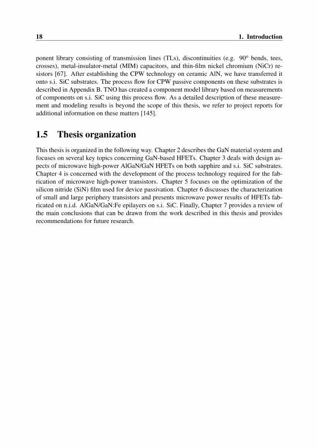
The basic layer stack of these devices consists of a highly doped wider bandgap materialgrown on top of a non-intentionally doped (n.i.d.) narrower bandgap material. Figure 2.1
19
20 2. GaN-based heterostructure field-effect transistors
≈ ≈
n.i.d. GaAs
Si-doped Al0.32Ga0.68As(n = 6.6 × 1017 cm-3)
n.i.d. GaAs
semi-insulating (s.i.)
GaAs substrate
(Cr-doped)
+ + + + ++ Ec
EF
Ev
ionized donor impurities
depletion layer
Si-doped n-AlxGa1-xAs n.i.d. GaAs
2DEG
E
x
x
Figure 2.1: Schematic cross section of the original AlxGa1-xAs/GaAs HFET and the cor-responding energy band diagram [121].
shows a schematic cross section of the original AlxGa1-xAs/GaAs, hereafter indicated as Al-GaAs/GaAs, HFET and the corresponding energy band diagram after Mimura [121]. Thealways present conducting channel in these devices, which are referred to as normally-on, con-sists of electrons from the highly doped wider bandgap material that have accumulated in thequantum well, which resides in the narrower bandgap material near the heterojunction. Asthis quantum well is confined in the direction perpendicular to the heterojunction, quantummechanics dictates that the energy levels in this spatial direction are discrete. However, theelectrons are still allowed to move freely in the plane parallel to the heterojunction. Hence,the electrons in the quantum well are usually referred to as a two-dimensional electron gas(2DEG). These electrons show enhanced mobility due to significantly reduced Coulomb scat-tering as they are separated from the ionized donor atoms in the highly doped material fromwhich they stem. In addition, mobility is further enhanced because of strongly reduced impu-rity scattering as the quantum well resides in the n.i.d. material. Enhanced electron mobility isthe key feature that differentiates HFETs from ordinary FETs.
This chapter starts with a description of the GaN material system. We will give an overviewof the crystal structure and the unique polarization effects in III-nitride crystals. Next, we willdiscuss some key topics concerning GaN-based HFETs. We will start with the most importantmaterial growth techniques followed by different HFET layer structures. After describing thetheory of 2DEG formation we will end this chapter with an explanation of two major chargetrapping effects in GaN-based HFETs that severely deteriorate their microwave high-powerperformance.

2.2 GaN material system 21
2.2 GaN material system
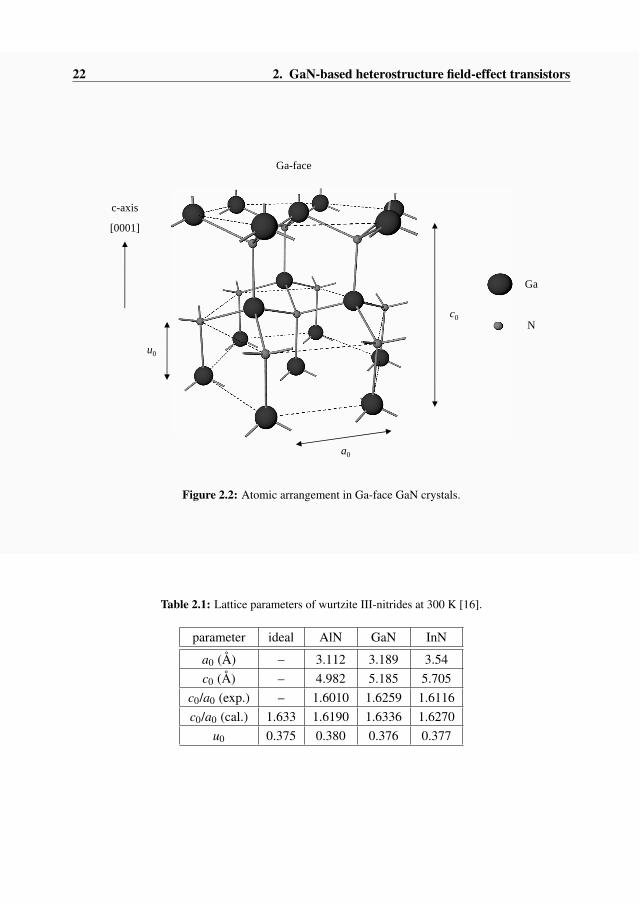
2.2.1 Crystal structureThe group III-nitrides AlN, GaN, and InN can crystallize in the following three crystal struc-tures: wurtzite, zinc-blende, and rock-salt. However, at ambient conditions the wurtzite struc-ture is the thermodynamically stable phase consisting of two interpenetrating hexagonal close-packed lattices, which are shifted with respect to each other ideally by 3/8 · c0 [135], wherec0 is the height of the hexagonal lattice cell as shown in Fig. 2.2. The chemical bonds of III-nitride compounds such as GaN are predominantly covalent, which means that each atom istetrahedrally bonded to four atoms of the other type. Because of the large difference in elec-tronegativity of Ga and N atoms, there is a significant ionic contribution to the bond whichdetermines the stability of the respective structural phase. The unit cell of the wurtzite latticeis hexagonal with a basis of four atoms, two of each kind. There is no inversion symmetry inthis lattice along the [0001] direction or c-axis, which by convention is the direction shown bya vector pointing from a Ga atom to the nearest neighbor N atom. Lack of inversion symmetrymeans that, when defining an atom position on a close-packed plane with coordinates (x,y,z) itis not invariant to the position (−x,−y,−z) since inversion results in replacement of group IIIatoms by nitrogen atoms and vice versa. As a result of the lack of inversion symmetry all atomson the same plane at each side of a bond are the same. Hence, wurtzite GaN crystals have twodistinct faces, commonly known as Ga-face and N-face, which correspond to the (0001) and(0001) crystalline faces. Figure 2.2 shows the atomic arrangement in Ga-face GaN crystals.For N-face material this can be obtained by flipping the Ga-face material upside-down. It hasto be noted that for Ga-face material the N atom is stacked directly over the Ga atom and viceversa for N-face.
Figure 2.2 also shows the three parameters that define the wurtzite lattice. These are theedge length of the basal hexagon (a0), the height of the hexagonal lattice cell (c0), and thecation-anion bond length ratio (u0) along the [0001] direction in units of c0. The subscript “0”indicates that these values are those of the equilibrium lattice. In an ideal wurtzite crystal the
c0/a0 ratio equals√
83 = 1.633 and the value for u0 is 0.375 [135]. Because of the different metal
cations, the bond lengths and the resultant c0/a0 ratios of AlN, GaN, and InN are different.Table 2.1 shows an overview of these lattice parameters of wurtzite III-nitrides at 300 K [16].
From Tab. 2.1 it is clear that GaN is closest to the ideal wurtzite structure, followed by InNand AlN. This fact is very important because the degree of non-ideality is a significant factorin determining the strength of polarization in III-nitrides.
2.2.2 Polarization effects in III-nitridesThe involvement of nitrogen, which is the smallest and the most electronegative Group Velement, makes the III-nitrides special among the other III-V compounds as this has a strongeffect on their properties. Because of the 1s22s22p3 electronic configuration of the N atom, orrather the lack of electrons occupying the outer orbitals, the electrons involved in the metal-nitrogen covalent bond will be strongly attracted by the Coulomb potential of the N atomic
c0
Ga
N
a0
Ga-face
c-axis
[0001]
u0
Figure 2.2: Atomic arrangement in Ga-face GaN crystals.
Table 2.1: Lattice parameters of wurtzite III-nitrides at 300 K [16].
parameter ideal AlN GaN InN
a0 (Å) – 3.112 3.189 3.54c0 (Å) – 4.982 5.185 5.705
c0/a0 (exp.) – 1.6010 1.6259 1.6116c0/a0 (cal.) 1.633 1.6190 1.6336 1.6270
u0 0.375 0.380 0.376 0.377
22 2. GaN-based heterostructure field-effect transistors
2.2 GaN material system 23
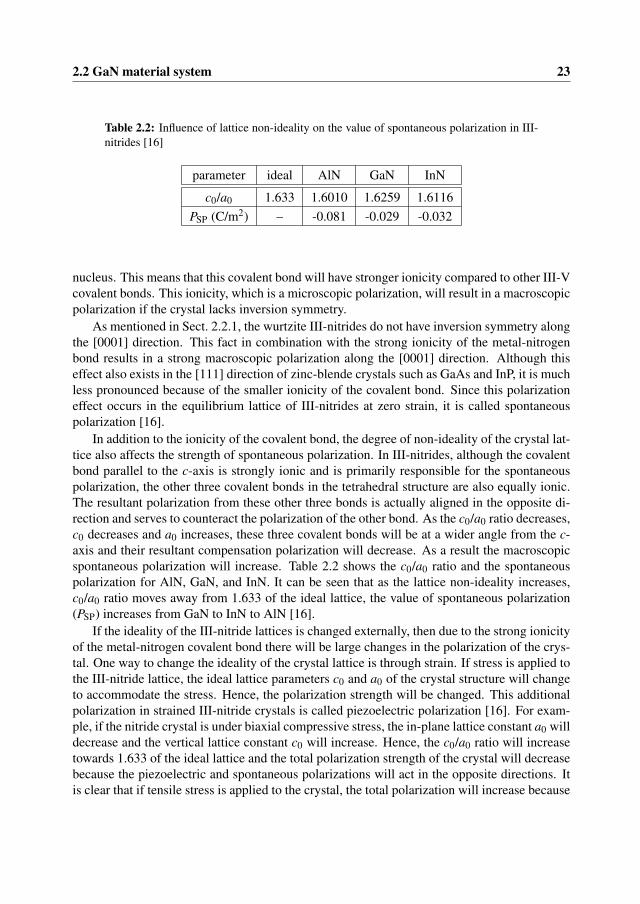
Table 2.2: Influence of lattice non-ideality on the value of spontaneous polarization in III-nitrides [16]
parameter ideal AlN GaN InN
c0/a0 1.633 1.6010 1.6259 1.6116PSP (C/m2) – -0.081 -0.029 -0.032
nucleus. This means that this covalent bond will have stronger ionicity compared to other III-Vcovalent bonds. This ionicity, which is a microscopic polarization, will result in a macroscopicpolarization if the crystal lacks inversion symmetry.
As mentioned in Sect. 2.2.1, the wurtzite III-nitrides do not have inversion symmetry alongthe [0001] direction. This fact in combination with the strong ionicity of the metal-nitrogenbond results in a strong macroscopic polarization along the [0001] direction. Although thiseffect also exists in the [111] direction of zinc-blende crystals such as GaAs and InP, it is muchless pronounced because of the smaller ionicity of the covalent bond. Since this polarizationeffect occurs in the equilibrium lattice of III-nitrides at zero strain, it is called spontaneouspolarization [16].
In addition to the ionicity of the covalent bond, the degree of non-ideality of the crystal lat-tice also affects the strength of spontaneous polarization. In III-nitrides, although the covalentbond parallel to the c-axis is strongly ionic and is primarily responsible for the spontaneouspolarization, the other three covalent bonds in the tetrahedral structure are also equally ionic.The resultant polarization from these other three bonds is actually aligned in the opposite di-rection and serves to counteract the polarization of the other bond. As the c0/a0 ratio decreases,c0 decreases and a0 increases, these three covalent bonds will be at a wider angle from the c-axis and their resultant compensation polarization will decrease. As a result the macroscopicspontaneous polarization will increase. Table 2.2 shows the c0/a0 ratio and the spontaneouspolarization for AlN, GaN, and InN. It can be seen that as the lattice non-ideality increases,c0/a0 ratio moves away from 1.633 of the ideal lattice, the value of spontaneous polarization(PSP) increases from GaN to InN to AlN [16].
If the ideality of the III-nitride lattices is changed externally, then due to the strong ionicityof the metal-nitrogen covalent bond there will be large changes in the polarization of the crys-tal. One way to change the ideality of the crystal lattice is through strain. If stress is applied tothe III-nitride lattice, the ideal lattice parameters c0 and a0 of the crystal structure will changeto accommodate the stress. Hence, the polarization strength will be changed. This additionalpolarization in strained III-nitride crystals is called piezoelectric polarization [16]. For exam-ple, if the nitride crystal is under biaxial compressive stress, the in-plane lattice constant a0 willdecrease and the vertical lattice constant c0 will increase. Hence, the c0/a0 ratio will increasetowards 1.633 of the ideal lattice and the total polarization strength of the crystal will decreasebecause the piezoelectric and spontaneous polarizations will act in the opposite directions. Itis clear that if tensile stress is applied to the crystal, the total polarization will increase because
24 2. GaN-based heterostructure field-effect transistors
the piezoelectric and spontaneous polarizations in that case act in the same direction.According to Bernardini et al. [16], the strength of piezoelectric polarization (PPE) can be
calculated with the piezoelectric coefficients e33 and e31 as
PPE = e33 · εz + e31 · (εx + εy), (2.1)
where εz = (c− c0)/c0 is the strain along the c-axis, and the in-plane strain εx = εy = (a−a0)/a0 is assumed to be isotropic, with a0 and c0 being the equilibrium lattice constants. Thedifferent strains in the lattice are related as in [16]
εz =−2 · C13
C33· εx, (2.2)
where C13 and C33 are elastic constants. Equations (2.1) and (2.2) can be combined to obtainthe following equation
PPE = 2 · a−a0
a0·[
e31− e33 ·C13
C33
]. (2.3)
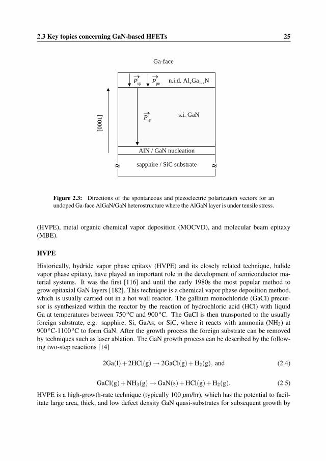
Since in the wurtzite III-nitrides the piezoelectric coefficient e31 is always negative whilee33, C13, and C33 are always positive, it turns out that (e31 − e33 ·C13/C33) will always benegative [16, 135]. As a consequence, the value of piezoelectric polarization (PPE) in III-nitrides is always negative for layers under tensile stress (a > a0) and positive for layers undercompressive stress (a < a0). As spontaneous polarization in III-nitrides is always negative, itcan be concluded that for layers under tensile stress, spontaneous and piezoelectric polariza-tions are parallel to each other, and for layers under compressive stress the two polarizationsare anti-parallel. Figure 2.3 shows the directions of the spontaneous and piezoelectric polar-ization vectors for an undoped Ga-face AlxGa1-xN/GaN, hereafter indicated as AlGaN/GaN,heterostructure where the AlGaN layer is under tensile stress. We will consider this hetero-structure in more detail in Sect. 2.3.2. Furthermore, it has to be noted that we only considerthe heterojunction at which the 2DEG is formed.
2.3 Key topics concerning GaN-based HFETsThis section starts with a brief summary of the most important techniques for GaN epitaxy.This is followed by a discussion of HFET layer structures and the theory of 2DEG formationin GaN-based HFETs. Finally, we will give an overview of trapping effects in these devicesthat severely deteriorate their microwave high-power performance.
2.3.1 Growth techniquesAs mentioned in Sect 1.3, the lack of a lattice and thermally matched substrate forces to useheteroepitaxy on lattice and thermally mismatched substrates such as sapphire, SiC, or Si. Wewill briefly discuss the most commonly used growth techniques: hydride vapor phase epitaxy
2.3 Key topics concerning GaN-based HFETs 25
sapphire / SiC substrate
AlN / GaN nucleation
s.i. GaN
n.i.d. AlxGa1-xN
≈≈
Psp→
Psp→
Ppe→
[000
1]
Ga-face
Figure 2.3: Directions of the spontaneous and piezoelectric polarization vectors for anundoped Ga-face AlGaN/GaN heterostructure where the AlGaN layer is under tensile stress.
(HVPE), metal organic chemical vapor deposition (MOCVD), and molecular beam epitaxy(MBE).
HVPE
Historically, hydride vapor phase epitaxy (HVPE) and its closely related technique, halidevapor phase epitaxy, have played an important role in the development of semiconductor ma-terial systems. It was the first [116] and until the early 1980s the most popular method togrow epitaxial GaN layers [182]. This technique is a chemical vapor phase deposition method,which is usually carried out in a hot wall reactor. The gallium monochloride (GaCl) precur-sor is synthesized within the reactor by the reaction of hydrochloric acid (HCl) with liquidGa at temperatures between 750 oC and 900 oC. The GaCl is then transported to the usuallyforeign substrate, e.g. sapphire, Si, GaAs, or SiC, where it reacts with ammonia (NH3) at900 oC-1100 oC to form GaN. After the growth process the foreign substrate can be removedby techniques such as laser ablation. The GaN growth process can be described by the follow-ing two-step reactions [14]
2Ga(l)+2HCl(g)→ 2GaCl(g)+H2(g), and (2.4)
GaCl(g)+NH3(g)→ GaN(s)+HCl(g)+H2(g). (2.5)
HVPE is a high-growth-rate technique (typically 100 µm/hr), which has the potential to facil-itate large area, thick, and low defect density GaN quasi-substrates for subsequent growth by

26 2. GaN-based heterostructure field-effect transistors
MOCVD or MBE.
MOCVD
To date, metal organic chemical vapor deposition (MOCVD) is the workhorse for the growthof GaN and related materials. Manasevit et al. applied this technique for the deposition of GaNand AlN in 1971 [112]. Using trimethylgallium (TMG) and NH3 as source gases for GroupsIII and V species, respectively, they obtained c-axis oriented films on sapphire (0001) and on6H-SiC (0001) substrates. In the MOCVD process, substrate temperatures well in excess of900 oC are required to obtain single crystalline high-quality GaN layers. GaN films with thebest electrical and optical properties are grown at 1050 oC or even higher [142]. These highgrowth temperatures require that the used substrates do not decompose. Sapphire, SiC, Si, andAlN are among those that meet this criterion. In addition, metalalkyls must be kept belowpyrolysis temperature and should be kept separate from NH3 until just before the reaction zoneto minimize predeposition reactions. The MOCVD process is also characterized by a lowgrowth rate (typically 1-2 µm/hr) and a high N/Ga (V/III) flux ratio. The former enables thecontrollable growth of abrupt junctions whereas the latter is used to minimize nitrogen loss.The high growth temperatures have a contradictory effect on the crystal quality. On the onehand, because of the higher surface mobility of the atoms the grown films are of better quality.On the other hand, high vapor pressure of N over Ga brings the growth process very close tothe dissociation temperature. Also, post-growth cooling introduces more strain and thus morestructural defects may be introduced during cooling.
It is well established that two pretreatment steps are essential to obtain high-quality MOCVDGaN films on sapphire substrates: a high temperature nitridation of the sapphire surface [77,122, 159] and the deposition of a low-temperature buffer layer [5, 125, 166]. The nitridationof sapphire was found to result in the formation of a relaxed AlN layer [159], which acts sub-sequently as a buffer layer. The mechanism of this layer was studied by Amano et al. [5]. Theessential role of the low-temperature buffer layer is to supply nucleation centers having thesame orientations as the substrate and to promote lateral growth of the GaN film due to thedecrease in the interfacial free energy between the film and the substrate [182]. In the case ofa SiC substrate, efficient surface wetting can only be achieved by using an AlN layer. To avoidconfusion later on with the high-temperature GaN buffer layer in HFET layer stacks, we willfrom now on refer to the former AlN and the latter low-temperature layers as nucleation layers.
In Sect. 2.2.1 we have seen that III-nitrides have either Ga-face or N-face structure. It hasbeen observed that III-nitride films grown by MOCVD are almost always Ga-face irrespectiveof the growth conditions or the nature of the intervening layers [142].
MBE
Molecular beam epitaxy (MBE) of GaN layers is slow (typically 1 µm/hr, or slightly more thanone monolayer per second) and tedious due to a variety of reasons such as finding a suitablenitrogen source since NH3 is very stable at the lower temperatures (500 oC-900 oC ) that arecommon for MBE growth. To avoid this problem, reactive species of nitrogen, generated by

2.3 Key topics concerning GaN-based HFETs 27
n.i.d. GaAs
sapphire / SiC substrate
x
AlN / GaN nucleation
s.i. GaN buffer
n.i.d. AlxGa1-xNSi-doped AlxGa1-xN
n.i.d. AlxGa1-xN
≈≈
Ec
2DEG
AlxGa1-xN s.i. GaN
E
xn.i.d. n.i.d.n-type
EF
Ev
Figure 2.4: Schematic cross section of a basic Ga-face doped AlGaN/GaN HFET structureand the corresponding energy band diagram.
electron cyclotron resonance (ECR) or radio frequency (RF) plasmas with low energy, are gen-erally used. In addition to the problem of the nitrogen source, the intrinsic problem of MBEgrowth is that it is carried out far from thermodynamic equilibrium. Hence it is primarily gov-erned by the kinetics of the surface processes that occur when the impinging beam reacts withthe outermost layer of the substrate crystal [142]. This is in contrast with the other epitax-ial growth techniques HVPE and MOCVD, which proceed at conditions near thermodynamicequilibrium and are therefore most frequently controlled by diffusion processes occurring inthe crystallizing phase near the substrate. Despite of these difficulties, MBE grown GaN layersof comparable material quality to those grown by MOCVD have been shown. This is especiallytrue if MOCVD or HVPE grown GaN templates are used for further MBE growth.
Contrary to what has been observed for MOCVD grown GaN-based films, growth by MBEcan result in either Ga-face or N-face material depending on the nature of the nucleation layer.For growth on sapphire it has been shown that a low-temperature GaN nucleation layer willresult in an N-face crystal and the use of a high-temperature AlN nucleation layer yields Ga-face epilayers.
2.3.2 GaN-based HFET layer structuresThe first AlGaN/GaN HFET structures consisted of an identical layer sequence as the originalAlGaAs/GaAs HFET structures described in Sect. 6.1. Figure 2.4 shows a schematic crosssection of a basic Ga-face doped AlGaN/GaN HFET structure and the corresponding energyband diagram.
The most pronounced differences in the case of GaN-based epitaxy are of course the for-
28 2. GaN-based heterostructure field-effect transistors
eign substrates and the use of a nucleation layer. As in the case of AlGaAs/GaAs the GaNbuffer layer should be semi-insulating (s.i.) to provide good electrical isolation between activedevices when used in an integrated circuit (IC). Without the application of advanced growthsteps such as lateral epitaxial overgrowth (LEO) the dislocation densities of GaN buffer layerson sapphire and SiC substrates are very high, typically 108 - 1010 cm−2 [3, 142]. These veryhigh dislocation densities can act as recombination and trapping centers which cause a seriousthreat to device performance and reliability. Nevertheless, s.i. GaN buffers can for examplebe achieved by compensation doping using e.g. iron (Fe) atoms. Reported resistivity valuesof such buffer layers are in excess of 108 Ωcm [142]. The highly Si-doped (typically, n = 1.0x 1019 cm−3) AlGaN layer is used to supply sufficient electrons to the 2DEG. Between thissupply layer and the s.i. GaN buffer layer a thin (typically 3 nm) n.i.d. AlGaN layer usuallywith the same Al alloy composition as the supply layer is inserted. This so-called spacer layerstrongly decreases Coulomb scattering between the 2DEG electrons and their ionized parentatoms in the supply layer. Hence the mobility of the 2DEG electrons is significantly increasedto typical values ranging from 1200 - 2000 cm2/Vs at room temperature (RT). The n.i.d. Al-GaN capping layer is used to improve the performance of the Schottky gate contact as it isimpossible to realize a properly rectifying control electrode on highly doped semiconductormaterial.
In Sect. 2.2.2 we mentioned the much stronger spontaneous polarization in III-nitridescompared to other III-V semiconductors because of the involvement of nitrogen as the GroupV element. If we consider a Ga-face AlGaN/GaN HFET structure in which the AlGaN layeris under tensile stress, the polarization fields in the AlGaN and GaN layers are parallel andpointing towards the substrate as shown in Fig. 2.3. As we will see in Sect. 2.3.3, a gradient inthe polarization field (~P) at the AlGaN/GaN heterojunction induces a bound sheet charge. Tomaintain charge neutrality, this induced bound sheet charge has to be compensated by mobilecharge. We will see that in the case of a Ga-face AlGaN/GaN HFET structure the inducedbound charge is positive. Hence, free electrons accumulate in the quantum well on the GaNside of the heterojunction forming a 2DEG. Figure 2.5 shows a schematic cross section ofa basic Ga-face undoped AlGaN/GaN HFET structure and the corresponding energy banddiagram.
It has been shown that even in the case of un undoped AlGaN layer, 2DEG sheet chargedensities in excess of 1013 cm−2 can be achieved [6]. These values are ten times higher thanthe sheet charge densities obtained in impurity doped AlGaAs/GaAs HFETs. The so-calledpiezoelectric induced 2DEG formation in undoped AlGaN/GaN heterostructures is typical forthe III-nitrides. The omission of impurity doping has several advantages such as increasedbreakdown voltage due to reduced gate leakage currents. However, some serious disadvantagesarise in these structures as they are very sensitive for trapping and de-trapping phenomena atthe AlGaN barrier layer as the donor resides on this surface. We will elaborate on this matterin Sect. 2.3.4.
In Sect. 2.2.1 we have explained the Ga- and N-faces of wurtzite GaN crystals. Thesedifferent polarities have different properties that affect both device technology and perfor-mance. Although N-face crystals have lower dislocation density and are chemically active,which enables wet-chemical etching of the material, these layers suffer from a very rough
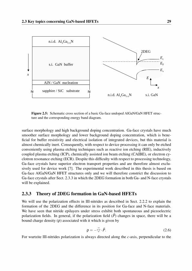
2.3 Key topics concerning GaN-based HFETs 29
Ec
EF
2DEG
Evx
n.i.d. AlxGa1-xN s.i. GaN
E
x
n.i.d. GaAs
sapphire / SiC substrate
AlN / GaN nucleation
s.i. GaN buffer
n.i.d. AlxGa1-xN
≈≈
Figure 2.5: Schematic cross section of a basic Ga-face undoped AlGaN/GaN HFET struc-ture and the corresponding energy band diagram.
surface morphology and high background doping concentration. Ga-face crystals have muchsmoother surface morphology and lower background doping concentration, which is bene-ficial for buffer resistivity and electrical isolation of integrated devices, but this material isalmost chemically inert. Consequently, with respect to device processing it can only be etchedconveniently using plasma etching techniques such as reactive ion etching (RIE), inductivelycoupled plasma etching (ICP), chemically assisted ion beam etching (CAIBE), or electron cy-clotron resonance etching (ECR). Despite this difficulty with respect to processing technology,Ga-face crystals have superior electron transport properties and are therefore almost exclu-sively used for device work [7]. The experimental work described in this thesis is based onGa-face AlGaN/GaN HFET structures only and we will therefore constrict the discussion toGa-face crystals after Sect. 2.3.3 in which the 2DEG formation in both Ga- and N-face crystalswill be explained.
2.3.3 Theory of 2DEG formation in GaN-based HFETsWe will use the polarization effects in III-nitrides as described in Sect. 2.2.2 to explain theformation of the 2DEG and the difference in its position for Ga-face and N-face materials.We have seen that nitride epilayers under stress exhibit both spontaneous and piezoelectricpolarization fields. In general, if the polarization field (~P) changes in space, there will be abound charge density (ρ) associated with it which is given by
ρ =−~5·~P. (2.6)
For wurtzite III-nitrides polarization is always directed along the c-axis, perpendicular to the

30 2. GaN-based heterostructure field-effect transistors
Table 2.3: Values for lattice parameters, piezoelectric constants, elasticity constants, andspontaneous polarization for GaN and AlN [6, 16]
parameter AlN GaN
a0 (Å) 3.112 3.189e31 (C/m2) -0.60 -0.49e33 (C/m2) 1.46 0.73C13 (GPa) 108 103C33 (GPa) 373 405PSP (C/m2) -0.081 -0.029
heterostructure interface. Hence, at the heterojunction, which is assumed to be planar andabrupt a bound sheet charge (σint) will be formed that is given by [7]
σint = Ptot,layer1−Ptot,layer2 = (PSP +PPE)layer1− (PSP +PPE)layer2. (2.7)
In reality, heterojunctions are rarely totally abrupt due to interface roughness or an uninten-tional composition gradient. However, as long as the gradient of the heterojunction is not overa large distance (e.g. > 20 Å), a sheet density (σ) given by equation 2.7 is a quite good approx-imation. This bound charge, which is induced by a change in polarization of the two layers,will attract compensating mobile charge at the interface. If the bound charge is positive it willcause a negative mobile sheet charge and vice versa. Baring this in mind we will focus onthe calculation of bound charge and the corresponding 2DEG density in a Ga-face undopedAlGaN/GaN heterojunction as shown in Fig. 2.5.
To calculate the amount of bound sheet charge at an abrupt undoped AlGaN/GaN hetero-junction we need to know the physical properties of the AlGaN barrier layer as a function of itsaluminum (Al) mole fraction (x). Table 2.3 gives the values for the lattice parameters, piezo-electric constants, elasticity constants, and spontaneous polarization for GaN and AlN [6, 16].
It has to be noted that the GaN buffer layer in the structure shown in Fig. 2.5 is relaxedand therefore only has spontaneous polarization. The AlGaN barrier layer however is tensilestrained and therefore has both spontaneous and piezoelectric polarization. Using equations(2.1) - (2.3), and (2.7) the bound sheet charge at the AlGaN/GaN interface is given by
σint = (PSP)GaN− (PSP +PPE)AlGaN
= PSP(0)−PSP(x)−2 · a(0)−a(x)a(x) ·
[e31(x)− e33(x) · C13(x)
C33(x)
].
(2.8)
Using Vegard’s law for interpolation between the values of the parameters of AlN and GaNgiven in table 2.3, σint can be calculated for any Al alloy composition. Figure 2.6 shows thetotal polarization induced bound sheet charge, which equals the sum of the charge densitiesinduced by the spontaneous and piezoelectric polarization components, as a function of the
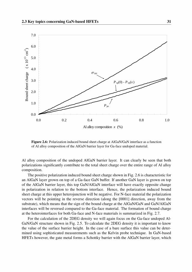
2.3 Key topics concerning GaN-based HFETs 31
0.0
1.0
2.0
3.0
4.0
5.0
6.0
7.0
0.0 0.2 0.4 0.6 0.8 1.0
Al alloy composition x (%)
Bou
nd sh
eet c
harg
e
( x 1
0 13
cm-2
)
σ int
P sp(0) - P sp(x )
P pe
Figure 2.6: Polarization induced bound sheet charge at AlGaN/GaN interface as a functionof Al alloy composition of the AlGaN barrier layer for Ga-face undoped material.
Al alloy composition of the undoped AlGaN barrier layer. It can clearly be seen that bothpolarizations significantly contribute to the total sheet charge over the entire range of Al alloycomposition.
The positive polarization induced bound sheet charge shown in Fig. 2.6 is characteristic foran AlGaN layer grown on top of a Ga-face GaN buffer. If another GaN layer is grown on topof the AlGaN barrier layer, this top GaN/AlGaN interface will have exactly opposite changein polarization in relation to the bottom interface. Hence, the polarization induced boundsheet charge at this upper heterojunction will be negative. For N-face material the polarizationvectors will be pointing in the reverse direction (along the [0001] direction, away from thesubstrate), which means that the sign of the bound charge at the AlGaN/GaN and GaN/AlGaNinterfaces will be reversed compared to the Ga-face material. The formation of bound chargeat the heterointerfaces for both Ga-face and N-face materials is summarized in Fig. 2.7.
For the calculation of the 2DEG density we will again focus on the Ga-face undoped Al-GaN/GaN structure shown in Fig. 2.5. To calculate the 2DEG density it is important to knowthe value of the surface barrier height. In the case of a bare surface this value can be deter-mined using sophisticated measurements such as the Kelvin probe technique. In GaN-basedHFETs however, the gate metal forms a Schottky barrier with the AlGaN barrier layer, which

32 2. GaN-based heterostructure field-effect transistors
sapphire / SiC substrate
AlN / GaN nucleation
s.i. GaN buffer
n.i.d. AlxGa1-xN
≈≈ sapphire / SiC substrate
n.i.d. GaN
s.i. GaN buffer
n.i.d. AlxGa1-xN
≈≈
2DEG
Ga-face N-face
Figure 2.7: Formation of bound sheet charge at AlGaN/GaN and GaN/AlGaN interfacesfor Ga-face and N-face materials.
can be measured easily by a variety of techniques such as capacitance-voltage measurements.Figure 2.8 again shows the energy band diagram of a Ga-face undoped AlGaN/GaN hetero-structure. In addition, the polarization induced bound sheet charge densities at the AlGaN/GaNand air/AlGaN interfaces, σint, σsurf, and σcomp , and the compensating mobile sheet chargedensity σ2DEG are shown. As the material is Ga-face, the sign of the charge densities σint andσsurf is positive and negative, respectively. To satisfy charge neutrality across the AlGaN bar-rier the net charge at the surface must be positive and therefore a positive compensating charge(σcomp) is required. Furthermore, it has to be noted that as the considered AlGaN/GaN struc-tures are undoped, the compensating mobile sheet charge density (σ2DEG) consists of electronsthat must originate from the surface of the AlGaN barrier [64].
Although an accurate calculation of the 2DEG density in this structure would require asophisticated simulation tool, a simple semi-classical electrostatic analysis assuming chargeneutrality to hold between the sheet charge densities at the surface and the interface, leads tothe following analytical expression for the 2DEG sheet charge density (ns) as a function of theAl alloy composition (x) of the AlxGa1-xN barrier layer [176]
ns =σint
q−
[ε0ε(x)
dq2
][qφb(x)+EF(x)−∆Ec(x)] , (2.9)
where σint is the polarization induced bound sheet charge density at the AlGaN/GaN hetero-junction, q the electron charge, ε0 the permittivity of free space, ε, d, x, are the relative dielec-tric constant, thickness, and Al mole fraction of the AlxGa1-xN barrier layer, φb is the Schottkybarrier height, EF is the Fermi level at the heterojunction with respect to the GaN conduction

2.3 Key topics concerning GaN-based HFETs 33
x
Ec
EF
2DEG
d
E0
φb
n.i.d. AlxGa1-xN s.i. GaN
σcomp
σsurf
σint
σ2DEG
posi
tive
nega
tive
C/cm2
x
Ev
E
Figure 2.8: Energy band diagram of a Ga-face undoped AlGaN/GaN heterostructure andthe polarization induced bound and compensating mobile sheet charge densities.
band edge, and finally ∆Ec is the conduction band offset at the AlGaN/GaN interface. Thevalues for ε(x) and φb(x) can be calculated by interpolation again using Vegard’s law as [178]
ε(x) = 9.0−0.5x, and (2.10)
φb(x) = 0.84+1.3x. (2.11)
The value for EF as a function of Al mole fraction can be approximated by [7]
EF(x) = E0(x)+π~2
m?(x)·ns(x), (2.12)
with the ground state level (E0) of the 2DEG being equal to
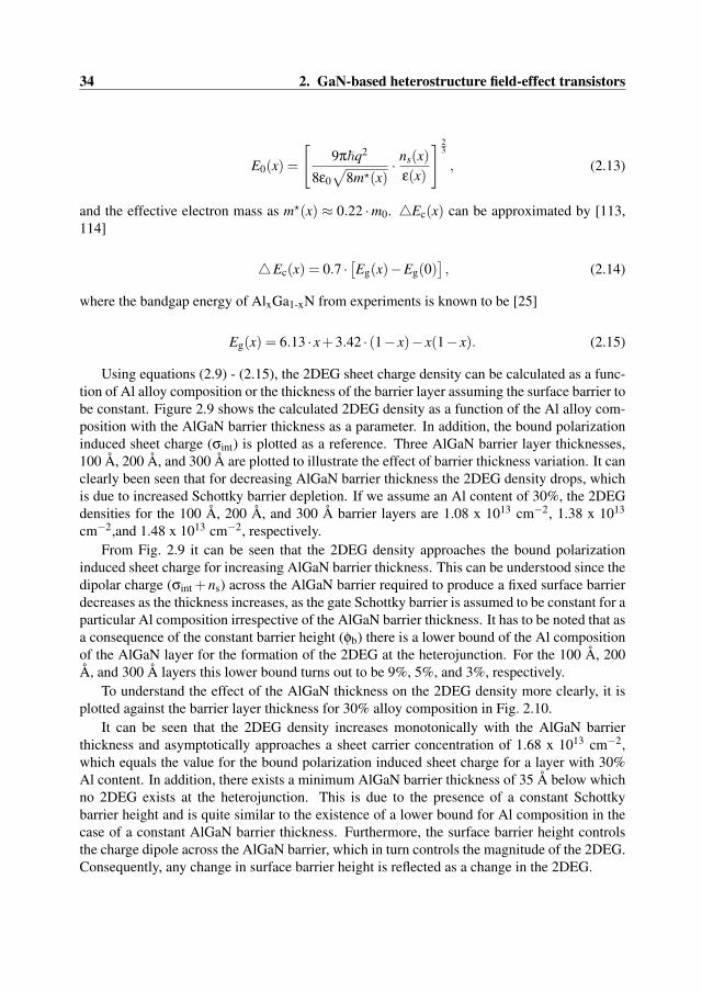
34 2. GaN-based heterostructure field-effect transistors
E0(x) =
[9π~q2
8ε0√
8m?(x)· ns(x)
ε(x)
] 23
, (2.13)
and the effective electron mass as m?(x) ≈ 0.22 ·m0. 4Ec(x) can be approximated by [113,114]
4Ec(x) = 0.7 ·[Eg(x)−Eg(0)
], (2.14)
where the bandgap energy of AlxGa1-xN from experiments is known to be [25]
Eg(x) = 6.13 · x+3.42 · (1− x)− x(1− x). (2.15)
Using equations (2.9) - (2.15), the 2DEG sheet charge density can be calculated as a func-tion of Al alloy composition or the thickness of the barrier layer assuming the surface barrier tobe constant. Figure 2.9 shows the calculated 2DEG density as a function of the Al alloy com-position with the AlGaN barrier thickness as a parameter. In addition, the bound polarizationinduced sheet charge (σint) is plotted as a reference. Three AlGaN barrier layer thicknesses,100 Å, 200 Å, and 300 Å are plotted to illustrate the effect of barrier thickness variation. It canclearly been seen that for decreasing AlGaN barrier thickness the 2DEG density drops, whichis due to increased Schottky barrier depletion. If we assume an Al content of 30%, the 2DEGdensities for the 100 Å, 200 Å, and 300 Å barrier layers are 1.08 x 1013 cm−2, 1.38 x 10¹³
cm−2,and 1.48 x 1013 cm−2, respectively.From Fig. 2.9 it can be seen that the 2DEG density approaches the bound polarization
induced sheet charge for increasing AlGaN barrier thickness. This can be understood since thedipolar charge (σint +ns) across the AlGaN barrier required to produce a fixed surface barrierdecreases as the thickness increases, as the gate Schottky barrier is assumed to be constant for aparticular Al composition irrespective of the AlGaN barrier thickness. It has to be noted that asa consequence of the constant barrier height (φb) there is a lower bound of the Al compositionof the AlGaN layer for the formation of the 2DEG at the heterojunction. For the 100 Å, 200Å, and 300 Å layers this lower bound turns out to be 9%, 5%, and 3%, respectively.
To understand the effect of the AlGaN thickness on the 2DEG density more clearly, it isplotted against the barrier layer thickness for 30% alloy composition in Fig. 2.10.
It can be seen that the 2DEG density increases monotonically with the AlGaN barrierthickness and asymptotically approaches a sheet carrier concentration of 1.68 x 1013 cm−2,which equals the value for the bound polarization induced sheet charge for a layer with 30%Al content. In addition, there exists a minimum AlGaN barrier thickness of 35 Å below whichno 2DEG exists at the heterojunction. This is due to the presence of a constant Schottkybarrier height and is quite similar to the existence of a lower bound for Al composition in thecase of a constant AlGaN barrier thickness. Furthermore, the surface barrier height controlsthe charge dipole across the AlGaN barrier, which in turn controls the magnitude of the 2DEG.Consequently, any change in surface barrier height is reflected as a change in the 2DEG.
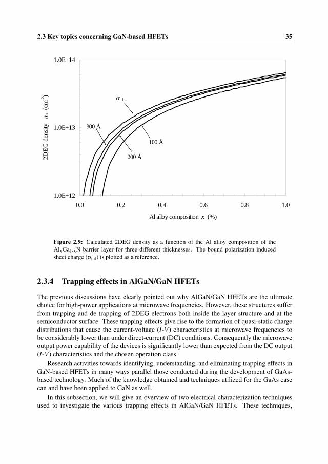
2.3 Key topics concerning GaN-based HFETs 35
1.0E+12
1.0E+13
1.0E+14
0.0 0.2 0.4 0.6 0.8 1.0
Al alloy composition x (%)
2DEG
den
sity
n s
(cm
-2) σ int
100 Å
300 Å
200 Å
Figure 2.9: Calculated 2DEG density as a function of the Al alloy composition of theAlxGa1-xN barrier layer for three different thicknesses. The bound polarization inducedsheet charge (σint) is plotted as a reference.
2.3.4 Trapping effects in AlGaN/GaN HFETs
The previous discussions have clearly pointed out why AlGaN/GaN HFETs are the ultimatechoice for high-power applications at microwave frequencies. However, these structures sufferfrom trapping and de-trapping of 2DEG electrons both inside the layer structure and at thesemiconductor surface. These trapping effects give rise to the formation of quasi-static chargedistributions that cause the current-voltage (I-V) characteristics at microwave frequencies tobe considerably lower than under direct-current (DC) conditions. Consequently the microwaveoutput power capability of the devices is significantly lower than expected from the DC output(I-V) characteristics and the chosen operation class.
Research activities towards identifying, understanding, and eliminating trapping effects inGaN-based HFETs in many ways parallel those conducted during the development of GaAs-based technology. Much of the knowledge obtained and techniques utilized for the GaAs casecan and have been applied to GaN as well.
In this subsection, we will give an overview of two electrical characterization techniquesused to investigate the various trapping effects in AlGaN/GaN HFETs. These techniques,

36 2. GaN-based heterostructure field-effect transistors
0.0E+00
2.0E+12
4.0E+12
6.0E+12
8.0E+12
1.0E+13
1.2E+13
1.4E+13
1.6E+13
1.8E+13
0 50 100 150 200 250 300 350 400
AlxGa1-xN barrier thickness d (Å)
2DEG
den
sity
n s
(cm
-2)
Figure 2.10: Calculated 2DEG density as a function of the AlGaN barrier thickness for anAl alloy composition of 30%.
which try to discriminate between lateral and vertical trapping phenomena, are commonlyknown as drain lag and gate lag respectively. Although the underlying physical mechanismsare completely different, the various trapping effects cause a reduction in drain current andconsequently in output power. It has to be noted that in literature these reductions in draincurrent and output power are often referred to by a variety of terms such as current col-lapse, current slump, drain dispersion, DC-to-RF current dispersion, power drift, and powerslump [19, 49, 168]. These terms sometimes cause some ambiguity regarding the responsibletrapping mechanism as collapse, dispersion, and drift refer to a recoverable reduction whereasslump indicates a permanent degradation.
Drain lag
A significant but recoverable reduction in drain current resulting from the application of highdrain-source bias voltages (typically VDS > 20 V) is known as drain lag. This current collapse inGaN-based HFETs can be caused by instabilities in the positive compensation charge densityat the AlGaN surface (σcomp) that needs to be present to maintain the 2DEG channel. Theseinstabilities in σcomp can be caused by oxidation of the AlGaN barrier layer due to the high
2.3 Key topics concerning GaN-based HFETs 37
current densities and elevated temperatures at the source contacts. Any reduction of σcompleads to a reduction of σ2DEG and hence a decreased drain current and lower output power.However, initially the current collapse observed during a drain lag measurement has beenrelated mainly to trapping of hot 2DEG electrons inside the layer stack because of the analogyobserved in GaN-based MESFETs. Possible trapping locations inside the AlGaN/GaN layerstack, first reported by Khan et al. [81], are:
• the semi-insulating (s.i.) substrate (in the case of growth on SiC),
• at the interface between GaN and the substrate (either sapphire or SiC),
• in the n.i.d. high-resistivity (HR) GaN buffer,
• at the AlGaN/GaN interface, or
• in the AlGaN barrier layer.
Binari et al. [20] were the first to correlate drain current collapse in GaN-based MESFETs withhot electron trapping by deep traps in the n.i.d. HR GaN buffer layer. In addition, they showedthe dependence of drain current recovery on illumination and temperature. These findings wereconfirmed by Zhang et al. and Kuliev et al. [94, 180]. A continuous transition from partialto complete drain current recovery was observed upon decreasing the wavelength of the lightused from 720 nm to 366 nm (corresponding to the GaN bandgap energy at RT), respectively.The same behavior can be observed if the ambient temperature is increased up to temperaturesover 150 oC, which is consistent with thermal emission of trapped electrons from deep traps.For both dependencies no threshold in the amount of current recovery is observed which isindicative for a distribution of trap energy levels rather than a single trap with a well-definedlevel [20]. Further studies by Binari et al. [17, 18] revealed that the degree of drain lag isrelated to the conductivity of the GaN buffer layer, which can be significantly influenced bythe growth pressure used. It has been shown that at low pressures (typically < 50 Torr) trapformation is strongly enhanced. As these traps compensate shallow donors this enables thegrowth of HR GaN buffer layers but also results in increased drain lag. At higher pressurestrap formation decreases which results in more conductive GaN buffers and reduced drain lageither because of the lower trap density or the filling of these traps by shallow donors.
By studying the wavelength dependence of the drain current recovery in more detail, Kleinet al. [88] have succeeded in providing spectroscopic signatures of the traps responsible fordrain lag in GaN MESFETs and to estimate the energy levels of these traps with respect to theconduction band. They observed two broad absorptions below the GaN bandgap correspondingto the photoionization of carriers from two distinct traps that are located approximately 1.8eV and 2.85 eV below the conduction band, respectively. The trap at 1.8 eV is suggestedto be related to dislocations and grain boundaries [19] and the trap at 2.85 eV is related tocarbon (C) incorporation which increases as growth pressure decreases [86]. Photoionizationmeasurements on AlGaN/GaN HFETs have shown the same broad trap-related absorptions anda rapid increase at the GaN bandgap [87]. As no enhancement of the optically induced draincurrent recovery was observed for photon energies at or above the AlGaN bandgap it seems

38 2. GaN-based heterostructure field-effect transistors
obvious that drain lag in AlGaN/GaN HFETs is caused by the same traps in the HR GaN bufferlayer that also caused drain lag in the GaN MESFETs.
It is well known that AlGaAs/GaAs HFETs suffer from trapping by so-called DX centersin the AlGaAs barrier layer [76]. In the nitrides a DX-like center associated with oxygen inthe AlGaN barrier layer has been observed [119]. This trap, like the DX center in AlGaAs, iseffective only at low temperatures. However, in the nitrides current collapse is observed at RT.Therefore it is unlikely that current collapse in AlGaN/GaN HFETs is due to a DX-like trap inthe AlGaN barrier layer.
Recovery from current collapse by thermal emission of the trapped carriers has a character-istic time dependence which can be investigated by measuring the drain current at a low drain-source voltage (typically VDS < 1 V) before and after applying a large drain-source voltage(typically VDS > 20 V) while keeping the gate-source voltage at 0 V (open channel). Exposureto the high drain-source voltage induces current collapse and the recovery of the drain currentto its low-field value is monitored as a function of time. Dang et al. [35] have determined threetime constants, designated as fast (∼1 s), intermediate (∼10 s), and slow (> 100 s), which theyassigned to traps at the semiconductor surface, deep levels in the AlGaN barrier layer, andtraps at the AlGaN/GaN interface, respectively.
Gate lag
For an ideal HFET an estimate of the maximum obtainable output power under large-signaloperation at microwave frequencies can be calculated using the DC output (I-V) characteristicsand the chosen operation class. If biased in class A, i.e. ID= 0.5·ID,max, the maximum outputpower is given by [67]
Pout,max =(VBD−Vknee) · ID,max
8, (2.16)
where VBD is the drain-source breakdown voltage, Vknee is the knee voltage of the curve rep-resenting the maximum drain current (ID,max). It has been observed that the maximum outputpower under large-signal operation at microwave frequencies, even for AlGaN/GaN HFETshardly suffering from any drain lag, is much less than calculated using equation 2.16 [90, 173].Figure 2.11-(a) shows a schematic representation of the (ID−VDS) characteristics of an idealHFET under DC operation with the location of the quiescent bias point (Q) for class A oper-ation on the load line for maximum output power. It should be noted that this representationshows the (I-V) curves for a given maximum power dissipated in the device. Figure 2.11-(b)shows a schematic representation of the (ID−VDS) characteristics under large-signal operationat microwave frequencies. Note that the (I-V) curves are shown for the same maximum powerdissipated in the device as under DC operation.
Comparing Figs. 2.11-(left) and (right) it can clearly be concluded that although the bigdiscrepancy between expected and measured microwave output power is caused by both re-duced voltage and current swings, the reduction of the latter is dominant. Reduced voltageswing is due to an increased knee voltage, also known as knee voltage walk-out, which is gen-erally related to surface oxidation but has also been attributed to trapping of electrons in thes.i. GaN buffer layer [17].
2.3 Key topics concerning GaN-based HFETs 39
0.0
0.2
0.4
0.6
0.8
1.0
1.2
0 10 20 30
V DS (V) I
D (
A)
I D,max 2 < I D,max 1
Q 2
V knee 2 > V knee 1
V BD 2 = V BD 1
load line 2
0.0
0.2
0.4
0.6
0.8
1.0
1.2
0 10 20 30
V DS (V)
ID
(A
)
I D,max 1
Q 1
V knee 1V BD 1
load line 1
Figure 2.11: Schematic representation of the output (I-V) curves for an ideal HFET underDC operation (left), and under large-signal operation at microwave frequencies (right).
Nguyen et al. [131] showed that drain current compression during large-signal operationat microwave frequencies has been observed even when the load impedance was near zero. Asthe voltage swing in this case is minimal, they concluded that the trapping of electrons occurseither in the AlGaN barrier layer or at the AlGaN surface and not in the GaN buffer layer.Despite the fact that this effect has been observed over a wide range of time and frequency,which makes it very difficult to unambiguously determine the location of the responsible trap-ping mechanism, various research groups have confirmed that drain current reduction duringlarge-signal operation at microwave frequencies is mainly caused by trapping of electrons atthe free AlGaN surface [17, 48, 64, 141, 162, 164].
To understand how electrons that get trapped at the free AlGaN surface can influence themagnitude of the drain current we have to recall the discussion about the formation of the2DEG at the AlGaN/GaN heterojunction. As described in Subsect. 2.3.3, the existence of thepolarization dipole in the AlGaN barrier layer alone is not enough for a 2DEG to form in thepotential well at the AlGaN/GaN interface. For this to happen, a positive sheet charge (σcomp)must exist at the free AlGaN surface to compensate the negative sheet charge (σ2DEG) due toelectrons in the channel. Such positive sheet charge can arise from surface states created bydangling bonds, threading dislocations accessible at the surface, ionized donor states, and ionsabsorbed from the ambient environment [48, 64]. Neutralizing the positive surface charge,either by the capture of electrons in trap states, the emission of holes, or by the adsorption ofcharged ions, leads to depletion of the 2DEG density and hence reduction of the drain current.
The effect of surface states was measured for the first time by Vetury et al. [163]. Theyused floating gates as potential probes to directly measure the surface potential along the gate-drain access region. It was found that the lateral extension of the gate depletion region was

40 2. GaN-based heterostructure field-effect transistors
inconsistent with the ionized positive donor density, suggesting the presence of negative chargeon the surface. This negative charge causes the surface potential to become more negativeleading to a rapid extension of the gate depletion region. The observation that negative surfacecharge acts like a negatively biased metal gate has led to the virtual gate concept [37, 164].
According to this concept, there now exist two gates, the actual metal gate and the so-called virtual gate on the AlGaN surface in the gate-drain access region, the depletion regionsof which being in series. The potential on the metal gate is controlled by the applied gate biaswhile the potential on the virtual gate is determined by the total amount of trapped charge in thegate-drain access region. As a consequence, the drain current is now a function of the potentialon the metal gate, on the virtual gate, and on the gate-drain voltage (VGD). The potential onthe virtual gate is zero as long as no bias is or has been applied to the device. Upon biasing thedevice the potential on the virtual gate starts changing. The general trend is that the virtual gatebecomes reverse biased when the metal gate is (negatively) biased towards pinch-off and thedrain bias is increased. In any dynamic measurement, e.g. a load-pull power measurement, thecurrent available at any point during the cycle depends on the instantaneous trap occupancy, i.e.the instantaneous value of the potential on the virtual gate at that specific point. It is obviousthat the ability of the metal gate to decrease the drain current is never impaired as to decreasethe drain current the trap occupancy must either remain unchanged or increase. However, theability of the metal gate to open up the channel is in fact impaired as that requires the trapoccupancy to decrease. Because of this dependency of drain current reduction on the (virtual)gate, the term gate lag is now obvious.
It has become clear that the potential of the virtual gate depends on the instantaneoustrap occupancy and hence is a complex function of the spatial distribution of the total chargetrapped and on the charging path. Charging and discharging of the virtual gate are processeswith time constants that not only depend on the spatial location of the surface traps involvedbut also on their capture and emission constants, the charging and discharging paths, and thesurface mobility of mobile charges, either electrons or holes. The latter is a function of thelocation dependent electric field. As charging of the virtual gate proceeds, the depletion regionextends from the edge of the metal gate towards the drain. As a result the electric field at thegate edge is decreased, thereby reducing the surface gate leakage current. Because unoccupiedsurface states are located continuously further away from the metal gate, the reduced electricfield reduces the rate at which the depletion region extends.
It is obvious that in order to restore the drain current the net positive charge (σcomp) on theAlGaN surface has to be restored, i.e. eliminating the virtual gate. This can be done either byforward biasing the metal gate with respect to the source and drain or by illumination usingphotons with energy larger than the bandgap of the GaN buffer. In the latter process the photonscreate electron-hole pairs in the GaN buffer layer. Due to the strong electric field in the AlGaNbarrier layer these holes get swept towards the AlGaN surface. The accumulation of holes atthe surface forward biases the surface and thereby eliminates the virtual gate.
It has been reported that the formation of a virtual gate and the resulting drain currentreduction can effectively be eliminated by passivation of the free AlGaN surface [17, 48, 109,141, 162, 164]. Traditionally a silicon nitride film (a-SiNx:H), hereafter indicated as SiN,deposited by plasma enhanced chemical vapor deposition (PECVD) has been used as surface

2.4 Conclusions 41
passivation layer. However other passivation layers, e.g. silicon dioxide (SiO2), scandiumoxide (Sc2O3), and magnesium oxide (MgO), have also been reported [110]. Although theexact mechanism by which surface passivation prevents the formation of the virtual gate isstill unclear, several possible mechanisms can be found in literature. Green et al. [48] suggestthat upon passivation with SiN the properties of the surface traps are changed leading to anunchanged or even slightly increased amount of positive charge at the SiN/AlGaN interfacepreventing drain current reduction. Vetury et al. [164] and Kohn et al. [89] suggest that theSiN film buries the positively charged surface donors and makes them inaccessible to electronsleaking from the metal gate. The total amount of positive surface charge remains unchanged,at least, and drain current reduction is prevented. In addition to this mechanism, the SiN filmor the deposition process is assumed to change the energy level of the surface donor. Thismechanism seems likely since it has been observed that deposition of a SiN film results in anincrease of the 2DEG density. Such an increase indicates that the electric field in the AlGaNbarrier layer must have decreased since the deposition cannot change the energy band diagramin the GaN buffer layer. This change of the electric field implies that the level of surface pinninghas decreased [89, 164]. It has to be remarked that the passivation layers being amorphousmaterials can also contain electronic or ionic charge states, e.g. the K0-center in SiN filmswhich has been identified in power slump measurements in passivated AlGaAs/GaAs powerHEMTs [63]. This could negatively impact long time stability and reliability of the devicecharacteristics and performance.
2.4 ConclusionsThis chapter started with a description of the GaN material system. We have given an overviewof the wurtzite crystal structure and the unique polarization effects in III-nitride crystals, whichare mainly caused by the involvement of nitrogen (N), which is the smallest and most elec-tronegative Group V element. We have also discussed some key topics concerning GaN-basedHFETs such as the most important material growth techniques, different AlGaN/GaN HFETlayer structures, and the theory of 2DEG formation in these structures. The chapter ended witha discussion about charge trapping effects in GaN-based HFETs that severely deteriorate theirmicrowave high-power performance. A priori, the surface of AlGaN/GaN HFETs needs to beand remain positively charged.

42 2. GaN-based heterostructure field-effect transistors

Chapter 3
Design of GaN-based HFETs
In this chapter we will focus on design aspects of microwave high-power AlGaN/GaN HFETson both sapphire and s.i. SiC substrates. The chapter starts with epitaxial device design. Wewill describe the requirements that the epitaxial AlGaN/GaN layers on sapphire and s.i. SiChave to meet for application in microwave high-power devices. This is followed by the devel-opment of the growth processes and the electrical characterization of the different epitaxiallayers. This subject ends with an overview of the optimized AlGaN/GaN epitaxial heterostruc-tures that have been used for the fabrication of large gate periphery microwave high-powerHFETs the results of which will be shown in Chapter 6.
Next, we will discuss several device layouts that have been designed to fabricate both smalland large gate periphery devices. We will explain key aspects that have to be taken into accountin the design of microwave high-power devices. Finally, schematic overviews of the processflows of the different mask sets will be given. Detailed descriptions of these process flows areprovided in Appendix A.
3.1 Epitaxial device designThis section describes the design, development and electrical characterization of epitaxial Al-GaN/GaN layer stacks on sapphire and s.i. SiC substrates using metal organic chemical va-por deposition (MOCVD) suited for the fabrication of microwave high-power HFETs. TheMOCVD hetero-epitaxial growth has been carried out by Andrzej Grzegorczyk (sapphire) [50]and Mariusz Rudzinski (s.i. SiC) [146], PhD students with the group Applied Materials Sci-ence (AMS) of the Radboud University Nijmegen (RU). At TU/e we have defined the epi-taxial layer stack and electrically characterized the epilayers using current-voltage (I-V) andcapacitance-voltage (C-V) measurements.
First we will consider the requirements which AlGaN/GaN epilayers have to meet froma device perspective in order to be used in microwave high-power applications. Baring these
43
44 3. Design of GaN-based HFETs
requirements in mind and taking into account the boundary conditions determined by our re-sources we will explain our choice for the initial AlGaN/GaN layer stack. Next we will discussthe optimization of the different layers, i.e. GaN buffer layer and AlGaN barrier layer. Finallywe will present the optimized layer stack that has been processed into large periphery mi-crowave high-power HFETs the results of which will be presented in Chapter 6.
3.1.1 Requirements for AlGaN/GaN epilayers from a device perspective
From a device perspective there are several requirements the GaN-based layer stack must meetin order to be used in microwave high-power applications. As mentioned in Sect. 1.3, GaN ishetero-epitaxially grown on both lattice and thermally mismatched substrates such as sapphireand s.i. SiC. As pointed out in Sect. 1.3, at the moment s.i. SiC is the substrate of choicefor application in microwave high-power HFETs because of its relatively low lattice mismatch(3.4%), and relatively low thermal expansion coefficient mismatch (25%), which lead to rela-tively low dislocation densities on the order of 108 - 109 cm−2. In addition, its high thermalconductivity (3.7 - 4.5 W/cmK at 300 K) provides good heat-sinking capabilities. However, aconsiderable drawback of these substrates is that they were and still are very expensive (at thetime of writing this thesis about $ 4,000 for a single 2 inch wafer). Besides the fact that highquality s.i. SiC substrates were not available to us at the start of the project the decision wasmade to develop both the MOCVD material growth and device technology on cheap ($ 100 fora single 2 inch wafer) sapphire substrates.
To achieve optimal device performance it is of utmost importance that the GaN bufferlayer is of a very high quality, i.e. low defect density and high resistivity (semi-insulatingbehavior) to avoid both charge trapping of 2DEG electrons, which causes drain current collapseand hence output power reduction, and high buffer leakage, which makes it very difficult oreven impossible to pinch-off a device and achieve a high breakdown voltage. The inabilityto effectively pinching-off a device also reduces the available current swing and therefore theachievable microwave output power. In addition, buffer leakage can cause interaction betweenactive devices on the same chip even if they are isolated by mesa structures. Furthermore thesurface of the GaN buffer layer should be smooth to render a good interface between itself andthe AlGaN barrier layer. A smooth and sharp interface is required to obtain a high mobilityand good confinement of the 2DEG electrons. Good carrier confinement also enables effectivedevice pinch-off.
To obtain a high drain current, as a partial requirement for high output power, not only ahigh density of the 2DEG electrons (ns) but also a high saturation velocity (vsat) is required asthe drain current is proportional to the product of ns and vsat. In addition to a high value ofns, a high electron mobility (µn) is required to achieve a low series resistance (Rs) and conse-quently a low knee voltage (Vknee). In Sect. 2.3.3 it has been shown that ns is a function of thealuminum content and to a lesser extent of the thickness of the tensile strained AlGaN barrierlayer. Therefore, to achieve a high 2DEG density it should be tried to incorporate as much alu-minum as possible without causing relaxation of the AlGaN layer. An additional restriction onthe maximum thickness of the AlGaN layer is imposed by a very important device structuraldesign concept described by Das [36], which is also known as the high-aspect-ratio design
3.1 Epitaxial device design 45
concept, that puts a limit on the maximum AlGaN thickness. For microwave high-power ap-plications the most important device figures of merit are the unity current gain frequency orcut-off frequency (f T), and the unity power gain frequency or maximum oscillation frequency,(f max). The aspect ratio in the aforementioned design concept is the ratio of the effective gatelength, i.e. including lateral depletion between the gate and drain regions, and the distancebetween the Schottky gate metal and the 2DEG. It has been shown that for good microwavedevice performance this ratio should not drop below 10 [36]. If the frequency of operation istargeted at the center of the X-band, i.e. 10 GHz, a rule of thumb tells that the minimum valuefor f T would have to be 40 GHz. Under the assumptions that all electrons in the 2DEG travel atthe saturation velocity and that any intrinsic feedback due to the gate-drain capacitance (Cgd)can be neglected, a first order approximation of f T is given by
fT =vsat
2πLg, (3.1)
where vsat is the saturation velocity of the electrons (2.7 x 107 cm/s), and Lg is the gate length.Using Eqn. 3.1 the allowed gate length is 1 µm at maximum. However, if parasitic capacitancesare taken into account the required gate lengths are in the range of 0.25 µm - 0.5 µm. Hencethe maximum thickness of the AlGaN barrier layer is about 25 nm. A possibility to use thickerAlGaN layers without disobeying the high-aspect-ratio concept would be to use a gate recess.
3.1.2 Initial AlGaN/GaN layer stack
To develop an epitaxial MOCVD growth process for AlGaN/GaN layer stacks that can meetthe requirements described in Sect. 3.1.1 from scratch is very complex. In order not to obscurethe development process too much, we have chosen to keep the initial epitaxial layer stack assimple as possible. Figure 3.1 shows a schematic representation of the initial stack consistingof a c-plane (0001) sapphire substrate, GaN nucleation layer (NL), non-intentionally doped(n.i.d.) GaN buffer layer, and n.i.d. AlGaN barrier layer. In addition, the idea was to developthe epitaxial MOCVD growth process on cheap sapphire substrates and after obtaining goodresults start transferring the growth technology onto s.i. SiC substrates.
As a first step the growth process for obtaining high quality s.i. GaN buffer layers has beeninvestigated. Section 3.1.3 will describe the approach used and the results obtained on bothc-plane sapphire and s.i. 4H-SiC substrates.
3.1.3 GaN buffer layer
In this section we will briefly touch upon the developed growth strategy for high quality GaNbuffer layers on both c-plane sapphire and s.i. 4H-SiC substrates using MOCVD. For a de-tailed explanation of all process details and the involved growth mechanisms we refer to thePhD theses of Andrzej Grzegorczyk (sapphire) [50] and Mariusz Rudzinski (s.i. SiC) [146].Furthermore, we will present and discuss electrical characterization results of these layers thathave been obtained by current-voltage (I-V) and capacitance-voltage (C-V) measurements.
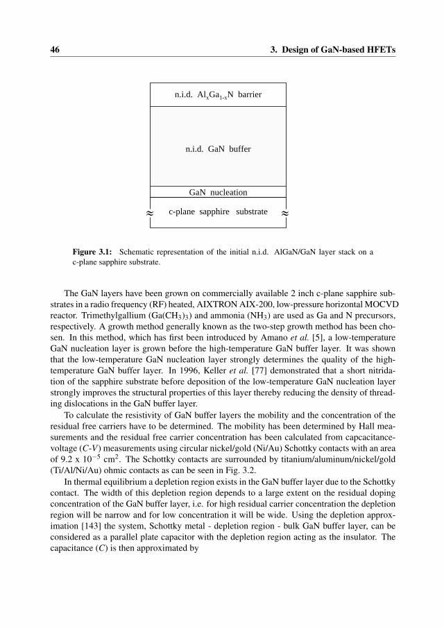
46 3. Design of GaN-based HFETs
n.i.d. GaAs
c-plane sapphire substrate
GaN nucleation
n.i.d. GaN buffer
n.i.d. AlxGa1-xN barrier
≈≈
Figure 3.1: Schematic representation of the initial n.i.d. AlGaN/GaN layer stack on ac-plane sapphire substrate.
The GaN layers have been grown on commercially available 2 inch c-plane sapphire sub-strates in a radio frequency (RF) heated, AIXTRON AIX-200, low-pressure horizontal MOCVDreactor. Trimethylgallium (Ga(CH3)3) and ammonia (NH3) are used as Ga and N precursors,respectively. A growth method generally known as the two-step growth method has been cho-sen. In this method, which has first been introduced by Amano et al. [5], a low-temperatureGaN nucleation layer is grown before the high-temperature GaN buffer layer. It was shownthat the low-temperature GaN nucleation layer strongly determines the quality of the high-temperature GaN buffer layer. In 1996, Keller et al. [77] demonstrated that a short nitrida-tion of the sapphire substrate before deposition of the low-temperature GaN nucleation layerstrongly improves the structural properties of this layer thereby reducing the density of thread-ing dislocations in the GaN buffer layer.
To calculate the resistivity of GaN buffer layers the mobility and the concentration of theresidual free carriers have to be determined. The mobility has been determined by Hall mea-surements and the residual free carrier concentration has been calculated from capcacitance-voltage (C-V) measurements using circular nickel/gold (Ni/Au) Schottky contacts with an areaof 9.2 x 10⁻⁵ cm2. The Schottky contacts are surrounded by titanium/aluminum/nickel/gold(Ti/Al/Ni/Au) ohmic contacts as can be seen in Fig. 3.2.
In thermal equilibrium a depletion region exists in the GaN buffer layer due to the Schottkycontact. The width of this depletion region depends to a large extent on the residual dopingconcentration of the GaN buffer layer, i.e. for high residual carrier concentration the depletionregion will be narrow and for low concentration it will be wide. Using the depletion approx-imation [143] the system, Schottky metal - depletion region - bulk GaN buffer layer, can beconsidered as a parallel plate capacitor with the depletion region acting as the insulator. Thecapacitance (C) is then approximated by

3.1 Epitaxial device design 47
Schottky contact
ohmic contact
Figure 3.2: Circular Ni/Au Schottky contacts with an area of 9.2 x 10⁻⁵ cm2 used for (C-V) measurements. The Schottky contacts are surrounded by (Ti/Al/Ni/Au) ohmic contacts.
C =ε0εrA
W, (3.2)
where ε0 is the permittivity of free space, εr is the relative permittivity of the GaN buffer layer,A is the area of the Schottky contact, and W is the width of the depletion region. The latter isgiven by
W =
√2ε0εr
qND(Vbi−VR), (3.3)
where q is the elementary charge, ND is the concentration of completely ionized donor atoms,Vbi is the built-in voltage, and VR is the applied reverse bias. Combining Eqns. 3.2 and 3.3yields
C =A√
2(Vbi−VR)qNDε0εr
. (3.4)
This equation can be inverted and squared to obtain
1C2 =
2(Vbi−VR)qNDε0εrA2 , (3.5)
which describes the dependency of the capacitance (C) on the applied reverse bias (VR). Aplot of 1/C2 versus VR yields a straight line with a slope that is inversely proportional to ND.After a derivation of Eq. 3.5 with respect to VR, ND is given by
ND =−2
qε0εrA2d(
1C2
)dVR
. (3.6)

48 3. Design of GaN-based HFETs
0.0
2.0
4.0
6.0
8.0
10.0
12.0
14.0
16.0
0.0 1.0 2.0 3.0 4.0
Reverse voltage, V R (V)
Cap
acita
nce,
C
(pF
)
N D = 2 × 1017 cm-3
N D = 5 × 1016 cm-3
0.0E+00
4.0E+22
8.0E+22
1.2E+23
1.6E+23
2.0E+23
-1.0 0.0 1.0 2.0 3.0 4.0
Reverse voltage, V R (V)
C-2,
(F-2)
|V bi|N D = 2 × 1017 cm-3
N D = 5 × 1016 cm-3
Figure 3.3: Typical (C-V) profiles of our first GaN buffer layers on sapphire (left) and thecorresponding (1/C2-VR) plots (right).
Using this equation we can calculate the residual free carrier concentration in the GaN bufferlayer once we have measured the (C-V) profile. To do this an alternating current (ac) capac-itance bridge can be used. The amplitude of the ac test signal used must be much smallerthan the applied DC bias voltage in order not to significantly influence the width of the deple-tion layer and the corresponding capacitance value. A difficulty in obtaining the (C-V) profilecan be caused by the presence of electron traps in the GaN buffer layer. These traps may befilled and depleted in response to the ac signal which influences the measurement results. Tominimize these effects (C-V) measurements must be performed at a frequency, typically largerthan 100 kHz, where the traps cannot follow the ac signal [143]. We have performed (C-V)measurements using a HP4275A multi-frequency LCR meter at a frequency of 1 MHz. Fig-ure 3.3-(left) shows typical (C-V) profiles of our first GaN buffer layers that were grown usinga GaN nucleation layer deposited at 525 oC followed by a thick (1 µm) GaN layer depositedat 1170 oC using hydrogen as carrier gas throughout the process. Figure 3.3-(right) shows thecorresponding (1/C2-VR) plots from which the residual free carrier concentrations have beencalculated.
Hall measurement results of these GaN buffer layers showed mobility values ranging from300 - 500 cm2/Vs. Together with the residual free carrier concentrations in the range of 5 x1016 cm−3 - 2 x 1017 cm−3 this results in resistivity values ranging from 0.06 Ωcm - 0.4 Ωcm.It is obvious that these low resistivity values make these buffer layers unsuitable for applicationin an actual device.
In an attempt to decrease the residual electron concentration and thereby increasing theresistivity of the high-temperature GaN buffer layer, the growth procedure has been changedin the following way. The low-temperature GaN nucleation layer has been replaced by a layerconsisting of selectively grown GaN islands realized by an in-situ grown SixNy, hereafterSiN, mask [52]. The in-situ deposition of the SiN mask starts directly after nitridation ofthe sapphire substrate at 1170 oC by mixing silane (SiH4) to the ammonia (NH3) flow. Aftercooling down to 525 oC a 30 nm standard low-temperature GaN layer is deposited on the SiNlayer. During heating up the SiN/GaN layers to the growth temperature of the high-temperature
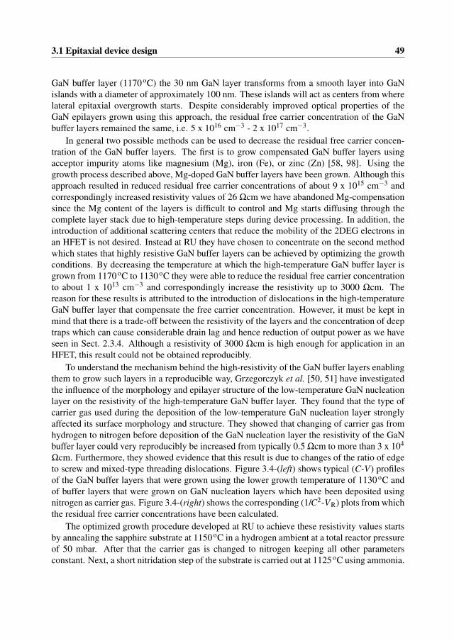
3.1 Epitaxial device design 49
GaN buffer layer (1170 oC) the 30 nm GaN layer transforms from a smooth layer into GaNislands with a diameter of approximately 100 nm. These islands will act as centers from wherelateral epitaxial overgrowth starts. Despite considerably improved optical properties of theGaN epilayers grown using this approach, the residual free carrier concentration of the GaNbuffer layers remained the same, i.e. 5 x 1016 cm−3 - 2 x 1017 cm−3.
In general two possible methods can be used to decrease the residual free carrier concen-tration of the GaN buffer layers. The first is to grow compensated GaN buffer layers usingacceptor impurity atoms like magnesium (Mg), iron (Fe), or zinc (Zn) [58, 98]. Using thegrowth process described above, Mg-doped GaN buffer layers have been grown. Although thisapproach resulted in reduced residual free carrier concentrations of about 9 x 1015 cm−3 andcorrespondingly increased resistivity values of 26 Ωcm we have abandoned Mg-compensationsince the Mg content of the layers is difficult to control and Mg starts diffusing through thecomplete layer stack due to high-temperature steps during device processing. In addition, theintroduction of additional scattering centers that reduce the mobility of the 2DEG electrons inan HFET is not desired. Instead at RU they have chosen to concentrate on the second methodwhich states that highly resistive GaN buffer layers can be achieved by optimizing the growthconditions. By decreasing the temperature at which the high-temperature GaN buffer layer isgrown from 1170 oC to 1130 oC they were able to reduce the residual free carrier concentrationto about 1 x 1013 cm−3 and correspondingly increase the resistivity up to 3000 Ωcm. Thereason for these results is attributed to the introduction of dislocations in the high-temperatureGaN buffer layer that compensate the free carrier concentration. However, it must be kept inmind that there is a trade-off between the resistivity of the layers and the concentration of deeptraps which can cause considerable drain lag and hence reduction of output power as we haveseen in Sect. 2.3.4. Although a resistivity of 3000 Ωcm is high enough for application in anHFET, this result could not be obtained reproducibly.
To understand the mechanism behind the high-resistivity of the GaN buffer layers enablingthem to grow such layers in a reproducible way, Grzegorczyk et al. [50, 51] have investigatedthe influence of the morphology and epilayer structure of the low-temperature GaN nucleationlayer on the resistivity of the high-temperature GaN buffer layer. They found that the type ofcarrier gas used during the deposition of the low-temperature GaN nucleation layer stronglyaffected its surface morphology and structure. They showed that changing of carrier gas fromhydrogen to nitrogen before deposition of the GaN nucleation layer the resistivity of the GaNbuffer layer could very reproducibly be increased from typically 0.5 Ωcm to more than 3 x 10⁴
Ωcm. Furthermore, they showed evidence that this result is due to changes of the ratio of edgeto screw and mixed-type threading dislocations. Figure 3.4-(left) shows typical (C-V) profilesof the GaN buffer layers that were grown using the lower growth temperature of 1130 oC andof buffer layers that were grown on GaN nucleation layers which have been deposited usingnitrogen as carrier gas. Figure 3.4-(right) shows the corresponding (1/C2-VR) plots from whichthe residual free carrier concentrations have been calculated.
The optimized growth procedure developed at RU to achieve these resistivity values startsby annealing the sapphire substrate at 1150 oC in a hydrogen ambient at a total reactor pressureof 50 mbar. After that the carrier gas is changed to nitrogen keeping all other parametersconstant. Next, a short nitridation step of the substrate is carried out at 1125 oC using ammonia.
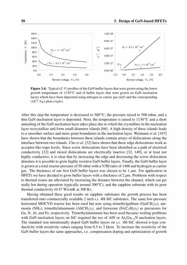
50 3. Design of GaN-based HFETs
0.0
20.0
40.0
60.0
80.0
100.0
120.0
140.0
160.0
0.0 1.0 2.0 3.0 4.0
Reverse voltage, V R (V)
Cap
acita
nce,
C
(fF
)
N D = 1 × 1013 cm-3
N D = 8.3 × 1011 cm-3
0.0E+00
2.0E+27
4.0E+27
6.0E+27
8.0E+27
1.0E+28
-1.0 0.0 1.0 2.0 3.0 4.0
Reverse voltage, V R (V)
C-2,
(F-2)
|V bi|
N D = 8.3 × 1011 cm-3
N D = 1 × 1013 cm-3
Figure 3.4: Typical (C-V) profiles of the GaN buffer layers that were grown using the lowergrowth temperature of 1130 oC and of buffer layers that were grown on GaN nucleationlayers which have been deposited using nitrogen as carrier gas (left) and the corresponding(1/C2-VR) plots (right).
After this step the temperature is decreased to 560 oC, the pressure raised to 500 mbar, and athin GaN nucleation layer is deposited. Next, the temperature is raised to 1130 oC and a shortannealing of the GaN nucleation layer takes place due to which the crystallites in the nucleationlayer recrystallize and form small-diameter islands [66]. A high density of these islands leadsto a smoother surface and more grain boundaries in the nucleation layer. Weimann et al. [167]have shown that the boundaries between these islands contain arrays of dislocations along theinterface between two islands. Cho et al. [32] have shown that these edge dislocations work asacceptor-like traps levels. Since screw dislocations have been identified as a path of electricalconductivity [32] and mixed dislocations are electrically inactive [32, 149], or at least nothighly conductive, it is clear that by increasing the edge and decreasing the screw dislocationdensities it is possible to grow highly resistive GaN buffer layers. Finally, the GaN buffer layeris grown at a total reactor pressure of 50 mbar with a V/III ratio of 1400 and hydrogen as carriergas. The thickness of our first GaN buffer layers was chosen to be 1 µm. For application inHFETs we have decided to grow buffer layers with a thickness of 2 µm. Problems with respectto thermal issues are alleviated by increasing the distance between the channel, which can getreally hot during operation (typically around 300 oC), and the sapphire substrate with its poorthermal conductivity (0.47 W/cmK at 300 K).
Having obtained these good results on sapphire substrates the growth process has beentransferred onto commercially available 2 inch s.i. 4H-SiC substrates. The same low-pressurehorizontal MOCVD reactor has been used but now using trimethylgallium (Ga(CH3)3), am-monia (NH3), trimethylaluminum (Al(CH3)3), and ferrocene (Fe(C5H5)2) as precursors forGa, N, Al, and Fe, respectively. Trimethylaluminum has been used because wetting problemswith GaN nucleation layers on SiC required the use of AlN or AlxGa1-xN nucleation layers.The standard non-intentionally doped GaN buffer layers on s.i. 4H-SiC showed n-type con-ductivity with resistivity values ranging from 0.5 to 3 Ωcm. To increase the resistivity of theGaN buffer layers the same approaches, i.e. compensation doping and optimization of growth
3.1 Epitaxial device design 51
conditions, have been used as for the GaN buffer layers grown on sapphire. Pyrolyzationof the metalorganic ferrocene has been used to investigate compensation doping of the GaNbuffer layers with Fe as this has been proposed to be an effective way to control their resistiv-ity [23, 57]. Rudzinski et al. [146] have been able to show that both the compensation dopingand non-compensation doping approaches can be used to grow highly resistive GaN bufferlayers on s.i. SiC substrates. Typical resistivity values for GaN buffer layers on Fe-doped andnon-compensation doped GaN buffer layers on s.i. 4H-SiC exceed 104 Ωcm. Due to the ex-cellent thermal conductivity of SiC substrates (3.7 - 4.5 W/cmK at 300 K) it is not necessaryto grow buffer layers with a thickness of 2 µm as in the case of sapphire substrates. There-fore, in the case of SiC substrates the choice has been made to grow GaN buffer layers witha thickness of 1 µm in order to keep the active part of the device at a safe distance from thehigher-defect-density material near the substrate interface.
3.1.4 AlGaN barrier layer
The final step towards the realization of the initial AlGaN/GaN layer stack as proposed inSect. 3.1.2 is the development of the n.i.d. AlGaN barrier layer. In Sect. 2.3.3 it has beenshown that the growth of a tensile strained AlGaN barrier layer with an aluminum contenthigher than 20% is required to achieve a 2DEG with a sheet carrier density (ns) larger than 1x 1013 cm−2 without any additional doping of the AlGaN layer. The optimization described inthis section is done baring in mind the requirements for achieving optimal device performancementioned in Sect. 3.1.1. For detailed information on the actual growth procedure we refer tothe PhD theses of Andrzej Grzegorczyk (sapphire) [50] and Mariusz Rudzinski (s.i. SiC) [146].Furthermore, we will discuss electrical characterization results of the first and optimized n.i.d.AlGaN/GaN layers obtained by reverse I-V and C-V measurements.
As starting point for the optimization of the AlGaN barrier we have used the optimizedGaN buffer layers grown on commercially available 2 inch c-plane sapphire substrates. Westarted with AlGaN barrier layers with a thickness of 20 nm and a targeted aluminum contentof about 30%. Experiments have been done with different growth temperatures, different alu-minum flows and different total reactor pressures during the growth of the AlGaN layer. Asmentioned in Sect. 3.1.3 the optimized growth conditions for our high-resistivity GaN layersinclude a total reactor pressure of 50 mbar so it has been tried to grow the AlGaN layer atthe same pressure in order to facilitate a simple transition during growth from GaN to AlGaN.Grzegorczyk et al. [50] noticed a very strong dependence of the aluminum content of the Al-GaN layers on the pressure in the reactor. At 50 mbar, a maximum aluminum content of about19% can be achieved. By decreasing the pressure to 35 mbar, they managed to grow layerswith an aluminum content higher then 60%. Additionally, the growth rate of the AlGaN layerincreased from less than 0.1 µm/h to 0.6 µm/h. The reproducibility of the aluminum contentin AlGaN layers is a very important aspect in device development. To accurately determinethe aluminum content of thin (20 - 30 nm) AlGaN layers photoluminescence should be usedsince Raman spectroscopy and X-ray measurements require layer thicknesses of at least 0.3µm. As we have seen in Sect. 2.3.3, the thickness of the tensile strained AlGaN barrier layeralso influences the magnitude of the sheet carrier concentration. Furthermore, the sharpness

52 3. Design of GaN-based HFETs
Table 3.1: Summary of the intended thicknesses of the AlGaN barriers and aluminumcontents of structures S1 to S4.
Structure S1 S2 S3 S4
AlGaN thickness (nm) 15 20 20 20Aluminum content (%) 20 25 20 25
0.0
10.0
20.0
30.0
40.0
50.0
60.0
-12.0 -10.0 -8.0 -6.0 -4.0 -2.0 0.0 2.0 4.0
Applied bias , V (V)
Cap
acita
nce
C ,
(pF)
zt
S2
S3
S4
S1
Figure 3.5: Typical (C-V) profiles of our first (S1 and S2), nearly optimized (S3), andoptimized (S4) n.i.d. AlGaN/GaN layers on sapphire substrates.
and smoothness of the interface between the AlGaN barrier and GaN buffer layers is criticalfor the mobility and confinement of the 2DEG electrons.
(C-V) measurements using the Schottky contacts mentioned before have been done to de-termine the thickness of the AlGaN barrier, the 2DEG sheet carrier density (ns) , and theresidual carrier concentration of the GaN buffer layer. Reverse (I-V) measurements usingthese contacts have been done to determine the leakage currents of the different layer stacks.Figure 3.5 shows typical (C-V) profiles of our first (S1 and S2), nearly optimized (S3), andoptimized (S4) AlGaN/GaN layers on sapphire substrates. Table 3.1 shows a summary of theintended thicknesses of the AlGaN barriers and aluminum contents of structures S1 to S4.
Looking at Fig. 3.5 it can be concluded that the 2DEG concentration of structure S1 must
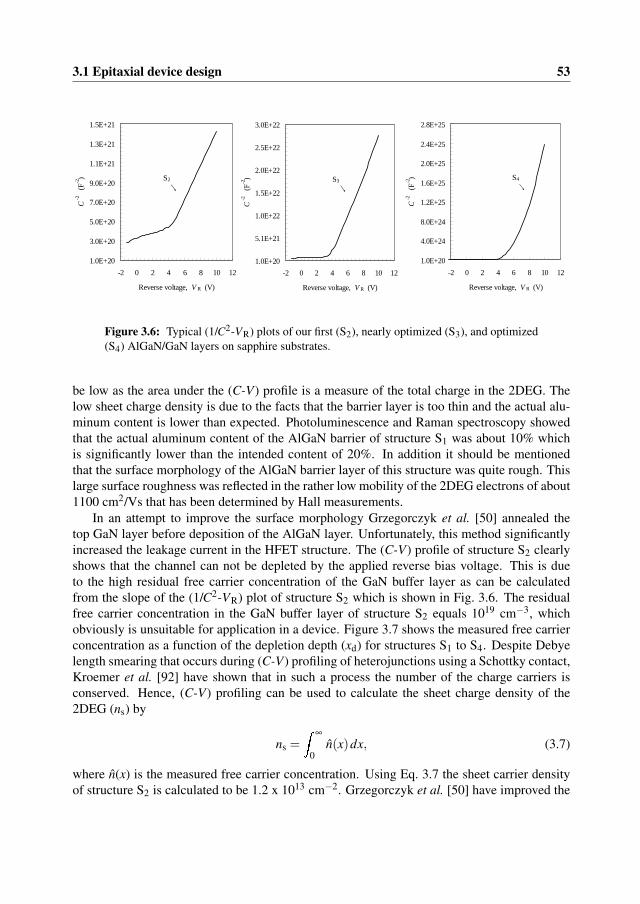
3.1 Epitaxial device design 53
1.0E+20
4.0E+24
8.0E+24
1.2E+25
1.6E+25
2.0E+25
2.4E+25
2.8E+25
-2 0 2 4 6 8 10 12
Reverse voltage, V R (V)
C-2
(F-2) S4
1.0E+20
5.1E+21
1.0E+22
1.5E+22
2.0E+22
2.5E+22
3.0E+22
-2 0 2 4 6 8 10 12
Reverse voltage, V R (V)
C-2
(F-2) S3
1.0E+20
3.0E+20
5.0E+20
7.0E+20
9.0E+20
1.1E+21
1.3E+21
1.5E+21
-2 0 2 4 6 8 10 12
Reverse voltage, V R (V)
C-2
(F-2) S2
Figure 3.6: Typical (1/C2-VR) plots of our first (S2), nearly optimized (S3), and optimized(S4) AlGaN/GaN layers on sapphire substrates.
be low as the area under the (C-V) profile is a measure of the total charge in the 2DEG. Thelow sheet charge density is due to the facts that the barrier layer is too thin and the actual alu-minum content is lower than expected. Photoluminescence and Raman spectroscopy showedthat the actual aluminum content of the AlGaN barrier of structure S1 was about 10% whichis significantly lower than the intended content of 20%. In addition it should be mentionedthat the surface morphology of the AlGaN barrier layer of this structure was quite rough. Thislarge surface roughness was reflected in the rather low mobility of the 2DEG electrons of about1100 cm2/Vs that has been determined by Hall measurements.
In an attempt to improve the surface morphology Grzegorczyk et al. [50] annealed thetop GaN layer before deposition of the AlGaN layer. Unfortunately, this method significantlyincreased the leakage current in the HFET structure. The (C-V) profile of structure S2 clearlyshows that the channel can not be depleted by the applied reverse bias voltage. This is dueto the high residual free carrier concentration of the GaN buffer layer as can be calculatedfrom the slope of the (1/C2-VR) plot of structure S2 which is shown in Fig. 3.6. The residualfree carrier concentration in the GaN buffer layer of structure S2 equals 1019 cm−3, whichobviously is unsuitable for application in a device. Figure 3.7 shows the measured free carrierconcentration as a function of the depletion depth (xd) for structures S1 to S4. Despite Debyelength smearing that occurs during (C-V) profiling of heterojunctions using a Schottky contact,Kroemer et al. [92] have shown that in such a process the number of the charge carriers isconserved. Hence, (C-V) profiling can be used to calculate the sheet charge density of the2DEG (ns) by
ns =Z
∞
0n(x)dx, (3.7)
where n(x) is the measured free carrier concentration. Using Eq. 3.7 the sheet carrier densityof structure S2 is calculated to be 1.2 x 1013 cm−2. Grzegorczyk et al. [50] have improved the
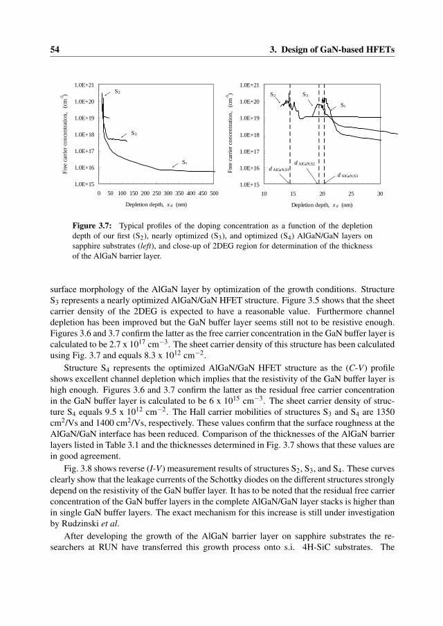
54 3. Design of GaN-based HFETs
1.0E+15
1.0E+16
1.0E+17
1.0E+18
1.0E+19
1.0E+20
1.0E+21
0 50 100 150 200 250 300 350 400 450 500
Depletion depth, x d (nm)
Free
car
rier c
once
ntra
tion,
(c
m-3) S2
S3
S4
1.0E+15
1.0E+16
1.0E+17
1.0E+18
1.0E+19
1.0E+20
1.0E+21
10 15 20 25 30
Depletion depth, x d (nm)
Fre
e ca
rrier
con
cent
ratio
n,
(cm
-3) S2 S3
S4
d AlGaN,S1d AlGaN,S2
d AlGaN,S3
Figure 3.7: Typical profiles of the doping concentration as a function of the depletiondepth of our first (S2), nearly optimized (S3), and optimized (S4) AlGaN/GaN layers onsapphire substrates (left), and close-up of 2DEG region for determination of the thicknessof the AlGaN barrier layer.
surface morphology of the AlGaN layer by optimization of the growth conditions. StructureS3 represents a nearly optimized AlGaN/GaN HFET structure. Figure 3.5 shows that the sheetcarrier density of the 2DEG is expected to have a reasonable value. Furthermore channeldepletion has been improved but the GaN buffer layer seems still not to be resistive enough.Figures 3.6 and 3.7 confirm the latter as the free carrier concentration in the GaN buffer layer iscalculated to be 2.7 x 1017 cm−3. The sheet carrier density of this structure has been calculatedusing Fig. 3.7 and equals 8.3 x 1012 cm−2.
Structure S4 represents the optimized AlGaN/GaN HFET structure as the (C-V) profileshows excellent channel depletion which implies that the resistivity of the GaN buffer layer ishigh enough. Figures 3.6 and 3.7 confirm the latter as the residual free carrier concentrationin the GaN buffer layer is calculated to be 6 x 1015 cm−3. The sheet carrier density of struc-ture S4 equals 9.5 x 1012 cm−2. The Hall carrier mobilities of structures S3 and S4 are 1350cm2/Vs and 1400 cm2/Vs, respectively. These values confirm that the surface roughness at theAlGaN/GaN interface has been reduced. Comparison of the thicknesses of the AlGaN barrierlayers listed in Table 3.1 and the thicknesses determined in Fig. 3.7 shows that these values arein good agreement.
Fig. 3.8 shows reverse (I-V) measurement results of structures S2, S3, and S4. These curvesclearly show that the leakage currents of the Schottky diodes on the different structures stronglydepend on the resistivity of the GaN buffer layer. It has to be noted that the residual free carrierconcentration of the GaN buffer layers in the complete AlGaN/GaN layer stacks is higher thanin single GaN buffer layers. The exact mechanism for this increase is still under investigationby Rudzinski et al.
After developing the growth of the AlGaN barrier layer on sapphire substrates the re-searchers at RUN have transferred this growth process onto s.i. 4H-SiC substrates. The

3.1 Epitaxial device design 55
1.0E-08
1.0E-07
1.0E-06
1.0E-05
1.0E-04
1.0E-03
1.0E-02
-50 -40 -30 -20 -10 0
Applied bias, V (V)
Rev
erse
cur
rent
, I
R (A
)ii
S4
S3
S2
Figure 3.8: Typical reverse (I-V) characteristics of Schottky diodes on our first (S2), nearlyoptimized (S3), and optimized (S4) AlGaN/GaN layers on sapphire substrates.
same development sequence of growth and characterization has been carried out. Rudzinski etal. [146] managed to grow n.i.d. AlGaN barrier layers with a thickness of 30 nm, an aluminumcontent between 25% and 30%, and a very smooth surface morphology. The resulting Hallmobility of the 2DEG electrons varied between 1300 cm2/Vs and 1500 cm2/Vs. By inserting avery thin, typically 1 nm AlN layer between the GaN buffer layer and AlGaN barrier layer theysucceeded in improving the Hall mobility to values between 1700 cm2/Vs and 1900 cm2/Vsat room temperature. The very thin AlN layer not only improved the carrier mobility due toreduced alloy scattering at the heterojunction but also improved the confinement of the 2DEGas a result of the increased discontinuity in the conduction band. The residual free carrier con-centration of the GaN buffer layers was low, typically 3.5 x 1013 cm−3, which resulted in verylow leakage currents, typically 1 x 10⁻⁷ A. The latter enables a high breakdown voltage (VBD)which is one of the necessary conditions to realize high output powers as has been discussedin Sect. 2.3.4.
3.1.5 Complete AlGaN/GaN epitaxial layer stack
For the fabrication of small and large gate periphery microwave high-power HFETs we haveused n.i.d. AlGaN/GaN epilayers on s.i. 4H-SiC substrates. Table 3.2 provides an overviewof the thicknesses of the GaN and AlGaN layers, the aluminum content of the latter, the sheetresistance (Rsheet), the 2DEG sheet carrier density, and the Hall mobility of the 2DEG electronsfor the different layer stacks. Wafer 1203 is the only structure with an Fe-doped GaN bufferlayer. The Fe doping concentration in the first 0.3 µm of this layer is 5 x 1018 cm−3. In

56 3. Design of GaN-based HFETs
Table 3.2: Overview of the n.i.d. AlGaN/GaN epilayers on s.i. 4H-SiC substrates.
Wafer Layer stack dGaN Fe dAlGaN Al Rsheet ns µ(µm) (nm) (%) (Ω/sq.) (cm−2) (cm2/Vs)
1200 AlGaN/AlN/GaN 1.2 no 30 26 350 9.5 x 10¹² 18751201 AlGaN/GaN 1.2 no 30 26 440 9.3 x 10¹² 15151203 AlGaN/GaN:Fe 1.4 yes 30 26 530 8.8 x 10¹² 1352
350 µm s.i. 4H-SiC substrate
50 nm n.i.d. Al0.2Ga0.8N nucleation
1.1 µm n.i.d. GaN buffer
30 nm n.i.d. Al0.26Ga0.74N barrier
≈≈
0.3 µm Fe-doped 5×1018 cm-3
GaN
1 - 2 nm n.i.d. AlN
350 µm s.i. 4H-SiC substrate
10 nm n.i.d. AlN nucleation
≈≈
1.2 µm n.i.d. GaN buffer
30 nm n.i.d. Al0.26Ga0.74N barrier
Figure 3.9: Schematic overviews of the completely n.i.d. AlGaN/GaN epilayers on s.i.4H-SiC (left) and of the structure with the Fe compensation doped GaN buffer layer (right).
addition, the nucleation layer of this structure is a 50 nm AlGaN layer with an aluminumcontent of 20%. In the case of the completely n.i.d. structures the nucleation layer is a 10nm AlN layer. Figure 3.9 shows schematic overviews of the completely n.i.d. AlGaN/GaNepilayers (left) and the structure with the Fe compensation doped GaN buffer layer (right).
3.2 Device layout and process flows
The next step towards the realization of microwave high-power AlGaN/GaN HFETs is thedesign of a suitable device layout. We will describe the key aspects that have led to the designof mask sets for both small and large periphery devices. Furthermore we will present schematicoverviews of the process flows whose detailed descriptions are given in Appendix A.

3.2 Device layout and process flows 57
3.2.1 Mask layoutWe have designed layouts for both small and large gate periphery devices. For short loop ex-periments where fast feedback is very desirable as they are performed for process developmentand optimization, we have used small gate periphery devices. The gates of these devices have atotal width (Wg) of 80 µm and consist of two parallel gate fingers with a unit gate width (Wgu)of 40 µm. The mask set for these small devices consists of the following steps:
1. device isolation by mesa etching,
2. formation of ohmic contacts,
3. formation of Schottky contacts and ground-signal-ground (GSG) probe pads, and
4. etching of openings in the silicon nitride passivation layer (optional).
The gates of these devices are defined using optical contact lithography and have a gate length(Lg) of 2 µm. In the remainder of this thesis, devices with such long gates are referred to as“fat gate” devices. Usually, device isolation is done after ohmic contact formation. We haveinvestigated the influence of mesa etching on leakage currents of AlGaN/GaN devices andfound that the leakage current levels can significantly be reduced if mesa etching is done asthe first step in the process flow. The details of this investigation have been described in thethesis of B. Jacobs [67]. As our process flow starts with mesa isolation, the mask set used forprocessing small fat gate devices is called the “Inverse Mesa” mask.
Using the Inverse Mesa mask set, devices can be made with a drain-source spacing (Lds) of10 µm. As the fat gates are placed in the middle of this gap the gate-source (Lgs) and gate-drain(Lgd) spacings are equal, i.e. 4 µm. Figure 3.10-(left) shows an optical microscope picture ofa small fat gate device. The dimensions of the GSG probe pads contacting the gate, drain, andsource regions of the device are indicated. The gate-to-gate pitch (Lgg) of these devices is 60µm. Figure 3.10-(right) shows a SEM image of the active region of the same device. The unitwidth (Wgu) and Lg of the fat gates are indicated.
As we want to fabricate HFETs that can operate at microwave frequencies, e.g. X-band, wehave seen that the gate length has to be reduced to sub-micrometer values in the range of 0.25µm - 0.5 µm. To fabricate these gate lengths we have switched from optical contact lithographyto electron beam lithography (EBL), which will be discussed in more detail in Sect. 4.3. Forquick development of this process step and to suppress the influence of heating effects on thedevice results as much as possible we have designed a mask set based on the Inverse Mesaprinciple. This mask set is called “Submu” referring to the sub-micrometer length of the gatecontacts. In this layout the source-drain spacing is reduced to lower the drain-source resistance(Rds) and the sub-micrometer gates are placed closer to the source than to the drain contact. Thelatter has been done for two reasons. First to increase the speed of the device as the electronssooner start drifting through the channel at the saturated velocity (vsat) and second to maintaina high breakdown voltage, typically 80 V - 100 V, as the largest electric field exists across thedrift region in the gate-drain spacing. The internal device dimensions of the Submu mask setare: Lg = 0.25 µm, Wg = 80 µm, Wgu = 40 µm, Lgg = 60 µm, Lgs = 1 µm , Lgd = 2 µm ,and

58 3. Design of GaN-based HFETs
75 µm
60 µm75 µm
75 µm
210
µm
75 µm
75 µm
gate sourcesource
drain“Fat gate” device
Wgu Lg
Figure 3.10: Optical microscope picture of a small fat gate device showing dimensions ofGSG probe pads and gate-to-gate pitch (left) and SEM image of active region of the samedevice indicating unit width (Wgu) and length (Lg) of the fat gates (right).
Lds = 3.25 µm. Figure 3.11 shows a SEM image of the active region of a small submicron gatedevice. The strongly reduced Lds and Lg can clearly be seen. It has to be noted that the Submumask set for reference purposes contains devices, which have the same internal dimensions asthose of the Inverse Mesa mask set.
With the previously described mask sets it was only possible to fabricate small gate pe-riphery (80 µm) devices. As we want to realize actual high-power devices the total gate widthof the devices has to be increased to eventually 1 mm and beyond. To achieve this, we havedesigned a mask set named “mmTor” which refers to the fact that the design contains deviceswith gate peripheries of 1 mm and more. Key aspects that need to be considered in the designof microwave large gate periphery devices are the following:
• gate length (Lg),
• total gate width (Wg),
• unit gate width (Wgu),
• gate-to-gate pitch (Lgg),
• layout of the gate fingers,
• gate-source spacing (Lgs), and
• gate-drain spacing (Lgd).
As mentioned before, the gate length of HFETs that have to operate at X-band frequencies(8 GHz - 12.4 GHz) has to be in the range of 0.25 µm - 0.5 µm to achieve values for f Thigher than 40 GHz. In addition, a shorter gate length contributes to the increase of the drain
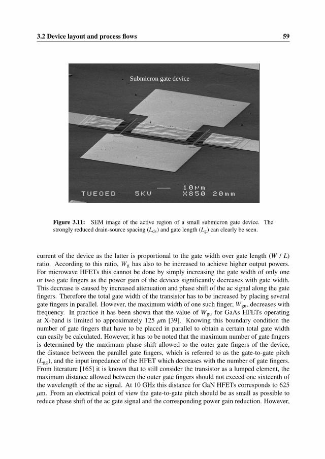
3.2 Device layout and process flows 59
Submicron gate device
Figure 3.11: SEM image of the active region of a small submicron gate device. Thestrongly reduced drain-source spacing (Lds) and gate length (Lg) can clearly be seen.
current of the device as the latter is proportional to the gate width over gate length (W / L)ratio. According to this ratio, Wg has also to be increased to achieve higher output powers.For microwave HFETs this cannot be done by simply increasing the gate width of only oneor two gate fingers as the power gain of the devices significantly decreases with gate width.This decrease is caused by increased attenuation and phase shift of the ac signal along the gatefingers. Therefore the total gate width of the transistor has to be increased by placing severalgate fingers in parallel. However, the maximum width of one such finger, Wgu, decreases withfrequency. In practice it has been shown that the value of Wgu for GaAs HFETs operatingat X-band is limited to approximately 125 µm [39]. Knowing this boundary condition thenumber of gate fingers that have to be placed in parallel to obtain a certain total gate widthcan easily be calculated. However, it has to be noted that the maximum number of gate fingersis determined by the maximum phase shift allowed to the outer gate fingers of the device,the distance between the parallel gate fingers, which is referred to as the gate-to-gate pitch(Lgg), and the input impedance of the HFET which decreases with the number of gate fingers.From literature [165] it is known that to still consider the transistor as a lumped element, themaximum distance allowed between the outer gate fingers should not exceed one sixteenth ofthe wavelength of the ac signal. At 10 GHz this distance for GaN HFETs corresponds to 625µm. From an electrical point of view the gate-to-gate pitch should be as small as possible toreduce phase shift of the ac gate signal and the corresponding power gain reduction. However,
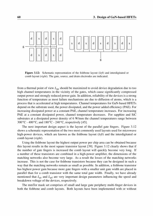
60 3. Design of GaN-based HFETs
d
d
d
d
s
s
g
d
d
s
s
d ds s s
g
d ds s
Figure 3.12: Schematic representation of the fishbone layout (left) and interdigitated orcomb layout (right). The gate, source, and drain electrodes are indicated.
from a thermal point of view Lgg should be maximized to avoid device degradation due to toohigh channel temperatures in the vicinity of the gates, which cause significantly compressedoutput power and strongly reduced power gain. In addition, reliability of the devices is a strongfunction of temperature as most failure mechanisms are due to diffusion of atoms, which is aprocess that is accelerated at high temperatures. Channel temperatures for GaN-based HFETsdepend on the substrate used, the power dissipated, and the power added efficiency (PAE). Forincreasing dissipated power at a constant PAE, channel temperature increases. For increasingPAE at a constant dissipated power, channel temperature decreases. For sapphire and SiCsubstrates at a dissipated power density of 6 W/mm the channel temperatures range between300 oC - 400 oC, and 180 oC - 240 oC, respectively [45].
The next important design aspect is the layout of the parallel gate fingers. Figure 3.12shows a schematic representation of the two most commonly used layouts used for microwavehigh-power devices, which are known as the fishbone layout (left) and the interdigitated orcomb layout (right).
Using the fishbone layout the highest output power per chip area can be obtained becausethis layout results in the most square transistor layout [39]. Figure 3.12 clearly shows that ifthe number of gate fingers is increased the comb layout will quickly become very long. Ifa number of these transistors are combined in a high-power amplifier, the dimensions of thematching networks also become very large. As a result the losses of the matching networksincrease. This is not the case for fishbone transistors because they can be designed in such away that the matching networks remain as small as possible. In addition, a fishbone transistorhas highest power gain because more gate fingers with a smaller unit gate width are placed inparallel than for a comb transistor with the same total gate width. Finally, we have alreadymentioned that Lgs and Lgd are very important design parameters influencing the speed andbreakdown voltage of the devices, respectively.
The mmTor mask set comprises of small and large gate periphery multi-finger devices inboth the fishbone and comb layouts. Both layouts have been implemented with or without
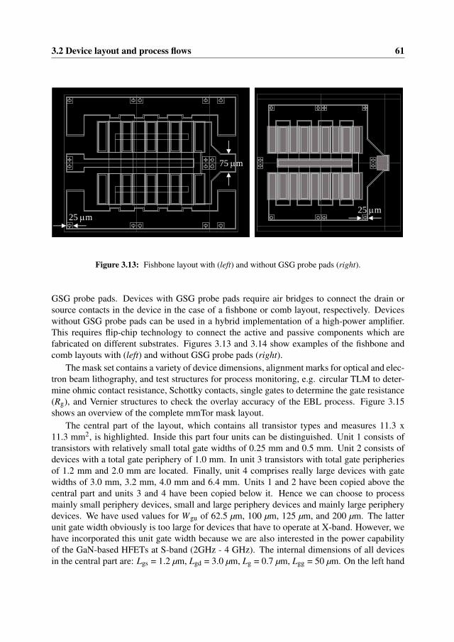
3.2 Device layout and process flows 61
75 µm
25 µm25 µm
Figure 3.13: Fishbone layout with (left) and without GSG probe pads (right).
GSG probe pads. Devices with GSG probe pads require air bridges to connect the drain orsource contacts in the device in the case of a fishbone or comb layout, respectively. Deviceswithout GSG probe pads can be used in a hybrid implementation of a high-power amplifier.This requires flip-chip technology to connect the active and passive components which arefabricated on different substrates. Figures 3.13 and 3.14 show examples of the fishbone andcomb layouts with (left) and without GSG probe pads (right).
The mask set contains a variety of device dimensions, alignment marks for optical and elec-tron beam lithography, and test structures for process monitoring, e.g. circular TLM to deter-mine ohmic contact resistance, Schottky contacts, single gates to determine the gate resistance(Rg), and Vernier structures to check the overlay accuracy of the EBL process. Figure 3.15shows an overview of the complete mmTor mask layout.
The central part of the layout, which contains all transistor types and measures 11.3 x11.3 mm2, is highlighted. Inside this part four units can be distinguished. Unit 1 consists oftransistors with relatively small total gate widths of 0.25 mm and 0.5 mm. Unit 2 consists ofdevices with a total gate periphery of 1.0 mm. In unit 3 transistors with total gate peripheriesof 1.2 mm and 2.0 mm are located. Finally, unit 4 comprises really large devices with gatewidths of 3.0 mm, 3.2 mm, 4.0 mm and 6.4 mm. Units 1 and 2 have been copied above thecentral part and units 3 and 4 have been copied below it. Hence we can choose to processmainly small periphery devices, small and large periphery devices and mainly large peripherydevices. We have used values for Wgu of 62.5 µm, 100 µm, 125 µm, and 200 µm. The latterunit gate width obviously is too large for devices that have to operate at X-band. However, wehave incorporated this unit gate width because we are also interested in the power capabilityof the GaN-based HFETs at S-band (2GHz - 4 GHz). The internal dimensions of all devicesin the central part are: Lgs = 1.2 µm, Lgd = 3.0 µm, Lg = 0.7 µm, Lgg = 50 µm. On the left hand

62 3. Design of GaN-based HFETs
75 µm
25 µm
25 µm
Figure 3.14: Comb layout with (left) and without GSG probe pads (right).
1 2
3 4
15 mm
15 mm
Figure 3.15: Overview of the complete mmTor mask layout. Highlighted is the centralpart showing the four basic units.
3.3 Conclusions 63
side of the central part we have incorporated test structures to characterize the GSG probe padsthat are used in the devices with air bridges. On the right hand side of the central part weplaced transistors with a total gate width Wg of 1.0 mm in which the value for Lgg is varied, i.e.30 µm, 40µm, 50µm, and 60 µm, to determine the trade-off between the thermal and electricalbehavior of the transistors. In this part we also incorporated devices with a total gate width of1.0 mm in which the value for Lgd is varied, i.e. 1.0 µm, 2.0 µm, 3.0 µm, 4.0 µm, and 5.0 µm,to investigate the breakdown behavior of the HFETs. In addition, we want to mention that themask is suitable for processing either using only positive resists or a combination of positiveand negative resists.
3.2.2 Process flowsFigures 3.16 and 3.17 show schematic overviews of the main steps in the process flows of theInverse Mesa and mmTor mask sets, respectively. Detailed descriptions of the process flowsfor all mask sets can be found in Appendix A.
3.3 ConclusionsIn this chapter we have focused on design aspects of microwave high-power AlGaN/GaNHFETs on both sapphire and s.i. SiC substrates. With respect to the development of theMOCVD growth process the following conclusions can be drawn:
• Optimization of the growth process of the GaN buffer layer on sapphire substrates hasshown that buffer layers with resistivities exceeding 104 Ωcm can be achieved in a con-trolled and reproducible manner if nitrogen is used as carrier gas during the depositionof the low-temperature GaN nucleation layer [50].
• GaN buffer layers on commercially available 2 inch s.i. 4H-SiC substrates with resistiv-ities also exceeding 104 Ωcm can be obtained by both compensation doping with Fe andnon-intentionally doping as has been done on sapphire substrates [146].
• The residual free carrier concentration of the GaN buffer layers was low, typically 3.5 x1013 cm−3, which resulted in very low leakage currents, typically 1 x 10⁻⁷ A. The latterare required to enable a high value for VBD, which is one of the necessary conditions torealize high microwave output power.
• Non-intentionally doped AlGaN barrier layers with a thickness of 30 nm, an aluminumcontent between 25% and 30%, and a very smooth surface morphology have been grownon s.i. 4H-SiC substrates. The sheet carrier density and Hall mobility of the 2DEGelectrons varied between 8.8 x 1012 cm−2 - 9.3 x 1012 cm−2, and 1300 cm2/Vs - 1500cm2/Vs at room temperature, respectively. By inserting a very thin, typically 1 nm, AlNlayer between the GaN buffer layer and AlGaN barrier layer these values have beenincreased to 9.5 x 1012 cm−2 - 1.0 x 1013 cm−2, and 1700 cm2/Vs - 1900 cm2/Vs.
64 3. Design of GaN-based HFETs
Sapphire / SiC substrate
GaN buffer
AlGaN barrier
2DEG
Ohmic contacts (source - drain - source)
mesa
1
6
4
5
2
3Schottky gate
Probe pad connection
SiN passivation Opening in SiN
Ti/Al/Ni/Au Ni/Au SiN
Figure 3.16: Schematic overview of the main steps in the process flow of the Inverse Mesamask set.

1
6
4
5
2
3
7 8
Ohmic contacts (source - drain - source - drain - source)
Sapphire / SiC substrate
GaN buffer
AlGaN barrier
2DEG
mesa
SiN passivation
Opening in SiN Foot gate contact
Top gate contactAir bridge Probe pad connection
Ti/Al/Ni/Au Ni/Au SiNTi/Au
Figure 3.17: Schematic overview of the main steps in the process flow of the mmTor maskset.
653.3 Conclusions
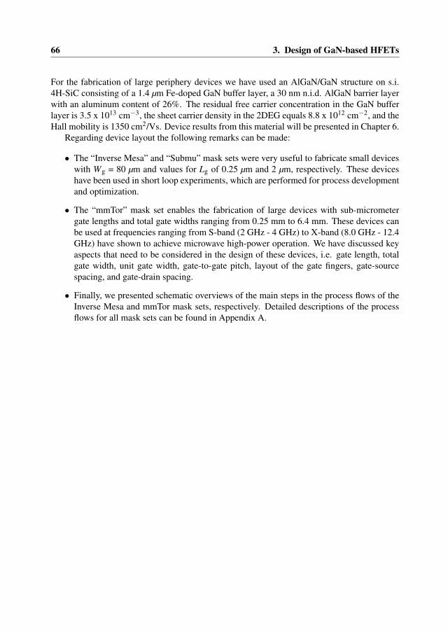
66 3. Design of GaN-based HFETs
For the fabrication of large periphery devices we have used an AlGaN/GaN structure on s.i.4H-SiC consisting of a 1.4 µm Fe-doped GaN buffer layer, a 30 nm n.i.d. AlGaN barrier layerwith an aluminum content of 26%. The residual free carrier concentration in the GaN bufferlayer is 3.5 x 1013 cm−3, the sheet carrier density in the 2DEG equals 8.8 x 1012 cm−2, and theHall mobility is 1350 cm2/Vs. Device results from this material will be presented in Chapter 6.
Regarding device layout the following remarks can be made:
• The “Inverse Mesa” and “Submu” mask sets were very useful to fabricate small deviceswith Wg = 80 µm and values for Lg of 0.25 µm and 2 µm, respectively. These deviceshave been used in short loop experiments, which are performed for process developmentand optimization.
• The “mmTor” mask set enables the fabrication of large devices with sub-micrometergate lengths and total gate widths ranging from 0.25 mm to 6.4 mm. These devices canbe used at frequencies ranging from S-band (2 GHz - 4 GHz) to X-band (8.0 GHz - 12.4GHz) have shown to achieve microwave high-power operation. We have discussed keyaspects that need to be considered in the design of these devices, i.e. gate length, totalgate width, unit gate width, gate-to-gate pitch, layout of the gate fingers, gate-sourcespacing, and gate-drain spacing.
• Finally, we presented schematic overviews of the main steps in the process flows of theInverse Mesa and mmTor mask sets, respectively. Detailed descriptions of the processflows for all mask sets can be found in Appendix A.
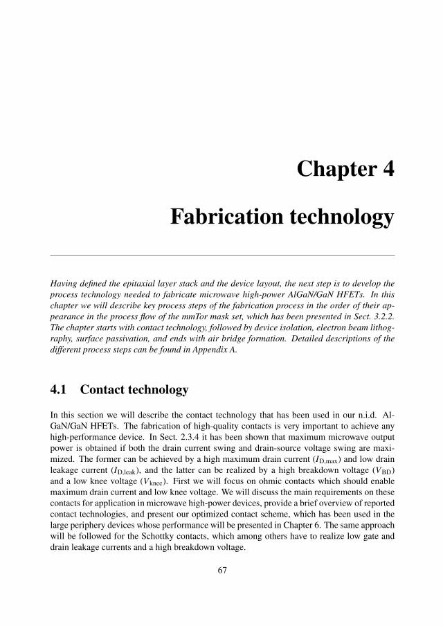
Chapter 4
Fabrication technology
Having defined the epitaxial layer stack and the device layout, the next step is to develop theprocess technology needed to fabricate microwave high-power AlGaN/GaN HFETs. In thischapter we will describe key process steps of the fabrication process in the order of their ap-pearance in the process flow of the mmTor mask set, which has been presented in Sect. 3.2.2.The chapter starts with contact technology, followed by device isolation, electron beam lithog-raphy, surface passivation, and ends with air bridge formation. Detailed descriptions of thedifferent process steps can be found in Appendix A.
4.1 Contact technology
In this section we will describe the contact technology that has been used in our n.i.d. Al-GaN/GaN HFETs. The fabrication of high-quality contacts is very important to achieve anyhigh-performance device. In Sect. 2.3.4 it has been shown that maximum microwave outputpower is obtained if both the drain current swing and drain-source voltage swing are maxi-mized. The former can be achieved by a high maximum drain current (ID,max) and low drainleakage current (ID,leak), and the latter can be realized by a high breakdown voltage (VBD)and a low knee voltage (Vknee). First we will focus on ohmic contacts which should enablemaximum drain current and low knee voltage. We will discuss the main requirements on thesecontacts for application in microwave high-power devices, provide a brief overview of reportedcontact technologies, and present our optimized contact scheme, which has been used in thelarge periphery devices whose performance will be presented in Chapter 6. The same approachwill be followed for the Schottky contacts, which among others have to realize low gate anddrain leakage currents and a high breakdown voltage.
67

68 4. Fabrication technology
4.1.1 Ohmic contactsThe first key process step, after preparing and cleaning of the sample and defining alignmentmarks for both optical and electron beam lithography (EBL), is the formation of ohmic con-tacts, which form the drain and source contacts of the HFETs. To enable high performance ofthe microwave high-power devices they have to meet the following requirements:
• lowest possible ohmic contact resistance (Rc),
• excellent line definition,
• smooth surface morphology, and
• high mechanical and thermal stability.
The lowest possible value for Rc is required to obtain ID,max, reduce the on-resistance, whichdetermines the slope of the linear region of the I-V output characteristics and hence the valueof Vknee, and to minimize the power dissipated in the ohmic contacts because of the highcurrent densities in power devices, typically 1.0 A/mm - 1.5 A/mm [8, 85, 174] for state-of-the-art AlGaN/GaN HFETs. Furthermore, to achieve high values for f T and f max the extrinsictransconductance (gm,ext), which is given by Eqn. 4.1, should be maximized.
gm,ext =gm
1+gmRs(4.1)
In Eqn. 4.1, gm is the intrinsic transconductance, and Rs is the source resistance, whichis the sum of the sheet resistance between the gate and source contacts (Rsh,gs) and Rc. FromEqn. 4.1 it is obvious that Rs should be minimized. This has to be done by decreasing the sheetand contact resistances. The latter can be minimized by choosing an appropriate metallizationscheme and optimization of the process technology used. The sheet resistance can be decreasedthrough epitaxy and design, i.e. by reducing the gate-source spacing (Lgs). It is clear that thecontacts need to have excellent line definition to position the gate very close to the sourcecontact. In addition, good line definition is required to achieve a high breakdown voltage.
Smooth surface morphology and limited thickness of the ohmic contacts is very impor-tant to avoid alignment problems in optical contact lithography due to too much topography.Finally, the contacts should be mechanically stable, i.e. they should not be scratched awayduring testing or bonding, and they should not degrade due to the high temperatures that canarise during device operation. In Sect. 3.2.1 it has been mentioned that the channel temperaturecan be between 180 oC and 400 oC depending on the substrate used.
Most ohmic contacts on AlGaN/GaN heterostructures are based on titanium / aluminum(Ti / Al) based metallization schemes. The most frequently reported are the Ti/Al/Ti/Au,Ti/Al/Ni/Au, and Ti/Al/Pt/Au schemes [27, 108, 147]. The various metals in these schemeshave their own specific role. Titanium is the first metal layer deposited on the AlGaN materialand is believed to:
• serve as an adhesion layer to provide good mechanical stability [147],

4.1 Contact technology 69
• dissolve the native oxide on the AlGaN surface [107, 147], and
• create nitrogen vacancies (VN) by reacting with nitrogen atoms in the AlGaN barrierlayer. Hence, the AlGaN material underneath the contact becomes highly doped en-abling electrons to tunnel through the remaining thin potential barrier which separatesthem from the 2DEG [108, 147].
Aluminum is supposed to:
• react with Ti to form an Al3Ti layer that prevents oxidation of the underlying Ti layer [108,147], and
• serves as a diffusion barrier for the Ni and Au layers as they form high Schottky barrierswith the AlGaN barrier layer [107].
Nickel (Ni) and platinum (Pt) layers are used to form a diffusion barrier for the gold (Au) toplayer. If this Au layer, which has been added to improve the conductivity of the metal stack,reacts with Al a highly resistive alloy is formed, which generally is called “purple plague”. Oneof the most important reasons to add metals on top of Al is to prevent this layer from smearingout. Usually the ohmic contacts are annealed at high temperatures, typically ≥ 800 oC, whichis far above the melting point of Al (660 oC at atmospheric pressure). Without the additionalNi/(Pt)/Au layers the line definition of the contacts cannot be controlled.
Instead of the formation of tunnel contacts with one of the metallization schemes men-tioned above, other techniques such as ion implantation using Si have been tried to realizeohmic contacts with low contact resistance. Yu et al. [177] have succeeded in fabricatingn.i.d. AlGaN/GaN HFETs with ion implanted nonalloyed Ti/Al/Ni/Au ohmic contacts thatshow comparable contact resistance and device performance as HFETs fabricated using con-ventional tunnel contacts. Device fabrication starts with ion implantation in the source anddrain regions because of the extremely high thermal budget of this process needed for activa-tion of the Si dopants and damage recovery of the implanted AlGaN/GaN regions. The Si ionsare implanted at a temperature of 200 oC with doses of 1.5 x 1015 cm−2 at energies of 30 keVand 60 keV, with the dopant concentration peak overlapping with the 2DEG. In order to avoidion channeling and non-intentional doping in areas outside the source and drain regions, theSi ion beam is tilted by 7 relative to the normal of the sample surface. After implantation,the activation and damage removal anneal was done at 1500 oC with 100-bar N2 overpressurefor 1 minute. As deposited Ti/Al/Ni/Au contacts showed ohmic behavior and a contact resis-tance of 0.4 Ωmm. Very important advantages of the nonalloyed ion implanted ohmic contactsare the superior line definition and surface morphology, which can strongly improve yield,reproducibility, and reliability in AlGaN/GaN HFETs [177].
Initially, we have chosen to optimize the Ti/Al/Ni/Au tunnel contact for lowest contactresistance. Detailed descriptions of this optimization process can be found in [67, 91]. The op-timized metal stack consisting of Ti/Al/Ni/Au = 30/180/40/150 nm yielded contact resistancesof 0.2 Ωmm and 0.35 Ωmm on doped and undoped AlGaN/GaN layers, respectively [68].However, these contacts show very rough surface morphology and poor line definition. These
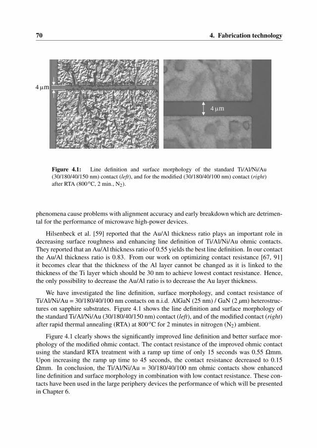
70 4. Fabrication technology
4 µm
4 µm
Figure 4.1: Line definition and surface morphology of the standard Ti/Al/Ni/Au(30/180/40/150 nm) contact (left), and for the modified (30/180/40/100 nm) contact (right)after RTA (800 oC, 2 min., N2).
phenomena cause problems with alignment accuracy and early breakdown which are detrimen-tal for the performance of microwave high-power devices.
Hilsenbeck et al. [59] reported that the Au/Al thickness ratio plays an important role indecreasing surface roughness and enhancing line definition of Ti/Al/Ni/Au ohmic contacts.They reported that an Au/Al thickness ratio of 0.55 yields the best line definition. In our contactthe Au/Al thickness ratio is 0.83. From our work on optimizing contact resistance [67, 91]it becomes clear that the thickness of the Al layer cannot be changed as it is linked to thethickness of the Ti layer which should be 30 nm to achieve lowest contact resistance. Hence,the only possibility to decrease the Au/Al ratio is to decrease the Au layer thickness.
We have investigated the line definition, surface morphology, and contact resistance ofTi/Al/Ni/Au = 30/180/40/100 nm contacts on n.i.d. AlGaN (25 nm) / GaN (2 µm) heterostruc-tures on sapphire substrates. Figure 4.1 shows the line definition and surface morphology ofthe standard Ti/Al/Ni/Au (30/180/40/150 nm) contact (left), and of the modified contact (right)after rapid thermal annealing (RTA) at 800 oC for 2 minutes in nitrogen (N2) ambient.
Figure 4.1 clearly shows the significantly improved line definition and better surface mor-phology of the modified ohmic contact. The contact resistance of the improved ohmic contactusing the standard RTA treatment with a ramp up time of only 15 seconds was 0.55 Ωmm.Upon increasing the ramp up time to 45 seconds, the contact resistance decreased to 0.15Ωmm. In conclusion, the Ti/Al/Ni/Au = 30/180/40/100 nm ohmic contacts show enhancedline definition and surface morphology in combination with low contact resistance. These con-tacts have been used in the large periphery devices the performance of which will be presentedin Chapter 6.
4.1 Contact technology 71
Table 4.1: Reported values of the work functions and barrier heights of the most commonlyused Schottky metals to n-type bulk GaN [138, 143].
Metal Work function (eV) Barrier height (eV)
Pt 5.65 1.0 - 1.2Ir 5.20 0.9 - 1.1Ni 5.15 0.66 - 0.97Pd 5.12 0.7 - 0.94Au 5.10 0.8 - 0.93
4.1.2 Schottky contactsSchottky contacts are very suitable gate electrodes for microwave devices because of theirfast switching speed, typically in the picoseconds range, between forward and reverse currenttransport. This is due to the fact that they are mainly majority carrier devices and thereforehardly suffer from time delays caused by minority carrier storage effects. For application inmicrowave high-power devices Schottky gates are required to realize:
• low gate and drain leakage currents (IG,leak and ID,leak),
• high breakdown voltage (VBD),
• good adhesion,
• good thermal stability, and
• low gate resistance (Rg).
To ensure low gate and drain leakage currents and a high breakdown voltage, the barrier heightbetween the gate metal and the AlGaN barrier layer should be as high as possible. Widebandgap materials like AlGaN and GaN suffer much less from Fermi level pinning than semi-conductors with small bandgaps like Si and GaAs. As a result, the work function of the metalapplied has a stronger influence on the Schottky barrier height. In the case of n.i.d. or n-typebulk or relaxed material, metals with high work functions are used to realize high-performanceSchottky contacts. Table 4.1 gives an overview of reported values of the work functions andbarrier heights of the most commonly used Schottky metals to n-type bulk GaN [138, 143].
The spread on the reported values of the barrier height in Table 4.1 is believed to resultfrom both the presence of several transport mechanisms and to material and process detailssuch as the defect density of the films used, local stoichiometry variations, differences in sur-face roughness, and the effectiveness of surface cleans prior to metal deposition. Table 4.1shows that the Schottky barrier height on n-type bulk GaN tends to increase with the work
72 4. Fabrication technology
function. However, Lin et al. [105] reported that the barrier height of Schottky contacts fab-ricated on strained AlGaN/GaN heterostructures shows the complete opposite behavior. Inthat case the barrier height is lower for metals with a higher work function. They explain thisin the following way. The 2DEG electrons in strained AlGaN/GaN heterostructures originatefrom donor states at the surface of the AlGaN barrier layer. As electrons in metals with lowerwork functions have higher energy, they have larger moving spaces. As a result, their elec-tron wave functions overlap more with those of the 2DEG electrons. This stronger couplinginfluences characteristics of the AlGaN surface states such as their density and energy levelsand thereby directly affects the 2DEG sheet carrier concentration. This is shown by the differ-ence between the calculated 2DEG sheet carrier concentrations using different Schottky metalsand the 2DEG sheet carrier concentration determined using Hall measurements, i.e. withouta Schottky contact, which increases as the metal work function decreases. At the same po-larization sheet charge density, barrier heights of Schottky contacts are higher because of thedecreased 2DEG sheet carrier concentration. Therefore, due to the significant influence on thecharacteristics of AlGaN surface states, the barrier heights of Schottky contacts on strainedAlGaN/GaN heterostructures are higher for lower metal work functions [105].
From the metals listed in Table 4.1 Ir and Ni have the best adhesion to AlGaN and GaN epi-layers, which is very important to avoid metal breaking off the surface during device process-ing, e.g. during lift-off. Good thermal stability of the Schottky contacts is required as the chan-nel temperature of AlGaN/GaN HFETs can get very high, typically between 180 oC and 400 oCdepending on the substrate used, the bias conditions and the power dissipated [45, 93, 97]. Theresistance of the Schottky gates (Rg) should be low as it not only determines the input impe-dance but also strongly influences the values of f max, maximum available gain (MAG), andminimum noise figure (NFmin) of the HFETs. The gate resistance can be decreased if T-shapedor so-called mushroom gates are used. We will discuss this topic into more detail in Sect. 4.3.Further reduction of the gate resistance can be achieved using copper (Cu) as contact metal.Ao et al. [11] have reported Cu gates on strained AlGaN/GaN heterostructures whose gateresistance is 40% lower than that of comparable Ni/Au Schottky gates. In addition, these Cugates show much lower leakage currents than Ni/Au contacts processed on the same material,which is attributed to the fact that the barrier height of the Cu gates is higher than that of theNi/Au gates as the work function of Cu (4.65 eV) is lower than that of Ni (5.15 eV). This is incomplete agreement with the work of Lin et al. [105].
Based on our previous studies with respect to Schottky contacts on AlGaN/GaN het-erostructures [67, 91, 170] we have chosen to use Ni/Au = 20/200 nm gates in our HFETs.The thickness of the Au layer, which has been used to enhance conductivity and prevent theoxidation of Ni, is arbitrary. Because of our choice to use AlGaN/GaN heterostructures it isdifficult to apply conventional characterization techniques such as (I-V) and (C-V) to deter-mine Schottky contact characteristics like barrier height and ideality factor. This is due tothe fact that this system consists of two back-to-back series diodes, i.e. the Schottky diodeand a diode as a result of the bandgap discontinuity at the heterojunction. Therefore we haveoptimized the Ni/Au contacts for lowest reverse current and highest breakdown voltage.
The main focus of these studies was to develop a suitable pre-metallization surface cleanto improve the performance, stability and reliability of the Ni/Au Schottky contacts. We have
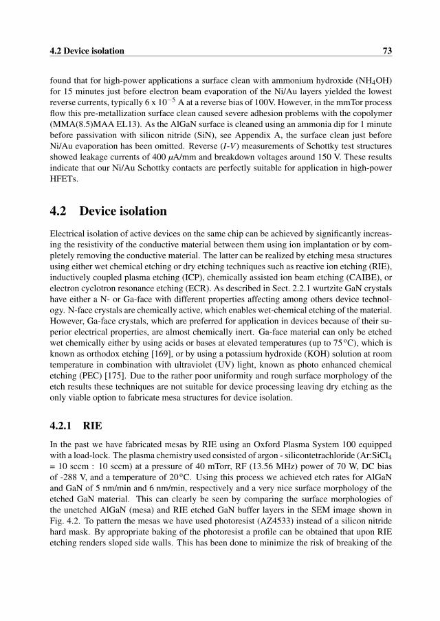
4.2 Device isolation 73
found that for high-power applications a surface clean with ammonium hydroxide (NH4OH)for 15 minutes just before electron beam evaporation of the Ni/Au layers yielded the lowestreverse currents, typically 6 x 10⁻⁵ A at a reverse bias of 100V. However, in the mmTor processflow this pre-metallization surface clean caused severe adhesion problems with the copolymer(MMA(8.5)MAA EL13). As the AlGaN surface is cleaned using an ammonia dip for 1 minutebefore passivation with silicon nitride (SiN), see Appendix A, the surface clean just beforeNi/Au evaporation has been omitted. Reverse (I-V) measurements of Schottky test structuresshowed leakage currents of 400 µA/mm and breakdown voltages around 150 V. These resultsindicate that our Ni/Au Schottky contacts are perfectly suitable for application in high-powerHFETs.
4.2 Device isolation
Electrical isolation of active devices on the same chip can be achieved by significantly increas-ing the resistivity of the conductive material between them using ion implantation or by com-pletely removing the conductive material. The latter can be realized by etching mesa structuresusing either wet chemical etching or dry etching techniques such as reactive ion etching (RIE),inductively coupled plasma etching (ICP), chemically assisted ion beam etching (CAIBE), orelectron cyclotron resonance etching (ECR). As described in Sect. 2.2.1 wurtzite GaN crystalshave either a N- or Ga-face with different properties affecting among others device technol-ogy. N-face crystals are chemically active, which enables wet-chemical etching of the material.However, Ga-face crystals, which are preferred for application in devices because of their su-perior electrical properties, are almost chemically inert. Ga-face material can only be etchedwet chemically either by using acids or bases at elevated temperatures (up to 75 oC), which isknown as orthodox etching [169], or by using a potassium hydroxide (KOH) solution at roomtemperature in combination with ultraviolet (UV) light, known as photo enhanced chemicaletching (PEC) [175]. Due to the rather poor uniformity and rough surface morphology of theetch results these techniques are not suitable for device processing leaving dry etching as theonly viable option to fabricate mesa structures for device isolation.
4.2.1 RIE
In the past we have fabricated mesas by RIE using an Oxford Plasma System 100 equippedwith a load-lock. The plasma chemistry used consisted of argon - silicontetrachloride (Ar:SiCl4= 10 sccm : 10 sccm) at a pressure of 40 mTorr, RF (13.56 MHz) power of 70 W, DC biasof -288 V, and a temperature of 20 oC. Using this process we achieved etch rates for AlGaNand GaN of 5 nm/min and 6 nm/min, respectively and a very nice surface morphology of theetched GaN material. This can clearly be seen by comparing the surface morphologies ofthe unetched AlGaN (mesa) and RIE etched GaN buffer layers in the SEM image shown inFig. 4.2. To pattern the mesas we have used photoresist (AZ4533) instead of a silicon nitridehard mask. By appropriate baking of the photoresist a profile can be obtained that upon RIEetching renders sloped side walls. This has been done to minimize the risk of breaking of the
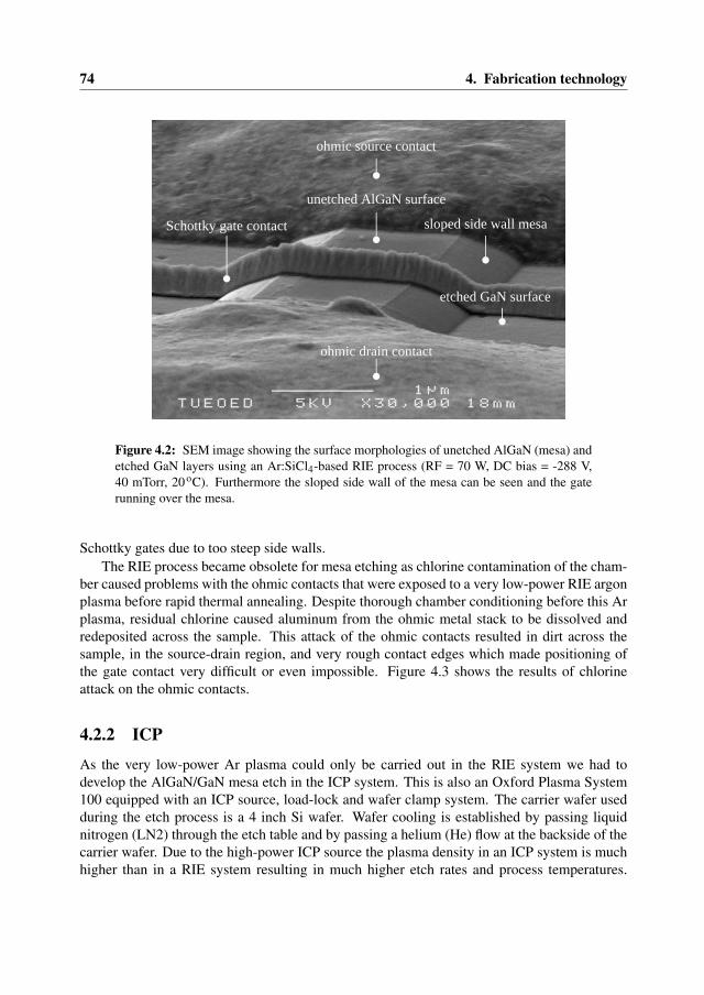
74 4. Fabrication technology
unetched AlGaN surface
sloped side wall mesaSchottky gate contact
etched GaN surface
ohmic source contact
ohmic drain contact
Figure 4.2: SEM image showing the surface morphologies of unetched AlGaN (mesa) andetched GaN layers using an Ar:SiCl4-based RIE process (RF = 70 W, DC bias = -288 V,40 mTorr, 20 oC). Furthermore the sloped side wall of the mesa can be seen and the gaterunning over the mesa.
Schottky gates due to too steep side walls.The RIE process became obsolete for mesa etching as chlorine contamination of the cham-
ber caused problems with the ohmic contacts that were exposed to a very low-power RIE argonplasma before rapid thermal annealing. Despite thorough chamber conditioning before this Arplasma, residual chlorine caused aluminum from the ohmic metal stack to be dissolved andredeposited across the sample. This attack of the ohmic contacts resulted in dirt across thesample, in the source-drain region, and very rough contact edges which made positioning ofthe gate contact very difficult or even impossible. Figure 4.3 shows the results of chlorineattack on the ohmic contacts.
4.2.2 ICP
As the very low-power Ar plasma could only be carried out in the RIE system we had todevelop the AlGaN/GaN mesa etch in the ICP system. This is also an Oxford Plasma System100 equipped with an ICP source, load-lock and wafer clamp system. The carrier wafer usedduring the etch process is a 4 inch Si wafer. Wafer cooling is established by passing liquidnitrogen (LN2) through the etch table and by passing a helium (He) flow at the backside of thecarrier wafer. Due to the high-power ICP source the plasma density in an ICP system is muchhigher than in a RIE system resulting in much higher etch rates and process temperatures.
4.2 Device isolation 75
redeposited aluminum
Al outburst
TiAlNiAu
Figure 4.3: SEM images showing the redeposition of aluminum across the sample due toresidual chlorine in the RIE process chamber (left), and aluminum outbursts at the edgesof the ohmic contacts causing difficulties with respect to the positioning of the gate contact(right).
From literature it is known that the etch rate in an ICP process is mainly determined by theICP power whereas the RF power mainly determines the surface morphology of the etchedlayers [103]. Typical power settings for ICP systems of ICP/RF = 2000/200 W, enable etchrates of several micrometers per minute which are suitable for through wafer via-hole etchingbut are completely impractical for etching AlGaN/GaN mesas with heights of 100-200 nm.In addition, the high process temperature renders photoresist useless as masking material. Aswe intend to use photoresist (AZ4533) as an etch mask to obtain sloped side walls, we hadto considerably downscale the ICP etching rate and process temperature. As a starting pointfor our experiments we have chosen the two most commonly used plasma chemistries forAlGaN/GaN ICP etching known from literature, i.e. chlorine-argon (Cl2/Ar) and chlorine-hydrogen (Cl2/H2), respectively [103, 137]. Our first experiments were carried out using Cl2: Ar = 30 sccm : 10 sccm at a pressure of 10 mTor at T = 20 oC with ICP/RF powers rangingfrom 500/50 W to 200/20 W, the latter being at the lowest power limit for obtaining a stableplasma. The resulting AlGaN/GaN etch rates ranged from 250 nm/min to 140 nm/min. It hasto be noted that we have not considered selectivity between AlGaN and GaN as we have notused a recess etch in which selectivity of AlGaN with respect to GaN is critical. The SEMimage in Fig. 4.4 shows a typical example of the surface morphology of the etched GaN bufferlayer obtained using the Cl2 /Ar chemistry.
For better process control and to achieve a smoother surface of the etched GaN layer wewanted to further decrease the etch rate. Therefore we tried the Cl2/H2 chemistry using thesame ICP/RF power sweep as mentioned before. The resulting AlGaN/GaN etch rate rangedfrom 170 nm/min to 40 nm/min. SEM images of the etched samples showed that the smoothestGaN surface is obtained using ICP/RF powers of 200/50 W (etch rate of 110 nm/min). LowerICP/RF power combinations, leading to lower etch rates (e.g. ICP/RF = 150/30 W, 40 nm/min),

76 4. Fabrication technology
Figure 4.4: SEM image showing the surface morphologies of the AlGaN/GaN mesa andthe etched GaN buffer layer using Cl2 : Ar = 30 sccm : 10 sccm, ICP/RF = 200/20 W, p =10 mTor, T = 20 oC.
result in rougher etched GaN surfaces. Figure 4.5-(left) shows the AlGaN/GaN mesa and thesurface morphology of the etched GaN layer using Cl2/H2 = 30 sccm : 10 sccm with ICP/RF= 150/30 W, p = 10 mTor, at T = 20 oC. Figure 4.5-(right) shows a typical example of the verysmooth surface morphology of the etched GaN layer using Cl2/H2 = 30 sccm : 10 sccm withICP/RF = 200/50 W, p = 10 mTor at T = 20 oC. This process is very suitable for mesa etchingand has been used in the transistor processing (see Appendix A).
Our ICP etching tool is used to etch several different materials using different gas chemistries.Hence, it was very important to isolate the AlGaN/GaN mesa etch process from these otherprocesses by creating a process window in order to achieve reproducible etch results from runto run. To achieve this, we have embedded the actual mesa etch step in a process sequenceconsisting of the following steps: chamber cleaning, chamber conditioning, mesa etching, andagain chamber cleaning. For chamber cleaning we have used an oxygen plasma (see AppendixA). To obtain a stable and reproducible AlGaN/GaN etch rate it is very important to carefullycondition the process chamber as it is significantly affected by residual oxygen from the clean-ing process. The residual oxygen enhances the ionization of chlorine and hence increases theetch rate. Chamber conditioning has been done using the process settings of the actual mesaetch process. We found out that for a stable etch rate of 110 nm/min, the chamber needs to beconditioned for more than 1 hour. As chlorine significantly etches the Si carrier wafer, whichhas to be used during this long conditioning step to protect the etch table, we have used a cyclicconditioning process to suppress excessive Si etching (see Appendix A).
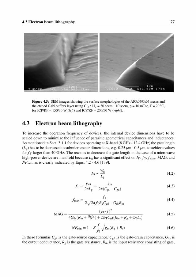
4.3 Electron beam lithography 77
Figure 4.5: SEM images showing the surface morphologies of the AlGaN/GaN mesas andthe etched GaN buffers layer using Cl2 : H2 = 30 sccm : 10 sccm, p = 10 mTor, T = 20oC,for ICP/RF = 150/30 W (left) and ICP/RF = 200/50 W (right).
4.3 Electron beam lithographyTo increase the operation frequency of devices, the internal device dimensions have to bescaled down to minimize the influence of parasitic geometrical capacitances and inductances.As mentioned in Sect. 3.1.1 for devices operating at X-band (8 GHz - 12.4 GHz) the gate length(Lg) has to be decreased to submicrometer dimensions, e.g. 0.25 µm - 0.5 µm, to achieve valuesfor f T larger than 40 GHz. The reasons to decrease the gate length in the case of a microwavehigh-power device are manifold because Lg has a significant effect on ID, f T, f max, MAG, andNFmin, as is clearly indicated by Eqns. 4.2 - 4.6 [139].
ID ∝Wg
Lg(4.2)
fT =vsat
2πLg=
gm
2π(Cgs +Cgd)(4.3)
fmax =fT
2√
2π fTRgCgd +GdsRin(4.4)
MAG =( fT/ f )2
4Gds(Rin + ωTLs2 )+2ωTCgd(Rin +Rg +ωTLs)
(4.5)
NFmin = 1+KffT
√gm(Rg +Rs) (4.6)
In these formulas Cgs is the gate-source capacitance, Cgd is the gate-drain capacitance, Gds isthe output conductance, Rg is the gate resistance, Rin is the input resistance consisting of gate,
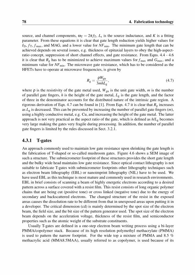
78 4. Fabrication technology
source, and channel components, ωT = 2π fT, Ls is the source inductance, and K is a fittingparameter. From these equations it is clear that gate length reduction yields higher values forID, f T, f max, and MAG, and a lower value for NFmin. The minimum gate length that can beachieved depends on several issues, e.g. thickness of epitaxial layers to obey the high-aspect-ratio concept, suppression of short channel effects, and gate resistance. From Eqns. 4.4 - 4.6it is clear that Rg has to be minimized to achieve maximum values for f max and Gmax, and aminimum value for NFmin. The microwave gate resistance, which has to be considered as theHFETs have to operate at microwave frequencies, is given by
Rg =ρWgu
3mhLg, (4.7)
where ρ is the resistivity of the gate metal used, Wgu is the unit gate width, m is the numberof parallel gate fingers, h is the height of the gate metal, Lg is the gate length, and the factorof three in the denominator accounts for the distributed nature of the intrinsic gate region. Arigorous derivation of Eqn. 4.7 can be found in [1]. From Eqn. 4.7 it is clear that Rg increasesas Lg is decreased. This can be prevented by increasing the number of parallel gate fingers (m),using a highly conductive metal, e.g. Cu, and increasing the height of the gate metal. The latterapproach is not very practical as the aspect ratio of the gate, which is defined as h/Lg becomesvery large making the gates very fragile during processing. In addition, the number of parallelgate fingers is limited by the rules discussed in Sect. 3.2.1.
4.3.1 T-gatesAn approach commonly used to maintain low gate resistance upon shrinking the gate length isthe fabrication of T-shaped or so-called mushroom gates. Figure 4.6 shows a SEM image ofsuch a structure. The submicrometer footprint of these structures provides the short gate lengthand the bulky wide head maintains low gate resistance. Since optical contact lithography is notsuitable to fabricate T-gates with submicrometer footprints other lithography techniques suchas electron beam lithography (EBL) or nanoimprint lithography (NIL) have to be used. Wehave used EBL as this technique is most mature and commonly used in research environments.EBL in brief consists of scanning a beam of highly energetic electrons according to a desiredpattern across a surface covered with a resist film. This resist consists of long organic polymerchains that are being cut (positive tone) or cross linked (negative tone) due to the energy ofsecondary and backscattered electrons. The changed structure of the resist in the exposedareas causes the dissolution rate to be different from that in unexposed areas upon putting it ina developer. The critical dimension (cd) is mainly determined by the spot size of the electronbeam, the field size, and the bit size of the pattern generator used. The spot size of the electronbeam depends on the acceleration voltage, thickness of the resist film, and semiconductorproperties such as the atomic weight of the substrate constituents.
Usually T-gates are defined in a one-step electron beam writing process using a bi-layerPMMA/copolymer stack. Because of its high resolution polymethyl methacrylate (PMMA)is used to pattern the narrow footprint. For the wide top a mixture of PMMA and 8.5 %methacrylic acid (MMA8.5MAA), usually referred to as copolymer, is used because of its

4.3 Electron beam lithography 79
Figure 4.6: SEM image of a T-gate structure. Note the narrow footprint (197 nm) and thewide top. Courtesy of Dr. G. Schmidt, Universität Würzburg, Germany.
higher sensitivity to the electron beam. This difference in sensitivity is required for the one-step process in which the top is written with a much lower electron dose than the footprint,which has been written first. Also the step size used to write the footprint is much smaller,typically 1 pixel, to achieve best line width control. The minimum step size or single pixel sizeis defined as the ratio of the field size and the bit size of the pattern generator. In our case wherewe have used a field size of 300 µm and a 16 bit digital-to-analog converter (DAC), the singlepixel size equals 5 nm (300 µm / 216). Figure 4.7 shows a SEM image of a T-gate that we havefabricated on AlGaN/GaN using a one-step process with a PMMA950K / MMA(8.5)MAAEL13 = 250/650 nm stack and the following settings: acceleration voltage = 20 kV, aperturesize = 10 µm, field size = 300 µm, step sizes for the footprint and top of 5 nm and 15 nm,respectively, doses footprint and top are 80 µC/cm2 and 60 µC/cm2, respectively.
The EBL process on nonconducting substrates such as AlGaN/GaN on sapphire and s.i.SiC suffers from electrostatic charge-up of the sample surface due to the scanning electronbeam. As a result of the negative charge buildup the electron beam is deflected and the writingprocess is disrupted. This problem can be solved by evaporating a transparent Au layer with athickness of 12.5 nm on top of the PMMA/copolymer stack, which enables the electrons to bedrained away to ground. However, it should be noted that this Au layer should be applied bythermal evaporation instead of e-beam evaporation. Some electrons from the e-gun, which areused to heat up the metal, escape the electric field that directs them into the metal crucible andcompletely expose the PMMA/copolymer during the evaporation. As a result the EBL processwill fail because the structure of the PMMA/copolymer cannot be changed locally anymore.
4.3.2 Field platesAs mentioned in Sect. 2.3.4, AlGaN/GaN HFETs suffer from gate lag if the AlGaN surface hasnot been passivated properly using e.g. SiN. However, SiN passivated devices hardly suffering

80 4. Fabrication technology
Figure 4.7: SEM image of a T-gate on AlGaN/GaN using a one-step process with aPMMA950K / MMA(8.5)MAA EL13 = 250/650 nm stack and the following settings: ac-celeration voltage = 20 kV, aperture size = 10 µm, field size = 300 µm, step sizes for thefootprint and top of 5 nm and 15 nm, respectively, doses footprint and top are 80 µC/cm2
and 60 µC/cm2, respectively.
from gate lag have been reported to exhibit significant degradation of gate-drain breakdownvoltage [181]. Hence, the trade-off between current collapse and breakdown voltage is a majordifficulty for realizing the high-power capability of AlGaN/GaN HFETs. A similar problemhas been encountered in Si and AlGaAs/GaAs power devices. In these devices the introduc-tion of a field-modulating plate connected with the gate and extending towards the drain contacthas not only shown to increase the breakdown voltage but also to suppress surface trapping ef-fects [12, 28, 29, 34]. Zhang et al. [181] have used the field plate (FP) concept in AlGaN/GaNHFETs for the first time showing strongly improved breakdown voltages. In the original im-plementation the FP is directly connected to the gate finger and supported by a dielectric film.Chini et al. [30] were the first to introduce a different implementation in which the FP is sepa-rated from the gate finger by a dielectric film and connected to the gate finger only by the gatebus outside the intrinsic device. Although the maximum output power that can be achieved bythe modified implementation is less, the value of Cgd has significantly been reduced. ReducedCgd yields higher gain and efficiency as Miller feedback, which is a negative current feedbackfor which Cgd provides a path, has been decreased. Figure 4.8 shows schematic representationsof the original (left) and modified (right) FP implementation.
The function of the field plate is to reduce the peak value of the electric field which occursat the drain-edge of the Schottky gate and to redistribute the electric field along the 2DEGchannel in the gate-drain spacing (Lgd). It should be noted that in AlGaN/GaN HFETs thehighest electric field occurs at the AlGaN/GaN interface instead of the depletion region as isthe case for GaAs MESFETs [104]. Specific for AlGaN/GaN HFETs is the role of the positivecompensating charge (σcomp) at the AlGaN surface, which helps to reduce and redistributethe electric field on the drain-edge of the Schottky gate. As discussed in Sect. 2.3.4, in the

4.3 Electron beam lithography 81
t
Sapphire / SiC substrate
GaN buffer
AlGaN barrier
source
SiN
Lg LFP
t
Lgd
drainFPgate
Sapphire / SiC substrate
GaN buffer
AlGaN barrier
source
SiN
tdrain
Lg LFPLgd
FPgate
Figure 4.8: Schematic representations of the original (left) and modified (right) FP imple-mentation.
case of unpassivated devices this positive charge is neutralized mainly by electron trapping.As a result both the 2DEG becomes depleted thereby reducing the drain current swing and thebreakdown voltage is decreased. SiN surface passivation prevents neutralization of the positivecompensating charge and the FP reduces and reshapes the electric field. Hence, output poweris significantly increased because both the current and voltage swings have been increased.For AlGaN/GaN HFETs on sapphire tremendous increase in output power density from 5 - 6W/mm to 12 W/mm has been reported [30]. For AlGaN/GaN HFETs on s.i. SiC the increaseis even more spectacular as the output power density has been increased from 10 - 12 W/mmto over 30 W/mm [174].
Karmalkar et al. [75] show that the field distribution for devices without a FP will beconfined to a small distance from the gate edge. Hence, a high field is reached even for smallvalues of the drain-source voltage and the breakdown voltage will be low. Incorporation ofa FP reduces the peak value of the electric field and the reshaped field distribution along the2DEG shows two triangular lobes with peaks at the gate and FP edges. Figure 4.9 shows aschematic representation of the electric field distributions in the gate-drain spacing for deviceswith and without FPs.
Karmalkar et al. [75] also show that the critical variables associated with the FP are thefollowing geometrical and material parameters, which have been indicated in Fig. 4.8:
• FP length (LFP),
• thickness of the dielectric film (t),
• gate-drain spacing (Lgd),
• 2DEG sheet carrier concentration (ns), and
• the relative permittivity of the dielectric film (εr,diel).
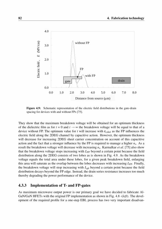
82 4. Fabrication technology
0.0
1.0
2.0
3.0
4.0
0.0 1.0 2.0 3.0 4.0 5.0 6.0 7.0 8.0
Distance from source (µm)
Elec
tric
field
,
E (
MV
/cm
)
draingate
FP
without FP
with FP
Distance from source (µm)
Figure 4.9: Schematic representation of the electric field distributions in the gate-drainspacing for devices with and without FPs [75].
They show that the maximum breakdown voltage will be obtained for an optimum thicknessof the dielectric film as for t = 0 and t → ∞ the breakdown voltage will be equal to that of adevice without FP. The optimum value for t will increase with εr,diel as the FP influences theelectric field along the 2DEG channel by capacitive action. However, the optimum thicknesswill decrease for increasing 2DEG sheet carrier concentration on account of this capacitiveaction and the fact that a stronger influence by the FP is required to manage a higher ns. As aresult the breakdown voltage will decrease with increasing ns. Karmalkar et al. [75] also showthat the breakdown voltage stops increasing with LFP beyond a certain point because the fielddistribution along the 2DEG consists of two lobes as is shown in Fig. 4.9. As the breakdownvoltage equals the total area under these lobes, for a given peak breakdown field, enlargingthis area will saturate as the overlap between the lobes decreases with increasing LFP. Finally,the breakdown voltage will stop increasing with Lgd beyond a certain point because the fielddistribution decays beyond the FP edge. Instead, the drain series resistance increases too muchthereby degrading the power performance of the device.
4.3.3 Implementation of T- and FP-gatesAs maximum microwave output power is our primary goal we have decided to fabricate Al-GaN/GaN HFETs with the original FP implementation as shown in Fig. 4.8 -(left). The devel-opment of the required profile for a one-step EBL process has two very important disadvan-

4.4 Surface passivation 83
tages:
• the FP will not be completely parallel to the AlGaN surface as can be seen in Fig. 4.6,and
• complete coverage of the AlGaN layer with SiN up to the footprint of the gate can notbe guaranteed.
To solve these problems we have decided to use a two-step EBL process, which offers twoadditional advantages:
• excellent control over the width of the footprint, the actual gate length, because it can bedefined using a very thin (typically 250 nm) high resolution PMMA layer, and
• SiN passivation layer is deposited early on in the fabrication process protecting the Al-GaN barrier layer from getting damaged or contaminated.
After defining the footprint, the SiN passivation layer is opened using a RIE sulfurhexafluoride(SF6) plasma. To prevent the AlGaN barrier layer from excessive plasma damage, which givesrise to high gate leakage currents, an etch process with very low RF power and DC bias of10 W and -10 V, respectively has been developed. Furthermore, the etch time is accuratelydetermined using dummy samples to avoid excessive overetching. After opening the SiN layerthe footprint is evaporated and the wide top of a T- or FP-gate is defined using a thick (typically900 nm) copolymer layer. Although fabrication is slowed down as it takes two writing steps,the process is much less critical as only a good overlay accuracy between the top and thefootprint is required as this determines LFP. Figure 4.10 shows a schematic overview of thetwo-step EBL process. More detailed information can be found in Appendix A.
Figure 4.11 shows a SEM image of the cross-section of a submicron T-gate fabricated usingthe two-step process. The footprint of this gate is 0.4 µm and the top is 1.0 µm wide. The imagealso shows the excellent coverage of the semiconductor surface with SiN up to the footprint ofthe gate. Furthermore, it can be seen that the top part of the gate is parallel to the semiconductorsurface. Figure 4.12 shows photographs using an optical microscope of a T-gate (left), and twoFP-gates with FP lengths of 0.5 µm (middle) and 1.0 µm (right), respectively. The footprint ofthese gates is 0.7 µm and the extension of the top part towards the source contact is 0.25 µm inall cases.
4.4 Surface passivationSurface passivation is a very important topic in any device technology. As the periodic struc-ture of the crystal lattice abruptly stops at the surface many defect or trap states can be presentdue to e.g. dangling bonds. Surface passivation is used to terminate these bonds with elementsassuring chemical stability of the surface. If there is no suitable native oxide, e.g. SiO2 inthe case of Si, this can be done using hydrogen or a dielectric film such as SiN. In addition,passivation is used to prevent the surface from mechanical and chemical damage during assem-bly and packaging and environmental influences such as moisture, which is one of the maincatalysts for corrosion, and highly mobile impurities like sodium (Na).

copolymer
10 11
Sapphire / SiC substrate
GaN buffer
AlGaN barrierSiN
PMMA
Transparent therm. evap. Au
Ni/Au footprint
1 2 3
4 5 6
7 8 9
84 4. Fabrication technology
Figure 4.10: Schematic overview of the two-step EBL process.
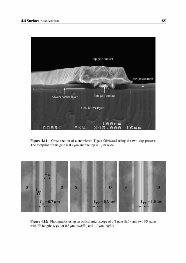
4.4 Surface passivation 85
top gate contact
foot gate contact
SiN passivation
GaN buffer layer
AlGaN barrier layer
Figure 4.11: Cross-section of a submicron T-gate fabricated using the two step process.The footprint of this gate is 0.4 µm and the top is 1 µm wide.
S S SD D DLgs
Lgd
Lg = 0.7 µm LFP = 0.5 µm LFP = 1.0 µm
Figure 4.12: Photographs using an optical microscope of a T-gate (left), and two FP-gateswith FP lengths (LFP) of 0.5 µm (middle) and 1.0 µm (right).
86 4. Fabrication technology
4.4.1 PECVD SiN
Especially in the case of AlGaN/GaN heterostructures effective surface passivation is requiredbecause the AlGaN surface and in particular the amount of positive compensating charge(σcomp) plays a crucial role with respect to device operation and microwave power perfor-mance as has been explained in Sect. 2.3.4. In that Section we also mentioned that accordingto literature [17, 48, 109, 141, 162, 164] effective passivation of the free AlGaN surface, whichprevents the formation of a virtual gate and thereby eliminates gate lag, can be achieved by aplasma enhanced chemical vapor deposited (PECVD) SiN film.
We have investigated the efficiency of gate lag reduction and the uniformity of microwavedevice performance using PECVD SiN on both n.i.d. and doped AlGaN/GaN heterostructures.Undoped HFETs on sapphire have been fabricated on samples, typical size 10 x 10 mm2,from 2 inch wafers with comparable material characteristics grown by RU, RF Nitro, andQinetiQ. Si-doped HFETs on s.i. SiC have been processed on identical samples from 2 inchwafers grown by the Fraunhofer Institute for Applied Solid-State Physics (IAF). All epitaxialmaterial has been grown using MOCVD. We have investigated “fat gate” and “submicron gate”devices processed using the Inverse Mesa and Submu mask sets respectively, as described inSect. 3.2.1.
Our experiments confirm that passivation with SiN indeed achieves increased drain currentswing because of reduced gate lag but the observed uniformity of the microwave device per-formance was very poor. This was quite surprising as microwave device performance beforepassivation showed to be poor but very uniform. The uniformity of the DC I-V characteristicsbefore and after passivation remained good.
4.4.2 Surface treatments
To improve uniformity of microwave device performance after SiN deposition, thereby im-proving process yield, we∗ have investigated surface treatments before passivation. AlthoughGaN is well known to withstand harsh environmental conditions we have found that gate lagreduction is very sensitive to proper surface preparation before passivation and device process-ing. The idea to apply surface treatments to the AlGaN barrier layer is based on the hypothesisthat contaminants, processing remnants or crystal irregularities residing at the AlGaN-SiN in-terface prevent effective and reproducible gate lag reduction, which leads to poor uniformityof microwave device performance even on samples as small as 10 x 10 mm2. We assumedthat cleaning and reorganization of the AlGaN surface before SiN passivation would stronglyimprove reproducible gate lag minimization. We have investigated the influence of a wet etchusing buffered hydrofluoric acid (BHF) and a low-power RIE Ar plasma (10 sccm, 40 mTorr,30 W, 30”, DC bias = -86 V, 20 oC) in combination with SiN passivation on the amount of gatelag and the uniformity of microwave device performance. The wet etch with BHF (1’30”) wasperformed at the start of device processing whereas the Ar plasma was applied just before theRTA step (800 oC, 2 minutes, N2 ambient) of the Ti/Al/Ni/Au ohmic contacts. The RTA step is
∗This work was a joint effort between this author and B. Jacobs, at that time Ph.D. student at the same institute [67].
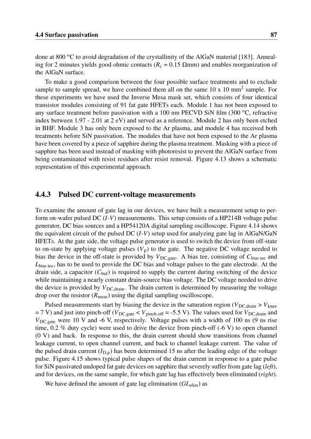
4.4 Surface passivation 87
done at 800 oC to avoid degradation of the crystallinity of the AlGaN material [183]. Anneal-ing for 2 minutes yields good ohmic contacts (Rc = 0.15 Ωmm) and enables reorganization ofthe AlGaN surface.
To make a good comparison between the four possible surface treatments and to excludesample to sample spread, we have combined them all on the same 10 x 10 mm2 sample. Forthese experiments we have used the Inverse Mesa mask set, which consists of four identicaltransistor modules consisting of 91 fat gate HFETs each. Module 1 has not been exposed toany surface treatment before passivation with a 100 nm PECVD SiN film (300 oC, refractiveindex between 1.97 - 2.01 at 2 eV) and served as a reference. Module 2 has only been etchedin BHF. Module 3 has only been exposed to the Ar plasma, and module 4 has received bothtreatments before SiN passivation. The modules that have not been exposed to the Ar plasmahave been covered by a piece of sapphire during the plasma treatment. Masking with a piece ofsapphire has been used instead of masking with photoresist to prevent the AlGaN surface frombeing contaminated with resist residues after resist removal. Figure 4.13 shows a schematicrepresentation of this experimental approach.
4.4.3 Pulsed DC current-voltage measurements
To examine the amount of gate lag in our devices, we have built a measurement setup to per-form on-wafer pulsed DC (I-V) measurements. This setup consists of a HP214B voltage pulsegenerator, DC bias sources and a HP54120A digital sampling oscilloscope. Figure 4.14 showsthe equivalent circuit of the pulsed DC (I-V) setup used for analyzing gate lag in AlGaN/GaNHFETs. At the gate side, the voltage pulse generator is used to switch the device from off-stateto on-state by applying voltage pulses (Vp) to the gate. The negative DC voltage needed tobias the device in the off-state is provided by VDC,gate. A bias tee, consisting of Cbias tee andLbias tee, has to be used to provide the DC bias and voltage pulses to the gate electrode. At thedrain side, a capacitor (Cbuf) is required to supply the current during switching of the devicewhile maintaining a nearly constant drain-source bias voltage. The DC voltage needed to drivethe device is provided by VDC,drain. The drain current is determined by measuring the voltagedrop over the resistor (Rmeas) using the digital sampling oscilloscope.
Pulsed measurements start by biasing the device in the saturation region (VDC,drain > Vknee= 7 V) and just into pinch-off (VDC,gate < Vpinch-off = -5.5 V). The values used for VDC,drain andVDC,gate were 10 V and -6 V, respectively. Voltage pulses with a width of 100 ns (9 ns risetime, 0.2 % duty cycle) were used to drive the device from pinch-off (-6 V) to open channel(0 V) and back. In response to this, the drain current should show transitions from channelleakage current, to open channel current, and back to channel leakage current. The value ofthe pulsed drain current (ID,p) has been determined 15 ns after the leading edge of the voltagepulse. Figure 4.15 shows typical pulse shapes of the drain current in response to a gate pulsefor SiN passivated undoped fat gate devices on sapphire that severely suffer from gate lag (left),and for devices, on the same sample, for which gate lag has effectively been eliminated (right).
We have defined the amount of gate lag elimination (GLelim) as
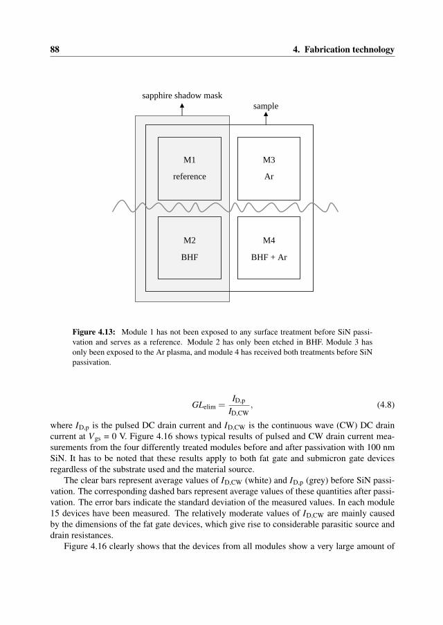
88 4. Fabrication technology
BHF + Ar
Ar
sample
M1 M3
M2 M4
BHF
reference
sapphire shadow mask
Figure 4.13: Module 1 has not been exposed to any surface treatment before SiN passi-vation and serves as a reference. Module 2 has only been etched in BHF. Module 3 hasonly been exposed to the Ar plasma, and module 4 has received both treatments before SiNpassivation.
GLelim =ID,p
ID,CW, (4.8)
where ID,p is the pulsed DC drain current and ID,CW is the continuous wave (CW) DC draincurrent at Vgs = 0 V. Figure 4.16 shows typical results of pulsed and CW drain current mea-surements from the four differently treated modules before and after passivation with 100 nmSiN. It has to be noted that these results apply to both fat gate and submicron gate devicesregardless of the substrate used and the material source.
The clear bars represent average values of ID,CW (white) and ID,p (grey) before SiN passi-vation. The corresponding dashed bars represent average values of these quantities after passi-vation. The error bars indicate the standard deviation of the measured values. In each module15 devices have been measured. The relatively moderate values of ID,CW are mainly causedby the dimensions of the fat gate devices, which give rise to considerable parasitic source anddrain resistances.
Figure 4.16 clearly shows that the devices from all modules show a very large amount of
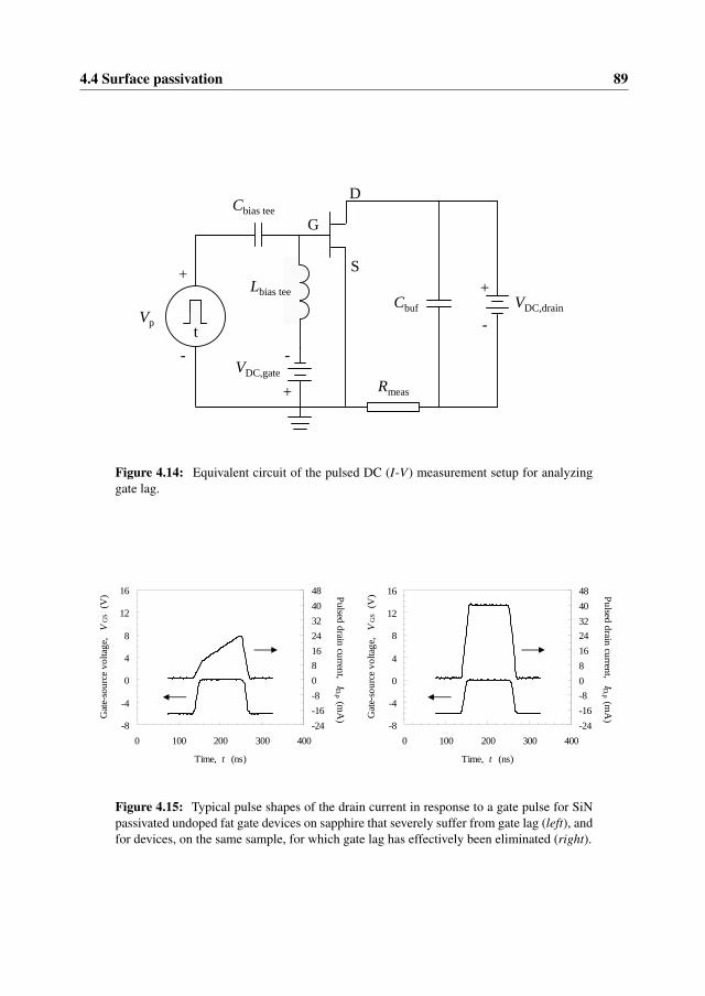
4.4 Surface passivation 89
Rmeas
VDC,drain
Cbias tee
Vpt
+
- -
+
G
Cbuf
+
-
S
D
Lbias tee
VDC,gate
Figure 4.14: Equivalent circuit of the pulsed DC (I-V) measurement setup for analyzinggate lag.
-8
-4
0
4
8
12
16
0 100 200 300 400
Time, t (ns)
Gat
e-so
urce
vol
tage
, V
GS
(V)
-24-16-8081624324048 Pulsed drain current, ID
,p (mA
)
-8
-4
0
4
8
12
16
0 100 200 300 400
Time, t (ns)
Gat
e-so
urce
vol
tage
, V
GS
(V)
-24-16-8081624324048 Pulsed drain current, ID
,p (mA
)
Figure 4.15: Typical pulse shapes of the drain current in response to a gate pulse for SiNpassivated undoped fat gate devices on sapphire that severely suffer from gate lag (left), andfor devices, on the same sample, for which gate lag has effectively been eliminated (right).

90 4. Fabrication technology
0
125
250
375
500
1 2 3 4
Dra
in c
urre
nt d
ensit
y,
ID
(m
A/m
m) ll
l
M 1: reference
M 2: BHF
M 3: Ar
M 4: BHF + Ar
ID,CW before passivation
ID,CW after passivation
ID,p before passivation
ID,p after passivation
Figure 4.16: Typical results of pulsed and CW drain current measurements from the fourdifferently treated modules before and after passivation with the standard SiN film (100 nm,300 oC, refractive index between 1.97 - 2.01 at 2 eV). It has to be noted that these resultsapply to both fat gate and submicron gate devices regardless of the substrate used and thematerial source. The clear bars represent average values of ID,CW (white) and ID,p (grey)before SiN passivation. The corresponding dashed bars represent average values of thesequantities after passivation. The error bars indicate the standard deviation of the measuredvalues.
gate lag before passivation. This is especially true for the modules that have not been exposedto the Ar plasma (modules 1 and 2, respectively). After SiN passivation, the amount of gate lagin devices from modules 1 and 2 has been decreased significantly but it still is unacceptablylarge. This is in sharp contrast with devices from the modules that have been exposed to the Arplasma (modules 3 and 4, respectively) as in that case gate lag has completely disappeared. Itshould be noted that the strong reduction of self-heating under pulsed measurement conditionscauses ID,p to be higher than the corresponding ID,CW. Looking at the error bars it should alsobe noted that the Ar plasma treatment has significantly improved the uniformity of the pulsedI-V results after passivation. The observed increase in the values for ID,CW and ID,p afterpassivation is in accordance with literature [48, 71]. Although the best results after passivationare achieved using the combination of the BHF wet etch and the Ar RIE etch (module 4), it hasto be concluded that the Ar plasma treatment is the key processing step leading to the stronglyminimized gat lag and the significantly improved uniformity of the measurement results.

4.5 Air bridges 91
-10.0
-8.0
-6.0
-4.0
-2.0
0.0
2.0
4.0
6.0
8.0
10.0
1
I G, l
eak
and
I D, l
eak
(mA
/mm
) lll
ID,leak before passivation
ID,leak after passivation
IG,leak before passivation
IG,leak after passivation
Figure 4.17: Typical gate and drain leakage current densities (IG,leak and ID,leak) of un-doped fat gate devices on sapphire substrates before and after passivation using the standardSiN film (100 nm, 300 oC, refractive index between 1.97 - 2.01 at 2 eV), respectively.
A serious drawback of our standard PECVD SiN film (100 nm, 300 oC, refractive indexbetween 1.97 - 2.01 at 2 eV) is the strongly increased gate leakage current (IG,leak) after passi-vation of the AlGaN surface. Figure 4.17 shows typical gate and drain leakage current densitiesof undoped fat gate devices on sapphire substrates before and after passivation, respectively.Although the increased drain leakage current density after SiN deposition is undesired, it doesnot have a very big influence on the drain current swing. However, the increased gate leakagecurrent density significantly reduces the maximum breakdown voltage and hence the drain-source voltage swing. It is obvious that this is detrimental for high-power device operation.In chapter 5 we will investigate the influence of several process settings, i.e. gas flow, RFpower, total gas pressure, and substrate temperature, on the material properties of PECVD SiNfilms and their influence on the surface passivation of AlGaN/GaN HFETs on sapphire and s.i.SiC substrates. The main goals of these investigations have been to minimize gate and drainleakage currents while maintaining the passivation properties of the standard SiN film.
4.5 Air bridgesAir bridges, which in fact are lifted metal lines, are required to connect the multiple drain orsource contacts in multi-finger devices as can be seen in Fig. 3.17. In the case of a comb layout

92 4. Fabrication technology
the internal sources are connected through air bridges whereas for a fishbone layout this is thecase for the drain contacts.
4.5.1 Electroplating
A typical air bridge is defined using a double-layer photoresist pattern and Au electroplating.The first photoresist layer is used to define the posts of the air bridges and to support them.This resist layer should be thick, typically thicker than 3 µm, to ensure that the bridges are highenough and to reduce parasitic capacitances. After definition of the posts a seed layer, typicallyTi/Au, is deposited, which serves as cathode electrode in the Au electroplating process. Thisseed layer should be continuous over the complete sample surface otherwise no plating willoccur due to a break in the cathode electrode. Therefore, the side walls of the thick supportresist should not be too steep. This can be achieved by a two-step backing step, in whichthe resist is hardened first and then rounded by controlled flowing of the resist. After thedeposition of the seed layer the second resist layer is used to define the areas where the airbridges will be realized. In the next step the actual air bridges are fabricated by electroplatingof a thick Au layer. After the plating process, the top resist layer is removed first. Then first theAu part of the seed layer is removed by wet etching using a potassium cyanide (KCN) basedsolution (DEGUSSA) followed by an etch with oxalic acid (mixture of C2H2O4.2H2O, H2O2,and KOH) to remove the Ti part of the seed layer. Finally, the thick support resist is removed.
Electroplating of thick Au layers on small samples, typically 10 mm x 10 mm, is verytroublesome as a clamp has to be used to attach them to a sample holder. Such constructionseverely affects the flow in the Au bath which results in strongly non-uniform plating resultswith respect to the thickness of the plated metal across the sample. In addition, huge topogra-phy on the small samples also significantly deteriorates the uniformity of the thickness of theplated Au layer.
4.5.2 Electron beam evaporation
To circumvent these problems we have chosen to use e-beam evaporation to fabricate airbridges with a 1.5 µm thick Au layer. As a consequence, we had to use a resist with a lift-off profile, i.e. negatively sloped side walls, to define the areas where the air bridges will berealized. For this purpose we have used ma-N440, which is a 4 µm thick negative resist with anexcellent lift-off profile. To prevent the support resist from being attacked during developmentof the top resist we have evaporated a 12.5 nm transparent Au layer on top of the support resistbefore starting the bridge litho process. This Au layer has to be transparent to allow alignmentof the bridge litho to the litho of the posts. After the bridge litho we have evaporated Ti/Au= 20/1500 nm. The Au layer has been evaporated in three consecutive runs of 500 nm eachto avoid excessive heating of the sample, which can cause flowing and hardening of the resistduring the metallization process that is long as the evaporation rate is as low as 0.6 nm/s toavoid sputtering of Au. After lift-off of the bridge metallization, the transparent Au layer isremoved using the DEGUSSA solution, and finally the support resist is removed.

4.6 Conclusions 93
Figure 4.18: Steep (left) and strongly rounded or lens-shaped AZ4533 profiles (right).
The reliability of air bridges depends on the metal thickness used, the size of the posts, theheight of the bridge, and its width-to-length ratio. These aspects should be well considered toprevent the bridge from sagging. Foundries use a width-to-length ratio of 1 : 4. In our mmTordesign the maximum distance the air bridges have to span is about 100 µm. As the minimumwidth of the air bridges is 62.5 µm, implying a span width of 250µm, this design criterion hasperfectly been obeyed. However, we have encountered problems with respect to breaking ofbridges during removal of the thick support resist, in our case 3.3 µm thick AZ4533 (positivetone). We found out that this problem was caused by the side walls of the AZ4533 profile thatwere too steep and had a notch at the top edge causing a weak spot in the connection betweenthe bridge and the posts. We have solved this problem by significantly improving the roundingof the AZ4533 profile by increasing the temperature of the second bake step from105 oC to160 oC. Figure 4.18 shows SEM images of the steep (left) and strongly rounded or lens-shapedAZ4533 profiles (right).
Furthermore, we have introduced slits that split up wide air bridges into several narrowerparts in parallel because it is difficult to efficiently remove the thick support resist underneathvery wide air bridges without destroying them. Figure 4.19-(left) shows a photograph of anAlGaN/GaN HFET with a total gate width (Wg) of 1 mm in which the drain contacts have beenconnected using air bridges including the aforementioned slits. Figure 4.19-(right) is a closeup showing two source-drain regions through the split in an air bridge connecting two draincontacts.
4.6 Conclusions
In this chapter we have described key steps of the process technology that we have developedto fabricate microwave high-power AlGaN/GaN HFETs on sapphire and s.i. SiC substrates.The following conclusions can be drawn:
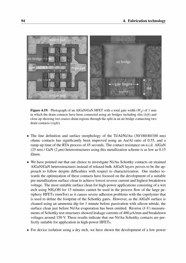
94 4. Fabrication technology
gate fingers
gate pad & bus drain pad
source pad
source pad
slit
air bridgeair bridge
sourceslit
Figure 4.19: Photograph of an AlGaN/GaN HFET with a total gate width (Wg) of 1 mmin which the drain contacts have been connected using air bridges including slits (left) andclose up showing two source-drain regions through the split in an air bridge connecting twodrain contacts (right).
• The line definition and surface morphology of the Ti/Al/Ni/Au (30/180/40/100 nm)ohmic contacts has significantly been improved using an Au/Al ratio of 0.55, and aramp-up time of the RTA process of 45 seconds. The contact resistance on n.i.d. AlGaN(25 nm) / GaN (2 µm) heterostructures using this metallization scheme is as low as 0.15Ωmm.
• We have pointed out that our choice to investigate Ni/Au Schottky contacts on strainedAlGaN/GaN heterostructures instead of relaxed bulk AlGaN layers proves to be the ap-proach to follow despite difficulties with respect to characterization. Our studies to-wards the optimization of these contacts have focused on the development of a suitablepre-metallization surface clean to achieve lowest reverse current and highest breakdownvoltage. The most suitable surface clean for high-power applications consisting of a wetetch using NH4OH for 15 minutes cannot be used in the process flow of the large pe-riphery HFETs (mmTor) as it causes severe adhesion problems with the copolymer thatis used to define the footprint of the Schottky gates. However, as the AlGaN surface iscleaned using an ammonia dip for 1 minute before passivation with silicon nitride, thesurface clean just before Ni/Au evaporation has been omitted. Reverse (I-V) measure-ments of Schottky test structures showed leakage currents of 400 µA/mm and breakdownvoltages around 150 V. These results indicate that our Ni/Au Schottky contacts are per-fectly suitable for application in high-power HFETs.
• For device isolation using a dry etch, we have shown the development of a low power
4.6 Conclusions 95
ICP process using a Cl2/H2 chemistry that enables the use of photoresist as masking ma-terial to obtain mesa structures with sloped side walls. This process etches AlGaN/GaNunselectively at a rate of 110 nm/min and yields a very smooth surface morphology ofthe etched GaN buffer layer. Furthermore, we have discussed the importance of creatinga process window for the etch process to assure a constant etch rate and reproducibleetch results from run to run.
• A two-step EBL process has been developed to fabricate T-shaped and FP-gates withsub-micrometer footprints, which define the actual gate length. The top parts of thesegates are parallel to the semiconductor surface, which is completely covered with SiN upto the footprint of the gate. Additional advantages of this process are the excellent linewidth control of the footprint and the protection of the AlGaN layer due to the depositionof the SiN passivation layer early in the fabrication process.
• We have investigated the efficiency of gate lag reduction and the uniformity of mi-crowave device performance using PECVD SiN on both n.i.d. and doped AlGaN/GaNheterostructures. Our experiments confirm that passivation with SiN indeed achievesincreased drain current swing because of reduced gate lag but the observed uniformityof the microwave device performance showed to be very poor. We have shown thatthe application of a low power dry etch using Ar (10 sccm, 40 mTorr, 30 W, 30”, DCbias = -86 V, 20 oC) just before the RTA step (800 oC, 2 minutes, N2 ambient) of theTi/Al/Ni/Au ohmic contacts is the key processing step leading to strongly minimized gatlag and the significantly improved uniformity of microwave device performance uponsurface passivation with SiN. The observed increase in gate and drain leakage currentsafter SiN deposition will be investigated into more detail in Chapter 5.
• We have developed a process that uses e-beam evaporation to fabricate air bridges witha 1.5 µm thick Au layer. To improve the stability and reliability of the air bridges alens-shaped support resist has been used to avoid the posts of the bridges to be too steepwhich causes easy breaking. Furthermore, we have introduced slits that split up wide airbridges into several narrower parts in parallel because it is difficult to efficiently removethe thick support resist underneath very wide air bridges without destroying them.

96 4. Fabrication technology
Chapter 5
PECVD silicon nitride passivationfilms
Insulating amorphous silicon nitride (SiN) films are widely used both as an element of micro-electronic solid-state device structures, and in device process technology. A few examplesof the former are the use of SiN as a gate dielectric of nonvolatile memories, it is one ofthe dielectric materials in the stacked oxide-nitride-oxide layers in DRAM capacitors, and itis used as sidewall spacers in MOSFETs. In process technology it is for example used asmasking material, as stop-layer for chemical mechanical polishing and etching processes, andas surface passivation layer.
In 1964 researchers at IBM started working on amorphous SiN films to develop an im-proved substitute or supplement for silicon dioxide (SiO2) as a passivation layer of Si surfaces.They discovered that SiN is extremely impervious to e.g. moisture, oxygen, and ions of differentmetals, first of all sodium (Na), which is a very important requirement for the use as passi-vation layer [61]. Additional properties making SiN suitable for surface passivation are thefacts that it can be synthesized by plasma enhanced chemical vapor deposition (PECVD) tohave low compressive stress, which allows it to be exposed to severe environmental stress withless likelihood of delamination or cracking. Furthermore, its coverage of underlying metal isconformal, and finally it can be deposited with an acceptably low pinhole density [171].
In this chapter we will investigate the influence of several process settings, i.e. gas flow,RF power, total gas pressure, and substrate temperature, on the material properties of PECVDamorphous SiN films and their influence on both leakage currents and surface passivation ofAlGaN/GaN HFETs on sapphire and s.i. SiC substrates.
97

98 5. PECVD silicon nitride passivation films
5.1 Introduction
In Sect. 4.4 it has clearly been shown that the AlGaN barrier of HFETs on sapphire and s.i.SiC substrates can effectively be passivated using the combination of a BHF wet etch, an ArRIE etch, and a PECVD SiN film (100 nm, 300 oC, refractive index between 1.97 - 2.01 at 2eV). However, after passivation with this standard SiN film a significant increase in the gateand drain leakage currents has been observed. Although the increased drain leakage currentdensity after SiN deposition is undesired, it does not severely reduce the drain current swing.However, the increased gate leakage current density significantly reduces the maximum break-down voltage and hence the drain-source voltage swing, which obviously is detrimental forhigh-power device operation.
We assumed that the cause for the increased gate leakage current was related to the SiN-AlGaN interface. This assumption is supported by Ansell et al. [10] and Tan et al. [154]who have shown that hopping conduction, which they suggest to be the dominant gate leakagemechanism in the case that the device is pinched-off and drain-source voltages above the kneevoltage are applied, increased after SiN passivation as the average activation energy decreasedfrom 200 meV to 50 - 70 meV. We have investigated if changing the composition of the PECVDSiN film or preparation of the AlGaN barrier layer before SiN deposition, or both, results indecreased leakage currents after SiN deposition. It should be noted that the surface passivationcapability should remain equal to that of the standard film.
The composition of SiN films can be changed by altering the settings of the PECVD pro-cess, e.g. gas flow, RF power (PRF), total gas pressure (p), and substrate temperature (Tsubstrate).To investigate the material properties and compositions of differently synthesized SiN films us-ing spectral ellipsometry (SE), Fourier transform infrared spectroscopy (FTIR), effective mi-nority carrier lifetime measurements, and stress measurements, the films have been depositedon monocrystalline Si wafers. Characterization and analysis of the results obtained by SE,FTIR, and effective minority carrier lifetime measurements have been performed by BramHoex and Erwin Kessels, researchers with the group Equilibrium and Transport in Plasmas(ETP) from the faculty of Applied Physics at TU/e. Stress measurements have been performedby Eugene Timmering and Johan Klootwijk from Philips Research Laboratories Eindhoven.
Preparation of the AlGaN barrier layer before SiN deposition can be done by a combinationof organic cleaning, using acetone and iso-propyl alcohol (IPA), and wet etching either usingdilute hydrofluoric acid (HF), buffered HF (BHF), or dilute ammonia (NH4OH) [48, 109].Regarding the mmTor process flow we have chosen to use NH4OH to avoid degradation of theTi/Al/Ni/Au ohmic contacts as Ti is attacked by HF and BHF.
CW and pulsed DC I-V measurements have been performed to determine the influenceof the film properties of different PECVD SiN films as well as the preparation of the AlGaNbarrier layer before SiN deposition on the surface passivation and the amount of gate and drainleakage currents of n.i.d. AlGaN/GaN HFETs on sapphire substrates.
5.2 Deposition of silicon nitride by PECVD 99
5.2 Deposition of silicon nitride by PECVD
When used as a passivation layer, the deposition process of amorphous SiN is preferably doneat relatively low substrate temperatures, typically 200 oC - 400 oC, for example to be compat-ible with metals that have low melting points like aluminum (660 oC at atmospheric pressure)or to prevent outgassing of volatile elements like phosphorus (P). In those cases, PECVD is themethod of choice as it enables deposition of SiN films in the aforementioned low-temperaturerange because the major part of the energy required to initiate and sustain the chemical reac-tion is supplied by an RF plasma. Hence, the high temperature that is generated within thegaseous molecules facilitates their reaction and results in deposition at relatively low substratetemperatures.
Already in 1965, Sterling and Swann described SiN deposition by PECVD [153]. How-ever, in 1990 Smith et al. [151] provided a thorough explanation of this technique for the firsttime. Stoichiometric amorphous SiN films have a nitrogen to silicon ratio (x) of 1.33 [15]and a refractive index (n) of 1.95 at 2eV [80]. However, PECVD SiN films tend to be non-stoichiometric and commonly contain substantial quantities of atomic hydrogen, typically 10at% - 30 at% [171]. For this reason the chemical representation sometimes used for these filmsis a-SiNx:H. In this thesis we will just use the representation SiN.
The two main reactions for synthesizing SiN films from the gas phase are the interactionsof silane (SiH4) and silicon tetrachloride (SiCl4) with ammonia (NH3) as is given by reactionequations 5.1 and 5.2, respectively. An alternative for using pure silane is the use of dilutesilane, i.e. diluted in an inert gas such as argon (Ar) or nitrogen (N2), which does not sponta-neously combust when exposed to air.
3SiH4(g)+4NH3(g)→ Si3N4(s)+12H2(g) (5.1)
3SiCl4(g)+4NH3(g)→ Si3N4(s)+12HCl(g) (5.2)
5.2.1 Equipment
The deposition of our SiN films has been done in a load-locked Oxford Plasmalab 100 systemusing ammonia (NH3), pure silane (SiH4) and nitrogen (N2) as process gases. The samples areplaced on a 4 inch Si carrier wafer, which is transferred by a robot arm into the parallel platedeposition chamber and placed on a grounded and heated lower electrode with a diameter of205 mm. The process gases are mixed and injected into the deposition chamber at the desiredflow rates through a showerhead-type upper electrode. Gas is continuously pumped out of thechamber, underneath the lower electrode, to maintain a constant total gas pressure (p) duringthe deposition. An RF field with a frequency of 13.56 MHz is applied between the upper andlower electrodes to initiate and sustain a plasma that contains the ionized gas species fromwhich the SiN film is synthesized. A high excitation frequency is used to minimize plasmadamage of the sample surface during the deposition process [80].

100 5. PECVD silicon nitride passivation films
5.2.2 Characterization techniquesTo investigate the material properties and composition of the SiN films we have chosen todeposit them on monocrystalline Si wafers as this enables the use of the following standardcharacterization techniques:
• spectroscopic ellipsometry (SE),
• Fourier transform infrared spectroscopy (FTIR), and
• effective minority carrier lifetime measurements.
SE measurements have been performed on SiN films deposited on 2 inch monocrystallineSi wafers using a Woolam M2000 system in the energy range from 0.7 eV - 5 eV. Usingthe Tauc-Lorentz formalism, the SE measurement results are used to extract the followingmaterial properties of the films: thickness (dSiN), surface roughness (ds), refractive index (n),and extinction coefficient (k) [69]. From the extinction coefficient, the absorption coefficient(α) can be calculated using α = 4πk/λ. In addition, the photon energy at which the absorptioncoefficient equals 104 cm−1 is often referred to as the optical band gap (E04).
FTIR measurements using a Bruker Vector 22 system have been performed on relativelythick SiN films, typically > 300 nm, which are also deposited on 2 inch monocrystalline Siwafers. In these measurements, which are performed at normal incidence to the substrate,transmittance spectra of the bare Si substrate and of the same Si substrate covered with aSiN film are recorded on the same spot. This differential measurement approach enables theextraction of the absorbance of the SiN film. FTIR measurements provide information aboutthe configuration and amount of bonded hydrogen in SiN films. Therefore, they can be usedto determine the regime in which the SiN films have been deposited. The so-called simpleradical deposition regime, i.e. plasma deposition from SiH3 and NH2 radicals, yields SiN filmscontaining Si-H and N-H bonds. In the case of aminosilane SiN deposition, gas phase reactionscause all SiH4 to be incorporated into Si(NH2)3 molecules and radicals before SiN deposition.These films can contain N-H and N-H2 bonds but no Si-H bonds [124]. In addition it shouldbe noted that films which only contain N-H bonds are dense and highly stable, whereas filmscontaining N-H2 bonds are highly unstable because they get oxidized due to the reaction withwater vapor from the air [123].
To measure the effective minority carrier lifetime (τeff ) SiN films have been deposited on3 inch double polished float zone (FZ) monocrystalline Si wafers. The resistivity of the p-typeand n-type substrates used was 8.4 Ωcm and 1.3 Ωcm, respectively. Before SiN depositionthe Si wafers have been cleaned using the standard RCA clean [79] followed by an HF dip.The effective minority carrier lifetime is a measure for the surface passivation capability ofthe deposited SiN film. The higher the effective lifetime, the better the Si surface has beenpassivated. We have determined the effective minority carrier lifetime using a Sinton lifetimetester. This system, first introduced by Sinton et al. [150], is a contactless implementation ofthe steady-state photoconductance technique in which the photoconductance of a Si substrateis measured in a quasi-steady-state mode during a long, slowly varying light pulse. Contrary toconventional techniques, which are based on the analysis of photoconductance decay transients
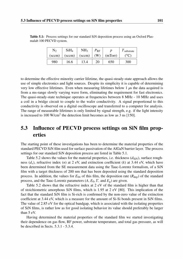
5.3 Influence of PECVD process settings on SiN film properties 101
Table 5.1: Process settings for our standard SiN deposition process using an Oxford Plas-malab 100 PECVD system.
N2 SiH4 NH3 PRF p Tsubstrate
(sccm) (sccm) (sccm) (W) (mTorr) (oC)
980 16.6 13.4 20 650 300
to determine the effective minority carrier lifetime, the quasi-steady-state approach allows theuse of simple electronics and light sources. Despite its simplicity it is capable of determiningvery low effective lifetimes. Even when measuring lifetimes below 1 µs the data acquired isfrom a ms-range slowly varying wave form, eliminating the requirement for fast electronics.The quasi-steady-state technique operates at frequencies between 8 MHz - 10 MHz and usesa coil in a bridge circuit to couple to the wafer conductivity. A signal proportional to thisconductivity is observed on a digital oscilloscope and transferred to a computer for analysis.The range of measurable lifetimes is only limited by signal strength, e.g. if the light intensityis increased to 100 W/cm2 the detection limit becomes as low as 3 ns [150].
5.3 Influence of PECVD process settings on SiN film prop-erties
The starting point of these investigations has been to determine the material properties of thestandard PECVD SiN film used for surface passivation of the AlGaN barrier layer. The processsettings for our standard SiN deposition process are listed in Table 5.1.
Table 5.2 shows the values for the material properties, i.e. thickness (dSiN), surface rough-ness (ds), refractive index (n) at 2 eV, and extinction coefficient (k) at 3.44 eV, which havebeen determined from the SE measurement data using the Tauc-Lorentz formalism, of a SiNfilm with a target thickness of 200 nm that has been deposited using the standard depositionprocess. In addition, the values for E04 of this film, the deposition rate (Rdep) of the standardprocess, and the Tauc-Lorentz parameters (A, E0, Γ, and Eg) are given.
Table 5.2 shows that the refractive index at 2 eV of the standard film is higher than thatof stoichiometric amorphous SiN films, which is 1.95 at 2 eV [80]. This implication of thefact that the standard SiN film is Si-rich is confirmed by the non-zero value of the extinctioncoefficient at 3.44 eV, which is a measure for the amount of Si-Si bonds present in SiN films.The value of 2.85 eV for the optical bandgap, which is associated with the isolating propertiesof SiN films, is rather low as for good isolating behavior its value should preferably be largerthan 5 eV.
Having determined the material properties of the standard film we started investigatingtheir dependence on gas flow, RF power, substrate temperature, and total gas pressure, as willbe described in Sects. 5.3.1 - 5.3.4.
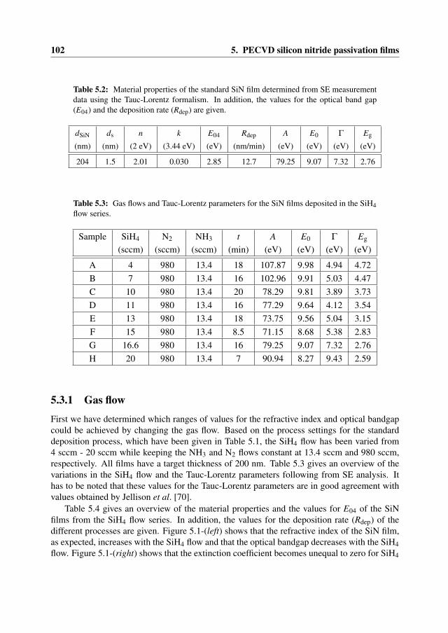
102 5. PECVD silicon nitride passivation films
Table 5.2: Material properties of the standard SiN film determined from SE measurementdata using the Tauc-Lorentz formalism. In addition, the values for the optical band gap(E04) and the deposition rate (Rdep) are given.
dSiN ds n k E04 Rdep A E0 Γ Eg
(nm) (nm) (2 eV) (3.44 eV) (eV) (nm/min) (eV) (eV) (eV) (eV)
204 1.5 2.01 0.030 2.85 12.7 79.25 9.07 7.32 2.76
Table 5.3: Gas flows and Tauc-Lorentz parameters for the SiN films deposited in the SiH4flow series.
Sample SiH4 N2 NH3 t A E0 Γ Eg
(sccm) (sccm) (sccm) (min) (eV) (eV) (eV) (eV)
A 4 980 13.4 18 107.87 9.98 4.94 4.72B 7 980 13.4 16 102.96 9.91 5.03 4.47C 10 980 13.4 20 78.29 9.81 3.89 3.73D 11 980 13.4 16 77.29 9.64 4.12 3.54E 13 980 13.4 18 73.75 9.56 5.04 3.15F 15 980 13.4 8.5 71.15 8.68 5.38 2.83G 16.6 980 13.4 16 79.25 9.07 7.32 2.76H 20 980 13.4 7 90.94 8.27 9.43 2.59
5.3.1 Gas flow
First we have determined which ranges of values for the refractive index and optical bandgapcould be achieved by changing the gas flow. Based on the process settings for the standarddeposition process, which have been given in Table 5.1, the SiH4 flow has been varied from4 sccm - 20 sccm while keeping the NH3 and N2 flows constant at 13.4 sccm and 980 sccm,respectively. All films have a target thickness of 200 nm. Table 5.3 gives an overview of thevariations in the SiH4 flow and the Tauc-Lorentz parameters following from SE analysis. Ithas to be noted that these values for the Tauc-Lorentz parameters are in good agreement withvalues obtained by Jellison et al. [70].
Table 5.4 gives an overview of the material properties and the values for E04 of the SiNfilms from the SiH4 flow series. In addition, the values for the deposition rate (Rdep) of thedifferent processes are given. Figure 5.1-(left) shows that the refractive index of the SiN film,as expected, increases with the SiH4 flow and that the optical bandgap decreases with the SiH4flow. Figure 5.1-(right) shows that the extinction coefficient becomes unequal to zero for SiH4
5.3 Influence of PECVD process settings on SiN film properties 103
Table 5.4: Material properties and optical bandgaps (E04) of the 200 nm thick SiN filmsfrom the SiH4 flow series that have been determined from SE measurement data usingthe Tauc-Lorentz formalism. In addition, the values for the deposition rate (Rdep) of thedifferent processes are given.
Sample SiH4 n k E04 Rdep
(sccm) (2 eV) (3.44 eV) (eV) (nm/min)
A 4 1.82 0 4.38 11.1B 7 1.84 0 3.63 12.5C 10 1.88 0 4.15 12.9D 11 1.91 0 3.64 12.9E 13 1.94 0.003 3.27 12.8F 15 1.97 0.020 2.93 11.5G 16.6 2.01 0.030 2.85 12.7H 20 2.07 0.078 2.68 11.5
0.000
0.010
0.020
0.030
0.040
0.050
0.060
0.070
0.080
2 4 6 8 10 12 14 16 18 20 22
SiH4 flow (sccm)
Extin
ctio
n co
effic
ient
, k
(at 3
.44
eV)
10.0
11.0
12.0
13.0
14.0
Deposition rate, R
dep (nm/m
in) lll
1.80
1.85
1.90
1.95
2.00
2.05
2.10
2 4 6 8 10 12 14 16 18 20 22
SiH4 flow (sccm)
Ref
ract
ive
inde
x,
n (
at 2
eV
)
2.5
3
3.5
4
4.5
5
Optical bandgap, E
04 (eV)
Figure 5.1: Refractive index (n), optical bandgap (E04) (left), extinction coefficient (k),and deposition rate (Rdep) (right) as a function of SiH4 flow. The other process settings arelisted in Table 5.1.
flows of 13 sccm and larger. The observed increase in extinction coefficient with SiH4 flow isexpected as the films get increasingly Si-rich. Figure 5.1-(right) also shows the deposition rateas a function of SiH4 flow.
104 5. PECVD silicon nitride passivation films
Table 5.5: Settings for the deposition process of the SiN films from the RF power series.
N2 SiH4 NH3 PRF p Tsubstrate
(sccm) (sccm) (sccm) (W) (mTorr) (oC)
980 4 13.4 20 - 150 650 300
Table 5.6: Tauc-Lorentz parameters for the SiN films deposited in the RF power series.
Sample PRF A E0 Γ Eg
(W) (eV) (eV) (eV) (eV)
I 20 107.9 9.98 4.94 4.72J 40 140.2 9.0 5.0 5.0K 70 169.7 8.80 6.48 5.13L 110 181.9 8.63 6.01 5.22M 150 217.9 8.03 6.64 5.28
5.3.2 RF power
From literature [80] it is known that the RF power (PRF) has an impact on both the surfacepassivation and the density of the SiN films. We have varied the RF power using the processsettings summarized in Table 5.5. An SiH4 flow of 4 sccm has been chosen as for this valuethe optical bandgap is largest. It has to be noted that also in this case all films have a targetthickness of 200 nm. The Tauc-Lorentz parameters for the SiN films deposited in the RFpower series are summarized in Table 5.6. The values for the resulting material properties andthe deposition rates are summarized in Table 5.7. It has to be noted that in this study it was notpossible to directly determine values for E04 above 5 eV. As this is the case for samples J - M,the values for E04 have not been specified. To give an indication of the influence of RF poweron the bandgap Eg has been listed instead.
Figure 5.2 shows the influence of RF power on the refractive index (left) and on the depo-sition rate (right). It can clearly be seen that the refractive index only marginally increases asa function of RF power while the deposition rate significantly increases up to an RF power of110 W. However, if the RF power is increased beyond this value it starts decreasing. The causefor this phenomenon might be related to the simultaneous etching of the growing SiN film,which depends on the energy of the ions in the plasma and consequently on the RF power.
Figure 5.3 shows Eg, as determined by SE, as a function of RF power. It can be seen that Egcontinuously increases with RF power and that this increase is more pronounced for RF powersin the range of 20 W - 80 W than in that of 80 W - 150 W. From the RF power sweep it becomes

5.3 Influence of PECVD process settings on SiN film properties 105
Table 5.7: Material properties of the 200 nm SiN films from the RF power series that havebeen determined from SE measurement data using the Tauc-Lorentz formalism. In addition,the values for Eg and Rdep are given.
Sample PRF n k Eg Rdep
(W) (2 eV) (3.44 eV) (eV) (nm/min)
I 20 1.82 0 4.72 11.1J 40 1.83 0 5.0 16.4K 70 1.84 0 5.13 21.6L 110 1.86 0 5.22 24.0M 150 1.86 0 5.28 20.9
1.80
1.82
1.84
1.86
1.88
0 20 40 60 80 100 120 140 160
RF power, P RF (W)
Ref
ract
ive
inde
x,
n (
at 2
eV
)
10.0
12.0
14.0
16.0
18.0
20.0
22.0
24.0
26.0
0 20 40 60 80 100 120 140 160
RF power, P RF (W)
Dep
ositi
on ra
te,
Rde
p (n
m/m
in)
Figure 5.2: Influence of RF power on the refractive index (left) and on the deposition rate(right) of the SiN films from the RF power series.
clear that the (optical) bandgap of SiN films can be increased using a higher RF power whilethe refractive index only shows a minor increase. This is a clear indication for densification ofthe SiN films, which could be beneficial for the level of surface passivation [60]. However, toohigh RF power must be avoided to prevent the semiconductor surface form excessive plasmadamage.
5.3.3 Total gas pressureAs a next step we have investigated the influence of the total gas pressure (p) on the materialproperties of the SiN films. The total gas pressure has been varied using the process settingssummarized in Table 5.8. It has to be noted that the target thickness for all films is again 200nm. The Tauc-Lorentz parameters for the SiN films deposited in the total gas pressure series

106 5. PECVD silicon nitride passivation films
4.6
4.7
4.8
4.9
5.0
5.1
5.2
5.3
5.4
0 20 40 60 80 100 120 140 160
RF power, P RF (W)
Ban
dgap
, E
g (e
V)
Figure 5.3: Bandgap (Eg), as determined by SE, as a function of RF power.
Table 5.8: Settings for the deposition process of the SiN films from the total gas pressureseries.
N2 SiH4 NH3 PRF p Tsubstrate
(sccm) (sccm) (sccm) (W) (mTorr) (oC)
980 10 13.4 110 150 - 650 300
are summarized in Table 5.9. The values for the resulting material properties, E04, and Rdepare summarized in Table 5.10.
Figure 5.4 shows the influence of the total gas pressure on the refractive index (left) andon the deposition rate (right) of the SiN films. It can clearly be seen that the refractive indexincreases with total gas pressure and that the deposition rate also significantly increases withtotal gas pressure.
Figure 5.5 shows the influence of the total gas pressure on the value of E04. It can be seenthat E04 significantly decreases for increasing total gas pressure. From the total gas pressuresweep it can be concluded that the optical bandgap and the deposition rate are strong functionsof the total gas pressure. Furthermore, it can be observed that the influence on the refractiveindex is reasonably large.

5.3 Influence of PECVD process settings on SiN film properties 107
Table 5.9: Tauc-Lorentz parameters for the SiN films deposited in the total gas pressureseries.
Sample p A E0 Γ Eg
(mTorr) (eV) (eV) (eV) (eV)
N 150 196.4 8.3 9.8 4.95O 400 103.1 10.2 6.7 4.10P 650 79.1 9.9 9.9 3.67
Table 5.10: Material properties of the 200 nm SiN films from the total gas pressure seriesthat have been determined from SE measurement data using the Tauc-Lorentz formalism.In addition, the values for E04 and Rdep are given.
Sample p n k E04 Rdep
(mTorr) (2 eV) (3.44 eV) (eV) (nm/min)
N 150 1.84 0 5.10 19.8O 400 1.89 0 4.24 26.9P 650 1.91 0 3.79 37.3
1.83
1.84
1.85
1.86
1.87
1.88
1.89
1.90
1.91
1.92
0 200 400 600 800
Total gas pressure, p (mTorr)
Ref
ract
ive
inde
x,
n (
at 2
eV
)
0.0
10.0
20.0
30.0
40.0
50.0
0 200 400 600 800
Total gas pressure, p (mTorr)
Dep
ositi
on ra
te,
Rde
p (n
m/m
in)
Figure 5.4: Influence of the total gas pressure on the refractive index (left) and on thedeposition rate (right) of the SiN films from the total gas pressure series.

108 5. PECVD silicon nitride passivation films
2.0
3.0
4.0
5.0
6.0
0 200 400 600 800
Total gas pressure, p (mTorr)
Opt
ical
ban
dgap
, E
04
(eV
)
Figure 5.5: Influence of the total gas pressure on the optical bandgap (E04) of the SiNfilms from the total gas pressure series.
5.3.4 Substrate temperature
Finally, we have investigated the influence of the substrate temperature (Tsubstrate) on the mate-rial properties of the SiN films and on both the configuration and amount of bonded hydrogenin these films. We have made a temperature series, i.e. 100 oC, 175 oC, 250 oC, 300 oC, and350 oC, of the standard film, whose process settings have been listed in Table 5.1.
Influence on material properties
For these experiments, the deposited films have a target thickness of 100 nm. The Tauc-Lorentzparameters for the SiN films deposited in the temperature series are summarized in Table 5.11.The values for the resulting material properties, E04, and Rdep are summarized in Table 5.12.
Figure 5.6-(left) shows the influence of the substrate temperature on the refractive indexand optical bandgap. Figure 5.6-(right) shows the same for the extinction coefficient and de-position rate. It can clearly be seen that both the refractive index and extinction coefficientincrease with the substrate temperature and that both the optical bandgap and deposition ratedecrease if the substrate temperature is increased. Higher substrate temperatures lead to a den-sification of the SiN films deposited, which explains the increase of the refractive index andthe decrease of the deposition rate. In addition, the increasing extinction coefficient indicates alarger incorporation of Si into the SiN layer which also contributes to the increase of the refrac-tive index. From the temperature sweep it can be concluded that all properties, i.e. refractiveindex, extinction coefficient, optical bandgap, and deposition rate are strong functions of thesubstrate temperature.

5.3 Influence of PECVD process settings on SiN film properties 109
Table 5.11: Tauc-Lorentz parameters for the SiN films deposited in the temperature series.
Sample T A E0 Γ Eg
(oC) (eV) (eV) (eV) (eV)
Q 100 63.6 8.75 5.6 2.99R 175 64.5 8.63 5.4 2.82S 250 74.0 9.04 6.78 2.78T 300 79.3 9.07 7.32 2.76U 350 77.5 8.49 6.40 2.65
Table 5.12: Material properties of the 100 nm SiN films from the temperature series thathave been determined from SE measurement data using the Tauc-Lorentz formalism. Inaddition, the values for E04 and Rdep are given.
Sample T n k E04 Rdep
(oC) (2 eV) (3.44 eV) (eV) (nm/min)
Q 100 1.84 0.010 3.10 15.8R 175 1.90 0.020 2.92 13.8S 250 1.95 0.025 2.87 13.0T 300 2.01 0.030 2.85 12.7U 350 2.04 0.042 2.74 11.3
1.80
1.84
1.88
1.92
1.96
2.00
2.04
2.08
50 100 150 200 250 300 350 400
Substrate temperature, T substrate (°C)
Ref
ract
ive
inde
x,
n (
at 2
eV
)
2.0
2.5
3.0
3.5
4.0
Optical bandgap, E
04 (eV)
0.000
0.010
0.020
0.030
0.040
0.050
50 150 250 350
Substrate temperature, T substrate (°C)
Extin
ctio
n co
effic
ient
, k
(at 3
.44
eV)
11.0
12.0
13.0
14.0
15.0
16.0
Deposition rate, R
dep (nm/m
in) lll
Figure 5.6: Influence of the substrate temperature on the refractive index and opticalbandgap (left) and on the extinction coefficient and deposition rate (right) of the SiN filmsfrom the temperature series.

110 5. PECVD silicon nitride passivation films
-0.6
-0.4
-0.2
0.0
0.2
0.4
0.6
1500 2000 2500 3000 3500 4000
Frequency (cm-1)
Abs
orpt
ion
coef
ficie
nt,
α (x
10 4 c
m -1
)
CO2 (air)
Si-HN-H
Figure 5.7: Typical FTIR spectrum of the standard SiN film deposited in the Oxford Plas-malab 100 PECVD system.
Influence on the configuration and amount of bonded hydrogen
FTIR measurements provide information about the configuration and amount of bonded hy-drogen in the different SiN films from the temperature series. Figure 5.7 shows a typical FTIRspectrum of the standard SiN film whose process settings are listed in Table 5.1. Using theabsorption peak positions proposed by Bustaret et al. [26], Fig. 5.7 clearly shows the presenceof Si-H and N-H bonds and the absence of N-H2 bonds. Figure 5.7 also points out that the stan-dard film is deposited in the so-called simple radical deposition regime, which was mentionedin Sect. 5.2.2, as the film contains both Si-H and N-H bonds.
The hydrogen content of the SiN films can be determined by the integrated absorptionof both Si-H and N-H stretching modes. The peak positions of the several Si-H and N-Hconfigurations are well known [26] and their relative intensities can be determined. From thetotal Si-H and N-H absorption intensities, the amount of bonded hydrogen can be calculatedusing the proportionality constants proposed by Lanford et al. [100]. Figure 5.8 shows theintegrated intensities as a function of the substrate temperature for the various Si-H (left) andN-H (right) stretching modes, respectively. Figure 5.9 shows the individual Si-H and N-Hconcentrations, and the total bonded hydrogen (H) concentration in the SiN films as a functionof the substrate temperature.
Figures 5.8 and 5.9 show that the hydrogen content decreases with increasing substratetemperature. This behavior is observed for any PECVD SiN film, independent of the depositionmethod [15, 80]. Assuming an atomic hydrogen concentration of typically 8 - 10 x 1022
cm−3 [53], the total amount of bonded hydrogen is about 50 at% and 35 at% for substratetemperatures of 100 oC and 250 oC, respectively. These values are relatively high as values
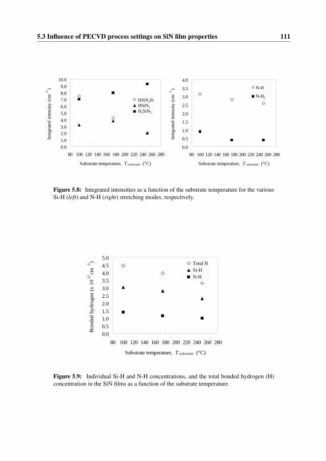
5.3 Influence of PECVD process settings on SiN film properties 111
0.0
0.5
1.0
1.5
2.0
2.5
3.0
3.5
4.0
80 100 120 140 160 180 200 220 240 260 280
Substrate temperature, T substrate (°C)
Inte
grat
ed in
tens
ity (c
m -1
) N-H
N-H2
0.01.02.03.04.05.06.07.08.09.0
10.0
80 100 120 140 160 180 200 220 240 260 280
Substrate temperature, T substrate (°C)
Inte
grat
ed in
tens
ity (c
m -1
)
HSiN2SiHSiN3H2SiN2
HSiN2Si HSiN3 H2SiN2
N-H
N-H2
Figure 5.8: Integrated intensities as a function of the substrate temperature for the variousSi-H (left) and N-H (right) stretching modes, respectively.
0.00.51.01.52.02.53.03.54.04.55.0
80 100 120 140 160 180 200 220 240 260 280
Substrate temperature, T substrate (°C)
Bon
ded
hydr
ogen
(x 1
0 22 c
m -3
) Total-HSiHiNH
Total H Si-H N-H
Figure 5.9: Individual Si-H and N-H concentrations, and the total bonded hydrogen (H)concentration in the SiN films as a function of the substrate temperature.
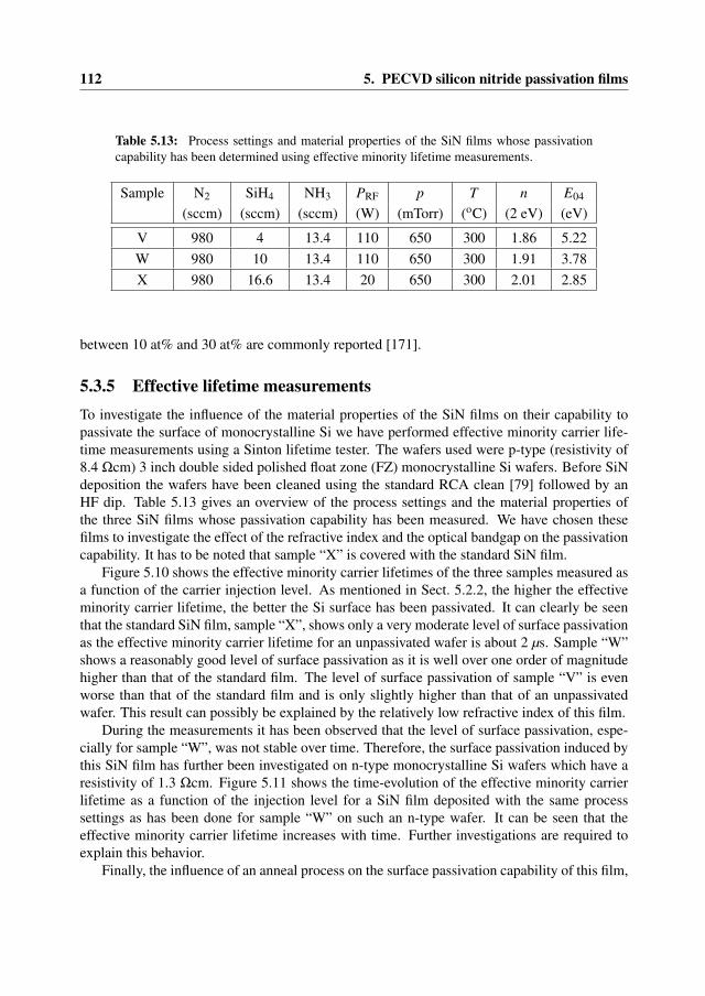
112 5. PECVD silicon nitride passivation films
Table 5.13: Process settings and material properties of the SiN films whose passivationcapability has been determined using effective minority lifetime measurements.
Sample N2 SiH4 NH3 PRF p T n E04
(sccm) (sccm) (sccm) (W) (mTorr) (oC) (2 eV) (eV)
V 980 4 13.4 110 650 300 1.86 5.22W 980 10 13.4 110 650 300 1.91 3.78X 980 16.6 13.4 20 650 300 2.01 2.85
between 10 at% and 30 at% are commonly reported [171].
5.3.5 Effective lifetime measurementsTo investigate the influence of the material properties of the SiN films on their capability topassivate the surface of monocrystalline Si we have performed effective minority carrier life-time measurements using a Sinton lifetime tester. The wafers used were p-type (resistivity of8.4 Ωcm) 3 inch double sided polished float zone (FZ) monocrystalline Si wafers. Before SiNdeposition the wafers have been cleaned using the standard RCA clean [79] followed by anHF dip. Table 5.13 gives an overview of the process settings and the material properties ofthe three SiN films whose passivation capability has been measured. We have chosen thesefilms to investigate the effect of the refractive index and the optical bandgap on the passivationcapability. It has to be noted that sample “X” is covered with the standard SiN film.
Figure 5.10 shows the effective minority carrier lifetimes of the three samples measured asa function of the carrier injection level. As mentioned in Sect. 5.2.2, the higher the effectiveminority carrier lifetime, the better the Si surface has been passivated. It can clearly be seenthat the standard SiN film, sample “X”, shows only a very moderate level of surface passivationas the effective minority carrier lifetime for an unpassivated wafer is about 2 µs. Sample “W”shows a reasonably good level of surface passivation as it is well over one order of magnitudehigher than that of the standard film. The level of surface passivation of sample “V” is evenworse than that of the standard film and is only slightly higher than that of an unpassivatedwafer. This result can possibly be explained by the relatively low refractive index of this film.
During the measurements it has been observed that the level of surface passivation, espe-cially for sample “W”, was not stable over time. Therefore, the surface passivation induced bythis SiN film has further been investigated on n-type monocrystalline Si wafers which have aresistivity of 1.3 Ωcm. Figure 5.11 shows the time-evolution of the effective minority carrierlifetime as a function of the injection level for a SiN film deposited with the same processsettings as has been done for sample “W” on such an n-type wafer. It can be seen that theeffective minority carrier lifetime increases with time. Further investigations are required toexplain this behavior.
Finally, the influence of an anneal process on the surface passivation capability of this film,
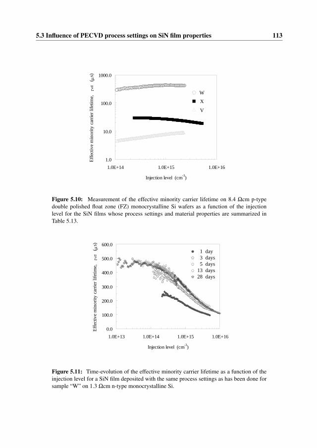
5.3 Influence of PECVD process settings on SiN film properties 113
1.0
10.0
100.0
1000.0
1.0E+14 1.0E+15 1.0E+16
Injection level (cm-3)
Effe
ctiv
e m
inor
ity c
arrie
r life
time,
τe
ff ( µ
s)W
V
X
Figure 5.10: Measurement of the effective minority carrier lifetime on 8.4 Ωcm p-typedouble polished float zone (FZ) monocrystalline Si wafers as a function of the injectionlevel for the SiN films whose process settings and material properties are summarized inTable 5.13.
0.0
100.0
200.0
300.0
400.0
500.0
600.0
1.0E+13 1.0E+14 1.0E+15 1.0E+16
Injection level (cm-3)
Effe
ctiv
e m
inor
ity c
arrie
r life
time,
τe
ff ( µ
s)
1 3 5
13 28
day days daysdaysdays
Figure 5.11: Time-evolution of the effective minority carrier lifetime as a function of theinjection level for a SiN film deposited with the same process settings as has been done forsample “W” on 1.3 Ωcm n-type monocrystalline Si.
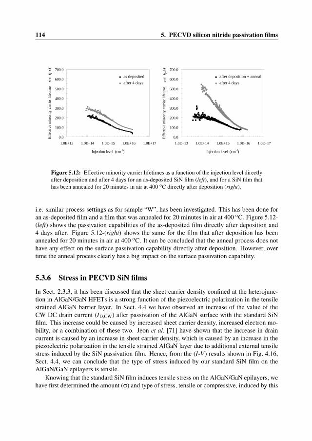
114 5. PECVD silicon nitride passivation films
0.0
100.0
200.0
300.0
400.0
500.0
600.0
700.0
1.0E+13 1.0E+14 1.0E+15 1.0E+16 1.0E+17
Injection level (cm-3)
Effe
ctiv
e m
inor
ity c
arrie
r life
time,
τe
ff ( µ
s)
after 4 daysafter deposition + anneal
0.0
100.0
200.0
300.0
400.0
500.0
600.0
700.0
1.0E+13 1.0E+14 1.0E+15 1.0E+16 1.0E+17
Injection level (cm-3)
Effe
ctiv
e m
inor
ity c
arrie
r life
time,
τe
ff ( µ
s)
as depositedafter 4 days
Figure 5.12: Effective minority carrier lifetimes as a function of the injection level directlyafter deposition and after 4 days for an as-deposited SiN film (left), and for a SiN film thathas been annealed for 20 minutes in air at 400 oC directly after deposition (right).
i.e. similar process settings as for sample “W”, has been investigated. This has been done foran as-deposited film and a film that was annealed for 20 minutes in air at 400 oC. Figure 5.12-(left) shows the passivation capabilities of the as-deposited film directly after deposition and4 days after. Figure 5.12-(right) shows the same for the film that after deposition has beenannealed for 20 minutes in air at 400 oC. It can be concluded that the anneal process does nothave any effect on the surface passivation capability directly after deposition. However, overtime the anneal process clearly has a big impact on the surface passivation capability.
5.3.6 Stress in PECVD SiN films
In Sect. 2.3.3, it has been discussed that the sheet carrier density confined at the heterojunc-tion in AlGaN/GaN HFETs is a strong function of the piezoelectric polarization in the tensilestrained AlGaN barrier layer. In Sect. 4.4 we have observed an increase of the value of theCW DC drain current (ID,CW) after passivation of the AlGaN surface with the standard SiNfilm. This increase could be caused by increased sheet carrier density, increased electron mo-bility, or a combination of these two. Jeon et al. [71] have shown that the increase in draincurrent is caused by an increase in sheet carrier density, which is caused by an increase in thepiezoelectric polarization in the tensile strained AlGaN layer due to additional external tensilestress induced by the SiN passivation film. Hence, from the (I-V) results shown in Fig. 4.16,Sect. 4.4, we can conclude that the type of stress induced by our standard SiN film on theAlGaN/GaN epilayers is tensile.
Knowing that the standard SiN film induces tensile stress on the AlGaN/GaN epilayers, wehave first determined the amount (σ) and type of stress, tensile or compressive, induced by this
5.4 Influence of SiN properties and surface preparation on passivation and leakage 115
film on a Si substrate. Independent of the absolute result, this information serves as a referencethat can be used to correlate the changes in the amount and type of stress of different SiNfilms deposited on Si substrates to changes in the stress induced by these films on AlGaN/GaNepilayers. The different films have been deposited on 4 inch monocrystalline Si substratesand the measurements have been performed by Eugene Timmering and Johan Klootwijk fromPhilips Research Laboratories Eindhoven.
From the range of SiN films that have been deposited on Si substrates using different pro-cess settings, we have selected a set of films for which we will investigate both the ability topassivate the AlGaN barrier layer of AlGaN/GaN HFETs and the amount of gate and drainleakage currents in these devices after deposition. The process settings and material propertiesof these films are listed in Table 5.14. We have chosen this set for the following reasons:
• sample “A” versus sample “G” (standard film), indicates the influence of the opticalbandgap (E04),
• sample “L” versus samples “A” and “G”, separates the influence of the optical bandgapand RF power (PRF),
• sample “W” versus sample “N”, shows the influence of total gas pressure (p), and
• samples “G”, “L”, and “W”, enable the correlation of the effective minority lifetimemeasurements on Si to the surface passivation of AlGaN.
To investigate the influence of the hydrogen content of SiN films on their capability of passi-vating the AlGaN barrier layer, we have also tested the films from the substrate temperatureseries on AlGaN/GaN HFETs. The process settings and material properties of these films havealso been listed in Table 5.14.
The amount (σ) and type of stress, tensile or compressive, induced by the films listed inTable 5.14 on 4 inch monocrystalline Si substrates have been determined. The results for thefilms deposited at 300 oC are listed in Table 5.15. The results for the films from the temperatureseries are shown in Fig. 5.13. It has to be noted that the target thickness of all films is 100 nm.
From Table 5.15 it becomes clear that all SiN films induce tensile stress on the Si substrateswhich is the same type of stress induced by the standard film on the AlGaN/GaN epilayers.Hence, we assume that deposition of films “G”, “A”, “L”, and “N” on AlGaN/GaN HFETs willresult in an increased DC drain current. The influence on the electrical device results will bedescribed in Sect. 5.4. Figure 5.13 shows that all films but the one deposited at 100 oC inducetensile stress on the Si substrates. In addition, it can be observed that the amount of stress is astrong function of the substrate temperature.
5.4 Influence of SiN properties and surface preparation onpassivation and leakage
In this section we will describe the influence of the film properties of the different PECVD SiNfilms listed in Table 5.14 and the preparation of the AlGaN barrier layer before SiN deposition

116 5. PECVD silicon nitride passivation films
Table 5.14: Process settings and material properties of the SiN films that have been selectedto investigate both the ability to passivate the AlGaN barrier layer of AlGaN/GaN HFETsand the amount of gate and drain leakage currents in these devices after deposition.
Sample SiH4 NH3 PRF p T n k E04
(sccm) (sccm) (W) (mTorr) (oC) (2 eV) (3.44 eV) (eV)
H 20 13.4 20 650 300 2.07 0.078 2.68G 16.6 13.4 20 650 300 2.01 0.030 2.85C 10 13.4 20 650 300 1.88 0 4.15A 4 13.4 20 650 300 1.82 0 4.38L 4 13.4 110 650 300 1.86 0 5.22W 10 13.4 110 650 300 1.91 0 3.78N 12 13.4 110 150 300 1.86 0 4.99Q 16.6 13.4 20 650 100 1.84 0.010 3.10R 16.6 13.4 20 650 175 1.90 0.020 2.92S 16.6 13.4 20 650 250 1.95 0.025 2.87U 16.6 13.4 20 650 350 2.04 0.042 2.74
Table 5.15: Amount and type of stress induced by selected films on 4 inch monocrystallineSi substrates. The target thickness of all films is 100 nm.
Sample σ type(MPa)
G 390 tensileA 540 tensileL 350 tensileN 450 tensile
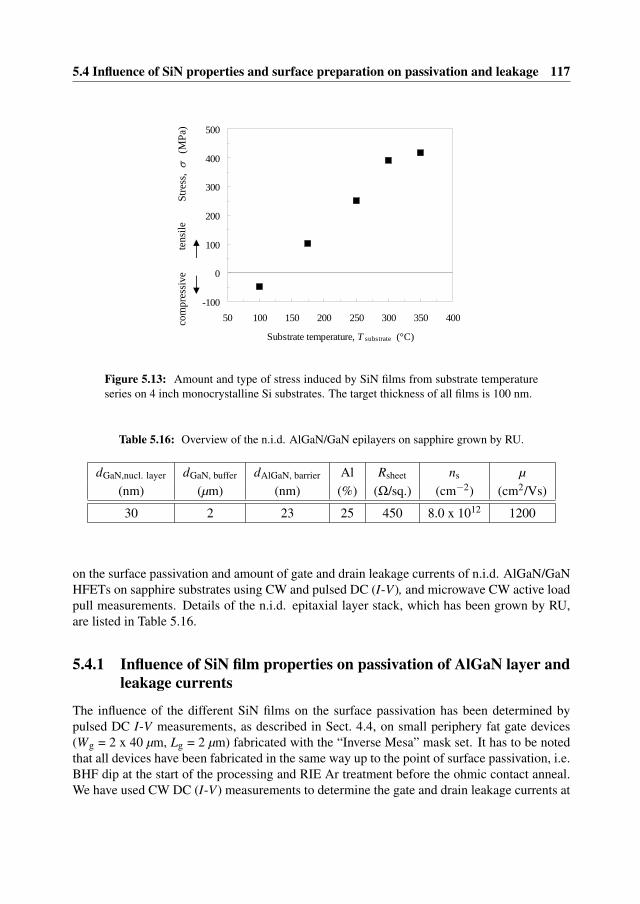
5.4 Influence of SiN properties and surface preparation on passivation and leakage 117
-100
0
100
200
300
400
500
50 100 150 200 250 300 350 400
Substrate temperature, T substrate (°C)
Stre
ss, σ
(MPa
)co
mpr
essi
vete
nsile
Figure 5.13: Amount and type of stress induced by SiN films from substrate temperatureseries on 4 inch monocrystalline Si substrates. The target thickness of all films is 100 nm.
Table 5.16: Overview of the n.i.d. AlGaN/GaN epilayers on sapphire grown by RU.
dGaN,nucl. layer dGaN, buffer dAlGaN, barrier Al Rsheet ns µ(nm) (µm) (nm) (%) (Ω/sq.) (cm−2) (cm2/Vs)
30 2 23 25 450 8.0 x 10¹² 1200
on the surface passivation and amount of gate and drain leakage currents of n.i.d. AlGaN/GaNHFETs on sapphire substrates using CW and pulsed DC (I-V), and microwave CW active loadpull measurements. Details of the n.i.d. epitaxial layer stack, which has been grown by RU,are listed in Table 5.16.
5.4.1 Influence of SiN film properties on passivation of AlGaN layer andleakage currents
The influence of the different SiN films on the surface passivation has been determined bypulsed DC I-V measurements, as described in Sect. 4.4, on small periphery fat gate devices(Wg = 2 x 40 µm, Lg = 2 µm) fabricated with the “Inverse Mesa” mask set. It has to be notedthat all devices have been fabricated in the same way up to the point of surface passivation, i.e.BHF dip at the start of the processing and RIE Ar treatment before the ohmic contact anneal.We have used CW DC (I-V) measurements to determine the gate and drain leakage currents at
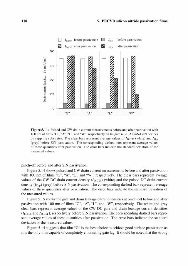
118 5. PECVD silicon nitride passivation films
0
125
250
375
500
1 2 3 4
Dra
in c
urre
nt d
ensit
y,
ID
(m
A/m
m) ll
lID,CW before passivation
ID,CW after passivation
ID,p before passivation
ID,p after passivation
“G” “A” “L” “W”
Figure 5.14: Pulsed and CW drain current measurements before and after passivation with100 nm of films “G”, “A”, “L”, and “W”, respectively on fat gate n.i.d. AlGaN/GaN deviceson sapphire substrates. The clear bars represent average values of ID,CW (white) and ID,p(grey) before SiN passivation. The corresponding dashed bars represent average valuesof these quantities after passivation. The error bars indicate the standard deviation of themeasured values.
pinch-off before and after SiN passivation.Figure 5.14 shows pulsed and CW drain current measurements before and after passivation
with 100 nm of films “G”, “A”, “L”, and “W”, respectively. The clear bars represent averagevalues of the CW DC drain current density (ID,CW) (white) and the pulsed DC drain currentdensity (ID,p) (grey) before SiN passivation. The corresponding dashed bars represent averagevalues of these quantities after passivation. The error bars indicate the standard deviation ofthe measured values.
Figure 5.15 shows the gate and drain leakage current densities at pinch-off before and afterpassivation with 100 nm of films “G”, “A”, “L”, and “W”, respectively. The white and greyclear bars represent average values of the CW DC gate and drain leakage current densities(IG,leak and ID,leak), respectively before SiN passivation. The corresponding dashed bars repre-sent average values of these quantities after passivation. The error bars indicate the standarddeviation of the measured values.
Figure 5.14 suggests that film “G” is the best choice to achieve good surface passivation asit is the only film capable of completely eliminating gate lag. It should be noted that the strong
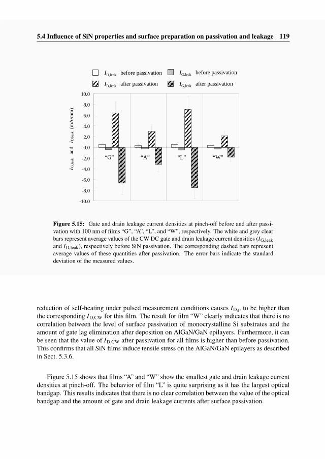
ID,leak before passivation
ID,leak after passivation
IG,leak before passivation
IG,leak after passivation
-10.0
-8.0
-6.0
-4.0
-2.0
0.0
2.0
4.0
6.0
8.0
10.0
1 2 3 4
IG
,leak
a
nd
I D,le
ak
(mA
/mm
) lll
“G” “A” “L” “W”
5.4 Influence of SiN properties and surface preparation on passivation and leakage 119
Figure 5.15: Gate and drain leakage current densities at pinch-off before and after passi-vation with 100 nm of films “G”, “A”, “L”, and “W”, respectively. The white and grey clearbars represent average values of the CW DC gate and drain leakage current densities (IG,leakand ID,leak), respectively before SiN passivation. The corresponding dashed bars representaverage values of these quantities after passivation. The error bars indicate the standarddeviation of the measured values.
reduction of self-heating under pulsed measurement conditions causes ID,p to be higher thanthe corresponding ID,CW for this film. The result for film “W” clearly indicates that there is nocorrelation between the level of surface passivation of monocrystalline Si substrates and theamount of gate lag elimination after deposition on AlGaN/GaN epilayers. Furthermore, it canbe seen that the value of ID,CW after passivation for all films is higher than before passivation.This confirms that all SiN films induce tensile stress on the AlGaN/GaN epilayers as describedin Sect. 5.3.6.
Figure 5.15 shows that films “A” and “W” show the smallest gate and drain leakage currentdensities at pinch-off. The behavior of film “L” is quite surprising as it has the largest opticalbandgap. This results indicates that there is no clear correlation between the value of the opticalbandgap and the amount of gate and drain leakage currents after surface passivation.

120 5. PECVD silicon nitride passivation films
0
125
250
375
500
1 2 3 4 5
Dra
in c
urre
nt d
ensit
y,
ID
(m
A/m
m) ll
lID,CW before passivation
ID,CW after passivation
ID,p before passivation
ID,p after passivation
“G”
300°C
“Q”
100°C
“R”
175°C
“U”
350°C
“S”
250°C
Figure 5.16: Pulsed and CW drain current measurements before and after passivationwith 100 nm of films “Q”, “R”, “S”, “G”, and “U”, from the temperature series on fat gaten.i.d. AlGaN/GaN devices on sapphire substrates. The clear bars represent average valuesof ID,CW (white) and ID,p (grey) before SiN passivation. The corresponding dashed barsrepresent average values of these quantities after passivation. The error bars indicate thestandard deviation of the measured values.
Temperature series
To determine the influence of the hydrogen content of SiN films on the surface passivation andamount of gate and drain leakage currents we have deposited 100 nm of films “Q”, “R”, “S”,“G”, and “U”, see Table 5.14, on the n.i.d. AlGaN/GaN devices. Figures 5.16 and 5.17 showpulsed and CW drain current measurements before and after passivation, and gate and drainleakage current densities for the different films from the temperature series, respectively.
Figure 5.16 shows that film “G” achieves the best surface passivation. This clearly pointsout that the hydrogen content does not play the same role in surface passivation of AlGaN/GaNHFETs as it does in surface passivation of monocrystalline Si substrates. In addition, it shouldbe noted that only for film “Q”, the CW drain current (ID,CW ) after passivation is slightlylower that before passivation. This could be caused by the fact that this film induces compres-sive stress on the AlGaN/GaN epilayers whereas the films deposited at higher temperaturesinduce tensile stress. This result correlates with the measurements of the amount and type of
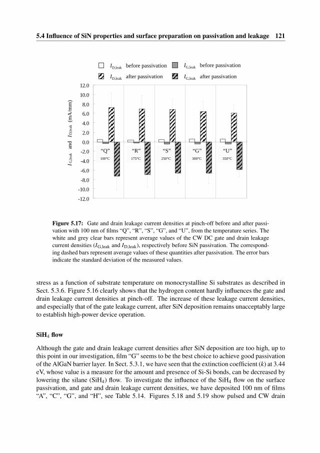
5.4 Influence of SiN properties and surface preparation on passivation and leakage 121
-12.0
-10.0
-8.0
-6.0
-4.0
-2.0
0.0
2.0
4.0
6.0
8.0
10.0
12.0
1 2 3 4 5
IG
,leak
a
nd
I D,le
ak
(mA
/mm
) lll
ID,leak before passivation
ID,leak after passivation
IG,leak before passivation
IG,leak after passivation
“G”300°C
“Q”100°C
“R”175°C
“U”350°C
“S”250°C
Figure 5.17: Gate and drain leakage current densities at pinch-off before and after passi-vation with 100 nm of films “Q”, “R”, “S”, “G”, and “U”, from the temperature series. Thewhite and grey clear bars represent average values of the CW DC gate and drain leakagecurrent densities (IG,leak and ID,leak), respectively before SiN passivation. The correspond-ing dashed bars represent average values of these quantities after passivation. The error barsindicate the standard deviation of the measured values.
stress as a function of substrate temperature on monocrystalline Si substrates as described inSect. 5.3.6. Figure 5.16 clearly shows that the hydrogen content hardly influences the gate anddrain leakage current densities at pinch-off. The increase of these leakage current densities,and especially that of the gate leakage current, after SiN deposition remains unacceptably largeto establish high-power device operation.
SiH4 flow
Although the gate and drain leakage current densities after SiN deposition are too high, up tothis point in our investigation, film “G” seems to be the best choice to achieve good passivationof the AlGaN barrier layer. In Sect. 5.3.1, we have seen that the extinction coefficient (k) at 3.44eV, whose value is a measure for the amount and presence of Si-Si bonds, can be decreased bylowering the silane (SiH4) flow. To investigate the influence of the SiH4 flow on the surfacepassivation, and gate and drain leakage current densities, we have deposited 100 nm of films“A”, “C”, “G”, and “H”, see Table 5.14. Figures 5.18 and 5.19 show pulsed and CW drain
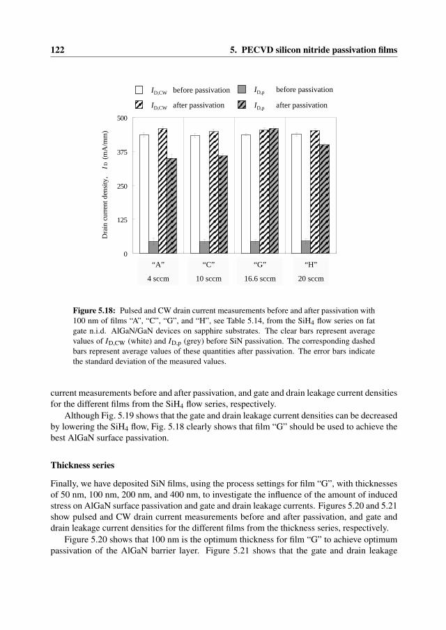
122 5. PECVD silicon nitride passivation films
0
125
250
375
500
1 2 3 4
Dra
in c
urre
nt d
ensit
y,
ID
(m
A/m
m) ll
l
ID,CW before passivation
ID,CW after passivation
ID,p before passivation
ID,p after passivation
“H”
20 sccm
“A”
4 sccm
“C”
10 sccm
“G”
16.6 sccm
Figure 5.18: Pulsed and CW drain current measurements before and after passivation with100 nm of films “A”, “C”, “G”, and “H”, see Table 5.14, from the SiH4 flow series on fatgate n.i.d. AlGaN/GaN devices on sapphire substrates. The clear bars represent averagevalues of ID,CW (white) and ID,p (grey) before SiN passivation. The corresponding dashedbars represent average values of these quantities after passivation. The error bars indicatethe standard deviation of the measured values.
current measurements before and after passivation, and gate and drain leakage current densitiesfor the different films from the SiH4 flow series, respectively.
Although Fig. 5.19 shows that the gate and drain leakage current densities can be decreasedby lowering the SiH4 flow, Fig. 5.18 clearly shows that film “G” should be used to achieve thebest AlGaN surface passivation.
Thickness series
Finally, we have deposited SiN films, using the process settings for film “G”, with thicknessesof 50 nm, 100 nm, 200 nm, and 400 nm, to investigate the influence of the amount of inducedstress on AlGaN surface passivation and gate and drain leakage currents. Figures 5.20 and 5.21show pulsed and CW drain current measurements before and after passivation, and gate anddrain leakage current densities for the different films from the thickness series, respectively.
Figure 5.20 shows that 100 nm is the optimum thickness for film “G” to achieve optimumpassivation of the AlGaN barrier layer. Figure 5.21 shows that the gate and drain leakage
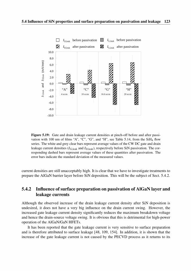
5.4 Influence of SiN properties and surface preparation on passivation and leakage 123
-10.0
-8.0
-6.0
-4.0
-2.0
0.0
2.0
4.0
6.0
8.0
10.0
1 2 3 4
IG
,leak
a
nd
I D,le
ak
(mA
/mm
) lll
“H”20 sccm
“A”4 sccm
“C”10 sccm
“G”16.6 sccm
ID,leak before passivation
ID,leak after passivation
IG,leak before passivation
IG,leak after passivation
Figure 5.19: Gate and drain leakage current densities at pinch-off before and after passi-vation with 100 nm of films “A”, “C”, “G”, and “H”, see Table 5.14, from the SiH4 flowseries. The white and grey clear bars represent average values of the CW DC gate and drainleakage current densities (IG,leak and ID,leak), respectively before SiN passivation. The cor-responding dashed bars represent average values of these quantities after passivation. Theerror bars indicate the standard deviation of the measured values.
current densities are still unacceptably high. It is clear that we have to investigate treatments toprepare the AlGaN barrier layer before SiN deposition. This will be the subject of Sect. 5.4.2.
5.4.2 Influence of surface preparation on passivation of AlGaN layer andleakage currents
Although the observed increase of the drain leakage current density after SiN deposition isundesired, it does not have a very big influence on the drain current swing. However, theincreased gate leakage current density significantly reduces the maximum breakdown voltageand hence the drain-source voltage swing. It is obvious that this is detrimental for high-poweroperation of the AlGaN/GaN HFETs.
It has been reported that the gate leakage current is very sensitive to surface preparationand is therefore attributed to surface leakage [48, 109, 154]. In addition, it is shown that theincrease of the gate leakage current is not caused by the PECVD process as it returns to its
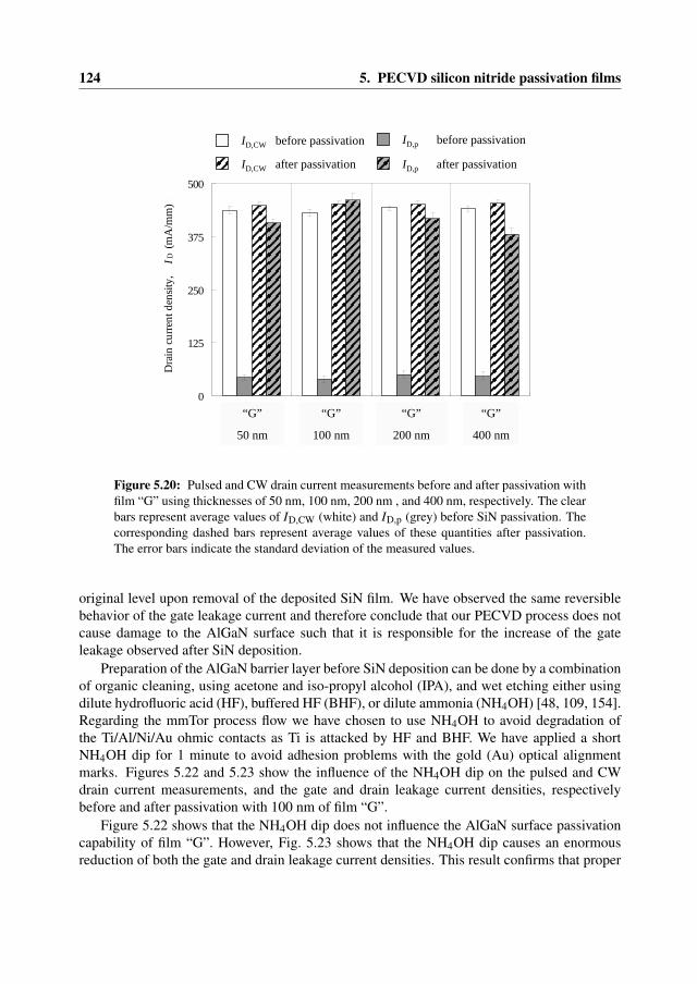
124 5. PECVD silicon nitride passivation films
0
125
250
375
500
1 2 3 4
Dra
in c
urre
nt d
ensit
y,
ID
(m
A/m
m) ll
l
ID,CW before passivation
ID,CW after passivation
ID,p before passivation
ID,p after passivation
“G”
400 nm
“G”
50 nm
“G”
100 nm
“G”
200 nm
Figure 5.20: Pulsed and CW drain current measurements before and after passivation withfilm “G” using thicknesses of 50 nm, 100 nm, 200 nm , and 400 nm, respectively. The clearbars represent average values of ID,CW (white) and ID,p (grey) before SiN passivation. Thecorresponding dashed bars represent average values of these quantities after passivation.The error bars indicate the standard deviation of the measured values.
original level upon removal of the deposited SiN film. We have observed the same reversiblebehavior of the gate leakage current and therefore conclude that our PECVD process does notcause damage to the AlGaN surface such that it is responsible for the increase of the gateleakage observed after SiN deposition.
Preparation of the AlGaN barrier layer before SiN deposition can be done by a combinationof organic cleaning, using acetone and iso-propyl alcohol (IPA), and wet etching either usingdilute hydrofluoric acid (HF), buffered HF (BHF), or dilute ammonia (NH4OH) [48, 109, 154].Regarding the mmTor process flow we have chosen to use NH4OH to avoid degradation ofthe Ti/Al/Ni/Au ohmic contacts as Ti is attacked by HF and BHF. We have applied a shortNH4OH dip for 1 minute to avoid adhesion problems with the gold (Au) optical alignmentmarks. Figures 5.22 and 5.23 show the influence of the NH4OH dip on the pulsed and CWdrain current measurements, and the gate and drain leakage current densities, respectivelybefore and after passivation with 100 nm of film “G”.
Figure 5.22 shows that the NH4OH dip does not influence the AlGaN surface passivationcapability of film “G”. However, Fig. 5.23 shows that the NH4OH dip causes an enormousreduction of both the gate and drain leakage current densities. This result confirms that proper
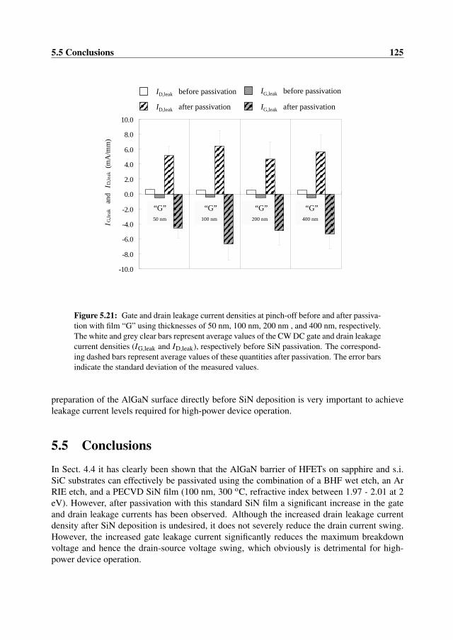
5.5 Conclusions 125
-10.0
-8.0
-6.0
-4.0
-2.0
0.0
2.0
4.0
6.0
8.0
10.0
1 2 3 4
IG
,leak
a
nd
I D,le
ak
(mA
/mm
) lll
ID,leak before passivation
ID,leak after passivation
IG,leak before passivation
IG,leak after passivation
“G”400 nm
“G”50 nm
“G”100 nm
“G”200 nm
Figure 5.21: Gate and drain leakage current densities at pinch-off before and after passiva-tion with film “G” using thicknesses of 50 nm, 100 nm, 200 nm , and 400 nm, respectively.The white and grey clear bars represent average values of the CW DC gate and drain leakagecurrent densities (IG,leak and ID,leak), respectively before SiN passivation. The correspond-ing dashed bars represent average values of these quantities after passivation. The error barsindicate the standard deviation of the measured values.
preparation of the AlGaN surface directly before SiN deposition is very important to achieveleakage current levels required for high-power device operation.
5.5 Conclusions
In Sect. 4.4 it has clearly been shown that the AlGaN barrier of HFETs on sapphire and s.i.SiC substrates can effectively be passivated using the combination of a BHF wet etch, an ArRIE etch, and a PECVD SiN film (100 nm, 300 oC, refractive index between 1.97 - 2.01 at 2eV). However, after passivation with this standard SiN film a significant increase in the gateand drain leakage currents has been observed. Although the increased drain leakage currentdensity after SiN deposition is undesired, it does not severely reduce the drain current swing.However, the increased gate leakage current significantly reduces the maximum breakdownvoltage and hence the drain-source voltage swing, which obviously is detrimental for high-power device operation.

126 5. PECVD silicon nitride passivation films
0
125
250
375
500
1 2
Dra
in c
urre
nt d
ensit
y,
ID
(m
A/m
m) ll
l
ID,CW before passivation
ID,CW after passivation
ID,p before passivation
ID,p after passivation
“G”
no NH4OH
“G”
NH4OH
Figure 5.22: Influence of the NH4OH dip on the pulsed and CW drain current measure-ments before and after passivation with 100 nm of film “G”. The clear bars represent averagevalues of ID,CW (white) and ID,p (grey) before SiN passivation. The corresponding dashedbars represent average values of these quantities after passivation. The error bars indicatethe standard deviation of the measured values.
As we assumed that the cause for the increased gate leakage current was related to the SiN-AlGaN interface, we have investigated if changing the composition of the PECVD SiN filmor preparation of the AlGaN barrier layer before SiN deposition, or both, results in decreasedleakage currents after SiN deposition. It should be noted that the surface passivation capabilityshould remain equal to that of the standard film.
This chapter started with a description of our investigations of the influence of the processsettings of an Oxford Plasmalab 100 PECVD system on the SiN film properties. It has tobe noted that this work, as it has been done on monocrystalline Si substrates, can only beused as an indirect reference for the investigations of the surface passivation and amount ofgate and drain leakage currents of AlGaN/GaN HFETs after passivation. Nevertheless, wehave established an overview of the capabilities of the Oxford Plasmalab 100 PECVD systemand gained an understanding about how film properties such as refractive index, extinctioncoefficient, optical bandgap, and stress can be influenced by the process settings, i.e. gas flow,RF power, substrate temperature, and total gas pressure.
From the range of SiN films that have been deposited on Si substrates using different pro-cess settings, we have selected a set of films, see Table 5.14, for which we have investigated
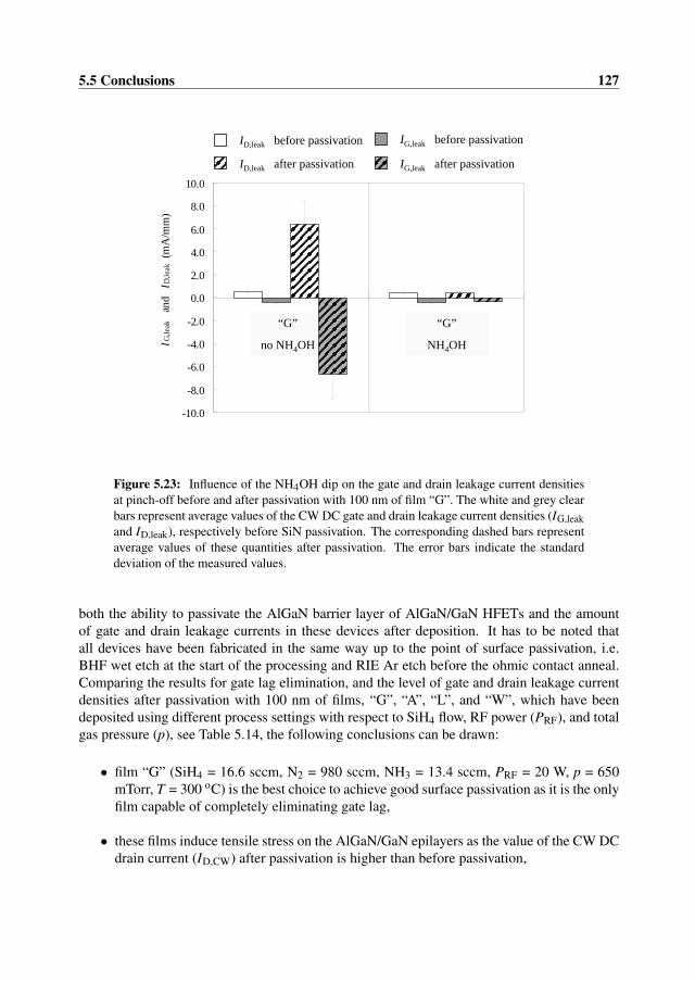
5.5 Conclusions 127
“G”
no NH4OH
-10.0
-8.0
-6.0
-4.0
-2.0
0.0
2.0
4.0
6.0
8.0
10.0
1 2
IG
,leak
a
nd
I D,le
ak
(mA
/mm
) lll
“G”
NH4OH
ID,leak before passivation
ID,leak after passivation
IG,leak before passivation
IG,leak after passivation
Figure 5.23: Influence of the NH4OH dip on the gate and drain leakage current densitiesat pinch-off before and after passivation with 100 nm of film “G”. The white and grey clearbars represent average values of the CW DC gate and drain leakage current densities (IG,leakand ID,leak), respectively before SiN passivation. The corresponding dashed bars representaverage values of these quantities after passivation. The error bars indicate the standarddeviation of the measured values.
both the ability to passivate the AlGaN barrier layer of AlGaN/GaN HFETs and the amountof gate and drain leakage currents in these devices after deposition. It has to be noted thatall devices have been fabricated in the same way up to the point of surface passivation, i.e.BHF wet etch at the start of the processing and RIE Ar etch before the ohmic contact anneal.Comparing the results for gate lag elimination, and the level of gate and drain leakage currentdensities after passivation with 100 nm of films, “G”, “A”, “L”, and “W”, which have beendeposited using different process settings with respect to SiH4 flow, RF power (PRF), and totalgas pressure (p), see Table 5.14, the following conclusions can be drawn:
• film “G” (SiH4 = 16.6 sccm, N2 = 980 sccm, NH3 = 13.4 sccm, PRF = 20 W, p = 650mTorr, T = 300 oC) is the best choice to achieve good surface passivation as it is the onlyfilm capable of completely eliminating gate lag,
• these films induce tensile stress on the AlGaN/GaN epilayers as the value of the CW DCdrain current (ID,CW) after passivation is higher than before passivation,
128 5. PECVD silicon nitride passivation films
• there is no correlation between the level of surface passivation of monocrystalline Si sub-strates and the amount of gate lag elimination after deposition on AlGaN/GaN epilayers,and
• there is no clear correlation between the value of the optical bandgap (E04) and theamount of gate and drain leakage currents after surface passivation.
From the temperature series, films “Q”, “R”, “S”, “G”, and “U” (Table 5.14) respectively,we can conclude that the hydrogen content of the SiN films does not play the same role insurface passivation of AlGaN/GaN HFETs as it does in surface passivation of monocrystallineSi substrates.
From the SiH4 flow series, films “A”, “C”, “G”, and “H” (Table 5.14) respectively, it can beconcluded that the value of the extinction coefficient (k) at 3.44 eV, which is a measure for theamount and presence of Si-Si bonds, should be minimized to reduce the gate and drain leakagecurrents after SiN deposition. However, the best passivation of the AlGaN surface is achievedby film “G” for which the value of the extinction coefficient equals 0.030.
From the results of the thickness series, 50 nm, 100 nm, 200 nm , and 400 nm of film “G”respectively, it can be concluded that 100 nm is the optimum thickness for this film to achievegood passivation of the AlGaN barrier layer.
Finally, as the gate and drain leakage current densities remained unacceptably high forhigh-power device operation, we have investigated the influence of the preparation of the Al-GaN barrier layer directly before SiN deposition on both gate lag elimination and the gate anddrain leakage current densities after passivation with 100 nm of film “G”. It has been reportedthat the gate leakage current is very sensitive to surface preparation and is therefore attributedto surface leakage [48, 109, 154]. In addition, it is shown that the increase of the gate leakagecurrent is not caused by the PECVD process as it returns to its original level upon removal ofthe deposited SiN film. We have observed the same reversible behavior of the gate leakagecurrent and therefore conclude that our PECVD process does not cause damage to the AlGaNsurface such that it is responsible for the increase of the gate leakage observed after SiN de-position. Preparation of the AlGaN surface can be done by a combination of organic cleaning,using acetone and iso-propyl alcohol (IPA), and wet etching either using dilute hydrofluoricacid (HF), buffered HF (BHF), or dilute ammonia (NH4OH) [48, 109]. Regarding the mmTorprocess flow we have chosen to use NH4OH to avoid degradation of the Ti/Al/Ni/Au ohmiccontacts as Ti is attacked by HF and BHF. We have applied a short NH4OH dip for 1 minute toavoid adhesion problems with the gold (Au) optical alignment marks. Although the NH4OHdip does not influence the AlGaN surface passivation capability of film “G”, it causes an enor-mous reduction of both the gate and drain leakage current densities from about 6.7 mA/mmto 400 µA/mm. This result confirms that proper preparation of the AlGaN surface directly be-fore SiN deposition is very important to achieve leakage current levels required for high-powerdevice operation.
To conclude, passivation of the AlGaN barrier layer of the large periphery microwave high-power AlGaN/GaN HFETs, whose performance will be presented in Chapter 6, has been doneusing an NH4OH dip for 1 minute, which is immediately followed by the deposition of 100

5.5 Conclusions 129
nm SiN according to the PECVD process settings for film “G” (SiH4 = 16.6 sccm, N2 = 980sccm, NH3 = 13.4 sccm, PRF = 20 W, p = 650 mTorr, T = 300 oC).

130 5. PECVD silicon nitride passivation films
Chapter 6
Device results
In this chapter we will present measurement results of small and large gate periphery HFETsfabricated by TU/e using MOCVD n.i.d. AlGaN/GaN epilayers on s.i. 4H-SiC substratesgrown by RU [146]. The development of both the epitaxial growth process, and the processtechnology required to fabricate microwave high-power HFETs have proven to be major chal-lenges and therefore are the main topics of this thesis. The measurement results presented inthis chapter, will illustrate the successful integration of process modules such as ohmic andSchottky contact technology, device isolation, electron beam lithography, surface passivation,and air bridge technology, into a process flow that enables the fabrication of large n.i.d. Al-GaN/GaN HFETs that are capable of producing an output power density of 11.9 W/mm atS-band (2 GHz - 4 GHz).
6.1 Introduction
We will start with a brief description of the measurement techniques used to determine the DC(I-V) characteristics, the small-signal S-parameters, and the microwave power performance ofboth small and large gate periphery n.i.d. AlGaN/GaN HFETs on s.i. 4H-SiC substrates. Next,we will present the measurement results of the small devices which have a total gate width(Wg) of 80 µm and a gate length (Lg) of 0.25 µm. These devices, which have been fabricatedusing the “Submu” mask set described in Sect. 3.2.1, have been used for short loop experimentsto tune the fabrication process before fabricating the large devices with values for Wg of 0.25mm, 0.5 mm, and 1.0 mm, respectively. After this, we will present the measurement results ofthese large AlGaN/GaN HFETs, which have values for Lg of 0.7 µm and have been fabricatedusing the “mmTor” mask set that has also been described in Sect. 3.2.1. Finally, we will presentthe conclusions that can be drawn from the measurement results.
131
132 6. Device results
6.2 Measurement techniquesIn this section, we will give a brief description of the measurement techniques used to deter-mine the DC (I-V) characteristics, the small-signal S-parameters, and the microwave powerperformance of both small and large gate periphery n.i.d. AlGaN/GaN HFETs on s.i. 4H-SiC substrates. All measurements have been performed on-wafer using ground-signal-ground(GSG) RF probes and without any active chip cooling. The measurements have been per-formed in cooperation with Thieu Kwaspen from TU/e, Erwin Suijker from TNO Defence,Security and Safety, Thomas Rödle from Philips Semiconductors, and Iouri Volokhine fromPhilips Research Eindhoven. The scope of the measurements has been to monitor the influenceof device design, both epitaxial design and layout, and processing on device performance. Fig-ures of merit used to evaluate the latter are the minimum value of the knee voltage (Vknee) andthe maximum values of the:
• drain current (ID),
• gate and drain leakage currents at pinch-off (IG,leak and ID,leak),
• breakdown voltage (VBD),
• extrinsic transconductance (gm,ext),
• extrinsic unity current gain frequency (f T),
• extrinsic unity power gain frequency (f max),
• output power (Pout) and output power density (PD),
• associated power gain (Gp), and
• power added efficiency (PAE).
6.2.1 DC current-voltage measurementsThe DC (I-V) output characteristics, i.e. (ID−VDS), and the transfer characteristics, i.e. (ID−VGS), of the AlGaN/GaN HFETs have been obtained either by continuous wave (CW) or pulsedon-wafer measurements using an HP4142B DC supply at TNO Defence, Security and Safety.As no active cooling of the devices under test (DUTs) has been applied, we have done pulsedmeasurements for devices with total gate peripheries larger than 250 µm to avoid excessiveself-heating and the resulting decrease of the drain current for increasing drain-source (VDS)bias voltages. This decrease of the drain current can be observed in the output characteristicsas a negative slope of the (ID −VDS) curves in the saturation region, i.e. VDS > Vknee. Thepulsed I-V measurements were performed using a pulse width (PW) of 10 µs, and a duty cycle(dc) of 10 %.
From the DC I-V measurements we have determined values for ID,max, IG,leak, ID,leak, VBD,Vknee, and gm,ext. To estimate the microwave output power that can be achieved if the device is

6.2 Measurement techniques 133
biased in class A, i.e. ID= 0.5·ID,max, we can use Eqn. 2.16. However, as the processed devicessuffer from a certain amount of drain leakage current at pinch-off (ID,leak), the term ID,max inEqn. 2.16 has to be replaced by (ID,max− ID,leak), yielding
Pout,max =(VBD−Vknee) · (ID,max− ID,leak)
8. (6.1)
The maximum drain current densities of state-of-the-art AlGaN/GaN HFETs range from 1.0A/mm to 1.5 A/mm [8, 85, 174]. Hence, from Eqn. 6.1 it is obvious that breakdown voltagesover 160 V are required to achieve record output power densities larger than 30 W/mm [174]for class A operation. For breakdown voltages the distinction between off-state and on-statebreakdown voltages (VBD,off and VBD,on, respectively) is often made due to the difference inbreakdown mechanism. In general, VBD,off is dominated by a combination of thermionic fieldemission (TFE) and tunneling of electrons from the gate into the channel, whereas impactionization in the channel, when a considerable amount of current is flowing through the device,dominates VBD,on [120, 152]. The operation class used obviously determines whether VBD,offor VBD,on is mostly relevant when choosing the drain-source bias voltage.
The extrinsic transconductance (gm) can be determined from the transfer characteristicsusing
gm =∂ID
∂VGS|VDS=constant. (6.2)
Together with the value for the extrinsic unity current gain frequency (f T), which can be de-termined from small-signal S-parameter measurements as will be discussed in Sect. 6.2.2, thegate-source capacitance (Cgs) can be calculated using Eqn. 4.3.
6.2.2 Small-signal S-parameter measurements
Linear components, or nonlinear components, e.g. transistors, operating with signals suffi-ciently small to cause them to respond in a linear manner, can be completely characterizedby parameters measured at their input and output terminals (ports) while considering the ac-tual component as a “black box”. Among the many representations available, e.g. Z-, Y-, and h-parameters, scattering or S-parameters [96] are the most convenient to use for thecharacterization of components at microwave frequencies because S-parameters can easily bedetermined from the measured ratios of the incident (ai) and reflected (bi) power waves us-ing a network analyzer. The small-signal S-parameter measurements have been performedby Thieu Kwaspen from TU/e, Erwin Suijker from TNO Defence, Security and Safety, andThomas Rödle from Philips Semiconductors using an HP8510C network analyzer in combina-tion with an HP85110A pulsed test-set. Figure 6.1 shows these power waves and the individualS-parameters in the case of a two-port component, e.g. a transistor where the gate-source andthe drain-source terminals are considered as the input and output ports, respectively.
From Fig. 6.1, it becomes clear that the relations between the input and the output of thetwo-port can be represented as
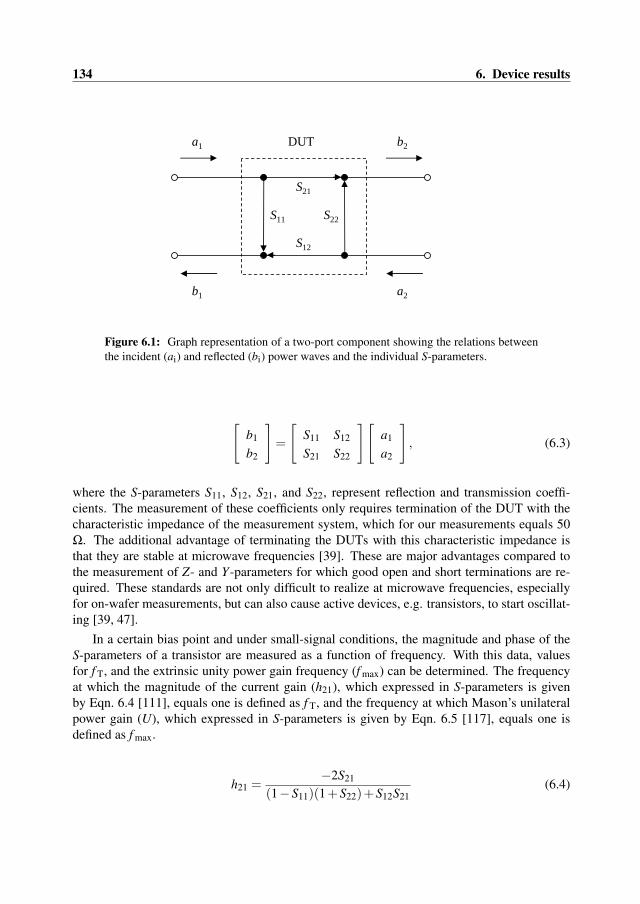
134 6. Device results
DUTa1 b2
a2b1
S11
S12
S21
S22
Figure 6.1: Graph representation of a two-port component showing the relations betweenthe incident (ai) and reflected (bi) power waves and the individual S-parameters.
[b1
b2
]=
[S11 S12
S21 S22
][a1
a2
], (6.3)
where the S-parameters S11, S12, S21, and S22, represent reflection and transmission coeffi-cients. The measurement of these coefficients only requires termination of the DUT with thecharacteristic impedance of the measurement system, which for our measurements equals 50Ω. The additional advantage of terminating the DUTs with this characteristic impedance isthat they are stable at microwave frequencies [39]. These are major advantages compared tothe measurement of Z- and Y-parameters for which good open and short terminations are re-quired. These standards are not only difficult to realize at microwave frequencies, especiallyfor on-wafer measurements, but can also cause active devices, e.g. transistors, to start oscillat-ing [39, 47].
In a certain bias point and under small-signal conditions, the magnitude and phase of theS-parameters of a transistor are measured as a function of frequency. With this data, valuesfor f T, and the extrinsic unity power gain frequency (f max) can be determined. The frequencyat which the magnitude of the current gain (h21), which expressed in S-parameters is givenby Eqn. 6.4 [111], equals one is defined as f T, and the frequency at which Mason’s unilateralpower gain (U), which expressed in S-parameters is given by Eqn. 6.5 [117], equals one isdefined as f max.
h21 =−2S21
(1−S11)(1+S22)+S12S21(6.4)
6.2 Measurement techniques 135
U =
∣∣∣ S21S12−1
∣∣∣2
2[K
∣∣∣ S21S12
∣∣∣−Re(
S21S12
)] (6.5)
In Eqn. 6.5, K is the Rollet stability factor, which expressed in S-parameters, is givenby [144]
K =1−|S11|2−|S22|2 + |S11S22−S12S21|2
2 |S12S21|. (6.6)
The value of K determines whether a transistor operates stable at the frequency of interest orhas a tendency to start oscillating. For K > 1, and |S11S22−S12S21|< 1, the transistor operatesunconditionally stable whereas for K ≤ 1, the stability of the transistor depends on the sourceand load terminations and hence is called conditionally stable. For K < 0, transistor operationis unstable. It has to be noted that the validity of K is rather limited. Actually, it can onlybe applied to discrete devices without any external feedback. In practice, the use of K isvalid for a maximum of two amplifier stages. Furthermore, it cannot be used for devices thatare connected in parallel, which however is very common practice in the case of high-poweramplifiers.
Figure 6.2 shows the theoretical determination of the values for f T and f max from plots ofthe magnitudes of the current gain and the unilateral power gain, |h12|2 and |U | respectively,in decibels (dB) on a linear scale, versus frequency (f ) on a logarithmic scale. It has to benoted that the magnitude of both gains rolls off at a theoretical rate of 6 dB/octave or 20dB/decade. Hence, extrapolation of measurement results to determine the values for f T andf max in practical situations have to be done in those regions where the gain roll-off equals 6dB/octave.
Besides the determination of the high-frequency response of the HFETs from the measuredsmall-signal S-parameters, a start value for the load reflection coefficient (ΓL), which is usedin the active load-pull measurements that will be discussed in Sect. 6.2.3, is found by usingthe complex conjugated value of the measured output reflection coefficient S22, i.e. S∗22, of theHFET [39]. It is well known that, under small-signal conditions, this approach will give themaximum gain and hence maximum output power for a given input power. In addition, thisapproach provides good starting values for parameters like PAE. The use of S∗22 as a startingvalue for ΓL is the first step of a very fast search algorithm, developed by De Hek [38, 39], forfinding the optimum load impedance (ZL), which must be presented to the output of the HFETto achieve maximum power transfer between the source (HFET) and the load.
6.2.3 Active load-pull measurementsActive load-pull measurements, both CW and pulsed, have been performed to determine themaximum output power (Pout), the associated maximum power gain (Gp), and power addedefficiency (PAE) of the AlGaN/GaN HFETs at fundamental frequencies (f 0) of 2 GHz and 4GHz, which are the lower and upper frequency limits, respectively of the so-called S-band. It
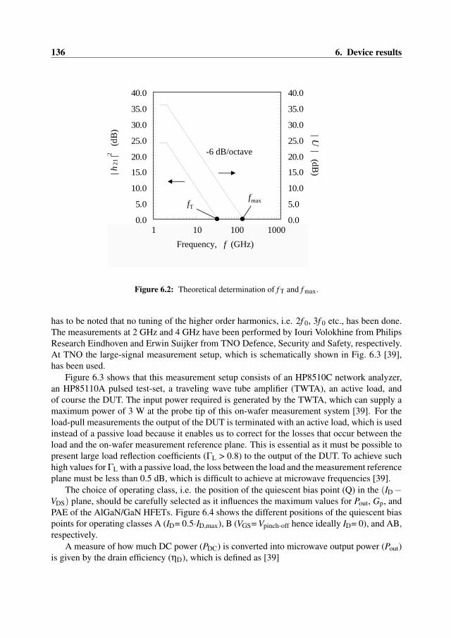
136 6. Device results
0.0
5.0
10.0
15.0
20.0
25.0
30.0
35.0
40.0
1.0E+09 1.0E+10 1.0E+11 1.0E+12Frequency, f (Hz)
| h 2
1 |2
(dB
)
0.0
5.0
10.0
15.0
20.0
25.0
30.0
35.0
40.0
| U | (dB
)
fTfmax
-6 dB/octave
Frequency, f (GHz)1 10 100 1000
Figure 6.2: Theoretical determination of f T and f max.
has to be noted that no tuning of the higher order harmonics, i.e. 2f 0, 3f 0 etc., has been done.The measurements at 2 GHz and 4 GHz have been performed by Iouri Volokhine from PhilipsResearch Eindhoven and Erwin Suijker from TNO Defence, Security and Safety, respectively.At TNO the large-signal measurement setup, which is schematically shown in Fig. 6.3 [39],has been used.
Figure 6.3 shows that this measurement setup consists of an HP8510C network analyzer,an HP85110A pulsed test-set, a traveling wave tube amplifier (TWTA), an active load, andof course the DUT. The input power required is generated by the TWTA, which can supply amaximum power of 3 W at the probe tip of this on-wafer measurement system [39]. For theload-pull measurements the output of the DUT is terminated with an active load, which is usedinstead of a passive load because it enables us to correct for the losses that occur between theload and the on-wafer measurement reference plane. This is essential as it must be possible topresent large load reflection coefficients (ΓL > 0.8) to the output of the DUT. To achieve suchhigh values for ΓL with a passive load, the loss between the load and the measurement referenceplane must be less than 0.5 dB, which is difficult to achieve at microwave frequencies [39].
The choice of operating class, i.e. the position of the quiescent bias point (Q) in the (ID−VDS) plane, should be carefully selected as it influences the maximum values for Pout, Gp, andPAE of the AlGaN/GaN HFETs. Figure 6.4 shows the different positions of the quiescent biaspoints for operating classes A (ID= 0.5·ID,max), B (VGS= Vpinch-off hence ideally ID= 0), and AB,respectively.
A measure of how much DC power (PDC) is converted into microwave output power (Pout)is given by the drain efficiency (ηD), which is defined as [39]

6.2 Measurement techniques 137
HP85110A
pulsed test-setActive load
HP8510C
network analyzer
TWTA
DUT
Figure 6.3: Schematic representation of the large-signal measurement setup used to per-form the active load-pull measurements [39].
0.0
0.2
0.4
0.6
0.8
1.0
1.2
0 10 20 30 40
V DS (V)
ID
(A
)
Qclass A
Qclass AB
Qclass B
Figure 6.4: Different positions of the quiescent bias point (Q) in the (ID−VDS) plane foroperating classes A, B, and AB, respectively.

138 6. Device results
ηD =Pout
PDC. (6.7)
However, the drain efficiency is the maximum achievable efficiency assuming an infinite Gp.Furthermore, it does not take into account the incident microwave power (Pin) that is providedto the device. Therefore, a more relevant measure for transistor efficiency is provided byPAE, because it takes into account the influence of both a finite power gain and the incidentmicrowave power provided to the device. An expression for PAE is given by Eqn. 6.8 [139]
PAE =Pout−Pin
PDC=
Pout
PDC
[1− 1
Gp
]. (6.8)
Equation 6.8 shows that PAE is directly related to the drain efficiency and that Gp shouldbe as high as possible to obtain maximum PAE. In practice, a value for Gp less than 10 dBis unacceptable in terms of PAE reduction [39]. Especially for high-power HFETs, as highas possible values for PAE, i.e. > 50 %, are desirable to avoid excessive heat generation,which causes the drain current to drop as the mobility of the 2DEG electrons decreases withincreasing temperature. Consequently, the output power of the devices also decreases.
Investigations by De Hek [39] have shown that Pout is almost equal for operating classes A,B, and AB. However, maximum PAE is obtained if the devices are biased in class AB. Hence,active load-pull measurements of our AlGaN/GaN HFETs on s.i. 4H-SiC substrates have beenperformed using bias conditions that correspond to an AB operating class.
6.3 Small periphery devices
The small periphery devices have been processed using the “Submu” mask set, which has beendescribed in Sect. 3.2.1. The internal device dimensions using this mask set are: Lg = 0.25 µm,Wg = 80 µm, Wgu = 40 µm, Lgg = 60 µm, Lgs = 1 µm , Lgd = 2 µm ,and Lds = 3.25 µm. For thesub-micrometer gate contacts we have used T-gates. The top of these gates is 0.75 µm wideand the extensions towards the source and drain contacts are both 0.25 µm long. The deviceshave been fabricated on 10 mm x 10 mm samples from wafers 1200, 1201, and 1203, whoselayer stack and material properties are listed in Table 6.1.
Figure 6.5 shows continuous wave (CW) DC (I-V) measurement results for the devices pro-cessed on structures 1200, 1201, and 1203, respectively. The output characteristics (ID−VDS)show maximum drain current densities at VGS = +2 V of 1.0 A/mm, 1.1 A/mm, and 1.2 A/mmfor structures 1203, 1201, and 1200, respectively. These current densities are in perfect agree-ment with the values that can be calculated using the material properties listed in Table 6.1.In addition, it can be concluded that the very thin (1 - 2 nm) AlN layer between the AlGaNbarrier and GaN buffer layers in structure 1200 indeed enhances both the density and mobilityof the 2DEG electrons as this structure shows the highest drain current density. Furthermore,Fig. 6.5 shows that these structures have knee voltages (Vknee) as low as 4 V, which is excellentfor achieving a large drain-source voltage swing provided that the breakdown voltage is high.
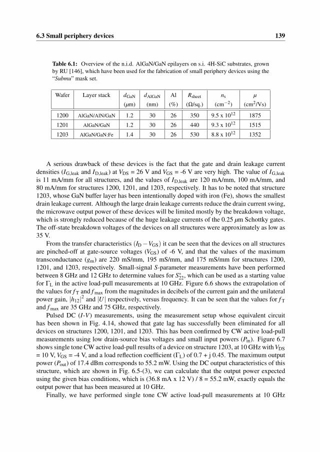
6.3 Small periphery devices 139
Table 6.1: Overview of the n.i.d. AlGaN/GaN epilayers on s.i. 4H-SiC substrates, grownby RU [146], which have been used for the fabrication of small periphery devices using the“Submu” mask set.
Wafer Layer stack dGaN dAlGaN Al Rsheet ns µ
(µm) (nm) (%) (Ω/sq.) (cm−2) (cm2/Vs)
1200 AlGaN/AlN/GaN 1.2 30 26 350 9.5 x 10¹² 1875
1201 AlGaN/GaN 1.2 30 26 440 9.3 x 10¹² 1515
1203 AlGaN/GaN:Fe 1.4 30 26 530 8.8 x 10¹² 1352
A serious drawback of these devices is the fact that the gate and drain leakage currentdensities (IG,leak and ID,leak) at VDS = 26 V and VGS = -6 V are very high. The value of IG,leakis 11 mA/mm for all structures, and the values of ID,leak are 120 mA/mm, 100 mA/mm, and80 mA/mm for structures 1200, 1201, and 1203, respectively. It has to be noted that structure1203, whose GaN buffer layer has been intentionally doped with iron (Fe), shows the smallestdrain leakage current. Although the large drain leakage currents reduce the drain current swing,the microwave output power of these devices will be limited mostly by the breakdown voltage,which is strongly reduced because of the huge leakage currents of the 0.25 µm Schottky gates.The off-state breakdown voltages of the devices on all structures were approximately as low as35 V.
From the transfer characteristics (ID−VGS) it can be seen that the devices on all structuresare pinched-off at gate-source voltages (VGS) of -6 V, and that the values of the maximumtransconductance (gm) are 220 mS/mm, 195 mS/mm, and 175 mS/mm for structures 1200,1201, and 1203, respectively. Small-signal S-parameter measurements have been performedbetween 8 GHz and 12 GHz to determine values for S∗22, which can be used as a starting valuefor ΓL in the active load-pull measurements at 10 GHz. Figure 6.6 shows the extrapolation ofthe values for f T and f max from the magnitudes in decibels of the current gain and the unilateralpower gain, |h12|2 and |U | respectively, versus frequency. It can be seen that the values for f Tand f max are 35 GHz and 75 GHz, respectively.
Pulsed DC (I-V) measurements, using the measurement setup whose equivalent circuithas been shown in Fig. 4.14, showed that gate lag has successfully been eliminated for alldevices on structures 1200, 1201, and 1203. This has been confirmed by CW active load-pullmeasurements using low drain-source bias voltages and small input powers (Pin). Figure 6.7shows single tone CW active load-pull results of a device on structure 1203, at 10 GHz with VDS= 10 V, VGS = -4 V, and a load reflection coefficient (ΓL) of 0.7 + j 0.45. The maximum outputpower (Pout) of 17.4 dBm corresponds to 55.2 mW. Using the DC output characteristics of thisstructure, which are shown in Fig. 6.5-(3), we can calculate that the output power expectedusing the given bias conditions, which is (36.8 mA x 12 V) / 8 = 55.2 mW, exactly equals theoutput power that has been measured at 10 GHz.
Finally, we have performed single tone CW active load-pull measurements at 10 GHz
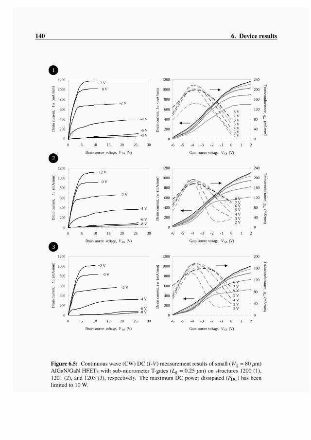
1
2
3
0
200
400
600
800
1000
1200
0 5 10 15 20 25 30
Drain-source voltage, V DS (V)
Dra
in c
urre
nt,
ID
(mA
/mm
) ll
0 V
-2 V
-4 V
-6 V
+2 V
-8 V0
200
400
600
800
1000
1200
-6 -5 -4 -3 -2 -1 0 1 2
Gate-source voltage, V GS (V)
Dra
in c
urre
nt, I
D (
mA
/mm
) ll
0
40
80
120
160
200
240
Transconductance, gm (m
S/mm
) ll
8 V7 V6 V5 V4 V3 V2 V
0
200
400
600
800
1000
1200
0 5 10 15 20 25 30
Drain-source voltage, V DS (V)
Dra
in c
urre
nt,
ID
(mA
/mm
) ll
0 V
-2 V
-4 V
-6 V
+2 V
-8 V0
200
400
600
800
1000
1200
-6 -5 -4 -3 -2 -1 0 1 2
Gate-source voltage, V GS (V)
Dra
in c
urre
nt, I
D (
mA
/mm
) ll
0
40
80
120
160
200
Transconductance, gm (m
S/mm
) ll
8 V7 V6 V5 V4 V3 V2 V
0
200
400
600
800
1000
1200
0 5 10 15 20 25 30
Drain-source voltage, V DS (V)
Dra
in c
urre
nt,
ID
(mA
/mm
) ll
0 V
-2 V
-4 V
-6 V
+2 V
-8 V0
200
400
600
800
1000
1200
-6 -5 -4 -3 -2 -1 0 1 2
Gate-source voltage, V GS (V)D
rain
cur
rent
, ID
(m
A/m
m) l
l
0
40
80
120
160
200
240
Transconductance, gm (m
S/mm
) ll
8 V7 V6 V5 V4 V3 V2 V
140 6. Device results
Figure 6.5: Continuous wave (CW) DC (I-V) measurement results of small (Wg = 80 µm)AlGaN/GaN HFETs with sub-micrometer T-gates (Lg = 0.25 µm) on structures 1200 (1),1201 (2), and 1203 (3), respectively. The maximum DC power dissipated (PDC) has beenlimited to 10 W.

6.3 Small periphery devices 141
0.0
5.0
10.0
15.0
20.0
25.0
30.0
1.0E+09 1.0E+10 1.0E+11
Frequency, f (GHz)
| h 2
1 |2 ,
(dB
)
0.0
5.0
10.0
15.0
20.0
25.0
30.0
| U | , (dB
)
fT
fmax
1 10 100
Figure 6.6: Extrapolation of the values for f T and f max for small (Wg = 80 µm) Al-GaN/GaN HFETs with sub-micrometer T-gates (Lg = 0.25 µm) on structures 1200, 1201,and 1203, respectively. The small-signal S-parameter measurements have been performedbetween 8 GHz and 12 GHz at VDS = 26 V and VGS = -3.5 V.
using class AB bias conditions (VDS = 26 V and VGS = - 4 V) on all structures to determinevalues for the maximum output power (Pout), associated power gain (Gp), and PAE of thesmall gate periphery AlGaN/GaN HFETs. Figure 6.8 shows the results for structures 1200(left), 1201 (middle), and 1203 (right), respectively. Using ΓL = 0.75 + j 0.30, a maximumoutput power density (PD) of 1.0 W/mm, power gain of 3.5 dB, and PAE of 4.3 % are obtainedfor structure 1200. For structure 1201 values for PD, Gp, and PAE of 2.7 W/mm, 6 dB, and 13%, respectively have been obtained using the same load reflection coefficient as for structure1200. Finally, for structure 1203 using ΓL = 0.80 + j 0.25, values for PD, Gp, and PAE of 3.5W/mm, 8 dB, and 26 %, respectively have been measured.
Considering the facts that the devices on all structures show dispersion free behavior at 10GHz and have high maximum drain current densities of on average 1 A/mm, these load-pullresults are very disappointing. The reason for these poor results obviously is the very lowbreakdown voltage caused by the excessively high gate and drain leakage currents. Compar-ison of the gate and drain leakage currents of the submicron T-gate devices and the fat gate(Lg = 2 µm) reference devices, which are also present on the Submu mask set as described inSect. 3.2.1, shows that the huge leakage currents are not introduced by the SiN deposition pro-cess as the fat gate devices show values for IG,leak and ID,leak of 150 µA/mm and 400 µA/mm,respectively.

142 6. Device results
0
5
10
15
20
-5 0 5 10 15
P in (dBm)
Pou
t (d
Bm
), G
p (d
B)
0
5
10
15
20
25
30PAE (%
)PoutGpPAE
Pout
Gp
PAE PAE (%
)
Figure 6.7: Single tone CW active load-pull results of a device on structure 1203, at 10GHz with VDS = 10 V, VGS = -4 V, and a load reflection coefficient (ΓL) of 0.7 + j 0.45.
0
5
10
15
20
6 8 10 12 14 16 18
P in (dBm)
Pou
t (d
Bm
), G
p (d
B)
0
1
2
3
4
5
PAE (%)
PoutGpPAE
0
5
10
15
20
25
6 8 10 12 14 16 18
P in (dBm)
Pou
t (d
Bm
), G
p (d
B)
0
2
4
6
8
10
12
14
PAE (%)
PoutGpPAE
0
5
10
15
20
25
30
6 8 10 12 14 16 18
P in (dBm)
Pou
t (d
Bm
), G
p (d
B)
0
5
10
15
20
25
30
PAE (%)
PoutGpPAE
PoutGpPAE
PoutGpPAE
PoutGpPAE
PAE (%
)
PAE (%
)
PAE (%
)
Figure 6.8: Single tone CW active load-pull results at 10 GHz using class AB bias condi-tions (VDS = 26 V and VGS = - 4 V) for devices on structures 1200 (left), 1201 (middle), and1203 (right), respectively.
6.4 Large periphery devices 143
The reason for the high leakage currents most likely is the use of titanium (Ti) in the toppart of the T-gates. The T-gate consists of a Ni/Au = 20/40 nm foot and a Ti/Au = 20/380nm top. Titanium has been chosen to achieve a good mechanical stability of the top part ofthe gates due to the good adhesion between Ti and the SiN passivation film. However, as thetemperatures in the channel underneath the Schottky gates can get as high as 240 oC [45], it ispossible that Ti diffuses towards the AlGaN surface and causes the Schottky barrier height tobe lowered. As a consequence, the gate leakage current increases and the breakdown voltagedecreases. To circumvent this problem we have used Ni/Au for both the foot and top parts ofthe T- and FP-gates of the large gate periphery devices the results of which will be describedin the next section.
6.4 Large periphery devices
The large periphery devices have been processed using the “mmTor” mask set, which has beendescribed in Sect. 3.2.1. Devices with air bridges in both comb and fishbone layouts, whichhave total gate widths (Wg) of 0.25 mm, 0.5 mm, and 1.0 mm have been fabricated. The unitgate widths (Wgu) used are 62.5 µm, 100 µm, and 125 µm, respectively. For the fabrication ofthe sub-micrometer gate contacts we have used T-gates and gates with a field plate (FP) towardsthe drain contact using the original implementation, which has been shown in Fig. 4.8-(left),Sect. 4.3. The gate length (Lg), which defines the footprint of the T- and FP-gates, is 0.7 µm.The top of the T-gates is 1.2 µm wide and its extensions towards the source and drain contactsare 0.25 µm long. For the FP-gates we have used two FP lengths (LFP) of 0.5 µm and 1.0µm, which will be indicated as “FP0.5” and “FP1.0”, respectively. According to the definitionof the FP length, see Fig. 4.8, the T-gate can also be considered as a FP-gate. Hence, weactually have three FP lengths of 0.25 µm, 0.5 µm, and 1.0 µm. It has to be noted that theextension of the FP-gate towards the source contact is also 0.25 µm. The remaining internaldimensions for all large periphery devices are: Lgs = 1.2 µm, Lgd = 3.0 µm, Lds = 4.9 µm, andLgg = 50 µm, respectively. Table 6.2 shows an overview of the different device layouts andgate configurations, i.e. unit gate width (Wgu) and number of gate fingers (Ng), that have beenfabricated. It has to be noted that each of these device types has been implemented with a T-,FP0.5, and FP1.0 gate.
All devices have been fabricated on a 15 mm x 15 mm sample from structure 1203 becausethis material showed the lowest gate and drain leakage currents as we have seen in Sect. 6.3.Figure 6.9 shows CW DC (I-V) results for 0.25 mm, and pulsed DC (I-V) results for 0.5 mmand 1.0 mm T-gate devices. The output characteristics (ID−VDS) show drain current densitiesof 1.0 A/mm and 840 mA/mm at VGS = +2 V and VGS = 0 V, respectively. These currentdensities are in perfect agreement with the values that can be calculated using the materialproperties listed in Table 6.1 and with the results for the small periphery devices shown inSect. 6.3. From Fig. 6.9 we can see that the knee voltages (Vknee) for the output characteristicsat VGS = 0 V are 5 V. From the transfer characteristics (ID−VGS) it can be seen that all devicesare pinched-off at VGS = -6 V, and that the values of the maximum gm range from 180 mS/mmto 190 mS/mm.
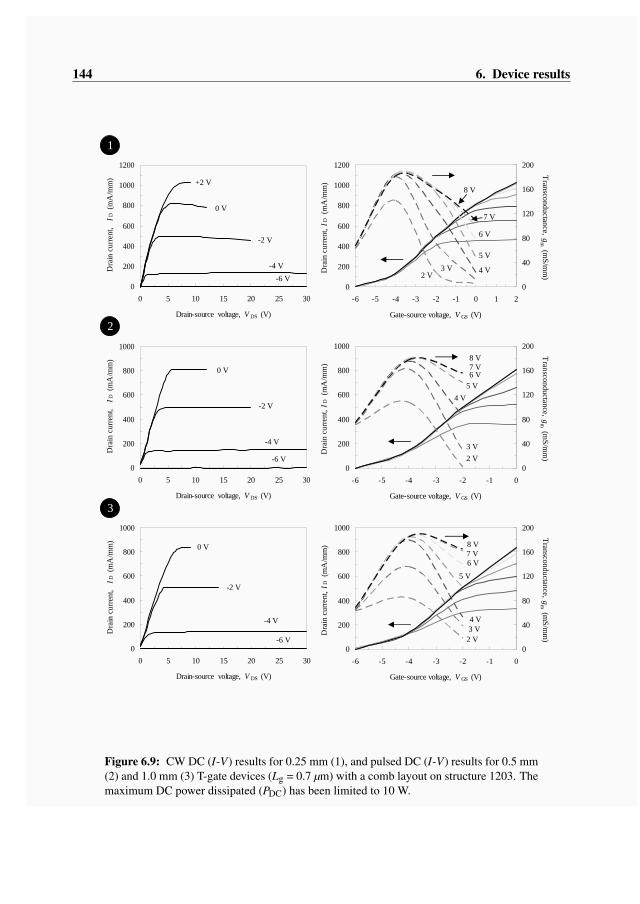
1
2
3
0
200
400
600
800
1000
0 5 10 15 20 25 30
Drain-source voltage, V DS (V)
Dra
in c
urre
nt,
ID
(mA
/mm
) ll
0 V
-2 V
-4 V
-6 V0
200
400
600
800
1000
-6 -5 -4 -3 -2 -1 0
Gate-source voltage, V GS (V)
Dra
in c
urre
nt, I
D (
mA
/mm
) ll
0
40
80
120
160
200
Transconductance, gm (m
S/mm
) ll
8 V7 V6 V
5 V4 V
3 V2 V
0
200
400
600
800
1000
0 5 10 15 20 25 30
Drain-source voltage, V DS (V)
Dra
in c
urre
nt,
ID
(mA
/mm
) ll
0 V
-2 V
-4 V
-6 V
8 V7 V6 V
5 V
4 V3 V
2 V0
200
400
600
800
1000
-6 -5 -4 -3 -2 -1 0
Gate-source voltage, V GS (V)
Dra
in c
urre
nt, I
D (
mA
/mm
) ll
0
40
80
120
160
200
Transconductance, gm (m
S/mm
) ll
0
200
400
600
800
1000
1200
0 5 10 15 20 25 30
Drain-source voltage, V DS (V)
Dra
in c
urre
nt,
ID
(mA
/mm
) ll
0 V
-2 V
-4 V-6 V
+2 V
0
200
400
600
800
1000
1200
-6 -5 -4 -3 -2 -1 0 1 2
Gate-source voltage, V GS (V)D
rain
cur
rent
, ID
(m
A/m
m) l
l
0
40
80
120
160
200
Transconductance, gm (m
S/mm
) ll
8 V
7 V
6 V
5 V
4 V3 V2 V
144 6. Device results
Figure 6.9: CW DC (I-V) results for 0.25 mm (1), and pulsed DC (I-V) results for 0.5 mm(2) and 1.0 mm (3) T-gate devices (Lg = 0.7 µm) with a comb layout on structure 1203. Themaximum DC power dissipated (PDC) has been limited to 10 W.
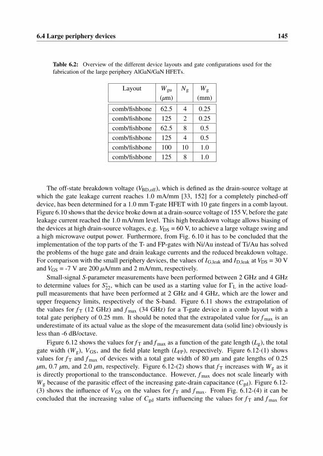
6.4 Large periphery devices 145
Table 6.2: Overview of the different device layouts and gate configurations used for thefabrication of the large periphery AlGaN/GaN HFETs.
Layout Wgu Ng Wg
(µm) (mm)
comb/fishbone 62.5 4 0.25comb/fishbone 125 2 0.25comb/fishbone 62.5 8 0.5comb/fishbone 125 4 0.5comb/fishbone 100 10 1.0comb/fishbone 125 8 1.0
The off-state breakdown voltage (VBD,off), which is defined as the drain-source voltage atwhich the gate leakage current reaches 1.0 mA/mm [33, 152] for a completely pinched-offdevice, has been determined for a 1.0 mm T-gate HFET with 10 gate fingers in a comb layout.Figure 6.10 shows that the device broke down at a drain-source voltage of 155 V, before the gateleakage current reached the 1.0 mA/mm level. This high breakdown voltage allows biasing ofthe devices at high drain-source voltages, e.g. VDS = 60 V, to achieve a large voltage swing anda high microwave output power. Furthermore, from Fig. 6.10 it has to be concluded that theimplementation of the top parts of the T- and FP-gates with Ni/Au instead of Ti/Au has solvedthe problems of the huge gate and drain leakage currents and the reduced breakdown voltage.For comparison with the small periphery devices, the values of IG,leak and ID,leak at VDS = 30 Vand VGS = -7 V are 200 µA/mm and 2 mA/mm, respectively.
Small-signal S-parameter measurements have been performed between 2 GHz and 4 GHzto determine values for S∗22, which can be used as a starting value for ΓL in the active load-pull measurements that have been performed at 2 GHz and 4 GHz, which are the lower andupper frequency limits, respectively of the S-band. Figure 6.11 shows the extrapolation ofthe values for f T (12 GHz) and f max (34 GHz) for a T-gate device in a comb layout with atotal gate periphery of 0.25 mm. It should be noted that the extrapolated value for f max is anunderestimate of its actual value as the slope of the measurement data (solid line) obviously isless than -6 dB/octave.
Figure 6.12 shows the values for f T and f max as a function of the gate length (Lg), the totalgate width (Wg), VGS, and the field plate length (LFP), respectively. Figure 6.12-(1) showsvalues for f T and f max of devices with a total gate width of 80 µm and gate lengths of 0.25µm, 0.7 µm, and 2.0 µm, respectively. Figure 6.12-(2) shows that f T increases with Wg as itis directly proportional to the transconductance. However, f max does not scale linearly withWg because of the parasitic effect of the increasing gate-drain capacitance (Cgd). Figure 6.12-(3) shows the influence of VGS on the values for f T and f max. From Fig. 6.12-(4) it can beconcluded that the increasing value of Cgd starts influencing the values for f T and f max for
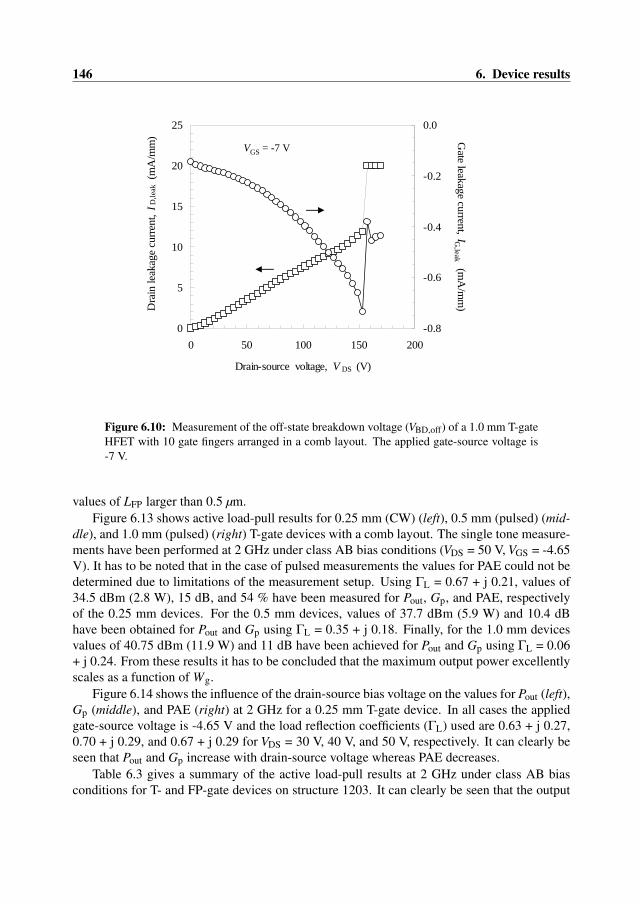
146 6. Device results
0
5
10
15
20
25
0 50 100 150 200
Drain-source voltage, V DS (V)
Dra
in le
akag
e cu
rrent
, I D
,leak
(m
A/m
m) l
l
-0.8
-0.6
-0.4
-0.2
0.0
Gate leakage current, IG
,leak (mA
/mm
) ll
VGS = -7 V
Figure 6.10: Measurement of the off-state breakdown voltage (VBD,off) of a 1.0 mm T-gateHFET with 10 gate fingers arranged in a comb layout. The applied gate-source voltage is-7 V.
values of LFP larger than 0.5 µm.Figure 6.13 shows active load-pull results for 0.25 mm (CW) (left), 0.5 mm (pulsed) (mid-
dle), and 1.0 mm (pulsed) (right) T-gate devices with a comb layout. The single tone measure-ments have been performed at 2 GHz under class AB bias conditions (VDS = 50 V, VGS = -4.65V). It has to be noted that in the case of pulsed measurements the values for PAE could not bedetermined due to limitations of the measurement setup. Using ΓL = 0.67 + j 0.21, values of34.5 dBm (2.8 W), 15 dB, and 54 % have been measured for Pout, Gp, and PAE, respectivelyof the 0.25 mm devices. For the 0.5 mm devices, values of 37.7 dBm (5.9 W) and 10.4 dBhave been obtained for Pout and Gp using ΓL = 0.35 + j 0.18. Finally, for the 1.0 mm devicesvalues of 40.75 dBm (11.9 W) and 11 dB have been achieved for Pout and Gp using ΓL = 0.06+ j 0.24. From these results it has to be concluded that the maximum output power excellentlyscales as a function of Wg.
Figure 6.14 shows the influence of the drain-source bias voltage on the values for Pout (left),Gp (middle), and PAE (right) at 2 GHz for a 0.25 mm T-gate device. In all cases the appliedgate-source voltage is -4.65 V and the load reflection coefficients (ΓL) used are 0.63 + j 0.27,0.70 + j 0.29, and 0.67 + j 0.29 for VDS = 30 V, 40 V, and 50 V, respectively. It can clearly beseen that Pout and Gp increase with drain-source voltage whereas PAE decreases.
Table 6.3 gives a summary of the active load-pull results at 2 GHz under class AB biasconditions for T- and FP-gate devices on structure 1203. It can clearly be seen that the output

6.4 Large periphery devices 147
0.0
5.0
10.0
15.0
20.0
25.0
30.0
1.0E+08 1.0E+09 1.0E+10 1.0E+11
Frequency, f (Hz)
| h 2
1 |2 ,
(dB
)
0.0
5.0
10.0
15.0
20.0
25.0
30.0
| U | , (dB
)
fT
fmax
Frequency, f (GHz)
0.1 1 10 100
Figure 6.11: Extrapolation of the values for f T and f max for a T-gate device with a comblayout with a total gate periphery of 0.25 mm and a gate length of 0.7 µm. The small-signalS-parameter measurements have been performed between 2 GHz and 4 GHz at VDS = 30 Vand VGS = -3.5 V.
power density (PD) scales very well with Wg, i.e. within 5 %, for devices with the same typeof gate and biased at the same drain-source voltage. Although LFP does not seem to influencethe value for PD, it can be observed that Gp decreases for increasing LFP because Cgd increaseswith LFP. Furthermore, the values for Gp and PAE clearly show that devices fabricated onstructure 1203 using the mmTor mask set and the process flow that is described in AppendixA, are very well suited for application in high-power amplifiers (HPA) at 2 GHz.
Figure 6.15 shows single tone pulsed active load-pull results for 0.25 mm (left), 0.5 mm(middle), and 1.0 mm (right) T-gate devices with a comb layout at 4 GHz under class AB biasconditions (VDS = 40 V, VGS = -4.0 V). Using ΓL = 0.45 + j 0.45, values of 33.1 dBm (2.05W), 14 dB, and 47 % have been measured for Pout, Gp, and PAE of the 0.25 mm devices. Forthe 0.5 mm devices, values of 36.1 dBm (4.07 W), 14.5 dB, and 52 % have been obtained forPout, Gp, and PAE using ΓL = 0.20 + j 0.50. Finally, for the 1.0 mm devices values of 37.7dBm (5.9 W), 19.8 dB, and 46 % have been achieved for Pout, Gp, and PAE using ΓL = 0.10 +j 0.40. It has to be noted that Pout of the 1.0 mm devices is less than can be expected from thescaling with Wg, which can clearly be observed for the 0.25 mm and 0.5 mm devices, becauseof the limited power available from the TWTA used. However, based on the scaling of Poutwith Wg observed at 2 GHz and the scaling of the 0.25 mm and 0.5 mm devices at 4 GHz, itis reasonable to assume that the 1.0 mm devices can show an output power of 8 W at 4 GHz
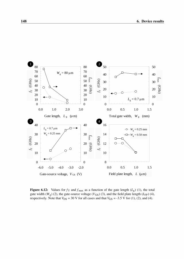
148 6. Device results
0
10
20
30
40
50
0.0 0.5 1.0 1.5
Total gate width, W g (mm)
f t,ex
t (G
Hz)
0
10
20
30
40
50
fmax,ext (G
Hz)
Lg = 0.7 µm0
1020304050607080
0.0 1.0 2.0 3.0
Gate length, L g (µm)
f t,ex
t (G
Hz)
01020304050607080
fmax,ext (G
Hz)
Wg = 80 µm
0
10
20
30
40
-6.0 -5.0 -4.0 -3.0 -2.0
Gate-source voltage, V GS (V)
f t,ex
t (G
Hz)
0
10
20
30
40
fmax,ext (G
Hz)
Lg = 0.7 µm
Wg = 0.25 mm
8
10
12
14
16
0.0 0.5 1.0 1.5
Field plate length, L FP (µm)
f t,ex
t (G
Hz)
Wg = 0.25 mm
Wg = 0.50 mmWg = 0.50 mm
Wg = 0.25 mm
(µm)
1 2
3 4
f T(G
Hz)
fmax
(GH
z) f T(G
Hz)
fmax
(GH
z)f T
(GH
z)
fmax
(GH
z) f T(G
Hz)
Figure 6.12: Values for f T and f max as a function of the gate length (Lg) (1), the totalgate width (Wg) (2), the gate-source voltage (VGS) (3), and the field plate length (LFP) (4),respectively. Note that VDS = 30 V for all cases and that VGS = -3.5 V for (1), (2), and (4).
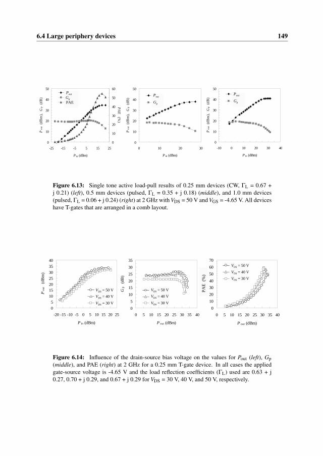
6.4 Large periphery devices 149
0
10
20
30
40
50
-25 -15 -5 5 15 25
P in (dBm)
Pou
t (d
Bm
), G
p (d
B)
0
10
20
30
40
50
60
PAE (%)
PoutGpPAE
PoutGpPAE
0
10
20
30
40
50
-10 0 10 20 30 40
P in (dBm)
Pou
t (d
Bm
), G
p (d
B)
Pout
Gp
Pout
Gp
0
10
20
30
40
50
0 10 20 30
P in (dBm)
Pou
t (d
Bm
), G
p (d
B)
Pout
Gp
Pout
Gp
Figure 6.13: Single tone active load-pull results of 0.25 mm devices (CW, ΓL = 0.67 +j 0.21) (left), 0.5 mm devices (pulsed, ΓL = 0.35 + j 0.18) (middle), and 1.0 mm devices(pulsed, ΓL = 0.06 + j 0.24) (right) at 2 GHz with VDS = 50 V and VGS = -4.65 V. All deviceshave T-gates that are arranged in a comb layout.
05
10152025303540
-20 -15 -10 -5 0 5 10 15 20 25
P in (dBm)
Pou
t (d
Bm
)
Vds = 50 V
Vds = 40 V
Vds = 30 V05
101520253035
0 5 10 15 20 25 30 35 40
P out (dBm)
Gp
(d
B)
Vds = 50 V
Vds = 40 V
Vds = 30 V0
10203040506070
0 5 10 15 20 25 30 35 40
P out (dBm)
PAE
(%
)
Vds = 50 V
Vds = 40 V
Vds = 30 V
VDS = 50 VVDS = 40 V
VDS = 30 V
VDS = 50 VVDS = 40 V
VDS = 30 V
VDS = 50 VVDS = 40 VVDS = 30 V
PAE
(%)
Figure 6.14: Influence of the drain-source bias voltage on the values for Pout (left), Gp(middle), and PAE (right) at 2 GHz for a 0.25 mm T-gate device. In all cases the appliedgate-source voltage is -4.65 V and the load reflection coefficients (ΓL) used are 0.63 + j0.27, 0.70 + j 0.29, and 0.67 + j 0.29 for VDS = 30 V, 40 V, and 50 V, respectively.

150 6. Device results
Table 6.3: Summary of single tone active load-pull results at 2 GHz under class AB biasconditions for T- and FP-gate devices on structure 1203. The total gate peripheries (Wg) ofthe devices are 0.25 mm, 0.5 mm, and 1.0 mm, respectively, and all gates are arranged in acomb layout.
Wg type Wgu x Ng mode VDS VGS Pout PD Gp PAE
(mm) (V) (V) (W) (W/mm) (dB) (%)
0.25 T 62.5 x 4 CW 30 -4.65 1.6 6.4 > 20 60
0.25 T 62.5 x 4 CW 40 -4.65 2.2 8.8 > 20 60
0.25 T 62.5 x 4 CW 50 -4.65 2.8 11.2 > 20 54
0.25 FP0.5 62.5 x 4 CW 30 -4.65 1.5 6.0 > 17 57
0.25 FP0.5 62.5 x 4 CW 40 -4.65 2.0 8.0 > 17 57
0.25 FP0.5 62.5 x 4 CW 50 -4.65 2.7 10.8 > 17 -
0.25 FP1.0 62.5 x 4 CW 30 -4.65 1.6 6.4 15 70
0.25 FP1.0 62.5 x 4 CW 40 -4.65 2.4 9.6 > 15 -
0.25 FP1.0 62.5 x 4 CW 50 -4.65 3.0 12.0 > 17 -
0.5 T 125 x 4 pulsed 30 -4.65 3.2 6.4 > 16 -
0.5 T 125 x 4 pulsed 40 -4.65 4.6 9.2 > 17 -
0.5 T 125 x 4 pulsed 50 -4.65 5.9 11.8 > 20 -
0.5 T 62.5 x 8 pulsed 30 -4.65 3.1 6.2 > 15 -
0.5 T 62.5 x 8 pulsed 40 -4.65 4.3 8.6 > 17 -
0.5 T 62.5 x 8 pulsed 50 -4.65 5.7 11.4 > 18 -
1.0 T 125 x 8 pulsed 30 -4.65 6.5 6.5 > 15 -
1.0 T 125 x 8 pulsed 40 -4.65 9.3 9.3 > 18 -
1.0 T 125 x 8 pulsed 50 -4.65 11.9 11.9 > 19 -
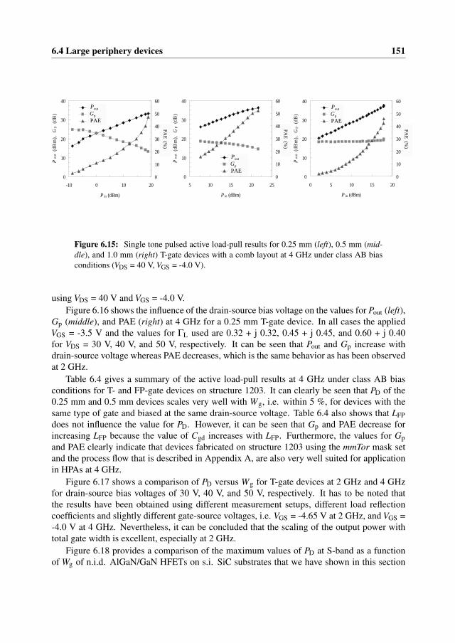
6.4 Large periphery devices 151
0
10
20
30
40
-10 0 10 20
P in (dBm)
Pou
t (d
Bm
), G
p (d
B)
0
10
20
30
40
50
60
PAE (%)
PoutGpPAE
PoutGpPAE
0
10
20
30
40
5 10 15 20 25
P in (dBm)
Pou
t (d
Bm
), G
p (d
B)
0
10
20
30
40
50
60
PAE (%)
PoutGpPAE
PoutGpPAE
0
10
20
30
40
0 5 10 15 20
P in (dBm)
Pou
t (d
Bm
), G
p (d
B)
0
10
20
30
40
50
60
PAE (%)
PoutGpPAE
Pout
PAEGp
PAE (%
)
PAE (%
)
PAE (%
)
Figure 6.15: Single tone pulsed active load-pull results for 0.25 mm (left), 0.5 mm (mid-dle), and 1.0 mm (right) T-gate devices with a comb layout at 4 GHz under class AB biasconditions (VDS = 40 V, VGS = -4.0 V).
using VDS = 40 V and VGS = -4.0 V.Figure 6.16 shows the influence of the drain-source bias voltage on the values for Pout (left),
Gp (middle), and PAE (right) at 4 GHz for a 0.25 mm T-gate device. In all cases the appliedVGS = -3.5 V and the values for ΓL used are 0.32 + j 0.32, 0.45 + j 0.45, and 0.60 + j 0.40for VDS = 30 V, 40 V, and 50 V, respectively. It can be seen that Pout and Gp increase withdrain-source voltage whereas PAE decreases, which is the same behavior as has been observedat 2 GHz.
Table 6.4 gives a summary of the active load-pull results at 4 GHz under class AB biasconditions for T- and FP-gate devices on structure 1203. It can clearly be seen that PD of the0.25 mm and 0.5 mm devices scales very well with Wg, i.e. within 5 %, for devices with thesame type of gate and biased at the same drain-source voltage. Table 6.4 also shows that LFPdoes not influence the value for PD. However, it can be seen that Gp and PAE decrease forincreasing LFP because the value of Cgd increases with LFP. Furthermore, the values for Gpand PAE clearly indicate that devices fabricated on structure 1203 using the mmTor mask setand the process flow that is described in Appendix A, are also very well suited for applicationin HPAs at 4 GHz.
Figure 6.17 shows a comparison of PD versus Wg for T-gate devices at 2 GHz and 4 GHzfor drain-source bias voltages of 30 V, 40 V, and 50 V, respectively. It has to be noted thatthe results have been obtained using different measurement setups, different load reflectioncoefficients and slightly different gate-source voltages, i.e. VGS = -4.65 V at 2 GHz, and VGS =-4.0 V at 4 GHz. Nevertheless, it can be concluded that the scaling of the output power withtotal gate width is excellent, especially at 2 GHz.
Figure 6.18 provides a comparison of the maximum values of PD at S-band as a functionof Wg of n.i.d. AlGaN/GaN HFETs on s.i. SiC substrates that we have shown in this section

152 6. Device results
0
10
20
30
40
50
60
0 5 10 15 20 25 30 35 40
P out (dBm)
PAE
(%
)
Vds = 50 V
Vds = 40 V
Vds = 30 V
05
10152025303540
-15 -10 -5 0 5 10 15 20 25
P in (dBm)
Pou
t (d
Bm
)
Vds = 50 V
Vds = 40 V
Vds = 30 V
VDS = 50 VVDS = 40 V
VDS = 30 V05
101520253035
5 10 15 20 25 30 35 40
P out (dBm)
Gp
(d
B)
Vds = 50 V
Vds = 40 V
Vds = 30 V
VDS = 50 VVDS = 40 V
VDS = 30 V
VDS = 50 VVDS = 40 VVDS = 30 V
PAE
(%)
Figure 6.16: Influence of the drain-source bias voltage on the values for Pout (left), Gp(middle), and PAE (right) at 4 GHz for a 0.25 mm T-gate device. In all cases the appliedgate-source voltage is -3.5 V and the load reflection coefficients (ΓL) used are 0.32 + j 0.32,0.45 + j 0.45, and 0.60 + j 0.40 for VDS = 30 V, 40 V, and 50 V, respectively.
4
6
8
10
12
14
0.00 0.25 0.50 0.75 1.00 1.25
Total gate width, W g (mm)
Out
put p
ower
den
sity,
P
D (W
/mm
)
Pd-2GHz-30V Pd-2GHz-40V Pd-2GHz-50VPd-4GHz-30V Pd-4GHz-40V Pd-4GHz-50VPD-2GHz-30VPD-4GHz-30V
PD-2GHz-40VPD-4GHz-40V
PD-2GHz-50VPD-4GHz-50V
Figure 6.17: Comparison of PD versus Wg for T-gate devices at 2 GHz and 4 GHz for VGS= -4.65 V and VDS is 30 V, 40 V, and 50 V, respectively.

6.5 Conclusions 153
Table 6.4: Summary of single tone active load-pull results at 4 GHz under class AB biasconditions for T- and FP-gate devices on structure 1203. The total gate peripheries (Wg) ofthe devices are 0.25 mm, 0.5 mm, and 1.0 mm, respectively, and all gates are arranged in acomb layout.
Wg type VDS VGS Pout PD Gp PAE(mm) (V) (V) (W) (W/mm) (dB) (%)
0.25 T 30 -3.5 1.64 6.5 14.0 420.25 T 40 -3.5 2.05 8.2 14.0 470.25 T 50 -3.5 2.63 10.5 12.9 490.25 FP0.5 30 -3.5 1.66 6.6 12.4 450.25 FP0.5 40 -3.5 2.09 8.4 12.8 400.25 FP0.5 50 -3.5 2.75 11.0 13.8 440.25 FP0.5 60 -3.5 2.95 11.8 14.0 440.25 FP1.0 50 -3.5 2.40 9.6 11.0 380.5 T 40 -4.0 4.07 8.1 14.5 520.5 T 50 -4.0 5.01 10.0 15.9 480.5 FP0.5 30 -4.0 3.27 6.5 10.0 590.5 FP0.5 40 -4.0 4.17 8.3 14.2 520.5 FP1.0 40 -4.0 3.39 6.8 13.6 441.0 T 40 -4.0 5.89 5.9 19.8 461.0 FP0.5 30 -4.0 4.61 4.6 14.0 431.0 FP0.5 40 -4.0 5.89 5.9 19.8 461.0 FP1.0 40 -4.0 4.27 4.3 17.3 36
(diamonds) and that have been reported in literature (squares) [8, 41, 73, 132, 140, 174]. Itcan be concluded that we have achieved state-of-the-art results with respect to the generationof large, i.e. 11.9 W, microwave output power for devices with large total gate widths, e.g. 1.0mm.
6.5 Conclusions
In this chapter we have presented DC (I-V), small signal S-parameter and active load-pullresults for both small (Wg = 80 µm) and large (Wg = 0.25 mm, 0.5 mm, and 1.0 mm) gateperiphery n.i.d. AlGaN/GaN HFETs on s.i. 4H-SiC substrates. These devices are the productof a joint research effort between TU/e and RU and demonstrate the successful development

154 6. Device results
14
6
7
10
13 23
5
14
119
0
5
10
15
20
25
30
35
0.0 0.1 1.0 10.0 100.0
Total gate width, W g (mm)
Out
put p
ower
den
sity,
P
D (
W/m
m) ll
[8][132]
[132]
[41] [140]
[174]
[73]
TU/e-RU
Figure 6.18: Comparison of the maximum output power densities (PD) at S-band as afunction of the total gate width (Wg) of n.i.d. AlGaN/GaN HFETs on s.i. SiC substratesthat we have shown in this section (diamonds) and that have been reported in literature(squares) [8, 41, 73, 132, 140, 174].
and integration of both MOCVD epitaxial growth processes and device process technology.DC (I-V) data of the presented HFETs show the potential for high-power performance of
these devices as they enable both large drain current and drain-source voltage swings. Theformer can be realized because of the high maximum drain current densities, typically 1.0A/mm, and the low values of IG,leak and ID,leak at pinch-off, which are typically 200 µA/mm and2 mA/mm, respectively for large gate periphery devices. The large voltage swing is enabled bythe low value of Vknee, typically 4 V - 6 V, and the high value of VBD,off, typically larger than150 V, which is enabled by the incorporation of T-gates with a field plate length of 0.25 µm.It has to be noted that the lowest values for IG,leak and ID,leak have been obtained on structure1203, which incorporates an iron (Fe) compensation doped GaN buffer layer. Hence, onlythis structure has been used to fabricate large gate periphery devices whose microwave powerperformance as a function of Wg has been investigated.
For devices with an Lg of 0.7 µm the values for f T and f max, which have been extrapolatedfrom small-signal S-parameter measurements, were 12 GHz and 34 GHz, respectively. Thesevalues indicate that devices with these gate lengths are suitable for S-band (2 GHz - 4 GHz)applications.
Single tone CW active load-pull results of small gate periphery (Wg = 80 µm) devices witha gate length of 0.25 µm at 10 GHz have demonstrated the successful elimination of gate lagfrom devices on all epitaxial layer structures used. This result proved the successful integrationof the developed surface passivation modules, i.e. the plasma surface treatment (Sect. 4.4) and
6.5 Conclusions 155
SiN surface passivation (Chapter 5), into the process flow described in Appendix A.Single tone CW and pulsed active load-pull results at 2 GHz under class AB bias condi-
tions, e.g. VDS = 50 V and VGS = -4.65 V, have shown excellent values for Pout of large gateperiphery AlGaN/GaN HFETs on the Fe-doped epistructure (1203), i.e. 11.9 W for a 1.0 mmT-gate device. Moreover, excellent scaling of Pout with Wg has been demonstrated for equallybiased devices with the same type of gate, i.e. T- or FP-gate. Although LFP does not seemto influence the value for PD, it can be observed that Gp decreases for increasing LFP becausethe value of Cgd increases with LFP. In addition, the values for Gp, typically 15 dB, and PAE,typically larger than 54 %, clearly show that devices fabricated on structure 1203 using themmTor mask set and the process flow described in Appendix A, are very well suited for appli-cation in HPAs. Single tone pulsed active load-pull measurements at 4 GHz under class ABbias conditions, e.g. VDS = 50 V and VGS = -4 V, have shown similar results, which has clearlybeen shown in Fig. 6.17. We want to mention that the results of comparable measurements onthese devices performed by TU/e, TNO, and Philips were in excellent agreement. In addition,as the devices have been measured over a period of 5 months, it has clearly been shown thattheir behavior is stable over time.
Comparison of the maximum output power densities at S-band as a function of total gatewidth of n.i.d. AlGaN/GaN HFETs on s.i. SiC substrates that we have shown in Sect. 6.4and that have been reported in literature, clearly shows that we have achieved state-of-the-artresults with respect to the generation of large, i.e. 11.9 W, microwave output power for deviceswith large total gate widths, e.g. 1.0 mm. Furthermore, it can be concluded that GaN:Fe bufferlayers are perfectly suitable for high-power applications at S-band.

156 6. Device results
Chapter 7
Conclusions and recommendations
This chapter provides a review of the main conclusions that can be drawn from the work de-scribed in this thesis and provides recommendations for future research.
7.1 Main conclusionsThe objectives of the research described in this thesis were to develop the technology re-quired to grow state-of-the-art AlGaN/GaN epilayers on sapphire and s.i. SiC substrates byMOCVD and to fabricate microwave high-power HFETs on these epitaxial films. The largeperiphery HFETs consisting of n.i.d. AlGaN/GaN:Fe epilayers on s.i. SiC substrates havesub-micrometer T- or FP-gates with a gate length (Lg) of 0.7 µm and total gate widths (Wg) of0.25 mm, 0.5 mm, and 1.0 mm, respectively. The 1.0 mm devices are capable of producing amaximum microwave output power (Pout) of 11.9 W at S-band (2 GHz - 4 GHz) using classAB bias conditions of VDS = 50 V and VGS = -4.65 V. Moreover, excellent scaling of Pout withWg has been demonstrated as has been shown in Fig. 6.17. In addition, the associated powergain (Gp) ranges between 15 dB and 20 dB, and for the power added efficiency (PAE) valuesfrom 54 % up to 70 % have been obtained.
Figure 6.18 provided a comparison of the maximum output power densities (PD) at S-band as a function of the total gate width (Wg) of n.i.d. AlGaN/GaN HFETs on s.i. SiCsubstrates that we have shown in Sect. 6.4 (diamonds) and that have been reported in literature(squares) [8, 41, 73, 132, 140, 174]. It is clear that we have achieved state-of-the-art resultswith respect to the generation of large, i.e. 11.9 W, microwave output power for devices withlarge total gate widths, e.g. 1.0 mm.
The device results presented, illustrate both the successful development of the MOCVDgrowth process, and the successful integration of process modules such as ohmic and Schot-tky contact technology, device isolation, electron beam lithography, surface passivation, and
157

158 7. Conclusions and recommendations
air bridge technology, into a process flow that enables the fabrication of state-of-the-art largeperiphery n.i.d. AlGaN/GaN:Fe HFETs on s.i. SiC substrates. These devices are perfectlysuitable for application in e.g. high-power amplifiers at S-band (2 GHz - 4 GHz).
With respect to the development of the MOCVD growth process (Chapter 3), which is re-quired for the fabrication of state-of-the-art n.i.d. AlGaN/GaN epilayers, the following mainconclusions can be drawn:
• Optimization of the growth process of the GaN buffer layer on sapphire substrates hasshown that buffer layers with resistivities exceeding 104 Ωcm can be achieved in a con-trolled and reproducible manner if nitrogen is used as carrier gas during the depositionof the low-temperature GaN nucleation layer [50].
• GaN buffer layers on commercially available 2 inch s.i. 4H-SiC substrates with resistiv-ities also exceeding 104 Ωcm can be obtained by both compensation doping with iron(Fe) and non-intentionally doping as has been done on sapphire substrates [146].
• The residual free carrier concentration of the GaN buffer layers was low, typically 3.5 x1013 cm−3, which resulted in very low leakage currents, typically 1 x 10⁻⁷ A. The latteris required to enable a high breakdown voltage (VBD) which is one of the necessaryconditions to realize high output power.
• Non-intentionally doped AlGaN barrier layers with a thickness of 30 nm, an aluminumcontent between 25% and 30%, and a very smooth surface morphology have been grownon s.i. 4H-SiC substrates. The sheet carrier density and Hall mobility of the 2DEGelectrons varied between 8.8 x 1012 cm−2 - 9.3 x 1012 cm−2, and 1300 cm2/Vs - 1500cm2/Vs at room temperature, respectively. By inserting a very thin, typically 1 nm, AlNlayer between the GaN buffer layer and AlGaN barrier layer these values have beenincreased to 9.5 x 1012 cm−2 - 1.0 x 1013 cm−2, and 1700 cm2/Vs - 1900 cm2/Vs.
Regarding device layout (Chapter 3) we make the following remarks:
• The “Inverse Mesa” and “Submu” mask sets were very useful to fabricate small deviceswith a total gate width (Wg) of 80 µm and gate lengths (Lg) of 0.25 µm and 2 µm, respec-tively. These devices have been used in short loop experiments, which are performed forprocess development and optimization.
• The “mmTor” mask set enables the fabrication of large devices with sub-micrometergate lengths and total gate widths ranging from 0.25 mm to 6.4 mm. These devices canbe used at frequencies ranging from S-band (2 GHz - 4 GHz) to X-band (8 GHz - 12.4GHz) have shown to achieve microwave high-power operation. We have discussed keyaspects that need to be considered in the design of these devices, i.e. gate length, totalgate width, unit gate width, gate-to-gate pitch, layout of the gate fingers, gate-sourcespacing, gate-drain spacing, and the pitch of the ground-signal-ground probe pads.
7.1 Main conclusions 159
• Finally, we presented schematic overviews of the main steps in the process flows of theInverse Mesa and mmTor mask sets, respectively. Detailed descriptions of the processflows for all mask sets can be found in Appendix A.
With respect to the individual process modules (Chapter 4), which have been integrated into theprocess flow that enables the fabrication of state-of-the-art large periphery n.i.d. AlGaN/GaNHFETs on s.i. SiC substrates, the following conclusions can be drawn:
• The line definition and surface morphology of the Ti/Al/Ni/Au (30/180/40/100 nm)ohmic contacts has significantly been improved using an Au/Al ratio of 0.55, and aramp-up time of the RTA process of 45 seconds. The contact resistance on n.i.d. AlGaN(25 nm) / GaN (2 µm) heterostructures using this metallization scheme is as low as 0.15Ωmm.
• We have pointed out that our choice to investigate Ni/Au Schottky contacts on strainedAlGaN/GaN heterostructures instead of relaxed bulk AlGaN layers proves to be the ap-proach to follow despite difficulties with respect to characterization. Our studies to-wards the optimization of these contacts have focused on the development of a suitablepre-metallization surface clean to achieve lowest reverse current and highest breakdownvoltage. The most suitable surface clean for high-power applications consisting of a wetetch using ammonia (NH4OH) for 15 minutes cannot be used in the process flow of thelarge periphery HFETs (mmTor) as it causes severe adhesion problems with the copoly-mer that is used to define the footprint of the Schottky gates. However, as the AlGaNsurface is cleaned using an ammonia dip for 1 minute before passivation with siliconnitride, the surface clean just before Ni/Au evaporation has been omitted. Reverse (I-V) measurements of Schottky test structures showed leakage currents of 400 µA/mmand breakdown voltages around 150 V. These results indicate that our Ni/Au Schottkycontacts are perfectly suitable for application in high-power HFETs.
• For device isolation using a dry etch, we have shown the development of a low powerICP process using a chlorine-hydrogen (Cl2/H2) chemistry that enables the use of pho-toresist as masking material to obtain mesa structures with sloped side walls. This pro-cess etches AlGaN/GaN unselectively at a rate of 110 nm/min and yields a very smoothsurface morphology of the etched GaN buffer layer. Furthermore, we have discussed theimportance of creating a process window for the etch process to assure a constant etchrate and reproducible etch results from run to run.
• A two-step electron beam lithography (EBL) process has been developed to fabricateT-shaped and field-plated (FP) gates with sub-micrometer footprints, which define theactual gate length. The top parts of these gates are parallel to the semiconductor sur-face, which is completely covered with SiN up to the footprint of the gate. Additionaladvantages of this process are the excellent line width control of the footprint and theprotection of the AlGaN layer due to the deposition of the SiN passivation layer early inthe fabrication process.
160 7. Conclusions and recommendations
• We have investigated the efficiency of gate lag reduction and the uniformity of mi-crowave device performance using PECVD silicon nitride (SiN) on both n.i.d. and dopedAlGaN/GaN heterostructures. Our experiments confirm that passivation with SiN indeedachieves increased drain current swing because of reduced gate lag but the observed uni-formity of the microwave device performance showed to be very poor. We have shownthat the application of a low power dry etch using Ar (10 sccm, 40 mTorr, 30 W, 30”,DC bias = -86 V, 20 oC) just before the RTA step (800 oC, 2 minutes, N2 ambient) of theTi/Al/Ni/Au ohmic contacts is the key processing step leading to strongly minimized gatlag and the significantly improved uniformity of microwave device performance uponsurface passivation with SiN.
• We have developed a process that uses e-beam evaporation to fabricate air bridges witha 1.5 µm thick Au layer. To improve the stability and reliability of the air bridges alens-shaped support resist has been used to avoid the posts of the bridges to be too steepwhich causes easy breaking. Furthermore, we have introduced slits that split up wide airbridges into several narrower parts in parallel because it is difficult to efficiently removethe thick support resist underneath very wide air bridges without destroying them.
• After passivation of the AlGaN surface using a PECVD SiN film a huge increase in drainand gate leakage currents has been observed. Especially the latter is detrimental for thehigh-power performance of the devices as it severely reduces the maximum breakdownvoltage. As we assumed that the cause for the increased gate leakage current was relatedto the SiN-AlGaN interface, we have investigated if changing the composition of thePECVD SiN film or preparation of the AlGaN barrier layer before SiN deposition, orboth, results in decreased leakage currents after SiN deposition (Chapter 5). It should benoted that the surface passivation capability should remain equal to that of the standardfilm (SiH4 = 16.6 sccm, N2 = 980 sccm, NH3 = 13.4 sccm, PRF = 20 W, p = 650 mTorr,T = 300 oC) deposited using an Oxford Plasmalab 100 PECVD system. From our in-vestigations it can be concluded that proper preparation of the AlGaN surface directlybefore SiN deposition is very important to achieve leakage current levels (typically 400µA/mm) that enable high-power device operation. Passivation of the AlGaN barrier layerof the large periphery microwave high-power AlGaN/GaN HFETs has been done usingan NH4OH dip for 1 minute, which is immediately followed by the deposition of 100nm SiN according to the PECVD process settings of the standard SiN film.
7.2 Recommendations for future research
The research described in this thesis was concerned with the developments of both MOCVDepitaxial growth processes and device technologies for the fabrication of n.i.d. AlGaN/GaNHFETs on c-plane sapphire and s.i. 4H-SiC substrates. Future research topics concerningmaterial growth, process technology, and device characterization will be discussed.

7.2 Recommendations for future research 161
Material growth
Physical models should be developed to optimize material growth and enable the evaluation ofnew device structures by simulations. Furthermore, MOCVD growth of AlGaN/GaN epilayerson high-resistivity, e.g. 104 Ωcm, Si (111) substrates should be developed as this substrate pro-vides the best chances for successful commercialization of GaN-based electronics [73]. Alsofree-standing GaN substrates grown by hydride vapor phase epitaxy (HVPE) are very interest-ing as this material can be used as starting material to achieve MOCVD grown AlGaN/GaNepilayers with reduced defect densities, i.e. lower than 108 cm−2.
Device concepts
Another interesting topic that should be considered is the investigation of new device conceptssuch as an indium gallium nitride (InGaN) channel structure sandwiched between two GaNbarrier layers and the double barrier AlGaN/GaN structure [129]. Both concepts aim at theelimination of polarization related surface charge instabilities by burying these surface chargesinside the heterostructure. The latter allows charge accumulation due to the polarization fieldto be substituted by ionized doping. This technique of screening the polarization field bydoping in fact substitutes mobile polarization induced interface charges by immobile donorsor acceptors [16, 129].
Process technology
To improve device performance and reliability, we recommend the development of drain andsource contacts that show ohmic behavior either as deposited or after rapid thermal annealingat low temperatures, i.e. T < 660 oC, which is the melting point of aluminum.
To increase the operating frequency of the devices it is obvious that Lg has to be decreased.As a result, recessing of the gate contact becomes important to satisfy the high-aspect-ratiodesign concept discussed in Sect. 3.1.1. A gate recess also leads to higher values of VBD as thehighest electric field strength at the drain side of the gate is reduced. Hence, the output poweris increased [133].
The influence of the implementation of the FP-gate on device performance should be in-vestigated into more detail. The original implementation after Zhang et al. [181] suffers fromincreased values of Cgd which reduces power gain and PAE as described in Sect. 4.3. Reductionof Cgd can be achieved using the implementation first introduced by Chini et al. [30] in whichthe FP is separated from the gate finger by a dielectric film and connected to the gate fingeronly by the gate bus outside the intrinsic device. A different field plate configuration, whichcould be considered if frequency does not have the highest priority, is the so-called source-terminated field plate (SFP) which is reported to achieve improved output power, linearity andPAE compared to gate-terminated field plates [31]. The SFP reduces current crowding at thesource contacts. As a result, it decreases oxidation and possible morphology degradation ofthe AlGaN barrier layer, which give rise to surface charge instabilities that contribute to draincurrent and consequently microwave output power reduction.

162 7. Conclusions and recommendations
Device characterization
We have used device characterization to investigate the influence of process technology on de-vice performance. However, accurate measurements should be done to enable the developmentof small- and large-signal transistor models that can be used to simulate device performanceas a function of device layout. In addition, thermal simulations should be available to opti-mize device layout. Finally, reliability testing of GaN-based devices is an important topic tobe addressed with respect to commercialization of this technology.

References
[1] E. Abou-Allam and T. Manku, “A small signal MOSFET model for radio frequency IC applica-tions,” IEEE Transactions on Computer-Aided Design, pp. 437–447, May 1997.
[2] I. Akasaki, H. Amano, M. Kito, and K. Hiramatsu, “Photoluminescence of Mg-doped p-type GaNand electroluminescence of GaN p-n junction LED,” J. Lumin., vol. 48, pp. 666–670, 1991.
[3] H. Amano, M. Iwaya, S. Nitta, S. Terao, R. Nakamura, T. Ukai, S. Saitoh, S. Kamiyama, C. Wetzel,and I. Akasaki, “Defect and stress control of AlGaN and fabrication of high-efficiency UV-LED,”in Mat. Res. Soc. Symp. Proc., vol. 639. Materials Research Society, 2001, pp. G12.7.1–G12.7.7.
[4] H. Amano, M. Kito, K. Hiramatsu, and I. Akasaki, “p-type conduction in Mg-doped GaN treatedwith low-energy electron beam irradiation (LEEBI),” Jpn. J. Appl. Phys., vol. 28, pp. L2112–L2114, Dec. 1989.
[5] H. Amano, N. Sawaki, I. Akasaki, and Y. Toyoda, “Metalorganic vapor phase epitaxial growth of ahigh quality GaN film using AlN buffer layer,” Appl. Phys. Lett., vol. 48, pp. 353–355, Feb. 1986.
[6] O. Ambacher, B. Foutz, J. Smart, J. R. Shealy, N. G. Weimann, K. Chu, M. Murphy, A. J. Sier-akowski, W. J. Schaff, R. Dimitrov, A. Mitchell, M. Stutzmann, and L. F. Eastman, “Two dimen-sional electron gases induced by spontaneous and piezoelectric polarization in undoped and dopedAlGaN/GaN heterostructures,” J. Appl. Phys., vol. 87, no. 1, p. 334, 2000.
[7] O. Ambacher, J. Smart, J. R. Shealy, N. G. Weimann, K. Chu, M. Murphy, R. Dimitrov, L. Wittmer,M. Stutzmann, W. Rieger, and J. Hilsenbeck, “Two-dimensional electron gases induced by spon-taneous and piezoelectric polarization charges in N- and Ga-face AlGaN/GaN heterostructures,”J. Appl. Phys., vol. 85, no. 6, pp. 3222–3233, Mar. 1999.
[8] Y. Ando, Y. Okamoto, K. Hataya, T. Nakayama, H. Miyamoto, T. Inoue, and M. Kuzuhara,“12 W/mm recessed-gate AlGaN/GaN heterojunction field-plate fet,” in Proc. IEEE InternationalElectron Devices Meeting. IEEE, 2003, pp. 563–566.
[9] Y. Ando, Y. Okamoto, H. Miyamoto, N. Hayama, T. Nakayama, K. Kasahara, and M. Kuzuhara,“A 110-w AlGaN/GaN heterojunction FET on thinned sapphire substrate,” in Proc. IEEE Interna-tional Electron Devices Meeting. IEEE, 2001, pp. 381–384.
[10] B. J. Ansell, I. Harrison, and C. T. Foxon, “The effect of surface passivation and illumination onthe device properties of AlGaN/GaN HFETs,” Phys. Stat. Sol. (a), vol. 188, no. 1, pp. 279–282,2001.
[11] J. P. Ao, D. Kikuta, N. Kubota, Y. Naoi, and Y. Ohno, “Copper gate AlGaN/GaN HEMT with lowgate leakage current,” IEEE Electron Device Letters, vol. 24, no. 8, pp. 500–502, 2003.
[12] K. Asano, Y. Miyoshi, K. Ishikura, Y. Nashimoto, M. Kuzuhara, and M. Mizuta, “Novel highpower AlGaAs/GaAs hfet with a field-modulating plate operated at 35 v drain voltage,” IEDMTech. Dig., pp. 59–62, Dec. 1998.
163

164 References
[13] B. J. Baliga, “Semiconductors for high-voltage, vertical channel FET’s,” J. Appl. Phys., vol. 53,pp. 1759–1764, 1982.
[14] V. S. Ban, J. Electrochem. Soc., vol. 119, p. 761, 1972.[15] V. I. Belyi, L. L. Vasilyeva, A. S. Ginovker, V. A. Gritsenko, S. M. Repinski, S. P. Sinitsa, T. P.
Smirnova, and F. L. Edelman, Materials science monographs, 34: Silicon nitride in electronics.Amsterdam: Elsevier, 1988, ISBN 0-444-42689-2.
[16] F. Bernardini, V. Fiorentini, and D. Vanderbilt, “Spontaneous polarization and piezoelectric con-stants of III-V nitrides,” Phys. Rev. B, vol. 56, no. 16, pp. R10–024–R10–027, Oct. 1997.
[17] S. C. Binari, K. Ikossi, J. A. Roussos, W. Kruppa, D. Park, H. B. Dietrich, D. D. Koleske, A. E.Wickenden, and R. L. Henry, “Trapping effects and microwave power performance in AlGaN/GaNHEMTs,” IEEE Transactions on Electron Devices, vol. 48, pp. 465–471, Mar. 2001.
[18] S. C. Binari, K. Ikossi-Anastasiou, J. A. Roussos, D. Park, D. D. Koleske, A. E. Wickenden, andR. L. Henry, “GaN electronic devices for microwave power applications,” in Proc. Int. Conf. GaAsManufacturing Technology, 2000, pp. 201–204.
[19] S. C. Binari, P. B. Klein, and T. E. Kazior, “Trapping effects in GaN and SiC microwave FETs,”Proceedings of the IEEE, vol. 90, no. 6, pp. 1048–1058, June 2002.
[20] S. C. Binari, W. Kruppa, H. B. Dietrich, G. Kelner, A. E. Wickenden, and J. A. F. Jr, “Fabricationand characterization of GaN FETs,” Solid State Electronics, vol. 41, no. 10, pp. 1549–1554, Oct.1997.
[21] R. Borges, “Gallium nitride electronic devices for high-power wireless applications,” RF Design,pp. 72–82, Sept. 2001.
[22] R. Borges, J. Brown, A. Hanson, S. Singhal, A. Vescan, and P. Williams, “GaN HFETs on silicontarget wireless infrastructure market,” Compound Semiconductor, vol. 9, pp. 22–24, Aug. 2003.
[23] Z. Bougrioua, M. Azize, A. Jimenez, A. F. Brana, P. Lorenzini, B. Beaumont, E. Munoz, andP. Gibart, “Fe doping for making resistive GaN layers with low dislocation density ; consequenceon HEMTs,” Phys. Stat. Sol. (c), vol. 2, no. 7, pp. 2424–2428, 2005.
[24] J. D. Brown, W. Nagy, S. Singhal, S. Peters, A. Chaudhari, T. Lie, R. Nichols, R. Borges, P. Ra-jagopal, J. W. Johnson, R. J. Therrien, A. W. Hanson, and A. Vescan, “Performance of AlGaN/GaNHFETs fabricated on 100 mm silicon substrates for wireless basestation applications,” IEEE MTT-S Digest, pp. 833–836, 2004.
[25] D. Brunner, H. Angerer, E. Bustarret, R. Höpler, R. Dimitrov, O. Ambacher, and M. Stutzmann,“Optical constants of epitaxial AlGaN films and their temperature dependence,” J. Appl. Phys.,vol. 82, no. 10, pp. 5090–5096, Nov. 1997.
[26] E. Bustarret, M. Bensouda, M. C. Habrard, J. C. Bruyere, S. Poulin, and S. C. Gujrathi, “Config-urational statistics in a-SixNyHz alloys - a quantitative bonding analysis,” Phys. Rev. B, vol. 38,no. 12, pp. 8171–8184, Oct. 1988.
[27] S. J. Cai, R. Li, Y. L. Chen, L. Wong, W. G. Wu, S. G. Thomas, and K. L. Wang, “High perfor-mance AlGaN/GaN HEMT with improved ohmic contacts,” Electron. Lett., vol. 34, no. 24, pp.2354–2356, 1998.
[28] C. L. Chen, “Breakdown of overlapping-gate GaAs MESFET’s,” IEEE Transactions on ElectronDevices, vol. 43, no. 4, pp. 535–542, Apr. 1996.
[29] C. L. Chen, L. J. Mahoney, M. J. Manfra, F. W. Smith, D. H. Temme, and A. R. Calawa, “High-breakdown-voltage MESFET with a low-temperature-grown GaAs passivation layer and overlap-ping gate structure,” IEEE Electron Device Letters, vol. 13, no. 6, pp. 335–337, June 1992.

References 165
[30] A. Chini, D. Buttari, R. Coffie, S. Heikman, S. Keller, and U. K. Mishra, “12 W/mm power densityAlGaN-GaN HEMTs on sapphire substrate,” Electron. Lett., vol. 40, no. 1, pp. 73–74, Jan. 2004.
[31] H. C. Chiu, C. S. Cheng, and Y. J. Shih, “Power and linearity comparisons of gate- and source-terminated field-plate pseudomorphic HEMTs,” Semiconductor Science and Technology, vol. 20,no. 12, pp. 1183–1186, Nov. 2005.
[32] H. K. Cho, K. S. Kim, C. H. Hong, and H. J. Lee, “Electron traps and growth rate of buffer layersin unintentionally doped GaN,” J. Cryst. Growth, vol. 223, no. 1, 2001.
[33] Y. C. Chou, G. P. Li, Y. C. Chen, C. S. Wu, K. K. Yu, and T. A. Midford, “Off-state breakdown ef-fects on gate leakage current in power pseudomorphic AlGaAs/InGaAs HEMT’s,” IEEE ElectronDevice Letters, vol. 17, pp. 479–481, Oct. 1996.
[34] F. Conti and M. Conti, “Surface breakdown in silicon planar diodes equipped with field plate,”Solid State Electronics, vol. 15, no. 1, pp. 93–105, Jan. 1972.
[35] X. Dang, P. M. Asbeck, E. T. Yu, K. S. Boutros, and J. M. Redwing, “Long time-constant trapeffects in nitride heterostructure field-effect transistors,” in Proc. Mater. Res. Soc. Symp., vol. 622,2000, pp. T6.28.1–T6.28.6.
[36] M. B. Das, “A high-aspect-ratio design approach to millimeter-wave HEMT’s,” IEEE Transactionson Electron Devices, pp. 11–17, 1985.
[37] I. Daumiller, D. Theron, C. Gaquiere, A. Vescan, R. Dietrich, A. Wieszt, H. Leier, R. Vetury, U. K.Mishra, I. P. Smorchkova, S. Keller, N. X. Nguyen, C. Nguyen, and E. Kohn, “Current instabilitiesin GaN-based devices,” IEEE Electron Device Letters, vol. 22, pp. 62–64, Feb. 2001.
[38] A. P. de Hek, “A novel fast search algorithm for an active load-pull measurement system,”GAAS’98 Symposium Digest, pp. 268–273, Oct. 1998.
[39] ——, Design, realisation and test of GaAs-based monolithic integrated X-band high-power am-plifiers. Ph.D thesis, Technische Universiteit Eindhoven, 2002, ISBN 90-386-1920-0.
[40] D. Delagebeaudeuf, P. Delescluse, P. Etienne, M. Laviron, J. Chaplart, and N. T. Linh, “Two-dimensional electron gas M.E.S.F.E.T. structure,” Electron. Lett., vol. 16, no. 17, pp. 667–668,Aug. 1980.
[41] V. Desmaris, Processing, characterization and modeling of AlGaN/GaN HEMTs. Göteborg,Sweden: Ph.D thesis, Chalmers University of Technology, 2006, ISBN 91-7291-734-2.
[42] R. Dingle, H. L. Störmer, A. C. Gossard, and W. Wiegmann, “Electron mobilities in modulation-doped semiconductor heterojunction superlattices,” Appl. Phys. Lett., vol. 33, no. 7, pp. 665–667,Oct. 1978.
[43] D. C. Dumka, C. Lee, H. Q. Tserng, P. Saunier, and M. Kumar, “AlGaN/GaN HEMTs on Sisubstrate with 7W/mm output power density at 10 GHz,” Electron. Lett., vol. 40, no. 16, Aug.2004.
[44] L. Esaki and R. Tsu, “Superlattice and negative differential conductivity in semiconductors,” IBMJ. Res. & Develop., pp. 61–65, Jan. 1970.
[45] J. C. Freeman, Channel temperature model for microwave AlGaN/GaN HEMTs on SiC and sap-phire MMICs in high power, high efficiency SSPAs. NASA, Hanover, MD, 2004, TM-2004-212900.
[46] L. Geppert, “The great Gallium Nitride gamble,” IEEE Spectrum, vol. 41, pp. 44–51, Jan. 2004.
[47] G. Gonzalez, Microwave transistor amplifiers - analysis and design, second edition. UpperSaddle River: Prentice Hall, 1997, ISBN 0-13-254335-4.
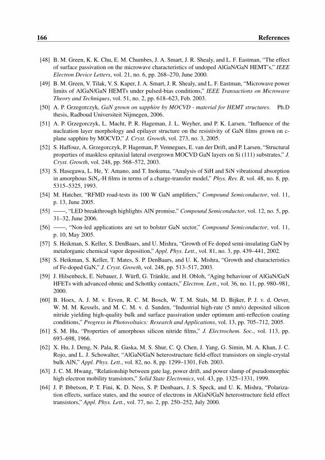
166 References
[48] B. M. Green, K. K. Chu, E. M. Chumbes, J. A. Smart, J. R. Shealy, and L. F. Eastman, “The effectof surface passivation on the microwave characteristics of undoped AlGaN/GaN HEMT’s,” IEEEElectron Device Letters, vol. 21, no. 6, pp. 268–270, June 2000.
[49] B. M. Green, V. Tilak, V. S. Kaper, J. A. Smart, J. R. Shealy, and L. F. Eastman, “Microwave powerlimits of AlGaN/GaN HEMTs under pulsed-bias conditions,” IEEE Transactions on MicrowaveTheory and Techniques, vol. 51, no. 2, pp. 618–623, Feb. 2003.
[50] A. P. Grzegorczyk, GaN grown on sapphire by MOCVD - material for HEMT structures. Ph.Dthesis, Radboud Universiteit Nijmegen, 2006.
[51] A. P. Grzegorczyk, L. Macht, P. R. Hageman, J. L. Weyher, and P. K. Larsen, “Influence of thenucleation layer morphology and epilayer structure on the resistivity of GaN films grown on c-plane sapphire by MOCVD,” J. Cryst. Growth, vol. 273, no. 3, 2005.
[52] S. Haffouz, A. Grzegorczyk, P. Hageman, P. Vennegues, E. van der Drift, and P. Larsen, “Structuralproperties of maskless epitaxial lateral overgrown MOCVD GaN layers on Si (111) substrates,” J.Cryst. Growth, vol. 248, pp. 568–572, 2003.
[53] S. Hasegawa, L. He, Y. Amano, and T. Inokuma, “Analysis of SiH and SiN vibrational absorptionin amorphous SiNx-H films in terms of a charge-transfer model,” Phys. Rev. B, vol. 48, no. 8, pp.5315–5325, 1993.
[54] M. Hatcher, “RFMD road-tests its 100 W GaN amplifiers,” Compound Semiconductor, vol. 11,p. 13, June 2005.
[55] ——, “LED breakthrough highlights AlN promise,” Compound Semiconductor, vol. 12, no. 5, pp.31–32, June 2006.
[56] ——, “Non-led applications are set to bolster GaN sector,” Compound Semiconductor, vol. 11,p. 10, May 2005.
[57] S. Heikman, S. Keller, S. DenBaars, and U. Mishra, “Growth of Fe doped semi-insulating GaN bymetalorganic chemical vapor deposition,” Appl. Phys. Lett., vol. 81, no. 3, pp. 439–441, 2002.
[58] S. Heikman, S. Keller, T. Mates, S. P. DenBaars, and U. K. Mishra, “Growth and characteristicsof Fe-doped GaN,” J. Cryst. Growth, vol. 248, pp. 513–517, 2003.
[59] J. Hilsenbeck, E. Nebauer, J. Würfl, G. Tränkle, and H. Obloh, “Aging behaviour of AlGaN/GaNHFETs with advanced ohmic and Schottky contacts,” Electron. Lett., vol. 36, no. 11, pp. 980–981,2000.
[60] B. Hoex, A. J. M. v. Erven, R. C. M. Bosch, W. T. M. Stals, M. D. Bijker, P. J. v. d. Oever,W. M. M. Kessels, and M. C. M. v. d. Sanden, “Industrial high-rate (5 nm/s) deposited siliconnitride yielding high-quality bulk and surface passivation under optimum anti-reflection coatingconditions,” Progress in Photovoltaics: Research and Applications, vol. 13, pp. 705–712, 2005.
[61] S. M. Hu, “Properties of amorphous silicon nitride films,” J. Electrochem. Soc., vol. 113, pp.693–698, 1966.
[62] X. Hu, J. Deng, N. Pala, R. Gaska, M. S. Shur, C. Q. Chen, J. Yang, G. Simin, M. A. Khan, J. C.Rojo, and L. J. Schowalter, “AlGaN/GaN heterostructure field-effect transistors on single-crystalbulk AlN,” Appl. Phys. Lett., vol. 82, no. 8, pp. 1299–1301, Feb. 2003.
[63] J. C. M. Hwang, “Relationship between gate lag, power drift, and power slump of pseudomorphichigh electron mobility transistors,” Solid State Electronics, vol. 43, pp. 1325–1331, 1999.
[64] J. P. Ibbetson, P. T. Fini, K. D. Ness, S. P. Denbaars, J. S. Speck, and U. K. Mishra, “Polariza-tion effects, surface states, and the source of electrons in AlGaN/GaN heterostructure field effecttransistors,” Appl. Phys. Lett., vol. 77, no. 2, pp. 250–252, July 2000.
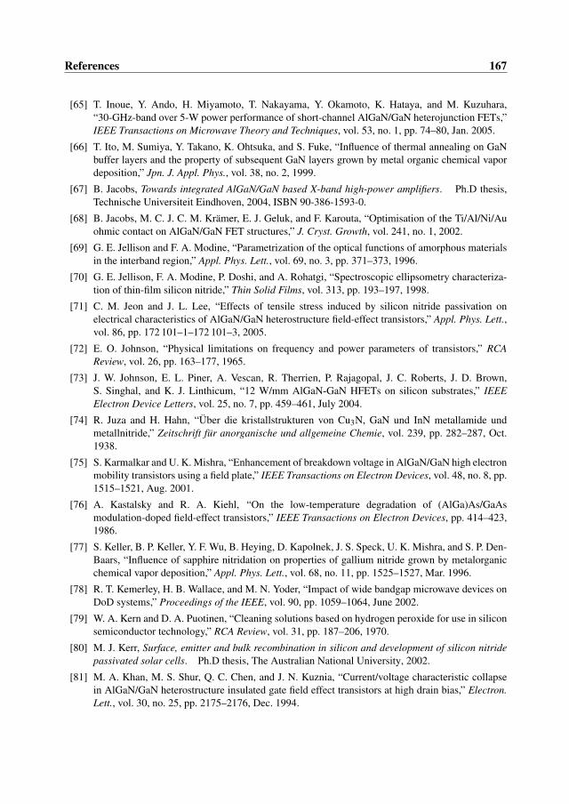
References 167
[65] T. Inoue, Y. Ando, H. Miyamoto, T. Nakayama, Y. Okamoto, K. Hataya, and M. Kuzuhara,“30-GHz-band over 5-W power performance of short-channel AlGaN/GaN heterojunction FETs,”IEEE Transactions on Microwave Theory and Techniques, vol. 53, no. 1, pp. 74–80, Jan. 2005.
[66] T. Ito, M. Sumiya, Y. Takano, K. Ohtsuka, and S. Fuke, “Influence of thermal annealing on GaNbuffer layers and the property of subsequent GaN layers grown by metal organic chemical vapordeposition,” Jpn. J. Appl. Phys., vol. 38, no. 2, 1999.
[67] B. Jacobs, Towards integrated AlGaN/GaN based X-band high-power amplifiers. Ph.D thesis,Technische Universiteit Eindhoven, 2004, ISBN 90-386-1593-0.
[68] B. Jacobs, M. C. J. C. M. Krämer, E. J. Geluk, and F. Karouta, “Optimisation of the Ti/Al/Ni/Auohmic contact on AlGaN/GaN FET structures,” J. Cryst. Growth, vol. 241, no. 1, 2002.
[69] G. E. Jellison and F. A. Modine, “Parametrization of the optical functions of amorphous materialsin the interband region,” Appl. Phys. Lett., vol. 69, no. 3, pp. 371–373, 1996.
[70] G. E. Jellison, F. A. Modine, P. Doshi, and A. Rohatgi, “Spectroscopic ellipsometry characteriza-tion of thin-film silicon nitride,” Thin Solid Films, vol. 313, pp. 193–197, 1998.
[71] C. M. Jeon and J. L. Lee, “Effects of tensile stress induced by silicon nitride passivation onelectrical characteristics of AlGaN/GaN heterostructure field-effect transistors,” Appl. Phys. Lett.,vol. 86, pp. 172 101–1–172 101–3, 2005.
[72] E. O. Johnson, “Physical limitations on frequency and power parameters of transistors,” RCAReview, vol. 26, pp. 163–177, 1965.
[73] J. W. Johnson, E. L. Piner, A. Vescan, R. Therrien, P. Rajagopal, J. C. Roberts, J. D. Brown,S. Singhal, and K. J. Linthicum, “12 W/mm AlGaN-GaN HFETs on silicon substrates,” IEEEElectron Device Letters, vol. 25, no. 7, pp. 459–461, July 2004.
[74] R. Juza and H. Hahn, “Über die kristallstrukturen von Cu3N, GaN und InN metallamide undmetallnitride,” Zeitschrift für anorganische und allgemeine Chemie, vol. 239, pp. 282–287, Oct.1938.
[75] S. Karmalkar and U. K. Mishra, “Enhancement of breakdown voltage in AlGaN/GaN high electronmobility transistors using a field plate,” IEEE Transactions on Electron Devices, vol. 48, no. 8, pp.1515–1521, Aug. 2001.
[76] A. Kastalsky and R. A. Kiehl, “On the low-temperature degradation of (AlGa)As/GaAsmodulation-doped field-effect transistors,” IEEE Transactions on Electron Devices, pp. 414–423,1986.
[77] S. Keller, B. P. Keller, Y. F. Wu, B. Heying, D. Kapolnek, J. S. Speck, U. K. Mishra, and S. P. Den-Baars, “Influence of sapphire nitridation on properties of gallium nitride grown by metalorganicchemical vapor deposition,” Appl. Phys. Lett., vol. 68, no. 11, pp. 1525–1527, Mar. 1996.
[78] R. T. Kemerley, H. B. Wallace, and M. N. Yoder, “Impact of wide bandgap microwave devices onDoD systems,” Proceedings of the IEEE, vol. 90, pp. 1059–1064, June 2002.
[79] W. A. Kern and D. A. Puotinen, “Cleaning solutions based on hydrogen peroxide for use in siliconsemiconductor technology,” RCA Review, vol. 31, pp. 187–206, 1970.
[80] M. J. Kerr, Surface, emitter and bulk recombination in silicon and development of silicon nitridepassivated solar cells. Ph.D thesis, The Australian National University, 2002.
[81] M. A. Khan, M. S. Shur, Q. C. Chen, and J. N. Kuznia, “Current/voltage characteristic collapsein AlGaN/GaN heterostructure insulated gate field effect transistors at high drain bias,” Electron.Lett., vol. 30, no. 25, pp. 2175–2176, Dec. 1994.

168 References
[82] M. Khan, J. N. Kuznia, D. T. Olson, W. Schaff, J. Burm, and M. Shur, “Microwave performanceof a 0.25 µm gate AlGaN/GaN heterostructure field effect transistor,” Appl. Phys. Lett., vol. 65,no. 9, pp. 1121–1123, 1994.
[83] M. Khan, J. Kuznia, A. Bhattarai, and D. Olson, “Metal semiconductor field effect transistor basedon single crystal GaN,” Appl. Phys. Lett., vol. 62, no. 15, pp. 1786–1787, 1993.
[84] M. Khan, J. van Hoven, J. Kuznia, and D. Olson, “High electron mobility GaN/AlGaN heterostruc-tures grown by low-pressure metalorganic chemical vapor deposition,” Appl. Phys. Lett., vol. 58,no. 21, pp. 2408–2410, 1991.
[85] T. Kikkawa, T. Maniwa, H. Hayashi, M. Kanamura, S. Yokokawa, M. Nishi, N. Adachi,M. Yokoyama, Y. Tateno, and K. Joshin, “An over 200-w output power GaN HEMT push-pullamplifier with high reliability,” IEEE MTT-S Digest, pp. 1347–1350, 2004.
[86] P. B. Klein, S. C. Binari, K. Ikossi, A. E. Wickenden, D. D. Koleske, and R. L. Henry, “Cur-rent collapse and the role of carbon in AlGaN/GaN high electron mobility transistors grown bymetalorganic vapor-phase epitaxy,” Appl. Phys. Lett., vol. 79, no. 21, pp. 3527–3529, Nov. 2001.
[87] P. B. Klein, S. C. Binari, K. Ikossi-Anastasiou, A. E. Wickenden, D. D. Koleske, R. L. Henry,and D. S. Katzer, “Investigation of traps producing current collapse in AlGaN/GaN high electronmobility transistors,” Electron. Lett., vol. 37, no. 10, pp. 661–662, May 2001.
[88] P. B. Klein, J. A. F. Jr, S. C. Binari, and A. E. Wickenden, “Observation of deep traps responsiblefor current collapse in GaN metal semiconductor field effect transistors,” Appl. Phys. Lett., vol. 75,no. 25, pp. 4016–4018, Dec. 1999.
[89] E. Kohn, I. Daumiller, M. Kunze, M. Neuburger, M. Seyboth, T. J. Jenkins, J. S. Sewell, J. V. Nor-stand, Y. Smorchkova, and U. K. Mishra, “Transient characteristics of GaN-based heterostructurefield-effect transistors,” IEEE Transactions on Microwave Theory and Techniques, vol. 51, no. 2,pp. 634–642, 2003.
[90] E. Kohn, I. Daumiller, P. Schmid, N. X. Nguyen, and C. N. Nguyen, “Large signal frequencydispersion of AlGaN/GaN heterostructure field-effect transistors,” Electron. Lett., vol. 35, no. 12,pp. 1022–1024, June 1999.
[91] M. C. J. C. M. Krämer, Fabrication and characterization of metal-semiconductor contacts forapplication in AlGaN/GaN HEMTs. M.Sc. thesis, Technische Universiteit Eindhoven, 2000.
[92] H. Kroemer, W. Y. Chien, J. S. Harris Jr., and D. D. Edwall, “Measurement of isotype heterojunc-tion barriers by (C-V) profiling,” Appl. Phys. Lett., vol. 36, no. 4, pp. 295–297, 1980.
[93] M. Kuball, J. M. Hayes, M. J. Uren, T. Martin, J. C. H. Birbeck, R. S. Balmer, and B. T.Hughes, “Measurement of temperature in active high-power AlGaN/GaN HFETs using Ramanspectroscopy,” IEEE Electron Device Letters, vol. 23, no. 1, pp. 7–9, Jan. 2002.
[94] A. Kuliev, C. Lee, W. Lu, E. Piner, S. R. Bahl, and I. Adesida, “A study of on-state and off-statebreakdown voltages in GaN MESFETs,” in Proc. IEEE/Cornell Conf., 2000, pp. 110–114.
[95] V. Kumar, J. W. Lee, A. Kuliev, O. Aktas, R. Schwindt, R. Birkhahn, D. Gotthold, S. Guo, B. Al-bert, and I. Adesida, “High performance 0.25 µm gate-length AlGaN/GaN HEMTs on 6H-SiCwith power density of 6.7 W/mm at 18 GHz,” Electron. Lett., vol. 39, no. 22, 2003.
[96] K. Kurokawa, “Power waves and the scattering matrix,” IEEE Transactions on Microwave Theoryand Techniques, vol. 13, no. 2, pp. 194–202, Mar. 1965.
[97] J. Kuzmik, P. Javorka, A. Alam, M. Marso, M. Heuken, and P. Kordos, “Determination of channeltemperature in AlGaN/GaN HEMTs grown on sapphire and silicon substrates using DC charac-terization method,” IEEE Transactions on Electron Devices, vol. 49, no. 8, pp. 1496–1498, Aug.2002.
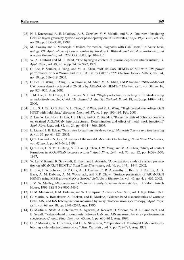
References 169
[98] N. I. Kuznetsov, A. E. Nikolaev, A. S. Zubrilov, Y. V. Melnik, and V. A. Dmitriev, “InsulatingGaN:Zn layers grown by hydride vapor phase epitaxy on SiC substrates,” Appl. Phys. Lett., vol. 75,no. 20, pp. 3138–3140, 1999.
[99] M. Kwasny and Z. Mierczyk, “Devices for medical diagnosis with GaN lasers,” in Laser Tech-nology VII: Applications of Lasers. Edited by Wieslaw L. Wolinski and Zdzislaw Jankiewicz andRyszard Romaniuk, vol. 5229, Oct. 2003, pp. 104–115.
[100] W. A. Lanford and M. J. Rand, “The hydrogen content of plasma-deposited silicon nitride,” J.Appl. Phys., vol. 49, no. 4, pp. 2473–2477, 1978.
[101] C. Lee, P. Saunier, J. Yang, and M. A. Khan, “AlGaN-GaN HEMTs on SiC with CW powerperformance of > 4 W/mm and 23% PAE at 35 GHz,” IEEE Electron Device Letters, vol. 24,no. 10, pp. 616–618, 2003.
[102] C. Lee, H. Wang, J. Yang, L. Witkowski, M. Muir, M. A. Khan, and P. Saunier, “State-of-the-artCW power density achieved at 26 GHz by AlGaN/GaN HEMTs,” Electron. Lett., vol. 38, no. 16,pp. 924–925, Aug. 2002.
[103] J. M. Lee, K. M. Chang, I. H. Lee, and S. J. Park, “Highly selective dry etching of III nitrides usingan inductively coupled Cl2/Ar/O2 plasma,” J. Vac. Sci. Technol. B, vol. 18, no. 3, pp. 1409–1411,2000.
[104] J. Li, S. J. Cai, G. Z. Pan, Y. L. Chen, C. P. Wen, and K. L. Wang, “High breakdown voltage GaNHFET with field plate,” Electron. Lett., vol. 37, no. 3, pp. 196–197, Feb. 2001.
[105] Z. Lin, W. Lu, J. Lee, D. Liu, J. S. Flynn, and G. R. Brandes, “Barrier heights of Schottky contactson strained AlGaN/GaN heterostructures: Determination and effect of metal work functions,”Appl. Phys. Lett., vol. 82, no. 24, pp. 4364–4366, 2003.
[106] L. Liu and J. H. Edgar, “Substrates for gallium nitride epitaxy,” Materials Science and EngineeringR, vol. 37, pp. 61–127, 2002.
[107] Q. Z. Liu and S. S. Lau, “A review of the metal-GaN contact technology,” Solid State Electronics,vol. 42, no. 5, pp. 677–691, 1998.
[108] Q. Z. Liu, L. S. Yu, F. Deng, S. S. Lau, Q. Chen, J. W. Yang, and M. A. Khan, “Study of contactformation in AlGaN/GaN heterostructures,” Appl. Phys. Lett., vol. 71, no. 12, pp. 1658–1660,1997.
[109] W. Lu, V. Kumar, R. Schwindt, E. Piner, and I. Adesida, “A comparative study of surface passiva-tion on AlGaN/GaN HEMTs,” Solid State Electronics, vol. 46, pp. 1441–1444, 2002.
[110] B. Luo, J. W. Johnson, B. P. Gila, A. H. Onstine, C. R. Abernathy, F. Ren, S. J. Pearton, A. G.Baca, A. M. Dabiran, A. M. Wowchack, and P. P. Chow, “Surface passivation of AlGaN/GaNHEMTs using MBE-grown MgO or Sc2O3,” Solid State Electronics, vol. 46, no. 4, p. 467, 2002.
[111] J. M. W. Medley, Microwave and RF circuits - analysis, synthesis and design. London: ArtechHouse, 1993, ISBN 0-89006-546-2.
[112] H. M. Manasevit, F. M. Erdman, and W. I. Simpson, J. Electrochem. Soc., vol. 118, p. 1864, 1971.[113] G. Martin, A. Botchkarev, A. Rockett, and H. Morkoc, “Valence-band discontinuities of wurtzite
GaN, AlN, and InN heterojunctions measured by x-ray photoemission spectroscopy,” Appl. Phys.Lett., vol. 68, no. 18, pp. 2541–2543, Apr. 1996.
[114] G. Martin, S. Strite, A. Botchkarev, A. Agarwal, A. Rockett, H. Morkoc, W. R. L. Lambrecht, andB. Segall, “Valence-band discontinuity between GaN and AlN measured by x-ray photoemissionspectroscopy,” Appl. Phys. Lett., vol. 65, no. 5, pp. 610–612, Aug. 1994.
[115] H. P. Maruska, W. C. Rhines, and D. A. Stevenson, “Preparation of Mg-doped GaN diodes ex-hibiting violet electroluminescence,” Mat. Res. Bull., vol. 7, pp. 777–781, Aug. 1972.
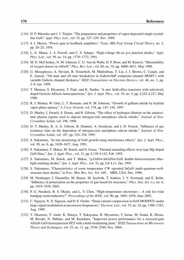
170 References
[116] H. P. Maruska and J. J. Tietjen, “The preparation and properties of vapor-deposited single-crystal-line GaN,” Appl. Phys. Lett., vol. 15, pp. 327–329, Nov. 1969.
[117] S. J. Mason, “Power gain in feedback amplifiers,” Trans. IRE Prof. Group Circuit Theory, no. 2,pp. 20–25, 1954.
[118] L. G. Matus, J. A. Powell, and C. S. Salupo, “High-voltage 6h-sic p-n junction diodes,” Appl.Phys. Lett., vol. 59, no. 14, pp. 1770–1772, 1991.
[119] M. D. McCluskey, N. M. Johnson, C. G. Van de Walle, D. P. Bour, and M. Kneissl, “Metastabilityof oxygen donors in AlGaN,” Phys. Rev. Lett., vol. 80, no. 18, pp. 4008–4011, May 1998.
[120] G. Meneghesso, A. Neviani, R. Oesterholt, M. Matloubian, T. Liu, J. J. Brown, C. Canali, andE. Zanoni, “On-state and off-state breakdown in GaInAs/InP composite-channel HEMT’s withvariable GaInAs channel thickness,” IEEE Transactions on Electron Devices, vol. 46, no. 1, pp.2–9, Jan. 1999.
[121] T. Mimura, S. Hiyamizu, T. Fujii, and K. Nanbu, “A new field-effect transistor with selectivelydoped GaAs/n-AlGaAs heterojunctions,” Jpn. J. Appl. Phys., vol. 19, no. 5, pp. L225–L227, May1980.
[122] R. J. Molnar, W. Götz, L. T. Romano, and N. M. Johnson, “Growth of gallium nitride by hydridevapor-phase epitaxy,” J. Cryst. Growth, vol. 178, pp. 147–156, 1997.
[123] D. Murley, I. French, S. Deane, and R. Gibson, “The effect of hydrogen dilution on the aminosi-lane plasma regime used to deposit nitrogen-rich amorphous silicon nitride,” Journal of Non-Crystalline Solids, vol. 198, 1996.
[124] D. T. Murley, R. A. G. Gibson, B. Dunnett, A. Goodyear, and I. D. French, “Influence of gasresidence time on the deposition of nitrogen-rich amorphous silicon nitride,” Journal of Non-Crystalline Solids, vol. 187, pp. 324–328, 1995.
[125] S. Nakamura, “In situ monitoring of GaN growth using interference effects,” Jpn. J. Appl. Phys.,vol. 30, no. 8, pp. 1620–1627, Aug. 1991.
[126] S. Nakamura, T. Mukai, M. Senoh, and N. Iwasa, “Thermal annealing effects on p-type Mg-dopedGaN films,” Jpn. J. Appl. Phys., vol. 31, pp. L139–L142, Feb. 1992.
[127] S. Nakamura, M. Senoh, and T. Mukai, “p-GaN/n-InGaN/n-GaN double-heterostructure blue-light-emitting diodes,” Jpn. J. Appl. Phys., vol. 32, pp. L8–L11, Jan. 1993.
[128] S. Nakamura, “Characteristics of room temperature CW operated InGaN multi-quantum-well-structure laser diodes,” in Proc. Mat. Res. Soc. Vol. 449. MRS, USA, Dec. 1996.
[129] M. Neuburger, I. Daumiller, M. Kunze, M. Seyboth, T. Jenkins, J. V. Nostrand, and E. Kohn,“Influence of polarization on the properties of gan based fet structures,” Phys. Stat. Sol. (c), no. 6,pp. 1919–1939, 2003.
[130] P. G. Neudeck, R. S. Okojie, and L. Y. Chen, “High-temperature electronics – A role for widebandgap semiconductors?” Proceedings of the IEEE, vol. 90, pp. 1065–1076, June 2002.
[131] C. Nguyen, N. X. Nguyen, and D. E. Grider, “Drain current compression in GaN MODFETs underlarge-signal modulation at microwave frequencies,” Electron. Lett., vol. 35, no. 16, pp. 1380–1382,Aug. 1999.
[132] Y. Okamoto, Y. Ando, K. Hataya, T. Nakayama, H. Miyamoto, T. Inoue, M. Senda, K. Hirata,M. Kosaki, N. Shibata, and M. Kuzuhara, “Improved power performance for a recessed-gateAlGaN-GaN heterojunction FET with a field-modulating plate,” IEEE Transactions on MicrowaveTheory and Techniques, vol. 52, no. 11, pp. 2536–2540, Nov. 2004.

References 171
[133] Y. Okamoto, Y. Ando, T. Nakayama, K. Hataya, H. Miyamoto, T. Inoue, M. Senda, K. Hirata,M. Kosaki, N. Shibata, and M. Kuzuhara, “High-power recessed-gate AlGaN-GaN HFET with afield-modulating plate,” IEEE Transactions on Electron Devices, vol. 51, no. 12, pp. 2217–2222,Dec. 2004.
[134] J. I. Pankove, E. A. Miller, and J. E. Berkeyheiser, RCA Review, vol. 32, p. 383, 1971.[135] J. I. Pankove and T. D. Moustakas, Gallium Nitride (GaN) I. San Diego: Academic Press, 1998,
ISBN 0-12-752158-5.[136] S. J. Pearton, C. R. Abernathy, M. E. Overberg, G. T. Thaler, A. H. Onstine, B. P. Gila, F. Ren,
B. Lou, and J. Kim, “New applications for Gallium Nitride,” Materials Today, pp. 24–31, June2002.
[137] S. J. Pearton, C. R. Abernathy, and C. B. Vartuli, “ECR plasma etching of GaN, AlN, and InNusing iodine or bromine chemistries,” Electron. Lett., vol. 30, no. 23, pp. 1985–1986, 1994.
[138] S. J. Pearton, J. C. Zolper, R. J. Shul, and F. Ren, “GaN: Processing, defects, and devices,” J. Appl.Phys., vol. 86, no. 1, pp. 1–78, 1999.
[139] R. S. Pengelly, Microwave field-effect transistors: Theory, design and applications. Researchstudies press, Letchworth, England, 1986, ISBN 0-86380-040-8.
[140] W. L. Pribble, J. W. Palmour, S. T. Sheppard, R. P. Smith, S. T. Allen, T. J. Smith, Z. Ring, J. J.Sumakeris, A. W. Saxler, and J. W. Milligan, “Applications of SiC MESFETs and GaN HEMTs inpower amplifier design,” IEEE MTT-S Digest, pp. 1819–1822, 2002.
[141] T. R. Prunty, J. A. Smart, E. M. Chumbes, B. K. Ridley, L. F. Eastman, and J. R. Shealy, “Passiva-tion of AlGaN/GaN heterostructures with silicon nitride for insulated gate transistors,” in Proceed-ings of the IEEE / Cornell High-Performance Devices Conference. IEEE, 2000, pp. 208–214.
[142] F. Ren and J. C. Zolper, Wide energy bandgap electronic devices. New Jersey: World Scientific,2003, ISBN 981-238-246-1.
[143] E. H. Rhoderick and R. H. Williams, Metal-Semiconductor contacts, second edition. Oxford:Clarendon Press, 1988, ISBN 0-19-859336-8.
[144] J. M. Rollett, “Stability and power-gain invariants of linear two ports,” IEEE Transactions onCircuit Theory, no. 1, pp. 29–32, 1962.
[145] S. Rudner and E. M. Suijker, SiC and GaN transistors for microwave power amplifiers - A Swedish- Dutch co-operation project. Report series 2000 - 2006.
[146] M. Rudzinski. Ph.D thesis, Radboud Universiteit Nijmegen, 2006.[147] S. Ruvimov, Z. Liliental-Weber, J. Washburn, D. Qiao, S. S. Lau, and P. K. Chu, “Microstructure
of ti/al ohmic contacts for n-AlGaN,” Appl. Phys. Lett., vol. 73, no. 18, pp. 2582–2584, 1998.[148] W. Seifert, R. Franzheld, E. Butter, H. Subotta, and V. Riede, “On the origin of free carriers in
high-conducting n-GaN,” Crystal Res. and Technol., vol. 18, p. 383, 1983.[149] B. S. Simpkins, E. T. Yu, P. Waltereit, and J. S. Speck, “Correlated scanning Kelvin probe and
conductive atomic force microscopy studies of dislocations in gallium nitride,” J. Appl. Phys.,vol. 94, no. 3, pp. 1448–1453, 2003.
[150] R. A. Sinton and A. Cuevas, “Contactless determination of current-voltage characteristics andminority-carrier lifetimes in semiconductors from quasi-steady-state photoconductance data,”Appl. Phys. Lett., vol. 69, no. 17, pp. 2510–2512, Oct. 1996.
[151] D. L. Smith, A. S. Alimonda, C. C. Cheng, S. E. Ready, and B. Wacker, “Mechanisms of SiNxHydeposition from NH3-SiH4 plasma,” J. Electrochem. Soc., vol. 137, pp. 614–623, 1990.
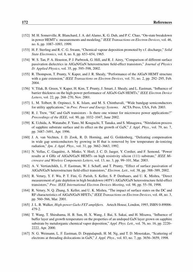
172 References
[152] M. H. Somerville, R. Blanchard, J. A. del Alamo, K. G. Duh, and P. C. Chao, “On-state breakdownin power HEMT’s: measurements and modeling,” IEEE Transactions on Electron Devices, vol. 46,no. 6, pp. 1087–1093, 1999.
[153] H. F. Sterling and R. C. G. Swann, “Chemical vapour deposition promoted by r.f. discharge,” SolidState Electronics, vol. 8, no. 8, pp. 653–654, 1965.
[154] W. S. Tan, P. A. Houston, P. J. Parbrook, G. Hill, and R. J. Airey, “Comparison of different surfacepassivation dielectrics in AlGaN/GaN heterostructure field-effect transistors,” Journal of PhysicsD: Applied Physics, vol. 35, pp. 595–598, 2002.
[155] R. Thompson, T. Prunty, V. Kaper, and J. R. Shealy, “Performance of the AlGaN HEMT structurewith a gate extension,” IEEE Transactions on Electron Devices, vol. 51, no. 2, pp. 292–295, Feb.2004.
[156] V. Tilak, B. Green, V. Kaper, H. Kim, T. Prunty, J. Smart, J. Shealy, and L. Eastman, “Influence ofbarrier thickness on the high-power performance of AlGaN-GaN HEMTs,” IEEE Electron DeviceLetters, vol. 22, pp. 268–270, Nov. 2001.
[157] L. M. Tolbert, B. Ozpineci, S. K. Islam, and M. S. Chinthavali, “Wide bandgap semiconductorsfor utility applications,” in Proc. Power and Energy Systems. ACTA Press, USA, Feb. 2003.
[158] R. J. Trew, “SiC and GaN transistors - Is there one winner for microwave power applications?”Proceedings of the IEEE, vol. 90, pp. 1032–1047, June 2002.
[159] K. Uchida, A. Watanabe, F. Yano, M. Kouguchi, T. Tanaka, and S. Minagawa, “Nitridation processof sapphire substrate surface and its effect on the growth of GaN,” J. Appl. Phys., vol. 79, no. 7,pp. 3487–3491, Apr. 1996.
[160] J. A. van Vechten, J. D. Zook, R. D. Horning, and G. Goldenberg, “Defeating compensationin wide gap semiconductors by growing in H that is removed by low temperature de-ionizingradiation,” Jpn. J. Appl. Phys., vol. 31, pp. 3662–3663, 1992.
[161] N. Vellas, C. Gaquière, A. Minko, V. Hoël, J. C. D. Jaeger, Y. Cordier, and F. Semond, “Powerresults at 4 GHz of AlGaN/GaN HEMTs on high resistivity silicon (111) substrate,” IEEE Mi-crowave and Wireless Components Letters, vol. 13, no. 3, pp. 99–101, Mar. 2003.
[162] A. V. Vertiatchikh, L. F. Eastman, W. J. Schaff, and T. Prunty, “Effect of surface passivation ofAlGaN/GaN heterostructure field-effect transistors,” Electron. Lett., vol. 38, pp. 388–389, 2002.
[163] R. Vetury, Y. F. Wu, P. T. Fini, G. Parish, S. Keller, S. P. Denbaars, and U. K. Mishra, “Directmeasurement of gate depletion in high breakdown (405V) AlGaN/GaN heterostructure field-effecttransistors,” Proc. IEEE International Electron Devices Meeting, vol. 98, pp. 55–58, 1998.
[164] R. Vetury, N. Q. Zhang, S. Keller, and U. K. Mishra, “The impact of surface states on the DC andRF characteristics of AlGaN/GaN HFETs,” IEEE Transactions on Electron Devices, vol. 48, no. 3,pp. 560–566, Mar. 2001.
[165] J. L. B. Walker, High-power GaAs FET amplifiers. Artech House, London, 1993, ISBN 0-89006-479-2.
[166] T. Wang, T. Shirahama, H. B. Sun, H. X. Wang, J. Bai, S. Sakai, and H. Misawa, “Influence ofbuffer layer and growth temperature on the properties of an undoped GaN layer grown on sapphiresubstrate by metalorganic chemical vapor deposition,” Appl. Phys. Lett., vol. 76, no. 16, pp. 2220–2222, Apr. 2000.
[167] N. G. Weimann, L. F. Eastman, D. Doppalapudi, H. M. Ng, and T. D. Moustakas, “Scattering ofelectrons at threading dislocations in GaN,” J. Appl. Phys., vol. 83, no. 7, pp. 3656–3659, 1998.
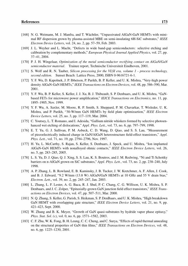
References 173
[168] N. G. Weimann, M. J. Manfra, and T. Wächtler, “Unpassivated AlGaN-GaN HEMTs with mini-mal RF dispersion grown by plasma-assisted MBE on semi-insulating 6H-SiC substrates,” IEEEElectron Device Letters, vol. 24, no. 2, pp. 57–59, Feb. 2003.
[169] J. L. Weyher and L. Macht, “Defects in wide band-gap semiconductors: selective etching andcalibration by complementary methods,” European Physical Journal Applied Physics, vol. 27, pp.37–41, 2004.
[170] P. J. H. Wingelaar, Optimization of the metal semiconductor rectifying contact on AlGaN/GaNsemiconductor material. Trainee report, Technische Universiteit Eindhoven, 2001.
[171] S. Wolf and R. N. Tauber, Silicon processing for the VLSI era, volume 1 - process technology,second edition. Sunset Beach: Lattice Press, 2000, ISBN 0-9616721-6-1.
[172] Y. F. Wu, D. Kapolnek, J. P. Ibbetson, P. Parikh, B. P. Keller, and U. K. Mishra, “Very-high powerdensity AlGaN-GaN HEMTs,” IEEE Transactions on Electron Devices, vol. 48, pp. 586–590, Mar.2001.
[173] Y. F. Wu, B. P. Keller, S. Keller, J. J. Xu, B. J. Thibeault, S. P. Denbaars, and U. K. Mishra, “GaN-based FETs for microwave power amplification,” IEICE Transactions on Electronics, no. 11, pp.1895–1905, Nov. 1999.
[174] Y. F. Wu, A. Saxler, M. Moore, R. P. Smith, S. Sheppard, P. M. Chavarkar, T. Wisleder, U. K.Mishra, and P. Parikh, “30-W/mm GaN HEMTs by field plate optimizaztion,” IEEE ElectronDevice Letters, vol. 25, no. 3, pp. 117–119, Mar. 2004.
[175] C. Youtsey, L. T. Romano, and I. Adesida, “Gallium nitride whiskers formed by selective photoen-hanced wet etching of dislocations,” Appl. Phys. Lett., vol. 73, no. 6, pp. 797–799, 1998.
[176] E. T. Yu, G. J. Sullivan, P. M. Asbeck, C. D. Wang, D. Qiao, and S. S. Lau, “Measurementof piezoelectrically induced charge in GaN/AlGaN heterostructure field-effect transistors,” Appl.Phys. Lett., vol. 71, no. 19, pp. 2794–2796, Nov. 1997.
[177] H. Yu, L. McCarthy, S. Rajan, S. Keller, S. Denbaars, J. Speck, and U. Mishra, “Ion implantedAlGaN-GaN HEMTs with nonalloyed ohmic contacts,” IEEE Electron Device Letters, vol. 26,no. 5, pp. 283–285, 2005.
[178] L. S. Yu, D. J. Qiao, Q. J. Xing, S. S. Lau, K. S. Boutros, and J. M. Redwing, “Ni and Ti Schottkybarriers on n-AlGaN grown on SiC substrates,” Appl. Phys. Lett., vol. 73, no. 2, pp. 238–240, July1998.
[179] A. P. Zhang, L. B. Rowland, E. B. Kaminsky, J. B. Tucker, J. W. Kretchmer, A. F. Allen, J. Cook,and B. J. Edward, “9.2 W/mm (13.8 W) AlGaN/GaN HEMTs at 10 GHz and 55 V drain bias,”Electron. Lett., vol. 39, no. 2, pp. 245–247, Jan. 2003.
[180] L. Zhang, L. F. Lester, A. G. Baca, R. J. Shul, P. C. Chang, C. G. Willison, U. K. Mishra, S. P.Denbaars, and J. C. Zolper, “Epitaxially-grown GaN junction field effect transistors,” IEEE Trans-actions on Electron Devices, vol. 47, pp. 507–511, Mar. 2000.
[181] N. Q. Zhang, S. Keller, G. Parish, S. Heikman, S. P. DenBaars, and U. K. Mishra, “High breakdownGaN HEMT with overlapping gate structure,” IEEE Electron Device Letters, vol. 21, no. 9, pp.421–423, Sept. 2000.
[182] W. Zhang and B. K. Meyer, “Growth of GaN quasi-substrates by hydride vapor phase epitaxy,”Phys. Stat. Sol. (c), vol. 0, no. 6, pp. 1571–1582, 2003.
[183] C. F. Zhu, W. K. Fong, B. H. Leung, C. C. Cheng, and C. Surya, “Effects of rapid thermal annealingon the structural properties of GaN thin films,” IEEE Transactions on Electron Devices, vol. 48,no. 6, pp. 1225–1230, 2001.

174 References

Appendix A
Process flows for GaN-based HFETsWe have developed process flows for GaN-based HFETs that can be used for the fabricationon sapphire and s.i. SiC substrates. This appendix starts with descriptions of process steps thatform the building blocks for the process flows of both small and large gate periphery devices.Section A.2 describes the process settings for resists used for optical contact lithography andpolymers used for electron beam lithography. Section A.3 provides process settings for differentplasma processes used. Finally, sections A.3 to A.6 provide the complete process flows forsmall and large periphery devices, respectively.
A.1 Building blocks
A.1.1 Cleaning
Cleaning Comments
Spray with acetone(CH3COCH3)
- in quartz basket with teflon insert- above waste container
Spray with iso-propyl alcohol(CH3CHOHCH3)
- in quartz basket with teflon insert- above waste container
Blow dry with nitrogen (N2)
A.1.2 Rinsing
Rinsing Comments
Rinse in ultra pure water(UPW)
- for positive resists time > 1 minute- for negative resists time > 3 minutes- for both resist types resistance water > 5MΩ
- place sample in quartz basket with teflon insertBlow dry with nitrogen (N2)
175

176 Appendix A
A.1.3 Exposure
Exposure Comments
UV 300 - Karl Süss MJB3 mask aligner- λ = 300 nm- optical power density: 3.4 mW/cm2 (range 20)
UV 400 - Karl Süss MJB3 mask aligner- λ = 400 nm- optical power density: 21.7 mW/cm2 (range 200)
UV 430 - Karl Süss MA6 mask aligner- λ = 430 nm- optical power density: 7.5 mW/cm2 (range 20)- vacuum mode
A.1.4 Metal lift-off
Lift-off Comments
Soak in aceton time > 3 minutesSpray with acetone - in quartz basket with teflon insert
- above waste containerUltrasonically stirring in ace-tone
- time > 1 minute- place quartz basket with teflon holder on bottom ofbeaker glass
Cleaning see A.1.1
A.1.5 Oxygen plasmas
Oxygen plasmas T(oC)
time(m:s)
Comments
Descum 20 0:30 - Tepla- process power 50W- Faraday cage to prevent surfacedamage due to ion bombardment
Stripping 20 5:00 - Tepla- process power 150W- Faraday cage
Ashing 20 15:00 - Tepla- process power 300W- Faraday cage

Appendix A 177
A.1.6 Resist removal after plasma etching
Resist removal T(oC)
time(m:s)
Comments
Stripping 20 5:00 see A.1.5Spray with acetone - in quartz basket with teflon insert
- above waste containerUltrasonically stirring inacetone
2:00 place quartz basket with teflon holderon bottom of beaker glass
Cleaning see A.1.1

178 Appendix A
A.2 Resists and polymers
A.2.1 Microchemicals AZ5214e
AZ5214e T(oC)
time(m:s)
Comments
- optical lithography- positive radiation sensitive
Spinning 0:30 - open air spinner- 5000 rpm
Soft bake 95 5:00 hotplateFlood exposure 0:00.8 - UV 300, see A.1.3
- required for lift-off profileBake 105 5:00 hotplateMask exposure 0:30 UV 300, see A.1.3Develop 1:30 AZ developer : UPW = 1 : 1 (volume)Rinsing see A.1.2
A.2.2 Microchemicals AZ4533
AZ4533 T(oC)
time(m:s)
Comments
- optical lithography- positive radiation sensitive
Spinning 0:30 - open air spinner- 5000 rpm
Soft bake 95 20:00 hotplateMask exposure: UV 400 0:15 UV 400, see A.1.3Mask exposure: UV 430 0:32 UV 430, see A.1.3Develop 1:20 AZ developer : UPW = 1 : 1 (volume)Rinsing see A.1.2Hard bake 105 30:00 hotplate

Appendix A 179
A.2.3 Micro resist ma-N415
ma-N415 T(oC)
time(m:s)
Comments
- optical lithography- negative radiation sensitive
Spinning 0:30 - CONVAC open air spinner- 5000 rpm
Bake 95 5:00 hotplateMask exposure 0:24 UV 300, see A.1.3Develop 1:50 ma-D332S (concentrated)Rinsing see A.1.2
A.2.4 Micro resist ma-N440
ma-N440 T(oC)
time(m:s)
Comments
- optical lithography- negative radiation sensitive
Spinning 0:30 - CONVAC open air spinner- 3000 rpm
Bake 95 5:00 hotplateMask exposure 8:20 - UV 430, see A.1.3
- Vacuum mode- 5 x 100 seconds
Develop 1:30 ma-D332S (concentrated)Rinsing see A.1.2
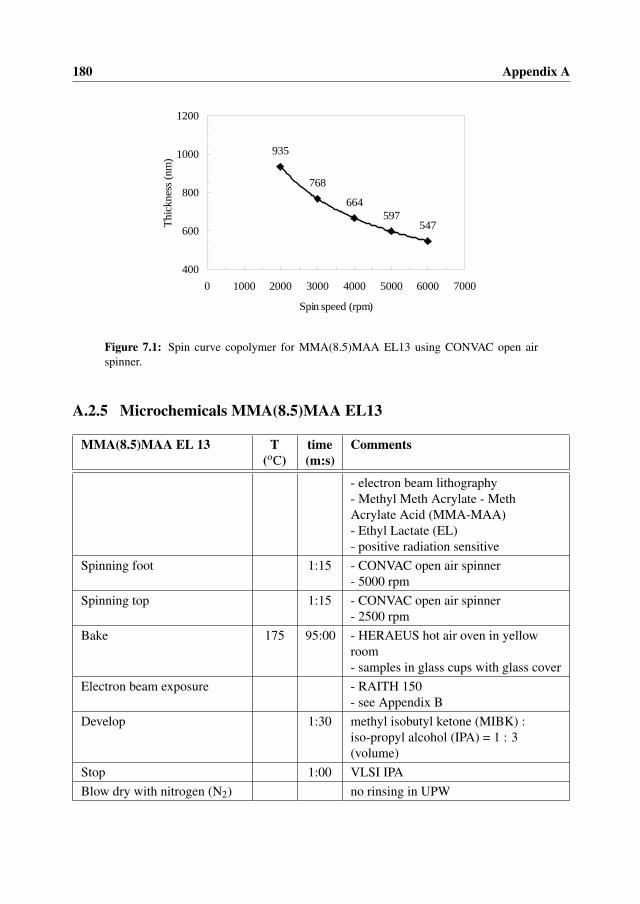
180 Appendix A
935
768
664597
547
400
600
800
1000
1200
0 1000 2000 3000 4000 5000 6000 7000
Spin speed (rpm)
Thic
knes
s (nm
) mm
m
Figure 7.1: Spin curve copolymer for MMA(8.5)MAA EL13 using CONVAC open airspinner.
A.2.5 Microchemicals MMA(8.5)MAA EL13
MMA(8.5)MAA EL 13 T(oC)
time(m:s)
Comments
- electron beam lithography- Methyl Meth Acrylate - MethAcrylate Acid (MMA-MAA)- Ethyl Lactate (EL)- positive radiation sensitive
Spinning foot 1:15 - CONVAC open air spinner- 5000 rpm
Spinning top 1:15 - CONVAC open air spinner- 2500 rpm
Bake 175 95:00 - HERAEUS hot air oven in yellowroom- samples in glass cups with glass cover
Electron beam exposure - RAITH 150- see Appendix B
Develop 1:30 methyl isobutyl ketone (MIBK) :iso-propyl alcohol (IPA) = 1 : 3(volume)
Stop 1:00 VLSI IPABlow dry with nitrogen (N2) no rinsing in UPW

Appendix A 181
420
284228 204 178 168 155
0
100
200
300
400
500
600
0 1000 2000 3000 4000 5000 6000 7000 8000
Spin speed (rpm)
Thic
knes
s (n
m) m
mm
Figure 7.2: Spin curve for PMMA 950K A4 using CONVAC open air spinner.
A.2.6 Microchemicals PMMA 950K A4PMMA 950K A4 T
(oC)time(m:s)
Comments
- electron beam lithography- Poly Methyl Meth Acrylat (PMMA)- positive radiation sensitive
Spinning SPL 1:00 - CONVAC open air spinner- 5000 rpm- single pixel lines
Bake 175 95:00 - HERAEUS hot air oven in yellowroom- samples in glass cups with glass cover
Electron beam exposure - RAITH 150- see Appendix B
Develop 1:30 methyl isobutyl ketone (MIBK):iso-propyl alcohol (IPA) = 1 : 3(volume)
Stop 1:00 VLSI IPABlow dry with nitrogen (N2) no rinsing in UPW

182 Appendix A
A.3 Plasma processes
A.3.1 Reactive ion etching (RIE): dispersion
RIE: dispersion T(oC)
time(m:s)
Comments
Oxford instruments Plasmalab system100
Chamber and quartz platecleaning
20 30:00 - O2 = 20 sccm, Ar = 10 sccm- PRF = 100 W, DCbias = -141 V- p = 100 mmTor- heater-chiller on, cooling on
Chamber and quartz plateconditioning
20 10:00 - no sample- 3B mode, C1 = 86, C2 = 21- Ar = 10 sccm- PRF = 30 W, DCbias = -86 V- p = 40 mmTor- heater-chiller on, cooling on
Dummy run 20 0:30 - one dummy sample- 1F mode, C1 = 86, C2 = 21- tset = 33 seconds- Ar = 10 sccm- PRF = 30 W, DCbias = -86 V- p = 40 mmTor- heater-chiller on, cooling on
Dispersion etch 20 0:30 - one sample at a time- 1F mode, C1 = 86, C2 = 21- tset = 33 seconds- Ar = 10 sccm- PRF = 30 W, DCbias = -86 V- p = 40 mmTor- heater-chiller on, cooling on
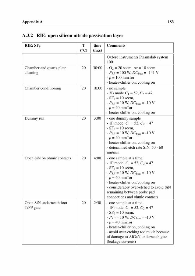
Appendix A 183
A.3.2 RIE: open silicon nitride passivation layer
RIE: SF6 T(oC)
time(m:s)
Comments
Oxford instruments Plasmalab system100
Chamber and quartz platecleaning
20 30:00 - O2 = 20 sccm, Ar = 10 sccm- PRF = 100 W, DCbias = -141 V- p = 100 mmTor- heater-chiller on, cooling on
Chamber conditioning 20 10:00 - no sample- 3B mode C1 = 52, C2 = 47- SF6 = 10 sccm,- PRF = 10 W, DCbias = -10 V- p = 40 mmTor- heater-chiller on, cooling on
Dummy run 20 3:00 - one dummy sample- 1F mode, C1 = 52, C2 = 47- SF6 = 10 sccm,- PRF = 10 W, DCbias = -10 V- p = 40 mmTor- heater-chiller on, cooling on- determined etch rate SiN: 50 - 60nm/min
Open SiN on ohmic contacts 20 4:00 - one sample at a time- 1F mode, C1 = 52, C2 = 47- SF6 = 10 sccm,- PRF = 10 W, DCbias = -10 V- p = 40 mmTor- heater-chiller on, cooling on- considerably over-etched to avoid SiNremaining between probe padconnections and ohmic contacts
Open SiN underneath footT/FP gate
20 2:50 - one sample at a time- 1F mode, C1 = 52, C2 = 47- SF6 = 10 sccm,- PRF = 10 W, DCbias = -10 V- p = 40 mmTor- heater-chiller on, cooling on- avoid over-etching too much becauseof damage to AlGaN underneath gate(leakage currents)

184 Appendix A
A.3.3 Inductively coupled plasma etching (ICP): mesa
ICP: mesa T(oC)
time(m:s)
Comments
Oxford instruments Plasmalab system100
Chamber cleaning 40 60:00 - C1 = 4.06, C2 = 4.92- O2 = 40 sccm- PICP = 1500 W, PRF = 150 W- DCbias = -260 V- p = 20 mmTor- LN2 cooling on
Chamber conditioning 40 105:00 - with Si carrier wafer, no sample- cyclic etching process, tetch cycle = 5minutes- C1 = 6.85, C2 = 4.06- Cl2 = 30 sccm, H2 = 10 sccm- PICP = 200 W, PRF = 50 W- DCbias = -210 V- p = 10 mmTor, pHe = 16 Torr (8 sccm)- LN2 cooling on
Dummy run 40 2:00 - one dummy sample- C1 = 6.85, C2 = 4.06- Cl2 = 30 sccm, H2 = 10 sccm- PICP = 200 W, PRF = 50 W- DCbias = -210 V- p = 10 mmTor, pHe = 16 Torr (8 sccm)- LN2 cooling on- determined etch rate AlGaN/GaN:110 nm/min
Mesa etch 40 1:35 - one sample at a time- C1 = 6.85, C2 = 4.06- Cl2 = 30 sccm, H2 = 10 sccm- PICP = 200 W, PRF = 50 W- DCbias = -210 V- p = 10 mmTor, pHe = 16 Torr (8 sccm)- LN2 cooling on- targeted mesa height: 175 nm

Appendix A 185
A.3.4 Plasma enhanced chemical vapor deposition (PECVD)
PECVD T(oC)
time(m:s)
Comments
Oxford instruments Plasmalab system100
SiN deposition 300 - SiH4 = 16.6 sccm, NH3 = 13.4 sccm- N2 = 980 sccm- PRF = 20 W- p = 650 mmTor- deposition rate: 12 nm/min

186 Appendix A
A.4 Small gate periphery devices (inverse mesa)Small periphery devices consist of two parallel gate fingers in a U-shape layout with total gatewidth (Wg) of 80µm. The gates have been defined either using optical contact lithography orelectron beam lithography. The optically defined gates are called “long” or “fat” as theirgate length (Lg) is 2µm. The e-beam defined gates are called “sub-micron” gates and the gatelength used for small periphery devices is 0.25µm.
We have processed small periphery devices using two different mask sets. The first set(“inverse mesa”) consists of devices with optically defined gates only. The process flow forthis set is described in this section. The second mask set (“submu”) consists of devices withboth optically and e-beam defined gates. The process flow for this set will be described inSect. A.5.
A.4.1 Sample preparation
Preparation T(oC)
time(m:s)
Comments
Spin coat epi-side 2” waferwith AZ5214e
protect epilayers during saw/diceprocess
Bake AZ5214e 95 5:00 hotplatePaste 2” wafer with resistcoated epi-side on blue tape
if sawn with disco
Sawing of 2” wafer - sample size at least 10 x 10 mm2
- diamond coated saw blade- water cooled
Dicing of 2” wafer - sample size at least 10 x 10 mm2
- Manually with diamond scratch penMark substrate side scratch “Z” on substrate (sapphire/SiC)
side to identify epi-side duringprocessing
A.4.2 Sample cleaning
T(oC)
time(m:s)
Comments
Cleaning see A.1.1Remove surface oxides 1:30 - sample completely dipped
- BHFRinsing see A.1.2Optical inspection polyvar

Appendix A 187
A.4.3 Ohmic contact lithography
T(oC)
time(m:s)
Comments
Cleaning see A.1.1AZ5214e see A.2.1Optical inspection - polyvar
- check development and lift-off profile
A.4.4 Ohmic contact metallization
T(oC)
time(m:s)
Comments
Evaporation - Ti/Al/Ni/Au = 30/180/40/100 nm- evaporation rate: 3 Å/s- Airco electron beam evaporator
A.4.5 Lift-off after ohmic contact metallization
T(oC)
time(m:s)
Comments
Metal lift-off see A.1.4Optical inspection polyvar
A.4.6 Dispersion etch
T(oC)
time(m:s)
Comments
RIE: dispersion see A.3.1

188 Appendix A
A.4.7 Rapid thermal annealing of ohmic contacts
T(oC)
time(m:s)
Comments
RTA process 800 2:00 - AST RTA: 800n-m02.2- N2ambient- ramp-up 100 oC - 800 oC in 45seconds
Dummy run 800 2:00 - no samples- AST RTA: 800n-m02.2
RTA ohmic contacts 800 2:00 - all samples at once- AST RTA: 800n-m02.2
A.4.8 Mesa lithography
T(oC)
time(m:s)
Comments
Cleaning see A.1.1AZ4533 see A.2.2Measure resist height Tencor Alpha Step
A.4.9 Mesa formationT
(oC)time(m:s)
Comments
ICP: mesa see A.3.3Measurement step height afterICP etch
Tencor Alpha Step
Remove AZ4533 see A.1.6Optical inspection polyvarMeasurement mesa height Tencor Alpha Step
A.4.10 Schottky gate and probe pad lithography
T(oC)
time(m:s)
Comments
Cleaning see A.1.1AZ5214e see A.2.2Optical inspection - polyvar
- check development and lift-off profile

Appendix A 189
A.4.11 Schottky gate and probe pad metallization
T(oC)
time(m:s)
Comments
Evaporation - Ni/Au = 20/250 nm- evaporation rate: 3 Å/s- Airco electron beam evaporator
A.4.12 Lift-off after Schottky gate and probe pad metallization
T(oC)
time(m:s)
Comments
Metal lift-off see A.1.4Optical inspection polyvar
A.4.13 Surface passivation
T(oC)
time(m:s)
Comments
Cleaning see A.1.1SiN deposition 300 8:36 - see A.3.4
- 100 nm

190 Appendix A
A.5 Small gate periphery devices (submu)This section describes the process flow for small periphery devices using the submu mask set.The gate length for these devices is 0.25µm.
A.5.1 Sample preparation
Preparation T(oC)
time(m:s)
Comments
Spin coat epi-side 2” waferwith AZ5214e
protect epilayers during saw/diceprocess
Bake AZ5214e 95 5:00 hotplatePaste 2” wafer with resistcoated epi-side on blue tape
if sawn with disco
Sawing of 2” wafer - sample size 10 x 10 mm2
- diamond coated saw blade- water cooled
Dicing of 2” wafer - sample size 10 x 10 mm2
- Manually with diamond scratch penMark substrate side - scratch “Z” on substrate
(sapphire/SiC) side to identify epi-sideduring processing
A.5.2 Sample cleaning
T(oC)
time(m:s)
Comments
Cleaning see A.1.1Remove surface oxides 1:30 - sample completely dipped
- BHFRinsing see A.1.2Optical inspection polyvar
A.5.3 Mesa lithography
T(oC)
time(m:s)
Comments
Cleaning see A.1.1AZ4533 see A.2.2Measure resist height Tencor Alpha Step

Appendix A 191
A.5.4 Mesa formationT
(oC)time(m:s)
Comments
ICP: mesa see A.3.3Measurement step height afterICP etch
Tencor Alpha Step
Remove AZ4533 see A.1.6Optical inspection polyvarMeasurement mesa height Tencor Alpha Step
A.5.5 Ohmic contact lithography
T(oC)
time(m:s)
Comments
Cleaning see A.1.1AZ5214e see A.2.1Optical inspection - polyvar
- check development and lift-off profile
A.5.6 Ohmic contact metallizationT
(oC)time(m:s)
Comments
Evaporation - Ti/Al/Ni/Au = 30/180/40/100 nm- evaporation rate: 3 Å/s- Airco electron beam evaporator
A.5.7 Lift-off after ohmic contact metallizationT
(oC)time(m:s)
Comments
Metal lift-off see A.1.4Optical inspection polyvar
A.5.8 Oxygen plasma
T(oC)
time(m:s)
Comments
Stripping 20 5:00 see A.1.5
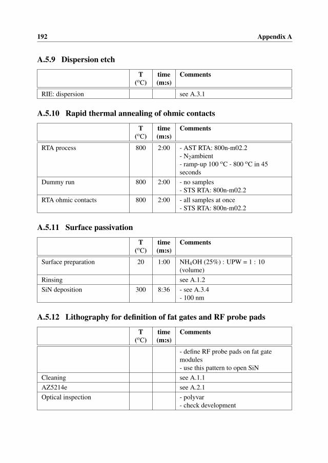
192 Appendix A
A.5.9 Dispersion etch
T(oC)
time(m:s)
Comments
RIE: dispersion see A.3.1
A.5.10 Rapid thermal annealing of ohmic contacts
T(oC)
time(m:s)
Comments
RTA process 800 2:00 - AST RTA: 800n-m02.2- N2ambient- ramp-up 100 oC - 800 oC in 45seconds
Dummy run 800 2:00 - no samples- STS RTA: 800n-m02.2
RTA ohmic contacts 800 2:00 - all samples at once- STS RTA: 800n-m02.2
A.5.11 Surface passivation
T(oC)
time(m:s)
Comments
Surface preparation 20 1:00 NH4OH (25%) : UPW = 1 : 10(volume)
Rinsing see A.1.2SiN deposition 300 8:36 - see A.3.4
- 100 nm
A.5.12 Lithography for definition of fat gates and RF probe pads
T(oC)
time(m:s)
Comments
- define RF probe pads on fat gatemodules- use this pattern to open SiN
Cleaning see A.1.1AZ5214e see A.2.1Optical inspection - polyvar
- check development

Appendix A 193
A.5.13 Open SiN passivation layer on fat gate modules
T(oC)
time(m:s)
Comments
RIE: SF6 20 4:00 - see A.3.2- open SiN on ohmic contacts andunderneath gates and RF probe pads
Optical inspection polyvar
A.5.14 Metallization of fat gates and RF probe pads
T(oC)
time(m:s)
Comments
Evaporation - Ni/Au = 20/250 nm- evaporation rate Au: 3 Å/s- Airco electron beam evaporator
A.5.15 Lift-off after metallization of fat gates and RF probe pads
T(oC)
time(m:s)
Comments
Metal lift-off see A.1.4, but now soak in acetone for10 minutes
Optical inspection polyvar
A.5.16 Lithography for foot T/FP gates
T(oC)
time(m:s)
Comments
Cleaning see A.1.1PMMA 950K A4 see A.2.6Thermal evaporation - Edwards, tooling factor 1.4
- Au = 12.5 nm
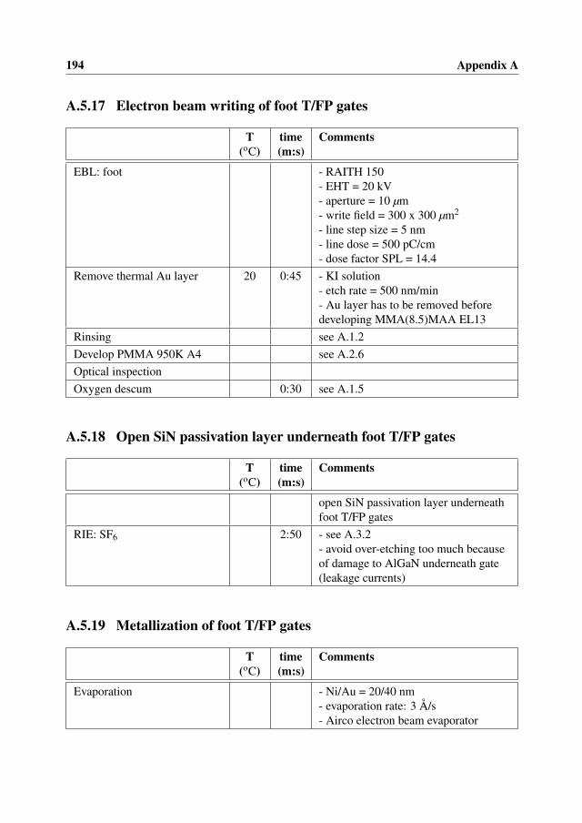
194 Appendix A
A.5.17 Electron beam writing of foot T/FP gates
T(oC)
time(m:s)
Comments
EBL: foot - RAITH 150- EHT = 20 kV- aperture = 10 µm- write field = 300 x 300 µm2
- line step size = 5 nm- line dose = 500 pC/cm- dose factor SPL = 14.4
Remove thermal Au layer 20 0:45 - KI solution- etch rate = 500 nm/min- Au layer has to be removed beforedeveloping MMA(8.5)MAA EL13
Rinsing see A.1.2Develop PMMA 950K A4 see A.2.6Optical inspectionOxygen descum 0:30 see A.1.5
A.5.18 Open SiN passivation layer underneath foot T/FP gates
T(oC)
time(m:s)
Comments
open SiN passivation layer underneathfoot T/FP gates
RIE: SF6 2:50 - see A.3.2- avoid over-etching too much becauseof damage to AlGaN underneath gate(leakage currents)
A.5.19 Metallization of foot T/FP gates
T(oC)
time(m:s)
Comments
Evaporation - Ni/Au = 20/40 nm- evaporation rate: 3 Å/s- Airco electron beam evaporator
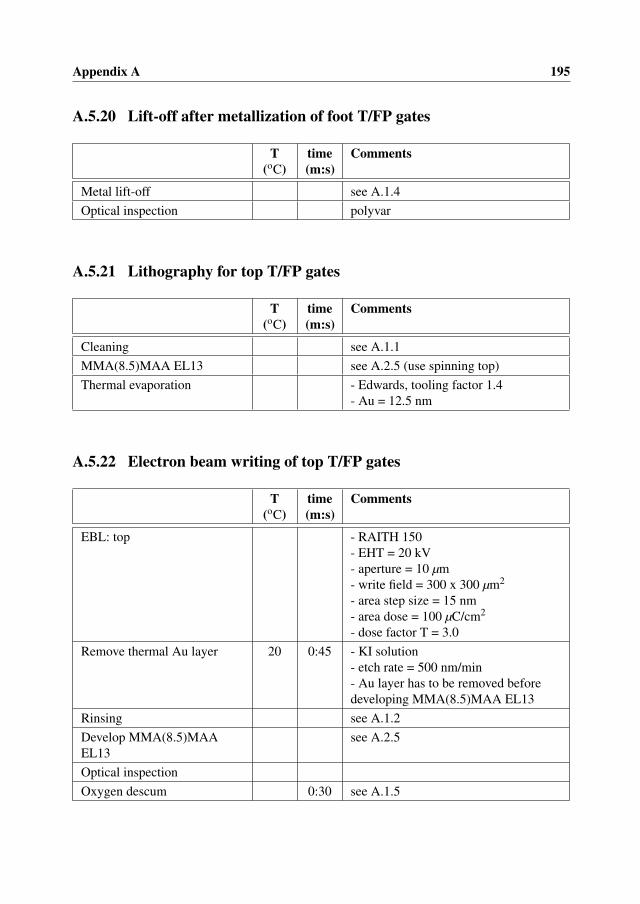
Appendix A 195
A.5.20 Lift-off after metallization of foot T/FP gates
T(oC)
time(m:s)
Comments
Metal lift-off see A.1.4Optical inspection polyvar
A.5.21 Lithography for top T/FP gates
T(oC)
time(m:s)
Comments
Cleaning see A.1.1MMA(8.5)MAA EL13 see A.2.5 (use spinning top)Thermal evaporation - Edwards, tooling factor 1.4
- Au = 12.5 nm
A.5.22 Electron beam writing of top T/FP gates
T(oC)
time(m:s)
Comments
EBL: top - RAITH 150- EHT = 20 kV- aperture = 10 µm- write field = 300 x 300 µm2
- area step size = 15 nm- area dose = 100 µC/cm2
- dose factor T = 3.0Remove thermal Au layer 20 0:45 - KI solution
- etch rate = 500 nm/min- Au layer has to be removed beforedeveloping MMA(8.5)MAA EL13
Rinsing see A.1.2Develop MMA(8.5)MAAEL13
see A.2.5
Optical inspectionOxygen descum 0:30 see A.1.5
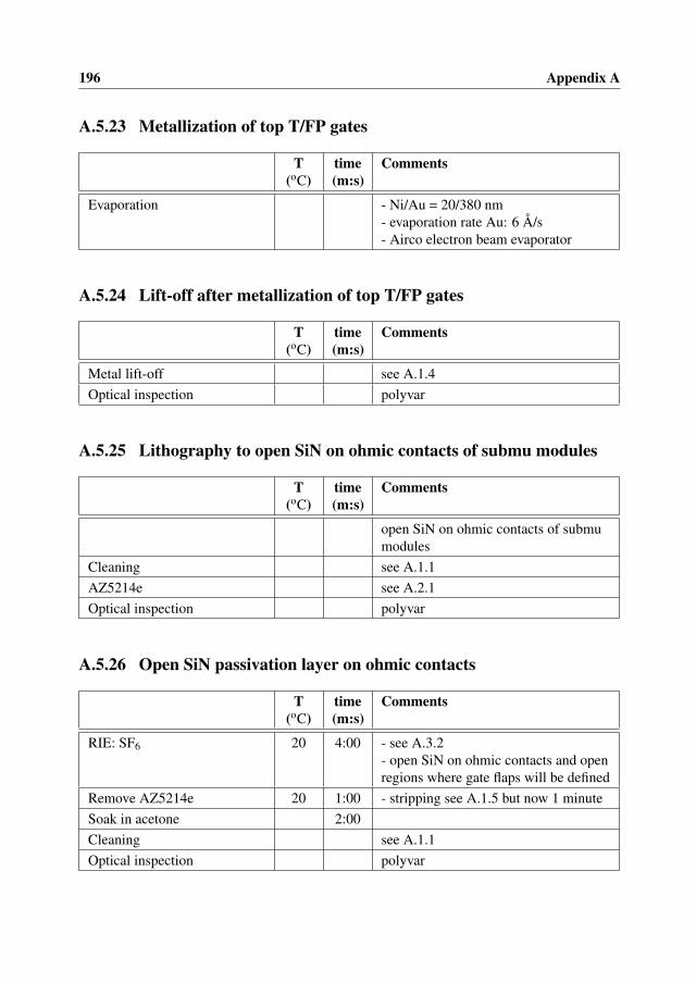
196 Appendix A
A.5.23 Metallization of top T/FP gates
T(oC)
time(m:s)
Comments
Evaporation - Ni/Au = 20/380 nm- evaporation rate Au: 6 Å/s- Airco electron beam evaporator
A.5.24 Lift-off after metallization of top T/FP gates
T(oC)
time(m:s)
Comments
Metal lift-off see A.1.4Optical inspection polyvar
A.5.25 Lithography to open SiN on ohmic contacts of submu modules
T(oC)
time(m:s)
Comments
open SiN on ohmic contacts of submumodules
Cleaning see A.1.1AZ5214e see A.2.1Optical inspection polyvar
A.5.26 Open SiN passivation layer on ohmic contacts
T(oC)
time(m:s)
Comments
RIE: SF6 20 4:00 - see A.3.2- open SiN on ohmic contacts and openregions where gate flaps will be defined
Remove AZ5214e 20 1:00 - stripping see A.1.5 but now 1 minuteSoak in acetone 2:00Cleaning see A.1.1Optical inspection polyvar

Appendix A 197
A.5.27 Lithography for definition of RF probe pads
T(oC)
time(m:s)
Comments
Cleaning see A.1.1AZ5214e see A.2.1Optical inspection - polyvar
- check development and lift-off profile
A.5.28 Metallization of RF probe pads
T(oC)
time(m:s)
Comments
Evaporation - Ti/Au = 20/250 nm- evaporation rate Au: 6 Å/s- Airco electron beam evaporator
A.5.29 Lift-off after metallization of RF probe pads
T(oC)
time(m:s)
Comments
Metal lift-off see A.1.4, but now soak in acetone for10 minutes
Optical inspection polyvar
198 Appendix A
A.6 Large gate periphery devices (mmTor)
The large periphery devices have total gate widths that vary from 0.25 mm to 6.4 mm. Toachieve these device widths multiple parallel gate fingers are needed that are arranged ineither “comb” or “fishbone” layouts. The unit gate widths (Wgu) are 62.5µm, 100µm, 125µm,and 200µm respectively. The gates are defined using electron beam lithography to obtain agate length of 0.7µm. T-shaped and field-plated (FP) sub-micron gates have been fabricatedto prevent high gate resistance at microwave frequencies due to the skin effect, reduce chargetrapping at the edge of the gate nearest to the drain contact, and increase the breakdownvoltage of the HFETs.
A.6.1 Sample preparation
Preparation T(oC)
time(m:s)
Comments
Spin coat epi-side 2” waferwith AZ5214e
protect epilayers during saw/diceprocess
Bake AZ5214e 95 5:00 hotplatePaste 2” wafer with resistcoated epi-side on blue tape
if sawn with disco
Sawing of 2” wafer - sample size 10 x 10 mm2
- diamond coated saw blade- water cooled
Dicing of 2” wafer - sample size 10 x 10 mm2
- Manually with diamond scratch penMark substrate side scratch “Z” on substrate (sapphire/SiC)
side to identify epi-side duringprocessing
A.6.2 Sample cleaning
T(oC)
time(m:s)
Comments
Cleaning see A.1.1Remove surface oxides 1:30 - sample completely dipped
- BHFRinsing see A.1.2Optical inspection polyvar

Appendix A 199
A.6.3 Optical alignment marks lithography
T(oC)
time(m:s)
Comments
Cleaning see A.1.1ma-N415 see A.2.3Optical inspection - polyvar
- check development and lift-off profile
A.6.4 Optical alignment marks metallization
T(oC)
time(m:s)
Comments
Evaporation - Au = 100 nm- evaporation rate: 3 Å/s- Airco electron beam evaporator
A.6.5 Lift-off after optical alignment marks metallization
T(oC)
time(m:s)
Comments
Metal lift-off see A.1.4Optical inspection polyvar
A.6.6 Ohmic contact lithography
T(oC)
time(m:s)
Comments
Cleaning see A.1.1ma-N415 see A.2.3Optical inspection - polyvar
- check development and lift-off profile
A.6.7 Ohmic contact metallizationT
(oC)time(m:s)
Comments
Evaporation - Ti/Al/Ni/Au = 30/180/40/100 nm- evaporation rate: 3 Å/s- Airco electron beam evaporator
200 Appendix A
A.6.8 Lift-off after ohmic contact metallization
T(oC)
time(m:s)
Comments
Metal lift-off see A.1.4Optical inspection polyvar
A.6.9 Oxygen plasma
T(oC)
time(m:s)
Comments
Stripping 20 5:00 see A.1.5
A.6.10 Dispersion etch
T(oC)
time(m:s)
Comments
RIE: dispersion see A.3.1
A.6.11 Rapid thermal annealing of ohmic contacts
T(oC)
time(m:s)
Comments
RTA process 800 2:00 - AST RTA: 800n-m02.2- N2ambient- ramp-up 100 oC - 800 oC in 45seconds
Dummy run 800 2:00 - no samples- AST RTA: 800n-m02.2
RTA ohmic contacts 800 2:00 - all samples at once- AST RTA: 800n-m02.2
A.6.12 Mesa lithography
T(oC)
time(m:s)
Comments
Cleaning see A.1.1AZ4533 see A.2.2Measure resist height Tencor Alpha Step
Appendix A 201
A.6.13 Mesa formation
T(oC)
time(m:s)
Comments
ICP: mesa see A.3.3Measurement step height afterICP etch
Tencor Alpha Step
Remove AZ4533 see A.1.6Optical inspection polyvarMeasurement mesa height Tencor Alpha Step
A.6.14 Surface passivation
T(oC)
time(m:s)
Comments
Surface preparation 20 1:00 NH4OH (25%) : UPW = 1 : 10(volume)
Rinsing see A.1.2SiN deposition 300 8:36 - see A.3.4
- 100 nm
A.6.15 Lithography to open SiN
T(oC)
time(m:s)
Comments
open SiN on ohmic contacts and openregions where gate flaps will be defined
Cleaning see A.1.1AZ5214e see A.2.2Optical inspection polyvar
202 Appendix A
A.6.16 Open SiN passivation layer on ohmic contacts
T(oC)
time(m:s)
Comments
RIE: SF6 20 4:00 - see A.3.2- open SiN on ohmic contacts and openregions where gate flaps will be defined
Remove AZ5214e 20 1:00 stripping see A.1.5 but now 1 minuteSoak in acetone 2:00Cleaning see A.1.1Optical inspection polyvar
A.6.17 Lithography for foot T/FP gates
T(oC)
time(m:s)
Comments
Cleaning see A.1.1MMA(8.5)MAA EL13 see A.2.5 (use spinning foot)Thermal evaporation - Edwards, tooling factor 1.4
- Au = 12.5 nm
Appendix A 203
A.6.18 Electron beam writing of foot T/FP gates
T(oC)
time(m:s)
Comments
EBL: foot - RAITH 150- EHT = 20 kV- aperture = 10 µm- write field = 300 x 300 µm2
- area step size = 15 nm- area dose = 100 µC/cm2
- dose factor = 3.0Remove thermal Au layer 20 0:45 - KI solution
- etch rate = 500 nm/min- Au layer has to be removed beforedeveloping MMA(8.5)MAA EL13
Rinsing see A.1.2Develop MMA(8.5)MAAEL13
see A.2.5
Optical inspectionOxygen descum 0:30 see A.1.5
A.6.19 Open SiN passivation layer underneath foot T/FP gates
T(oC)
time(m:s)
Comments
open SiN passivation layer underneathfoot T/FP gates
RIE: SF6 2:50 - see A.3.2- avoid over-etching too much becauseof damage to AlGaN underneath gate(leakage currents)
A.6.20 Metallization of foot T/FP gates
T(oC)
time(m:s)
Comments
Evaporation - Ni/Au = 20/150 nm- evaporation rate: 3 Å/s- Airco electron beam evaporator
204 Appendix A
A.6.21 Lift-off after metallization of foot T/FP gates
T(oC)
time(m:s)
Comments
Metal lift-off see A.1.4Optical inspection polyvar
A.6.22 Lithography for top T/FP gates
T(oC)
time(m:s)
Comments
Cleaning see A.1.1MMA(8.5)MAA EL13 see A.2.5 (use spinning top)Thermal evaporation - Edwards, tooling factor 1.4
- Au = 12.5 nm
A.6.23 Electron beam writing of top T/FP gates
T(oC)
time(m:s)
Comments
EBL: top - RAITH 150- EHT = 20 kV- aperture = 10 µm- write field = 300 x 300 µm2
- area step size = 15 nm- area dose = 100 µC/cm2
- dose factor T = 3.0- dose factor FP0.5 = 1.0- dose factor FP1.0 = 1.1
Remove thermal Au layer 20 0:45 - KI solution- etch rate = 500 nm/min- Au layer has to be removed beforedeveloping MMA(8.5)MAA EL13
Rinsing see A.1.2Develop MMA(8.5)MAAEL13
see A.2.5
Optical inspectionOxygen descum 0:30 see A.1.5

Appendix A 205
A.6.24 Metallization of top T/FP gates
T(oC)
time(m:s)
Comments
Evaporation - Ni/Au = 20/250 nm- evaporation rate Au: 6 Å/s- Airco electron beam evaporator
A.6.25 Lift-off after metallization of top T/FP gates
T(oC)
time(m:s)
Comments
Metal lift-off see A.1.4Optical inspection polyvar
A.6.26 Lithography for definition of RF probe pads
T(oC)
time(m:s)
Comments
Cleaning see A.1.1ma-N415 see A.2.3Optical inspection - polyvar
- check development and lift-off profile
A.6.27 Oxygen plasma
T(oC)
time(m:s)
Comments
Stripping 20 1:00 see A.1.5, but now 1 minute
A.6.28 Metallization of RF probe pads
T(oC)
time(m:s)
Comments
Evaporation - Ti/Au = 20/250 nm- evaporation rate Au: 6 Å/s- Airco electron beam evaporator

206 Appendix A
A.6.29 Lift-off after metallization of RF probe pads
T(oC)
time(m:s)
Comments
Metal lift-off see A.1.4, but now soak in acetone for10 minutes
Optical inspection polyvar
A.6.30 Lithography for definition of via openings
T(oC)
time(m:s)
Comments
definition of via openings and airbridge support
Cleaning see A.1.1AZ4533 - see A.2.2 (use in this case Mask
exposure: UV 430)- hard bake this time at 160 oC for 20minutes in HERAEUS hot air oven inyellow room
Optical inspection polyvar
A.6.31 Oxygen plasma
T(oC)
time(m:s)
Comments
Stripping 20 1:00 see A.1.5, but now 1 minuteOptical inspection polyvar
A.6.32 Evaporation transparent Au separation layer
T(oC)
time(m:s)
Comments
Evaporation of transparent Au layer toseparate via litho (see A.5.30) andbridge litho (see A.5.33)
Evaporation - Au = 12.5 nm- evaporation rate Au: 3 Å/s- Airco electron beam evaporator

Appendix A 207
A.6.33 Lithography for definition of air bridges
T(oC)
time(m:s)
Comments
NO cleaning with acetone andiso-propyl alcohol!
ma-N440 see A.2.4Optical inspection - polyvar
- check development and lift-off profile
A.6.34 Oxygen plasma
T(oC)
time(m:s)
Comments
Stripping 20 1:00 see A.1.5, but now 1 minute
A.6.35 Metallization of air bridges
T(oC)
time(m:s)
Comments
Evaporation - Ti/Au = 20/1500 nm- evaporate Au in three steps of 500 nmeach with cool down intervals of 30minutes- evaporation rate Au: 6 Å/s- Airco electron beam evaporator

208 Appendix A
A.6.36 Lift-off after metallization of air bridges
T(oC)
time(m:s)
Comments
Metal lift-off - see A.1.4, but now soak in acetone for10 minutes- spray with acetone on sample while itis still underneath acetone surface- metallization comes off as one thickfilm
Optical inspection - polyvar- all slits between air bridges have beenremoved
Removal transparent Au layer 1:00 - KCN solution (DEGUSSA)- use the old solution with an etch rateof about 20 nm/min- don’t use KI solution because the etchrate is too high (500 nm/min). Thishigh etch rate causes a very rough Ausurface
Optical inspection polyvar
A.6.37 Removal of air bridge support resist
T(oC)
time(m:s)
Comments
Remove AZ4533Soak in aceton 30:00Spray with acetone - in quartz basket with teflon insert
- above waste containerCleaning see A.1.1Ashing 20 15:00 see A.1.5Optical inspection polyvar
Appendix B
Process flow for CPW passive componentson s.i. SiCWe have developed a process flow for coplanar waveguide (CPW) passive components on s.i.SiC substrates. This appendix starts with descriptions of process steps that form the buildingblocks for the complete process flow. Section B.2 describes the process settings for resists usedfor optical contact lithography. Section B.3 provides process settings for different plasma pro-cesses used. Finally, section B.4 provides the complete process flow for the CPW components.
B.1 Building blocks
B.1.1 Cleaning
Cleaning Comments
Spray with acetone(CH3COCH3)
- in quartz basket with teflon insert- above waste container
Spray with iso-propyl alcohol(CH3CHOHCH3)
- in quartz basket with teflon insert- above waste container
Blow dry with nitrogen (N2)
B.1.2 Rinsing
Rinsing Comments
Rinse in ultra pure water(UPW)
- for positive resists time > 1 minute- for negative resists time > 3 minutes- for both resist types resistance water > 5MΩ
- place sample in quartz basket with teflon insertBlow dry with nitrogen (N2)
209

210 Appendix B
B.1.3 Exposure
Exposure Comments
UV 300 - Karl Süss MJB3 mask aligner- λ = 300 nm- optical power density: 3.4 mW/cm2 (range 20)
UV 430 - Karl Süss MA6 mask aligner- λ = 430 nm- optical power density: 7.5 mW/cm2 (range 20)- vacuum mode
B.1.4 Metal lift-off
Lift-off Comments
Soak in aceton time > 3 minutesSpray with acetone - in quartz basket with teflon insert
- above waste containerUltrasonically stirring in ace-tone
- time > 1 minute- place quartz basket with teflon holder on bottom ofbeaker glass
Cleaning see C.1.1
B.1.5 Oxygen plasmas
Oxygen plasmas T(oC)
time(m:s)
Comments
Stripping_CPW 20 1:00 - Tepla- process power 150W- Faraday cage
Ashing_CPW 20 5:00 - Tepla- process power 300W- Faraday cage

Appendix B 211
B.1.6 Resist removal after plasma etching
Resist removal T(oC)
time(m:s)
Comments
Stripping_CPW 20 5:00 see C.1.5Spray with acetone - in quartz basket with teflon insert
- above waste containerUltrasonically stirring inacetone
2:00 place quartz basket with teflon holderon bottom of beaker glass
Cleaning see C.1.1
B.1.7 Adhesion promotion
Adhesion promotion T(oC)
time(m:s)
Comments
Ashing_CPW 20 5:00 see C.1.5Rinsing see C.1.2HMDS deposition 20 3:00 old Delft vapour cylinder
212 Appendix B
B.2 Resists for optical contact lithography
B.2.1 Microchemicals AZ5214e
AZ5214e T(oC)
time(m:s)
Comments
- optical lithography- positive radiation sensitive
Spinning 0:30 - open air spinner- 5000 rpm
Soft bake 95 5:00 hotplateFlood exposure 0:00.8 - UV 300, see C.1.3
- required for lift-off profileBake 105 5:00 hotplateMask exposure 0:30 UV 300, see C.1.3Develop 1:35 AZ developer : UPW = 1 : 1 (volume)Rinsing see C.1.2
B.2.2 Microchemicals AZ4533
AZ4533 T(oC)
time(m:s)
Comments
- optical lithography- positive radiation sensitive
Spinning 0:30 - open air spinner- 5000 rpm
Soft bake 95 20:00 hotplateMask exposure: UV 430 0:32 UV 430, see C.1.3Develop 1:50 AZ developer : UPW = 1 : 1 (volume)Rinsing see C.1.2Hard bake 160 20:00 HERAEUS hot air oven in yellow room

Appendix B 213
B.2.3 Micro resist ma-N440ma-N440 T
(oC)time(m:s)
Comments
- optical lithography- negative radiation sensitive
Spinning_top plate 0:30 - CONVAC open air spinner- 3000 rpm
Spinning_air bridge 0:30 - CONVAC open air spinner- 2500 rpm
Bake_top plate 90 4:00 hotplateBake_air bridge 95 5:00 hotplateMask exposure_top plate 3:20 - UV 430, see C.1.3
- Vacuum modeMask exposure_air bridge 8:20 - UV 430, see C.1.3
- Vacuum mode- 5 x 100 seconds
Develop_top plate 1:00 ma-D332S (concentrated)Develop_air bridge 1:30 ma-D332S (concentrated)Rinsing see C.1.2
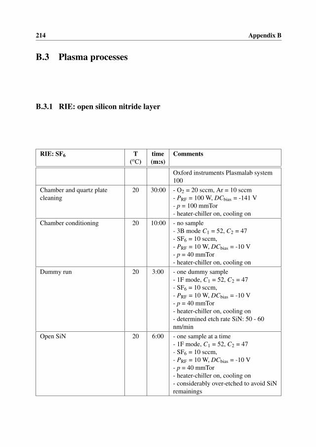
214 Appendix B
B.3 Plasma processes
B.3.1 RIE: open silicon nitride layer
RIE: SF6 T(oC)
time(m:s)
Comments
Oxford instruments Plasmalab system100
Chamber and quartz platecleaning
20 30:00 - O2 = 20 sccm, Ar = 10 sccm- PRF = 100 W, DCbias = -141 V- p = 100 mmTor- heater-chiller on, cooling on
Chamber conditioning 20 10:00 - no sample- 3B mode C1 = 52, C2 = 47- SF6 = 10 sccm,- PRF = 10 W, DCbias = -10 V- p = 40 mmTor- heater-chiller on, cooling on
Dummy run 20 3:00 - one dummy sample- 1F mode, C1 = 52, C2 = 47- SF6 = 10 sccm,- PRF = 10 W, DCbias = -10 V- p = 40 mmTor- heater-chiller on, cooling on- determined etch rate SiN: 50 - 60nm/min
Open SiN 20 6:00 - one sample at a time- 1F mode, C1 = 52, C2 = 47- SF6 = 10 sccm,- PRF = 10 W, DCbias = -10 V- p = 40 mmTor- heater-chiller on, cooling on- considerably over-etched to avoid SiNremainings
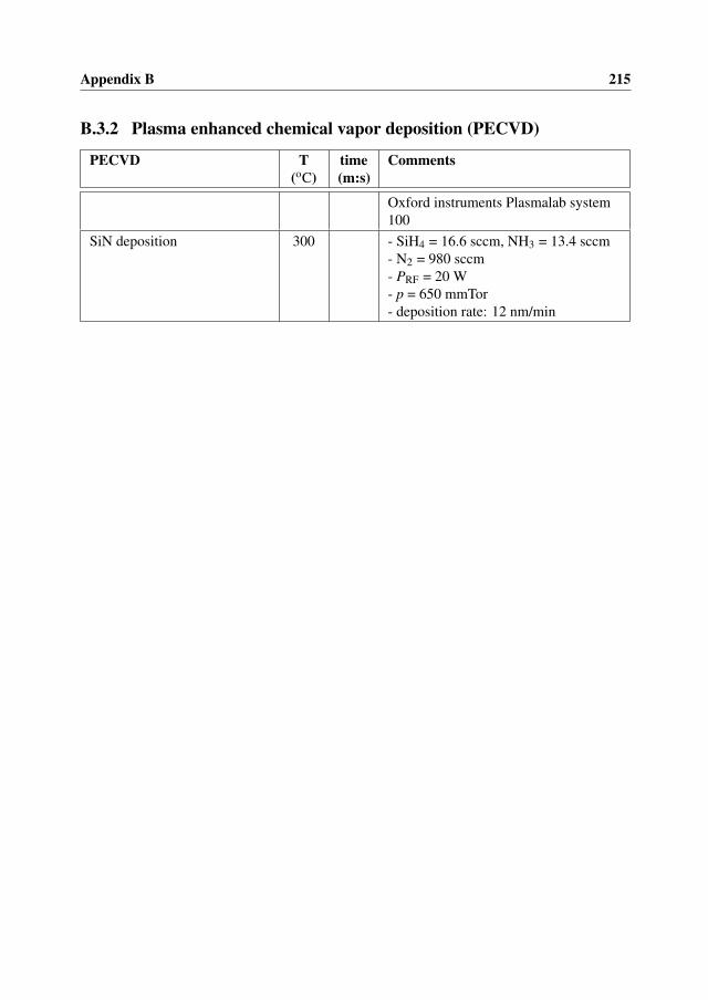
Appendix B 215
B.3.2 Plasma enhanced chemical vapor deposition (PECVD)
PECVD T(oC)
time(m:s)
Comments
Oxford instruments Plasmalab system100
SiN deposition 300 - SiH4 = 16.6 sccm, NH3 = 13.4 sccm- N2 = 980 sccm- PRF = 20 W- p = 650 mmTor- deposition rate: 12 nm/min
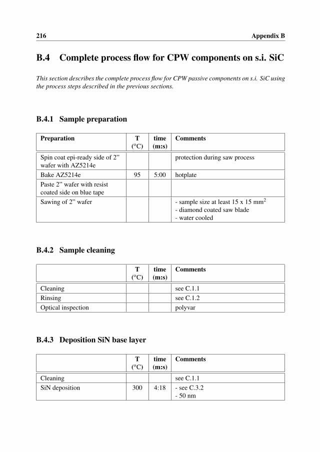
216 Appendix B
B.4 Complete process flow for CPW components on s.i. SiC
This section describes the complete process flow for CPW passive components on s.i. SiC usingthe process steps described in the previous sections.
B.4.1 Sample preparation
Preparation T(oC)
time(m:s)
Comments
Spin coat epi-ready side of 2”wafer with AZ5214e
protection during saw process
Bake AZ5214e 95 5:00 hotplatePaste 2” wafer with resistcoated side on blue tapeSawing of 2” wafer - sample size at least 15 x 15 mm2
- diamond coated saw blade- water cooled
B.4.2 Sample cleaning
T(oC)
time(m:s)
Comments
Cleaning see C.1.1Rinsing see C.1.2Optical inspection polyvar
B.4.3 Deposition SiN base layer
T(oC)
time(m:s)
Comments
Cleaning see C.1.1SiN deposition 300 4:18 - see C.3.2
- 50 nm

Appendix B 217
B.4.4 Lithography of bottom plate
T(oC)
time(m:s)
Comments
Adhesion promotion see C.1.7AZ5214e see C.2.1Optical inspection - polyvar
- check development and lift-off profile
B.4.5 Oxygen plasma
T(oC)
time(m:s)
Comments
Stripping_CPW 20 1:00 see C.1.5
B.4.6 Metallization of bottom plate
T(oC)
time(m:s)
Comments
Evaporation - Ti/Au = 50/200 nm- evaporation rate: 3 Å/s- Airco electron beam evaporator
B.4.7 Lift-off after metallization of bottom plate
T(oC)
time(m:s)
Comments
Metal lift-off see C.1.4Optical inspection polyvar
B.4.8 Oxygen plasma
T(oC)
time(m:s)
Comments
Ashing_CPW 20 5:00 see C.1.5
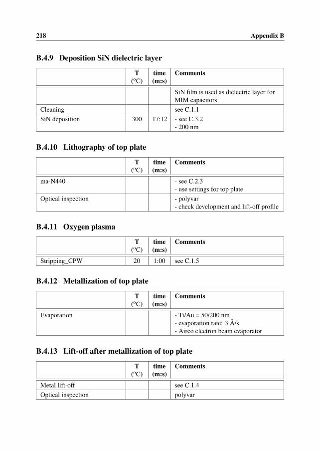
218 Appendix B
B.4.9 Deposition SiN dielectric layer
T(oC)
time(m:s)
Comments
SiN film is used as dielectric layer forMIM capacitors
Cleaning see C.1.1SiN deposition 300 17:12 - see C.3.2
- 200 nm
B.4.10 Lithography of top plate
T(oC)
time(m:s)
Comments
ma-N440 - see C.2.3- use settings for top plate
Optical inspection - polyvar- check development and lift-off profile
B.4.11 Oxygen plasma
T(oC)
time(m:s)
Comments
Stripping_CPW 20 1:00 see C.1.5
B.4.12 Metallization of top plate
T(oC)
time(m:s)
Comments
Evaporation - Ti/Au = 50/200 nm- evaporation rate: 3 Å/s- Airco electron beam evaporator
B.4.13 Lift-off after metallization of top plate
T(oC)
time(m:s)
Comments
Metal lift-off see C.1.4Optical inspection polyvar
Appendix B 219
B.4.14 Oxygen plasma
T(oC)
time(m:s)
Comments
Ashing_CPW 20 5:00 see C.1.5
B.4.15 Lithography for via openings
T(oC)
time(m:s)
Comments
Cleaning see C.1.1Adhesion promotion see C.1.7AZ5214e see C.2.1Optical inspection polyvar
B.4.16 Oxygen plasma
T(oC)
time(m:s)
Comments
Stripping_CPW 20 1:00 see C.1.5
B.4.17 Open SiN dielectric layer
T(oC)
time(m:s)
Comments
RIE: SF6 20 6:00 - see C.3.1- etch rate: 50 - 60 nm/min- deliberately over etch to avoid SiNremainings
Remove AZ5214e see C.1.6Optical inspection polyvar
B.4.18 Oxygen plasma
T(oC)
time(m:s)
Comments
Ashing_CPW 20 5:00 see C.1.5

220 Appendix B
B.4.19 Lithography of air bridge support layer
T(oC)
time(m:s)
Comments
Cleaning see C.1.1Adhesion promotion see C.1.7AZ4533 see C.2.2Optical inspection polyvar
B.4.20 Evaporation transparent Au separation layer
T(oC)
time(m:s)
Comments
Evaporation of transparent Au layer toseparate bridge support litho (seeC.4.19) and bridge litho (see C.4.21)
Evaporation - Au = 12.5 nm- evaporation rate Au: 3 Å/s- Airco electron beam evaporator
B.4.21 Lithography for definition of air bridges
T(oC)
time(m:s)
Comments
NO cleaning with acetone andiso-propyl alcohol!
ma-N440 - see C.2.3- use settings for air bridge
Optical inspection - polyvar- check development and lift-off profile
B.4.22 Oxygen plasma
T(oC)
time(m:s)
Comments
Stripping_CPW 20 1:00 see C.1.5
Appendix B 221
B.4.23 Metallization of air bridges and thick gold on TLs
T(oC)
time(m:s)
Comments
Metallization of air bridges and thickgold layer on transmission lines (TLs)
Evaporation - Ti/Au = 12.5/2000 nm- evaporate Au in four steps of 500 nmeach with cool down intervals of 30minutes- evaporation rate Au: 6 Å/s- Airco electron beam evaporator
B.4.24 Lift-off after metallization of air bridges and TLs
T(oC)
time(m:s)
Comments
Metal lift-off - see C.1.4, but now soak in acetone for10 minutes
Optical inspection polyvarAshing_CPW 20 5:00 see C.1.5Removal transparent Au layer 1:00 - KCN solution (DEGUSSA)
- use the old solution with an etch rateof about 20 nm/min- don’t use KI solution because the etchrate is too high (500 nm/min). Thishigh etch rate causes a very rough Ausurface
Optical inspection polyvar
222 Appendix B
B.4.25 Removal of air bridge support resist
T(oC)
time(m:s)
Comments
Remove AZ4533Soak in aceton 20:00Spray with acetone - in quartz basket with teflon insert
- above waste containerCleaning see C.1.1Ashing_CPW 20 15:00 see C.1.5Optical inspection polyvar

List of contstants and acronyms
List of constants
q elementary charge 1.60 ·10−19 Cε0 permittivity of vacuum 8.85 ·10−12 F/mh Planck’s constant 6.63 ·10−34 Js~ Dirac’s constant (h/2π) 1.05 ·10−34 Jsk Bolzmann’s constant 1.38 ·10−23 J/Kµ0 permeability of vacuum 4π ·10−7 H/m
List of acronyms
2DEG two-dimensional electron gas3G third generationAC alternating-currentACLR adjacent channel leakage ratioACPR adjacent channel power ratioAl aluminumAlGaAs aluminum gallium arsenideAlGaN aluminum gallium nitrideAlInGaN aluminum indium gallium nitrideAlInGaP aluminum indium gallium phosphideAlN aluminum nitrideAMS Applied Materials Science groupAr argonAu gold
223

224 List of contstants and acronyms
BFOM Baliga’s figure of meritBHF buffered hydrofluoric acidBJT bipolar junction transistorCAIBE chemically assisted ion beam etchingcd critical dimensionCD compact discCL cathodoluminescenceCl2 chlorineCPW coplanar waveguideCu copperCW continuous waveDAC digital-to-analog converterDARPA Defense Advanced Research Projects Agencydc duty cycleDC direct-currentDH double-heterostructureDoD department of defenseDRAM dynamic random access memoryDUT device under testDVD digital versatile discEBL electron beam lithographyECR electron cyclotron resonanceETP Equilibrium and Transport in Plasmas groupFET field-effect transistorFP field plateFTIR Fourier transform infrared spectroscopyFZ float zoneGa galliumGaAs gallium arsenideGaAsP gallium arsenide phosphideGaCl gallium monochlorideGaN gallium nitrideGaP:N gallium phosphide nitrideGB giga byteGSG ground-signal-groundH2 hydrogenHB high-brightness
List of contstants and acronyms 225
HBT heterojunction bipolar transistorHCl hydrochloric acidHD-DVD high-density digital versatile discHEMT high electron mobility transistorHEV hybrid electric vehicleHF hydrofluoric acidHFET heterostructure field-effect transistorHPA high-power amplifierHR high-resistivityHVPE hydride vapor phase epitaxyIC integrated circuitICE internal combustion engineICP inductively coupled plasmaIGBT insulated-gate bipolar transistorInGaAs indium gallium arsenideInGaP indium gallium phosphideInN indium nitrideInP indium phosphideJFOM Johnson’s figure of meritKCN potassium cyanideLD laser diodeLDMOS laterally diffused metal oxide semiconductorLED light emitting diodeLEEBI low-energy electron beam irradiationLEO lateral epitaxial overgrowthLIF laser-induced fluorescenceLNA low-noise amplifierMAG maximum available gainMBE molecular beam epitaxyMEMS micro-electro-mechanical systemMESFET metal semiconductor field-effect transistorMg magnesiumMMA methacrylic acidMMIC microwave monolithic integrated circuitMOCVD metal organic chemical vapor depositionMoD ministry of defense

226 List of contstants and acronyms
MODFET modulation-doped field-effect transistorMOSFET metal oxide semiconductor field-effect transistorNa sodiumN2 nitrogenNH3 ammoniaNH4OH ammonium hydroxideNi nickelNiCr nickel chromiumn.i.d. non-intentionally dopedNIL nano-imprint lithographyNL nucleation layerOED Opto-Electronic Devices groupP phosphorusPA power amplifierPAE power added efficiencyPDA personal digital assistantPECVD plasma enhanced chemical vapor depositionpHEMT pseudomorphic high electron mobility transistorPL photoluminescencePMMA polymethyl methacrylatePt platinumPW pulse widthRF radio frequencyRIE reactive ion etchingRT room temperatureRTA rapid thermal annealingRU Radboud Universiteit Nijmegens.i. semi-insulatingSDHT selectively-doped heterostructure transistorSE spectroscopic ellipsometrySEM scanning electron microscopySF6 sulfurhexafluorideSFP source-terminated field plateSi siliconSiC silicon carbideSiCl4 silicon tetrachlorideSiGe silicon germaniumSiH4 silane

List of contstants and acronyms 227
SiN silicon nitrideSiO2 silicon dioxideSOI silicon-on-insulatorSTW Stichting voor Technische WetenschappenTEC thermal expansion coefficientTEGFET two-dimensional electron gas field-effect transistorTFE thermionic field emissionTi titaniumTL transmission lineTLM transmission line methodTMG trimethyl galliumTU/e Technische Universiteit EindhovenTWTA traveling wave tube amplifierUV ultra violetWBG wide-bandgapW-CDMA wide-band code-division multiple access

228 List of contstants and acronyms

Summary
Gallium Nitride-based Microwave High-Power HeterostructureField-Effect Transistors
design, technology, and characterization
The research described in this thesis has been carried out within a joint project between theRadboud Universiteit Nijmegen (RU) and the Technische Universiteit Eindhoven (TU/e) withthe title: “Performance enhancement of GaN-based microwave power amplifiers: material, de-vice and design issues”. This project has been granted by the Dutch Technology FoundationSTW under project number NAF 5040. The aims of this project have been to develop the tech-nology required to grow state-of-the-art AlGaN/GaN epilayers on sapphire and semi-insulating(s.i.) SiC substrates using metal organic chemical vapor deposition (MOCVD) and to fabri-cate microwave (f > 1 GHz) high-power (Pout > 10 W) heterostructure field-effect transistors(HFETs) on these epitaxial films. MOCVD growth of AlGaN/GaN epilayers and materialcharacterization has been done within the group Applied Materials Science (AMS) of RU. Re-search at the Opto-Electronic Devices group (OED) of TU/e has focused on both electricalcharacterization of AlGaN/GaN epilayers and design, process technology development, andcharacterization of GaN-based HFETs and CPW passive components. Although a consider-able amount of work has been done during this research with respect to processing of CPWpassive components on s.i. SiC substrates, this thesis focused on active AlGaN/GaN devicesonly.
GaN is an excellent option for high-power/high-temperature microwave applications be-cause of its high electric breakdown field (3 MV/cm) and high electron saturation velocity(1.5 x 107 cm/s). The former is a result of the wide bandgap (3.44 eV at RT) and enables theapplication of high supply voltages (> 50 V), which is one of the two requirements for high-power device performance. In addition, the wide bandgap allows the material to withstandmuch higher operating temperatures (300 oC - 500 oC) than can the conventional semiconduc-tor materials such as Si, GaAs, and InP. A big advantage of GaN over SiC is the possibility togrow heterostructures, e.g. AlGaN/GaN. The resulting two-dimensional electron gas (2DEG)at the AlGaN/GaN heterojunction serves as the conductive channel. Large drain currents (> 1A/mm), which are the second requirement for a power device, can be achieved because of the
229
230 Summary
high electron sheet densities (> 1 x 1013 cm−2) and high electron saturation velocity. Thesematerial properties clearly indicate why GaN is a very suitable candidate for next-generationmicrowave high-power/high-temperature applications such as high-power amplifiers (HPAs)for GSM base stations, and microwave monolithic integrated circuits (MMICs) for radar sys-tems.
In this thesis we have presented the design, technology, and measurement results of n.i.d.AlGaN/GaN:Fe HFETs grown on s.i. 4H-SiC substrates by MOCVD. These devices have sub-micrometer T- or FP-gates with a gate length (Lg) of 0.7 µm and total gate widths (Wg) of0.25 mm, 0.5 mm, and 1.0 mm, respectively. The 1.0 mm devices are capable of producing amaximum microwave output power (Pout) of 11.9 W at S-band (2 GHz - 4 GHz) using classAB bias conditions of VDS = 50 V and VGS = -4.65 V. It has to be noted that excellent scalingof Pout with Wg has been demonstrated. In addition, the associated power gain (Gp) ranges be-tween 15 dB and 20 dB, and for the power added efficiency (PAE) values from 54 % up to 70% have been obtained. These results clearly illustrate both the successful development of theMOCVD growth process, and the successful development and integration of process modulessuch as ohmic and Schottky contact technology, device isolation, electron beam lithography,surface passivation, and air bridge technology, into a process flow that enables the fabricationof state-of-the-art large periphery n.i.d. AlGaN/GaN:Fe HFETs on s.i. SiC substrates, whichare perfectly suitable for application in e.g. HPAs at S-band.
Mark Krämer
Samenvatting
Gallium Nitride Gebaseerde Microgolf HoogvermogenHeterostructuur Veldeffect Transistoren
ontwerp, technologie en karakterisatie
Het onderzoek dat in dit proefschrift beschreven wordt, is uitgevoerd binnen een gezamenlijkproject van de Radboud Universiteit Nijmegen (RU) en de Technische Universiteit Eindhoven(TU/e) met als titel: “Performance enhancement of GaN-based microwave power amplifiers:material, device and design issues”. De beoogde doelen van dit project, dat gehonoreerd enfinancieel ondersteund is door de Stichting voor Technische Wetenschappen (STW) onderprojectnummer NAF 5040, waren het ontwikkelen van de vereiste technologie ten behoevevan de epitaxiale groei van hoogwaardige AlGaN/GaN lagen op saffier en halfisolerende SiCsubstraten en de fabricage van heterostructuur veldeffect transistoren welke in staat zijn eenhoog uitgangsvermogen (Pout > 10 W) te leveren op microgolf frequenties (f > 1 GHz). Detoegepaste epitaxiale groeitechniek, die bekend staat als metaal-organische chemische gas fasedepositie (MOCVD), en de benodigde materiaalkarakterisatie is uitgevoerd binnen de leerstoelApplied Material Science (AMS) van RU. Het onderzoek binnen de leerstoel Opto-ElectronicDevices (OED) van de TU/e heeft zich toegespitst op zowel de elektrische karakterisatie vande epitaxiale AlGaN/GaN lagen als op het ontwerpen van transistorstructuren, het ontwikkelenvan procestechnologie en het elektrisch karakteriseren van AlGaN/GaN HFETs en coplanairepassieve componenten. Hoewel een aanzienlijke hoeveelheid werk is verricht met betrekkingtot de procesontwikkeling en karakterisatie van coplanaire passieve componenten op halfisol-erende SiC substraten, wordt in dit proefschrift uitsluitend ingegaan op actieve AlGaN/GaNHFETs.
GaN is een uitstekende optie voor hoogvermogen en hoge temperatuur microgolf toepassin-gen vanwege zijn hoge elektrische doorslag veldsterkte (3 MV/cm) en hoge verzadigingssnel-heid van de elektronen (1.5 x 107 cm/s). Het gebruik van hoge voedingsspanningen (> 50 V),hetgeen een van de voorwaarden is om hoge uitgangsvermogens te genereren, wordt mogelijkgemaakt door de hoge doorslag veldsterkte, die het gevolg is van de grote bandafstand van GaN(3.44 eV bij kamer temperatuur). Een bijkomend voordeel van deze grote bandafstand is datGaN transistoren nog steeds goed kunnen functioneren bij bedrijfstemperaturen, die tussen de
231

232 Samenvatting
300 oC en 500 oC liggen, hetgeen niet mogelijk is voor Si en andere III-V halfgeleidermateri-alen. Een groot voordeel van GaN ten opzichte van SiC is de mogelijkheid om heterostructurenzoals AlGaN/GaN te groeien. Het tweedimensionale elektronen gas (2DEG) dat zich aan deheterojunctie bevindt, vormt het geleidende kanaal van de transistoren. Een nodige voorwaardevoor het genereren van hoge uitgangsvermogens zijn ook grote drain stromen (> 1 A/mm),welke tot stand komen door de hoge dichtheid (>1 x 1013 cm−2) en verzadigingssnelheid vande elektronen die het tweedimensionale elektronen gas vormen. Deze materiaaleigenschappentonen duidelijk aan dat GaN een zeer geschikte kandidaat is voor toekomstige generaties vanmicrogolf hoogvermogen en hoge temperatuur toepassingen zoals versterkers voor GSM basisstations en microgolf monolithisch geïntegreerde circuits (MMICs) voor radarsystemen.
In dit proefschrift zijn we uitvoering ingegaan op het ontwerp, de technologie en de meetre-sultaten van ongedoteerde AlGaN/GaN:Fe HFETs die met behulp van MOCVD gegroeid zijnop halfisolerende 4H-SiC substraten. Deze transistoren hebben T- en FP-gate contacten meteen lengte (Lg) van 0.7 µm en totale breedten (Wg) van 0.25 mm, 0.5 mm, en 1.0 mm, respec-tievelijk. Wanneer de transistoren met een totale gate breedte van 1.0 mm ingesteld worden ineen klasse AB werkpunt (VDS = 50 V en VGS = -4.65 V), kunnen ze een maximaal uitgangsver-mogen (Pout) leveren van 11.9 W op S-band (2 GHz - 4 GHz). Tevens dient vermeld te wordendat Pout perfect schaalt met de totale gate breedte. Daarnaast laten de vermogensversterking(Gp) en de power added efficiency (PAE) waarden zien van 15 dB - 20 dB en 54 % - 70 %, re-spectievelijk. Uit deze resultaten kan duidelijk geconcludeerd worden dat we erin geslaagd zijnom zowel een geschikt MOCVD groeiproces als een solide procestechnologie te ontwikkelen.De laatste, welke bestaat uit een integratie van afzonderlijke procesmodules zoals ohmse enSchottky contacten, transistor isolatie, elektronen bundel lithografie, oppervlakte passivatie enluchtbrugtechnologie, maakt het mogelijk om hoogwaardige AlGaN/GaN:Fe HFETs op SiCmet een grote totale gate breedte te vervaardigen. Deze transistoren zijn uitstekend geschiktom toegepast te worden in bijvoorbeeld HPAs op S-band.
Mark Krämer
List of publications
1. F. Karouta, M.J. Kappers, M.C.J.C.M. Krämer, and B. Jacobs, “Enhancement of p-GaNconductivity using SiOx,” Electrochemical and Solid-State Letters, vol. 8, No. 7, 2005,pp. G170 - G171.
2. M.C.J.C.M. Krämer, R.C.P. Hoskens, B. Jacobs, J.J.M. Kwaspen, E.M. Suijker, A.P. deHek, F. Karouta, and L.M.F. Kaufmann, “Towards X-band GaN-based high-power am-plifiers,” proc. Asia Pacific Microwave Conference 2004 (APMC’04), 15 - 18 December2004, New Delhi, India, 2004, pp. F13-1 - F13-4, Invited paper.
3. M.C.J.C.M. Krämer, R.C.P. Hoskens, B. Jacobs, E.M. Suijker, A.P. de Hek, J.J.M.Kwaspen, F. Karouta, and L.M.F. Kaufmann, “Coplanar waveguide passive componentson ceramic AlN substrates for application in hybrid integrated X-band GaN-based high-power amplifiers,” proc. Semiconductor Advances for Future Electronics 2004 (SAFE2004), 25 - 26 November 2004, Veldhoven, The Netherlands, 2004, pp. 651 - 656.
4. F. Karouta, A.M.L. Kappers, M.C.J.C.M. Krämer, and B. Jacobs, “Post-growth enhance-ment of p-GaN conductivity,” proc. 17th IEEE Lasers and Electro-Optics Society AnnualMeeting (IEEE/LEOS) 2004, 7 - 11 November 2004, Rio Grande, Puerto Rico, 2004, pp.284 - 285.
5. M.C.J.C.M. Krämer, R.C.P. Hoskens, B. Jacobs, J.J.M. Kwaspen, E.M. Suijker, A.P.de Hek, F. Karouta, and L.M.F. Kaufmann, “Dispersion free doped and undoped Al-GaN/GaN HEMTs on sapphire and SiC substrates,” proc. Gallium Arsenide and otherCompound Semiconductors Application Symposium 2004 (GAAS 2004), European Mi-crowave Week, 11 - 15 October 2004, Amsterdam, The Netherlands, 2004, pp. 75 - 78.
6. M.C.J.C.M. Krämer, B. Jacobs, J.J.M. Kwaspen, A.P. de Hek, E.J. Geluk, and F. Karouta,“Strongly reduced gate lag in undoped AlGaN/GaN HEMTs on sapphire,” proc. Semi-conductor Advances for Future Electronics 2003 (SAFE2003), 25 - 26 November 2003,Veldhoven, The Netherlands, 2003, pp. 618 - 621.
7. M.C.J.C.M. Krämer, B. Jacobs, A.P. de Hek, J.J.M. Kwaspen, F. Karouta, E.J. Geluk, T.de Vries, and E. Smalbrugge, “Highly uniform and reproducible I-V and power results ofundoped AlGaN/GaN HEMTs on sapphire indicating strongly reduced gate lag,” proc.CEPA2 Microelectronics WBG Workshop, 27 - 28 May 2003, Gothenburg, Sweden.
233
234 List of publications
8. B. Jacobs, M.C.J.C.M. Krämer, E.J. Geluk, and F. Karouta, “Optimisation of the Ti / Al /Ni / Au ohmic contact on AlGaN/GaN FET structures,” Journal of Crystal Growth, vol.241, 2002, pp. 15 - 18.
9. F. Karouta, R. Ruscassie, M.C.J.C.M. Krämer, B. Jacobs, K. Jacobs, and I. Moerman,“Investigation on p - contacts in Mg - doped GaN and the effect of various pre - treat-ments,” proc. 2001 Annual Symposium IEEE/LEOS Benelux Chapter, 3 December 2001,Brussels, Belgium, 2001, pp. 101 - 104.
10. B. Jacobs, P. Wingelaar, M.C.J.C.M. Krämer, S. Falcone, F. Karouta, A.P. de Hek,E.M. Suijker, and R. van Dijk, “Passive components on AlN for application in Al-GaN/GaN power amplifiers,” proc. Materials Research Society (MRS) Fall Meeting,26 - 30 November 2001, Boston, USA, vol. 693, 2001, pp. 629 - 634.
11. R. Feyaerts, L.K.J. Vandamme, G. Trefan, M.C.J.C.M. Krämer, and C. Zellweger, “Bulkand contact 1/f noise in GaN TLM structures,” proc. 31th European Solid-State DeviceResearch Conference 2001 (ESSDERC 2001), 11 - 13 September 2001, Nuremberg,Germany, 2001, pp. 355 - 358.
12. B. Jacobs, P. Wingelaar, M.C.J.C.M. Krämer, S. Falcone, F. Karouta, A.P de Hek, E.M.Suijker, and R. van Dijk, “Components for AlGaN/GaN power amplifiers,” proc. Mate-rials Research Society (MRS) Spring Meeting, 17 - 20 April 2001, San Francisco, USA,2001, pp. E10.4.1 - E10.4.6.
13. F. Karouta, B. Jacobs, and M.C.J.C.M. Krämer, “Role of fluorine in a chlorine-basedreactive ion etching of semiconductors,” proc. Conference on Semiconductors and Inte-grated Opto-Electronics 2001 (SIOE’01), 9 - 11 April 2001, Cardiff, UK.
14. B. Jacobs, M.C.J.C.M. Krämer, B. van Straaten, J.J.M. Kwaspen, F. Karouta, A.P. deHek, R. van Dijk, and F.E. van Vliet, “Metal semiconductor contacts and CPW MMICissues for AlGaN/GaN FETs,” proc. Materials Research Society (MRS) Fall Meeting,27 November - 1 December 2000, Boston, USA, 2000, pp. 1 - 6.
15. B. Jacobs, M.C.J.C.M. Krämer, and F. Karouta, “Influence of two steps thermal anneal-ing on n-AlGaN contacts,” proc. 4th European Workshop on Gallium Nitride (EGW-4:2000), 2 - 5 July 2000, Nottingham, UK.
16. F. Karouta, B. Jacobs, M.C.J.C.M. Krämer, K. Jacobs, and I. Moerman, “Chemical roleof SF6 in a SiCl4 - based reactive ion etching of GaN,” proc. Conference on Semicon-ductors and Integrated Opto-Electronics 1999 (SIOE’99), 7 - 9 April 1999, Universityof Wales, Bangor and Cardiff, UK.
Dankwoord
Promoveren is veel meer dan het onderzoeken van een bepaald fascinerend wetenschappelijkonderwerp. Als promovendus krijg je de kans om je, gesteund door een team van specialis-ten, te verbreden op velerlei gebied. Naast een verdieping van je kennis op je eigen vakge-bied leer je te interacteren met andere technische en niet-technische disciplines. Tijdens mijnpromotieonderzoek heb ik de kans gehad om de cyclus van idee, ontwerp, technologie, karak-terisatie en evaluatie te doorlopen en me hierbij vaardigheden eigen te maken op zowel elek-trotechnisch, natuurkundig en scheikundig gebied als ook op het gebied van projectmanage-ment. Naast professionele vorming heb ik op persoonlijk vlak heel veel geleerd, niet in deminste plaats door het ongeval dat ik op 24 juli 2002 heb meegemaakt. Ik wil benadrukken datik dit onderzoek en het voorliggende proefschrift nooit had kunnen realiseren zonder de hulpvan bekwame, enthousiaste en toegewijde collega’s en de steun, zorg en begrip van mijn lievevriendin en familie.
Als eerste wil ik graag mijn eerste promotor, Leon Kaufmann, bedanken voor zijn begeleidingen ondersteuning die hebben bijgedragen aan het tot stand komen van dit proefschrift. Ik hebonze samenwerking, die al dateert sinds mijn externe onderzoeksstage aan de RWTH Aachen,als zeer prettig ervaren. Naast inhoudelijke discussies over het onderzoek hebben we menigpersoonlijk gesprek gevoerd waaraan ik met veel genoegen terugdenk.
An dieser Stelle möchte ich mich ganz herzlich bedanken bei Herrn Prof.Dr.-Ing. Erhard Kohnfür seine Bereitschaft als meinen zweiten Promotor zu fungieren. Dazu danke ich Ihnen fürdie sehr hilfsbereite und angenehme Unterstützung und Diskussionen.
Fouad Karouta wil ik heel hartelijk bedanken voor de dagelijkse begeleiding, het vervullenvan het copromotorschap en alle ondersteuning die ik heb gekregen om dit onderzoek tot eengoed einde te brengen. Naast al je interesse voor het onderzoek heb ik erg veel waarderingvoor de vriendschappelijke manier waarop we al die jaren hebben samengewerkt. Ik heb zeergenoten van de conferentie- en andere dienstreizen die we samen gemaakt hebben en van alonze gesprekken variërend van vakinhoudelijk tot persoonlijk.
Poul Larsen, de projectleider van STW project NAF 5040 waarbinnen ik mijn onderzoek hebuitgevoerd, wil ik heel hartelijk bedanken voor zijn vakkundige leiding, het willen plaatsnemen
235

236 Dankwoord
in mijn promotiecommissie en voor onze discussies en samenwerking die ik als zeer plezierigheb ervaren.
Meint Smit wil ik bedanken voor de mogelijkheid die hij mij heeft geboden om mijn onder-zoek, dat toch ver naast de kernbezigheid van de OED groep ligt, uit te voeren. Ik waardeerhet zeer dat je altijd interesse toonde voor het onderzoek en de ondersteuning die je me hebtgegeven om mijn promotietraject tot een goed einde te brengen.
Frank van Vliet bedank ik heel hartelijk voor zijn bereidheid om in mijn promotiecommissieplaats te nemen. Frank, ik waardeer jouw zeer constructieve bijdragen aan het tot stand komenvan de uiteindelijke versie van mijn proefschrift enorm. Ik heb onze samenwerking als zeerprettig ervaren en denk met genoegen terug aan alle gesprekken die we de afgelopen jarengevoerd hebben.
Richard van de Sanden, hartelijk bedankt voor het willen plaatsnemen in mijn promotiecom-missie en jouw bijdragen aan het tot stand komen van dit proefschrift.
At the start of the project we had to use commercially available material to start developing thetransistor processing. In this respect, I want to thank Trevor Martin from QinetiQ very muchfor his willingness to provide us free of charge with GaN material on sapphire substrates. Fur-thermore, I want to thank Rüdiger Quay from the Fraunhofer Institute for Applied Solid-StatePhysics (IAF) for his efforts to provide us with GaN material on SiC substrates.
The GaN material on which my research mainly is based has been grown by my colleaguePhD students Andrzej Grzegorczyk (sapphire) and Mariusz Rudzinski (SiC) from the AppliedMaterials Science (AMS) group of the Radboud University Nijmegen (RU) under supervisionof Paul Hageman. Guys, I have really enjoyed working with you and I am very proud of thegreat results we have been able to achieve!
Ik wil de Stichting voor Technische Wetenschappen (STW) in de persoon van Frank van denBerg hartelijk danken voor het honoreren van het project en de zeer constructieve gebruiker-scommissievergaderingen. I also cordially thank the members of the users’ committee: LarsSiebert, and Christoph Giesen (Aixtron), Rik Jos, and Thomas Rödle (Philips Semiconduc-tors), Herve Brouzes (Thales), Frank van Vliet, Peter de Hek, and Erwin Suijker (TNO De-fence, Security, and Safety), for the many constructive conversations and comments.
Besides the STW project I have enjoyed participating in the Swedish - Dutch MOD project. Iwould like to thank all participants for the very pleasant cooperation.
Alvorens een proefschrift als dit geschreven kan worden, gaat er een heel traject van ontwer-pen, technologie ontwikkelen (en onderhouden!) en meten aan vooraf. Iedereen die met pro-cestechnologie, chipfabricage en -karakterisatie te maken heeft, weet dat het bereiken van enigresultaat in deze disciplines onmogelijk is zonder een ongebreideld optimisme en gigantisch

Dankwoord 237
doorzettingsvermogen maar bovenal door de steun van bekwame en toegewijde collega’s. Ikben veel dank verschuldigd aan mijn collega’s die het werken in de cleanroom elke dag weermogelijk maken. Erik Jan Geluk, heel hartelijk bedankt voor al jouw ondersteuning en de aan-gename samenwerking. Of ik nu hulp nodig had bij de Airco, Edwards, ICP, RAITH, RIE, ofSEM, jij stond altijd voor mij klaar! Barry Smalbrugge, naast al jouw steun in de cleanroom, inhet bijzonder met betrekking tot het zagen van talloze saffier en SiC wafers en het repareren vande voeding van de MJB3, wil ik je ook hartelijk bedanken voor jouw betrokkenheid buiten hetwerk. De brief die je me schreef tijdens mijn revalidatieproces heeft me erg opgebeurd! Benvan Roy, naast vele mooie gelegenheden hebben wij samen de voor mij minst gedenkwaardigegebeurtenis van mijn TU/e tijdperk meegemaakt. Ik wil jou heel hartelijk bedanken voor degeweldige manier waarop jij me op dat moment gesteund hebt. Kitty Sander, heel hartelijkbedankt voor je adviezen, de gezellige gesprekken en je hulp bij het zoeken naar een uitda-gende baan. Tjibbe de Vries, hartelijk bedankt voor alle ondersteuning in het bijzonder met dePECVD, eerst in Delft, later in Eindhoven.
Na de fabricage van de devices komt het spannende moment van de karakterisatie. ThieuKwaspen wil ik heel hartelijk bedanken voor zijn uitermate deskundige ondersteuning op hetgebied van RF device karakterisatie. Ik waardeer het enorm dat jij, hoewel je jouw loopbaanbij de TU/e al enige jaren geleden hebt afgesloten, uit jezelf bereid was om mij in jouw eigentijd volledig belangeloos te blijven ondersteunen! Ik heb grote bewondering voor de wijzewaarop jij hoogfrequent meetkoppen voor on-wafer metingen hebt ontworpen en vervaardigddie mij in staat stelden om mijn grote RF devices in Eindhoven te karakteriseren.
Op het gebied van RF karakterisatie van de transistoren heb ik ook veel ondersteuning gekre-gen van TNO Defensie en Veiligheid in Den Haag. Ik wil Erwin Suijker, Peter de Hek en Frankvan den Bogaart bedanken voor de zeer constructieve en prettige samenwerking. Met name Er-win heel hartelijk bedankt voor je bereidheid tot het uitvoeren van load-pull metingen tot verna het reguliere einde van de werkdag! With respect to this subject I am also very thankfulto Thomas Rödle (Philips Semiconductors) and Iouri Volokhine (Philips Research Eindhoven)for the very valuable additional characterization of my final power HFETs!
Eind 1998 ben ik in aanraking gekomen met Gallium Nitride toen ik mijn eerste stage hebgelopen binnen het promotieonderzoek van Bart Jacobs. Die eerste samenwerking was onsal heel goed bevallen en uiteindelijk ben ik ook in Bart’s project afgestudeerd en hebben weongeveer twee jaar als collega-promovendi aan GaN gewerkt. Bart ik wil je heel hartelijk be-danken voor de altijd ontzettend plezierige samenwerking! Zowel tijdens als buiten het werkhebben we heel veel leuke dingen beleefd. Ik denk met heel veel plezier terug aan de fantastis-che conferentie in Boston en onze marathondagen in de cleanroom en het meetlab ten eindehet dispersie probleem van onze transistoren op te lossen.
Een onmisbare schakel in de technologie van mijn transistoren is de silicium nitride passivatielaag. Ik kijk met bijzonder veel genoegen terug op de optimalisatie van deze laag in samen-werking met de ETP groep van de faculteit Technische Natuurkunde van onze universiteit. Ik
238 Dankwoord
wil Erwin Kessels en Bram Hoex bedanken voor hun adviezen met betrekking tot het vast-stellen van de juiste depositieparameters en de prettige samenwerking. Bram, heel hartelijkbedankt voor het meten (zelfs in het weekend) en analyseren van talloze samples!
Om een geïntegreerde microgolf hoogvermogensversterker te realiseren heb je naast actievecomponenten, de transistoren, passieve componenten nodig. Met betrekking tot de technologieen karakterisatie van de passieve componenten wil ik Roger Hoskens en Francisco Soares heelhartelijk bedanken voor de ondersteuning in de cleanroom, hun uitstekende bijdragen en deplezierige samenwerking. Roger wil ik daarnaast bedanken voor het programmeren van hetmasker van de vermogenstransistoren.I want to thank Erwin Bente, Fokke Groen, Hugo Heyker, Siang Oei, Jos van der Tol, YoucaiZhu, Stefano Beri, Rabah Hanfoug, Mirvais Yousefi, Omar Abu-Zeid, Luc Augustin, YohanBarbarin, Pietro Binetti, Boudewijn Docter, Martijn Heck, Genia Patent, Mahmoud Nikoufard,Ling Xu, and Milan Marell for their interest in my research and the nice atmosphere. I wantto cordially thank Uzma Khalique and Martin Hill for working late hours and over weekendsin the cleanroom during my last process run. Although it were tough times, working with youguys made it a lot easier!Aert van de Hulsbeek bedankt voor de leuke sfeer op de kamer en ik wil je heel veel succeswensen voor de toekomst. Xaveer Leijtens wil ik heel hartelijk bedanken voor het schrijvenvan de de Python scripts die me heel erg veel werk bespaard hebben bij het aanpassen van mijnmasker set voor het EBL proces. Els Kok, bedankt voor alle gezelligheid tijdens en naast hetwerk. Van hardlopen is het niet meer gekomen, maar het eten was erg lekker! Jan Hendrik denBesten, hartelijk bedankt voor het ter beschikking stellen van jouw LYX style file en je hulpbij het oplossen van last-minute layout probleempjes. Mocht je ooit problemen hebben methet uitloggen op welke pc in de cleanroom dan ook, dan moet je me maar even bellen! ElsGerritsen en Susan de Leeuw, bedankt voor alle ondersteuning gedurende de afgelopen jaren.Hans Moerman en Hans Olijslagers hartelijk bedankt voor jullie ondersteuning op het gebiedvan meetapparatuur tot alles wat met computers en unix systemen te maken had.
Jos Hermus, heel hartelijk bedankt voor de goede verstandhouding en ondersteuning tijdenshet afronden van mijn werk bij de TU/e na mijn arbeidsongeval. In deze context wil ik ookde plastisch chirurgen, Maarten Hoogbergen en Esther Bodde, en alle fysiotherapeuten heelhartelijk bedanken! Mede dankzij jullie enorme deskundigheid heb ik deze promotie tot eengoed einde kunnen brengen.
Ik wil ook graag Andre Montree, Erwin Hijzen, Jean-Sebastien Galloo en al mijn andere col-lega’s van de afdeling Silicon Process Options bij Philips Research Leuven heel hartelijk be-danken voor hun interesse, ondersteuning en begrip tijdens het afronden van mijn promotieon-derzoek!
Naast alle drukke werkzaamheden waren er gelukkig ook nog (spaarzame) momenten omsamen met goede vrienden te ontspannen en veel plezier te hebben! In het bijzonder wil ikmijn goede vriend Bahaa Eddine Sarroukh, zijn vrouw Nabila en hun zoontjes Ziade en Iyad

Dankwoord 239
heel hartelijk bedanken voor hun vriendschap door de jaren heen. Eddine-san, wie had in 1994kunnen bedenken dat je vandaag een van de paranimfen zou zijn van de jongen die jij aansprakom samen FP1 mee te doen!
Mijn schoonouders, Ine en Albin, en mijn schoonzus, Fenna, wil ik heel hartelijk bedankenvoor hun interesse, goede zorgen en gezelligheid!
Ik heb het voorrecht dat mijn broer ook mijn allerbeste vriend is. Ralf, ik wil je heel hartelijkbedanken voor alles wat je voor mij hebt gedaan! Ik ben er heel erg trots op dat je vandaagmijn paranimf hebt willen zijn!
De twee mensen aan wie ik al mijn dank verschuldigd ben, zijn mijn lieve ouders, Mary en Jo.Jullie onvoorwaardelijke liefde, zorg en steun hebben mij gemaakt tot de persoon die ik ben.Ik ben jullie hier heel erg dankbaar voor en hoop dat ik jullie prestaties zal kunnen evenaren!
Ten slotte wil ik de vrouw van mijn leven heel hartelijk bedanken voor al haar liefde en steun.Lieve Petra, de enorme levensvreugde die jij mij geeft, maakt elke dag samen tot een waarfeest. Op naar de volgende stap in ons leven!
Mark

240 Dankwoord
Curriculum Vitae
Mark Krämer was born in Sittard, The Netherlands, on the 10th of October 1975. He studiedElectrical Engineering at the Eindhoven University of Technology, The Netherlands. Afterobtaining the ir. (M.Sc.) degree, cum laude, in 2000, he started a Ph.D. research on the de-sign, technology, and characterization of gallium nitride-based microwave high-power hetero-structure field-effect transistors. This research was carried out within the Opto-Electronic De-vices group at the Eindhoven University of Technology. In March 2006, he started workingwithin the RF Devices & Technology group of the Silicon Process Options division at PhilipsResearch Laboratories in Leuven, Belgium.
241