Ferroelectric Field Effect Transistor for Memory and - Infoscience
189
POUR L'OBTENTION DU GRADE DE DOCTEUR ÈS SCIENCES acceptée sur proposition du jury: Prof. J. Brugger, président du jury Prof. M. A. Ionescu, Dr D. Bouvet, directeurs de thèse Dr H. Riel, rapporteur Prof. S. Salahuddin, rapporteur Prof. N. Setter, rapporteur Ferroelectric Field Effect Transistor for Memory and Switch Applications THÈSE N O 4990 (2011) ÉCOLE POLYTECHNIQUE FÉDÉRALE DE LAUSANNE PRÉSENTÉE LE 18 MARS 2011 À LA FACULTÉ SCIENCES ET TECHNIQUES DE L'INGÉNIEUR LABORATOIRE DES DISPOSITIFS NANOÉLECTRONIQUES PROGRAMME DOCTORAL EN MICROSYSTÈMES ET MICROÉLECTRONIQUE Suisse 2011 PAR Giovanni Antonio SALVATORE
Transcript of Ferroelectric Field Effect Transistor for Memory and - Infoscience
POUR L'OBTENTION DU GRADE DE DOCTEUR ÈS SCIENCES
acceptée sur proposition du jury:
Prof. J. Brugger, président du juryProf. M. A. Ionescu, Dr D. Bouvet, directeurs de thèse
Dr H. Riel, rapporteur Prof. S. Salahuddin, rapporteur
Prof. N. Setter, rapporteur
Ferroelectric Field Effect Transistor for Memory and Switch Applications
THÈSE NO 4990 (2011)
ÉCOLE POLYTECHNIQUE FÉDÉRALE DE LAUSANNE
PRÉSENTÉE LE 18 MARS 2011
À LA FACULTÉ SCIENCES ET TECHNIQUES DE L'INGÉNIEURLABORATOIRE DES DISPOSITIFS NANOÉLECTRONIQUES
PROGRAMME DOCTORAL EN MICROSYSTÈMES ET MICROÉLECTRONIQUE
Suisse2011
PAR
Giovanni Antonio SALvATORE


Acknowledgment
The sun is shining in a cold morning of what can be already considered Swiss winter. The
silence in the room is broken by the Boss's voice singing “Glory Days”…and on the table the
last page of this manuscript, the end of more than 4 years spent at the NANOLAB. Not all were
“glory days” but some of them are, for sure, unforgettable.
The most important thanks goes to the person who gave me the possibility of doing all of this:
Prof. Ionescu. I read the acknowledgment of other theses from the lab and these are the most
commonly used adjectives used to describe the qualities of Prof. Ionescu: open minded,
visionary foresight, honesty and friendliness, dynamic, inspiring personality, tireless work,
visionary man, curious. I confirm. But the thing, that still now, most surprises me about Prof.
Ionescu is his multitasking capability. Often during the talks I had the impression he was not
listening to me because he was doing thousands of other things or because he looked as being
on another planet; but then at the end of the talk I got a perfectly focused question that left me
impressed and speechless for seconds. This is Prof. Ionescu.
Another special and great thank goes to Didier. I’m not exaggerating in saying that, if the first
device I fabricated was perfectly working, most of the merit goes to him. He has always been
helpful, kind and patient. I would owe him much more than a coffee!!
What about Karin and Isabelle? I’m used to changing my mind, about flight schedules and hotel
reservations, twice per second and they have been always kind. Thanks for your patience and
kindness. Moreover I want to thank all the NANOLAB staff: Marie Halm, Joseph Guzzardi,
Roland Jaques and Raymond Sutter.
Also, without the Microelectronic Center at EPFL, CMI, and its very competent and helpful
staff nothing would have come of all my efforts.
I would also like to mention Dr. Igor Stolichnov and Dr. Jean Michel Sallese for the help and
for the useful discussions and for his availability and kindness.
And then the NANOLAB Italian “family”: Luca, Livio and Sara for standing all my
meaningless dissertations. It was also great to work with Alex, Anu, Montserrat, Sebastian, Ji,
Nenad and Matthieu.
No words for my family in Lausanne: Donatello and Daniele…and Ivana and Tania.
Laura also deserves something more than a simple thankyou. She always awakened me when I
was falling asleep (this happens quite often ).
Last but not least are the thanks to my parents and grandparents for their constant and endless
love.
Now it is time to run again, Bruce is singing “Born to Run”.

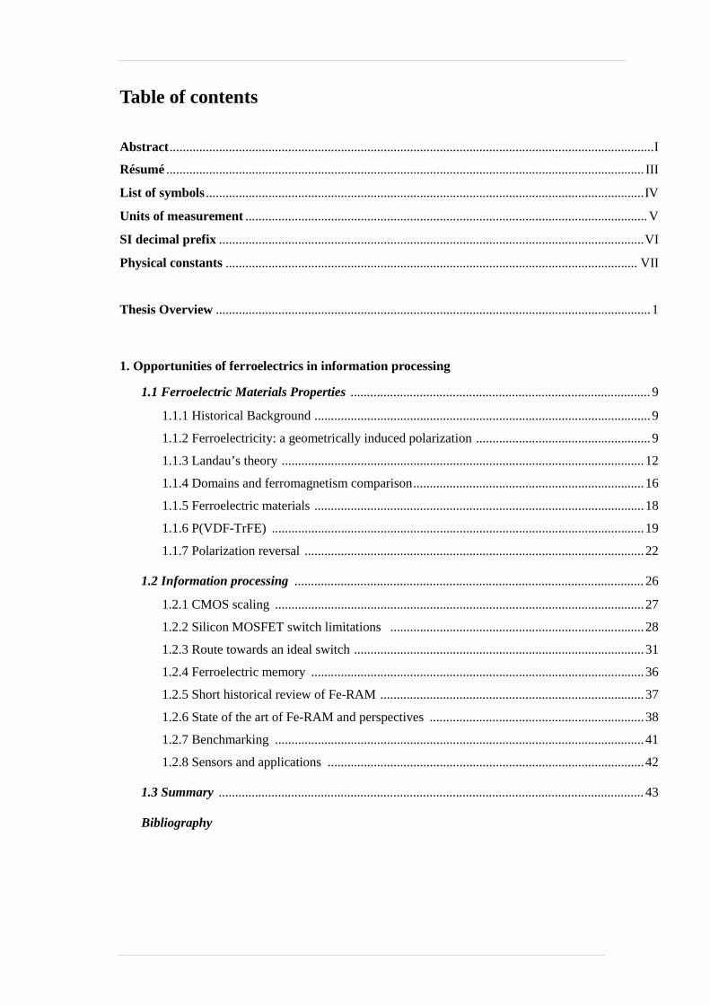
Table of contents
Abstract...................................................................................................................................................I
Résumé ................................................................................................................................................. III
List of symbols .....................................................................................................................................IV
Units of measurement .......................................................................................................................... V
SI decimal prefix .................................................................................................................................VI
Physical constants ............................................................................................................................. VII
Thesis Overview ....................................................................................................................................1
1. Opportunities of ferroelectrics in information processing
1.1 Ferroelectric Materials Properties ...........................................................................................9
1.1.1 Historical Background ......................................................................................................9
1.1.2 Ferroelectricity: a geometrically induced polarization .....................................................9
1.1.3 Landau’s theory ..............................................................................................................12
1.1.4 Domains and ferromagnetism comparison......................................................................16
1.1.5 Ferroelectric materials ....................................................................................................18
1.1.6 P(VDF-TrFE) .................................................................................................................19
1.1.7 Polarization reversal .......................................................................................................22 1.2 Information processing ..........................................................................................................26
1.2.1 CMOS scaling ................................................................................................................27
1.2.2 Silicon MOSFET switch limitations .............................................................................28
1.2.3 Route towards an ideal switch ........................................................................................31
1.2.4 Ferroelectric memory .....................................................................................................36
1.2.5 Short historical review of Fe-RAM ................................................................................37
1.2.6 State of the art of Fe-RAM and perspectives .................................................................38
1.2.7 Benchmarking ................................................................................................................41
1.2.8 Sensors and applications ................................................................................................42 1.3 Summary .................................................................................................................................43 Bibliography
2. Ferroelectric transistor for 1T memory cell
2.1 Organic ferroelectric transistor...............................................................................................51 2.2 Ferroelectric MOSFET ...........................................................................................................52
2.2.1 Fabrication.......................................................................................................................52
2.2.2 Why P(VDF-TrFE) .........................................................................................................54
2.2.3 Characterization ..............................................................................................................55
2.2.4 Discussion .......................................................................................................................70 2.3 Ferroelectric Tunnel FET .......................................................................................................71
2.3.1 Fabrication.......................................................................................................................72
2.3.2 Characterization ..............................................................................................................73
2.3.3 Discussion .......................................................................................................................77
2.3 Summary .................................................................................................................................78 Bibliography
3. Small slope ferroelectric FET
3.1 How to design a gate stack for abrupt switch .........................................................................83 3.2 Ferroelectric switch: from theory to experiment ....................................................................94
3.2.1 Device with no intermediate contact ...............................................................................94
3.2.2 Device with intermediate contact ..................................................................................103
3.3 Summary ................................................................................................................................123
Bibliography
4. Temperature performance of a ferroelectric transistor
4.1 The Curie Temperature as a key design parameter in a Fe-MOSFET .............................127 4.2 SOI ferroelectric transistor ..................................................................................................132
4.2.1 Fabrication.....................................................................................................................132
4.2.2 Characterization and experimental results.....................................................................134
4.2.3 Modeling and parameters extraction .............................................................................140
4.2.4 Applications ..................................................................................................................143
4.3 Discussion ..............................................................................................................................145 4.4 Summary ................................................................................................................................146 Bibliography
5. Conclusions and Perspectives
5.1 Conclusions………………… ................................................................................................151
5.2 Perspectives ............................................................................................................................153
Appendix A: A microscopic description of Landau’s theory ........................................................154
Appendix B: Clean Room run card for Fe-MOSFET fabrication................................................161


I
Abstract Silicon technology has advanced at exponential rates both in performances and
productivity through the past four decades. However the limit of CMOS technology seems to
be closer and closer and in the future we might see an increasing number of hybrid approaches
where other technologies add to the CMOS performance, while maintaining a back-bone of
CMOS logic. Ferro-electricity in ultra-thin films has been investigated as a credible candidate
for nonvolatile memory thanks to the bistability of polarization. 1 transistor (1T) ferroelectric
memory cells have been proposed and experimentally studied in order to reduce the size of 1T-
1C (1Transistor-1Capacitor) design with consequent advantages in terms of size, read-out
operation and costs. More recently ferroelectrics have been proposed by Salahuddin and Datta
as dielectric materials in order to lower the 60mV/dec limit of the subthreshold swing (SS) in
silicon Metal Oxide Semiconductor Field Effect Transistors, MOSFETs.
The objective of this thesis is to study the ferroelectric transistor performance for both
memory and switch application. For this purpose different Ferroelectric Field Effect
Transistors, Fe-FETs, structures have been designed, fabricated and characterized.
An organic ferroelectric polymer, vinylidene fluoride trifluorethylene, P(VDF-TrFE), of
100nm and 40nm thickness has been successfully integrated into the gate stack of bulk and SOI
MOSFET and, later, on a Tunnel FET, TFET, structure. The 1T ferroelectric FET memory cells
have shown a programming time in the order of ms at 9V as programming voltage. The
retention of a few seconds, however, is the main limiting factor for the usage of this device for
NV-memory applications. The retention failure mechanisms have been studied and investigated
for future improvement.
For the first time this work experimentally demonstrates that a subthreshold swing
lower than 60mv/dec can be achieved in a ferroelectric transistor thanks to the voltage
amplification arising from the ferroelectric material. This unique finding has been first
measured in a 40nm P(VDF-TrFE)/10nm SiO2 gate stack MOSFET and then, confirmed, in a
100nm P(VDF-TrFE)/10nm SiO2 gate MOSFET with an intermediate contact between the two
dielectrics. This internal node contact allows the study of the voltage amplification due to the
ferroelectric material.
Finally a temperature study of the performance of a ferroelectric Fully Depleted Silicon
on Insulator, FD SOI, transistor has been done. A model based on Landau’s theory has been
carried out and it has been experimentally validated for both the subthreshold and the strong
inversion regions. It has been demonstrated for the first time that, because of the divergence of
the ferroelectric permittivity at the Curie temperature, Tc, a ferroelectric transistor has a
maximum and a minimum, respectively of its transconductance and subthreshold swing, at Tc
KEYWORDS: ferroelectricity, MOSFETs, TFETs, small slope switches, Fe-RAMs, Landau’s theory, P(VDF-TrFE), negative capacitance.

II
III
Résumé La technologie de silicium a progressé à un rythme exponentiel aussi bien en termes de performances que de productivité au cours des quatre dernières décennies. Toutefois, la limite de la technologie CMOS semble être de plus en plus proche et à l'avenir, nous pourrions voir un nombre croissant d'approches hybrides où d'autres technologies ajouter de la performance au CMOS, tout en conservant comme une épine dorsale la logique CMOS. Les propriétés ferroélectriques de films ultra-minces ont été étudiées comme un candidat crédible pour la mémoire non volatile grâce à la bistabilité de la polarisation. La cellule mémoire ferroélectrique à 1 transistor (1T) a été proposée et étudiée expérimentalement afin de réduire la taille par rapport à des cellules 1T-1C (1Transistor-1Capacitor) avec des avantages conséquents en termes de taille, opération de lecture et coûts. Plus récemment, les matériaux ferroélectriques ont été proposés par Salahuddin et Datta comme matériaux diélectriques dans le but d'abaisser la limite de 60mV/dec de la pente sous le seuil (SS) dans le silicium pour un transistor MOS à effet de champ (MOSFET). L'objectif de cette thèse est d'étudier les performances des transistors ferroélectriques pour des applications mémoire et commutateur. Dans ce but, des transistors ferroélectriques de différentes dimensions (Fe-FETs), ont été conçus, fabriqués et caractérisés. Des polymères ferroélectriques organiques de 100 nm et 40 nm d'épaisseur, le trifluorethylene fluorure de vinylidène (P (VDF-TrFE)), ont été intégrét avec succès dans des empilements grille/diélectrique/substrat sur isolant (SOI), pour obtenir un dispositif MOSFET et plus tard une structure tunnel FET (TFET). La cellule mémoire ferroélectrique 1T FET a montré des temps de programmation de l'ordre de la ms avec 9V comme tension de programmation. La rétention de quelques secondes reste cependant le principal facteur limitant pour l'utilisation de ce dispositif pour des applications de mémoire non volatile. Les mécanismes de défaillance de rétention ont été étudiés et analysées dans le but de proposer des améliorations pour le futur. Pour la première fois ce travail démontre expérimentalement qu’une pente sous seuil inférieure à 60mv/dec peut être obtenue avec un transistor ferroélectrique et ce grâce à l'amplification de tension découlant du matériau ferroélectrique. Cette constatation unique a été d'abord mesurée sur un MOSFET avec un empilement diélectrique de grille de 40nm de P(VDF-TrFE) / 10nm SiO2 puis confirmée sur un MOSFET avec contact intermédiaire entre les deux diélectriques 100 nm P(VDF-TrFE) et 10nm SiO2 . Ce contact interne permet l'étude de l'amplification de tension due au matériau ferroélectrique. Enfin, une étude en température d’un transistor FET sur SOI FD, a été faite. Un modèle basé sur la théorie de Landau a été construit et validé expérimentalement pour les régions sous seuil et en forte inversion. Il a été démontré pour la première fois que, en raison de la divergence de la permittivité ferroélectriques à la température de Curie, Tc, un transistor ferroélectrique a un maximum et un minimum, respectivement de sa transconductance et le pente sous le seuil, à Tc. MOTS-CLÉS: ferroélectricité, MOSFETs, TFETs, commutateurs petite pente, Fe-RAM, la théorie de Landau, P (VDF-TrFE), capacité négative.
IV
Acronyms AC Alternate Current
AFM Atomic Force Microscopy
BHF Buffered Hydrofluoric acid
CMOS Complementary Metal-Oxide Semiconductor
CNT Carbon Nanotube
DC Direct Current
FET Field Effect Transistor
MOSFET Metal Oxide Semiconductor Field Effect Transistor
FIB Focus Ion Beam
GND Ground
IC Integrated Circuit
LTO Low Thermal Oxide
MEMS Micro Electro Mechanical System
MIS Metal Insulator Semiconductor
NEMS Nano Electro Mechanical System
NVM Non Volatile Memory
RT Room Temperature
SEM Scanning Electron Microscopy
SOI Silicon On Insulator
FD-SOI Fully Depleted Silicon On Insulator
1T-1C 1 Transistor-1 Capacitor
2T-2C 2 Transistors-2 Capacitors
TEM Transmission Electron Microscopy
VLSI Very Large Scale Integration
NV-Memory Non Volatile Memory
P(VDF-TrFE) Polyvinylidene Fluoride-Trifluoroethylene

V
Units of Measurement
°C Celsius degree
A Ampere
C Culomb
eV Electron Volt
J Joule
K Kelvin degree
kg Kilogram
m Meter
N Newton
s Second
V Volt
W Power
Ω Ohm
VI
SI Decimal Prefixes
Tera T 1012
Giga G 109
Mega M 106
Kilo k 103
hecto h 102
deca da 101
1
deci d 10-1
centi c 10-2
milli m 10-3
micro μ 10-6
nano n 10-9
pico p 10-12
femto f 10-15
VII
Physical Constants
Elementary Charge e (or q) = 1.60206·10-19 C
Planck Constant h = 6.62606896·10−34 J·s
Boltzmann Constant kB = 8.617 343·10−5 eV·K−1
Free Space Permittivity ε0 = 8,854 187 82·10-12 F·m-1
Air Relative Permittivity εr = 1
Speed of Light c = 2.99792458·108 ms-1
Number Pi π = 3,14159265


Thesis Overview
Here an overview of the thesis is presented. The subject of each chapter is briefly described highlighting the most important results obtained.

3
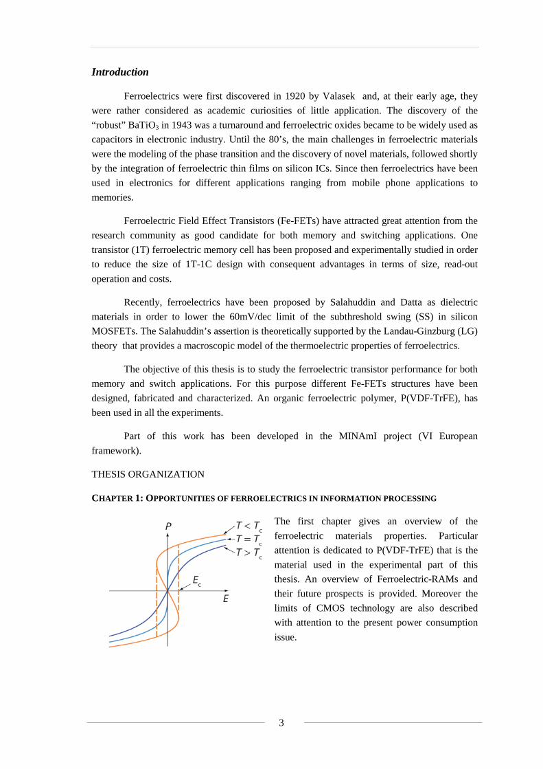
Introduction
Ferroelectrics were first discovered in 1920 by Valasek and, at their early age, they
were rather considered as academic curiosities of little application. The discovery of the
“robust” BaTiO3 in 1943 was a turnaround and ferroelectric oxides became to be widely used as
capacitors in electronic industry. Until the 80’s, the main challenges in ferroelectric materials
were the modeling of the phase transition and the discovery of novel materials, followed shortly
by the integration of ferroelectric thin films on silicon ICs. Since then ferroelectrics have been
used in electronics for different applications ranging from mobile phone applications to
memories.
Ferroelectric Field Effect Transistors (Fe-FETs) have attracted great attention from the
research community as good candidate for both memory and switching applications. One
transistor (1T) ferroelectric memory cell has been proposed and experimentally studied in order
to reduce the size of 1T-1C design with consequent advantages in terms of size, read-out
operation and costs.
Recently, ferroelectrics have been proposed by Salahuddin and Datta as dielectric
materials in order to lower the 60mV/dec limit of the subthreshold swing (SS) in silicon
MOSFETs. The Salahuddin’s assertion is theoretically supported by the Landau-Ginzburg (LG)
theory that provides a macroscopic model of the thermoelectric properties of ferroelectrics.
The objective of this thesis is to study the ferroelectric transistor performance for both
memory and switch applications. For this purpose different Fe-FETs structures have been
designed, fabricated and characterized. An organic ferroelectric polymer, P(VDF-TrFE), has
been used in all the experiments.
Part of this work has been developed in the MINAmI project (VI European
framework).
THESIS ORGANIZATION
CHAPTER 1: OPPORTUNITIES OF FERROELECTRICS IN INFORMATION PROCESSING
The first chapter gives an overview of the
ferroelectric materials properties. Particular
attention is dedicated to P(VDF-TrFE) that is the
material used in the experimental part of this
thesis. An overview of Ferroelectric-RAMs and
their future prospects is provided. Moreover the
limits of CMOS technology are also described
with attention to the present power consumption
issue.
4
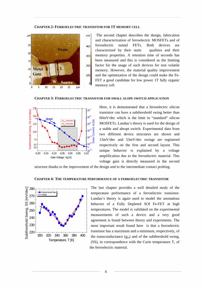
CHAPTER 2: FERROELECTRIC TRANSISTOR FOR 1T MEMORY CELL
The second chapter describes the design, fabrication and characterization of ferroelectric MOSFETs and of ferroelectric tunnel FETs. Both devices are characterized by their static qualities and their memory properties. A retention time of seconds has been measured and this is considered as the limiting factor for the usage of such devices for non volatile memory. However, the material quality improvement and the optimization of the design could make the Fe-FET a good candidate for low power 1T fully organic memory cell.
CHAPTER 3: FERROELECTRIC TRANSISTOR FOR SMALL SLOPE SWITCH APPLICATION
Here, it is demonstrated that a ferroelectric silicon
transistor can have a subthreshold swing better than
60mV/dec which is the limit in “standard” silicon
MOSFETs. Landau’s theory is used for the design of
a stable and abrupt switch. Experimental data from
two different device structures are shown and
13mV/dec and 53mV/dec swings are registered
respectively on the first and second layout. This
unique behavior is explained by a voltage
amplification due to the ferroelectric material. This
voltage gain is directly measured in the second
structure thanks to the improvement of the design and to the intermediate contact probing.
CHAPTER 4: THE TEMPERATURE PERFORMANCE OF A FERROELECTRIC TRANSISTOR
The last chapter provides a well detailed study of the
temperature performance of a ferroelectric transistor.
Landau’s theory is again used to model the anomalous
behavior of a Fully Depleted SOI Fe-FET at high
temperatures. The model is validated on the experimental
measurements of such a device and a very good
agreement is found between theory and experiments. The
most important result found here is that a ferroelectric
transistor has a maximum and a minimum, respectively, of
the transconductance (gm) and of the subthreshold swing,
(SS), in correspondence with the Curie temperature Tc of
the ferroelectric material.
-0,20 -0,15 -0,10 -0,05 0,00 0,05 0,10
50
75
100
125
150
175
Sub
thre
shol
d S
win
g, S
S [m
V/d
ec]
Gate Voltage, Vg [V]
60
SSAVE
=53mV/dec
SSMIN
=50mV/dec
down
10-13
10-12
10-11
10-10
10-9
10-8
10-7
Dra
in C
urre
nt, I
d [A
]
300 320 340 360 380 400220
230
240
250
260
270
280
Experimental Data Model
Sub
thre
shol
d S
win
g, S
S [m
V/d
ec]
Temperature, T [K]
5
CHAPTER 5: CONCLUSIONS AND PERSPECTIVES
This chapter summarizes the results presented in the thesis, and suggests some topics which
would need deeper investigation in the future.

Chapter 1
Opportunities of ferroelectrics in information processing
This chapter is focused on the description of the general properties of ferroelectric
materials and on their applications in information technology. Landau’s theory is explained
and a microscopic approach is also discussed in appendix A. Perovskite and polymeric
ferroelectrics are described with particular attention to P(VDF-TrFE), which is the material
used in the experimental part of this work. The second part of the chapter is about the possible
application of ferroelectrics. The MOSFET scalability and limitations are illustrated and the
opportunity of ferroelectrics in information processing is evaluated.

1.1 – Ferroelectric Material Properties
9
1.1 Ferroelectric Materials Properties
1.1.1 Historical Background
Ferroelectrics were first discovered in 1920 by Valasek [1] and, at their early age, they
were rather considered as academic curiosities of little application value. The discovery of the
“robust” BaTiO3 in 1943 [2] was a turnaround and ferroelectric oxides became to be widely
used as capacitors in the electronic industry. Until the 80’s, the main challenges in ferroelectric
materials were the modeling of the phase transition and the discovery of novel materials,
followed shortly by the integration of ferroelectric thin films on silicon ICs. Since then,
ferroelectrics have been widely used in electronics for different applications, ranging from
mobile phone applications to memories. In 1994 a ferroelectric bypass capacitor for 2.3GHz
operation in mobile digital telephones won the Japanese Electronic Industry “Product of the
Year” award with 6 million chips per month in production. The renaissance of ferromaterials
occurred thanks to the development of the thin film technology. The polarization of a typical
material is reversed at a critical “coercive” field E=50kV/cm and this, in a 1mm bulk device,
means a 5kV switching voltage that is unsuitable for a mobile phone or any other electronics;
however for a sub-micrometer thin film it is less than 5V permitting the integration into many
silicon chips. The first review on thin film ferroelectrics was published in 1989 [3] and the first
book of memoirs appeared in 2000 [4].
Nowadays there are several directions for ferroelectric research including substrate-film
interface, finite size effect, phase transition study, nanotubes and nanowires, electrocaloric
devices, ferroelectric memory (FeRAMs and DRAM), electron emitters, magnetoelectrics,
multiferroics, ferroelectric liquid crystal, piezoelectric devices and ferroelectric transistors.
This thesis is focused on the design, fabrication and characterization of a ferroelectric
transistor that is exploited for different applications.
1.1.2 Ferroelectricity: a geometrically induced polarization
The “ferro” part in the name “ferroelectric” is something of a misnomer since it does
not refer to the presence of any iron in the material but it arises from the many similarity with
ferromagnetism. In fact, in one of the earliest observations of ferroelectricity by Rochelle, salt
is described as “analogous to the magnetic hysteresis in the case of iron” [1]. From the physical
point of view there are similarities between ferromagnetism and ferroelectricity but, of course,
also some differences and in particular the physical origin of the magnetic and electric dipole.
In all known ferroelectric crystals the spontaneous polarization is produced by the
atomic arrangement of ions in the crystal structure. A nonzero spontaneous polarization can be
present only in a crystal with a polar space group. However for ferroelectrics the polarization
should be switchable from at least two different stable states and so many polar crystals cannot
be considered ferroelectric. One condition that ensures the presence of discrete states of
different polarization and enhance the possibility of switching is that the crystal structure can be
obtained as a “small” symmetry breaking distortion of a higher-symmetry reference state. This
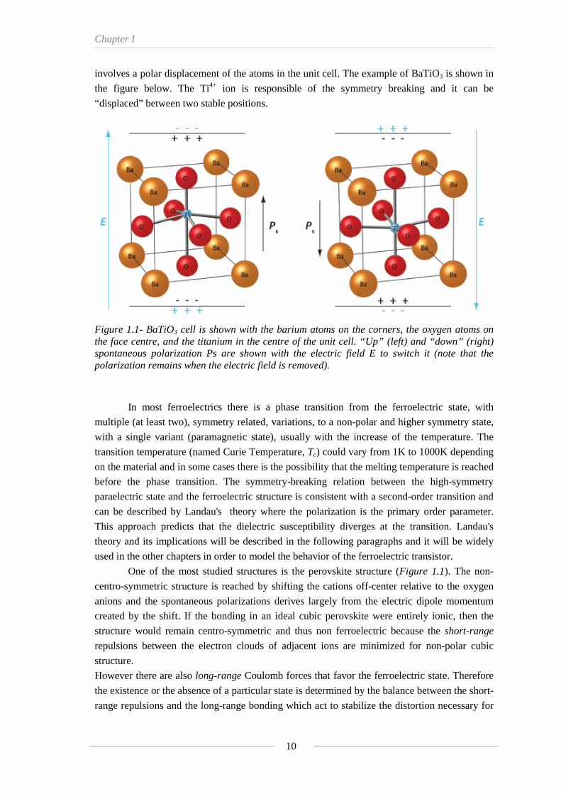
Chapter I
10
involves a polar displacement of the atoms in the unit cell. The example of BaTiO3 is shown in
the figure below. The Ti4+ ion is responsible of the symmetry breaking and it can be
“displaced” between two stable positions.
Figure 1.1- BaTiO3 cell is shown with the barium atoms on the corners, the oxygen atoms on the face centre, and the titanium in the centre of the unit cell. “Up” (left) and “down” (right) spontaneous polarization Ps are shown with the electric field E to switch it (note that the polarization remains when the electric field is removed).
In most ferroelectrics there is a phase transition from the ferroelectric state, with
multiple (at least two), symmetry related, variations, to a non-polar and higher symmetry state,
with a single variant (paramagnetic state), usually with the increase of the temperature. The
transition temperature (named Curie Temperature, Tc) could vary from 1K to 1000K depending
on the material and in some cases there is the possibility that the melting temperature is reached
before the phase transition. The symmetry-breaking relation between the high-symmetry
paraelectric state and the ferroelectric structure is consistent with a second-order transition and
can be described by Landau's theory where the polarization is the primary order parameter.
This approach predicts that the dielectric susceptibility diverges at the transition. Landau's
theory and its implications will be described in the following paragraphs and it will be widely
used in the other chapters in order to model the behavior of the ferroelectric transistor.
One of the most studied structures is the perovskite structure (Figure 1.1). The non-
centro-symmetric structure is reached by shifting the cations off-center relative to the oxygen
anions and the spontaneous polarizations derives largely from the electric dipole momentum
created by the shift. If the bonding in an ideal cubic perovskite were entirely ionic, then the
structure would remain centro-symmetric and thus non ferroelectric because the short-range
repulsions between the electron clouds of adjacent ions are minimized for non-polar cubic
structure.
However there are also long-range Coulomb forces that favor the ferroelectric state. Therefore
the existence or the absence of a particular state is determined by the balance between the short-
range repulsions and the long-range bonding which act to stabilize the distortion necessary for
1.1 – Ferroelectric Material Properties
11
the ferroelectric phase. The same physical process happens in ferromagnets, even if in that case,
the spin and angular momentum of the electron are involved. Figure 1.2 shows a classification
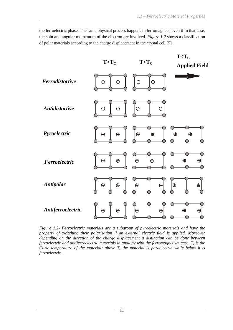
of polar materials according to the charge displacement in the crystal cell [5].
Figure 1.2- Ferroelectric materials are a subgroup of pyroelectric materials and have the property of switching their polarization if an external electric field is applied. Moreover depending on the direction of the charge displacement a distinction can be done between ferroelectric and antiferroelectric materials in analogy with the ferromagnetism case. Tc is the Curie temperature of the material; above Tc the material is paraelectric while below it is ferroelectric.
T<TC
Applied Field
Ferrodistortive
Antidistortive
Pyroelectric
Ferroelectric
Antipolar
Antiferroelectric
T>TC T<TC
Chapter I
12
1.1.3 Landau’s Theory
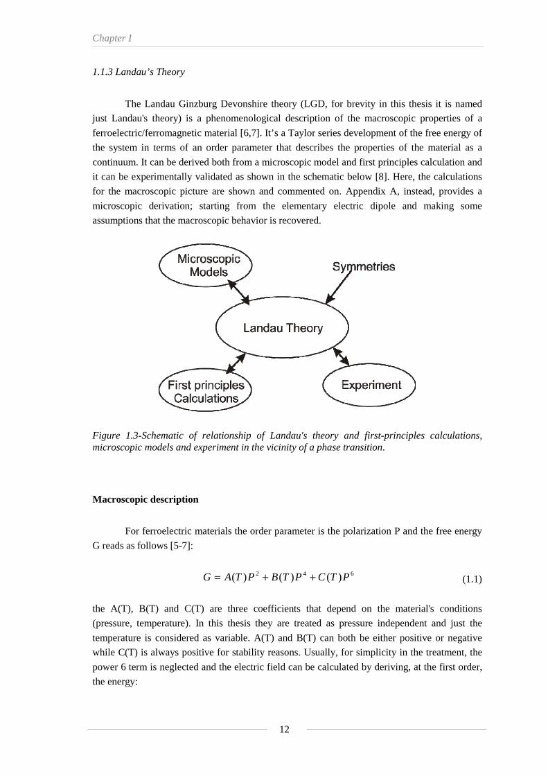
The Landau Ginzburg Devonshire theory (LGD, for brevity in this thesis it is named
just Landau's theory) is a phenomenological description of the macroscopic properties of a
ferroelectric/ferromagnetic material [6,7]. It’s a Taylor series development of the free energy of
the system in terms of an order parameter that describes the properties of the material as a
continuum. It can be derived both from a microscopic model and first principles calculation and
it can be experimentally validated as shown in the schematic below [8]. Here, the calculations
for the macroscopic picture are shown and commented on. Appendix A, instead, provides a
microscopic derivation; starting from the elementary electric dipole and making some
assumptions that the macroscopic behavior is recovered.
Figure 1.3-Schematic of relationship of Landau's theory and first-principles calculations, microscopic models and experiment in the vicinity of a phase transition.
Macroscopic description
For ferroelectric materials the order parameter is the polarization P and the free energy
G reads as follows [5-7]:
642 )()()( PTCPTBPTAG ++= (1.1)
the A(T), B(T) and C(T) are three coefficients that depend on the material's conditions
(pressure, temperature). In this thesis they are treated as pressure independent and just the
temperature is considered as variable. A(T) and B(T) can both be either positive or negative
while C(T) is always positive for stability reasons. Usually, for simplicity in the treatment, the
power 6 term is neglected and the electric field can be calculated by deriving, at the first order,
the energy:
1.1 – Ferroelectric Material Properties
13
3)(4)(2 PTBPTAEP
G +==∂∂
(1.2)
It is worth noting that A(T) is equal to 1/εε0 for the non polar phase (paraelectric phase i.e. for
T>Tc). In order to find the minimum of the energy and so the points of stable equilibrium, the
following conditions are imposed:
( )
⎪⎪⎩
⎪⎪⎨
⎧
>+⇒>∂∂
=+⇒==∂∂
0)(6)(0
0)(2)(20
22
2
2
PTBTAP
G
PTBTAPEP
G
(1.3)
For T>Tc the system admits the trivial solution: Ps=0 with A(t)>0, i.e. there is no spontaneous
polarization, typical of the paraelectric phase.
For T<Tc it has as solutions:
)(2)(2
TB
TAPs −= (1.4)
with A(T)<0 (it is assumed that B(T) is positive. More details are provided at the end of the
paragraph about the sign of B(T)). The simplest function (first order) that meets the
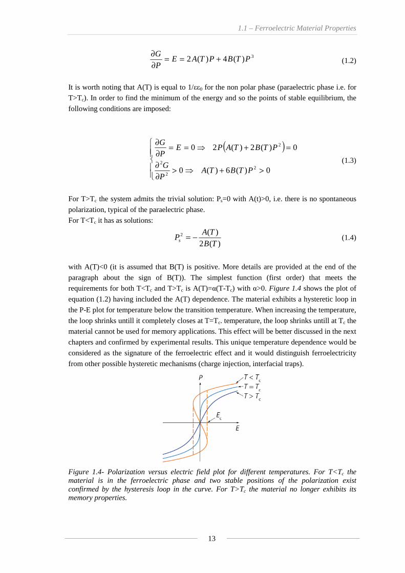
requirements for both T<Tc and T>Tc is A(T)=α(T-Tc) with α>0. Figure 1.4 shows the plot of
equation (1.2) having included the A(T) dependence. The material exhibits a hysteretic loop in
the P-E plot for temperature below the transition temperature. When increasing the temperature,
the loop shrinks untill it completely closes at T=Tc. temperature, the loop shrinks untill at Tc the
material cannot be used for memory applications. This effect will be better discussed in the next
chapters and confirmed by experimental results. This unique temperature dependence would be
considered as the signature of the ferroelectric effect and it would distinguish ferroelectricity
from other possible hysteretic mechanisms (charge injection, interfacial traps).
Figure 1.4- Polarization versus electric field plot for different temperatures. For T<Tc the material is in the ferroelectric phase and two stable positions of the polarization exist confirmed by the hysteresis loop in the curve. For T>Tc the material no longer exhibits its memory properties.
Chapter I
14
The coercive field, Ec, is defined as the field at which:
⎪⎩
⎪⎨⎧
=
=+⇒=∂∂
0)(
0)()(6)(0 2
c
c
EP
EPTBTAP
E
(1.5)
and substituting the (1.4) in the (1.5) it is possible to calculate its dependence on Ps:
22
3
1)( sc PEP =
(1.6)
and so:
ssc PPTAE0
17.0
33
4)(
εε≈= (1.7)
In most of the experiments an external electric field is applied to the material. Therefore it is
interesting to study this case. The equivalent energy that has to be added to G is –E*P. So that
(1.1) becomes:
EPPTBPTAG −+= 42 )()( (1.8)
and applying the same conditions as before (see the (1.3)):
⎪⎪⎩
⎪⎪⎨
⎧
>∂∂
+−=⇒=∂∂
0
)(2)(2
10
2
2
3
P
G
PTBPTTEP
Gcα
(1.9)
From the previous equation it’s possible to calculate the susceptibility, χ, of the material
according to the following definition:
( )20 )(2)(2
1
PTBTTPE
Piml
cE +−
=∂∂=
→ αχ (1.10)
A ferroelectric material has an χ that is linearly dependent on the temperature with two different
coefficients for the ferroelectric and paraelectric phase:
⎪⎪
⎩
⎪⎪
⎨
⎧
<−
>−
=
cc
cc
TTforTT
TTforTT
)(41
)(21
α
αχ (1.11)
1.1 – Ferroelectric Material Properties
15
It is worth noting that χ is always positive according to this derivation. It is also important to
calculate an approximate induced polarization in the ferroelectric phase:
ETT
EEPc
ind )(41
0 −=≈=
αχεε (1.12)
Moreover there is a critical field at which the spontaneous polarization Ps is equalized by the
induced polarization:
[ ])(2
)(4 2
TB
TTE c
crit
−−= α (1.13)
This critical field sets the boundary for the low field condition (E<Ecrit) and high field condition
(E>Ecrit) that is important when any approximation is done.
Till now in the calculation, no assumption has been done about the term B(T). It has
only been mentioned that the sign of B(T) can be positive or negative and this discriminates
between a first order transition (B(T)<0) and a second order transition (B(T)>0). In reality all
the discussion done in this paragraph is valid only for B(T) positive and so for a second order
phase transition.
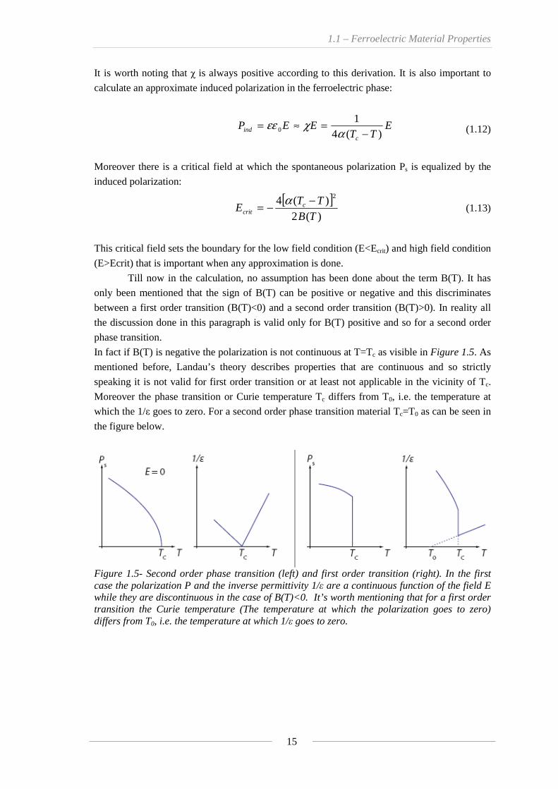
In fact if B(T) is negative the polarization is not continuous at T=Tc as visible in Figure 1.5. As
mentioned before, Landau’s theory describes properties that are continuous and so strictly
speaking it is not valid for first order transition or at least not applicable in the vicinity of Tc.
Moreover the phase transition or Curie temperature Tc differs from T0, i.e. the temperature at
which the 1/ε goes to zero. For a second order phase transition material Tc=T0 as can be seen in
the figure below.
Figure 1.5- Second order phase transition (left) and first order transition (right). In the first case the polarization P and the inverse permittivity 1/ε are a continuous function of the field E while they are discontinuous in the case of B(T)<0. It’s worth mentioning that for a first order transition the Curie temperature (The temperature at which the polarization goes to zero) differs from T0, i.e. the temperature at which 1/ε goes to zero.

Chapter I
16
1.1.4 Domains and Ferromagnetism comparison
Landau's theory is a macroscopic description of a ferroelectric system in the vicinity of
the transition temperature. It is useful to understand the overall behavior of a material but it
does not provide any microscopic information, moreover it considers the system as uniform and
homogenous. In a real material this is not the case. There are several reasons for the existence
of domains including non uniform strain, microscopic defects and the thermal and electrical
history of the sample. A domain is a region in which the dipoles have parallel polarization
direction. Another important cause of the domain's formation is that in a ferroelectric crystal
plate or a thin film with the polarization perpendicular to the plate or film surface, the bound
charges of the polarization induce a very high electric field opposite to the polarization [5,9].
This so-called depolarization field can be high enough to impede ferroelectricity. The
ferroelectric sample can however break up into domains of antiparallel polarization to stabilize
the ferroelectric phase by a reduction of the depolarization field (Figure 1.6). The system in
fact will minimize its energy by eliminating, as far as possible, the surface charges and in a thin
film, for example, the preferred orientation of the polarization will be in the plane of the film
rather than pointing perpendicular to it. Although a single domain, in which all the momentum
are aligned, would minimize the repulsion energy, it also maximizes the electrostatic energy
which is responsible for the domain formation.
Figure 1.6- Domains and domain wall. (left) schematic of a multi domains sample; (right) sketch to illustrate the domain wall concept. The wall domain is the distance between two different polarization directions and it can be modeled as a free charge space.
The width of the boundary between domains is called the domain wall and it is determined by a
balance between the dipole-dipole (electrostatic energy) interaction (which prefers wide wall)
and the anisotropy energy (also named domain-wall interaction which prefers small wall).
Usually in ferroelectrics, the domain wall is much smaller than that in ferromagnetics. This
could be understood by studying the different interactions involved in the two kinds of
materials. In ferroelectrics, the two kinds of energy, dipole-dipole (electrostatic energy) and
anisotropy, are in the same order of magnitude, while for ferromagnetics, the “exchange”
energy (corresponding to the dipole-dipole energy in ferromaterials) is much bigger than the
magnetocrystalline energy (corresponding to the anisotropy energy) [6]. This has great
implications from the application point of view. In fact, the multi domains formation is
Domain wall width
Atomic dipole
North
South
1.1 – Ferroelectric Material Properties
17
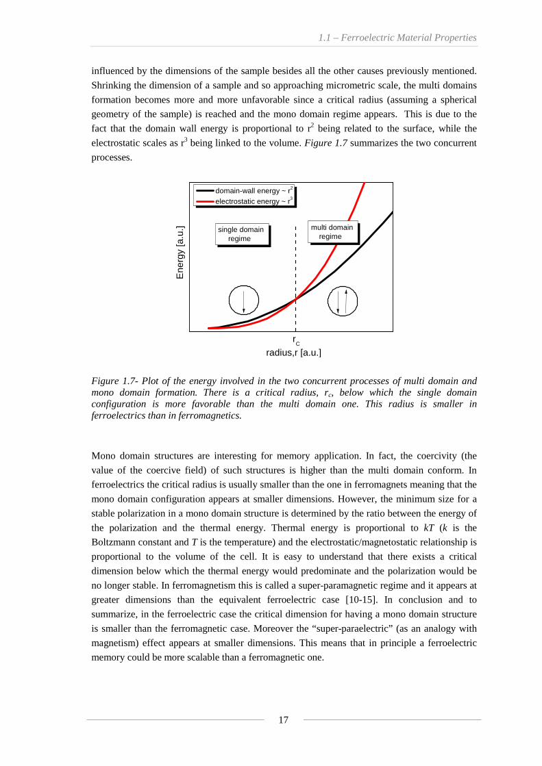
influenced by the dimensions of the sample besides all the other causes previously mentioned.
Shrinking the dimension of a sample and so approaching micrometric scale, the multi domains
formation becomes more and more unfavorable since a critical radius (assuming a spherical
geometry of the sample) is reached and the mono domain regime appears. This is due to the
fact that the domain wall energy is proportional to r2 being related to the surface, while the
electrostatic scales as r3 being linked to the volume. Figure 1.7 summarizes the two concurrent
processes.
single domain regime
Ene
rgy
[a.u
.]
radius,r [a.u.]
domain-wall energy ~ r2
electrostatic energy ~ r3
rC
multi domain regime
Figure 1.7- Plot of the energy involved in the two concurrent processes of multi domain and mono domain formation. There is a critical radius, rc, below which the single domain configuration is more favorable than the multi domain one. This radius is smaller in ferroelectrics than in ferromagnetics.
Mono domain structures are interesting for memory application. In fact, the coercivity (the
value of the coercive field) of such structures is higher than the multi domain conform. In
ferroelectrics the critical radius is usually smaller than the one in ferromagnets meaning that the
mono domain configuration appears at smaller dimensions. However, the minimum size for a
stable polarization in a mono domain structure is determined by the ratio between the energy of
the polarization and the thermal energy. Thermal energy is proportional to kT (k is the
Boltzmann constant and T is the temperature) and the electrostatic/magnetostatic relationship is
proportional to the volume of the cell. It is easy to understand that there exists a critical
dimension below which the thermal energy would predominate and the polarization would be
no longer stable. In ferromagnetism this is called a super-paramagnetic regime and it appears at
greater dimensions than the equivalent ferroelectric case [10-15]. In conclusion and to
summarize, in the ferroelectric case the critical dimension for having a mono domain structure
is smaller than the ferromagnetic case. Moreover the “super-paraelectric” (as an analogy with
magnetism) effect appears at smaller dimensions. This means that in principle a ferroelectric
memory could be more scalable than a ferromagnetic one.
Chapter I
18
1.1.5 Ferroelectric materials
Ferroelectric materials exist in various compositions and forms. The study of single
crystal materials is much simpler and it is important for the understanding of fundamental
ferroelectric phenomena. The crystallographic orientation can be well controlled and intrinsic
properties more easily accessed. However, single crystals are not an option for many
applications, because their costs are high. Ceramic materials can be processed, shaped and
manipulated more easily and they are therefore preferred in many, e.g. piezoelectric,
applications. With the age of miniaturisation and computing, the interest in thin ferroelectric
film grew fast. Thin films can be deposited in many different ways and consequently in many
different phases and various degrees of perfection. The choice of a substrate is decisive for the
quality of the films. Using appropriate single crystalline substrates, films can be grown with an
orientation of the crystallographic axes that is fully controlled by the substrate. Such films are
called epitaxial. For more economic applications, methods were found to control the
crystallographic orientation of the film and to achieve textured films with a preferential out-of-
plane crystallographic orientation of the grains. In this thesis a ferroelectric polymer is used and
it has been deposited by spin coating that allows fast and low cost processing.
One of the most studied ferroelectric specie is the so called perovskite. Perovskites are
pseudo-cubic structures with a chemical formula of the form ABO3. Apart from the big class of
ferroelectric oxides, ferroelectricity was discovered but, long after, in fundamentally different
materials, namely in liquid crystals [16] and polymers [17]. Due to the more complicated units
constituting a crystal, these two materials have in general a more complex structure. Ions or
atoms are stacked in the crystal lattice of oxide ferroelectrics and their order is repeated over
large volumes, whereas polymers consist of macromolecules, which arrange in a lower
symmetry and frequently with mixed amorphous and crystalline regions. Probably due to their
higher complexity, ferroelectricity in these soft matter materials was discovered decades after
the phenomena was known in ionic structures. Ferroelectricity was found for the first time in
polyvinylidene fluoride (PVDF) two years after observing piezoelectric effects in this material
[18]. PVDF and its copolymers are still among the most prominent members of the organic
ferroelectrics due to their high piezoelectric and pyroelectric coefficients. P(VDF-TrFE), Polyvinylidene Fluoride-Trifluoroethylene, copolymer in the 70%-30% percentage is the
polymer used in the experimental part of this work and so it deserves particular attention.
1.1 – Ferroelectric Material Properties
19
1.1.6 P(VDF-TrFE)
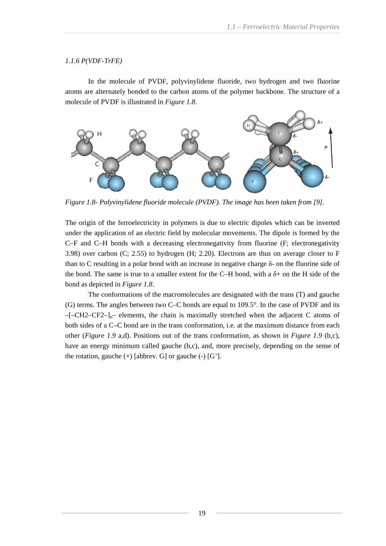
In the molecule of PVDF, polyvinylidene fluoride, two hydrogen and two fluorine
atoms are alternately bonded to the carbon atoms of the polymer backbone. The structure of a
molecule of PVDF is illustrated in Figure 1.8.
Figure 1.8- Polyvinylidene fluoride molecule (PVDF). The image has been taken from [9].
The origin of the ferroelectricity in polymers is due to electric dipoles which can be inverted
under the application of an electric field by molecular movements. The dipole is formed by the
C–F and C–H bonds with a decreasing electronegativity from fluorine (F; electronegativity
3.98) over carbon (C; 2.55) to hydrogen (H; 2.20). Electrons are thus on average closer to F
than to C resulting in a polar bond with an increase in negative charge δ- on the fluorine side of
the bond. The same is true to a smaller extent for the C–H bond, with a δ+ on the H side of the
bond as depicted in Figure 1.8.
The conformations of the macromolecules are designated with the trans (T) and gauche
(G) terms. The angles between two C–C bonds are equal to 109.5°. In the case of PVDF and its
–[–CH2–CF2–]n– elements, the chain is maximally stretched when the adjacent C atoms of
both sides of a C–C bond are in the trans conformation, i.e. at the maximum distance from each
other (Figure 1.9 a,d). Positions out of the trans conformation, as shown in Figure 1.9 (b,c),
have an energy minimum called gauche (b,c), and, more precisely, depending on the sense of
the rotation, gauche (+) [abbrev. G] or gauche (-) [G’].
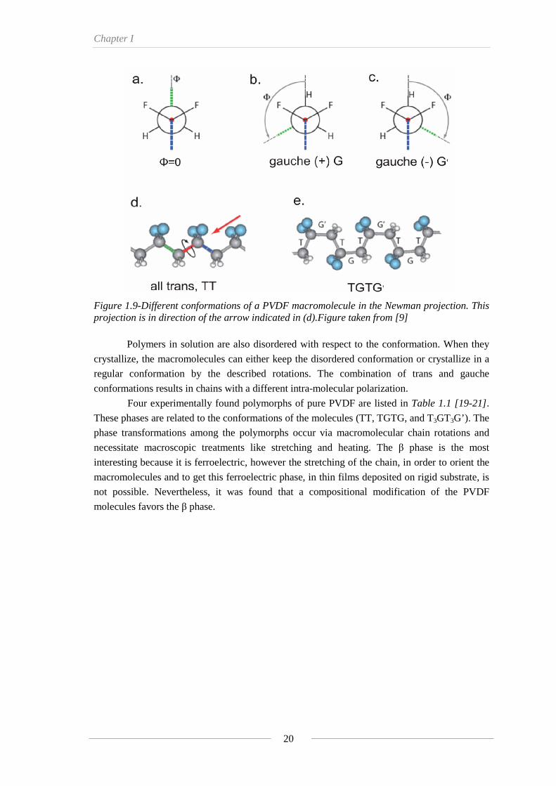
Chapter I
20
Figure 1.9-Different conformations of a PVDF macromolecule in the Newman projection. This projection is in direction of the arrow indicated in (d).Figure taken from [9]
Polymers in solution are also disordered with respect to the conformation. When they
crystallize, the macromolecules can either keep the disordered conformation or crystallize in a
regular conformation by the described rotations. The combination of trans and gauche
conformations results in chains with a different intra-molecular polarization.
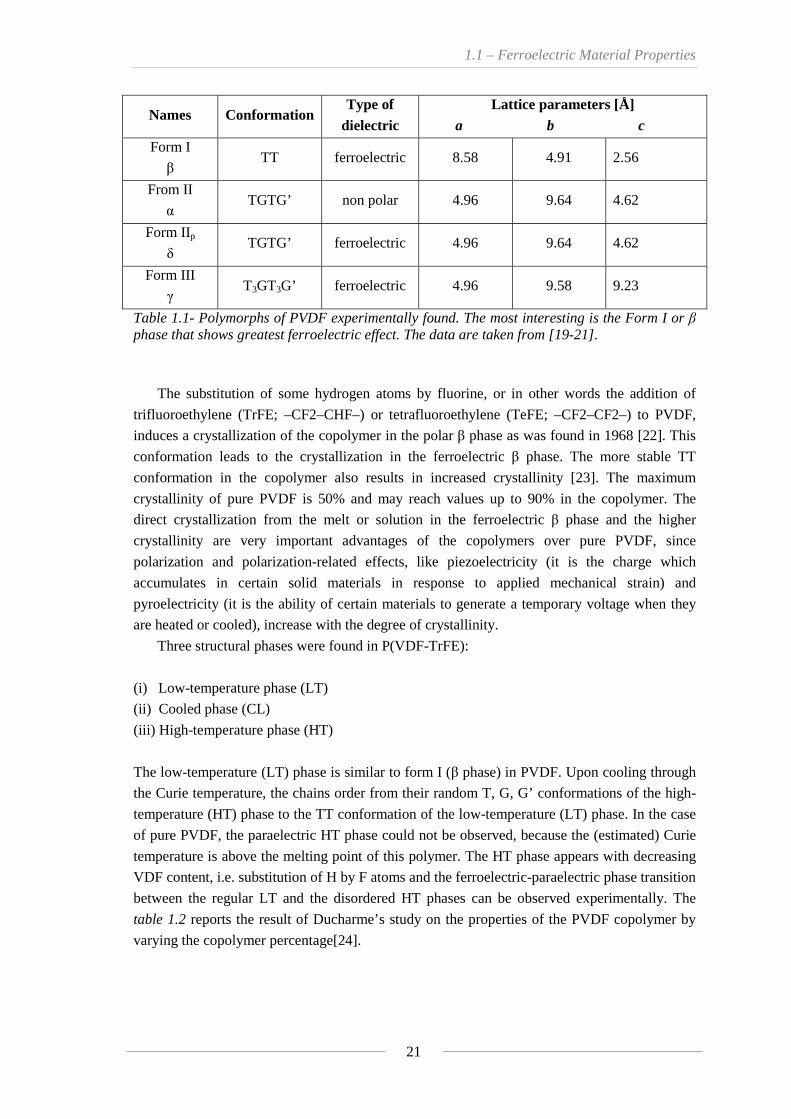
Four experimentally found polymorphs of pure PVDF are listed in Table 1.1 [19-21].
These phases are related to the conformations of the molecules (TT, TGTG, and T3GT3G’). The
phase transformations among the polymorphs occur via macromolecular chain rotations and
necessitate macroscopic treatments like stretching and heating. The β phase is the most
interesting because it is ferroelectric, however the stretching of the chain, in order to orient the
macromolecules and to get this ferroelectric phase, in thin films deposited on rigid substrate, is
not possible. Nevertheless, it was found that a compositional modification of the PVDF
molecules favors the β phase.
1.1 – Ferroelectric Material Properties
21
Names Conformation Type of
dielectric Lattice parameters [Å]
a b c
Form I
β TT ferroelectric 8.58 4.91 2.56
From II
α TGTG’ non polar 4.96 9.64 4.62
Form IIp
δ TGTG’ ferroelectric 4.96 9.64 4.62
Form III
γ T3GT3G’ ferroelectric 4.96 9.58 9.23
Table 1.1- Polymorphs of PVDF experimentally found. The most interesting is the Form I or β phase that shows greatest ferroelectric effect. The data are taken from [19-21].
The substitution of some hydrogen atoms by fluorine, or in other words the addition of
trifluoroethylene (TrFE; –CF2–CHF–) or tetrafluoroethylene (TeFE; –CF2–CF2–) to PVDF,
induces a crystallization of the copolymer in the polar β phase as was found in 1968 [22]. This
conformation leads to the crystallization in the ferroelectric β phase. The more stable TT
conformation in the copolymer also results in increased crystallinity [23]. The maximum
crystallinity of pure PVDF is 50% and may reach values up to 90% in the copolymer. The
direct crystallization from the melt or solution in the ferroelectric β phase and the higher
crystallinity are very important advantages of the copolymers over pure PVDF, since
polarization and polarization-related effects, like piezoelectricity (it is the charge which
accumulates in certain solid materials in response to applied mechanical strain) and
pyroelectricity (it is the ability of certain materials to generate a temporary voltage when they
are heated or cooled), increase with the degree of crystallinity.
Three structural phases were found in P(VDF-TrFE):
(i) Low-temperature phase (LT)
(ii) Cooled phase (CL)
(iii) High-temperature phase (HT)
The low-temperature (LT) phase is similar to form I (β phase) in PVDF. Upon cooling through
the Curie temperature, the chains order from their random T, G, G’ conformations of the high-
temperature (HT) phase to the TT conformation of the low-temperature (LT) phase. In the case
of pure PVDF, the paraelectric HT phase could not be observed, because the (estimated) Curie
temperature is above the melting point of this polymer. The HT phase appears with decreasing
VDF content, i.e. substitution of H by F atoms and the ferroelectric-paraelectric phase transition
between the regular LT and the disordered HT phases can be observed experimentally. The
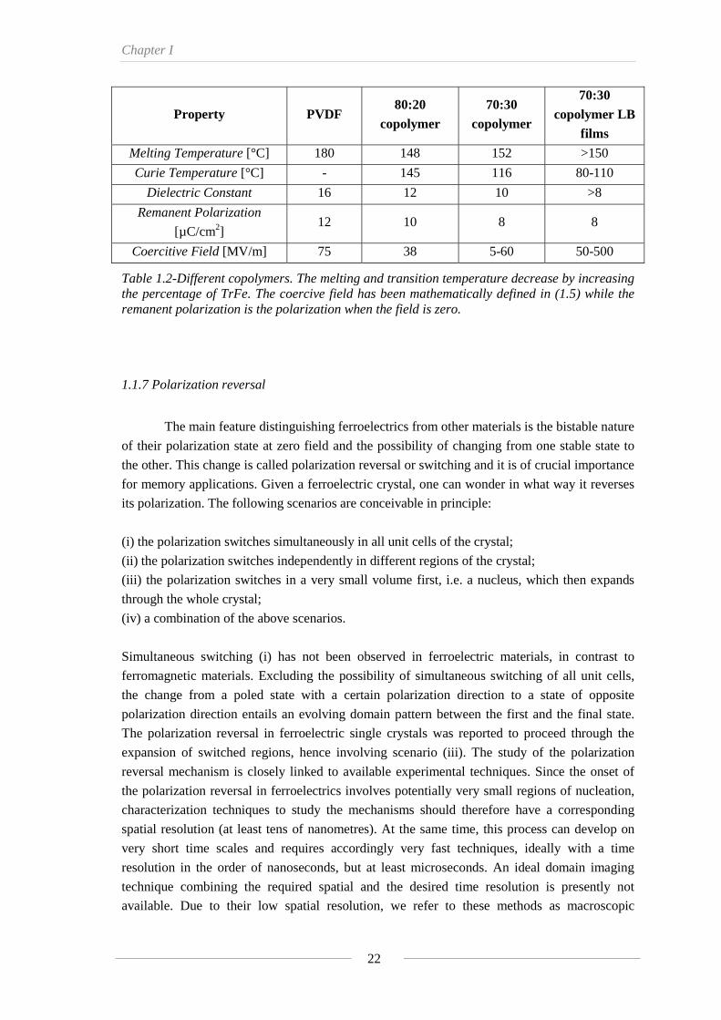
table 1.2 reports the result of Ducharme’s study on the properties of the PVDF copolymer by
varying the copolymer percentage[24].
Chapter I
22
Property PVDF 80:20
copolymer 70:30
copolymer
70:30 copolymer LB
films
Melting Temperature [°C] 180 148 152 >150
Curie Temperature [°C] - 145 116 80-110
Dielectric Constant 16 12 10 >8
Remanent Polarization
[µC/cm2] 12 10 8 8
Coercitive Field [MV/m] 75 38 5-60 50-500
Table 1.2-Different copolymers. The melting and transition temperature decrease by increasing the percentage of TrFe. The coercive field has been mathematically defined in (1.5) while the remanent polarization is the polarization when the field is zero.
1.1.7 Polarization reversal
The main feature distinguishing ferroelectrics from other materials is the bistable nature
of their polarization state at zero field and the possibility of changing from one stable state to
the other. This change is called polarization reversal or switching and it is of crucial importance
for memory applications. Given a ferroelectric crystal, one can wonder in what way it reverses
its polarization. The following scenarios are conceivable in principle:
(i) the polarization switches simultaneously in all unit cells of the crystal;
(ii) the polarization switches independently in different regions of the crystal;
(iii) the polarization switches in a very small volume first, i.e. a nucleus, which then expands
through the whole crystal;
(iv) a combination of the above scenarios.
Simultaneous switching (i) has not been observed in ferroelectric materials, in contrast to
ferromagnetic materials. Excluding the possibility of simultaneous switching of all unit cells,
the change from a poled state with a certain polarization direction to a state of opposite
polarization direction entails an evolving domain pattern between the first and the final state.
The polarization reversal in ferroelectric single crystals was reported to proceed through the
expansion of switched regions, hence involving scenario (iii). The study of the polarization
reversal mechanism is closely linked to available experimental techniques. Since the onset of
the polarization reversal in ferroelectrics involves potentially very small regions of nucleation,
characterization techniques to study the mechanisms should therefore have a corresponding
spatial resolution (at least tens of nanometres). At the same time, this process can develop on
very short time scales and requires accordingly very fast techniques, ideally with a time
resolution in the order of nanoseconds, but at least microseconds. An ideal domain imaging
technique combining the required spatial and the desired time resolution is presently not
available. Due to their low spatial resolution, we refer to these methods as macroscopic
1.1 – Ferroelectric Material Properties
23
techniques. Generally, they measure global or macroscopic polarization reversal effects, e.g. the
switching current or switching charges, permittivity or even structural parameters, i.e. lattice
spacing. A comprehensive body of results on polarization reversal in ferroelectric crystals was
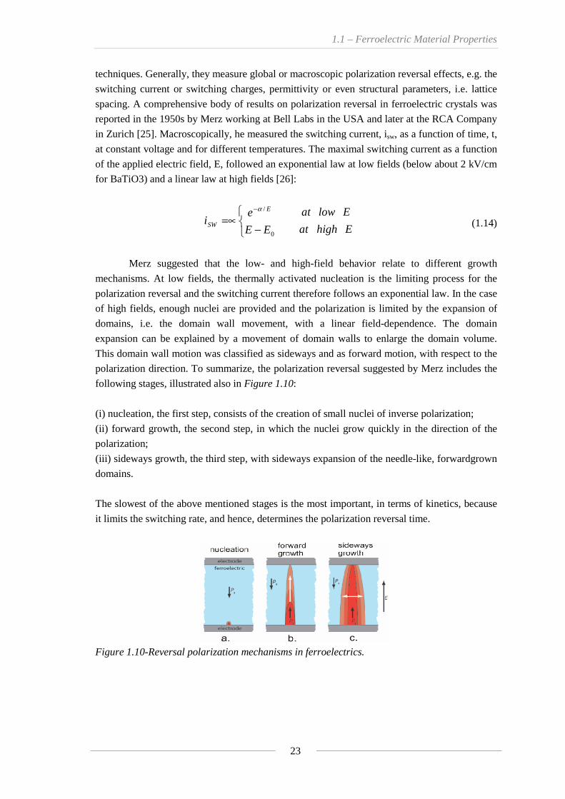
reported in the 1950s by Merz working at Bell Labs in the USA and later at the RCA Company
in Zurich [25]. Macroscopically, he measured the switching current, isw, as a function of time, t,
at constant voltage and for different temperatures. The maximal switching current as a function
of the applied electric field, E, followed an exponential law at low fields (below about 2 kV/cm
for BaTiO3) and a linear law at high fields [26]:
Ehighat
Elowat
EE
ei
E
SW
⎩⎨⎧
−=∝
−
0
/α
(1.14)
Merz suggested that the low- and high-field behavior relate to different growth
mechanisms. At low fields, the thermally activated nucleation is the limiting process for the
polarization reversal and the switching current therefore follows an exponential law. In the case
of high fields, enough nuclei are provided and the polarization is limited by the expansion of
domains, i.e. the domain wall movement, with a linear field-dependence. The domain
expansion can be explained by a movement of domain walls to enlarge the domain volume.
This domain wall motion was classified as sideways and as forward motion, with respect to the
polarization direction. To summarize, the polarization reversal suggested by Merz includes the
following stages, illustrated also in Figure 1.10:
(i) nucleation, the first step, consists of the creation of small nuclei of inverse polarization;
(ii) forward growth, the second step, in which the nuclei grow quickly in the direction of the
polarization;
(iii) sideways growth, the third step, with sideways expansion of the needle-like, forwardgrown
domains.
The slowest of the above mentioned stages is the most important, in terms of kinetics, because
it limits the switching rate, and hence, determines the polarization reversal time.
Figure 1.10-Reversal polarization mechanisms in ferroelectrics.
Chapter I
24
Polarization reversal in PVDF
The characteristic feature of ferroelectrics, the polarization reversal, can be understood
as a molecular chain rotation in the PVDF polymers, in which the polarization is normal to the
main axis of the macromolecules. Chain rotations are however only one part of the complex
polarization reversal of polymers. The complex structure with crystalline lamellae in an
amorphous matrix makes the process hard to understand and to investigate. Furukawa [27]
described the polarization reversal in ferroelectric polymers by three stages:
(i) the first, intramolecular stage involves the reversal of a single molecular chain;
(ii) the second stage deals with the expansion of the rotated chains in a lamella;
(iii) the third stage concerns the totality of the film with the interactions between the lamellae
and the matrix in between.
The first process (i) is very fast (a chain rotation propagates along the chain within 50 ps along
10nm at room temperature [28]) and hence, is not the limiting stage for the polarization reversal
in ferroelectrics. The second process (ii) agrees with a nucleation and growth scenario similar
to the one described for perovskite ferroelectrics and is probably the rate limiting step in the
polarization reversal of PVDF-type ferroelectric polymers because the reversal does not occur
via the rotation of single chains, but several molecules.
In the beginning of intensive studies on ferroelectric polymers during the 1970s, the
polarization reversal was found to be rather slow, i.e. from tens of seconds up to days.
Furukawa and Johnson were the first to demonstrate switching times of 4μs at 393 K. They
used much higher fields of 2000 kV/cm compared to previous experiments in their 7μm thick,
oriented films of PVDF [29]. The experimental data on the switching time as a function of field
was described by the exponential law (equation (2.14)) that was found for classical perovskite
materials at the low-field regime. From the larger switching time values in PVDF, it is clear
that the polarization reversal in PVDF requires much greater applied electric fields for
comparable polarization reversal times. The coercive field differs also by at least three orders of
magnitude between PVDF and BaTiO3 (MV/cm compared to KV/cm respectively).
Due to large electric fields needed to reverse the polarization in ferroelectric polymers,
there is a particular interest to reduce the film thickness in order to reduce the applied voltage.
Along with the down-scaling of the film thickness from thick (several micrometers) to thin
films (below about 200 nm) come the necessary change of the material. Films cannot easily be
oriented by stretching on a rigid substrate. Since pure PVDF cannot be brought into the desired
β phase without stretching, the copolymer P(VDF-TrFE) is preferred. It crystallizes directly in
the ferroelectric β phase from the melt or solution. Studies on the polarization reversal in
ferroelectric copolymer films can be categorized by their thickness into thin and ultrathin films.
Ultrathin films are characterized by a thickness below 60 nm, but usually only several
nanometers. They are typically deposited by the Langmuir-Blodgett (LB) technique [22]. Thin
films with a thickness of about 60nm to several hundreds of nanometers are typically spin
coated.

1.1 – Ferroelectric Material Properties
25
A study of the polarization reversal in thin copolymer films has recently been published
by Furukawa et al. [30]. VDF/TrFE copolymers with a 75%-25% composition were studied
under variable thickness, temperature, and electrode materials. Furukawa et al. found that the
grain size and the remnant polarization increased with increasing annealing temperature up to
about 140°C. Switching studies are rather difficult in ultrathin films, because the films
consisting of only a few polymer layers become very leaky. Hysteresis loops were therefore
typically measured as pyroelectric hysteresis loops (in a pyroelectric loop, the charge is
measured as a function of heating pulses and a slow driving field similar to piezoelectric loops).
In this thesis 100nm and 40nm of P(VDF-TrFE) are deposited by spin coating to build
up the gate stack of a ferroelectric transistor. Macroscopic measurements, transistor
transfer-characteristic, output characteristic, retention and programming time, are carried out.
The piezoelectric force microscopy is only used to investigate the retention failure mechanism.
Chapter I
26
1.2 Information Processing
Microelectronics has been one of the most enabling technologies of the 20th century.
All the technology which influences our everyday lives such as computers, mobile phones, the
internet etc., would not have been possible without the invention of the transistor and the
integrated circuit. It has shaped the way we perceive and interact with the world, more than any
other invention. The invention of the transistor in 1947 by W. Shockley, J. Bardeen and W.
Brattain [1, 2] has been the beginning of a long road toward modern electronics. Silicon
technology has advanced at exponential rates both in performance and productivity through the
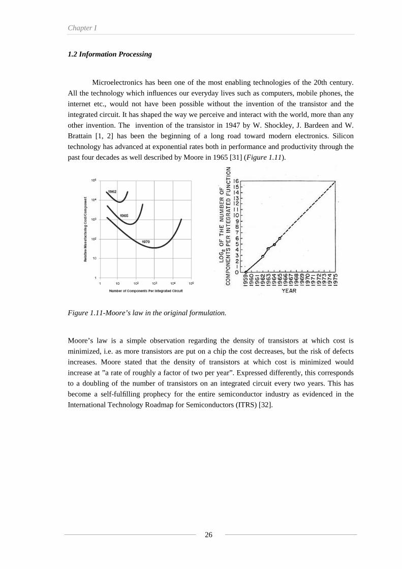
past four decades as well described by Moore in 1965 [31] (Figure 1.11).
Figure 1.11-Moore’s law in the original formulation.
Moore’s law is a simple observation regarding the density of transistors at which cost is
minimized, i.e. as more transistors are put on a chip the cost decreases, but the risk of defects
increases. Moore stated that the density of transistors at which cost is minimized would
increase at ”a rate of roughly a factor of two per year”. Expressed differently, this corresponds
to a doubling of the number of transistors on an integrated circuit every two years. This has
become a self-fulfilling prophecy for the entire semiconductor industry as evidenced in the
International Technology Roadmap for Semiconductors (ITRS) [32].
1.2 – Information Processing
27
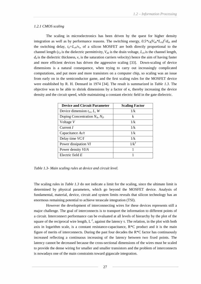
1.2.1 CMOS scaling
The scaling in microelectronics has been driven by the quest for higher density
integration as well as by performance reasons. The switching energy, 0.5*εd(Vdd*Lch)2/dd, and
the switching delay, td=Lch/vs, of a silicon MOSFET are both directly proportional to the
channel length (εd is the dielectric permittivity, Vdd is the drain voltage, Lch is the channel length, dd is the dielectric thickness, vs is the saturation carriers velocity) hence the aim of having faster
and more efficient devices has driven the aggressive scaling [33]. Down-scaling of device
dimensions is a natural consequence, when trying to carry out increasingly complicated
computations, and put more and more transistors on a computer chip, so scaling was an issue
from early on in the semiconductor game, and the first scaling rules for the MOSFET device
were established by R. H. Dennard in 1974 [34]. The result is summarized in Table 1.3. The
objective was to be able to shrink dimensions by a factor of κ, thereby increasing the device
density and the circuit speed, while maintaining a constant electric field in the gate dielectric.
Device and Circuit Parameter Scaling Factor
Device dimension tox, L, W 1/k
Doping Concentration NA, ND k
Voltage V 1/k
Current I 1/k
Capacitance Aε/t 1/k
Delay time VC/I 1/k
Power dissipation VI 1/k2
Power density VI/A 1
Electric field E 1
Table 1.3- Main scaling rules at device and circuit level.
The scaling rules in Table 1.3 do not indicate a limit for the scaling, since the ultimate limit is
determined by physical parameters, which go beyond the MOSFET device. Analysis of
fundamental, material, device, circuit and system limits reveals that silicon technology has an
enormous remaining potential to achieve terascale integration (TSI).
However the development of interconnecting wires for these devices represents still a
major challenge. The goal of interconnects is to transport the information to different points of
a circuit. Interconnect performance can be evaluated at all levels of hierarchy by the plot of the
square of the reciprocal wire length, L-2, against the latency τ. The relation, in the plot with both
axis in logarithm scale, is a constant resistance-capacitance, R*C product and it is the main
figure of merits of interconnects. During the past four decades the R*C factor has continuously
increased reflecting a continuous increasing of the latency between two fixed points. The
latency cannot be decreased because the cross-sectional dimensions of the wires must be scaled
to provide the dense wiring for smaller and smaller transistors and the problem of interconnects
is nowadays one of the main constraints toward gigascale integration.

Chapter I
28
Today, no single other technology can provide the performance of CMOS with respect
to the combination of parameters: integration, speed, logic operation, memory functionality,
and, not least, cost. However, in the future we might see an increasing number of hybrid
approaches where other technologies add to the CMOS performance, while maintaining a
back-bone of CMOS logic.
1.2.2 Silicon MOSFET Switch limitations
Dennard, in his famous paper, recommended that all device dimensions should be
scaled by 1/κ, while the doping of the source and drain regions should increase by a factor of κ.
Applied voltages should also be scaled by 1/κ. These rules have been roughly followed ever
since, untill rather recently. The reason for which Dennard’s scaling rules no longer work as
well as they did in the past can be seen in Figure 1.12, which shows the scaling trend from the
1.4 μm node to the 65 nm node. While the supply voltage VDD decreased to about 20% of its
original value, the threshold voltage VTH only went down to approximately half of its starting
value. That threshold voltage decrease did not happen as a natural result of Dennard scaling. It
occurs differently such as when changing the doping of the channel region under the gate. Since
the electric fields inside a MOSFET stay nearly constant when the scaling rules are followed
correctly, the threshold voltage stays nearly constant as well, unless other changes are made.
Figure 1.12-VDD scaled much more than the VTH with a consequent reduction of the gate overdrive, VDD-VTH.[35].
The most important consequence of VDD reducing during device scaling while VTH reduces
significantly less, is that the gate overdrive, VDD-VTH, goes down. When the gate overdrive
decreases, on-current decreases, which negatively affects device performance, the Ion/Ioff ratio,
and dynamic speed (CgVDD/Ion). There are two possible solutions to this problem of needing a
high gate overdrive: either VDD can stay higher than it should with constant field scaling, or VTH
can be scaled down more aggressively. Figure 1.13 shows that the formerly-followed scaling
trends of 1/κ = 0.7 every 2 or 3 years (bold and dashed lines at the top of the figure, for
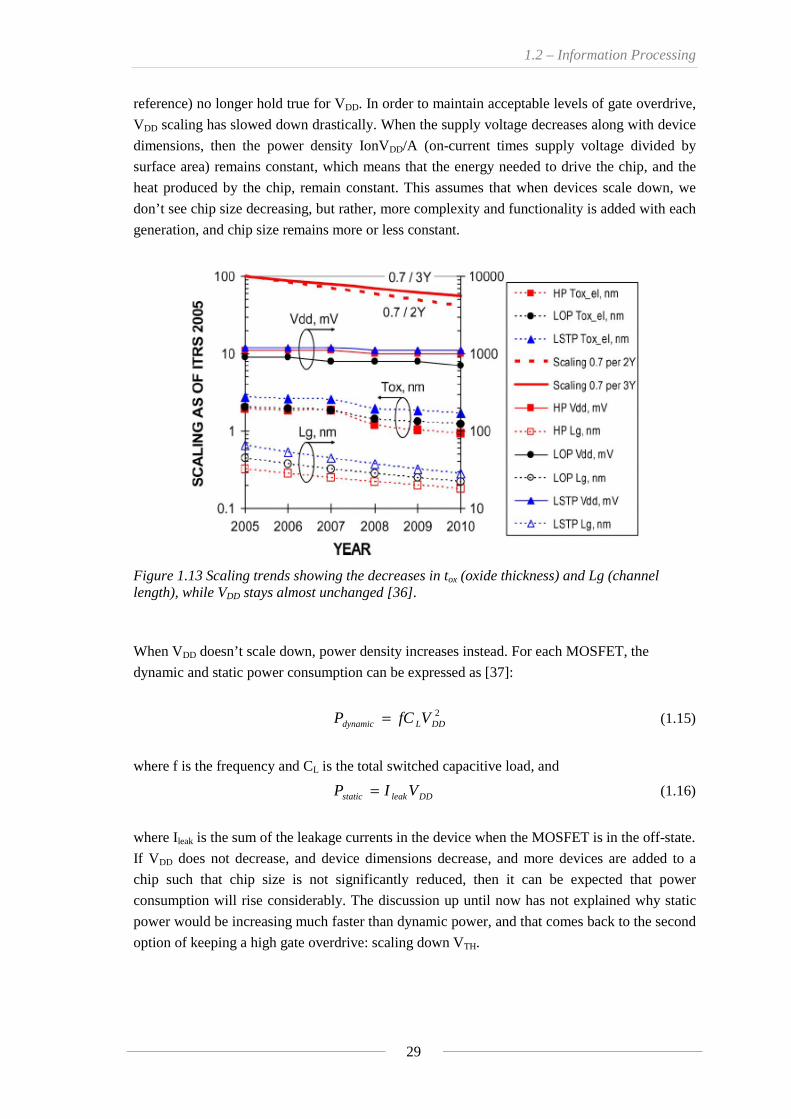
1.2 – Information Processing
29
reference) no longer hold true for VDD. In order to maintain acceptable levels of gate overdrive,
VDD scaling has slowed down drastically. When the supply voltage decreases along with device
dimensions, then the power density IonVDD/A (on-current times supply voltage divided by
surface area) remains constant, which means that the energy needed to drive the chip, and the
heat produced by the chip, remain constant. This assumes that when devices scale down, we
don’t see chip size decreasing, but rather, more complexity and functionality is added with each
generation, and chip size remains more or less constant.
Figure 1.13 Scaling trends showing the decreases in tox (oxide thickness) and Lg (channel length), while VDD stays almost unchanged [36].
When VDD doesn’t scale down, power density increases instead. For each MOSFET, the
dynamic and static power consumption can be expressed as [37]:
2
DDLdynamic VfCP = (1.15)
where f is the frequency and CL is the total switched capacitive load, and
DDleakstatic VIP = (1.16)
where Ileak is the sum of the leakage currents in the device when the MOSFET is in the off-state.
If VDD does not decrease, and device dimensions decrease, and more devices are added to a
chip such that chip size is not significantly reduced, then it can be expected that power
consumption will rise considerably. The discussion up until now has not explained why static
power would be increasing much faster than dynamic power, and that comes back to the second
option of keeping a high gate overdrive: scaling down VTH.
Chapter I
30
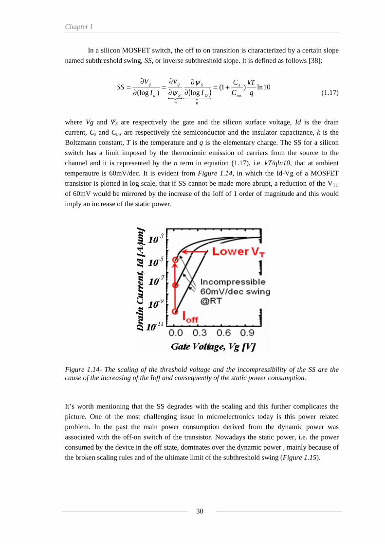
In a silicon MOSFET switch, the off to on transition is characterized by a certain slope
named subthreshold swing, SS, or inverse subthreshold slope. It is defined as follows [38]:
( ) 10ln)1(log)(log q
kT
C
C
I
V
I
VSS
ins
s
n
D
S
m
S
g
d
g +=∂
∂∂∂
=∂
∂=
43421
ψψ (1.17)
where Vg and ΨS are respectively the gate and the silicon surface voltage, Id is the drain
current, Cs and Cins are respectively the semiconductor and the insulator capacitance, k is the
Boltzmann constant, T is the temperature and q is the elementary charge. The SS for a silicon
switch has a limit imposed by the thermoionic emission of carriers from the source to the
channel and it is represented by the n term in equation (1.17), i.e. kT/qln10, that at ambient
temperautre is 60mV/dec. It is evident from Figure 1.14, in which the Id-Vg of a MOSFET
transistor is plotted in log scale, that if SS cannot be made more abrupt, a reduction of the VTH
of 60mV would be mirrored by the increase of the Ioff of 1 order of magnitude and this would
imply an increase of the static power.
Figure 1.14- The scaling of the threshold voltage and the incompressibility of the SS are the cause of the increasing of the Ioff and consequently of the static power consumption.
It’s worth mentioning that the SS degrades with the scaling and this further complicates the
picture. One of the most challenging issue in microelectronics today is this power related
problem. In the past the main power consumption derived from the dynamic power was
associated with the off-on switch of the transistor. Nowadays the static power, i.e. the power
consumed by the device in the off state, dominates over the dynamic power , mainly because of
the broken scaling rules and of the ultimate limit of the subthreshold swing (Figure 1.15).
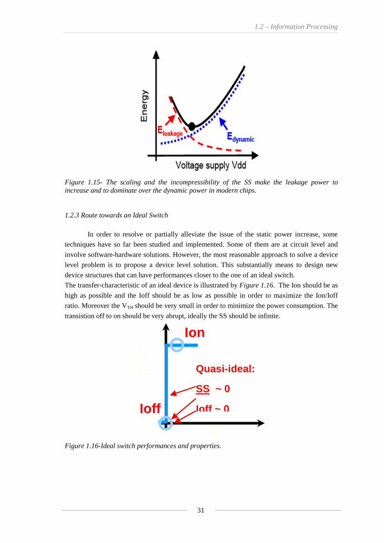
1.2 – Information Processing
31
Figure 1.15- The scaling and the incompressibility of the SS make the leakage power to increase and to dominate over the dynamic power in modern chips.
1.2.3 Route towards an Ideal Switch
In order to resolve or partially alleviate the issue of the static power increase, some
techniques have so far been studied and implemented. Some of them are at circuit level and
involve software-hardware solutions. However, the most reasonable approach to solve a device
level problem is to propose a device level solution. This substantially means to design new
device structures that can have performances closer to the one of an ideal switch.
The transfer-characteristic of an ideal device is illustrated by Figure 1.16. The Ion should be as
high as possible and the Ioff should be as low as possible in order to maximize the Ion/Ioff
ratio. Moreover the VTH should be very small in order to minimize the power consumption. The
transistion off to on should be very abrupt, ideally the SS should be infinite.
Figure 1.16-Ideal switch performances and properties.
VG
ID (log) Ioff
Ion
Quasi-ideal:
SS ~ 0
Ioff ~ 0
Chapter I
32
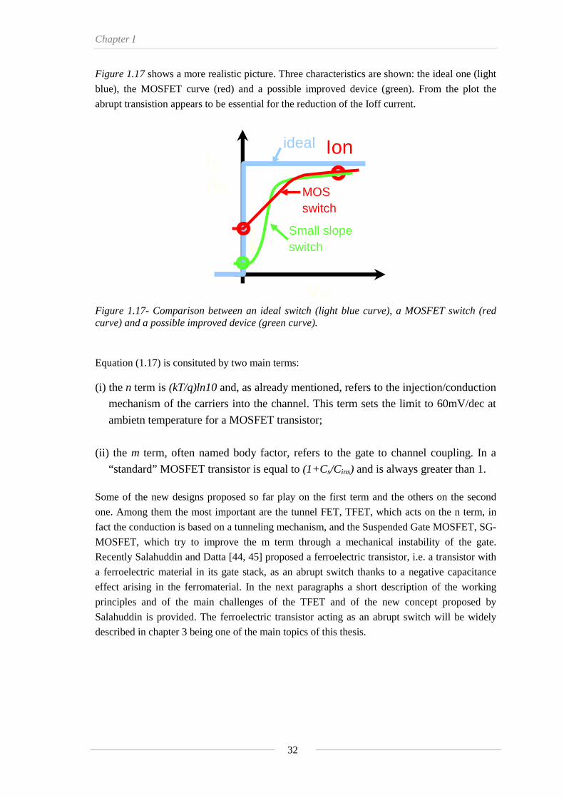
Figure 1.17 shows a more realistic picture. Three characteristics are shown: the ideal one (light
blue), the MOSFET curve (red) and a possible improved device (green). From the plot the
abrupt transistion appears to be essential for the reduction of the Ioff current.
Figure 1.17- Comparison between an ideal switch (light blue curve), a MOSFET switch (red curve) and a possible improved device (green curve).
Equation (1.17) is consituted by two main terms: (i) the n term is (kT/q)ln10 and, as already mentioned, refers to the injection/conduction
mechanism of the carriers into the channel. This term sets the limit to 60mV/dec at
ambietn temperature for a MOSFET transistor;
(ii) the m term, often named body factor, refers to the gate to channel coupling. In a
“standard” MOSFET transistor is equal to (1+Cs/Cins) and is always greater than 1. Some of the new designs proposed so far play on the first term and the others on the second
one. Among them the most important are the tunnel FET, TFET, which acts on the n term, in
fact the conduction is based on a tunneling mechanism, and the Suspended Gate MOSFET, SG-
MOSFET, which try to improve the m term through a mechanical instability of the gate.
Recently Salahuddin and Datta [44, 45] proposed a ferroelectric transistor, i.e. a transistor with
a ferroelectric material in its gate stack, as an abrupt switch thanks to a negative capacitance
effect arising in the ferromaterial. In the next paragraphs a short description of the working
principles and of the main challenges of the TFET and of the new concept proposed by
Salahuddin is provided. The ferroelectric transistor acting as an abrupt switch will be widely
described in chapter 3 being one of the main topics of this thesis.
VG
ID (log)
MOS switch
Ion
Small slope switch
ideal
1.2 – Information Processing
33
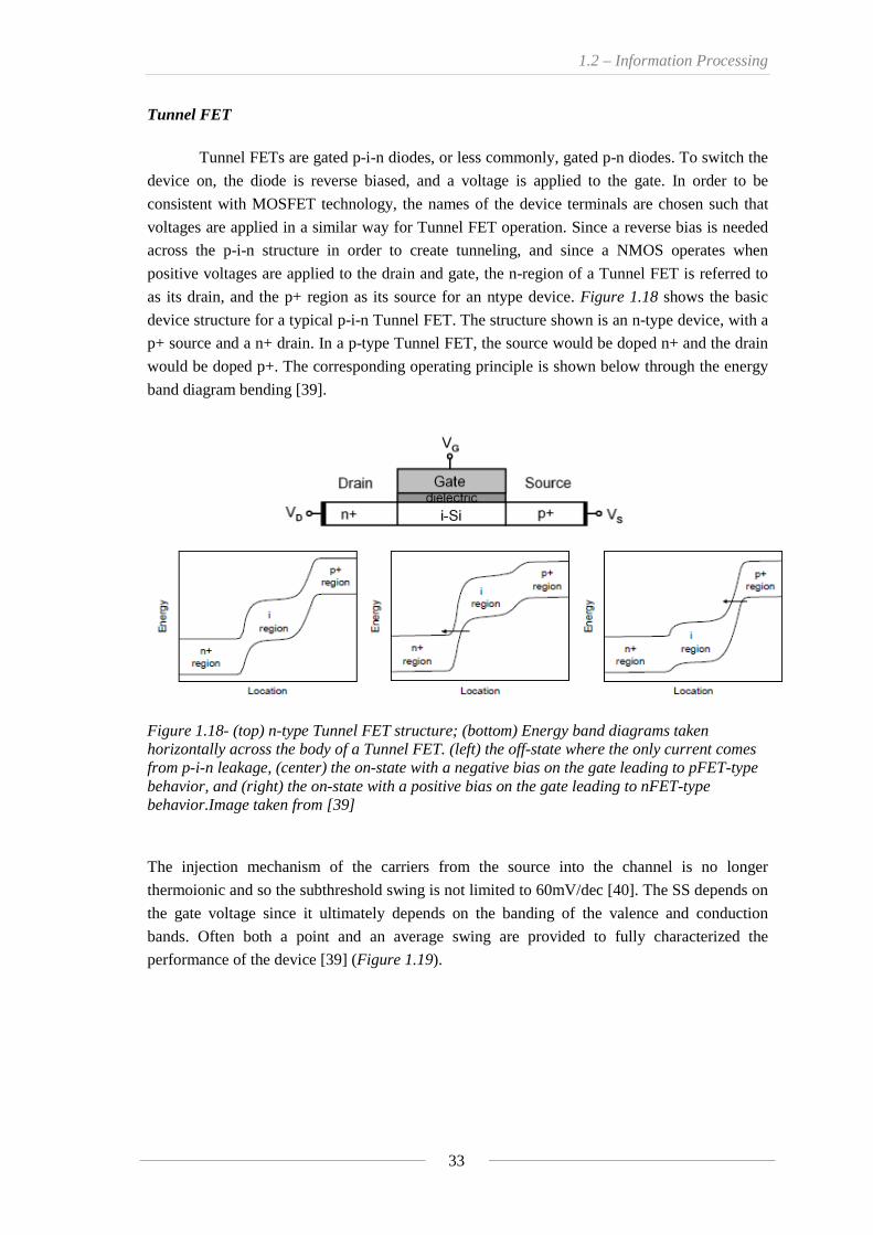
Tunnel FET
Tunnel FETs are gated p-i-n diodes, or less commonly, gated p-n diodes. To switch the
device on, the diode is reverse biased, and a voltage is applied to the gate. In order to be
consistent with MOSFET technology, the names of the device terminals are chosen such that
voltages are applied in a similar way for Tunnel FET operation. Since a reverse bias is needed
across the p-i-n structure in order to create tunneling, and since a NMOS operates when
positive voltages are applied to the drain and gate, the n-region of a Tunnel FET is referred to
as its drain, and the p+ region as its source for an ntype device. Figure 1.18 shows the basic
device structure for a typical p-i-n Tunnel FET. The structure shown is an n-type device, with a
p+ source and a n+ drain. In a p-type Tunnel FET, the source would be doped n+ and the drain
would be doped p+. The corresponding operating principle is shown below through the energy
band diagram bending [39].
Figure 1.18- (top) n-type Tunnel FET structure; (bottom) Energy band diagrams taken horizontally across the body of a Tunnel FET. (left) the off-state where the only current comes from p-i-n leakage, (center) the on-state with a negative bias on the gate leading to pFET-type behavior, and (right) the on-state with a positive bias on the gate leading to nFET-type behavior.Image taken from [39]
The injection mechanism of the carriers from the source into the channel is no longer
thermoionic and so the subthreshold swing is not limited to 60mV/dec [40]. The SS depends on
the gate voltage since it ultimately depends on the banding of the valence and conduction
bands. Often both a point and an average swing are provided to fully characterized the
performance of the device [39] (Figure 1.19).

Chapter I
34
Figure 1.19- The Subthreshold Swing in a TFET depends on the gate voltage and so a point swing and an average swing are necessary to completely characterize its performance. Image taken from [39]. If the doping profile is completely symmetric then the device shows an ambipolar behavior and
so it will be in the on-state for both positive and negative gate voltages. The ambipolarity could
be minimized or suppressed by the engineering of the band diagram. However the silicon
tunnel FET suffers for low Ion current if compared to an equivalent MOSFET. It is
exponentialy dependent on the width of the barrier where the direct tunneling occurs. The
increase of the on state current is one of the greatest challenges for making this device a good
candidate for future electronics. A solution that involves multiple conduction mechanisms has
been recently proposed [41]. Scientific research is focusing its attention on TFET
heterostructure, that allows a better and more flexible engineering of the energy bands, and on
strain engineering.
In a heterostructuralTunnel FET, the materials are chosen so that the source material
has a small band gap so that the energy barrier width at the source junction is reduced in the on-
state, while the drain material has a large band gap, which creates the largest possible energy
barrier width at the drain side in the off-state, to keep the off-current low. It is not enough to
choose any small band gap material for the source and any large band gap material for the
drain, however. The way in which the bands naturally line up with each other at the
heterojunction, which depends on their electron affinities, is also crucial. This was illustrated by
Verhulst et al. from IMEC in [42, 43], showing that the best situation is a continuous valence
band with a conduction band offset for p-type Tunnel FETs, and a continuous conduction band
with a valence band offset for n-type Tunnel FETs. In this way, the energy barrier width in the
on-state is minimized, and the highest possible on-current results. When low-band gap
materials and strain are combined at the tunnel junction of a Tunnel FET, the band gap there is
reduced by both effects, and the on-current is improved by both. A group at Stanford [44]
presented experimental results from a heterostructure Tunnel FET whose strained germanium
layer goes all the way across the device, comprising source, intrinsic region and drain.

1.2 – Information Processing
35
Use of Negative Capacitance to Provide Voltage Amplification This is an introduction to the negative capacitance concept of ferroelectrics proposed by
Salahuddin and Datta [44,45] in order to decrease the m factor (see (1.17)) and ultimately to
improve the subthreshold swing . From Landau’s theory for ferroelectrics (see paragraph 1.1.3),
the electric field Vs. the polarization reads as follows:
53 )()()( PTCPTBPTTE c ++−= α (1.18)
Neglecting the P3 and the P5 terms and considering that α is always positive, it is evident that
the E-P plot can have a negative slope and indeed a negative electric permittivity. This, of
course, is not valid for standard dielectrics that exhibit a parabolic energy-charge plot. The
ferroelectric instead has an unstable equilibrium point in the energy-charge curve. This point is
placed around Q=0 (Figure 1.20).
Figure 1.20-Energy Vs. Charge curves for a ferroelectric dielectric and for a regular insulator. The instable equilibrium point in the U-Q plot (extreme left) is mirrored in a negative permittivity (negative slope in the V-Q curve). Image taken from [44] This negative permittivity can give raise to a negative capacitance that can be used in series
with a positive one in order to stabilize the system and lower the SS (see the (1.17)) of a
transistor below the 60mV/dec limit. Salahuddin and Datta considered the schematic illustrated
in Figure 1.21 where the Cins is indeed the ferroelectric capacitance. It is important to note that
no other dielectric layer is taken into account. This device would theoretically exhibit the best
possible SS, however it presents some technological problems.
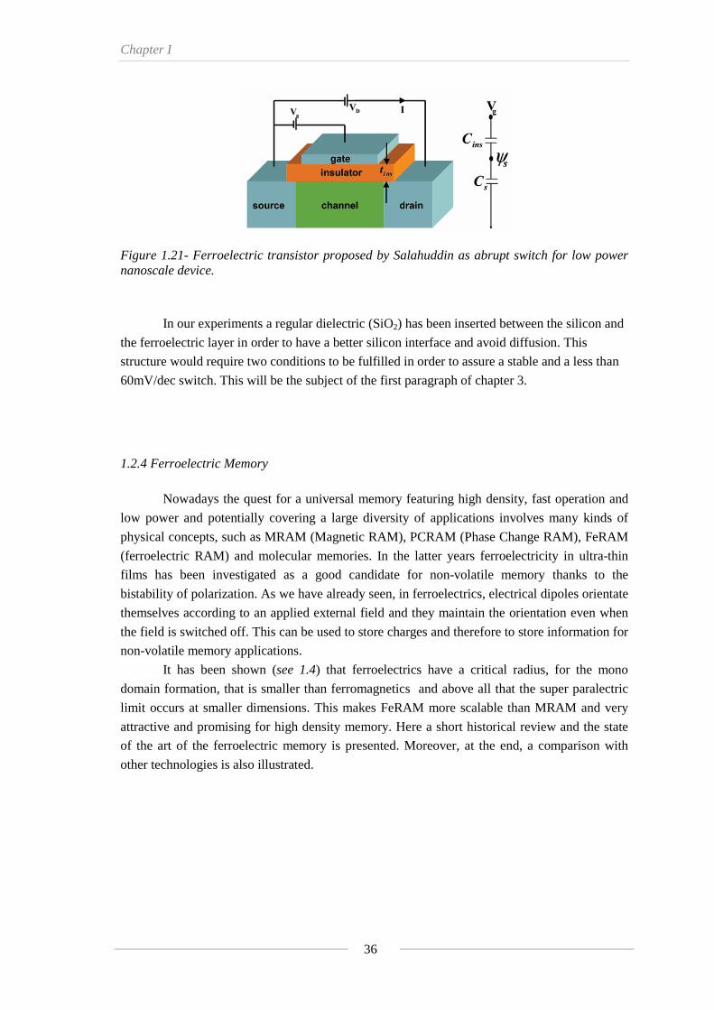
Chapter I
36
Figure 1.21- Ferroelectric transistor proposed by Salahuddin as abrupt switch for low power nanoscale device.
In our experiments a regular dielectric (SiO2) has been inserted between the silicon and
the ferroelectric layer in order to have a better silicon interface and avoid diffusion. This
structure would require two conditions to be fulfilled in order to assure a stable and a less than
60mV/dec switch. This will be the subject of the first paragraph of chapter 3.
1.2.4 Ferroelectric Memory
Nowadays the quest for a universal memory featuring high density, fast operation and
low power and potentially covering a large diversity of applications involves many kinds of
physical concepts, such as MRAM (Magnetic RAM), PCRAM (Phase Change RAM), FeRAM
(ferroelectric RAM) and molecular memories. In the latter years ferroelectricity in ultra-thin
films has been investigated as a good candidate for non-volatile memory thanks to the
bistability of polarization. As we have already seen, in ferroelectrics, electrical dipoles orientate
themselves according to an applied external field and they maintain the orientation even when
the field is switched off. This can be used to store charges and therefore to store information for
non-volatile memory applications.
It has been shown (see 1.4) that ferroelectrics have a critical radius, for the mono
domain formation, that is smaller than ferromagnetics and above all that the super paralectric
limit occurs at smaller dimensions. This makes FeRAM more scalable than MRAM and very
attractive and promising for high density memory. Here a short historical review and the state
of the art of the ferroelectric memory is presented. Moreover, at the end, a comparison with
other technologies is also illustrated.
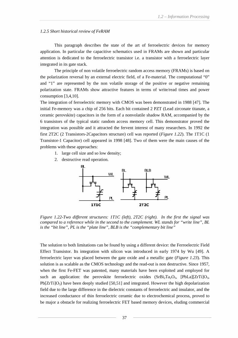
1.2 – Information Processing
37
1.2.5 Short historical review of FeRAM
This paragraph describes the state of the art of ferroelectric devices for memory
application. In particular the capacitive schematics used in FRAMs are shown and particular
attention is dedicated to the ferroelectric transistor i.e. a transistor with a ferroelectric layer
integrated in its gate stack.
The principle of non volatile ferroelectric random access memory (FRAMs) is based on
the polarization reversal by an external electric field, of a Fe-material. The computational “0”
and “1” are represented by the non volatile storage of the positive or negative remaining
polarization state. FRAMs show attractive features in terms of write/read times and power
consumption [3,4,10].
The integration of ferroelectric memory with CMOS was been demonstrated in 1988 [47]. The
initial Fe-memory was a chip of 256 bits. Each bit contained 2 PZT (Lead zirconate titanate, a
ceramic perovskite) capacitors in the form of a nonvolatile shadow RAM, accompanied by the
6 transistors of the typical static random access memory cell. This demonstrator proved the
integration was possible and it attracted the fervent interest of many researchers. In 1992 the
first 2T2C (2 Transistors-2Capacitors structure) cell was reported (Figure 1.22). The 1T1C (1
Transistor-1 Capacitor) cell appeared in 1998 [48]. Two of them were the main causes of the
problems with these approaches:
1. large cell size and so low density;
2. destructive read operation.
Figure 1.22-Two different structures: 1T1C (left), 2T2C (right). In the first the signal was compared to a reference while in the second to the complement. WL stands for “write line”, BL is the “bit line”, PL is the “plate line”, BLB is the “complementary bit line”
The solution to both limitations can be found by using a different device: the Ferroelectric Field
Effect Transistor. Its integration with silicon was introduced in early 1974 by Wu [49]. A
ferroelectric layer was placed between the gate oxide and a metallic gate (Figure 1.23). This
solution is as scalable as the CMOS technology and the read-out is non destructive. Since 1957,
when the first Fe-FET was patented, many materials have been exploited and employed for
such an application: the perovskite ferroelectric oxides (SrBi2Ta2O5, [PbLa][ZrTi]O3,
Pb[ZrTi]O3) have been deeply studied [50,51] and integrated. However the high depolarization
field due to the large difference in the dielectric constants of ferroelectric and insulator, and the
increased conductance of thin ferroelectric ceramic due to electrochemical process, proved to
be major a obstacle for realizing ferroelectric FET based memory devices, eluding commercial
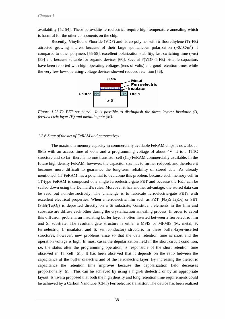
Chapter I
38
availability [52-54]. These perovskite ferroelectrics require high-temperature annealing which
is harmful for the other components on the chip.
Recently, Vinylidene Fluoride (VDF) and its co-polymer with trifluorethylene (Tr-FE)
attracted growing interest because of their large spontaneous polarization (~0.1C/m2) if
compared to other polymers [55-58], excellent polarization stability, fast switching time (~ns)
[59] and because suitable for organic devices [60]. Several P(VDF-TrFE) bistable capacitors
have been reported with high operating voltages (tens of volts) and good retention times while
the very few low-operating-voltage devices showed reduced retention [56].
Figure 1.23-Fe-FET structure. It is possible to distinguish the three layers: insulator (I), ferroelectric layer (F) and metallic gate (M). 1.2.6 State of the art of FeRAM and perspectives The maximum memory capacity in commercially available FeRAM chips is now about
8Mb with an access time of 60ns and a programming voltage of about 4V. It is a 1T1C
structure and so far there is no one-transistor cell (1T) FeRAM commercially available. In the
future high-density FeRAM, however, the capacitor size has to further reduced, and therefore it
becomes more difficult to guarantee the long-term reliability of stored data. As already
mentioned, 1T FeRAM has a potential to overcome this problem, because each memory cell in
1T-type FeRAM is composed of a single ferroelectric-gate FET and because the FET can be
scaled down using the Dennard’s rules. Moreover it has another advantage: the stored data can
be read out non-destructively. The challenge is to fabricate ferroelectric-gate FETs with
excellent electrical properties. When a ferroelectric film such as PZT (Pb(Zr,Ti)O3) or SBT
(SrBi2Ta2O9) is deposited directly on a Si substrate, constituent elements in the film and
substrate are diffuse each other during the crystallization annealing process. In order to avoid
this diffusion problem, an insulating buffer layer is often inserted between a ferroelectric film
and Si substrate. The resultant gate structure is either a MFIS or MFMIS (M: metal, F:
ferroelectric, I: insulator, and S: semiconductor) structure. In these buffer-layer-inserted
structures, however, new problems arise so that the data retention time is short and the
operation voltage is high. In most cases the depolarization field in the short circuit condition,
i.e. the status after the programming operation, is responsible of the short retention time
observed in 1T cell [61]. It has been observed that it depends on the ratio between the
capacitance of the buffer dielectric and of the ferroelectric layer. By increasing the dielectric
capacitance the retention time improves because the depolarization field decreases
proportionally [61]. This can be achieved by using a high-k dielectric or by an appropriate
layout. Ishiwara proposed that both the high density and long retention time requirements could
be achieved by a Carbon Nanotube (CNT) Ferroelectric transistor. The device has been realized
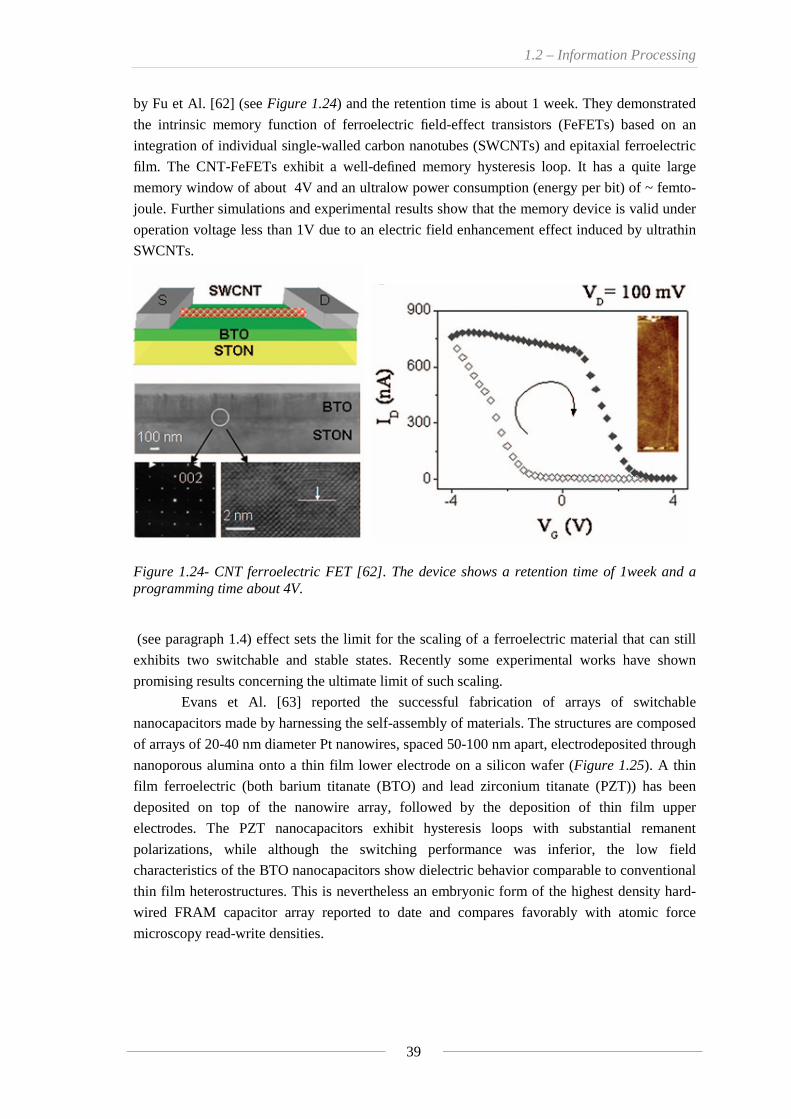
1.2 – Information Processing
39
by Fu et Al. [62] (see Figure 1.24) and the retention time is about 1 week. They demonstrated
the intrinsic memory function of ferroelectric field-effect transistors (FeFETs) based on an
integration of individual single-walled carbon nanotubes (SWCNTs) and epitaxial ferroelectric
film. The CNT-FeFETs exhibit a well-defined memory hysteresis loop. It has a quite large
memory window of about 4V and an ultralow power consumption (energy per bit) of ~ femto-
joule. Further simulations and experimental results show that the memory device is valid under
operation voltage less than 1V due to an electric field enhancement effect induced by ultrathin
SWCNTs.
Figure 1.24- CNT ferroelectric FET [62]. The device shows a retention time of 1week and a programming time about 4V. (see paragraph 1.4) effect sets the limit for the scaling of a ferroelectric material that can still
exhibits two switchable and stable states. Recently some experimental works have shown
promising results concerning the ultimate limit of such scaling.
Evans et Al. [63] reported the successful fabrication of arrays of switchable
nanocapacitors made by harnessing the self-assembly of materials. The structures are composed
of arrays of 20-40 nm diameter Pt nanowires, spaced 50-100 nm apart, electrodeposited through
nanoporous alumina onto a thin film lower electrode on a silicon wafer (Figure 1.25). A thin
film ferroelectric (both barium titanate (BTO) and lead zirconium titanate (PZT)) has been
deposited on top of the nanowire array, followed by the deposition of thin film upper
electrodes. The PZT nanocapacitors exhibit hysteresis loops with substantial remanent
polarizations, while although the switching performance was inferior, the low field
characteristics of the BTO nanocapacitors show dielectric behavior comparable to conventional
thin film heterostructures. This is nevertheless an embryonic form of the highest density hard-
wired FRAM capacitor array reported to date and compares favorably with atomic force
microscopy read-write densities.
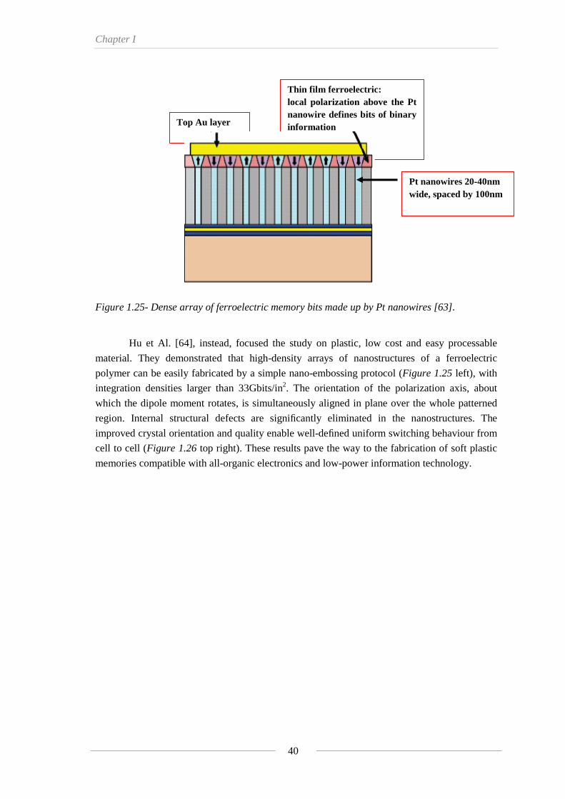
Chapter I
40
Figure 1.25- Dense array of ferroelectric memory bits made up by Pt nanowires [63]. Hu et Al. [64], instead, focused the study on plastic, low cost and easy processable
material. They demonstrated that high-density arrays of nanostructures of a ferroelectric
polymer can be easily fabricated by a simple nano-embossing protocol (Figure 1.25 left), with
integration densities larger than 33Gbits/in2. The orientation of the polarization axis, about
which the dipole moment rotates, is simultaneously aligned in plane over the whole patterned
region. Internal structural defects are significantly eliminated in the nanostructures. The
improved crystal orientation and quality enable well-defined uniform switching behaviour from
cell to cell (Figure 1.26 top right). These results pave the way to the fabrication of soft plastic
memories compatible with all-organic electronics and low-power information technology.
Top Au layer
Thin film ferroelectric: local polarization above the Pt nanowire defines bits of binary information
Pt nanowires 20-40nm wide, spaced by 100nm
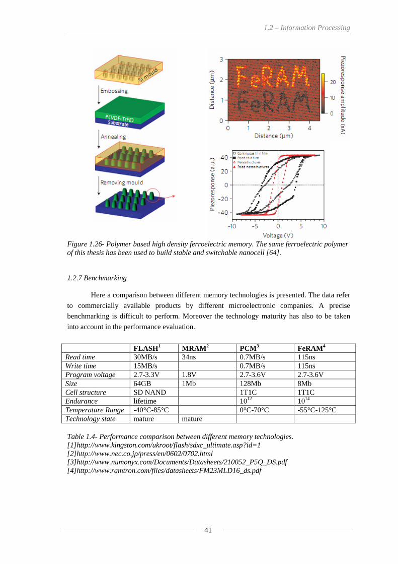
1.2 – Information Processing
41
Figure 1.26- Polymer based high density ferroelectric memory. The same ferroelectric polymer of this thesis has been used to build stable and switchable nanocell [64]. 1.2.7 Benchmarking Here a comparison between different memory technologies is presented. The data refer
to commercially available products by different microelectronic companies. A precise
benchmarking is difficult to perform. Moreover the technology maturity has also to be taken
into account in the performance evaluation.
FLASH1 MRAM2 PCM3 FeRAM4
Read time 30MB/s 34ns 0.7MB/s 115ns Write time 15MB/s 0.7MB/s 115ns Program voltage 2.7-3.3V 1.8V 2.7-3.6V 2.7-3.6V Size 64GB 1Mb 128Mb 8Mb Cell structure SD NAND 1T1C 1T1C Endurance lifetime 1012 1014
Temperature Range -40°C-85°C 0°C-70°C -55°C-125°C Technology state mature mature Table 1.4- Performance comparison between different memory technologies. [1]http://www.kingston.com/ukroot/flash/sdxc_ultimate.asp?id=1 [2]http://www.nec.co.jp/press/en/0602/0702.html [3]http://www.numonyx.com/Documents/Datasheets/210052_P5Q_DS.pdf [4]http://www.ramtron.com/files/datasheets/FM23MLD16_ds.pdf

Chapter I
42
1.2.8 Sensors and other applications
Ferroelectric materials can be used in a plethora of applications thanks to their unique
properties. Ferromaterials, in fact, are also piezoelectric, pyroelectric and electrocalorific [5],
moreover they exhibit also a photovoltaic effect [65,66]. A huge volume of literature exists
about ferroelectric sensors [67,68] that covers a very differentiate spectrum of applications.
Here, the attention is focused on the thermal-electrical energy conversion that can
occur in ferromaterials. Pyroelectric effect refers to the capability of a material to exhibit an
electrical voltage when the temperature is changed. So a ΔT is converted in a ΔV. The
electrocalorific effect is the dual mechanism. This mechanism is also consistent with
experimental results regarding the magnetocaloric effect (MCE) in ferromagnetic materials, in
which a giant MCE was observed at temperatures above the ferromagnetic-paramagnetic
transition [69,70]. Recently a huge electrocalorific effect has been experimentally registered in
P(VDF-TrFE) copolymer [71]. The pyroelectric effect, instead, is better known and studied and
it also deals with the change of the polarization when the temperature is changed. The so called
Olson [72] cycle is used to graphically illustrate the change in the entropy (Figure 1.27) and to
understand a complete energy cycle conversion..
Figure 1.27- Olson cycle for thermal to electrical conversion calculation.
The loop ABCD is traversed in a clockwise direction. When the temperature of a pyroelectric
film is decreased at low voltage, a charge accumulates on the film along C-D. This occurs
because the crystal structure within the pyroelectric film begins to transform from the
paraelectric to the ferroelectric phase. As the voltage is raised from low to high at the low film
temperature, the charge increases along D-A. If the temperature of the film is increased at high
voltage, the charge is released along A-B. This results because the ability of the film to store the
charge decreases as the crystal structure is transformed from the ferroelectric to the paraelectric
phase. Finally, the external voltage is lowered from high to low and a further discharge occurs
along B-C, thus completing a heat-to-electric conversion cycle.
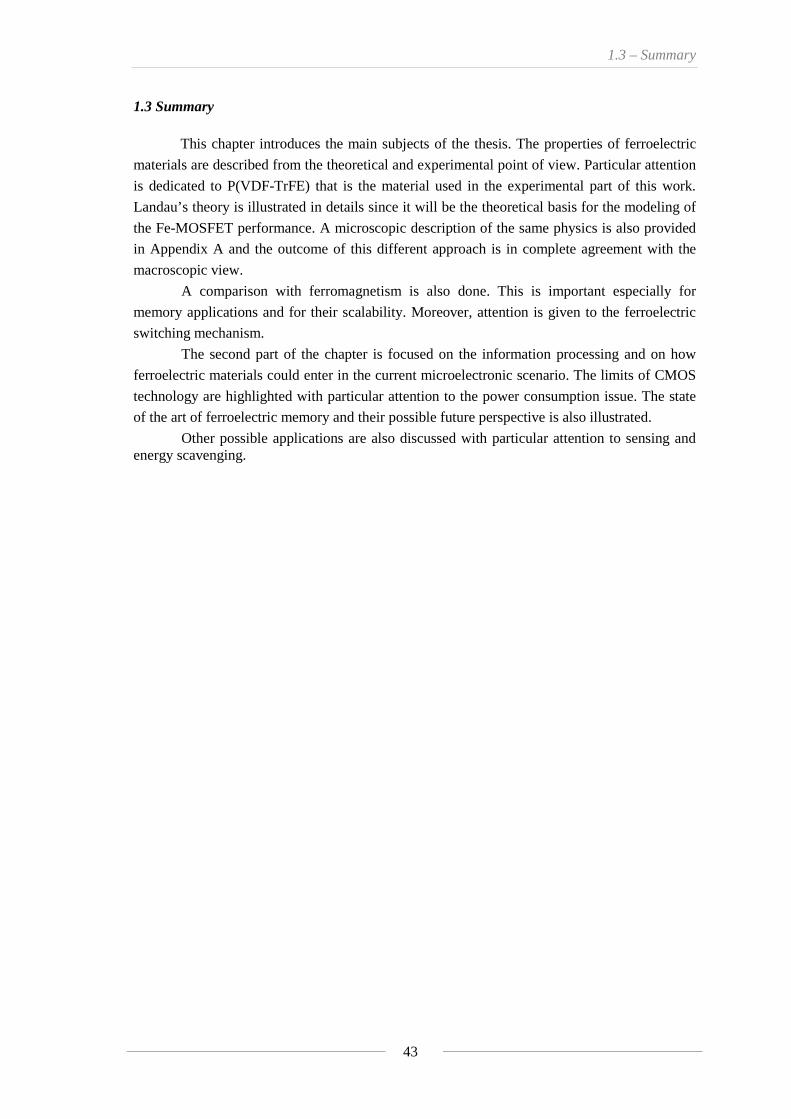
1.3 – Summary
43
1.3 Summary This chapter introduces the main subjects of the thesis. The properties of ferroelectric
materials are described from the theoretical and experimental point of view. Particular attention
is dedicated to P(VDF-TrFE) that is the material used in the experimental part of this work.
Landau’s theory is illustrated in details since it will be the theoretical basis for the modeling of
the Fe-MOSFET performance. A microscopic description of the same physics is also provided
in Appendix A and the outcome of this different approach is in complete agreement with the
macroscopic view.
A comparison with ferromagnetism is also done. This is important especially for
memory applications and for their scalability. Moreover, attention is given to the ferroelectric
switching mechanism.
The second part of the chapter is focused on the information processing and on how
ferroelectric materials could enter in the current microelectronic scenario. The limits of CMOS
technology are highlighted with particular attention to the power consumption issue. The state
of the art of ferroelectric memory and their possible future perspective is also illustrated.
Other possible applications are also discussed with particular attention to sensing and energy scavenging.

Chapter I - Bibliography
Bibliography
[1] J. Valasek, “Piezo-Electric and Allied Phenomena in Rochelle Salt”, Phys. Rev. 17, 475–481 (1921)
[2] A. von Hippel, "U.S. National Defense Research Committee Report 300", NDRC, Boston, MA, (1944)
[3] J. F. Scott, C. A. Araujo, “Ferroelectric Memories”, Science 246, 1400 (1989)
[4] J. F. Scott, “Ferroelectric Memories”, Springer, Heidelberg, Germany, (2000)
[5] M. Lines, A. Glass, “Principles and applications of ferroelectrics and related materials”, Clarendon Press, Oxford (1979)
[6] Tagantsev A.K., Sherman V.O., Astafiev K.F., Venkatesh J., Setter N., “Ferroelectric materials for microwave tunable applications”, Journal of Electroceramics 11, pp. 5-66 (2003)
[7] Ginzburg V. L., “Phase transitions in ferroelectrics: some historical remarks”, Physics Uspekhi 44 (10), pp. 1037-1043 (2001)
[8] K. Rabe, C. H. Ahn, J.-M. Triscone, Physics of Ferroelectrics, “A Modern prespective, Topics, Application, Physics”, Springer-Verlag Berlin Heidelberg (2007)
[9] R. Gysel, “Polarization reversal in ferroelectric PVDF and PZT film”, EPFL thesis No. 4097 (2008)
[10] N. A. Spaldin, “Fundamental Size Limits in Ferroelectricity”, Science vol 304, (2004)
[11]T. M. Shaw, S. Trolier-McKinstry, P. C. McIntyre, “The properties of ferroelectric films at small dimensions”, Annu. Rev. Mater. Sci. 30, 263 (2000).
[12] Ph. Ghosez, K. Rabe, "Microscopic model of ferroelectricity in stress-free PbTiO3 ultrathin films", Appl. Phys. Lett. 76, 2767 (2000).
[13] B. Meyer, D.Vanderbilt, “Ab initio study of BaTiO3 and PbTiO3 surfaces in external electric fields”, Phys. Rev. B 63, 205426 (2001).
[14] J. Junquera, Ph. Ghosez, “Critical thickness for ferroelectricity in perovskite ultrathin films“, Nature 422, 506 (2003)
[15] C. H. Ahn, K. M. Rabe, J.-M. Triscone, “Ferroelectricity at the Nanoscale: Local Polarization in Oxide Thin Films and Heterostructures”, Science 303, 488 (2004).
[16] R. B. Meyer,L. Liebert, L. Strzelecki and P. Keller,“Ferroelectric liquid-crystals”, Journal De Physique Lettres, 36(3):L69–L71 (1975).
[17] K. Nakamura and Y. Wada, “Piezoelectricity, pyroelectricity, and the electrostriction constant of poly(vinylidene fluoride)”, Journal of Polymer Science Part A-2: Polymer Physics, 9(1):161–173 (1971)
[18] H. Kawai, “Piezoelectricity of poly(vinylidene fluoride)”, Japanese Journal of Applied Physics, 8(7):975 (1969)
[19] R. Hasegawa, Y. Takahash, H. Tadokoro and Y. Chatani “Crystal-structures of 3 crystalline forms of poly(vinylidene fluoride)”, Polymer Journal, 3(5):600 (1972).
[20] N. Karasawa and W. Goddard III “Force fields, structures, and properties of poly(vinylidene fluoride) crystals”, Macromolecules, 25(26):7268–7281 (1992).
[21] K. Tashiro, “Crystal structure and phase transition of PVDF and related copolymers”, Ferroelectric Polymers, pages 63–181. Marcel Dekker Inc., New York (1995)

Chapter I - Bibliography
[22] J. B. Lando and W. W. Doll, “The polymorphism of poly(vinylidene fluoride). The effect of head-to-head structure”, Journal of Macromolecular Science, Part B, 2(2):205–218 (1968)
[23] K. Koga and H. Ohigashi, “Piezoelectricity and related properties of vinylidene fluoride and trifluoroethylene copolymers”, Journal of Applied Physics, 59(6):2142–2150 (1986).
[24] S. Ducharme, “Ferroelectric polymer Langmuir-Blodgett films for nonvolatile memory applications”, IEEE Trans. on Dev. and Mat. Rel., Vol. 5, No.4 (2005)
[25] W. J. Merz, “Domain formation and domain wall motions in ferroelectric BaTiO3 single crystals”, Physical Review, 95:690–698 (1954)
[26] E. Fatuzzo and W. J. Merz, “Switching mechanism in triglycine sulfate and other ferroelectrics”, Physical Review, 116(1):61 (1959)
[27] T. Furukawa, “Ferroelectric properties of vinylidene fluoride copolymers”, Phase Transitions, 18(3):143 – 211(1989).
[28] H. Dvey-Aharon, T. J. Sluckin, P. L. Taylor and A. J. Hopfinger, “Kink propagation as a model for poling in poly(vinylidene fluoride)”, Physical Review B, 21(8):3700 (1980)
[29] T. Furukawa and G. E. Johnson, “Measurements of ferroelectric switching characteristics in polyvinylidene fluoride”, Applied Physics Letters, 38(12):1027–1029 (1981)
[30] T. Furukawa, T. Nakajima and Y. Takahashi, Y, “Factors governing ferroelectric switching characteristics of thin VDF/TrFE copolymer films”, IEEE Trans. on Dielectrics and Electrical Insulation, 13(5):1120–1131 (2006)
[31] G. E. Moore, “Cramming more components onto integrated circuits”, Electronics Vol. 38 No. 8, (1965)
[32] http://www.itrs.net. International Technology Roadmap for Semiconductors. web page, Latest edition (2009)
[33] James D. Meindl, Qiang Chen, Jeffrey A. Davis, ”Limits on silicon nanoelectronics for terascale integration”, Science Vol. 293 (2001)
[34] R. H. Dennard et al., “Design of ion-implanted MOSFET’s with very small physical dimensions”, IEEE Journal of Solid-State Circuits, SC-9 (5) pp. 256–268, (1974)
[35] P. Packan, Short Course, IEDM (2007)
[36] T. Skotnicki et Al., “Innovative Materials, Devices, and CMOS Technologies for Low-Power Mobile Multimedia,” IEEE Trans. Electron Devices, vol. 55, No. 1, pp. 96-130 (2008)
[37] P. Nilsson, “Arithmetic Reduction of the Static Power Consumption in Nanoscale CMOS” IEEE Int. Conf. on Electronics, Circuits and Systems, pp. 656-659 (2006)
[38] R. J. Van Overstraeten, “Theory of the MOS Transistor in Weak Inversion-New Method to Determine the Number of Surface States”, IEEE Transaction of Electron Devices Vol. 22 N. 5 (1975)
[39] K. Boucart, “Simulation of Double-Gate Silicon Tunnel FETs with a High-k Gate Dielectric”, EPFL Thesis No. 4729 (2010)
[40] J. Appenzeller, Y.-M. Lin, J. Knoch and Ph. Avouris, “Band-to-Band Tunneling in Carbon Nanotube Field-Effect Transistors”, Phys. Rev. Lett. 93, 196805 (2004)
[41] L. Lattanzio, L. De Michielis, A. Biswas, A. M. Ionescu, "Abrupt Switch based on Internally Combined Band-To-Band and Barrier Tunneling Mechanisms", ESSDERC 2010, 13-17 September 2010, Sevilles, Spain.
Chapter I - Bibliography
[42] A. Verhulst, W. Vandenberghe, K. Maex, S. De Gendt, M. Heyns, and G. Groeseneken, “Complementary Silicon-Based Heterostructure Tunnel-FETs With High Tunnel Rates” Electron Device Lett., vol. 29, no. 12, pp. 1398-1401 (2008)
[43] J.Knoch, “Optimizing tunnel FET performance - Impact of device structure, transistor dimensions and choice of material”, Proc. VLSI-TSA, pp. 45-46. (2009)
[44] T. Krishnamohan, D. Kim, S. Raghunathan, and K. Saraswat, “Double-Gate Strained-Ge Heterostructure Tunneling FET (TFET) With Record High Drive Currents and <60mV/dec Subthreshold Slope”, IEDM Tech. Dig., 2008, pp. 947-949.
[45] S. Salahuddin, S. Datta, “Use of Negative Capacitance to Provide Voltage Amplification for Low Power Nanoscale Devices”, Nanoletters Vol.8 No.2 405-410 (2008).
[46] S. Salahuddin, S. Datta, “Can the subthreshold swing in a classical FET be lowered below 60 mV/decade?”, IEDM Digest, pp. 693-696, (2008).
[47] S.S.Eaton, D.B. Butler, M.Parris, D.Wilson, H.McNeillie, “A Ferroelectric Nonvolatile Memory” ISSCC Digest of Technical Papers, pp. 130-131, February 1988.
[48] W. Kraus, L. Lehman, D. Wilson, T. Yamazaki, C. Ohno, E. Nagai, H. Yamazaki, and H. Suzuki, “A 42.5 mm 1 Mb nonvolatile ferroelectric memory utilizing advanced architecture for enhanced reliability”, Symp. VLSI Circuits Dig. Tech. Papers, June 1998, pp. 242–245.
[49] S. Y. Wu, “A new ferroelectric memory device, metal–ferroelec- tric–semiconductor transistor”, IEEE Trans. Electron Devices ED-21, 499 (1974)
[50] H. Takasu, “Ferroelectric memories and their applications”, Microelectronic Engineering 59, 237-246 (2001)
[51] A. Chin, “Stack Gate PZT/Al2O3 One Transistor Ferroelectric Memory”, IEEE Electron Device Letters, vol. 22, No. 7, (2001)
[52] H. Ishiwara, “Current status and prospects of FET-type ferreoelctric memories”, J. Semicond. Technol. Sci., vol. 1, pp. 1–14, (2001)
[53] T. P. Ma and Jin-Ping Han,” Why is Nonvolatile Ferroelectric Memory Field-Effect Transistor Still Elusive?”, IEEE Electron Device Letters Vol. 23, No. 7 (2002)
[54] C. T. Black, C. Farrell and T. J. Licata, “Suppression of ferroelectric polarization by an adjustable depolarization field”, Appl. Phys. Lett. 71, 2041 (1997)
[55] S. H. Lim et al.,” Electrical properties of metal-ferroelectric-insulator-semiconductor structures based on ferroelectric polyvinylidene fluoride copolymer film gate for nonvolatile random access memory application”, J. Appl. Phys. v. 96, no.10 (2004).
[56] A. Gerber et al., “Low-voltage operation of metal-ferroelectric-insulator-semiconductor diodes incorporating a ferroelectric polyvinylidene fluoride copolymer Langmuir-Blodgett film“, J. Appl. Phys. v.100 024110 (2006)
[57] T. J. Reece et al.,” Nonvolatile memory element based on a ferroelectric polymer Langmuir-Blodgett film”, Appl. Phys. Lett. V. 82, no.1 (2003).
[58] Sachio Horiuchi and Yoshinori Tokura, “Organic ferroelectrics”, Nature Materials Vol. 7 2008
[59] T. Furukawa et al., “Nanosecond Switching in Thin Fims of Vinylidene FluorideTrilluoroethylene Copolymers”, J.J. Appl. Phys., Vol. 24, No.8, 1985
[60] R. C. G. Naber et al, ”High-performance solution-processed polymer ferroelectric field-effect transistors”, Nature Material, v. 4 n.3 (2005).
Chapter I - Bibliography
[61] Hiroshi Ishiwara, “Current status of ferroelectric-gate Si transistors and challenge to ferroelectric-gate CNT transistors”, Current Applied Physics 9 (2009) S2–S6
[62] W. Fu, Z. Xu, X. Bai, C. Gu, and E. Wang, “Intrinsic Memory Function of Carbon Nanotube-based Ferroelectric Field-Effect Transistor”, Nano Lett., 2009, 9 (3), pp 921–925
[63] P. Evans et Al., “Toward Self-Assembled Ferroelectric Random Access Memories: Hard-Wired Switching Capacitor Arrays with Almost Tb/in.2 Densities”, Nano Lett., 2007, 7 (5), pp 1134–1137
[64] Z. Hu, M. Tian, B. Nysten and A. M. Jonas, “Regular arrays of highly ordered ferroelectric polymer nanostructures for non-volatile low-voltage memories”, Nature materials advanced publication, November 2008
[65] S. Y. Yang et Al. “Above-bandgap voltages from ferroelectric photovoltaic devices“, Nature Nanotech. 5, 143–147 (2010).
[66] T. Choi, S. Lee,Y. J. Choi, V. Kiryukhin, S. W. Cheong, “Switchable Ferroelectric Diode and Photovoltaic Effect in BiFeO3“, Science 324, 63–66 (2009).
[67] S.B. Lang, S. Muensit, “Review of some lesser-known applications of piezoelectric and pyroelectric polymers”, Appl. Phys. A 85, 125–134 (2006)
[68] Dragan Damjanovic, Paul Muralt, and Nava Setter, “ Ferroelectric Sensor”, IEEE Sensors Journal, Vol. 1, No. 3, (2001)
[69] V. Provenzano, A. J. Shapiro, R. D. Shull, “Reduction of hysteresis losses in the magnetic refrigerant Gd5Ge2Si2 by the addition of iron”, Nature 429, 853 (2004)
[70] O. Tegus, E. Brück, K. H. J. Buschow and F. R. de Boer, “Transition-metal-based magnetic refrigerants for room-temperature applications”, Nature 415, 150 (2002)
[71] Bret Neese, Baojin Chu, Sheng-Guo Lu, Yong Wang, E. Furman, Q. M. Zhang, “Large electrocaloric effect in ferroelectric polymers near room temperature”, Science Vol 321 August 2008
[72] R.B. Olsen, D.A. Bruno, M. Brisco, “Pyroelectric conversion cycles”, J. Appl. Phys. 58, 4709 (1985)

Chapter 2
Ferroelectric transistor for 1T memory cell
This chapter reports on ferroelectric transistors and their applications as non-volatile
memory. The first part is about the fabrication and the characterization of a ferroelectric
MOSFET. A 100nm and a 40nm thick layer of P(VDF-TrFE) have been successfully integrated
into the gate stack of a MOSFET. The fabrication process and the device performance, in terms
of static characteristic and memory, are described. The second part of the chapter describes a
ferroelectric tunnel field effect transistor, Fe-TFET. This is a completely new device concept
and it would allow extremely low power consumption for memory applications. In both cases a
retention time of a few seconds, in short circuit conditions, is registered, limiting the usage of
such devices as NV-memory. The retention failure mechanisms are described and studied for
future possible improvements.

2.1 – Organic Ferroelectric transistor
51
2.1 Organic ferroelectric transistor
Ferroelectric materials thanks, to their polarization switching, can be used for memory
applications as already illustrated in chapter 1, where a general overview of the Fe-RAM
technology has also been illustrated. The integration issues of non-organic ferromaterials have
been commented upon (high annealing temperature and consequently bad interface formation);
here, the attention is on P(VDF-TrFE), one of the most studied and well processable organic
ferroelectric polymers. This chapter is focused on the description of two ferroelectric
transistors, a bulk Fe-MOSFET and a ferroelectric tunnel FET, that have been fabricated and
characterized mainly for their memory properties [1]. One of the most important achievements
of this work is the integration of the ferroelectric polymer, P(VDF-TrFE), into the gate stack of
a standard MOSFET structure.
The ferroelectric layer thickness sets the operating voltage of the memory cell, in fact
the switching voltage can be approximately calculated as:
dEV cc = (2.1)
where Ec is the coercive field of the material and d is the thickness of the layer. The first
fabricated device has 100nm of polymer and 10nm of SiO2 as gate stack for a corresponding
operating voltage of about 15V. The spin coating process has been optimized in order to thin
down the thickness to about 40nm. This optimized structure shows an operating voltage of
about 7V. A further scaling of the thickness is at the moment limited by the roughness of the
polymer itself that is about 20nm. Different deposition techniques and a more careful
preparation of the polymer solution should be taken into account in order to achieve nanometric
scale.
The integration of 40nm of such a polymer has also been achieved on a tunnel FET
structure [2]. This is a completely new device and it would, in principle, guarantee a low
voltage and an abrupt switching memory cell.
All the fabrications processes, described in this work, have been carried out in the clean
room facility at CMI at EPFL. In Appendix B an example of process runcard is presented (it
refers to the fabrication of the ferroelectric MOSFET described in this chapter).
Chapter II
52
2.2 Ferroelectric MOSFET
In this part of the chapter the fabrication and the characterization of a bulk ferroelectric
transistor is described. Two devices with 100nm and 40nm thick polymer are compared.
2.2.1 Fabrication
The fabrication to integrate a sub-100nm layer of PVDF copolymer as gate dielectric of
silicon MOSFET is relatively simple and it consists in 3 masks process (Figure 2.1). First,
device active areas and STI isolation are UV-lithographically defined on p-doped Si (100).
Two different substrates have been explored: a low-resistivity (ρ=0.4 Ωcm, Na=4*1016cm-3)
wafer for the 40nm P(VDF-TrFE) devices and a high-resistivity one for the 100nm case
(ρ=13.7 Ωcm, Na=1015cm-3). Source and drain regions are doped (Nd=1020cm-3) by POCl3 and
10nm of SiO2 is thermally grown to reduce the leakage of the gate dielectric stack. The
P(VDF-TrFE) (70%-30%) is prepared using an original method, similar to a recent report [3]
based on Methyl-Ethyl-Ketone, optimized to considerably reduce the film thickness (into sub-
100nm range) and, consequently, the voltage for the coercive field. The solution (1% for
100nm thick layer and 0.5% for the 40nm one) is spin coated and baked for 5 minutes at 137ºC.
Two polymer layer thicknesses, of 100nm and 40nm, are studied. Atomic Force Microscope
(AFM) measurements were systematically used to evaluate the topography of the copolymer
films and optimize their preparation. A thin gold layer (100nm) defines the gate contact.
MOSFET devices with different channel lengths, L, and widths, W, ranging from 2μm to
50μm, have been designed. Figure 2.2 shows a SEM (left) and an AFM (right) image of
fabricated transistor.
The polymer solution was prepared at the Ceramic Laboratory at EPFL.

2.2 – Ferroelectric MOSFET
53
Figure 2.1- Main steps of the Fe-MOSFET fabrication process. The SiO2 layer is about 10nm, the ferroelectric layer is about 100, 40nm. The substrate is a p-doped silicon wafer (ρ=13.7 Ωcm, Na=1015cm-3).
Figure 2.2- Images of fabricated transistors. (right) SEM image illustrating the layout; (left) AFM image in which the drain, source and gate areas can be distinguished.
1. STI isolation
2. Source/Drain Boron Implantation
3. SiO2 dry growth
4. P(VDF-TrFE) spin coating
5. Au layer evaporation 6. Lithography and Au etch
100nm Au gate
100/40nm P(VDF-TrFE)
n+ implanted Si
10nm SiO2
Source/ Drain
Gate
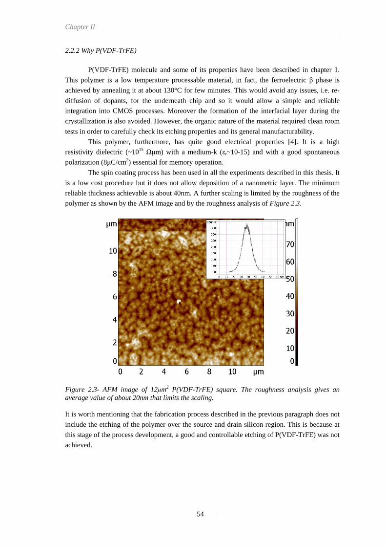
Chapter II
54
2.2.2 Why P(VDF-TrFE)
P(VDF-TrFE) molecule and some of its properties have been described in chapter 1.
This polymer is a low temperature processable material, in fact, the ferroelectric β phase is
achieved by annealing it at about 130°C for few minutes. This would avoid any issues, i.e. re-
diffusion of dopants, for the underneath chip and so it would allow a simple and reliable
integration into CMOS processes. Moreover the formation of the interfacial layer during the
crystallization is also avoided. However, the organic nature of the material required clean room
tests in order to carefully check its etching properties and its general manufacturability.
This polymer, furthermore, has quite good electrical properties [4]. It is a high
resistivity dielectric (~1015 Ωμm) with a medium-k (εr~10-15) and with a good spontaneous
polarization (8μC/cm2) essential for memory operation.
The spin coating process has been used in all the experiments described in this thesis. It
is a low cost procedure but it does not allow deposition of a nanometric layer. The minimum
reliable thickness achievable is about 40nm. A further scaling is limited by the roughness of the
polymer as shown by the AFM image and by the roughness analysis of Figure 2.3.
Figure 2.3- AFM image of 12μm2 P(VDF-TrFE) square. The roughness analysis gives an average value of about 20nm that limits the scaling. It is worth mentioning that the fabrication process described in the previous paragraph does not
include the etching of the polymer over the source and drain silicon region. This is because at
this stage of the process development, a good and controllable etching of P(VDF-TrFE) was not
achieved.

2.2 – Ferroelectric MOSFET
55
2.1.3 Characterization
The picture below shows the measurement set up for the static transistor
characterization. It highlights the fact that the probe tips have to scratch the polymer and the
SiO2 to come in contact with the silicon drain/source region.
Figure 2.4- (left) Measurement set up for DC characterization of the ferroelectric transistor; (right) Optical microscope image in which the three probes and the scratch in the polymer are visible.
The transistors with 100nm and 40nm of polymer in the gate stack are both
characterized for their DC and memory performance. The gate capacitance and polarization has
been first measured. Then the transfer characteristic and the output characteristics are
registered. The programming time, the retention and the fatigue tests are also performed. The
characterization has been done using the Agilent Parameter analyzer HP4156.
DC measurements
The gate stack of the transistor has been characterized by measuring the capacitance
and the polarization as shown in the Figure 2.5. In particular the P-E curve (Figure 2.5-left) has
been registered for two L=W= 50μm ferroelectric capacitors; one with 10nm SiO2/100nm
P(VDF-TrFE) stack and the other one without the silicon oxide layer. The different slope
between the two curves refers to the difference in the average permittivity of the two stacks.
The plot on the right is interesting because it shows the capacitance of the gate stack of a
L=W=40μm transistor with 100nm of polymer. The voltage has been applied on the gate and
the drain, source and bulk have been grounded. When the voltage is increased from 0V to 40V,
the capacitance exhibits a peak in correspondence of the coercive field of the material;
sweeping back the voltage, the capacitance stays low because the electrical dipoles keep the
alignment even if the field is decreased.
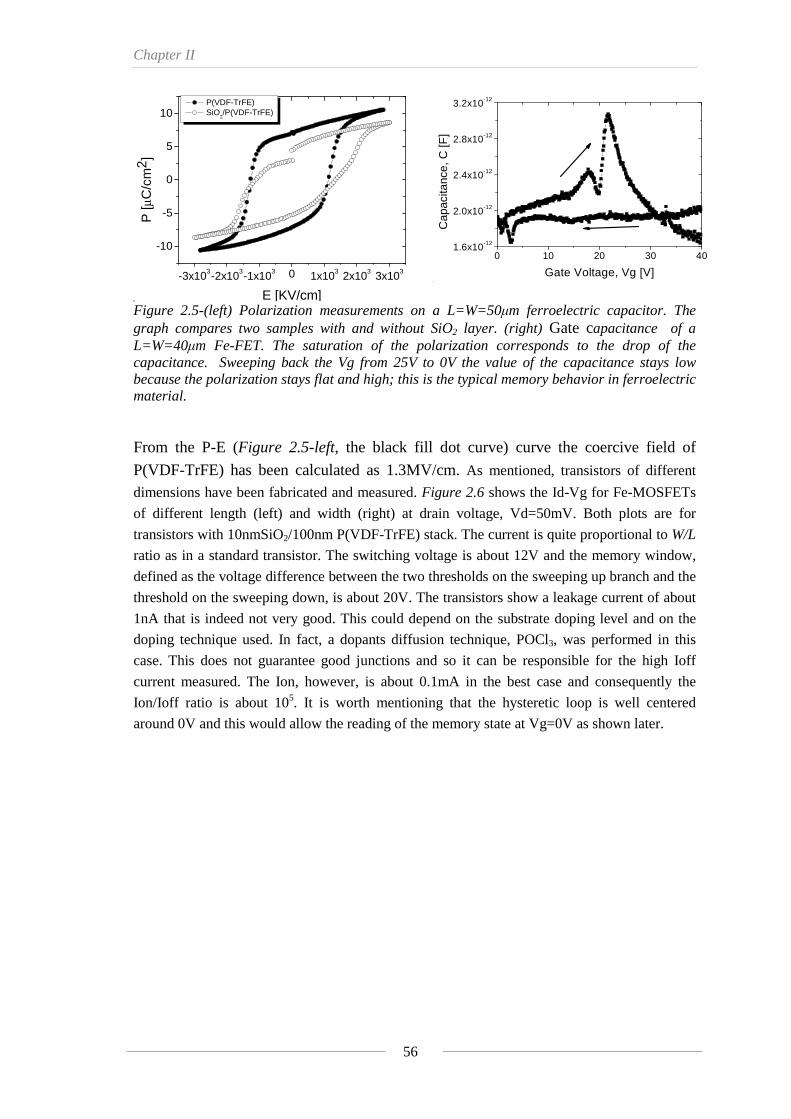
Chapter II
56
-3x10³-2 x10³-1x10³ 01x1032 x1033x103
-10
-5
0
5
10 P(V DF-TrFE) SiO 2/P(VDF-TrFE)
P [μC/c
m2 ]
E [K V/cm]
-3x10³-2x10³-1x10³ 0 1x10³ 2x10³ 3x10³
-10
-5
0
5
10 P(VDF-TrFE) SiO
2/P(VDF-TrFE)
P [μ
C/c
m2 ]
E [KV/cm] 0 10 20 30 401.6x10
-12
2.0x10⁻¹²
2.4x10⁻¹²
2.8x10⁻¹²
3.2x10⁻¹²
Capacita
nce, C [F]
Gate Voltage, Vg [V]
0 10 20 30 401.6x10⁻¹²
2.0x10⁻¹²
2.4x10⁻¹²
2.8x10⁻¹²
3.2x10⁻¹²
Cap
acita
nce,
C [F
]
Gate Voltage, Vg [V]
Figure 2.5-(left) Polarization measurements on a L=W=50μm ferroelectric capacitor. The graph compares two samples with and without SiO2 layer. (right) Gate capacitance of a L=W=40μm Fe-FET. The saturation of the polarization corresponds to the drop of the capacitance. Sweeping back the Vg from 25V to 0V the value of the capacitance stays low because the polarization stays flat and high; this is the typical memory behavior in ferroelectric material. From the P-E (Figure 2.5-left, the black fill dot curve) curve the coercive field of
P(VDF-TrFE) has been calculated as 1.3MV/cm. As mentioned, transistors of different
dimensions have been fabricated and measured. Figure 2.6 shows the Id-Vg for Fe-MOSFETs
of different length (left) and width (right) at drain voltage, Vd=50mV. Both plots are for
transistors with 10nmSiO2/100nm P(VDF-TrFE) stack. The current is quite proportional to W/L
ratio as in a standard transistor. The switching voltage is about 12V and the memory window,
defined as the voltage difference between the two thresholds on the sweeping up branch and the
threshold on the sweeping down, is about 20V. The transistors show a leakage current of about
1nA that is indeed not very good. This could depend on the substrate doping level and on the
doping technique used. In fact, a dopants diffusion technique, POCl3, was performed in this
case. This does not guarantee good junctions and so it can be responsible for the high Ioff
current measured. The Ion, however, is about 0.1mA in the best case and consequently the
Ion/Ioff ratio is about 105. It is worth mentioning that the hysteretic loop is well centered
around 0V and this would allow the reading of the memory state at Vg=0V as shown later.

2.2 – Ferroelectric MOSFET
57
-10 0 10 20
10-9
10-8
10-7
10-6
10-5
Dra
in C
urre
nt, I
d [A
]
Gate Voltage, Vg [V]
W=50µm
L=2µm L=10µm L=30µm L=50µm
MemoryWindow, Mw
-10 0 10 20
10-9
10-8
10-7
10-6
10-5
L=50µm
W=2µm W=10µm W=50µm
Dra
in C
urre
nt, I
d [A
]
Gate Voltage, Vg [V]
Figure 2.6- (left)Id-Vg hysteretic characteristics of Fe-FET with 100nm P(VDF-TrFE) and gate length, L, as parameter for W=50um; (right) transfer-characteristic for a L=50um transistor with W as parameter. The plot of Figure 2.7 summarizes the trend of the current in strong inversions regime for
different dimensions. The filled dots shows the current dependence on the length while the
empty dots the dependence on the width.
010 20 3040 50
1x10⁻⁵
2x10⁻⁵
3x10-54x10
-55x10-5
W= 50µm L= 50µm
Saturation
Drain Curren
t, Idsat [A]
L,W μ m
0 10 20 30 40 50
1x10⁻⁵
2x10⁻⁵
3x10⁻⁵
4x10⁻⁵
5x10⁻⁵
W=50µm L=50µm
Sat
urat
ion
Dra
in C
urre
nt, I
d sat [A
]
L,W μm
Figure 2.7-Idmax dependence on L and W, for all the investigated devices. The filled dots shows the current dependence on the length while the empty dots the dependence on the width. The Id-Vg and the Id-Vd of a L=W=50μm transistor have also been measured for
different values of Vd and Vg respectively. It is important noting that the memory window is
not influenced by Vd (Figure 2.8-left) and that it is quite stable and reproducible (the
measurements at different Vd are one subsequent to the other). The leakage current as well as
the Ion increases when the Vd is increased (Figure 2.8-left). The Id-Vd (Figure 2.8-right)
curves shows a linear and saturation regions as in a standard MOSFET.

Chapter II
58
-10 0 10 2010-9
10-8
10-7
10-6
10-5
10-4
Dra
in C
urre
nt, I
d[A
]
Gate Voltage, Vg [V]
Vd=50, 100, 200, 500mV
0 2 4 6 8 10
0
5x10⁻⁴
1x10⁻³
2x10⁻³Vg(V)=10
9
8
7
Dra
in-S
ourc
e C
urre
nt, I
d [A
]
Drain Voltage, Vd [V]
6
Figure 2.8- Transfer-characteristic (left) and output characteristic (right) of a L=W=50μm transistor for different Vd and Vg respectively.
An important effect, that should be taken into account when characterizing any
ferroelectric transistor, is visible in Figure 2.9. The output characteristic is measured by doing a
double sweep of the Vd voltage for value up to 15V. An hysteretic behavior is registered and
this is due to the induced gate polarization by the drain voltage; this happens even if there is no
gate-drain overlapping and because of the fringing effect and of the 3D nature of the field.
Hence it is of crucial importance, when characterizing the memory effect due exclusively to the
gate, to bias the device at low drain voltage in order to not influence the polarization.
0 2 4 6 8 10 12 140
10
20
30
40
Dra
in C
urre
nt, I
d [μ
A]
Drain Voltage, Vd[V]
Vg=3V
Figure 2.9- Id-Vd curve showing an hysteretic behavior because of the drain to gate coupling capacitance.
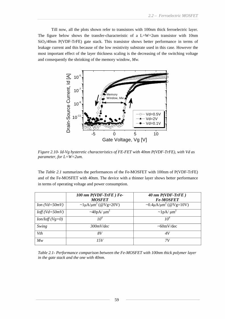
2.2 – Ferroelectric MOSFET
59
Till now, all the plots shown refer to transistors with 100nm thick ferroelectric layer.
The figure below shows the transfer-characteristic of a L=W=2um transistor with 10nm
SiO2/40nm P(VDF-TrFE) gate stack. This transistor shows better performance in terms of
leakage current and this because of the low resistivity substrate used in this case. However the
most important effect of the layer thickness scaling is the decreasing of the switching voltage
and consequently the shrinking of the memory window, Mw.
-5 0 5 10
10-11
10-9
10-7
10-5
Vd=0.5V Vd=2V Vd=0.1V
Dra
in-S
ourc
e C
urre
nt, I
d [A
]
Gate Voltage, Vg [V]
Memory Window, Mw
-5 0 5 10
10
-11
10-9
10-7
10-5
Vd= 0.5V
Vd= 2V Vd= 0.1V
Drain-S
ource Cur
rent, Id [A
]
Mem ory
Win dow, Mw Figure 2.10- Id-Vg hysteretic characteristics of FE-FET with 40nm P(VDF-TrFE), with Vd as parameter, for L=W=2um.
The Table 2.1 summarizes the performances of the Fe-MOSFET with 100nm of P(VDF-TrFE)
and of the Fe-MOSFET with 40nm. The device with a thinner layer shows better performance
in terms of operating voltage and power consumption.
100 nm P(VDF-TrFE ) Fe-
MOSFET 40 nm P(VDF-TrFE )
Fe-MOSFET Ion (Vd=50mV) ~1μA/μm2 (@Vg=20V) ~0.4μA/μm2 (@Vg=10V)
Ioff (Vd=50mV) ~40pA/ μm2 ~1pA/ μm2
Ion/Ioff (Vg=0) 104 104
Swing 300mV/dec ~60mV/dec
Vth 8V 4V
Mw 15V 7V
Table 2.1- Performance comparison between the Fe-MOSFET with 100nm thick polymer layer in the gate stack and the one with 40nm.
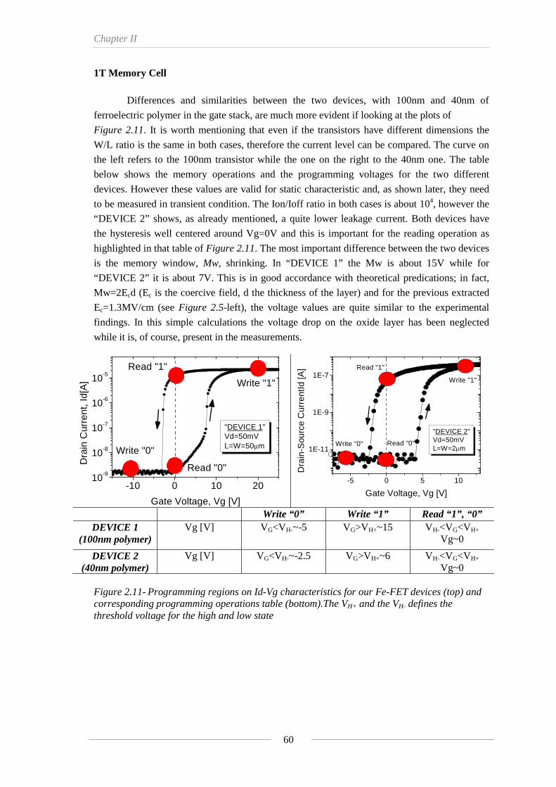
Chapter II
60
1T Memory Cell
Differences and similarities between the two devices, with 100nm and 40nm of
ferroelectric polymer in the gate stack, are much more evident if looking at the plots of
Figure 2.11. It is worth mentioning that even if the transistors have different dimensions the
W/L ratio is the same in both cases, therefore the current level can be compared. The curve on
the left refers to the 100nm transistor while the one on the right to the 40nm one. The table
below shows the memory operations and the programming voltages for the two different
devices. However these values are valid for static characteristic and, as shown later, they need
to be measured in transient condition. The Ion/Ioff ratio in both cases is about 104, however the
“DEVICE 2” shows, as already mentioned, a quite lower leakage current. Both devices have
the hysteresis well centered around Vg=0V and this is important for the reading operation as
highlighted in that table of Figure 2.11. The most important difference between the two devices
is the memory window, Mw, shrinking. In “DEVICE 1” the Mw is about 15V while for
“DEVICE 2” it is about 7V. This is in good accordance with theoretical predications; in fact,
Mw=2Ecd (Ec is the coercive field, d the thickness of the layer) and for the previous extracted
Ec=1.3MV/cm (see Figure 2.5-left), the voltage values are quite similar to the experimental
findings. In this simple calculations the voltage drop on the oxide layer has been neglected
while it is, of course, present in the measurements.
Figure 2.11- Programming regions on Id-Vg characteristics for our Fe-FET devices (top) and corresponding programming operations table (bottom).The VH+ and the VH- defines the threshold voltage for the high and low state
-10 0 10 2010-9
10-8
10-7
10-6
10-5
Dra
in C
urre
nt, I
d[A
]
Gate Voltage, Vg [V]
Read "0"
Write "1"
Read "1"
Write "0"
"DEVICE 1"Vd=50mVL=W=50μm
-5 0 5 10
1E-11
1E-9
1E-7
"DEVICE 2"Vd=50mVL=W=2μm
Read "1"
Read "0"
Write "1"
Dra
in-S
ourc
e C
urre
ntId
[A]
Gate Voltage, Vg [V]
Write "0"
Write “0” Write “1” Read “1”, “0” DEVICE 1
(100nm polymer) Vg [V] VG<VH-~-5 VG>VH+~15 VH-<VG<VH+
Vg~0
DEVICE 2 (40nm polymer)
Vg [V] VG<VH-~-2.5 VG>VH+~6 VH-<VG<VH+ Vg~0

2.2 – Ferroelectric MOSFET
61
A unique behavior of a ferroelectric transistor is shown in Figure 2.12. Various
hysteresis cycles are measured by sweeping up and down the gate voltage and changing the
maximum applied voltage (6,8,10,15V); a memory window of about 1V is obtained for
Vgmax=6V. It is interesting to note that different states can be programmed as function of the
programming voltages thanks to the invariability of the threshold voltage. The inset of
Figure 2.12 shows the different current levels for a fixed reading voltage as function of
different programming voltages.
-2 0 2 4 6 8 10
10-12
10-11
10-10
10-9
10-8
10-7
6 8 10 12 14 16
1E-9
1E-8
1E-7
Id [A
]
Vg sweep limit [V]
6V8V
10V
Dra
in-S
ourc
e C
urre
nt, I
d [A
]
Gate Voltage, Vg [V]
15V
ΔIreading
VG sweep limit
ΔIreading [A] ΔVG [V] 4.73x 10⁻⁸ 6-8 6.77x10⁻⁸ 8-10 1.1x10⁻⁷ 10-15
Figure 2.12- Multiple Id-Vg hysteretic curves obtained by sweeping Vg up to 6V, 8V, 10V and 15V and then down to –2.5V, for a device with 40nm thin PVDF-TrFE gate dielectric and L=W=10μm.. Inset: different levels of current for a reading voltage of 2.5V as function of the programming voltage. The table shows the difference in current between two different possible programming states. The ferroelectric transistor could be used for a multi-bits memory cell thanks also to the
stability and reproducibility of the hysteretic loop. However a careful calibration of the device
is necessary, in fact, as visible in the inset of Figure 2.12, the ΔI reading gradually reduces
when increasing the voltage Vgmax.
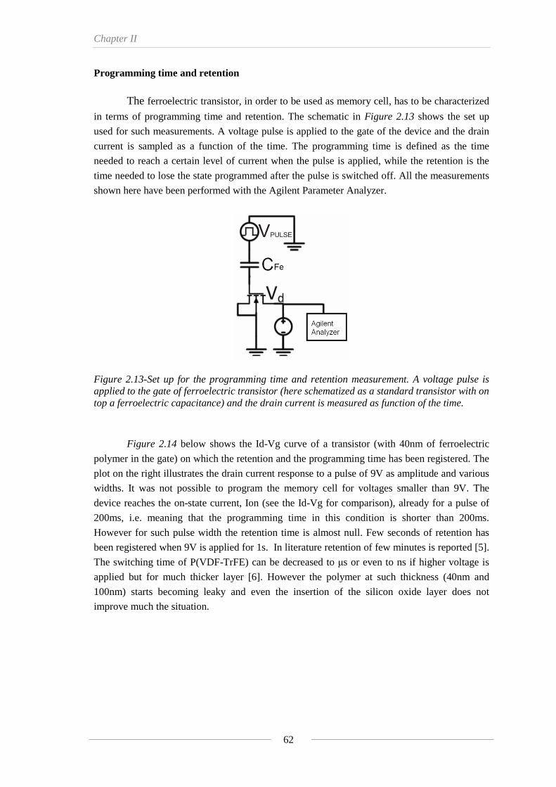
Chapter II
62
Programming time and retention
The ferroelectric transistor, in order to be used as memory cell, has to be characterized
in terms of programming time and retention. The schematic in Figure 2.13 shows the set up
used for such measurements. A voltage pulse is applied to the gate of the device and the drain
current is sampled as a function of the time. The programming time is defined as the time
needed to reach a certain level of current when the pulse is applied, while the retention is the
time needed to lose the state programmed after the pulse is switched off. All the measurements
shown here have been performed with the Agilent Parameter Analyzer.
Figure 2.13-Set up for the programming time and retention measurement. A voltage pulse is applied to the gate of ferroelectric transistor (here schematized as a standard transistor with on top a ferroelectric capacitance) and the drain current is measured as function of the time. Figure 2.14 below shows the Id-Vg curve of a transistor (with 40nm of ferroelectric
polymer in the gate) on which the retention and the programming time has been registered. The
plot on the right illustrates the drain current response to a pulse of 9V as amplitude and various
widths. It was not possible to program the memory cell for voltages smaller than 9V. The
device reaches the on-state current, Ion (see the Id-Vg for comparison), already for a pulse of
200ms, i.e. meaning that the programming time in this condition is shorter than 200ms.
However for such pulse width the retention time is almost null. Few seconds of retention has
been registered when 9V is applied for 1s. In literature retention of few minutes is reported [5].
The switching time of P(VDF-TrFE) can be decreased to μs or even to ns if higher voltage is
applied but for much thicker layer [6]. However the polymer at such thickness (40nm and
100nm) starts becoming leaky and even the insertion of the silicon oxide layer does not
improve much the situation.
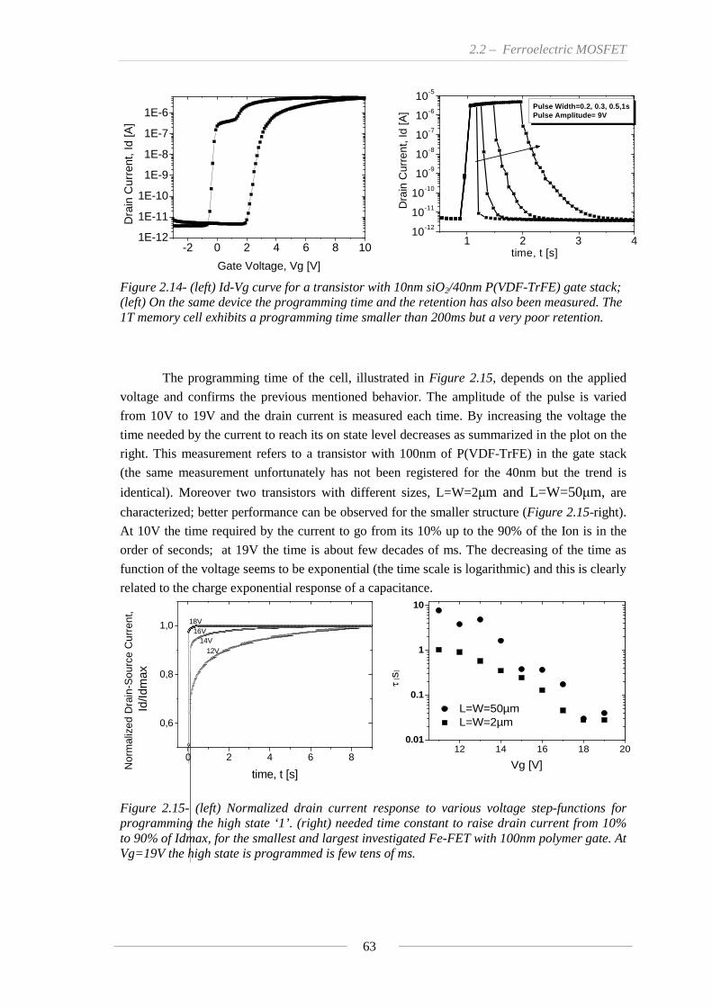
2.2 – Ferroelectric MOSFET
63
-2 0 2 4 6 8 101E-12
1E-11
1E-10
1E-9
1E-8
1E-7
1E-6
Dra
in C
urre
nt, I
d [A
]
Gate Voltage, Vg [V]
1 2 3 410-12
10-11
10-10
10-9
10-8
10-7
10-6
10-5
Pulse Width=0.2, 0.3, 0.5,1sPulse Amplitude= 9V
Dra
in C
urre
nt, I
d [A
]
time, t [s]
Figure 2.14- (left) Id-Vg curve for a transistor with 10nm siO2/40nm P(VDF-TrFE) gate stack; (left) On the same device the programming time and the retention has also been measured. The 1T memory cell exhibits a programming time smaller than 200ms but a very poor retention. The programming time of the cell, illustrated in Figure 2.15, depends on the applied
voltage and confirms the previous mentioned behavior. The amplitude of the pulse is varied
from 10V to 19V and the drain current is measured each time. By increasing the voltage the
time needed by the current to reach its on state level decreases as summarized in the plot on the
right. This measurement refers to a transistor with 100nm of P(VDF-TrFE) in the gate stack
(the same measurement unfortunately has not been registered for the 40nm but the trend is
identical). Moreover two transistors with different sizes, L=W=2μm and L=W=50μm, are
characterized; better performance can be observed for the smaller structure (Figure 2.15-right).
At 10V the time required by the current to go from its 10% up to the 90% of the Ion is in the
order of seconds; at 19V the time is about few decades of ms. The decreasing of the time as
function of the voltage seems to be exponential (the time scale is logarithmic) and this is clearly
related to the charge exponential response of a capacitance.
0 2 4 6 8
0,6
0,8
1,0 18V16V
12V14V
Nor
mal
ized
Dra
in-S
ourc
e C
urre
nt,
Id/Id
max
time, t [s]
12 14 16 18 200.01
0.1
1
10
L=W=50µm L=W=2µm
τ [s
]
Vg [V]
Figure 2.15- (left) Normalized drain current response to various voltage step-functions for programming the high state ‘1’. (right) needed time constant to raise drain current from 10% to 90% of Idmax, for the smallest and largest investigated Fe-FET with 100nm polymer gate. At Vg=19V the high state is programmed is few tens of ms.
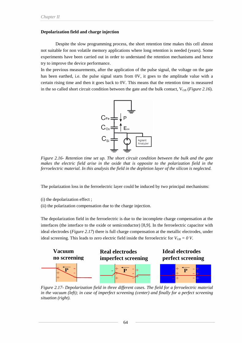
Chapter II
64
Depolarization field and charge injection
Despite the slow programming process, the short retention time makes this cell almost
not suitable for non volatile memory applications where long retention is needed (years). Some
experiments have been carried out in order to understand the retention mechanisms and hence
try to improve the device performance.
In the previous measurements, after the application of the pulse signal, the voltage on the gate
has been earthed, i.e. the pulse signal starts from 0V, it goes to the amplitude value with a
certain rising time and then it goes back to 0V. This means that the retention time is measured
in the so called short circuit condition between the gate and the bulk contact, VGB (Figure 2.16).
Figure 2.16- Retention time set up. The short circuit condition between the bulk and the gate makes the electric field arise in the oxide that is opposite to the polarization field in the ferroelectric material. In this analysis the field in the depletion layer of the silicon is neglected.
The polarization loss in the ferroelectric layer could be induced by two principal mechanisms:
(i) the depolarization effect ;
(ii) the polarization compensation due to the charge injection.
The depolarization field in the ferroelectric is due to the incomplete charge compensation at the
interfaces (the interface to the oxide or semiconductor) [8,9]. In the ferroelectric capacitor with
ideal electrodes (Figure 2.17) there is full charge compensation at the metallic electrodes, under
ideal screening. This leads to zero electric field inside the ferroelectric for VGB = 0 V.
Figure 2.17- Depolarization field in three different cases. The field for a ferroelectric material in the vacuum (left); in case of imperfect screening (center) and finally for a perfect screening situation (right).
Vacuum no screening
Real electrodes imperfect screening
Ideal electrodes perfect screening
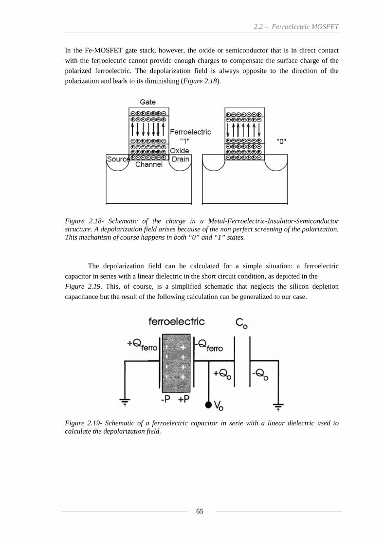
2.2 – Ferroelectric MOSFET
65
In the Fe-MOSFET gate stack, however, the oxide or semiconductor that is in direct contact
with the ferroelectric cannot provide enough charges to compensate the surface charge of the
polarized ferroelectric. The depolarization field is always opposite to the direction of the
polarization and leads to its diminishing (Figure 2.18).
Figure 2.18- Schematic of the charge in a Metal-Ferroelectric-Insulator-Semiconductor structure. A depolarization field arises because of the non perfect screening of the polarization. This mechanism of course happens in both “0” and “1” states.
The depolarization field can be calculated for a simple situation: a ferroelectric
capacitor in series with a linear dielectric in the short circuit condition, as depicted in the
Figure 2.19. This, of course, is a simplified schematic that neglects the silicon depletion
capacitance but the result of the following calculation can be generalized to our case.
Figure 2.19- Schematic of a ferroelectric capacitor in serie with a linear dielectric used to calculate the depolarization field.

Chapter II
66
From Figure 2.19 it follows:
0
00 C
Q
C
PAQVV
Ferro
Ferroferro +
−=+ (2.2)
where A is the area of the parallel plate capacitor and it is the same for the ferroelectric and the
dielectric. Considering that the charge Q 0 is equal to QFerro, it comes out as:
PACC
CQ
Ferro+=
0
00 (2.3)
Hence in order to have a perfect screening (Q0=PA), C0 should be infinite.
In a Fe-MOSFET structure (see Figure 2.18) the depolarization field can be decreased
by decreasing the ratio CFerro/COx and by increasing the silicon doping [9]. This can also be
achieved by changing the ratio between the area of the ferroelectric capacitor and the area of
the dielectric one, i.e. making AOx>AFerro [8]. This is more difficult from the technology point of
view because two masks are required for the areas definition. It is well recommended to use a
high-k dielectric and high doping substrate in order to improve as much as possible the
retention time.
As said, the other effect of the short circuit condition is charge injection into the gate
stack because of the high field in the oxide. This charge screens the polarization consequently
reducing the retention.
In this work an optimized structure has not been fabricated however the open circuit
retention has been measured for both transistors (with 40nm and with 100nm of polymer). This
measurement does not allow any distinction between the scenarios (i) and (ii) but it is
fundamental to compare the results with the short circuit case.
After poling the gate with a voltage pulse, the probe has been mechanically lifted up
from the gate contact and the drain current has been registered. The results found, illustrated in
Figure 2.20 (left plot for the 100nm polymer transistor and right one for the 40nm P(VDF-
TrFE) device), are quite different from the one in short circuit condition (Figure 2.14).
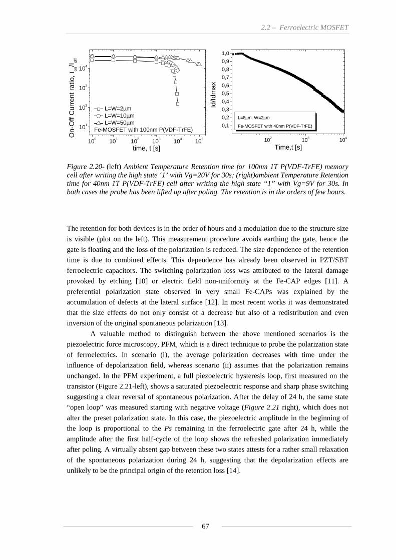
2.2 – Ferroelectric MOSFET
67
100 101 102 103 104 105
101
102
103
104
On-
Off
Cur
rent
rat
io, Ι
on/I of
f
time, t [s]
L=W=2µm L=W=10µm L=W=50µm
Fe-MOSFET with 100nm P(VDF-TrFE)
102 103 104
0,1
0,2
0,3
0,4
0,5
0,6
0,7
0,8
0,9
1,0
Id/Id
max
Time,t [s]
L=8μm, W=2μm
Fe-MOSFET with 40nm P(VDF-TrFE)
102 103 104
0,10,20,3
0,40,5
0,60,7
0,80,9
1,0
Id/Idmax
Tim e,t [s]
L=8μm , W=2μm
Fe-MO SFET with 40nm P(VDF-TrFE) Figure 2.20- (left) Ambient Temperature Retention time for 100nm 1T P(VDF-TrFE) memory cell after writing the high state ‘1’ with Vg=20V for 30s; (right)ambient Temperature Retention time for 40nm 1T P(VDF-TrFE) cell after writing the high state “1” with Vg=9V for 30s. In both cases the probe has been lifted up after poling. The retention is in the orders of few hours.
The retention for both devices is in the order of hours and a modulation due to the structure size
is visible (plot on the left). This measurement procedure avoids earthing the gate, hence the
gate is floating and the loss of the polarization is reduced. The size dependence of the retention
time is due to combined effects. This dependence has already been observed in PZT/SBT
ferroelectric capacitors. The switching polarization loss was attributed to the lateral damage
provoked by etching [10] or electric field non-uniformity at the Fe-CAP edges [11]. A
preferential polarization state observed in very small Fe-CAPs was explained by the
accumulation of defects at the lateral surface [12]. In most recent works it was demonstrated
that the size effects do not only consist of a decrease but also of a redistribution and even
inversion of the original spontaneous polarization [13].
A valuable method to distinguish between the above mentioned scenarios is the
piezoelectric force microscopy, PFM, which is a direct technique to probe the polarization state
of ferroelectrics. In scenario (i), the average polarization decreases with time under the
influence of depolarization field, whereas scenario (ii) assumes that the polarization remains
unchanged. In the PFM experiment, a full piezoelectric hysteresis loop, first measured on the
transistor (Figure 2.21-left), shows a saturated piezoelectric response and sharp phase switching
suggesting a clear reversal of spontaneous polarization. After the delay of 24 h, the same state
“open loop” was measured starting with negative voltage (Figure 2.21 right), which does not
alter the preset polarization state. In this case, the piezoelectric amplitude in the beginning of
the loop is proportional to the Ps remaining in the ferroelectric gate after 24 h, while the
amplitude after the first half-cycle of the loop shows the refreshed polarization immediately
after poling. A virtually absent gap between these two states attests for a rather small relaxation
of the spontaneous polarization during 24 h, suggesting that the depolarization effects are
unlikely to be the principal origin of the retention loss [14].
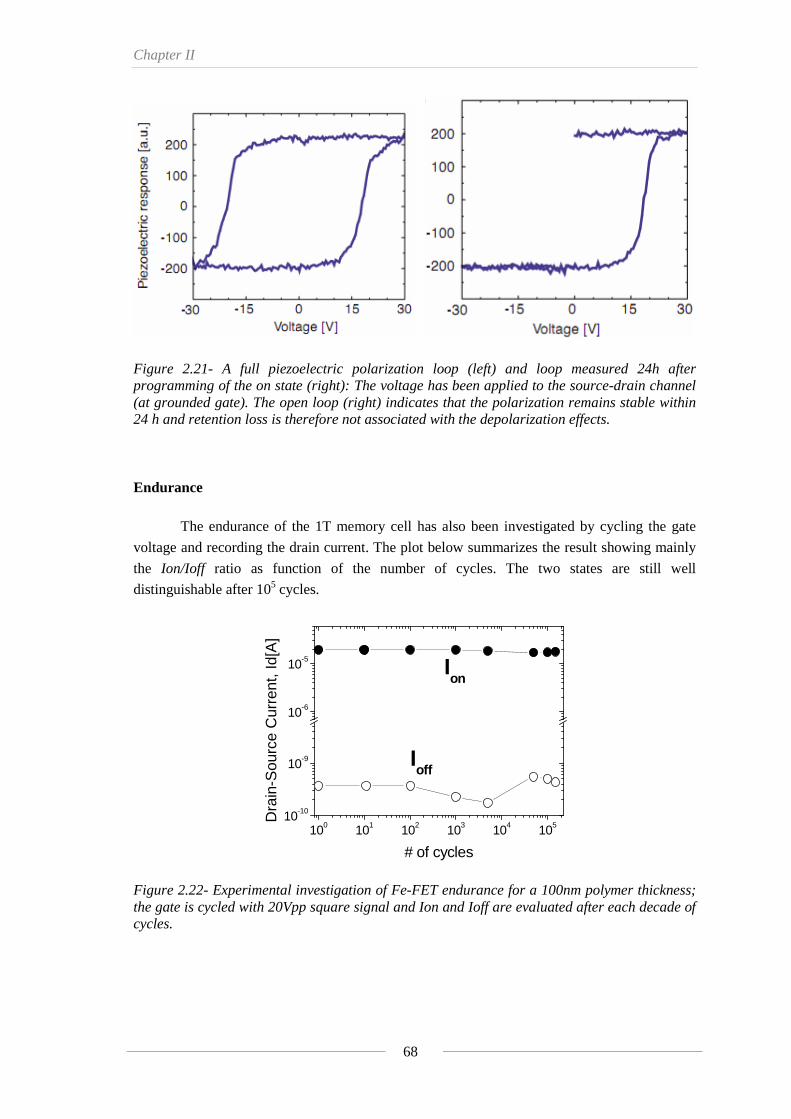
Chapter II
68
Figure 2.21- A full piezoelectric polarization loop (left) and loop measured 24h after programming of the on state (right): The voltage has been applied to the source-drain channel (at grounded gate). The open loop (right) indicates that the polarization remains stable within 24 h and retention loss is therefore not associated with the depolarization effects.
Endurance
The endurance of the 1T memory cell has also been investigated by cycling the gate
voltage and recording the drain current. The plot below summarizes the result showing mainly
the Ion/Ioff ratio as function of the number of cycles. The two states are still well
distinguishable after 105 cycles.
100 101 102 103 104 10510-10
10-9
10-6
10-5 Ion
Dra
in-S
ourc
e C
urre
nt, I
d[A
]
# of cycles
Ioff
Figure 2.22- Experimental investigation of Fe-FET endurance for a 100nm polymer thickness; the gate is cycled with 20Vpp square signal and Ion and Ioff are evaluated after each decade of cycles.
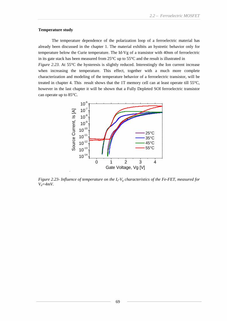
2.2 – Ferroelectric MOSFET
69
Temperature study The temperature dependence of the polarization loop of a ferroelectric material has
already been discussed in the chapter 1. The material exhibits an hystretic behavior only for
temperature below the Curie temperature. The Id-Vg of a transistor with 40nm of ferroelectric
in its gate stack has been measured from 25°C up to 55°C and the result is illustrated in
Figure 2.23. At 55°C the hysteresis is slightly reduced. Interestingly the Ion current increase
when increasing the temperature. This effect, together with a much more complete
characterization and modeling of the temperature behavior of a ferroelectric transistor, will be
treated in chapter 4. This result shows that the 1T memory cell can at least operate till 55°C,
however in the last chapter it will be shown that a Fully Depleted SOI ferroelectric transistor
can operate up to 85°C.
0 1 2 3 410
-1410-13
10-1210
-1110-10
10-910
-810-7
10-6
25°C
35°C 45°C
55°C
Source
Current, I
s [A]
0 1 2 3 410-14
10-13
10-12
10-11
10-10
10-9
10-8
10-7
10-6
25°C 35°C 45°C 55°C
Sou
rce
Cur
rent
, Is
[A]
Gate Voltage, Vg [V]
Figure 2.23- Influence of temperature on the Is-Vg characteristics of the Fe-FET, measured for Vd=4mV.
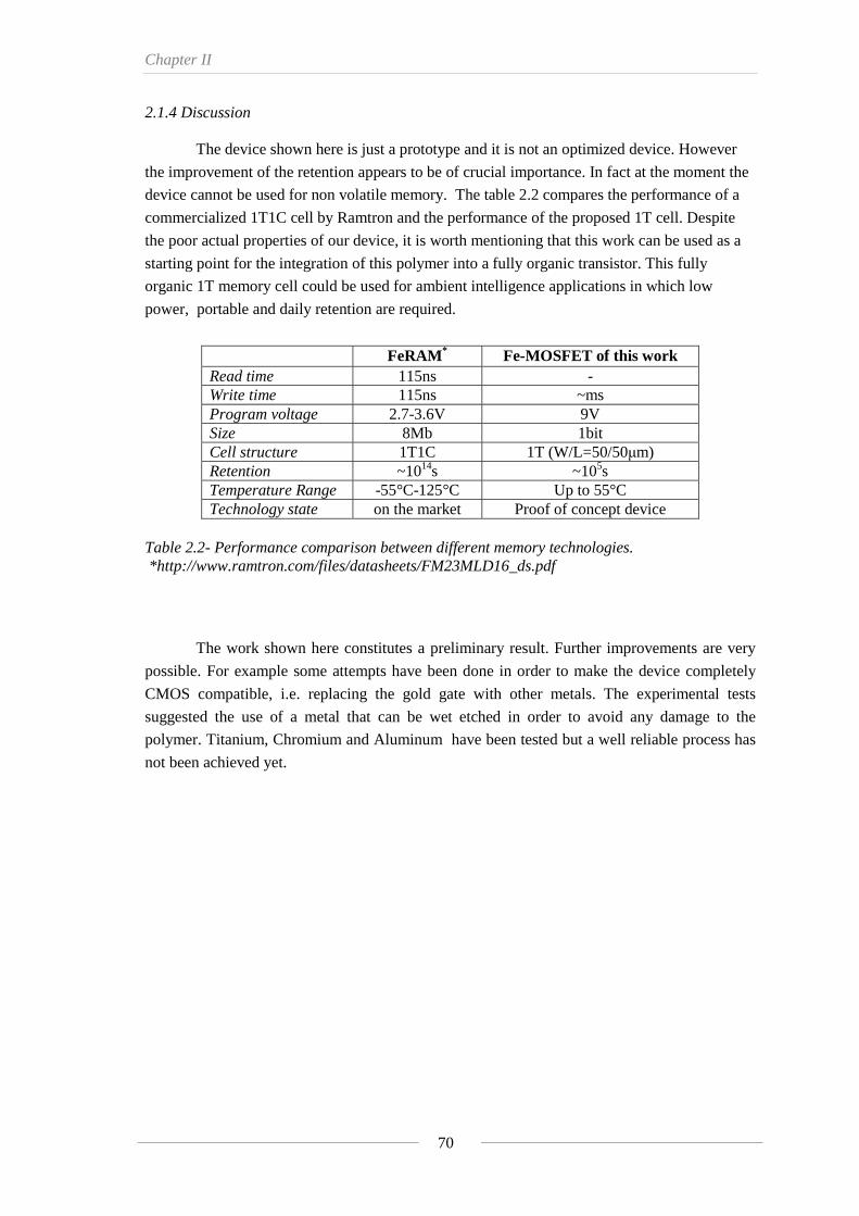
Chapter II
70
2.1.4 Discussion The device shown here is just a prototype and it is not an optimized device. However
the improvement of the retention appears to be of crucial importance. In fact at the moment the
device cannot be used for non volatile memory. The table 2.2 compares the performance of a
commercialized 1T1C cell by Ramtron and the performance of the proposed 1T cell. Despite
the poor actual properties of our device, it is worth mentioning that this work can be used as a
starting point for the integration of this polymer into a fully organic transistor. This fully
organic 1T memory cell could be used for ambient intelligence applications in which low
power, portable and daily retention are required.
FeRAM* Fe-MOSFET of this work Read time 115ns - Write time 115ns ~ms Program voltage 2.7-3.6V 9V Size 8Mb 1bit Cell structure 1T1C 1T (W/L=50/50μm) Retention ~1014s ~105s Temperature Range -55°C-125°C Up to 55°C Technology state on the market Proof of concept device
Table 2.2- Performance comparison between different memory technologies. *http://www.ramtron.com/files/datasheets/FM23MLD16_ds.pdf
The work shown here constitutes a preliminary result. Further improvements are very
possible. For example some attempts have been done in order to make the device completely
CMOS compatible, i.e. replacing the gold gate with other metals. The experimental tests
suggested the use of a metal that can be wet etched in order to avoid any damage to the
polymer. Titanium, Chromium and Aluminum have been tested but a well reliable process has
not been achieved yet.
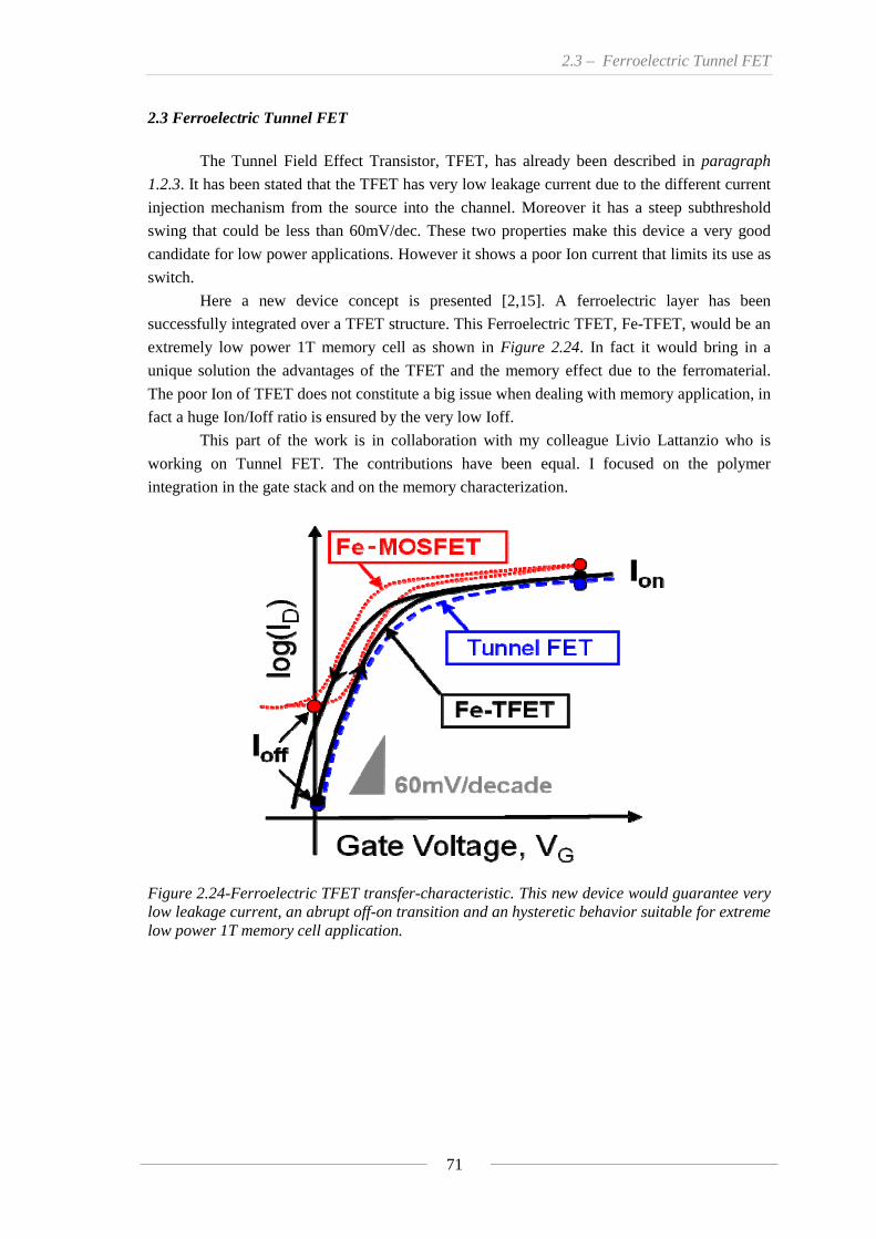
2.3 – Ferroelectric Tunnel FET
71
2.3 Ferroelectric Tunnel FET
The Tunnel Field Effect Transistor, TFET, has already been described in paragraph
1.2.3. It has been stated that the TFET has very low leakage current due to the different current
injection mechanism from the source into the channel. Moreover it has a steep subthreshold
swing that could be less than 60mV/dec. These two properties make this device a very good
candidate for low power applications. However it shows a poor Ion current that limits its use as
switch.
Here a new device concept is presented [2,15]. A ferroelectric layer has been
successfully integrated over a TFET structure. This Ferroelectric TFET, Fe-TFET, would be an
extremely low power 1T memory cell as shown in Figure 2.24. In fact it would bring in a
unique solution the advantages of the TFET and the memory effect due to the ferromaterial.
The poor Ion of TFET does not constitute a big issue when dealing with memory application, in
fact a huge Ion/Ioff ratio is ensured by the very low Ioff.
This part of the work is in collaboration with my colleague Livio Lattanzio who is
working on Tunnel FET. The contributions have been equal. I focused on the polymer
integration in the gate stack and on the memory characterization.
Figure 2.24-Ferroelectric TFET transfer-characteristic. This new device would guarantee very low leakage current, an abrupt off-on transition and an hysteretic behavior suitable for extreme low power 1T memory cell application.

Chapter II
72
2.3.1 Fabrication
Here is reported the fabrication of a Fe-TFET, implementing a tri-layer gate dielectric
stack formed by silicon dioxide, high-k and a thin ferroelectric polymer. The goal of this work
is not to realize a high performance logic device, but an EOT (Equivalent Oxide Thickness) of
about 14 nm has been used, which provides a small gate leakage current and the needed
hysteretic gate stack properties to demonstrate the basic functionality of a one-transistor Fe-
TFET memory cell. A summary of the process flow used for a p-type (p-i-n) Fe-TFET is given
in Figure 2.25. The starting SOI substrates are UNIBOND wafers with a 65 nm p-type Si (1-10
Ωcm) top layer and 150 nm buried oxide (BOX). The gate dielectric stack is formed by a 2 nm
thermal oxide, a 5 nm high-k Al2O3 layer deposited with atomic layer deposition (ALD), and 30
nm of P(VDF-TrFE) 70%-30%, annealed at 135°C for 10 minutes. Such ultra-thin polymer
films obtained by spinning can show some discontinuities, as it can be seen in the TEM
micrograph in Figure 2.26 (image on the right). By considering the dark areas of the AFM
picture (Figure 2.26-left), where the polymer appears to be discontinuous, we deduce a number
of 3 discontinuities/μm2. As a consequence, transistors with W=L=20μm can have such
ferroelectric discontinuities on the channel and/or tunneling regions, leading to large variations
of the resulting EOT from device to device. The implanted species to create the p-i-n junction
are BF2 (energy 35 keV, dose 5×1014 cm-2) and As (energy 20 keV, dose 1×1016 cm-2). The
activation is achieved by flash annealing [16]: three subsequent 20 ms pulses at 1050°C activate
the implanted species, resulting in an abruptness of 4nm/decade of the tunneling junction (from
Sentaurus-process simulation). On the same wafer some ferroelectric MOSFET has also been
fabricated as reference. They have of course the same gate stack and the same dimensions as
the corresponding Fe-TFET.
Figure 2.25- Process flow for the fabrication of the Fe-TFET based on Silicon-On-Insulator substrate: (I) MESA isolation (by silicon etching), (II) thermal oxidation followed by atomic layer deposition (ALD) of Al2O3 to form the device gate stack, (III) BF2 doping, and, (IV) As ion implantation for source and drain, (V) flash annealing to provide activation in an abrupt junction, (VI) oxide etch of S/D pads, (VII) P(VDF-TrFE) polymer spinning, (VIII) Au evaporation and patterning.
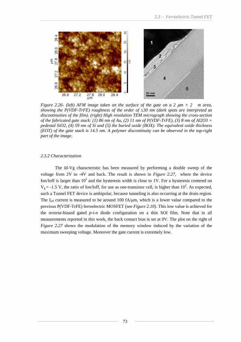
2.3 – Ferroelectric Tunnel FET
73
Figure 2.26- (left) AFM image taken on the surface of the gate on a 2 μm × 2 m area, showing the P(VDF-TrFE) roughness of the order of ±30 nm (dark spots are interpreted as discontinuities of the film). (right) High resolution TEM micrograph showing the cross-section of the fabricated gate stack: (1) 86 nm of Au, (2) 11 nm of P(VDF-TrFE), (3) 8 nm of Al2O3 + pedestal SiO2, (4) 59 nm of Si and (5) the buried oxide (BOX). The equivalent oxide thickness (EOT) of the gate stack is 14.5 nm. A polymer discontinuity can be observed in the top-right part of the image.
2.3.2 Characterization
The Id-Vg characteristic has been measured by performing a double sweep of the
voltage from 2V to -4V and back. The result is shown in Figure 2.27, where the device
Ion/Ioff is larger than 105 and the hysteresis width is close to 1V. For a hysteresis centered on
Vg = -1.5 V, the ratio of Ion/Ioff, for use as one-transistor cell, is higher than 102. As expected,
such a Tunnel FET device is ambipolar, because tunneling is also occurring at the drain region.
The Ioff current is measured to be around 100 fA/μm, which is a lower value compared to the
previous P(VDF-TrFE) ferroelectric MOSFET (see Figure 2.10). This low value is achieved for
the reverse-biased gated p-i-n diode configuration on a thin SOI film. Note that in all
measurements reported in this work, the back contact bias is set at 0V. The plot on the right of
Figure 2.27 shows the modulation of the memory window induced by the variation of the
maximum sweeping voltage. Moreover the gate current is extremely low.

Chapter II
74
-4 -3 -2 -1 0 1 210-9
10-8
10-7
10-6
10-5
10-4
10-3
10-2
10-1
Experiment Simulation
Vd = -1VDra
in C
urre
nt, I
d [μ
A/μ
m]
Gate Voltage, Vg [V]
(a)
-4 -3 -2 -1 0 1 2
10-9
10-8
10-7
10-6
10-5
10-4
10-3
10-2
10-1
Vd = -2V
Dra
in C
urre
nt, I
d [μ
A/μ
m]
Gate Voltage, Vg [V]
Vg up to -4V Vg up to -3V Vg up to -2V
(b)
Gat
e C
urre
nt, I
g [μ
A/μ
m]
Figure 2.27-(left) Id-Vg experimental data and simulations; (right) Id-Vg measured for different Vgmax of the voltage sweep. The hysteresis is modulated by Vgmax as visible also in Figure 2.11 for a Fe-MOSFET. Advanced TCAD simulations have been performed to verify the behavior of the device. The
simulator used is Sentaurus TCAD A2009.06. The ferroelectric material parameters have been
carefully extracted from Figure 2.5 (coercive field and remanent polarization). The model used
for band-to-band tunneling in the numerical simulations is the Schenk model [17] that takes into
account the phonon-assisted band-to-band tunneling. Moreover, due to the high electric fields
occurring at the tunneling junction, we have activated the Schenk trap-assisted tunneling model
[17] to define the lifetimes of the carriers in the Shockley-Read-Hall (SRH) recombination. For
both these Schenk models we have enabled the local density correction [18, 19] for a more
correct computation of the electron concentration. Simulations show that off current in the flat
region of the transfer characteristics (around Vg = 0V) is mainly determined by SRH
recombination and the values of the generation lifetime of the carriers. In agreement with data
reported in literature [20], we have used the following lifetimes values for electron and holes,
τmax,n=10-8s and τmax,p=3x10⁻⁹s, respectively, corresponding to the silicon film of a UNIBOND
wafer.
The output characteristic of the device is measured and compared to the one of a
Fe-MOSFET with the same dimensions (Figure 2.28). This comparison clearly shows the
difference between the two structure and in particular between the two conduction mechanisms.
In fact the Id-Vd of the Fe-TFET is characterized by three main regions: at low Vd an
exponential dependence of the current is visible, followed by the linear region and finally by
the saturation. Moreover a threshold voltage, VTD, is highlighted in the plot and this can be
considered as the signature of the TFET operational mode as already reported in literature [21].
The Fe-MOSFET instead shows just the linear and the saturation regime without any threshold
voltage. It’s worth mentioning that the saturation current for the Fe-TFET is 3 order of
magnitude smaller than for the same Fe-MOSFET.
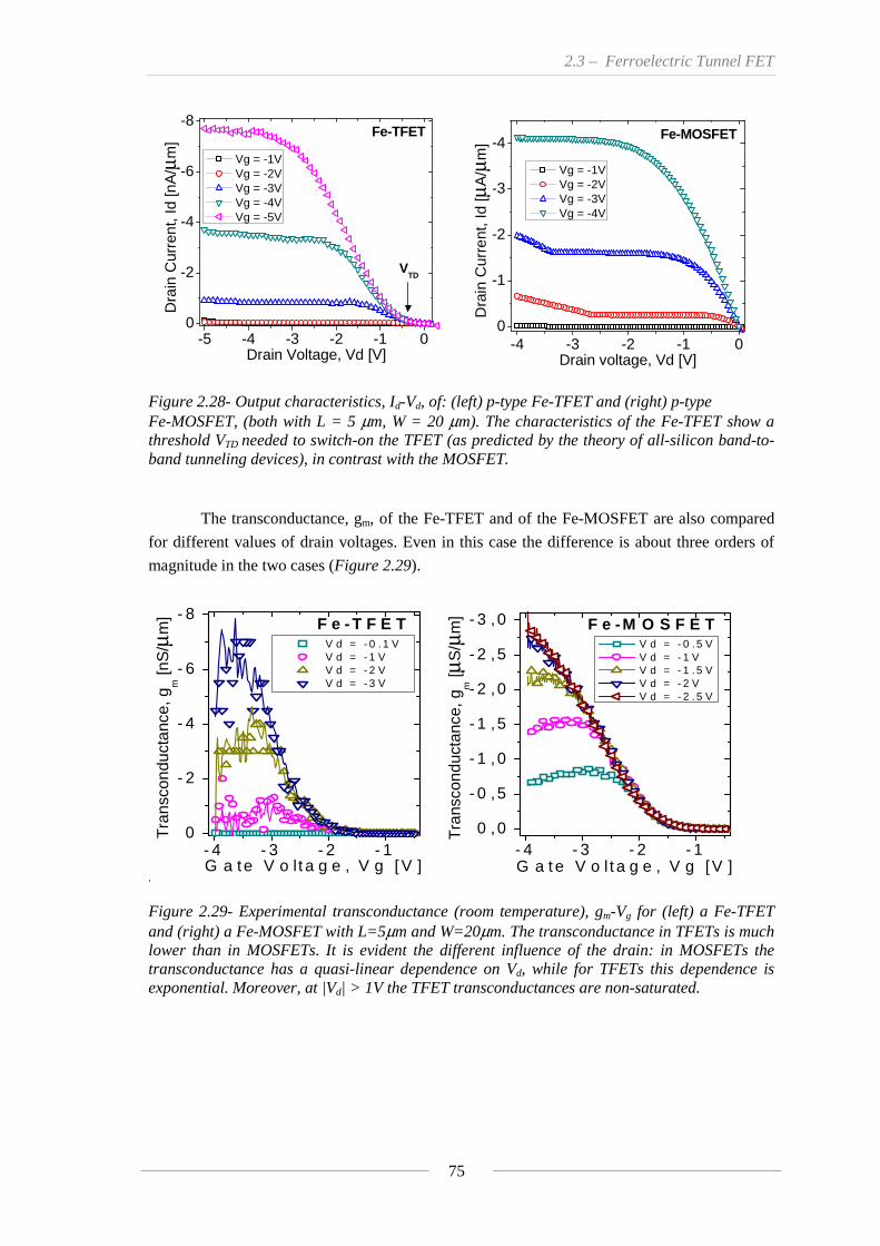
2.3 – Ferroelectric Tunnel FET
75
-5 -4 -3 -2 -1 00
-2
-4
-6
-8Fe-TFET
Dra
in C
urre
nt, I
d [n
A/μ
m]
Drain Voltage, Vd [V]
Vg = -1V Vg = -2V Vg = -3V Vg = -4V Vg = -5V
VTD
-4 -3 -2 -1 00
-1
-2
-3
-4
Dra
in C
urre
nt, I
d [μ
A/μ
m]
Drain voltage, Vd [V]
Vg = -1V Vg = -2V Vg = -3V Vg = -4V
Fe-MOSFET
Figure 2.28- Output characteristics, Id-Vd, of: (left) p-type Fe-TFET and (right) p-type Fe-MOSFET, (both with L = 5 μm, W = 20 μm). The characteristics of the Fe-TFET show a threshold VTD
needed to switch-on the TFET (as predicted by the theory of all-silicon band-to-band tunneling devices), in contrast with the MOSFET. The transconductance, gm, of the Fe-TFET and of the Fe-MOSFET are also compared
for different values of drain voltages. Even in this case the difference is about three orders of
magnitude in the two cases (Figure 2.29).
-4-3 -2-10
-2
-4
-6
-8
-4 -3-20,0
-0,5
-1,0
-1,5
-2,0
-2,5
-3,0 Fe-MOS FET
Transco
nductanc
e, gm [μS/
μm] Vd = -0.5V
Vd = -1V Vd = -1.5V
Vd = -2V Vd = -2.5V
Vd = -0.1V
Vd = -1V Vd = -2V
Vd = -3V
Transc
onductanc
e, gm [nS/
μm] Fe-TFET
- 4 - 3 - 2 - 10
- 2
- 4
- 6
- 8
- 4 - 3 - 2 - 10 ,0
- 0 ,5
- 1 ,0
- 1 ,5
- 2 ,0
- 2 ,5
- 3 ,0 F e - M O S F E T
Tra
nsco
nduc
tanc
e, g
m [μ
S/μ
m]
G a t e V o l t a g e , V g [V ]
V d = - 0 . 5 V V d = - 1 V V d = - 1 . 5 V V d = - 2 V V d = - 2 . 5 V
V d = - 0 . 1 V V d = - 1 V V d = - 2 V V d = - 3 V
Tra
nsco
nduc
tanc
e, g
m [n
S/μ
m]
G a te V o lt a g e , V g [ V ]
F e - T F E T
Figure 2.29- Experimental transconductance (room temperature), gm-Vg for (left) a Fe-TFET and (right) a Fe-MOSFET with L=5μm and W=20μm. The transconductance in TFETs is much lower than in MOSFETs. It is evident the different influence of the drain: in MOSFETs the transconductance has a quasi-linear dependence on Vd, while for TFETs this dependence is exponential. Moreover, at |Vd| > 1V the TFET transconductances are non-saturated.
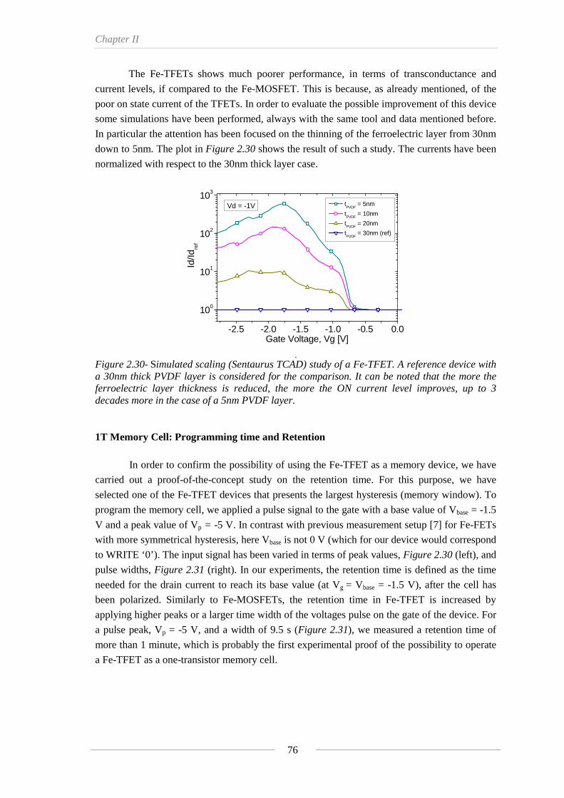
Chapter II
76
The Fe-TFETs shows much poorer performance, in terms of transconductance and
current levels, if compared to the Fe-MOSFET. This is because, as already mentioned, of the
poor on state current of the TFETs. In order to evaluate the possible improvement of this device
some simulations have been performed, always with the same tool and data mentioned before.
In particular the attention has been focused on the thinning of the ferroelectric layer from 30nm
down to 5nm. The plot in Figure 2.30 shows the result of such a study. The currents have been
normalized with respect to the 30nm thick layer case.
-2.5 -2.0 -1.5 -1.0 -0.5 0.0
100
101
102
103
tPVDF
= 5nm
tPVDF
= 10nm
tPVDF
= 20nm
tPVDF
= 30nm (ref)
Vd = -1V
Id/Id
ref
Gate Voltage, Vg [V] -2.5 -2.0- 1.5-1.0 -0.5 0.0
100
10
1
10
2
10 tPVDF = 5nm
tPVDF = 10nm tPVDF = 20nm
tPVDF = 30nm (ref )
Vd = -1 V
Id/Idref
Gate Vo ltage, Vg [V ] Figure 2.30- Simulated scaling (Sentaurus TCAD) study of a Fe-TFET. A reference device with a 30nm thick PVDF layer is considered for the comparison. It can be noted that the more the ferroelectric layer thickness is reduced, the more the ON current level improves, up to 3 decades more in the case of a 5nm PVDF layer.
1T Memory Cell: Programming time and Retention
In order to confirm the possibility of using the Fe-TFET as a memory device, we have
carried out a proof-of-the-concept study on the retention time. For this purpose, we have
selected one of the Fe-TFET devices that presents the largest hysteresis (memory window). To
program the memory cell, we applied a pulse signal to the gate with a base value of Vbase = -1.5
V and a peak value of Vp = -5 V. In contrast with previous measurement setup [7] for Fe-FETs
with more symmetrical hysteresis, here Vbase is not 0 V (which for our device would correspond
to WRITE ‘0’). The input signal has been varied in terms of peak values, Figure 2.30 (left), and
pulse widths, Figure 2.31 (right). In our experiments, the retention time is defined as the time
needed for the drain current to reach its base value (at Vg = Vbase = -1.5 V), after the cell has
been polarized. Similarly to Fe-MOSFETs, the retention time in Fe-TFET is increased by
applying higher peaks or a larger time width of the voltages pulse on the gate of the device. For
a pulse peak, Vp = -5 V, and a width of 9.5 s (Figure 2.31), we measured a retention time of
more than 1 minute, which is probably the first experimental proof of the possibility to operate
a Fe-TFET as a one-transistor memory cell.
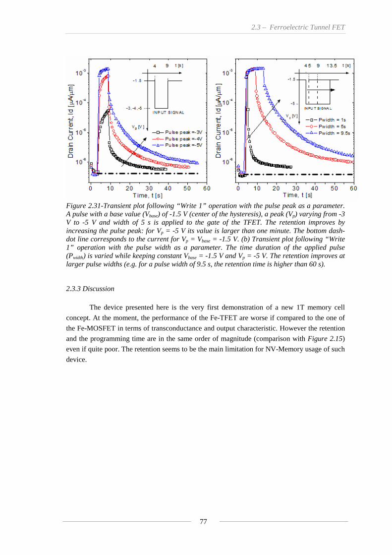
2.3 – Ferroelectric Tunnel FET
77
Figure 2.31-Transient plot following “Write 1” operation with the pulse peak as a parameter. A pulse with a base value (Vbase) of -1.5 V (center of the hysteresis), a peak (Vp) varying from -3 V to -5 V and width of 5 s is applied to the gate of the TFET. The retention improves by increasing the pulse peak: for Vp = -5 V its value is larger than one minute. The bottom dash-dot line corresponds to the current for Vp = Vbase = -1.5 V. (b) Transient plot following “Write 1” operation with the pulse width as a parameter. The time duration of the applied pulse (Pwidth) is varied while keeping constant Vbase = -1.5 V and Vp = -5 V. The retention improves at larger pulse widths (e.g. for a pulse width of 9.5 s, the retention time is higher than 60 s).
2.3.3 Discussion
The device presented here is the very first demonstration of a new 1T memory cell
concept. At the moment, the performance of the Fe-TFET are worse if compared to the one of
the Fe-MOSFET in terms of transconductance and output characteristic. However the retention
and the programming time are in the same order of magnitude (comparison with Figure 2.15)
even if quite poor. The retention seems to be the main limitation for NV-Memory usage of such
device.
Chapter II
78
2.3 Summary This chapter started out by describing the fabrication of a transistor with an organic
ferroelectric polymer, P(VDF-TrFE), into its gate stack. The polymer has been deposited by
spin coating. The first fabricated device has 100nm of polymer while an optimized one has a
40nm layer with a consequent decreasing of the operating voltage by almost one half.
Both devices have been successfully characterized for their static performance and in
terms of memory operation. The 100nm device operates about 15V with a memory window,
Mw, of more than 10V. The 40nm transistor has instead a programming voltage of 9V and a
Mw of about 7V. This transistor has also better Ioff (1pA/μm2) current thanks to the choice of a
low resistivity substrate and a better implantation process. The Ion/Ioff is about 104 at Vg=0V.
Both devices, however, shows a poor retention time in the order of few seconds because of the
short circuit condition. A detailed analysis of the two main mechanisms, depolarization field
and charge injection, responsible for this poor performance has been done. The piezoelectric
force microscopy, PFM, shows that the charge injection mechanism is the most important in
our structure. The open-circuit retention has also been measured demonstrating that the
polarization is stable and that the information can be preserved for several hours.
The second part of the chapter deals with the experimental demonstration of a new
hybrid device. A 40nm layer of P(VDF-TrFE) was deposited over a tunnel FET structure. This
new device concept, Fe-TFET, shows a retention time comparable to the one measured for the
Fe-MOSFET. It has very low leakage current that makes this device a good candidate for
extremely low power memory.
The original work carried out relative to this chapter includes:
Fabrication. I studied and then realized the fabrication process of a transistor with sub 100nm
layer of an organic ferroelectric material into its gate stack. Moreover and successively, in
collaboration with Livio Lattanzio, I fabricated a completely new structure, called ferroelectric
tunnel field effect transistor, that consists of a TFET with a 40nm P(VDF-TFE) layer in the gate
stack.
1T memory cell characterization. Both devices, the Fe-MOSFET and the Fe-TFET, were
characterized for their static performance and for their memory operations. In both cases a
programming time of the order of ms and a retention of few seconds was registered.
New device concept experimentally demonstrated. A ferroelectric TFET was designed,
fabricated and characterized for low power memory cell. This work was realized in
collaboration with my colleague Livio Lattanzio and I focused on the polymer integration in the
gate stack and on the memory characterization.
Chapter II - Bibliography
Bibliography
[1] G. A. Salvatore, D. Bouvet, I. Stolitchnov, N. Setter, A. M. Ionescu, "Low Voltage Ferroelectric FET with sub-100nm Copolymer P(VDF-TrFE) Gate Dielectric for Non-Volatile 1T Memory", ESSDERC 2008, Edinburgh, Scotland, UK (2008).
[2] A. M. Ionescu, L. Lattanzio, G. A. Salvatore, L. De Michielis, K. Boucart, D. Bouvet, “The Hysteretic Ferroelectric Tunnel FET”, IEEE Trans. on Elect. Dev. Article in press
[3] S. Fujisaki and H Ishiwara, “Low-voltage operation of ferroelectric poly(vinylidene fluoridetrifluoroethylene) copolymer capacitors and metal-ferroelectric- insulator-semiconductor diodes “, Appl. Phys. Letts. Vol. 90, (2007).
[4] S. Horiuchi and Y. Tokura, “Organic ferroelectrics”, Nature Materials Vol. 7 (2008)
[5] A. Gerber et al., “Low-voltage operation of metal-ferroelectric-insulator-semiconductor diodes incorporating a ferroelectric polyvinylidene fluoride copolymer Langmuir-Blodgett film“, J. Appl. Phys. v.100 024110 (2006)
[6] T. Furukawa et al., “Nanosecond Switching in Thin Fims of Vinylidene FluorideTrilluoroethylene Copolymers”, J.J. Appl. Phys., Vol. 24, No.8 (1985)
[7] T. P. Ma and Jin-Ping Han,” Why is Nonvolatile Ferroelectric Memory Field-Effect Transistor Still Elusive?”, IEEE Electron Device Letters Vol. 23, No. 7 (2002)
[8] Hiroshi Ishiwara, “Current status of ferroelectric-gate Si transistors and challenge to ferroelectric-gate CNT transistors”, Current Applied Physics Vol. 9 (2009)
[9] M. Fitsilis, “Scaling of the ferroelectric field effect transistor and programming concepts for non-volatile memory applications”, thesis (2005)
[10] T. Sakoda et Al., “Hydrogen-Robust Submicron IrOx/Pb(Zr, Ti)O3/Ir Capacitors for Embedded Ferroelectric Memory”, Jpn. J. Appl. Phys., Part 1 40, (2001).
[11] J. Scott, IEICE Trans. Electron. E81-C, 447 (1998).
[12] M. Alexe, C. Harnagea, D. Hesse, and U. Gosele,” Polarization imprint and size effects in mesoscopic ferroelectric structures”, Appl. Phys. Lett. 79, (2001).
[13] I. Stolitchnov et Al., “Unusual size effect on the polarization patterns in micron-size Pb(Zr,Ti)O3 film capacitors”, Appl. Phys. Let., Vol. 8, No. 25, (2002).
[14] R. Gysel, I. Stolichnov, A. K. Tagantsev, S. W. E. Riester, N. Setter, G. A. Salvatore, D. Bouvet, A. M. Ionescu, "Retention in Non-Volatile Silicon Transistors with an Organic Ferroelectric Gate", App. Phys. Lett., vol. 94, No. 26, (2009).
[15] A. M. Ionescu, US Patent Application 12/631,052, December (2008).
[16] W. Skorupa et al. , Proceedings of 13th IEEE International Conference on Advanced Thermal Processing of Semiconductors, RTP, pp. 53-71 (2005)
Chapter II - Bibliography
[17] A. Schenk, ‘Rigorous theory and simplified model of the band-to-band tunneling in silicon’, Solid-State Electronics, Vol. 36, pp. 19-34 (1993).
[18] A. Schenk, ‘A model for the field and temperature-dependence of Shockley-Read-Hall lifetimes in silicon’, Solid-State Electronics, Vol. 35, pp. 1585-1596 (1992).
[19] Sentaurus Device User Guide, Version A-2009.06.
[20] D.K. Schroder, ‘Carrier lifetimes in silicon’, IEEE Transactions on Electron Devices, Vol. 44, pp. 160-170 (1997).
[21] K. Boucart, A.M. Ionescu, ‘A new definition of threshold voltage in Tunnel FETs’, Solid-State Electronics, Vol. 52, pp. 1318-1323 (2008).
3.1 Intro: how design a gate stack for abrupt switch
Chapter 3
Small Slope Ferroelectric FET
In this chapter the negative capacitance effect in ferroelectrics is investigated from the
theoretical and experimental point of view. A design procedure for a stable and abrupt
ferroelectric switch is presented. A standard MOSFET with a linear dielectric and a
ferroelectric layer in its gate stack is taken into consideration. The experimental data referring
to two different designs are shown and commented. The first layout consists of a ferroelectric
transistor with 10nm SiO2 and 40nm of P(VDF-TrFE) gate stack. On this device a slope of
13mV/dec has been experimentally measured on a very narrow range of voltage and for very
small current level. This structure presents some problems for the deep understanding of the
behavior of the device and a new layout has been conceived and fabricated. It consists of a
ferroelectric transistor with 10nm SiO2 and 100nm P(VDF-TrFE) gate stack with an
intermediate contact between the two dielectric layers. Several transistors exhibited a slope
less than 60mV/dec and thanks to the intermediate contact this behavior has been finally
attributed and explained by the NC concept. This layout, in fact, allows the characterization of
the ferroelectric material and the comparison with a reference transistor, i.e. the transistor
without the ferroelectric layer. This study is the first experimental demonstration that thanks to
the NC, a ferroelectric silicon MOSFET could have a swing less than the theoretical 60mV/dec
limit.

3.1 Intro: how design a gate stack for abrupt switch
83
3.1 Intro: how to design a gate stack for abrupt switch
This paragraph describes the concept of Negative Capacitance (NC) in ferroelectrics, its
physical origin and how it can be used in order to design a small slope switch [1]. In chapter 1
Landau’s theory was discussed in its main aspects and it showed that the equation of the field
reads as follow: 3)()( PTBPTTE c +−= α (3.1)
0
Electric Field
Pol
ariz
atio
n
0
Negative Capacitance Region
Figure 3.1- Polarization Vs Field curve for a temperature below the Curie temperature, Tc. Theoretically a region of negative slope exists close to E=0 and P=0.
It is worth noting that if the term P3 is negligible with respect to the linear term then the E-P
relation could have a negative slope for T<Tc since α is always positive. This could give rise to
a negative capacitive effect. In fact, considering a parallel plate capacitor with a dielectric
constant given by:
)()(
11
)(
1
c
cw
ccFerro TT
C
TTTT −=
−≈+
−=
ααε
(3.2)
and separated by a distance d (normalizing over the area), the equivalent low field capacitance
is:
)(0
c
cwFerro TT
C
dC
−≈ ε
[F/m2] (3.3)
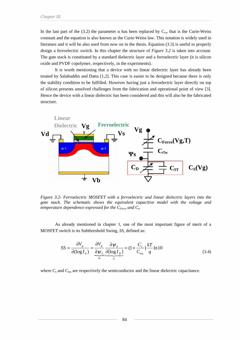
Chapter III
84
In the last part of the (3.2) the parameter α has been replaced by Ccw that is the Curie-Weiss
constant and the equation is also known as the Curie-Weiss law. This notation is widely used in
literature and it will be also used from now on in the thesis. Equation (3.3) is useful to properly
design a ferroelectric switch. In this chapter the structure of Figure 3.2 is taken into account.
The gate stack is constituted by a standard dielectric layer and a ferroelectric layer (it is silicon
oxide and PVDF copolymer, respectively, in the experiments).
It is worth mentioning that a device with no linear dielectric layer has already been
treated by Salahuddin and Datta [1,2]. This case is easier to be designed because there is only
the stability condition to be fulfilled. However having just a ferroelectric layer directly on top
of silicon presents unsolved challenges from the fabrication and operational point of view [3].
Hence the device with a linear dielectric has been considered and this will also be the fabricated
structure.
Figure 3.2- Ferroelectric MOSFET with a ferroelectric and linear dielectric layers into the gate stack. The schematic shows the equivalent capacitive model with the voltage and temperature dependence expressed for the CFerro and Cs.
As already mentioned in chapter 1, one of the most important figure of merit of a
MOSFET switch is its Subthreshold Swing, SS, defined as:
( ) 10ln)1(log)(log q
kT
C
C
I
V
I
VSS
ins
s
n
D
S
m
S
g
d
g +=∂
∂∂∂
=∂
∂=
43421
ψψ (3.4)
where Cs and Cins are respectively the semiconductor and the linear dielectric capacitance.
Ferroelectric Linear Dielectric
Vd Vg
Vs
Vb
Vg
Ψs
CFerro(Vg,T)
COx
CS(Vg) CIT CD
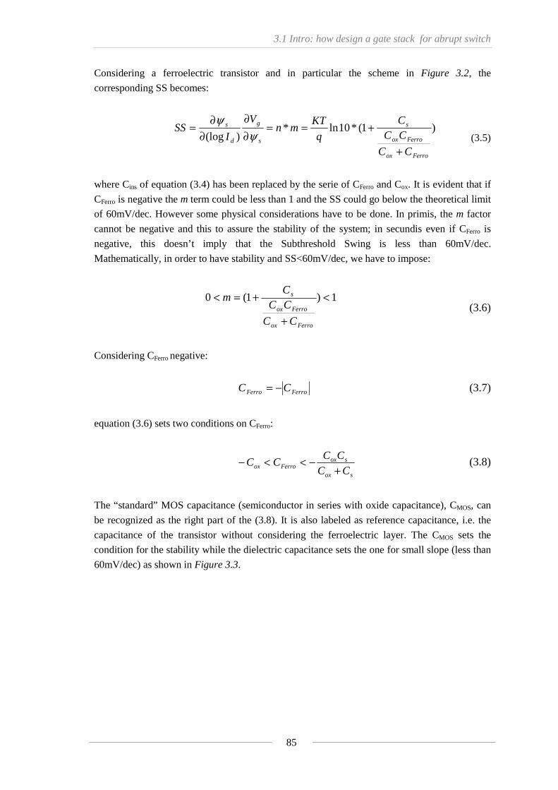
3.1 Intro: how design a gate stack for abrupt switch
85
Considering a ferroelectric transistor and in particular the scheme in Figure 3.2, the
corresponding SS becomes:
)1(*10ln*)(log
Ferroox
Ferroox
s
s
g
d
s
CC
CCC
q
KTmn
V
ISS
+
+==∂∂
∂∂
=ψ
ψ (3.5)
where Cins of equation (3.4) has been replaced by the serie of CFerro and Cox. It is evident that if
CFerro is negative the m term could be less than 1 and the SS could go below the theoretical limit
of 60mV/dec. However some physical considerations have to be done. In primis, the m factor
cannot be negative and this to assure the stability of the system; in secundis even if CFerro is
negative, this doesn’t imply that the Subthreshold Swing is less than 60mV/dec.
Mathematically, in order to have stability and SS<60mV/dec, we have to impose:
1)1(0 <
+
+=<
Ferroox
Ferroox
s
CC
CCC
m (3.6)
Considering CFerro negative:
FerroFerro CC −= (3.7)
equation (3.6) sets two conditions on CFerro:
sox
soxFerroox CC
CCCC
+−<<− (3.8)
The “standard” MOS capacitance (semiconductor in series with oxide capacitance), CMOS, can
be recognized as the right part of the (3.8). It is also labeled as reference capacitance, i.e. the
capacitance of the transistor without considering the ferroelectric layer. The CMOS sets the
condition for the stability while the dielectric capacitance sets the one for small slope (less than
60mV/dec) as shown in Figure 3.3.
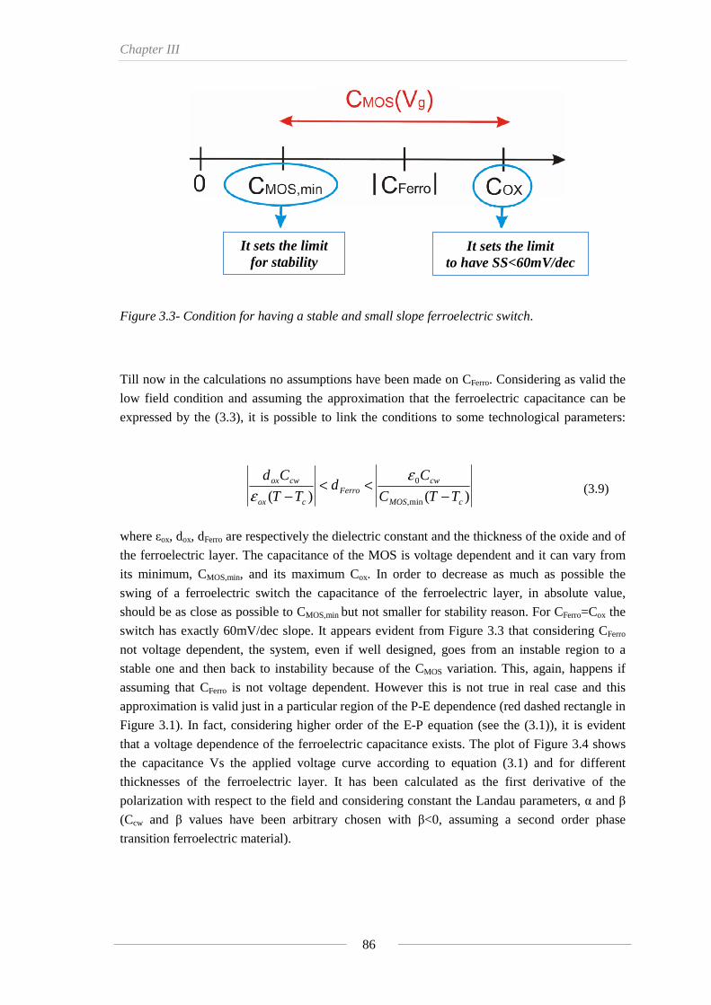
Chapter III
86
Figure 3.3- Condition for having a stable and small slope ferroelectric switch.
Till now in the calculations no assumptions have been made on CFerro. Considering as valid the
low field condition and assuming the approximation that the ferroelectric capacitance can be
expressed by the (3.3), it is possible to link the conditions to some technological parameters:
)()( min,
0
cMOS
cwFerro
cox
cwox
TTC
Cd
TT
Cd
−<<
−ε
ε (3.9)
where εox, dox, dFerro are respectively the dielectric constant and the thickness of the oxide and of
the ferroelectric layer. The capacitance of the MOS is voltage dependent and it can vary from
its minimum, CMOS,min, and its maximum Cox. In order to decrease as much as possible the
swing of a ferroelectric switch the capacitance of the ferroelectric layer, in absolute value,
should be as close as possible to CMOS,min but not smaller for stability reason. For CFerro=Cox the
switch has exactly 60mV/dec slope. It appears evident from Figure 3.3 that considering CFerro
not voltage dependent, the system, even if well designed, goes from an instable region to a
stable one and then back to instability because of the CMOS variation. This, again, happens if
assuming that CFerro is not voltage dependent. However this is not true in real case and this
approximation is valid just in a particular region of the P-E dependence (red dashed rectangle in
Figure 3.1). In fact, considering higher order of the E-P equation (see the (3.1)), it is evident
that a voltage dependence of the ferroelectric capacitance exists. The plot of Figure 3.4 shows
the capacitance Vs the applied voltage curve according to equation (3.1) and for different
thicknesses of the ferroelectric layer. It has been calculated as the first derivative of the
polarization with respect to the field and considering constant the Landau parameters, α and β
(Ccw and β values have been arbitrary chosen with β<0, assuming a second order phase
transition ferroelectric material).
It sets the limit for stability
It sets the limit to have SS<60mV/dec

3.1 Intro: how design a gate stack for abrupt switch
87
c
CW
TT
C
d −≈ 0ε
0
0
Voltage [a.u.]
Cap
acita
nce
[a.u
.]
C
Ferro d=100nm
CFerro
d=50nm
CFerro
d=10nm
Figure 3.4- Ferroelectric capacitance as function of applied voltage for different thicknesses of the layer. The capacitance has been calculated as [∂P/(d*∂E)]. The NC region width and value depend on the thickness. It’s important noting that the approximation done in the (3.3) is less and less accurate when decreasing the thickness.
The NC region shrinks by decreasing the thickness. In fact, the coercive voltage (the voltage
corresponding to the coercive field for a given thickness) reduces with the thickness of the layer
because of the E=–grad(V) relation. It is also worth mentioning that the ferroelectric does not
exhibit a negative capacitance over the whole voltage range and this range could be modulated
by the thickness of the layer. This is very important to fulfill both conditions of stability and
small swing. Moreover, it is also important to note the approximation we did, i.e. considering
the capacitance constant in voltage, becomes less and less accurate for thin layers. The value of
the “quasi”-constant capacitance is modulated by the thickness as predicted by equation (3.3).
The curve's shape, of course, depends also on the Landau parameter and hence on the material
properties; here a single given material is considered. It is interesting to look at how the MOS
capacitance could enter into this picture and how the condition for small slope and stability
could be simultaneously fulfilled. In Figure 3.5 a typical MOS capacitance (p-MOS in the
example) has been plotted together with the ferroelectric capacitance. Some remarks have to be
made when looking at the curves. First, they are plotted for negative value, so the MOS
capacitance has been inverted in sign (according to equation (3.8)). Moreover, at this stage the
MOS system and the ferroelectric one are taken separately, meaning they are not considered in
series one to the other and hence the drop of voltage on the ferromaterial is not the result of the
partition over the complete stack. Indeed this means that the voltage scale in the plots could be
different for the ferroelectric and for the MOS capacitance (arbitrary units in the plot). However
it is useful to look at the curves in order to understand how to design the switch and which are
the parameters that have to be taken into account. Two different design strategies can be
chosen:
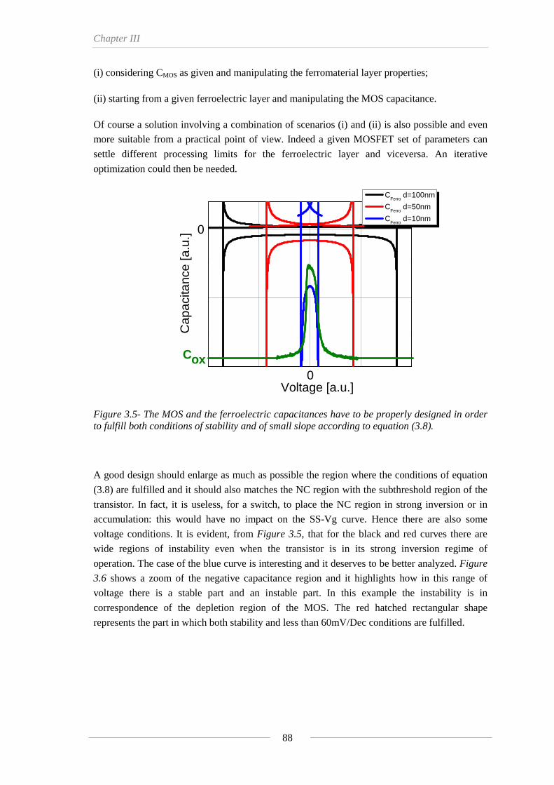
Chapter III
88
(i) considering CMOS as given and manipulating the ferromaterial layer properties;
(ii) starting from a given ferroelectric layer and manipulating the MOS capacitance.
Of course a solution involving a combination of scenarios (i) and (ii) is also possible and even
more suitable from a practical point of view. Indeed a given MOSFET set of parameters can
settle different processing limits for the ferroelectric layer and viceversa. An iterative
optimization could then be needed.
Cox0
0
Voltage [a.u.]
Cap
acita
nce
[a.u
.]
CFerro
d=100nm
CFerro
d=50nm
CFerro
d=10nm
Figure 3.5- The MOS and the ferroelectric capacitances have to be properly designed in order to fulfill both conditions of stability and of small slope according to equation (3.8).
A good design should enlarge as much as possible the region where the conditions of equation
(3.8) are fulfilled and it should also matches the NC region with the subthreshold region of the
transistor. In fact, it is useless, for a switch, to place the NC region in strong inversion or in
accumulation: this would have no impact on the SS-Vg curve. Hence there are also some
voltage conditions. It is evident, from Figure 3.5, that for the black and red curves there are
wide regions of instability even when the transistor is in its strong inversion regime of
operation. The case of the blue curve is interesting and it deserves to be better analyzed. Figure
3.6 shows a zoom of the negative capacitance region and it highlights how in this range of
voltage there is a stable part and an instable part. In this example the instability is in
correspondence of the depletion region of the MOS. The red hatched rectangular shape
represents the part in which both stability and less than 60mV/Dec conditions are fulfilled.
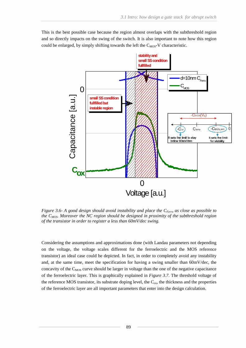
3.1 Intro: how design a gate stack for abrupt switch
89
This is the best possible case because the region almost overlaps with the subthreshold region
and so directly impacts on the swing of the switch. It is also important to note how this region
could be enlarged, by simply shifting towards the left the CMOS-V characteristic.
Figure 3.6- A good design should avoid instability and place the CFerro as close as possible to the CMOS. Moreover the NC region should be designed in proximity of the subthreshold region of the transistor in order to register a less than 60mV/dec swing.
Considering the assumptions and approximations done (with Landau parameters not depending
on the voltage, the voltage scales different for the ferroelectric and the MOS reference
transistor) an ideal case could be depicted. In fact, in order to completely avoid any instability
and, at the same time, meet the specification for having a swing smaller than 60mV/dec, the
concavity of the CMOS curve should be larger in voltage than the one of the negative capacitance
of the ferroelectric layer. This is graphically explained in Figure 3.7. The threshold voltage of
the reference MOS transistor, its substrate doping level, the Cox, the thickness and the properties
of the ferroelectric layer are all important parameters that enter into the design calculation.
small SS condition fullfilled but instable region
stability andsmall SS condition fullfilled
Cox0
0
Voltage [a.u.]
Cap
acita
nce
[a.u
.]
d=10nm CFerro
CMOS
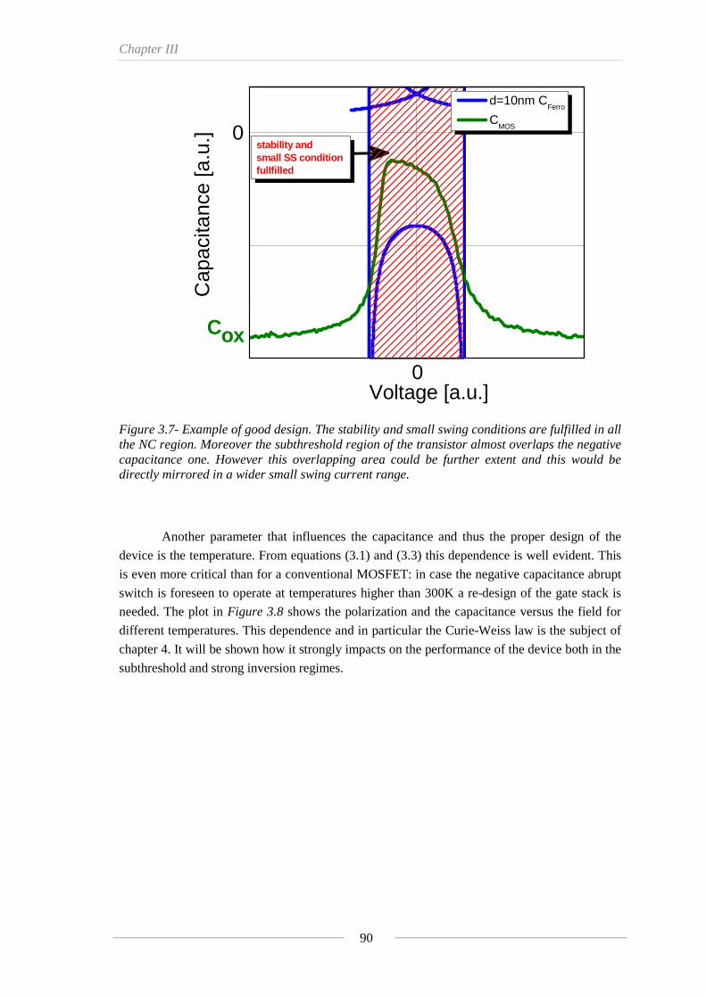
Chapter III
90
stability andsmall SS condition fullfilled
Cox
0
0
Voltage [a.u.]
Cap
acita
nce
[a.u
.]
d=10nm CFerro
CMOS
Figure 3.7- Example of good design. The stability and small swing conditions are fulfilled in all the NC region. Moreover the subthreshold region of the transistor almost overlaps the negative capacitance one. However this overlapping area could be further extent and this would be directly mirrored in a wider small swing current range.
Another parameter that influences the capacitance and thus the proper design of the
device is the temperature. From equations (3.1) and (3.3) this dependence is well evident. This
is even more critical than for a conventional MOSFET: in case the negative capacitance abrupt
switch is foreseen to operate at temperatures higher than 300K a re-design of the gate stack is
needed. The plot in Figure 3.8 shows the polarization and the capacitance versus the field for
different temperatures. This dependence and in particular the Curie-Weiss law is the subject of
chapter 4. It will be shown how it strongly impacts on the performance of the device both in the
subthreshold and strong inversion regimes.
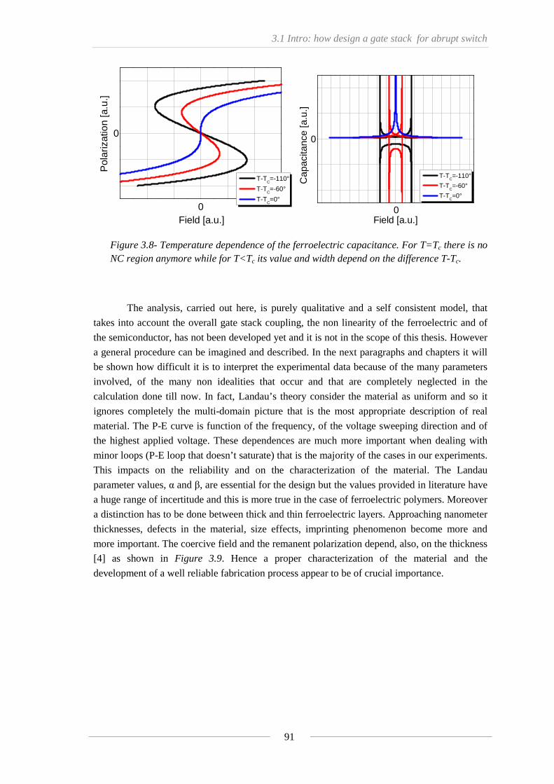
3.1 Intro: how design a gate stack for abrupt switch
91
T-TC=-110°
T-TC=-60°
T-TC=0°
0
0
Field [a.u.]
Pol
ariz
atio
n [a
.u.]
0
T-TC=-110°
T-TC=-60°
T-TC=0°
Cap
acita
nce
[a.u
.]
Field [a.u.]
0
Figure 3.8- Temperature dependence of the ferroelectric capacitance. For T=Tc there is no NC region anymore while for T<Tc its value and width depend on the difference T-Tc.
The analysis, carried out here, is purely qualitative and a self consistent model, that
takes into account the overall gate stack coupling, the non linearity of the ferroelectric and of
the semiconductor, has not been developed yet and it is not in the scope of this thesis. However
a general procedure can be imagined and described. In the next paragraphs and chapters it will
be shown how difficult it is to interpret the experimental data because of the many parameters
involved, of the many non idealities that occur and that are completely neglected in the
calculation done till now. In fact, Landau’s theory consider the material as uniform and so it
ignores completely the multi-domain picture that is the most appropriate description of real
material. The P-E curve is function of the frequency, of the voltage sweeping direction and of
the highest applied voltage. These dependences are much more important when dealing with
minor loops (P-E loop that doesn’t saturate) that is the majority of the cases in our experiments.
This impacts on the reliability and on the characterization of the material. The Landau
parameter values, α and β, are essential for the design but the values provided in literature have
a huge range of incertitude and this is more true in the case of ferroelectric polymers. Moreover
a distinction has to be done between thick and thin ferroelectric layers. Approaching nanometer
thicknesses, defects in the material, size effects, imprinting phenomenon become more and
more important. The coercive field and the remanent polarization depend, also, on the thickness
[4] as shown in Figure 3.9. Hence a proper characterization of the material and the
development of a well reliable fabrication process appear to be of crucial importance.
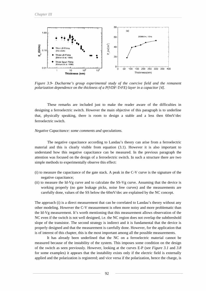
Chapter III
92
Figure 3.9- Ducharme’s group experimental study of the coercive field and the remanent polarization dependence on the thickness of a P(VDF-TrFE) layer in a capacitor [4].
These remarks are included just to make the reader aware of the difficulties in
designing a ferroelectric switch. However the main objective of this paragraph is to underline
that, physically speaking, there is room to design a stable and a less then 60mV/dec
ferroelectric switch.
Negative Capacitance: some comments and speculations.
The negative capacitance according to Landau’s theory can arise from a ferroelectric
material and this is clearly visible from equation (3.1). However it is also important to understand how this negative capacitance can be measured. In the previous paragraph the attention was focused on the design of a ferroelectric switch. In such a structure there are two simple methods to experimentally observe this effect:
(i) to measure the capacitance of the gate stack. A peak in the C-V curve is the signature of the
negative capacitance; (ii) to measure the Id-Vg curve and to calculate the SS-Vg curve. Assuming that the device is
working properly (no gate leakage picks, noise free curves) and the measurements are carefully done, values of the SS below the 60mV/dec are explained by the NC concept.
The approach (i) is a direct measurement that can be correlated to Landau’s theory without any other modeling. However the C-V measurement is often more noisy and more problematic than the Id-Vg measurement. It’s worth mentioning that this measurement allows observation of the NC even if the switch is not well designed, i.e. the NC region does not overlap the subthreshold slope of the transistor. The second strategy is indirect and it is fundamental that the device is properly designed and that the measurement is carefully done. However, for the application that is of interest of this chapter, this is the most important among all the possible measurements. It has already been underlined that the NC on a ferroelectric material cannot be measured because of the instability of the system. This imposes some condition on the design of the switch as seen previously. However, looking at the curves E-P (see Figure 3.1 and 3.8 for some examples) it appears that the instability exists only if the electric field is externally applied and the polarization is registered; and vice versa if the polarization, hence the charge, is
3.1 Intro: how design a gate stack for abrupt switch
93
applied and the field, hence the voltage, is registered then the instability and the hysteresis disappear. A virtual experiment could be done: imagine being able to add the elementary charge, q, on the plate of a ferroelectric capacitor and be able to measure the drop of voltage (assuming that the capacitor is ideal). Physically it should be possible to recover the E-P curve illustrated by Figure 3.1 without any instability occurring and without having any hysteresis. This charge bias approach presents problems from the experimental point of view because it can cause charge injection into the device. The goal of these small comments is to underline the fact that even if the NC concept is simple to be explained from the physical and mathematical point of view, it is hard to be experimentally demonstrated and measured. Moreover a distinction has to be made when dealing with a purely ferroelectric material and when dealing with a ferroelectric switch. The measurement strategy (voltage or charge biased) implies some constraint on the design of the device in order to avoid instability. Here, the interest is focused on the design and experimental demonstration of a ferroelectric switch that, thanks to the NC, can have a swing less than 60mV/dec. All the measurements, C-V and Id-Vg, performed are voltage biased.
Chapter III
94
3.2 Ferroelectric switch: from theory to experiment
In the next part of this chapter the fabrication and the characterization of ferroelectric
MOS transistors in bulk technology will be described. Two different designs will be presented:
(i) an n-type ferroelectric transistor with 10nm SiO2 and 40nm of P(VDF-TrFE) as gate stack
(this design is referred as “without intermediate contact”);
(ii) a p-type ferroelectric transistor with 10nm SiO2 and 100nm of P(VDF-TrFE) as gate stack
and with a metal intermediate contact in between the two dielectrics (this design is referred
to as “with intermediate contact” or “optimized”). In both cases a slope less than 60mV/dec has been registered and an attempt has been made to
explain this using the NC concept. In the case of the first device, the one without intermediate
contact, the analysis of the physics involved varies from difficult to almost impossible. This is
mainly due to the fact that a comparison with a reference transistor, a transistor with the same
doping and geometries but without the ferroelectric layer, cannot be done. The second design
has been conceived to allow a more detailed understanding of the physics and to compare the
ferroelectric device to that of a reference device. Moreover it can also be used for modeling
purposes and for the characterization of the ferroelectric material.
3.2.1 Device with no intermediate contact
Fabrication
The fabrication has been described in paragraph 2.21 of chapter 2. The experimental results
shown here refer to the device with a 40nm of P(VDF-TrFE) thick layer in the gate stack. The
design of the layer thickness has not been done for switch application but the main goal was to
lower the programming voltage of the 1T memory cell. Hence the goal in the design phase was
to reduce as much as possible the thickness of the ferroelectric layer. The 40nm layer, as
already discussed, represents the technological limit at the moment. It is worth remembering
that the drain and source region are contacting through direct probing the silicon surface
because no metallization was performed. This implies also that the polymer has to be scratched
by the measuring tips.
The device with 100nm exhibited a leakage current too high and this does not allow any swing
analysis.

3.2 – Ferroelectric switch: from theory to experiment
95
Characterization and experimental results
Several n-type ferroelectric MOSFETs have been characterized mainly for their Id-Vg
and Gate Capacitance at ambient temperatures. The Agilent Analyzer 4156C has been used for
the measurements. In most cases an “integration time” of 1ms has been adopted (“medium” in
the tool configuration) and the “wait time” has been set to zero (In a I-V measurement, the
“integration time” is the time between the application of two subsequent voltage values. The
“wait time”, instead, sets, at the very beginning of the measurement, the time in which the
voltage is applied before starting the measurement of the current ). The voltage step has been
made as short as possible in order to measure as many I-V points as possible, essential for the
resolution in the SS-Vg curve. The voltage has been swept from negative to positive values in
order to set the MOSFET in accumulation and then go to the inversion. Of course a double
sweep has always been performed since dealing with an hysteretic behavior. The voltage range
is in most cases non symmetric with respect to zero. Moreover, the voltage applied to the drain
has been limited to a small value (from 5mV to at most 20mV) in order to not influence the
polarization of the gate because of the gate-drain coupling. All these parameters can influence
the measurement and can have an impact on the performances of the transistor, and hence, on
its subthreshold swing. This is mainly due to the intrinsic memory effect of the ferromaterial
and also to the fact that the hysteretic behavior refers always to minor loop conditions.
The subthreshold slope dependence on the gate to semiconductor coupling has been
widely discussed. However, from the experimental point of view, the swing is also limited by
the leakage current of the transistor. This is more important in a ferroelectric transistor in which
the SS depends on the gate voltage. A high Ioff current, due to junction leakages, can hide the
on-off transition region. Hence, it appears of crucial importance the fabrication of a good
reference transistor.
Figure 3.10 below shows the Id-Vg for a L=W=10μm. The gate voltage has been
varied from -7V to 7V first and then back. In the subsequent measurements the upper positive
voltage has been increased to 8, 9, 10, 12, 15 and the plot shows the experimental results. The
threshold voltage of the device does not change pretty much by increasing the voltage but the
memory window increases progressively. This can be explained by an increase of the
polarization during the sweeping up and hence an increased negative voltage to depolarize the
material in the sweeping back. This example shows that the device works properly and that a
simple parameter can change the measurement condition. The transistor has an Ion current of
several hundreds of nA and an Ioff current of less than 10pA with a consequent ratio Ion/Ioff of
more than 104. Moreover the bigger loops are almost perfectly centered around zero.

Chapter III
96
-5 0 5 10 1510-12
10-11
10-10
10-9
10-8
10-7
10-6
Dra
in c
urre
nt, I
d [A
]
Gate voltage, Vg (V)
Figure 3.10- Multiple Id-Vg hysteretic curves measured by sweeping gate voltage up to 7V, 8V, 9V, 10V, 12V and 15V and then down to-7V, for a fabricated Fe-FET with L=W=10μm. A larger hysteresis is obtained for larger sweep, which could be potentially useful for multi bit 1T-memory application.
Figure 3.11 shows the impact of the drain voltage on the transfer-characteristic of a
L=W=20μm ferroelectric transistor. Despite of the increase of the leakage and of the Ion
current not much difference can be notice among the curves. A slight change of the threshold
voltage could be explained by an increase of the drain-gate coupling and also by a polarizing
effect of the drain on the gate stack. This device shows an extremely low Ioff, in the order of
100fA, and its subthreshold swing has been analyzed.
0 2 4 6 810-13
10-12
10-11
10-10
10-9
10-8
10-7
10-6
10-5
Dra
in C
urre
nt, I
d [A
]
Gate Voltage, Vg [V]
Vd
Vd=5, 10, 50, 100, 200mV
Vd=2
00m
V
Figure 3.11- Id-Vg with drain voltage as a parameter. The gate voltage is swept from -0.5V to 8V and the transistor body is connected to ground (Vbulk=0V). The hysteresis window is reported only for Vd=200mV and is due to the polarization of the ferroelectric layer; the hysteresis is about 1V and the Ion/Ioff is about 106 with typical leakage current of the order of few 10-13 to 10-12 A.
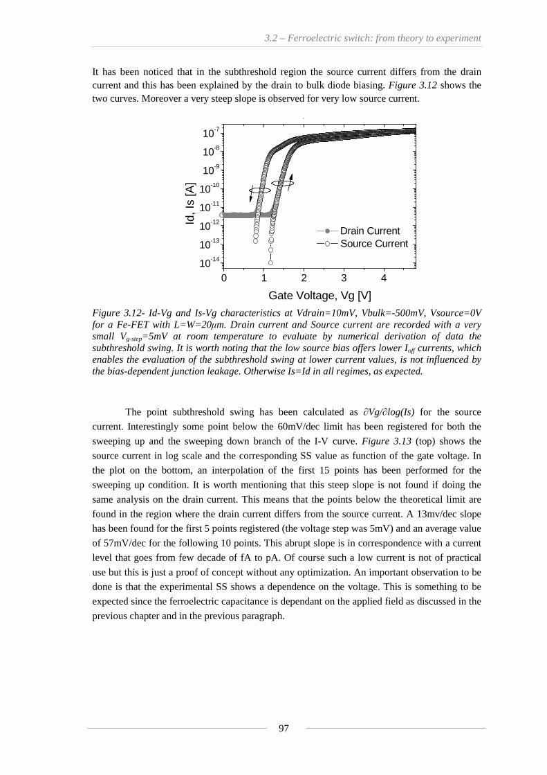
3.2 – Ferroelectric switch: from theory to experiment
97
It has been noticed that in the subthreshold region the source current differs from the drain current and this has been explained by the drain to bulk diode biasing. Figure 3.12 shows the two curves. Moreover a very steep slope is observed for very low source current.
0 1 23 4
10-1410-13
10-1210
-1110-10
10-910-8
10-7
Dra in Current
Sou rce Current
Id, Is [A]
Gate V oltage, Vg [V]
0 1 2 3 410-14
10-13
10-12
10-11
10-10
10-9
10-8
10-7
Drain Current Source Current
Id, I
s [A
]
Gate Voltage, Vg [V] Figure 3.12- Id-Vg and Is-Vg characteristics at Vdrain=10mV, Vbulk=-500mV, Vsource=0V for a Fe-FET with L=W=20μm. Drain current and Source current are recorded with a very small Vg-step=5mV at room temperature to evaluate by numerical derivation of data the subthreshold swing. It is worth noting that the low source bias offers lower Ioff currents, which enables the evaluation of the subthreshold swing at lower current values, is not influenced by the bias-dependent junction leakage. Otherwise Is=Id in all regimes, as expected.
The point subthreshold swing has been calculated as ∂Vg/∂log(Is) for the source
current. Interestingly some point below the 60mV/dec limit has been registered for both the
sweeping up and the sweeping down branch of the I-V curve. Figure 3.13 (top) shows the
source current in log scale and the corresponding SS value as function of the gate voltage. In
the plot on the bottom, an interpolation of the first 15 points has been performed for the
sweeping up condition. It is worth mentioning that this steep slope is not found if doing the
same analysis on the drain current. This means that the points below the theoretical limit are
found in the region where the drain current differs from the source current. A 13mv/dec slope
has been found for the first 5 points registered (the voltage step was 5mV) and an average value
of 57mV/dec for the following 10 points. This abrupt slope is in correspondence with a current
level that goes from few decade of fA to pA. Of course such a low current is not of practical
use but this is just a proof of concept without any optimization. An important observation to be
done is that the experimental SS shows a dependence on the voltage. This is something to be
expected since the ferroelectric capacitance is dependant on the applied field as discussed in the
previous chapter and in the previous paragraph.
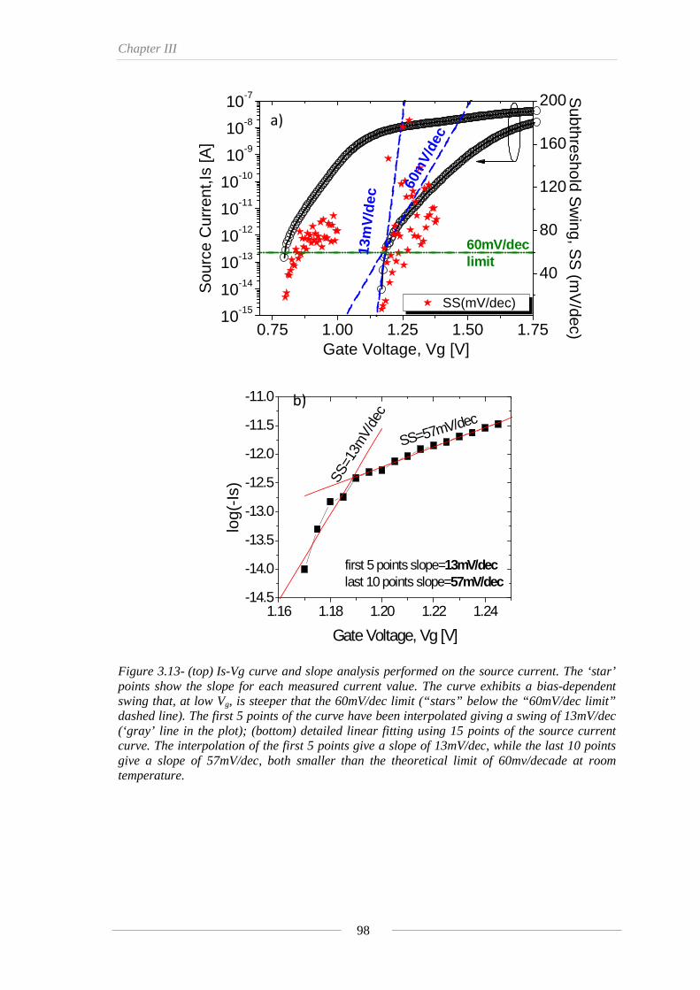
Chapter III
98
Figure 3.13- (top) Is-Vg curve and slope analysis performed on the source current. The ‘star’ points show the slope for each measured current value. The curve exhibits a bias-dependent swing that, at low Vg, is steeper that the 60mV/dec limit (“stars” below the “60mV/dec limit” dashed line). The first 5 points of the curve have been interpolated giving a swing of 13mV/dec (‘gray’ line in the plot); (bottom) detailed linear fitting using 15 points of the source current curve. The interpolation of the first 5 points give a slope of 13mV/dec, while the last 10 points give a slope of 57mV/dec, both smaller than the theoretical limit of 60mv/decade at room temperature.
0.75 1.00 1.25 1.50 1.7510-15
10-14
10-13
10-12
10-11
10-10
10-9
10-8
10-7
60m
V/de
c
SS(mV/dec)
Gate Voltage, Vg [V]
Sou
rce
Cur
rent
,Is [A
]
60mV/declimit
13m
V/d
ec
40
80
120
160
200 Subthreshold S
wing, S
S (m
V/dec)
a)
1.16 1.18 1.20 1.22 1.24-14.5
-14.0
-13.5
-13.0
-12.5
-12.0
-11.5
-11.0
SS=57mV/dec
log(
-Is)
Gate Voltage, Vg [V]
SS=1
3mV/
dec
first 5 points slope=13mV/declast 10 points slope=57mV/dec
b)
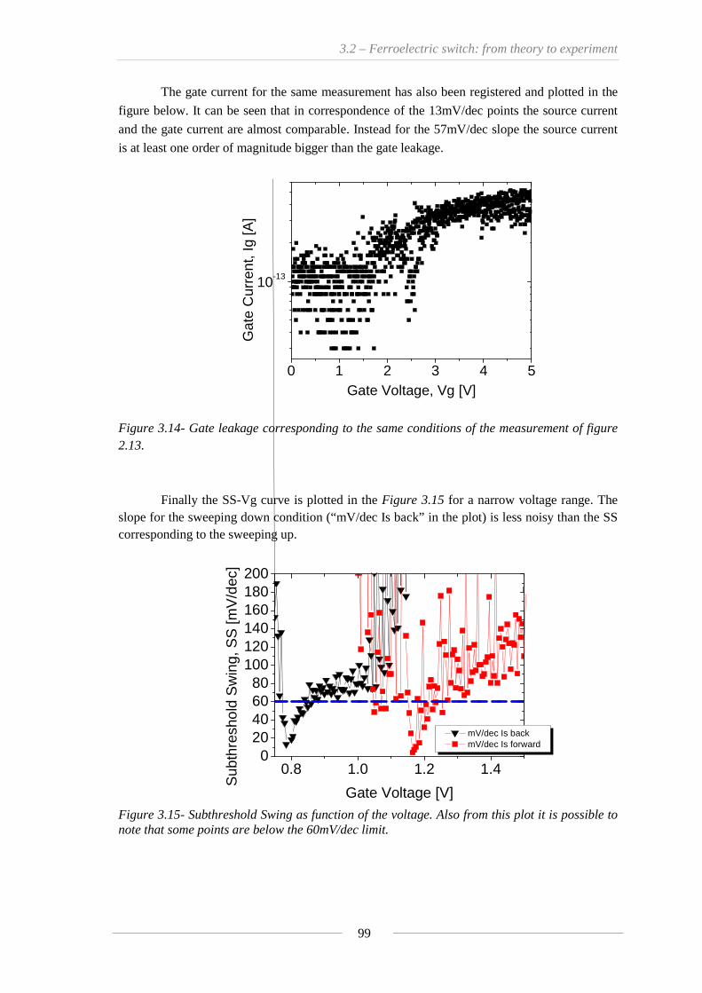
3.2 – Ferroelectric switch: from theory to experiment
99
The gate current for the same measurement has also been registered and plotted in the
figure below. It can be seen that in correspondence of the 13mV/dec points the source current
and the gate current are almost comparable. Instead for the 57mV/dec slope the source current
is at least one order of magnitude bigger than the gate leakage.
0 1 2 3 4 5
10-13
Gat
e C
urre
nt, I
g [A
]
Gate Voltage, Vg [V] Figure 3.14- Gate leakage corresponding to the same conditions of the measurement of figure 2.13.
Finally the SS-Vg curve is plotted in the Figure 3.15 for a narrow voltage range. The
slope for the sweeping down condition (“mV/dec Is back” in the plot) is less noisy than the SS corresponding to the sweeping up.
0.8 1.0 1.2 1.40
20406080
100120140160180200
mV/dec Is back mV/dec Is forward
Sub
thre
shol
d S
win
g, S
S [m
V/d
ec]
Gate Voltage [V] Figure 3.15- Subthreshold Swing as function of the voltage. Also from this plot it is possible to note that some points are below the 60mV/dec limit.
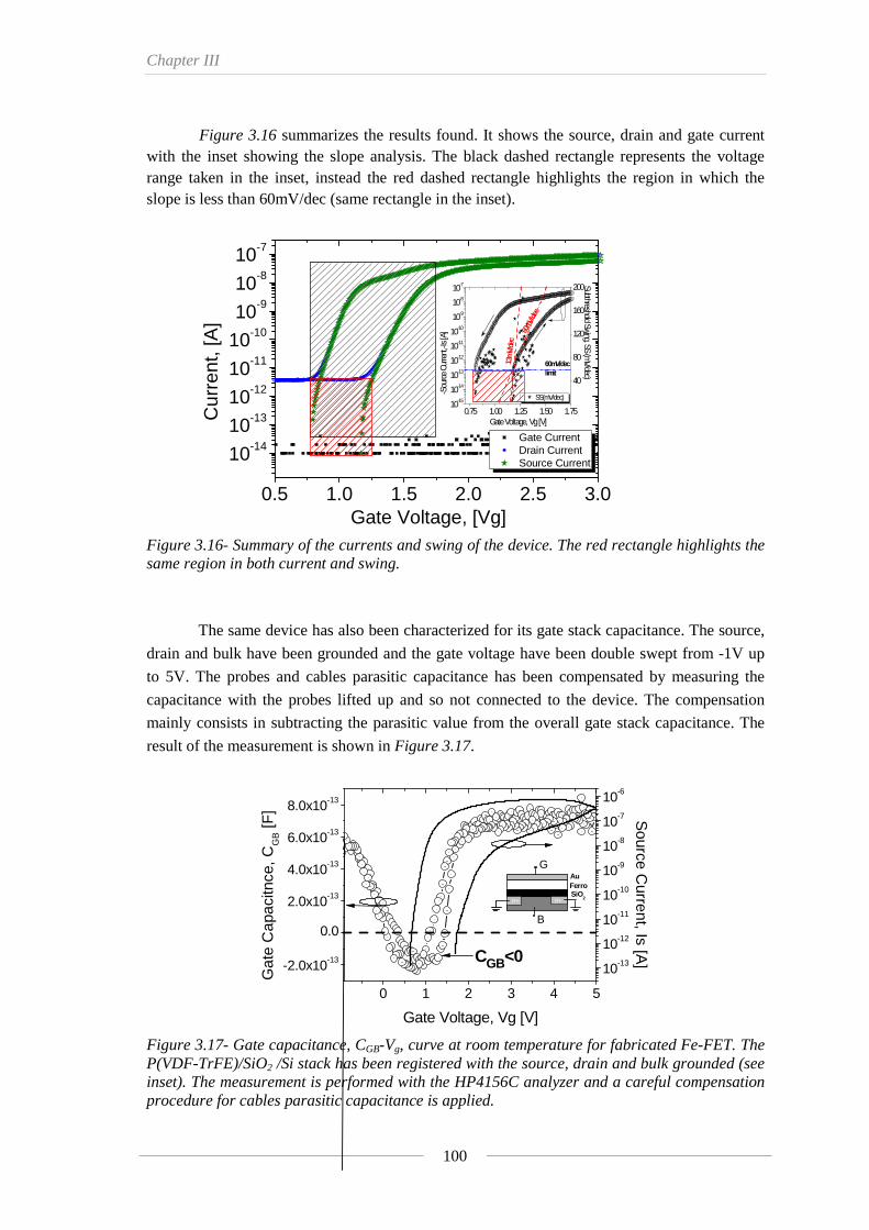
Chapter III
100
Figure 3.16 summarizes the results found. It shows the source, drain and gate current
with the inset showing the slope analysis. The black dashed rectangle represents the voltage range taken in the inset, instead the red dashed rectangle highlights the region in which the slope is less than 60mV/dec (same rectangle in the inset).
0.5 1.0 1.5 2.0 2.5 3.0
10-14
10-13
10-12
10-11
10-10
10-9
10-8
10-7
0.75 1.00 1.25 1.50 1.7510-15
10-14
10-13
10-12
10-11
10-10
10-9
10-8
10-7
60mV
/dec
SS(mV/dec)
Gate Voltage, Vg [V]
-Sou
rce
Curre
nt,-I
s [A]
60mV/declimit
13m
V/de
c
40
80
120
160
200Subthreshold Swing, SS (mV/dec)
Cur
rent
, [A
]
Gate Voltage, [Vg]
Gate Current Drain Current Source Current
Figure 3.16- Summary of the currents and swing of the device. The red rectangle highlights the same region in both current and swing.
The same device has also been characterized for its gate stack capacitance. The source,
drain and bulk have been grounded and the gate voltage have been double swept from -1V up
to 5V. The probes and cables parasitic capacitance has been compensated by measuring the
capacitance with the probes lifted up and so not connected to the device. The compensation
mainly consists in subtracting the parasitic value from the overall gate stack capacitance. The
result of the measurement is shown in Figure 3.17.
0 1 2 3 4 5
-2.0x10⁻¹³
0.0
2.0x10⁻¹³
4.0x10⁻¹³
6.0x10⁻¹³
8.0x10⁻¹³
Gate Voltage, Vg [V]
Gat
e C
apac
itnce
, CG
B [F
]
n+
B
G
n+ n+
AuFerroSiO
2
CGB<010-13
10-12
10-11
10-10
10-9
10-8
10-7
10-6
Source C
urrent, Is [A]
Figure 3.17- Gate capacitance, CGB-Vg, curve at room temperature for fabricated Fe-FET. The P(VDF-TrFE)/SiO2 /Si stack has been registered with the source, drain and bulk grounded (see inset). The measurement is performed with the HP4156C analyzer and a careful compensation procedure for cables parasitic capacitance is applied.
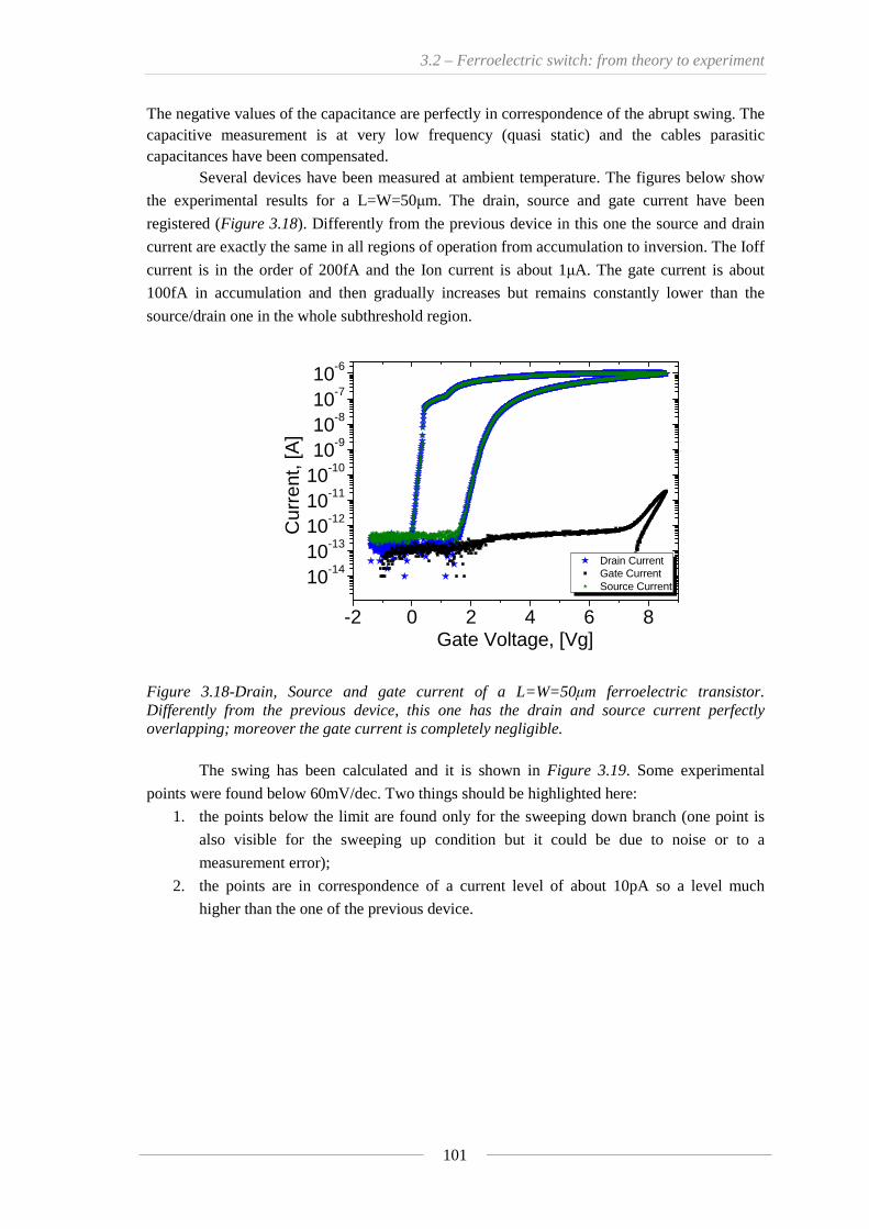
3.2 – Ferroelectric switch: from theory to experiment
101
The negative values of the capacitance are perfectly in correspondence of the abrupt swing. The capacitive measurement is at very low frequency (quasi static) and the cables parasitic capacitances have been compensated.
Several devices have been measured at ambient temperature. The figures below show
the experimental results for a L=W=50μm. The drain, source and gate current have been
registered (Figure 3.18). Differently from the previous device in this one the source and drain
current are exactly the same in all regions of operation from accumulation to inversion. The Ioff
current is in the order of 200fA and the Ion current is about 1μA. The gate current is about
100fA in accumulation and then gradually increases but remains constantly lower than the
source/drain one in the whole subthreshold region.
-2 0 2 4 6 8
10-1410-1310-1210-1110-1010-910-810-710-6
Gate Voltage, [Vg]
Cur
rent
, [A
]
Drain Current Gate Current Source Current
Figure 3.18-Drain, Source and gate current of a L=W=50μm ferroelectric transistor. Differently from the previous device, this one has the drain and source current perfectly overlapping; moreover the gate current is completely negligible.
The swing has been calculated and it is shown in Figure 3.19. Some experimental
points were found below 60mV/dec. Two things should be highlighted here:
1. the points below the limit are found only for the sweeping down branch (one point is
also visible for the sweeping up condition but it could be due to noise or to a
measurement error);
2. the points are in correspondence of a current level of about 10pA so a level much
higher than the one of the previous device.
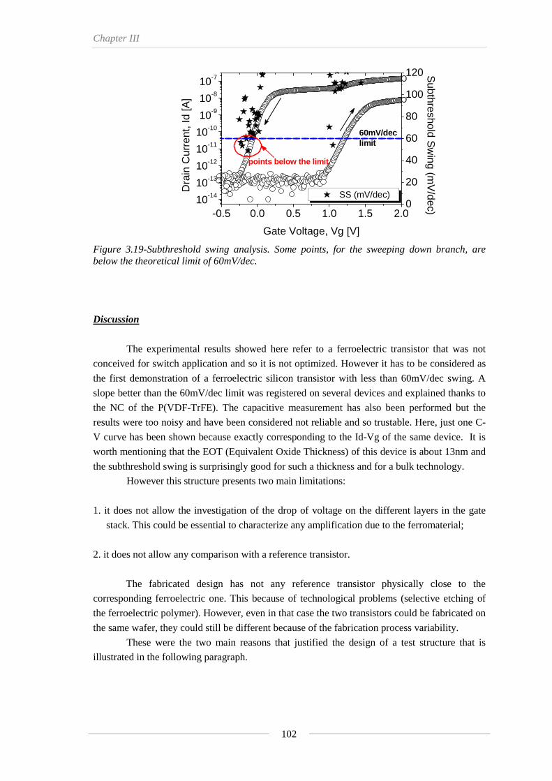
Chapter III
102
-0.5 0.0 0.5 1.0 1.5 2.010-14
10-13
10-12
10-11
10-10
10-9
10-8
10-7
SS (mV/dec)
Gate Voltage, Vg [V]
Dra
in C
urre
nt, I
d [A
]
60mV/dec limit
points below the limit
0
20
40
60
80
100
120 Subthreshold S
wing (m
V/dec)
Figure 3.19-Subthreshold swing analysis. Some points, for the sweeping down branch, are below the theoretical limit of 60mV/dec.
Discussion
The experimental results showed here refer to a ferroelectric transistor that was not
conceived for switch application and so it is not optimized. However it has to be considered as
the first demonstration of a ferroelectric silicon transistor with less than 60mV/dec swing. A
slope better than the 60mV/dec limit was registered on several devices and explained thanks to
the NC of the P(VDF-TrFE). The capacitive measurement has also been performed but the
results were too noisy and have been considered not reliable and so trustable. Here, just one C-
V curve has been shown because exactly corresponding to the Id-Vg of the same device. It is
worth mentioning that the EOT (Equivalent Oxide Thickness) of this device is about 13nm and
the subthreshold swing is surprisingly good for such a thickness and for a bulk technology.
However this structure presents two main limitations:
1. it does not allow the investigation of the drop of voltage on the different layers in the gate
stack. This could be essential to characterize any amplification due to the ferromaterial;
2. it does not allow any comparison with a reference transistor.
The fabricated design has not any reference transistor physically close to the
corresponding ferroelectric one. This because of technological problems (selective etching of
the ferroelectric polymer). However, even in that case the two transistors could be fabricated on
the same wafer, they could still be different because of the fabrication process variability.
These were the two main reasons that justified the design of a test structure that is
illustrated in the following paragraph.
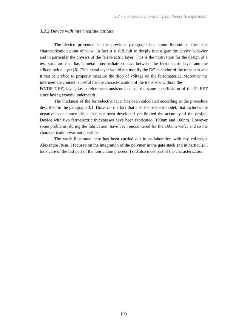
3.2 – Ferroelectric switch: from theory to experiment
103
3.2.2 Device with intermediate contact
The device presented in the previous paragraph has some limitations from the
characterization point of view. In fact it is difficult to deeply investigate the device behavior
and in particular the physics of the ferroelectric layer. This is the motivation for the design of a
test structure that has a metal intermediate contact between the ferroelectric layer and the
silicon oxide layer [8]. This metal layer would not modify the DC behavior of the transistor and
it can be probed to properly measure the drop of voltage on the ferromaterial. Moreover the
intermediate contact is useful for the characterization of the transistor without the
P(VDF-TrFE) layer, i.e. a reference transistor that has the same specification of the Fe-FET
since laying exactly underneath.
The thickness of the ferroelectric layer has been calculated according to the procedure
described in the paragraph 3.1. However the fact that a self-consistent model, that includes the
negative capacitance effect, has not been developed yet limited the accuracy of the design.
Device with two ferroelectric thicknesses have been fabricated: 100nm and 160nm. However
some problems, during the fabrication, have been encountered for the 160nm wafer and so the
characterization was not possible.
The work illustrated here has been carried out in collaboration with my colleague
Alexandre Rusu. I focused on the integration of the polymer in the gate stack and in particular I
took care of the last part of the fabrication process. I did also most part of the characterization.
Chapter III
104
Fabrication
The device consists in a conventional silicon p-type MOSFET, where, a 100nm layer of
P(VDF-TrFE) (70%-30%) ferroelectric copolymer is integrated in the gate stack, together with
thin film AlSi metal at the junction between the ferroelectric and insulator. A particular
attention was paid to the isolation of the device by using an optimized n-well (ND=3.3 1017cm-3)
and STI (Shallow Trench Isolation) isolation, which minimize all sources of leakage (Figure
3.20).
Figure 3.20- Simulated doping profile for the p-type device. The drain/source and well doping and depth can be distinguished.
The first step of the fabrication consists in the STI isolation in order to insulate one device from the other. The different implantations are then performed: the n-well first and then the source and drain and bulk contacts. As shown in the figure below a special contact for the bulk has been n++ implanted for each device in order to avoid the contacting of the bulk from the back of the whole wafer. A thin layer of 10nm of SiO2 has been growth and then 50nm of Al have been sputtered for internal gate and for source/drain and bulk contacts. The ferroelectric polymer has been spin coated and then annealed at 135°C fro 10minutes in order to make it crystallize in the ferroelectric β-phase. A 100nm gold layer has been evaporated and twice patterned through a UV lithographic step. The first lithography and subsequent Au etching is for source/drain and bulk opening that allows the plasma etching of P(VDF-TrFE). The second lithography is for the gate patterning (Figure 3.21). This process if compared to the one described in chapter 2 is optimized, in fact, the aluminum layer has also been used to contact source and drain region and so to avoid any scratch of the polymer layer during the characterization.

3.2 – Ferroelectric switch: from theory to experiment
105
Figure 3.21-Main steps for the fabrication of a ferroelectric transistor with an intermediate contact in the gate stack.
Figure 3.22 shows the layout of the device and two images (Scanning Electron Microscopy, SEM, in the center and Atomic Force Microscopy, AFM, on the right) of a fabricated transistor. The different part of the structure are highlighted.
Figure 3.22-(left) Design of the transistor with two gates: the top one (Au) and the intermediate one (Al); (center) SEM top image of a fabricated device; (right) AFM image of the area where the two gates overlap.
100nm Au gate
1. n well phosphorus implantation 2. Source/Drain Boron implantation 3. n++ bulk contact implantation
4. gate dry oxidation
5. Al layer sputtering for internal node, Source/Drain and Bulk contacts
6. P(VDF-TrFE) spin coating
7. Au layer evaporation 8. lithography and Au etching 9. polymer plasma O2 etch
100nm ferroelectric P(VDF-TrFE)
n+ implanted Si
p+ implanted Si
10nm SiO2
50nm Al
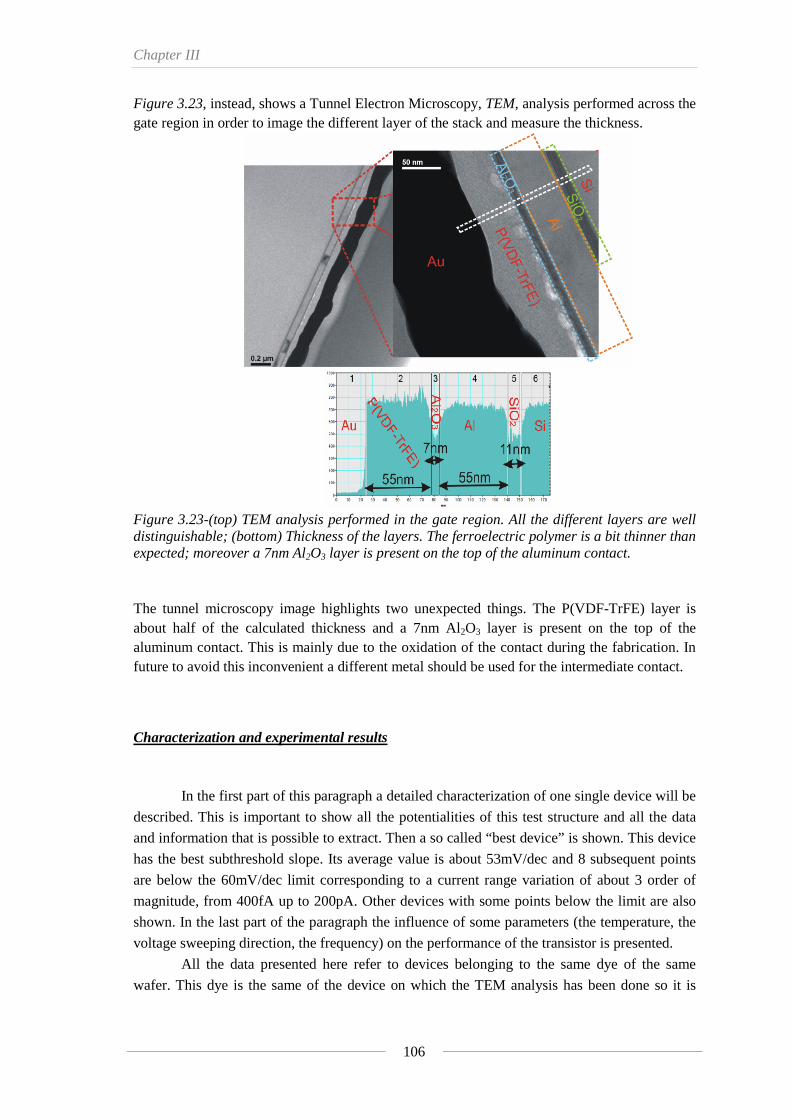
Chapter III
106
Figure 3.23, instead, shows a Tunnel Electron Microscopy, TEM, analysis performed across the gate region in order to image the different layer of the stack and measure the thickness.
Figure 3.23-(top) TEM analysis performed in the gate region. All the different layers are well distinguishable; (bottom) Thickness of the layers. The ferroelectric polymer is a bit thinner than expected; moreover a 7nm Al2O3 layer is present on the top of the aluminum contact. The tunnel microscopy image highlights two unexpected things. The P(VDF-TrFE) layer is about half of the calculated thickness and a 7nm Al2O3 layer is present on the top of the aluminum contact. This is mainly due to the oxidation of the contact during the fabrication. In future to avoid this inconvenient a different metal should be used for the intermediate contact.
Characterization and experimental results
In the first part of this paragraph a detailed characterization of one single device will be
described. This is important to show all the potentialities of this test structure and all the data
and information that is possible to extract. Then a so called “best device” is shown. This device
has the best subthreshold slope. Its average value is about 53mV/dec and 8 subsequent points
are below the 60mV/dec limit corresponding to a current range variation of about 3 order of
magnitude, from 400fA up to 200pA. Other devices with some points below the limit are also
shown. In the last part of the paragraph the influence of some parameters (the temperature, the
voltage sweeping direction, the frequency) on the performance of the transistor is presented.
All the data presented here refer to devices belonging to the same dye of the same
wafer. This dye is the same of the device on which the TEM analysis has been done so it is
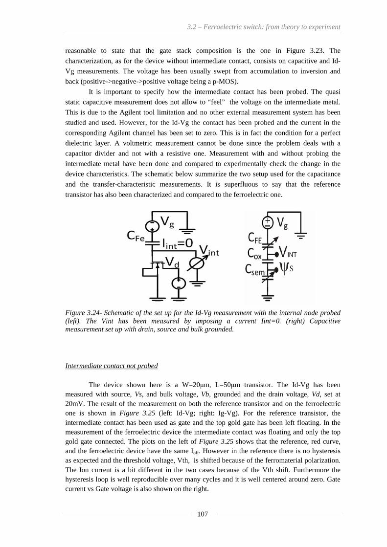
3.2 – Ferroelectric switch: from theory to experiment
107
reasonable to state that the gate stack composition is the one in Figure 3.23. The
characterization, as for the device without intermediate contact, consists on capacitive and Id-
Vg measurements. The voltage has been usually swept from accumulation to inversion and
back (positive->negative->positive voltage being a p-MOS).
It is important to specify how the intermediate contact has been probed. The quasi
static capacitive measurement does not allow to “feel” the voltage on the intermediate metal.
This is due to the Agilent tool limitation and no other external measurement system has been
studied and used. However, for the Id-Vg the contact has been probed and the current in the
corresponding Agilent channel has been set to zero. This is in fact the condition for a perfect
dielectric layer. A voltmetric measurement cannot be done since the problem deals with a
capacitor divider and not with a resistive one. Measurement with and without probing the
intermediate metal have been done and compared to experimentally check the change in the
device characteristics. The schematic below summarize the two setup used for the capacitance
and the transfer-characteristic measurements. It is superfluous to say that the reference
transistor has also been characterized and compared to the ferroelectric one.
Figure 3.24- Schematic of the set up for the Id-Vg measurement with the internal node probed (left). The Vint has been measured by imposing a current Iint=0. (right) Capacitive measurement set up with drain, source and bulk grounded. Intermediate contact not probed
The device shown here is a W=20μm, L=50μm transistor. The Id-Vg has been measured with source, Vs, and bulk voltage, Vb, grounded and the drain voltage, Vd, set at 20mV. The result of the measurement on both the reference transistor and on the ferroelectric one is shown in Figure 3.25 (left: Id-Vg; right: Ig-Vg). For the reference transistor, the intermediate contact has been used as gate and the top gold gate has been left floating. In the measurement of the ferroelectric device the intermediate contact was floating and only the top gold gate connected. The plots on the left of Figure 3.25 shows that the reference, red curve, and the ferroelectric device have the same Ioff. However in the reference there is no hysteresis as expected and the threshold voltage, Vth, is shifted because of the ferromaterial polarization. The Ion current is a bit different in the two cases because of the Vth shift. Furthermore the hysteresis loop is well reproducible over many cycles and it is well centered around zero. Gate current vs Gate voltage is also shown on the right.
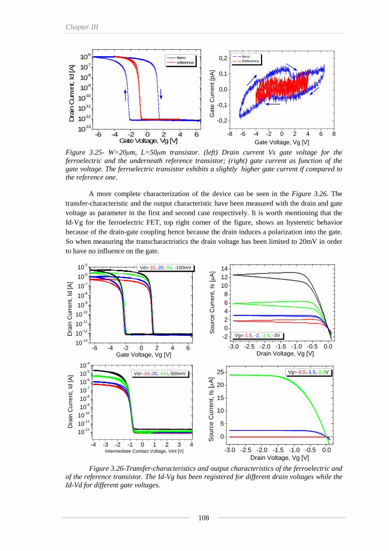
Chapter III
108
-6 -4 -2 0 2 4 610-13
10-12
10-11
10-10
10-9
10-8
10-7
10-6 ferro reference
Gate Voltage, Vg [V]
Dra
in C
urre
nt, I
d [A
]
-8 -6 -4 -2 0 2 4 6 8
-0,2
-0,1
0,0
0,1
0,2 ferro Reference
Gat
e C
urre
nt [p
A]
Gate Voltage, Vg [V] Figure 3.25- W=20μm, L=50μm transistor. (left) Drain current Vs gate voltage for the ferroelectric and the underneath reference transistor; (right) gate current as function of the gate voltage. The ferroelectric transistor exhibits a slightly higher gate current if compared to the reference one.
A more complete characterization of the device can be seen in the Figure 3.26. The transfer-characteristic and the output characteristic have been measured with the drain and gate voltage as parameter in the first and second case respectively. It is worth mentioning that the Id-Vg for the ferroelectric FET, top right corner of the figure, shows an hysteretic behavior because of the drain-gate coupling hence because the drain induces a polarization into the gate. So when measuring the transcharactristics the drain voltage has been limited to 20mV in order to have no influence on the gate.
Figure 3.26-Transfer-characteristics and output characteristics of the ferroelectric and of the reference transistor. The Id-Vg has been registered for different drain voltages while the Id-Vd for different gate voltages.
-6 -4 -2 0 2 4 610-13
10-12
10-11
10-10
10-9
10-8
10-7
10-6
10-5Vd=-10,-20,-50, -100mV
Gate Voltage, Vg [V]
Dra
in C
urre
nt, I
d [A
]
-3.0 -2.5 -2.0 -1.5 -1.0 -0.5 0.0
-202468
101214
Vg=-1.5, -2, -2.5, -3V
Drain Voltage, Vg [V]
Sou
rce
Cur
rent
, Is
[μA
]
-4 -3 -2 -1 0 1 2 3 4
10-1210-1110-1010-910-810-710-610-510-4
Vd=-10,-20,-100,-500mV
Dra
in C
urre
nt, I
d [A
]
Intermediate Contact Voltage, Vint [V]
-3.0 -2.5 -2.0 -1.5 -1.0 -0.5 0.0
0
5
10
15
20
25
Sou
rce
Cur
rent
, Is
[μA
]
Drain Voltage, Vg [V]
Vg=-0.5,-1.5,-2.5V
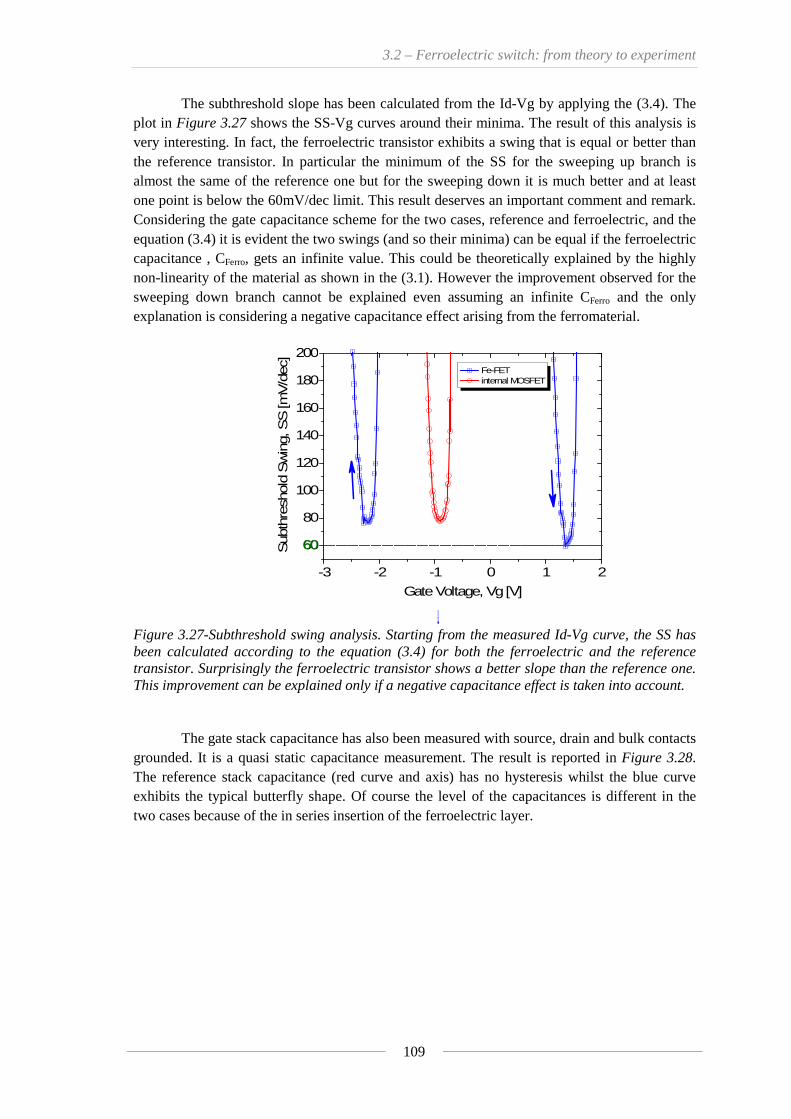
3.2 – Ferroelectric switch: from theory to experiment
109
The subthreshold slope has been calculated from the Id-Vg by applying the (3.4). The plot in Figure 3.27 shows the SS-Vg curves around their minima. The result of this analysis is very interesting. In fact, the ferroelectric transistor exhibits a swing that is equal or better than the reference transistor. In particular the minimum of the SS for the sweeping up branch is almost the same of the reference one but for the sweeping down it is much better and at least one point is below the 60mV/dec limit. This result deserves an important comment and remark. Considering the gate capacitance scheme for the two cases, reference and ferroelectric, and the equation (3.4) it is evident the two swings (and so their minima) can be equal if the ferroelectric capacitance , CFerro, gets an infinite value. This could be theoretically explained by the highly non-linearity of the material as shown in the (3.1). However the improvement observed for the sweeping down branch cannot be explained even assuming an infinite CFerro and the only explanation is considering a negative capacitance effect arising from the ferromaterial.
-3 -2 -1 0 1 2
60
80
100
120
140
160
180
200 Fe-FET internal MOSFET
Sub
thre
shol
d Sw
ing,
SS [m
V/d
ec]
Gate Voltage, Vg [V]
60
-3 -2 -1 01 260
80100
120140
160
180200 F e-FET in ternal MOSFET
Subthreshol
d Swing, SS [mV
/dec]
Ga te Voltage, V g [V]
60 Figure 3.27-Subthreshold swing analysis. Starting from the measured Id-Vg curve, the SS has been calculated according to the equation (3.4) for both the ferroelectric and the reference transistor. Surprisingly the ferroelectric transistor shows a better slope than the reference one. This improvement can be explained only if a negative capacitance effect is taken into account.
The gate stack capacitance has also been measured with source, drain and bulk contacts
grounded. It is a quasi static capacitance measurement. The result is reported in Figure 3.28. The reference stack capacitance (red curve and axis) has no hysteresis whilst the blue curve exhibits the typical butterfly shape. Of course the level of the capacitances is different in the two cases because of the in series insertion of the ferroelectric layer.
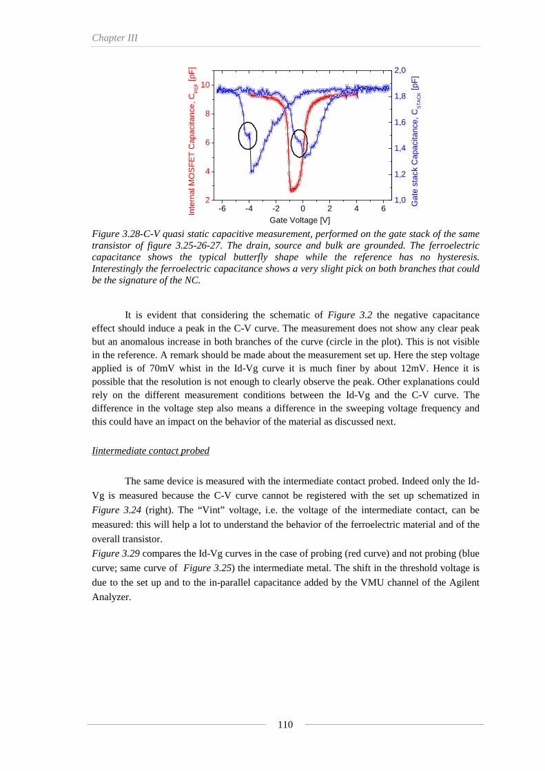
Chapter III
110
-6 -4 -2 0 2 4 62
4
6
8
10
Inte
rnal
MO
SF
ET
Cap
acita
nce,
CR
EF [p
F]
Gate Voltage [V]
1,0
1,2
1,4
1,6
1,8
2,0
Gat
e st
ack
Cap
acita
nce,
CS
TA
CK [p
F]
Figure 3.28-C-V quasi static capacitive measurement, performed on the gate stack of the same transistor of figure 3.25-26-27. The drain, source and bulk are grounded. The ferroelectric capacitance shows the typical butterfly shape while the reference has no hysteresis. Interestingly the ferroelectric capacitance shows a very slight pick on both branches that could be the signature of the NC.
It is evident that considering the schematic of Figure 3.2 the negative capacitance effect should induce a peak in the C-V curve. The measurement does not show any clear peak but an anomalous increase in both branches of the curve (circle in the plot). This is not visible in the reference. A remark should be made about the measurement set up. Here the step voltage applied is of 70mV whist in the Id-Vg curve it is much finer by about 12mV. Hence it is possible that the resolution is not enough to clearly observe the peak. Other explanations could rely on the different measurement conditions between the Id-Vg and the C-V curve. The difference in the voltage step also means a difference in the sweeping voltage frequency and this could have an impact on the behavior of the material as discussed next.
Iintermediate contact probed
The same device is measured with the intermediate contact probed. Indeed only the Id-
Vg is measured because the C-V curve cannot be registered with the set up schematized in
Figure 3.24 (right). The “Vint” voltage, i.e. the voltage of the intermediate contact, can be
measured: this will help a lot to understand the behavior of the ferroelectric material and of the
overall transistor.
Figure 3.29 compares the Id-Vg curves in the case of probing (red curve) and not probing (blue
curve; same curve of Figure 3.25) the intermediate metal. The shift in the threshold voltage is
due to the set up and to the in-parallel capacitance added by the VMU channel of the Agilent
Analyzer.
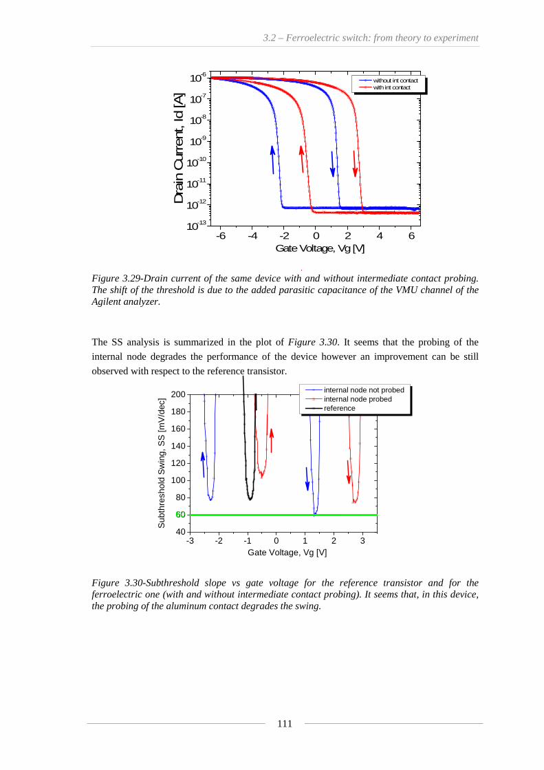
3.2 – Ferroelectric switch: from theory to experiment
111
-6 -4 -2 0 2 4 610-13
10-12
10-11
10-10
10-9
10-8
10-7
10-6 without int contact with int contact
Dra
in C
urre
nt, I
d [A
]
Gate Voltage, Vg [V] -6 -4-2 02 4610-1310
-1210-11
10-1010-9
10-810
-710-6 without int contact with int contact
Drain Curren
t, Id [A]
Gate Vo ltage, Vg [V] Figure 3.29-Drain current of the same device with and without intermediate contact probing. The shift of the threshold is due to the added parasitic capacitance of the VMU channel of the Agilent analyzer.
The SS analysis is summarized in the plot of Figure 3.30. It seems that the probing of the
internal node degrades the performance of the device however an improvement can be still
observed with respect to the reference transistor.
-3 -2 -1 0 1 2 340
60
80
100
120
140
160
180
200 internal node not probed internal node probed reference
Sub
thre
shol
d S
win
g, S
S [m
V/d
ec]
Gate Voltage, Vg [V]
60
Figure 3.30-Subthreshold slope vs gate voltage for the reference transistor and for the ferroelectric one (with and without intermediate contact probing). It seems that, in this device, the probing of the aluminum contact degrades the swing.
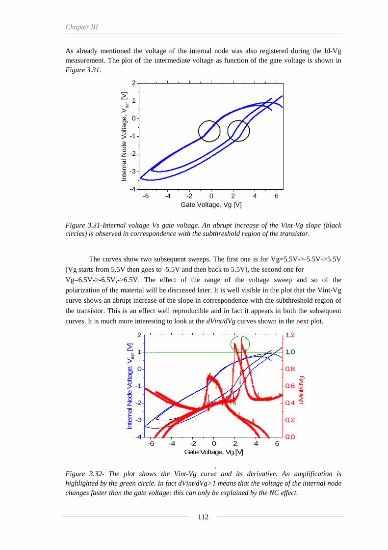
Chapter III
112
As already mentioned the voltage of the internal node was also registered during the Id-Vg measurement. The plot of the intermediate voltage as function of the gate voltage is shown in Figure 3.31.
-6 -4 -2 0 2 4 6-4
-3
-2
-1
0
1
2
Inte
rnal
Nod
e V
olta
ge, V
INT [V
]
Gate Voltage, Vg [V] -6 -4-2 02 46-4
-3
-2
-10
1
2
Internal Node
Voltage, VINT [V
]
Gate Vol tage, Vg [V] Figure 3.31-Internal voltage Vs gate voltage. An abrupt increase of the Vint-Vg slope (black circles) is observed in correspondence with the subthreshold region of the transistor.
The curves show two subsequent sweeps. The first one is for Vg=5.5V->-5.5V->5.5V
(Vg starts from 5.5V then goes to -5.5V and then back to 5.5V), the second one for
Vg=6.5V->-6.5V,->6.5V. The effect of the range of the voltage sweep and so of the
polarization of the material will be discussed later. It is well visible in the plot that the Vint-Vg
curve shows an abrupt increase of the slope in correspondence with the subthreshold region of
the transistor. This is an effect well reproducible and in fact it appears in both the subsequent
curves. It is much more interesting to look at the dVint/dVg curves shown in the next plot.
-6 -4 -2 0 2 4 6-4
-3
-2
-1
0
1
2
Inte
rnal
Nod
e Vol
tage
, VIN
T [V
]
Gate Voltage, Vg [V]
0.0
0.2
0.4
0.6
0.8
1.0
1.2
dVin
t/dVg
1.0
-6 -4 -2 02 4 6-4
-3
-2
-10
1
2
Internal Node
Voltage, VINT [V
]
Gate Vol tage, Vg [V ]
0.0
0.2
0.4
0.60.8
1.0
1.2
dVint/dVg
1.0 Figure 3.32- The plot shows the Vint-Vg curve and its derivative. An amplification is highlighted by the green circle. In fact dVint/dVg>1 means that the voltage of the internal node changes faster than the gate voltage: this can only be explained by the NC effect.

3.2 – Ferroelectric switch: from theory to experiment
113
The derivative of the internal node voltage with respect to the gate voltage has a peak, of course
in correspondence to the steep Vint-Vg slope. Interestingly, the peak exceeds the value one and
this for both sweeps. It is worth mentioning that dVint/dVg>1 means that the voltage on the
internal node changes faster than the gate voltage. This is a kind of amplification that cannot be
explained by assuming the capacitive schematic (see Figure 3.2) with standard positive
capacitances. This amplification has been attributed and explained with a negative capacitance
effect. However despite such amplification the subthreshold swing does not go below the
60mV/dec limit (see Figure 3.30). In order to better understand the overall behavior of the gate
stack it is important to better analyze the “m” term in equation (3.4).
For our particular structure it can be divided as follows:
int
int1
VV
V
Vm S
gg
S
∂∂
∂∂
=∂∂
=− ψψ (3.10)
It is evident that the term ∂Ψs/∂Vint is always less than 1 (related to the oxide capacitance). In
order to have a SS better than the theoretical limit the m-1 term has to be greater than one and so
the possible amplification of the ∂Ψint/∂Vg has to dominate over the other term. This means that
in this structure, but in general for a ferroelectric transistor with also a linear dielectric in the
stack, it is very important to have a good reference transistor in order to fully take advantage of
the possible amplification coming from the ferroelectric material. Developing further the
analysis, the polarization of the ferroelectric layer has been calculated as follows:
(i) the doping and the oxide capacitance have been extracted from the reference capacitance
measurement;
(ii) the surface potential is extracted by using the Tsividis model [5, 6]
(iii) the polarization is calculated by the Gauss Theorem:
ferro
ferro
goxide
oxide
s
ferroferrooxide
Pd
VV
d
V
PED
=⎥⎥⎦
⎤
⎢⎢⎣
⎡ −−
−
+=
0intint
0
εεψ
ε
(3.11)
Here a remark is mandatory. Equation (3.11) assumes that the only charge present in
the capacitive scheme is the charge on the capacitor plates and the charge of the polarization.
No other charge is taken into consideration, considering the structure as ideal. This is
considered reasonable since the SS of the reference transistor is quite good meaning that trap
charges in the oxide and the Si/SiO2 interface charges can be neglected.
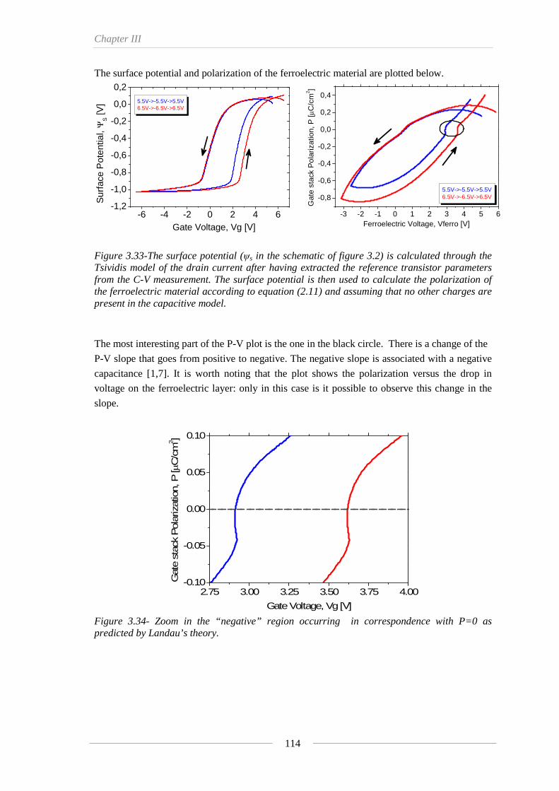
Chapter III
114
The surface potential and polarization of the ferroelectric material are plotted below.
-6 -4 -2 0 2 4 6-1,2
-1,0
-0,8
-0,6
-0,4
-0,2
0,0
0,2
5.5V->-5.5V->5.5V6.5V->-6.5V->6.5V
Sur
face
Pot
entia
l, Ψ
S [V
]
Gate Voltage, Vg [V]
-3 -2 -1 0 1 2 3 4 5 6
-0,8
-0,6
-0,4
-0,2
0,0
0,2
0,4
Gat
e st
ack
Pol
ariz
atio
n, P
[μC
/cm
2 ]
Ferroelectric Voltage, Vferro [V]
5.5V->-5.5V->5.5V6.5V->-6.5V->6.5V
Figure 3.33-The surface potential (ψs in the schematic of figure 3.2) is calculated through the Tsividis model of the drain current after having extracted the reference transistor parameters from the C-V measurement. The surface potential is then used to calculate the polarization of the ferroelectric material according to equation (2.11) and assuming that no other charges are present in the capacitive model.
The most interesting part of the P-V plot is the one in the black circle. There is a change of the
P-V slope that goes from positive to negative. The negative slope is associated with a negative
capacitance [1,7]. It is worth noting that the plot shows the polarization versus the drop in
voltage on the ferroelectric layer: only in this case is it possible to observe this change in the
slope.
2.75 3.00 3.25 3.50 3.75 4.00-0.10
-0.05
0.00
0.05
0.10
Gat
e st
ack
Pol
ariz
atio
n, P
[μC
/cm
2 ]
Gate Voltage, Vg [V] Figure 3.34- Zoom in the “negative” region occurring in correspondence with P=0 as predicted by Landau’s theory.
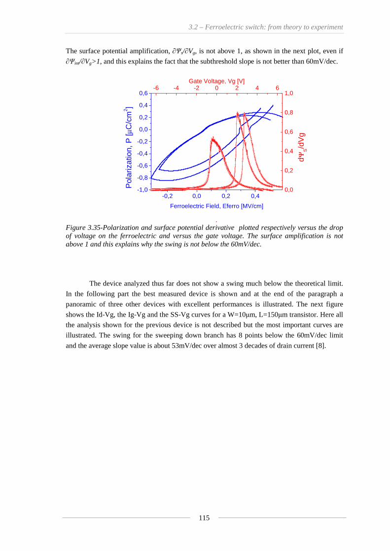
3.2 – Ferroelectric switch: from theory to experiment
115
The surface potential amplification, ∂Ψs/∂Vg, is not above 1, as shown in the next plot, even if
∂Ψint/∂Vg>1, and this explains the fact that the subthreshold slope is not better than 60mV/dec.
-0,2 0,0 0,2 0,4-1,0
-0,8
-0,6
-0,4
-0,2
0,0
0,2
0,4
0,6
Pol
ariz
atio
n, P
[μC
/cm
2 ]
Ferroelectric Field, Eferro [MV/cm]
-6 -4 -2 0 2 4 6
0,0
0,2
0,4
0,6
0,8
1,0
dΨS/d
Vg
Gate Voltage, Vg [V]
-0,2 0,0 0,2 0,4-1,0
-0,8
-0,6-0,4
-0,2
0,0
0,20,4
0,6
Polari
zation, P
[μC/cm2 ]
Ferroe lectric Fie ld, Eferro [MV/cm]
-6 -4 -2 02 4 6
0,0
0,2
0,4
0,6
0,8
1,0
dΨS/dVg
Figure 3.35-Polarization and surface potential derivative plotted respectively versus the drop of voltage on the ferroelectric and versus the gate voltage. The surface amplification is not above 1 and this explains why the swing is not below the 60mV/dec.
The device analyzed thus far does not show a swing much below the theoretical limit.
In the following part the best measured device is shown and at the end of the paragraph a
panoramic of three other devices with excellent performances is illustrated. The next figure
shows the Id-Vg, the Ig-Vg and the SS-Vg curves for a W=10μm, L=150μm transistor. Here all
the analysis shown for the previous device is not described but the most important curves are
illustrated. The swing for the sweeping down branch has 8 points below the 60mV/dec limit
and the average slope value is about 53mV/dec over almost 3 decades of drain current [8].
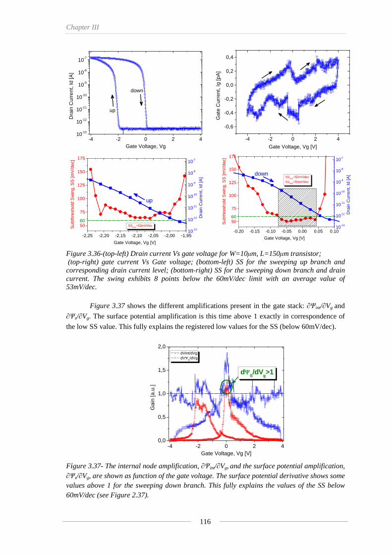
Chapter III
116
-4 -2 0 2 410-13
10-12
10-11
10-10
10-9
10-8
10-7
down
Dra
in C
urre
nt, I
d [A
]
Gate Voltage, Vg
up
-4 -2 0 2 4
-0,6
-0,4
-0,2
0,0
0,2
0,4
Gat
e C
urre
nt, I
g [p
A]
Gate Voltage, Vg [V]
-2,25 -2,20 -2,15 -2,10 -2,05 -2,00 -1,95
50
75
100
125
150
175
up
Sub
thre
shol
d S
win
g, S
S [m
V/d
ec]
Gate Voltage, Vg [V]
60SS
MIN=63mV/dec
10-13
10-12
10-11
10-10
10-9
10-8
10-7
Dra
in C
urre
nt, I
d [A
]
-0.20 -0.15 -0.10 -0.05 0.00 0.05 0.10
50
75
100
125
150
175
Sub
thre
shol
d S
win
g, S
S [m
V/d
ec]
Gate Voltage, Vg [V]
60
SSAVE
=53mV/dec
SSMIN
=50mV/dec
down
10-13
10-12
10-11
10-10
10-9
10-8
10-7
Dra
in C
urre
nt, I
d [A
]
Figure 3.36-(top-left) Drain current Vs gate voltage for W=10μm, L=150μm transistor; (top-right) gate current Vs Gate voltage; (bottom-left) SS for the sweeping up branch and corresponding drain current level; (bottom-right) SS for the sweeping down branch and drain current. The swing exhibits 8 points below the 60mV/dec limit with an average value of 53mV/dec.
Figure 3.37 shows the different amplifications present in the gate stack: ∂Ψint/∂Vg and
∂Ψs/∂Vg. The surface potential amplification is this time above 1 exactly in correspondence of
the low SS value. This fully explains the registered low values for the SS (below 60mV/dec).
-4 -2 0 2 40,0
0,5
1,0
1,5
2,0 dVint/dVg dVΨ
S/dVg
Gai
n [a
.u.]
Gate Voltage, Vg [V]
dΨS/dV
g>1
Figure 3.37- The internal node amplification, ∂Ψint/∂Vg, and the surface potential amplification, ∂Ψs/∂Vg, are shown as function of the gate voltage. The surface potential derivative shows some values above 1 for the sweeping down branch. This fully explains the values of the SS below 60mV/dec (see Figure 2.37).
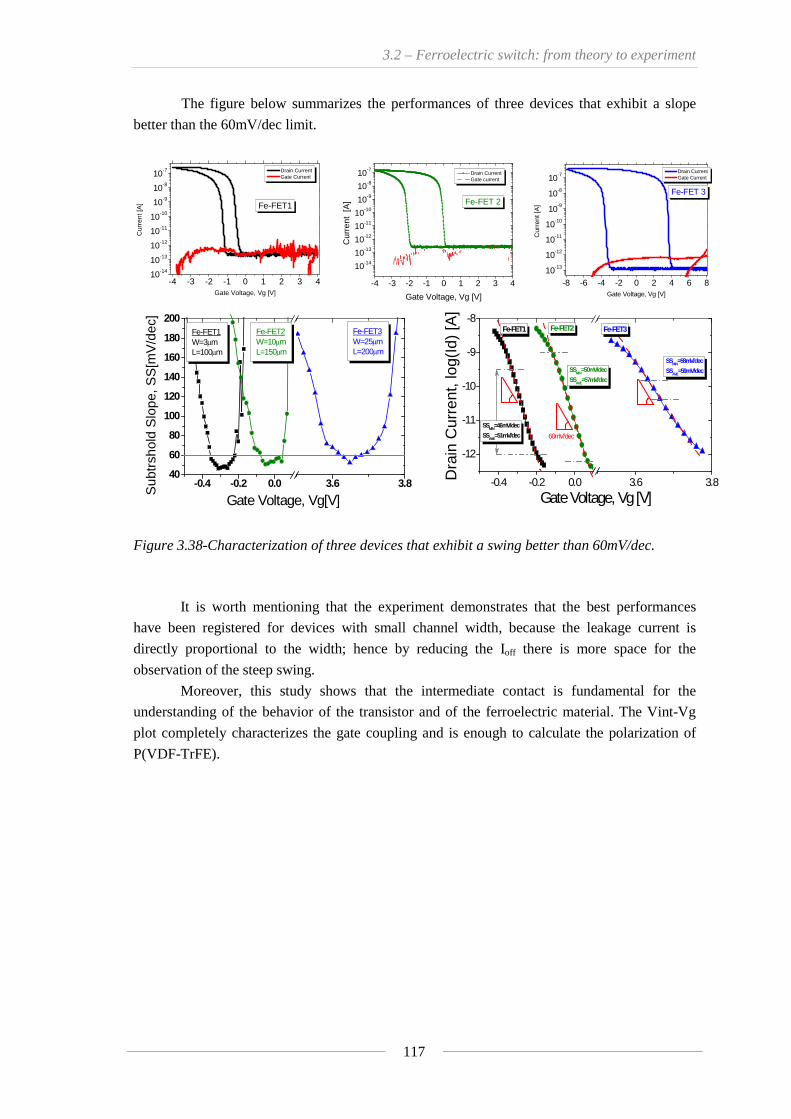
3.2 – Ferroelectric switch: from theory to experiment
117
The figure below summarizes the performances of three devices that exhibit a slope
better than the 60mV/dec limit.
-4 -3 -2 -1 0 1 2 3 410-14
10-13
10-12
10-11
10-10
10-9
10-8
10-7 Drain Current Gate Current
Cur
rent
[A]
Gate Voltage, Vg [V]
Fe-FET1
-4 -3 -2 -1 0 1 2 3 4
10-14
10-13
10-12
10-11
10-10
10-9
10-8
10-7 Drain Current Gate current
Cur
rent
[A
]
Gate Voltage, Vg [V]
Fe-FET 2
-8 -6 -4 -2 0 2 4 6 8
10-13
10-12
10-11
10-10
10-9
10-8
10-7 Drain Current Gate Current
Cur
rent
[A]
Gate Voltage, Vg [V]
Fe-FET 3
-0.4 -0.2 0.0 3.6 3.840
60
80
100
120
140
160
180
200Fe-FET3W=25μmL=200μm
Fe-FET2W=10μmL=150μm
Sub
trsh
old
Slo
pe, S
S[m
V/d
ec]
Gate Voltage, Vg[V]
Fe-FET1W=3μmL=100μm
-0.4 -0.2 0.0 3.6 3.8
-12
-11
-10
-9
-8
SSMIN
=58mV/dec
SSAVE
=59mV/decSSMIN
=50mV/dec
SSAVE
=58mV/dec
SSMIN
=50mV/dec
SSAVE
=57mV/dec
SSMIN
=46mV/dec
SSAVE
=51mV/dec
Fe-FET3Fe-FET2Fe-FET1
Dra
in C
urre
nt, l
og(I
d) [A
]
Gate Voltage, Vg [V]
60mV/dec
Figure 3.38-Characterization of three devices that exhibit a swing better than 60mV/dec.
It is worth mentioning that the experiment demonstrates that the best performances
have been registered for devices with small channel width, because the leakage current is
directly proportional to the width; hence by reducing the Ioff there is more space for the
observation of the steep swing.
Moreover, this study shows that the intermediate contact is fundamental for the
understanding of the behavior of the transistor and of the ferroelectric material. The Vint-Vg
plot completely characterizes the gate coupling and is enough to calculate the polarization of
P(VDF-TrFE).

Chapter III
118
Performance Sensitivity to experimental conditions
In the previous paragraph a complete characterization of some devices has been shown.
Here, instead, the attention is focussed on some measurement conditions and parameters and
their influence on the performances of the transistor. It has already been observed that the
Vint-Vg plot is sufficient to understand the gate stack behavior; hence just this curve is used to
illustrate some effects typical of a ferroelectric stack.
The first parameter that can change the polarization condition, and hence the
performance, of the switch is the range of the voltage sweep. Figure 3.39 shows that enlarging
the range and going from 3V to 5V up to 7V the amplification ∂Ψint/∂Vg changes and in this
particular case it increases [5]. This is not yet well understood but of course is related to the
polarization of the material.
Figure 3.39-(left) Vint-Vg curve for different voltage sweep. (right) derivative of the internal voltage. The range of the sweeping voltage modulates the amplification.
The second parameter that has been changed in the measurements is the loop
frequency, i.e. the frequency to register a complete voltage double sweep (Figure 3.40). This
also influences the Vint-Vg plot and the experiments suggest that by decreasing the frequency
untill a certain value of the amplification increases. This could be explained by considering that
the ferroelectric material needs a certain time to become polarized; once it is polarized any
further reduction of the frequency has no impact on its condition.
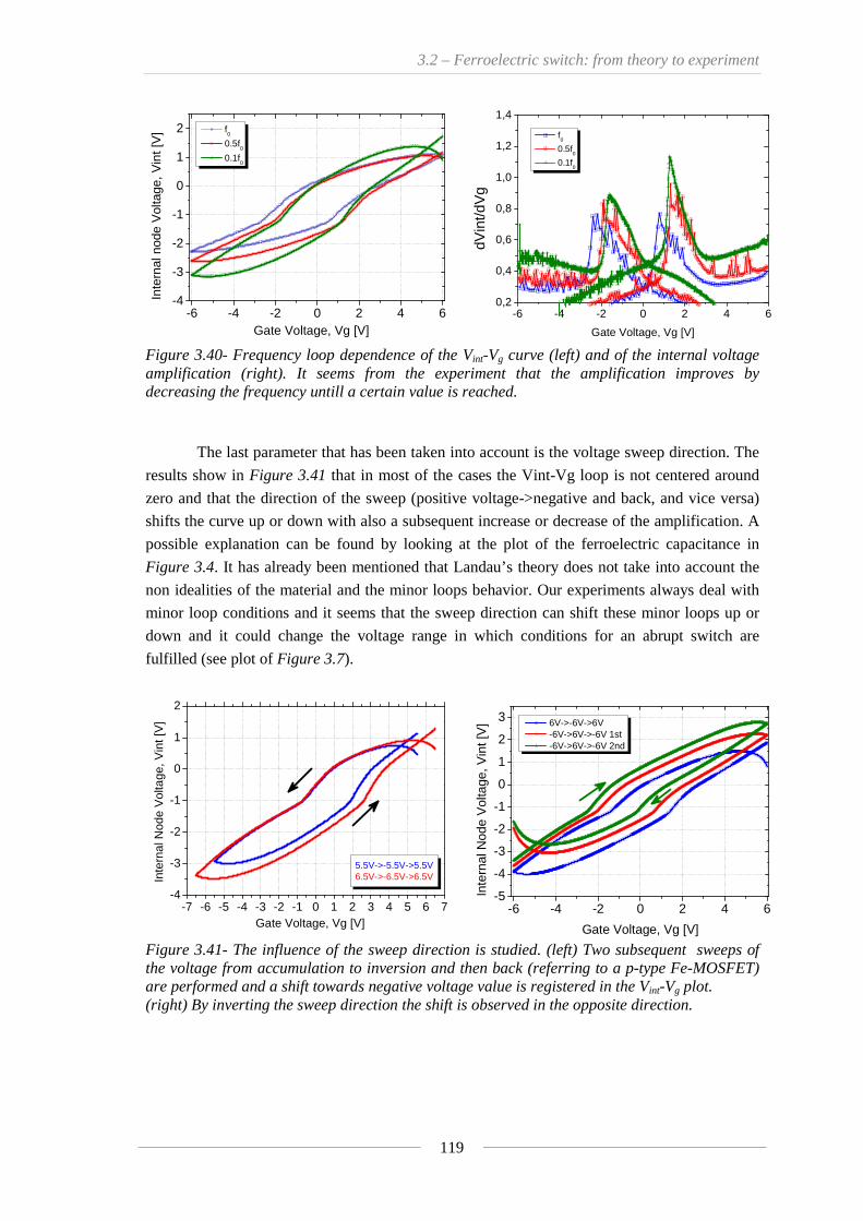
3.2 – Ferroelectric switch: from theory to experiment
119
-6 -4 -2 0 2 4 6-4
-3
-2
-1
0
1
2
Inte
rnal
nod
e V
olta
ge, V
int [
V]
Gate Voltage, Vg [V]
f0
0.5f0
0.1f0
-6 -4 -2 0 2 4 60,2
0,4
0,6
0,8
1,0
1,2
1,4
f0
0.5f0
0.1f0
dVin
t/dV
g
Gate Voltage, Vg [V] Figure 3.40- Frequency loop dependence of the Vint-Vg curve (left) and of the internal voltage amplification (right). It seems from the experiment that the amplification improves by decreasing the frequency untill a certain value is reached.
The last parameter that has been taken into account is the voltage sweep direction. The
results show in Figure 3.41 that in most of the cases the Vint-Vg loop is not centered around
zero and that the direction of the sweep (positive voltage->negative and back, and vice versa)
shifts the curve up or down with also a subsequent increase or decrease of the amplification. A
possible explanation can be found by looking at the plot of the ferroelectric capacitance in
Figure 3.4. It has already been mentioned that Landau’s theory does not take into account the
non idealities of the material and the minor loops behavior. Our experiments always deal with
minor loop conditions and it seems that the sweep direction can shift these minor loops up or
down and it could change the voltage range in which conditions for an abrupt switch are
fulfilled (see plot of Figure 3.7).
-7 -6 -5 -4 -3 -2 -1 0 1 2 3 4 5 6 7-4
-3
-2
-1
0
1
2
Inte
rnal
Nod
e V
olta
ge, V
int [
V]
Gate Voltage, Vg [V]
5.5V->-5.5V->5.5V6.5V->-6.5V->6.5V
-6 -4 -2 0 2 4 6-5
-4
-3
-2
-1
0
1
2
3 6V->-6V->6V -6V->6V->-6V 1st -6V->6V->-6V 2nd
Inte
rnal
Nod
e V
olta
ge, V
int [
V]
Gate Voltage, Vg [V] Figure 3.41- The influence of the sweep direction is studied. (left) Two subsequent sweeps of the voltage from accumulation to inversion and then back (referring to a p-type Fe-MOSFET) are performed and a shift towards negative voltage value is registered in the Vint-Vg plot. (right) By inverting the sweep direction the shift is observed in the opposite direction.
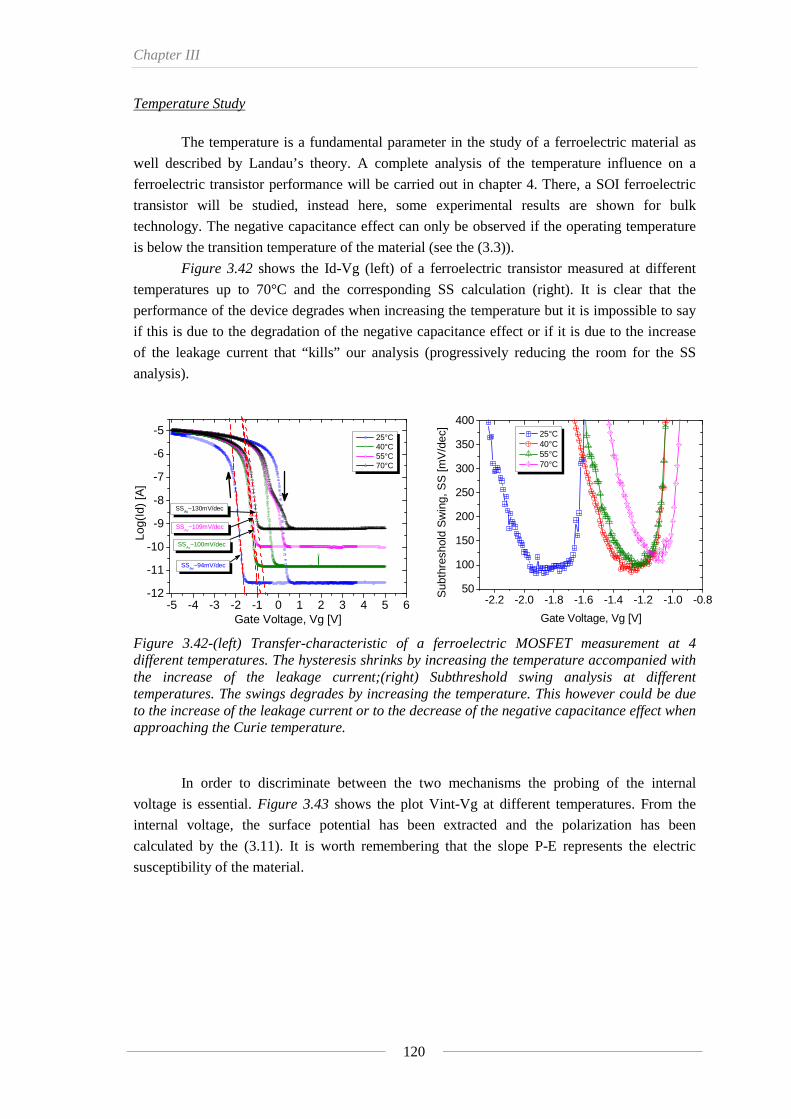
Chapter III
120
Temperature Study The temperature is a fundamental parameter in the study of a ferroelectric material as
well described by Landau’s theory. A complete analysis of the temperature influence on a
ferroelectric transistor performance will be carried out in chapter 4. There, a SOI ferroelectric
transistor will be studied, instead here, some experimental results are shown for bulk
technology. The negative capacitance effect can only be observed if the operating temperature
is below the transition temperature of the material (see the (3.3)).
Figure 3.42 shows the Id-Vg (left) of a ferroelectric transistor measured at different
temperatures up to 70°C and the corresponding SS calculation (right). It is clear that the
performance of the device degrades when increasing the temperature but it is impossible to say
if this is due to the degradation of the negative capacitance effect or if it is due to the increase
of the leakage current that “kills” our analysis (progressively reducing the room for the SS
analysis).
Figure 3.42-(left) Transfer-characteristic of a ferroelectric MOSFET measurement at 4 different temperatures. The hysteresis shrinks by increasing the temperature accompanied with the increase of the leakage current;(right) Subthreshold swing analysis at different temperatures. The swings degrades by increasing the temperature. This however could be due to the increase of the leakage current or to the decrease of the negative capacitance effect when approaching the Curie temperature.
In order to discriminate between the two mechanisms the probing of the internal
voltage is essential. Figure 3.43 shows the plot Vint-Vg at different temperatures. From the
internal voltage, the surface potential has been extracted and the polarization has been
calculated by the (3.11). It is worth remembering that the slope P-E represents the electric
susceptibility of the material.
-5 -4 -3 -2 -1 0 1 2 3 4 5 6-12
-11
-10
-9
-8
-7
-6
-5 25°C 40°C 55°C 70°C
SSAv
~130mV/dec
SSAv
~109mV/dec
Log(
Id)
[A]
Gate Voltage, Vg [V]
SSAv
~94mV/dec
SSAv
~100mV/dec
-2.2 -2.0 -1.8 -1.6 -1.4 -1.2 -1.0 -0.850
100
150
200
250
300
350
400 25°C 40°C 55°C 70°C
Sub
thre
shol
d S
win
g, S
S [m
V/d
ec]
Gate Voltage, Vg [V]
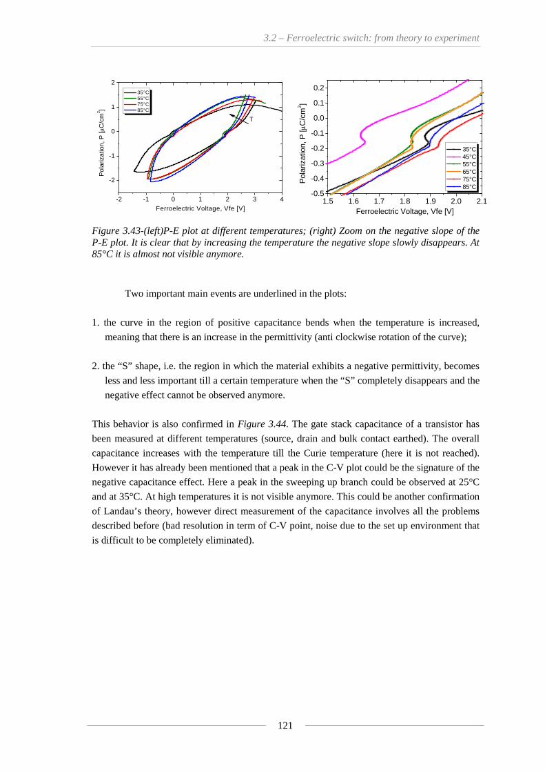
3.2 – Ferroelectric switch: from theory to experiment
121
-2 -1 0 1 2 3 4
-2
-1
0
1
2
35°C 55°C 75°C 85°C
Pol
ariz
atio
n, P
[μC
/cm
2 ]
Ferroelectric Voltage, Vfe [V]
T
1.5 1.6 1.7 1.8 1.9 2.0 2.1
-0.5
-0.4
-0.3
-0.2
-0.1
0.0
0.1
0.2
35°C 45°C 55°C 65°C 75°C 85°C
Pol
ariz
atio
n, P
[μC
/cm
2 ]
Ferroelectric Voltage, Vfe [V]
Figure 3.43-(left)P-E plot at different temperatures; (right) Zoom on the negative slope of the P-E plot. It is clear that by increasing the temperature the negative slope slowly disappears. At 85°C it is almost not visible anymore.
Two important main events are underlined in the plots:
1. the curve in the region of positive capacitance bends when the temperature is increased,
meaning that there is an increase in the permittivity (anti clockwise rotation of the curve);
2. the “S” shape, i.e. the region in which the material exhibits a negative permittivity, becomes
less and less important till a certain temperature when the “S” completely disappears and the
negative effect cannot be observed anymore.
This behavior is also confirmed in Figure 3.44. The gate stack capacitance of a transistor has
been measured at different temperatures (source, drain and bulk contact earthed). The overall
capacitance increases with the temperature till the Curie temperature (here it is not reached).
However it has already been mentioned that a peak in the C-V plot could be the signature of the
negative capacitance effect. Here a peak in the sweeping up branch could be observed at 25°C
and at 35°C. At high temperatures it is not visible anymore. This could be another confirmation
of Landau’s theory, however direct measurement of the capacitance involves all the problems
described before (bad resolution in term of C-V point, noise due to the set up environment that
is difficult to be completely eliminated).
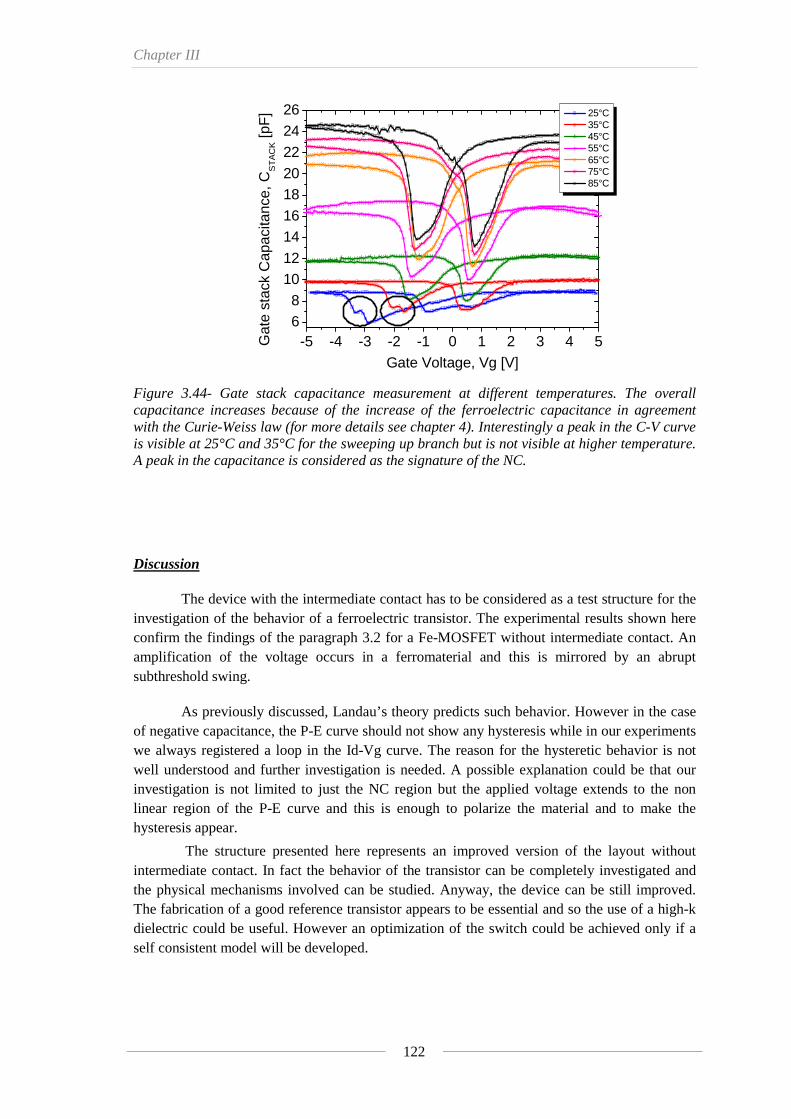
Chapter III
122
-5 -4 -3 -2 -1 0 1 2 3 4 568
1012
1416
1820
22
24
26 25°C 35°C 45°C 55°C 65°C 75°C 85°C
Gat
e st
ack
Cap
acita
nce,
CS
TA
CK [p
F]
Gate Voltage, Vg [V]
Figure 3.44- Gate stack capacitance measurement at different temperatures. The overall capacitance increases because of the increase of the ferroelectric capacitance in agreement with the Curie-Weiss law (for more details see chapter 4). Interestingly a peak in the C-V curve is visible at 25°C and 35°C for the sweeping up branch but is not visible at higher temperature. A peak in the capacitance is considered as the signature of the NC.
Discussion
The device with the intermediate contact has to be considered as a test structure for the investigation of the behavior of a ferroelectric transistor. The experimental results shown here confirm the findings of the paragraph 3.2 for a Fe-MOSFET without intermediate contact. An amplification of the voltage occurs in a ferromaterial and this is mirrored by an abrupt subthreshold swing.
As previously discussed, Landau’s theory predicts such behavior. However in the case of negative capacitance, the P-E curve should not show any hysteresis while in our experiments we always registered a loop in the Id-Vg curve. The reason for the hysteretic behavior is not well understood and further investigation is needed. A possible explanation could be that our investigation is not limited to just the NC region but the applied voltage extends to the non linear region of the P-E curve and this is enough to polarize the material and to make the hysteresis appear.
The structure presented here represents an improved version of the layout without intermediate contact. In fact the behavior of the transistor can be completely investigated and the physical mechanisms involved can be studied. Anyway, the device can be still improved. The fabrication of a good reference transistor appears to be essential and so the use of a high-k dielectric could be useful. However an optimization of the switch could be achieved only if a self consistent model will be developed.
3.3 – Summary
123
3.3 Summary
This chapter starts out by describing the negative capacitance (NC) effect and how it can be used for the design of an abrupt ferroelectric switch. The conditions for stability and for having a less than 60mV/dec switch are discussed and a design procedure is illustrated. The second part of the chapter focuses on the experimental results. Two different devices are shown. The first one is a ferroelectric MOSFET with 10nm of silicon oxide and 40nm of P(VDF-TRFE) as dielectric stack. The second device gate stack was made up of a 10nm SiO2, a 100nm P(VDF-TrFE) and a 50nm Al layer as intermediate contact. In both cases a swing less 60mV/dec was registered. This behavior was finally attributed to and explained by a voltage amplification occurring in the ferroelectric material. The original work carried out relative to this chapter includes: Design. A ferroelectric transistor on bulk silicon with a linear dielectric layer is considered. Landau’s theory was used to model an equivalent ferroelectric capacitance that is, then, inserted in the equation of the subthreshold swing for a MOSFET. The conditions for designing a stable and less than 60mV/dec ferroelectric switch were found and a qualitative example of a well designed device was also reported. Abrupt ferroelectric switch demonstration. Two different layouts of a ferroelectric MOSFET were fabricated and characterized for switch application, demonstrating, for the first time, less than 60mV/dec swing. The improved layout device has an average swing of 53mV/dec for a corresponding drain current variation of about 3 order of magnitude, from 400fA up to 200pA. Finally, thanks to the probing of the ferroelectric/oxide interface voltage, this behavior has been explained by a ∂Ψint/∂Vg amplification that is mirrored in an abrupt switch. The ferroelectric material polarization was calculated and a negative P-E slope has been found as proof of a negative permittivity occurring for P≈0 as predicted by theory.
Experimental condition study. The negative capacitance dependence on the voltage sweep range, on the frequency loop, on the voltage sweep direction and finally on the temperature was studied. All these parameters influence the performance of the ferroelectric switch, particularly, the temperature. Landau’s theory predicts that the NC effect decreases by approaching the Curie temperature of the material. The prediction was experimentally validated by measuring the degradation of the subthreshold swing and by calculating the P-E curves at each investigated temperature.
Chapter III - Bibliography
Bibliography
[1] S. Salahuddin, S. Datta, “Use of Negative Capacitance to Provide Voltage Amplification for Low Power Nanoscale Devices”, Nanoletters Vol.8 No.2 405-410 (2008).
[2] S. Salahuddin, S. Datta, “Can the subthreshold swing in a classical FET be lowered below 60 mV/decade?”, IEDM Digest, pp. 693-696, (2008).
[3] H. Ishiwara, “Current status and prospects of FET-type ferreoelctric memories”,
J. Semicond. Technol. Sci., vol. 1, pp. 1–14, (2001)
[4] S. Ducharme et Al. “Intrinsic ferroelectric coercive field”, Ph. Rev. Letters, Vol. 84 No. 1, (2000.)
[5] Al. Rusu, G. A. Salvatore, A. M. Ionescu, "Test Structure and Method for the Experimental Investigation of Internal Voltage Amplification and Surface Potential of Ferroelectric MOSFETs", ESSDERC 2010, 13-17 September, Sevilles, Spain (2010).
[6] Y. Tsividis, “Operation and Modeling of the MOS Transistor”, 2nd Edition, McGraw Hill, (1999).
[7] A. M. Bratkovsky, A. P. Levanyuk, “Depolarizing field and “real” hysteresis loops in nanometer-scale ferroelectric films”, Appl. Phys. Lett. 89, 253108, (2006).
[8] Al. Rusu, G. A. Salvatore, D. Jiménez, A. M. Ionescu, "Metal-Ferroelectric-Metal-Oxide-Semiconductor Field Effect Transistor with Sub-60mV/decade Subthreshold Swing and Internal Voltage Amplification" to appear in IEDM 2010.
Chapter 4
Temperature performance of a ferroelectric transistor
In this chapter the temperature dependence of the performance (static characteristic and
capacitances) of a ferroelectric transistor are studied. Landau’s theory and the standard MOSFET
equations are used to model the behavior of a ferroelectric transistor, Fe-MOSFET. The model is
then validated through the characterization of a SOI Fe-MOSFET. The study proposed in this
chapter suggests that the temperature is a key parameter in the design when dealing with a
ferroelectric transistor. Moreover this study highlights new functionalities of such a device and
these anomalous physical mechanisms could be exploited for new applications, such as
temperature sensing and energy harvesting.

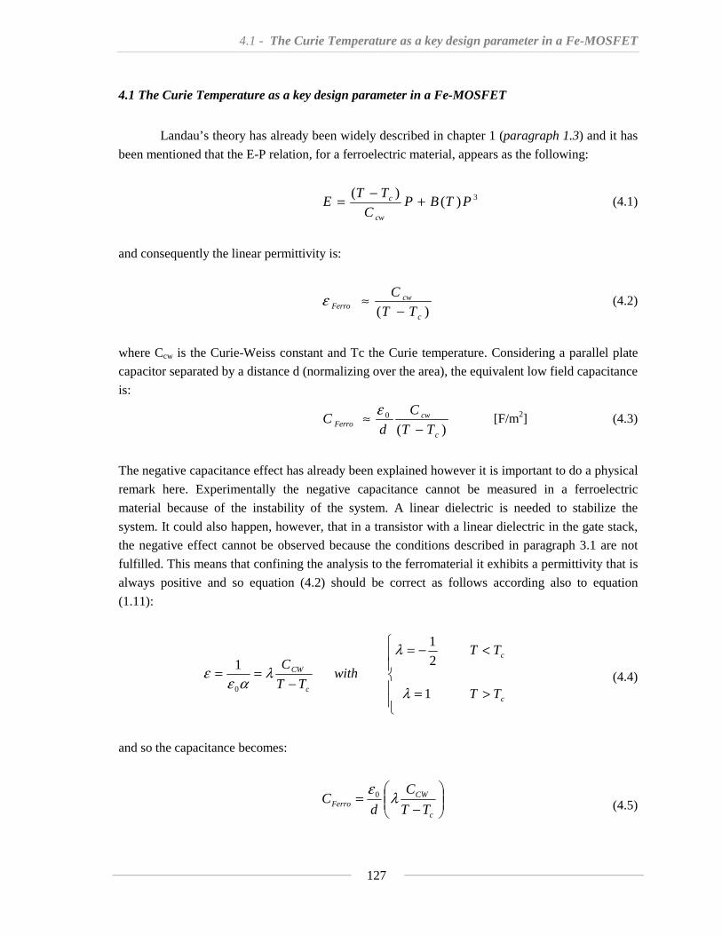
4.1 - The Curie Temperature as a key design parameter in a Fe-MOSFET
127
4.1 The Curie Temperature as a key design parameter in a Fe-MOSFET
Landau’s theory has already been widely described in chapter 1 (paragraph 1.3) and it has
been mentioned that the E-P relation, for a ferroelectric material, appears as the following:
3)()(
PTBPC
TTE
cw
c +−= (4.1)
and consequently the linear permittivity is:
)( c
cwFerro TT
C
−≈ε (4.2)
where Ccw is the Curie-Weiss constant and Tc the Curie temperature. Considering a parallel plate
capacitor separated by a distance d (normalizing over the area), the equivalent low field capacitance
is:
)(0
c
cwFerro TT
C
dC
−≈ ε
[F/m2] (4.3)
The negative capacitance effect has already been explained however it is important to do a physical
remark here. Experimentally the negative capacitance cannot be measured in a ferroelectric
material because of the instability of the system. A linear dielectric is needed to stabilize the
system. It could also happen, however, that in a transistor with a linear dielectric in the gate stack,
the negative effect cannot be observed because the conditions described in paragraph 3.1 are not
fulfilled. This means that confining the analysis to the ferromaterial it exhibits a permittivity that is
always positive and so equation (4.2) should be correct as follows according also to equation
(1.11):
⎪⎪⎩
⎪⎪⎨
⎧
>=
<−=
−==
c
c
c
CW
TT
TT
withTT
C
1
2
1
1
0 λ
λλ
αεε (4.4)
and so the capacitance becomes:
⎟⎟⎠
⎞⎜⎜⎝
⎛−
=c
CWFerro TT
C
dC λε 0
(4.5)
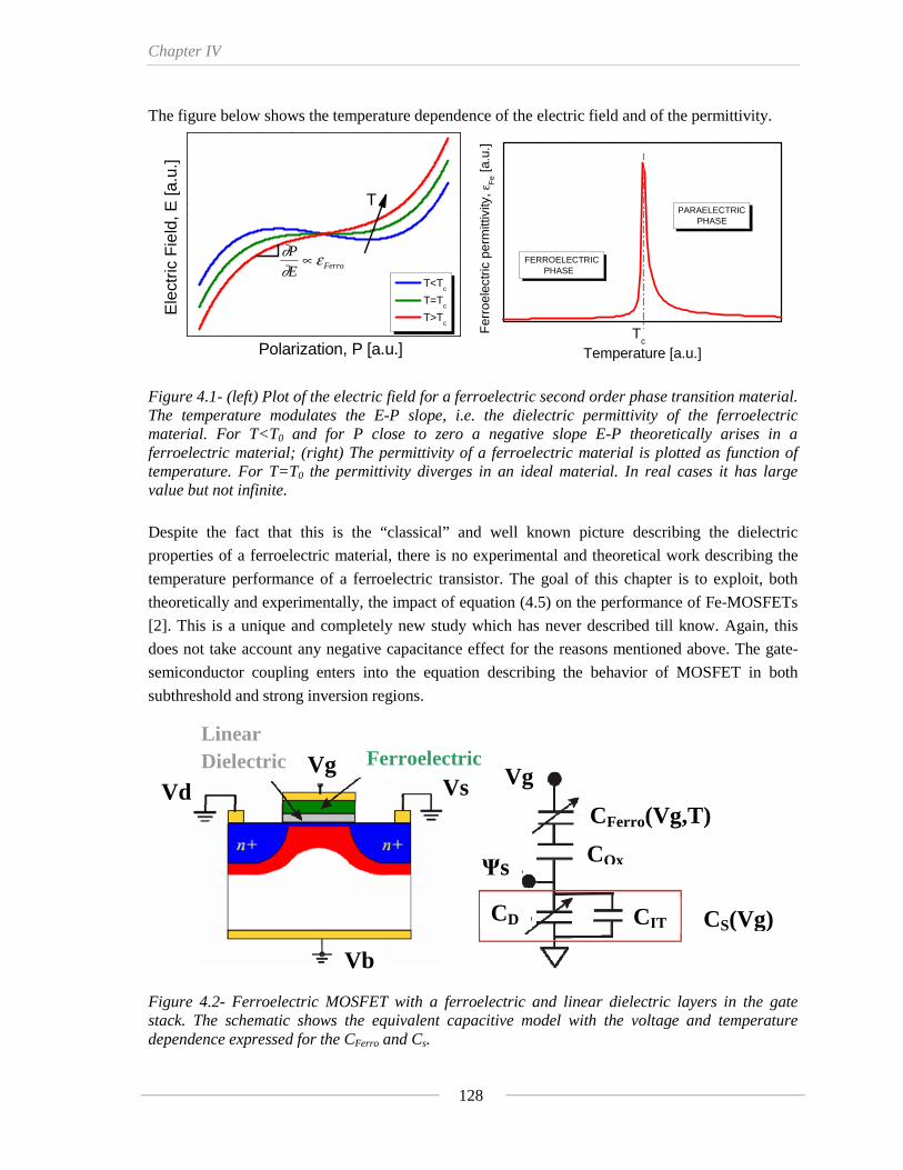
Chapter IV
128
The figure below shows the temperature dependence of the electric field and of the permittivity.
T<Tc
T=Tc
T>Tc
FerroE
P ε∂∂ ∝
Ele
ctric
Fie
ld, E
[a.u
.]
Polarization, P [a.u.]
T
PARAELECTRIC PHASE
Fer
roel
ectr
ic p
erm
ittiv
ity, ε
Fe
[a.u
.]
Temperature [a.u.]T
c
FERROELECTRIC PHASE
Figure 4.1- (left) Plot of the electric field for a ferroelectric second order phase transition material. The temperature modulates the E-P slope, i.e. the dielectric permittivity of the ferroelectric material. For T<T0 and for P close to zero a negative slope E-P theoretically arises in a ferroelectric material; (right) The permittivity of a ferroelectric material is plotted as function of temperature. For T=T0 the permittivity diverges in an ideal material. In real cases it has large value but not infinite.
Despite the fact that this is the “classical” and well known picture describing the dielectric
properties of a ferroelectric material, there is no experimental and theoretical work describing the
temperature performance of a ferroelectric transistor. The goal of this chapter is to exploit, both
theoretically and experimentally, the impact of equation (4.5) on the performance of Fe-MOSFETs
[2]. This is a unique and completely new study which has never described till know. Again, this
does not take account any negative capacitance effect for the reasons mentioned above. The gate-
semiconductor coupling enters into the equation describing the behavior of MOSFET in both
subthreshold and strong inversion regions.
Figure 4.2- Ferroelectric MOSFET with a ferroelectric and linear dielectric layers in the gate stack. The schematic shows the equivalent capacitive model with the voltage and temperature dependence expressed for the CFerro and Cs.
Ferroelectric Linear Dielectric
Vd Vg
Vs
Vb
Vg
Ψs
CFerro(Vg,T)
COx
CS(Vg) CIT CD
4.1 - The Curie Temperature as a key design parameter in a Fe-MOSFET
129
Based on equation (4.5) and considering a standard n-type MOSFET (see Figure 4.2) with
a ferroelectric layer in its gate stack, it is possible to derive the gate-stack capacitance, CFe-MOS, as
the equivalent in-series connection of a ferroelectric capacitance of thickness d and of a silicon
oxide capacitance, COX at low transversal field :
( ) ( )cOXCW
CWOXMOSFe TTdCC
CCTC
−+=−
0
0
λελε
(4.6)
This equation is fundamental to explaining the behavior of a Fe-FET because this gate capacitance
has to replace the COX of a classical FET. The (4.6) exhibits a maximum for T=Tc when the
ferroelectric capacitance ideally diverges and this greatly impacts on the transconductance and on
the subthreshold swing of the transistor. Moreover, the design of the gate stack capacitance can be
optimized taking by into account that the transition temperature of a stack changes according to its
composition:
d
CWcc
CqTT
α−=* (4.7)
where q and αd are the volume concentration and the permittivity of the linear dielectric
respectively [1]. This effect, originating from the incomplete compensation of the spontaneous
polarization, reduces the polarization in such a way that the ferroelectric/dielectric sandwich
behaves like a ferroelectric material with a lower transition temperature.
In standard silicon MOSFETs, temperature change, mainly, impacts the threshold voltage,
Vth, the carrier mobility in the channel, μ, and the junction leakage, degrading the drain current, Id,
the transconductance, gm=dId/dVg. and the inverse subthreshold slope, SS=[dlogId/dVg]-1. The
threshold voltage reads as follow [2]:
OX
FASiFFBth C
NqVV
φεφ
42 ++= (4.8)
where VFB is the flat band voltage, ΦF is the pseudo-fermi level, q is the electron charge, εSi is the
silicon permittivity and NA is the doping concentration. The threshold drift with the temperature is
almost linear and essentially due to the KBT/q term (neglecting the dependence of the intrinsic
doping concentration). It is about 4mV/K for a multigate SOI device [3]. In a ferroelectric
transistor the dependence is not linear because of the contribution of the ferroelectric material; in
fact by replacing COX, in the (4.8), with the (4.6), it gives:
( )0
042λε
λεφεφCWOX
cOXCWFASiFFBth CC
TTdCCNqVV
−+++= (4.9)
Chapter IV
130
The standard MOSFET trend is recovered when approaching Tc.
The drain current in the linear region of operation of a standard transistor can be written as:
( ) ( ) ⎥⎦⎤
⎢⎣⎡ −−= 2
, 2
1)()( dthgdOXMOSd VTVVVCT
L
WTI μ
(4.10)
where W/L is the channel width/length ratio and μ is the mobility. In addition to the already
mentioned Vth, the increase in the temperature degrades the carrier mobility and hence the drain
current. The shift of the threshold voltage and the decrease of the drain current in the strong
inversion region set a point where the curves at different temperatures cross each other and this
crossing point is usually used in circuit design as a bias point in order to avoid any temperature
variability.
For a ferroelectric transistor, the drain current and the transconductance become:
( ) ( ) ⎥⎦⎤
⎢⎣⎡ −−
−+=−
2
0
0, 2
1)()()( dthgd
cOXCW
CWOXMOSFed VTVVV
TTdCC
CCT
L
WTI
λελεμ
(4.11)
( ) dcOXCW
CWOXKT
g
dMOSFem V
TTdCC
CC
K
T
L
W
V
ITg
−+⎟⎟⎠
⎞⎜⎜⎝
⎛=
∂∂
= =−0
0300, 300
)(λε
λεμ
γ
(4.12)
where we substituted COX with CFe-MOS, moreover a power law of coefficient γ has been assumed
for the mobility degradation with the temperature (in silicon MOSFET the value of coefficient γ is
around -1.5 [4]). Equations (4.11) and (4.12) show that in Fe-FET, in addition to the mobility and
threshold dependences on the temperature, one should also carefully consider the change of the
equivalent gate ferroelectric capacitance when the temperature varies. Very interestingly, equation
(4.12) predicts a unique feature of any Fe-MOSFET that was not exploited to date: when
approaching the Curie temperature, if the ferroelectric/paralectric gate capacitance variation
dominates the mobility and threshold voltage dependences with temperature, the transconductance
and, particularly, its peak, gmax, should reach a maximum at T=Tc followed by a decrease for T>Tc.
Such behavior could be interesting for new applications of Fe-FETs as switches with performance
(on-current and transconductance) improvement at high temperature.
4.1 - The Curie Temperature as a key design parameter in a Fe-MOSFET
131
Another major feature of a transistor is the abruptness of the off-to-on current transition,
which is mirrored by the subthreshold swing (or inverse subthreshold slope), SS, as already widely
described in chapter 1 and 3. The SS usually linearly degrades with the temperature in any
conventional MOSFETs. For a MOSFET in weak inversion the drain current is an exponential
function of the gate voltage [5] and the swing is expressed in millivolts per decade (mV/dec) being
defined as:
10ln10ln1)(log)(log q
TK
q
TK
C
C
C
C
I
V
I
VSS B
n
B
m
OX
IT
OX
D
n
d
S
m
S
g
d
g ≥⎟⎟⎠
⎞⎜⎜⎝
⎛++≅
∂∂
∂∂
=∂
∂=
4342144 344 2143421
ψψ (4.13)
where CD and CIT are the depletion and the interface charge capacitance respectively. The factor m
is also called the body factor, reflecting the gate-to-semiconductor coupling, while the n parameter
describes the conduction mechanism in the channel, setting the limit of 60mV/dec at room
temperature (300K) for silicon MOSFET. The significance of equation (13) in terms of SS
dependence on temperature is that for conventional MOSFET (bulk or Silicon-On-Insulator), SS is
increasing (i.e. degrading) linearly when T increases.
The behavior is completely different in a Fe-MOSFET, in which the gate dielectric is
formed by a ferroelectric/oxide stack and the temperature dependence of the ferroelectric layer
capacitance improves the gate coupling and the electrostatic control when the temperature
approaches the Curie temperature. Therefore, the body factor of the Fe-MOSFET has a specific
temperature dependence given by:
CWS
OX
SMOSFe C
TTdC
C
CTm
λε0
01)(−++=− (4.14)
where CS= CD+CIT (Figure 4.2). An important consequence is that the subthreshold swing of a Fe-
MOSFET shall then follow a parabolic dependence on temperature:
2
00
0 10ln10ln1
10ln)()( T
q
K
C
dCT
q
K
C
TdC
C
CT
q
KTmTSS B
CW
SB
CW
S
OX
SBMOSFeMOSFe λελε
+⎥⎦
⎤⎢⎣
⎡−+=≈ −− (4.15)
in strong contrast with the linear dependence of the subthreshold swing in a conventional MOSFET
given by equation (4.13). Note that expresion (4.15) is valid in both ferroelectric and paraelectric
phases but, as the coefficient λ has a different sign (λ<0 and λ>0) ,the convexity of the parabola is
different in the two phases of the ferroelectric material and a minimum value of SS (with a local
change of the sign of the derivative of the inverse subthreshold with the temperature, ∂SS/∂T) is
expected near the Curie temperature.

Chapter IV
132
4.2 SOI ferroelectric transistor
4.2.1 Fabrication
We fabricated a Fully Depleted SOI ferroelectric transistor (FD Fe-FET) with 10nm SiO2
and 40nm P(VDF-TrFE) 70%-30% ferroelectric polymer in the gate stack. The device consists of
n-MOSFET transistor realized on an SOI substrate, implementing a gate dielectric stack made of
40nm of P(VDF-TrFE) 70%-30% and 10nm of SiO2. The substrate is of p-type (Boron), with an
initial doping concentration of about 1 x 1017 cm-3. The initial silicon thickness is 100nm, which is
thinned down to 60nm in order to obtain a recessed-gate structure for a fully-depleted SOI film.
The thinning is achieved through a LOCOS technique using a 15nm SiO2 hard mask and 150nm of
LPCVD Si3N4. The devices are then laterally isolated through an anisotropic etching step of silicon
(MESA isolation) and 10nm of silicon oxide are grown for the gate stack. Source and drain
contacts are implanted with phosphorous, dose 5x 1015cm-2 and energy 10keV, with photoresist
used as implantation mask to protect the transistor body. The thermal activation of the dopants has
been performed for 30 minutes at 900°C in a nitrogen atmosphere. Contact windows are etched
with buffered-HF in the 10nm oxide layer to liberate source and drain pads. A 40nm layer of
P(VDF-TrFE) 70%-30% is then spin coated over the whole wafer and annealed at 135°C for 10
minutes. The roughness of the resulting layer has been measured by an AFM and it is about ±20nm
(Figure 4.3). A 100nm layer of gold is finally deposited on the polymer through e-beam
evaporation, patterned and etched in a KI + I2 bath to form the gate electrode. The FIB cross-
section of the resulting gate stack is shown in Figure 4.3. It is worth noting that no metallization
has been performed for source and drain contacts. The FD Fe-FET devices are characterized
through the polymer layer by direct probing; the prober tips are used to scratch out the polymer on
source and drain and achieve electrical contacts directly on the implanted silicon pads.
It’s worth mentioning that a thin film SOI technology was chosen for two important
reasons:
(i) the individual devices are electrically insulated from each other and from the bulk, which limits
the influence of parasitic leakage current at high temperatures;
(ii) since the channel silicon layer is fully depleted, the depletion capacitance CD is set by the
thickness of the silicon layer, therefore it can be considered independent of temperature (this will
greatly simplify the calculation and extraction for the analysis in the subthreshold region. See
equation (4.15)).
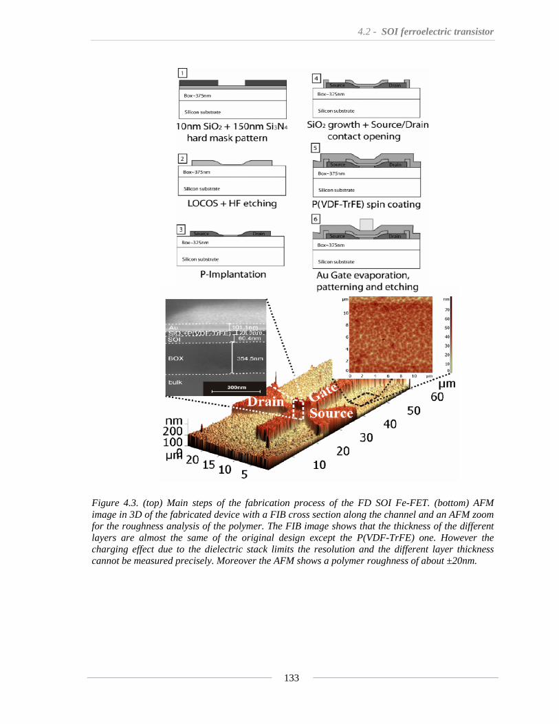
4.2 - SOI ferroelectric transistor
133
Figure 4.3. (top) Main steps of the fabrication process of the FD SOI Fe-FET. (bottom) AFM image in 3D of the fabricated device with a FIB cross section along the channel and an AFM zoom for the roughness analysis of the polymer. The FIB image shows that the thickness of the different layers are almost the same of the original design except the P(VDF-TrFE) one. However the charging effect due to the dielectric stack limits the resolution and the different layer thickness cannot be measured precisely. Moreover the AFM shows a polymer roughness of about ±20nm.
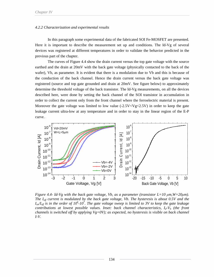
Chapter IV
134
4.2.2 Characterization and experimental results
In this paragraph some experimental data of the fabricated SOI Fe-MOSFET are presented.
Here it is important to describe the measurement set up and conditions. The Id-Vg of several
devices was registered at different temperatures in order to validate the behavior predicted in the
previous part of the chapter.
The curves of Figure 4.4 show the drain current versus the top gate voltage with the source
earthed and the drain at 20mV with the back gate voltage (physically contacted to the back of the
wafer), Vb, as parameter. It is evident that there is a modulation due to Vb and this is because of
the conduction of the back channel. Hence the drain current versus the back gate voltage was
registered (source and top gate grounded and drain at 20mV. See figure below) to approximately
determine the threshold voltage of the back transistor. The Id-Vg measurements, on all the devices
described here, were done by setting the back channel of the SOI transistor in accumulation in
order to collect the current only from the front channel where the ferroelectric material is present.
Moreover the gate voltage was limited to low value (-2.5V<Vg<2.5V) in order to keep the gate
leakage current ultra-low at any temperature and in order to stay in the linear region of the E-P
curve. -20 -15 -10 -50 5 1010-1410
-1310-1210
-1110-1010
-910-810
-710-6
Drain Curren
t, Id [A]
Bac k Gate V oltage, Vb [V]
-3 -2 -1 0 1 2 310-14
10-13
10-12
10-11
10-10
10-9
10-8
10-7
10-6
Vb=-4V Vb=-2V Vb=0V
Dra
in C
urre
nt, I
d [A
]
Gate Voltage, Vg [V]
Vd=20mVW=L=5μm
-20 -15 -10 -5 0 5 1010-14
10-13
10-12
10-11
10-10
10-9
10-8
10-7
10-6
Dra
in C
urre
nt, I
d [A
]
Back Gate Voltage, Vb [V]
Figure 4.4- Id-Vg with the back gate voltage, Vb, as a parameter (transistor L=10 μm,W=20μm). The Ioff current is modulated by the back gate voltage, Vb. The hysteresis is about 0.5V and the Ion/Ioff is in the order of 106-107. The gate voltage sweep is limited to 3V to keep the gate leakage contributions at lowest possible values. Inset: back channel characteristics, Id-Vb (the front channels is switched off by applying Vg=0V); as expected, no hysteresis is visible on back channel I-V.
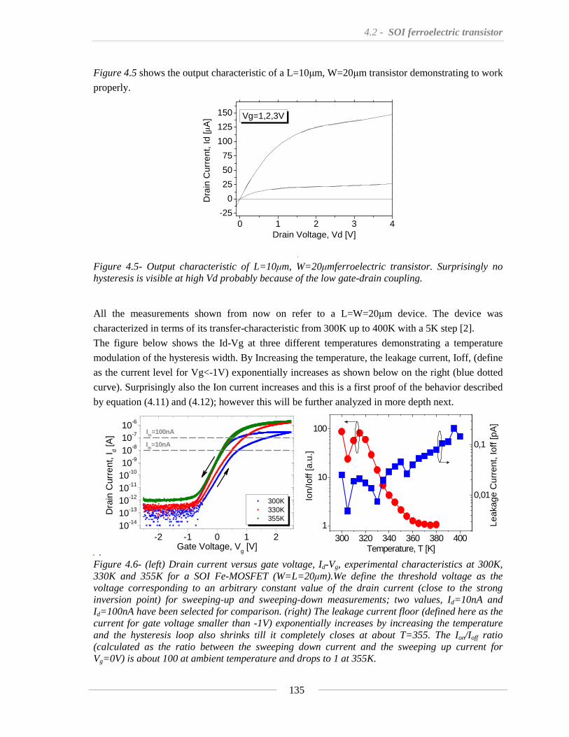
4.2 - SOI ferroelectric transistor
135
Figure 4.5 shows the output characteristic of a L=10μm, W=20μm transistor demonstrating to work
properly.
0 1 2 3 4-25
0
25
50
75
100
125
150
Dra
in C
urre
nt, I
d [μ
A]
Drain Voltage, Vd [V]
Vg=1,2,3V
0 1 23 4-25
025
50
75100
125
150
Drain Curr
ent, Id [μA]
Drain Vol tage, Vd [V]
Vg=1, 2,3V Figure 4.5- Output characteristic of L=10μm, W=20μmferroelectric transistor. Surprisingly no hysteresis is visible at high Vd probably because of the low gate-drain coupling. All the measurements shown from now on refer to a L=W=20μm device. The device was
characterized in terms of its transfer-characteristic from 300K up to 400K with a 5K step [2].
The figure below shows the Id-Vg at three different temperatures demonstrating a temperature
modulation of the hysteresis width. By Increasing the temperature, the leakage current, Ioff, (define
as the current level for Vg<-1V) exponentially increases as shown below on the right (blue dotted
curve). Surprisingly also the Ion current increases and this is a first proof of the behavior described
by equation (4.11) and (4.12); however this will be further analyzed in more depth next.
- 2-1 0 1 210-14
10-1310-12
10-1110
-1010-9
10-810-7
10-6
Ith= 10nA
300K 330K 355K
Drain Cur
rent, Id [A]
Gate Voltage , Vg [V]
Ith= 100nA 30 0320 34036 0380 4001
10
100
Leakag
e Current, I
off [pA]
Ion/Ioff
[a.u.]
Tem perature, T [K]
0,0 1
0,1
-2 -1 0 1 210-1410-1310-1210-1110-1010-910-810-710-6
Ith=10nA
300K 330K 355K
Dra
in C
urre
nt, I
d [A]
Gate Voltage, Vg [V]
Ith=100nA
300 320 340 360 380 400
1
10
100
Lea
kage
Cur
rent
, Iof
f [pA
]
Ion/
Ioff
[a.u
.]
Temperature, T [K]
0,01
0,1
Figure 4.6- (left) Drain current versus gate voltage, Id-Vg, experimental characteristics at 300K, 330K and 355K for a SOI Fe-MOSFET (W=L=20μm).We define the threshold voltage as the voltage corresponding to an arbitrary constant value of the drain current (close to the strong inversion point) for sweeping-up and sweeping-down measurements; two values, Id=10nA and Id=100nA have been selected for comparison. (right) The leakage current floor (defined here as the current for gate voltage smaller than -1V) exponentially increases by increasing the temperature and the hysteresis loop also shrinks till it completely closes at about T=355. The Ion/Ioff ratio (calculated as the ratio between the sweeping down current and the sweeping up current for Vg=0V) is about 100 at ambient temperature and drops to 1 at 355K.

Chapter IV
136
The hysteresis loop closes at T=355K and this temperature could be considered as the transition
temperature of the gate stack. This slightly lower value of Tc, with respect to the values reported for
the bulk copolymer of the same composition [6], is due to the depolarizing effect already
commented and summarized by equation (4.7). Hence it would be more correct to refer to this
temperature as the gate stack Curie temperature than the pure P(VDF-TrFE) Curie temperature.
The plot on the right of Figure 4.6 shows also the Ion/Ioff ration calculated for Vg=0V. At ambient
temperature it is about 100 and at T=Tc=355K it is 1. This further confirms that the ferroelectric
transistor is properly working and that the hysteresis observed is really due to the ferroelectric
material and not to any charge injection mechanism.
In order to study the threshold voltage behavior, the constant current method was adopted:
a threshold in current, Ith, was defined and the corresponding voltage was considered. The
hysteretic behavior of the Id-Vg implies two Vth, one for the sweeping up branch, Vth-up, and one for
the sweeping down, Vth-down. The memory window, Mw, is the difference between these two
voltage values. Figure 4.7 shows on the left the threshold analysis for two values of current: Ith=10,
100nA while the plot on the left shows the memory window as a function of the temperature. It is
evident that the Curie temperature occurs when Vth-up=Vth-down hence when Mw=0. The trend of the
Mw and of the Vth is almost the same for both value of current and from now on just Ith=100nA
has been considered in the coming calculation. Moreover the temperature dependence is more than
linear and becomes linear when approaching 355K. The increase of the Mw (first 3 points of the
curves), corresponding to a right shift of the Vth-up, is not well understood but could be due to
imprinting effects[7].
300 320340 36038 0400- 0.20.0
0.20.4
0.60.8
1.01.2
1.41.6
1.82.0
Vth up @ Ith=1 0nA
Vth down @ I th=10nA Vth up @ Ith=1 00nA
Vth down @ I th=100nA
Thresho
ld Voltage
, Vth [V]
Tempera ture, T [K] 300 320340 36038 04000.0
0.2
0.40.6
0.8
1.01.2
1.4 Mw @ I
th
=10nA
Mw @ I th=100nA
Memory
Window, M
w [V]
Tempera ture, T [K]
300 320 340 360 380 400-0.20.00.20.40.60.81.01.21.41.61.82.0
Vth up @ I
th=10nA
Vth down @ I
th=10nA
Vth up @ I
th=100nA
Vth down @ I
th=100nA
Thr
esho
ld V
olta
ge, V
th [V
]
Temperature, T [K]
300 320 340 360 380 400
0.0
0.2
0.4
0.6
0.8
1.0
1.2
1.4 Mw @ I
th=10nA
Mw @ Ith=100nA
Mem
ory
Win
dow
, Mw
[V]
Temperature, T [K] Figure 4.7- (left) Threshold voltage calculated with the constant current method for two different values. (right) We calculate the Memory Window, Mw, as the difference between Vth-up and Vth-down for the two mentioned values of Id. A similar trend of both threshold voltage and memory window with the temperature, closing for T> 355K, is observed for both values. This analysis places the transition temperature of the gate stack in the range 355K±5K
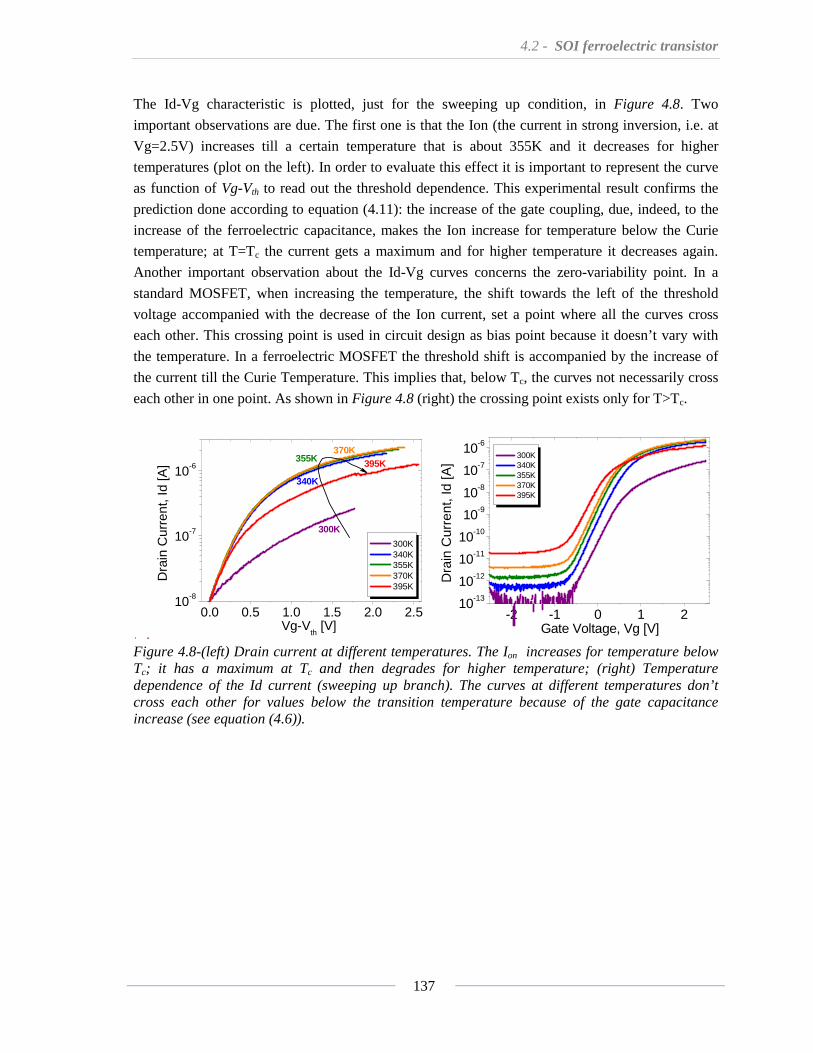
4.2 - SOI ferroelectric transistor
137
The Id-Vg characteristic is plotted, just for the sweeping up condition, in Figure 4.8. Two
important observations are due. The first one is that the Ion (the current in strong inversion, i.e. at
Vg=2.5V) increases till a certain temperature that is about 355K and it decreases for higher
temperatures (plot on the left). In order to evaluate this effect it is important to represent the curve
as function of Vg-Vth to read out the threshold dependence. This experimental result confirms the
prediction done according to equation (4.11): the increase of the gate coupling, due, indeed, to the
increase of the ferroelectric capacitance, makes the Ion increase for temperature below the Curie
temperature; at T=Tc the current gets a maximum and for higher temperature it decreases again.
Another important observation about the Id-Vg curves concerns the zero-variability point. In a
standard MOSFET, when increasing the temperature, the shift towards the left of the threshold
voltage accompanied with the decrease of the Ion current, set a point where all the curves cross
each other. This crossing point is used in circuit design as bias point because it doesn’t vary with
the temperature. In a ferroelectric MOSFET the threshold shift is accompanied by the increase of
the current till the Curie Temperature. This implies that, below Tc, the curves not necessarily cross
each other in one point. As shown in Figure 4.8 (right) the crossing point exists only for T>Tc.
0.0 0.5 1.01. 52.0 2.5
10-8
10-7
10-6 395K370K355K
340K
300K 340K 355K
370K 395K
Drain Curr
ent, Id [A]
Vg-Vth [V ]
300 K -2 -1 01 21 0-13
1 0-121 0
-111 0-10
10-910
-810-7
10-6 300 K
340 K 355 K 370 K
395 K
Drain Cur
rent, Id [A]
Gate Vol tage, Vg [V]
0.0 0.5 1.0 1.5 2.0 2.510-8
10-7
10-6 395K370K
355K
340K
300K 340K 355K 370K 395K
Dra
in C
urre
nt, I
d [A
]
Vg-Vth [V]
300K
-2 -1 0 1 2
10-13
10-12
10-11
10-10
10-9
10-8
10-7
10-6
300K 340K 355K 370K 395K
Dra
in C
urre
nt, I
d [A
]
Gate Voltage, Vg [V] Figure 4.8-(left) Drain current at different temperatures. The Ion increases for temperature below Tc; it has a maximum at Tc and then degrades for higher temperature; (right) Temperature dependence of the Id current (sweeping up branch). The curves at different temperatures don’t cross each other for values below the transition temperature because of the gate capacitance increase (see equation (4.6)).
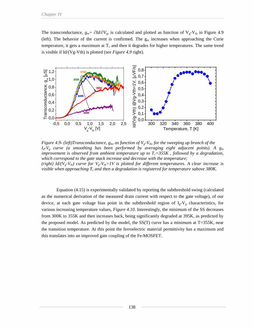
Chapter IV
138
The transconductance, gm= ∂Id/∂Vg, is calculated and plotted as function of Vg-Vth in Figure 4.9
(left). The behavior of the current is confirmed. The gm increases when approaching the Curie
temperature, it gets a maximum at Tc and then it degrades for higher temperatures. The same trend
is visible if Id/(Vg-Vth) is plotted (see Figure 4.9 right).
-0,5 0,0 0,5 1,0 1,5 2,0 2,50,0
0,2
0,4
0,6
0,8
1,0
1,2
395K
370K
355K
340K
Tra
nsco
nduc
tanc
e, g
m [μ
S]
Vg-V
th [V]
300K
300 320 340 360 380 4000,0
0,1
0,2
0,3
0,4
0,5
0,6
0,7
0,8
Id/(
Vg-
Vth
) @
Vg-
Vth
=1V
, [μV
F/s
]Temperature, T [K]
-0,5 0,00,5 1,0 1,52, 02,50,0
0,2
0,40,6
0,8
1,0
1,2
395K
370K
355K
34 0K
Transco
nductance
, gm [μS]
Vg-Vth [ V]
300K 300 320340 36038 04000,0
0,10,2
0,30,4
0,5
0,60,7
0,8
Id/(Vg-
Vth) @Vg-
Vth=1V, [μV
F/s]
Tempera ture, T [K]
Figure 4.9- (left)Transconductance, gm, as function of Vg-Vth, for the sweeping up branch of the Id-Vg curve (a smoothing has been performed by averaging eight adjacent points). A gm improvement is observed from ambient temperature up to Tc=355K , followed by a degradation, which correspond to the gate stack increase and decrease with the temperature; (right) Id/(Vg-Vth) curve for Vg-Vth=1V is plotted for different temperatures. A clear increase is visible when approaching Tc and then a degradation is registered for temperature sabove 380K.
Equation (4.15) is experimentally validated by reporting the subthreshold swing (calculated
as the numerical derivation of the measured drain current with respect to the gate voltage), of our
device, at each gate voltage bias point in the subthreshold region of Ig-Vg characteristics, for
various increasing temperature values, Figure 4.10. Interestingly, the minimum of the SS decreases
from 300K to 355K and then increases back, being significantly degraded at 395K, as predicted by
the proposed model. As predicted by the model, the SS(T) curve has a minimum at T=355K, near
the transition temperature. At this point the ferroelectric material permittivity has a maximum and
this translates into an improved gate coupling of the Fe-MOSFET.

4.2 - SOI ferroelectric transistor
139
-0,8 -0,6 -0,4 -0,2 0,0 0,2
250
300
350
400 300K 340K 355K 370K 395K
Sub
thre
shol
d S
win
g, S
S [m
V/d
ec]
Vg-Vth [V]
Figure 4.10- Subthreshold Slope curve as function of the gate voltage Vg plotted for five different temperature. Interestingly, the minimum of the SS decreases from 300K to 355K and then increases back, being significantly degraded at 395K, as predicted by the proposed model.
In order to carefully validate the proposed analytical model for the SSFe-MOS, we have
extracted the SS at each temperature by interpolating the log of the current in the same region, for
more than one decade of variation, for the sweeping-up measurement conditions. The SS extraction
versus temperature are summarized in Figure 4.11 by the colored circles and a minimum for SS(T)
curve is clearly visible. Note that the relatively high values of the SS ranging from 210 to 260
mV/decade are rather due to a relatively large amount of interface states and less to the large value
of the equivalent oxide thickness EOT=14 nm, which has a small effect in a fully depleted SOI
transistor. Indeed, the implant resistor used on top of the gate oxide for implantation has been
removed by oxygen plasma, which is responsible for the large amount of charges and interface
states. On the other hand, our thick dielectric stack ensures negligible gate current leakage and
highly accurate measurement conditions. As predicted by the model, the SS(T) curve has a
minimum at T=355K, near the transition temperature. At this point the ferroelectric material
permittivity has a maximum and this translates into an improved gate coupling of the Fe-MOSFET.
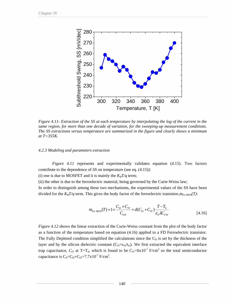
Chapter IV
140
300 320 340 360 380 400220
230
240
250
260
270
280
Sub
thre
shol
d S
win
g, S
S [m
V/d
ec]
Temperature, T [K]
300 320340 36038 0400220
230
240
250260
270
280
Subthr
eshold Swi
ng, SS [mV
/dec]
Tempera ture, T [K] Figure 4.11- Extraction of the SS at each temperature by interpolating the log of the current in the same region, for more than one decade of variation, for the sweeping-up measurement conditions. The SS extractions versus temperature are summarized in the figure and clearly shows a minimum at T=355K.
4.2.3 Modeling and parameters extraction
Figure 4.11 represents and experimentally validates equation (4.15). Two factors
contribute to the dependence of SS on temperature (see eq. (4.15)):
(i) one is due to MOSFET and it is mainly the KBT/q term;
(ii) the other is due to the ferroelectric material, being governed by the Curie-Weiss law;
In order to distinguish among these two mechanisms, the experimental values of the SS have been
divided for the KBT/q term. This gives the body factor of the ferroelectric transistor,mFe-MOS(T):
CWITD
OX
ITDMOSFe C
TTCCd
C
CCTm
λε0
0)(1)(−
+++
+=− [4.16]
Figure 4.12 shows the linear extraction of the Curie-Weiss constant from the plot of the body factor
as a function of the temperature based on equation (4.16) applied to a FD Ferroelectric transistor.
The Fully Depleted condition simplified the calculations since the CD is set by the thickness of the
layer and by the silicon dielectric constant (CD=εSi/tSi). We first extracted the equivalent interface
trap capacitance, CIT at T=T0, which is found to be CIT=6x10⁻⁷ F/cm2 so the total semiconductor
capacitance is CS=CD+CIT=7.7x10⁻⁷ F/cm2.

4.2 - SOI ferroelectric transistor
141
Thus, considering CS independent of temperature as already mentioned, we calculated, from the
slope of the plot, a CCW=3429K in the ferroelectric phase and a CCW=11878K in the paraelectric
phase [8]. These values are in agreement with those already reported in literature for P(VDF-TrFE)
[9,10]. It is worth mentioning that the interface charge capacitance is quite high but could be
explained by the plasma oxygen bombardment of the gate oxide during the resist, used as
implantation mask, removal.
300 320 340 360 380 400
3,2
3,4
3,6
3,8
4,0
4,2
4,4
KC
B
CW 3429
0203.0
≈−=
KC
B
CW 11878
00293.0
≈=
BTATm MOSFe +=− )(
Experimental data Linear Fit
Fer
ro b
ody
fact
or, m
Fe
Temperature, T [K]
Figure 4.12- Body factor of the FD Fe-FET calculated by dividing the SS for a KBT/q term. In a standard FET the body factor should not depend on the temperature while for a Fe-FET the case is different as demonstrated by the plot. We extracted the Curie-Weiss constant and the trap charge capacitance CIT according to equation (4.14).
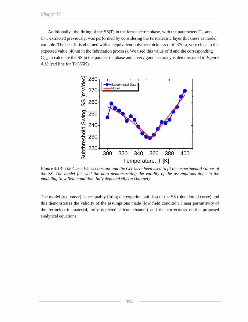
Chapter IV
142
Additionally, the fitting of the SS(T) in the ferroelectric phase, with the parameters CIT and
CCW extracted previously, was performed by considering the ferroelectric layer thickness as model
variable. The best fit is obtained with an equivalent polymer thickness of d=37nm, very close to the
expected value (40nm in the fabrication process). We used this value of d and the corresponding
CCW to calculate the SS in the paralectric phase and a very good accuracy is demonstrated in Figure
4.13 (red line for T>355K).
300 320 340 360 380 400220
230
240
250
260
270
280
Experimental Data Model
Sub
thre
shol
d S
win
g, S
S [m
V/d
ec]
Temperature, T [K] Figure 4.13- The Curie Weiss constant and the CIT have been used to fit the experimental values of the SS. The model fits well the data demonstrating the validity of the assumptions done in the modeling (low field condition, fully depleted silicon channel)
The model (red curve) is acceptably fitting the experimental data of the SS (blue dotted curve) and
this demonstrates the validity of the assumptions made (low field condition, linear permittivity of
the ferroelectric material, fully depleted silicon channel) and the correctness of the proposed
analytical equations.
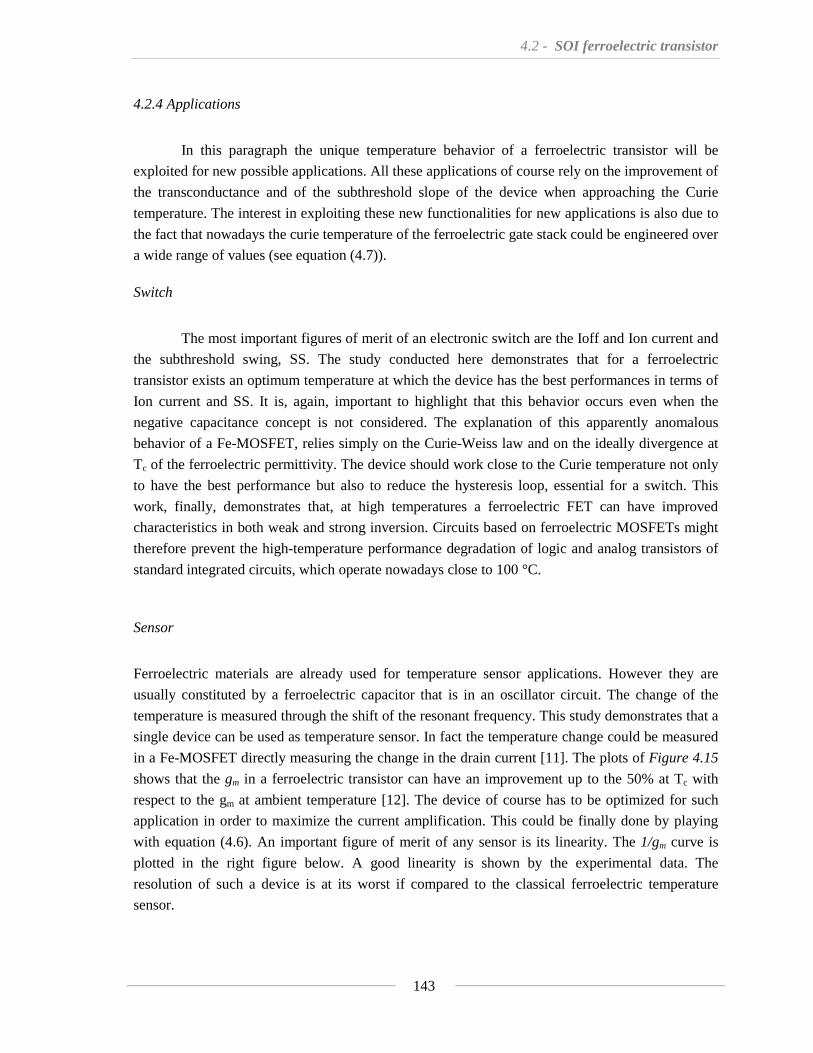
4.2 - SOI ferroelectric transistor
143
4.2.4 Applications
In this paragraph the unique temperature behavior of a ferroelectric transistor will be
exploited for new possible applications. All these applications of course rely on the improvement of
the transconductance and of the subthreshold slope of the device when approaching the Curie
temperature. The interest in exploiting these new functionalities for new applications is also due to
the fact that nowadays the curie temperature of the ferroelectric gate stack could be engineered over
a wide range of values (see equation (4.7)).
Switch
The most important figures of merit of an electronic switch are the Ioff and Ion current and
the subthreshold swing, SS. The study conducted here demonstrates that for a ferroelectric
transistor exists an optimum temperature at which the device has the best performances in terms of
Ion current and SS. It is, again, important to highlight that this behavior occurs even when the
negative capacitance concept is not considered. The explanation of this apparently anomalous
behavior of a Fe-MOSFET, relies simply on the Curie-Weiss law and on the ideally divergence at
Tc of the ferroelectric permittivity. The device should work close to the Curie temperature not only
to have the best performance but also to reduce the hysteresis loop, essential for a switch. This
work, finally, demonstrates that, at high temperatures a ferroelectric FET can have improved
characteristics in both weak and strong inversion. Circuits based on ferroelectric MOSFETs might
therefore prevent the high-temperature performance degradation of logic and analog transistors of
standard integrated circuits, which operate nowadays close to 100 °C.
Sensor
Ferroelectric materials are already used for temperature sensor applications. However they are
usually constituted by a ferroelectric capacitor that is in an oscillator circuit. The change of the
temperature is measured through the shift of the resonant frequency. This study demonstrates that a
single device can be used as temperature sensor. In fact the temperature change could be measured
in a Fe-MOSFET directly measuring the change in the drain current [11]. The plots of Figure 4.15
shows that the gm in a ferroelectric transistor can have an improvement up to the 50% at Tc with
respect to the gm at ambient temperature [12]. The device of course has to be optimized for such
application in order to maximize the current amplification. This could be finally done by playing
with equation (4.6). An important figure of merit of any sensor is its linearity. The 1/gm curve is
plotted in the right figure below. A good linearity is shown by the experimental data. The
resolution of such a device is at its worst if compared to the classical ferroelectric temperature
sensor.
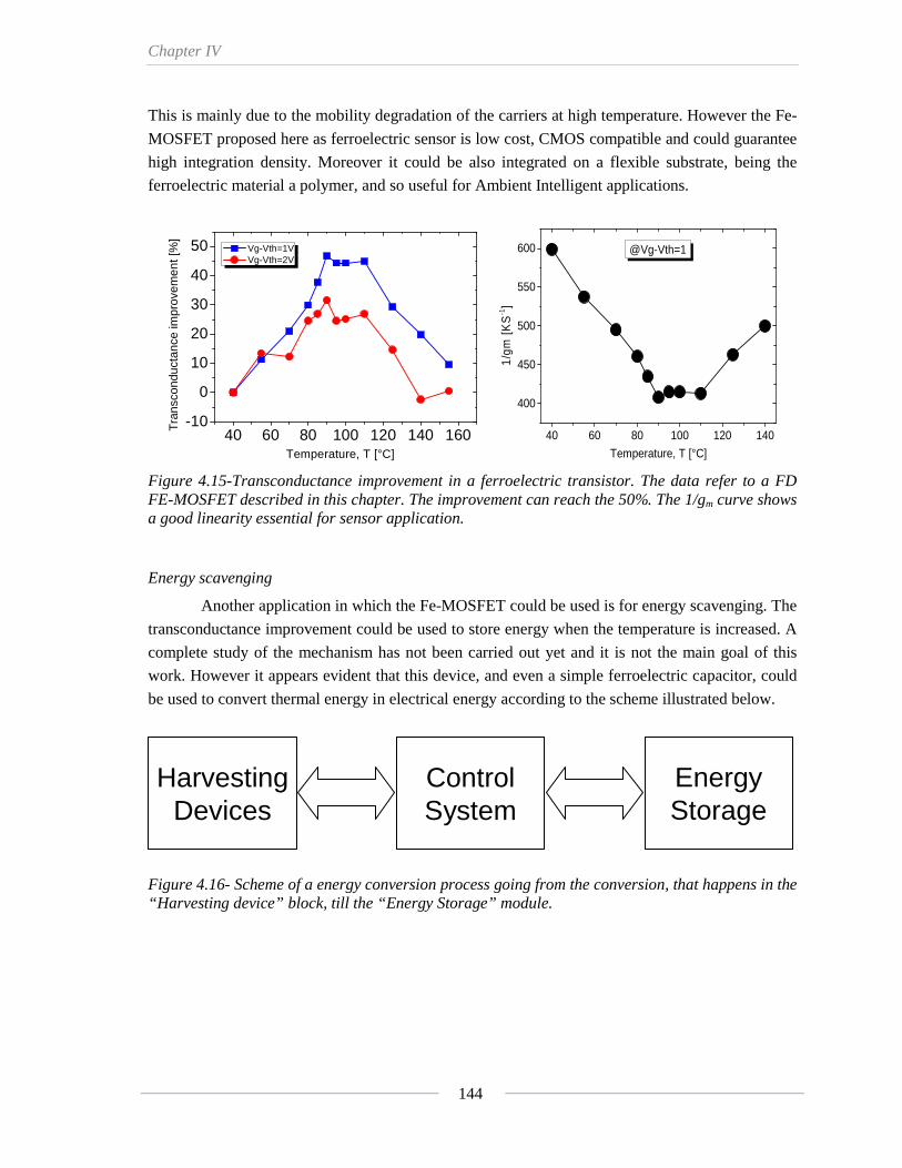
Chapter IV
144
This is mainly due to the mobility degradation of the carriers at high temperature. However the Fe-
MOSFET proposed here as ferroelectric sensor is low cost, CMOS compatible and could guarantee
high integration density. Moreover it could be also integrated on a flexible substrate, being the
ferroelectric material a polymer, and so useful for Ambient Intelligent applications.
40 60 80 100 120 140 160-10
0
10
20
30
40
50
Vg-Vth=1V Vg-Vth=2V
Tra
nsco
nduc
tanc
e im
prov
emen
t [%
]
Temperature, T [°C]
40 60 80 100 120 140
400
450
500
550
600
1/gm
[KS
-1]
Temperature, T [°C]
@Vg-Vth=1
Figure 4.15-Transconductance improvement in a ferroelectric transistor. The data refer to a FD FE-MOSFET described in this chapter. The improvement can reach the 50%. The 1/gm curve shows a good linearity essential for sensor application.
Energy scavenging
Another application in which the Fe-MOSFET could be used is for energy scavenging. The
transconductance improvement could be used to store energy when the temperature is increased. A
complete study of the mechanism has not been carried out yet and it is not the main goal of this
work. However it appears evident that this device, and even a simple ferroelectric capacitor, could
be used to convert thermal energy in electrical energy according to the scheme illustrated below.
HarvestingDevices
ControlSystem
EnergyStorage
Figure 4.16- Scheme of a energy conversion process going from the conversion, that happens in the “Harvesting device” block, till the “Energy Storage” module.
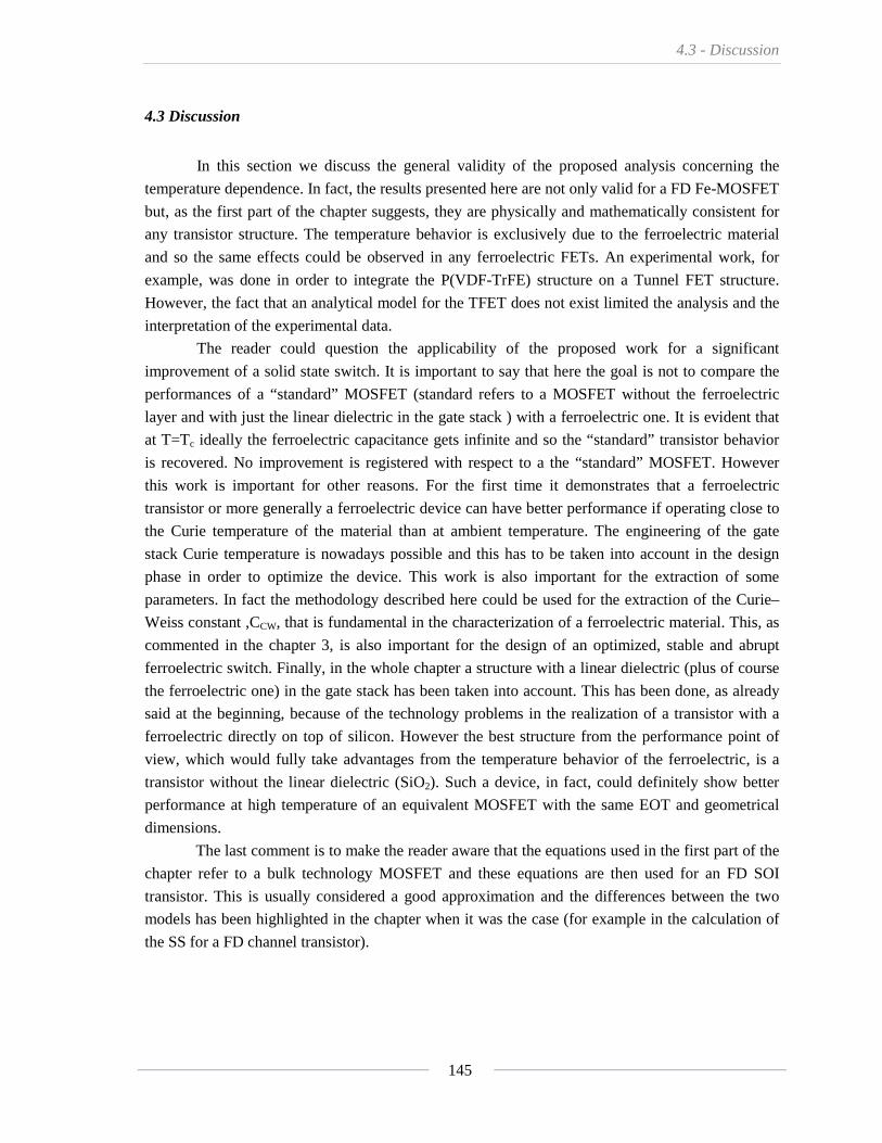
4.3 - Discussion
145
4.3 Discussion
In this section we discuss the general validity of the proposed analysis concerning the
temperature dependence. In fact, the results presented here are not only valid for a FD Fe-MOSFET
but, as the first part of the chapter suggests, they are physically and mathematically consistent for
any transistor structure. The temperature behavior is exclusively due to the ferroelectric material
and so the same effects could be observed in any ferroelectric FETs. An experimental work, for
example, was done in order to integrate the P(VDF-TrFE) structure on a Tunnel FET structure.
However, the fact that an analytical model for the TFET does not exist limited the analysis and the
interpretation of the experimental data.
The reader could question the applicability of the proposed work for a significant
improvement of a solid state switch. It is important to say that here the goal is not to compare the
performances of a “standard” MOSFET (standard refers to a MOSFET without the ferroelectric
layer and with just the linear dielectric in the gate stack ) with a ferroelectric one. It is evident that
at T=Tc ideally the ferroelectric capacitance gets infinite and so the “standard” transistor behavior
is recovered. No improvement is registered with respect to a the “standard” MOSFET. However
this work is important for other reasons. For the first time it demonstrates that a ferroelectric
transistor or more generally a ferroelectric device can have better performance if operating close to
the Curie temperature of the material than at ambient temperature. The engineering of the gate
stack Curie temperature is nowadays possible and this has to be taken into account in the design
phase in order to optimize the device. This work is also important for the extraction of some
parameters. In fact the methodology described here could be used for the extraction of the Curie–
Weiss constant ,CCW, that is fundamental in the characterization of a ferroelectric material. This, as
commented in the chapter 3, is also important for the design of an optimized, stable and abrupt
ferroelectric switch. Finally, in the whole chapter a structure with a linear dielectric (plus of course
the ferroelectric one) in the gate stack has been taken into account. This has been done, as already
said at the beginning, because of the technology problems in the realization of a transistor with a
ferroelectric directly on top of silicon. However the best structure from the performance point of
view, which would fully take advantages from the temperature behavior of the ferroelectric, is a
transistor without the linear dielectric (SiO2). Such a device, in fact, could definitely show better
performance at high temperature of an equivalent MOSFET with the same EOT and geometrical
dimensions.
The last comment is to make the reader aware that the equations used in the first part of the
chapter refer to a bulk technology MOSFET and these equations are then used for an FD SOI
transistor. This is usually considered a good approximation and the differences between the two
models has been highlighted in the chapter when it was the case (for example in the calculation of
the SS for a FD channel transistor).
Chapter IV
146
4.4 Summary
In this chapter we described the Curie-Weiss law for ferroelectric and we applied it to
calculate the equivalent capacitance of a parallel plate ferroelectric capacitor. This preliminary
calculation was then used for investigating the performance of a ferroelectric transistor. It was
found that a Fe-MOSFET has a completely different behavior, at high temperatures, compared to a
standard MOSFET. If the gate capacitance amplification dominates over the mobility degradation,
a maximum of the transconductance is measured at the Curie temperature, Tc, of the material.
Moreover at Tc the subthreshold swing has a minimum thanks to the improved gate coupling.
The theoretical behavior was experimentally validated by the fabrication and the
characterization of a Fe-MOSFET in SOI technology. The Id-Vg characteristic was registered from
ambient temperature up to 140°C. The experimental data for the transconductance and the
subthreshold swing confirm the model prediction. Moreover the Curie-Weiss constant was
extracted for P(VDF-TrFE) with good agreement with the values already reported in the literature.
The original work carried out relative to this chapter includes:
Modeling. The Curie-Weiss law describes a temperature modulation of the permittivity in
ferroelectric that is well known and studied. Here, we demonstrated for the first time that this
physical mechanism is responsible for the improvement of the performances of a Fe-MOSFET at
high temperatures. The modeling of the device was originally reported in both subthreshold and
strong inversion region of operation.
Fabrication. A Fully depleted SOI ferroelectric transistor has been successfully fabricated. The
thinning of the channel region and the deposition of 40nm of P(VDF-TrFE) have been the main
challenges.
Experimental Validation. It was demonstrated for the first time that the subthreshold swing and
the gm of a ferroelectric SOI transistor has a minimum and a maximum gm at the Curie temperature
respectively. The proposed model has been validated on experimental data and a very good
agreement has been demonstrated. The Curie-Weiss constant for P(VDF-TrFE) was extracted and
the value I found is in good accordance with the values reported in literature. This proved one more
the validity of the model.
Chapter IV - Bibliography
Bibliography
[1] Tagantsev A.K., Sherman V.O., Astafiev K.F., Venkatesh J., Setter N., “Ferroelectric materials for microwave tunable applications”, Journal of Electroceramics 11, pp. 5-66 (003)
[2] G. A. Salvatore, L. Lattanzio, D. Bouvet, I. Stolichnov, N. Setter, A. M. Ionescu, "Ferroelectric transistors with improved characteristics at high temperature", article in press, available online 06. August 2010, Applied Physics Letters, vol. 97, iss. 5, (2010)
[3] Colinge J.-P., Floyd L., Quinn A.J., Redmond G., Alderman J.C., Xiong W., Cleavelin C.R., Schulz T., Schruefer K., Knoblinger G., Patruno P., “Temperature effects on trigate SOI MOSFETs”, IEEE Electron Device Letters 27 (3), pp. 172-174 (2006)
[4] G. Reichert , T. Ouisse, J. L. Pelloie, S. Cristoloveanu , “Mobility modeling of SOI MOSFETs in the high temperature range”, Solid-State Electronics 39 (9), pp. 1347-1352 (1996)
[5] R. J. Van Overstraeten, “Theory of the MOS Transistor in Weak Inversion-New Method to Determine the Number of Surface States”, IEEE Transaction of Electron Devices Vol. 22 No. 5 (1975)
[6] R. Kepler and R. Anderson, “Ferroelectric polymers”, Adv. Phys. 41,1 (1992)
[7] G. D. Zhu, X. Y. Luo, J. H. Zhang and X. Yan, “Imprint effect in ferroelectric poly„vinylidene fluoride-trifluoroethylene thin films”, J. Appl. Phys. 106 (2009)
[8] G. A. Salvatore, L. Lattanzio, D. Bouvet, A. M. Ionescu, “Modeling the temperature dependance of Fe-FET static characteristics based on Landau’s theory”, submitted to Trans. On Elec. Dev. (2010)
[9] B. Ploss, “Dielectric nonlinearity of PVDF–TrFE copolymer”, Polymer Vol. 41 6087–6093 (2000)
[10] E. Bellet-Amalric, J. F. Legrand, “Crystalline structures and phase transition of the ferroelectric P(VDF-TrFE) copolymers, a neutron diffraction study”, The European Physical Journal B, Vol.3 No.2 (1998).
[11] G. A. Salvatore, L. Lattanzio, D. Bouvet, Al. Rusu, A. M. Ionescu, "Temperature sensor based on Ferroelectric FET", MNE 2010, 19-22 September, Genoa, Italy
[12] G. A. Salvatore, L. Lattanzio, D. Bouvet, A. M. Ionescu, "The Curie Temperature as a Key Design Parameter of Ferroelectric Field Effect Transistors", ESSDERC 2010, 13-17 September 2010, Sevilles, Spain

Chapter 5
Conclusions and Perspectives
This short chapter summarizes the main general conclusions concerning the most important contributions of this work. It highlights the potential of ferroelectric FETs for both switching and memory applications and the progress achieved during this Phd work compared to the state of the art. At the end, we discuss the open challenges and some less conventional perspectives for the future.

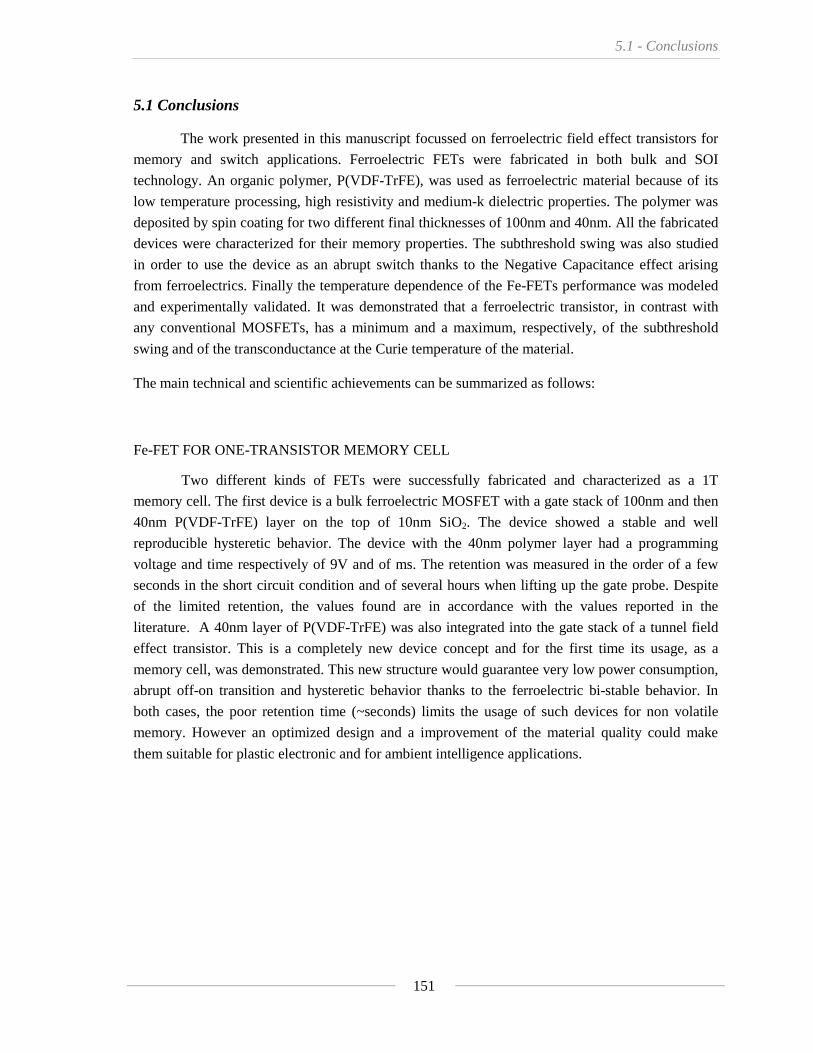
5.1 - Conclusions
151
5.1 Conclusions
The work presented in this manuscript focussed on ferroelectric field effect transistors for
memory and switch applications. Ferroelectric FETs were fabricated in both bulk and SOI
technology. An organic polymer, P(VDF-TrFE), was used as ferroelectric material because of its
low temperature processing, high resistivity and medium-k dielectric properties. The polymer was
deposited by spin coating for two different final thicknesses of 100nm and 40nm. All the fabricated
devices were characterized for their memory properties. The subthreshold swing was also studied
in order to use the device as an abrupt switch thanks to the Negative Capacitance effect arising
from ferroelectrics. Finally the temperature dependence of the Fe-FETs performance was modeled
and experimentally validated. It was demonstrated that a ferroelectric transistor, in contrast with
any conventional MOSFETs, has a minimum and a maximum, respectively, of the subthreshold
swing and of the transconductance at the Curie temperature of the material.
The main technical and scientific achievements can be summarized as follows:
Fe-FET FOR ONE-TRANSISTOR MEMORY CELL
Two different kinds of FETs were successfully fabricated and characterized as a 1T
memory cell. The first device is a bulk ferroelectric MOSFET with a gate stack of 100nm and then
40nm P(VDF-TrFE) layer on the top of 10nm SiO2. The device showed a stable and well
reproducible hysteretic behavior. The device with the 40nm polymer layer had a programming
voltage and time respectively of 9V and of ms. The retention was measured in the order of a few
seconds in the short circuit condition and of several hours when lifting up the gate probe. Despite
of the limited retention, the values found are in accordance with the values reported in the
literature. A 40nm layer of P(VDF-TrFE) was also integrated into the gate stack of a tunnel field
effect transistor. This is a completely new device concept and for the first time its usage, as a
memory cell, was demonstrated. This new structure would guarantee very low power consumption,
abrupt off-on transition and hysteretic behavior thanks to the ferroelectric bi-stable behavior. In
both cases, the poor retention time (~seconds) limits the usage of such devices for non volatile
memory. However an optimized design and a improvement of the material quality could make
them suitable for plastic electronic and for ambient intelligence applications.
Chapter V
152
Fe-MOSFET FOR ABRUPT SWITCHING
A bulk ferroelectric transistor with 40nm P(VDF-TrFE)/10nm SiO2 gate stack was
carefully characterized in the subthreshold region of operation in order to exploit the negative
capacitance effect and lower the swing below 60mV/dec. This device was conceived for memory
and so it was non optimized for switch applications. A slope of 13mV/dec was measured for the
first time but in a very limited range of voltage and for very low current level. In order to avoid any
effects due to leakage sources on the evaluation of the subthreshold swing and to correlate the low
SS value with the negative capacitance effect, a test structure has been designed and fabricated. Its
gate stack was made up by 100nm P(VDF-TrFE) and 10nm SiO2. Between the two dielectrics a
50nm layer of Aluminum was deposited in order to probe the internal node voltage. Also on this
device a swing less than 60mV/dec was measured confirming the previous results. This improved
layout device exhibited an average swing of 53mV/dec for a corresponding drain current variation
of about 3 order of magnitude, from 400fA up to 200pA. Finally, thanks to the probing of the
ferroelectric/oxide interface voltage, this behavior was explained by a ∂Ψint/∂Vg amplification that is
mirrored in an abrupt switch. The ferroelectric material polarization was calculated and a negative
P-E slope has been found as proof of a negative permittivity occurring for P≈0 as predicted by
theory.
TEMPERATURE BEHAVIOR OF Fe-FET
An analytical model, based on Landau’s theory, was developed in order to study the
performance temperature dependence of the ferroelectric transistor. A first order ferroelectric
capacitance, valid at low transversal field, was used for the modeling of the ferroelectric transistor
in strong inversion and in the subthreshold region. The experimental validation of the calculation
was accomplished by the fabrication and the characterization of a Fully depleted SOI transistor
with 40nm P(VDF-TrFE)/10nm SiO2 gate stack. The transfer characteristic Id-Vg was measured
from 25°C up to 140°C with 10°C stepping. The experimental data demonstrate that a ferroelectric
transistor, in contrast with any conventional MOSFETs, has a minimum and a maximum
respectively of the subthreshold swing and of the transconductance at the Curie temperature of the
material.
5.2 - Perspectives
153
5.2 Perspectives
The work presented here can be improved at different levels: fabrication, modeling and exploitation of new applications.
FABRICATION AND PROCESSING CHALLENGES
The fabrication process could be further improved and made completely CMOS
compatible. The gold should be replaced by other wet-etchable metals (Cr, Al, Ti) and the polymer
deposition should be optimized in order to reduce the wafer thickness variability and roughness.
The scalability study of the device should also be considered in the future plan in order to exploit
the dimension limit of the negative capacitance effect and of the 1T memory cell.
RETENTION CHALLENGE
The retention time is the limiting factor for the usage of this P(VDF-TrFE) based
ferroelectric transistor. The improvement of the deposition method, of the material quality and the
optimization of the layout design could make the memory effect more durable. Other materials, as
ferroelectric BaTiO3 nanoparticles in an organic solution, could be also taken into consideration.
Moreover the use of high/medium-k dielectric appears to be necessary.
MODELING THE NEGATIVE CAPACITANCE EFFECT
Future work should focus upon the development of a self consistent model of the device.
This would allow the optimization of the thickness of the different gate stack layers and of the
substrate doping. A Landau's theory based model would allow the understanding of some
anomalies that at moment are not well clear.
ENERGY HARVESTING: FUNCTIONAL DIVERSIFICATION WITH Fe-FETs
Future work should focus on a better modeling of performance temperature dependence of
a Fe-MOSFET in the strong regime. This involves a careful mobility degradation characterization
and calibration. However the work shown in chapter 4 could path the routes for completely new
applications. At the moment the most interesting is the energy scavenging. The device could be
used to convert thermal energy to electrical energy taking advantage of the fact that the Curie
temperature nowadays could be engineered by optimizing the material composition. The basic
principle for energy harvesting has been described but future work should focus on the effective
Chapter V
154
and experimental exploitation of the concept and on the integration of energy harvesters in BEOL
(Back End Of the Line) rather than in FEOL (Front End Of the Line) devices.
Appendix A
155
Appendix A
A microscopic description of Landau’s theory
A microscopic description of Landau’s theory
156

Appendix A
157
Microscopic description
This paragraph describes the ferroelectric material as a sum of microscopic electrical
dipoles that have no interaction with each other and that immediately “rotate” (frequency
dependence is not considered) under the application of an external electric field. No quantum
theory argument is taken into account, however it is shown from the microscopic dipoles picture
that it is possible to extract a macroscopic behavior that expresses the free energy of the system as a
function of the total polarization, i.e. the order parameter in Landau’s theory. A similar calculation
is done in [1] for polar molecules. Of course the calculation reported here deals with an ideal
picture of a ferroelectric material and in fact the real case is much more complex (multi domains,
domain wall thicknesses, defects should be considered).
Considering two elementary charges +q and –q separated by a distance d, the electric
dipole momentum, p0, is given by the charge multiplied by the distance d. If the dipole is placed
in an electric field, E, the energy associated with the dipole is:
θφ cos0 EpqdU −=∇= (a.1)
where Φ is the electric potential and θ is the angle between the momentum and the field.
From statistical mechanics it is known that at thermal equilibrium the number of dipoles with the
potential energy U is proportional to:
KTUen /−∝ (a.2)
where K is the Boltzmann constant and T is the temperature.
The same argument is valid if using equation (a.1) for the potential energy as function of angle, so
that the number of dipoles for unit solid angle is :
KTEpenn /cos
00)( θθ = (a.3)
Now considering the case of a ferroelectric material and considering just two polarization
directions, up and down, the (a.3) becomes:
)(/cos0
)(/cos0
0
0
)(
)(
c
c
TTKEp
TTKEp
enn
enn−−
↓
−↑
=
=θ
θ
θ
θ (a.4)
where n0 is a constant.
[1] R. Feynman, R. B. Leighton,M. Sands, “The Feynman lectures on physics ”, Vol II Addison Wesley
Publishing Company

A microscopic description of Landau’s theory
158
The total number of dipoles can be calculated by integrating the (a.4) over the solid angle dθ:
⎪⎩
⎪⎨
⎧
><−>=<
>=<
↑↓
−↑ ∫
nNn
denno
TTKEp c θθππ
θ sin2)(/cos0
0
(a.5)
where N is the total number of dipoles (up+down). Moreover the following boundary conditions
can be applied:
⎪⎪
⎩
⎪⎪
⎨
⎧
>=<>=<
>=<>=<
=>=<><
↓−∞→↑−∞→
↓+∞→↑+∞→
=↓=↑
Nnn
nNn
Nnn
EE
EE
EE
lim,0lim
0lim,lim200
(a.6)
where it has simply been assumed that at zero field the number of dipoles pointing up is the same
of the dipoles pointing down and that at very high field there is a perfect and complete alignment of
the dipoles towards the corresponding direction of the field.
⎪⎪
⎩
⎪⎪
⎨
⎧
+⎥⎦
⎤⎢⎣
⎡+−−>=<
+⎥⎦
⎤⎢⎣
⎡+−>=<
−−−
−−−
↓
−−−
−−−
↑
22
22
)(/)(/
)(/)(/
)(/)(/
)(/)(/
00
00
00
00
N
ee
eeNn
N
ee
eeNn
cc
cc
cc
cc
TTKEpTTKEp
TTKEpTTKEp
TTKEpTTKEp
TTKEpTTKEp
(a.7)
with:
⎥⎦
⎤⎢⎣
⎡+−
= −−− )(/)(/0
0 00
1
)(22 cc TTKEpTTKEpc eeTTK
EpNn
π (a.8)

Appendix A
159
>< ↓n
< n< n< n< n0
>< ↑n
0
N
num
ber
of d
ipol
es [a
.u.]
Ep0/K(T-T
c) [a.u.]
N/2
Figure 1- Plot of equation (a.7) showing the number of dipoles pointing up and down as function of the applied field.
Once calculated the total number of dipoles it is easy to get the polarization by simply multiplying
for the elementary dipole momentum:
00 , pnPpnP >=<>=< ↓↓↑↑
⎪⎪⎩
⎪⎪⎨
⎧
+−
−=
+−
=
↓
↑
2)
)(tanh(
2
2)
)(tanh(
2
0
0
N
TTK
EpNP
N
TTK
EpNP
c
c (a.10)
Usually it is more useful to express the field as function of the polarization and so inverting the
function:
5320
)()()(
PTCPTBPNp
TTKE cB ++−= (a.11)
where B(T) and C(T) are two parameters that depend on T.
Equation (a.11) has the same shape of the electrical field expressed according to Landau’s theory
formulation but here it has been derived from an elementary dipole picture and by considering
some assumptions.

Appendix B
Clean Room Runcard for Fe-MOSFET Fabrication

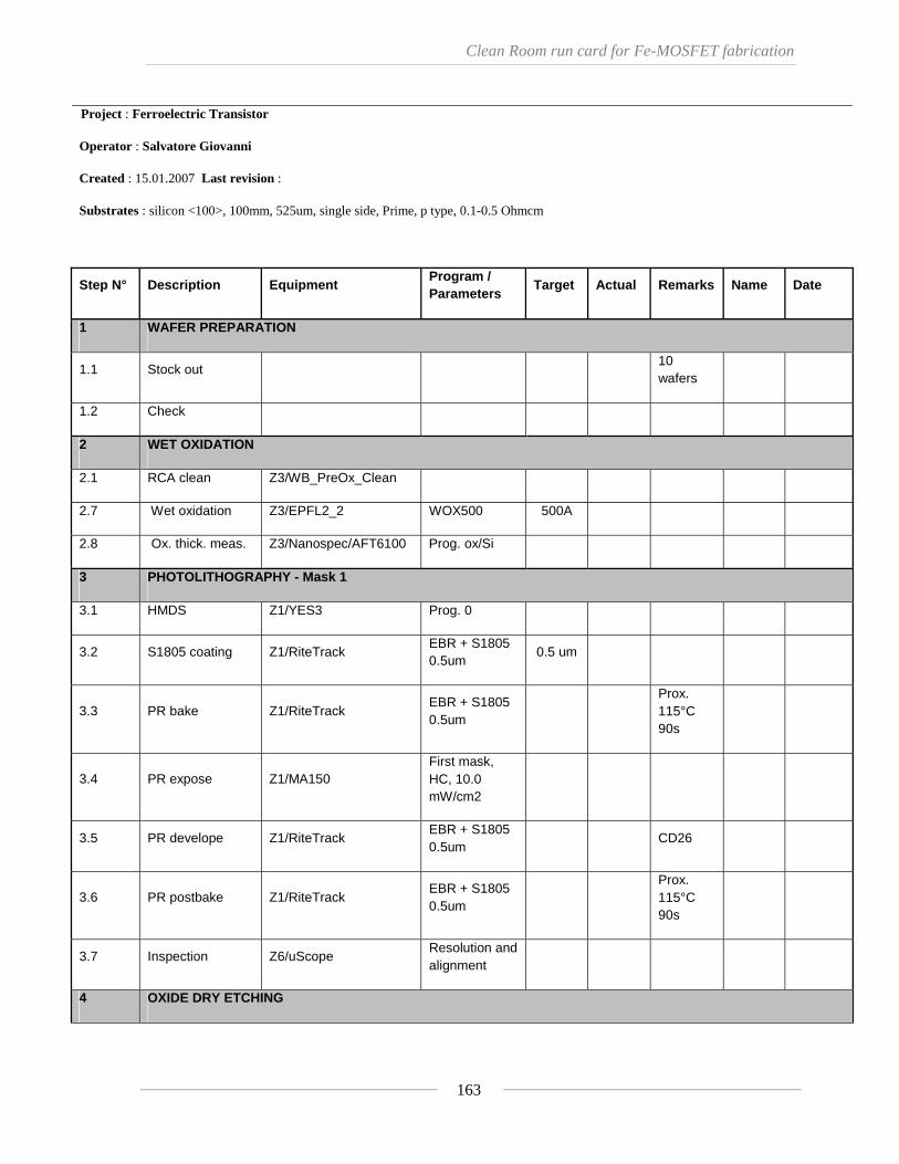
Clean Room run card for Fe-MOSFET fabrication
163
Project : Ferroelectric Transistor
Operator : Salvatore Giovanni
Created : 15.01.2007 Last revision :
Substrates : silicon <100>, 100mm, 525um, single side, Prime, p type, 0.1-0.5 Ohmcm
Step N° Description Equipment Program / Parameters
Target Actual Remarks Name Date
1 WAFER PREPARATION
1.1 Stock out 10 wafers
1.2 Check
2 WET OXIDATION
2.1 RCA clean Z3/WB_PreOx_Clean
2.7 Wet oxidation Z3/EPFL2_2 WOX500 500A
2.8 Ox. thick. meas. Z3/Nanospec/AFT6100 Prog. ox/Si
3 PHOTOLITHOGRAPHY - Mask 1
3.1 HMDS Z1/YES3 Prog. 0
3.2 S1805 coating Z1/RiteTrack EBR + S1805 0.5um
0.5 um
3.3 PR bake Z1/RiteTrack EBR + S1805 0.5um
Prox. 115°C 90s
3.4 PR expose Z1/MA150 First mask, HC, 10.0 mW/cm2
3.5 PR develope Z1/RiteTrack EBR + S1805 0.5um
CD26
3.6 PR postbake Z1/RiteTrack EBR + S1805 0.5um
Prox. 115°C 90s
3.7 Inspection Z6/uScope Resolution and alignment
4 OXIDE DRY ETCHING
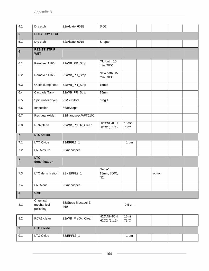
Appendix B
164
4.1 Dry etch Z2/Alcatel 601E SiO2
5 POLY DRY ETCH
5.1 Dry etch Z2/Alcatel 601E Si-opto
6 RESIST STRIP WET
6.1 Remover 1165 Z2/WB_PR_Strip Old bath, 15 min, 70°C
6.2 Remover 1165 Z2/WB_PR_Strip New bath, 15 min, 70°C
6.3 Quick dump rinse Z2/WB_PR_Strip 15min
6.4 Cascade Tank Z2/WB_PR_Strip 15min
6.5 Spin rinser dryer Z2/Semitool prog 1
6,6 Inspection Z6/uScope
6,7 Residual oxide Z3/Nanospec/AFT6100
6.8 RCA clean Z3/WB_PreOx_Clean H2O:NH4OH:H2O2 (5:1:1)
15min 75°C
7 LTO Oxide
7.1 LTO Oxide Z3/EPFL3_1 1 um
7.2 Ox. Mesure Z3/nanospec
7 LTO densification
7.3 LTO densification Z3 - EPFL2_1 Dens-1, 15min, 700C, N2
option
7.4 Ox. Meas. Z3/nanospec
8 CMP
8.1 Chemical mechanical polishing
Z5/Steag Mecapol E 460
0.5 um
8.2 RCA1 clean Z3/WB_PreOx_Clean H2O:NH4OH:H2O2 (5:1:1)
15min 75°C
9 LTO Oxide
9.1 LTO Oxide Z3/EPFL3_1 1 um
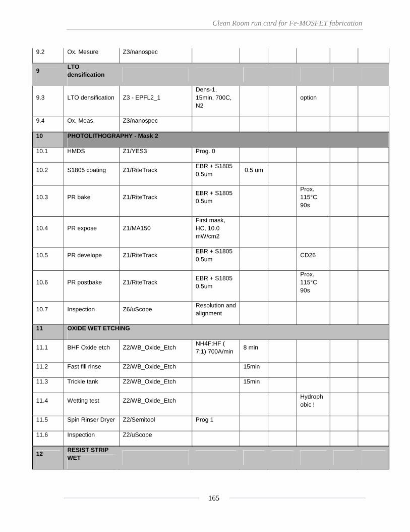
Clean Room run card for Fe-MOSFET fabrication
165
9.2 Ox. Mesure Z3/nanospec
9 LTO densification
9.3 LTO densification Z3 - EPFL2_1 Dens-1, 15min, 700C, N2
option
9.4 Ox. Meas. Z3/nanospec
10 PHOTOLITHOGRAPHY - Mask 2
10.1 HMDS Z1/YES3 Prog. 0
10.2 S1805 coating Z1/RiteTrack EBR + S1805 0.5um
0.5 um
10.3 PR bake Z1/RiteTrack EBR + S1805 0.5um
Prox. 115°C 90s
10.4 PR expose Z1/MA150 First mask, HC, 10.0 mW/cm2
10.5 PR develope Z1/RiteTrack EBR + S1805 0.5um
CD26
10.6 PR postbake Z1/RiteTrack EBR + S1805 0.5um
Prox. 115°C 90s
10.7 Inspection Z6/uScope Resolution and alignment
11 OXIDE WET ETCHING
11.1 BHF Oxide etch Z2/WB_Oxide_Etch NH4F:HF ( 7:1) 700A/min
8 min
11.2 Fast fill rinse Z2/WB_Oxide_Etch 15min
11.3 Trickle tank Z2/WB_Oxide_Etch 15min
11.4 Wetting test Z2/WB_Oxide_Etch Hydrophobic !
11.5 Spin Rinser Dryer Z2/Semitool Prog 1
11.6 Inspection Z2/uScope
12 RESIST STRIP WET
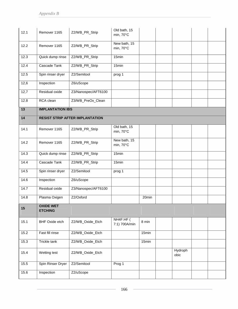
Appendix B
166
12.1 Remover 1165 Z2/WB_PR_Strip Old bath, 15 min, 70°C
12.2 Remover 1165 Z2/WB_PR_Strip New bath, 15 min, 70°C
12.3 Quick dump rinse Z2/WB_PR_Strip 15min
12.4 Cascade Tank Z2/WB_PR_Strip 15min
12.5 Spin rinser dryer Z2/Semitool prog 1
12,6 Inspection Z6/uScope
12,7 Residual oxide Z3/Nanospec/AFT6100
12.8 RCA clean Z3/WB_PreOx_Clean
13 IMPLANTATION IBS
14 RESIST STRIP AFTER IMPLANTATION
14.1 Remover 1165 Z2/WB_PR_Strip Old bath, 15 min, 70°C
14.2 Remover 1165 Z2/WB_PR_Strip New bath, 15 min, 70°C
14.3 Quick dump rinse Z2/WB_PR_Strip 15min
14.4 Cascade Tank Z2/WB_PR_Strip 15min
14.5 Spin rinser dryer Z2/Semitool prog 1
14.6 Inspection Z6/uScope
14.7 Residual oxide Z3/Nanospec/AFT6100
14.8 Plasma Oxigen Z2/Oxford 20min
15 OXIDE WET ETCHING
15.1 BHF Oxide etch Z2/WB_Oxide_Etch NH4F:HF ( 7:1) 700A/min
8 min
15.2 Fast fill rinse Z2/WB_Oxide_Etch 15min
15.3 Trickle tank Z2/WB_Oxide_Etch 15min
15.4 Wetting test Z2/WB_Oxide_Etch Hydrophobic
15.5 Spin Rinser Dryer Z2/Semitool Prog 1
15.6 Inspection Z2/uScope

Clean Room run card for Fe-MOSFET fabrication
167
15.7 RCA clean Z3/WB_PreOx_Clean
16 GATE OXIDATION
16.1 RCA clean Z3/WB_PreOx_Clean
16.2 Gate oxidation Z3/EPFL2_3 DOX250 50-200A
16.3 Ox. thick. meas. Z3/Nanospec/AFT6100
17 PVDF spin coating
17.1 PVDF 2% spin coating
Z1/RC8 160nm Option
18
PHOTOLITHOGRAPHY mask Metal
18.1 S1813 coating Z1/RiteTrack 88 Serie Prog 2; 2930rpm; 30 ''
1.50 um
18.2 PR bake Z1/RiteTrack 88 Serie Prog SEMI 2, 60s, 115C
18.3 PR Expose Z1/RiteTrack 88 Serie VC prg(3), 10.0 mW/cm2 6,5s
18.4 PR Develope Z1/RiteTrack 88 Serie CD26 45s. + Rinse/Dry
18.5 PR postbake Z1/RiteTrack 88 Serie Prog SEMI 2, 60s, 115C
18.6 Inspection Z6/uScope CDI
18.8 PR Thickness Z3/Naospec AFT6100 TP_PR S1813 On test wafer
19 TOP GATE METAL ETCHING
19.1 Prettl, wet bench, miscellaneous applications/Z5
Au wet etching Au 2min to
be tested
19.2 Prettl, wet bench, miscellaneous applications/Z5
Cr wet etching Cr to be tested
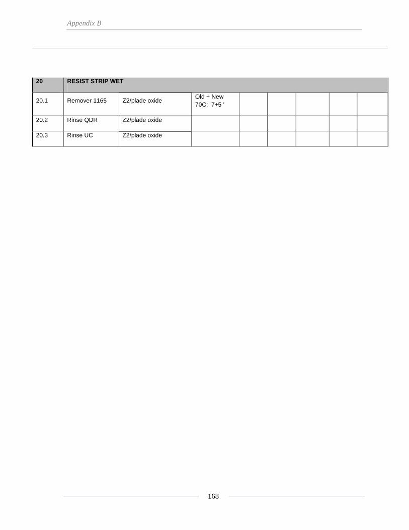
Appendix B
168
20 RESIST STRIP WET
20.1 Remover 1165 Z2/plade oxide Old + New 70C; 7+5 '
20.2 Rinse QDR Z2/plade oxide
20.3 Rinse UC Z2/plade oxide
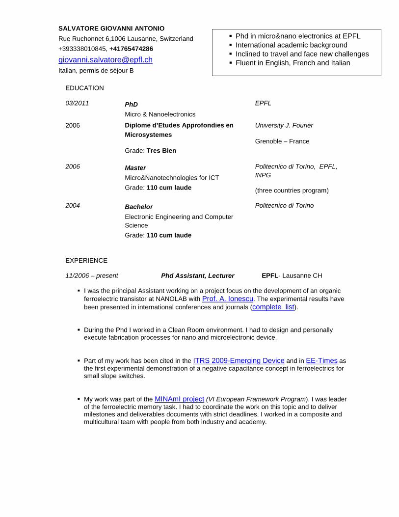
EDUCATION
03/2011 PhD
Micro & Nanoelectronics
EPFL
2006 Diplome d’Etudes Approfondies en Microsystemes
Grade: Tres Bien
University J. Fourier
Grenoble – France
2006 Master
Micro&Nanotechnologies for ICT
Grade: 110 cum laude
Politecnico di Torino, EPFL, INPG
(three countries program)
2004 Bachelor
Electronic Engineering and Computer Science
Grade: 110 cum laude
Politecnico di Torino
EXPERIENCE
11/2006 – present Phd Assistant, Lecturer EPFL- Lausanne CH
I was the principal Assistant working on a project focus on the development of an organic ferroelectric transistor at NANOLAB with Prof. A. Ionescu. The experimental results have been presented in international conferences and journals (complete list).
During the Phd I worked in a Clean Room environment. I had to design and personally execute fabrication processes for nano and microelectronic device.
Part of my work has been cited in the ITRS 2009-Emerging Device and in EE-Times as the first experimental demonstration of a negative capacitance concept in ferroelectrics for small slope switches.
My work was part of the MINAmI project (VI European Framework Program). I was leader of the ferroelectric memory task. I had to coordinate the work on this topic and to deliver milestones and deliverables documents with strict deadlines. I worked in a composite and multicultural team with people from both industry and academy.
SALVATORE GIOVANNI ANTONIO
Rue Ruchonnet 6,1006 Lausanne, Switzerland
+393338010845, +41765474286
Italian, permis de sèjour B
Phd in micro&nano electronics at EPFL International academic background Inclined to travel and face new challenges Fluent in English, French and Italian

02/2006 - 09/2006 Visiting student MIT- Cambridge, U.S.A.
I worked on a project for the development of a new photolithographic technique at RLE with Prof. K. Berggren . A new nanoimprinting method at room temperature had been conceived and the preliminaries demonstrated. I had two main tasks: finalize and optimize the on road process and start using the AFM as lithographic tool on polymeric substrates.
I was able to successfully validate the process and demonstrate the feasibility of the fabrication techinique. My work was awarded 2006 IEEE Best Student Paper Award in Nanotechnology.
I successfully proved the feasibility of using the AFM as imprinting tool. This work was included in the patent “Nanotemplate Arbitrary Imprint Lithography”, United States of America Serial No. 11/542474, October 3, 2006.
AWARDS
2006 Accenture Best Thesis in Electronics at Politecnico of Turin for Master
2006 IEEE Best Student Paper Award in Nanotechnology
2000 Salmon Prize assigned to distinguished high school students in Latin Language
TECHNICAL SKILLS
Nanotechnology Fabrication & Characterization: optical lithography, Wet and Dry etching, Nanoimprinting, SEM, spin coating, lift-off, HP analyzer, cryogenic measurements.
Informatics: matlab, Mathematica, VHDL, C++, C, Sentaurus, Origin, Adobe Photoshop, Corel Suite, Office Suite
LANGUAGES
ITALIAN (mother tongue) ENGLISH (fluent both written and spoken) FRENCH (fluent spoken, intermediate written)
OTHER ACTIVITIES
I played the piano in a music band for 10 years.
I participated at the World Youth Day in Köln (Summer 2005) as volunteer.
I was a staff member at Montreux Jazz Festival 2009 and I’m a member of Rotaract Lausanne
I like travelling, discovering new cultures and meeting new people
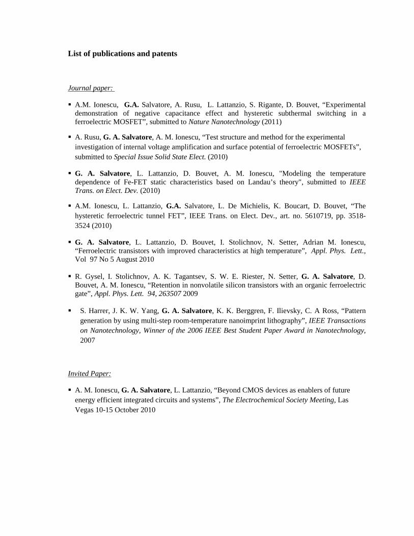
List of publications and patents
Journal paper:
A.M. Ionescu, G.A. Salvatore, A. Rusu, L. Lattanzio, S. Rigante, D. Bouvet, “Experimental demonstration of negative capacitance effect and hysteretic subthermal switching in a ferroelectric MOSFET”, submitted to Nature Nanotechnology (2011)
A. Rusu, G. A. Salvatore, A. M. Ionescu, “Test structure and method for the experimental investigation of internal voltage amplification and surface potential of ferroelectric MOSFETs”, submitted to Special Issue Solid State Elect. (2010)
G. A. Salvatore, L. Lattanzio, D. Bouvet, A. M. Ionescu, "Modeling the temperature dependence of Fe-FET static characteristics based on Landau’s theory", submitted to IEEE Trans. on Elect. Dev. (2010)
A.M. Ionescu, L. Lattanzio, G.A. Salvatore, L. De Michielis, K. Boucart, D. Bouvet, “The hysteretic ferroelectric tunnel FET”, IEEE Trans. on Elect. Dev., art. no. 5610719, pp. 3518-3524 (2010)
G. A. Salvatore, L. Lattanzio, D. Bouvet, I. Stolichnov, N. Setter, Adrian M. Ionescu, “Ferroelectric transistors with improved characteristics at high temperature”, Appl. Phys. Lett., Vol 97 No 5 August 2010
R. Gysel, I. Stolichnov, A. K. Tagantsev, S. W. E. Riester, N. Setter, G. A. Salvatore, D. Bouvet, A. M. Ionescu, “Retention in nonvolatile silicon transistors with an organic ferroelectric gate”, Appl. Phys. Lett. 94, 263507 2009
S. Harrer, J. K. W. Yang, G. A. Salvatore, K. K. Berggren, F. Ilievsky, C. A Ross, “Pattern
generation by using multi-step room-temperature nanoimprint lithography”, IEEE Transactions on Nanotechnology, Winner of the 2006 IEEE Best Student Paper Award in Nanotechnology, 2007
Invited Paper:
A. M. Ionescu, G. A. Salvatore, L. Lattanzio, “Beyond CMOS devices as enablers of future energy efficient integrated circuits and systems”, The Electrochemical Society Meeting, Las Vegas 10-15 October 2010

Conference paper:
A. Rusu, G. A. Salvatore, D. Jiménez, A. M. Ionescu, “Metal-Ferroelectric-Metal-Oxide-Semiconductor Field Effect Transistor with Sub-60mV/decade Subthreshold Swing and Internal Voltage Amplification”, to be presented at International Electron Devices Meeting, IEDM, San Francisco 2010
A. Rusu, G. A. Salvatore, Adrian M. Ionescu, “Test structure and method for the experimental investigation of internal voltage amplification and surface potential of ferroelectric MOSFETs”, Proceedings of the 40th European Solid-State Device Research Conference, ESSDERC, pp. 174-177, Sevilla 2010
G. A. Salvatore, L. Lattanzio, D. Bouvet, A. M. Ionescu, “The Curie Temperature as a Key Design Parameter of Ferroelectric Field Effect Transistors”, Proceedings of the 40th European Solid-State Device Research Conference, ESSDERC, pp. 218-221, Sevilla 2010
G. A. Salvatore, L. Lattanzio, D. Bouvet, A. Rusu, A. M. Ionescu, “Temperature sensor based on Ferroelectric FET”, to be presented at 34th International Conference on Micro- and Nano-Engineering, MNE 2010, Genova Italy 2010
L. Lattanzio, G. A. Salvatore, A. M. Ionescu, “Non-Hysteretic Ferroelectric Tunnel FET with Improved Conductance at Curie Temperature”, Device Research Conference 2010, South Bend, IN, USA, 21-23 June, 2010.
L. Lattanzio, L. De Michielis, G. A. Salvatore, D. Bouvet, K. Boucart, A. M. Ionescu,
“Ferroelectric Tunnel FET with a SiO2/Al2O3/P(VDF-TrFE) gate stack”, ULIS 2010, Glasgow, Scotland, UK, 17-19 March 2010.
Al. Rusu, G. A. Salvatore, A. M. Ionescu, “An experimental investigation of the surface
potential in ferroelectric P(VDF-TrFE) FETs”, 34th International Conference on Micro- and Nano-Engineering, MNE 2009, Ghent, Belgium, 28 September - 01 October 2009.
G. A. Salvatore, L. Lattanzio, D. Bouvet, A. M. Ionescu, “An experimental study of temperature influence on electrical characteristics of ferroelectric P(VDF-TrFE) FETs on SOI”, Proceedings of the 39th European Solid-State Device Research Conference, ESSDERC art. no. 5331330, pp. 97-100, Athens 2009
G. A. Salvatore, D. Bouvet, A. M. Ionescu, “Demonstration of subthrehold swing smaller than 60mV/decade in Fe-FET with P(VDF-TrFE)/SiO2 gate stack”, Technical Digest - International Electron Devices Meeting, IEDM, San Francisco 2008
G. A. Salvatore, L. Lattanzio, D. Bouvet, I. Stolichnov, N. Setter, A. M. Ionescu, ”Low voltage ferroelectric FET with sub-l00nm copolymer P(VDF-TrFE) gate dielectric for non-volatile IT memory”, Proceedings of the 38th European Solid-State Device Research Conference, ESSDERC art. no. 4681724, pp. 162-165, Edinburgh 2008
D. Acquaviva, G. A. Salvatore, D. Bouvet, D. Tsamados, P. Coronel, T. Skotnicki, A. M. Ionescu, “Micro-Electro-Mechanical Metal-Air-Insulator-Semiconductor Diode Switch”, 34th International Conference on Micro- and Nano-Engineering, MNE 2008, 15-19 September 2008, Athens, Greece

G. A. Salvatore, D. Bouvet, M. A. Ionescu, S. Riester, I. Stolichnov, R. Gysel, N. Setter, “1T memory cell based on PVDF-TrFE Field Effect Transistor”, MRS 2008, 24-28 March 2008, San Francisco, USA
Patent:
K. K. Berggren, S. Harrer, G. A. Salvatore, J. Yang , “Nanotemplate Arbitrary Imprint Lithography”, United States of America Serial No. 11/542474, October 3, 2006.


![Transistor, fotodiode, dan diode pemencar [14]](https://static.fdocuments.nl/doc/165x107/58723e0b1a28ab102f8b6ff3/transistor-fotodiode-dan-diode-pemencar-14.jpg)