DATASHEET - linux-sunxilinux-sunxi.org/images/8/89/AXP209_Datasheet_v1.0en.pdf · VIN ACIN Input...
45
DATASHEET AXP209 Enhanced single Cell Li-Battery and Power System Management IC X-Powers © 2010 X-Powers Limited - All rights reserved
Transcript of DATASHEET - linux-sunxilinux-sunxi.org/images/8/89/AXP209_Datasheet_v1.0en.pdf · VIN ACIN Input...
DATASHEET
AXP209Enhanced single Cell Li-Battery and Power System Management IC
X-Powers© 2010 X-Powers Limited - All rights reserved
AXP209Enhanced single Cell Li-Battery and Power System Management IC
Table of Contents1. Overview ........................................................................................................................................3
2. Features .........................................................................................................................................4
3. Typical Application........................................................................................................................5
4. Absolute Maximum Ratings .........................................................................................................6
5. Electrical Characteristics................................................................................................................6
6. Typical Characteristics...................................................................................................................9
7. Pin Definition............................................................................................................................... 12
8. Functional Block Diagram........................................................................................................... 14
9. Control and Operation................................................................................................................ 15
9.1 Power On / Off & Reset ..................................................................................................... 15
9.2 Power path management (IPS).......................................................................................... 17
9.3 Adaptive PWM Charger ..................................................................................................... 19
9.4 Backup battery ...................................................................................................................22
9.5 Multi-channel power outputs............................................................................................23
9.6 Default Voltage / Timing Settings..................................................................................... 24
9.7 Signal Acquisition System .................................................................................................25
9.8 Multifunction Pin Description ........................................................................................... 25
9.9 Timer ................................................................................................................................... 25
9.10 Decryption ........................................................................................................................26
9.11 HOST Interface and interrupt(TWSI and IRQ).................................................................26
9.12 Register.............................................................................................................................28
10. Package...............................................................................................................................................................45Page 2/45
AXP209Enhanced single Cell Li-Battery and Power System Management IC
1. Overview
AXP209 is designed to be a highly-integrated power system management IC that is optimized forapplications requiring single-cell Li-battery (Li-Ion/Polymer) and multiple output DC-DC converters. It isoffering an easy-to-use and flexible complete solution which can fully meet the increasingly complexityof accurate power control required by modern application processor system.
AXP209 Incorporates an adaptive USB-Compatible PWM Charger, 2 Buck DC-DC converters,5 Linearregulators (LDOs), Voltage/Current/Temperature and other multi-channel 12-Bit ADC, as well as 4Configurable GPIOs. To ensure power system safety and stability, the AXP209 also integrates over/under(OVP / UVP), Over temperature(OTP), and Overcurrent (OCP) Protection circuits.
With Intelligent Power Select, IPS™ circuits, the AXP209 can distribute power safely and transparentlyamong external AC-adapter, Li-battery and application system load. It can still work normally whenthere is no battery (e.g. deeply discharged/defective battery) but only external input power source.
The AXP209 provides a small, simple solution for obtaining power from three different power sources;single-cell Li-Ion battery, USB port, and AC-adapter. It can also support a rechargeable backup batterytoo.
To ensure compatibility with a wide range of system processors, AXP209 uses a Two Wire SerialInterface (TWSI), through which application processor is capable of enabling/disabling power rails,programming voltages, accessing internal registers, as well as measurement data (including FuelGauge). With the power monitoring results of high precision (1%, determined by the 1% BIASresistance), end users will always know the real-time power consumption, which can bring them anunprecedented experience of power management.
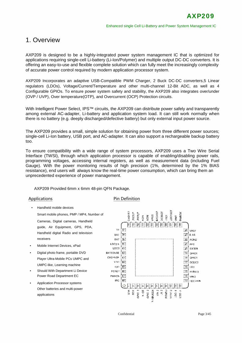
AXP209 Provided 6mm x 6mm 48-pin QFN Package.
Applications Pin Definition
Handheld mobile devices
Smart mobile phones, PMP / MP4, Number of
Cameras, Digital cameras, Handheld
guide, Air Equipment, GPS, PDA,
Handheld digital Radio and television
receivers
Mobile Internet Devices, xPad
Digital photo frame, portable DVD
Player Ultra-Mobile PCs UMPC and
UMPC-like, Learning machine
Should With Department Li DevicePower Road Department EC
Application Processor systems
Other batteries and multi-power
applications
Confidential Page 3/45

AXP209Enhanced single Cell Li-Battery and Power System Management IC
2. Features
Intelligent Power Select (IPS)o Wide input voltage range: 2.9V ~ 6.3V
(AMR:-0.3V ~ 11V)o Configurable Intelligent Power Delect
"IPS™" Systemo Adaptive USB (Support USB3.0) Or AC
adapter with current limiting (4.4V /900mA / 500mA / 100mA)
o Battery path is less than equivalentresistance of 75mΩ
Fully Integrated PWM Chargero Maximum charge current to 1.8Ao Support battery temperature monitoring
o Full support of USB compatible chargers(including USB 3.0)
o High charging accuracy error of less than0.5%
o Supports 4.1V/4.15V/4.2V/4.36V andother battery voltages
o Automatic charging process control andmanagement
o Can directly drive LED to indicatecharging status
o The system automatically adjusts thecharge current to suit the system load
Backup battery supporto Provision for a backup battery input
supply an RTC Moduleo Supports backup battery charging, with
adjustable charging current.
2 Synchronous Buck Converterso DC-DC1: The PWM chargero DC-DC2: 1.6A 0.7-2.275V, adjustable
25mV / step, supporting VRC (Voltageramp control)
o DC-DC3: 1.2A 0.7-3.5V, adjustable 25mV/ step.
5 Linear regulators (LDO)o LDO1:30mA Always oneo LDO2: 200mA Low Noise LDO,1.8V
~3.3V, Adjustable 100mV / stepo LDO3: 200mA 0.7-3.5V Adjustable,
25mV / step
o LDO4: 200mA Low Noise LDO,1.8V ~3.3V Adjustable 100mV / step
o LDO5: 50mA Low Noise LDO, 1.8-3.3V Adjustable, 100mV / step.
Timer (Timer)
o 7bit Timer, Timing range 1 ~ 127
minutes
o Timer Interrupt Output Signal Acquisition System (Signal Capture)
o Built-in 12-channel 12 Bit ADCo Accept two external analog signal inputso Provide battery and external power supply
voltage and current datao Built-Precision Coulomb Counter and Fuel
gauge systemo Provide a wealth of power management
information, such as instantaneous power(mA or mW), the remaining batterycapacity (% or mAh), The state of charge(%) and remaining battery or charging time
o Two-level low-battery warning andprotection
o Provides chip die temperature data
• Application Processor Interface (Host Interface)o Host can exchange data through the TWSI
(I2C)o Flexible interrupt and sleep managemento Flexible pin function, multiple GPIO can be
set as IO, ADC and other functionso Built-in configurable timero Provide 12 sets of registers that can retain
data when the system is shut down.• System Management (System Management)
o Support soft and hard reseto Support for soft and hard shutdowno Support for external wakeup triggerso Supports output voltage monitoring and
self-diagnostic functiono Output PWROK indication for system
reset or shutdowno External power detection
(insertion/removal/sufficient currentcapacity)
o Supports soft power on via GPIOso Over / under voltage protection (OVP /
UVP)o Overcurrent protection (OCP)o Over-temperature protection (OTP)o Support OTG VBUS power state
setting / monitoring Highly Integrated
o Internal precision voltage reference(0.5%)
o Built-in MOSFETo Timing and the output voltages can be
customized
Decryption module (Decryption)o 128bit OTP password storageo Dynamic real-time decryption algorithm
Confidential Page 4/45
AXP209Enhanced single Cell Li-Battery and Power System Management IC
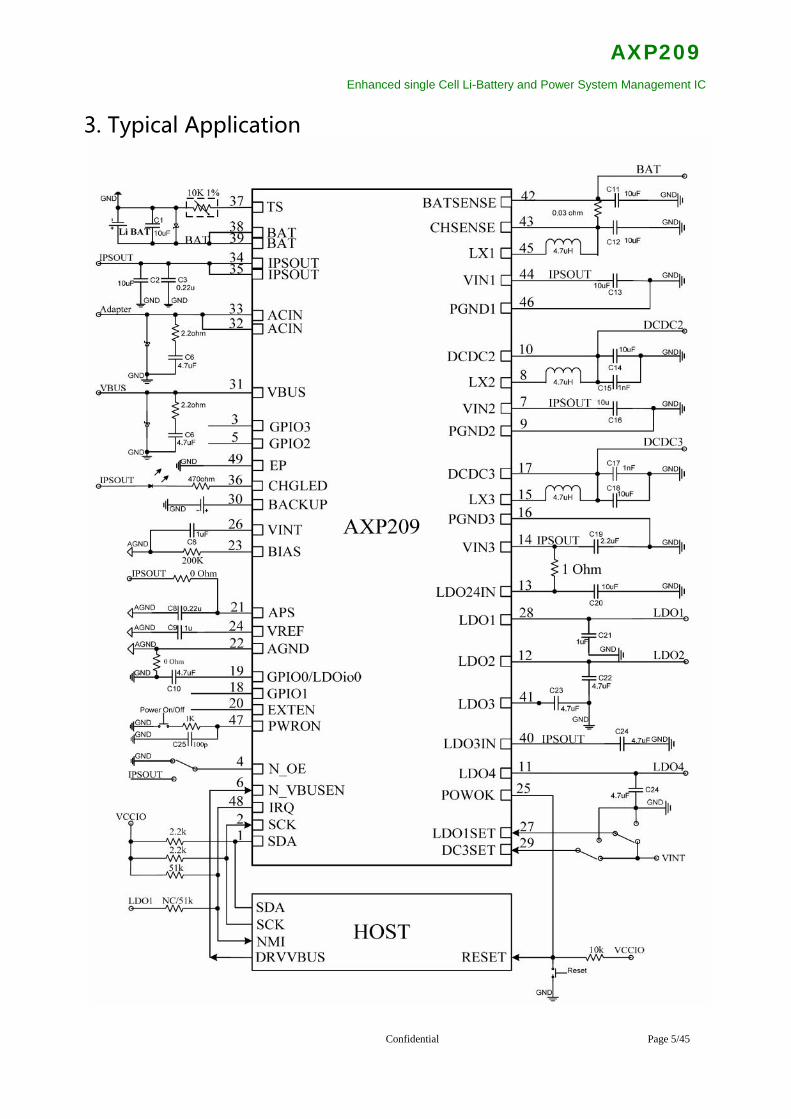
3. Typical Application
Confidential Page 5/45
AXP209Enhanced single Cell Li-Battery and Power System Management IC
4. Absolute Maximum Ratings
Symbol Description Value Units
ACIN Input Voltage -0.3 To 11 V
VBUS Input Voltage -0.3 To 11 V
TJ Operating Temperature Range -40 To 130 ℃
Ts Storage Temperature Range -40 To 150 ℃
TLEAD Maximum Soldering Temperature (at leads,10sec) 300 ℃
VESD Maximum ESD stress voltage, Human Body Model > 4000 V
PD Internal Power Dissipation 2100 mW
5. Electrical CharacteristicsVIN = 5V, BAT = 3.8V, TA= 25℃
SYMBOL DESCRIPTION CONDITIONS MIN TYP MAX UNITS
ACIN
VIN ACIN Input Voltage 3.8 6.3 V
IOUT VOUT Current Available Before 500mV Voltage Drop 2500 mALoading BAT
VUVLO ACIN Under Voltage Lockout 3.8 V
VOUT IPS Output Voltage 2.9 5.0 V
RACIN Internal Ideal Diode On PIN to PIN, ACIN to 170 mΩResistance IPSOUT
VBUS
VIN VBUS Input Voltage 3.8 6.3 V
IOUT VOUT Current Available Before 500 900 mALoading BAT
VUVLO VBUS Under Voltage Lockout 3.8 V
VOUT IPS Output Voltage 2.9 5.0 V
RVBUS Internal Ideal Diode On PIN to PIN, VBUS to 300 mΩResistance IPSOUT
Battery Charger
VTRGT BAT Charge Target Voltage -0.5% 4.2 + 0.5% V
ICHRG Charge Current 1200 1800 mA
ITRKL Trickle Charge Current 10% ICHRG
Confidential Page 6/45

AXP209Enhanced single Cell Li-Battery and Power System Management IC
mA
VTRKL Trickle Charge Threshold 3.0 V
VoltageVRECHG Recharge Battery Threshold Threshold Voltage -100 mV
Voltage Relative to VTARGET
TTIMER1 Charger Safety Timer Trickle Mode 40 Min
Termination Time
TTIMER2 Charger Safety Timer CC Mode 480 Min
Termination Time
IEND End of Charge Indication CV Mode 10% 15% ICHRG
Current Ratio mA
Backup Battery
VTRGT Backup Battery Charge Target 2.5 3.0 3.1 V
Voltage
ICHRG Backup Battery Charge Current 50 200 400 uA
IBackup Current when use Backup 10 15 uA
Battery
NTC
VTL Cold Temperature Fault Charge 2.112 V0 3.264
Threshold Voltage Discharge 3.226
VTH Hot Temperature Fault Threshold Charge 0.397 V0 3.264
Voltage Discharge 0.282
VTE NTC Disable Threshold Voltage Falling Threshold 0.2 V
Hysteresis
Ideal Diode
Rds (on) On Resistance (BAT to IPSOUT) 75 mΩ
SYMBOL DESCRIPTION CONDITIONS MIN TYP MAX UNITS
Off Mode Current
IBATOFF OFF Mode Current BAT = 3.8V 27 μAISUSPEND USB VBUS suspend Mode BAT = 3.8V, 86 μA
current VBUS = 5V,
N_VBUSEN = 1
Logic
VIL Logic Low Input Voltage 0.3 V
VIH Logic High Input Voltage 2 V
TWSI
VCC Input Supply Voltage 3.3 V
ADDRESS TWSI Address 0x68
fSCK Clock Operating Frequency 400 1200 kHZ
tf Clock Data Fall Time 2.2Kohm Pull up 60 ns
Confidential Page 7/45
AXP209Enhanced single Cell Li-Battery and Power System Management IC
tr Clock Data Rise Time 2.2Kohm Pull up 100 ns
DCDC
fOSC Oscillator Frequency Default 1.5 MHz
DCDC2
ILIM2 PMOS Switch Current Limit PWM Mode 2300 mA
IDC2OUT Available Output Current PWM Mode 1800 mA
VDC2OUT Output Voltage Range 0.7 2.275 V
DCDC3
ILIM3 PMOS Switch Current Limit PWM Mode 1400 mA
IDC3OUT Available Output Current PWM Mode 1000 mA
VDC3OUT Output Voltage Range 0.7 3.5 V
SYMBOL DESCRIPTION CONDITIONS MIN TYP MAX UNITS
LDO1
VLDO1 Output Voltage ILDO1= 1mA 1.3 V-1% 1%
3.3
ILDO1 Output Current 30 mA
LDO2
VLDO2 Output Voltage ILDO2= 1mA 1.8 3.3 V
ILDO2 Output Current 200 mA
PSRR Power Supply Rejection Ratio ILDO2= 60mA,1KHz TBD dB
eN Output Noise, 20-80KHz Vo = 3V, Io = 150mA 28 μVRMS
LDO3
VLDO3 Output Voltage ILDO3= 1mA 0.7 3.5 V
ILDO3 Output Current 200 mA
PSRR Power Supply Rejection Ratio ILDO3= 10mA, 1KHz TBD dB
eN Output Noise, 20-80KHzVo = 1.8V, Io =150mA TBD μVRMS
LDO4
VLDO3 Output Voltage ILDO3= 1mA 1.8 3.3 V
ILDO3 Output Current 200 mA
PSRR Power Supply Rejection Ratio ILDO3= 10mA, 1KHz TBD dB
eN Output Noise, 20-80KHzVo = 1.8V, Io =150mA 18 μVRMS
LDO5
VLDO5 Output Voltage ILDO5= 1mA 1.5 3.3 V
ILDO5 Output Current 50 mA
PSRR Power Supply Rejection Ratio ILDO5= 10mA,1KHz TBD dB
eN Output Noise, 20-80KHz Vo = 1.8V, Io = 30mA 18 μVRMS
Confidential Page 8/45
AXP209Enhanced single Cell Li-Battery and Power System Management IC
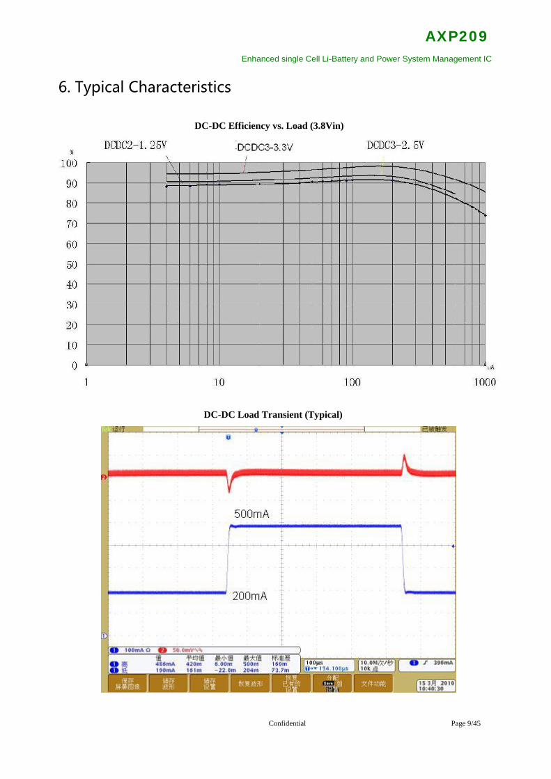
6. Typical Characteristics
DC-DC Efficiency vs. Load (3.8Vin)
DC-DC Load Transient (Typical)
Confidential Page 9/45
AXP209Enhanced single Cell Li-Battery and Power System Management IC
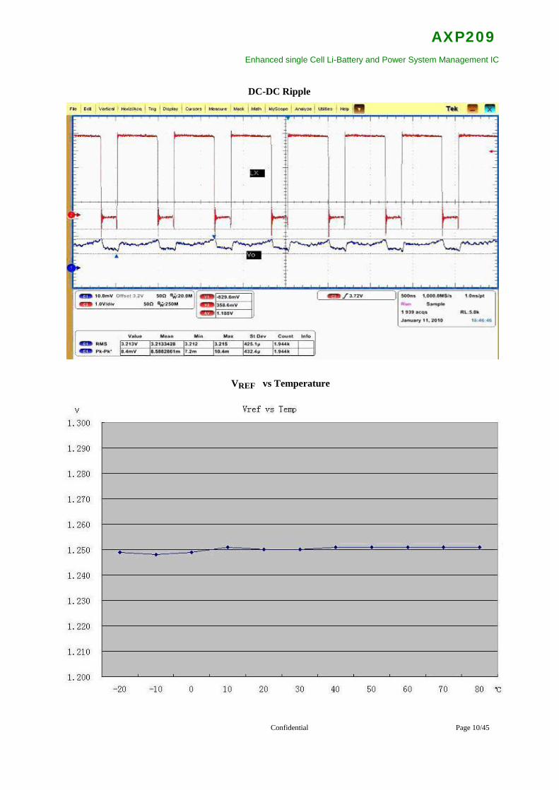
DC-DC Ripple
VREF vs Temperature
Confidential Page 10/45
AXP209Enhanced single Cell Li-Battery and Power System Management IC
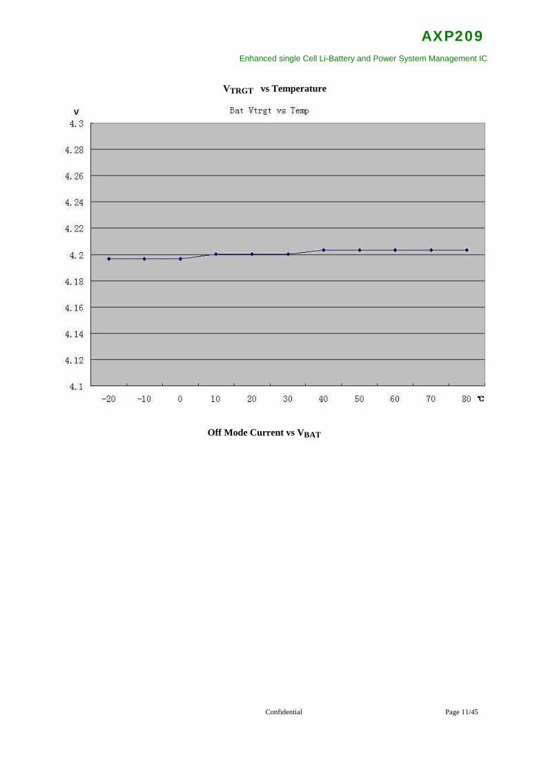
VTRGT vs Temperature
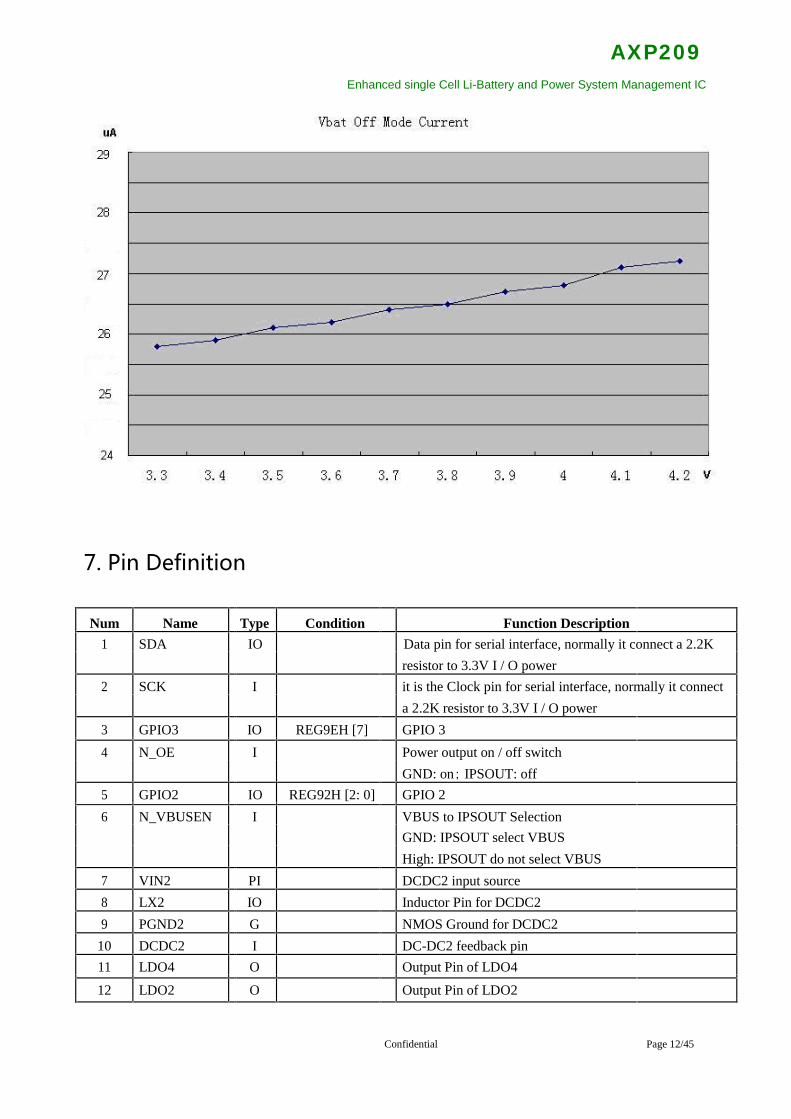
Off Mode Current vs VBAT
Confidential Page 11/45
AXP209Enhanced single Cell Li-Battery and Power System Management IC
7. Pin Definition
Num Name Type Condition Function Description
1 SDA IO Data pin for serial interface, normally it connect a 2.2K
resistor to 3.3V I / O power
2 SCK I it is the Clock pin for serial interface, normally it connect
a 2.2K resistor to 3.3V I / O power
3 GPIO3 IO REG9EH [7] GPIO 3
4 N_OE I Power output on / off switch
GND: on; IPSOUT: off
5 GPIO2 IO REG92H [2: 0] GPIO 2
6 N_VBUSEN I VBUS to IPSOUT Selection
GND: IPSOUT select VBUS
High: IPSOUT do not select VBUS
7 VIN2 PI DCDC2 input source
8 LX2 IO Inductor Pin for DCDC2
9 PGND2 G NMOS Ground for DCDC2
10 DCDC2 I DC-DC2 feedback pin
11 LDO4 O Output Pin of LDO4
12 LDO2 O Output Pin of LDO2
Confidential Page 12/45

AXP209Enhanced single Cell Li-Battery and Power System Management IC
13 LDO24IN PI Input to LDO2 and LDO4
14 VIN3 PI DCDC3 input source
15 LX3 IO Inductor Pin for DCDC3
16 PGND3 G NMOS GND for DCDC3
17 DCDC3 I Feed back to DCDC3
18 GPIO1 IO GPIO 1REG93H [2: 0]
ADC Input
19 GPIO0 IO GPIO 0
REG90H [2: 0] Low noise LDO / Switch
ADC Input
20 EXTEN O External Power Enable
21 APS PI Internal Power Input
22 AGND G Analog Ground
34 BIAS IO External 200Kohm 1% resistor
24 VREF O Internal reference voltage
25 PWROK O Power Good Indication OutPut
26 VINT PO Internal logic power, 2.5V
27 LDO1SET I It set the LDO1 default voltage.
28 LDO1 O LDO1 output,for Host RTC block
29 DC3SET I It set the DCDC3 default voltage
30 BACKUP IO Backup battery pin
31 VBUS PI USB VBUS input
32,33 ACIN PI Adapter input
34,35 IPSOUT IO Main Battery
36 CHGLED O charger status indication
37 TS I Battery Temperature sensor input or an external ADC
input
38,39 BAT PO System power source
40 LDO3IN O LDO3 input source
41 LDO3 I Output Pin of LDO3
42 BATSENSE I Current sense port1
43 CHSENSE O Current sense port2
44 VIN1 PI DCDC1 input source
45 LX1 IO Inductor Pin for DCDC1
46 PGND1 G NMOS Ground for DCDC1
47 PWRON I Power On-Off key input,Internal 100k pull high to APS
48 IRQ / IO IRQ output or wakeup
WAKEUP
49 EP G Exposed Pad, need to connect to system ground
Confidential Page 13/45

AXP209Enhanced single Cell Li-Battery and Power System Management IC
8. Functional Block Diagram
N_OE Control LogicDCDC3LX3
DC-DC3 VIN3PGND3DC3SET
IRQSCK
Serial InterfaceGPIO3
SDA GPIO2
GPIO1GPIO0 /LDOio0
Bat EXTEN
TS TemperatureRegister
MonitorOutput voltage PWROKmonitor / LBO
BIAS 12 bit ADCReference Current MonitorVREF
Voltage Voltage Monitor AGNDVINT Temperature Monitor EP
Confidential Page 14/45
AXP209Enhanced single Cell Li-Battery and Power System Management IC
9. Control and Operation
When AXP209 powers on and TWS interface SCK / SDA pins are pulled to host IO voltage source, the hostcan then adjust and monitor the AXP209. This provides flexible adjustment and monitoring options, and awealth of information.
Note: "Host" Referring to the main application processorNote: "External power supply" refers to ACIN And VBUS Inputs.
9.1 Power On / Off & ResetButton(PEK)
AXP209 PWRON Pin can be connected to GND through a button, as a Power Enable Key (PEK) orhibernation/wake button. The AXP209 can automatically identify long and short button presses andreact accordingly.
Power on Sources:1. ACIN, VBUS, and battery2. N_OE transition from high to low.3. PEK press
Power On
System power-on is initiated whenever the following conditions occur:1. When N_OE is low, and upon connection of a power supply that meets the requirements
(ACIN Or VBUS > 3.8V, and the battery voltage is higher than the shutdown voltage), AXP209will automatically boot (Automatic booting on power supply connection can be configured bythe developer).
2. N_OE is low and the system is powered off, press PEK can power on AXP209. If required theHost
3. When there is a valid external power source or battery present and N_OE changes from high tolow, AXP209 will be turned on.
After power on, DC-DC and LDO will be soft booted in a preset timing sequence, and then either theHost or PWREN the pin can enable/disable power.
Shutdown (Power off)
When you push-and-hold PEK longer than IRQLEVEL, HOST can write “1” into“REG32H [7]” to informAXP202 to shutdown, which can disable all power output except LDO1.
System power-off is initiated whenever the following conditions occur:
1. Input voltage is too low( Low-Power Protection)2. Power output voltage is too low due to overload( Overload Protection)
Confidential Page 15/45
AXP209Enhanced single Cell Li-Battery and Power System Management IC
3. Input voltage is too high( Overvoltage Protection)( See more details in chapter “ IntelligentPower Select”
4. Have waited more than 2S(default) when N_OE changes from hight to low5. Push PEK longer more than OFFLEVEL( Default 6S), and system will cut off all power output
except LDO1( there is no need for an extra RESET key)
Note: With the automatic protection mechanism, AXP209 can protect the whole system by preventingcomponents suffering from irreversible damage due to system abnormality.
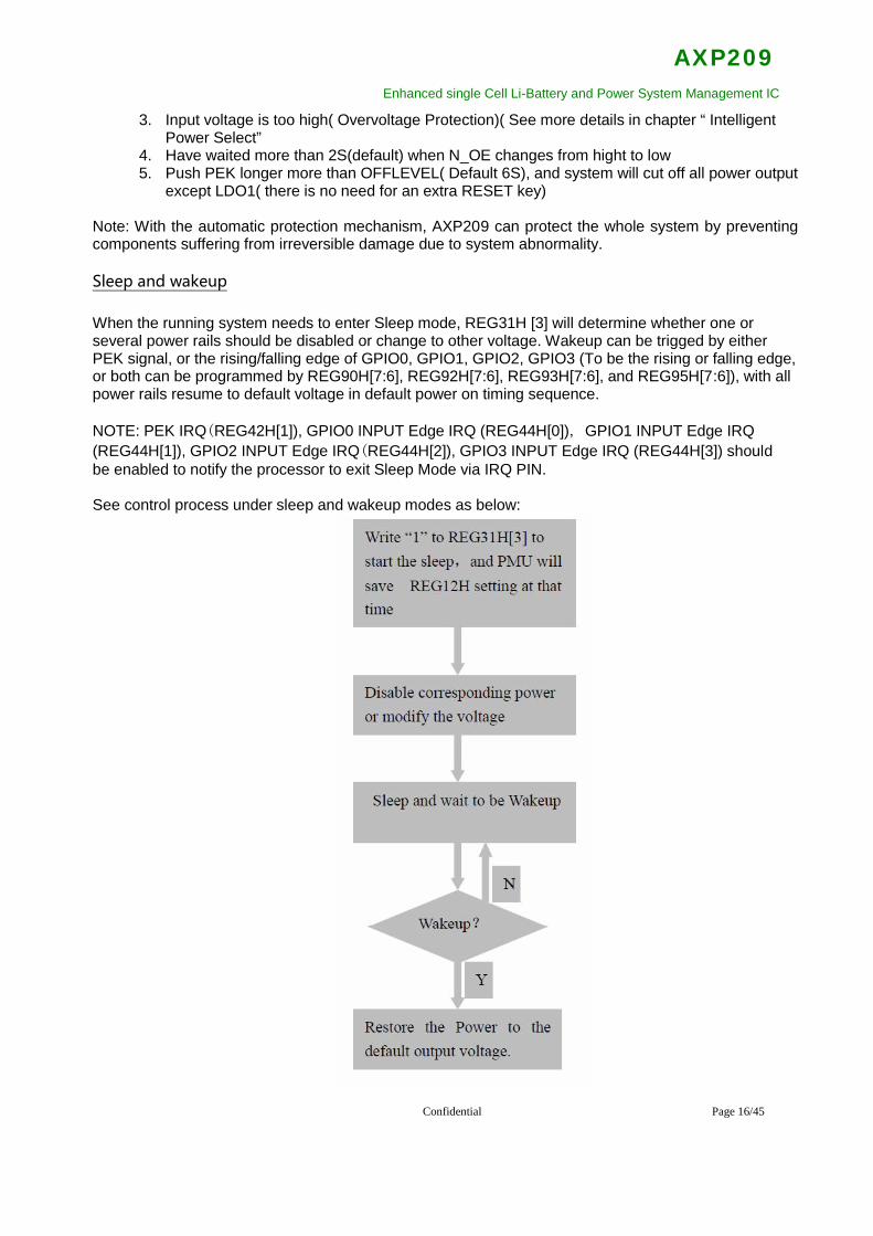
Sleep and wakeup
When the running system needs to enter Sleep mode, REG31H [3] will determine whether one orseveral power rails should be disabled or change to other voltage. Wakeup can be trigged by eitherPEK signal, or the rising/falling edge of GPIO0, GPIO1, GPIO2, GPIO3 (To be the rising or falling edge,or both can be programmed by REG90H[7:6], REG92H[7:6], REG93H[7:6], and REG95H[7:6]), with allpower rails resume to default voltage in default power on timing sequence.
NOTE: PEK IRQ(REG42H[1]), GPIO0 INPUT Edge IRQ (REG44H[0]), GPIO1 INPUT Edge IRQ(REG44H[1]), GPIO2 INPUT Edge IRQ(REG44H[2]), GPIO3 INPUT Edge IRQ (REG44H[3]) shouldbe enabled to notify the processor to exit Sleep Mode via IRQ PIN.
See control process under sleep and wakeup modes as below:
Confidential Page 16/45
AXP209Enhanced single Cell Li-Battery and Power System Management IC
System reset function and output monitoring (PWROK)
The PWROK in AXP209 can be used as the reset signal for the application system. During AXP209startup, PWROK outputs low level, which will then be pulled high to startup and reset the system afterall output voltage reaches the regulated value.
Under normal operation, the AXP209 will be always monitoring the voltage and load status. If overloador under-voltage occurs, the PWROK will instantly be driven low to reset the system and prevent datalosses.
9.2 Power path management (IPS)The AXP209 power input can come from lithium battery (BAT),USB VBUS Input, external powersupply (ACIN). The IPS will select an appropriate power source depending on the battery and externalpower conditions.
O When only the battery is available, no external power input, the battery powers the system;O When there is a valid external power source(VBUS Or ACIN), is is the preferred power supply.O When the external power is removed, the IPS will seamlessly switch over to battery power.O When both VBUS and ACIN are available, ACIN will be used to power the system and rechargethe lithium battery;O If the ACIN cannot provide sufficient current, VBUS is also connected to source morecurrent;O If the drive capacity is still insufficient, then the charge current is reduced to zero, thebattery is used to power the system.
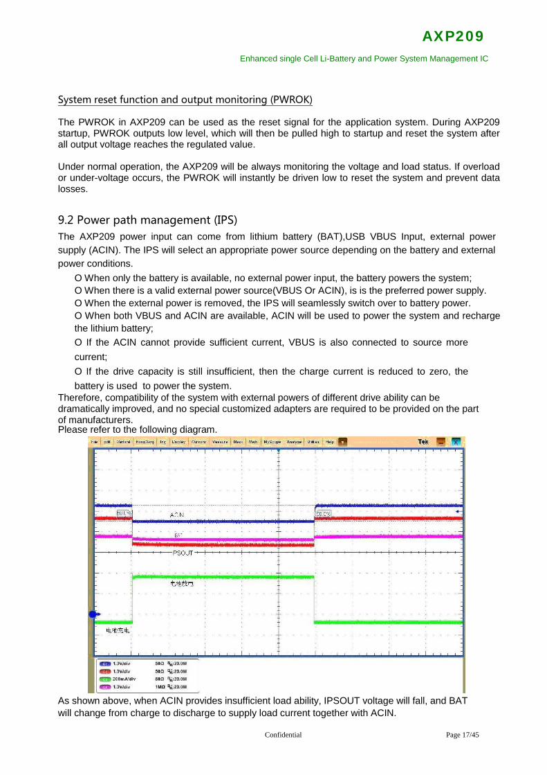
Therefore, compatibility of the system with external powers of different drive ability can bedramatically improved, and no special customized adapters are required to be provided on the partof manufacturers.Please refer to the following diagram.
As shown above, when ACIN provides insufficient load ability, IPSOUT voltage will fall, and BATwill change from charge to discharge to supply load current together with ACIN.
Confidential Page 17/45
AXP209Enhanced single Cell Li-Battery and Power System Management IC
The Host can set IPS parameters and read the feedback by using internal registers in AXP209 viaTWSI.
Voltage Limiting/Current Limiting mode and Direct Mode
In order not to affect the USB communication, VBUS is always working under Voltage-Limit mode bydefault. In this mode, AXP209 ensures that VBUS voltage remains above a configurable referencevoltage VHOLD which can meet the USB specification. The default VHOLD is 4.4V, adjustable inReg30H [5:3] register.
If the system has limit on current obtained from USB VBUS, a current-limit mode is provided (SeeREG30H[1] register), with 900mA/500mA/100mA (Reg30H [0]) selectable.
If the system just utilizes the USB for power supply rather than communication, or the USB poweradapter is utilized, AXP209 can be set to “VBUS Direct Mode” by modifying register REG30H[6], andthen AXP202 will give priority to the application power demand. When the drive ability of USB Host isinsufficient or system power consumption is large then the VBUS voltage is lower than VHOLD,AXP202 will release IRQ to indicate the weak power supply ability of Host VBUS, which may affectUSB communication, and then Host software will follow up.
AXP209’s Reaction to External Power Supply Connection
AXP209 can automatically detect the connection of external power and judge whether the power isusable or not. The result will be set in corresponding registers, and IRQ will be asserted to inform theHost at the same time.The following table has listed the status bits and meanings of external power registers:
Status register bits DescriptionRegister REG00H [7] Indicates the presence of external ACINRegister REG00H [6] Indicates whether the external ACIN is usable or notRegister REG00H [5] Indicates the presence of external VBUSRegister REG00H [4] Indicates whether the external VBUS is usable or notRegister REG00H [3] Indicates whether the VBUS voltage is above VHOLD when usedRegister REG00H [1] Indicates whether ACIN/VBUS short circuits on PCB or notRegister REG00H [0] Indicates whether the system is triggered to startup by ACIN/VBUS
The status bit indicating “whether the VBUS voltage is above VHOLD or not when used” allows the Hostto judge when it receives IRQ7 (indicating weak supply ability) whether VBUS is pulled low by systemload input or the external power itself is below VHOLD, which may facilitate Host software to decideeither to keep on working in Voltage-Limit mode or switch to Direct Mode.
When to Select VBUS as Input Power
N_VBUSEN and register REG30H[7]: is used to determined when shall VBUS be used as the powersupply
N_VBUSEN REG30H [7] Input Power Description
Low 0 VBUSSelect if VBUS is valid and no ACIN isavailable
Low 1 VBUS Select if VBUS is valid
Confidential Page 18/45
AXP209Enhanced single Cell Li-Battery and Power System Management IC
High 1 VBUS Select if VBUS is validHigh 0 ACIN / BAT Don’t select VBUS
Low-Power Warning and Low-Power Protection (Automatic Poweroff)
The value of VWARNING (low-power warning voltage) and VOFF(automatic shutdown voltage)can be configured. If the system power is found to be lower than VWARNING, IRQ19/IRQ20 will bereleased. If APS is lower than VOFF, AXP202 will automatically enter Shutdown Mode, and disable allother outputs except LDO1.
There are two-levels in VWARNING, namely, LEVEL 1 and LEVEL 2, which can be defined differently inapplications. For example, use LEVEL1 to indicate insufficient power while LEVEL 2 can be used toindicate the oncoming shutdown.The default values of VWARNING and VOFF can be respectively set in registers REG3AH、REG3BH andREG31H[2:0].
Over-Voltage Protection
If the external power voltage exceeds 6.3V, AXP209 will send IRQ1/4 for indication. If the externalpower voltage exceeds 7V, AXP209 will automatically shutdown the system.
9.3 Adaptive PWM Charger
The AXP209 integrates a constant current/voltage PWM charger to automatically control the chargecycle, with a built-in safety clock capable of automatic charge termination without host processorintervention. This charger features automatic charge current scaling in accordance with the systempower consumption, as well as battery detection, trickle charge and activation. In addition, the built-intemperature detection circuit can automatically decrease the charge current when the temperature istoo high or too low. Compared with traditional linear chargers, this PWM charger features dramaticefficiency increase and power consumption decrease in systems that require large power consumptionand fast battery charging, and thus greatly improve the system temperature performance.
Adaptive Charging Startup
The default state of the charger is “Enabled”. (It can be programmed via registers. Refer to registerREG33H.) When external power is plugged in, AXP209 will firstly judge whether it is suitable. If thecharger is suitable for the power, and the charge function is allowed, AXP209 will automatically start thecharge, and send IRQ to Host. At the same time, GHGLED pin will output low level to drive externalLED to indicate the charging state.
Charging voltage and current:
Confidential Page 19/45
AXP209Enhanced single Cell Li-Battery and Power System Management IC
VTRGT
ICHRG
VTRKL
ITRKL
VTRGT = charge target voltage. The VTRGT is 4.2V by default, which can be set via a register (Refer to“REG33H[6:5]”) . At the same time, AXP209 will automatically adjust the charge target voltage whenexternal power voltage is low.
VRCH = automatic recharge voltage. VRCH=VTRGT-0.1V
Charging current
The charge current is 500mAor 1200mA by default, which can be set by REG33H [3:0].
Charging Process
If the battery voltage is lower than 3.0V, the charger will automatically enter the pre-charge mode, withcharge current being 1/10 of the preset value. If the battery voltage is still below 3.0V 40 minutes later(adjustable, see “REG34H”), the charger will automatically enter the battery activate mode. Refer to“Battery Activate Mode” section for details.
Once the battery voltage exceeds 3.0V, the charger enters constant current mode. If the charge currentis below 65% of the preset value, the system will send IRQ17 to indicate that “drive ability of externalpower is insufficient”, as a result, the charge current is lower than the preset value, which may lead tolonger charge time, so stronger power is preferred, or power-consuming functions should be disabled toshorten the charge time.
When the battery voltage reaches the VTRGT, the charger will switch from the constant current mode toconstant voltage mode, and the charge current will taper off.
When the charge current is lower than 10% or 15% (adjustable, see register “REG33H”) of the presetvalue, a charge cycle ends, and AXP202 will release IRQ18 while the CHGLED pin will stop indicatingthe charging state. When the battery voltage is below VRCH again, the automatic charge will restart, andIRQ17 will be issued.
Confidential Page 20/45
AXP209Enhanced single Cell Li-Battery and Power System Management IC
In non-precharge mode, if the charge cycle is not ending after 480 minutes (adjustable, refer toregister “REG34H”), the charger will automatically enter the battery activate mode.
Battery activation mode
At the entering the battery activation mode from either pre-charge mode or constant current mode (thetimer expires), AXP209 will issue IRQ10 in both cases to indicate that the battery may bedamaged/faulty. In battery activate mode, the charger always inputs relatively low current to batteries.AXP209 will exit activate mode and release IRQ11 only if the battery voltage has reached VRCH.
AXP209 will indicate whether the charger is in battery activate mode or not in register REG01H.
CHGLED
CHGLED pin is used to indicate charge state and warning. There are four states, namely, charging,not charging, battery abnormal warning, and external power over-voltage warning. CHGLED is NMOSOpen Drain output, so a LED can be directly driven by a current-limit resistor to show the four states.The following table has displayed its two operation modes.
REG34H[4] Status
CHGLEDState Comments
0 Charging LowNotcharging Hi ZBatteryabnormal
1HzFlashing
The charger enters the battery activate mode, orthe battery temperature is too high/low.
Overvoltage4HzFlashing External power input voltage is too high
1 Charging1HzFlashing
Can not becharged Hi No external power supplyNotcharging Low
Overvoltage4HzFlashing
External power input voltage is too high, or thebattery temperature is too high, too low
Battery temperature detection
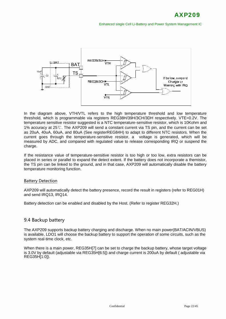
The AXP209 can connect a temperature-sensitive resistor via the TS pin to monitor the batterytemperature when the battery is charging or discharging. The diagram is shown below.
Confidential Page 21/45
AXP209Enhanced single Cell Li-Battery and Power System Management IC
BAT10uF TS
C2NTC
GND
In the diagram above, VTH/VTL refers to the high temperature threshold and low temperaturethreshold, which is programmable via registers REG38H/39H/3CH/3DH respectively. VTE=0.2V. Thetemperature sensitive resistor suggested is a NTC temperature-sensitive resistor, which is 10Kohm and1% accuracy at 25℃. The AXP209 will send a constant current via TS pin, and the current can be setas 20uA, 40uA, 60uA, and 80uA (See registerREG84H) to adapt to different NTC resistors. When thecurrent goes through the temperature-sensitive resistor, a voltage is generated, which will bemeasured by ADC, and compared with regulated value to release corresponding IRQ or suspend thecharge.
If the resistance value of temperature-sensitive resistor is too high or too low, extra resistors can beplaced in series or parallel to expand the detect extent. If the battery does not incorporate a themistor,the TS pin can be linked to the ground, and in that case, AXP209 will automatically disable the batterytemperature monitoring function.
Battery Detection
AXP209 will automatically detect the battery presence, record the result in registers (refer to REG01H)and send IRQ13, IRQ14.
Battery detection can be enabled and disabled by the Host. (Refer to register REG32H.)
9.4 Backup battery
The AXP209 supports backup battery charging and discharge. When no main power(BAT/ACIN/VBUS)is available, LDO1 will choose the backup battery to support the operation of some circuits, such as thesystem real-time clock, etc.
When there is a main power, REG35H[7] can be set to charge the backup battery, whose target voltageis 3.0V by default (adjustable via REG35H[6:5]) and charge current is 200uA by default ( adjustable viaREG35H[1:0]).
Confidential Page 22/45
AXP209Enhanced single Cell Li-Battery and Power System Management IC
9.5 Multi-channel power output
AXP209 provides multiple Output voltages as follows:Outputpath Type Default voltage
Applicationexamples Drive capability
DCDC2 BUCK Configurable 1.25Vcore 1600 mADCDC3 BUCK Configurable 2.5Vddr 700 mALDO1 LDO Configurable RTC 30 mALDO2 LDO Configurable Analog / FM 200 mALDO3 LDO Configurable 1.3V PLL 200 mALDO4 LDO Configurable 1.8V HDMI 200 mALDO5 LDO Configurable Vmic 50 mA
AXP209 comes with two synchronous step-down DC-DCs, five LDOs, as well as multiple timing andcontrolling methods. The operating frequency of DC-DC converters is 1.5MHz by default, which isadjustable via registers. External small inductors and capacitors can be connected as well. In addition,both DC-DCs can be set in PWM mode or auto mode (automatically switchable according to theAXP209 load). See register REG80H.
DC-DC2 / 3
DCDC3 output voltage ranges from 0.7 V to 3.5V, and output voltage of DCDC2 is ranged from0.7-2.275V, which can be programmed via registers.(refer to “Register REG23H 27H”).
DCDC2/3 output capacitor is recommended to use small ESR ceramic capacitors above 10uF X7R;when the output voltage is set above 2.5V,2.2uH inductors is recommended; when the outputvoltage is set under 2.5V, 4.7uH inductors is recommended. Besides, the inductor saturation currentshould be more than 50% of the largest demanded current.
The following is a list of recommended inductor-capacitor:InductorModel Current specifications DC resistance
Murata LQH55PN2R2NR0 [email protected] 30mOhmMurata LQH55PN4R7NR0 [email protected] 60mOhmMurata LQH44PN2R2MP0 [email protected] 49mOhmMurata LQH44PN4R7MP0 [email protected] 80mOhmTDK VLF5010ST-2R2M2R3 [email protected] 41mOhmTDK VLF5014ST-4R7M1R7 [email protected] 98mOhmTDK SLF6045T-4R7N2R4-3PF [email protected] 27mOhmCapacitorModel Temperature characteristics Tolerance
TDK C2012X5R0J475K X5R / X7R 10%@4.7uFTDK C2012X5R0J106K X5R / X7R 10% @ 10uFMurata GRM31E71A475K X7R 10%@4.7uFMurata GRM21E71A106K X7R 10% @ 10uFMurata GRM31E71A106K X7R 10% @ 10uF
Confidential Page 23/45
AXP209Enhanced single Cell Li-Battery and Power System Management IC
LDO1
LDO1 is always on and can be used to supply continuous power for application RTC with 30mA driveability of 30mA.
LDO2/3/4
LDO2/4 output noise is as low as 18uVrms,and can be used to supply power for analog circuits ofapplication system. LDO3 can supply power for systems like SRAM or PLL with 200mA drive ability.
LDO5
LDO5 also features the low noise design, and its drive ability is 50mA.
Soft Start
All DC-DCs and LDOs support soft start which can avoid the impact of dramatic current change on theinput path in system boot stage.
Self-diagnosis: Load monitoring and current limiting
All DC-DCs and LDOs support load monitoring and current-limit functions. When the load currentexceeds its drive ability, all output voltages will decrease to protect the internal circuits. When the twoDC-DCs output voltage is lower than 85% of the set voltage, AXP209 will automatically shutdown. Atthe same time, the system will record the detailed output voltage that has lead to automatic shutdown(refer to register REG46H[5:2]) and issue a corresponding IRQ.
All DC-DCs do not require external Schottky diodes and resister divider feedback circuits. If a certainDC-DC is unnecessary in the application, just float the corresponding LX pins.
9.6 The default voltage/Start timing settings(Default Voltage / Timing Setting)
The AXP209 provides customizable default voltage settings of each power supply and start up timing.
Boot Timing: includes 8 levels, and the interval between each level can be set, from 1, 4, 16, 32 ms.
Default voltage setting: Each DC-DC / LDO can be set from the lowest to the highest voltage of therange.
LDO1SET PIN For setting LDO1 initial voltage:LDO1SET LDO1SET = GND LDO1SET = VINTLDO1 Voltage 1.3V 3.3V
DC3SET PIN For setting DC-DC3 initial voltage:DC3SET DC3SET = GND DC3SET = APS DC3SET = floatingDC-DC3 Voltage 1.8V 3.3V / 2.5V 1.2V / 1.5V
For more information, see “The default configuration instructions” section.
Confidential Page 24/45
AXP209Enhanced single Cell Li-Battery and Power System Management IC
9.7 Signal Acquisition System
Simple battery monitors estimate the battery energy by measuring the battery voltage. However, themultiple 12-bit ADCs in the AXP209 can measure battery voltage, as well as battery current andexternal power voltage and current. It integrates battery charge and discharge coulomb counter. Usingthis data, the Host is capable of calculating accurately the battery energy and other battery data, suchas the system real-time consumption, remaining battery energy, battery charge progress, remainingbattery using time and charge time, etc.
The enabled state and sampling rate of each ADC can be set via registers REG82H, 83H, 84H. Thesampling results will be saved in corresponding registers, and reference can be made to theADC data in Register Instruction section. The input range of GPIO[1:0] can be set via registerREG85H, while register REG00H[2] is used to indicate the battery charge/discharge current directions.
Channel 000H STEP FFFHBattery Voltage 0mV 1.1mV 4.5045V
Bat discharge current 0mA 0.5mA 4.095ABat charge current 0mA 0.5mA 4.095A
ACIN voltage 0mV 1.7mV 6.9615VACIN current 0mA 0.625mA 2.5594AVBUS voltage 0mV 1.7mV 6.9615VVBUS current 0mA 0.375mA 1.5356A
Internal temperature -144.7C 0.1C 264.8CAPS voltage 0mV 1.4mV 5.733VTS pin input 0mV 0.8mV 3.276V
GPIO0 0 / 0.7V 0.5mV 2.0475 / 2.7475VGPIO1 0 / 0.7V 0.5mV 2.0475 / 2.7475V
9.8 Multifunction Pin Description(Multi-Function Pin Description)
GPIO [3: 0]
GPIO[3:0] Can be defined as ADC Input (monitoring external signals), or LDO, etc. Please refer toREG90H-96H Instruction for details.
CHGLED
Features charge state indication, over-temperature/over-voltage warning, and GPO. Please refer toREG32H Instruction section for details.
9.9 Timer
AXP209 Contains a 7 bit Internal timer, the value is set by register REG8AH [6: 0]. If the register is set to 0,the timer is disabled. If REG8AH [6: 0] = A, The timer starts count from 0 to A and sets REG8AH [7], also
Confidential Page 25/45
AXP209Enhanced single Cell Li-Battery and Power System Management IC
issuing a timer interrupt. Write 1 in register REG8AH [7] to clear the flag and re-start timing. Clearinginterrupt flag will not re-start counting. The minimum step size for the timer is 1 minute, and the timingrange 1 ~ 127 Minutes.
9.10 Decryption
AXP209 Contains a decryption module. The Host writes data to REG300-REG30F to be decrypted,and then writes 1 to the register REGB8H [1] to start decryption. After the decryption is complete,status bit REGB8 [0] is set to 1. Then the Host can read back the decrypted data from REG31x. Startsagain automatically when the decryption AXP209 status bits are clared.
9.11 HOST Interface timing and interrupt (TWSI and IRQ)
... ... ......
... ... ......
...
...
... ...
..
....
Figure 1: Single Read and Write
Confidential Page 26/45
AXP209Enhanced single Cell Li-Battery and Power System Management IC
Figure 2: Multi Read and Write
Host can access the AXP209 registers via the TWSI interface, and the operation timing is shownabove. Standard 100KHz or 400KHz frequency is supported, and the highest rate can reach 1.2MHz.In addition, multi read and write operation is supported, and the device addresses are 69H (READ)and 68H (WRITE).
When certain events occur, AXP209 will inform the Host by pulling down the IRQ interrupt line, andthe interrupt state will be stored in interrupt state registers (See registers REG48H, REG49H,REG4AH, REG4BH and REG4CH). The interrupt can be cleared by writing 1 to corresponding stateregister bit. When there is no interrupt, IRQ output will be pulled high (by 51K external pull-up resistor).Each interrupt can be masked via interrupt control registers (Refer to registers REG40H, REG41H,REG42H, REG43H, and REG44H).
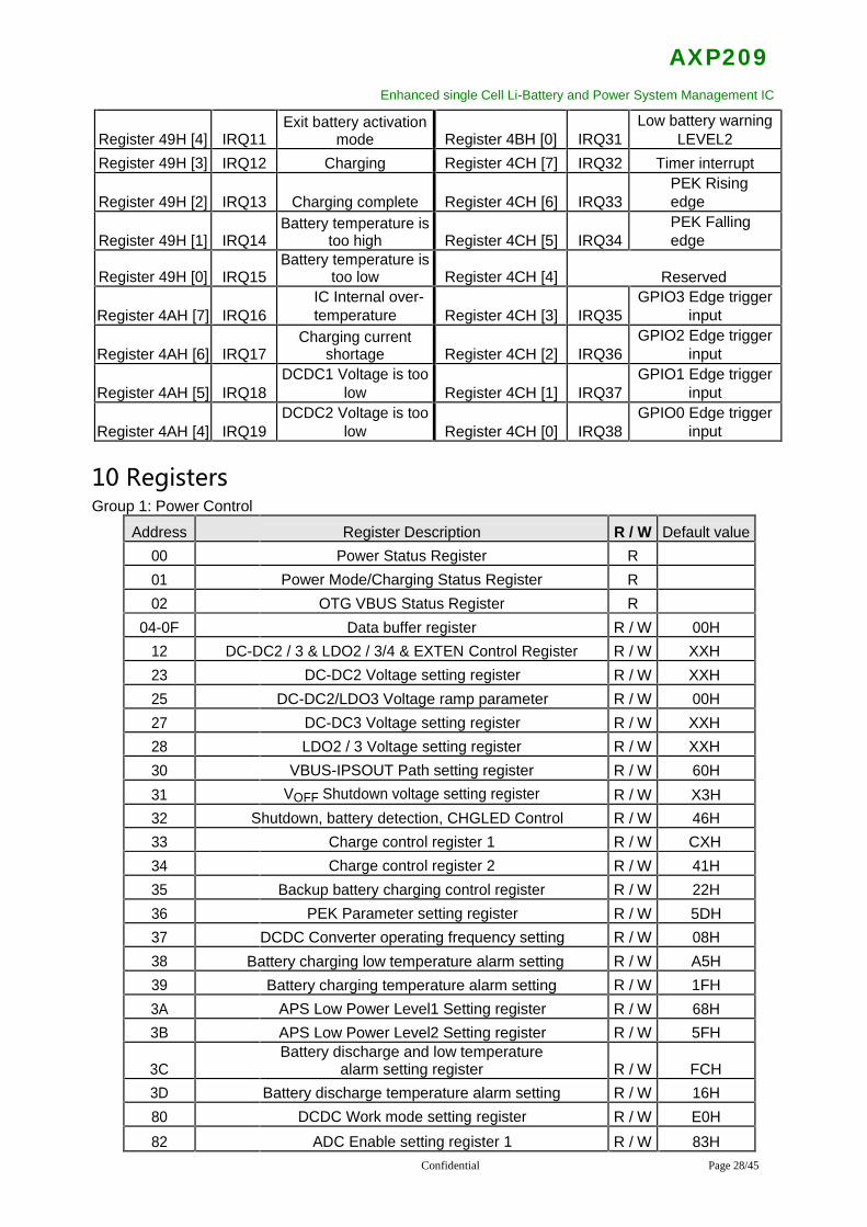
Location Interrupt Meaning Location Interrupt Meaning
Register 48H [7] IRQ1Power supply ACIN
over voltage Register 4AH [3] IRQ20DCDC3 Voltage is too
low
Register 48H [6] IRQ2Power supply ACIN
Inserted Register 4AH [2] Reservations
Register 48H [5] IRQ3Power supply ACIN
Removed Register 4AH [1] IRQ22 PEK Short press
Register 48H [4] IRQ4Power supply VBUS
Overvoltage Register 4AH [0] IRQ23 PEK Press
Register 48H [3] IRQ5Power supply VBUS
Inserted Register 4BH [7] IRQ24 N_OE Boot
Register 48H [2] IRQ6Power supply VBUS
Removed Register 4BH [6] IRQ25 N_OE Shutdown
Register 48H [1] IRQ7VBUS Voltage is less
than VHOLD Register 4BH [5] IRQ26 VBUS EffectiveRegister 48H [0] Reserved Register 4BH [4] IRQ27 VBUS InvalidRegister 49H [7] IRQ8 Battery access Register 4BH [3] IRQ28 VBUS Session ValidRegister 49H [6] IRQ9 Remove the battery Register 4BH [2] IRQ29 VBUS Session End
Register 49H [5] IRQ10Into the batteryactivation mode Register 4BH [1] IRQ30
Low battery warningLEVEL1
Confidential Page 27/45
AXP209Enhanced single Cell Li-Battery and Power System Management IC
Register 49H [4] IRQ11Exit battery activation
mode Register 4BH [0] IRQ31Low battery warning
LEVEL2Register 49H [3] IRQ12 Charging Register 4CH [7] IRQ32 Timer interrupt
Register 49H [2] IRQ13 Charging complete Register 4CH [6] IRQ33PEK Risingedge
Register 49H [1] IRQ14Battery temperature is
too high Register 4CH [5] IRQ34PEK Fallingedge
Register 49H [0] IRQ15Battery temperature is
too low Register 4CH [4] Reserved
Register 4AH [7] IRQ16IC Internal over-temperature Register 4CH [3] IRQ35
GPIO3 Edge triggerinput
Register 4AH [6] IRQ17Charging current
shortage Register 4CH [2] IRQ36GPIO2 Edge trigger
input
Register 4AH [5] IRQ18DCDC1 Voltage is too
low Register 4CH [1] IRQ37GPIO1 Edge trigger
input
Register 4AH [4] IRQ19DCDC2 Voltage is too
low Register 4CH [0] IRQ38GPIO0 Edge trigger
input
10 RegistersGroup 1: Power Control
Address Register Description R / W Default value00 Power Status Register R01 Power Mode/Charging Status Register R02 OTG VBUS Status Register R
04-0F Data buffer register R / W 00H12 DC-DC2 / 3 & LDO2 / 3/4 & EXTEN Control Register R / W XXH23 DC-DC2 Voltage setting register R / W XXH25 DC-DC2/LDO3 Voltage ramp parameter R / W 00H27 DC-DC3 Voltage setting register R / W XXH28 LDO2 / 3 Voltage setting register R / W XXH30 VBUS-IPSOUT Path setting register R / W 60H31 VOFF Shutdown voltage setting register R / W X3H32 Shutdown, battery detection, CHGLED Control R / W 46H33 Charge control register 1 R / W CXH34 Charge control register 2 R / W 41H35 Backup battery charging control register R / W 22H36 PEK Parameter setting register R / W 5DH37 DCDC Converter operating frequency setting R / W 08H38 Battery charging low temperature alarm setting R / W A5H39 Battery charging temperature alarm setting R / W 1FH3A APS Low Power Level1 Setting register R / W 68H3B APS Low Power Level2 Setting register R / W 5FH
3CBattery discharge and low temperature
alarm setting register R / W FCH3D Battery discharge temperature alarm setting R / W 16H80 DCDC Work mode setting register R / W E0H82 ADC Enable setting register 1 R / W 83H
Confidential Page 28/45
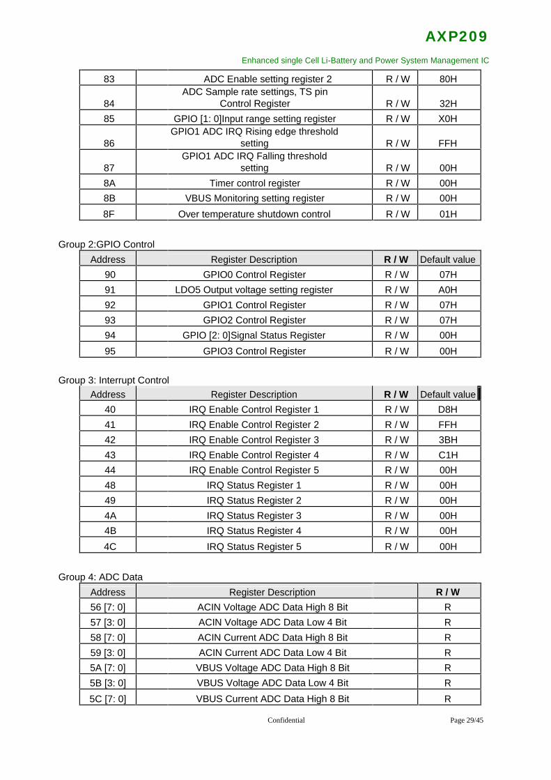
AXP209Enhanced single Cell Li-Battery and Power System Management IC
83 ADC Enable setting register 2 R / W 80H
84ADC Sample rate settings, TS pin
Control Register R / W 32H85 GPIO [1: 0]Input range setting register R / W X0H
86GPIO1 ADC IRQ Rising edge threshold
setting R / W FFH
87GPIO1 ADC IRQ Falling threshold
setting R / W 00H8A Timer control register R / W 00H8B VBUS Monitoring setting register R / W 00H8F Over temperature shutdown control R / W 01H
Group 2:GPIO ControlAddress Register Description R / W Default value
90 GPIO0 Control Register R / W 07H91 LDO5 Output voltage setting register R / W A0H92 GPIO1 Control Register R / W 07H93 GPIO2 Control Register R / W 07H94 GPIO [2: 0]Signal Status Register R / W 00H95 GPIO3 Control Register R / W 00H
Group 3: Interrupt ControlAddress Register Description R / W Default value
40 IRQ Enable Control Register 1 R / W D8H41 IRQ Enable Control Register 2 R / W FFH42 IRQ Enable Control Register 3 R / W 3BH43 IRQ Enable Control Register 4 R / W C1H44 IRQ Enable Control Register 5 R / W 00H48 IRQ Status Register 1 R / W 00H49 IRQ Status Register 2 R / W 00H4A IRQ Status Register 3 R / W 00H4B IRQ Status Register 4 R / W 00H4C IRQ Status Register 5 R / W 00H
Group 4: ADC DataAddress Register Description R / W56 [7: 0] ACIN Voltage ADC Data High 8 Bit R57 [3: 0] ACIN Voltage ADC Data Low 4 Bit R58 [7: 0] ACIN Current ADC Data High 8 Bit R59 [3: 0] ACIN Current ADC Data Low 4 Bit R5A [7: 0] VBUS Voltage ADC Data High 8 Bit R5B [3: 0] VBUS Voltage ADC Data Low 4 Bit R5C [7: 0] VBUS Current ADC Data High 8 Bit R
Confidential Page 29/45
AXP209Enhanced single Cell Li-Battery and Power System Management IC
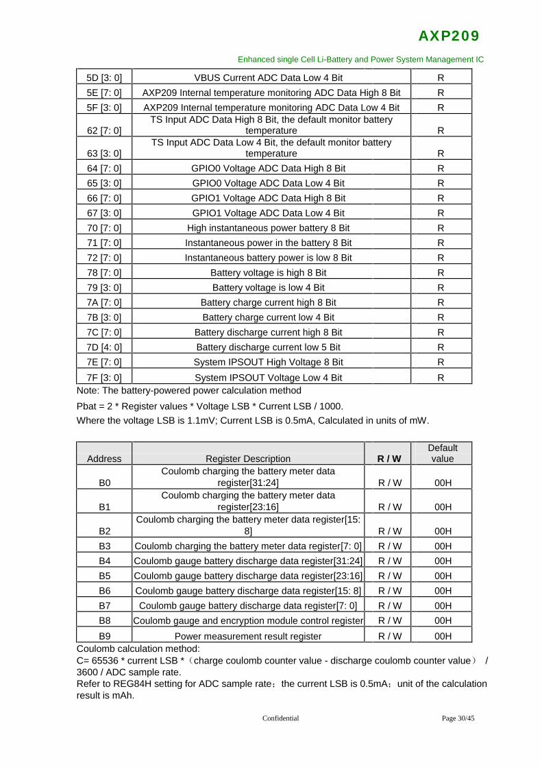
5D [3: 0] VBUS Current ADC Data Low 4 Bit R5E [7: 0] AXP209 Internal temperature monitoring ADC Data High 8 Bit R5F [3: 0] AXP209 Internal temperature monitoring ADC Data Low 4 Bit R
62 [7: 0]TS Input ADC Data High 8 Bit, the default monitor battery
temperature R
63 [3: 0]TS Input ADC Data Low 4 Bit, the default monitor battery
temperature R64 [7: 0] GPIO0 Voltage ADC Data High 8 Bit R65 [3: 0] GPIO0 Voltage ADC Data Low 4 Bit R66 [7: 0] GPIO1 Voltage ADC Data High 8 Bit R67 [3: 0] GPIO1 Voltage ADC Data Low 4 Bit R70 [7: 0] High instantaneous power battery 8 Bit R71 [7: 0] Instantaneous power in the battery 8 Bit R72 [7: 0] Instantaneous battery power is low 8 Bit R78 [7: 0] Battery voltage is high 8 Bit R79 [3: 0] Battery voltage is low 4 Bit R7A [7: 0] Battery charge current high 8 Bit R7B [3: 0] Battery charge current low 4 Bit R7C [7: 0] Battery discharge current high 8 Bit R7D [4: 0] Battery discharge current low 5 Bit R7E [7: 0] System IPSOUT High Voltage 8 Bit R7F [3: 0] System IPSOUT Voltage Low 4 Bit R
Note: The battery-powered power calculation methodPbat = 2 * Register values * Voltage LSB * Current LSB / 1000.Where the voltage LSB is 1.1mV; Current LSB is 0.5mA, Calculated in units of mW.
Address Register Description R / WDefaultvalue
B0Coulomb charging the battery meter data
register[31:24] R / W 00H
B1Coulomb charging the battery meter data
register[23:16] R / W 00H
B2Coulomb charging the battery meter data register[15:
8] R / W 00HB3 Coulomb charging the battery meter data register[7: 0] R / W 00HB4 Coulomb gauge battery discharge data register[31:24] R / W 00HB5 Coulomb gauge battery discharge data register[23:16] R / W 00HB6 Coulomb gauge battery discharge data register[15: 8] R / W 00HB7 Coulomb gauge battery discharge data register[7: 0] R / W 00HB8 Coulomb gauge and encryption module control register R / W 00HB9 Power measurement result register R / W 00H
Coulomb calculation method:C= 65536 * current LSB *(charge coulomb counter value - discharge coulomb counter value) /3600 / ADC sample rate.Refer to REG84H setting for ADC sample rate;the current LSB is 0.5mA;unit of the calculationresult is mAh.
Confidential Page 30/45
AXP209Enhanced single Cell Li-Battery and Power System Management IC
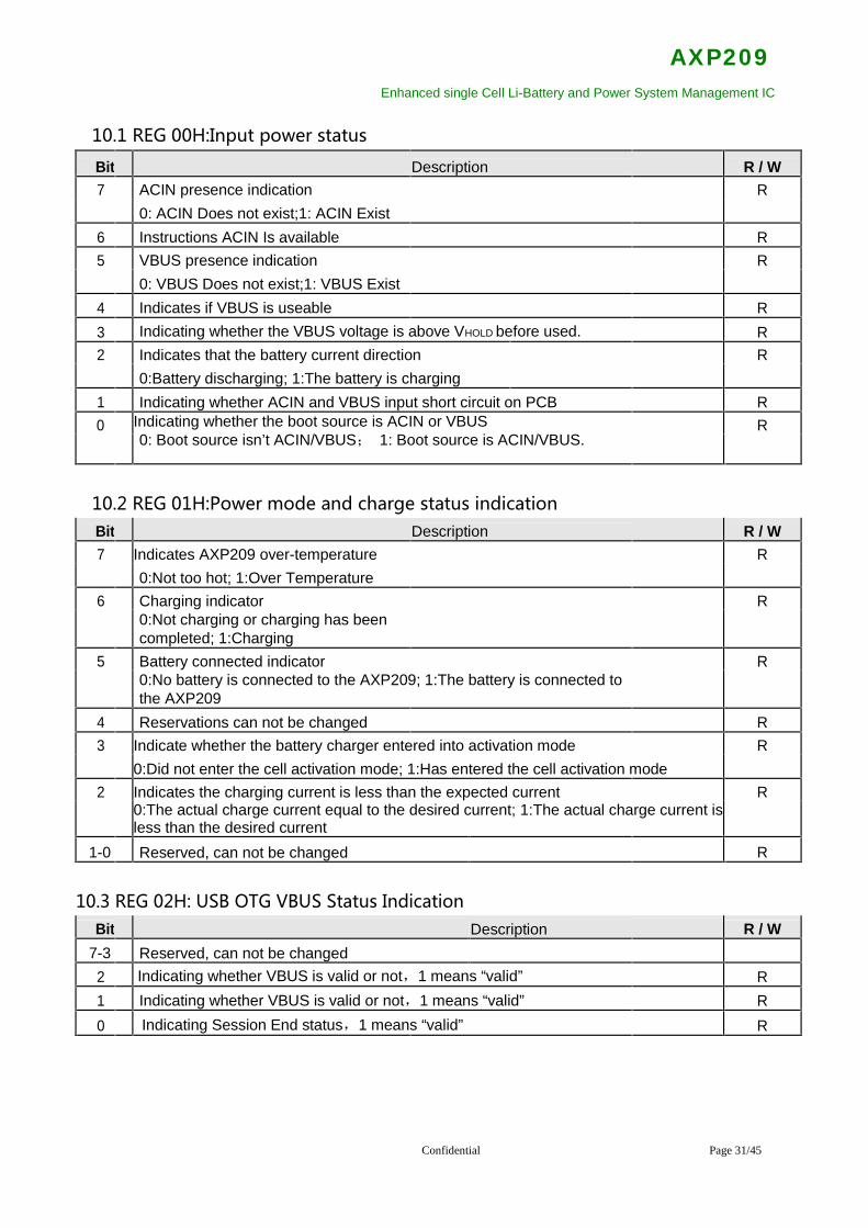
10.1 REG 00H:Input power status
Bit Description R / W7 ACIN presence indication R
0: ACIN Does not exist;1: ACIN Exist6 Instructions ACIN Is available R5 VBUS presence indication R
0: VBUS Does not exist;1: VBUS Exist4 Indicates if VBUS is useable R3 Indicating whether the VBUS voltage is above VHOLD before used. R2 Indicates that the battery current direction R
0:Battery discharging; 1:The battery is charging1 Indicating whether ACIN and VBUS input short circuit on PCB R0 RIndicating whether the boot source is ACIN or VBUS
0: Boot source isn’t ACIN/VBUS; 1: Boot source is ACIN/VBUS.
10.2 REG 01H:Power mode and charge status indicationBit Description R / W7 Indicates AXP209 over-temperature R
0:Not too hot; 1:Over Temperature6 Charging indicator R
0:Not charging or charging has beencompleted; 1:Charging
5 Battery connected indicator R0:No battery is connected to the AXP209; 1:The battery is connected tothe AXP209
4 Reservations can not be changed R3 Indicate whether the battery charger entered into activation mode R
0:Did not enter the cell activation mode; 1:Has entered the cell activation mode2 Indicates the charging current is less than the expected current R
0:The actual charge current equal to the desired current; 1:The actual charge current isless than the desired current
1-0 Reserved, can not be changed R
10.3 REG 02H: USB OTG VBUS Status IndicationBit Description R / W
7-3 Reserved, can not be changed2 Indicating whether VBUS is valid or not,1 means “valid” R1 Indicating whether VBUS is valid or not,1 means “valid” R0 Indicating Session End status,1 means “valid” R
Confidential Page 31/45
AXP209Enhanced single Cell Li-Battery and Power System Management IC
10.4 REG 04-0FH: Data Cache
Note: As long as the external power supply, battery or backup battery power exists, this data will not belost.
10.5 REG 12H:Power Output Control
The default value: XXH
Bit Description R / WDefaultvalue
7 Reserved, can not be changed RW X6 LDO3 Switch Control 0:Shut down; 1:Turn on RW X5 Reserved, can not be changed RW X4 DC-DC2 Switch Control 0:Shut down; 1:Turn on RW X3 LDO4 Switch Control RW X2 LDO2 Switch Control RW X1 DC-DC3 Switch Control RW X0 EXTEN Switch Control RW X
10.6 REG 23H: DC-DC2 output voltage setting
The default value: XXH
Bit Description R / WDefaultvalue
7-6 Reserved, can not be changed5-0 DC-DC2 The output voltage is set 0.7-2.275V,25mV / step RW X
Vout = [0.7+ (Bit5-0) * 0.025] V
10.7 REG 25H: DC-DC2 / LDO3 Dynamic voltage scaling parameter settings
The default value: 00H
Bit DescriptionR /W
Defaultvalue
7-4 Reserved, can not be changed3 LDO3 VRC Enable Control RW 0
0:Turn on; 1:Shut down2 DC-DC2 VRC Enable Control RW 0
0:Turn on; 1:Shut down1 LDO3 VRC soft start control 0: 25mV / 15.625us = 1.6mV / us RW 0
1: 25mV / 31.250us = 0.8mV / us
0 DC-DC2 VRC soft start control 0: 25mV / 15.625us = 1.6mV / us RW 01: 25mV / 31.250us = 0.8mV / us
Confidential Page 32/45
AXP209Enhanced single Cell Li-Battery and Power System Management IC
10.8 REG 27H: DC-DC3 output voltage setting
The default value: XXH
Bit Description R / WDefaultvalue
7 Reserved, can not be changed6-0 DC-DC3 output voltage setting 0.7-3.5V, 25mV / step RW X
Vout = [0.7+ (Bit6-0) * 0.025] V
10.9 REG 28H: LDO2 / 4 output voltage setting
The default value: XXH
Bit Description R / WDefaultvalue
7-4 LDO2 output voltage setting 1.8-3.3V, 100mV / step RW XVout = [1.8+ (Bit7-4) * 0.1] V
3-0 LDO4 output voltage setting1.25, 1.3, 1.4, 1.5, 1.6, 1.7, 1.8, 1.9,2.0, 2.5, 2.7, 2.8, 3.0, 3.1, 3.2, 3.3 RW X
10.10 REG 29H: LDO3 output voltage setting
The default value: XXH
Bit Description R / WDefaultvalue
7 LDO3 Mode selection: RW 00:LDO Mode, the voltage is set by [6: 0]1:enable/disable control mode, voltage is determined by LDO3IN.
6-0 LDO3 output voltage setting0.7-2.275V,25mV / stepVout = [0.7+ (Bit6-0) * 0.025] V RW X
10.11 REG 30H: VBUS-IPSOUT Power Path Management
The default value: 6XH
Bit DescriptionR /W
Defaultvalue
7 VBUS-IPSOUT Path selection control signal source RW 00:By N_VBUSEN pin controls whether to enable this path1: VBUS-IPSOUT enabled, regardless of N_VBUSEN State
6 VBUS VHOLD voltage limiting control RW 10: No voltage drop limit ; 1: Limit the voltage drop
5-3 VHOLD Set VHOLD= [4.0+ (Bit5-3) * 0.1] V RW 1002 Reserved, can not be changed
1-0VBUS current-limit selection when current-limit is enabled00:900mA ; 01:500mA; 10:100mA; 11:no limit RW 0
Confidential Page 33/45
AXP209Enhanced single Cell Li-Battery and Power System Management IC
10.12 REG 31H: VOFF Shutdown voltage setting
The default value: X3H
Bit Description R / WDefaultvalue
7-4 Reserved, can not be changed3 Sleep Mode PEK or GPIO edge wakeup enable settings:
0: Disable1: EnableThis bit will be automatically cleared to 0 after writing, so “1 ”should berewritten whenever entering Sleep mode.
2-0 VOFF Setting VOFF= [2.6+ (Bit2-0) * 0.1] V RW 011Default: 2.9V
10.13 REG 32H:Shutdown settings, battery detection, and CHGLED Pin control
The default value: 46H
Bit Description R / WDefaultvalue
7 Shutdown Control RW 0This bit is write 1 will shutdown the AXP209 outputs
6 Battery monitoring function setting bit: 0:Shut down; 1:Turn on RW 15-4 CHGLED Pin function setting 00: Hi RW 00
01: 25% 1Hz Flashing10: 25% 4Hz Flashing11: Output Low
3 CHGLED Pin control settings 0: Controlled by charging RW 01: Controlled by REG 32H [5: 4]
2Output off timing sequencecontrol 0: Shutdown simultaneously RW 0
1: Shutdown in reverse sequence tostartup
1-0 RW 10Shutdown delay time after N_OEchanges from low to high
00: 128mS; 01: 1S;
10: 2S; 11: 3S
10.14 REG 33H:Charge Control 1
The default value: CXH
Bit DescriptionR /W
Defaultvalue
7 Charging function enable control bit RW 10:Disable, 1:Enable
6-5Charging target voltagesetting 00: 4.1V; 01: 4.15V; 10: 4.2V; 11: 4.36V RW 10
Confidential Page 34/45
AXP209Enhanced single Cell Li-Battery and Power System Management IC
4 Charge termination current settings RW 00:End when charging current is less than 10% of the set value1:End when charging current is less than 15% of the set value
3-0 Charge current setting RW XIcharge= [300+ (Bit3-0) * 100] mA
10.15 REG 34H:Charge Control 2
The default value: 45H
Bit Description R / WDefaultvalue
7 Pre-charge timeout setting Bit 1 00: 40 min; 01: 50min; RW 06 Pre-charge timeout setting Bit 0 10: 60min; 11: 70min RW 15 Reserved, can not be changed4 CHGLED Mode Selection RW 0
0:Constant on when Charging1:Flashes when charging
3-2 Reserved, can not be changed
1-0Constant current mode timeoutsetting Bit 1-0 00: 6Hours; 01: 8Hours; RW 01
10: 10Hours; 11: 12Hours
10.16 REG 35H:Backup battery charge control
The default value: 22H
Bit Description R / WDefaultvalue
7 Backup battery charge enable control RW 00:Disable; 1:Enable
6-5 Backup battery voltage target setting RW 0100: 3.1V; 01: 3.0V; 10: 3.6V; 11: 2.5V
4-2 Reserved, can not be changed1-0 Spare battery charging current is set 00: 50uA; 01: 100uA; 10: 200uA; RW 10
11: 400uA
10.17 REG 36H: PEK Key parameter settings
The default value: 9DH
Bit Description R / WDefaultvalue
Confidential Page 35/45

AXP209Enhanced single Cell Li-Battery and Power System Management IC
7-6 Startup press time settings 00: 128mS; 01: 3S; 10: 1S; 11: 2S. RW 015-4 Long press time setting 00: 1S; 01: 1.5S;10: 2S; 11: 2.5S. RW 013 Automatic shutdown on long press time exceeding the shutdown time RW 1
0:Disable; 1:Enable2 PWROK Signal Delay after power-up completed RW 1
0: 8mS; 1: 64mS1-0 Shutdown time setting 00: 4S; 01: 6S; 10: 8S; 11: 10S. RW 01
10.18 REG 37H: DC-DC Operating frequency settings
The default value: 08H
Bit Description R / WDefaultvalue
7-4Reserved, can not bechanged
3-0 DC-DC switching frequencyEach level changes by 5%The default value 1.5MHz RW 1000F = [1 +/- (Bit3-0) * 5%)] * 1.5MHz
10.19 REG 38H: VLTF-charge Battery charging low temperature threshold settings
The default value: A5H
Bit Description R / WDefaultvalue
7-0
Battery Under-temperaturethreshold setting when thebattery is charging, M
M*10H,When M=A5H, correspondingvoltage is 2.112V RW A5HVoltage range 0V ~ 3.264V
VLTF-charge = M * 10H * 0.0008V
10.20 REG 39H: VHTF-charge Battery charging high temperature threshold setting
The default value: 1FH
Bit Description R / WDefaultvalue
7-0When charging the batterytemperature threshold setting,N
N*10H, When N=1FH, thecorresponding voltage is 0.397V RW 1FHVoltage range 0V ~ 3.264V
VHTF-charge = N * 10H * 0.0008V
10.21 REG 3AH: System IPSOUT Vwarning Level1
The default value: 68H
Bit Description R / WDefaultvalue
7-0 System IPSOUT Vwarning Level1 RW 68H
Confidential Page 36/45
AXP209Enhanced single Cell Li-Battery and Power System Management IC
10.22 REG 3BH: System IPSOUT Vwarning Level2
The default value: 5FH
Bit Description R / WDefaultvalue
7-0System IPSOUT VwarningLevel2 RW 5FH
REG3AH, REG3BHVoltage corresponding to the following relationship (where the registervalue is n):
Vwarning = 2.8672 + 1.4mV * n * 4
10.23 REG 3CH: VLTF-discharge Battery discharge under temperature threshold settings
The default value: FCH
Bit Description R / WDefaultvalue
7-0 RW FCHBattery under-temperaturethreshold setting when the batteryis discharging,M
M*10H, when M=FC, correspondingvoltage is 3.226V ;Voltage ranges from 0V~3.264
VLTF-discharge = M * 10H * 0.0008V
10.24 REG 3DH: VHTF-discharge Battery discharge over temperature threshold settingsThe default value: 16H
Bit Description R / WDefaultvalue
7-0 RW 16HWhen discharging the battery undertemperature threshold setting,N
N*10H,when N=16H,correspondingvoltage is 0.282V ;Voltage ranges from 0V~3.264V
VLTF-discharge = N * 10H * 0.0008V
10.25 REG 80H: DC-DC Operating mode selectionThe default value: E0H
Bit Description R / WDefaultvalue
7-3 Reserved, can not be changed2 DC-DC2 Control mode 0: PFM / PWM Automatic switching RW 01 DC-DC3 Control mode 1:Fixed PWM RW 00 Reserved, can not be changed
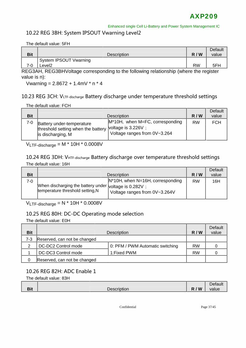
10.26 REG 82H: ADC Enable 1The default value: 83H
Bit Description R / WDefaultvalue
Confidential Page 37/45

AXP209Enhanced single Cell Li-Battery and Power System Management IC
7 Battery voltage ADC Enable 0:Disable, 1:Enable RW 16 Battery current ADC Enable RW 05 ACIN Voltage ADC Enable RW 04 ACIN Current ADC Enable RW 03 VBUS Voltage ADC Enable RW 02 VBUS Current ADC Enable RW 01 APS Voltage ADC Enable RW 10 TS Pin ADC Function is enabled RW 1
10.27 REG 83H: ADC Enable 2
The default value: 80H
Bit Description R / WDefaultvalue
7AXP209 Internal temperaturemonitoring ADC Enable 0:Disable, 1:Enable RW 1
6-4 Reserved, can not be changed3 GPIO0 ADC Function is enabled 0:Disable, 1:Enable RW 02 GPIO1 ADC Function is enabled RW 0
1-0 Reserved, can not be changed
10.28 REG 84H: ADC Sampling rate settings, TS Pin control
The default value: 32H
Bit Description R / WDefaultvalue
7-6 ADC Sampling rate settings 25 × 2nRW 0
Sampling rates is 25, 50, 100, 200Hz5-4 TS Pin output current setting: RW 11
00: 20uA; 01: 40uA; 10: 60uA; 11: 80uA3 Reserved, can not be changed2 TS Pin function select RW 0
0:Battery temperature monitoring function,1:External independent ADC1-0 TS Current output setting 00:Disabled RW 1
01:Output current only when charging RW 010: Only when ADC is sampling input11:Always enabled
10.29 REG 85H: ADC Input Range
The default value: X0H
Confidential Page 38/45
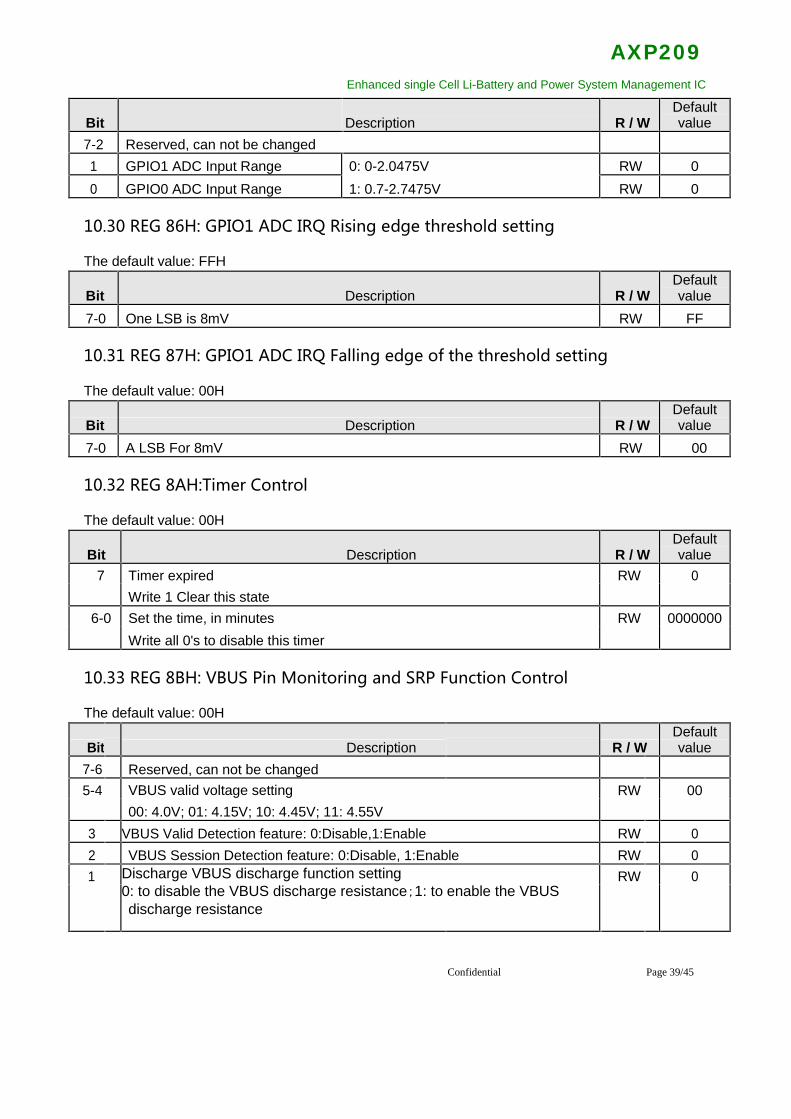
AXP209Enhanced single Cell Li-Battery and Power System Management IC
Bit Description R / WDefaultvalue
7-2 Reserved, can not be changed1 GPIO1 ADC Input Range 0: 0-2.0475V RW 00 GPIO0 ADC Input Range 1: 0.7-2.7475V RW 0
10.30 REG 86H: GPIO1 ADC IRQ Rising edge threshold setting
The default value: FFH
Bit Description R / WDefaultvalue
7-0 One LSB is 8mV RW FF
10.31 REG 87H: GPIO1 ADC IRQ Falling edge of the threshold setting
The default value: 00H
Bit Description R / WDefaultvalue
7-0 A LSB For 8mV RW 00
10.32 REG 8AH:Timer Control
The default value: 00H
Bit Description R / WDefaultvalue
7 Timer expired RW 0Write 1 Clear this state
6-0 Set the time, in minutes RW 0000000Write all 0's to disable this timer
10.33 REG 8BH: VBUS Pin Monitoring and SRP Function Control
The default value: 00H
Bit Description R / WDefaultvalue
7-6 Reserved, can not be changed5-4 VBUS valid voltage setting RW 00
00: 4.0V; 01: 4.15V; 10: 4.45V; 11: 4.55V3 VBUS Valid Detection feature: 0:Disable,1:Enable RW 02 VBUS Session Detection feature: 0:Disable, 1:Enable RW 01 RW 0Discharge VBUS discharge function setting
0: to disable the VBUS discharge resistance;1: to enable the VBUSdischarge resistance
Confidential Page 39/45
AXP209Enhanced single Cell Li-Battery and Power System Management IC
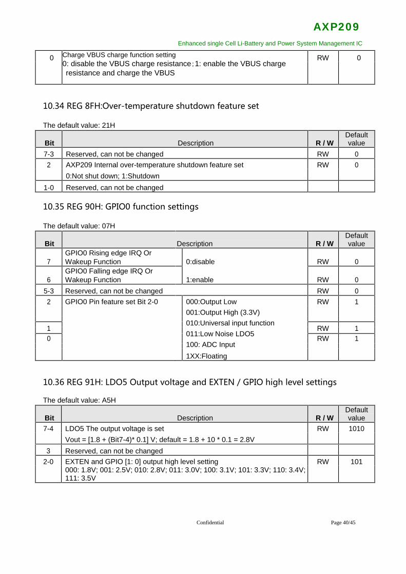
0 RW 0Charge VBUS charge function setting0: disable the VBUS charge resistance;1: enable the VBUS chargeresistance and charge the VBUS
10.34 REG 8FH:Over-temperature shutdown feature set
The default value: 21H
Bit Description R / WDefaultvalue
7-3 Reserved, can not be changed RW 02 AXP209 Internal over-temperature shutdown feature set RW 0
0:Not shut down; 1:Shutdown1-0 Reserved, can not be changed
10.35 REG 90H: GPIO0 function settings
The default value: 07H
Bit Description R / WDefaultvalue
7GPIO0 Rising edge IRQ OrWakeup Function 0:disable RW 0
6GPIO0 Falling edge IRQ OrWakeup Function 1:enable RW 0
5-3 Reserved, can not be changed RW 02 GPIO0 Pin feature set Bit 2-0 000:Output Low RW 1
001:Output High (3.3V)010:Universal input function
1 RW 1011:Low Noise LDO50 RW 1100: ADC Input1XX:Floating
10.36 REG 91H: LDO5 Output voltage and EXTEN / GPIO high level settings
The default value: A5H
Bit Description R / WDefaultvalue
7-4 LDO5 The output voltage is set RW 1010Vout = [1.8 + (Bit7-4)* 0.1] V; default = 1.8 + 10 * 0.1 = 2.8V
3 Reserved, can not be changed2-0 EXTEN and GPIO [1: 0] output high level setting RW 101
000: 1.8V; 001: 2.5V; 010: 2.8V; 011: 3.0V; 100: 3.1V; 101: 3.3V; 110: 3.4V;111: 3.5V
Confidential Page 40/45

AXP209Enhanced single Cell Li-Battery and Power System Management IC
10.37 REG 92H: GPIO1 Feature setttings
The default value: 07H
Bit Description R / WDefaultvalue
7GPIO1 Rising edge IRQ OrWakeup Function 0:disable RW 0
6GPIO1 Rising edge IRQ OrWakeup Function 1:enable RW 0
5-3 Reserved, can not be changed RW 02-0 GPIO1 Pin feature set 000:Output Low RW 111
001:Output High (3.3V)010:Universal input function011:Low Noise LDO100: ADC Input1XX:Floating
10.38 REG 93H: GPIO2 Feature set
The default value: 07H
Bit Description R / WDefaultvalue
7GPIO2 Rising edge IRQ OrWakeup Function 0:disable RW 0
6GPIO2 Falling edge IRQ OrWakeup Function 1:enable RW 0
5-3 Reserved, can not be changed RW 02-0 GPIO2 Pin feature set 000:Output Low RW 111
001:Floating010:Universal input functionXXX:Floating
10.39 REG 94H: GPIO [2: 0]Setting and monitoring of signal status
The default value: 00H
Bit Description R / W
Thedefaultvalue
7 Reserved, can not be changed R6 GPIO2 Input Status 0:Input low level R5 GPIO1 Input Status 1:Input high level R4 GPIO0 Input Status R
3-0 Reserved, can not be changed
10.40 REG 95H: GPIO3 Settings
The default value: 00HConfidential Page 41/45
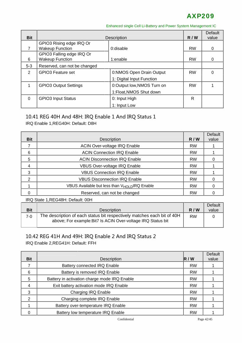
AXP209Enhanced single Cell Li-Battery and Power System Management IC
Bit Description R / WDefaultvalue
7GPIO3 Rising edge IRQ OrWakeup Function 0:disable RW 0
6GPIO3 Falling edge IRQ OrWakeup Function 1:enable RW 0
5-3 Reserved, can not be changed2 GPIO3 Feature set 0:NMOS Open Drain Output RW 0
1: Digital Input Function1 GPIO3 Output Settings 0:Output low,NMOS Turn on RW 1
1:Float,NMOS Shut down0 GPIO3 Input Status 0: Input High R
1: Input Low
10.41 REG 40H And 48H: IRQ Enable 1 And IRQ Status 1IRQ Enable 1,REG40H: Default: D8H
Bit Description R / WDefaultvalue
7 ACIN Over-voltage IRQ Enable RW 16 ACIN Connection IRQ Enable RW 15 ACIN Disconnection IRQ Enable RW 04 VBUS Over-voltage IRQ Enable RW 13 VBUS Connection IRQ Enable RW 12 VBUS Disconnection IRQ Enable RW 01 VBUS Available but less than VHOLDIRQ Enable RW 00 Reserved, can not be changed RW 0
IRQ State 1,REG48H: Default: 00H
Bit Description R / WDefaultvalue
7-0 RW 0The description of each status bit respectively matches each bit of 40Habove; For example:Bit7 Is ACIN Over-voltage IRQ Status bit
10.42 REG 41H And 49H: IRQ Enable 2 And IRQ Status 2IRQ Enable 2,REG41H: Default: FFH
Bit Description R / WDefaultvalue
7 Battery connected IRQ Enable RW 16 Battery is removed IRQ Enable RW 15 Battery in activation charge mode IRQ Enable RW 14 Exit battery activation mode IRQ Enable RW 13 Charging IRQ Enable RW 12 Charging complete IRQ Enable RW 11 Battery over-temperature IRQ Enable RW 10 Battery low temperature IRQ Enable RW 1
Confidential Page 42/45
AXP209Enhanced single Cell Li-Battery and Power System Management IC
IRQ State 2,REG49H: Default: 00H
Bit Description R / W
Thedefaultvalue
7-0 Meaning of the status bits correspond to each bit of 41H listed above RW 0
10.43 REG 42H And 4AH: IRQ Enable 3 And IRQ Status 3
IRQ Enable 3,REG42H: Default: 03H
Bit Description R / WDefaultvalue
7 AXP209 Internal over-temperature IRQ Enable RW 06 Charging current is less than the set current IRQ Enable RW 05 Reserved, can not be changed4 DC-DC2 The output voltage is less than the set value IRQ Enable RW 03 DC-DC3 The output voltage is less than the set value IRQ Enable RW 02 LDO3 The output voltage is less than the set value IRQ Enable1 PEK Short press IRQ Enable RW 10 PEK Long press IRQ Enable RW 1
IRQ State 3,REG4AH: Default: 00H
Bit Description R / WDefaultvalue
7-0 Meaning of the status bits correspond to each bit of 42H above RW 0
10.44 REG 43H And 4BH: IRQ Enable 4 And IRQ Status 4
IRQ Enable 4,REG43H: Default: 01H
Bit Description R / WDefaultvalue
7 N_OE startup IRQ Enable RW 06 N_OE Shutdown IRQ Enable RW 05 VBUS Valid IRQ Enable RW 04 VBUS Invalid IRQ Enable RW 03 VBUS Session A / B IRQ Enable RW 02 VBUS Session End IRQ Enable RW 01 APS Low voltage IRQ Enable (LEVEL1) RW 00 APS Low voltage IRQ Enable (LEVEL2) RW 1
IRQ State 4,REG4BH: Default: 00H
Bit Description R / WDefaultvalue
7-0 Meaning of the status bits correspond to each bit of 43H above RW 0
10.45 REG 44H And 4C: IRQ Enable 5 And IRQ Status 5
IRQ Enable 5,REG44HThe default value: 00H;
Confidential Page 43/45
AXP209Enhanced single Cell Li-Battery and Power System Management IC
Bit Description R / WDefaultvalue
7 Timer expires IRQ Enable RW 06 PEK Button on the rising edge IRQ Enable RW 05 PEK Button on the falling edge IRQ Enable RW 04 Reserved, can not be changed RW 03 GPIO3 Edge trigger input IRQ Enable RW 02 GPIO2 Edge trigger input IRQ Enable RW 01 GPIO1 input edge-trigger or ADC Input IRQ Enable RW 00 GPIO0 Edge trigger input IRQ Enable RW 0
IRQ State 5,REG4CH: Default: 00H
Bit Description R / WDefaultvalue
7-0 Meaning of the status bits corresponds to each bit 44H above RW 0Note: Writing 1 to all IRQ status register bits will clear corresponding status.
10.51 REG B8H:Coulomb Counter Control
The default value: 00H
Bit Description R / WDefaultvalue
7 Coulomb gauge enable/disable RW 0
6Coulomb counter suspend control. Writing “1” to this bit will suspend theCoulomb counter, and this bit will be automatically cleared to 0 as well RW 0
5Coulomb counter clear control. Writing “1” to this bit will clear the coulombcounter, and this bit will automatically be cleared to 0. RW 0
4-2 Reserved, can not be changed RW 01-0 Decrypt the start bit. Automatically clear to 0 after the decryption. RW 00 Decryption is complete: RW 0
0: Not finished1: Finished
10.52 REG B9H:Fuel Gauge
The default value: 7FH
Bit Description R / WDefaultvalue
7 Fuel Gauge Control RW 00: Normal operating mode1: Suspended
6-0 Fuel gauge percentage R 7F
Confidential Page 44/45
AXP209Enhanced single Cell Li-Battery and Power System Management IC
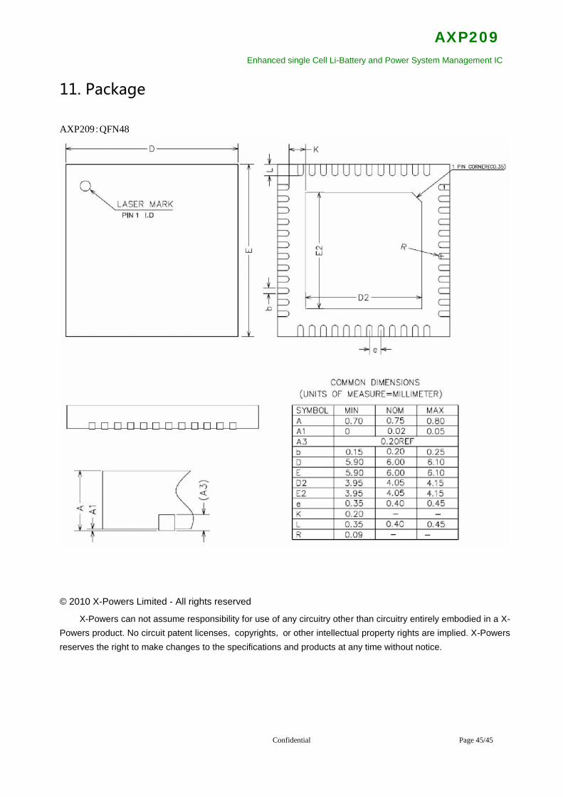
11. Package
AXP209:QFN48
© 2010 X-Powers Limited - All rights reserved
X-Powers can not assume responsibility for use of any circuitry other than circuitry entirely embodied in a X-Powers product. No circuit patent licenses, copyrights, or other intellectual property rights are implied. X-Powersreserves the right to make changes to the specifications and products at any time without notice.
Confidential Page 45/45