Space Charge Accumulation in Polymeric High Voltage DC ...
210
Space Charge Accumulation in Polymeric High Voltage DC Cable Systems
Transcript of Space Charge Accumulation in Polymeric High Voltage DC ...
Space Charge Accumulation in Polymeric
High Voltage DC Cable Systems

Space Charge Accumulation in Polymeric
High Voltage DC Cable Systems
Proefschrift
ter verkrijging van de graad van doctor aan de Technische Universiteit Delft
op gezag van de Rector Magnificus prof. dr. ir. J. T. Fokkema voorzitter van het College voor Promoties,
in het openbaar te verdedigen, op dinsdag 28 november 2006 om 15:00 uur
door
Riccardo BODEGA
dottore in ingegneria elettrica, Politecnico di Milano geboren te Lecco (Italië)
Dit proefschrift is goedgekeurd door de promotor: Prof. dr. J. J. Smit Samenstelling promotiecommissie: Rector Magnificus, Voorzitter Prof. dr. J. J. Smit, Technische Universiteit Delft, promotor Prof. dr. eng. J. A. Ferreira, Technische Universiteit Delft Prof. ir. W. L. Kling, Technische Universiteit Delft/Eindhoven Prof. dr. ir. E. F. Steennis, Technische Universiteit Eindhoven Prof. dr. J. C. Fothergill, University of Leicester, United Kingdom Dr. ir. P. H. F. Morshuis, Technische Universiteit Delft Dr. ir. M. D. Verweij, Technische Universiteit Delft
This research was funded by the European Commission in the framework of the European project “Benefits of HVDC Links in the European Power Electrical System and Improved HVDC Technology” (contract ENK6-CT-2002-00670).
ISBN 90-8559-228-3 Copyright © 2006 by R. Bodega Cover: photograph by Bruno van den Elshout – copyright PhotologiX.nl Printing: Optima Grafische Communicatie – Rotterdam, The Netherlands
Ai miei genitori, i migliori maestri che abbia mai avuto [To my parents, the best teachers I’ve ever had]
Alla mia compagna, Yvonne, per avermi insegnato a conoscere meglio me stesso
[To my girlfriend Yvonne, who taught me more about who I am]
He who loves practice without theory is like the sailor who boards ship
without a rudder and compass and never knows where he may cast.
Leonardo da Vinci

Preface This Ph.D. thesis was completed within the framework of the project “HVDC” (“Benefits of HVDC Links in the European Power Electrical System and Improved HVDC Technology”) funded by the European Commission. The “HVDC” project was launched in January 2003 to provide a methodology and associated software and hardware tools to assess the potential technical, economical and environmental benefits and impacts of high-voltage direct current interconnections embedded in the actual electrical power transmission and distribution systems of the European network. The project investigated also the potential benefits of using environmentally more acceptable high-voltage direct current power cable systems. Delft University of Technology contributed to the “HVDC” project together with the following European Partners: University of Leicester (UK) University of Surrey (UK) University of Bologna (IT) University Paul Sabatier, Toulouse III (FR) IECOS (UK) CESI (IT) Prysmian Cavi e Sistemi Energia S.r.l. (IT) Borealis (SW) TenneT (NL) Terna (IT) RTE (FR) Some of the data presented in this thesis were produced by the project Partners in the framework of the “HVDC” project. When so, this is explicitly indicated in the thesis.
vii

Table of contents Preface. . . . . . . . . . . . . . . . . . . . . . . . . . . . . . . . . . . . . . . . . . . . . . . . . . . . . . . . . . vii Table of contents . . . . . . . . . . . . . . . . . . . . . . . . . . . . . . . . . . . . . . . . . . . . . . . . . ix 1. Introduction . . . . . . . . . . . . . . . . . . . . . . . . . . . . . . . . . . . . . 1 1.1. General . . . . . . . . . . . . . . . . . . . . . . . . . . . . . . . . . . . . . . . . . . . . . . . . . . . . 1
1.1.1. HVDC cable systems . . . . . . . . . . . . . . . . . . . . . . . . . . . . . . . . . . . 1 1.1.2. HVDC cable insulation . . . . . . . . . . . . . . . . . . . . . . . . . . . . . . . . . 2
1.2. Polymeric HVDC cable systems and space charges. . . . . . . . . . . . . . . . . . 3 1.2.1. Historical development of HVDC cables . . . . . . . . . . . . . . . . . . . . . 3 1.2.2. Space charge and space charge field . . . . . . . . . . . . . . . . . . . . . . . . . 4 1.2.3. Research and development trend for space charge phenomena in HVDC polymeric cable insulation . . . . . . . . . . . . . . . . . . . . . . . . . . . . . . . 5
1.3. Objective of the present study . . . . . . . . . . . . . . . . . . . . . . . . . . . . . . . . . . 7 1.4. Scientific contribution of the thesis to the field of polymeric HVDC cable
systems . . . . . . . . . . . . . . . . . . . . . . . . . . . . . . . . . . . . . . . . . . . . . . . . . . . . 7 1.5. Outline of the thesis . . . . . . . . . . . . . . . . . . . . . . . . . . . . . . . . . . . . . . . . . . 8 2. Experimental methods . . . . . . . . . . . . . . . . . . . . . . . . . . . . 9 2.1. Test specimens. . . . . . . . . . . . . . . . . . . . . . . . . . . . . . . . . . . . . . . . . . . . . . . 9 2.2. Conduction current measurements . . . . . . . . . . . . . . . . . . . . . . . . . . . . . . . 13 2.3. Space charge measurements . . . . . . . . . . . . . . . . . . . . . . . . . . . . . . . . . . . . 16
2.3.1. General . . . . . . . . . . . . . . . . . . . . . . . . . . . . . . . . . . . . . . . . . . . . . . . 16 2.3.2. Pulsed electroacoustic method (PEA) . . . . . . . . . . . . . . . . . . . . . . . . 17 2.3.3. PEA method for multi-dielectric test objects . . . . . . . . . . . . . . . . . . 20 2.3.4. PEA method for cable geometry test objects . . . . . . . . . . . . . . . . . . . 21 2.3.5. Space charge parameters. . . . . . . . . . . . . . . . . . . . . . . . . . . . . . . . . . . 23 2.3.6. Accuracy of the measurements. . . . . . . . . . . . . . . . . . . . . . . . . . . . . . 26
2.4. Test conditions . . . . . . . . . . . . . . . . . . . . . . . . . . . . . . . . . . . . . . . . . . . . . . . 27 2.4.1. Temperature conditions . . . . . . . . . . . . . . . . . . . . . . . . . . . . . . . . . . . 27 2.4.2. Electrical conditions . . . . . . . . . . . . . . . . . . . . . . . . . . . . . . . . . . . . . . 31
3. Experimental observation of space charge and
electric field dynamics. . . . . . . . . . . . . . . . . . . . . . . . . . . . . . 33 3.1. Conduction current measurements on XLPE and EPR flat specimens . . . . 34
3.1.1. Introduction . . . . . . . . . . . . . . . . . . . . . . . . . . . . . . . . . . . . . . . . . . . . 34 3.1.2. Results . . . . . . . . . . . . . . . . . . . . . . . . . . . . . . . . . . . . . . . . . . . . . . . . 34 3.1.3. Discussion . . . . . . . . . . . . . . . . . . . . . . . . . . . . . . . . . . . . . . . . . . . . . 35 3.1.4. Summary and conclusions . . . . . . . . . . . . . . . . . . . . . . . . . . . . . . . . . 38
3.2. Space charge measurements on XLPE-EPR flat interfaces . . . . . . . . . . . . . 39 3.2.1. Introduction . . . . . . . . . . . . . . . . . . . . . . . . . . . . . . . . . . . . . . . . . . . . 39 3.2.2. Results. . . . . . . . . . . . . . . . . . . . . . . . . . . . . . . . . . . . . . . . . . . . . . . . . 40 3.2.3. Discussion . . . . . . . . . . . . . . . . . . . . . . . . . . . . . . . . . . . . . . . . . . . . . 42
ix
3.2.4. Summary and conclusions . . . . . . . . . . . . . . . . . . . . . . . . . . . . . . . . . 45
3.3. Space charge measurements on MV-size XLPE cables. . . . . . . . . . . . . . . . 46 3.3.1. Introduction . . . . . . . . . . . . . . . . . . . . . . . . . . . . . . . . . . . . . . . . . . . . 46 3.3.2. Results . . . . . . . . . . . . . . . . . . . . . . . . . . . . . . . . . . . . . . . . . . . . . . . . 47 3.3.3. Discussion . . . . . . . . . . . . . . . . . . . . . . . . . . . . . . . . . . . . . . . . . . . . . 49 3.3.4. Summary and conclusions . . . . . . . . . . . . . . . . . . . . . . . . . . . . . . . . . 55
3.4. Space charge measurements on dual-dielectric mini-cables . . . . . . . . . . . . 56 3.4.1. Introduction . . . . . . . . . . . . . . . . . . . . . . . . . . . . . . . . . . . . . . . . . . . . 56 3.4.2. Results . . . . . . . . . . . . . . . . . . . . . . . . . . . . . . . . . . . . . . . . . . . . . . . . 58 3.4.3. Discussion. . . . . . . . . . . . . . . . . . . . . . . . . . . . . . . . . . . . . . . . . . . . . . 60 3.4.4. Summary and conclusions . . . . . . . . . . . . . . . . . . . . . . . . . . . . . . . . . 64
3.5. Space charge measurements on MV-size models of cable joints . . . . . . . . 65 3.5.1. Introduction . . . . . . . . . . . . . . . . . . . . . . . . . . . . . . . . . . . . . . . . . . . . 65 3.5.2. Results . . . . . . . . . . . . . . . . . . . . . . . . . . . . . . . . . . . . . . . . . . . . . . . . 66 3.5.3. Discussion . . . . . . . . . . . . . . . . . . . . . . . . . . . . . . . . . . . . . . . . . . . . . 69 3.5.4. Summary and conclusions . . . . . . . . . . . . . . . . . . . . . . . . . . . . . . . . . 71
3.6. Conclusions . . . . . . . . . . . . . . . . . . . . . . . . . . . . . . . . . . . . . . . . . . . . . . . . . 72 4. Calculation of space charge and electric field
in DC cable systems . . . . . . . . . . . . . . . . . . . . . . . . . . . . . . . 75 4.1. Introduction . . . . . . . . . . . . . . . . . . . . . . . . . . . . . . . . . . . . . . . . . . . . . . . . . 75 4.2. Physical model . . . . . . . . . . . . . . . . . . . . . . . . . . . . . . . . . . . . . . . . . . . . . . 78
4.2.1. Theoretical background . . . . . . . . . . . . . . . . . . . . . . . . . . . . . . . . . . . 78 4.2.2. Model of the insulation. . . . . . . . . . . . . . . . . . . . . . . . . . . . . . . . . . . . 79 4.2.3. Numerical implementation of the physical model . . . . . . . . . . . . . . . 81
4.3. Results of the calculation . . . . . . . . . . . . . . . . . . . . . . . . . . . . . . . . . . . . . . . 83 4.3.1. Calculation vs. measurements . . . . . . . . . . . . . . . . . . . . . . . . . . . . . . 83 4.3.2. Effect of the conductivity function on the
calculated patterns . . . . . . . . . . . . . . . . . . . . . . . . . . . . . . . . . . . . . . . 88 4.4. Electric field in cable systems for particular situations . . . . . . . . . . . . . . . . 89 4.5. Conclusions . . . . . . . . . . . . . . . . . . . . . . . . . . . . . . . . . . . . . . . . . . . . . . . . . 95 5. Space charge at interfaces in HVDC cable systems. . . . . 97 5.1. Interfaces in HVDC cable systems . . . . . . . . . . . . . . . . . . . . . . . . . . . . . . . 97 5.2. Space charge accumulation at the semicon-insulation interface . . . . . . . . . 101
5.2.1. Charge accumulation mechanisms at the semicon-XLPE interface . . 101 5.2.2. Accumulation of charge at the semicon-XLPE interface in the studied specimens . . . . . . . . . . . . . . . . . . . . . . . . . . . . . . . . . . . . . . . . . . . . . . 102
5.3. Space charge accumulation at the dielectric interface . . . . . . . . . . . . . . . . . 105 5.3.1. Mawxell-Wagner theory for the interfacial polarization . . . . . . . . . . 105 5.3.2. Deviation from the Maxwell-Wagner theory: literature . . . . . . . . . . 107 5.3.3. Deviation from the Maxwell-Wagner theory: experimental results. . 108
5.3.4. Three-layer model for the dielectric interface . . . . . . . . . . . . . . . . . . 110 5.4. Suggestions on how to improve the macroscopic model for space charge
accumulation . . . . . . . . . . . . . . . . . . . . . . . . . . . . . . . . . . . . . . . . . . . . . . . . 113
x
6. Feasibility study for on-line on-site PEA measurements. . 115 6.1. Introduction . . . . . . . . . . . . . . . . . . . . . . . . . . . . . . . . . . . . . . . . . . . . . . . . . 115 6.2. Implementation . . . . . . . . . . . . . . . . . . . . . . . . . . . . . . . . . . . . . . . . . . . . . . 116 6.3. Conclusions . . . . . . . . . . . . . . . . . . . . . . . . . . . . . . . . . . . . . . . . . . . . . . . . . 118 7. Conclusions . . . . . . . . . . . . . . . . . . . . . . . . . . . . . . . . . . . . . . 119 7.1 . Space charge at dielectric discontinuities . . . . . . . . . . . . . . . . . . . . . . . . . . 119 7.2. Space charge in cable systems that experience a temperature drop across
the insulation . . . . . . . . . . . . . . . . . . . . . . . . . . . . . . . . . . . . . . . . . . . . . . . . 120 8. Recommendations and suggestions for further studies. . . 121 8.1. Recommendations . . . . . . . . . . . . . . . . . . . . . . . . . . . . . . . . . . . . . . . . . . . . 121
8.1.1. Recommendations for PEA testing on HVDC cable system insulation . . . . . . . . . . . . . . . . . . . . . . . . . . . . . . . . . . . . . . . . . . . . . . 121
8.1.2. Recommendations for the design of polymeric HVDC cable systems . . . . . . . . . . . . . . . . . . . . . . . . . . . . . . . . . . . . . . . . . . . . . . . 122
8.1.3. Recommendations for the operation on HVDC cable systems . . . . . 123 8.2. Suggestions for further study . . . . . . . . . . . . . . . . . . . . . . . . . . . . . . . . . . . . 125 Appendix. . . . . . . . . . . . . . . . . . . . . . . . . . . . . . . . . . . . . . . . . . . . . . . . . . . . . . . . . 127 A. Space charge measurements on multi-dielectrics
by means of the PEA method. . . . . . . . . . . . . . . . . . . . . . . . . . . . . . . . . . . 129 A.1. Generation of acoustic waves . . . . . . . . . . . . . . . . . . . . . . . . . . . . . . . . . . . . 129 A.1.1. Calculation of electrically-induced pressure waves . . . . . . . . . . . . . . 129
A.1.2. DC voltage applied in absence of space charge and interfacial charge . . . . . . . . . . . . . . . . . . . . . . . . . . . . . . . . . . . . . . . . . . . . . . . . . 131 A.1.3. Space charge in the absence of DC voltage and interfacial charge. . 133
A.1.4. Presence of interfacial charge in absence of DC voltage and space charge . . . . . . . . . . . . . . . . . . . . . . . . . . . . . . . . . . . . . . . . . . . . . . . . 134 A.1.5. DC voltage applied in presence of space charge and interfacial charge . . . . . . . . . . . . . . . . . . . . . . . . . . . . . . . . . . . . . . . . . . . . . . . . 136 A.2. Acoustic wave traveling and reflection . . . . . . . . . . . . . . . . . . . . . . . . . . . . 136
A.2.1. Acoustic wave propagation . . . . . . . . . . . . . . . . . . . . . . . . . . . . . . . . 136 A.2.2. Acoustic wave reflection . . . . . . . . . . . . . . . . . . . . . . . . . . . . . . . . . . 138 A.3. Interpretation of detected acoustic signals . . . . . . . . . . . . . . . . . . . . . . . . . . 140
A.3.1. Test specimens and test procedures . . . . . . . . . . . . . . . . . . . . . . . . . . 140 A.3.2. Measurement results . . . . . . . . . . . . . . . . . . . . . . . . . . . . . . . . . . . . . 141
A.3.3. Interpretation of measurement results . . . . . . . . . . . . . . . . . . . . . . . . 142 A.4. Conclusions . . . . . . . . . . . . . . . . . . . . . . . . . . . . . . . . . . . . . . . . . . . . . . . . . 145 B. PEA method for cylindrical test objects . . . . . . . . . . . . . . . . . . . . . . . . . . 147 B.1. Different type of PEA set-ups . . . . . . . . . . . . . . . . . . . . . . . . . . . . . . . . . . . 147
B.1.1. Shape of the earth electrode . . . . . . . . . . . . . . . . . . . . . . . . . . . . . . . 148 B.1.2. Application of the pulsed voltage . . . . . . . . . . . . . . . . . . . . . . . . . . . 148 B.2. Application of the pulse to the cables . . . . . . . . . . . . . . . . . . . . . . . . . . . . . 151 B.3. Effect of cylindrical geometry on the amplitude of acoustic waves . . . . . . 153
xi
C. Attenuation and dispersion of acoustic waves in the PEA method . . . . 155 C.1. Problem identification . . . . . . . . . . . . . . . . . . . . . . . . . . . . . . . . . . . . . . . . . 155 C.2. Theoretical background . . . . . . . . . . . . . . . . . . . . . . . . . . . . . . . . . . . . . . . . 156 C.3. Procedure for recovering the original acoustic waveform from the attenuated and distorted waveform . . . . . . . . . . . . . . . . . . . . . . . . . . . . . . . . 157 D. Calibration . . . . . . . . . . . . . . . . . . . . . . . . . . . . . . . . . . . . . . . . . . . . . . . . . 159 D.1. Flat homogeneous test object . . . . . . . . . . . . . . . . . . . . . . . . . . . . . . . . . . . . 159 D.2. Flat multi-dielectric test object . . . . . . . . . . . . . . . . . . . . . . . . . . . . . . . . . . . 160 D.3. Cylindrical homogeneous test object . . . . . . . . . . . . . . . . . . . . . . . . . . . . . . 160 D.4. Cylindrical multi-dielectric test object . . . . . . . . . . . . . . . . . . . . . . . . . . . . . 161 E. Equations adopted in the numerical procedure . . . . . . . . . . . . . . . . . . . 165 E.1. Poisson’s equation for the electric field . . . . . . . . . . . . . . . . . . . . . . . . . . . . 165 E.2. Calculation of the charge-induced field . . . . . . . . . . . . . . . . . . . . . . . . . . . . 166 E.2.1. Field induced by space charge in coaxial interfaces . . . . . . . . . . . . . 166 E.2.2. Field induced by interfacial charge in coaxial interfaces . . . . . . . . . 167 E.2.3. General expression of the field . . . . . . . . . . . . . . . . . . . . . . . . . . . . . 168 E.3. Fourier’s heat diffusion equation for cables and cable joints . . . . . . . . . . . 169 References . . . . . . . . . . . . . . . . . . . . . . . . . . . . . . . . . . . . . . . . . . . . . . . . . . . . . . . 171 List of abbreviations . . . . . . . . . . . . . . . . . . . . . . . . . . . . . . . . . . . . . . . . . . . . . . . 183 List of symbols. . . . . . . . . . . . . . . . . . . . . . . . . . . . . . . . . . . . . . . . . . . . . . . . . . . . 187 Summary . . . . . . . . . . . . . . . . . . . . . . . . . . . . . . . . . . . . . . . . . . . . . . . . . . . . . . . . 189 Samenvatting . . . . . . . . . . . . . . . . . . . . . . . . . . . . . . . . . . . . . . . . . . . . . . . . . . . . . 191 Sommario . . . . . . . . . . . . . . . . . . . . . . . . . . . . . . . . . . . . . . . . . . . . . . . . . . . . . . . . 193 Acknowledgement . . . . . . . . . . . . . . . . . . . . . . . . . . . . . . . . . . . . . . . . . . . . . . . . . 195 Curriculum Vitae . . . . . . . . . . . . . . . . . . . . . . . . . . . . . . . . . . . . . . . . . . . . . . . . . 196
xii


Chapter 1 - Introduction
1
1. Introduction
1.1 General 1.1.1. HVDC cable systems Since the nineteen fifties, high voltage (HV) direct current (DC) cable systems have been used worldwide for the transport of electrical energy. A cable system consists of a cable and its accessories, i.e. joints and terminations. Terminations are needed at the ends of the cable circuit, to grade the electric field and to connect the cable to the power line. Joints are required when the cable becomes too long to be produced in one length. Traditionally, HVDC cable systems have been used only when alternate current (AC) technology could not be applied. The main reason for this is that DC links need two conversion stations at the ends of the transmission link. In the past, the conversion stations often increased the costs of the project too much. A typical example of HVDC cable application is the sea-crossing energy transport. In this case, AC overhead lines cannot be employed. Moreover, if the length of the sea crossing exceeds 30 - 50 km, the use of AC cables becomes unfeasible because of the high value of the capacitive reactive power. Therefore, HVDC cable systems are the only technically applicable solution for long distance underground or submarine connections. The traditional restrictions on the use of HVDC technology are rapidly changing, especially within Europe, giving a potential opportunity for application of HVDC cable systems. The actual European transmission network consists in fact of large HVAC synchronous zones, rather scarcely interconnected by HVDC links. New HVDC links are a means for reinforcing the actual HVAC European transmission network. The main drivers for HVAC network reinforcement by means of HVDC links are [73, 154]: - The liberalization of the electrical energy market and the consequent increase of
traded energy are leading to large variations of the power flows. This asks for additional cross-border transmission capacity.
- Decentralized power generation plants, in particular wind energy, are increasingly being introduced in the networks. Decentralized generation plants essentially operate at variable conditions that may have an impact on the power quality of the network, e.g. [136].
- Nowadays, more difficulties are encountered in getting the necessary permits to build additional overhead transmission lines.
- The effect of magnetic fields on human health and the visual/noise impact are ongoing controversial debates because of which the public refrains to accept new overhead transmission lines.
Chapter 1 - Introduction
2
In this framework HVDC cable links can provide: - interconnection between independent networks, increasing the transmission
capacity and increasing the possibilities for energy exchange; - the control of reactive power, which supports the network stability and the power
quality (when voltage source converters – VSC – are used); - relatively short time for delivering a new link. As important as the previous aspects, HVDC cable systems are considered environmental friendly, because of their very low visual impact and noise impact. Furthermore, when using HVDC cables in a bipolar configuration, practically no magnetic field is produced. 1.1.2. HVDC cable insulation The main concern about the employment of new HVDC cable links is the rather high cost of the connection. The cost of the connection could be significantly reduced by using polymer-insulated HVDC cable systems (also called extruded HVDC cable systems) instead of mass-impregnated or oil-filled HVDC cable systems (also called lapped or oil-paper HVDC cable systems). The extrusion production process is, in fact, simpler and cheaper than the process for manufacturing lapped insulation. In addition, extruded cable systems present the following advantages if compared to lapped cable systems: - no use of any impregnants or oil; - more mechanical rigidity, allowing the use of a thinner cable armor; - higher maximal working temperature; - easier cable maintenance and easier component replacement; - easier preparation and mounting of cable joints. On the other hand, HVDC mass-impregnated cables have been proven to be reliable over many decades, while HVDC polymeric cables have been only recently employed. The reason for this will be explained in the next paragraph.
Chapter 1 - Introduction
3
1.2. Polymeric HVDC cable systems and space charges
1.2.1. Historical development of polymeric HVDC cables The first HVDC cable went into service in 1954, for connecting the Gotland Island in the Baltic Sea to the Swedish mainland. This was a mass-impregnated cable. Since then, many HVDC cables have been employed all over the world. Most of these cables are mass-impregnated or oil-filled insulated. Through the years, the power transported by the DC links and their rated voltages have increased, the cable systems have become longer, the AC/DC conversion technology has changed, but mass-impregnated and oil-filled insulation have been, in practice, the only type of insulation to be used up to 1999. In that year, the first commercial HVDC polymeric cable system was put into service. This trend is in contrast to what happened in the AC cable technology, where polymeric insulation has been successfully used since many decades. Now it is the dominating AC cable technology. The main issue, which needed to be resolved for the development of the HVDC polymeric cables, is the control of the space charge phenomena, which affect the reliability of the connection. Nowadays, this concern has been addressed, but only partially solved. As a consequence, mass-impregnated paper is still the dominating technology for HVDC cable insulation. Recently, some innovative HVDC cable projects making use of polymeric cable insulation have been completed [52, 130], up to a rated voltage of 150 kV and for a maximal power capacity of about 500 MW1. However, in these projects, the polarity of the DC voltage must be kept fixed and then the inversion of the power flow has to be done by inverting the current direction. This limits the application of the polymeric cable system to HVDC links using IGBT-based converters (VSC). In the future, as it has already happened for AC cables, polymeric HVDC cables are expected to replace the traditional lapped HVDC cables. However, in order to make this step feasible, more understanding about the fundamental space charge processes occurring in polymeric DC cable insulation is needed.
1 According to [77], the HVDC polymeric cable technology will be soon upgraded up to 300 kV and 1000 MW.
Chapter 1 - Introduction
4
1.2.2. Space charge and space charge field One of the intrinsic properties of the DC cable insulation is the accumulation of charges. Insulating materials allow a weak electrical conduction. This weak flow of charge within the insulation may not be uniform, because of a local non-homogeneity of the material. According to the current density continuity equation, when an inequality occurs between the flow of charges into a region and the flow of charges out of that region, charge accumulates in that region, see equation (1.1):
0=∂∂
+⋅∇t
j ρr (1.1)
In equation (1.1), j is the current density, ρ is the charge per unit volume (also called space charge density or simply space charge) and t the time. According to Gauss’ law, a space charge field Eρ is associated to a charge distribution:
( )ρεερ Er
r0⋅∇= (1.2)
where ε0 is the vacuum permittivity and εr the relative permittivity of the insulation. Therefore, the electric field E within the insulation in the presence of space charge is given by the sum of two contributions: the space charge field and the external field E0 (also called Laplacian field), which is induced by the applied voltage, see equation (1.3).
ρEEErrr
+= 0 (1.3)
In the AC situation, the flow of charges inverts its direction too quickly to allow a significant growth of space charge at the insulation inhomogeneities, at least for conventional insulating materials. This means that the space charge field can be neglected. On the other hand, under DC stressing condition, the flow of charge maintains the same direction. This allows a build-up of charge, which, in general, significantly affects the electric field distribution inside the insulation. Accumulated charges can be released by the insulation when the external field is removed and the insulation short-circuited. However, this process can last quite a long time, depending on the type of insulation and on the temperature. In general, charge depletion is much longer for polymeric insulation than for lapped insulation. A consequence of this phenomenon is that the accumulated charges will be kept within the insulation also when the external DC voltage is removed or when the value of the external DC voltage changes. The inversion of the voltage polarity in HVDC cables is a practical example of such a situation. In this particular case, the insulation experiences the sum of the space charge field and the field induced by the DC voltage, which direction has been inverted. This generally leads to a maximum field near the inner conductor of the cable. In the worst case, the maximum field can be as high as twice the maximum value of the Laplacian field.
Chapter 1 - Introduction
5
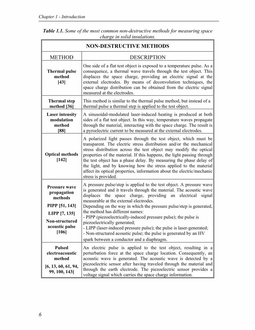
1.2.3. Research and development trend for space charge phenomena in HVDC polymeric cable insulation
During the last three decades, space charge phenomena in HVDC insulation have been investigated worldwide. Many techniques have been developed for the experimental observation of space charge. This, combined with a better theoretical understanding of the physical processes and an improvement of the extrusion cable technology, has been instrumental to the development of polymeric HVDC cables [30]. Table 1.1 reports an overview of the most adopted non-destructive2 methods for the measurement of space charge in solid insulation. Nowadays, the scientific community agrees that space charge measuring techniques have reached maturity. However, there are still two main directions of advancement regarding the use of space charge measurements for the development of polymeric HVDC cable insulation. The first one considers the improvement of the space charge measuring systems and the enlargement of the applicability field for space charge measuring techniques, e.g. [54]. Often, combinations of more insulating materials or semiconducting and insulating materials are used in cable systems. For instance, new (nano)composite materials are potential candidate for the cable insulation technology. Consequently, the objects of space charge measurements as well as the measuring conditions are becoming more complex. This means that the measuring systems and their operational limits have to be upgraded. The second field of advancement for space charge methods regards the exploitation of the information derived from the measurement results, e.g. [116]. In addition to the indication of space charge and electric field magnitude and location, further quantities can be derived from the results of the measurements. If properly analyzed, these quantities can support the identification of the charge carriers, the nature of the conduction mechanism and even the aging state of the insulation.
2 Destructive methods for the measurement of space charge, such as the dust figure method [8] and the probe technique method [82, 83], were also used until the beginning of nineteen eighty. The principles of those techniques consist of cutting the test object into small slices and detecting the charge present at the surface of the cut slice.
Chapter 1 - Introduction
6
Table 1.1. Some of the most common non-destructive methods for measuring space charge in solid insulations.
NON-DESTRUCTIVE METHODS
METHOD DESCRIPTION
Thermal pulse method
[43]
One side of a flat test object is exposed to a temperature pulse. As a consequence, a thermal wave travels through the test object. This displaces the space charge, providing an electric signal at the external electrodes. By means of deconvolution techniques, the space charge distribution can be obtained from the electric signal measured at the electrodes.
Thermal step method [36]
This method is similar to the thermal pulse method, but instead of a thermal pulse a thermal step is applied to the test object.
Laser intensity modulation
method [88]
A sinusoidal-modulated laser-induced heating is produced at both sides of a flat test object. In this way, temperature waves propagate through the material, interacting with the space charge. The result is a pyroelectric current to be measured at the external electrodes.
Optical methods
[142]
A polarized light passes through the test object, which must be transparent. The electric stress distribution and/or the mechanical stress distribution across the test object may modify the optical properties of the material. If this happens, the light passing through the test object has a phase delay. By measuring the phase delay of the light, and by knowing how the stress applied to the material affect its optical properties, information about the electric/mechanic stress is provided.
Pressure wave propagation
methods PIPP [51, 143] LIPP [7, 135]
Non-structured acoustic pulse
[106]
A pressure pulse/step is applied to the test object. A pressure wave is generated and it travels through the material. The acoustic wave displaces the space charge, providing an electrical signal measurable at the external electrodes. Depending on the way in which the pressure pulse/step is generated,the method has different names: - PIPP (piezoelectrically-induced pressure pulse); the pulse is piezoelectrically generated; - LIPP (laser-induced pressure pulse); the pulse is laser-generated; - Non-structured acoustic pulse; the pulse is generated by an HV spark between a conductor and a diaphragm.
Pulsed electroacoustic
method [6, 13, 60, 61, 94,
99, 100, 143]
An electric pulse is applied to the test object, resulting in a perturbation force at the space charge location. Consequently, an acoustic wave is generated. The acoustic wave is detected by a piezoelectric sensor after having traveled through the material and through the earth electrode. The piezoelectric sensor provides a voltage signal which carries the space charge information.
Chapter 1 - Introduction
7
1.3. Objective of the present study The general objective of the present study is to obtain a better understanding of the major factors that control the space charge processes in polymeric HVDC cable systems. Electric field prediction methods, which include space charge phenomena, have to be developed to provide tools and principles to support the design and the operation of HVDC polymeric cable systems. In order to achieve this goal, two main factors of influence have been investigated: 1. Cable accessories are considered to be the weakest part of a cable system, because
of the presence of a dielectric interface between the cable insulation and that of the accessory. This thesis aims at a better knowledge of the polarization phenomena occurring at dielectric interfaces. To that purpose, we developed an accurate methodology for the experimental study of the space charge behavior at the dielectric interface.
2. When operating, HVDC cable systems experience a temperature drop across their insulation. This thesis aims to provide a better understanding about the mechanisms responsible for space charge accumulation when a temperature drop is present across the insulation of the cable system. To that purpose, we developed a physical model for the prediction of space charge dynamics and electric field in loaded HVDC cable systems. The physical model is validated by means of laboratory investigation.
1.4. Scientific contribution of the thesis to the field of polymeric HVDC cable systems
This thesis contributes to the scientific development in the field of polymeric HVDC cable systems by: - reviewing the pulsed electroacoustic method for the measurement of space charges
at dielectric discontinuities, such as those encountered in cable accessories; - developing measuring systems which are able to detect charges in test objects
resembling the real HVDC cables and cable accessories; - identifying the main mechanisms responsible for the accumulation of charges at
dielectric discontinuities and recognizing the main parameters affecting the accumulation of charge;
- experimentally investigating the effect of a temperature gradient on charge accumulation in the insulation of HVDC polymeric cables and cable accessories;
- experimentally investigating the effect of the voltage polarity reversal on loaded HVDC cables and cable accessories;
- developing a model for the prediction of charge accumulation in HVDC cable systems and implementing it by means of a numerical procedure;
- developing operational recommendations for the optimization of the electric stress in particular working conditions of the cable system.
Chapter 1 - Introduction
8
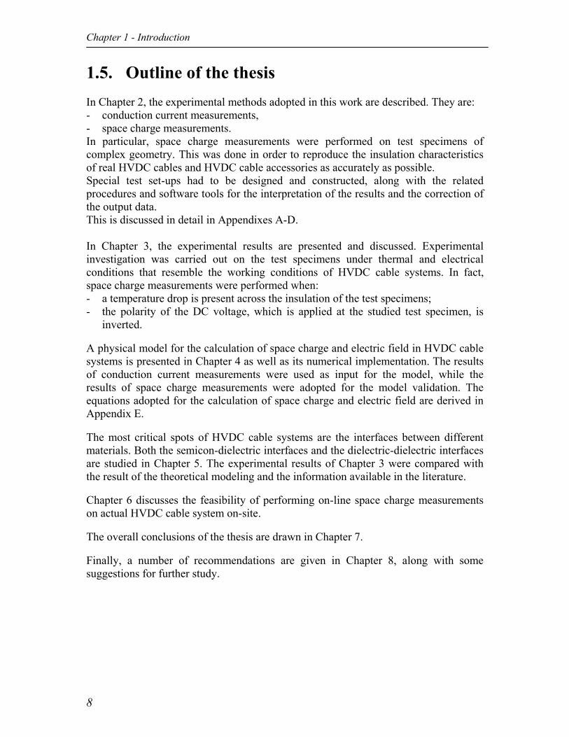
1.5. Outline of the thesis In Chapter 2, the experimental methods adopted in this work are described. They are: - conduction current measurements, - space charge measurements. In particular, space charge measurements were performed on test specimens of complex geometry. This was done in order to reproduce the insulation characteristics of real HVDC cables and HVDC cable accessories as accurately as possible. Special test set-ups had to be designed and constructed, along with the related procedures and software tools for the interpretation of the results and the correction of the output data. This is discussed in detail in Appendixes A-D. In Chapter 3, the experimental results are presented and discussed. Experimental investigation was carried out on the test specimens under thermal and electrical conditions that resemble the working conditions of HVDC cable systems. In fact, space charge measurements were performed when: - a temperature drop is present across the insulation of the test specimens; - the polarity of the DC voltage, which is applied at the studied test specimen, is
inverted.
A physical model for the calculation of space charge and electric field in HVDC cable systems is presented in Chapter 4 as well as its numerical implementation. The results of conduction current measurements were used as input for the model, while the results of space charge measurements were adopted for the model validation. The equations adopted for the calculation of space charge and electric field are derived in Appendix E.
The most critical spots of HVDC cable systems are the interfaces between different materials. Both the semicon-dielectric interfaces and the dielectric-dielectric interfaces are studied in Chapter 5. The experimental results of Chapter 3 were compared with the result of the theoretical modeling and the information available in the literature.
Chapter 6 discusses the feasibility of performing on-line space charge measurements on actual HVDC cable system on-site.
The overall conclusions of the thesis are drawn in Chapter 7.
Finally, a number of recommendations are given in Chapter 8, along with some suggestions for further study.
Chapter 2 – Experimental methods
9
2. Experimental methods In this chapter, the experimental investigations performed in this work are introduced. In section 2.1, the different test specimens used for the laboratory researches are described. Section 2.2 deals with the test set-up and the test protocol that were adopted for measuring the conduction current in insulating materials. The technique, the test set-ups and the test protocols used for space charge measurements on different test objects are discussed in section 2.3. In section 2.4, the experimental conditions, at which the measurements were performed, are given. In the thesis, the charging phenomena occurring in extruded DC cables and accessories are investigated. This is the main reason for choosing the experimental methods presented in this chapter. In fact, space charge measurements directly provide information about the charge that may be present within the insulation and the consequent field distortion. On the other hand, the outcomes of conduction current measurements are the basic input for the model proposed in Chapter 4, which describes the studied charging phenomena.
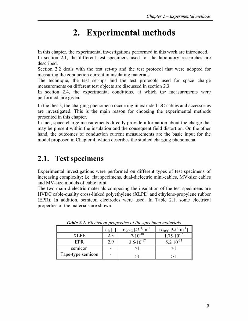
2.1. Test specimens Experimental investigations were performed on different types of test specimens of increasing complexity: i.e. flat specimens, dual-dielectric mini-cables, MV-size cables and MV-size models of cable joint. The two main dielectric materials composing the insulation of the test specimens are HVDC cable-quality cross-linked polyethylene (XLPE) and ethylene-propylene rubber (EPR). In addition, semicon electrodes were used. In Table 2.1, some electrical properties of the materials are shown.
Table 2.1. Electrical properties of the specimen materials. εR [-] σ20°C [Ω-1⋅m-1] σ60°C [Ω-1⋅m-1]
XLPE 2.3 7⋅10-18 1.75⋅10-15 EPR 2.9 3.5⋅10-17 5.2⋅10-15
semicon - >1 >1 Tape-type semicon - >1 >1
Chapter 2 – Experimental methods
10
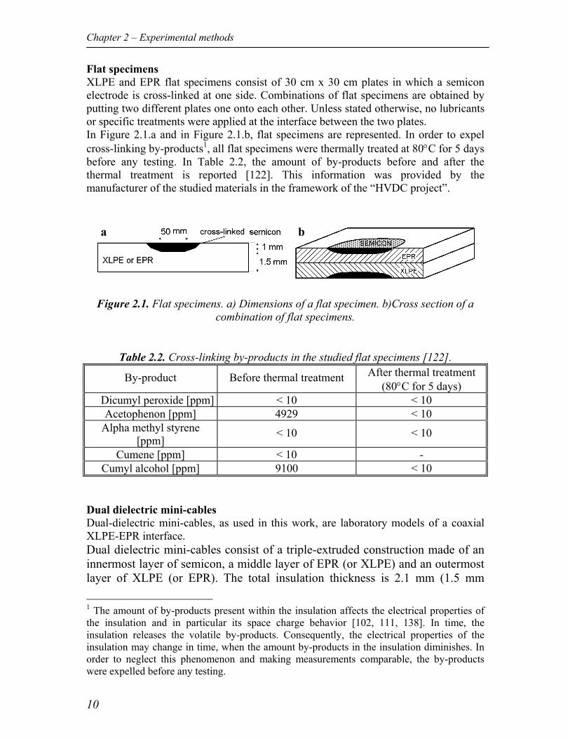
Flat specimens XLPE and EPR flat specimens consist of 30 cm x 30 cm plates in which a semicon electrode is cross-linked at one side. Combinations of flat specimens are obtained by putting two different plates one onto each other. Unless stated otherwise, no lubricants or specific treatments were applied at the interface between the two plates. In Figure 2.1.a and in Figure 2.1.b, flat specimens are represented. In order to expel cross-linking by-products1, all flat specimens were thermally treated at 80°C for 5 days before any testing. In Table 2.2, the amount of by-products before and after the thermal treatment is reported [122]. This information was provided by the manufacturer of the studied materials in the framework of the “HVDC project”.
Figure 2.1. Flat specimens. a) Dimensions of a flat specimen. b)Cross section of a combination of flat specimens.
Table 2.2. Cross-linking by-products in the studied flat specimens [122].
By-product Before thermal treatment After thermal treatment (80°C for 5 days)
Dicumyl peroxide [ppm] < 10 < 10 Acetophenon [ppm] 4929 < 10
Alpha methyl styrene [ppm]
< 10 < 10
Cumene [ppm] < 10 - Cumyl alcohol [ppm] 9100 < 10
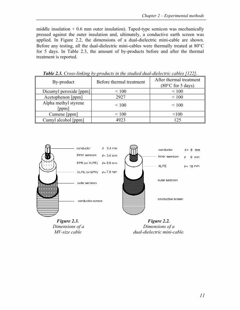
Dual dielectric mini-cables Dual-dielectric mini-cables, as used in this work, are laboratory models of a coaxial XLPE-EPR interface. Dual dielectric mini-cables consist of a triple-extruded construction made of an innermost layer of semicon, a middle layer of EPR (or XLPE) and an outermost layer of XLPE (or EPR). The total insulation thickness is 2.1 mm (1.5 mm 1 The amount of by-products present within the insulation affects the electrical properties of the insulation and in particular its space charge behavior [102, 111, 138]. In time, the insulation releases the volatile by-products. Consequently, the electrical properties of the insulation may change in time, when the amount by-products in the insulation diminishes. In order to neglect this phenomenon and making measurements comparable, the by-products were expelled before any testing.
a b
Chapter 2 – Experimental methods
11
middle insulation + 0.6 mm outer insulation). Taped-type semicon was mechanically pressed against the outer insulation and, ultimately, a conductive earth screen was applied. In Figure 2.2, the dimensions of a dual-dielectric mini-cable are shown. Before any testing, all the dual-dielectric mini-cables were thermally treated at 80°C for 5 days. In Table 2.3, the amount of by-products before and after the thermal treatment is reported.
Table 2.3. Cross-linking by-products in the studied dual-dielectric cables [122].
By-product Before thermal treatment After thermal treatment (80°C for 5 days)
Dicumyl peroxide [ppm] < 100 < 100 Acetophenon [ppm] 2927 < 100
Alpha methyl styrene [ppm]
< 100 < 100
Cumene [ppm] < 100 <100 Cumyl alcohol [ppm] 4923 125
Figure 2.2. Dimensions of a
dual-dielectric mini-cable.
Figure 2.3. Dimensions of a
MV-size cable
Chapter 2 – Experimental methods
12
MV-size cables MV-size cables consist of 4.5-mm thick extruded XLPE cables with a conductor of 50mm2. In Figure 2.3, the dimensions of a MV-size cable are shown. Before any testing, all the MV-size cables were thermally treated at 80°C for 20 days. In Table 2.4, the amount of by-products before and after the thermal treatment is reported.
Table 2.4. Cross-linking by-products in the studied MV-size cables [122].
By-product Before thermal treatment After thermal treatment (80°C for 20 days)
Dicumyl peroxide [ppm] 17 < 10 Acetophenon [ppm] 1169 < 10
Alpha methyl styrene [ppm]
15 < 10
Cumene [ppm] < 10 <10 Cumyl alcohol [ppm] 3227 30
MV-size models of cable joints MV-size models of cable joints are constructed in the following way. Firstly, the earth screen and the outer semicon of an XLPE-insulated cable (area of the inner conductor = 50 mm2; insulation thickness = 4.5 mm) is scraped off for a length of 80 mm. Then, part of the exposed insulation is removed by means of a glass blade and the insulation surface is smoothed by using successive grades of abrasive cloth. After these operations, the thickness of the remaining XLPE in the central part of the opening is 2 mm. At this point, a 100-mm long elastic tube made of EPR (thickness = 2 mm) can be applied on the XLPE by means of a special tool. After fitting the EPR tube onto a hollow mandrel placed over the exposed XLPE, the tool pulls back the mandrel. In this way, the EPR tube stretches over the XLPE. To make easy this operation, silicon oil has to be applied at the inner surface of the EPR tube. Finally, an outer semicon is taped on the EPR. In Figure 2.4, a cross section of a joint model is represented. Before any testing, all the MV-size models of cable joints were thermally treated at 80°C for 20 days. Conditioning of used specimens After a measurement, the specimen used for the test was conditioned in an oven at 80 °C for at least 24 hours. This was done in order to reset the space charge history of the specimen, allowing to use the same specimen for different measurements.
Chapter 2 – Experimental methods
13
2.2. Conduction current measurements
Measurements of DC conduction current on flat specimens were performed for two main purposes. Firstly, from the measured current values, the DC conductivity of the insulation can be inferred. This was done at different electric fields and at different temperature conditions. Secondly, results of current measurements can provide information on the conduction mechanisms. If the set of data collected from the measurements at different conditions are plotted in a voltage-current characteristic (or in a current density-field (J-E) characteristic), the electric field above which the conduction mechanism changes can be detected. This particular value of the electric field is usually called electric threshold. (Several works, e.g. [15, 48, 113, 133, 134], on HVDC polymeric insulation have shown that significant space charge build-up starts when the applied field is above the electric threshold. Recently, this parameter has also been associated with the startup of electrical aging [46, 47]. For these reasons, the electric threshold can be considered a parameter of utmost interest not only for insulation design, but also for material characterization and material comparison [3, 15, 113, 114]). Test set-up Conduction current measurements were performed in a three-terminal cell by means of a Keithley 617 electrometer. In order to protect the electrometer from over currents, the instrument was connected to the measuring electrode via a series resistor. The DC voltage was supplied to the test specimen via a Rogowski-profiled electrode made of aluminum. In all tests, a 1-mm semicon layer was applied to the aluminum measuring and guarding electrodes. In this way, the insulation of the test specimen was always in contact with the semicon. A personal computer equipped with a GPIB interface was used for displaying and storing the acquired data. In Figure 2.5, the test set-up is represented, whereas in Table 2.5 some specifications of the set-up are given.
a
b
Figure 2.4. a) Cross-section of a MV-size model of a
cable joint. b) Detail of the
dielectric interface.
Chapter 2 – Experimental methods
14
Figure 2.5. Experimental set-up used for measurements of conduction current.
Table 2.5. Specifications of the set-up used in this work for conduction current measurements.
Conduction current set-up Measuring electrode: diameter = 28 mm HV electrode diameter = 35 mm Guarding electrode: diameter = 40 mm-350 mm Sensitivity: 2⋅10-11 A/m2 Max temperature: 80°C Max voltage: +/- 30 kV Series resistor: 10 MΩ
Test procedure In Figure 2.6., the typical behavior of the detected current density j(t) is represented. The current density is obtained by means of the following equation:
( ) ( )elmA
titj,
= (2.1)
where i(t) is the current measured by the electrometer and Am,el is the area of the measuring electrode. Defining the steady-state value of the current density Jss as:
( )∞→
=t
ss tjJ (2.2)
the conductivity σ of the insulation can be inferred from:
Chapter 2 – Experimental methods
15
0EJ ss=σ (2.3)
where E0 is the external field which is applied across the insulation under test. In practice, in order to reach a quasi steady-state regime, the applied field has to be present across the insulation for a sufficiently long polarization time. For the test condition adopted in this study, the polarization time varies from a few hours, in case of measurements performed at a relatively high applied field and temperature, to a few days, in case of measurements performed at relatively low applied field and temperature. In some of the tests, the measured current did not stabilize on a constant value even after a few days. In these cases, a graphical fitting was used to estimate the steady-state value of the measured current.
Figure 2.6. Example of detected
current density. EPR flat specimen at 20 kV/mm and 40°C.
Chapter 2 – Experimental methods
16
2.3. Space charge measurements In this section, the following topics are discussed: 2.3.1. some general considerations about space charge measurements and an
overview of the most used space charge measuring techniques; 2.3.2. the method used in this investigation (pulsed electroacoustic method) and
the test set-ups adopted for measuring space charge; 2.3.3. the pulsed electroacoustic method when the test object is a multi-dielectric; 2.3.4. the pulsed electroacoustic method when the test object has cylindrical
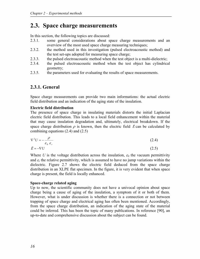
geometry; 2.3.5. the parameters used for evaluating the results of space measurements. 2.3.1. General Space charge measurements can provide two main informations: the actual electric field distribution and an indication of the aging state of the insulation. Electric field distribution The presence of space charge in insulating materials distorts the initial Laplacian electric field distribution. This leads to a local field enhancement within the material that may cause insulation degradation and, ultimately, electrical breakdown. If the space charge distribution ρ is known, then the electric field E
rcan be calculated by
combining equations (2.4) and (2.5)
r
Uεερ
0
2 −=∇ (2.4)
UE −∇=r
(2.5)
Where U is the voltage distribution across the insulation, ε0 the vacuum permittivity and εr the relative permittivity, which is assumed to have no jump variations within the dielectric. Figure 2.7 shows the electric field deduced from the space charge distribution in an XLPE flat specimen. In the figure, it is very evident that when space charge is present, the field is locally enhanced. Space-charge related aging Up to now, the scientific community does not have a univocal opinion about space charge being a cause of aging of the insulation, a symptom of it or both of them. However, what is under discussion is whether there is a connection or not between trapping of space charge and electrical aging has often been mentioned. Accordingly, from the space charge distribution, an indication of the aging state of the material could be inferred. This has been the topic of many publications. In reference [90], an up-to-date and comprehensive discussion about the subject can be found.
Chapter 2 – Experimental methods
17
Figure 2.7. Examples of space charge (figure a) and electric field (figure b) distributions in a 1.5-mm thick XLPE insulation. Applied voltage= 17 kV.
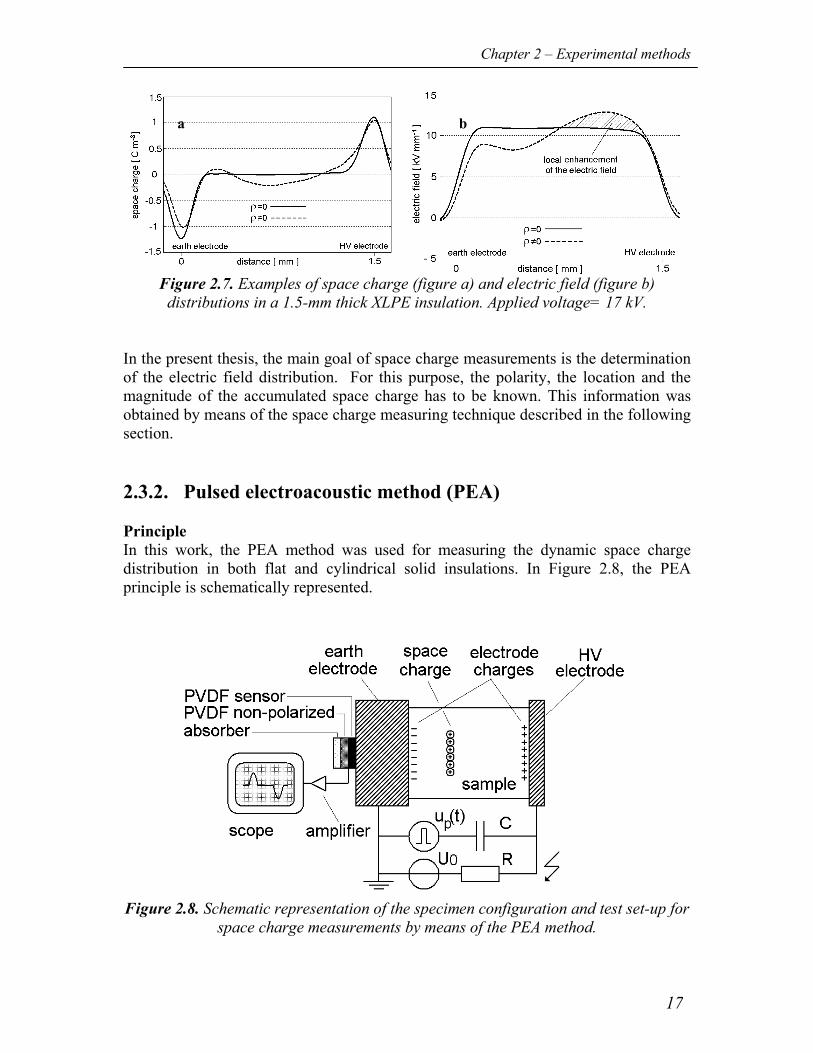
In the present thesis, the main goal of space charge measurements is the determination of the electric field distribution. For this purpose, the polarity, the location and the magnitude of the accumulated space charge has to be known. This information was obtained by means of the space charge measuring technique described in the following section. 2.3.2. Pulsed electroacoustic method (PEA) Principle In this work, the PEA method was used for measuring the dynamic space charge distribution in both flat and cylindrical solid insulations. In Figure 2.8, the PEA principle is schematically represented.
Figure 2.8. Schematic representation of the specimen configuration and test set-up for
space charge measurements by means of the PEA method.
a b
Chapter 2 – Experimental methods
18
In the PEA method, a pulsed voltage up(t) is applied across a test object (e.g. a flat or cylindrical specimen). The pulsed voltage can be superimposed on a DC voltage U0. In this case, a decoupling capacitor C and a resistor R have to be placed in series to the pulse source and DC source respectively. Depending on the thickness of the specimen, typical values for the amplitude of the pulse are 0.1-4 kV whereas the pulse width varies in the range 5-200 ns. Reference [39] discusses in detail how to choose the proper pulse parameters given a specific size of the test object. If space charge is embedded within the test object, the application of the pulse induces a perturbation force on the space charge distribution. The perturbation force makes the charge to move slightly and, as a result, strain (acoustic) waves are initiated at the space charge location. Those waves are detected by a piezoelectric sensor after having traveled through the test object and through the earth electrode. Usually, polyvinylidenefluoride (PVDF) or lithium niobate (LiNbO3) are used as sensors. In order to avoid reflections of acoustic waves, a proper acoustic termination is required at the sensor. For this purpose, a material with the same acoustic properties of the sensor is used in combination with a material which is able to absorb the acoustic waves. The electric signal provided at the sensor is amplified and fed into a scope, where it is displayed and stored. Correction of the detected signal Generally, the electrical signal detected at the scope does not directly represent the acoustic signal at the sensor. This is mainly due to the fact that the sensor-amplifier system acts as a high-pass filter [118]. In order to correct the detected signal, deconvolution techniques [78, 100] have been adopted in this work. Moreover, acoustic waves are attenuated and dispersed, while traveling through lossy media. So, the acoustic signal detected at the sensor does not directly correspond to the space charge distribution within the test specimen. In this study, the original acoustic signal is recovered from the attenuated one by means of the procedure described in Appendix C. The procedure is mainly based on the ideas proposed by Li [97]. Voltage-off and voltage-on measurements There are two main conditions at which measurements can be performed. - Voltage-off condition. Space charge is measured while the DC voltage is absent and
while the test object is short-circuited. The space charge present in the bulk of the insulation is detected. In addition, charges, which are induced by the space charge, are also detected at both electrodes.
- Voltage-on condition. Space charge within the test specimen is measured while the DC voltage is applied. The space charge present in the bulk of the insulation is detected as well as the charges at the electrodes. In this case, electrode charges are induced by both the space charge and by the applied voltage.
Calibration of the measuring system must be performed in order to convert the detected signal at the scope in [mV] into a space charge signal in [C/m3]. This is done on the basis of a known charge distribution at the earth electrode. In Appendix D, the calibration procedure is discussed in detail for different types of test objects.
Chapter 2 – Experimental methods
19
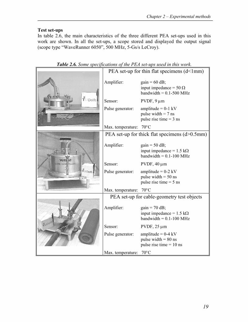
Test set-ups In table 2.6, the main characteristics of the three different PEA set-ups used in this work are shown. In all the set-ups, a scope stored and displayed the output signal (scope type “WaveRunner 6050”, 500 MHz, 5-Gs/s LeCroy).
Table 2.6. Some specifications of the PEA set-ups used in this work.
PEA set-up for thin flat specimens (d<1mm) Amplifier: gain = 60 dB; input impedance = 50 Ω bandwidth = 0.1-500 MHz
Sensor: PVDF, 9 µm
Pulse generator: amplitude = 0-1 kV pulse width = 7 ns pulse rise time = 3 ns
Max. temperature: 70°C
PEA set-up for thick flat specimens (d>0.5mm) Amplifier: gain = 50 dB; input impedance = 1.5 kΩ bandwidth = 0.1-100 MHz
Sensor: PVDF, 40 µm
Pulse generator: amplitude = 0-2 kV pulse width = 50 ns pulse rise time = 5 ns
Max. temperature: 70°C
PEA set-up for cable-geometry test objects Amplifier: gain = 70 dB; input impedance = 1.5 kΩ bandwidth = 0.1-100 MHz
Sensor: PVDF, 25 µm
Pulse generator: amplitude = 0-4 kV pulse width = 80 ns pulse rise time = 10 ns
Max. temperature: 70°C
Chapter 2 – Experimental methods
20
2.3.3. PEA method for multi-dielectric test objects Recently, the PEA method has been applied also to laminar test objects composed of two or more layers of different dielectrics (multi-dielectrics). Hitherto, several kinds of multi-dielectrics have been tested by means of the PEA method, e.g. [16, 17, 20, 21, 35, 79, 95, 101, 107, 139, 140, 145, 147]. Nevertheless, only little attention has been paid to the fact that, generally, the PEA method does not directly provide the space charge distribution within the test specimen if the test specimen is composed of different insulation layers [17, 22, 25, 108, 148, 149]. There are two main reasons why the output signal of a PEA measurement does not directly correspond to the space charge distribution within a multi-dielectric. 1. In the PEA method, a pulsed voltage is applied across the insulation to be tested.
The pulse induces a transient mechanical stress within the multi-dielectric which initiates the acoustic signal to be detected. Assuming each layer of a multi-dielectric is electrically homogeneous, the electrically-induced transient mechanical stress is determined not only by the space charge distribution, but also by the different permittivities of each layer of the multi-dielectric. The main consequences of this fact are: - the shape of the space charge distribution within the test specimen is different
from the shape of the mechanical stress distribution induced by the pulsed voltage;
- a different calibration factor must be chosen for each layer of the multi-dielectric.
2. The PEA method is based on generation and propagation of acoustic waves. In the case of different acoustic properties of the materials in contact (acoustical mismatching), waves experience different generation, transmission and reflection coefficients. The main consequences of this fact are: - the shape of the detected acoustic signal is different from the shape of the stress
distribution within the multi-dielectric; - reflections can occur at the interfaces between two different materials, leading
to possible misjudgment of measurement results. Therefore, in order to correctly evaluate the space charge distribution in a multi-dielectric by means of PEA measurements, the relation between the detected acoustic signal and both location and magnitude of space charge must be known. To contribute to this discussion, the author studied the electro-acoustic phenomena occurring in a multi-dielectric tested by means of the PEA method. This is detailed explained in Appendix A, where the principle of the PEA technique is reviewed in case the test object is a multi-dielectric. Representation of space charge profiles for multi-dielectrics test objects In this thesis, the presented space charge patterns for multi-dielectrics do not represent the actual space charge distributions within the multi-dielectric. Instead, they represent the electrically-induced mechanical stress distributions calibrated in [C/m3]. If a proper
Chapter 2 – Experimental methods
21
calibration procedure is accomplished (see Appendix D), the space-charge-calibrated stress distribution provides a correct estimation of the space charge accumulated in the insulation bulk. At the electrode-dielectric interfaces and at the dielectric interface, the pattern provides a signal which is different from the actual space charge distribution, but more meaningful. In fact, the space-charge-calibrated pattern indicates the interface location and it suggests how the electric field is distributed across the multi-dielectric2. The EPR, the XLPE and the semicon used in this work have quite similar acoustic impedances (see Table A.1. in Appendix A). So, if not stated otherwise, reflection phenomena are neglected in the space charge patterns presented in this thesis. In fact, no clear reflected peaks could be identified in the patterns related to XLPE-EPR multi-dielectrics. 2.3.4. PEA method for cable geometry test objects A typical coaxial cable suitable for PEA measurements consists of inner conductor, inner semicon, insulation and outer semicon. The conductive earth screen is removed at the measuring location. In fact, at the measuring location, the outer semicon must be in contact to the measuring electrode of the PEA cell. The acoustic impedance of the semicon is usually very similar to that of the cable insulation. So, no reflections of acoustic waves occur at the semicon-insulation interface. The DC voltage is applied between the cable conductor and earth via a resistor. As detailed explained in Appendix B, there are several ways of injecting the pulsed voltage across the cable insulation at the measuring section. In this work, the pulsed voltage is injected across the measuring section via the outer screen of the cable, as shown in Figure 2.9. In this way, the cable itself acts as a decoupling capacitor. The cable is fixed to the PEA cell by means of a cable holder. This guarantees a good acoustic contact between outer semicon and measuring electrode (see Figure 2.10). The measuring electrode can be either flat or curved. The PEA system adopted in this investigation is provided with a flat measuring electrode, which allows performing measurements on cables of different sizes. As in the PEA method for flat specimens, the acoustic signal is collected by a piezoelectric sensor, amplified and displayed by a scope.
2 In the space-charge-calibrated stress distribution, a signal peak is present at the dielectric interface, also in the absence of space charge at that location. The variation of the interfacial peak magnitude from its initial value represents the accumulated charge at the interface. If the interfacial peak has the same polarity as that of the applied voltage, then the layer connected to earth is the most electrically-stressed layer. On the other hand, if the interfacial peak has polarity opposite to that of the applied voltage, then the layer connected to HV is the most electrically-stressed layer.
Chapter 2 – Experimental methods
22
Figure 2.9. Schematic representation of the cable configuration and test set-up for PEA measurements on cable-geometry test objects. Drawing not on scale.
Figure 2.10. Cross section of the cable and of the PEA cell at the measuring point.
Correction of the detected signal As in the case in which a flat object is tested, the signal detected on a cable geometry object results different from the space charge distribution. This is again due to the response of the measuring system, which is frequency dependent, and because the acoustic waves are attenuated and dispersed. In addition, because of the cylindrical geometry of the test object, the acoustic waves and the pulsed field are divergent. This has to be taken into account in order to obtain a correct space charge profile. For this reason, the geometrical factor Kg(r), which is derived in Appendix B, was applied to the unprocessed space charge waveforms.
Chapter 2 – Experimental methods
23
2.3.5. Space charge parameters Dynamic space charge distribution The basic outcome of a space charge measurement is the dynamic space charge distribution. The dynamic space charge distribution, ρ(x,t), represents the amount of charge per unit volume present within a test object as a function of position x and time t, see Figure 2.11. From this basic quantity, a number of derived quantities can be deduced. They can be used to evaluate and compare measurement results. Dynamic electric field distribution Figure 2.12 shows the dynamic electric field distribution, E(x,t), which represents the magnitude of the electric field present within a test object as a function of position and time. E(x,t) can be derived by solving equation (2.4), in which the dynamic space charge distribution has been introduced. (Equation (2.5) must be used to satisfy the boundary conditions).
Figure 2.12. 3D plot of the dynamic
electric field distribution E(x,t)
deduced from a space charge measurement
on a 4.5-mm thick cable. Applied voltage:
+90kV.
Figure 2.11. 3D plot of the dynamic
space charge distribution ρ(x,t)
deduced from a space charge measurement
on a 4.5-mm thick cable. Applied voltage:
+90 kV.
Chapter 2 – Experimental methods
24
Field enhancement factor The field enhancement caused by the space charge can be described by means of the field enhancement factor FE%. FE% represents the percentage with which the field strength is maximally increased by the space charge [78]. For a flat specimen, FE% is defined as:
1000
0max
%
dU
dU
EFE
−= (2.6)
where Emax is the maximum electric field present within a test object of thickness d and U0 is the applied voltage. In this thesis, the field enhancement factor for cylindrical test objects is used as a function of the radius, FE%(r):
( )
100)(0
0
%
dU
dU
rErFE
−= (2.7)
This is done because of in a cable the Laplacian field distribution is inversely proportional to the radius. So, for cylindrical test objects, FE%(r) represents the percentage with which the electric field differs from the average field U0/d, because of the geometry and because of the presence of space charge. As a consequence, when no space charge is present, FE%(r) is different from zero and becomes:
( )100)(
0
00
0%,
dU
dU
rErFE
−= (2.8)
where E0(r) indicates a Laplacian distribution of the electric field.
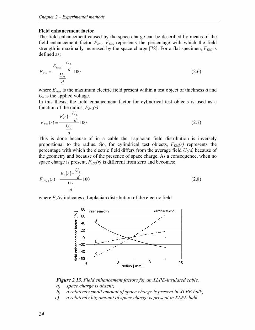
Figure 2.13. Field enhancement factors for an XLPE-insulated cable. a) space charge is absent; b) a relatively small amount of space charge is present in XLPE bulk;
c) a relatively big amount of space charge is present in XLPE bulk.
Chapter 2 – Experimental methods
25
In Figure 2.13, the field enhancement factor is plotted for a cable in which: (a) space charge is absent (Laplacian field); (b) a relatively small amount of space charge is present within the insulation bulk; (c) a relatively big amount of space charge is present within the insulation bulk. The figure shows that a situation in which space charge is present within a cable is not necessarily the worst situation with regard to the maximum field (case “b”). Space charge location and average charge Space charge can build up in several locations of the insulation. - Near the electrodes. Charge with the same polarity as that of the charge induced by
the applied voltage at the adjacent electrode is called homo-charge. The effect of homo-charge is to increase the electric field in the insulation bulk and to decrease the electric field near the electrodes. On the other hand, hetero-charge is space charge with polarity opposite to that of the charge induced by the applied voltage at the adjacent electrode. The effect of hetero-charge is to increase the electric field near the electrodes and to decrease the electric field in the insulation bulk.
- In the insulation bulk. Space charge can accumulate all over the insulation bulk. For instance, this happens when a temperature drop is present across the insulation. The polarity of the space charge in the bulk can be either the same as that of the applied voltage or opposite to that of the applied voltage. In the first case, the charge increases the electric field near the earth electrode and decreases the electric field near the HV electrode. In the second case, the charge increases the electric field near the HV electrode and decreases the electric field near the earth electrode.
- At dielectric interfaces. Generally, dielectric interfaces are favorite locations for space charge accumulation. Interfacial charge with the same polarity as that of the applied voltage increases the field in the insulation between the interface and the earth electrode and decreases the field in the insulation between the interface and the HV electrode. On the other hand, interfacial charge with the polarity opposite to that of the applied voltage increases the field in the insulation between the interface and the HV electrode and decreases the field in the insulation between the interface and the earth electrode.
- At the electrode-insulation interface. When a DC voltage is applied across the insulation, charges are present at both electrode-insulation interfaces. In addition, if space charge is present within the insulation, charges are induced at the electrode-insulation interfaces (those charges are often called mirror charges). So, the total charge at the electrode-dielectric interface is given by both the charges due to the applied voltage and the mirror charges.
The average charge density present in the insulation is defined as:
( ) dxxd
d
avg ∫=0
1 ρρ (2.9)
Induced charges at the electrodes are not included in (2.9). The average charge is mostly used for comparing different materials with regard to the accumulation of space charge, e.g. [115].
Chapter 2 – Experimental methods
26
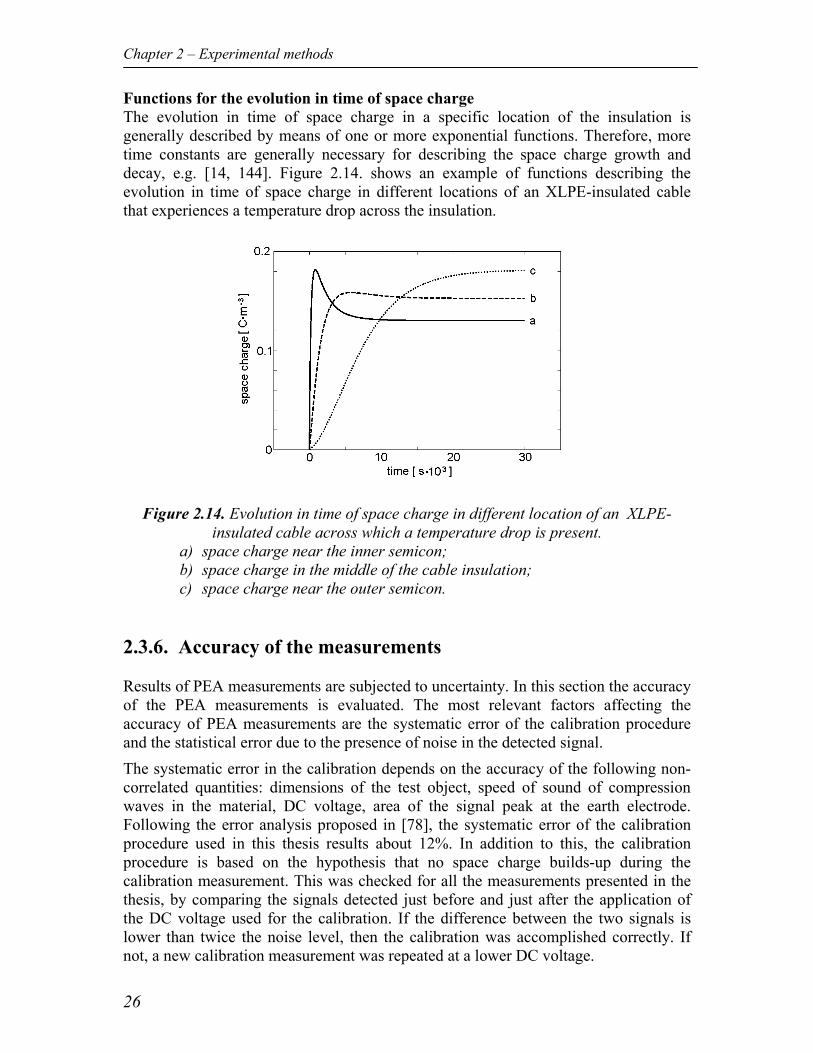
Functions for the evolution in time of space charge The evolution in time of space charge in a specific location of the insulation is generally described by means of one or more exponential functions. Therefore, more time constants are generally necessary for describing the space charge growth and decay, e.g. [14, 144]. Figure 2.14. shows an example of functions describing the evolution in time of space charge in different locations of an XLPE-insulated cable that experiences a temperature drop across the insulation.
Figure 2.14. Evolution in time of space charge in different location of an XLPE-insulated cable across which a temperature drop is present.
a) space charge near the inner semicon; b) space charge in the middle of the cable insulation; c) space charge near the outer semicon.
2.3.6. Accuracy of the measurements Results of PEA measurements are subjected to uncertainty. In this section the accuracy of the PEA measurements is evaluated. The most relevant factors affecting the accuracy of PEA measurements are the systematic error of the calibration procedure and the statistical error due to the presence of noise in the detected signal. The systematic error in the calibration depends on the accuracy of the following non-correlated quantities: dimensions of the test object, speed of sound of compression waves in the material, DC voltage, area of the signal peak at the earth electrode. Following the error analysis proposed in [78], the systematic error of the calibration procedure used in this thesis results about 12%. In addition to this, the calibration procedure is based on the hypothesis that no space charge builds-up during the calibration measurement. This was checked for all the measurements presented in the thesis, by comparing the signals detected just before and just after the application of the DC voltage used for the calibration. If the difference between the two signals is lower than twice the noise level, then the calibration was accomplished correctly. If not, a new calibration measurement was repeated at a lower DC voltage.
Chapter 2 – Experimental methods
27
The presence of noise in the signal is the origin of a statistical error. Noise is introduced in the measuring system at the following locations: at the sensor, at the sensor-amplifier connection, in the amplifiers and in the cables bringing the signal into the scope. To reduce the noise level, the signal saved at the scope was the average of 1000 sweeps, i.e. the noise level was decreased approximately of a factor 32. This ensured a noise/signal ratio of a few percent. Besides the noise, electro-magnetic disturbances, which are generated by the firing of the pulse, are also present in the measured signal. However, since those disturbances are constant in time, they can be detected before starting a measurement and then they can be subtracted from the measured signal. In conclusion, due to both systematic error and statistical error, the uncertainty of our measurement results is about 15%.
2.4. Test conditions 2.4.1. Temperature conditions Electrical behavior of polymeric materials strongly depends on temperature. In particular, in case of polymeric-type cable systems, the radial electric stress profile can be critically affected by the temperature distribution across the insulation. For these reasons, the radial temperature distribution is discussed in the following for the insulation of a cable system. Steady state Because of joule losses in its inner conductor, a loaded cable system is heated3. This generates a temperature drop between the inner conductor and the outer shield. The steady-state temperature distribution across the cable insulation can be obtained by means of equation (2.10):
( )( )
−
−=
in
out
outinin
a
rr
TTrr
TrTln
ln (2.10)
In the cable accessories the insulation is composed of two different dielectrics arranged in a coaxial lay out. Then, the temperature will be distributed not only according to the specific geometry of the insulation, but also according to the thermal conductivity k of each material. So, the temperature distribution is:
3Insulation losses, which are due to leakage currents through the insulation bulk, are also a source of heat. However, in case of polymer-insulated cables, the insulation losses are usually negligible if compared to the joule losses in the cable conductor.
Chapter 2 – Experimental methods
28
( )( )
out
inout
in
outinin
in
kk
rr
rr
TTrr
TrT
+
−
−=
int
int lnln
ln intrrrin << (2.11)
( )( )
+
−
+=
int
int lnln
ln
rr
kk
rr
TTr
r
TrTout
in
out
in
outinout
out outrrr <<int (2.12)
The symbols adopted in (2.10), (2.11) and (2.12) have the following meaning: r = generic radius rin = inner conductor radius rout = outer screen radius rint = interface radius T(r) = temperature at the generic radius r Tin = temperature at the inner conductor Tout = temperature at the outer screen kin = thermal conductivity innermost dielectric kout = thermal conductivity outermost dielectric Equations (2.11) and (2.12) assume that the interfacial contact between the two dielectrics does not affect the temperature distribution. This may be considered true if the dielectric interface is chemically bonded (e.g. in case of cross-linked interface). However, in case of a not-bonded interface, a contact thermal resistance per unit of length (Rth,c, expressed in K m W-1) needs to be taken into account. The parameter Rth,c is mainly affected by the roughness of the surfaces in contact, by the contact pressure and by the presence of lubricants at the interface [131]. Because of the contact thermal resistance, the two different media in contact experience different temperatures at the interface. The value of the interfacial temperatures, Tint,in and Tint,out in Figure 2.15, can be deduced from the following equations:
( )( )
cthinout
inout
in
outinin
in
Rkkk
rr
rr
TTrr
TrT
,int
int 2lnln
ln
π+
+
−
−= intrrrin << (2.13)
( )( )
cthoutout
in
out
in
outinout
out
Rkrr
kk
rr
TTr
r
TrT
,int
int 2lnln
ln
π+
+
−
+= outrrr <<int (2.14)
Chapter 2 – Experimental methods
29
Figure 2.15. a) Radial temperature distribution in the insulation of a loaded cable.
b) Radial temperature distribution in the insulation of a loaded cable accessory. Thermal transient When a load is applied to a cable system, which was in a uniform temperature condition, a thermal transient starts. The temperature distribution across the insulation as function of time can be calculated by means of Fourier’s heat diffusion equation:
δδ cQT
ck
tT
+
∇⋅∇=
∂∂ (2.15)
where c and δ are respectively the specific heat and the density of the materials being studied, whereas Q represents the heat losses per unit of volume. In Chapter 4, equation (2.15) is used for the numerical calculation of the dynamic radial distribution of the temperature in cable systems. The duration of the thermal transient, experienced by the cable insulation, can be estimated by means of the thermal time constant τth. The thermal transient can be considered finished after a time equal to 5τth. The thermal time constant is given by:
ththth CR=τ (2.16)
where Rth and Cth are respectively the thermal resistance per unit of length and the heat capacitance for unit of length of the thermal system composed by the cable and the environment surrounding the cable. For the cable insulation only, Rth and Cth are:
=
in
outcableth r
rk
R ln2
1, π
(2.17)
( )22, inoutcableth rrcC −= δπ (2.18)
a b
Chapter 2 – Experimental methods
30
whereas for the insulation of the cable accessory:
+
=out
out
in
inaccessoryth k
rr
krr
R int
int
,
lnln
21π
(2.19)
( ) ( )[ ]2int
222int, rrcrrcC outoutoutinininaccessoryth −+−= δδπ (2.20)
It is to be noted that the thermal time constant of the insulation depends on the material properties, on the geometry and on the cable dimensions (the thicker the cable insulation, the longer the thermal transient). In Table 2.7, the thermal time constant is calculated for different types of cables. In practice, the thermal transient for the whole thermal system will depend the cable insulation, on the layers of material surrounding the insulation and on the thermal properties of the environment in which the cable is deployed [62]. Therefore, the thermal transient of a cable system in service is generally (much) longer than that of the cable insulation reported in Table 2.7.
Table 2.7. Estimation of the thermal time constant of the cable insulation. rin
[mm] rout
[mm]k
[W m-1 K-1] c
[J K-1 kg] δ
[kg m-3] τth [s]
XLPE mini-cable 1.9 3.4 0.3 1900 920 15 XLPE MV-size
cable 4.5 9 0.3 1900 920 120
XLPE HV-size cable
23 42 0.3 1900 920 2200
Mass-impregnated HV-size cable
23 42 0.18 1400 ÷ 1500
800 ÷ 1100
2300÷3400
Induced-current heating technique In order to obtain the same temperature conditions a cable insulation experiences in practice, the induced-current heating technique was used in this study. A schematic diagram of the induced-current heating technique is represented in Figure 2.16. By means of a current transformer, an AC current is induced in the conductor of the cable object of the measurement, which is connected in a loop. In this way conductor losses are produced and a temperature drop is present between inner conductor and outer shield of the cable. The temperature and the current in the cable were continuously monitored during the tests. This was done on a dummy loop with the same characteristics as the cable object of the measurement. Two temperature sensors were placed on the dummy loop, the first at the conductor and the second at the outer semicon.
Chapter 2 – Experimental methods
31
Figure 2.16. Schematic representation of the induced-current heating technique.
Drawing not on scale.
Temperature values adopted in the present work In the present work, the laboratory investigations were performed at several temperature conditions. Flat specimens were tested at several uniform and constant temperatures, between 20°C and 60 °C. Measurements on dual-dielectric cables, MV-size cables and MV-size models of cable joints were performed at room temperature and when a temperature drop was present within the insulation. The temperature at the inner conductor was kept between 20 °C and 65 °C, whereas the temperature at the outer semicon was kept between 20 °C and 45 °C. In all tests, the measurements were started only after the temperature sensors indicated that a stable temperature distribution was reached. 2.4.2. Electrical conditions During its operation, the insulation of an HVDC cable system experiences several distributions of the electric stress. For instance, the electric field distribution across the dielectric is different if the voltage has just been applied or the voltage has been present for several hours. In the present work, the laboratory investigations were performed at several electrical conditions. They were chosen in order to test the insulation under stresses as close as possible to those an HVDC polymeric-type cable experiences in the field. DC voltages only were used: neither impulse nor AC voltages were taken into account in this work. For this reason, the following conditions were adopted. - Electric field. The specimens were stressed at an average electric field U0/d
between 5 kV/mm and 30 kV/mm.
Chapter 2 – Experimental methods
32
- Voltage polarity. Both positive and negative voltages were applied at the test specimens. Moreover, in some of the tests, the polarity reversal condition was included.
- Polarization time. Generally, a depolarization time of 2 104 s (5.6 h) was used. However, in some of the tests, the voltage was applied for a much longer time, up to 1.2 106 s (2 weeks).
- Depolarization time. Generally, a polarization time of 3600 s (1 h) was used. However, some of the tests lasted for a much longer time after the removal of the voltage and the short-circuiting of the specimen, up to 1.2 106 s (2 weeks).
Chapter 3 – Experimental observation of space charge and electric field dynamics
33
3. Experimental observation of space charge and electric field dynamics
This chapter summarizes the main results of the experimental work performed in the framework of this thesis. In Section 3.1 the results of conduction current measurements are presented and discussed. Conduction current measurements were performed in order to feed the numerical calculation presented in Chapter 4. In fact, the input parameters of the calculation were chosen to match the values of the insulation conductivity deduced from the conduction current measurements. In this way, the conduction mechanisms experimentally identified are taken into account in the numerical calculation. Space charge measurements can give information about charging phenomena occurring in actual HVDC polymeric cables. However, measurements should be performed on test specimens resembling as much as possible the actual cables, in order to provide results that are representative for the actual situation. Moreover, the test conditions adopted for the measurements should be very similar to the conditions a cable experiences when operating in practice. In the literature a vast amount of publications is available about experimental space charge investigations on thin flat specimens. However, only a limited number of publications discusses results obtained from measurements on full-size models of DC cables. To fill this lack of empirical knowledge and to provide a better understanding about space charge phenomena on actual DC cables, we performed space charge measurements on MV-size DC cables. The condition in which a temperature drop is present across the cable insulation is considered along with the situation in which the polarity of the applied DC voltage is inverted. This is discussed in Section 3.3. Dielectric interfaces encountered in cable joints and terminations are generally regarded as the weakest parts of a DC cable system. However, little attention only has been given in the literature to the polarization phenomena occurring at dielectric interfaces. Therefore, we performed space charge measurements on XLPE-EPR interfaces of increasing complexity, i.e. flat specimens, dual-dielectric mini-cables and MV-size models of cable joints. The results of space charge measurements performed on those three different types of dielectric interfaces are respectively analyzed in Section 3.2, 3.4 and 3.5. Finally, some conclusions are drawn in Section 3.6.
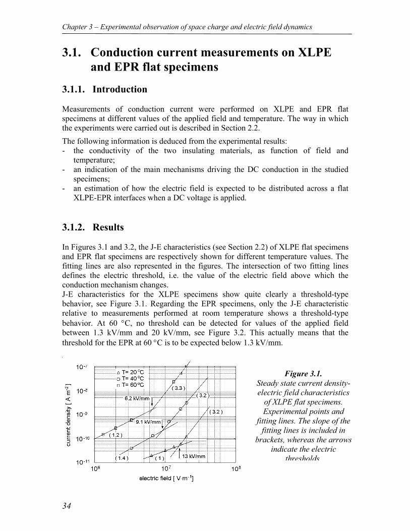
Chapter 3 – Experimental observation of space charge and electric field dynamics
34
3.1. Conduction current measurements on XLPE and EPR flat specimens
3.1.1. Introduction Measurements of conduction current were performed on XLPE and EPR flat specimens at different values of the applied field and temperature. The way in which the experiments were carried out is described in Section 2.2. The following information is deduced from the experimental results: - the conductivity of the two insulating materials, as function of field and
temperature; - an indication of the main mechanisms driving the DC conduction in the studied
specimens; - an estimation of how the electric field is expected to be distributed across a flat
XLPE-EPR interfaces when a DC voltage is applied. 3.1.2. Results In Figures 3.1 and 3.2, the J-E characteristics (see Section 2.2) of XLPE flat specimens and EPR flat specimens are respectively shown for different temperature values. The fitting lines are also represented in the figures. The intersection of two fitting lines defines the electric threshold, i.e. the value of the electric field above which the conduction mechanism changes. J-E characteristics for the XLPE specimens show quite clearly a threshold-type behavior, see Figure 3.1. Regarding the EPR specimens, only the J-E characteristic relative to measurements performed at room temperature shows a threshold-type behavior. At 60 °C, no threshold can be detected for values of the applied field between 1.3 kV/mm and 20 kV/mm, see Figure 3.2. This actually means that the threshold for the EPR at 60 °C is to be expected below 1.3 kV/mm.
Figure 3.1. Steady state current density-electric field characteristics
of XLPE flat specimens. Experimental points and
fitting lines. The slope of the fitting lines is included in
brackets, whereas the arrows indicate the electric
thresholds.
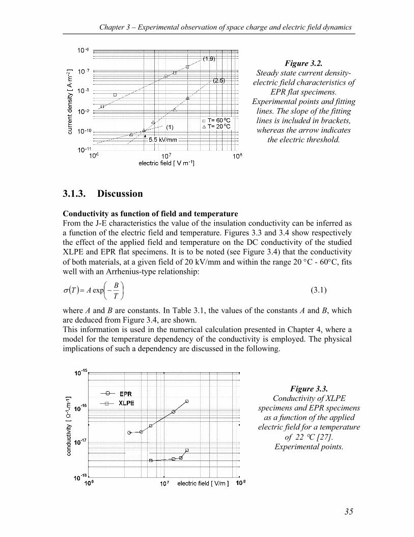
Chapter 3 – Experimental observation of space charge and electric field dynamics
35
3.1.3. Discussion Conductivity as function of field and temperature From the J-E characteristics the value of the insulation conductivity can be inferred as a function of the electric field and temperature. Figures 3.3 and 3.4 show respectively the effect of the applied field and temperature on the DC conductivity of the studied XLPE and EPR flat specimens. It is to be noted (see Figure 3.4) that the conductivity of both materials, at a given field of 20 kV/mm and within the range 20 °C - 60°C, fits well with an Arrhenius-type relationship:
( )
−=
TBAT expσ (3.1)
where A and B are constants. In Table 3.1, the values of the constants A and B, which are deduced from Figure 3.4, are shown. This information is used in the numerical calculation presented in Chapter 4, where a model for the temperature dependency of the conductivity is employed. The physical implications of such a dependency are discussed in the following.
Figure 3.2. Steady state current density-
electric field characteristics of EPR flat specimens.
Experimental points and fitting lines. The slope of the fitting lines is included in brackets, whereas the arrow indicates
the electric threshold.
Figure 3.3. Conductivity of XLPE
specimens and EPR specimens as a function of the applied
electric field for a temperature of 22 °C [27].
Experimental points.
Chapter 3 – Experimental observation of space charge and electric field dynamics
36
Table 3.1. A and B coefficients as defined in Equation (3.1) for the conductivity of the studied XLPE and EPR specimens.
MATERIAL A [Ω-1⋅m-1] B [K] XLPE 242 106 17.4 103
EPR 1.54 10.9 103
Conduction mechanisms According to the theory of electric conduction in solid dielectrics (e.g. [45, 124]), a log-log plot of the steady-state J-E characteristic can show the transition between different conduction mechanisms. In fact, if the slope of the characteristic is ≈1, ohmic conduction is believed to be the dominant mechanism. On the other hand, a slope > 1 indicates that a conduction mechanism is active in which the current density is more than proportional to the applied field. In the first case, the conductivity of the insulation is independent from the applied field. In the latter, the conductivity is field dependent. A transition between two different types of conduction mechanisms was observed for XLPE specimens and for the EPR specimens at room temperature. Similarly to what is reported in the literature [114], the values of electric threshold experimentally determined for XLPE fit well with an Arrhenius-type relationship within the range 20°C - 60°C, as shown in Figure 3.5. EPR specimens at 60 °C have shown only a conduction mechanism in which the current density is more than proportional to the applied field for fields between 1.3 kV/mm and 20 kV/mm. Both types of specimens show an Arrhenius-type temperature dependency of the conductivity. A trap-limited mobility interprets this phenomenon. Because of the presence of trap states within the band gap of dielectrics, not all the charge carriers contribute to the conduction. However, according to the trap-limited model [45], the number of effective charge carriers, which is proportional to the mobility and then to the
Figure 3.4. Conductivity of XLPE specimens and EPR
specimens vs. reciprocal absolute temperature, for an applied field of
20 kV/mm [27]. Experimental points and
fitting lines.
Chapter 3 – Experimental observation of space charge and electric field dynamics
37
conductivity, is a function of temperature and an Arrhenius-type model describes the physical phenomenon. So, the trap-limited mobility is believed to be the reason for the observed dependency of the conductivity on temperature.
Effect of conductivity on interfacial charge and electric field in flat XLPE-EPR interfaces Based on the results of conduction current measurements performed on single flat specimens, the electrical behavior of a flat XLPE-EPR interfaces is discussed in the following. According to the Maxwell-Wagner (MW) theory for the interfacial polarization [84, 150], charge accumulates at the interface between two dielectrics “A” and “B” if a discontinuity in the ratio between conductivity and permittivity exists (i.e. if ∇(σ/ε)≠0). The exponential growth of the MW interfacial charge, which is related to the transition between capacitively-distributed field to resistively-distributed field, is described by a time constant τ:
ABBA
ABBAMW dd
ddσσεετ
++
= (3.2)
where dA, dB are the thickness of the two dielectrics, σA, σB the conductivities and εA, εB the permittivities. Equation (3.2) can be used for the calculation of the MW time constant of the specimen combinations studied in this work, as shown in Figure 3.6. Since the conductivity of the XLPE and EPR specimens is much more affected by the temperature rather than by the applied field, the time constant is estimated assuming that a constant field of 20 kV/mm is present in each layer of the combination. (The effect of the field dependency of the conductivity on accumulation of interfacial charge will be considered in Chapter 4). The MW time constant shows an Arrhenius-type dependency with the temperature. This is due to the fact that the MW transition is practically driven by the conductivity of the most conductive layer of the combination (EPR in the studied case), which follows also an Arrhenius-type behavior. In fact, comparing the charts in Figures 3.4 and 3.6, the slope of the MW constant is
Figure 3.5. Electric threshold for XLPE flat specimens vs. reciprocal
absolute temperature. Experimental points (as
derived from J-E plots) and fitting line.
Arrhenius coefficients: A=11.5 103 V⋅m-1; B=-2.05 103 K.
Chapter 3 – Experimental observation of space charge and electric field dynamics
38
comparable with the slope of the EPR conductivity (Bτ,MW = 11.3 103 K; Bσ,EPR = 10.9 103 K).
During the transition time (transition time ≈ 5τMW), the electric field distribution in the two materials can drastically change, even if we assume that no space charge accumulates in the insulation bulk. For instance, from Figure 3.4, we can see that the lower the temperature, the larger the relative difference between the conductivity of EPR and that of XLPE. This means that the resistively-distributed field across an XLPE/EPR combination is almost entirely applied on the XLPE layer at room temperature. However, in order to reach this situation a DC voltage must be applied for a relatively long time (5τMW ≈ 400 h). On the other hand, at higher temperatures (T > 70 °C), the conductivity of XLPE is expected to be larger than that of EPR. In this case, the electric field will be mostly distributed across the EPR layer. In this situation, a relatively short transition time is expected (5τMW ≈ 2.5 h).
3.1.4. Summary and conclusions From the conduction current measurements performed on XLPE and EPR flat specimens, the following can be concluded. - Both the conductivities of XLPE and EPR specimens strongly depend on applied
field and temperature. In particular, an Arrhenius-type dependency of conductivity on temperature is found. This let us assume that a trap-limited mobility model is valid for the studied specimens (when the field is around 20 kV/mm).
- J-E characteristics of XLPE specimens show the presence of an electric threshold. The temperature dependency of the electric threshold for the XLPE (within a temperature range 20°C - 60°C) can be described by using an Arrhenius-type relationship.
Figure 3.6. Maxwell-Wagner time constant of a combination of XLPE/EPR
flat specimens vs. reciprocal absolute temperature, when an external field of 20 kV/mm is
applied [27]. Calculated points and fitting line.
Arrhenius coefficients: A=6.94 10-12 s; B=-11.3 103 K.
Chapter 3 – Experimental observation of space charge and electric field dynamics
39
- At room temperature, the J-E characteristic of EPR specimens shows the presence of an electric threshold. At 60°C, no threshold can be inferred for fields between 1.3 kV/mm and 20 kV/mm and the only conduction mechanism active is characterized by a current density which is more than proportional to the applied field.
- On the basis of the Maxwell-Wagner theory, results obtained from conduction current measurements on single flat specimens can be used for describing the electrical behavior of a combination of flat specimens. The MW time constant can be estimated for XLPE-EPR combination. For the studied specimens, a strong temperature dependency of the MW time constant is found (also in this case of the Arrhenius type).
3.2. Space charge measurements on XLPE-EPR flat interfaces
3.2.1. Introduction Space charge and electric field distributions were investigated in combinations of XLPE-EPR flat specimens. Neither lubricants nor specific chemical treatments were applied at the dielectric interface of the flat specimens. The DC voltage was applied across the specimens as shown in Figure 3.7. A typical voltage-on space charge profile, measured immediately after the application of the DC voltage on an XLPE-EPR specimen combination, is depicted in Figure 3.8.a. In Figure 3.8.b, the corresponding electric field distribution is represented. In addition to the peaks at both the electrodes, a peak is present at the dielectric interface in the space charge profile. This peak is due to the discontinuity of the permittivity at the dielectric interface. A variation of the peak magnitude from its initial value indicates that interfacial charge has been accumulated. A detailed explanation for this phenomenon is given in Appendix A.
Figure 3.7. XLPE-EPR flat specimens as tested in the PEA set-up.
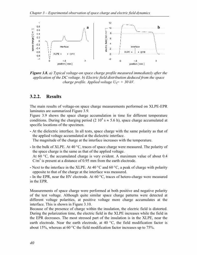
Chapter 3 – Experimental observation of space charge and electric field dynamics
40
Figure 3.8. a) Typical voltage-on space charge profile measured immediately after the application of the DC voltage. b) Electric field distribution deduced from the space
charge profile. Applied voltage U0= + 30 kV. 3.2.2. Results The main results of voltage-on space charge measurements performed on XLPE-EPR laminates are summarized Figure 3.9. Figure 3.9 shows the space charge accumulation in time for different temperature conditions. During the charging period (2 104 s ≈ 5.6 h), space charge accumulated at specific locations of the specimen. - At the dielectric interface. In all tests, space charge with the same polarity as that of
the applied voltage accumulated at the dielectric interface. The magnitude of the charge at the interface increases with the temperature.
- In the bulk of XLPE. At 40 °C, traces of space charge were measured. The polarity of the space charge is the same as that of the applied voltage. At 60 °C, the accumulated charge is very evident. A maximum value of about 0.4 C/m3 is present at a distance of 0.95 mm from the earth electrode.
- Next to the interface in the XLPE. At 40 °C and 60 °C, a peak of charge with polarity opposite to that of the charge at the interface was measured.
- In the EPR, near the HV electrode. At 60 °C, traces of hetero-charge were measured in the EPR. Measurements of space charge were performed at both positive and negative polarity of the test voltage. Although quite similar space charge patterns were detected at different voltage polarities, at positive voltage more charge accumulates at the interface. This is shown in Figure 3.10. Because of the presence of charge within the insulation, the electric field is distorted. During the polarization time, the electric field in the XLPE increases while the field in the EPR decreases. The most stressed part of the insulation is in the XLPE, near the earth electrode. Near the earth electrode, at 40 °C, the field modification factor is about 15%, whereas at 60 °C the field modification factor increases up to 75%.
a b
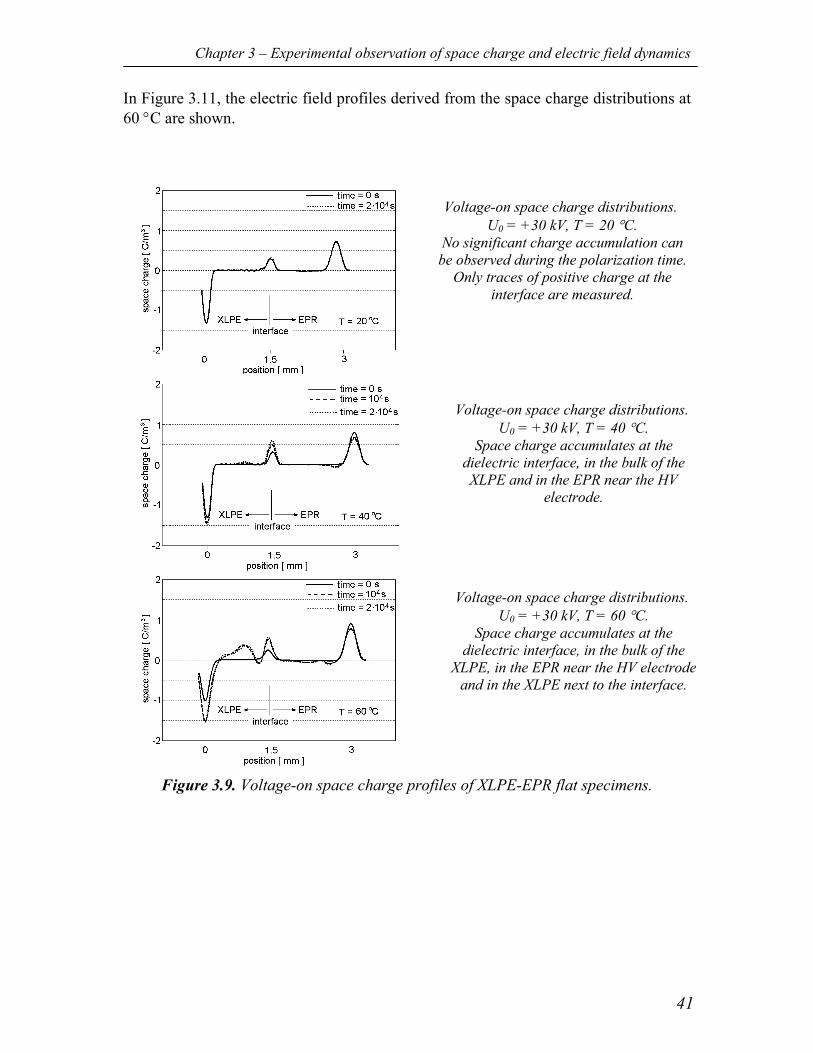
Chapter 3 – Experimental observation of space charge and electric field dynamics
41
In Figure 3.11, the electric field profiles derived from the space charge distributions at 60 °C are shown.
Figure 3.9. Voltage-on space charge profiles of XLPE-EPR flat specimens.
Voltage-on space charge distributions. U0 = +30 kV, T = 20 °C.
No significant charge accumulation can be observed during the polarization time.
Only traces of positive charge at the interface are measured.
Voltage-on space charge distributions. U0 = +30 kV, T = 40 °C.
Space charge accumulates at the dielectric interface, in the bulk of the XLPE and in the EPR near the HV
electrode.
Voltage-on space charge distributions. U0 = +30 kV, T = 60 °C.
Space charge accumulates at the dielectric interface, in the bulk of the
XLPE, in the EPR near the HV electrode and in the XLPE next to the interface.
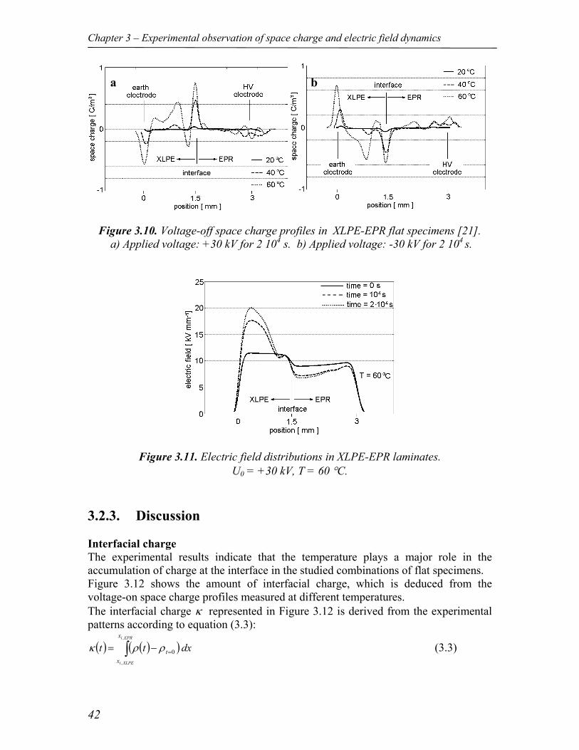
Chapter 3 – Experimental observation of space charge and electric field dynamics
42
Figure 3.10. Voltage-off space charge profiles in XLPE-EPR flat specimens [21]. a) Applied voltage: +30 kV for 2 104 s. b) Applied voltage: -30 kV for 2 104 s.
Figure 3.11. Electric field distributions in XLPE-EPR laminates. U0 = +30 kV, T = 60 °C.
3.2.3. Discussion Interfacial charge The experimental results indicate that the temperature plays a major role in the accumulation of charge at the interface in the studied combinations of flat specimens. Figure 3.12 shows the amount of interfacial charge, which is deduced from the voltage-on space charge profiles measured at different temperatures. The interfacial charge κ represented in Figure 3.12 is derived from the experimental patterns according to equation (3.3):
( ) ( )( )∫ =−=EPRi
XLPEi
x
xt dxtt
,
,
0ρρκ (3.3)
a b
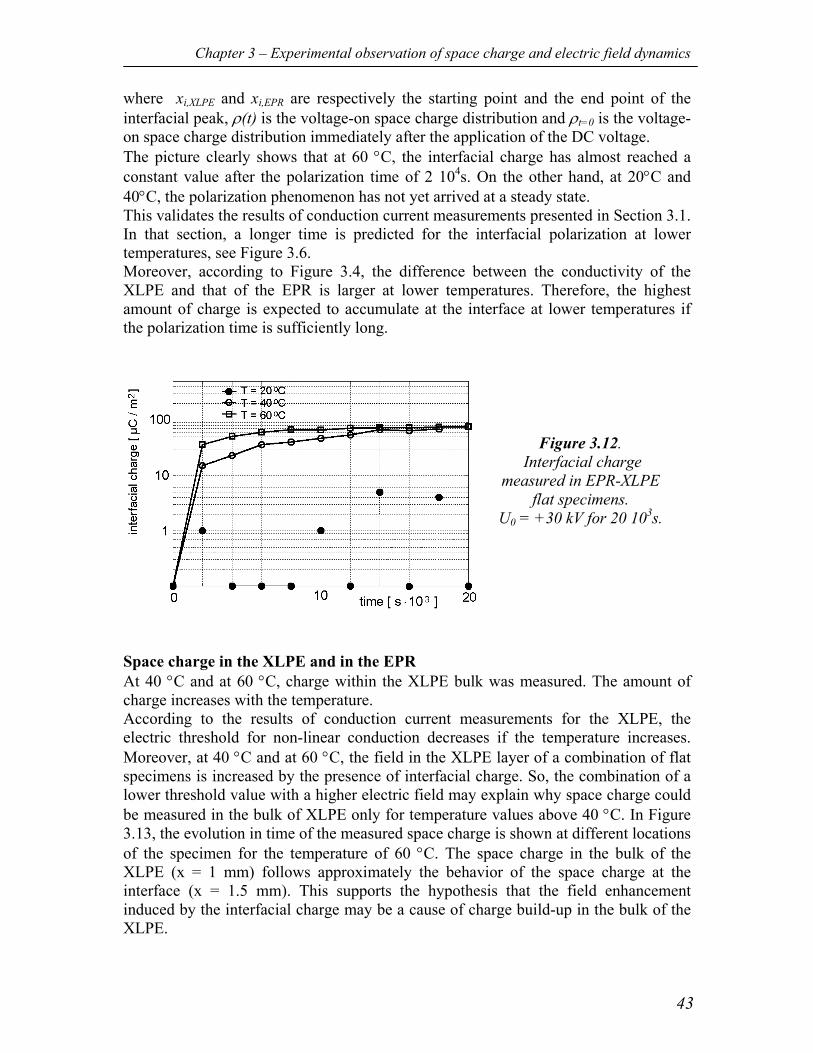
Chapter 3 – Experimental observation of space charge and electric field dynamics
43
where xi,XLPE and xi,EPR are respectively the starting point and the end point of the interfacial peak, ρ(t) is the voltage-on space charge distribution and ρt=0 is the voltage-on space charge distribution immediately after the application of the DC voltage. The picture clearly shows that at 60 °C, the interfacial charge has almost reached a constant value after the polarization time of 2 104s. On the other hand, at 20°C and 40°C, the polarization phenomenon has not yet arrived at a steady state. This validates the results of conduction current measurements presented in Section 3.1. In that section, a longer time is predicted for the interfacial polarization at lower temperatures, see Figure 3.6. Moreover, according to Figure 3.4, the difference between the conductivity of the XLPE and that of the EPR is larger at lower temperatures. Therefore, the highest amount of charge is expected to accumulate at the interface at lower temperatures if the polarization time is sufficiently long.
Space charge in the XLPE and in the EPR At 40 °C and at 60 °C, charge within the XLPE bulk was measured. The amount of charge increases with the temperature. According to the results of conduction current measurements for the XLPE, the electric threshold for non-linear conduction decreases if the temperature increases. Moreover, at 40 °C and at 60 °C, the field in the XLPE layer of a combination of flat specimens is increased by the presence of interfacial charge. So, the combination of a lower threshold value with a higher electric field may explain why space charge could be measured in the bulk of XLPE only for temperature values above 40 °C. In Figure 3.13, the evolution in time of the measured space charge is shown at different locations of the specimen for the temperature of 60 °C. The space charge in the bulk of the XLPE (x = 1 mm) follows approximately the behavior of the space charge at the interface (x = 1.5 mm). This supports the hypothesis that the field enhancement induced by the interfacial charge may be a cause of charge build-up in the bulk of the XLPE.
Figure 3.12. Interfacial charge
measured in EPR-XLPE flat specimens.
U0 = +30 kV for 20 103s.
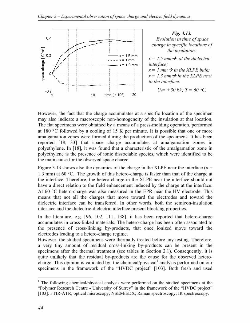
Chapter 3 – Experimental observation of space charge and electric field dynamics
44
However, the fact that the charge accumulates at a specific location of the specimen may also indicate a macroscopic non-homogeneity of the insulation at that location. The flat specimens were obtained by a means of a press-molding operation, performed at 180 °C followed by a cooling of 15 K per minute. It is possible that one or more amalgamation zones were formed during the production of the specimens. It has been reported [18, 33] that space charge accumulates at amalgamation zones in polyethylene. In [18], it was found that a characteristic of the amalgamation zone in polyethylene is the presence of ionic dissociable species, which were identified to be the main cause for the observed space charge. Figure 3.13 shows also the dynamics of the charge in the XLPE near the interface (x = 1.3 mm) at 60 °C. The growth of this hetero-charge is faster than that of the charge at the interface. Therefore, the hetero-charge in the XLPE near the interface should not have a direct relation to the field enhancement induced by the charge at the interface. At 60 °C hetero-charge was also measured in the EPR near the HV electrode. This means that not all the charges that move toward the electrodes and toward the dielectric interface can be transferred. In other words, both the semicon-insulation interface and the dielectric-dielectric interface present blocking properties. In the literature, e.g. [96, 102, 111, 138], it has been reported that hetero-charge accumulates in cross-linked materials. The hetero-charge has been often associated to the presence of cross-linking by-products, that once ionized move toward the electrodes leading to a hetero-charge regime. However, the studied specimens were thermally treated before any testing. Therefore, a very tiny amount of residual cross-linking by-products can be present in the specimens after the thermal treatment (see tables in Section 2.1). Consequently, it is quite unlikely that the residual by-products are the cause for the observed hetero-charge. This opinion is validated by the chemical/physical1 analysis performed on our specimens in the framework of the “HVDC project” [103]. Both fresh and used
1 The following chemical/physical analysis were performed on the studied specimens at the “Polymer Research Centre - University of Surrey” in the framework of the “HVDC project” [103]: FTIR-ATR; optical microscopy; NSEM/EDX; Raman spectroscopy; IR spectroscopy.
Fig. 3.13. Evolution in time of space
charge in specific locations of the insulation:
x = 1.5 mm at the dielectric interface; x = 1 mm in the XLPE bulk; x = 1.3 mm in the XLPE next to the interface.
U0= +30 kV; T = 60 °C.
Chapter 3 – Experimental observation of space charge and electric field dynamics
45
specimens were analyzed. No evidence of migrating species that correlate with ionic conduction were found. A different explanation, which considers charges of electronic nature can be speculated for the observed charging phenomena. Depending on the temperature, some shallow traps may be present in the trap distribution. As a consequence, charge carriers with a relatively high mobility would contribute to the conduction. They would move quickly to the electrodes and to the dielectric interface, being blocked. This could explain why the hetero-charge accumulation is faster than the accumulation of interfacial charge and why it is observed at the higher temperatures only. 3.2.4. Summary and conclusions Space charge measurements on XLPE-EPR flat interfaces showed the following main results. - Space charge with the same polarity as that of the applied voltage accumulates at the
interface between XLPE and EPR. Since the measurements did not last long enough for the charging process at lower temperatures to finish, the highest amount of interfacial charge was measured at the higher temperature, situation in which a faster charge build-up occurs. However, it is believed that if the measuring time is increased, the higher amount of charge will be seen at the lower temperature, as predicted by the results of conduction current measurements.
- The interfacial charge modifies the field distribution: the field increases in the XLPE and decreases in the EPR.
- At the temperatures of 40 °C and 60 °C, space charge accumulates in the XLPE bulk. Two hypotheses were formulated for explaining the observed phenomenon. Firstly, the space charge accumulation may have been triggered by the combined effect of the lower value that the electric threshold assumes at higher temperatures and the increase of the field in the XLPE when interfacial charge is present. Secondly, amalgamation zones could have been present within the specimens because of their production process, leading to favourite regions for space charge accumulation.
- At 60 °C, hetero-charge accumulates in both XLPE and EPR. The blocking properties of the semicon-dielectric interface and of the dielectric-dielectric interface are assumed to be the cause for the observed hetero-charge.
- Measurements performed at different voltage polarity do not show perfectly symmetric patterns. In fact, more interfacial charge was measured at positive voltage polarity.
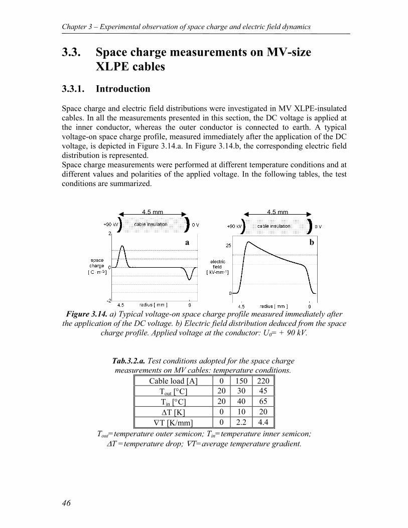
Chapter 3 – Experimental observation of space charge and electric field dynamics
46
3.3. Space charge measurements on MV-size XLPE cables
3.3.1. Introduction Space charge and electric field distributions were investigated in MV XLPE-insulated cables. In all the measurements presented in this section, the DC voltage is applied at the inner conductor, whereas the outer conductor is connected to earth. A typical voltage-on space charge profile, measured immediately after the application of the DC voltage, is depicted in Figure 3.14.a. In Figure 3.14.b, the corresponding electric field distribution is represented. Space charge measurements were performed at different temperature conditions and at different values and polarities of the applied voltage. In the following tables, the test conditions are summarized.
Figure 3.14. a) Typical voltage-on space charge profile measured immediately after
the application of the DC voltage. b) Electric field distribution deduced from the space charge profile. Applied voltage at the conductor: U0= + 90 kV.
Tab.3.2.a. Test conditions adopted for the space charge measurements on MV cables: temperature conditions.
Cable load [A] 0 150 220 Tout [°C] 20 30 45 Tin [°C] 20 40 65 ∆T [K] 0 10 20
∇T [K/mm] 0 2.2 4.4 Tout=temperature outer semicon; Tin=temperature inner semicon;
∆T =temperature drop; ∇T=average temperature gradient.
a b
4.5 mm 4.5 mm
Chapter 3 – Experimental observation of space charge and electric field dynamics
47
Tab.3.2.b. Test conditions adopted for the space charge measurements on MV cables: polarization conditions.
Voltage [kV] 22.5 45 90 Voltage polarity +/- +/- +/- and
polarity reversal Electric field (average) [kV/mm] 5 10 20
Polarization time [s] 2 104
3.3.2. Results The main outcomes of space charge measurements performed on MV XLPE cables are shown in Figures 3.15 and 3.16. From the measured space charge patterns, the following characteristics have been observed. - At room temperature, no significant charge build-up was observed during the
polarization time for voltages up to 90 kV. Therefore, the relative patterns are not represented in Figures 3.15.
- Space charge with the same polarity as that of the applied voltage accumulated in the insulation bulk when a temperature drop was present across the cable insulation (Tin > Tout). The amount of charge increases with the temperature drop for a given applied voltage (see Figures 3.15.c and 3.15.d). The amount of charge increases with the applied field for a given temperature distribution (see Figures 3.15.a and 3.15.b).
- Hetero-charge near the inner semicon was measured in some of the measurements, performed when a temperature drop was present (see Figures 3.15.c and 3.15.d).
Measurements of space charge were performed at both positive and negative polarities. Differently from what observed for flat XLPE-EPR specimens, Figure 3.16 shows that space charge patterns detected at different voltage polarities are practically symmetric for MV size cables. The space charge accumulated within the cable insulation modifies the electric field from its initial Laplacian distribution. During the polarization time, the electric field increased in the insulation near the outer semicon while the field decreased near the inner semicon. In Figure 3.17, examples of the electric field profiles derived from the space charge distributions are shown.
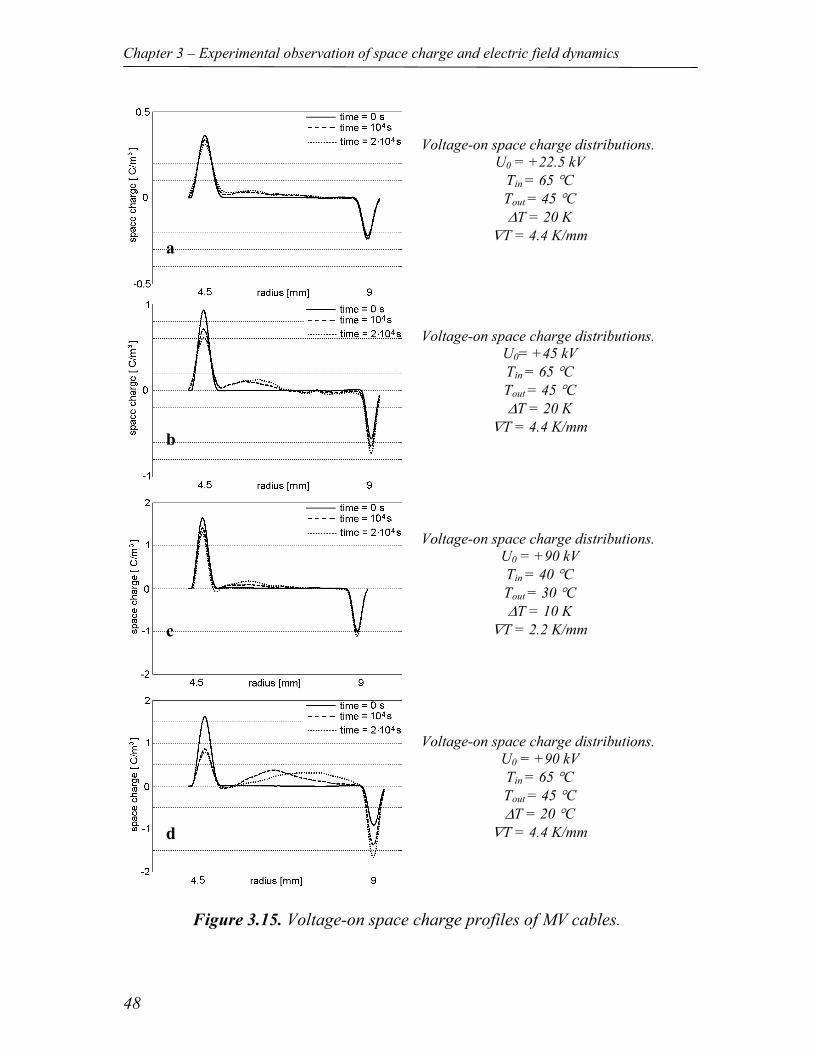
Chapter 3 – Experimental observation of space charge and electric field dynamics
48
Figure 3.15. Voltage-on space charge profiles of MV cables.
Voltage-on space charge distributions. U0 = +22.5 kV
Tin = 65 °C Tout = 45 °C ∆T = 20 K
∇T = 4.4 K/mm
Voltage-on space charge distributions. U0= +45 kV Tin = 65 °C Tout = 45 °C ∆T = 20 K
∇T = 4.4 K/mm
Voltage-on space charge distributions. U0 = +90 kV Tin = 40 °C Tout = 30 °C ∆T = 10 K
∇T = 2.2 K/mm
Voltage-on space charge distributions. U0 = +90 kV Tin = 65 °C Tout = 45 °C ∆T = 20 °C
∇T = 4.4 K/mm
a
b
c
d
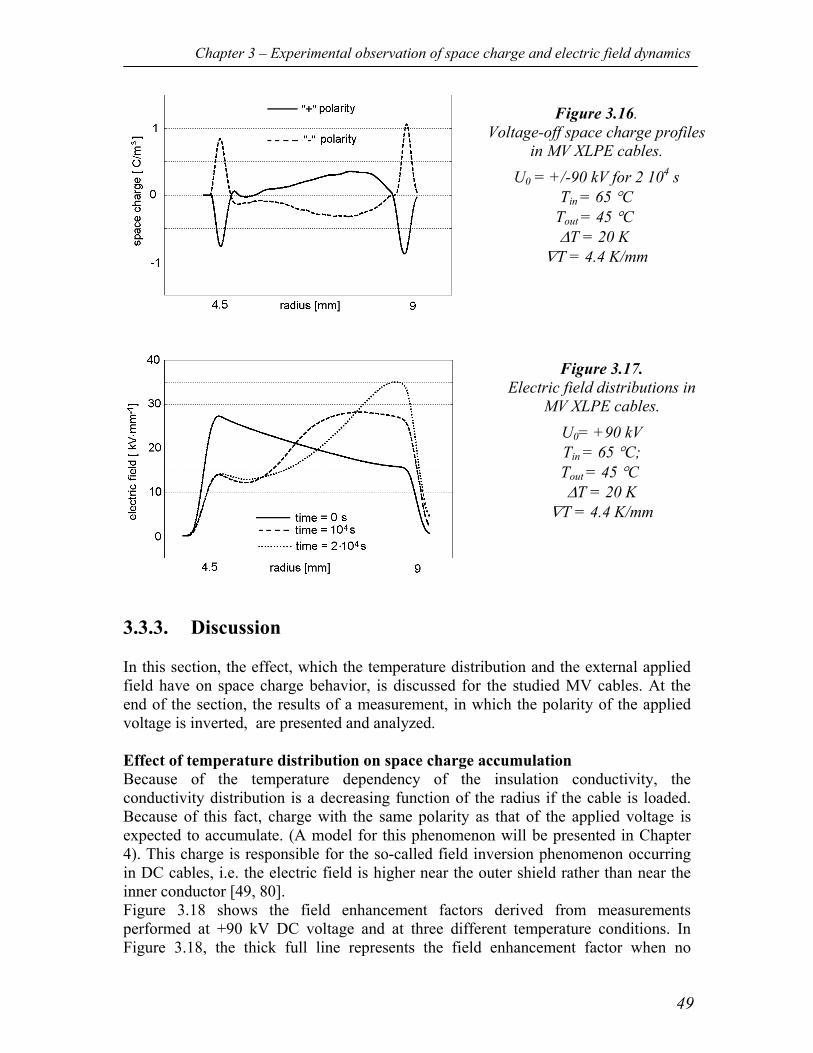
Chapter 3 – Experimental observation of space charge and electric field dynamics
49
3.3.3. Discussion In this section, the effect, which the temperature distribution and the external applied field have on space charge behavior, is discussed for the studied MV cables. At the end of the section, the results of a measurement, in which the polarity of the applied voltage is inverted, are presented and analyzed. Effect of temperature distribution on space charge accumulation Because of the temperature dependency of the insulation conductivity, the conductivity distribution is a decreasing function of the radius if the cable is loaded. Because of this fact, charge with the same polarity as that of the applied voltage is expected to accumulate. (A model for this phenomenon will be presented in Chapter 4). This charge is responsible for the so-called field inversion phenomenon occurring in DC cables, i.e. the electric field is higher near the outer shield rather than near the inner conductor [49, 80]. Figure 3.18 shows the field enhancement factors derived from measurements performed at +90 kV DC voltage and at three different temperature conditions. In Figure 3.18, the thick full line represents the field enhancement factor when no
Figure 3.16. Voltage-off space charge profiles
in MV XLPE cables. U0 = +/-90 kV for 2 104 s
Tin = 65 °C Tout = 45 °C ∆T = 20 K
∇T = 4.4 K/mm
Figure 3.17. Electric field distributions in
MV XLPE cables. U0= +90 kV Tin = 65 °C; Tout = 45 °C ∆T = 20 K
∇T = 4.4 K/mm
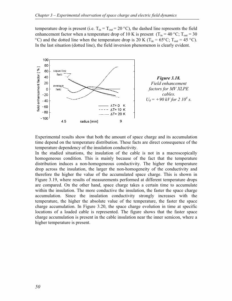
Chapter 3 – Experimental observation of space charge and electric field dynamics
50
temperature drop is present (i.e. Tin = Tout = 20 °C), the dashed line represents the field enhancement factor when a temperature drop of 10 K is present (Tin = 40 °C; Tout = 30 °C) and the dotted line when the temperature drop is 20 K (Tin = 65°C; Tout = 45 °C). In the last situation (dotted line), the field inversion phenomenon is clearly evident.
Experimental results show that both the amount of space charge and its accumulation time depend on the temperature distribution. These facts are direct consequence of the temperature dependency of the insulation conductivity. In the studied situations, the insulation of the cable is not in a macroscopically homogeneous condition. This is mainly because of the fact that the temperature distribution induces a non-homogeneous conductivity. The higher the temperature drop across the insulation, the larger the non-homogeneity of the conductivity and therefore the higher the value of the accumulated space charge. This is shown in Figure 3.19, where results of measurements performed at different temperature drops are compared. On the other hand, space charge takes a certain time to accumulate within the insulation. The more conductive the insulation, the faster the space charge accumulation. Since the insulation conductivity strongly increases with the temperature, the higher the absolute value of the temperature, the faster the space charge accumulation. In Figure 3.20, the space charge evolution in time at specific locations of a loaded cable is represented. The figure shows that the faster space charge accumulation is present in the cable insulation near the inner semicon, where a higher temperature is present.
Figure 3.18. Field enhancement
factors for MV XLPE cables.
U0 = +90 kV for 2 104 s.
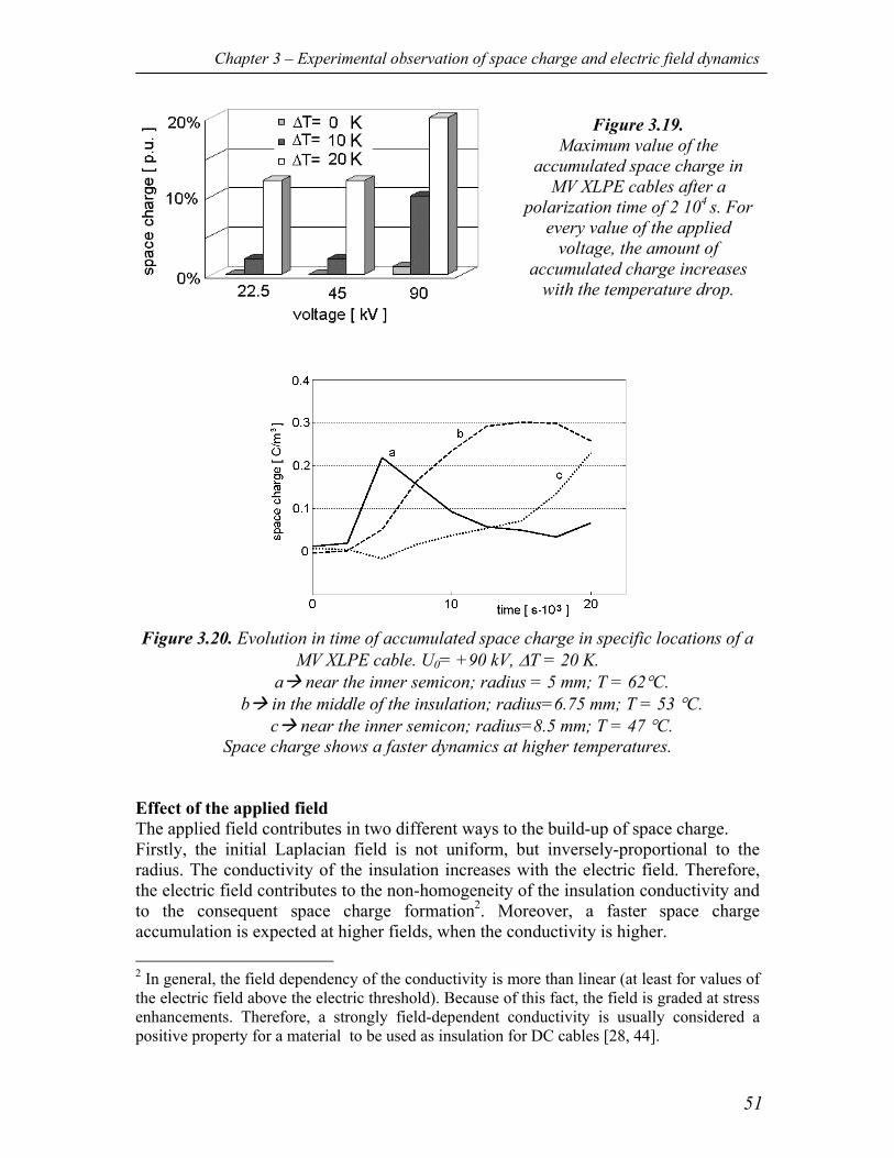
Chapter 3 – Experimental observation of space charge and electric field dynamics
51
Figure 3.20. Evolution in time of accumulated space charge in specific locations of a
MV XLPE cable. U0= +90 kV, ∆T = 20 K. a near the inner semicon; radius = 5 mm; T = 62°C.
b in the middle of the insulation; radius=6.75 mm; T = 53 °C. c near the inner semicon; radius=8.5 mm; T = 47 °C.
Space charge shows a faster dynamics at higher temperatures. Effect of the applied field The applied field contributes in two different ways to the build-up of space charge. Firstly, the initial Laplacian field is not uniform, but inversely-proportional to the radius. The conductivity of the insulation increases with the electric field. Therefore, the electric field contributes to the non-homogeneity of the insulation conductivity and to the consequent space charge formation2. Moreover, a faster space charge accumulation is expected at higher fields, when the conductivity is higher. 2 In general, the field dependency of the conductivity is more than linear (at least for values of the electric field above the electric threshold). Because of this fact, the field is graded at stress enhancements. Therefore, a strongly field-dependent conductivity is usually considered a positive property for a material to be used as insulation for DC cables [28, 44].
Figure 3.19. Maximum value of the
accumulated space charge in MV XLPE cables after a
polarization time of 2 104 s. For every value of the applied
voltage, the amount of accumulated charge increases
with the temperature drop.
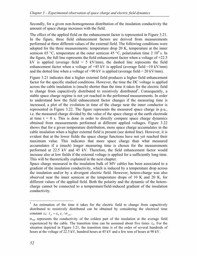
Chapter 3 – Experimental observation of space charge and electric field dynamics
52
Secondly, for a given non-homogeneous distribution of the insulation conductivity the amount of space charge increases with the field. The effect of the applied field on the enhancement factor is represented in Figure 3.21. In the figure, three field enhancement factors are derived from measurements performed at three different values of the external field. The following conditions were adopted for the three measurements: temperature drop 20 K, temperature at the inner semicon 65 °C, temperature at the outer semicon 45 °C, polarization time 2 104 s. In the figure, the full line represents the field enhancement factor when a voltage of +22.5 kV is applied (average field = 5 kV/mm), the dashed line represents the field enhancement factor when a voltage of +45 kV is applied (average field =10 kV/mm) and the dotted line when a voltage of +90 kV is applied (average field = 20 kV/mm). Figure 3.21 indicates that a higher external field produces a higher field enhancement factor for the specific studied conditions. However, the time the DC voltage is applied across the cable insulation is (much) shorter than the time it takes for the electric field to change from capacitively distributed to resistively distributed3. Consequently, a stable space charge regime is not yet reached in the performed measurements. In order to understand how the field enhancement factor changes if the measuring time is increased, a plot of the evolution in time of the charge near the inner conductor is represented in Figure 3.22. The figure represents the measured space charge in p.u., i.e. the measured charge divided by the value of the space charge at the earth electrode at time t = 0 s. This is done in order to directly compare space charge dynamics obtained from measurements performed at different applied voltages. Figure 3.22 shows that for a given temperature distribution, more space charge accumulates in the cable insulation when a higher external field is present (see dotted line). However, it is evident that at the lower fields the space charge functions have not yet reached their maximum value. This indicates that more space charge than what measured accumulates if a (much) longer measuring time is chosen for the measurements performed at 22.5 kV and 45 kV. Therefore, the field enhancement factor would increase also at low fields if the external voltage is applied for a sufficiently long time. This will be theoretically explained in the next chapter. Space charge measured in the insulation bulk of MV cables has been associated to a gradient of the insulation conductivity, which is induced by a temperature drop across the insulation and/or by a divergent electric field. However, hetero-charge was also observed near the inner semicon at the temperature drops of 10 K and 20 K, for different values of the applied field. Both the polarity and the dynamic of the hetero-charge cannot be connected to a temperature/field-induced gradient of the insulation conductivity.
3 An estimation of the time it takes for the electric field to change from capacitively distributed to resistively distributed can be obtained by considering the electrical time constant τel: outrel σεετ /0= . σout represents the conductivity of the coldest part of the insulation at the average field experienced by the cable. The transition time can be assumed about five times τel. For the situation depicted in Figure 3.21, the transition time is of the order of several hundreds of hours at the voltage of 22.5 kV, hundred hours at 45 kV and a few tens of hours at 90 kV.
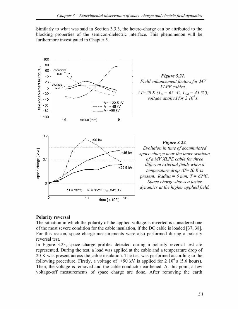
Chapter 3 – Experimental observation of space charge and electric field dynamics
53
Similarly to what was said in Section 3.3.3, the hetero-charge can be attributed to the blocking properties of the semicon-dielectric interface. This phenomenon will be furthermore investigated in Chapter 5.
Polarity reversal The situation in which the polarity of the applied voltage is inverted is considered one of the most severe condition for the cable insulation, if the DC cable is loaded [37, 38]. For this reason, space charge measurements were also performed during a polarity reversal test. In Figure 3.23, space charge profiles detected during a polarity reversal test are represented. During the test, a load was applied at the cable and a temperature drop of 20 K was present across the cable insulation. The test was performed according to the following procedure. Firstly, a voltage of +90 kV is applied for 2 104 s (5.6 hours). Then, the voltage is removed and the cable conductor earthened. At this point, a few voltage-off measurements of space charge are done. After removing the earth
Figure 3.21. Field enhancement factors for MV
XLPE cables. ∆T=20 K (Tin = 65 °C, Tout = 45 °C);
voltage applied for 2 104 s.
Figure 3.22. Evolution in time of accumulated
space charge near the inner semicon of a MV XLPE cable for three different external fields when a temperature drop ∆T=20 K is
present. Radius = 5 mm; T = 62°C.Space charge shows a faster
dynamics at the higher applied field.
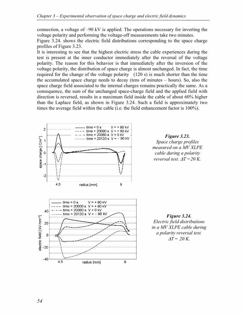
Chapter 3 – Experimental observation of space charge and electric field dynamics
54
connection, a voltage of –90 kV is applied. The operations necessary for inverting the voltage polarity and performing the voltage-off measurements take two minutes. Figure 3.24. shows the electric field distributions corresponding to the space charge profiles of Figure 3.23. It is interesting to see that the highest electric stress the cable experiences during the test is present at the inner conductor immediately after the reversal of the voltage polarity. The reason for this behavior is that immediately after the inversion of the voltage polarity, the distribution of space charge is almost unchanged. In fact, the time required for the change of the voltage polarity (120 s) is much shorter than the time the accumulated space charge needs to decay (tens of minutes – hours). So, also the space charge field associated to the internal charges remains practically the same. As a consequence, the sum of the unchanged space-charge field and the applied field with direction is reversed, results in a maximum field inside the cable of about 60% higher than the Laplace field, as shown in Figure 3.24. Such a field is approximately two times the average field within the cable (i.e. the field enhancement factor is 100%).
Figure 3.23. Space charge profiles
measured on a MV XLPE cable during a polarity reversal test. ∆T =20 K.
Figure 3.24. Electric field distributions
in a MV XLPE cable during a polarity reversal test.
∆T = 20 K.
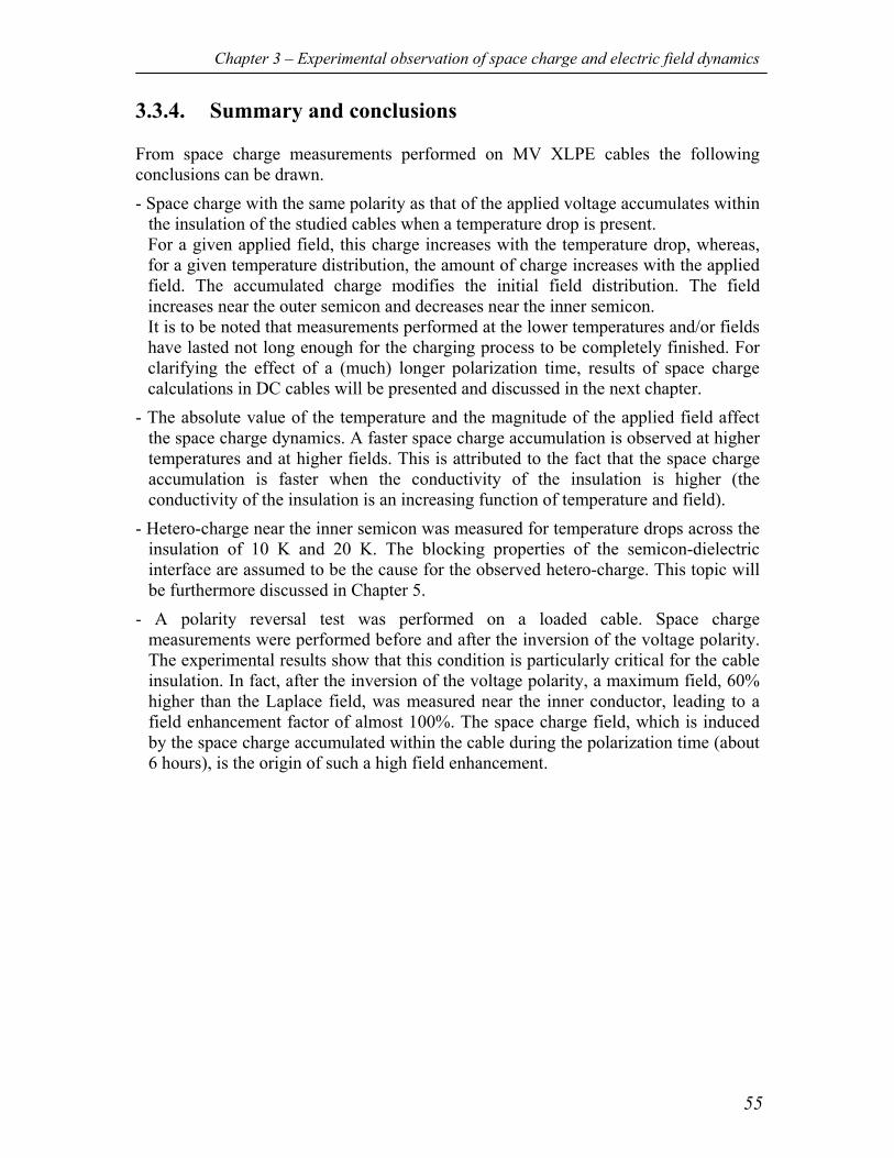
Chapter 3 – Experimental observation of space charge and electric field dynamics
55
3.3.4. Summary and conclusions From space charge measurements performed on MV XLPE cables the following conclusions can be drawn. - Space charge with the same polarity as that of the applied voltage accumulates within
the insulation of the studied cables when a temperature drop is present. For a given applied field, this charge increases with the temperature drop, whereas, for a given temperature distribution, the amount of charge increases with the applied field. The accumulated charge modifies the initial field distribution. The field increases near the outer semicon and decreases near the inner semicon. It is to be noted that measurements performed at the lower temperatures and/or fields have lasted not long enough for the charging process to be completely finished. For clarifying the effect of a (much) longer polarization time, results of space charge calculations in DC cables will be presented and discussed in the next chapter.
- The absolute value of the temperature and the magnitude of the applied field affect the space charge dynamics. A faster space charge accumulation is observed at higher temperatures and at higher fields. This is attributed to the fact that the space charge accumulation is faster when the conductivity of the insulation is higher (the conductivity of the insulation is an increasing function of temperature and field).
- Hetero-charge near the inner semicon was measured for temperature drops across the insulation of 10 K and 20 K. The blocking properties of the semicon-dielectric interface are assumed to be the cause for the observed hetero-charge. This topic will be furthermore discussed in Chapter 5.
- A polarity reversal test was performed on a loaded cable. Space charge measurements were performed before and after the inversion of the voltage polarity. The experimental results show that this condition is particularly critical for the cable insulation. In fact, after the inversion of the voltage polarity, a maximum field, 60% higher than the Laplace field, was measured near the inner conductor, leading to a field enhancement factor of almost 100%. The space charge field, which is induced by the space charge accumulated within the cable during the polarization time (about 6 hours), is the origin of such a high field enhancement.
Chapter 3 – Experimental observation of space charge and electric field dynamics
56
3.4. Space charge measurements on dual-dielectric mini-cables
3.4.1. Introduction In order to investigate the space charge and electric field distributions at coaxial interfaces, space charge measurements were performed on dual-dielectric mini-cables. Two types of dual-dielectric mini-cables were studied: EPR-XLPE mini-cables, in which the EPR is the innermost insulation and the XLPE is the outermost insulation, and XLPE-EPR mini-cables in which the XLPE is the innermost insulation and the EPR is the outermost insulation. In all the measurements, a DC voltage was applied at the inner conductor, whereas the outer semicon was connected to earth. Typical voltage-on space charge profiles, which were measured immediately after the application of the DC voltage, are represented in Figure 3.25 for both types of mini-cables. In the figure, the corresponding electric field distributions are also depicted. Similarly to what is observed in flat interfaces, a peak is present in the space charge patterns at the dielectric interface also in the absence of interfacial charge. Again, the discontinuity of the permittivity at the dielectric interface is the cause of this peak. Space charge measurements were performed at different temperature conditions and at different values and polarities of the applied voltage. The polarization conditions are summarized In Table 3.3.a. In Table 3.3.b the temperature conditions are summarized. In Table 3.3.b, the temperature distributions across a EPR-XLPE dual-dielectric mini-cable are also represented for the different studied conditions. (The temperature distributions in XLPE-EPR mini-cables are very similar to those represented in the table). The data in the table are obtained using the measured temperature values and assuming a thermal conductivity of 0.3 W/mK for both XLPE and EPR.
Tab.3.3.a. Test conditions adopted for the space charge measurements on dual-dielectric mini-cables: polarization conditions.
Dual-dielectric EPR-XLPE
Dual-dielectric XLPE-EPR
Voltage [kV] 30 30 Voltage polarity +/- and pol. rev. +/-
Electric field (average) [kV/mm]
14.3 14.3
Polarization time [s] 2 104
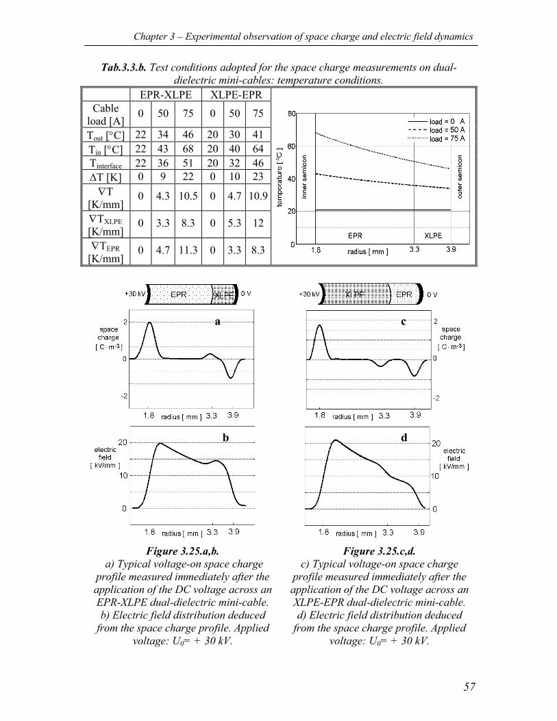
Chapter 3 – Experimental observation of space charge and electric field dynamics
57
Tab.3.3.b. Test conditions adopted for the space charge measurements on dual-dielectric mini-cables: temperature conditions.
EPR-XLPE XLPE-EPR Cable
load [A] 0 50 75 0 50 75
Tout [°C] 22 34 46 20 30 41 Tin [°C] 22 43 68 20 40 64 Tinterface
22 36 51 20 32 46 ∆T [K] 0 9 22 0 10 23 ∇T
[K/mm] 0 4.3 10.5 0 4.7 10.9
∇TXLPE [K/mm]
0 3.3 8.3 0 5.3 12
∇TEPR [K/mm]
0 4.7 11.3 0 3.3 8.3
a
b
c
d
Figure 3.25.a,b. a) Typical voltage-on space charge
profile measured immediately after the application of the DC voltage across an EPR-XLPE dual-dielectric mini-cable. b) Electric field distribution deduced
from the space charge profile. Applied voltage: U0= + 30 kV.
Figure 3.25.c,d. c) Typical voltage-on space charge
profile measured immediately after the application of the DC voltage across an XLPE-EPR dual-dielectric mini-cable. d) Electric field distribution deduced
from the space charge profile. Applied voltage: U0= + 30 kV.
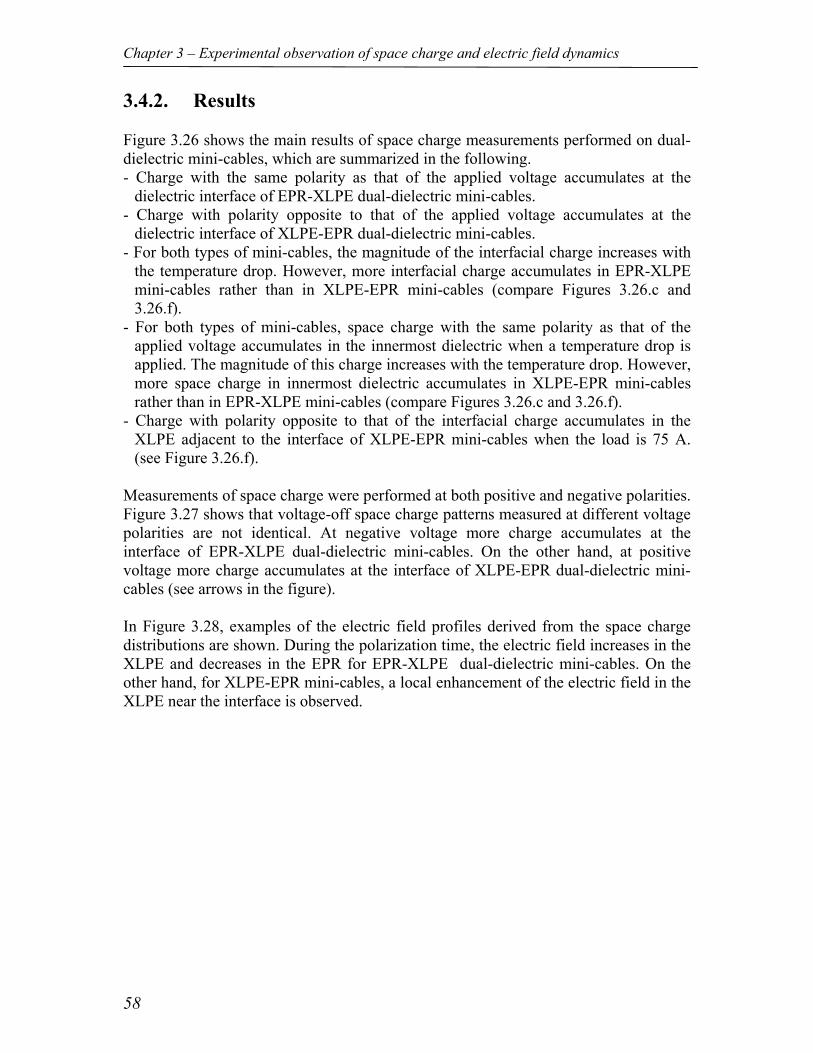
Chapter 3 – Experimental observation of space charge and electric field dynamics
58
3.4.2. Results Figure 3.26 shows the main results of space charge measurements performed on dual-dielectric mini-cables, which are summarized in the following. - Charge with the same polarity as that of the applied voltage accumulates at the
dielectric interface of EPR-XLPE dual-dielectric mini-cables. - Charge with polarity opposite to that of the applied voltage accumulates at the
dielectric interface of XLPE-EPR dual-dielectric mini-cables. - For both types of mini-cables, the magnitude of the interfacial charge increases with
the temperature drop. However, more interfacial charge accumulates in EPR-XLPE mini-cables rather than in XLPE-EPR mini-cables (compare Figures 3.26.c and 3.26.f).
- For both types of mini-cables, space charge with the same polarity as that of the applied voltage accumulates in the innermost dielectric when a temperature drop is applied. The magnitude of this charge increases with the temperature drop. However, more space charge in innermost dielectric accumulates in XLPE-EPR mini-cables rather than in EPR-XLPE mini-cables (compare Figures 3.26.c and 3.26.f).
- Charge with polarity opposite to that of the interfacial charge accumulates in the XLPE adjacent to the interface of XLPE-EPR mini-cables when the load is 75 A. (see Figure 3.26.f).
Measurements of space charge were performed at both positive and negative polarities. Figure 3.27 shows that voltage-off space charge patterns measured at different voltage polarities are not identical. At negative voltage more charge accumulates at the interface of EPR-XLPE dual-dielectric mini-cables. On the other hand, at positive voltage more charge accumulates at the interface of XLPE-EPR dual-dielectric mini-cables (see arrows in the figure). In Figure 3.28, examples of the electric field profiles derived from the space charge distributions are shown. During the polarization time, the electric field increases in the XLPE and decreases in the EPR for EPR-XLPE dual-dielectric mini-cables. On the other hand, for XLPE-EPR mini-cables, a local enhancement of the electric field in the XLPE near the interface is observed.
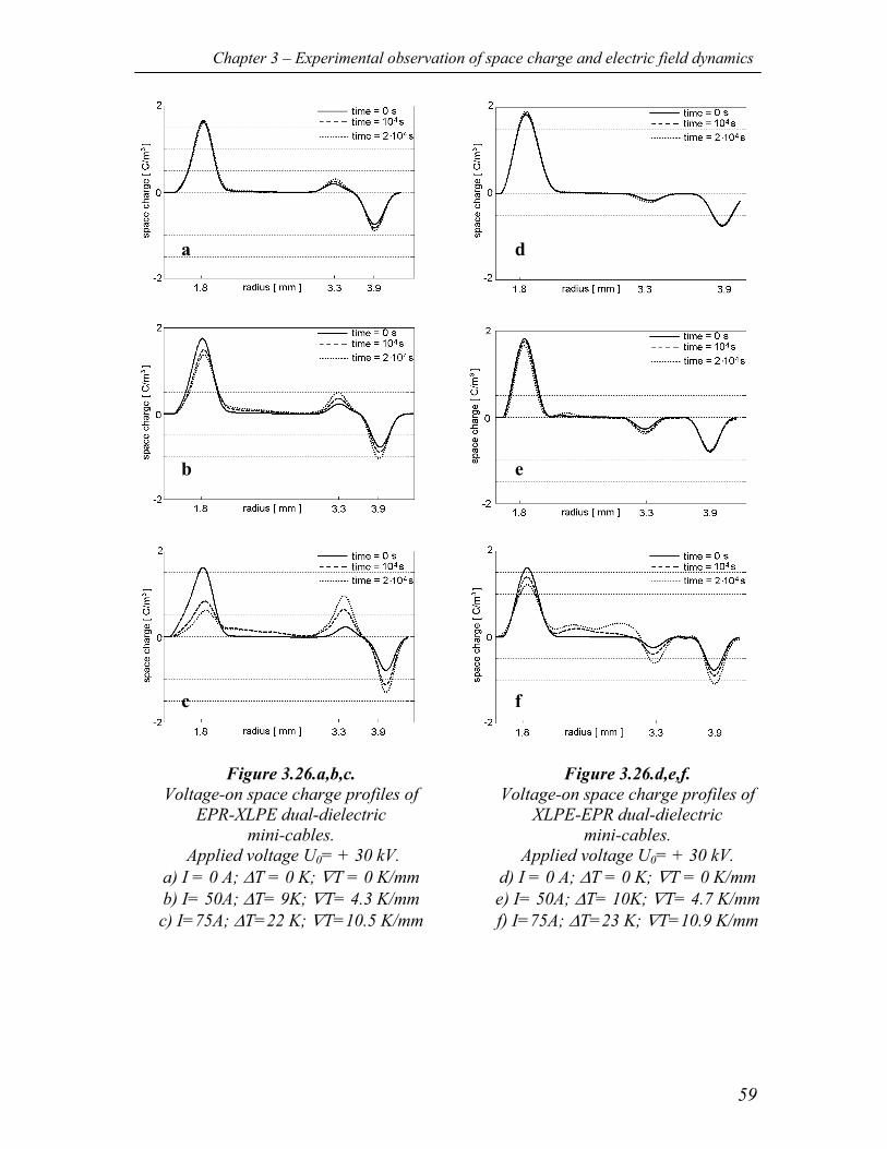
Chapter 3 – Experimental observation of space charge and electric field dynamics
59
a
b
c
e
d
f
Figure 3.26.a,b,c. Voltage-on space charge profiles of
EPR-XLPE dual-dielectric mini-cables.
Applied voltage U0= + 30 kV. a) I = 0 A; ∆T = 0 K; ∇T = 0 K/mmb) I= 50A; ∆T= 9K; ∇T= 4.3 K/mmc) I=75A; ∆T=22 K; ∇T=10.5 K/mm
Figure 3.26.d,e,f. Voltage-on space charge profiles of
XLPE-EPR dual-dielectric mini-cables.
Applied voltage U0= + 30 kV. d) I = 0 A; ∆T = 0 K; ∇T = 0 K/mme) I= 50A; ∆T= 10K; ∇T= 4.7 K/mmf) I=75A; ∆T=23 K; ∇T=10.9 K/mm
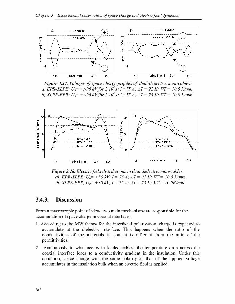
Chapter 3 – Experimental observation of space charge and electric field dynamics
60
Figure 3.27. Voltage-off space charge profiles of dual-dielectric mini-cables.
a) EPR-XLPE; U0= +/-90 kV for 2 104 s; I =75 A; ∆T = 22 K; ∇T = 10.5 K/mm. b) XLPE-EPR; U0= +/-90 kV for 2 104 s; I =75 A; ∆T = 23 K; ∇T = 10.9 K/mm.
Figure 3.28. Electric field distributions in dual dielectric mini-cables. a) EPR-XLPE; Uo= +30 kV; I = 75 A; ∆T = 22 K; ∇T = 10.5 K/mm. b) XLPE-EPR; U0= +30 kV; I = 75 A; ∆T = 23 K; ∇T = 10.9K/mm.
3.4.3. Discussion From a macroscopic point of view, two main mechanisms are responsible for the accumulation of space charge in coaxial interfaces. 1. According to the MW theory for the interfacial polarization, charge is expected to
accumulate at the dielectric interface. This happens when the ratio of the conductivities of the materials in contact is different from the ratio of the permittivities.
2. Analogously to what occurs in loaded cables, the temperature drop across the coaxial interface leads to a conductivity gradient in the insulation. Under this condition, space charge with the same polarity as that of the applied voltage accumulates in the insulation bulk when an electric field is applied.
a b
a b
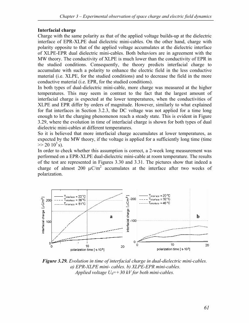
Chapter 3 – Experimental observation of space charge and electric field dynamics
61
Interfacial charge Charge with the same polarity as that of the applied voltage builds-up at the dielectric interface of EPR-XLPE dual dielectric mini-cables. On the other hand, charge with polarity opposite to that of the applied voltage accumulates at the dielectric interface of XLPE-EPR dual dielectric mini-cables. Both behaviors are in agreement with the MW theory. The conductivity of XLPE is much lower than the conductivity of EPR in the studied conditions. Consequently, the theory predicts interfacial charge to accumulate with such a polarity to enhance the electric field in the less conductive material (i.e. XLPE, for the studied conditions) and to decrease the field in the more conductive material (i.e. EPR, for the studied conditions). In both types of dual-dielectric mini-cable, more charge was measured at the higher temperatures. This may seem in contrast to the fact that the largest amount of interfacial charge is expected at the lower temperatures, when the conductivities of XLPE and EPR differ by orders of magnitude. However, similarly to what explained for flat interfaces in Section 3.2.3, the DC voltage was not applied for a time long enough to let the charging phenomenon reach a steady state. This is evident in Figure 3.29, where the evolution in time of interfacial charge is shown for both types of dual dielectric mini-cables at different temperatures. So it is believed that more interfacial charge accumulates at lower temperatures, as expected by the MW theory, if the voltage is applied for a sufficiently long time (time >> 20 103 s). In order to check whether this assumption is correct, a 2-week long measurement was performed on a EPR-XLPE dual-dielectric mini-cable at room temperature. The results of the test are represented in Figures 3.30 and 3.31. The pictures show that indeed a charge of almost 200 µC/m2 accumulates at the interface after two weeks of polarization.
Figure 3.29. Evolution in time of interfacial charge in dual-dielectric mini-cables. a) EPR-XLPE mini- cables. b) XLPE-EPR mini-cables.
Applied voltage U0=+30 kV for both mini-cables.
a b
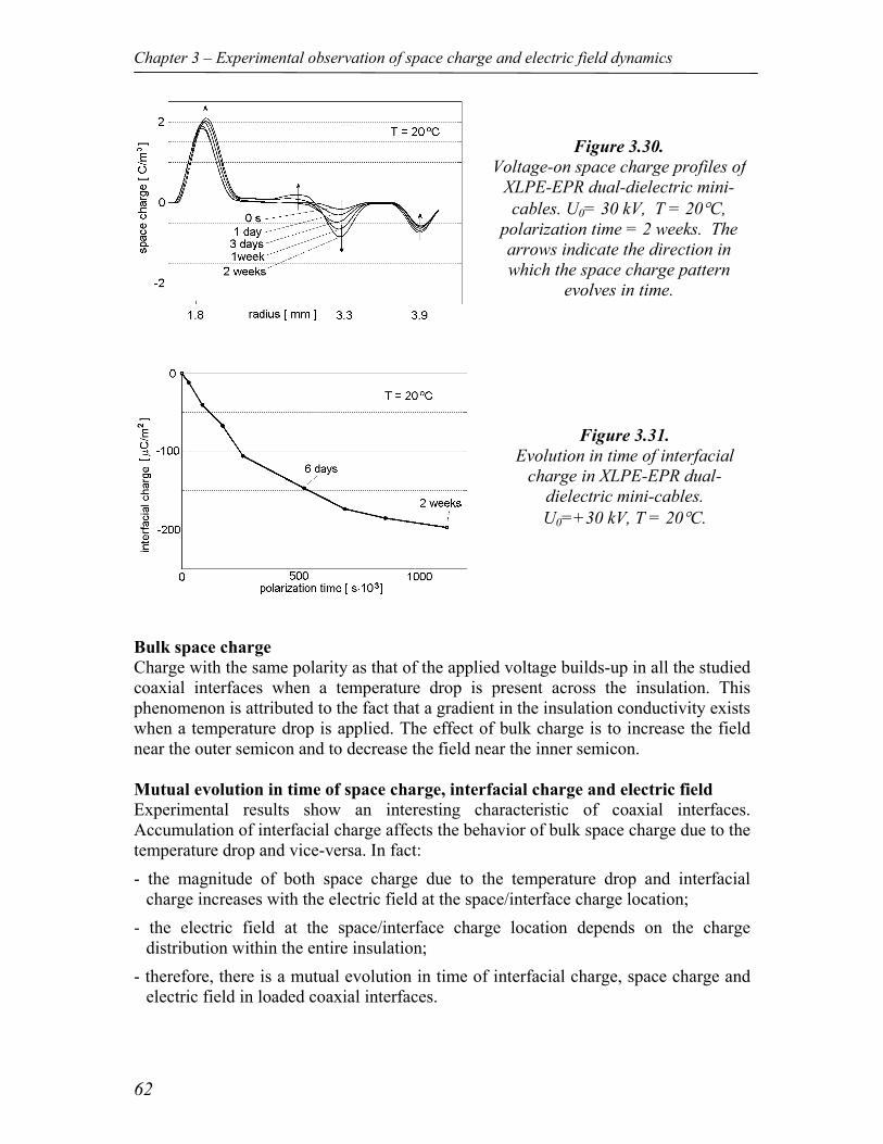
Chapter 3 – Experimental observation of space charge and electric field dynamics
62
Bulk space charge Charge with the same polarity as that of the applied voltage builds-up in all the studied coaxial interfaces when a temperature drop is present across the insulation. This phenomenon is attributed to the fact that a gradient in the insulation conductivity exists when a temperature drop is applied. The effect of bulk charge is to increase the field near the outer semicon and to decrease the field near the inner semicon. Mutual evolution in time of space charge, interfacial charge and electric field Experimental results show an interesting characteristic of coaxial interfaces. Accumulation of interfacial charge affects the behavior of bulk space charge due to the temperature drop and vice-versa. In fact: - the magnitude of both space charge due to the temperature drop and interfacial
charge increases with the electric field at the space/interface charge location; - the electric field at the space/interface charge location depends on the charge
distribution within the entire insulation; - therefore, there is a mutual evolution in time of interfacial charge, space charge and
electric field in loaded coaxial interfaces.
Figure 3.30. Voltage-on space charge profiles of
XLPE-EPR dual-dielectric mini-cables. U0= 30 kV, T = 20°C,
polarization time = 2 weeks. The arrows indicate the direction in which the space charge pattern
evolves in time.
Figure 3.31. Evolution in time of interfacial
charge in XLPE-EPR dual-dielectric mini-cables. U0=+30 kV, T = 20°C.
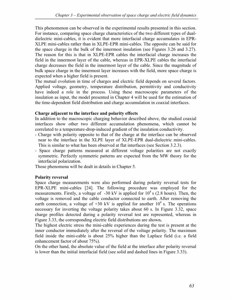
Chapter 3 – Experimental observation of space charge and electric field dynamics
63
This phenomenon can be observed in the experimental results presented in this section. For instance, comparing space charge characteristics of the two different types of dual-dielectric mini-cables, it is evident that more interfacial charge accumulates in EPR-XLPE mini-cables rather than in XLPE-EPR mini-cables. The opposite can be said for the space charge in the bulk of the innermost insulation (see Figures 3.26 and 3.27). The reason for this is that in XLPE-EPR cables the interfacial charge increases the field in the innermost layer of the cable, whereas in EPR-XLPE cables the interfacial charge decreases the field in the innermost layer of the cable. Since the magnitude of bulk space charge in the innermost layer increases with the field, more space charge is expected when a higher field is present. The mutual evolution in time of charges and electric field depends on several factors. Applied voltage, geometry, temperature distribution, permittivity and conductivity have indeed a role in the process. Using these macroscopic parameters of the insulation as input, the model presented in Chapter 4 will be used for the estimation of the time-dependent field distribution and charge accumulation in coaxial interfaces. Charge adjacent to the interface and polarity effects In addition to the macroscopic charging behavior described above, the studied coaxial interfaces show other two different accumulation phenomena, which cannot be correlated to a temperature-drop-induced gradient of the insulation conductivity. - Charge with polarity opposite to that of the charge at the interface can be observed
near to the interface in the XLPE layer of XLPE-EPR dual-dielectric mini-cables. This is similar to what has been observed at flat interfaces (see Section 3.2.3).
- Space charge patterns measured at different voltage polarities are not exactly symmetric. Perfectly symmetric patterns are expected from the MW theory for the interfacial polarization.
Those phenomena will be dealt in details in Chapter 5. Polarity reversal Space charge measurements were also performed during polarity reversal tests for EPR-XLPE mini-cables [24]. The following procedure was employed for the measurements. Firstly, a voltage of -30 kV is applied for 104 s (2.8 hours). Then, the voltage is removed and the cable conductor connected to earth. After removing the earth connection, a voltage of +30 kV is applied for another 104 s. The operations necessary for inverting the voltage polarity takes about 60 s. In Figure 3.32, space charge profiles detected during a polarity reversal test are represented, whereas in Figure 3.33, the corresponding electric field distributions are shown. The highest electric stress the mini-cable experiences during the test is present at the inner conductor immediately after the reversal of the voltage polarity. The maximum field inside the mini-cable is about 25% higher than the Laplace field (i.e. a field enhancement factor of about 75%). On the other hand, the absolute value of the field at the interface after polarity reversal is lower than the initial interfacial field (see solid and dashed lines in Figure 3.33).
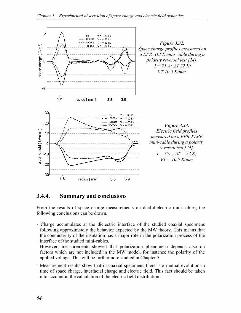
Chapter 3 – Experimental observation of space charge and electric field dynamics
64
3.4.4. Summary and conclusions From the results of space charge measurements on dual-dielectric mini-cables, the following conclusions can be drawn. - Charge accumulates at the dielectric interface of the studied coaxial specimens
following approximately the behavior expected by the MW theory. This means that the conductivity of the insulation has a major role in the polarization process of the interface of the studied mini-cables. However, measurements showed that polarization phenomena depends also on factors which are not included in the MW model, for instance the polarity of the applied voltage. This will be furthermore studied in Chapter 5.
- Measurement results show that in coaxial specimens there is a mutual evolution in time of space charge, interfacial charge and electric field. This fact should be taken into account in the calculation of the electric field distribution.
Figure 3.32. Space charge profiles measured on a EPR-XLPE mini-cable during a
polarity reversal test [24]. I = 75 A; ∆T 22 K; ∇T 10.5 K/mm.
Figure 3.33. Electric field profiles
measured on a EPR-XLPE mini-cable during a polarity
reversal test [24]. I = 75A; ∆T = 22 K; ∇T = 10.5 K/mm.
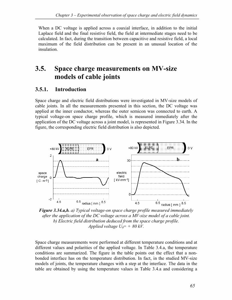
Chapter 3 – Experimental observation of space charge and electric field dynamics
65
When a DC voltage is applied across a coaxial interface, in addition to the initial Laplace field and the final resistive field, the field at intermediate stages need to be calculated. In fact, during the transition between capacitive and resistive field, a local maximum of the field distribution can be present in an unusual location of the insulation.
3.5. Space charge measurements on MV-size
models of cable joints 3.5.1. Introduction Space charge and electric field distributions were investigated in MV-size models of cable joints. In all the measurements presented in this section, the DC voltage was applied at the inner conductor, whereas the outer semicon was connected to earth. A typical voltage-on space charge profile, which is measured immediately after the application of the DC voltage across a joint model, is represented in Figure 3.34. In the figure, the corresponding electric field distribution is also depicted.
Figure 3.34.a,b. a) Typical voltage-on space charge profile measured immediately
after the application of the DC voltage across a MV-size model of a cable joint. b) Electric field distribution deduced from the space charge profile.
Applied voltage U0= + 80 kV. Space charge measurements were performed at different temperature conditions and at different values and polarities of the applied voltage. In Table 3.4.a, the temperature conditions are summarized. The figure in the table points out the effect that a non-bonded interface has on the temperature distribution. In fact, in the studied MV-size models of joints, the temperature changes with a step at the interface. The data in the table are obtained by using the temperature values in Table 3.4.a and considering a
a b
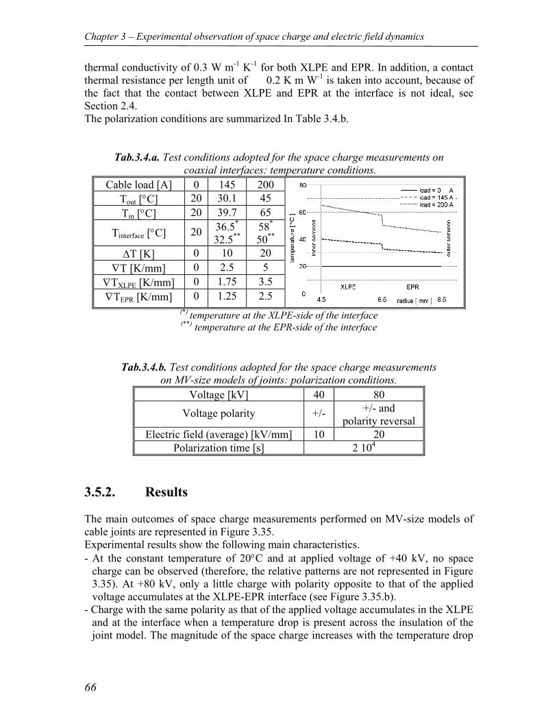
Chapter 3 – Experimental observation of space charge and electric field dynamics
66
thermal conductivity of 0.3 W m-1 K-1 for both XLPE and EPR. In addition, a contact thermal resistance per length unit of 0.2 K m W-1 is taken into account, because of the fact that the contact between XLPE and EPR at the interface is not ideal, see Section 2.4. The polarization conditions are summarized In Table 3.4.b.
Tab.3.4.a. Test conditions adopted for the space charge measurements on coaxial interfaces: temperature conditions.
Cable load [A] 0 145 200 Tout [°C] 20 30.1 45 Tin [°C] 20 39.7 65
Tinterface [°C] 20 36.5* 32.5**
58* 50**
∆T [K] 0 10 20 ∇T [K/mm] 0 2.5 5
∇TXLPE [K/mm] 0 1.75 3.5 ∇TEPR [K/mm] 0 1.25 2.5
(*) temperature at the XLPE-side of the interface (**) temperature at the EPR-side of the interface
Tab.3.4.b. Test conditions adopted for the space charge measurements on MV-size models of joints: polarization conditions.
Voltage [kV] 40 80
Voltage polarity +/- +/- and polarity reversal
Electric field (average) [kV/mm] 10 20 Polarization time [s] 2 104
3.5.2. Results The main outcomes of space charge measurements performed on MV-size models of cable joints are represented in Figure 3.35. Experimental results show the following main characteristics. - At the constant temperature of 20°C and at applied voltage of +40 kV, no space
charge can be observed (therefore, the relative patterns are not represented in Figure 3.35). At +80 kV, only a little charge with polarity opposite to that of the applied voltage accumulates at the XLPE-EPR interface (see Figure 3.35.b).
- Charge with the same polarity as that of the applied voltage accumulates in the XLPE and at the interface when a temperature drop is present across the insulation of the joint model. The magnitude of the space charge increases with the temperature drop
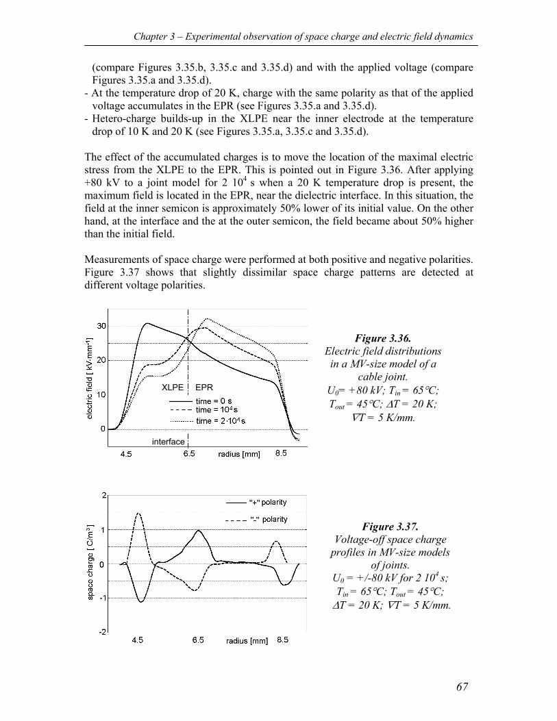
Chapter 3 – Experimental observation of space charge and electric field dynamics
67
(compare Figures 3.35.b, 3.35.c and 3.35.d) and with the applied voltage (compare Figures 3.35.a and 3.35.d).
- At the temperature drop of 20 K, charge with the same polarity as that of the applied voltage accumulates in the EPR (see Figures 3.35.a and 3.35.d).
- Hetero-charge builds-up in the XLPE near the inner electrode at the temperature drop of 10 K and 20 K (see Figures 3.35.a, 3.35.c and 3.35.d).
The effect of the accumulated charges is to move the location of the maximal electric stress from the XLPE to the EPR. This is pointed out in Figure 3.36. After applying +80 kV to a joint model for 2 104 s when a 20 K temperature drop is present, the maximum field is located in the EPR, near the dielectric interface. In this situation, the field at the inner semicon is approximately 50% lower of its initial value. On the other hand, at the interface and the at the outer semicon, the field became about 50% higher than the initial field. Measurements of space charge were performed at both positive and negative polarities. Figure 3.37 shows that slightly dissimilar space charge patterns are detected at different voltage polarities.
interface
XLPE EPR
Figure 3.36. Electric field distributions in a MV-size model of a
cable joint. U0= +80 kV; Tin = 65°C; Tout = 45°C; ∆T = 20 K;
∇T = 5 K/mm.
Figure 3.37. Voltage-off space charge
profiles in MV-size models of joints.
U0 = +/-80 kV for 2 104 s; Tin = 65°C; Tout = 45°C; ∆T = 20 K; ∇T = 5 K/mm.
Chapter 3 – Experimental observation of space charge and electric field dynamics
68
Figure 3.35. Voltage-on space charge profiles in MV-size models of joints.
Voltage-on space charge distributions. U0= +40 kV Tin = 65 °C Tout = 45 °C ∆T = 20 K
∇T = 5 K/mm
Voltage-on space charge distributions. U0 = +80 kV Tin = 20°C Tout = 20°C ∆T = 0 K
∇T = 0 K/mm
Voltage-on space charge distributions. U0 = +80 kV Tin = 40°C Tout = 30°C ∆T = 10 K
∇T = 2.5 K/mm
Voltage-on space charge distributions. U0 = +80 kV Tin = 65°C Tout = 45°C ∆T = 20 K
∇T = 5 K/mm
a
b
c
d
Chapter 3 – Experimental observation of space charge and electric field dynamics
69
3.5.3. Discussion Similarly to what said for dual-dielectric cables, also in MV-size models of joints charge is expected to accumulate at the dielectric interface and, when a temperature drop is present, in the insulation bulk. However, differently to what observed in dual-dielectric cables, in MV-size models of joints the interfacial charge accumulates with such a polarity to increase the electric field in the EPR and to decrease the field in the XLPE. According to the MW theory, this behavior implies that the conductivity of XLPE is higher than that of EPR for the studied conditions. To verify whether the conductivity of XLPE is higher than that of EPR in the studied joint models, the radial distribution of the insulation conductivity σ(r) is calculated according to the following relation [26]: ( ) ( )( )[ ]00 exp TrTr −= ασσ (3.4)
The value of the conductivity σ0 at the reference temperature T0 and the value of the parameter α are reported in Table 3.5. They are chosen in order to match the experimental data presented in Section 3.1. Figure 3.38 shows that indeed the conductivity of the XLPE is higher than that of EPR, for the temperature conditions ∆T=10 K and ∆T= 20 K. Therefore, the particular temperature distribution present across the joint model is the main cause of the observed space charge and field behaviors. It is to be noted that the contact between XLPE and EPR strongly affects the temperature distribution (and then the field distribution) by means of the parameter contact thermal resistance.
Table 3.5. Parameters used for the calculation of the conductivity distribution in MV-size models of cable joints.
T0 [°C] σ0 [Ω-1m-1] α [1/K] XLPE 20 10-17 @ 25 kV/mm 0.2 EPR 20 7 10-17 @ 15 kV/mm 0.1
Figure 3.38. Radial distribution of the insulation conductivity
calculated for the studied MV-size models of joint
models at different temperature when a DC
voltage of 80 kV is applied.
Chapter 3 – Experimental observation of space charge and electric field dynamics
70
Polarity reversal Space charge measurements were performed also during a polarity reversal test. A test procedure similar to that used for MV-size cables was adopted. Firstly, a voltage of +80 kV is applied for 20 104 s (5.6 hours). Then, the voltage is removed and the cable conductor earthened. At this point, a few voltage-off measurements of space charge are done. After removing the earth connection, a voltage of –80 kV is applied. The operations necessary for inverting the voltage polarity and performing the voltage-off measurements take about two minutes. In Figure 3.39, space charge profiles detected during the polarity reversal test are represented, whereas Figure 3.40 shows the corresponding electric field distributions. Similarly to what observed for MV-size cables, the joint model experiences the highest electric stress at the inner conductor immediately after the reversal of the voltage polarity. The maximum field is about 50% higher than the Laplacian field, as shown in Figure 3.40. Such a field is more than two times the average field within the cable (i.e. the field enhancement factor is 125%).
Figure 3.39. Space charge profiles
measured on a MV-size model of cable joint during
a polarity reversal test. U0 = +/-80 kV;
Tin = 65°C; Tout = 45°C ; ∆T = 20 K ; ∇T = 5 K/mm.
Figure 3.40. Electric field distributions
in a MV-size model of cable joint during a polarity
reversal test. U0 = +/-80 kV; Tin = 65°C; Tout = 45°C ; ∆T = 20 K ;
∇T = 5 K/mm.
Chapter 3 – Experimental observation of space charge and electric field dynamics
71
3.5.4. Summary and conclusions From the space charge measurements performed on MV-size models of cable joints, the following conclusions can be drawn. - Charge with the same polarity as that of the applied voltage accumulates at the
XLPE-EPR interface. The effect of the interfacial charge is to increase the electric field in the EPR and to decrease the field in the XLPE.
- Space charge with the same polarity as that of the applied voltage accumulates within the insulation of the joint models when a temperature drop is applied. The charge builds-up mainly in the XLPE. The amount of accumulated charge increases with the temperature drop for a given applied field and with the applied field for a given temperature condition. The effect of this charge is to increase the electric field near the outer semicon and decrease the field near the inner semicon.
- The detected space charge is mainly attributed to the non-uniform conductivity distribution of the insulation.
- Some hetero-charge was also measured in the XLPE, mainly at the higher temperatures.
- A polarity reversal test showed that this condition is particularly critical for the studied joint models. In fact, after inversion of the voltage polarity, a maximum field 50% higher than the Laplacian field was measured near the inner conductor, leading to a field enhancement factor of about 125%.
Chapter 3 – Experimental observation of space charge and electric field dynamics
72
3.6. Conclusions Space charge measurements performed on different types of XLPE-EPR specimens showed that different accumulation mechanisms are responsible for space charge build-up in the insulation of the studied specimens. Conductivity-gradient accumulation If a gradient is present in the spatial distribution of the conductivity, space charge accumulates in time with such a polarity to increase the field in the part of the insulation where the conductivity is lower and to decrease the field in the part of the insulation where the conductivity is higher. Since the insulation conductivity depends on electric field and temperature, this mechanism is active when a temperature drop and/or a field gradient are present across the insulation. In particular, this mechanism is evident in all the results of tests performed while a temperature drop is applied across the insulation. The amount of accumulated charge increases with the temperature drop for a given applied field, whereas for a given temperature drop the amount of charge increases with the applied field. The accumulation in time of the charge is faster at higher temperatures and at higher applied fields. Therefore, if a temperature drop is applied, space charge accumulates faster in the warmest part of the insulation. In the coldest part of the insulation, slower space charge build-ups are present. Consequently, this kind of accumulation process can be considered stabilized only when the space charge in the coldest part of the insulation has reached a steady state. Interfacial polarization At dielectric interfaces, the Maxwell-Wagner polarization mechanism is responsible for the accumulation of charge. The MW polarization can be considered a particular case of the accumulation mechanism described above. If the insulation is composed of two different materials, then the distribution of conductivity and that of the permittivity have a discontinuity at the interface between the two materials. In practice, this leads to a discontinuity of the ratio between permittivity and conductivity at the dielectric interface. For this reason, interfacial charge is expected to accumulate. Interfacial charge was measured in all specimens in which a dielectric interface is present. Both magnitude and accumulation time are in a quite good agreement to what expected by the MW theory. As for the previous mechanism, charge takes more time to accumulate at lower temperature. (As an example, at room temperature, the accumulation of interfacial charge in a XLPE-EPR interface takes more than two weeks before reaching the steady state, when an average field of about 14 kV/mm is applied). Hetero-charge and polarity effects Measurement results showed also accumulation of charge which could not be correlated neither to the conductivity-gradient mechanism nor to the interfacial polarization mechanism.
Chapter 3 – Experimental observation of space charge and electric field dynamics
73
For temperatures above 40°C, hetero-charge accumulates in the XLPE of different types of specimens. The hetero-charge has been attributed to the blocking properties of the semicon-dielectric interface and dielectric-dielectric interface encountered in the studied specimens. The MW theory predicts symmetric behavior of the interfacial charge at different polarities of the applied voltage. However, measurements showed clear differences between interfacial charge patterns detected at different voltage polarities. Those charging phenomena will be furthermore investigated in Chapter 5. A physical model of the insulation describing the space charge accumulation in cable systems will be presented in the next chapter. For the studied specimens, the extent of charge that has been attributed to the conductivity-gradient accumulation mechanism and to the interfacial polarization mechanism are more significant than the extent of charge attributed to charge injection/blocking. This means that the conductivity of the insulation and its dependency on field and temperature have a major role in the charging behavior of the studied XLPE-EPR specimens. For this reason, the model presented in Chapter 4 will consider the space charge build-up due to only the conductivity-gradient accumulation mechanism and the interfacial polarization mechanism. The charge dynamics will be calculated for the studied specimens and compared to the experimental results. In this way, the model presented in the next chapter will be validated.

Chapter 3 – Experimental observation of space charge and electric field dynamics
74
Chapter 4 – Calculation of space charge and electric field in DC cable systems
75
4. Calculation of space charge and electric field in DC cable systems
In this chapter, a physical model and a numerical procedure are presented for the calculation of the space charge dynamics and the electric field distributions in DC cable systems. In Section 4.1, some general considerations about the models and the procedures for the calculation of the space charge and the electric field in DC insulation are given. In particular, an overview is shown of the procedures available in the literature for the calculation of the DC field in cables. The physical model and the corresponding calculation procedure developed in this thesis are introduced in Section 4.2. Moreover, the limits of the chosen model are assessed and the hypotheses, on which the model is based, are discussed. Section 4.3 shows the results of the calculation in the form of space charge patterns. The experimental patterns presented in Chapter 3 are compared to the patterns derived by means of the numerical procedure. In Section 4.4, the space charge and the electric field are derived for several situations of practical interest. Finally, some conclusions are drawn in Section 4.5. 4.1. Introduction Through the years, several models have been presented in the literature for the calculation of space charge and electric field in DC insulation when a conductivity gradient and an external field are present at the same time. In general, the models (see Table 4.1) consider the insulation as a weakly conductive continuum in which a non-homogeneity can be induced by a non-uniform applied stress. This is the case of loaded DC cables and of the majority of HVDC devices. In fact, in those components a conductivity gradient is induced by the non-uniform electric field and/or by the temperature drop across the insulation. The main advantage of this type of model is that only a few macroscopic parameters of the insulation are required for the characterization of the model (e.g. conductivity and permittivity as a function of field and temperature). This makes the model applicable to a number of different situations without the need for modifying its structure. Moreover, for a given material, the model can be applied to several geometries and several external conditions without changing the parameters of the insulation. Other advantages are that the implementation of a macroscopic modeling of the insulation is relatively straightforward and the application of the model to practical cases is fairly simple. On the other hand, no information is provided for instance about charge carrier injection, blocking or space charge trapping. Those space charge processes can be
Chapter 4 – Calculation of space charge and electric field in DC cable systems
76
described by a different type of model, which considers the microscopic properties of the insulation, e.g. [31, 32, 91, 129]. However, a large number of parameters have to be properly set in order to achieve good results. Hitherto, several authors studied the space charge phenomena in DC cables caused by a temperature-drop-induced conductivity gradient. After the pioneering work of Lau [89], in which the evolution of charge in time was considered for the first time, a number of publications have appeared. Table 4.1 gives an overview of some of the macroscopic models and relative procedures available in the literature for the calculation of space charge in DC cables. The procedure developed in this thesis differs from the procedures listed in Table 4.1 on the fact that it can be applied for the study of an insulation system consisting of two different materials. This is done by considering both the conductivity-gradient mechanism and the interfacial polarization mechanism for the charge accumulation. In this way, we are able to calculate space charge dynamics and electric field not only in loaded cables, but also in loaded cable joints.
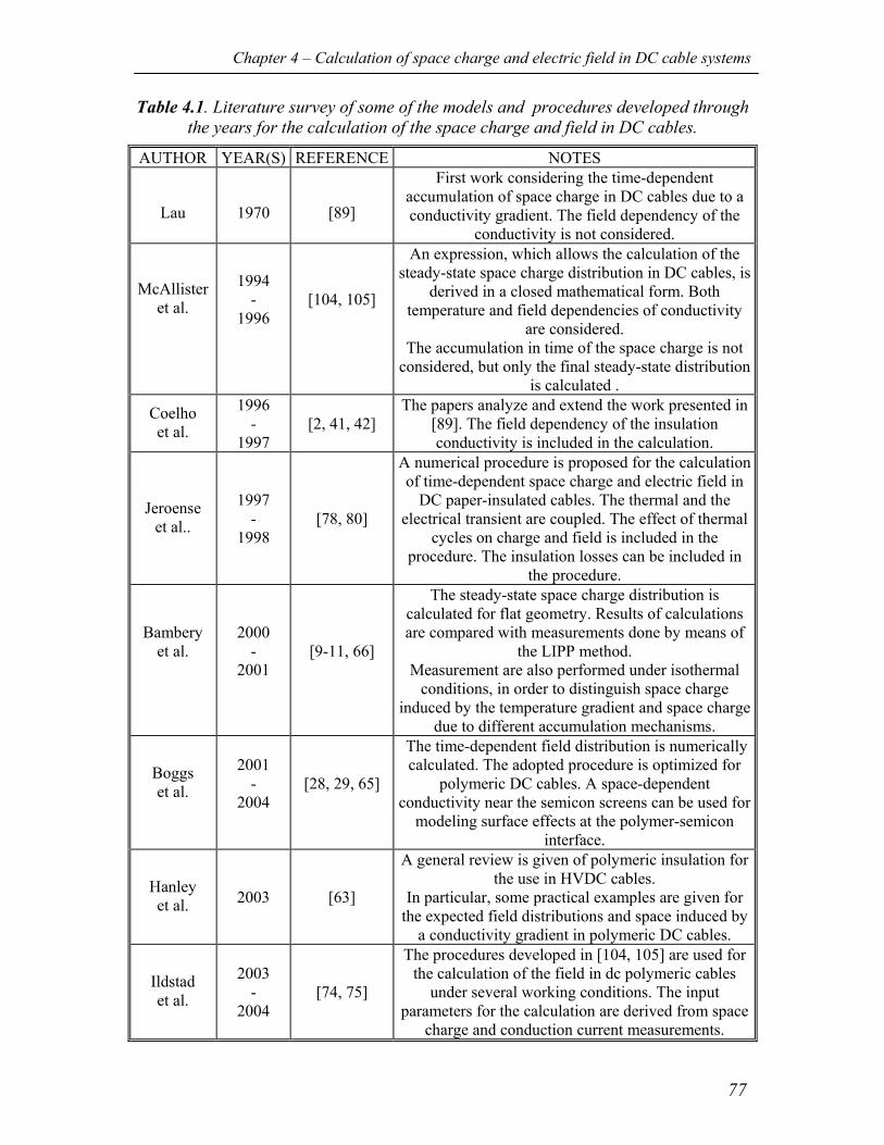
Chapter 4 – Calculation of space charge and electric field in DC cable systems
77
Table 4.1. Literature survey of some of the models and procedures developed through the years for the calculation of the space charge and field in DC cables.
AUTHOR YEAR(S) REFERENCE NOTES
Lau
1970
[89]
First work considering the time-dependent accumulation of space charge in DC cables due to a conductivity gradient. The field dependency of the
conductivity is not considered.
McAllister et al.
1994 -
1996
[104, 105]
An expression, which allows the calculation of the steady-state space charge distribution in DC cables, is
derived in a closed mathematical form. Both temperature and field dependencies of conductivity
are considered. The accumulation in time of the space charge is not
considered, but only the final steady-state distribution is calculated .
Coelho et al.
1996 -
1997
[2, 41, 42]
The papers analyze and extend the work presented in [89]. The field dependency of the insulation conductivity is included in the calculation.
Jeroense et al..
1997 -
1998
[78, 80]
A numerical procedure is proposed for the calculation of time-dependent space charge and electric field in
DC paper-insulated cables. The thermal and the electrical transient are coupled. The effect of thermal
cycles on charge and field is included in the procedure. The insulation losses can be included in
the procedure.
Bambery et al.
2000 -
2001
[9-11, 66]
The steady-state space charge distribution is calculated for flat geometry. Results of calculations are compared with measurements done by means of
the LIPP method. Measurement are also performed under isothermal
conditions, in order to distinguish space charge induced by the temperature gradient and space charge
due to different accumulation mechanisms.
Boggs et al.
2001
- 2004
[28, 29, 65]
The time-dependent field distribution is numerically calculated. The adopted procedure is optimized for
polymeric DC cables. A space-dependent conductivity near the semicon screens can be used for
modeling surface effects at the polymer-semicon interface.
Hanley et al.
2003
[63]
A general review is given of polymeric insulation for the use in HVDC cables.
In particular, some practical examples are given for the expected field distributions and space induced by
a conductivity gradient in polymeric DC cables.
Ildstad et al.
2003
- 2004
[74, 75]
The procedures developed in [104, 105] are used for the calculation of the field in dc polymeric cables
under several working conditions. The input parameters for the calculation are derived from space
charge and conduction current measurements.
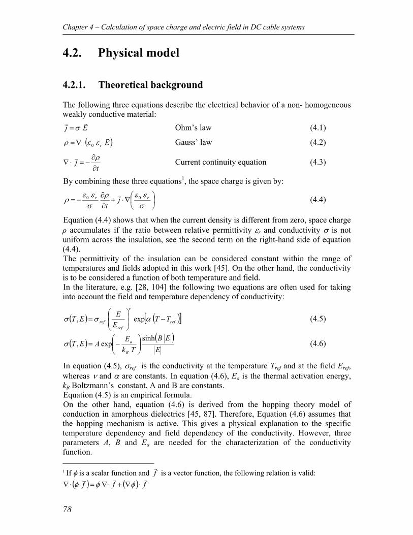
Chapter 4 – Calculation of space charge and electric field in DC cable systems
78
4.2. Physical model 4.2.1. Theoretical background The following three equations describe the electrical behavior of a non- homogeneous weakly conductive material:
Ejrr
σ= Ohm’s law (4.1)
( )Er
rεερ 0⋅∇= Gauss’ law (4.2)
tj
∂∂
−=⋅∇ρr Current continuity equation (4.3)
By combining these three equations1, the space charge is given by:
∇⋅+
∂∂
−=σεερ
σεερ rr j
t00 r (4.4)
Equation (4.4) shows that when the current density is different from zero, space charge ρ accumulates if the ratio between relative permittivity εr and conductivity σ is not uniform across the insulation, see the second term on the right-hand side of equation (4.4). The permittivity of the insulation can be considered constant within the range of temperatures and fields adopted in this work [45]. On the other hand, the conductivity is to be considered a function of both temperature and field. In the literature, e.g. [28, 104] the following two equations are often used for taking into account the field and temperature dependency of conductivity:
( ) ( )[ ]refref
ref TTEEET −
= ασσ
ν
exp, (4.5)
( ) ( )E
EBTk
EAETB
a sinhexp,
−=σ (4.6)
In equation (4.5), σref is the conductivity at the temperature Tref and at the field Eref, whereas ν and α are constants. In equation (4.6), Ea is the thermal activation energy, kB Boltzmann’s constant, A and B are constants. Equation (4.5) is an empirical formula. On the other hand, equation (4.6) is derived from the hopping theory model of conduction in amorphous dielectrics [45, 87]. Therefore, Equation (4.6) assumes that the hopping mechanism is active. This gives a physical explanation to the specific temperature dependency and field dependency of the conductivity. However, three parameters A, B and Ea are needed for the characterization of the conductivity function. 1 If φ is a scalar function and f
r is a vector function, the following relation is valid:
( ) ( ) fffrrv
⋅∇+⋅∇=⋅∇ φφφ
Chapter 4 – Calculation of space charge and electric field in DC cable systems
79
Field calculations were performed using both conductivity equations. The effect of the two different conductivity equations on the calculation results is discussed in Section 4.3. As discussed in Section 2.4.1, either a steady-state temperature distribution or a dynamic temperature distribution can be applied across the cable insulation. Both conditions are considered in the developed procedure. In order to solve equation (4.4), the following initial conditions and boundary conditions are used. Initial conditions The electric field immediately after the application of the DC voltage is capacitively distributed. This implies that at time t = 0 s, no space charge is present within the insulation: ( ) 00 ==tρ (4.7)
Boundary conditions The external DC voltage applied across the insulation must be known and the electric field distribution must fulfil the following equation:
UE −∇=r
(4.8) In Appendix E, the equations presented in this section are characterized for the specific studied configuration (i.e. two different insulating materials arranged in a coaxial lay out). 4.2.2. Model of the insulation The system to be studied consists of the cable insulation in non-ohmic2 contact with the electrodes [45]. This is modelled by considering an equivalent insulation in ohmic contact with the electrodes. The conductivity of the equivalent insulation is derived by fitting the conductivity function with the experimental results of conduction current measurements. The measurements have been performed on the system to be modelled, i.e. the cable insulation in non-ohmic contact with the electrodes. In this way, the equivalent insulation includes the effect that the electrodes have on the conduction process. In Figure 4.1, this concept is schematised. Limits of the model By considering ohmic contact between insulation and electrodes, injection and blocking properties of the dielectric/electrode interface cannot be included in the model. The same is valid for the dielectric interface between two insulations, if a cable joint is modelled.
2 Ohmic contact between electrodes and insulation occurs if the current injected by the electrodes equalizes the current transported by the insulation. If this condition is not fulfilled, the contact is non-homic.
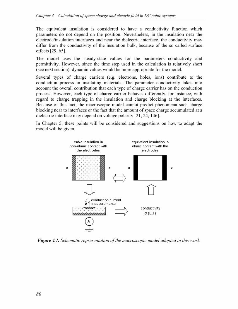
Chapter 4 – Calculation of space charge and electric field in DC cable systems
80
The equivalent insulation is considered to have a conductivity function which parameters do not depend on the position. Nevertheless, in the insulation near the electrode/insulation interfaces and near the dielectric interface, the conductivity may differ from the conductivity of the insulation bulk, because of the so called surface effects [29, 65]. The model uses the steady-state values for the parameters conductivity and permittivity. However, since the time step used in the calculation is relatively short (see next section), dynamic values would be more appropriate for the model. Several types of charge carriers (e.g. electrons, holes, ions) contribute to the conduction process in insulating materials. The parameter conductivity takes into account the overall contribution that each type of charge carrier has on the conduction process. However, each type of charge carrier behaves differently, for instance, with regard to charge trapping in the insulation and charge blocking at the interfaces. Because of this fact, the macroscopic model cannot predict phenomena such charge blocking near to interfaces or the fact that the amount of space charge accumulated at a dielectric interface may depend on voltage polarity [21, 24, 146]. In Chapter 5, these points will be considered and suggestions on how to adapt the model will be given.
Figure 4.1. Schematic representation of the macroscopic model adopted in this work.
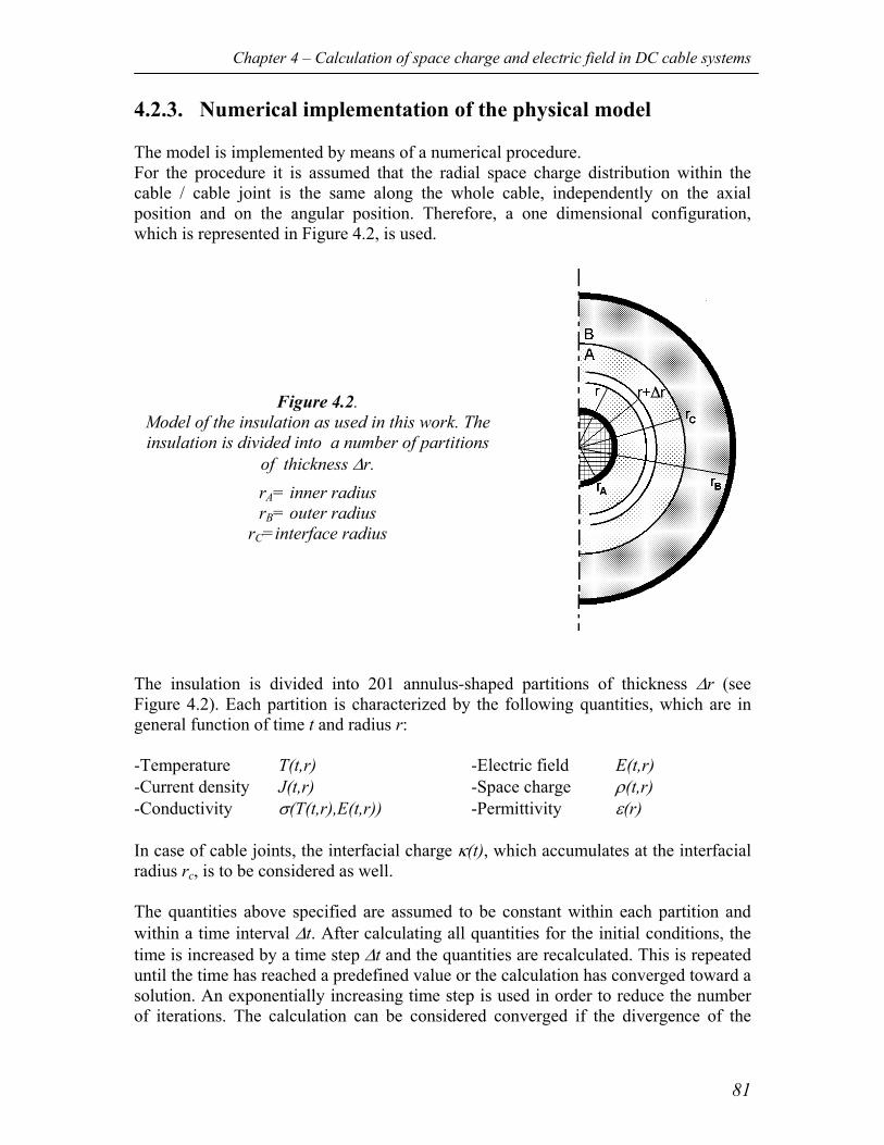
Chapter 4 – Calculation of space charge and electric field in DC cable systems
81
4.2.3. Numerical implementation of the physical model The model is implemented by means of a numerical procedure. For the procedure it is assumed that the radial space charge distribution within the cable / cable joint is the same along the whole cable, independently on the axial position and on the angular position. Therefore, a one dimensional configuration, which is represented in Figure 4.2, is used.
The insulation is divided into 201 annulus-shaped partitions of thickness ∆r (see Figure 4.2). Each partition is characterized by the following quantities, which are in general function of time t and radius r: -Temperature T(t,r) -Electric field E(t,r) -Current density J(t,r) -Space charge ρ(t,r) -Conductivity σ(T(t,r),E(t,r)) -Permittivity ε(r) In case of cable joints, the interfacial charge κ(t), which accumulates at the interfacial radius rc, is to be considered as well. The quantities above specified are assumed to be constant within each partition and within a time interval ∆t. After calculating all quantities for the initial conditions, the time is increased by a time step ∆t and the quantities are recalculated. This is repeated until the time has reached a predefined value or the calculation has converged toward a solution. An exponentially increasing time step is used in order to reduce the number of iterations. The calculation can be considered converged if the divergence of the
Figure 4.2. Model of the insulation as used in this work. The insulation is divided into a number of partitions
of thickness ∆r. rA= inner radius rB= outer radius
rC=interface radius
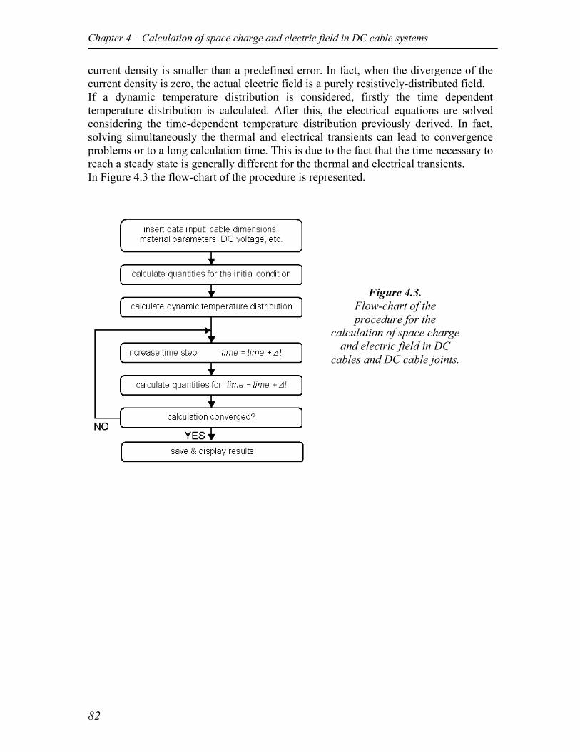
Chapter 4 – Calculation of space charge and electric field in DC cable systems
82
current density is smaller than a predefined error. In fact, when the divergence of the current density is zero, the actual electric field is a purely resistively-distributed field. If a dynamic temperature distribution is considered, firstly the time dependent temperature distribution is calculated. After this, the electrical equations are solved considering the time-dependent temperature distribution previously derived. In fact, solving simultaneously the thermal and electrical transients can lead to convergence problems or to a long calculation time. This is due to the fact that the time necessary to reach a steady state is generally different for the thermal and electrical transients. In Figure 4.3 the flow-chart of the procedure is represented.
Figure 4.3. Flow-chart of the procedure for the
calculation of space charge and electric field in DC
cables and DC cable joints.
Chapter 4 – Calculation of space charge and electric field in DC cable systems
83
4.3. Results of the calculation 4.3.1. Calculation vs. measurements In this section the results of the calculation are presented and compared with the experimental results. A gaussian filter is applied to the simulated data, in order to reproduce patterns of the same type as the measured patterns. All the calculated patterns are obtained by considering the same polarization and temperature conditions as adopted for the measurements. For each studied situation, the insulation is always characterized with the following parameters:
rel. permittivity XLPE εr = 2.3
rel. permittivity EPR εr = 2.9
Conductivity XLPE as in equation (4.5): σref = 3 10-18 Ω-1m-1; Tref = 20 °C; Eref = 13 kV/mm; α = 0.16 K-1; ν = 1.8
Conductivity EPR as in equation (4.5): σref = 5 10-17 Ω-1m-1; Tref = 20 °C; Eref = 13 kV/mm; α = 0.1 K-1; ν = 1.6
MV-size XLPE cable The development in time of space charge and electric field is calculated for a studied MV-size XLPE cable under the following conditions: Applied voltage : U0= + 90 kV Temperature : Tin = 65 °C ; Tout = 45 °C ; ∆T = 20 K; ∇T = 4.4 K/mm In Figure 4.4, the results of the calculation are compared to the results of the measurements. Figure 4.4 shows that accumulation of positive space charge is predicted in the insulation bulk due to the presence of the temperature drop. The maximum of the calculated space charge distribution is slightly underestimated and no hetero-charge near the inner semicon is simulated (compare Figures 4.4.a and 4.4.b). On the other hand, the fact that most of the charge accumulates in the first 104 s of polarization is acceptably estimated by the model. This is shown in Figures 4.4.e and 4.4.f, where the charge evolution in time is shown at specific locations in the cable insulation. The calculated field patterns and the measured electric field patterns are quite similar: the field inversion phenomenon is in fact predicted by the model. However, the field at the outer semicon is slightly underestimated. In addition, the minimum of the field distribution near the inner semicon (compare Figures 4.4.c and 4.4.d) is not reproduced.
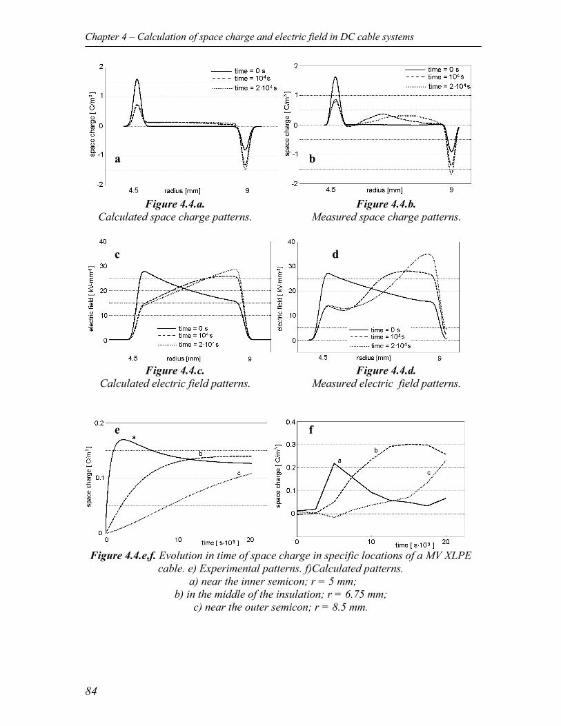
Chapter 4 – Calculation of space charge and electric field in DC cable systems
84
Figure 4.4.a.
Calculated space charge patterns. Figure 4.4.b.
Measured space charge patterns.
Figure 4.4.c.
Calculated electric field patterns. Figure 4.4.d.
Measured electric field patterns.
Figure 4.4.e,f. Evolution in time of space charge in specific locations of a MV XLPE
cable. e) Experimental patterns. f)Calculated patterns. a) near the inner semicon; r = 5 mm;
b) in the middle of the insulation; r = 6.75 mm; c) near the outer semicon; r = 8.5 mm.
a b
c d
e f
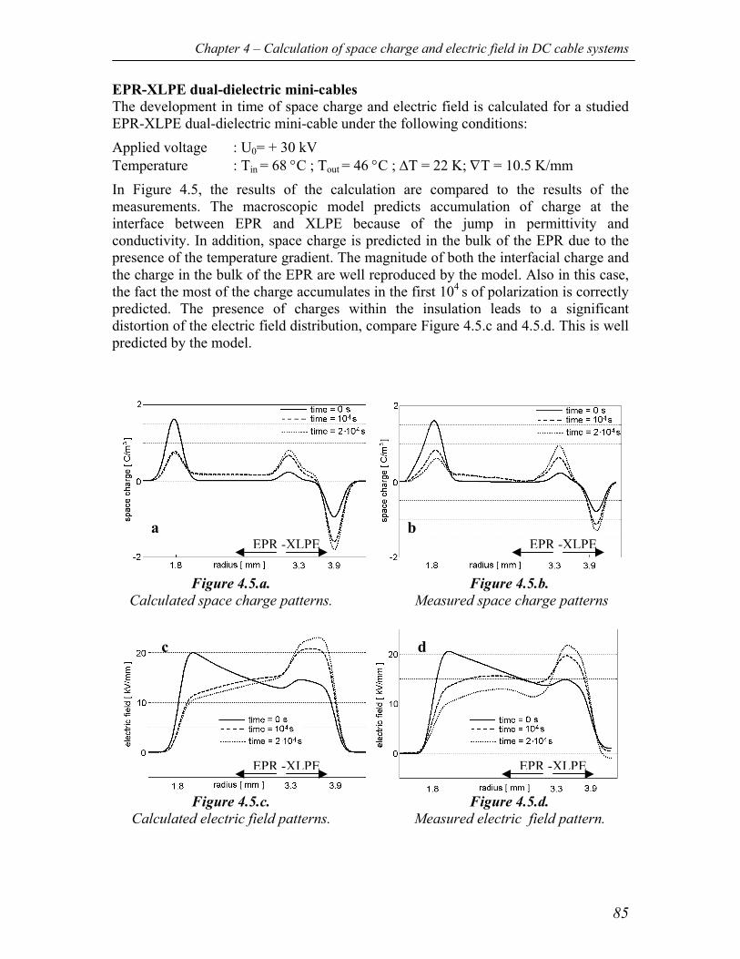
Chapter 4 – Calculation of space charge and electric field in DC cable systems
85
EPR-XLPE dual-dielectric mini-cables The development in time of space charge and electric field is calculated for a studied EPR-XLPE dual-dielectric mini-cable under the following conditions: Applied voltage : U0= + 30 kV Temperature : Tin = 68 °C ; Tout = 46 °C ; ∆T = 22 K; ∇T = 10.5 K/mm In Figure 4.5, the results of the calculation are compared to the results of the measurements. The macroscopic model predicts accumulation of charge at the interface between EPR and XLPE because of the jump in permittivity and conductivity. In addition, space charge is predicted in the bulk of the EPR due to the presence of the temperature gradient. The magnitude of both the interfacial charge and the charge in the bulk of the EPR are well reproduced by the model. Also in this case, the fact the most of the charge accumulates in the first 104 s of polarization is correctly predicted. The presence of charges within the insulation leads to a significant distortion of the electric field distribution, compare Figure 4.5.c and 4.5.d. This is well predicted by the model.
Figure 4.5.a.
Calculated space charge patterns.
Figure 4.5.b. Measured space charge patterns
Figure 4.5.c.
Calculated electric field patterns. Figure 4.5.d.
Measured electric field pattern.
a b
c d
EPR -XLPE EPR -XLPE
EPR -XLPE EPR -XLPE
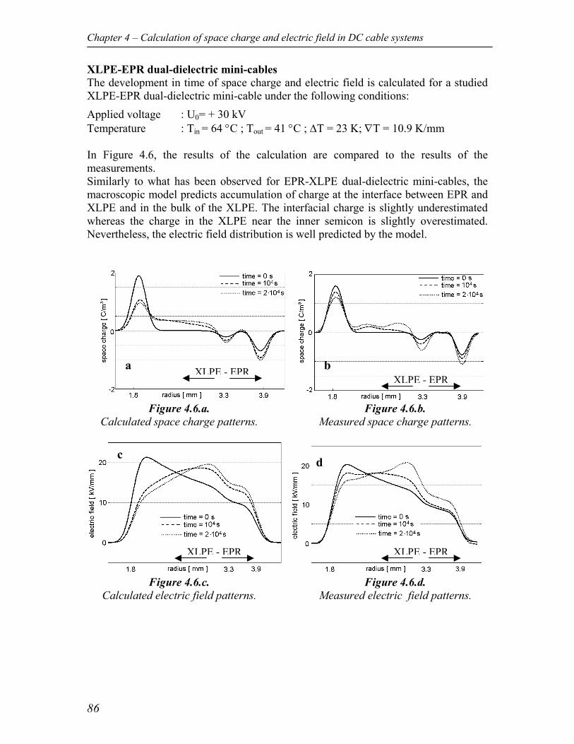
Chapter 4 – Calculation of space charge and electric field in DC cable systems
86
XLPE-EPR dual-dielectric mini-cables The development in time of space charge and electric field is calculated for a studied XLPE-EPR dual-dielectric mini-cable under the following conditions: Applied voltage : U0= + 30 kV Temperature : Tin = 64 °C ; Tout = 41 °C ; ∆T = 23 K; ∇T = 10.9 K/mm In Figure 4.6, the results of the calculation are compared to the results of the measurements. Similarly to what has been observed for EPR-XLPE dual-dielectric mini-cables, the macroscopic model predicts accumulation of charge at the interface between EPR and XLPE and in the bulk of the XLPE. The interfacial charge is slightly underestimated whereas the charge in the XLPE near the inner semicon is slightly overestimated. Nevertheless, the electric field distribution is well predicted by the model.
Figure 4.6.a.
Calculated space charge patterns. Figure 4.6.b.
Measured space charge patterns.
Figure 4.6.c.
Calculated electric field patterns.
Figure 4.6.d. Measured electric field patterns.
c
a b
d
XLPE - EPRXLPE - EPR
XLPE - EPR XLPE - EPR
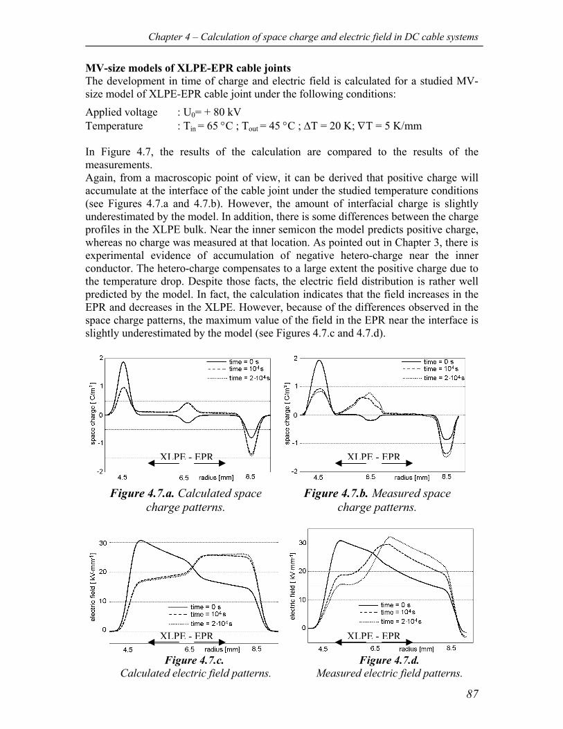
Chapter 4 – Calculation of space charge and electric field in DC cable systems
87
MV-size models of XLPE-EPR cable joints The development in time of charge and electric field is calculated for a studied MV-size model of XLPE-EPR cable joint under the following conditions: Applied voltage : U0= + 80 kV Temperature : Tin = 65 °C ; Tout = 45 °C ; ∆T = 20 K; ∇T = 5 K/mm In Figure 4.7, the results of the calculation are compared to the results of the measurements. Again, from a macroscopic point of view, it can be derived that positive charge will accumulate at the interface of the cable joint under the studied temperature conditions (see Figures 4.7.a and 4.7.b). However, the amount of interfacial charge is slightly underestimated by the model. In addition, there is some differences between the charge profiles in the XLPE bulk. Near the inner semicon the model predicts positive charge, whereas no charge was measured at that location. As pointed out in Chapter 3, there is experimental evidence of accumulation of negative hetero-charge near the inner conductor. The hetero-charge compensates to a large extent the positive charge due to the temperature drop. Despite those facts, the electric field distribution is rather well predicted by the model. In fact, the calculation indicates that the field increases in the EPR and decreases in the XLPE. However, because of the differences observed in the space charge patterns, the maximum value of the field in the EPR near the interface is slightly underestimated by the model (see Figures 4.7.c and 4.7.d).
XLPE - EPR XLPE - EPR
Figure 4.7.a. Calculated space charge patterns.
Figure 4.7.b. Measured space charge patterns.
XLPE - EPR XLPE - EPR
Figure 4.7.c. Calculated electric field patterns.
Figure 4.7.d. Measured electric field patterns.
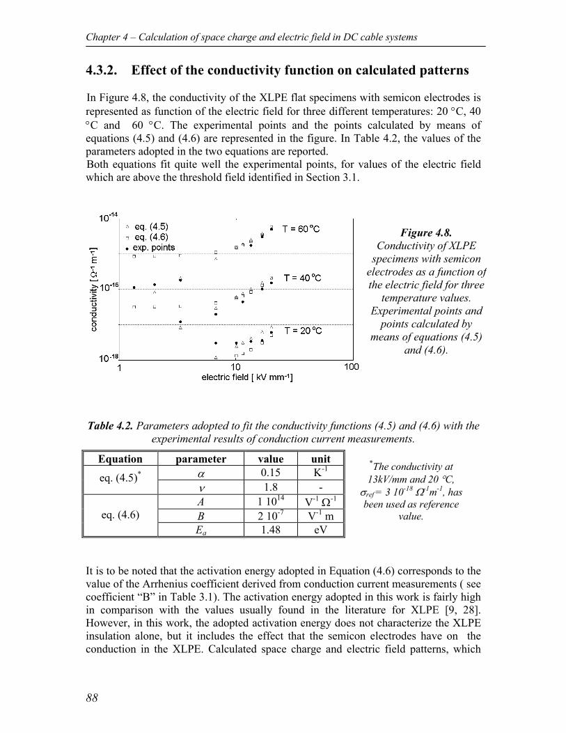
Chapter 4 – Calculation of space charge and electric field in DC cable systems
88
4.3.2. Effect of the conductivity function on calculated patterns In Figure 4.8, the conductivity of the XLPE flat specimens with semicon electrodes is represented as function of the electric field for three different temperatures: 20 °C, 40 °C and 60 °C. The experimental points and the points calculated by means of equations (4.5) and (4.6) are represented in the figure. In Table 4.2, the values of the parameters adopted in the two equations are reported. Both equations fit quite well the experimental points, for values of the electric field which are above the threshold field identified in Section 3.1.
Table 4.2. Parameters adopted to fit the conductivity functions (4.5) and (4.6) with the experimental results of conduction current measurements.
Equation parameter value unit α 0.15 K-1 eq. (4.5)* ν 1.8 - A 1 1014 V-1 Ω-1 B 2 10-7 V-1 m
eq. (4.6)
Ea 1.48 eV
It is to be noted that the activation energy adopted in Equation (4.6) corresponds to the value of the Arrhenius coefficient derived from conduction current measurements ( see coefficient “B” in Table 3.1). The activation energy adopted in this work is fairly high in comparison with the values usually found in the literature for XLPE [9, 28]. However, in this work, the adopted activation energy does not characterize the XLPE insulation alone, but it includes the effect that the semicon electrodes have on the conduction in the XLPE. Calculated space charge and electric field patterns, which
*The conductivity at 13kV/mm and 20 °C,
σref = 3 10-18 Ω-1m-1, has been used as reference
value.
Figure 4.8. Conductivity of XLPE
specimens with semicon electrodes as a function of the electric field for three
temperature values. Experimental points and
points calculated by means of equations (4.5)
and (4.6).
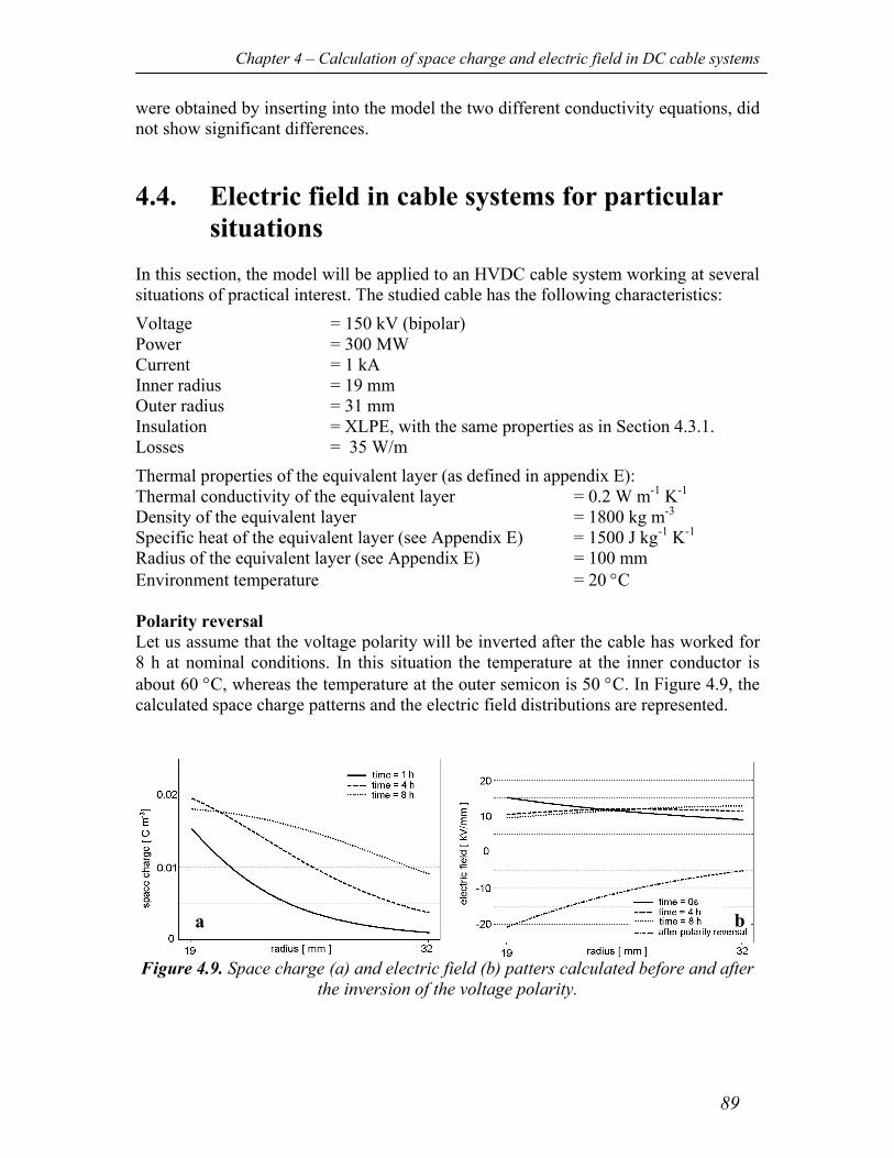
Chapter 4 – Calculation of space charge and electric field in DC cable systems
89
were obtained by inserting into the model the two different conductivity equations, did not show significant differences.
4.4. Electric field in cable systems for particular situations
In this section, the model will be applied to an HVDC cable system working at several situations of practical interest. The studied cable has the following characteristics: Voltage = 150 kV (bipolar) Power = 300 MW Current = 1 kA Inner radius = 19 mm Outer radius = 31 mm Insulation = XLPE, with the same properties as in Section 4.3.1. Losses = 35 W/m Thermal properties of the equivalent layer (as defined in appendix E): Thermal conductivity of the equivalent layer = 0.2 W m-1 K-1 Density of the equivalent layer = 1800 kg m-3
Specific heat of the equivalent layer (see Appendix E) = 1500 J kg-1 K-1
Radius of the equivalent layer (see Appendix E) = 100 mm Environment temperature = 20 °C Polarity reversal Let us assume that the voltage polarity will be inverted after the cable has worked for 8 h at nominal conditions. In this situation the temperature at the inner conductor is about 60 °C, whereas the temperature at the outer semicon is 50 °C. In Figure 4.9, the calculated space charge patterns and the electric field distributions are represented.
Figure 4.9. Space charge (a) and electric field (b) patters calculated before and after
the inversion of the voltage polarity.
a b
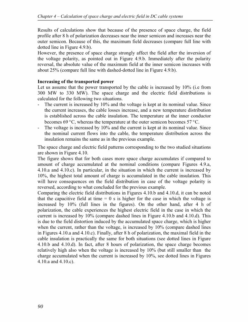
Chapter 4 – Calculation of space charge and electric field in DC cable systems
90
Results of calculations show that because of the presence of space charge, the field profile after 8 h of polarization decreases near the inner semicon and increases near the outer semicon. Because of this, the maximum field decreases (compare full line with dotted line in Figure 4.9.b). However, the presence of space charge strongly affect the field after the inversion of the voltage polarity, as pointed out in Figure 4.9.b. Immediately after the polarity reversal, the absolute value of the maximum field at the inner semicon increases with about 25% (compare full line with dashed-dotted line in Figure 4.9.b). Increasing of the transported power Let us assume that the power transported by the cable is increased by 10% (i.e from 300 MW to 330 MW). The space charge and the electric field distributions is calculated for the following two situations. - The current is increased by 10% and the voltage is kept at its nominal value. Since
the current increases, the cable losses increase, and a new temperature distribution is established across the cable insulation. The temperature at the inner conductor becomes 69 °C, whereas the temperature at the outer semicon becomes 57 °C.
- The voltage is increased by 10% and the current is kept at its nominal value. Since the nominal current flows into the cable, the temperature distribution across the insulation remains the same as in the previous example.
The space charge and electric field patterns corresponding to the two studied situations are shown in Figure 4.10. The figure shows that for both cases more space charge accumulates if compared to amount of charge accumulated at the nominal conditions (compare Figures 4.9.a, 4.10.a and 4.10.c). In particular, in the situation in which the current is increased by 10%, the highest total amount of charge is accumulated in the cable insulation. This will have consequences on the field distribution in case of the voltage polarity is reversed, according to what concluded for the previous example. Comparing the electric field distributions in Figures 4.10.b and 4.10.d, it can be noted that the capacitive field at time = 0 s is higher for the case in which the voltage is increased by 10% (full lines in the figures). On the other hand, after 4 h of polarization, the cable experiences the highest electric field in the case in which the current is increased by 10% (compare dashed lines in Figure 4.10.b and 4.10.d). This is due to the field distortion induced by the accumulated space charge, which is higher when the current, rather than the voltage, is increased by 10% (compare dashed lines in Figures 4.10.a and 4.10.c). Finally, after 8 h of polarization, the maximal field in the cable insulation is practically the same for both situations (see dotted lines in Figure 4.10.b and 4.10.d). In fact, after 8 hours of polarization, the space charge becomes relatively high also when the voltage is increased by 10% (but still smaller than the charge accumulated when the current is increased by 10%, see dotted lines in Figures 4.10.a and 4.10.c).
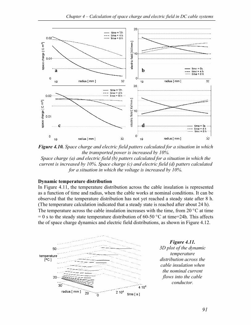
Chapter 4 – Calculation of space charge and electric field in DC cable systems
91
Figure 4.10. Space charge and electric field patters calculated for a situation in which
the transported power is increased by 10%. Space charge (a) and electric field (b) patters calculated for a situation in which the
current is increased by 10%. Space charge (c) and electric field (d) patters calculated for a situation in which the voltage is increased by 10%.
Dynamic temperature distribution In Figure 4.11, the temperature distribution across the cable insulation is represented as a function of time and radius, when the cable works at nominal conditions. It can be observed that the temperature distribution has not yet reached a steady state after 8 h. (The temperature calculation indicated that a steady state is reached after about 24 h). The temperature across the cable insulation increases with the time, from 20 °C at time = 0 s to the steady state temperature distribution of 60-50 °C at time=24h. This affects the of space charge dynamics and electric field distributions, as shown in Figure 4.12.
a b
c d
Figure 4.11. 3D plot of the dynamic
temperature distribution across the cable insulation when the nominal current flows into the cable
conductor.
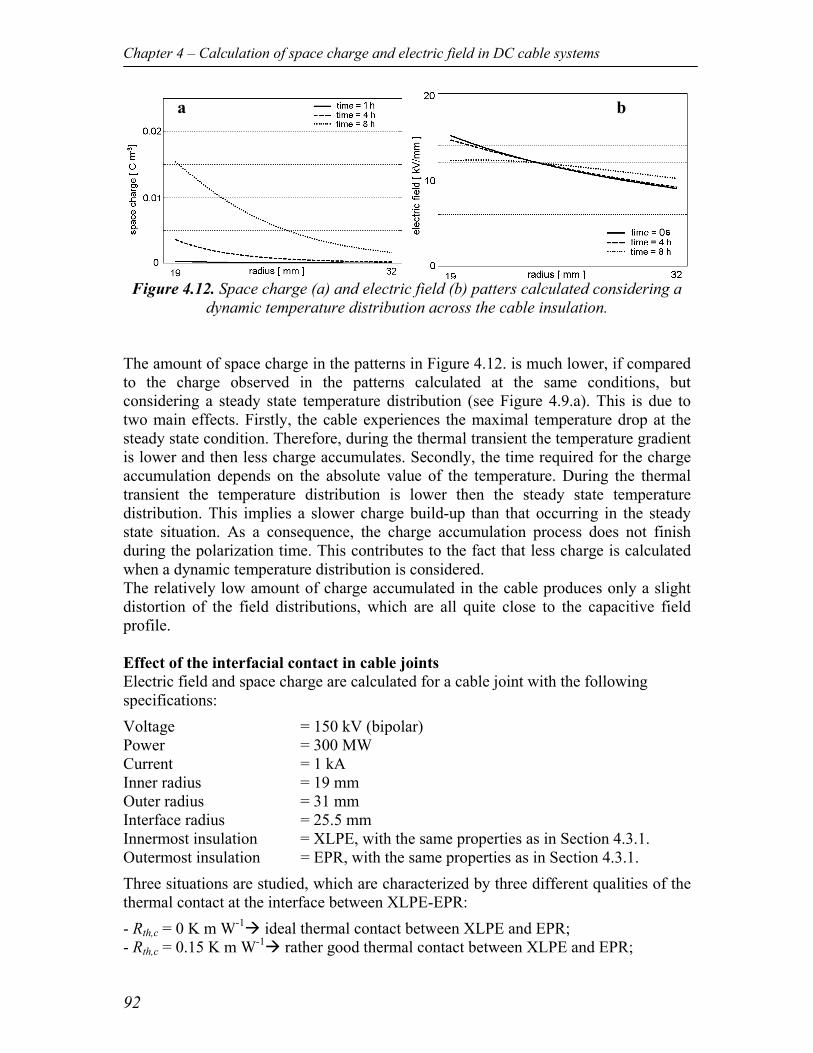
Chapter 4 – Calculation of space charge and electric field in DC cable systems
92
Figure 4.12. Space charge (a) and electric field (b) patters calculated considering a
dynamic temperature distribution across the cable insulation.
The amount of space charge in the patterns in Figure 4.12. is much lower, if compared to the charge observed in the patterns calculated at the same conditions, but considering a steady state temperature distribution (see Figure 4.9.a). This is due to two main effects. Firstly, the cable experiences the maximal temperature drop at the steady state condition. Therefore, during the thermal transient the temperature gradient is lower and then less charge accumulates. Secondly, the time required for the charge accumulation depends on the absolute value of the temperature. During the thermal transient the temperature distribution is lower then the steady state temperature distribution. This implies a slower charge build-up than that occurring in the steady state situation. As a consequence, the charge accumulation process does not finish during the polarization time. This contributes to the fact that less charge is calculated when a dynamic temperature distribution is considered. The relatively low amount of charge accumulated in the cable produces only a slight distortion of the field distributions, which are all quite close to the capacitive field profile. Effect of the interfacial contact in cable joints Electric field and space charge are calculated for a cable joint with the following specifications: Voltage = 150 kV (bipolar) Power = 300 MW Current = 1 kA Inner radius = 19 mm Outer radius = 31 mm Interface radius = 25.5 mm Innermost insulation = XLPE, with the same properties as in Section 4.3.1. Outermost insulation = EPR, with the same properties as in Section 4.3.1. Three situations are studied, which are characterized by three different qualities of the thermal contact at the interface between XLPE-EPR: - Rth,c = 0 K m W-1 ideal thermal contact between XLPE and EPR; - Rth,c = 0.15 K m W-1 rather good thermal contact between XLPE and EPR;
a b
Chapter 4 – Calculation of space charge and electric field in DC cable systems
93
- Rth,c = 0.3 K m W-1 fairly bad thermal contact between XLPE and EPR. Rth,c is the contact thermal resistance per unit of length, introduced in Chapter 2. In Figure 4.13, the temperature distribution across the insulation of the joint is represented for the three studied cases, whereas in Figure 4.14 the electric field distributions are represented. Figure 4.14 shows that the quality of the thermal contact at the XLPE-EPR interface strongly affects the electric field distribution within the joint insulation. In case of ideal contact, the field is higher in the XLPE and lower in the EPR. If the quality of the contact becomes worse (i.e. the contact thermal resistance increases), the field in the XLPE decreases and the field in the EPR increases. In the case in which the contact is “bad” (see Figure 4.14.c), the field in the EPR results higher than the field in the XLPE. The polarization at the interface depends on the conductivity of XLPE and EPR. The conductivity is temperature dependent and the temperature distribution is different according to the type of contact (see Figure 4.13). Then, the polarization at the interface is affected by the quality of thermal contact. Figure 4.15 shows the accumulation in time of charge at the XLPE-EPR interface. In the figure, it is evident how different the polarization of the interface is according to the qulity of the thermal contact at the interface (see for instance full and dotted lines in Figure 4.14).
Figure 4.13. Temperature distribution across the insulation of a cable joint calculated for different qualities of the
interfacial contact.
Figure 4.15. Evolution in time of interfacial charge
calculated for an XLPE-EPR cable joint.
Chapter 4 – Calculation of space charge and electric field in DC cable systems
94
Figure 4.14. Electric field profiles calculated for an XLPE-EPR cable joint.
Calculated electric field distributions:
ideal contact (Rth,c = 0 K m W-1) Tin = 60°C Tout = 50°C
Calculated electric field distributions:
good contact (Rth,c = 0.15 K m W-1) Tin = 65°C Tout = 50°C
Calculated electric field distributions:
bad contact (Rth,c = 0.3 K m W-1) Tin = 71°C Tout = 50°C
a
b
c
Chapter 4 – Calculation of space charge and electric field in DC cable systems
95
4.5. Conclusions In this chapter a physical model, which describes the dynamic space charge behavior in cables and cable joints, was presented. The model was implemented by means of a numerical procedure, allowing the calculation of the space charge distribution and the time dependent electric field. Despite the fact that the model is based only on macroscopic properties of the insulation, the experimental data presented in Chapter 3 were quite well reproduced by the proposed model. This validates the theory that the macroscopic properties of the insulation have a major effect on space charge and electric field behavior of the studied test specimens within the adopted temperature/voltage conditions. However, in some cases, some differences are observed between calculated and experimental patterns. In particular at the higher temperatures, the measured hetero-charge distribution near the electrode-insulation interface could not be predicted by the model. Furthermore, at the dielectric interface of MV-size models of cable joints, more charge accumulated than what estimated by the physical model. Those findings point out that at interfaces the space charge accumulation mechanism is generally more complex than the mechanism expected from a purely macroscopic approach. The proposed model can give a quantitative indication of the time-dependent electric field in full-size DC cable systems. Results of calculation reveal that the cable load can strongly affect the space charge distribution and consequently the electric field. This was very evident in the following conditions. - Polarity reversal. If the voltage polarity is inverted on a loaded cable, the electric
field results enhanced near the inner conductor, because of the accumulated space charge. This agrees with the experimental results of Chapter 3.
- Overloading of the cable. Under this condition, the model predicts the highest amount of accumulated space charge. Therefore, increasing the current above its nominal value not only leads to an increase of the thermal stress, but also to an enhancement of the electric stress experienced by the cable insulation.
- Bad thermal contact at interfaces in cable joints. If the thermal contact resistance between the cable insulation and the restored insulation of the joint is relatively high, the temperature drop across the dielectric interface results quite large. This affects the polarization of the interface and leads to an enhancement of the electric field in the insulation of the accessory near the interface.

Chapter 4 – Calculation of space charge and electric field in DC cable systems
96
Chapter 5 – Space charge at interfaces in HVDC cable systems
97
5. Space charge at interfaces in HVDC cable systems
Both the experimental data and the results of the theoretical modelling have shown that interfaces in HVDC cable systems are particularly critical with regard to the accumulation of space charge. For this reason, this chapter focuses on interfaces present in HVDC cable systems and on their polarization mechanisms. In Section 5.1, the different types of interfaces encountered in HVDC polymeric cable systems are introduced and compared to the interfaces of the studied test specimens. The concept of width of an interface is also discussed. In section 5.2, the effect of the semicon-insulation interface on space charge accumulation is discussed on the basis of the literature and on the experimental results presented in this thesis. Section 5.3 discusses the effect of a dielectric interface on space charge accumulation. The theory of interfacial polarization is reviewed and an improved model is given. Finally, in Section 5.4 some suggestions are given on how to improve the model presented in Chapter 4.
5.1. Interfaces in HVDC cable systems Two main types of interfaces are encountered in extruded-type HVDC cable systems: semicon-dielectric interfaces and dielectric-dielectric interfaces, also simply called dielectric interfaces. In Figure 5.1, both interfaces are represented.
Figure 5.1. Interfaces in extruded-
type HVDC cable systems.
a)Semicon-dielectric interface.
b)Dielectric-dielectric interface (or simply dielectric interface).
a
b
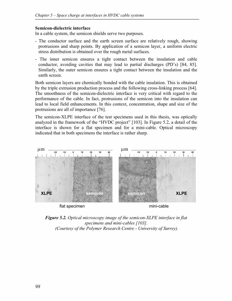
Chapter 5 – Space charge at interfaces in HVDC cable systems
98
Semicon-dielectric interface In a cable system, the semicon shields serve two purposes. - The conductor surface and the earth screen surface are relatively rough, showing
protrusions and sharp points. By application of a semicon layer, a uniform electric stress distribution is obtained over the rough metal surfaces.
- The inner semicon ensures a tight contact between the insulation and cable conductor, avoiding cavities that may lead to partial discharges (PD’s) [84, 85]. Similarly, the outer semicon ensures a tight contact between the insulation and the earth screen.
Both semicon layers are chemically bonded with the cable insulation. This is obtained by the triple extrusion production process and the following cross-linking process [64]. The smoothness of the semicon-dielectric interface is very critical with regard to the performance of the cable. In fact, protrusions of the semicon into the insulation can lead to local field enhancements. In this context, concentration, shape and size of the protrusions are all of importance [76]. The semicon-XLPE interface of the test specimens used in this thesis, was optically analyzed in the framework of the “HVDC project” [103]. In Figure 5.2, a detail of the interface is shown for a flat specimen and for a mini-cable. Optical microscopy indicated that in both specimens the interface is rather sharp.
Figure 5.2. Optical microscopy image of the semicon-XLPE interface in flat specimens and mini-cables [103].
(Courtesy of the Polymer Research Centre - University of Surrey).
XLPE XLPE semicon semicon
flat specimen mini-cable
µmµm
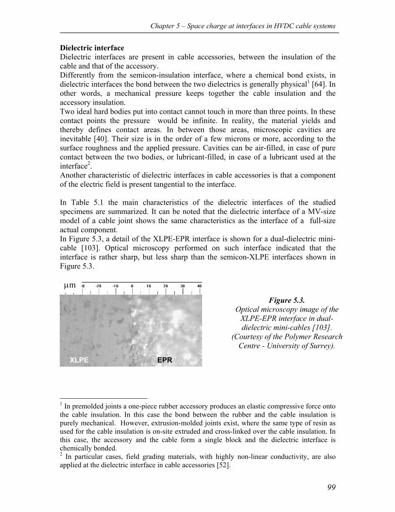
Chapter 5 – Space charge at interfaces in HVDC cable systems
99
Dielectric interface Dielectric interfaces are present in cable accessories, between the insulation of the cable and that of the accessory. Differently from the semicon-insulation interface, where a chemical bond exists, in dielectric interfaces the bond between the two dielectrics is generally physical1 [64]. In other words, a mechanical pressure keeps together the cable insulation and the accessory insulation. Two ideal hard bodies put into contact cannot touch in more than three points. In these contact points the pressure would be infinite. In reality, the material yields and thereby defines contact areas. In between those areas, microscopic cavities are inevitable [40]. Their size is in the order of a few microns or more, according to the surface roughness and the applied pressure. Cavities can be air-filled, in case of pure contact between the two bodies, or lubricant-filled, in case of a lubricant used at the interface2. Another characteristic of dielectric interfaces in cable accessories is that a component of the electric field is present tangential to the interface. In Table 5.1 the main characteristics of the dielectric interfaces of the studied specimens are summarized. It can be noted that the dielectric interface of a MV-size model of a cable joint shows the same characteristics as the interface of a full-size actual component. In Figure 5.3, a detail of the XLPE-EPR interface is shown for a dual-dielectric mini-cable [103]. Optical microscopy performed on such interface indicated that the interface is rather sharp, but less sharp than the semicon-XLPE interfaces shown in Figure 5.3. 1 In premolded joints a one-piece rubber accessory produces an elastic compressive force onto the cable insulation. In this case the bond between the rubber and the cable insulation is purely mechanical. However, extrusion-molded joints exist, where the same type of resin as used for the cable insulation is on-site extruded and cross-linked over the cable insulation. In this case, the accessory and the cable form a single block and the dielectric interface is chemically bonded. 2 In particular cases, field grading materials, with highly non-linear conductivity, are also applied at the dielectric interface in cable accessories [52].
XLPE EPR
µm Figure 5.3.
Optical microscopy image of the XLPE-EPR interface in dual-dielectric mini-cables [103].
(Courtesy of the Polymer Research Centre - University of Surrey).
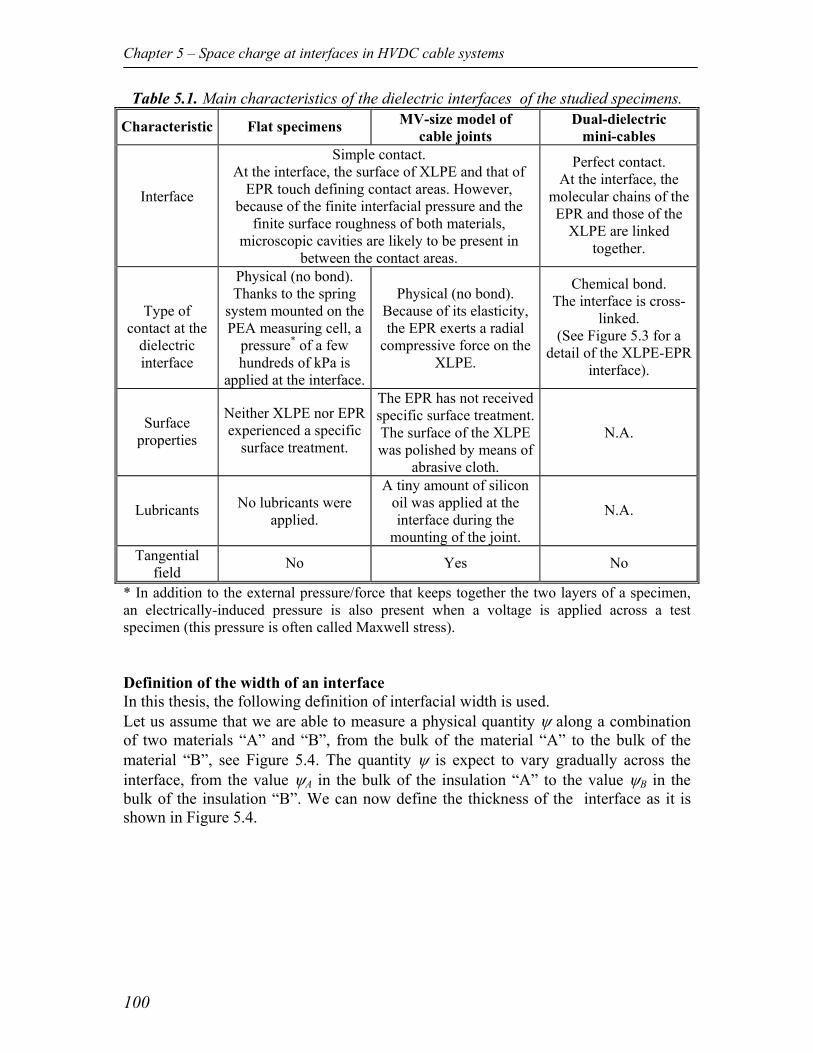
Chapter 5 – Space charge at interfaces in HVDC cable systems
100
Table 5.1. Main characteristics of the dielectric interfaces of the studied specimens. Characteristic Flat specimens MV-size model of
cable joints Dual-dielectric
mini-cables
Interface
Simple contact. At the interface, the surface of XLPE and that of
EPR touch defining contact areas. However, because of the finite interfacial pressure and the
finite surface roughness of both materials, microscopic cavities are likely to be present in
between the contact areas.
Perfect contact. At the interface, the
molecular chains of the EPR and those of the
XLPE are linked together.
Type of contact at the
dielectric interface
Physical (no bond). Thanks to the spring
system mounted on the PEA measuring cell, a
pressure* of a few hundreds of kPa is
applied at the interface.
Physical (no bond).
Because of its elasticity, the EPR exerts a radial
compressive force on the XLPE.
Chemical bond. The interface is cross-
linked. (See Figure 5.3 for a
detail of the XLPE-EPR interface).
Surface properties
Neither XLPE nor EPR experienced a specific
surface treatment.
The EPR has not received specific surface treatment. The surface of the XLPE was polished by means of
abrasive cloth.
N.A.
Lubricants
No lubricants were
applied.
A tiny amount of silicon oil was applied at the interface during the
mounting of the joint.
N.A.
Tangential field No Yes No
* In addition to the external pressure/force that keeps together the two layers of a specimen, an electrically-induced pressure is also present when a voltage is applied across a test specimen (this pressure is often called Maxwell stress). Definition of the width of an interface In this thesis, the following definition of interfacial width is used. Let us assume that we are able to measure a physical quantity ψ along a combination of two materials “A” and “B”, from the bulk of the material “A” to the bulk of the material “B”, see Figure 5.4. The quantity ψ is expect to vary gradually across the interface, from the value ψA in the bulk of the insulation “A” to the value ψB in the bulk of the insulation “B”. We can now define the thickness of the interface as it is shown in Figure 5.4.
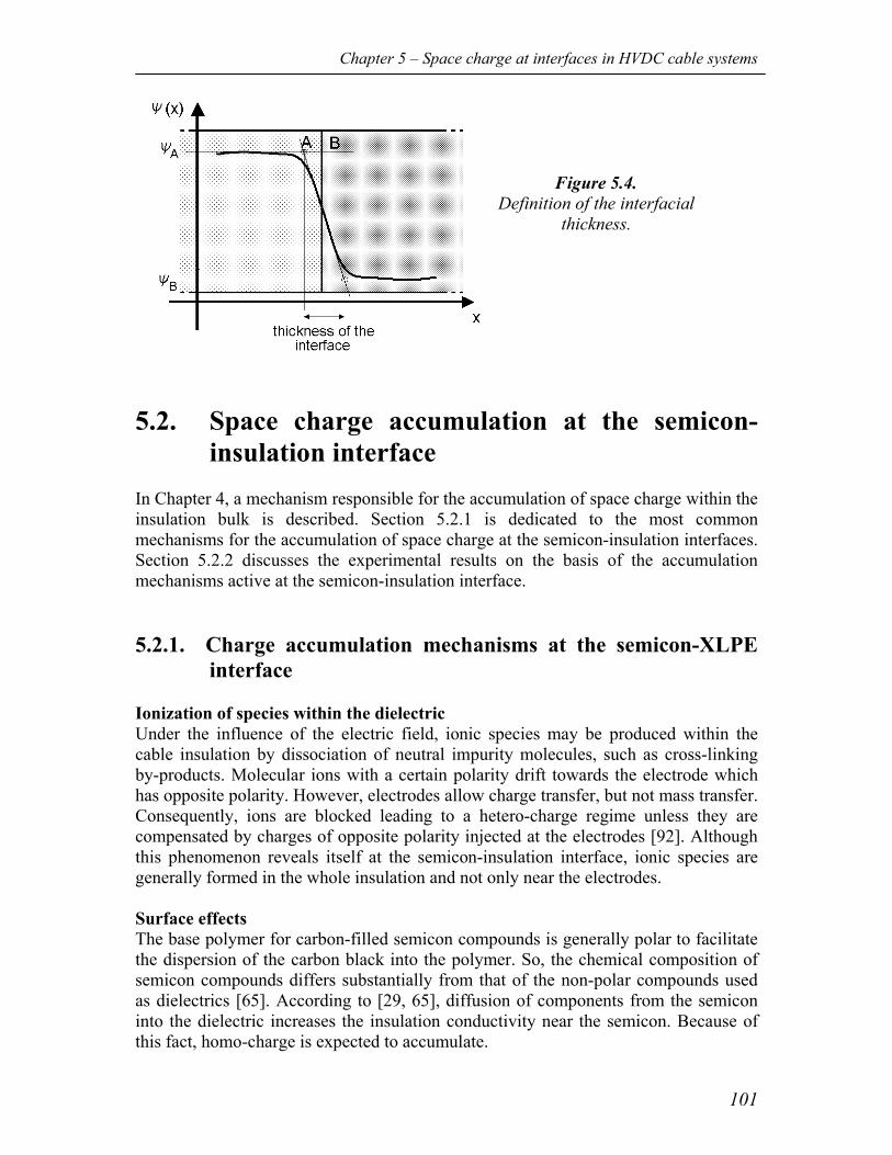
Chapter 5 – Space charge at interfaces in HVDC cable systems
101
5.2. Space charge accumulation at the semicon-insulation interface
In Chapter 4, a mechanism responsible for the accumulation of space charge within the insulation bulk is described. Section 5.2.1 is dedicated to the most common mechanisms for the accumulation of space charge at the semicon-insulation interfaces. Section 5.2.2 discusses the experimental results on the basis of the accumulation mechanisms active at the semicon-insulation interface. 5.2.1. Charge accumulation mechanisms at the semicon-XLPE
interface Ionization of species within the dielectric Under the influence of the electric field, ionic species may be produced within the cable insulation by dissociation of neutral impurity molecules, such as cross-linking by-products. Molecular ions with a certain polarity drift towards the electrode which has opposite polarity. However, electrodes allow charge transfer, but not mass transfer. Consequently, ions are blocked leading to a hetero-charge regime unless they are compensated by charges of opposite polarity injected at the electrodes [92]. Although this phenomenon reveals itself at the semicon-insulation interface, ionic species are generally formed in the whole insulation and not only near the electrodes. Surface effects The base polymer for carbon-filled semicon compounds is generally polar to facilitate the dispersion of the carbon black into the polymer. So, the chemical composition of semicon compounds differs substantially from that of the non-polar compounds used as dielectrics [65]. According to [29, 65], diffusion of components from the semicon into the dielectric increases the insulation conductivity near the semicon. Because of this fact, homo-charge is expected to accumulate.
Figure 5.4. Definition of the interfacial
thickness.
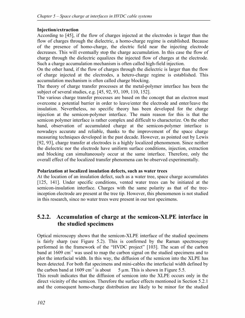
Chapter 5 – Space charge at interfaces in HVDC cable systems
102
Injection/extraction According to [45], if the flow of charges injected at the electrodes is larger than the flow of charges through the dielectric, a homo-charge regime is established. Because of the presence of homo-charge, the electric field near the injecting electrode decreases. This will eventually stop the charge accumulation. In this case the flow of charge through the dielectric equalizes the injected flow of charges at the electrode. Such a charge accumulation mechanism is often called high-field injection. On the other hand, if the flow of charges through the dielectric is larger than the flow of charge injected at the electrodes, a hetero-charge regime is established. This accumulation mechanism is often called charge blocking. The theory of charge transfer processes at the metal-polymer interface has been the subject of several studies, e.g. [45, 92, 93, 109, 110, 152]. The various charge transfer processes are based on the concept that an electron must overcome a potential barrier in order to leave/enter the electrode and enter/leave the insulation. Nevertheless, no specific theory has been developed for the charge injection at the semicon-polymer interface. The main reason for this is that the semicon polymer interface is rather complex and difficult to characterize. On the other hand, observation of accumulated charge at the semicon-polymer interface is nowadays accurate and reliable, thanks to the improvement of the space charge measuring techniques developed in the past decade. However, as pointed out by Lewis [92, 93], charge transfer at electrodes is a highly localized phenomenon. Since neither the dielectric nor the electrode have uniform surface conditions, injection, extraction and blocking can simultaneously occur at the same interface. Therefore, only the overall effect of the localized transfer phenomena can be observed experimentally. Polarization at localized insulation defects, such as water trees At the location of an insulation defect, such as a water tree, space charge accumulates [125, 141]. Under specific conditions, vented water trees can be initiated at the semicon-insulation interface. Charges with the same polarity as that of the tree-inception electrode are present at the tree tip. However, this phenomenon is not studied in this research, since no water trees were present in our test specimens. 5.2.2. Accumulation of charge at the semicon-XLPE interface in
the studied specimens Optical microscopy shows that the semicon-XLPE interface of the studied specimens is fairly sharp (see Figure 5.2). This is confirmed by the Raman spectroscopy performed in the framework of the “HVDC project” [103]. The scan of the carbon band at 1609 cm-1 was used to map the carbon signal on the studied specimens and to plot the interfacial width. In this way, the diffusion of the semicon into the XLPE has been detected. For both flat specimens and mini-cables the interfacial width defined by the carbon band at 1609 cm-1 is about 5 µm. This is shown in Figure 5.5. This result indicates that the diffusion of semicon into the XLPE occurs only in the direct vicinity of the semicon. Therefore the surface effects mentioned in Section 5.2.1 and the consequent homo-charge distribution are likely to be minor for the studied
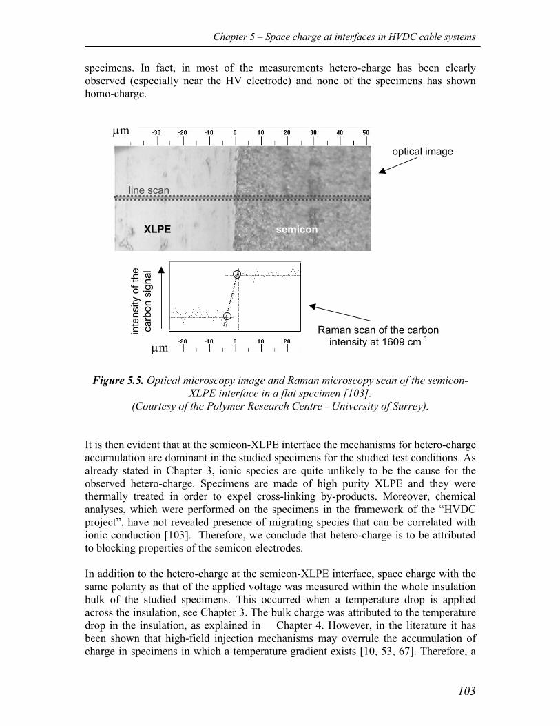
Chapter 5 – Space charge at interfaces in HVDC cable systems
103
specimens. In fact, in most of the measurements hetero-charge has been clearly observed (especially near the HV electrode) and none of the specimens has shown homo-charge.
Figure 5.5. Optical microscopy image and Raman microscopy scan of the semicon-
XLPE interface in a flat specimen [103]. (Courtesy of the Polymer Research Centre - University of Surrey).
It is then evident that at the semicon-XLPE interface the mechanisms for hetero-charge accumulation are dominant in the studied specimens for the studied test conditions. As already stated in Chapter 3, ionic species are quite unlikely to be the cause for the observed hetero-charge. Specimens are made of high purity XLPE and they were thermally treated in order to expel cross-linking by-products. Moreover, chemical analyses, which were performed on the specimens in the framework of the “HVDC project”, have not revealed presence of migrating species that can be correlated with ionic conduction [103]. Therefore, we conclude that hetero-charge is to be attributed to blocking properties of the semicon electrodes. In addition to the hetero-charge at the semicon-XLPE interface, space charge with the same polarity as that of the applied voltage was measured within the whole insulation bulk of the studied specimens. This occurred when a temperature drop is applied across the insulation, see Chapter 3. The bulk charge was attributed to the temperature drop in the insulation, as explained in Chapter 4. However, in the literature it has been shown that high-field injection mechanisms may overrule the accumulation of charge in specimens in which a temperature gradient exists [10, 53, 67]. Therefore, a
XLPE
line scan
µm
semicon
µm
inte
nsity
of t
he
carb
on s
igna
l optical image
Raman scan of the carbon intensity at 1609 cm-1
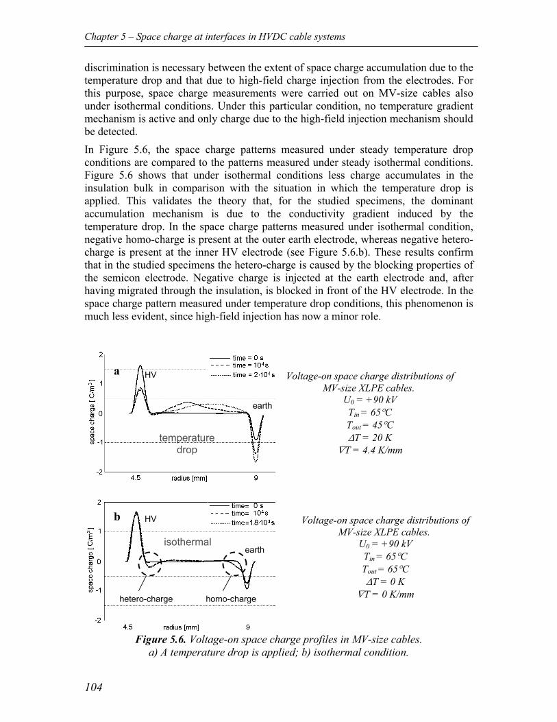
Chapter 5 – Space charge at interfaces in HVDC cable systems
104
discrimination is necessary between the extent of space charge accumulation due to the temperature drop and that due to high-field charge injection from the electrodes. For this purpose, space charge measurements were carried out on MV-size cables also under isothermal conditions. Under this particular condition, no temperature gradient mechanism is active and only charge due to the high-field injection mechanism should be detected. In Figure 5.6, the space charge patterns measured under steady temperature drop conditions are compared to the patterns measured under steady isothermal conditions. Figure 5.6 shows that under isothermal conditions less charge accumulates in the insulation bulk in comparison with the situation in which the temperature drop is applied. This validates the theory that, for the studied specimens, the dominant accumulation mechanism is due to the conductivity gradient induced by the temperature drop. In the space charge patterns measured under isothermal condition, negative homo-charge is present at the outer earth electrode, whereas negative hetero-charge is present at the inner HV electrode (see Figure 5.6.b). These results confirm that in the studied specimens the hetero-charge is caused by the blocking properties of the semicon electrode. Negative charge is injected at the earth electrode and, after having migrated through the insulation, is blocked in front of the HV electrode. In the space charge pattern measured under temperature drop conditions, this phenomenon is much less evident, since high-field injection has now a minor role.
Figure 5.6. Voltage-on space charge profiles in MV-size cables.
a) A temperature drop is applied; b) isothermal condition.
Voltage-on space charge distributions of MV-size XLPE cables.
U0 = +90 kV Tin = 65°C Tout = 45°C ∆T = 20 K
∇T = 4.4 K/mm
a
Voltage-on space charge distributions of MV-size XLPE cables.
U0 = +90 kV Tin = 65°C Tout = 65°C ∆T = 0 K
∇T = 0 K/mm
b
hetero-charge homo-charge
HV
HV
earth
earth isothermal
temperature drop
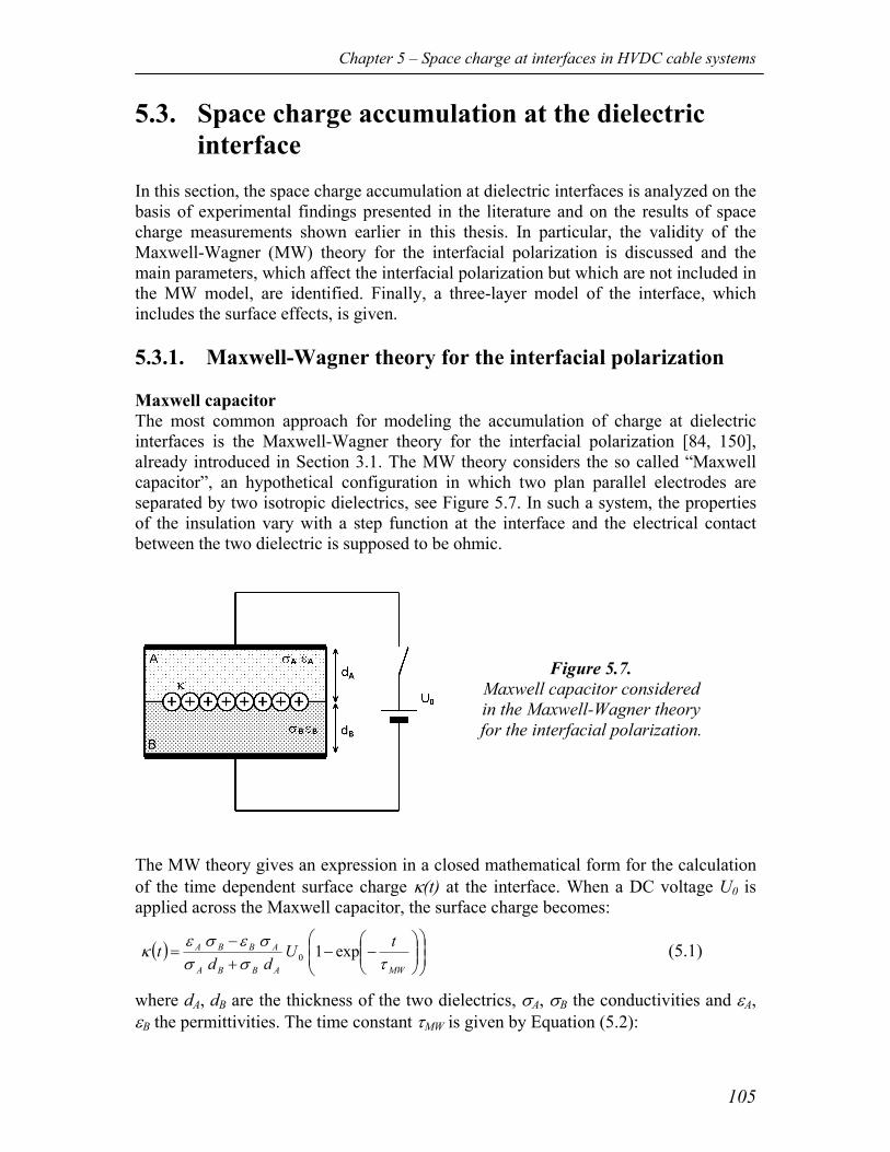
Chapter 5 – Space charge at interfaces in HVDC cable systems
105
5.3. Space charge accumulation at the dielectric interface
In this section, the space charge accumulation at dielectric interfaces is analyzed on the basis of experimental findings presented in the literature and on the results of space charge measurements shown earlier in this thesis. In particular, the validity of the Maxwell-Wagner (MW) theory for the interfacial polarization is discussed and the main parameters, which affect the interfacial polarization but which are not included in the MW model, are identified. Finally, a three-layer model of the interface, which includes the surface effects, is given. 5.3.1. Maxwell-Wagner theory for the interfacial polarization Maxwell capacitor The most common approach for modeling the accumulation of charge at dielectric interfaces is the Maxwell-Wagner theory for the interfacial polarization [84, 150], already introduced in Section 3.1. The MW theory considers the so called “Maxwell capacitor”, an hypothetical configuration in which two plan parallel electrodes are separated by two isotropic dielectrics, see Figure 5.7. In such a system, the properties of the insulation vary with a step function at the interface and the electrical contact between the two dielectric is supposed to be ohmic.
The MW theory gives an expression in a closed mathematical form for the calculation of the time dependent surface charge κ(t) at the interface. When a DC voltage U0 is applied across the Maxwell capacitor, the surface charge becomes:
( )
−−
+−
=MWABBA
ABBA tUdd
tτσσ
σεσεκ exp10 (5.1)
where dA, dB are the thickness of the two dielectrics, σA, σB the conductivities and εA, εB the permittivities. The time constant τMW is given by Equation (5.2):
Figure 5.7. Maxwell capacitor considered in the Maxwell-Wagner theory for the interfacial polarization.
Chapter 5 – Space charge at interfaces in HVDC cable systems
106
ABBA
ABBAMW dd
ddσσεετ
++
= (5.2)
The main advantage of the MW approach is that the interfacial charge can be directly calculated from the knowledge of a few insulation properties and the value of the insulation thickness. To be noted that once the interfacial charge is known, the electric field in both dielectrics can be found:
( )
( )
)(
)()()(
)(
)(
)(
AB
BAABBA
AB
AB
BA
dd
dtU
tE
εε
εκ
+
−
= (5.3)
Modified MW approach Equation (5.3) shows that in a combination of two dielectrics the electric field distribution changes in time, because of the accumulation of interfacial charge. The conductivity of insulating materials strongly depends on the electric field the material experiences. Thus, also the conductivity changes in time while charges accumulate at the interface. If the field dependency of the conductivity is taken into account, the conventional MW approach discussed above is no longer valid [21]. Interfacial charge and electric field have to be calculated numerically. For this purpose, the numerical procedure presented in Chapter 4 is used, after being adapted to the flat geometry. In Figure 5.8, electric field and interfacial charge calculated numerically are compared to the results of the conventional MW calculation. A two-layer insulation composed of XLPE and EPR flat specimens is considered for both calculations. It can be noted that when the field dependency of the insulation conductivity is taken into account, a smaller amount of accumulated charge is predicted along with a weaker field distortion.
Figure 5.8. Calculated interfacial charge and electric field in XLPE-EPR flat specimens, when a DC voltage is applied [21].
Input data: U0 =+30 kV; dXLPE = 1.5 mm; dEPR =1.5 mm; εr,XLPE = 2.3; εr,EPR =2.9; conductivity as derived from conduction current measurements at the temperature of
40 ° C (see Section 3.1).
Chapter 5 – Space charge at interfaces in HVDC cable systems
107
5.3.2. Deviations from the Maxwell-Wagner theory: literature Differences between bulk and surface properties The MW approach does not include the fact that the surface of insulating materials presents electrical properties different from those shown by the insulation bulk. The surface of insulators may exhibit ohmic conduction, e.g. due to the presence of a film of condensed water or because a specific chemical treatment has been applied [127]. Moreover, in most cases, it can be expected that the outer part of the material is oxidized to a larger degree than the inner part [116]. The way in which a test specimen is produced influences the properties of the insulation bulk. However, the production process may have an even larger effect on the surface properties. For instance, if the specimen has been cut, the molecular chains result abruptly terminated near to the surface. This will have consequences on the distribution of traps near the surface. A consequence of the difference between bulk and surface properties is that charge generally accumulates at interfaces between two identical dielectrics [20, 35, 79]. This is not predicted by the MW theory, where the dielectrics are assumed to be isotropous. Several works, e.g. [16, 144, 145], have shown that the polarity of the charge measured at the dielectric interface agrees with the MW theory. However, the amount of charge accumulated at the interface is often quite different from what is expected by the MW theory. Effect of interfacial contact According to the MW theory, the interface is a sharp discontinuity. In the reality, the dielectric interface has a finite thickness. This can vary from a few microns, for chemically bonded interfaces or extremely smooth surfaces in contact, to several tens of microns, when fairly rough surfaces are placed into contact. The fact that the interface is not sharp allows accumulation of charges at both sides of the interface. In fact, several experimental results have shown a bipolar charge distribution at the interface for various materials, e.g. [20, 35, 79, 95, 139]. The mechanical pressure applied at the interface has a role in defining the interface thickness for interfaces in simple contact. However, while the contact pressure is a crucial factor with regard to the PD activity at the interface [120], the amount of charge that accumulates at dielectric interfaces has been found to be quite insensible to the applied mechanical pressure [20]. Effect of lubricants Lubricants such as oil or grease are often applied at dielectric interfaces of HV components. Lubricants have generally a (much) higher conductivity in comparison with the conductivity of solid insulating materials. Therefore, the conductivity of the interfacial area is expected to increase when lubricants are used. This explains why a faster space charge accumulation has been observed in lubricated interfaces if compared to dry interfaces. [20]. Effect of air pockets Air pockets are present within the interfaces in simple contact (physical interfaces) when no lubricant is present or when the lubricant has dried out. Air pockets may
Chapter 5 – Space charge at interfaces in HVDC cable systems
108
affect the build up of interfacial charge. Air is in fact an electronegative gas, which will attract electrons. Another effect due to the presence of air within the interface is the alteration of the space charge signal. Since the PEA method is based on the generation and on the propagation acoustic waves, reflection and refraction of phenomena could occur at the interface, leading to a modification of the original space charge signal. A description of this phenomenon is given in Appendix A. Effect of the voltage polarity In the literature, dissimilarities have been found between space charge profiles measured at different voltage polarities [21, 24, 146]. According to the MW approach, no polarity effects are expected and interfacial charge patterns measured at different polarities should be perfectly symmetric. In [116, 146], the idea that the interface is to be regarded as a semi-blocking contact has been proposed in order to explain the polarity effects. However, such a model is still far from being implemented. 5.3.3. Deviations from the Maxwell-Wagner theory:
experimental results In Chapter 3, several results of space charge measurements performed on various types of dielectric interfaces were shown. Generally, a quite good agreement was found between the amount of measured charge and the charge expected by means of the MW theory. Nevertheless, some of the charging phenomena experimentally observed could not be explained by means of the MW theory. In this section, these particular phenomena are described and discussed. Charge accumulation next to the interface In all types of specimens, space charge accumulated next to the dielectric interface. This phenomenon was particularly evident within the XLPE layer of the specimens. In Figure 5.9 three examples are given (see dotted circles in the figures). Such a space charge pattern may indicate that in the XLPE next to the interface the density of deep traps is higher than in the bulk of the XLPE. Deep traps decrease the mobility of charge carriers (electrons and/or holes) in the dielectric. Accordingly, in the XLPE adjacent to the interface, where a higher density of traps is assumed, a mismatch will occur between the current density into this region and the current density out of this region. Consequently, charges will accumulate next to the interface. In Figure 5.10, this mechanism is schematically represented.
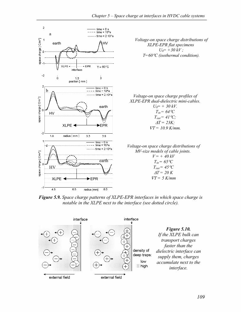
Chapter 5 – Space charge at interfaces in HVDC cable systems
109
Figure 5.9. Space charge patterns of XLPE-EPR interfaces in which space charge is
notable in the XLPE next to the interface (see dotted circle).
XLPE EPR
Voltage-on space charge profiles of XLPE-EPR dual-dielectric mini-cables.
U0= + 30 kV. Tin = 64°C
Tout = 41°C; ∆T = 23K;
∇T = 10.9 K/mm.
Voltage-on space charge distributions of XLPE-EPR flat specimens
U0= +30 kV ; T=60°C (isothermal condition).
a
b
HVearth
HV
earth
XLPE EPR
Voltage-on space charge distributions of MV-size models of cable joints.
V = + 40 kV Tin = 65°C Tout = 45°C ∆T = 20 K
∇T = 5 K/mm
c
HV earth
Figure 5.10. If the XLPE bulk can
transport charges faster than the
dielectric interface can supply them, charges
accumulate next to the interface.
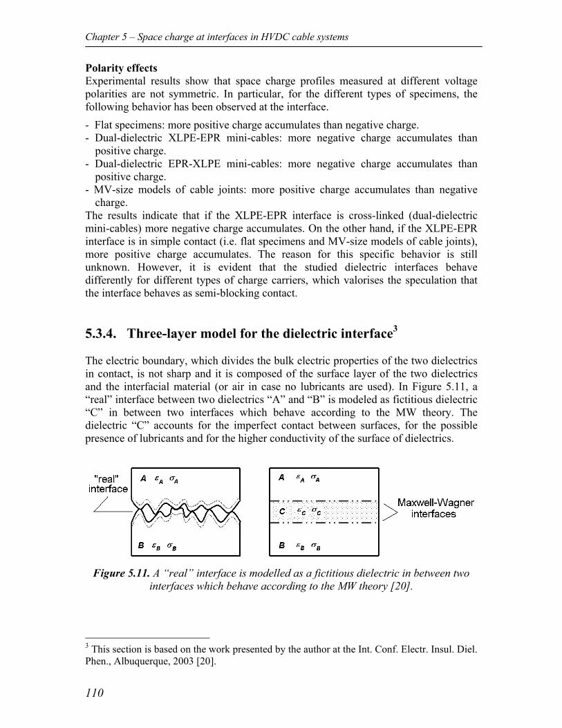
Chapter 5 – Space charge at interfaces in HVDC cable systems
110
Polarity effects Experimental results show that space charge profiles measured at different voltage polarities are not symmetric. In particular, for the different types of specimens, the following behavior has been observed at the interface. - Flat specimens: more positive charge accumulates than negative charge. - Dual-dielectric XLPE-EPR mini-cables: more negative charge accumulates than
positive charge. - Dual-dielectric EPR-XLPE mini-cables: more negative charge accumulates than
positive charge. - MV-size models of cable joints: more positive charge accumulates than negative
charge. The results indicate that if the XLPE-EPR interface is cross-linked (dual-dielectric mini-cables) more negative charge accumulates. On the other hand, if the XLPE-EPR interface is in simple contact (i.e. flat specimens and MV-size models of cable joints), more positive charge accumulates. The reason for this specific behavior is still unknown. However, it is evident that the studied dielectric interfaces behave differently for different types of charge carriers, which valorises the speculation that the interface behaves as semi-blocking contact. 5.3.4. Three-layer model for the dielectric interface3 The electric boundary, which divides the bulk electric properties of the two dielectrics in contact, is not sharp and it is composed of the surface layer of the two dielectrics and the interfacial material (or air in case no lubricants are used). In Figure 5.11, a “real” interface between two dielectrics “A” and “B” is modeled as fictitious dielectric “C” in between two interfaces which behave according to the MW theory. The dielectric “C” accounts for the imperfect contact between surfaces, for the possible presence of lubricants and for the higher conductivity of the surface of dielectrics.
Figure 5.11. A “real” interface is modelled as a fictitious dielectric in between two
interfaces which behave according to the MW theory [20].
3 This section is based on the work presented by the author at the Int. Conf. Electr. Insul. Diel. Phen., Albuquerque, 2003 [20].
Chapter 5 – Space charge at interfaces in HVDC cable systems
111
The fictitious dielectric “C” can be characterized by a thickness dC, a conductivity σC and a permittivity εC. The surface roughness ξA and ξB of the dielectrics “A” and “B” determine the thickness of the dielectric “C”:
BACd ξξ +≈ (5.4)
Equation (5.4) is valid if the deformation of the microscopic surface peaks is relatively small. However, increasing the mechanical pressure origin of the contact, a reduction of dC is expected. The permittivity εC is mainly given by the permittivity εL of the lubricant that can be present at the interface and by the permittivity εA and εB of the dielectrics “A” and “B”. If εL is smaller than εA and εB, the following relation is valid:
BA
BBAACL ξξ
ξεξεεε++
<< (5.5)
If no lubricants are present at the interface, the vacuum permittivity ε0 can replace εL in eq. (5.5).
Regarding the conductivity σC, a distinction can be made between two situations. If a lubricant is present within the interface, the conductivity of the dielectric “C” will be mainly given by the conductivity of the surface layer of dielectrics “A” and “B”, and by the conductivity σL of the lubricant. Assuming that the conductivity of the surface of dielectrics “A” and “B” is higher than that of the bulk of the insulators (σA and σB), and assuming that lubricants such as oil or grease are normally much more conductive than solid insulators, σC results:
LCBA σσσσ <<<, (5.6)
In case no lubricant is present between materials “A” and “B”, σC is expected to be lower than that previously estimated, but always higher than the bulk conductivity σA and σB. Interfacial charge estimation In an interface behaving according to the MW theory, the interfacial charge is given according to Equation (5.1) and (5.2). If now we apply those equations to the interface model in Figure 5.11, at the “A-C” interface we obtain:
=−CAκ
−−
+−
−−
CAMWCA
ACCA
ACCA tUdd ,
exp1τσσ
σεσε (5.7)
ACCA
ACCAMW dd
ddCA σσ
εετ++
=−
(5.8)
Assuming that the applied DC voltage is capacitively divided across the two layers “A” and “B”, the voltage UA-C becomes:
0Udd
dUUABBA
ABACA εε
ε+
=≈− (5.9)
Chapter 5 – Space charge at interfaces in HVDC cable systems
112
Inserting (5.9) into (5.7) and considering:
ACCA dd σσ << (5.10)
and
ACCA σεσε >> (5.11)
one obtains:
0Udd ABBA
BACA εε
εεκ+
≈−
−−
−CAMW
t
,
exp1τ
(5.12)
Moreover, taking into account that: ACCA dd εε << (5.13)
the MW time constant τMW,A-C can be expressed as:
C
CMW CA σ
ετ ≈−
(5.14)
Similarly, for the “C-B” interface the interfacial charge and the time constant results:
0Udd ABBA
BABC εε
εεκ
+−≈−
−−
−BCMW
t
,
exp1τ
(5.15)
C
CMW BC σ
ετ ≈−
(5.16)
According to the presented model, a bipolar charge distribution builds-up at both sides of an interface. The magnitude of this charge depends on the bulk properties of the two dielectrics in contact, whereas the time required for the bipolar charge to accumulate depends on the properties of the interfacial layer. The accumulation of the bipolar charge distribution occurs in the interfacial layer in the very beginning of the transition from capacitive to resistive field. This is due to the fact that the time constant for the bipolar charge accumulation (τMW,A-C or τMW,C-B) is much smaller than the time constant for the conventional MW accumulation (τMW,A-B). Because of the accumulation of bipolar charge, the electric field across the interfacial layer strongly decreases. Since the thickness of the interfacial layer is generally very small if compared to the total thickness of the specimen, the electric field in the insulation bulk remains practically unchanged. Of course, if time increases, additional charge of one polarity only will accumulate at the interface, modifying the electric field in the whole specimen and leading to a resistive distribution of the electric field. Validity of the assumptions The validity of the assumptions adopted in the model presented above can be checked by calculating the exact field and the exact interfacial charge in a three-layer dielectric. The following equations rule the charge accumulation process in a three-layer dielectric:
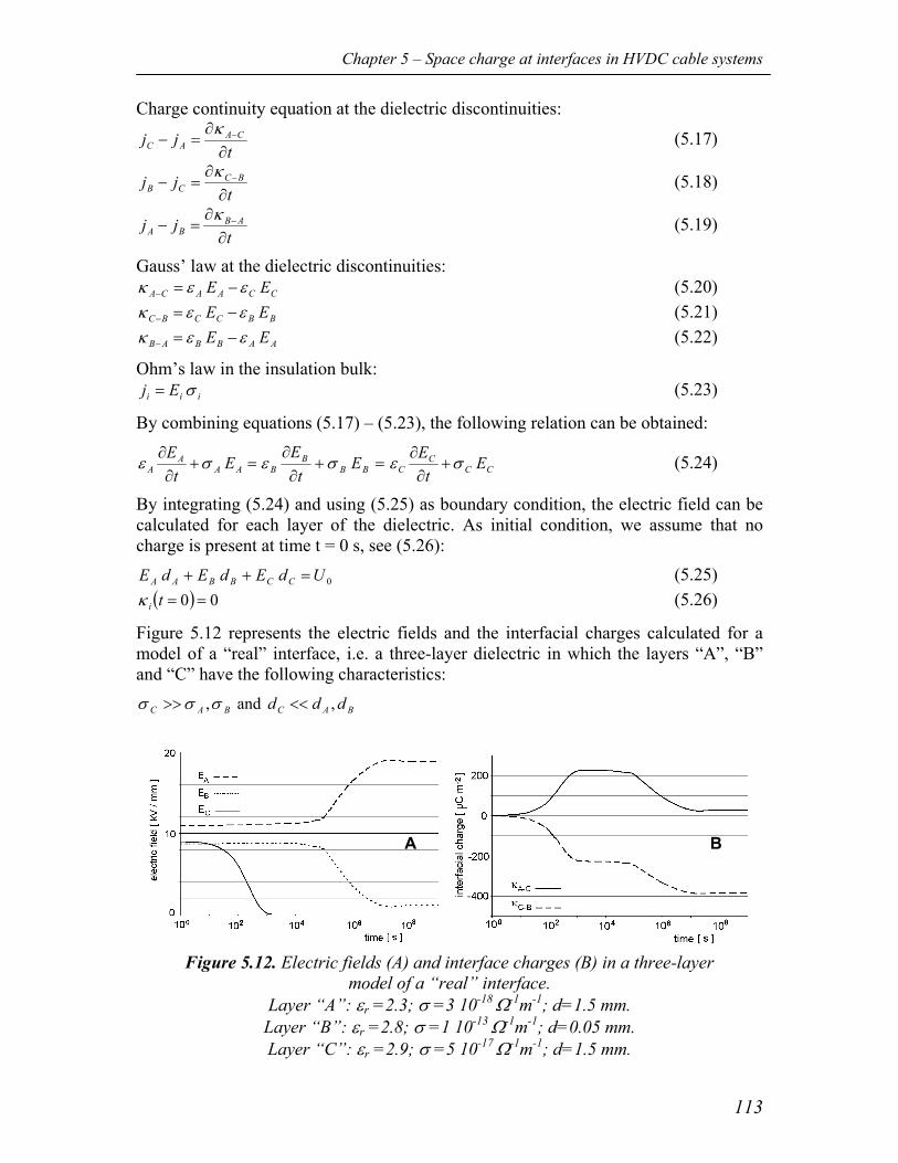
Chapter 5 – Space charge at interfaces in HVDC cable systems
113
Charge continuity equation at the dielectric discontinuities:
tjj CA
AC ∂∂
=− −κ (5.17)
tjj BCCB ∂
∂=− −κ (5.18)
tjj AB
BA ∂∂
=− −κ (5.19)
Gauss’ law at the dielectric discontinuities: CCAACA EE εεκ −=− (5.20) BBCCBC EE εεκ −=− (5.21) AABBAB EE εεκ −=− (5.22)
Ohm’s law in the insulation bulk: iii Ej σ= (5.23)
By combining equations (5.17) – (5.23), the following relation can be obtained:
=+∂∂
AAA
A Et
Eσε =+
∂∂
BBB
B Et
Eσε CC
CC E
tE
σε +∂∂ (5.24)
By integrating (5.24) and using (5.25) as boundary condition, the electric field can be calculated for each layer of the dielectric. As initial condition, we assume that no charge is present at time t = 0 s, see (5.26):
0UdEdEdE CCBBAA =++ (5.25) ( ) 00 ==tiκ (5.26)
Figure 5.12 represents the electric fields and the interfacial charges calculated for a model of a “real” interface, i.e. a three-layer dielectric in which the layers “A”, “B” and “C” have the following characteristics:
BAC σσσ ,>> and BAC ddd ,<<
Figure 5.12. Electric fields (A) and interface charges (B) in a three-layer
model of a “real” interface. Layer “A”: εr =2.3; σ =3 10-18 Ω-1m-1; d=1.5 mm.
Layer “B”: εr =2.8; σ =1 10-13 Ω-1m-1; d=0.05 mm. Layer “C”: εr =2.9; σ =5 10-17 Ω-1m-1; d=1.5 mm.
A B
Chapter 5 – Space charge at interfaces in HVDC cable systems
114
Figure 5.12 points out that for a three-layer model of a “real” interface, indeed the relation κA-C ≈ -κC-B is valid when the time is much shorter than the time constant τMW,A-B. By using the values in the caption of Figure 2, one obtains τMW,A-B = 106 s. Besides, the figure shows that the accumulation of interfacial charge for t << τMW,A-B follows approximately the time constant τMW,A-C (or τMW,C-B). By using the values in the caption of Figure 5.12, τMW,A-C = τMW,C-B = 250 s.
5.4. Suggestions on how to improve the macroscopic model for space charge accumulation
In Chapter 4 a cable system was modelled as an equivalent insulation in between ohmic electrodes. In this way, the high-field injection and/or the blocking mechanisms for space charge accumulation are included in the bulk properties of the equivalent insulation. However, as shown in this chapter, it would be more correct to localize these effects near the interfaces. In order to implement this idea without changing the structure of the model, the following actions can be performed: - considering the equivalent insulation inhomogeneous, by means of a position-
dependent conductivity; - considering the parameters, which describe the field and temperature dependency
of the conductivity, position-dependent. This means that Equation (4.5), which is here repeated for clarity, could be modified as in Equation (5.17):
( ) ( )[ ]refref
ref TTEEET −
= ασσ
ν
exp, (4.5)
( ) ( )( )
( ) ( )[ ]ref
x
refref TTx
EExxET −
= ασσ
ν
exp,, (5.27)
Chapter 6 – Feasibility study for on-line on-site PEA measurements
115
6. Feasibility study for on-line on-site PEA measurements
The feasibility of performing on-line and on-site PEA measurements on HVDC polymeric type cable systems is studied in this chapter. In Section 6.1, the concept of on-line on site PEA measurements is introduced and the benefits of such measurements are discussed. A schematic description of how to implement on-line on site PEA measurements on HVDC cables is given in Section 6.2. Finally some conclusions are drawn in Section 6.3.
6.1. Introduction On-line on-site space charge measurements are defined as space charge measurements performed on HVDC cable systems in operation. Up to now, no measurement of this kind has been reported in the literature. Space charge measurements are a means for providing the actual field distribution within the insulation of an HVDC cable system. This information is of utmost importance, because the electric field influences the life time of the cable system, e.g. [45]. Unfortunately, space charge measurements provide the electric field distribution for a very tiny portion of the cable system. In case of PEA measurements, this portion is defined by the length of the piezoelectric sensor, which is at most a few centimeters. Therefore, it is rather unlikely that a PEA measurement could identify a weak spot of the insulation, where an anomalous electric field distribution is present. This would occur only if the weak spot corresponds to the portion of the cable where the measurement is done. Moreover, on an HVDC cable the radial electric field distribution changes along the length of the cable, since different cable locations experience different temperature conditions. Despite of those facts, the electric field distribution inferred by an on-line on site space charge measurement is a significant information for monitoring the overall condition of the cable insulation. Firstly, the measurement can be performed on a portion of the cable where the most critical working conditions are expected. For instance this could be a joint of the cable system in which the temperature is expected to be higher than in the rest of the cable. By measuring the space charge in that specific section, the maximum electric field would be characteristic for the whole insulation system and therefore it could be of use for controlling and optimising the operation. Secondly, we need to make a difference between two irreversible electrical phenomena occurring in insulating material: aging and degradation. According to [55], material
Chapter 6 – Feasibility study for on-line on-site PEA measurements
116
aging is a global phenomenon, i.e. it is present on the whole insulation subjected to electric stress. For the insulation of HVDC cables under typical stress conditions, electrical aging is characterized by a relatively long duration (tens of years). Following the definition given in [55], degradation is a local phenomenon, i.e. it is present at a specific location of the insulation. For the insulation of HVDC cables under typical stress conditions, degradation phenomena are characterized by a relatively short duration (from a few days to a few years, according to the type of degradation mechanism). Generally, aging precedes degradation and degradation precedes the electrical breakdown. It is therefore very useful to understand the aging state of the insulation in order to get an idea of the risk for electrical breakdown occurrence. By comparing the space charge and the electric field distributions measured in the course of the years, changes in the measured patterns could be identified. These can be correlated to the aging state of the insulation, e.g. [4, 5], and then to an indication of the risk of breakdown. Another application of on-line on-site space charge measurements is provided by keeping a record of the electric field experienced by the cable through the years in a data-base. The information contained in the data-base could be used to assist cable management. For instance, decisions regarding the planning of the maintenance or the analysis of the remaining cable life could be supported by the data-base information.
6.2. Implementation In Appendix B, three PEA configurations for measuring space charge on cables are described. Among those configurations, the most suitable for performing PEA measurements on HVDC cables in the field is that in which the pulsed voltage is applied between the PEA cell and earth, see Section B.1.2 and Fig. B.3 in Appendix B. In fact, because of the length of the cable, the configuration in which the pulse is applied at the conductor is not optimal, since it would result in reflections of the pulsed voltage. Moreover, the configuration in which the pulse is applied at the earth screen is not applicable, since the earth screen must be kept at earth potential. Two major technical problems have to be considered in order to put into practice on-line on-site space charge measurements. 1. The outer semicon of the cable must be exposed at the measuring point. This
implies that the PEA system needs to be mounted inside a special compartment. This compartment has to be perfectly sealed, in order to protect the cable and to prevent the introduction of any moist.
2. The measuring system can affect the temperature distribution within the insulation of the measuring portion of the cable. In order to minimize this phenomenon, the thermal properties of the measuring system need to be considered in its design.
Figure 6.1 shows a schematic representation of a PEA system for measuring space charge on HVDC cables in the field. The entire system is contained within an armored compartment (3) which is sealed together with the armor of the cable (1). At the measuring section the earth screen of
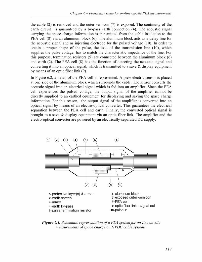
Chapter 6 – Feasibility study for on-line on-site PEA measurements
117
the cable (2) is removed and the outer semicon (7) is exposed. The continuity of the earth circuit is guaranteed by a by-pass earth connection (4). The acoustic signal carrying the space charge information is transmitted from the cable insulation to the PEA cell (8) via an aluminum block (6). The aluminum block acts as a delay line for the acoustic signal and as injecting electrode for the pulsed voltage (10). In order to obtain a proper shape of the pulse, the load of the transmission line (10), which supplies the pulse voltage, has to match the characteristic impedance of the line. For this purpose, termination resistors (5) are connected between the aluminum block (6) and earth (2). The PEA cell (8) has the function of detecting the acoustic signal and converting it into an optical signal, which is transmitted to a save & display equipment by means of an optic fiber link (9). In Figure 6.2, a detail of the PEA cell is represented. A piezoelectric sensor is placed at one side of the aluminum block which surrounds the cable. The sensor converts the acoustic signal into an electrical signal which is fed into an amplifier. Since the PEA cell experiences the pulsed voltage, the output signal of the amplifier cannot be directly supplied to an earthed equipment for displaying and saving the space charge information. For this reason, the output signal of the amplifier is converted into an optical signal by means of an electro-optical converter. This guarantees the electrical separation between the PEA cell and earth. Finally, the converted optical signal is brought to a save & display equipment via an optic fiber link. The amplifier and the electro-optical converter are powered by an electrically-separated DC supply.
Figure 6.1. Schematic representation of a PEA system for on-line on-site measurements of space charge on HVDC cable systems.
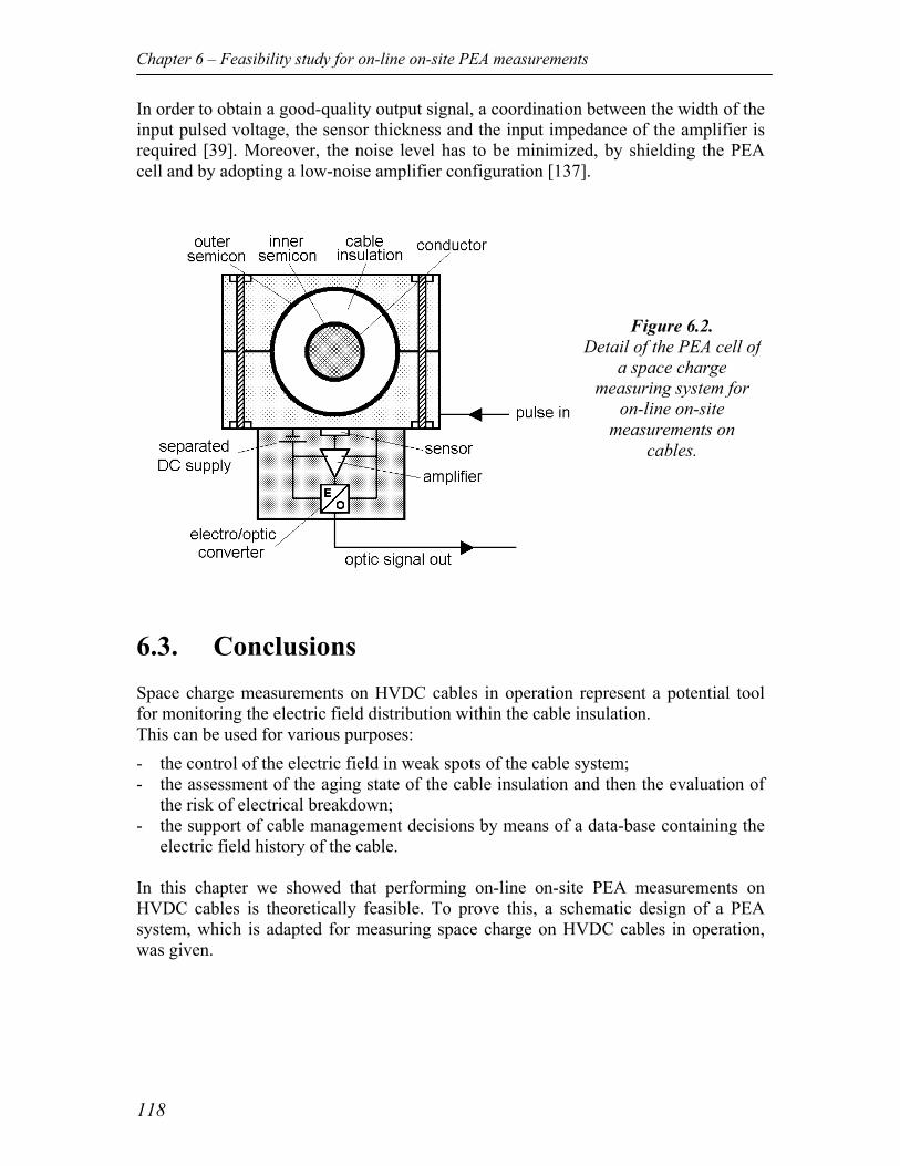
Chapter 6 – Feasibility study for on-line on-site PEA measurements
118
In order to obtain a good-quality output signal, a coordination between the width of the input pulsed voltage, the sensor thickness and the input impedance of the amplifier is required [39]. Moreover, the noise level has to be minimized, by shielding the PEA cell and by adopting a low-noise amplifier configuration [137].
6.3. Conclusions Space charge measurements on HVDC cables in operation represent a potential tool for monitoring the electric field distribution within the cable insulation. This can be used for various purposes: - the control of the electric field in weak spots of the cable system; - the assessment of the aging state of the cable insulation and then the evaluation of
the risk of electrical breakdown; - the support of cable management decisions by means of a data-base containing the
electric field history of the cable. In this chapter we showed that performing on-line on-site PEA measurements on HVDC cables is theoretically feasible. To prove this, a schematic design of a PEA system, which is adapted for measuring space charge on HVDC cables in operation, was given.
Figure 6.2. Detail of the PEA cell of
a space charge measuring system for
on-line on-site measurements on
cables.
Chapter 7 - Conclusions
119
7. Conclusions In this thesis, we investigated space charge phenomena occurring in DC polymeric cable systems. We showed that the following two phenomena have major influence on the technical performance of the insulation of HVDC polymeric cable systems: 7.1 Space charge formation at dielectric discontinuity, such as the interfaces of cable
accessories. 7.2 Space charge accumulation process due to a temperature drop across the
insulation of the cable system.
7.1. Space charge at dielectric discontinuities First of all, we reviewed the PEA method to make it suitable for the study of polarization and charging phenomena at dielectric interfaces. In fact, if a discontinuity of the dielectric and/or acoustic properties occurs at the interface, the signal provided by the PEA method does not directly correspond to the space charge distribution. In order to correctly evaluate the results of the PEA measurements, we introduced: 1. A methodology for the interpretation of the detected space charge patterns which
takes into account the reflection and the propagation of acoustic waves within the test specimen.
2. A procedure for the calibration of the measuring system that makes use of a different calibration factor for each layer of the test specimen.
We experimentally observed space charge accumulation at the dielectric interfaces of the studied test specimens. Both magnitude and dynamics of the charge could be fairly well described by the Maxwell-Wagner theory for the interfacial polarization. This means that the conductivity has a large influence on the polarization at the interface. 1. The larger the relative difference between the conductivities of the two dielectrics
forming the interface, the larger the accumulated charge at the interface. 2. The higher the conductivity of one of the two dielectrics, the faster the charge
accumulation at the interface. Since the conductivity increases with temperature and field, the higher the temperature (and/or the field), the faster the charge accumulation at the interface.
We observed two main deviations from the behavior predicted by the Maxwell-Wagner theory. 1. We measured different absolute values of interfacial charge magnitude at
different voltage polarities. From the latter, we conclude that a semi-blocking contact is likely to occur at dielectric interfaces.
2. We found that hetero-charge generally accumulates adjacent to the interface of the studied test specimens. We could attribute this phenomenon to the morphological differences between the bulk and the surface layer of polymeric insulation.
Chapter 7 - Conclusions
120
For MV-size models of cable joints, we confirmed experimentally that the temperature distribution across the joint has indeed a major effect on the distribution of the electric field. In particular, the larger the temperature jump at the dielectric interface, the higher the field in the rubber part of the joint. This is an unfavorable condition from a design point of view. 7.2 Space charge in cable systems that experience a
temperature drop across the insulation In the thesis, we analyzed space charge accumulation when a temperature drop and an electric field are simultaneously present across the insulation of the studied test specimens. We found that the conductivity gradient induced by the temperature drop is responsible for the accumulation of charge within the insulation bulk. By using a macroscopic modeling of the insulation, we could quite well reproduce the magnitude and the dynamics of the space charge measured on the studied test specimens. This confirms that the conductivity and its dependencies on temperature and field strongly affect the accumulation of space charge in the insulation bulk. In fact, both measurements and calculations of space charge point out that: 1. For a given applied field, the amount of space charge in the insulation bulk
increases with the temperature drop. 2. For a given temperature drop the amount of space charge in the insulation bulk
increases with the applied field. 3. The accumulation of space charge in the insulation bulk becomes faster when the
temperature increases. 4. The accumulation of space charge in the insulation bulk becomes faster when the
applied field increases. 5. The charge distribution takes a certain time to reach a quasi-steady state. This
time depends on the value of the insulation conductivity and, for the studied XLPE insulation, it can be as long as several weeks for tests done at room temperature and at moderate fields.
In addition to the charge in the insulation bulk, attributed to the presence of the temperature drop, we measured hetero-charge, mainly in the XLPE near the inner semicon of the studied specimens. This is not predicted by the developed macroscopic model. However, our interpretation is that this phenomenon is due to high-field charge injection and blocking mechanisms. We performed space charge measurements on loaded MV-size models of cable systems under polarity reversal condition. The results of our measurements show that the maximum electric field immediately after this reversal operation is present at the inner conductor and its value can be higher than the maximum Laplacian field. We concluded that this field enhancement is caused by the space charge due to the temperature drop.
Chapter 8 – Recommendations and suggestions for further study
121
8. Recommendations and suggestions for further study
On the basis of the results achieved in this thesis work, a number of recommendations will be presented in Section 8.1. Our findings have possible implications on: - the testing of cable insulation by means of the PEA method (Section 8.1.1); - the design of HVDC extruded-type cable systems (Section 8.1.2); - the operation of HVDC extruded-type cable systems (Section 8.1.3). Finally, some suggestions for further research are given in section 8.2. 8.1. Recommendations 8.1.1. Recommendations for PEA testing of HVDC cable system
insulation Space charge measurements on multi-dielectrics We recommend to use specific procedures (such as those presented in Appendix A) for the interpretation and for the calibration of measurement results provided by PEA measurements on multi-dielectric test objects. Space charge measurements on cables when a temperature drop is applied For a correct PEA measurement of the space charge induced by a temperature drop across the insulation of a DC cable, the following three properties of the space charge pattern need to be considered.
1. The amount of charge is rather small: its magnitude is of the order of a few hundreds of mC/m3 for MV-size XLPE-insulated cables and of the order of a few tens of mC/m3 for HV-size XLPE-insulated cables under typical stress conditions [42, 63]. Therefore, we recommend to check that the PEA system adopted for the measurement is sufficiently sensitive. The sensitivity of the PEA system used in this thesis for the measurements on MV cables is 50 mC/m3.
2. The charge is distributed in the whole insulation bulk: a wide distribution of charge is detected by the measuring system only if the frequency range of the measuring system is sufficiently broad [39, 118]. For instance, for a 1-mm thick XLPE cable, the lower cut-off frequency of the measuring system should not be higher than 300 kHz. Conventional PEA systems, which are equipped with a 50-Ω input resistance amplifier and a piezoelectric sensor with a capacitance of about 1 nF, have a lower cut-off frequency of about 3 MHz. Therefore, a conventional PEA system is not suitable for measuring wide distributions of charge such as those induced by a temperature gradient in (MV)HVDC cables. So, we recommend to check that the frequency range of the PEA system adopted for the measurements is sufficiently
Chapter 8 – Recommendations and suggestions for further study
122
wide. The frequency range of the PEA system used in this thesis for the measurements on MV cables is 0.1-100 MHz.
3. The charge distribution takes a certain time to reach a quasi-steady state: this time depends on the value of the insulation conductivity and can be as long as several weeks for tests done at room temperature and at moderate fields. For the measurement of the quasi steady-state space charge it is required to adopt a polarization time sufficiently long, according to the type of insulation, the temperature conditions and the applied field.
8.1.2. Recommendations for the design of polymeric HVDC
cable systems Cable insulation The macroscopic modeling of the insulation presented in this thesis provides a quite good estimation of the electric field within the cable. This implies that the temperature dependency and the field dependency of the conductivity need to be considered for the calculation of the dynamic field distribution within the cable. The conductivity as a function of field and temperature can be obtained from conduction current measurements. However, conduction current measurements should be performed on specimens of the cable insulation that have the same type of electrodes as the cable is equipped with (i.e. semicon electrodes in case of extruded cables). This is necessary because the measured conduction current depends on the electrode material. We recommend to check the extent of space charge accumulation due to high-field injection and/or blocking mechanisms and to consider the enhancement of field amplitude caused by injected/blocked charges in the cable design. This effect can be quantified by comparing measured space charge patterns to space charge patterns predicted our macroscopic model. Another way to determine the space charge accumulation due to high-field injection and/or blocking mechanisms is to perform space charge measurements under isothermal conditions. Joint insulation In order to reduce the maximum field in the rubber part of the joint, we recommend to design the joint and to mount it in such a way that it minimizes the contact thermal resistance at the dielectric interface. Results of space charge measurements on models of cable joints indicate that charge tends to be blocked in the XLPE next to the interface. We recommend to take into account the field enhancement induced by the charge blocked next to the interface in the design of the cable joint. Cable system The temperature conditions experienced by a cable system are generally different according to the location where the cable system is deployed. For instance, in case of submarine cables, the part of the cable laying in shallow water experiences higher temperatures than the part of the cable laying in deep water.
Chapter 8 – Recommendations and suggestions for further study
123
We showed that, for a given applied field, the highest field enhancement factor is generally present at the higher temperature at which the cable has to operate. This let us believe that, for a submarine cable, the insulation of the cable laying in deep water will experience a maximum electric field which is smaller than the maximum electric field experienced by the insulation of the cable length laying in shallow water. Therefore, the insulation of the deep-water part of the cable might allow a more compact design in comparison with the insulation of the shallow-water part of the cable. This means that the insulation thickness of the deep-water length of cable might be reduced. A more compact design of a portion of the cable system presents the following advantages: - less insulating material is used; - the volume of the cable is smaller; - the minimal banding radius is smaller; - more length of cable can be shipped on the cable laying vessel, therefore:
- less field joints may be required; - a shorter time for the deployment of the cable is needed.
On the other hand, the following disadvantages arises if a part of the cable system has a more compact design: - two different cable systems have to be designed and produced; - two transition joints need to be designed and mounted for joining together the
shallow-water cable and the deep-water cable. We recommend to investigate the advantages and disadvantages of using a more compact cable design for a portion of the cable system. This could shorten the deployment time, especially when less field joints are required if compared to the situation in which the entire cable presents the same design. 8.2.2. Recommendations for the operation of HVDC cable
systems
In Chapter 4 we showed that the dynamic electric field distribution can be predicted (up to a certain degree) for a DC cable system considering the temperature dependency and field dependency of the insulation conductivity. This knowledge can be used to define operational procedures that minimize the electric stress within the cable system for a number of working conditions. For instance, critical working conditions can be predicted and suggestions can be obtained on how to minimize the electric stress in the cable system for a given energy transport. In the following, two practical examples are given. Polarity reversal It is well known that the inversion of the voltage polarity on a loaded DC cable leads to a field enhancement in the insulation near the inner conductor. This is the reason
Chapter 8 – Recommendations and suggestions for further study
124
why nowadays the voltage polarity cannot be inverted for extruded-type DC cable systems. On such cable systems, the inversion of the power flow is done by inverting the current direction rather than the voltage polarity. However, a procedure could be followed to minimize the maximal electric field after polarity reversal and to shorten the time this relatively high field is present within the cable. In this way, the polarity reversal becomes a feasible option also for polymeric HVDC cable systems. As an example of the procedure, we make use of the fact that the amount of space charge, which accumulates in the cable before the inversion of the voltage polarity, is relatively small, then the space charge field also remains relatively low and the maximal field after polarity reversal is contained. This condition can be obtained by decreasing the temperature drop experienced by the cable (i.e. by decreasing the current) a few hours before performing the polarity reversal operation. (Eventually, the applied voltage can be increased, for maintaining constant the transported power). To shorten the time during which a relatively high field is present after the polarity reversal, the current can be increased after the polarity reversal. An increase of the current induces a higher temperature drop across the insulation. This favors the depletion of space charges, since the polarity of the voltage is now opposite to that of the accumulated charges. (Eventually, the applied voltage can be decreased, providing an additional decrease of the maximum electric field while the transported power is maintained constant). Increase of the energy transport In Chapter 4, the electric field distribution was derived by means of a physical model for an initially space-charge-free DC cable, in which the transported power was required to be 10% higher than its nominal value. Two different situations were investigated: 1) the voltage is increased by 10%; 2) the current is increased by 10% (see Section 4.4). The result was that just after the application of the DC voltage the maximum field was higher in the situation “1” - the voltage is increased by 10% -, near the inner conductor. On the other hand, after a few hours from the application of the DC voltage, the maximum field was higher in the situation “2” - the current is increased by 10% -, near the outer conductor. The reason for this behavior is that more space charge accumulates when the current, rather than the voltage, is increased by 10%. Moreover, in this situation the space charge accumulation is faster if compared to the accumulation of charge occurring when the voltage is increased by 10%. (See Figure 4.10 for the plots of electric field distributions and space charge distributions for the different situations). This example shows that an operational procedure can be identified for overloading the cable and at the same time containing the maximal electric field. Initially, the field near the inner conductor needs to be contained. Therefore, the current has to be increased while the voltage is kept relatively low. After a certain time, the maximal field is present near the outer conductor. To contain it, the current has to be decreased while the voltage can be increased. We recommend to investigate the dynamic electric field distribution by means of a model (such as that presented in this thesis) for several working conditions of the cable
Chapter 8 – Recommendations and suggestions for further study
125
system. In this way, operational procedures, which minimize the electric stress within the cable system, could be defined for different situations. This could enhance the performance of the cable (e.g. increase the transported capacity or decrease the losses in the conductor) without exceeding the maximal design field.
8.2. Suggestions for further study Macroscopic modeling of the insulation The macroscopic modeling of the insulation adopted in this thesis considers the temperature and field dependencies of the conductivity position-independent. However, morphological differences exist between the insulation bulk and the regions of the insulation adjacent to the semicon-dielectric interfaces and to the dielectric-dielectric interfaces. In order to include this into the macroscopic modeling, further work need to be done. A first step could be considering the field and temperature dependencies of the conductivity as functions of the position. Aging In the research presented in this thesis, space charge phenomena have been investigated in non-aged cable insulation. Further investigation is required to understand whether the different charge accumulation mechanisms recognized in this work change with the aging state of the insulation. On-line on-site space charge measurements A chapter of this thesis is dedicated to explain how to implement on-line on-site space charge measurements on HVDC cable systems. However, further work need to be done before such a measurement could be performed on actual HVDC cable systems.

Chapter 8 – Recommendations and suggestions for further study
126

Appendix

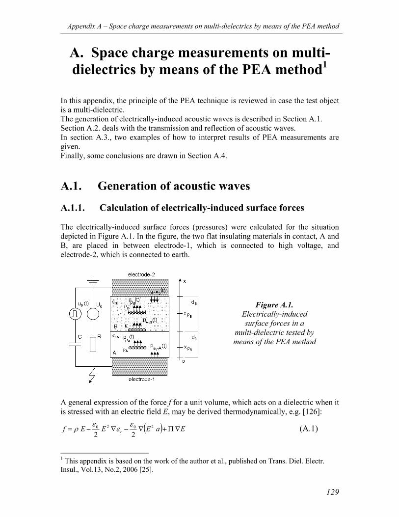
Appendix A – Space charge measurements on multi-dielectrics by means of the PEA method
129
A. Space charge measurements on multi-dielectrics by means of the PEA method1
In this appendix, the principle of the PEA technique is reviewed in case the test object is a multi-dielectric. The generation of electrically-induced acoustic waves is described in Section A.1. Section A.2. deals with the transmission and reflection of acoustic waves. In section A.3., two examples of how to interpret results of PEA measurements are given. Finally, some conclusions are drawn in Section A.4.
A.1. Generation of acoustic waves A.1.1. Calculation of electrically-induced surface forces The electrically-induced surface forces (pressures) were calculated for the situation depicted in Figure A.1. In the figure, the two flat insulating materials in contact, A and B, are placed in between electrode-1, which is connected to high voltage, and electrode-2, which is connected to earth.
A general expression of the force f for a unit volume, which acts on a dielectric when it is stressed with an electric field E, may be derived thermodynamically, e.g. [126]:
( ) EaEEEf r ∇Π+∇−∇−= 2020
22εεερ (A.1)
1 This appendix is based on the work of the author et al., published on Trans. Diel. Electr. Insul., Vol.13, No.2, 2006 [25].
Figure A.1. Electrically-induced surface forces in a
multi-dielectric tested by means of the PEA method
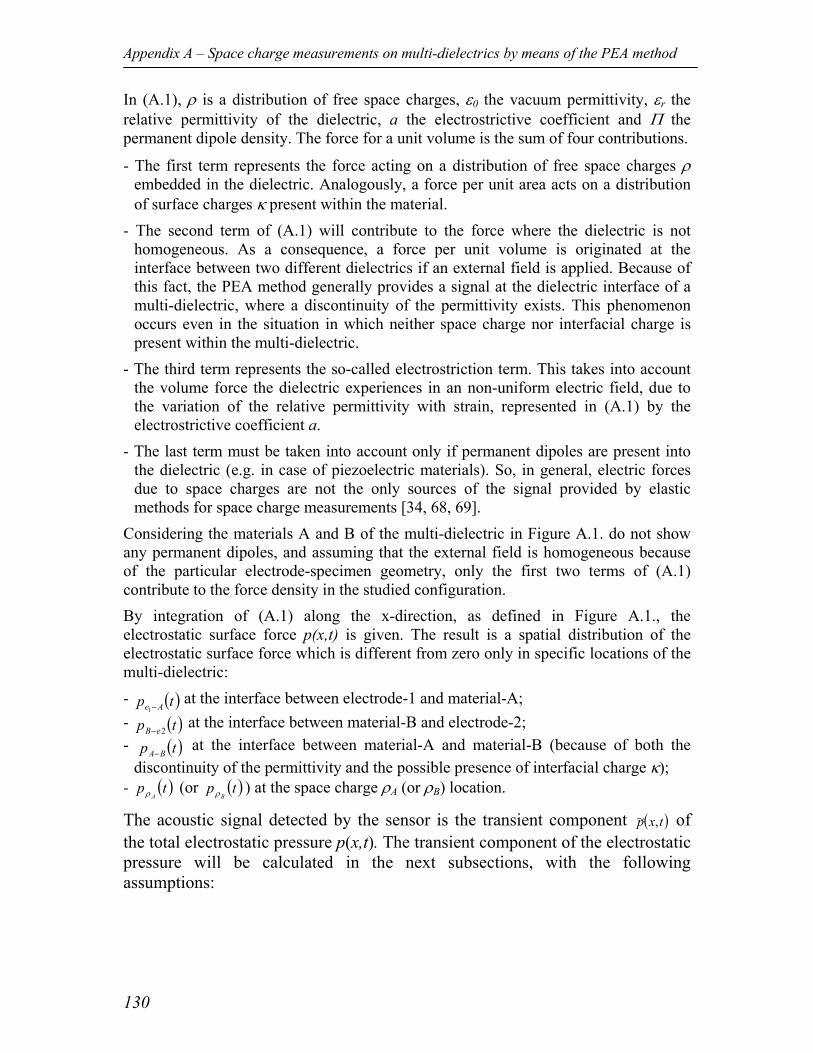
Appendix A – Space charge measurements on multi-dielectrics by means of the PEA method
130
In (A.1), ρ is a distribution of free space charges, ε0 the vacuum permittivity, εr the relative permittivity of the dielectric, a the electrostrictive coefficient and Π the permanent dipole density. The force for a unit volume is the sum of four contributions.
- The first term represents the force acting on a distribution of free space charges ρ embedded in the dielectric. Analogously, a force per unit area acts on a distribution of surface charges κ present within the material.
- The second term of (A.1) will contribute to the force where the dielectric is not homogeneous. As a consequence, a force per unit volume is originated at the interface between two different dielectrics if an external field is applied. Because of this fact, the PEA method generally provides a signal at the dielectric interface of a multi-dielectric, where a discontinuity of the permittivity exists. This phenomenon occurs even in the situation in which neither space charge nor interfacial charge is present within the multi-dielectric.
- The third term represents the so-called electrostriction term. This takes into account the volume force the dielectric experiences in an non-uniform electric field, due to the variation of the relative permittivity with strain, represented in (A.1) by the electrostrictive coefficient a.
- The last term must be taken into account only if permanent dipoles are present into the dielectric (e.g. in case of piezoelectric materials). So, in general, electric forces due to space charges are not the only sources of the signal provided by elastic methods for space charge measurements [34, 68, 69].
Considering the materials A and B of the multi-dielectric in Figure A.1. do not show any permanent dipoles, and assuming that the external field is homogeneous because of the particular electrode-specimen geometry, only the first two terms of (A.1) contribute to the force density in the studied configuration. By integration of (A.1) along the x-direction, as defined in Figure A.1., the electrostatic surface force p(x,t) is given. The result is a spatial distribution of the electrostatic surface force which is different from zero only in specific locations of the multi-dielectric: - ( )tp Ae −1
at the interface between electrode-1 and material-A; - ( )tp eB 2−
at the interface between material-B and electrode-2; - ( )tp BA−
at the interface between material-A and material-B (because of both the discontinuity of the permittivity and the possible presence of interfacial charge κ);
- ( )tpAρ
(or ( )tpBρ
) at the space charge ρA (or ρB) location.
The acoustic signal detected by the sensor is the transient component ( )txp ,~ of the total electrostatic pressure p(x,t). The transient component of the electrostatic pressure will be calculated in the next subsections, with the following assumptions:
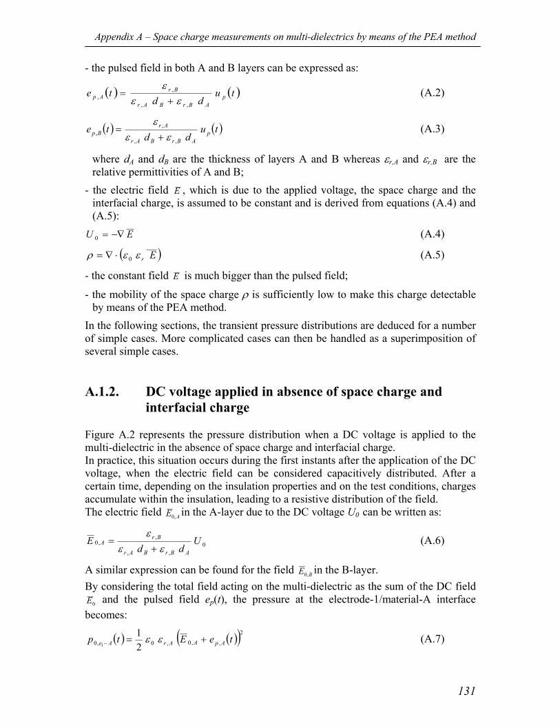
Appendix A – Space charge measurements on multi-dielectrics by means of the PEA method
131
- the pulsed field in both A and B layers can be expressed as:
( ) ( )tudd
te pABrBAr
BrAp
,,
,, εε
ε+
= (A.2)
( ) ( )tudd
te pABrBAr
ArBp
,,
,, εε
ε+
= (A.3)
where dA and dB are the thickness of layers A and B whereas εr,A and εr,B are the relative permittivities of A and B;
- the electric field E , which is due to the applied voltage, the space charge and the interfacial charge, is assumed to be constant and is derived from equations (A.4) and (A.5):
EU −∇=0 (A.4)
( )Erεερ 0⋅∇= (A.5)
- the constant field E is much bigger than the pulsed field;
- the mobility of the space charge ρ is sufficiently low to make this charge detectable by means of the PEA method.
In the following sections, the transient pressure distributions are deduced for a number of simple cases. More complicated cases can then be handled as a superimposition of several simple cases. A.1.2. DC voltage applied in absence of space charge and
interfacial charge Figure A.2 represents the pressure distribution when a DC voltage is applied to the multi-dielectric in the absence of space charge and interfacial charge. In practice, this situation occurs during the first instants after the application of the DC voltage, when the electric field can be considered capacitively distributed. After a certain time, depending on the insulation properties and on the test conditions, charges accumulate within the insulation, leading to a resistive distribution of the field. The electric field AE ,0 in the A-layer due to the DC voltage U0 can be written as:
0,,
,,0 U
ddE
ABrBAr
BrA
εεε+
= (A.6)
A similar expression can be found for the field BE ,0 in the B-layer. By considering the total field acting on the multi-dielectric as the sum of the DC field
0E and the pulsed field ep(t), the pressure at the electrode-1/material-A interface becomes:
( ) ( )( )2,,0,0,0 21
1teEtp ApAArAe +=− εε (A.7)
Appendix A – Space charge measurements on multi-dielectrics by means of the PEA method
132
Combining (A.2), (A.6) and (A.7) and considering 0E >> ep, the transient component
( )tp Ae −1,0~ of the pressure ( )tp Ae −1,0 becomes:
( ) ( )tuUdd
tp pArBBrA
BrArAe 02
,,
2,,0
,0 )(~
1 εεεεε
+=− (A.8)
Analogously, at the interface between material-B and electrode-2, the transient pressure ( )tp eB 2,0
~− is given by:
( ) ( )tuUdd
tp pArBBrA
BrAreB 02
,,
,2,0
,0 )(~
2 εεεεε
+−=− (A.9)
At the interface between material-A and material-B, the electrostatic pressure is given by integrating the second term of (A.1):
rBA dEpBr
Ar
εε ε
ε∫−=−
,
,
20,0 2
(A.10)
Introducing the electric flux density D, where: ED rεε0= (A.11)
the pressure can be expressed as:
−=−= ∫−
ArBrr
rBA
DdDpBr
Ar ,,0
2
2
2
0,0
1122
1 ,
,εεε
εεε
ε
ε
(A.12)
Equation (12) can be rewritten in terms of time-dependent electric field:
( ) ( )( )
−+=−
ArBrApAArBA teEtp
,,
2,,0
2,0,0
1121
εεεε (A.13)
The transient component ( )tp BA−,0~ results:
( ) ( )tuUdd
tp pArBrArBBrA
BrArBA 0
,,2
,,
2,
2,0
,011
)(~
−
+=− εεεε
εεε (A.14)
Figure A.2. Electrically-induced
pressure distribution in a multi-dielectric tested by means of the PEA method
(U0≠0, ρ=0, κ=0).
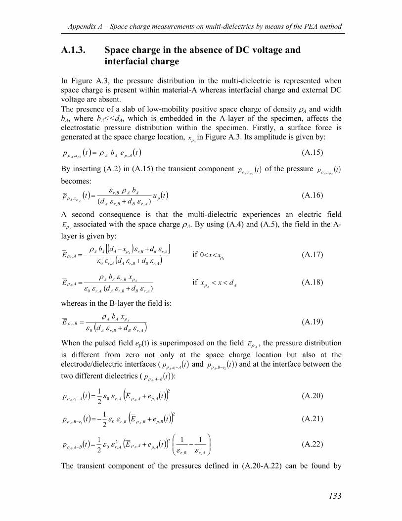
Appendix A – Space charge measurements on multi-dielectrics by means of the PEA method
133
A.1.3. Space charge in the absence of DC voltage and interfacial charge
In Figure A.3, the pressure distribution in the multi-dielectric is represented when space charge is present within material-A whereas interfacial charge and external DC voltage are absent. The presence of a slab of low-mobility positive space charge of density ρA and width bA, where bA<<dA, which is embedded in the A-layer of the specimen, affects the electrostatic pressure distribution within the specimen. Firstly, a surface force is generated at the space charge location,
Axρ in Figure A.3. Its amplitude is given by:
( ) ( )tebtp ApAAx AA ,, ρρρ = (A.15)
By inserting (A.2) in (A.15) the transient component ( )tpAA xρρ ,
~ of the pressure ( )tpAA xρρ ,
becomes:
( ) ( )tudd
btp p
ArBBrA
AABrx
AA )(~
,,
,, εε
ρερρ +
= (A.16)
A second consequence is that the multi-dielectric experiences an electric field A
Eρ associated with the space charge ρA. By using (A.4) and (A.5), the field in the A-layer is given by:
−=AAE ,ρ( )[ ]
( )ArBBrAAr
ArBBrAAA
dddxdb
A
,,,0
,,
εεεεεερ ρ
+
+− if
Axx ρ<<0 (A.17)
)( ,,,0
,,
ArBBrAAr
BrAAA
ddxb
E AA εεεε
ερ ρρ
+= if Adxx
A<<ρ (A.18)
whereas in the B-layer the field is:
( )ArBBrA
AAB
ddxb
E AA
,,0
,εεε
ρ ρρ
+= (A.19)
When the pulsed field ep(t) is superimposed on the field A
Eρ , the pressure distribution is different from zero not only at the space charge location but also at the electrode/dielectric interfaces ( ( )tp AeA −1,ρ and ( )tp eBA 2, −ρ ) and at the interface between the two different dielectrics ( ( )tp BAA −,ρ ):
( ) ( )( )2,,,0, 21
1teEtp ApAArAe AA
+=− ρρ εε (A.20)
( ) ( )( )2,,,0, 21
2teEtp BpBBreB AA
+−=− ρρ εε (A.21)
( ) ( )( )
−+=−
ArBrApAArBA teEtp AA
,,
2,,
2,0,
1121
εεεε ρρ (A.22)
The transient component of the pressures defined in (A.20-A.22) can be found by
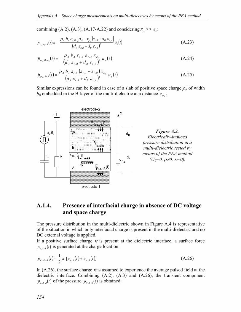
Appendix A – Space charge measurements on multi-dielectrics by means of the PEA method
134
combining (A.2), (A.3), (A.17-A.22) and considering ρE >> ep:
( ) −=− tp AeA 1,~ρ
( )[ ]( ) ( )tu
dd
dxdbp
ArBBrA
ArBBrABrAA A
2,,
,,,
εε
εεερ ρ
+
+− (A.23)
( )tp eBA 2,~
−ρ ( ) ( )tudd
xbp
ArBBrA
ArBrAA A2
,,
,,
εεεερ ρ
+−= (A.24)
( )tp BAA −,~ρ
( )( ) ( )tu
ddxb
pArBBrA
BrArBrAA A
2,,
,,,
εε
εεερ ρ
+
−= (A.25)
Similar expressions can be found in case of a slab of positive space charge ρB of width bB embedded in the B-layer of the multi-dielectric at a distance
Bxρ .
A.1.4. Presence of interfacial charge in absence of DC voltage
and space charge The pressure distribution in the multi-dielectric shown in Figure A.4 is representative of the situation in which only interfacial charge is present in the multi-dielectric and no DC external voltage is applied. If a positive surface charge κ is present at the dielectric interface, a surface force
( )tp BA−,κ is generated at the charge location:
( ) ( ) ( )][21
,,, tetetp BpApBA +=− κκ (A.26)
In (A.26), the surface charge κ is assumed to experience the average pulsed field at the dielectric interface. Combining (A.2), (A.3) and (A.26), the transient component
( )tp BA−,~κ of the pressure ( )tp BA−,κ is obtained:
Figure A.3. Electrically-induced
pressure distribution in a multi-dielectric tested by means of the PEA method
(U0=0, ρ≠0, κ=0).
Appendix A – Space charge measurements on multi-dielectrics by means of the PEA method
135
( ) ( ) ( )tudd
tp pArBBrA
BrArBA κ
εεεε
κ,,
,,, 2
~⋅+⋅
+=− (A.27)
The electric field κE associated with the surface charge can be calculated by means of (4) and (5). In the A-layer the field is given by:
( )ArBBrA
BA
dddE
,,0
,εεε
κκ
+−= (A.28)
whereas in the B-layer:
( )ArBBrA
AB
dddE
,,0
,εεε
κκ
+= (A.29)
At the electrode/dielectric interfaces the pressures ( )tp Ae −1,κ and ( )tp eB 2, −κ are present:
( ) ( )( )2,,,0, 21
1teEtp ApAArAe +=− κκ εε (A.30)
( ) ( )( )2,,,0, 21
2teEtp BpBBreB +⋅−=− κκ εε (A.31)
By means of (A.2), (A.3), (A.28-A.31) and considering κE >> ep, the transient components ( )tp Ae −1,
~κ and ( )tp eB 2,
~−κ become:
( ) =− tp Ae1,~κ ( ) ( )tu
ddd
pArBBrA
BBrAr2
,,
,,
εεκεε
+− (A.32)
( )tp eB 2,~
−κ ( ) ( )tudd
dp
ArBBrA
ABrAr2
,,
,,
εεκεε
+−= (A.33)
Figure A.4. Electrically-induced
pressure distribution in a multi-dielectric tested by means of the PEA method
(U0=0, ρ=0, κ≠0).
Appendix A – Space charge measurements on multi-dielectrics by means of the PEA method
136
A.1.5. DC voltage applied in presence of space charge and interfacial charge
In general, the total transient pressure distribution within the test object can be expressed as the superimposition of the transient pressure distributions obtained in the three particular situations studied before:
( ) ( ) ( ) ( )txptxptxptxpi
i,~,~,~,~
0 κρ ++= ∑ (A.34)
It is to be noted that for every considered case, the total pressure distribution, pTOT, across the multi-dielectric is zero:
( ) 00
== ∫+
dxxfpBA dd
TOT (A.35)
A.2. Acoustic wave traveling and reflection From the surface forces calculated in the previous section the acoustic waves detected at the sensor can be obtained. Firstly, acoustic waves traveling through an elastic medium are attenuated and dispersed. For situations where these effects are not negligible, procedures for recovering the original waveform from the attenuated/distorted signal have been developed [97]. Secondly, waves generated at different locations of the dielectric experience different generation, transmission and reflection coefficients. These phenomena will be studied for a multi-dielectric. A.2.1. Acoustic wave propagation After their generation, pressure waves travel both in the direction of electrode-1 and electrode-2. However, only those waves that travel towards electrode-2 are detected by the sensor. Waves traveling toward electrode-1 do not reach the sensor, unless they are reflected at the interface between two different media. This will be discussed later. The propagation of compressional pressure waves originated during the testing of the multi-dielectric shown in Figure A.5. is described in the following. The acoustic impedance of a material that is relevant in our case is defined as:
iiiac vZ δ=, (A.36) where δi is the mass density of the medium and vi the speed of compressional waves in the medium. Considering the waves traveling through the multi-dielectric as planar waves, the generation coefficient G, the transmission coefficient T and reflection coefficient R can be calculated as [19]:
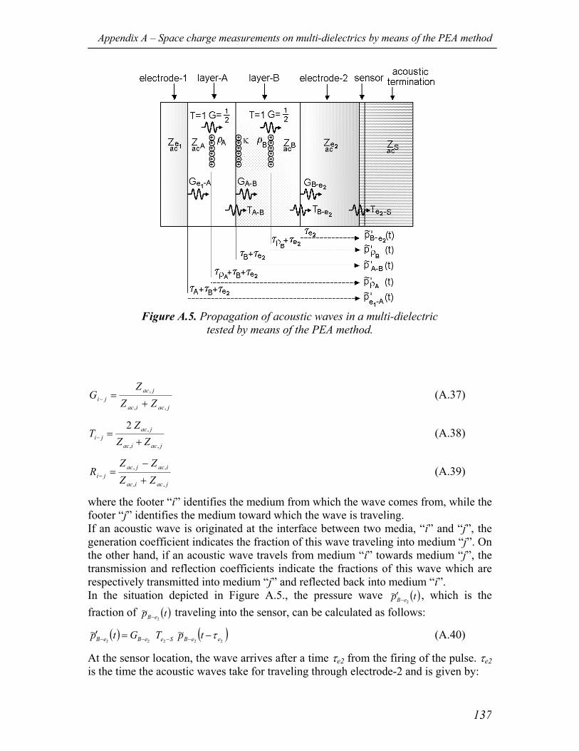
Appendix A – Space charge measurements on multi-dielectrics by means of the PEA method
137
Figure A.5. Propagation of acoustic waves in a multi-dielectric
tested by means of the PEA method.
jaciac
jacji ZZ
ZG
,,
,
+=− (A.37)
jaciac
jacji ZZ
ZT
,,
,2+
=− (A.38)
jaciac
iacjacji ZZ
ZZR
,,
,,
+
−=− (A.39)
where the footer “i” identifies the medium from which the wave comes from, while the footer “j” identifies the medium toward which the wave is traveling. If an acoustic wave is originated at the interface between two media, “i” and “j”, the generation coefficient indicates the fraction of this wave traveling into medium “j”. On the other hand, if an acoustic wave travels from medium “i” towards medium “j”, the transmission and reflection coefficients indicate the fractions of this wave which are respectively transmitted into medium “j” and reflected back into medium “i”. In the situation depicted in Figure A.5., the pressure wave ( )tp eB 2
~−′ , which is the
fraction of ( )tp eB 2~
− traveling into the sensor, can be calculated as follows:
( )22
~eBeB Gtp −− =′ ( )
222~
eeBSe tpT τ−−− (A.40)
At the sensor location, the wave arrives after a time τe2 from the firing of the pulse. τe2 is the time the acoustic waves take for traveling through electrode-2 and is given by:
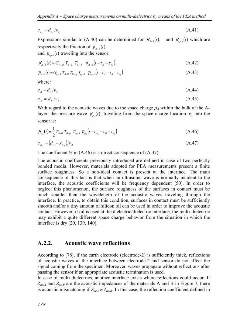
Appendix A – Space charge measurements on multi-dielectrics by means of the PEA method
138
222 eee vd=τ (A.41)
Expressions similar to (A.40) can be determined for ( )tp BA−′~ , and ( )tp Ae −′1~ which are
respectively the fraction of ( )tp BA−~ .
and ( )tp Ae −1~ traveling into the sensor:
( ) SeeBBABA TTGtp −−−− =′22
~ ( )2
~eBBA tp ττ −−− (A.42)
( ) SeeBBAAeAe TTTGtp −−−−− =′2211
~ ( )21
~eBAAe tp τττ −−−− (A.43)
where:
AAA vd=τ (A.44)
BBB vd=τ (A.45)
With regard to the acoustic waves due to the space charge ρA within the bulk of the A-layer, the pressure wave ( )tp
Aρ′~ , traveling from the space charge location
Axρ into the
sensor is:
( ) ( )222
~21~
eBSeeBBA AAAtpTTTtp τττρρρ −−−=′ −−− (A.46)
( ) AA vxdAA ρρτ −= (A.47)
The coefficient ½ in (A.46) is a direct consequence of (A.37). The acoustic coefficients previously introduced are defined in case of two perfectly bonded media. However, materials adopted for PEA measurements present a finite surface roughness. So a non-ideal contact is present at the interface. The main consequence of this fact is that when an ultrasonic wave is normally incident to the interface, the acoustic coefficients will be frequency dependent [50]. In order to neglect this phenomenon, the surface roughness of the surfaces in contact must be much smaller then the wavelength of the acoustic waves traveling through the interface. In practice, to obtain this condition, surfaces in contact must be sufficiently smooth and/or a tiny amount of silicon oil can be used in order to improve the acoustic contact. However, if oil is used at the dielectric/dielectric interface, the multi-dielectric may exhibit a quite different space charge behavior from the situation in which the interface is dry [20, 139, 140]. A.2.2. Acoustic wave reflections According to [78], if the earth electrode (electrode-2) is sufficiently thick, reflections of acoustic waves at the interface between electrode-2 and sensor do not affect the signal coming from the specimen. Moreover, waves propagate without reflections after passing the sensor if an appropriate acoustic termination is used. In case of multi-dielectrics, another interface exists where reflections could occur. If Zac,A and Zac,B are the acoustic impedances of the materials A and B in Figure 7, there is acoustic mismatching if Zac,A≠ Zac,B. In this case, the reflection coefficient defined in
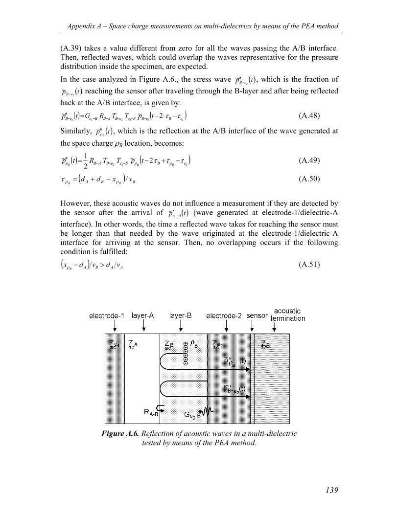
Appendix A – Space charge measurements on multi-dielectrics by means of the PEA method
139
(A.39) takes a value different from zero for all the waves passing the A/B interface. Then, reflected waves, which could overlap the waves representative for the pressure distribution inside the specimen, are expected. In the case analyzed in Figure A.6., the stress wave ( )tp eB 2
~−′′ , which is the fraction of
( )tp eB 2~
− reaching the sensor after traveling through the B-layer and after being reflected back at the A/B interface, is given by:
( ) ( )222222
2~~eBeBSeeBABBeeB tpTTRGtp ττ −⋅−=′′ −−−−−− (A.48)
Similarly, ( )tpBρ′′~ , which is the reflection at the A/B interface of the wave generated at
the space charge ρB location, becomes:
( ) ( )222
2~21~
eBSeeBAB BBBtpTTRtp τττ ρρρ −+−=′′ −−− (A.49)
( ) BBA vxddBB
/ρρτ −+= (A.50)
However, these acoustic waves do not influence a measurement if they are detected by the sensor after the arrival of ( )tp Ae −′1
~ (wave generated at electrode-1/dielectric-A interface). In other words, the time a reflected wave takes for reaching the sensor must be longer than that needed by the wave originated at the electrode-1/dielectric-A interface for arriving at the sensor. Then, no overlapping occurs if the following condition is fulfilled: ( ) AABA vdvdx
B>−ρ (A.51)
Figure A.6. Reflection of acoustic waves in a multi-dielectric
tested by means of the PEA method.
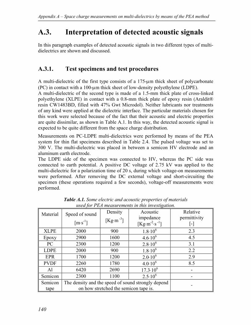
Appendix A – Space charge measurements on multi-dielectrics by means of the PEA method
140
A.3. Interpretation of detected acoustic signals In this paragraph examples of detected acoustic signals in two different types of multi-dielectrics are shown and discussed. A.3.1. Test specimens and test procedures A multi-dielectric of the first type consists of a 175-µm thick sheet of polycarbonate (PC) in contact with a 100-µm thick sheet of low-density polyethylene (LDPE). A multi-dielectric of the second type is made of a 1.5-mm thick plate of cross-linked polyethylene (XLPE) in contact with a 0.8-mm thick plate of epoxy resin (Araldit® resin CW1483BD, filled with 47% Gwt Microdol). Neither lubricants nor treatments of any kind were applied at the dielectric interface. The particular materials chosen for this work were selected because of the fact that their acoustic and electric properties are quite dissimilar, as shown in Table A.1. In this way, the detected acoustic signal is expected to be quite different from the space charge distribution. Measurements on PC-LDPE multi-dielectrics were performed by means of the PEA system for thin flat specimens described in Table 2.4. The pulsed voltage was set to 300 V. The multi-dielectric was placed in between a semicon HV electrode and an aluminum earth electrode. The LDPE side of the specimen was connected to HV, whereas the PC side was connected to earth potential. A positive DC voltage of 2.75 kV was applied to the multi-dielectric for a polarization time of 20 s, during which voltage-on measurements were performed. After removing the DC external voltage and short-circuiting the specimen (these operations required a few seconds), voltage-off measurements were performed.
Table A.1. Some electric and acoustic properties of materials used for PEA measurements in this investigation.
Material Speed of sound
[m⋅s-1]
Density
[Kg⋅m -3]
Acoustic impedance [Kg⋅m-2⋅s -1]
Relative permittivity
[-] XLPE 2000 900 1.8⋅106 2.3 Epoxy 2900 1600 4.6⋅106 4.5
PC 2300 1200 2.8⋅106 3.1 LDPE 2000 900 1.8⋅106 2.2 EPR 1700 1200 2.0⋅106 2.9
PVDF 2260 1780 4.0⋅106 8.5 Al 6420 2690 17.3⋅106 -
Semicon 2300 1100 2.5⋅106 - Semicon
tape The density and the speed of sound strongly depend
on how stretched the semicon tape is. -
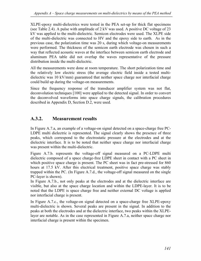
Appendix A – Space charge measurements on multi-dielectrics by means of the PEA method
141
XLPE-epoxy multi-dielectrics were tested in the PEA set-up for thick flat specimens (see Table 2.4). A pulse with amplitude of 2 kV was used. A positive DC voltage of 23 kV was applied to the multi-dielectric. Semicon electrodes were used. The XLPE side of the multi-dielectric was connected to HV and the epoxy side to earth. As in the previous case, the polarization time was 20 s, during which voltage-on measurements were performed. The thickness of the semicon earth electrode was chosen in such a way that reflected acoustic waves at the interface between semicon earth electrode and aluminum PEA table did not overlap the waves representative of the pressure distribution inside the multi-dielectric. All the measurements were done at room temperature. The short polarization time and the relatively low electric stress (the average electric field inside a tested multi-dielectric was 10 kV/mm) guaranteed that neither space charge nor interfacial charge could build up during the voltage-on measurements. Since the frequency response of the transducer amplifier system was not flat, deconvolution techniques [100] were applied to the detected signal. In order to convert the deconvolved waveforms into space charge signals, the calibration procedures described in Appendix D, Section D.2, were used. A.3.2. Measurement results In Figure A.7.a, an example of a voltage-on signal detected on a space-charge free PC-LDPE multi dielectric is represented. The signal clearly shows the presence of three peaks, which correspond to the electrostatic pressure at the electrodes and at the dielectric interface. It is to be noted that neither space charge nor interfacial charge was present within the multi-dielectric. Figure A.7.b. represents the voltage-off signal measured on a PC-LDPE multi dielectric composed of a space charge-free LDPE sheet in contact with a PC sheet in which positive space charge is present. The PC sheet was in fact pre-stressed for 860 hours at 17.5 kV. After this electrical treatment, positive space charge was stably trapped within the PC. (In Figure A.7.d., the voltage-off signal measured on the single PC-layer is shown). In Figure A.7.b., not only peaks at the electrodes and at the dielectric interface are visible, but also at the space charge location and within the LDPE-layer. It is to be noted that the LDPE is space charge free and neither external DC voltage is applied nor interfacial charge is present. In Figure A.7.c., the voltage-on signal detected on a space-charge free XLPE-epoxy multi-dielectric is shown. Several peaks are present in the signal. In addition to the peaks at both the electrodes and at the dielectric interface, two peaks within the XLPE-layer are notable. As in the case represented in Figure A.7.a, neither space charge nor interfacial charge is present within the specimen.
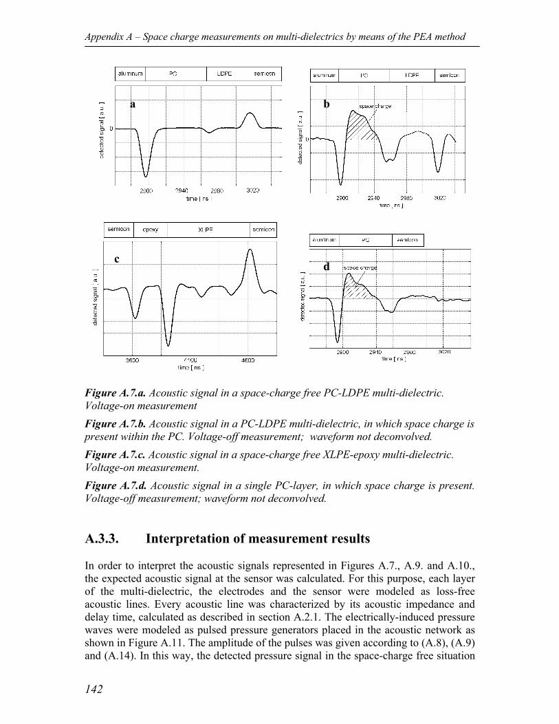
Appendix A – Space charge measurements on multi-dielectrics by means of the PEA method
142
Figure A.7.a. Acoustic signal in a space-charge free PC-LDPE multi-dielectric. Voltage-on measurement Figure A.7.b. Acoustic signal in a PC-LDPE multi-dielectric, in which space charge is present within the PC. Voltage-off measurement; waveform not deconvolved. Figure A.7.c. Acoustic signal in a space-charge free XLPE-epoxy multi-dielectric. Voltage-on measurement. Figure A.7.d. Acoustic signal in a single PC-layer, in which space charge is present. Voltage-off measurement; waveform not deconvolved. A.3.3. Interpretation of measurement results In order to interpret the acoustic signals represented in Figures A.7., A.9. and A.10., the expected acoustic signal at the sensor was calculated. For this purpose, each layer of the multi-dielectric, the electrodes and the sensor were modeled as loss-free acoustic lines. Every acoustic line was characterized by its acoustic impedance and delay time, calculated as described in section A.2.1. The electrically-induced pressure waves were modeled as pulsed pressure generators placed in the acoustic network as shown in Figure A.11. The amplitude of the pulses was given according to (A.8), (A.9) and (A.14). In this way, the detected pressure signal in the space-charge free situation
a b
c d
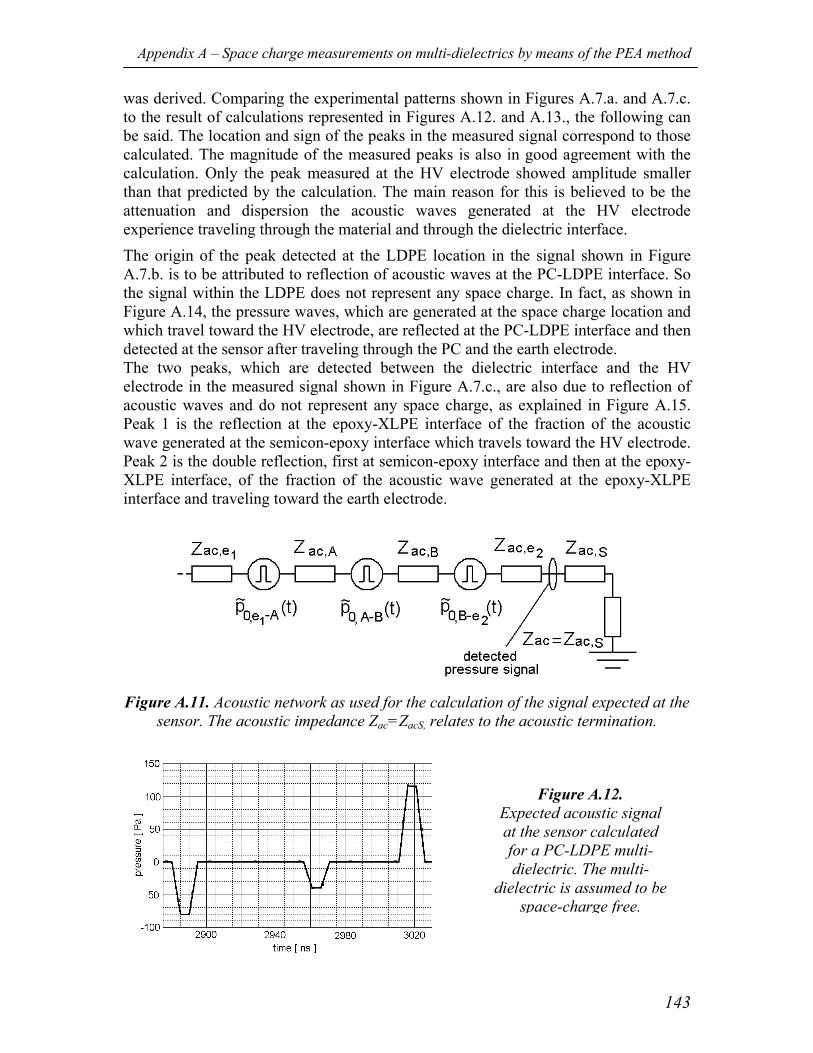
Appendix A – Space charge measurements on multi-dielectrics by means of the PEA method
143
was derived. Comparing the experimental patterns shown in Figures A.7.a. and A.7.c. to the result of calculations represented in Figures A.12. and A.13., the following can be said. The location and sign of the peaks in the measured signal correspond to those calculated. The magnitude of the measured peaks is also in good agreement with the calculation. Only the peak measured at the HV electrode showed amplitude smaller than that predicted by the calculation. The main reason for this is believed to be the attenuation and dispersion the acoustic waves generated at the HV electrode experience traveling through the material and through the dielectric interface. The origin of the peak detected at the LDPE location in the signal shown in Figure A.7.b. is to be attributed to reflection of acoustic waves at the PC-LDPE interface. So the signal within the LDPE does not represent any space charge. In fact, as shown in Figure A.14, the pressure waves, which are generated at the space charge location and which travel toward the HV electrode, are reflected at the PC-LDPE interface and then detected at the sensor after traveling through the PC and the earth electrode. The two peaks, which are detected between the dielectric interface and the HV electrode in the measured signal shown in Figure A.7.c., are also due to reflection of acoustic waves and do not represent any space charge, as explained in Figure A.15. Peak 1 is the reflection at the epoxy-XLPE interface of the fraction of the acoustic wave generated at the semicon-epoxy interface which travels toward the HV electrode. Peak 2 is the double reflection, first at semicon-epoxy interface and then at the epoxy-XLPE interface, of the fraction of the acoustic wave generated at the epoxy-XLPE interface and traveling toward the earth electrode.
Figure A.11. Acoustic network as used for the calculation of the signal expected at the
sensor. The acoustic impedance Zac=ZacS, relates to the acoustic termination.
Figure A.12. Expected acoustic signal at the sensor calculated for a PC-LDPE multi-dielectric. The multi-
dielectric is assumed to be space-charge free.
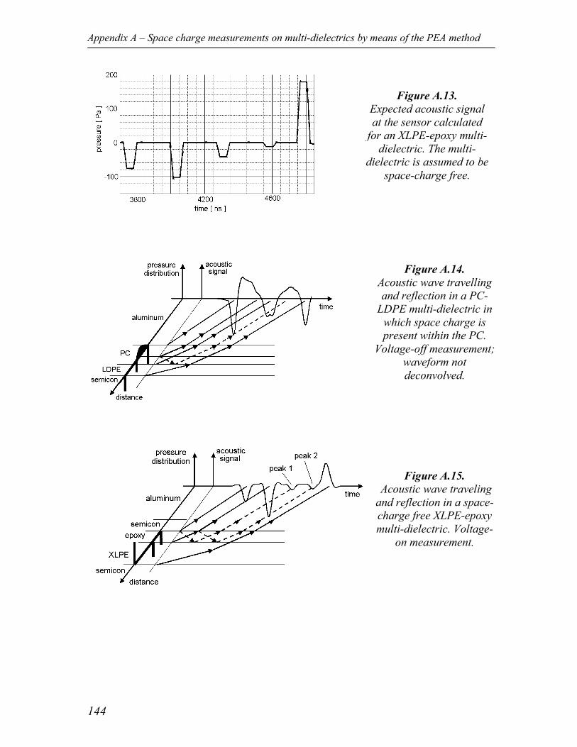
Appendix A – Space charge measurements on multi-dielectrics by means of the PEA method
144
Figure A.13. Expected acoustic signal at the sensor calculated
for an XLPE-epoxy multi-dielectric. The multi-
dielectric is assumed to be space-charge free.
Figure A.14. Acoustic wave travelling and reflection in a PC-
LDPE multi-dielectric in which space charge is present within the PC.
Voltage-off measurement; waveform not deconvolved.
Figure A.15. Acoustic wave traveling and reflection in a space-charge free XLPE-epoxy multi-dielectric. Voltage-
on measurement.
Appendix A – Space charge measurements on multi-dielectrics by means of the PEA method
145
A.4. Conclusions Generation, traveling and reflection of electrically-induced acoustic waves in a multi-dielectric tested by means of the PEA method were described in this appendix. Based on a theoretical approach, procedures were developed for relating the space charge magnitude and location to the acoustic output signal given by a PEA system. Experimental investigations validated the proposed analytical methods. Generally, when a multi-dielectric is tested, the detected acoustic signal does not correspond to the space charge distribution. There are two main reasons. 1. The electrically-induced pressure distribution is different from the charge
distribution if the permittivities of the layers composing the multi-dielectric are not the same. This leads to the presence of a pressure signal at the dielectric interface even in the absence of interfacial charge. Moreover, the different permittivity values should be considered in the calibration procedure for converting the output signal into a calibrated space charge profile.
2. The detected acoustic signal does not correspond to the pressure distribution if the layers of the multi-dielectric have different acoustic properties. In fact, the magnitude of the acoustic waves is affected by the acoustic impedance of the materials. Besides, in case of acoustic mismatching, reflected waves may overlap the waves representing the pressure distribution inside the multi-dielectric.
Therefore, when the PEA method is applied to multi-dielectric test objects, particular attention should be paid to the interpretation of the detected signal. If the multi-dielectric is electrically and acoustically inhomogeneous, procedures should be used in order to collect a meaningful space charge pattern.

Appendix A – Space charge measurements on multi-dielectrics by means of the PEA method
146
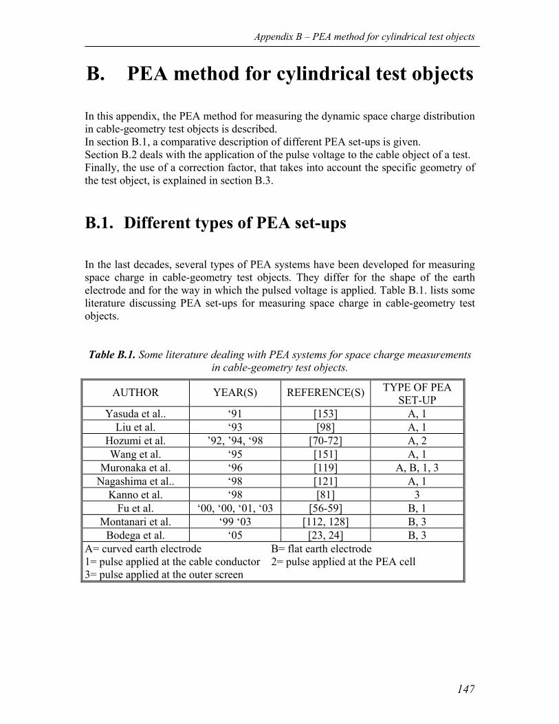
Appendix B – PEA method for cylindrical test objects
147
B. PEA method for cylindrical test objects In this appendix, the PEA method for measuring the dynamic space charge distribution in cable-geometry test objects is described. In section B.1, a comparative description of different PEA set-ups is given. Section B.2 deals with the application of the pulse voltage to the cable object of a test. Finally, the use of a correction factor, that takes into account the specific geometry of the test object, is explained in section B.3.
B.1. Different types of PEA set-ups In the last decades, several types of PEA systems have been developed for measuring space charge in cable-geometry test objects. They differ for the shape of the earth electrode and for the way in which the pulsed voltage is applied. Table B.1. lists some literature discussing PEA set-ups for measuring space charge in cable-geometry test objects. Table B.1. Some literature dealing with PEA systems for space charge measurements
in cable-geometry test objects.
AUTHOR YEAR(S) REFERENCE(S) TYPE OF PEA SET-UP
Yasuda et al.. ‘91 [153] A, 1 Liu et al. ‘93 [98] A, 1
Hozumi et al. ’92, ’94, ‘98 [70-72] A, 2 Wang et al. ‘95 [151] A, 1
Muronaka et al. ‘96 [119] A, B, 1, 3 Nagashima et al.. ‘98 [121] A, 1
Kanno et al. ‘98 [81] 3 Fu et al. ‘00, ‘00, ‘01, ‘03 [56-59] B, 1
Montanari et al. ‘99 ‘03 [112, 128] B, 3 Bodega et al. ‘05 [23, 24] B, 3
A= curved earth electrode B= flat earth electrode 1= pulse applied at the cable conductor 2= pulse applied at the PEA cell 3= pulse applied at the outer screen
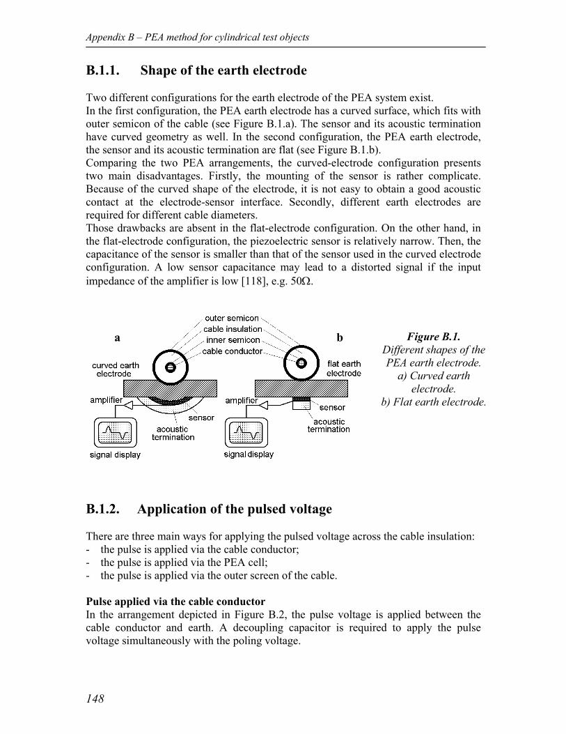
Appendix B – PEA method for cylindrical test objects
148
B.1.1. Shape of the earth electrode Two different configurations for the earth electrode of the PEA system exist. In the first configuration, the PEA earth electrode has a curved surface, which fits with outer semicon of the cable (see Figure B.1.a). The sensor and its acoustic termination have curved geometry as well. In the second configuration, the PEA earth electrode, the sensor and its acoustic termination are flat (see Figure B.1.b). Comparing the two PEA arrangements, the curved-electrode configuration presents two main disadvantages. Firstly, the mounting of the sensor is rather complicate. Because of the curved shape of the electrode, it is not easy to obtain a good acoustic contact at the electrode-sensor interface. Secondly, different earth electrodes are required for different cable diameters. Those drawbacks are absent in the flat-electrode configuration. On the other hand, in the flat-electrode configuration, the piezoelectric sensor is relatively narrow. Then, the capacitance of the sensor is smaller than that of the sensor used in the curved electrode configuration. A low sensor capacitance may lead to a distorted signal if the input impedance of the amplifier is low [118], e.g. 50Ω.
B.1.2. Application of the pulsed voltage There are three main ways for applying the pulsed voltage across the cable insulation: - the pulse is applied via the cable conductor; - the pulse is applied via the PEA cell; - the pulse is applied via the outer screen of the cable. Pulse applied via the cable conductor In the arrangement depicted in Figure B.2, the pulse voltage is applied between the cable conductor and earth. A decoupling capacitor is required to apply the pulse voltage simultaneously with the poling voltage.
a b Figure B.1. Different shapes of the PEA earth electrode.
a) Curved earth electrode.
b) Flat earth electrode.
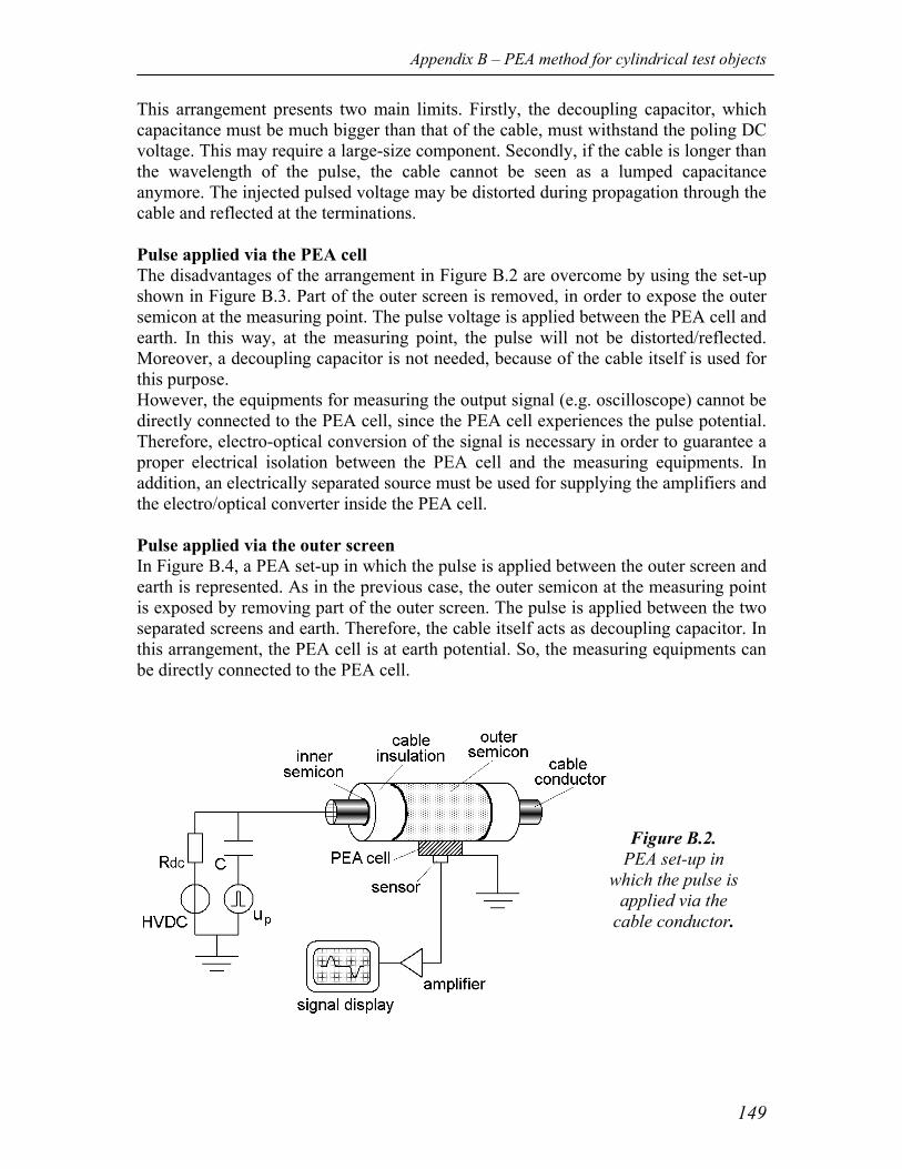
Appendix B – PEA method for cylindrical test objects
149
This arrangement presents two main limits. Firstly, the decoupling capacitor, which capacitance must be much bigger than that of the cable, must withstand the poling DC voltage. This may require a large-size component. Secondly, if the cable is longer than the wavelength of the pulse, the cable cannot be seen as a lumped capacitance anymore. The injected pulsed voltage may be distorted during propagation through the cable and reflected at the terminations. Pulse applied via the PEA cell The disadvantages of the arrangement in Figure B.2 are overcome by using the set-up shown in Figure B.3. Part of the outer screen is removed, in order to expose the outer semicon at the measuring point. The pulse voltage is applied between the PEA cell and earth. In this way, at the measuring point, the pulse will not be distorted/reflected. Moreover, a decoupling capacitor is not needed, because of the cable itself is used for this purpose. However, the equipments for measuring the output signal (e.g. oscilloscope) cannot be directly connected to the PEA cell, since the PEA cell experiences the pulse potential. Therefore, electro-optical conversion of the signal is necessary in order to guarantee a proper electrical isolation between the PEA cell and the measuring equipments. In addition, an electrically separated source must be used for supplying the amplifiers and the electro/optical converter inside the PEA cell. Pulse applied via the outer screen In Figure B.4, a PEA set-up in which the pulse is applied between the outer screen and earth is represented. As in the previous case, the outer semicon at the measuring point is exposed by removing part of the outer screen. The pulse is applied between the two separated screens and earth. Therefore, the cable itself acts as decoupling capacitor. In this arrangement, the PEA cell is at earth potential. So, the measuring equipments can be directly connected to the PEA cell.
Figure B.2. PEA set-up in
which the pulse is applied via the
cable conductor.
Appendix B – PEA method for cylindrical test objects
150
Figure B.3. PEA set-up in which the pulse is applied
via the PEA cell.
Figure B.4. PEA set-up in which the pulse is applied via the outer screen.
Appendix B – PEA method for cylindrical test objects
151
B.2. Application of the pulse to the cable In this work, a PEA system with a flat earth electrode was adopted (Figure B.1.b). In every test, the pulse was applied to the cable via the outer screen, as shown in Figure B.4. The equivalent circuit for the pulse voltage is represented in Figure B.5.
Figure B.5. Equivalent circuit for the pulse voltage.
The two halves of the cable are represented by transmission lines with impedance Zcable, whereas the measuring point is represented by a lumped capacitor Cm. A transmission line, Zline, connects the pulse generator to the cable object of the test. The transmission line is properly terminated by means of the resistor Rpulse (Rpulse = Zline). Table B.2 shows the parameters of the pulse circuit adopted in the present work. The pulse has a very short rise time and a narrow width (typical values are 2-20 ns and 20-200 ns for pulse rise time and pulse width respectively, whereas the pulse amplitude is 0.5-5kV). So, when stray inductances Ls are present in the pulse circuit, fly-back voltages may be generated. This will distort the pulse shape. (For example, the inductance of a simple 1-mm2 wire is about 10nH/cm. Considering a 5-kV pulse with a rise time of 10 ns and considering a 50-Ω transmission line, a 1-kV fly-back voltage will be generated when a 10-cm long wire is used). Moreover, the outer semicon presents a finite resistance Rsem, which connects the outer screen to earth. This decreases the total pulse load that may become too small for matching the transmission line Zline. In order to avoid the negative effects produced by both the stray inductances and the finite semicon resistance, a low-inductance damping resistor, Rd, is connected in series to the cable object of the test, as shown in Figure B.5. In Figures B.6, the calculated shape of the pulse voltage at the outer screen is shown. The figure shows that when no damping resistor is used, fly-back voltages are present in the pulse waveform.
Appendix B – PEA method for cylindrical test objects
152
Table B.2. Some parameters of the pulse circuit adopted in this work.
SYMBOL QUANTITY VALUE UNIT
up Pulse amplitude 0-4 kV ∆Tpulse Pulse width 80 ns Rline Termination resistor 50 Ω
Zline Characteristic impedance of
the pulse line 50 Ω
Zcable* Characteristic impedance of
the cable object of the test 30-50 Ω
Cm** Cable capacitance at the
measuring point 5-10 pF
Rd Damping resistor 180 Ω Rdc DC resistor 30 MΩ
* in
outcable r
rZ ln21
εµ
π= **
in
out
mm
rr
lCln
2 επ=
- µ = permeability of the insulation (µ=µ0= 4π 10-7 H/m) - lm = length of the cable at the measuring section (lm= 5 cm)
Figure B.5. Calculated pulsed
voltage at the outer screen of a cable.
Applied pulse: 4 kV, 80 ns.
Appendix B – PEA method for cylindrical test objects
153
B.3. Effect of the cylindrical geometry on the amplitude of acoustic waves
When a cylindrical-geometry object is tested by means of the PEA method, the acoustic signal detected at the sensor does not correspond to the charge distribution in the test object. Therefore, the detected signal must be corrected.
Divergence of the pulsed field The electric field distribution epulse(r), which is due to the applied pulse up, is:
( )
=
in
out
ppulse
rrr
ure
ln (B.1)
The magnitude of the pressure wave generated at the space charge location is proportional to the pulsed field at the space charge location. Because of the pulsed field distribution is not homogeneous, the space charge distribution will be position dependent. In order to correct the detected signal from the divergence of the pulsed field, a factor Kg,pulse is defined as:
( )( )
( )( ) outpulse
outpulseoutpulseg r
rre
rerp
rpK ===, (B.2)
Where p(rout) is the magnitude of a pressure wave associated to a given amount of charge at the outer radius rout, whereas p(r) is the magnitude of a pressure wave associated to the same amount of charge at the generic radius r.
Divergence of acoustic waves The magnitude of an acoustic wave decreases while traveling from the inner part of the cable toward the sensor. This is direct consequence of the wave equation:
02
222 =
∂∂
−∇tppv (B.3)
In cylindrical coordinates and restricting the analysis to the radial dimension only, (B.3) becomes:
2
22
tp
rpr
rv
∂∂
−
∂∂
∂∂ (B.4)
The solution of (B.4), for high ω , is [1, 12]:
( ) ( )
−= tvr
vi
rAtrp ωexp, (B.5)
where i is the imaginary unit, ω is the angular frequency of the acoustic wave and A is a constant established by the boundary conditions.
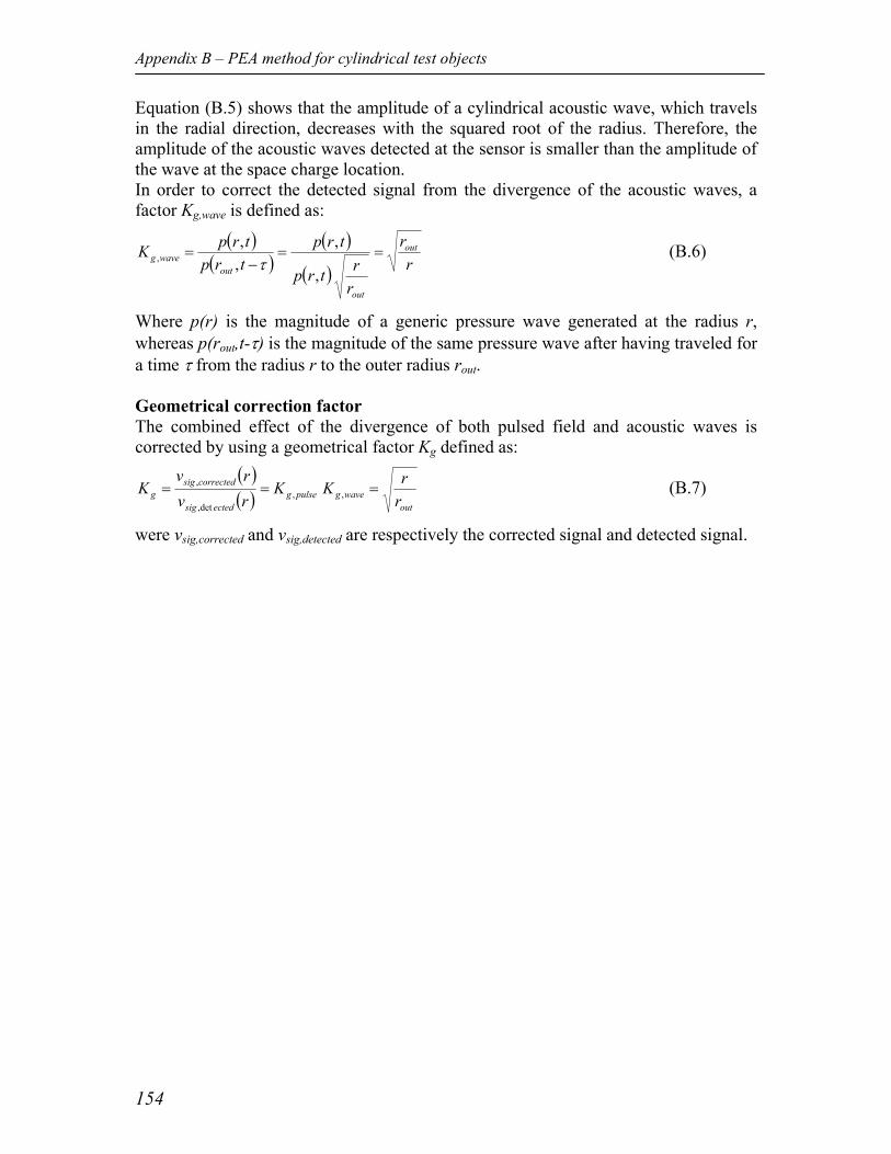
Appendix B – PEA method for cylindrical test objects
154
Equation (B.5) shows that the amplitude of a cylindrical acoustic wave, which travels in the radial direction, decreases with the squared root of the radius. Therefore, the amplitude of the acoustic waves detected at the sensor is smaller than the amplitude of the wave at the space charge location. In order to correct the detected signal from the divergence of the acoustic waves, a factor Kg,wave is defined as:
( )( )
( )
( ) rr
rrtrp
trptrptrpK out
out
outwaveg ==
−=
,
,,,
, τ (B.6)
Where p(r) is the magnitude of a generic pressure wave generated at the radius r, whereas p(rout,t-τ) is the magnitude of the same pressure wave after having traveled for a time τ from the radius r to the outer radius rout. Geometrical correction factor The combined effect of the divergence of both pulsed field and acoustic waves is corrected by using a geometrical factor Kg defined as:
( )( ) out
wavegpulsegectedsig
correctedsigg r
rKKrvrv
K === ,,det,
, (B.7)
were vsig,corrected and vsig,detected are respectively the corrected signal and detected signal.
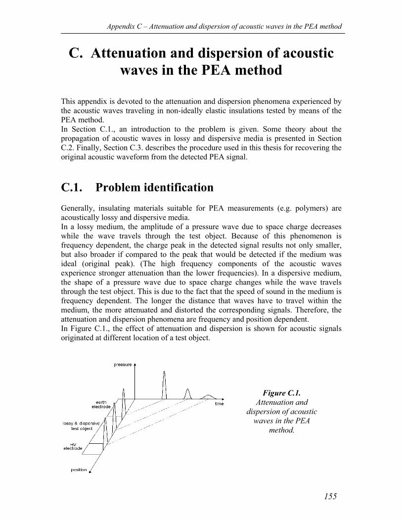
Appendix C – Attenuation and dispersion of acoustic waves in the PEA method
155
C. Attenuation and dispersion of acoustic waves in the PEA method
This appendix is devoted to the attenuation and dispersion phenomena experienced by the acoustic waves traveling in non-ideally elastic insulations tested by means of the PEA method. In Section C.1., an introduction to the problem is given. Some theory about the propagation of acoustic waves in lossy and dispersive media is presented in Section C.2. Finally, Section C.3. describes the procedure used in this thesis for recovering the original acoustic waveform from the detected PEA signal.
C.1. Problem identification Generally, insulating materials suitable for PEA measurements (e.g. polymers) are acoustically lossy and dispersive media. In a lossy medium, the amplitude of a pressure wave due to space charge decreases while the wave travels through the test object. Because of this phenomenon is frequency dependent, the charge peak in the detected signal results not only smaller, but also broader if compared to the peak that would be detected if the medium was ideal (original peak). (The high frequency components of the acoustic waves experience stronger attenuation than the lower frequencies). In a dispersive medium, the shape of a pressure wave due to space charge changes while the wave travels through the test object. This is due to the fact that the speed of sound in the medium is frequency dependent. The longer the distance that waves have to travel within the medium, the more attenuated and distorted the corresponding signals. Therefore, the attenuation and dispersion phenomena are frequency and position dependent. In Figure C.1., the effect of attenuation and dispersion is shown for acoustic signals originated at different location of a test object.
Figure C.1. Attenuation and
dispersion of acoustic waves in the PEA
method.
Appendix C – Attenuation and dispersion of acoustic waves in the PEA method
156
C.2. Theoretical background A general expression for a transient planar acoustic wave p(x,t) traveling through an ideal medium is obtained through its Fourier integral representation:
( ) ( ) ( ) ωωωπ
dtixptxp exp,ˆ21, ∫
∞
∞−
= (C.1)
in which: ( ) ( ) ( )ωβωω iPxp −= exp,ˆ 0 (C.2)
is the expression of the acoustic wave in the Fourier domain. In (C.2), P0(ω) represents the magnitude of the pressure wave component with angular frequency ω at the location x=0. This waves propagates without attenuation and has a velocity v that is related to the phase coefficient β according to:
ωβ v= (C.3)
In case of a lossy and dispersive medium, (C.2) can be rewritten as [97, 132]: ( ) ( ) ( )( ) ( )( )xixPtxp ωβωαω −−= expexp,ˆ 0 (C.4)
where α(ω) and β(ω) are respectively the frequency-dependent attenuation factor and phase factor, respectively. The factor α(ω) takes into account that the wave magnitude decreases while the wave travels through the medium (attenuation). The factor β(ω) takes into account that the speed of sound in the medium is frequency dependent (dispersion).
Next, a function G(x,ω) can be defined as:
( ) ( )( ) ( )( ) ( )( )xix
pxp
xG ωβωαωω
ω −−== expexp,0ˆ,ˆ
, (C.5)
In order to calculate the coefficients α(ω) and β(ω), the acoustic waveform at two different locations of the sample are sufficient. Generally, the acoustic wave generated at the HV electrode p(d,t)) (where d is the sample thickness) and the corresponding detected wave at the sensor p(0,t) are used [97]. In this particular case, G becomes:
( ) ( )( )( )( ) ( )( ) ( )( )did
pFdpFdG ωβωαωωω −−== expexp
,0,, (C.6)
where F is the Fourier transform. Then, α(ω) and β(ω) can be derived from the following relations:
( )( ) ( ) ( ) ( )ωωαωωα ,ln1,exp dGd
dGd −=⇒=− (C.7)
( ) ( )( ) ( ) ( )( )ωωβωωβ ,1, dGangled
dGangled −=⇒=− (C.8)
Appendix C – Attenuation and dispersion of acoustic waves in the PEA method
157
C.3. Procedure for recovering the original acoustic waveform from the attenuated and distorted waveform
Once the function G(x,ω) is determined by means of the coefficients α(ω) and β(ω), the pressure distribution p(x,t) inside the sample can be derived as:
( ) ( ) ( )[ ]ωω ,,0, 1 xGPFtxp −= (C.9)
were F-1 represents the inverse Fourier transform. The pressure distribution p(x,t) for t=0 represents the acoustic wave before it has traveled through the medium (i.e. before attenuation and dispersion phenomena have occurred). On the other hand, the pressure distribution p(x,t) for x=0 represents the acoustic wave after it has traveled through the medium (i.e. after attenuation and dispersion phenomena have occurred), see Figure C.1. Therefore, the detected voltage signal corresponds to pressure p(0,t), whereas the recovered voltage signal corresponds to the pressure p(x,0)= p(v t,0). In order to implement the procedure described in this chapter, the original signal at the HV electrode location is required. If the sample is space-charge free, the recovered signal at the HV electrode location is known. In fact, in this situation, the signal represents the electrode charge only, which can be determined if a known voltage is applied across the sample. In Figure C.2., the detected signal vdetected, the recovered signal vrecovered and the original signal expected from the electrode charge distribution voriginal are given for a flat 4.5-mm thick XLPE cable in which no space charge is present. In the figure, the recovered signal does not exactly correspond to the original signal. As explained in [58], this is due to the fact that some of the higher frequencies of the original signal may be totally attenuated, so they are not present in the detected signal. Therefore, it is not possible to recover completely the original waveform. However, the area of the peak at the HV electrode corresponds to the correct charge value. Hence, the recovered signal can be used for the determination of the electric field. When the computation of the parameters α(ω) and β(ω) is performed based on the function G(d,ω), some problems may occur. Firstly, G(d,ω) is given as ratio of two functions. If the denominator contains zeros, the division becomes impossible. Secondly, the mathematical procedure will produce a higher amplification for the high frequencies of the signal, rather then for the low frequencies. So, if noise is present in the detected signal, it will be amplified as well. To avoid these complications, two specific functions were assumed for α(ω) and β(ω) in this work:
2)( ωωα aA+= (C.10)
( ) ωωβ b= (C.11)
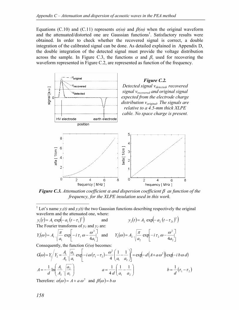
Appendix C – Attenuation and dispersion of acoustic waves in the PEA method
158
Equations (C.10) and (C.11) represents α(ω) and β(ω) when the original waveform and the attenuated/distorted one are Gaussian functions1. Satisfactory results were obtained. In order to check whether the recovered signal is correct, a double integration of the calibrated signal can be done. As detailed explained in Appendix D, the double integration of the detected signal must provide the voltage distribution across the sample. In Figure C.3, the functions α and β, used for recovering the waveform represented in Figure C.2, are represented as function of the frequency.
Figure C.3. Attenuation coefficient α and dispersion coefficient β as function of the
frequency, for the XLPE insulation used in this work. 1 Let’s name y1(t) and y2(t) the two Gaussian functions describing respectively the original waveform and the attenuated one, where: ( ) ( )( )2
1111 exp τ−−= taAty and ( ) ( )( )221222 exp τ−−= taAty
The Fourier transforms of y1 and y2 are:
( )
−−=
1
2
11
11 4exp
ai
aAY ωωτπω and ( )
−−=
2
2
22
22 4exp
ai
aAY ωωτπω
Consequently, the function G(ω) becomes:
( ) ( ) ( )( ) ( )dbiaAdaa
iaa
AAYYG ωωωττωω −+−=
−−−−== expexp11
4exp 2
21
2
211
2
2
121
−=
1
2
2
1ln1aa
AA
dA
−=
21
1141
aada ( )21
1 ττ −=d
b
Therefore: ( ) 2ωωα aA += and ( ) ωωβ b=
Figure C.2. Detected signal vdetected, recovered signal vrecovered and original signal expected from the electrode charge distribution voriginal. The signals are
relative to a 4.5-mm thick XLPE cable. No space charge is present.
Appendix D - Calibration
159
D. Calibration This appendix deals with the calibration of the measured space charge signals. The calibration procedure is given for four different types of test object: D.1. flat homogeneous test object; D.2. flat multi-dielectric test object; D.3. cylindrical homogeneous test object; D.4. cylindrical multi-dielectric test object. Calibration of the measured signals should be preferably performed on deconvolved waveforms which have been also corrected taking into account the attenuation and dispersion phenomena described in Appendix C.
D.1. Flat homogeneous test object To convert a processed waveform vsignal(t) into a calibrated space charge profile ρ(t), a calibration factor Kcal (e.g. [78]) is defined:
( ) ( )ttvK signalcal ρ= (D.1)
The calibration factor is usually calculated based on the knowledge of the charge at the earth electrode. In order to check whether the calibration is correctly done, the electric field distribution E(x) across the sample can be provided by means of the following equation:
( ) ( )∫=d
r
dxxxE00
1 ρεε
(D.2)
If the calibration is correct, the voltage distribution across the sample, V(x), must result from:
( ) ( )∫−=d
dxxExV0
(D.3)
where: tvx = (v is the speed of sound in the sample) and d is the sample thickness. In Figure D.1, an example of calibrated space charge distribution is given along with the derived electric field distribution and voltage distribution across a flat homogeneous sample.
Appendix D - Calibration
160
D.2. Flat multi-dielectric test object When a multi-dielectric is tested, the same amount of charge present in both layers will generate a pressure wave with higher amplitude in the layer with lower permittivity. This is a direct consequence of equation (A.15) in Appendix A. Then, the calibration factor cannot be the same for both layers of the multi-dielectric. Assuming the material “B” is connected to the earth electrode, the calibration factor KB,cal deduced from the charge at the earth electrode is to be used for the calibration of the signal in the layer “B” of the multi-dielectric. KB,cal is given by equation (D.1). On the other hand, the signal originated in the material “A”, which is connected to the HV electrode, is to be evaluated according to the calibration factor KA,cal defined as:
ArBrcalBcalA KK ,,,, εε= (D.4)
The calibration procedure described above is based on the value of electrode charges, which are known if the voltage U0 applied to the multi-dielectric is capacitively distributed. However, if U0 is a DC voltage, transition from a capacitively-graded to a resistively-graded field occurs in time. This leads to a build-up of interfacial charge at the dielectric interface and to a consequent modification of the charges at the electrodes. Then, as suggested in [14], the calibration measurements must be accomplished long before this transition becomes effective. The electric field distribution across the multi-dielectric can be provided by means of equation (D.2), in which the relative permittivity has to be considered function of the distance. Equation (D.3) can be used for determine the voltage distribution across the multi-dielectric. In Figure D.2, an example of calibrated space charge distribution is given along with the derived electric field distribution and voltage distribution across a multi-dielectric.
D.3. Cylindrical homogeneous test object After being corrected according to the geometrical factor derived in Appendix B, the signals measured on a cylindrical–geometry test object can be calibrated. A known charge at the earth electrode can be used for calculating the calibration factor defined in equation (D.1), to convert the non-calibrated signal into a calibrated space charge profile.
Once the radial space charge distribution ρ(r) is known, the electric field distribution can be derived according to:
( ) ( )∫=out
in
r
rr
drrrr
rE ρεε 0
1 (D.5)
where rin and rout are respectively the inner and outer radius. Then, the voltage distribution is given by:
Appendix D - Calibration
161
( ) ( )∫−=out
in
r
r
drrErV (D.6)
In Figure D.3, an example of calibrated space charge distribution is given along with the derived electric field distribution and voltage distribution across a MV-size cable.
D.4. Cylindrical multi-dielectric test object As in the case dealt in the previous section, also for a cylindrical multi-dielectric the detected signals must be corrected according to the geometrical factor derived in Appendix B, before the calibration is performed. The calibration factor in (D.1) can be derived from a known charge at the outer electrode. This calibration factor can be used for converting into space charge unit the signal originated within the dielectric connected to the outer electrode. On the other hand, the calibration factor in (D.4) is to be used for converting into space charge unit the signal originated within the dielectric connected to the inner electrode. For the same reasons explained in Section D.2, also in case of a cylindrical multi-dielectric the calibration should be accomplished long before the transition from capacitive field to resistive field becomes effective. After obtaining the radial space charge distribution within the cylindrical multi-dielectric, the electric field distribution can be derived by means of (D.5), in which the relative permittivity is to be consider a function of the radius. Finally, equation (D.6) can be used for the determination of the voltage distribution across the coaxial multi-dielectric. In Figure D.4, an example of calibrated space charge distribution is given along with the derived electric field distribution and voltage distribution across a MV-size model of a cable joint.
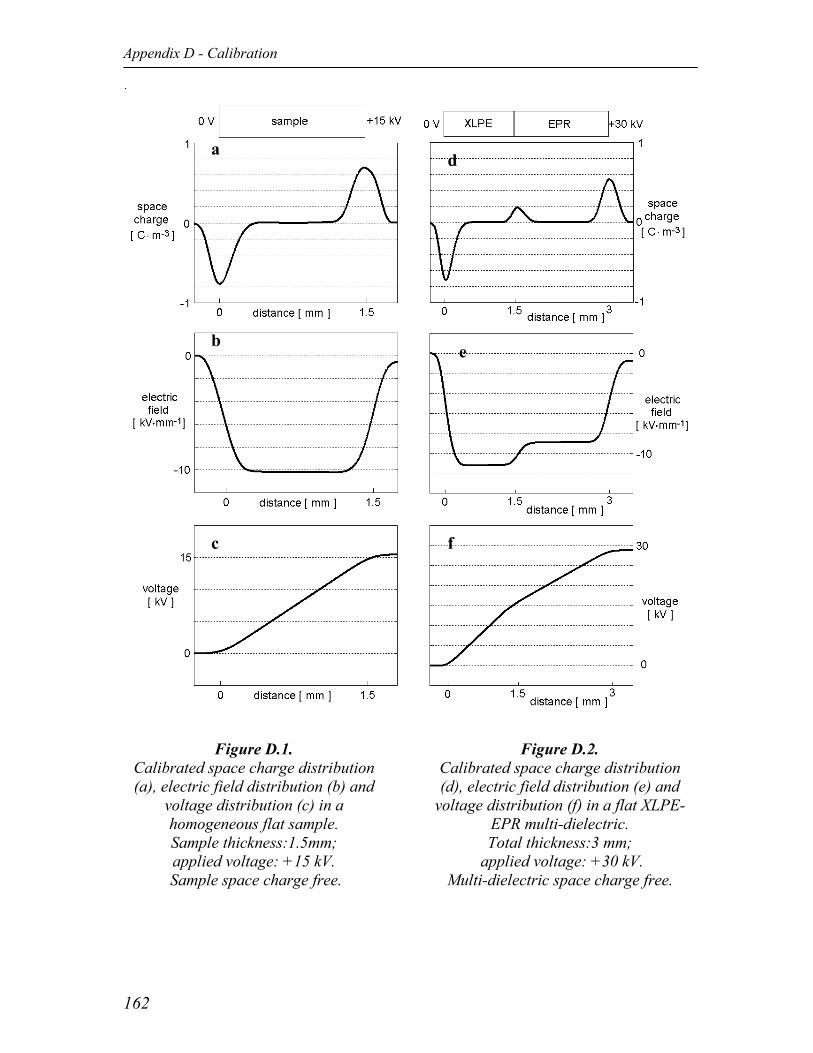
Appendix D - Calibration
162
Figure D.1. Calibrated space charge distribution (a), electric field distribution (b) and
voltage distribution (c) in a homogeneous flat sample. Sample thickness:1.5mm; applied voltage: +15 kV.
Sample space charge free.
Figure D.2.
Calibrated space charge distribution (d), electric field distribution (e) and
voltage distribution (f) in a flat XLPE-EPR multi-dielectric. Total thickness:3 mm;
applied voltage: +30 kV. Multi-dielectric space charge free.
a
b
c
d
e
f
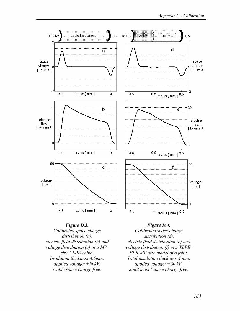
Appendix D - Calibration
163
a
b
c
d
e
f
Figure D.3. Calibrated space charge
distribution (a), electric field distribution (b) and voltage distribution (c) in a MV-
size XLPE cable. Insulation thickness:4.5mm;
applied voltage: +90kV. Cable space charge free.
Figure D.4. Calibrated space charge
distribution (d), electric field distribution (e) and
voltage distribution (f) in a XLPE-EPR MV-size model of a joint.
Total insulation thickness:4 mm; applied voltage: +80 kV.
Joint model space charge free.

Appendix D - Calibration
164
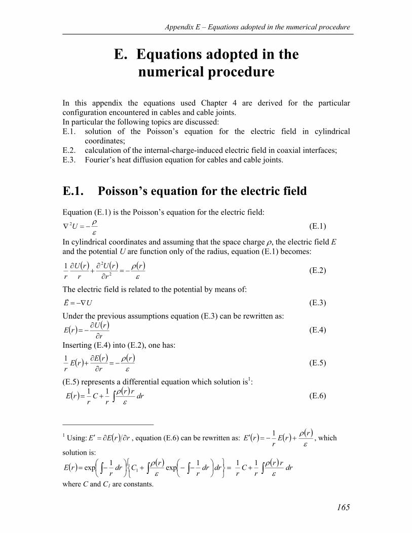
Appendix E – Equations adopted in the numerical procedure
165
E. Equations adopted in the numerical procedure
In this appendix the equations used Chapter 4 are derived for the particular configuration encountered in cables and cable joints. In particular the following topics are discussed: E.1. solution of the Poisson’s equation for the electric field in cylindrical
coordinates; E.2. calculation of the internal-charge-induced electric field in coaxial interfaces; E.3. Fourier’s heat diffusion equation for cables and cable joints.
E.1. Poisson’s equation for the electric field Equation (E.1) is the Poisson’s equation for the electric field:
ερ
−=∇ U2 (E.1)
In cylindrical coordinates and assuming that the space charge ρ, the electric field E and the potential U are function only of the radius, equation (E.1) becomes:
( ) ( ) ( )ερ r
rrU
rrU
r−=
∂∂
+∂
2
21 (E.2)
The electric field is related to the potential by means of: UE −∇=
r (E.3)
Under the previous assumptions equation (E.3) can be rewritten as:
( ) ( )rrUrE
∂∂
−= (E.4)
Inserting (E.4) into (E.2), one has:
( ) ( ) ( )ερ r
rrErE
r−=
∂∂
+1 (E.5)
(E.5) represents a differential equation which solution is1:
( ) ( ) drrrr
Cr
rE ∫+=ε
ρ11 (E.6)
1 Using: ( ) rrEE ∂∂=′ , equation (E.6) can be rewritten as: ( ) ( ) ( )
ερ rrE
rrE +−=′ 1 , which
solution is:
( ) ( )=
−−+
−= ∫ ∫∫ drdr
rrCdr
rrE 1exp1exp 1 ε
ρ ( ) drrrr
Cr ∫+
ερ11
where C and C1 are constants.
Appendix E – Equations adopted in the numerical procedure
166
where C is a constant which value can be deduced from the specific boundary condition.
E.2. Calculation of the charge-induced field
E.2.1. Field induced by space charges in coaxial interfaces
Let’s consider the situation depicted in Figure E.1. Two different insulating materials, A and B, are arranged in a coaxial layout. Each material is characterized by its permittivity εA and εB. The space charge distributions ρA(r) and ρB(r) are present within the insulations. Neither external voltage is applied nor charge κ is present at the dielectric interface. Consequently, no external field E0 is applied and no interfacial-charge-induced field is present. Only the space-charge-induced field Eρ contributes to the electric field distribution E(r) within the material.
The field distribution can be calculated by integrating the following equations:
no external voltage is applied ( ) ( )∫ ∫ =+C
A
B
C
r
r
r
rBA rEdrrE 0 (E.7)
no interfacial charge is present ( ) ( ) 0=− AcABCB rErE εε (E.8) Inserting (E.6) into (E.7) and (E.8), one obtains:
Figure E.1. Coaxial interface in which
space charge is present within the insulation. Neither external
voltage is applied nor interfacial charge is present.
Appendix E – Equations adopted in the numerical procedure
167
( ) ( ) ( )
+== ∫C
A
r
r A
AAA drrrC
rrErE
ερ
ρ1 if cA rrr << (E.9)
( ) ( ) ( )
+== ∫B
C
r
r B
BBB drrrC
rrErE
ερ
ρ1 if BC rrr << (E.10)
where:
( ) ( ) ( )
+
+
+
−=∫∫ ∫∫ ∫
C
B
B
A
A
C
C
B
B
Ar
r A
Ar
r
r
r B
Br
r
r
r A
A
A
rr
rr
rrdrrrdrdrrr
rdrdrrr
rC
C
A
B
C
B
C
C
A
C
A
lnln
ln11
εε
εε
ερ
ερ
ερ
(E.11)
( ) ( ) ( )
+
−
+
−=∫∫ ∫∫ ∫
C
B
A
C
A
B
A
Cr
r A
Ar
r
r
r B
Br
r
r
r A
A
B
rr
rr
rrdrrrdrdrrr
rdrdrrr
rC
C
A
B
C
B
C
C
A
C
A
lnln
ln11
εε
ερ
ερ
ερ
(E.12)
E.2.2. Field induced by interfacial charge in coaxial interfaces
Let’s now consider the situation depicted in Figure E.2. As in the previous situation, two different insulating materials, A and B, are arranged in a coaxial layout and each material is characterized by its permittivity εA and εB. However, interfacial charge κ is present at the boundary between the two different insulating materials. Neither external voltage is applied nor space charge is present within the insulation. Consequently, no external field E0 is applied and no space-charge-induced field is present. Only the interface-charge-induced field Eκ contributes to the electric field distribution E(r) within the material. In this case, the following two equations have to be combined for calculating the electric field distribution:
no external voltage is applied ( ) ( )∫ ∫ =+⋅C
A
B
C
r
r
r
rBA rEdrrE 0 (E.7)
interfacial charge is present ( ) ( ) κεε =− AcABCB rErE (E.13)
Inserting (E.6) into (E.7) and (E.13) and considering ρ(r) = 0, one obtains:
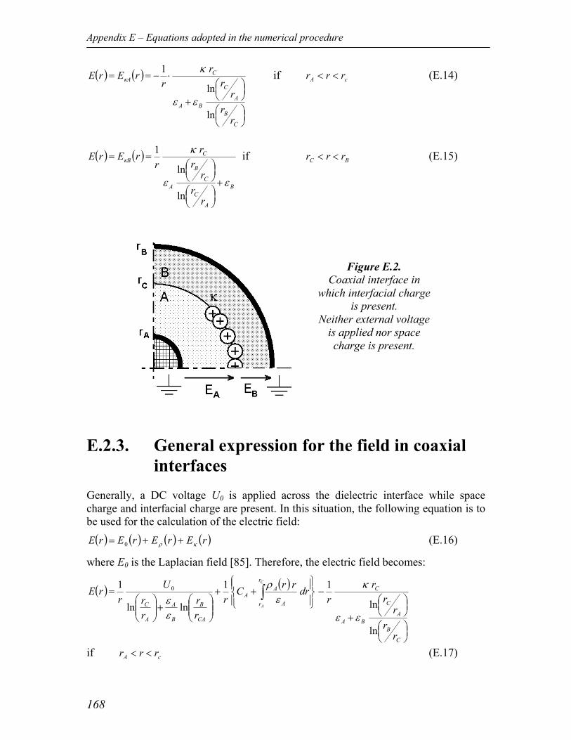
Appendix E – Equations adopted in the numerical procedure
168
( ) ( )
+
⋅−==
C
B
A
C
BA
CA
rr
rr
rr
rErE
ln
ln
1
εε
κκ if cA rrr << (E.14)
( ) ( )
B
A
C
C
B
A
CB
rr
rr
rr
rErE
εε
κκ
+
==
ln
ln
1 if BC rrr << (E.15)
E.2.3. General expression for the field in coaxial interfaces
Generally, a DC voltage U0 is applied across the dielectric interface while space charge and interfacial charge are present. In this situation, the following equation is to be used for the calculation of the electric field: ( ) ( ) ( ) ( )rErErErE κρ ++= 0 (E.16)
where E0 is the Laplacian field [85]. Therefore, the electric field becomes:
( ) ( )
++
+
= ∫
C
A
r
r A
AA
CA
B
B
A
A
C
drrrCr
rr
rr
Ur
rEε
ρ
εε
1
lnln
1 0
+
−
C
B
A
C
BA
C
rr
rr
rr
ln
ln
1
εε
κ
if cA rrr << (E.17)
Figure E.2. Coaxial interface in
which interfacial charge is present.
Neither external voltage is applied nor space charge is present.
Appendix E – Equations adopted in the numerical procedure
169
and
( ) ( )+
++
+
= ∫
B
C
r
r B
BB
CA
B
A
C
A
B
drrrCr
rr
rr
Ur
rEε
ρ
εε
1
lnln
1 0
B
A
C
C
B
A
C
rr
rr
rr
εε
κ
+
ln
ln
1
if BC rrr << (E.18)
E.3. Fourier’s heat diffusion equation for cables and cable joints
In order to obtain the temperature distribution within the insulation of a cable/cable joint, it is necessary to solve the heat diffusion equation:
δδ cQT
ck
tT
+
∇⋅∇=
∂∂ (E.19)
where c and δ are respectively the specific heat and the density of the materials being studied, and Q the heat losses per unit of volume. In the studied cases, the only considered loss is the power per unit of length Pc dissipated in the cable conductor, which is assumed to be constant. The cable jacket, the shield, the sheath and the environment surrounding the cable are modeled with an equivalent outermost layer made of a fictitious material E. An isothermal temperature distribution is assumed at the inner conductor, because of its high thermal conductivity. Using cylindrical coordinates and assuming that the temperature distribution is a function only of radius and time, equation (E.19) becomes.
( )( )
rr
trTkr
crttrT
∂
∂∂
∂=
∂∂
,11,δ
(E.20)
The term considering the heat dissipation does not appear directly in equation (E.20). This is because the heat dissipation is taken into account in the boundary conditions. In Figure E.3, the model used for the calculation of the dynamic radial temperature distribution in cables and cable joints is represented. Equation (E.20) is subject to the following initial and boundary conditions. Initial condition The temperature at time zero is isothermal and equal to the environment temperature Tamb: ( ) ambTtrT == 0, (E.21)
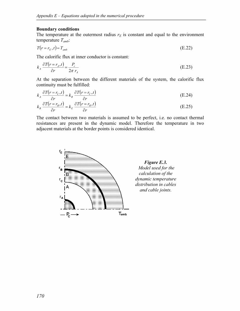
Appendix E – Equations adopted in the numerical procedure
170
Boundary conditions The temperature at the outermost radius rE is constant and equal to the environment temperature Tamb: ( ) ambE TtrrT == , (E.22)
The calorific flux at inner conductor is constant: ( )
A
cAA r
Pr
trrTkπ2
,=
∂=∂ (E.23)
At the separation between the different materials of the system, the calorific flux continuity must be fulfilled:
( )r
trrTk CA ∂
=∂ , ( )r
trrTk CB ∂
=∂=
, (E.24)
( )r
trrTk BB ∂
=∂ , ( )r
trrTk BE ∂
=∂=
, (E.25)
The contact between two materials is assumed to be perfect, i.e. no contact thermal resistances are present in the dynamic model. Therefore the temperature in two adjacent materials at the border points is considered identical.
Figure E.3. Model used for the calculation of the
dynamic temperature distribution in cables
and cable joints.
References
171
References [1] J. D. Achenbach, Wave propagation in elastic solids, Chapter 4, North-Holland
Publishing Company, 1973. [2] B. Aladenize, R. Coelho, F. Guillaumond, P. Mirebeau, “On the intrinsic space
charge in a dc power cable”, Jour. Electrost., Vol. 39, pp. 235-251, 1997. [3] B. Alijagic-Jonuz, P. H. F. Morshuis, J. J. Smit, “Space charge measurements,
dielectric spectroscopy and breakdown tests on new and aged polycarbonate”. Proc. IEEE Conf. Electr. Insul. Diel. Phenom., pp. 275 – 278, 2004.
[4] B. Alijagic-Jonuz, P. H. F. Morshuis, J. J. Smit, “Possibilities for using space charge quantities as aging markers and as a tool for material ranking”. Proc. IEEE Int. Conf. Sol. Diel., pp. 743 – 746, 2004.
[5] B. Alijagic-Jonuz, P. H. F. Morshuis, J. J. Smit, “Changing of space charge related material properties due to electrical aging”. Proc. Int. Conf. Prop. App. Diel. Mat., pp. 904-908, 2003.
[6] J. M. Alison, “The pulsed electro-acoustic method for the measurement of the dynamic space charge profile within insulators”, in Space charge in solid dielectric, edit by J. C. Fothergill and L. A. Dissado, ISBN 0-9533538-0-X, pp. 93-121, 1998.
[7] C. Alquié, G. Dreyfus, J. Lewiner, “Stress-wave probing of electric field distributions in dielectrics”, Phys. Rev. Lett., Vol. 47, No. 20, pp. 1483 – 1487, 1981.
[8] N. Ando, F. Numajiri, “Experimental investigation of space charge in XLPE cable using dust figures”, IEEE Trans. Electr. Insul., Vol. 14, No. 1, pp. 36 – 42, 1979.
[9] K. R. Bambery, R. J. Fleming, “Activation energies and electron transport in LDPE”, Proc. IEEE Conf. Electr. Insul. Diel. Phen., pp. 28–31, 2003.
[10] K. R. Bambery, R. J. Fleming, J. T. Holboll, “Space charge profiles in low density polyethylene samples containing a permittivity/conductivity gradient”, J. Phys. D Appl. Phys., 34, pp.3071-3074, 2001.
[11] K. R. Bambery, R. J. Fleming, “Space charge profiles in planar LDPE with TiO2 additive and a temperature gradient”, Proc. IEEE Conf. Electr. Insul. Diel. Phen., pp. 36–39, 2001.
[12] A. J. Berkhout, Applied seismic wave theory – Advances in exploration geophysics 1, Elsevier Science Publishers, 1987.
[13] J. B. Bernstein, “Improvements to the electrically stimulated acoustic-wave method for analysing bulk space charge”, IEEE Trans. Electr. Insul., Vol. 27, pp. 152 – 161, 1992.
[14] J. Beyer, Space Charge and Partial Discharge Phenomena in HVDC Devices, PhD-thesis Delft University of Technology, ISBN 90-6734-097-9, 2002.
References
172
[15] J. Beyer, P. H. F. Morshuis, “Conduction current measurements on polycarbonates subjected to electrical and thermal stress”, Proc. IEEE Conf. Electr. Insul. Diel. Phenom., pp. 617 – 621, 2000.
[16] J. Beyer, P. H. F. Morshuis, J. J. Smit, “Investigation on charge and polarization effects at dielectric interfaces in laminated HVDC insulation”, Proc. IEEE Conf. Electr. Insul. Diel. Phenom., pp. 32-37, 1999.
[17] J. Beyer, P. H. F. Morshuis, J. J. Smit, “Space charge phenomena in laminated HVDC insulation”, Proc. Int. Symp. Electr. Insul. Mater., pp. 181-186, 1998.
[18] J. Bishop, G. Chen, E. A. Davies, I. Doble, A. s. Vaughan, “DC electrical characteristics of amalgamation regions in PE insulations”, Proc. Int. Conf. Prop. App. Diel. Mat., pp. 314-317, 1992.
[19] J. Blitz, Fundamentals of ultrasonics, Chapter 1 and 2, second edition, London butterworths, 1967.
[20] R. Bodega, P. H. F. Morshuis, E. Redjosentono, J. J. Smit, “Dielectric interface characterization by means of space charge measurements”, Proc. IEEE Conf. on Electr. Insul. Diel. Phenom., pp. 728-733, 2003.
[21] R. Bodega, P.H.F. Morshuis, U.H. Nilsson, G. Perego, J.J Smit, “Polarization mechanisms of flat XLPE-EPR interfaces”, Proc. Nord. Ins. Symp, pp.224-227, 2005.
[22] R. Bodega, P. H. F. Morshuis, J. J. Smit, “Space charge signal interpretation in dielectric combinations tested by means of the PEA method”, Proc. IEEE Int. Conf. Sol. Diel., pp. 240-243, 2004.
[23] R. Bodega, P. H. F. Morshuis, U. H. Nilsson, G. Perego, J. J Smit, “Charging and polarization phenomena in coaxial XLPE-EPR interfaces”, Proc. IEEE Int. Symp. Electr. Insul. Mat., pp. 107-110, 2005.
[24] R. Bodega, P. H. F. Morshuis, U. H. Nilsson, G. Perego, J. J Smit, “Space charge measurements in dual-dielectric cables”, Proc. Nord. Ins. Symp, pp. 107-110, 2005.
[25] R. Bodega, P. H. F. Morshuis, J. J Smit, “Space charge measurements on multi-dielectrics by means of the pulsed electroacoustic method”, IEEE Trans. Dielectr. Electr. Insul., Vol. 13, No. 2, pp.272-281, 2006.
[26] R. Bodega, G. Perego, P. H. F. Morshuis, U. H. Nilsson, J.J. Smit, “Space charge and electric field characteristics of polymeric-type MV-size DC cable joint models”, Proc. IEEE Conf. on Electr. Insul. Diel. Phenom., pp. 507-510, 2005.
[27] R. Bodega, G. C. Montanari, P. H. F. Morshuis, “Conduction current measurements on XLPE and EPR insulation”, Proc. IEEE Conf. Electr. Insul. Diel. Phen., pp. 101-105, 2004.
[28] S. Boggs, D. H. Damon, J. Hjerrild, J. T. Holbøll, M. Henriksen, “Effect of insulation properties on field grading of solid dielectric DC cables”, IEEE Trans. Pow. Del., Vol. 16, No. 4, pp. 456-461, 2001.
References
173
[29] S. Boggs, “A rational consideration of space charge”, IEEE Electr. Insul. Mag., Vol. 20, No. 4, pp. 22-27, 2004.
[30] J-O Boström, A. Campus, R. N. Hampton, U. H. Nilsson, “Evaluation of the material reliability for polymeric direct current cables”, Cigré 15-404, 2002.
[31] F. Boufayed, S. Leroy, G. Teyssedre, C. Laurent, P. Segur, E. Cooper, L. A. Dissado, G. C. Montanari, “Numerical resolution of charge transport in cross-linked polyethylene by means of a bipolar model with a distribution of traps”, Proc. IEEE Int. Conf. Sol. Diel., pp. 562-566, 2004.
[32] F. Boufayed, S. Leroy, G. Teyssedre, C. Laurent, P. Segur, L. A. Dissado, G. C. Montanari, “Simulation of bipolar charge transport in polyethylene featuring trapping and hopping conduction through an exponentioal distribution of traps”, Proc. IEEE Int. Symp. Electr. Insul. Mat., pp. 340-343, 2005.
[33] M. A. Brown, G. Chen, A. E. Davies, L. A. Dissado, P. A. Norman, “Space charge characterization in aged LDPE amalgamated insulation regions from underwater telecommunication systems”, IEEE Trans. Dielectr. Electr. Insul., Vol. 7, No. 3, pp. 346-352, 2000.
[34] M. P. Cals, J. P. Marque, C. Alquié, “Application of the pressure wave propagation method to the study of interfacial effects in e-irradiated polymer films”, J. Appl. Phys, Vol. 72, No. 5, pp.1940-1951, 1992.
[35] G. Chen, Y. Tanaka, T. Takada, L. Zhong, “Effect of polyethylene interface on space charge formation”, IEEE Trans. Dielectr. Electr. Insul., Vol.11, No. 1, pp. 113-121, 2004.
[36] A. Cherifi, M. A. Dakka, A. Toureille, “The validation of the thermal step method”, IEEE Trans. Electr. Insul., Vol. 27, No. 6, pp. 1152 – 1158, 1992.
[37] Cigré WG 21.02, “Recommendations for tests of power transmission DC cables for a rated voltage up to 800 kV (Electra 72, 1980 – revision)”, Electra No. 189, pp. 39-45, 2000.
[38] Cigré WG 21.02, “Recommendations for testing DC extruded cable systems for power transmission at a rated voltage up to 250 kV”, Brochure 219, 2003.
[39] Cigré TF D1-12-01, “Space charge measurements in dielectrics and insulating materials”, version 5, 2005.
[40] Cigré, Joint TF 21/15. “Interfaces in Accessories for Extruded HV and EHV Cables”, 2002.
[41] R. Coelho, B. Aladenize, P.Mirebeau, “On the intrinsic space charge in a dc power cable”, Proc. IEEE Conf. Electr. Insul. Diel. Phen., pp. 278-282, 1996.
[42] R. Coelho, “Charges in non homogeneous dielectrics”, Proc. IEEE Conf. Electr. Insul. Diel. Phen., pp. 1-10, 1997.
[43] R. E. Collins, “Analysis of spatial distribution of charges and dipoles in electrets by a transient heating technique”, Jour. App. Phys., Vol. 47, No. 11, pp. 4804 – 4808, 1976.
References
174
[44] J. Densley, M. Henriksen, J. Holbøll, “The effect of semiconducting electrode material on the conductivity of low density polyethylene”, Proc. Nord. Ins. Symp, pp.115-118, 2005.
[45] L. A. Dissado, J. C. Fothergill, Electrical degradation and breakdown in polymers, published by Peter Peregrinus Ltd, ISBN 0-86341-196-7, 1992.
[46] L. Dissado, G. Mazzanti, G. C. Montanari, “The incorporation of space charge degradation in the life model of insulating materials”. IEEE Trans. Dielectr. Electr. Insul., Vol. 2, No. 6, pp. 1147-1158, 1995.
[47] L. Dissado, G. Mazzanti, G. C. Montanari, “The role of trapped space charges in the electrical ageing of insulating materials”. IEEE Trans. Dielectr. Electr. Insul., Vol. 4, No. 5, pp. 496-506, 1997.
[48] L. A. Dissado, C. Laurant, G. C. Montanari, P. H. F. Morshuis, “Demostrating the threshold for trapped space charge accumulation in solid dielectrics under DC field”, IEEE Trans. Dielectr. Electr. Insul., Vol. 12, No. 3, pp. 612-620, 2005.
[49] C. Doench, K. D. Srivastava, “High-voltage direct-current cables”, in Power and communication cables – Theory and applications, R. Bartnikas editor, K. D. Srivastava coeditor, pp. 624-651.
[50] B. Drinkwater, P. Cawley, “Measurement of the frequency dependence of the ultrasonic reflection coefficient from thin interface layers and partially contacting interfaces”, Ultrasonics 35, pp. 479-488, 1997.
[51] W. Eisenmenger, M. Haardt, “Observation of charge compensated polarization zones in polyvinylidenefluoride (PVDF) films by piezoelectric acoustic step-wave response”, Solid State Commun., Vol. 41, No 12, pp. 917 – 920, 1982.
[52] A. Ericsson, M. Jeroense, J. Miller, L. Palmqvist, B. Reiling, P. Riffon, “HVDC-Light cable systems – the latest projects”, Proc. Nord. Ins. Symp, 2003.
[53] D. Fabiani, G. C. Montanari, R. Bodega, P. H. F. Morshuis, C. laurant, L. A. Dissado, “The effect of temperature gradient on space charge and electric field distribution of HVDC cable models”, Proc. Int. Conf. Prop. App. Diel. Mat., 2006.
[54] R. J. Fleming, “Space charge profile measurement techniques: recent advances and future directions”, IEEE Trans. Dielectr. Electr. Insul., Vol. 12, No. 5, pp. 967-978, 2005.
[55] J. C. Fothergill, “The effect of charges in electrical insulation”, workshop at the IEEE Int. Conf. Sol. Diel., Toulouse 2004.
[56] M. Fu, G. Chen, E. A. Davies, Y. Tanaka, T. Takada, “A modified PEA space charge measuring system for power cables”, Proc. Int. Conf. Prop. App. Diel. Mat., pp. 104-107, 2000.
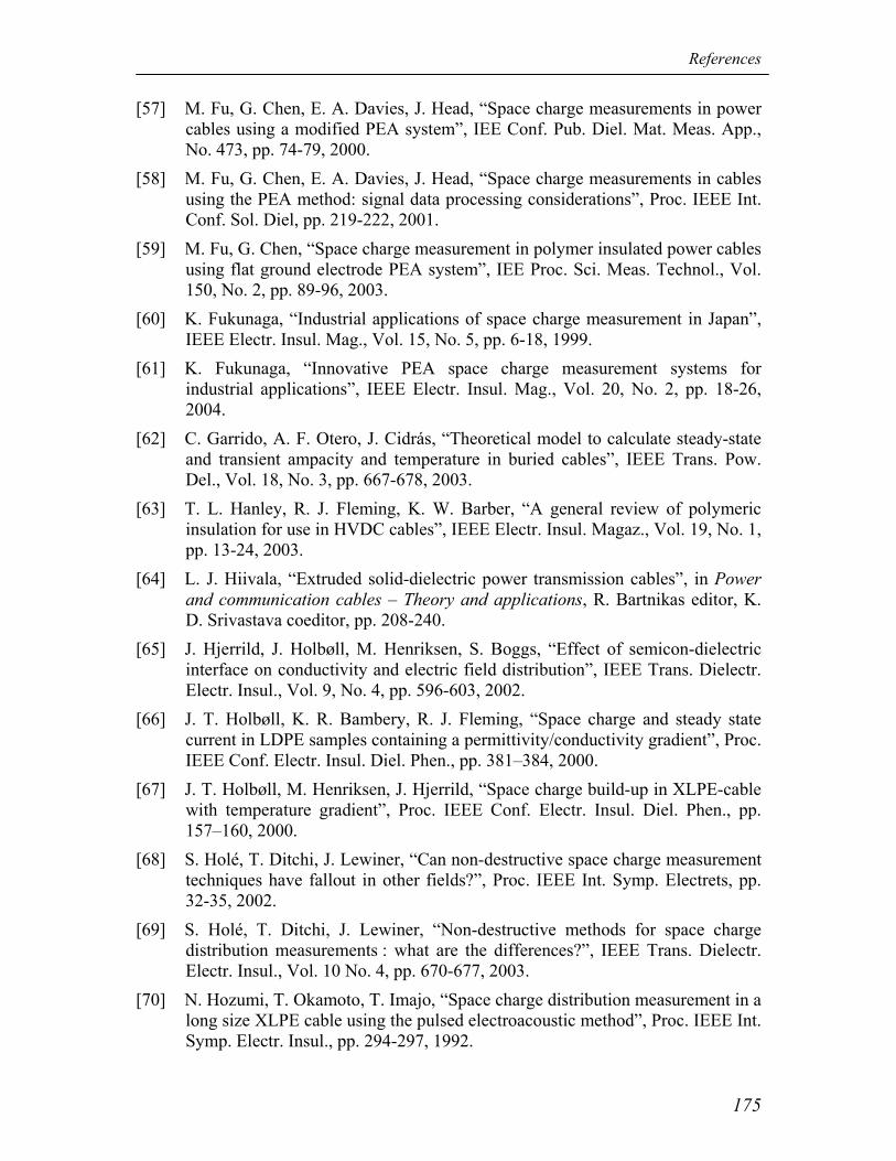
References
175
[57] M. Fu, G. Chen, E. A. Davies, J. Head, “Space charge measurements in power cables using a modified PEA system”, IEE Conf. Pub. Diel. Mat. Meas. App., No. 473, pp. 74-79, 2000.
[58] M. Fu, G. Chen, E. A. Davies, J. Head, “Space charge measurements in cables using the PEA method: signal data processing considerations”, Proc. IEEE Int. Conf. Sol. Diel, pp. 219-222, 2001.
[59] M. Fu, G. Chen, “Space charge measurement in polymer insulated power cables using flat ground electrode PEA system”, IEE Proc. Sci. Meas. Technol., Vol. 150, No. 2, pp. 89-96, 2003.
[60] K. Fukunaga, “Industrial applications of space charge measurement in Japan”, IEEE Electr. Insul. Mag., Vol. 15, No. 5, pp. 6-18, 1999.
[61] K. Fukunaga, “Innovative PEA space charge measurement systems for industrial applications”, IEEE Electr. Insul. Mag., Vol. 20, No. 2, pp. 18-26, 2004.
[62] C. Garrido, A. F. Otero, J. Cidrás, “Theoretical model to calculate steady-state and transient ampacity and temperature in buried cables”, IEEE Trans. Pow. Del., Vol. 18, No. 3, pp. 667-678, 2003.
[63] T. L. Hanley, R. J. Fleming, K. W. Barber, “A general review of polymeric insulation for use in HVDC cables”, IEEE Electr. Insul. Magaz., Vol. 19, No. 1, pp. 13-24, 2003.
[64] L. J. Hiivala, “Extruded solid-dielectric power transmission cables”, in Power and communication cables – Theory and applications, R. Bartnikas editor, K. D. Srivastava coeditor, pp. 208-240.
[65] J. Hjerrild, J. Holbøll, M. Henriksen, S. Boggs, “Effect of semicon-dielectric interface on conductivity and electric field distribution”, IEEE Trans. Dielectr. Electr. Insul., Vol. 9, No. 4, pp. 596-603, 2002.
[66] J. T. Holbøll, K. R. Bambery, R. J. Fleming, “Space charge and steady state current in LDPE samples containing a permittivity/conductivity gradient”, Proc. IEEE Conf. Electr. Insul. Diel. Phen., pp. 381–384, 2000.
[67] J. T. Holbøll, M. Henriksen, J. Hjerrild, “Space charge build-up in XLPE-cable with temperature gradient”, Proc. IEEE Conf. Electr. Insul. Diel. Phen., pp. 157–160, 2000.
[68] S. Holé, T. Ditchi, J. Lewiner, “Can non-destructive space charge measurement techniques have fallout in other fields?”, Proc. IEEE Int. Symp. Electrets, pp. 32-35, 2002.
[69] S. Holé, T. Ditchi, J. Lewiner, “Non-destructive methods for space charge distribution measurements : what are the differences?”, IEEE Trans. Dielectr. Electr. Insul., Vol. 10 No. 4, pp. 670-677, 2003.
[70] N. Hozumi, T. Okamoto, T. Imajo, “Space charge distribution measurement in a long size XLPE cable using the pulsed electroacoustic method”, Proc. IEEE Int. Symp. Electr. Insul., pp. 294-297, 1992.
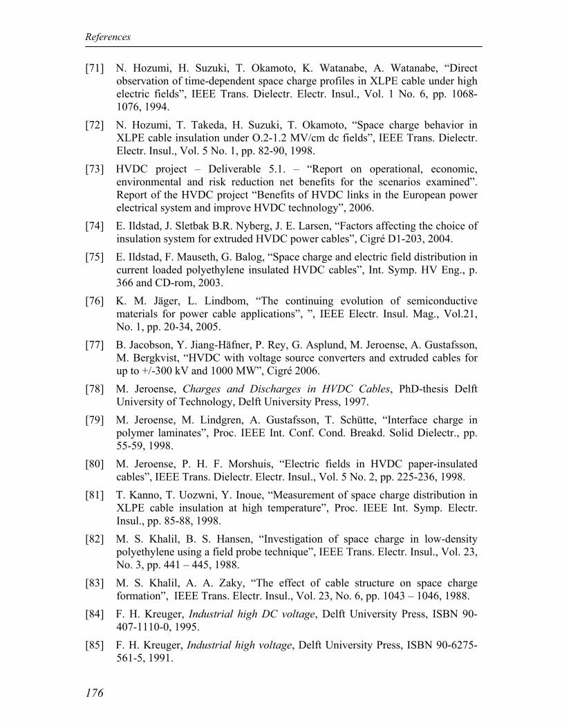
References
176
[71] N. Hozumi, H. Suzuki, T. Okamoto, K. Watanabe, A. Watanabe, “Direct observation of time-dependent space charge profiles in XLPE cable under high electric fields”, IEEE Trans. Dielectr. Electr. Insul., Vol. 1 No. 6, pp. 1068-1076, 1994.
[72] N. Hozumi, T. Takeda, H. Suzuki, T. Okamoto, “Space charge behavior in XLPE cable insulation under O.2-1.2 MV/cm dc fields”, IEEE Trans. Dielectr. Electr. Insul., Vol. 5 No. 1, pp. 82-90, 1998.
[73] HVDC project – Deliverable 5.1. – “Report on operational, economic, environmental and risk reduction net benefits for the scenarios examined”. Report of the HVDC project “Benefits of HVDC links in the European power electrical system and improve HVDC technology”, 2006.
[74] E. Ildstad, J. Sletbak B.R. Nyberg, J. E. Larsen, “Factors affecting the choice of insulation system for extruded HVDC power cables”, Cigré D1-203, 2004.
[75] E. Ildstad, F. Mauseth, G. Balog, “Space charge and electric field distribution in current loaded polyethylene insulated HVDC cables”, Int. Symp. HV Eng., p. 366 and CD-rom, 2003.
[76] K. M. Jäger, L. Lindbom, “The continuing evolution of semiconductive materials for power cable applications”, ”, IEEE Electr. Insul. Mag., Vol.21, No. 1, pp. 20-34, 2005.
[77] B. Jacobson, Y. Jiang-Häfner, P. Rey, G. Asplund, M. Jeroense, A. Gustafsson, M. Bergkvist, “HVDC with voltage source converters and extruded cables for up to +/-300 kV and 1000 MW”, Cigré 2006.
[78] M. Jeroense, Charges and Discharges in HVDC Cables, PhD-thesis Delft University of Technology, Delft University Press, 1997.
[79] M. Jeroense, M. Lindgren, A. Gustafsson, T. Schütte, “Interface charge in polymer laminates”, Proc. IEEE Int. Conf. Cond. Breakd. Solid Dielectr., pp. 55-59, 1998.
[80] M. Jeroense, P. H. F. Morshuis, “Electric fields in HVDC paper-insulated cables”, IEEE Trans. Dielectr. Electr. Insul., Vol. 5 No. 2, pp. 225-236, 1998.
[81] T. Kanno, T. Uozwni, Y. Inoue, “Measurement of space charge distribution in XLPE cable insulation at high temperature”, Proc. IEEE Int. Symp. Electr. Insul., pp. 85-88, 1998.
[82] M. S. Khalil, B. S. Hansen, “Investigation of space charge in low-density polyethylene using a field probe technique”, IEEE Trans. Electr. Insul., Vol. 23, No. 3, pp. 441 – 445, 1988.
[83] M. S. Khalil, A. A. Zaky, “The effect of cable structure on space charge formation”, IEEE Trans. Electr. Insul., Vol. 23, No. 6, pp. 1043 – 1046, 1988.
[84] F. H. Kreuger, Industrial high DC voltage, Delft University Press, ISBN 90-407-1110-0, 1995.
[85] F. H. Kreuger, Industrial high voltage, Delft University Press, ISBN 90-6275-561-5, 1991.
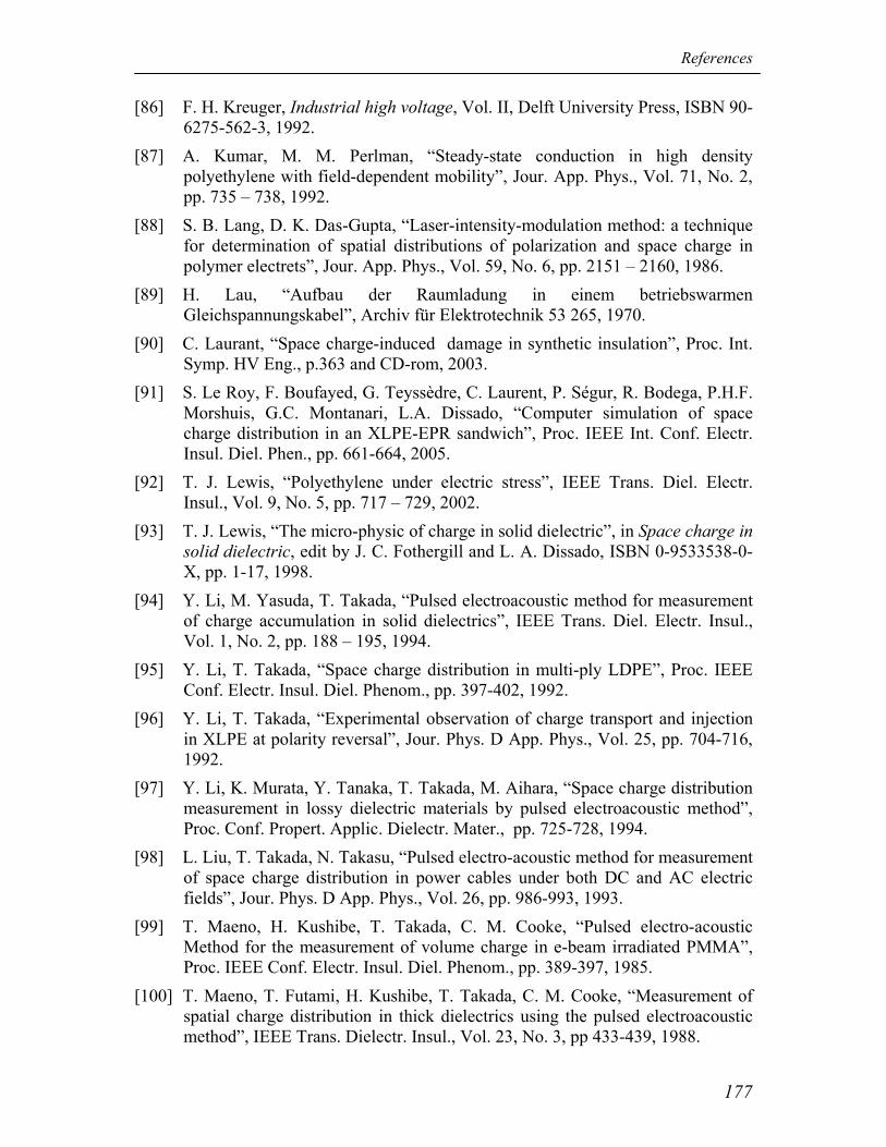
References
177
[86] F. H. Kreuger, Industrial high voltage, Vol. II, Delft University Press, ISBN 90-6275-562-3, 1992.
[87] A. Kumar, M. M. Perlman, “Steady-state conduction in high density polyethylene with field-dependent mobility”, Jour. App. Phys., Vol. 71, No. 2, pp. 735 – 738, 1992.
[88] S. B. Lang, D. K. Das-Gupta, “Laser-intensity-modulation method: a technique for determination of spatial distributions of polarization and space charge in polymer electrets”, Jour. App. Phys., Vol. 59, No. 6, pp. 2151 – 2160, 1986.
[89] H. Lau, “Aufbau der Raumladung in einem betriebswarmen Gleichspannungskabel”, Archiv für Elektrotechnik 53 265, 1970.
[90] C. Laurant, “Space charge-induced damage in synthetic insulation”, Proc. Int. Symp. HV Eng., p.363 and CD-rom, 2003.
[91] S. Le Roy, F. Boufayed, G. Teyssèdre, C. Laurent, P. Ségur, R. Bodega, P.H.F. Morshuis, G.C. Montanari, L.A. Dissado, “Computer simulation of space charge distribution in an XLPE-EPR sandwich”, Proc. IEEE Int. Conf. Electr. Insul. Diel. Phen., pp. 661-664, 2005.
[92] T. J. Lewis, “Polyethylene under electric stress”, IEEE Trans. Diel. Electr. Insul., Vol. 9, No. 5, pp. 717 – 729, 2002.
[93] T. J. Lewis, “The micro-physic of charge in solid dielectric”, in Space charge in solid dielectric, edit by J. C. Fothergill and L. A. Dissado, ISBN 0-9533538-0-X, pp. 1-17, 1998.
[94] Y. Li, M. Yasuda, T. Takada, “Pulsed electroacoustic method for measurement of charge accumulation in solid dielectrics”, IEEE Trans. Diel. Electr. Insul., Vol. 1, No. 2, pp. 188 – 195, 1994.
[95] Y. Li, T. Takada, “Space charge distribution in multi-ply LDPE”, Proc. IEEE Conf. Electr. Insul. Diel. Phenom., pp. 397-402, 1992.
[96] Y. Li, T. Takada, “Experimental observation of charge transport and injection in XLPE at polarity reversal”, Jour. Phys. D App. Phys., Vol. 25, pp. 704-716, 1992.
[97] Y. Li, K. Murata, Y. Tanaka, T. Takada, M. Aihara, “Space charge distribution measurement in lossy dielectric materials by pulsed electroacoustic method”, Proc. Conf. Propert. Applic. Dielectr. Mater., pp. 725-728, 1994.
[98] L. Liu, T. Takada, N. Takasu, “Pulsed electro-acoustic method for measurement of space charge distribution in power cables under both DC and AC electric fields”, Jour. Phys. D App. Phys., Vol. 26, pp. 986-993, 1993.
[99] T. Maeno, H. Kushibe, T. Takada, C. M. Cooke, “Pulsed electro-acoustic Method for the measurement of volume charge in e-beam irradiated PMMA”, Proc. IEEE Conf. Electr. Insul. Diel. Phenom., pp. 389-397, 1985.
[100] T. Maeno, T. Futami, H. Kushibe, T. Takada, C. M. Cooke, “Measurement of spatial charge distribution in thick dielectrics using the pulsed electroacoustic method”, IEEE Trans. Dielectr. Insul., Vol. 23, No. 3, pp 433-439, 1988.
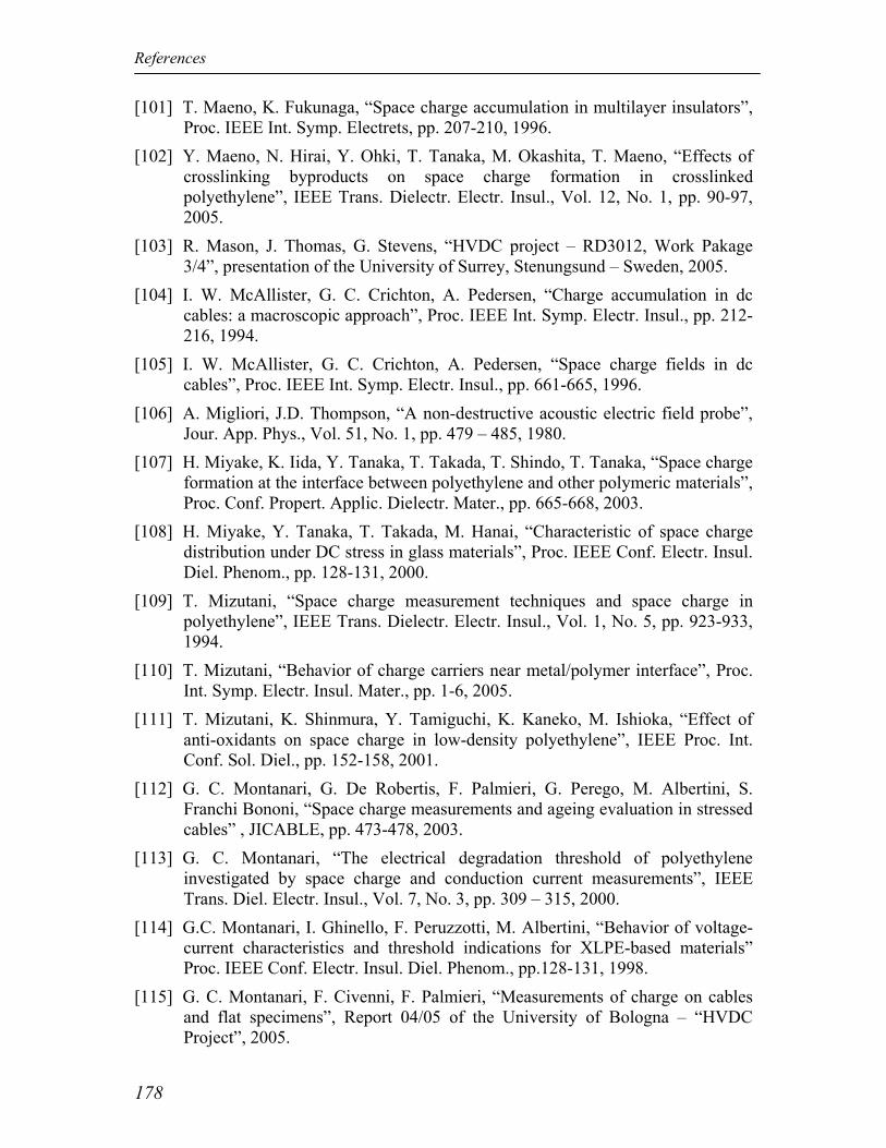
References
178
[101] T. Maeno, K. Fukunaga, “Space charge accumulation in multilayer insulators”, Proc. IEEE Int. Symp. Electrets, pp. 207-210, 1996.
[102] Y. Maeno, N. Hirai, Y. Ohki, T. Tanaka, M. Okashita, T. Maeno, “Effects of crosslinking byproducts on space charge formation in crosslinked polyethylene”, IEEE Trans. Dielectr. Electr. Insul., Vol. 12, No. 1, pp. 90-97, 2005.
[103] R. Mason, J. Thomas, G. Stevens, “HVDC project – RD3012, Work Pakage 3/4”, presentation of the University of Surrey, Stenungsund – Sweden, 2005.
[104] I. W. McAllister, G. C. Crichton, A. Pedersen, “Charge accumulation in dc cables: a macroscopic approach”, Proc. IEEE Int. Symp. Electr. Insul., pp. 212-216, 1994.
[105] I. W. McAllister, G. C. Crichton, A. Pedersen, “Space charge fields in dc cables”, Proc. IEEE Int. Symp. Electr. Insul., pp. 661-665, 1996.
[106] A. Migliori, J.D. Thompson, “A non-destructive acoustic electric field probe”, Jour. App. Phys., Vol. 51, No. 1, pp. 479 – 485, 1980.
[107] H. Miyake, K. Iida, Y. Tanaka, T. Takada, T. Shindo, T. Tanaka, “Space charge formation at the interface between polyethylene and other polymeric materials”, Proc. Conf. Propert. Applic. Dielectr. Mater., pp. 665-668, 2003.
[108] H. Miyake, Y. Tanaka, T. Takada, M. Hanai, “Characteristic of space charge distribution under DC stress in glass materials”, Proc. IEEE Conf. Electr. Insul. Diel. Phenom., pp. 128-131, 2000.
[109] T. Mizutani, “Space charge measurement techniques and space charge in polyethylene”, IEEE Trans. Dielectr. Electr. Insul., Vol. 1, No. 5, pp. 923-933, 1994.
[110] T. Mizutani, “Behavior of charge carriers near metal/polymer interface”, Proc. Int. Symp. Electr. Insul. Mater., pp. 1-6, 2005.
[111] T. Mizutani, K. Shinmura, Y. Tamiguchi, K. Kaneko, M. Ishioka, “Effect of anti-oxidants on space charge in low-density polyethylene”, IEEE Proc. Int. Conf. Sol. Diel., pp. 152-158, 2001.
[112] G. C. Montanari, G. De Robertis, F. Palmieri, G. Perego, M. Albertini, S. Franchi Bononi, “Space charge measurements and ageing evaluation in stressed cables” , JICABLE, pp. 473-478, 2003.
[113] G. C. Montanari, “The electrical degradation threshold of polyethylene investigated by space charge and conduction current measurements”, IEEE Trans. Diel. Electr. Insul., Vol. 7, No. 3, pp. 309 – 315, 2000.
[114] G.C. Montanari, I. Ghinello, F. Peruzzotti, M. Albertini, “Behavior of voltage-current characteristics and threshold indications for XLPE-based materials” Proc. IEEE Conf. Electr. Insul. Diel. Phenom., pp.128-131, 1998.
[115] G. C. Montanari, F. Civenni, F. Palmieri, “Measurements of charge on cables and flat specimens”, Report 04/05 of the University of Bologna – “HVDC Project”, 2005.
References
179
[116] G. C. Montanari, P. H. F. Morshuis, “Space charge phenomenology in polymeric insulating materials”, IEEE Trans. on Diel. Electr. Insul., Vol. 12, No. 4, pp.754-767, 2005.
[117] G.C. Montanari, I. Ghinello, A. Motori, S. Gubanski, D. Das Gupta, “High field conductivity measurements and search for threshold in PET films”, Proc. IEEE Conf. Electr. Insul. Diel. Phenom., pp.20-23, 1996.
[118] P. H. F. Morshuis, M. Jeroense, “Space charge measurements on impregnated paper: a review of the PEA method and a discussion of the results”, IEEE Electr. Insul. Mag., Vol.13 No.3, pp.26-35, 1997.
[119] T. Muronaka, Y. Tanaka T. Takada, S. Maruyama, H. Mutou, “Measurement of space charge distribution in XLPE cable using PEA system with flat electrode”, Proc. IEEE Conf. Electr. Insul. Diel. Phenom., pp. 266-269, 1996.
[120] Z. Nadolny, J. M. Braun, R. J Densley, “Effect of mechanical pressure and silicone grease on partial discharge characteristics for model XLPE transmission cable joint”, Proc. Int. Symp. HV Eng., Vol.5, No.467, pp 297-300, 1999.
[121] K. Nagashima, X. Qin, Y. Tanaka, T, Takada, “Calibration of accumulated space charge in power cable using PEA measurement”, Proc. IEEE Int. Conf. Cond. Break. Sol. Diel., pp. 60-63, 1998.
[122] U. H. Nilsson, “Material under study in EU HVDC project”, Presentation of Borealis – “HVDC Project”, September 2004.
[123] U. H. Nilsson, “The use of model cables for evaluation of electrical performance of polymeric power cable materials”, Proc. Nord. Ins. Symp, pp.101-106, 2005.
[124] J. J. O’Dwyer, The theory of electrical conduction and breakdown is solid dielectric, Calderon Press, Oxford, 1973.
[125] Y. Ohki, Y. Ebinuma, S. Katakai, “Space charge formation in water-treed insulation”, IEEE Trans. Dielectr. Insul., Vol.5, No.5, pp. 707-712, 1998.
[126] W. K. H. Panofsky, M. Phillips, Classical Electricity and Magnetism, Chapter 6, Addison-Wesley, Reading, 1962.
[127] M. P. Pépin, H.J. Wintle, “Charge injection and conduction on the surface of insulators”, Journ. App. Phys., Vol.83, No.11, pp. 5870-5879, 1998.
[128] G. Perego, F. Peruzzotti, G. C. Montanari, F. Palmieri, G. De Robertis, “Investigating the effect of additives for high-voltage polymeric dc cables through space charge measurements on cables and films”, Proc. IEEE Conf. Electr. Insul. Diel. Phenom., pp. 456-459, 2001.
[129] C. N. Rasmussen, J. T. Holboll, M. Henriksen, “Dynamic space charge behaviour in polymeric DC cables”, Proc. IEEE Int. Symp. Electrets, pp. 23-36, 2002.
References
180
[130] B. D. Reiling, J. J. Miller, P. Steckley, G. Moreau, P. Bard, L. Romström, J. Lindberg, “Cross Sound cable project second generation VSC technology for HVDC”, Cigré B4-102, 2004.
[131] R. Remsburg, Thermal design of electronic equipment, Section 2.6, CCR Press, ISBN 0-8493-0082-7, 2001.
[132] W. Sachse, Y.H. Pao, “On the determination of phase and group velocities of dispersive waves in solids”, Journ. App. Pyhs., Vol. 49(8), pp. 4320-4327, 1978.
[133] B. Sanden, XLPE cable insulation subjected to HVDC stress – Space charge, conduction and breakdown strength, PhD-thesis Norwegian University of Science and Technology, ISBN 82-471-0001-0, 1996.
[134] B. Sanden, E. Ildstad, R. Hegerberg, “Space charge accumulation and conduction current in XLPE insulation”. IEE Int. Proc. Conf. Diel. Mat. Meas. App., No. 430, pp. 368-373, 1996.
[135] G. M. Sessler, J. E. West, G. Gerhard, “High-resolution laser-pulse method for measuring charge distributions in dielectrics”, Phys. Rev. Lett., Vol. 48, No. 8, pp. 563 – 566, 1982.
[136] J. G. Slootweg, Wind power – modelling and impact on power system dynamics, Ph.D. thesis – Delft University of Technology, ISBN 90-9017239-4, 2003.
[137] E. J. D. Straathof, “Characterization and comparison of XLPE MV-size DC cables by means of space charge measurements”, M.Sc. thesis, Delft University of Technology, 2006.
[138] K. S. Suh, S. J. Hwang, J. S. Noh, T. Takada, “Effect of constituents of XLPE on the formation of space charge”, IEEE Trans. Dielectr. Insul., Vol.1, No.6, pp. 1077-1083, 1994.
[139] K. S. Suh, J. H. Nam, J. H. Kim, K. C. Ko, S.O. Han, “Interfacial properties of XLPE/EPDM laminates”, IEEE Trans. Dielectr. Insul., Vol.7, No.2, pp. 216-221, 2000.
[140] K. S. Suh, J. Y. Kim, H. S. Noh, C. R. Lee, “Interfacial charge in polyethylene/ethylene vinylacetate laminates, IEEE Trans. Dielectr. Insul., Vol.3, No.6, pp. 758-764, 1996.
[141] K. Suzuki, Y. Tanaka, T. Takada, Y. Ohki, C. Takeya, “Correlation between space charge distribution and water-tree location in aged XLPE cable”, IEEE Trans. Dielectr. Insul., Vol.8, No.1, pp. 78-81, 2001.
[142] T. Takada, “Acoustic and optical methods for measuring electric charge distributions in dielectrics”, IEEE Trans. Diel. Electr. Insul., Vol. 6, No. 5, pp. 519 – 547, 1999.
[143] T. Takada, Y. Tanaka, N. Adachi, X. Qin, “Comparison between the PEA method and the PWP method for space charge measurements in solid dielectrcs”, IEEE Trans. Diel. Electr. Insul., Vol. 5, No. 6, pp. 944 – 950, 1998.
References
181
[144] T. Tanaka, M. Uchiumi, “Two kinds of time constants for interfacial space charge in polyethylene-laminated dielectrics”,Proc. IEEE Conf. Electr. Insul. Diel. Phenom., pp. 472-475, 1999.
[145] T. Tanaka, M. Uchiumi, “Some consideration of voltage-induced interfacial space charge in several laminated dielectrics”, Proc. IEEE Int. Conf. Cond. Breakdown Solid Dielectr., pp. 23-27, 1998.
[146] T. Tanaka, T. Ito, Y. Tanaka, T. Takada, “Carrier jumping over a potential barrier at the interface of LDPE laminated dielectrics”, IEEE Proc. Int. Symp. Electr. Insul., pp. 40-43, 2000.
[147] M. Uchiumi, T. Tanaka, K. Ueda, M. Nitta, “Characteristics of space charge in polyethylene/ethylene-propylene-terpolymer laminates”, Proc. Int. Symp. Electr. Insul. Mater., pp. 117-120, 1998.
[148] M. Wadamori, M. Fukuma, T. Maeno, K. Fukunaga, M. Nagao, “Proposal of numerical analysis model of acoustic wave propagation and generation on PEA method”, Proc. Conf. Propert. Applic. Dielectr. Mater, pp. 863-866, 2003.
[149] M. Wadamori, M. Fukuma, M. Nagao, N. Hozumi, M. Kosaki, Y. Fukui, “Numerical analysis of acoustic wave generation and propagation on PEA method”, Proc. Int. Symp. Electr. Insul. Mater., pp.403-406, 2001.
[150] K. W. Wagner, “Erklärung der dielektrischen Nachwirkungsvorgänge auf Grund Maxwellscher Vorstellungen”, Archiv für Elektrotechnik II, Vol. 9, pp. 371-387, 1914.
[151] X. Wang, D. Tu, Y. Tanaka, T. Muronaka, T. Takada, C. Shinoda, T. Hashizumi, “Space Charge in XLPE Power Cable under dc Electrical Stress and Heat Treatment”, IEEE Trans. Diel. Electr. Insul., Vol. 2, No. 3, pp. 467 – 474, 1995.
[152] A. J. Wintle, “Charge motion and trapping at insulators – surface and bulk effects”, IEEE Trans. Diel. Electr. Insul., Vol. 6, No. 1, pp. 1 – 10, 1999.
[153] M. Yasuda, M. Ito, T. Takada, “Measurement. of Charge Distributions in Coaxial Cable Using. the Pulsed Electroacoustic Method”, Japan. Journ. App. Phys., Vol. 30, pp. 71-73, 1991. Web site:
[154] http://www.engg.le.ac.uk/hvdc/

References
182
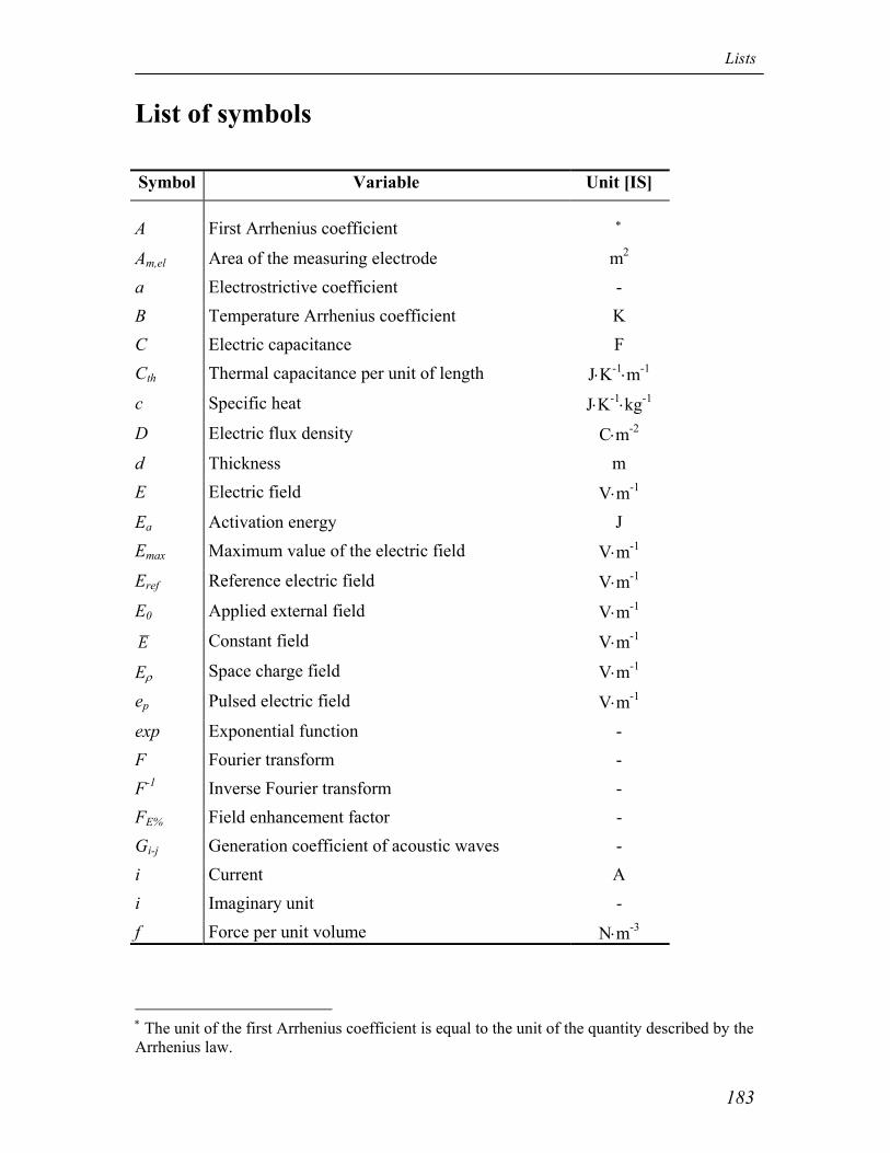
Lists
183
List of symbols Symbol Variable Unit [IS]
A First Arrhenius coefficient ∗ Am,el Area of the measuring electrode m2
a Electrostrictive coefficient - B Temperature Arrhenius coefficient K C Electric capacitance F Cth Thermal capacitance per unit of length J⋅K-1⋅m-1
c Specific heat J⋅K-1⋅kg-1
D Electric flux density C⋅m-2
d Thickness m E Electric field V⋅m-1
Ea Activation energy J Emax Maximum value of the electric field V⋅m-1 Eref Reference electric field V⋅m-1 E0 Applied external field V⋅m-1
E Constant field V⋅m-1
Eρ Space charge field V⋅m-1 ep Pulsed electric field V⋅m-1 exp Exponential function - F Fourier transform - F-1 Inverse Fourier transform - FE% Field enhancement factor - Gi-j Generation coefficient of acoustic waves - i Current A i Imaginary unit - f Force per unit volume N⋅m-3
∗ The unit of the first Arrhenius coefficient is equal to the unit of the quantity described by the Arrhenius law.
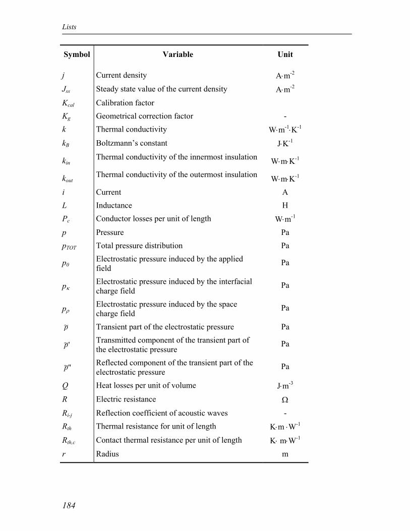
Lists
184
Symbol Variable Unit
j Current density A⋅m-2
Jss Steady state value of the current density A⋅m-2 Kcal Calibration factor Kg Geometrical correction factor - k Thermal conductivity W⋅m-1⋅K-1
kB Boltzmann’s constant J⋅K-1
kin Thermal conductivity of the innermost insulation W⋅m⋅K-1
kout Thermal conductivity of the outermost insulation W⋅m⋅K-1
i Current A L Inductance H Pc Conductor losses per unit of length W⋅m-1 p Pressure Pa pTOT Total pressure distribution Pa
p0 Electrostatic pressure induced by the applied field
Pa
pκ Electrostatic pressure induced by the interfacial charge field
Pa
pρ Electrostatic pressure induced by the space charge field
Pa
p~ Transient part of the electrostatic pressure Pa
'~p Transmitted component of the transient part of the electrostatic pressure
Pa
"~p Reflected component of the transient part of the electrostatic pressure
Pa
Q Heat losses per unit of volume J⋅m-3 R Electric resistance Ω Ri-j Reflection coefficient of acoustic waves - Rth Thermal resistance for unit of length K⋅m ⋅W-1 Rth,c Contact thermal resistance per unit of length K⋅ m⋅W-1 r Radius m
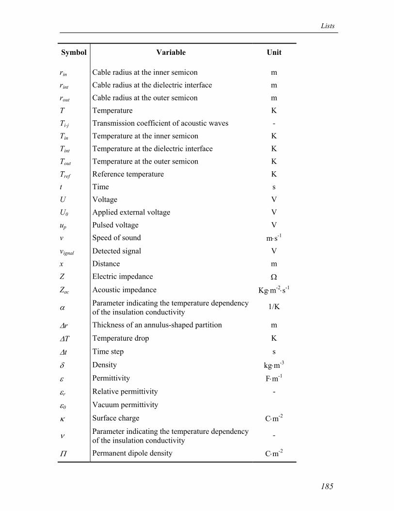
Lists
185
Symbol Variable Unit
rin Cable radius at the inner semicon m rint Cable radius at the dielectric interface m rout Cable radius at the outer semicon m T Temperature K Ti-j Transmission coefficient of acoustic waves - Tin Temperature at the inner semicon K Tint Temperature at the dielectric interface K Tout Temperature at the outer semicon K Tref Reference temperature K t Time s U Voltage V U0 Applied external voltage V up Pulsed voltage V v Speed of sound m⋅s-1 vignal Detected signal V x Distance m Z Electric impedance Ω Zac Acoustic impedance Kg⋅m-2⋅s-1
α Parameter indicating the temperature dependency of the insulation conductivity
1/K
∆r Thickness of an annulus-shaped partition m
∆T Temperature drop K
∆t Time step s
δ Density kg⋅m-3
ε Permittivity F⋅m-1
εr Relative permittivity -
ε0 Vacuum permittivity
κ Surface charge C⋅m-2
ν Parameter indicating the temperature dependency of the insulation conductivity
-
Π Permanent dipole density C⋅m-2
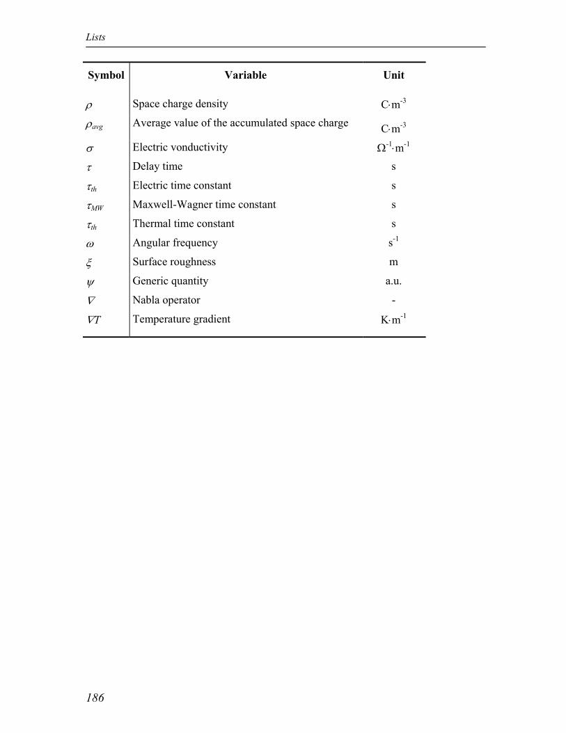
Lists
186
Symbol Variable Unit
ρ Space charge density C⋅m-3
ρavg Average value of the accumulated space charge C⋅m-3
σ Electric vonductivity Ω-1⋅m-1
τ Delay time s
τth Electric time constant s
τMW Maxwell-Wagner time constant s
τth Thermal time constant s
ω Angular frequency s-1
ξ Surface roughness m
ψ Generic quantity a.u.
∇ Nabla operator -
∇T Temperature gradient K⋅m-1
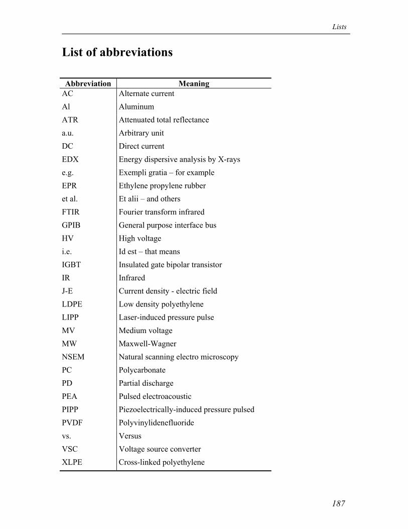
Lists
187
List of abbreviations Abbreviation Meaning
AC Alternate current Al Aluminum ATR Attenuated total reflectance a.u. Arbitrary unit DC Direct current EDX Energy dispersive analysis by X-rays e.g. Exempli gratia – for example EPR Ethylene propylene rubber et al. Et alii – and others FTIR Fourier transform infrared GPIB General purpose interface bus HV High voltage i.e. Id est – that means IGBT Insulated gate bipolar transistor IR Infrared J-E Current density - electric field LDPE Low density polyethylene LIPP Laser-induced pressure pulse MV Medium voltage MW Maxwell-Wagner NSEM Natural scanning electro microscopy PC Polycarbonate PD Partial discharge PEA Pulsed electroacoustic PIPP Piezoelectrically-induced pressure pulsed PVDF Polyvinylidenefluoride vs. Versus VSC Voltage source converter XLPE Cross-linked polyethylene

Lists
188
Summary
189
Summary Since the 1950s, high voltage (HV) direct current (DC) cable systems have been used worldwide for the transport of electrical energy. Traditionally, HVDC cable systems have been employed only when alternate current (AC) technology could not be applied. In fact, the main concern about the use of new HVDC cable links is the rather high cost of the connection. This could be significantly reduced by using polymer-insulated HVDC cable systems (also called extruded HVDC cable systems) instead of mass-impregnated or oil-paper filled HVDC cable systems (also called lapped HVDC cable systems). The extrusion production process is, in fact, simpler and cheaper than the process for manufacturing lapped insulation. In addition, extruded cable systems present some environmental advantages if compared to lapped cable systems. On the other hand, HVDC mass/oil-impregnated cables have been proven to be reliable over many decades, while HVDC polymeric cables have been only recently employed. The main issue, which needed to be resolved for the development of the HVDC polymeric cables, is the control of the space charge phenomena, which affect the reliability of the connection. Nowadays, this concern has been addressed, but only partially solved. As a consequence, mass-impregnated paper is still the dominating technology for HVDC cable insulation. In fact, one of the intrinsic properties of the polymeric DC cable insulation is the accumulation of charges. Accumulated charges distort the initial Laplacian field distribution, leading to a local field enhancement that may cause insulation degradation and premature breakdown of the system. The general objective of the present study is to obtain a better understanding of the major factors that control the space charge processes in polymeric HVDC cable systems. In order to achieve this goal, two main factors of influence are investigated. 1. Space charge at dielectric discontinuities Cable accessories are considered to be the weakest part of a cable system, because
of the presence of a dielectric interface between the cable insulation and that of the accessory. This thesis aims at a better knowledge of the polarization phenomena occurring at dielectric interfaces.
Firstly, we developed an accurate methodology for the experimental study of the space charge behavior at the dielectric interface. We reviewed the pulsed electroacoustic (PEA) method for the measurement of space charge in case of dielectric interfaces.
Secondly, we experimentally observed space charge accumulation at the dielectric interfaces of different test specimens. Both magnitude and dynamics of the charge could be fairly well described by the Maxwell-Wagner theory for the interfacial polarization. This means that the conductivity of the insulation has a large influence on the polarization at the interface. However, we also observed deviations from the behavior predicted by the Maxwell-Wagner theory. We could
Summary
190
attribute this to the morphological differences between the bulk and the surface layer of polymeric insulation.
2. Space charge in cable systems that experience a temperature drop across the insulation Across the insulation of HVDC cable systems a temperature drop is present when the cable carries a current. This thesis aims to provide a better understanding about the mechanisms responsible for space charge accumulation when a temperature drop is present across the insulation of the cable system. To that purpose, we developed a physical model for the prediction of space charge dynamics and electric field in loaded HVDC cable systems. The physical model has been validated by means of laboratory investigation. Our study indicates that space charge accumulates in the insulation bulk when a temperature drop and an electric field are simultaneously applied to the cable system. We attributed this phenomenon to the temperature dependency of the insulation conductivity. In addition to the charge in the insulation bulk, we measured so-called hetero-charge, mainly near the inner semicon of the studied test specimens. This was not predicted by the developed physical model. However, our interpretation is that this phenomenon is due to high-field charge injection and blocking mechanisms.
Our findings have possible implications on: 1. The measurements of space charge in cable system insulation by means of the PEA
method: we identified the main requirements the PEA measuring system needs to meet in order to correctly measure the space charge distributions, according to the type of the test object and the test conditions.
2. The design of HVDC extruded-type cable systems: by providing the electric field distribution in HVDC cable systems, the physical model presented in the thesis can be used as a support tool for the design of cable system insulation.
3. The operation of HVDC extruded-type cable systems: we showed how different operational conditions affect the electric field distribution in the cable system; on the basis of this information, we proposed procedures to optimize the electric stress on cable systems in particular operation conditions.
Samenvatting
191
Samenvatting Sinds de vijftiger jaren worden hoogspanning (HV) gelijkstroom (DC) kabelsystemen over de hele wereld gebruikt voor het transport van elektrische energie. Vanwege de hoge kosten, werden HVDC kabelsystemen alleen toegepast als de wisselspanning (AC) technologie niet gebruikt kon worden. Een significante vermindering van de kosten is mogelijk als voor de HVDC kabelisolatie kunststof wordt gebruikt (geïsoleerde kunststof kabels worden ook geëxtrudeerde kabels genoemd) in plaats van de klassieke met olie geïmpregneerde papieren kabelisolatie (ook geïmpregneerde of olie-papier kabels genoemd). Het produceren van geëxtrudeerde kabels is namelijk simpeler en goedkoper dan het produceren van olie-papier kabels. Daarnaast zijn geëxtrudeerde kabels milieuvriendelijker in vergelijking met olie-papier kabels. Geïmpregneerde kabels hebben echter over meerdere decennia bewezen erg betrouwbaar te zijn terwijl geëxtrudeerde kabels pas recentelijk worden toegepast. Het belangrijkste met betrekking tot de ontwikkeling van HVDC kabels van kunststof, is de accumulatie van ruimtelading, die de betrouwbaarheid van de verbinding beïnvloed. Tegenwoordig wordt dit probleem erkend, maar het is slechts ten dele opgelost. Daardoor is geïmpregneerd papier nog steeds de belangrijkste technologie bij HVDC kabelisolatie. In feite is de opbouw van lading één van de intrinsieke eigenschappen van de kunststof kabelisolatie. Opgebouwde lading vertekent de initiële distributie van het elektrische veld, waardoor concentraties kunnen ontstaan die de isolatie aantasten en kunnen leiden tot voortijdig uitvallen van het kabelsysteem. De algemene doelstelling van onderhavig onderzoek is om de belangrijkste mechanismen te begrijpen die de ruimtelading in kunststof HVDC kabelsystemen reguleren. Om dit doel te bereiken zijn twee factoren die van grote invloed zijn, onderzocht. 1. Ruimtelading in diëlektrische discontinuïteiten
Kabelgarnituren worden als het zwakste deel van een kabelsysteem beschouwd omdat er een diëlektrisch grensvlak tussen de kabelisolatie en het garnituur bestaat. Onderhavig proefschrift beoogt meer begrip te verkrijgen over de polarisatie-fenomenen op diëlektrische grensvlakken. Ten eerste hebben we een nauwkeurige methodologie ontwikkeld voor de experimentele bestudering van het gedrag van ruimtelading op diëlektrische grensvlakken. We hebben de gepulseerde elektroakoestische methode (PEA) herzien om ruimtelading op diëlektrische grensvlakken te kunnen meten. Ten tweede hebben we de accumulatie van ruimtelading bestudeerd op de diëlektrische grensvlakken van verschillende monsters. Zowel de grootte als de dynamiek van de lading kon voldoende worden beschreven door de Maxwell-Wagner theorie voor grensvlakpolarisatie. Dit betekent dat de geleidbaarheid van de isolatie een grote invloed heeft op de grensvlak polarisatie. We vonden echter ook afwijkingen van het gedrag voorspeld door de Maxwell-Wagner theorie. We konden deze afwijkingen toeschrijven aan de morfologische verschillen tussen de bulk en het oppervlak van kunststof isolatie.
Samenvatting
192
2. Ruimtelading in kabelsystemen met temperatuurverschil.
Over de isolatie van HVDC kabelsystemen staat een temperatuurgradiënt als ze stroom voeren. Dit proefschrift heeft tot doel om meer begrip te verkrijgen over de mechanismen die verantwoordelijk zijn voor ruimteladingsopbouw als er sprake is van een temperatuurgradiënt in de isolatie van het kabelsysteem. Om die reden hebben we een natuurkundig model ontwikkeld om de dynamiek van ruimtelading en het elektrische veld in geladen HVDC kabelsystemen te kunnen voorspellen. Het model wordt ondersteund door onderzoek in het laboratorium. Ons onderzoek duidt aan dat ruimtelading zich in de bulk van de isolatie ophoopt als een temperatuurgradiënt en een elektrisch veld tegelijkertijd in de kabel aanwezig zijn. We schreven dit fenomeen toe aan de temperatuurafhankelijkheid van de geleidbaarheid van de isolatie. Naast de lading in de bulk van de isolatie, hebben we ook de aanwezigheid van zogenaamde hetero-lading vastgesteld naast de binnenste halfgeleidende laag van de bestudeerde monsters. Dit werd niet door het ontwikkelde natuurkundige model voorspeld. Onze interpretatie is echter dat dit fenomeen het gevolg is van “high-field charge injection” en “blocking” mechanismen.
Onze resultaten hebben mogelijke implicaties voor: 1- Het meten van ruimtelading in kabelisolatie door middel van de PEA-methode: we
hebben de belangrijkste vereisten geïdentificeerd waaraan PEA-meetsystemen moeten voldoen om de distributie van ruimtelading goed te kunnen meten, afhankelijk van het type testobject en de testomstandigheden.
2- Het ontwerp van HVDC kabelsystemen van het geëxtrudeerde type: door de mogelijkheid van het voorspellen van het elektrische veld in HVDC kabelsystemen, kan het natuurkundige model gepresenteerd in dit proefschrift gebruikt worden bij het ontwerpen van kabelisolatie.
3- Het gebruik van HVDC kabelsystemen van het geëxtrudeerde type: we hebben laten zien hoe verschillende operationele condities de distributie van het elektrische veld beïnvloeden. Op basis van deze informatie stelden we procedures voor om de elektrische belasting op kabelsystemen in bepaalde operationele omstandigheden te optimaliseren.
Sommario
193
Sommario I sistemi in cavo in corrente continua (CC) per il trasporto dell’ energia elettrica in alta tensione (AT) fanno la loro comparsa negli anni cinquanta e sono oggi presenti su scala mondiale. I sistemi in cavo ATCC sono stati tradizionalmente utilizzati quando la tecnologia in corrente alternata (CA) non poteva essere applicata, questo a causa dei costi piuttosto elevati. Una significativa riduzione dei costi si potrebbe ottenere utilizzando sistemi in cavo ATCC di materiale polimerico (tale tipologia di cavo é anche chiamata “cavo estruso”) invece dei classici sistemi ATCC in cavo in carta impregnata (anche semplicemente chiamato “cavo in carta”). La produzione di cavi estrusi é infatti piú semplice ed economica di quella dei cavi in carta. Inoltre, se paragonati ai cavi in carta, i cavi estrusi presentano un minor impatto ambientale, non necessitando di alcuna sostanza impregnante. D’altra parte, l’utilizzo di cavi impregnati ATCC può contare su un altissimo livello di affidabilità confermato da oltre mezzo secolo di esperienza nel settore elettrico; tale caratteristica, invece, non può essere ancora attribuita ai cavi polimerici ATCC, visto che la loro introduzione nel settore è ancora troppo recente e quindi non è stata ancora possibile una reale e duratura prova sul campo. Il ritardo nello sviluppo dei cavi polimerici ATCC é stato causato dal fatto che, nell’isolamento di tali cavi, il fenomeno dell’accumulo di carica risulta di difficile controllo, pregiudicando, così, l’affidabilitá dell’ intero sistema in cavo. Questo problema é stato identificato e studiato, ma non é ancora stato completamente risolto. Per questo motivo i sistemi in cavo in carta impregnata rappresentano ancora tutt’oggi la tecnologia dominante nel settore dei cavi ATCC. L’accumulo di carica é una caratteristica intrinseca dell’isolante polimerico per cavi CC. La carica accumulata modifica la distribuzione iniziale del campo elettrico, generando concentrazioni che possono degradare l’isolante e quindi provocarne un prematuro cedimento e compromettere la funzionalitá dell’ intero sistema in cavo. Questa tesi si propone di migliorare la conoscenza dei fattori principali che controllano il processo di accumulo di carica nei sistemi in cavo polimerico ATCC. A tal fine sono stati studiati i seguenti aspetti: 1. Le parti piú vulnerabili dell’intero sistema in cavo sono gli accessori, in quanto in
essi é presente un’interfaccia tra dielettrici, formata dall’isolante del cavo e da quello dell’accessorio. La tesi sviluppa una metodologia per lo studio sperimentale dell’accumulo di carica nelle interfacce tra dielettrici. Tale metodologia consiste nella revisione del metodo dell’impulso elettroacustico (PEA), per renderlo applicabile alla misura di carica interfacciale tra dielettrici. Le misure di laboratorio hanno dimostrato che l’accumulo di carica segue approssimativamente il comportamento previsto dalla teoria Maxwell-Wagner per la polarizzazione interfacciale. Ció implica che la polarizzazione dell’interfaccia dipende fortemente dalla conducibilitá dell’isolante. I risultati sperimentali mostrano inoltre comportamenti della carica non previsti dalla teoria Maxwell-Wagner. Quest’ultimi
Sommario
194
sono stati attribuiti alla particolare morfologia dello strato superficiale del materiale isolante, in prossimitá dell’interfaccia.
2. Quando un sistema in cavo ATCC é in funzione, il suo isolamento é sottoposto ad un gradiente termico. Questa tesi analizza i meccanismi di accumulo di carica nell’isolante in presenza di un gradiente termico. La tesi propone un modello fisico dell’isolamento dei sistemi in cavo ATCC, in grado di calcolare il comportamento dinamico della carica accumulata, e, quindi, del campo elettrico, in funzione del gradiente termico. La validitá del modello é stata verificata tramite misure sperimentali di carica. I risultati presentati nella tesi indicano che, quando un gradiente termico é applicato al cavo in presenza di un campo elettrico, vi é accumulo di carica nell’isolante. Tale fenomeno é stato attribuito al fatto che la conducibilitá dell’isolante varia fortemente con la temperatura. Differentemente da quanto calcolato dal modello, una certa carica é stata inoltre misurata vicino al semiconduttore interno del sistema in cavo. La tesi dá un’interpretazione a tale fenomeno in termini di meccanismi di iniezione e di blocco della carica.
I risultati della ricerca effettuata possono trovare appllicazione nei seguenti campi:
1. La caratterizzazione dei materiali isolanti tramite misure di carica (metodo PEA): la tesi individua i requisiti che un sistema per misure PEA deve possedere per una corretta valutazione della distribuzione della carica, a seconda delle differenti tipologie di provini e condizioni di misura.
2. La progettazione dei sistemi in cavo polimerico ATCC: il modello fisico proposto in questa tesi puó essere utilizzato come strumento di supporto per la progettazione dei sistemi in cavo ATCC, essendo in grado di fornire la distribuzione dinamica del campo elettrico.
3. Il modo d’ utilizzo dei sistemi in cavo polimerico ATCC: la tesi mostra come la distribuzione del campo elettrico sia influenzata dalle condizioni di lavoro del sistema in cavo; tale informazione può essere utilizzata per creare procedure operative atte a ottimizzare il campo elettrico gestendo il sistema in cavo in condizioni di lavoro variabili.
Acknowledgement & CV
195
Acknowledgement When I think about the work done to complete this thesis, I feel indebted to many people. First of all, I would like to express my gratitude to my promotor, prof. Smit. Among many things, I am thankful to him for his trust. I will not forget his resolution for helping me stay in Delft when the Italian Defence Ministry wanted me back home. Not of less importance was the spontaneous support my supervisor dr. Morshuis offered me during my stay at Delft University of Technology. I am grateful for his inspiration, encouragement and guidance. I warmly thank all colleagues, former colleagues and staff of the HV department at the Delft University of Technology, for providing a friendly and stimulating work environment. In particular, I would like to thank my former colleagues dr. Beyer and dr. van den Bosch for all the interesting discussions we had inside and outside our laboratory. I’m thankful to ing. van Nes, mr. van der Graaf and mr. Naagen, for their invaluable help in designing and constructing the test set-ups used in this research. I enjoyed their company very much and their original Dutch humour too (most of the time). My gratitude goes also to ir. Redjosentono and ir. Straathof, the former students who worked with me on this research. It was a great pleasure to have the opportunity to work on the European project “HVDC”. I’m sincerely grateful to all the “HVDC” Partners, for the attention they gave to my research. I would like to express a particular appreciation to: the coordinator of the “HVDC” project, prof. Fothergill, for putting high value on this work within the project; dr. Fabiani and prof. Montanari from the University of Bologna, for many fruitful discussions on the effect of temperature drop on DC cable insulation; prof. Dissado from the University of Leicester, for his constructive criticism about the modelling of space charge dynamics; prof. Stevens and co-workers of the University of Surrey, for performing the physical-chemical analyses of interfaces; dr. Le Roy, dr. Teyssedre and dr. Laurent from the University Paul Sabatier, Toulouse III, for our productive cooperation; Prysmian Cavi e Sistemi Energia S.r.l. and Borealis A.B. Wires & Cables B.U., for providing us with the test specimens used in this research. Finally, I would like to acknowledge the fact that this research would not have been possible without the funds of the European Commission.
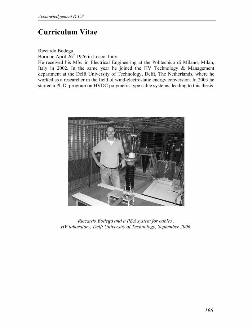
Acknowledgement & CV
196
Curriculum Vitae Riccardo Bodega Born on April 26th 1976 in Lecco, Italy. He received his MSc in Electrical Engineering at the Politecnico di Milano, Milan, Italy in 2002. In the same year he joined the HV Technology & Management department at the Delft University of Technology, Delft, The Netherlands, where he worked as a researcher in the field of wind-electrostatic energy conversion. In 2003 he started a Ph.D. program on HVDC polymeric-type cable systems, leading to this thesis.
Riccardo Bodega and a PEA system for cables . HV laboratory, Delft University of Technology, September 2006.