Datasheet IKZA50N65RH5 - Infineon
15
Datasheet Please read the Important Notice and Warnings at the end of this document V 2.1 www.infineon.com 2020-07-27 IKZA50N65RH5 Hybrid CoolSiC TM IGBT TRENCHSTOP TM 5 H5 IGBT co-packed with half-rated 6 th generation CoolSiC TM Schottky barrier diode Features and Benefits: • Ultra-low switching losses due to the combination of TRENCHSTOP TM 5 and CoolSiC TM technology as well as the Kelvin emitter pin • Benchmark efficiency in hard switching topologies • Plug-and-play replacement of pure silicon devices • Simplified PCB design due to the optimized pin-out of the four-pin package • Improved wave soldering quality due to the increased clearance of the Kelvin emitter and gate pins • Maximum junction temperature 175°C • Qualified according to JEDEC for target applications • Pb-free lead plating; RoHS compliant • Complete product spectrum and PSpice models: http://www.infineon.com/igbt/ Potential Applications: • Industrial Power Supplies - Industrial SMPS - Industrial UPS • Energy Generation - Solar String Inverter • Energy Distribution - Energy Storage • Infrastructure – Charge - Charger Product Validation: Qualified for applications listed above based on the test conditions in the relevant tests of JEDEC20/22 Package pin definition: • Pin C & backside - collector • Pin E - emitter • Pin K - Kelvin emitter • Pin G - gate Key Performance and Package Parameters Type VCE IC VCEsat, Tvj=25°C Tvjmax Marking Package IKZA50N65RH5 650V 50A 1.65V 175°C K50ERH5 PG-TO247-4-3
Transcript of Datasheet IKZA50N65RH5 - Infineon

Datasheet PleasereadtheImportantNoticeandWarningsattheendofthisdocument V2.1www.infineon.com 2020-07-27
IKZA50N65RH5
HybridCoolSiCTMIGBT
TRENCHSTOPTM5H5IGBTco-packedwithhalf-rated6thgenerationCoolSiCTMSchottkybarrierdiodeFeaturesandBenefits:
•Ultra-lowswitchinglossesduetothecombinationofTRENCHSTOPTM5andCoolSiCTMtechnologyaswellastheKelvinemitterpin•Benchmarkefficiencyinhardswitchingtopologies•Plug-and-playreplacementofpuresilicondevices•SimplifiedPCBdesignduetotheoptimizedpin-outofthefour-pinpackage•ImprovedwavesolderingqualityduetotheincreasedclearanceoftheKelvinemitterandgatepins•Maximumjunctiontemperature175°C•QualifiedaccordingtoJEDECfortargetapplications•Pb-freeleadplating;RoHScompliant•CompleteproductspectrumandPSpicemodels:http://www.infineon.com/igbt/
PotentialApplications:
•IndustrialPowerSupplies-IndustrialSMPS-IndustrialUPS•EnergyGeneration-SolarStringInverter•EnergyDistribution-EnergyStorage•Infrastructure–Charge-Charger
ProductValidation:
QualifiedforapplicationslistedabovebasedonthetestconditionsintherelevanttestsofJEDEC20/22
Packagepindefinition:
•PinC&backside-collector•PinE-emitter•PinK-Kelvinemitter•PinG-gate
KeyPerformanceandPackageParametersType VCE IC VCEsat,Tvj=25°C Tvjmax Marking PackageIKZA50N65RH5 650V 50A 1.65V 175°C K50ERH5 PG-TO247-4-3

Datasheet 2 V2.12020-07-27
IKZA50N65RH5
HybridCoolSiCTMIGBT
TableofContents
Description . . . . . . . . . . . . . . . . . . . . . . . . . . . . . . . . . . . . . . . . . . . . . . . . . . . . . . . . . . . . . . . . . . . . . . . . 1
Table of Contents . . . . . . . . . . . . . . . . . . . . . . . . . . . . . . . . . . . . . . . . . . . . . . . . . . . . . . . . . . . . . . . . . . . 2
Maximum Ratings . . . . . . . . . . . . . . . . . . . . . . . . . . . . . . . . . . . . . . . . . . . . . . . . . . . . . . . . . . . . . . . . . . . 3
Thermal Resistance . . . . . . . . . . . . . . . . . . . . . . . . . . . . . . . . . . . . . . . . . . . . . . . . . . . . . . . . . . . . . . . . . 3
Electrical Characteristics . . . . . . . . . . . . . . . . . . . . . . . . . . . . . . . . . . . . . . . . . . . . . . . . . . . . . . . . . . . . . . 4
Electrical Characteristics Diagrams . . . . . . . . . . . . . . . . . . . . . . . . . . . . . . . . . . . . . . . . . . . . . . . . . . . . . 6
Package Drawing . . . . . . . . . . . . . . . . . . . . . . . . . . . . . . . . . . . . . . . . . . . . . . . . . . . . . . . . . . . . . . . . . . .12
Testing Conditions . . . . . . . . . . . . . . . . . . . . . . . . . . . . . . . . . . . . . . . . . . . . . . . . . . . . . . . . . . . . . . . . . .13
Revision History . . . . . . . . . . . . . . . . . . . . . . . . . . . . . . . . . . . . . . . . . . . . . . . . . . . . . . . . . . . . . . . . . . . .14
Disclaimer . . . . . . . . . . . . . . . . . . . . . . . . . . . . . . . . . . . . . . . . . . . . . . . . . . . . . . . . . . . . . . . . . . . . . . . . .15

Datasheet 3 V2.12020-07-27
IKZA50N65RH5
HybridCoolSiCTMIGBT
MaximumRatingsForoptimumlifetimeandreliability,Infineonrecommendsoperatingconditionsthatdonotexceed80%ofthemaximumratingsstatedinthisdatasheet.
Parameter Symbol Value UnitCollector-emittervoltage,Tvj≥25°C VCE 650 V
DCcollectorcurrent,limitedbyTvjmaxTc=25°CvaluelimitedbybondwireTc=100°C
IC 80.056.0
A
Pulsedcollectorcurrent,tplimitedbyTvjmax ICpuls 200.0 A
Turn off safe operating areaVCE≤650V,Tvj≤175°C,tp=1µs - 200.0 A
Diodeforwardcurrent,limitedbyTvjmaxTc=25°CTc=100°C
IF 33.722.8
A
Diodepulsedcurrent,tplimitedbyTvjmax1) IFpuls 75.0 A
Gate-emitter voltageTransientGate-emittervoltage(tp≤10µs,D<0.010) VGE
±20±30 V
PowerdissipationTc=25°CPowerdissipationTc=100°C Ptot
305.0152.5 W
Operating junction temperature Tvj -40...+175 °C
Storage temperature Tstg -55...+150 °C
Soldering temperature,wave soldering 1.6mm (0.063in.) from case for 10s 260 °C
Mounting torque, M3 screwMaximum of mounting processes: 3 M 0.6 Nm
ThermalResistance
Valuemin. typ. max.
Parameter Symbol Conditions Unit
RthCharacteristics
IGBT thermal resistance,junction - case Rth(j-c) - - 0.50 K/W
Diode thermal resistance,junction - case Rth(j-c) - - 1.50 K/W
Thermal resistancejunction - ambient Rth(j-a) - - 40 K/W
1) Pulse current level depends on Tvj of diode chip, see also Fig. "Maximum pulse current as a function of junction temperature"

Datasheet 4 V2.12020-07-27
IKZA50N65RH5
HybridCoolSiCTMIGBT
ElectricalCharacteristic,atTvj=25°C,unlessotherwisespecified
Valuemin. typ. max.
Parameter Symbol Conditions Unit
StaticCharacteristic
Collector-emitter saturation voltage VCEsat
VGE=15.0V,IC=50.0ATvj=25°CTvj=125°CTvj=175°C
---
1.651.851.95
2.10--
V
Diode forward voltage VF
VGE=0V,IF=20.0ATvj=25°CTvj=125°CTvj=175°C
---
1.351.551.65
1.50--
V
Gate-emitter threshold voltage VGE(th) IC=0.50mA,VCE=VGE 3.2 4.0 4.8 V
Zero gate voltage collector current ICESVCE=650V,VGE=0VTvj=25°CTvj=175°C
--
-2000
700-
µA
Zero gate voltage collector current ICES VCE=480V,VGE=0VTvj=25°C - - 25 µA
Gate-emitter leakage current IGES VCE=0V,VGE=20V - - 100 nA
Transconductance gfs VCE=20V,IC=50.0A - 62.0 - S
ElectricalCharacteristic,atTvj=25°C,unlessotherwisespecified
Valuemin. typ. max.
Parameter Symbol Conditions Unit
DynamicCharacteristic
Input capacitance Cies - 2660 -
Output capacitance Coes - 320 -
Reverse transfer capacitance Cres - 10 -
VCE=25V,VGE=0Vf=250kHz pF
Gate charge QGVCC=520V,IC=50.0A,VGE=15V - 120.0 - nC
Internal emitter inductancemeasured 5mm (0.197 in.) fromcase
LE - 13.0 - nH
SwitchingCharacteristic,InductiveLoad
Valuemin. typ. max.
Parameter Symbol Conditions Unit
IGBTCharacteristic,atTvj=25°CTurn-on delay time td(on) - 21 - ns
Rise time tr - 6 - ns
Turn-off delay time td(off) - 180 - ns
Fall time tf - 18 - ns
Turn-on energy Eon - 0.20 - mJ
Turn-off energy Eoff - 0.18 - mJ
Total switching energy Ets - 0.38 - mJ
Tvj=25°C,VCC=400V,IC=25.0A,VGE=0.0/15.0V,RG(on)=12.0Ω,RG(off)=12.0Ω,Lσ=30nH,Cσ=30pFLσ,CσfromFig.EEnergy losses include “tail” anddiode reverse recovery.

Datasheet 5 V2.12020-07-27
IKZA50N65RH5
HybridCoolSiCTMIGBT
Turn-on delay time td(on) - 19 - ns
Rise time tr - 3 - ns
Turn-off delay time td(off) - 200 - ns
Fall time tf - 25 - ns
Turn-on energy Eon - 0.05 - mJ
Turn-off energy Eoff - 0.05 - mJ
Total switching energy Ets - 0.10 - mJ
Tvj=25°C,VCC=400V,IC=5.0A,VGE=0.0/15.0V,RG(on)=12.0Ω,RG(off)=12.0Ω,Lσ=30nH,Cσ=30pFLσ,CσfromFig.EEnergy losses include “tail” anddiode reverse recovery.
SwitchingCharacteristic,InductiveLoad
Valuemin. typ. max.
Parameter Symbol Conditions Unit
IGBTCharacteristic,atTvj=150°CTurn-on delay time td(on) - 20 - ns
Rise time tr - 7 - ns
Turn-off delay time td(off) - 200 - ns
Fall time tf - 25 - ns
Turn-on energy Eon - 0.27 - mJ
Turn-off energy Eoff - 0.27 - mJ
Total switching energy Ets - 0.54 - mJ
Tvj=150°C,VCC=400V,IC=25.0A,VGE=0.0/15.0V,RG(on)=12.0Ω,RG(off)=12.0Ω,Lσ=30nH,Cσ=30pFLσ,CσfromFig.EEnergy losses include “tail” anddiode reverse recovery.
Turn-on delay time td(on) - 18 - ns
Rise time tr - 3 - ns
Turn-off delay time td(off) - 250 - ns
Fall time tf - 35 - ns
Turn-on energy Eon - 0.08 - mJ
Turn-off energy Eoff - 0.08 - mJ
Total switching energy Ets - 0.16 - mJ
Tvj=150°C,VCC=400V,IC=5.0A,VGE=0.0/15.0V,RG(on)=12.0Ω,RG(off)=12.0Ω,Lσ=30nH,Cσ=30pFLσ,CσfromFig.EEnergy losses include “tail” anddiode reverse recovery.

Datasheet 6 V2.12020-07-27
IKZA50N65RH5
HybridCoolSiCTMIGBT
Figure 1. Powerdissipationasafunctionofcasetemperature(Tvj≤175°C)
TC,CASETEMPERATURE[°C]
Ptot ,PO
WER
DISSIPA
TION[W
]
25 50 75 100 125 150 1750
40
80
120
160
200
240
280
320
Figure 2. Collectorcurrentasafunctionofcasetemperature(VGE≥15V,Tvj≤175°C)
TC,CASETEMPERATURE[°C]
IC,C
OLLEC
TORCURREN
T[A]
25 50 75 100 125 150 1750
10
20
30
40
50
60
70
80
90
Figure 3. Typicaloutputcharacteristic(Tvj=25°C)
VCE,COLLECTOR-EMITTERVOLTAGE[V]
IC,C
OLLEC
TORCURREN
T[A]
0 1 2 3 4 50
20
40
60
80
100
120
140
160
180
200
VGE=20V
18V
15V
12V
10V
8V
7V
6V
5V
Figure 4. Typicaloutputcharacteristic(Tvj=150°C)
VCE,COLLECTOR-EMITTERVOLTAGE[V]
IC,C
OLLEC
TORCURREN
T[A]
0 1 2 3 4 50
20
40
60
80
100
120
140
160
180
200
VGE=20V
18V
15V
12V
10V
8V
7V
6V
5V

Datasheet 7 V2.12020-07-27
IKZA50N65RH5
HybridCoolSiCTMIGBT
Figure 5. Typicaltransfercharacteristic(VCE=20V)
VGE,GATE-EMITTERVOLTAGE[V]
IC,C
OLLEC
TORCURREN
T[A]
2.5 3.5 4.5 5.5 6.5 7.5 8.5 9.50
20
40
60
80
100
120
140
160
180
200Tj=25°CTj=150°C
Figure 6. Typicalcollector-emittersaturationvoltageasafunctionofjunctiontemperature(VGE=15V)
Tvj,JUNCTIONTEMPERATURE[°C]
VCEsat,C
OLLEC
TOR-EMITTE
RSAT
URAT
ION[V
]
25 50 75 100 125 150 1750.50
0.75
1.00
1.25
1.50
1.75
2.00
2.25
2.50IC=12.5AIC=25AIC=50A
Figure 7. Typicalswitchingtimesasafunctionofcollectorcurrent(inductiveload,Tvj=150°C,VCE=400V,VGE=15/0V,RG=12Ω,DynamictestcircuitinFigure E)
IC,COLLECTORCURRENT[A]
t,SW
ITCHINGTIMES
[ns]
0 30 60 90 120 1501
10
100
1000td(off)
tftd(on)
tr
Figure 8. Typicalswitchingtimesasafunctionofgateresistor(inductiveload,Tvj=150°C,VCE=400V,VGE=15/0V,IC=25A,DynamictestcircuitinFigure E)
RG,GATERESISTOR[Ω]
t,SW
ITCHINGTIMES
[ns]
5 15 25 35 45 55 651
10
100
1000td(off)
tftd(on)
tr

Datasheet 8 V2.12020-07-27
IKZA50N65RH5
HybridCoolSiCTMIGBT
Figure 9. Typicalswitchingtimesasafunctionofjunctiontemperature(inductiveload,VCE=400V,VGE=15/0V,IC=25A,RG=12Ω,DynamictestcircuitinFigure E)
Tvj,JUNCTIONTEMPERATURE[°C]
t,SW
ITCHINGTIMES
[ns]
25 50 75 100 125 150 1751
10
100
1000td(off)
tftd(on)
tr
Figure 10. Gate-emitterthresholdvoltageasafunctionofjunctiontemperature(IC=0.5mA)
Tvj,JUNCTIONTEMPERATURE[°C]
VGE(th) ,GAT
E-EM
ITTE
RTHRES
HOLD
VOLTAG
E[V]
25 50 75 100 125 1501.0
1.5
2.0
2.5
3.0
3.5
4.0
4.5
5.0
5.5typ.
Figure 11. Typicalswitchingenergylossesasafunctionofcollectorcurrent(inductiveload,Tvj=150°C,VCE=400V,VGE=15/0V,RG=12Ω,DynamictestcircuitinFigure E)
IC,COLLECTORCURRENT[A]
E,S
WITCHINGENER
GYLO
SSES
[mJ]
0 30 60 90 120 1500
1
2
3
4
5
6
7Eoff
Eon
Ets
Figure 12. Typicalswitchingenergylossesasafunctionofgateresistor(inductiveload,Tvj=150°C,VCE=400V,VGE=15/0V,IC=25A,DynamictestcircuitinFigure E)
RG,GATERESISTOR[Ω]
E,S
WITCHINGENER
GYLO
SSES
[mJ]
5 15 25 35 45 55 650.0
0.2
0.4
0.6
0.8
1.0
1.2
1.4Eoff
Eon
Ets

Datasheet 9 V2.12020-07-27
IKZA50N65RH5
HybridCoolSiCTMIGBT
Figure 13. Typicalswitchingenergylossesasafunctionofjunctiontemperature(inductiveload,VCE=400V,VGE=15/0V,IC=25A,RG=12Ω,DynamictestcircuitinFigure E)
Tvj,JUNCTIONTEMPERATURE[°C]
E,S
WITCHINGENER
GYLO
SSES
[mJ]
25 50 75 100 125 150 1750.0
0.1
0.2
0.3
0.4
0.5
0.6Eoff
Eon
Ets
Figure 14. Typicalswitchingenergylossesasafunctionofcollectoremittervoltage(inductiveload,Tvj=150°C,VGE=15/0V,IC=25A,RG=12Ω,DynamictestcircuitinFigure E)
VCE,COLLECTOR-EMITTERVOLTAGE[V]
E,S
WITCHINGENER
GYLO
SSES
[mJ]
200 250 300 350 400 450 5000.0
0.1
0.2
0.3
0.4
0.5
0.6
0.7Eoff
Eon
Ets
Figure 15. Typ.reversecurrentvs.reversevoltageasafunctionofTvj
VCE,COLLECTOR-EMITTERVOLTAGE[V]
ICES,ZER
OGAT
EVO
LTAG
ECOLLEC
TORCURREN
T[A]
100 200 300 400 500 600 7001E-8
1E-7
1E-6
1E-5
1E-4
0.001
0.01
0.1Tvj=175°C
Tvj=150°C
Tvj=100°C
Tvj=25°C
Figure 16. Typicalgatecharge(IC=50A)
QGE,GATECHARGE[nC]
VGE ,GAT
E-EM
ITTE
RVOLTAG
E[V]
0 20 40 60 80 100 1200
2
4
6
8
10
12
14
16130V520V
Datasheet 10 V2.12020-07-27
IKZA50N65RH5
HybridCoolSiCTMIGBT
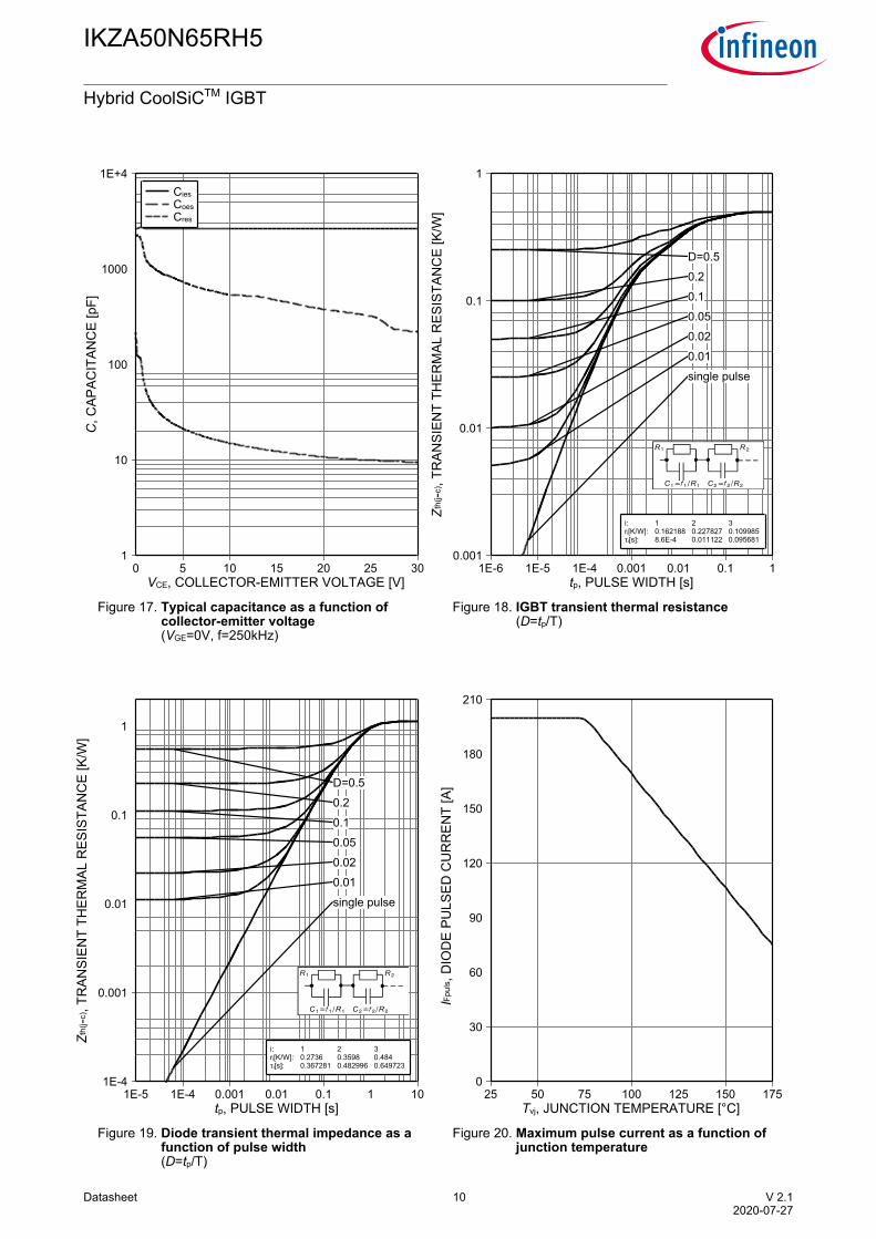
Figure 17. Typicalcapacitanceasafunctionofcollector-emittervoltage(VGE=0V,f=250kHz)
VCE,COLLECTOR-EMITTERVOLTAGE[V]
C,C
APAC
ITAN
CE[pF]
0 5 10 15 20 25 301
10
100
1000
1E+4Cies
Coes
Cres
Figure 18. IGBTtransientthermalresistance(D=tp/T)
tp,PULSEWIDTH[s]
Zth(j -c
) ,TR
ANSIEN
TTH
ERMAL
RES
ISTA
NCE[K/W
]
1E-6 1E-5 1E-4 0.001 0.01 0.1 10.001
0.01
0.1
1
D=0.5
0.2
0.1
0.05
0.02
0.01
single pulse
i:ri[K/W]:τi[s]:
10.1621888.6E-4
20.2278270.011122
30.1099850.095681
Figure 19. Diodetransientthermalimpedanceasafunctionofpulsewidth(D=tp/T)
tp,PULSEWIDTH[s]
Zth(j -c
) ,TR
ANSIEN
TTH
ERMAL
RES
ISTA
NCE[K/W
]
1E-5 1E-4 0.001 0.01 0.1 1 101E-4
0.001
0.01
0.1
1
D=0.5
0.2
0.1
0.05
0.02
0.01
single pulse
i:ri[K/W]:τi[s]:
10.27360.367281
20.35980.482996
30.4840.649723
Figure 20. Maximumpulsecurrentasafunctionofjunctiontemperature
Tvj,JUNCTIONTEMPERATURE[°C]
IFpuls ,DIODEPU
LSED
CURREN
T[A]
25 50 75 100 125 150 1750
30
60
90
120
150
180
210
Datasheet 11 V2.12020-07-27
IKZA50N65RH5
HybridCoolSiCTMIGBT
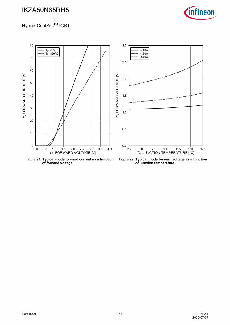
Figure 21. Typicaldiodeforwardcurrentasafunctionofforwardvoltage
VF,FORWARDVOLTAGE[V]
IF ,FORWAR
DCURREN
T[A]
0.0 0.5 1.0 1.5 2.0 2.5 3.0 3.5 4.00
10
20
30
40
50
60
70
80Tj=25°CTj=150°C
Figure 22. Typicaldiodeforwardvoltageasafunctionofjunctiontemperature
Tvj,JUNCTIONTEMPERATURE[°C]
VF ,FO
RWAR
DVOLTAG
E[V]
25 50 75 100 125 150 1750.0
0.5
1.0
1.5
2.0
2.5
3.0IF=10AIF=20AIF=40A

Datasheet 12 V2.12020-07-27
IKZA50N65RH5
HybridCoolSiCTMIGBT
DIMENSIONSMIN. MAX.
A2
L
b
D
c
b2
E
e1
L1
Q
øP2
D1
A
A1
2.101.90
5.08
19.80
-
20.90
0.58
0.65
15.70
5.60
2.40
16.25
20.10
0.79
0.66
0.20
21.10
6.00
2.60
4.30
15.90
16.85
MILLIMETERS
4.90
2.31
5.10
2.51
b1
1.10 1.30
b3
PG-TO247-4-3
SCALE
Z8B00184785
REVISION
ISSUE DATE
EUROPEAN PROJECTION
03
21.08.2017
0 5
DOCUMENT NO.
2:1
A3 0.250.05
D2 1.05 1.35
D3 24.97 25.27
10mm
E1 13.10 13.50
E2 2.40 2.60
-
øP1 7.00 7.40
øP 3.50 3.70
S 6.15
T 9.80 10.20
U 6.00 6.40
1.34 1.44
e2 2.79
e3 2.54
D4 4.90 5.10
Datasheet 13 V2.12020-07-27
IKZA50N65RH5
HybridCoolSiCTMIGBT
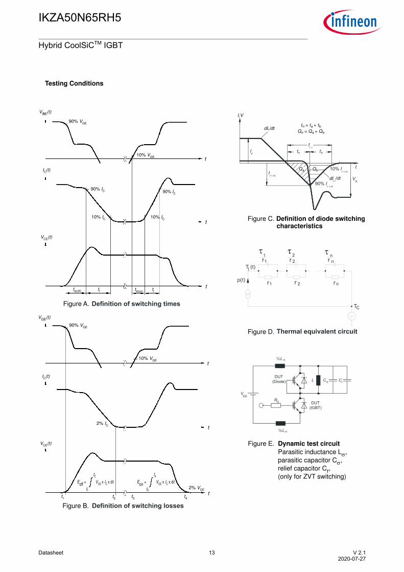
t
a b
td(off)
tf t
rtd(on)
90% IC
10% IC
90% IC
10% VGE
10% IC
t
90% VGE
t
t
90% VGE
VGE
(t)
t
t
tt1 t
4
2% IC
10% VGE
2% VCE
t2
t3
E
t
t
V I toff
= x x d
1
2
CE CE
t
t
V I ton
= x x d
3
4
CE C
CC
dI /dtF
dI
I,V
Figure A.
Figure B.
Figure C. Definition of diode switchingcharacteristics
Figure E. Dynamic test circuit
Figure D.
I (t)C
Parasitic inductance L ,
parasitic capacitor C ,
relief capacitor C ,
(only for ZVT switching)
s
s
r
t t t
Q Q Qrr a b
rr a b
= +
= +
Qa Qb
V (t)CE
VGE
(t)
I (t)C
V (t)CE
Testing Conditions

Datasheet 14 V2.12020-07-27
IKZA50N65RH5
HybridCoolSiCTMIGBT
RevisionHistory
IKZA50N65RH5
Revision:2020-07-27,Rev.2.1Previous Revision
Revision Date Subjects (major changes since last revision)
1.1 2020-03-20 Preliminary Data Sheet
2.1 2020-07-27 Final Data Sheet

Trademarks
Allreferencedproductorservicenamesandtrademarksarethepropertyoftheirrespectiveowners.
PublishedbyInfineonTechnologiesAG81726München,Germany©InfineonTechnologiesAG2020.AllRightsReserved.
ImportantNoticeTheinformationgiveninthisdocumentshallinnoeventberegardedasaguaranteeofconditionsorcharacteristics(“Beschaffenheitsgarantie”).Withrespecttoanyexamples,hintsoranytypicalvaluesstatedhereinand/oranyinformationregardingtheapplicationoftheproduct,InfineonTechnologiesherebydisclaimsanyandallwarrantiesandliabilitiesofanykind,includingwithoutlimitationwarrantiesofnon-infringementofintellectualpropertyrightsofanythirdparty.
Inaddition,anyinformationgiveninthisdocumentissubjecttocustomer’scompliancewithitsobligationsstatedinthisdocumentandanyapplicablelegalrequirements,normsandstandardsconcerningcustomer’sproductsandanyuseoftheproductofInfineonTechnologiesincustomer’sapplications.
Thedatacontainedinthisdocumentisexclusivelyintendedfortechnicallytrainedstaff.Itistheresponsibilityofcustomer’stechnicaldepartmentstoevaluatethesuitabilityoftheproductfortheintendedapplicationandthecompletenessoftheproductinformationgiveninthisdocumentwithrespecttosuchapplication.
Forfurtherinformationontheproduct,technology,deliverytermsandconditionsandpricespleasecontactyournearestInfineonTechnologiesoffice(www.infineon.com).
PleasenotethatthisproductisnotqualifiedaccordingtotheAECQ100orAECQ101documentsoftheAutomotiveElectronicsCouncil.
WarningsDuetotechnicalrequirementsproductsmaycontaindangeroussubstances.ForinformationonthetypesinquestionpleasecontactyournearestInfineonTechnologiesoffice.
ExceptasotherwiseexplicitlyapprovedbyInfineonTechnologiesinawrittendocumentsignedbyauthorizedrepresentativesofInfineonTechnologies,InfineonTechnologies’productsmaynotbeusedinanyapplicationswhereafailureoftheproductoranyconsequencesoftheusethereofcanreasonablybeexpectedtoresultinpersonalinjury.