Can the RF radio foster the 140 GHz spectrum?
15
Can the RF radio foster the 140 GHz spectrum? Björn Debaillie #1 , Akshay Visweswaran #1 , Tim Maiwald #2 , Karina Schneider #3 , Alper Karakuzulu #4 , Dieter Ferling #5 , Klaus Aufinger #6 #1 Imec, Belgium; #2 Friedrich‐Alexander‐Universität Erlangen‐Nürnberg; #3 Karlsruhe Institute of Technology; #4 IHP microelectronics; #5 Nokia Bel Labs; #5 Infineon #1 [email protected] WS‐01 Recent advances in SiGe BiCMOS: technologies, modelling & circuits for 5G, radar & imaging http://tima.univ‐grenoble‐alpes.fr/taranto/
Transcript of Can the RF radio foster the 140 GHz spectrum?

Can the RF radio foster the 140 GHz spectrum?
Björn Debaillie#1, Akshay Visweswaran#1, Tim Maiwald#2, Karina Schneider#3, Alper Karakuzulu#4, Dieter Ferling#5, Klaus Aufinger#6
#1Imec, Belgium; #2Friedrich‐Alexander‐Universität Erlangen‐Nürnberg; #3Karlsruhe Institute of Technology; #4IHP microelectronics; #5Nokia Bel Labs; #5Infineon
WS‐01 Recent advances in SiGe BiCMOS: technologies, modelling & circuits for 5G, radar & imaging
http://tima.univ‐grenoble‐alpes.fr/taranto/

The road towards 6G: motivation and use cases
2
100 Gbps 100 Gbps100 Gbps100 Gbps
Upcoming needs (beyond 5G)• High speed wireless access• Individual and secure connectivity
• Mobile and static links • Efficient & generic technology solutions
Road blockers towards 6G• Radio spectrum availability • Radio technology availability• Long distance ultra‐fast wireless links
• Multi‐layer beamforming
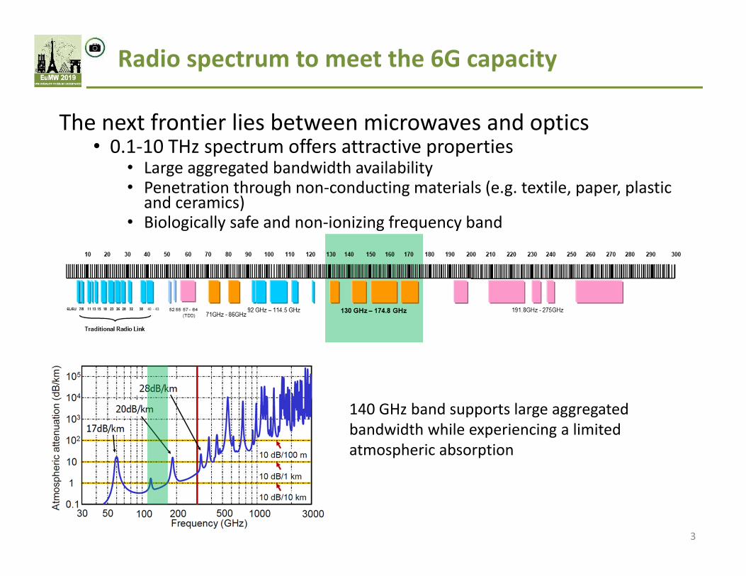
The next frontier lies between microwaves and optics• 0.1‐10 THz spectrum offers attractive properties
• Large aggregated bandwidth availability• Penetration through non‐conducting materials (e.g. textile, paper, plastic and ceramics)
• Biologically safe and non‐ionizing frequency band
Radio spectrum to meet the 6G capacity
3
140 GHz band supports large aggregated bandwidth while experiencing a limited atmospheric absorption
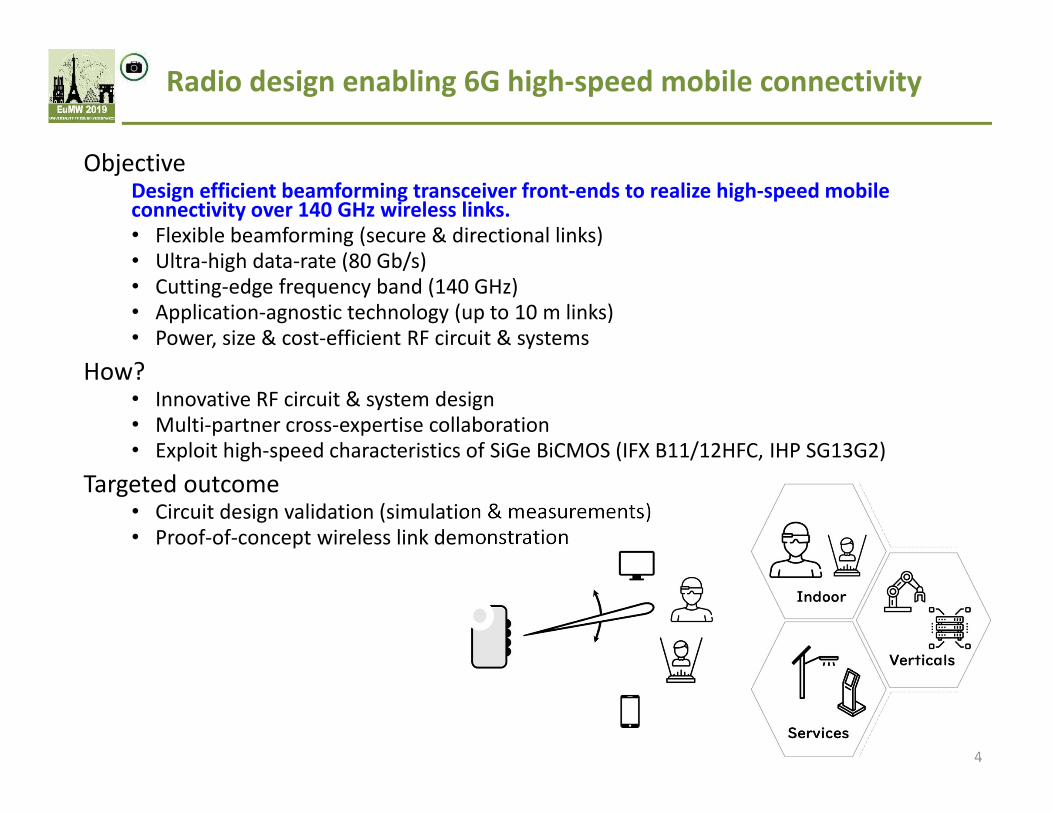
Radio design enabling 6G high‐speed mobile connectivity
4
ObjectiveDesign efficient beamforming transceiver front‐ends to realize high‐speed mobile connectivity over 140 GHz wireless links.• Flexible beamforming (secure & directional links)• Ultra‐high data‐rate (80 Gb/s)• Cutting‐edge frequency band (140 GHz)• Application‐agnostic technology (up to 10 m links)• Power, size & cost‐efficient RF circuit & systems
How?• Innovative RF circuit & system design• Multi‐partner cross‐expertise collaboration• Exploit high‐speed characteristics of SiGe BiCMOS (IFX B11/12HFC, IHP SG13G2)
Targeted outcome• Circuit design validation (simulation & measurements)• Proof‐of‐concept wireless link demonstration
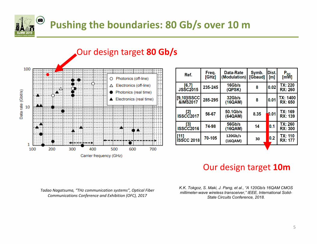
Pushing the boundaries: 80 Gb/s over 10 m
5
K.K. Tokgoz, S. Maki, J. Pang, et al., “A 120Gb/s 16QAM CMOS millimeter-wave wireless transceiver,” IEEE, International Solid-
State Circuits Conference, 2018.
Tadao Nagatsuma, “THz communication systems”, Optical Fiber Communications Conference and Exhibition (OFC), 2017
120Gb/s(16QAM) 30
Our design target 10m
Our design target 80 Gb/s

10 m specs can be achieved with 2‐way beamforming 80 Gbps links, with orthogonal polarizations for doubling the data rate. Modulation scheme is QPSK and an RF bandwidth of 20 GHz. The transmit power target is 13 dBm, the RX noise figure target is 12 dB, and the antenna gain target is 23 dBi.
Can this be achieved? Link budget analysis
6
0 5 10 15 20 250
5
10
15
20
25
16-QAM
QPSK
TX and RX Antenna Gain (dB)
Com
mun
icat
ion
rang
e (m
) Pb = 1e-6
Center frequency 140 GHzBandwidth (RF) 120‐140 GHz, 20 GHzModulation QPSKData‐rate 40 Gbps per channelDual polarization data rate 80 GbpsDistance of communication 10 mBeamforming 2‐way beamformingBeamforming implementation off‐chip 16GHz at LONumber of Transmitters 4 (two per chip)Number of receivers 1TX power +13 dBmRX NF 12 dBBaseband bandwidth 20 GHzAntenna type PackageAntenna gain 23 dBiData modulation (AWG) 10 GHz 4‐channels
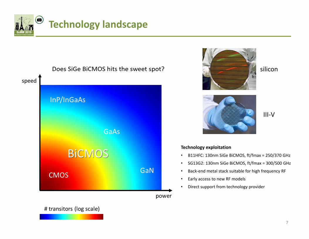
Technology exploitation• B11HFC: 130nm SiGe BiCMOS, ft/fmax = 250/370 GHz
• SG13G2: 130nm SiGe BiCMOS, ft/fmax = 300/500 GHz
• Back‐end metal stack suitable for high frequency RF
• Early access to new RF models
• Direct support from technology provider
Technology landscape
7
Does SiGe BiCMOS hits the sweet spot? silicon
III‐V
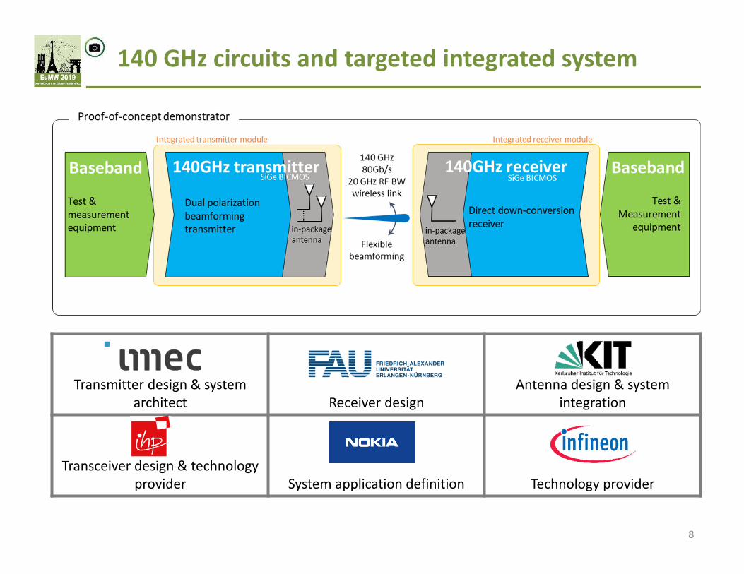
140 GHz circuits and targeted integrated system
8
Transmitter design & system architect Receiver design
Antenna design & system integration
Transceiver design & technology provider System application definition Technology provider

Highly linear and high gain 140 GHz 20 GHz RF bandwidth Power Amplifier, designed in Infineon 0.13µm SiGe‐BiCMOSPerformance compared to SOTA:
• exhibits the highest gain• Psat (and PAE) exceed CMOS designs, comparable to
90 nm SiGe amplifiers
High gain and linear Power Amplifier at 140 GHz
9
Akshay Visweswaran, Bastien Vignon, Xinyan Tang, Steven Brebels,Björn Debaillie, Piet Wambacq, A 112‐142GHz Power Amplifier withRegenerative Reactive Feedback achieving 17dBm peak Psat at 13% PAE,accepted for European Solid‐State Circuits Conference (ESSCIRC), 2019.
Reference Technology Powercombining
Saturated b/w (GHz)
Psat(dBm)
PAE(%)
Gain(dB)
Area(mm2)
[1] 2019 28nm CMOS No 127‐154 7 7 21 0.1*
[7] 2014 90nm SiGe 8‐way 112‐134 20.8+ 7.6+ 15+ 4.95§No 114‐134 17+ 12.5+ 20+ 1.29§
[8] 2013 65nm CMOS 8‐way 125‐155 13.2 14.6 15 0.38§
[9] 2013 0.13µm SiGe No 154‐163 10 ‐ 32 0.39§
[10] 2015 0.12µm SiGe No 110‐130 17.8+ 4.3+ 32+ 1.92§
[4] 2017 0.13µm SiGe No 131‐180 14 5.7 27 0.48§
[11] 2018 40nm CMOS 2‐way ‐ 14.8 8.9 20 0.125*
This work 0.13µm SiGe 2‐way 112‐142 17+ 13+ 34+ 0.35*/1.06§
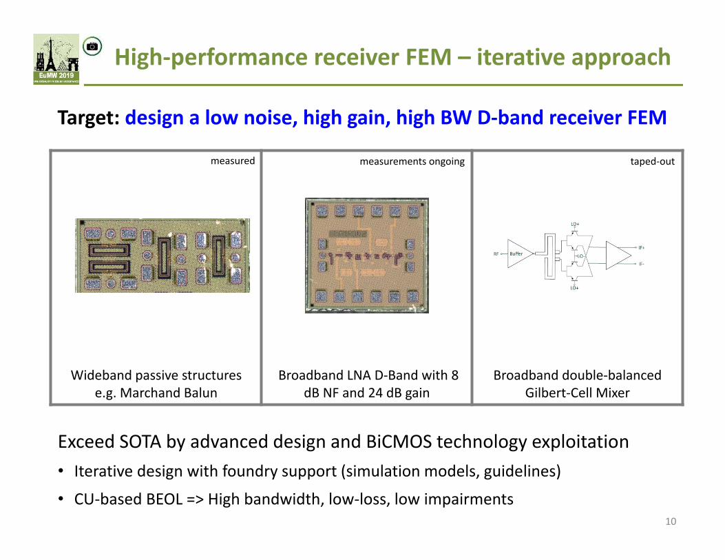
Target: design a low noise, high gain, high BW D‐band receiver FEM
High‐performance receiver FEM – iterative approach
10
Wideband passive structurese.g. Marchand Balun
Broadband LNA D‐Band with 8 dB NF and 24 dB gain
Broadband double‐balanced Gilbert‐Cell Mixer
Exceed SOTA by advanced design and BiCMOS technology exploitation• Iterative design with foundry support (simulation models, guidelines)
• CU‐based BEOL => High bandwidth, low‐loss, low impairments
measured measurements ongoing taped‐out
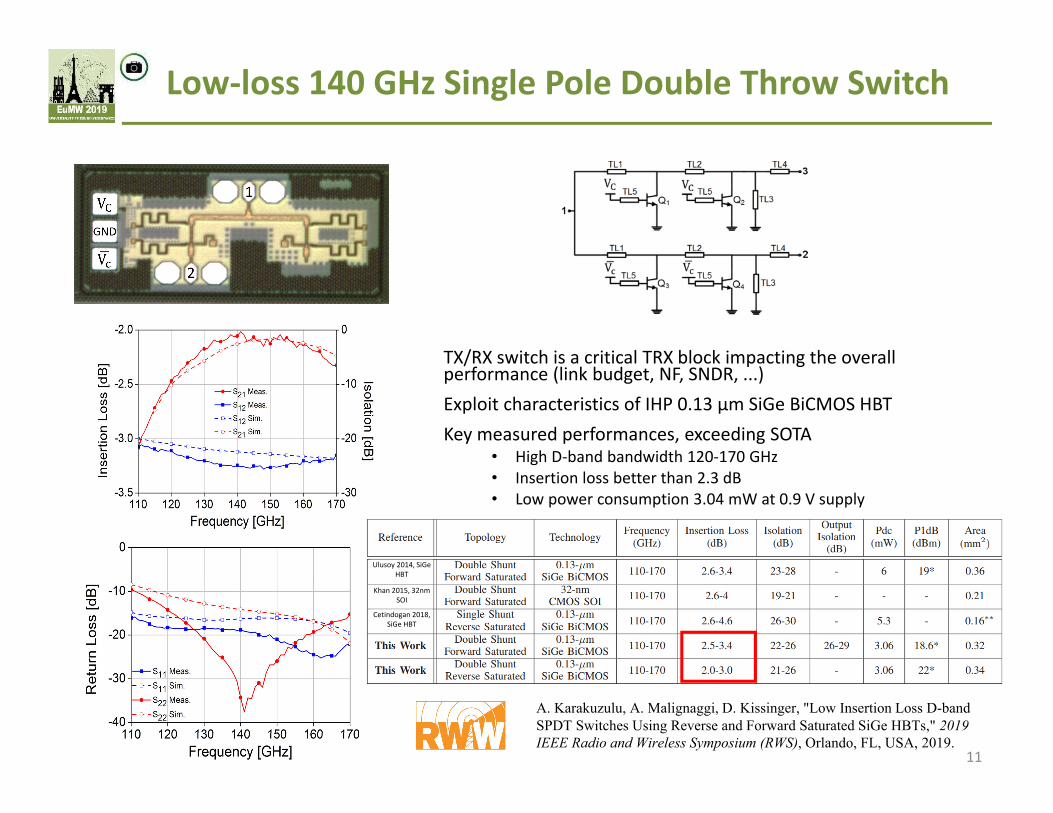
TX/RX switch is a critical TRX block impacting the overall performance (link budget, NF, SNDR, ...)Exploit characteristics of IHP 0.13 μm SiGe BiCMOS HBTKey measured performances, exceeding SOTA
• High D‐band bandwidth 120‐170 GHz• Insertion loss better than 2.3 dB • Low power consumption 3.04 mW at 0.9 V supply
Low‐loss 140 GHz Single Pole Double Throw Switch
11
A. Karakuzulu, A. Malignaggi, D. Kissinger, "Low Insertion Loss D-band SPDT Switches Using Reverse and Forward Saturated SiGe HBTs," 2019 IEEE Radio and Wireless Symposium (RWS), Orlando, FL, USA, 2019.
Khan 2015, 32nm SOI
Cetindogan 2018, SiGe HBT
Ulusoy 2014, SiGeHBT
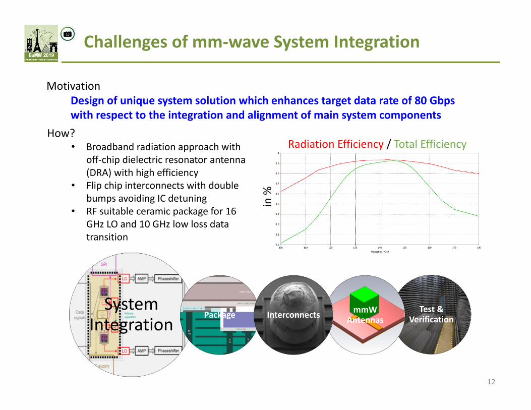
Challenges of mm‐wave System Integration
12
System Integration
Test & Verification
mmWAntennasPackage Interconnects
MotivationDesign of unique system solution which enhances target data rate of 80 Gbps with respect to the integration and alignment of main system components
Radiation Efficiency / Total Efficiency
in %
How?• Broadband radiation approach with
off‐chip dielectric resonator antenna (DRA) with high efficiency
• Flip chip interconnects with double bumps avoiding IC detuning
• RF suitable ceramic package for 16 GHz LO and 10 GHz low loss data transition
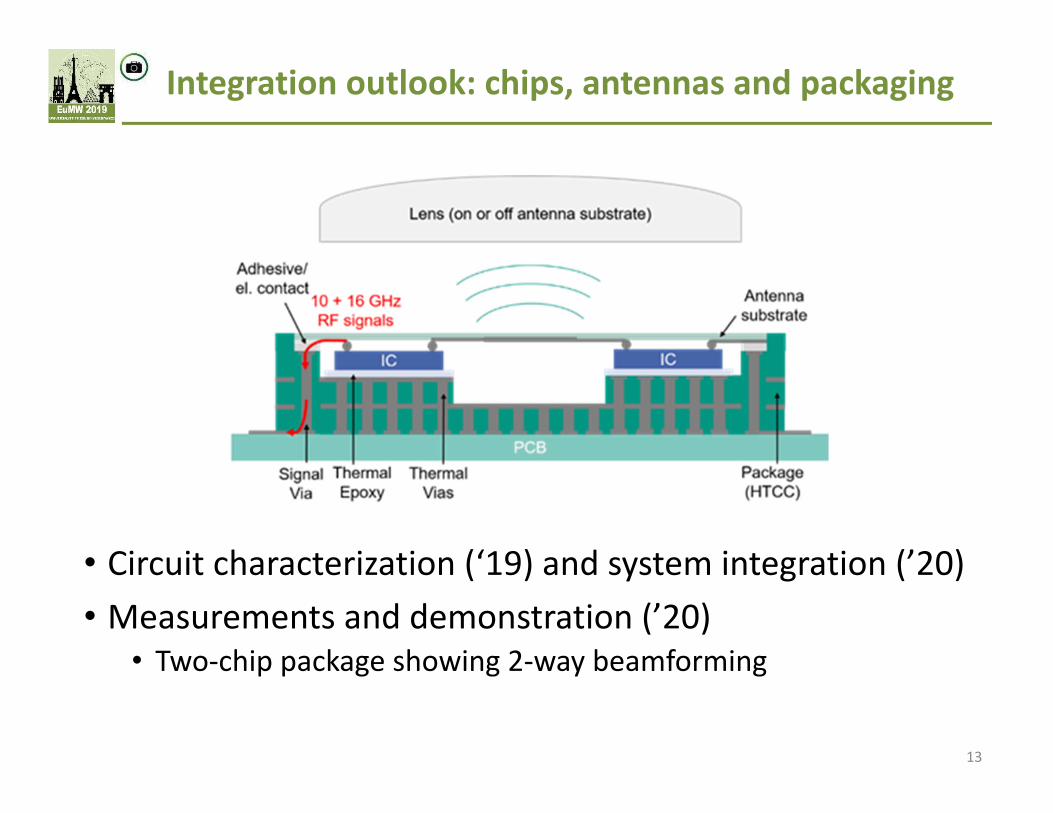
• Circuit characterization (‘19) and system integration (’20)• Measurements and demonstration (’20)
• Two‐chip package showing 2‐way beamforming
Integration outlook: chips, antennas and packaging
13

Conclusion: we are on‐track to achieve our objective
14

The research leading to these results has received funding from the European Commission'sECSEL Joint Undertaking under grant agreement n° 737454 ‐ project TARANTO ‐ and therespective Public Authorities of France, Austria, Germany, Greece, Italy and Belgium.
Thank you
‐ 15 ‐WS‐01 ‐ Recent advances in SiGe BiCMOS: technologies, modelling and circuits for 5G, radar and imaging