Ultra-thin silica films on metals: The long and winding ...
60
1 Ultra-thin silica films on metals: The long and winding road to understanding the atomic structure Shamil Shaikhutdinov* and Hans-Joachim Freund Abteilung Chemische Physik, Fritz-Haber-Institut der Max-Planck-Gesellschaft, Faradayweg 4-6, 14195 Berlin, Germany Abstract This paper critically reviews the experimental and theoretical studies on the growth of ultra-thin silica films onto metal single crystal substrates reported to date. The silica films on Mo(112) and Ru(0001) are discussed in more detail to demonstrate the key roles of the multi- technique approach and interplay between experiment and theory in the quest for understanding the atomic structure of the films. The results show the structural complexity and diversity of silica overlayers on metals, providing further information towards our understanding of the atomic structure, structural dynamics and physical and chemical properties of silica and related materials. *Corresponding author: [email protected]
Transcript of Ultra-thin silica films on metals: The long and winding ...

1
Ultra-thin silica films on metals: The long and winding road to understanding the atomic
structure
Shamil Shaikhutdinov* and Hans-Joachim Freund
Abteilung Chemische Physik, Fritz-Haber-Institut der Max-Planck-Gesellschaft,
Faradayweg 4-6, 14195 Berlin, Germany
Abstract
This paper critically reviews the experimental and theoretical studies on the growth of
ultra-thin silica films onto metal single crystal substrates reported to date. The silica films on
Mo(112) and Ru(0001) are discussed in more detail to demonstrate the key roles of the multi-
technique approach and interplay between experiment and theory in the quest for understanding
the atomic structure of the films. The results show the structural complexity and diversity of
silica overlayers on metals, providing further information towards our understanding of the
atomic structure, structural dynamics and physical and chemical properties of silica and related
materials.
*Corresponding author: [email protected]

2
About the Authors:
Shamil Shaikhutdinov received his PhD (1986) in Physics at the
Moscow Institute of Physics and Technology studying the microwave
properties of bio-organic materials and their models. Then he joined
the Boreskov Institute of Catalysis at Novosibirsk to carry out surface
science studies of catalytic systems. From 1994, he worked as a
postdoctoral fellow in several research centres in Germany and France.
Since 2004 he has been a group leader at the Department of Chemical
Physics of the Fritz-Haber Institute in Berlin. His current research is focused on an
understanding of structure-reactivity relationships in heterogeneous catalysis.
Hans-Joachim Freund studied physics and chemistry at the University
of Cologne where he received his Ph.D. in 1978 and his habilitation in
1983. Between 1979 and 1981, he worked in the Physics Department
at the University of Pennsylvania as a postdoctoral fellow. In 1983, he
became Associate Professor at Erlangen University and in 1987
Professor at Bochum University, and in 1995, he accepted a position
as scientific member and director of the Department of Chemical Physics at the Fritz-Haber-
Institut der Max-Planck-Gesellschaft in Berlin. He serves as Honorary Professor of five
universities. He received several national and international awards and he is a member of several
academies, scientific societies, and advisory boards of scientific journals.

3
1. Introduction
Silicon dioxide (SiO2) is one of the most abundant materials on our planet and is the key
material in many modern technological applications. It has been widely studied because of its
importance to geology, material science, microelectronics, photonics, and catalysis.
There is a long-standing interest in the synthesis of thin SiO2 films for microelectronic
processing. The properties of silica layers are essential for the performance of electronic devices.
The understanding of ultra-thin silica films becomes even more important for the new generation
of metal-oxide-semiconductor transistors, which use silica films as the gate dielectric. Further
miniaturization critically depends on our knowledge about the transition region of sub-
stoichiometric SiOx at the SiO2/Si interface.[1]
Silica (together with alumina) is also a widely used support in catalysis. It is evident that
the performance of silica in heterogeneous catalysts is primarily determined by surface species,
such as silanols (Si-OH), regardless whether silica is involved either as a support for catalyst
particles or as a reactive surface.[2] The surface structures become very complex in porous
systems like zeolites. The current understanding of the relation between structure and chemical
reactivity of these complex materials often comes from studies employing bulk-sensitive
techniques and from theoretical calculations based on a general wisdom about their structure.
The application of surface-sensitive techniques to elucidate the atomic structure and the
mechanism of catalytic reactions on silica-based materials remains challenging.
Finally, vitreous silica is the basis of traditional silicate glasses. Despite about a hundred
years of studies in this field, the greatest surprise about glasses is just how little is really known,
as opposed to merely postulated, about its structure.[3] Surface-science studies of vitreous silica
are rather in an “embryonic” state.

4
The rational approach to tackle some of the above-mentioned fundamental issues about
silica at low dimensions requires the preparation of a system which (i) is well suited to a whole
“army” of the experimental and computational methods available in surface science and (ii)
features atomic structures of the bulk counterparts. This can be realized in practice through the
preparation of a thin film with a well-defined structure supported by a planar metal single crystal
substrate. Although such an approach is currently applied to many transition metal oxides, to the
best of our knowledge, there is no comprehensive review about silica and related materials.
Here, we attempt to review the experimental, often theoretically supported, studies on
ultra-thin silica films grown on metals available to date. The review is organized as follows. We
first start with the introduction of the basic silica polymorphs and key observations for silica thin
films grown on Si single crystals, which may be considered as a benchmark to the thin silica
films on metals - the main topic of this paper. The results for a silica/Mo(112) system will be
discussed in more detail in order to demonstrate, on one hand, the necessity of the multi-
technique approach and, on the other hand, the key role of the interplay between experiment and
theory, in the quest for understanding the atomic structures. Further studies showed that the film
structure strongly depends on the metal substrate used (Mo, Ni, Pd, Ru, Pt). In particular, studies
on Ru(0001) and Pt(111) led to the observation of well-defined “bilayer” films only weakly
bonded to the metal support, like a free-standing SiO2 sheet. In addition, these systems made
possible the preparation and atomic imaging of vitreous silica in the two-dimensional form, thus
opening an avenue for further studies of long standing problems of real space imaging of crystal-
to-glass transitions. The paper ends with some concluding remarks.
2. Background

5
2.1. Silica polymorphs
Silica has relatively simple crystal structures, all made up from SiO4 tetrahedra, but a rich
phase diagram as depicted in Fig. 1. At atmospheric pressure, the equilibrium sequence of phase
transitions, prior to melting at ~1705°C, includes α-quartz to β-quartz (via an incommensurate
phase at 573°C), then to tridymite (870°C), and finally to β-cristobalite (1470°C). Tridymite is
notable for the surprisingly high number of phases which have been reported to exist.[4] All
crystalline phases consist of infinite frameworks of corner-sharing [SiO4] tetrahedra. For
example, the high-temperature phases HP-tridymite and β-cristobalite consist of identical sheets
of corner-sharing SiO4 tetrahedra (shown in the inset in Fig. 1) joined in a hexagonal close-
packed or face cubic-centered arrangement, respectively.[5]
Figure 1. (a) Phase diagram of the SiO2 polymorphs. (b) Layers containing 6-membered rings of
corner-sharing [SiO4] tetrahedra corresponding to the HP-tridymite(001) and β-cristobalite(111)
planes. The unit cell is indicated.

6
2.2. Silica thin films on silicon single crystals
When one aims solely at the preparation of silica films (i.e., on any substrate), thermal
growth on Si single crystal surfaces is the obvious choice to try first. Motivated by the key role
of the SiO2/Si interface in microelectronics, oxidation of silicon single crystals was studied in a
huge number of publications addressing the mechanism and kinetics of the oxide film growth,
structural and electronic properties of silicon dioxide, the formation of silicon suboxides, etc
(see, for example, refs. [6]) It is fair to say that almost every newly developed surface science
technique was applied to the SiO2/Si system. Below, only a brief survey of such studies will be
presented.
Auger electron spectroscopy (AES) and electron energy loss spectroscopy (EELS)
studies[7] of the initial stages of oxidation of Si(111)-(7×7) under well-controlled conditions for
thin (0 - 3 nm) silica layers fit fairly well to a phenomenological model based on oxygen
diffusion through the oxide layer under the presence of a surface electric field.[8] Oxygen
adsorption on Si(111)-(7×7) and Si(100)-(2×1) surfaces in the entire range of exposures from 0.1
Langmuir (1 L = 10-6 Torr × sec) to oxidation in air in the temperature range between 100 K and
700 K was examined by high resolution EELS (HREELS).[9] The formation of SiO2 was
observed only after annealing to 700 K, at least; at room temperature, even exposures as high as
~1011 L did not produce the spectrum of SiO2.
While it is generally accepted that the bulk of silica films grown on Si crystals have the
structure of vitreous (amorphous) silica (see Fig.2), the structure and properties of the interface
between SiO2 and crystalline Si remains controversial. A comparative HREELS study[10] of
7
quartz(0001) and silica films on Si(100) wafers as a function of oxide thickness indicated the
presence of a transition layer of ~ 2.5 nm at the SiO2/Si(100) interface. With decreasing oxide
thickness, peak positions gradually shifted to lower frequencies and intensities decreased. The
dielectric theory applied to a thin homogeneous supported film could not account for the
observed frequency shift.
X-ray photoelectron spectroscopy (XPS) studies of differently prepared samples also
found that a transition region exists between the Si substrate and the SiO2 film.[11] The Si3+ state
may be found up to ~3 nm into the bulk SiO2, whereas the Si+ and Si2+ states were mostly
localized at the abrupt SiO2/Si interface. Interestingly, Si+ species dominated at the SiO2/Si(111)
interface, whereas Si2+ dominated at the SiO2/Si(100) interface.[12] XPS studies with synchrotron
radiation showed that the transition region from crystalline Si to amorphous SiO2 is less than 0.5
nm thick.[13] The oxide films grown by ozone as an oxidation agent are thought to have a thinner
transition layer than that of a thermally grown oxide under the same pressure and temperature.
[14] For a comprehensive analysis of XPS studies on SiO2/Si the readers are referred to a recent
review by Hirose et al.[6b]
It should be mentioned that few studies reported ordering at SiO2/Si(100) interfaces when
SiO2 films were grown on passivated, ordered (1×1)-Si(100) surfaces produced by a novel wet
chemical cleaning.[15] Ion beam channeling and nuclear resonance analysis results revealed
registry of Si atoms in silica relative to the Si substrate, which was attributed to a β-cristobalite
epitaxial phase. This structurally ordered phase transforms into an amorphous structure
approximately 2 nm from the interface. Beyond this thickness, the oxide becomes amorphous.

8
Figure 2. Cross-sectional transmission electron microscopy imaging of the interfacial SiO2/Si
region. Reprinted from ref.[16] Copyright (2001) with permission from Elsevier.
The infrared (IR) spectra of silica films are commonly analyzed in terms of their
transverse-optic (TO) and longitudinal-optic (LO) vibrational modes. To fit the experimental
results obtained on the 10 – 100 nm thick SiO2/Si films, disorder-induced mechanical coupling
between the asymmetric stretch (AS1) TO mode (in-phase motion of adjacent oxygen atoms) and
the relatively optically inactive oxygen asymmetric stretch (AS2) mode (out-of-phase motion of
adjacent oxygen atoms) was included in the oscillator model.[17] Coupled AS1- and AS2-mode
LO-TO frequency pairs were observed as peaks at approximately 1256–1076 cm-1 and 1160–
1200 cm-1, respectively. LO-TO splitting can be observed experimentally by making use of the
Berreman effect.[18] The TO modes are optically active, whereas the LO modes are optically
inactive for an infinite crystal and hence cannot be observed in conventional transmission IR
spectra. However, they can be detected in p-polarized oblique-incidence absorption spectra
measured for thin films with thickness much smaller than the wavelength of the lattice vibration.
Then the vibrational modes normal to the surface have the frequencies of the LO modes, whereas
the vibrational modes parallel to the surface correspond to the TO modes.
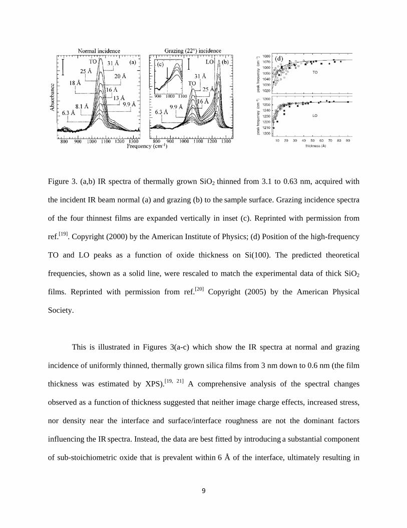
9
Figure 3. (a,b) IR spectra of thermally grown SiO2 thinned from 3.1 to 0.63 nm, acquired with
the incident IR beam normal (a) and grazing (b) to the sample surface. Grazing incidence spectra
of the four thinnest films are expanded vertically in inset (c). Reprinted with permission from
ref.[19]. Copyright (2000) by the American Institute of Physics; (d) Position of the high-frequency
TO and LO peaks as a function of oxide thickness on Si(100). The predicted theoretical
frequencies, shown as a solid line, were rescaled to match the experimental data of thick SiO2
films. Reprinted with permission from ref.[20] Copyright (2005) by the American Physical
Society.
This is illustrated in Figures 3(a-c) which show the IR spectra at normal and grazing
incidence of uniformly thinned, thermally grown silica films from 3 nm down to 0.6 nm (the film
thickness was estimated by XPS).[19, 21] A comprehensive analysis of the spectral changes
observed as a function of thickness suggested that neither image charge effects, increased stress,
nor density near the interface and surface/interface roughness are not the dominant factors
influencing the IR spectra. Instead, the data are best fitted by introducing a substantial component
of sub-stoichiometric oxide that is prevalent within 6 Å of the interface, ultimately resulting in
10
the red-shift of both TO and LO modes for the thinnest films. This conclusion was theoretically
supported using a scheme for calculating both the TO and LO spectra of surfaces and interfaces
from first principles.[20] Applied to the previously suggested structural model of a SiO2 film on
Si(100),[22] this scheme yielded IR spectra which basically reproduced the experimentally
observed shifts as shown in Fig. 3d. The effect was assigned to the lengthening of the Si-O bonds
in the sub-stoichiometric oxide at the interface.
Therefore, irrespective of the film preparation, the silica films grown on Si crystals are
vitreous in nature. The thinnest films (below 1 nm) are ill-defined and apparently
inhomogeneous. These findings can, in principle, be rationalized in terms of a large (~ 25% )
lattice mismatch between silica and Si. In this respect, it was mentioned that the lattice
parameters of SiC and SiO2 match within ~ 5%, thus allowing for an epitaxial SiC/SiO2
interface. Note, that the formation of a high quality insulating oxide layer on SiC is a key
requirement for metal-oxide-semiconductor devices based on this material.[23]
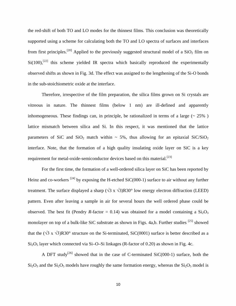
For the first time, the formation of a well-ordered silica layer on SiC has been reported by
Heinz and co-workers [24] by exposing the H-etched SiC(000-1) surface to air without any further
treatment. The surface displayed a sharp (√3 x √3)R30° low energy electron diffraction (LEED)
pattern. Even after leaving a sample in air for several hours the well ordered phase could be
observed. The best fit (Pendry R-factor = 0.14) was obtained for a model containing a Si2O3
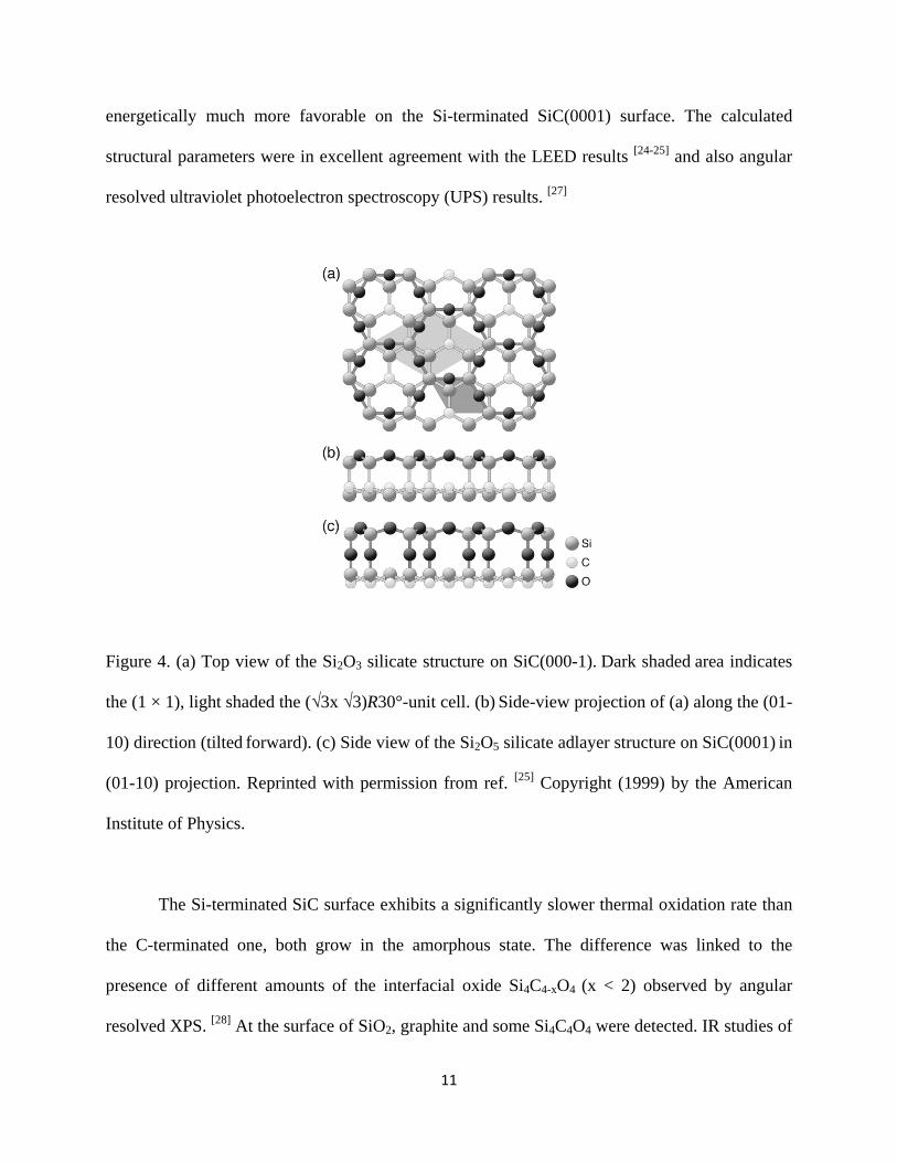
monolayer on top of a bulk-like SiC substrate as shown in Figs. 4a,b. Further studies [25] showed
that the (√3 x √3)R30° structure on the Si-terminated, SiC(0001) surface is better described as a
Si2O5 layer which connected via Si–O–Si linkages (R-factor of 0.20) as shown in Fig. 4c.
A DFT study[26] showed that in the case of C-terminated SiC(000-1) surface, both the
Si2O3 and the Si2O5 models have roughly the same formation energy, whereas the Si2O5 model is
11
energetically much more favorable on the Si-terminated SiC(0001) surface. The calculated
structural parameters were in excellent agreement with the LEED results [24-25] and also angular
resolved ultraviolet photoelectron spectroscopy (UPS) results. [27]
Figure 4. (a) Top view of the Si2O3 silicate structure on SiC(000-1). Dark shaded area indicates
the (1 × 1), light shaded the (√3x √3)R30°-unit cell. (b) Side-view projection of (a) along the (01-
10) direction (tilted forward). (c) Side view of the Si2O5 silicate adlayer structure on SiC(0001) in
(01-10) projection. Reprinted with permission from ref. [25] Copyright (1999) by the American
Institute of Physics.
The Si-terminated SiC surface exhibits a significantly slower thermal oxidation rate than
the C-terminated one, both grow in the amorphous state. The difference was linked to the
presence of different amounts of the interfacial oxide Si4C4-xO4 (x < 2) observed by angular
resolved XPS. [28] At the surface of SiO2, graphite and some Si4C4O4 were detected. IR studies of
12
silica films grown on SiC as a function of film thickness[29] showed frequency shifts below 10
nm for the TO mode, similar to that observed on Si-grown films (see Fig. 3b), but not for the LO
mode.
3. Silica films on metals
The formation of adventitious silica on metal surfaces was reported in early days of
“surface science” in the course of preparation of clean metal single crystal surfaces which
commonly contained silicon as a bulk impurity. Its segregation and oxidation resulted in
formation of oxidic structures which could sometimes be confused with or even erroneously
referred to as the formation of a surface metal oxide, like in the case of “platinum oxide” (see
e.g. refs.[30]) For example, at technically relevant pressures the formation of a “PtSiO” phase was
observed on pure polycrystalline Pt even at room temperature.[31] Adsorption studies of a Pt foil
systematically contaminated with Si revealed that the resulting silica layers solely block
adsorption of CO and H2 on Pt and do not produce any new adsorption sites.[32]
3.1. Silica films on Molybdenum
To the best of our knowledge, metal supported thin silica films were prepared for the first
time by Xu and Goodman[33] using Mo(110) as a substrate. Basically, a Mo(110) single crystal
was chosen because of its relative ease of cleaning and the ability to thermally desorb the oxide
thin films from the surface. Silica overlayers were grown at a relatively low temperature (<
100 °C) by evaporating silicon in oxygen background, typically ~ 1×10⁻⁵ Torr. Based on AES
data the SiO2 films could be as thin as 2 Å,[34] although it was unclear whether such ultrathin
films were dense and uniform. Under these deposition conditions, the gas phase precursor to the
13
SiO2 film was thought to be a gas-phase oxygen containing silicon species (likely SiO), not gas-
phase silicon. The latter seems to dominate at lower oxygen pressures, in which further oxidation
to SiO2 occurs on the Mo(110) surface. As deposited, the films were amorphous. Upon
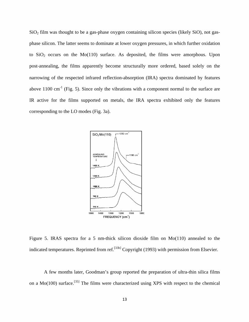
post‐annealing, the films apparently become structurally more ordered, based solely on the
narrowing of the respected infrared reflection-absorption (IRA) spectra dominated by features
above 1100 cm-1 (Fig. 5). Since only the vibrations with a component normal to the surface are
IR active for the films supported on metals, the IRA spectra exhibited only the features
corresponding to the LO modes (Fig. 3a).
Figure 5. IRAS spectra for a 5 nm-thick silicon dioxide film on Mo(110) annealed to the
indicated temperatures. Reprinted from ref.[33b] Copyright (1993) with permission from Elsevier.
A few months later, Goodman’s group reported the preparation of ultra-thin silica films
on a Mo(100) surface.[35] The films were characterized using XPS with respect to the chemical
14
states of silicon and the composition of the film. It has been shown that the “as deposited” silicon
oxide consisted predominantly of SiO2 with a small fraction of sub-oxides. Annealing to ~ 1300
K yielded a stoichiometric film of SiO2 which exhibited electronic and structural properties
similar to those of vitreous silica.
However, the lattice parameters of both Mo(110) and Mo(100) surfaces do not fit those
of the low-index silica surfaces of common silica polymorphs (depicted in Fig. 1b). This may
explain the lack of long-range ordering in the resulting films. From all the stable single crystal
surfaces of Mo, which has a body centered cubic structure, only Mo(112) could accommodate
hexagonal surfaces without severe distortions. This choice has been proven successful, indeed.[36]
In the original recipe of Schroeder et al.[37], the preparation consisted of four cycles of
deposition of ~0.5 ML Si onto clean Mo(112) at room temperature and oxidation at 800 K in
5×10⁻⁵ mbar O2 for 6 min. The films were stepwise oxidized at higher temperatures, with the
final oxidation being performed in 5×10⁻⁶ mbar O2 at 1150 K for 20 min. This preparation
resulted in a closed film (as judged by CO and H2 adsorption experiments) which exhibited a
sharp c(2×2)-Mo(112) LEED pattern (Fig. 6a), thus indicating the high degree of crystallinity.

15
Figure 6. (a) Typical LEED pattern of a well-ordered silica film on Mo(112). A perspective view
of the Mo(112) surface is shown, for clarity. Unit cells are indicated. (b) Large-scale STM image
of the film annealed to 1150 K. Inset shows high resolution image with a honeycomb-like
structure. (c) IRAS spectra of silica films upon stepwise annealing to the indicated temperatures.
(d) Model for a silica film on Mo(112) as suggested in ref.[37d]
Figure 6a shows a perspective view of the Mo(112) surface which consists of close-
packed atomic rows orientated along the [-1-11] direction which are separated by furrows in the
[-110] direction, thus resulting in a rectangular surface unit cell with a spacing of a1=2.73 Å and
a2=4.45 Å, as indicated. The c(2×2) structure of the silica overlayer on Mo(112) is very close to
16
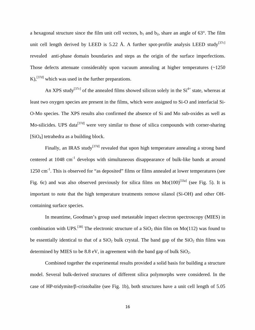
a hexagonal structure since the film unit cell vectors, b1 and b2, share an angle of 63°. The film
unit cell length derived by LEED is 5.22 Å. A further spot-profile analysis LEED study[37c]
revealed anti-phase domain boundaries and steps as the origin of the surface imperfections.
Those defects attenuate considerably upon vacuum annealing at higher temperatures (~1250
K),[37d] which was used in the further preparations.
An XPS study[37c] of the annealed films showed silicon solely in the Si4+ state, whereas at
least two oxygen species are present in the films, which were assigned to Si-O and interfacial Si-
O-Mo species. The XPS results also confirmed the absence of Si and Mo sub-oxides as well as
Mo-silicides. UPS data[37d] were very similar to those of silica compounds with corner-sharing
[SiO4] tetrahedra as a building block.
Finally, an IRAS study[37d] revealed that upon high temperature annealing a strong band
centered at 1048 cm-1 develops with simultaneous disappearance of bulk-like bands at around
1250 cm-1. This is observed for “as deposited” films or films annealed at lower temperatures (see
Fig. 6c) and was also observed previously for silica films on Mo(100)[33a] (see Fig. 5). It is
important to note that the high temperature treatments remove silanol (Si-OH) and other OH-
containing surface species.
In meantime, Goodman’s group used metastable impact electron spectroscopy (MIES) in
combination with UPS.[38] The electronic structure of a SiO2 thin film on Mo(112) was found to
be essentially identical to that of a SiO2 bulk crystal. The band gap of the SiO2 thin films was
determined by MIES to be 8.8 eV, in agreement with the band gap of bulk SiO2.
Combined together the experimental results provided a solid basis for building a structure
model. Several bulk-derived structures of different silica polymorphs were considered. In the
case of HP-tridymite/β-cristobalite (see Fig. 1b), both structures have a unit cell length of 5.05
17
Å, but a different stacking sequence (AB and ABC along [0001] and [111] directions of HP-
tridymite and β-cristobalite, respectively). The (0001) planes of the quartz have a unit cell length
of 4.91 Å. All these structures have a considerable lattice mismatch with respect to the measured
lattice constant of the pseudo-hexagonal silica overlayer on Mo(112) (= 5.22 Å) (also seen in
scanning tunneling microscopy (STM) images, see inset in Fig. 6b), and should therefore be
distorted as compared with the bulk.
At this point it became clear that any model verification needs additional structural
information and theoretical modeling. On the other hand, DFT calculations need input data about
surface symmetry, its stoichiometry and thickness of an oxide overlayer, but the latter was the
least known in that time. Indeed, determination of the film thickness with electron spectroscopies
such as XPS and AES is based on the precise knowledge of a mean free path of electron in a
material under study and therefore suffers from large uncertainty when applied to ultra-thin films
where each layer counts. The reported values of Schroeder et al.[37c] and Goodman’s group[38a, 38b]
scattered between 4 and 8 Å. Later, Chen et al.[39] reported the value of 3 Å.
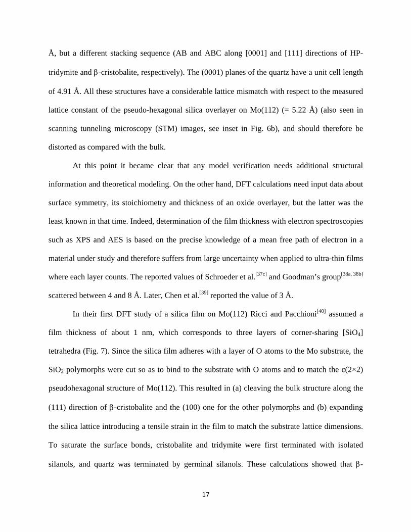
In their first DFT study of a silica film on Mo(112) Ricci and Pacchioni[40] assumed a
film thickness of about 1 nm, which corresponds to three layers of corner-sharing [SiO4]
tetrahedra (Fig. 7). Since the silica film adheres with a layer of O atoms to the Mo substrate, the
SiO2 polymorphs were cut so as to bind to the substrate with O atoms and to match the c(2×2)
pseudohexagonal structure of Mo(112). This resulted in (a) cleaving the bulk structure along the
(111) direction of β-cristobalite and the (100) one for the other polymorphs and (b) expanding
the silica lattice introducing a tensile strain in the film to match the substrate lattice dimensions.
To saturate the surface bonds, cristobalite and tridymite were first terminated with isolated
silanols, and quartz was terminated by germinal silanols. These calculations showed that β-
18
cristobalite is the most stable structure and exhibits the strongest adhesion energy to the Mo
substrate. Then the dehydroxylated surface (to fit the experimental results showing the absence
of OH at surface) undergoes a strong reconstruction which leads to the formation of two-
membered silica rings that yield a vibrational band around 800 cm-1, i.e. close to 795 cm-1 found
in the IRAS experiments (Fig. 6c).
Figure 7. Structural model of the 3-layers thick SiO2(cristobalite) film on Mo(112) exposing two-
membered silica rings at the surface. (O: small black; Si: gray, Mo: large black). Reprinted with
permission from ref. [40] Copyright (2004) by the American Physical Society.
Almost simultaneously with this DFT study, Goodman and co-workers published a
paper[39] addressing the atomic structure of the silica film on Mo(112), where, seemingly for the
first time, the term “a monolayer silica film” was introduced. In addition to the original recipe of
Schroeder et al.[37a], this group used another preparation, where the clean Mo(112) surface was
first exposed to 5×10⁻⁸ Torr O2 at 850 K to form the well-ordered Mo(112)-p(2×3)O structure.
Then less than 1 ML Si was deposited, followed by annealing at 800 K in a ~10-7 Torr O2 for 5
19
min and then increasing the temperature to 1200 K for an additional 5 min. This deposition and
annealing was repeated several times until a constant Si/Mo AES ratio was achieved, which was
assigned to the film thickness approximately of 1 ML.
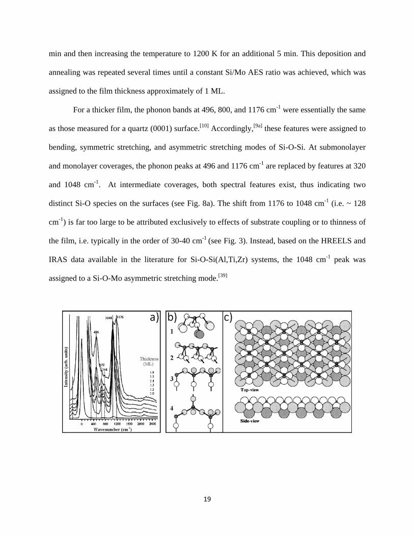
For a thicker film, the phonon bands at 496, 800, and 1176 cm-1 were essentially the same
as those measured for a quartz (0001) surface.[10] Accordingly,[9a] these features were assigned to
bending, symmetric stretching, and asymmetric stretching modes of Si-O-Si. At submonolayer
and monolayer coverages, the phonon peaks at 496 and 1176 cm-1 are replaced by features at 320
and 1048 cm-1. At intermediate coverages, both spectral features exist, thus indicating two
distinct Si-O species on the surfaces (see Fig. 8a). The shift from 1176 to 1048 cm-1 (i.e. ~ 128
cm-1) is far too large to be attributed exclusively to effects of substrate coupling or to thinness of
the film, i.e. typically in the order of 30-40 cm-1 (see Fig. 3). Instead, based on the HREELS and
IRAS data available in the literature for Si-O-Si(Al,Ti,Zr) systems, the 1048 cm-1 peak was
assigned to a Si-O-Mo asymmetric stretching mode.[39]
20
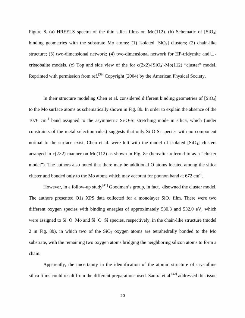
Figure 8. (a) HREELS spectra of the thin silica films on Mo(112). (b) Schematic of [SiO4]
binding geometries with the substrate Mo atoms: (1) isolated [SiO4] clusters; (2) chain-like
structure; (3) two-dimensional network; (4) two-dimensional network for HP-tridymite and -
cristobalite models. (c) Top and side view of the for c(2x2)-[SiO4]-Mo(112) “cluster” model.
Reprinted with permission from ref.[39] Copyright (2004) by the American Physical Society.
In their structure modeling Chen et al. considered different binding geometries of [SiO4]
to the Mo surface atoms as schematically shown in Fig. 8b. In order to explain the absence of the
1076 cm-1 band assigned to the asymmetric Si-O-Si stretching mode in silica, which (under
constraints of the metal selection rules) suggests that only Si-O-Si species with no component
normal to the surface exist, Chen et al. were left with the model of isolated [SiO4] clusters
arranged in c(2×2) manner on Mo(112) as shown in Fig. 8c (hereafter referred to as a “cluster
model”). The authors also noted that there may be additional O atoms located among the silica
cluster and bonded only to the Mo atoms which may account for phonon band at 672 cm-1.
However, in a follow-up study[41] Goodman’s group, in fact, disowned the cluster model.
The authors presented O1s XPS data collected for a monolayer SiO2 film. There were two
different oxygen species with binding energies of approximately 530.3 and 532.0 eV, which
were assigned to Si−O−Mo and Si−O−Si species, respectively, in the chain-like structure (model
2 in Fig. 8b), in which two of the SiO2 oxygen atoms are tetrahedrally bonded to the Mo
substrate, with the remaining two oxygen atoms bridging the neighboring silicon atoms to form a
chain.
Apparently, the uncertainty in the identification of the atomic structure of crystalline
silica films could result from the different preparations used. Santra et al.[42] addressed this issue
21
using LEED and STM in attempt to optimize the parameters crucial to the preparation of high-
quality SiO2 films on Mo(112), i.e., silicon deposition flux, oxidation time and exposures, and
the temperature/time of the final anneal. Comparative STM and LEED studies showed that a
sharp c(2×2) LEED pattern is insufficient evidence for a high-quality, flat film. The large-scale
STM images of the films obtained in this work showed a stripe-like morphology oriented along
the Mo(-1-11) direction, which was very similar to that shown in Fig. 6b by Schroeder et al.[37d]
On the other hand, STM images published later by the same group[41, 43] revealed a much
smoother surface, although the films were prepared identically.
Electronic and vibrational properties of SiO2/Mo(112) was addressed by Wendt et al. [44]
using polarization modulation (PM) IRAS and UPS/MIES. The authors focused on the film
synthesis using various preparation methods. In addition to the method of deposition-oxidation
cycles on O(2×3)-Mo(112) previously introduced by Chen et al.[39], the second method included
a single step deposition and annealing in oxygen at high temperatures. Regardless of the
preparation recipe, the electronic and vibrational properties of monolayer films were best
rationalized by a surface dominated by Si-O-Mo linkages. For such films a single vibrational
feature at 1048 - 1057 cm−1 was detected with PM IRAS and assigned to the Si-O-Mo linkages.
For coverages greater than one monolayer, the formation of Si-O-Si linkages in the second layer
of the SiO2 films was observed. In the well-ordered monolayer film, UPS and MIES spectra
revealed the O(2p) nonbonding band splitting in two well-resolved features at 7.6 and ~ 6.3 eV,
consistent with two distinct O(2p) nonbonding orbitals at the surface. The fine structure of the
nonbonding band was, again, attributed to isolated [SiO4] tetrahedra attached via O atoms to the
substrate.

22
At this point it became more and more evident that only a multi-technique approach,
including high-resolution STM, and electronic and vibrational spectroscopies applied to the same
sample, in combination with the state-of-the art DFT calculations can elucidate the atomic
structure of the monolayer silica film on Mo(112). This step forward was made in 2005, when
two groups[45] almost independently came to the conclusion that the structure of a silica film on
Mo(112) consisted of a two-dimensional network of corner-sharing [SiO4] tetrahedra. It is fair to
say that this “2D-network” model was considered, but rejected, by Goodman and co-workers.[39]
The experiments were performed in an UHV chamber equipped with LEED, UPS/XPS,
IRAS and STM. Following the recipe of Chen et al.[39] the films were prepared by exposing the
clean Mo(112) surface to 5×10⁻⁸ mbar O2 at 900 K, thus resulting in p(2×3)O-Mo(112) surface.
(NB: The proposed atomic structure of this surface was later revisited by us[46]). Subsequently,
approximately 1 ML of Si was deposited in one step at the same oxygen pressure and
temperature. The film was then annealed in UHV at ~ 1250 K for 5 min. The annealing
temperature has turned out to be critical. Based on the STM studies, overheating leads to a partial
sublimation of the film, while annealing at the lower temperatures results in the presence of ill-
defined silica particles on top of the ordered film.
Figures 9 shows large-scale STM images and respective IRAS spectra of the “as
deposited” and annealed films. It is clear that a well-ordered films is characterized by an
extremely sharp (FWHM= 12 cm-1) and strong band at around 1060 cm-1 and weak, but clearly
visible bands at 770 and 675 cm-1. All peaks are red-shifted by 41, 7 and 19 cm-1, respectively,
when measured on the films prepared with 36O2 isotope.[45a] Silica deposition on top of the
annealed films immediately results in the broad band at ~1240 cm-1 also seen for the “as
deposited” samples, and as such is attributed to silica particles and their aggregates,[47] in

23
agreement with the previous results.[33b, 39, 44] Subsequent annealing to 1250 K restores both the
morphology and IRAS spectrum of the atomically flat film, thus indicating “self-limited” growth
of the monolayer film via sublimation of the silica clusters at high temperatures. The crystalline
films show wide terraces (Fig. 9b), with steps of 1.2 Å in height corresponding to monoatomic
steps of the Mo(112) substrate underneath the film.
Figure 9. STM images (a-c) and IRAS spectra (d) of the silica film: (a) as deposited at 900 K; (b)
subsequently annealed in UHV at 1250 K; (c) with additionally deposited silica on top of the
film (b). Image size is 100 nm x 100 nm.
An XPS study showed only a single peak in the Si 2p region with a binding energy (BE)
of 103.2 eV, which is characteristic for the Si4+ oxidation state. In contrast, the O 1s region
revealed two different chemical environments for oxygen, with BE at 532.5 eV and 531.3 eV.

24
These two states are much better resolved using synchrotron light (Fig. 10). [48] The BE values
are considerably higher than the 530.5 eV observed for the MoOx oxide layers on Mo(112) and
therefore cannot be assigned to Mo-oxide formation underneath the film. The intensity ratio of
two O species at higher and lower BEs in well-ordered films is found to be about 3:2.
Figure 10. (Left panel) XPS spectra (O1s and Mo3d core levels) of a silica film on Mo(112)
obtained with the synchrotron light at photon energies as indicated. The dotted line shows the
O1s spectrum obtained with a conventional x-ray source, for comparison. (Right panel) UPS
spectrum (He I) of a crystalline silica film on Mo(112). Spectrum (*) from ref.[44] is shown for
comparison.
The presence of very narrow bands in an UPS spectrum (Fig. 10) confirms the high
crystallinity of the films grown. The signals between 4 and 9 eV are commonly attributed to
nonbonding O2p derived valence levels, and the signals between 10 and 12 eV, in the region of
Si-O bonding states observed for silica films on Si, are attributed to the hybridized O2p-Si3s,3p
25
bonding states. Wendt et al.[44] previously assigned a band at ~ 11.4 eV to the Si-O-Si bonds.
Consequently, the band at 10.6 eV was attributed to the Si-O-Mo bond, where the interface O
atoms are thought to accumulate electron density from the Mo substrate. Some differences
between UPS spectra from different publications could be traced to the differences in film
preparations and film quality, which is hard to compare without STM. Indeed, STM studies [49]
revealed that atomically flat films can be produced only after annealing at temperatures above
1200 K, which was not always the case in the previous works.
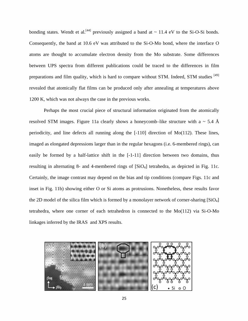
Perhaps the most crucial piece of structural information originated from the atomically
resolved STM images. Figure 11a clearly shows a honeycomb–like structure with a ~ 5.4 Å
periodicity, and line defects all running along the [-110] direction of Mo(112). These lines,
imaged as elongated depressions larger than in the regular hexagons (i.e. 6-membered rings), can
easily be formed by a half-lattice shift in the [-1-11] direction between two domains, thus
resulting in alternating 8- and 4-membered rings of [SiO4] tetrahedra, as depicted in Fig. 11c.
Certainly, the image contrast may depend on the bias and tip conditions (compare Figs. 11c and
inset in Fig. 11b) showing either O or Si atoms as protrusions. Nonetheless, these results favor
the 2D model of the silica film which is formed by a monolayer network of corner-sharing [SiO4]
tetrahedra, where one corner of each tetrahedron is connected to the Mo(112) via Si-O-Mo
linkages inferred by the IRAS and XPS results.
26
Figure 11. High resolution STM images of a crystalline silica film on Mo(112). Depending on
the tunneling conditions the O and Si atoms are imaged as protrusions in (a) and (b),
respectively. The line defect, running along the [-110] direction, in the image (a) is atomically
resolved in the image (b). Panel (c) displays a top-view of the monolayer network of corner-
sharing [SiO4] tetrahedra, which readily explains the STM contrast in the image (b) by
introducing a half-lattice shift between two domains. Inset in (a) and the image (b) are
superimposed with the simulated STM images based on the DFT-optimized structural model
shown in Fig. 12.
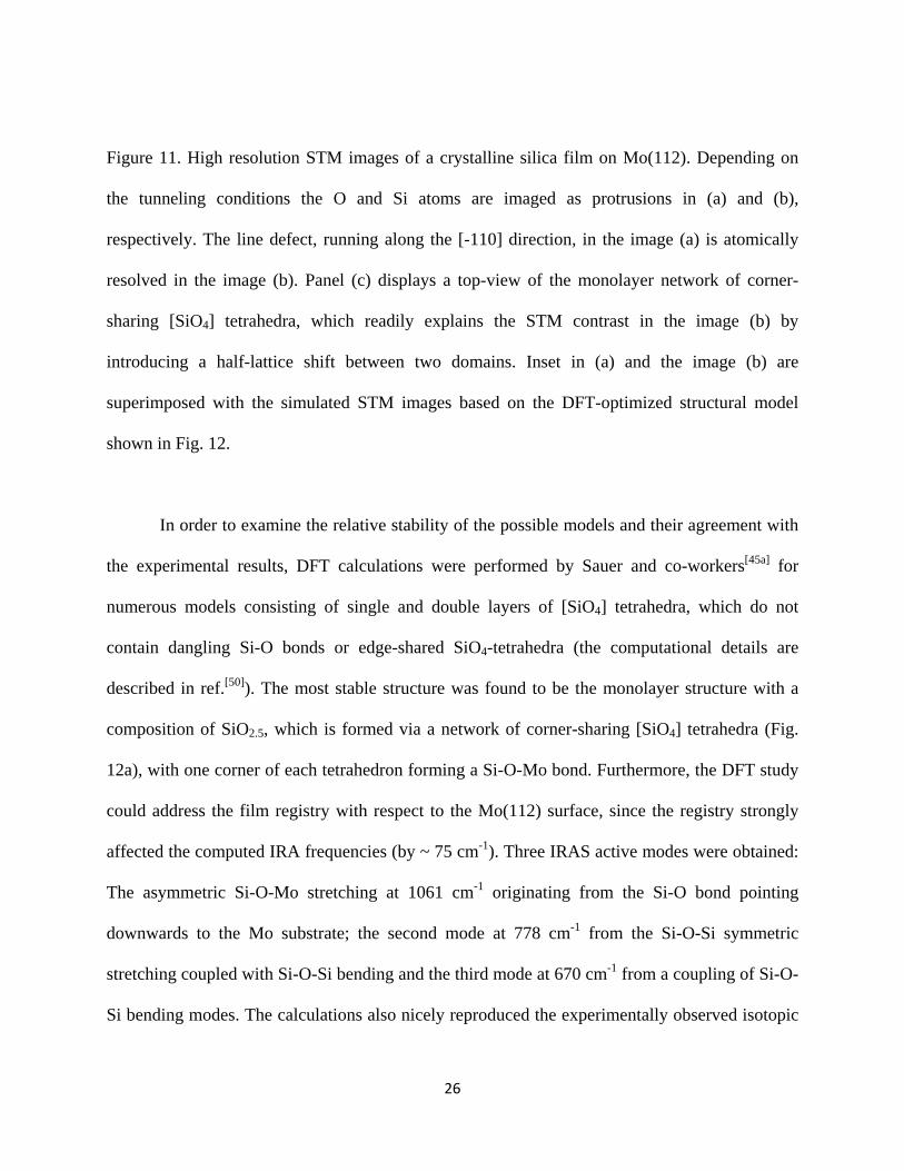
In order to examine the relative stability of the possible models and their agreement with
the experimental results, DFT calculations were performed by Sauer and co-workers[45a] for
numerous models consisting of single and double layers of [SiO4] tetrahedra, which do not
contain dangling Si-O bonds or edge-shared SiO4-tetrahedra (the computational details are
described in ref.[50]). The most stable structure was found to be the monolayer structure with a
composition of SiO2.5, which is formed via a network of corner-sharing [SiO4] tetrahedra (Fig.
12a), with one corner of each tetrahedron forming a Si-O-Mo bond. Furthermore, the DFT study
could address the film registry with respect to the Mo(112) surface, since the registry strongly
affected the computed IRA frequencies (by ~ 75 cm-1). Three IRAS active modes were obtained:
The asymmetric Si-O-Mo stretching at 1061 cm-1 originating from the Si-O bond pointing
downwards to the Mo substrate; the second mode at 778 cm-1 from the Si-O-Si symmetric
stretching coupled with Si-O-Si bending and the third mode at 670 cm-1 from a coupling of Si-O-
Si bending modes. The calculations also nicely reproduced the experimentally observed isotopic
27
shifts for the films grown with 36O2. Furthermore, this model explained the BE shift (1.3 eV) and
intensity ratio (3:2) for the O 1s core level of the oxygen ions in the top-most layer, O(Si), and
the interfacial O(Mo) atoms, having bonds both to Si and Mo. Finally, STM image simulations
nicely agree with experimental high-resolution STM images (see insets in Fig. 11).
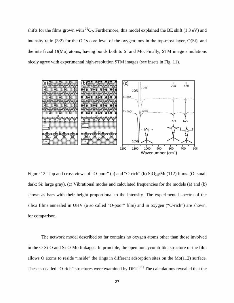
Figure 12. Top and cross views of “O-poor” (a) and “O-rich” (b) SiO2.5/Mo(112) films. (O: small
dark; Si: large gray). (c) Vibrational modes and calculated frequencies for the models (a) and (b)
shown as bars with their height proportional to the intensity. The experimental spectra of the
silica films annealed in UHV (a so called “O-poor” film) and in oxygen (“O-rich”) are shown,
for comparison.
The network model described so far contains no oxygen atoms other than those involved
in the O-Si-O and Si-O-Mo linkages. In principle, the open honeycomb-like structure of the film
allows O atoms to reside “inside” the rings in different adsorption sites on the Mo(112) surface.
These so-called “O-rich” structures were examined by DFT.[51] The calculations revealed that the

28
stability of the “O-rich” phases considerably increases at high chemical potential of oxygen (e.g.,
high pressure, low temperature). A careful analysis of the experimental IRAS and XPS spectra in
the monolayer films prepared by high temperature annealing either in UHV or 10-6 mbar O2
showed, indeed, small but detectable changes, which agreed well with the theoretical predictions
(Fig. 12c). Due to subtle differences between properties of the O-poor and O-rich films, the
existence of the latter might not have been discovered without the aid of theory. The observation
of a variety of different structures may explain the somewhat controversial results reported from
different groups and experimental setups as discussed above. It became evident that the precise
atomic structure may strongly depend on film preparation.
As already mentioned, Giordano et al.[45b] basically came to the same conclusions about
the atomic structure of the crystalline silica films. Again, their DFT study showed that neither the
cluster nor the chain-like model could account for the measured vibrational spectra. Later,
Yakovkin[52] reported calculations for the [SiO4] cluster model which resulted in a vibrational
mode at 1044 cm-1, which was then used by Chen et al.[53] to theoretically support the cluster
model. However, these calculations were based on a small molecular model of the surface
containing just one [SiO4] unit, which could not, adequately, describe the Mo conduction band
electrons and the coupling between vibrational modes of the silica layer and the substrate.
Indeed, the DFT calculations of the cluster model by Todorova et al.[49] and Giordano et al.[45b]
did not reveal any IRAS active bands at frequencies higher than 706 and 840 cm-1, respectively.
It was tempting to directly measure the thickness of the silica films by STM, e.g. by
preparing films which partially covered the surface. Surprisingly, the STM images revealed a
strip-like surface morphology[54] which somewhat resembled those reported in early publications
[37d, 42] of the films thought to be dense. When coalesced, the stripes form islands with a
29
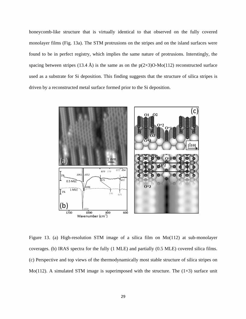
honeycomb-like structure that is virtually identical to that observed on the fully covered
monolayer films (Fig. 13a). The STM protrusions on the stripes and on the island surfaces were
found to be in perfect registry, which implies the same nature of protrusions. Interstingly, the
spacing between stripes (13.4 Å) is the same as on the p(2×3)O-Mo(112) reconstructed surface
used as a substrate for Si deposition. This finding suggests that the structure of silica stripes is
driven by a reconstructed metal surface formed prior to the Si deposition.
Figure 13. (a) High-resolution STM image of a silica film on Mo(112) at sub-monolayer
coverages. (b) IRAS spectra for the fully (1 MLE) and partially (0.5 MLE) covered silica films.
(c) Perspective and top views of the thermodynamically most stable structure of silica stripes on
Mo(112). A simulated STM image is superimposed with the structure. The (1×3) surface unit

30
cell is indicated. The calculated frequencies for this structure are shown in (b) as bars in the same
color code as the experimental spectra.
The proposed model is shown in Fig. 13c. This structure explains the STM image
contrast. Even stronger evidence for the proposed structure came from the analysis of lattice
vibrations, which were previously shown to be sensitive to the silica structure and, in particular,
to the registry between silica and the Mo substrate.[49] Figure 13b shows that the DFT computed
band positions and intensities are in excellent agreement with the experimental IRAS spectra.
For the silica stripes, the spectra revealed a small red-shift of the principal phonon at 1059 cm-1
to 1046 cm−1, whereas the mode at 770 cm-1 in the films is considerably (~100 cm−1) blue-shifted
to 875 cm−1. This large shift is due to the fact that this mode, i.e. coupling the Si–O–Si
symmetric stretching and Si–O–Si bending mode in the 2D-film, has less Si–O–Si bending
character in the 1D-stripe. Again, the results provided further indirect evidence for the 2D-
network model of the monolayer silica film.
Nonetheless, Chen and Goodman[53] continued the discussions on the structure of the
monolayer silica films on Mo(112).[55] The key point was the nature of vibrational modes
measured for the silica films by IRAS and HREELS. Basically, the absence of the band at
∼1176 cm−1 (assigned to asymmetric Si–O–Si stretching) in the monolayer films has been used
as a central argument to conclude that the monolayer film does not exhibit Si–O–Si bonds at all
and hence consists of exclusively [SiO4] clusters with the Si–O–Mo linkages only.
These issues were explicitly addressed by Kaya et al.[48]. A very detailed analysis of the
vibrational spectra based on symmetry considerations was carried out to explain how these
31
spectra relate to those observed for the “bulk”-like systems, e.g. thick silica films and single
crystals.
Recently, further support for the network model of the monolayer silica film came from
studies by Seifert et al.,[56] using fast hydrogen and helium atom scattering at a grazing angle of
incidence. The experimental results exclude the cluster model and nicely fit the network
structure. Finally, a very recent I/V LEED study[57] showed again excellent agreement (R factor
0.14) with the network model.
Having established the atomic structure of a crystalline silica film on Mo(112), one may
raise the question: how is this surface related to surfaces of silica polymorphs? In this context, it
is noteworthy that a similar surface structure was predicted by molecular-dynamics simulations
for the reconstructed α-quartz(0001) surface as the most stable of all investigated structures, and
as such was proposed as a model of the dry reconstructed (0001) surface obtained upon
cleaving.[58] Such a surface was modelled via densification of the two uppermost layers of [SiO4]
tetrahedral units, with 6-membered (in top view) and 3-membered (cross view) rings that do not
exist in bulk α-quartz. The free-standing silica double layer is computed to have a lattice
constant of 5.24 Å[59] or 5.30 Å,[60] which shows a considerable mismatch with respect to α-
quartz(0001) (= 4.91 Å), such that its formation on real quartz surfaces is most likely prevented.
In contrast, a silicate monolayer was observed on SiC(000-1) and (0001) surfaces[24] (see Fig. 4)
leading to the hexagonal (√3x√3)R30° structure with a lattice constant of 5.25 Å, i.e. very close
to that calculated for the unsupported silica layer. On the other hand, the silicate monolayer
hardly fits the Mo(112) surface with a rectangular unit cell (5.46 Å × 8.92 Å), and is, therefore,
accompanied by a lattice extension along the Mo[-1-11] direction to 5.46 Å as compared to the
free-standing layer. Despite this distortion, the monolayer silica films on Mo(112) are perfectly
32
ordered, as shown by STM. The reason is the very strong Si-O-Mo bond that stabilizes this
particular structure. Consequently, the metal support induces considerable changes in the
electronic structure. A DFT analysis of valence band structures suggested that the silica film on
Mo(112) must be considered as a novel oxidic surface and not as another incarnation of a
“dense” surface on bulk α-quartz.[59]
As expected, the O-terminated silica film on Mo(112) is essentially inert towards any
gases. Moreover, even after exposure to air, the film surface is fully recovered by a thermal flash
in UHV to ~1000 K. The adsorption properties of the monolayer silica film on Mo(112) were
primarily studied with respect to water, since silanol (Si-OH) groups are very important in
catalysis where silica is involved either as a support for catalyst particles or as a reactive
surface.[2] Wendt et al.[61] studied the interaction of water at low temperatures using MIES, UPS,
HREELS, TPD and work function measurements. The data suggested the growth of three-
dimensional water clusters even at low coverage from the onset, i.e. the water–water hydrogen
bonding is stronger than the water–silica interaction. No evidence was found for dissociation of
water.
No water dissociation was found either in our own studies of the defect-free silica films
by TPD, IRAS and XPS with synchrotron radiation.[62] In contrast to adsorption at 100 K, where
water followed zero-order desorption kinetics, when adsorbed at 140 K, water exhibited pseudo-
first-order kinetics and induced a strong blue shift of the principal silica phonon at ~1060 cm-1.
Even larger spectral shifts were observed for D2O adsorption. The results were rationalized in
terms of the formation of a crystalline ice film at 140−150 K in contrast to an amorphous solid
water film at 100 K. This film is well-ordered and exhibits a long-range ordered c(2×2) structure
with respect to the silica surface or a c(6×2) structure when referred to Mo(112). The epitaxial
33
growth of ice is probably favored by the small lattice mismatch. Indeed, the O−O distance in the
ice Ih phase is 2.75 Å (2.61 Å when projected onto the (0001) plane), which fits fairly well to the
O−O distance in the topmost O-layer of the silica film (2.73 Å). The proposed model consists of
a water bilayer, commonly considered for adsorption on metal surfaces, but still needs
verification by theoretical calculations. For comparison, DFT calculations of water adsorption on
hydroxylated α-quartz (0001) surfaces found an ordered hexagonal water layer with a flat bilayer
structure, compared with the basal plane of ice Ih. The so-called “H-down” configuration was
found to be energetically more favorable than the “H-up” configuration.[63]
Attempts to grow well-ordered multilayer silica films on Mo(112) resulted in silica
overlayers with smooth but amorphous surfaces, i.e. showing no LEED pattern, although the
films exhibited sharp phonon spectra.[64] Annealing these “thick” films at higher temperatures led
either to film decomposition or back to the monolayer film.
The history of establishing the atomic structure of the crystalline silica films on Mo(112),
discussed here in great detail, illustrates that it is very important to make use of a combination of
several experimental techniques applied to the same sample. This system also exemplifies the
critical role of theoretical calculations in determining the atomic structure of metal supported
oxide films where a substrate is critically involved in the stabilization of the oxide structure.
3.2. Silica films on Nickel and Palladium
Along with the preparation of silica films on Mo(112), there were a few other attempts to
grow crystalline silica films on metal supports. Kundu and Murata[65] reported the growth of a
single-crystal SiO2 film on Ni(111). The surface structure of the films was studied by LEED,
34
AES and STM. Three-dimensional structural information was obtained by grazing-incidence x-
ray diffraction (GIXD) analysis along a reciprocal lattice rod known as a Crystal Truncation
Rod. The interfacial structure between SiO2 and Ni(111) phases was characterized by in-plane
GIXD.
For the preparation of crystalline silica film, first a Si film of about 3 nm in thickness was
deposited in UHV onto the clean Ni(111) surface at 300 K. This was followed by oxidation at
2×10⁻⁷ Torr O2 in the presence of atomic hydrogen for 1 h at 350°C. Finally, the sample was
annealed at 800°C in the oxygen ambient for 10 min. The resulting silica film was about 4 nm in
thickness as measured by optical ellipsometry, i.e. less than the value expected from the
deposited Si thickness, which was attributed to partial evaporation of volatile SiOx species. The
film showed a sharp LEED pattern assigned to a (√3×√3)R30° structure. Atomic hydrogen
exposure during the initial growth of the amorphous silica film and an ambient oxygen
atmosphere during annealing of this film play important roles for crystallinity of these films.
Except the above-described recipe, all other attempts did not result in ordered films. Also, the
preparation of thinner films was not possible due to the formation of a polycrystalline silicide
phase at the SiO2/Ni(111) interface.
GIXD analysis of a crystalline film led the authors to conclude that this silica film is -
quartz (a= 5.01 Å) which better fits the surface of Ni(111) (2 × aNi(111)= 4.984 Å) than α-quartz
(4.913 Å). Nonetheless, the surface structure of the films was not identified.
Recently, Zhang et al. [66] reported the preparation of thin silica films on Pd(100). The
films were characterized by XPS/UPS, HREELS, STM and ion scattering spectroscopy (ISS).
The silica films were grown by depositing Si onto a Pd(100) substrate kept at 500 K in
1 × 10⁻³ Pa of O2. The film thickness was measured by attenuation of the Pd 3d XPS signal and

35
controlled by the Si deposition time. The calculated silica film thicknesses ranged between 0.4
and 6.5 nm.
An XPS study showed no Pd-silicide formation at the SiO2/Pd(100) interface, in contrast
to the SiO2/Ni(111) system (see above). For the 2.8 and 6.5 nm-thick silica films, the Si 2p
spectra presented a small shoulder peak at low binding energy, most likely originating from
silicon suboxide. The UPS results indicated that these films have a similar electronic band
structure compared to that of crystalline bulk SiO2, although the O 2p non-bonding states were
not resolved in this study. HREELS spectra showed losses at 458, 827 (as a shoulder) and
1106 cm−1 (Fig. 14a), which were assigned to the bending, symmetric stretching, and asymmetric
stretching modes of Si–O–Si, respectively. The most prominent 1106 cm-1 band considerably
deviates from the values previously reported for silica films and single crystals, although it falls
in the range obtained for the thinnest (1-3 ML) films thermally grown on Si(100).
Figure 14. HREELS spectra of: (a) 2.8 nm thick SiO2 film grown on Pd(100). Reprinted from
ref.[66] Copyright (2008) with permission from Elsevier. (b) SiOx film grown on Pd(111) by
chemical vapor deposition of SiH4 onto O-precovered surface, then annealed to 900 K. Reprinted
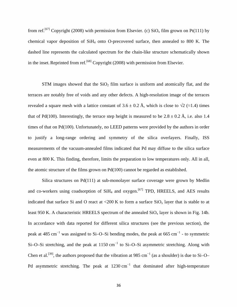
36
from ref.[67] Copyright (2008) with permission from Elsevier. (c) SiOx film grown on Pt(111) by
chemical vapor deposition of SiH4 onto O-precovered surface, then annealed to 800 K. The
dashed line represents the calculated spectrum for the chain-like structure schematically shown
in the inset. Reprinted from ref.[68] Copyright (2008) with permission from Elsevier.
STM images showed that the SiO2 film surface is uniform and atomically flat, and the
terraces are notably free of voids and any other defects. A high-resolution image of the terraces
revealed a square mesh with a lattice constant of 3.6 ± 0.2 Å, which is close to √2 (≈1.4) times
that of Pd(100). Interestingly, the terrace step height is measured to be 2.8 ± 0.2 Å, i.e. also 1.4
times of that on Pd(100). Unfortunately, no LEED patterns were provided by the authors in order
to justify a long-range ordering and symmetry of the silica overlayers. Finally, ISS
measurements of the vacuum-annealed films indicated that Pd may diffuse to the silica surface
even at 800 K. This finding, therefore, limits the preparation to low temperatures only. All in all,
the atomic structure of the films grown on Pd(100) cannot be regarded as established.
Silica structures on Pd(111) at sub-monolayer surface coverage were grown by Medlin
and co-workers using coadsorption of SiH4 and oxygen.[67] TPD, HREELS, and AES results
indicated that surface Si and O react at <200 K to form a surface SiOx layer that is stable to at
least 950 K. A characteristic HREELS spectrum of the annealed SiOx layer is shown in Fig. 14b.
In accordance with data reported for different silica structures (see the previous section), the
peak at 485 cm−1 was assigned to Si–O–Si bending modes, the peak at 665 cm−1 - to symmetric
Si–O–Si stretching, and the peak at 1150 cm−1 to Si–O–Si asymmetric stretching. Along with
Chen et al.[39], the authors proposed that the vibration at 985 cm−1 (as a shoulder) is due to Si–O–
Pd asymmetric stretching. The peak at 1230 cm−1 that dominated after high-temperature

37
annealing was taken as evidence for the formation of a long-range network of Si–O bonding at
high temperatures.
Later, this group performed similar experiments with Pt(111).[68] HREELS spectra after
low exposures of SiH4 on an O-saturated Pt(111) surface consisted of three primary peaks at 480,
800, and 1130 cm−1, similar to those modes observed in their experiments with Pd(111).
However, spectra measured after higher exposures of SiH4 showed a single dominant peak at
~750 cm−1 (Fig. 14c) indicating a different surface structure at higher Si coverage. The
following-up DFT calculations[69] for both Pd(111) and Pt(111) surfaces were focused on the low
coverage regime, hence only isolated and chain-like SiOx structures were considered. A
vibrational mode analysis showed that chain formation, as schematically shown in the inset of
Fig. 14c, may explain the experimental results on Pt(111), but not on Pd(111).[67]
3.3. Silica films on Ruthenium
Very recently, our group has initiated studies on the growth of thin silica films on
Ru(0001).[70] This substrate was previously used successfully for the growth of crystalline
CeO2(111) films despite a very large (~ 40%) mismatch between ceria and Ru lattices.[71] Among
numerous preparation recipes tested, a low temperature (~ 100 K) Si deposition onto the
3O(2×2)-Ru(0001) surface in ~ 10-7 mbar O2 and subsequent annealing at ~1200 K in ~ 10-6
mbar O2 showed the best quality. The presence of chemisorbed oxygen prevents intermixing of
Si and Ru, as judged by XPS, and supplies more reactive, i.e. atomic, oxygen species for
oxidation of the Si deposits than molecular oxygen in the gas phase. A low substrate temperature
during the Si deposition to ~100 K most likely suppresses the diffusivity of Si atoms on the
38
surface, thereby favoring the formation of two-dimensional structures prior to final oxidation at
high temperatures. The full oxidation and film ordering occurs upon high temperature annealing
in oxygen (ca. 10-6 mbar) at 1150 - 1200 K, ultimately resulting in a (2×2) LEED pattern.
At a Si coverage of about 0.5 ML (with respect to Ru(0001)), the atomically flat surface
expresses domains with a honeycomb-like structure with a ~5.5 Å periodicity.[72] The domains
are shifted by half a lattice constant with respect to each other, thus producing a network of
domain boundaries (Fig. 15a). The silica film is ~1.4 Å in apparent height with respect to
underlying support. The respective IRAS spectrum shows the principal band at 1134 cm-1 and
weaker signals at 1074, 790 and 687 cm-1 (Fig. 15b), which clearly resemble those observed for
SiO2.5/Mo(112) films (see Fig. 9). XPS spectra of the film are also very similar to that of the
Mo(112) supported film, where the O1s core level revealed two components centered at 531.3
and 529.8 eV with a similar peak separation (1.5 eV) and the intensity ratio (~3:2) as for
SiO2.5/Mo(112). Given the STM results, showing the formation of a complete overlayer with
(2×2) lattice structure, and the agreement between XPS and IRAS results for this film with those
previously reported for SiO2.5/Mo(112),[45a, 48] a similar structure for silica films over Ru(0001)
is suggested under these conditions. Namely, the film is formed by a honeycomb shaped network
of tetrahedral Si-O linkages with a 5.4 Å lattice constant, in which every Si forms one Si-O-Ru
bond and three bridging Si-O-Si bonds. (For simplicity, the Si coverage is henceforth presented
in monolayers equivalent (MLE), such that 1 MLE corresponds to a closed monolayer film).

39
Figure 15. STM image (a), IRAS (b) and O1s XPS (c) spectra of a SiO2.5/Ru(0001) film. Dashed
lines show the IRAS and XPS spectra, computed for the structural model, shown in (d), and
artificially broadened to fit the experimental spectra. (O: small black; Si: small gray; Ru: large
gray).
DFT calculations nicely corroborated the proposed structure.[72] It has turned out,
however, that among the several monolayer structures computed, only the film containing
additional oxygen atoms directly adsorbed on Ru (henceforth referred to as O(Ru) atoms) is
stable (Fig. 15d). The harmonic IRA spectrum (see Fig. 15c) simulated for the most stable
monolayer structure revealed the most intense IR-active mode at ~ 1160 cm-1, which originates
from the in-phase combination of asymmetric stretching vibrations of the Si-O-Ru linkages. The
much weaker mode at 1076 cm-1 involves combinations of symmetric O-Si-O stretching
vibrations. The bands at 820 and 677 cm-1 represent the combinations of asymmetric stretching
of Si-O-Ru linkages and O-Si-O bending modes. The positions and relative intensities of those

40
calculated bands are in good agreement with the experimental data, as is the XPS spectrum
simulated for this structure (Fig. 15c).
Figure 16. Large-scale (a) and high-resolution (inset) STM images and (b) IRAS spectrum of a
SiO2/Ru(0001) film. IRA-active vibrational modes in the structural model (c) are shown as bars
with their height proportional to the intensity. The “O-poor” structure shown in (c) may contain
additional oxygen atoms chemisorbed only to the Ru atoms, thus forming “O-rich” phases. The
(2×2) unit cell is indicated.
Increasing Si coverage up to 2 MLE resulted in no change in the surface symmetry, still
showing a (2×2) LEED pattern. However, the IRAS spectra revealed very sharp (thus indicating
good crystallinity) and intense bands at 1300 and 692 cm-1 which developed with concomitant
disappearance of the bands associated with the monolayer structure (Fig. 16b). STM inspection

41
of the prepared films showed atomically flat morphology, exposing some holes of ~ 5 Å in
apparent depth. High-resolution STM images of such structures showed again a honeycomb-like
network with a ~ 5.5 Å periodicity (inset in Fig. 16a), similar to the monolayer films (Fig. 15a).
Analysis of different structures previously considered in DFT calculations of silica films on
Mo(112)[47a] led to the suggestion that, in this case, a “bilayer” structure composed of two
monolayers linked together through bridging O atoms is formed as shown in Fig. 16c,. Since this
structure can also be obtained in two deposition-oxidation steps with 1 MLE Si each, the
transformation of the mono- into the bi-layer structure must be accompanied by breaking Si-O-
Ru bonds and creating the Si-O-Si linkages. Apparently, such a process is a thermodynamically
unfavorable in the case of the Mo(112) support. As a result, the formation of bilayer films on
Mo(112) has never been observed.
The bilayer model was examined by DFT including semi-empirical dispersion correction
(DFT+D).[70] The calculated adhesion energy of the bilayer silica film to the Ru(0001) support
was only about 3 kJ mol-1 Å-2, with the main contribution coming from the dispersion term. The
phonon spectrum, calculated for this structure, revealed two IR active modes (see Fig. 16b). The
most intense mode at 1296 cm-1 represents an in-phase combination of asymmetric Si-O-Si
stretching vibrations of the Si-O-Si linkage between two layers. The second mode at 642 cm-1 is
a combination of symmetric Si-O-Si stretching vibrations of Si-O-Si bonds nearly parallel to the
surface. Not only the positions but also the relative intensities of the vibrational bands are in very
good agreement with the experimental results.
Combined XPS/UPS and DFT studies[73] further showed that the system may exist in “O-
poor” and “O-rich” configurations, depending on the amount of O(Ru) atoms directly
chemisorbed onto the Ru(0001) surface. The presence of the O(Ru) atoms considerably lowers

42
the adhesion energy. Almost certainly, this effect is connected to the repulsive interaction
between the oxygen atoms of the silica film and the O(Ru) atoms. As a result the distance
between the silica sheet and metal support increases. The SiO2/Ru electronic states reversibly
vary with the amounts of adsorbed oxygen underneath the silica film. In principle, this opens the
possibility to tune the electronic properties of oxide/metal systems without altering the thickness
and structure of an oxide overlayer itself as discussed before for the monolayer silica films on
Mo(112).[74] Interestingly, the transition between the O-poor and O-rich states is fully reversible
via annealing and reoxidation treatments, whereas the O-rich films are much more stable in the
case of SiO2.5/Mo(112), since the O-Mo bond is much stronger than the O-Ru bond.
In order to see whether the silica film on Ru(0001) can be further grown in a layer-by-
layer mode, thicker silica films were prepared by deposition of 4 MLE Si.[72] The results were
almost independent of whether the films were prepared in one step or in two sequential 2 MLE
deposition–oxidation steps. STM images of the films revealed a smooth surface, albeit not
atomically flat. Unfortunately, attempts to achieve atomic resolution were not successful, as an
STM imaging becomes unstable for thick insulating films. As in the case of mono- and bilayer
structures, the substantial changes are observed in IRAS spectra: The intensities of the 1300 and
694 cm-1 peaks strongly decreased, and a new band developed at 1257 cm-1 with a prominent
shoulder at 1164 cm-1. The shape and position of this band are characteristic for the LO vibration
modes in bulk-like silica (see Figs. 3 and 5). It therefore appears that thicker films exhibit a
three-dimensional network of [SiO4] tetrahedra rather than the layered structure observed for
mono- and bi-layer films. In this case, the termination of the film may be ill-defined, resulting in
relatively high surface corrugation (ca. 1 Å) as measured by STM.
43
3.4. Silica films on Platinum
In order to elucidate the role of the metal support in the films’ atomic structure, silica
films were grown on Pt(111) for comparison.[75] The Pt(111) surface has a slightly larger lattice
constant, than Ru(0001), i.e., 2.77 and 2.71 Å, respectively. In addition, the film preparations on
Mo(112) and Ru(0001) include oxygen precovered surfaces prior to the Si deposition in the
oxygen ambient. In this respect, Pt as a noble metal may behave differently than the Mo and Ru
supports
The film preparation was basically the same as that on Ru(0001). Upon Si deposition, a
new Pt 3d state was observed by XPS as a shoulder at low binding energy, thus indicating Pt-Si
surface intermixing, which was not observed on a Ru support most likely due to the presence of a
3O(2×2) ad-layer that oxidizes the first incoming Si atoms. This state disappeared upon
subsequent oxidation at high temperatures. The XPS spectra of the finally prepared films were
very similar to those obtained for the bilayer film on Ru(0001), except that the ∼530 eV signal
for the O1s level (see e.g. Fig. 15c) was less prominent on Pt(111). Since this signal is associated
with oxygen atoms directly adsorbed on the metal surface underneath a film and/or in holes
exposing a metal support in the not fully covered films, the difference can easily be attributed to
the lower affinity of Pt(111) toward oxygen as compared to Ru(0001).
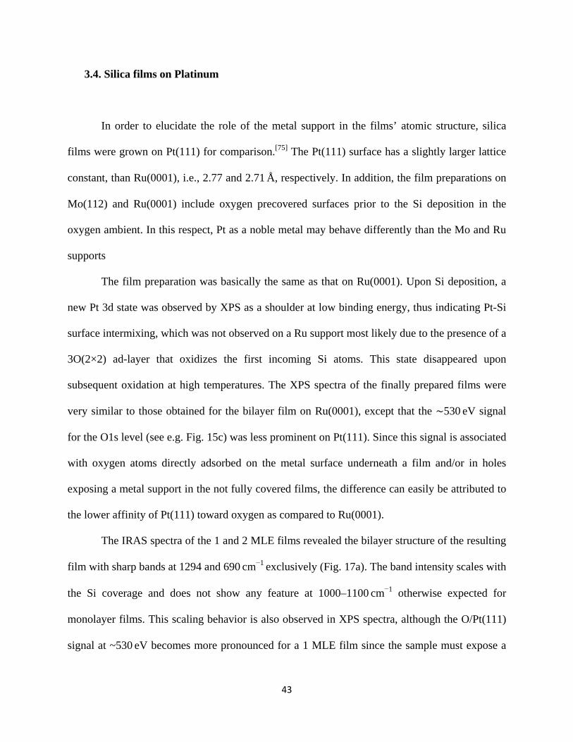
The IRAS spectra of the 1 and 2 MLE films revealed the bilayer structure of the resulting
film with sharp bands at 1294 and 690 cm−1 exclusively (Fig. 17a). The band intensity scales with
the Si coverage and does not show any feature at 1000–1100 cm−1 otherwise expected for
monolayer films. This scaling behavior is also observed in XPS spectra, although the O/Pt(111)
signal at ~530 eV becomes more pronounced for a 1 MLE film since the sample must expose a
44
larger fraction of the Si-free, O-covered Pt surface. The results, therefore, indicate the formation
of exclusively bilayer films under the conditions applied. The respective STM images (Figs.
17(b-d) do not reveal an ordered, crystalline overlayer, but rather the formation of a two-
dimensional vitreous silica film (see details in the next section).
The apparent thickness of the bilayer silica films on Pt(111), i.e. on the order of 2 Å, is
considerably lower than ∼5 Å measured for the bilayer films on Ru(0001), which is in turn very
close to the geometrical film thickness determined by DFT. Such behavior can be assigned to the
electronic effects frequently observed for STM imaging of metal-oxide systems, which, in
addition, may be bias- and polarity-dependent. As a side note, this finding again points to the
general conclusion that only a multi-technique approach allows for determination of the atomic
structure of metal supported thin oxide films.
Figure 17. IRAS spectra (a) and STM images (b,c) of SiO2 films grown on Pt(111) at 1 and 2
MLE coverages as indicated. (d) High resolution STM image of a (vitreous) silica bilayer
observed at both coverages.
45
Interestingly, the silica islands formed at sub-monolayer coverages on Pt(111) are
bridged by narrow stripes of the same height running primarily along the principal
crystallographic directions of Pt(111). Most of these “bridges” are ∼7 Å in width, although ∼4 Å
and ∼10 Å wide lines were observed as well. To some extent, these stripes resemble one-
dimensional silica rows formed at low Si coverage on Mo(112) (see Fig. 13), although its atomic
structure has not yet be identified.
3.5. Crystalline and vitreous films
In the course of preparation of the bilayer silica films on Ru(0001) it was realized that
LEED patterns sometimes show both (2×2) spots and a diffraction ring representing the same
lattice constant. On Pt(111), only a (2×2) diffraction ring was observed under the conditions
studied. The diffraction rings are characteristic for randomly oriented crystallites such as those
observed in powders, which could be identified as vitreous (amorphous, glassy) silica.
One of the first proposed theories of glasses, the so-called “crystallite” theory envisaged
glass as an aggregate of extremely small crystals (“crystallites”) with fairly sharp external
boundaries, which are connected with each other in a random way. (Although it is generally
attributed to Lebedev’s paper published in 1921, it appears that the crystallite theory was in fact
first mentioned in 1835 by Frankenheim).[3] Later, in his famous paper in 1932, Zachariasen[76]
proposed that the glass consists of a three-dimensional random network (RN) of tetrahedral SiO4
molecular units. One of the first x-ray diffraction (XRD) studies of silica glasses by Warren[77]

46
favored the RN model, which accounts satisfactorily for the observed x-ray as well as neutron
radial distribution functions of vitreous silica.[3, 78] Neighboring SiO4 units in the solid are linked
at the vertices by sharing a common or bridging oxygen atom. Although the SiO4 units
themselves are thought to be effectively regular in shape, the mutual orientation of adjacent units
can vary widely throughout the glass in a manner which is apparently random in character,
subject only to the restriction that the network be continuously connected. There were several
attempts to find a compromise between the two models, which differ essentially in the size of the
short-range ordering (15–20 Å in the crystallite theory versus 7–8 Å in the RN theory). For
example, Görlich et al. [79] proposed the “sintered powder model”, where vitreous silica forms a
loose and randomly mixed texture of high-temperature α-cristobalite; between the domains there
exists disorder. Another model includes a continuous random network, but of deformed six-
membered rings (see, for example, ref. [5]) These models are schematically depicted in Fig. 18.

47
Figure 18. Schematic representations of structural models for vitreous silica: (a) crystallite; (b)
random network; (c) ordered domains; (d) distorted network.
Nonetheless, none of these models was justified with any imaging (microscopy)
technique. Although modern transmission and scanning electron microscopes possess atomic
resolution (particularly when aberration correction is applied) to resolve atomic spacings in
disordered systems, these techniques commonly produce images which are 2D projections of 3D
structures. In this context, the thin films, which are well-suited materials for STM and AFM, can
be employed to directly visualize the atomic structure of the amorphous silica as has been
recently demonstrated in our own laboratories.[75, 80]
Figure 19. (a) High resolution STM image (8 nm × 3 nm) of an amorphous silica film on
Ru(0001). (b) The same image superimposed with a model, where O atoms are imaged as
protrusions forming N-membered rings (N = 4-8). (c-e) The ring size and angle distributions in
the silica film derived from STM images. (f,g) Pair correlation function obtained by STM in
comparison with X-ray and neutron radial distribution factors of vitreous silica.[80]
48
Figure 19a shows an atomically resolved STM image of a disordered silica bilayer film
on Ru(0001).[80] The polygonal network in the surface plane can be clearly recognized. The
protrusions are grouped in triangles, and as such they may be assigned to three of four O atoms
in the SiO4 units. The position of the Si atoms may then be calculated. Figure 19b displays the
same STM image superimposed with the positions of the Si and O atoms. A histogram revealed
that the ring size, measured as a number (N) of members forming the ring, varies between N = 4
and 9, with a maximum at N = 6 that corresponds to the pure crystalline structure (Fig. 19c). The
intra-tetrahedral Si-O-Si angle (Fig. 19d) showed a symmetric distribution with an average of
110° (+- 10°) which fits well the 109.5° angle in a regular tetrahedron. The histogram of the Si-
O-Si angles (Fig. 19e) revealed a peak at 141°, which is, again, in nice agreement to the average
angle of 143° obtained for vitreous silica by 29Si magic-angle spinning nuclear magnetic
resonance spectroscopy[81] and 144° by XRD.[82] A sharp edge at 145° manifests the flat and 2D
character of the silica film. (Note, that in this analysis the structural information about the z-
direction (normal to the surface) was taken from the previous DFT calculations of the crystalline
bilayer film, see Fig. 16).[70]
From the STM images, the pair correlation function was obtained using X-ray and
neutron scattering factors of Si and O according to the formula from refs.[78, 83], which were
normalized by r−1 to account for the 2D structure of the film. The peak positions and their
relative intensities are shown in Figs. 19(f,g) which reveal good agreement with those obtained
by XRD and neutron scattering. The small deviations are not surprising since the silica bilayer
film on Ru(0001) is atomically flat in contrast to 3D silica glasses used for comparison.

49
Figure 20. High resolution STM image (10 nm × 5 nm) of a silica bilayer film, showing
crystalline (left portion) and vitreous (right portion) phases coexisting.
Furthermore, direct STM imaging of the bilayer silica films allows one to address
structural transformation between crystalline and vitreous phases.[84] Figure 20 displays an STM
image, where the crystalline phase smoothly transforms into the vitreous one without any
“defects” in terms of unsaturated bonds or different bonding arrangements beyond corner-
sharing [SiO4] tetrahedra. The transition region extends no more than 1.5 nm, in which two
adjacent 6-membered rings “disproportionate” into the 5- and 7-membered rings until the
distribution of a pure vitreous ring network is reached.
Analysis of bilayer films prepared under different conditions by varying annealing time,
temperature, oxygen pressure, etc. showed that the rate of sample cooling after the high-
temperature oxidation step may play the key role in controlling crystallinity of the films on
Ru(0001). Note also, that once formed, the vitreous film, prepared by fast cooling, cannot be
transformed into the crystalline state by re-oxidation of the same sample followed by slow
cooling, and vice versa. Applying higher temperatures leads to film decomposition. These
findings agree well with the very high barrier for crystal-to-glassy transformation predicted by
the DFT calculations.[80]The influence of the cooling rate has been examined also for the

50
monolayer silica films on Ru(0001) that showed essentially no effect. Most likely, the strong Si-
O-Ru bonds drive the monolayer film to be in registry with a Ru(0001) substrate, ultimately
resulting in the long-range ordering of the films.
Very recently Huang et al.[85] reported TEM and STEM studies of ultrathin silica films
accidently synthesized during the chemical vapor deposition growth of graphene. Image analysis
showed close similarities to the results of Lichtenstein et al.[80] Both studies demonstrated that
bilayer silica films, weakly bound to an underlying support, provide the unique possibility to
study silicate glasses and the glass transition with atomic precision in real space and, eventually,
in time, for example, employing low energy electron microscopy.
3.6. The support effects: General trend
We are now in position to compare the structures of ultra-thin silica films formed on
three different supports (Mo, Ru, Pt). The principal structure of the silica films can be identified
by IRA spectroscopy, as each structure shows a characteristic vibrational band, i.e., ~1100 cm-1
for monolayer films, ~1300 cm-1 for the bilayer structures, and ~ 1250 cm-1 for the bulk-like
silica films.
On Mo(112), silica grows only as a monolayer strongly bonded to Mo via the Si-O-Mo
linkages. On Ru(0001), both monolayer, bonded through the Si-O-Ru linkage, and bilayer films,
weakly bonded to Ru, are observed, depending on the Si coverage. Irrespective of the Si
coverage, only bilayer films grew on Pt(111). There is an obvious trend in the principal structure
which correlates with the oxygen affinity to the metal support. Indeed, heats of dissociative
adsorption of oxygen are of −544, −220, and −133 kJ/mole for Mo, Ru, and Pt, respectively.
51
Therefore, the SiO-Mo bond is much stronger than the SiO-Pt bond, and it will favor the
monolayer structure, whereas on Pt(111) silica forms a “closed shell” bilayer structure
terminated by the fully saturated oxygen layer on either side. Ru(0001) exhibits intermediate
properties and allows formation of both mono- and bi-layer structures.
Another issue relates to the role of the lattice mismatch between a silica film and a metal
substrate, which is obviously different for the three metals studied. The lattice constant of the
unsupported, free-standing silica bilayer is computed to be 5.24 - 5.32 Å[45b, 59]. When supported
on Ru(0001) (lattice constant 2.71 Å) and Pt(111) (lattice constant 2.77 Å), the most “natural”
structure for the silica film to accommodate these metal supports is the (2×2) structure, resulting
in a periodicity of 5.42 and 5.54 Å, respectively, that is indeed observed by LEED and STM.
From this point of view, Ru(0001) is better suited than Pt(111) as the lattice mismatch is smaller.
In principle, this may explain why only amorphous films were so far obtained on Pt(111).
4. Summary and concluding remarks
Based on the results available to date, one may safely conclude that ultrathin silica films
on Mo(112), Ru(0001) and, to lesser extent, on Pt(111) seem to be the only silica films whose
structures are established at the atomic level. The results show that the metal-oxygen bond
strength plays the decisive role. Metals with high oxygen adsorption energy favor the formation
of crystalline films as a monolayer network of corner-sharing [SiO4] tetrahedra with SiO2.5
composition. Noble metals primarily form bilayer SiO2 sheets. The metals with intermediate
energies may form either of the structures. In contrast to monolayer films, the bilayer films exist
in both crystalline and amorphous forms. These two-dimensional silica films provide unique
52
opportunities to directly visualize the atomic structure of vitreous silica. The results open a new
playground for studying the fundamental aspects of glasses such as the order-disorder transition.
In addition, such systems also open up opportunities to look for model systems involving silica
films in the area of catalysis, e.g. as a support anchoring specific metal species. Finally, doping
these silica films with Al allowed preparation of aluminosilicate films which can be considered
as adequate model systems for zeolite surfaces.[86]
The results reveal a structural complexity and diversity of the silica overlayers on metals
and provide further steps towards our understanding of the atomic structure, structural dynamics
and physical and chemical properties of silica.
Acknowledgements
We thank all our co-workers, whose names appear in the cited papers, for their
tremendous work in the laboratories. We acknowledge collaboration with the groups of J. Sauer
(Humboldt University in Berlin) and G. Pacchioni (University Milano) as well as fruitful
discussions with D.W. Goodman and his coworkers (Texas A & M University). This work has
been supported by Fonds der Chemischen Industrie and Deutsche Forschungsgemeinschaft.
53
References
[1] D. A. Muller, T. Sorsch, S. Moccio, F. H. Baumann, K. Evans-Lutterodt, G. Timp,
Nature 1999, 399, 758-761.
[2] J. T. Yates Jr, Surface Science 2004, 565, 103-106.
[3] A. C. Wright, Journal of Non-Crystalline Solids 1994, 179, 84-115.
[4] A. K. A. Pryde, M. T. Dove, Physics and Chemistry of Minerals 1998, 26, 171-179.
[5] D. Keen, M. Dove, Journal of Physics: Condensed Matter 1999, 11, 9263.
[6] a) C. R. Helms, E. H. Poindexter, Reports on Progress in Physics 1994, 57, 791; b) K.
Hirose, H. Nohira, K. Azuma, T. Hattori, Progress in Surface Science 2007, 82, 3-54.
[7] J. Derrie, M. Commandré, Surface Science 1982, 118, 32-46.
[8] N. Cabrera, N. F. Mott, Rep. Prog. Phys. 1948, 12, 163.
[9] a) J. A. Schaefer, W. Göpel, Surface Science 1985, 155, 535-552; b) H. Ibach, H. D.
Bruchmann, H. Wagner, Applied Physics A Solids and Surfaces 1982, 29, 113-124.
[10] P. A. Thiry, M. Liehr, J. J. Pireaux, R. Sporken, R. Caudano, J. P. Vigneron, A. A. Lucas,
Journal of Vacuum Science & Technology B: Microelectronics and Nanometer Structures
1985, 3, 1118-1121.
[11] J. Finster, D. Schulze, F. Bechstedt, A. Meisel, Surface Science 1985, 152-153, 1063-
1070.
[12] P. J. Grunthaner, M. H. Hecht, F. J. Grunthaner, N. M. Johnson, Journal of Applied
Physics 1987, 61, 629-638.
[13] W. Braun, H. Kuhlenbeck, Surface Science 1987, 180, 279-288.
54
[14] S. Ichimura, A. Kurokawa, K. Nakamura, H. Itoh, H. Nonaka, K. Koike, Thin Solid Films
2000, 377–378, 518-524.
[15] a) J. M. Shaw, N. Herbots, Q. B. Hurst, D. Bradley, R. J. Culbertson, V. Atluri, K. T.
Queeney, Journal of Applied Physics 2006, 100, 104109-104104; b) N. Herbots, J. M.
Shaw, Q. B. Hurst, M. P. Grams, R. J. Culbertson, D. J. Smith, V. Atluri, P. Zimmerman,
K. T. Queeney, Materials Science and Engineering B: Solid-State Materials for
Advanced Technology 2001, 87, 303-316.
[16] N. Herbots, J. M. Shaw, Q. B. Hurst, M. P. Grams, R. J. Culbertson, D. J. Smith, V.
Atluri, P. Zimmerman, K. T. Queeney, Materials Science and Engineering: B 2001, 87,
303-316.
[17] C. T. Kirk, Physical Review B 1988, 38, 1255-1273.
[18] D. W. Berreman, Physical Review 1963, 130, 2193-2198.
[19] K. T. Queeney, M. K. Weldon, J. P. Chang, Y. J. Chabal, A. B. Gurevich, J. Sapjeta, R.
L. Opila, Journal of Applied Physics 2000, 87, 1322-1330.
[20] F. Giustino, A. Pasquarello, Physical Review Letters 2005, 95, 187402.
[21] K. T. Queeney, Y. J. Chabal, M. K. Weldon, K. Raghavachari, Physica status solidi (a)
1999, 175, 77-88.
[22] G. Feliciano, B. Angelo, P. Alfredo, Journal of Physics: Condensed Matter 2005, 17,
S2065.
[23] C. Raynaud, Journal of Non-Crystalline Solids 2001, 280, 1-31.
[24] U. Starke, J. Schardt, J. Bernhardt, K. Heinz, Journal of Vacuum Science and
Technology A 1999, 17, 1688-1692.
55
[25] J. Bernhardt, J. Schardt, U. Starke, K. Heinz, Applied Physics Letters 1999, 74, 1084-
1086.
[26] W. Lu, P. Krüger, J. Pollmann, Physical Review B 2000, 61, 13737-13744.
[27] M. Hollering, F. Maier, N. Sieber, M. Stammler, J. Ristein, L. Ley, A. P. J. Stampfl, J. D.
Riley, R. C. G. Leckey, F. P. Leisenberger, F. P. Netzer, Surface Science 1999, 442, 531-
542.
[28] B. Hornetz, H. J. Michel, J. Halbritter, J. Mater. Res. 1994, 9, 3088-3094.
[29] H. Tsuchida, I. Kamata, K. Izumi, Applied Surface Science 1997, 117–118, 225-229.
[30] a) H. P. Bonzel, A. M. Franken, G. Pirug, Surface Science 1981, 104, 625-642; b) P.
Légaré, L. Hilaire, G. Maire, Surface Science 1984, 141, 604-616.
[31] K. E. Keck, B. Kasemo, Surface Science 1986, 167, 313-330.
[32] C. S. Ko, R. J. Gorte, Surface Science 1985, 155, 296-312.
[33] a) X. Xu, D. W. Goodman, Applied Physics Letters 1992, 61, 774-776; b) X. Xu, D. W.
Goodman, Surface Science 1993, 282, 323-332.
[34] K. Luo, D. Y. Kim, D. W. Goodman, Journal of Molecular Catalysis A: Chemical 2001,
167, 191-198.
[35] J. W. He, X. Xu, J. S. Corneille, D. W. Goodman, Surface Science 1992, 279, 119-126.
[36] T. Schroeder, PhD Thesis 2001.
[37] a) T. Schroeder, M. Adelt, B. Richter, M. Naschitzki, M. Baumer, H. J. Freund, Surface
Review and Letters 2000, 7, 7-14; b) T. Schroeder, M. Adelt, B. Richter, M. Naschitzki,
M. Bäumer, H. J. Freund, Microelectronics Reliability 2000, 40, 841-844; c) T.
Schroeder, A. Hammoudeh, M. Pykavy, N. Magg, M. Adelt, M. Bäumer, H. J. Freund,

56
Solid-State Electronics 2001, 45, 1471-1478; d) T. Schroeder, J. B. Giorgi, M. Bäumer,
H. J. Freund, Physical Review B 2002, 66, 165422.
[38] a) Y. D. Kim, T. Wei, D. W. Goodman, Langmuir 2002, 19, 354-357; b) S. Wendt, Y. D.
Kim, D. W. Goodman, Progress in Surface Science 2003, 74, 141-159; c) Y. D. Kim, J.
Stultz, T. Wei, D. W. Goodman, The Journal of Physical Chemistry B 2002, 107, 592-
596.
[39] M. S. Chen, A. K. Santra, D. W. Goodman, Physical Review B 2004, 69, 155404.
[40] D. Ricci, G. Pacchioni, Physical Review B 2004, 69, 161307.
[41] B. K. Min, W. T. Wallace, D. W. Goodman, The Journal of Physical Chemistry B 2004,
108, 14609-14615.
[42] A. K. Santra, B. K. Min, D. W. Goodman, Surface Science 2002, 515, L475-L479.
[43] E. Ozensoy, B. K. Min, A. K. Santra, D. W. Goodman, The Journal of Physical
Chemistry B 2004, 108, 4351-4357.
[44] S. Wendt, E. Ozensoy, T. Wei, M. Frerichs, Y. Cai, M. S. Chen, D. W. Goodman,
Physical Review B 2005, 72, 115409.
[45] a) J. Weissenrieder, S. Kaya, J. L. Lu, H. J. Gao, S. Shaikhutdinov, H. J. Freund, M.
Sierka, T. K. Todorova, J. Sauer, Physical Review Letters 2005, 95, 076103; b) L.
Giordano, D. Ricci, G. Pacchioni, P. Ugliengo, Surface Science 2005, 584, 225-236.
[46] S. Kaya, J. Weissenrieder, D. Stacchiola, T. K. Todorova, M. Sierka, J. Sauer, S.
Shaikhutdinov, H. J. Freund, Surface Science 2008, 602, 3338-3342.
[47] a) T. K. Todorova, M. Sierka, J. Sauer, S. Kaya, J. Weissenrieder, J. L. Lu, H. J. Gao, S.
Shaikhutdinov, H. J. Freund, Physical Review B 2006, 73, 165414; b) T. K. Todorova, M.
57
Sierka, J. Sauer, S. Kaya, J. Weissenrieder, J. L. Lu, H. J. Gao, S. Shaikhutdinov, H. J.
Freund, Physical Review B 2006, 73, 249902.
[48] S. Kaya, M. Baron, D. Stacchiola, J. Weissenrieder, S. Shaikhutdinov, T. K. Todorova,
M. Sierka, J. Sauer, H. J. Freund, Surface Science 2007, 601, 4849-4861.
[49] T. K. Todorova, M. Sierka, J. Sauer, S. Kaya, J. Weissenrieder, J. L. Lu, H. J. Gao, S.
Shaikhutdinov, H. J. Freund, Physical Review B 2006, 73.
[50] M. Sierka, Progress in Surface Science 2010, 85, 398-434.
[51] M. Sierka, T. K. Todorova, S. Kaya, D. Stacchiola, J. Weissenrieder, J. Lu, H. Gao, S.
Shaikhutdinov, H.-J. Freund, J. Sauer, Chemical Physics Letters 2006, 424, 115-119.
[52] I. N. Yakovkin, Surface Review and Letters 2005, 12, 449-456.
[53] M. Chen, D. W. Goodman, Surface Science 2006, 600, L255-L259.
[54] J. L. Lu, S. Kaya, J. Weissenrieder, T. K. Todorova, M. Sierka, J. Sauer, H. J. Gao, S.
Shaikhutdinov, H. J. Freund, Surface Science 2006, 600, L164-L168.
[55] a) L. Giordano, D. Ricci, G. Pacchioni, P. Ugliengo, Surface Science 2007, 601, 588-590;
b) M. Chen, D. W. Goodman, Surface Science 2007, 601, 591-593.
[56] a) J. Seifert, D. Blauth, H. Winter, Physical Review Letters 2009, 103, 017601; b) J.
Seifert, M. Busch, A. Schüller, D. Blauth, S. Wethekam, H. Winter, Surface and
Interface Analysis 2010, 42, 1575-1580; c) J. Seifert, A. Schüller, H. Winter, R.
Włodarczyk, J. Sauer, M. Sierka, Physical Review B 2010, 82, 035436; d) J. Seifert, H.
Winter, Surface Science 2009, 603, L109-L112.
[57] T. Kinoshita, S. Mizuno, Surface Science 2011, 605, 1209-1213.
[58] G. M. Rignanese, A. De Vita, J. C. Charlier, X. Gonze, R. Car, Physical Review B 2000,
61, 13250-13255.
58
[59] C. Freysoldt, P. Rinke, M. Scheffler, Physical Review Letters 2007, 99, 086101.
[60] U. Martinez, L. Giordano, G. Pacchioni, The Journal of Physical Chemistry B 2006, 110,
17015-17023.
[61] S. Wendt, M. Frerichs, T. Wei, M. S. Chen, V. Kempter, D. W. Goodman, Surface
Science 2004, 565, 107-120.
[62] S. Kaya, J. Weissenrieder, D. Stacchiola, S. Shaikhutdinov, H. J. Freund, The Journal of
Physical Chemistry C 2006, 111, 759-764.
[63] J. Yang, E. G. Wang, Physical Review B 2006, 73, 035406.
[64] D. J. Stacchiola, M. Baron, S. Kaya, J. Weissenrieder, S. Shaikhutdinov, H. J. Freund, J.
Freund, Applied Physics Letters 2008, 92, 011911- 011913.
[65] M. Kundu, Y. Murata, Applied Physics Letters 2002, 80, 1921-1923.
[66] Z. Zhang, Z. Jiang, Y. Yao, D. Tan, Q. Fu, X. Bao, Thin Solid Films 2008, 516, 3741-
3746.
[67] D. C. Kershner, J. W. Medlin, Surface Science 2008, 602, 786-794.
[68] D. C. Kershner, W. Zhang, J. Will Medlin, Surface Science 2008, 602, 3225-3231.
[69] D. C. Kershner, M. P. Hyman, J. W. Medlin, Surface Science 2008, 602, 3603-3610.
[70] D. Loeffler, J. J. Uhlrich, M. Baron, B. Yang, X. Yu, L. Lichtenstein, L. Heinke, C.
Buechner, M. Heyde, S. Shaikhutdinov, H. J. Freund, R. Wlodarczyk, M. Sierka, J.
Sauer, Physical Review Letters 2010, 105, 146104.
[71] a) D. R. Mullins, P. V. Radulovic, S. H. Overbury, Surface Science 1999, 429, 186-198;
b) J. L. Lu, H. J. Gao, S. Shaikhutdinov, H. J. Freund, Surface Science 2006, 600, 5004-
5010.

59
[72] B. Yang, W. E. Kaden, X. Yu, J. A. Boscoboinik, Y. Martynova, L. Lichtenstein, M.
Heyde, M. Sterrer, R. Wlodarczyk, M. Sierka, J. Sauer, S. Shaikhutdinov, H.-J. Freund,
Physical Chemistry Chemical Physics 2012.
[73] R. Włodarczyk, M. Sierka, J. Sauer, D. Löffler, J. J. Uhlrich, X. Yu, B. Yang, I. M. N.
Groot, S. Shaikhutdinov, H. J. Freund, Physical Review B 2012, 85, 085403.
[74] a) U. Martinez, L. Giordano, G. Pacchioni, The Journal of Chemical Physics 2008, 128,
164707-164708; b) S. Ulrich, N. Nilius, H.-J. Freund, U. Martinez, L. Giordano, G.
Pacchioni, Physical Review Letters 2009, 102, 016102.
[75] X. Yu, B. Yang, J. A. Boscoboinik, S. Shaikhutdinov, H.-J. Freund, Applied Physics
Letters 2012, 100, 151608-151604.
[76] W. H. Zachariasen, Journal of the American Chemical Society 1932, 54, 3841-3851.
[77] B. E. Warren, Journal of the American Ceramic Society 1934, 17, 249-254.
[78] R. J. Bell, P. Dean, Philosophical Magazine 1972, 25, 1381-1398.
[79] E. Görlich, K. Błaszczak, G. Sieminska, Journal of Materials Science 1974, 9, 1926-
1932.
[80] L. Lichtenstein, C. Büchner, B. Yang, S. Shaikhutdinov, M. Heyde, M. Sierka, R.
Włodarczyk, J. Sauer, H.-J. Freund, Angewandte Chemie International Edition 2012, 51,
404-407.
[81] L. F. Gladden, T. A. Carpenter, S. R. Elliott, Philosophical Magazine Part B 1986, 53,
L81-L87.
[82] R. L. Mozzi, B. E. Warren, Journal of Applied Crystallography 1969, 2, 164-172.
[83] L. F. Gladden, Journal of Non-Crystalline Solids 1990, 119, 318-330.
[84] L. Lichtenstein, M. Heyde, H. J. Freund, Phys. Rev. Lett. 2012, 109, 10601
60
[85] P. Y. Huang, S. Kurasch, A. Srivastava, V. Skakalova, J. Kotakoski, A. V.
Krasheninnikov, R. Hovden, Q. Mao, J. C. Meyer, J. Smet, D. A. Muller, U. Kaiser,
Nano Letters 2012, 12, 1081-1086.
[86] J. A. Boscoboinik, X. Yu, B. Yang, F. D. Fischer, R. Włodarczyk, M. Sierka, S.
Shaikhutdinov, J. Sauer, H.-J. Freund, Angewandte Chemie International Edition 2012,
51, 6005-6008.