PWM8 DataSheet
14
Cypr ess Semi condu ctor Corpo ratio n • 198 Champion Court • SanJose , CA 95134-1709 • 408-943-2600 Document Number: 001-13581 Rev. *K Revised November 24, 201 1 8-Bit Pulse Width Modulator Datasheet PWM8 V 2.60 001-13581 Rev. *K 8-Bit Pulse Width Modulator Copyright © 2000-201 1 Cypress Semicon ductor Corporation. All Ri ghts Reserved. For one or more fully configured, functional example projects that use this user module go to www.cypress.com/psocexampleprojects . Features and Overview 8 -bit general purpose pulse width modulator uses one PSoC block Source clock rates up to 48 MHz Automatic reload of period for each pulse cycle Programmable pulse width Input enables/disables continuous counter operation Interrupt option on rising edge of the output or terminal count The 8-bit PWM User Module is a pulse width modulator with programmable period and pulse width. The clock and enable signals can be sel ected from several sourc es. The output signal can be routed to a pin or to one of the global output buses, for internal use by other user modules. An interrupt can be programmed to trigger on the rising edge of the output or when the counter reaches the terminal count condition. Fi gure 1. PWM Blo ck Diagr am, Dat a Pa th width n = 8 Functional Description The PWM User Module employs one digital PSoC block for 8 bits to the total resolution. Resources PSoC ® Blocks API Memory (Bytes) Pins (per External I/O) Digital Analog CT Analog SC flash RAM CY8C29/27/24/22/21xxx, CY8C23x33, CY7C64215/603xx, CYWUSB6953, CY8CLED02/04/08/16, CY8CLED0xD, CY8CLED0xG , CY8CTST110, CY8CTMG110, CY8CTST120, CY8CTMG120, CY8CTMA120, CY8CTMA140, CY8C21x45, CY8C22x45, CY8CTMA30xx, CY8C28x45, CY8CPLC20, CY8CLED16P01, CY8C28xxx, CY8C21x12 8-bit 1 0 0 67 0 1
Transcript of PWM8 DataSheet
8/2/2019 PWM8 DataSheet
http://slidepdf.com/reader/full/pwm8-datasheet 1/14
Cypress Semiconductor Corporation • 198 Champion Court • San Jose, CA 95134-1709 • 408-943-2600
Document Number: 001-13581 Rev. *K Revised November 24, 2011
8-Bit Pulse Width Modulator Datasheet PWM8 V 2.60001-13581 Rev. *K 8-Bit Pulse Width Modulator
Copyright © 2000-2011 Cypress Semiconductor Corporation. All Rights Reserved.
For one or more fully configured, functional example projects that use this user module go towww.cypress.com/psocexampleprojects.
Features and Overview
8 -bit general purpose pulse width modulator uses one PSoC block
Source clock rates up to 48 MHz
Automatic reload of period for each pulse cycle
Programmable pulse width
Input enables/disables continuous counter operation
Interrupt option on rising edge of the output or terminal count
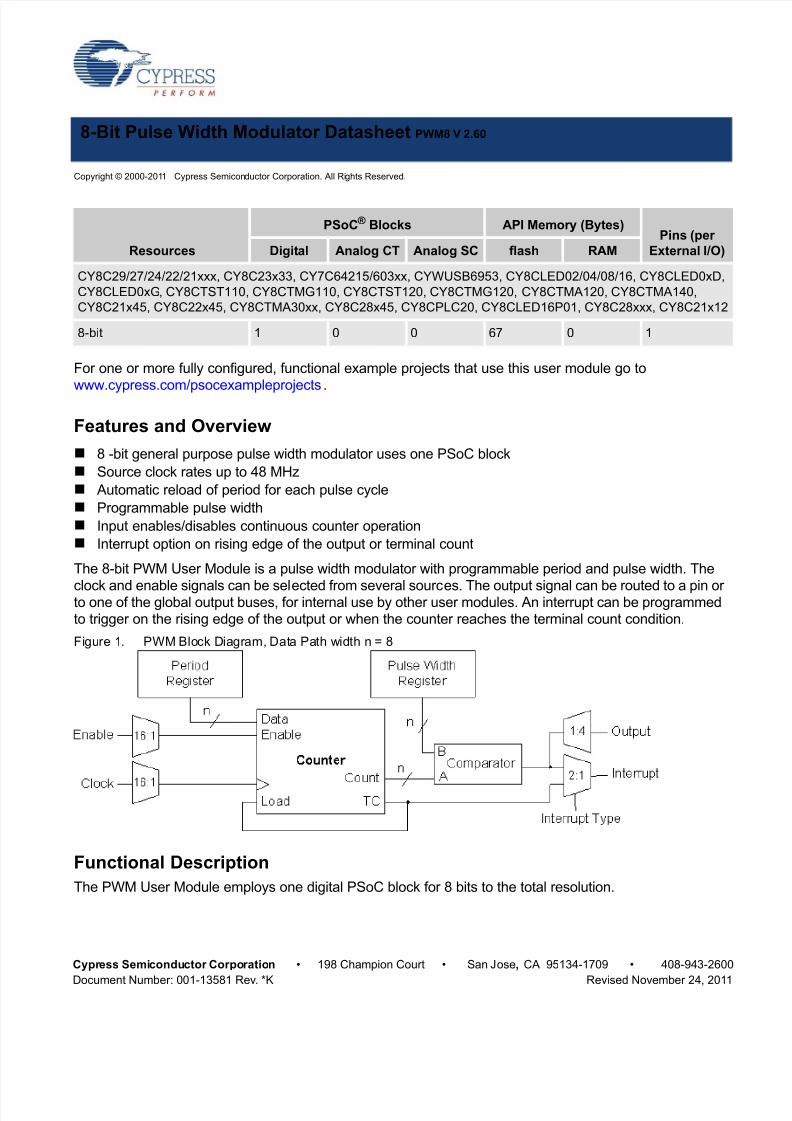
The 8-bit PWM User Module is a pulse width modulator with programmable period and pulse width. The
clock and enable signals can be selected from several sources. The output signal can be routed to a pin or to one of the global output buses, for internal use by other user modules. An interrupt can be programmedto trigger on the rising edge of the output or when the counter reaches the terminal count condition.
Figure 1. PWM Block Diagram, Data Path width n = 8
Functional Description
The PWM User Module employs one digital PSoC block for 8 bits to the total resolution.
Resources
PSoC ® Blocks API Memory (Bytes)Pins (per
External I/O)Digital Analog CT Analog SC flash RAM
CY8C29/27/24/22/21xxx, CY8C23x33, CY7C64215/603xx, CYWUSB6953, CY8CLED02/04/08/16, CY8CLED0xD,
CY8CLED0xG, CY8CTST110, CY8CTMG110, CY8CTST120, CY8CTMG120, CY8CTMA120, CY8CTMA140,
CY8C21x45, CY8C22x45, CY8CTMA30xx, CY8C28x45, CY8CPLC20, CY8CLED16P01, CY8C28xxx, CY8C21x12
8-bit 1 0 0 67 0 1
8/2/2019 PWM8 DataSheet
http://slidepdf.com/reader/full/pwm8-datasheet 2/14
8-Bit Pulse Width Modulator
Document Number: 001-13581 Rev. *K Page 2 of 14
The PWM API provides functions that may be called from C and assembly to stop and start operation of the Counter and to read and write the various data registers. The data register values may also beestablished by using the Device Editor. Once started, the Count register is decremented on the rising edgeof each clock cycle at which the active-high enable input signal is asserted. The Count register is reloadedwith the value in the Period register on the risking clock edge following a terminal count (when the countregister reaches zero).
The Period register can be modified with a new value at anytime. When the PWM is stopped, writing avalue to the Period register also changes the value in the Count register. While the PWM is running,writing the Period register does not update the Count register with the new Period value until the nextreload occurs, following terminal count. Because the terminal count is reached when the count is zero, theperiod of operation and of the output signal is greater by 1 than the value stored in the Period register. Thefollowing equations relate the output of the PWM to the input clock and the value in the Period register.
TOUT = (PeriodValue+1)/FCLOCK
FOUT = FCLOCK/(PeriodValue+1) Equation 1
Where F OUT is The output frequency of the PWM, T OUT is the output period of the PWM, F CLOCK is
frequency of the input clock, and PeriodValue is the value entered for the period.The PWM asserts its output low when stopped. While running, a comparator controls the duty cycle of theoutput signal. During every clock cycle, this comparator tests the values of the Count register against thatof the PulseWidth register, performing a "Less Than" or "Less Than Or Equal" test depending on an optionselected using the Device Editor. The PWM asserts the active-high truth value of the comparison at therising edge of the clock following the period in which the comparison is made. The ratio between thePulseWidth value and the period sets the duty cycle of the output waveform. The duty cycle ratio can becomputed using this equation.
For PulseWidthValue < PeriodValue:
Equation 2
For PulseWidthValue >= PeriodValue
DutyCycle = 100%
The following table summarizes some special output signal conditions based on the setting of the Period,the PulseWidth, and the comparison operation.
Table 1. Counter Special Output Signal Conditions
Period Register Value Compare Type PulseWidth Register ValueRatio of Pulse-Width High Time
to Period
0 Don’t Care > 0 1.0
0 ≤ 0 1.0
0 < 0 0.0
> 0 ≤ 0 1/(Period+1)
8/2/2019 PWM8 DataSheet
http://slidepdf.com/reader/full/pwm8-datasheet 3/14
8-Bit Pulse Width Modulator
Document Number: 001-13581 Rev. *K Page 3 of 14
The value of the PulseWidth register may be set using the Device Editor or during run time using the API.No buffering of the PulseWidth register is provided in the way the Period register buffers the Count register before terminal count. Therefore, changes to the PulseWidth register affect the compare output on thenext clock cycle, rather than following terminal count. This can produce periods with multiple pulses.
In the CY8C29/27/24/22/21xxx, CY8C23x33, CY7C64215/603xx, CYWUSB6953, CY8CLED02/04/08/16,CY8CLED03D/04D, CY8CTST110, CY8CTMG110, CY8CTST120, CY8CTMG120, CY8CTMA120,CY8C21x45, CY8C22x45, CY8CTMG300, CY8CTST300, CY8CTMA300, CY8CTMA301,CY8CTMA301D, CY8C28x45, CY8CPLC20, CY8CLED16P01, CY8C28xxx device families, the PWM
User Module provides the terminal count signal as an auxiliary output. This active-high signal is assertedon the rising edge of the clock cycle following terminal count in which the Count register is loaded from thePeriod register.
An interrupt can be programmed to occur on terminal count or when the compare becomes true. Thecomparator output triggers an interrupt on the rising edge of the output signal and the terminal counttriggers an interrupt one-half clock cycle before the falling edge of the output signal. This option is setusing the Device Editor. Enabling or disabling the interrupt is done at run time using the Counter API.Global interrupts must be enabled before the Counter’s interrupt fires.
Care must be taken when modifying the PulseWidth register since its value, in conjunction with the currentcount value, determines the PWM’s output state. To prevent a possible premature low assertion of theoutput signal and potential glitches, the PulseWidth register must be modified after the terminal countcondition is detected using the interrupt.
For applications that require a faster duty cycle update interval, the output of the PWM can be routed to apin where its state is polled. Upon the detection of the output transition from high to low, the PulseWidthcan then be updated. Note that if the PulseWidth causes the compare true condition, then the output isasserted high on the next clock.
Acquiring the Count register value must be done very carefully. Reading the Count register causes itscontents to latch into the PulseWidth register. This causes the output duty cycle to change.
If you need to read the Count register “on-the-fly,” then the ReadCounter() API function can be called. Thisfunction temporarily disables the clock, saves the PulseWidth register contents, reads the Count register,reads the PulseWidth register, restores the PulseWidth register, and then restores the clock. See the
description for the ReadCounter() function in the Application Programming Interface section for possibleside effects.
> 0 < 0 0.0
Period = PulseWidth ≤ Period = PulseWidth 1.0
Period = PulseWidth < Period = PulseWidth Period/(Period+1)
PulseWidthValue > Period Don’t Care PulseWidthValue > Period 1.0
Period Register Value Compare Type PulseWidth Register Value
Ratio of Pulse-Width High Time
to Period
8/2/2019 PWM8 DataSheet
http://slidepdf.com/reader/full/pwm8-datasheet 4/14
8-Bit Pulse Width Modulator
Document Number: 001-13581 Rev. *K Page 4 of 14
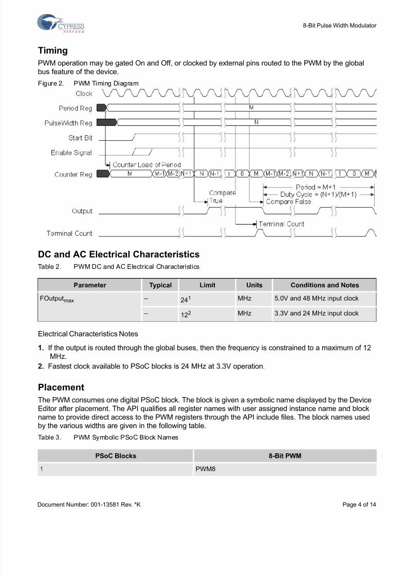
Timing
PWM operation may be gated On and Off, or clocked by external pins routed to the PWM by the globalbus feature of the device.
Figure 2. PWM Timing Diagram
DC and AC Electrical Characteristics
Table 2. PWM DC and AC Electrical Characteristics
Electrical Characteristics Notes
1. If the output is routed through the global buses, then the frequency is constrained to a maximum of 12MHz.
2. Fastest clock available to PSoC blocks is 24 MHz at 3.3V operation.
Placement
The PWM consumes one digital PSoC block. The block is given a symbolic name displayed by the DeviceEditor after placement. The API qualifies all register names with user assigned instance name and blockname to provide direct access to the PWM registers through the API include files. The block names usedby the various widths are given in the following table.
Table 3. PWM Symbolic PSoC Block Names
Parameter Typical Limit Units Conditions and Notes
FOutputmax
--24
1 MHz 5.0V and 48 MHz input clock
-- 122 MHz 3.3V and 24 MHz input clock
PSoC Blocks 8-Bit PWM
1 PWM8
8/2/2019 PWM8 DataSheet
http://slidepdf.com/reader/full/pwm8-datasheet 5/14
8-Bit Pulse Width Modulator
Document Number: 001-13581 Rev. *K Page 5 of 14
Parameters and Resources
Clock
The Clock parameter is selected from one of 16 sources. These sources include the 48 MHz oscillator (5.0V operation only), lower frequencies (VC1, VC2, and VC3) divided down from the 24 MHz systemclock, other PSoC blocks, and external inputs routed through global inputs and outputs. When using
an external digital clock for the block, the row input synchronization should be turned off for best accu-racy, and sleep operation.
Enable
The Enable parameter is selected from one of 16 sources. A high input enables continuous count,while a low enable disables count without resetting the counter.
CompareOut
The compare output may be disabled (without interfering with interrupt operations) or connected toany of the row output busses. It is always available as an input to the next higher digital PSoC blockand to the analog column clock selection multiplexors, regardless of the setting of this parameter. Thisparameter appears only for members of the CY8C29/27/24/22/21xxx, CY8C23x33,
CY7C64215/603xx, CYWUSB6953, CY8CLED02/04/08/16, CY8CLED03D/04D, CY8CTST110,CY8CTMG110, CY8CTST120, CY8CTMG120, CY8CTMA120, CY8C21x45, CY8C22x45,CY8CTMG300, CY8CTST300, CY8CTMA300, CY8CTMA301, CY8CTMA301D, CY8C28x45,CY8CPLC20, CY8CLED16P01, CY8C28xxx families of PSoC devices.
TerminalCountOut
The terminal count output is an auxiliary Counter output. This parameter allows it to be disabled or connected to any of the row output buses. This parameter appears only for members of theCY8C29/27/24/22/21xxx, CY8C23x33, CY7C64215/603xx, CYWUSB6953, CY8CLED02/04/08/16,CY8CLED03D/04D, CY8CTST110, CY8CTMG110, CY8CTST120, CY8CTMG120, CY8CTMA120,CY8C21x45, CY8C22x45, CY8CTMG300, CY8CTST300, CY8CTMA300, CY8CTMA301,CY8CTMA301D, CY8C28x45, CY8CPLC20, CY8CLED16P01, CY8C28xxx families of PSoC
devices.
Period
This parameter sets the period of the counter. Allowed values for PWM8 are between zero and 255.Allowed values for PWM16 are between zero and 216-1. The period is loaded into the Period register.The effective output waveform period of the PWM16 is the period count + 1. The value may be modi-fied using the API.
PulseWidth
Sets the pulse width of the PWM output. Allowed values are between zero and the period value. Thevalue may be modified using the API.
InterruptTypeThis parameter sets the interrupt trigger type. The interrupt can be set so that it triggers on the risingedge of the output signal or on the terminal count of the Counter register. A separate register inde-pendently enables the interrupt.
CompareType
This parameter sets the compare function type “Less Than” or “Less Than or Equal To.”
8/2/2019 PWM8 DataSheet
http://slidepdf.com/reader/full/pwm8-datasheet 6/14
8-Bit Pulse Width Modulator
Document Number: 001-13581 Rev. *K Page 6 of 14
ClockSync
In the PSoC devices, digital blocks may provide clock sources in addition to the system clocks. Digitalclock sources may even be chained in ripple fashion. This introduces skew with respect to the systemclocks. These skews are more critical in the CY8C29/27/24/22/21xxx, CY8C23x33,CY7C64215/603xx, CYWUSB6953, CY8CLED02/04/08/16, CY8CLED03D/04D, CY8CTST110,CY8CTMG110, CY8CTST120, CY8CTMG120, CY8CTMA120, CY8C21x45, CY8C22x45,
CY8CTMG300, CY8CTST300, CY8CTMA300, CY8CTMA301, CY8CTMA301D, CY8C28x45,CY8CPLC20, CY8CLED16P01, CY8C28xxx PSoC device families because of various data-path opti-mizations, particularly those applied to the system buses. This parameter may be used to controlclock skew and ensure proper operation when reading and writing PSoC block register values. Appro-priate values for this parameter must be determined from the following table.
InvertEnable
This parameter determines the sense of the enable input signal. When “Normal” is selected, theenable input is active-high. Selecting “Invert” causes the sense to be interpreted as active-low.InvertEnable applies only to the CY8C29/27/24/22/21xxx, CY8C23x33, CY7C64215/603xx,CYWUSB6953, CY8CLED02/04/08/16, CY8CLED03D/04D, CY8CTST110, CY8CTMG110,CY8CTST120, CY8CTMG120, CY8CTMA120, CY8C21x45, CY8C22x45, CY8CTMG300,CY8CTST300, CY8CTMA300, CY8CTMA301, CY8CTMA301D, CY8C28x45, CY8CPLC20,CY8CLED16P01, CY8C28xxx families of PSoC devices.
Interrupt Generation Control
The following two parameters InterruptAPI and IntDispatchMode are only accessible by setting theEnable Interrupt Generation Control check box in PSoC Designer. This is available under Project >Settings > Device Editor .
Interrupt Generation Control
There are two additional parameters that become available when the Enable interrupt generationcontrol check box in PSoC Designer is checked. This is available under Project > Settings > ChipEditor . Interrupt Generation Control is important when multiple overlays are used with interrupts sharedby multiple user modules across overlays:
ClockSync Value Use
Sync to SysClk Use this setting for any 24 MHz (SysClk) derived input clock source less than 24 MHz.
Examples include VC1, VC2, VC3 (when VC3 is driven by SysClk), 32KHz, and digital PSoC
blocks with SysClk-based sources. Externally generated clock sources must also use this
value to ensure that proper synchronization occurs.
Sync to SysClk*2 Use this setting for any 48 MHz (SysClk*2) based input clock less than 48 MHz.
Use SysClk Direct Use when a 24 MHz (SysClk/1) clock is desired. This does not actually perform
synchronization but provides low-skew access to the system clock itself. If selected, this
option overrides the setting of the Clock parameter, above. It must always be used instead of
VC1, VC2, VC3 or digital blocks where the net result of all dividers in combination produces a
24 MHz output.
Unsynchronized Use when the 48 MHz (SysClk*2) input is selected.
Use when unsynchronized inputs are desired. In general this use is advisable only when
interrupt generation is the sole application of the Counter. This setting is required for blocks
that remain active during sleep.
8/2/2019 PWM8 DataSheet
http://slidepdf.com/reader/full/pwm8-datasheet 7/14
8-Bit Pulse Width Modulator
Document Number: 001-13581 Rev. *K Page 7 of 14
Interrupt API
IntDispatchMode
InterruptAPI
The InterruptAPI parameter allows conditional generation of a User Module’s interrupt handler andinterrupt vector table entry. Select “Enable” to generate the interrupt handler and interrupt vector tableentry. Select “Disable” to bypass the generation of the interrupt handler and interrupt vector tableentry. Properly selecting whether an Interrupt API is to be generated is recommended particularly withprojects that have multiple overlays where a single block resource is used by the different overlays.By selecting only Interrupt API generation when it is necessary the need to generate an interruptdispatch code might be eliminated, thereby reducing overhead.
IntDispatchMode
The IntDispatchMode parameter is used to specify how an interrupt request is handled for interruptsshared by multiple user modules existing in the same block but in different overlays. Selecting“ActiveStatus” causes firmware to test which overlay is active before servicing the shared interruptrequest. This test occurs every time the shared interrupt is requested. This adds latency and alsoproduces a nondeterministic procedure of servicing shared interrupt requests, but does not requireany RAM. Selecting “OffsetPreCalc” causes firmware to calculate the source of a shared interruptrequest only when an overlay is initially loaded. This calculation decreases interrupt latency andproduces a deterministic procedure for servicing shared interrupt requests, but at the expense of abyte of RAM.
Application Programming Interface
The Application Programming Interface (API) routines are provided as part of the user module to allow thedesigner to deal with the module at a higher level. This sections specifies the interface to each functiontogether with related constants provided by the “include” files.
Note
In this, as in all user module APIs, the values of the A and X register may be altered by calling an APIfunction. It is the responsibility of the calling function to preserve the values of A and X before the call if those values are required after the call. This “registers are volatile” policy was selected for efficiencyreasons and has been in force since version 1.0 of PSoC Designer. The C compiler automatically takescare of this requirement. Assembly language programmers must ensure their code observes the policy,too. Though some user module API functions may leave A and X unchanged, there is no guarantee theywill do so in the future.
For Large Memory Model devices, it is also the caller's responsibility to preserve any value in theCUR_PP, IDX_PP, MVR_PP, and MVW_PP registers. Even though some of these registers may not bemodified now, there is no guarantee that will remain the case in future releases.
PWM8_PERIOD
Description:
Represents the value chosen for the Period field of the PWM8 in the Device Editor. The value canhave a range between 0 and 255.
8/2/2019 PWM8 DataSheet
http://slidepdf.com/reader/full/pwm8-datasheet 8/14
8-Bit Pulse Width Modulator
Document Number: 001-13581 Rev. *K Page 8 of 14
PWM8_PULSE_WIDTH
Description:
Represents the value chose for the PulseWidth field of the PWM8 in the Device Editor. The value canhave a range between 0 and 255.
PWM8_EnableInt
Description:
Enables the interrupt mode operation.
C Prototype:
void PWM8_EnableInt(void);
Assembly:
lcall PWM8_EnableInt
Parameters:
None
Return Value:
None
Side Effects:
The A and X registers may be altered by this function.
PWM8_DisableInt
Description:
Disables the interrupt mode operation.
C Prototype:
void PWM8_DisableInt(void);
Assembly:
lcall PWM8_DisableInt
Parameters:
None
Return Value:
None
Side Effects:
The A and X registers may be altered by this function.
PWM8_Start
Description:
Starts the PWM8 User Module. If the enable input is high, the Counter begins to down count.
8/2/2019 PWM8 DataSheet
http://slidepdf.com/reader/full/pwm8-datasheet 9/14
8-Bit Pulse Width Modulator
Document Number: 001-13581 Rev. *K Page 9 of 14
C Prototype:
void PWM8_Start(void);
Assembly:
lcall PWM8_Start
Parameters:
None
Return Value:
None
Side Effects:
The A and X registers may be altered by this function.
PWM8_Stop
Description:
Stops the counter operation.
C Prototype:
void PWM8_Stop(void);
Assembly:
lcall PWM8_Stop
Parameters:
None
Return Value:
None
Side Effects:
The output is reset low and writing to the Period register causes the Counter register to update withthe new period value. The A and X registers may be altered by this function.
PWM8_WritePeriod
Description:
Writes the Period register with the period value. The period value is transferred from the Periodregister to the Counter register immediately, if the PWM8 is stopped or when the counter reaches thezero count.
C Prototype:
void PWM8_WritePeriod(BYTE bPeriod);
Assembly:
mov A, [bPeriod]
lcall PWM8_WritePeriod
Parameters:
bPeriod: bPeriod value is a value from 0 to 255 and is passed in the Accumulator.
8/2/2019 PWM8 DataSheet
http://slidepdf.com/reader/full/pwm8-datasheet 10/14
8-Bit Pulse Width Modulator
Document Number: 001-13581 Rev. *K Page 10 of 14
Return Value:
None
Side Effects:
The A and X registers may be altered by this function.
PWM8_WritePulseWidth
Description:
Writes the PulseWidth register with the pulse width value.
C Prototype:
void PWM8_WritePulseWidth(BYTE bPulseWidth);
Assembly:
mov A, [bPulseWidth]
lcall PWM8_WritePulseWidth
Parameters:bPulseWidth: bPulseWidth value is the value from 0 to the period value and is passed in the Accumu-lator.
Return Value:
None
Side Effects:
Writing the PulseWidth register, while the counter is active, changes the duty cycle of the output. Thismay cause the output to glitch or change inadvertently. The A and X registers may be altered by thisfunction.
PWM8_bReadPulseWidth
Description:
Reads the PulseWidth register.
C Prototype:
BYTE PWM8_bReadPulseWidth();
Assembly:
lcall PWM8_bReadPulseWidth
mov [bPulseWidth], A
Parameters:
None
Return Value:
The Pulse width value is stored in the PulseWidth register and returned in the Accumulator.
Side Effects:
The A and X registers may be altered by this function.
8/2/2019 PWM8 DataSheet
http://slidepdf.com/reader/full/pwm8-datasheet 11/14
8-Bit Pulse Width Modulator
Document Number: 001-13581 Rev. *K Page 11 of 14
PWM8_bReadCounter
Description:
Reads the Counter register.
Note that this function is for applications that must read the Counter register on-the-fly, creating some
side effects.C Prototype:
BYTE PWM8_bReadCounter();
Assembly:
lcall PWM8_bReadCounter
mov [bCounter], A
Parameters:
None
Return Value:
Returns the Counter register value and is returned in the Accumulator.
Side Effects:
To read the PWM8 Counter register, the PulseWidth register must be temporarily modified. This couldcause the PWM8 Counter register operation to be postponed by one or more counts. In addition, thiscould result in an inadvertent interrupt condition. The A and X registers may be altered by this function.
Sample Firmware Source Code
In the following examples, the correspondence between the C and assembly code is simple and direct.The values shown for period and compare value are each “off-by-1” from the cardinal values because theregisters are zero-based; that is, zero is the terminal count in their down-count cycle. Passing a simple
one byte parameter in the A register rather than on the stack is a performance optimization used by boththe assembler and C compiler for user module APIs. The C compiler employs this mechanism for “INT”types instead of pushing the argument on the stack when it sees the #pragma fastcall declarations in thePWM8.h file.
The following is assembly language source that illustrates the use of the APIs.
;;;;;;;;;;;;;;;;;;;;;;;;;;;;;;;;;;;;;;;;;;;;;;;;;;;;;;;;;;;;;;;;;;;;;;;;;;;;
; Function: GenerateOneThirdDutyCycle
; Description:
; This sample shows how to create a 33% duty cycle output pulse.
; The clock selected should be 24 times the required period. The
; comparator operation is specified to be "Less than or Equal".
;; Parameters: none
; Returns: none
;;;;;;;;;;;;;;;;;;;;;;;;;;;;;;;;;;;;;;;;;;;;;;;;;;;;;;;;;;;;;;;;;;;;;;;;;;;;
include "PWM8.inc" ; include the PWM8 API include file
GenerateOneThirdDutyCycle:
mov A, 23 ; set the period to be 24 counts of the clock
call PWM8_WritePeriod
mov A, 7 ; set Pulse Width to generate a 33% duty cycle
8/2/2019 PWM8 DataSheet
http://slidepdf.com/reader/full/pwm8-datasheet 12/14
8-Bit Pulse Width Modulator
Document Number: 001-13581 Rev. *K Page 12 of 14
call PWM8_WritePulseWidth
call PWM8_DisableInt ; ensure that interrupts are disabled
call PWM8_Start ; start the PWM8 – counter will start to
ret ; count when the enable input is asserted high
The same code in C is:
/* include the Counter8 API header file */
#include "PWM8.h"
/* function prototype */
void GenerateOneThirdDutyCycle(void);
/* Divide by eight function */
void GenerateOneThirdDutyCycle(void)
{
/* set period to eight clocks */
PWM8_WritePeriod(23);
/* set pulse width to generate a 33% duty cycle */
PWM8_WritePulseWidth(7);
/* ensure interrupt is disabled */
PWM8_DisableInt();
/* start the PWM8! */
PWM8_Start();
}
Configuration Registers
Except where noted, the register specifications given in this section apply to all PSoC device families.
The 8-bit PWM uses a single digital PSoC block named PWM8. Each block is personalized andparameterized through 7 registers. The following tables give the “personality” values as constants and theparameters as named bit-fields with brief descriptions. Symbolic names for these registers are defined inthe user module instance’s C and assembly language interface files (the “.h” and “.inc” files).
Table 4. Function Register, Bank 1 CY8C29/27/24/22/21xxx and CY8CLED04/08/16
BCEN gates the compare output onto the row broadcast bus line. This bitfield is set in the Device Editor bydirectly configuring the broadcast line. The Data Invert flag, set through a user module parameter displayed in the Device Editor, controls the sense of the enable input signal. The CompareType flagindicates whether the compare function is set to “Less Than or Equal” or “Less Than.” The InterruptTypeflag determines whether to trigger the interrupt on the compare event or on the terminal count. Both
Block/Bit 7 6 5 4 3 2 1 0
PWM8 Data Invert BCEN 1 Compare
Type
Interrupt
Type
0 0 1
8/2/2019 PWM8 DataSheet
http://slidepdf.com/reader/full/pwm8-datasheet 13/14
8-Bit Pulse Width Modulator
Document Number: 001-13581 Rev. *K Page 13 of 14
CompareType and InterruptType are set in the Device Editor directly through user module parametersdescribed in the earlier section on the topic.
Table 5. Input Register, Bank 1
Enable selects the data input from one of 16 sources. Clock selects the clock input from one of 16sources. Both parameters are set in the Device Editor.
Table 6. Output Register, Bank 1 CY8C29/27/24/22/21xxx and CY8CLED04/08/16
The user module “ClockSync” parameter in the Device Editor determines the value of the AuxClk bits.Though similarly named, the AuxEnable and AuxSelect bits are related, instead, to the OutEnable and
OutSelect bit fields. AuxEnable and AuxSelect permit driving the terminal count output signal onto one of the row output busses and are controlled by manipulating the row bus graphically in the Device Editor Interconnect View. OutEnable is set when the compare output is driven onto one of the row or globaloutput busses. OutputSelect controls which of the busses are driven from the compare output.
Table 7. Count Register (DR0), Bank 0
Count is the PWM8 down counter. It can be read using the PWM8 API.
Table 8. Period Register (DR1), Bank 0
Period holds the period value that is loaded into the Counter register upon enable or terminal countcondition. It can be set in the Device Editor and the PWM8 API.
Table 9. Compare Register (DR2), Bank 0
PulseWidth holds the pulse width value used to generate the output. It can be set in the Device Editor andthe PWM8 API.
Table 10. Control Register (CR0), Bank 0
Start indicates that the PWM8 is enabled when set. It is modified by using the PWM8 API.
Block/Bit 7 6 5 4 3 2 1 0
PWM8 Enable Clock
Block/Bit 7 6 5 4 3 2 1 0
CNTR8 AuxClk AuxEnable AuxSelect OutEnable OutputSelect
Block/Bit 7 6 5 4 3 2 1 0
PWM8 Count
Block/Bit 7 6 5 4 3 2 1 0
PWM8 Period
Block/Bit 7 6 5 4 3 2 1 0
PWM8 PulseWidth
Block/Bit 7 6 5 4 3 2 1 0
PWM8 0 0 0 0 0 0 0 Start
8/2/2019 PWM8 DataSheet
http://slidepdf.com/reader/full/pwm8-datasheet 14/14
8-Bit Pulse Width Modulator
Document Number: 001-13581 Rev. *K Revised November 24, 2011 Page 14 of 14Copyright © 2000-2011 Cypress Semiconductor Corporation. The information contained herein is subject to change without notice. Cypress Semiconductor Corporation assumes no responsibilityfor the use of any circuitry other than circuitry embodied in a Cypress product. Nor does it convey or imply any license under patent or other rights. Cypress products are not warranted nor intendedto be used for medical, life support, life saving, critical control or safety applications, unless pursuant to an express written agreement with Cypress. Furthermore, Cypress does not authorize itsproducts for use as critical components in life-support systems where a malfunction or failure may reasonably be expected to result in significant injury to the user. The inclusion of Cypress productsin life-support systems application implies that the manufacturer assumes all risk of such use and in doing so indemnifies Cypress against all charges.
PSoC Designer™ and Programmable System-on-Chip™ are trademarks and PSoC® is a registered trademark of Cypress Semiconductor Corp. All other trademarks or registered trademarksreferenced herein are property of the respective corporations.
Any Source Code (software and/or firmware) is owned by Cypress Semiconductor Corporation (Cypress) and is protected by and subject to worldwide patent protection (United States and foreign),United States copyright laws and international treaty provisions. Cypress hereby grants to licensee a personal, non-exclusive, non-transferable license to copy, use, modify, create derivative worksof, and compile the Cypress Source Code and derivative works for the sole purpose of creating custom software and or firmware in support of licensee product to be used only in conjunction witha Cypress integrated circuit as specified in the applicable agreement. Any reproduction, modification, translation, compilation, or representation of this Source Code except as specified above isprohibited without the express written permission of Cypress.
Disclaimer: CYPRESS MAKES NO WARRANTY OF ANY KIND, EXPRESS OR IMPLIED, WITH REGARD TO THIS MATERIAL, INCLUDING, BUT NOT LIMITED TO, THE IMPLIED WARRANTIESOF MERCHANTABILITY AND FITNESS FOR A PARTICULAR PURPOSE. Cypress reserves the right to make changes without further notice to the materials described herein. Cypress does notassume any liability arising out of the application or use of any product or circuit described herein. Cypress does not authorize its products for use as critical components in life-support systemswhere a malfunction or failure may reasonably be expected to result in significant injury to the user. The inclusion of Cypress' product in a life-support systems application implies that the manufacturer assumes all risk of such use and in doing so indemnifies Cypress against all charges.
Version History
Note PSoC Designer 5.1 introduces a Version History in all user module datasheets. This section docu-ments high level descriptions of the differences between the current and previous user module ver-sions.
Version Originator Description
2.5 TDU Updated Clock description to include: When using an external digital clock for the block,
the row input synchronization should be turned off for best accuracy, and sleep operation.
2.60 DHA Added support for CY8C21x12 devices.