Plasma-assisted atomic layer deposition of metal oxides and nitrides
168
Transcript of Plasma-assisted atomic layer deposition of metal oxides and nitrides

Plasma-Assisted Atomic Layer Deposition of Metal Oxides and Nitrides
PROEFSCHRIFT
ter verkrijging van de graad van doctor aan de Technische Universiteit Eindhoven, op gezag van de Rector Magnificus, prof.dr.ir. C.J. van Duijn, voor een
commissie aangewezen door het College voor Promoties in het openbaar te verdedigen
op dinsdag 29 januari 2008 om 16.00 uur
door
Stephan Bastiaan Simon Heil
geboren te Made en Drimmelen
Dit proefschrift is goedgekeurd door de promotor: prof.dr.ir. M.C.M. van de Sanden Copromotor: dr.ir. W.M.M. Kessels This research was financially supported by the Dutch Technology Foundation STW (EMM.6174).
Printed and bound by universiteitsdrukkerij Technische Universiteit Eindhoven Cover design by Jorrit van Rijt, Oranje Vormgevers CIP-DATA LIBRARY TECHNISCHE UNIVERSITEIT EINDHOVEN Heil, Stephan Bastiaan Simon Plasma-assisted atomic layer deposition of metal oxides and nitrides / by Stephan Bastiaan Simon Heil. – Eindhoven : Technische Universiteit Eindhoven, 2007. - Proefschrift. ISBN 978-90-386-1198-3 NUR 926 Trefwoorden: plasmadepositie / plasmadiagnostiek / plasmachemie / dunne lagen / materiaalonderzoek / atomaire lagen Subject headings: plasma deposition / plasma diagnostics / plasma chemistry / thin films / material properties / metal oxides / metal nitrides / growth mechanism / atomic layer deposition
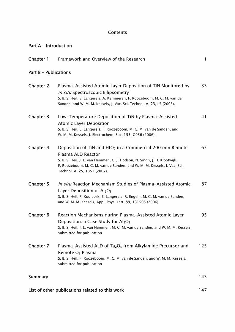
Contents
Part A – Introduction Chapter 1 Framework and Overview of the Research 1 Part B – Publications Chapter 2 Plasma-Assisted Atomic Layer Deposition of TiN Monitored by
in situ Spectroscopic Ellipsometry S. B. S. Heil, E. Langereis, A. Kemmeren, F. Roozeboom, M. C. M. van de Sanden, and W. M. M. Kessels, J. Vac. Sci. Technol. A. 23, L5 (2005).
33
Chapter 3 Low-Temperature Deposition of TiN by Plasma-Assisted
Atomic Layer Deposition S. B. S. Heil, E. Langereis, F. Roozeboom, M. C. M. van de Sanden, and W. M. M. Kessels, J. Electrochem. Soc. 153, G956 (2006).
41
Chapter 4 Deposition of TiN and HfO2 in a Commercial 200 mm Remote
Plasma ALD Reactor S. B. S. Heil, J. L. van Hemmen, C. J. Hodson, N. Singh, J. H. Klootwijk, F. Roozeboom, M. C. M. van de Sanden, and W. M. M. Kessels, J. Vac. Sci. Technol. A. 25, 1357 (2007).
65
Chapter 5 In situ Reaction Mechanism Studies of Plasma-Assisted Atomic
Layer Deposition of Al2O3 S. B. S. Heil, P. Kudlacek, E. Langereis, R. Engeln, M. C. M. van de Sanden, and W. M. M. Kessels, Appl. Phys. Lett. 89, 131505 (2006).
87
Chapter 6 Reaction Mechanisms during Plasma-Assisted Atomic Layer
Deposition: a Case Study for Al2O3 S. B. S. Heil, J. L. van Hemmen, M. C. M. van de Sanden, and W. M. M. Kessels, submitted for publication
95
Chapter 7 Plasma-Assisted ALD of Ta2O5 from Alkylamide Precursor and
Remote O2 Plasma S. B. S. Heil, F. Roozeboom, M. C. M. van de Sanden, and W. M. M. Kessels, submitted for publication
125
Summary 143 List of other publications related to this work 147

Acknowledgments 151 Curriculum Vitae 155

Part A
Introduction


1
Chapter 1 Framework and Overview of the Research
2
I. Introduction and framework of the research A. Thin film growth and atomic layer deposition
Thin films play an important role in present day society, being intensively used in a wide variety of applications. Depending on their optical, electrical, mechanical or chemical properties, thin films can be applied as, for example, antireflection coating on glasses, capacitor dielectrics in microelectronics, wear resistive coatings on microelectromechanical systems, or catalytic surfaces in chemical sensors. Furthermore, thin films can change the surface properties of the substrates they are covering, adding new functionality to bulk materials, like in the case of permeation barriers on polymers and surface passivation layers on semiconductors. Currently, there is an increasing interest and need for thin films with a nanoscale thickness. The best known examples stem from the continuous miniaturization in the field of micro-electronics and the upcoming fields of nanoscience and nano-technology. An additional effect of decreasing film thickness is the discovery of new and interesting material properties, such as for example quantum effects and finite size effects, which play a role when films have a thickness of only a few atomic layers. From a miniaturization and process integration perspective, however, the demand is commonly raised to be able to tailor the growth process and the material properties of the films grown to fit certain specifications. New thin film materials and methods for growth are therefore actively pursued.
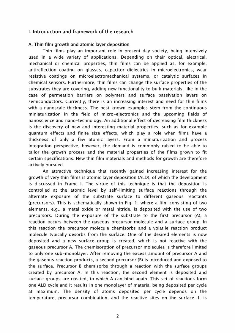
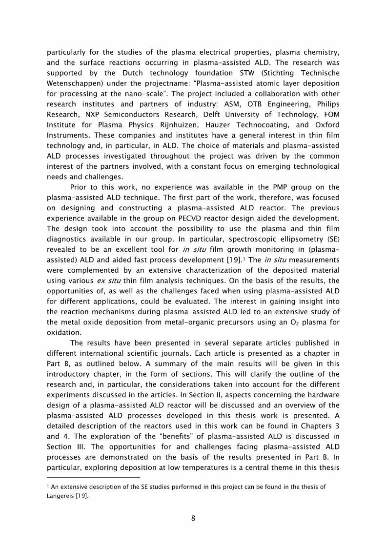
An attractive technique that recently gained increasing interest for the growth of very thin films is atomic layer deposition (ALD), of which the development is discussed in Frame I. The virtue of this technique is that the deposition is controlled at the atomic level by self-limiting surface reactions through the alternate exposure of the substrate surface to different gaseous reactants (precursors). This is schematically shown in Fig. 1, where a film consisting of two elements, e.g., a metal oxide or metal nitride, is deposited with the use of two precursors. During the exposure of the substrate to the first precursor (A), a reaction occurs between the gaseous precursor molecule and a surface group. In this reaction the precursor molecule chemisorbs and a volatile reaction product molecule typically desorbs from the surface. One of the desired elements is now deposited and a new surface group is created, which is not reactive with the gaseous precursor A. The chemisorption of precursor molecules is therefore limited to only one sub-monolayer. After removing the excess amount of precursor A and the gaseous reaction products, a second precursor (B) is introduced and exposed to the surface. Precursor B chemisorbs through a reaction with the surface groups created by precursor A. In this reaction, the second element is deposited and surface groups are created, to which A can bind again. This set of reactions form one ALD cycle and it results in one monolayer of material being deposited per cycle at maximum. The density of atoms deposited per cycle depends on the temperature, precursor combination, and the reactive sites on the surface. It is
3
therefore only rarely the case that a full monolayer growth per cycle is obtained. The ALD cycle can be repeated until the desired film thickness is reached. Furthermore, due to the self-limiting surface reactions, the deposition rate in ALD is not proportional to the flux of reactive species on the surface, like in the case of chemical vapor deposition (CVD) and physical vapor deposition (PVD). Therefore, given that there is a sufficient flux applied, the same amount of material is deposited everywhere on the surface, even in high-aspect ratio structures. Other key features of ALD are the good uniformity of film properties, which can be achieved on large area substrates, the relatively low substrate temperatures used in the process (temperature window typically 200-400 °C), and the ability of readily producing multilayer structures.
Thin films deposited by ALD are currently applied in a number of devices, such as thin film electroluminescent displays, (embedded) dynamic random access memories (DRAM), and magnetic read heads. Currently, new variants of ALD are explored, which can be expected to provide even more benefits to the ALD process. Our interest lies in a specific type of ALD in which a plasma exposure is included in the ALD cycle. In this so-called plasma-assisted ALD, also referred to as plasma-enhanced ALD or PE-ALD, the substrate is exposed to the different species present in the plasma. The reactive species, predominantly radicals, react with the surface groups created during the preceding precursor exposure. This reaction leads to reduction or oxidation of the chemisorbed precursor, film formation, and the
FIG. 1 Schematic representation of the ALD principle. The ALD cycle typically includes two precursor exposures. Precursor B chemisorbs on the surface groups created by precursor A and vice versa. After saturation of the precursor an intermitting purge step is commonly applied to remove the excess precursor and reaction products. The complete ALD cycle results in the deposition of the desired material.
4
creation of new surface groups to which a precursor can bind. Since in plasma-assisted ALD part of the chemical activity, i.e., the creation of radical species, takes already place in the gas phase, the process depends less on the thermal energy available on the surface. This facilitates deposition at lower temperatures and can result in improved material properties compared to conventional (thermal) ALD. Furthermore, the use of radicals as a reactant allows the deposition of materials that are otherwise difficult or not attainable with the solely chemical process due to the absence of a suitable precursor combination. This is for example the case for certain metals (Ti, Ta, Al [1,2]) and metal nitrides (TaN [3]).
B. Research on plasma-assisted atomic layer deposition
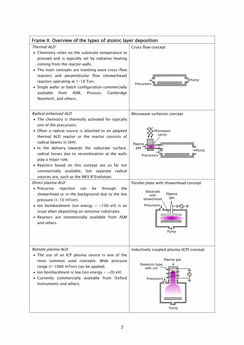
The selection of the hardware is a necessary first step in the research and development of plasma-assisted ALD processes. Over the past years, different hardware concepts have been developed and there are currently several choices available. The development of the plasma-assisted ALD hardware can roughly be traced back to two different origins: the incorporation of a radical source in existing thermal ALD equipment; and the adaptation of plasma-enhanced chemical vapor deposition (PECVD) reactor configurations to operate in ALD mode. In this respect, next to thermal ALD, three types plasma-based ALD can be categorized: radical enhanced ALD, direct plasma ALD, and remote plasma ALD. The characteristics of the four types are presented in Frame II.
Thermal ALD is the most researched type of ALD, because it mostly resembles CVD whereas the hardware configuration is also relatively simple. It typically consists of a (wall) heated vacuum chamber in which substrates are coated by the alternate pulsing of precursor vapors, separated by the use of intermitting purge gas flows. The whole ALD processing cycle can often be regarded as a sort of “pulse-train”, commonly referred to as “traveling wave”. This pulse-train starts at one end of the reactor moves over the substrate surface, where deposition occurs, and dissappears into the pump at the other end. Two reactor concepts currently exist: the cross flow concept, where the flow of precursors is parallel to substrate surface; and the perpendicular flow concept, in which the precursors are introduced from the top of the reactor and flow perpendicular towards the substrate going downwards into the pump. Both concepts can be found in commercially available thermal ALD reactors, for example the Cambridge Nanotech Savannah [4], ASM F120 [5], and ASM Pulsar [5] reactors are based on the cross flow concept, while the perpendicular flow concept is applied in the Picosun SUNALE series [6] and the ASM Advance 400 series batch reactor [5].
From the three plasma types that are categorized, the radical enhanced ALD configuration can be considered the closest to thermal ALD processing. Thermal ALD hardware can adapted to include a remotely placed radical source, such as the implementation of a surfatron microwave plasma in a ASM F120, as recently
5
Frame I: Development of atomic layer deposition
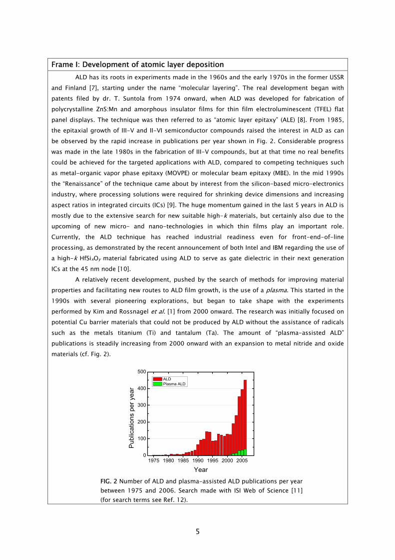
ALD has its roots in experiments made in the 1960s and the early 1970s in the former USSR and Finland [7], starting under the name “molecular layering”. The real development began with patents filed by dr. T. Suntola from 1974 onward, when ALD was developed for fabrication of polycrystalline ZnS:Mn and amorphous insulator films for thin film electroluminescent (TFEL) flat panel displays. The technique was then referred to as “atomic layer epitaxy” (ALE) [8]. From 1985, the epitaxial growth of III-V and II-VI semiconductor compounds raised the interest in ALD as can be observed by the rapid increase in publications per year shown in Fig. 2. Considerable progress was made in the late 1980s in the fabrication of III-V compounds, but at that time no real benefits could be achieved for the targeted applications with ALD, compared to competing techniques such as metal-organic vapor phase epitaxy (MOVPE) or molecular beam epitaxy (MBE). In the mid 1990s the “Renaissance” of the technique came about by interest from the silicon-based micro-electronics industry, where processing solutions were required for shrinking device dimensions and increasing aspect ratios in integrated circuits (ICs) [9]. The huge momentum gained in the last 5 years in ALD is mostly due to the extensive search for new suitable high-k materials, but certainly also due to the upcoming of new micro- and nano-technologies in which thin films play an important role. Currently, the ALD technique has reached industrial readiness even for front-end-of-line processing, as demonstrated by the recent announcement of both Intel and IBM regarding the use of a high-k HfSixOy material fabricated using ALD to serve as gate dielectric in their next generation ICs at the 45 nm node [10]. A relatively recent development, pushed by the search of methods for improving material properties and facilitating new routes to ALD film growth, is the use of a plasma. This started in the 1990s with several pioneering explorations, but began to take shape with the experiments performed by Kim and Rossnagel et al. [1] from 2000 onward. The research was initially focused on potential Cu barrier materials that could not be produced by ALD without the assistance of radicals such as the metals titanium (Ti) and tantalum (Ta). The amount of “plasma-assisted ALD” publications is steadily increasing from 2000 onward with an expansion to metal nitride and oxide materials (cf. Fig. 2).
1975 1980 1985 1990 1995 2000 20050
100
200
300
400
500
Pub
licat
ions
per
yea
r
Year
ALD Plasma ALD
FIG. 2 Number of ALD and plasma-assisted ALD publications per year between 1975 and 2006. Search made with ISI Web of Science [11] (for search terms see Ref. 12).
6
reported by Niskanen et al. [13,14]. A plasma is created in the source at low pressure (~1-1000 mTorr) from a source gas, most commonly being O2, N2, H2, and mixtures thereof. It is attempted to deliver the generated radical species to the substrate surface, in a similar fashion as a normal precursor vapor dosing would be performed, i.e., via a tubular inlet. A different approach, which is also referred to as radical enhanced ALD, is the use of a particle beam setup. The deposition is carried out in an (ultra-)high vacuum chamber where a substrate is alternately exposed to beams consisting of a single type of radical species, which are, in most cases, plasma generated [15,16]. This approach is often used to mimic or simplify the actual deposition process, and is therefore especially suited for fundamental film growth studies [15].
Originating from the PECVD background is direct plasma ALD. A common plasma configuration is the parallel plate concept, as shown in Frame II. The plasma is generated in between two parallel placed electrodes that are spaced ~1-5 cm apart, from a source gas at low pressure (1-10 mTorr). A rf voltage is applied to the top electrode. The substrate is residing on the lower, grounded counter-electrode, and the substrate plays “directly” a role in the plasma generation. To improve the uniformity of the plasma, the top electrode commonly consists of a showerhead gas distributor, through which the flow of plasma source gases is fed into the chamber. For the same reason, in some cases also the precursor is fed through the showerhead [17]. The parallel plate concept is used in the ASM Genitech reactor, with which direct plasma ALD processing can be carried out.
Remote plasma ALD is another type of ALD that is developed from a plasma processing background. In this type of ALD, the plasma source is positioned at a distance of typically a few tens of centimeters from the substrate. Plasma species diffuse from the source towards the substrate located in a relatively spacious deposition chamber. A common plasma configuration is the inductively coupled plasma (ICP) concept, in which a plasma can be generated at a pressure in the range of 1-1000 mTorr. A commercial remote plasma-assisted ALD reactor based on the ICP concept is the Oxford Instruments FlexAL [18]. C. Goal and outline of this thesis
The goal of the research described in this thesis was to develop and study plasma-assisted atomic layer deposition of metal oxides and metal nitrides and to acquire knowledge on the parameters controlling the material properties. Besides the necessary hardware and process development, a particular interest was to gain insight into the underlying plasma and surface reactions ruling plasma-assisted ALD.
The research was carried out in the group Plasma & Materials Processing (PMP) at the Department of Applied Physics of the Eindhoven University of Technology. The strong background of the group in the study of both the plasma fundamentals and thin film growth in PECVD provided an exceptional environment,
7
Frame II. Overview of the types of atomic layer deposition Thermal ALD • Chemistry relies on the substrate temperature to
proceed and is typically set by radiative heating coming from the reactor walls.
• The main concepts are traveling wave cross-flow reactors and perpendicular flow (showerhead) reactors operating at 1-10 Torr.
• Single wafer or batch configuration commercially available from ASM, Picosun, Cambridge Nanotech, and others.
Cross flow concept
Radical enhanced ALD • The chemistry is thermally activated for typically
one of the precursors. • Often a radical source is attached to an adapted
thermal ALD reactor or the reactor consists of radical beams in UHV.
• In the delivery towards the substrate surface, radical losses due to recombination at the walls play a major role.
• Reactors based on this concept are so far not commercially available, but separate radical sources are, such as the MKS R*Evolution.
Microwave surfatron concept
Direct plasma ALD • Precursor injection can be through the
showerhead or in the background due to the low pressure (1-10 mTorr).
• Ion bombardment (ion energy > ~100 eV) is an issue when depositing on sensitive substrates.
• Reactors are commercially available from ASM and others.
Parallel plate with showerhead concept
Remote plasma ALD • The use of an ICP plasma source is one of the
most common used concepts. Wide pressure range (1-1000 mTorr) can be applied.
• Ion bombardment is low (ion energy < ~20 eV) • Currently commercially available from Oxford
Instruments and others.
Inductively coupled plasma (ICP) concept
8
particularly for the studies of the plasma electrical properties, plasma chemistry, and the surface reactions occurring in plasma-assisted ALD. The research was supported by the Dutch technology foundation STW (Stichting Technische Wetenschappen) under the projectname: “Plasma-assisted atomic layer deposition for processing at the nano-scale”. The project included a collaboration with other research institutes and partners of industry: ASM, OTB Engineering, Philips Research, NXP Semiconductors Research, Delft University of Technology, FOM Institute for Plasma Physics Rijnhuizen, Hauzer Technocoating, and Oxford Instruments. These companies and institutes have a general interest in thin film technology and, in particular, in ALD. The choice of materials and plasma-assisted ALD processes investigated throughout the project was driven by the common interest of the partners involved, with a constant focus on emerging technological needs and challenges.
Prior to this work, no experience was available in the PMP group on the plasma-assisted ALD technique. The first part of the work, therefore, was focused on designing and constructing a plasma-assisted ALD reactor. The previous experience available in the group on PECVD reactor design aided the development. The design took into account the possibility to use the plasma and thin film diagnostics available in our group. In particular, spectroscopic ellipsometry (SE) revealed to be an excellent tool for in situ film growth monitoring in (plasma-assisted) ALD and aided fast process development [19].1 The in situ measurements were complemented by an extensive characterization of the deposited material using various ex situ thin film analysis techniques. On the basis of the results, the opportunities of, as well as the challenges faced when using plasma-assisted ALD for different applications, could be evaluated. The interest in gaining insight into the reaction mechanisms during plasma-assisted ALD led to an extensive study of the metal oxide deposition from metal-organic precursors using an O2 plasma for oxidation.
The results have been presented in several separate articles published in different international scientific journals. Each article is presented as a chapter in Part B, as outlined below. A summary of the main results will be given in this introductory chapter, in the form of sections. This will clarify the outline of the research and, in particular, the considerations taken into account for the different experiments discussed in the articles. In Section II, aspects concerning the hardware design of a plasma-assisted ALD reactor will be discussed and an overview of the plasma-assisted ALD processes developed in this thesis work is presented. A detailed description of the reactors used in this work can be found in Chapters 3 and 4. The exploration of the “benefits” of plasma-assisted ALD is discussed in Section III. The opportunities for and challenges facing plasma-assisted ALD processes are demonstrated on the basis of the results presented in Part B. In particular, exploring deposition at low temperatures is a central theme in this thesis 1 An extensive description of the SE studies performed in this project can be found in the thesis of Langereis [19].
9
and details can be found in Chapters 2 and 3, and Chapters 5 and 6, for the plasma-assisted ALD of TiN and Al2O3, respectively. In Section IV a summary of the results on the plasma properties and on the growth mechanism during plasma-assisted ALD is given. The plasma properties are presented in terms of ion density and electron temperature in Chapter 3 for the H2-N2 plasma used in the deposition of TiN. The growth mechanism of metal oxides was investigated for the case of Al2O3 and Ta2O5 deposited by plasma-assisted ALD using different type of metal-organic precursors. From these results, general consequences for plasma-assisted ALD of metal oxides from metal-organic precursors and O2 plasma were deduced. The details about the experiments can be found in Chapters 5, 6, and 7. Finally, in Section V an outlook to the future is presented. Overview of the chapters in Part B: Chapter 2: Plasma-assisted atomic layer deposition of TiN monitored by in situ
spectroscopic ellipsometry S. B. S. Heil, E. Langereis, A. Kemmeren, F. Roozeboom, M. C. M. van de Sanden, and W. M. M. Kessels, J. Vac. Sci. Technol. A. 23, L5 (2005).
Chapter 3: Low temperature deposition of TiN by plasma-assisted atomic layer
deposition S. B. S. Heil, E. Langereis, F. Roozeboom, M. C. M. van de Sanden, and W. M. M. Kessels, J. Electrochem. Soc. 153, G956 (2006).
Chapter 4: Deposition of TiN and HfO2 in a commercial 200 mm remote plasma
atomic layer deposition reactor S. B. S. Heil, J. L. van Hemmen, C. J. Hodson, N. Singh, J. H. Klootwijk, F. Roozeboom, M. C. M. van de Sanden, and W. M. M. Kessels, J. Vac. Sci. Technol. A. 25, 1357 (2007).
Chapter 5: In situ studies of the reaction mechanisms during plasma-assisted
atomic layer deposition of Al2O3
S. B. S. Heil, P. Kudlacek, E. Langereis, R. Engeln, M. C. M. van de Sanden, and W. M. M. Kessels, Appl. Phys. Lett. 89, 131505 (2006).
Chapter 6: Reaction mechanisms during plasma-assisted atomic layer deposition
of metal oxides: A case study for Al2O3
S. B. S. Heil, J. L. van Hemmen, M. C. M. van de Sanden, and W. M. M. Kessels, submitted for publication
Chapter 7: Plasma-assisted atomic layer deposition of Ta2O5 from alkylamide
precursor and remote O2 plasma S. B. S. Heil, F. Roozeboom, M. C. M. van de Sanden, and W. M. M. Kessels, submitted for publication
10
II. Reactor design for remote plasma-assisted atomic layer deposition
A. Background In plasma materials processing a radio frequency (rf) power source is
commonly used for plasma generation. The power in the plasma source region is dissipated by the acceleration of electrons in the generated rf electric fields. The mean electron kinetic energy is referred to as the electron temperature (Te) and is commonly expressed in electronvolt (eV). The heavy ions cannot “follow” the rf electric fields and, therefore, respond only to the time-averaged field. The ion temperature (Ti), i.e., the mean ion kinetic energy, is, therefore, much smaller than the electron temperature (Ti<<Te). Energy transfer from the highly energetic electrons to the heavy gas species is very inefficient and as a consequence the actual gas temperature remains low. This allows this type of plasma to be used for materials processing without considerable heat transfer to the substrate. The collisions between electrons and source gas species results in the ionization of the gas phase species such that the plasma is sustained. The collisions also lead to the formation of radical species through dissociation processes.
There are two methods that can be used to couple the rf power into the plasma: capacitive, with the rf electrode in direct contact with the plasma; or inductive, across a dielectric window. The former is used in the parallel plate concept in direct plasma ALD, and the latter in the inductively coupled plasma concept in remote plasma ALD, as presented in Frame II.
Capacitive power coupling is performed by the acceleration of electrons in the oscillating electric field between two electrodes. The oscillation of the electrons creates a sheath region near each electrode, which contains a net positive charge when averaged over an oscillation period. The positive charge density decreases from the plasma towards the electrode surface, generating a dc voltage drop over the sheath region. Ions diffusing from the bulk plasma towards the electrode are accelerated due to the presence of this voltage drop, which results in ion bombardment. In a direct plasma configuration the substrate is located on one of the electrodes and is, therefore, exposed to an ion energy which could reach 200-1000 eV, depending on the rf voltage and electrode design used [20]. High ion energy values can lead to displacement of particles present in the film and at the surface. This can have positive effects such as smoothening and densification of the film, but in ALD, where very thin films are commonly grown in a stack, energetic ion bombardment can also induce damage to the underlying film or substrate.
In order to avoid severe ion bombardment, inductive power coupling can be used. This is known to result in low dc voltages across the plasma sheaths, hence low ion bombardment (typically <20 eV) at all surfaces [20]. In order to further decrease the ion bombardment, while maintaining a high radical production, the source can be placed remotely from the deposition area. By using low pressures, plasma generation and radical production can still occur at the substrate level. This is a major difference compared to radical enhanced ALD, where outside the source
11
region only radical loss processes take place. The combination of a relatively low ion bombardment energy with the ability
to deliver a sufficient radical flux is the main reason why a remote plasma configuration was chosen in the work presented in this thesis.
B. Considerations in remote plasma ALD reactor design
The main challenge was to construct a versatile research tool dedicated to the study of a wide variety of plasma-assisted ALD processes. Several choices were made with respect to the plasma source, reactor chamber, heating, substrate handling, precursor delivery, pumping, and accessibility for diagnostics.
A homebuilt inductively coupled plasma (ICP) source was chosen for its flexibility, versatility, and cleanliness. The ICP consists of a copper coil wrapped around a dielectric tube, that can be made of glass, quartz, or alumina. A plasma can be generated in various source gases, such as N2, H2, O2 and mixtures thereof, throughout a wide pressure range (1-1000 mTorr). Because of these features, the ICP source can also be found in a variety of other commercial plasma processing tools.
To prevent film growth in the source, however, there is a need for a gate valve to be positioned in between the source and the deposition chamber, which shields the plasma source from precursor adsorption. The deposition of a conductive film (e.g., TiN or TaN) in the source is undesired, since it would alter the dielectric properties affecting the power incoupling over time. At a certain moment, plasma generation becomes impossible. The use of a gate valve positioned above the substrate is however a compromise, since the movement of the valve during processing can be a source of particle contamination and generally slows the process down (~1.5 s open-close time). In the deposition of metal oxides, where contamination of the source is less, or not an issue, the gate valve could be fixed in the open position or, preferably, be omitted entirely.
To minimize pump and purge periods, the volume of the deposition chamber was kept at a reasonable size (~20 liter). Additionally, the need for a high gas conductivity was taken into account by using a 100 mm diameter opening from the plasma source to the chamber, and from the chamber towards the pump. To keep the reactor relatively simple, it is open-load, i.e., the deposition chamber is vented to atmosphere each time a substrate is loaded.
The substrate holder is resistively heated to allow deposition at elevated temperatures. The reactor walls can be heated to reduce condensation losses of precursors with a low vapor pressure and to aid the removal of sticky reaction products. Furthermore, for the deposition of metals and metal nitrides, reducing the background presence of H2O, which can act as a source for O impurities, can be important, depending on the precursors used. Heating of the reactor walls was made possible by applying heating tape on the outside of the reactor and by using
12
aluminum foil to achieve uniform heating. Furthermore, on the gate valves heating jackets were applied. The coating on the reactor walls, in particular TiN, proved to be hard to remove by chemical solvents. For complete cleaning, sand blasting of the chamber during maintenance was applied. The chamber was typically cleaned before switching from the deposition of one material to another. Although not available at the beginning of the project, a process that could be used for in situ cleaning is the etching of TiN using an SF6 plasma.
The precursor is dosed from a small inlet (~4 mm diameter) at a position above the substrate holder using a fast open-close gas valve. The precursor is heated when its vapor pressure is low. The delivery can be done on the basis of vapor drawn, e.g., in the case of TiCl4 or Al(CH3)3; or assisted by an inert carrier gas flow (so-called bubbling), e.g., in the case of Hf[N(CH3)(C2H5)]4 or Ta[N(CH3)2]5. The use of a divert line allows the carrier gas to serve also as purge gas, through which cycle time can be reduced.
In plasma-assisted ALD processing the pressure during deposition should be chosen in a range of typically 1-1000 mTorr, in order to be able to generate and sustain the plasma efficiently. This is related to the breakdown voltage which varies with pressure, or the so-called Paschen curve [21]. Furthermore, due to the use of very reactive precursors, it is beneficial to have a good quality vacuum in order to reduce incorporation of impurities in the deposited material. The choice was therefore made for a turbomolecular pump which resulted in a 10-6 Torr base pressure in the reactor chamber. To protect the bearings, the turbo pump is continuously purged using a small nitrogen flow. The turbo pump is backed by a mineral oil greased rotary vane pump. An oil mist filter is placed in between the turbopump and rotary vane pump to minimize the diffusion of oil towards the turbo pump.
To obtain an understanding of the film growth in plasma-assisted ALD processes the setup should also allow the application of in situ diagnostics. Windows were added to the sides of the deposition chamber, allowing the use of non-invasive measurement techniques, such as optical emission spectroscopy, laser absorption or laser induced fluorescence measurements, or Fourier transform infrared (FTIR) spectroscopy. Furthermore, special quartz windows were mounted under a 68° angle with the substrate normal for the use of spectroscopic ellipsometry. This angle is close to the average Brewster angle of Si (~75°) in the wavelength range used (250-1500 nm), which enhances the sensitivity of the in situ SE measurement when depositing on silicon-based substrates. To protect the SE windows from being coated upon, open-close gate valves were mounted between the windows and the chamber. Moreover, ports for mass spectrometry and the insertion of a quartz crystal microbalance were also implemented.
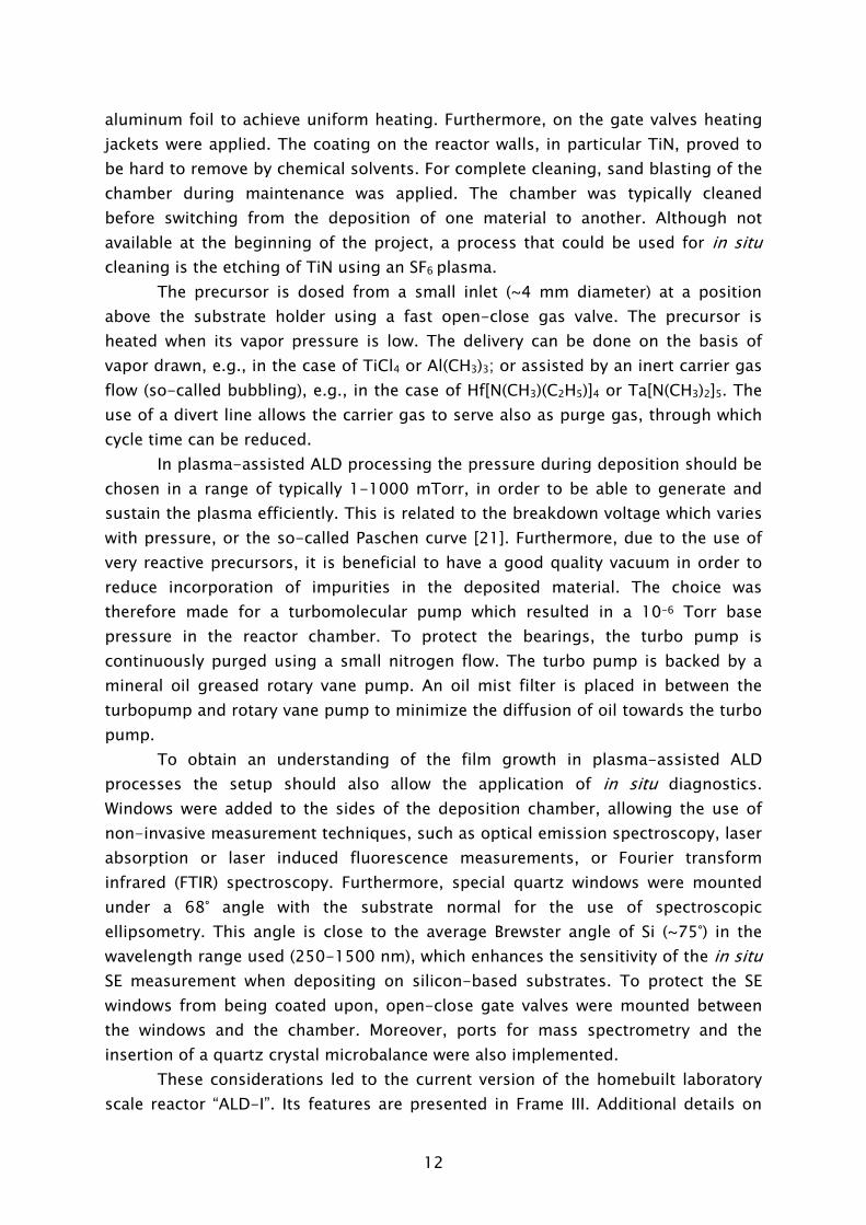
These considerations led to the current version of the homebuilt laboratory scale reactor “ALD-I”. Its features are presented in Frame III. Additional details on
13
Frame III. Plasma-assisted ALD reactors ALD-I
Manufacturer: homebuilt Plasma source: ICP (60 mm diameter, 0-100 W) Source gases: H2, N2, O2, NH3, Ar Precursors: 2 connections Substrate loading: open-load Substrate: up to 100 mm diameter Deposition temperature: RT-400 °C Wall heating: RT-150 °C Diagnostics: spectroscopic ellipsometry, mass spectrometry, optical emission spectroscopy, quartz crystal microbalance, Fourier transform infrared spectroscopy, Langmuir probe Processes developed: TiN from TiCl4 and H2-N2 plasma [22-24] TaNx from Ta[N(CH3)2]5 and H2, NH3, H2-N2 plasma [25,26] Ta2O5 from Ta[N(CH3)2]5 and O2 plasma [27] Al2O3 from Al(CH3)3 and O2 plasma, Al(CH3)3 and H2O [28-31, 32] AlN from Al(CH3)3 and H2-N2 plasma [30]
FlexAL RPT
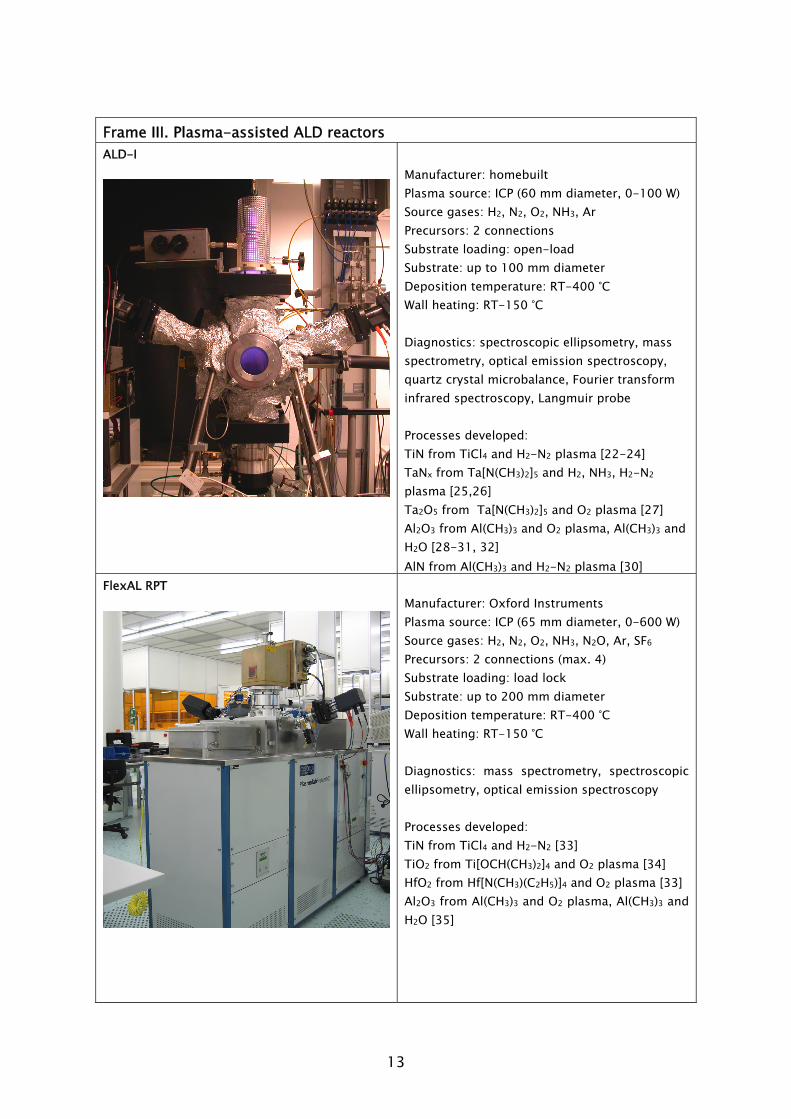
Manufacturer: Oxford Instruments Plasma source: ICP (65 mm diameter, 0-600 W) Source gases: H2, N2, O2, NH3, N2O, Ar, SF6 Precursors: 2 connections (max. 4) Substrate loading: load lock Substrate: up to 200 mm diameter Deposition temperature: RT-400 °C Wall heating: RT-150 °C Diagnostics: mass spectrometry, spectroscopic ellipsometry, optical emission spectroscopy Processes developed: TiN from TiCl4 and H2-N2 [33] TiO2 from Ti[OCH(CH3)2]4 and O2 plasma [34] HfO2 from Hf[N(CH3)(C2H5)]4 and O2 plasma [33] Al2O3 from Al(CH3)3 and O2 plasma, Al(CH3)3 and H2O [35]
14
the ALD-I reactor can be found in Chapter 3 of this thesis. Currently, this type of reactor, based on the remote ICP concept, is the most commonly used for remote plasma-assisted ALD processing [1,36-38].
C. The Oxford Instruments FlexAL reactor
The rising interest in ALD both in industry and academia (cf. Fig. 1) was the motivation for Oxford Instruments to investigate the market for plasma-assisted ALD reactors. The PMP groups’ expertise in plasmas and diagnostics combined with the experience already gained in plasma-assisted ALD on the ALD-I reactor provided a unique opportunity for co-developing their first commercial plasma ALD reactor, the FlexAL.2 The FlexAL is also a remote plasma-assisted ALD reactor. Similar to the ALD-I, it is based on the remote ICP concept. A beta-version of the Oxford Instruments FlexAL reactor is currently installed in the Eindhoven University clean room, as shown in Frame III. Key advantages compared to the ALD-I, are the capability to process large substrates (up to 200 mm) and the availability of a load lock. In our case, a spectroscopic ellipsometer and mass spectrometer are mounted for process development and monitoring. The features of the FlexAL are extensively described in Chapter 4 of this thesis. III. Opportunities and challenges for plasma-assisted atomic layer deposition
Thermal ALD is already being used in the manufacturing of several applications such as TFEL displays (Planar company in Finland uses ALD already for more than two decades) [39], read-write heads in hard disks, and in (embedded) DRAM [40,41]. Recently, it was announced by both Intel and IBM that ALD will be utilized for the fabrication of the high-k dielectric in their complementary-metal-oxide-semiconductor (CMOS) transistors in the 45 nm technology [10]. The use of plasma-assisted ALD is however still in a development phase at (corporate) research institutes and universities.
The investigation of the films grown by plasma-assisted ALD processes, as presented in Part B of this thesis, demonstrates that the introduction of a plasma step in the ALD cycle is a very promising development. The plasma-assisted ALD approach yields several potential benefits, in addition to the earlier mentioned merits of the thermal ALD process mentioned in Section I:
• Improved material properties including higher film density, lower impurity
levels, and better control of film composition and microstructure;
2 In the development of the FlexAL reactor Dr. H. Jeon (Hangyang University, South Korea), Dr. Steve Rossnagel (IBM Research, USA) and Dr. W.M.M. Kessels (Eindhoven University, The Netherlands), took place in an international advisory panel.
15
• Deposition at reduced substrate temperatures due to the increased reactivity provided by the plasma species;
• Increased growth per cycle as well as reduced purging steps, especially at low substrate temperatures;
• Good control of film stoichiometry by tailoring the plasma step as well as the possibility to introduce dopants by co-doping during the plasma step;
• Increased choice of precursors and obtainable materials, including high quality single element films (metals), difficult to obtain by thermal ALD;
• More process versatility due to the possibility of in situ substrate conditioning, plasma densification, nitridation, etc. These benefits can be illustrated by several examples taken from the
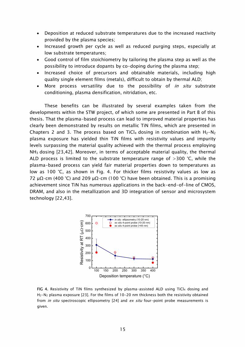
developments within the STW project, of which some are presented in Part B of this thesis. That the plasma-based process can lead to improved material properties has clearly been demonstrated by results on metallic TiN films, which are presented in Chapters 2 and 3. The process based on TiCl4
dosing in combination with H2-N2 plasma exposure has yielded thin TiN films with resistivity values and impurity levels surpassing the material quality achieved with the thermal process employing NH3
dosing [23,42]. Moreover, in terms of acceptable material quality, the thermal ALD process is limited to the substrate temperature range of >300 °C, while the plasma-based process can yield fair material properties down to temperatures as low as 100 °C, as shown in Fig. 4. For thicker films resistivity values as low as 72 μΩ·cm (400 °C) and 209 μΩ·cm (100 °C) have been obtained. This is a promising achievement since TiN has numerous applications in the back-end-of-line of CMOS, DRAM, and also in the metallization and 3D integration of sensor and microsystem technology [22,43].
100 150 200 250 300 350 4000
100
200
300
400
500
600
700
in situ ellipsometry (10-20 nm) ex situ 4-point probe (10-20 nm) ex situ 4-point probe (>45 nm)
Res
istiv
ity a
t RT
(μΩ
·cm
)
Deposition temperature (°C) FIG 4. Resistivity of TiN films synthesized by plasma-assisted ALD using TiCl4 dosing and H2-N2 plasma exposure [23]. For the films of 10-20 nm thickness both the resistivity obtained from in situ spectroscopic ellipsometry [24] and ex situ four-point probe measurements is given.
16
High quality Al2O3 films can be synthesized by plasma-assisted ALD using
the combination of Al(CH3)3 dosing and O2 plasma exposure, even at room
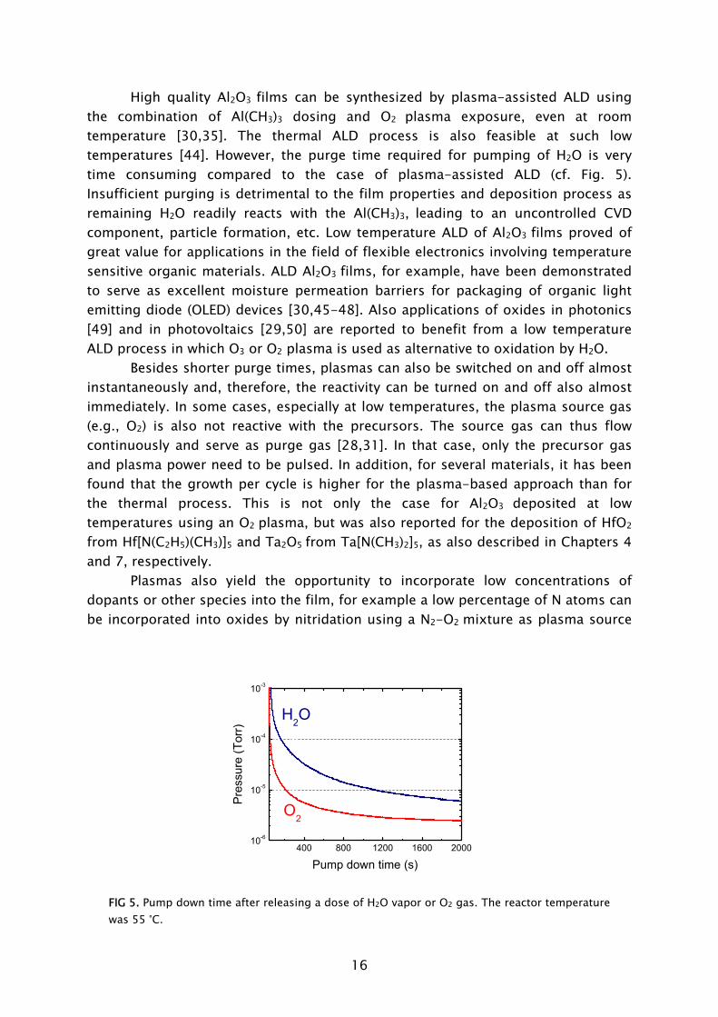
temperature [30,35]. The thermal ALD process is also feasible at such low temperatures [44]. However, the purge time required for pumping of H2O is very time consuming compared to the case of plasma-assisted ALD (cf. Fig. 5). Insufficient purging is detrimental to the film properties and deposition process as remaining H2O readily reacts with the Al(CH3)3, leading to an uncontrolled CVD component, particle formation, etc. Low temperature ALD of Al2O3
films proved of great value for applications in the field of flexible electronics involving temperature sensitive organic materials. ALD Al2O3
films, for example, have been demonstrated to serve as excellent moisture permeation barriers for packaging of organic light emitting diode (OLED) devices [30,45-48]. Also applications of oxides in photonics [49] and in photovoltaics [29,50] are reported to benefit from a low temperature ALD process in which O3 or O2 plasma is used as alternative to oxidation by H2O.
Besides shorter purge times, plasmas can also be switched on and off almost instantaneously and, therefore, the reactivity can be turned on and off also almost immediately. In some cases, especially at low temperatures, the plasma source gas (e.g., O2) is also not reactive with the precursors. The source gas can thus flow continuously and serve as purge gas [28,31]. In that case, only the precursor gas and plasma power need to be pulsed. In addition, for several materials, it has been found that the growth per cycle is higher for the plasma-based approach than for the thermal process. This is not only the case for Al2O3
deposited at low temperatures using an O2
plasma, but was also reported for the deposition of HfO2 from Hf[N(C2H5)(CH3)]5 and Ta2O5 from Ta[N(CH3)2]5, as also described in Chapters 4 and 7, respectively.
Plasmas also yield the opportunity to incorporate low concentrations of dopants or other species into the film, for example a low percentage of N atoms can be incorporated into oxides by nitridation using a N2-O2
mixture as plasma source
400 800 1200 1600 200010-6
10-5
10-4
10-3
H2O
Pre
ssur
e (T
orr)
Pump down time (s)
O2
FIG 5. Pump down time after releasing a dose of H2O vapor or O2 gas. The reactor temperature was 55 °C.
17
gas [30]. The stoichiometry of the films can be controlled by tailoring the plasma composition and exposure time which has clearly been demonstrated for metal nitrides. For example for TaN deposited from metalorganic precursors (e.g., Ta[N(CH3)2]5) it is possible to tune the material properties [26,51]: from insulating N-rich Ta3N5 by using a H2-N2
plasma to low resistivity cubic TaN by using H2 plasma exposure. In the deposition of TiN, presented in Chapter 3, the variation of the H2-N2 plasma exposure time from 5 to 60 s resulted in a control of the stoichiometry ([N]/[Ti]) ranging from 0.93 to 1.15.
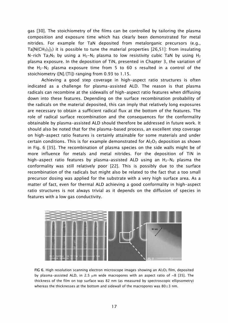
Achieving a good step coverage in high-aspect ratio structures is often indicated as a challenge for plasma-assisted ALD. The reason is that plasma radicals can recombine at the sidewalls of high-aspect ratio features when diffusing down into these features. Depending on the surface recombination probability of the radicals on the material deposited, this can imply that relatively long exposures are necessary to obtain a sufficient radical flux at the bottom of the features. The role of radical surface recombination and the consequences for the conformality obtainable by plasma-assisted ALD should therefore be addressed in future work. It should also be noted that for the plasma-based process, an excellent step coverage on high-aspect ratio features is certainly attainable for some materials and under certain conditions. This is for example demonstrated for Al2O3 deposition as shown in Fig. 6 [35]. The recombination of plasma species on the side walls might be of more influence for metals and metal nitrides. For the deposition of TiN in high-aspect ratio features by plasma-assisted ALD using an H2-N2 plasma the conformality was still relatively poor [22]. This is possibly due to the surface recombination of the radicals but might also be related to the fact that a too small precursor dosing was applied for the substrate with a very high surface area. As a matter of fact, even for thermal ALD achieving a good conformality in high-aspect ratio structures is not always trivial as it depends on the diffusion of species in features with a low gas conductivity.
FIG 6. High resolution scanning electron microscope images showing an Al2O3 film, deposited by plasma-assisted ALD, in 2.5 μm wide macropores with an aspect ratio of ~8 [35]. The thickness of the film on top surface was 82 nm (as measured by spectroscopic ellipsometry) whereas the thicknesses at the bottom and sidewall of the macropores was 80±3 nm.
18
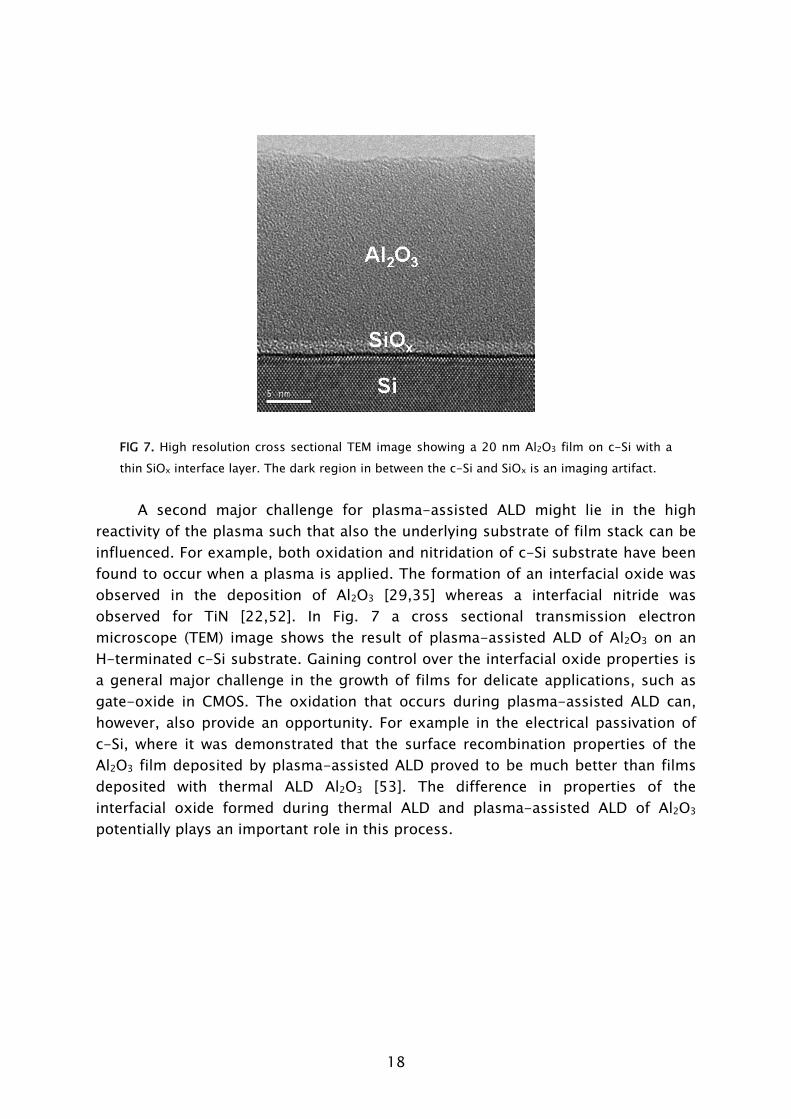
FIG 7. High resolution cross sectional TEM image showing a 20 nm Al2O3 film on c-Si with a thin SiOx interface layer. The dark region in between the c-Si and SiOx is an imaging artifact.
A second major challenge for plasma-assisted ALD might lie in the high
reactivity of the plasma such that also the underlying substrate of film stack can be influenced. For example, both oxidation and nitridation of c-Si substrate have been found to occur when a plasma is applied. The formation of an interfacial oxide was observed in the deposition of Al2O3 [29,35] whereas a interfacial nitride was observed for TiN [22,52]. In Fig. 7 a cross sectional transmission electron microscope (TEM) image shows the result of plasma-assisted ALD of Al2O3 on an H-terminated c-Si substrate. Gaining control over the interfacial oxide properties is a general major challenge in the growth of films for delicate applications, such as gate-oxide in CMOS. The oxidation that occurs during plasma-assisted ALD can, however, also provide an opportunity. For example in the electrical passivation of c-Si, where it was demonstrated that the surface recombination properties of the Al2O3 film deposited by plasma-assisted ALD proved to be much better than films deposited with thermal ALD Al2O3 [53]. The difference in properties of the interfacial oxide formed during thermal ALD and plasma-assisted ALD of Al2O3 potentially plays an important role in this process.
19
IV Reaction mechanisms A. Introduction
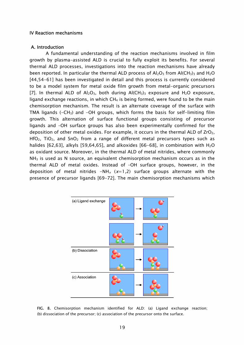
A fundamental understanding of the reaction mechanisms involved in film growth by plasma-assisted ALD is crucial to fully exploit its benefits. For several thermal ALD processes, investigations into the reaction mechanisms have already been reported. In particular the thermal ALD process of Al2O3 from Al(CH3)3 and H2O [44,54-61] has been investigated in detail and this process is currently considered to be a model system for metal oxide film growth from metal-organic precursors [7]. In thermal ALD of Al2O3, both during Al(CH3)3 exposure and H2O exposure, ligand exchange reactions, in which CH4 is being formed, were found to be the main chemisorption mechanism. The result is an alternate coverage of the surface with TMA ligands (-CH3) and -OH groups, which forms the basis for self-limiting film growth. This alternation of surface functional groups consisting of precursor ligands and –OH surface groups has also been experimentally confirmed for the deposition of other metal oxides. For example, it occurs in the thermal ALD of ZrO2, HfO2, TiO2, and SnO2 from a range of different metal precursors types such as halides [62,63], alkyls [59,64,65], and alkoxides [66-68], in combination with H2O as oxidant source. Moreover, in the thermal ALD of metal nitrides, where commonly NH3 is used as N source, an equivalent chemisorption mechanism occurs as in the thermal ALD of metal oxides. Instead of –OH surface groups, however, in the deposition of metal nitrides -NHx (x=1,2) surface groups alternate with the presence of precursor ligands [69-72]. The main chemisorption mechanisms which
FIG. 8. Chemisorption mechanism identified for ALD: (a) Ligand exchange reaction; (b) dissociation of the precursor; (c) association of the precursor onto the surface.
20
have been found in thermal ALD are shown schematically in Fig. 8. Next to ligand exchange, there exists mechanisms involving dissociation of the precursor, in which the ligands are split off but remain at the surface, and association, in which the precursor remains intact but bonded to the surface [7].
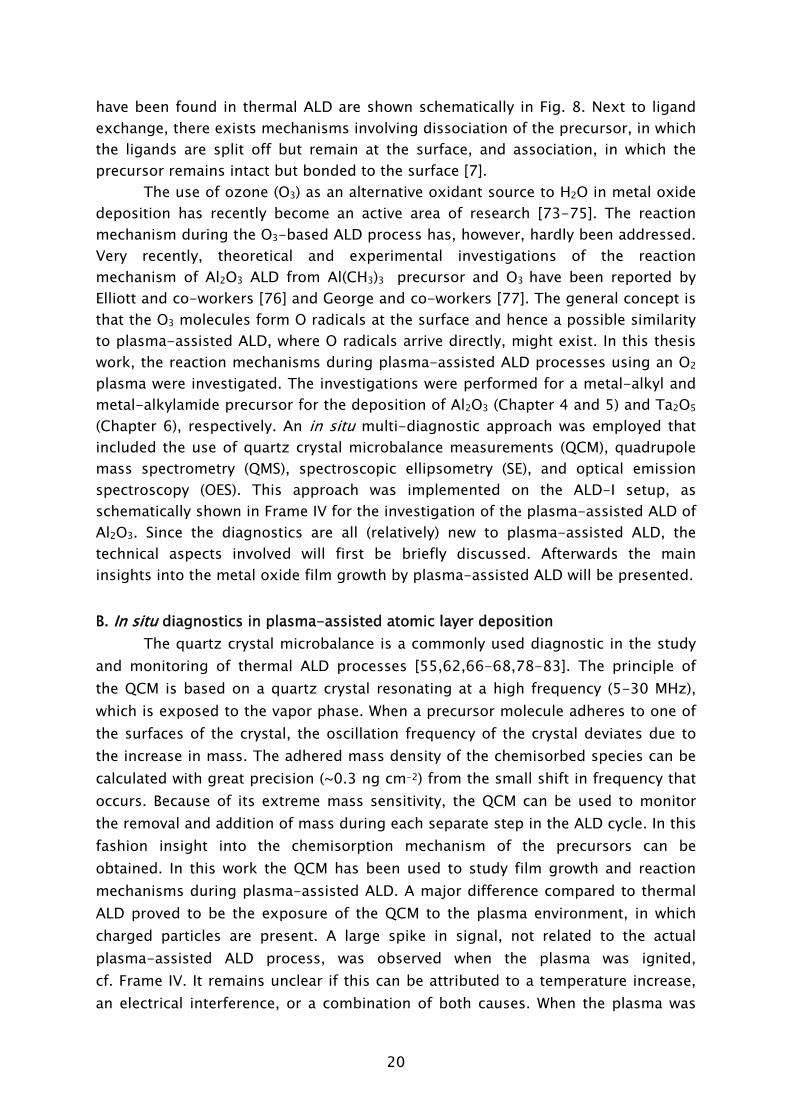
The use of ozone (O3) as an alternative oxidant source to H2O in metal oxide deposition has recently become an active area of research [73-75]. The reaction mechanism during the O3-based ALD process has, however, hardly been addressed. Very recently, theoretical and experimental investigations of the reaction mechanism of Al2O3 ALD from Al(CH3)3 precursor and O3 have been reported by Elliott and co-workers [76] and George and co-workers [77]. The general concept is that the O3 molecules form O radicals at the surface and hence a possible similarity to plasma-assisted ALD, where O radicals arrive directly, might exist. In this thesis work, the reaction mechanisms during plasma-assisted ALD processes using an O2 plasma were investigated. The investigations were performed for a metal-alkyl and metal-alkylamide precursor for the deposition of Al2O3 (Chapter 4 and 5) and Ta2O5 (Chapter 6), respectively. An in situ multi-diagnostic approach was employed that included the use of quartz crystal microbalance measurements (QCM), quadrupole mass spectrometry (QMS), spectroscopic ellipsometry (SE), and optical emission spectroscopy (OES). This approach was implemented on the ALD-I setup, as schematically shown in Frame IV for the investigation of the plasma-assisted ALD of Al2O3. Since the diagnostics are all (relatively) new to plasma-assisted ALD, the technical aspects involved will first be briefly discussed. Afterwards the main insights into the metal oxide film growth by plasma-assisted ALD will be presented. B. In situ diagnostics in plasma-assisted atomic layer deposition
The quartz crystal microbalance is a commonly used diagnostic in the study and monitoring of thermal ALD processes [55,62,66-68,78-83]. The principle of the QCM is based on a quartz crystal resonating at a high frequency (5-30 MHz), which is exposed to the vapor phase. When a precursor molecule adheres to one of the surfaces of the crystal, the oscillation frequency of the crystal deviates due to the increase in mass. The adhered mass density of the chemisorbed species can be calculated with great precision (~0.3 ng cm-2) from the small shift in frequency that occurs. Because of its extreme mass sensitivity, the QCM can be used to monitor the removal and addition of mass during each separate step in the ALD cycle. In this fashion insight into the chemisorption mechanism of the precursors can be obtained. In this work the QCM has been used to study film growth and reaction mechanisms during plasma-assisted ALD. A major difference compared to thermal ALD proved to be the exposure of the QCM to the plasma environment, in which charged particles are present. A large spike in signal, not related to the actual plasma-assisted ALD process, was observed when the plasma was ignited, cf. Frame IV. It remains unclear if this can be attributed to a temperature increase, an electrical interference, or a combination of both causes. When the plasma was
21
turned off, the QCM signal recovered over a time period of ~10 s after which a correct value of the mass change could be deduced.
Mass spectrometry has been previously used in the study of several thermal ALD processes [54,55,67,72,84,85]. In this work, the quadrupole mass spectrometer (QMS) is separately pumped and gas sampling occurs via a small diameter pinhole which connects it to the deposition chamber. A major difference compared to thermal ALD is that the highly reactive radicals, which form the surface reactants in plasma-assisted ALD, have a negligible chance to be detected in the mass spectrometer. The radicals have a low flux compared to the unreactive neutral species such that their signals cannot easily be distinguished. Moreover, the radicals will have many wall collisions before reaching the ionizer of the QMS and therefore their signal will also be reduced due to surface recombination. In this work it was demonstrated that the consumption of radicals, such as O, H, and N, in for example, O2, H2, N2 plasmas can, however, be monitored indirectly via the depletion of the source gas.
Spectroscopic ellipsometry is an often used thin film measurement technique to determine the thickness and optical properties of films. New in this work is that SE was applied in situ for ALD, which allowed for the fast evaluation of saturated growth conditions [22]. Moreover, on the basis of the in situ SE measurements the evolution of the material properties, such as electrical resistivity, composition, and microstructure could also be determined during the plasma-assisted ALD film growth [24,26,34]. The SE modeling and measurement procedures are the topic of another PhD thesis related to this project [19].
Optical emission spectroscopy is a commonly used diagnostic in the study of plasmas and plasma processing of materials. The technique is based on the analysis of the light emitted by the electronically excited species in the plasma. The optical decay of the excited atom or molecule gives rise to the emission of light with a characteristic wavelength associated with the energy levels of the atom or molecule involved. The presence of a certain molecule can therefore be deduced from the identification of the emission lines present in the emission spectrum. The use of OES to determine the radical species in plasma-assisted ALD has also been reported by others [86,87]. However, in this work it was observed that the light emission during processing was different to the normal plasma operation due to the presence of gas phase reaction products [28,31]. Moreover, by monitoring the emission related to the presence of reaction products as a function of time, it has been demonstrated that OES can be a valuable technique in the optimization of plasma-assisted ALD processes [88].
22
Frame IV: Reaction mechanism studies of plasma-assisted ALD of Al2O3
Quartz Crystal Microbalance (mass uptake)
Mas
s ga
in (H
z)
Time (s)0 20 40
-15
-10
-5
0
5
10
Precursor
Plasma off
1 cyclePlasma on
(a)
0 10 20 30
Plasma off(b)
Plasma on
Spectroscopic Ellipsometry (thickness increase)
0 100 200 3000
100
200
300
400
500
600
70 °C 200 °C
Thic
knes
s (Å
)
Number of cycles
(Quadrupole) Mass Spectrometry (reaction products)
0 20 40 6010-13
10-12
10-11
10-10
15
4428
18
32
Ion
curr
ent (
A)
Time (s)
PlasmaAl(CH3)3
16
m/z
Optical Emission Spectroscopy
(plasma species)
300 400 500 600 700 8000
500
1000
1500
2000
OH (A²Σ -X²Π)
Hα
CO+ (B2Σ+-A2Πi) / (A2Πi-X
2Σ+)
Inte
nsity
(a.u
.)
Wavelength (nm)
CO (b3Σ+-a3Πr) / (C1Σ+-A1Πi) / (B
1Σ+-A1Π)
Hβ
23
C. Main insights into the reaction mechanisms during plasma-assisted ALD of metal oxides
Two different types of metal-organic precursors were chosen to investigate the reaction mechanisms during metal oxide film growth by plasma-assisted ALD. The alkyl-based Al(CH3)3 was used as Al source in Al2O3 deposition and the alkylamine-based Ta(N(CH3)2)5 as Ta source in the deposition of Ta2O5 [27,28,31].
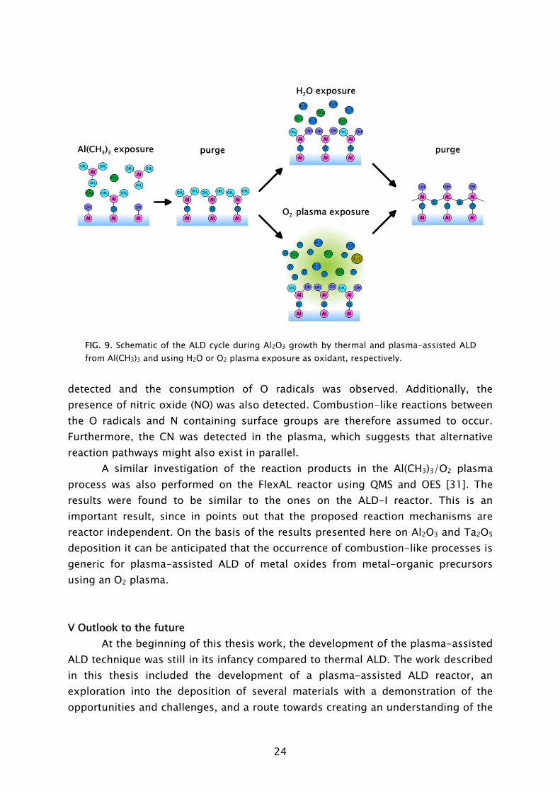
During the Al(CH3)3 exposure, CH4 was detected to leave the surface into the gas phase [28,33]. This indicates that in the chemisorption of Al(CH3)3 an H atom is abstracted from the surface to form a volatile CH4 molecule together with one of the –CH3 ligands. A proposed mechanism could be ligand exchange, similarly as in thermal ALD.3 The plasma-assisted ALD process of Al2O3 from Al(CH3)3 in which O2 plasma exposure is used for oxidation is schematically shown in Fig. 9. The thermal ALD process using H2O is also shown for comparison.
During the O2 plasma exposure, the presence of H2O, CO2, and CO was detected in the gas phase. Furthermore, the consumption of O radicals was observed by a decrease in the O2 density by QMS and in the O radical light emission coming from the plasma by OES. These observations demonstrate that combustion-like reactions in which the surface groups are converted by O radicals into combustion products occur at the surface. Moreover, the chemisorbed precursor is oxidized and new surface groups are formed. In addition to the combustion products, also CH4 was detected to be produced during the O2 plasma exposure. The observance of CH4 can be explained by the fact that the produced H2O is also acting as an additional oxidant source next to the O radicals. This reveals that besides the combustion-like reactions more reaction pathways appear to be active. Thirdly, C2Hx species were detected in relative small amounts. This indicates that, although minor, a third reaction pathway, e.g., association processes at the surface, might be active, as also suggested on the basis of theoretical calculations [56,76].
For the case of Ta2O5, during the Ta(N(CH3)2)5 dosing, the formation of
reaction products could not be observed by mass spectrometry in the range studied (m/z = 15-46). This might suggest a chemisorption mechanism in which the complete precursor molecule remains on the surface, such as the dissociation or association mechanisms presented earlier. We would like to note that there is little literature data available about the surface composition of amorphous Ta2O5, in particular after the oxidation step in thermal ALD. Moreover, the chemisorption of metal-alkylamides has not been as extensively studied as for metal-alkyl or metal-halide precursors. Similar as in the case of Al2O3, during the O2 plasma exposure in the plasma-assisted ALD of Ta2O5, CO, CO2, and H2O were also 3 In a separate experiment on plasma-assisted ALD of Al2O3, in situ Fourier transform infrared measurements revealed the presence of –OH groups on the surface after O2 plasma exposure. After Al(CH3)3 dosing it was determined that the surface was covered with –CH3 groups [32].
24
detected and the consumption of O radicals was observed. Additionally, the presence of nitric oxide (NO) was also detected. Combustion-like reactions between the O radicals and N containing surface groups are therefore assumed to occur. Furthermore, the CN was detected in the plasma, which suggests that alternative reaction pathways might also exist in parallel.
A similar investigation of the reaction products in the Al(CH3)3/O2 plasma process was also performed on the FlexAL reactor using QMS and OES [31]. The results were found to be similar to the ones on the ALD-I reactor. This is an important result, since in points out that the proposed reaction mechanisms are reactor independent. On the basis of the results presented here on Al2O3 and Ta2O5 deposition it can be anticipated that the occurrence of combustion-like processes is generic for plasma-assisted ALD of metal oxides from metal-organic precursors using an O2 plasma.
V Outlook to the future At the beginning of this thesis work, the development of the plasma-assisted
ALD technique was still in its infancy compared to thermal ALD. The work described in this thesis included the development of a plasma-assisted ALD reactor, an exploration into the deposition of several materials with a demonstration of the opportunities and challenges, and a route towards creating an understanding of the
FIG. 9. Schematic of the ALD cycle during Al2O3 growth by thermal and plasma-assisted ALD from Al(CH3)3 and using H2O or O2 plasma exposure as oxidant, respectively.
25
reaction mechanisms in plasma-assisted ALD. With the interest in ALD shown by industry, the reactor and process
development has progressed the past years. In particular, the improvement of material properties at low temperatures has broadened the interest, in particular in plasma-assisted ALD processing. With the infrastructure available in our group, a widescale investigation into plasma-assisted ALD processes for a variety of processes and applications has started. Related to this project, the application of Al2O3 has been investigated as dielectric in metal-insulator-metal (MIM) capacitors [35,89,90], as passivation layer on c-Si for solar cell applications [29,50], and as moisture diffusion barrier in organic light emitting diode (OLED) devices [30]. Moreover, TiN has been tested as a diffusion barrier and copper plating base in the Cu filling of through wafer vias and as an electrode in MIM capacitor structures [43]. TiN is currently also under investigation for the application as Li diffusion barrier in solid state batteries [91]. First results on the use of plasma-assisted ALD in these applications look promising and will aid the further development of plasma-assisted ALD equipment and processes to industrial readiness.
From a fundamental point of view, the study of the surface chemical composition is an important addition to the gas phase analysis presented in this work for obtaining a detailed understanding of film growth in plasma-assisted ALD. Besides studies of the surface composition using FTIR, which have already been initiated on the basis of this work, the time has come to include more sensitive techniques such as evanescent wave cavity ring down spectroscopy (EW-CRDS) [92,93]. This technique has already been used in our group in the study of the growth of a-Si:H [94,95], and has demonstrated its potential in determining surface coverage with sub-monolayer sensitivity [96]. Preferably, this experiment should be done in a specialized beam setup under ultra high vacuum conditions [94,95,97,98].
Determining the role of ions and in particular ion bombardment in the deposition chemistry is an important topic for investigation. In the remote configuration presented in this work, this could for instance be done by applying a controlled substrate bias. The energy of the ions can then be tuned and the influence of ion bombardment on the film growth can be studied in more detail. The ion bombardment could potentially be an important factor to allow further improvement of material properties at low deposition temperatures. Furthermore, the results could be valuable to create a general understanding of the differences in film growth characteristics and material properties that are sometimes reported for different reactors and plasma-assisted ALD configurations.
26
References [1] S. M. Rossnagel, A. Sherman, and F. Turner, J. Vac. Sci. Technol. B 18, 2016
(2000). [2] Y. J. Lee and S. W. Kang, J. Vac. Sci. Technol. A 20, 1983 (2002). [3] H. Kim, A. J. Kellock, and S. M. Rossnagel, J. Appl. Phys. 92, 7080 (2002). [4] Cambridge Nanotech, http://www.cambridgenanotech.com/ [5] ASM, http://www.asm.com [6] Picosun, http://www.picosun.com [7] R. L. Puurunen, J. Appl. Phys. 97, 121301 (2005). [8] T. Suntola and J. Antson, U.S. Patent No. 4,058,430, 15 November 1977. [9] M. Leskelä and M. Ritala, Angew. Chem.-Int. Edit. 42, 5548 (2003). [10] Solid State Technology, March 1, 2007 [11] Thomson Scientific, Web of Science, part of ISI Web of science [12] Key words used: "atomic layer chemical vapor deposition", "atomic layer
deposition", "atomic layer epitaxy", "molecular lamination", "molecular layer epitaxy", "molecular layering", and "molecular stratification".
[13] A. Niskanen, K. Arstila, M. Ritala, and M. Leskelä, J. Electrochem. Soc. 152, F90 (2005).
[14] A. Niskanen, A. Rahtu, T. Sajavaara, K. Arstila, M. Ritala, and M. Leskelä, J. Electrochem. Soc. 152, G25 (2005).
[15] F. Greer, D. Fraser, J. W. Coburn, and D. B. Graves, J. Vac. Sci. Technol. A 21, 96 (2003).
[16] T. T. Van and J. P. Chang, Surf. Sci. 596, 1 (2005). [17] K.-E. Elers, T. Blomberg, M. Peussa, B. Aitchison, S. Haukka, and S. Marcus,
Chem. Vap. Deposition 12, 13 (2006). [18] Oxford Instruments, http://www.oxford-instruments.com [19] E. Langereis, PhD Thesis (Eindhoven University of Technology, Eindhoven,
2008). [20] M. A. Lieberman and A. J. Lichtenberg, Principles of Plasma Discharges and
Materials Processing (John Wiley & Sons Inc., New York, 1994). [21] J. Reece Roth, Industrial Plasma Engineering: Volume 1 Principles (Institute of
Physics, London, 1995). [22] S. B. S. Heil, E. Langereis, A. Kemmeren, F. Roozeboom, M. C. M. van de
Sanden, and W. M. M. Kessels, J. Vac. Sci. Technol. A 23, L5 (2005). [23] S. B. S. Heil, E. Langereis, F. Roozeboom, M. C. M. van de Sanden, and W. M.
M. Kessels, J. Electrochem. Soc. 153, G956 (2006). [24] E. Langereis, S. B. S. Heil, M. C. M. van de Sanden, and W. M. M. Kessels, J.
Appl. Phys. 100, 023534 (2006). [25] H. C. M. Knoops, Master Thesis (Eindhoven University of Technology,
Eindhoven, 2007). [26] E. Langereis, H. C. M. Knoops, A. J. M. Mackus, F. Roozeboom, M. C. M. van
de Sanden, and W. M. M. Kessels, J. Appl. Phys. 102, 083517 (2007).
27
[27] S. B. S. Heil, F. Roozeboom, M. C. M. van de Sanden, and W. M. M. Kessels, submitted for publication (2007).
[28] S. B. S. Heil, P. Kudlacek, E. Langereis, R. Engeln, M. C. M. van de Sanden, and W. M. M. Kessels, Appl. Phys. Lett. 89, 131505 (2006).
[29] B. Hoex, S. B. S. Heil, E. Langereis, M. C. M. van de Sanden, and W. M. M. Kessels, Appl. Phys. Lett. 89, 042112 (2006).
[30] E. Langereis, M. Creatore, S. B. S. Heil, M. C. M. van de Sanden, and W. M. M. Kessels, Appl. Phys. Lett. 89, 081915 (2006).
[31] S. B. S. Heil, J. L. Van Hemmen, M. C. M. van de Sanden, and W. M. M. Kessels, submitted for publication (2007).
[32] J. Keijmel, Master Thesis (Eindhoven University of Technology, Eindhoven, 2008).
[33] S. B. S. Heil, J. L. van Hemmen, C. J. Hodson, N. Singh, J. H. Klootwijk, F. Roozeboom, M. C. M. van de Sanden, and W. M. M. Kessels, J. Vac. Sci. Technol. A 25, 1357 (2007).
[34] W. Keuning, J. L. Van Hemmen, M. C. M. v. d. Sanden, and W. M. M. Kessels, (2007).
[35] J. L. van Hemmen, S. B. S. Heil, J. H. Klootwijk, F. Roozeboom, M. C. M. van de Sanden, and W. M. M. Kessels, J. Electrochem. Soc. 154, G165 (2007).
[36] G. A. Ten Eyck, J. J. Senkevich, F. Tang, D. L. Liu, S. Pimanpang, T. Karaback, G. C. Wang, T. M. Lu, C. Jezewski, and W. A. Lanford, Chem. Vap. Deposition 11, 60 (2005).
[37] W. J. Maeng, S. J. Park, and H. Kim, J. Vac. Sci. Technol. B 24, 2276 (2006). [38] J. Y. Kim, Y. Kim, and H. Jeon, Jpn. J. Appl. Phys., Part 2 42, L414 (2003). [39] Planar, www.planar.com [40] http://www.fabtech.org/content/view/1604 [41] http://www.fabtech.org/content/view/1658 [42] K.-E. Elers, J. Winkler, K. Weeks, and S. Marcus, J. Electrochem. Soc. 152,
G589 (2005). [43] S. B. S. Heil, E. Langereis, F. Roozeboom, A. Kemmeren, N. P. Pham, P. M.
Sarro, M. C. M. van de Sanden, and W. M. M. Kessels, Mater. Res. Soc. Symp. Proc. 863, B6.4.1 (2005).
[44] M. D. Groner, F. H. Fabreguette, J. W. Elam, and S. M. George, Chem. Mat. 16, 639 (2004).
[45] S. J. Yun, Y. W. Ko, and J. W. Lim, Appl. Phys. Lett. 85, 4896 (2004). [46] M. D. Groner, S. M. George, R. S. McLean, and P. F. Carcia, Appl. Phys. Lett.
88, 051907 (2006). [47] P. F. Carcia, R. S. McLean, M. H. Reilly, M. D. Groner, and S. M. George, Appl.
Phys. Lett. 89, 031915 (2006). [48] A. P. Ghosh, L. J. Gerenser, C. M. Jarman, and J. E. Fornalik, Appl. Phys. Lett.
86, 223503 (2005). [49] T. T. Van and J. P. Chang, Appl. Phys. Lett. 87, 011907 (2005).
28
[50] B. Hoex, J. Schmidt, R. Bock, P. P. Altermatt, M. C. M. van de Sanden, and W. M. M. Kessels, Appl. Phys. Lett. 91, 112107 (2007).
[51] H. Kim, C. Detavenier, O. van der Straten, S. M. Rossnagel, A. J. Kellock, and D. G. Park, J. Appl. Phys. 98, 8 (2005).
[52] E. Langereis, S. B. S. Heil, M. C. M. v. d. Sanden, and W. M. M. Kessels, Phys. Status Solidi C. 2, 3958 (2005).
[53] B. Hoex et al., to be published [54] M. Juppo, A. Rahtu, M. Ritala, and M. Leskelä, Langmuir 16, 4034 (2000). [55] A. Rahtu, T. Alaranta, and M. Ritala, Langmuir 17, 6506 (2001). [56] S. D. Elliott and J. C. Greer, J. Mater. Chem. 14, 3246 (2004). [57] Y. Widjaja and C. B. Musgrave, Appl. Phys. Lett. 80, 3304 (2002). [58] C. Soto and W. T. Tysoe, J. Vac. Sci. Technol. A 9, 2686 (1991). [59] A. C. Dillon, A. W. Ott, J. D. Way, and S. M. George, Surf. Sci. 322, 230 (1995). [60] A. W. Ott, K. C. McCarley, J. W. Klaus, J. D. Way, and S. M. George, Appl. Surf.
Sci. 107, 128 (1996). [61] A. W. Ott, J. W. Klaus, J. M. Johnson, and S. M. George, Thin Solid Films 292,
135 (1997). [62] A. Rahtu and M. Ritala, J. Mater. Chem. 12, 1484 (2002). [63] X. Du, Y. Du, and S. M. George, J. Vac. Sci. Technol. A 23, 581 (2005). [64] R. L. Puurunen, J. Appl. Phys. 95, 4777 (2004). [65] R. L. Puurunen, Chem. Vap. Deposition 11, 79 (2005). [66] K. Kukli, J. Aarik, A. Aidla, H. Siimon, M. Ritala, and M. Leskelä, Appl. Surf.
Sci. 112, 236 (1997). [67] A. Rahtu, K. Kukli, and M. Ritala, Chem. Mat. 13, 817 (2001). [68] A. Rahtu and M. Ritala, Chem. Vap. Deposition 8, 21 (2002). [69] R. L. Puurunen, M. Lindblad, A. Root, and A. O. I. Krause, Phys. Chem. Chem.
Phys. 3, 1093 (2001). [70] R. L. Puurunen, A. Root, S. Haukka, E. I. Iiskola, M. Lindblad, and A. O. I.
Krause, J. Phys. Chem. B 104, 6599 (2000). [71] R. L. Puurunen, A. Root, P. Sarv, S. Haukka, E. I. Iiskola, M. Lindblad, and A.
O. I. Krause, Appl. Surf. Sci. 165, 193 (2000). [72] M. Juppo, A. Rahtu, and M. Ritala, Chem. Mat. 14, 281 (2002). [73] J. B. Kim, D. R. Kwon, K. Chakrabarti, C. Lee, K. Y. Oh, and J. H. Lee, J. Appl.
Phys. 92, 6739 (2002). [74] J. Niinisto, M. Putkonen, L. Niinisto, K. Kukli, M. Ritala, and M. Leskela, J.
Appl. Phys. 95, 84 (2004). [75] Y. Senzaki, S. Park, H. Chatham, L. Bartholomew, and W. Nieveen, J. Vac. Sci.
Technol. A 22, 1175 (2004). [76] S. D. Elliott, G. Scarel, C. Wiemer, M. Fanciulli, and G. Pavia, Chem. Mat. 18,
3764 (2006). [77] D. N. Goldstein and S. M. George, presentation at the 6th AVS topical
conference on ALD, Seoul, South Korea (2006).
29
[78] J. W. Elam, M. D. Groner, and S. M. George, Rev. Sci. Instrum. 73, 2981 (2002).
[79] J. Aarik, A. Aidla, and K. Kukli, Appl. Surf. Sci. 75, 180 (1994). [80] A. Rahtu, T. Hanninen, and M. Ritala, J. Phys. IV 11, 923 (2001). [81] A. Rahtu and M. Ritala, Langmuir 18, 10046 (2002). [82] A. Rahtu and M. Ritala, Appl. Phys. Lett. 80, 521 (2002). [83] A. Rahtu, M. Ritala, and M. Leskela, Chem. Mat. 13, 1528 (2001). [84] M. Ritala, M. Juppo, K. Kukli, A. Rahtu, and M. Leskelä, J. Phys. IV 9, 1021
(1999). [85] R. Matero, A. Rahtu, and M. Ritala, Chem. Mat. 13, 4506 (2001). [86] J. Y. Kim, S. H. Kim, H. Seo, J. H. Kim, and H. Jeon, Electrochem. Solid-State
Lett. 8, G82 (2005). [87] J. Choi, S. Kim, J. Kim, H. Kang, H. Jeon, and C. Bae, J. Vac. Sci. Technol. A 24,
900 (2006). [88] A. J. M. Mackus, S. B. S. Heil, et al. to be published [89] J. L. van Hemmen, S. B. S. Heil, J. H. Klootwijk, F. Roozeboom, C. J. Hodson,
M. C. M. van de Sanden, and W. M. M. Kessels, ECS trans. 3 (2007). [90] F. Roozeboom, J. H. Klootwijk, J. F. C. Verhoeven, F. C. v. d. Heuvel, W.
Dekkers, S. B. S. Heil, J. L. van Hemmen, M. C. M. v. d. Sanden, W. M. M. Kessels, F. Le Cornec, L. Guirand, D. Chevrie, C. Bunel, F. Murray, H.-D. Kim, and D. Blin, ECS trans. 3, 173 (2007).
[91] H. C. M. Knoops, L. Bagetto, E. Langereis, M. C. M. Van de Sanden, J. H. Klootwijk, F. Roozeboom, R. A. H. Niessen, P. H. L. Notten, and W. M. M. Kessels, ECS trans. 11 (2007).
[92] A. C. R. Pipino, Appl. Opt. 39, 1449 (2000). [93] A. C. R. Pipino, J. W. Hudgens, and R. E. Huie, Rev. Sci. Instrum. 68, 2978
(1997). [94] I. M. P. Aarts, PhD Thesis (Eindhoven University of Technology, Eindhoven,
2006). [95] J. P. M. Hoefnagels, PhD Thesis (Eindhoven University of Technology,
Eindhoven, 2005). [96] I. M. P. Aarts, A. C. R. Pipino, J. P. M. Hoefnagels, W. M. M. Kessels, and M. C.
M. van de Sanden, Phys. Rev. Lett. 95 (2005). [97] P. J. v. d. Oever, PhD Thesis (Eindhoven University of Technology, Eindhoven,
2007). [98] A new project proposal (NWO Chemical Sciences) on the topic of surface
chemistry during plasma-assisted ALD has recently been granted. The research will start at the beginning of 2008.

30

Part B
Publications

32
33
Chapter 2 Plasma-Assisted Atomic Layer Deposition of TiN Monitored by in situ Spectroscopic Ellipsometry In situ spectroscopic ellipsometry has been employed to determine the properties of titanium nitride (TiN) films during plasma-assisted atomic layer deposition by alternating TiCl4 precursor dosing and H2-N2 plasma exposure. Besides monitoring the film thickness when optimizing the half reactions, it is shown that spectroscopic ellipsometry is a very valuable tool for in situ studies of (air-sensitive) film properties such as resistivity, and for investigating the nucleation phase during initial film growth.1
1 Published as: S. B. S. Heil, E. Langereis, A. Kemmeren, F. Roozeboom, M. C. M. van de Sanden, and
W. M. M. Kessels, J. Vac. Sci. Technol. A, 23, L5 (2005).
34
I. Introduction The processing challenges in next-generation semiconductor device
fabrication and integration make the self-limiting growth method of atomic layer deposition (ALD) a very innovative field from a scientific and technological perspective. For example, by the recent introduction of a low-temperature plasma step in the ALD reaction cycle, it is possible to deliver additional reactivity to the surface in the form of plasma-produced radical species. This opens up a processing parameter space that is unattainable by the strictly thermally driven process [1]. Plasma-assisted ALD, therefore, is a bright prospect in terms of increased choice of chemistry and precursors as well as in improved film quality at lower substrate temperatures and higher growth rates.
A key factor in (plasma-assisted) ALD, which still needs to be explored extensively, is in situ monitoring of the film growth and on-line process control. Currently, for (plasma-assisted) ALD the most common techniques used for in situ studies are quartz crystal microbalance measurements and mass spectrometry [2-4]. However, early insight into the growth of the film on the substrate material of interest and into the specific film properties obtained is also desired. This is especially relevant when information about the film properties during initial growth is required or when one cannot simply rely on ex situ film characterization, for example for film properties that change under air exposure.
In this Letter we will show that the optical technique of spectroscopic ellipsometry (SE) is a very valuable tool for in situ monitoring of the growth process and determining the film properties. We illustrate this for the plasma-assisted ALD process of titanium nitride (TiN) which is based on TiCl4 precursor dosing and H2-N2 plasma exposure and which is an extension of the set of metals and their nitrides deposited by plasma-assisted ALD as recently reviewed by Kim [5]. Thin metallic TiN films have wide-spread applications in semiconductor industry, for example as diffusion barrier layers in interconnect technology (for W, Al, etc.), as a future replacement for the poly-silicon gate electrode in metal-oxide-semiconductor (MOS-FET) gate stacks, and as metal electrode in high density MOS “trench” capacitors. From a comparison with ex situ techniques, we will show that SE gives accurate information on the TiN film thickness as well as on the resistivity of the films, even for very small film thicknesses (possibly as thin as 10 Å). Furthermore, it is revealed that SE also yields insight into the nucleation phase during initial film growth.
II. Experiment
The deposition system is similar to the one described by Rossnagel et al. [1] and consists of a H2-N2 operated plasma source connected through a gate valve to a deposition chamber. The radio frequency plasma power (100 W) is coupled inductively to the source that consists of a multiple-turn copper coil wrapped around a quartz tube. A resistively heated substrate holder is present in the chamber for depositing at elevated substrate temperatures (100-400 °C). TiCl4
35
vapor from a bottle with liquid TiCl4, kept at room temperature, is injected into the wall-heated chamber (20-200 °C) using a timed leak valve. TiN films were deposited at 400 °C on ~2 nm native-oxide and 1000 nm SiO2-covered c-Si substrates. One plasma-assisted ALD cycle typically consisted of 5 s exposure to TiCl4 (3 mTorr), followed by 10 s Ar purge, 15 s plasma exposure (10 mTorr H2 and 1 mTorr N2 partial pressures), and 10 s pump-down of the reactor to base pressure (10-6 Torr).
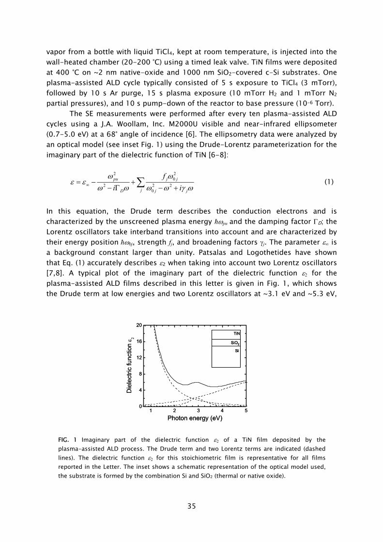
The SE measurements were performed after every ten plasma-assisted ALD cycles using a J.A. Woollam, Inc. M2000U visible and near-infrared ellipsometer (0.7-5.0 eV) at a 68° angle of incidence [6]. The ellipsometry data were analyzed by an optical model (see inset Fig. 1) using the Drude-Lorentz parameterization for the imaginary part of the dielectric function of TiN [6-8]:
2 2
02 2 2
0
pu j j
jD j j
fi i
ω ωε ε
ω ω ω ω γ ω∞= − +− Γ − +∑ (1)
In this equation, the Drude term describes the conduction electrons and is characterized by the unscreened plasma energy ħωpu and the damping factor ΓD; the Lorentz oscillators take interband transitions into account and are characterized by their energy position ħω0j, strength fj, and broadening factors γj. The parameter ε∞ is a background constant larger than unity. Patsalas and Logothetides have shown that Eq. (1) accurately describes ε2 when taking into account two Lorentz oscillators [7,8]. A typical plot of the imaginary part of the dielectric function ε2 for the plasma-assisted ALD films described in this letter is given in Fig. 1, which shows the Drude term at low energies and two Lorentz oscillators at ~3.1 eV and ~5.3 eV,
TiN
SiO2
Si
1 2 3 4 50
4
8
12
16
20
Die
lect
ric fu
nctio
n ε 2
Photon energy (eV)
TiN
SiO2
Si
TiN
SiO2
Si
1 2 3 4 50
4
8
12
16
20
Die
lect
ric fu
nctio
n ε 2
Photon energy (eV)
FIG. 1 Imaginary part of the dielectric function ε2 of a TiN film deposited by the plasma-assisted ALD process. The Drude term and two Lorentz terms are indicated (dashed lines). The dielectric function ε2 for this stoichiometric film is representative for all films reported in the Letter. The inset shows a schematic representation of the optical model used, the substrate is formed by the combination Si and SiO2 (thermal or native oxide).
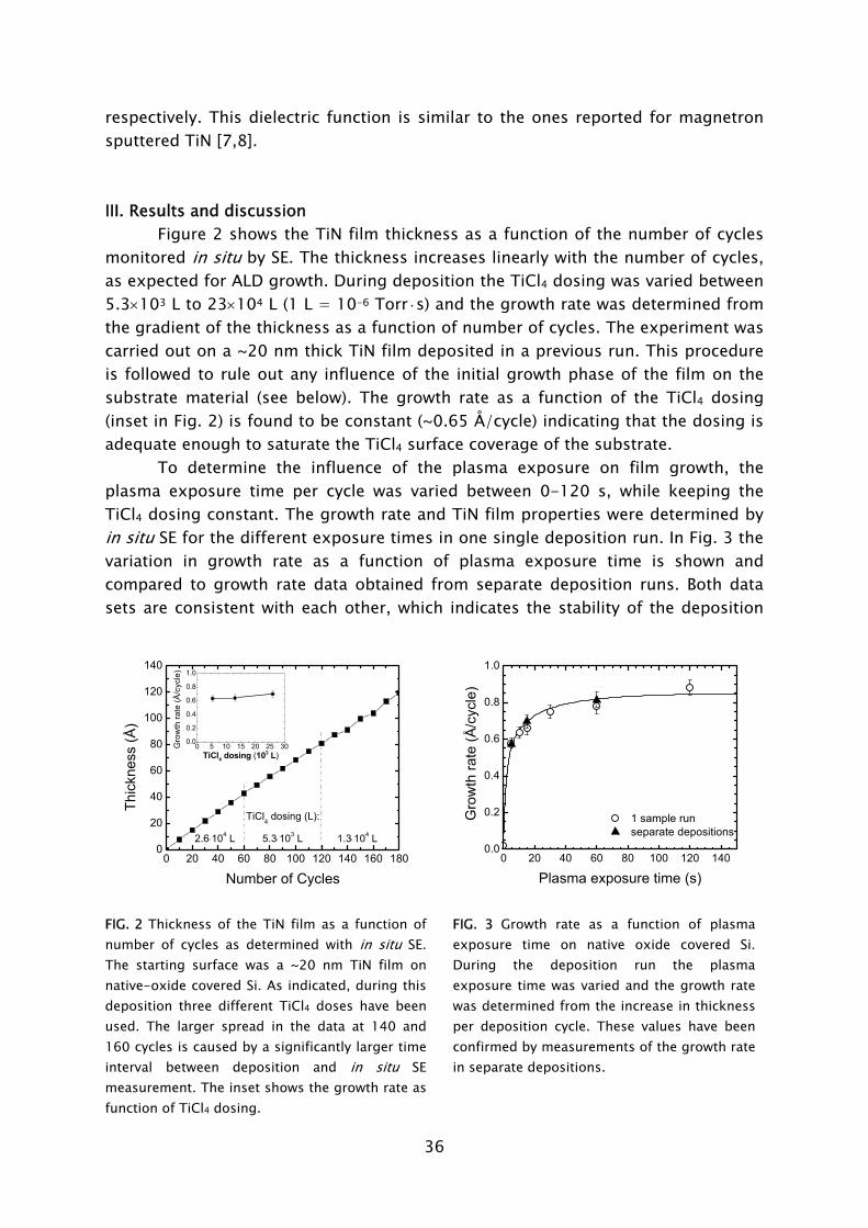
36
respectively. This dielectric function is similar to the ones reported for magnetron sputtered TiN [7,8].
III. Results and discussion
Figure 2 shows the TiN film thickness as a function of the number of cycles monitored in situ by SE. The thickness increases linearly with the number of cycles, as expected for ALD growth. During deposition the TiCl4 dosing was varied between 5.3×10³ L to 23×104 L (1 L = 10-6 Torr·s) and the growth rate was determined from the gradient of the thickness as a function of number of cycles. The experiment was carried out on a ~20 nm thick TiN film deposited in a previous run. This procedure is followed to rule out any influence of the initial growth phase of the film on the substrate material (see below). The growth rate as a function of the TiCl4 dosing (inset in Fig. 2) is found to be constant (~0.65 Å/cycle) indicating that the dosing is adequate enough to saturate the TiCl4 surface coverage of the substrate.
To determine the influence of the plasma exposure on film growth, the plasma exposure time per cycle was varied between 0-120 s, while keeping the TiCl4 dosing constant. The growth rate and TiN film properties were determined by in situ SE for the different exposure times in one single deposition run. In Fig. 3 the variation in growth rate as a function of plasma exposure time is shown and compared to growth rate data obtained from separate deposition runs. Both data sets are consistent with each other, which indicates the stability of the deposition
0 20 40 60 80 100 120 140 160 1800
20
40
60
80
100
120
140
0 5 10 15 20 25 300.0
0.2
0.4
0.6
0.8
1.0
TiCl4 dosing (L):
2.6⋅104 L 1.3⋅104 L5.3⋅103 L
Thic
knes
s (Å
)
Number of Cycles
Gro
wth
rate
(Å/c
ycle
)
TiCl4 dosing (103 L)
0 20 40 60 80 100 120 1400.0
0.2
0.4
0.6
0.8
1.0
1 sample run separate depositions
Gro
wth
rate
(Å/c
ycle
)
Plasma exposure time (s)
FIG. 2 Thickness of the TiN film as a function of number of cycles as determined with in situ SE. The starting surface was a ~20 nm TiN film on native-oxide covered Si. As indicated, during this deposition three different TiCl4 doses have been used. The larger spread in the data at 140 and 160 cycles is caused by a significantly larger time interval between deposition and in situ SE measurement. The inset shows the growth rate as function of TiCl4 dosing.
FIG. 3 Growth rate as a function of plasma exposure time on native oxide covered Si. During the deposition run the plasma exposure time was varied and the growth rate was determined from the increase in thickness per deposition cycle. These values have been confirmed by measurements of the growth rate in separate depositions.
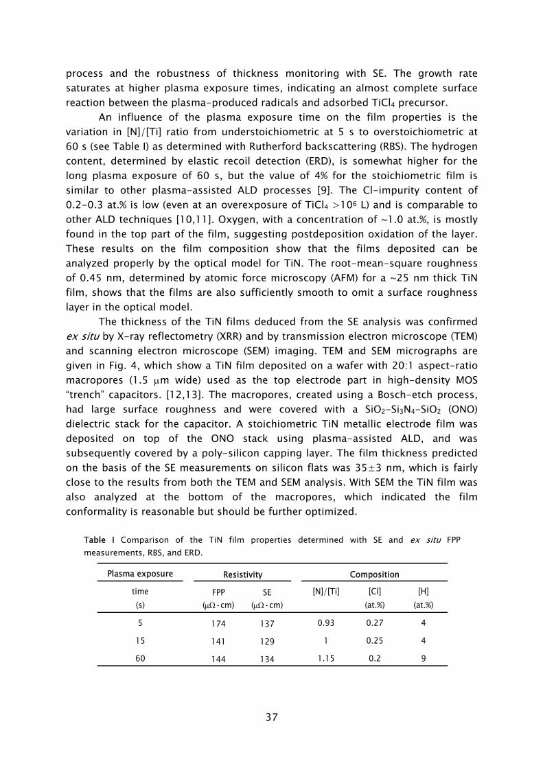
37
process and the robustness of thickness monitoring with SE. The growth rate saturates at higher plasma exposure times, indicating an almost complete surface reaction between the plasma-produced radicals and adsorbed TiCl4 precursor.
An influence of the plasma exposure time on the film properties is the variation in [N]/[Ti] ratio from understoichiometric at 5 s to overstoichiometric at 60 s (see Table I) as determined with Rutherford backscattering (RBS). The hydrogen content, determined by elastic recoil detection (ERD), is somewhat higher for the long plasma exposure of 60 s, but the value of 4% for the stoichiometric film is similar to other plasma-assisted ALD processes [9]. The Cl-impurity content of 0.2-0.3 at.% is low (even at an overexposure of TiCl4 >106 L) and is comparable to other ALD techniques [10,11]. Oxygen, with a concentration of ~1.0 at.%, is mostly found in the top part of the film, suggesting postdeposition oxidation of the layer. These results on the film composition show that the films deposited can be analyzed properly by the optical model for TiN. The root-mean-square roughness of 0.45 nm, determined by atomic force microscopy (AFM) for a ~25 nm thick TiN film, shows that the films are also sufficiently smooth to omit a surface roughness layer in the optical model.
The thickness of the TiN films deduced from the SE analysis was confirmed ex situ by X-ray reflectometry (XRR) and by transmission electron microscope (TEM) and scanning electron microscope (SEM) imaging. TEM and SEM micrographs are given in Fig. 4, which show a TiN film deposited on a wafer with 20:1 aspect-ratio macropores (1.5 μm wide) used as the top electrode part in high-density MOS “trench” capacitors. [12,13]. The macropores, created using a Bosch-etch process, had large surface roughness and were covered with a SiO2-Si3N4-SiO2 (ONO) dielectric stack for the capacitor. A stoichiometric TiN metallic electrode film was deposited on top of the ONO stack using plasma-assisted ALD, and was subsequently covered by a poly-silicon capping layer. The film thickness predicted on the basis of the SE measurements on silicon flats was 35±3 nm, which is fairly close to the results from both the TEM and SEM analysis. With SEM the TiN film was also analyzed at the bottom of the macropores, which indicated the film conformality is reasonable but should be further optimized.
Table I Comparison of the TiN film properties determined with SE and ex situ FPP measurements, RBS, and ERD.
Plasma exposure
time FPP SE [N]/[Ti] [Cl] [H](s) (μΩ•cm) (μΩ•cm) (at.%) (at.%)
5 174 137 0.93 0.27 4
15 141 129 1 0.25 4
60 144 134 1.15 0.2 9
Resistivity Composition
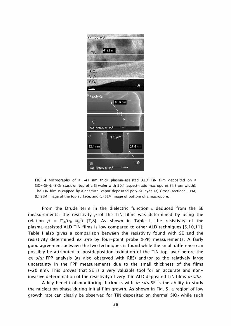
38
Si
poly-Si
TiN
40.6 nm
b)
Si
poly-Si
TiN
40.6 nm
b)
poly-Si
TiN
SiO2Si3N4
SiO2 Si
41±2 nm
a) poly-Si
TiN
SiO2Si3N4
SiO2 Si
41±2 nm
a)
1.5 μm
32.1 nm 27.5 nm
TiNSi
c) 1.5 μm
32.1 nm 27.5 nm
TiNSi
c)
FIG. 4 Micrographs of a ~41 nm thick plasma-assisted ALD TiN film deposited on a SiO2-Si3N4-SiO2 stack on top of a Si wafer with 20:1 aspect-ratio macropores (1.5 μm width). The TiN film is capped by a chemical vapor deposited poly-Si layer. (a) Cross-sectional TEM, (b) SEM image of the top surface, and (c) SEM image of bottom of a macropore.
From the Drude term in the dielectric function ε deduced from the SE
measurements, the resistivity ρ of the TiN films was determined by using the relation ρ = ΓD/(ε0 ωpu
2) [7,8]. As shown in Table I, the resistivity of the plasma-assisted ALD TiN films is low compared to other ALD techniques [5,10,11]. Table I also gives a comparison between the resistivity found with SE and the resistivity determined ex situ by four-point probe (FPP) measurements. A fairly good agreement between the two techniques is found while the small difference can possibly be attributed to postdeposition oxidation of the TiN top layer before the ex situ FPP analysis (as also observed with RBS) and/or to the relatively large uncertainty in the FPP measurements due to the small thickness of the films (~20 nm). This proves that SE is a very valuable tool for an accurate and non-invasive determination of the resistivity of very thin ALD deposited TiN films in situ.
A key benefit of monitoring thickness with in situ SE is the ability to study the nucleation phase during initial film growth. As shown in Fig. 5, a region of low growth rate can clearly be observed for TiN deposited on thermal SiO2 while such
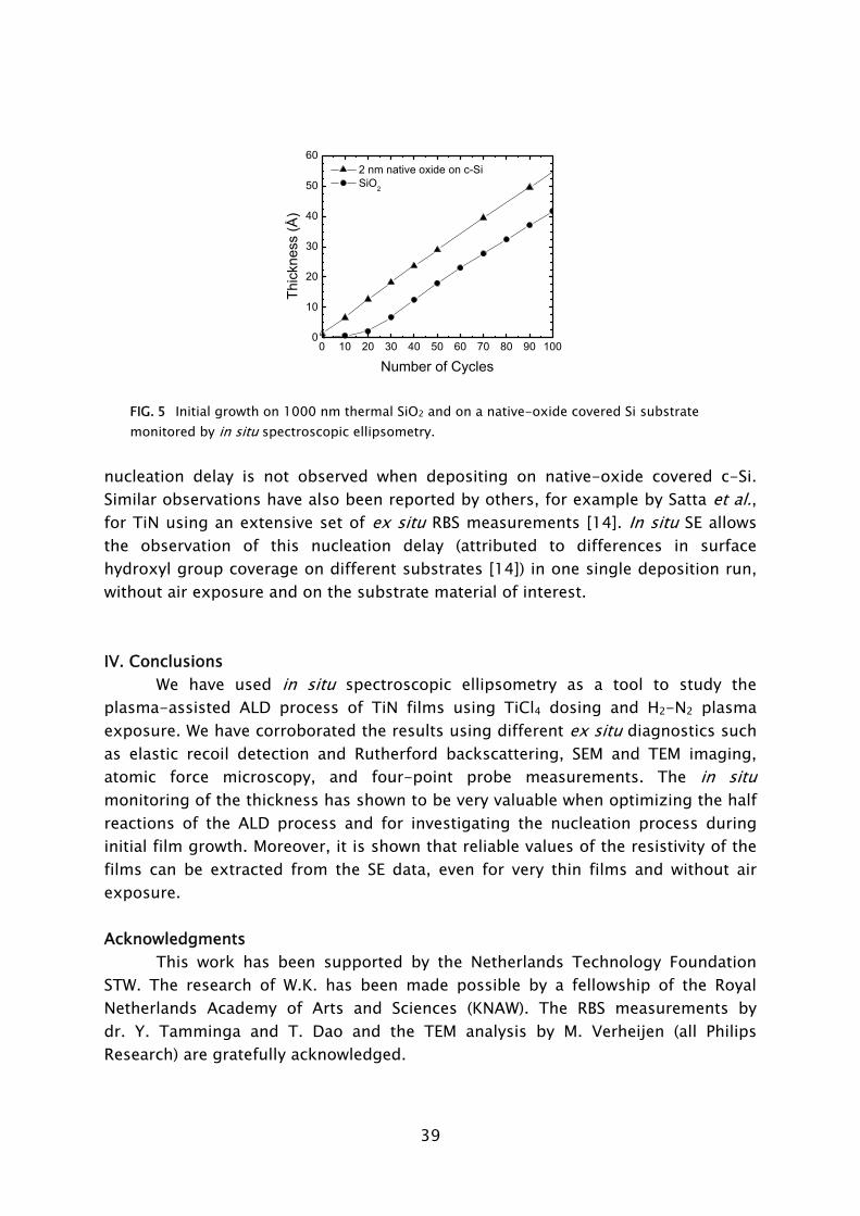
39
0 10 20 30 40 50 60 70 80 90 1000
10
20
30
40
50
60 2 nm native oxide on c-Si SiO2
Thic
knes
s (Å
)
Number of Cycles
FIG. 5 Initial growth on 1000 nm thermal SiO2 and on a native-oxide covered Si substrate monitored by in situ spectroscopic ellipsometry.
nucleation delay is not observed when depositing on native-oxide covered c-Si. Similar observations have also been reported by others, for example by Satta et al., for TiN using an extensive set of ex situ RBS measurements [14]. In situ SE allows the observation of this nucleation delay (attributed to differences in surface hydroxyl group coverage on different substrates [14]) in one single deposition run, without air exposure and on the substrate material of interest.
IV. Conclusions
We have used in situ spectroscopic ellipsometry as a tool to study the plasma-assisted ALD process of TiN films using TiCl4 dosing and H2-N2 plasma exposure. We have corroborated the results using different ex situ diagnostics such as elastic recoil detection and Rutherford backscattering, SEM and TEM imaging, atomic force microscopy, and four-point probe measurements. The in situ monitoring of the thickness has shown to be very valuable when optimizing the half reactions of the ALD process and for investigating the nucleation process during initial film growth. Moreover, it is shown that reliable values of the resistivity of the films can be extracted from the SE data, even for very thin films and without air exposure.
Acknowledgments
This work has been supported by the Netherlands Technology Foundation STW. The research of W.K. has been made possible by a fellowship of the Royal Netherlands Academy of Arts and Sciences (KNAW). The RBS measurements by dr. Y. Tamminga and T. Dao and the TEM analysis by M. Verheijen (all Philips Research) are gratefully acknowledged.
40
References [1] S. M. Rossnagel, A. Sherman, and F. Turner, J. Vac. Sci. Technol. B 18, 2016
(2000). [2] M. Ritala, M. Juppo, K. Kukli, A. Rahtu, and M. Leskelä, J. Phys. IV 9, 1021
(1999). [3] A. Rahtu, T. Alaranta, and M. Ritala, Langmuir 17, 6506 (2001). [4] R. Matero, A. Rahtu, and M. Ritala, Chem. Mat. 13, 4506 (2001). [5] H. Kim, J. Vac. Sci. Technol. B 21, 2231 (2003). [6] H. G. Tompkins and W. A. McGahan, Spectroscopic Ellipsometry and
Reflectometry: a User's Guide (Wiley and Sons, New York, 1999). [7] P. Patsalas and S. Logothetidis, J. Appl. Phys. 90, 4725 (2001). [8] P. Patsalas and S. Logothetidis, J. Appl. Phys. 93, 989 (2003). [9] H. Kim, A. J. Kellock, and S. M. Rossnagel, J. Appl. Phys. 92, 7080 (2002). [10] J. Kim, H. Hong, S. Ghosh, K. Y. Oh, and C. Lee, Jpn. J. Appl. Phys., Part 1 42,
1375 (2003). [11] H. Jeon, J. W. Lee, Y. D. Kim, D. S. Kim, and K. S. Yi, J. Vac. Sci. Technol. A 18,
1595 (2000). [12] F. Roozeboom, R. Elfrink, T. G. S. M. Rijks, J. Verhoeven, A. Kemmeren, and J.
D. van den Meerakker, Int. J. Microcircuits and Electronic Packaging 24, 182 (2001).
[13] F. Roozeboom, A. Kemmeren, J. Verhoeven, F. van den Heuvel, H. Kretschman, and T. Frič, Mater. Res. Soc. Proc. 783, 157 (2003).
[14] A. Satta, A. Vantomme, J. Schuhmacher, C. M. Whelan, V. Sutcliffe, and K. Maex, Appl. Phys. Lett. 84, 4571 (2004).
41
Chapter 3 Low Temperature Deposition of TiN by Plasma-Assisted Atomic Layer Deposition TiN films were deposited by a plasma-assisted atomic layer deposition process, based on TiCl4 precursor dosing and remote H2-N2 plasma exposure, at temperatures ranging from 100 to 400 °C. The plasma, the plasma-assisted ALD process and the resulting TiN material properties were extensively investigated. The plasma was studied by optical emission spectroscopy and Langmuir probe revealing an ion density of 109 cm-3 and an electron temperature of 3.5 eV just above the substrate. Under floating conditions there is thus a considerable ion flux towards the substrate per ALD cycle with a typical ion energy of ~15 eV. TiN film growth was studied by in situ spectroscopic ellipsometry revealing self-limiting surface reactions for the complete temperature range. At 100 °C the growth rate of 0.3 Å/cycle was found to be significantly lower than the growth rate of 0.6 Å/cycle at 400 °C. The stoichiometry of the films varied with the plasma exposure time while the Cl content was mostly affected by the deposition temperature (2.1 at.%. at 100 °C to 0.07 at.% at 400 °C). Resistivities as low as 71 μΩ·cm were obtained at a temperature of 400 °C while at 100 °C a fair resistivity of 209 μΩ·cm was reached. These results show that plasma-assisted ALD with TiCl4 and H2-N2 plasma is well suited for low temperature deposition of high-quality TiN films.1
1 Published as: S. B. S. Heil, E. Langereis, F. Roozeboom, M. C. M. van de Sanden, and W. M. M. Kessels,
J. Electrochem. Soc. 153, G956 (2005).
42
I. Introduction The unique material properties of titanium nitride (TiN) such as high thermal
stability, chemical inertness and low electrical resistivity make it a widely studied material in the semiconductor industry. TiN has been studied for applications such as copper diffusion barrier in interconnect technology [1-3], as protective layer during tungsten chemical vapor deposition (CVD) in contact holes, and as gate metal for dynamic random access memory (DRAM) capacitor devices and complementary metal-oxide-semiconductor (CMOS) transistors [4-6]. At present, some of these applications pose stricter demands on the deposition temperatures while the requirements on the step coverage keep increasing with the continuous trend towards higher aspect ratio structures with every technology node.
Atomic layer deposition (ALD) is a very promising thin-film process technology to meet these requirements. ALD is a CVD-like process which is based on the alternating exposure of the substrate surface to different deposition precursors. To avoid direct reaction between the precursors as in conventional CVD, the dosing steps in an ALD cycle are intermitted by purge steps. The precursors have a selective reactivity to certain surface groups such that the deposition chemistry is limited to the first monolayer of the substrate surface resulting in at maximum one atomic layer being deposited per cycle. The chemistry is such that the second precursor is reactive to the surface groups created by the first precursor and vice versa. The selective chemistry at temperatures below the (self-)decomposition temperatures of the precursors, as well as the self-limiting surface reactions during separated precursor steps, allow the ALD deposition process to take place with excellent step coverage and at substrate temperatures of typically 400 ºC or lower.
Currently, for atomic layer deposition of TiN, the best material properties are obtained using TiCl4 and NH3 as precursors. With this process, low resistivity films and a perfect step coverage have been obtained in high aspect ratio (10:1) structures at a deposition temperature between 350 and 400 °C [7]. For lower temperatures, however, the formation of ammonium chloride (NH4Cl) by HCl and NH3 during the precursor step, which sticks to the surface, is suggested to be the main cause for the inclusion of higher amount of Cl impurities in the film [8]. Unfortunately, a high Cl impurity content is known to deteriorate the long-term reliability of devices [9].
To enable deposition at low temperatures, the use of plasma produced radical species for halide abstraction in the ALD process provides a good alternative [10]. In such so-called plasma-assisted ALD processes, the use of a plasma recently been reported to provide films with excellent material properties at deposition temperatures around 400 °C [11,12]. For TiN, the investigations have mainly been confined to substrate temperatures between 300 and 400 °C [11,12], although some studies have also indicated that a plasma-assisted ALD process should also be possible for temperatures down to 100 °C [13,14]. Besides the production of radicals, a plasma-based process has also the unique property that the substrate is
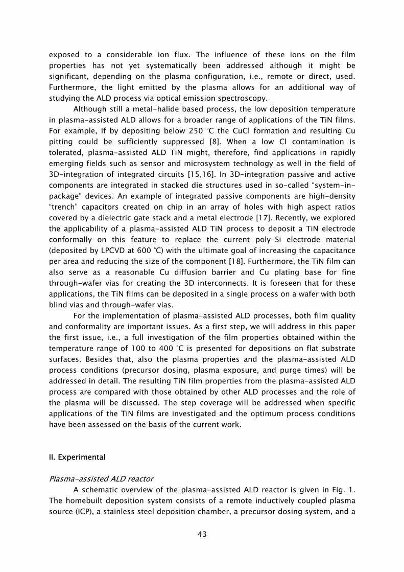
43
exposed to a considerable ion flux. The influence of these ions on the film properties has not yet systematically been addressed although it might be significant, depending on the plasma configuration, i.e., remote or direct, used. Furthermore, the light emitted by the plasma allows for an additional way of studying the ALD process via optical emission spectroscopy.
Although still a metal-halide based process, the low deposition temperature in plasma-assisted ALD allows for a broader range of applications of the TiN films. For example, if by depositing below 250 °C the CuCl formation and resulting Cu pitting could be sufficiently suppressed [8]. When a low Cl contamination is tolerated, plasma-assisted ALD TiN might, therefore, find applications in rapidly emerging fields such as sensor and microsystem technology as well in the field of 3D-integration of integrated circuits [15,16]. In 3D-integration passive and active components are integrated in stacked die structures used in so-called “system-in-package” devices. An example of integrated passive components are high-density “trench” capacitors created on chip in an array of holes with high aspect ratios covered by a dielectric gate stack and a metal electrode [17]. Recently, we explored the applicability of a plasma-assisted ALD TiN process to deposit a TiN electrode conformally on this feature to replace the current poly-Si electrode material (deposited by LPCVD at 600 °C) with the ultimate goal of increasing the capacitance per area and reducing the size of the component [18]. Furthermore, the TiN film can also serve as a reasonable Cu diffusion barrier and Cu plating base for fine through-wafer vias for creating the 3D interconnects. It is foreseen that for these applications, the TiN films can be deposited in a single process on a wafer with both blind vias and through-wafer vias.
For the implementation of plasma-assisted ALD processes, both film quality and conformality are important issues. As a first step, we will address in this paper the first issue, i.e., a full investigation of the film properties obtained within the temperature range of 100 to 400 °C is presented for depositions on flat substrate surfaces. Besides that, also the plasma properties and the plasma-assisted ALD process conditions (precursor dosing, plasma exposure, and purge times) will be addressed in detail. The resulting TiN film properties from the plasma-assisted ALD process are compared with those obtained by other ALD processes and the role of the plasma will be discussed. The step coverage will be addressed when specific applications of the TiN films are investigated and the optimum process conditions have been assessed on the basis of the current work. II. Experimental Plasma-assisted ALD reactor
A schematic overview of the plasma-assisted ALD reactor is given in Fig. 1. The homebuilt deposition system consists of a remote inductively coupled plasma source (ICP), a stainless steel deposition chamber, a precursor dosing system, and a
44
FIG. 1 Schematic of (a) the plasma-assisted atomic layer deposition (plasma-assisted ALD) reactor and (b) representation of a plasma-assisted ALD cycle for TiN deposition.
pump unit. The plasma source and pump unit are connected to the deposition chamber through gate valves.
The plasma source consists of a multiple-turn copper coil wrapped around a 6 cm diameter quartz tube. The source is powered by a function generator at 13.56 MHz and a broadband amplifier providing a plasma power of up to 100 W. The impedance is matched to the source by a manual matching unit consisting of two parallel placed vacuum capacitors in a Pi-network configuration. A H2-N2 gas mixture (>99.999% purity) with typically a 10:1 mixing ratio is fed into the ICP source using leak valves. The plasma source operates at a pressure of typically 7.5 mTorr and the plasma expands through a 100 mm heated gate valve into the deposition chamber.
Substrates are loaded on a stainless steel substrate holder present at a distance of 30 cm from the plasma source. The temperature of the 2-inch diameter substrate holder is actively controlled by a resistive heater and a thermocouple. A clamping ring is positioned on top of the substrate to improve the thermal contact with the substrate holder. The substrate holder is electrically insulated to allow low voltage substrate biasing.
TiCl4 precursor (Sigma-Aldrich, ≥99.0% purity) is evaporated at room temperature from a bubbler containing liquid TiCl4 and trapped in a fixed volume (0.25 cm3) in between two gas valves. The TiCl4 is subsequently injected into the chamber by releasing this trapped volume into the chamber resulting in a working pressure in the chamber of typically 2.5 mTorr. During the precursor step the gate valves between the chamber and the pump and between the chamber and the plasma source are closed. The latter prevents TiN deposition in the plasma source.
The chamber is pumped by a combination of a turbo molecular pump (250 l/s) and a rotary pump (5 m3/h). A chamber base pressure of ~10-6 Torr is
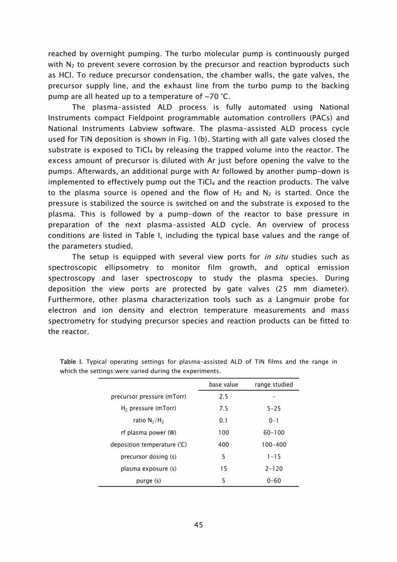
45
reached by overnight pumping. The turbo molecular pump is continuously purged with N2 to prevent severe corrosion by the precursor and reaction byproducts such as HCl. To reduce precursor condensation, the chamber walls, the gate valves, the precursor supply line, and the exhaust line from the turbo pump to the backing pump are all heated up to a temperature of ~70 °C.
The plasma-assisted ALD process is fully automated using National Instruments compact Fieldpoint programmable automation controllers (PACs) and National Instruments Labview software. The plasma-assisted ALD process cycle used for TiN deposition is shown in Fig. 1(b). Starting with all gate valves closed the substrate is exposed to TiCl4 by releasing the trapped volume into the reactor. The excess amount of precursor is diluted with Ar just before opening the valve to the pumps. Afterwards, an additional purge with Ar followed by another pump-down is implemented to effectively pump out the TiCl4 and the reaction products. The valve to the plasma source is opened and the flow of H2 and N2 is started. Once the pressure is stabilized the source is switched on and the substrate is exposed to the plasma. This is followed by a pump-down of the reactor to base pressure in preparation of the next plasma-assisted ALD cycle. An overview of process conditions are listed in Table I, including the typical base values and the range of the parameters studied.
The setup is equipped with several view ports for in situ studies such as spectroscopic ellipsometry to monitor film growth, and optical emission spectroscopy and laser spectroscopy to study the plasma species. During deposition the view ports are protected by gate valves (25 mm diameter). Furthermore, other plasma characterization tools such as a Langmuir probe for electron and ion density and electron temperature measurements and mass spectrometry for studying precursor species and reaction products can be fitted to the reactor.
Table I. Typical operating settings for plasma-assisted ALD of TiN films and the range in which the settings were varied during the experiments.
base value range studied
precursor pressure (mTorr) 2.5 -
H2 pressure (mTorr) 7.5 5-25
ratio N2/H2 0.1 0-1
rf plasma power (W) 100 60-100
deposition temperature (°C) 400 100-400
precursor dosing (s) 5 1-15
plasma exposure (s) 15 2-120
purge (s) 5 0-60
46
Plasma diagnostics In the present work the plasma was studied by optical emission spectroscopy
(OES) using an Ocean Optics USB2000 spectrometer with a wavelength detection range of 250-870 nm and a resolution of approximately 1 nm. The light emission from the plasma was measured both at the plasma source region as well as downstream near the substrate holder. At the plasma source the emission was collected by an optical fiber connected to the spectrometer. To image the emission coming from just above the substrate holder on the entrance of the optical fiber, a one inch diameter, f=16 cm focal length lens was used in 2f-2f configuration. Spectra were taken at different plasma powers, pressures, and H2-N2 mixture ratios. Typical integration times were 20 ms for the emission from the plasma source and 200 ms for the downstream region.
Langmuir probe measurements were carried out simultaneously with the OES measurements at a position just above the substrate holder. The homebuilt double Langmuir probe consists of two 11 mm long tungsten wires, approximately 5 mm from each other apart. The wires were connected to a Keithley 2400 Sourcemeter which served both as voltage source and as current meter. Typically the applied voltage was varied from -50 V to +50 V. From the Langmuir probe data the electron and ion density and the electron temperature were determined using the method described by Peterson and Talbot [19]. TiN deposition and film characterization
The TiN films were deposited on p-type Si wafer substrates (10-30 Ω·cm) at deposition temperatures between 100 and 400 ºC. Unless mentioned otherwise, the silicon substrates did not undergo additional cleaning steps and were covered with a 1-2 nm native oxide layer. The film growth was monitored in situ using a J.A. Woollam, Inc. M2000U visible and near-infrared spectroscopic ellipsometer (SE, 0.75-5.0 eV) mounted on the chamber at a 68º angle of incidence with respect to the substrate normal. After every ten completed ALD cycles SE data were acquired by averaging over 500 complete SE spectra. The measurement time was approximately one minute. The SE data were analyzed by an optical two-layer model in which the dielectric function of TiN was parameterized by the Drude-Lorentz formalism [20]. Besides yielding information on thickness, the SE analysis also gave insight into material properties such as the electrical resistivity. The method for analysis of the SE data is discussed extensively in separate publications [21,22].
The film composition was determined by Rutherford backscattering spectrometry (RBS) for the Ti, N, Cl, and O content. Elastic recoil detection (ERD) was used for determining the H content. A 2 MeV 4He+ beam was targeted at the surface at two different angles (-80º and -10º) for every sample to get improved sensitivity for both the heavy and light elements, while it also allowed for depth profiling of the TiN layer. The RBS and ERD data were modeled using the RUMP program [23].
The microstructure of the films was studied by X-ray diffraction using a
47
Philips X’Pert MPD diffractometer equipped with a Cu Kα source (1.54 Å radiation). To reduce the measurement time a Philips X’Celerator detector was used and to increase the surface sensitivity the measurements were performed under grazing angle of incidence. For thickness and mass density determination X-ray reflectometry measurements were performed on a Bruker D8 Advance X-ray diffractometer.
The surface roughness of the TiN film was determined by atomic force microscopy (AFM) using a NT-MDT Solver P47 SPM in non-contact mode using NSG11 TiN covered cantilevers with curvatures below 10 nm. Two scan sizes were used, 1×1 μm2 and 2×2 μm2, with 512 sample points in both x and y directions and a scan velocity of 1 Hz. From the scans the RMS roughness was extracted by determining the saturation value of the RMS roughness with increasing scanned area size.
Ex situ resistivity measurements were carried out at room temperature using a Signatone four point probe in combination with a Keithley 2400 Sourcemeter acting both as current source and as a voltage meter. The resistivity was determined from the slope of the I-V curve.
III. Plasma studies
In the plasma, H and N radicals, as well as other reactive species such as excited N2 and possibly NHx radicals are created that can contribute to the surface chemistry. While generally not abundant, also electrons and ions are present and the subsequent surface ion bombardment, which is caused by acceleration of the ions towards the substrate caused by the self-bias voltage over the plasma sheath, can provide additional energy for surface reactions to take place. It can lead to substrate modification, but can also contribute in improving the film density. An investigation of the plasma characteristics is therefore imperative. Both in the source as well as in the downstream deposition region the emission of the plasma is studied using optical emission spectroscopy. The electrical properties of the plasma in the downstream region have been studied by Langmuir probe measurements.
Although the information obtained from optical emission spectroscopy is limited because it relies on excitation processes and radiative transitions, it can give qualitative insight into the (radical) species produced in the plasma and their relative densities under different plasma settings. Emission spectra were measured of an H2 plasma, a H2-N2 (10:1) mixture plasma, and a H2-N2 (1:1) mixture plasma at the position of the plasma source (cf. Fig. 2(a)). In the hydrogen plasma the atomic hydrogen emission from the Balmer series, Hα (656.5 nm) and Hβ (485.6 nm) indicates the presence of H radicals. Molecular hydrogen emission from the d3Πu a3Σg+ transition, the so-called Fulcher bands (590-640 nm), is observed indicating excited H2. In the H2-N2 mixture plasmas, the N2 emission from the first positive system B3Π A3Π (500-1050 nm) and second positive system C3Π B3Π (280-500 nm) is observed. The excitation of N, however, depends mainly on
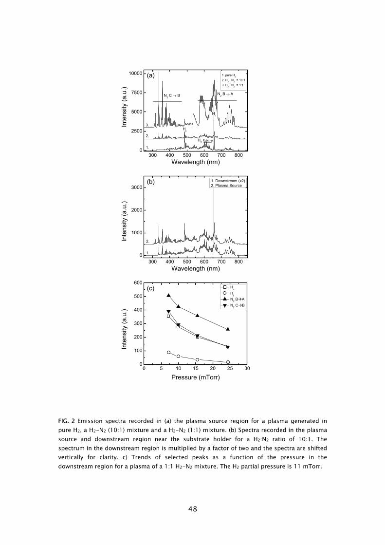
48
Inte
nsity
(a.u
.)In
tens
ity (a
.u.)
Inte
nsity
(a.u
.)
0 5 10 15 20 25 300
100
200
300
400
500
600(c)
Pressure (mTorr)
Hα
Hβ
N2 B A N2 C B
300 400 500 600 700 8000
1000
2000
3000(b) 1. Downstream (x2)
2. Plasma Source
Wavelength (nm)
1.
2.
300 400 500 600 700 8000
2500
5000
7500
10000
1.
2.
1. pure H2
2. H2 : N2 = 10:13. H2 : N2 = 1:1
H2 Fulcher
Hβ
N2 B → A
Wavelength (nm)
N2 C → B
Hα
3.
(a)
FIG. 2 Emission spectra recorded in (a) the plasma source region for a plasma generated in pure H2, a H2-N2 (10:1) mixture and a H2-N2 (1:1) mixture. (b) Spectra recorded in the plasma source and downstream region near the substrate holder for a H2:N2 ratio of 10:1. The spectrum in the downstream region is multiplied by a factor of two and the spectra are shifted vertically for clarity. c) Trends of selected peaks as a function of the pressure in the downstream region for a plasma of a 1:1 H2-N2 mixture. The H2 partial pressure is 11 mTorr.
49
collisions with electrons and due to the high excitation energy involved, N emission is therefore normally not observed. But this does not exclude the possibility that a large amount of N radicals can still be present. The N2 emission becomes clearly dominant when adding more N2. The absolute intensity of the H emission appears to become lower with increasing H2:N2 ratio.
In Fig. 2(b) a comparison is made between the emission coming from the plasma source and the emission in the downstream region at the position of the substrate holder for a (10:1) H2-N2 mixture. Apparently emission is still observed at a distance of 30 cm from the plasma source although the intensity has clearly diminished. It can be clearly seen that the N2 emission becomes relatively more dominant in the spectrum downstream compared to the Balmer lines. Recombination of H at the chamber surfaces can be a possible cause for this. Since the relative intensity of the Hα and Hβ lines does not change we can assume that the electron temperature remains roughly the same as the excitation of hydrogen takes mainly place by electron collisions from the ground state.
To monitor the diffusion of the plasma from the source, the absolute intensity of several peaks was measured downstream in a H2-N2 (10:1) mixture plasma for different pressures (cf. Fig. 2(c)). For N2 the v’-v’’ = 5-2 (670.4 nm) peak in the first positive system (B-A) and the v’-v’’ = 0-0 (337.1 nm) peak for the second positive system (C-B) were monitored. For hydrogen, Hα and Hβ were monitored. The intensity decrease with increasing pressure suggests the plasma generation is more confined to the source region. An increase in emission in the source region is observed at higher pressures. Since all peaks have roughly the same rate of decrease, we can assume that the plasma chemistry and composition remains similar when going to higher pressures.
For the H2-N2 (10:1) mixture plasma, which is used in most of the depositions reported, an electron and ion density of ~109 cm-3 was measured for various pressures and plasma powers just above the substrate holder as shown in Fig. 3(a). Despite the remote character of the plasma, this is a considerable electron density in the downstream region which is caused by the low operating pressure. The decrease in electron density at higher pressures again confirms that the plasma is more confined to the source region and diffuses less downstream as also indicated by the decrease in optical emission intensity. Using the dimensions of the probe we estimated the ion flux towards the substrate, under the typical plasma conditions used for deposition, to be ~2.5×1014 cm-2s-1. When integrated over the total plasma exposure time the number of ions arriving at the surface is thus of similar magnitude to the number of deposited molecules and therefore their contribution to the deposition process can be significant.
The electron temperature ranges from ~3.7 to 2.7 eV and decreases with increasing pressure as typically expected from the reduced loss of electrons and ions by diffusion (cf. Fig. 3(b)). At the typical operating pressure of 7.5 mTorr the electron temperature is 3.5 eV. This high electron temperature has the important consequence that the plasma in the downstream region can still be considered as
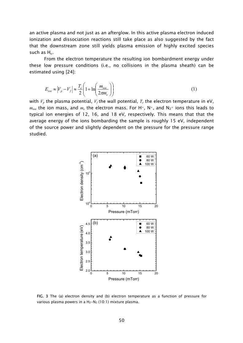
50
an active plasma and not just as an afterglow. In this active plasma electron induced ionization and dissociation reactions still take place as also suggested by the fact that the downstream zone still yields plasma emission of highly excited species such as Hα.
From the electron temperature the resulting ion bombardment energy under these low pressure conditions (i.e., no collisions in the plasma sheath) can be estimated using [24]:
⎟⎟⎠
⎞⎜⎜⎝
⎛⎟⎟⎠
⎞⎜⎜⎝
⎛+≈−≈
e
ionefpion m
mTVVEπ2
ln12
(1)
with Vp the plasma potential, Vf the wall potential, Te the electron temperature in eV, mion the ion mass, and me the electron mass. For H+, N+, and N2+ ions this leads to typical ion energies of 12, 16, and 18 eV, respectively. This means that that the average energy of the ions bombarding the sample is roughly 15 eV, independent of the source power and slightly dependent on the pressure for the pressure range studied.
0 5 10 15 202.0
2.5
3.0
3.5
4.0
4.5
Ele
ctro
n te
mpe
ratu
re (e
V)
Pressure (mTorr)
60 W 80 W 100 W
(b)
0 5 10 15 20108
109
Ele
ctro
n de
nsity
(cm
-3)
Pressure (mTorr)
60 W 80 W 100 W
(a)
FIG. 3 The (a) electron density and (b) electron temperature as a function of pressure for various plasma powers in a H2-N2 (10:1) mixture plasma.
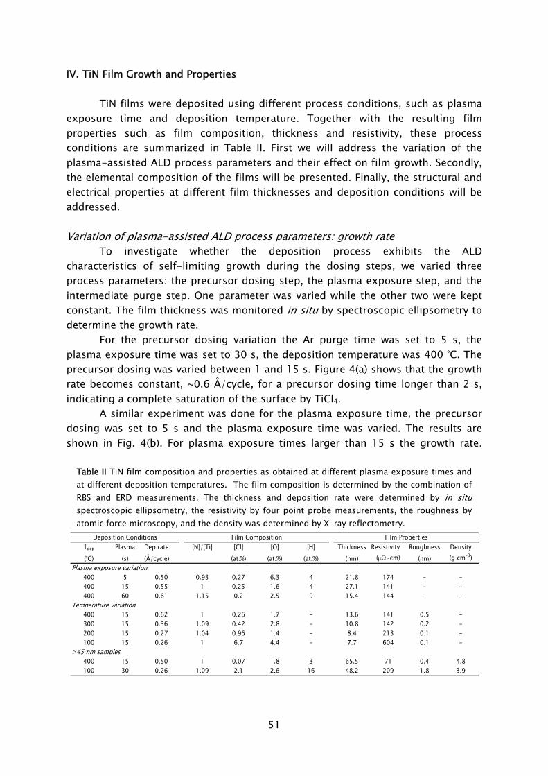
51
IV. TiN Film Growth and Properties TiN films were deposited using different process conditions, such as plasma
exposure time and deposition temperature. Together with the resulting film properties such as film composition, thickness and resistivity, these process conditions are summarized in Table II. First we will address the variation of the plasma-assisted ALD process parameters and their effect on film growth. Secondly, the elemental composition of the films will be presented. Finally, the structural and electrical properties at different film thicknesses and deposition conditions will be addressed. Variation of plasma-assisted ALD process parameters: growth rate
To investigate whether the deposition process exhibits the ALD characteristics of self-limiting growth during the dosing steps, we varied three process parameters: the precursor dosing step, the plasma exposure step, and the intermediate purge step. One parameter was varied while the other two were kept constant. The film thickness was monitored in situ by spectroscopic ellipsometry to determine the growth rate.
For the precursor dosing variation the Ar purge time was set to 5 s, the plasma exposure time was set to 30 s, the deposition temperature was 400 °C. The precursor dosing was varied between 1 and 15 s. Figure 4(a) shows that the growth rate becomes constant, ~0.6 Å/cycle, for a precursor dosing time longer than 2 s, indicating a complete saturation of the surface by TiCl4.
A similar experiment was done for the plasma exposure time, the precursor dosing was set to 5 s and the plasma exposure time was varied. The results are shown in Fig. 4(b). For plasma exposure times larger than 15 s the growth rate.
Table II TiN film composition and properties as obtained at different plasma exposure times and at different deposition temperatures. The film composition is determined by the combination of RBS and ERD measurements. The thickness and deposition rate were determined by in situ spectroscopic ellipsometry, the resistivity by four point probe measurements, the roughness by atomic force microscopy, and the density was determined by X-ray reflectometry.
Tdep Plasma Dep.rate [N]/[Ti] [Cl] [O] [H] Thickness Resistivity Roughness Density(°C) (s) (Å/cycle) (at.%) (at.%) (at.%) (nm) (μΩ•cm) (nm) (g cm-3)
Plasma exposure variation400 5 0.50 0.93 0.27 6.3 4 21.8 174 - -400 15 0.55 1 0.25 1.6 4 27.1 141 - -400 60 0.61 1.15 0.2 2.5 9 15.4 144 - -
Temperature variation400 15 0.62 1 0.26 1.7 - 13.6 141 0.5 -300 15 0.36 1.09 0.42 2.8 - 10.8 142 0.2 -200 15 0.27 1.04 0.96 1.4 - 8.4 213 0.1 -100 15 0.26 1 6.7 4.4 - 7.7 604 0.1 -
>45 nm samples400 15 0.50 1 0.07 1.8 3 65.5 71 0.4 4.8100 30 0.26 1.09 2.1 2.6 16 48.2 209 1.8 3.9
Film Composition Film PropertiesDeposition Conditions
52
becomes constant indicating a saturated removal of the chlorine by the plasma produced radicals. Both experiments indicate this plasma-assisted ALD process exhibits the ALD principle of self-limiting growth under these deposition conditions.
We also varied the influence of the Ar purge time to fully exclude CVD-like growth processes that might occur due to the presence of residual TiCl4 during the plasma step. Such processes could increase the growth rate, but normally take place at the cost of lower quality films at the substrate temperatures used. The precursor dosing time was set to 5 s and the plasma exposure time was set to 15 s. As shown in Fig. 4c, the Ar purge time has no influence on the growth rate. This shows that the dilution of the precursor by Ar at the end of the precursor dosing (employed to improve the lifetime of the pumps), is already sufficient to effectively remove TiCl4 from the chamber. In the following experiments, an Ar purge of 5 s is included in the cycle but, if desired, this step can be omitted to shorten the cycle time.
To investigate whether the deposition process remains true ALD at low deposition temperatures, the same experiments were also performed at 100 °C. The process exhibited the same properties with a saturated growth rate of ~0.3 Å/cycle. This growth rate is significantly lower than the ~0.6 Å/cycle obtained at 400 °C. When investigating the temperature dependence of the growth rate as shown in Fig. 5, it turned out that the growth rate decreased drastically with decreasing temperature with the largest drop when going from 400 to 300 °C. The growth rate at 400 °C is relatively high, but comparable high growth rates for thermal and plasma-assisted ALD of TiN have been reported previously [7,25]. Film composition
The stochiometry and composition of the films were studied by Rutherford backscattering spectrometry (RBS) of which a typical spectrum is shown in Fig. 6. For all RBS measurements, it was found that the N peak in the spectrum was slightly broader than expected on the basis of the width of the Ti peak which indicates the presence of nitrogen in the underlying substrate. Apparently, during the plasma-assisted ALD process of TiN nitrogen is incorporated into the native oxide covered Si substrate forming a ~2-3 nm SiOxNy interface layer underneath the TiN film. The nitridation of the substrate takes place during the initial growth in the first ~40 cycles as revealed by spectroscopic ellipsometry and is addressed in a separate publication [22]. The double peak of Cl in the RBS spectrum indicates a relatively high Cl concentration on the buried interface between the TiN and SiOxNy layer and on the top surface. Oxygen was found mostly in the top part of the film. The double oxygen peak in Fig. 6 is the result of the native oxide covered silicon substrate and the surface oxidation of the TiN.
With this knowledge, a 3-stack model was used to determine the TiN film composition from the RBS measurements. The model is shown in the inset in Fig. 6. A SiOxNy layer is modeled at the buried interface between the Si substrate and the
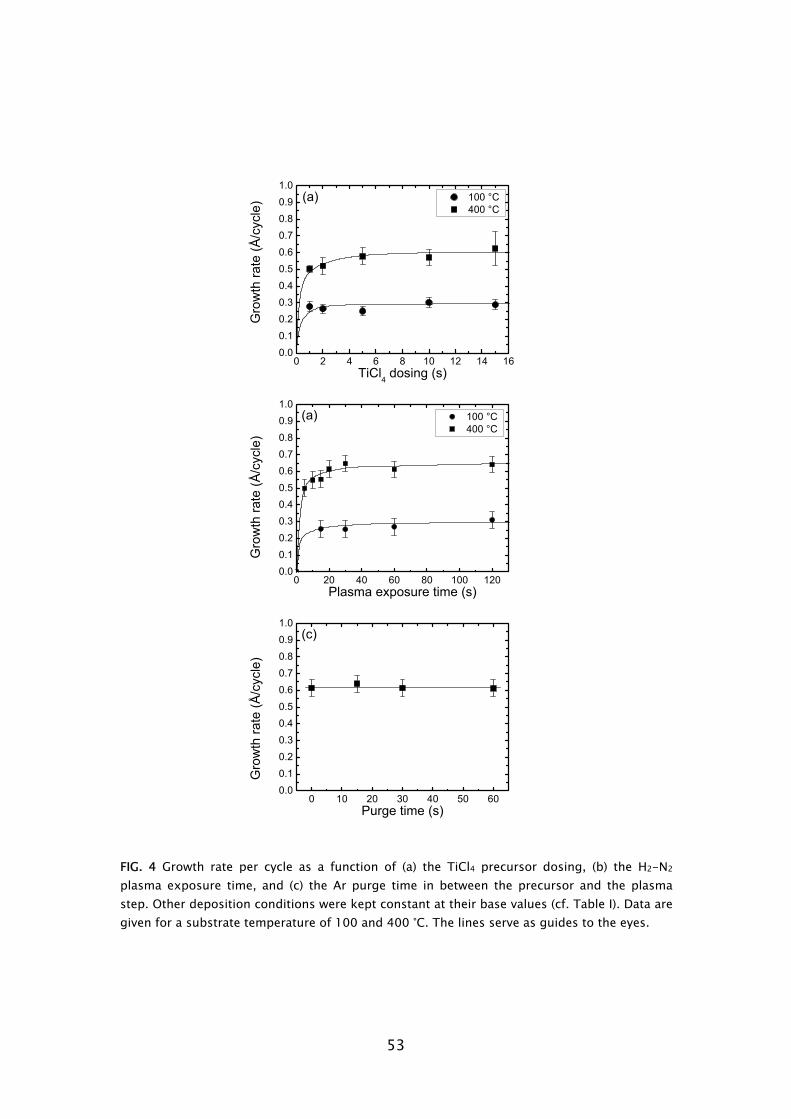
53
0 10 20 30 40 50 600.00.10.20.30.40.50.60.70.80.91.0
Purge time (s)
(c)
0 20 40 60 80 100 1200.00.10.20.30.40.50.60.70.80.91.0
(a) 100 °C 400 °C
Plasma exposure time (s)
0 2 4 6 8 10 12 14 160.00.10.20.30.40.50.60.70.80.91.0
100 °C 400 °C
TiCl4 dosing (s)
(a)
Gro
wth
rate
(Å/c
ycle
)G
row
th ra
te (Å
/cyc
le)
Gro
wth
rate
(Å/c
ycle
)
FIG. 4 Growth rate per cycle as a function of (a) the TiCl4 precursor dosing, (b) the H2-N2 plasma exposure time, and (c) the Ar purge time in between the precursor and the plasma step. Other deposition conditions were kept constant at their base values (cf. Table I). Data are given for a substrate temperature of 100 and 400 °C. The lines serve as guides to the eyes.
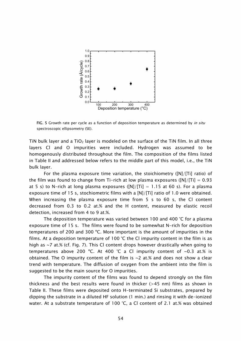
54
TiN bulk layer and a TiO2 layer is modeled on the surface of the TiN film. In all three layers Cl and O impurities were included. Hydrogen was assumed to be homogenously distributed throughout the film. The composition of the films listed in Table II and addressed below refers to the middle part of this model, i.e., the TiN bulk layer.
For the plasma exposure time variation, the stoichiometry ([N]/[Ti] ratio) of the film was found to change from Ti-rich at low plasma exposures ([N]/[Ti] = 0.93 at 5 s) to N-rich at long plasma exposures ([N]/[Ti] = 1.15 at 60 s). For a plasma exposure time of 15 s, stochiometric films with a [N]/[Ti] ratio of 1.0 were obtained. When increasing the plasma exposure time from 5 s to 60 s, the Cl content decreased from 0.3 to 0.2 at.% and the H content, measured by elastic recoil detection, increased from 4 to 9 at.%.
The deposition temperature was varied between 100 and 400 °C for a plasma exposure time of 15 s. The films were found to be somewhat N-rich for deposition temperatures of 200 and 300 ºC. More important is the amount of impurities in the films. At a deposition temperature of 100 °C the Cl impurity content in the film is as high as ~7 at.% (cf. Fig. 7). This Cl content drops however drastically when going to temperatures above 200 ºC. At 400 °C a Cl impurity content of ~0.3 at.% is obtained. The O impurity content of the film is ~2 at.% and does not show a clear trend with temperature. The diffusion of oxygen from the ambient into the film is suggested to be the main source for O impurities.
The impurity content of the films was found to depend strongly on the film thickness and the best results were found in thicker (>45 nm) films as shown in Table II. These films were deposited onto H-terminated Si substrates, prepared by dipping the substrate in a diluted HF solution (1 min.) and rinsing it with de-ionized water. At a substrate temperature of 100 °C, a Cl content of 2.1 at.% was obtained
100 200 300 4000.00.10.20.30.40.50.60.70.80.91.0
Gro
wth
rate
(Å/c
ycle
)
Deposition temperature (°C)
FIG. 5 Growth rate per cycle as a function of deposition temperature as determined by in situ spectroscopic ellipsometry (SE).
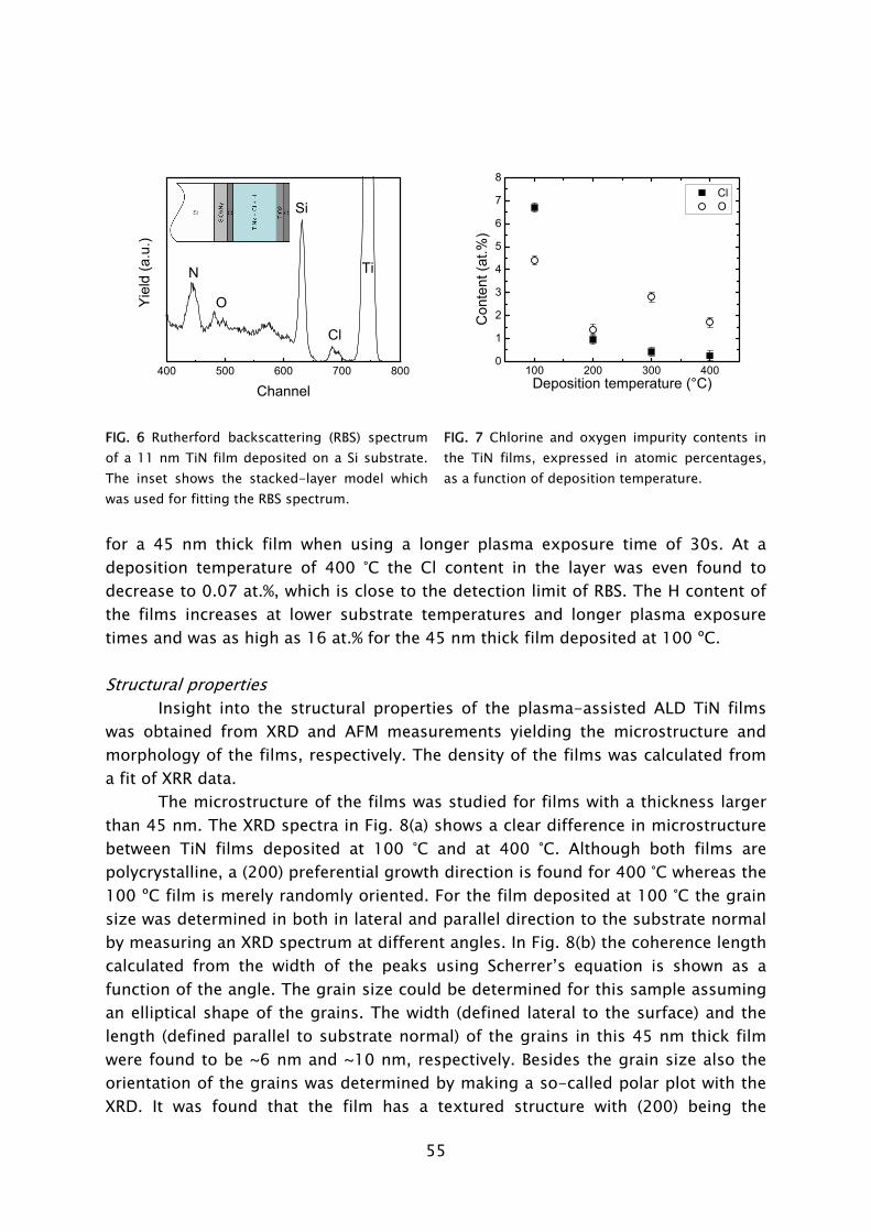
55
400 500 600 700 800
Yie
ld (a
.u.)
Channel
N
O
Si
Cl
Ti
100 200 300 4000
1
2
3
4
5
6
7
8 Cl O
Con
tent
(at.%
)
Deposition temperature (°C)
FIG. 6 Rutherford backscattering (RBS) spectrum of a 11 nm TiN film deposited on a Si substrate. The inset shows the stacked-layer model which was used for fitting the RBS spectrum.
FIG. 7 Chlorine and oxygen impurity contents in the TiN films, expressed in atomic percentages, as a function of deposition temperature.
for a 45 nm thick film when using a longer plasma exposure time of 30s. At a deposition temperature of 400 °C the Cl content in the layer was even found to decrease to 0.07 at.%, which is close to the detection limit of RBS. The H content of the films increases at lower substrate temperatures and longer plasma exposure times and was as high as 16 at.% for the 45 nm thick film deposited at 100 ºC. Structural properties
Insight into the structural properties of the plasma-assisted ALD TiN films was obtained from XRD and AFM measurements yielding the microstructure and morphology of the films, respectively. The density of the films was calculated from a fit of XRR data.
The microstructure of the films was studied for films with a thickness larger than 45 nm. The XRD spectra in Fig. 8(a) shows a clear difference in microstructure between TiN films deposited at 100 °C and at 400 °C. Although both films are polycrystalline, a (200) preferential growth direction is found for 400 °C whereas the 100 ºC film is merely randomly oriented. For the film deposited at 100 °C the grain size was determined in both in lateral and parallel direction to the substrate normal by measuring an XRD spectrum at different angles. In Fig. 8(b) the coherence length calculated from the width of the peaks using Scherrer’s equation is shown as a function of the angle. The grain size could be determined for this sample assuming an elliptical shape of the grains. The width (defined lateral to the surface) and the length (defined parallel to substrate normal) of the grains in this 45 nm thick film were found to be ~6 nm and ~10 nm, respectively. Besides the grain size also the orientation of the grains was determined by making a so-called polar plot with the XRD. It was found that the film has a textured structure with (200) being the
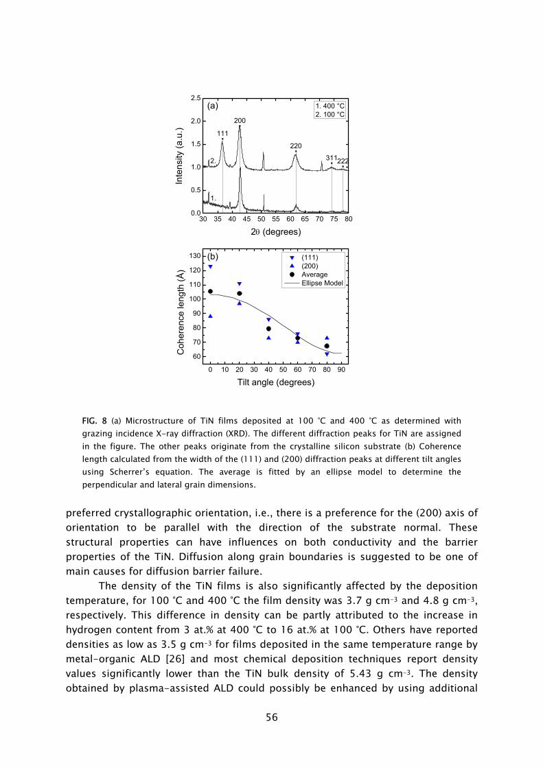
56
0 10 20 30 40 50 60 70 80 90
60
70
80
90
100
110
120
130
(111) (200) Average Ellipse Model
Coh
eren
ce le
ngth
(Å)
Tilt angle (degrees)
(b)
30 35 40 45 50 55 60 65 70 75 800.0
0.5
1.0
1.5
2.0
2.5
111
200
220
3112222.
Inte
nsity
(a.u
.)
2θ (degrees)
1. 400 °C2. 100 °C
1.
(a)
FIG. 8 (a) Microstructure of TiN films deposited at 100 °C and 400 °C as determined with grazing incidence X-ray diffraction (XRD). The different diffraction peaks for TiN are assigned in the figure. The other peaks originate from the crystalline silicon substrate (b) Coherence length calculated from the width of the (111) and (200) diffraction peaks at different tilt angles using Scherrer’s equation. The average is fitted by an ellipse model to determine the perpendicular and lateral grain dimensions.
preferred crystallographic orientation, i.e., there is a preference for the (200) axis of orientation to be parallel with the direction of the substrate normal. These structural properties can have influences on both conductivity and the barrier properties of the TiN. Diffusion along grain boundaries is suggested to be one of main causes for diffusion barrier failure.
The density of the TiN films is also significantly affected by the deposition temperature, for 100 °C and 400 °C the film density was 3.7 g cm-3 and 4.8 g cm-3, respectively. This difference in density can be partly attributed to the increase in hydrogen content from 3 at.% at 400 °C to 16 at.% at 100 °C. Others have reported densities as low as 3.5 g cm-3 for films deposited in the same temperature range by metal-organic ALD [26] and most chemical deposition techniques report density values significantly lower than the TiN bulk density of 5.43 g cm-3. The density obtained by plasma-assisted ALD could possibly be enhanced by using additional
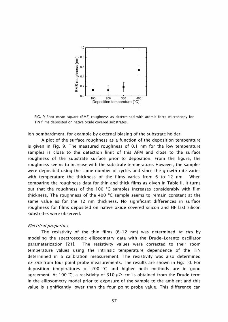
57
100 200 300 4000.0
0.2
0.4
0.6
0.8
1.0
RM
S ro
ughn
ess
(nm
)
Deposition temperature (°C)
FIG. 9 Root-mean-square (RMS) roughness as determined with atomic force microscopy for TiN films deposited on native oxide covered substrates.
ion bombardment, for example by external biasing of the substrate holder.
A plot of the surface roughness as a function of the deposition temperature is given in Fig. 9. The measured roughness of 0.1 nm for the low temperature samples is close to the detection limit of this AFM and close to the surface roughness of the substrate surface prior to deposition. From the figure, the roughness seems to increase with the substrate temperature. However, the samples were deposited using the same number of cycles and since the growth rate varies with temperature the thickness of the films varies from 6 to 12 nm. When comparing the roughness data for thin and thick films as given in Table II, it turns out that the roughness of the 100 ºC samples increases considerably with film thickness. The roughness of the 400 ºC sample seems to remain constant at the same value as for the 12 nm thickness. No significant differences in surface roughness for films deposited on native oxide covered silicon and HF last silicon substrates were observed. Electrical properties
The resistivity of the thin films (6-12 nm) was determined in situ by modeling the spectroscopic ellipsometry data with the Drude-Lorentz oscillator parameterization [21]. The resistivity values were corrected to their room temperature values using the intrinsic temperature dependence of the TiN determined in a calibration measurement. The resistivity was also determined ex situ from four point probe measurements. The results are shown in Fig. 10. For deposition temperatures of 200 °C and higher both methods are in good agreement. At 100 °C, a resistivity of 310 μΩ·cm is obtained from the Drude term in the ellipsometry model prior to exposure of the sample to the ambient and this value is significantly lower than the four point probe value. This difference can
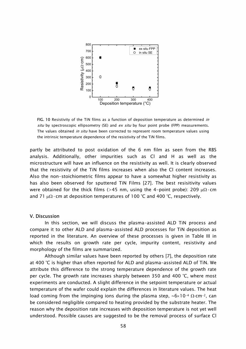
58
100 200 300 4000
100
200
300
400
500
600
700
800 ex situ FPP in situ SE
Res
istiv
ity (μ
Ω·c
m)
Deposition temperature (°C)
FIG. 10 Resistivity of the TiN films as a function of deposition temperature as determined in situ by spectroscopic ellipsometry (SE) and ex situ by four point probe (FPP) measurements. The values obtained in situ have been corrected to represent room temperature values using the intrinsic temperature dependence of the resistivity of the TiN films.
partly be attributed to post oxidation of the 6 nm film as seen from the RBS analysis. Additionally, other impurities such as Cl and H as well as the microstructure will have an influence on the resistivity as well. It is clearly observed that the resistivity of the TiN films increases when also the Cl content increases. Also the non-stoichiometric films appear to have a somewhat higher resistivity as has also been observed for sputtered TiN Films [27]. The best resisitivity values were obtained for the thick films (>45 nm, using the 4-point probe): 209 μΩ·cm and 71 μΩ·cm at deposition temperatures of 100 °C and 400 °C, respectively. V. Discussion
In this section, we will discuss the plasma-assisted ALD TiN process and compare it to other ALD and plasma-assisted ALD processes for TiN deposition as reported in the literature. An overview of these processes is given in Table III in which the results on growth rate per cycle, impurity content, resistivity and morphology of the films are summarized.
Although similar values have been reported by others [7], the deposition rate at 400 °C is higher than often reported for ALD and plasma-assisted ALD of TiN. We attribute this difference to the strong temperature dependence of the growth rate per cycle. The growth rate increases sharply between 350 and 400 °C, where most experiments are conducted. A slight difference in the setpoint temperature or actual temperature of the wafer could explain the differences in literature values. The heat load coming from the impinging ions during the plasma step, ~6×10⁻⁴ Ω⋅cm-2, can be considered negligible compared to heating provided by the substrate heater. The reason why the deposition rate increases with deposition temperature is not yet well understood. Possible causes are suggested to be the removal process of surface Cl
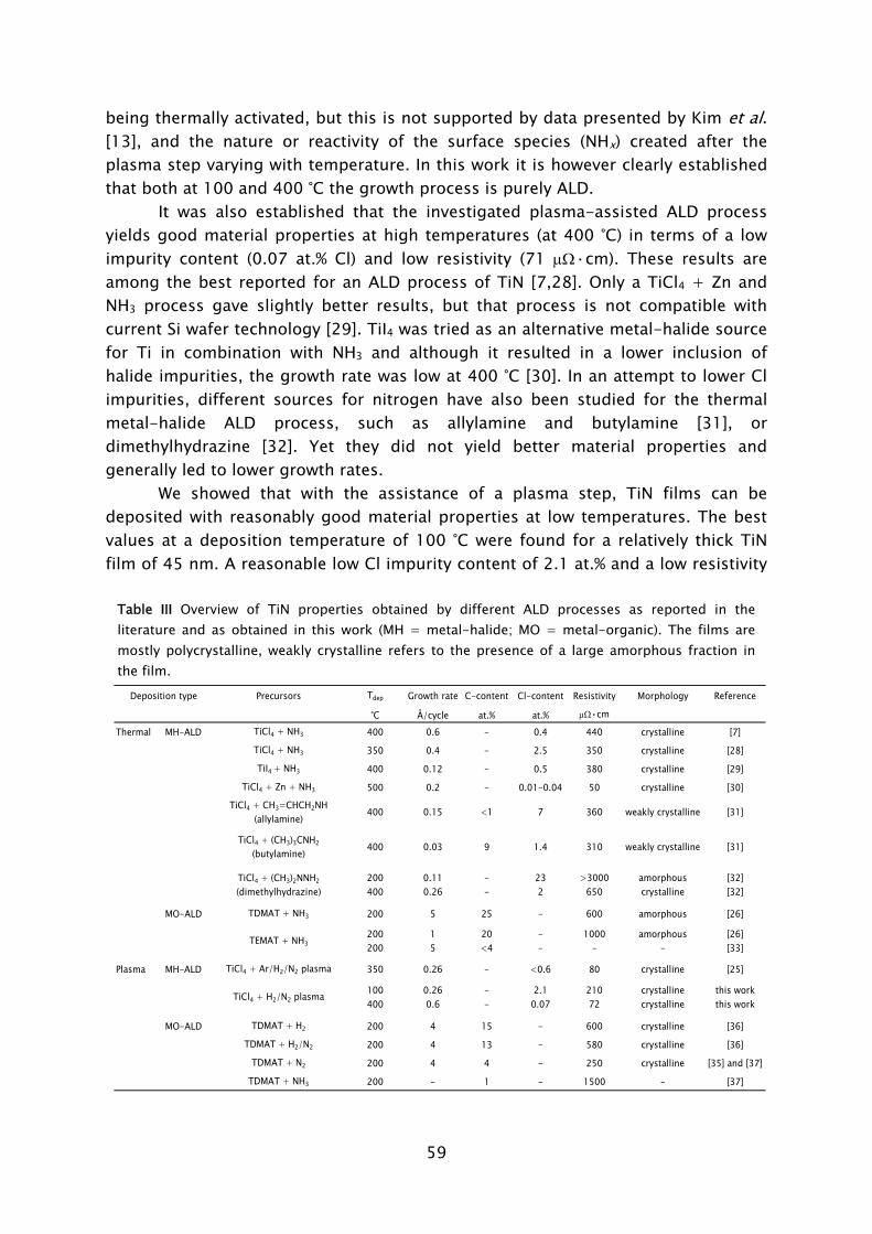
59
being thermally activated, but this is not supported by data presented by Kim et al. [13], and the nature or reactivity of the surface species (NHx) created after the plasma step varying with temperature. In this work it is however clearly established that both at 100 and 400 °C the growth process is purely ALD.
It was also established that the investigated plasma-assisted ALD process yields good material properties at high temperatures (at 400 °C) in terms of a low impurity content (0.07 at.% Cl) and low resistivity (71 μΩ·cm). These results are among the best reported for an ALD process of TiN [7,28]. Only a TiCl4 + Zn and NH3 process gave slightly better results, but that process is not compatible with current Si wafer technology [29]. TiI4 was tried as an alternative metal-halide source for Ti in combination with NH3 and although it resulted in a lower inclusion of halide impurities, the growth rate was low at 400 °C [30]. In an attempt to lower Cl impurities, different sources for nitrogen have also been studied for the thermal metal-halide ALD process, such as allylamine and butylamine [31], or dimethylhydrazine [32]. Yet they did not yield better material properties and generally led to lower growth rates.
We showed that with the assistance of a plasma step, TiN films can be deposited with reasonably good material properties at low temperatures. The best values at a deposition temperature of 100 °C were found for a relatively thick TiN film of 45 nm. A reasonable low Cl impurity content of 2.1 at.% and a low resistivity
Table III Overview of TiN properties obtained by different ALD processes as reported in the literature and as obtained in this work (MH = metal-halide; MO = metal-organic). The films are mostly polycrystalline, weakly crystalline refers to the presence of a large amorphous fraction in the film.
Precursors Tdep Growth rate C-content Cl-content Resistivity Morphology Reference
°C Å/cycle at.% at.% μΩ•cm
Thermal MH-ALD TiCl4 + NH3 400 0.6 - 0.4 440 crystalline [7]
TiCl4 + NH3 350 0.4 - 2.5 350 crystalline [28]
TiI4 + NH3 400 0.12 - 0.5 380 crystalline [29]
TiCl4 + Zn + NH3 500 0.2 - 0.01-0.04 50 crystalline [30]
TiCl4 + CH3=CHCH2NH (allylamine)
400 0.15 <1 7 360 weakly crystalline [31]
TiCl4 + (CH3)3CNH2
(butylamine)400 0.03 9 1.4 310 weakly crystalline [31]
200 0.11 - 23 >3000 amorphous [32]400 0.26 - 2 650 crystalline [32]
MO-ALD TDMAT + NH3 200 5 25 - 600 amorphous [26]
200 1 20 - 1000 amorphous [26]200 5 <4 - - - [33]
Plasma MH-ALD TiCl4 + Ar/H2/N2 plasma 350 0.26 - <0.6 80 crystalline [25]
100 0.26 - 2.1 210 crystalline this work400 0.6 - 0.07 72 crystalline this work
MO-ALD TDMAT + H2 200 4 15 - 600 crystalline [36]
TDMAT + H2/N2 200 4 13 - 580 crystalline [36]
TDMAT + N2 200 4 4 - 250 crystalline [35] and [37]
TDMAT + NH3 200 - 1 - 1500 - [37]
TiCl4 + (CH3)2NNH2
(dimethylhydrazine)
Deposition type
TEMAT + NH3
TiCl4 + H2/N2 plasma
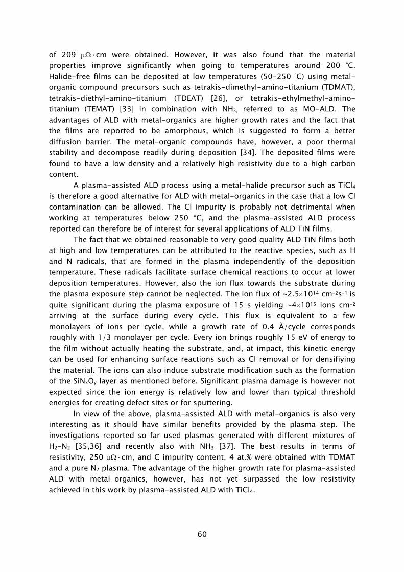
60
of 209 μΩ·cm were obtained. However, it was also found that the material properties improve significantly when going to temperatures around 200 °C. Halide-free films can be deposited at low temperatures (50-250 °C) using metal-organic compound precursors such as tetrakis-dimethyl-amino-titanium (TDMAT), tetrakis-diethyl-amino-titanium (TDEAT) [26], or tetrakis-ethylmethyl-amino-titanium (TEMAT) [33] in combination with NH3, referred to as MO-ALD. The advantages of ALD with metal-organics are higher growth rates and the fact that the films are reported to be amorphous, which is suggested to form a better diffusion barrier. The metal-organic compounds have, however, a poor thermal stability and decompose readily during deposition [34]. The deposited films were found to have a low density and a relatively high resistivity due to a high carbon content.
A plasma-assisted ALD process using a metal-halide precursor such as TiCl4 is therefore a good alternative for ALD with metal-organics in the case that a low Cl contamination can be allowed. The Cl impurity is probably not detrimental when working at temperatures below 250 ºC, and the plasma-assisted ALD process reported can therefore be of interest for several applications of ALD TiN films.
The fact that we obtained reasonable to very good quality ALD TiN films both at high and low temperatures can be attributed to the reactive species, such as H and N radicals, that are formed in the plasma independently of the deposition temperature. These radicals facilitate surface chemical reactions to occur at lower deposition temperatures. However, also the ion flux towards the substrate during the plasma exposure step cannot be neglected. The ion flux of ~2.5×1014 cm-2s-1 is quite significant during the plasma exposure of 15 s yielding ~4×10¹⁵ ions cm-2 arriving at the surface during every cycle. This flux is equivalent to a few monolayers of ions per cycle, while a growth rate of 0.4 Å/cycle corresponds roughly with 1/3 monolayer per cycle. Every ion brings roughly 15 eV of energy to the film without actually heating the substrate, and, at impact, this kinetic energy can be used for enhancing surface reactions such as Cl removal or for densifiying the material. The ions can also induce substrate modification such as the formation of the SiNxOy layer as mentioned before. Significant plasma damage is however not expected since the ion energy is relatively low and lower than typical threshold energies for creating defect sites or for sputtering.
In view of the above, plasma-assisted ALD with metal-organics is also very interesting as it should have similar benefits provided by the plasma step. The investigations reported so far used plasmas generated with different mixtures of H2-N2 [35,36] and recently also with NH3 [37]. The best results in terms of resistivity, 250 μΩ·cm, and C impurity content, 4 at.% were obtained with TDMAT and a pure N2 plasma. The advantage of the higher growth rate for plasma-assisted ALD with metal-organics, however, has not yet surpassed the low resistivity achieved in this work by plasma-assisted ALD with TiCl4.
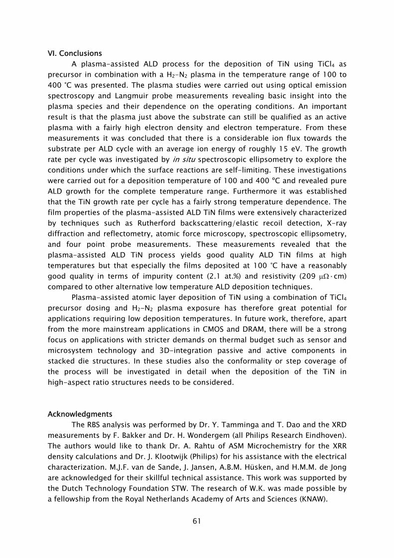
61
VI. Conclusions A plasma-assisted ALD process for the deposition of TiN using TiCl4 as
precursor in combination with a H2-N2 plasma in the temperature range of 100 to 400 °C was presented. The plasma studies were carried out using optical emission spectroscopy and Langmuir probe measurements revealing basic insight into the plasma species and their dependence on the operating conditions. An important result is that the plasma just above the substrate can still be qualified as an active plasma with a fairly high electron density and electron temperature. From these measurements it was concluded that there is a considerable ion flux towards the substrate per ALD cycle with an average ion energy of roughly 15 eV. The growth rate per cycle was investigated by in situ spectroscopic ellipsometry to explore the conditions under which the surface reactions are self-limiting. These investigations were carried out for a deposition temperature of 100 and 400 ºC and revealed pure ALD growth for the complete temperature range. Furthermore it was established that the TiN growth rate per cycle has a fairly strong temperature dependence. The film properties of the plasma-assisted ALD TiN films were extensively characterized by techniques such as Rutherford backscattering/elastic recoil detection, X-ray diffraction and reflectometry, atomic force microscopy, spectroscopic ellipsometry, and four point probe measurements. These measurements revealed that the plasma-assisted ALD TiN process yields good quality ALD TiN films at high temperatures but that especially the films deposited at 100 °C have a reasonably good quality in terms of impurity content (2.1 at.%) and resistivity (209 μΩ·cm) compared to other alternative low temperature ALD deposition techniques.
Plasma-assisted atomic layer deposition of TiN using a combination of TiCl4 precursor dosing and H2-N2 plasma exposure has therefore great potential for applications requiring low deposition temperatures. In future work, therefore, apart from the more mainstream applications in CMOS and DRAM, there will be a strong focus on applications with stricter demands on thermal budget such as sensor and microsystem technology and 3D-integration passive and active components in stacked die structures. In these studies also the conformality or step coverage of the process will be investigated in detail when the deposition of the TiN in high-aspect ratio structures needs to be considered. Acknowledgments
The RBS analysis was performed by Dr. Y. Tamminga and T. Dao and the XRD measurements by F. Bakker and Dr. H. Wondergem (all Philips Research Eindhoven). The authors would like to thank Dr. A. Rahtu of ASM Microchemistry for the XRR density calculations and Dr. J. Klootwijk (Philips) for his assistance with the electrical characterization. M.J.F. van de Sande, J. Jansen, A.B.M. Hüsken, and H.M.M. de Jong are acknowledged for their skillful technical assistance. This work was supported by the Dutch Technology Foundation STW. The research of W.K. was made possible by a fellowship from the Royal Netherlands Academy of Arts and Sciences (KNAW).
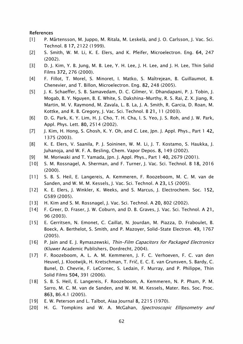
62
References [1] P. Mårtensson, M. Juppo, M. Ritala, M. Leskelä, and J. O. Carlsson, J. Vac. Sci.
Technol. B 17, 2122 (1999). [2] S. Smith, W. M. Li, K. E. Elers, and K. Pfeifer, Microelectron. Eng. 64, 247
(2002). [3] D. J. Kim, Y. B. Jung, M. B. Lee, Y. H. Lee, J. H. Lee, and J. H. Lee, Thin Solid
Films 372, 276 (2000). [4] F. Fillot, T. Morel, S. Minoret, I. Matko, S. Maîtrejean, B. Guillaumot, B.
Chenevier, and T. Billon, Microelectron. Eng. 82, 248 (2005). [5] J. K. Schaeffer, S. B. Samavedam, D. C. Gilmer, V. Dhandapani, P. J. Tobin, J.
Mogab, B. Y. Nguyen, B. E. White, S. Dakshina-Murthy, R. S. Rai, Z. X. Jiang, R. Martin, M. V. Raymond, M. Zavala, L. B. La, J. A. Smith, R. Garcia, D. Roan, M. Kottke, and R. B. Gregory, J. Vac. Sci. Technol. B 21, 11 (2003).
[6] D. G. Park, K. Y. Lim, H. J. Cho, T. H. Cha, I. S. Yeo, J. S. Roh, and J. W. Park, Appl. Phys. Lett. 80, 2514 (2002).
[7] J. Kim, H. Hong, S. Ghosh, K. Y. Oh, and C. Lee, Jpn. J. Appl. Phys., Part 1 42, 1375 (2003).
[8] K. E. Elers, V. Saanila, P. J. Soininen, W. M. Li, J. T. Kostamo, S. Haukka, J. Juhanoja, and W. F. A. Besling, Chem. Vapor Depos. 8, 149 (2002).
[9] M. Moriwaki and T. Yamada, Jpn. J. Appl. Phys., Part 1 40, 2679 (2001). [10] S. M. Rossnagel, A. Sherman, and F. Turner, J. Vac. Sci. Technol. B 18, 2016
(2000). [11] S. B. S. Heil, E. Langereis, A. Kemmeren, F. Roozeboom, M. C. M. van de
Sanden, and W. M. M. Kessels, J. Vac. Sci. Technol. A 23, L5 (2005). [12] K. E. Elers, J. Winkler, K. Weeks, and S. Marcus, J. Electrochem. Soc. 152,
G589 (2005). [13] H. Kim and S. M. Rossnagel, J. Vac. Sci. Technol. A 20, 802 (2002). [14] F. Greer, D. Fraser, J. W. Coburn, and D. B. Graves, J. Vac. Sci. Technol. A 21,
96 (2003). [15] E. Gerritsen, N. Emonet, C. Caillat, N. Jourdan, M. Piazza, D. Fraboulet, B.
Boeck, A. Berthelot, S. Smith, and P. Mazoyer, Solid-State Electron. 49, 1767 (2005).
[16] P. Jain and E. J. Rymaszewski, Thin-Film Capacitors for Packaged Electronics (Kluwer Academic Publishers, Dordrecht, 2004).
[17] F. Roozeboom, A. L. A. M. Kemmeren, J. F. C. Verhoeven, F. C. van den Heuvel, J. Klootwijk, H. Kretschman, T. Frič, E. C. E. van Grunsven, S. Bardy, C. Bunel, D. Chevrie, F. LeCornec, S. Ledain, F. Murray, and P. Philippe, Thin Solid Films 504, 391 (2006).
[18] S. B. S. Heil, E. Langereis, F. Roozeboom, A. Kemmeren, N. P. Pham, P. M. Sarro, M. C. M. van de Sanden, and W. M. M. Kessels, Mater. Res. Soc. Proc. 863, B6.4.1 (2005).
[19] E. W. Peterson and L. Talbot, Aiaa Journal 8, 2215 (1970). [20] H. G. Tompkins and W. A. McGahan, Spectroscopic Ellipsometry and
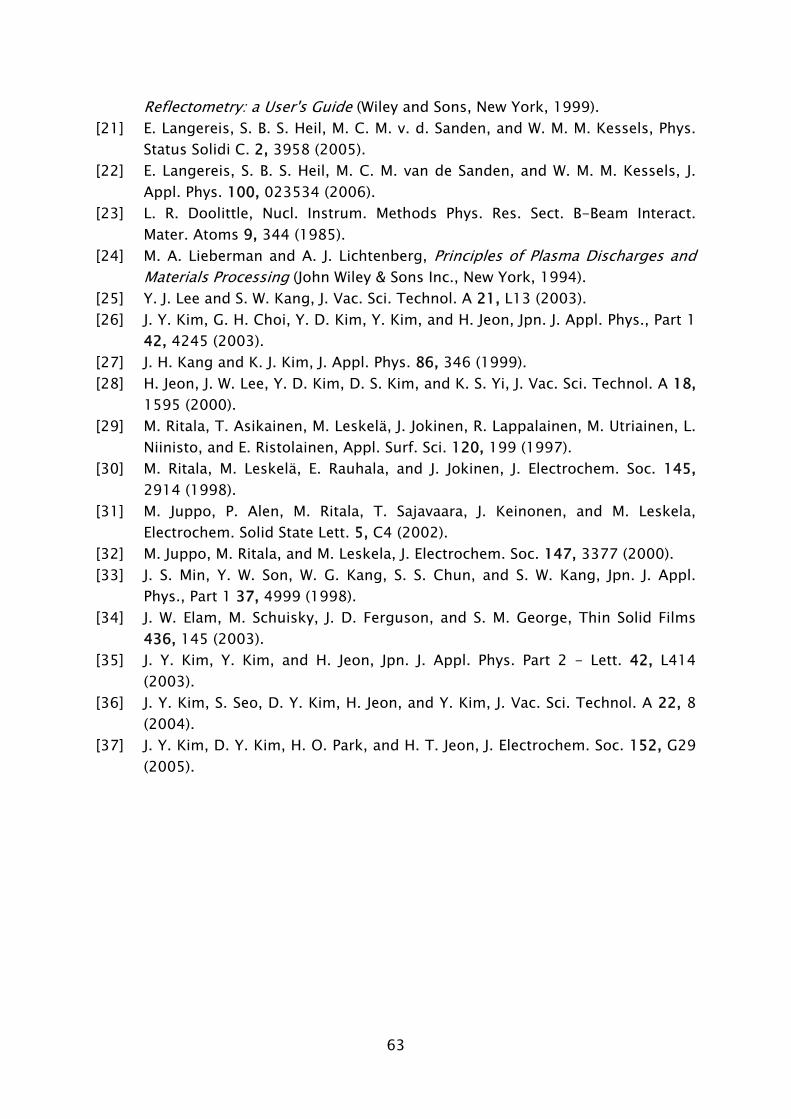
63
Reflectometry: a User's Guide (Wiley and Sons, New York, 1999). [21] E. Langereis, S. B. S. Heil, M. C. M. v. d. Sanden, and W. M. M. Kessels, Phys.
Status Solidi C. 2, 3958 (2005). [22] E. Langereis, S. B. S. Heil, M. C. M. van de Sanden, and W. M. M. Kessels, J.
Appl. Phys. 100, 023534 (2006). [23] L. R. Doolittle, Nucl. Instrum. Methods Phys. Res. Sect. B-Beam Interact.
Mater. Atoms 9, 344 (1985). [24] M. A. Lieberman and A. J. Lichtenberg, Principles of Plasma Discharges and
Materials Processing (John Wiley & Sons Inc., New York, 1994). [25] Y. J. Lee and S. W. Kang, J. Vac. Sci. Technol. A 21, L13 (2003). [26] J. Y. Kim, G. H. Choi, Y. D. Kim, Y. Kim, and H. Jeon, Jpn. J. Appl. Phys., Part 1
42, 4245 (2003). [27] J. H. Kang and K. J. Kim, J. Appl. Phys. 86, 346 (1999). [28] H. Jeon, J. W. Lee, Y. D. Kim, D. S. Kim, and K. S. Yi, J. Vac. Sci. Technol. A 18,
1595 (2000). [29] M. Ritala, T. Asikainen, M. Leskelä, J. Jokinen, R. Lappalainen, M. Utriainen, L.
Niinisto, and E. Ristolainen, Appl. Surf. Sci. 120, 199 (1997). [30] M. Ritala, M. Leskelä, E. Rauhala, and J. Jokinen, J. Electrochem. Soc. 145,
2914 (1998). [31] M. Juppo, P. Alen, M. Ritala, T. Sajavaara, J. Keinonen, and M. Leskela,
Electrochem. Solid State Lett. 5, C4 (2002). [32] M. Juppo, M. Ritala, and M. Leskela, J. Electrochem. Soc. 147, 3377 (2000). [33] J. S. Min, Y. W. Son, W. G. Kang, S. S. Chun, and S. W. Kang, Jpn. J. Appl.
Phys., Part 1 37, 4999 (1998). [34] J. W. Elam, M. Schuisky, J. D. Ferguson, and S. M. George, Thin Solid Films
436, 145 (2003). [35] J. Y. Kim, Y. Kim, and H. Jeon, Jpn. J. Appl. Phys. Part 2 - Lett. 42, L414
(2003). [36] J. Y. Kim, S. Seo, D. Y. Kim, H. Jeon, and Y. Kim, J. Vac. Sci. Technol. A 22, 8
(2004). [37] J. Y. Kim, D. Y. Kim, H. O. Park, and H. T. Jeon, J. Electrochem. Soc. 152, G29
(2005).

64
65
Chapter 4 Deposition of TiN and HfO2 in a Commercial Remote Plasma ALD reactor The authors describe a remote plasma ALD reactor (Oxford Instruments FlexALTM) that includes an inductively coupled plasma source and a load lock capable of handling substrates up to 200 mm in diameter. The deposition of titanium nitride (TiN) and hafnium oxide (HfO2) is described for the combination of the metal-halide precursor TiCl4 and H2-N2 plasma and the combination of the metal-organic precursor Hf[N(CH3)(C2H5)]4 and O2 plasma, respectively. The influence of the plasma exposure time and substrate temperature has been studied and compositional, structural, and electrical properties are reported. TiN films with a low Cl impurity content were obtained at 350 °C at a growth rate of 0.35 Å/cycle with an electrical resistivity as low as 150 μΩ·cm. Carbon-free (detection limit <2 at.%) HfO2 films were obtained with a growth rate of 1.0 Å/cycle at 290 °C. The thickness and resisitivity nonuniformity was <5% for the TiN and the thickness uniformity was <2% for the HfO2 films as determined over 200 mm wafers.1
1 Published as: S. B. S. Heil, J. L. van Hemmen, C. J. Hodson, N. Singh, J. H. Klootwijk, F. Roozeboom,
M. C. M. van de Sanden, and W. M. M. Kessels, J. Vac. Sci. Technol. A 25, 1357 (2007).

66
I. Introduction From industry there is a pressing demand for high-quality thin films with
decreasing thicknesses, i.e. within the range of 1 nanometer to a few tens of nanometers, over increasingly larger substrate areas. Often these films also need to be deposited at relatively low substrate temperatures (<400 °C) and on substrates with demanding topologies. Atomic layer deposition (ALD) is considered as the method of choice for these applications [1], although a wide variety of technological challenges still needs to be met before large-scale implementation of this method in industry will take place. Nevertheless, ALD processing has already proven itself in production schemes for, e.g., electroluminescent displays [2], while ALD is currently also being introduced in deep trench capacitors in dynamic random access memory at the production level [3-5]. Furthermore, ALD is at the verge of being introduced in the production of complementary metal-oxide-semiconductor capacitor stacks while the application of ALD films at the interconnect level of state-of-the-art integrated circuits is actively being researched [6]. More recently, the scope of potential applications of ALD films has been widened with research on ALD films rapidly emerging in fields such as flexible electronics [7,8], photovoltaics [9,10], photonics [11,12] and microsystems [13,14].
So far, most research has been concentrated on so-called thermal ALD processes, where the chemistry of the process is thermally activated due to the (elevated) deposition temperature. Also the application of ALD in industry has been limited to thermal ALD with commercial thermal ALD reactors widely available, both for research as for production purposes. A trend that started half a decade ago and that is currently gaining more momentum is the introduction of a plasma step in the ALD process. This so-called plasma-enhanced or plasma-assisted ALD has several advantages such as deposition at reduced temperatures, increased choice of precursors and materials, higher growth rate, more process versatility, and in some cases also improved material properties. These advantages of plasma-assisted ALD are important for applications of ALD currently being investigated but they might turn out to be of key importance for the aforementioned emerging applications of ALD. Plasma-assisted ALD of oxides [15-17], nitrides [18-20], and metals [21-24] has already been demonstrated. The studies on plasma-assisted ALD have mostly been carried out in homebuilt laboratory scale reactors which are often limited to small substrate sizes. However, with the interest in plasma-assisted ALD growing, tool manufacturers have started to work on commercial plasma-assisted ALD reactors with to date only one manufacturer reported to offer a plasma-assisted ALD reactor for production applications [25]. Most plasma-assisted ALD reactors, including the few commercial tools, are so-called direct plasma ALD reactors. In a direct plasma ALD reactor plasma generation takes place in between two electrodes positioned in the ALD chamber and with the substrate mounted on one of the electrodes [cf. Fig. 1(a)]. This is a relatively simple approach that allows for a small reactor volume and flow-type operation although layers are grown here at the cost of possible plasma damage due to the relatively high ion energies involved. Other
67
FIG. 1 Schematic representation of the three different types of plasma-assisted atomic layer deposition that can be distinguished: (a) direct plasma, (b) remote plasma, and (c) radical enhanced. For each type different hardware configurations and plasma sources exist.
types of plasma-assisted ALD reactors are remote plasma ALD [cf. Fig. 1(b)] and radical enhanced ALD (cf. Fig. 1(c)), yet until recently reactors based on these configurations were not commercially available.
Remote plasmas are a well-proven concept in plasma-enhanced chemical vapor deposition (PECVD) [26]. In a remote plasma reactor the plasma creation takes place upstream of the substrate stage independently of the substrate conditions. This allows for independent optimization of the plasma properties as well as the ability to tune the chemistry of the plasma when it flows or diffuses to the substrate. The plasma species including ions and electrons are generally still in contact with the substrate; however, the energies of ions impacting the surface are well below the threshold value for ion-induced plasma damage. Under particular conditions, the mild ion energies might even have a beneficial effect on the surface chemistry as they add energy to the substrate without heating it. The contact between plasma and substrate as well as the mild ion energies distinguish remote plasma ALD from radical enhanced ALD. In the latter configuration, plasma creation takes place at a large distance from the substrate such that the electron and ion densities in the plasma are low at the substrate region. Amongst the reactive species, only longer lived radicals are able to reach the substrate, however, generally at reduced fluxes due to wall recombination processes. Although from a hardware point of view, remote plasma ALD is still at its infancy, several studies using remote-plasma ALD reactors have been reported [20,21,27,28] that all indicate that these reactors are well suited for research and development applications. Besides their mild ion bombardment, they provide a high flux of plasma species enabling relatively short plasma exposure times while their geometry in principle also allows for a good uniformity over large substrates. Furthermore, remote plasma ALD reactors offer a high degree of versatility due to
68
the remote plasma creation (which, e.g., also can be used for plasma cleaning) while the plasma source can also be isolated from the ALD chamber for thermal ALD studies.
In the present work, we describe the recently introduced Oxford Instruments FlexALTM reactor which is a remote plasma reactor that is also suited for thermal ALD. This reactor, aimed particularly at research and development studies, is equipped with a load lock and is capable of handling substrate sizes up to 200 mm in diameter. In this article, the reactor is described in detail and results obtained for both a nitride and an oxide are presented employing two different types of precursors, i.e., a metal-halide and a metal-organic precursor. TiN films were deposited from TiCl4 in combination with an H2-N2 plasma. In our previous work on a homebuilt lab scale reactor we have also studied this process for small substrate sizes [20]; here we report on scaling up the process to substrate sizes up to 200 mm with simultaneously optimizing the cycle time of the process. Results using the same reagents have also been reported for direct plasma ALD by Elers et al. who showed that obtaining a good uniformity is challenging [29,30]. Furthermore, in the current study also results obtained at low substrate temperatures (temperature range is 150-350 °C) are presented while the direct plasma ALD results were limited to temperatures above 300 °C. Films of the high-k dielectric HfO2 were deposited by the metal-organic precursor Hf[N(CH3)(C2H5)]4 [tetrakis(ethylmethylamido)hafnium (TEMAH)] in combination with an O2 plasma. The TEMAH precursor together with the other alkylamides Hf[N(CH2)]4 [tetrakis(dimethylamido)hafnium, (TDMAH)] and Hf[N(C2H5)2]4 [tetrakis(diethylamido)hafnium (TDEAH)] form the most commonly used metal-organic precursors for thermal ALD of HfO2 [31-34]. For plasma-assisted ALD mainly the usage of TDEAH (Refs. 15 and 27) in combination with an O2 plasma is reported and only few reports of TEMAH exist [35]. Here, we present a parameter study of the growth rate as a function of deposition temperature and plasma exposure time while also addressing material properties such as morphology, microstructure and dielectric performance. The difference with other Hf based metal-organic precursors and with other methods of atomic layer deposition is briefly discussed. Furthermore, it is noted that the deposition of Al2O3 by remote plasma ALD and thermal ALD in the FlexALTM reactor will be addressed in a separate publication [36].
II. Experiment A. The FlexAL reactor
In Fig. 2, a schematic of the Oxford Instruments FlexAL reactor is given [37]. The reactor consists of a main deposition chamber to which a pump unit, a plasma source, and a load lock are connected through gate valves.
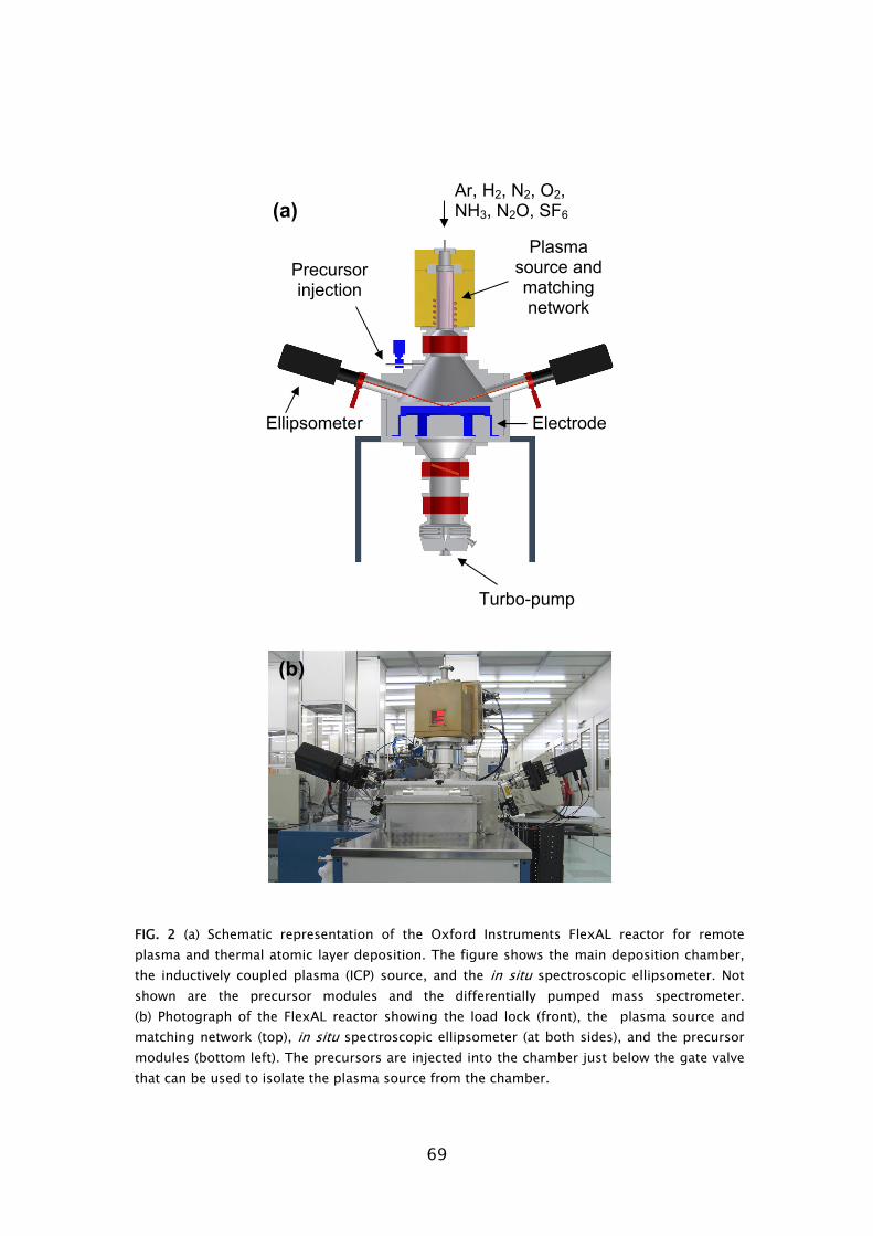
69
FIG. 2 (a) Schematic representation of the Oxford Instruments FlexAL reactor for remote plasma and thermal atomic layer deposition. The figure shows the main deposition chamber, the inductively coupled plasma (ICP) source, and the in situ spectroscopic ellipsometer. Not shown are the precursor modules and the differentially pumped mass spectrometer. (b) Photograph of the FlexAL reactor showing the load lock (front), the plasma source and matching network (top), in situ spectroscopic ellipsometer (at both sides), and the precursor modules (bottom left). The precursors are injected into the chamber just below the gate valve that can be used to isolate the plasma source from the chamber.
(b)
(a) Ar, H2, N2, O2, NH3, N2O, SF6
Ellipsometer
Precursor injection
Turbo-pump
Electrode
Plasma source and matching network
70
The aluminum deposition chamber is optimized to minimize the volume and the presence of dead spaces while maintaining a good film uniformity and pumping capacity. A 240 mm diameter ceramic heater is located in the center of the deposition chamber and its temperature can be actively controlled between 25-400 °C. The chamber wall temperature can be controlled separately between room temperature and a maximum temperature of 120 °C.
A base pressure of ~10-6 Torr in the chamber is reached by a nitrogen-purged 400 l/s turbo molecular pump which is backed by a Fomblin oil greased rotary vane pump. The operating pressure in the chamber during processing can be set using an automated pressure controller (APC), which comprises a fast (90 ms open-close) butterfly valve located in front of the turbo pump and a 100 mTorr capacitance manometer (CM) gauge mounted on the chamber. A gate valve is positioned in between the APC and the turbo pump to isolate the pump from the chamber (e.g., for the case of venting to atmosphere). The valves, the piping in between, and the turbo pump itself are heated to prevent precursor condensation. Also the exhaust line between the turbo pump and the foreline pump is heated.
The plasma is generated by a remotely placed inductively coupled plasma (ICP) source operating at a pressure of typically 10 mTorr. The source can deliver up to 600 W of radio frequency power at 13.56 MHz and is controlled by an automated matching network. The source consists of a three turn water-cooled copper coil around a 65 mm Al2O3 ceramic plasma tube. A wide range of gases such as Ar, H2, N2, O2, NH3, SF6, and N2O is connected to a common plasma source line. The flow of the plasma source gases is controlled by dedicated mass flow controllers (maximum range is 500 sccm for Ar, 100 sccm for H2, N2, and O2, SF6 and N2O and 50 sccm for NH3) (sccm denotes cubic centimeter at STP) located in an extractable gas cabinet. There is no special gas mixing besides in the plasma source line when two or more source gases are used simultaneously. The source gases are fed axially into of the plasma tube and the plasma-generated radicals diffuse through the 100 mm gate valve into the deposition chamber. When depositing conductive films the gate valve is closed during the precursor dosing to prevent film deposition inside the source. When using the reactor for thermal ALD the gate valve can also remain closed and the reducing or oxidizing gases can directly be injected into the chamber.
Liquid and solid precursors can be delivered into the process chamber from bubbler source pots sited in independently heated and extracted modules close to the deposition chamber. The precursor delivery module and delivery lines from the module to the process chamber are heated. Precursors are delivered into the chamber by fast ALD valves with a minimum opening time of 10 ms. The precursors are injected into the deposition chamber above the center of the substrate stage through a cone-shaped flange positioned just below the gate valve to the plasma source. Depending on the vapor pressure of the precursor at the set temperature the delivery can either be vapor-drawn or via bubbling with ultrapure Ar carrier gas. In the case of bubbling the Ar gas is diverted directly into the deposition chamber
71
when no precursor dosing takes place. The use of a divert line ensures fast on and off switching of the precursor without the need of very fast acting mass flow controllers. Moreover, when diverted, the Ar acts as purge gas. In the precursor module a cross-valve is positioned between the gas line where the Ar gas enters the bubbler and the exit line to the deposition chamber. This enables extensive purging of the precursor lines after bubbler exchange. Furthermore, the precursor delivery lines and ALD valves are separately heated and are set to a temperature generally 10-20 °C higher than the precursor module to prevent condensation of the precursors in the lines.
Substrates are transferred into the deposition chamber using a load lock. The load lock is separately pumped with a base pressure of 10-5 Torr and can directly transfer wafer sizes ranging from 50 to 200 mm in diameter, while other substrate sizes and shapes require the use of a carrier wafer.
The reactor operation is completely automated and computer controlled. In a graphical user interface different menus exist for setting process recipes. Standard recipes such as SF6 plasma cleaning for the removal of for example TiN film residues on the chamber walls are also available.
Diagnostic ports located at 70° with the normal on the substrate stage allow in situ ellipsometry measurements for online measurements of the thickness and film optical properties [38]. The windows are valved off when not in use. An additional analytical port positioned above the wafer may be used for residual gas analysis using a differentially pumped quadrupole mass spectrometer. As shown earlier by our group, these analytical capabilities allow for fast process development and process condition monitoring [39,40]. B. Details on TiN and HfO2 deposition
For the TiN depositions, titanium tetrachloride (99.995+%, Sigma-Aldrich, TiCl4) contained in a glass flask, kept at room temperature, is vapor drawn into the setup using a fixed open-close time of the ALD valve of 40 ms. The plasma is generated in an H2-N2 (both purity >99.999%) gas mixture in a ratio of 10:1 to produce N, H, and NHx radical species, etc. to remove the chlorine from the surface and nitridate the film. For the deposition of HfO2, tetrakis(ethylmethylamido)hafnium (99.99+%, Sigma-Aldrich, Hf[N(CH3)(C2H5)]4, TEMAH) contained in a stainless steel bubbler, heated to 70 °C is bubbled using an 30 sccm Ar (purity >99.9999%) flow for a variable dosing period. The plasma is generated in O2 (purity >99.999%) gas to produce O radicals that are considered to be the main oxidizing species.
The TiN and HfO2 films were deposited on 200 mm p-type monocrystalline Si (100) wafers with a resistivity of 10-30 Ω·cm. Unless otherwise mentioned, the wafers were not additionally cleaned and therefore a ~2 nm native oxide layer was present. For electrical characterization some HfO2 films were grown on boron doped p-type monocrystalline Si substrates (~1 Ω·cm), which were dipped in a diluted HF solution (1% HF) for 1 minute and rinsed with de-ionized water prior to deposition.
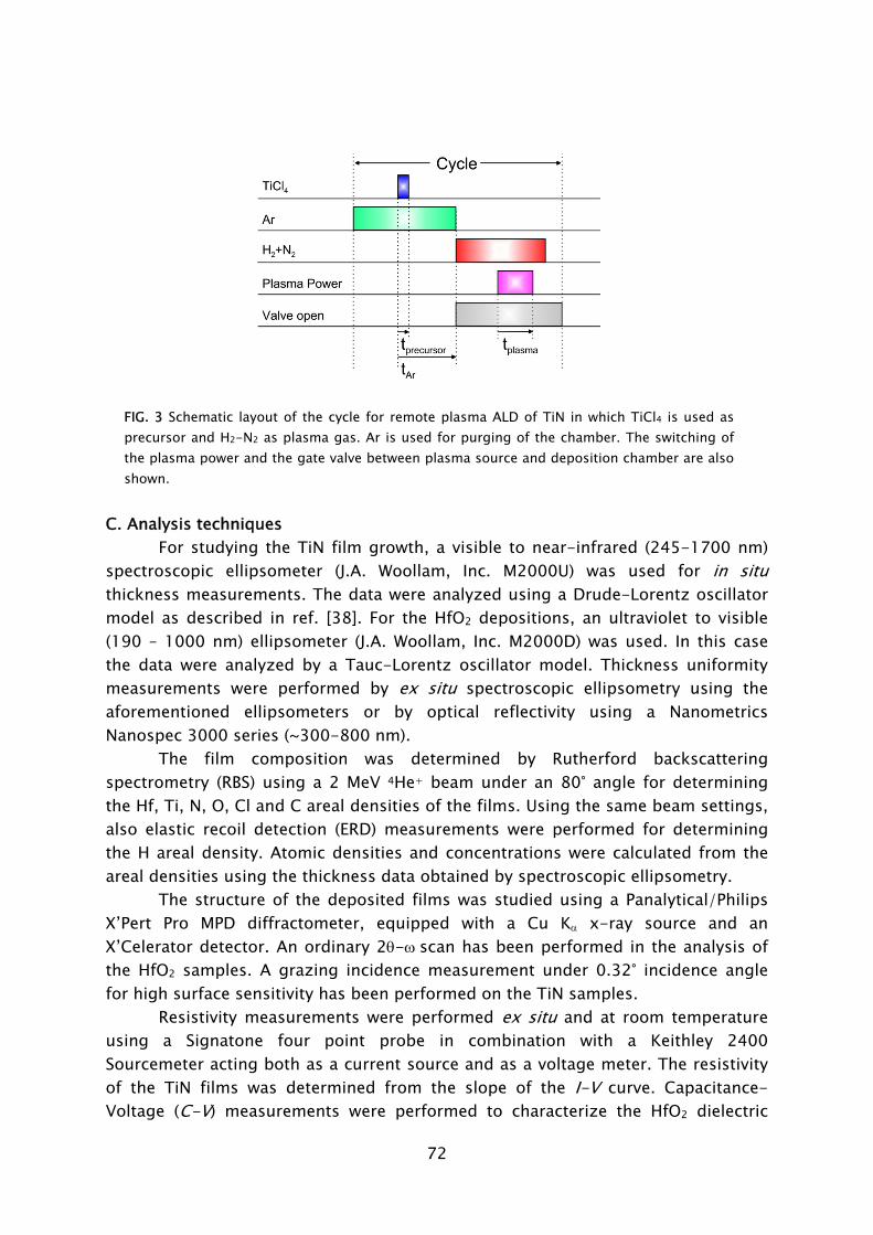
72
FIG. 3 Schematic layout of the cycle for remote plasma ALD of TiN in which TiCl4 is used as precursor and H2-N2 as plasma gas. Ar is used for purging of the chamber. The switching of the plasma power and the gate valve between plasma source and deposition chamber are also shown.
C. Analysis techniques
For studying the TiN film growth, a visible to near-infrared (245-1700 nm) spectroscopic ellipsometer (J.A. Woollam, Inc. M2000U) was used for in situ thickness measurements. The data were analyzed using a Drude-Lorentz oscillator model as described in ref. [38]. For the HfO2 depositions, an ultraviolet to visible (190 – 1000 nm) ellipsometer (J.A. Woollam, Inc. M2000D) was used. In this case the data were analyzed by a Tauc-Lorentz oscillator model. Thickness uniformity measurements were performed by ex situ spectroscopic ellipsometry using the aforementioned ellipsometers or by optical reflectivity using a Nanometrics Nanospec 3000 series (~300-800 nm).
The film composition was determined by Rutherford backscattering spectrometry (RBS) using a 2 MeV 4He+ beam under an 80° angle for determining the Hf, Ti, N, O, Cl and C areal densities of the films. Using the same beam settings, also elastic recoil detection (ERD) measurements were performed for determining the H areal density. Atomic densities and concentrations were calculated from the areal densities using the thickness data obtained by spectroscopic ellipsometry.
The structure of the deposited films was studied using a Panalytical/Philips X’Pert Pro MPD diffractometer, equipped with a Cu Kα x-ray source and an X’Celerator detector. An ordinary 2θ-ω scan has been performed in the analysis of the HfO2 samples. A grazing incidence measurement under 0.32° incidence angle for high surface sensitivity has been performed on the TiN samples.
Resistivity measurements were performed ex situ and at room temperature using a Signatone four point probe in combination with a Keithley 2400 Sourcemeter acting both as a current source and as a voltage meter. The resistivity of the TiN films was determined from the slope of the I-V curve. Capacitance-Voltage (C-V) measurements were performed to characterize the HfO2 dielectric
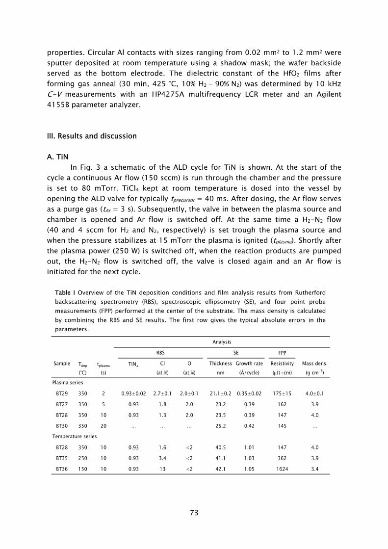
73
properties. Circular Al contacts with sizes ranging from 0.02 mm2 to 1.2 mm2 were sputter deposited at room temperature using a shadow mask; the wafer backside served as the bottom electrode. The dielectric constant of the HfO2 films after forming gas anneal (30 min, 425 °C, 10% H2 – 90% N2) was determined by 10 kHz C-V measurements with an HP4275A multifrequency LCR meter and an Agilent 4155B parameter analyzer. III. Results and discussion A. TiN
In Fig. 3 a schematic of the ALD cycle for TiN is shown. At the start of the cycle a continuous Ar flow (150 sccm) is run through the chamber and the pressure is set to 80 mTorr. TiCl4 kept at room temperature is dosed into the vessel by opening the ALD valve for typically tprecursor = 40 ms. After dosing, the Ar flow serves as a purge gas (tAr = 3 s). Subsequently, the valve in between the plasma source and chamber is opened and Ar flow is switched off. At the same time a H2-N2 flow (40 and 4 sccm for H2 and N2, respectively) is set trough the plasma source and when the pressure stabilizes at 15 mTorr the plasma is ignited (tplasma). Shortly after the plasma power (250 W) is switched off, when the reaction products are pumped out, the H2-N2 flow is switched off, the valve is closed again and an Ar flow is initiated for the next cycle.
Table I Overview of the TiN deposition conditions and film analysis results from Rutherford backscattering spectrometry (RBS), spectroscopic ellipsometry (SE), and four point probe measurements (FPP) performed at the center of the substrate. The mass density is calculated by combining the RBS and SE results. The first row gives the typical absolute errors in the parameters.
FPP
Sample Tdep tplasma TiNx Cl O Thickness Growth rate Resistivity Mass dens.(°C) (s) (at.%) (at.%) nm (Å/cycle) (μΩ•cm) (g cm-3)
BT29 350 2 0.93±0.02 2.7±0.1 2.0±0.1 21.1±0.2 0.35±0.02 175±15 4.0±0.1
BT27 350 5 0.93 1.8 2.0 23.2 0.39 162 3.9
BT28 350 10 0.93 1.3 2.0 23.5 0.39 147 4.0
BT30 350 20 … … … 25.2 0.42 145 …
BT28 350 10 0.93 1.6 <2 40.5 1.01 147 4.0
BT35 250 10 0.93 3.4 <2 41.1 1.03 362 3.9
BT36 150 10 0.93 13 <2 42.1 1.05 1624 3.4
Temperature series
Analysis
RBS SE
Plasma series
74
In Table I an overview of the TiN deposition conditions, process properties and resulting material properties is given. There are two series in which the varied parameters are the plasma exposure time and the deposition temperature. For the plasma series the temperature was kept constant at 350 °C, the cycle time varied from 11-29 s. The selected “standard” deposition condition (sample BT28) is shown for both series. The 40 ms dosing with TiCl4 proved sufficient to reach saturating conditions both in growth rate and uniformity across the substrate at all given temperatures, as will be discussed below.
Figure 4(a) shows that the growth rate saturates at ~0.4 Å/cycle at 350 °C for plasma exposures larger than 5 s. For the temperature series, a plasma exposure of 10 s was therefore selected, resulting in a cycle time of 19 s. Figure 4(b) shows a decrease of the growth rate when operating at a lower deposition temperature. This is similar to what we have observed before for depositions carried out in a smaller laboratory scale reactor, here referred to as “ALD-I”. These data, which were obtained previously, are also shown in Fig. 4(b) for comparison [20]. It can be observed that the growth rate at 350 °C is slightly lower, 0.39 Å/cycle, than the trend on the basis of the ALD-I results would suggest. This minor discrepancy can most probably be explained by a small difference, 10-15 °C, in actual wafer surface temperature between the ALD-I and the FlexAL reactor. Slightly different growth rates, however, have been reported for various types of reactors and for different plasma composition and power settings [29,41].
As is shown by the RBS results in Table I, the films are slightly Ti-rich with the ratio [N]/[Ti] = 0.93-0.95 for all deposition conditions. Contrary to what was observed before [20], in this case the plasma exposure time did not show to have an influence on the stoichiometry. Cl and O impurities were found to be present throughout the film, as can be clearly observed in Fig. 5. The Cl-content is found to
0 5 10 15 20 250.0
0.1
0.2
0.3
0.4
0.5
0.6
0.7
0.8
Gro
wth
rate
(Å/c
ycle
)
Plasma exposure (s)
(a)
100 200 300 4000.0
0.1
0.2
0.3
0.4
0.5
0.6
0.7
0.8(b)
ALD-I FlexAl
Gro
wth
rate
(Å/c
ycle
)
Deposition temperature (°C)
FIG. 4 Growth rate per cycle as a function of (a) the H2-N2 plasma exposure time at 350 °C and (b) the substrate temperature using an H2-N2 plasma exposure time of 10 s. For comparison, in (b) also the growth rate per cycle as obtained in the homebuilt laboratory scale reactor “ALD-I” is given [20].
75
be reduced when longer plasma exposure times are used at 350 °C. A dramatic increase in Cl content, however, occurs when using lower deposition temperatures. The Cl content rises from 1.3 at.% at 350 °C to 14.6 at.% at 150 °C. Similar results have been reported before for both thermal and plasma-assisted ALD at 350 °C. However in the ALD-I setup we managed to have lower Cl-impurities as low as ~7 at.% at a deposition temperature of 100 °C by extending the plasma exposure time to 30 s [20]. It appears that in this larger reactor also longer plasma exposures are required at low temperatures to sufficiently reduce the impurity contents.
Figure 6 shows an x-ray diffraction (XRD) spectrum of the TiN film deposited under standard conditions, 350 °C, 10 s plasma exposure. The diffractogram contains peaks originating from crystalline TiN, of which the expected peak positions are indicated by the reference pattern. All other peaks that are visible originate from the Si substrate. The TiN peaks are at slightly higher diffraction angle than the positions of the reference pattern. This indicates a slightly smaller lattice constant, which might be due to the nitrogen deficiency, which was also observed in the RBS measurements, or due to (tensile) stress in the TiN layer. The ordinary 2θ-ω measurement yielded only one TiN diffraction peak, the (2 0 0) peak between 42° and 43°. This indicates a preferred orientation of the TiN crystallites, with their (2 0 0) lattice planes parallel to the sample surface. This has been observed before for TiN deposition by various techniques and appeared to be mainly deposition temperature dependent, lower temperatures typically resulting in films with a polymorphous or amorphous structure [20].
400 600 800 1000
1.0 1.5 2.0
Yie
ld (a
.u.)
Channel
Si
ClO
TiNC
Energy (MeV)
20 30 40 50 60 70 80 90
111
200
220
311
222
Inte
nsity
(a.u
.)
2θ (degrees)
FIG. 5 Typical Rutherford backscattering spectrum of a remote plasma ALD TiN film (BT28, 23.5 nm thick) deposited on a crystalline Si substrate.
FIG. 6 Typical grazing incidence x-ray diffractogram of a remote plasma ALD TiN film (BT28, 23.5 nm thick). The peak positions and relative intensities of the different crystallographic planes for a randomly oriented TiN powder sample have been indicated. The non-labeled peaks originate from the crystalline Si substrate.
76
The electrical properties of the film can be improved by extending the
plasma exposure, as can be observed in Figure 7. For a plasma exposure longer than 10 s at 350 °C the resistivity seems to level off at ~145 μΩ·cm for 25 nm thick films. The resistivity, however, becomes very high, when going to lower deposition temperatures, i.e., 1624 ± 15 μΩ·cm at 150 °C. This is most probably due to the scattering of the carrier electrons at Cl impurities (14.6 at.%). This was indicated by the electron mean free path being decreased as the Cl-content increases which was observed before by spectroscopic ellipsometry [38]. The resistivity could be improved by extending the plasma exposure, resulting in a reduction of Cl content [20], but this option has not been pursued in the current study.
In Fig. 8 the thickness and resistivity uniformity of a TiN film (5 s plasma exposure, 12-13 nm thickness) is plotted. The nonuniformity, as defined by (maximum-minimum)/(2 x average), was 5% using an edge exclusion of 10 mm. No correlation between the precursor injection position and the profile was observed indicating the symmetric “bowl” shape is solely due to the radical profile. Since most remote plasma reactors are small homebuilt systems no literature comparison is available for such large wafer diameter. A similar uniformity profile can also be observed for the resistivity in Fig. 8(b).
As stated earlier, details about the (non)uniformity of deposition over the substrate area have hardly been reported. However, uniformity is an important factor in the scalability of direct, remote plasma, and radical enhanced based ALD processes. In a recent review, Elers et al. pointed out that the most typical reasons for nonuniformity are considered to be overlapping material pulses, nonuniform gas distribution and thermal self-decomposition of the precursor [30]. Reactor design and plasma operation were also found to play a key role in the deposition of TiN from TiCl4 and a direct H2-N2 plasma using a showerhead gas distributor [29]. In
0 5 10 15 20 250
50
100
150
200
250
Res
istiv
ity (μ
Ω c
m)
Plasma exposure (s)
FIG. 7 Resistivity as a function of the plasma exposure time for 20-25 nm thick TiN films deposited at a temperature of 350 °C.
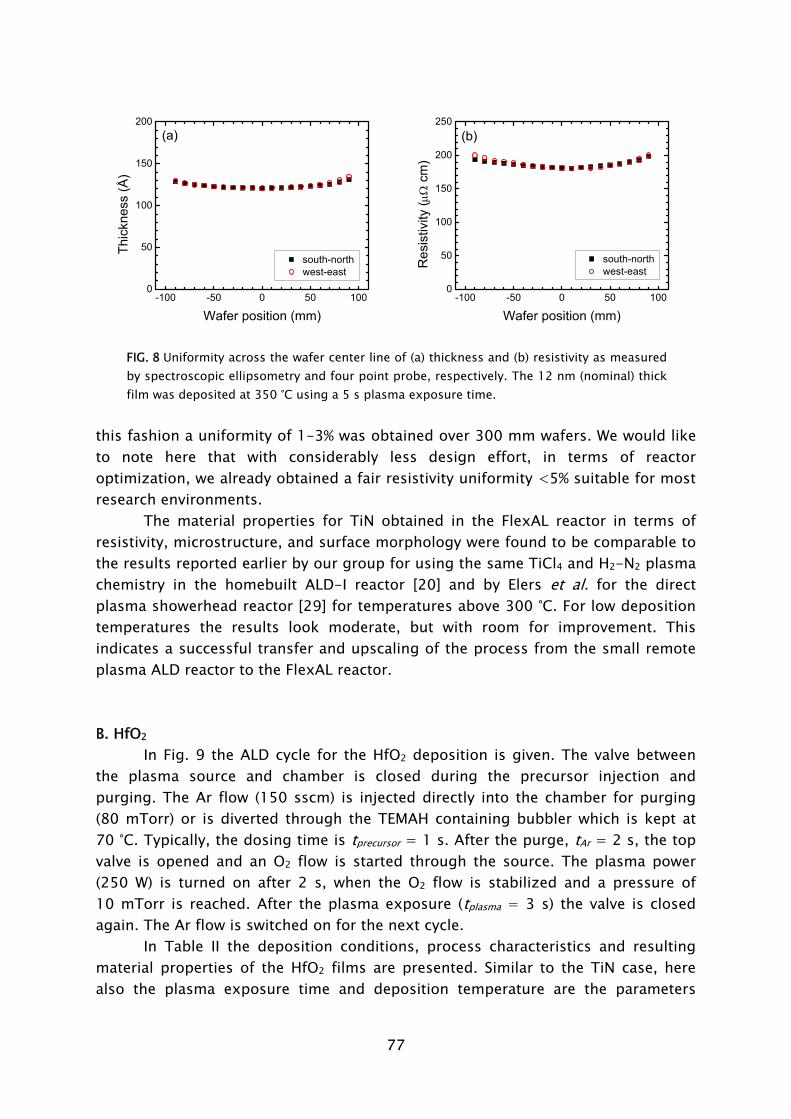
77
-100 -50 0 50 1000
50
100
150
200(a)
south-northwest-east
Thic
knes
s (Å
)
Wafer position (mm)
-100 -50 0 50 1000
50
100
150
200
250
south-northwest-east
Res
istiv
ity (μ
Ω c
m)
Wafer position (mm)
(b)
FIG. 8 Uniformity across the wafer center line of (a) thickness and (b) resistivity as measured by spectroscopic ellipsometry and four point probe, respectively. The 12 nm (nominal) thick film was deposited at 350 °C using a 5 s plasma exposure time.
this fashion a uniformity of 1-3% was obtained over 300 mm wafers. We would like to note here that with considerably less design effort, in terms of reactor optimization, we already obtained a fair resistivity uniformity <5% suitable for most research environments.
The material properties for TiN obtained in the FlexAL reactor in terms of resistivity, microstructure, and surface morphology were found to be comparable to the results reported earlier by our group for using the same TiCl4 and H2-N2 plasma chemistry in the homebuilt ALD-I reactor [20] and by Elers et al. for the direct plasma showerhead reactor [29] for temperatures above 300 °C. For low deposition temperatures the results look moderate, but with room for improvement. This indicates a successful transfer and upscaling of the process from the small remote plasma ALD reactor to the FlexAL reactor. B. HfO2
In Fig. 9 the ALD cycle for the HfO2 deposition is given. The valve between the plasma source and chamber is closed during the precursor injection and purging. The Ar flow (150 sscm) is injected directly into the chamber for purging (80 mTorr) or is diverted through the TEMAH containing bubbler which is kept at 70 °C. Typically, the dosing time is tprecursor = 1 s. After the purge, tAr = 2 s, the top valve is opened and an O2 flow is started through the source. The plasma power (250 W) is turned on after 2 s, when the O2 flow is stabilized and a pressure of 10 mTorr is reached. After the plasma exposure (tplasma = 3 s) the valve is closed again. The Ar flow is switched on for the next cycle.
In Table II the deposition conditions, process characteristics and resulting material properties of the HfO2 films are presented. Similar to the TiN case, here also the plasma exposure time and deposition temperature are the parameters
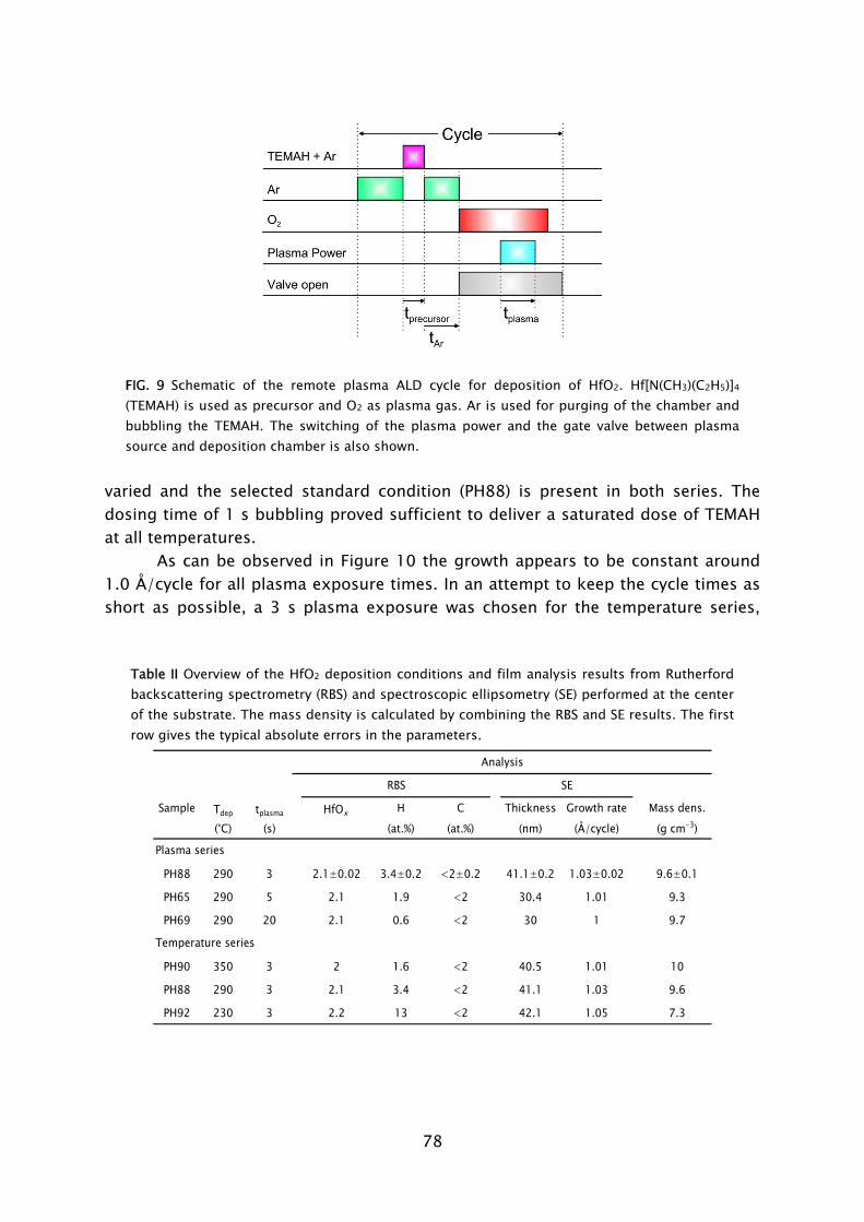
78
FIG. 9 Schematic of the remote plasma ALD cycle for deposition of HfO2. Hf[N(CH3)(C2H5)]4 (TEMAH) is used as precursor and O2 as plasma gas. Ar is used for purging of the chamber and bubbling the TEMAH. The switching of the plasma power and the gate valve between plasma source and deposition chamber is also shown.
varied and the selected standard condition (PH88) is present in both series. The dosing time of 1 s bubbling proved sufficient to deliver a saturated dose of TEMAH at all temperatures.
As can be observed in Figure 10 the growth appears to be constant around 1.0 Å/cycle for all plasma exposure times. In an attempt to keep the cycle times as short as possible, a 3 s plasma exposure was chosen for the temperature series,
Table II Overview of the HfO2 deposition conditions and film analysis results from Rutherford backscattering spectrometry (RBS) and spectroscopic ellipsometry (SE) performed at the center of the substrate. The mass density is calculated by combining the RBS and SE results. The first row gives the typical absolute errors in the parameters.
Sample Tdep tplasma HfOx H C Thickness Growth rate Mass dens.(°C) (s) (at.%) (at.%) (nm) (Å/cycle) (g cm-3)
PH88 290 3 2.1±0.02 3.4±0.2 <2±0.2 41.1±0.2 1.03±0.02 9.6±0.1
PH65 290 5 2.1 1.9 <2 30.4 1.01 9.3
PH69 290 20 2.1 0.6 <2 30 1 9.7
PH90 350 3 2 1.6 <2 40.5 1.01 10
PH88 290 3 2.1 3.4 <2 41.1 1.03 9.6
PH92 230 3 2.2 13 <2 42.1 1.05 7.3
Temperature series
Analysis
RBS SE
Plasma series
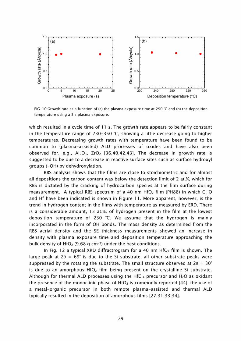
79
0 5 10 15 20 250.0
0.5
1.0
1.5
Gro
wth
rate
(Å/c
ycle
)
Plasma exposure (s)
(a)
200 240 280 320 3600.0
0.5
1.0
1.5
Gro
wth
rate
(Å/c
ycle
)
Deposition temperature (°C)
(b)
FIG. 10 Growth rate as a function of (a) the plasma exposure time at 290 °C and (b) the deposition temperature using a 3 s plasma exposure.
which resulted in a cycle time of 11 s. The growth rate appears to be fairly constant in the temperature range of 230-350 °C, showing a little decrease going to higher temperatures. Decreasing growth rates with temperature have been found to be common to (plasma-assisted) ALD processes of oxides and have also been observed for, e.g., Al2O3, ZrO2 [36,40,42,43]. The decrease in growth rate is suggested to be due to a decrease in reactive surface sites such as surface hydroxyl groups (-OH) by dehydroxylation.
RBS analysis shows that the films are close to stoichiometric and for almost all depositions the carbon content was below the detection limit of 2 at.%, which for RBS is dictated by the cracking of hydrocarbon species at the film surface during measurement. A typical RBS spectrum of a 40 nm HfO2 film (PH88) in which C, O and Hf have been indicated is shown in Figure 11. More apparent, however, is the trend in hydrogen content in the films with temperature as measured by ERD. There is a considerable amount, 13 at.%, of hydrogen present in the film at the lowest deposition temperature of 230 °C. We assume that the hydrogen is mainly incorporated in the form of OH bonds. The mass density as determined from the RBS aerial density and the SE thickness measurements showed an increase in density with plasma exposure time and deposition temperature approaching the bulk density of HfO2 (9.68 g cm-3) under the best conditions.
In Fig. 12 a typical XRD diffractrogram for a 40 nm HfO2 film is shown. The large peak at 2θ = 69° is due to the Si substrate, all other substrate peaks were suppressed by the rotating the substrate. The small structure observed at 2θ = 30° is due to an amorphous HfO2 film being present on the crystalline Si substrate. Although for thermal ALD processes using the HfCl4 precursor and H2O as oxidant the presence of the monoclinic phase of HfO2 is commonly reported [44], the use of a metal-organic precursor in both remote plasma-assisted and thermal ALD typically resulted in the deposition of amorphous films [27,31,33,34].
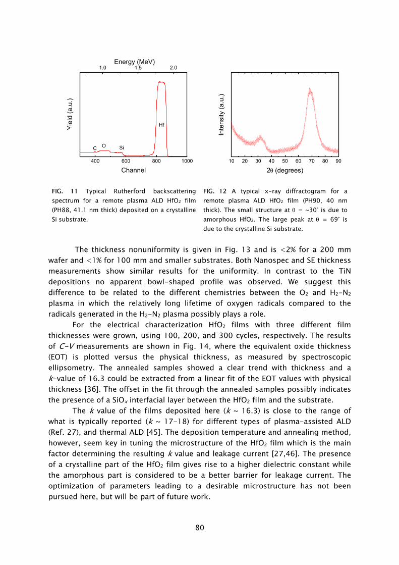
80
400 600 800 1000
1.0 1.5 2.0
Yie
ld (a
.u.)
Channel
SiC O
Hf
Energy (MeV)
10 20 30 40 50 60 70 80 90
Inte
nsity
(a.u
.)
2θ (degrees)
FIG. 11 Typical Rutherford backscattering spectrum for a remote plasma ALD HfO2 film (PH88, 41.1 nm thick) deposited on a crystalline Si substrate.
FIG. 12 A typical x-ray diffractogram for a remote plasma ALD HfO2 film (PH90, 40 nm thick). The small structure at θ = ~30° is due to amorphous HfO2. The large peak at θ = 69° is due to the crystalline Si substrate.
The thickness nonuniformity is given in Fig. 13 and is <2% for a 200 mm
wafer and <1% for 100 mm and smaller substrates. Both Nanospec and SE thickness measurements show similar results for the uniformity. In contrast to the TiN depositions no apparent bowl-shaped profile was observed. We suggest this difference to be related to the different chemistries between the O2 and H2-N2 plasma in which the relatively long lifetime of oxygen radicals compared to the radicals generated in the H2-N2 plasma possibly plays a role.
For the electrical characterization HfO2 films with three different film thicknesses were grown, using 100, 200, and 300 cycles, respectively. The results of C-V measurements are shown in Fig. 14, where the equivalent oxide thickness (EOT) is plotted versus the physical thickness, as measured by spectroscopic ellipsometry. The annealed samples showed a clear trend with thickness and a k-value of 16.3 could be extracted from a linear fit of the EOT values with physical thickness [36]. The offset in the fit through the annealed samples possibly indicates the presence of a SiOx interfacial layer between the HfO2 film and the substrate. The k value of the films deposited here (k ~ 16.3) is close to the range of what is typically reported (k ~ 17-18) for different types of plasma-assisted ALD (Ref. 27), and thermal ALD [45]. The deposition temperature and annealing method, however, seem key in tuning the microstructure of the HfO2 film which is the main factor determining the resulting k value and leakage current [27,46]. The presence of a crystalline part of the HfO2 film gives rise to a higher dielectric constant while the amorphous part is considered to be a better barrier for leakage current. The optimization of parameters leading to a desirable microstructure has not been pursued here, but will be part of future work.
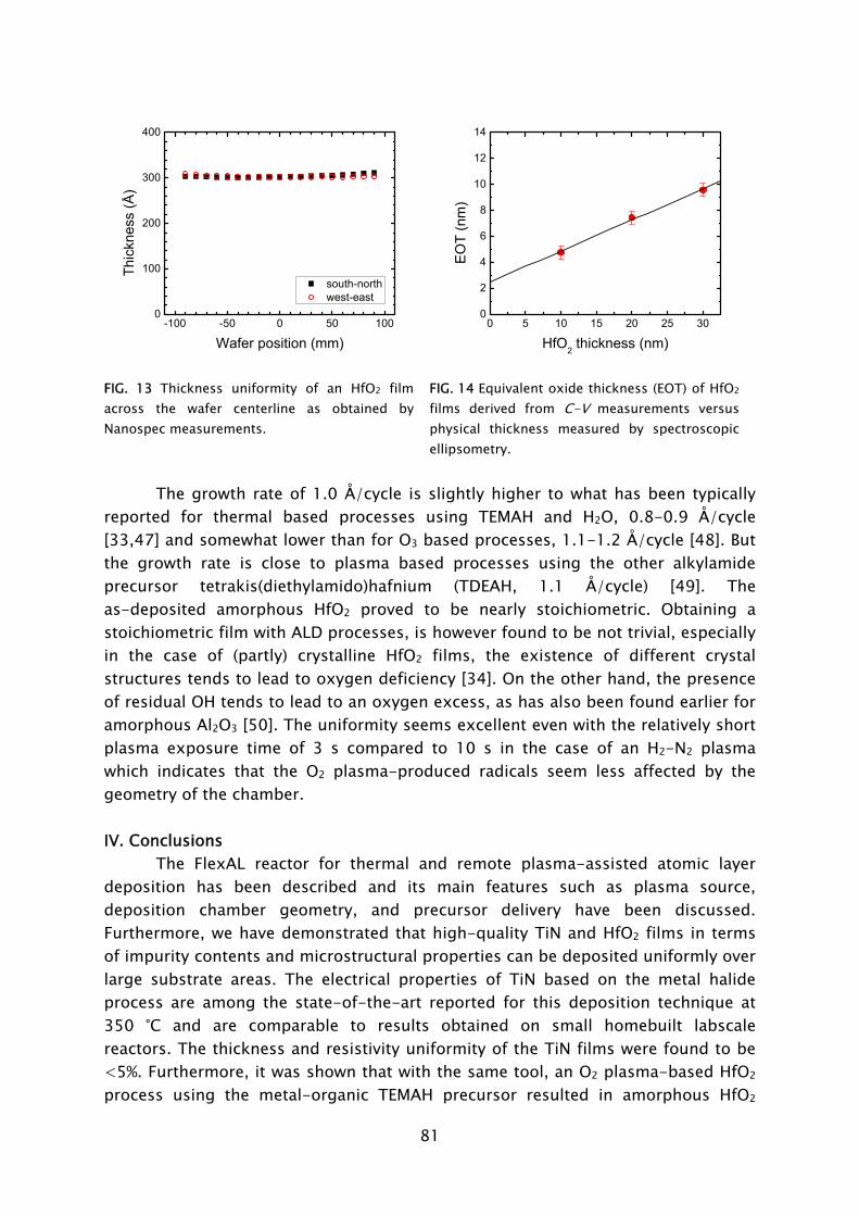
81
-100 -50 0 50 1000
100
200
300
400
south-north west-east
Thic
knes
s (Å
)
Wafer position (mm)
0 5 10 15 20 25 300
2
4
6
8
10
12
14
EO
T (n
m)
HfO2 thickness (nm)
FIG. 13 Thickness uniformity of an HfO2 film across the wafer centerline as obtained by Nanospec measurements.
FIG. 14 Equivalent oxide thickness (EOT) of HfO2 films derived from C-V measurements versus physical thickness measured by spectroscopic ellipsometry.
The growth rate of 1.0 Å/cycle is slightly higher to what has been typically
reported for thermal based processes using TEMAH and H2O, 0.8-0.9 Å/cycle [33,47] and somewhat lower than for O3 based processes, 1.1-1.2 Å/cycle [48]. But the growth rate is close to plasma based processes using the other alkylamide precursor tetrakis(diethylamido)hafnium (TDEAH, 1.1 Å/cycle) [49]. The as-deposited amorphous HfO2 proved to be nearly stoichiometric. Obtaining a stoichiometric film with ALD processes, is however found to be not trivial, especially in the case of (partly) crystalline HfO2 films, the existence of different crystal structures tends to lead to oxygen deficiency [34]. On the other hand, the presence of residual OH tends to lead to an oxygen excess, as has also been found earlier for amorphous Al2O3 [50]. The uniformity seems excellent even with the relatively short plasma exposure time of 3 s compared to 10 s in the case of an H2-N2 plasma which indicates that the O2 plasma-produced radicals seem less affected by the geometry of the chamber. IV. Conclusions
The FlexAL reactor for thermal and remote plasma-assisted atomic layer deposition has been described and its main features such as plasma source, deposition chamber geometry, and precursor delivery have been discussed. Furthermore, we have demonstrated that high-quality TiN and HfO2 films in terms of impurity contents and microstructural properties can be deposited uniformly over large substrate areas. The electrical properties of TiN based on the metal halide process are among the state-of-the-art reported for this deposition technique at 350 °C and are comparable to results obtained on small homebuilt labscale reactors. The thickness and resistivity uniformity of the TiN films were found to be <5%. Furthermore, it was shown that with the same tool, an O2 plasma-based HfO2 process using the metal-organic TEMAH precursor resulted in amorphous HfO2
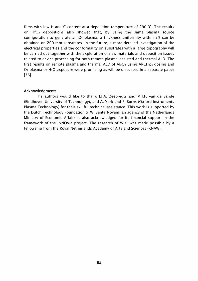
82
films with low H and C content at a deposition temperature of 290 °C. The results on HfO2 depositions also showed that, by using the same plasma source configuration to generate an O2 plasma, a thickness uniformity within 2% can be obtained on 200 mm substrates. In the future, a more detailed investigation of the electrical properties and the conformality on substrates with a large topography will be carried out together with the exploration of new materials and deposition issues related to device processing for both remote plasma-assisted and thermal ALD. The first results on remote plasma and thermal ALD of Al2O3 using Al(CH3)3 dosing and O2 plasma or H2O exposure were promising as will be discussed in a separate paper [36]. Acknowledgments
The authors would like to thank J.J.A. Zeebregts and M.J.F. van de Sande (Eindhoven University of Technology), and A. York and P. Burns (Oxford Instruments Plasma Technology) for their skillful technical assistance. This work is supported by the Dutch Technology Foundation STW. SenterNovem, an agency of the Netherlands Ministry of Economic Affairs is also acknowledged for its financial support in the framework of the INNOVia project. The research of W.K. was made possible by a fellowship from the Royal Netherlands Academy of Arts and Sciences (KNAW).
83
References [1] M. Ritala and M. Leskelä, in Handbook of Thin Films Materials, edited by H. S.
Nalwa (Academic Press, San Diego, CA, 2002), p. 103. [2] M. Tiitta and L. Niinistö, Chem. Vap. Deposition 3, 167 (1997). [3] E. Gerritsen, N. Emonet, C. Caillat, N. Jourdan, M. Piazza, D. Fraboulet, B.
Boeck, A. Berthelot, S. Smith, and P. Mazoyer, Solid-State Electron. 49, 1767 (2005).
[4] S. Jakschik, U. Schroeder, T. Hecht, G. Dollinger, A. Bergmaier, and J. W. Bartha, Mater. Sci. Eng. B-Solid State Mater. Adv. Technol. 107, 251 (2004).
[5] W. S. Yang, Y. K. Kim, S. Y. Yang, J. H. Choi, H. S. Park, S. I. Lee, and J. B. Yoo, Surf. Coat. Technol. 131, 79 (2000).
[6] International Technology Roadmap for Semiconductors, Semiconductor Industry Associates, Available from: http://www.itrs.net (2005).
[7] A. P. Ghosh, L. J. Gerenser, C. M. Jarman, and J. E. Fornalik, Appl. Phys. Lett. 86, 223503 (2005).
[8] M. D. Groner, S. M. George, R. S. McLean, and P. F. Carcia, Appl. Phys. Lett. 88, 051907 (2006).
[9] G. Agostinelli, A. Delabie, P. Vitanov, Z. Alexieva, H. F. W. Dekkers, S. De Wolf, and G. Beaucarne, Sol. Energy Mater. 90, 3438 (2006).
[10] L. Reijnen, B. Meester, A. Goossens, and J. Schoonman, Chem. Vap. Deposition 9, 15 (2003).
[11] T. T. Van and J. P. Chang, Appl. Phys. Lett. 87, 011907 (2005). [12] J. S. King, C. W. Neff, C. J. Summers, W. Park, S. Blomquist, E. Forsythe, and
D. Morton, Appl. Phys. Lett. 83, 2566 (2003). [13] T. M. Mayer, J. W. Elam, S. M. George, P. G. Kotula, and R. S. Goeke, Appl.
Phys. Lett. 82, 2883 (2003). [14] T. W. Scharf, S. V. Prasad, M. T. Dugger, P. G. Kotula, R. S. Goeke, and R. K.
Grubbs, Acta Mater. 54, 4731 (2006). [15] Y. Won, S. Park, J. Koo, S. Kim, J. Kim, and H. Jeon, Appl. Phys. Lett. 87,
262901 (2005). [16] J. Kim, S. Kim, H. Jeon, M. H. Cho, K. B. Chung, and C. Bae, Appl. Phys. Lett.
87, 053108 (2005). [17] B. Hoex, S. B. S. Heil, E. Langereis, M. C. M. van de Sanden, and W. M. M.
Kessels, Appl. Phys. Lett. 89, 042112 (2006). [18] H. Kim, A. J. Kellock, and S. M. Rossnagel, J. Appl. Phys. 92, 7080 (2002). [19] S. M. Rossnagel and H. Kim, J. Vac. Sci. Technol. B 21, 2550 (2003). [20] S. B. S. Heil, E. Langereis, F. Roozeboom, M. C. M. van de Sanden, and W. M.
M. Kessels, J. Electrochem. Soc. 153, G956 (2006). [21] G. A. Ten Eyck, J. J. Senkevich, F. Tang, D. L. Liu, S. Pimanpang, T. Karaback,
G. C. Wang, T. M. Lu, C. Jezewski, and W. A. Lanford, Chem. Vap. Deposition 11, 60 (2005).
[22] H. Kim, C. Cabral, C. Lavoie, and S. M. Rossnagel, J. Vac. Sci. Technol. B 20, 1321 (2002).
84
[23] O. K. Kwon, S. H. Kwon, H. S. Park, and S. W. Kang, Electrochem. Solid-State Lett. 7, C46 (2004).
[24] C. Jezewski, W. A. Lanford, C. J. Wiegand, J. P. Singh, P. I. Wang, J. J. Senkevich, and T. M. Lu, J. Electrochem. Soc. 152, C60 (2005).
[25] S. S. Yim, M. S. Lee, K. S. Kim, and K. B. Kim, Appl. Phys. Lett. 89, 093115 (2006).
[26] G. Lucovsky and D. V. Tsu, J. Vac. Sci. Technol. A 5, 2231 (1987). [27] J. Kim, S. Kim, H. Kang, J. Choi, H. Jeon, M. Cho, K. Chung, S. Back, K. Yoo,
and C. Bae, J. Appl. Phys. 98, 094504 (2005). [28] S. M. Rossnagel, A. Sherman, and F. Turner, J. Vac. Sci. Technol. B 18, 2016
(2000). [29] K. E. Elers, J. Winkler, K. Weeks, and S. Marcus, J. Electrochem. Soc. 152,
G589 (2005). [30] K. E. Elers, T. Blomberg, M. Peussa, B. Aitchison, S. Haukka, and S. Marcus,
Chem. Vap. Deposition 12, 13 (2006). [31] S. Kamiyama, T. Miura, and Y. Nara, Appl. Phys. Lett. 87, 132904 (2005). [32] M. S. Akbar, J. C. Lee, N. Moumen, and J. Peterson, Appl. Phys. Lett. 88,
032906 (2006). [33] K. Kukli, M. Ritala, T. Sajavaara, J. Keinonen, and M. Leskelä, Chem. Vap.
Deposition 8, 199 (2002). [34] K. Kukli, T. Pilvi, M. Ritala, T. Sajavaara, J. Lu, and M. Leskelä, Thin Solid Films
491, 328 (2005). [35] P. K. Park, J. S. Roh, B. H. Choi, and S. W. Kang, Electrochem. Solid-State Lett.
9, F34 (2006). [36] J. L. van Hemmen, S. B. S. Heil, J. H. Klootwijk, F. Roozeboom, M. C. M. van de
Sanden, and W. M. M. Kessels, J. Electrochem. Soc. (2006). [37] See EPAPS Document No. E-JVSTAD6-25-004705 for a movie of the
operation of the Oxford Instruments FlexAL system standing in the cleanroom at the Eindhoven University of Technology. This document can be reacehd via a direct link in the online article's HTML reference section or via the EPAPS homepage (http://www.aip.org/pubservs/epaps.html).
[38] E. Langereis, S. B. S. Heil, M. C. M. van de Sanden, and W. M. M. Kessels, J. Appl. Phys. 100, 023534 (2006).
[39] S. B. S. Heil, E. Langereis, A. Kemmeren, F. Roozeboom, M. C. M. van de Sanden, and W. M. M. Kessels, J. Vac. Sci. Technol. A 23, L5 (2005).
[40] S. B. S. Heil, P. Kudlacek, E. Langereis, R. Engeln, M. C. M. van de Sanden, and W. M. M. Kessels, Appl. Phys. Lett. 89, 131505 (2006).
[41] Y. J. Lee and S. W. Kang, J. Vac. Sci. Technol. A 21, L13 (2003). [42] A. C. Dillon, M. L. Wise, M. B. Robinson, and S. M. George, J. Vac. Sci.
Technol. A 13, 1 (1995). [43] A. Rahtu and M. Ritala, J. Mater. Chem. 12, 1484 (2002). [44] K. Kukli, J. Aarik, M. Ritala, T. Uustare, T. Sajavaara, J. Lu, J. Sundqvist, A.
Aidla, L. Pung, A. Harsta, and M. Leskelä, J. Appl. Phys. 96, 5298 (2004).
85
[45] M. J. Biercuk, D. J. Monsma, C. M. Marcus, J. S. Becker, and R. G. Gordon, Appl. Phys. Lett. 83, 2405 (2003).
[46] K. Kukli, J. Aarik, T. Uustare, J. Lu, M. Ritala, A. Aidla, L. Pung, A. Harsta, M. Leskelä, A. Kikas, and V. Sammelselg, Thin Solid Films 479, 1 (2005).
[47] D. W. McNeil (private communication) [48] S. Kamiyama, T. Miura, and Y. Nara, Electrochem. Solid-State Lett. 8, F37
(2005). [49] J. Choi, S. Kim, J. Kim, H. Kang, H. Jeon, and C. Bae, J. Vac. Sci. Technol. A 24,
678 (2006). [50] E. Langereis, M. Creatore, S. B. S. Heil, M. C. M. van de Sanden, and W. M. M.
Kessels, Appl. Phys. Lett. 89, 081915 (2006).

86
87
Chapter 5 In Situ Reaction Mechanism Study of Plasma-Assisted Atomic Layer Deposition of Al2O3 Reaction mechanisms during plasma-assisted atomic layer deposition (ALD) of Al2O3 from Al(CH3)3 and O2 plasma were studied by time resolved quartz crystal microbalance measurements, mass spectrometry, and optical emission spectroscopy. Al(CH3)3 chemisorption on the oxide surface after the plasma pulse releases CH4 products while from the detection of CO, CO2, and H2O in the O2 plasma it is established that surface –CH3 groups are predominantly removed by O radical-driven combustion-like reactions. Also a second pathway exists for –CH3 removal driven by H2O generated in this plasma step. These reaction pathways are expected to be generic for plasma-assisted ALD of oxides from metal-organic precursors.1
1 Published as: S. B. S. Heil, P. Kudlacek, E. Langereis, R. Engeln, M. C. M. van de Sanden, and W. M. M.
Kessels, Appl. Phys. Lett. 89, 131505 (2006).
88
I. Introduction The search for appropriate high-k dielectrics for semiconductor applications
has made atomic layer deposition (ALD) of oxides a very active research field. Recently, the investigations have been extended to ALD processes in which the commonly used H2O dosing step is replaced by O3 dosing or O2 plasma exposure, because of potential advantages such as improved film quality, increased flexibility in process conditions, and feasibility of lower deposition temperatures. For the pure thermal process, the reaction mechanisms underlying film growth have been investigated for several materials, but for the O3-based or plasma-assisted ALD process virtually no dedicated studies have appeared yet. Especially the thermal process for Al2O3 ALD from trimethylaluminum [Al(CH3)3] and H2O, which can be considered as a model system for ALD [1], has been examined quite thoroughly both experimentally and theoretically [2-9]. Details about the reaction mechanism have been established for this process, which is ruled by (i) chemisorption of Al(CH3)3 on –OH surface groups forming adsorbed (–O–)nAl(CH3)3-n by splitting off one of more ligands in the form of CH4 and (ii) the oxidation of the metal by H2O regenerating –OH surface groups while forming CH4.
In this letter, we report on the reaction mechanism of plasma-assisted ALD of Al2O3 by Al(CH3)3 and O2 plasma. In situ diagnostics such as quartz crystal microbalance and quadrupole mass spectrometry were employed and also optical emission spectroscopy was shown to provide unique time resolved information. Details of the chemisorption step of Al(CH3)3 are presented and key insight about the removal of –CH3 ligands by the plasma is provided by revealing combustion-like reactions by O radicals. Such reactions have been hypothesized for metal-organic precursors earlier, but without experimental support. It is also shown that reaction products created by the plasma (particularly H2O) can lead to concurrent reaction pathways at the surface and that reaction products can significantly affect the plasma properties. II. Experimental
The experiments were carried out in a remote-plasma ALD system with an inductively coupled plasma source. A continuous flow of O2 serves both as plasma gas and as purge gas. Al(CH3)3 dosing and plasma exposure are alternated by releasing a trapped volume of Al(CH3)3 at room temperature and by pulsing 100 W plasma power for 2 s, respectively. During the cycle the background pressure was kept constant at ~10 mTorr and the deposition temperature was set at 70 °C by the wall heating of the reactor. Film growth was monitored by a quartz crystal microbalance (QCM) with a bakeable crystal holder positioned close to the substrate holder. The gold covered quartz crystals were first coated with Al2O3 before taking any data. The reaction products were sampled by a differentially pumped quadrupole mass spectrometer fitted at the side of the reactor, while plasma emission just above the substrate holder was detected by optical emission
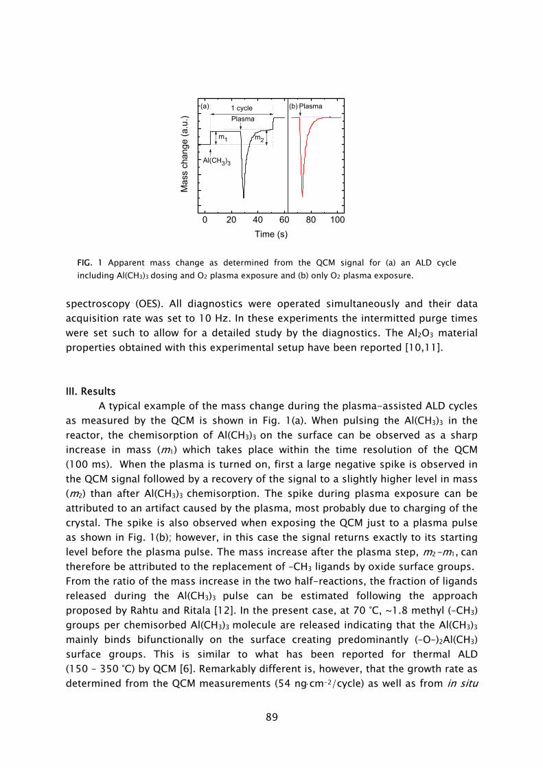
89
0 20 40 60 80 100
(b)(a)
Mas
s ch
ange
(a.u
.)
Time (s)
1 cyclePlasma
m1 m2
Al(CH3)3
Plasma
FIG. 1 Apparent mass change as determined from the QCM signal for (a) an ALD cycle including Al(CH3)3 dosing and O2 plasma exposure and (b) only O2 plasma exposure.
spectroscopy (OES). All diagnostics were operated simultaneously and their data acquisition rate was set to 10 Hz. In these experiments the intermitted purge times were set such to allow for a detailed study by the diagnostics. The Al2O3 material properties obtained with this experimental setup have been reported [10,11].
III. Results
A typical example of the mass change during the plasma-assisted ALD cycles as measured by the QCM is shown in Fig. 1(a). When pulsing the Al(CH3)3 in the reactor, the chemisorption of Al(CH3)3 on the surface can be observed as a sharp increase in mass (m1) which takes place within the time resolution of the QCM (100 ms). When the plasma is turned on, first a large negative spike is observed in the QCM signal followed by a recovery of the signal to a slightly higher level in mass (m2) than after Al(CH3)3 chemisorption. The spike during plasma exposure can be attributed to an artifact caused by the plasma, most probably due to charging of the crystal. The spike is also observed when exposing the QCM just to a plasma pulse as shown in Fig. 1(b); however, in this case the signal returns exactly to its starting level before the plasma pulse. The mass increase after the plasma step, m2-m1, can therefore be attributed to the replacement of –CH3 ligands by oxide surface groups. From the ratio of the mass increase in the two half-reactions, the fraction of ligands released during the Al(CH3)3 pulse can be estimated following the approach proposed by Rahtu and Ritala [12]. In the present case, at 70 °C, ~1.8 methyl (–CH3) groups per chemisorbed Al(CH3)3 molecule are released indicating that the Al(CH3)3
mainly binds bifunctionally on the surface creating predominantly (–O–)2Al(CH3) surface groups. This is similar to what has been reported for thermal ALD (150 – 350 °C) by QCM [6]. Remarkably different is, however, that the growth rate as determined from the QCM measurements (54 ng⋅cm-2/cycle) as well as from in situ
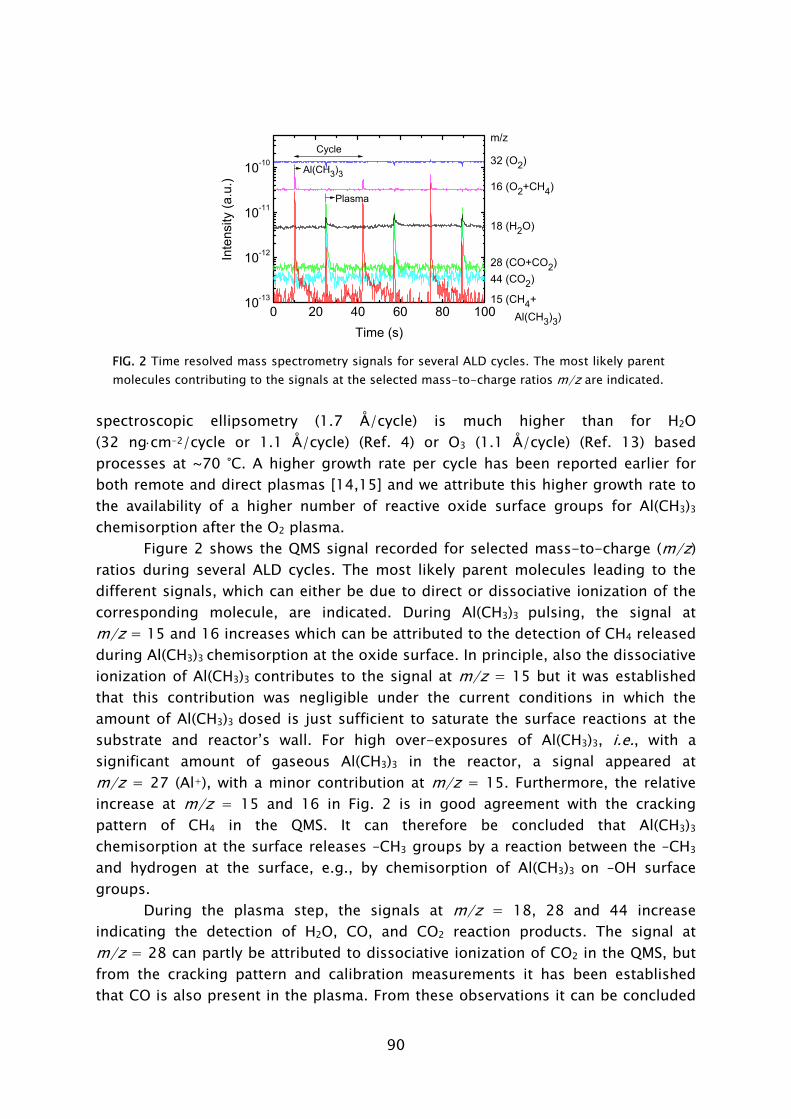
90
0 20 40 60 80 10010-13
10-12
10-11
10-10
Inte
nsity
(a.u
.)
Time (s)
Plasma
Cycle
Al(CH3)3
44 (CO2)
18 (H2O)
15 (CH4+ Al(CH3)3)
28 (CO+CO2)
16 (O2+CH4)
32 (O2)
m/z
FIG. 2 Time resolved mass spectrometry signals for several ALD cycles. The most likely parent molecules contributing to the signals at the selected mass-to-charge ratios m/z are indicated.
spectroscopic ellipsometry (1.7 Å/cycle) is much higher than for H2O (32 ng⋅cm-2/cycle or 1.1 Å/cycle) (Ref. 4) or O3 (1.1 Å/cycle) (Ref. 13) based processes at ~70 °C. A higher growth rate per cycle has been reported earlier for both remote and direct plasmas [14,15] and we attribute this higher growth rate to the availability of a higher number of reactive oxide surface groups for Al(CH3)3
chemisorption after the O2 plasma. Figure 2 shows the QMS signal recorded for selected mass-to-charge (m/z)
ratios during several ALD cycles. The most likely parent molecules leading to the different signals, which can either be due to direct or dissociative ionization of the corresponding molecule, are indicated. During Al(CH3)3 pulsing, the signal at m/z = 15 and 16 increases which can be attributed to the detection of CH4 released during Al(CH3)3 chemisorption at the oxide surface. In principle, also the dissociative ionization of Al(CH3)3 contributes to the signal at m/z = 15 but it was established that this contribution was negligible under the current conditions in which the amount of Al(CH3)3 dosed is just sufficient to saturate the surface reactions at the substrate and reactor’s wall. For high over-exposures of Al(CH3)3, i.e., with a significant amount of gaseous Al(CH3)3 in the reactor, a signal appeared at m/z = 27 (Al+), with a minor contribution at m/z = 15. Furthermore, the relative increase at m/z = 15 and 16 in Fig. 2 is in good agreement with the cracking pattern of CH4 in the QMS. It can therefore be concluded that Al(CH3)3 chemisorption at the surface releases –CH3 groups by a reaction between the –CH3 and hydrogen at the surface, e.g., by chemisorption of Al(CH3)3 on –OH surface groups.
During the plasma step, the signals at m/z = 18, 28 and 44 increase indicating the detection of H2O, CO, and CO2 reaction products. The signal at m/z = 28 can partly be attributed to dissociative ionization of CO2 in the QMS, but from the cracking pattern and calibration measurements it has been established that CO is also present in the plasma. From these observations it can be concluded
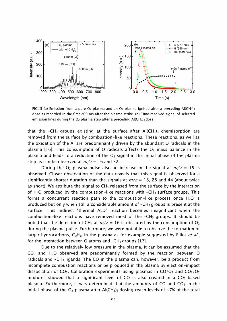
91
200 300 400 500 600 700 8000
100
200
300
400(a)
O2 plasma with Al(CH3)3
Inte
nsity
(a.u
.)
Wavelength (nm)
777nm (O)
656nm (H)
558nm (O+2)
519nm (CO)
0.0 0.5 1.0 1.5 2.0 2.5 3.00
50
100
150
200
Inte
nsity
(a.u
.)
Time (s)
O (777 nm) H (656 nm) CO (519 nm)
t=2s Plasma off
(b)t=0s Plasma on
FIG. 3 (a) Emission from a pure O2 plasma and an O2 plasma ignited after a preceding Al(CH3)3
dose as recorded in the first 200 ms after the plasma strike. (b) Time resolved signal of selected emission lines during the O2 plasma step after a preceding Al(CH3)3 dose.
that the –CH3 groups existing at the surface after Al(CH3)3 chemisorption are removed from the surface by combustion-like reactions. These reactions, as well as the oxidation of the Al are predominantly driven by the abundant O radicals in the plasma [16]. This consumption of O radicals affects the O2 mass balance in the plasma and leads to a reduction of the O2 signal in the initial phase of the plasma step as can be observed at m/z = 16 and 32.
During the O2 plasma pulse also an increase in the signal at m/z = 15 is observed. Closer observation of the data reveals that this signal is observed for a significantly shorter duration than the signals at m/z = 18, 28 and 44 (about twice as short). We attribute the signal to CH4 released from the surface by the interaction of H2O produced by the combustion-like reactions with –CH3 surface groups. This forms a concurrent reaction path to the combustion-like process once H2O is produced but only when still a considerable amount of –CH3 groups is present at the surface. This indirect “thermal ALD” reaction becomes insignificant when the combustion-like reactions have removed most of the –CH3 groups. It should be noted that the detection of CH4 at m/z = 16 is obscured by the consumption of O2 during the plasma pulse. Furthermore, we were not able to observe the formation of larger hydrocarbons, CxHy, in the plasma as for example suggested by Elliot et al., for the interaction between O atoms and –CH3 groups [17].
Due to the relatively low pressure in the plasma, it can be assumed that the CO2 and H2O observed are predominantly formed by the reaction between O radicals and –CH3 ligands. The CO in the plasma can, however, be a product from incomplete combustion reactions or be produced in the plasma by electron-impact dissociation of CO2. Calibration experiments using plasmas in CO/O2 and CO2/O2 mixtures showed that a significant level of CO is also created in a CO2–based plasma. Furthermore, it was determined that the amounts of CO and CO2 in the initial phase of the O2 plasma after Al(CH3)3 dosing reach levels of ~7% of the total
92
gas density. The excitation of the plasma species gives also insight into the
plasma-assisted ALD process. In Fig. 3(a) the emission spectrum of a pure O2 plasma is shown. Mainly emission by O2+ from the first (b4Σg- → a4Πu) and second (A2Πu → X2Πg) negative systems and by O radicals (5P → 5S, 777 nm; 3P → 3S, 845 nm) can be observed. When an Al(CH3)3 dose has preceded the plasma exposure, the emission in the first hundreds of ms of the plasma pulse is remarkably different from the pure O2 plasma. As also shown in Fig. 3(a), there is an intense broadband emission in the first 200 ms of the plasma pulse which can clearly be observed by the naked eye as a “blue flash” [18]. At the end of the plasma pulse the emission is identical to the emission of a pure O2 plasma. The difference in emission at the start of the plasma pulse can be attributed to the plasma excitation of reaction products released from the surface, which evidently disappears when the surface reactions are saturated. From the identification of the spectral lines, we found that the broadband emission is coming predominantly from CO (with the Angström and Herzberg systems most prominent). Furthermore, also emission by atomic hydrogen (Hα) can clearly be observed, which is due to electron-impact dissociation of the H2O and CH4 reaction products.
Figure 3(b) shows time resolved emission signals of the reaction products (CO Angström system v-v’ = 0-2 and Hα) and of the O radicals (3p5P → 3s5S) in the plasma. From the time resolved signal of H and CO, for which a 1/e-decay time of ~300 ms and ~500 ms can be determined, respectively, it can be concluded that the surface reactions during the plasma step are saturated well within 1 s. This is in agreement with results obtained by in situ spectroscopic ellipsometry showing saturation of the growth rate for plasma pulses of >0.5 s. The time resolved emission from O radicals shows that oxygen is consumed by the surface reactions generating the CO, CO2 and H2O reaction products, as well as by oxidizing the Al on the surface.
IV. Conclusions
In summary, for the plasma-assisted ALD process of Al2O3 it has been established that the O2 plasma removes –CH3 ligands from the surface mainly by combustion-like reactions driven by O radicals although a concurrent “thermal ALD”-like reaction path by H2O generated by the plasma is also present. The subsequent chemisorption step of Al(CH3)3 on the surface appears to be similar as for thermal ALD albeit at a higher saturation level. Apparently, after the O2 plasma exposure a higher number of reactive oxide surface groups are available for Al(CH3)3 chemisorption. Whether these oxide surface groups after O2 plasma exposure are predominantly –OH groups, such as in the thermal ALD process, cannot be concluded from the present data. However, the release of CH4 during Al(CH3)3 chemisorption indicates the availability of hydrogen at the surface and surface –OH groups are likely to be formed in the reaction by the H2O created in the
93
combustion-like reactions. The reaction mechanism discussed is expected to have generic relevance for plasma-assisted ALD processes of other oxides from metal-organic precursors and the insight presented has important implications for processing, e.g., in terms of growth rate per cycle for plasma-assisted ALD. Furthermore, it is shown that reaction products from the plasma can significantly affect the plasma properties and hardware settings (e.g., power coupling), while a technique such as optical emission spectroscopy yields unique opportunities to study and optimize the properties for plasma-assisted ALD processes. Acknowledgments
The authors would like to thank Dr. A. Rahtu (ASM Microchemistry) for his assistance with the QCM measurements and stimulating discussions. The Dutch Technology Foundation STW is acknowledged for their financial support. The research of W.K. was made possible by a fellowship from the Royal Netherlands Academy of Arts and Sciences (KNAW).
94
References [1] R. L. Puurunen, J. Appl. Phys. 97, 121301 (2005). [2] S. M. George, A. W. Ott, and J. W. Klaus, J. Phys. Chem. 100, 13121 (1996). [3] M. Ritala, H. Saloniemi, M. Leskelä, T. Prohaska, G. Friedbacher, and M.
Grasserbauer, Thin Solid Films 286, 54 (1996). [4] M. D. Groner, F. H. Fabreguette, J. W. Elam, and S. M. George, Chem. Mat. 16,
639 (2004). [5] A. W. Ott, J. W. Klaus, J. M. Johnson, and S. M. George, Thin Solid Films 292,
135 (1997). [6] A. Rahtu, T. Alaranta, and M. Ritala, Langmuir 17, 6506 (2001). [7] M. Juppo, A. Rahtu, M. Ritala, and M. Leskelä, Langmuir 16, 4034 (2000). [8] S. D. Elliott and J. C. Greer, J. Mater. Chem. 14, 3246 (2004). [9] Y. Widjaja and C. B. Musgrave, Appl. Phys. Lett. 80, 3304 (2002). [10] E. Langereis, M. Creatore, S. B. S. Heil, M. C. M. van de Sanden, and W. M. M.
Kessels, Appl. Phys. Lett. 89, 081915 (2006). [11] B. Hoex, S. B. S. Heil, E. Langereis, M. C. M. van de Sanden, and W. M. M.
Kessels, Appl. Phys. Lett. 89, 042112 (2006). [12] A. Rahtu and M. Ritala, Chem. Vap. Deposition 8, 21 (2002). [13] S. K. Kim, S. W. Lee, C. S. Hwang, Y. S. Min, J. Y. Won, and J. Jeong, J.
Electrochem. Soc. 153, F69 (2006). [14] A. Niskanen, K. Arstila, M. Ritala, and M. Leskelä, J. Electrochem. Soc. 152,
F90 (2005). [15] S. J. Yun, J. W. Lim, and J.-H. Lee, Electrochem. Solid-State Lett. 7, C13
(2004). [16] J. T. Gudmundsson, I. G. Kouznetsov, K. K. Patel, and M. A. Lieberman, J.
Phys. D 34, 1100 (2001). [17] S. D. Elliott, G. Scarel, C. Wiemer, M. Fanciulli, and G. Pavia, Chem. Mat. 18,
3764 (2006). [18] See EPAPS Document No.E-APPLAB-89-331639 for a movie of the plasma
emission during a plasma-assisted ALD cycle. This document can be reached through a direct link in the online article's HTML reference section or via the EPAPS homepage (http://www.aip.org/pubservs/epaps.html).
95
Chapter 6 Reaction Mechanisms during Plasma-Assisted Atomic Layer Deposition of Metal Oxides: A Case Study for Al2O3 Plasma-assisted atomic layer deposition (ALD) of metal oxide films is increasingly gaining interest, however the underlying reaction mechanisms have rarely been addressed. In this work, a case study is presented for the plasma-assisted ALD process of Al2O3 based on Al(CH3)3 dosing and O2 plasma exposure. A complementary set of time resolved in situ diagnostics was employed, including spectroscopic ellipsometry, quartz crystal microbalance, mass spectrometry, and optical emission spectroscopy. The saturation of the Al(CH3)3 adsorption reactions was investigated, as well as the reaction products created during both the precursor dosing and the plasma exposure step. The generality of the observations were cross-checked on a second, commercial ALD reactor. The main observations are: (i) during the precursor dosing, the Al(CH3)3 predominantly binds bifunctionally to the surface at 70 °C through a reaction in which H is abstracted from the surface and CH4 is released into the gas phase; (ii) during the plasma exposure, O radicals in the plasma are consumed at the surface by combustion-like reactions with the surface –CH3 ligands, producing mainly H2O, CO2, and CO; (iii) small gas phase densities of CH4 and higher hydrocarbons (C2Hx) are also present during the O2 plasma exposure step indicating complementary surface reactions including a secondary thermal ALD-like reaction by the H2O produced at the surface; (iv) the plasma and its optical emission are strongly affected by the surface reaction products released in the plasma. In the latter respect, optical emission spectroscopy proved to be a valuable tool to study the surface reaction products during the plasma exposure as well as the saturation of the surface reactions. The implications of the experimental observations are addressed and it is discussed that the reaction mechanisms are generic for plasma-assisted ALD processes based on metal-organic precursors and O2 plasma as oxidant source.1
1 S.B.S. Heil, J. L. van Hemmen, M. C. M. van de Sanden, and W. M. M. Kessels, submitted for publication.
96
I. INTRODUCTION The synthesis of very thin metal oxide films by atomic layer deposition (ALD)
is currently a very active research field. Investigations into various metal oxide materials for applications in semiconductor devices such as gate oxide in complementary-metal-oxide-semiconductor (CMOS) gate stacks and as dielectric layer in dynamic-random-access-memory (DRAM) devices has led to a rapid increase in the number of ALD processes developed. In many of the metal oxide ALD processes metal-organic precursors are employed and H2O is used as oxidant [1]. However, since recently, ALD processes in which O3 or an O2 plasma are used as an alternative oxidant source are gaining increasingly more attention. In these latter processes the oxidant is more reactive than H2O and, therefore, the surface reactions rely less on thermal activation by the substrate temperature. For example, when an O2 plasma is used, chemical activation of the oxidant has already occurred in the gas phase and, therefore, the use of a lower deposition temperature is in many cases facilitated. Furthermore, for some materials it has been reported that improved film properties are obtained when using O3 or O2 plasma instead of H2O [2-8]. The potentially more favorable process settings (e.g., in terms of substrate temperature and purge times) as well as the potentially improved material properties obtained for the O3 and O2 plasma based ALD processes have also contributed to an increased interest into ALD by other fields of technology than semiconductor industry. Potential application of ALD films in areas such as microsystems, solar cells, flexible electronics, energy storage, and photonics have recently been reported [9-19].
While the material properties and functionality of the films have already been investigated in relative detail, the reaction mechanisms leading to film growth in the O3 and O2 plasma based ALD processes have hardly been addressed. Very recently, however, theoretical and experimental investigations of the reaction mechanism of Al2O3 ALD from Al(CH3)3 (trimethylaluminum;TMA) precursor and O3 were reported by Elliott and co-workers [20] and George and co-workers [21]. Our research group recently published a first study into the reaction mechanism of plasma-assisted ALD of Al2O3 using Al(CH3)3 and O2 plasma [22]. The current article is a follow-up on this earlier work and a more extended study of the plasma-assisted ALD process of Al2O3 will be presented.
Due to its excellent dielectric properties, its good adhesion to many surfaces, and its high thermal and chemical stability, Al2O3 is a very relevant material for a wide range of applications. Furthermore, the thermal ALD process of Al2O3 using Al(CH3)3 and H2O is considered to be a model system for ALD film growth of metal oxides [1]. The ALD reaction mechanisms during the Al(CH3)3 and the H2O step have been thoroughly investigated both experimentally and theoretically [23-31]. From these investigations, it has been established that Al2O3 growth by thermal ALD occurs via the following successive “half reactions” [32]:
97
AlOH (s) + Al(CH3)3 (g) AlOAl(CH3)2 (s) + CH4 (g) (1) Al–CH3 (s) + H2O (g) AlOH (s)+ CH4 (g) (2)
where (s) and (g) represent surface groups and gas species, respectively. The chemisorption of Al(CH3)3 and H2O on the surface are Lewis acid-base reactions in which methyl ligands (CH3-) and hydroxyl protons (H+) combine in a Brønsted acid-base reaction and are eliminated as CH4 [20,28,29,33]. For Al2O3, as well as for some other metal oxides, the amount of material deposited per cycle was found to relate directly to the substrate temperature dependent –OH density on the surface [34,35].
For the plasma-assisted ALD process of Al2O3 based on Al(CH3)3 dosing and O2 plasma exposure, we recently presented some proof that the Al(CH3)3
chemisorption step appears very similar as in the thermal ALD process with H2O [22]. Nonetheless, the oxidation step by the O2 plasma appeared to be very different from the H2O based process. It was demonstrated that combustion-like reactions by the plasma generated O radicals removed the –CH3 ligands from the surface because combustion products such as CO2 and H2O were detected by mass spectrometry [22]. Furthermore, a small signal due to the presence of CH4 during the plasma exposure step indicated that the formed H2O byproduct induces a secondary thermal ALD-like reaction pathway. Such secondary reaction pathway in which the reaction products of the oxidation step play a role in the surface chemistry was speculated upon previously [2,36]. In this article we present additional proof and detail for the earlier proposed reaction mechanism. A more extensive and complementary data set is reported as obtained by a combination of several in situ diagnostics such as spectroscopic ellipsometry (SE), quartz crystal microbalance (QCM) measurements, quadrupole mass spectrometry (QMS), and optical emission spectroscopy (OES). More specifically, extensive data on the saturation of the Al(CH3)3 chemisorption reaction are presented. The previous observations are also corroborated by an additional data set obtained on a commercial 200 mm ALD reactor (Oxford Instruments FlexAL). More insight into several aspects of the reaction mechanism of plasma-assisted ALD of Al2O3 has been obtained: QMS signals for mass-to-charge ratios of m/z = 24-30 suggest the presence of small amounts of C2Hx during the plasma exposure, in addition to the earlier detected presence of H2O, CO2, CO and CH4 [22]. By optical emission spectroscopy (OES) with an extended wavelength range in the UV the presence of OH* emission was also identified during the plasma step. Furthermore, it has been demonstrated that the saturation conditions for the Al2O3 film growth can be determined not only directly via the use of film growth monitoring techniques, such as spectroscopic ellipsometry and quartz crystal microbalance, but also indirectly by gas phase diagnostics, such as OES and QMS. On the basis of the results reported a more complete picture of the reaction mechanisms during plasma-assisted ALD of Al2O3 will be presented. Finally, from this case study of Al2O3, the implications for
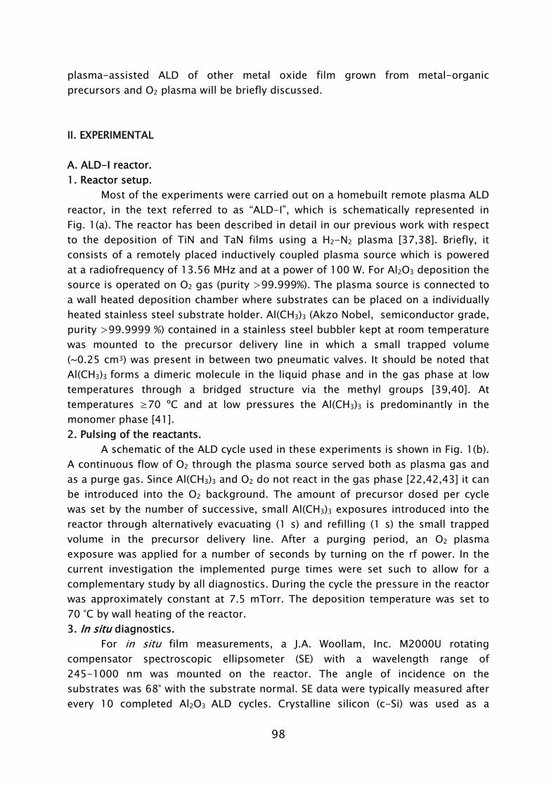
98
plasma-assisted ALD of other metal oxide film grown from metal-organic precursors and O2 plasma will be briefly discussed. II. EXPERIMENTAL A. ALD-I reactor. 1. Reactor setup.
Most of the experiments were carried out on a homebuilt remote plasma ALD reactor, in the text referred to as “ALD-I”, which is schematically represented in Fig. 1(a). The reactor has been described in detail in our previous work with respect to the deposition of TiN and TaN films using a H2-N2 plasma [37,38]. Briefly, it consists of a remotely placed inductively coupled plasma source which is powered at a radiofrequency of 13.56 MHz and at a power of 100 W. For Al2O3 deposition the source is operated on O2 gas (purity >99.999%). The plasma source is connected to a wall heated deposition chamber where substrates can be placed on a individually heated stainless steel substrate holder. Al(CH3)3 (Akzo Nobel, semiconductor grade, purity >99.9999 %) contained in a stainless steel bubbler kept at room temperature was mounted to the precursor delivery line in which a small trapped volume (~0.25 cm3) was present in between two pneumatic valves. It should be noted that Al(CH3)3 forms a dimeric molecule in the liquid phase and in the gas phase at low temperatures through a bridged structure via the methyl groups [39,40]. At temperatures ≥70 ºC and at low pressures the Al(CH3)3 is predominantly in the monomer phase [41]. 2. Pulsing of the reactants.
A schematic of the ALD cycle used in these experiments is shown in Fig. 1(b). A continuous flow of O2 through the plasma source served both as plasma gas and as a purge gas. Since Al(CH3)3 and O2 do not react in the gas phase [22,42,43] it can be introduced into the O2 background. The amount of precursor dosed per cycle was set by the number of successive, small Al(CH3)3 exposures introduced into the reactor through alternatively evacuating (1 s) and refilling (1 s) the small trapped volume in the precursor delivery line. After a purging period, an O2 plasma exposure was applied for a number of seconds by turning on the rf power. In the current investigation the implemented purge times were set such to allow for a complementary study by all diagnostics. During the cycle the pressure in the reactor was approximately constant at 7.5 mTorr. The deposition temperature was set to 70 °C by wall heating of the reactor. 3. In situ diagnostics.
For in situ film measurements, a J.A. Woollam, Inc. M2000U rotating compensator spectroscopic ellipsometer (SE) with a wavelength range of 245-1000 nm was mounted on the reactor. The angle of incidence on the substrates was 68° with the substrate normal. SE data were typically measured after every 10 completed Al2O3 ALD cycles. Crystalline silicon (c-Si) was used as a
99
substrate material which was either plasma oxidized for 5 min prior to deposition or contained a 400 nm thick thermal SiO2 layer on top. The thickness of the Al2O3 was determined by fitting the SE data with a Cauchy model using the Woollam WVASE software. The value of the refractive index at a photon energy of 2 eV ranged typically between 1.60 and 1.65 for the Al2O3 films investigated by SE.
Film growth was also monitored by a quartz crystal microbalance (QCM). Gold covered AT-cut quartz crystals with an oscillation frequency of 6 MHz were mounted in a Maxtek 150BSH bakeable crystal holder positioned in close proximity to the substrate holder and with the crystal surface facing down (i.e., not facing the plasma source). The crystals were first coated with a “fresh” plasma-assisted ALD Al2O3 film before taking any film growth data. The QCM signal was monitored using a Maxtek TM400 thickness monitor which was interfaced with a computer at a data
FIG. 1 (a) Schematic of the homebuilt remote plasma ALD reactor “ALD-I” with the in situ diagnostics indicated. (b) Schematic layout of the plasma-assisted ALD cycle for Al2O3
deposition. The precursor dosing by several successive, small Al(CH3)3 exposures per cycle is indicated.
(a)
(b)
100
acquisition rate of 10 Hz. The extremely high sensitivity of the QCM to surface temperature fluctuations on the crystal progresses with temperature and, consequently, a careful interpretation of the measured signal is required [44,45]. This high sensitivity of the QCM is the reason for controlling the temperature at 70 °C by uniform wall heating in this particular experiment as described above. In addition, pressure variations in the reactor were adequately minimized by continuously flowing the O2 gas. The QCM results are expressed in terms of mass gain with the unit Hz [46].
The gas composition was measured by a differentially pumped quadrupole mass spectrometer (QMS, Pfeifer QME 200, mass-to-charge ratio m/z = 0-100) fitted at the side of the reactor. The gas sampling took place through a 150 μm diameter pinhole keeping the pressure in the mass spectrometer within the working range (<10-5 Torr) for the secondary electron multiplier (SEM) to operate. The electron impact ionization by ~70 eV electrons in the mass spectrometer leads to fragmentation or “cracking” of incoming gas species. The identification of the parent molecules was therefore performed on the basis of its so-called cracking pattern. The cracking pattern of some molecules (CO, CO2, Al(CH3)3) was measured specifically for our QMS by introducing calibration gases yielding good agreement with data reported in the literature. To achieve sufficient time resolution, time resolved measurements were carried out by monitoring only two mass-to-charge ratios (m/z) at a time with an integration time of 10 ms. One of the two masses selected served as a reference signal while the other mass (in the range of m/z = 10-75) was varied over several runs. In the current measurements m/z = 32 (O2+) was taken as reference as there is a constant flow of O2 into the reactor. Data was typically taken over 10 ALD cycles and on the basis of the m/z = 32 (O2+) signal the measurements were synchronized afterwards. This procedure allowed for constructing a time resolved mass scan of several masses with an adequate time resolution.
Optical emission spectroscopy (OES) measurements were carried out by measuring the plasma emission just above the substrate holder using an Ocean Optics USB2000 spectrometer having a wavelength detection range of 250-870 nm and a spectral resolution of approximately 1 nm. The emission by the plasma was coupled into the spectrometer by placing an optical fiber with a small aperture (~100 μm diameter) close to one of the quartz windows on the main chamber. Time dependent measurements were carried out by repetitively acquiring full spectra (250-870 nm) with an integration time of 100 ms. The option in the software for selecting emission peaks in the spectrum and measuring the signal height as a function of time was also used to monitor excited plasma species during the plasma exposure step.
B. FlexAL reactor.
A similar, but less extensive in situ study of the Al2O3 process was carried out in the commercial 200 mm FlexAL reactor from Oxford Instruments. Both the
101
FlexAL reactor itself and the characteristics of the deposition process of Al2O3 by remote plasma ALD using this reactor have been described in our previous work [3,47]. One main difference with the experiments carried out on the homebuilt ALD-I reactor described above is the method of precursor dosing. In the FlexAL a single dose is injected into the deposition chamber using a fast open-close (20 ms) Swagelok ALD valve positioned in the precursor delivery line. In all experiments an open-close time of 20 ms was used for Al(CH3)3 dosing leading to saturated ALD reactions for Al2O3. Furthermore, a continuous O2 flow of 60 sccm was applied through the plasma source and the pressure in the reactor was kept constant at 15 mTorr. The intermitting purge time between precursor and plasma was 3 s, the plasma exposure was set to 4 s, and the purge between plasma and precursor was 0.5 s. Both the reactor walls and the substrate holder were not heated and remained at a temperature of approximately 25 °C.
Similar to the ALD-I setup, the FlexAL was equipped with a spectroscopic ellipsometer, a mass spectrometer, and optical emission spectroscopy. The SE configuration was similar to the ALD-I [3]. The mass spectrometer (QMS, Pfeifer QME 200, m/z = 0-200) was differentially pumped and the only difference with the ALD-I setup is that this mass spectrometer has an extended mass-over-charge (m/z) range and, consequently, a higher signal-to-noise ratio, especially for m/z ratios exceeding 40. Optical emission spectroscopy was performed using the same equipment as for the ALD-I. The plasma emission was collected through a quartz window at the top of the plasma source probing the emission from both the plasma source region and the downstream reactor region by line-of-sight measurement. This configuration was chosen because probing the emission downstream from the side of the reactor lead to a poor signal-to-noise-ratio at the high time resolution (≤100 ms) desired. The data analysis of the in situ diagnostics on the FlexAL reactor was identical to the data analysis on the ALD-I reactor. III. RESULTS A. In situ thickness monitoring by SE
In our previous work, it was established that in situ spectroscopic ellipsometry is a valuable tool to monitor ALD film growth [3,38,48]. In the current work the plasma-assisted ALD process of Al2O3 was characterized at a substrate temperature of 70 °C and 200 °C. Figure 2 shows the results obtained for a plasma exposure time of 2 s. The substrates were plasma oxidized Si samples prepared in situ. A clear linear increase in thickness with the number of cycles can be observed at both deposition temperatures. A thickness increase per cycle of 1.66±0.02 Å at 70 °C and 1.27±0.02 Å at 200 °C was calculated from the slope of the data shown in Fig. 2. No significant initial growth delay was observed in the first few cycles of Al2O3 deposition both on the plasma oxidized Si samples and on the thermal oxide covered c-Si.
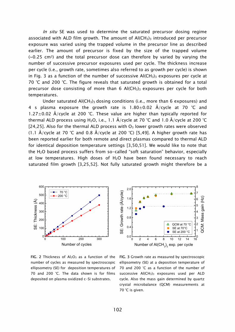
102
In situ SE was used to determine the saturated precursor dosing regime associated with ALD film growth. The amount of Al(CH3)3 introduced per precursor exposure was varied using the trapped volume in the precursor line as described earlier. The amount of precursor is fixed by the size of the trapped volume (~0.25 cm3) and the total precursor dose can therefore by varied by varying the number of successive precursor exposures used per cycle. The thickness increase per cycle (i.e., growth rate, sometimes also referred to as growth per cycle) is shown in Fig. 3 as a function of the number of successive Al(CH3)3 exposures per cycle at 70 °C and 200 °C. The figure reveals that saturated growth is obtained for a total precursor dose consisting of more than 6 Al(CH3)3 exposures per cycle for both temperatures.
Under saturated Al(CH3)3 dosing conditions (i.e., more than 6 exposures) and 4 s plasma exposure the growth rate is 1.80±0.02 Å/cycle at 70 °C and 1.27±0.02 Å/cycle at 200 °C. These value are higher than typically reported for thermal ALD process using H2O, i.e., 1.1 Å/cycle at 70 °C and 1.0 Å/cycle at 200 °C [24,25]. Also for the thermal ALD process with O3 lower growth rates were observed (1.1 Å/cycle at 70 °C and 0.8 Å/cycle at 200 °C) [5,49]. A higher growth rate has been reported earlier for both remote and direct plasmas compared to thermal ALD for identical deposition temperature settings [3,50,51]. We would like to note that the H2O based process suffers from so-called “soft saturation” behavior, especially at low temperatures. High doses of H2O have been found necessary to reach saturated film growth [3,25,52]. Not fully saturated growth might therefore be a
0 100 200 3000
100
200
300
400
500
600
70 °C 200 °C
SE
: Thi
ckne
ss (Å
)
Number of cycles
0 2 4 6 8 10 12 14 160.0
0.4
0.8
1.2
1.6
2.0
0
1
2
3
4
5
6
7
8
SE at 70°C SE at 200 °C
SE
: Gro
wth
rate
(Å/c
ycle
)
Number of Al(CH3)3 exp. per cycle
QCM at 70 °C
QC
M: M
ass
gain
(Hz)
FIG. 2 Thickness of Al2O3 as a function of the number of cycles as measured by spectroscopic ellipsometry (SE) for deposition temperatures of 70 and 200 °C. The data shown is for films deposited on plasma oxidized c-Si substrates.
FIG. 3 Growth rate as measured by spectroscopic ellipsometry (SE) at a deposition temperature of 70 and 200 °C as a function of the number of successive Al(CH3)3 exposures used per ALD cycle. Also the mass gain determined by quartz crystal microbalance (QCM) measurements at 70 °C is given.
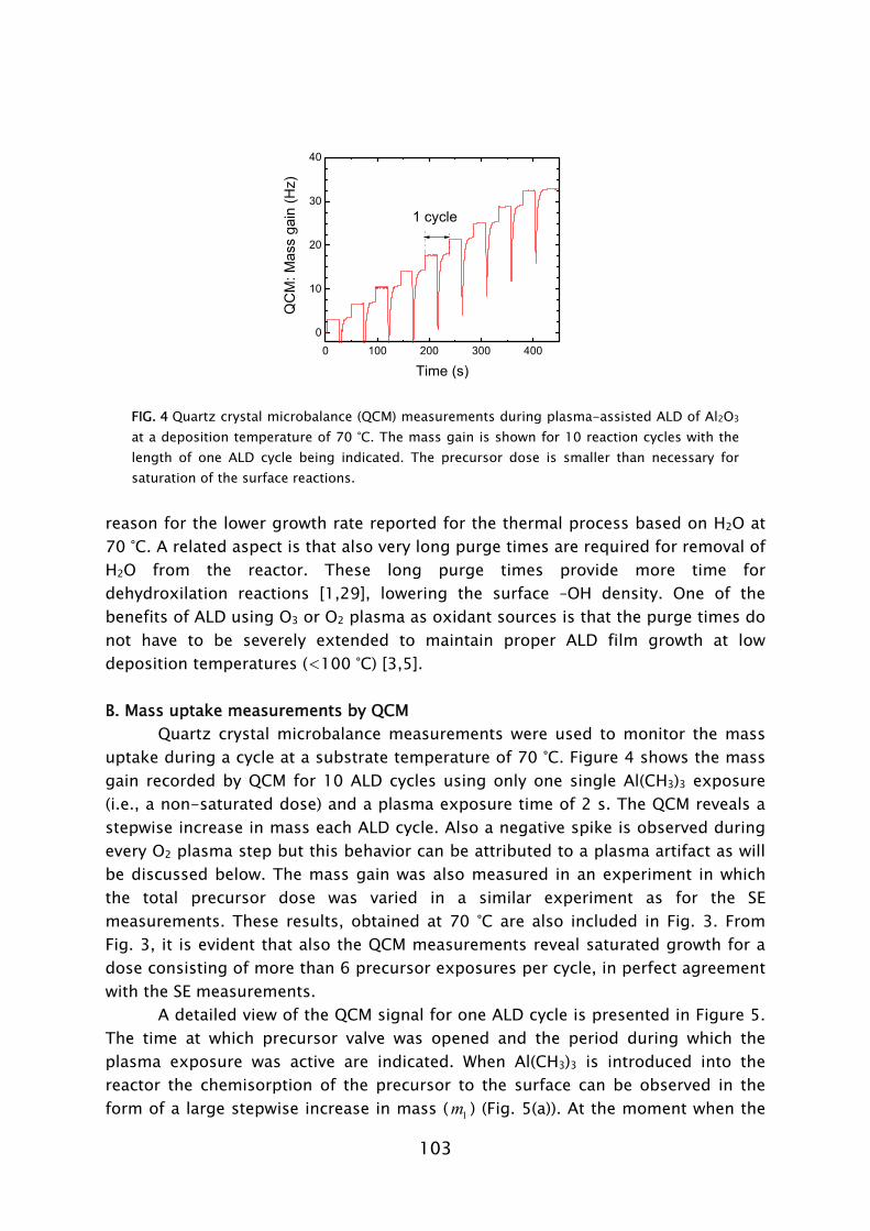
103
0 100 200 300 4000
10
20
30
40
QC
M: M
ass
gain
(Hz)
Time (s)
1 cycle
FIG. 4 Quartz crystal microbalance (QCM) measurements during plasma-assisted ALD of Al2O3 at a deposition temperature of 70 °C. The mass gain is shown for 10 reaction cycles with the length of one ALD cycle being indicated. The precursor dose is smaller than necessary for saturation of the surface reactions.
reason for the lower growth rate reported for the thermal process based on H2O at 70 °C. A related aspect is that also very long purge times are required for removal of H2O from the reactor. These long purge times provide more time for dehydroxilation reactions [1,29], lowering the surface –OH density. One of the benefits of ALD using O3 or O2 plasma as oxidant sources is that the purge times do not have to be severely extended to maintain proper ALD film growth at low deposition temperatures (<100 °C) [3,5]. B. Mass uptake measurements by QCM
Quartz crystal microbalance measurements were used to monitor the mass uptake during a cycle at a substrate temperature of 70 °C. Figure 4 shows the mass gain recorded by QCM for 10 ALD cycles using only one single Al(CH3)3 exposure (i.e., a non-saturated dose) and a plasma exposure time of 2 s. The QCM reveals a stepwise increase in mass each ALD cycle. Also a negative spike is observed during every O2 plasma step but this behavior can be attributed to a plasma artifact as will be discussed below. The mass gain was also measured in an experiment in which the total precursor dose was varied in a similar experiment as for the SE measurements. These results, obtained at 70 °C are also included in Fig. 3. From Fig. 3, it is evident that also the QCM measurements reveal saturated growth for a dose consisting of more than 6 precursor exposures per cycle, in perfect agreement with the SE measurements.
A detailed view of the QCM signal for one ALD cycle is presented in Figure 5. The time at which precursor valve was opened and the period during which the plasma exposure was active are indicated. When Al(CH3)3 is introduced into the reactor the chemisorption of the precursor to the surface can be observed in the form of a large stepwise increase in mass ( 1m ) (Fig. 5(a)). At the moment when the
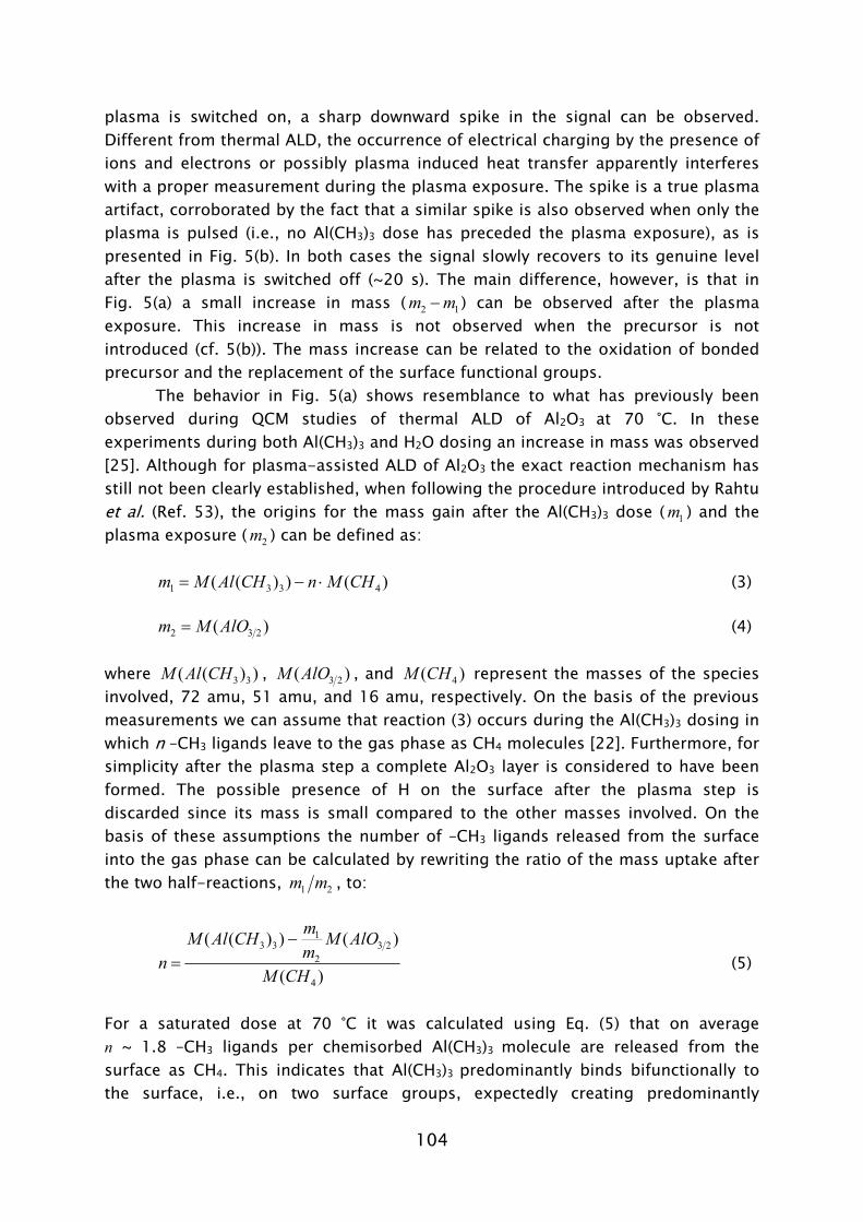
104
plasma is switched on, a sharp downward spike in the signal can be observed. Different from thermal ALD, the occurrence of electrical charging by the presence of ions and electrons or possibly plasma induced heat transfer apparently interferes with a proper measurement during the plasma exposure. The spike is a true plasma artifact, corroborated by the fact that a similar spike is also observed when only the plasma is pulsed (i.e., no Al(CH3)3 dose has preceded the plasma exposure), as is presented in Fig. 5(b). In both cases the signal slowly recovers to its genuine level after the plasma is switched off (~20 s). The main difference, however, is that in Fig. 5(a) a small increase in mass ( 2 1m m− ) can be observed after the plasma exposure. This increase in mass is not observed when the precursor is not introduced (cf. 5(b)). The mass increase can be related to the oxidation of bonded precursor and the replacement of the surface functional groups.
The behavior in Fig. 5(a) shows resemblance to what has previously been observed during QCM studies of thermal ALD of Al2O3 at 70 °C. In these experiments during both Al(CH3)3 and H2O dosing an increase in mass was observed [25]. Although for plasma-assisted ALD of Al2O3 the exact reaction mechanism has still not been clearly established, when following the procedure introduced by Rahtu et al. (Ref. 53), the origins for the mass gain after the Al(CH3)3 dose ( 1m ) and the plasma exposure ( 2m ) can be defined as:
)())(( 4331 CHMnCHAlMm ⋅−= (3)
)( 232 AlOMm = (4)
where 3 3( ( ) )M Al CH , 3 2( )M AlO , and 4( )M CH represent the masses of the species involved, 72 amu, 51 amu, and 16 amu, respectively. On the basis of the previous measurements we can assume that reaction (3) occurs during the Al(CH3)3 dosing in which n –CH3 ligands leave to the gas phase as CH4 molecules [22]. Furthermore, for simplicity after the plasma step a complete Al2O3 layer is considered to have been formed. The possible presence of H on the surface after the plasma step is discarded since its mass is small compared to the other masses involved. On the basis of these assumptions the number of –CH3 ligands released from the surface into the gas phase can be calculated by rewriting the ratio of the mass uptake after the two half-reactions, 1 2m m , to:
)(
)())((
4
232
133
CHM
AlOMmmCHAlM
n−
= (5)
For a saturated dose at 70 °C it was calculated using Eq. (5) that on average n ~ 1.8 –CH3 ligands per chemisorbed Al(CH3)3 molecule are released from the surface as CH4. This indicates that Al(CH3)3 predominantly binds bifunctionally to the surface, i.e., on two surface groups, expectedly creating predominantly
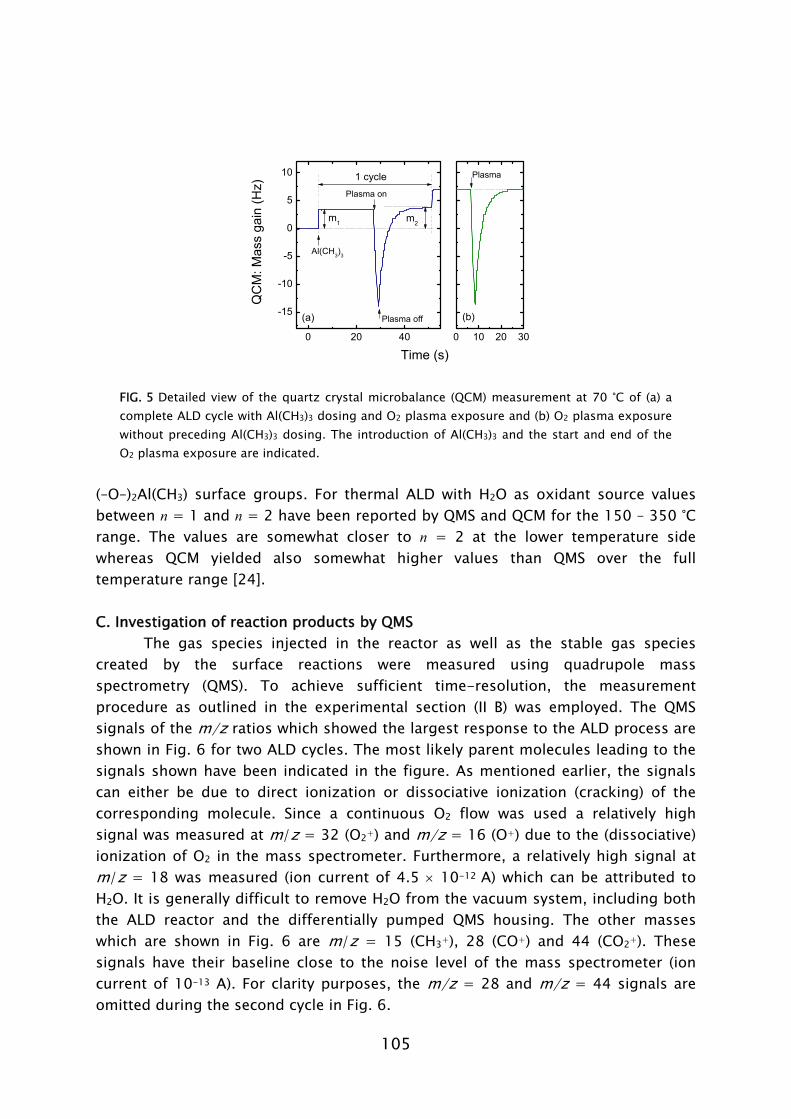
105
QC
M: M
ass
gain
(Hz)
Time (s)0 20 40
-15
-10
-5
0
5
10
Plasma off
1 cyclePlasma on
m1 m2
Al(CH3)3
(a)
0 10 20 30
(b)
Plasma
FIG. 5 Detailed view of the quartz crystal microbalance (QCM) measurement at 70 °C of (a) a complete ALD cycle with Al(CH3)3 dosing and O2 plasma exposure and (b) O2 plasma exposure without preceding Al(CH3)3 dosing. The introduction of Al(CH3)3 and the start and end of the O2 plasma exposure are indicated.
(–O–)2Al(CH3) surface groups. For thermal ALD with H2O as oxidant source values between n = 1 and n = 2 have been reported by QMS and QCM for the 150 – 350 °C range. The values are somewhat closer to n = 2 at the lower temperature side whereas QCM yielded also somewhat higher values than QMS over the full temperature range [24]. C. Investigation of reaction products by QMS
The gas species injected in the reactor as well as the stable gas species created by the surface reactions were measured using quadrupole mass spectrometry (QMS). To achieve sufficient time-resolution, the measurement procedure as outlined in the experimental section (II B) was employed. The QMS signals of the m/z ratios which showed the largest response to the ALD process are shown in Fig. 6 for two ALD cycles. The most likely parent molecules leading to the signals shown have been indicated in the figure. As mentioned earlier, the signals can either be due to direct ionization or dissociative ionization (cracking) of the corresponding molecule. Since a continuous O2 flow was used a relatively high signal was measured at m/z = 32 (O2+) and m/z = 16 (O+) due to the (dissociative) ionization of O2 in the mass spectrometer. Furthermore, a relatively high signal at m/z = 18 was measured (ion current of 4.5 × 10⁻¹² A) which can be attributed to H2O. It is generally difficult to remove H2O from the vacuum system, including both the ALD reactor and the differentially pumped QMS housing. The other masses which are shown in Fig. 6 are m/z = 15 (CH3+), 28 (CO+) and 44 (CO2+). These signals have their baseline close to the noise level of the mass spectrometer (ion current of 10-13 A). For clarity purposes, the m/z = 28 and m/z = 44 signals are omitted during the second cycle in Fig. 6.
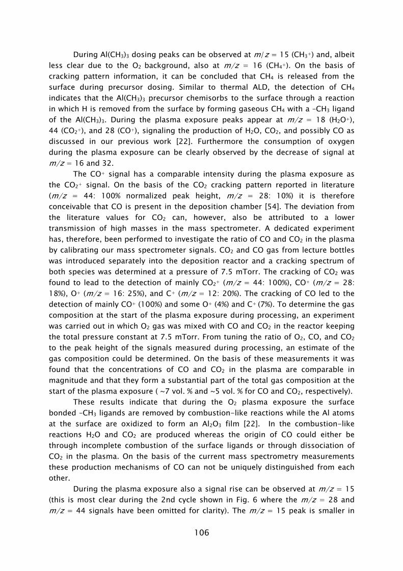
106
During Al(CH3)3 dosing peaks can be observed at m/z = 15 (CH3+) and, albeit less clear due to the O2 background, also at m/z = 16 (CH4+). On the basis of cracking pattern information, it can be concluded that CH4 is released from the surface during precursor dosing. Similar to thermal ALD, the detection of CH4 indicates that the Al(CH3)3 precursor chemisorbs to the surface through a reaction in which H is removed from the surface by forming gaseous CH4 with a –CH3 ligand of the Al(CH3)3. During the plasma exposure peaks appear at m/z = 18 (H2O+), 44 (CO2+), and 28 (CO+), signaling the production of H2O, CO2, and possibly CO as discussed in our previous work [22]. Furthermore the consumption of oxygen during the plasma exposure can be clearly observed by the decrease of signal at m/z = 16 and 32.
The CO+ signal has a comparable intensity during the plasma exposure as the CO2+ signal. On the basis of the CO2 cracking pattern reported in literature (m/z = 44: 100% normalized peak height, m/z = 28: 10%) it is therefore conceivable that CO is present in the deposition chamber [54]. The deviation from the literature values for CO2 can, however, also be attributed to a lower transmission of high masses in the mass spectrometer. A dedicated experiment has, therefore, been performed to investigate the ratio of CO and CO2 in the plasma by calibrating our mass spectrometer signals. CO2 and CO gas from lecture bottles was introduced separately into the deposition reactor and a cracking spectrum of both species was determined at a pressure of 7.5 mTorr. The cracking of CO2 was found to lead to the detection of mainly CO2+ (m/z = 44: 100%), CO+ (m/z = 28: 18%), O+ (m/z = 16: 25%), and C+ (m/z = 12: 20%). The cracking of CO led to the detection of mainly CO+ (100%) and some O+ (4%) and C+ (7%). To determine the gas composition at the start of the plasma exposure during processing, an experiment was carried out in which O2 gas was mixed with CO and CO2 in the reactor keeping the total pressure constant at 7.5 mTorr. From tuning the ratio of O2, CO, and CO2 to the peak height of the signals measured during processing, an estimate of the gas composition could be determined. On the basis of these measurements it was found that the concentrations of CO and CO2 in the plasma are comparable in magnitude and that they form a substantial part of the total gas composition at the start of the plasma exposure ( ~7 vol. % and ~5 vol. % for CO and CO2, respectively).
These results indicate that during the O2 plasma exposure the surface bonded –CH3 ligands are removed by combustion-like reactions while the Al atoms at the surface are oxidized to form an Al2O3 film [22]. In the combustion-like reactions H2O and CO2 are produced whereas the origin of CO could either be through incomplete combustion of the surface ligands or through dissociation of CO2 in the plasma. On the basis of the current mass spectrometry measurements these production mechanisms of CO can not be uniquely distinguished from each other.
During the plasma exposure also a signal rise can be observed at m/z = 15 (this is most clear during the 2nd cycle shown in Fig. 6 where the m/z = 28 and m/z = 44 signals have been omitted for clarity). The m/z = 15 peak is smaller in
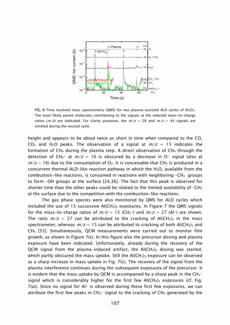
107
0 20 40 6010-13
10-12
10-11
10-10
CO2 + CO
Al(CH3)3 + CH4
CO2
H2O
O2 + CH4
15
4428
18
32
QM
S: I
on c
urre
nt (A
)
Time (s)
PlasmaAl(CH3)3
16
m/zO2
FIG. 6 Time resolved mass spectrometry (QMS) for two plasma-assisted ALD cycles of Al2O3. The most likely parent molecules contributing to the signals at the selected mass-to-charge ratios (m/z) are indicated. For clarity purposes, the m/z = 28 and m/z = 44 signals are omitted during the second cycle.
height and appears to be about twice as short in time when compared to the CO, CO2 and H2O peaks. The observation of a signal at m/z = 15 indicates the formation of CH4 during the plasma step. A direct observation of CH4 through the detection of CH4+ at m/z = 16 is obscured by a decrease in O+ signal (also at m/z = 16) due to the consumption of O2. It is conceivable that CH4 is produced in a concurrent thermal ALD-like reaction pathway in which the H2O, available from the combustion-like reactions, is consumed in reactions with neighboring –CH3 groups to form –OH groups at the surface [24,36]. The fact that this peak is observed for shorter time than the other peaks could be related to the limited availability of –CH3
at the surface due to the competition with the combustion-like reactions. The gas phase species were also monitored by QMS for ALD cycles which
included the use of 15 successive Al(CH3)3 exposures. In Figure 7 the QMS signals for the mass-to-charge ratios of m/z = 15 (CH3+) and m/z = 27 (Al+) are shown. The ratio m/z = 27 can be attributed to the cracking of Al(CH3)3 in the mass spectrometer, whereas m/z = 15 can be attributed to cracking of both Al(CH3)3 and CH4 [55]. Simultaneously, QCM measurements were carried out to monitor film growth, as shown in Figure 7(c). In this figure also the precursor dosing and plasma exposure have been indicated. Unfortunately, already during the recovery of the QCM signal from the plasma-induced artifact, the Al(CH3)3 dosing was started, which partly obscured the mass uptake. Still the Al(CH3)3 exposure can be observed as a sharp increase in mass uptake in Fig. 7(c). The recovery of the signal from the plasma interference continues during the subsequent exposures of the precursor. It is evident that the mass uptake by QCM is accompanied by a sharp peak in the CH3+ signal which is considerably higher for the first few Al(CH3)3 exposures (cf. Fig. 7(a)). Since no signal for Al+ is observed during these first few exposures, we can attribute the first few peaks in CH3+ signal to the cracking of CH4 generated by the
108
Al(CH3)3
QM
S: I
on c
urre
nt (1
0-11 A
)Q
MS
: Ion
cur
rent
(10-1
0 A)
100 150 200 250
0
10
20
30
Time (s)
(c)
QC
M: M
ass
gain
(Hz)
0
1
2
3
4m/z = 27(b)
0
2
4
6
8
10
12m/z = 15(a)
Plasma
Plasma
Plasma
Al(CH3)3 dose
FIG. 7 (a) Quadrupole mass spectrometry (QMS) signal at m/z = 15 and (b) at m/z = 27 during an experiment in which 15 successive Al(CH3)3 exposures per cycle were applied. During the Al(CH3)3 exposures, the signal at m/z = 27 can be attributed to Al(CH3)3 and the signal at m/z = 15 to both CH4 and Al(CH3)3. During plasma exposure the signal at m/z = 27 can most probably be attributed to C2H3+ created by dissociative ionization from higher hydrocarbon species. (c) Corresponding mass gain as measured by quartz crystal microbalance (QCM). The Al(CH3)3 exposures are indicated by vertical tic marks in (c).
chemisorption of Al(CH3)3 on the surface as reported above. The peak intensities of the CH3+ signal gradually decreases with the number of Al(CH3)3 exposures since less and less precursor chemisorps with each succeeding Al(CH3)3 exposure. After 5-6 Al(CH3)3 exposures the CH3+ peaks reach approximately a constant intensity at each additional exposure whereas also a signal for Al+ is now observed in the QMS data (cf. Fig. 7(b)). For the remainder of Al(CH3)3 exposures, the Al+ and CH3+ signal intensities have roughly the same peak height and both signals correlate to the dissociation of unreacted Al(CH3)3 in the QMS. Also after 5-6 Al(CH3)3 exposures no more mass uptake is observed with the QCM (cf. Fig. 7(c)), indicating that the surface reactions have reached saturation. These observations agree well with the growth rate saturation curves obtained by SE and QCM shown in Fig. 3. Since QMS is
109
a volume-based technique the aforementioned observations indicate that all surfaces, i.e., not only the surface of the QCM crystal or the substrate, but also the reactor walls, are saturatively covered with Al(CH3)3 precursor after 5-6 successive Al(CH3)3 exposures. The measurements in Fig. 7 also indicate that the Al(CH3)3
introduced into the reactor is fully consumed by the surface reactions for the first 5-6 Al(CH3)3 exposures. Only when the surface reactions have saturated a significant density of Al(CH3)3 can build up in the gas phase leading to a QMS signal.
Another detail about the reaction mechanism is revealed by the QMS signal at m/z = 27 during the plasma exposure in Fig. 7(a). During the plasma step, a relatively high peak can be observed at m/z = 27 which cannot be attributed to Al(CH3)3. From a careful investigation of the other signals in the m/z = 24-28 range we came to the conclusion that also larger hydrocarbons (C2Hx) are present in the gas phase during the plasma exposure. This was not evident from our previous experiments [22], as the signal at m/z = 28 consists of contributions of CO+ as well as C2H4+. The absolute signals (ion current ~3 × 10-11 A) at m/z = 26 and 27 are, however, a factor of 10 smaller compared to the CO+ and CH4+ signals. On the basis of cracking pattern and cross-section data [56,57] it can be inferred that the production of these higher hydrocarbons is only a minor effect. It indicates, however, an alternative, third pathway next to the already discussed combustion-like and thermal ALD-like reactions. D. Monitoring excited plasma species and reaction products by OES
Specific to plasma-assisted ALD is the emission of light by plasma species during the plasma exposure step. This light emission provides an additional tool in the study of the gas composition and chemistry as the emission lines observed originate from radiative de-excitation of the gas species present in the plasma. These gas species can be both reactant or reaction products, and, consequently, these species can be identified by the use of optical emission spectroscopy [22,37]. In Fig. 8(a) the emission spectrum of a pure O2 plasma is shown as collected in the proximity of the position of the substrate holder. The use of a quartz window provided better sensitivity in the UV region <350 nm compared to our earlier results in which a glass window was applied [22]. The identification of the various emission lines is given in Fig 8(a). In the spectra mainly emission lines of excited O radicals (denoted as O*) and of O2+* ions from the first (b4Σg- → a4Πu) and second (A2Πu → X2Πg) negative systems are visible. This emission gives rise to the greenish color of the plasma which can also be observed around the substrate holder as shown in the photograph in Fig. 8(c). The photograph is taken from a window fitted at the side of the deposition chamber.
When an Al(CH3)3 dose has preceded the plasma exposure, the emission in the first hundreds of milliseconds of the plasma exposure is remarkably different from that of the pure O2 plasma [22]. In the spectrum, taken at 200 ms after the start of the plasma exposure, an intense broadband emission in the blue region can be observed (Fig. 8(b)). The plasma appears bluish to the naked eye, as is also
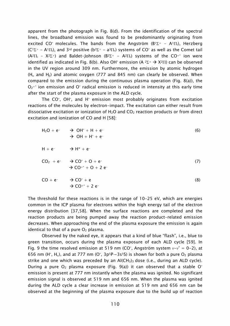
110
apparent from the photograph in Fig. 8(d). From the identification of the spectral lines, the broadband emission was found to be predominantly originating from excited CO* molecules. The bands from the Angström (B1Σ+ - A1Πi), Herzberg (C1Σ+ - A1Πi), and 3rd positive (b3Σ+ - a3Πr) systems of CO* as well as the Comet tail (A2Πi – X2Σ+) and Baldet-Johnson (B2Σ+ - A2Πi) systems of the CO+* ion were identified as indicated in Fig. 8(b). Also OH* emission (A 2Σ+ X2Π) can be observed in the UV region around 309 nm. Furthermore, the emission by atomic hydrogen (Hα and Hβ) and atomic oxygen (777 and 845 nm) can clearly be observed. When compared to the emission during the continuous plasma operation (Fig. 8(a)), the O2+* ion emission and O* radical emission is reduced in intensity at this early time after the start of the plasma exposure in the ALD cycle.
The CO*, OH*, and H* emission most probably originates from excitation reactions of the molecules by electron-impact. The excitation can either result from dissociative excitation or ionization of H2O and CO2 reaction products or from direct excitation and ionization of CO and H [58]:
H2O + e- OH* + H + e- (6) OH + H* + e-
H + e- H* + e- CO2 + e- CO* + O + e- (7)
CO+* + O + 2 e- CO + e- CO* + e (8) CO+* + 2 e-
The threshold for these reactions is in the range of 10-25 eV, which are energies common in the ICP plasma for electrons within the high energy tail of the electron energy distribution [37,58]. When the surface reactions are completed and the reaction products are being pumped away the reaction product-related emission decreases. When approaching the end of the plasma exposure the emission is again identical to that of a pure O2 plasma.
Observed by the naked eye, it appears that a kind of blue “flash”, i.e., blue to green transition, occurs during the plasma exposure of each ALD cycle [59]. In Fig. 9 the time resolved emission at 519 nm (CO*, Angström system v-v’ = 0-2), at 656 nm (H*, Hα), and at 777 nm (O*, 3p5P→3s5S) is shown for both a pure O2 plasma strike and one which was preceded by an Al(CH3)3 dose (i.e., during an ALD cycle). During a pure O2 plasma exposure (Fig. 9(a)) it can observed that a stable O* emission is present at 777 nm instantly when the plasma was ignited. No significant emission signal is observed at 519 nm and 656 nm. When the plasma was ignited during the ALD cycle a clear increase in emission at 519 nm and 656 nm can be observed at the beginning of the plasma exposure due to the build up of reaction
111
300 400 500 600 700 8000
500
1000
1500
2000(b)
OH (A²Σ -X²Π)
Hα
CO+ (B2Σ+-A2Πi) / (A2Πi-X
2Σ+)
OE
S: I
nten
sity
(a.u
.)
Wavelength (nm)
CO (b3Σ+-a3Πr) / (C1Σ+-A1Πi) / (B
1Σ+-A1Π)
Hβ
0
500
1000
1500
2000
O+2 (b
4Σ-g → a4Πu)
O
O+2 (A
2Πu → X2Πg)
(a)
OE
S: In
tens
ity (a
.u.)
FIG. 8 (a) Optical emission spectrum (OES) from a pure O2 plasma and (b) from the plasma after a preceding Al(CH3)3 dose recorded in the first 200 ms after the plasma strike. The different emission lines have been identified in the figure. (c) and (d) show photographs of the plasma corresponding to (a) and (b), respectively. The photographs are taken through the viewport at the side of the reactor and show the downstream region where the substrate holder is located.
products, CO, CO2, H2O in the gas phase (cf. Fig. 9(b)). This increase is followed by a decrease in emission of the reactants due to the removal of the species by pumping when the surface reactions reach saturation. In the beginning of the plasma pulse the consumption of O radicals is also apparent from the initially lower emission intensity at 777 nm. This O* emission is lower as oxygen is used to generate CO, CO2 and H2O reaction products as well as to oxidize the Al on the surface. Subsequently, the O* intensity increases and at the end of the plasma exposure it levels off at the same height as in a pure O2 plasma.
Besides giving insight into the reaction mechanisms, the time dependent OES signals in Fig. 9 also yield insight into the plasma exposure time necessary for reaching saturation. From the time resolved signal of the CO* and H* emission, for which an 1/e decay time of ~300 ms can be determined, it can be concluded that the surface reactions and removal of reactants during the plasma step occur in a time span well within 1 s. This was corroborated by in situ spectroscopic
(d)
(c)
112
Time (s)0 1 2
(b)
OE
S: I
nten
sity
(a.u
.)
0 1 20
50
100
150
200
777 nm - O* 656 nm - H* 519 nm - CO*
(a)
0 2 4 6 8 10 12 14 16 18 200
20
40
60
80
100
OE
S: I
nteg
rate
d in
tens
ity (a
.u.)
Number of Al(CH3)3 exp. per cycle
777 nm - O* 656 nm - H* 519 nm - CO*
FIG. 9 Time resolved optical emission (OES) measurements at the wavelengths 519 nm, 656 nm, and 777 nm corresponding to CO*, H*, and O*, respectively. (a) Emission for an O2 plasma without preceding Al(CH3)3 dosing and (b) the emission for a plasma exposure step during an ALD cycle.
FIG. 10 Integrated intensity of the time resolved optical emission spectroscopy (OES) measurements of CO*, H*, and O* during the plasma step of the ALD cycle as a function of the number of successive Al(CH3)3 exposures used in the cycle.
ellipsometry measurements of films deposited under different plasma conditions. These measurements revealed a saturation of the growth rate for plasma exposure times >0.5 s.
Optical emission spectroscopy, which is a volume based technique similar to QMS, probes the saturation of the surface reactions on all the different surfaces of the reactor. To learn about the saturation behavior of the Al(CH3)3 precursor reactions, time dependent measurements of the reaction products were performed for different Al(CH3)3 doses. The time resolved signals of O*, H*, and CO* were integrated and plotted as a function of the preceding precursor dose expressed in the total number of successive Al(CH3)3 exposures per cycle in Fig. 10. Clearly the saturation of surface reactions can be observed on the basis of the amount of H* and CO* emission during the plasma exposure. The integrated signals saturate at a dose of ~6 successive Al(CH3)3 exposures per cycle, as also found with SE, QCM, and QMS discussed earlier. Furthermore, also the amount of oxygen consumed can be observed to increase in the non-saturated region by a decrease in the integrated O* emission with increasing Al(CH3)3 dose. E. QMS and OES results on the FlexAL reactor
To test the general validity of the results obtained on the ALD-I reactor, quadrupole mass spectrometry (QMS) and optical emission spectroscopy studies (OES) were also performed during the deposition of Al2O3 in the FlexAL reactor. The experiments were carried out without heating the reactor walls and substrate holder, i.e., at 25 °C. At this temperature a considerable fraction of the Al(CH3)3
113
might be in the dimer phase [39,41]. However, to the best of our knowledge, there have been no reports that this dimer phase has a substantial influence on the surface chemistry during ALD at low temperatures.
Measurements by QMS, which had a better signal-to-noise ratio at higher m/z ratios for the FlexAL than for the ALD-I reactor, revealed signals at m/z = 57 (Al(CH3)2+), m/z = 42 (Al(CH3)+), m/z = 27 (Al+) and m/z = 15 (CH3+) for the unreacted precursor. The peak heights were found to correspond well to the Al(CH3)3 cracking pattern reported under room temperature conditions [55].
In Fig. 11 the time dependent signals of selected masses are given for a number of ALD cycles covering the same span as in Fig. 6. The moment of precursor dosing (20 ms duration) and period of plasma exposure (4 s duration) have been indicated. The chemisorption of Al(CH3)3 can observed through the detection of CH4, both on m/z = 15 (CH3+) and m/z = 16 (CH4+) as shown in Fig. 11. During precursor injection the signal rises also slightly for m/z = 32. This increase is smaller than for m/z = 16 and we attribute the increase at m/z = 32 to the pressure increase in the QMS induced by the precursor injection. Albeit less clear, during the plasma exposure also a decrease in the signals at m/z = 16 and 32 can be observed similar to the case in the ALD-I reactor as discussed above. This decrease can be explained by the consumption of oxygen by the oxidation of the surface and the production of combustion-like reaction products. These reaction products created during the plasma step are observed at m/z = 28 (CO+) and m/z = 44 (CO2+). From the relative intensity of the CO+ and CO2+ signals it can be concluded that both CO2 and CO are present in the plasma similar to the case in the ALD-I reactor. The production of H2O during the plasma exposure is remarkably not observed at m/z = 18. This can be attributed to the relatively high pressure and therefore high background signal in the QMS on the FlexAL reactor in comparison
0 20 40 6010-12
10-11
10-10
10-9
10-8
15
28
QM
S: I
on c
urre
nt (A
)
Time (s)
Al(CH3)3
Plasma
44
18
3216
m/z =
CO2 + CO
Al(CH3)3 + CH4
CO2
H2O
O2 + CH4
O2
FIG. 11 Time resolved quadrupole mass spectrometry (QMS) during several plasma-assisted ALD cycles of Al2O3 carried out in the Oxford Instruments FlexAL reactor. The most likely parent molecules contributing to the signals at the selected mass-to-charge ratios (m/z) are given. The Al(CH3)3 dosing and plasma exposures are indicated in the figure.
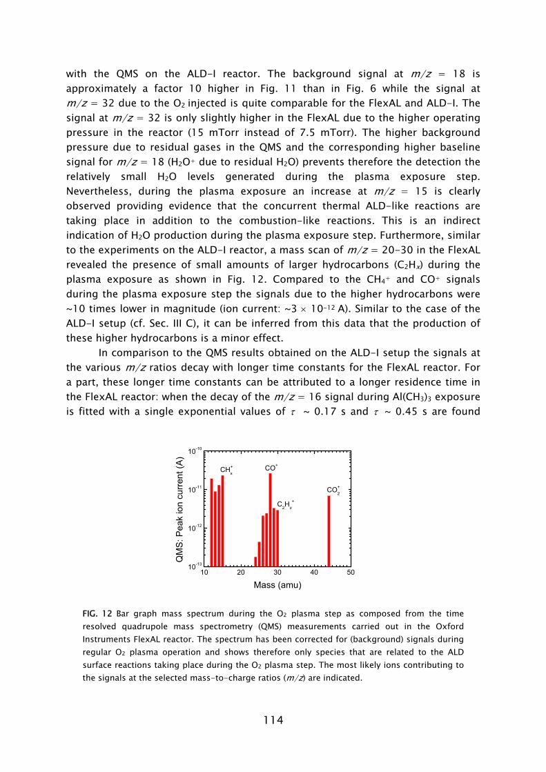
114
with the QMS on the ALD-I reactor. The background signal at m/z = 18 is approximately a factor 10 higher in Fig. 11 than in Fig. 6 while the signal at m/z = 32 due to the O2 injected is quite comparable for the FlexAL and ALD-I. The signal at m/z = 32 is only slightly higher in the FlexAL due to the higher operating pressure in the reactor (15 mTorr instead of 7.5 mTorr). The higher background pressure due to residual gases in the QMS and the corresponding higher baseline signal for m/z = 18 (H2O+ due to residual H2O) prevents therefore the detection the relatively small H2O levels generated during the plasma exposure step. Nevertheless, during the plasma exposure an increase at m/z = 15 is clearly observed providing evidence that the concurrent thermal ALD-like reactions are taking place in addition to the combustion-like reactions. This is an indirect indication of H2O production during the plasma exposure step. Furthermore, similar to the experiments on the ALD-I reactor, a mass scan of m/z = 20-30 in the FlexAL revealed the presence of small amounts of larger hydrocarbons (C2Hx) during the plasma exposure as shown in Fig. 12. Compared to the CH4+ and CO+ signals during the plasma exposure step the signals due to the higher hydrocarbons were ~10 times lower in magnitude (ion current: ~3 × 10-12 A). Similar to the case of the ALD-I setup (cf. Sec. III C), it can be inferred from this data that the production of these higher hydrocarbons is a minor effect.
In comparison to the QMS results obtained on the ALD-I setup the signals at the various m/z ratios decay with longer time constants for the FlexAL reactor. For a part, these longer time constants can be attributed to a longer residence time in the FlexAL reactor: when the decay of the m/z = 16 signal during Al(CH3)3 exposure is fitted with a single exponential values of τ ~ 0.17 s and τ ~ 0.45 s are found
10 20 30 40 5010-13
10-12
10-11
10-10
QM
S: P
eak
ion
curr
ent (
A)
Mass (amu)
CO+
CO+2
C2Hx+
CH+x
FIG. 12 Bar graph mass spectrum during the O2 plasma step as composed from the time resolved quadrupole mass spectrometry (QMS) measurements carried out in the Oxford Instruments FlexAL reactor. The spectrum has been corrected for (background) signals during regular O2 plasma operation and shows therefore only species that are related to the ALD surface reactions taking place during the O2 plasma step. The most likely ions contributing to the signals at the selected mass-to-charge ratios (m/z) are indicated.
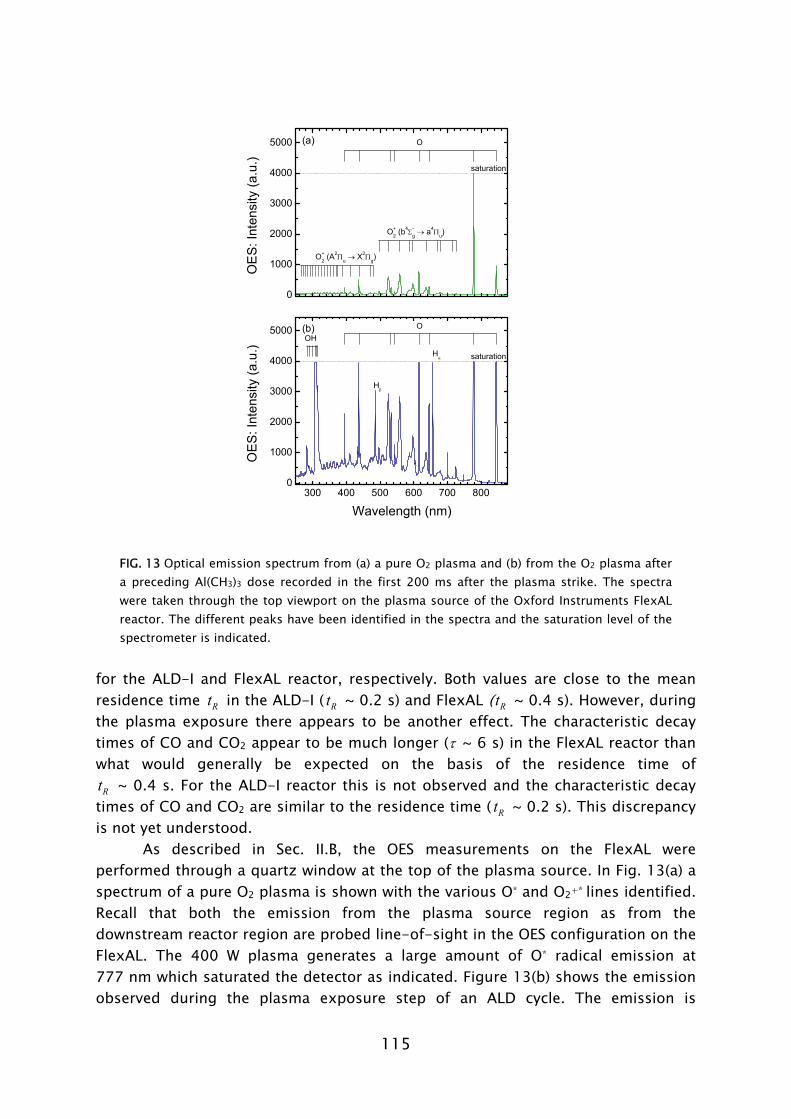
115
300 400 500 600 700 8000
1000
2000
3000
4000
5000 (b)
saturation
OH
Hα
OE
S: I
nten
sity
(a.u
.)
Wavelength (nm)
Hβ
O
0
1000
2000
3000
4000
5000 (a)
OE
S: I
nten
sity
(a.u
.)
O
O+2 (A
2Πu → X2Πg)
O+2 (b
4Σ-g → a4Πu)
saturation
FIG. 13 Optical emission spectrum from (a) a pure O2 plasma and (b) from the O2 plasma after a preceding Al(CH3)3 dose recorded in the first 200 ms after the plasma strike. The spectra were taken through the top viewport on the plasma source of the Oxford Instruments FlexAL reactor. The different peaks have been identified in the spectra and the saturation level of the spectrometer is indicated.
for the ALD-I and FlexAL reactor, respectively. Both values are close to the mean residence time Rt in the ALD-I ( Rt ~ 0.2 s) and FlexAL ( Rt ~ 0.4 s). However, during the plasma exposure there appears to be another effect. The characteristic decay times of CO and CO2 appear to be much longer (τ ~ 6 s) in the FlexAL reactor than what would generally be expected on the basis of the residence time of
Rt ~ 0.4 s. For the ALD-I reactor this is not observed and the characteristic decay times of CO and CO2 are similar to the residence time ( Rt ~ 0.2 s). This discrepancy is not yet understood.
As described in Sec. II.B, the OES measurements on the FlexAL were performed through a quartz window at the top of the plasma source. In Fig. 13(a) a spectrum of a pure O2 plasma is shown with the various O* and O2+* lines identified. Recall that both the emission from the plasma source region as from the downstream reactor region are probed line-of-sight in the OES configuration on the FlexAL. The 400 W plasma generates a large amount of O* radical emission at 777 nm which saturated the detector as indicated. Figure 13(b) shows the emission observed during the plasma exposure step of an ALD cycle. The emission is
116
collected at the beginning of the plasma exposure (t ~ 200 ms after plasma ignition). It is evident that a large amount of O2 plasma-related emission is still present, probably most prominently generated in the plasma source itself. The presence of H2O in the plasma can be deduced from the strong OH* and H* emission around 309 and 656 nm, respectively. This provides additional evidence that H2O is produced in the FlexAL reactor despite the fact that the H2O signal was obscured in the QMS data. Furthermore, compared to the pure O2 plasma (Fig. 13(a)), the spectrum during the ALD processing (Fig. 13(b)) shows also a clear broadband emission. Although no clearly resolved CO* related peaks can be distinguished the subtraction of both spectra in Fig. 13 confirms the presence of CO* emission. IV. DISCUSSION A. Reaction mechanism for plasma-assisted ALD of Al2O3
In the previous sections, the plasma-assisted ALD process of Al2O3 from Al(CH3)3 and O2 plasma has been investigated in two remote plasma ALD reactors by four different in situ diagnostics. With respect to the reaction mechanism of Al2O3, the results can be summarized in the following major observations:
(i) In the precursor dosing step, the chemisorption of Al(CH3)3 takes place by the release of CH4 in the gas phase.
(ii) At a substrate temperature of 70 ºC, Al(CH3)3 predominantly chemisorbs bifunctionally to the surface, i.e., it reacts predominantly with two surface groups.
(iii) Because the process window of plasma-assisted ALD extends down to room temperature, all internal surfaces of the reactor (i.e., also the reactor walls) contribute to Al(CH3)3 consumption during the precursor dosing step. A significant gas phase density of Al(CH3)3 builds only up in the reactor when the reactions at all the internal surfaces reach saturation.
(iv) During the O2 plasma exposure, the oxygen in the plasma is significantly consumed by the oxidation of the Al2O3 surface and the combustion of –CH3 surface groups.
(v) The combustion of the –CH3 surface groups leads to the production of CO, CO2 and H2O reaction products. The presence of CO in the plasma can indicate incomplete combustion reactions but can also be caused by the dissociation of CO2 in the plasma.
(vi) CH4 is also a reaction product during the O2 plasma exposure step. From the height of the CH4 signal and its time response, it is concluded that the CH4 is created in a concurrent thermal ALD-like reaction pathway initiated by the H2O produced in the combustion-like reactions of the –CH3 groups. This secondary reaction competes with the combustion-like reactions. It is, however, a minor effect as it requires first the production
117
of H2O, while it can only be significant during the time when there are still –CH3 groups present at the surface.
(vii) The presence of higher hydrocarbons (C2Hx) is also observed during the O2 plasma exposure step indicating a possible third reaction pathway.
(viii) At the beginning of the plasma exposure step, large quantities of reaction products are released into the plasma because Al(CH3)3 has been chemisorbed at all internal surfaces of the reactor. This leads to significant disturbance of the O2 plasma properties as the reaction products undergo ionization and dissociation reactions in the plasma.
On the basis of these observations the following qualitative picture of the reaction mechanism during plasma-assisted ALD of Al2O3 can be deduced:
The surface reactions during Al(CH3)3 dosing in plasma-assisted ALD appear to be very similar to those in thermal ALD. In both cases CH4 is released as a reaction product during the chemisorption of Al(CH3)3 on the surface. For both plasma-assisted ALD and thermal ALD it appears that Al(CH3)3 chemisorbs mostly bifunctionally on the surface, at least at the low substrate temperatures investigated [24]. Information on the surface groups involved during Al(CH3)3 chemisorption cannot directly be deduced from the data. However, from the fact that CH4 is released from the surface, it can be concluded that H atoms are available on the surface for the reaction with the –CH3 ligands of the chemisorbing Al(CH3)3.
The oxidation step during plasma-assisted ALD is very different from the oxidation step during thermal ALD with H2O. Oxygen radicals are the dominant species in an (inductively coupled) O2 plasma [60] and rule therefore the surface reactions during the oxidation step. These O radicals are consumed in the oxidation of the Al atoms on the surface and the combustion of the –CH3 surface groups. This consumption of O radicals leads to a change in the mass balance in the plasma decreasing the O and O2 density levels during the time interval that the surface reactions take place. The reaction of the O radicals with the –CH3 surface groups leads to several reaction products. Most important is the combustion of the –CH3 surface groups leading to CO, CO2 and H2O reaction products in the gas phase. The fact that CO is observed in the plasma can indicate incomplete combustion reaction, however, from the data reported CO production from incomplete combustion cannot be distinguished unambiguously from the production of CO in the gas phase by dissociation of CO2 molecules in the plasma. This latter reaction will certainly also take place. A second reaction pathway during the O2 plasma step is initiated by the H2O produced by the combustion-like reactions. Once H2O is produced from a –CH3 surface group it can react with a neighboring –CH3 surface group by a thermal ALD-like reaction. This secondary reaction competes therefore with the combustion-like reactions but it can only take place during the time when there are still –CH3 groups present at the surface. This reaction pathway becomes insignificant at the moment when almost all –CH3 surface groups are reacted away by the combustion-like reactions. A third reaction pathway is indicated by the observation of higher hydrocarbon species (C2Hx) in the plasma. The observation of
118
such higher hydrocarbons suggests that the oxygen radicals are not effective in combusting all –CH3 surface groups. Consequently it makes it more plausible that the combustion-like surface reactions are incomplete and that CO is also directly produced at the surface. The production of higher hydrocarbon species appears to be a minor effect, however some of the higher hydrocarbon species can also be oxidized by combustion-like reactions with oxygen species in the gas phase [61]. The higher hydrocarbon species can be generated at the surface by reaction mechanisms such as proposed by Elliott et al. [20]. They suggest that, when O radicals attack the bonds within the –Al–CH3 surface groups, intermediate surface groups can be formed such as –Al–O–CH3 (methoxy-groups) or –Al–CH2OH. Subsequently, volatile higher hydrocarbon species (C2Hx) can be formed. For example, by association reactions between neighboring –CH2 surface groups, ethene (C2H4) is suggested to be formed. On the basis of first principle density functional theory calculations it has been found that such reaction pathways might be energetically favored over combustion-like reactions [20]. It should, however, be noted that the preference for certain surface reaction pathways is also determined by the flux of the incoming O radicals. During the O2 plasma exposure there is a relatively high flux of O radicals to the surface [60] which can cause the combustion-like reactions to be favored.
The large quantities of reaction products that are released into the plasma at the beginning of the plasma step have a substantial effect on the plasma properties. The reaction products become dissociated and ionized in the plasma changing the composition of the plasma significantly. As a consequence also the impedance of the plasma can be altered, which might affect plasma power coupling and drift in the optimum power matching conditions. In addition the change in plasma composition can also lead to secondary effects at the surface, for example, redeposition reactions can occur. These effects caused by the surface reaction products increase in importance with increasing inner surface area of the reactor because under saturated conditions Al(CH3)3 has been chemisorbed at all internal surfaces of the reactor.
As mentioned earlier, information on the surface groups created after O2 plasma exposure of the –CH3 terminated surface cannot directly be deduced from the reaction product data. The fact that CH4 is released from the surface during Al(CH3)3 dosing indicates, however, that H atoms are present at the surface after O2 plasma exposure. This aspect, as well as the observation that the temperature dependence of the growth rate of plasma-assisted and thermal ALD show remarkable similarities (most notably at higher substrate temperatures) [3] might suggest the presence of hydroxyl (–OH) surface groups after the O2 plasma step. Such –OH surface groups can possibly be created directly in the combustion-like reactions, but they can also be created indirectly by the H2O molecules generated at the surface in the combustion-like reactions. The presence of –OH surface groups after the oxidation step has also been predicted for ALD of Al2O3 using O3 as oxidant source [20] although experimental investigations showed some variance
119
[21]. Possible differences between results obtained with O3 as oxidant source and between the O3 and O2 plasma case can possibly be attributed to differences in the flux of reactive species to the surface during the oxidation step. A difference in flux and related surface chemistry can also possibly explain differences in growth rate observed for the different oxidant sources [3]. More insight into the surface reactions and the surface groups present after the O2 plasma step will be provided by in situ infrared spectroscopy measurements of the surface groups. These infrared spectroscopy measurements are currently carried out and will be reported in a future publication [62].
B. Consequences for other plasma-assisted ALD processes
The qualitative picture of the reaction mechanism for plasma-assisted ALD of Al2O3 described above can most probably be generalized to other plasma-assisted ALD processes of metal oxide films employing O2 plasma as oxidant source. It is expected that the reaction mechanism is similar when using other metal-alkyl compounds as precursor whereas it is also anticipated that roughly the same reaction mechanism holds for oxide films deposited by ALD from metal-organic precursors and O2 plasmas in general. During the precursor dosing, the chemisorption reactions are expected to specifically depend on the precursor, most notably on the nature of its organic ligands. The O2 plasma step is, however, expected to be ruled by combustion-like reactions due to the large O flux in an O2 plasma. Also secondary reactions such as initiated by H2O by-products are expected to play a role for other plasma-assisted ALD processes employing metal-organic precursors. In addition, for other metal-organic compounds (metal-alkoxide, alkylamide, beta-diketonate, etc.) also other types of reaction products than CO2, CO, H2O and hydrocarbon species might be formed during the O2 plasma step depending on the atomic composition of the organic ligands. For example, for metal-alkylamide precursors and O2 plasma, the formation of CN and NO-related species can be anticipated. The level of influence of these and other reaction products on the plasma properties depends on the ALD process characteristics. For example, when the precursor does not chemisorb on the reactor walls for a cold-wall reactor, the influence of the reaction products released from the heated substrate holder during the O2 plasma step will be relatively minor. Insight in these and other aspects of plasma-assisted ALD of metal oxides from metal-organic precursors and O2 plasma can relatively easily be obtained by mass spectrometry and optical emission spectroscopy studies as shown in this work. V. CONCLUSIONS
The reaction mechanism of the plasma-assisted ALD process of Al2O3 from Al(CH3)3 dosing and O2 plasma exposure was investigated. Results were combined from four complementary in situ diagnostics. With spectroscopic ellipsometry and quartz crystal microbalance measurements the thickness increase and mass gain
120
per cycle was monitored whereas with quadrupole mass spectrometry and optical emission spectroscopy the reaction products created during the ALD surface reactions were investigated. Aspects such as Al(CH3)3 chemisorption and its saturation behavior, combustion-like reactions and additional reaction pathways during O2 plasma exposure leading to hydrocarbon species, and the influence of the reaction products on the O2 plasma properties were discussed. From a comparison with thermal ALD of Al2O3 and the main observations made, a qualitative picture of the reaction mechanism of plasma-assisted ALD of Al2O3 was presented. To achieve a higher level of understanding of the reaction mechanism experimental data on the surface functional groups created by the ALD half-reactions will be required. Such information can be obtained by infrared spectroscopy measurements that are currently carried out for plasma-assisted ALD of Al2O3.
It has also been discussed that the results on the reaction mechanism obtained for Al2O3 can most probably be generalized for plasma-assisted processes of metal oxides employing metal-alkyl compounds and even for metal-organic precursors in general. From the results presented in this work, it has become clear that considerable insight into the reaction mechanisms of plasma-assisted ALD processes of other metal oxides can be obtained by common diagnostics such as quadrupole mass spectrometry and optical emission spectroscopy. Especially optical emission spectroscopy has turned out to be a relatively simple and inexpensive diagnostic which can easily be applied to (commercial) plasma-assisted ALD reactors while providing much more information than only the oxygen species present in the steady-state O2 plasma employed. The in situ diagnostics will therefore also be employed in future studies of the plasma-assisted ALD processes of other metal oxide films deposited from different kinds of metal-organic precursors. ACKNOWLEDGMENTS
The authors acknowledge A.J.M. Mackus and P. Kudlacek for the assistance with the measurements and dr. R. Engeln for the fruitful discussions. M.J.F. van de Sande, J. Janssen, W. Keuning, and J.J.A. Zeebregts are thanked for their skilful technical assistance. The Dutch Technology Foundation STW is acknowledged for their financial support. The research of W.K. was made possible by a fellowship from the Royal Netherlands Academy of Arts and Sciences (KNAW).
121
References [1] R. L. Puurunen, J. Appl. Phys. 97, 121301 (2005). [2] S. C. Ha, E. Choi, S. H. Kim, and J. S. Roh, Thin Solid Films 476, 252 (2005). [3] J. L. van Hemmen, S. B. S. Heil, J. H. Klootwijk, F. Roozeboom, M. C. M. van de
Sanden, and W. M. M. Kessels, J. Electrochem. Soc. 154, G165 (2007). [4] J. W. Lim and S. J. Yun, Electrochem. Solid-State Lett. 7, F45 (2004). [5] S. K. Kim, S. W. Lee, C. S. Hwang, Y. S. Min, J. Y. Won, and J. Jeong, J.
Electrochem. Soc. 153, F69 (2006). [6] M. J. Cho, D. S. Jeong, J. Park, H. B. Park, S. W. Lee, T. J. Park, C. S. Hwang, G.
H. Jang, and J. Jeong, Appl. Phys. Lett. 85, 5953 (2004). [7] X. Y. Liu, S. Ramanathan, A. Longdergan, A. Srivastava, E. Lee, T. E. Seidel, J.
T. Barton, D. Pang, and R. G. Gordon, J. Electrochem. Soc. 152, G213 (2005). [8] J. B. Kim, D. R. Kwon, K. Chakrabarti, C. Lee, K. Y. Oh, and J. H. Lee, J. Appl.
Phys. 92, 6739 (2002). [9] T. M. Mayer, J. W. Elam, S. M. George, P. G. Kotula, and R. S. Goeke, Appl.
Phys. Lett. 82, 2883 (2003). [10] B. Hoex, S. B. S. Heil, E. Langereis, M. C. M. van de Sanden, and W. M. M.
Kessels, Appl. Phys. Lett. 89, 042112 (2006). [11] E. Langereis, M. Creatore, S. B. S. Heil, M. C. M. van de Sanden, and W. M. M.
Kessels, Appl. Phys. Lett. 89, 081915 (2006). [12] S. J. Yun, Y. W. Ko, and J. W. Lim, Appl. Phys. Lett. 85, 4896 (2004). [13] T. T. Van and J. P. Chang, Appl. Phys. Lett. 87, 011907 (2005). [14] P. F. Carcia, R. S. McLean, M. H. Reilly, M. D. Groner, and S. M. George, Appl.
Phys. Lett. 89, 031915 (2006). [15] A. P. Ghosh, L. J. Gerenser, C. M. Jarman, and J. E. Fornalik, Appl. Phys. Lett.
86, 223503 (2005). [16] M. D. Groner, S. M. George, R. S. McLean, and P. F. Carcia, Appl. Phys. Lett.
88, 051907 (2006). [17] G. Agostinelli, A. Delabie, P. Vitanov, Z. Alexieva, H. F. W. Dekkers, S. De
Wolf, and G. Beaucarne, Sol. Energy Mater. 90, 3438 (2006). [18] C. Bernay, A. Ringuede, P. Colomban, D. Lincot, and M. Cassir, J. Phys. Chem.
Solids 64, 1761 (2003). [19] C. N. Ginestra, R. Sreenivasan, A. Karthikeyan, S. Ramanathan, and P. C.
McIntyre, Electrochem. Solid-State Lett. 10, B161 (2007). [20] S. D. Elliott, G. Scarel, C. Wiemer, M. Fanciulli, and G. Pavia, Chem. Mat. 18,
3764 (2006). [21] D.N. Goldstein and S.M. George, presentation at the 6th AVS topical
conference on ALD, Seoul, Korea (2006). [22] S. B. S. Heil, P. Kudlacek, E. Langereis, R. Engeln, M. C. M. van de Sanden, and
W. M. M. Kessels, Appl. Phys. Lett. 89, 131505 (2006). [23] M. Juppo, A. Rahtu, M. Ritala, and M. Leskelä, Langmuir 16, 4034 (2000). [24] A. Rahtu, T. Alaranta, and M. Ritala, Langmuir 17, 6506 (2001). [25] M. D. Groner, F. H. Fabreguette, J. W. Elam, and S. M. George, Chem. Mat. 16,
122
639 (2004). [26] S. D. Elliott and J. C. Greer, J. Mater. Chem. 14, 3246 (2004). [27] Y. Widjaja and C. B. Musgrave, Appl. Phys. Lett. 80, 3304 (2002). [28] C. Soto and W. T. Tysoe, J. Vac. Sci. Technol. A 9, 2686 (1991). [29] A. C. Dillon, A. W. Ott, J. D. Way, and S. M. George, Surf. Sci. 322, 230 (1995). [30] A. W. Ott, K. C. McCarley, J. W. Klaus, J. D. Way, and S. M. George, Appl. Surf.
Sci. 107, 128 (1996). [31] A. W. Ott, J. W. Klaus, J. M. Johnson, and S. M. George, Thin Solid Films 292,
135 (1997). [32] For simplicity only the reaction is given in which Al(CH3)3 reacts with one
surface –OH group (i.e., monofunctionally). As discussed below, there is evidence that a considerable fraction of Al(CH3)3 reacts with two surface –OH groups (i.e., bifunctionally).
[33] F. A. Cotton, C. A. Murillo, and M. Bochmann, Advanced Inorganic Chemistry (Interscience, New York, 1988).
[34] R. L. Puurunen, Appl. Surf. Sci. 245, 6 (2005). [35] R. L. Puurunen, J. Appl. Phys. 95, 4777 (2004). [36] R. L. Puurunen, Chem. Vap. Deposition 9, 327 (2003). [37] S. B. S. Heil, E. Langereis, F. Roozeboom, M. C. M. van de Sanden, and W. M.
M. Kessels, J. Electrochem. Soc. 153, G956 (2006). [38] E. Langereis, H. C. M. Knoops, A. J. M. Mackus, F. Roozeboom, M. C. M. van
de Sanden, and W. M. M. Kessels, J. Appl. Phys. 102, 083517 (2007). [39] A. W. Laubengayer and W. F. Gilliam, J. Am. Chem. Soc. 63, 477 (1941). [40] K. S. Pitzer and H. S. Gutowsky, J. Am. Chem. Soc. 68, 2204 (1946). [41] S. Kvisle and E. Rytter, Spectrochim. Acta Part A 40, 939 (1984). [42] S. F. Szymanski, M. T. Seman, and C. A. Wolden, J. Vac. Sci. Technol. A 25,
1493 (2007). [43] S. F. Szymanski, M. T. Seman, and C. A. Wolden, Surf. Coat. Technol. 201,
8991 (2007). [44] M. N. Rocklein and S. M. George, Anal. Chem. 75, 4975 (2003). [45] A. Rahtu and M. Ritala, Appl. Phys. Lett. 80, 521 (2002). [46] Absolute calibration of the mass gain proved to be inaccurate because the
effective surface area of the QCM was ill-defined. This is due to the fact that also a part of the backside of the QCM crystal is covered with Al2O3 by ALD.
[47] S. B. S. Heil, J. L. van Hemmen, C. J. Hodson, N. Singh, J. H. Klootwijk, F. Roozeboom, M. C. M. van de Sanden, and W. M. M. Kessels, J. Vac. Sci. Technol. A 25, 1357 (2007).
[48] S. B. S. Heil, E. Langereis, A. Kemmeren, F. Roozeboom, M. C. M. van de Sanden, and W. M. M. Kessels, J. Vac. Sci. Technol. A 23, L5 (2005).
[49] J. Kim, K. Chakrabarti, J. Lee, K. Y. Oh, and C. Lee, Mater. Chem. Phys. 78, 733 (2003).
[50] A. Niskanen, K. Arstila, M. Ritala, and M. Leskelä, J. Electrochem. Soc. 152, F90 (2005).
123
[51] S. J. Yun, J. W. Lim, and J.-H. Lee, Electrochem. Solid-State Lett. 7, C13 (2004).
[52] R. Matero, A. Rahtu, M. Ritala, M. Leskelä, and T. Sajavaara, Thin Solid Films 368, 1 (2000).
[53] A. Rahtu and M. Ritala, J. Mater. Chem. 12, 1484 (2002). [54] NIST/EPA/NIH Mass Spectral Library, Data Version NIST05, Software Version
2.0d. [55] C. Q. Jiao, C. A. DeJoseph, P. Haaland, and A. Garscadden, Int. J. Mass
Spectrom. 202, 345 (2000). [56] T. Shirai, T. Tabata, H. Tawara, and Y. Itikawa, At. Data Nucl. Data Tables 80,
147 (2002). [57] O. J. Orient and S. K. Srivastava, J. Phys. B: At., Mol. Opt. Phys. 20, 3923
(1987). [58] M. A. Lieberman and A. J. Lichtenberg, Principles of Plasma Discharges and
Materials Processing (John Wiley & Sons Inc., New York, 1994). [59] See EPAPS Document No. E-APPLAB-89-331639 for a movie of the plasma
emission during a plasma-assisted ALD cycle. This document can be reached through a direct link in the online article’s HTML reference section or via the EPAPS homepage http://www.aip.org/pubservs/epaps.html.
[60] J. T. Gudmundsson, I. G. Kouznetsov, K. K. Patel, and M. A. Lieberman, J. Phys. D 34, 1100 (2001).
[61] I. Moller, A. Serdyuchenko, and H. Soltwisch, J. Appl. Phys. 100, 033302 (2006).
[62] E. Langereis, J. Keijmel, M. C. M. van de Sanden, and W. M. M. Kessels, to be published.

124
125
Chapter 7 Plasma-Assisted ALD of Ta2O5 from Alkylamide Precursor and Remote O2 plasma Tantalum oxide (Ta2O5) films were synthesized by plasma-assisted atomic layer deposition (ALD) from pentakis(dimethylamino)tantalum [Ta(N(CH3)2)5, PDMAT] precursor and using a remote O2 plasma as oxidation source. Film growth was monitored in situ by spectroscopic ellipsometry and film properties were investigated for deposition temperatures between 100 and 225 °C. Saturated precursor dosing conditions and plasma exposure times were identified and growth rates ranging from 0.8 Å/cycle at 225 °C to 0.87 Å/cycle at 100 °C were obtained. The deposited films were found to be stoichiometric (Ta:O = 2:5). Moreover, no N incorporation was detected and the C content was below the detection limit of the Rutherford backscattering measurement (<2 at.%) for all films studied. The mass density of the films, ranging from 7.8 g cm-3 at 100 °C to 8.1 cm-3 at 225 °C, was found to be close to the bulk Ta2O5 density. The deviation could be partly accounted for by the amount of H detected with elastic recoil detection analysis, varying from 2 at.% at 225 °C to 4.6 at.% at 100 °C. X-ray diffraction revealed that all films were amorphous, independent of deposition temperature. The reaction mechanisms, in particular during the plasma step, were investigated using quadrupole mass spectrometry and optical emission spectroscopy. During the plasma step, combustion products such as CO, CO2, and H2O were detected. This indicates that combustion-like processes occur, in which the alkylamide N(CH3)2 ligands are oxidized by the O radicals generated in the plasma. Additionally, the presence of excited C≡N* molecules in the plasma was observed in the plasma emission.1
1 S.B.S. Heil, F. Roozeboom, M. C. M. van de Sanden, and W. M. M. Kessels, submitted for publication.
126
I. Introduction Tantalum oxide (Ta2O5) is an extensively studied material because of its
interesting optical and electrical properties. With a relatively high refractive index (n ~ 2.2) and a wide optical bandgap (~4.35 eV), Ta2O5 is of interest for optical applications such as reflective coatings on mirrors and optical waveguides. Due to its high dielectric constant (k ~ 25, for amorphous films), low leakage current (<10-6 A/cm2 at ≤3 MV/cm), and voltage linearity, Ta2O5 has been investigated for electrical applications such as gate dielectric in metal-oxide-semiconductor field effect transistors (MOSFETs) [1,2], storage dielectric in dynamic random access memories (DRAMs), and insulating layer in thin film electroluminescent (TFEL) devices [3]. Ta2O5 has proven to be especially suited as a dielectric in stacked metal-insulator-metal (MIM) capacitor structures that can be found in applications integrated in the back-end-of-line (BEOL), such as embedded dynamic random access memory (eDRAM) and rf decoupling capacitors in radio frequency integrated circuits [3-5].
A common method for the deposition of Ta2O5 is metal-organic chemical vapor deposition (MOCVD) using Ta(OC2H5)5 ((pentaethoxide)tantalum; PET) precursor and O2 gas at temperatures around 400 °C [3,6]. The deposited films, however, contain relatively large amounts of C and H impurities and need to be annealed at temperatures >600 °C to obtain the appropriate film properties [6]. For temperature sensitive applications, such as MIM capacitors embedded in the back-end-of-line (BEOL), there is a desire to minimize the heat load during Ta2O5
processing, making the current annealing step less compatible. Furthermore, due to the miniaturization of devices, there is a demand for higher capacitance density and a shift has been made towards the deposition of MIM capacitor stacks on 3D structures such as trenches and pores [7]. With MOCVD it will become increasingly more challenging to grow thin, conformal Ta2O5 films at a low temperature on these structures once the aspect ratios employed increase. Therefore, alternative process techniques for the deposition of Ta2O5 are actively pursued.
Atomic layer deposition (ALD) has gained increasing interest for the growth of dielectric materials and is considered to be an attractive alternative technique to MOCVD for the growth of thin Ta2O5 films [3]. In ALD, film growth is established through self-limiting surface reactions between alternately supplied gaseous precursors [8]. The cyclic nature of ALD allows for excellent thickness control by the deposition of a single (sub-)monolayer of film per cycle. Furthermore, the self-limiting surface reactions facilitate the growth of conformal and uniform films over large substrate areas with a challenging 3D topography. The possibility to deposit at relatively low temperatures is another major advantage of ALD.
Using H2O as oxidant source, Ta2O5 has been deposited by the thermal ALD process from various Ta sources such as PET [9,10], and the metal-halides TaCl5 (tantalumpentachloride) [11-13], TaF5 (tantalumpentafluoride) [14], and TaI5 (tantalumpentaiodine) [15]. Deposition temperatures typically ranged from 200 °C to 400 °C. Alternatively, the growth of Ta2O5 from alternating exposures of PET and
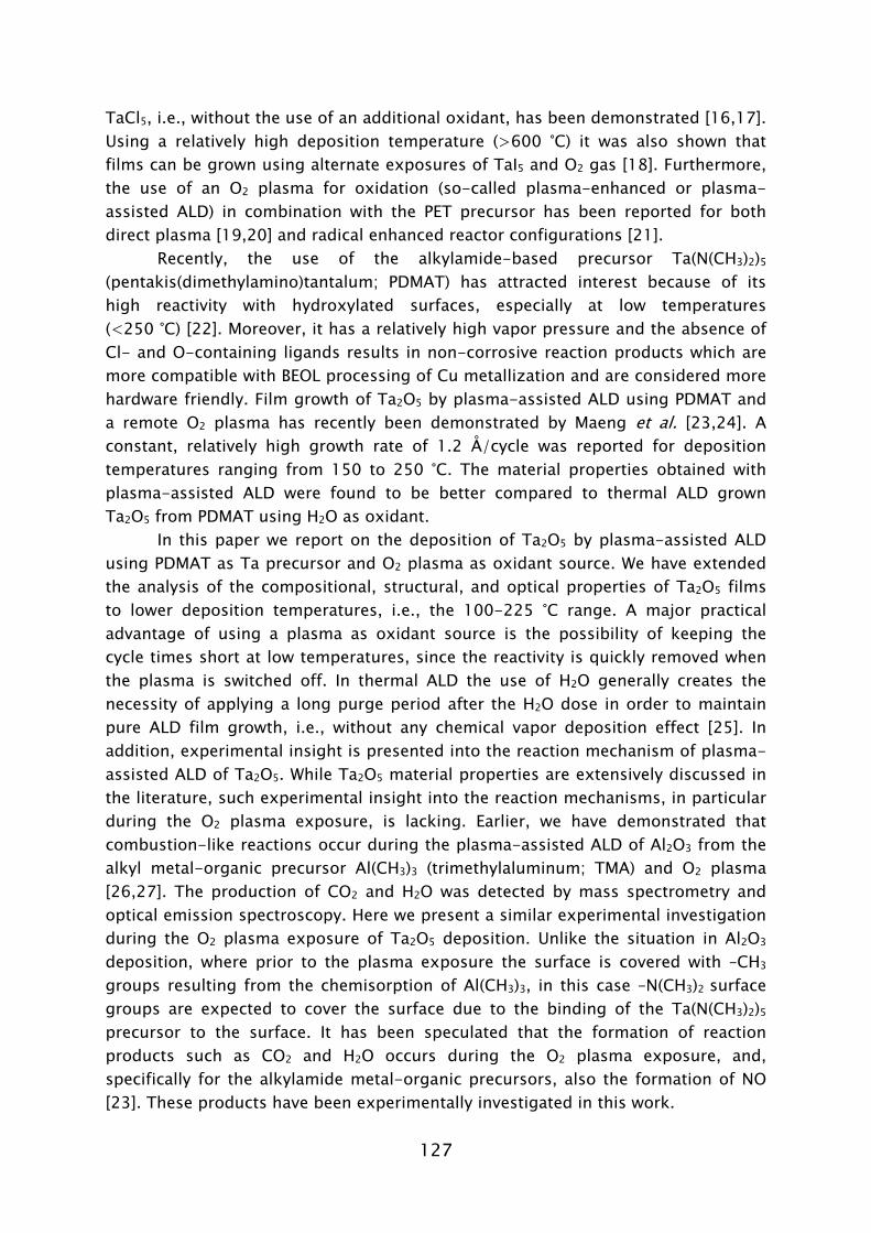
127
TaCl5, i.e., without the use of an additional oxidant, has been demonstrated [16,17]. Using a relatively high deposition temperature (>600 °C) it was also shown that films can be grown using alternate exposures of TaI5 and O2 gas [18]. Furthermore, the use of an O2 plasma for oxidation (so-called plasma-enhanced or plasma-assisted ALD) in combination with the PET precursor has been reported for both direct plasma [19,20] and radical enhanced reactor configurations [21].
Recently, the use of the alkylamide-based precursor Ta(N(CH3)2)5 (pentakis(dimethylamino)tantalum; PDMAT) has attracted interest because of its high reactivity with hydroxylated surfaces, especially at low temperatures (<250 °C) [22]. Moreover, it has a relatively high vapor pressure and the absence of Cl- and O-containing ligands results in non-corrosive reaction products which are more compatible with BEOL processing of Cu metallization and are considered more hardware friendly. Film growth of Ta2O5 by plasma-assisted ALD using PDMAT and a remote O2 plasma has recently been demonstrated by Maeng et al. [23,24]. A constant, relatively high growth rate of 1.2 Å/cycle was reported for deposition temperatures ranging from 150 to 250 °C. The material properties obtained with plasma-assisted ALD were found to be better compared to thermal ALD grown Ta2O5 from PDMAT using H2O as oxidant.
In this paper we report on the deposition of Ta2O5 by plasma-assisted ALD using PDMAT as Ta precursor and O2 plasma as oxidant source. We have extended the analysis of the compositional, structural, and optical properties of Ta2O5 films to lower deposition temperatures, i.e., the 100-225 °C range. A major practical advantage of using a plasma as oxidant source is the possibility of keeping the cycle times short at low temperatures, since the reactivity is quickly removed when the plasma is switched off. In thermal ALD the use of H2O generally creates the necessity of applying a long purge period after the H2O dose in order to maintain pure ALD film growth, i.e., without any chemical vapor deposition effect [25]. In addition, experimental insight is presented into the reaction mechanism of plasma-assisted ALD of Ta2O5. While Ta2O5 material properties are extensively discussed in the literature, such experimental insight into the reaction mechanisms, in particular during the O2 plasma exposure, is lacking. Earlier, we have demonstrated that combustion-like reactions occur during the plasma-assisted ALD of Al2O3 from the alkyl metal-organic precursor Al(CH3)3 (trimethylaluminum; TMA) and O2 plasma [26,27]. The production of CO2 and H2O was detected by mass spectrometry and optical emission spectroscopy. Here we present a similar experimental investigation during the O2 plasma exposure of Ta2O5 deposition. Unlike the situation in Al2O3
deposition, where prior to the plasma exposure the surface is covered with –CH3 groups resulting from the chemisorption of Al(CH3)3, in this case –N(CH3)2 surface groups are expected to cover the surface due to the binding of the Ta(N(CH3)2)5 precursor to the surface. It has been speculated that the formation of reaction products such as CO2 and H2O occurs during the O2 plasma exposure, and, specifically for the alkylamide metal-organic precursors, also the formation of NO [23]. These products have been experimentally investigated in this work.
128
II. Experimental The experiments were carried out in a homebuilt remote plasma ALD reactor
described in detail elsewhere [27,28]. Briefly, it consists of a deposition chamber to which a precursor delivery system and remote inductively coupled plasma (ICP) source are attached. The chamber is pumped by a turbomolecular pump and has a base pressure of ~10-6 Torr. The typical processing conditions and experimental settings are summarized in Table I. The wall temperature was controlled at 85 °C. The solid metal-organic precursor Ta[N(CH3)2]5 (pentakis(dimethylamino)tantalum, PDMAT, Sigma-Aldrich, purity >99.99%), stored in a stainless steel bubbler, was heated up to a temperature of 65 °C to reach an adequate vapor pressure. To prevent condensation, the PDMAT vapor was delivered to the chamber through heated supply lines (>70 °C), using a small Ar carrier gas flow controlled by a leak valve upstream. The Ar flow results in an operating pressure of ~30 mTorr in the reactor and is also used to purge the chamber after the precursor dosing, using a divert line. In addition, the chamber was briefly pumped down (<10-4 Torr) after purging with Ar to remove any remaining gaseous precursor and reaction by-products before switching on the O2 flow through the plasma source. The ALD reaction was completed by exposure to an O2 plasma generated in the ICP source (100 W), operated at a pressure of 7.5 mTorr.
The films were deposited on 4x4 cm2 native oxide covered monocrystalline Si (100) substrates (p-type, 10-30 Ω cm) placed on a heated substrate holder (100-225 °C). The substrates were exposed to an O2 plasma for 5 minutes prior to the deposition. During this plasma oxidation step of the substrate the SiOx film growth was monitored in situ by spectroscopic ellipsometry using a J.A. Woollam, Inc. M2000U visible and infrared extended ellipsometer (0.75-5.0 eV), mounted under a 68° angle relative to the substrate normal. During Ta2O5 processing, SE thickness measurements of the grown Ta2O5 film were taken after completion of a certain number of ALD cycles. To investigate the optical properties of the deposited
Table I. Typical operating settings during plasma-assisted ALD of Ta2O5. The range in which the settings were varied during the experiments is given between brackets.
Parameter Range varied
Ta[N(CH3)2]5 dose time 3.0 s (0.5-8 s)
Ar partial pressure 30 mTorr
Plasma exposure time 2.0 s (0.5-5 s)
O2 partial pressure 7.5 mTorr
Deposition temperature 225 °C (100-225 °C)
Wall temperature 85 °C
Bubbler temperature 65 °C
Plasma power 100 W
Standard setting
129
Ta2O5 films near its bandgap, also an ex situ characterization was performed using a J.A. Woollam, Inc. M2000D visible and UV extended ellipsometer (1.2-6.5 eV), under an angle of 75°. A Tauc-Lorentz model was applied to fit the data using the Woollam WVASE software [29,30].
The film composition was determined by Rutherford backscattering spectrometry (RBS), using a 2 MeV 4He+ beam under an 80° angle of incidence for determining the Ta, O, N, and C areal densities of the films. Using the same beam settings, also elastic recoil detection (ERD) measurements were performed to determine the H areal density. The mass density was calculated from the areal density by RBS using the thickness data obtained by spectroscopic ellipsometry. The microstructure of the deposited films was studied using a Panalytical/Philips X’Pert Pro MPD diffractometer, equipped with a Cu-Kα x-ray source and an X’Celerator detector.
A differentially-pumped quadrupole mass spectrometer (QMS, Pfeiffer QME 200, mass-to-charge ratio m/z = 0-200) was fitted to the side of the reactor. The gas sampling took place through a 150 μm orifice, keeping the pressure in the mass spectrometer within the working range (<10-5 Torr) for the secondary electron multiplier (SEM) to operate. The incoming molecules are ionized in the QMS through electron impact ionization by ~70 eV electrons. For most species this leads to dissociative ionization of the incoming molecules. Therefore, the identification of the original incoming molecules was performed on the basis of their so-called cracking patterns. To achieve sufficient time resolution, the time resolved measurements were carried out by monitoring only four mass-to-charge ratios (m/z) per deposition of typically 10 ALD cycles. This experiment was repeated until data were obtained for all m/z ratios in the range of m/z = 15-45. In each deposition the signal at m/z = 40 (Ar+) was included to serve as a reference while the other three m/z varied. On the basis of the Ar+ signal the different measurements were synchronized afterwards. This procedure allowed for constructing a time resolved mass scan of all masses (m/z = 15-45), with an adequate time resolution.
Optical emission spectroscopy (OES) was carried out by measuring the plasma emission just above the substrate holder using an Ocean Optics USB2000 spectrometer having a wavelength detection range of 250-870 nm and a resolution of approximately 1 nm. The emission by the plasma was coupled into the spectrometer by placing an optical fiber with a small aperture (~100 μm diameter) close to one of the glass windows (cutt-off wavelength ~350 nm) on the deposition chamber. Time dependent measurements were carried out by repetitively acquiring full spectra (350-870 nm) with an integration time of 100 ms. The spectral data of each spectrum were stored in separate files. For data reduction, the option in the software for selecting a single wavelength in the spectrum and acquiring the signal height as a function of time was used to monitor excited plasma species as a function of time during the plasma exposure step.
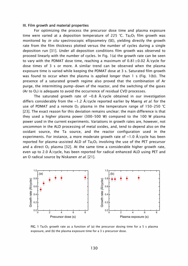
130
III. Film growth and material properties For optimizing the process the precursor dose time and plasma exposure
time were varied at a deposition temperature of 225 °C. Ta2O5 film growth was monitored by in situ spectroscopic ellipsometry (SE), yielding directly the growth rate from the film thickness plotted versus the number of cycles during a single deposition run [31]. Under all deposition conditions film growth was observed to proceed linearly with the number of cycles. In Fig. 1(a) the growth rate can be seen to vary with the PDMAT dose time, reaching a maximum of 0.81±0.02 Å/cycle for dose times of 3 s or more. A similar trend can be observed when the plasma exposure time is varied while keeping the PDMAT dose at 3 s. Saturated film growth was found to occur when the plasma is applied longer than 1 s (Fig. 1(b)). The presence of a saturated growth regime also proved that the combination of Ar purge, the intermitting pump-down of the reactor, and the switching of the gases (Ar to O2) is adequate to avoid the occurrence of residual CVD processes.
The saturated growth rate of ~0.8 Å/cycle obtained in our investigation differs considerably from the ~1.2 Å/cycle reported earlier by Maeng et al. for the use of PDMAT and a remote O2 plasma in the temperature range of 150-250 °C [23]. The exact reason for this deviation remains unclear; the main difference is that they used a higher plasma power (300-500 W) compared to the 100 W plasma power used in the current experiments. Variations in growth rates are, however, not uncommon in the ALD processing of metal oxides, and, tend to depend also on the oxidant source, the Ta source, and the reactor configuration used in the experiments. For instance, a more moderate growth rate of ~1.0 Å/cycle has been reported for plasma-assisted ALD of Ta2O5 involving the use of the PET precursor and a direct O2 plasma [32]. At the same time a considerable higher growth rate, even up to 2.0 Å/cycle, has been reported for radical enhanced ALD using PET and an O radical source by Niskanen et al. [21].
0 2 4 6 80.0
0.2
0.4
0.6
0.8
1.0
Gro
wth
rate
(Å/c
ycle
)
Precursor dose (s)
(a)
0 2 4 6 80.0
0.2
0.4
0.6
0.8
1.0
Gro
wth
rate
(Å/c
ycle
)
Plasma exposure (s)
(b)
FIG. 1 Ta2O5 growth rate as a function of (a) the precursor dosing time for a 5 s plasma exposure, and (b) the plasma exposure time for a 3 s precursor dose.
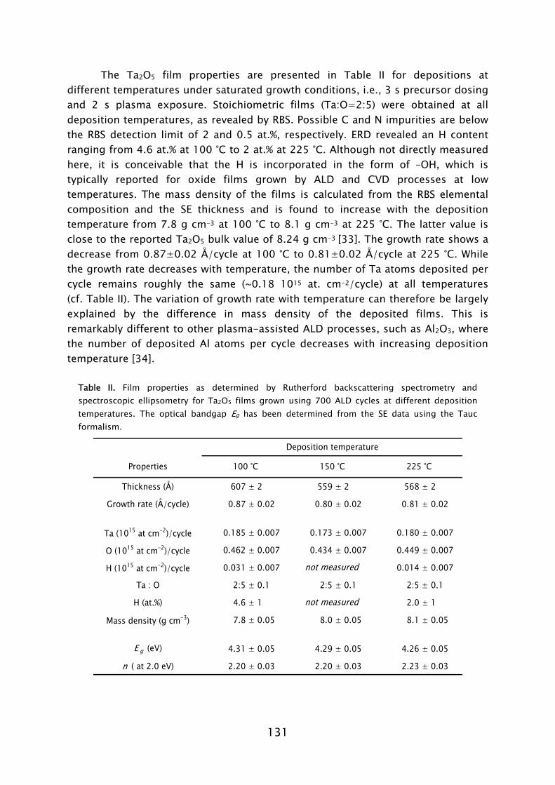
131
The Ta2O5 film properties are presented in Table II for depositions at different temperatures under saturated growth conditions, i.e., 3 s precursor dosing and 2 s plasma exposure. Stoichiometric films (Ta:O=2:5) were obtained at all deposition temperatures, as revealed by RBS. Possible C and N impurities are below the RBS detection limit of 2 and 0.5 at.%, respectively. ERD revealed an H content ranging from 4.6 at.% at 100 °C to 2 at.% at 225 °C. Although not directly measured here, it is conceivable that the H is incorporated in the form of –OH, which is typically reported for oxide films grown by ALD and CVD processes at low temperatures. The mass density of the films is calculated from the RBS elemental composition and the SE thickness and is found to increase with the deposition temperature from 7.8 g cm-3 at 100 °C to 8.1 g cm-3 at 225 °C. The latter value is close to the reported Ta2O5 bulk value of 8.24 g cm-3 [33]. The growth rate shows a decrease from 0.87±0.02 Å/cycle at 100 °C to 0.81±0.02 Å/cycle at 225 °C. While the growth rate decreases with temperature, the number of Ta atoms deposited per cycle remains roughly the same (~0.18 1015 at. cm-2/cycle) at all temperatures (cf. Table II). The variation of growth rate with temperature can therefore be largely explained by the difference in mass density of the deposited films. This is remarkably different to other plasma-assisted ALD processes, such as Al2O3, where the number of deposited Al atoms per cycle decreases with increasing deposition temperature [34].
Table II. Film properties as determined by Rutherford backscattering spectrometry and spectroscopic ellipsometry for Ta2O5 films grown using 700 ALD cycles at different deposition temperatures. The optical bandgap Eg has been determined from the SE data using the Tauc formalism.
Thickness (Å) 607 ± 2 559 ± 2 568 ± 2
Growth rate (Å/cycle) 0.87 ± 0.02 0.80 ± 0.02 0.81 ± 0.02
Ta (1015 at cm-2)/cycle 0.185 ± 0.007 0.173 ± 0.007 0.180 ± 0.007
O (1015 at cm-2)/cycle 0.462 ± 0.007 0.434 ± 0.007 0.449 ± 0.007
H (1015 at cm-2)/cycle 0.031 ± 0.007 0.014 ± 0.007
Ta : O 2:5 ± 0.1 2:5 ± 0.1 2:5 ± 0.1
H (at.%) 4.6 ± 1 2.0 ± 1
Mass density (g cm-3) 7.8 ± 0.05 8.0 ± 0.05 8.1 ± 0.05
E g (eV) 4.31 ± 0.05 4.29 ± 0.05 4.26 ± 0.05
n ( at 2.0 eV) 2.20 ± 0.03 2.20 ± 0.03 2.23 ± 0.03
Deposition temperature
Properties
not measured
100 °C 150 °C 225 °C
not measured
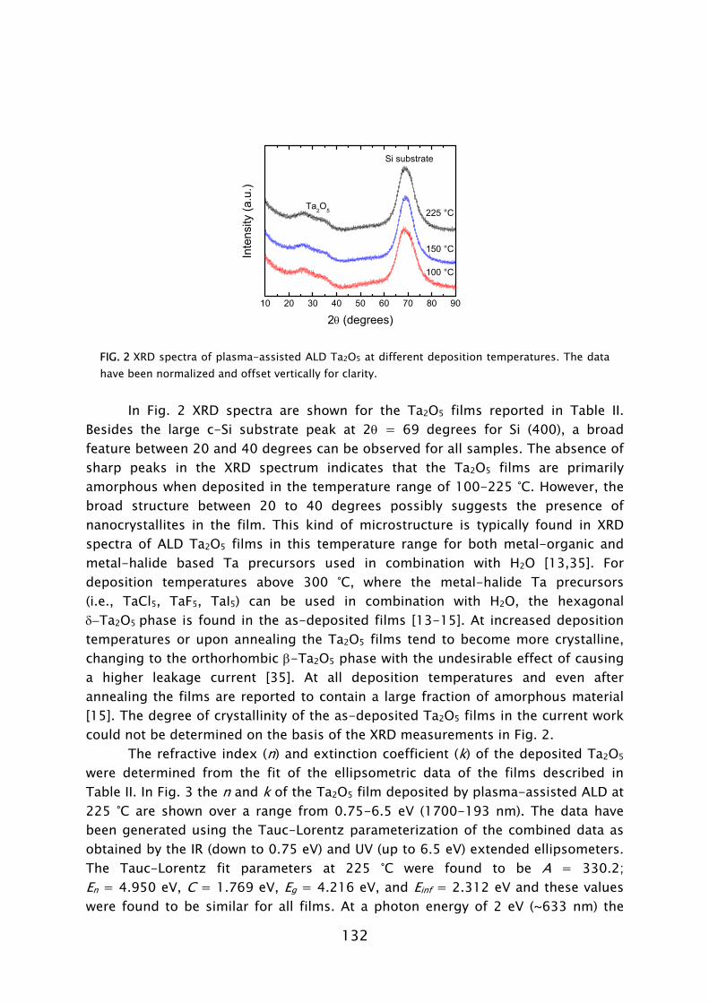
132
10 20 30 40 50 60 70 80 90
100 °C
150 °C
Inte
nsity
(a.u
.)
2θ (degrees)
225 °C
Si substrate
Ta2O5
FIG. 2 XRD spectra of plasma-assisted ALD Ta2O5 at different deposition temperatures. The data have been normalized and offset vertically for clarity.
In Fig. 2 XRD spectra are shown for the Ta2O5 films reported in Table II.
Besides the large c-Si substrate peak at 2θ = 69 degrees for Si (400), a broad feature between 20 and 40 degrees can be observed for all samples. The absence of sharp peaks in the XRD spectrum indicates that the Ta2O5 films are primarily amorphous when deposited in the temperature range of 100-225 °C. However, the broad structure between 20 to 40 degrees possibly suggests the presence of nanocrystallites in the film. This kind of microstructure is typically found in XRD spectra of ALD Ta2O5 films in this temperature range for both metal-organic and metal-halide based Ta precursors used in combination with H2O [13,35]. For deposition temperatures above 300 °C, where the metal-halide Ta precursors (i.e., TaCl5, TaF5, TaI5) can be used in combination with H2O, the hexagonal δ−Ta2O5 phase is found in the as-deposited films [13-15]. At increased deposition temperatures or upon annealing the Ta2O5 films tend to become more crystalline, changing to the orthorhombic β-Ta2O5 phase with the undesirable effect of causing a higher leakage current [35]. At all deposition temperatures and even after annealing the films are reported to contain a large fraction of amorphous material [15]. The degree of crystallinity of the as-deposited Ta2O5 films in the current work could not be determined on the basis of the XRD measurements in Fig. 2.
The refractive index (n) and extinction coefficient (k) of the deposited Ta2O5 were determined from the fit of the ellipsometric data of the films described in Table II. In Fig. 3 the n and k of the Ta2O5 film deposited by plasma-assisted ALD at 225 °C are shown over a range from 0.75-6.5 eV (1700-193 nm). The data have been generated using the Tauc-Lorentz parameterization of the combined data as obtained by the IR (down to 0.75 eV) and UV (up to 6.5 eV) extended ellipsometers. The Tauc-Lorentz fit parameters at 225 °C were found to be A = 330.2; En = 4.950 eV, C = 1.769 eV, Eg = 4.216 eV, and Einf = 2.312 eV and these values were found to be similar for all films. At a photon energy of 2 eV (~633 nm) the
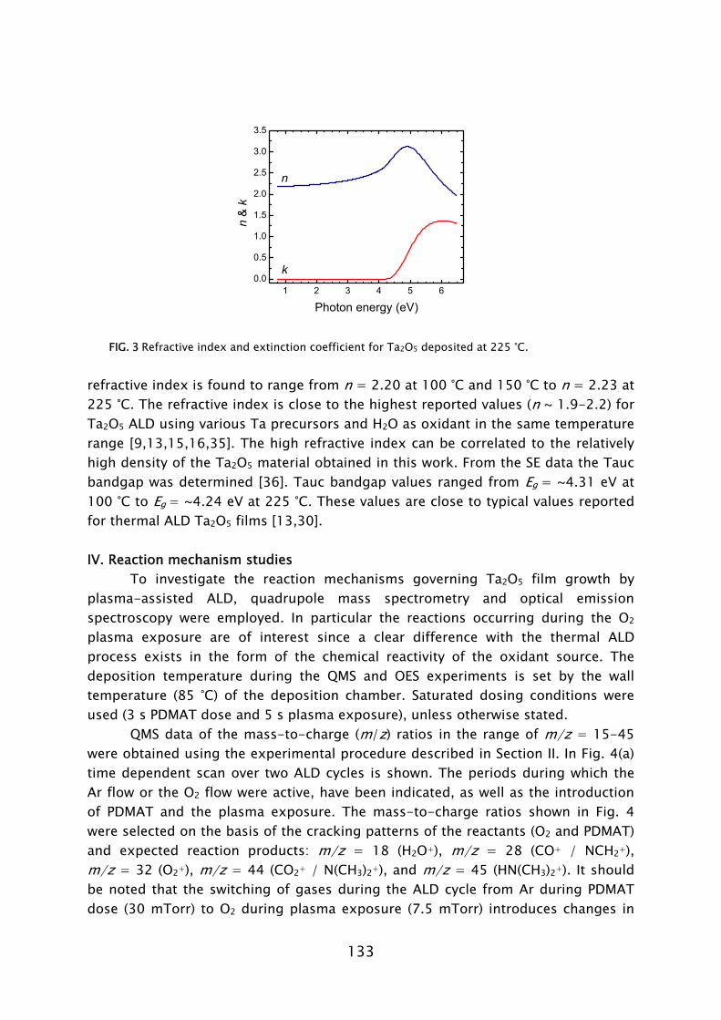
133
1 2 3 4 5 60.0
0.5
1.0
1.5
2.0
2.5
3.0
3.5
n &
k
k
Photon energy (eV)
n
FIG. 3 Refractive index and extinction coefficient for Ta2O5 deposited at 225 °C. refractive index is found to range from n = 2.20 at 100 °C and 150 °C to n = 2.23 at 225 °C. The refractive index is close to the highest reported values (n ~ 1.9-2.2) for Ta2O5 ALD using various Ta precursors and H2O as oxidant in the same temperature range [9,13,15,16,35]. The high refractive index can be correlated to the relatively high density of the Ta2O5 material obtained in this work. From the SE data the Tauc bandgap was determined [36]. Tauc bandgap values ranged from Eg = ~4.31 eV at 100 °C to Eg = ~4.24 eV at 225 °C. These values are close to typical values reported for thermal ALD Ta2O5 films [13,30]. IV. Reaction mechanism studies
To investigate the reaction mechanisms governing Ta2O5 film growth by plasma-assisted ALD, quadrupole mass spectrometry and optical emission spectroscopy were employed. In particular the reactions occurring during the O2 plasma exposure are of interest since a clear difference with the thermal ALD process exists in the form of the chemical reactivity of the oxidant source. The deposition temperature during the QMS and OES experiments is set by the wall temperature (85 °C) of the deposition chamber. Saturated dosing conditions were used (3 s PDMAT dose and 5 s plasma exposure), unless otherwise stated.
QMS data of the mass-to-charge (m/z) ratios in the range of m/z = 15-45 were obtained using the experimental procedure described in Section II. In Fig. 4(a) time dependent scan over two ALD cycles is shown. The periods during which the Ar flow or the O2 flow were active, have been indicated, as well as the introduction of PDMAT and the plasma exposure. The mass-to-charge ratios shown in Fig. 4 were selected on the basis of the cracking patterns of the reactants (O2 and PDMAT) and expected reaction products: m/z = 18 (H2O+), m/z = 28 (CO+ / NCH2+), m/z = 32 (O2+), m/z = 44 (CO2+ / N(CH3)2+), and m/z = 45 (HN(CH3)2+). It should be noted that the switching of gases during the ALD cycle from Ar during PDMAT dose (30 mTorr) to O2 during plasma exposure (7.5 mTorr) introduces changes in
134
0 10 20 30 40 50 60 70
10-13
10-12
10-11
10-10
10-9
m/z
45
44
32
28
O2
Ion
curr
ent (
A)
Time (s)
PDMAT
Ar O2Ar
18
Plasma PDMAT Plasma
FIG. 4 QMS signals of key fragments (m/z = 18, 28, 32, 44, 45) during two cycles of the Ta2O5 plasma-assisted ALD process. The periods during which the Ar flow and O2 flow are active, have been indicated, as well as the precursor dosing time and the plasma exposure.
(background) pressure inside the mass spectrometer. The baselines of the m/z signals therefore shift in height, whereas spikes associated to the sudden pressure increase induced by the start of Ar and O2 flow can be observed. In Fig. 4 these effects are most pronounced for m/z = 32 (O2+).
During the precursor dose no response was observed at any of the m/z signals shown in Fig. 4. As a matter of fact no response to the PDMAT precursor introduction was seen at any of the m/z signals in the range of m/z = 15–45. This is remarkable since this would imply that there is no production of HN(CH3)2 which would suggest another chemisorption mechanism than the commonly presumed ligand exchange reaction would be occurring. A lack of detection sensitivity of the QMS for the measurements carried out could be another explanation for the absence of a signal due to HN(CH3)2. However, in a similar investigation of plasma-assisted deposition of TaN from PDMAT and H2 plasma [37], where the same mass spectrometer was used and under similar experimental conditions, a clear response was observed during the precursor dosing at m/z = 28, 44, and 45. Under these conditions the response closely matched the cracking pattern of HN(CH3)2 (m/z = 44 (100%), 45 (64%), 28 (18%)) [38]. In the case of plasma-assisted ALD of TaN the chemisorption of PDMAT most likely involves binding to NHx surface groups by splitting off volatile HN(CH3)2 reaction products [37]. A lack of sensitivity of the mass spectrometer does therefore not seem obvious in the Ta2O5 experiments. In addition, we would like to note that the chemisorption of metal-alkylamides has not been as extensively studied as for metal-alkyl or metal-halide precursors, in particular not for plasma-assisted ALD processes of metal oxides. Furthermore, there are only little literature data available about the surface compositio of amorphous Ta2O5 after the oxidation step in ALD. This is contrary to the Al2O3 case, for which evidence has been presented that –OH groups are the main reactive surface sites both in thermal ALD with H2O as oxidant and
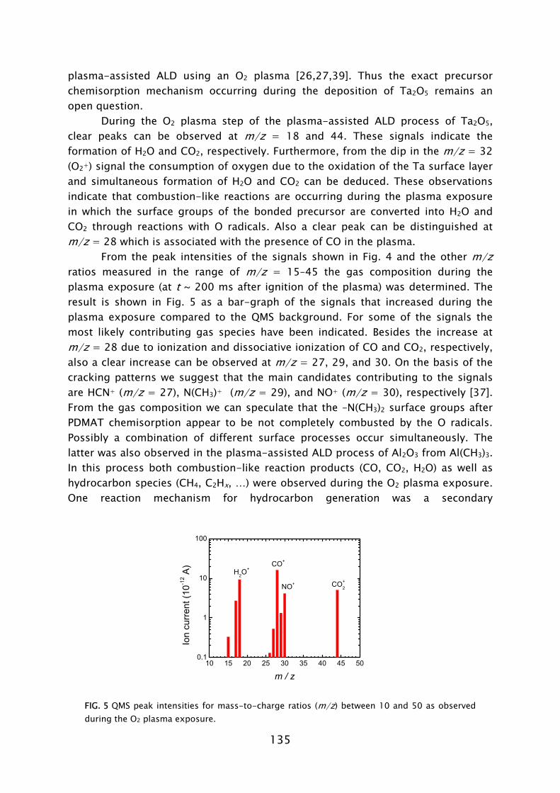
135
plasma-assisted ALD using an O2 plasma [26,27,39]. Thus the exact precursor chemisorption mechanism occurring during the deposition of Ta2O5 remains an open question.
During the O2 plasma step of the plasma-assisted ALD process of Ta2O5, clear peaks can be observed at m/z = 18 and 44. These signals indicate the formation of H2O and CO2, respectively. Furthermore, from the dip in the m/z = 32 (O2+) signal the consumption of oxygen due to the oxidation of the Ta surface layer and simultaneous formation of H2O and CO2 can be deduced. These observations indicate that combustion-like reactions are occurring during the plasma exposure in which the surface groups of the bonded precursor are converted into H2O and CO2 through reactions with O radicals. Also a clear peak can be distinguished at m/z = 28 which is associated with the presence of CO in the plasma.
From the peak intensities of the signals shown in Fig. 4 and the other m/z ratios measured in the range of m/z = 15–45 the gas composition during the plasma exposure (at t ~ 200 ms after ignition of the plasma) was determined. The result is shown in Fig. 5 as a bar-graph of the signals that increased during the plasma exposure compared to the QMS background. For some of the signals the most likely contributing gas species have been indicated. Besides the increase at m/z = 28 due to ionization and dissociative ionization of CO and CO2, respectively, also a clear increase can be observed at m/z = 27, 29, and 30. On the basis of the cracking patterns we suggest that the main candidates contributing to the signals are HCN+ (m/z = 27), N(CH3)+ (m/z = 29), and NO+ (m/z = 30), respectively [37]. From the gas composition we can speculate that the –N(CH3)2 surface groups after PDMAT chemisorption appear to be not completely combusted by the O radicals. Possibly a combination of different surface processes occur simultaneously. The latter was also observed in the plasma-assisted ALD process of Al2O3 from Al(CH3)3. In this process both combustion-like reaction products (CO, CO2, H2O) as well as hydrocarbon species (CH4, C2Hx, …) were observed during the O2 plasma exposure. One reaction mechanism for hydrocarbon generation was a secondary
10 15 20 25 30 35 40 45 500.1
1
10
100
NO+
CO+
CO+2
Ion
curr
ent (
10-1
2 A)
m / z
H2O+
FIG. 5 QMS peak intensities for mass-to-charge ratios (m/z) between 10 and 50 as observed during the O2 plasma exposure.
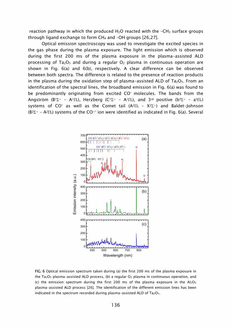
136
reaction pathway in which the produced H2O reacted with the –CH3 surface groups through ligand exchange to form CH4 and –OH groups [26,27].
Optical emission spectroscopy was used to investigate the excited species in the gas phase during the plasma exposure. The light emission which is observed during the first 200 ms of the plasma exposure in the plasma-assisted ALD processing of Ta2O5 and during a regular O2 plasma in continuous operation are shown in Fig. 6(a) and 6(b), respectively. A clear difference can be observed between both spectra. The difference is related to the presence of reaction products in the plasma during the oxidation step of plasma-assisted ALD of Ta2O5. From an identification of the spectral lines, the broadband emission in Fig. 6(a) was found to be predominantly originating from excited CO* molecules. The bands from the Angström (B1Σ+ - A1Πi), Herzberg (C1Σ+ - A1Πi), and 3rd positive (b3Σ+ - a3Πr) systems of CO* as well as the Comet tail (A2Πi – X2Σ+) and Baldet-Johnson (B2Σ+ - A2Πi) systems of the CO+* ion were identified as indicated in Fig. 6(a). Several
(a)
(c)
400 500 600 700 8000
100
200
300
400
0
100
200
300
400
0
100
200
300
400
500
600
700
O
O
CN (B²Σ+ -X²Σ+) Hα
CO+ (B2Σ+-A2Πi) / (A2Πi-X
2Σ+)
Hβ
CO (b3Σ+-a3Πr) / (C1Σ+-A1Πi) / (B
1Σ+-A1Π)
(b)
Em
issi
on in
tens
ity (a
.u.)
Wavelength (nm)
FIG. 6 Optical emission spectrum taken during (a) the first 200 ms of the plasma exposure in the Ta2O5 plasma-assisted ALD process, (b) a regular O2 plasma in continuous operation, and (c) the emission spectrum during the first 200 ms of the plasma exposure in the Al2O3
plasma-assisted ALD process [26]. The identification of the different emission lines has been indicated in the spectrum recorded during plasma-assisted ALD of Ta2O5.
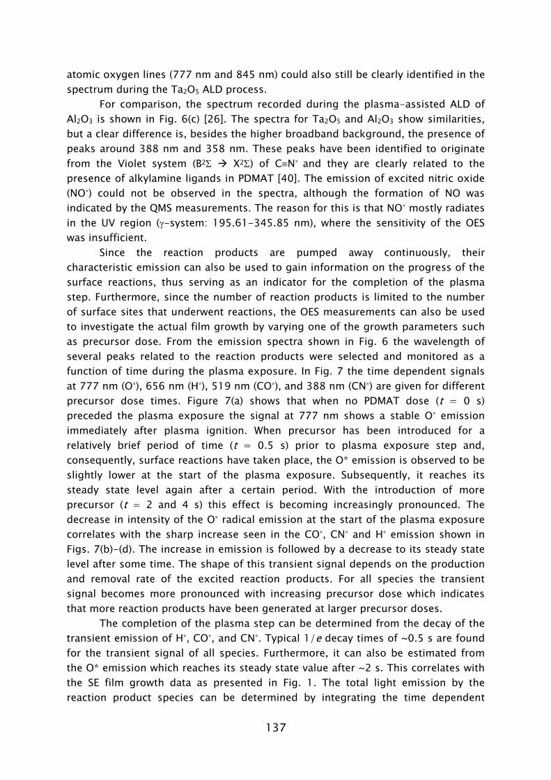
137
atomic oxygen lines (777 nm and 845 nm) could also still be clearly identified in the spectrum during the Ta2O5 ALD process.
For comparison, the spectrum recorded during the plasma-assisted ALD of Al2O3 is shown in Fig. 6(c) [26]. The spectra for Ta2O5 and Al2O3 show similarities, but a clear difference is, besides the higher broadband background, the presence of peaks around 388 nm and 358 nm. These peaks have been identified to originate from the Violet system (B2Σ X2Σ) of C≡N* and they are clearly related to the presence of alkylamine ligands in PDMAT [40]. The emission of excited nitric oxide (NO*) could not be observed in the spectra, although the formation of NO was indicated by the QMS measurements. The reason for this is that NO* mostly radiates in the UV region (γ-system: 195.61-345.85 nm), where the sensitivity of the OES was insufficient.
Since the reaction products are pumped away continuously, their characteristic emission can also be used to gain information on the progress of the surface reactions, thus serving as an indicator for the completion of the plasma step. Furthermore, since the number of reaction products is limited to the number of surface sites that underwent reactions, the OES measurements can also be used to investigate the actual film growth by varying one of the growth parameters such as precursor dose. From the emission spectra shown in Fig. 6 the wavelength of several peaks related to the reaction products were selected and monitored as a function of time during the plasma exposure. In Fig. 7 the time dependent signals at 777 nm (O*), 656 nm (H*), 519 nm (CO*), and 388 nm (CN*) are given for different precursor dose times. Figure 7(a) shows that when no PDMAT dose (t = 0 s) preceded the plasma exposure the signal at 777 nm shows a stable O* emission immediately after plasma ignition. When precursor has been introduced for a relatively brief period of time (t = 0.5 s) prior to plasma exposure step and, consequently, surface reactions have taken place, the O* emission is observed to be slightly lower at the start of the plasma exposure. Subsequently, it reaches its steady state level again after a certain period. With the introduction of more precursor (t = 2 and 4 s) this effect is becoming increasingly pronounced. The decrease in intensity of the O* radical emission at the start of the plasma exposure correlates with the sharp increase seen in the CO*, CN* and H* emission shown in Figs. 7(b)-(d). The increase in emission is followed by a decrease to its steady state level after some time. The shape of this transient signal depends on the production and removal rate of the excited reaction products. For all species the transient signal becomes more pronounced with increasing precursor dose which indicates that more reaction products have been generated at larger precursor doses.
The completion of the plasma step can be determined from the decay of the transient emission of H*, CO*, and CN*. Typical 1/e decay times of ~0.5 s are found for the transient signal of all species. Furthermore, it can also be estimated from the O* emission which reaches its steady state value after ~2 s. This correlates with the SE film growth data as presented in Fig. 1. The total light emission by the reaction product species can be determined by integrating the time dependent
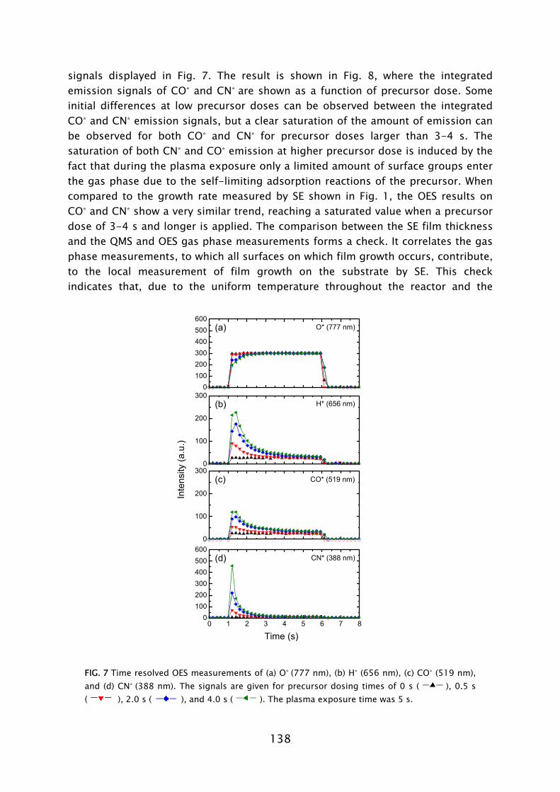
138
signals displayed in Fig. 7. The result is shown in Fig. 8, where the integrated emission signals of CO* and CN* are shown as a function of precursor dose. Some initial differences at low precursor doses can be observed between the integrated CO* and CN* emission signals, but a clear saturation of the amount of emission can be observed for both CO* and CN* for precursor doses larger than 3-4 s. The saturation of both CN* and CO* emission at higher precursor dose is induced by the fact that during the plasma exposure only a limited amount of surface groups enter the gas phase due to the self-limiting adsorption reactions of the precursor. When compared to the growth rate measured by SE shown in Fig. 1, the OES results on CO* and CN* show a very similar trend, reaching a saturated value when a precursor dose of 3-4 s and longer is applied. The comparison between the SE film thickness and the QMS and OES gas phase measurements forms a check. It correlates the gas phase measurements, to which all surfaces on which film growth occurs, contribute, to the local measurement of film growth on the substrate by SE. This check indicates that, due to the uniform temperature throughout the reactor and the
Inte
nsity
(a.u
.)
Time (s)0 1 2 3 4 5 6 7 8
0100200300400500600
(d)
CN* (388 nm)
0
100
200
300(c)
CO* (519 nm)
0
100
200
300(b)
H* (656 nm)
0100200300400500600
(a)
O* (777 nm)
FIG. 7 Time resolved OES measurements of (a) O* (777 nm), (b) H* (656 nm), (c) CO* (519 nm), and (d) CN* (388 nm). The signals are given for precursor dosing times of 0 s ( ), 0.5 s ( ), 2.0 s ( ), and 4.0 s ( ). The plasma exposure time was 5 s.
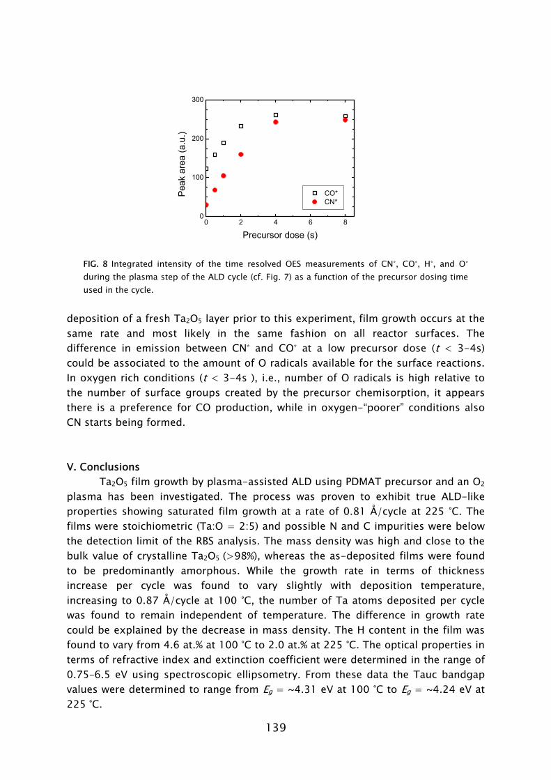
139
0 2 4 6 80
100
200
300
CO* CN*
Pea
k ar
ea (a
.u.)
Precursor dose (s)
FIG. 8 Integrated intensity of the time resolved OES measurements of CN*, CO*, H*, and O* during the plasma step of the ALD cycle (cf. Fig. 7) as a function of the precursor dosing time used in the cycle.
deposition of a fresh Ta2O5 layer prior to this experiment, film growth occurs at the same rate and most likely in the same fashion on all reactor surfaces. The difference in emission between CN* and CO* at a low precursor dose (t < 3-4s) could be associated to the amount of O radicals available for the surface reactions. In oxygen rich conditions (t < 3-4s ), i.e., number of O radicals is high relative to the number of surface groups created by the precursor chemisorption, it appears there is a preference for CO production, while in oxygen-“poorer” conditions also CN starts being formed. V. Conclusions
Ta2O5 film growth by plasma-assisted ALD using PDMAT precursor and an O2 plasma has been investigated. The process was proven to exhibit true ALD-like properties showing saturated film growth at a rate of 0.81 Å/cycle at 225 °C. The films were stoichiometric (Ta:O = 2:5) and possible N and C impurities were below the detection limit of the RBS analysis. The mass density was high and close to the bulk value of crystalline Ta2O5 (>98%), whereas the as-deposited films were found to be predominantly amorphous. While the growth rate in terms of thickness increase per cycle was found to vary slightly with deposition temperature, increasing to 0.87 Å/cycle at 100 °C, the number of Ta atoms deposited per cycle was found to remain independent of temperature. The difference in growth rate could be explained by the decrease in mass density. The H content in the film was found to vary from 4.6 at.% at 100 °C to 2.0 at.% at 225 °C. The optical properties in terms of refractive index and extinction coefficient were determined in the range of 0.75–6.5 eV using spectroscopic ellipsometry. From these data the Tauc bandgap values were determined to range from Eg = ~4.31 eV at 100 °C to Eg = ~4.24 eV at 225 °C.
140
The associated reaction mechanisms of the ALD process have been studied using quadrupole mass spectrometry and optical emission spectroscopy. During the precursor dose remarkably no HN(CH3)2 and associated cracking products in the range of m/z = 15-45 were found. This might suggest that a different chemisorption mechanism than simple ligand exchange could be occurring during the PDMAT step. However, further investigations are necessary to settle this issue. During the plasma exposure the occurrence of combustion-like reactions was established through the detection of CO, CO2 and H2O. The Ta2O5 plasma-assisted ALD process from the alkylamide-based Ta(N(CH3)2)5 precursor therefore showed great similarities with the deposition of Al2O3 from the alkyl-based Al(CH3)3 precursor reported previously [26,27]. Specifically for the Ta2O5 process, however, the production of NO was found by mass spectrometry, indicating the presence of alkylamide surface groups (-N(CH3)2) after chemisorption of PDMAT. Furthermore, the detection of signals due to HCN+, NCH2+, and C≡N* by mass spectrometry and optical emission spectroscopy suggests that during the plasma exposure also other processes occur at the surface, in addition to combustion reactions. On the basis of the investigation on Ta2O5 presented here and the earlier work on Al2O3 it can be concluded that the occurrence of combustion-like reactions during the plasma exposure appears to be generic for plasma-assisted ALD processes of metal oxides from metal-organic precursors when using an O2 plasma for oxidation. Acknowledgments
The skilful technical assistance of J.F.C. Jansen, M.J.F. van de Sande, and J.J.A. Zeebregts was appreciated. A.J.M. Mackus is thanked for his help with the optical emission spectroscopy measurements and spectrum analysis. The authors would like to acknowledge the RBS measurements done by T. Dao and dr. P.C. Zalm and the XRD measurements done by R. Bakker (all Philips Material Analysis). This work was financially supported by the Dutch Technology Foundation STW. The research of W.K. was made possible by a fellowship from the Royal Netherlands Academy of Arts and Sciences (KNAW).
141
References [1] G. B. Alers, D. J. Werder, Y. Chabal, H. C. Lu, E. P. Gusev, E. Garfunkel, T.
Gustafsson, and R. S. Urdahl, Appl. Phys. Lett. 73, 1517 (1998). [2] G. D. Wilk, R. M. Wallace, and J. M. Anthony, J. Appl. Phys. 89, 5243 (2001). [3] C. Chaneliere, J. L. Autran, R. A. B. Devine, and B. Balland, Mater. Sci. Eng., R
22, 269 (1998). [4] E. Gerritsen, N. Emonet, C. Caillat, N. Jourdan, M. Piazza, D. Fraboulet, B.
Boeck, A. Berthelot, S. Smith, and P. Mazoyer, Solid-State Electron. 49, 1767 (2005).
[5] M. B. Yu, Y. Z. Xiong, S. J. Kim, S. Balakumar, C. X. Zhu, M. F. Li, B. J. Cho, G. Q. Lo, N. Balasubramanian, and D.-L. Kwong, IEEE Electron Device Lett. 26, 793 (2005).
[6] E. Deloffre, C. Wyon, and M. Gros-Jean, Electrochem. Soc. Proc. 2005-1, 510 (2005).
[7] M. Thomas, A. Farcy, N. Gaillard, C. Perrot, M. Gros-Jean, I. Matko, M. Cordeau, W. Saikaly, M. Proust, P. Caubet, E. Deloffre, S. Cremer, S. Bruyere, B. Chenevier, and J. Torres, Microelectron. Eng. 83, 2163 (2006).
[8] M. Ritala and M. Leskelä, in Handbook of Thin Films Materials, edited by H. S. Nalwa (Academic Press, San Diego, CA, 2002), p. 103.
[9] K. Kukli, M. Ritala, and M. Leskelä, J. Electrochem. Soc. 142, 1670 (1995). [10] K. Kukli, J. Aarik, A. Aidla, H. Siimon, M. Ritala, and M. Leskelä, Appl. Surf.
Sci. 112, 236 (1997). [11] H. Kattelus, M. Ylilammi, J. Saarilahti, J. Antson, and S. Lindfors, Thin Solid
Films 225, 296 (1993). [12] J. Aarik, A. Aidla, K. Kukli, and T. Uustare, J. Cryst. Growth 144, 116 (1994). [13] K. Kukli, J. Aarik, A. Aidla, O. Kohan, T. Uustare, and V. Sammelselg, Thin
Solid Films 260, 135 (1995). [14] C. W. Hill, G. J. Derderian, and G. Sandhu, J. Electrochem. Soc. 152, G386
(2005). [15] K. Kukli, J. Aarik, A. Aidla, K. Forsgren, J. Sundqvist, A. Harsta, T. Uustare, H.
Mandar, and A. A. Kiisler, Chem. Mat. 13, 122 (2001). [16] K. Kukli, M. Ritala, and M. Leskelä, Chem. Mat. 12, 1914 (2000). [17] M. Ritala, K. Kukli, A. Rahtu, P. I. Raisanen, M. Leskela, T. Sajavaara, and J.
Keinonen, Science 288, 319 (2000). [18] J. Sundqvist, H. Högberg, and A. Hårsta, Chem. Vap. Deposition 9, 245
(2003). [19] D. F. Gu, J. Li, S. K. Dey, H. de Waard, and S. Marcus, J. Vac. Sci. Technol. B
24, 2230 (2006). [20] H.-J. Song, C.-S. Lee, and S. W. Kang, Electrochem. Solid-State Lett. 4, F13
(2001). [21] A. Niskanen, U. Kreissig, M. Leskelä, and M. Ritala, Chem. Mat. 19, 2316
(2007).
142
[22] D. M. Hausmann, P. de Rouffignac, A. Smith, R. Gordon, and D. Monsma, Thin Solid Films 443, 1 (2003).
[23] W. J. Maeng, S. J. Park, and H. Kim, J. Vac. Sci. Technol. B 24, 2276 (2006). [24] W. J. Maeng and H. Kim, Electrochem. Solid-State Lett. 9, G191 (2006). [25] M. D. Groner, F. H. Fabreguette, J. W. Elam, and S. M. George, Chem. Mat. 16,
639 (2004). [26] S. B. S. Heil, P. Kudlacek, E. Langereis, R. Engeln, M. C. M. van de Sanden, and
W. M. M. Kessels, Appl. Phys. Lett. 89, 131505 (2006). [27] S. B. S. Heil, J. L. Van Hemmen, M. C. M. van de Sanden, and W. M. M. Kessels,
submitted for publication (2007). [28] S. B. S. Heil, E. Langereis, F. Roozeboom, M. C. M. van de Sanden, and W. M.
M. Kessels, J. Electrochem. Soc. 153, G956 (2006). [29] B. von Blanckenhagen, D. Tonova, and J. Ullmann, Appl. Opt. 41, 3137
(2002). [30] N. V. Nguyen, C. A. Richter, Y. J. Cho, G. B. Alers, and L. A. Stirling, Appl.
Phys. Lett. 77, 3012 (2000). [31] S. B. S. Heil, E. Langereis, A. Kemmeren, F. Roozeboom, M. C. M. van de
Sanden, and W. M. M. Kessels, J. Vac. Sci. Technol. A 23, L5 (2005). [32] E. Deloffre et al., 7th AVS topical conference on atomic layer deposition, San
Diego, USA (2007). [33] D. R. Lide, CRC Handbook of Chemistry and Physics 87th edition (CRC Press,
Boca Raton, 2007). [34] J. L. van Hemmen, S. B. S. Heil, J. H. Klootwijk, F. Roozeboom, C. J. Hodson,
M. C. M. van de Sanden, and W. M. M. Kessels, ECS trans. 3 (2007). [35] K. Kukli, M. Ritala, R. Matero, and M. Leskelä, J. Cryst. Growth 212, 459
(2000). [36] J. Tauc, Grigorov.R, and A. Vancu, Physica Status Solidi 15, 627 (1966). [37] E. Langereis, H. C. M. Knoops, A. J. M. Mackus, F. Roozeboom, M. C. M. van
de Sanden, and W. M. M. Kessels, J. Appl. Phys. 102, 083517 (2007). [38] NIST/EPA/NIH Mass Spectral Library, Data Version NIST05, Software Version
2.0d. [39] R. L. Puurunen, J. Appl. Phys. 97, 121301 (2005). [40] R. W. B. Pearse and A. G. Gaydon, The identification of molecular spectra
(Chapman and Hall, London, 1976).

143
Summary
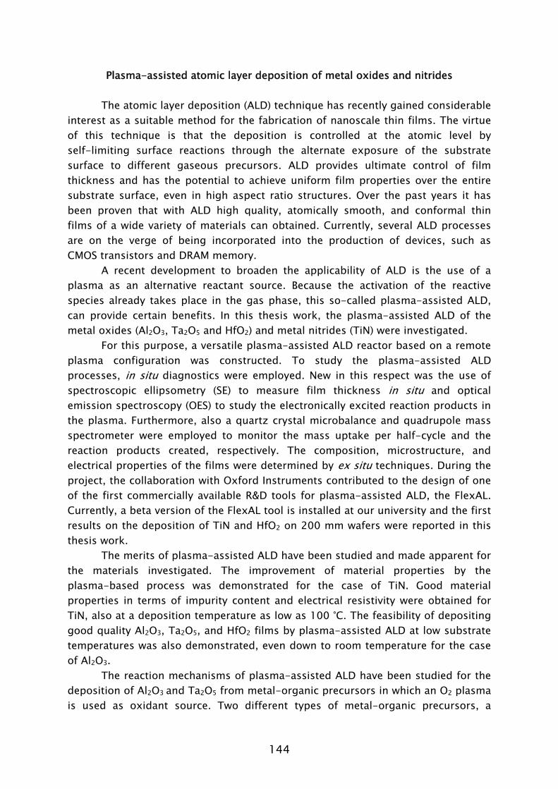
144
Plasma-assisted atomic layer deposition of metal oxides and nitrides
The atomic layer deposition (ALD) technique has recently gained considerable interest as a suitable method for the fabrication of nanoscale thin films. The virtue of this technique is that the deposition is controlled at the atomic level by self-limiting surface reactions through the alternate exposure of the substrate surface to different gaseous precursors. ALD provides ultimate control of film thickness and has the potential to achieve uniform film properties over the entire substrate surface, even in high aspect ratio structures. Over the past years it has been proven that with ALD high quality, atomically smooth, and conformal thin films of a wide variety of materials can obtained. Currently, several ALD processes are on the verge of being incorporated into the production of devices, such as CMOS transistors and DRAM memory.
A recent development to broaden the applicability of ALD is the use of a plasma as an alternative reactant source. Because the activation of the reactive species already takes place in the gas phase, this so-called plasma-assisted ALD, can provide certain benefits. In this thesis work, the plasma-assisted ALD of the metal oxides (Al2O3, Ta2O5 and HfO2) and metal nitrides (TiN) were investigated.
For this purpose, a versatile plasma-assisted ALD reactor based on a remote plasma configuration was constructed. To study the plasma-assisted ALD processes, in situ diagnostics were employed. New in this respect was the use of spectroscopic ellipsometry (SE) to measure film thickness in situ and optical emission spectroscopy (OES) to study the electronically excited reaction products in the plasma. Furthermore, also a quartz crystal microbalance and quadrupole mass spectrometer were employed to monitor the mass uptake per half-cycle and the reaction products created, respectively. The composition, microstructure, and electrical properties of the films were determined by ex situ techniques. During the project, the collaboration with Oxford Instruments contributed to the design of one of the first commercially available R&D tools for plasma-assisted ALD, the FlexAL. Currently, a beta version of the FlexAL tool is installed at our university and the first results on the deposition of TiN and HfO2 on 200 mm wafers were reported in this thesis work.
The merits of plasma-assisted ALD have been studied and made apparent for the materials investigated. The improvement of material properties by the plasma-based process was demonstrated for the case of TiN. Good material properties in terms of impurity content and electrical resistivity were obtained for TiN, also at a deposition temperature as low as 100 °C. The feasibility of depositing good quality Al2O3, Ta2O5, and HfO2 films by plasma-assisted ALD at low substrate temperatures was also demonstrated, even down to room temperature for the case of Al2O3.
The reaction mechanisms of plasma-assisted ALD have been studied for the deposition of Al2O3 and Ta2O5 from metal-organic precursors in which an O2 plasma is used as oxidant source. Two different types of metal-organic precursors, a
145
metal-alkyl (Al(CH3)3) and metal-alkylamide (Ta[N(CH3)2]5), were used. During the O2 plasma exposure, the presence of CO, CO2 and H2O was detected in both processes. Furthermore, the depletion of the O2 source gas indicated the consumption of O radicals. These observations demonstrated that combustion-like reactions in which the surface groups are converted by O radicals into combustion products occur at the surface. Secondly, in the Al2O3 process the detection of CH4 during the O2 plasma exposure indicated that the production of H2O has an effect on the surface chemistry during the Al2O3 deposition process. The produced H2O apparently forms an alternative thermal ALD-like reaction pathway in concurrence with the combustion-like reactions. The possible existence of more reaction pathways is suggested by the presence of C2Hx and CN species during the O2 plasma exposure in the Al2O3 and Ta2O5 deposition, respectively. Additionally, the dissociation and excitation of molecules are other reactions that can take place in the plasma. This was demonstrated by the light emission coming from the plasma during Al2O3 and Ta2O5 processing, which changes in the presence of reaction products released from the surface.

146

List of other publications related to this work
148
List of other publications related to this work
Plasma-Assisted Atomic Layer Deposition of TiN at Low Process Temperatures for High-Aspect Ratio Applications S. B. S. Heil, E. Langereis, F. Roozeboom, A. Kemmeren, N. P. Pham, P. M. Sarro, M. C. M. van de Sanden, and W. M. M. Kessels, Mater. Res. Soc. Symp. Proc. 863, B6.4.1 (2005). Initial Growth and Properties of Atomic Layer Deposited TiN Films Studied by in situ Spectroscopic Ellipsometry E. Langereis, S. B. S. Heil, M. C. M. van de Sanden, and W. M. M. Kessels, Phys. Stat. Sol. C 2, 3958 (2005). In situ Spectroscopic Ellipsometry Study on the Growth of Ultrathin TiN Films by Plasma-Assisted Atomic Layer Deposition E. Langereis, S. B. S. Heil, M. C. M. van de Sanden, and W. M. M. Kessels, J. Appl. Phys. 100, 023534 (2006). Ultralow Surface Recombination of c-Si Substrates Passivated by Plasma-Assisted Atomic Layer Deposited Al2O3 B. Hoex, S. B. S. Heil, E. Langereis, M. C. M. van de Sanden, and W. M. M. Kessels, Appl. Phys. Lett. 89, 042112 (2006). Room Temperature Atomic Layer Deposition of Al2O3 Moisture Permeation Barriers on Polymers E. Langereis, M. Creatore, S. B. S. Heil, M. C. M. van de Sanden, and W. M. M. Kessels, Appl. Phys. Lett. 89, 081915 (2006). ALD Options for Si-integrated Ultrahigh-density Decoupling Capacitors in Pore and Trench Designs F. Roozeboom, J. H. Klootwijk, J. F. C. Verhoeven, F. C. van den Heuvel, W. Dekkers, S. B. S. Heil, J. L. van Hemmen, M. C. M. van de Sanden, W. M. M. Kessels, F. Le Cornec, L. Guiraud, D. Chevrie, C. Bunel, F. Murray, H.-D. Kim and D. Blin, ECS Transactions 3, 173 (2007). Opportunities for Plasma-Assisted Atomic Layer Deposition Erwin Kessels, Stephan Heil, Erik Langereis, Hans van Hemmen, Harm Knoops, Wytze Keuning, and Richard van de Sanden, ECS Transactions 3, 183 (2007).
149
Remote Plasma and Thermal ALD of Al2O3 for Trench Capacitor Applications Hans van Hemmen, Stephan Heil, Johan Klootwijk, Fred Roozeboom, Chris Hodson, Richard van de Sanden and Erwin Kessels, ECS transactions 3, 67 (2007). Optimization of Plasma Enhanced Atomic Layer Deposition Processes for Oxides, Nitrides and Metals in the Oxford Instruments FlexAL reactor Chris Hodson, Nick Singh, Stephan Heil, Hans van Hemmen, and Erwin Kessels, ECS transactions 3, 79 (2007). Growth Characteristics and Physical Properties of Remote Plasma and Thermal ALD of Al2O3 in a commercial 200 mm ALD reactor J. L. van Hemmen, S. B. S. Heil, J. H. Klootwijk, F. Roozeboom, C. J. Hodson, M. C. M. van de Sanden and W. M. M. Kessels, J. Electrochem. Soc. 154, G165 (2007).

150

151
Acknowledgments

152
Acknowledgments
Na vier jaar hard werken is het nu eindelijk geheel afgerond. Althans voor mij, ik hoop dat degene die dit boekje leest geïnspireerd raakt en op het beschreven werk kan voortbouwen. Natuurlijk is het tot stand komen van dit proefschrift niet alleen te danken aan mijn inspanningen, maar ook dankzij de nodige hulp van anderen. In dit hoofdstuk wil ik dan ook even stil staan om sommige van deze mensen speciaal te bedanken.
Allereerst Erwin, voor het initiëren van dit toch wel erg succesvol te noemen project. De ambitie om ALD en in het bijzonder plasma-assisted ALD in Eindhoven op de kaart te zetten is zeker geslaagd. Jouw dagelijkse begeleiding was een enorme bron van inspiratie voor mij. Wat me vooral bij zal blijven is het oog voor detail en het streven naar een enorme mate van compleetheid van het onderzoek.
Richard wil ik bedanken voor het delen van zijn inspiraties en de vrijheid die we kregen in het onderzoek. Vooral je commentaar op het geschreven werk was in de eindfase van publicaties en het proefschrift erg belangrijk.
Erik, als directe collega in het project hebben we de afgelopen vier jaar toch veel meegemaakt, vooral in de opstartfase. De uren die we toen gespendeerd hebben aan het bouwen en klussen aan “onze” opstelling hebben geleid tot een van de meest veelzijdige opstellingen binnen PMP. Onze eerste experimenten waren voor mij toch echt legendarisch en ik denk dat we veel geleerd hebben door het af en toe gewoon eens te proberen, ook al sneuvelde er af en toe de nodige hardware.
I would like to thank the members of the reading committee for the proofreading of my Thesis, which also counts for Erik. Your combined input certainly improved the content and layout.
Binnen het innoviaproject wil ik in het bijzonder Hans bedanken. Samen hebben we de mogelijkheden op de nieuw aangeschafte FlexAL geprobeerd te maximaliseren. Al gauw werd het onderzoek erg uitgebreid en dit leidde tot een scala aan ideeën voor verbetering van de machine en de receptuur.
Gedurende het project ben ik ook bijgestaan door verschillende afstudeerders, stagaires en technici. I would like to say thanks to Pavel for partnering with me on the investigation of the Al2O3 growth mechanisms. The six months we spend in the lab formed the basis for two chapters in this thesis, and it inspired a third!
Een aantal experimenten waren niet mogelijk geweest zonder de hulp van Adrie, Harm en Alex. Helaas is niet al het werk terug te vinden in dit proefschrift.
Ik wil ook de technici Ries, Jo, en Janneke bedanken voor hun inspanningen om de nieuwe ideetjes die we hadden, vaak getekend op kladpapiertjes, in een technisch hoogstaand product om te zetten. Wytze wil ik bedanken voor zijn hulp bij het operationeel houden van de FlexAL en verschillende deposities. Ook Bertus en Herman wil ik bedanken voor hun inspanningen, vooral op elektronisch gebied.
153
De collega’s van PMP wil ik bedanken voor de collegiale sfeer en het creëren van een gezellige werkomgeving, in het bijzonder mijn kamergenoten Bram en Joost.
During the promotion, I also spent three months abroad at the Renselaer Polytechnic Institute. I would like to thank Dr. Lu for giving me the opportunity to participate in the research in his group and in particular Greg with whom I did the experiments.
Daarnaast gaat mijn dank uit naar mijn familie en vrienden voor de steun en het zorgen voor de nodige afleiding gedurende mijn promotie. Bovenal wil ik mijn ouders, Bas en Ria, en zus(je) Patricia bedanken voor hun steun en liefde, en voor hun interesse naar wat ik op de TU aan het doen was.
In the end I would like to say thanks to a very special person in my life, who has had a close watch on me during the last year(s). Ioana, I would like to thank you for the support and comfort that you offered me especially in the last year of the promotion, even though you were in the same situation as me. Writing our theses drained a lot of energy from us, but now we will have more time to enjoy life together!
Stephan Heil, December 2007

154

155
Curriculum vitae

156
157
Curriculum Vitae
18 September 1979
Born in Made, The Netherlands.
June 1997 Diploma Voortgezet Wetenschappelijk Onderwijs,
Newman College, Breda, The Netherlands.
June 2003 Master of Science degree Applied Physics,
Eindhoven University of Technology, Eindhoven, The Netherlands.
Three months (Fall 2002) traineeship in the group of Prof. J. Källne at the department of Neutron Research, Uppsala University, Uppsala, Sweden.
Master thesis project in the group Equilibrium and Transport in Plasmas,
Eindhoven University of Technology, Eindhoven, The Netherlands.
October 2003 - December 2007 PhD project in the group Plasma and Materials processing,
Department of Applied Physics, Eindhoven University of Technology, Eindhoven, The Netherlands.
Three months (fall 2006) working visit to the group of Prof. T.-M. Lu,
Department of Physics, Rensselaer Polytechnic Institute, Troy, New York, U.S.A.

158

159

160


![VAPOR LIQUID · Web viewAluminium, indium and gallium oxides have been reported as effective n- type dopants to increase the electrical conductivity of pure zinc oxide. [4] [4] Recently,](https://static.fdocuments.nl/doc/165x107/60ee0fa87400717ff27a2521/vapor-web-view-aluminium-indium-and-gallium-oxides-have-been-reported-as-effective.jpg)