![Nanoparticle-doped electrospun fiber random lasers with ... · [2,6,8,10]. Organic crystals [16,17] and epitaxial nanowires [18], biopolymers [19,20], as well as conjugated polymers](https://static.fdocuments.nl/doc/165x107/600d3d88f8e5ef616721ea08/nanoparticle-doped-electrospun-fiber-random-lasers-with-26810-organic.jpg)
Opto-electronic study of phosphorous-doped n … Ken...Opto-electronic study of phosphorous-doped...
137
= Instituut voor Materiaalonderzoek Faculteit Wetenschappen Opto-electronic study of phosphorous-doped n-type and hydrogen-doped p-type CVD diamond films. Proefschrift voorgelegd tot het behalen van de graad van Doctor in de Wetenschappen, richting Natuurkunde aan het Limburgs Universitair Centrum, te verdedigen door Ken Haenen Op 22 mei 2002 om 15.00 Promotor: Prof. Dr. G. Knuyt Co-promotor: Dr. M. Nesládek 2002
Transcript of Opto-electronic study of phosphorous-doped n … Ken...Opto-electronic study of phosphorous-doped...
= Instituut voor Materiaalonderzoek Faculteit Wetenschappen
Opto-electronic study of phosphorous-doped n-type and hydrogen-doped p-type
CVD diamond films.
Proefschrift voorgelegd tot het behalen van de graad van
Doctor in de Wetenschappen, richting Natuurkunde
aan het Limburgs Universitair Centrum, te verdedigen door
Ken Haenen
Op 22 mei 2002 om 15.00
Promotor: Prof. Dr. G. Knuyt Co-promotor: Dr. M. Nesládek
2002

… and of starlight and the purest water-drops, of the dew of Silpion, and the thinnest air, they made diamonds, and challenged any to make fairer.
J.R.R. Tolkien – The Book of Lost Tales Part 1

Chairman Prof. dr. H. Callaert
Dean Faculty of Science
LUC, Belgium
Promoter: Prof. dr. G. Knuyt
LUC-IMO, Belgium
Co-promoter: Dr. M. Nesládek
LUC-IMO, Belgium
Members of the jury: Prof. dr. G. Adriaenssens
KUL, Belgium
Prof. dr. L. De Schepper
LUC-IMO, Belgium
Dr. E. Gheeraert
CNRS-LEPES, France
Prof. dr. em. L.M. Stals
LUC-IMO, Belgium
Prof. dr. C. Van Haesendonck
KUL, Belgium


Acknowledgments
An enormous gratitude goes out to prof. dr. em. L.M Stals. His enthusiastic talks about “his” Institute for Materials Research and the fact that they could grow real diamond definitely initiated the idea to aim for a PhD. I thank him for the opportunity he gave me to do my first steps in scientific research at IMO. His thorough correction of this manuscript, regarding the scientific content as well as what the English is concerned, is greatly appreciated.
Prof. dr. Knuyt, who is the promoter of this thesis, I want to thank for his continuing interest in CVD diamond and my work on P-doped diamond in particular. He was also the person who reminded me to focus on my work, in spite of the always lurking side projects that sometimes seemed more interesting to pursue.
More than by any other person the content of this work has been determined by dr. M. Nesládek. Miloš, while discussions were certainly not always straightforward due to your busy time schedule and lots and lots of other commitments, most of my accomplishments in the scientific community I own to you. Besides your drive and your ideas, your connections in the diamond world proved to be indispensable. Because of this I had the chance to spend a lot of time abroad, as well for conferences as for scientific stays. Your workshop provided me with, next to my first “audience experience”, a unique chance to meet the top of the diamond community. I can only hope that our further collaboration will continue like this and that we will take some more steps in elucidating some of the “mysteries” of CVD diamond and wide band gap materials in general. Although the process of research is sometimes chaotic, we always seem to make it in the end!
As the title of this thesis makes clear the availability of phosphorous-doped diamond was indispensable. Thanks to dr. S. Koizumi and dr. T. Teraji from the National Institute for Materials Science, Tsukuba, Japan, I could work with the first active n-type CVD diamond films available in the world. Their continuous interest in the results of my research kept me motivated and well provided with new and better samples. Our numerous meetings at workshops and conferences were always enlightening albeit that some of our conversations were definitely not work-related!
ii Acknowledgments
Also a big “thank you” to dr. E. Gheeraert. Not only for accepting to be in my jury but also for the interesting discussions about his work on the same diamond films. These results proved to be a major help in interpreting mine and certainly contributed a lot to the present knowledge about the phosphorous in diamond and n-type doping in general. Etienne, malgré ma persistance à parler l’anglais, je promets de rafraîchir mon vocabulaire. Donc, la prochaine fois, après ma défense si tu n’as pas d’objection, la conversation sera en français.
A major part of the last chapter is the direct result of my six weeks stay at the Institut de Recherche sur l'Hydrogène, in Trois-Rivières, Québec, Canada. Besides the interesting scientific outcome, the success of my stay was definitely the result of the nice atmosphere and people I got to know there. I especially want to thank prof. dr. J. Goyette and dr. J.F. Rouleau who made Canada a place I surely want to visit again.
Dr. M. Vaněček deserves my gratitude for his excellent way of explaining things and for the warm welcome he gave me each time when we were making use of the “Prague-connection”. It was a pleasure to visit his lab, a thing I hope that will happen again.
I also want to thank all foreign researchers that I have met over the past years, and that I will hopefully meet again in the near future. They all contributed in one way or another to this work. Some of them surely changed their status from “co-worker” to “friend”.
This thesis reflects years of experimental scientific research. Even though there is only one author on the cover, every experimental physicist will admit that a lot of the experiments would not be possible without the help of skilled technicians. I want to thank them all, especially Johnny, for having a box filled with good solutions for all the small and big problems we encountered.
Every time the word administration popped up, and for people that know Belgium this should ring a big alarm bell, I could always count on a helping hand of our secretaries to guide me out of the labyrinth of forms, paper work and other nerve-wracking stuff. Relinde, Lea and Martien, your efforts were of huge value.
Without good colleagues it is impossible to get any work done. Fortunately I could not have wished for better representatives of this category than the ones I had know. Kristien, Els and Ludwig, you all played, and still play, an important role in my daily life, as well inside as outside IMO. A special word of thanks for Kristien, who was my scientific point of reference whenever Milos was not around or too busy, and, willingly or unwillingly, acted as a guide by writing the first IMO diamond thesis.
Acknowledgments iii
The Fonds Slimme Regio of the province Limburg, Belgium, is acknowledged for the financial support which allowed me to carry out my research.
After two pages of work-related people I finally get to the people that were not always on the front row but whose support was equally and sometimes even more important to me.
My friends. Old friends, like Bart, Philipp, Tom and all the others who I keep planning to visit, but never seem to reach. But also new ones like Hans and Signe. Thanks for all the support and necessary distraction.
It goes without question that none of this was possible without the encouragement of my parents as well as my grandparents. I must have driven you crazy, raving about annoying results, deadlines, papers that seemed to drag on endlessly, and all these other things that make PhD research so much fun. Especially this last half year, you sometimes must have wondered if I was still on the planet. I was not around a lot, but it was nice to know that there was a place where I could come home to.
To finish, only the proverbial last-but-definitely-not-least-place is left. Greet, although the last months were without doubt not always easy, you sure made it more interesting than I could have ever imagined before I started writing this thesis. I wish you at least an equal amount of fun and fulfilment in your new job as I have found in mine during the past years. Thank you for your support and your ability to calm me down all the times it was more than necessary.
Ken Haenen, May 2002

Table of contents
ACKNOWLEDGMENTS I
TABLE OF CONTENTS V
NEDERLANDSE SAMENVATTING IX Hoofdstuk 1 – Diamant......................................................................................................ix Hoofdstuk 2 – Experimentele fotostroomtechnieken..........................................................x Hoofdstuk 3 – Fosfor: een actieve donor in CVD diamant................................................xi Hoofdstuk 4 – Waterstof op het diamantoppervlak ........................................................ xiii
LIST OF SYMBOLS AND ABBREVIATIONS XV
PREFACE 1
1. DIAMOND 5 1.1. Diamond: a form of carbon ........................................................................................5
1.1.1. Structure .........................................................................................................5 1.1.2. Classification of diamond ...............................................................................6
1.2. Natural, HPHT and CVD diamond: applicable or not? ..............................................8 1.2.1. Natural diamond .............................................................................................8 1.2.2. High Pressure – High Temperature (HPHT) diamond..................................10 1.2.3. Chemical Vapour Deposition (CVD) diamond.............................................12
1.3. Microwave (MW) Plasma Enhanced (PE) CVD ......................................................14 1.3.1. Main principle...............................................................................................14 1.3.2. Substrates......................................................................................................16 1.3.3. Doping ..........................................................................................................17
1.4. Applications: present and future...............................................................................17 1.5. References ................................................................................................................19
2. EXPERIMENTAL PHOTOCURRENT TECHNIQUES 23 2.1. Introduction ..............................................................................................................23 2.2. Quasi-steady-state photocurrent measurements (PC) ...............................................24
2.2.1. Theoretical considerations ............................................................................24 2.2.1.1. Generation of charge carriers .........................................................24
vi Table of contents
2.2.1.2. Electrical transport .........................................................................26 2.2.1.3. Trapping and recombination ..........................................................26 2.2.1.4. Surface recombination ...................................................................28 2.2.1.5. Contacts .........................................................................................29
2.2.2. Experimental set-up ......................................................................................29 2.3. The Constant Photocurrent Method (CPM)..............................................................33
2.3.1. Theoretical considerations ............................................................................33 2.3.2. Experimental set-up ......................................................................................35
2.4. PhotoThermal Ionisation Spectroscopy (PTIS) ........................................................35 2.4.1. Theoretical considerations ............................................................................35 2.4.2. Experimental set-up ......................................................................................36
2.5. Photocurrent versus optical absorption.....................................................................36 2.6. References ................................................................................................................38
3. PHOSPHOROUS: AN ACTIVE DONOR IN CVD DIAMOND 41 3.1. Introduction: problems with n-type dopants ............................................................41 3.2. Samples ....................................................................................................................44
3.2.1. Samples NIMS..............................................................................................44 3.2.1.1. 111-oriented substrates...............................................................45 3.2.1.2. 100-oriented substrates...............................................................45
3.2.2. Samples IMO................................................................................................46 3.2.3. Contacts ........................................................................................................46
3.3. XP1 and XP2: two new defect levels in n-type diamond ............................................49 3.3.1. The optical photoionisation energy oEi .........................................................52 3.3.2. XP1: substitutional phosphorous....................................................................55 3.3.3. XP2: phosphorous-related? ............................................................................56 3.3.4. Results from the nominally undoped film ....................................................57
3.3.4.1. The 1.5 eV defect ...........................................................................59 3.4. The electronic structure of phosphorous in CVD diamond ......................................61
3.4.1. Oscillatory photoconductivity ......................................................................63 3.4.2. Results from the 1000 ppm PH3/CH4 doped films........................................65 3.4.3. The influence of the doping concentration ...................................................66 3.4.4. Detection of the excited states of phosphorous with PTIS ...........................72 3.4.5. The influence of the applied electric field on the photoionisation onset.......75 3.4.6. Confirmation of the electronic structure of phosphorous with FTIR............78
3.5. Results from the 100-oriented P-doped film.........................................................81 3.6. Comparison between NIMS and IMO P-doped CVD diamond ...............................82 3.7. Conclusions ..............................................................................................................85 3.8. References ................................................................................................................87
4. HYDROGEN ON THE DIAMOND SURFACE 93 4.1. Introduction ..............................................................................................................93
Table of contents vii 4.2. Photocurrent measurements......................................................................................94
4.2.1. Undoped diamond film from IMO................................................................94 4.2.2. n-Type P-doped diamond film from NIMS ..................................................95
4.3. Dielectric measurements ..........................................................................................97 4.3.1. Experimental.................................................................................................97 4.3.2. Oxidised films...............................................................................................99 4.3.3. Hydrogenated films ....................................................................................100 4.3.4. Annealed films............................................................................................106
4.4. Conclusions ............................................................................................................107 4.5. References ..............................................................................................................108
APPENDIX A. LIST OF PUBLICATIONS A1 A.1 Papers in international journals ...............................................................................A1 A.2 Contributions to proceedings...................................................................................A3 A.3 Other publications ...................................................................................................A3

Nederlandse samenvatting
Hoofdstuk 1 – Diamant Diamant, een natuurlijk halfgeleidend materiaal met een zeer wijde band gap (5.45 eV), bezit een unieke combinatie van fysische eigenschappen. Bekende voorbeelden zijn de chemische inertheid en de transparantie voor zowel infrarood, zichtbaar als ultraviolet licht. Het is tevens het materiaal met de hoogste thermische geleidbaarheid bij kamertemperatuur (2000 W m-1 K-1) en het bezit een zeer hoge gaten- (1600 cm² V-1 s-1) en elektronenmobiliteit (2200 cm² V-1 s-1). Het is duidelijk dat één of een combinatie van deze eigenschappen mogelijkheden biedt om diamant te gebruiken als een hoogtechnologisch materiaal. Dit heeft tot gevolg dat diamant al jaren bekend staat als de ideale kandidaat om meer conventionele materialen zoals silicium en germanium te vervangen in een brede waaier van toepassingen. Natuurlijk diamant en het klassieke synthetische diamant, geproduceerd met een hoge druk / hoge temperatuur–proces, zijn echter niet geschikt omwille van de zeldzaamheid, de kostprijs, de gebrekkige zuiverheid en de beperkingen in vorm en afmetingen. Sinds de ontwikkeling van het “Chemical Vapor Deposition” (CVD)–proces (lage druk / lage temperatuur) heeft men evenwel een methode die het toelaat om diamant als dunne films af te zetten. Gebaseerd op zowel mechanische, thermische, optische als elektronische karakteristieken, zouden applicaties zich kunnen situeren in verschillende gebieden, gaande van laseroptica, stralings- en deeltjesdetectoren tot micro- en bioelektronische devices. De eerste twee voorbeelden zijn reeds gerealiseerd en verkrijgbaar op de markt, maar vooral de elektronische industrie lijkt niet geïnteresseerd in diamant. Wat is de oorzaak?
Een groot deel van de huidige elektronica is gebaseerd op het bestaan van p-n-juncties in silicium, germanium en andere stoffen. Dit vereist goede p- en n-type doperingsatomen die het mogelijk maken om op een reproduceerbare en gecontroleerde manier de gewenste filmen te groeien. Voor diamant vormen p-type lagen geen enkel probleem. Natuurlijk IIb diamant is p-type geleidend door de aanwezigheid van boor. Ook de synthetische vormen van diamant zijn makkelijk en reproduceerbaar te doperen met boor. Meer problematisch was de n-type variant. Niet aanwezig in natuurlijke vorm, en ondanks grote onderzoeksinspanningen wereldwijd, duurde het tot 1997 voor de eerste actieve fosfor-gedopeerde n-type CVD diamant film gerealiseerd werd door Japanse
x Nederlandse samenvatting
onderzoekers van het NIMS1.
Het eerste deel van deze thesis is gewijd aan de studie van deze NIMS films met behulp van fotostroomgebaseerde technieken. Dit zal toelaten om een model op te stellen voor de elektronische structuur van het fosforatoom in CVD diamant films. De resultaten van de eerste P-gedopeerde films gegroeid aan het IMO zullen aan dit model getoetst worden.
Even belangrijk als n-type diamant, is de studie van waterstofgetermineerde diamantoppervlakken. Als noodzakelijk onderdeel van het gasmengel gebruikt in het CVD proces om diamantfilms te groeien, speelt waterstof een belangrijke rol in het hedendaags diamantonderzoek. Reeds meer dan tien jaar geleden werd ontdekt dat gehydrogeneerde diamantoppervlakken een duidelijke p-type oppervlakteconductiviteit vertoonden. Dit effect, uniek voor diamant, is nog steeds niet volledig verklaard, maar wordt wel al volop gebruikt in het onderzoek naar oppervlaktedevices. Afhankelijk van de terminatie van het oppervlak kan een diamant film zeer makkelijk hydrofoob (H-terminatie) of hydrofiel (O-terminatie) gemaakt worden. Waterstof op het opppervlak heeft ook een invloed op de bulk van het materiaal door het verschuiven van het Fermi-niveau.
Om af te ronden worden de resultaten besproken van een dielektrische studie over gehydrogeneerde diamantfilms.
Hoofdstuk 2 – Experimentele fotostroomtechnieken Methoden gebaseerd op de detectie van fotogeïnduceerde stromen zijn de aangewezen technieken om de P-gedopeerde films te bestuderen. Drie varianten worden gebruikt in deze thesis: de “quasi-steady-state” fotostroomtechniek (PC); de constante fotostroommethode (CPM); fotothermische ionisatiespectroscopie (PTIS).
Al deze technieken zijn gebaseerd op de excitatie van ladingsdragers van defectniveaus in de band gap naar de valentie- of conductieband met behulp van een monochromatische lichtbundel. Dit licht, afkomstig van een halogeen- of xenonlamp, wordt via een monochromator en de nodige filters op een systematische manier gefocusseerd op het te
1 Alhoewel substitutioneel stikstof een diepe donor vormt in CVD diamant, is de thermische activatie-energie van 1.7 eV te hoog om bij kamertemperatuur een elektrische actieve n-type diamant te vormen. Daarom worden fosfor-gedopeerde films beschouwd als de eerste echte n-type CVD diamanten.
Nederlandse samenvatting xi
onderzoeken diamant monster. Een deel van de lichtbundel wordt afgesplitst en via een pyrodetector wordt de intensiteit opgemeten. Hierdoor kan rekening gehouden worden met de spectrale afhankelijkheid van de lamp. Om de signaal/ruisverhouding te verbeteren gebeurt de belichting periodiek zodat gebruik kan gemaakt worden van de lock-in techniek. Om de invloed van akoestische fononen op de resultaten zoveel mogelijk uit te sluiten wordt gebruik gemaakt van een cryostaat uitgerust met optische vensters. Via vloeibaar helium of stikstof wordt de n-type film tijdens de experimenten gekoeld tot temperaturen variërend tussen 4.2 K en 170 K.
PC-spectra tonen de opgemeten fotostroom in functie van de energie van het monochromatisch licht.
Bij CPM wordt een constante bezetting van de onderzochte defectniveaus gegarandeerd door de fotostroom tijdens de meting constant te houden. Dit gebeurt door de lampintensiteit bij te regelen telkens er een nieuwe energiewaarde wordt ingesteld. Het uiteindelijke CPM-spectra bestaat uit het inverse van het pyrodetectorsignaal in functie van de fotonenergie.
In tegenstelling tot de twee vorige methodes waarbij de excitatie van de ladingsdragers uitsluitend gebeurt met behulp van licht, maakt PTIS, ook wel fonon-geassisteerde PC genoemd, gebruik van een combinatie van optische en thermische energie in een twee-stapsproces. Elektronen die zich in de grondtoestand van een donoratoom bevinden, worden door de optische energie naar een van de geëxciteerde toestanden gebracht, waarna de overgang naar de conductieband uiteindelijk bewerkstelligd wordt door thermische energie. Dit is dan opnieuw detecteerbaar als fotostroom. Een identiek proces is mogelijk in het geval van een acceptor en gaten. Een PTIS spectrum maakt dus deel uit van een normaal PC-spectrum.
Hoofdstuk 3 – Fosfor: een actieve donor in CVD diamant Alle in dit proefschrift bestudeerde films werden gegroeid met de zogenaamde “microwave plasma enhanced chemical vapor deposition (MW PE CVD)” methode. Hierbij wordt een plasma opgewekt met behulp van microgolven zodat de procesgassen omgezet worden in reactieve componenten die de groei van diamant mogelijk maken.
In het geval van de n-type films wordt aan het normale mengsel van waterstof en methaan, fosfine (PH3) toegevoegd om het fosforatoom in de diamantfilm te incorporeren. Als substraat werden zowel natuurlijke als synthetische Ia en Ib
xii Nederlandse samenvatting
diamantkristallen met een 111-oriëntatie gebruikt. Een enkele film werd afgezet op een 100 Ib film. De dikte van de lagen varieerde tussen 0.5 µm en 20 µm. Alle films werden opgemeten zonder het substraat te verwijderen.
De eerst onderzochte 111 n-type films vertoonden een hoge weerstand en een lage Hall-mobiliteit. Met behulp van PC konden twee nieuwe defecten worden gedetecteerd, XP1 en XP2 genaamd. Het eerste niveau kon geïdentificeerd worden als de substitutionele fosfordonor met een grondniveau 0.6 eV onder de conductieband. Het tweede niveau heeft een foto-ionisatie-energie rond 0.81 eV. De oorsprong van dit defect kon niet worden achterhaald, maar het is niet uit te sluiten dat ook dit defect gerelateerd is aan fosfor. Door een verbetering van de depositiecondities en de depositie-apparatuur werden films van een hogere kwaliteit gegroeid. Dit was merkbaar aan de verhoogde Hall-mobiliteit. Opmerkelijk is het ontbreken van het XP2-niveau in al deze films wat leidt tot het besluit dat de aanwezigheid van dit defect de geleidende eigenschappen van de films schaadt.
Door experimenten uit te voeren op lage temperatuur was het mogelijk om zogenaamde oscillerende fotoconductiviteit te detecteren in het fotostroomspectrum van het XP1-niveau. Dit fenomeen is het resultaat van het verdwijnen van een substantieel deel van de fotogeëxciteerde elektronen uit de conductieband (CB). Deze elektronen komen terecht in collectieniveaus door een emissiecascade van longitudinale optische (LO) fononen. Deze collectieniveaus die zich vlak onder de CB bevinden zijn in feite de geëxciteerde toestanden van het fosforatoom. Door PC-spectra van n-type films met een verschillende P-concentratie te vergelijken kon de LO-fononenergie bepaald worden rond 155 meV. De golfvector van dit fonon komt overeen met de positie van het CB-minimum in de bandstructuur van diamant. Een combinatie van deze data met de gelijktijdig waargenomen PTIS-maxima, liet toe om vier geëxciteerde toestanden te identificeren in de band gap, 523 meV, 563 meV, 575 meV en 584 meV boven de fosforgrondtoestand die, zoals reeds vermeld, vastgelegd werd op 600 meV onder de conductieband. Drie van deze niveaus werden bevestigd door onafhankelijk onderzoek uitgevoerd aan het NIMS en het LEPES met behulp van FTIR.
Alhoewel de gedetecteerde maxima toegeschreven werden aan fotothermische ionisatie, kan deze verklaring maar gedeeltelijk juist zijn. Spectra opgemeten bij 4.2 K vertonen deze maxima ook en het is duidelijk dat er bij deze temperatuur onvoldoende thermische energie is om een transitie te bewerkstelligen. Verder onderzoek toonde aan dat het aangelegde elektrisch veld een grote rol speelt. Veldwaarden van 103 V cm-1 tot 104 V
Nederlandse samenvatting xiii
cm-1 induceren een duidelijke verschuiving van de aanzet van de fotostroom naar lagere energieën. Dit effect was zeer duidelijk waarneembaar bij 4.2 K. Bij 77.4 K werd de verschuiving nog versterkt door een thermische bijdrage, wat resulteerde in een meetbare fotostroom vanaf 0.5 eV. Dit is maar liefst 100 meV lager dan de foto-ionisatie-energie om een elektron van de P-grondtoestand naar de CB te exciteren. Niettegenstaande dat fotostroom bij energieën lager dan de foto-ionisatie-aanzet nog niet volledig verklaarbaar is, is het mogelijk dat een combinatie van hoge elektrische velden met stress en onzuiverheden in de films de oorzaak zijn van dit effect.
Preliminair onderzoek op een 100-georiënteerde P-gedopeerde film maakte duidelijk dat de kwaliteit van deze films nog ver onder het niveau van de 111 films ligt. Een defect werd waargenomen rond 0.85 eV. Mogelijk is dit hetzelfde niveau dat voordien XP2 genoemd werd.
Als tweede labo ter wereld slaagde het IMO erin om n-type CVD diamant films af te zetten, gedopeerd met fosfor. Alhoewel de n-type conductiviteit zelf nog niet geconfirmeerd werd via Hall-metingen, de enige betrouwbare methode om de aard van ladingsdragers te confirmeren, werd via fotostroommetingen op lage temperatuur het karakteristieke fosforspectrum opgemeten, inclusief de PTIS maxima en de oscillerende fotostroom. Dit geeft een sterke aanwijzing voor de actieve incorporatie van substitutioneel fosfor in de diamantstructuur. FTIR-metingen toonden ook duidelijk de bekende fosfor-pieken, afkomstig van de excitatie van elektronen uit de grondtoestand naar de eerste twee geëxciteerde toestanden van fosfor.
Hoofdstuk 4 – Waterstof op het diamantoppervlak De ongedopeerde lagen bestudeerd in dit hoofdstuk werden gegroeid met behulp van een mengsel van waterstof, methaan en zuurstof. Na de depositie werden de siliciumsubstraten verwijderd via een etsprocedure resulterend in vrijstaande diamantfilms met een dikte tussen 700 µm en 2 mm. De n-type laag was afkomstig van het NIMS.
Waterstofterminatie van het oppervlak heeft ook een invloed op het Fermi-niveau en bijgevolg ook op de bezetting van de niveaus aanwezig in de band gap. In ongedopeerde films geeft dit aanleiding tot de detectie van het Dx defect, met een foto-ionisatie-energie rond 0.9 eV. Dit niveau was ook meetbaar op een P-gedopeerde n-type film die dezelfde waterstofbehandeling onderging. Een tweede effect was het detecteerbaar maken van het
xiv Nederlandse samenvatting
bekende fosfor fotostroomspectra bij kamertemperatuur. Dit in tegenstelling tot de geöxideerde P-gedopeerde films die alleen bij lage temperaturen een duidelijk fotostroomspectrum vertonen. Dit wijst dus op een lagere bezetting van het fosfor grondniveau en een duidelijke verschuiving van het Fermi-niveau. Er zijn ook aanwijzingen dat XP2 en het Dx defect, een acceptor, geconfirmeerd met behulp van foto-Hallmetingen, hetzelfde defect zijn.
Diëlektrische metingen werden uitgevoerd bij kamertemperatuur met behulp van een coaxiale probe met een open einde in combinatie met een netwerk analysator en een microgolf generator. Dit maakte het mogelijk om op waterstofgetermineerde films de diëlektrisch respons te bepalen in het 45 MHz - 20G Hz frequentiegebied. De gepolijste film vertoonde alleen DC conductiviteit toe te schrijven aan de oppervlakte conductiviteit. Op ongepolijste films werd een duidelijke diëlektrische relaxatie opgemeten. De experimentele resultaten die een quasi-Debye gedrag vertonen, konden gefit worden met de Cole-Cole-formule. Het ontwikkelde model schrijft de respons toe aan de aanwezigheid van 2D plasmons op het diamantoppervlak, corresponderend met een gaten concentratie van ~ 1013 cm-2 geïnduceerd door de waterstofterminatie. Na een opwarming van de films tot 200 °C verdween de diëlektrische relaxatie en bereikte de permittiviteit opnieuw dezelfde waarde als voor geoxideerde films.
List of symbols and abbreviations
α optical absorption coefficient (cm-1)
α empirical exponent
a-C amorphous carbon
BEN bias enhanced nucleation
CB conduction band
CH4 methane
CNRS Centre National de la Recherche Scientifique, France
CPM constant photocurrent method
CVD chemical vapour deposition
Cr(VI)O3 chromium oxide
∆n increase in carrier density under illumination
DC direct current
DLC diamond like carbon
DOS density of states
ε complex permittivity
ε' real part of the complex permittivity
ε'' imaginary part of the complex permittivity
εf permittivity of free space (C2 / N m2)
ε0 permittivity at low frequency (i.e. dielectric constant) (C2 / N m2)
ε∞ permittivity at high frequency (i.e. optical frequency)
E energy (eV)
Ea activation energy (eV)
xvi List of symbols and abbreviations
EC conduction band minimum
EFn electron quasi-Fermi level
EFp hole quasi-Fermi level
Eg band gap energy (eV)
Ehν photon energy
oEi optical ionisation energy (eV)
EPR electron paramagnetic resonance
FTIR fourier transform infrared spectroscopy
FWHM full width at half maximum
η quantum efficiency
ħω photon energy (eV)
HF hydrogen fluoride
HNO3 nitric acid
HOD highly oriented diamond
HPHT high pressure - high temperature
H2SO4 sulphuric acid
Iph,s secondary photocurrent
IMO Instituut voor Materiaalonderzoek / Institute for Materials Research, Diepenbeek, Belgium
IR infrared
IRH Institut de Recherche sur l'Hydrogène, Trois-Rivières, Québec, Canada
k
wavevector
kB constant of Boltzmann
KUL Katholieke Universiteit Leuven
LEPES Laboratoire d’Etudes des Propriétés Electroniques des Solides, CNRS, Grenoble, France
List of symbols and abbreviations xvii
LHeT liquid helium temperature (= 4.2 K)
LNT liquid nitrogen temperature (= 77 K)
LO longitudinal optical phonon
LT low temperature
µ free carrier mobility (cm2 V-1 s-1)
µH Hall mobility (cm2 V-1 s-1)
m0 free electron mass (kg)
me* effective electron mass (kg)
mh* effective electron mass (kg)
MW microwave
MW PE microwave plasma enhanced
ν2D 2D plasmon frequency (Hz)
n0 dark carrier concentration
N number of photons
NC conduction band density of states
Nd defect concentration (cm-3)
N2D planar charge density (cm-2)
NIMS National Institute for Materials Science, Tsukuba, Japan
NIRIM National Institute for Research in Inorganic Materials, Tsukuba, Japan.
OC oscillatory photoconductivity
Pt transition probability
PC quasi-steady-state photocurrent technique
PDS photothermal deflection spectroscopy
PE plasma enhanced
PH3 phosphine
xviii List of symbols and abbreviations
PTIS photothermal ionisation spectroscopy
R reflection coefficient (%)
RF radio frequency (Hz)
RT room temperature
σ DC electrical conductivity (Ω-1 m-1)
σo optical photoionisation cross-section (cm-2)
S Huang-Rhys factor
SC surface conductivity
SEM scanning electron microscope
SIMS secundary ion mass spectroscopy
sccm cubic centimeter per minute at standard temperature and pressure
τ free carrier lifetime (s)
τsurf surface carrier lifetime (s)
τbulk bulk carrier lifetime
T temperature (K)
ta-C tetrahedral amorphous carbon
t-PDS transverse photothermal deflection spectroscopy
UV ultraviolet
VB valence band
ω circular frequency (Hz)
Preface
“Diamond is a unique material, possessing an extraordinary combination of properties, making it an ideal candidate for future applications.” is a much reappearing sentence when reading literature on diamond. Over the past years the general knowledge about diamond growth, defects in diamond and the way to control them, improved enormously. This resulted in a continuous progress of the quality of CVD diamond. Depending on the kind of application one had in mind, research efforts were focussed on the improvement of specific properties of CVD diamond. The aim was and still is to reach the same superior values as the one of natural IIa diamond, the best quality type of natural diamond. This led to the successful application of diamond technology in different industrial fields. The best-known property, and also the first that was used for an application, is the extreme hardness of diamond. At this moment, diamond is for example commonly used as a wear-resistant coating for tools to enhance their lifetime. Other examples and the main property on which they are based are: heatsinks – diamond has the highest known value for thermal conductivity at room temperature; optical windows – aside from the intrinsic two-phonon absorption, diamond is optically transparent from the infrared to the ultraviolet region. In spite of the success in mechanical, thermal and optical applications, a breakthrough based on the electronic properties of diamond was hindered due to some hard problems.
The mobility values for holes and electrons in diamond are extremely high compared with other, more conventional semiconductors. In nature, type IIb diamond is p-type conductive because of the substantial amounts of boron inside. With this knowledge researchers were motivated to obtain the same results with man-made diamond. At this moment, several groups are able to grow highly conductive, flat boron-doped CVD diamond films. Despite a lot of efforts for years to obtain the n-type counterpart, it was only in 1997 that the first report about a successful n-type layer appeared. Earlier attempts by other groups to obtain these much-demanded films included efforts with oxygen, nitrogen, sodium and lithium. These tries included doping in the gas phase of the CVD process as well as implantation of the fully-grown films. With this last technique, successes were reported, but questions arose about the reproducibility and the quality of the films. The group of dr. Koizumi at NIMS, Japan, finally succeeded in depositing phosphorous-doped layers with clear n-type conductivity confirmed by Hall measurements. Building on this accomplishment they recently published results on the
2 Preface
first UV-LED based on a diamond p-n junction. Till 2001, when researchers at IMO and LEPES also succeeded in growing P-doped films, the Japanese group remained the only laboratory to deposit active P-doped diamond layers.
Because theoretical studies also showed sulphur to be a valid n-type dopant other groups tried to repeat the phosphorous-success using a S-containing gas. A paper was published claiming Hall mobility values of about 597 cm2 V-1 s-1 and an ionisation energy of 0.38 eV. This would mean that sulphur is more shallow than phosphorous, which would make it even more important for electronic applications. However, later, other researchers, after doing Hall-experiments on the same samples, contradicted these claims, ascribing the conductivity to boron, so p type, not n type.
These two previous facts point out that n-type doping stays an intriguing and hard to solve problem, requiring ongoing research efforts. A big part of this thesis will deal with the study of P-doped n-type CVD diamond films, grown at NIMS as well as at IMO. Therefore different photocurrent techniques are applied in order to investigate the electronic structure of the phosphorous atom.
Besides n-type doping, hydrogen-related surface conductivity is a topic that has kept the scientific diamond community busy over the last years. Especially the mechanism behind the p-type surface conductivity has given rise to many different models. Also the influence of the hydrogen termination on (surface) states in the band gap is still controversial. In addition to the fundamental interest, surface conductivity also provides possibilities for surface based devices like transistors and biosensors.
Chapter 1 is a general introduction on the material studied in this thesis: diamond, its properties and the difference between natural, HPHT and CVD diamond. After a short initiation on the structure of diamond and the other forms of carbon, the classification system of diamond is discussed. As all the studied samples in this work are grown by the microwave plasma enhanced CVD technique, a part of the chapter covers this method of growth. To end, a short summary on present and future applications based on diamond is given.
In Chapter 2 a thorough description of the used photocurrent-based methods is given. Both the experimental set-ups and the theoretical background of the techniques are treated. The main difference between the quasi-steady-state photocurrent measurements and the Constant Photocurrent Method (CPM) is discussed. Additional experimental information is acquired by the use of PhotoThermal Ionisation Spectroscopy (PTIS), a
Preface 3
photocurrent technique based on the combination of light and temperature induced transitions. To detect the currents, the use of metal contacts is essential. This topic is also treated in this part of this thesis.
Chapter 3 deals with the experimental results on phosphorous-doped n-type CVD diamond films from NIMS, the first laboratory that was successful in depositing such films. By using quasi-steady-state photocurrent measurements, CPM and PTIS it was possible to construct a model describing the electronic structure of the phosphorous atom in CVD diamond. The influence of temperature and the applied electric field on the experiments is also looked into. The results are compared with FTIR data from similar samples, carried out at NIMS and LEPES. The end of this chapter will cover experimental data from P-doped films grown at IMO. A comparison between the PC, PTIS and FTIR spectra of the NIMS and the IMO films show not much difference, indicating the n-type character and the substitutional incorporation of phosphorous for the IMO films.
All hydrogen-related experiments are covered in Chapter 4. The first part of this section deals with preliminary photocurrent measurement on hydrogen-terminated samples. These undoped films were grown at IMO. In addition, a P-doped NIMS film was hydrogenated to investigate the influence of the p-type H-related surface conductivity on the n-type conductivity. In the second part of this chapter the results obtained at the Institut de Recherche sur l'Hydrogène, Québec, Canada, are reported. During a six-week stay dielectric measurements with an open-ended coaxial probe were performed on different quality undoped diamond films. These samples were all grown at IMO after which they were subjected to a hydrogenation treatment. The detected near-Debye dielectric response is ascribed to 2D plasmons on the diamond surface. These 2D plasmons correspond to a surface hole concentration of ~ 1013 cm-2, induced by the hydrogen termination.

1. Diamond
This chapter can be considered as a general introduction. Following a short description about the nature of diamond, the different ways to produce it are discussed. Section 1.3 covers the growth method used for all diamond films that were investigated. Finally, a short summary is given on applications, some already realised and on the market, others still in the development phase.
1.1. Diamond: a form of carbon
1.1.1. Structure
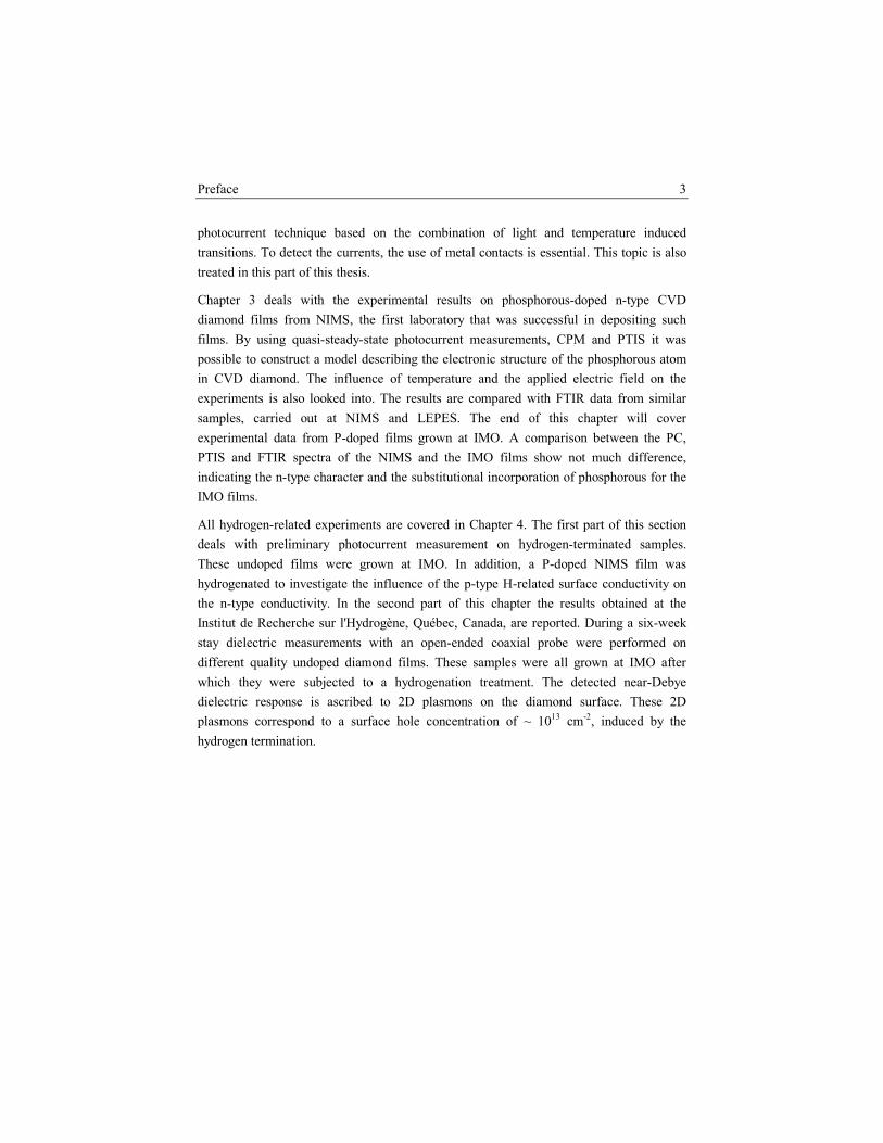
Depending on the way carbon atoms are arranged, different solids are formed, each with their specific properties. There are three crystallographic structures possible for carbon: hexagonal graphite, cubic diamond and hexagonal lonsdaleite, also known as hexagonal diamond (Figure 1.1) [Spe94]. Besides crystalline forms, carbon can also exist as an amorphous or semi-crystalline material. Examples are a-C, ta-C, DLC, bucky balls and carbon nanotubes.
a) b) c)
Figure 1.1 Atomic arrangements of the three possible crystallographic structures of carbon: a)graphite; b) lonsdaleite; c) diamond [Spe94].
In diamond, each carbon atom forms four single σ bonds (0,154nm), composed of sp3-hybridised orbitals, with four adjacent C atoms at the corners of a regular tetrahedron (Figure 1.2). This means that the bonds form equal angles of 109°28’ to each other. Each
6 Chapter 1
tetrahedron combines with four other tetrahedrons, resulting in a tightly covalent crystal, giving a partial explanation for the unique properties of diamond. Graphite on the other hand, consists of stacks of planar layers built up with hexagonal rings of carbon atoms. Each atom has three nearest neighbours (0.141nm) to which it is connected through three σ-bonds, with angles of 120°. These are formed from the overlap of sp2-hybrids. The remaining perpendicular p-orbitals form so-called π-bonds that are delocalised over the plane. Between the planes, separated by a distance of 0.335nm, weak van de Waals forces are present. This explains the anisotropic characteristics of graphite. An application based on this weak interplane bonding is the use of graphite as a lubricant with a very low hardness compared with diamond [Liu95].
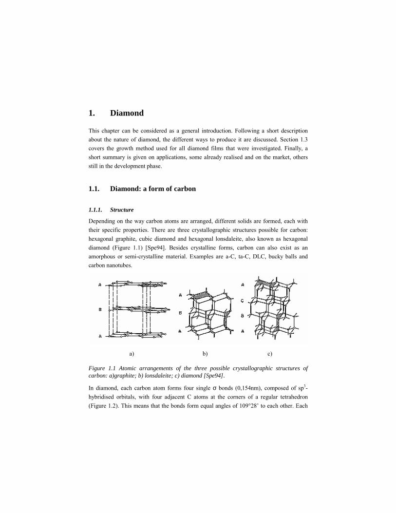
The space lattice of diamond is face-centred cubic (fcc) with a primitive basis of two carbon atoms. This is similar to shifting a second fcc lattice by one-fourth along the diagonal of the first, creating the diamond structure. The lattice constant a = 0.356nm, a being the edge of the conventional cubic cell [Kit86].
Figure 1.2 Face-centred cubic structure of diamond [Yod93].
1.1.2. Classification of diamond
The currently used classification system of diamond is based on optical absorption of a few much occurring elements and/or defects in diamond and finds its origin in 1934 [Rob34]. The most important element in this respect is nitrogen. Of all natural diamonds, about 98% contains enough nitrogen to be detectable by optical absorption. Also boron and hydrogen-related defects play a role in the categorization of natural, high pressure – high temperature (HPHT) as well as chemical vapour deposited (CVD) diamonds. Although other classification schemes have been tried, based on physical properties,
Diamond 7
morphology and mineralogy [Zai01], absorption spectroscopy proved to be an easy, reliable and unambiguous way to divide all diamonds into groups. The presence of impurities give rise to very typical features in the absorption spectra, making it possible to distinguish between the different sorts. More specific, the absorption in the infrared region of the spectrum is very sensitive to intrinsic and extrinsic impurities. By disturbing the perfect crystal structure, the lattice symmetry is broken. This causes certain phonon modes of diamond, normally forbidden because of symmetry reasons, to be active in the IR region.
The first important subdivision is based on the amount of nitrogen present in the diamond. Roughly one can say that type I diamond contains a lot of nitrogen and type II diamonds don’t. Most nitrogen-containing diamonds found in nature, 78%, are classified as type I. Strictly, to be classified as a type II diamond, the nitrogen content has to be below 1017 cm-3, although sometimes the number 1018 cm-3 is used. [Zai01]
Within these two types, further subdivisions are possible, which will now be summarised briefly. [Enc94, Pan94, Wal79, Zai01]
Type I crystals are further split up depending on the way the N-atoms are incorporated in the diamond lattice.
• Type Ia: to be graded as a pure Ia diamond, the amount of single substitutional nitrogen atoms should be lower than 1016 cm-3 [Zai01]. These crystals are most common in nature and encompass several subtypes, depending on the nonparamagnetic aggregated state the nitrogen is in. The most important ones are IaA, IaB and IaB’, named after the aggregates that are predominantly present in each of these diamonds. The A-centre consists of two neighboring substitutional nitrogen atoms. When four nitrogen atoms surround a vacancy, a B-centre is formed. Type IaB is rare and also found in literature as type III. Finally, nitrogen-containing platelets are known as B’-centres. These impurities are a feature in almost all Ia diamonds and are never found without B-centres.
• Type Ib: covers all diamonds incorporating atomically dispersed nitrogen, showing the paramagnetic signal for substitutional nitrogen, known in EPR research as the P1 centre [Gra97]. Synthetic HPHT diamonds usually are of this type, and are commonly used as substrates for doping experiments. The substitutional nitrogen forms a deep donor (oEi = 2.2eV) [Wal79], making it unsuitable for electronic applications. Yellow is the typical colour for these diamonds.
8 Chapter 1
• Type Ic: this category is almost never used. Unlike the previous two, this labelling is not based on the presence of nitrogen, but covers all diamonds with high concentrations of dislocations.
Type II diamonds don’t show any nitrogen-related optical absorption features nor paramagnetic signals.
• Type IIa: the purest form of diamond. It shows no forbidden one-phonon absorption due to boron or hydrogen impurities, only the allowed intrinsic two-and three-phonon processes are present. Therefore IIa is optically the most transparent of all diamonds. Being colourless and very rare, this type is very much appreciated as a gemstone used in jewellery.
• Type IIb: natural p-type semiconducting diamonds are grouped in this class. Boron is the shallow acceptor ((oEi = 0.373 eV) [Col68]) responsible for the p-type conductivity. In nature, these diamonds, which are very rarely found, have a maximum boron concentration of 1017 cm-3. On the other hand, the manmade equivalents, by HPHT as well as CVD techniques, can contain as much as 1020 cm-3 boron atoms. Because of this element, IIb diamonds are coloured blue.
• Type IIc: equal to Ic, this name is not commonly used. It includes type II diamonds with a specific hydrogen-related absorption.
When classifying diamonds using these categories, care has to be taken. As many crystals are inhomogeneous, a mix of different types may be present in the same diamond sample.
1.2. Natural, HPHT and CVD diamond: applicable or not?
1.2.1. Natural diamond
In 1797 it was discovered that diamond was an allotrope form of carbon. Since that day scientists tried to find a way to synthesise diamond. After all, diamond is one of the most scientifically and technologically valuable materials found in nature. Table 1.1 shows some properties of a single crystal diamond, compared with the conventional semiconductor Si, commonly used for microelectronic applications. Looking at this table, it becomes apparent that diamond surpasses silicon in all fields. And not only silicon but also all other semiconductors used in applications that are on the market, all have worse characteristics than diamond. So, why is diamond not used in microelectronics?
Diamond 9
Firstly, it is obvious that a widespread use of natural diamond for applications is limited. Extremely high prices, the scarcity of diamond and the near-impossibility to tailor the crystals to well-defined shapes and sizes, all these factors make the practical application of natural diamond nearly impossible. Secondly, the figures mentioned in Table 1.1 are values for a perfect single crystal of diamond. Unfortunately, all diamonds contain defects to a more or lesser extent. Intrinsic (e.g. dislocations, vacancies, twins, a-C, graphite) as well as extrinsic (e.g. boron, hydrogen, nitrogen) impurities deteriorate the diamond properties by inducing defect states in de the band gap. Not only the electronic, but also mechanical and thermal, as well as the optical properties are influenced. Also the lack of an n-type counterpart for the natural p-type diamond strongly restricts the exploitation of diamonds’ full potential in the electronic field.
All this unmistakably made the search for man-made diamond a hot topic.
Table 1.1 Overview of some properties of a single crystal of diamond, compared with silicon, the current world leader as a material for microelectronic applications [Dav94].
Properties Diamond Silicon
Thermal expansion (x 10-6 K-1) 1.1 2.6
Band gap (eV) 5.45 (indirect) 1.1 (indirect)
Carrier mobility (cm2 V-1 s-1) Electron Hole
2200 1600
1500 600
Breakdown voltage (x 105 V cm-1) 100 3
Dielectric constant 5.5 11.8
Resistivity (Ω cm) 1013 103
Thermal conductivity (W cm-1 K-1) 20 1.5
Refractive index 2.42 3.5
Hardness (GPa) 98 9.8
10 Chapter 1
As can be clearly seen in the phase diagram (Figure 1.3), diamond is not the stable form of carbon at room temperature and atmospheric pressure. Although the transformation to graphite is spontaneous below 1300 °C and 4 GPa, the rate of this process is so low that changes are unobservable at normal conditions. Thus, diamond is said to be metastable, not thermodynamically, but kinetically [Dis98, May00]. This knowledge together with the carbon phase diagram played an important role in the development of the two techniques that are nowadays commonly used to produce diamond. The next two sections will be devoted to the HPHT and CVD techniques. Together with the historical milestones that lead to the development of these methods, the basic constituents are discussed.
Figure 1.3 Phase diagram of carbon. A) Catalytic diamond synthesis (HPHT); B) spontaneous transition to diamond; C) spontaneous transition to graphite; M) region of low pressure diamond synthesis (CVD) [Bun55].
1.2.2. High Pressure – High Temperature (HPHT) diamond
This method is based on the imitation of the natural circumstances under which natural diamond is formed. As indicated by Figure 1.3 this can be realised by subjecting carbon
Diamond 11
to very high pressures (> 12 GPa) and temperatures (> 3000 °C). However, early experiments showed that the conversion rate of graphite to diamond, decreases with increasing pressure. This makes this so-called static HPHT process very slow, economically not viable and unattractive for serious applications [Davi94, Liu95].
In 1955, a breakthrough was reached by Bundy and co-workers at General Electric, by developing the solvent-catalytic HPHT method [Bun55]. In this procedure graphite is compressed in a hydraulic press in the presence of a suitable molten metal catalyst/solvent until diamond crystallizes. Heat is provided by passing an electric current through the graphite, heating it to sufficiently high temperatures. In the molten metal, usually transition metals like Ni, Co or Fe, graphite dissolves thus leaving behind the diamond phase [Liu95, Nas93]. In spite of the fact that the method is called ‘solvent-catalytic’, the metal has no catalytic effect whatsoever. The term is a remainder of the first historical presumptions about the role of the metal. By using such a solvent, diamond can already be synthesised between 5GPa and 10GPa, in the temperature range 1300 °C - 2300 °C. The transition of graphite to diamond is accompanied by a volume decrease of 43%, posing severe technical problems to maintain a suitable pressure, which is a vital condition [Wed79]. Indeed, if not, the formed diamond would immediately convert back to graphite. A secondary role of the metal is to act as a heat-sink, cooling down the end product. In the last step, the metal is dissolved, leaving behind synthetic diamond crystals with sizes ranging from a few nanometres to millimetres [May00]. Even though CVD diamond is also man-made, the term ‘synthetic’ is mainly reserved for HPHT diamond.
When a single synthetic crystal is required, the same procedure is used, with the addition of a seed crystal to the feed material. Thin slices of natural or previously grown synthetic diamond are used as seeds. The feed material consists of graphite or diamond grit (natural or synthetic). The use of the latter has the advantage that no volume decrease will occur during the process. Because of the presence of a temperature gradient, carbon is transported from the feed material to the diamond seed.
With the invention of the HPHT route, a way of producing diamond on a reliable, industrial scale was found. The end product is a single crystal. The same remark as for natural diamond holds also here: because of the limitations in suitable shapes and sizes, the use of HPHT diamond is mainly restricted to mechanical and thermal applications [Liu95]. It is also evident that the use of a solvent leaves inevitable traces in the end product. Metallic inclusions create defects and limit the possible use in more sophisticated applications and devices. This will be further looked into in Section 1.4.
12 Chapter 1
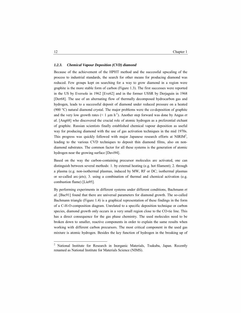
1.2.3. Chemical Vapour Deposition (CVD) diamond
Because of the achievement of the HPHT method and the successful upscaling of the process to industrial standards, the search for other means for producing diamond was reduced. Few groups kept on searching for a way to grow diamond in a region were graphite is the more stable form of carbon (Figure 1.3). The first successes were reported in the US by Eversole in 1962 [Eve62] and in the former USSR by Derjaguin in 1968 [Der68]. The use of an alternating flow of thermally decomposed hydrocarbon gas and hydrogen, leads to a successful deposit of diamond under reduced pressure on a heated (900 °C) natural diamond crystal. The major problems were the co-deposition of graphite and the very low growth rates (< 1 µm h-1). Another step forward was done by Angus et al. [Ang68] who discovered the crucial role of atomic hydrogen as a preferential etchant of graphite. Russian scientists finally established chemical vapour deposition as useful way for producing diamond with the use of gas activation techniques in the mid 1970s. This progress was quickly followed with major Japanese research efforts at NIRIM2, leading to the various CVD techniques to deposit thin diamond films, also on non-diamond substrates. The common factor for all these systems is the generation of atomic hydrogen near the growing surface [Davi94].
Based on the way the carbon-containing precursor molecules are activated, one can distinguish between several methods: 1. by external heating (e.g. hot filament); 2. through a plasma (e.g. non-isothermal plasmas, induced by MW, RF or DC; isothermal plasmas or so-called arc-jets); 3. using a combination of thermal and chemical activation (e.g. combustion flame) [Liu95].
By performing experiments in different systems under different conditions, Bachmann et al. [Bac91] found that there are universal parameters for diamond growth. The so-called Bachmann triangle (Figure 1.4) is a graphical representation of these findings in the form of a C-H-O-composition diagram. Unrelated to a specific deposition technique or carbon species, diamond growth only occurs in a very small region close to the CO-tie line. This has a direct consequence for the gas phase chemistry. The used molecules need to be broken down to smaller, reactive components in order to explain the same results when working with different carbon precursors. The most critical component in the used gas mixture is atomic hydrogen. Besides the key function of hydrogen in the breaking up of
2 National Institute for Research in Inorganic Materials, Tsukuba, Japan. Recently renamed as National Institute for Materials Science (NIMS).
Diamond 13
long hydrocarbon molecules and the creation of reactive radicals (e.g. CH3), it plays an essential part in the ongoing surface reactions during deposition. First, hydrogen stabilizes the surface by satisfying the dangling bonds. This prevents surface graphitisation, keeping the surface carbons in an sp3-configuration, rather then forming graphitic sp2-bonds [Spe94]. Secondly, and even more important, atomic hydrogen etches graphitic sp2-bonded carbon much faster than the diamond sp3-bonded carbon. The net result of this process is the growth of a diamond layer. H can also be partially replaced by O or F, which both are faster etchants [Sau99]. Atomic oxygen has the advantage that it etches even faster and reduces the incorporation of Si, but contrary to hydrogen it does not promote sp3-bonding at the surface of the growing layer [Den00].
Figure 1.4 Simplified Bachmann triangle. Note that experiments with a few percent CH4 in H2 are situated to a small region in the lower left-hand corner [May00].
For CVD the carbon phase diagram (Figure 1.3) doesn’t play a direct role as the growth is based on kinetic factors. The deposition of diamond with this low temperature and low pressure process is governed by the laws of crystal growth from the gas phase. A lot of
O
C
H
0.1 0.9
0.90.1
diamond growth region
CO 0.5
0.9
0.5
0.1
CO3
0.5
non-diamond carbon
1-3% CH4 in H2 acetone
no growth
14 Chapter 1
complex surface reactions, that are still not completely unveiled, are going on in a non thermal equilibrium [Dis98].
With the dawn of the CVD diamond era, a whole new array of possible applications came into sight. Previously unattainable because of the earlier mentioned limitations of natural and HPHT diamond, the CVD technique provided an easy way to deposit diamond films on various substrates. Both from a fundamental and an applied point of view, this proved to be a crucial step, boosting diamond research to new heights. Also, contrary to the HPHT method, that requires big, expensive industrial machines, CVD can be performed using standard laboratory equipment. This resulted in a widespread research activity all over the world [May00].
Today the most used techniques are hot filament (HF) CVD and microwave (MW) CVD. The first uses a metal filament, like tungsten or tantalum, electrically heated up to about 2200 °C to dissociate the hydrocarbon – hydrogen mixtures. At pressures varying between 0.5 - 1.3 hPa it produces reasonable quality polycrystalline diamond at a rate of 1-10 µm h-1. The absence of electric fields makes this HF deposition suitable for 3D product geometries, e.g. tool applications or insulating protective coatings in chemically adverse environments [Kla98]. A big disadvantage is the contamination of the diamond films by metal evaporation or oxidation of the filament. In addition, because of problems with the long-term stability of the filament, forming metal carbide, this method is not suitable for long-term depositions required for thick layers.
A solution for these obstacles was found in the microwave plasma enhanced CVD technique. Microwave systems are inherently cleaner because they don’t make any use of filaments or electrodes, avoiding erosion problems. MW CVD is at this moment the most used method to fabricate large area (up to ca. 20 cm diameter), high quality diamond thin films (up to 1 mm thickness) at a relatively high growth rate. Section 1.3 will deal more profoundly with the microwave plasma enhanced CVD technique. As this is the method that was used to deposit all films that were investigated for this thesis, the focus will be on these systems.
1.3. Microwave (MW) Plasma Enhanced (PE) CVD
1.3.1. Main principle
Figure 1.5 shows a schematic representation of a microwave deposition system as used at
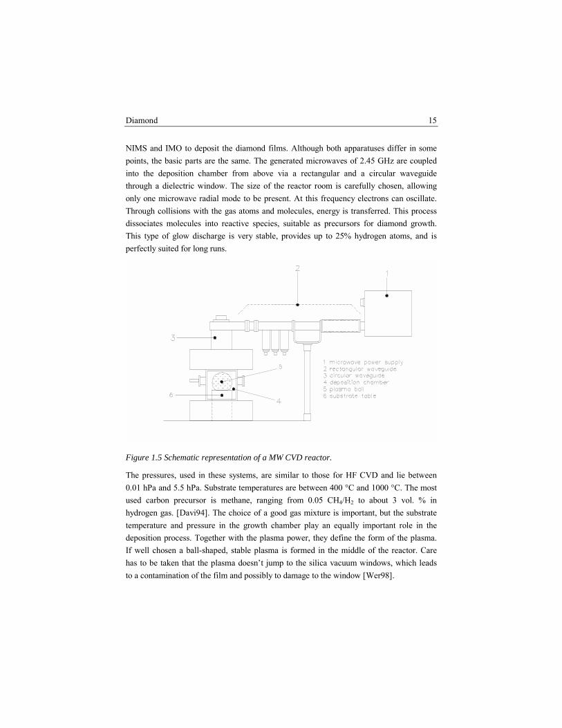
Diamond 15
NIMS and IMO to deposit the diamond films. Although both apparatuses differ in some points, the basic parts are the same. The generated microwaves of 2.45 GHz are coupled into the deposition chamber from above via a rectangular and a circular waveguide through a dielectric window. The size of the reactor room is carefully chosen, allowing only one microwave radial mode to be present. At this frequency electrons can oscillate. Through collisions with the gas atoms and molecules, energy is transferred. This process dissociates molecules into reactive species, suitable as precursors for diamond growth. This type of glow discharge is very stable, provides up to 25% hydrogen atoms, and is perfectly suited for long runs.
Figure 1.5 Schematic representation of a MW CVD reactor.
The pressures, used in these systems, are similar to those for HF CVD and lie between 0.01 hPa and 5.5 hPa. Substrate temperatures are between 400 °C and 1000 °C. The most used carbon precursor is methane, ranging from 0.05 CH4/H2 to about 3 vol. % in hydrogen gas. [Davi94]. The choice of a good gas mixture is important, but the substrate temperature and pressure in the growth chamber play an equally important role in the deposition process. Together with the plasma power, they define the form of the plasma. If well chosen a ball-shaped, stable plasma is formed in the middle of the reactor. Care has to be taken that the plasma doesn’t jump to the silica vacuum windows, which leads to a contamination of the film and possibly to damage to the window [Wer98].
16 Chapter 1
1.3.2. Substrates
The choice of a good substrate plays an essential role in the final quality and properties of the diamond film. Depending on the requisites of the end product, a first choice has to be made between homoepitaxial and heteroepitaxial growth. In the first case, the CVD diamond layer is deposited on a natural or HPHT diamond. Because of the absence of lattice mismatch, monocrystalline layers are grown. In particular doping research aimed at electronic applications requires a high purity layer without intrinsic defects like twins, dislocations and other defects induced by a lattice mismatch. HPHT diamonds can be used in the form of as-grown crystals, but are usually cut into square synthetic diamond films. The latter films have been used for phosphorous doping experiments (Chapter 3).
When growing heteroepitaxially, the resulting film is polycrystalline, with grain boundaries, including defects, a-C and graphitic inclusions. As growth starts simultaneously on different nucleation sites, the films grow with a columnar structure, different crystallites coalescing as growth proceeds. This leads to a lower number of distinct crystals at the growth surface of the film. For this thesis only silicon was used in heteroepitaxial growth (Chapter 4). HF CVD and microwave CVD are the only techniques that can use silicon substrates to deposit diamond films. Silicon is a material that is plenty available at a low price and it possesses some necessary properties: a thermal expansion coefficient comparable to that of diamond and the ability to form a carbide layer [May00]. This is essential to prevent the carbon to diffuse into the substrate instead of remaining on the surface, and it also improves the adhesion of the formed diamond layer to the substrate. To augment the number of nucleation sites, silicon can be pre-treated. This is done by scratching the surface with the help of a polishing machine and diamond slurry. This slurry contains diamond particles with a diameter < 1 µm. The effect is dual. By roughening the surface, diamond precursors will settle more easily on the surface. Moreover, small diamond particles left in the scratches will act as seeds were the growth of the film will start [Lee99]. In the discharge a lot of ions are present, of which use can be made in the case of the so-called bias enhanced nucleation (BEN). By applying a negative bias to the substrate, the carbon-containing ions are accelerated onto and into the substrate surface, making it possible to grow textured and highly oriented diamond (HOD) films [Wol01].
Diamond 17
1.3.3. Doping
As mentioned before, MW PE CVD is a very flexible method if one opts to using different carbon precursors. This fact is also valid for addition of other gasses, unlike HF CVD, where adding of halogens or oxygen would destroy the filament. This also means that in-situ doping experiments can easily be performed by just adding a gas compound that contains the atom targeted to be included in the diamond lattice. The aim of doping can be dual. It is evident that the growth chemistry is influenced by the addition of other gases. Nitrogen for instance has an effect on the orientation of the films and can be used to grow more textured films [Wer98]. But the main point of interest for this thesis is the doping of films in order to create p- or n-type semiconducting diamond. Especially the long search for and the final success in finding a suitable n-type dopant will be further deepened in Chapter 3.
1.4. Applications: present and future With the optimisation of the various techniques for producing diamond, research efforts focussed not only on the improvement of the diamond film quality itself, but also on the possible application of the material in many areas. Depending on the synthesis process used, CVD diamond can be engineered to give a range of diamond materials that enable new technologies and new opportunities for research and industry. The (possible) applications of diamond are situated in many fields. Based on one or more extraordinary properties of the material, as partly listed in Table 1.1, diamond is used for mechanical, thermal, optical and electronic purposes.
Even though diamond is practically chemically inert and very stable up to high temperatures, a few precautions need to be taken into account when using it for applications. Graphitisation in an inert atmosphere or vacuum does not start below 1520 °C. However, when used in an oxidising environment, atomic oxygen starts affecting the surface at 625 °C, leaving behind a black graphitic-like surface layer. Also metals, like manganese, iron, cobalt, nickel and the platinum group of metals, pose a threat by acting as a solvent for carbon and thus also for diamond [Yod93]. Besides these negative effects, diamond can be used in very harsh environments and is the ideal candidate for high power and high temperature devices.
The most important mechanical applications are sawing, drilling, grinding, cutting, lapping and polishing [Deb01]. The extreme hardness is one of the best-known qualities
18 Chapter 1
of the material, as it is the hardest material found in nature. For a major part of the just mentioned applications, natural or HPHT diamond grit is used. Tools can also be coated with a CVD diamond film, enhancing their performance and prolonging their lifetime. Because of the just mentioned limitations some materials cannot be processed by diamond tools. As a direct consequence the industrially important ferrous materials cannot be machined with diamond-coated tools [Yod93].
Because of the high thermal conductivity (see Table 1.1), diamond can be used as a heat sink [Wer98]. At this moment diamond lenses [Wör01] and high power laser windows [Pic00] are already available, based on the high thermal conductivity, hardness and high transparency of diamond, especially in the economically important IR-region.
The large band gap of diamond makes this material “solar-blind”, so perfect to be applied as a UV-detector [Whi00]. In nuclear and high-energy physics research, diamond particle detectors start to play a role because of their superior quality with respect to radiation hardness [Tap00].
An interesting new field is the area of biosensors. Not only is diamond biocompatible, it can also very easily be made hydrophobic or hydrophilic by switching between a H- or O-terminated surface, an important feature for biosensing applications.
All above-mentioned applications can be realised with high quality polycrystalline material. Because of the higher density of grain boundaries at the growth side of the film, this first grown layer is often polished away enhancing the quality even more. Continuous growth research resulted in the successful deposition of very smooth layers, undoped [Tak99] as well as boron-doped [Tak01]. Still, the presence of grain boundaries and other defects related to the polycrystalline nature severely deteriorate the electronic properties. By trapping and scattering, the lifetime and mobility of the charge carriers is drastically reduced. Therefore the utilisation of diamond on a larger scale in the electronic domain would require monocrystalline films. Given the fact that homoepitaxial growth is restricted because of substrate limitations, research is aimed at depositing heteroepitaxial single crystalline CVD diamond layers. Recently, Schreck et al. reported growth of diamond films where the grain boundaries are limited to certain regions. By using BEN on an Ir buffer layer, films with a minimum thickness of ~34 µm showed no longer a polycrystalline nature [Sch01].
It is clear that the applications just described are just a short representation of products already feasible with diamond and of devices that are still in a more experimental stage of
Diamond 19
development. Some are even not yet realised on a laboratory scale. Incessant research keeps improving the diamond quality and increases the knowledge how to make use of it. An important step forward in the realisation of electronic devices that make use of a p-n-junction, was the discovery of a suitable n-type dopant by Koizumi et al. in 1997 [Koi97], leading to the realisation of a UV-LED based on a diamond p-n-junction [Koi01]. A thorough opto-electronic characterisation of the phosphorous-doped n-type layers is not only interesting from a fundamental point of view. It can also give vital feedback how to enhance the characteristics of the layers to be used in devices.
1.5. References [Ang68] J.C. Angus, H.A Will, W.S. Stanko, J. Appl. Phys. 39 (1968), 2915.
[Bac91] P.K. Bachmann, D. Leers, H. Lydtin, Diamond Relat. Mater. 1 (1991), 1.
[Bun55] F.B. Bundy, H.T. Hall, H.M. Strong, R.H. Wentorf Jr., Nature 176 (1955), 51.
[Col68] A.T.Collins, E.C. Lightowlers, Phys. Rev. 171/3 (1968), 843.
[Dav94] J.L Davidson, Synthetic Diamond: Emerging CVD Science and Technology, Eds. K.E. Spear, J.P. Dismukes, Wiley-Interscience, New York, 1994, p.356.
[Davi94] R.F. Davis, Handbook on Semiconductors, Ed. T.S. Moss, Elsevier Science, Amsterdam, 1994, p.454 - p.483.
[Deb01] http://www.debid.co.uk/.
[Den00] A. Deneuville, C. R. Acad. Sci. IV 1/1 (2000), 81.
[Der68] B.V. Derjaguin, D.V. Fedoseev, V.M. Lukyanovich, B.V. Spitsyn, A.V. Ryanov, A.V. Lavrentyev, J. Cryst. Growth 2 (1968), 380.
[Dis98] B. Dischler, Low-Pressure Synthetic Diamond: Manufacturing and Applications, Eds. B. Dischler, C. Wild, Springer, Berlin, 1998, p.4.
[Enc94] W.J.P. Van Enckevort, Synthetic Diamond: Emerging CVD Science and Technology, Eds. K.E. Spear, J.P. Dismukes, Wiley-Interscience, New York, 1994, p.322 - p.332.
[Eve62] W.G. Eversole, Synthesis of Diamond, U.S. Patents Nos 3030187 and 3030188, April 17, 1962.
20 Chapter 1
[Gra97] C.F.O. Graeff, C.E. Nebel, M. Stutzmann, A. Flöter, R. Zachai, J. Appl. Phys. 81/1 (1997), 234.
[Kit86] C. Kittel, Introduction to Solid State Physics, Wiley, New York, 1986, p.19 - p.20.
[Kla98] C.-P. Klages, L. Schäfer, Low-Pressure Synthetic Diamond: Manufacturing and Applications, Eds. B. Dischler, C. Wild, Springer, Berlin, 1998, p.85 - p.101.
[Koi97] S. Koizumi, M. Kamo, Y. Sato, H. Ozaki, T. Inuzuka, Appl. Phys. Lett. 71 (1997), 1065.
[Koi01] S. Koizumi, K. Watanabe, M. Hasegawa, H. Kanda, Science 292 (2001), 1899.
[Lee99] S.-T. Lee, Z. Lin, X. Jiang, Mater. Sci. Eng. 25 (1999), 123.
[Liu95] H. Liu, D.S. Dandy, Diamond Chemical Vapor Deposition: Nucleation and Early Growth Stages, Noyes Publications, Park Ridge, 1995, p.1 - p.45.
[May00] P.W. May, Phil. Trans. R. Soc. Lond. A 358 (2000), 473.
[Nas93] K. Nassau, Diamond Films and Coatings: Development, Properties and Applications, Ed. R.F. Davis, Noyes Publications, Park Ridge, 1993, p.49 - p.53.
[Pan94] J.I. Pankove, C.-H. Qiu, Synthetic Diamond: Emerging CVD Science and Technology, Eds. K.E. Spear, J.P. Dismukes, Wiley-Interscience, New York, 1994, p.403 - p.407.
[Pic00] C.S.J. Pickles, T.D. Madgwick, R.S. Sussmann, C.J.H. Wort, Diamond Relat. Mater. 9/3-6 (2001), 917
[Rob34] R. Robertson, J.J. Fox, A.E. Martin, Phil. Trans. R. Soc. London A 232 (1934), 463.
[Sau99] R. Sauer, Cryst. Res. Technol. 34/2 (1999), 227.
[Sch01] M. Schreck, F. Hörmann, H. Roll, J.K.N. Lindner, B. Stritzker, Appl. Phys. Lett. 78/28 (2001), 192.
[Spe94] K.E. Spear, M. Frenklach, Synthetic Diamond: Emerging CVD Science and Technology, Eds. K.E. Spear, J.P. Dismukes, Wiley-Interscience, New York,
Diamond 21
1994, p.244 - p.249, p.260 - p.265.
[Tak99] D. Takeuchi, H. Watanabe, S. Yamanaka, H. Okushi, K. Kajimura, Phys. Stat. Sol. (a) 174/1 (1999), 101.
[Tak01] D. Takeuchi, S. Yamanaka, H. Watanabe, H. Okushi, Phys. Stat. Sol. (a) 186/2 (2001), 269.
[Tap00] R.J. Tapper, Rep. Prog. Phys. 63 (2000), 1273.
[Wal79] J. Walker, Rep. Prog. Phys. 42 (1979), 1605.
[Wed79] R.J. Wedlake, The Properties of Diamond, Ed. J.E. Field, Academic Press, London, 1979, p.507.
[Wer98] M. Werner, R. Locher, Rep. Prog. Phys. 61 (1998), 1665.
[Whi00] M.D. Whitfield, S.P. Lansley, O. Gaudin, R.D. McKeag, N. Rizvi, R.B. Jackman, Phys. Stat. Sol. (a) 181/1 (2000), 121.
[Wör01] E. Wörner, C. Wild, W. Müller-Sebert, P. Koidl, Diamond Relat. Mater. 10/3-7 (2001), 557.
[Wol01] S.D. Wolter, F. Okuzumi, J.T. Prater, Z. Sitar, Phys. Stat. Sol. (a) 186/2 (2001), 331.
[Yod93] M.N. Yoder, Diamond Films and Coatings: Development, Properties and Applications, Ed. R.F. Davis, Noyes Publications, Park Ridge, 1992.
[Zai01] A.M. Zaitsev, Optical Properties of Diamond: a Data Handbook, Springer-Verlag, Berlin, 2001, p.389 - p.393.

2. Experimental photocurrent techniques
Chapter 2 deals with the majority of the experimental methods that were used for this thesis. The common factor is that they are all based on the detection of electrical currents, completely or partly generated by the use of light. After a short introduction in Section 2.1, the used techniques are covered in the next three sections. Following a review on the most important theoretical points of the method in question, attention is devoted to the experimental set-up used in the experiments. The last section, Section 2.5 deals with a comparison between photocurrent and optical absorption.
2.1. Introduction Intrinsic as well as extrinsic defects create imperfections in the diamond structure, thus deteriorating the outstanding properties of the material. By distorting the structure the band structure is also influenced by the creation of defect levels in the forbidden band gap. This effect can also be turned to good account when intentional doping is applied, enabling an improvement of the conduction process by electrons and/or holes. In this case the level is no longer called a defect state, but an acceptor or donor level, depending on the impurity atom.
A variety of methods are being used to investigate the properties of defect levels. The optical ionisation energy (oEi), the optical cross-section (σo), the electronic structure, the density, etc., can all be evaluated by using one or more techniques that are based on the absorption of light.
Photocurrent-based methods are ideal tools to obtain knowledge about different opto-electronic aspects of the defect levels present in the band gap. The only restriction that has to be taken into account is that the used experimental technique must give rise to measurable charge carriers. This can be very advantageous as some features that are obscured in normal absorption experiments become visible with photocurrent techniques. Also the more defect-rich surface is ignored in these types of experiments because the excited charge carriers are trapped by the defects and do not reach the electrodes. Thus, photocurrent spectroscopy techniques are considered bulk-sensitive and are ideal to investigate the diamond films studied in this thesis.
The main point of interest for this work is the wavelength dependence of the generated
24 Chapter 2
photocurrent. The variation of photoconductivity with incident photon energy can be used to detect the presence of imperfection levels, defects as well as dopant atoms, and determine their energetic position in the band gap of the material.
2.2. Quasi-steady-state photocurrent measurements (PC)
2.2.1. Theoretical considerations
To generate free charge carriers, one can distinguish between three possible processes depending on the way the necessary energy is supplied: thermal, optical and electrical. Photocurrent is generated using optical energy in the form of a monochromatic light beam. Combinations of different types of energy are also possible as will become clear in Section 2.4.
The quasi-steady-state photocurrent technique is the basic type of photocurrent measurements. This method measures the photo-excited current in function of the incident photon energy. Especially when investigating the electronic structure of dopant atoms it can yield interesting information. Because of the periodic illumination (Section 2.2.2), the term “quasi”-steady-state is used to describe the state of the semiconductor during the experiment.
The concept of photoconductivity can be described by dividing the process in three major parts: the optical absorption of light creating the free charge carriers; the electrical transport of these carriers that contribute to the overall current; the capture of the photogenerated excess carriers, leading to trapping or recombination.
2.2.1.1. Generation of charge carriers
The absorption of light in a film can be described through the absorption coefficient α. When neglecting reflection or interference effects the intensity of the transmitted light I through the material can be expressed by Beer’s law,
d0eII α−= (2. 1)
where I0 is the incident light intensity, d the thickness of the film, and I the transmitted light [Bub92]. The absorption of a material is determined by the transitions that are allowed and that can be excited with the specific energy of the photons of the incident
Experimental photocurrent techniques 25
light bundle, which is monochromatic for all experiments that were carried out. In pristine material the only transitions possible are so-called intrinsic transitions. As there are no levels in the forbidden gap, carriers can only be excited with photons that have at least the energy equal to the band gap value. With such a photon an electron can be excited from the valence band in the conduction band, creating a free hole and electron. This is called interband generation of carriers and it occurs between non-localised states. Especially for direct band gap materials, this effect is responsible for the fact that most of the absorption will occur near the surface. For diamond, that has an indirect band gap, light can penetrate deeper into the film as the excitation can only take place when the absorption of a photon is accompanied with the absorption or emission of a phonon. This phonon is needed to provide the necessary change in k
to preserve momentum.
Defects in the material in the form of structural imperfections or impurities deteriorate the band structure by forming localised states in the band gap. Transitions that involve one of these levels as the initial or the final state are called extrinsic transitions. These transitions require photons with sub band gap energy, leading to absorption taking place in the bulk of the material. This extrinsic photoconductivity is wavelength dependent and allows the studying of the defects present. It is important to note that the majority carriers of the photoconductivity do not need to be the same as the majority carriers of the dark conductivity.
Photoconductivity measurements can only be carried out under constant illumination if the increase in charge carrier density ∆n is large compared to the dark carrier concentration n0. This is usually not the case for diamond and in particular not in this work. Therefore, in case ∆n < n0, alternating illumination is chosen so that AC amplification techniques can be used to measure the photocurrent. By chopping the monochromatic light beam the lock-in technique is the proper method to detect and record the photocurrent signal of the sample. By the modulation of the small AC photocurrent on a high DC dark current, the signal-to-noise ratio is improved, making it possible to detect small photocurrents even when the dark current signal is a few orders of magnitude higher. This is an important advantage over DC photocurrent experiments. By keeping the chop frequency low enough it is still possible to reach equilibrium between the generation and recombination of the charge carriers, obtaining a quasi-steady-state.
In summary, the generation of free charge carriers is dependent on the absorption coefficient α, the reflection R of the film and the quantum efficiency η. For sub band gap
26 Chapter 2
illumination, η can be considered constant and equal to 1. According to the quantum mechanical model describing the process of photoexcitatation, the wavelength dependence of r and α is given by the matrix element, describing the interaction of light with the material, and the joint density of states between the initial and final states involved in the absorption process [Boë90].
2.2.1.2. Electrical transport
Once the charges are excited into the non-localised states of the valence or conduction band free carrier transport can take place. This electrical transport is governed by the free carrier mobility µ and the free carrier lifetime τ of the type of carrier involved.
In PC-experiments, always the secondary photocurrent (see 2.2.1.5) is measured. In case of electrons, this can be expressed as follows:
( )( ) Fe1R1NeI 0d
s,ph τµη−−≈ α− (2. 2)
In this formula, e is electron charge, ( )( )de1R1N α−−− is the number of absorbed
photons in the sample, no interference of light taken into account. (This assumption is correct for the incoherent limit, a situation applicable for these films.) N the number of incident photons, R the reflection coefficient, α the absorption coefficient, d the film thickness, η is the quantum efficiency for the generation of free electrons, τ the free carrier lifetime, µ0 the free carrier mobility and F the applied electric field.
2.2.1.3. Trapping and recombination
Excited charges can recombine to the original state they were in before, or to another state. For recombination of charge carriers one can distinguish between two principle types: radiative and nonradiative recombination. The first type is important for luminescence studies and is accompanied by the emission of a photon. In the case of nonradiative recombination, phonons play an important role. Because diamond is an indirect band gap material, the chance to have direct radiative recombination of conduction band electrons and valence band holes, i.e. luminescence, is much lower than for a direct band gap material as GaAs [Bub92]. In the ideal situation, the µτ-product is equal to the product of the free carrier values. However, the quality of the material strongly influences these values and is responsible for the fact that the effective µτ-
Experimental photocurrent techniques 27
product is much lower than can be expected. Scattering events caused by impurities, lattice defects and phonons influence the µτ-product in a negative way.
The defect levels can be divided into traps and recombination centres. Shallow trapping states lie close to either the conduction (CB) or the valence band (VB) and are in thermal equilibrium with this band. A charge carrier that is trapped can later be reemitted to the band, participating again in the transport process. The occupancy of traps is determined by the Boltzmann factor. Carriers that are caught by a recombination centre, which is more located to the centre of the band gap, are “lost” for transport.
When no excitation source is present, a thermal equilibrium described by the Fermi-level is reached in the material, and no net carrier transport takes place. During the illumination a nonequilibrium steady state is reached, where a net flow of carriers between a band and a defect level is possible as long as this is balanced by other transitions, e.g. optical induced transitions. However, the electron population in the centre needs to be time-independent to meet with the steady-state condition. From the moment that this non- thermal additional excitation is present, e.g. light, the equilibrium carrier density is altered and the Fermi level no longer describes the equilibrium. Two quasi-Fermi levels must replace it, one for each type of charge carrier. At the same time, two demarcation lines will appear for each defect centre.
The quasi-Fermi level for electrons EFn is defined as
( )n/NlnTkEE CBFnC =− (2. 3)
where EC - EFn is the distance between the CB and the electron quasi-Fermi level, kB the constant of Boltzmann, T the absolute temperature, NC the density of states in the conduction band and n = n0 + ∆n the total electron concentration. For holes a similar expression holds. With these levels it is possible to describe the occupancy of the traps during illumination. Levels whose occupation is regulated by recombination require a description by demarcation lines, again one for electrons and one for holes. States that lie between these lines are recombination centres, while the ones that are situated between a band and a corresponding demarcation line, are traps. As there is usually one dominating recombination centre dominating the process, the demarcation lines of this centre is used [Boë90].
The presence of traps and recombination centres influence the response time of the investigated material. This response time reflects the time that is needed before the
28 Chapter 2
photoconductivity reaches its steady state after the light is switched on or its dark current level after switching off the illumination. Depending on the trap energies the time to reach thermal equilibrium can vary. Since reaching of a quasi-steady-state is an indispensable condition caution is recommended. After all, due to the abundant presence of traps and/or recombination centres a slow response time may be possible. During and between experiments it is possible that the dark current may be slightly higher than before the illumination, eventually complicating the interpretation of the experimental data. More than one explanation can account for this effect. Trapped charge carriers do not always have direct contact to the recombination centres because they lie at different places physically. The remaining current can also be an effect of the redistribution of charge carriers in the recombination centres [Ros63]. An extreme example is the well-know persistent photocurrent that can be detected for days after the source of excitation has been switched off. The origin of this phenomenon, which has also been observed in diamond [Neb00], can be diverse.
2.2.1.4. Surface recombination
A special case of recombination is the so-called surface recombination. It has been demonstrated that in order to create a photocurrent, the used light has to be absorbed and the intrinsic or extrinsic optical absorption has to lead to a measurable free charge carrier. This means that there is a close correlation between an optical absorption spectrum, α versus photon energy ħω, and the spectral response of the photoconductivity. To deduce α from a photoconductivity spectrum, caution is needed when the high absorption region of the material is reached, usually at energies close to the value of the band gap. In this situation αd >> 1 and the photoexcitation is concentrated in a thin top layer of the material. As a result, most of the light, if not all, gets absorbed in this top layer and the photocurrent is governed by the surface lifetime of the carriers. As this is a defect rich region, the surface lifetime τsurf is usually smaller than τbulk of the material. Defects influence the excited charge carriers by trapping them, so they don’t reach the contacts anymore. This effect, due to the limited penetration dept of the light is called surface recombination, and is responsible for the decrease in photocurrent, whereas an increase of absorption is expected to lead to more photocurrent. In Section 2.5, the energy value were surface recombination starts to play a role, shall be used in an assessment of the optical absorption coefficient α from photocurrent spectra.
Experimental photocurrent techniques 29
2.2.1.5. Contacts
To collect the excited carriers the use of contacts is required. In case of blocking contacts, the primary photocurrent is measured. There is no replenishing of extracted carries at the electrodes, which means that the current can only flow if both electrons and holes are present. The charge carriers with the smallest µτ-product thus limits the photocurrent. To avoid this, all experiments are carried out with ohmic contacts. This secondary photocurrent can consist of holes, electrons or a combination of both. To maintain charge neutrality every carrier that leaves the material at an electrode is replenished at the opposite electrode. For low applied voltages, a linear current versus voltage curve should be obtained, as the current flow is controlled by the resistance of the bulk semiconductor. For higher applied voltages, care has to be taken as carriers may become injected, and so-called injecting contacts are formed. In this case a superlinear behaviour of current versus voltage is obtained, misrepresenting the experimental results.
While blocking contacts are mostly used in a sandwich structure to investigate device structures, thin films are usually studied with ohmic contacts in a coplanar configuration. All experiments were performed with coplanar contacts unless stated otherwise. As the n-type films, studied in Chapter 3 are of the order of 1 µm thick, the films cannot be detached from their HPHT Ib substrate and the use of coplanar contacts is inevitable. The contact material that has to be used to obtain an ohmic character is dependent on the nature of the sample, undoped, n-type or p-type, and shall be discussed in further detail in each chapter separately.
As mentioned before, the application of photocurrent techniques is basically a method used to investigate bulk properties. In the coplanar configuration some care has to be taken to avoid influence of the contacts on the surface and thus on the experimental results. Therefore the light beam is systematically focussed onto the sample surface in the area between the electrodes. Also the pre-treatment of the samples before the deposition of the contact material can influence the final nature of the contact. In particular the possible impact due to the presence of hydrogen must not be ruled out and thoroughly checked [Mor91].
2.2.2. Experimental set-up
This section will cover the experimental set-up that was used for all photocurrent-measurements. As will become clear in Sections 2.3.2 and 2.4.2 only small modifications
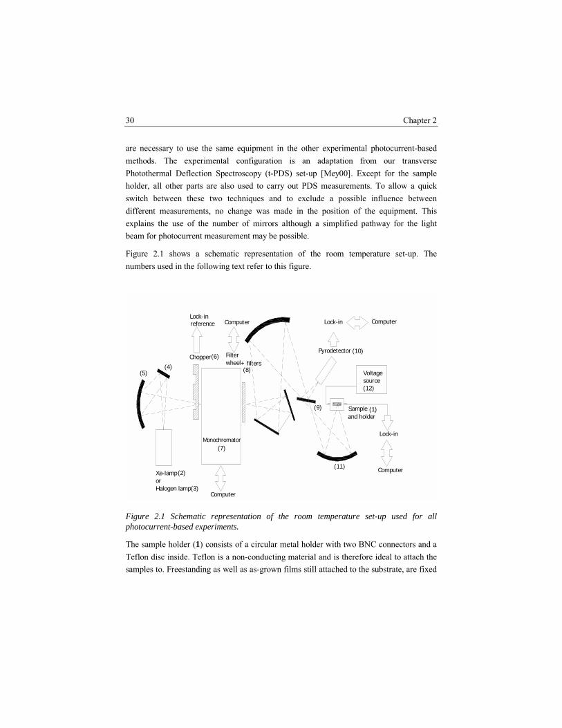
30 Chapter 2
are necessary to use the same equipment in the other experimental photocurrent-based methods. The experimental configuration is an adaptation from our transverse Photothermal Deflection Spectroscopy (t-PDS) set-up [Mey00]. Except for the sample holder, all other parts are also used to carry out PDS measurements. To allow a quick switch between these two techniques and to exclude a possible influence between different measurements, no change was made in the position of the equipment. This explains the use of the number of mirrors although a simplified pathway for the light beam for photocurrent measurement may be possible.
Figure 2.1 shows a schematic representation of the room temperature set-up. The numbers used in the following text refer to this figure.
PyrodetectorFilterwheel
Chopper
Xe-lamporHalogen lamp
Monochromator
Lock-inComputer
Computer
Lock-in
Computer
(1)
(2)
(5)
(3)
(4)
(7)
(10)
(9) Sampleand holder
reference Lock-in Computer
(6)
(8)
(11)
+ filters
Voltagesource(12)
Figure 2.1 Schematic representation of the room temperature set-up used for all photocurrent-based experiments.
The sample holder (1) consists of a circular metal holder with two BNC connectors and a Teflon disc inside. Teflon is a non-conducting material and is therefore ideal to attach the samples to. Freestanding as well as as-grown films still attached to the substrate, are fixed
Experimental photocurrent techniques 31
to the holder with a drop of carbon paste. Care is taken that no contact is made to the topside of the diamond layers. The BNC connectors are connected to the contacts on the sample surface with a Ag wire and again a drop of carbon paste. When low temperature (LT) experiments are performed the films are mounted in an UTREKS LSO cryostat, placed at the same position as the RT sample holder. The stainless steel cryostat sample stick is equipped with an electric field unit suitable to perform photocurrent measurements. To prevent short-circuiting the diamond film is in the LT case fixed onto a Corning glass plate with a drop of carbon paste.
The cryostat can be used with liquid helium (LHe) or liquid nitrogen (LN) as cryogenic fluids, depending on the required temperature. The sample chamber is cooled by the gas flux, which also regulates the stability of the temperature, monitored by the build-in thermosensor at the base of the sample holder. The system has a temperature stability of ± 0.2 K. The sample chamber in the cryostat is equipped with fused-quartz optical windows thus allowing optical experiments. The monochromatic light beam is focussed on the sample through these windows.
The monochromatic light that is used in all experiments is generated by using a lamp, a monochromator and some appropriate filters. Because of the high band gap of diamond and the need for a lamp with sufficient power in the required spectral range, two lamps are used. In the range 0.3 – 3 eV (≈ 4133 – 413 nm) a quartz tungsten halogen light source (2) provides a spectrum especially suitable for infrared (IR) and visible light. For the ultraviolet (UV) region a water cooled UV-enhanced xenon lamp (3) is used. Even though the light of this lamp contains also IR components, the spectrum in that region shows spikes, making it very hard to be used. For this reason use is restricted to between 1.5 and 5.9 eV (≈ 827 – 210 nm). To switch on the Xe-lamp a flash ignition is required which is provided by a high voltage source.
By means of a flat (4) and concave (5) mirror the light beam is focussed onto the entrance slit of the monochromator (7). The intensity of the light is modulated by means of a mechanical chopper (6) placed in front of the entrance slit. To cover the whole spectral range the monochromator is equipped with three different diffraction gratings with different blazing. Each grating covers a specific wavelength interval. Higher order diffraction wavelengths are an unwanted by-product in the output beam. Therefore a filter wheel (8) with 6 different positions is placed directly behind the output slit. By making use of 5 different filters with an appropriate cut-off frequency it is possible to create a monochromatic light beam with a wavelength between 210 and 2480 nm (≈ 5.9 – 0.5
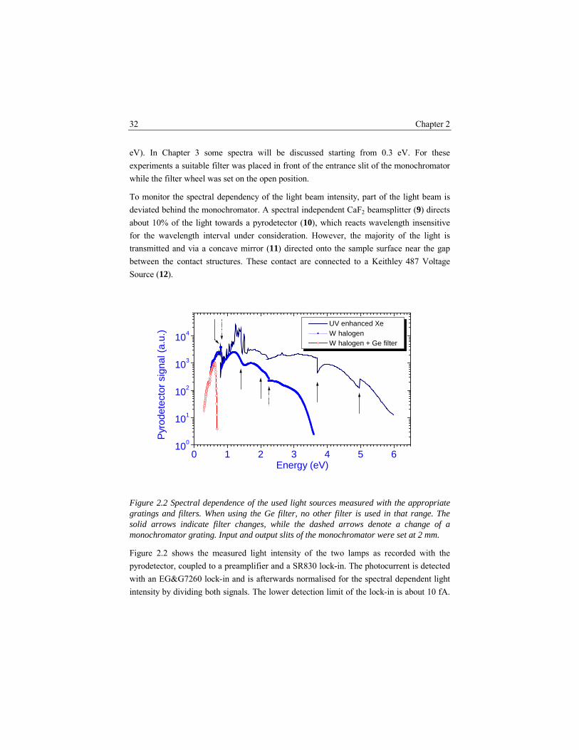
32 Chapter 2
eV). In Chapter 3 some spectra will be discussed starting from 0.3 eV. For these experiments a suitable filter was placed in front of the entrance slit of the monochromator while the filter wheel was set on the open position.
To monitor the spectral dependency of the light beam intensity, part of the light beam is deviated behind the monochromator. A spectral independent CaF2 beamsplitter (9) directs about 10% of the light towards a pyrodetector (10), which reacts wavelength insensitive for the wavelength interval under consideration. However, the majority of the light is transmitted and via a concave mirror (11) directed onto the sample surface near the gap between the contact structures. These contact are connected to a Keithley 487 Voltage Source (12).
0 1 2 3 4 5 6100
101
102
103
104
UV enhanced Xe W halogen W halogen + Ge filter
Pyro
dete
ctor
sig
nal (
a.u.
)
Energy (eV)
Figure 2.2 Spectral dependence of the used light sources measured with the appropriate gratings and filters. When using the Ge filter, no other filter is used in that range. The solid arrows indicate filter changes, while the dashed arrows denote a change of a monochromator grating. Input and output slits of the monochromator were set at 2 mm.
Figure 2.2 shows the measured light intensity of the two lamps as recorded with the pyrodetector, coupled to a preamplifier and a SR830 lock-in. The photocurrent is detected with an EG&G7260 lock-in and is afterwards normalised for the spectral dependent light intensity by dividing both signals. The lower detection limit of the lock-in is about 10 fA.
Experimental photocurrent techniques 33
The reference signal for the lock-ins are provided by the frequency of the mechanical chopper, which is usually between 3 and 17 Hz.
The quasi-steady-state photocurrent experiments as well as the PTIS measurements are completely automated and computer-controlled by using LabVIEW programs. Filter as well as grating changes take place at well-defined wavelengths. These can be slightly shifted without deteriorating the sensitivity of the system. This may be necessary if there is an indication for interesting experimental features around these values.
All spectra for this thesis are recorded from low to high energy. This is to prevent that possible persistent photocurrents that are created at higher energies, influence the measurement of experimental features at low energies.
2.3. The Constant Photocurrent Method (CPM)
2.3.1. Theoretical considerations
Although the PC-method is a powerful tool, some problems may nevertheless arise when one tries to relate the experimental spectra to the spectral dependence of the optical absorption coefficient α(E). To be able to do this, the occupation of the defect levels that are being investigated, should remain constant. However, the quasi-Fermi levels (and demarcation lines) that describe this occupation are dependent on the energy of the impinging light and may shift when a spectrum is scanned during an experiment. To solve this problem, the constant photocurrent method (CPM) was developed. By keeping the current constant, changes of the photoexcitation rate during the measurement are avoided [Bub92], resulting in a method that always yields spectra that are directly proportional to α(E) [Koč89].
For weak absorption, as is the case for sub band gap illumination, and a thin film, αd << 1 and formula (2. 2) can be simplified to
( ) FdR1NeI 0s,ph τµηα−≈ (2. 4)
which is the starting point for the theoretical basis of CPM. Starting from formula (2.4), together with some assumptions and/or independent experimental information, it will be possible to elucidate the spectral dependence of α(E) from s,phI , as will be described
below
34 Chapter 2
In formula (2.4) there are four parameters that can show a spectrally dependent behaviour. It immediately becomes clear that when we can rule out this dependence, a linear relationship between photocurrent and absorption can be found.
The reflection R usually shows very or little spectral dependence in the sub band gap area. When necessary, this effect can be measured and taken into account. As already mentioned, the quantum efficiency can also be considered as constant. Thus remains the important µτ-product to be considered. When assuming one transport path, the mobility can also be regarded as spectrally independent.
The last parameter to be taken into account is the lifetime τ. The position of the quasi-Fermi levels in the band gap can be influenced by temperature, light intensity and photon energy. Because this changes the number and the occupation of the recombination centres, it becomes immediately clear that the lifetime τ cannot always be considered constant. In the presumption that there is one dominating recombination centre and one majority type of carriers, the quasi-Fermi levels can be fixed in the band gap by keeping the photocurrent constant [Ros63].
With this information, formula (2.4) can be further simplified to
)E(N
ttancons)E(CPM ≈α (2. 5)
with N(E) the number of photons necessary to keep the secondary photocurrent constant. This proves the quasi-proportionality between α (E) and s,phI .
As just discussed, the lifetime and mobility should both be spectrally independent for a correct interpretation of the results. To verify this, the phase of the photocurrent signal is an important indicator. Under the experimental conditions of CPM this phase should also be spectrally independent. Phase changes point to a change of the transport properties [Van84], i.e. of the µτ-product, and prove that one of the assumptions made above is invalid. An example of this will be given in Chapter 4 where the assumption of one majority type of carriers for the whole measured spectral range is in conflict with the presence of both n- and p-type conductivity.
To finally put the CPM-spectra on an absolute scale, the experimental curves need to be matched to classical transmission/reflection measurements at the high-energy side of α(E). To avoid additional measurements absolute CPM can be used. This technique is a combination of standard CPM and transmission CPM, where the photon detector is
Experimental photocurrent techniques 35
placed behind the sample [Van95].
It is interesting to note that if there is no spectral change of quasi-Fermi levels, the occupation of the defect levels is also unchanged in case of a photocurrent measurement, which consequently should give the same results as a CPM-measurement. This is an important fact as PC is much easier to apply than CPM. A stable photocurrent signal is a prerequisite to perform CPM. In case of a drifting current level or of persistent photoconductivity or of a very small photocurrent signal compared to the dark current level, the technique is not easy to apply. Therefore most of the experiments were done using the PC-method, which should generate the same results as CPM in case of a stable phase.
2.3.2. Experimental set-up
The set-up for CPM is exactly the same as the one for PC measurements described in 2.2.2, but the experiments are only performed semi-automatically. As just discussed, the basic element of this method is to control the photocurrent in such a way that it remains constant over the whole experimentally measured spectral range. To do this it is vital to choose a good starting value. Because instabilities and noise of the photocurrent signal in diamond are higher then for instance in silicon, it is not easy to perform fully automated measurements. Therefore it was decided to perform the CPM experiments semi-automatically. This means that the user decides, based upon automatic read-outs of the photocurrent, phase and their average values, when the level is considered constant. All apparatuses are operated from the computer. For these experiments, only the halogen lamp can be used varying the power. This is impossible for the Xe-lamp, whose intensity cannot be varied through the applied voltage source once it is switched on. Because of the limited range of the light intensity, it is in most cases impossible to do a complete measurement with one chosen constant value for the current. Therefore, the parts with different constant levels are manually matched after the measurement. For the spectra, the inverse of pyrodetector signal is plotted against the photon energy.
2.4. PhotoThermal Ionisation Spectroscopy (PTIS)
2.4.1. Theoretical considerations
PTIS is a very sensitive technique, based on thermal promotion of electrons or holes and
36 Chapter 2
can also be described as phonon-assisted photoconductivity [Yu01]. While the normal photocurrent technique is a one-step process immediately generating a charge carrier, PTIS is clearly a two-step process, where the carrier generation is governed by a combination of optical and thermal energy. Electrons (holes) that are photoexcited into excited levels of a donor (acceptor) atom can make the transition into the conduction (valence) band by absorbing phonons, which are thermally created. Thus, the transition probability Pt from the level into the conduction band minimum EC is proportional to
−≅ Tk
EexpAPB
Xit , (2. 6)
where kB is the Boltzmann constant, Exi the energy between the level and the closest band and A a temperature independent constant. Contrary to PC, PTIS is more sensitive for the higher excited states of an atom as the thermal energy needed to induce a transition is smaller. The closer the state lies to the valence (in the case of an acceptor) or the conduction band (the donor case), the higher the probability is to detect this state with PTIS. Although PTIS normally yields discrete line spectra, the lineshape of the maxima is influenced by the purity of the material. A high defect concentration and/or stress in the film can broaden the lines [Lif93].
2.4.2. Experimental set-up
Because PTIS is also based on photocurrent, this technique requires no change of the experimental set-up used for the PC-measurements as described in Section 2.2.2. All treated PTIS-spectra are a part of simultaneously recorded PC-data.
2.5. Photocurrent versus optical absorption Contrary to all photocurrent-based techniques, methods like optical absorption spectroscopy and photothermal deflection spectroscopy (PDS) [Mey00] detect all allowed transitions that are possible in the band gap. Techniques that detect all transitions are inherently very sensitive for the surface of the measured material. For diamond, absorption at the surface is usually dominated by non-diamond phases [Roh98], like a-C. For sub band gap illumination, this can lead to a discrepancy in the optical absorption coefficient determined by PC and PDS. To demonstrate this fact, a comparison is made between αPDS of a high quality optical diamond window, 1 mm thick, and αPC of a 20 µm
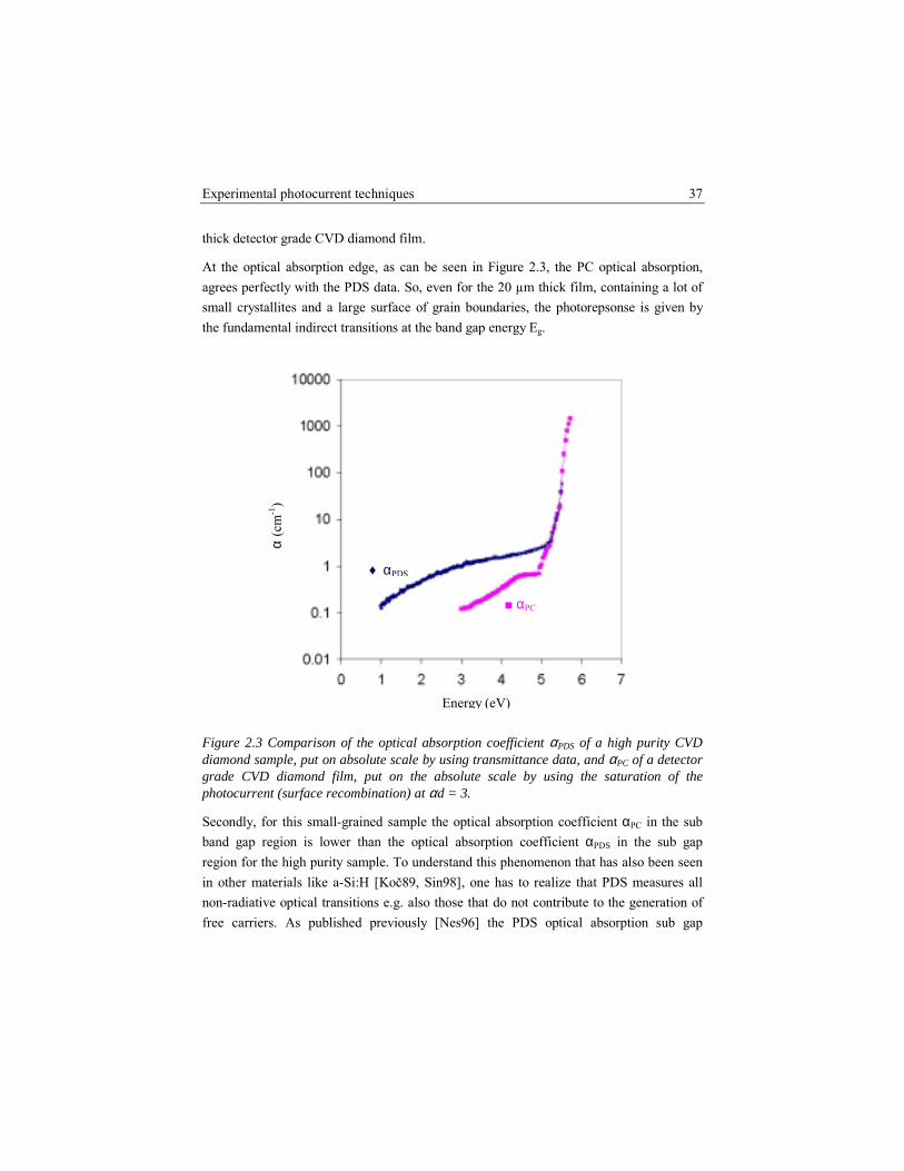
Experimental photocurrent techniques 37
thick detector grade CVD diamond film.
At the optical absorption edge, as can be seen in Figure 2.3, the PC optical absorption, agrees perfectly with the PDS data. So, even for the 20 µm thick film, containing a lot of small crystallites and a large surface of grain boundaries, the photorepsonse is given by the fundamental indirect transitions at the band gap energy Eg.
Figure 2.3 Comparison of the optical absorption coefficient αPDS of a high purity CVD diamond sample, put on absolute scale by using transmittance data, and αPC of a detector grade CVD diamond film, put on the absolute scale by using the saturation of the photocurrent (surface recombination) at αd = 3.
Secondly, for this small-grained sample the optical absorption coefficient αPC in the sub band gap region is lower than the optical absorption coefficient αPDS in the sub gap region for the high purity sample. To understand this phenomenon that has also been seen in other materials like a-Si:H [Koč89, Sin98], one has to realize that PDS measures all non-radiative optical transitions e.g. also those that do not contribute to the generation of free carriers. As published previously [Nes96] the PDS optical absorption sub gap
Energy (eV)
♦ αPDS
α
(cm
-1)
αPC
38 Chapter 2
response is dominated by the presence of amorphous carbon in the grain boundaries inducing π−π* optical transitions. The comparison of PC and PDS data suggests that the photocarriers in the quasi-steady-state configuration “do not see” the amorphous carbon which is decorating the grain boundaries. Also the shape of the PDS and PC spectra is different in support of this statement. Thus, though we can not exclude completely the changes of the recombination kinetics in the sub band gap region, the comparison of the small grained diamond film and the large grained (200-300 µm) optical window gives a very nice view on the difference between PDS and photocurrent measurements and how a complementary use of these techniques can yield valuable information about the origin of the defects present.
2.6. References [Boë90] K.W. Boër, Survey of Semiconductor Physics, Van Nostrand Reinhold, New
York, 1990, p.935 - p.1100.
[Bub92] R.H. Bube, Photoelectronic Properties of Semiconductors, Cambridge University Press, Cambridge, 1992, p.1 - p.44, p.119 - p.120.
[Koč89] J. Kočka, M. Vanĕček, A. Tříska, Amorphous Silicon and Related Materials, Ed. H. Fritzsche, World Scientific Publishing Co. Pte. Ltd., Singapore, 1998, p.297 - p.327.
[Lif93] T.M. Lifshits, Instrum. Exp. Tech. 36/1 (1993), 1.
[Mey00] K. Meykens, PhD thesis: “Study by means of photothermal deflection methods of the opto-electronic properties of CVD diamond in relation to the defect population”, Limburgs Universitair Centrum, Diepenbeek, 2000, p.35 - p.44.
[Mor91] Y. Mori, H. Kawarada, A. Hiraki, Appl. Phys. Lett. 58/9 (1991), 940.
[Neb00] C.E. Nebel, A. Waltenspiel, M. Stutzmann, M. Paul, L. Schäfer, Diamond Relat. Mater. 9/3-6 (2000), 404.
[Nes96] M. Nesládek, K. Meykens, L.M. Stals, M. Vanĕček, J. Rosa, Phys. Rev. B 54 (1996), 5552.
[Nes01] M. Nesládek, M. Vaněček, K. Meykens, K. Haenen, J. Manca, L. De Schepper, E. Pace, A. Pini, G. Verona Rinati, C. Kimura, Y. Etou, T. Sugino, Phys. Stat. Sol. (a) 185/1 (2001), 107-113.
Experimental photocurrent techniques 39
[Roh98] E. Rohrer, C.E. Nebel, M. Stutzmann, A. Flöter, R. Zachai, X. Jiang, C.-P. Klages, Diamond Relat. Mater. 7 (1998), 879.
[Ros63] A. Rose, Concepts in Photoconductivity and Allied Problems, Interscience Publishers, New York, 1963, p.1 - p.68.
[Sin98] A.K. Sinha, S.C. Agarwal, Indian J. Pure & Appl. Phys. 36 (1998), 328.
[Van84] M. Vanĕček, A. Abrahám, O. Štika, J. Stuchlík, J. Kočka, Phys. Stat. Sol. (a) 83 (1984), 617.
[Van95] M. Vanĕček, J. Kočka, A. Poruba, A. Fejfar, J. Appl. Phys. 78/10 (1995), 6203.
[Yu01] P.Y. Yu, M. Cardona, Fundamentals of Semiconductors: Physics and Materials Properties, Springer-Verlag, Berlin, 2001, p.311 - p.315.

3. Phosphorous: an active donor in CVD diamond
As is commonly known in diamond research, the way to finally achieve active n-type doping was long and hard. Section 3.1 covers an overview of the search for a suitable dopant and problems that arose during this search. After a description of the samples and their preparation prior to the experiments in Section 3.2, Section 3.3 deals with the first results on the intra band gap defect levels in P-doped films. Next, in Section 3.4, the electronic structure of the phosphorous atom in active n-type diamond films is discussed. Preliminary results on a 100-oriented P-doped diamond film are treated in Section 3.5. At the end of this chapter (Section 3.6) a comparison is made between the results obtained on the Japanese films and the ones grown at IMO, after which the conclusions are given in the last section.
3.1. Introduction: problems with n-type dopants Although very rarely found in nature, IIb diamonds are natural p-type semiconductors because of the presence of substitutional boron impurities. Because of this, boron was the expected candidate to be used in doping experiments in order to produce manmade p-type diamond. Success after success led to the present situation where atomically flat device grade B-doped films can be homoepitaxialy grown using the MW CVD technique and trimethylboron as the dopant source [Tak01, Yam00].
Contrary to the achievement in producing p-type films, the realisation of an active n-type diamond remained a problem for many years3, even though enormous research efforts were focussed on this topic. Not only from a fundamental point of view is n-type doping an intriguing issue, it is also of crucial importance if diamond is ever going to make the step from a research material to the electronic industry. This requires a good reproducibility of high quality n-type material to be used in p-n-junctions. To achieve this goal, two important questions need to be addressed: which method of doping will have the biggest chance to be successful and, more important, which atom will lead to an active n-type diamond layer? 3 Although substitutional nitrogen forms a deep donor in CVD diamond, the thermal activation energy of 1.7 eV is too high to create an electrically active n-type diamond at room temperature. For this reason phosphorous-doped films will be considered as the first n-type CVD diamonds.
42 Chapter 3
For doping three possible pathways can be followed: by diffusion or implantation which are ex-situ methods applied to the already grown film, or through in-situ doping by adding a precursor containing the targeted donor, during the CVD process. For the ex-situ methods it is evident that the incorporation of dopant atoms is clearly dependent on the texture of the diamond film or crystal that serves as a substrate. However, the orientation of the used substrate also influences the incorporation of dopants during the growth, as will be treated later. Compared to ex-situ doping by diffusion or ion-implantation, the in-situ technique has several advantages. Diffusion of impurities in diamond is very hard, as the diffusion coefficient is extremely low at moderate temperatures. This process requires very high temperatures, making the technique laborious and uninteresting to apply on larger scale. Ion-Implantation has the disadvantage that it creates various defects, like amorphisation, graphitisation, interstitials and vacancies. Although these defects can be partly removed by high-T annealing steps, one has to remain cautious that the required electrical activity is not caused by the damage in the diamond instead of the implanted impurities [Wer98].
As the diamond structure is very rigid and the carbon atom rather small, suitable n-type dopants are hard to find. Theoretical studies proposed lithium, sodium, phosphorous and sulphur to be valid candidates [Kaj90, Miy01a]. Their very low solubility in the diamond structure makes in-diffusion of these atoms impossible. Li and Na, if occupying interstitial positions, were predicted to form donor levels respectively at 0.1 eV and 0.3 eV under the conduction band [Kaj93]. Because of their preference to occupy interstitial positions ion-implantation is a valid alternative as there is no competition with carbon for the substitutional sites. Despite the fact that this produced active n-type doping with the optical ionisation energy consistent with the predicted value of Kajihara et al. [Kaj93, Vav79], the donor was turned inactive by annealing [Vav78]. As Li and Na are fast diffusers, Li even at room temperature, complex formation with structural defects or diffusion to the surface after the implantation can lead to an inactivation of the active donor after long storage or annealing [Kaj90]. In spite of many trials, Li was also never established as an active n-type dopant by using the CVD method. Although photocurrent studies of films grown under addition of a lithium-containing precursors during growth, might show some Li-related defect centres, the films showed never n-type conduction as confirmed by Hall measurements [Nes96, Ste00, Zei00a].
The situation for phosphorous has long been ambiguous because calculations engendered non-consistent results and experimental evidence remained absent. Theoretical research
Phosphorous: an active donor in CVD diamond 43
showed a donor character for substitutional P and energies ranging from 0.2 eV [Kaj93] to 1.09 eV [Jac90] under the conduction band were reported. In the later case it was even argued that this value was probably an underestimation of the real value. Unfortunately, at the same time a very low substitutional solubility was predicted, thus leading to a very low contribution to the conductivity of possible incorporated P [And93]. From the experimental side, implantation as well as in-situ doping was tested. Prins achieved n-type conduction by implanting natural IIa diamonds with very low doses of P+ ions, though the quality of the layers was low [Pri95]. By adapting and improving the implantation technique, the quality was enhanced, leading to a thermal activation energy of ≈ 0.43 eV [Pri98]. However, the use natural IIa diamonds as substrates could not be considered as a real solution for the n-type doping problem when looking from a device-based point of view. A try to grow on silicon substrates by adding diphosphorus pentaoxide (P2O5) during hot filament growth was reported to produce active n-type doping, but no P could be found in the diamond film, thus creating uncertainty about the cause of the n-type conduction [Oka94]. It was not till 1997 when Koizumi et al. used phosphine to grow active P-doped 111 homoepitaxial diamond films, that the n-type nature of phosphorous in diamond was firmly and unconditionally established [Koi97].
The success of phosphorous doping encouraged researchers to achieve similar results by adding other possible dopants to the MW PE CVD process. In 1999 another Japanese group claimed to have grown 100 homoepitaxial n-type diamond by using H2S making sulphur the dopant atom [Sak99]. A donor level at 0.38 eV under the CB, combined with high electron mobility values, up to 597 cm2 V-1 s-1, created high expectations for device applications. Later, the status of sulphur as being a good n-type dopant was made doubtful again. When examining the same diamond films Kalish et al. found consistently p-type conductivity in all the samples and ascribed this to an unintentional doping with boron impurities [Kal00]. Up to now no further success with sulphur was obtained [Gar01, Ste01b], leaving phosphorous the only active n-type dopant at the moment. This obviously does not rule out the possibility that sulphur can be an active donor. Theoretical studies ascribe donor behaviour to substitutional sulphur but are again not consistent as far as the activation energy is concerned, with values varying between 0.15 eV [Saa00] and 1 eV [Miy01a].
Recently theoretical doping research focuses on co-doping, whereby two different elements, forming complexes in the diamond film, are used to achieve a successful doping. Calculations indicate that more shallow levels should be accomplished by this
44 Chapter 3
method, opening up new possible ways to achieve a shallow active n-type donor [Kat01, Miy01b].
3.2. Samples The main part of the experiments was carried out on CVD diamond films provided by dr. Koizumi and dr. Teraji from NIMS. At the end of this chapter, a comparison is made between the data extracted from these samples and the first promising results from n-type doping experiments carried out at IMO.
3.2.1. Samples NIMS
As the electrical properties of diamond films are closely related to the crystalline perfection of the film, HPHT diamonds were chosen as a substrate material so homoepitaxial growth could be achieved. Ia and Ib diamonds were chosen because of their low optical absorption in the 0.5 eV - 2 eV energy region and the fact that the donor level was predicted at energies lower then 1 eV. First trials were focussed on the optimisation of the growth parameters. These initial experiments showed that it was very difficult to obtain smooth and continuous P-doped films on 100 single crystal diamonds, favouring growth on 111-oriented diamond substrates [Koi98]. Table 3.1 gives an overview of all CVD diamond films grown at NIMS that were investigated within the framework of this thesis. It sums up the most important deposition conditions together with results from SIMS and van der Pauw Hall measurements.
Samples #P1-#P3 were grown in a classical quartz tube reactor, on a diamond coated quartz substrate holder. This can lead to unwanted incorporation of impurities like silicon and oxygen, which have a negative influence on the electrical properties of the films. Therefore Koizumi and co-workers opted to replace the system by a metallic chamber type CVD apparatus. The only quartz window present in this system, to introduce the microwaves into the stainless steel chamber, is at approximately 10 cm distance from the plasma, strongly reducing contamination. The substrate holder is made of molybdenum, a non-reactive metal for the ongoing chemical reactions. All other NIMS films were grown with this apparatus. A thorough description of the full deposition process can be found in [Koi00a].
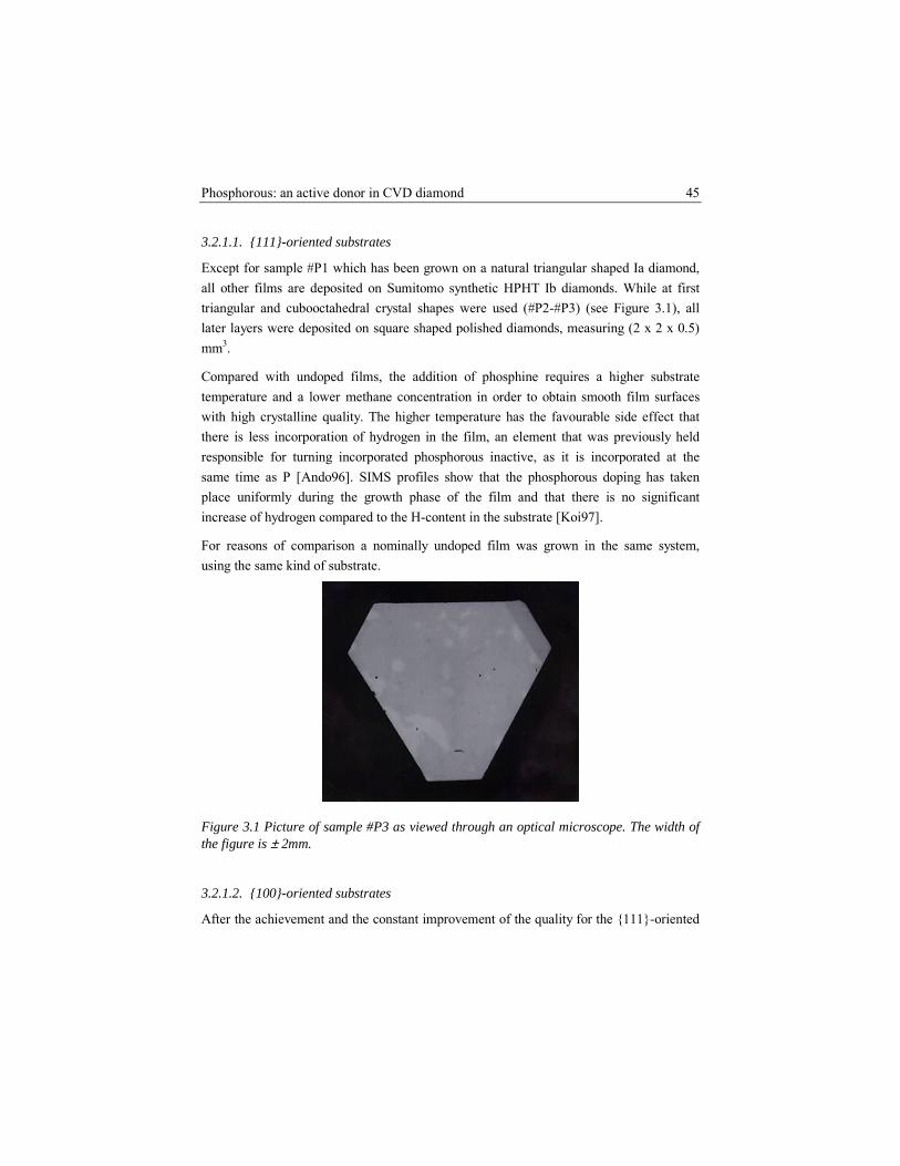
Phosphorous: an active donor in CVD diamond 45
3.2.1.1. 111-oriented substrates
Except for sample #P1 which has been grown on a natural triangular shaped Ia diamond, all other films are deposited on Sumitomo synthetic HPHT Ib diamonds. While at first triangular and cubooctahedral crystal shapes were used (#P2-#P3) (see Figure 3.1), all later layers were deposited on square shaped polished diamonds, measuring (2 x 2 x 0.5) mm3.
Compared with undoped films, the addition of phosphine requires a higher substrate temperature and a lower methane concentration in order to obtain smooth film surfaces with high crystalline quality. The higher temperature has the favourable side effect that there is less incorporation of hydrogen in the film, an element that was previously held responsible for turning incorporated phosphorous inactive, as it is incorporated at the same time as P [Ando96]. SIMS profiles show that the phosphorous doping has taken place uniformly during the growth phase of the film and that there is no significant increase of hydrogen compared to the H-content in the substrate [Koi97].
For reasons of comparison a nominally undoped film was grown in the same system, using the same kind of substrate.
Figure 3.1 Picture of sample #P3 as viewed through an optical microscope. The width of the figure is ± 2mm.
3.2.1.2. 100-oriented substrates
After the achievement and the constant improvement of the quality for the 111-oriented
46 Chapter 3
films, an attempt was made to repeat the obtained results for 100 layers. Especially because the growth of atomically flat boron-doped p-type 100 surfaces has already been accomplished [Yam00], similar results with n-type diamond would be interesting from the point of view of electronic applications, more specifically in the p-n-junctions area. Again a Sumitomo synthetic HPHT (2 x 2 x 0.5) mm3 Ib substrate was used. Incorporation of phosphorous in the 100-direction proved to be very hard so that the doping conditions as used for the 111-films were changed [Koi00b]. Phosphine concentrations were increased, together with an increase of the methane concentration and a lowering of the substrate temperature. These last two parameters are now much more comparable with the normal conditions for the growth of undoped diamond sheets. The sample proved to be too resistive to apply Hall measurements, making a confirmation of active n-type conductivity impossible.
3.2.2. Samples IMO
The IMO P-doped films were prepared in a commercial ASTeX PDS 17 MW CVD deposition system. Besides a standard 111 Sumitomo HPHT Ib substrates, a black looking heavily B-doped HPHT crystals was used. Further details are given in Table 3.2.
3.2.3. Contacts
As mentioned in Chapter 2, the application of photocurrent-based methods requires the use of ohmic contacts in order to retain charge neutrality in the diamond film. Due to the specific nature of the diamond films, not freestanding but still attached to the substrate, coplanar contacts are recommended to exclude the influence of the substrate as much as possible.
In case of thermally deposited contacts, aluminium showed the best ohmic behaviour [Koi00a, Ter99], especially for films containing a high dose of phosphorous, and thus containing more defects. When implantation is an option, implanted gallium forms ohmic contacts with a contact resistivity one order lower than for the vacuum-deposited case [Ter00b]. All results reported in this work were obtained with the use of thin aluminium contacts.
It is established that as-grown CVD diamond films exhibit p-type surface conductivity induced by the hydrogen on the surface [Lan89]. Moreover Mori et al. clearly showed that the presence of hydrogen on the surface could influence the contact behaviour
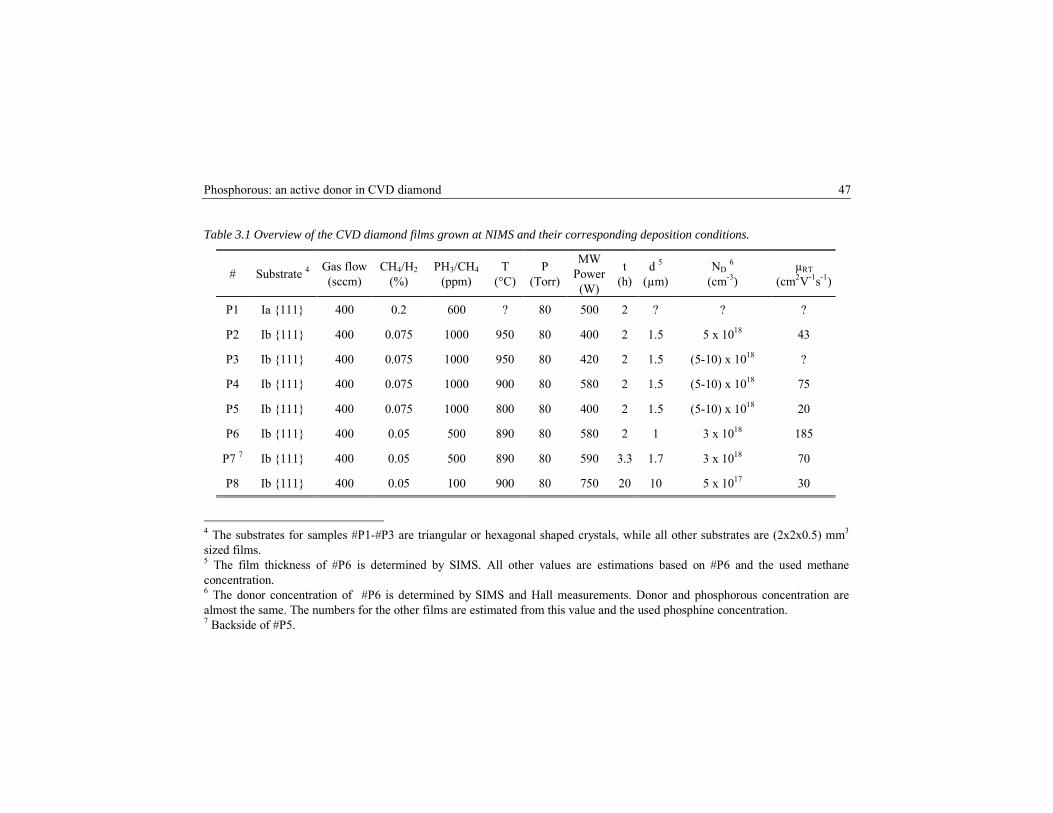
Phosphorous: an active donor in CVD diamond 47
Table 3.1 Overview of the CVD diamond films grown at NIMS and their corresponding deposition conditions.
# Substrate 4 Gas flow(sccm)
CH4/H2(%)
PH3/CH4 (ppm)
T (°C)
P (Torr)
MW Power(W)
t (h)
d 5
(µm)
ND 6 (cm-3)
µRT (cm2V-1s-1)
P1 Ia 111 400 0.2 600 ? 80 500 2 ? ? ?
P2 Ib 111 400 0.075 1000 950 80 400 2 1.5 5 x 10¹⁸ 43
P3 Ib 111 400 0.075 1000 950 80 420 2 1.5 (5-10) x 1018 ?
P4 Ib 111 400 0.075 1000 900 80 580 2 1.5 (5-10) x 1018 75
P5 Ib 111 400 0.075 1000 800 80 400 2 1.5 (5-10) x 1018 20
P6 Ib 111 400 0.05 500 890 80 580 2 1 3 x 10¹⁸ 185
P7 7 Ib 111 400 0.05 500 890 80 590 3.3 1.7 3 x 10¹⁸ 70
P8 Ib 111 400 0.05 100 900 80 750 20 10 5 x 10¹⁷ 30
4 The substrates for samples #P1-#P3 are triangular or hexagonal shaped crystals, while all other substrates are (2x2x0.5) mm3 sized films. 5 The film thickness of #P6 is determined by SIMS. All other values are estimations based on #P6 and the used methane concentration. 6 The donor concentration of #P6 is determined by SIMS and Hall measurements. Donor and phosphorous concentration are almost the same. The numbers for the other films are estimated from this value and the used phosphine concentration. 7 Backside of #P5.
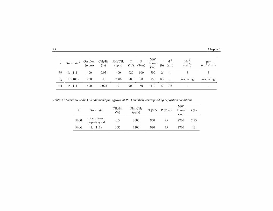
48 Chapter 3
# Substrate 4 Gas flow(sccm)
CH4/H2(%)
PH3/CH4 (ppm)
T (°C)
P (Torr)
MW Power(W)
t (h)
d 5
(µm)
ND 6 (cm-3)
µRT (cm2V-1s-1)
P9 Ib 111 400 0.05 400 920 100 700 2 1 ? ?
PA Ib 100 200 2 2000 800 80 750 0.5 1 insulating insulating
U1 Ib 111 400 0.075 0 900 80 510 5 3.8 - -
Table 3.2 Overview of the CVD diamond films grown at IMO and their corresponding deposition conditions.
# Substrate CH4/H2
(%) PH3/CH4
(ppm) T (°C) P (Torr) MW
Power (W)
t (h)
IMO1 Black boron doped crystal 0.5 2000 950 75 2700 2.75
IMO2 Ib 111 0.35 1200 920 75 2700 13
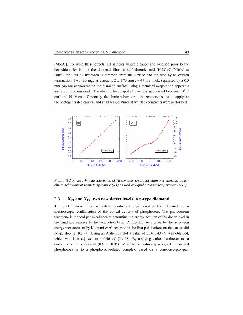
Phosphorous: an active donor in CVD diamond 49
[Mor91]. To avoid these effects, all samples where cleaned and oxidised prior to the deposition. By boiling the diamond films in sulfochromic acid (H2SO4/Cr(VI)O3) at 200°C for 0.5h all hydrogen is removed from the surface and replaced by an oxygen termination. Two rectangular contacts, 2 x 1.75 mm², ~ 45 nm thick, separated by a 0.5 mm gap are evaporated on the diamond surface, using a standard evaporation apparatus and an aluminium mask. The electric fields applied over this gap varied between 104 V cm-1 and 105 V cm-1. Obviously, the ohmic behaviour of the contacts also has to apply for the photogenerated carriers and at all temperatures at which experiments were performed.
-200 -100 0 100 200-6-4-2024681012
LNT
Photocurrent (nA)
#P4
Electric field (V)0 50 100 150 200 250
0.0
0.1
0.2
0.3
0.4
0.5
0.6
0.7
0.8RT
#P1
Phot
ocur
rent
(nA)
Electric field (V)
Figure 3.2 Photo-I-V characteristics of Al-contacts on n-type diamond showing quasi-ohmic behaviour at room temperature (RT) as well as liquid nitrogen temperature (LNT).
3.3. XP1 and XP2: two new defect levels in n-type diamond The confirmation of active n-type conduction engendered a high demand for a spectroscopic confirmation of the optical activity of phosphorous. The photocurrent technique is the tool par excellence to determine the energy position of the donor level in the band gap relative to the conduction band. A first hint was given by the activation energy measurement by Koizumi et al. reported in the first publications on the successful n-type doping [Koi97]. Using an Arrhenius plot a value of Ea ≈ 0.43 eV was obtained, which was later adjusted to ~ 0.46 eV [Koi98]. By applying cathodoluminescence, a donor ionisation energy of (0.63 ± 0.05) eV could be indirectly assigned to isolated phosphorous or to a phosphorous-related complex, based on a donor-acceptor-pair
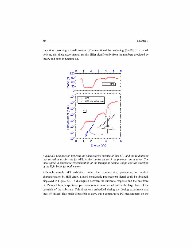
50 Chapter 3
transition, involving a small amount of unintentional boron-doping [Ste99]. It is worth noticing that these experimental results differ significantly from the numbers predicted by theory and cited in Section 3.1.
0 1 2 3 4 5 6100
101
102
103
104
105
106
107
RT
#P1 #P1 - Ia substrate
Phot
ocur
rent
(a.u
.)
Energy (eV)
hν
0306090
1200 1 2 3 4 5 6
#P1
Phas
e (°
)
Figure 3.3 Comparison between the photocurrent spectra of film #P1 and the Ia diamond that served as a substrate for #P1. At the top the phase of the photocurrent is given. The inset shows a schematic representation of the triangular sample shape and the direction of the light beam for both curves.
Although sample #P1 exhibited rather low conductivity, preventing an explicit characterisation by Hall effect, a good measurable photocurrent signal could be obtained, displayed in Figure 3.3. To distinguish between the substrate response and the one from the P-doped film, a spectroscopic measurement was carried out on the large facet of the backside of the substrate. This facet was embedded during the doping experiment and thus left intact. This made it possible to carry out a comparative PC measurement on the
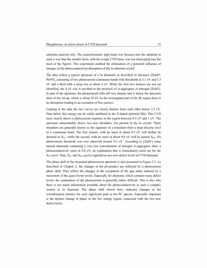
Phosphorous: an active donor in CVD diamond 51
substrate material only. The monochromatic light beam was focused onto the substrate in such a way that the smaller facet, with the n-type CVD layer, was not intercepted (see the inset of the figure). This experiment enabled the elimination of a potential influence of changes in the photoconductivity/absorption of the Ia substrate crystal.
The data reflect a typical spectrum of a Ia diamond, as described in literature [Den67, Per95], consisting of two photocurrent continuum bands with thresholds at 3.1 eV and 3.3 eV and a third with a steep rise at about 4 eV. While the first two features are not yet identified, the 4 eV rise is ascribed to the presence of A-aggregates of nitrogen [Zai01]. In part of the spectrum, the photocurrent falls off very sharply and is below the detection limit of the set-up, which is about 10 fA. In the investigated part of the IR region there is no absorption leading to an excitation of free carriers.
Looking at the data the two curves are clearly distinct from each other below 2.5 eV. Data below this energy can be solely attributed to the P-doped epitaxial film. This CVD layer clearly shows a photocurrent response in the region between 0.5 eV and 1 eV. The spectrum unmistakably shows two new shoulders, not present in the Ia crystal. These shoulders are generally known as the signature of a transition from a deep discrete level to a continuum band. The first feature, with an onset at about 0.5 eV will further be denoted as XP1, while the second, with an onset at about 0.8 eV will be named XP2. No photocurrent threshold was ever observed around 0.5 eV. According to [Zai01] some natural diamonds containing a very low concentration of nitrogen A-aggregates show a photoconductivity onset at 0.8 eV, an explanation that is immediately ruled out for the XP2 level. Thus, XP1 and XP2 can be regarded as two new defect levels in CVD diamond.
The phase shift of the measured photocurrent spectrum is also presented in Figure 3.3. As described in Chapter 2, the changes in the µτ-product are reflected by a photocurrent phase shift. They reflect the changes in the occupation of the gap states induced by a movement of the quasi-Fermi levels. Especially for diamond, which contains many defect levels, the explanation of the photocurrent is generally rather difficult. This is also why there is not much information available about the photoconductivity in such a complex system as Ia diamond. The phase shift shown here, indicates changes in the recombination kinetics for each significant peak in the PC spectra. Especially important is the distinct change in phase in the low energy region, connected with the two new defect levels.
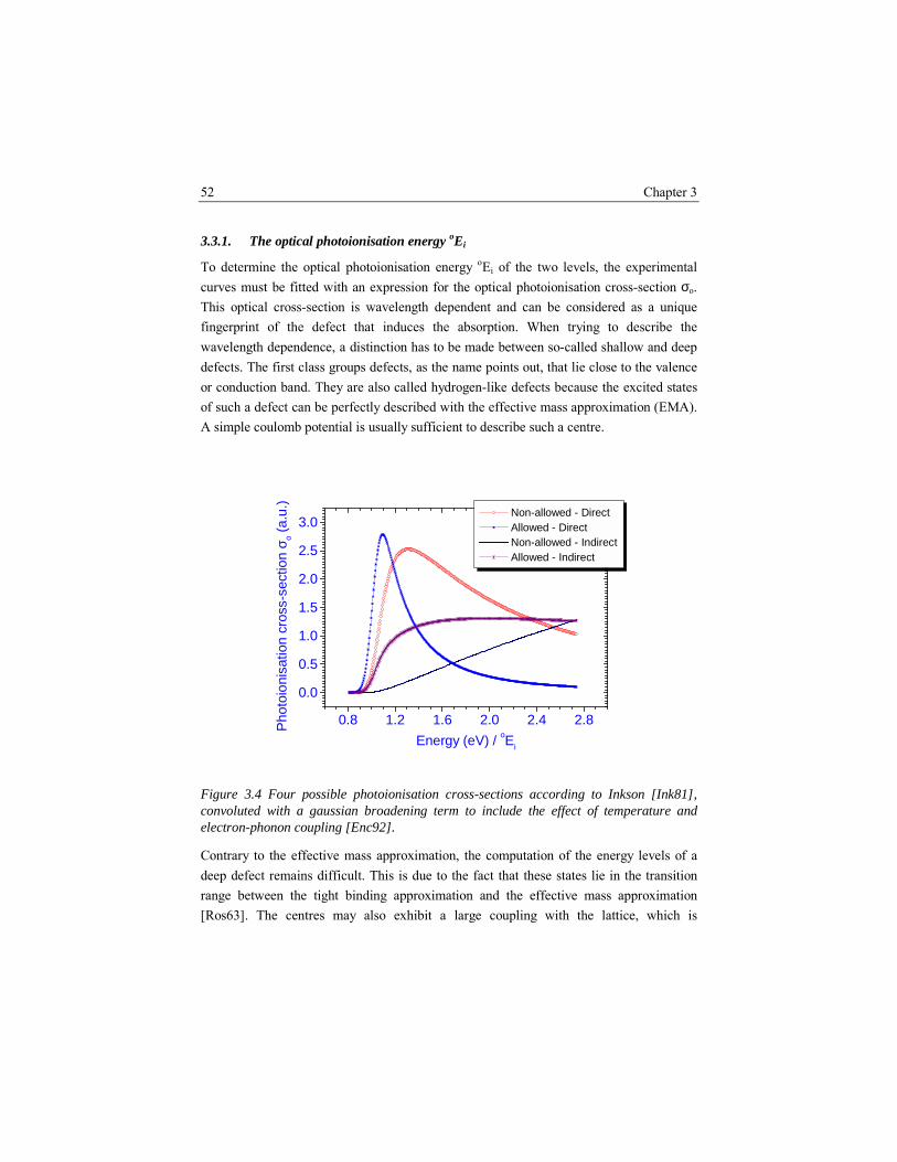
52 Chapter 3
3.3.1. The optical photoionisation energy oEi
To determine the optical photoionisation energy oEi of the two levels, the experimental curves must be fitted with an expression for the optical photoionisation cross-section σo. This optical cross-section is wavelength dependent and can be considered as a unique fingerprint of the defect that induces the absorption. When trying to describe the wavelength dependence, a distinction has to be made between so-called shallow and deep defects. The first class groups defects, as the name points out, that lie close to the valence or conduction band. They are also called hydrogen-like defects because the excited states of such a defect can be perfectly described with the effective mass approximation (EMA). A simple coulomb potential is usually sufficient to describe such a centre.
0.8 1.2 1.6 2.0 2.4 2.8
0.0
0.5
1.0
1.5
2.0
2.5
3.0
Non-allowed - Direct Allowed - Direct Non-allowed - Indirect Allowed - Indirect
Phot
oion
isat
ion
cros
s-se
ctio
n σ o (
a.u.
)
Energy (eV) / oEi
Figure 3.4 Four possible photoionisation cross-sections according to Inkson [Ink81], convoluted with a gaussian broadening term to include the effect of temperature and electron-phonon coupling [Enc92].
Contrary to the effective mass approximation, the computation of the energy levels of a deep defect remains difficult. This is due to the fact that these states lie in the transition range between the tight binding approximation and the effective mass approximation [Ros63]. The centres may also exhibit a large coupling with the lattice, which is
Phosphorous: an active donor in CVD diamond 53
expressed by the Huang-Rhys factor S. This dimensionless parameter is a measure for the coupling of the electronic states with the so-called lattice states, connected with the vibrations/phonons of the crystal structure. When the HR-factor is zero, the transition is pure electronic, not involving any phonons [Hen89].
Much theoretical work has been done to calculate σo based on quantummechanics [Ink81, Luc65]. The key element is the choice of a good potential representing the defect and describing the way the charge carrier is bound to the atomic system. Especially for deep defects a good choice to model the centre can be useful to fit the experimental curves in order to obtain the optical ionisation energy oEi and the Huang-Rhys factor S. Inkson [Ink81] distinguishes four types of transitions: allowed and non-allowed, each in combination with a direct and indirect transition. To include the effect of temperature and electron-phonon coupling, these expressions can be convoluted with a gaussian broadening term [Enc92].
Figure 3.5 depicts results taken from sample #P3, which was also a highly resistive film like #P1. The same two levels are also present here. Data taken at liquid nitrogen temperature (LNT) yield similar results as at RT, but the measured spectrum is sharper as it is less broadened by acoustic phonons. The substrate of #P3 is a Ib diamond, which accounts for the defect onset around 2.2 eV. This can be attributed to single substitutional nitrogen present in large amounts in Ib diamond (see Chapter 1) [Wal79].
To fit the curves and extract the photoionisation energy oEi, one must realise that the optical cross-section is the proportionality constant between the concentration of a defect present in the material and the amount of absorption that it induces. This relation can be expressed by the following formula:
odN σ=α (3. 1)
Nd is the defect concentration associated with the investigated level. According to the theory covered in Chapter 2, the optical absorption coefficient α can be deducted from a CPM spectrum. As the phase in Figure 3.3 indicates, the recombination traffic changes when changing the excitation wavelength during the measurement. This normally excludes the possibility to determine α from the PC spectra because mutual exchange of carriers between the two levels cannot be ruled out. However, because the PC phase is stable for each separate defect, the photocurrent spectrum is interpreted as the spectral dependence of the photoionisation cross-section of a deep impurity. This enables the fit of the PC data in that specific energy range. Using PC data instead of CPM does not
54 Chapter 3
influence the photoionisation energy. By using PC the population of the levels relative to each other can change, influencing the magnitude of the cross-sections in relation to each other. Thus the defect concentration cannot be estimated from these spectra.
Figure 3.5 Comparison between the RT and LNT spectra of #P3. The optical cross-sections of the two defects levels present, XP1 and XP2, are fitted using one of the Inkson expressions, convoluted with a Gaussian broadening term.
For the numerical fitting of the RT data of Figure 3.5, the best results were obtained by using the Inkson formula for the non-allowed vertical transitions, convoluted with a gaussian broadening term [Enc92]:
( ) ( )( )
επ
∆−ε−−
−εε−ε
=σ ∞+
∞−
dw2
)w2
)EE(exp(
BE
AE2
2
2ph
2
2/3i
o
Inkson . (3. 2)
0 1 2 3 4
100
101
102
103LNT
Photocurrent (a.u.) #P3 Fit σXP1
+ σXP2
Energy (eV)0 1 2 3 4
100
101
102
103
EXP1EXP2
RT
#P3 Fit σXP1 Fit σXP2
Phot
ocur
rent
(a.u
.)
Energy (eV)
Phosphorous: an active donor in CVD diamond 55
A and B are constants, ε the integration variable of the convolution integral, oEi the photoionization threshold, and 2w is the full width at half-maximum (FWHM) of the gaussian phonon broadening term. This gaussian term describes the fact that at higher, non-cryogenic temperatures the charge carrier can be excited with a non-zero probability from the defect level to the transport band by interacting with an optical phonon. ∆Eph is a term related to the Huang-Rhys factor, describing this interaction. Preliminary fittings proved ∆Eph to be very small, making it possible to omit this term. For the photoionisation energy of the XP1 and XP2 defect the fit of the RT spectra yielded the following values: EXP1 = (0.56 ± 0.03) eV; EXP2 = (0.81 ± 0.03) eV. The FWHM of the curves are 2wXP1 = 60 meV and 2wXP2 = 200 meV, pointing again to a small Huang-Rhys factor.
3.3.2. XP1: substitutional phosphorous
1.5 2.0 2.5 3.0 3.510-11
10-10
10-9
10-8
10-7
10-6
10-5
10-4
10-3
Ea = 0.55 - 0.60 eV
#P3
Dar
k cu
rrent
(A)
1000/T (K-1)
Figure 3.6 Arrhenius plot used to determine the activation energy Ea of the dark current of #P3.
The activation energy obtained from the film #P3 (Figure 3.6) in the RT - 600 K range is about Ea ≈ 0.55 eV - 0.60 eV. This is in excellent agreement with EXP1 = (0.56 ± 0.03) obtained with the fit of the XP1 optical cross section. Together with the data mentioned at
56 Chapter 3
the beginning of this section, the origin of this defect level is convincing enough to be linked to a P-related donor level, 0.56 eV from the conduction band.
In order to further associate the level to a certain structural configuration of the atom, the lattice location of phosphorous needed to be determined. EPR studies on diamonds ion-implanted with phosphorous had already shown that this atom occupied substitutional sites when prepared in this way [Cas00, Zva94]. Particle-induced x-ray emission (PIXE) and ion channeling experiments finally confirmed these findings in the case of CVD P-doped films. Hasegawa et al. [Has01] proved that the substitutional fraction of phosphorus was more than 0.9 for both the <011> and <111> directions. This finding corresponds very well with the already mentioned fit result indicating a low electron-phonon coupling. These facts allow attributing XP1 without doubt to substitutional phosphorous acting as an electrically active donor atom.
3.3.3. XP2: phosphorous-related?
A further examination of the PC spectra shows that the temperature change has a visible influence on the mutual population of the defect levels. The ratio of the maximum values of the cross-sections of the two defects is larger at low temperature than at room temperature. Opposite to the case for a shallow defect, were the maximum value is reached at the ionisation energy itself, the cross-section of a deep defect reaches its maximum at almost twice the photoionisation energy [Luc65].
To explain this change in photocurrent at LNT and RT one first has to make an assumption about the character of the XP2. If XP2 is also a donor level, like XP1, the change in occupation could be explained by a shift of the electron quasi-Fermi level EFn towards the conduction band upon lowering the temperature. This increases the occupation of XP1 compared to that of XP2 explaining the more neutralizing effect of XP2 at room temperature. Because the XP1 level is more shallow it will be dominating the temperature dependence of the dark conductivity making it very hard to see the XP2 level. A hypothetical intercept of the dark conductivity with activation energies of 0.55 eV and 0.81 eV is situated well above 2000 K.
In the supposition that XP2 is an acceptor, and thus a compensating defect, the situation can be clarified by assuming a movement of both the electron (EFn) and hole (EFp) quasi-Fermi levels, possibly leading to a change in the recombination kinetics. An indication for this can be found by looking at the phase that clearly shifts when going from one to
Phosphorous: an active donor in CVD diamond 57
the other defect level.
To elucidate the exact mechanism of the quasi-Fermi level shift further study is needed. However, in all further experiments on the other 111 P-doped films, the presence of XP2 was never detected again. So far it has only been observed on highly resistive samples, showing almost no n-type conductivity. Although the exact nature of the XP2 defect remains unclear, it is observable that it negatively influences the active donor character of phosphorous, as observed in all other samples that only show the XP1 level. Its presence seems to inhibit the doping action of the XP1 level by possibly acting as a compensating or neutralising defect. Knowledge of the source of the XP2 defect could lead to a better understanding of the doping process. One can speculate about the possible origin of XP2.
As referred to in the previous section, hydrogen can be incorporated together with phosphorous, leading to its inactivation [Ando96]. Related to hydrogen, Nesládek et al. reported the existence of D1, a defect level around 1.3 eV in as-grown MW CVD diamond films [Nes98]. Careful examination of the shoulder showed the presence of another component around 0.9 eV, called Dx, which can be tentatively linked with XP2 taking into account the uncertainty on the fit results yielding the photoionisation energies. However, although it was not possible to attribute Dx to a defect, its sensitivity to surface treatments was distinctly established. Removal of the surface hydrogen by an oxidation treatment disabled the detection of the defect with photocurrent. This is not the case for XP2 as all n-type films are oxidised prior to the contact deposition.
Another possibility for the origin of the 0.8 eV level is a new extrinsic defect that is phosphorous-related, or through the doping itself, or for example by forming a complex with the atom. Evidence that can support this hypothesis is given in Section 3.3.4 by comparing the previous results with data from the nominally undoped film #U1.
3.3.4. Results from the nominally undoped film
A comparison between RT PC spectra from #P1 and #U1 results in the identification of the XP2 level in the undoped film. Unlike the first film, #U1 is grown in the improved steel chamber system, which rules out a contamination with silicon. Nevertheless, some phosphorous incorporation cannot be ruled out, as this system is used to grow n-type films. Evidence for this assumption is given in Figure 3.7 b). To investigate the influence of hydrogen on CVD diamond films, results that will be discussed in Chapter 4, film #U1
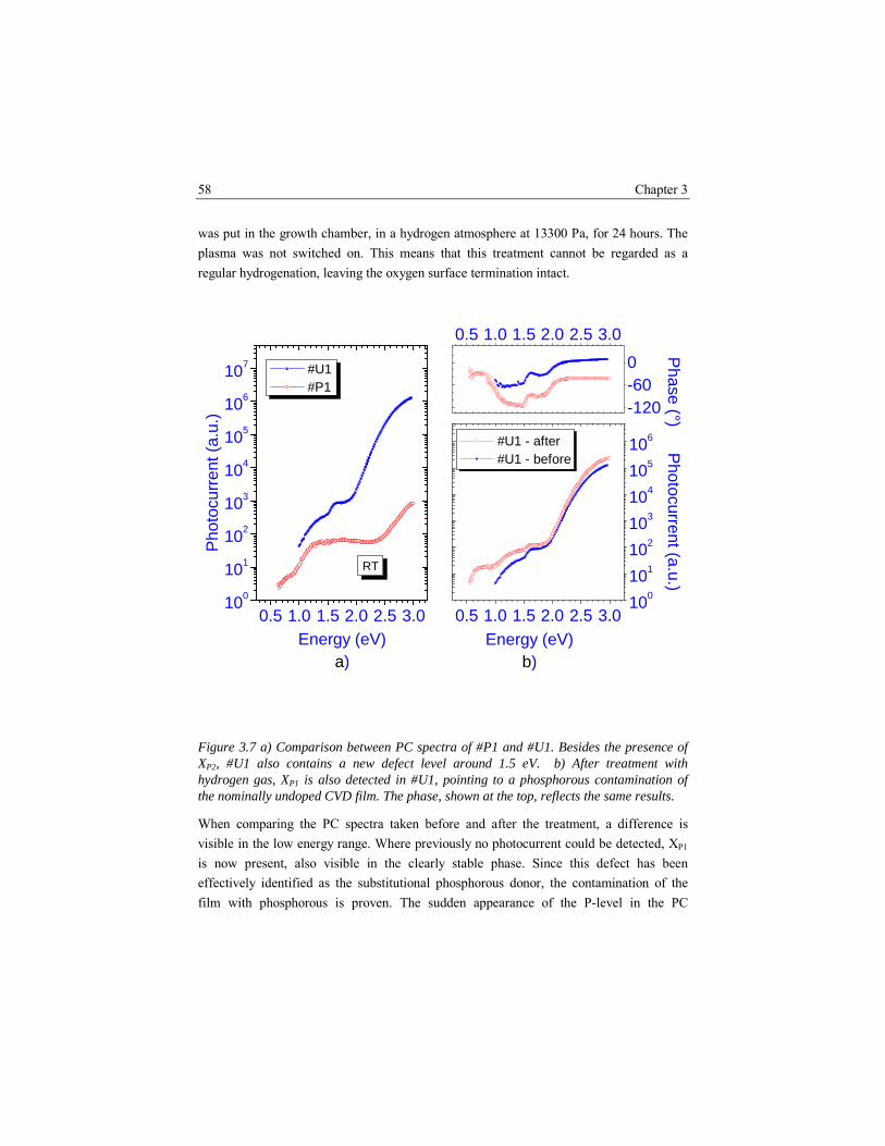
58 Chapter 3
was put in the growth chamber, in a hydrogen atmosphere at 13300 Pa, for 24 hours. The plasma was not switched on. This means that this treatment cannot be regarded as a regular hydrogenation, leaving the oxygen surface termination intact.
Figure 3.7 a) Comparison between PC spectra of #P1 and #U1. Besides the presence of XP2, #U1 also contains a new defect level around 1.5 eV. b) After treatment with hydrogen gas, XP1 is also detected in #U1, pointing to a phosphorous contamination of the nominally undoped CVD film. The phase, shown at the top, reflects the same results.
When comparing the PC spectra taken before and after the treatment, a difference is visible in the low energy range. Where previously no photocurrent could be detected, XP1 is now present, also visible in the clearly stable phase. Since this defect has been effectively identified as the substitutional phosphorous donor, the contamination of the film with phosphorous is proven. The sudden appearance of the P-level in the PC
0.5 1.0 1.5 2.0 2.5 3.0100
101
102
103
104
105
106
107
RT
#U1 #P1
Phot
ocur
rent
(a.u
.)
Energy (eV)a)
0.5 1.0 1.5 2.0 2.5 3.0100
101
102
103
104
105
106
Photocurrent (a.u.)
#U1 - after #U1 - before
Energy (eV)b)
0.5 1.0 1.5 2.0 2.5 3.0
-120-600
Phase (°)
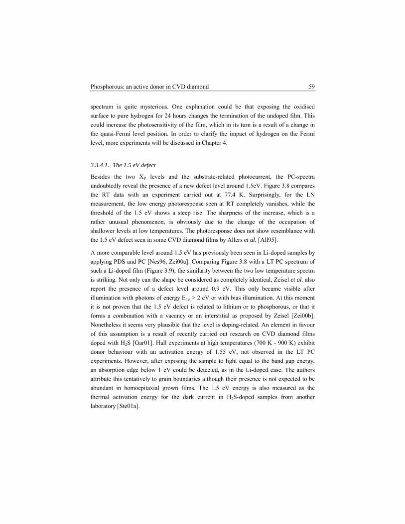
Phosphorous: an active donor in CVD diamond 59
spectrum is quite mysterious. One explanation could be that exposing the oxidised surface to pure hydrogen for 24 hours changes the termination of the undoped film. This could increase the photosensitivity of the film, which in its turn is a result of a change in the quasi-Fermi level position. In order to clarify the impact of hydrogen on the Fermi level, more experiments will be discussed in Chapter 4.
3.3.4.1. The 1.5 eV defect
Besides the two XP levels and the substrate-related photocurrent, the PC-spectra undoubtedly reveal the presence of a new defect level around 1.5eV. Figure 3.8 compares the RT data with an experiment carried out at 77.4 K. Surprisingly, for the LN measurement, the low energy photoresponse seen at RT completely vanishes, while the threshold of the 1.5 eV shows a steep rise. The sharpness of the increase, which is a rather unusual phenomenon, is obviously due to the change of the occupation of shallower levels at low temperatures. The photoresponse does not show resemblance with the 1.5 eV defect seen in some CVD diamond films by Allers et al. [All95].
A more comparable level around 1.5 eV has previously been seen in Li-doped samples by applying PDS and PC [Nes96, Zei00a]. Comparing Figure 3.8 with a LT PC spectrum of such a Li-doped film (Figure 3.9), the similarity between the two low temperature spectra is striking. Not only can the shape be considered as completely identical, Zeisel et al. also report the presence of a defect level around 0.9 eV. This only became visible after illumination with photons of energy Ehν > 2 eV or with bias illumination. At this moment it is not proven that the 1.5 eV defect is related to lithium or to phosphorous, or that it forms a combination with a vacancy or an interstitial as proposed by Zeisel [Zei00b]. Nonetheless it seems very plausible that the level is doping-related. An element in favour of this assumption is a result of recently carried out research on CVD diamond films doped with H2S [Gar01]. Hall experiments at high temperatures (700 K - 900 K) exhibit donor behaviour with an activation energy of 1.55 eV, not observed in the LT PC experiments. However, after exposing the sample to light equal to the band gap energy, an absorption edge below 1 eV could be detected, as in the Li-doped case. The authors attribute this tentatively to grain boundaries although their presence is not expected to be abundant in homoepitaxial grown films. The 1.5 eV energy is also measured as the thermal activation energy for the dark current in H2S-doped samples from another laboratory [Ste01a].
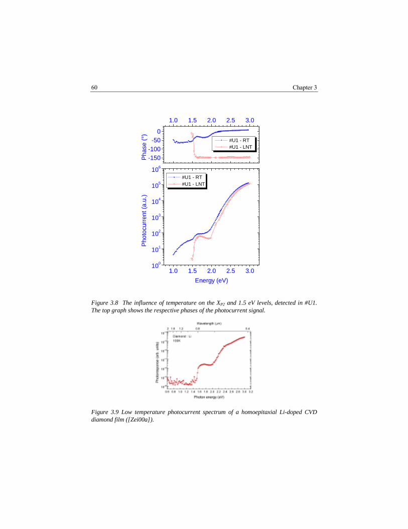
60 Chapter 3
1.0 1.5 2.0 2.5 3.0100
101
102
103
104
105
106
#U1 - RT #U1 - LNT
Phot
ocur
rent
(a.u
.)
Energy (eV)
-150-100-50
0
1.0 1.5 2.0 2.5 3.0
#U1 - RT #U1 - LNT
Phas
e (°
)
Figure 3.8 The influence of temperature on the XP2 and 1.5 eV levels, detected in #U1. The top graph shows the respective phases of the photocurrent signal.
Figure 3.9 Low temperature photocurrent spectrum of a homoepitaxial Li-doped CVD diamond film ([Zei00a]).
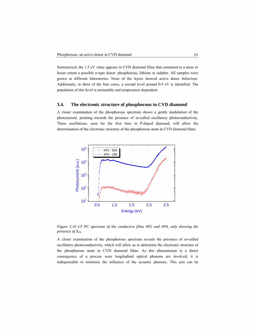
Phosphorous: an active donor in CVD diamond 61
Summarised, the 1.5 eV value appears in CVD diamond films that contained to a more or lesser extent a possible n-type donor: phosphorous, lithium or sulphur. All samples were grown at different laboratories. None of the layers showed active donor behaviour. Additionaly, in three of the four cases, a second level around 0.9 eV is identified. The population of this level is metastable and temperature dependent.
3.4. The electronic structure of phosphorous in CVD diamond A closer examination of the phosphorous spectrum shows a gentle modulation of the photocurrent, pointing towards the presence of so-called oscillatory photoconductivity. These oscillations, seen for the first time in P-doped diamond, will allow the determination of the electronic structure of the phosphorous atom in CVD diamond films.
0.5 1.0 1.5 2.0 2.5101
102
103
104
105
#P2 - 50K #P4 - 20K
Phot
ocur
rent
(a.u
.)
Energy (eV)
Figure 3.10 LT PC spectrum of the conductive films #P2 and #P4, only showing the presence of XP1.
A closer examination of the phosphorous spectrum reveals the presence of so-called oscillatory photoconductivity, which will allow us to determine the electronic structure of the phosphorous atom in CVD diamond films. As this phenomenon is a direct consequence of a process were longitudinal optical phonons are involved, it is indispensable to minimise the influence of the acoustic phonons. This aim can be
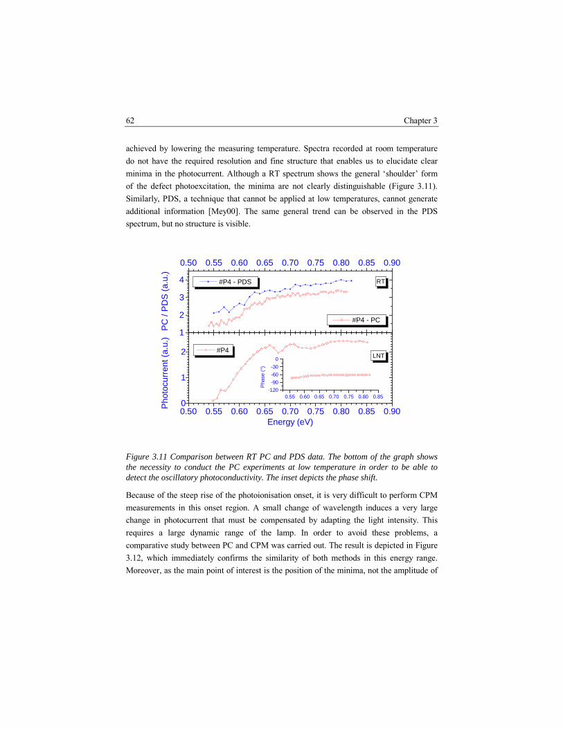
62 Chapter 3
achieved by lowering the measuring temperature. Spectra recorded at room temperature do not have the required resolution and fine structure that enables us to elucidate clear minima in the photocurrent. Although a RT spectrum shows the general ‘shoulder’ form of the defect photoexcitation, the minima are not clearly distinguishable (Figure 3.11). Similarly, PDS, a technique that cannot be applied at low temperatures, cannot generate additional information [Mey00]. The same general trend can be observed in the PDS spectrum, but no structure is visible.
0.50 0.55 0.60 0.65 0.70 0.75 0.80 0.85 0.900
1
2 #P4
Phot
ocur
rent
(a.u
.)
Energy (eV)
0.55 0.60 0.65 0.70 0.75 0.80 0.85-120-90-60-30
0
Pha
se (°
)
1
2
3
4
0.50 0.55 0.60 0.65 0.70 0.75 0.80 0.85 0.90
#P4 - PDS
PC /
PDS
(a.u
.)
LNT
RT
#P4 - PC
Figure 3.11 Comparison between RT PC and PDS data. The bottom of the graph shows the necessity to conduct the PC experiments at low temperature in order to be able to detect the oscillatory photoconductivity. The inset depicts the phase shift.
Because of the steep rise of the photoionisation onset, it is very difficult to perform CPM measurements in this onset region. A small change of wavelength induces a very large change in photocurrent that must be compensated by adapting the light intensity. This requires a large dynamic range of the lamp. In order to avoid these problems, a comparative study between PC and CPM was carried out. The result is depicted in Figure 3.12, which immediately confirms the similarity of both methods in this energy range. Moreover, as the main point of interest is the position of the minima, not the amplitude of
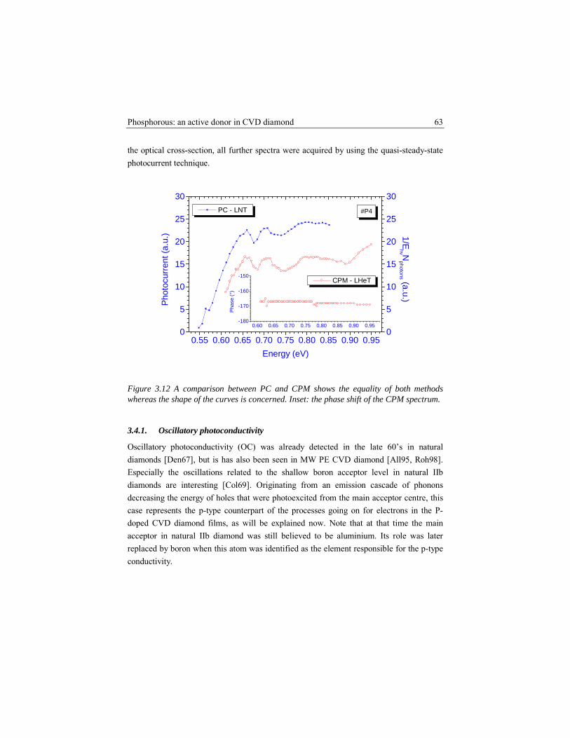
Phosphorous: an active donor in CVD diamond 63
the optical cross-section, all further spectra were acquired by using the quasi-steady-state photocurrent technique.
0.55 0.60 0.65 0.70 0.75 0.80 0.85 0.90 0.950
5
10
15
20
25
30#P4
CPM - LHeT
Phot
ocur
rent
(a.u
.)
Energy (eV)
0
5
10
15
20
25
30 PC - LNT
1/Ehν N
photons (a.u.)
0.60 0.65 0.70 0.75 0.80 0.85 0.90 0.95-180
-170
-160
-150
Phas
e (°
)
Figure 3.12 A comparison between PC and CPM shows the equality of both methods whereas the shape of the curves is concerned. Inset: the phase shift of the CPM spectrum.
3.4.1. Oscillatory photoconductivity
Oscillatory photoconductivity (OC) was already detected in the late 60’s in natural diamonds [Den67], but is has also been seen in MW PE CVD diamond [All95, Roh98]. Especially the oscillations related to the shallow boron acceptor level in natural IIb diamonds are interesting [Col69]. Originating from an emission cascade of phonons decreasing the energy of holes that were photoexcited from the main acceptor centre, this case represents the p-type counterpart of the processes going on for electrons in the P-doped CVD diamond films, as will be explained now. Note that at that time the main acceptor in natural IIb diamond was still believed to be aluminium. Its role was later replaced by boron when this atom was identified as the element responsible for the p-type conductivity.
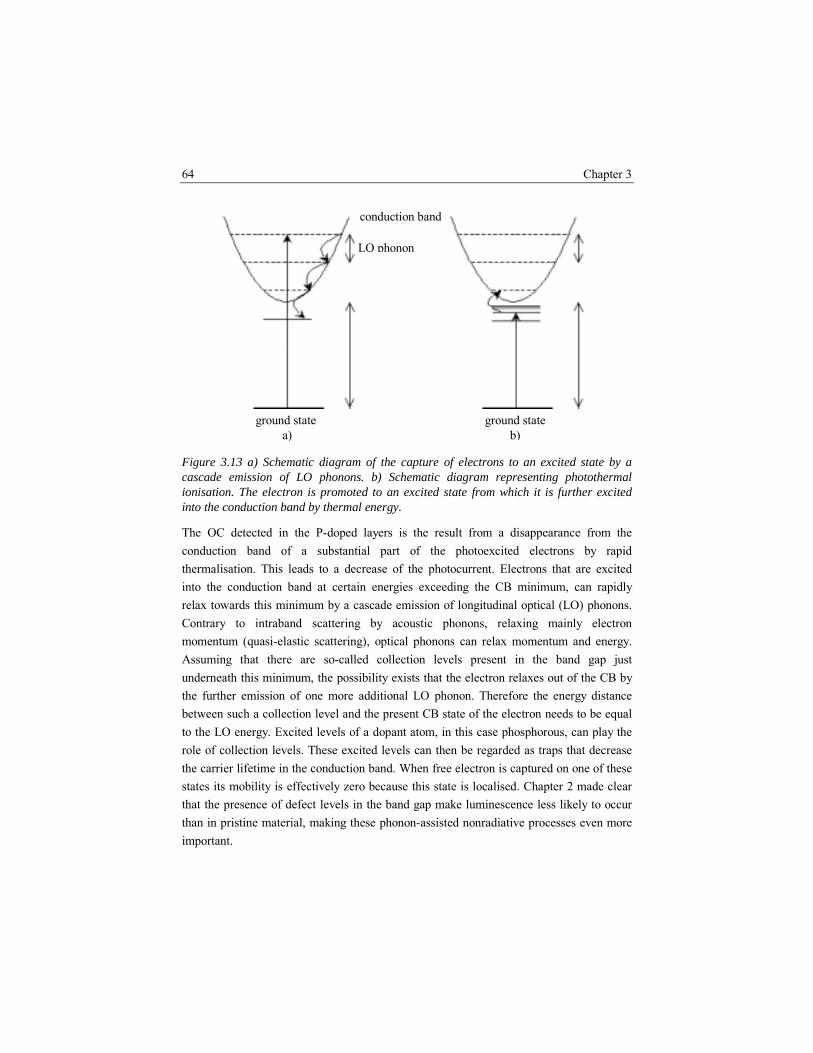
64 Chapter 3
Figure 3.13 a) Schematic diagram of the capture of electrons to an excited state by a cascade emission of LO phonons. b) Schematic diagram representing photothermal ionisation. The electron is promoted to an excited state from which it is further excited into the conduction band by thermal energy.
The OC detected in the P-doped layers is the result from a disappearance from the conduction band of a substantial part of the photoexcited electrons by rapid thermalisation. This leads to a decrease of the photocurrent. Electrons that are excited into the conduction band at certain energies exceeding the CB minimum, can rapidly relax towards this minimum by a cascade emission of longitudinal optical (LO) phonons. Contrary to intraband scattering by acoustic phonons, relaxing mainly electron momentum (quasi-elastic scattering), optical phonons can relax momentum and energy. Assuming that there are so-called collection levels present in the band gap just underneath this minimum, the possibility exists that the electron relaxes out of the CB by the further emission of one more additional LO phonon. Therefore the energy distance between such a collection level and the present CB state of the electron needs to be equal to the LO energy. Excited levels of a dopant atom, in this case phosphorous, can play the role of collection levels. These excited levels can then be regarded as traps that decrease the carrier lifetime in the conduction band. When free electron is captured on one of these states its mobility is effectively zero because this state is localised. Chapter 2 made clear that the presence of defect levels in the band gap make luminescence less likely to occur than in pristine material, making these phonon-assisted nonradiative processes even more important.
LO phonon
ground state a)
ground state b)
conduction band
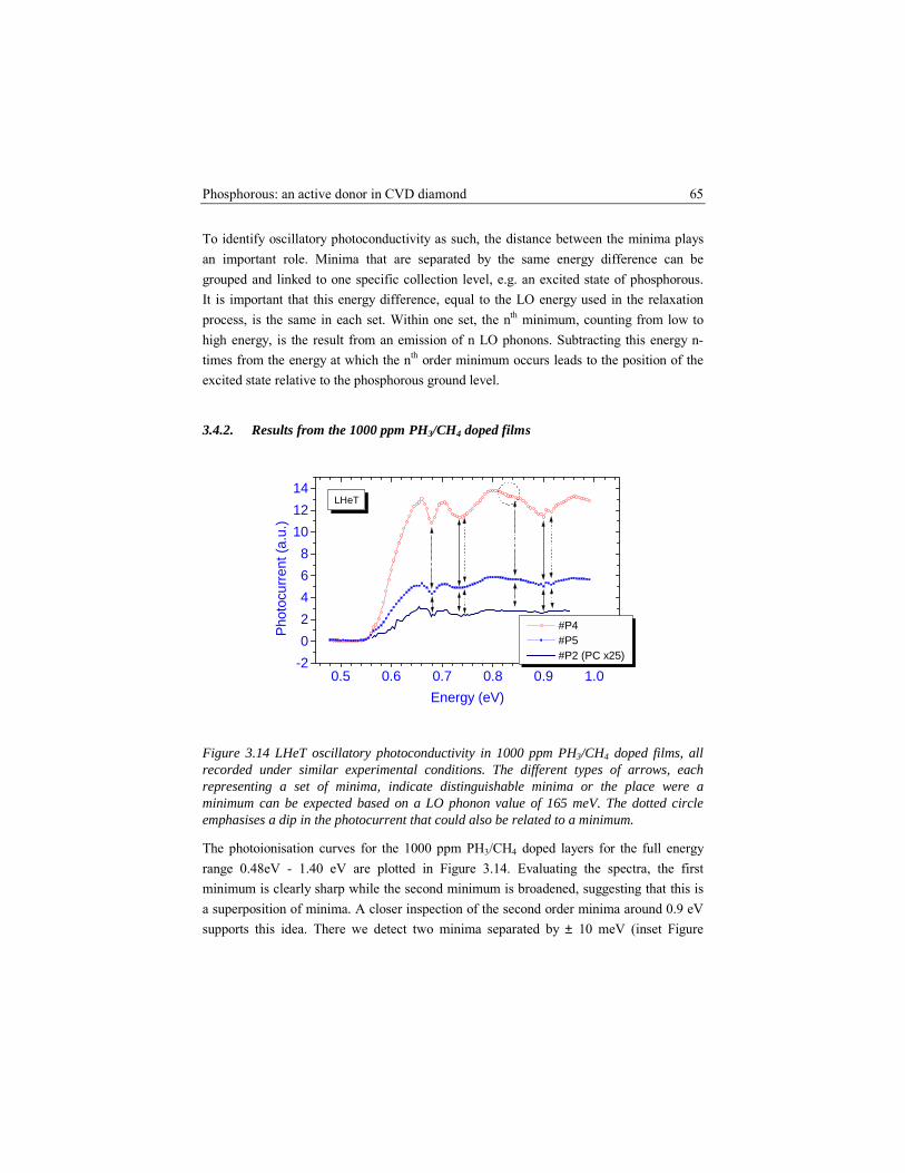
Phosphorous: an active donor in CVD diamond 65
To identify oscillatory photoconductivity as such, the distance between the minima plays an important role. Minima that are separated by the same energy difference can be grouped and linked to one specific collection level, e.g. an excited state of phosphorous. It is important that this energy difference, equal to the LO energy used in the relaxation process, is the same in each set. Within one set, the nth minimum, counting from low to high energy, is the result from an emission of n LO phonons. Subtracting this energy n-times from the energy at which the nth order minimum occurs leads to the position of the excited state relative to the phosphorous ground level.
3.4.2. Results from the 1000 ppm PH3/CH4 doped films
0.5 0.6 0.7 0.8 0.9 1.0-202468
101214
LHeT
#P4 #P5 #P2 (PC x25)
Phot
ocur
rent
(a.u
.)
Energy (eV)
Figure 3.14 LHeT oscillatory photoconductivity in 1000 ppm PH3/CH4 doped films, all recorded under similar experimental conditions. The different types of arrows, each representing a set of minima, indicate distinguishable minima or the place were a minimum can be expected based on a LO phonon value of 165 meV. The dotted circle emphasises a dip in the photocurrent that could also be related to a minimum.
The photoionisation curves for the 1000 ppm PH3/CH4 doped layers for the full energy range 0.48eV - 1.40 eV are plotted in Figure 3.14. Evaluating the spectra, the first minimum is clearly sharp while the second minimum is broadened, suggesting that this is a superposition of minima. A closer inspection of the second order minima around 0.9 eV supports this idea. There we detect two minima separated by ± 10 meV (inset Figure
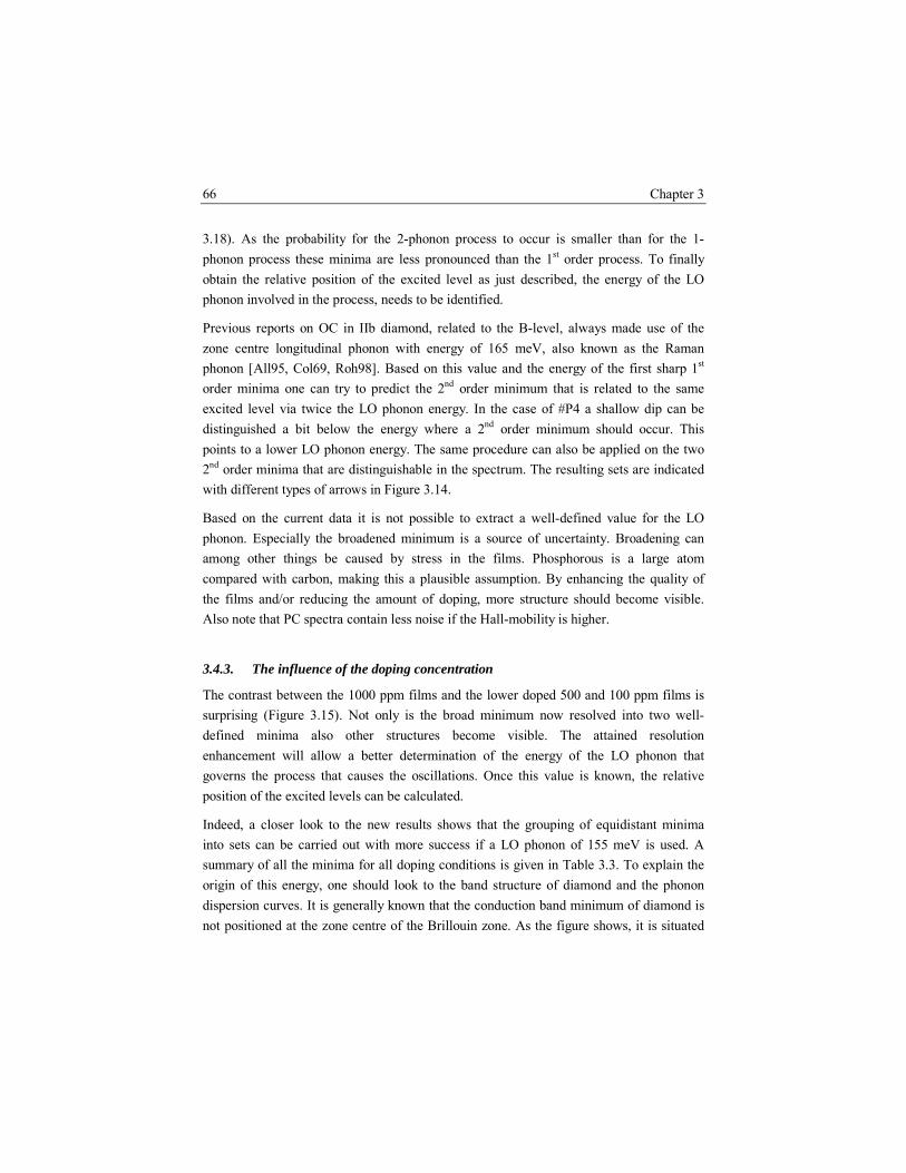
66 Chapter 3
3.18). As the probability for the 2-phonon process to occur is smaller than for the 1-phonon process these minima are less pronounced than the 1st order process. To finally obtain the relative position of the excited level as just described, the energy of the LO phonon involved in the process, needs to be identified.
Previous reports on OC in IIb diamond, related to the B-level, always made use of the zone centre longitudinal phonon with energy of 165 meV, also known as the Raman phonon [All95, Col69, Roh98]. Based on this value and the energy of the first sharp 1st order minima one can try to predict the 2nd order minimum that is related to the same excited level via twice the LO phonon energy. In the case of #P4 a shallow dip can be distinguished a bit below the energy where a 2nd order minimum should occur. This points to a lower LO phonon energy. The same procedure can also be applied on the two 2nd order minima that are distinguishable in the spectrum. The resulting sets are indicated with different types of arrows in Figure 3.14.
Based on the current data it is not possible to extract a well-defined value for the LO phonon. Especially the broadened minimum is a source of uncertainty. Broadening can among other things be caused by stress in the films. Phosphorous is a large atom compared with carbon, making this a plausible assumption. By enhancing the quality of the films and/or reducing the amount of doping, more structure should become visible. Also note that PC spectra contain less noise if the Hall-mobility is higher.
3.4.3. The influence of the doping concentration
The contrast between the 1000 ppm films and the lower doped 500 and 100 ppm films is surprising (Figure 3.15). Not only is the broad minimum now resolved into two well-defined minima also other structures become visible. The attained resolution enhancement will allow a better determination of the energy of the LO phonon that governs the process that causes the oscillations. Once this value is known, the relative position of the excited levels can be calculated.
Indeed, a closer look to the new results shows that the grouping of equidistant minima into sets can be carried out with more success if a LO phonon of 155 meV is used. A summary of all the minima for all doping conditions is given in Table 3.3. To explain the origin of this energy, one should look to the band structure of diamond and the phonon dispersion curves. It is generally known that the conduction band minimum of diamond is not positioned at the zone centre of the Brillouin zone. As the figure shows, it is situated
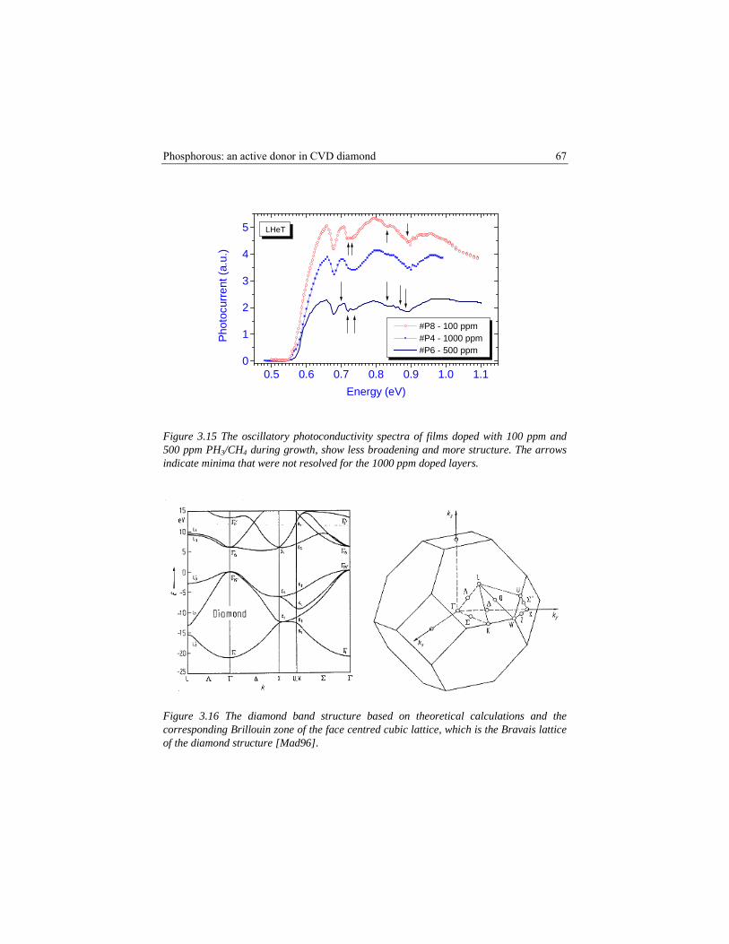
Phosphorous: an active donor in CVD diamond 67
0.5 0.6 0.7 0.8 0.9 1.0 1.10
1
2
3
4
5 LHeT
#P8 - 100 ppm #P4 - 1000 ppm #P6 - 500 ppm
Phot
ocur
rent
(a.u
.)
Energy (eV)
Figure 3.15 The oscillatory photoconductivity spectra of films doped with 100 ppm and 500 ppm PH3/CH4 during growth, show less broadening and more structure. The arrows indicate minima that were not resolved for the 1000 ppm doped layers.
Figure 3.16 The diamond band structure based on theoretical calculations and the corresponding Brillouin zone of the face centred cubic lattice, which is the Bravais lattice of the diamond structure [Mad96].
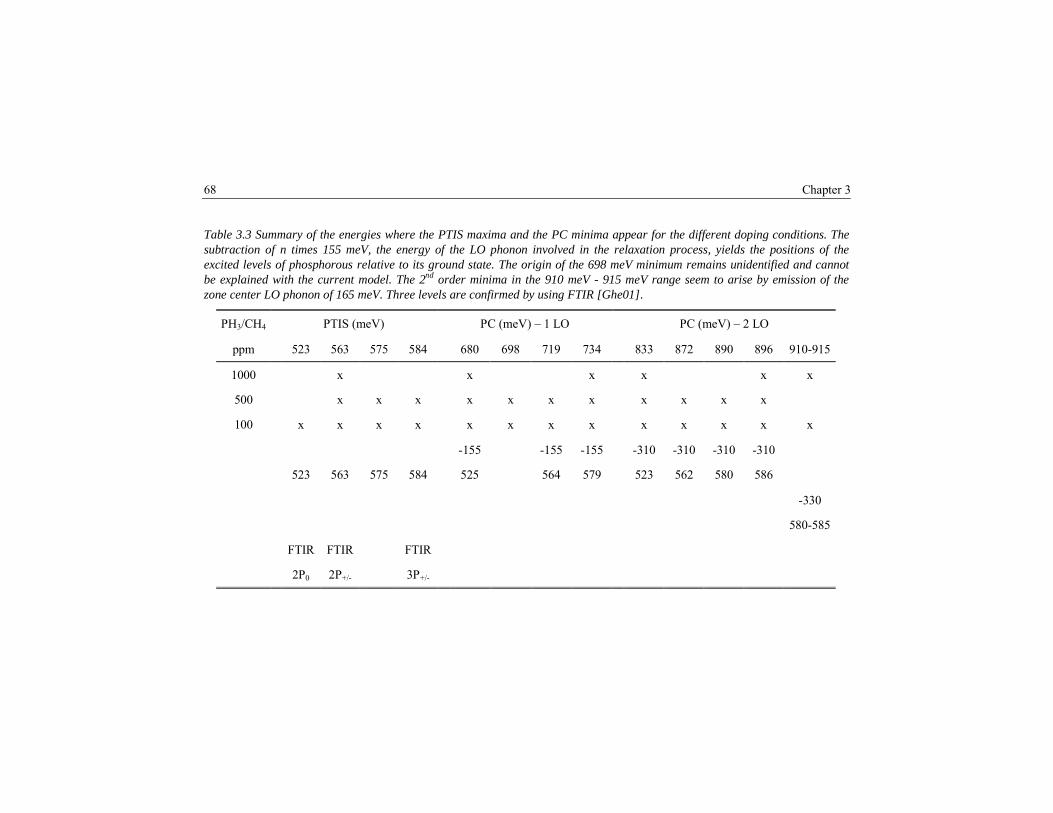
68 Chapter 3
Table 3.3 Summary of the energies where the PTIS maxima and the PC minima appear for the different doping conditions. The subtraction of n times 155 meV, the energy of the LO phonon involved in the relaxation process, yields the positions of the excited levels of phosphorous relative to its ground state. The origin of the 698 meV minimum remains unidentified and cannot be explained with the current model. The 2nd order minima in the 910 meV - 915 meV range seem to arise by emission of the zone center LO phonon of 165 meV. Three levels are confirmed by using FTIR [Ghe01].
PH3/CH4 PTIS (meV) PC (meV) – 1 LO PC (meV) – 2 LO
ppm 523 563 575 584 680 698 719 734 833 872 890 896 910-915
1000 x x x x x x
500 x x x x x x x x x x x
100 x x x x x x x x x x x x x
-155 -155 -155 -310 -310 -310 -310
523 563 575 584 525 564 579 523 562 580 586
-330
580-585
FTIR FTIR FTIR
2P0 2P+/- 3P+/-
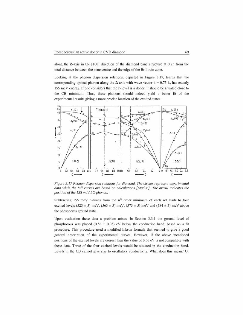
Phosphorous: an active donor in CVD diamond 69
along the ∆-axis in the [100] direction of the diamond band structure at 0.75 from the total distance between the zone centre and the edge of the Brillouin zone.
Looking at the phonon dispersion relations, depicted in Figure 3.17, learns that the corresponding optical phonon along the ∆-axis with wave vector k = 0.75 k0 has exactly 155 meV energy. If one considers that the P-level is a donor, it should be situated close to the CB minimum. Thus, these phonons should indeed yield a better fit of the experimental results giving a more precise location of the excited states.
Figure 3.17 Phonon dispersion relations for diamond. The circles represent experimental data while the full curves are based on calculations [Mad96]. The arrow indicates the position of the 155 meV LO phonon.
Subtracting 155 meV n-times from the nth order minimum of each set leads to four excited levels (523 ± 5) meV, (563 ± 5) meV, (575 ± 5) meV and (584 ± 5) meV above the phosphorus ground state.
Upon evaluation these data a problem arises. In Section 3.3.1 the ground level of phosphorous was placed (0.56 ± 0.03) eV below the conduction band, based on a fit procedure. This procedure used a modified Inkson formula that seemed to give a good general description of the experimental curves. However, if the above mentioned positions of the excited levels are correct then the value of 0.56 eV is not compatible with these data. Three of the four excited levels would be situated in the conduction band. Levels in the CB cannot give rise to oscillatory conductivity. What does this mean? Or
70 Chapter 3
the ground level is deeper than the fit hints, or the oscillations find their origin in another process. A closer look to the data in Figure 3.18 demonstrate that the Inkson formula gives a good fit for the rising edge of the photoionisation but problems arise at higher energies. This difficulty was encountered for all experiments that were carried out at low temperature (4.2 K to 170 K) and gave rise to measurable oscillatory photoconductivity. The Inkson model does not take into account this OC, making it ambiguous to draw conclusions from the fit at higher energies. Moreover, a distinct sharp maximum around 563 meV is detected (see inset Figure 3.18) in all LT spectra. This peak is modulating the rising edge of the ground level optical cross-section making the modelling of the data even more difficult. These two elements create an uncertainty on the gathered data. Together with complementary data from PTIS and FTIR that will discussed in the next sections, it will undeniably become clear that the ground level is indeed deeper into the band gap and is situated about 0.6 eV under the CB. This is slightly above the upper limit of the result (0.56 ± 0.03 meV) from the fitting of the rising edge of the photoconductivity as discussed in Section 3.3.1.
The spectra of the 500 ppm sample undoubtedly exhibit the best defined minima. The enhanced quality of the spectra for the lower doped films can be due to a better film quality with less stress, resulting in less broadening of the defect levels in the band gap. A confirmation of this quality is given by Koizumi et al. [Koi00a] who reported that the highest measured room temperature Hall-mobility was measured for films deposited under 500 ppm conditions. At that time this value was 240 cm2 V-1 s-1, but in the meanwhile values around 450 cm2 V-1 s-1 can be attained [Koi02]. It is concluded that the incorporation of a large amount of phosphorous indeed deteriorates the crystalline perfection and thus also efficient carrier transport in the diamond films. This can account for the lower mobility values and the fact that the minima are more broadened in the 1000 ppm films. However, at PH3/CH4 = 100 ppm, the Hall mobility is about 30 cm2 V-1 s-1. This means that besides the phosphorous concentration another factor plays a crucial role. This lower value may be the effect of trapping of electrons at defects not related to phosphorous that decrease the mobility [Koi00a]. The carrier density from Hall measurements is about two orders lower than that for 1000 pm. However, a smaller Hall-mobility does not necessarily mean that the photocurrent signal is also worse. Therefore the µτ-product needs to be taken into account. When investigating the influence of the applied electric field in Section 3.4.5 it will be shown that the 100 ppm film gives the best photocurrent signal, pointing to a higher lifetime of the charge carriers.
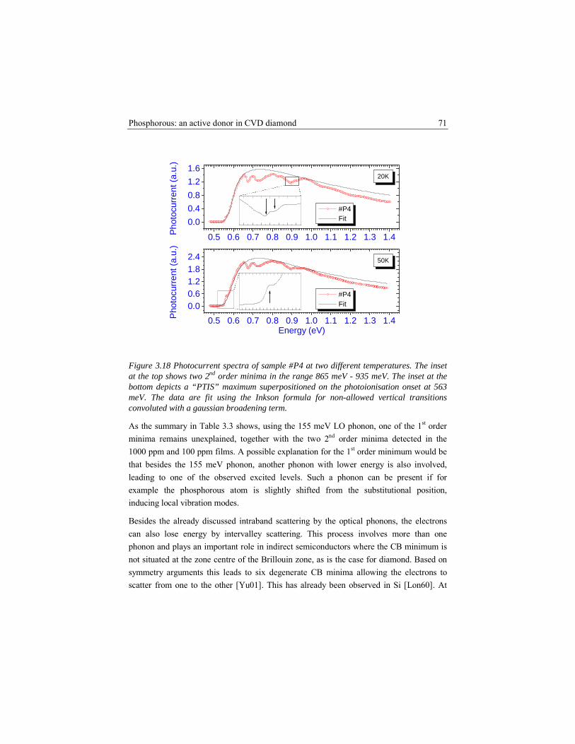
Phosphorous: an active donor in CVD diamond 71
0.5 0.6 0.7 0.8 0.9 1.0 1.1 1.2 1.3 1.40.00.61.21.82.4 50K
#P4 Fit
Phot
ocur
rent
(a.u
.)
Energy (eV)
0.5 0.6 0.7 0.8 0.9 1.0 1.1 1.2 1.3 1.4
0.00.40.81.21.6
20K
#P4 Fit
Phot
ocur
rent
(a.u
.)
Figure 3.18 Photocurrent spectra of sample #P4 at two different temperatures. The inset at the top shows two 2nd order minima in the range 865 meV - 935 meV. The inset at the bottom depicts a “PTIS” maximum superpositioned on the photoionisation onset at 563 meV. The data are fit using the Inkson formula for non-allowed vertical transitions convoluted with a gaussian broadening term.
As the summary in Table 3.3 shows, using the 155 meV LO phonon, one of the 1st order minima remains unexplained, together with the two 2nd order minima detected in the 1000 ppm and 100 ppm films. A possible explanation for the 1st order minimum would be that besides the 155 meV phonon, another phonon with lower energy is also involved, leading to one of the observed excited levels. Such a phonon can be present if for example the phosphorous atom is slightly shifted from the substitutional position, inducing local vibration modes.
Besides the already discussed intraband scattering by the optical phonons, the electrons can also lose energy by intervalley scattering. This process involves more than one phonon and plays an important role in indirect semiconductors where the CB minimum is not situated at the zone centre of the Brillouin zone, as is the case for diamond. Based on symmetry arguments this leads to six degenerate CB minima allowing the electrons to scatter from one to the other [Yu01]. This has already been observed in Si [Lon60]. At
72 Chapter 3
this stage it is only possible to say that in principle it is very probable that intervalley scattering also occurs in P-doped n-type diamond but no phonon values can be derived.
The shift to higher energies of some of the 2nd order minima in the 1000 ppm and 100 ppm films is not easy to explain, especially for the 100 ppm films, were these minima are not really shifted but appear next to the minima that do fit well in the proposed model. To lead to one of the four excited states, the use of a higher phonon energy than 155 meV must be considered. It is not clear why the 2nd order process should make use of two phonons with different energy. A change in phonon energy during the cascade has already been observed for boron-doped films. Contrary to the CB minimum, the valence band maximum is situated at the zone centre and the cascade emission makes use of the zone centre LO phonon of 165 meV. It was observed that the energy separating the higher order minima, resulting from a multiple phonon relaxation, decreased as more phonons were involved. Looking in E-k-space and taking into account the curvature of the valence band, if the initial hole state is deep in the valence band, it is no longer situated at the zone centre. Consequently a larger dissipation of momentum is required for this route to occur. This results in a decrease of the energy of the phonon used in the process [Roh98]. This argumentation can also be applied to the n-type case. Bearing in mind that the position of 155 meV phonon in the phonon dispersion curves corresponds to the position of the CB minimum in the band gap diagram, an electron state shifted from the CB minimum would also induce a shift in the phonon value. This can lead to an increase or a decrease of the phonon energy. On the other hand, the boron-related OC shows up to 15 phonon replica whereby the phonon energy is slowly reduced leading to an average value of 161 meV [Col69, Roh98]. Thus it seems very unlikely that this explains a difference of 10 meV in phonon energy for the P-doped films. Again, stress and the presence of impurities can play a major role by inducing a change in position of the levels, even locally influencing the band structure. To finally clear this matter the detection of higher order minima is required.
3.4.4. Detection of the excited states of phosphorous with PTIS
The previous sections only dealt with photocurrents that are the result of the direct excitation of charge carriers from the phosphorous ground state into the conduction band. These transitions are purely the result of optical excitation. In addition to this one-step transition, a two-step process is also possible by combining optical and thermal energy. As Figure 3.13 makes clear schematically, the first part of the transition process is
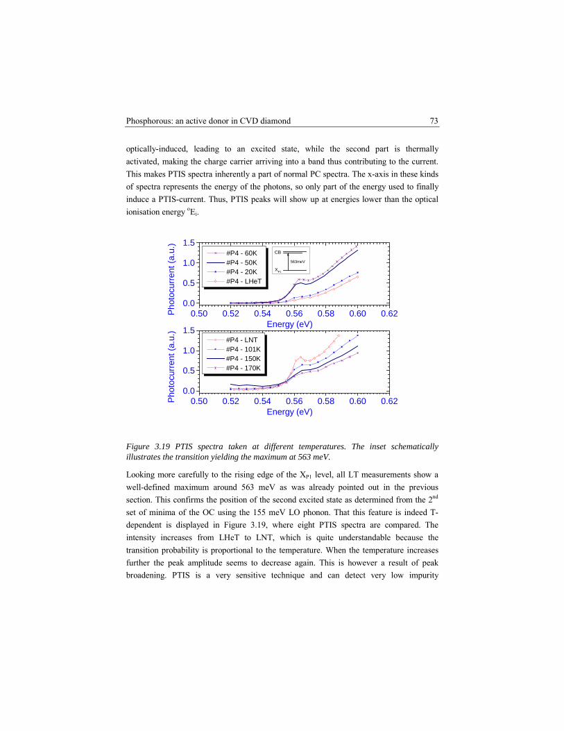
Phosphorous: an active donor in CVD diamond 73
optically-induced, leading to an excited state, while the second part is thermally activated, making the charge carrier arriving into a band thus contributing to the current. This makes PTIS spectra inherently a part of normal PC spectra. The x-axis in these kinds of spectra represents the energy of the photons, so only part of the energy used to finally induce a PTIS-current. Thus, PTIS peaks will show up at energies lower than the optical ionisation energy oEi.
0.50 0.52 0.54 0.56 0.58 0.60 0.620.0
0.5
1.0
1.5
#P4 - 60K #P4 - 50K #P4 - 20K #P4 - LHeT
Phot
ocur
rent
(a.u
.)
Energy (eV)
0.50 0.52 0.54 0.56 0.58 0.60 0.620.0
0.5
1.0
1.5
#P4 - LNT #P4 - 101K #P4 - 150K #P4 - 170K
Phot
ocur
rent
(a.u
.)
Energy (eV)
563meV
XP1
CB
Figure 3.19 PTIS spectra taken at different temperatures. The inset schematically illustrates the transition yielding the maximum at 563 meV.
Looking more carefully to the rising edge of the XP1 level, all LT measurements show a well-defined maximum around 563 meV as was already pointed out in the previous section. This confirms the position of the second excited state as determined from the 2nd set of minima of the OC using the 155 meV LO phonon. That this feature is indeed T-dependent is displayed in Figure 3.19, where eight PTIS spectra are compared. The intensity increases from LHeT to LNT, which is quite understandable because the transition probability is proportional to the temperature. When the temperature increases further the peak amplitude seems to decrease again. This is however a result of peak broadening. PTIS is a very sensitive technique and can detect very low impurity
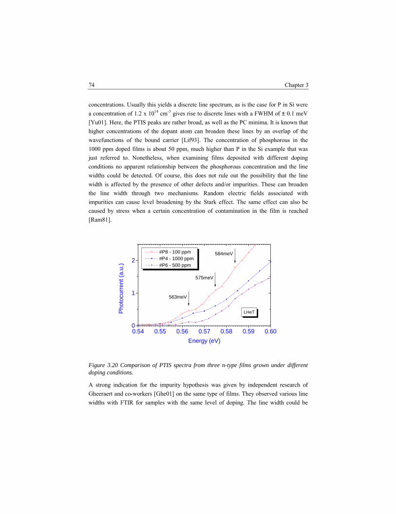
74 Chapter 3
concentrations. Usually this yields a discrete line spectrum, as is the case for P in Si were a concentration of 1.2 x 1014 cm-3 gives rise to discrete lines with a FWHM of ± 0.1 meV [Yu01]. Here, the PTIS peaks are rather broad, as well as the PC minima. It is known that higher concentrations of the dopant atom can broaden these lines by an overlap of the wavefunctions of the bound carrier [Lif93]. The concentration of phosphorous in the 1000 ppm doped films is about 50 ppm, much higher than P in the Si example that was just referred to. Nonetheless, when examining films deposited with different doping conditions no apparent relationship between the phosphorous concentration and the line widths could be detected. Of course, this does not rule out the possibility that the line width is affected by the presence of other defects and/or impurities. These can broaden the line width through two mechanisms. Random electric fields associated with impurities can cause level broadening by the Stark effect. The same effect can also be caused by stress when a certain concentration of contamination in the film is reached [Ram81].
0.54 0.55 0.56 0.57 0.58 0.59 0.600
1
2
575meV
584meV
563meV
LHeT
#P8 - 100 ppm #P4 - 1000 ppm #P6 - 500 ppm
Phot
ocur
rent
(a.u
.)
Energy (eV)
Figure 3.20 Comparison of PTIS spectra from three n-type films grown under different doping conditions.
A strong indication for the impurity hypothesis was given by independent research of Gheeraert and co-workers [Ghe01] on the same type of films. They observed various line widths with FTIR for samples with the same level of doping. The line width could be
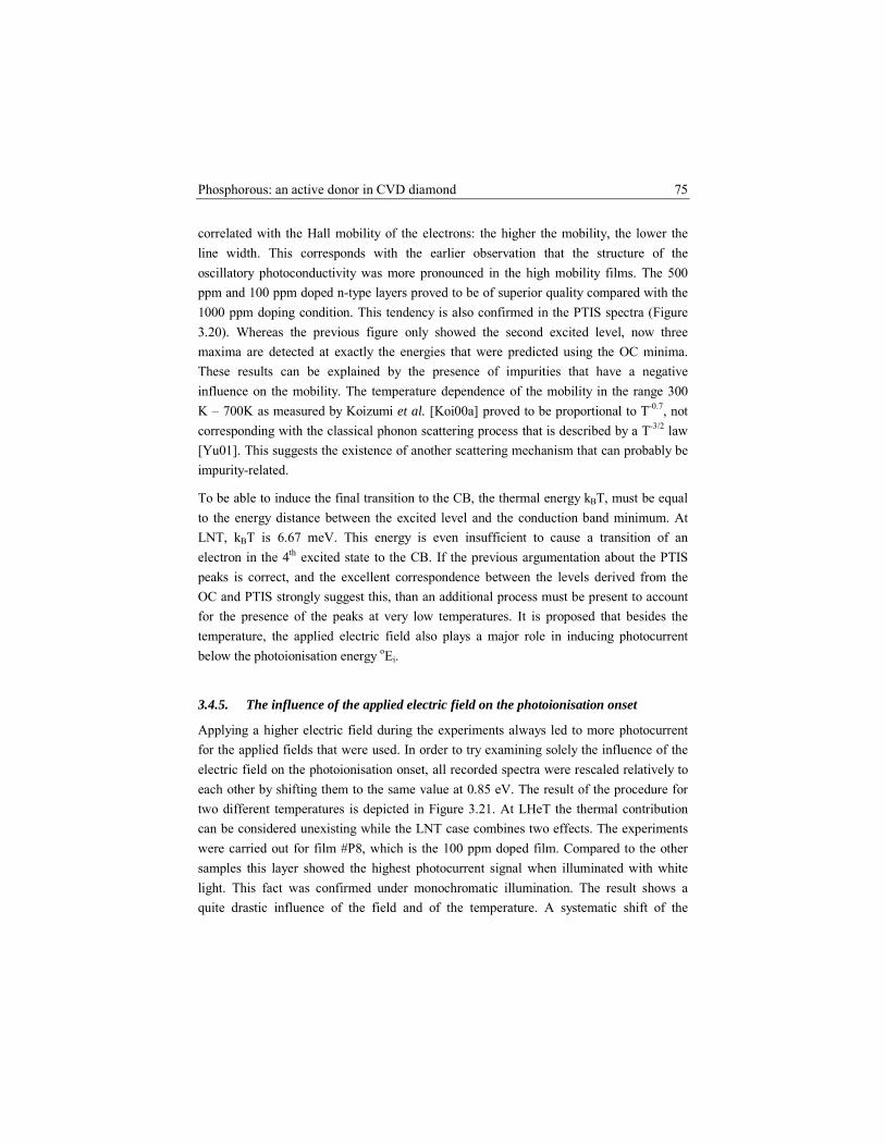
Phosphorous: an active donor in CVD diamond 75
correlated with the Hall mobility of the electrons: the higher the mobility, the lower the line width. This corresponds with the earlier observation that the structure of the oscillatory photoconductivity was more pronounced in the high mobility films. The 500 ppm and 100 ppm doped n-type layers proved to be of superior quality compared with the 1000 ppm doping condition. This tendency is also confirmed in the PTIS spectra (Figure 3.20). Whereas the previous figure only showed the second excited level, now three maxima are detected at exactly the energies that were predicted using the OC minima. These results can be explained by the presence of impurities that have a negative influence on the mobility. The temperature dependence of the mobility in the range 300 K – 700K as measured by Koizumi et al. [Koi00a] proved to be proportional to T-0.7, not corresponding with the classical phonon scattering process that is described by a T-3/2 law [Yu01]. This suggests the existence of another scattering mechanism that can probably be impurity-related.
To be able to induce the final transition to the CB, the thermal energy kBT, must be equal to the energy distance between the excited level and the conduction band minimum. At LNT, kBT is 6.67 meV. This energy is even insufficient to cause a transition of an electron in the 4th excited state to the CB. If the previous argumentation about the PTIS peaks is correct, and the excellent correspondence between the levels derived from the OC and PTIS strongly suggest this, than an additional process must be present to account for the presence of the peaks at very low temperatures. It is proposed that besides the temperature, the applied electric field also plays a major role in inducing photocurrent below the photoionisation energy oEi.
3.4.5. The influence of the applied electric field on the photoionisation onset
Applying a higher electric field during the experiments always led to more photocurrent for the applied fields that were used. In order to try examining solely the influence of the electric field on the photoionisation onset, all recorded spectra were rescaled relatively to each other by shifting them to the same value at 0.85 eV. The result of the procedure for two different temperatures is depicted in Figure 3.21. At LHeT the thermal contribution can be considered unexisting while the LNT case combines two effects. The experiments were carried out for film #P8, which is the 100 ppm doped film. Compared to the other samples this layer showed the highest photocurrent signal when illuminated with white light. This fact was confirmed under monochromatic illumination. The result shows a quite drastic influence of the field and of the temperature. A systematic shift of the
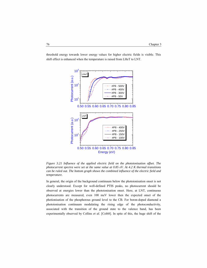
76 Chapter 3
threshold energy towards lower energy values for higher electric fields is visible. This shift effect is enhanced when the temperature is raised from LHeT to LNT.
0.50 0.55 0.60 0.65 0.70 0.75 0.80 0.85
101
102LNT
#P8 - 400V #P8 - 250V #P8 - 150V #P8 - 100V
Phot
ocur
rent
(a.u
.)
Energy (eV)
0.50 0.55 0.60 0.65 0.70 0.75 0.80 0.85
101
102
103
LHeT
#P8 - 500V #P8 - 400V #P8 - 300V #P8 - 50V
Phot
ocur
rent
(a.u
.)
Figure 3.21 Influence of the applied electric field on the photoionisation offset. The photocurrent spectra were set at the same value at 0.85 eV. At 4.2 K thermal transitions can be ruled out. The bottom graph shows the combined influence of the electric field and temperature.
In general, the origin of the background continuum below the photoionisation onset is not clearly understood. Except for well-defined PTIS peaks, no photocurrent should be observed at energies lower than the photoionisation onset. Here, at LNT, continuous photocurrents are measured, even 100 meV lower then the expected onset of the photionisation of the phosphorous ground level to the CB. For boron-doped diamond a photoionisation continuum modulating the rising edge of the photoconductivity, associated with the transition of the ground state to the valence band, has been experimentally observed by Collins et al. [Col68]. In spite of this, the huge shift of the
Phosphorous: an active donor in CVD diamond 77
photocurrent onset was not observed for that case, where only a slight broadening of the peaks with high electric fields is observed.
0.50 0.52 0.54 0.56 0.58 0.600.0
0.1
0.2
0.3
0.4
0.5
575meV584meV
523meV
563meV
LNT
#P8 - 500V #P8 - 400VPh
otoc
urre
nt (a
.u.)
Energy (eV)
Figure 3.22 Film #P8 allowed to measure the first excited level of phosphorous using PTIS. The position that was determined from the oscillatory photoconductivity is confirmed.
One can speculate about the effect responsible for the presence of the peaks even at 4.2 K. An electric field-dependent process assisting the photoelectron in an excited level to shift to the conduction path can be, for example quantummechanical tunnelling. As noted in the previous section, the line widths are doping independent, excluding the overlap of wavefunctions due to high doping of phosphorous. However, the overlap of states and the generation of a band rather than a very sharp level could be due to the presence of perturbed centres and strain. This is a common phenomenon in many semiconductors. It is known that the lifetime of an electron in an excited state is higher in case of an unperturbed centre. PTIS will preferentially select those donors [Col68], but under influence of high electric fields, the electron may tunnel to the excited states of neighboring perturbed centres. Although PIXE measurements confirmed that the substitutional fraction of phosphorus was more than 0.9 for <011> and <111> directions [Has01], phosphorous is very hard to incorporate in the 100 growth sectors as was already mentioned. This built up stress together with defect rich regions can induce
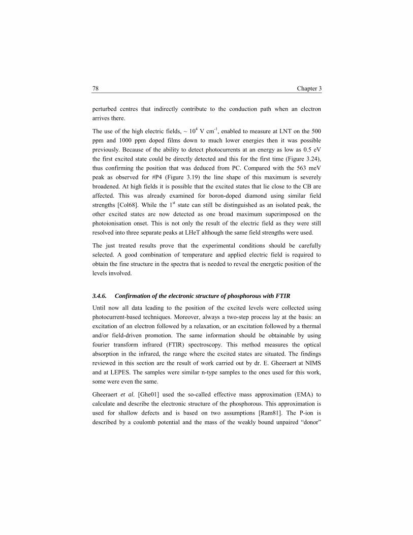
78 Chapter 3
perturbed centres that indirectly contribute to the conduction path when an electron arrives there.
The use of the high electric fields, ~ 104 V cm-1, enabled to measure at LNT on the 500 ppm and 1000 ppm doped films down to much lower energies then it was possible previously. Because of the ability to detect photocurrents at an energy as low as 0.5 eV the first excited state could be directly detected and this for the first time (Figure 3.24), thus confirming the position that was deduced from PC. Compared with the 563 meV peak as observed for #P4 (Figure 3.19) the line shape of this maximum is severely broadened. At high fields it is possible that the excited states that lie close to the CB are affected. This was already examined for boron-doped diamond using similar field strengths [Col68]. While the 1st state can still be distinguished as an isolated peak, the other excited states are now detected as one broad maximum superimposed on the photoionisation onset. This is not only the result of the electric field as they were still resolved into three separate peaks at LHeT although the same field strengths were used.
The just treated results prove that the experimental conditions should be carefully selected. A good combination of temperature and applied electric field is required to obtain the fine structure in the spectra that is needed to reveal the energetic position of the levels involved.
3.4.6. Confirmation of the electronic structure of phosphorous with FTIR
Until now all data leading to the position of the excited levels were collected using photocurrent-based techniques. Moreover, always a two-step process lay at the basis: an excitation of an electron followed by a relaxation, or an excitation followed by a thermal and/or field-driven promotion. The same information should be obtainable by using fourier transform infrared (FTIR) spectroscopy. This method measures the optical absorption in the infrared, the range where the excited states are situated. The findings reviewed in this section are the result of work carried out by dr. E. Gheeraert at NIMS and at LEPES. The samples were similar n-type samples to the ones used for this work, some were even the same.
Gheeraert et al. [Ghe01] used the so-called effective mass approximation (EMA) to calculate and describe the electronic structure of the phosphorous. This approximation is used for shallow defects and is based on two assumptions [Ram81]. The P-ion is described by a coulomb potential and the mass of the weakly bound unpaired “donor”
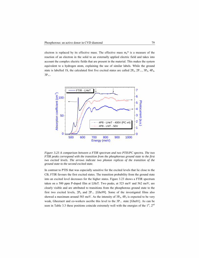
Phosphorous: an active donor in CVD diamond 79
electron is replaced by its effective mass. The effective mass me* is a measure of the reaction of an electron in the solid to an externally applied electric field and takes into account the complex electric fields that are present in the material. This makes the system equivalent to a hydrogen atom, explaining the use of similar labels. While the ground state is labelled 1S, the calculated first five excited states are called 2P0, 2P+/-, 3P0, 4P0, 3P+/-.
500 600 700 800 900 10000
50
100
FTIR - LHeT
Abso
rptio
n co
effic
ient
(cm
-1)
Energy (meV)
0
1
2
3
4
5
6
7
#P8 - LHeT - 400V (PC x4) #P8 - LNT - 50V
Photocurrent (a.u.)
Figure 3.23 A comparison between a FTIR spectrum and two PTIS/PC spectra. The two FTIR peaks correspond with the transition from the phosphorous ground state to the first two excited levels. The arrows indicate two phonon replicas of the transition of the ground state to the second excited state.
In contrast to PTIS that was especially sensitive for the excited levels that lie close to the CB, FTIR favours the first excited states. The transition probability from the ground state into an excited level decreases for the higher states. Figure 3.23 shows a FTIR spectrum taken on a 500 ppm P-doped film at LHeT. Two peaks, at 523 meV and 562 meV, are clearly visible and are attributed to transitions from the phosphorous ground state to the first two excited levels, 2P0 and 2P+/- [Ghe99]. Some of the investigated films also showed a maximum around 583 meV. As the intensity of 3P0, 4P0 is expected to be very weak, Gheeraert and co-workers ascribe this level to the 3P+/- state [Ghe01]. As can be seen in Table 3.3 these positions coincide extremely well with the energies of the 1st, 2nd
80 Chapter 3
and 4th excited states as deduced from the PC and PTIS results. At this moment it is not clear to which EMA level the 575 meV level corresponds. As the relevant PTIS peak is broad and the OC yields values with an uncertainty of a few meV, it is possible that the 575 meV level is a superposition of both predicted 3P0 and 4P0 EMA states.
Although the EMA gives a very good description of the excited states, the energy of the ground level relative to the closest band is usually underestimated. While the calculation predicts the P-ground level to be 218 meV under the CB, experiments point out that this level is situated around 600 meV, a value considerably deeper. Present observations imply that the deep level of phosphorus in diamond is attributed to the relaxation of surrounding carbon atoms of the network around the P atom [Has01].
0
50
100
450475500525550575600
600 meV
523 meV
584 meV575 meV
563 meV
P
CB
Ener
gy (m
eV)
Figure 3.24 The electronic structure of phosphorous in n-type CVD diamond based on the results from PC and PTIS experiments and as confirmed by FTIR.
In addition to the just explained absorption peaks, the FTIR spectrum shows also two maxima at higher energies. These maxima are separated by approximately 152 meV, which is approximately the value of the LO phonon that is involved in the OC (Section 3.4.3). The two maxima are attributed to phonon replicas of the transition of the ground state to the second excited state combined with the creation of one and two LO phonons
Phosphorous: an active donor in CVD diamond 81
[Ghe01]. The observation of this process, which can be considered as the opposite of the one giving rise to the oscillatory photoconductivity, hereby independently confirms the validity of the use of the 155 meV LO phonon.
It is also worth noting that the io EE− dependence, which is typical for the optical
photoionisation cross-section σo for shallow impurities [Boë90], does not describe the photocurrent results. Thus, although the photoionisation spectra have the typical form that is known to appear in case of a deep defect, the electronic structure of the excited states on the other hand can be calculated by the EMA, which points to a shallow nature for the phosphorous level. A similar type of defect, combining characteristics from both defect classes has already been observed and is for example In in Si [Sch82].
In conclusion Figure 3.24 gives a picture of the electronic structure of the phosphorous atom in n-type CVD diamond based on the results from PC, PTIS and FTIR.
3.5. Results from the 100-oriented P-doped film The first photocurrent data of a thin P-doped diamond film deposited homoepitaxially on a 100 oriented Ib diamond film are given in Figure 3.25. The sample was almost insulating and almost no photocurrent signal could be obtained. Hence, the presented experimental result should be treated with care and considered as very preliminary.
Only a photoionisation with an onset at about 0.85 eV is present. At higher energies the photocurrent drops below the detection level of the set-up, to appear again around 2.2 eV. This last feature is again the rising edge of the photoionisation for substitutional nitrogen, originating from the substrate absorption. It should be noted that our first measurements on 111 oriented films #P1 and #P3 also showed a peak at ± 0.85 eV, reported as the XP2 defect. These samples were also highly resistive. This suggests that the P atom might be incorporated in another configuration than the substitutional position, not leading to good conductive properties. Activation energy measurements on different 100 layers, carried out at NIMS yielded two different values: ± 0.82 eV and ± 1.41 eV [Ter00a]. The first corresponds to the XP2 defect, while the second can tentatively be related to the defect discussed in Section 3.3.4.1. In general, Hall measurements on 100 samples show a much lower mobility value (~ 10 cm2 V-1 s-1) than is observed for the optimised case for 111 substrates [Koi00a]. This suggests a necessary optimisation for 100 growth to reach the current level of 111 films with mobilities over 400 cm2 V-1 s-1.
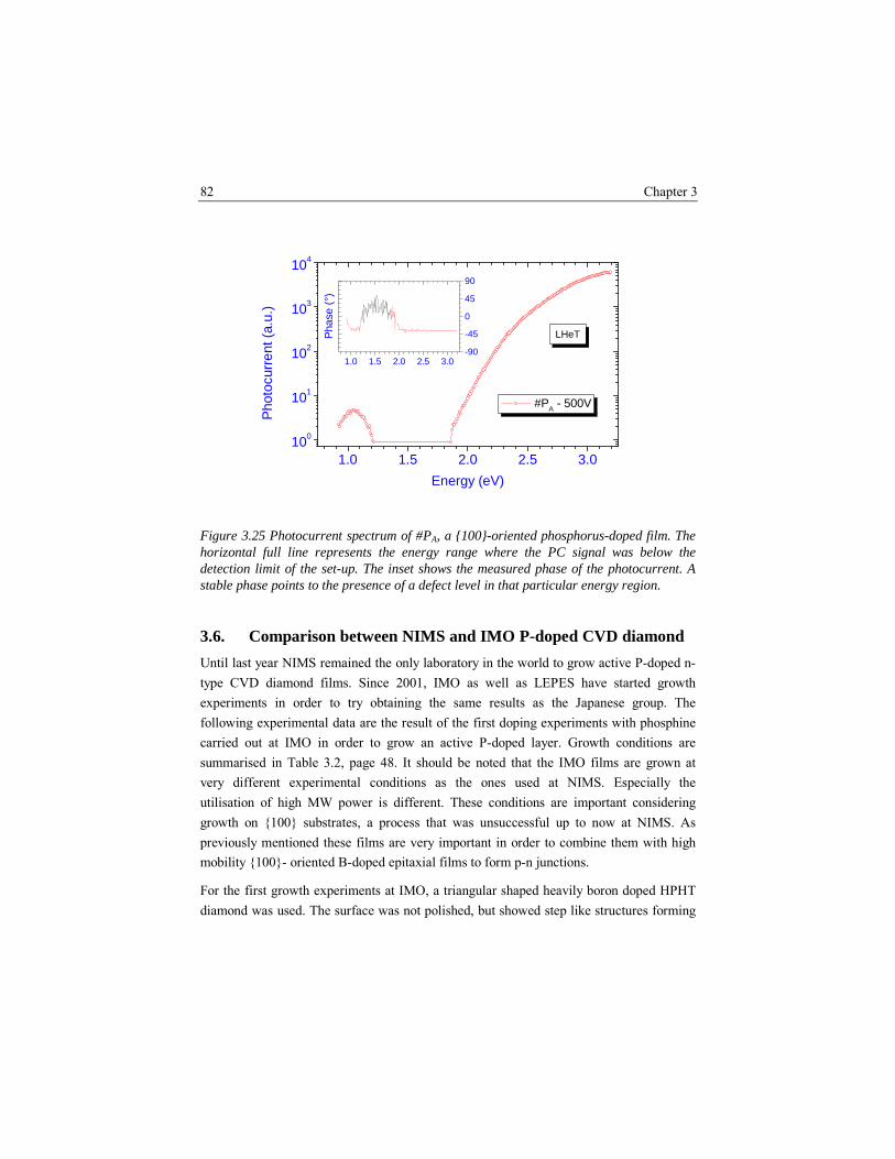
82 Chapter 3
1.0 1.5 2.0 2.5 3.0-90
-45
0
45
90
Phas
e (°
)
1.0 1.5 2.0 2.5 3.0100
101
102
103
104
LHeT
#PA - 500V
Phot
ocur
rent
(a.u
.)
Energy (eV)
Figure 3.25 Photocurrent spectrum of #PA, a 100-oriented phosphorus-doped film. The horizontal full line represents the energy range where the PC signal was below the detection limit of the set-up. The inset shows the measured phase of the photocurrent. A stable phase points to the presence of a defect level in that particular energy region.
3.6. Comparison between NIMS and IMO P-doped CVD diamond Until last year NIMS remained the only laboratory in the world to grow active P-doped n-type CVD diamond films. Since 2001, IMO as well as LEPES have started growth experiments in order to try obtaining the same results as the Japanese group. The following experimental data are the result of the first doping experiments with phosphine carried out at IMO in order to grow an active P-doped layer. Growth conditions are summarised in Table 3.2, page 48. It should be noted that the IMO films are grown at very different experimental conditions as the ones used at NIMS. Especially the utilisation of high MW power is different. These conditions are important considering growth on 100 substrates, a process that was unsuccessful up to now at NIMS. As previously mentioned these films are very important in order to combine them with high mobility 100- oriented B-doped epitaxial films to form p-n junctions.
For the first growth experiments at IMO, a triangular shaped heavily boron doped HPHT diamond was used. The surface was not polished, but showed step like structures forming
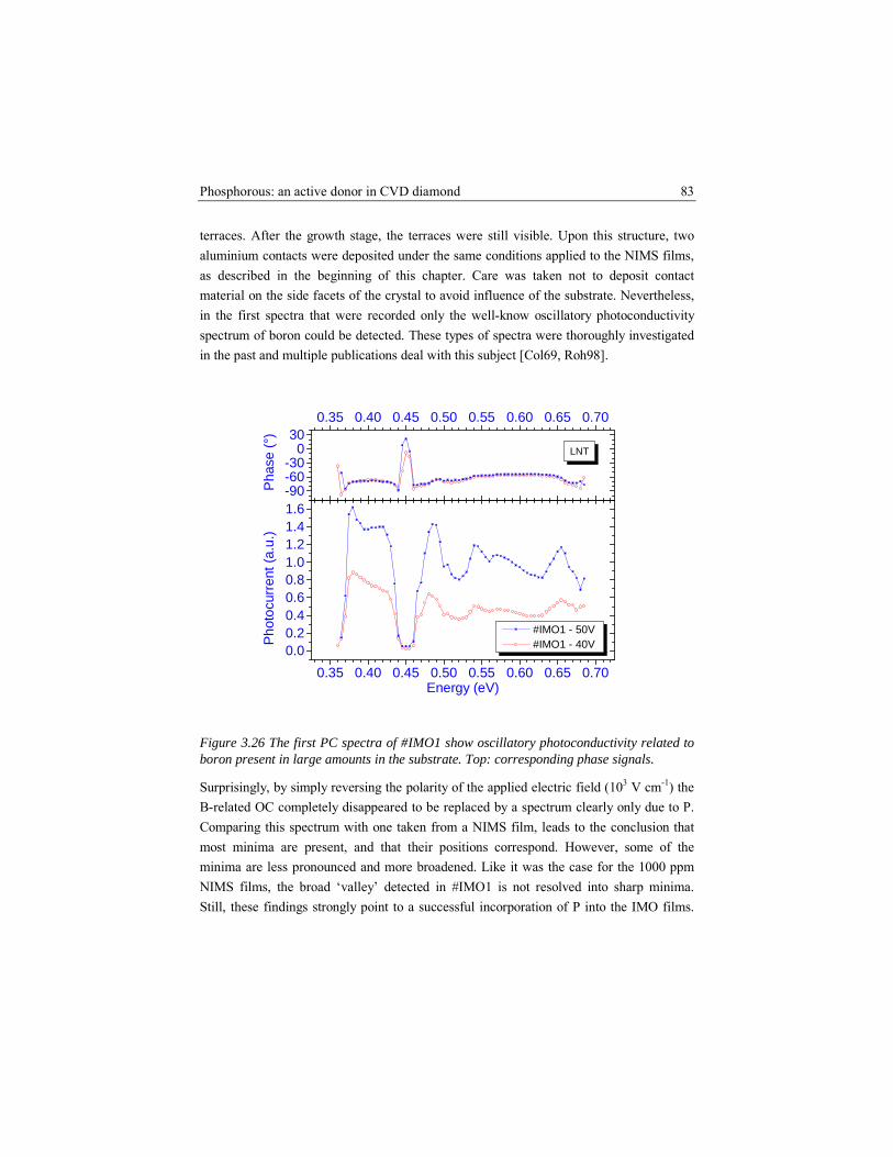
Phosphorous: an active donor in CVD diamond 83
terraces. After the growth stage, the terraces were still visible. Upon this structure, two aluminium contacts were deposited under the same conditions applied to the NIMS films, as described in the beginning of this chapter. Care was taken not to deposit contact material on the side facets of the crystal to avoid influence of the substrate. Nevertheless, in the first spectra that were recorded only the well-know oscillatory photoconductivity spectrum of boron could be detected. These types of spectra were thoroughly investigated in the past and multiple publications deal with this subject [Col69, Roh98].
0.35 0.40 0.45 0.50 0.55 0.60 0.65 0.700.00.20.40.60.81.01.21.41.6
Phot
ocur
rent
(a.u
.)
Energy (eV)
-90-60-30
030
0.35 0.40 0.45 0.50 0.55 0.60 0.65 0.70
LNT
#IMO1 - 50V #IMO1 - 40V
Phas
e (°
)
Figure 3.26 The first PC spectra of #IMO1 show oscillatory photoconductivity related to boron present in large amounts in the substrate. Top: corresponding phase signals.
Surprisingly, by simply reversing the polarity of the applied electric field (103 V cm-1) the B-related OC completely disappeared to be replaced by a spectrum clearly only due to P. Comparing this spectrum with one taken from a NIMS film, leads to the conclusion that most minima are present, and that their positions correspond. However, some of the minima are less pronounced and more broadened. Like it was the case for the 1000 ppm NIMS films, the broad ‘valley’ detected in #IMO1 is not resolved into sharp minima. Still, these findings strongly point to a successful incorporation of P into the IMO films.
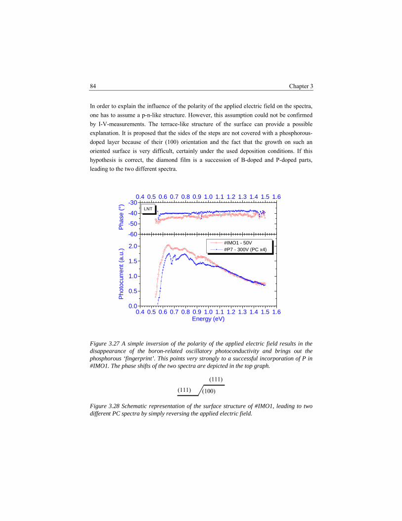
84 Chapter 3
In order to explain the influence of the polarity of the applied electric field on the spectra, one has to assume a p-n-like structure. However, this assumption could not be confirmed by I-V-measurements. The terrace-like structure of the surface can provide a possible explanation. It is proposed that the sides of the steps are not covered with a phosphorous-doped layer because of their (100) orientation and the fact that the growth on such an oriented surface is very difficult, certainly under the used deposition conditions. If this hypothesis is correct, the diamond film is a succession of B-doped and P-doped parts, leading to the two different spectra.
0.4 0.5 0.6 0.7 0.8 0.9 1.0 1.1 1.2 1.3 1.4 1.5 1.60.0
0.5
1.0
1.5
2.0
Phot
ocur
rent
(a.u
.)
Energy (eV)
-60-50-40
-300.4 0.5 0.6 0.7 0.8 0.9 1.0 1.1 1.2 1.3 1.4 1.5 1.6
LNT
#IMO1 - 50V #P7 - 300V (PC x4)
Phas
e (°
)
Figure 3.27 A simple inversion of the polarity of the applied electric field results in the disappearance of the boron-related oscillatory photoconductivity and brings out the phosphorous ‘fingerprint’. This points very strongly to a successful incorporation of P in #IMO1. The phase shifts of the two spectra are depicted in the top graph.
Figure 3.28 Schematic representation of the surface structure of #IMO1, leading to two different PC spectra by simply reversing the applied electric field.
(100)
(111)
(111)
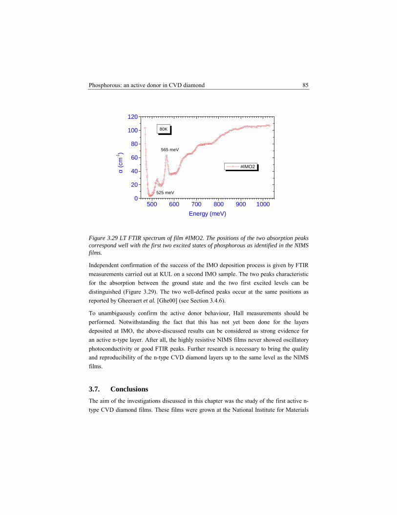
Phosphorous: an active donor in CVD diamond 85
500 600 700 800 900 10000
20
40
60
80
100
120
565 meV
525 meV
Energy (meV)
80K
#IMO2
α (c
m-1)
Figure 3.29 LT FTIR spectrum of film #IMO2. The positions of the two absorption peaks correspond well with the first two excited states of phosphorous as identified in the NIMS films.
Independent confirmation of the success of the IMO deposition process is given by FTIR measurements carried out at KUL on a second IMO sample. The two peaks characteristic for the absorption between the ground state and the two first excited levels can be distinguished (Figure 3.29). The two well-defined peaks occur at the same positions as reported by Gheeraert et al. [Ghe00] (see Section 3.4.6).
To unambiguously confirm the active donor behaviour, Hall measurements should be performed. Notwithstanding the fact that this has not yet been done for the layers deposited at IMO, the above-discussed results can be considered as strong evidence for an active n-type layer. After all, the highly resistive NIMS films never showed oscillatory photoconductivity or good FTIR peaks. Further research is necessary to bring the quality and reproducibility of the n-type CVD diamond layers up to the same level as the NIMS films.
3.7. Conclusions The aim of the investigations discussed in this chapter was the study of the first active n-type CVD diamond films. These films were grown at the National Institute for Materials
86 Chapter 3
Science in Japan by adding phosphine to the gas mixture used in MW PE CVD process.
Using quasi-steady-state photocurrent measurements two new defect levels could be detected. These were labelled XP1 and XP2. The first level was attributed to the substitutional phosphorous donor with the ground level situated 0.6 eV under the conduction band. The origin of XP2, a defect with a photoionisation onset around 0.81 eV, remains unidentified up to now. This defect is only detected in highly resistive films and it is claimed that its presence deteriorates the quality of the conductive properties of the layer. Besides the possibility that the defect is phosphorous-related, also a link with a surface hydrogen-sensitive level was not ruled out.
In a nominally undoped film a defect level around 1.5 eV was detected. Based on this energy and the shape of the photocurrent spectrum at low temperature it was assumed that the same level was already observed in lithium-doped films. These films did not show any active n-type conductivity.
The improvement of the deposition system and growth parameters lead to P-doped films of better quality only showing the presence of the XP1 level. Low temperature experiments made it possible to detect oscillatory photoconductivity. This phenomenon was attributed to a disappearance of a substantial amount of photoexcited electrons out of the conduction band into collection levels situated in the band gap. This rapid thermalisation takes place by a cascade emission of LO phonons. The value of this phonon was established around 155 meV, its wave vector corresponding with the position of the conduction band minimum in the diamond band structure. Simultaneously, photothermal ionisation maxima were observed. A combination of these data led to the discovery of four collection levels. They were identified as excited states of phosphorous and positioned in the band gap at 523 meV, 563 meV, 575 meV and 584 meV relative to the ground level. Three of these positions were confirmed by independent research carried out with FTIR at NIMS and LEPES.
Although peaks were indicated as PTIS peaks, their presence at low temperature could only be explained by taking into account the applied electric field. Photocurrent was detected at energies up to 0.1 eV lower than the photoionisation onset related to the transition of an electron from the P-ground state to the conduction band. It was tentatively opted that the presence of stress and impurities in the film was responsible for this effect.
Preliminary results obtained on a 100-oriented P-doped film showed the presence of a
Phosphorous: an active donor in CVD diamond 87
defect level around 0.85 eV, which may be the same level previously labelled as XP2.
Experiments on the first n-type layers deposited at IMO showed promising results. Although the n-type conductivity was not confirmed by Hall effect measurements, PC and FTIR spectra are similar to the ones acquired from the NIMS films. This points strongly to a successful incorporation of the phosphorous atom in substitutional positions.
3.8. References [All95] L. Allers, A.T. Collins, J. Appl. Phys. 79/19 (1995), 3879.
[And93] A.B. Anderson, S.P. Mehandru, Phys. Rev. B 48/7 (1993) 4423.
[Ando96] T. Ando, H. Haneda, M. Akaishi, Y. Sato, M. Kamo, Diamond Relat. Mater. 5 (1996), 34.
[Boë90] K.W. Boër, Survey of Semiconductor Physics, Van Nostrand Reinhold, New York, 1990, p.1055.
[Cas00] N. Casanova, E. Gheeraert, A. Deneuville, C. Uzan-Saguy, R. Kalish, Phys. Stat. Sol. (a) 181/1 (2000), 5
[Col68] A.T.Collins, E.C. Lightowlers, Phys. Rev. 171/3 (1968), 843.
[Col69] A.T.Collins, E.C. Lightowlers, P.J. Dean, Phys. Rev. 183/3 (1969), 725.
[Den67] P. Denham, E.C. Lightowlers, P.J. Dean, Phys. Rev. 161/3 (1967), 762.
[Enc92] W.J.P. van Enckevort, E.H. Versteegen, J. Phys.: Condens. Matter 4 (1992), 2361.
[Gar01] J.A. Garrido, C.E. Nebel, M. Stutzmann, E. Gheeraert, N. Casanova, E. Bustarret, presented at the 12th European Conference on Diamond, Diamond-like Materials, Carbon Nanotubes, Nitrides and Silicon Carbide, Budapest Marriott Hotel, Budapest, Hungary, 2-7 September 2001, to be published in Diamond Relat. Mater. (2002).
[Ghe99] E. Gheeraert, S. Koizumi, T. Teraji, H. Kanda, M. Nesládek, Phys. Stat. Sol. (a) 174/1 (1999), 39.
[Ghe00] E. Gheeraert, S. Koizumi, T. Teraji, H. Kanda, M. Nesládek, Diamond Relat. Mater. 9 (2000), 948.
88 Chapter 3
[Ghe01] E. Gheeraert, N. Casanova, S. Koizumi, T. Teraji, H. Kanda, Diamond Relat. Mater. 10/3-7 (2001), 444.
[Has01] M. Hasegawa, T. Teraji, S. Koizumi, Appl. Phys. Lett. 79/19 (2001), 3068.
[Hen89] B. Henderson, G.F. Imbush, Optical Spectroscopy of Inorganic Solids, Clarendon Press, Oxford, 1998, p.201.
[Ink81] J.C. Inkson, J. Phys. C: Solid State Phys. 14 (1981), 1093.
[Jac90] K. Jackson, M.R. Pederson, J.G. Harrison, Phys. Rev. B 41/18 (1990), 12641.
[Kaj90] S.A. Kajihara, A. Antonelli, J. Bernholc, Mat. Res. Soc. Symp. Proc. 162 (1990), 315.
[Kaj93] S.A. Kajihara, A. Antonelli, J. Bernholc, Physica B 185 (1993), 144.
[Kal00] R. Kalish, A. Reznik, C. Uzan-Saguy, C. Cytermann, Appl. Phys. Lett. 76/6 (2000), 757.
[Kat01] H. Katayama-Yoshida, T. Nishimatsu, T. Yamamoto, N. Orita, J. Phys.: Condens. Matter 13/40 (2001), 8901.
[Koi97] S. Koizumi, M. Kamo, Y. Sato, H. Ozaki, T. Inuzuka, Appl. Phys. Lett. 71 (1997), 1065.
[Koi98] S. Koizumi, M. Kamo, Y. Sato, S. Mita, A. Sawaba, A. Reznik, C. Uzan-Saguy, R. Kalish, Diamond Relat. Mater. 7 (1998), 540.
[Koi00a] S. Koizumi, T. Teraji, H. Kanda, Diamond Relat. Mater. 9 (2000), 935.
[Koi00b] S. Koizumi, T. Teraji, H. Kanda, presented at the 11th European Conference on Diamond, Diamond-like Materials, Carbon Nanotubes, Nitrides and Silicon Carbide, Fundação Dr António Cupertino de Miranda, Porto, Portugal, 3-8 September 2000.
[Koi02] S. Koizumi, M. Nesladek, M. Katagiri, K. Watanabe, H. Kanda, presented at Surface and Bulk Defects in CVD Diamond Films, VII, Diepenbeek-Hasselt, Belgium, 13-15 March 2002.
[Lan89] M.I. Landstrass, K.V. Ravi, Appl. Phys. Lett. 55/10 (1989), 975; Appl. Phys. Lett. 55/14 (1989), 1391.
[Lif93] T.M. Lifshits, Instrum. Exp. Tech. 36/1 (1993), 1.
Phosphorous: an active donor in CVD diamond 89
[Lon60] D. Long, Phys. Rev. 120 (1960), 2024.
[Luc65] G. Lucovsky, Solid State Commun. 3 (1965), 299.
[Mad96] O. Madelung (Ed.), Semiconductors - Basic Data, Springer-Verlag, Berlin, 1996, p.5 - p.8.
[Mey00] K. Meykens, PhD thesis: “Study by means of photothermal deflection methods of the opto-electronic properties of CVD diamond in relation to the defect population”, Limburgs Universitair Centrum, Diepenbeek, 2000, p.31 - p.50.
[Miy01a] T. Miyazaki, H. Okushi, Diamond Relat. Mater. 10 (2001), 449.
[Miy01b] T. Miyazaki, H. Okushi, T. Uda, Appl. Phys. Lett. 78/25 (2001), 3977.
[Mor91] Y. Mori, H. Kawarada, A. Hiraki, Appl. Phys. Lett. 58/9 (1991), 940.
[Nes96] M. Nesládek, K. Meykens, L.M. Stals, C. Quaeyhaegens, M. D’Olieslaeger, T.D. Wu, M. Vaněček, J. Rosa, Diamond Relat. Mater. 5 (1996), 1006.
[Nes98] M. Nesládek, L.M. Stals, A. Stesmans, K. Iakoubovskij, G.J. Adriaenssens, J. Rosa, M. Vaněček, Appl. Phys. Lett. 72/25 (1998), 3306.
[Nes02] M. Nesládek, K. Haenen, M. Cannaerts, C. Van Haesendonck, M. Vaněček, J. Rosa, P. Moravec, in preparation.
[Oka94] K. Okano, H. Kiyota, T. Kurosu, M. Iida, Diamond Relat. Mater. 3 (1994), 35.
[Per95] E. Pereira, L. Santos, Diamond Relat. Mater. 4 (1995), 688.
[Pri95] J.F. Prins, Diamond Relat. Mater. 4 (1995), 580.
[Pri98] J.F. Prins, Diamond Film. Technol. 8/4 (1998), 181.
[Ram81] A.K. Ramdas, S. Rodriguez, Rep. Prog. Phys. 44/12 (1981), 1297.
[Roh98] E. Rohrer, C.E. Nebel, M. Stutzmann, A. Flöter, R. Zachai, X. Jiang, C.-P. Klages, Diamond Relat. Mater. 7 (1998), 879.
[Ros63] A. Rose, Concepts in Photoconductivity and Allied Problems, Interscience Publishers, New York, 1963, p.150.
[Saa00] D. Saada, J. Adler, R. Kalish, Appl. Phys. Lett. 77/6 (2000), 878.
[Sak99] I. Sakaguchi, M. Nishitani-Gamo, Y. Kikuchi, E. Yasu, H. Haneda, T. Suzuki, T. Ando, Phys. Rev. B 60/4 (1999), R2139.
90 Chapter 3
[Sch82] W. Schelter, W. Hell, R. Helbig, M Schulz, J. Phys. C: Solid State Phys. 15 (1982) 5839.
[Ste99] H. Sternschulte, K. Thonke, R. Sauer, S. Koizumi, Phys. Rev. B 59/20 (1999), 12924.
[Ste00] H. Sternschulte, M. Schreck, B. Stritzker, A. Bergmaier, G. Dollinger, Diamond Relat. Mater. 9/3-6 (2000), 1046.
[Ste01a] H. Sternschulte, personal communication (2001).
[Ste01b] H. Sternschulte, M. Schreck, B. Stritzker, presented at the 12th European Conference on Diamond, Diamond-like Materials, Carbon Nanotubes, Nitrides and Silicon Carbide, Budapest Marriott Hotel, Budapest, Hungary, 2-7 September 2001, to be published in Diamond Relat. Mater. (2002).
[Tak01] D. Takeuchi, S. Yamanaka, H. Watanabe, H. Okushi, Phys. Stat. Sol. (a) 186/2 (2001), 269.
[Ter99] T. Teraji, S. Koizumi, S. Mita, A. Sawabe, H. Kanda, Jpn. J. Appl. Phys. 38 (1999), L1096.
[Ter00a] T. Teraji, personal communication (2000).
[Ter00b] T. Teraji, S. Koizumi, H. Kanda, Phys. Stat. Sol. (a) 181/1 (2000), 129.
[Vav78] V.S. Vavilov, Radiat. Eff. Defect. S. 37/3-4 (1978), 229.
[Vav79] V.S. Vavilov, E.A. Konorova, E.B. Stepanova, E.M. Trukhan, Sov. Phys. Semicond. 13/6 (1979), 635.
[Wal79] J. Walker, Rep. Prog. Phys. 42 (1979), 1605.
[Wer98] M. Werner, R. Locher, Rep. Prog. Phys. 61 (1998), 1665.
[Yam00] S. Yamanaka, D. Takeuchi, H. Watanabe, H. Okushi, K. Kajimura, Diamond Rel. Mater. 9 (2000), 956.
[Yu01] P.Y. Yu, M. Cardona, Fundamentals of Semiconductors: Physics and Materials Properties, Springer-Verlag, Berlin, 2001, p.215 - p.220, p.313.
[Zai01] A.M. Zaitsev, Optical Properties of Diamond: a Data Handbook, Springer-Verlag, Berlin, 2001, p.414 & p.420.
Phosphorous: an active donor in CVD diamond 91
[Zei00a] R. Zeisel, C.E. Nebel, M. Stutzmann, H. Sternschulte, M. Schreck, B. Stritzker, Phys. Stat. Sol. (a) 181/1 (2000), 45.
[Zei00b] R. Zeisel, PhD thesis: “Optoelectronic Properties of Defects in Diamond and AlGaN alloys”, Technischen Universität München, München, 2000, p.87 - p.92.
[Zva94] M.E. Zvanut, W.E. Carlos, J.A. Freitas, K.D. Jamison, R.P. Hellmer, Appl. Phys. Lett. 65/18 (1994), 2287.

4. Hydrogen on the diamond surface
This final chapter covers results from investigations carried out on hydrogenated CVD diamond surfaces. After a short introduction to explain the important role of hydrogen in diamond research, in Section 4.2 some preliminary results from photocurrent experiments are reported. Although a full discussion falls outside the framework of this thesis the mentioned results show that hydrogen on the surface of a diamond film has an important influence on surface and bulk properties of the material. In Section 4.3 a model is developed linking the dielectric relaxation measured on hydrogenated undoped CVD diamond films with the known p-type surface conductivity. To end this chapter, some conclusions are formulated.
4.1. Introduction As a necessary part of the gas mixture used in CVD processes to grow diamond, hydrogen is a much-studied subject in diamond research. Although a lot of research efforts have been directed towards the understanding of the role hydrogen plays in CVD diamond, a lot of questions still remain to be answered. Hydrogen in the film can act as a compensator in doped films, complicating doping in general. Even more important in current investigations is the role hydrogen plays on the diamond surface. A decade ago it was discovered that hydrogenated diamond possesses a very conductive surface layer, a property unique for diamond [Lan89]. Despite the fact that this has been observed more then 10 years ago, the underlying mechanism of this effect is not completely cleared up till now. Surface hydrogen is also known to generate surface defect states and/or changes the occupation of bulk states in the band gap [Nes99].
It is clear that, as a result of hydrogenation, some physical properties of the diamond films are modified. This phenomenon, combined with the other excellent properties of this material, e.g. its chemical inertness, makes diamond an interesting candidate for all kind of applications. Especially the fact that the surface can easily be made hydrophobic or hydrophilic, just by switching between a H- and O-termination, opens up possibilities for the design of in-plane devices. Already transistors have been demonstrated which are sensitive to the treatment the surface underwent [Den01]. By nanoprobe techniques the surface can be locally oxidised enabling to create complex structures [Tac00]. Further research into the fundamental and applied aspects of the surface conductivity must lead to
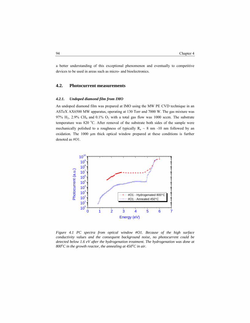
94 Chapter 4
a better understanding of this exceptional phenomenon and eventually to competitive devices to be used in areas such as micro- and bioelectronics.
4.2. Photocurrent measurements
4.2.1. Undoped diamond film from IMO
An undoped diamond film was prepared at IMO using the MW PE CVD technique in an ASTeX AX6500 MW apparatus, operating at 130 Torr and 7000 W. The gas mixture was 97% H2, 2.9% CH4 and 0.1% O2 with a total gas flow was 1000 sccm. The substrate temperature was 820 oC. After removal of the substrate both sides of the sample were mechanically polished to a roughness of typically Ra ~ 8 nm -10 nm followed by an oxidation. The 1000 µm thick optical window prepared at these conditions is further denoted as #O1.
0 1 2 3 4 5 6 7100101102103104105106107108109
1010
#O1 - Hydrogenated 800°C #O1 - Annealed 450°CPhot
ocur
rent
(a.u
.)
Energy (eV)
Figure 4.1 PC spectra from optical window #O1. Because of the high surface conductivity values and the consequent background noise, no photocurrent could be detected below 1.6 eV after the hydrogenation treatment. The hydrogenation was done at 800oC in the growth reactor, the annealing at 450oC in air.
Hydrogen on the diamond surface 95
Figure 4.1 compares the PC spectra of the same sample after a hydrogenation and a subsequent annealing procedure. The hydrogenation was achieved in a hydrogen plasma in the growth reactor at 800 oC for 5 minutes. This suffices to attain the p-type surface conductivity (SC) [Lan89]. This results in a high value for the DC dark conductivity, inducing a high background noise, which makes it impossible to detect photocurrent below 1.6 eV for the hydrogenated sample. Upon annealing the difference in magnitude between DC dark current and photocurrent decreases with a better signal/noise ratio as a result. The annealing occurred in air at 450°C.
Both spectra show the presence of the earlier reported defect level D2 (oEi = 2.2 eV). For the hydrogenated film, an onset pointing to the presence of the D1 level (oEi = 1.2 eV - 1.3 eV) can be seen. After the annealing D1 is fully visible and even Dx is present [Nes98]. This last level seems to be connected to D1, explaining the uncertainty on the photoionisation energy of D1. The D2 level was attributed to substitutional nitrogen. D1, and the related Dx, remained unidentified but the intensity of both levels as seen in PC experiments was clearly dependent on the surface treatments [Nes98, Nes99]. Upon annealing the subgap photocurrent in comparison to the absorption edge photo-response has clearly decreased. Two possible explanations can be given. Maier et al. showed that the Fermi level must lie just beneath the valence band maximum to account for a hole concentration of ~ 1012 - 1013 cm-2 which is the concentration connected with the p-type SC [Mai00]. According to the same model hydrogen is necessary for the SC but also other surface adsorbents. Upon annealing at 450 °C the hydrogen termination remains intact, but some of the adsorbents are removed [Can02]. This moves the Fermi level towards the middle of the gap, changing the occupation of the levels involved. Annealing can also change the µτ product associated with the subgap levels, an effect that can also be detected by PC.
4.2.2. n-Type P-doped diamond film from NIMS
One of the films that were already discussed in Chapter 3 was also subjected to a hydrogenation treatment. This is to investigate the influence of the surface p-type conductive layer on the n-type conductivity of the P-doped diamond film. After an oxidation to clean the sample surface, it was inserted into an ASTeX growth reactor. After pumping down to a vacuum of 1.33 10-6 Pa, the hydrogen plasma was ignited and the pressure was raised to 10640 Pa. At a temperature of 780 °C - 800 oC the sample surface has been hydrogenated for 10 minutes. After this treatment, the plasma was
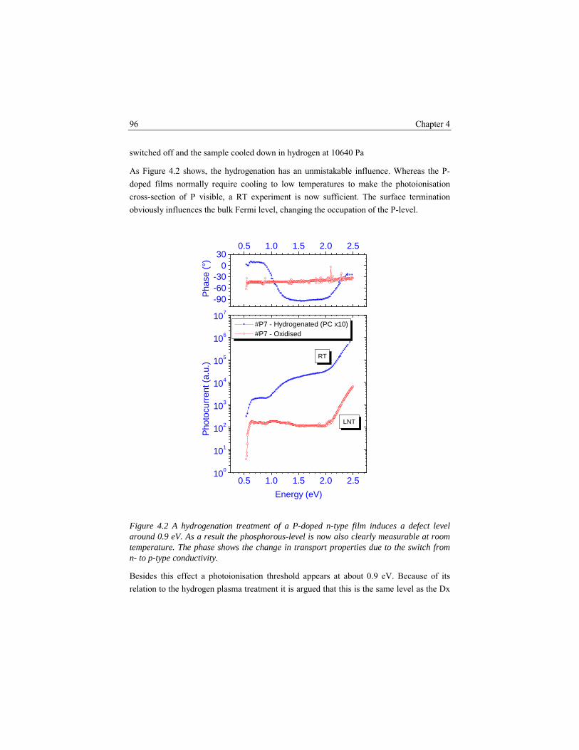
96 Chapter 4
switched off and the sample cooled down in hydrogen at 10640 Pa
As Figure 4.2 shows, the hydrogenation has an unmistakable influence. Whereas the P-doped films normally require cooling to low temperatures to make the photoionisation cross-section of P visible, a RT experiment is now sufficient. The surface termination obviously influences the bulk Fermi level, changing the occupation of the P-level.
-90-60-30
030
0.5 1.0 1.5 2.0 2.5
Phas
e (°
)
0.5 1.0 1.5 2.0 2.5100
101
102
103
104
105
106
107
RT
LNT
#P7 - Hydrogenated (PC x10) #P7 - Oxidised
Phot
ocur
rent
(a.u
.)
Energy (eV)
Figure 4.2 A hydrogenation treatment of a P-doped n-type film induces a defect level around 0.9 eV. As a result the phosphorous-level is now also clearly measurable at room temperature. The phase shows the change in transport properties due to the switch from n- to p-type conductivity.
Besides this effect a photoionisation threshold appears at about 0.9 eV. Because of its relation to the hydrogen plasma treatment it is argued that this is the same level as the Dx
Hydrogen on the diamond surface 97
level mentioned in the previous section and already detected in numerous undoped CVD diamond films. However, in the previous chapter it was reported that the first resistive oxidised n-type films showed a defect level around 0.81 eV, called XP2. These films also showed the phosphorous level, at RT as well as LT. A nominally undoped film, in oxidised state, containing a small contamination of P, also showed the XP2 level. It seems that in all these films the same level is present and that its occupation can be influenced through a shift of the bulk Fermi level by surface treatments.
Photo-Hall experiments proved that Dx is an acceptor [Nes02]. This means that the level is situated 0.9 eV above the valence band, giving rise to holes when excited. As the P-level is a donor, the majority type of charge carriers switches during the PC-experiment. This normally changes the recombination mechanism, reflected in the phase shift as depicted at the top of Figure 4.2. Compared with the oxidised film, dominated by electron conduction from phosphorous (film) and nitrogen (substrate), that has a stable phase for the whole spectrum, three different phase levels can be distinguished in the hydrogenated case. Note that the application of CPM is prevented as one of the conditions, one type of majority carriers, is not satisfied.
4.3. Dielectric measurements Up to now, dielectric measurements on diamond were mainly concentrated on the influence of the structure and morphology on the dielectric constant and the loss tangent [Ala94, Ye00]. This research was mainly carried out on oxidised films in lower frequency ranges. This section deals with the influence of oxidation, hydrogenation and annealing on the dielectric properties of microwave plasma enhanced CVD diamond films measured in the 45 Mhz - 20 GHz range.
4.3.1. Experimental
A set of samples was grown at IMO by the microwave plasma enhanced CVD technique in a commercial ASTeX PDS 17 MW 5 kW system, using undoped Si-wafers as substrates. This is the same system as was used to grow n-type films. However, the films investigated here were grown before the machine was adapted to use phosphine. Consequently, no unintentional doping with P was possible. Methane was used as the carbon containing gas precursor, together with hydrogen, oxygen and nitrogen forming the process gases used to deposit the films [Nes96]. A variation of the deposition
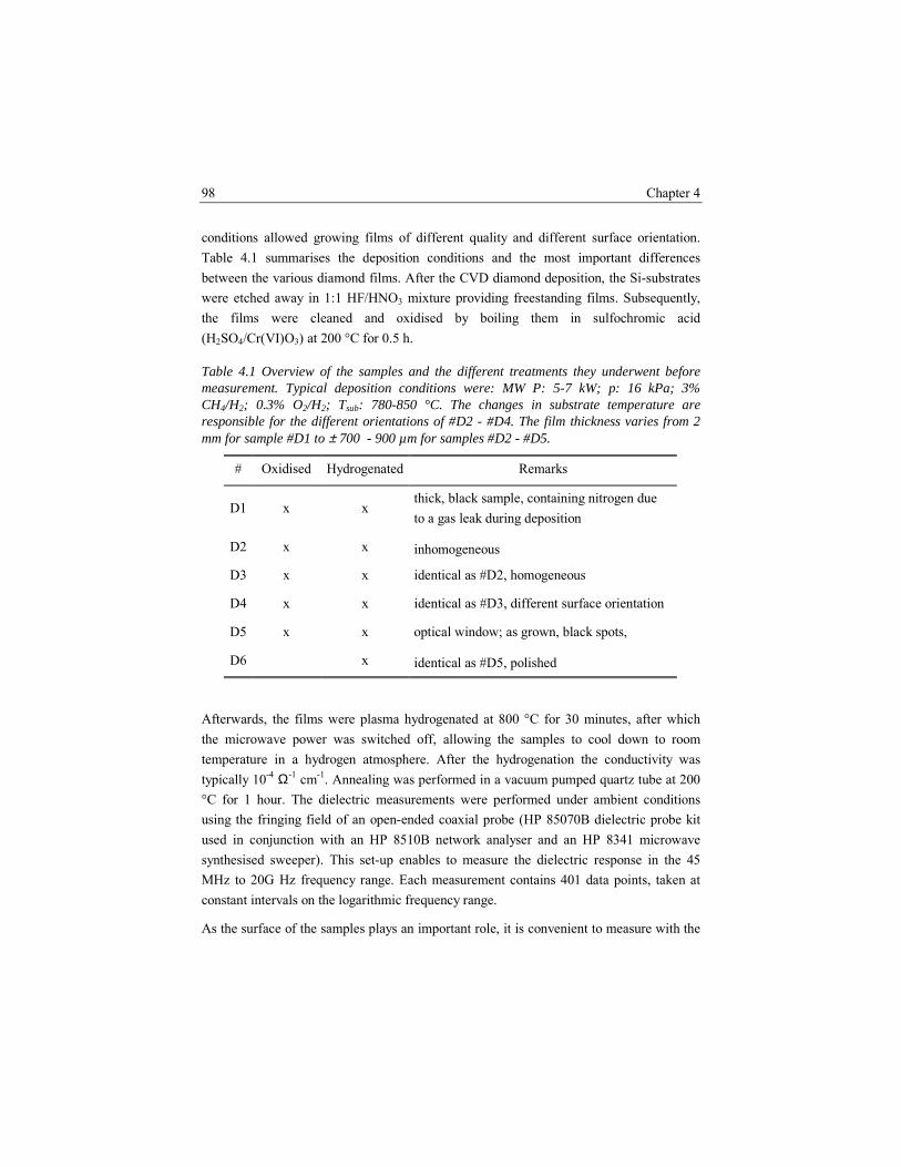
98 Chapter 4
conditions allowed growing films of different quality and different surface orientation. Table 4.1 summarises the deposition conditions and the most important differences between the various diamond films. After the CVD diamond deposition, the Si-substrates were etched away in 1:1 HF/HNO3 mixture providing freestanding films. Subsequently, the films were cleaned and oxidised by boiling them in sulfochromic acid (H2SO4/Cr(VI)O3) at 200 °C for 0.5 h.
Table 4.1 Overview of the samples and the different treatments they underwent before measurement. Typical deposition conditions were: MW P: 5-7 kW; p: 16 kPa; 3% CH4/H2; 0.3% O2/H2; Tsub: 780-850 °C. The changes in substrate temperature are responsible for the different orientations of #D2 - #D4. The film thickness varies from 2 mm for sample #D1 to ± 700 - 900 µm for samples #D2 - #D5.
# Oxidised Hydrogenated Remarks
D1 x x thick, black sample, containing nitrogen due to a gas leak during deposition
D2 x x inhomogeneous
D3 x x identical as #D2, homogeneous
D4 x x identical as #D3, different surface orientation
D5 x x optical window; as grown, black spots,
D6 x identical as #D5, polished
Afterwards, the films were plasma hydrogenated at 800 °C for 30 minutes, after which the microwave power was switched off, allowing the samples to cool down to room temperature in a hydrogen atmosphere. After the hydrogenation the conductivity was typically 10-4 Ω-1 cm-1. Annealing was performed in a vacuum pumped quartz tube at 200 °C for 1 hour. The dielectric measurements were performed under ambient conditions using the fringing field of an open-ended coaxial probe (HP 85070B dielectric probe kit used in conjunction with an HP 8510B network analyser and an HP 8341 microwave synthesised sweeper). This set-up enables to measure the dielectric response in the 45 MHz to 20G Hz frequency range. Each measurement contains 401 data points, taken at constant intervals on the logarithmic frequency range.
As the surface of the samples plays an important role, it is convenient to measure with the
Hydrogen on the diamond surface 99
open probe where the deposition of metal contacts onto the surface is not required, thus excluding a possible influence of space charge at the contacts. System calibration is performed with the probe in air, making a so-called open circuit, terminating the probe with a perfect load, creating a short circuit, and putting the probe in a fluid with well-known and well-defined dielectric properties. Water and ethanol were used as calibration fluids, both leading to the same results in the following experiments.
Experiments were done at room temperature in air, and to assure good contact between probe and sample, the probe was vertically pressed on the growth surface of the diamond films. Because the majority of the films were unpolished and exhibited as-grown rough surfaces with grain sizes of typically 50 - 100 µm, the mechanical contact was dependent on the surface roughness, inducing a constant downwards shift of the measured permittivity value. The thickness of the samples was sufficient to avoid influence of the substrate holder.
4.3.2. Oxidised films
The first measurements were performed on the oxidised, non-hydrogenated films that showed, as expected, a flat response without any dielectric relaxation in the applied frequency span. The average measured permittivity is about 4. Ibarra et al. were able to measure the RT frequency dependence of the permittivity for CVD diamond. They found that, for frequencies higher than 100 kHz, the permittivity could be considered constant with a value of 5.7 equal to that of natural diamond [Iba97, Mad96]. However, for some polycrystalline CVD diamond films higher values have been reported. These values have been ascribed to the polycrystalline nature of the films, which contains more defects than a natural single crystal [Ala94]. As already briefly mentioned the systematic underestimation of the permittivity value is due to the fact that the probe makes contact to the rather rough polycrystalline surface of the diamond film without use of metal contacts, making the probe fringing field partially interacting with the sample. This induces a negative offset of the permittivity value. However, because the point of interest is mainly on the frequency dependent response due to relaxation, this offset is of no importance and is not further discussed. The data presented in the next section are the first dielectric measurements on hydrogenated diamond in the frequency range in question. The resulting values for the permittivity may thus differ from the well-known values for oxidized diamond films.
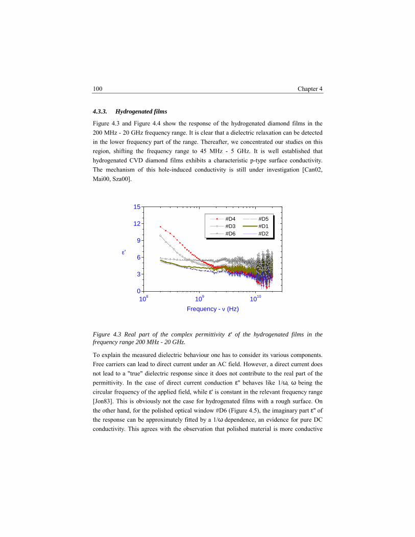
100 Chapter 4
4.3.3. Hydrogenated films
Figure 4.3 and Figure 4.4 show the response of the hydrogenated diamond films in the 200 MHz - 20 GHz frequency range. It is clear that a dielectric relaxation can be detected in the lower frequency part of the range. Thereafter, we concentrated our studies on this region, shifting the frequency range to 45 MHz - 5 GHz. It is well established that hydrogenated CVD diamond films exhibits a characteristic p-type surface conductivity. The mechanism of this hole-induced conductivity is still under investigation [Can02, Mai00, Sza00].
108 109 10100
3
6
9
12
15
#D4 #D5 #D3 #D1 #D6 #D2
ε'
Frequency - ν (Hz)
Figure 4.3 Real part of the complex permittivity ε' of the hydrogenated films in the frequency range 200 MHz - 20 GHz.
To explain the measured dielectric behaviour one has to consider its various components. Free carriers can lead to direct current under an AC field. However, a direct current does not lead to a "true" dielectric response since it does not contribute to the real part of the permittivity. In the case of direct current conduction ε'' behaves like 1/ω, ω being the circular frequency of the applied field, while ε' is constant in the relevant frequency range [Jon83]. This is obviously not the case for hydrogenated films with a rough surface. On the other hand, for the polished optical window #D6 (Figure 4.5), the imaginary part ε'' of the response can be approximately fitted by a 1/ω dependence, an evidence for pure DC conductivity. This agrees with the observation that polished material is more conductive
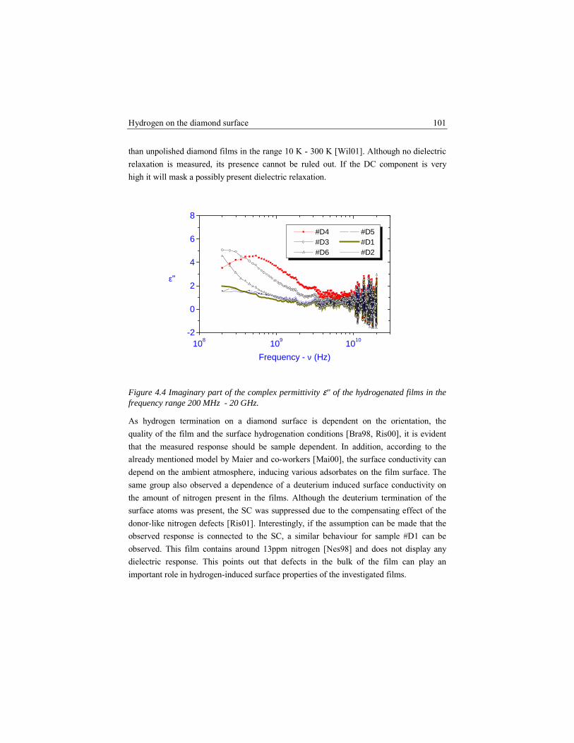
Hydrogen on the diamond surface 101
than unpolished diamond films in the range 10 K - 300 K [Wil01]. Although no dielectric relaxation is measured, its presence cannot be ruled out. If the DC component is very high it will mask a possibly present dielectric relaxation.
108 109 1010-2
0
2
4
6
8
#D4 #D5 #D3 #D1 #D6 #D2
ε"
Frequency - ν (Hz)
Figure 4.4 Imaginary part of the complex permittivity ε'' of the hydrogenated films in the frequency range 200 MHz - 20 GHz.
As hydrogen termination on a diamond surface is dependent on the orientation, the quality of the film and the surface hydrogenation conditions [Bra98, Ris00], it is evident that the measured response should be sample dependent. In addition, according to the already mentioned model by Maier and co-workers [Mai00], the surface conductivity can depend on the ambient atmosphere, inducing various adsorbates on the film surface. The same group also observed a dependence of a deuterium induced surface conductivity on the amount of nitrogen present in the films. Although the deuterium termination of the surface atoms was present, the SC was suppressed due to the compensating effect of the donor-like nitrogen defects [Ris01]. Interestingly, if the assumption can be made that the observed response is connected to the SC, a similar behaviour for sample #D1 can be observed. This film contains around 13ppm nitrogen [Nes98] and does not display any dielectric response. This points out that defects in the bulk of the film can play an important role in hydrogen-induced surface properties of the investigated films.
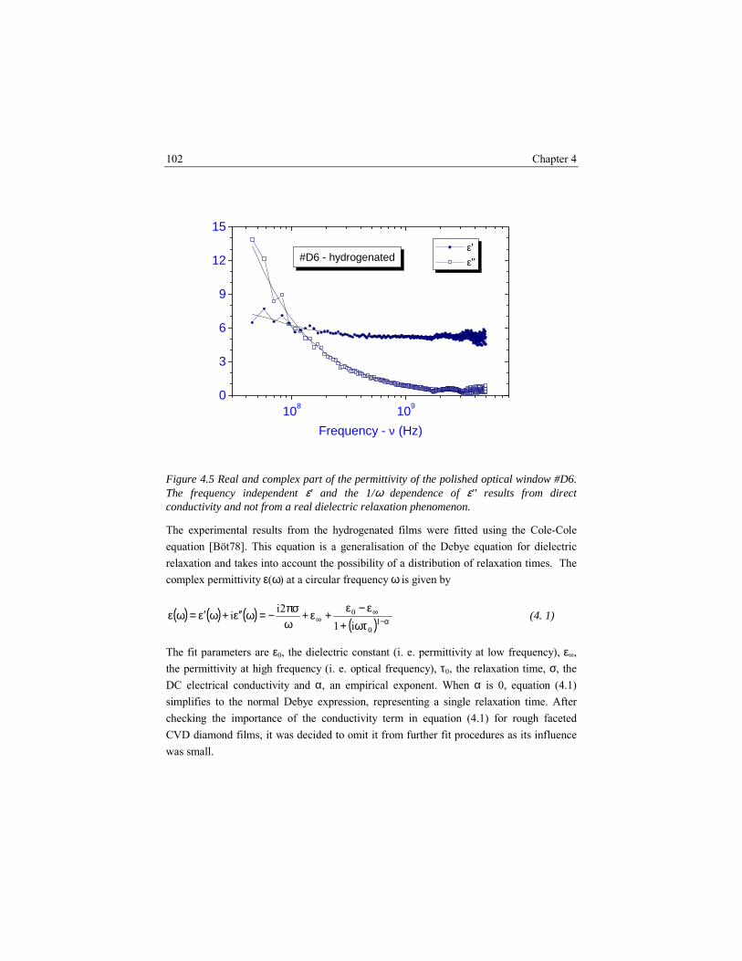
102 Chapter 4
108 1090
3
6
9
12
15
#D6 - hydrogenated
ε' ε''
Frequency - ν (Hz)
Figure 4.5 Real and complex part of the permittivity of the polished optical window #D6. The frequency independent ε' and the 1/ω dependence of ε'' results from direct conductivity and not from a real dielectric relaxation phenomenon.
The experimental results from the hydrogenated films were fitted using the Cole-Cole equation [Böt78]. This equation is a generalisation of the Debye equation for dielectric relaxation and takes into account the possibility of a distribution of relaxation times. The complex permittivity ε(ω) at a circular frequency ω is given by
( ) ( ) ( )( ) α−
∞∞
ωτ+ε−ε+ε+
ωπσ−=ωε ′′+ωε′=ωε 1
0
0
i12ii (4. 1)
The fit parameters are ε0, the dielectric constant (i. e. permittivity at low frequency), ε∞, the permittivity at high frequency (i. e. optical frequency), τ0, the relaxation time, σ, the DC electrical conductivity and α, an empirical exponent. When α is 0, equation (4.1) simplifies to the normal Debye expression, representing a single relaxation time. After checking the importance of the conductivity term in equation (4.1) for rough faceted CVD diamond films, it was decided to omit it from further fit procedures as its influence was small.
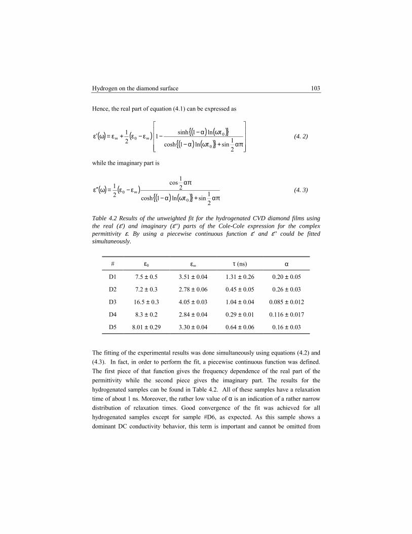
Hydrogen on the diamond surface 103
Hence, the real part of equation (4.1) can be expressed as
( ) ( ) ( ) ( ) ( ) ( )
απ+ωτα−
ωτα−−ε−ε+ε=ωε′ ∞∞
21sinln1cosh
ln1sinh121
0
00 (4. 2)
while the imaginary part is
( ) ( )( ) ( ) απ+ωτα−
απε−ε=ωε ′′ ∞
21sinln1cosh
21cos
21
0
0 (4. 3)
Table 4.2 Results of the unweighted fit for the hydrogenated CVD diamond films using the real (ε') and imaginary (ε'') parts of the Cole-Cole expression for the complex permittivity ε. By using a piecewise continuous function ε' and ε'' could be fitted simultaneously.
# ε0 ε∞ τ (ns) α
D1 7.5 ± 0.5 3.51 ± 0.04 1.31 ± 0.26 0.20 ± 0.05
D2 7.2 ± 0.3 2.78 ± 0.06 0.45 ± 0.05 0.26 ± 0.03
D3 16.5 ± 0.3 4.05 ± 0.03 1.04 ± 0.04 0.085 ± 0.012
D4 8.3 ± 0.2 2.84 ± 0.04 0.29 ± 0.01 0.116 ± 0.017
D5 8.01 ± 0.29 3.30 ± 0.04 0.64 ± 0.06 0.16 ± 0.03
The fitting of the experimental results was done simultaneously using equations (4.2) and (4.3). In fact, in order to perform the fit, a piecewise continuous function was defined. The first piece of that function gives the frequency dependence of the real part of the permittivity while the second piece gives the imaginary part. The results for the hydrogenated samples can be found in Table 4.2. All of these samples have a relaxation time of about 1 ns. Moreover, the rather low value of α is an indication of a rather narrow distribution of relaxation times. Good convergence of the fit was achieved for all hydrogenated samples except for sample #D6, as expected. As this sample shows a dominant DC conductivity behavior, this term is important and cannot be omitted from
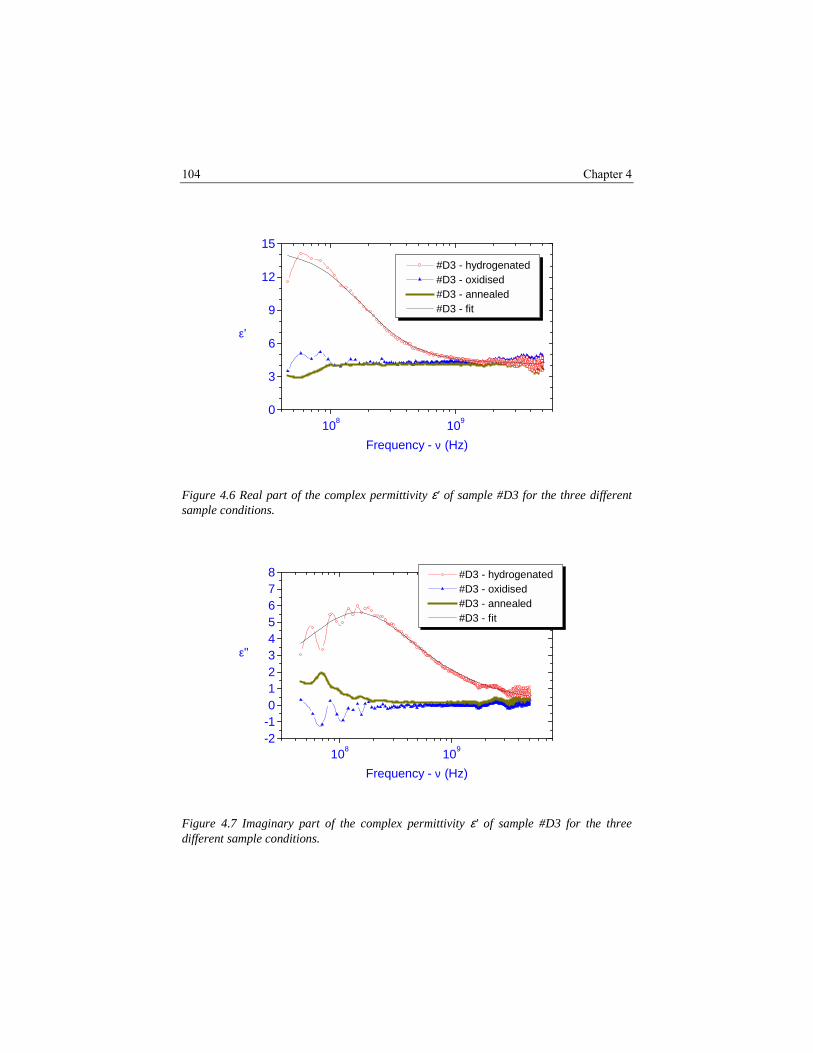
104 Chapter 4
108 1090
3
6
9
12
15
#D3 - hydrogenated #D3 - oxidised #D3 - annealed #D3 - fit
ε'
Frequency - ν (Hz)
Figure 4.6 Real part of the complex permittivity ε' of sample #D3 for the three different sample conditions.
108 109-2-1012345678
#D3 - hydrogenated #D3 - oxidised #D3 - annealed #D3 - fit
ε"
Frequency - ν (Hz)
Figure 4.7 Imaginary part of the complex permittivity ε' of sample #D3 for the three different sample conditions.
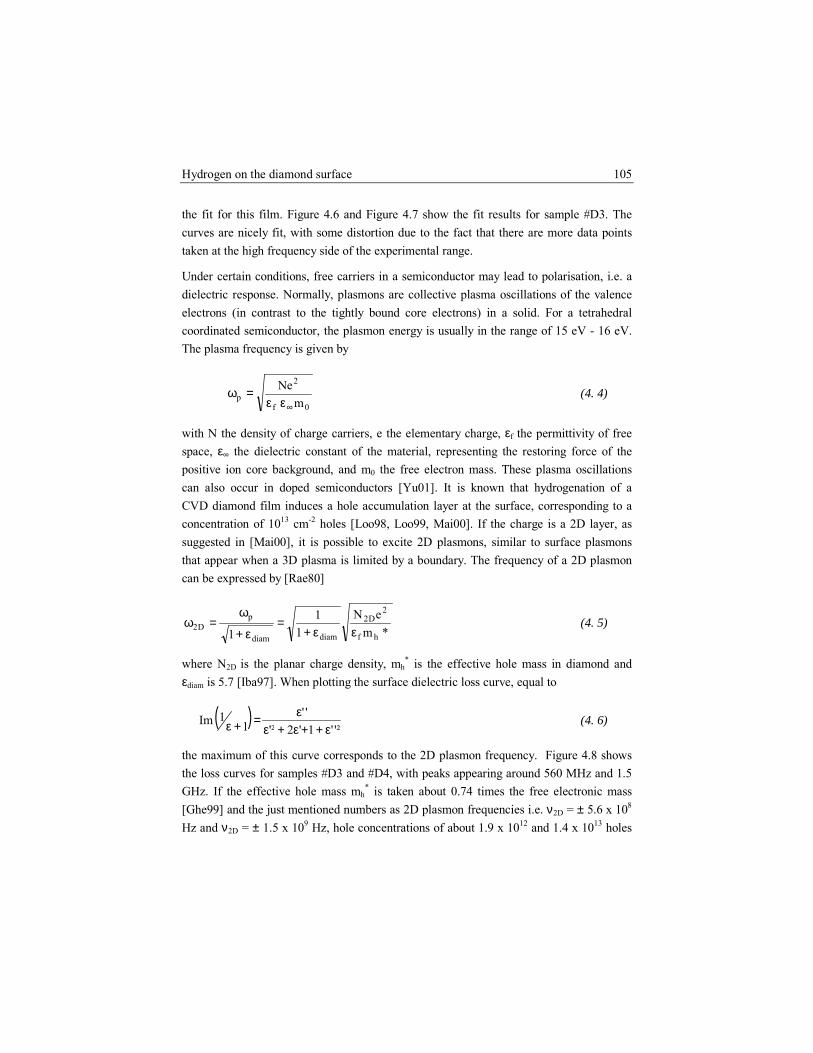
Hydrogen on the diamond surface 105
the fit for this film. Figure 4.6 and Figure 4.7 show the fit results for sample #D3. The curves are nicely fit, with some distortion due to the fact that there are more data points taken at the high frequency side of the experimental range.
Under certain conditions, free carriers in a semiconductor may lead to polarisation, i.e. a dielectric response. Normally, plasmons are collective plasma oscillations of the valence electrons (in contrast to the tightly bound core electrons) in a solid. For a tetrahedral coordinated semiconductor, the plasmon energy is usually in the range of 15 eV - 16 eV. The plasma frequency is given by
0f
2
p mNe
∞εε=ω (4. 4)
with N the density of charge carriers, e the elementary charge, εf the permittivity of free space, ε∞ the dielectric constant of the material, representing the restoring force of the positive ion core background, and m0 the free electron mass. These plasma oscillations can also occur in doped semiconductors [Yu01]. It is known that hydrogenation of a CVD diamond film induces a hole accumulation layer at the surface, corresponding to a concentration of 1013 cm-2 holes [Loo98, Loo99, Mai00]. If the charge is a 2D layer, as suggested in [Mai00], it is possible to excite 2D plasmons, similar to surface plasmons that appear when a 3D plasma is limited by a boundary. The frequency of a 2D plasmon can be expressed by [Rae80]
*meN
11
1 hf
2D2
diamdiam
pD2 εε+
=ε+
ω=ω (4. 5)
where N2D is the planar charge density, mh* is the effective hole mass in diamond and
εdiam is 5.7 [Iba97]. When plotting the surface dielectric loss curve, equal to
( )'²'1'2'²
''1
1Imε++ε+ε
ε=+ε (4. 6)
the maximum of this curve corresponds to the 2D plasmon frequency. Figure 4.8 shows the loss curves for samples #D3 and #D4, with peaks appearing around 560 MHz and 1.5 GHz. If the effective hole mass mh
* is taken about 0.74 times the free electronic mass [Ghe99] and the just mentioned numbers as 2D plasmon frequencies i.e. ν2D = ± 5.6 x 10⁸ Hz and ν2D = ± 1.5 x 10⁹ Hz, hole concentrations of about 1.9 x 10¹² and 1.4 x 10¹³ holes
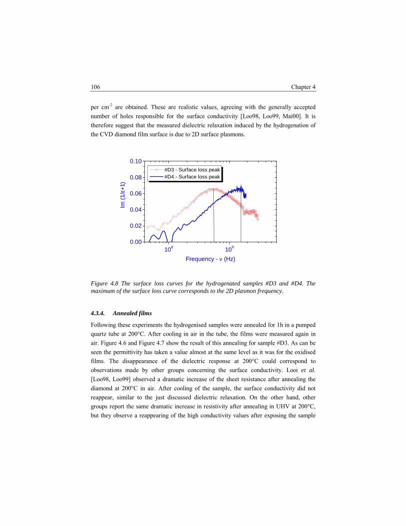
106 Chapter 4
per cm-2 are obtained. These are realistic values, agreeing with the generally accepted number of holes responsible for the surface conductivity [Loo98, Loo99, Mai00]. It is therefore suggest that the measured dielectric relaxation induced by the hydrogenation of the CVD diamond film surface is due to 2D surface plasmons.
108 1090.00
0.02
0.04
0.06
0.08
0.10
#D3 - Surface loss peak #D4 - Surface loss peak
Im (1
/ε+1
)
Frequency - ν (Hz)
Figure 4.8 The surface loss curves for the hydrogenated samples #D3 and #D4. The maximum of the surface loss curve corresponds to the 2D plasmon frequency.
4.3.4. Annealed films
Following these experiments the hydrogenised samples were annealed for 1h in a pumped quartz tube at 200°C. After cooling in air in the tube, the films were measured again in air. Figure 4.6 and Figure 4.7 show the result of this annealing for sample #D3. As can be seen the permittivity has taken a value almost at the same level as it was for the oxidised films. The disappearance of the dielectric response at 200°C could correspond to observations made by other groups concerning the surface conductivity. Looi et al. [Loo98, Loo99] observed a dramatic increase of the sheet resistance after annealing the diamond at 200°C in air. After cooling of the sample, the surface conductivity did not reappear, similar to the just discussed dielectric relaxation. On the other hand, other groups report the same dramatic increase in resistivity after annealing in UHV at 200°C, but they observe a reappearing of the high conductivity values after exposing the sample
Hydrogen on the diamond surface 107
back to ambient conditions [Can01, Mai00, Sza00]. The key issue here seems to be the annealing in vacuum or in air. Szameitat et al. [Sza00] and Maier et al. [Mai00] recently proposed a model for the surface conductivity, claiming that the surface conductivity is a result from a hydrogenated surface together with adsorbents on the diamond surface. There are two possible explanations for the loss of the 2D plasmon-related dielectric relaxation. One is a drastic decrease in charge carrier concentration, which would shift the dielectric response to lower frequencies, outside the used frequency range. The other option is the disappearance of the restoring force necessary to have plasmons. These could be supplied by the adsorbants (anions) that play a crucial part in the process that generates the surface conductivity according to Maier et al. [Mai00]. Although it is known that chemisorbed hydrogen at the diamond surface doesn't desorbs below 900-1000°C in vacuum [Loo98, Loo99, Nes99], these adsorbants can disappear at lower temperatures. It is also useful to point out that [Mai00] claims, following measurements on a IIa C(100) single crystal, that, in air, hydrogen is desorbed from the surface at around 200°C. This might provide a possible explanation for the difference between the two situations.
4.4. Conclusions Photocurrent experiments in the quasi-steady-state mode performed on an undoped and a hydrogenated P-doped CVD diamond film showed that hydrogenation of the surface strongly affects the population of defects in the bulk of the material. Levels that (almost) cannot be detected in oxidised films, such as the phosphorous donor and the Dx level, are now easy detectable. To explain this, a movement of the Fermi level induced by the surface termination must be taken into account.
Dielectric measurements in the 45 Mhz - 20 GHz range were performed on different quality CVD diamond samples. Oxidised and hydrogenated samples were measured in air at room temperature. While the polished film only showed strong DC conductivity, the unpolished hydrogenated films showed a clear near-Debye dielectric response around 108 - 109Hz. This was attributed to 2D plasmons, formed by the hole accumulation layer (1013 holes cm-2) present on such films. The response was clearly film quality dependent, which can be explained by the different hydrogen coverage on the surface of the diamond films. After a 1h anneal at 200°C in a vacuum pumped quartz tube, the dielectric response disappeared, giving the same results as the oxidised samples, proving the origin of the dielectric relaxation to be hydrogen. This corresponds to the reported
108 Chapter 4
disappearance of the surface conductivity at 200°C. A reappearance of the dielectric relaxation after exposing the sample to air is not seen.
4.5. References [Ala94] M. Alam, A. Lucero, Mater. Sci. Eng. B27 (1994), 81.
[Böt78] C.J.F. Böttcher and P. Bordewijk, Theory of Electric Polarization, Volume II, Dielectrics in Time-dependent Fields, Elsevier, Amsterdam, 1978, p.63.
[Bra98] G.R. Brandes, A.P. Mills, Jr., Phys. Rev. B 58 (1998), 4952.
[Can01] M. Cannaerts, M. Nesládek, K. Haenen, L.M. Stals, L. De Schepper, C. Van Haesendonck, Phys. Stat. Sol. (a) 186/2 (2001), 235.
[Can02] M. Cannaerts, M. Nesládek, K. Haenen, L. De Schepper, C. Van Haesendonck, submitted to Diamond Relat. Mater.
[Den01] A. Denisenko, A. Aleksov, E. Kohn, Diamond Relat. Mater. 10 (2001), 667.
[Ghe99] E. Gheeraert, S. Koizumi, T. Teraji, H. Kanda, M. Nesládek, Phys. Stat. Sol. (a) 174/1 (1999), 39.
[Iba97] A. Ibarra, M. González, R. Vila, J. Mollá, Diamond Relat. Mater. 6 (1997), 856.
[Jon83] A.K. Jonscher, Dielectric relaxation in solids, Chelsea Dielectric Press, London, 1983, p.47, p.149.
[Lan89] M.I. Landstrass; K.V. Ravi, Appl. Phys. Lett. 55 (1989), 975.
[Loo98] H.J. Looi, R.B. Jackman, J.S. Foord, Appl. Phys. Lett. 72 (1998), 353.
[Loo99] H.J. Looi, M.D. Whitfield, J.S. Foord, R.B. Jackman, Thin Solid Films 343-344 (1999), 623.
[Mad96] O. Madelung (Ed.), Semiconductors - Basic Data, Springer-Verlag, Berlin, 1996, p.10.
[Mai00] F. Maier, M. Riedel, B. Mantel, J. Ristein, L. Ley, Phys. Rev. Lett. 85 (2000), 3472.
[Nes96] M. Nesládek, M. Vaněček, L.M. Stals, Phys. Stat. Sol. (a) 154/1 (1996), 283.
Hydrogen on the diamond surface 109
[Nes98] M. Nesládek, L.M. Stals, A. Stesmans, K. Iakoubovskij, G.J. Adriaenssens, J. Rosa, M. Vaněček, Appl. Phys. Lett. 72 (1998), 3306.
[Nes99] M. Nesládek, K. Meykens, K. Haenen, J. Navratil, C. Quaeyhaegens, L.M. Stals, A. Stesmans, K. Iakoubovskij, G.J. Adriaenssens, J. Rosa and M. Vaněček, Diamond Relat. Mater. 8 (1999), 1480.
[Nes02] M. Nesládek, K. Haenen, M. Cannaerts, C. Van Haesendonck, M. Vaněček, J. Rosa, P. Moravec, in preparation.
[Rae80] H. Raether, Excitation of Plasmons and Interband Transitions by Electrons, Springer-Verlag, Berlin, 1980, p.166.
[Ris00] J. Ristein, Diamond Relat. Mater. 9 (2000), 1129.
[Ris01] J. Ristein, M. Riedel, F. Maier, B.F. Mantel, M. Stammler, L. Ley, Phys. Stat. Sol. (a) 186/2 (2001), 249.
[Sza00] M. Szameitat, X. Jiang, W. Beyer, Appl. Phys. Lett. 77 (2000), 1554.
[Tac00] M. Tachiki, T. Fukuda, K. Sugata, H. Seo, H. Umezawa, H. Kawarada, Jpn. J. Appl. Phys. 39 (2000), 4631.
[Wil01] O.A. Williams, M.D. Whitfield, R.B. Jackman, J.S. Foord, J.E. Butler, C.E. Nebel, Diamond Relat. Mater. 10 (2001), 423.
[Ye00] H. Ye, C.Q. Sun, P. Hing, J. Phys. D: Appl. Phys. 33 (2000), L148.
[Yu01] P.Y. Yu and M. Cardona, Fundamentals of Semiconductors: Physics and Materials Properties, Springer-Verlag, Berlin, 2001, p.306.

Appendix A. List of publications
A.1 Papers in international journals
1. “Photocurrent and optical absorption spectroscopic study of n-type phosphorus-doped CVD diamond”
M. Nesládek, K. Meykens, K. Haenen, L.M. Stals, T. Teraji, S. Koizumi, Diamond Relat. Mater. 8/2-5 (1999), 882-885.
2. “Low-temperature spectroscopic study of n-type diamond” M. Nesladek, K. Meykens, K. Haenen, L.M. Stals, T. Teraji, S. Koizumi, Phys. Rev.
B 59/23 (1999), 14852-14855. 3. “Characteristic defects in CVD diamond: optical and electron paramagnetic
resonance study” M. Nesládek, K. Meykens, K. Haenen, J. Navratil, C. Quaeyhaegens, L.M. Stals, A.
Stesmans, K. Iakoubovskij, G.J. Adriaenssens, J. Rosa, M. Vaněček, Diamond Relat. Mater. 8/8-9 (1999), 1480-1484.
4. “Study of the electronic structure of the phosphorus level in n-type CVD diamond”
K. Haenen, K. Meykens, M. Nesládek, L.M. Stals, T. Teraji, S. Koizumi, E. Gheeraert, Phys. Stat. Sol. (a) 174/1 (1999), R1-R2.
5. “Low temperature photoconductivity detection of phosphorus in diamond”
K. Haenen, K. Meykens, M. Nesládek, G. Knuyt, C. Quaeyhaegens, L.M. Stals, S. Koizumi, E. Gheeraert, Phys. Stat. Sol. (a) 174/1 (1999), 53-58.
6. “Temperature dependent spectroscopic study of the electronic structure of
phosphorus in n-type diamond films” K. Haenen, K. Meykens, M. Nesladek, G. Knuyt, L.M. Stals, T. Teraji, S. Koizumi,
E. Gheeraert, Diamond Relat. Mater. 9/3-6 (2000), 952-955. 7. “Measurement and mapping of very low optical absorption in CVD diamond IR
windows” K. Meykens, K. Haenen, M. Nesládek, L.M. Stals, C.S.J. Pickles, R.S. Sussmann, Diamond Relat. Mater. 9/3-6 (2000), 1021-1025.
A2 Appendix A
8. “The electronic structure of phosphorous in n-type CVD diamond films: Revised” K. Haenen, K. Meykens, M. Nesládek, G. Knuyt, L.M. Stals, T. Teraji, S. Koizumi, Phys. Stat. Sol. (a) 181/1 (2000), 11-16.
9. “Phonon-assisted electronic transitions in phosphorus-doped n-type CVD diamond
films” K. Haenen, K. Meykens, M. Nesládek, G. Knuyt, L.M. Stals, T. Teraji, S. Koizumi, E. Gheeraert, Diamond Relat. Mater. 10/3-7 (2001), 439-443.
10. “Study of UV and subgap photocurrent response in diamond and BCN thin films for
detector applications” M. Nesládek, M. Vaněček, K. Meykens, K. Haenen, J. Manca, L. De Schepper, E.
Pace, A. Pini, G. Verona Rinati, C. Kimura, Y. Etou, T. Sugino, Phys. Stat. Sol. (a) 185/1 (2001), 107-113.
11. “Reversible switching of the surface conductance of hydrogenated CVD diamond
films” M. Cannaerts, M. Nesládek, K. Haenen, L.M. Stals, L. De Schepper, C. Van Haesendonck, Phys. Stat. Sol. (a) 186/2 (2001), 235-240.
12. “Influence of annealing on the electronic properties of chemical vapor deposited
diamond films studied by high vacuum scanning tunneling microscopy and spectroscopy” M. Cannaerts, M. Nesládek, K. Haenen, L. De Schepper, L.M. Stals, C. Van Haesendonck, Diamond Relat. Mater. 11/2 (2002), 212-217.
13. “Dielectric measurements on oxidized and hydrogenated chemical vapor deposited
diamond films” K. Haenen, J.F. Rouleau, M. Nesládek, J. Goyette, L. M. Stals, T. K. Bose, J. Appl.
Phys. 91/10 (2002), 6670-6674. 14. “Finite surface conductance of chemical vapor deposited diamond films in the
absence of a water layer” M. Cannaerts, M. Nesládek, K. Haenen, L. De Schepper, C. Van Haesendonck,
submitted for publication in Diamond Relat. Mater. 15. “Hydrogen-induced photocoductivity and photo-Hall effect in CVD diamond films” M. Nesládek, K. Haenen, M. Cannaerts, C. Van Haesendonck, M. Vaněček, J. Rosa,
P. Moravec, in preparation.
List of publications A3
A.2 Contributions to proceedings
1. “Optical spectroscopic study of n-type diamond” M. Nesládek, K. Meykens, K. Haenen, L. Stals, S. Koizumi, T. Teraji, Proceedings of
the 6th NIRIM International Symposium on Advanced Materials (ISAM’99), NIRIM, February 28 – March 3 1999, NIRIM, Tsukuba, Japan, ISBN4-944122-04-7.
A.3 Other publications
1. “Origin of hydrogen-related surface conductivity in chemical vapor deposited diamond films”
M. Cannaerts, M. Nesládek, K. Haenen, L. De Schepper, N.S. Maslova, C. Van Haesendonck, Physicalia Mag. 123/2-3 (2001) 105-110.
2. “Synthesis and characterisation of undoped and P-doped CVD diamond films for
optical and electronic applications” K. Meykens, M. Nesládek, K. Haenen, L.M. Stals, Physicalia Mag. 123/2-3 (2001)
141-147.