MasterNanowetenschappen en Nanotechnologie · The IBM “millipede”: AFM tips fordata storage 21...
36
Master Nanowetenschappen en Nanotechnologie G. Groeseneken Programma direkteur 2 μm Outline • Wat is Nanowetenschappen en Nanotechnologie ? – Wat is het ? – Voorbeelden – Toepassingen • Master Nanowetenschappen en Nanotechnologie – Structuur en instroom – Overzicht vakkenclusters – Master thesis – Industriele stage • Erasmus Mundus Master Nanoscience and Nanotechnology – Wat is het ? – Structuur – Kandidaatstelling • Perspectieven
Transcript of MasterNanowetenschappen en Nanotechnologie · The IBM “millipede”: AFM tips fordata storage 21...

Master Nanowetenschappen
en Nanotechnologie
G. Groeseneken
Programma direkteur
2 µµµµm
Outline• Wat is Nanowetenschappen en Nanotechnologie ?
– Wat is het ?
– Voorbeelden
– Toepassingen
• Master Nanowetenschappen en Nanotechnologie– Structuur en instroom
– Overzicht vakkenclusters
– Master thesis
– Industriele stage
• Erasmus Mundus Master Nanoscience and Nanotechnology– Wat is het ?
– Structuur
– Kandidaatstelling
• Perspectieven

The Vision or the dream ?The Classic Talk: “There’s Plenty of Room at the Bottom”
Richard Feynman
Noble Prize Physics 1965
”The principles of physics do not speak againstthe possibility of maneuvering things atom byatom. It is not an attempt to violate any laws; it
is something, in principle, that can be done; but
in practice, it has not been done because we are
too big”
”I want to build a billion tiny factories, models of each other, which are manufacturing
simultaneously, drilling holes, stamping parts,
and so on.
Wat is Nanowetenschappen en
Nanotechnologie ?
Nanowetenschappen
= studie van fenomenen en manipulatie
van materialen op atomaire, moleculaire
en macromoleculaire schaal (nanometers),
waar de eigenschappen significant
verschillen van die op grotere schaal !
Nanotechnologie
= toepassing van nano-effecten en
nanomaterialen, structuren en –concepten
in (nieuwe) devices, systemen en
produkten

Nanotechnologie ?
Nanotechnologie:
= Methoden and tools voor de fabricage en/of het gebruik
van structuren op de nanometer schaal (1 to 100nm)
Influenza virus
100 nanometer (nm)
Atom
0.3 nanometer (nm)
NANOTECHNOLOGY
What is Special at the Nanoscale?
• Reactivity ~ outside atoms (chemical reactivity)• Quantum properties change (optical properties different)• Material properties change (strength, conduction, magnetic…)• New materials by synthesis (1022) => nanotoxicity research!• Chemical decoration possible (“hooks” to bio)• …
A NEW FRONTIER TO BE DISCOVERED, ASSESSED AND APPLIED.
WILL IMPACT ALL INDUSTRIES
Nano
54 atoms
24 outside 36 outside
nm
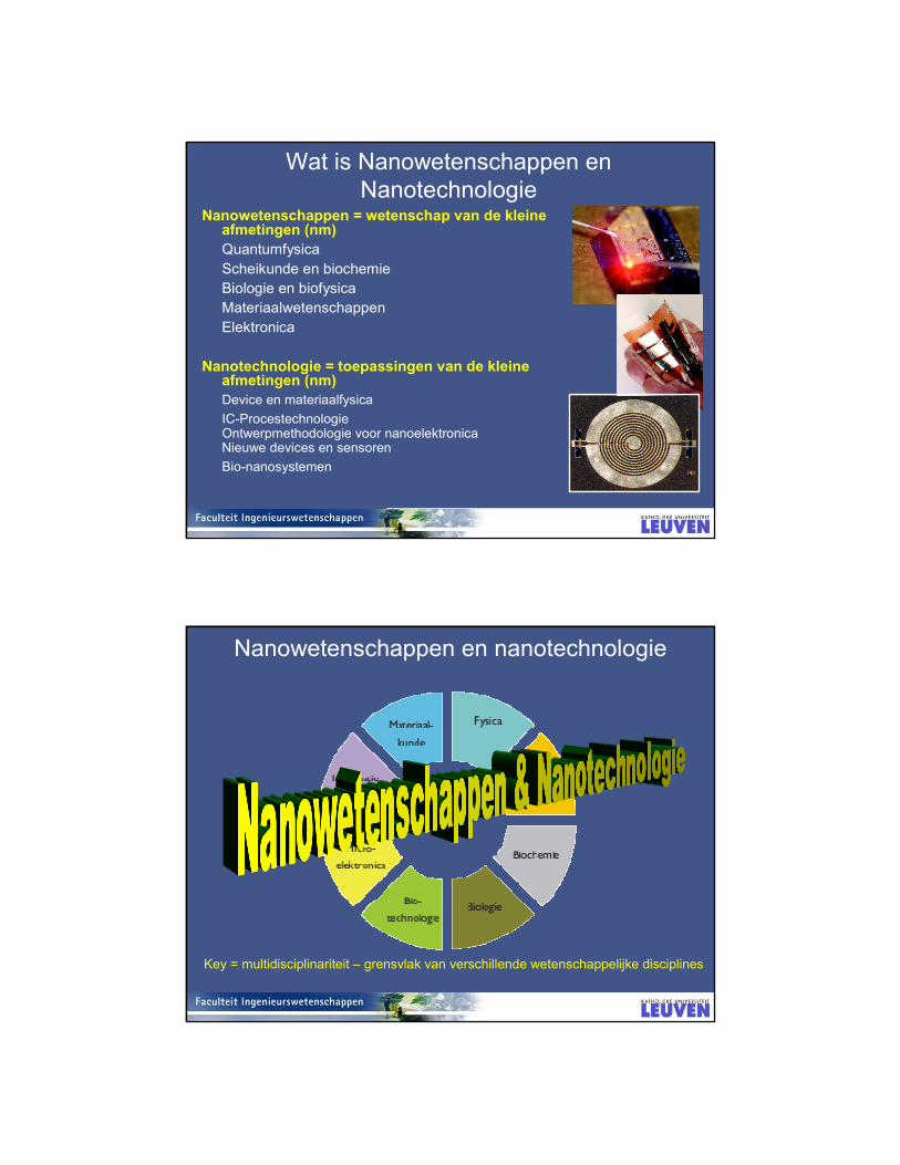
Wat is Nanowetenschappen en
NanotechnologieNanowetenschappen = wetenschap van de kleine
afmetingen (nm)
Quantumfysica
Scheikunde en biochemie
Biologie en biofysica
Materiaalwetenschappen
Elektronica
Nanotechnologie = toepassingen van de kleine afmetingen (nm)
Device en materiaalfysica
IC-ProcestechnologieOntwerpmethodologie voor nanoelektronicaNieuwe devices en sensoren
Bio-nanosystemen
Nanowetenschappen en nanotechnologie
Key = multidisciplinariteit – grensvlak van verschillende wetenschappelijke disciplines

• “Top-down” nanofabricationImplementation of various
techniques to remove, add or
redistribute atoms or molecules in a
bulk material to create a final
structure.
• “Bottom-up” nanofabricationAtomic and molecular scale directed
self-assembly to create larger scale
structures with engineered properties.
Nanofabrication Approaches:
top-down vs bottom-upMachined
Assembled
Al
Si,SiO2
Poly-SiSi3N4
TiSi2CoSi2TaSi2MoSi2WSi2
W
Cu, TiN
Low-k dielectrics
PZT, SBT
Metal gates
High-k dielectrics
?
1970 1980 1990 2000 2010
Materials
TRENDS IN IC MATERIALS
Van micro- tot nanoelektronica
Top-down scaling
Lithografie
Nieuwe materialen

YANO et al. , IEEE ED-41, 1628 (1994)
Single electron memory transistor
Source: Hitachi
Top-down vs. bottom-up approach
Nanowetenschappen Nanotechnologie
Microelectronica
Scheikunde
Biologie
Atomaire manipulatie
Top-down
Bottom-up
Moleculaire elektronica
Organische elektronica
Bioelektronica
NanoMEMS
Nanotechnologie

Spintronica
Semiconductor
devices:Lading=drager van
informatie
Magnetische materialen:Spin is drager van
informatie
Nieuwe devicesNieuwe functionaliteitNieuwe toepassingen
Semiconductor-based spintronics
• Spin in non-magnetic semiconductors
• Injection: Spin LED
• … and detection: SpinFET
• (Ferro)magnetic semiconductors
Metal-based spintronics
• Magnetic (bio-)sensors
• MRAM
• Spin torque oscillators
•Magnetophotonics
"more than Moore"
"no more Moore"
Carbon Nanotubes, buckyballs, nanodraden
2 µµµµm
S
DG
First CNT transistor
R. Martel et al. Appl. Phys. Lett. 73 (1998) 2447.
Carbon Nanotubes
Nanowires
Buckyballs
CNT transistoren
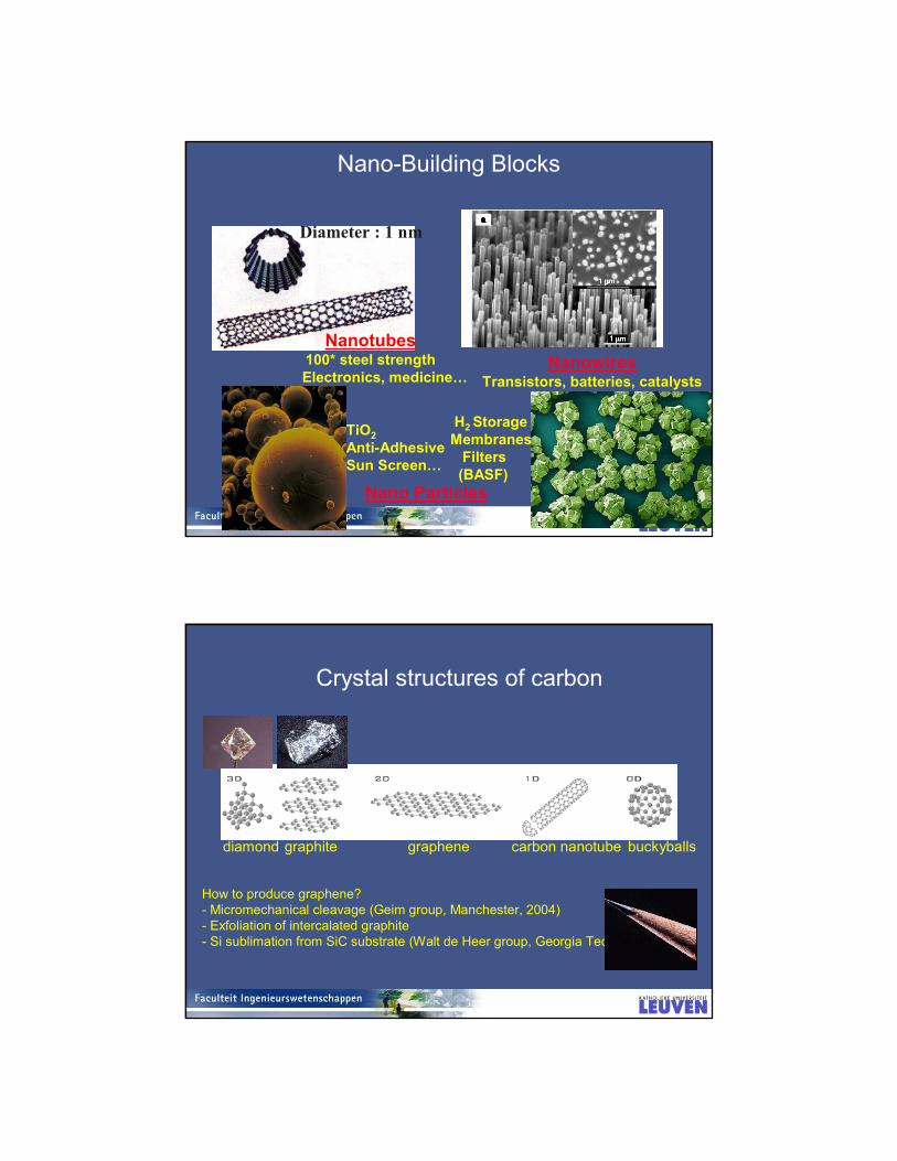
Nano-Building Blocks
Diameter : 1 nm
Nanotubes100* steel strengthElectronics, medicine…
NanowiresTransistors, batteries, catalysts
…
Nano Particles
TiO2
Anti-AdhesiveSun Screen…
H2 StorageMembranesFilters(BASF)
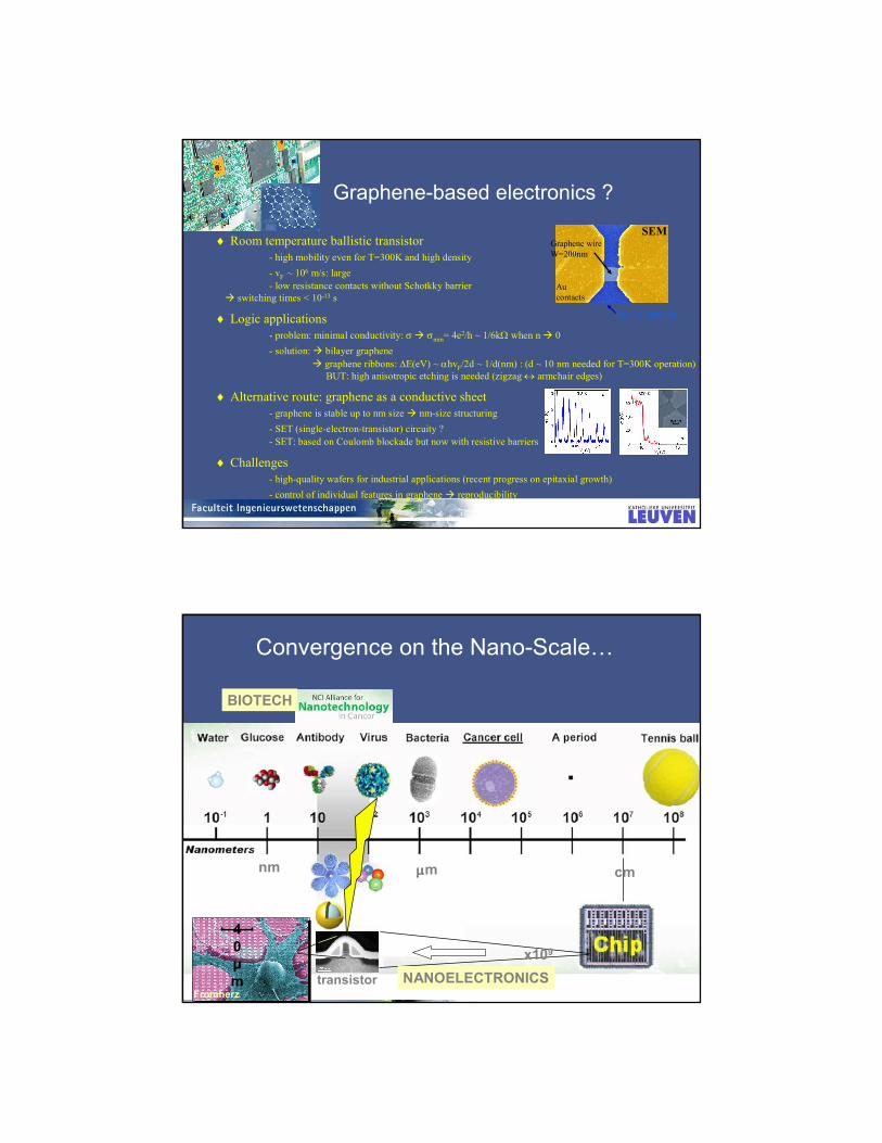
Crystal structures of carbon
diamond graphite graphene carbon nanotube buckyballs
How to produce graphene?
- Micromechanical cleavage (Geim group, Manchester, 2004)
- Exfoliation of intercalated graphite
- Si sublimation from SiC substrate (Walt de Heer group, Georgia Tech, 2004)
Graphene-based electronics ?
♦ Room temperature ballistic transistor
- high mobility even for T=300K and high density
- vF ~ 106 m/s: large
- low resistance contacts without Schotkky barrier
switching times < 10-13 s
♦ Logic applications
- problem: minimal conductivity: σ σmin= 4e2/h ~ 1/6kΩ when n 0
- solution: bilayer graphene
graphene ribbons: ∆E(eV) ~ αhvF/2d ~ 1/d(nm) : (d ~ 10 nm needed for T=300K operation)
BUT: high anisotropic etching is needed (zigzag ↔ armchair edges)
♦ Alternative route: graphene as a conductive sheet
- graphene is stable up to nm size nm-size structuring
- SET (single-electron-transistor) circuity ?
- SET: based on Coulomb blockade but now with resistive barriers
♦ Challenges
- high-quality wafers for industrial applications (recent progress on epitaxial growth)
- control of individual features in graphene reproducibility
SEM
Au
contacts
SiO2 /Si substrate
Graphene wire
W=200nm
Convergence on the Nano-Scale…
cmµµµµmnm
BIOTECH
transistor
x109
NANOELECTRONICS
31nm31nm
40 µm
Fromherz
ICT interfaces Bio at Nano-Scale…
© IMEC-HUJI 2003
electrical
action potential
chemical
neurotransmitter
ICT Interpretation-control-transmissionChip
Neuron
IMEC-VIBK.U.Leuven
AlzheimerParkinsonBrain ResearchNeuroprobes…
Convergence on the Nano-Scale…
cmµµµµmnm
BIOTECH
Nano Particles
NANOTECH
transistor
x109
NANOELECTRONICS
31nm31nm
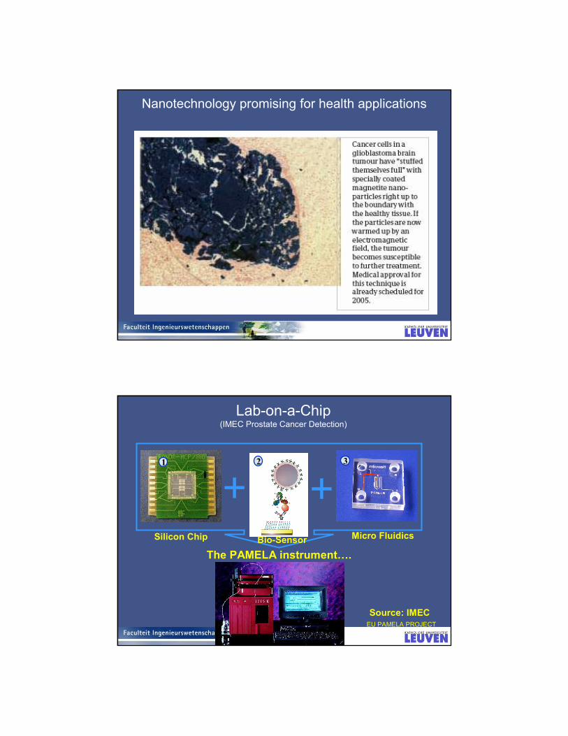
Nanotechnology promising for health applications
Lab-on-a-Chip (IMEC Prostate Cancer Detection)
1
The PAMELA instrument….
2 3
EU PAMELA PROJECT
Source: IMEC
Micro FluidicsSilicon Chip Bio-Sensor

Applications
• "Nanotechnology is an area which
has highly promising prospects for
turning fundamental research into
successful innovations. Not only to
boost the competitiveness of our
industry but also to create new
products that will make positive
changes in the lives of our citizens,
be it in medicine, environment,
electronics or any other field."
• (European Commissioner for
Science & Research, Janez
Potočnik)
Possible application area
• Smart materials
• Sensors
• Nanoscale biostructures
• Energy capture and storage
• Health
• Environmental
• Nanoelectronics
• …
• …
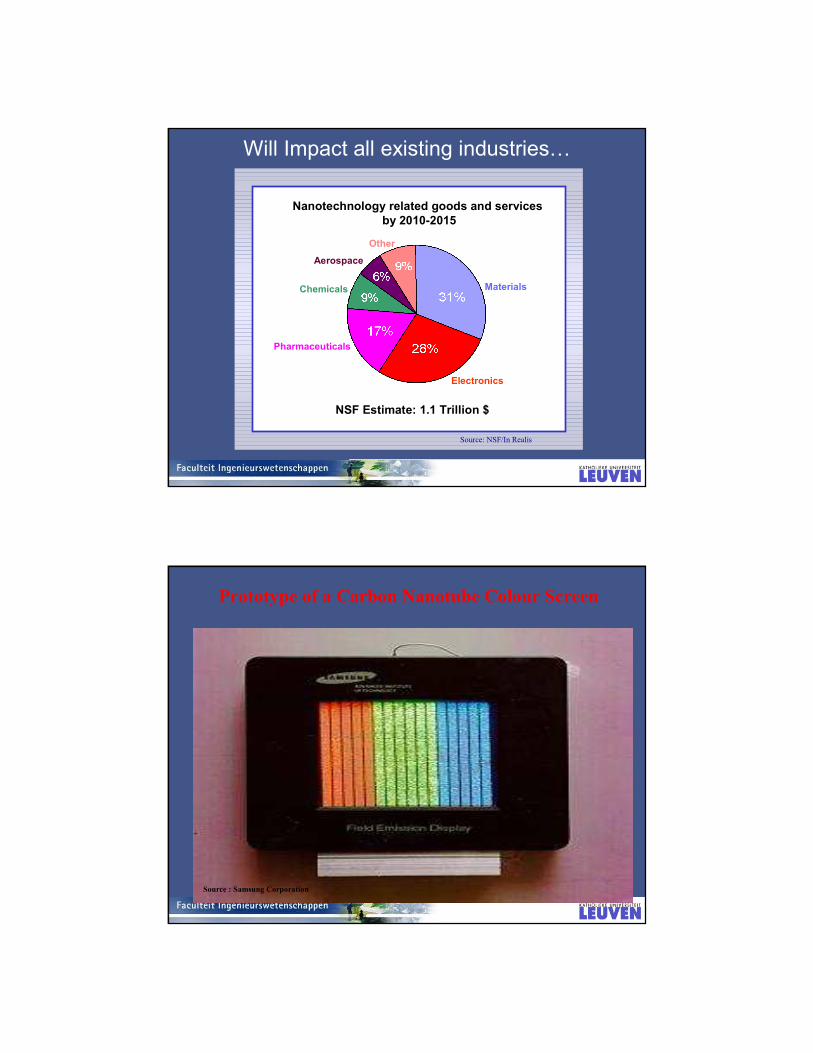
Will Impact all existing industries…
Other
Aerospace
Chemicals
Pharmaceuticals
Electronics
Materials
Nanotechnology related goods and services by 2010-2015
NSF Estimate: 1.1 Trillion $
Source: NSF/In Realis
Prototype of a Carbon Nanotube Colour Screen
Source : Samsung Corporation
The IBM “millipede” : AFM tips for data storage
21st Century ICT: The Post-PC era
Broadband WirelessPersonal Assistant
PolymerElectronics
Dissapearing ICT
15 more years of Moore and More than Moore…Before we reach quantum limits…
Smart Sensorsand Actuators
On the way to…
More Moore More Than Moore
WWW
Source : Koparka, Nanosys
.
Thin Flexible Photovoltaic Cells
Tiny solar cells can be printed onto flexible, very thin
light-retaining materials.
Until recently, photovoltaic cells were derived from
silicon semiconductor technology. Recent research
into improving the efficiency of PV cells has gone into
polymer materials. Plastic semiconductors are highly
flexible but inefficient, converting less than 6% of the
energy landing on them.
Currently, researchers use nanocrystals made of lead
sulfide, which can be “tuned” to absorb wavelenghts
from the red to the deep infrared. Combined with
polymer sensitive to green and blue light,
nanocrystals can convert red and infrared light to
energy the polymer can turn into electrical current.
Nanotechnology Applications in
Automotive Industry

Nanotechnology Applications in
Aircraft Industry
Nanotechnology in future everyday life

Potential Applications in Nanotechnology
Meer informatie over nanotechnologie
• http://www.nanotechnologyfordummies.com/Resources.html
• http://www.viwta.be/files/Dossier2-VOLLDEF.pdf
• http://cordis.europa.eu/nanotechnology/
• ftp://ftp.cordis.europa.eu/pub/nanotechnology/docs/nano_brochure_en.pdf
• http://www.research.ibm.com/nanoscience/
• http://aspbs.com/jnn/
• http://www.royalsoc.ac.uk/landing.asp?id=1210
• http://www.nano.org.uk/
• http://www.nano.gov/
Outline• Wat is Nanowetenschappen en Nanotechnologie ?
– Wat is het ?
– Voorbeelden
– Toepassingen
• Master Nanowetenschappen en Nanotechnologie– Structuur en instroom
– Overzicht vakkenclusters
– Master thesis
– Industriele stage
• Erasmus Mundus Master Nanoscience and Nanotechnology– Wat is het ?
– Structuur
– Kandidaatstelling
• Perspectieven
Master Nanowetenschappen en
Nanotechnologie
• Nieuwe Master met cursussen uit drie verschillendefaculteiten– Wetenschappen: departementen Fysica en Scheikunde
– Ingenieurswetenschappen: departementen Elektrotechniek en Materiaalkunde
– Bio-ingenieurswetenschappen
– 3 Masters: Engelstalig traject, Nederlandstalig traject, Erasmus Mundus
• Academiejaar 2007-2008– officiele start van interfacultaire Master
– Instroom mogelijk vanuit de drie faculteiten
– Diploma Master in de Nanowetenschappen en Nanotechnologie
Nanowetenschappen Nanotechnologie
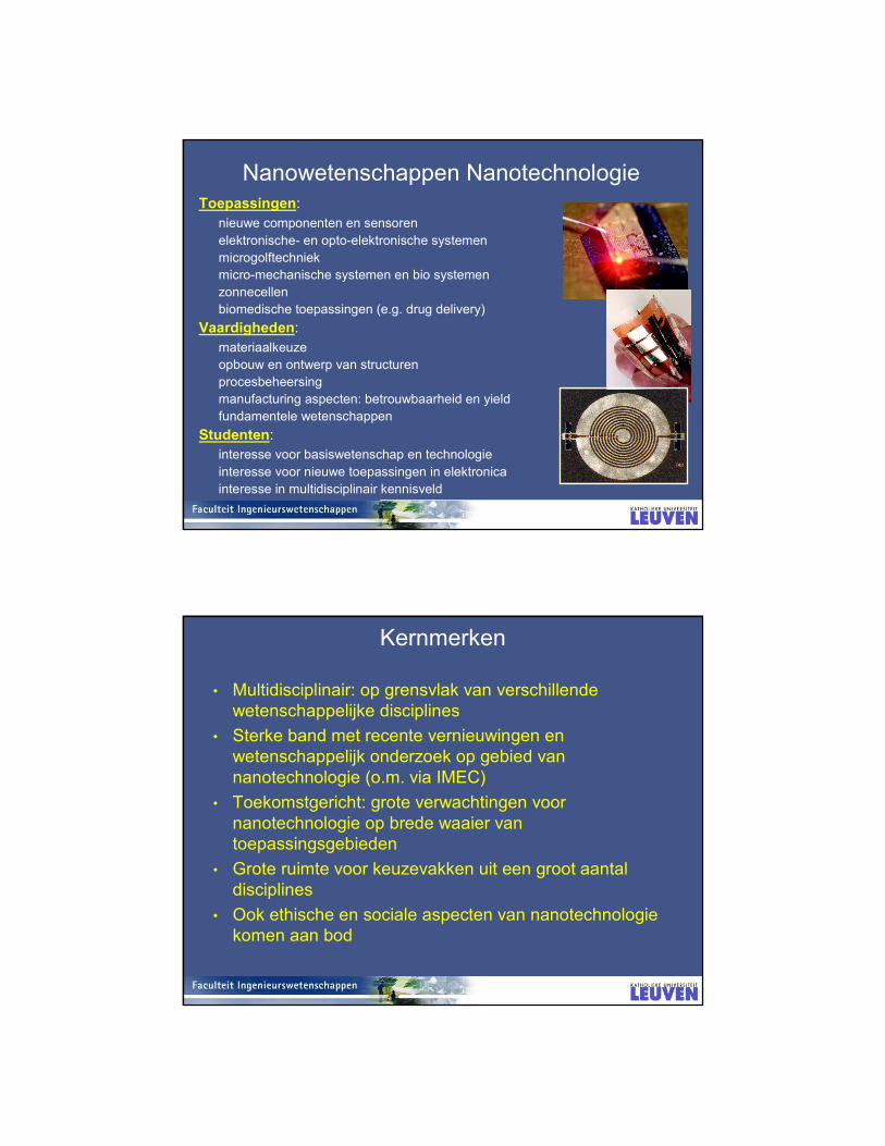
Toepassingen:
nieuwe componenten en sensoren
elektronische- en opto-elektronische systemen
microgolftechniek
micro-mechanische systemen en bio systemen
zonnecellen
biomedische toepassingen (e.g. drug delivery)
Vaardigheden:
materiaalkeuze
opbouw en ontwerp van structuren
procesbeheersing
manufacturing aspecten: betrouwbaarheid en yield
fundamentele wetenschappen
Studenten:
interesse voor basiswetenschap en technologie
interesse voor nieuwe toepassingen in elektronica
interesse in multidisciplinair kennisveld
Kernmerken
• Multidisciplinair: op grensvlak van verschillende
wetenschappelijke disciplines
• Sterke band met recente vernieuwingen en
wetenschappelijk onderzoek op gebied van
nanotechnologie (o.m. via IMEC)
• Toekomstgericht: grote verwachtingen voor
nanotechnologie op brede waaier van
toepassingsgebieden
• Grote ruimte voor keuzevakken uit een groot aantal
disciplines
• Ook ethische en sociale aspecten van nanotechnologie
komen aan bod
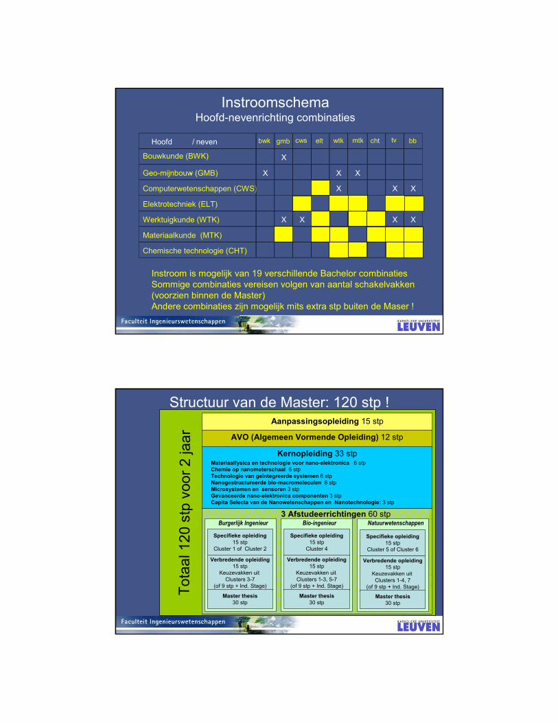
InstroomschemaHoofd-nevenrichting combinaties
Hoofd / neven bwk
X
Geo-mijnbouw (GMB)- X X X
Computerwetenschappen (CWS) X X X X
Elektrotechniek (ELT) X X X X X
Werktuigkunde (WTK) X X X X X X X
Materiaalkunde (MTK) X X X X X X
Chemische technologie (CHT) X X X X
Bouwkunde (BWK)
gmb cws elt wtk mtk cht tv bb
Instroom is mogelijk van 19 verschillende Bachelor combinaties
Sommige combinaties vereisen volgen van aantal schakelvakken
(voorzien binnen de Master)
Andere combinaties zijn mogelijk mits extra stp buiten de Maser !
Totaal120 st pvoor2 jaar
3 Afstudeerrichtingen 60 stp
Structuur van de Master: 120 stp !Aanpassingsopleiding 15 stp
AVO (Algemeen Vormende Opleiding) 12 stp
Kernopleiding 33 stpMateriaalfysica en technologie voor nano-elektronica 6 stp
Chemie op nanometerschaal 6 stpTechnologie van geintegreerde systemen 6 stpNanogestructureerde bio-macromoleculen 6 stp
Microsystemen en sensoren 3 stpGevanceerde nano-elektronica componenten 3 stpCapita Selecta van de Nanowetenschappen en Nanotechnologie: 3 stp
Bio-ingenieurBurgerlijk Ingenieur Natuurwetenschappen
Specifieke opleiding15 stp
Cluster 1 of Cluster 2
Specifieke opleiding15 stp
Cluster 4
Specifieke opleiding15 stp
Cluster 5 of Cluster 6
Verbredende opleiding15 stp
Keuzevakken uit
Clusters 3-7
(of 9 stp + Ind. Stage)
Verbredende opleiding15 stp
Keuzevakken uit
Clusters 1-3, 5-7
(of 9 stp + Ind. Stage)
Verbredende opleiding15 stp
Keuzevakken uit
Clusters 1-4, 7
(of 9 stp + Ind. Stage)
Master thesis30 stp
Master thesis30 stp
Master thesis30 stp

Clusters
Cluster 1 – Device implementatie
Cluster 2 – Electronica 1
Cluster 3 – Electronica 2
Cluster 4 – Biologische systemen
Cluster 5 – Natuurwetenschappen 1
Cluster 6 – Natuurwetenschappen 2
Cluster 7 – Materialen
Ingenieurs
Wetenschappen
Bio-ingenieurs
Nederlandstalige en Engelstalige Master
Nederlandstalig traject met een Nederlandstalig diploma
- bevat een deel Engelstalige vakken
- meeste kernvakken zijn enkel in het Engels beschikbaar
Engelstalig traject met een Engelstalig diploma
- vooral Engelstalige vakken
- minder aanbod van Engelstalige AVO’s
Erasmus Mundus Master (zie later)
- uitsluitend Engelstalige vakken
- studenten studeren een jaar aan andere universiteit
- studenten krijgen twee diploma’s

Aanpassingsopleiding (15 stp)
Basisvakken die nodig zijn om de kernvakken te kunnenvolgen, aanvulling op bachelor
• Semiconductor devices 3 stpHeremans/Groeseneken
• Elektronische basisschakelingen 3 stpSansen
• Structure, synthesis and cellular 3 stpfunction of macromoleculesVanderleyden
• Semiconductor Physics 3 stpMaes
• Quantum physics 3 stpF. Denef
• Atoomtheorie, chemische periodiciteit 3 stpen chemische bindingCreemers
Aanpassingsopleiding
Atoom theorie
Elektronische
basisschakelingen
Halfgeleider
componenten Kwantum fysica
Cellular functions
macromolecules
Halfgeleider
fysica Totaal
Major ELT
ELT-cws X X X 9STP
ELT-mtk X X 6STP
ELT-wtk X X X X 12STP
ELT-bb X X X 9STP
ELT-tv X X X 9STP
Major MTK
MTK-cht X X X X X 15STP
MTK-elt X X X 9STP
MTK-gmb X X X X X 15STP
MTK-wtk X X X X X 15STP
MTK-bb X X X X X 15STP
MTK-tv X X X X X 15STP
Major CHT
CHT-mtk X X X X X 15STP
CHT-wtk X X X X X 15STP
CHT-bb X X X X X 15STP
CHT-tv X X X X X 15STP
Minor ELT (en niet major MTK, CHT)
CWS-elt X X X X X 15STP
WTK-elt X X X X X 15STP
minor mtk (en niet major ELT, CHT)
WTK-mtk X X X X X 15STP
minor cht (en niet major ELT, MTK)
WTK-cht X X X X X 15STP

Kernopleiding (33 stp)
Alle studenten volgen alle kernvakken
• Material physics and technology 6 stpfor nanoelectronicsMaex/Houssa
• Advanced nanoelectronic components 3 stpVan Rossum
• Technology of integrated systems 6 stpMertens/Declerck
• Microsystems and Sensors 3 stpPuers
• Chemistry at the nanometer scale 6 stpDe Feyter
• Nanostructured bio-macromolecules 6 stpEngelborghs
• Lectures on Nanoscience and 3 stpnanotechnMaes
Algemeen Vormende Opleiding (12 stp)
Een totaal van 12 stp te kiezen uit ruim aanbod van algemeen vormende vakken
• Initiatie tot ondernemen
• Engels in technische bedrijfsomgeving
• Frans in technische bedrijfsomgeving
• Recht van Intellectuele eigendom
• Bouwrecht
• ICT-recht
• Economische aspecten van de energie
• Plichtenleer van de ingenieur
• Projectmanagement
• Psychologische en sociale aspecten van de bedrijfsleiding
• Expressievaardigheid in de technische bedrijfsomgeving
………
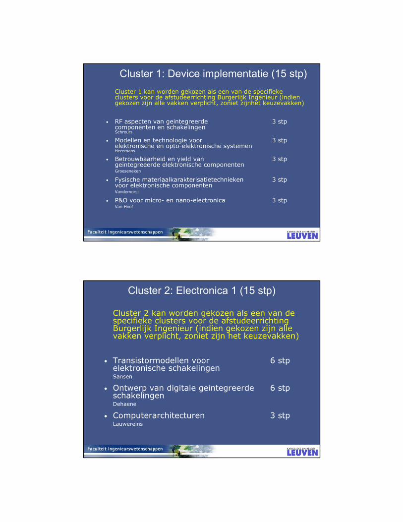
Cluster 1: Device implementatie (15 stp)
Cluster 1 kan worden gekozen als een van de specifiekeclusters voor de afstudeerrichting Burgerlijk Ingenieur (indiengekozen zijn alle vakken verplicht, zoniet zijnhet keuzevakken)
• RF aspecten van geintegreerde 3 stpcomponenten en schakelingenSchreurs
• Modellen en technologie voor 3 stpelektronische en opto-elektronische systemenHeremans
• Betrouwbaarheid en yield van 3 stpgeintegreeerde elektronische componentenGroeseneken
• Fysische materiaalkarakterisatietechnieken 3 stpvoor elektronische componentenVandervorst
• P&O voor micro- en nano-electronica 3 stpVan Hoof
Cluster 2: Electronica 1 (15 stp)
Cluster 2 kan worden gekozen als een van de specifieke clusters voor de afstudeerrichtingBurgerlijk Ingenieur (indien gekozen zijn allevakken verplicht, zoniet zijn het keuzevakken)
• Transistormodellen voor 6 stpelektronische schakelingenSansen
• Ontwerp van digitale geintegreerde 6 stpschakelingenDehaene
• Computerarchitecturen 3 stpLauwereins

Cluster 3: Electronica 2 (15 stp)
Cluster 3 kan enkel worden gekozen alsverbredende opleiding (alle vakken zijnkeuzevakken)
• Analoge bouwblokken voor 6 stpsignaalverwerkingGielen
• Computergesteund analoog 3 stpIC-ontwerpGielen
• Ontwerp van analoge 6 stpgeintegreerde schakelingenSteyaert
Cluster 4: Biologische systemen (15 stp)
Cluster 4 kan worden gekozen als een van de specifieke clusters voor de afstudeerrichting Bio-ingenieur (indien gekozen zijn alle vakkenverplicht
• Bio-response measurements 3 stpand process controlD. Berckmans
• Sensor technology and bioelectronics 3 stpJ. Lammertyn
• Systeem-fysiologie 3 stpG. Bultynck
• Fysicochemistry of biological systems 6 stpY. Engelborghs
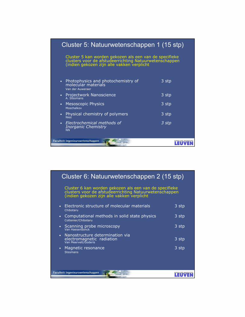
Cluster 5: Natuurwetenschappen 1 (15 stp)
Cluster 5 kan worden gekozen als een van de specifiekeclusters voor de afstudeerrichting Natuurwetenschappen(indien gekozen zijn alle vakken verplicht
• Photophysics and photochemistry of 3 stpmolecular materialsVan der Auweraer
• Projectwork Nanoscience 3 stpA. Stesmans
• Mesoscopic Physics 3 stpMoschalkov
• Physical chemistry of polymers 3 stpNies
• Electrochemical methods of 3 stpInorganic ChemistryNN
Cluster 6: Natuurwetenschappen 2 (15 stp)
Cluster 6 kan worden gekozen als een van de specifiekeclusters voor de afstudeerrichting Natuurwetenschappen(indien gekozen zijn alle vakken verplicht
• Electronic structure of molecular materials 3 stpChibotaru
• Computational methods in solid state physics 3 stpCottenier/Chibotaru
• Scanning probe microscopy 3 stpVan Haesendonck
• Nanostructure determination viaelectromagnetic radiation 3 stpVan Meervelt/Goderis
• Magnetic resonance 3 stpStesmans
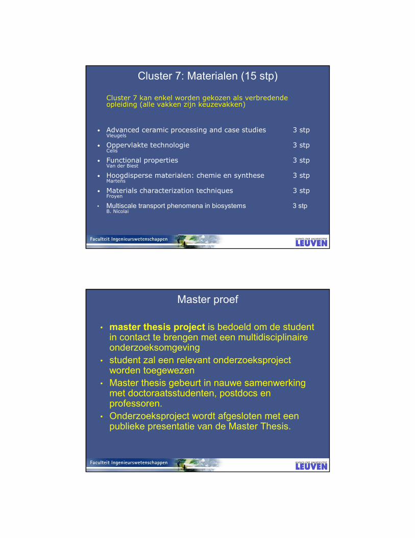
Cluster 7: Materialen (15 stp)
Cluster 7 kan enkel worden gekozen als verbredendeopleiding (alle vakken zijn keuzevakken)
• Advanced ceramic processing and case studies 3 stpVleugels
• Oppervlakte technologie 3 stpCelis
• Functional properties 3 stpVan der Biest
• Hoogdisperse materialen: chemie en synthese 3 stpMartens
• Materials characterization techniques 3 stpFroyen
• Multiscale transport phenomena in biosystems 3 stpB. Nicolai
Master proef
• master thesis project is bedoeld om de student in contact te brengen met een multidisciplinaireonderzoeksomgeving
• student zal een relevant onderzoeksprojectworden toegewezen
• Master thesis gebeurt in nauwe samenwerkingmet doctoraatsstudenten, postdocs en professoren.
• Onderzoeksproject wordt afgesloten met eenpublieke presentatie van de Master Thesis.
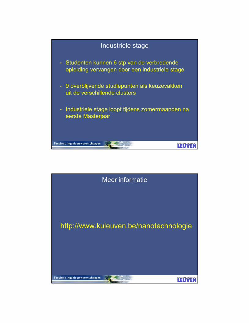
Industriele stage
• Studenten kunnen 6 stp van de verbredende
opleiding vervangen door een industriele stage
• 9 overblijvende studiepunten als keuzevakken
uit de verschillende clusters
• Industriele stage loopt tijdens zomermaanden na
eerste Masterjaar
Meer informatie
http://www.kuleuven.be/nanotechnologie
Outline• Wat is Nanowetenschappen en Nanotechnologie ?
– Wat is het ?
– Voorbeelden
– Toepassingen
• Master Nanowetenschappen en Nanotechnologie– Structuur en instroom
– Overzicht vakkenclusters
– Master thesis
– Industriele stage
• Erasmus Mundus Master Nanoscience and Nanotechnology– Wat is het ?
– Structuur
– Kandidaatstelling
• Perspectieven
Erasmus Mundus Master
Samenwerking tussen 4 Europese topuniversiteitenTUDelft/Leiden, Chalmers University, TUDresden, KULeuven

Erasmus Mundus Master
• Nieuwe Europese Master over de disciplines van de vier
partneruniversiteiten
• Programma is volledig Engelstalig
• KU Leuven is de coordinator van de Master
• Officieel gestart in academiejaar 2005-2006
• Studenten studeren telkens 1 jaar aan een van de
partneruniversiteiten
• Studenten ontvangen twee diploma’s: een van elke
universiteit waar werd gestudeerd !
• KUL-EMM programma is een subset van de KUL Master
• Aanvragen moeten ingediend worden voor 1 juni
• EMM Master coordinator: Prof. Guido Groeseneken
EMM-Nano curriculum
Course modules
(major/minor)
60 e.c.
Course modules
(major/minor)
60 e.c.
Master’s Thesis
Research Project
(major)
30-48 e.c.
Master’s Thesis
Research Project
(major)
30-48 e.c.
Course
modules
(major)
12-30 e.c.
Course
modules
(major)
12-30 e.c.
2 years = 120 e.c.
University 1 University 2
Major/minor themes:
nanoscience – nanotechnology – biophysics -
bionanotechnology

Chalmers
TU Dresden
Delft/Leiden
K.U.Leuven
BionanotechBiophysics NanoscienceNanotechMajor themes per university
Electives preparing for 2nd year
Electives preparing for 2nd year
Delft/LeidenDelft/Leiden
ChalmersChalmers
DresdenDresden
18 e.c. mandatory
6 e.c. Nanotech/ Nanoscience
EMM-Nano major electives: 1st year
12 e.c. Nanotech +
12 e.c. Nanoscience
12 e.c. mandatory
12 e.c. Nanoscience/nanotech
EMM-Nano courses: 1e jaar aan KUL
Introductory Courses (≤ 12 stp)Semiconductor Physics (3 stp)
Semiconductor Devices (3 stp)
Macromolecules (3 stp)
Quantum Physics (3 stp)
Introductory Courses (≤ 12 stp)Semiconductor Physics (3 stp)
Semiconductor Devices (3 stp)
Macromolecules (3 stp)
Quantum Physics (3 stp)
Core Courses (24 stp)
Materials Physics and Technology
for Nanoelectronics (6 stp)
Chemistry at nanometer schale (6 stp)
Technology of Integrated systems (6 stp)
Nano-structured bio-macromolecules (6 stp)
Core Courses (24 stp)
Materials Physics and Technology
for Nanoelectronics (6 stp)
Chemistry at nanometer schale (6 stp)
Technology of Integrated systems (6 stp)
Nano-structured bio-macromolecules (6 stp)
Non-technical electives (6 stp)Economics of information systems
Innovation management
Total quality management
Dutch for foreigners (obligatory)
Non-technical electives (6 stp)Economics of information systems
Innovation management
Total quality management
Dutch for foreigners (obligatory)
Courses preparing for 2nd year
Mandatory (depending on choice 2nd univ)
Electives(total 18 -30 stp)
Courses preparing for 2nd year
Mandatory (depending on choice 2nd univ)
Electives(total 18 -30 stp)
EMM-Nano courses: 2e jaar aan KUL
Master thesis (30 stp)idem
Master thesis (30 stp)idem
Mandatory courses
Depending on program of 1st year
And selected Major/minor
Mandatory courses
Depending on program of 1st year
And selected Major/minor
Elective coursesidem
Elective coursesidem
Toelating en kandidaatstelling
• Toegelaten zijn Bachelors in Physics en in andere
domeinen van wetenschappen en engineering
(Chemistry, Biochemistry, Electrical Engineering,
Materials Science)
• Application deadline is 1 Februari voor niet-EEA
studenten en 1 juni voor EEA studenten.
• Selectie gebeurt door EMM board op basis van
relevante achtergrond, kwaliteit van de student
tijdens Bachelors, kennis van het Engels
• K.U.Leuven online application form kan worden
gedownload van de website
Meer informatie
http://www.emm-nano.org/
Outline• Wat is Nanowetenschappen en Nanotechnologie ?
– Wat is het ?
– Voorbeelden
– Toepassingen
• Master Nanowetenschappen en Nanotechnologie– Structuur en instroom
– Overzicht vakkenclusters
– Master thesis
– Industriele stage
• Erasmus Mundus Master Nanoscience and Nanotechnology– Wat is het ?
– Structuur
– Kandidaatstelling
• Perspectieven

Source : Red Herring, May 2002
Nanotechnology de volgende technology-wave
voor de 21e eeuw ?
Nanotechnology-related Patents
(1990 – 2003)
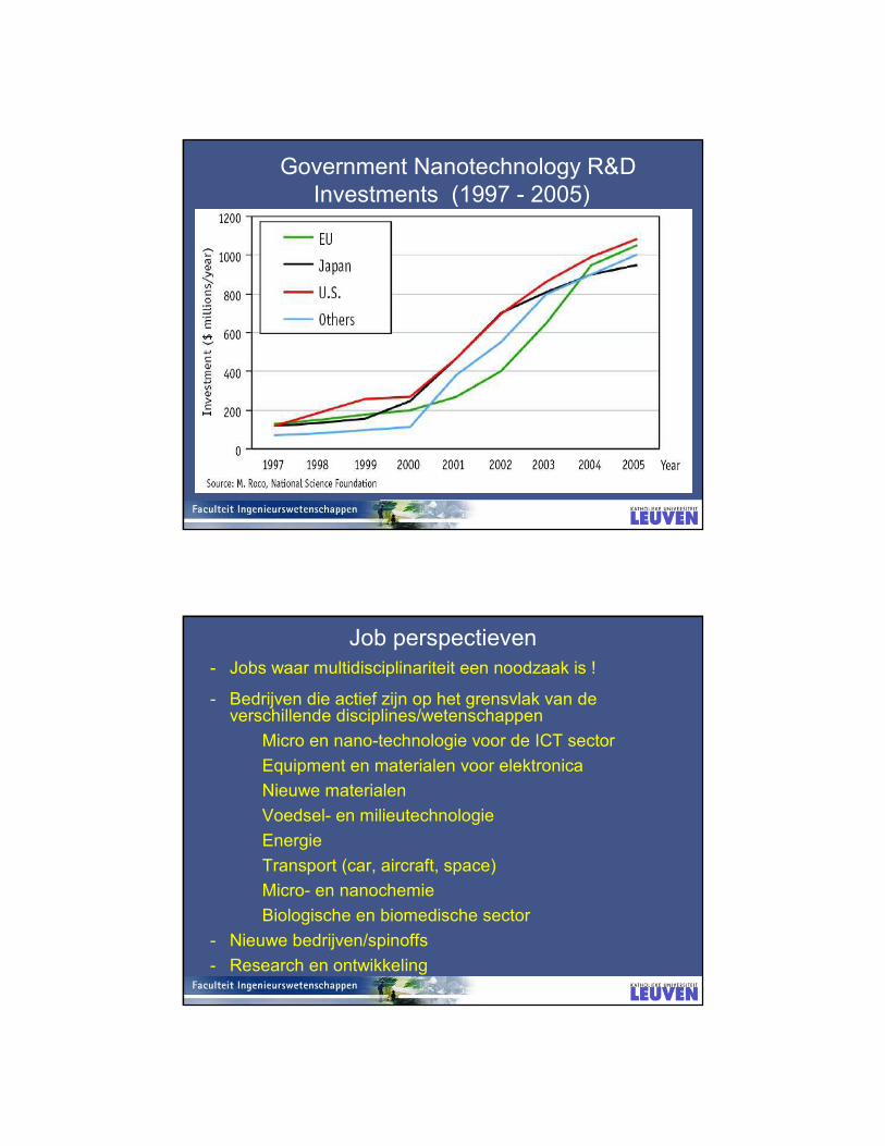
Government Nanotechnology R&D
Investments (1997 - 2005)
Job perspectieven
- Jobs waar multidisciplinariteit een noodzaak is !
- Bedrijven die actief zijn op het grensvlak van de verschillende disciplines/wetenschappen
Micro en nano-technologie voor de ICT sector
Equipment en materialen voor elektronica
Nieuwe materialen
Voedsel- en milieutechnologie
Energie
Transport (car, aircraft, space)
Micro- en nanochemie
Biologische en biomedische sector
- Nieuwe bedrijven/spinoffs
- Research en ontwikkeling

Bedrijven
? Future Perspectives ?

![[24] Nanotechnologie - KNAW Onderwijsprijs · 2014. 8. 22. · 6 2. Inleiding Het onderwerp van ons profielwerkstuk is in het voorwoord al naar voren gekomen, namelijk nanotechnologie.](https://static.fdocuments.nl/doc/165x107/604384113be22d75c83b1bf4/24-nanotechnologie-knaw-onderwijsprijs-2014-8-22-6-2-inleiding-het-onderwerp.jpg)