
Manuscript for Solar Energy Materials and Solar Cells
26
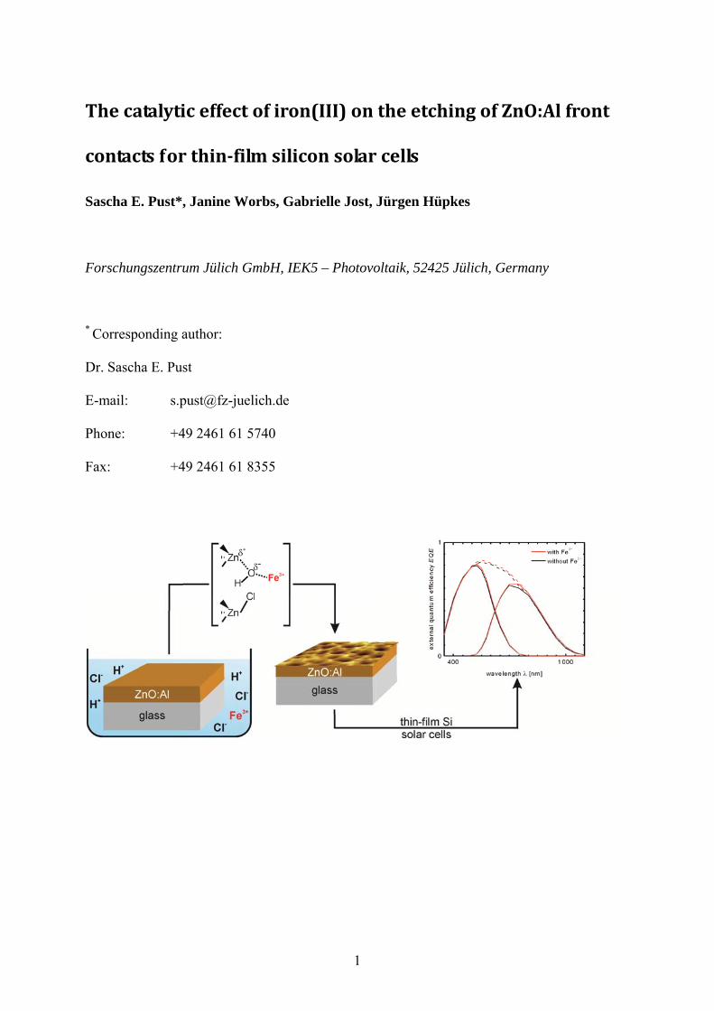
The catalytic effect of iron(III) on the etching of ZnO:Al front contacts for thin‐film silicon solar cells Sascha E. Pust*, Janine Worbs, Gabrielle Jost, Jürgen Hüpkes Forschungszentrum Jülich GmbH, IEK5 – Photovoltaik, 52425 Jülich, Germany * Corresponding author: Dr. Sascha E. Pust E-mail: [email protected] Phone: +49 2461 61 5740 Fax: +49 2461 61 8355 1
Transcript of Manuscript for Solar Energy Materials and Solar Cells
Thecatalyticeffectofiron(III)ontheetchingofZnO:Alfront
contactsforthin‐filmsiliconsolarcells
Sascha E. Pust*, Janine Worbs, Gabrielle Jost, Jürgen Hüpkes
Forschungszentrum Jülich GmbH, IEK5 – Photovoltaik, 52425 Jülich, Germany
* Corresponding author:
Dr. Sascha E. Pust
E-mail: [email protected]
Phone: +49 2461 61 5740
Fax: +49 2461 61 8355
1
j.huepkes
Textfeld
Solar energy materials & solar cells 113, 106-113 (2013) [10.1016/j.solmat.2013.01.045]
Abstract
Sputter-deposited ZnO:Al thin films, used as front contact in thin-film Si solar cells,
were etched in diluted HCl containing catalytic amounts of Fe(III) salts. The Fe(III)
effectively catalyzes the HCl-based etch process, leading to a crater-like morphology that is
qualitatively similar to the one generated by the uncatalyzed etching process at the same HCl
concentrations. Utilizing this catalyzed process, an increase of the etching rate by a factor of
approximately 1.8-2.6 was observed. This allows for a well-controllable tuning of the etch
duration without changing HCl concentration or temperature. The process has been evaluated
with a selection of Fe(III) salts at different concentrations of the acid and of the catalyst.
Optical, electrical and scanning force microscopic characterization of such catalytically
etched ZnO:Al films has shown that the catalytical process leads to slightly smaller
morphological features on the film compared to the uncatalyzed etching, accompanied by a
shift of light scattering intensity to higher angles. This etching behavior may be used
beneficially for light trapping in thin-film Si solar cells. In addition to these application-
oriented aspects, this approach provides a deeper insight into the mechanistical details of the
ZnO thin-film dissolution.
Keywords: Catalysis; Etching; Thin-film Si solar cells; Transparent conductive oxide (TCO);
ZnO thin films
2

1. Introduction
The front contact in thin-film Si solar cells has to fulfil three criteria: (i) it has to be
highly transparent, (ii) a low series resistance is necessary, and (iii) it has to provide a certain
roughness for light management in the device, thus helping to trap the light within the
absorber layer stack by total internal reflection. The first two aspects are given for many
doped, transparent conductive oxides (TCO) like SnO2:F, In2O3:SnO2, ZnO:Al, ZnO:B, or
ZnO:Ga [1-6]. The latter criterion, however, necessitates further texturing in the case of some
TCO materials that are smooth in the as-deposited state. Sputter-deposited, polycrystalline
ZnO:Al, for example, may be artificially roughened by an etching step in diluted HCl [7-10]
(e.g., leading to the 'standard Jülich' type material [11, 12]), HF [13], NH4Cl [14-16], other
acids in liquid [7-10, 17, 18], gaseous [19], or vaporized state [20], by electrochemical
means [21], or by a combination of such processes [13, 22-26]. The variety of possible
etching methods together with a model for the etching of polycrystalline ZnO:Al has been
addressed in a recent review [27].
Besides the texture, one parameter of significant industrial relevance is the duration of
the etching step. For inclusion of such a process into in-line production systems, adjustable
etch times are desirable. This can be done to a certain extent by changing the concentration of
the etchant or the temperature. However, the resulting morphology is changed significantly by
such alterations as well [22, 28]. Readily applicable methods for the adjustment of the etch
time are hence not at hand.
One general option for accelerating chemical reactions is the utilization of catalytic
processes. It is well known that catalysis is a concept of utmost relevance for chemical
industry because of its ability to initiate, accelerate, or steer chemical reactions. Although the
exact nature of the interfacial processes during acidic etching of ZnO:Al thin films is still not
completely understood [27], it can be expected that this process is accelerated by suitable,
catalytically active agents, similarly to what has been known for In2O3:SnO2 thin films since
many years [29].
In this study, we evaluated the potential of Fe(III) salts to catalyze and accelerate the
etching of sputter-deposited ZnO:Al thin films in diluted HCl. A catalytic mechanism is
proposed that is strongly supported by experimental evidence. Electrical measurements,
angle-resolved scattering (ARS), and scanning force microscopy (SFM) were used to quantify
3
the surface morphologies resulting from the catalyzed etching. This new process renders very
suitable morphologies for light scattering at increased etch rates, and their suitability for thin-
film Si photovoltaic devices is demonstrated.
2. Experimental
2.1 ZnO:Al thin-film preparation
Approximately 800-850 nm thick, polycrystalline ZnO:Al films were deposited on a
(1010) cm2 glass substrate (Corning Eagle XG) using radio frequency magnetron sputtering
in a vertical in-line system (cf. Fig. 1 in Ref. [30]) from a ceramic target consisting of ZnO
with 1 w/w% Al2O3 (Cerac Inc., Milwaukee, WI, USA). The deposition was carried out at a
substrate temperature of 300°C, a discharge power density of 2 W cm-2, and an Ar pressure of
0.1 Pa. Details about the process and ZnO:Al film properties are reported elsewhere [12].
2.2 Etching process and chemicals
All solutions were prepared with deionised water (>16 M cm) from an Elix 10 water
purification system (Millipore Co., Schwalbach, Germany). HCl, FeCl3, Fe(NO3)3,
K3[Fe(CN)6], FeCl2 (all Merck KGaA, Darmstadt, Germany), and Fe2(SO4)3 (Sigma-Aldrich
Chemie GmbH, Munich, Germany) were of analytical grade and were used without further
purification. The temperature was kept constant at 250.5°C during all etching experiments.
After etching, substrates were rinsed with copious amounts of deionized water to remove salt
residues originating from the etching solution.
Special care has to be taken when an acid is added to a compound containing
hexacyanidoferrate because very toxic HCN may be generated. Such experiments therefore
have to be carried out with proper personal protective equipment in a closed fume hood and
with a very small amount of CN-containing compounds only.
2.3 Film characterization
Film thicknesses d have been measured with a Dektak 3030 surface profiler (Veeco
Instruments Ltd., Santa Barbara, CA, USA), taking into account those points where the films
have got the highest thickness. To correct for inhomogeneities in the initial measured film
4
thickness, this initial thickness has been determined by taking the maximum measured d value
for each etch series as initial value instead of taking the measured values at each individual
etching spot. SFM images have been recorded utilizing a NANOStation 300 (S.I.S. GmbH,
Herzogenrath, Germany) in non-contact mode with NCHR-POINTPROBE Si cantilevers
(NanoWorld AG, Neuchâtel, Switzerland). Image post-treatment was performed with the
software SPIP, version 5.1.6 (Image Metrology A/S, Hørsholm, Denmark). A linear
background was subtracted from the images for removal of the sample tilt. A four-point probe
was utilized for determining the sheet resistance Rsh of the films. ARS measurements in
transmission were performed in a home-built system at an optical wavelength of =550 nm.
2.4 Solar cell preparation and characterization
Roughly 1 µm thick µc-Si:H films for single junction solar cells were deposited in a
(4040) cm2 in-line plasma-enhanced chemical vapor deposition (PECVD) system [31]. Si
films for 420 nm a-Si:H / 1.25 µm µc-Si:H tandem p-i-n solar cells were prepared by PECVD
in a (3030) cm2 reactor. Details of the Si PECVD process can be found elsewhere [32, 33].
The back contact consisted of sputter-deposited ZnO:Al and Ag from the same deposition
system as the front contact films. A lab-scale laser patterning system (ROFIN-SINAR Laser
GmbH, Hamburg, Germany) was used to determine a cell area of (11) cm2. Solar cells were
characterized with a Wacom WXS 140 S solar simulator (Wacom Electric Co., Saitama,
Japan) under standard test conditions (AM1.5 spectrum, 100 mW cm-2, 25°C). External
quantum efficiencies EQE were measured in a home-built system by differential spectral
response (DSR) at zero bias voltage. The crystallinity of the Si absorber was determined
from the back side of the cells via Raman measurements with an excitation wavelength of 647
nm which leads to information depths roughly of the thickness of the µc-Si:H absorber. In the
case of the tandem devices, the measured crystallinity of the bottom component cell is
also influenced by the top component cell. This is due to the penetration depth of the Raman
measurement and leads to an underestimation in compared to the real crystallinity of
the bottom component cell. To access the Si, the ZnO:Al/Ag back contact has been removed
at selected spots close to the measured cells with a wet-etching process. Details about the
Raman setup [34] and the determination of the crystallinity [35] can be found in the
respective references.
RSCI
bottom
RSbottomC,I
RSC,I
5
3. Results and discussion
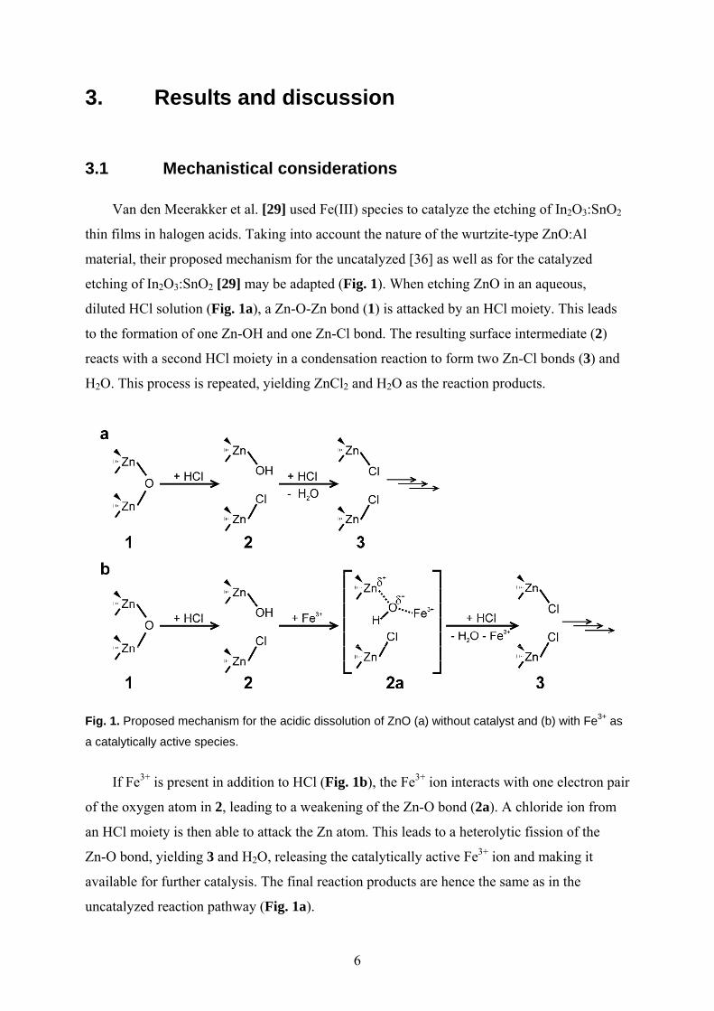
3.1 Mechanistical considerations
Van den Meerakker et al. [29] used Fe(III) species to catalyze the etching of In2O3:SnO2
thin films in halogen acids. Taking into account the nature of the wurtzite-type ZnO:Al
material, their proposed mechanism for the uncatalyzed [36] as well as for the catalyzed
etching of In2O3:SnO2 [29] may be adapted (Fig. 1). When etching ZnO in an aqueous,
diluted HCl solution (Fig. 1a), a Zn-O-Zn bond (1) is attacked by an HCl moiety. This leads
to the formation of one Zn-OH and one Zn-Cl bond. The resulting surface intermediate (2)
reacts with a second HCl moiety in a condensation reaction to form two Zn-Cl bonds (3) and
H2O. This process is repeated, yielding ZnCl2 and H2O as the reaction products.
Fig. 1. Proposed mechanism for the acidic dissolution of ZnO (a) without catalyst and (b) with Fe3+ as
a catalytically active species.
If Fe3+ is present in addition to HCl (Fig. 1b), the Fe3+ ion interacts with one electron pair
of the oxygen atom in 2, leading to a weakening of the Zn-O bond (2a). A chloride ion from
an HCl moiety is then able to attack the Zn atom. This leads to a heterolytic fission of the
Zn-O bond, yielding 3 and H2O, releasing the catalytically active Fe3+ ion and making it
available for further catalysis. The final reaction products are hence the same as in the
uncatalyzed reaction pathway (Fig. 1a).
6
Van den Meerakker et al. [29] have shown for In2O3:SnO2 etching that in the catalyzed
case (Fig. 1b), the reaction of 1 to 2 is the rate-determining step, while the conversion of 2 to
3 is limiting the reaction rate if the process is not catalyzed (Fig. 1a). This means that, in the
case of acidic ZnO etching, an increase in the etch rate can be expected when adding Fe3+ to
the etching solution if the mechanism of In2O3:SnO2 etching [29, 36] is directly transferable
to the ZnO:Al thin film.
3.2 Initial tests
Before applying Fe(III) salts as catalysts in the acidic etching process of ZnO:Al, the
immediate effect of those salts on the thin film had to be evaluated because aqueous solutions
of FeCl3, Fe(NO3)3, Fe2(SO4)3, or similar are slightly acidic by themselves. For example,
taking into account that Fe(III) salts will exist in solution mainly as hydroxo and aqua
complexes with acid dissociation constants pKa in the range of 3.0-3.3 [37], a 0.5 w/w%
solution of FeCl3 will have a pH of approximately 2. This is about one pH unit higher than the
value of an equally concentrated HCl solution. This means that etching in a diluted FeCl3
solution should proceed slower than in similarly concentrated HCl if a possible catalytic
effect of the Fe3+ ions is not too pronounced.
To check this assumption, ZnO:Al substrates have been etched for 40 s in FeCl3 solutions
of 0.5, 0.05, and 0.005 w/w%, respectively, without addition of HCl. While the standard
Jülich method with 0.5 w/w% HCl proceeds at etch rates of a few nm s-1 (depending on the
material properties), the etch rates in FeCl3-containing solutions are indeed much lower: the
0.5 w/w% solution of FeCl3 (corresponding to 0.116 mol L-1) resulted in an etch rate of
roughly 0.9 nm s-1. This value can be ascribed partly to the pH of approximately 2, and partly
to a catalytic effect of the Fe3+ in this slightly acidic solution. Almost no removal (in the range
of few nm min-1) was observed for solutions with an even lower concentration. On the one
hand, this meets the expectations concerning the acidic strength of Fe3+ salts. On the other
hand, it is an important prerequisite for further experiments as this observation implies that
the addition of catalytic amounts of Fe3+ to an HCl solution will be insignificant in terms of a
pH decrease. Hence, Fe3+ would not increase the etch rate in an HCl-based etching
significantly if no catalytic reaction takes place.
7
3.3 Quantification of the catalytic effect
To quantify the catalytic effect of Fe3+, several etch experiments on ZnO:Al substrates
were performed. While the HCl concentration was kept constant in all experiments at 0.5
w/w% (0.137 mol L-1), different catalytic amounts of iron salts were added to the HCl,
namely 1, 5, and 10 mol% with respect to the HCl concentration. Expressed as absolute iron
salt concentrations, these values correspond to 1.37, 6.85, and 13.7 mmol L-1, respectively.
The iron salt concentrations are hence at least about one order of magnitude smaller than in
the previously elucidated, initial experiments. FeCl3 was utilized as source for Fe3+.
Additionally, a cross-check was performed with HCl solutions containing FeCl2 as a salt that
does not contain Fe3+, and K3[Fe(CN)6] where the Fe3+ is tightly bound as the metal center of
a stable complex. The films were etched for 15, 30, 40, and 50 s with each catalyst
concentration and each iron salt. In addition to that, one reference substrate has been etched in
0.5 w/w% HCl without any iron compound to compare the catalyzed with the uncatalyzed
process.
The first visual impression was that all etch attempts lead to more or less pronounced,
hazy ZnO:Al surfaces. All etching solutions rendered visually homogeneous etch results. To
quantify the amount of material that is etched away in a given time, one may take into account
the film thickness d before and after etching, or the change in Rsh that will increase when the
film becomes thinner and more rough. Both parameters are good indicators for the change
that is introduced to the film via etching, but the change in film thickness d represents the
amount of removed material more exactly. Mainly due to the fact that the film is rough after
etching, the profilometric measurements will be afflicted with a certain overestimation of d
the rougher the films get [28]. For these experiments, we took into account only those points
where the films have got the highest thickness (namely crater rims instead of etch pits) in the
profilometric measurements to avoid a significant error originating from this overestimation.
Considering variations in the initial film thickness, we estimated the overall error for d to be
roughly 25 nm. The change in sheet resistance compared to the value before etching (Rsh)
has additionally been used to quantify the etch rates as the sheet resistance measurement is
straightforward and may advantageously be used in terms of process control. The according
Rsh values are presented in the supporting material (Fig. S1).
8
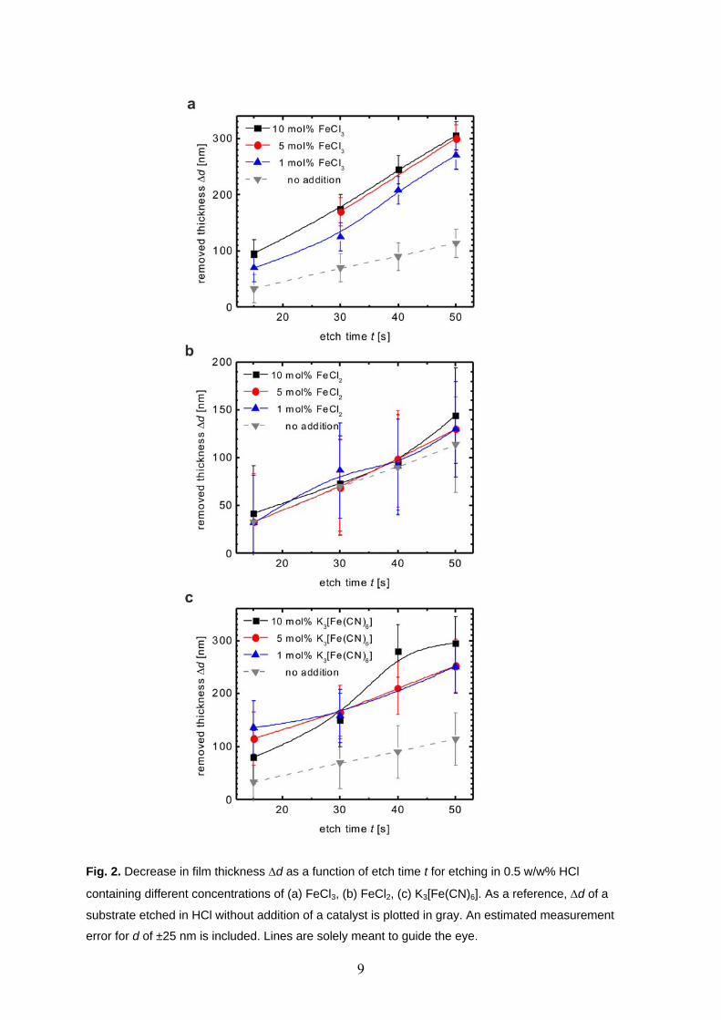
Fig. 2. Decrease in film thickness d as a function of etch time t for etching in 0.5 w/w% HCl
containing different concentrations of (a) FeCl3, (b) FeCl2, (c) K3[Fe(CN)6]. As a reference, d of a
substrate etched in HCl without addition of a catalyst is plotted in gray. An estimated measurement
error for d of ±25 nm is included. Lines are solely meant to guide the eye.
9
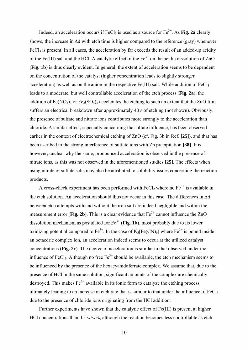
Indeed, an acceleration occurs if FeCl3 is used as a source for Fe3+. As Fig. 2a clearly
shows, the increase in d with etch time is higher compared to the reference (gray) whenever
FeCl3 is present. In all cases, the acceleration by far exceeds the result of an added-up acidity
of the Fe(III) salt and the HCl. A catalytic effect of the Fe3+ on the acidic dissolution of ZnO
(Fig. 1b) is thus clearly evident. In general, the extent of acceleration seems to be dependent
on the concentration of the catalyst (higher concentration leads to slightly stronger
acceleration) as well as on the anion in the respective Fe(III) salt. While addition of FeCl3
leads to a moderate, but well controllable acceleration of the etch process (Fig. 2a), the
addition of Fe(NO3)3 or Fe2(SO4)3 accelerates the etching to such an extent that the ZnO film
suffers an electrical breakdown after approximately 40 s of etching (not shown). Obviously,
the presence of sulfate and nitrate ions contributes more strongly to the acceleration than
chloride. A similar effect, especially concerning the sulfate influence, has been observed
earlier in the context of electrochemical etching of ZnO (cf. Fig. 3b in Ref. [25]), and that has
been ascribed to the strong interference of sulfate ions with Zn precipitation [38]. It is,
however, unclear why the same, pronounced acceleration is observed in the presence of
nitrate ions, as this was not observed in the aforementioned studies [25]. The effects when
using nitrate or sulfate salts may also be attributed to solubility issues concerning the reaction
products.
A cross-check experiment has been performed with FeCl2 where no Fe3+ is available in
the etch solution. An acceleration should thus not occur in this case. The differences in d
between etch attempts with and without the iron salt are indeed negligible and within the
measurement error (Fig. 2b). This is a clear evidence that Fe2+ cannot influence the ZnO
dissolution mechanism as postulated for Fe3+ (Fig. 1b), most probably due to its lower
oxidizing potential compared to Fe3+. In the case of K3[Fe(CN)6] where Fe3+ is bound inside
an octaedric complex ion, an acceleration indeed seems to occur at the utilized catalyst
concentrations (Fig. 2c). The degree of acceleration is similar to that observed under the
influence of FeCl3. Although no free Fe3+ should be available, the etch mechanism seems to
be influenced by the presence of the hexacyanidoferrate complex. We assume that, due to the
presence of HCl in the same solution, significant amounts of the complex are chemically
destroyed. This makes Fe3+ available in its ionic form to catalyze the etching process,
ultimately leading to an increase in etch rate that is similar to that under the influence of FeCl3
due to the presence of chloride ions originating from the HCl addition.
Further experiments have shown that the catalytic effect of Fe(III) is present at higher
HCl concentrations than 0.5 w/w%, although the reaction becomes less controllable as etch
10
times for generating a feasible etch result are in the range of only a few seconds then.
Concentrations as low as approximately 0.1 w/w% are possible as well. For example, while
the etching of a substrate in 0.1 w/w% HCl for 40 s resulted in Rsh=2.1 □, the etch time to
reach a similar value (Rsh=1.9 □) could be reduced to 10 s when adding 5 mol% FeCl3 to
the etchant. In both cases, approximately 85 nm of the film were removed.
Below that concentration, the pH value of the solution is shifted into a range where many
Fe(III) salts are not soluble to an appropriate extent, making a catalytic acceleration
impossible. Over the whole utilizable concentration range of HCl, however, the extent of
acceleration is similar to the previously elucidated extents. This results in an overall
acceleration factor (concerning d) of approximately 1.8-2.6 for the application of FeCl3,
mostly depending on the catalyst concentration.
It has been furthermore observed that the catalytic effect is not limited to HCl. Similar
results have been achieved with other acids (e.g. HNO3 or H2SO4) at pH values of about 1
(not shown), although the degree of acceleration is different for all utilized compounds.
3.4 Influence on surface morphology
Besides the advantage of an accelerated etching, the resulting layers have to have suitable
morphologies for light management in thin-film Si solar cells. Concerning sputter-deposited
ZnO:Al films, it is well known that the standard Jülich reference material [11] is well suited
for this purpose, and this has also been confirmed by optical simulations [39]. It is hence
desirable to keep the morphology after etching similar, even if the process is accelerated
catalytically. This is an important issue, as Owen et al. [28] have pointed out recently that the
etching of sputter-deposited ZnO:Al thin films at different HCl concentrations and different
etchant temperatures influences not only the etch rate, but also the crater size after etching.
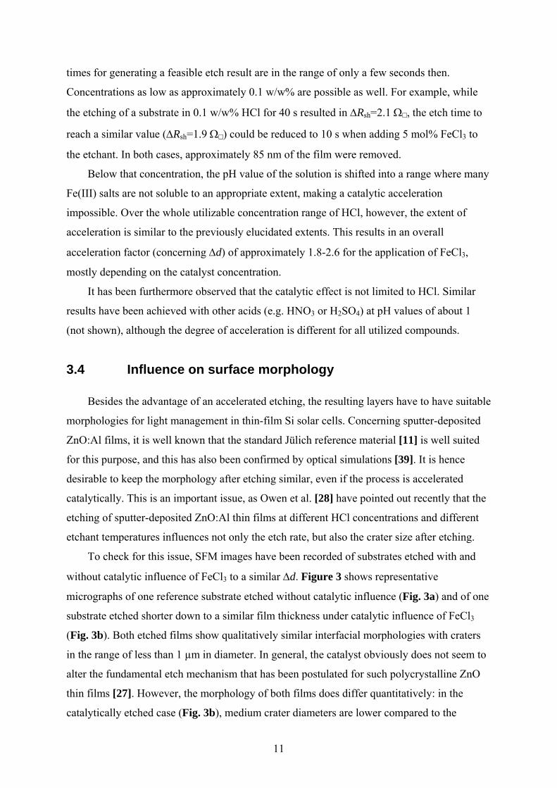
To check for this issue, SFM images have been recorded of substrates etched with and
without catalytic influence of FeCl3 to a similar d. Figure 3 shows representative
micrographs of one reference substrate etched without catalytic influence (Fig. 3a) and of one
substrate etched shorter down to a similar film thickness under catalytic influence of FeCl3
(Fig. 3b). Both etched films show qualitatively similar interfacial morphologies with craters
in the range of less than 1 µm in diameter. In general, the catalyst obviously does not seem to
alter the fundamental etch mechanism that has been postulated for such polycrystalline ZnO
thin films [27]. However, the morphology of both films does differ quantitatively: in the
catalytically etched case (Fig. 3b), medium crater diameters are lower compared to the
11
reference substrate (Fig. 3a), while the medium crater depths and the root mean square (RMS)
roughnesses are similar. The respective quantitative values are given in Table I.
Fig. 3. (10×10) µm2 scanning force micrographs of ZnO:Al thin films etched in (a) 0.5 w/w% HCl for
50 s and (b) 0.5 w/w% HCl with 5 mol% FeCl3 for 30 s.
Table I. Statistical evaluation of the SFM-derived topographies of etched ZnO:Al thin films (cf. Fig. 3). The errors given are the standard deviations derived from the statistical evaluation of the crater dimensions.
etching conditions medium crater diameter [nm]
medium crater depth [nm]
RMS roughness [nm]
50 s in 0.5 w/w% HCl (reference)
887 ± 437 279 ± 140 114
30 s in 0.5 w/w% HCl + 5 mol% FeCl3
791 ± 375 275 ± 146 113
Interestingly, this trend to smaller craters is also observed when etching without catalytic
influence at elevated temperatures, i.e., higher etch rates, or lower concentrations of the acid,
i.e., lower etch rates [28]. This implies that the morphology is not directly related to the etch
rate, but the catalyst seems to lower the etching threshold for grain boundaries with a certain
etch potential [27], leading to an increased crater density and, as a consequence, a decreased
medium crater diameter. Hence, this new method is another tool in addition to the established
procedures basing on different acids and different etching conditions that allows us to tune the
size of surface features on etched ZnO:Al.
12
While SFM is a local technique and can deliver representative topographic informations
of a microscopic fraction of the ZnO:Al surface, optical methods are suited to derive more
integral informations about the substrate on an area of about 1 mm2. Hence, we performed
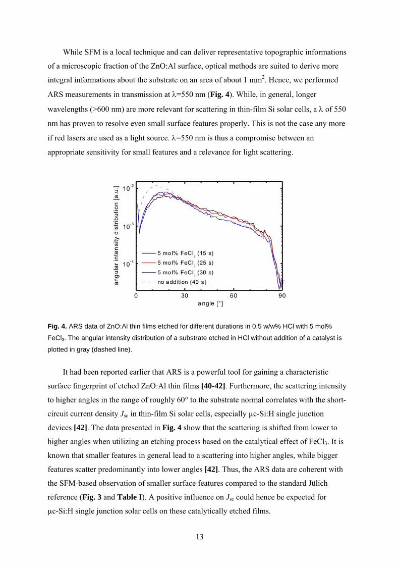
ARS measurements in transmission at =550 nm (Fig. 4). While, in general, longer
wavelengths (>600 nm) are more relevant for scattering in thin-film Si solar cells, a of 550
nm has proven to resolve even small surface features properly. This is not the case any more
if red lasers are used as a light source. =550 nm is thus a compromise between an
appropriate sensitivity for small features and a relevance for light scattering.
Fig. 4. ARS data of ZnO:Al thin films etched for different durations in 0.5 w/w% HCl with 5 mol%
FeCl3. The angular intensity distribution of a substrate etched in HCl without addition of a catalyst is
plotted in gray (dashed line).
It had been reported earlier that ARS is a powerful tool for gaining a characteristic
surface fingerprint of etched ZnO:Al thin films [40-42]. Furthermore, the scattering intensity
to higher angles in the range of roughly 60° to the substrate normal correlates with the short-
circuit current density Jsc in thin-film Si solar cells, especially µc-Si:H single junction
devices [42]. The data presented in Fig. 4 show that the scattering is shifted from lower to
higher angles when utilizing an etching process based on the catalytical effect of FeCl3. It is
known that smaller features in general lead to a scattering into higher angles, while bigger
features scatter predominantly into lower angles [42]. Thus, the ARS data are coherent with
the SFM-based observation of smaller surface features compared to the standard Jülich
reference (Fig. 3 and Table I). A positive influence on Jsc could hence be expected for
µc-Si:H single junction solar cells on these catalytically etched films.
13
3.5 Evaluation in solar cells
To check the catalytically etched films in terms of suitability for an application as front
contact, we co-deposited µc-Si:H p-i-n single junction solar cells onto films etched for
different durations in 0.5 w/w% HCl containing 5 mol% FeCl3. As a reference, a standard
Jülich-type ZnO etched for 40 s in 0.5 w/w% HCl was processed in the same deposition run.
Note that the utilized ZnO:Al thin films are the very same substrates that have been
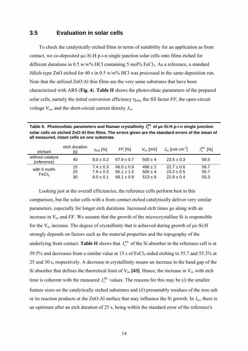
characterized with ARS (Fig. 4). Table II shows the photovoltaic parameters of the prepared
solar cells, namely the initial conversion efficiency init, the fill factor FF, the open-circuit
voltage Voc, and the short-circuit current density Jsc.
Table II. Photovoltaic parameters and Raman crystallinity of µc-Si:H p-i-n single junction
solar cells on etched ZnO:Al thin films. The errors given are the standard errors of the mean of all measured, intact cells on one substrate.
RSCI
etchant etch duration
[s] init [%] FF [%] Voc [mV] Jsc [mA cm-2] RSCI [%]
without catalyst (reference)
40 8.0 ± 0.2 67.9 ± 0.7 500 ± 4 23.5 ± 0.3 59.5
15 7.4 ± 0.3 66.0 ± 0.9 496 ± 2 22.7 ± 0.6 59.7 25 7.6 ± 0.3 65.1 ± 1.5 500 ± 4 23.2 ± 0.5 55.7 with 5 mol%
FeCl3 30 8.0 ± 0.1 68.1 ± 0.9 513 ± 6 22.8 ± 0.4 55.3
Looking just at the overall efficiencies, the reference cells perform best in this
comparison, but the solar cells with a front contact etched catalytically deliver very similar
parameters, especially for longer etch durations. Increased etch times go along with an
increase in Voc and FF. We assume that the growth of the microcrystalline Si is responsible
for the Voc increase. The degree of crystallinity that is achieved during growth of µc-Si:H
strongly depends on factors such as the material properties and the topography of the
underlying front contact. Table II shows that of the Si absorber in the reference cell is at
59.5% and decreases from a similar value at 15 s of FeCl3-aided etching to 55.7 and 55.3% at
25 und 30 s, respectively. A decrease in crystallinity means an increase in the band gap of the
Si absorber that defines the theoretical limit of Voc [43]. Hence, the increase in Voc with etch
time is coherent with the measured values. The reasons for this may be (i) the smaller
feature sizes on the catalytically etched substrates and (ii) presumably residues of the iron salt
or its reaction products at the ZnO:Al surface that may influence the Si growth. In Jsc, there is
an optimum after an etch duration of 25 s, being within the standard error of the reference's
RSCI
RSCI
14
Jsc. The cells after 30 s of FeCl3-catalyzed etching deliver the same init as the reference due
to a gain in Voc of roughly 10 mV.
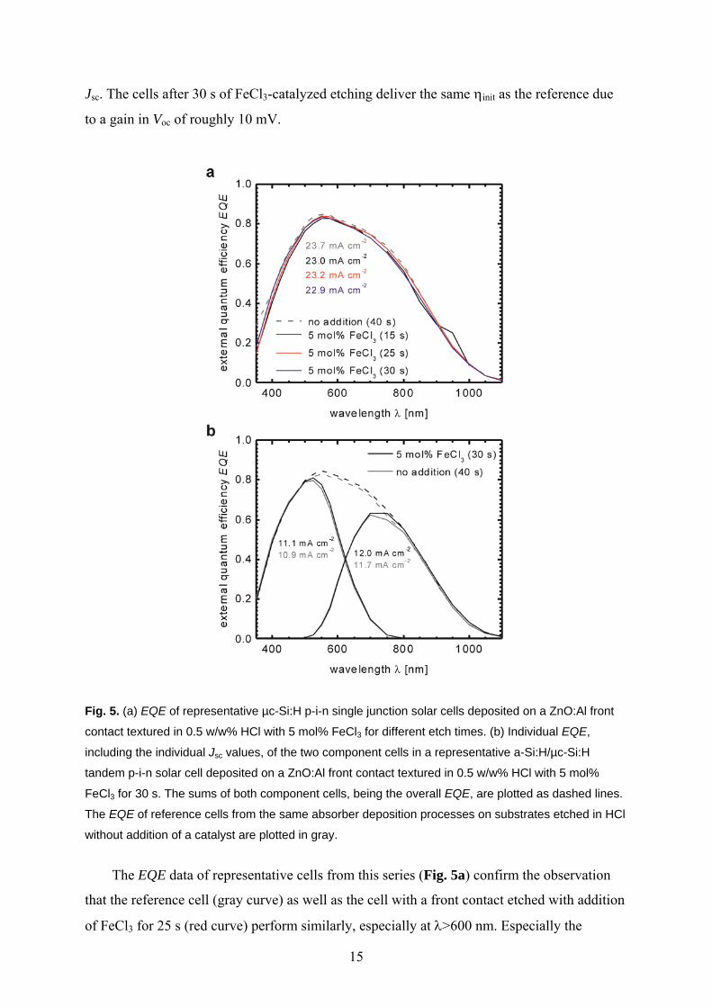
Fig. 5. (a) EQE of representative µc-Si:H p-i-n single junction solar cells deposited on a ZnO:Al front
contact textured in 0.5 w/w% HCl with 5 mol% FeCl3 for different etch times. (b) Individual EQE,
including the individual Jsc values, of the two component cells in a representative a-Si:H/µc-Si:H
tandem p-i-n solar cell deposited on a ZnO:Al front contact textured in 0.5 w/w% HCl with 5 mol%
FeCl3 for 30 s. The sums of both component cells, being the overall EQE, are plotted as dashed lines.
The EQE of reference cells from the same absorber deposition processes on substrates etched in HCl
without addition of a catalyst are plotted in gray.
The EQE data of representative cells from this series (Fig. 5a) confirm the observation
that the reference cell (gray curve) as well as the cell with a front contact etched with addition
of FeCl3 for 25 s (red curve) perform similarly, especially at >600 nm. Especially the
15
variation in Jsc for different etch times are almost within an error range that can occur just due
to inhomogeneities in the deposition. Nevertheless, there are small variations in the EQE for
different wavelength regions as a function of the etch time. Etching for only 15 s (black
curve) leads to a loss in the EQE over the whole spectral range compared to the reference,
while longer etching for 30 s (blue curve) results in a higher EQE at small wavelengths, but a
slight deterioration above 600 nm. On the one hand, this can be correlated to the tendency of
the cells to become more amorphous with increasing etch time (cf. Voc and in Table II).
On the other hand, the ZnO:Al thickness and the development of the morphology of course
plays a role as well. 15 s FeCl3-aided etching (black curve) means thick ZnO:Al and only
slight structure development, leading to losses over the whole spectral range. At 25 s (red
curve), the film is thinner and thus lets more light pass into the cell (short wavelength gain),
and the structures are further developed (long wavelength gain due to light trapping). 30 s of
etching (blue curve) mean that even more light passes through the very thin ZnO:Al (stronger
gain at <600 nm), but the craters reach the glass substrate and thus the structure depth is
reduced again (loss at long wavelengths due to deterioration of light trapping).
RSCI
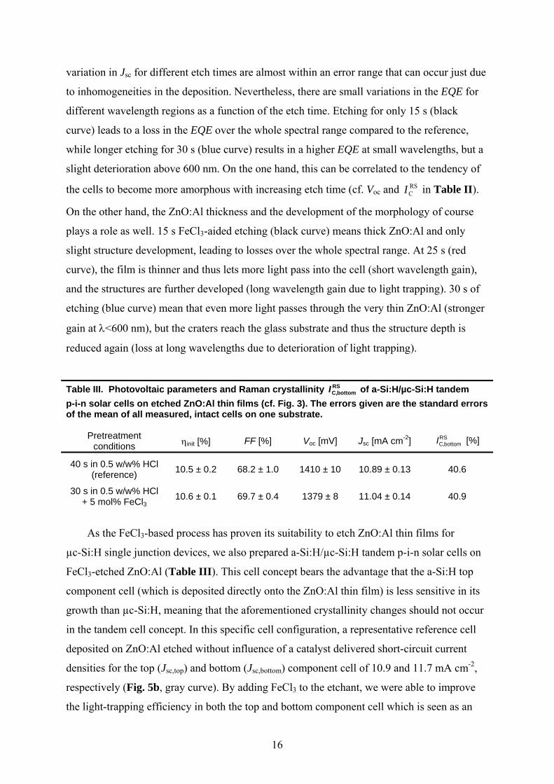
Table III. Photovoltaic parameters and Raman crystallinity of a-Si:H/µc-Si:H tandem
p-i-n solar cells on etched ZnO:Al thin films (cf. Fig. 3). The errors given are the standard errors of the mean of all measured, intact cells on one substrate.
RSbottomC,I
Pretreatment
conditions init [%] FF [%] Voc [mV] Jsc [mA cm-2] RSbottomC,I [%]
40 s in 0.5 w/w% HCl (reference)
10.5 ± 0.2 68.2 ± 1.0 1410 ± 10 10.89 ± 0.13 40.6
30 s in 0.5 w/w% HCl + 5 mol% FeCl3
10.6 ± 0.1 69.7 ± 0.4 1379 ± 8 11.04 ± 0.14 40.9
As the FeCl3-based process has proven its suitability to etch ZnO:Al thin films for
µc-Si:H single junction devices, we also prepared a-Si:H/µc-Si:H tandem p-i-n solar cells on
FeCl3-etched ZnO:Al (Table III). This cell concept bears the advantage that the a-Si:H top
component cell (which is deposited directly onto the ZnO:Al thin film) is less sensitive in its
growth than µc-Si:H, meaning that the aforementioned crystallinity changes should not occur
in the tandem cell concept. In this specific cell configuration, a representative reference cell
deposited on ZnO:Al etched without influence of a catalyst delivered short-circuit current
densities for the top (Jsc,top) and bottom (Jsc,bottom) component cell of 10.9 and 11.7 mA cm-2,
respectively (Fig. 5b, gray curve). By adding FeCl3 to the etchant, we were able to improve
the light-trapping efficiency in both the top and bottom component cell which is seen as an
16
increase in Jsc,top of 0.2 mA cm-2 and in Jsc,bottom of 0.3 mA cm-2 (Fig. 5b, black curve),
improving init compared to the reference as well. This improvement is at the cost of a loss of
roughly 30 mV in Voc and at similar crystallinities of the bottom component cell absorber
(Table III).
In addition, µc-Si:H single junction as well as a-Si:H/µc-Si:H tandem p-i-n solar cells
have been prepared on some subtrates etched under the contribution of other Fe(III) salts.
Those cell results are collected in the supporting material (Tables SI and SII, Figs. S2 and S3)
and are generally in agreement with the expectations from the film characterization
experiments.
4. Conclusions and outlook
We have shown that the acidic etching of polycrystalline, sputter-deposited ZnO:Al thin
films may be accelerated efficiently and in a well-controllable manner by adding catalytic
amounts of an Fe(III) salt to the etchant. The Fe(III) acts as a catalyst in the etching
mechanism and alters it in favor of a faster overall reaction, leading to an approximate
doubling of the etch rate. The best and most homogeneous results have been achieved when
utilizing FeCl3 as Fe(III) source. As a result of the catalytic influence of Fe(III), the resulting
morphology of the etched ZnO:Al thin film is altered towards slightly smaller features
compared to non-catalytically etched substrates. This leads to a shift of the light scattering at
the film/air interface to larger angles which can be advantageous for the light trapping in a
thin-film Si solar cell if such ZnO:Al thin films are used as the front contact.
The degree of acceleration as well as the extent of the change in morphology may be
controlled by changing the catalyst concentration or the concentration of the etchant. Thus,
we have got a method at hand to decrease the etch duration of an industrially relevant etching
process with no adverse or, in some cases, even beneficial effects on the light trapping in the
device. Such an additional process parameter is of significant practical importance, e.g., for
the adjustment of process step times in an in-line production system, and it upvalues the
industrial applicability of the well-established ZnO etching process.
17

Acknowledgments
The authors thank Mengfei Wu for ARS measurements, Simone Bugdol, Joachim
Kirchhoff, Daniel Weigand, and Thomas Zimmermann for assistance in solar cell deposition
and characterization, Markus Hülsbeck for Raman measurements as well as Nicole Lühmann,
Matthias Meier, and Eerke Bunte (all Forschungszentrum Jülich GmbH) for fruitful
discussions. Financial support by the German Federal Environment Ministry (BMU, grants
0327693A and 0325299A) is gratefully acknowledged.
18
References
[1] K. Sato, Y. Gotoh, Y. Wakayama, Y. Hayashi, K. Adachi, H. Nishimura, Highly
Textured SnO2:F TCO Films for a-Si Solar Cells, Rep. Res. Lab. Asahi Glass Co., Ltd.,
42 (1992) 129-137.
[2] J.K. Rath, Y. Liu, M.M. de Jong, J. de Wild, J.A. Schuttauf, M. Brinza, R.E.I. Schropp,
Transparent conducting oxide layers for thin film silicon solar cells, Thin Solid Films,
518 (2010) e129-e135.
[3] H.N. Wanka, M.B. Schubert, E. Lotter, Growth of a-Si:H on transparent conductive
oxides for solar cell applications, Sol. Energy Mater. Sol. Cells, 41-42 (1996) 519-527.
[4] J. Hüpkes, J. Müller, B. Rech, Texture Etched ZnO:Al for Silicon Thin Film Solar
Cells, in: K. Ellmer, A. Klein, B. Rech (Eds.) Transparent Conductive Zinc Oxide:
Basics and Applications in Thin Film Solar Cells, Springer, Berlin, 2008, pp. 359-414.
[5] J. Meier, J. Spitznagel, U. Kroll, C. Bucher, S. Faÿ, T. Moriarty, A. Shah, Potential of
amorphous and microcystalline silicon solar cells, Thin Solid Films, 451-452 (2004)
518-524.
[6] V. Bhosle, A. Tiwari, J. Narayan, Electrical properties of transparent and conducting Ga
doped ZnO, J. Appl. Phys., 100 (2006) 033713.
[7] B.-H. Seo, S.-H. Lee, J.H. Seo, J.-H. Jeon, H. Choe, Study on the wet etch behavior of a
zinc-oxide semiconductor in acid solutions, J. Korean Phys. Soc., 53 (2008) 402-405.
[8] D.-G. Yoo, S.-H. Nam, M.H. Kim, S.H. Jeong, H.-G. Jee, H.J. Lee, N.-E. Lee, B.Y.
Hong, Y.J. Kim, D. Jung, J.-H. Boo, Fabrication of the ZnO thin films using wet-
chemical etching processes on application for organic light emitting diode (OLED)
devices, Surf. Coat. Technol., 202 (2008) 5476-5479.
[9] W.T. Yen, Y.C. Lin, J.H. Ke, Surface textured ZnO:Al thin films by pulsed DC
magnetron sputtering for thin film solar cells applications, Appl. Surf. Sci., 257 (2010)
960-968.
[10] W.-L. Lu, K.-C. Huang, C.-H. Yeh, C.-I. Hung, M.-P. Houng, Investigation of textured
Al-doped ZnO thin films using chemical wet-etching methods, Mater. Chem. Phys., 127
(2011) 358-363.
[11] M. Kubon, E. Boehmer, F. Siebke, B. Rech, C. Beneking, H. Wagner, Solution of the
ZnO/p contact problem in a-Si:H solar cells, Sol. Energy Mater. Sol. Cells, 41-42
(1996) 485-492.
19
[12] M. Berginski, J. Hüpkes, M. Schulte, G. Schöpe, H. Stiebig, B. Rech, M. Wuttig, The
effect of front ZnO:Al surface texture and optical transparency on efficient light
trapping in silicon thin-film solar cells, J. Appl. Phys., 101 (2007) 074903.
[13] J.I. Owen, J. Hüpkes, H. Zhu, E. Bunte, S.E. Pust, Novel etch process to tune crater size
on magnetron sputtered ZnO:Al, Phys. Status Solidi A, 208 (2011) 109-113.
[14] J. Sun, J. Bian, H. Liang, J. Zhao, L. Hu, Z. Zhao, W. Liu, G. Du, Realization of
controllable etching for ZnO film by NH4Cl aqueous solution and its influence on
optical and electrical properties, Appl. Surf. Sci., 253 (2007) 5161-5165.
[15] S. Fernández, O. de Abril, F.B. Naranjo, J.J. Gandía, Etching process optimization using
NH4Cl aqueous solution to texture ZnO:Al films for efficient light trapping in flexible
thin film solar cells, Thin Solid Films, 520 (2012) 4144-4149.
[16] S. Fernández, S.E. Pust, J. Hüpkes, F.B. Naranjo, Development of two-step etching
approach for aluminum doped zinc oxide using a combination of standard HCl and
NH4Cl etch steps, Thin Solid Films, 520 (2012) 4678-4684.
[17] Y.C. Lin, Y.C. Jian, J.H. Jiang, A study on the wet etching behavior of AZO (ZnO:Al)
transparent conducting film, Appl. Surf. Sci., 254 (2008) 2671-2677.
[18] N. Kumar, G. Zhang, N. Kalyankar, M.A. Nguyen, J. Li, H. Yang, Z.-W. Sun, High
productivity combinatorial study of wet chemical texture etch of sputter deposited Al-
doped ZnO thin films for thin film Si solar cells, Photovoltaics International, 9 (2010)
137-141.
[19] S.R. Droes, T.T. Kodas, M.J. Hampden-Smith, Etching of ZnO films with
Hexafluoroacetylacetone, Adv. Mater. (Weinheim, Ger.), 10 (1998) 1129-1133.
[20] T. Kawaharamura, T. Hirao, Development and Research on the Mechanism of Novel
Mist Etching Method for Oxide Thin Films, Jpn. J. Appl. Phys., 51 (2012) 036503.
[21] S.O. Klemm, S.E. Pust, A.W. Hassel, J. Hüpkes, K.J.J. Mayrhofer, Electrochemical
texturing of Al-doped ZnO thin films for photovoltaic applications, J. Solid State
Electrochem., 16 (2012) 283-290.
[22] J. Hüpkes, J.I. Owen, E. Bunte, H. Zhu, S.E. Pust, J. Worbs, G. Jost, New Texture
Etching of Zinc Oxide: Tunable Light Trapping for Si Thin Film Solar Cells, in:
Proceedings of the 25th European Photovoltaic Solar Energy Conference, Valencia,
Spain, WIP, Munich, 2010, pp. 3224-3227.
[23] J.I. Owen, J. Hüpkes, E. Bunte, S.E. Pust, A. Gordijn, Etching Modulated Surface
Textures into Sputtered ZnO:Al Films, in: Proceedings of the 25th European
20
Photovoltaic Solar Energy Conference, Valencia, Spain, WIP, Munich, 2010, pp. 2951-
2955.
[24] E. Bunte, H. Zhu, J. Hüpkes, J. Owen, Novel texturing method for sputtered zinc oxide
films prepared at high deposition rate from ceramic tube targets, EPJ Photovolt., 2
(2011) 20602.
[25] S.E. Pust, J.-P. Becker, J. Worbs, S.O. Klemm, K.J.J. Mayrhofer, J. Hüpkes,
Electrochemical Etching of Zinc Oxide for Silicon Thin Film Solar Cell Applications, J.
Electrochem. Soc., 158 (2011) D413-D419.
[26] H. Zhu, J. Hüpkes, E. Bunte, J. Owen, S.M. Huang, Novel etching method on high rate
ZnO:Al thin films reactively sputtered from dual tube metallic targets for silicon-based
solar cells, Sol. Energy Mater. Sol. Cells, 95 (2011) 964-968.
[27] J. Hüpkes, J.I. Owen, S.E. Pust, E. Bunte, Chemical Etching of Zinc Oxide for Thin-
Film Silicon Solar Cells, ChemPhysChem, 13 (2012) 66-73.
[28] J.I. Owen, S.E. Pust, E. Bunte, J. Hüpkes, ZnO Etch-Feature Control via Concentration
and Temperature of Various Acids, ECS J. Solid State Sci. Technol., 1 (2012) P11-P17.
[29] J.E.A.M. van den Meerakker, P.C. Baarslag, M. Scholten, On the Mechanism of ITO
Etching in Halogen Acids: The Influence of Oxidizing Agents, J. Electrochem. Soc.,
142 (1995) 2321-2325.
[30] J. Hüpkes, H. Zhu, J.I. Owen, G. Jost, E. Bunte, Instabilities in reactive sputtering of
ZnO:Al and reliable texture-etching solution for light trapping in silicon thin film solar
cells, Thin Solid Films, 520 (2012) 1913-1917.
[31] T. Zimmermann, C. Strobel, M. Albert, W. Beyer, A. Gordijn, A.J. Flikweert, J. Kuske,
J.W. Bartha, Inline deposition of microcrystalline silicon solar cells using a linear
plasma source, Phys. Status Solidi C, 7 (2010) 1097-1100.
[32] B. Rech, T. Roschek, T. Repmann, J. Müller, R. Schmitz, W. Appenzeller,
Microcrystalline silicon for large area thin film solar cells, Thin Solid Films, 427 (2003)
157-165.
[33] A.J. Flikweert, T. Zimmermann, T. Merzhanova, D. Weigand, W. Appenzeller, A.
Gordjin, Microcrystalline thin-film solar cell deposition on moving substrates using a
linear VHF-PECVD reactor and a cross-flow geometry, J. Phys. D: Appl. Phys, 45
(2012) 015101.
[34] F. Köhler, S. Schicho, B. Wolfrum, A. Gordijn, S.E. Pust, R. Carius, Gradient etching
of silicon-based thin films for depth-resolved measurements: The example of Raman
crystallinity, Thin Solid Films, 520 (2012) 2605-2608.
21
22
[35] C. Smit, R.A.C.M.M. van Swaaij, H. Donker, A.M.H.N. Petit, W.M.M. Kessels,
M.C.M. van de Sanden, Determining the material structure of microcrystalline silicon
from Raman spectra, J. Appl. Phys., 94 (2003) 3582-3588.
[36] M. Scholten, J.E.A.M. van den Meerakker, On the Mechanism of ITO Etching: The
Specificity of Halogen Acids, J. Electrochem. Soc., 140 (1993) 471-475.
[37] A.F. Holleman, E. Wiberg, N. Wiberg, G. Fischer, Lehrbuch der Anorganischen
Chemie, 102nd ed., Walter de Gruyter, Berlin, New York, 2007.
[38] S.O. Klemm, J.-C. Schauer, B. Schuhmacher, A.W. Hassel, A microelectrochemical
scanning flow cell with downstream analytics, Electrochim. Acta, 56 (2011) 4315-4321.
[39] C. Rockstuhl, S. Fahr, F. Lederer, K. Bittkau, T. Beckers, R. Carius, Local versus global
absorption in thin-film solar cells with randomly textured surfaces, Appl. Phys. Lett., 93
(2008) 061105.
[40] G. Jost, E. Bunte, J. Worbs, H. Siekmann, J. Hüpkes, Surface Characterization of
Sputtered ZnO:Al for Silicon Thin-Film Solar Cells, in: Proceedings of the 25th
European Photovoltaic Solar Energy Conference, Valencia, Spain, WIP, Munich, 2010,
pp. 3078-3082.
[41] W. Dewald, V. Sittinger, B. Szyszka, D. Wippler, J. Hüpkes, P. Obermeyer, F.
Hamelmann, H. Stiebig, F. Säuberlich, D. Severin, S. Klein, M. Rhode, U. Schmidt,
Evaluation of Textured TCOs for a-Si:H/µc-Si:H Thin Film Solar Cells by Angular
Resolved Light Scattering Measurements, in: Proceedings of the 26th European
Photovoltaic Solar Energy Conference, Hamburg, Germany, WIP, Munich, 2011, pp.
2704-2708.
[42] G. Jost, T. Merdzhanova, T. Zimmermann, J. Hüpkes, Process control of texture-etched
high-rate ZnO:Al front contact layers for application in silicon thin-film solar cells, in:
Proceedings of the ICCG 9, Breda, The Netherlands, 2012.
[43] A.V. Shah, M. Vaněček, J. Meier, F. Meillaud, J. Guillet, D. Fischer, C. Droz, X.
Niquille, S. Faÿ, E. Vallat-Sauvain, V. Terrazzoni-Daudrix, J. Bailat, Basic efficiency
limits, recent experimental results and novel light-trapping schemes in a-Si:H, μc-Si:H
and 'micromorph tandem' solar cells, J. Non-Cryst. Solids, 338-340 (2004) 639-645.
Supporting material
The catalytic effect of iron(III) on the etching of ZnO:Al
front contacts for thin-film silicon solar cells
Sascha E. Pust*, Janine Worbs, Gabrielle Jost, Jürgen Hüpkes
Determination of sheet resistances
a
0 10 20 30 40 5
0
2
4
6
8
0
10 mol% FeCl3
05 mol% FeCl3
01 mol% FeCl3
00 no addition
incr
ease
in s
heet
res
ista
nce
R
sh [
]
etch time t [s]
b b
0 10 20 30 40 50
0
1
2
3
4 10 mol% FeCl
2
05 mol% FeCl2
01 mol% FeCl2
00 no addition
incr
ease
in s
heet
re
sist
ance
R
sh [
]
etch time t [s]
0 10 20 30 40 5
0
1
2
3
4
5
0
10 mol% K3[Fe(CN)
6]
05 mol% K3[Fe(CN)
6]
01 mol% K3[Fe(CN)
6]
00 no addition
incr
ease
in s
heet
res
ista
nce
R
sh [
]
etch time t [s]
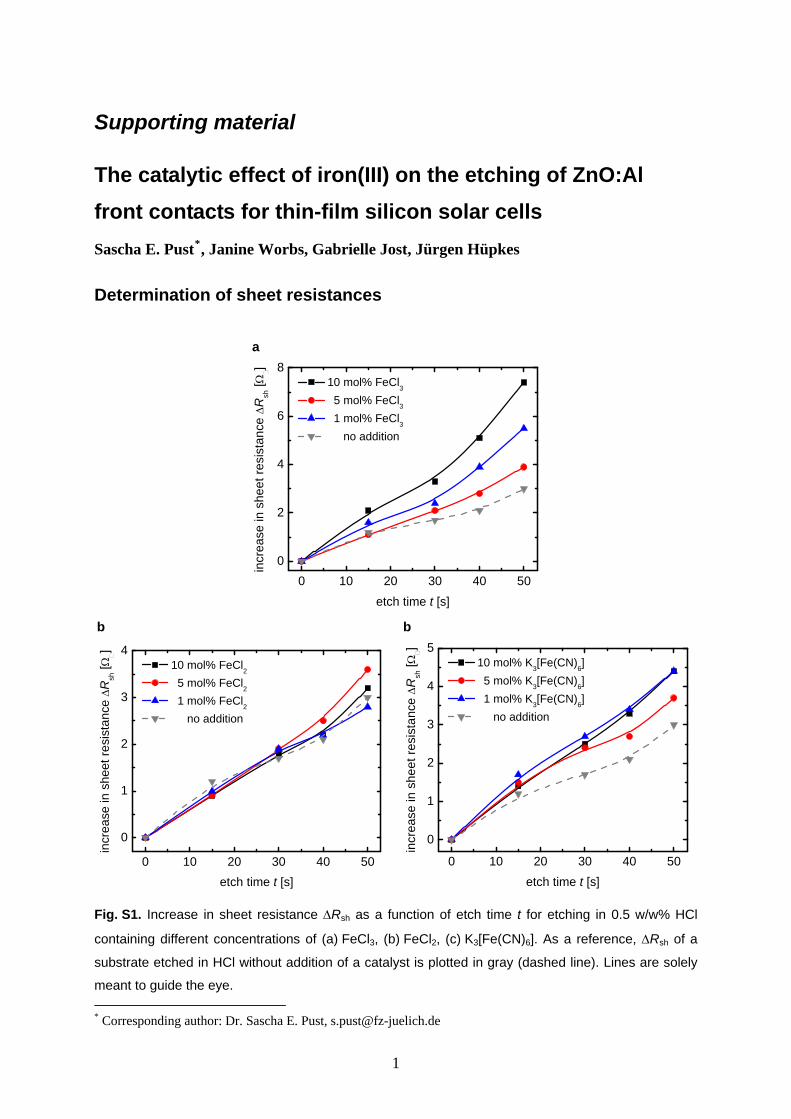
Fig. S1. Increase in sheet resistance Rsh as a function of etch time t for etching in 0.5 w/w% HCl
containing different concentrations of (a) FeCl3, (b) FeCl2, (c) K3[Fe(CN)6]. As a reference, Rsh of a
substrate etched in HCl without addition of a catalyst is plotted in gray (dashed line). Lines are solely
meant to guide the eye.
* Corresponding author: Dr. Sascha E. Pust, [email protected]
1
In addition to the measured film thicknesses, the sheet resistances Rsh have also been
used to control and quantify the ZnO:Al thin film etching with and without catalytic
influence. The increases in sheet resistance (Rsh) as a function of the etch time t are
reproduced above for the experiments with FeCl3 and for the reference experiments with
FeCl2 and K3[Fe(CN)6] (Fig. S1). In general, the results of the determined trends in Rsh and
the thickness changes d (cf. Fig. 2 of the paper) are qualitatively coherent, although the
trends in the dependence on catalyst concentrations are not as clear as they have been in the
case of d.
2
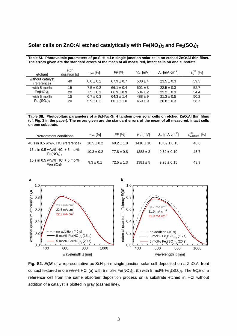
Solar cells on ZnO:Al etched catalytically with Fe(NO3)3 and Fe2(SO4)3
Table SI. Photovoltaic parameters of µc-Si:H p-i-n single junction solar cells on etched ZnO:Al thin films. The errors given are the standard errors of the mean of all measured, intact cells on one substrate.
etchant etch
duration [s] init [%] FF [%] Voc [mV] Jsc [mA cm-2] RSCI [%]
without catalyst (reference)
40 8.0 ± 0.2 67.9 ± 0.7 500 ± 4 23.5 ± 0.3 59.5
15 7.5 ± 0.2 66.1 ± 0.4 501 ± 3 22.5 ± 0.3 52.7 with 5 mol% Fe(NO3)3 20 7.5 ± 0.1 66.9 ± 0.9 504 ± 2 22.2 ± 0.3 54.4
15 6.7 ± 0.3 64.3 ± 1.4 488 ± 9 21.3 ± 0.5 50.2 with 5 mol% Fe2(SO4)3 20 5.9 ± 0.2 60.1 ± 1.0 469 ± 9 20.8 ± 0.3 58.7
Table SII. Photovoltaic parameters of a-Si:H/µc-Si:H tandem p-i-n solar cells on etched ZnO:Al thin films (cf. Fig. 3 in the paper). The errors given are the standard errors of the mean of all measured, intact cells on one substrate.
Pretreatment conditions init [%] FF [%] Voc [mV] Jsc [mA cm-2] RSbottomC,I [%]
40 s in 0.5 w/w% HCl (reference) 10.5 ± 0.2 68.2 ± 1.0 1410 ± 10 10.89 ± 0.13 40.6
15 s in 0.5 w/w% HCl + 5 mol% Fe(NO3)3
10.3 ± 0.2 77.8 ± 0.8 1388 ± 3 9.52 ± 0.10 45.7
15 s in 0.5 w/w% HCl + 5 mol% Fe2(SO4)3
9.3 ± 0.1 72.5 ± 1.3 1381 ± 5 9.25 ± 0.15 43.9
a b
400 600 800 10000.0
0.2
0.4
0.6
0.8
1.0
23.7 mA cm-2
22.5 mA cm-2
400 600 800 10000.0
0.2
0.4
0.6
0.8
1.0
23.7 mA cm-2
21.5 mA cm-2
22.2 mA cm-2
no addition (40 s) 5 mol% Fe(NO
3)
3 (15 s)
5 mol% Fe(NO3)
3 (20 s)ex
tern
al q
uan
tum
effi
cie
ncy
EQ
E
wavelength [nm]
21.0 mA cm-2
no addition (40 s) 5 mol% Fe
2(SO
4)
3 (15 s)
5 mol% Fe2(SO
4)
3 (20 s)ex
tern
al q
uan
tum
effi
cie
ncy
EQ
E
wavelength [nm]
Fig. S2. EQE of a representative µc-Si:H p-i-n single junction solar cell deposited on a ZnO:Al front
contact textured in 0.5 w/w% HCl (a) with 5 mol% Fe(NO3)3, (b) with 5 mol% Fe2(SO4)3. The EQE of a
reference cell from the same absorber deposition process on a substrate etched in HCl without
addition of a catalyst is plotted in gray (dashed line).
3

a b
400 600 800 10000.0
0.2
0.4
0.6
0.8
1.0 no addition (40 s) 5 mol% Fe(NO
3)
3 (15 s)
exte
rnal
quan
tum
effi
cienc
y E
QE
wavelength [nm]
9.9 mA cm-2
10.8 mA cm-2
11.7 mA cm-2
10.9 mA cm-2
400 600 800 10000.0
0.2
0.4
0.6
0.8
1.0 no addition (40 s) 5 mol% Fe
2(SO
4)
3 (15 s)
exte
rnal
quan
tum
effi
cienc
y E
QE
wavelength [nm]
8.9 mA cm-2
10.1 mA cm-2
11.7 mA cm-2
10.9 mA cm-2
Fig. S3. Individual EQE, including the individual Jsc values, of the two component cells in a
representative a-Si:H/µc-Si:H tandem p-i-n solar cell deposited on a ZnO:Al front contact textured in
0.5 w/w% HCl (a) with 5 mol% Fe(NO3)3 for 15 s, (b) with 5 mol% Fe2(SO4)3 for 15 s. The EQE of a
reference cell from the same absorber deposition process on a substrate etched in HCl without
addition of a catalyst is plotted in gray. The sums of both component cells, being the overall EQE, are
plotted as dashed lines.
The data in Tables SI, SII, Figs. S2a and S3a clearly show that the cell parameters and
EQE deteriorate slightly over the whole spectral range when using Fe(NO3)3. In the case of
tandem cells, this is especially true for the bottom component cell. For the Fe2(SO4)3-treated
substrates (Figs. S2b and S3b), this effect is even stronger with losses of up 2.7 mA cm-2
compared to the reference cells. However, this should not surprise on account of the
inhomogeneities and salt residues that come with the Fe2(SO4)3 treatment. The Fe(NO3)3 and
Fe2(SO4)3-treated tandem cells are clearly bottom-limited and show increased bottom
component cell crystallinities , explaining elevated FF and decreased Voc values
(Table SII).
RSbottomC,I
4