
Highly Efficient and Highly Linear RF Power Amplifiers
175
Highly Efficient and Highly Linear RF Power Amplifiers Weng Chuen Edmund Neo
Transcript of Highly Efficient and Highly Linear RF Power Amplifiers
Highly Efficient and HighlyLinear RF Power Amplifiers
Weng Chuen Edmund Neo


Highly Efficient and Highly Linear RF PowerAmplifiers
PROEFSCHRIFT
ter verkrijging van de graad van doctoraan de Technische Universiteit Delft,
op gezag van de Rector Magnificus Prof. ir. K. C. A. M. Luyben,voorzitter van het College voor Promoties,
in het openbaar te verdedigen
op maandag 8 maart 2010 om 15:00 uur
door
Weng Chuen Edmund NEO
elektrotechnisch ingenieur,geboren te Singapore

Dit proefschrift is goedgekeurd door de promotor:Prof. dr. Ing. J. N. Burghartz
Copromotor:Dr. ing. L. C. N. de Vreede
Samenstelling promotiecommissie:
Rector Magnificus, voorzitterProf. dr. Ing. J. N. Burghartz, Technische Universiteit Delft, promotorDr. ing. L. C. N de Vreede, Technische Universiteit Delft, copromotorProf. dr. H. F. F Jos, Chalmers University of Technology (Sweden)Prof. dr. J. Long, Technische Universiteit DelftProf. dr. L. E. Larson, University of California -San Diego (USA)Prof. dr. P. A. M. Baltus, Technische Universiteit EindhovenJ. Gajadharsing, NXP Semiconductors, adviseurProf. dr. P. M. Sarro, Technische Universiteit Delft, reservelid
Weng Chuen Edmund Neo,Highly Efficient and Highly linear RF Power Amplifiers,Ph.D. Thesis Delft University of Technology,with summary in Dutch.
Keywords: amplifier design, high-efficient, digital predistortion, mixed-signal, base-station, handsets, radio frequency (RF).
ISBN: 978-90-8559-934-0
Copyright © 2010 by Weng Chuen Edmund NeoAll rights reserved. No part of this publication may be reproduced, stored in aretrieval system, or transmitted in any form or by any means without the prior writtenpermission of the copyright owner.
Printed in The Netherlands.

“To mama
1952-2009”


Contents
1 Introduction 1
1.1 From 0G to 3G and Beyond . . . . . . . . . . . . . . . . . . . . . . . . . . 2
1.2 RF Front-end . . . . . . . . . . . . . . . . . . . . . . . . . . . . . . . . . . . 5
1.3 The RF Power Amplifier . . . . . . . . . . . . . . . . . . . . . . . . . . . . 6
1.4 Research Objectives . . . . . . . . . . . . . . . . . . . . . . . . . . . . . . . 6
1.5 Outline . . . . . . . . . . . . . . . . . . . . . . . . . . . . . . . . . . . . . . . 7
2 Theory of Highly Efficient and Linear Power Amplifiers 11
2.1 Ideal Class-A to C Power Amplifier . . . . . . . . . . . . . . . . . . . . . . 11
2.2 Distortion, Bandwidth and Efficiency issues in RF Power Amplifiers . . 16
2.2.1 Bandwidth . . . . . . . . . . . . . . . . . . . . . . . . . . . . . . . . 16
2.2.2 Efficiency . . . . . . . . . . . . . . . . . . . . . . . . . . . . . . . . . 17
2.2.3 Distortion . . . . . . . . . . . . . . . . . . . . . . . . . . . . . . . . . 17
2.3 Wireless Communication Standards and the RF Power Amplifier . . . . 19
3 Improved Class-B, Class-AB Power Amplifiers 23
3.1 Derivative Superposition . . . . . . . . . . . . . . . . . . . . . . . . . . . . 23
3.1.1 The Volterra Series approach to Derivative Superposition . . . . 24
3.1.2 Finding the optimum 2nd harmonic source impedance . . . . . . 27
3.2 Measurement verification . . . . . . . . . . . . . . . . . . . . . . . . . . . . 28
3.3 Input and output harmonic impedance control . . . . . . . . . . . . . . . 30
3.4 LDMOS Technology progress . . . . . . . . . . . . . . . . . . . . . . . . . . 31
3.5 Conclusion . . . . . . . . . . . . . . . . . . . . . . . . . . . . . . . . . . . . . 33
4 Predistortion of Power Amplifiers 37
4.1 Linearizing the memoryless Power Amplifier . . . . . . . . . . . . . . . . 37
4.1.1 Practical implementation of a memoryless predistorter . . . . . . 39
4.2 PA with memory effects . . . . . . . . . . . . . . . . . . . . . . . . . . . . . 45
4.3 Linearizing Power Amplifiers with memory effects . . . . . . . . . . . . . 47
4.3.1 Practical implementation . . . . . . . . . . . . . . . . . . . . . . . . 48
4.3.2 Hardware Experimental Verification . . . . . . . . . . . . . . . . . 49
4.4 Conclusions . . . . . . . . . . . . . . . . . . . . . . . . . . . . . . . . . . . . 56
i

ii CONTENTS
5 High Efficient Power Amplifier Architectures 595.1 Pulse width Modulation for RF Power Amplifiers . . . . . . . . . . . . . 605.2 Basis of High-Efficiency Power Amplifier Architectures . . . . . . . . . . 615.3 Bias Supply Variation Based Power Amplifier Architectures . . . . . . . 625.4 Load-line Variation Based Power Amplifier Architectures . . . . . . . . . 64
6 PA with adaptive matching 696.1 Reconfigurable/Adaptive matching networks . . . . . . . . . . . . . . . . 71
6.1.1 Design Goal of Adaptive Matching Networks . . . . . . . . . . . . 716.1.2 Choice of Adaptive Matching Network Topology . . . . . . . . . 726.1.3 Implementation and Measurements of the adaptive matching
network . . . . . . . . . . . . . . . . . . . . . . . . . . . . . . . . . . 736.2 Design of a Power and Frequency Adaptive PA . . . . . . . . . . . . . . . 786.3 Dynamic Load-line PA . . . . . . . . . . . . . . . . . . . . . . . . . . . . . 82
6.3.1 Dynamic Load-line Analysis . . . . . . . . . . . . . . . . . . . . . . 836.3.2 Limitations of the adaptive matching network . . . . . . . . . . . 846.3.3 Verification of the dynamic Load-Line PA concept . . . . . . . . 88
6.4 Conclusion . . . . . . . . . . . . . . . . . . . . . . . . . . . . . . . . . . . . . 92
7 Doherty Power Amplifier for base stations 957.1 Two-way Doherty Analysis . . . . . . . . . . . . . . . . . . . . . . . . . . . 96
7.1.1 Two-way Doherty Analysis Verification . . . . . . . . . . . . . . . 1007.2 Design of a two-way asymmetrical DPA . . . . . . . . . . . . . . . . . . . 1017.3 Three-way Doherty Analysis . . . . . . . . . . . . . . . . . . . . . . . . . . 108
7.3.1 Verification of the three-way Doherty Power Amplifier . . . . . . 1127.3.2 Analyzing the existing three-way Doherty solution . . . . . . . . 113
7.4 Practical issues in implementing the three-way DPA . . . . . . . . . . . . 1157.5 The “Linear” Three-Way Doherty . . . . . . . . . . . . . . . . . . . . . . . 1177.6 The Mixed-Signal Three-Way Doherty . . . . . . . . . . . . . . . . . . . . 122
7.6.1 Design of the Mixed-Signal three-way Doherty . . . . . . . . . . . 1247.6.2 Simulated Performance of the Mixed-Signal three-way Doherty . 1277.6.3 Mixed-signal three-way Doherty Experimental Verification . . . 129
7.7 Conclusions . . . . . . . . . . . . . . . . . . . . . . . . . . . . . . . . . . . . 133
8 Conclusions and Recommendations 1378.1 High-Efficient Amplifier Classes of Operation . . . . . . . . . . . . . . . . 1398.2 Technologies for Base-Station RF Power Amplifiers . . . . . . . . . . . . 1408.3 The Future − “Mixed-Signal”, “Software Radio” . . . . . . . . . . . . . . 142
A Black-box Parameter derivation of the Two-Way DohertyOutput Power Combiner 145
Misc/Bibliography 148
Summary 157
Samenvatting 159

CONTENTS iii
List of Publications 161
Acknowledgments 163
About the Author 165


Chapter 1
Introduction
The wireless communication industry has grown enormously since its humble begin-nings in the early 1950’s. At the start of this new century, it was estimated to be amulti-billion dollar industry and rapidly growing. The early driver for this growth ismans’ needs for communication. Man being the innovative creature he is, has con-stantly pushed for and developed new means to communicate, from paper (the postalsystem) to electric current in copper cables (telephones, fax machines and later com-puters) and now electromagnetic waves in free-space (wireless phones). These areall brilliant innovations driven by mans’ need for more effective communication. Intoday’s world, we can all communicate with each other instantaneously across largephysical distances (spanning the whole globe), anytime and anywhere in the civilizedworld.
The information age, which first started with radio and TV broadcast and reallytook off when the internet arrived, gave man for the first time in history wide accessto a vast amount of information. However in the early years of the internet, andstill very much valid today, the access to the internet is still limited to fix immobilephysical locations. Today, there is an increasing demand to be able to access theinternet anywhere, and this is becoming a strong driver behind the growth of thewireless communication industry.
Yet another area, which is earmarked to influence the wireless communicationbusiness, is machine to machine communication (loosely referred to M2M communi-cation). M2M enabled hardware is basically a group of devices/sensors capable ofresponding to external request (most likely from another machine) for data it holdsand are capable of transmitting these data autonomously using wireless technology.An application of such a technology could e.g. be in facility management where thestatus of the portable fire extinguishers are monitored wirelessly throughout a cam-pus. It eliminates the need for manual verification of the pressure gauge of if theextinguisher is discharged.
Table 1.1 gives a generic summary of the different forms of communication justdescribed and the typical applications that drives it. This summary is often called the“3G and Beyond”, “4G vision”. It is amazing to witness how far wireless communica-tion has evolved since its humble beginnings. In the following section, we will digress
1
2 Introduction
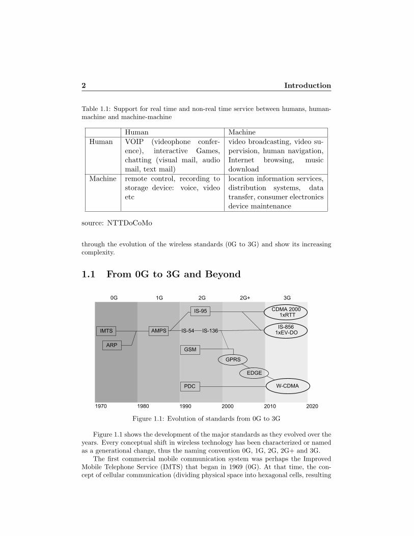
Table 1.1: Support for real time and non-real time service between humans, human-machine and machine-machine
Human Machine
Human VOIP (videophone confer-ence), interactive Games,chatting (visual mail, audiomail, text mail)
video broadcasting, video su-pervision, human navigation,Internet browsing, musicdownload
Machine remote control, recording tostorage device: voice, videoetc
location information services,distribution systems, datatransfer, consumer electronicsdevice maintenance
source: NTTDoCoMo
through the evolution of the wireless standards (0G to 3G) and show its increasingcomplexity.
1.1 From 0G to 3G and Beyond
Figure 1.1: Evolution of standards from 0G to 3G
Figure 1.1 shows the development of the major standards as they evolved over theyears. Every conceptual shift in wireless technology has been characterized or namedas a generational change, thus the naming convention 0G, 1G, 2G, 2G+ and 3G.
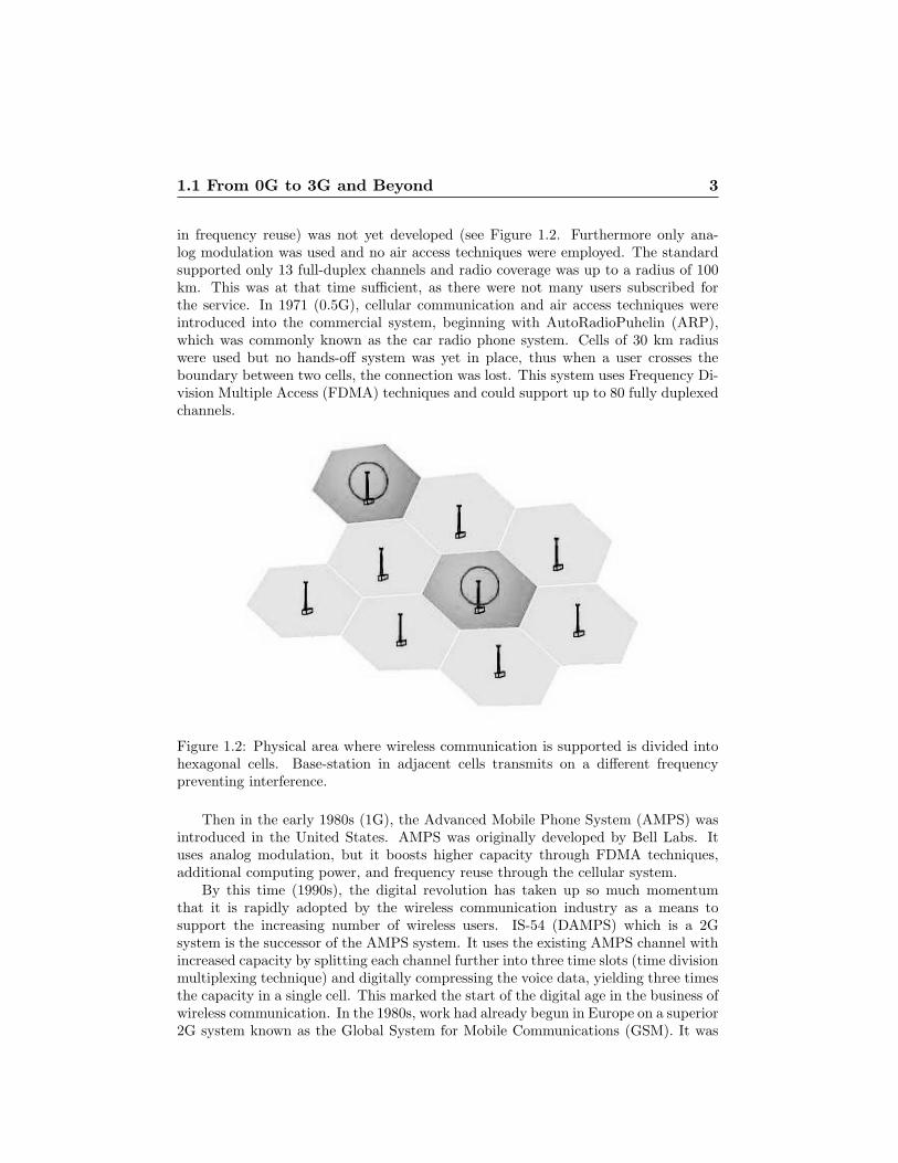
The first commercial mobile communication system was perhaps the ImprovedMobile Telephone Service (IMTS) that began in 1969 (0G). At that time, the con-cept of cellular communication (dividing physical space into hexagonal cells, resulting
1.1 From 0G to 3G and Beyond 3
in frequency reuse) was not yet developed (see Figure 1.2. Furthermore only ana-log modulation was used and no air access techniques were employed. The standardsupported only 13 full-duplex channels and radio coverage was up to a radius of 100km. This was at that time sufficient, as there were not many users subscribed forthe service. In 1971 (0.5G), cellular communication and air access techniques wereintroduced into the commercial system, beginning with AutoRadioPuhelin (ARP),which was commonly known as the car radio phone system. Cells of 30 km radiuswere used but no hands-off system was yet in place, thus when a user crosses theboundary between two cells, the connection was lost. This system uses Frequency Di-vision Multiple Access (FDMA) techniques and could support up to 80 fully duplexedchannels.
Figure 1.2: Physical area where wireless communication is supported is divided intohexagonal cells. Base-station in adjacent cells transmits on a different frequencypreventing interference.
Then in the early 1980s (1G), the Advanced Mobile Phone System (AMPS) wasintroduced in the United States. AMPS was originally developed by Bell Labs. Ituses analog modulation, but it boosts higher capacity through FDMA techniques,additional computing power, and frequency reuse through the cellular system.
By this time (1990s), the digital revolution has taken up so much momentumthat it is rapidly adopted by the wireless communication industry as a means tosupport the increasing number of wireless users. IS-54 (DAMPS) which is a 2Gsystem is the successor of the AMPS system. It uses the existing AMPS channel withincreased capacity by splitting each channel further into three time slots (time divisionmultiplexing technique) and digitally compressing the voice data, yielding three timesthe capacity in a single cell. This marked the start of the digital age in the business ofwireless communication. In the 1980s, work had already begun in Europe on a superior2G system known as the Global System for Mobile Communications (GSM). It was

4 Introduction
introduced to the market in 1991 and quickly became very popular. It is now widelyused in over 160 countries, and it is estimated that 82% of the global market appliesto this standard today. GSM is a constant envelope modulation scheme (GMSK) anduses Time Division Multiple Access (TDMA) as air access. It features a range ofdigital techniques, which lead to significant improvement in connectivity and voicequality, as well as the introduction of new digital services like Short Message Service(SMS).
Another 2G system, which played an important role in future standards to come,was the CDMA One (also known as IS-95) pioneered by QUALCOMM. IS-95 usesCode Division Multiple Access (CDMA). This is a digital technique that transmits astream of bits and allows several users to share the same frequency simultaneously.This implies that this system has a higher capacity then TDMA-based systems suchas GSM.
Increasing demand for information orientated features on our handsets, such asWireless Application Protocol (WAP) access, Multimedia Messaging Service (MMS),streaming video, and for internet email and world wide web (www) access led todevelopment of new standards capable of supporting these applications. GeneralPacket Radio Service (GPRS) introduced in 2000 is a Mobile Data Service compatiblewith GSM systems. GSM systems in combination with GPRS is often known as 2.5G,which is in fact a transition between 2G and 3G. Shortly after, Enhanced Data ratesfor GSM Evolution (EDGE) a 2.75G system compatible with GSM, was introducedwhich doubles the bandwidth capacity of GPRS systems, allowing for many high-speed data applications such as streaming video to be supported.
In 1999, the International Telecommunications Union (ITU) called for proposalsfor 3G protocols in an effort to ensure the smooth transition from 2G to 3G. Theseproposals were termed International Mobile Telecommunication 2000 (IMT-2000) andone of the adopted proposals which is becoming widely implemented is the UniversalTelecommunications Service (UMTS). According to the ITU, 3G technologies shouldenable network operators to offer users a wider range of more advanced services (wide-area wireless voice telephony and broadband wireless data) while achieving greaternetwork capacity through improved spectral efficiency. Wideband-CDMA (WCDMA)is an approved 3G protocol/technology used within the UMTS system which enablesthe network operators to achieve these stated goals. It works on the principles ofCode Division Multiplexing for air access. This direct spreading technology, spreadsits transmission over a 5 MHz bandwidth and can carry both voice and data simulta-neously. It features a peak data rate of 384 kbps and has support for a wide array ofnew and emerging multimedia services. NTTDoCoMo (subsidiary of Japan’s largesttelephone operator NTT) launched the first WCDMA service in 2001 and now hasover a million subscribers.
At the time of this thesis work, there was no formal definition of “3G and beyond”,4G requirements. But the trend of the wireless communication industry is movingtowards full integration of voice, data and video streaming. To achieve this, systemarchitects have predicted that bandwidth of more than 100Mbit/sec are required.This is a great challenge for designers of the essential components of the wirelesscommunication system.
1.2 RF Front-end 5
1.2 RF Front-end
The core element to the wireless communication system is perhaps the RF front-end.The RF front-end consist of electronic circuitry and an antenna. Its function is toconvert electrical signals to electromagnetic waves, which is subsequently transmitted(transmitter) and received (receiver) through the air.
Early implementation of the transmitter consisted of an oscillator which emitscontinuously a train of undamped waves. By interrupting these undamped wavesinto long and short pulses, the information to be transmitted/received was included.In early years, the active element in the oscillator was a vacuum tube and today incommercial RF transmitters for wireless communication, the vacuum tube has beenreplaced by the solid state transistor.
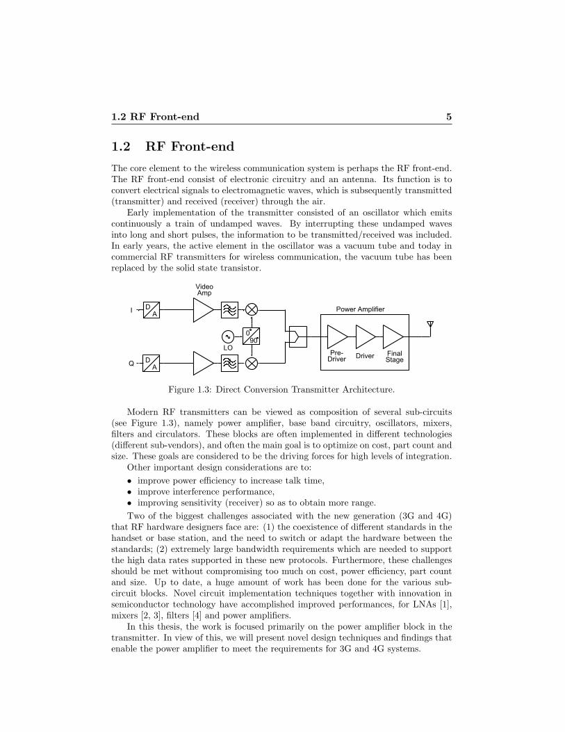
Figure 1.3: Direct Conversion Transmitter Architecture.
Modern RF transmitters can be viewed as composition of several sub-circuits(see Figure 1.3), namely power amplifier, base band circuitry, oscillators, mixers,filters and circulators. These blocks are often implemented in different technologies(different sub-vendors), and often the main goal is to optimize on cost, part count andsize. These goals are considered to be the driving forces for high levels of integration.
Other important design considerations are to:
• improve power efficiency to increase talk time,• improve interference performance,• improving sensitivity (receiver) so as to obtain more range.
Two of the biggest challenges associated with the new generation (3G and 4G)that RF hardware designers face are: (1) the coexistence of different standards in thehandset or base station, and the need to switch or adapt the hardware between thestandards; (2) extremely large bandwidth requirements which are needed to supportthe high data rates supported in these new protocols. Furthermore, these challengesshould be met without compromising too much on cost, power efficiency, part countand size. Up to date, a huge amount of work has been done for the various sub-circuit blocks. Novel circuit implementation techniques together with innovation insemiconductor technology have accomplished improved performances, for LNAs [1],mixers [2, 3], filters [4] and power amplifiers.
In this thesis, the work is focused primarily on the power amplifier block in thetransmitter. In view of this, we will present novel design techniques and findings thatenable the power amplifier to meet the requirements for 3G and 4G systems.

6 Introduction
1.3 The RF Power Amplifier
The Power Amplifier is a very crucial component in the transmitter as it is the lastactive link between the small signal part of the components and the antenna. The roleof the PA is to bring the transmitted power up to the level required in the specifica-tions for base stations or handsets of the various communication links. Typical PowerAmplifiers consist of three gain stages (Figure 1.3), namely the pre-driver, driver andthe final-stage. Ideally, in an application where linear amplification is required, eachof the gain stages in the PA should be able to provide amplification without any dis-tortion and with 100% efficiency. However, with real devices this is not possible as thecharacteristics of the devices change with drive power and self heating. Furthermorereal devices have losses and are non-linear, subjects that will be discussed in Chapter2.
Among the three gain stages in the PA, the final-stage is always the most costlyin terms of device size and current consumption. Furthermore, 3G protocols whichboast increase user capacity and high data rates (e.g. W-CDMA) often employ spreadspectrum techniques. This results in signals having noise-like behavior with occasionallarge peaks in power (high crest factor also known as high Peak-to-Average PowerRatio). In base-stations these peak power levels are often > 50 dBm. Thereforedesigners of the final-stage PA in base station have to oversize their PA (typically10dB greater than the average power), this often results in low efficiency (as furtherexplained in Chapter 2).
PA designers targeting handsets, on the other hand do not have to deal with suchhigh RF output power. Furthermore the crest factor for the signals at the hand-set is lower than in the base-stations, and linearity specifications are more relaxed.However, the market now demands that the phone be able to support multiple pro-tocols in multiple bands. Current implementations to support this, is to replicate thetransceiver chain in every band. However this takes up precious real estate on thePCB. The challenge facing the PA designer for handsets is to make the PA tunableor adaptable by software control.
1.4 Research Objectives
The focus of this thesis work is on the final-stage power amplifier. The objective isto provide innovative design solutions which can be adopted by the industry in thefuture. The following objectives are kept in mind throughout the thesis work.
Design solution for the handset PAs should meet the following objectives:
• high power efficiency;• linearity;• compactness;• multi-band capabilities;
where multi-band capabilities refer to using the same PA in various frequencybands so that multiple protocols can be supported within the same handset.
In contrast, design solution for the base-station PAs should meet the objectives:
• high RF output power;
1.5 Outline 7
• high efficiency despite high crest factor of the signals;• linearity;• low component count and reliability.
All concepts developed in this thesis havebeen demonstrated through hardwareprototypes. It was our aim that these demonstrators show a better performance thancurrent PA implementations deployed in the field.
1.5 Outline
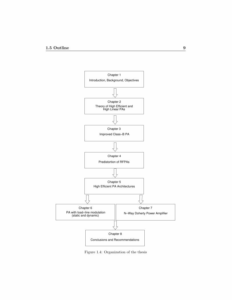
Figure 1.4 gives a flow chart outline of the thesis and represents the path that theauthor has taken to reach the objectives listed in Section 1.4.
Chapter 1 gives an introduction to the wireless communication industry fromits beginning to the state where it is now. Furthermore, it outlines the future ofwireless communication and its accompanying challenges. This is followed by a shortintroduction of the RF front-end hardware, with emphasis given to the transmitter.The power amplifier (which is part of the transmitter chain) is the subject of researchin this thesis work and is described in more detail, followed by stating the list ofobjectives in this work.
Chapter 2 provides the concepts required to understand the power amplifier. Inthe first part, we explain the different classes of power amplifier operation and showhow the classes of operation affect its efficiency. Subsequently, the concept of linear-ity/distortion in the power amplifier is introduced, and the various sources of distor-tion are discussed. This is followed by a discussion on how linearity and efficiencyare related and how designers make a balance of these two important parameters ina real power amplifier design.
In Chapter 3, based upon the understanding of the distortion sources withinthe power amplifier, we introduce the Derivative Superposition (DS) technique toreduce distortion in the Class-B/-AB amplifiers. Furthermore, we investigate har-monic impedance control both at the source and load side and its effect on the overalllinearity on the traditional power amplifiers.
Chapter 4 looks into predistortion as a proposed system level approach in solvingthe linearity problems of the power amplifier without trading in any efficiency. Adigital memoryless predistortion algorithm is developed within the scope of this work,which is suitable for linearizing classical power amplifiers. This algorithm is lateradapted and used in more advanced amplifier concepts as described in Chapter 5.Time dependent non-linear effects (also known as memory effects) are also addressed,and a compensation technique is introduced. The work up to this point has beenfocused on improving the linearity of the power amplifier. At this juncture we make aswitch to investigate techniques which will improve the average efficiency of the poweramplifier, which is highly desirable for complex modulated signals. In Chapter 5, welook into the general concept behind high efficiency power amplifier architectures andreview the major important high efficient architectures in use today.
Chapter 6 introduces a novel approach for handset power amplifiers to simul-taneously allow for multi-band tuning and high efficiency performance based on anadaptive matching network. And lastly in Chapter 7, the concept of the N-way Do-

8 Introduction
herty Power Amplifier is introduced, and it is experimentally shown why this is agood candidate for 3G base station power amplifiers.
Lastly, this thesis work is concluded in Chapter 8 with recommendations for futureresearch directions.
1.5 Outline 9
Theory of High Efficient and High Linear PAs
Chapter 1
Introduction, Background, Objectives
Chapter 2
Chapter 4
Predistortion of RFPAs
Chapter 3
Improved Class−B PA
Chapter 6
PA with load−line modulation(static and dynamic)
Chapter 7
N−Way Doherty Power Amplifier
Chapter 8
Conclusions and Recommendations
Chapter 5
High Efficient PA Architectures
Figure 1.4: Organization of the thesis


Chapter 2
Theory of Highly Efficientand Linear Power Amplifiers
This chapter covers the theory on RF power amplifiers (RFPA), which is requiredto understand the conditions when the amplifier is operating linearly and efficiently.This serves as a foundation for the content of the later chapters. Although this hasalready been presented in many ways in literature [5–7], it is still useful to review thetheory in light of the interpretation given in this thesis work.
Section 2.1 discusses the well known Class-A, Class-AB, Class-B and Class-Cpower amplifier, explaining its linearity and efficiency performance in the ideal case.In Section 2.2, non idealities associated with real transistors and their effect on lin-earity, bandwidth and efficiency are discussed. Lastly, Section 2.3 discusses the newgeneration wireless protocols (3G,4G) and the challenges it presents to designers ofRF power amplifiers.
2.1 Ideal Class-A to C Power Amplifier
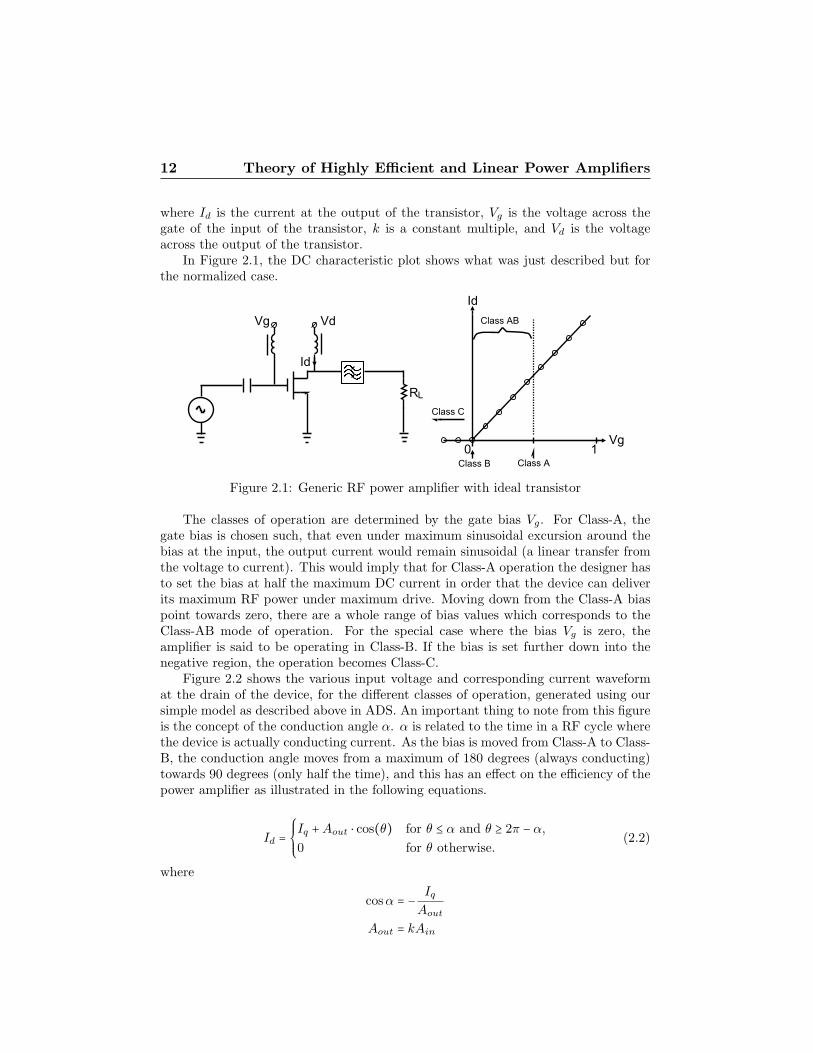
To explain the traditional classes of the RFPA (A, AB and C), the following “ideal”device is used in a circuit setup as shown in Figure 2.1. In this thesis work, thedefinition of an ideal transistor refers to a voltage controlled source with DC char-acteristics such that the device turns on at 0 volts and ramps up linearly till themaximum current. For the purpose of verifying the concepts in this thesis work usinga simulator, a simple transistor model based on a Symbolic Defined Device (SDD inAgilent’s ADS) will be used in the schematic of Figure 2.1, with maximum outputpower of the amplifier normalized to 1-Watt. This simple model is able to take intoaccount the effect of saturation, as shown in equation (2.1),
Id =⎧⎪⎪⎪⎪⎪⎨⎪⎪⎪⎪⎪⎩
0 if Vg ≤ 0,
(k ⋅ Vg) − 10−12 ⋅ exp( −Vd
10−3)
��models voltage saturation
if Vg > 0. (2.1)
11
12 Theory of Highly Efficient and Linear Power Amplifiers
where Id is the current at the output of the transistor, Vg is the voltage across thegate of the input of the transistor, k is a constant multiple, and Vd is the voltageacross the output of the transistor.
In Figure 2.1, the DC characteristic plot shows what was just described but forthe normalized case.
Figure 2.1: Generic RF power amplifier with ideal transistor
The classes of operation are determined by the gate bias Vg. For Class-A, thegate bias is chosen such, that even under maximum sinusoidal excursion around thebias at the input, the output current would remain sinusoidal (a linear transfer fromthe voltage to current). This would imply that for Class-A operation the designer hasto set the bias at half the maximum DC current in order that the device can deliverits maximum RF power under maximum drive. Moving down from the Class-A biaspoint towards zero, there are a whole range of bias values which corresponds to theClass-AB mode of operation. For the special case where the bias Vg is zero, theamplifier is said to be operating in Class-B. If the bias is set further down into thenegative region, the operation becomes Class-C.
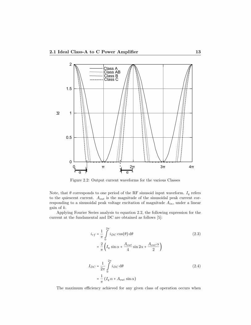
Figure 2.2 shows the various input voltage and corresponding current waveformat the drain of the device, for the different classes of operation, generated using oursimple model as described above in ADS. An important thing to note from this figureis the concept of the conduction angle α. α is related to the time in a RF cycle wherethe device is actually conducting current. As the bias is moved from Class-A to Class-B, the conduction angle moves from a maximum of 180 degrees (always conducting)towards 90 degrees (only half the time), and this has an effect on the efficiency of thepower amplifier as illustrated in the following equations.
Id =⎧⎪⎪⎨⎪⎪⎩Iq +Aout ⋅ cos(θ) for θ ≤ α and θ ≥ 2π − α,
0 for θ otherwise.(2.2)
where
cosα = − Iq
Aout
Aout = kAin
2.1 Ideal Class-A to C Power Amplifier 13
Figure 2.2: Output current waveforms for the various Classes
Note, that θ corresponds to one period of the RF sinusoid input waveform. Iq refersto the quiescent current. Aout is the magnitude of the sinusoidal peak current cor-responding to a sinusoidal peak voltage excitation of magnitude Ain, under a lineargain of k.
Applying Fourier Series analysis to equation 2.2, the following expression for thecurrent at the fundamental and DC are obtained as follows [5]:
irf = 1
π
2π
∫0
iDC cos(θ)dθ (2.3)
= 2
π(Iq sinα + Aout
4sin 2α + Aout α
2)
IDC = 1
2π
2π
∫0
iDC dθ (2.4)
= 1
π(Iq α +Aout sinα)
The maximum efficiency achieved for any given class of operation occurs when
14 Theory of Highly Efficient and Linear Power Amplifiers
the voltage across the device is in voltage saturation. This implies that the maximumefficiency is only determined by the ratio of the currents.
η = irf
IDC
(2.5)
= sin 2α − 2α
4 (α cosα − sinα) (2.6)
Substituting α = 180○ (which corresponds to the Class-A operation) into equa-tion 2.5, results in η = 50% and α = 90○ (Class-B) results in η = 78.5%. As theconduction angle decreases beyond 90○ (corresponding to Class-C operation), thetheoretical efficiency approaches 100% as shown in equation 2.7.
η = limα→0○
sin 2α − 2α
4 (α cosα − sinα) (2.7)
= 100%
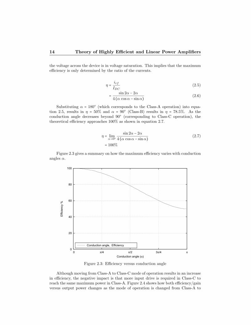
Figure 2.3 gives a summary on how the maximum efficiency varies with conductionangles α.
0
20
40
60
80
100
0 π/4 π/2 3π/4 π
Effi
cien
cy %
Conduction angle (α)
Conduction angle, Efficiency
Figure 2.3: Efficiency versus conduction angle
Although moving from Class-A to Class-C mode of operation results in an increasein efficiency, the negative impact is that more input drive is required in Class-C toreach the same maximum power in Class-A. Figure 2.4 shows how both efficiency/gainversus output power changes as the mode of operation is changed from Class-A to
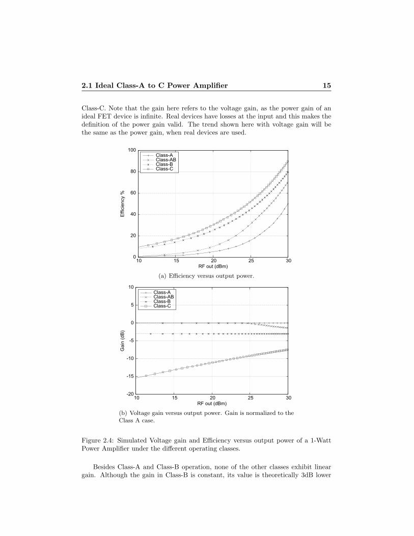
2.1 Ideal Class-A to C Power Amplifier 15
Class-C. Note that the gain here refers to the voltage gain, as the power gain of anideal FET device is infinite. Real devices have losses at the input and this makes thedefinition of the power gain valid. The trend shown here with voltage gain will bethe same as the power gain, when real devices are used.
0
20
40
60
80
100
10 15 20 25 30
Effi
cien
cy %
RF out (dBm)
Class-AClass-ABClass-BClass-C
(a) Efficiency versus output power.
-20
-15
-10
-5
0
5
10
10 15 20 25 30
Gai
n (d
B)
RF out (dBm)
Class-AClass-ABClass-BClass-C
(b) Voltage gain versus output power. Gain is normalized to theClass A case.
Figure 2.4: Simulated Voltage gain and Efficiency versus output power of a 1-WattPower Amplifier under the different operating classes.
Besides Class-A and Class-B operation, none of the other classes exhibit lineargain. Although the gain in Class-B is constant, its value is theoretically 3dB lower
16 Theory of Highly Efficient and Linear Power Amplifiers
than what is achieved in Class-A. In Class-AB, the gain starts off constant and similarto Class-A, however at a certain input drive, the output RF current starts to clip andthe conduction angle α starts being a function of the input drive. In Class-C, theconduction angle α is always a function of the input drive, resulting in a gain thatchanges as a function of power.
2.2 Distortion, Bandwidth and Efficiency issues in
RF Power Amplifiers
Real transistors unlike the ideal model used in Section 2.1 are unfortunately far morecomplex. Besides the basic voltage-controlled current source function, these real tran-sistors have parasitics that leads to reduction in bandwidth, in-band distortion, anddeviation from the ideal efficiency computed in the previous section.
2.2.1 Bandwidth
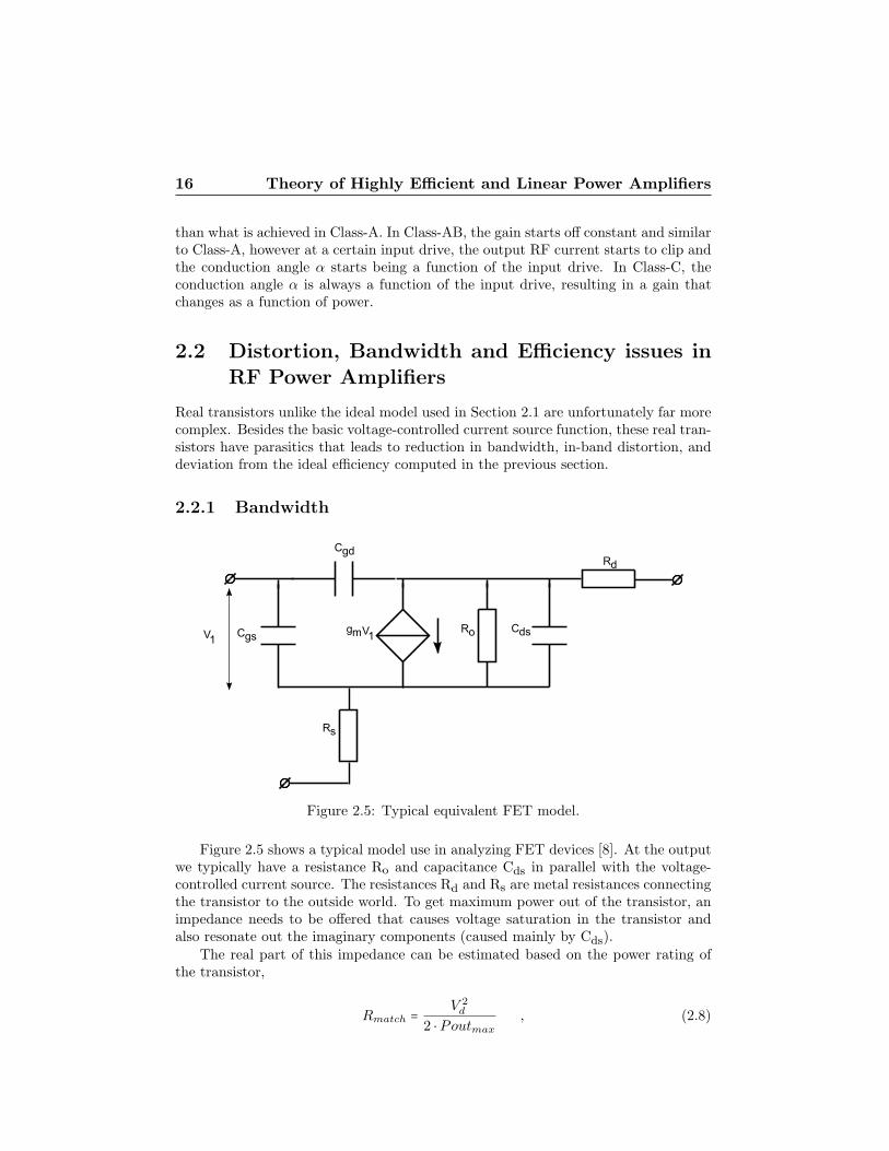
Figure 2.5: Typical equivalent FET model.
Figure 2.5 shows a typical model use in analyzing FET devices [8]. At the outputwe typically have a resistance Ro and capacitance Cds in parallel with the voltage-controlled current source. The resistances Rd and Rs are metal resistances connectingthe transistor to the outside world. To get maximum power out of the transistor, animpedance needs to be offered that causes voltage saturation in the transistor andalso resonate out the imaginary components (caused mainly by Cds).
The real part of this impedance can be estimated based on the power rating ofthe transistor,
Rmatch = V 2d
2 ⋅ Poutmax
, (2.8)

2.2 Distortion, Bandwidth and Efficiency issues in RF PowerAmplifiers 17
which in larger transistors can result in small values of Rmatch. Note also that theparasitic capacitances also scale with size of the transistor. In most RF power am-plifier applications for wireless communications, the system impedances are fixed at50Ω, this implies that a lossless impedance transformation is required (same appliesfor the input). The need for impedance transformation and the presence of thesefrequency dependence parasitics in the transistor causes bandwidth limitation in anypower amplifier design. Well known design techniques with regards to wide-bandmatching can be found in [7], but this often results in a trade-off with the physicalsize of the power-amplifier hardware.
2.2.2 Efficiency
The deviation from the ideal efficiency for the various classes computed in Section 2.1is attributed to two loss mechanism for FET transistors. The first is due to, what iscommonly referred to as on-resistance. This resistance is frequency independent andits impact on the efficiency can be estimated by the following equation (using Class-Bas an example):
η = 78.5%1
1 + 2 ⋅ Ro
RL
, (2.9)
where RL refers to the impedance which the device sees at its output.The second loss mechanism is frequency dependent and relates to the losses in the
output capacitance (Cds) where the resistive part is a combination of drain resistanceand substrate resistance. The resulting degradation in efficiency due to this effect isestimated as follow:
η = 78.5%1
1 + ω2 ⋅C2ds⋅Rp ⋅RL
, (2.10)
where Rp represents the losses in that output capacitance Cds.It is the goal of device technologist to minimize these losses [9], bringing the
efficiency of these transistor closer to its ideal performance.
2.2.3 Distortion
The voltage-controlled current source in real devices follows a so called “square-law”relationship (in reality the order is much higher than two) instead of the piecewiselinear we have assumed for the ideal device (Figure 2.1). Furthermore, the parasiticcapacitances in the transistor are also functions of drive power. These non-linearcomponent in the transistors add up in a vectorial fashion, and this interaction canbe analyzed with the Volterra Series analysis.
This technique allows one to derive close form expressions showing how the non-linear components interact with each other to generate the final distortion products[10]. However, the disadvantage of this technique is that, it is only valid in therange where the coefficients are extracted. Furthermore, to use the analysis at thepoint where the power amplifier is driven close to its compression, a large numberof terms are needed to be extracted and included in the analysis, which makes the
18 Theory of Highly Efficient and Linear Power Amplifiers
resulting equations cumbersome. To make these close form expressions interpretable,assumptions are usually required to simplify these expressions. As a result, thisanalysis only gives an approximate estimate of the distortion terms, which at best iswithin 3dB of the actual values.
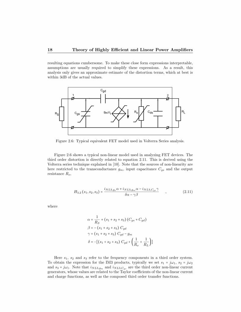
Figure 2.6: Typical equivalent FET model used in Volterra Series analysis.
Figure 2.6 shows a typical non-linear model used in analyzing FET devices. Thethird order distortion is directly related to equation 2.11. This is derived using theVolterra series technique explained in [10]. Note that the sources of non-linearity arehere restricted to the transconductance gm, input capacitance Cgs and the outputresistance Ro,
H3,2 (s1, s2, s3) = iNL3,goα + iNL3,gm
α − iNL3,Cgsγ
δα − γβ, (2.11)
where
α = 1
RS
+ (s1 + s2 + s3) (Cgs +Cgd)β = −(s1 + s2 + s3) Cgd
γ = (s1 + s2 + s3) Cgd − gm
δ = −[(s1 + s2 + s3) Cgd + ( 1
Ro
+ 1
RL
)]
Here s1, s2 and s3 refer to the frequency components in a third order system.To obtain the expression for the IM3 products, typically we set s1 = jω1, s2 = jω2
and s3 = jω1. Note that iNL3,gmand iNL3,Cgs
are the third order non-linear currentgenerators, whose values are related to the Taylor coefficients of the non-linear currentand charge functions, as well as the composed third order transfer functions.
2.3 Wireless Communication Standards and the RF PowerAmplifier 19
iNL3,gm=K3,gm
H1,1(s1)H1,1(s2)H1,1(s3) (2.12)
+ 2
3K2,gm
[H1,1(s1)H2,1(s2, s3)+H1,1(s2)H2,1(s1, s3)+H1,1(s3)H2,1(s1, s2)]
iNL3,go=K3,go
H1,2(s1)H1,2(s2)H1,2(s3) (2.13)
+ 2
3K2,go
[H1,2(s1)H2,2(s2, s3)+H1,2(s2)H2,2(s1, s3)+H1,2(s3)H2,2(s1, s2)]
iNL3,Cgs= (s1 + s2 + s3)K3,Cgs
H1,1(s1)H1,1(s2)H1,1(s3) (2.14)
+ 2
3K2,Cgs
(s1 + s2 + s3) [H1,1(s1)H2,1(s2, s3)+H1,1(s2)H2,1(s1, s3)+H1,1(s3)H2,1(s1, s2)]
In this notation, the first subscript of H refers to the order, and the secondsubscript refers to the node (see Figure 2.6). Thus, H2,1 and H2,2 are second-ordertransfer functions of the voltage at the input of the circuit to the nodes 1 and 2respectively. Likewise H1,1 and H1,2 are the voltage transfer functions that onlydepend on the linear network response. Equation 2.11 shows that the third orderintermodulation (which falls in band), is a result of a complex interaction of third-order non-linear currents from the various distortion components, as well as indirectthird-order terms that arise from the interaction of fundamental components withsecond order frequency products. This later contribution makes the circuit conditionsthat control the base band and second harmonic voltages very important to the overalllinearity performance of the design.
2.3 Wireless Communication Standards and the RFPower Amplifier
Modern wireless standards (2G and 3G) employ digital modulation and multiple airaccess technique to increase the capacity of the system (increase number of users).Understanding the wireless communication standard being employed is an importanttask for the power amplifier designer as it often states what the transmitted signalwill “looks like” (i.e. in terms of CF and bandwidth). Furthermore, it states the spec-ification on the accepted Signal-Noise-Ratio (SNR), the Bit-Error-Rate (BER) and

20 Theory of Highly Efficient and Linear Power Amplifiers
extraneous emissions tolerated. These criteria should all be met and where possiblewith the highest efficiency possible.
GSM the most common wireless standard for 2G uses GMSK (Gaussian Mini-mum Shift Keying) modulation and TDMA/FDD (Frequency Division Duplexing).GMSK is a continuous-phase frequency-shift keying modulation scheme (i.e. constantenvelope) similar to MSK but with the digital data stream first being preprocessedby pulling it through a Gaussian filter. This results in a constant envelope RF signalwhich allow power amplifier designers for GSM application to dimension the transis-tor such that it always is in saturation, resulting in high efficiency. Furthermore, italso allows for very relaxed linearity specifications as amplitude distortion is of noconcern. Note also that in GSM systems, the power amplifier has to amplify signalsin burst (TDMA), thus the thermal settling time of the transistor becomes impor-tant. Commonly used technique to get around this is to use a Class-A or AB biasingwhere the quiescent current is significantly high enough to mitigate the fluctuation intemperature due to the RF power.
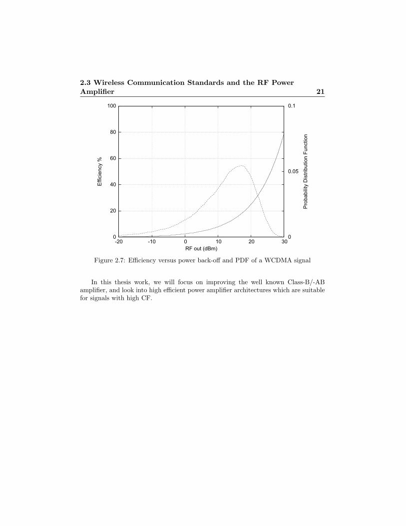
For 3G systems, WCDMA is one of the main standards. WCDMA employs QPSKas modulation and CDMA as air access technique. QPSK in itself is a constantenvelope signal, but when used in a CDMA environment, where the information isspread over the whole spectrum and all channels are just transmitted on the samefrequency, the signal becomes noise like and have occasionally high peaks. The crestfactor of a WCDMA signal is approximately 10-15 dB depending on the number ofchannels. This would imply that the devices used in the power amplifier has to be“over dimensioned” to handle the occasional peak powers, while the amplifier remainsmost of the time at its average power, 10dB lower than the maximum dimensionedpower.
Figure 2.7 gives the plot of the Probability Distribution Function (PDF) of aWCDMA signal versus normalized power levels and the efficiency performance of anideal transistor in Class-B operation. Note that for most of the time, the signal isbeing amplified at a low efficiency and only occasionally at the peaks the amplifier isoperated at its maximum efficiency. This implies that on average, the power amplifieris operated at a much lower efficiency than its peak efficiency capability. Given theCW efficiency characteristic of the amplifier and the PDF of the signal, the averageefficiency can be computed using Equation 2.15, and is found for WCDMA to be 22%for an ideal device when operated in Class-B.
⟨η⟩ = ⟨pout⟩⟨PDC⟩ =
∫ pout ⋅ p(pout)dpout
∫ pout ⋅ p(pout)η(pout) dpout
(2.15)
With a real transistor, it could be even required to operate the transistor furtherat back-off due to stringent linearity requirements. This together with the losses inthe device described in Section 2.2.2 will cause the efficiency value to be lower thanthe ideal case, and in practise this will range from 5 to 10%.
This low average efficiency for signals with high CF even for an ideal device, is themotivation at this time of writing for research within the RF power amplifier com-munity, into high efficient power amplifier classes [11], high efficient power amplifierarchitectures [12, 13] and crest factor reduction techniques [14].
2.3 Wireless Communication Standards and the RF PowerAmplifier 21
0
20
40
60
80
100
-20 -10 0 10 20 30 0
0.05
0.1E
ffici
ency
%
Pro
babi
lity
Dis
tribu
tion
Func
tion
RF out (dBm)
Figure 2.7: Efficiency versus power back-off and PDF of a WCDMA signal
In this thesis work, we will focus on improving the well known Class-B/-ABamplifier, and look into high efficient power amplifier architectures which are suitablefor signals with high CF.


Chapter 3
Improved Class-B, Class-ABPower Amplifiers
This chapter gives an overview on the progression in class-AB oriented power amplifierstages over the last few years. This progression has yielded a dramatic improvement inlinearity & efficiency, which can be contributed to technology, as well as, to improveddesign techniques. Following a historical perspective, we will first discuss in Sec-tion 3.1 how the transfer function of the active device itself can be made linear usingthe Derivative Superposition technique (DS) [15]. This technique, which uses multipledevices in parallel with small bias adjustments to shape the overall transconductanceof the composed device, proves to be very effective in the far output power back-offcondition. In order to improve the device linearity closer to compression, as nextstep the always present secondary mixing phenomena over the input non-linearitiesof the active device input are utilized to compensate direct third-order intermodula-tion distortion products. This so called “input out-of-band” matching strategy wasoriginally developed for bipolar devices [16] but proves to be also effective for FETdevices at moderate power back-off conditions. To improve linearity both in the faras well medium range output power back-off conditions, in this work, a combinationof derivative superposition with input-out-of-band matching was applied to LDMOSbase station technology. Finally, to improve linearity close to compression, simultane-ous input and output out-of-band matching has been utilized in Section 3.3 [17]. Thistechnique yields rather dramatic improvements in the classical linearity − efficiencytrade-off at the expense of some decreased linearity in the far power back-off condi-tions. We conclude with a consideration on the progress made in LDMOS technologywithin the constrains of (modified) “Class-B” operation.
3.1 Derivative Superposition
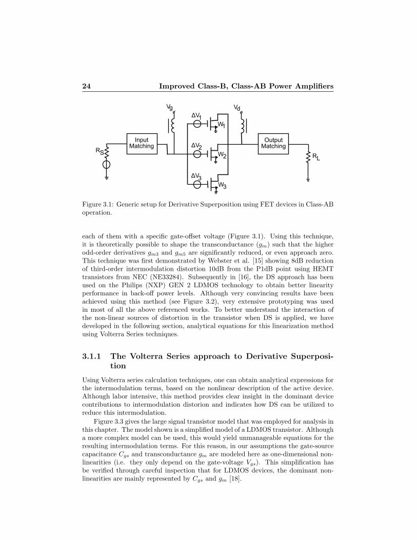
The technique of derivative Superposition (DS) aims to improve amplifier linearityby shaping the overall transconductance of an amplifier stage. This is implementedby using several FET devices with appropriate gate widths in parallel, while biasing
23
24 Improved Class-B, Class-AB Power Amplifiers
Figure 3.1: Generic setup for Derivative Superposition using FET devices in Class-ABoperation.
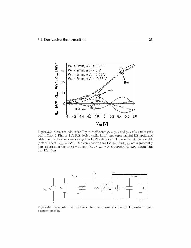
each of them with a specific gate-offset voltage (Figure 3.1). Using this technique,it is theoretically possible to shape the transconductance (gm) such that the higherodd-order derivatives gm3 and gm5 are significantly reduced, or even approach zero.This technique was first demonstrated by Webster et al. [15] showing 8dB reductionof third-order intermodulation distortion 10dB from the P1dB point using HEMTtransistors from NEC (NE33284). Subsequently in [16], the DS approach has beenused on the Philips (NXP) GEN 2 LDMOS technology to obtain better linearityperformance in back-off power levels. Although very convincing results have beenachieved using this method (see Figure 3.2), very extensive prototyping was usedin most of all the above referenced works. To better understand the interaction ofthe non-linear sources of distortion in the transistor when DS is applied, we havedeveloped in the following section, analytical equations for this linearization methodusing Volterra Series techniques.
3.1.1 The Volterra Series approach to Derivative Superposi-tion
Using Volterra series calculation techniques, one can obtain analytical expressions forthe intermodulation terms, based on the nonlinear description of the active device.Although labor intensive, this method provides clear insight in the dominant devicecontributions to intermodulation distorion and indicates how DS can be utilized toreduce this intermodulation.
Figure 3.3 gives the large signal transistor model that was employed for analysis inthis chapter. The model shown is a simplified model of a LDMOS transistor. Althougha more complex model can be used, this would yield unmanageable equations for theresulting intermodulation terms. For this reason, in our assumptions the gate-sourcecapacitance Cgs and transconductance gm are modeled here as one-dimensional non-linearities (i.e. they only depend on the gate-voltage Vgs). This simplification hasbe verified through careful inspection that for LDMOS devices, the dominant non-linearities are mainly represented by Cgs and gm [18].
3.1 Derivative Superposition 25
VGS [V]
gm
1[A
/V],
gm
3[A
/V3],
gm
5[A
/V5]
VGS [V]
gm
1[A
/V],
gm
3[A
/V3],
gm
5[A
/V5]
W1 = 3mm, �V1 = 0.28 V
W2 = 2mm, �V2 = 0 V
W3 = 2mm, �V3 = 0.56 V
W4 = 5mm, �V4 = -0.36 V
gm3
gm1
gm5
Figure 3.2: Measured odd-order Taylor coefficients gm1, gm3 and gm5 of a 12mm gatewidth GEN 2 Philips LDMOS device (solid lines) and experimental DS optimizedodd-order Taylor coefficients using four GEN 2 devices with the same total gate width(dotted lines) (VDS = 26V). One can observe that the gm3 and gm5 are significantlyreduced arround the IM3 sweet spot (gm3 = gm5 = 0) Courtesy of Dr. Mark vander Heijden
Figure 3.3: Schematic used for the Voltera-Series evaluation of the Derivative Super-position method.
26 Improved Class-B, Class-AB Power Amplifiers
In order to predict the IM3 of the device over a considerable input-power range, afifth-order Volterra-series expression has been developed for a two-tone drive signal.In our calculations, conventional class-AB operation was assumed, using short circuitconditions for the base-band as well the 2nd harmonic frequencies. Note that theseshort circuit conditions prevents the additional generation of IM3 components throughsecondary mixing over the out-of-band impedances (as seen in Chapter 2). In addition,it strongly simplifies the resulting equations, something that is highly desirable whendealing with Volterra series. Under these conditions, the IM3 output voltage at theoutput of our LDMOS device in class-B operation can be formulated as,
vout(ωIM3) = (gm − jωIM3Cgd) iCgs− (YS + jωIM3 (Cgd +Cgs)) igm
jωIM3Cgd (gm + YS + YL + jωIM3Cgs) + YL (YS + jωIM3Cgs) , (3.1)
where
iCgs= jωIM3{3
4Cgs3v
2in(ω2)vin(−ω1) + 25
8Cgs5v
3in(ω2)vin(−ω2)vin(−ω1)}, (3.2)
igm= 3
4gm3v
2in(ω2)vin(−ω1) + 25
8gm5v
3in(ω2)vin(−ω2)vin(−ω1), (3.3)
vin(ω) = YSvS (jω Cgd + YL)jω Cgd (gm + YS + YL + jω Cgs) + YL (YS + jω Cgs) . (3.4)
Note, that gm3 and gm5 are the third and fifth-order Taylor coefficients of Ids
versus Vgs respectively. Similarly, Cgs3 and Cgs5 are third and fifth-order Taylorcoefficients of Cgs versus Vgs, respectively. While, YS and YL are the source and loadadmittances at the fundamental frequency.
The above expressions can be further simplified by neglecting the feedback ca-pacitance Cgd. This proves to be a valid assumption for modern LDMOS devices dueto the presence of the grounded shield between the gate and the drain [19], whichstrongly reduces the feedback capacitance. Furthermore, the two-tone difference fre-quency (baseband or IF frequency) can be considered to be small compared to thedesign frequency (RF frequency). Consequently, by assuming (ω = ω1 = ω2), thefollowing simplified IM3 expression can be obtained:
vout(ωIM3) = −vinω∣vinω∣2
YL (YS + jω Cgs){ (YS + jω Cgs)(34gm3 + 25
8gm5∣vinω
∣2) (3.5)
− jω gm (34Cgs3 + 25
8Cgs5∣vinω
∣2)}
From this expression, an important conclusion can be drawn on the use of DS onLDMOS devices. Namely, the use of DS to shape the transconductance such that itsderivatives (gm3 and gm5) approaches zero, is insufficient when Cgs is non-linear in thearea of operation. In addition, at higher power levels, other components such as Cds
becomes non-linear and will start contributing to the distortion. These facts limit the
3.1 Derivative Superposition 27
use of classical DS techniques for achieving improved linearity close to compressionof the active device.
To improve the linearity also at higher power levels, we will now consider the useof baseband and harmonic source tuning to influence the IMD behavior of a poweramplifier. This was first demonstrated in the work of De Carvalho [20]. In theseworks the short circuited conditions for baseband and second harmonics are omitted,yielding secondary mixing of the double and base-band frequency components withfundamental frequency. This results in the generation of additional (secondary) IM3components with different phases and magnitudes. Since these IM3 components canhave opposite signs compared to the (direct) IM3 components which result from third-order nonlinearities, cancellation phenomena can occur, which can be used to ouradvantage.
These phenomena have been extensively explored in the past for bipolar devices[16]. However, FET devices show a more complicated behavior for their transcon-ductance and input capacitance, leaving still room for research at this point. To fillthis gap and to improve the linearity of LDMOS FET devices closer to their 1dBcompression point, we now extend our Volterra analysis of Section 3.1.1 by allowing anon-short circuit condition for the second harmonic at the source side, leaving (YS2ω
)as a variable. Besides using the out-of-band termination technique, derivative super-position is applied to improve linearity in the far back-off region. This is importantto communication signals with very high peak-to-average ratios.
In the following sub-sections, Volterra series analysis is used to evaluate the inputout-of-band matching conditions for improved linearity and efficiency. We will verifythese results experimentally in this chapter.
3.1.2 Finding the optimum 2nd harmonic source impedance
To keep our equations manageable we ignore again the feedback capacitance andconsidering here only terms that contribute at higher powers (i.e fifth-order terms),the resulting IM3 voltage at the output can be written as,
vout(ωIM3) ≊ −ZT {direct IM3 from input���
gmvin(ωIM3) +direct IM3���
3
8gm3vin(−2ω1)vin(2ω2)vin(ω1) (3.6)
+ 25
8gm5v
2in(ω2)vin(−ω1)∣vin(ω2)∣2}
��fifth order originated IM3
28 Improved Class-B, Class-AB Power Amplifiers
where
vin(ωIM3) = − j ωIM3
YS(ωIM3) + j ωIM3Cgs
{25
8Cgs5v
3in(ω2)vin(−ω2)vin(−ω1)} (3.7)
vin(2ω) =j ωCgs2v
2in(ω)
YS(2ω) + j ωCgs
(3.8)
ZT = 1
ZL(ωIM3)+ 1
rd
+ j ωCds (3.9)
Of which ZT is the impedance seen at the IM3 frequency by the Drain cur-rent source (approximately equal to the impedance at the fundamental frequencies)(Figure 3.3). Equation (3.6) and (3.8) show that by adjusting the second harmonicsource-termination YS2ω
, the phase of the secondary-mixing products at the IM3 fre-quency can be controlled to cancel the direct IM3 term generated by third-ordernon-linearities.
3.2 Measurement verification
In this measurement verification we use for the non-optimized LDMOS device aPhilips (NXP) GEN 2 device with the gate dimensions 3×0.8×100μm. the derivativesuperposition optimization is done in the same LDMOS technology “on wafer” asdescribed in [19]. The on-wafer linearity measurements were carried out using an inhouse developed active load/source pull setup [21] that provides independent controlof the fundamental, baseband and second-harmonic impedances at the source and theload side of the DUT. This setup allows a straight forward evaluation of the influenceof ZS(2ω) on the overall linearity of the PA stage.
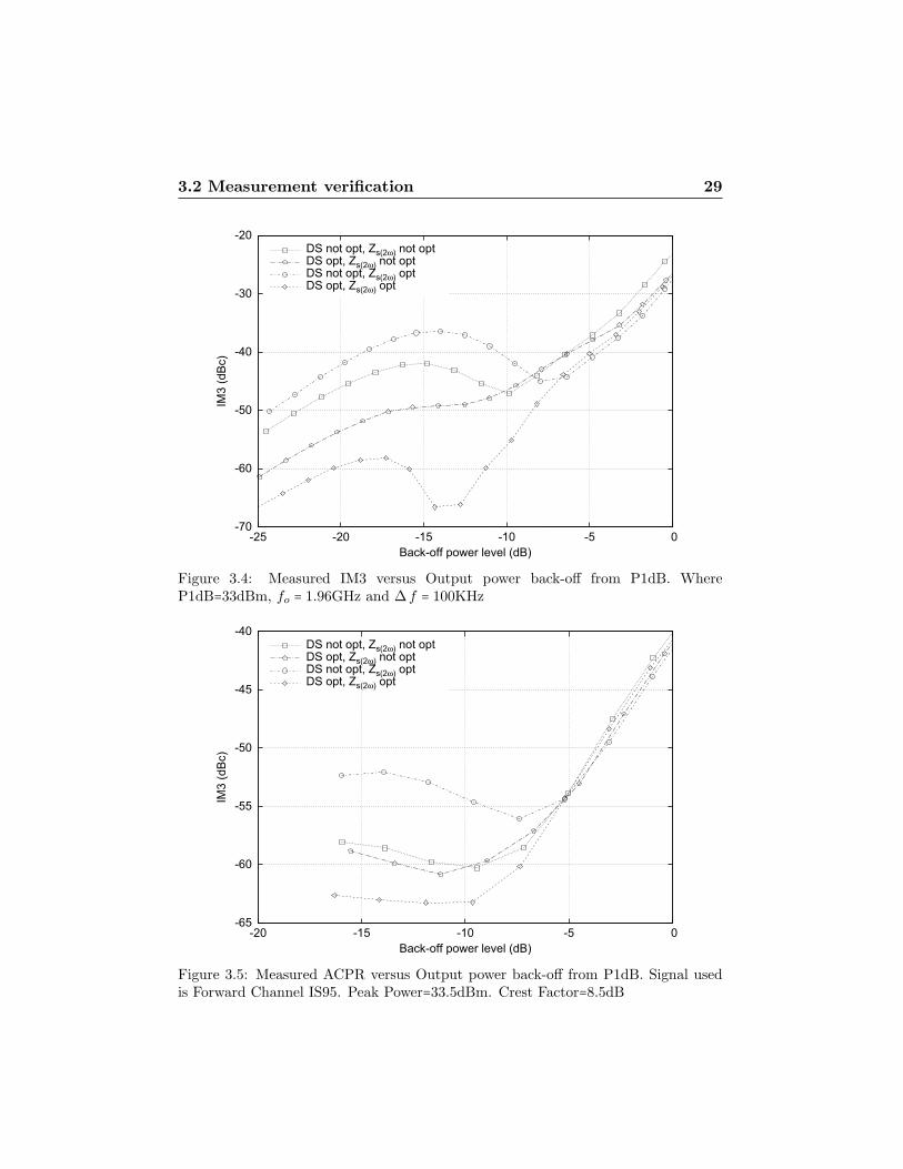
Figure 3.4 gives the results of a two-tone IM3 measurement. Both the lower andupper IM3 exhibits a similar trend and are within 0.5dB of each other. All out-of-band impedances were terminated with a short circuit except when explicitly statedin the figure. The transducer power gains of all 4 tests were similar (22dB) and theefficiency performances were also comparable. Using only derivative superposition, animprovement in IM3 can only be achieved up to 10dB back-off from compression. Ifonly out-of-band optimization is used with a focus to achieve linearity at high powers,linearity at lower power levels is degraded. However, using the combination of bothDS and ZS(2ω) optimization, the advantages of both techniques line up, providinga linearity improvement from lower power levels up to 4dB back-off from the 1 dBcompression point.
To further verify the effectiveness of this proposed technique, the PAs were drivenat various power levels closer to compression with a realistic test signal (CDMA IS-95).A transducer power gain of 22dB was achieved with all 4 setups and similar efficiencyperformance. The ACPR was measured at 750kHz offset at both the adjacent channels(Note that the ACPR specs for base-stations is 45 dBc). Figure 3.5 gives the averageACPR of the 2 adjacent channels versus output channel power. Note that for amodulated signal as used in our experiment, the output channel power represents theaverage power level, but the instantaneous power varies over a large power range, as
3.2 Measurement verification 29
-70
-60
-50
-40
-30
-20
-25 -20 -15 -10 -5 0
IM3
(dB
c)
Back-off power level (dB)
DS not opt, Zs(2ω) not optDS opt, Zs(2ω) not optDS not opt, Zs(2ω) optDS opt, Zs(2ω) opt
Figure 3.4: Measured IM3 versus Output power back-off from P1dB. WhereP1dB=33dBm, fo = 1.96GHz and Δf = 100KHz
-65
-60
-55
-50
-45
-40
-20 -15 -10 -5 0
IM3
(dB
c)
Back-off power level (dB)
DS not opt, Zs(2ω) not optDS opt, Zs(2ω) not optDS not opt, Zs(2ω) optDS opt, Zs(2ω) opt
Figure 3.5: Measured ACPR versus Output power back-off from P1dB. Signal usedis Forward Channel IS95. Peak Power=33.5dBm. Crest Factor=8.5dB
30 Improved Class-B, Class-AB Power Amplifiers
explained in Chapter 2. This is the reason why the two-tone intermodulation dataversus power does not follow exactly the characteristic of ACPR versus power.
Using only DS only (� plot, Figure 3.5), the linearity improvement is marginalover the conventional LDMOS operation (◻ plot) and only effective up to 10dB back-off. With ZS(2ω) tuning (○ plot), some improvement in linearity at power levels closeto P1dB compression point were achieved but at the expense of linearity at lowerpowers. Finally, with the combination of DS and ZS(2ω) tuning (◇ plot), significantimprovements in linearity is possible up to 4dB back-off from the compression point.
3.3 Input and output harmonic impedance control
In the previous section, linearity improvement at higher power levels was achieved bytuning only the second harmonic impedance at the source (YS2ω
). This basic conceptof harmonic impedance tuning was further extended in [17, 22] by including alsothe tuning of the second harmonic at the load side YL2ω
. The combination of bothinput and output second harmonic tuning gives a greater flexibility to control the IM3cancellation effects and can provide better results closer to compression.
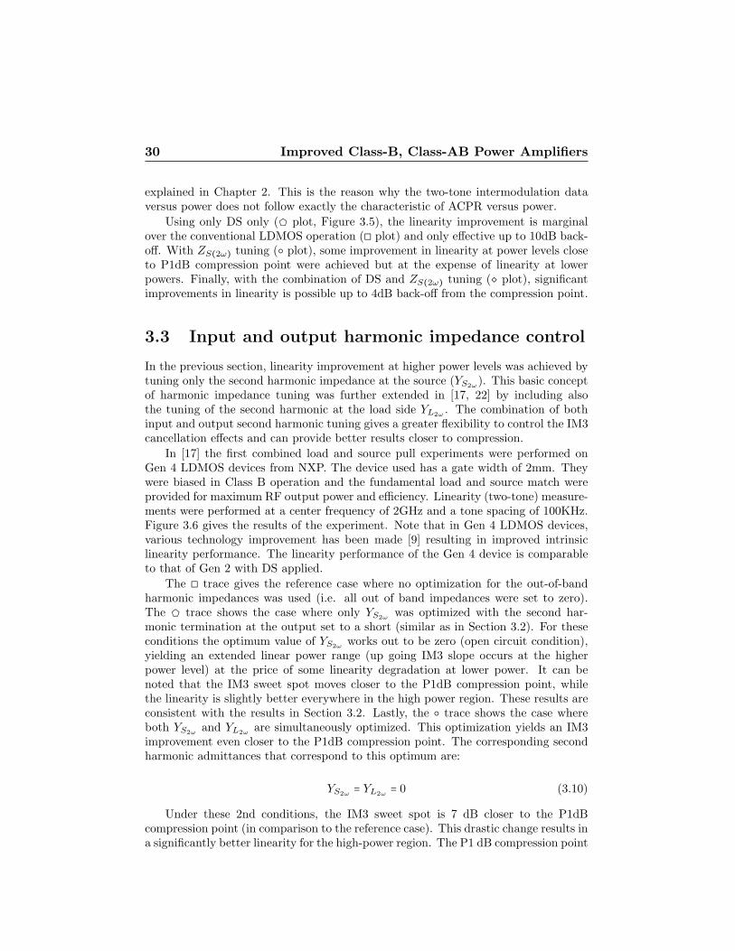
In [17] the first combined load and source pull experiments were performed onGen 4 LDMOS devices from NXP. The device used has a gate width of 2mm. Theywere biased in Class B operation and the fundamental load and source match wereprovided for maximum RF output power and efficiency. Linearity (two-tone) measure-ments were performed at a center frequency of 2GHz and a tone spacing of 100KHz.Figure 3.6 gives the results of the experiment. Note that in Gen 4 LDMOS devices,various technology improvement has been made [9] resulting in improved intrinsiclinearity performance. The linearity performance of the Gen 4 device is comparableto that of Gen 2 with DS applied.
The ◻ trace gives the reference case where no optimization for the out-of-bandharmonic impedances was used (i.e. all out of band impedances were set to zero).The � trace shows the case where only YS2ω
was optimized with the second har-monic termination at the output set to a short (similar as in Section 3.2). For theseconditions the optimum value of YS2ω
works out to be zero (open circuit condition),yielding an extended linear power range (up going IM3 slope occurs at the higherpower level) at the price of some linearity degradation at lower power. It can benoted that the IM3 sweet spot moves closer to the P1dB compression point, whilethe linearity is slightly better everywhere in the high power region. These results areconsistent with the results in Section 3.2. Lastly, the ○ trace shows the case whereboth YS2ω
and YL2ωare simultaneously optimized. This optimization yields an IM3
improvement even closer to the P1dB compression point. The corresponding secondharmonic admittances that correspond to this optimum are:
YS2ω= YL2ω
= 0 (3.10)
Under these 2nd conditions, the IM3 sweet spot is 7 dB closer to the P1dBcompression point (in comparison to the reference case). This drastic change results ina significantly better linearity for the high-power region. The P1 dB compression point
3.4 LDMOS Technology progress 31
-90
-80
-70
-60
-50
-40
-30
10 15 20 25 30
IM3
(dB
c)
Output RF power (dBm)
Zs(2ω) not opt, ZL(2ω) not optZs(2ω) opt, ZL(2ω) not optZs(2ω) opt, ZL(2ω) opt
Figure 3.6: Measurements from [17], demonstrating linearity improvements for Gen 4when using out-of-band tuning at both input, as well as, output of the Gen 4 LDMOSdevice. (fo = 2GHz, Δ f = 100KHz). Courtesy of Mr. Dave Hartskeerl and Dr. MarcoSpirito.
itself is hardly affected by these 2nd harmonic manipulations, since it is predominantlyset by the fundamental matching conditions.
The positive effect of improved linearity close to the P1dB point is two fold.First the power utilization factor (PUF) is maximized and second, higher efficiencycan be achieved while still meeting the linearity specifications, yielding significantimprovements when using complex modulated signals such as IS-95 or WCDMA.
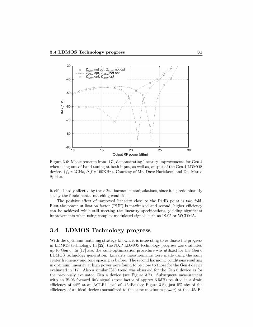
3.4 LDMOS Technology progress
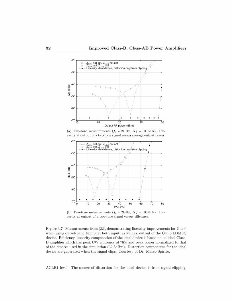
With the optimum matching strategy known, it is interesting to evaluate the progressin LDMOS technology. In [22], the NXP LDMOS technology progress was evaluatedup to Gen 6. In [17] also the same optimization procedure was utilized for the Gen 6LDMOS technology generation. Linearity measurements were made using the samecenter frequency and tone spacing as before. The second harmonic conditions resultingin optimum linearity at high power were found to be close to those for the Gen 4 deviceevaluated in [17]. Also a similar IM3 trend was observed for the Gen 6 device as forthe previously evaluated Gen 4 device (see Figure 3.7). Subsequent measurementwith an IS-95 forward link signal (crest factor of approx 6.5dB) resulted in a drainefficiency of 44% at an ACLR1 level of -45dBc (see Figure 3.8), just 5% shy of theefficiency of an ideal device (normalized to the same maximum power) at the -45dBc
32 Improved Class-B, Class-AB Power Amplifiers
-70
-60
-50
-40
-30
-20
10 15 20 25 30
IM3
(dB
c)
Output RF power (dBm)
Zs(2ω) not opt, ZL(2ω) not optZs(2ω) opt, ZL(2ω) optLinearity Ideal device, distortion only from clipping
(a) Two-tone measurements (fo = 2GHz, Δ f = 100KHz). Lin-earity at output of a two-tone signal versus average output power.
-70
-60
-50
-40
-30
-20
0 10 20 30 40 50 60 70 80
IM3
(dB
c)
PAE (%)
Zs(2ω) not opt, ZL(2ω) not optZs(2ω) opt, ZL(2ω) optLinearity Ideal device, distortion only from clipping
(b) Two-tone measurements (fo = 2GHz, Δ f = 100KHz). Lin-earity at output of a two-tone signal versus efficiency.
Figure 3.7: Measurements from [22], demonstrating linearity improvements for Gen 6when using out-of-band tuning at both input, as well as, output of the Gen 6 LDMOSdevice. Efficiency, linearity computation of the ideal device is based on an ideal Class-B amplifier which has peak CW efficiency of 78% and peak power normalized to thatof the devices used in the simulation (32.5dBm). Distortion components for the idealdevice are generated when the signal clips. Courtesy of Dr. Marco Spirito.
ACLR1 level. The source of distortion for the ideal device is from signal clipping.
3.5 Conclusion 33
This impressive efficiency performance was reported as a linearity-efficiency recordfor “Class-B” operated amplifiers using LDMOS technology in [22]. In this work wehave extended these experiments to include the latest progress in LDMOS technology.In addition we have also added the theoretical limit for an ideal device (peak poweris normalized to that of the devices used in the measurements) that is only limitedby clipping of the modulated signal.
-55
-50
-45
-40
-35
25 30 35 40 45 50
AC
LR (d
Bc)
PAE (%)
Zs(2ω) not opt, ZL(2ω) not optZs(2ω) opt, ZL(2ω) optLinearity Ideal device, distortion only from clipping
Figure 3.8: IS-95 forward link measurements from [22] at fo = 2GHz, demonstratinglinearity improvements for Gen 6 when using out-of-band tuning at both input, aswell as, output of the Gen 6 LDMOS device. Efficiency, linearity computation ofthe ideal device is based on an ideal Class-B amplifier which has peak CW efficiencyof 78% and peak power normalized to that of the devices used in the simulation(32.5dBm). Distortion components for the ideal device are generated when the signalclips. Courtesy of Dr. Marco Spirito.
3.5 Conclusion
In this part of the thesis work, two techniques have been utilized to improve thelinearity and efficiency performance of “class-AB” amplifier stages, namely derivativesuperposition and the out-of-band matching technique. Both techniques, as well astheir combined use, rely on basic understanding of the distortion mechanism presentin the single stage PA cell and prove to be useful in minimizing the intermodulationdistortion. In summary,
1. Derivative SuperpositionOriginally introduced to shape only the transconductance through superposi-

34 Improved Class-B, Class-AB Power Amplifiers
tion of individual device characteristic, in this work this technique was ana-lyzed with close form analytical equations and shown that the non-linear inputcapacitance Cgs also needs to be considered while applying DS, to obtain anoverall improvement in linearity at low to medium power levels (relative tothe 1dB compression point).
2. Derivative Superposition with second harmonic controlSince derivative superposition proved to be inadequate to provide better lin-earity close to compression, as next step, 2nd harmonic input control wasutilized to move the IM3 sweet spot closer to compression. It was found thatusing this second harmonic source impedance, a significant linearity improve-ment at medium to high power levels could be established. Experiments haveshown that the combination of DS and optimum 2nd harmonic input matchingcan provide improved linearity for all power levels.
3. Derivative Superposition with 2nd harmonic input and output con-trolTo push further the linearity vs. efficiency trade-off and obtain linearity im-provements at even higher power levels, 2nd harmonic tuning at both sourceand load can be utilized. By independent control of the input and output 2ndharmonic impedances, using a custom active load-pull setup, linearity improve-ments at high power levels were demonstrated up to the P1dB compressionpoint, with only a very limited linearity degradation at low powers levels. Formodern complex modulated signals (e.g. IS-95) this later technique using thelatest LDMOS technology provides a linearity-efficiency trade-off which be-comes closer to the theoretical limit given by an ideal signal clipping limitingdevice.
By using DS and no longer demanding second harmonic shorts, “Class-B” oper-ation (which originally assumes 2nd harmonic shorts) has been given a new future,since it provides low-cost, low-complexity, high-linearity and high-efficiency single-stage amplifier performance. With these latest results the author is of opinion thatthe modified Class-B PA cell is now very close to its theoretical limit. Marginal im-provements can still be made by looking at techniques to reduce losses in both theactive device (processing technology) or the peripheral matching network. However,to realize a further significant break through in efficiency performance, it is necessaryto look at high-efficiency PA architectures (system solutions), a subject which we willconsider in the next chapters.
In view of this, when aiming for highly efficient power amplifier architectures,such as Doherty and LINC, also linear operation can be achieved, when the poweramplifier cells are based on ideal devices. However in practical implementation ofthese high efficient architectures, the different power amplifier cells interact with eachother; consequently even if the PA cells are “linear enough”, the resulting interactionwould more often results in a unacceptable overall linearity performance. In theseconfigurations, a circuit solution is often not practically feasible due to the complexityof the problem statement or the required complexity of this linearization. As such asystem solution such as predistortion (digital for added flexibility/reconfigurability)is proposed to be used in conjunction with these high efficient PA architectures.

3.5 Conclusion 35
The following chapter looks into predistortion as a linearization technique, andfor this purpose a predistortion (PD) algorithm was implemented, for both the mem-oryless and the case with memory. We will use the PD algorithm in our later Dohertypower amplifier experiments and the adaptive PA for handsets.


Chapter 4
Predistortion of PowerAmplifiers
As industry embraces more complex PA architectures such as Doherty and EnvelopeTracking to improve for efficiency, simple circuit solutions to achieve high linearityare no longer become feasible and digital predistortion becomes mandatory. This hasyielded the situation that at the time of writing, Digital Predistortion (DPD) hasbecome an industrial standard for tackling nonlinear distortion in higher complexitypower amplifiers. This trend is accelerated by the the fall in cost of digital electronics,making it very attractive to incorporate a digital predistorter within the transceiversystem/ICs.
In this thesis work, the focus has been on the development of custom predistor-tion algorithms to meet the requirements of highly efficient but rather complex PAconcepts, which will be covered in later chapters. In this chapter, the basic principlesof predistortion for a single Class-B PA stage will be first introduced and furtherinvestigated. Section 4.1 considers the simplest case, namely the predistortion of amemoryless non-linear system. In Section 4.2, the case of a non-linear PA with mem-ory effects is discussed and the required extensions in the compensation algorithm aredescribed. The effectiveness of the algorithms are verified with both simulations andmeasurements.
4.1 Linearizing the memoryless Power Amplifier
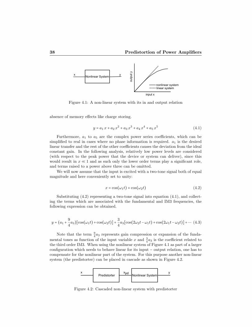
To aid understanding of predistortion, it is helpful to use a system theory approach.A system is linear if the output signal is always a linear scaled representation of theinput signal. This implies that the Gain (G) is constant and independent of the actualinput signal level. A system is considered to be non-linear if its transfer (e.g. Gain)depends on the input signal (x) as illustrated in Figure 4.1.
The nonlinearity of a system can be modeled in various ways. The easiest wouldbe the use of a polynomial approximation as in equation (4.1). Note that such a powerseries approximation is only valid in a very limited frequency range and assumes the
37
38 Predistortion of Power Amplifiers
Figure 4.1: A non-linear system with its in and output relation
absence of memory effects like charge storing.
y = a1 x + a2 x2 + a3 x3 + a4 x4 + a5 x5 (4.1)
Furthermore, a1 to a5 are the complex power series coefficients, which can besimplified to real in cases where no phase information is required. a1 is the desiredlinear transfer and the rest of the other coefficients causes the deviation from the idealconstant gain. In the following analysis, relatively low power levels are considered(with respect to the peak power that the device or system can deliver), since thiswould result in x ≪ 1 and as such only the lower order terms play a significant role,and terms raised to a power above three can be omitted.
We will now assume that the input is excited with a two-tone signal both of equalmagnitude and here conveniently set to unity:
x = cos(ω1t) + cos(ω2t) (4.2)
Substituting (4.2) representing a two-tone signal into equation (4.1), and collect-ing the terms which are associated with the fundamental and IM3 frequencies, thefollowing expression can be obtained.
y = (a1 + 9
4a3)[cos(ω1t)+ cos(ω2t)]+ 3
4a3[cos(2ω2t−ω1t)+ cos(2ω1t−ω2t)]+⋯ (4.3)
Note that the term 94a3 represents gain compression or expansion of the funda-
mental tones as function of the input variable x and 34a3 is the coefficient related to
the third order IM3. When using the nonlinear system of Figure 4.1 as part of a largerconfiguration which needs to behave linear for its input − output relation, one has tocompensate for the nonlinear part of the system. For this purpose another non-linearsystem (the predistorter) can be placed in cascade as shown in Figure 4.2.
Figure 4.2: Cascaded non-linear system with predistorter

4.1 Linearizing the memoryless Power Amplifier 39
For the transfer of the predistorter block we assume, the following:
xpd = b1 x + b3 x3 (4.4)
Note that this predistorter has besides its linear transfer only a third order non-linearity. The overall transfer function of the predistorter and non-linear system tobe linearized can now be written as:
y = a1b1x + a2b21x
2 + (a1b3 + a3b31)x3 (4.5)
+ 2a2b1b3x4 + 3a3b
21b3x
5 + a2b23x
6
+ 3a3b1b23x
7 + a3b33x9
By setting b1 = 1 and b3 = −a3
a1
the third order coefficient of the overall transferwould be set to zero. It is important to note that although the original non-linearsystem has only second and third order nonlinearities; due to the use of predistorterhigher order non-linearities are introduced/generated. Note that these higher odd or-der non-linearities (fifth, seventh and ninth) directly contribute to the distortion prod-ucts at the IM3 frequencies. From this result it can be concluded that a third-orderpredistorter used to compensate a third-order non-linear system will never be ableto completely eliminate all third-order distortion, furthermore higher-order distortion(which is typically lower in power) are added into the process. This phenomenon canbe also explained by the following.
The following mathematical equations represent the transfers of the block as func-tions.
y = k F(xpd) (4.6)
xpd = G(x) (4.7)
Where k is a constant. The output as a result of the cascade is:
y = k F(G(x)) (4.8)
To obtain a linear output, the transfer of the predistorter should be G = F−1.
In the example that was used before, F was a third order polynomial. However, itcan be shown that the inverse of a third-order polynomial will be a polynomial of aninfinite order. This implies that in order to completely cancel out the distortion of anonlinear system, a predistorter with an infinite amount of higher-order non-linearityis required. In practice such a requirement translates to an infinite bandwidth for thepredistorter to handle al the distortion products. Therefore at this juncture, it can beconcluded that there is no practical predistorter possible that can completely reducethe distortion of the overall system to zero.
4.1.1 Practical implementation of a memoryless predistorter
We will now discuss a practical implementation of a memoryless predistorter. To bestillustrate the algorithm for memoryless correction, accompanying simulation results
40 Predistortion of Power Amplifiers
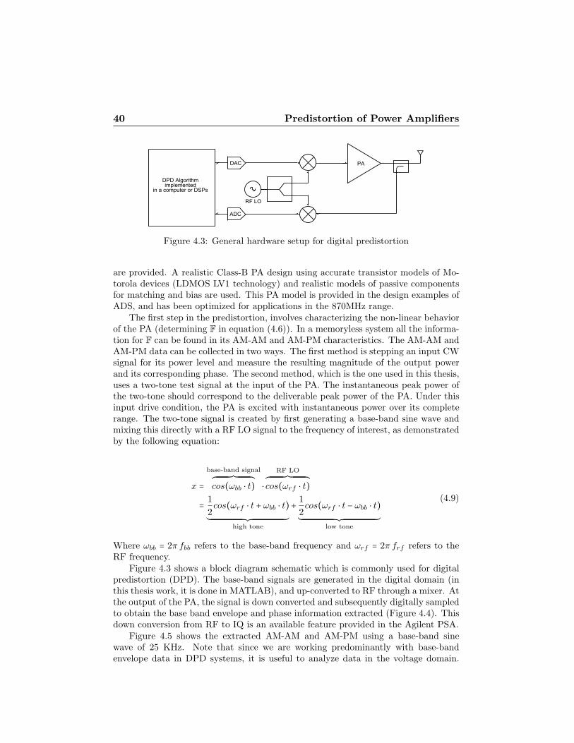
Figure 4.3: General hardware setup for digital predistortion
are provided. A realistic Class-B PA design using accurate transistor models of Mo-torola devices (LDMOS LV1 technology) and realistic models of passive componentsfor matching and bias are used. This PA model is provided in the design examples ofADS, and has been optimized for applications in the 870MHz range.
The first step in the predistortion, involves characterizing the non-linear behaviorof the PA (determining F in equation (4.6)). In a memoryless system all the informa-tion for F can be found in its AM-AM and AM-PM characteristics. The AM-AM andAM-PM data can be collected in two ways. The first method is stepping an input CWsignal for its power level and measure the resulting magnitude of the output powerand its corresponding phase. The second method, which is the one used in this thesis,uses a two-tone test signal at the input of the PA. The instantaneous peak power ofthe two-tone should correspond to the deliverable peak power of the PA. Under thisinput drive condition, the PA is excited with instantaneous power over its completerange. The two-tone signal is created by first generating a base-band sine wave andmixing this directly with a RF LO signal to the frequency of interest, as demonstratedby the following equation:
x =base-band signal³¹¹¹¹¹¹¹¹¹¹¹¹¹¹¹¹¹¹¹¹¹¹¹·¹¹¹¹¹¹¹¹¹¹¹¹¹¹¹¹¹¹¹¹¹¹¹µcos(ωbb ⋅ t) ⋅
RF LO³¹¹¹¹¹¹¹¹¹¹¹¹¹¹¹¹¹¹¹¹¹¹¹¹¹·¹¹¹¹¹¹¹¹¹¹¹¹¹¹¹¹¹¹¹¹¹¹¹¹µcos(ωrf ⋅ t)
= 1
2cos(ωrf ⋅ t + ωbb ⋅ t)´¹¹¹¹¹¹¹¹¹¹¹¹¹¹¹¹¹¹¹¹¹¹¹¹¹¹¹¹¹¹¹¹¹¹¹¹¹¹¹¹¹¹¹¹¹¹¹¹¹¹¹¹¹¹¹¹¹¹¹¹¹¸¹¹¹¹¹¹¹¹¹¹¹¹¹¹¹¹¹¹¹¹¹¹¹¹¹¹¹¹¹¹¹¹¹¹¹¹¹¹¹¹¹¹¹¹¹¹¹¹¹¹¹¹¹¹¹¹¹¹¹¹¹
high tone
+ 1
2cos(ωrf ⋅ t − ωbb ⋅ t)´¹¹¹¹¹¹¹¹¹¹¹¹¹¹¹¹¹¹¹¹¹¹¹¹¹¹¹¹¹¹¹¹¹¹¹¹¹¹¹¹¹¹¹¹¹¹¹¹¹¹¹¹¹¹¹¹¹¹¹¹¹¸¹¹¹¹¹¹¹¹¹¹¹¹¹¹¹¹¹¹¹¹¹¹¹¹¹¹¹¹¹¹¹¹¹¹¹¹¹¹¹¹¹¹¹¹¹¹¹¹¹¹¹¹¹¹¹¹¹¹¹¹¹
low tone
(4.9)
Where ωbb = 2π fbb refers to the base-band frequency and ωrf = 2π frf refers to theRF frequency.
Figure 4.3 shows a block diagram schematic which is commonly used for digitalpredistortion (DPD). The base-band signals are generated in the digital domain (inthis thesis work, it is done in MATLAB), and up-converted to RF through a mixer. Atthe output of the PA, the signal is down converted and subsequently digitally sampledto obtain the base band envelope and phase information extracted (Figure 4.4). Thisdown conversion from RF to IQ is an available feature provided in the Agilent PSA.
Figure 4.5 shows the extracted AM-AM and AM-PM using a base-band sinewave of 25 KHz. Note that since we are working predominantly with base-bandenvelope data in DPD systems, it is useful to analyze data in the voltage domain.
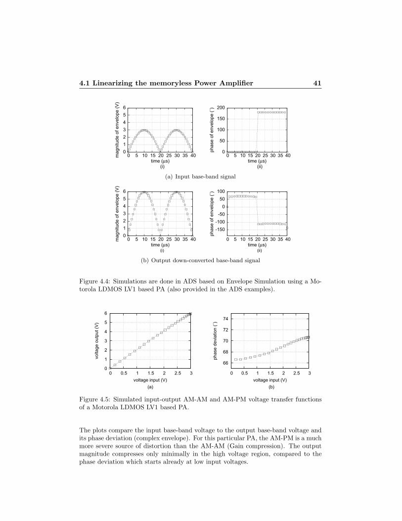
4.1 Linearizing the memoryless Power Amplifier 41
0 1 2 3 4 5 6
0 5 10 15 20 25 30 35 40mag
nitu
de o
f env
elop
e (V
)
time (μs)(i) (ii)
0
50
100
150
200
0 5 10 15 20 25 30 35 40
phas
e of
env
elop
e (˚
)
time (μs)
(a) Input base-band signal
0 1 2 3 4 5 6
0 5 10 15 20 25 30 35 40mag
nitu
de o
f env
elop
e (V
)
time (μs)(i) (ii)
-150-100
-50 0
50 100
0 5 10 15 20 25 30 35 40
phas
e of
env
elop
e (˚
)
time (μs)
(b) Output down-converted base-band signal
Figure 4.4: Simulations are done in ADS based on Envelope Simulation using a Mo-torola LDMOS LV1 based PA (also provided in the ADS examples).
0
1
2
3
4
5
6
0 0.5 1 1.5 2 2.5 3
volta
ge o
utpu
t (V
)
voltage input (V)(a) (b)
66
68
70
72
74
0 0.5 1 1.5 2 2.5 3
phas
e de
viat
ion
(˚)
voltage input (V)
Figure 4.5: Simulated input-output AM-AM and AM-PM voltage transfer functionsof a Motorola LDMOS LV1 based PA.
The plots compare the input base-band voltage to the output base-band voltage andits phase deviation (complex envelope). For this particular PA, the AM-PM is a muchmore severe source of distortion than the AM-AM (Gain compression). The outputmagnitude compresses only minimally in the high voltage region, compared to thephase deviation which starts already at low input voltages.
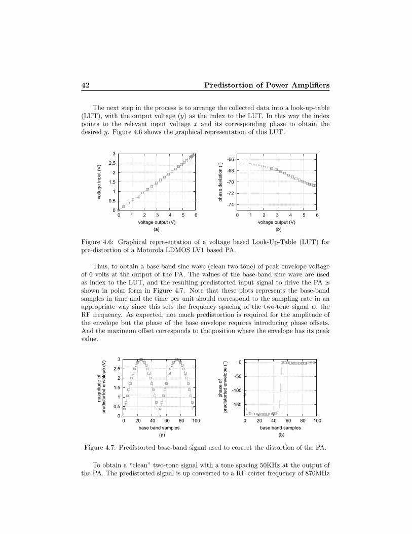
42 Predistortion of Power Amplifiers
The next step in the process is to arrange the collected data into a look-up-table(LUT), with the output voltage (y) as the index to the LUT. In this way the indexpoints to the relevant input voltage x and its corresponding phase to obtain thedesired y. Figure 4.6 shows the graphical representation of this LUT.
0
0.5
1
1.5
2
2.5
3
0 1 2 3 4 5 6
volta
ge in
put (
V)
voltage output (V)(a) (b)
-74
-72
-70
-68
-66
0 1 2 3 4 5 6ph
ase
devi
atio
n (˚
)voltage output (V)
Figure 4.6: Graphical representation of a voltage based Look-Up-Table (LUT) forpre-distortion of a Motorola LDMOS LV1 based PA.
Thus, to obtain a base-band sine wave (clean two-tone) of peak envelope voltageof 6 volts at the output of the PA. The values of the base-band sine wave are usedas index to the LUT, and the resulting predistorted input signal to drive the PA isshown in polar form in Figure 4.7. Note that these plots represents the base-bandsamples in time and the time per unit should correspond to the sampling rate in anappropriate way since this sets the frequency spacing of the two-tone signal at theRF frequency. As expected, not much predistortion is required for the amplitude ofthe envelope but the phase of the base envelope requires introducing phase offsets.And the maximum offset corresponds to the position where the envelope has its peakvalue.
0
0.5
1
1.5
2
2.5
3
0 20 40 60 80 100
mag
nitu
de o
f p
redi
stor
ted
enve
lope
(V)
base band samples(a) (b)
-150
-100
-50
0
0 20 40 60 80 100
phas
e of
p
redi
stor
ted
enve
lope
(˚)
base band samples
Figure 4.7: Predistorted base-band signal used to correct the distortion of the PA.
To obtain a “clean” two-tone signal with a tone spacing 50KHz at the output ofthe PA. The predistorted signal is up converted to a RF center frequency of 870MHz
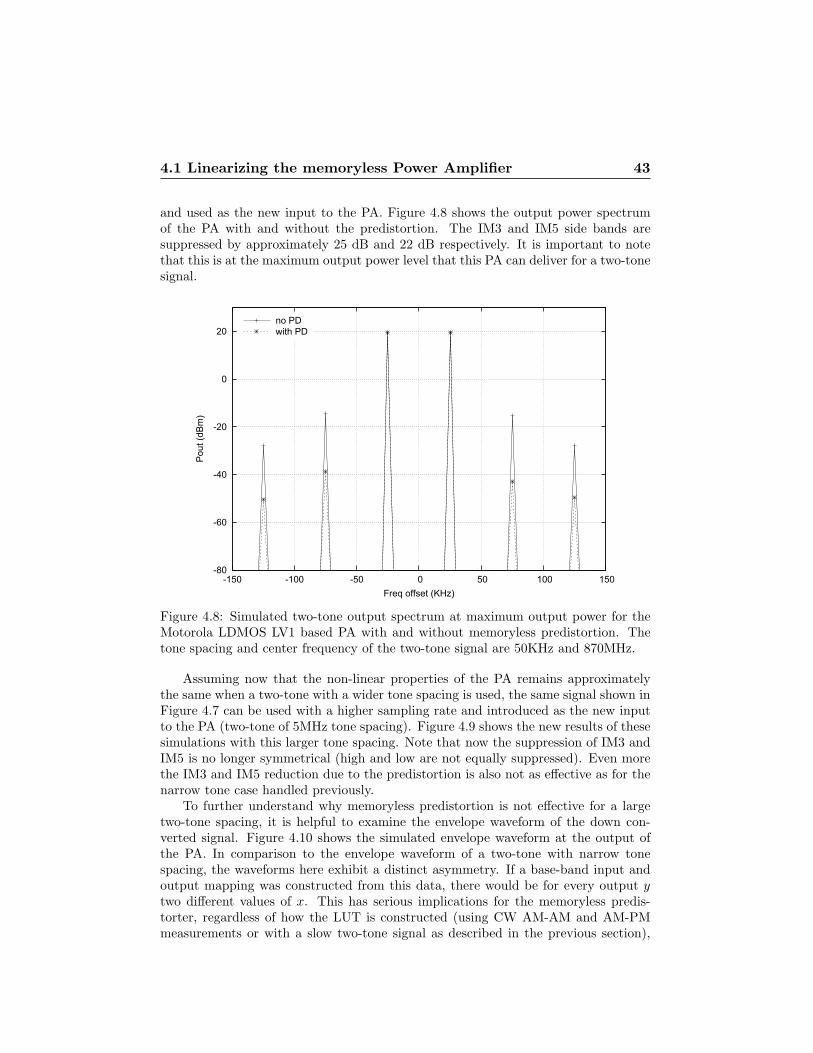
4.1 Linearizing the memoryless Power Amplifier 43
and used as the new input to the PA. Figure 4.8 shows the output power spectrumof the PA with and without the predistortion. The IM3 and IM5 side bands aresuppressed by approximately 25 dB and 22 dB respectively. It is important to notethat this is at the maximum output power level that this PA can deliver for a two-tonesignal.
-80
-60
-40
-20
0
20
-150 -100 -50 0 50 100 150
Pou
t (dB
m)
Freq offset (KHz)
no PDwith PD
Figure 4.8: Simulated two-tone output spectrum at maximum output power for theMotorola LDMOS LV1 based PA with and without memoryless predistortion. Thetone spacing and center frequency of the two-tone signal are 50KHz and 870MHz.
Assuming now that the non-linear properties of the PA remains approximatelythe same when a two-tone with a wider tone spacing is used, the same signal shown inFigure 4.7 can be used with a higher sampling rate and introduced as the new inputto the PA (two-tone of 5MHz tone spacing). Figure 4.9 shows the new results of thesesimulations with this larger tone spacing. Note that now the suppression of IM3 andIM5 is no longer symmetrical (high and low are not equally suppressed). Even morethe IM3 and IM5 reduction due to the predistortion is also not as effective as for thenarrow tone case handled previously.
To further understand why memoryless predistortion is not effective for a largetwo-tone spacing, it is helpful to examine the envelope waveform of the down con-verted signal. Figure 4.10 shows the simulated envelope waveform at the output ofthe PA. In comparison to the envelope waveform of a two-tone with narrow tonespacing, the waveforms here exhibit a distinct asymmetry. If a base-band input andoutput mapping was constructed from this data, there would be for every output y
two different values of x. This has serious implications for the memoryless predis-torter, regardless of how the LUT is constructed (using CW AM-AM and AM-PMmeasurements or with a slow two-tone signal as described in the previous section),
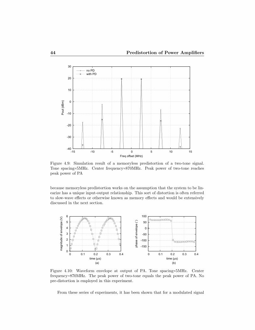
44 Predistortion of Power Amplifiers
-40
-30
-20
-10
0
10
20
30
-15 -10 -5 0 5 10 15
Pou
t (dB
m)
Freq offset (MHz)
no PDwith PD
Figure 4.9: Simulation result of a memoryless predistortion of a two-tone signal.Tone spacing=5MHz. Center frequency=870MHz. Peak power of two-tone reachespeak power of PA
because memoryless predistortion works on the assumption that the system to be lin-earize has a unique input-output relationship. This sort of distortion is often referredto slow-wave effects or otherwise known as memory effects and would be extensivelydiscussed in the next section.
0
1
2
3
4
5
6
0 0.1 0.2 0.3 0.4
mag
nitu
de o
f env
elop
e (V
)
time (μs)(a) (b)
-150
-100
-50
0
50
100
0 0.1 0.2 0.3 0.4
phas
e of
env
elop
e (˚
)
time (μs)
Figure 4.10: Waveform envelope at output of PA. Tone spacing=5MHz. Centerfrequency=870MHz. The peak power of two-tone equals the peak power of PA. Nopre-distortion is employed in this experiment.
From these series of experiments, it has been shown that for a modulated signal

4.2 PA with memory effects 45
that has a bandwidth that is narrow enough such that it falls in the range where thePA is memoryless, then the above mentioned predistortion algorithm is effective inimproving the linearity performance. Measurement verification of these experimentsare shown in Chapter 6, where this predistortion concept was used to improved thelinearity of a class AB PA under static load-line modulation.
4.2 PA with memory effects
In a system with memory, the output signal at time t is not only a function of the inputsignal applied to the amplifier at that time t but also from the forgoing history of theinput signal. This is mathematically represented by the well known convolution ofthe input signal with the impulse response of the system as shown in Equation (4.10).
y(t) =∞∫−∞
h(τ)x(t − τ)dτ (4.10)
However, in the case of a non-linear system with memory effects, the situationbecomes more complicated since the impulse response is now also a function of theinstantaneous power. A mathematical formulation of such a system can be expressedusing the Volterra/Wiener equations, which are the basis of the well known VolterraSeries calculation techniques. Equation (4.11) shows the third-order Volterra kernel,representing the third-order linearity with memory effects. This equation shows thatthe output is a of three dimensional convolution of the input signal with the impulseresponse, which is again a function of three time constants.
y(t) =∞∭−∞
h(τ1, τ2, τ3)x(t − τ1)x(t − τ2)x(t − τ3)dτ1dτ2dτ3 (4.11)
Although Volterra series analysis is probably the most appropriate tool to analyzeand model non-linear systems with memory. It has been shown in Chapter 2 that whenhigher order nonlinearities above the third are taken into account, the complexity ofthe expression increases dramatically. Furthermore, if impedances at the IF andhigher harmonics are taken into account, the equations become soon uninterpretable.The other even more important reason to avoid Volterra series for this application, liesin the difficulty of finding an analytical inverse function required for the pre-distortionaction. As such, a logic compromise is to seek where ease of implementation is tradedoff against accuracy of representation of the system.
Memory effects can come from distortion products at higher harmonic frequenciesmixing back to the in-channel, but more often the main contributors come from effectsat the IF frequency, such as self heating (thermal memory effects) and the effects of thebias-circuitry. In a RF power amplifier, the only memory effects that are detrimentalto in channel spectral regrowth are the ones that affect the envelope (amplitude andphase), as was seen in Figure 4.10.
Thus to characterize a non-linear PA with memory, it is helpful to introduce theconcept of an envelope step/pulse response. Figure 4.11(a) shows in simulation, thepulsed RF waveform at the input of the Motorola LDMOS LV1 PA, and Figure 4.11(b)
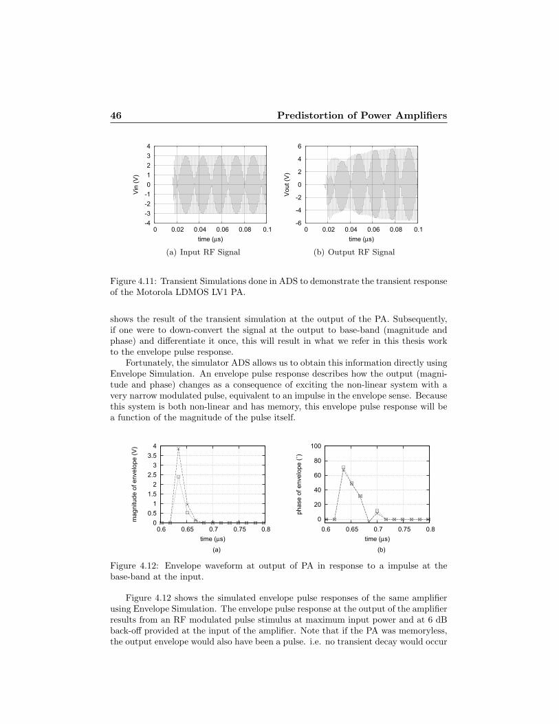
46 Predistortion of Power Amplifiers
-4-3-2-1 0 1 2 3 4
0 0.02 0.04 0.06 0.08 0.1
Vin
(V)
time (μs)
(a) Input RF Signal
-6
-4
-2
0
2
4
6
0 0.02 0.04 0.06 0.08 0.1
Vou
t (V
)
time (μs)
(b) Output RF Signal
Figure 4.11: Transient Simulations done in ADS to demonstrate the transient responseof the Motorola LDMOS LV1 PA.
shows the result of the transient simulation at the output of the PA. Subsequently,if one were to down-convert the signal at the output to base-band (magnitude andphase) and differentiate it once, this will result in what we refer in this thesis workto the envelope pulse response.
Fortunately, the simulator ADS allows us to obtain this information directly usingEnvelope Simulation. An envelope pulse response describes how the output (magni-tude and phase) changes as a consequence of exciting the non-linear system with avery narrow modulated pulse, equivalent to an impulse in the envelope sense. Becausethis system is both non-linear and has memory, this envelope pulse response will bea function of the magnitude of the pulse itself.
0 0.5
1 1.5
2 2.5
3 3.5
4
0.6 0.65 0.7 0.75 0.8
mag
nitu
de o
f env
elop
e (V
)
time (μs)
(a) (b)
0
20
40
60
80
100
0.6 0.65 0.7 0.75 0.8
phas
e of
env
elop
e (˚
)
time (μs)
Figure 4.12: Envelope waveform at output of PA in response to a impulse at thebase-band at the input.
Figure 4.12 shows the simulated envelope pulse responses of the same amplifierusing Envelope Simulation. The envelope pulse response at the output of the amplifierresults from an RF modulated pulse stimulus at maximum input power and at 6 dBback-off provided at the input of the amplifier. Note that if the PA was memoryless,the output envelope would also have been a pulse. i.e. no transient decay would occur
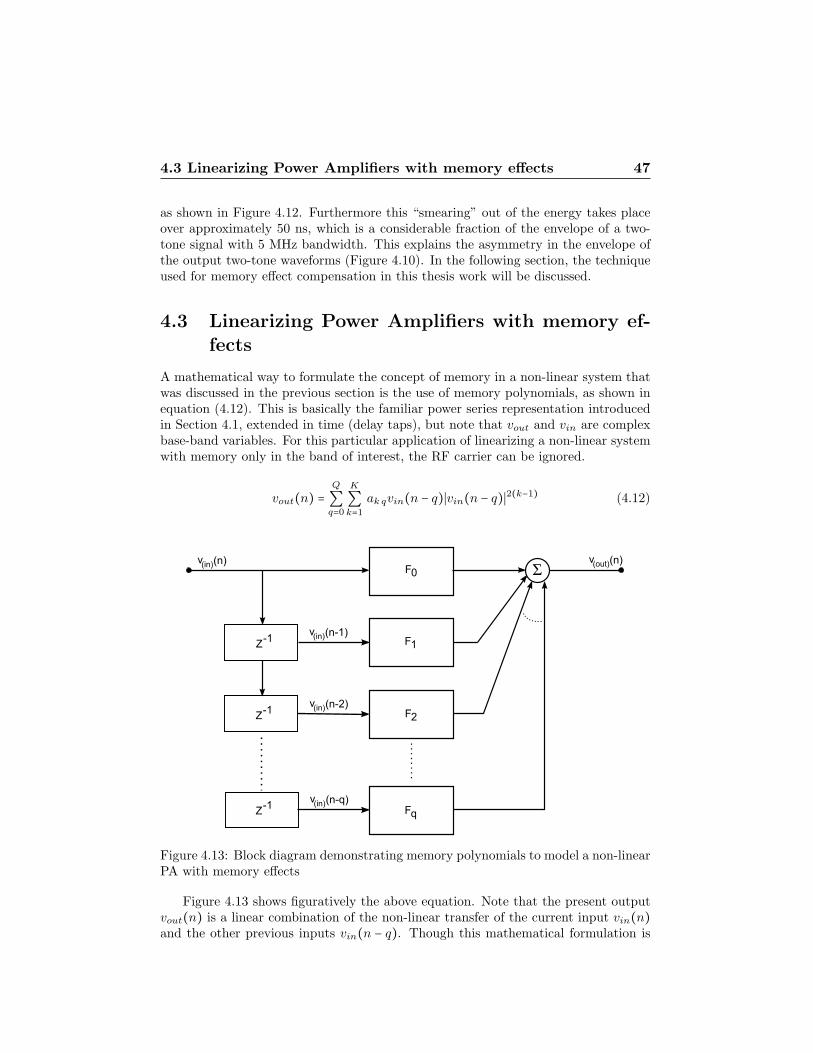
4.3 Linearizing Power Amplifiers with memory effects 47
as shown in Figure 4.12. Furthermore this “smearing” out of the energy takes placeover approximately 50 ns, which is a considerable fraction of the envelope of a two-tone signal with 5 MHz bandwidth. This explains the asymmetry in the envelope ofthe output two-tone waveforms (Figure 4.10). In the following section, the techniqueused for memory effect compensation in this thesis work will be discussed.
4.3 Linearizing Power Amplifiers with memory ef-fects
A mathematical way to formulate the concept of memory in a non-linear system thatwas discussed in the previous section is the use of memory polynomials, as shown inequation (4.12). This is basically the familiar power series representation introducedin Section 4.1, extended in time (delay taps), but note that vout and vin are complexbase-band variables. For this particular application of linearizing a non-linear systemwith memory only in the band of interest, the RF carrier can be ignored.
vout(n) =Q
∑q=0
K
∑k=1
ak qvin(n − q)∣vin(n − q)∣2(k−1) (4.12)
Figure 4.13: Block diagram demonstrating memory polynomials to model a non-linearPA with memory effects
Figure 4.13 shows figuratively the above equation. Note that the present outputvout(n) is a linear combination of the non-linear transfer of the current input vin(n)and the other previous inputs vin(n − q). Though this mathematical formulation is
48 Predistortion of Power Amplifiers
straight forward, it does not accurately model the non-linear system. This analysistechnique fails to take into account cross term non-linearities, which is the effect wherethe non-linear transfer F0 being also a function of vout(n − 1) and other larger delaytaps. This inadequacy also extends to the other transfer functions F1 to Fq. But aswas previously discussed, this compromise in accuracy of representation is justifiedby the ease of implementing the predistorter.
From the above figure and making the assumption that time delay greater than3 time steps away no longer has any influence on the output, equation (4.12) can besimplified to the following.
vout(n) = F0 (vin (n)) + F1 (vin (n − 1)) + F2 (vin (n − 2)) + F3 (vin (n − 3)) +⋯
(4.13)
≈ F0 (vin (n)) + F1 (vin (n − 1)) + F2 (vin (n − 2)) + F3 (vin (n − 3))Note that in this thesis, the second, third and fourth term in equation (4.13) are
referred to residual memory. To determine the input vin at time n necessary to obtaina vout at time n equal to y, equation (4.13) can be rearranged to give the following.
vin(n) = F −10 (y) − F −10 (F1 (vin (n − 1)) + F2 (vin (n − 2)) + F3 (vin (n − 3))) (4.14)
This implies that to compute the required vin at time n, the vector sum at theoutput due to the previous inputs must first be computed (residual memory). Thena subsequent computation F −10 of the residual memory to determine the input atthe current time n is required to cancel this memory residue. With the memoryresidue canceled, F −10 (y) at the input would give y at the output resulting in the finalpredistorted vin which is the vector sum of these two components. The above is theoperation principle of a predistorter with memory compensation.
4.3.1 Practical implementation
A practical implementation of the predistorter with memory compensation, is noth-ing more than taking the information of the desired output signal and applying equa-tion (4.14) to the complete output signal in order to compute the required predistortedinput. In order to do this, it is clear that F0 to Fq first have to be characterized, whereq is equal to the number of delay taps that is required. For this action, it is usefulto look at the envelope pulse response described in section 4.2. Figure 4.12 showsthe envelope pulse response at the output of the non-linear PA with memory, for twodifferent input voltages. The peak value at the magnitude plot and its correspondingphase vout(n) is related to the input vin(n) through F0, and one time step away (howthis time step is chosen will be explained in the following paragraph,) the outputmagnitude and phase of vout(n + 1) is related to the input vin(n) through F1. Thesame conclusions can be drawn for the rest of the transfer functions F2 to Fq. If a
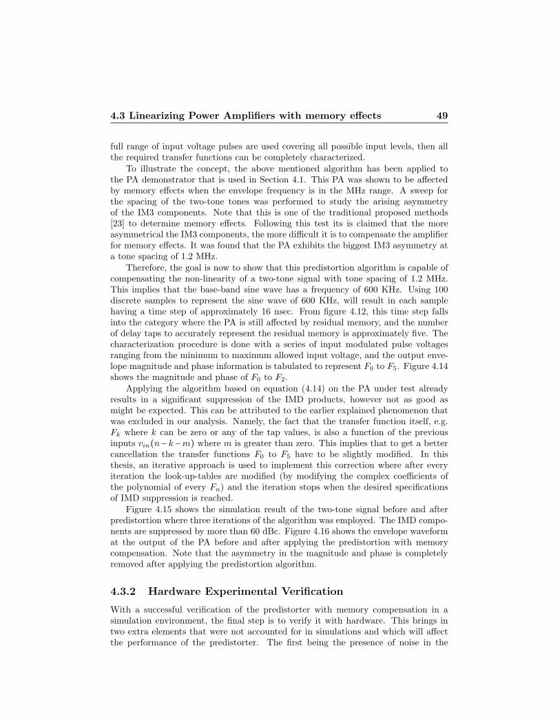
4.3 Linearizing Power Amplifiers with memory effects 49
full range of input voltage pulses are used covering all possible input levels, then allthe required transfer functions can be completely characterized.
To illustrate the concept, the above mentioned algorithm has been applied tothe PA demonstrator that is used in Section 4.1. This PA was shown to be affectedby memory effects when the envelope frequency is in the MHz range. A sweep forthe spacing of the two-tone tones was performed to study the arising asymmetryof the IM3 components. Note that this is one of the traditional proposed methods[23] to determine memory effects. Following this test its is claimed that the moreasymmetrical the IM3 components, the more difficult it is to compensate the amplifierfor memory effects. It was found that the PA exhibits the biggest IM3 asymmetry ata tone spacing of 1.2 MHz.
Therefore, the goal is now to show that this predistortion algorithm is capable ofcompensating the non-linearity of a two-tone signal with tone spacing of 1.2 MHz.This implies that the base-band sine wave has a frequency of 600 KHz. Using 100discrete samples to represent the sine wave of 600 KHz, will result in each samplehaving a time step of approximately 16 nsec. From figure 4.12, this time step fallsinto the category where the PA is still affected by residual memory, and the numberof delay taps to accurately represent the residual memory is approximately five. Thecharacterization procedure is done with a series of input modulated pulse voltagesranging from the minimum to maximum allowed input voltage, and the output enve-lope magnitude and phase information is tabulated to represent F0 to F5. Figure 4.14shows the magnitude and phase of F0 to F2.
Applying the algorithm based on equation (4.14) on the PA under test alreadyresults in a significant suppression of the IMD products, however not as good asmight be expected. This can be attributed to the earlier explained phenomenon thatwas excluded in our analysis. Namely, the fact that the transfer function itself, e.g.Fk where k can be zero or any of the tap values, is also a function of the previousinputs vin(n − k −m) where m is greater than zero. This implies that to get a bettercancellation the transfer functions F0 to F5 have to be slightly modified. In thisthesis, an iterative approach is used to implement this correction where after everyiteration the look-up-tables are modified (by modifying the complex coefficients ofthe polynomial of every Fn) and the iteration stops when the desired specificationsof IMD suppression is reached.
Figure 4.15 shows the simulation result of the two-tone signal before and afterpredistortion where three iterations of the algorithm was employed. The IMD compo-nents are suppressed by more than 60 dBc. Figure 4.16 shows the envelope waveformat the output of the PA before and after applying the predistortion with memorycompensation. Note that the asymmetry in the magnitude and phase is completelyremoved after applying the predistortion algorithm.
4.3.2 Hardware Experimental Verification
With a successful verification of the predistorter with memory compensation in asimulation environment, the final step is to verify it with hardware. This brings intwo extra elements that were not accounted for in simulations and which will affectthe performance of the predistorter. The first being the presence of noise in the
50 Predistortion of Power Amplifiers
0
0.2
0.4
0.6
0.8
1
0 0.5 1 1.5 2 2.5 3 3.5
Vou
t (V
)
Vin (V)(c)
(b)
(a)
30
32
34
36
38
40
0 0.5 1 1.5 2 2.5 3 3.5
phas
e (˚
)
Vin (V)
0
0.5
1
1.5
2
2.5
3
0 0.5 1 1.5 2 2.5 3 3.5
Vou
t (V
)
Vin (V)
46
48
50
52
54
0 0.5 1 1.5 2 2.5 3 3.5
phas
e (˚
)
Vin (V)
0
1
2
3
4
5
0 0.5 1 1.5 2 2.5 3 3.5
Vou
t (V
)
Vin (V)
66
68
70
72
74
0 0.5 1 1.5 2 2.5 3 3.5
phas
e (˚
)
Vin (V)
Figure 4.14: (a) Magnitude and phase of F0. (b) Magnitude and phase of F1. (c)Magnitude and phase of F2. Values are based on simulated envelope pulse responsedata.
calibration routine (when building the LUT) and the second, thermal memory effectswhich were not included in the models used in the simulation.
Figure 4.17 shows the block diagram schematic of our custom amplifier testbench for performing digital predistortion. Its structure is based on the heterodynetransceiver architecture. The complex base-band signals are generated using MAT-LAB and uploaded as a digital 400 MHz IF signal to the Agilent N6030A ArbitraryWaveform Generators (AWG). This signal is further up-converted in the analoguedomain to a center frequency of 2.14 GHz using a mixer with the LO port connectedto a ESG providing a CW signal at 1.74 GHz. A high-pass filter suppresses the lower-
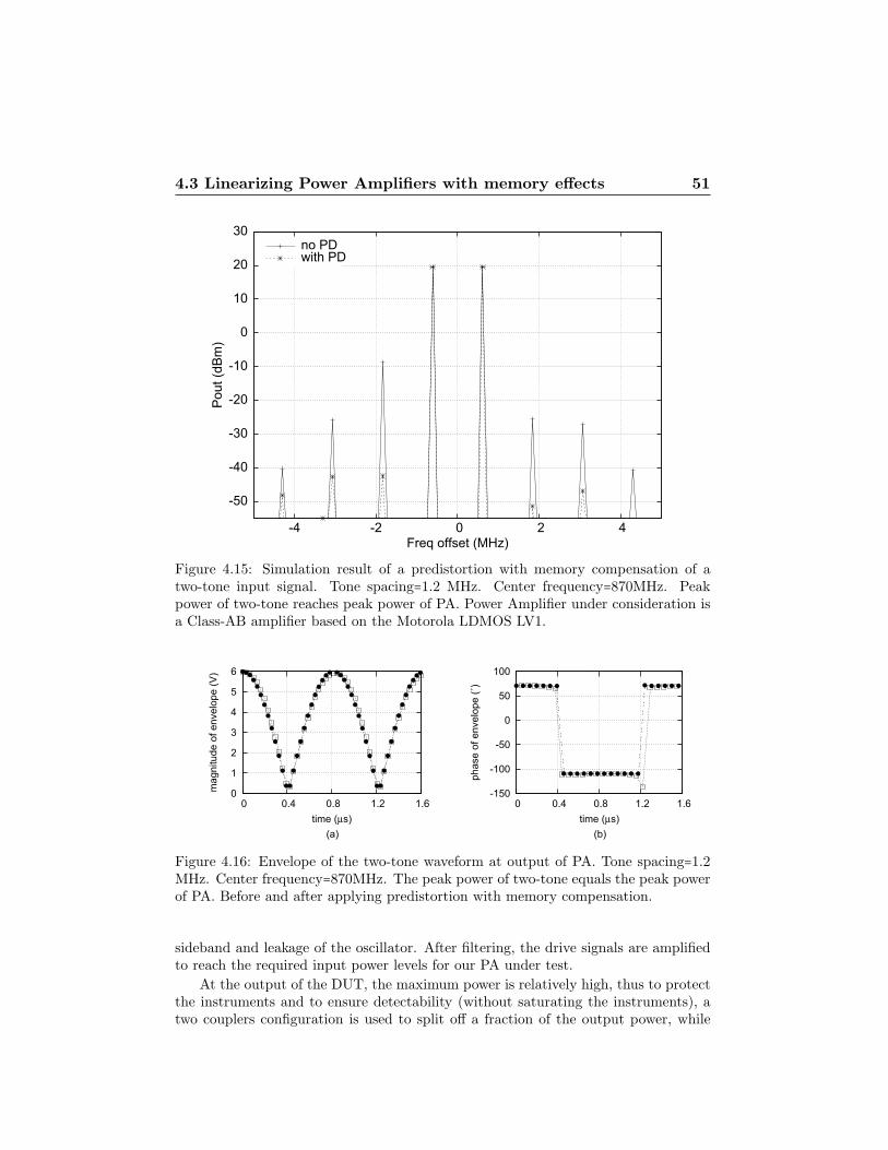
4.3 Linearizing Power Amplifiers with memory effects 51
-50
-40
-30
-20
-10
0
10
20
30
-4 -2 0 2 4
Pou
t (dB
m)
Freq offset (MHz)
no PDwith PD
Figure 4.15: Simulation result of a predistortion with memory compensation of atwo-tone input signal. Tone spacing=1.2 MHz. Center frequency=870MHz. Peakpower of two-tone reaches peak power of PA. Power Amplifier under consideration isa Class-AB amplifier based on the Motorola LDMOS LV1.
0
1
2
3
4
5
6
0 0.4 0.8 1.2 1.6
mag
nitu
de o
f env
elop
e (V
)
time (μs)(a) (b)
-150
-100
-50
0
50
100
0 0.4 0.8 1.2 1.6
phas
e of
env
elop
e (˚
)
time (μs)
Figure 4.16: Envelope of the two-tone waveform at output of PA. Tone spacing=1.2MHz. Center frequency=870MHz. The peak power of two-tone equals the peak powerof PA. Before and after applying predistortion with memory compensation.
sideband and leakage of the oscillator. After filtering, the drive signals are amplifiedto reach the required input power levels for our PA under test.
At the output of the DUT, the maximum power is relatively high, thus to protectthe instruments and to ensure detectability (without saturating the instruments), atwo couplers configuration is used to split off a fraction of the output power, while
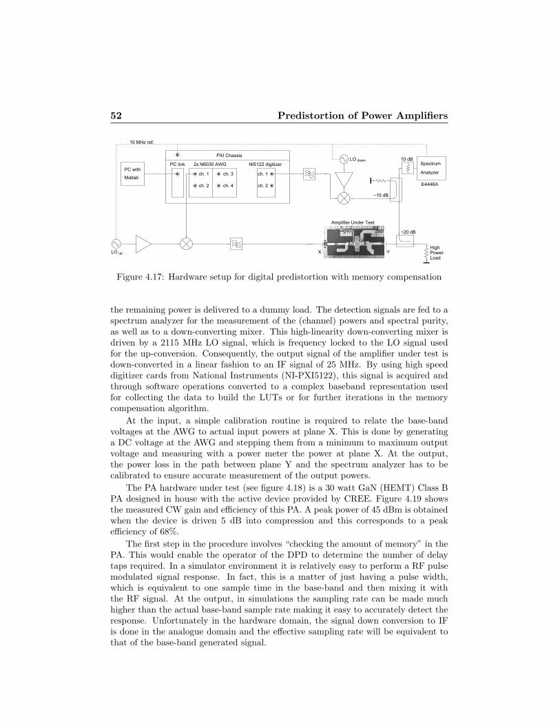
52 Predistortion of Power Amplifiers
LO down
Analyzer
Spectrum
HighPowerLoad
LO up
PC with
Matlab
10 MHz ref.
−20 dB
10 dB
−10 dB
E4446Ach. 2
ch. 1 ch. 3
ch. 4
NI5122 digitizer
ch. 1
ch. 2
2x N6030 AWGPC link
PXI Chassis
YX
Amplifier Under Test
Figure 4.17: Hardware setup for digital predistortion with memory compensation
the remaining power is delivered to a dummy load. The detection signals are fed to aspectrum analyzer for the measurement of the (channel) powers and spectral purity,as well as to a down-converting mixer. This high-linearity down-converting mixer isdriven by a 2115 MHz LO signal, which is frequency locked to the LO signal usedfor the up-conversion. Consequently, the output signal of the amplifier under test isdown-converted in a linear fashion to an IF signal of 25 MHz. By using high speeddigitizer cards from National Instruments (NI-PXI5122), this signal is acquired andthrough software operations converted to a complex baseband representation usedfor collecting the data to build the LUTs or for further iterations in the memorycompensation algorithm.
At the input, a simple calibration routine is required to relate the base-bandvoltages at the AWG to actual input powers at plane X. This is done by generatinga DC voltage at the AWG and stepping them from a minimum to maximum outputvoltage and measuring with a power meter the power at plane X. At the output,the power loss in the path between plane Y and the spectrum analyzer has to becalibrated to ensure accurate measurement of the output powers.
The PA hardware under test (see figure 4.18) is a 30 watt GaN (HEMT) Class BPA designed in house with the active device provided by CREE. Figure 4.19 showsthe measured CW gain and efficiency of this PA. A peak power of 45 dBm is obtainedwhen the device is driven 5 dB into compression and this corresponds to a peakefficiency of 68%.
The first step in the procedure involves “checking the amount of memory” in thePA. This would enable the operator of the DPD to determine the number of delaytaps required. In a simulator environment it is relatively easy to perform a RF pulsemodulated signal response. In fact, this is a matter of just having a pulse width,which is equivalent to one sample time in the base-band and then mixing it withthe RF signal. At the output, in simulations the sampling rate can be made muchhigher than the actual base-band sample rate making it easy to accurately detect theresponse. Unfortunately in the hardware domain, the signal down conversion to IFis done in the analogue domain and the effective sampling rate will be equivalent tothat of the base-band generated signal.
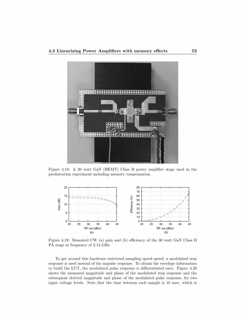
4.3 Linearizing Power Amplifiers with memory effects 53
Figure 4.18: A 30 watt GaN (HEMT) Class B power amplifier stage used in thepredistortion experiment including memory compensation.
0
5
10
15
20
20 25 30 35 40 45
Gai
n (d
B)
RF out (dBm)(a) (b)
0 10 20 30 40 50 60 70 80
20 25 30 35 40 45
Effi
cien
cy (%
)
RF out (dBm)
Figure 4.19: Measured CW (a) gain and (b) efficiency of the 30 watt GaN Class BPA stage at frequency of 2.14 GHz.
To get around this hardware restricted sampling speed speed, a modulated stepresponse is used instead of the impulse response. To obtain the envelope informationto build the LUT, the modulated pulse response is differentiated once. Figure 4.20shows the measured magnitude and phase of the modulated step response and thesubsequent derived magnitude and phase of the modulated pulse response, for twoinput voltage levels. Note that the time between each sample is 10 nsec, which is
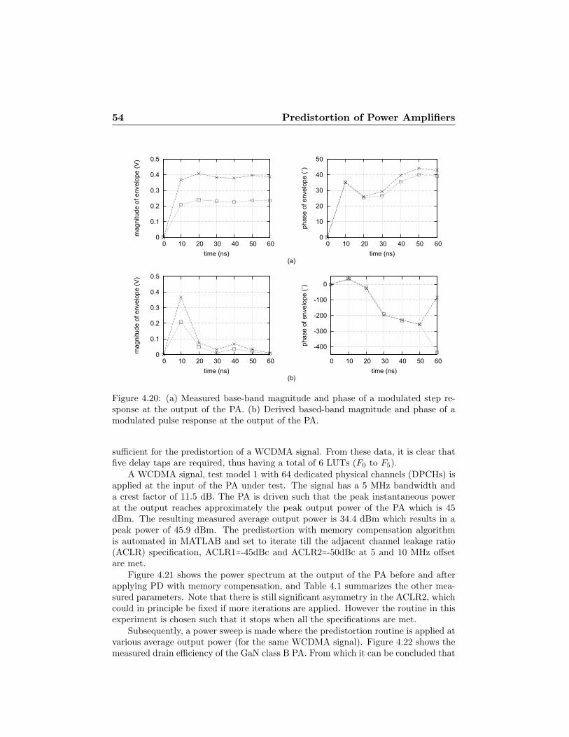
54 Predistortion of Power Amplifiers
0
0.1
0.2
0.3
0.4
0.5
0 10 20 30 40 50 60
mag
nitu
de o
f env
elop
e (V
)
time (ns)
(a)
(b)
-400
-300
-200
-100
0
0 10 20 30 40 50 60
phas
e of
env
elop
e (˚
)
time (ns)
0
0.1
0.2
0.3
0.4
0.5
0 10 20 30 40 50 60
mag
nitu
de o
f env
elop
e (V
)
time (ns)
0
10
20
30
40
50
0 10 20 30 40 50 60
phas
e of
env
elop
e (˚
)
time (ns)
Figure 4.20: (a) Measured base-band magnitude and phase of a modulated step re-sponse at the output of the PA. (b) Derived based-band magnitude and phase of amodulated pulse response at the output of the PA.
sufficient for the predistortion of a WCDMA signal. From these data, it is clear thatfive delay taps are required, thus having a total of 6 LUTs (F0 to F5).
A WCDMA signal, test model 1 with 64 dedicated physical channels (DPCHs) isapplied at the input of the PA under test. The signal has a 5 MHz bandwidth anda crest factor of 11.5 dB. The PA is driven such that the peak instantaneous powerat the output reaches approximately the peak output power of the PA which is 45dBm. The resulting measured average output power is 34.4 dBm which results in apeak power of 45.9 dBm. The predistortion with memory compensation algorithmis automated in MATLAB and set to iterate till the adjacent channel leakage ratio(ACLR) specification, ACLR1=-45dBc and ACLR2=-50dBc at 5 and 10 MHz offsetare met.
Figure 4.21 shows the power spectrum at the output of the PA before and afterapplying PD with memory compensation, and Table 4.1 summarizes the other mea-sured parameters. Note that there is still significant asymmetry in the ACLR2, whichcould in principle be fixed if more iterations are applied. However the routine in thisexperiment is chosen such that it stops when all the specifications are met.
Subsequently, a power sweep is made where the predistortion routine is applied atvarious average output power (for the same WCDMA signal). Figure 4.22 shows themeasured drain efficiency of the GaN class B PA. From which it can be concluded that
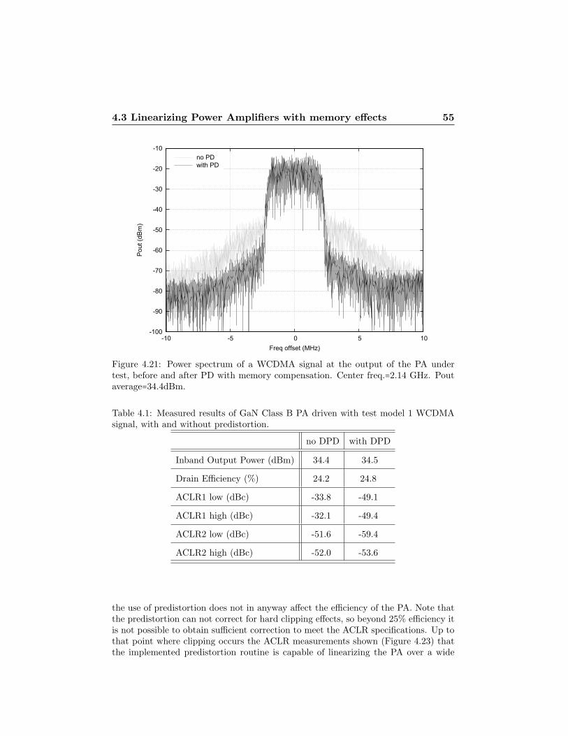
4.3 Linearizing Power Amplifiers with memory effects 55
-100
-90
-80
-70
-60
-50
-40
-30
-20
-10
-10 -5 0 5 10
Pou
t (dB
m)
Freq offset (MHz)
no PDwith PD
Figure 4.21: Power spectrum of a WCDMA signal at the output of the PA undertest, before and after PD with memory compensation. Center freq.=2.14 GHz. Poutaverage=34.4dBm.
Table 4.1: Measured results of GaN Class B PA driven with test model 1 WCDMAsignal, with and without predistortion.
no DPD with DPD
Inband Output Power (dBm) 34.4 34.5
Drain Efficiency (%) 24.2 24.8
ACLR1 low (dBc) -33.8 -49.1
ACLR1 high (dBc) -32.1 -49.4
ACLR2 low (dBc) -51.6 -59.4
ACLR2 high (dBc) -52.0 -53.6
the use of predistortion does not in anyway affect the efficiency of the PA. Note thatthe predistortion can not correct for hard clipping effects, so beyond 25% efficiency itis not possible to obtain sufficient correction to meet the ACLR specifications. Up tothat point where clipping occurs the ACLR measurements shown (Figure 4.23) thatthe implemented predistortion routine is capable of linearizing the PA over a wide
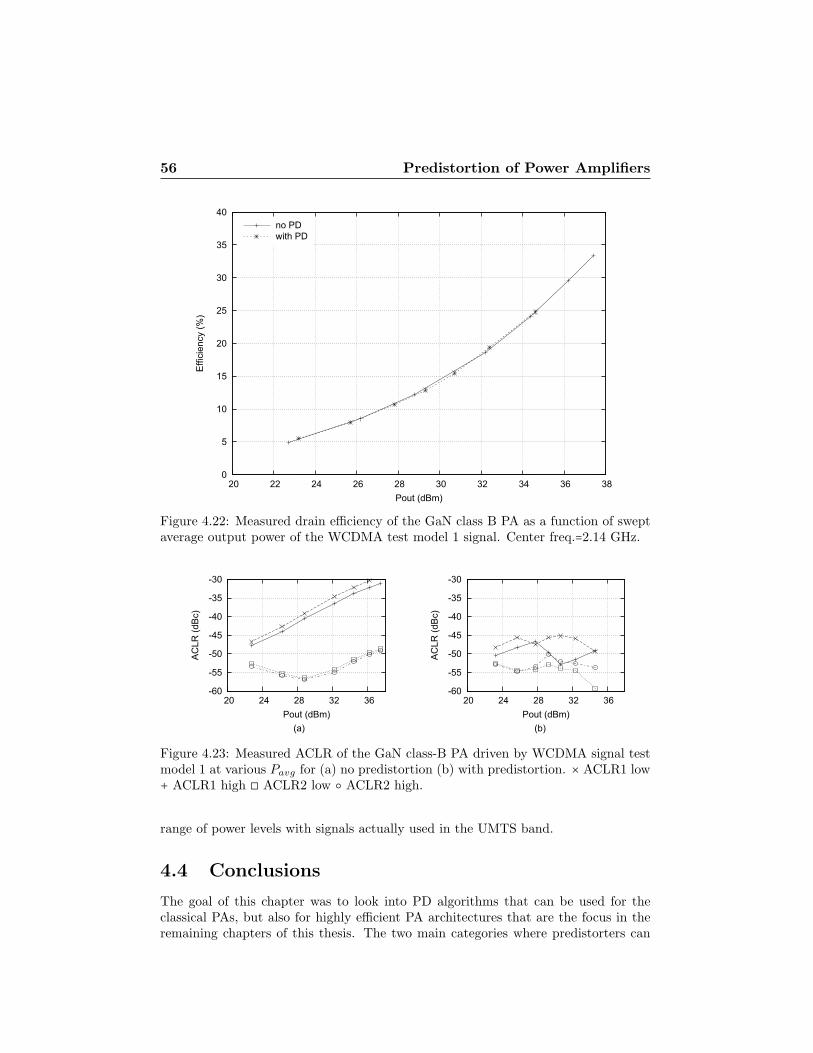
56 Predistortion of Power Amplifiers
0
5
10
15
20
25
30
35
40
20 22 24 26 28 30 32 34 36 38
Effi
cien
cy (%
)
Pout (dBm)
no PDwith PD
Figure 4.22: Measured drain efficiency of the GaN class B PA as a function of sweptaverage output power of the WCDMA test model 1 signal. Center freq.=2.14 GHz.
-60
-55
-50
-45
-40
-35
-30
20 24 28 32 36
AC
LR (d
Bc)
Pout (dBm)(a) (b)
-60
-55
-50
-45
-40
-35
-30
20 24 28 32 36
AC
LR (d
Bc)
Pout (dBm)
Figure 4.23: Measured ACLR of the GaN class-B PA driven by WCDMA signal testmodel 1 at various Pavg for (a) no predistortion (b) with predistortion. × ACLR1 low+ ACLR1 high ◻ ACLR2 low ○ ACLR2 high.
range of power levels with signals actually used in the UMTS band.
4.4 Conclusions
The goal of this chapter was to look into PD algorithms that can be used for theclassical PAs, but also for highly efficient PA architectures that are the focus in theremaining chapters of this thesis. The two main categories where predistorters can

4.4 Conclusions 57
be classified in are:
1. Memoryless predistorters.When a non-linear PA is memoryless, the output signal is only a functionof the currently applied input signal. This makes predistortion straightfor-ward. Namely the predistorter function is simply the inverse of the non-lineartransfer function of the non-linear PA itself. For most PAs, the memorylesssituation is valid when the bandwidth of the modulated signal is small. This isequivalent to having a very slowly changing envelope (magnitude and phase) ofthe modulated signal with time. A simple memoryless predistortion algorithmwas implemented that first requires the AM-AM and AM-PM characteristic ofthe non-linear PA to be characterized, this algorithm uses a LUT approach toimplement the inverse function of the non-linear transfer of the PA. Simula-tion results show this straight forward implementation is effective when usedwith a realistic PA design. In the next Chapter, this memoryless predistortionalgorithm will be utilized to predistort an adaptive PA prototype for futurehandset implementations.
2. Predistorters with memory effect compensation.When the bandwidth of the modulated signal becomes high (i.e. rapidlychanging envelope of the modulated signal), the bias circuitry of the PA isoften not fast enough to track the changes in the envelope and this shows upas distortion of the envelope (skewing of the envelope waveform). This effectreduces the effectiveness of the memoryless predistorter since the output is nolonger only a function of the presented input at the same time slot but alsofrom the history of this input signal. In this thesis work, a predistorter withmemory compensation was developed which is based on memory polynomials.This concept has proven to be effective in simulations and further verified on aUMTS GaN class-B power amplifier. Using this predistortion algorithm withmemory compensation, the PA can be used up to its peak output power (with-out signal clipping) and still meeting the stringent linearity specifications forUMTS base-stations.
With the linearization techniques developed in this chapter, the focus from hereon (chapter 6 and 7) will be on highly efficient PA concepts, which require digitalpredistortion techniques to meet their spectral specifications. It will be this combi-nation that set the trend for future amplifier implementations for use in third andfourth-generation communication applications.


Chapter 5
High Efficient PowerAmplifier Architectures
In Chapter 3, it has been shown how improvements can be made in the design ofClass-AB power amplifiers such that they can reach average efficiency numbers inthe order of 40%, when operated with complex modulated signals(such as IS95). Thenext milestone set by industry, is amplifier efficiencies greater than 50% for 3G signalslike WCDMA, WiMax, LTE etc. Note that due to the significantly higher peak-to-average power ratios (>8dB) of these signals, this is a very challenging task, evenwhen assuming that the peak efficiency of the active devices can reach 100%. Notethat such a number is for example theoretically feasible for ideal Class-F operation,however, in power back-off this efficiency number would typically degrade as,
η = √pout ηmax (5.1)
In which pout is the normalized output power varying between 0 and 1, with 1being the maximum (saturated) output power. Note that this relation implies that foroperation in 6dB back-off of the saturated output power (usually the 1dB compressedpoint), the efficiency drops to only half its maximum value.
One approach to overcome this limitation, is to use pulsewidth modulation (PWM)techniques at RF frequency to drive switch-mode power amplifiers (Class-D). This hasthe potential of having 100% efficiency even when amplifying signals with significantpeak-to-average power ratios. This PWM RF amplifier architecture and techniquewill be briefly discussed in section 5.1. At this time of writing, the most commonapproach used in the industry to overcome this on first sight rather fundamental lim-itation, is to use the “classical” amplfier core (e.g. an class-B or class-F operateddevice) in a larger system where this efficiency-output-power roll-off behavior is mod-ified. These so called high-efficiency power amplifier architectures, manipulate theirefficiency-output power behavior in such a way that a significantly lower efficiencydegradation versus back-off power is achieved. In section 5.2, we explain the basicprinciples how these amplifier architectures manage to keep their amplifying devicesat their peak efficiency, even when operated in power back-off. In section 5.3 and
59
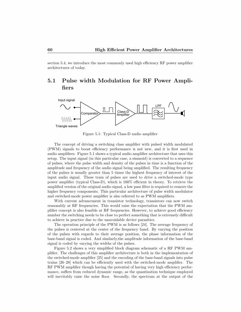
60 High Efficient Power Amplifier Architectures
section 5.4, we introduce the most commonly used high efficiency RF power amplifierarchitectures of today.
5.1 Pulse width Modulation for RF Power Ampli-fiers
Figure 5.1: Typical Class-D audio amplifier
The concept of driving a switching class amplifier with pulsed width modulated(PWM) signals to boost efficiency performance is not new, and it is first used inaudio amplifiers. Figure 5.1 shows a typical audio amplifier architecture that uses thissetup. The input signal (in this particular case, a sinusoid) is converted to a sequenceof pulses, where the pulse width and density of the pulses in time is a function of theamplitude and frequency of the audio signal being amplified. The resulting frequencyof the pulses is usually greater than 5 times the highest frequency of interest of theinput audio signal. These train of pulses are used to drive a switched-mode typepower amplifier (typical Class-D), which is 100% efficient in theory. To retrieve theamplified version of the original audio signal, a low pass filter is required to remove thehigher frequency components. This particular architecture of pulse width modulatorand switched-mode power amplifier is also referred to as PWM amplifiers.
With current advancement in transistor technology, transistors can now switchreasonably at RF frequencies. This would raise the expectation that the PWM am-plifier concept is also feasible at RF frequencies. However, to achieve good efficiencynumber the switching needs to be close to perfect something that is extremely difficultto achieve in practice due to the unavoidable device parasitics.
The operation principle of the PWM is as follows [24]. The average frequency ofthe pulses is centered at the center of the frequency band. By varying the positionof the pulses with regards to their average position, the phase information of thebase-band signal is coded. And similarly,the amplitude information of the base-bandsignal is coded by varying the widths of the pulses.
Figure 5.2 shows a very simplified block diagram schematic of a RF PWM am-plifier. The challenges of this amplifier architecture is both in the implementation ofthe switched-mode amplifier [25] and the encoding of the base-band signals into pulsetrains [26–28] which can be efficiently used with the switched-mode amplifier. TheRF PWM amplifier though having the potential of having very high efficiency perfor-mance, suffers from reduced dynamic range, as the quantization technique employedwill inevitably raise the noise floor. Secondly, the spectrum at the output of the
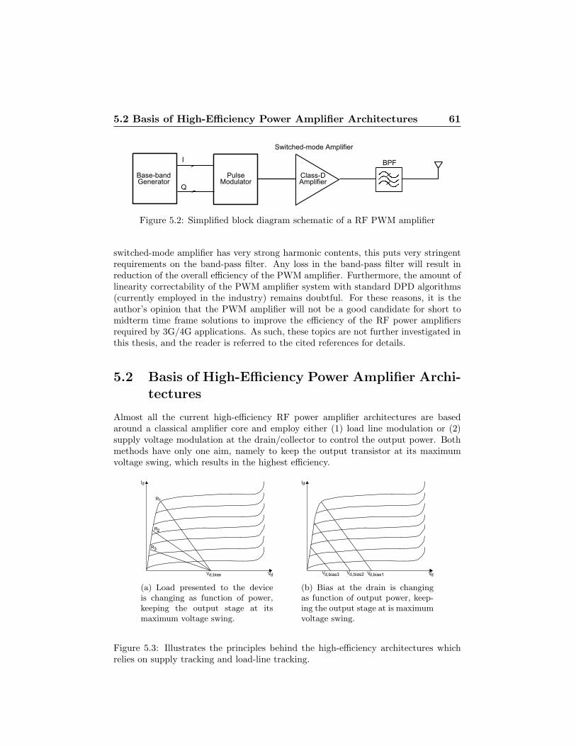
5.2 Basis of High-Efficiency Power Amplifier Architectures 61
Figure 5.2: Simplified block diagram schematic of a RF PWM amplifier
switched-mode amplifier has very strong harmonic contents, this puts very stringentrequirements on the band-pass filter. Any loss in the band-pass filter will result inreduction of the overall efficiency of the PWM amplifier. Furthermore, the amount oflinearity correctability of the PWM amplifier system with standard DPD algorithms(currently employed in the industry) remains doubtful. For these reasons, it is theauthor’s opinion that the PWM amplifier will not be a good candidate for short tomidterm time frame solutions to improve the efficiency of the RF power amplifiersrequired by 3G/4G applications. As such, these topics are not further investigated inthis thesis, and the reader is referred to the cited references for details.
5.2 Basis of High-Efficiency Power Amplifier Archi-
tectures
Almost all the current high-efficiency RF power amplifier architectures are basedaround a classical amplifier core and employ either (1) load line modulation or (2)supply voltage modulation at the drain/collector to control the output power. Bothmethods have only one aim, namely to keep the output transistor at its maximumvoltage swing, which results in the highest efficiency.
(a) Load presented to the deviceis changing as function of power,keeping the output stage at itsmaximum voltage swing.
(b) Bias at the drain is changingas function of output power, keep-ing the output stage at is maximumvoltage swing.
Figure 5.3: Illustrates the principles behind the high-efficiency architectures whichrelies on supply tracking and load-line tracking.

62 High Efficient Power Amplifier Architectures
For the first case, where the load-line is varied, the load which the transistor seeswhen delivering maximum power is:
RL,opt = V 2d,bias
2 ⋅ Poutmax
(5.2)
In normal Class-B operation, when the power amplifier is backed-off 3dB from itsmaximum output power (Poutmax/2), given that the load remains the same, the
voltage at the drain will decrease by a factor of the square root of 2 (Vd,bias√
2). To get
the voltage at the drain/collector again back to its maximum voltage swing, whichimplies high efficiency, the impedance offered to the transistor needs to be doubled(2 ⋅RL,opt). This is illustrated in Figure 5.3(a), which shows a typical plot of draincurrent versus drain voltage for various gate biases. R1 corresponds to the load-linewhere the transistor is matched for maximum power out. When the transistor isbacked-off in power, the load-line is changed to R2 and in further back-off its changedto R3 (where R3 > R2 > R1). In theory, this principle is able to offer the peak efficiencyperformance (78.5% in the case for Class-B) at all output power levels. The limitationof this approach is the feasibility to create a load that approximates infinity when thedesired output power level approaches zero.
The second approach to obtaining high-efficiency in back-off powers is to changethe drain/collector bias voltage as a function of output power. This also resultsin keeping the output stage at its maximum voltage swing for all output power-levels. This is illustrated in Figure 5.3(b). Here the load offered to the transistorremains constant, but when the power is backed-off the drain bias is also decreased(Vd,bias1 > Vd,bias2 > Vd,bias3). In practice this will keep the efficiency of the outputstage for a particular class of operation at its theoretical maximum.
5.3 Bias Supply Variation Based Power AmplifierArchitectures
The Kahn power amplifier architecture, commonly also known as Envelope Elimina-tion and Restoration (EER) is one technique that implements the bias supply variationconcept to achieve high efficiency. Figure 5.4 shows a block diagram schematic of atypical Kahn architecture implementation.
The Kahn high-efficient architecture in its pure form consist of a high efficiencyRF power amplifier cell, which linearity is of little concern (e.g. a switching mode typeamplifier like Class-D, E or F). The bias supply of this RF amplifier stage is connectedto the output of a video-bandwidth amplifier. The incoming RF signal is amplitudeclipped (phase information is retained) and this clipped signal is use to drive theinput of the RF power amplifier. Since the driving signal has a constant envelope, theRF power amplifier can be always operated in voltage saturation to maintain highefficiency at all times. To restore the desired envelope amplitude modulation, a partof the incoming RF signal is used to extract the envelope signal, which is fed to a highvoltage video-bandwidth amplifier in the supply path of the RF-stage. Doing so willbring the original envelope information of the input signal on the supply voltage of
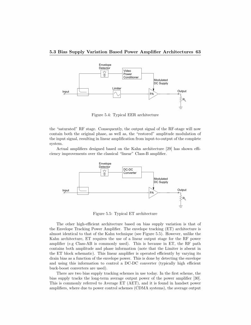
5.3 Bias Supply Variation Based Power Amplifier Architectures 63
RL
Output
VideoPowerConditioner
EnvelopeDetector
Limiter
PAInput
ModulatedDC Supply
Figure 5.4: Typical EER architecture
the “saturated” RF stage. Consequently, the output signal of the RF-stage will nowcontain both the original phase, as well as, the “restored” amplitude modulation ofthe input signal, resulting in linear amplification from input-to-output of the completesystem.
Actual amplifiers designed based on the Kahn architecture [29] has shown effi-ciency improvements over the classical “linear” Class-B amplifier.
RL
Output
DC-DCConverter
EnvelopeDetector
PAInput
ModulatedDC Supply
Figure 5.5: Typical ET architecture
The other high-efficient architecture based on bias supply variation is that ofthe Envelope Tracking Power Amplifier. The envelope tracking (ET) architecture isalmost identical to that of the Kahn technique (see Figure 5.5). However, unlike theKahn architecture, ET requires the use of a linear output stage for the RF poweramplifier (e.g Class-AB is commonly used). This is because in ET, the RF pathcontains both amplitude and phase information (note that the Limiter is absent inthe ET block schematic). This linear amplifier is operated efficiently by varying itsdrain bias as a function of the envelope power. This is done by detecting the envelopeand using this information to control a DC-DC converter (typically high efficientbuck-boost converters are used).
There are two bias supply tracking schemes in use today. In the first scheme, thebias supply tracks the long-term average output power of the power amplifier [30].This is commonly referred to Average ET (AET), and it is found in handset poweramplifiers, where due to power control schemes (CDMA systems), the average output
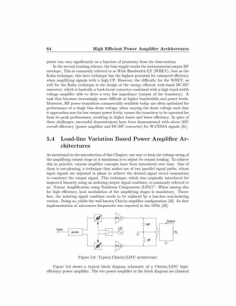
64 High Efficient Power Amplifier Architectures
power can vary significantly as a function of proximity from the base-station.In the second tracking scheme, the bias supply tracks the instantaneous output RF
envelope. This is commonly referred to as Wide Bandwidth ET (WBET). Just as theKahn technique, this later technique has the highest potential for enhanced efficiencywhen amplifying signals with a high CF. However, the difficulty for the WBET, aswell for the Kahn technique is the design of the energy efficient wide-band DC-DCconverter, which is basically a buck-boost converter combined with a high band-widthvoltage amplifier able to drive a very low impedance (output of the transistor). Atask that becomes increasingly more difficult at higher bandwidths and power levels.Moreover, RF power transistors commercially available today are often optimized forperformance at a single bias drain voltage, when varying the drain voltage such thatit approaches zero for low output power levels, causes the transistor to be operated farfrom its peak performance, resulting in higher losses and lower efficiency. In spite ofthese challenges, successful demonstrators have been demonstrated with above 50%overall efficiency (power amplifier and DC-DC converter) for W-CDMA signals [31].
5.4 Load-line Variation Based Power Amplifier Ar-
chitectures
As mentioned in the introduction of this Chapter, one way to keep the voltage swing ofthe amplifying output stage at is maximum is to adjust its output loading. To achievethis in practice, various amplifier concepts have been introduced over time. One ofthem is out-phasing, a technique that makes use of two parallel signal paths, whoseinput signals are adjusted in phase to achieve the desired signal vector summationto construct the output signal. This technique, which was originally introduced forimproved linearity using an isolating output signal combiner, is commonly referred toas, “Linear Amplification using Nonlinear Components (LINC)”. When aiming alsofor high efficiency, load modulation of the amplifying stages is mandatory. There-fore, the isolating signal combiner needs to be replaced by a loss-less non-isolatingversion. Doing so, yields the well known Chireix amplifier configuration [32]. Its firstimplementation at microwave frequencies was reported in the 1970s [33].
Φ
Φ
RL
Input
PA 1
PA 2
arcsinLO
+jB
−jB
Output
Figure 5.6: Typical Chireix/LINC architecture
Figure 5.6 shows a typical block diagram schematic of a Chireix/LINC high-efficiency power amplifier. The two power amplifier in the block diagram are classical
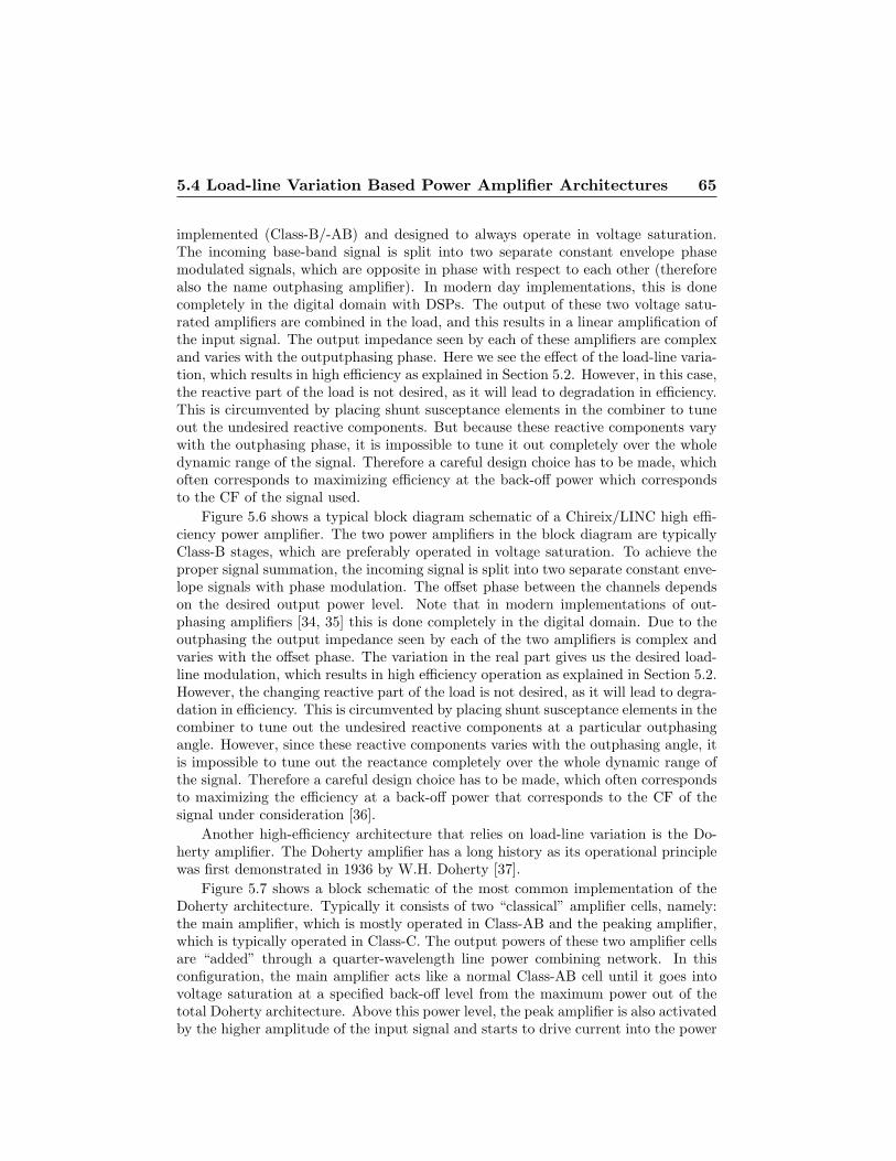
5.4 Load-line Variation Based Power Amplifier Architectures 65
implemented (Class-B/-AB) and designed to always operate in voltage saturation.The incoming base-band signal is split into two separate constant envelope phasemodulated signals, which are opposite in phase with respect to each other (thereforealso the name outphasing amplifier). In modern day implementations, this is donecompletely in the digital domain with DSPs. The output of these two voltage satu-rated amplifiers are combined in the load, and this results in a linear amplification ofthe input signal. The output impedance seen by each of these amplifiers are complexand varies with the outputphasing phase. Here we see the effect of the load-line varia-tion, which results in high efficiency as explained in Section 5.2. However, in this case,the reactive part of the load is not desired, as it will lead to degradation in efficiency.This is circumvented by placing shunt susceptance elements in the combiner to tuneout the undesired reactive components. But because these reactive components varywith the outphasing phase, it is impossible to tune it out completely over the wholedynamic range of the signal. Therefore a careful design choice has to be made, whichoften corresponds to maximizing efficiency at the back-off power which correspondsto the CF of the signal used.
Figure 5.6 shows a typical block diagram schematic of a Chireix/LINC high effi-ciency power amplifier. The two power amplifiers in the block diagram are typicallyClass-B stages, which are preferably operated in voltage saturation. To achieve theproper signal summation, the incoming signal is split into two separate constant enve-lope signals with phase modulation. The offset phase between the channels dependson the desired output power level. Note that in modern implementations of out-phasing amplifiers [34, 35] this is done completely in the digital domain. Due to theoutphasing the output impedance seen by each of the two amplifiers is complex andvaries with the offset phase. The variation in the real part gives us the desired load-line modulation, which results in high efficiency operation as explained in Section 5.2.However, the changing reactive part of the load is not desired, as it will lead to degra-dation in efficiency. This is circumvented by placing shunt susceptance elements in thecombiner to tune out the undesired reactive components at a particular outphasingangle. However, since these reactive components varies with the outphasing angle, itis impossible to tune out the reactance completely over the whole dynamic range ofthe signal. Therefore a careful design choice has to be made, which often correspondsto maximizing the efficiency at a back-off power that corresponds to the CF of thesignal under consideration [36].
Another high-efficiency architecture that relies on load-line variation is the Do-herty amplifier. The Doherty amplifier has a long history as its operational principlewas first demonstrated in 1936 by W.H. Doherty [37].
Figure 5.7 shows a block schematic of the most common implementation of theDoherty architecture. Typically it consists of two “classical” amplifier cells, namely:the main amplifier, which is mostly operated in Class-AB and the peaking amplifier,which is typically operated in Class-C. The output powers of these two amplifier cellsare “added” through a quarter-wavelength line power combining network. In thisconfiguration, the main amplifier acts like a normal Class-AB cell until it goes intovoltage saturation at a specified back-off level from the maximum power out of thetotal Doherty architecture. Above this power level, the peak amplifier is also activatedby the higher amplitude of the input signal and starts to drive current into the power
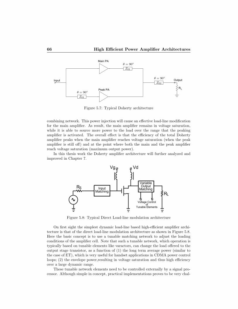
66 High Efficient Power Amplifier Architectures
RL
Output
Main PA
Peak PA
Input
Z01
θ = 90◦
Z01
θ = 90◦
Z02
θ = 90◦
Figure 5.7: Typical Doherty architecture
combining network. This power injection will cause an effective load-line modificationfor the main amplifier. As result, the main amplifier remains in voltage saturation,while it is able to source more power to the load over the range that the peakingamplifier is activated. The overall effect is that the efficiency of the total Dohertyamplifier peaks when the main amplifier reaches voltage saturation (when the peakamplifier is still off) and at the point where both the main and the peak amplifierreach voltage saturation (maximum output power).
In this thesis work the Doherty amplifier architecture will further analyzed andimproved in Chapter 7.
Figure 5.8: Typical Direct Load-line modulation architecture
On first sight the simplest dynamic load-line based high-efficient amplifier archi-tecture is that of the direct load-line modulation architecture as shown in Figure 5.8.Here the basic concept is to use a tunable matching network to adjust the loadingconditions of the amplifier cell. Note that such a tunable network, which operation istypically based on tunable elements like varactors, can change the load offered to theoutput stage transistor, as a function of (1) the long term average power (similar tothe case of ET), which is very useful for handset applications in CDMA power controlloops; (2) the envelope power,resulting in voltage saturation and thus high efficiencyover a large dynamic range.
These tunable network elements need to be controlled externally by a signal pro-cessor. Although simple in concept, practical implementations proves to be very chal-

5.4 Load-line Variation Based Power Amplifier Architectures 67
lenging. This due to very high requirements on the tunable components, which need tobe lossless, add no distortion to the system, and should be able to be switched/variedwith the speed of the RF envelope. In [38] a dynamic load-line amplifier with tunablematching networks has been implemented and demonstrated for signals with CF ap-proximately 10dB, a two-fold improvement in efficiency over a conventional Class-Bamplifier.
In summary, although many high efficiency amplifier concepts have been pro-posed, at the time of writing. Each concept seems to have its own unique advantagesand disadvantages, making one concept more, or in some cases less applicable to re-quirements of a specific application. In short, handset applications seem to benefitmost of the direct Load-line modulation concept. Since this concept can in principlealso provide the selection of different frequency bands, antenna mismatch correction,etc., while the power levels involved remain limited, something that significantly re-laxes the requirements of the tunable components. Base station applications, however,seems to benefit most of ET (high RF bandwidth), Chireix and Doherty (high mod-ulation bandwidth) based amplifier concepts. Here the very high power levels oftencomplicate the use of tunable network elements as varactors. In the following Chap-ters, we aim to evaluate and develop load modulation based amplifier concepts forimproved efficiency in power back-off, in addition, we also give attention to the RFreconfigurabiltiy when dealing with amplifiers for handset applications.


Chapter 6
PA with adaptive matching
Today, cellular phones supporting multiple communication standards such as GSM,EDGE and WCDMDA are already commercially available. To enable this multi-band,multi-mode operation, current handset implementations are using parallel line-upsfor the transmit and receive paths in combination with antenna duplexer and variousswitches as shown in Figure 6.1 a to meet the specific requirements of each standard.
However, with the increasing user demand to add more and more functionalitylike GPS, WiFi, WiMax, TV on Mobile etc. manufacturers of handsets are confrontedwith increasing costs, complexity and form factor, while customers require cost andsize reductions. With the architecture of Figure 6.1 a, the hardware complexity in-creases linearly with the number of frequency bands that need to be supported. Aproposed architecture that will support the multi-band multi-mode operation anddoes not introduce significant increase in cost and area is shown in Figure 6.1b. Al-though conceptually simple, practical design considerations place severe constraintson the technology implementation to realize the required adaptive circuit blocks. Forthe receive path most of the circuit functions have already been demonstrated [39–41].Major bottlenecks remain however in the implementation of the tunable filters andadaptive power amplifiers [42, 43].
Besides the size reduction of the multi-band multi-mode Power Amplifier, thereis also the desire to improve efficiency and amplifier operation under antenna mis-match conditions. Current amplifier implementations already include power controlloops to reduce output power when operating in close proximity of a base-station. Inthis mode of operation the transmit signal is backed-off from its maximum, yieldinga significantly decreased efficiency (see also Chapter 2). Increasing the loading ofthe output stage can reduce this loss in efficiency under power backed-off operation,something that in principle can be combined with the required tunability in outputmatching when aiming for multi-band operation.
To address these upcoming demands on the handset amplifier, this thesis worjkhas focused on implementing an adaptive handset PA using tunable matching net-works. This PA should have also improved efficiency at all output power levels, tocombine the needs of multi-mode and multi-band operation. Key elements in this am-plifier design are the adaptive matching networks, which are discussed in Section 6.1.
69

70 PA with adaptive matching
Figure 6.1: (a) Traditional parallel path multi-band multi-mode approach based onstatic RF circuit blocks. (b) Simplified next-generation transceiver concept usingadaptive RF function blocks.
Various tunable matching network topologies are considered and evaluated for theirperformance. Section 6.2 shows how these matching networks can provide improvedefficiency in power back-off operation and facilitate frequency band switching.

6.1 Reconfigurable/Adaptive matching networks 71
6.1 Reconfigurable/Adaptive matching networks
In order to effectively change the loading impedance of the output stage as a functionof the output power level and frequency of operation, tunable matching networks arerequired. In this section, the basic requirements that these networks must satisfy toobtain the desired PA functionality in terms of power control range and frequencytuning are discussed. Following that, the design of the matching network withinthe technology constraints is given and the resulting implementation is verified bymeasurement.
6.1.1 Design Goal of Adaptive Matching Networks
For the implementation of the tunable elements, DIMES silicon-on-glass Schottkydiodes are used [44–48]. To achieve high linearity, these uniformly doped devices areplaced in anti-series configuration [49] with a high impedance connection to establishthe biasing of the center node. Compared to other RF tunable components, theseelements provide superior linearity, reliability, tuning speed and quality factor (Q >100 @ 2 GHz).
In the time frame of this work the varactor devices in the silicon-on-glass processare characterized by the following design constraints:
• effective capacitance tuning range of the varactor stack. Cmax
Cmin< 2.5.
• control voltages < 18 V (to avoid diode breakdown).• no forward biasing of any of the diodes by the RF signal.
Although in principle, control voltages up to 18 V are required to obtain thefull capacitance tuning range for this technology version, it is noted that the varac-tor diodes are always operated in reverse bias and therefore require practically noDC current. Consequently, the generation of these control voltages by DC-to-DCup-conversion is relatively straightforward without any severe requirement on theconversion efficiency. The actual value of the control voltages depends on the in-tended capacitance control range and the RF voltage swing present in the matchingnetwork. By using a low impedance matching network solution, one can improve thepower handling of the tunable matching networks. With the constraints above, thefollowing specifications for the reconfigurable matching network are set:
• tunable impedance transformation ratio 10.• continuously tunable with high speed (20 MHz bandwidth).• operating frequencies of 900, 1800, 1900, and 2100 MHz (covering the most
important bands for handsets).• losses of less than 1 dB for the whole input impedance tuning range.• number of independent control voltages ≤ 2.• high linearity ( ≥ 55 dBc at 1 W output power level).• output power range from 0.1 to 1W, while assuming a 3V supply voltage.• improved amplifier efficiency for power back-off conditions.
In order to meet these requirements, the following subsection investigate the mostpromising network topology, and motivates the final choice made in this work.
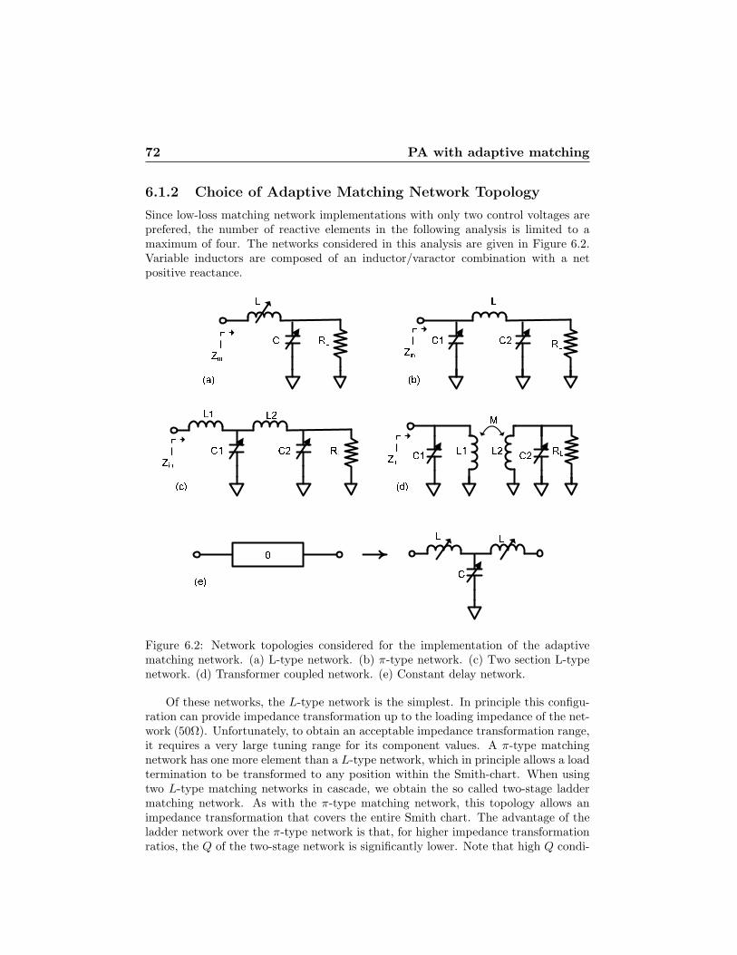
72 PA with adaptive matching
6.1.2 Choice of Adaptive Matching Network Topology
Since low-loss matching network implementations with only two control voltages areprefered, the number of reactive elements in the following analysis is limited to amaximum of four. The networks considered in this analysis are given in Figure 6.2.Variable inductors are composed of an inductor/varactor combination with a netpositive reactance.
Figure 6.2: Network topologies considered for the implementation of the adaptivematching network. (a) L-type network. (b) π-type network. (c) Two section L-typenetwork. (d) Transformer coupled network. (e) Constant delay network.
Of these networks, the L-type network is the simplest. In principle this configu-ration can provide impedance transformation up to the loading impedance of the net-work (50Ω). Unfortunately, to obtain an acceptable impedance transformation range,it requires a very large tuning range for its component values. A π-type matchingnetwork has one more element than a L-type network, which in principle allows a loadtermination to be transformed to any position within the Smith-chart. When usingtwo L-type matching networks in cascade, we obtain the so called two-stage laddermatching network. As with the π-type matching network, this topology allows animpedance transformation that covers the entire Smith chart. The advantage of theladder network over the π-type network is that, for higher impedance transformationratios, the Q of the two-stage network is significantly lower. Note that high Q condi-
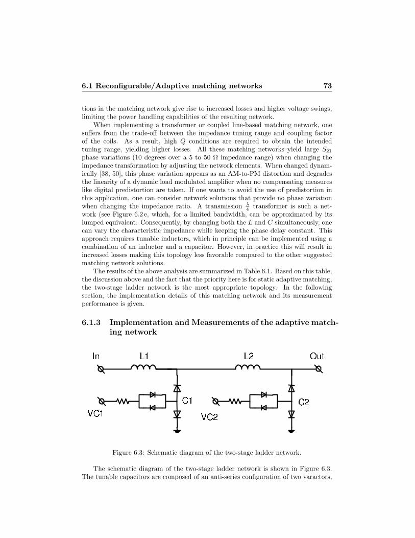
6.1 Reconfigurable/Adaptive matching networks 73
tions in the matching network give rise to increased losses and higher voltage swings,limiting the power handling capabilities of the resulting network.
When implementing a transformer or coupled line-based matching network, onesuffers from the trade-off between the impedance tuning range and coupling factorof the coils. As a result, high Q conditions are required to obtain the intendedtuning range, yielding higher losses. All these matching networks yield large S21
phase variations (10 degrees over a 5 to 50 Ω impedance range) when changing theimpedance transformation by adjusting the network elements. When changed dynam-ically [38, 50], this phase variation appears as an AM-to-PM distortion and degradesthe linearity of a dynamic load modulated amplifier when no compensating measureslike digital predistortion are taken. If one wants to avoid the use of predistortion inthis application, one can consider network solutions that provide no phase variationwhen changing the impedance ratio. A transmission λ
4transformer is such a net-
work (see Figure 6.2 e, which, for a limited bandwidth, can be approximated by itslumped equivalent. Consequently, by changing both the L and C simultaneously, onecan vary the characteristic impedance while keeping the phase delay constant. Thisapproach requires tunable inductors, which in principle can be implemented using acombination of an inductor and a capacitor. However, in practice this will result inincreased losses making this topology less favorable compared to the other suggestedmatching network solutions.
The results of the above analysis are summarized in Table 6.1. Based on this table,the discussion above and the fact that the priority here is for static adaptive matching,the two-stage ladder network is the most appropriate topology. In the followingsection, the implementation details of this matching network and its measurementperformance is given.
6.1.3 Implementation and Measurements of the adaptive match-ing network
Figure 6.3: Schematic diagram of the two-stage ladder network.
The schematic diagram of the two-stage ladder network is shown in Figure 6.3.The tunable capacitors are composed of an anti-series configuration of two varactors,
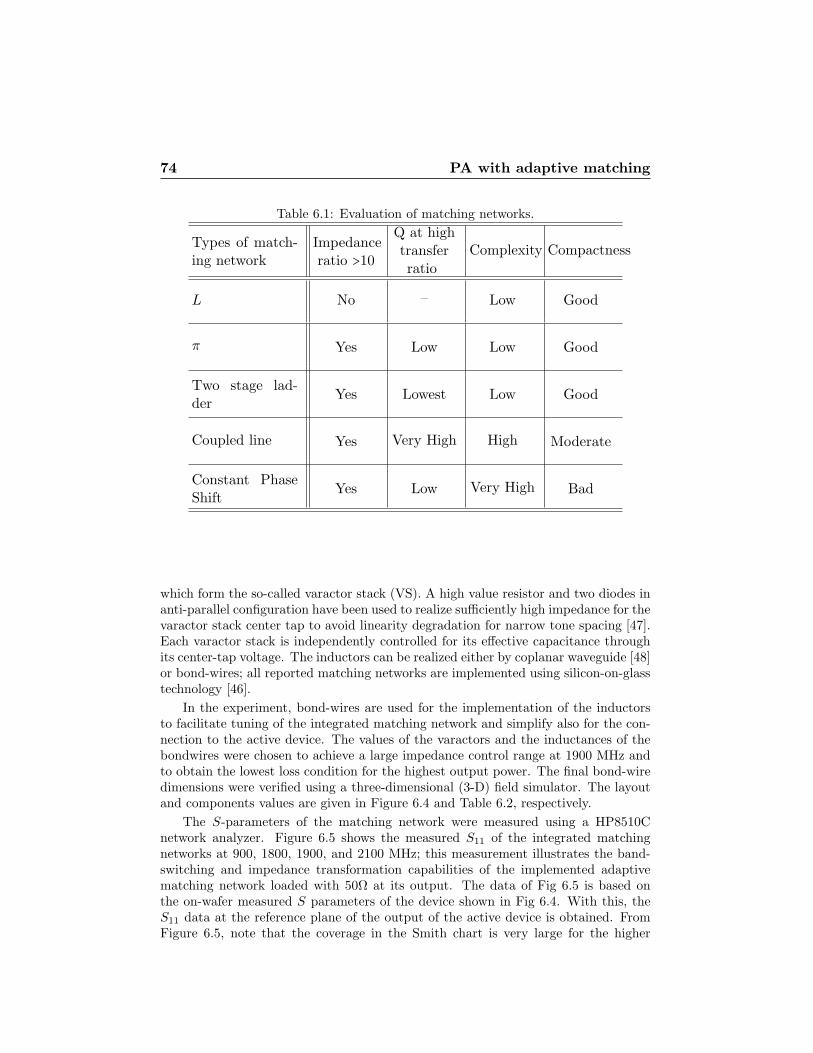
74 PA with adaptive matching
Table 6.1: Evaluation of matching networks.
Types of match-ing network
Impedanceratio >10
Q at hightransferratio
Complexity Compactness
L No – Low Good
π Yes Low Low Good
Two stage lad-der
Yes Lowest Low Good
Coupled line Yes Very High High Moderate
Constant PhaseShift
Yes Low Very High Bad
which form the so-called varactor stack (VS). A high value resistor and two diodes inanti-parallel configuration have been used to realize sufficiently high impedance for thevaractor stack center tap to avoid linearity degradation for narrow tone spacing [47].Each varactor stack is independently controlled for its effective capacitance throughits center-tap voltage. The inductors can be realized either by coplanar waveguide [48]or bond-wires; all reported matching networks are implemented using silicon-on-glasstechnology [46].
In the experiment, bond-wires are used for the implementation of the inductorsto facilitate tuning of the integrated matching network and simplify also for the con-nection to the active device. The values of the varactors and the inductances of thebondwires were chosen to achieve a large impedance control range at 1900 MHz andto obtain the lowest loss condition for the highest output power. The final bond-wiredimensions were verified using a three-dimensional (3-D) field simulator. The layoutand components values are given in Figure 6.4 and Table 6.2, respectively.
The S-parameters of the matching network were measured using a HP8510Cnetwork analyzer. Figure 6.5 shows the measured S11 of the integrated matchingnetworks at 900, 1800, 1900, and 2100 MHz; this measurement illustrates the band-switching and impedance transformation capabilities of the implemented adaptivematching network loaded with 50Ω at its output. The data of Fig 6.5 is based onthe on-wafer measured S parameters of the device shown in Fig 6.4. With this, theS11 data at the reference plane of the output of the active device is obtained. FromFigure 6.5, note that the coverage in the Smith chart is very large for the higher
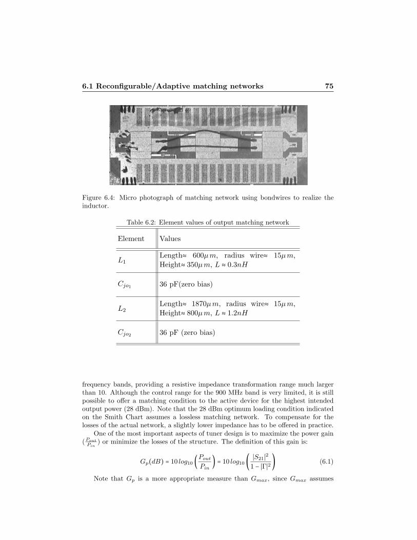
6.1 Reconfigurable/Adaptive matching networks 75
Figure 6.4: Micro photograph of matching network using bondwires to realize theinductor.
Table 6.2: Element values of output matching network
Element Values
L1Length≈ 600μm, radius wire≈ 15μm,Height≈ 350μm, L ≈ 0.3nH
Cjo136 pF(zero bias)
L2Length≈ 1870μm, radius wire≈ 15μm,Height≈ 800μm, L ≈ 1.2nH
Cjo236 pF (zero bias)
frequency bands, providing a resistive impedance transformation range much largerthan 10. Although the control range for the 900 MHz band is very limited, it is stillpossible to offer a matching condition to the active device for the highest intendedoutput power (28 dBm). Note that the 28 dBm optimum loading condition indicatedon the Smith Chart assumes a lossless matching network. To compensate for thelosses of the actual network, a slightly lower impedance has to be offered in practice.
One of the most important aspects of tuner design is to maximize the power gain(Pout
Pin) or minimize the losses of the structure. The definition of this gain is:
Gp(dB) = 10 log10 (Pout
Pin
) = 10 log10 ( ∣S21∣21 − ∣Γ∣2 ) (6.1)
Note that Gp is a more appropriate measure than Gmax, since Gmax assumes
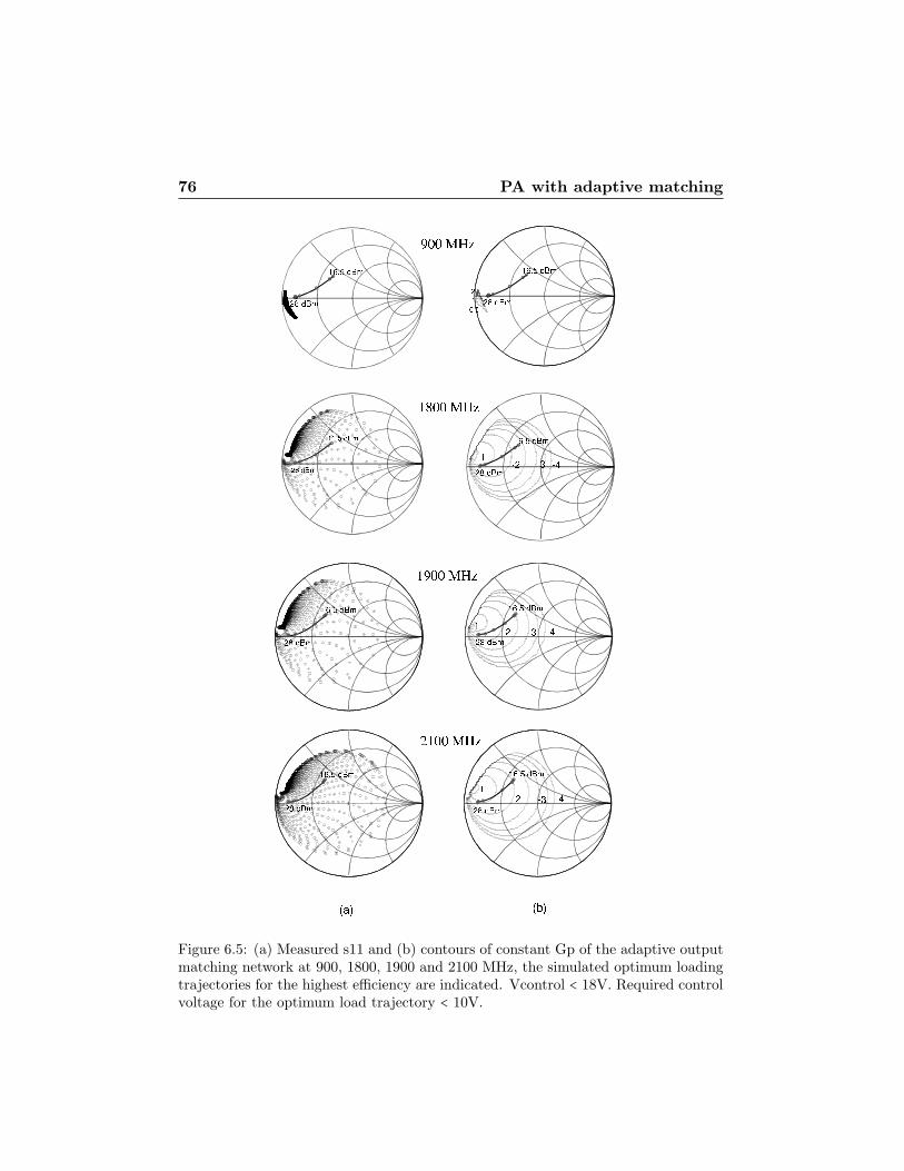
76 PA with adaptive matching
Figure 6.5: (a) Measured s11 and (b) contours of constant Gp of the adaptive outputmatching network at 900, 1800, 1900 and 2100 MHz, the simulated optimum loadingtrajectories for the highest efficiency are indicated. Vcontrol < 18V. Required controlvoltage for the optimum load trajectory < 10V.
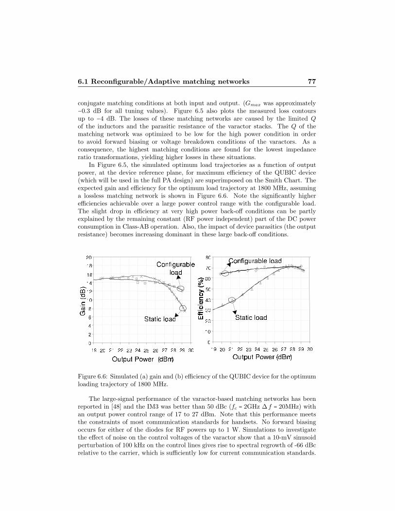
6.1 Reconfigurable/Adaptive matching networks 77
conjugate matching conditions at both input and output. (Gmax was approximately−0.3 dB for all tuning values). Figure 6.5 also plots the measured loss contoursup to −4 dB. The losses of these matching networks are caused by the limited Q
of the inductors and the parasitic resistance of the varactor stacks. The Q of thematching network was optimized to be low for the high power condition in orderto avoid forward biasing or voltage breakdown conditions of the varactors. As aconsequence, the highest matching conditions are found for the lowest impedanceratio transformations, yielding higher losses in these situations.
In Figure 6.5, the simulated optimum load trajectories as a function of outputpower, at the device reference plane, for maximum efficiency of the QUBIC device(which will be used in the full PA design) are superimposed on the Smith Chart. Theexpected gain and efficiency for the optimum load trajectory at 1800 MHz, assuminga lossless matching network is shown in Figure 6.6. Note the significantly higherefficiencies achievable over a large power control range with the configurable load.The slight drop in efficiency at very high power back-off conditions can be partlyexplained by the remaining constant (RF power independent) part of the DC powerconsumption in Class-AB operation. Also, the impact of device parasitics (the outputresistance) becomes increasing dominant in these large back-off conditions.
Figure 6.6: Simulated (a) gain and (b) efficiency of the QUBIC device for the optimumloading trajectory of 1800 MHz.
The large-signal performance of the varactor-based matching networks has beenreported in [48] and the IM3 was better than 50 dBc (fc = 2GHz Δ f = 20MHz) withan output power control range of 17 to 27 dBm. Note that this performance meetsthe constraints of most communication standards for handsets. No forward biasingoccurs for either of the diodes for RF powers up to 1 W. Simulations to investigatethe effect of noise on the control voltages of the varactor show that a 10-mV sinusoidperturbation of 100 kHz on the control lines gives rise to spectral regrowth of -66 dBcrelative to the carrier, which is sufficiently low for current communication standards.
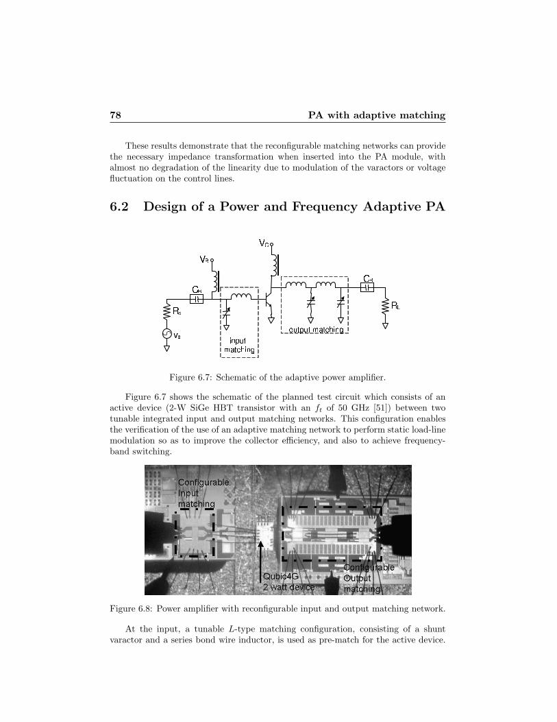
78 PA with adaptive matching
These results demonstrate that the reconfigurable matching networks can providethe necessary impedance transformation when inserted into the PA module, withalmost no degradation of the linearity due to modulation of the varactors or voltagefluctuation on the control lines.
6.2 Design of a Power and Frequency Adaptive PA
Figure 6.7: Schematic of the adaptive power amplifier.
Figure 6.7 shows the schematic of the planned test circuit which consists of anactive device (2-W SiGe HBT transistor with an ft of 50 GHz [51]) between twotunable integrated input and output matching networks. This configuration enablesthe verification of the use of an adaptive matching network to perform static load-linemodulation so as to improve the collector efficiency, and also to achieve frequency-band switching.
Figure 6.8: Power amplifier with reconfigurable input and output matching network.
At the input, a tunable L-type matching configuration, consisting of a shuntvaractor and a series bond wire inductor, is used as pre-match for the active device.
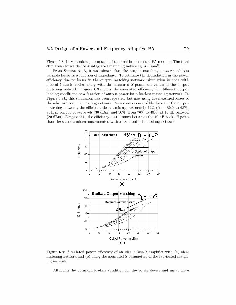
6.2 Design of a Power and Frequency Adaptive PA 79
Figure 6.8 shows a micro photograph of the final implemented PA module. The totalchip area (active device + integrated matching networks) is 8 mm2.
From Section 6.1.3, it was shown that the output matching network exhibitsvariable losses as a function of impedance. To estimate the degradation in the powerefficiency due to losses in the output matching network, simulation is done witha ideal Class-B device along with the measured S-parameter values of the outputmatching network. Figure 6.9 a plots the simulated efficiency for different outputloading conditions as a function of output power for a lossless matching network. InFigure 6.9b, this simulation has been repeated, but now using the measured losses ofthe adaptive output-matching network. As a consequence of the losses in the outputmatching network, the efficiency decrease is approximately 12% (from 80% to 68%)at high output power levels (30 dBm) and 30% (from 76% to 46%) at 10 dB back-off(20 dBm). Despite this, the efficiency is still much better at the 10 dB back-off pointthan the same amplifier implemented with a fixed output matching network.
Figure 6.9: Simulated power efficiency of an ideal Class-B amplifier with (a) idealmatching network and (b) using the measured S-parameters of the fabricated match-ing network.
Although the optimum loading condition for the active device and input drive
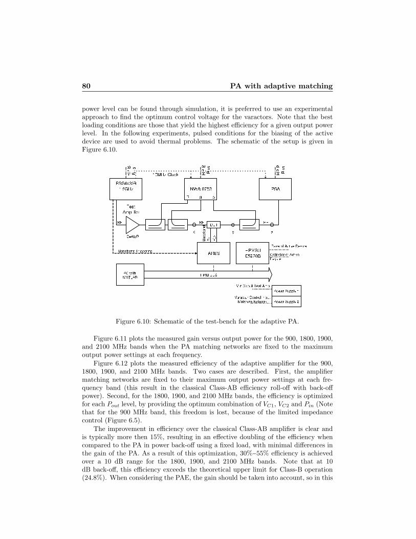
80 PA with adaptive matching
power level can be found through simulation, it is preferred to use an experimentalapproach to find the optimum control voltage for the varactors. Note that the bestloading conditions are those that yield the highest efficiency for a given output powerlevel. In the following experiments, pulsed conditions for the biasing of the activedevice are used to avoid thermal problems. The schematic of the setup is given inFigure 6.10.
Figure 6.10: Schematic of the test-bench for the adaptive PA.
Figure 6.11 plots the measured gain versus output power for the 900, 1800, 1900,and 2100 MHz bands when the PA matching networks are fixed to the maximumoutput power settings at each frequency.
Figure 6.12 plots the measured efficiency of the adaptive amplifier for the 900,1800, 1900, and 2100 MHz bands. Two cases are described. First, the amplifiermatching networks are fixed to their maximum output power settings at each fre-quency band (this result in the classical Class-AB efficiency roll-off with back-offpower). Second, for the 1800, 1900, and 2100 MHz bands, the efficiency is optimizedfor each Pout level, by providing the optimum combination of VC1, VC2 and Pin (Notethat for the 900 MHz band, this freedom is lost, because of the limited impedancecontrol (Figure 6.5).
The improvement in efficiency over the classical Class-AB amplifier is clear andis typically more then 15%, resulting in an effective doubling of the efficiency whencompared to the PA in power back-off using a fixed load, with minimal differences inthe gain of the PA. As a result of this optimization, 30%−55% efficiency is achievedover a 10 dB range for the 1800, 1900, and 2100 MHz bands. Note that at 10dB back-off, this efficiency exceeds the theoretical upper limit for Class-B operation(24.8%). When considering the PAE, the gain should be taken into account, so in this
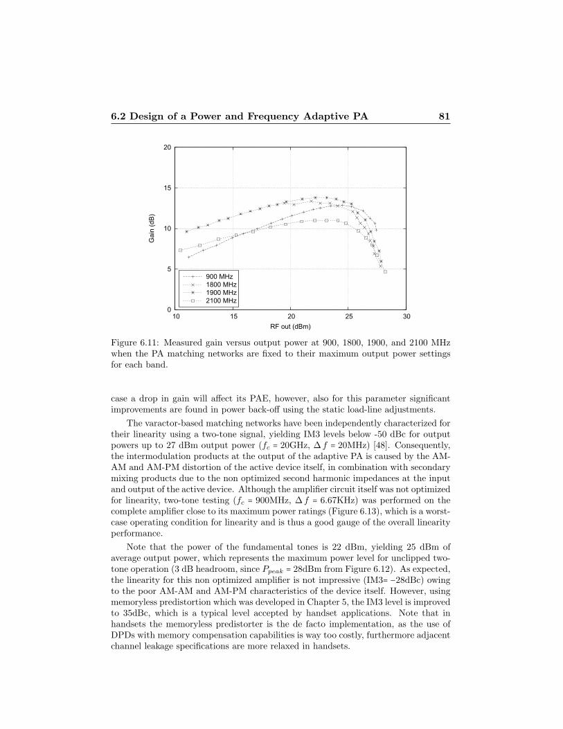
6.2 Design of a Power and Frequency Adaptive PA 81
0
5
10
15
20
10 15 20 25 30
Gai
n (d
B)
RF out (dBm)
900 MHz1800 MHz1900 MHz2100 MHz
Figure 6.11: Measured gain versus output power at 900, 1800, 1900, and 2100 MHzwhen the PA matching networks are fixed to their maximum output power settingsfor each band.
case a drop in gain will affect its PAE, however, also for this parameter significantimprovements are found in power back-off using the static load-line adjustments.
The varactor-based matching networks have been independently characterized fortheir linearity using a two-tone signal, yielding IM3 levels below -50 dBc for outputpowers up to 27 dBm output power (fc = 20GHz, Δ f = 20MHz) [48]. Consequently,the intermodulation products at the output of the adaptive PA is caused by the AM-AM and AM-PM distortion of the active device itself, in combination with secondarymixing products due to the non optimized second harmonic impedances at the inputand output of the active device. Although the amplifier circuit itself was not optimizedfor linearity, two-tone testing (fc = 900MHz, Δ f = 6.67KHz) was performed on thecomplete amplifier close to its maximum power ratings (Figure 6.13), which is a worst-case operating condition for linearity and is thus a good gauge of the overall linearityperformance.
Note that the power of the fundamental tones is 22 dBm, yielding 25 dBm ofaverage output power, which represents the maximum power level for unclipped two-tone operation (3 dB headroom, since Ppeak = 28dBm from Figure 6.12). As expected,the linearity for this non optimized amplifier is not impressive (IM3= −28dBc) owingto the poor AM-AM and AM-PM characteristics of the device itself. However, usingmemoryless predistortion which was developed in Chapter 5, the IM3 level is improvedto 35dBc, which is a typical level accepted by handset applications. Note that inhandsets the memoryless predistorter is the de facto implementation, as the use ofDPDs with memory compensation capabilities is way too costly, furthermore adjacentchannel leakage specifications are more relaxed in handsets.
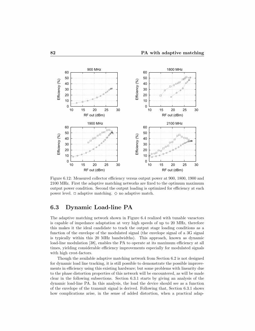
82 PA with adaptive matching
0 10 20 30 40 50 60
10 15 20 25 30
Effi
cien
cy (%
)
RF out (dBm)
900 MHz 1800 MHz
1900 MHz 2100 MHz
0 10 20 30 40 50 60
10 15 20 25 30
Effi
cien
cy (%
)
RF out (dBm)
0 10 20 30 40 50 60
10 15 20 25 30
Effi
cien
cy (%
)
RF out (dBm)
0 10 20 30 40 50 60
10 15 20 25 30
Effi
cien
cy (%
)
RF out (dBm)
Figure 6.12: Measured collector efficiency versus output power at 900, 1800, 1900 and2100 MHz. First the adaptive matching networks are fixed to the optimum maximumoutput power condition. Second the output loading is optimized for efficiency at eachpower level. ◻ adaptive matching. ◇ no adaptive match.
6.3 Dynamic Load-line PA
The adaptive matching network shown in Figure 6.4 realized with tunable varactorsis capable of impedance adaptation at very high speeds of up to 20 MHz, thereforethis makes it the ideal candidate to track the output stage loading conditions as afunction of the envelope of the modulated signal (the envelope signal of a 3G signalis typically within this 20 MHz bandwidths). This approach, known as dynamicload-line modulation [38], enables the PA to operate at its maximum efficiency at alltimes, yielding considerable efficiency improvements especially for modulated signalswith high crest-factors.
Though the available adaptive matching network from Section 6.2 is not designedfor dynamic load line tracking, it is still possible to demonstrate the possible improve-ments in efficiency using this existing hardware; but some problems with linearity dueto the phase distortion properties of this network will be encountered, as will be madeclear in the following subsections. Section 6.3.1 starts by giving an analysis of thedynamic load-line PA. In this analysis, the load the device should see as a functionof the envelope of the transmit signal is derived. Following that, Section 6.3.1 showshow complications arise, in the sense of added distortion, when a practical adap-
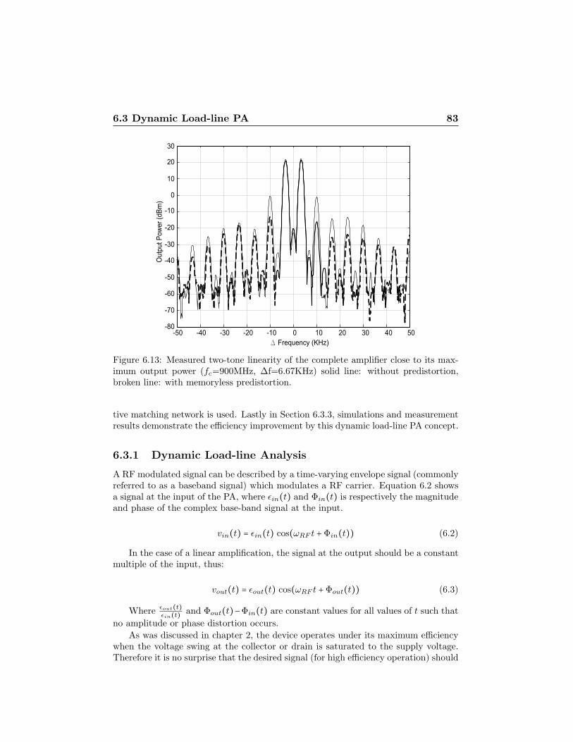
6.3 Dynamic Load-line PA 83
Figure 6.13: Measured two-tone linearity of the complete amplifier close to its max-imum output power (fc=900MHz, Δf=6.67KHz) solid line: without predistortion,broken line: with memoryless predistortion.
tive matching network is used. Lastly in Section 6.3.3, simulations and measurementresults demonstrate the efficiency improvement by this dynamic load-line PA concept.
6.3.1 Dynamic Load-line Analysis
A RF modulated signal can be described by a time-varying envelope signal (commonlyreferred to as a baseband signal) which modulates a RF carrier. Equation 6.2 showsa signal at the input of the PA, where εin(t) and Φin(t) is respectively the magnitudeand phase of the complex base-band signal at the input.
vin(t) = εin(t) cos(ωRF t +Φin(t)) (6.2)
In the case of a linear amplification, the signal at the output should be a constantmultiple of the input, thus:
vout(t) = εout(t) cos(ωRF t +Φout(t)) (6.3)
Where εout(t)εin(t) and Φout(t)−Φin(t) are constant values for all values of t such that
no amplitude or phase distortion occurs.
As was discussed in chapter 2, the device operates under its maximum efficiencywhen the voltage swing at the collector or drain is saturated to the supply voltage.Therefore it is no surprise that the desired signal (for high efficiency operation) should

84 PA with adaptive matching
be a constant envelope signal, while phase modulation is permitted, as shown in thefollowing:
vdev(t) = Vcc, cos(ωRF t +Φdev(t)) (6.4)
Where vdev(t) is the voltage at the output of the active device, and Vcc is theDC bias voltage provided to the output of the device. Assuming that the adaptivematching network is lossless and that the PA behaves quasi-static within one RF cycle(this assumption is valid when the RF frequency is much higher than the envelope orbase-band frequency); the following equation can be written:
Trf
∫0
V 2cc cos(ωRF t +Φout(t))2
Rvar
dt =Trf
∫0
ε2out cos(ωRF t +Φout(t))2RL
dt (6.5)
Which states that for a lossless adaptive matching network, the power deliveredby the active device to the input of the load varying network (Rvar) is equal to thepower delivered at the output into the fixed load connected at the output of theadaptive matching network (typically the antenna). Note that the integration is doneover one RF period (Trf ).
Rearranging this equation (6.5) in terms of Rvar, the following equation is ob-tained, which gives the loading conditions which the adaptive matching network needsto offer to the output stage device as a function of the envelope signal.
Rvar = V 2cc RL
ε2out
(6.6)
This concludes that the impedance offered to the active device should changeinversely with the square of the envelope. From the equation (6.4) and (6.6), thecurrent sourced by the active device can be computed as follows:
idev = εout(t)2 cos(ωrf t +Φdev(t))VccRL
(6.7)
Assuming that the active device is a voltage controlled current source, this wouldimply that the driving signal at the input of the active device is a constant scalarmultiple of it. Figure 6.14 shows the generic implementation of a dynamic load-linePA based on the above developed equations.
The envelope squarer at the input (in the ideal case) only squares the envelope ofthe RF signal as this information is not only required by the controller of the adaptivematching network, but also by the active device itself. Under these conditions, thevoltage at the output of the active device is a constant envelope making it highlyefficient. While the resulting signal at the output of the lossless adaptive matchingnetwork offered to RL is a linear amplification of the input signal.
6.3.2 Limitations of the adaptive matching network
In a classical PA, the active device is the only source of non-linearity in the PA.However, in the dynamic load-line PA, not only does the active device generates non-

6.3 Dynamic Load-line PA 85
Figure 6.14: Generic implementation schematic of a dynamic load-line PA.
linearity, but distortion is also caused by the time varying nature of the matchingnetwork.
Equation (6.6) shows that if the envelope of the signal at a certain point in timetends to zero, then Rvar which is the load which the adaptive matching network hasto offer to the device tends to infinity. However, all practical adaptive matching net-works have a finite impedance transformation ratio. In the following discussion, thislimitation is tested in simulation (ADS) using the generic setup shown in Figure 6.14and the equations developed in the previous section. The active device is implementedusing an ideal voltage current transfer similar to what was done in Chapter 2. Thebiasing and current is set such that the active device delivers a maximum of 1 wattto the load. The adaptive matching network is described using a three port SDDblock, which allows the impedance it offers to the active device to be controlled by athird port. A two-tone signal with a 1 MHz tone-spacing is used in this test since itsenvelope goes from zero to the maximum that the device can handle, thus offering aperfect test vehicle.
Figure 6.15 a shows the impedance offered to the active device which varies from4.5Ω to 450Ω. This is the reciprocal of the envelope square of the base-band signalwith its maximum value truncated at 450Ω. Figure 6.15b shows the envelope of thesignal at the output of the device, which is expected from theory to have a constantamplitude. The periodical dip to zero corresponds to the point where Rvar staysconstant and as the envelope of the actual signal goes to zero. The same experimentis again repeated but this time, the impedance transformation ratio is limited evenmore by setting the maximum impedance the network can provide to 45Ω.
Figure 6.16 shows the simulated output power spectrum for both cases. Limitingthe tuning range by a factor 10 in the second situation increases the spectral regrowthby approximately 25 dBc. The simulated efficiency performance for both cases is78.5%, which is identical to the maximum efficiency for a Class-B amplifier at fullpower.
The signal distortion is caused due to the fact that the active device is still driven
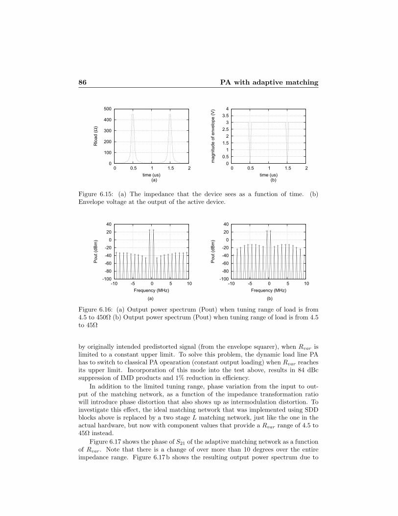
86 PA with adaptive matching
0
100
200
300
400
500
0 0.5 1 1.5 2
Rlo
ad (Ω
)
time (us)(a) (b)
0 0.5
1 1.5
2 2.5
3 3.5
4
0 0.5 1 1.5 2
mag
nitu
de o
f env
elop
e (V
)
time (us)
Figure 6.15: (a) The impedance that the device sees as a function of time. (b)Envelope voltage at the output of the active device.
-100
-80
-60
-40
-20
0
20
40
-10 -5 0 5 10
Pou
t (dB
m)
Frequency (MHz)
(a) (b)
-100
-80
-60
-40
-20
0
20
40
-10 -5 0 5 10
Pou
t (dB
m)
Frequency (MHz)
Figure 6.16: (a) Output power spectrum (Pout) when tuning range of load is from4.5 to 450Ω (b) Output power spectrum (Pout) when tuning range of load is from 4.5to 45Ω
by originally intended predistorted signal (from the envelope squarer), when Rvar islimited to a constant upper limit. To solve this problem, the dynamic load line PAhas to switch to classical PA opearation (constant output loading) when Rvar reachesits upper limit. Incorporation of this mode into the test above, results in 84 dBcsuppression of IMD products and 1% reduction in efficiency.
In addition to the limited tuning range, phase variation from the input to out-put of the matching network, as a function of the impedance transformation ratiowill introduce phase distortion that also shows up as intermodulation distortion. Toinvestigate this effect, the ideal matching network that was implemented using SDDblocks above is replaced by a two stage L matching network, just like the one in theactual hardware, but now with component values that provide a Rvar range of 4.5 to45Ω instead.
Figure 6.17 shows the phase of S21 of the adaptive matching network as a functionof Rvar. Note that there is a change of over more than 10 degrees over the entireimpedance range. Figure 6.17b shows the resulting output power spectrum due to
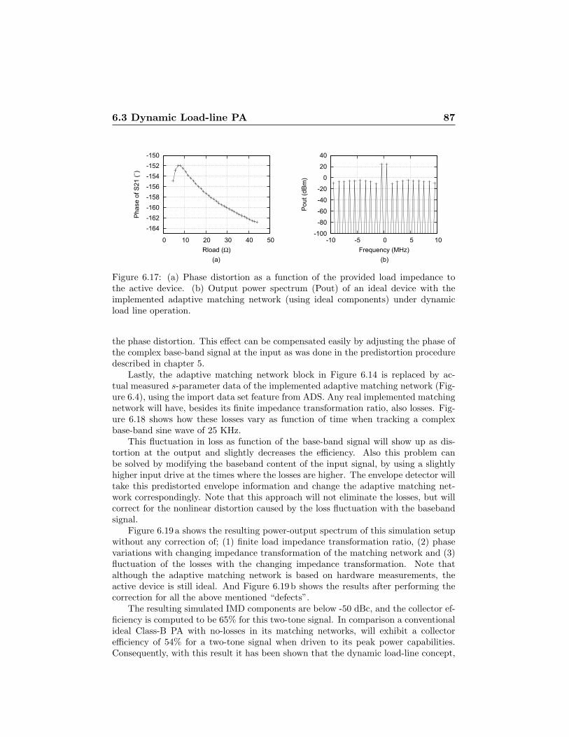
6.3 Dynamic Load-line PA 87
-164-162-160-158-156-154-152-150
0 10 20 30 40 50
Pha
se o
f S21
(˚)
Rload (Ω)(a) (b)
-100
-80
-60
-40
-20
0
20
40
-10 -5 0 5 10
Pou
t (dB
m)
Frequency (MHz)
Figure 6.17: (a) Phase distortion as a function of the provided load impedance tothe active device. (b) Output power spectrum (Pout) of an ideal device with theimplemented adaptive matching network (using ideal components) under dynamicload line operation.
the phase distortion. This effect can be compensated easily by adjusting the phase ofthe complex base-band signal at the input as was done in the predistortion proceduredescribed in chapter 5.
Lastly, the adaptive matching network block in Figure 6.14 is replaced by ac-tual measured s-parameter data of the implemented adaptive matching network (Fig-ure 6.4), using the import data set feature from ADS. Any real implemented matchingnetwork will have, besides its finite impedance transformation ratio, also losses. Fig-ure 6.18 shows how these losses vary as function of time when tracking a complexbase-band sine wave of 25 KHz.
This fluctuation in loss as function of the base-band signal will show up as dis-tortion at the output and slightly decreases the efficiency. Also this problem canbe solved by modifying the baseband content of the input signal, by using a slightlyhigher input drive at the times where the losses are higher. The envelope detector willtake this predistorted envelope information and change the adaptive matching net-work correspondingly. Note that this approach will not eliminate the losses, but willcorrect for the nonlinear distortion caused by the loss fluctuation with the basebandsignal.
Figure 6.19 a shows the resulting power-output spectrum of this simulation setupwithout any correction of; (1) finite load impedance transformation ratio, (2) phasevariations with changing impedance transformation of the matching network and (3)fluctuation of the losses with the changing impedance transformation. Note thatalthough the adaptive matching network is based on hardware measurements, theactive device is still ideal. And Figure 6.19b shows the results after performing thecorrection for all the above mentioned “defects”.
The resulting simulated IMD components are below -50 dBc, and the collector ef-ficiency is computed to be 65% for this two-tone signal. In comparison a conventionalideal Class-B PA with no-losses in its matching networks, will exhibit a collectorefficiency of 54% for a two-tone signal when driven to its peak power capabilities.Consequently, with this result it has been shown that the dynamic load-line concept,
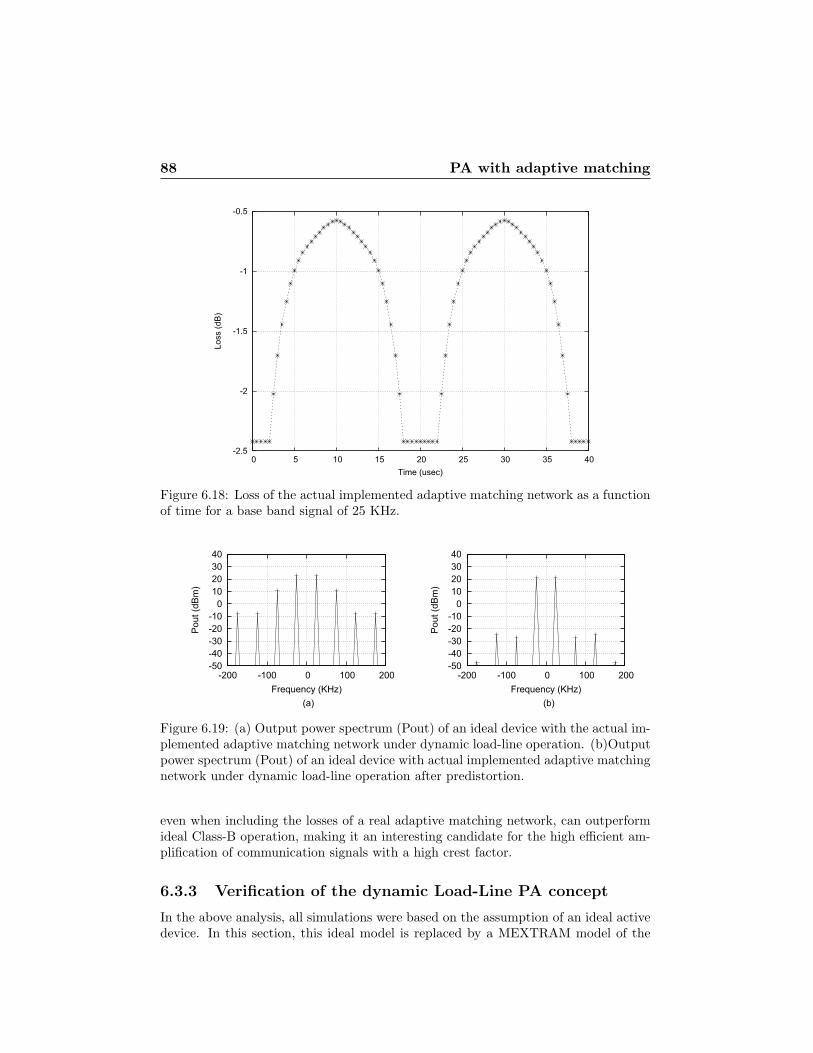
88 PA with adaptive matching
-2.5
-2
-1.5
-1
-0.5
0 5 10 15 20 25 30 35 40
Loss
(dB
)
Time (usec)
Figure 6.18: Loss of the actual implemented adaptive matching network as a functionof time for a base band signal of 25 KHz.
-50-40-30-20-10
0 10 20 30 40
-200 -100 0 100 200
Pou
t (dB
m)
Frequency (KHz)(a) (b)
-50-40-30-20-10
0 10 20 30 40
-200 -100 0 100 200
Pou
t (dB
m)
Frequency (KHz)
Figure 6.19: (a) Output power spectrum (Pout) of an ideal device with the actual im-plemented adaptive matching network under dynamic load-line operation. (b)Outputpower spectrum (Pout) of an ideal device with actual implemented adaptive matchingnetwork under dynamic load-line operation after predistortion.
even when including the losses of a real adaptive matching network, can outperformideal Class-B operation, making it an interesting candidate for the high efficient am-plification of communication signals with a high crest factor.
6.3.3 Verification of the dynamic Load-Line PA concept
In the above analysis, all simulations were based on the assumption of an ideal activedevice. In this section, this ideal model is replaced by a MEXTRAM model of the
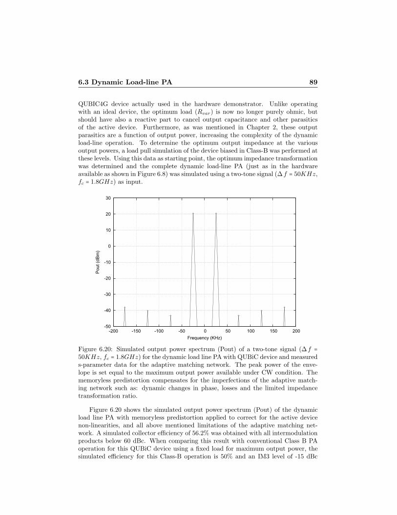
6.3 Dynamic Load-line PA 89
QUBIC4G device actually used in the hardware demonstrator. Unlike operatingwith an ideal device, the optimum load (Rvar) is now no longer purely ohmic, butshould have also a reactive part to cancel output capacitance and other parasiticsof the active device. Furthermore, as was mentioned in Chapter 2, these outputparasitics are a function of output power, increasing the complexity of the dynamicload-line operation. To determine the optimum output impedance at the variousoutput powers, a load pull simulation of the device biased in Class-B was performed atthese levels. Using this data as starting point, the optimum impedance transformationwas determined and the complete dynamic load-line PA (just as in the hardwareavailable as shown in Figure 6.8) was simulated using a two-tone signal (Δf = 50KHz,fc = 1.8GHz) as input.
-50
-40
-30
-20
-10
0
10
20
30
-200 -150 -100 -50 0 50 100 150 200
Pou
t (dB
m)
Frequency (KHz)
Figure 6.20: Simulated output power spectrum (Pout) of a two-tone signal (Δf =50KHz, fc = 1.8GHz) for the dynamic load line PA with QUBiC device and measureds-parameter data for the adaptive matching network. The peak power of the enve-lope is set equal to the maximum output power available under CW condition. Thememoryless predistortion compensates for the imperfections of the adaptive match-ing network such as: dynamic changes in phase, losses and the limited impedancetransformation ratio.
Figure 6.20 shows the simulated output power spectrum (Pout) of the dynamicload line PA with memoryless predistortion applied to correct for the active devicenon-linearities, and all above mentioned limitations of the adaptive matching net-work. A simulated collector efficiency of 56.2% was obtained with all intermodulationproducts below 60 dBc. When comparing this result with conventional Class B PAoperation for this QUBiC device using a fixed load for maximum output power, thesimulated efficiency for this Class-B operation is 50% and an IM3 level of -15 dBc
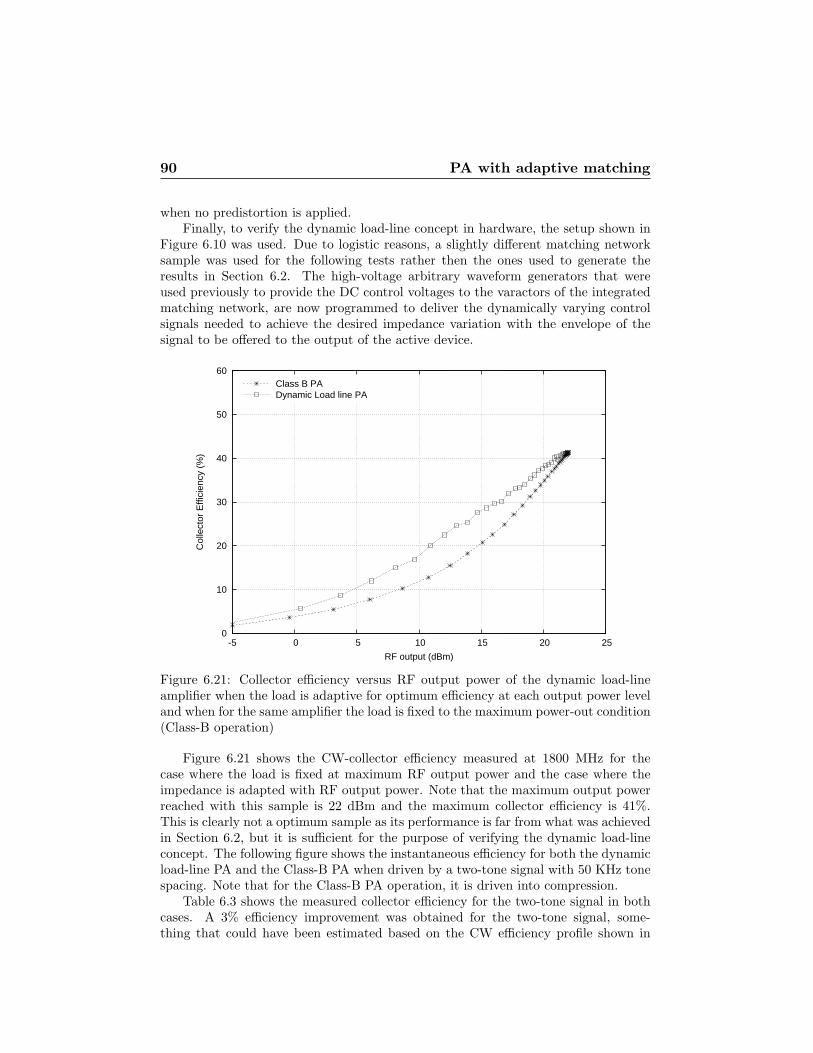
90 PA with adaptive matching
when no predistortion is applied.Finally, to verify the dynamic load-line concept in hardware, the setup shown in
Figure 6.10 was used. Due to logistic reasons, a slightly different matching networksample was used for the following tests rather then the ones used to generate theresults in Section 6.2. The high-voltage arbitrary waveform generators that wereused previously to provide the DC control voltages to the varactors of the integratedmatching network, are now programmed to deliver the dynamically varying controlsignals needed to achieve the desired impedance variation with the envelope of thesignal to be offered to the output of the active device.
0
10
20
30
40
50
60
-5 0 5 10 15 20 25
Col
lect
or E
ffici
ency
(%
)
RF output (dBm)
Class B PADynamic Load line PA
Figure 6.21: Collector efficiency versus RF output power of the dynamic load-lineamplifier when the load is adaptive for optimum efficiency at each output power leveland when for the same amplifier the load is fixed to the maximum power-out condition(Class-B operation)
Figure 6.21 shows the CW-collector efficiency measured at 1800 MHz for thecase where the load is fixed at maximum RF output power and the case where theimpedance is adapted with RF output power. Note that the maximum output powerreached with this sample is 22 dBm and the maximum collector efficiency is 41%.This is clearly not a optimum sample as its performance is far from what was achievedin Section 6.2, but it is sufficient for the purpose of verifying the dynamic load-lineconcept. The following figure shows the instantaneous efficiency for both the dynamicload-line PA and the Class-B PA when driven by a two-tone signal with 50 KHz tonespacing. Note that for the Class-B PA operation, it is driven into compression.
Table 6.3 shows the measured collector efficiency for the two-tone signal in bothcases. A 3% efficiency improvement was obtained for the two-tone signal, some-thing that could have been estimated based on the CW efficiency profile shown in
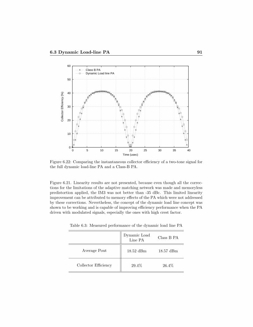
6.3 Dynamic Load-line PA 91
0
10
20
30
40
50
60
0 5 10 15 20 25 30 35 40
Col
lect
or E
ffici
ency
(%
)
Time (usec)
Class B PADynamic Load line PA
Figure 6.22: Comparing the instantaneous collector efficiency of a two-tone signal forthe full dynamic load-line PA and a Class-B PA.
Figure 6.21. Linearity results are not presented, because even though all the correc-tions for the limitations of the adaptive matching network was made and memorylesspredistortion applied, the IM3 was not better than -35 dBc. This limited linearityimprovement can be attributed to memory effects of the PA which were not addressedby these corrections. Nevertheless, the concept of the dynamic load line concept wasshown to be working and is capable of improving efficiency performance when the PAdriven with modulated signals, especially the ones with high crest factor.
Table 6.3: Measured performance of the dynamic load line PA
Dynamic LoadLine PA
Class B PA
Average Pout 18.52 dBm 18.57 dBm
Collector Efficiency 29.4% 26.4%

92 PA with adaptive matching
6.4 Conclusion
To the author’s knowledge, for the first time, a multi-band multi-mode power am-plifier, which is continuously tunable in operating frequency and output power level,has been demonstrated. The demonstrator PA has a peak output power between 27and 28 dBm (0.5 to 0.7 watts) at the 900, 1800, 1900, and 2100 MHz bands with veryreasonable efficiencies. The capability to adapt the loading of the active device asfunction of desired output-power results in high-efficiency performance under staticpower back-off, e.g. in power control loop applications. The integrated varactor-basedmatching networks are low-loss and provide low distortion due to the use of the anti-series silicon-on-glass technology. The required control voltages in this amplifier forthe intended load trajectory were restricted to 10 V. Since all varactors are reversedbiased, the control of the adaptive network requires almost no DC power. The totalchip area including integrated matching networks is restricted to 8 mm2, and can bemade even more compact.
Another strength of the varactor-based matching network is that it in principlecan handle high tuning speeds (up to 20 MHz). Therefore, it is capable to trackthe output stage loading conditions with the envelope of the modulated signal. Thisapproach, known as dynamic load-line modulation, enables the PA to operate at itsmaximum efficiency at each point in time, yielding considerable efficiency improve-ments also for modulated signals with a high crest factor. Using the design which wasmeant for the multi-band multi-mode power amplifier, it was shown in simulationsand measurement that the efficiency for signals with a non-constant envelope can beimproved. Although the principles are demonstrated, still increased efforts must bemade to solve the higher distortion due to the continuous adaptation of the match-ing network. Contributors to the overall distortion in a dynamic load-line PA wereidentified to be:
1. Finite impedance transformation ratio of the adaptive matching network,2. Impedance dependent phase shift from input to output of the adaptive match-
ing network,3. Impedance dependent losses of the adaptive matching network,4. Distortion from the active device.
Although simulation results of this concept show high efficiency together withgood linearity after applying memoryless predistortion, in practise improvement inefficiency was marginal and memoryless predistortion was not effective. This is at-tributed to the presence of memory effects that were not included in the simulation.At this moment it is not customary to apply memory compensation algorithms inhandsets, due to cost and power consumption considerations. This issue is not fur-ther investigated within these thesis. However, that leaves us with the question aboutthe cause of the memory effects in our practical demonstrator. After close inspectionit proved that one of the dominant contributors to memory effects was the require-ment for high impedance in the center node connection of the anti-series configured(uniformly doped) varactors diodes. This impedance is needed to guarantee a linearoperation of the varactors also for band modulated signals [52]. It works out thatthis requirement is somewhat conflicting with the desire to modulate the varactorswith the envelope of the modulated signal. This gives rise to increased distortion in

6.4 Conclusion 93
practical implementations. In the initial simulations this phenomena does not appeardue to the fact that s-parameters where used to model the matching network. Afterrecognizing the problem, new developments were started to find a new varactor topol-ogy that is suited for fast modulation while not introducing memory effects. This newactivity already has created many exciting results, which will find soon their applica-tion in a new generation of dynamic load-line amplifiers [36]. It is expected that forthese new implementations no memory correction will be required, so the use of mem-oryless predistortion as introduced in this chapter will be sufficient. The combinationof these techniques can provide compact, low-cost, band-switching, highly-efficientpower amplifiers for future mobile phones.
In the next chapter, the focus is on power amplifiers for base station applications,which should provide even higher levels of output power and efficiency, while band-switching is less a concern. These slightly different requirements, which make thehardware demands for base station applications much more severe, demand a differentapproach than the use of dynamic matching networks. Consequently, new designtechniques and signal processing concepts will be developed to meet also here thechallenges set by the latest generation of wireless communication standards.


Chapter 7
Doherty Power Amplifier forbase stations
In Chapter 1, the important considerations in the development of base-station PAswere discussed. The increasing information bandwidth and amount of users per chan-nel, led to the use of coding and modulation schemes, which require RF signals withsignificantly large Crest Factors (CF), also commonly refered to large peak-to-averagepower ratios. The Class-B/AB amplifier, which was and still is in many places thede-facto base-station PA, is no longer very attractive, simply because when the Class-B/AB amplifier is driven with RF signals with high CF, it exhibits typically a rela-tively low average efficiency.
It was also discussed in chapter 5 that to avoid this efficiency degradation, manyhigh efficient PA architectures have been proposed over the past 5 years. Despiteof the large variety in amplifier concepts, only the Envelope Tracking [31, 38] andDoherty amplifier [53, 54] concepts seem to be actively pursued by the industry tobecome commercial products for the base-station market. In these approaches, theEnvelope Tracking amplifier, in its most promising implementation, makes use of anefficient DC-to-DC converter in combination with a video amplifier to modulate thesupply voltage. This increases cost and gives rise to some additional power lossesthat slightly degrade the overall efficiency of the amplifier. As such, although thesupply tracking PA is promising, commercialize implementation is still many yearsaway. The Doherty amplifier, which does not require additional “peripheral” hard-ware, seem to have been adopted by the industry as the way forward in boostingefficiency performance at this present time, especially when signals with high CF areinvolved. Base station manufacturers such as Nokia (Europe) and Huawei (China) areat this moment already selling “green” base-stations based on the two-way symmet-rical Doherty power amplifier. Unfortunately, practical implementations of three-wayand higher branch Doherty PAs, which enables even higher efficiency performancepossible for signals with CF>10 dB, are still rare and not fully convincing in theirefficiency and linearity performance (even in the research labs). The main reason forthis, is the rather difficult design and the delicate fine tuning of the power distribu-tion/combining networks and the sensitive biasing of the main and peaking amplifier
95
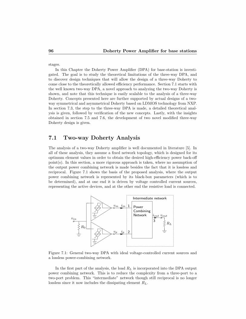
96 Doherty Power Amplifier for base stations
stages.
In this Chapter the Doherty Power Amplifier (DPA) for base-station is investi-gated. The goal is to study the theoretical limitations of the three-way DPA, andto discover design techniques that will allow the design of a three-way Doherty tocome close to the theoretically allowed efficiency performance. Section 7.1 starts withthe well known two-way DPA, a novel approach to analyzing the two-way Doherty isshown, and note that this technique is easily scalable to the analysis of a three-wayDoherty. Concepts presented here are further supported by actual designs of a two-way symmetrical and asymmetrical Doherty based on LDMOS technology from NXP.In section 7.3, the step to the three-way DPA is made, a detailed theoretical anal-ysis is given, followed by verification of the new concepts. Lastly, with the insightsobtained in section 7.5 and 7.6, the development of two novel modified three-wayDoherty design is given.
7.1 Two-way Doherty Analysis
The analysis of a two-way Doherty amplifier is well documented in literature [5]. Inall of these analysis, they assume a fixed network topology, which is designed for itsoptimum element values in order to obtain the desired high-efficiency power back-offpoint(s). In this section, a more rigorous approach is taken, where no assumption ofthe output power combining network is made besides the fact that it is lossless andreciprocal. Figure 7.1 shows the basis of the proposed analysis, where the outputpower combining network is represented by its black-box parameters (which is tobe determined), and at one end it is driven by voltage controlled current sources,representing the active devices, and at the other end the resistive load is connected.
PowerCombiningNetwork iout vout
imvm
ipvp
vin
RL
Intermediate network
R0
3
1
2
Figure 7.1: General two-way DPA with ideal voltage-controlled current sources anda lossless power-combining network.
In the first part of the analysis, the load RL is incorporated into the DPA outputpower combining network. This is to reduce the complexity from a three-port to atwo-port problem. This “intermediate” network though still reciprocal is no longerlossless since it now includes the dissipating element RL.

7.1 Two-way Doherty Analysis 97
Next the voltages and currents at the output of the main and peak devices (Fig-ure 7.1) are expressed as a function of the black-box parameters of the intermediatenetwork for two specific drive conditions, namely, the point where the DPA amplifierdelivers its maximum (full) power (F ), as well as the point where the main devicereaches its high-efficiency condition at the back-off point (B) (see Figure 7.2 (d));thus, at the power back-off point (B):
υm,B = im,B z11 + ip,B z12 (7.1)
υp,B = im,B z21 + ip,B z22 (7.2)
And at full power (F ),
υm,F = im,F z11 + ip,F z12 (7.3)
υp,F = im,F z21 + ip,F z22 (7.4)
Where vm,F , im,F and im,B, are the voltages and currents of the main deviceat the full output power and the back-off point, respectively, while vp,F , ip,F andvp,B , ip,B are the corresponding voltages and currents for the peaking device (seeFigure 7.2). Solving equation (7.1)−(7.4) simultaneously for the z-parameters yields
z11 = −υm,F ip,B + υm,Bip,F
−im,F ip,B + im,Bip,F
z12 = −υm,Bim,F − υm,F im,B
−im,F ip,B + im,Bip,F
z21 = − υp,F ip,B − υp,Bip,F
−im,F ip,B + im,Bip,F
z22 = υp,Bim,F + υp,F im,B
−im,F ip,B + im,Bip,F
(7.5)
The goal at this point is to determine all the voltage and current variables suchthat the black-box parameters of the intermediate network can be subsequently com-puted. To do this, the voltages and currents that are already “fixed” by the efficiencyrequirements are first written down. Note that high efficiency requires that the volt-age amplitude at the output of the active devices be maximized with respect to theirdc supply voltage when an output current is present. For the two-way DPA, the out-put voltage amplitude of the main device should be maximum at full output power(F ), as well as at a specific back-off power level (B) [see Figure 7.2d]. Consequently,the amplitude of υm,F , υm,B , and υp,F must be set to their maximum value, whichin Class-B operation equals their dc supply voltage, thus, υm,F = υm,B = υp,F = VDC .Furthermore, to guarantee maximum efficiency in power back-off, the peaking ampli-fier is off until the backed-off point is reached, yielding ip,B = 0. This leaves im,F ,ip,F , im,B, and vp,B as the remaining unknowns to solve for.
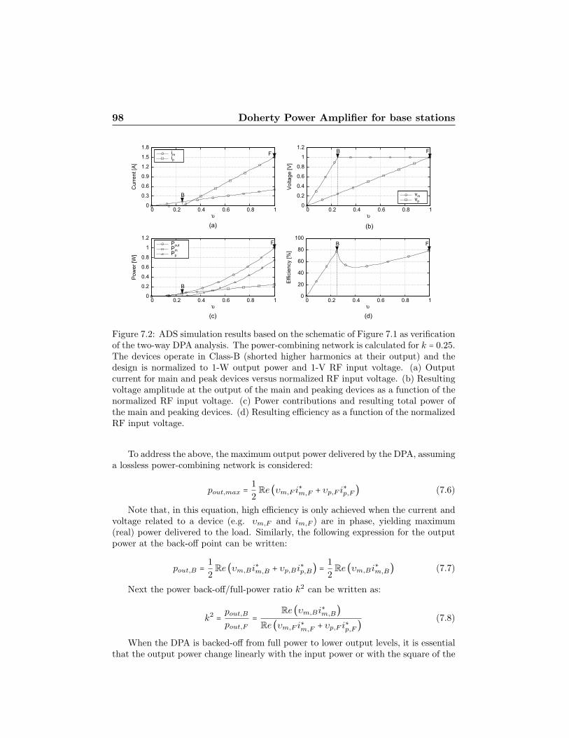
98 Doherty Power Amplifier for base stations
0
0.2
0.4
0.6
0.8
1
1.2
0 0.2 0.4 0.6 0.8 1
Vol
tage
[V]
υ
B F
vmvp
0
0.3
0.6
0.9
1.2
1.5
1.8
0 0.2 0.4 0.6 0.8 1
Cur
rent
[A]
υ
B
Fimip
0
0.2
0.4
0.6
0.8
1
1.2
0 0.2 0.4 0.6 0.8 1
Pow
er [W
]
υ
PoutPmPp
B
F
0
20
40
60
80
100
0 0.2 0.4 0.6 0.8 1
Effi
cien
cy [%
]
υ
B F
(a) (b)
(c) (d)
Figure 7.2: ADS simulation results based on the schematic of Figure 7.1 as verificationof the two-way DPA analysis. The power-combining network is calculated for k = 0.25.The devices operate in Class-B (shorted higher harmonics at their output) and thedesign is normalized to 1-W output power and 1-V RF input voltage. (a) Outputcurrent for main and peak devices versus normalized RF input voltage. (b) Resultingvoltage amplitude at the output of the main and peaking devices as a function of thenormalized RF input voltage. (c) Power contributions and resulting total power ofthe main and peaking devices. (d) Resulting efficiency as a function of the normalizedRF input voltage.
To address the above, the maximum output power delivered by the DPA, assuminga lossless power-combining network is considered:
pout,max = 1
2Re (υm,F i∗m,F + υp,F i∗p,F ) (7.6)
Note that, in this equation, high efficiency is only achieved when the current andvoltage related to a device (e.g. υm,F and im,F ) are in phase, yielding maximum(real) power delivered to the load. Similarly, the following expression for the outputpower at the back-off point can be written:
pout,B = 1
2Re (υm,Bi∗m,B + υp,Bi∗p,B) = 1
2Re (υm,Bi∗m,B) (7.7)
Next the power back-off/full-power ratio k2 can be written as:
k2 = pout,B
pout,F
= Re (υm,Bi∗m,B)Re (υm,F i∗m,F + υp,F i∗p,F
) (7.8)
When the DPA is backed-off from full power to lower output levels, it is essentialthat the output power change linearly with the input power or with the square of the
7.1 Two-way Doherty Analysis 99
input voltage. Consequently, the following condition enforces the output current ofthe active devices to their input-driving voltage. Here, the most logical choice from animplementation point-of-view is to assume a linear relation between output currentand input voltage when the device is turned on. Thus, this follows as:
im,B = k im,F (7.9)
The final condition to solve for the black-box parameters of the intermediatetwo-port network is found by making use of the reciprocal property z12 = z21 yielding:
υm,B im,F − υm,F im,B = υp,F ip,B − υp,Bip,F (7.10)
Using equation (7.6)−(7.10), the variables im,F , ip,F , im,B and vp,B are uniquelydetermined and the z-parameters of the intermediate network network are given byequation (7.5). The related s-parameters of the two−port network are:
s11 = −k2 − 2
k2 + 2(7.11)
s12 = s21 = − j2k
k2 + 2(7.12)
s22 = − k2
k2 + 2(7.13)
Note that to keep the above equations to a manageable size, the phase anglebetween the power waves of port 1 and port 2 have been set to 90○ .
Having solved the two-port parameters of the intermediate network, the last re-maining step in determining the power-combining network for the two-way DPA isto reintroduce the black-box parameters that involve the third port connected to theload, namely, s13, s31, s23, s32 and s33. Note that the original two-port -parameters donot change when going to a three-port network, provided that the loading impedanceis identical to the normalization impedance used for the s-matrix. The remaining s-parameters involving the third port can be found by imposing the well-known losslessthree-port s-parameter conditions using (N = 3) using:
N
∑n=1∣snp∣2 = 1 ∀p (7.14)
N
∑n=1
snp s∗nq = 0 ∀p ≠ q (7.15)
The expansion to the three-port case results in six equations. Since s13 = s31 ands23 = s32 due to the reciprocity, there remain six unknowns (since each s-parameteris, in general, complex) and six independent equations. Consequently, under thecondition that the RF signal in port 2 lags with respect to the signal in port 1by 90 degree, a unique analytical solution can be found for the three-port s-matrixrepresenting the power-combining network of the two-way DPA. The resulting s-parameter solution is a function of k and α , where α is the phase of s23 representingthe electrical angle of the signals between ports 2 and 3
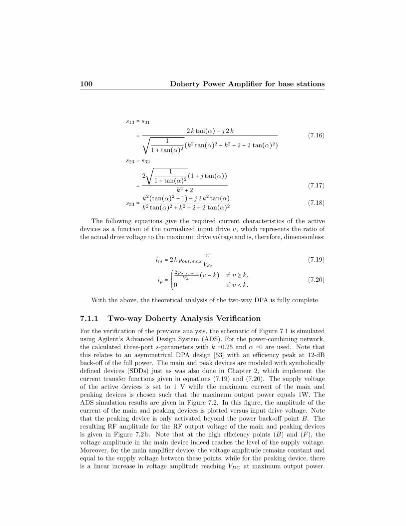
100 Doherty Power Amplifier for base stations
s13 = s31
= 2k tan(α) − j 2k√1
1 + tan(α)2 (k2 tan(α)2 + k2 + 2 + 2 tan(α)2)(7.16)
s23 = s32
=2
√1
1 + tan(α)2 (1 + j tan(α))k2 + 2
(7.17)
s33 = k2(tan(α)2 − 1) + j 2k2 tan(α)k2 tan(α)2 + k2 + 2 + 2 tan(α)2 (7.18)
The following equations give the required current characteristics of the activedevices as a function of the normalized input drive υ, which represents the ratio ofthe actual drive voltage to the maximum drive voltage and is, therefore, dimensionless:
im = 2k pout,max
υ
Vdc
(7.19)
ip =⎧⎪⎪⎨⎪⎪⎩
2pout,max
Vdc(υ − k) if υ ≥ k,
0 if υ < k.(7.20)
With the above, the theoretical analysis of the two-way DPA is fully complete.
7.1.1 Two-way Doherty Analysis Verification
For the verification of the previous analysis, the schematic of Figure 7.1 is simulatedusing Agilent’s Advanced Design System (ADS). For the power-combining network,the calculated three-port s-parameters with k =0.25 and α =0 are used. Note thatthis relates to an asymmetrical DPA design [53] with an efficiency peak at 12-dBback-off of the full power. The main and peak devices are modeled with symbolicallydefined devices (SDDs) just as was also done in Chapter 2, which implement thecurrent transfer functions given in equations (7.19) and (7.20). The supply voltageof the active devices is set to 1 V while the maximum current of the main andpeaking devices is chosen such that the maximum output power equals 1W. TheADS simulation results are given in Figure 7.2. In this figure, the amplitude of thecurrent of the main and peaking devices is plotted versus input drive voltage. Notethat the peaking device is only activated beyond the power back-off point B. Theresulting RF amplitude for the RF output voltage of the main and peaking devicesis given in Figure 7.2b. Note that at the high efficiency points (B) and (F ), thevoltage amplitude in the main device indeed reaches the level of the supply voltage.Moreover, for the main amplifier device, the voltage amplitude remains constant andequal to the supply voltage between these points, while for the peaking device, thereis a linear increase in voltage amplitude reaching VDC at maximum output power.

7.2 Design of a two-way asymmetrical DPA 101
Figure 7.2 c shows the power delivered by the main and peaking devices, as well as thetotal power. In Figure 7.2d, the resulting efficiency is plotted versus input voltage.As expected, the efficiency peaks at full power (F ) and at the chosen back-off point(B).
One can conclude from this result that the analysis method proposed indeedresults in the desired DPA behavior. However, unlike previous design methods, nopresumptions were made on the network topology. An additional advantage is that,one can also consider alternative driving conditions for the main and peak amplifiers.The following section shows how to relate the above analysis to the well known micro-strip line implementation of a two-way symmetrical and asymmetrical Doherty, anddiscusses an efficient design strategy for the proper design of the two-way Dohertypower amplifier.
7.2 Design of a two-way asymmetrical DPA
In the following design verification, a two-way DPA targeted for WiMAX base-stationwill be designed and made. The general specifications are that it should be able todeliver a peak power of at least 51 dBm, and have at least 13dB gain. Note thatWiMAX uses OFDM techniques to stack numerous users in a limited frequency band,as such, like WCDMA the resulting RF signals have high crest-factors, typically in therange of 10-13dB. To ensure that the DPA can still deliver good efficiency performancewhen driven by signals with such high CF, the efficiency peaks of the DPA should beengineered, such that the back-off peak lies in the same magnitude of the CF of thesignal.
Substituting the relevant voltage and current into equation (7.8) and simplifying,results in the following:
k = im,F
im,F + ip,F
(7.21)
This indicates that the back-off ratio k is related to the maximum current whichthe device can deliver, which is indirectly related to the size of the device. Thus, as-suming a linear drive profile (as indicated in (7.19)) and that the size of the transistorused for the peak is m times greater than that of the main (i.e. ip,F = mim,F ). Thefollowing equation is obtained which relates the device sizes used to that of the powerback-off ratio for which the DPA has its efficiency peak.
k = 1
1 +m(7.22)
Where m is the ratio of the power rating of the transistor in the peak with respect tothe transistor used in the main.
From the selection of transistors available, the BLF6G27-45 LDMOS transistorfrom NXP is chosen, which has a power rating of 45W for its 1dB compression point.The main amplifier will be designed with one of these transistors and the peak am-plifier will employ two of these transistors in parallel, giving a total of 135 Watts(51.3dBm) output power in the Doherty configuration. This sets the value of m to 2
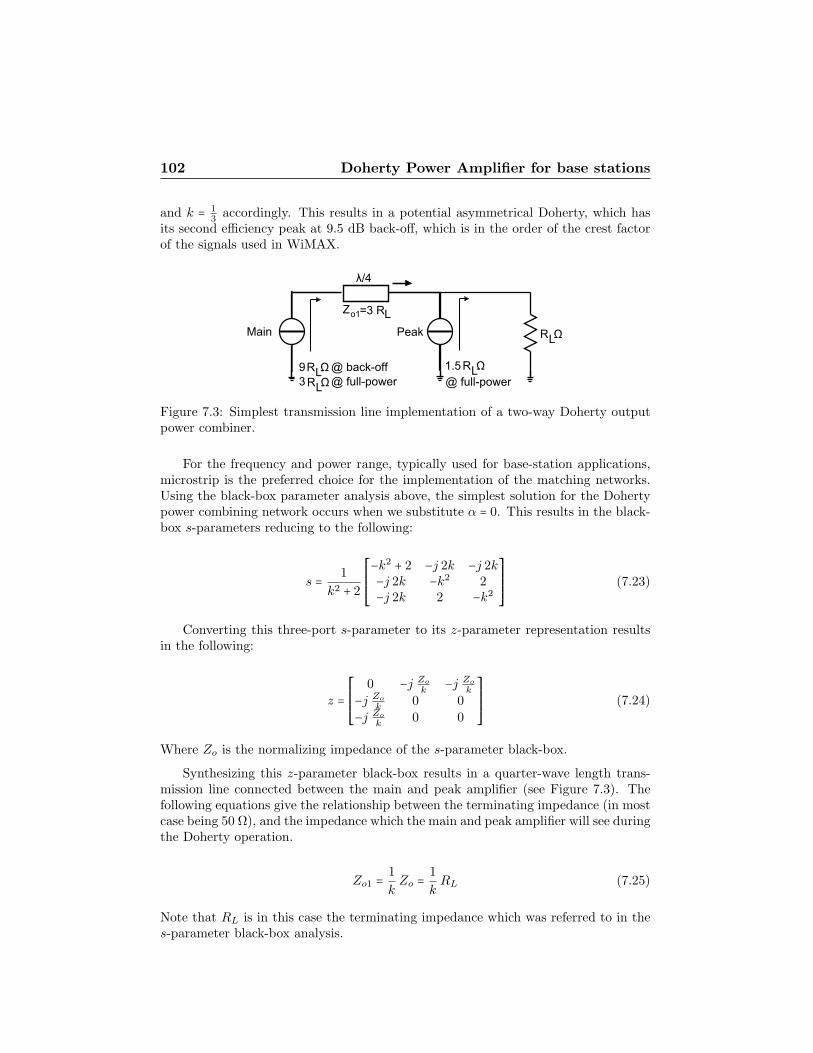
102 Doherty Power Amplifier for base stations
and k = 13
accordingly. This results in a potential asymmetrical Doherty, which hasits second efficiency peak at 9.5 dB back-off, which is in the order of the crest factorof the signals used in WiMAX.
Figure 7.3: Simplest transmission line implementation of a two-way Doherty outputpower combiner.
For the frequency and power range, typically used for base-station applications,microstrip is the preferred choice for the implementation of the matching networks.Using the black-box parameter analysis above, the simplest solution for the Dohertypower combining network occurs when we substitute α = 0. This results in the black-box s-parameters reducing to the following:
s = 1
k2 + 2
⎡⎢⎢⎢⎢⎢⎣
−k2 + 2 −j 2k −j 2k
−j 2k −k2 2−j 2k 2 −k2
⎤⎥⎥⎥⎥⎥⎦(7.23)
Converting this three-port s-parameter to its z-parameter representation resultsin the following:
z =⎡⎢⎢⎢⎢⎢⎣
0 −j Zo
k−j Zo
k−j Zo
k0 0
−j Zo
k0 0
⎤⎥⎥⎥⎥⎥⎦(7.24)
Where Zo is the normalizing impedance of the s-parameter black-box.
Synthesizing this z-parameter black-box results in a quarter-wave length trans-mission line connected between the main and peak amplifier (see Figure 7.3). Thefollowing equations give the relationship between the terminating impedance (in mostcase being 50 Ω), and the impedance which the main and peak amplifier will see duringthe Doherty operation.
Zo1 = 1
kZo = 1
kRL (7.25)
Note that RL is in this case the terminating impedance which was referred to in thes-parameter black-box analysis.
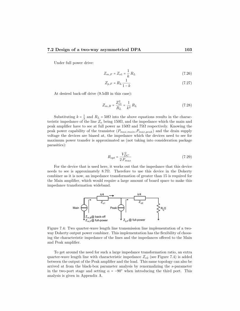
7.2 Design of a two-way asymmetrical DPA 103
Under full power drive:
Zm,F = Zo1 = 1
kRL (7.26)
Zp,F = RL
1
1 − k(7.27)
At desired back-off drive (9.5dB in this case):
Zm,B = Z2o1
RL
= 1
k2RL (7.28)
Substituting k = 13
and RL = 50Ω into the above equations results in the charac-teristic impedance of the line Zo being 150Ω, and the impedance which the main andpeak amplifier have to see at full power as 150Ω and 75Ω respectively. Knowing thepeak power capability of the transistor (Pmax,main,Pmax,peak) and the drain supplyvoltage the devices are biased at, the impedance which the devices need to see formaximum power transfer is approximated as (not taking into consideration packageparasitics):
Ropt = V 2DC
2Pmax
(7.29)
For the device that is used here, it works out that the impedance that this deviceneeds to see is approximately 8.7Ω. Therefore to use this device in the Dohertycombiner as it is now, an impedance transformation of greater than 15 is required forthe Main amplifier, which would require a large amount of board space to make thisimpedance transformation wideband.
Figure 7.4: Two quarter-wave length line transmission line implementation of a two-way Doherty output power combiner. This implementation has the flexibility of choos-ing the characteristic impedance of the lines and the impedances offered to the Mainand Peak amplifier.
To get around the need for such a large impedance transformation ratio, an extraquarter-wave length line with characteristic impedance Zo2 (see Figure 7.4) is addedbetween the output of the Peak amplifier and the load. This same topology can also bearrived at from the black-box parameter analysis by renormalizing the s-parameterin the two-port stage and setting α = −90○ when introducing the third port. Thisanalysis is given in Appendix A.
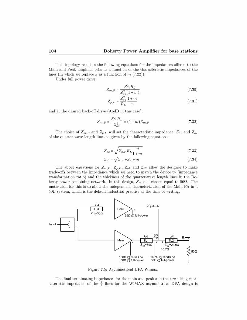
104 Doherty Power Amplifier for base stations
This topology result in the following equations for the impedances offered to theMain and Peak amplifier cells as a function of the characteristic impedances of thelines (in which we replace k as a function of m (7.22)).
Under full power drive:
Zm,F = Z2o1RL
Z2o2(1 +m) (7.30)
Zp,F = Z2o2
RL
1 +m
m(7.31)
and at the desired back-off drive (9.5dB in this case):
Zm,B = Z2o1RL
Z2o2
= (1 +m)Zm,F (7.32)
The choice of Zm,F and Zp,F will set the characteristic impedance, Zo1 and Zo2
of the quarter-wave length lines as given by the following equations:
Zo2 =√
Zp,F RL
m
1 +m(7.33)
Zo1 = √Zm,F Zp,F m (7.34)
The above equations for Zm,F , Zp,F , Zo1 and Z02 allow the designer to maketrade-offs between the impedance which we need to match the device to (impedancetransformation ratio) and the thickness of the quarter-wave length lines in the Do-herty power combining network. In this design, Zm,F is chosen equal to 50Ω. Themotivation for this is to allow the independent characterization of the Main PA in a50Ω system, which is the default industrial practise at the time of writing.
Figure 7.5: Asymmetrical DPA Wimax.
The final terminating impedances for the main and peak and their resulting char-acteristic impedance of the λ
4lines for the WiMAX asymmetrical DPA design is
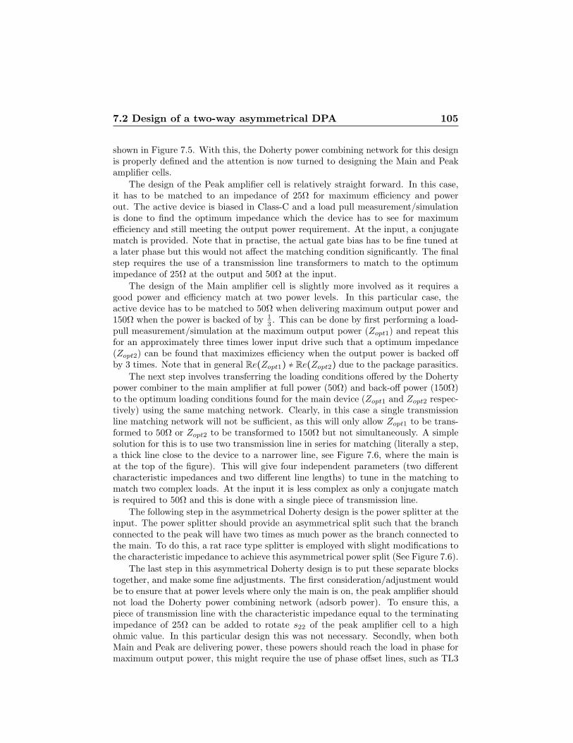
7.2 Design of a two-way asymmetrical DPA 105
shown in Figure 7.5. With this, the Doherty power combining network for this designis properly defined and the attention is now turned to designing the Main and Peakamplifier cells.
The design of the Peak amplifier cell is relatively straight forward. In this case,it has to be matched to an impedance of 25Ω for maximum efficiency and powerout. The active device is biased in Class-C and a load pull measurement/simulationis done to find the optimum impedance which the device has to see for maximumefficiency and still meeting the output power requirement. At the input, a conjugatematch is provided. Note that in practise, the actual gate bias has to be fine tuned ata later phase but this would not affect the matching condition significantly. The finalstep requires the use of a transmission line transformers to match to the optimumimpedance of 25Ω at the output and 50Ω at the input.
The design of the Main amplifier cell is slightly more involved as it requires agood power and efficiency match at two power levels. In this particular case, theactive device has to be matched to 50Ω when delivering maximum output power and150Ω when the power is backed of by 1
3. This can be done by first performing a load-
pull measurement/simulation at the maximum output power (Zopt1) and repeat thisfor an approximately three times lower input drive such that a optimum impedance(Zopt2) can be found that maximizes efficiency when the output power is backed offby 3 times. Note that in general Re(Zopt1) ≠ Re(Zopt2) due to the package parasitics.
The next step involves transferring the loading conditions offered by the Dohertypower combiner to the main amplifier at full power (50Ω) and back-off power (150Ω)to the optimum loading conditions found for the main device (Zopt1 and Zopt2 respec-tively) using the same matching network. Clearly, in this case a single transmissionline matching network will not be sufficient, as this will only allow Zopt1 to be trans-formed to 50Ω or Zopt2 to be transformed to 150Ω but not simultaneously. A simplesolution for this is to use two transmission line in series for matching (literally a step,a thick line close to the device to a narrower line, see Figure 7.6, where the main isat the top of the figure). This will give four independent parameters (two differentcharacteristic impedances and two different line lengths) to tune in the matching tomatch two complex loads. At the input it is less complex as only a conjugate matchis required to 50Ω and this is done with a single piece of transmission line.
The following step in the asymmetrical Doherty design is the power splitter at theinput. The power splitter should provide an asymmetrical split such that the branchconnected to the peak will have two times as much power as the branch connected tothe main. To do this, a rat race type splitter is employed with slight modifications tothe characteristic impedance to achieve this asymmetrical power split (See Figure 7.6).
The last step in this asymmetrical Doherty design is to put these separate blockstogether, and make some fine adjustments. The first consideration/adjustment wouldbe to ensure that at power levels where only the main is on, the peak amplifier shouldnot load the Doherty power combining network (adsorb power). To ensure this, apiece of transmission line with the characteristic impedance equal to the terminatingimpedance of 25Ω can be added to rotate s22 of the peak amplifier cell to a highohmic value. In this particular design this was not necessary. Secondly, when bothMain and Peak are delivering power, these powers should reach the load in phase formaximum output power, this might require the use of phase offset lines, such as TL3
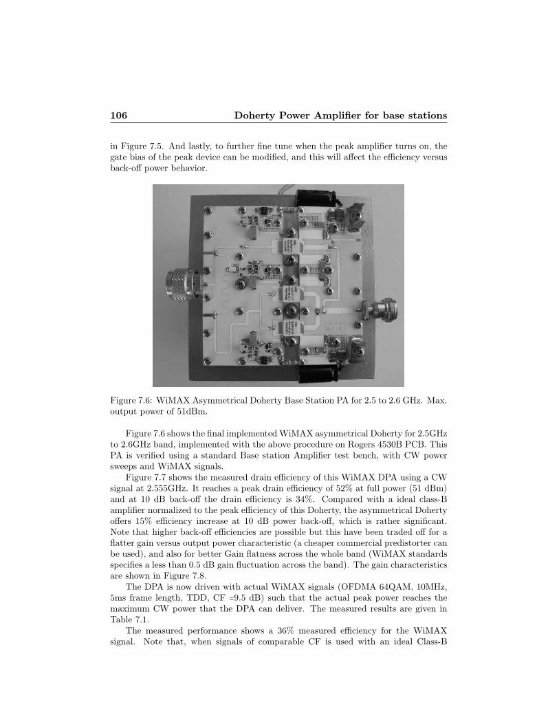
106 Doherty Power Amplifier for base stations
in Figure 7.5. And lastly, to further fine tune when the peak amplifier turns on, thegate bias of the peak device can be modified, and this will affect the efficiency versusback-off power behavior.
Figure 7.6: WiMAX Asymmetrical Doherty Base Station PA for 2.5 to 2.6 GHz. Max.output power of 51dBm.
Figure 7.6 shows the final implemented WiMAX asymmetrical Doherty for 2.5GHzto 2.6GHz band, implemented with the above procedure on Rogers 4530B PCB. ThisPA is verified using a standard Base station Amplifier test bench, with CW powersweeps and WiMAX signals.
Figure 7.7 shows the measured drain efficiency of this WiMAX DPA using a CWsignal at 2.555GHz. It reaches a peak drain efficiency of 52% at full power (51 dBm)and at 10 dB back-off the drain efficiency is 34%. Compared with a ideal class-Bamplifier normalized to the peak efficiency of this Doherty, the asymmetrical Dohertyoffers 15% efficiency increase at 10 dB power back-off, which is rather significant.Note that higher back-off efficiencies are possible but this have been traded off for aflatter gain versus output power characteristic (a cheaper commercial predistorter canbe used), and also for better Gain flatness across the whole band (WiMAX standardsspecifies a less than 0.5 dB gain fluctuation across the band). The gain characteristicsare shown in Figure 7.8.
The DPA is now driven with actual WiMAX signals (OFDMA 64QAM, 10MHz,5ms frame length, TDD, CF =9.5 dB) such that the actual peak power reaches themaximum CW power that the DPA can deliver. The measured results are given inTable 7.1.
The measured performance shows a 36% measured efficiency for the WiMAXsignal. Note that, when signals of comparable CF is used with an ideal Class-B
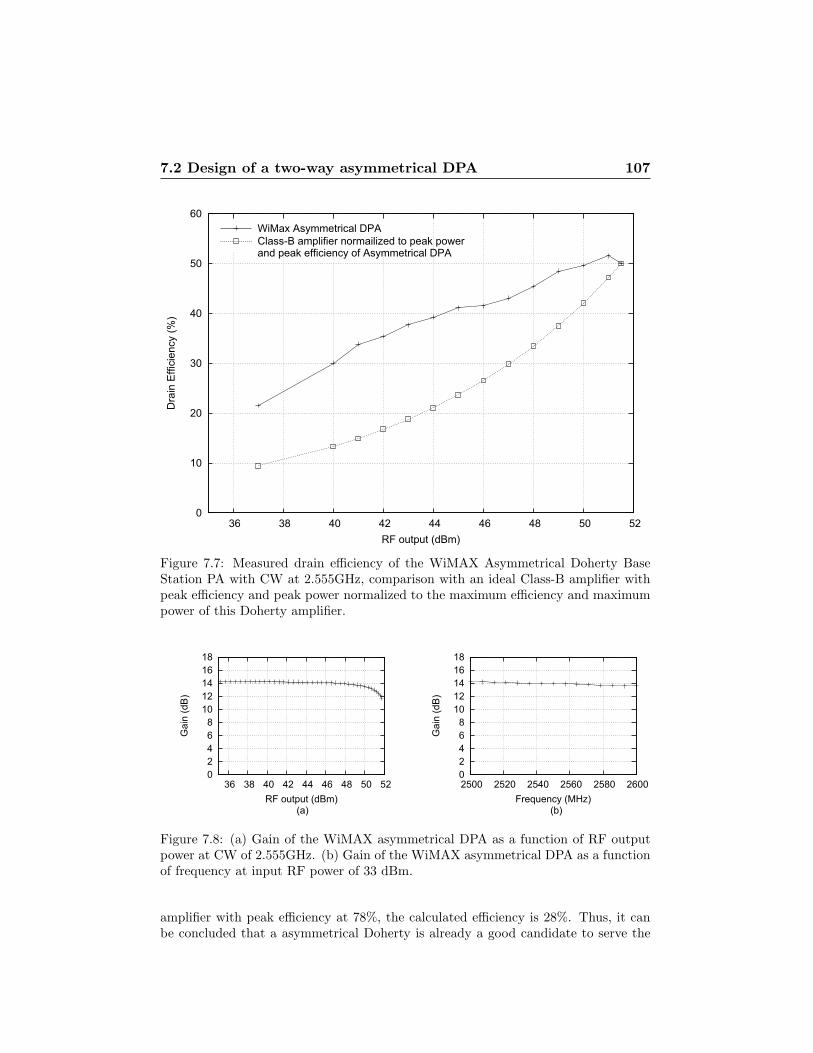
7.2 Design of a two-way asymmetrical DPA 107
0
10
20
30
40
50
60
36 38 40 42 44 46 48 50 52
Dra
in E
ffici
ency
(%)
RF output (dBm)
WiMax Asymmetrical DPAClass-B amplifier normailized to peak powerand peak efficiency of Asymmetrical DPA
Figure 7.7: Measured drain efficiency of the WiMAX Asymmetrical Doherty BaseStation PA with CW at 2.555GHz, comparison with an ideal Class-B amplifier withpeak efficiency and peak power normalized to the maximum efficiency and maximumpower of this Doherty amplifier.
0 2 4 6 8
10 12 14 16 18
36 38 40 42 44 46 48 50 52
Gai
n (d
B)
RF output (dBm)(a) (b)
0 2 4 6 8
10 12 14 16 18
2500 2520 2540 2560 2580 2600
Gai
n (d
B)
Frequency (MHz)
Figure 7.8: (a) Gain of the WiMAX asymmetrical DPA as a function of RF outputpower at CW of 2.555GHz. (b) Gain of the WiMAX asymmetrical DPA as a functionof frequency at input RF power of 33 dBm.
amplifier with peak efficiency at 78%, the calculated efficiency is 28%. Thus, it canbe concluded that a asymmetrical Doherty is already a good candidate to serve the
108 Doherty Power Amplifier for base stations
Table 7.1: Measured performance of the WiMAX asymmetrical Doherty with WiMAXsignals (Center Freq=2.555 GHZ ΔFreq =10 MHz CF≈9.5 dB)
Parameters Performance
Peak Power 52 dBm
Average Power 42 dBm
Drain Efficiency 36%
ACP @ 10 MHz -30 dBc
EVM -24 dB
Gain 14 dB
base-station market for 3G and beyond applications. In the coming sections, thefocus is turned to the three-way Doherty, which can provide even better efficienciesfor signals with this or higher CF.
7.3 Three-way Doherty Analysis
The analysis that was performed on the two-way DPA in section 7.1 can be extended toa three or even N-way DPA. As the whole analysis is based on working with black-boxparameters, going to a N-way DPA simply implies dealing with larger matrices andsolving a larger system of equations. To demonstrate the scalability of this approach,the following will show the analysis of a three-way DPA using the concepts describedin section 7.1.
The first step in the analysis is again the reduction of the number of network portsby “absorbing” the output load as part of the network. In Figure 7.9, this reducesa four-port network problem to a three-port problem. Next the RF output voltagesare expressed as currents of the main, peaking 1 and peaking 2 devices, through thethree-port z-parameters, at each of the desired efficiency peaks (see Figure 7.10),namely at full power (F ), first back-off point (B1) and second back-off point (B2);
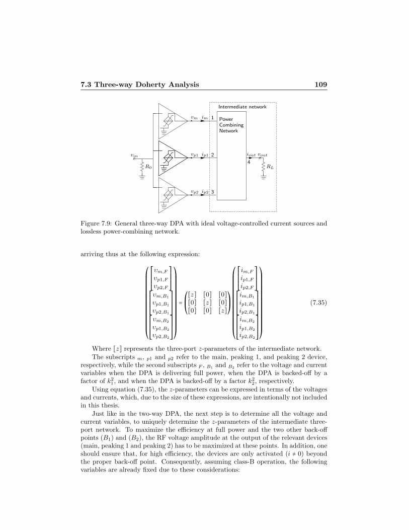
7.3 Three-way Doherty Analysis 109
imvm
ip1vp1
Intermediate network
PowerCombiningNetwork
ip2
iout vout
vp2
vin
R0 RL
1
4
2
3
Figure 7.9: General three-way DPA with ideal voltage-controlled current sources andlossless power-combining network.
arriving thus at the following expression:
⎛⎜⎜⎜⎜⎜⎜⎜⎜⎜⎜⎜⎜⎜⎜⎜⎝
⎡⎢⎢⎢⎢⎢⎣
υm,F
υp1,F
υp2,F
⎤⎥⎥⎥⎥⎥⎦⎡⎢⎢⎢⎢⎢⎣
υm,B1
υp1,B1
υp2,B1
⎤⎥⎥⎥⎥⎥⎦⎡⎢⎢⎢⎢⎢⎣
υm,B2
υp1,B2
υp2,B2
⎤⎥⎥⎥⎥⎥⎦
⎞⎟⎟⎟⎟⎟⎟⎟⎟⎟⎟⎟⎟⎟⎟⎟⎠
= ⎛⎜⎝[z] [0] [0][0] [z] [0][0] [0] [z]
⎞⎟⎠
⎛⎜⎜⎜⎜⎜⎜⎜⎜⎜⎜⎜⎜⎜⎜⎜⎝
⎡⎢⎢⎢⎢⎢⎣
im,F
ip1,F
ip2,F
⎤⎥⎥⎥⎥⎥⎦⎡⎢⎢⎢⎢⎢⎣
im,B1
ip1,B1
ip2,B1
⎤⎥⎥⎥⎥⎥⎦⎡⎢⎢⎢⎢⎢⎣
im,B2
ip1,B2
ip2,B2
⎤⎥⎥⎥⎥⎥⎦
⎞⎟⎟⎟⎟⎟⎟⎟⎟⎟⎟⎟⎟⎟⎟⎟⎠
(7.35)
Where [z] represents the three-port z-parameters of the intermediate network.The subscripts m, p1 and p2 refer to the main, peaking 1, and peaking 2 device,
respectively, while the second subscripts F , B1and B2
refer to the voltage and currentvariables when the DPA is delivering full power, when the DPA is backed-off by afactor of k2
1, and when the DPA is backed-off by a factor k22, respectively.
Using equation (7.35), the z-parameters can be expressed in terms of the voltagesand currents, which, due to the size of these expressions, are intentionally not includedin this thesis.
Just like in the two-way DPA, the next step is to determine all the voltage andcurrent variables, to uniquely determine the z-parameters of the intermediate three-port network. To maximize the efficiency at full power and the two other back-offpoints (B1) and (B2), the RF voltage amplitude at the output of the relevant devices(main, peaking 1 and peaking 2) has to be maximized at these points. In addition, oneshould ensure that, for high efficiency, the devices are only activated (i ≠ 0) beyondthe proper back-off point. Consequently, assuming class-B operation, the followingvariables are already fixed due to these considerations:

110 Doherty Power Amplifier for base stations
∣υm,F ∣ = ∣υm,B1∣ = ∣υm,B2
∣ = Vdc (7.36)
∣υp1,F ∣ = ∣υp1,B1∣ = Vdc (7.37)
∣υp2,F ∣ = Vdc (7.38)
ip1,B2= 0 (7.39)
ip2,B1= ip2,B2
= 0 (7.40)
The following shows the nine unknown variables left to solve, for the three-wayDoherty power amplifier:
im,F , im,B1, im,B2
, ip1,B1, ip2,F , υp1,B2
, υp2,B1, υp2,B2
(7.41)
Again, the output power of the three-way DPA, assuming a lossless power-combiningnetwork, can be expressed as a function of the voltage and current variables.
pout = 1
2Re (υmi∗m + υp1i
∗p1 + υp2i
∗p2) (7.42)
Here too, high efficiency is only achieved when the current and voltage related toa specific device (e.g., υm,F and im,F ) are in phase, yielding maximum (real) powerdelivered to the load. Next the power back-off/full-power ratios are specified as:
k21 = pout,B1
pout,F
= Re (υm,B1i∗m,B1
+ υp1,B1i∗p1,B1
)Re (υm,F i∗m,F + υp1,F i∗p1,F + υp2,F i∗p2,F
) (7.43)
k22 = pout,B2
pout,F
= Re (υm,B2i∗m,B2
)Re (υm,F i∗m,F + υp1,F i∗p1,F + υp2,F i∗p2,F
) (7.44)
Furthermore, assuming a linear dependency of the current source on the RF inputvoltage when the active device is turned on, the following current relationships canbe written:
im,B1= im,F ⋅ k1 (7.45)
im,B2= im,F ⋅ k2 (7.46)
ip1,B1= ip1,F (k1 − k2
1 − k2
) (7.47)
At this stage, similar to the two-way DPA, the reciprocal properties of the in-termediate network (z12 = z21, z23 = z32, z13 = z31) are used to complete the set ofequations to solve for the 9 unknowns.
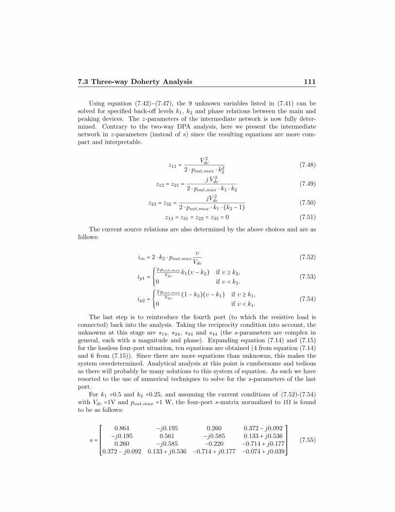
7.3 Three-way Doherty Analysis 111
Using equation (7.42)−(7.47), the 9 unknown variables listed in (7.41) can besolved for specified back-off levels k1, k2 and phase relations between the main andpeaking devices. The z-parameters of the intermediate network is now fully deter-mined. Contrary to the two-way DPA analysis, here we present the intermediatenetwork in z-parameters (instead of s) since the resulting equations are more com-pact and interpretable.
z11 = V 2dc
2 ⋅ pout,max ⋅ k22
(7.48)
z12 = z21 = j V 2dc
2 ⋅ pout,max ⋅ k1 ⋅ k2
(7.49)
z23 = z32 = jV 2dc
2 ⋅ pout,max ⋅ k1 ⋅ (k2 − 1) (7.50)
z13 = z31 = z22 = z33 = 0 (7.51)
The current source relations are also determined by the above choices and are asfollows:
im = 2 ⋅ k2 ⋅ pout,max
υ
Vdc
(7.52)
ip1 =⎧⎪⎪⎨⎪⎪⎩
2⋅pout,max
Vdck1(υ − k2) if υ ≥ k2,
0 if υ < k2.(7.53)
ip2 =⎧⎪⎪⎨⎪⎪⎩
2⋅pout,max
Vdc(1 − k2)(υ − k1) if υ ≥ k1,
0 if υ < k1.(7.54)
The last step is to reintroduce the fourth port (to which the resistive load isconnected) back into the analysis. Taking the reciprocity condition into account, theunknowns at this stage are s14, s24, s34 and s44 (the s-parameters are complex ingeneral, each with a magnitude and phase). Expanding equation (7.14) and (7.15)for the lossless four-port situation, ten equations are obtained (4 from equation (7.14)and 6 from (7.15)). Since there are more equations than unknowns, this makes thesystem overdetermined. Analytical analysis at this point is cumbersome and tediousas there will probably be many solutions to this system of equation. As such we haveresorted to the use of numerical techniques to solve for the s-parameters of the lastport.
For k1 =0.5 and k2 =0.25, and assuming the current conditions of (7.52)-(7.54)with Vdc =1V and pout,max =1 W, the four-port s-matrix normalized to 1Ω is foundto be as follows:
s =⎡⎢⎢⎢⎢⎢⎢⎢⎣
0.864 −j0.195 0.260 0.372 − j0.092−j0.195 0.561 −j0.585 0.133 + j0.5360.260 −j0.585 −0.220 −0.714 + j0.177
0.372 − j0.092 0.133 + j0.536 −0.714 + j0.177 −0.074 + j0.039
⎤⎥⎥⎥⎥⎥⎥⎥⎦(7.55)
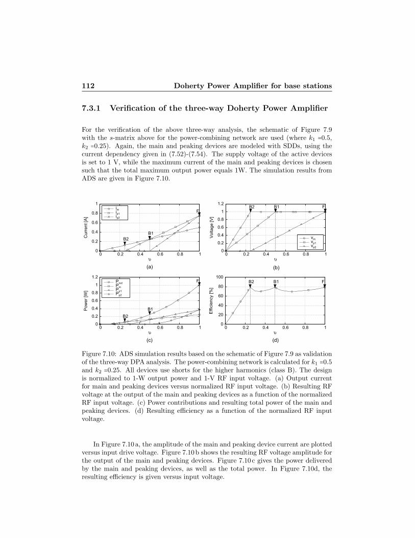
112 Doherty Power Amplifier for base stations
7.3.1 Verification of the three-way Doherty Power Amplifier
For the verification of the above three-way analysis, the schematic of Figure 7.9with the s-matrix above for the power-combining network are used (where k1 =0.5,k2 =0.25). Again, the main and peaking devices are modeled with SDDs, using thecurrent dependency given in (7.52)-(7.54). The supply voltage of the active devicesis set to 1 V, while the maximum current of the main and peaking devices is chosensuch that the total maximum output power equals 1W. The simulation results fromADS are given in Figure 7.10.
0
0.2
0.4
0.6
0.8
1
0 0.2 0.4 0.6 0.8 1
Cur
rent
[A]
υ
B1B2
Fimip1ip2
0
0.2
0.4
0.6
0.8
1
1.2
0 0.2 0.4 0.6 0.8 1
Vol
tage
[V]
υ
B1B2 F
vmvp1vp2
0
0.2
0.4
0.6
0.8
1
1.2
0 0.2 0.4 0.6 0.8 1
Pow
er [W
]
υ
B1B2
FPoutPmPp1Pp2
0
20
40
60
80
100
0 0.2 0.4 0.6 0.8 1
Effi
cien
cy [%
]
υ
B1B2 F
(a) (b)
(c) (d)
Figure 7.10: ADS simulation results based on the schematic of Figure 7.9 as validationof the three-way DPA analysis. The power-combining network is calculated for k1 =0.5and k2 =0.25. All devices use shorts for the higher harmonics (class B). The designis normalized to 1-W output power and 1-V RF input voltage. (a) Output currentfor main and peaking devices versus normalized RF input voltage. (b) Resulting RFvoltage at the output of the main and peaking devices as a function of the normalizedRF input voltage. (c) Power contributions and resulting total power of the main andpeaking devices. (d) Resulting efficiency as a function of the normalized RF inputvoltage.
In Figure 7.10 a, the amplitude of the main and peaking device current are plottedversus input drive voltage. Figure 7.10b shows the resulting RF voltage amplitude forthe output of the main and peaking devices. Figure 7.10 c gives the power deliveredby the main and peaking devices, as well as the total power. In Figure 7.10d, theresulting efficiency is given versus input voltage.
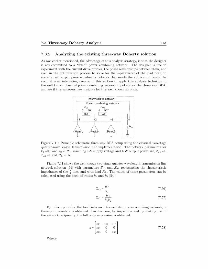
7.3 Three-way Doherty Analysis 113
7.3.2 Analyzing the existing three-way Doherty solution
As was earlier mentioned, the advantage of this analysis strategy, is that the designeris not committed to a “fixed” power combining network. The designer is free toexperiment with the current drive profiles, the phase relationships between them, andeven in the optimization process to solve for the s-parameter of the load port, toarrive at an output power-combining network that meets the application needs. Assuch, it is an interesting exercise in this section to apply this analysis technique tothe well known classical power-combining network topology for the three-way DPA,and see if this uncovers new insights for this well known solution.
Peak1 Peak2
1 2 3 4
Main
TL1 TL2θ = 90◦Z01
θ = 90◦Z02
RL
Power combining network
Intermediate network
Figure 7.11: Principle schematic three-way DPA setup using the classical two-stagequarter-wave length transmission line implementation. The network parameters fork1 =0.5 and k2 =0.25, assuming 1-V supply voltage and 1-W output power are, Zo1 =4,Zo2 =1 and RL =0.5.
Figure 7.11 shows the well-known two-stage quarter-wavelength transmission linenetwork solution [54] with parameters Zo1 and Z02 representing the characteristicimpedances of the λ
4lines and with load RL. The values of these parameters can be
calculated using the back-off ratios k1 and k2 [54]:
Zo2 = RL
k1
(7.56)
Zo1 = RL
k1k2
(7.57)
By reincorporating the load into an intermediate power-combining network, athree-port z-matrix is obtained. Furthermore, by inspection and by making use ofthe network reciprocity, the following expression is obtained:
z =⎡⎢⎢⎢⎢⎢⎣
z11 z12 z13
z12 0 0z13 0 z33
⎤⎥⎥⎥⎥⎥⎦(7.58)
Where
114 Doherty Power Amplifier for base stations
z11 = (Zo1
Zo2
)2
RL (7.59)
z12 = −jZo1 (7.60)
z13 = − Zo2
Zo1RL
(7.61)
z33 = RL (7.62)
To maximize the efficiency under full power and the two back-off conditions, thevoltage and current variables are chosen as in the prior analysis. In this classicalDPA implementation, the phase relations of the main and peaking amplifiers aredetermined by the network topology and expressed relative to the main amplifier,yielding:
υm,F = υm,P1 = υm,B2 = Vdc (7.63)
υp1,F = υp1,B1 = −jVdc (7.64)
υp2,F = −Vdc (7.65)
ip1,B2 = 0 (7.66)
ip2,B2 = ip2,B1 = 0 (7.67)
At this juncture, substituting the above variables together with the z-parametersof the network into equation (7.35), and solving for the following nine remainingunknowns results in:
im,F = im,B1 = −j Vdc
z12
(7.68)
im,B2 = Vdc
z11
(7.69)
ip1,F = Vdc
z12
[(1 − z13
z33
) + j (z11
z12
+ z213
z33z21
)] (7.70)
ip1,B1 = Vdc
z12
(1 + jz11
z12
) (7.71)
ip2,F = Vdc
z33
(1 − jz13
z12
) (7.72)
υp1,B2 = Vdc
z12
z11
(7.73)
υp2,B1 = −j Vdc
z13
z12
(7.74)
υp2,B2 = Vdc
z13
z11
(7.75)
Equation (7.68) shows that im,F = im,B1; this implies that the current provided by
the main device should be equal in magnitude when the three-way DPA is delivering
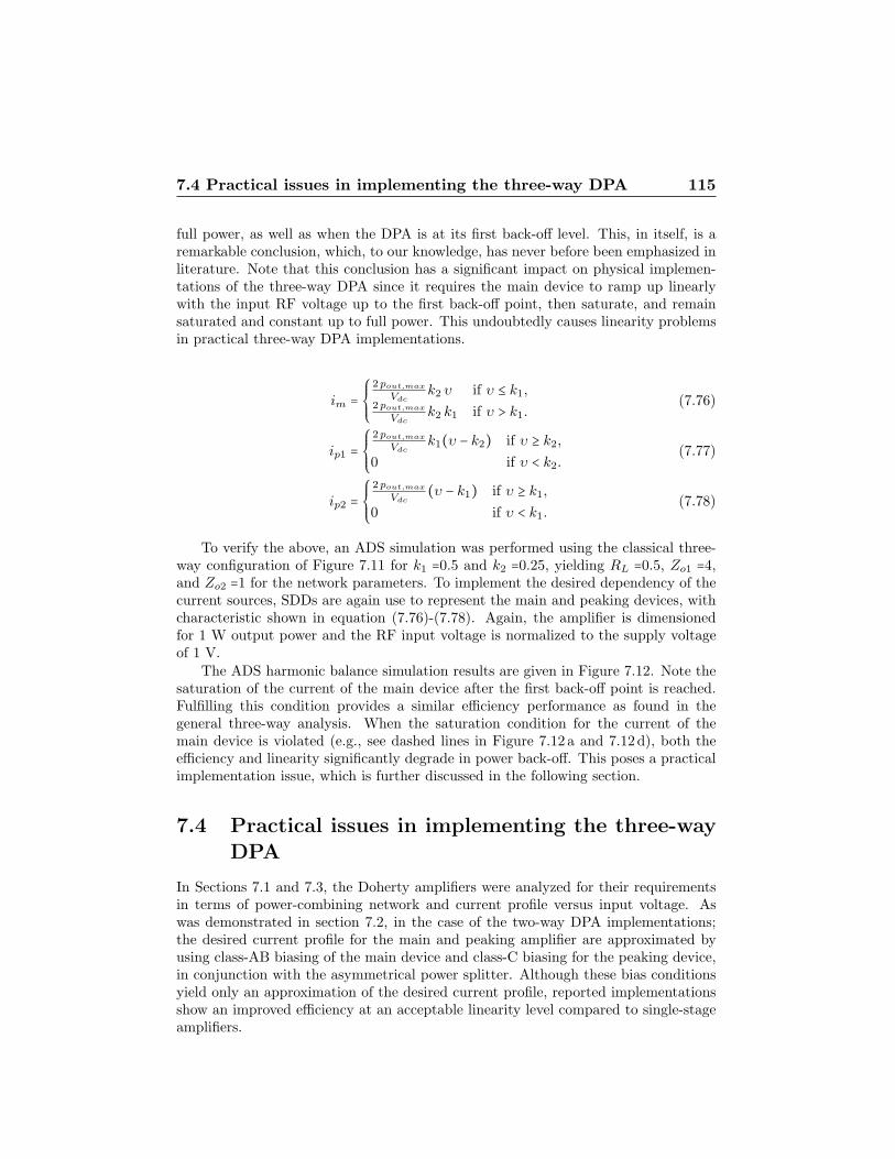
7.4 Practical issues in implementing the three-way DPA 115
full power, as well as when the DPA is at its first back-off level. This, in itself, is aremarkable conclusion, which, to our knowledge, has never before been emphasized inliterature. Note that this conclusion has a significant impact on physical implemen-tations of the three-way DPA since it requires the main device to ramp up linearlywith the input RF voltage up to the first back-off point, then saturate, and remainsaturated and constant up to full power. This undoubtedly causes linearity problemsin practical three-way DPA implementations.
im =⎧⎪⎪⎨⎪⎪⎩
2pout,max
Vdck2 υ if υ ≤ k1,
2pout,max
Vdck2 k1 if υ > k1.
(7.76)
ip1 =⎧⎪⎪⎨⎪⎪⎩
2pout,max
Vdck1(υ − k2) if υ ≥ k2,
0 if υ < k2.(7.77)
ip2 =⎧⎪⎪⎨⎪⎪⎩
2pout,max
Vdc(υ − k1) if υ ≥ k1,
0 if υ < k1.(7.78)
To verify the above, an ADS simulation was performed using the classical three-way configuration of Figure 7.11 for k1 =0.5 and k2 =0.25, yielding RL =0.5, Zo1 =4,and Zo2 =1 for the network parameters. To implement the desired dependency of thecurrent sources, SDDs are again use to represent the main and peaking devices, withcharacteristic shown in equation (7.76)-(7.78). Again, the amplifier is dimensionedfor 1 W output power and the RF input voltage is normalized to the supply voltageof 1 V.
The ADS harmonic balance simulation results are given in Figure 7.12. Note thesaturation of the current of the main device after the first back-off point is reached.Fulfilling this condition provides a similar efficiency performance as found in thegeneral three-way analysis. When the saturation condition for the current of themain device is violated (e.g., see dashed lines in Figure 7.12 a and 7.12d), both theefficiency and linearity significantly degrade in power back-off. This poses a practicalimplementation issue, which is further discussed in the following section.
7.4 Practical issues in implementing the three-way
DPA
In Sections 7.1 and 7.3, the Doherty amplifiers were analyzed for their requirementsin terms of power-combining network and current profile versus input voltage. Aswas demonstrated in section 7.2, in the case of the two-way DPA implementations;the desired current profile for the main and peaking amplifier are approximated byusing class-AB biasing of the main device and class-C biasing for the peaking device,in conjunction with the asymmetrical power splitter. Although these bias conditionsyield only an approximation of the desired current profile, reported implementationsshow an improved efficiency at an acceptable linearity level compared to single-stageamplifiers.
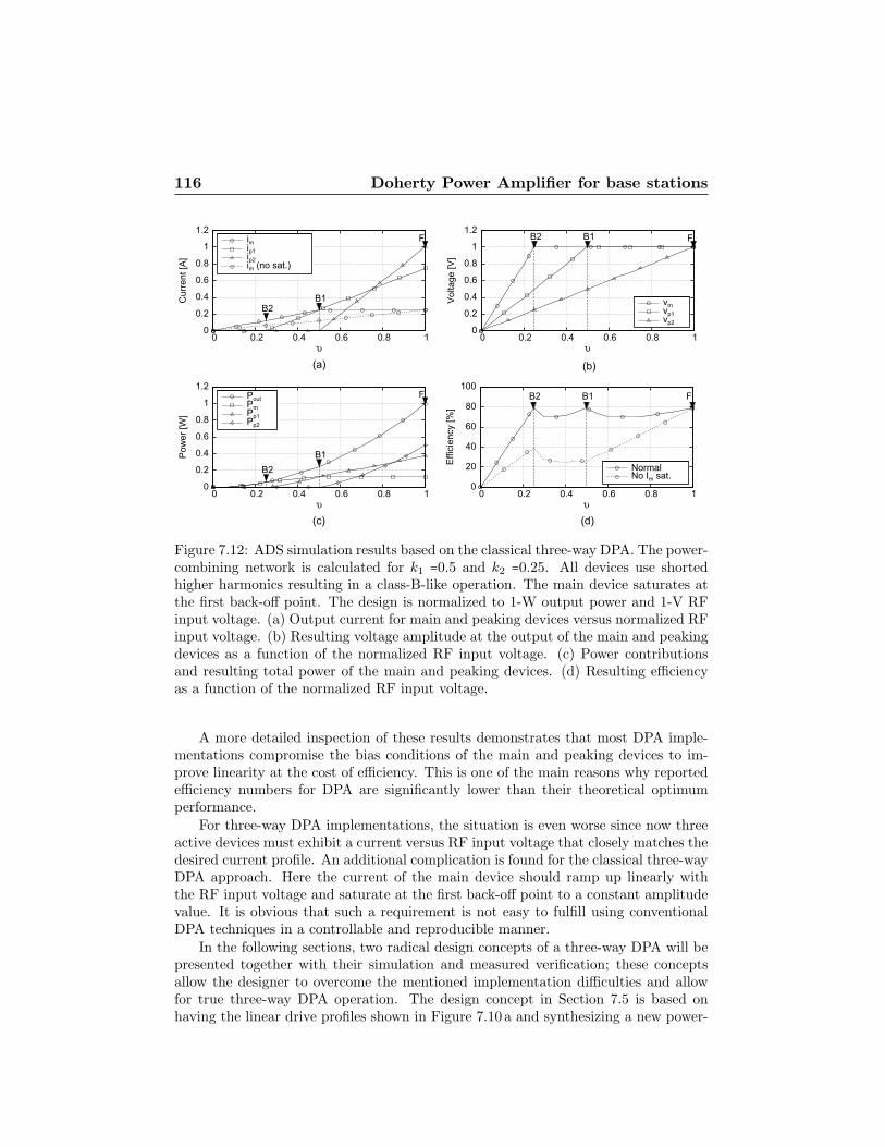
116 Doherty Power Amplifier for base stations
0
0.2
0.4
0.6
0.8
1
1.2
0 0.2 0.4 0.6 0.8 1
Cur
rent
[A]
υ
B1B2
Fimip1ip2im (no sat.)
0
0.2
0.4
0.6
0.8
1
1.2
0 0.2 0.4 0.6 0.8 1
Vol
tage
[V]
υ
B1B2 F
vmvp1vp2
0
0.2
0.4
0.6
0.8
1
1.2
0 0.2 0.4 0.6 0.8 1
Pow
er [W
]
υ
B1B2
FPoutPmPp1Pp2
0
20
40
60
80
100
0 0.2 0.4 0.6 0.8 1
Effi
cien
cy [%
]
υ
B1B2 F
NormalNo Im sat.
(a) (b)
(c) (d)
Figure 7.12: ADS simulation results based on the classical three-way DPA. The power-combining network is calculated for k1 =0.5 and k2 =0.25. All devices use shortedhigher harmonics resulting in a class-B-like operation. The main device saturates atthe first back-off point. The design is normalized to 1-W output power and 1-V RFinput voltage. (a) Output current for main and peaking devices versus normalized RFinput voltage. (b) Resulting voltage amplitude at the output of the main and peakingdevices as a function of the normalized RF input voltage. (c) Power contributionsand resulting total power of the main and peaking devices. (d) Resulting efficiencyas a function of the normalized RF input voltage.
A more detailed inspection of these results demonstrates that most DPA imple-mentations compromise the bias conditions of the main and peaking devices to im-prove linearity at the cost of efficiency. This is one of the main reasons why reportedefficiency numbers for DPA are significantly lower than their theoretical optimumperformance.
For three-way DPA implementations, the situation is even worse since now threeactive devices must exhibit a current versus RF input voltage that closely matches thedesired current profile. An additional complication is found for the classical three-wayDPA approach. Here the current of the main device should ramp up linearly withthe RF input voltage and saturate at the first back-off point to a constant amplitudevalue. It is obvious that such a requirement is not easy to fulfill using conventionalDPA techniques in a controllable and reproducible manner.
In the following sections, two radical design concepts of a three-way DPA will bepresented together with their simulation and measured verification; these conceptsallow the designer to overcome the mentioned implementation difficulties and allowfor true three-way DPA operation. The design concept in Section 7.5 is based onhaving the linear drive profiles shown in Figure 7.10 a and synthesizing a new power-


124 Doherty Power Amplifier for base stations
Peak 2 resulting in maximum efficiency. Furthermore, no more offset transmissionlines are required at the input to obtain the correct power combining at the output,as this can be easily taken care of in the digital domain.
To highlight the advantages of the mixed-signal approach, a three-way DPA usingthe traditional power combining network (see Section 7.3.2) will be designed. Notethat this choice allows the verification of the conclusions made in Section 7.3.2 withregards to the required current drive conditions for optimum three-way DPA behavior,as the mixed signal concept provides for the design of any arbitrary drive profile.Furthermore, this verification exercise will give a clear comparison with existing DPAsolutions. Note that this work is done in close collaboration with another PhD project(performed by Marco Pelk) which investigates innovative RF measurement setup andthe work has been published in [56].
7.6.1 Design of the Mixed-Signal three-way Doherty
The mixed-signal Doherty that will be prototyped here is targeted for UMTS base-stations at a center frequency of 2.14 GHz (same frequency as the “Linear” three-wayDoherty). The general design goal is to aim for a 100 Watt (peak power) amplifierwith gains above 10 dB and as high efficiency as possible when driven with a WCDMAsignal.
At present, LDMOS is still the preferred technology for base station power ampli-fiers due to its high reproducibility, good power handling, high-linearity and gain, butmost importantly, due to its low cost. However, over time it is expected that wide-bandgap materials like GaN will challenge the position of silicon LDMOS technology,since GaN can offer higher power densities and higher gain at microwave frequencies.To investigate these prospects, this Doherty prototype will be designed with GaNdevices and this will give a good indication of the potential of GaN technology forthree-way Doherty power amplifiers with improved efficiency in far back-off operationto better serve signals with very high crest factors.
Just like in two-way Asymmetrical Doherty and the “linear” three-way Doherty,the first step in the design procedure is to determine the relationship between thedevice sizes and the back-off powers B1 and B2 where the efficiency peaks of thethree-way Doherty occurs. Equation (7.92) which can be derived from the requireddrive profiles (see equation (7.76)-(7.78)) and the power relationships in back-off, givesthis relationships.
k1 = 1 +m1
1 +m1 +m2
, k2 = 1
1 +m1
(7.92)
If the back-off points B1 and B2 are desired to be at -6 dB (k1 = 0.5) and -12 dB(k2 = 0.25) respectively, the resulting required device size ratio will be 1:m1:m2=1:3:4.Unfortunately, in practical situations these device sizes are not always available. Alsofrom the GaN HEMT devices donated by CREE for this work, there were only twopower ratings available, namely: 15 W and 45 W. Consequently, the configurationthat approximates the intended device ratios best is 1:3:3. Substituting this intoequation (7.92) results in high-efficiency operation points being located at -4.9 dB and

7.6 The Mixed-Signal Three-Way Doherty 125
-12 dB power back-off respectively. Note that just like in the all the other Dohertyconcepts, this device size selection will fix also the load modulation ratios of the main(Υm) and peak1 device (Υp1). The following equations give these relationship.
Υm = (1 +m1)21 +m1 +m2
(7.93)
Υp1 = m1(1 +m1 +m2)m2
1 +m1 −m2
(7.94)
This yields Υm = 2.3 and Υp1 = 2.3, which are very favorable numbers comparedto the situation of the “linear” three-way Doherty ( Υm = 3 and Υp1 = 4) solutiondiscussed in Section 7.5. The next step is to find the proper trade-offs between thecharacteristic impedance and the loading impedances (impedance which the activedevice has to be matched to) required by the amplifier cells. For this purpose, thefollowing equations which relates the characteristic impedance of the lines in the powercombining network and the loading impedance of the Main, Peak 1 and Peak 2 arealso derived for the classical three-way DPA power combiner.
Z01 = √Zm,F ⋅Zp1,F ⋅m1 (7.95)
Z02 =√
Zp2,F ⋅Zp1,F ⋅m1 ⋅m2
(1 +m1)2 (7.96)
Z03 =√
Zp2,F ⋅RL ⋅m2
1 +m1 +m2
(7.97)
Where Zm,F , Zp1,F and Zp2,F are the impedances which we need to match the activedevice to for maximum power out, and they are given by the following equations.
Zm,F = Z203 ⋅Z2
01 ⋅ (1 +m1 +m2)Z2
02 ⋅RL ⋅ (1 +m1)2 (7.98)
Zp1,F = Z202 ⋅RL ⋅ (1 +m1)2
Z201 ⋅m1 ⋅ (1 +m1 +m2) (7.99)
Zp2,F = Z201 ⋅ (1 +m1 +m2)
RL ⋅m2
(7.100)
The following give the equations of the impedances that are offered to the Mainand Peak 1 amplifier in back-off, as a result of the load-modulation effect of thenetwork.At back-off 1:
Zm,B1 = Z203 ⋅Z2
01 ⋅ (1 +m1 +m2)Z2
02 ⋅RL ⋅ (1 +m1)2 (7.101)
Zp1,B1 = Z202 ⋅RL ⋅ (1 +m1)2
Z201[(1 +m1)2 − (1 +m1 +m2)] (7.102)
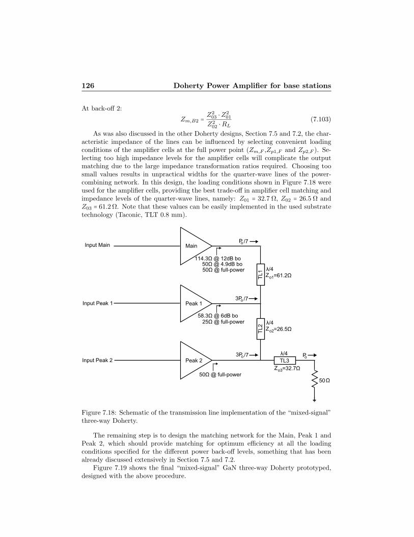
126 Doherty Power Amplifier for base stations
At back-off 2:
Zm,B2 = Z203 ⋅Z2
01
Z202 ⋅RL
(7.103)
As was also discussed in the other Doherty designs, Section 7.5 and 7.2, the char-acteristic impedance of the lines can be influenced by selecting convenient loadingconditions of the amplifier cells at the full power point (Zm,F ,Zp1,F and Zp2,F ). Se-lecting too high impedance levels for the amplifier cells will complicate the outputmatching due to the large impedance transformation ratios required. Choosing toosmall values results in unpractical widths for the quarter-wave lines of the power-combining network. In this design, the loading conditions shown in Figure 7.18 wereused for the amplifier cells, providing the best trade-off in amplifier cell matching andimpedance levels of the quarter-wave lines, namely: Z01 = 32.7 Ω, Z02 = 26.5 Ω andZ03 = 61.2 Ω. Note that these values can be easily implemented in the used substratetechnology (Taconic, TLT 0.8 mm).
Figure 7.18: Schematic of the transmission line implementation of the “mixed-signal”three-way Doherty.
The remaining step is to design the matching network for the Main, Peak 1 andPeak 2, which should provide matching for optimum efficiency at all the loadingconditions specified for the different power back-off levels, something that has beenalready discussed extensively in Section 7.5 and 7.2.
Figure 7.19 shows the final “mixed-signal” GaN three-way Doherty prototyped,designed with the above procedure.

7.6 The Mixed-Signal Three-Way Doherty 127
Figure 7.19: Hardware prototype of the “mixed-signal” GaN three-way Doherty.
7.6.2 Simulated Performance of the Mixed-Signal three-wayDoherty
After completion of the hardware design, it is still required to find the optimuminput drive conditions for the mixed-signal three-way Doherty to achieve maximumefficiency when driven with WCDMA signals. To address this problem, the single-tone DPA efficiency as function of power in the back-off region will be optimized.Note that this is a very effective approach, since once the probability distributionfunction (PDF) of a complex modulated signal is known, the average drain efficiency⟨ηd⟩ can be calculated based on the PDF and the DPA single-tone efficiency versuspower back-off [31], using equation (2.15) from Chapter 2.
In order to optimize the input drive signals of the DPA, also the phase relations(ϕpeak1 and ϕpeak2) between the amplifier cells need to be determined (this is donewith the offset transmission lines at the input for the “linear” three-way Doherty). Inpractice, the following three phase dependencies are considered:
1. Phases optimized at the full power condition.2. Optimization at the second backoff point.3. Phase optimization at all power levels.
Figure 7.20 shows the related simulated drain efficiencies. Also shown is the powerprobability distribution function (PDF) for the W-CDMA signal without de-crestingthat will be used later in the efficiency considerations.
By comparing the results of Figure 7.20 with DPA results found in literature[57, 58], it can be concluded that most conventional DPA implementations with apassive input power splitter use phase relations which are optimized for high-efficiencyat the maximum output power condition.
In order to make a careful selection of the optimum phase relations for driving theDPA, equation (2.15) is used with the efficiency curves of Figure 7.20 to calculate theW-CDMA efficiency performance for all three cases. The results of this calculation
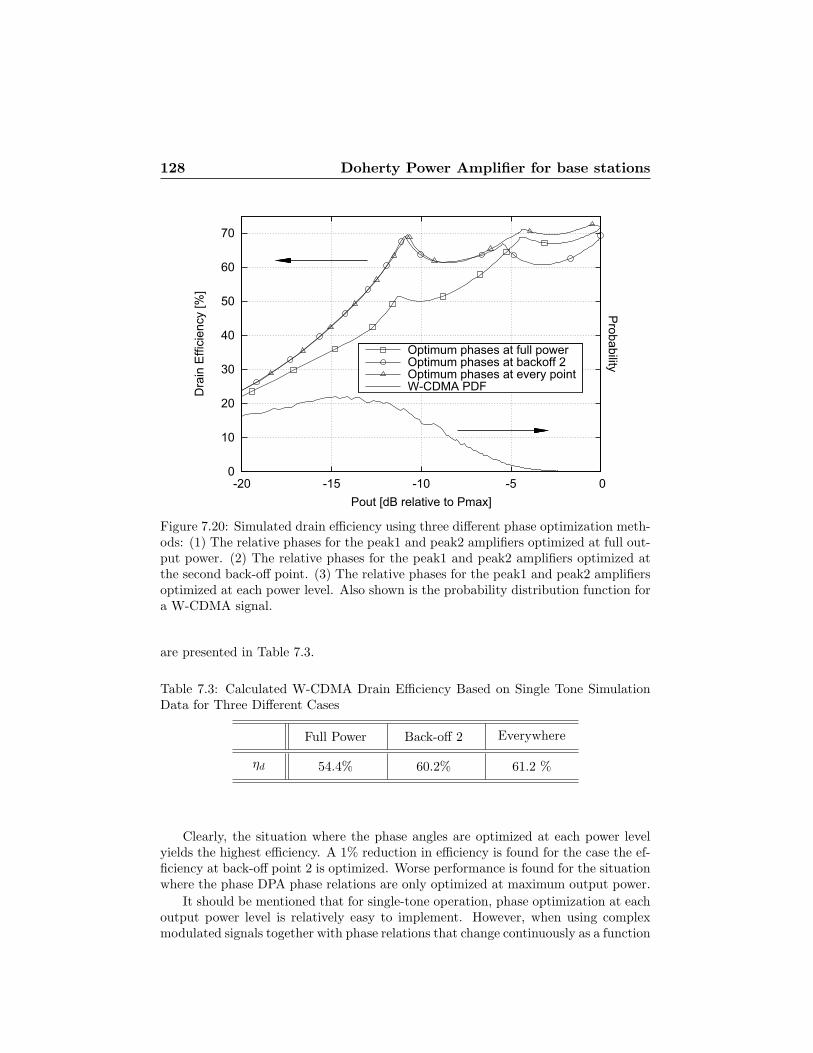
128 Doherty Power Amplifier for base stations
0
10
20
30
40
50
60
70
-20 -15 -10 -5 0
Dra
in E
ffici
ency
[%]
Probability
Pout [dB relative to Pmax]
Optimum phases at full powerOptimum phases at backoff 2Optimum phases at every pointW-CDMA PDF
Figure 7.20: Simulated drain efficiency using three different phase optimization meth-ods: (1) The relative phases for the peak1 and peak2 amplifiers optimized at full out-put power. (2) The relative phases for the peak1 and peak2 amplifiers optimized atthe second back-off point. (3) The relative phases for the peak1 and peak2 amplifiersoptimized at each power level. Also shown is the probability distribution function fora W-CDMA signal.
are presented in Table 7.3.
Table 7.3: Calculated W-CDMA Drain Efficiency Based on Single Tone SimulationData for Three Different Cases
Full Power Back-off 2 Everywhere
ηd 54.4% 60.2% 61.2 %
Clearly, the situation where the phase angles are optimized at each power levelyields the highest efficiency. A 1% reduction in efficiency is found for the case the ef-ficiency at back-off point 2 is optimized. Worse performance is found for the situationwhere the phase DPA phase relations are only optimized at maximum output power.
It should be mentioned that for single-tone operation, phase optimization at eachoutput power level is relatively easy to implement. However, when using complexmodulated signals together with phase relations that change continuously as a function

7.6 The Mixed-Signal Three-Way Doherty 129
of instantaneous power, this concept proves to be very difficult to implement. Thusto avoid too much computational overhead in signal processing for only 1% efficiencyimprovement, it is decided to restrict to the use of fixed but optimized phase relationsfor signals fed to the amplifier cells.
7.6.3 Mixed-signal three-way Doherty Experimental Verifica-tion
As mentioned above, this sort of three-input one-output PA concept is to the author’sknowledge new, and a custom test setup has to be built and used to verify the aboveconclusions. The description and feature of this prototype setup can be found in thework of M.Pelk [56].
Single tone Measurement of the “mixed-signal” three-way Doherty
From the simulations in Section 7.6.2, a good estimate is achieved for the powerlevels of the input signals for the main, peak 1 and peak 2 amplifiers, as well for therelative phases to reach maximum PAE at the 12 dB back-off point (38 dBm). Usingthese initial values as starting point in the MATLAB measurement optimization, theoptimum input powers and phase relations for maximum PAE are found. The sameprocedure is repeated at 4.9 dB back-off (45.1 dBm) and at full power (50 dBm).At each point optimizing the three input powers Pmain, Ppeak1, Ppeak2 and the tworelative phases ϕpeak1, ϕpeak2. Linear interpolation is used to obtain values betweenthese points. Note that this approach is almost equivalent to the use of optimized driveconditions at each power level, as discussed in the simulation section. The resultingPAE as function of normalized output power is plotted in Figure 7.21, indicating theupper bound for PAE that can be achieved with the “mixed-signal” GaN three-wayDoherty. Note the rather exceptional PAE performance as function of back-off power.
As a second experiment, the more simplistic drive condition with constant phaserelations between the amplifier cells is used. Doing so avoids the complication ofcontinuously varying phases in combination with complex modulated signals as dis-cussed in the simulation section. Consequently, the phase relations are kept constant,but their relative angles are optimized for maximum PAE at the 2nd power back-offpoint. The resulting PAE as function of back-off power is also plotted in Figure 7.21.Table 7.4 gives the resulting phases of ϕpeak1 and ϕpeak2 at the three high-efficiencypoints for both drive profiles.
It can be observed from this table that the phases are relatively close to thetheoretical values of −90○ and −180○ as one would expect for a three-way Dohertyamplifier.
It is clear that the curve with continuously optimized phase relations (Figure 7.21)indeed gives a better performance over the use of fixed phase relations at higher powerlevels. However, as discussed in the simulation section, this difference is not significantenough to justify a much more complicated signal processing when the DPA is drivenwith a complex modulated signal. Another reason why the fixed-phase drive conditionis preferred, is its more well-behaved gain-flatness (Figure 7.22), yielding a less criticalpredistortion.
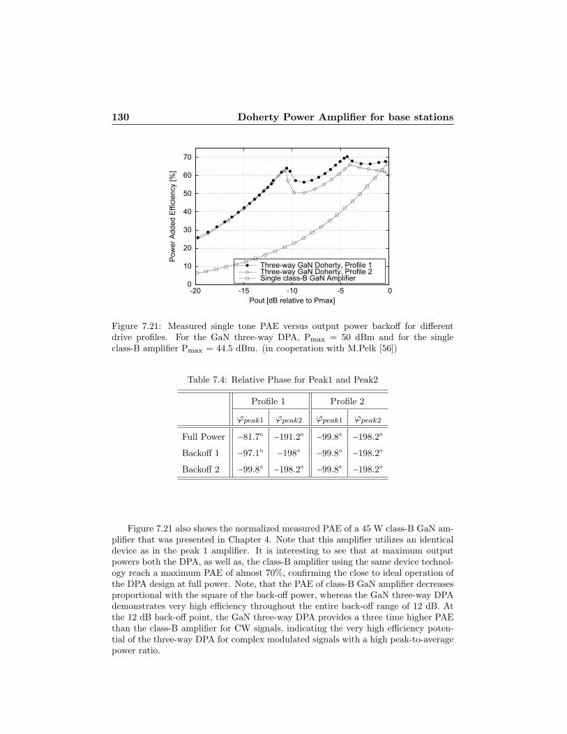
130 Doherty Power Amplifier for base stations
0
10
20
30
40
50
60
70
-20 -15 -10 -5 0
Pow
er A
dded
Effi
cien
cy [%
]
Pout [dB relative to Pmax]
Three-way GaN Doherty, Profile 1Three-way GaN Doherty, Profile 2Single class-B GaN Amplifier
Figure 7.21: Measured single tone PAE versus output power backoff for differentdrive profiles. For the GaN three-way DPA, Pmax = 50 dBm and for the singleclass-B amplifier Pmax = 44.5 dBm. (in cooperation with M.Pelk [56])
Table 7.4: Relative Phase for Peak1 and Peak2
Profile 1 Profile 2
ϕpeak1 ϕpeak2 ϕpeak1 ϕpeak2
Full Power −81.7○ −191.2○ −99.8○ −198.2○
Backoff 1 −97.1○ −198○ −99.8○ −198.2○
Backoff 2 −99.8○ −198.2○ −99.8○ −198.2○
Figure 7.21 also shows the normalized measured PAE of a 45 W class-B GaN am-plifier that was presented in Chapter 4. Note that this amplifier utilizes an identicaldevice as in the peak 1 amplifier. It is interesting to see that at maximum outputpowers both the DPA, as well as, the class-B amplifier using the same device technol-ogy reach a maximum PAE of almost 70%, confirming the close to ideal operation ofthe DPA design at full power. Note, that the PAE of class-B GaN amplifier decreasesproportional with the square of the back-off power, whereas the GaN three-way DPAdemonstrates very high efficiency throughout the entire back-off range of 12 dB. Atthe 12 dB back-off point, the GaN three-way DPA provides a three time higher PAEthan the class-B amplifier for CW signals, indicating the very high efficiency poten-tial of the three-way DPA for complex modulated signals with a high peak-to-averagepower ratio.
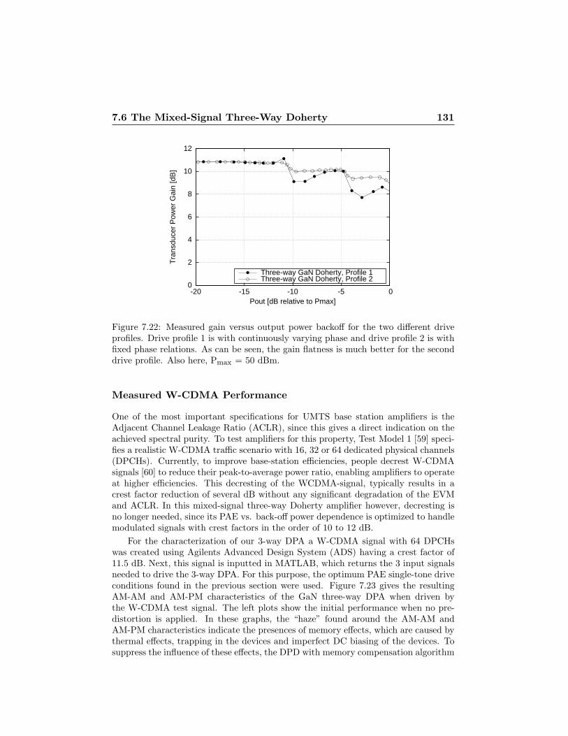
7.6 The Mixed-Signal Three-Way Doherty 131
0
2
4
6
8
10
12
-20 -15 -10 -5 0
Tra
nsdu
cer
Pow
er G
ain
[dB
]
Pout [dB relative to Pmax]
Three-way GaN Doherty, Profile 1Three-way GaN Doherty, Profile 2
Figure 7.22: Measured gain versus output power backoff for the two different driveprofiles. Drive profile 1 is with continuously varying phase and drive profile 2 is withfixed phase relations. As can be seen, the gain flatness is much better for the seconddrive profile. Also here, Pmax = 50 dBm.
Measured W-CDMA Performance
One of the most important specifications for UMTS base station amplifiers is theAdjacent Channel Leakage Ratio (ACLR), since this gives a direct indication on theachieved spectral purity. To test amplifiers for this property, Test Model 1 [59] speci-fies a realistic W-CDMA traffic scenario with 16, 32 or 64 dedicated physical channels(DPCHs). Currently, to improve base-station efficiencies, people decrest W-CDMAsignals [60] to reduce their peak-to-average power ratio, enabling amplifiers to operateat higher efficiencies. This decresting of the WCDMA-signal, typically results in acrest factor reduction of several dB without any significant degradation of the EVMand ACLR. In this mixed-signal three-way Doherty amplifier however, decresting isno longer needed, since its PAE vs. back-off power dependence is optimized to handlemodulated signals with crest factors in the order of 10 to 12 dB.
For the characterization of our 3-way DPA a W-CDMA signal with 64 DPCHswas created using Agilents Advanced Design System (ADS) having a crest factor of11.5 dB. Next, this signal is inputted in MATLAB, which returns the 3 input signalsneeded to drive the 3-way DPA. For this purpose, the optimum PAE single-tone driveconditions found in the previous section were used. Figure 7.23 gives the resultingAM-AM and AM-PM characteristics of the GaN three-way DPA when driven bythe W-CDMA test signal. The left plots show the initial performance when no pre-distortion is applied. In these graphs, the “haze” found around the AM-AM andAM-PM characteristics indicate the presences of memory effects, which are caused bythermal effects, trapping in the devices and imperfect DC biasing of the devices. Tosuppress the influence of these effects, the DPD with memory compensation algorithm
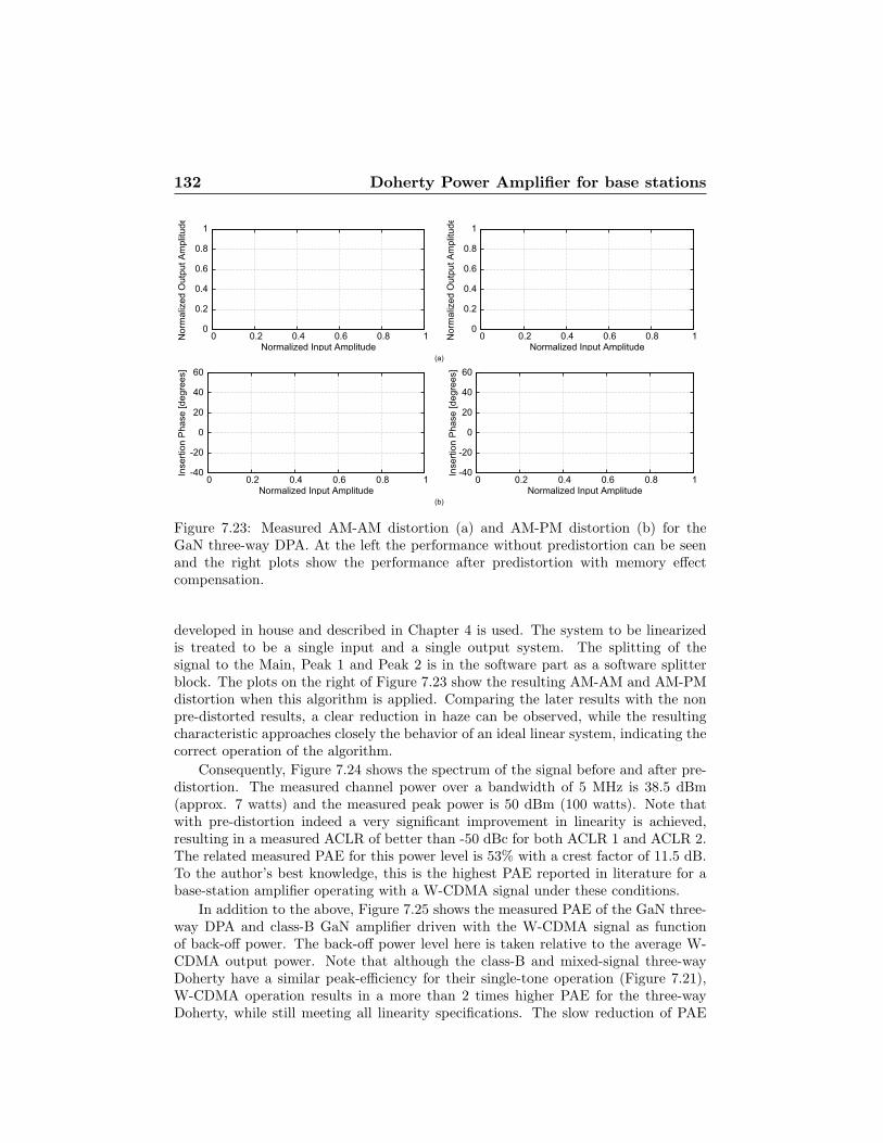
132 Doherty Power Amplifier for base stations
0
0.2
0.4
0.6
0.8
1
0 0.2 0.4 0.6 0.8 1Nor
mal
ized
Out
put A
mpl
itude
Normalized Input Amplitude
0
0.2
0.4
0.6
0.8
1
0 0.2 0.4 0.6 0.8 1Nor
mal
ized
Out
put A
mpl
itude
Normalized Input Amplitude
-40
-20
0
20
40
60
0 0.2 0.4 0.6 0.8 1
Inse
rtion
Pha
se [d
egre
es]
Normalized Input Amplitude
-40
-20
0
20
40
60
0 0.2 0.4 0.6 0.8 1
Inse
rtion
Pha
se [d
egre
es]
Normalized Input Amplitude
(a)
(b)
Figure 7.23: Measured AM-AM distortion (a) and AM-PM distortion (b) for theGaN three-way DPA. At the left the performance without predistortion can be seenand the right plots show the performance after predistortion with memory effectcompensation.
developed in house and described in Chapter 4 is used. The system to be linearizedis treated to be a single input and a single output system. The splitting of thesignal to the Main, Peak 1 and Peak 2 is in the software part as a software splitterblock. The plots on the right of Figure 7.23 show the resulting AM-AM and AM-PMdistortion when this algorithm is applied. Comparing the later results with the nonpre-distorted results, a clear reduction in haze can be observed, while the resultingcharacteristic approaches closely the behavior of an ideal linear system, indicating thecorrect operation of the algorithm.
Consequently, Figure 7.24 shows the spectrum of the signal before and after pre-distortion. The measured channel power over a bandwidth of 5 MHz is 38.5 dBm(approx. 7 watts) and the measured peak power is 50 dBm (100 watts). Note thatwith pre-distortion indeed a very significant improvement in linearity is achieved,resulting in a measured ACLR of better than -50 dBc for both ACLR 1 and ACLR 2.The related measured PAE for this power level is 53% with a crest factor of 11.5 dB.To the author’s best knowledge, this is the highest PAE reported in literature for abase-station amplifier operating with a W-CDMA signal under these conditions.
In addition to the above, Figure 7.25 shows the measured PAE of the GaN three-way DPA and class-B GaN amplifier driven with the W-CDMA signal as functionof back-off power. The back-off power level here is taken relative to the average W-CDMA output power. Note that although the class-B and mixed-signal three-wayDoherty have a similar peak-efficiency for their single-tone operation (Figure 7.21),W-CDMA operation results in a more than 2 times higher PAE for the three-wayDoherty, while still meeting all linearity specifications. The slow reduction of PAE
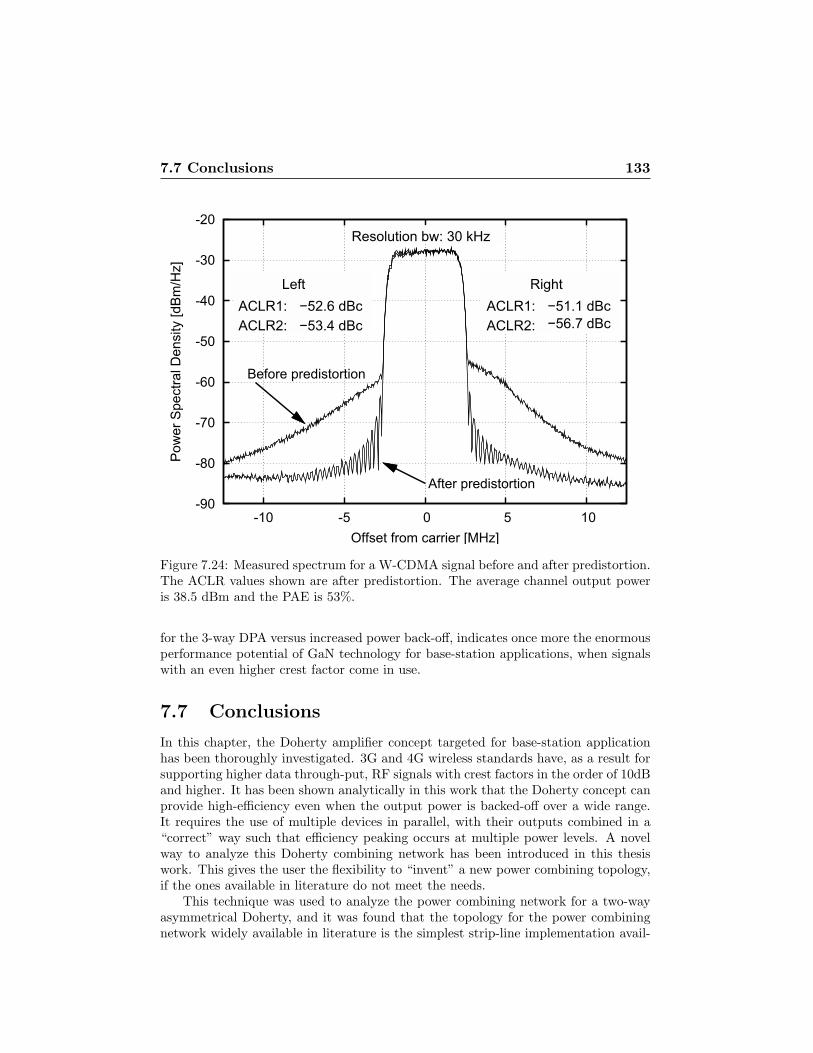
7.7 Conclusions 133
-90
-80
-70
-60
-50
-40
-30
-20
-10 -5 0 5 10
Pow
er S
pect
ral D
ensi
ty [d
Bm
/Hz]
Offset from carrier [MHz]
Before predistortion
After predistortion
ACLR2:ACLR1: −51.1 dBc
−56.7 dBc
RightACLR1:ACLR2:
−52.6 dBc−53.4 dBc
Left
Resolution bw: 30 kHz
Figure 7.24: Measured spectrum for a W-CDMA signal before and after predistortion.The ACLR values shown are after predistortion. The average channel output poweris 38.5 dBm and the PAE is 53%.
for the 3-way DPA versus increased power back-off, indicates once more the enormousperformance potential of GaN technology for base-station applications, when signalswith an even higher crest factor come in use.
7.7 Conclusions
In this chapter, the Doherty amplifier concept targeted for base-station applicationhas been thoroughly investigated. 3G and 4G wireless standards have, as a result forsupporting higher data through-put, RF signals with crest factors in the order of 10dBand higher. It has been shown analytically in this work that the Doherty concept canprovide high-efficiency even when the output power is backed-off over a wide range.It requires the use of multiple devices in parallel, with their outputs combined in a“correct” way such that efficiency peaking occurs at multiple power levels. A novelway to analyze this Doherty combining network has been introduced in this thesiswork. This gives the user the flexibility to “invent” a new power combining topology,if the ones available in literature do not meet the needs.
This technique was used to analyze the power combining network for a two-wayasymmetrical Doherty, and it was found that the topology for the power combiningnetwork widely available in literature is the simplest strip-line implementation avail-
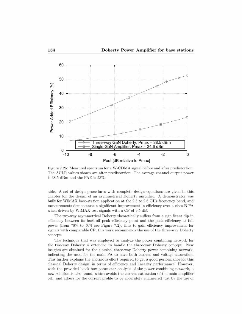
134 Doherty Power Amplifier for base stations
0
10
20
30
40
50
60
-10 -8 -6 -4 -2 0
Pow
er A
dded
Effi
cien
cy [%
]
Pout [dB relative to Pmax]
Three-way GaN Doherty, Pmax = 38.5 dBmSingle GaN Amplifier, Pmax = 34.6 dBm
Figure 7.25: Measured spectrum for a W-CDMA signal before and after predistortion.The ACLR values shown are after predistortion. The average channel output poweris 38.5 dBm and the PAE is 53%.
able. A set of design procedures with complete design equations are given in thischapter for the design of an asymmetrical Doherty amplifier. A demonstrator wasbuilt for WiMAX base-station application at the 2.5 to 2.6 GHz frequency band, andmeasurements demonstrate a significant improvement in efficiency over a class-B PAwhen driven by WiMAX test signals with a CF of 9.5 dB.
The two-way asymmetrical Doherty theoretically suffers from a significant dip inefficiency between its back-off peak efficiency point and the peak efficiency at fullpower (from 78% to 50% see Figure 7.2), thus to gain efficiency improvement forsignals with comparable CF, this work recommends the use of the three-way Dohertyconcept.
The technique that was employed to analyze the power combining network forthe two-way Doherty is extended to handle the three-way Doherty concept. Newinsights are obtained for the classical three-way Doherty power combining network,indicating the need for the main PA to have both current and voltage saturation.This further explains the enormous effort required to get a good performance for thisclassical Doherty design, in terms of efficiency and linearity performance. However,with the provided black-box parameter analysis of the power combining network, anew solution is also found, which avoids the current saturation of the main amplifiercell; and allows for the current profile to be accurately engineered just by the use of
7.7 Conclusions 135
asymmetrical splitters and the operating bias of the active devices.
In this work, we have labelled this new concept, the “Linear” three-way Doherty.This concept was verified in simulation, with a design aiming for UMTS applicationat 2.14 GHz. Simulation results show the linear ramp current profiles for the Main,Peak 1 and Peak 2, and the peak efficiencies at the targeted backed-off powers. Basedon the design procedure outlined in the work for the “Linear” three-way Doherty, aMaster of Science project performed by Ji Zhao and supervised by J. Gajadharsingat NXP was started to prototype the “linear” three-way hardware design [55]. Mea-surement results on the first prototype boards show improved performance over theasymmetrical Doherty amplifier prototype, but further design iterations are requiredto fully benefit from the performance potential.
To allow one to engineer any drive profile needed for the Main, Peak 1 and Peak2, we have introduced the “mixed-signal” three-way Doherty. This concept combinesdigital software control with the Doherty hardware. This is done by removing theanalogue symmetrical splitter and replacing it with a digital splitter. But, becauseany arbitrary drive profile can be made, it is now feasible to test this new conceptwith the well known three-way Doherty power combining network from literature.
To also investigate the potential of GaN as the technology of choice in futurebase-station implementations, a prototype mixed-signal three-way Doherty with GaNHEMT devices from CREE was built. To facilitate its calibrated testing, a custom3-way test-bench has been developed, which can provide the required input signals,as well as the measurement of the resulting input/output port powers [56]. Usingthis setup, the CW-performance of the 3-way GaN DPA has been characterized andoptimized using software control and yielding a measured performance of: 68% PAEat 50 dBm (full power), 70.4% at 45 dBm (first back-off point) and 64% at 38 dBm(second back-off point), while the measured transducer power gain was greater than10 dB at all times.
To demonstrate that this exceptional high-efficiency performance can be effec-tively utilized for practical base-station operation, our GaN three-way DPA was drivenby a W-CDMA signal with a crest factor of 11.5 dB. Using a dedicated, memory-effectcompensating pre-distortion algorithm, the resulting measured PAE for this signal was53% at an average power of 38.5 dBm, while meeting all linearity specifications.
To the author’s best knowledge this is the highest PAE performance ever reportedup to date, for any power amplifier operating with a W-CDMA signal without usingcrest factor reduction techniques.
To support this conclusion, various recent amplifier designs were considered, whichalso provide excellent W-CDMA performance (Table 7.5, column A). Note, that astraightforward comparison is troubled by the fact that W-CDMA signals with dif-ferent crest factors have been used. However, to obtain a good estimate of the perfor-mance of these amplifiers for the unaltered W-CDMA signal (crest factor 11.5dB) asused in our experiments, their estimated efficiency for this signal is computed as well.The computations are based on provided data for their single-tone Drain Efficiencyas function of back-off power, using the procedure demonstrated in Chapter 2. Thisestimate will be accurate within a few percent. The results are given in Table 7.5,column B.
The above demonstrates the performance potential of GaN technology for Doherty
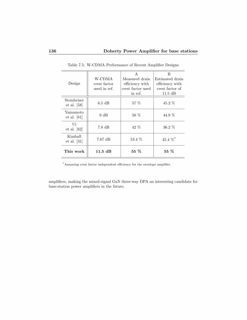
136 Doherty Power Amplifier for base stations
Table 7.5: W-CDMA Performance of Recent Amplifier Designs
DesignW-CDMAcrest factorused in ref.
AMeasured drainefficiency with
crest factor usedin ref.
BEstimated drainefficiency withcrest factor of
11.5 dB
Steinbeiseret al. [58] 6.5 dB 57 % 45.2 %
Yamamotoet al. [61] 9 dB 50 % 44.9 %
Uiet al. [62] 7.8 dB 42 % 36.2 %
Kimballet al. [31] 7.67 dB 53.4 % 45.4 %*
This work 11.5 dB 55 % 55 %
*Assuming crest factor independent efficiency for the envelope amplifier.
amplifiers, making the mixed-signal GaN three-way DPA an interesting candidate forbase-station power amplifiers in the future.

Chapter 8
Conclusions andRecommendations
The objectives of this thesis work is to investigate innovative design solutions for RFpower amplifiers, which provide efficient and linear amplifier operation. Besides thesetwo basic requirements, future handset transmit amplifiers need to provide multi-bandoperation, which requires adjustments in the broadcast frequency. For base-stationamplifiers emphasis is put on linear and efficient operation at very high output powerlevels (>100-Watts), while operating with signals that are characterized by a highpeak-to-average power ratios.
To reach these research objectives, we first considered the traditional Class-B/-AB amplifier, and searched for ways to make this operation mode more linear withoutsacrificing efficiency. In view of this, to achieve a better linearity in power back-offoperation, Chapter 3 proposes the use of Derivative Superposition. This technique,which manipulates the transconductance of the amplifying device by putting moredevices with different gate bias offset voltages in parallel, proves to be most effectivefor low output powers up to 10dB of the 1dB compression point. However, whenthe transistors are operated closer to their compression (e.g. 5 to 7dB from theP1dB point) the classical derivative superposition technique loses its effectiveness. Byextending this linearization technique and include also the second harmonic sourceand load terminations, improved linearity at much higher power levels (close to theP1dB compression point) were achieved. This “modified” Class-B operation resultedin a linearity-efficiency performance, with the latest generation of LDMOS devices,that approximates the theoretical limit of an ideal Class-B operated device, which isonly limited by signal clipping. This latter technique is of great importance whenaiming at low-cost high-bandwidth linear amplifier circuits, which does not requiredigital predistortion.
At the time that this research was performed, Digital Predistortion(DPD) wasalready gaining popularity as a system approach to correct for the distortion gen-erated by the power amplifier. Due to its flexibility and “ease” of implementation,Digital Predistortion seems to be the linearization concept of choice when dealingwith advanced high-efficiency power amplifier architectures. Although in theory these
137

138 Conclusions and Recommendations
high-efficiency power amplifier architectures are linear systems, in practice it provesthat they are much more susceptible to nonlinear signal distortion than traditionalor “modified” Class-B/-AB operated devices, due to the complex signal interactionwithin these architectures.
Therefore, before stepping into high-efficiency power amplifier architectures, wehave considered and developed an effective digital predistortion approach that is suit-able to be used in conjunction with the high-efficiency amplifier architectures thatwe discuss later in the thesis. Consequently, for this purpose in Chapter 4 we givepredistortion solutions for the case the amplifier can be considered to have no memoryand the more general case, where the memory effects of the amplifier can be no longerignored.
In Chapter 5, we give an overview of the most common high-efficiency amplifierarchitectures reported in literature to date, listing the advantages and disadvantagesof each architecture.
In Chapter 6, we discuss a high-efficiency amplifier architecture suitable for futurehandset applications. This direct load-line adaptation amplifier has been developedand implemented using the DIMES in-house “ultra-low distortion varactor technol-ogy”. This concept can provide improved amplifier efficiency under “static” powerback-off conditions. Note, that this feature is very useful for communication systemsthat make use of control loops for the transmitted output power (e.g. (W)CDMAsystems). In addition to this, it was shown that the realized adaptive load amplifieris also capable of tracking the instantaneous envelope of a modulated RF signal. Thislatest feature provides improved efficiency for the amplification of signals with a highpeak-to-average power ratio. Equally important is the fact that the tunable match-ing networks used to implement the load variable amplifier architecture provides theability to adjust the operating frequency and serve more communication frequencybands with a single amplifier. In support of this, a demonstrator realized using theseintegrated varactor based matching networks, managed to cover all frequency bandsfrom 900 MHz to 2100 MHz, while maintaining sufficient gain, output power andefficiency.
In Chapter 7, focus is placed on high-efficient power amplifier architectures suit-able for base-station applications. Here emphasis is on the Doherty power amplifier,which at the time of research investigations, was already being actively pursued inthe industry to meet the high-efficiency demands in 3G/4G applications. In thisthesis work, we have contributed to a deeper understanding of the N-way Dohertyarchitecture and contributed the novel linear three-way Doherty design procedure.The design concepts developed are translated to functional hardware demonstrators,which yielded record high efficiency performance. Based on these results these newdevelopments have reached already early adaptation in industry and will most likelybe utilized in the next generation of highly efficient base-stations for 3G/4G commu-nication systems.
In the next few sections, we will like to succinctly raise a few issues that werenot part of the thesis work, but which we see as potential to impact the RF poweramplifier community in the future.

8.1 High-Efficient Amplifier Classes of Operation 139
8.1 High-Efficient Amplifier Classes of Operation
In this work, the “Class-AB” amplifier formed the backbone of the improved effi-ciency architectures investigated in Chapter 3 (modified Class-B), Chapter 6 (adaptivematching) and Chapter 7 (Doherty amplifier). The reason for this choice is that theClass-B is simple, effective and can be easily adapted in more complex high efficiencyamplifier architectures.
However, to achieve peak efficiency operation beyond 78.5%, in various researchprojects focus is currently placed on the so called switched-mode classes, which inprinciple can provide peak efficiencies beyond 78.5%. The basic concept behind thesehigh-efficiency classes is to shape the voltage or/and current waveforms at the drainof the device such that the voltage/current waveforms becomes “squarish”. Thiseffectively minimizes the overlap between voltage and current at the device terminals,resulting in lower power losses and thus increasing efficiency. In view of this, currentlythe following amplifier classes have received an increased interest to enable the futuregeneration of high efficiency RF amplifier implementations:
Class-F [11], this amplifier class uses short-circuited conditions for the even har-monics and open conditions for the odd harmonics. When controlling the active deviceterminations up to the third harmonic, theoretical 90.7% efficiency can be achieved.This theoretical efficiency approaches 100% for maximum output power, when aninfinite amount of harmonics are controlled. Note that Class-F is still a “linear”operating amplifier and allows operation in power back-off. For this reason it is inprinciple also suited for application in Doherty and LINC amplifiers [63]. Practicalimplementations of Class-F amplifiers however are constrained in their effective con-trol of the higher harmonics, which becomes very problematic when aiming for largerbandwidths.
Class-D also utilizes square-waveforms at the output of the transistor, but achievesthis by using two or more transistor as switches. Due to this “ideal” switching itstheoretical efficiency is 100%, but power back-off operation is now only possible bymodulating the supply voltage or using a kind of pulse modulation of the output.This amplifier concept is extensively used in audio amplifiers and DC-DC converters.However at RF frequencies, practical implementations are scarce, as the transistorwill suffer at these frequencies from limitations in switching speed (deviating fromthe ideal square waveforms), and losses due to the output capacitance. Improvementin device technology has elevated some of these limitations to a certain extend, andto date Class-D demonstrators have been reported up to 2GHz [64–66].
Class-E power amplifiers [67] use a single transistor operated as a switch. But theconcept here is not to create square voltage waveforms at the drain of the transistor,but rather to ensure that the drain voltage drops to zero just before the drain currentcomes on. Figure 8.1 shows a generic Class-E voltage and current waveform at theoutput of the transistor, notice that the overlap in voltage and current is kept to abare minimum. The advantage of Class-E, is that it makes use of the parasitic drain-source capacitance as part of its matching, resulting in “skewed” voltage waveforms.As such Class-E compared to Class-D, seems much more practical at RF frequencies[68]. Since it also does not require true “square like” waveforms at the output of thetransistor, the switching speed is more relaxed than in Class-D. For these reasons
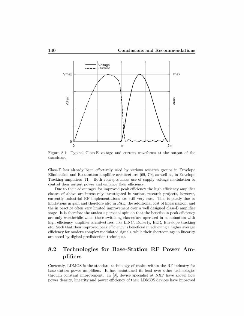
140 Conclusions and Recommendations
Figure 8.1: Typical Class-E voltage and current waveforms at the output of thetransistor.
Class-E has already been effectively used by various research groups in EnvelopeElimination and Restoration amplifier architectures [69, 70], as well as, in EnvelopeTracking amplifiers [71]. Both concepts make use of supply voltage modulation tocontrol their output power and enhance their efficiency.
Due to their advantages for improved peak efficiency the high efficiency amplifierclasses of above are intensively investigated in various research projects, however,currently industrial RF implementations are still very rare. This is partly due tolimitations in gain and therefore also in PAE, the additional cost of linearization, andthe in practice often very limited improvement over a well designed class-B amplifierstage. It is therefore the author’s personal opinion that the benefits in peak efficiencyare only worthwhile when these switching classes are operated in combination withhigh efficiency amplifier architectures, like LINC, Doherty, EER, Envelope trackingetc. Such that their improved peak efficiency is beneficial in achieving a higher averageefficiency for modern complex modulated signals, while their shortcomings in linearityare eased by digital predistortion techniques.
8.2 Technologies for Base-Station RF Power Am-plifiers
Currently, LDMOS is the standard technology of choice within the RF industry forbase-station power amplifiers. It has maintained its lead over other technologiesthrough constant improvement. In [9], device specialist at NXP have shown howpower density, linearity and power efficiency of their LDMOS devices have improved
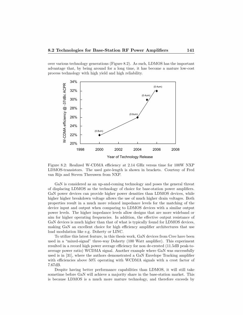
8.2 Technologies for Base-Station RF Power Amplifiers 141
over various technology generations (Figure 8.2). As such, LDMOS has the importantadvantage that, by being around for a long time, it has become a mature low-costprocess technology with high yield and high reliability.
Figure 8.2: Realized W-CDMA efficiency at 2.14 GHz versus time for 100W NXPLDMOS-transistors. The used gate-length is shown in brackets. Courtesy of Fredvan Rijs and Steven Theeuwen from NXP.
GaN is considered as an up-and-coming technology and poses the general threatof displacing LDMOS as the technology of choice for base-station power amplifiers.GaN power devices can provide higher power densities than LDMOS devices, whilehigher higher breakdown voltage allows the use of much higher drain voltages. Bothproperties result in a much more relaxed impedance levels for the matching of thedevice input and output when comparing to LDMOS devices with a similar outputpower levels. The higher impedance levels allow designs that are more wideband oraim for higher operating frequencies. In addition, the effective output resistance ofGaN devices is much higher than that of what is typically found for LDMOS devices,making GaN an excellent choice for high efficiency amplifier architectures that useload modulation like e.g. Doherty or LINC.
To utilize this latest feature, in this thesis work, GaN devices from Cree have beenused in a “mixed-signal” three-way Doherty (100 Watt amplifier). This experimentresulted in a record high power average efficiency for non de-crested (11.5dB peak-to-average power ratio) WCDMA signal. Another example where GaN was successfullyused is in [31], where the authors demonstrated a GaN Envelope Tracking amplifierwith efficiencies above 50% operating with WCDMA signals with a crest factor of7.67dB.
Despite having better performance capabilities than LDMOS, it will still takesometime before GaN will achieve a majority share in the base-station market. Thisis because LDMOS is a much more mature technology, and therefore exceeds by
142 Conclusions and Recommendations
far GaN in reliability and cost per watt. It are these two criteria that carry themost weight, when deciding for a particular technology. In spite of these economicalarguments, research to investigate the intrinsic advantages of GaN (such as its highbreak-down voltage), is extremely useful, since it will help us to find high performanceamplifier solutions for the future which are more environmental friendly.
8.3 The Future − “Mixed-Signal”, “Software Ra-dio”
One of the buzzwords in the wireless communication community today is “Software-defined Radio”. The concept of “Software-defined Radio” as visualized by the authorin [72] consist of a transmitter that is capable of characterizing the propagation path,adapt the signal to best suit the propagation environment, electronically steer thetransmit beam in the most optimal direction, set the optimal power level of the signalto be transmitted before the actual transmission takes place. Likewise, the receivershould be able to detect the frequency of the broad casted signal of interest. For thispurpose it needs to be able to sense the transmitted energy in multiple communicationchannels, while the modulation schemes used for these channels, must be detected onthe fly, resulting in a reconfiguration on demand of the demodulator of the receiver.
It is clear from this description that such an implementation will require tremen-dous amount of computing power for the signal processing and control (FPGAs anddedicated DSPs are usually employed). On the RF/analogue end, the challenge is tomove the digital interface as close to the antenna as possible. For the transmitter, theideal situation would be to just have the power amplifier stage as the only remaininganalogue part, which is directly driven by an extremely fast (D/A) converter. How-ever, this approach proves to be extremely difficult to realize in practice, since thiswould require a D/A converter that is able to operate with a high dynamic range atfrequencies above 1GHz. It is obvious that such a brute force approach would con-sume a tremendous amount of DC power. As such, the proposed “Software Radio”architecture these days uses a digital IF interface, where channel selection and filteringcan be done in the digital domain. Note that in spite the progressing digitalizationof the radio, critical parts like the PA stage and antenna remain analogue in nature,and for this reason are restricted in bandwidth. To easily change operating frequencyand make band-switching feasible, low-loss tunable matching elements are required[73–79].
Consequently, although true “Software-defined Radio” still seems to be a distantgoal, digitally enhanced RF circuits are already appearing. E.g. in [80, 81], a LINChigh-efficiency architecture is demonstrated that seems to be suitable to be employedwithin the “Software Radio” architecture. Also in this thesis, digitally enhancedRF circuits have been demonstrated; e.g. digital predistortion for correcting the non-linearities of the amplifier core, band-switching handset amplifiers that utilize softwarecontrol for pre-distortion and setting the value of the tunable elements to achieve thedesired frequency band of operation. One of the most outspoken examples of digitallyenhanced RF functionality in this work is the “Mixed-Signal” Doherty approach aspresented in Chapter 7. Here software control is used to optimize the phase-offsets and

8.3 The Future − “Mixed-Signal”, “Software Radio” 143
drive profiles of each individual device for achieving the very best Doherty operation.This was up to date, always done in an analogue fashion by the use of offset lines andanalogue signal splitters, by pushing these analogue functions to the digital domain,directly a record breaking efficiency performance was achieved. As a matter of fact,this result triggered new research activities within our group to integrate these todigital functions into a dedicated driver chip for compact highly efficiency Dohertyamplifiers.
It is clear from the examples given in this thesis work, that following a “Mixed-Signal”/software approach brings performance advantages, since it relaxes designspecifications on the analogue/RF part, as “errors” can be corrected easily correctedwithin the software. It is therefore our expectation that the future of RF power am-plifiers will be in the “Mixed-Signal” domain, where full use of the advancements indigital signal processing will result in power amplifier that are more efficient, morelinear, and reconfigurable. Consequently, the day that a typical RF amplifier willhave a digital I-Q baseband inputs is closer than ever before ⋯


Appendix A
Black-box Parameterderivation of the Two-WayDoherty Output PowerCombiner
This appendix describes how we can use the black-box parameter approach describedin Chapter 7, to derive a two-way Doherty output power combiner, that allows flexi-bility in choosing the characteristic impedance of the lines and the impedances offeredto the Main and the Peak amplifier.
From Figure 7.1, we can relate the z-parameter of the intermediate power com-bining network (with the load incorporated) to the voltages and currents of the Mainand Peak amplifier. Solving the voltages and currents against the boundary condi-tions (equations (7.6)− (7.10)), and setting the phase between the Main and the Peakto 90○, results in the following compact z-parameter description of the intermediatepower combiner.
z =⎡⎢⎢⎢⎢⎣
Zo,int
k2 −j Zo,int
k
−j Zo,int
k0
⎤⎥⎥⎥⎥⎦(A.1)
Where Zo,int refers to the intermediate load impedance that is embedded within thepower combining network, described by the black-box parameter. And k refers to theback-off ratio of the two-way Doherty amplifier.
Transforming the z-parameters to s-parameters with a system impedance Zo,sys
results in the following:
s = 1
ζ[ Zo,int ⋅Zo,sys − (k ⋅Zo,sys)2 +Z2
o,int −2 ⋅ j ⋅Zo,int ⋅Zo,sys ⋅ k−2 ⋅ j ⋅Zo,int ⋅Zo,sys ⋅ k −Zo,int ⋅Zo,sys − (k ⋅Zo,sys)2 +Z2
o,int
](A.2)
145

146Black-box Parameter derivation of the Two-Way Doherty
Output Power Combiner
Where
ζ = Zo,int ⋅Zo,sys + (k ⋅Zo,sys)2 +Z2o,int
To derive the full three-port s-parameter that describes the power combiningnetwork, we introduce the s-parameters of the third port.
s13 = ∣s13∣ ⋅ exp(j ⋅ β)s23 = ∣s23∣ ⋅ exp(j ⋅ α)s33 = ∣s33∣ ⋅ exp(j ⋅ σ)
(A.3)
Where β, α and σ are phases to be determined.Using the lossless three-port s-parameter conditions (equation (7.14)) we can write
down the following equation where only the magnitude of s13 is unknown.
∣s11∣2 + ∣s12∣2 + ∣s13∣2 = 1 (A.4)
Rearranging and substituting the known s-parameters.
∣s13∣2 = 1 − ∣s11∣2 − ∣s12∣2
∣s13∣ = 2 ⋅ k ⋅Zo,sys
√Zo,int ⋅Zo,sys
Zo,int ⋅Zo,sys + (k ⋅Zo,sys)2 +Z2o,int
(A.5)
The negative solution is ignored as we are referring here to magnitudes.Similarly to solve for the magnitude of s23 we can write the following equation:
∣s12∣ + ∣s22∣ + ∣s23∣ = 1 (A.6)
∣s23∣ = 2 ⋅Zo,int
√Zo,int ⋅Zo,sys
Zo,int ⋅Zo,sys + (k ⋅Zo,sys)2 +Z2o,int
(A.7)
Knowing the magnitude of s23, we can solve for the magnitude of s33 using:
∣s13∣ + ∣s23∣ + ∣s33∣ = 1 (A.8)
∣s33∣ = ∣−Zo,int ⋅Zo,sys + (k ⋅Zo,sys)2 +Z2o,int
Zo,int ⋅Zo,sys + (k ⋅Zo,sys)2 +Z2o,int
∣ (A.9)
At this point, the magnitudes of the s-parameters of the third port is uniquelyknown. To solve for their phases β, α and σ, the last three equations of the losslessthree-port s-parameter are used.
¯s11 ⋅ s12 + ¯s12 ⋅ s22 + ¯s13 ⋅ s23 = 0 (A.10)
¯s13 ⋅ s11 + ¯s23 ⋅ s12 + ¯s33 ⋅ s13 = 0 (A.11)
¯s12 ⋅ s13 + ¯s22 ⋅ s23 + ¯s23 ⋅ s33 = 0 (A.12)
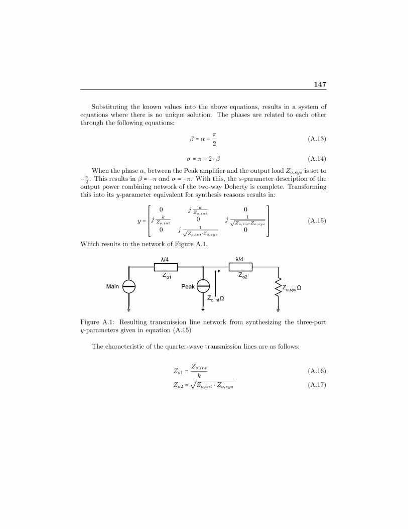
147
Substituting the known values into the above equations, results in a system ofequations where there is no unique solution. The phases are related to each otherthrough the following equations:
β = α − π
2(A.13)
σ = π + 2 ⋅ β (A.14)
When the phase α, between the Peak amplifier and the output load Zo,sys is set to−π
2. This results in β = −π and σ = −π. With this, the s-parameter description of the
output power combining network of the two-way Doherty is complete. Transformingthis into its y-parameter equivalent for synthesis reasons results in:
y =⎡⎢⎢⎢⎢⎢⎢⎢⎣
0 j kZo,int
0
j kZo,int
0 j 1√Zo,int⋅Zo,sys
0 j 1√Zo,int⋅Zo,sys
0
⎤⎥⎥⎥⎥⎥⎥⎥⎦(A.15)
Which results in the network of Figure A.1.
Figure A.1: Resulting transmission line network from synthesizing the three-porty-parameters given in equation (A.15)
The characteristic of the quarter-wave transmission lines are as follows:
Zo1 = Zo,int
k(A.16)
Zo2 = √Zo,int ⋅Zo,sys (A.17)


Bibliography
[1] M. van der Heijden, L. de Vreede, and J. Burghartz, “On the design of unilateraldual-loop feedback low-noise amplifiers with simultaneous noise, impedance, andIIP3 match,” Solid-State Circuits, IEEE Journal of, vol. 39, no. 10, pp. 1727–1736, Oct. 2004.
[2] S.-T. Lim and J. Long, “A Low-Voltage Broadband Feedforward-Linearized BJTMixer,” Solid-State Circuits, IEEE Journal of, vol. 41, no. 9, pp. 2177–2187,Sept. 2006.
[3] L. Sheng and L. Larson, “An Si-SiGe BiCMOS direct-conversion mixer withsecond-order and third-order nonlinearity cancellation for WCDMA applica-tions,” Microwave Theory and Techniques, IEEE Transactions on, vol. 51, no. 11,pp. 2211–2220, Nov. 2003.
[4] S. Li, J. Huang, Q. Meng, L. Sun, Q. Zhang, F. Li, A. He, X. Zhang, C. Li,H. Li, and Y. He, “A 12-Pole Narrowband Highly Selective High-TemperatureSuperconducting Filter for the Application in the Third-Generation WirelessCommunications,” Microwave Theory and Techniques, IEEE Transactions on,vol. 55, no. 4, pp. 754–759, April 2007.
[5] S. C. Cripps, RF Power Amplifiers for Wireless Communications. Norwood,MA: Artech House, 1999.
[6] P. B. Kennington, High-Linearity RF Amplifier Design. Norwood, MA: ArtechHouse, 2000.
[7] G. Gonzalez, Microwave Transistor Amplifiers Analysis and Design. UpperSaddle River: Prentice Hall, 1984.
[8] D. A. Neamen, Semiconductor Devices and Physics, Basic Principles, 2nd ed.New York: McGraw-Hill, 1997.
[9] F. van Rijs and S. Theeuwen, “Efficiency improvement of LDMOS transistorsfor base stations: towards the theoretical limit,” Electron Devices Meeting, 2006.IEDM ’06. International, pp. 1–4, Dec. 2006.
[10] P. Wamback and W. Sansen, Distortion Analysis of Analog Integrated Circuits.Dordrecht, The Netherlands: Kluwer Academic Publishers, 1998.
149

150 BIBLIOGRAPHY
[11] F. Raab, “Class-F power amplifiers with maximally flat waveforms,” MicrowaveTheory and Techniques, IEEE Transactions on, vol. 45, no. 11, pp. 2007–2012,Nov 1997.
[12] ——, “Efficiency of Outphasing RF Power-Amplifier Systems,” Communications,IEEE Transactions on [legacy, pre - 1988], vol. 33, no. 10, pp. 1094–1099, Oct1985.
[13] ——, “Efficiency of Doherty RF Power-Amplifier Systems,” Broadcasting, IEEETransactions on, vol. BC-33, no. 3, pp. 77–83, Sept. 1987.
[14] S. Marsili, “Technique for Peak to Average Power Ratio Reduction suited forM-carrier WCDMA Base Station Transmitters,” Circuits and Systems, 2007.ISCAS 2007. IEEE International Symposium on, pp. 3522–3525, May 2007.
[15] D. R. Webster, J. Scott, and D. G. Haigh, “Control of circuit distortion bythe derivative superposition method,” IEEE Microw. Guided Wave Lett., vol. 6,no. 3, pp. 123–125, Mar. 1996.
[16] M. van der Heijden, “RF Amplifier Design Techniques for Linearity and Dy-namic Range,” Ph.D. dissertation, Delft University of Technology, Delft, TheNetherlands, 2005.
[17] D. Hartskeerl, I. Volokhine, and M. Spirito, “On the optimum 2nd harmonicsource and load impedances for the efficiency-linearity trade-off of RF LD-MOS power amplifiers,” Radio Frequency integrated Circuits (RFIC) Symposium,2005. Digest of Papers. 2005 IEEE, pp. 447–450, 12-14 June 2005.
[18] J. Vuolevi, J. Aikio, and T. Rahkonen, “Extraction of a polynomial LDMOSmodel for distortion simulations using small-signal S-parameter measurements,”Microwave Symposium Digest, 2002 IEEE MTT-S International, vol. 3, pp.2157–2160, 2002.
[19] J. Gajadharsing, “Low distortion RF-LDMOS Power Transistor for WirelessCommunications Base Stations Application,” Microwave Symposium Digest,2003 IEEE MTT-S International, vol. 3, pp. 1563–1566, 2003.
[20] N. de Carvalho and J. Pedro, “Large signal IMD sweet spots in microwave poweramplifiers,” Microwave Symposium Digest, 1999 IEEE MTT-S International,vol. 2, pp. 517–520 vol.2, 1999.
[21] M. Spirito, “Enhanced Techniques for the Design and Characterization of RFPower Amplifiers,” Ph.D. dissertation, Delft University of Technology, Delft, TheNetherlands, 2005.
[22] M. Spirito, M. J. Pelk, F. van Rijs, S. J. C. H. Theeuwen, D. Hartskeerl, andL. C. N. de Vreede, “Active Harmonic Load-Pull for On-Wafer Out-of-Band De-vice Linearity Optimization,” Microwave Theory and Techniques, IEEE Trans-actions on, vol. 54, no. 12, pp. 4225–4236, Dec. 2006.

BIBLIOGRAPHY 151
[23] J. Vuolevi and T. Rahkonen, Distortion in RF Power Amplifiers. Artech House,2003.
[24] F. Raab, “Radio Frequency Pulsewidth Modulation,” Communications, IEEETransactions on, vol. 21, no. 8, pp. 958–966, Aug 1973.
[25] A. Grebennikov and N. O. Sokal, Switchmode RF Power Amplifiers. Burlington,MA: Newnes, 2007.
[26] A. Jayaraman, P. Asbeck, K. Nary, S. Beccue, and K.-C. Wang, “Bandpassdelta-sigma modulator with 800 Mhz center frequency,” Oct 1997, pp. 95–98.
[27] J. Keyzer, R. Uang, Y. Sugiyama, M. Iwamoto, I. Galton, and P. Asbeck, “Gen-eration of RF pulsewidth modulated microwave signals using delta-sigma mod-ulation,” vol. 1, 2002, pp. 397–400.
[28] S. Rosnell and J. Varis, “Bandpass pulse-width modulation (BP-PWM),” June2005, pp. 4 pp.–.
[29] F. Raab, B. Sigmon, R. Myers, and R. Jackson, “L-band transmitter using KahnEER technique,” Microwave Theory and Techniques, IEEE Transactions on,vol. 46, no. 12, pp. 2220–2225, Dec 1998.
[30] J. Staudinger, B. Gilsdorf, D. Newman, G. Norris, G. Sadowniczak, R. Sherman,and T. Quach, “High efficiency cdma rf power amplifier using dynamic envelopetracking technique,” Microwave Symposium Digest., 2000 IEEE MTT-S Inter-national, vol. 2, pp. 873–876 vol.2, 2000.
[31] D. F. Kimball, J. Jeong, C. Hsia, P. Draxler, S. Lanfranco, W. Nagy,K. Linthicum, L. E. Larson, and P. M. Asbeck, “High-Efficiency Envelope-Tracking W-CDMA Base-Station Amplifier Using GaN HFETs,” IEEE Trans.Microw. Theory Tech., vol. 54, no. 11, pp. 3848–3856, Nov. 2006.
[32] H. Chireix, “High Power Outphasing Modulation,” Proceedings of the IRE,vol. 23, no. 11, pp. 1370–1392, Nov. 1935.
[33] D. Cox and R. Leck, “A VHF Implementation of a LINC amplifier,” Communi-cations, IEEE Transactions on, vol. 24, no. 9, pp. 1018–1022, Sep 1976.
[34] W. Gerhard and R. Knoechel, “LINC digital component separator for singleand multicarrier W-CDMA signals,” Microwave Theory and Techniques, IEEETransactions on, vol. 53, no. 1, pp. 274–282, Jan. 2005.
[35] M. Helaoui, S. Boumaiza, A. Ghazel, and F. Ghannouchi, “Digital compensationof branches imbalance effects in LINC transmitters,” Dec. 2004, pp. 688–691.
[36] J. Qureshi, R. Lui, A. de Graaw, M. P. van der Heijden, J. Gajadharsing, andL. C. de Vreede, “A Highly Efficient Chireix Amplifier using Adaptive PowerCombining,” Microwave Symposium Digest, 2008 IEEE MTT-S International,2008.

152 BIBLIOGRAPHY
[37] W. Doherty, “A New High Efficiency Power Amplifier for Modulated Waves,”Proceedings of the IRE, vol. 24, no. 9, pp. 1163–1182, Sept. 1936.
[38] F. Raab, “High-efficiency linear amplification by dynamic load modulation,” Mi-crowave Symposium Digest, 2003 IEEE MTT-S International, vol. 3, pp. 1717–1720 vol.3, June 2003.
[39] J. Ryynanen, K. Kivekas, J. Jussila, A. Parssinen, and K. Halonen, “A dual-bandRF front-end for WCDMA and GSM applications,” Solid-State Circuits, IEEEJournal of, vol. 36, no. 8, pp. 1198–1204, Aug 2001.
[40] D. Wang, X. Wang, A. Eshraghi, D. Chang, and P. Bacon, “A fully integratedGSM/DCS/PCS Rx VCO with fast switching auto-band selection,” Radio andWireless Conference, 2002. RAWCON 2002. IEEE, pp. 209–212, Aug. 2002.
[41] A. Tasic, W. Serdijn, and J. Long, “Multi-standard/multi-band adaptive voltage-controlled oscillator,” Radio Frequency Integrated Circuits (RFIC) Symposium,2004. Digest of Papers. 2004 IEEE, pp. 135–138, June 2004.
[42] D. Qiao, R. Molfino, S. Lardizabal, B. Pillans, P. Asbeck, and G. Jerinic, “Anintelligently controlled RF power amplifier with a reconfigurable MEMS-varactortuner,” Microwave Theory and Techniques, IEEE Transactions on, vol. 53, no. 3,pp. 1089–1095, March 2005.
[43] H. T. Jeong, H. S. Lee, I. S. Chang, and C. D. Kim, “Efficiency enhancementmethod for high-power amplifiers using a dynamic load adaptation technique,”Microwave Symposium Digest, 2005 IEEE MTT-S International, pp. 4 pp.–,June 2005.
[44] K. Buisman, L. C. N. de Vreede, L. E. Larson, M. Spirito, A. Akhnoukh, Y. Lin,X. Liu, and L. K. Nanver, “A Monolithic Low-Distortion Low-Loss Silicon-on-Glass Varactor-Tuned Filter with Optimized Biasing,” Microwave and WirelessComponents Letters, IEEE, vol. 17, no. 1, pp. 58–60, Jan. 2007.
[45] K. Buisman, C. Huang, A. Akhnoukh, M. Marchetti, L. de Vreede, L. Larson,and L. Nanver, “Varactor Topologies for RF Adaptivity with Improved PowerHandling and Linearity,” Microwave Symposium, 2007. IEEE/MTT-S Interna-tional, pp. 319–322, June 2007.
[46] K. Buisman, L. Nanver, T. Scholtes, H. Schellevis, and L. de Vreede, “High-performance varactor diodes integrated in a silicon-on-glass technology,” Solid-State Device Research Conference, 2005. ESSDERC 2005. Proceedings of 35thEuropean, pp. 117–120, Sept. 2005.
[47] K. Buisman, L. de Vreede, L. Larson, M. Spirito, A. Akhnoukh, T. Scholtes,and L. Nanver, “Distortion-free varactor diode topologies for RF adaptivity,”Microwave Symposium Digest, 2005 IEEE MTT-S International, pp. 4 pp.–,June 2005.

BIBLIOGRAPHY 153
[48] K. Buisman, L. de Vreede, L. Larson, M. Spirito, A. Akhnoukh, Y. Lin, X. Liu,and L. Nanver, “Low-distortion, low-loss varactor-based adaptive matching net-works, implemented in a silicon-on-glass technology,” Radio Frequency integratedCircuits (RFIC) Symposium, 2005. Digest of Papers. 2005 IEEE, pp. 389–392,June 2005.
[49] R. Meyer and M. Stephens, “Distortion in variable-capacitance diodes,” Solid-State Circuits, IEEE Journal of, vol. 10, no. 1, pp. 47–54, Feb 1975.
[50] G. Leuzzi and C. Micheli, “Variable-Load Constant-Efficiency Power Ampli-fier for Mobile Communications Applications,” European Microwave Conference,2003. 33rd, pp. 375–377, Oct. 2003.
[51] P. Deixler, R. Colclaser, D. Bower, N. Bell, W. De Boer, D. Szmyd, S. Bardy,W. Wilbanks, P. Barre, M. v Houdt, J. Paasschens, H. Veenstra, E. v d Heijden,J. Donkers, and J. Slotboom, “Qubic4g: a fT /fmax = 70/100GHz 0.25μm lowpower SiGe-BiCMOS production technology with high quality passives for 12.5Gb/s optical networking and emerging wireless applications up to 20 Ghz,” Bipo-lar/BiCMOS Circuits and Technology Meeting, 2002. Proceedings of the 2002,pp. 201–204, 2002.
[52] C. Huang, L. de Vreede, F. Sarubbi, M. Popadic, K. Buisman, J. Qureshi,M. Marchetti, A. Akhnoukh, T. Scholtes, L. Larson, and L. Nanver, “EnablingLow-Distortion Varactors for Adaptive Transmitters,” Microwave Theory andTechniques, IEEE Transactions on, vol. 56, no. 5, pp. 1149–1163, May 2008.
[53] M. Iwamoto, A. Williams, P. Chen, A. G. Metzger, L. E. Larson, and P. M.Asbeck, “An extended Doherty amplifier with high efficiency over a wide powerrange,” IEEE Trans. Microw. Theory Tech., vol. 49, no. 12, pp. 2472–2479, Dec.2001.
[54] N. Srirattana, A. Raghavan, D. Heo, P. Allen, and J. Laskar, “Analysis andDesign of a High-Efficiency Multistage Doherty Power Amplifier for WirelessCommunications,” IEEE Trans. Microw. Theory Tech., vol. 53, no. 3, pp. 852–860, Mar. 2005.
[55] J. Zhao, “High Efficiency three-way Doherty Amplifier with a Passive InputSplitter,” Master’s thesis, Technische Universiteit Delft, Department of Micro-electronics, Delft, The Netherlands, 2008.
[56] M. Pelk, W. Neo, J. Gajadharsing, R. Pengelly, and L. de Vreede, “A High-Efficiency 100-W GaN Three-Way Doherty Amplifier for Base-Station Applica-tions,” Microwave Theory and Techniques, IEEE Transactions on, vol. 56, no. 7,pp. 1582–1591, July 2008.
[57] J. Gajadharsing, O. Bosma, and P. van Westen, “Analysis and design of a 200 WLDMOS based Doherty amplifier for 3 G base stations,” Microwave SymposiumDigest, 2004 IEEE MTT-S International, vol. 2, pp. 529–532 Vol.2, June 2004.

154 BIBLIOGRAPHY
[58] C. Steinbeiser, T. Landon, C. Suckling, J. Nelson, J. Delaney, J. Hitt,L. Witkowski, G. Burgin, R. Hajji, and O. Krutko, “250 W HVHBT Dohertywith 57% WCDMA Efficiency Linearized to -55 dBc for 2c11 6.5 dB PAR,”Solid-State Circuits, IEEE Journal of, vol. 43, no. 10, pp. 2218–2228, Oct. 2008.
[59] 3G TS 25.141 Base station conformance testing (FDD), 3rd Generation Part-nership Project; Technical Specification Group Radio Access Networks TechnicalSpecification, Rev. V3.1.0, 2000.
[60] L. Larson and D. K. P. Asbeck, “Challenges and Opportunities for CompoundSemiconductor Devices in Next Generation Wireless Base Station Power Ampli-fiers,” in Proc. IEEE Compound Semiconductor Integrated Circuit Symposium(CSIC’05), Nov. 2005.
[61] M. Iwamoto, A. Williams, P.-F. Chen, A. Metzger, C. Wang, L. Larson, andP. Asbeck, “An extended Doherty amplifier with high efficiency over a widepower range,” Microwave Symposium Digest, 2001 IEEE MTT-S International,vol. 2, pp. 931–934 vol.2, 2001.
[62] N. Ui, H. Sano, and S. Sano, “A 80W 2-stage GaN HEMT Doherty Amplifier with50dbc ACLR, 42% Efficiency 32dB Gain with DPD for WCDMA Base station,”Microwave Symposium, 2007. IEEE/MTT-S International, pp. 1259–1262, June2007.
[63] J. Kim, B. Kim, and Y. Y. Woo, “Advanced Design of Linear Doherty Amplifierfor High Efficiency using Saturation Amplifier,” June 2007, pp. 1573–1576.
[64] A. Long, J. Yao, and S. Long, “A 13 W current mode class D high efficiency 1GHz power amplifier,” vol. 1, Aug. 2002, pp. I–33–6 vol.1.
[65] H. Kobayashi, J. Hinrichs, and P. Asbeck, “Current mode class-D power ampli-fiers for high efficiency RF applications,” vol. 2, 2001, pp. 939–942 vol.2.
[66] A. Al Tanany, A. Sayed, and G. Boeck, “A 2.14 GHz 50 Watt 60% Power AddedEfficiency GaN Current Mode Class D Power Amplifier,” Oct. 2008, pp. 432–435.
[67] N. Sokal and A. Sokal, “Class e-a new class of high-efficiency tuned single-endedswitching power amplifiers,” Solid-State Circuits, IEEE Journal of, vol. 10, no. 3,pp. 168–176, Jun 1975.
[68] S. Pajic, N. Wang, P. Watson, T. Quach, and Z. Popovic, “X-band two-stagehigh-efficiency switched-mode power amplifiers,” Microwave Theory and Tech-niques, IEEE Transactions on, vol. 53, no. 9, pp. 2899–2907, Sept. 2005.
[69] A. Diet, C. Berland, M. Villegas, and G. Baudoin, “EER architecture specifica-tions for OFDM transmitter using a class E amplifier,” Microwave and WirelessComponents Letters, IEEE, vol. 14, no. 8, pp. 389–391, Aug. 2004.

BIBLIOGRAPHY 155
[70] D. Y. Lie, J. Popp, F. Wang, D. Kimball, and L. Larson, “Linearization of Highly-Efficient Monolithic Class E SiGe Power Amplifiers with Envelope-Tracking (ET)and Envelope-Elimination-and-Restoration (EER) at 900MHz,” Nov. 2007, pp.1–4.
[71] J. Popp, D. Lie, F. Wang, D. Kimball, and L. Larson, “Fully-integrated highly-efficient RF Class E SiGe power amplifier with an envelope-tracking techniquefor EDGE applications,” Jan. 2006, pp. 231–234.
[72] J. Mitola, “The software radio architecture,” Communications Magazine, IEEE,vol. 33, no. 5, pp. 26–38, May 1995.
[73] K. Buisman, L. de Vreede, L. Larson, M. Spirito, A. Akhnoukh, T. Scholtes,and L. Nanver, “Distortion-free varactor diode topologies for RF adaptivity,”Microwave Symposium Digest, 2005 IEEE MTT-S International, pp. 4 pp.–, 12-17 June 2005.
[74] R. Malmqvist, A. Ouacha, and R. Erickson, “Multi-Band and ReconfigurableFront-Ends for Flexible and Multi-Functional RF Systems,” Dec. 2007, pp. 1–4.
[75] N. Haridas, A. Erdogan, T. Arslan, A. Walton, S. Smith, T. Stevenson,C. Dunare, A. Gundlach, J. Terry, P. Argyrakis, K. Tierney, A. Ross, andT. O’Hara, “Reconfigurable MEMS Antennas,” June 2008, pp. 147–154.
[76] R. Whatley, Z. Zhou, and K. Melde, “Reconfigurable RF impedance tuner formatch control in broadband wireless devices,” Antennas and Propagation, IEEETransactions on, vol. 54, no. 2, pp. 470–478, Feb. 2006.
[77] L. Rabieirad and S. Mohammadi, “A reconfigurable MEMS-less CMOS tuner forsoftware defined radio,” June 2008, pp. 779–782.
[78] D. Kelly, C. Brindle, C. Kemerling, and M. Stuber, “The state-of-the-art ofsilicon-on-sapphire CMOS RF switches,” Oct.-2 Nov. 2005, pp. 4 pp.–.
[79] A. Botula, A. Joseph, J. Slinkman, R. Wolf, Z.-X. He, D. Ioannou, L. Wagner,M. Gordon, M. Abou-Khalil, R. Phelps, M. Gautsch, W. Abadeer, D. Harmon,M. Levy, J. Benoit, and J. Dunn, “A Thin-Film SOI 180nm CMOS RF SwitchTechnology,” Jan. 2009, pp. 1–4.
[80] S. Moloudi, K. Takinami, M. Youssef, M. Mikhemar, and A. Abidi, “An Out-phasing Power Amplifier for a Software-Defined Radio Transmitter,” Feb. 2008,pp. 568–636.
[81] Y. Y. Woo, J. Yi, Y. Yang, and B. Kim, “SDR transmitter based on LINCamplifier with bias control,” vol. 3, June 2003, pp. 1703–1706 vol.3.


Summary
This thesis introduces several concepts with their experimental verification for thedesign of efficient and linear RF power amplifiers.
In Chapter 1, a brief historical overview of the wireless communication market isgiven together with the author’s vision on the future of wireless communications withsubsequent related challenges for RF power amplifier designers. The main targets forboth handset power amplifiers and base-station power amplifiers are that they becomemore efficient, as well as, more linear. Besides that, for handset power amplifiers, thereis additional requirement for multi-band operation with emphasis on the compactnessof their implementation. For base-station power amplifiers the main emphasis ison increasing the power handling capability of the amplifier and its ever increasingefficiency requirement for signals that have high peak-to-average power ratios.
Chapter 2 introduces the basic concepts of linearity and efficiency associatedwith the power amplifier. The traditional amplifier classes of operation are discussedwith regards to their efficiency performance, assuming an ideal active device. Fol-lowing this discussion, the various dominant sources of distortion are identified for apractical device, and how this distortion increases when device operation is pushedtowards higher efficiency.
To operate at higher efficiencies and still reach an acceptable linearity perfor-mance, Chapter 3 introduces the use of Derivative Superposition as a techniqueto improve device linearity. Doing so, the resulting amplifier stage can be operatedat higher power levels, while still meeting its linearity requirements, resulting in animproved efficiency performance. However, at very high power levels close to com-pression, Derivative Superposition is no longer effective. Consequently, to overcomethis limitation, in this chapter, harmonic manipulation is introduced to shift the lin-earity “IM3 sweet-spot” of the device closer to compression. This yields improvedlinearity close to the compression point and allows therefore device operation at areduced power back-off levels yielding improved efficiency. Applying this techniqueon a NXP Gen 6 LDMOS device results in an efficiency of 44% at an ACLR1 level of-45dBc for a IS-95 forward link signal.
Relying entirely on analogue circuit techniques to meet the high linearity require-ments of present/future wireless communication standards, while simultaneously aim-ing for average efficiencies in excess of 50% for complex modulated signals, is close toimpossible. As such, the trend in the industry is to “solve” the linearity issues of thepower amplifier in the digital domain, a technique commonly referred to as digitalpredistortion. Chapter 4 introduces the theoretical concepts involved in digital pre-
157

158 Summary
distortion and discusses the current techniques for predistortion for power amplifierswith and without memory effects.
Digital predistortion allows the linearity specifications of the RF power amplifierto be “relaxed”, as the overall transmitter linearity can be improved digitally. Assuch, this opens up the possibility to use more aggressive power amplifier architecturessuch as LINC and Doherty, which although in theory are both linear and efficient, butin their practical implementation suffer from severe distortion. Chapter 5 gives anoverview of the common high-efficient power amplifier concepts reported in literature,and discusses their advantages and disadvantages.
Chapter 6 presents a multi-band, multi-mode class-AB power amplifier tar-geted for handset applications, which utilizes continuously tunable input and outputmatching networks integrated in a low-loss silicon-on-glass technology. The tunablematching networks make use of very high-Q varactor diodes in a low distortion anti-series configuration to achieve the desired source and load impedance tunability. AQUBIC4G high voltage breakdown transistor is used as active device. The realizedadaptive amplifier provides 13 dB gain, 27-28 dBm output power at the 900, 1800,1900 and 2100 MHz bands. For communication bands above 1 GHz optimum loadadaptation is facilitated, resulting in efficiencies between 30%-55% over a 10 dB out-put power control range.
Chapter 7 presents a mixed-signal approach for the design and testing of high-performance N-way Doherty amplifiers. In support of this N-way power-combiningnetworks are analyzed for their optimum design, by examining the relationship be-tween the input drive conditions of the active devices and their efficient output powercombining. This analysis makes no prior assumption on the network topology andfacilitates free-to-choose levels for the high-efficiency power back-off points. By com-paring the results of this analysis with prior work, it is shown that very specific driveconditions apply to traditional three-way Doherty amplifier implementations to ob-tain simultaneously high-efficiency and high-linearity operation. To demonstrate thisapproach, a three-way Doherty 100-W GaN base-station power amplifier at 2.14 GHzis designed and built. Mixed-signal techniques are utilized for uncompromised controlof the amplifier stages to optimize efficiency, as well as, linearity. The combination ofthe above techniques resulted in an unprecedented high efficiency over a 12 dB powerback-off range, facilitating a record high PAE for a W-CDMA test signal with highcrest factor, while meeting all the spectral requirements for UMTS base stations.
Chapter 8 presents the conclusions of this thesis work and provides suggestionsfor further research and development in the field of RF power amplifiers for wirelesscommunication applications.

Samenvatting
Dit proefschrift introduceert verschillende concepten voor efficiente en lineaire RFvermogensversterkers. Deze concepten worden allemaal experimenteel geverifieerd.
In Hoofdstuk 1 wordt een kort historisch overzicht van de draadloze commu-nicatie gegeven alsmede de visie van de auteur op de toekomst van draadloze com-municatie en de daarmee samenhangende uitdagingen voor de ontwerpers van de RFvermogensversterkers. Het blijkt dat verbeterde efficientie en lineariteit de belangri-jkste trends zijn voor zowel de vermogensversterkers van mobiele telefoons als dievan basisstations. Verder is er voor de vermogensversterkers van de mobiele telefoon,de aanvullende eis voor multi-band multi-mode functionaliteit waarbij de nadruk ligtop de compactheid van de uiteindelijke versterker implementatie. Voor basisstationsvermogensversterkers ligt de nadruk op het vergroten van het maximale vermogen datde versterker kan leveren met behoud van een goede efficientie voor signalen die eengroot verschil kennen in hun piek en gemiddelde vermogen.
Hoofdstuk 2 introduceert de basisconcepten voor lineariteit en efficientie m.b.t.de RF vermogensversterker. De traditionele versterkerklassen worden besproken samenmet hun efficientie prestaties. In deze discussies wordt eerst een ideale transistorverondersteld waarna voor een echte transistor de dominante bronnen van distor-tie worden geıdentificeerd. Er wordt aangetoond dat de signaalvervorming toeneemtwanneer de transistor wordt gebruikt bij een hoger uitgangsvermogen om een beterrendement te verkrijgen.
Om een hogere efficientie te bereiken bij een aanvaardbare lineariteit, introduceertHoofdstuk 3 het gebruik van de “Derivative Superposition” techniek om de lin-eariteit te verbeteren. Door het benutten van deze techniek blijft de versterkinglineair op een hoger vermogensniveau wat resulteert in een beter rendement. Opzeer hoge vermogensniveaus, dicht bij het P1dB compressiepunt, is de DerivativeSuperposition techiek niet meer effectief. Om deze beperking te overwinnen wordtharmonische manipulatie geıntroduceerd om het optimale IM3 punt dichter bij hetP1dB compressiepunt te plaatsen. Hierdoor verbetert de lineariteit bij het P1dBcompressiepunt waardoor men minder vermogensreductie hoeft te gebruiken voor detransistor. Dit leidt tot een beter rendement. Het toepassen van deze techniek op eenNXP Gen 6 LDMOS transistor resulteert in een efficientie van 44% met een ACLR1niveau van -45dBc voor een IS-95 verbindingssignaal.
Als men streeft naar een gemiddelde efficientie van meer dan 50% voor complexegemoduleerde signalen dan is het gebruik van uitsluitend analoge circuittechnieken,om aan de lineariteit eisen van de huidige/toekomstige draadloze communicatiesys-
159

160 Samenvatting
temen te voldoen, niet toereikend. Daarom is de algemene indruk dat digitale com-pensatietechnieken moet worden gebruikt om de lineariteits problemen van de ver-mogensversterker op te lossen. Hoofdstuk 4 introduceert de theoretische conceptenvan digitale precompensatie en bespreekt de gangbare technieken voor precompensatievoor vermogensversterkers met en zonder geheugeneffecten.
Door het gebruik van digitale compensatietechnieken wordt de lineariteit specifi-catie van de RF vermogensversterker minder streng. Dit komt omdat nu de digitaleprecompensatie de lineariteit van de totale zender verbetert. Dit biedt de mogeli-jkheid om een meer vooruitstrevende versterker architectuur zoals LINC en Dohertyte gebruiken, die weliswaar in theorie zowel lineair als efficient zijn maar in het prak-tijk aanleiding geven tot sterke signaalvervorming. Hoofdstuk 5 geeft een overzichtvan de meest gangbare hoog-efficiente RF vermogensversterker architecturen die inliteratuur worden vermeld en bespreekt hun voor- en nadelen.
Hoofdstuk 6 introduceert een multi-band, multi-mode klasse-AB vermogensver-sterker voor mobiele telefoon toepassingen. Dit versterker concept maakt gebruik vancontinu verstembare in- en uitgangs impedantie aanpasnetwerken, die zijn geıntegreerdin een silicium-op-glas technologie met zeer lage verliezen. De afstembare aanpas-netwerken maken gebruik van varactordiodes in een anti-series configuratie die vrijwelgeen signaalvervorming geeft. Een QUBIC4G transistor met verbeterde “breakdown”eigenschappen wordt gebruikt als versterkend element. De gerealiseerde multi-band,multi-mode versterker levert 13 dB gain bij 27-28 dBm uitgangsvermogen in de fre-quentiebanden van 900, 1800, 1900 en 2100 MHz. Voor de communicatiebandenboven de 1 GHz kan voor ieder afzonderlijk vermogensniveau, d.m.v. het afstembareuitgangsnetwerk, de optimale impedantie worden aangeboden aan de transistor watresulteert in 30%-55% efficientie over een 10 dB vermogensbereik.
Hoofdstuk 7 introduceert een mixed-signaal benadering voor het ontwerp enhet testen van “N-way” Doherty vermogensversterkers. Dit hoofdstuk begint met eenalgemene analyse voor het ontwerp van “N-way” vermogencombinerende netwerken.De analyse is gebaseerd op het verband tussen de optimale aansturing van de ac-tieve elementen en het combineren van hun uitgangsvermogens d.m.v. een verliesvrijnetwerk. De analyse maakt geen enkele aanname wat betreft de netwerktopologieen laat de ontwerper vrij om de “back-off” punten, waar de versterker zijn hoge ef-ficientie bereikt, te kiezen. Door deze analyse met eerder werk te vergelijken wordtaangetoond dat er zeer specifieke aanstuurvoorwaarden zijn om de traditionele “3-way” Doherty versterker goed te laten werken met een hoog rendement en lineariteit.Om dit aan te tonen wordt een “3-way” Doherty van GaN met 100-Watt uitgangsver-mogen voor base-stations bij 2.14 GHz ontworpen en gebouwd. De mixed-signaaltechniek is gebruikt om de individuele versterkertrappen optimaal aan te sturen omzowel een goed rendement als lineariteit te bereiken. De combinatie van de bovenge-noemde technieken resulteerde in een tot nu toe niet geevenaarde efficiency over een12 dB vermogens bereik t.o.v. het P1dB compressie punt. Dit resulteerde in eennieuw record voor de PAE van een W-CDMA testsignaal met hoge “crest-factor”terwijl voldaan wordt aan alle spectrale eisen van de UMTS specificatie.
Hoofdstuk 8 geeft een overzicht van de belangrijkste conclusies van dit proef-schrift en geeft nieuwe suggesties voor verder onderzoek en ontwikkelingen op hetgebied van de RF vermogensversterkers voor draadloze communicatie toepassingen.

List of Publications
Journal Papers
W. C. E. Neo, Y. Lin, X. Liu, L. C. N. de Vreede, L. E. Larson, M. Spirito,M. J. Pelk, K. Buisman, A. Akhnoukh, A. de Grauw, and L. K. Nanver, “Adap-tive Multi-Band Multi-Mode Power Amplifier Using Integrated Varactor-BasedTunable Matching Networks,” IEEE J. Solid-State Circuits, vol. 41, no. 9, pp.2166–2176, Sept. 2006.
W. C. E. Neo, J. H. Qureshi, M. J. Pelk, J. R. Gajadharsing, and L. C. N.de Vreede, “A Mixed-Signal Approach Towards Linear and Efficient N-WayDoherty Amplifiers,” IEEE Trans. Microwave Theory Tech., vol. 55, no. 5, pp.866–879, May. 2007.
Conference Papers
W. C. E. Neo, M. P. van der Heijden, L. C. N. de Vreede, M. Spirito, V. Cuocoand F. van. Rijs, “A technique to linearize LDMOS power amplifiers basedon derivative superposition and out-of-band impedance optimization,” in Eur.Microwave Conf., vol. 3, Oct. 2004, pp. 1173–1175.
W. C. E. Neo, X. Liu, Y. Lin, L. C. N. de Vreede, L. E. Larson, M. Spir-ito, A. Akhnoukh, A. de Grauw, and L. K. Nanver, “Improved hybrid SiGeHBT class-AB power amplifier efficiency using varactor-based tunable matchingnetworks,” in Proc. IEEE Bipolar/BiCMOS Circuits and Technology Meeting(BCTM2005), Oct. 2005, pp. 108–111.
Co-Authorship
V. Cuoco, W. C. E. Neo, L. C. N. de Vreede, H. C. de Graaff, L. K. Nan-ver, K. Buisman, H. C. Wu, H. F. F. Jos, and J. N. Burghartz, “A new ex-traction technique for the series resistances of semiconductor devices based onthe intrinsic properties of bias-dependent y-parameters,” in Proc. IEEE Bipo-lar/BiCMOS Circuits and Technology Meeting (BCTM2004), Sep. 2004, pp.148–151.
161

162 List of Publications
V. Cuoco, W. C. E. Neo, M. Spirito, O. Yanson, N. Nenadovic, L. C. N.de Vreede, H. F. F. Jos, and J. N. Burghartz, “The electro-thermal Smoothiedatabase model for LDMOS devices,” in Proc. ESSDERC 2004, Sept. 2004,pp. 457–460.
V. Cuoco, O. Yanson, P. Hammes, M. Spirito, L. C. N. de Vreede, A. van Steen-wijk, M. Versleijen, W. C. E. Neo, H. F. F. Jos, and J. N. Burghartz, “Largesignal verification of the circuit-oriented smoothie database model for LDMOSdevices,” in Eur. Microwave Conf., vol. 1, Oct. 2004, pp. 217–220.
M. J. Pelk, W. C. E. Neo, J. R. Gajadharsing, R. S. Pengelly, and L. C. N.de Vreede, “A High-Efficiency 100-W GaN Three-Way Doherty Amplifier forBase-Station Application,” IEEE Trans. Microwave Theory Tech., vol. 56,no. 7, pp. 1582–1591, Jul. 2008.
M. Marchetti, M. J. Pelk, K. Buisman, W. C. E. Neo, M. Spirito, and L. C. N.de Vreede, “Active Harmonic Load-Pull with Realistic Wideband Communica-tions Signals,” IEEE Trans. Microwave Theory Tech., vol. 56, no. 12, pp.2979–2988, Dec. 2008.
J. H. Qureshi, M. J. Pelk, M. Marchetti, W. C. E. Neo, J. R. Gajadharsing,M. P. van der Heijden, and L. C. N. de Vreede, “A 90-W Peak Power GaNOutphasing Amplifier With Optimum Input Signal Conditioning,” IEEE Trans.Microwave Theory Tech., vol. 57, no. 8, pp. 1925–1935, Aug. 2009.

Acknowledgments
The PhD experience in Delft will become one of the most memorable periods of mylife, and I am very fortunate that this opportunity was open up to me. This journeybegan when Prof. Kees Beenakker came to Singapore to recruit students for hisnow famous Master of Science program in Microelectronics at the Delft University ofTechnology. Thank you, Prof. Kees Beenakker for selecting me for this program.
After my Master of Science, I was very fortunate to be offered a PhD positionby Dr Leo de Vreede in the group of then Prof. Joachim Burghartz (my promotor).I am very grateful to both of them for having the confidence that I can undergothe grueling 4 years of a PhD student. Dr. Leo de Vreede who then became mysupervisor (co-promotor) for my PhD studies, did not only play a big role in my PhDthesis work, he also acted as role model for a good engineer, scientist and teacher,which I strive to become. Leo is someone who will never say ”no”when approachedfor discussions, I benefited a lot from these discussions, which led eventually to themany new concepts that are presented in this thesis work. Thank you Leo for thegreat time I had during the PhD, it was not an easy time, but a very memorableperiod. In this PhD work, I have received excellent support from NXP. Not only wasthis project financially supported by them, I also received a lot of technical input, aswell as, market input from them. Here, I would like to acknowledge in special JohnGajadharsing and Rik Jos for their strong support over the last few years and theirinterest in this thesis work.
Contrary, to the popular belief that a PhD study is very lonely work where onespends long hours alone in the laboratory or behind the computer, my PhD experienceis completely the opposite, as I have spend a big proportion of my time collaboratingwith other people. In the beginning of my PhD, I benefited from working closely withMark van der Heijden on improving the linearity of LDMOS devices. Also, MarcoSpirito provided me with his support when characterizing devices on his “famous”Load-pull setup. Not to forget Vittorio Cuoco, who taught me about modeling andcharacterization of the transistors. Subsequently, I got to work with Marco Pelk,who was the guy we all went to, if we had technical problems, no matter software orhardware. Together with Marco Pelk, we put many hours into the mixed-signal basedtest bench, which also has DPD capabilities. I will never forget the “hardship” wefaced in that laboratory, in getting everything to work together, as well as the manydinners we had at Burger King during our evening break. Marco, I am indebted toyou for all the help and want to thank you for your friendship, a great proportion ofthis work would never see light without your collaboration. I also like to acknowledge
163

164 Acknowledgments
my office room-mate and fellow PhD, Koen Buisman. Besides providing me withhours of interesting discussions, Koen also designed those very linear RF tunablevaractors, which was crucial for the adaptive PA in my thesis work. Here, I will alsolike to acknowledge and thank Prof. Lis Nanver and the DIMES technology team formaking those varactors. Also a special word of thanks has to be given to Atef Aknouk,who helped me in many ways to ensure that everything was operating smoothly inthe measurement laboratory.
Coming from a foreign country and living in The Netherlands can be a verychallenging task. Fortunately for me, I had the support from our ever helpful sec-retaries. Here, I will like to acknowledge; Birgit Rademakers, Pien Rijnink, MarysiaLagendijk-Korzeniewski who definitely went beyond the scope of their job to help mewith issues concerning housing, health insurance, taxes etc, etc. Last but not least,I also want to acknowledge my other fellow PhDs, Huang Cong, Jawad Qureshi andMauro Marchetti. The company of you guys definitely made the PhD experiencemuch more “tolerable”.
A great part of the thesis write up was done, after I left the university while work-ing full-time in NXP. This would not have been possible without the huge support andunderstanding of; Mark Murphy, Rik Jos, Korne Vennema and John Gajadharsing. Ialso like to acknowledge Sjoerd van Nederveen, Hans Kartman, Harrie Rahangmetan,and Ton Schouten, my colleagues at NXP, for helping me make that transition fromuniversity to company life, and their support and understanding while I was writingmy PhD thesis.
During my PhD studies, I was very fortunate to have the support of my familyand friends. I will like to acknowledge my family for all their love and encouragement.Their encouragements have kept me going through the tough times. At this juncture,I will like to acknowledge and thank my mentor Ruth Winden. I have benefited alot from her advice, guidance and encouragement through these years. I also like tothank my partner Shannon Koh for her love and patience, writing this thesis did notput me in the best of moods.
For my final acknowledgement, I like to dedicate this PhD thesis to my late motherMak Yoke, who passed away during the writing of this thesis.

About the Author
W. C. Edmund Neo was born in Singapore in 1977. He received the B.Eng. degreein electrical engineering with First Class honors from the National University of Sin-gapore in 2002. He subsequently pursued his master degree in electrical engineeringin Delft, and in 2004 he was awarded the M.Sc. degree in electrical engineering (cumlaude) from the Delft University of Technology, Delft, The Netherlands. From 2004to 2008 he worked towards his Ph.D. degree in electrical engineering at the Delft Uni-versity of Technology in the area of novel circuit design techniques for high-efficiencypower amplifiers. Since mid 2008, he joined NXP Semiconductors in Nijmegen wherehe holds the responsibility as application engineer in the RF power transistor productline.
165