Doan-Millimeter-Wave CMOS Design
12
144 IEEE JOURNAL OF SOLID-ST A TE CIRCUITS, VOL. 40, NO. 1, JANUARY 2005 Millimeter-Wave CMOS Design Chinh H. Doan, Student Member, IEEE , Sohrab Emami, Student Member, IEEE , Ali M. Niknejad, Member, IEEE , and Robert W. Brodersen, Fellow, IEEE AbstractThi s paper des cr ibe s the des ign and modeli ng of CMOS tra nsi stors , int egrate d pas si ves , and cir cui t blocks at millimeter-wave (mm-wave) frequencies. The effects of parasitics on the high-frequency performance of 130-nm CMOS transistors are investigated, and a peak of 135 GHz has been achieved with optimal devi ce layo ut. The inductive quality factor is prop osed as a mor e rep res entat ive metr ic for transmis sion lines, and for a standard CMOS bac k-e nd pr oce ss, cop lanar waveguide (CPW) lines are determined to possess a higher than microstrip lines. Techniques for accurate modeling of active and passive components at mm-wave frequencies are presented. The pr oposed met hodology was use d to des ign two wid eba nd mm-wave CMOS amplifiers operating at 40 GHz and 60 GHz. The 40-GHz amplifier achieves a peak dB, output dBm, dBm, and consumes 24 mA fr om a 1.5-V sup ply . The 60-GHz amplifier ach ie ves a pea k dB, output dBm, dB, and consumes 36 mA from a 1.5-V supply. The amplifiers were fab- ricated in a standard 130-nm 6-metal layer bulk-CMOS process, demon stra ting that comp lex mm-wave circuits are possible in today’s mainstream CMOS technologies. Inde x T erms CMOS milli mete r-wa ve inte grate d cir cuits , copla nar wav eguid es, , inte grat ed circuit mode li ng, high-s pee d int egr ate d cir cui ts, mil limete r-wave amplifier s, Q-factor, transmission lines, wideband amplifiers. I. INTRODUCTION I N THE last few years, 7 GHz of contiguous bandwidth have been opened for unlicensed use at millimeter-wave (mm- wave) frequencies around 60 GHz in the U.S. (57–64 GHz) and Japan (59–66 GHz). This allows for a variety of applications including gigabit/s point-to-point links, wireless local area net- works (WLANs) with extraordinary capacity, short-range high data-rate wireless personal area networks (WPANs), and vehic- ular radar. In order for these applications to meet marketplace requirements, the cost, size, and power consumption of any so- lut ion has to be sig nifican tly bel ow wha t is bei ng achievedtod ay using compound semiconductor technology. Thus, an alterna- tive approach is required, such as using a mainstream digital 130-nm bulk-CMOS process. His tor ica lly , monoli thi c mic rowave int egrat ed cir cui ts (MMICs ) ha ve bee n des ign ed usi ng III -V semico nductor tec hnolog ies, such as GaAs and InP, which ha ve superior performance compared to CMOS due to their higher electron Manu scrip t recei ved April 20, 2004 ; revi sed June 14, 2004. This work was supported in part by the Army Communications-Electronics Command (CECOM) Contract DAAB07-02-1-L428 and the industrial members of the Berkeley Wireless Research Center. The aut hor s are wit h the Ber ke ley Wi rel ess Research Cen ter , Uni - versit y of Ca li fornia, Be rkeley, CA 94 704 USA (e-mai l: cdoa n@ eecs.berkeley .edu; [email protected] eley .edu; niknejad@eecs .berkeley .edu; [email protected]). Digital Object Identifier 10.1109/JSSC.2004.8 37251 mobili ty , highe r break down voltage , and the availab ility of hig h qua lit y-f actor pas sives. Sti ll, a CMOS implement a- tion promises higher levels of integ ratio n and reduced cost. Several recent developments have combined to enable CMOS circuit blocks to operate at ever-increasing frequencies. First, mm-wave CMO S cir cui ts dir ect ly ben efit fro m the hig her speed of the scaled technology. Additionally, improved circuit topologie s and new design approaches to ful ly exp loi t the intrinsically faster devices have been introduced. Up to now, only CMOS oscillators [1]–[3] have been demonstrated beyond 30 GHz, while CMOS amplifiers [4]–[6] and mixers [6], [7] have only achieved operation up to 26 GHz and 21.8 GHz, respe ctiv ely . A key reason for this large discrepan cy is the lack of accurate CMOS active and passive device models at mm-wave frequencies. In this paper, a design and modeling methodology, based on MMIC approaches but tailored for the specific details of CMOS, will be presented that enables, for the first time, CMOS amplifiers operating above 30 GHz. Section II gives a brief descri pti on of the CMOS tec hno log y use d. The the ore tical and practical high-frequency limitations of active devices are explored in Section III, and a transistor modeling methodology that results in simple, highly accurate models up to 65 GHz is discussed in Section IV. Transmission lines are important passive components at mm-wave frequencies, and the design and modeli ng of int egrat ed CMOS tra nsmiss ion lin es are presented in Sections V and VI. Finally, to demonstrate the effectiveness of our approach, 40-GHz and 60-GHz wideband amplifiers have been designed and fabricated in a 130-nm dig- ital CMOS process. The 40-GHz amplifier attains 19-dB gain, output dBm, dBm, and consumes 36 mW. The 60-GHz amplifier achieves 12-dB gain, output dBm, dB, and dissipates 54 mW. II. CMOS T ECHNOLOGY This section provides a brief comparison between a modern dig ita l 130 -nm CMOS pro cess and a ded ica ted mic rowave technology such as GaAs. Some of the key differences, which motivate our design choices, are highlighted. A. Fr ont-End F eatures Two important disadvantages of a silicon metal–oxide–semi- conduc tor fiel d-e ffe ct transi sto r (MOSFET) compar ed to a GaAs field-effect transistor (FET) are: 1) the low-resistivity substrate and 2) the high sheet resistance of the polysilicon gates. The substrate resistivity of most modern standard silicon proc es ses is -cm, wh ic h is ma ny or de rs of ma gnit ude lower than that of GaAs ( – -cm) [ 8]. Signals that 0018-9200/$20.00 © 2005 IEEE Authorized licensed use limited to: TEXAS INSTRUMENTS. Downloaded on January 15, 2009 at 15:34 from IEEE Xplore. Restrictions apply.
-
Upload
sirajakhtar -
Category
Documents
-
view
229 -
download
0
Transcript of Doan-Millimeter-Wave CMOS Design
8/7/2019 Doan-Millimeter-Wave CMOS Design
http://slidepdf.com/reader/full/doan-millimeter-wave-cmos-design 1/12
144 IEEE JOURNAL OF SOLID-STATE CIRCUITS, VOL. 40, NO. 1, JANUARY 2005
Millimeter-Wave CMOS DesignChinh H. Doan, Student Member, IEEE , Sohrab Emami, Student Member, IEEE , Ali M. Niknejad, Member, IEEE ,
and Robert W. Brodersen, Fellow, IEEE
AbstractThis paper describes the design and modeling of CMOS transistors, integrated passives, and circuit blocks atmillimeter-wave (mm-wave) frequencies. The effects of parasiticson the high-frequency performance of 130-nm CMOS transistorsare investigated, and a peak
m a x
of 135 GHz has been achievedwith optimal device layout. The inductive quality factor ( )
is proposed as a more representative metric for transmissionlines, and for a standard CMOS back-end process, coplanarwaveguide (CPW) lines are determined to possess a higherthan microstrip lines. Techniques for accurate modeling of activeand passive components at mm-wave frequencies are presented.The proposed methodology was used to design two widebandmm-wave CMOS amplifiers operating at 40 GHz and 60 GHz.The 40-GHz amplifier achieves a peak S
2 1
= 1 9 dB, outputP
1 d B
= 0 9
dBm,I I P 3 = 7 4
dBm, and consumes 24 mAfrom a 1.5-V supply. The 60-GHz amplifier achieves a peak
S
2 1
= 1 2 dB, output P
1 d B
= + 2 0 dBm, N F = 8 8 dB, andconsumes 36 mA from a 1.5-V supply. The amplifiers were fab-ricated in a standard 130-nm 6-metal layer bulk-CMOS process,demonstrating that complex mm-wave circuits are possible intoday’s mainstream CMOS technologies.
Index TermsCMOS millimeter-wave integrated circuits,coplanar waveguides,
m a x
, integrated circuit modeling,high-speed integrated circuits, millimeter-wave amplifiers,Q-factor, transmission lines, wideband amplifiers.
I. INTRODUCTION
IN THE last few years, 7 GHz of contiguous bandwidth havebeen opened for unlicensed use at millimeter-wave (mm-
wave) frequencies around 60 GHz in the U.S. (57–64 GHz) and
Japan (59–66 GHz). This allows for a variety of applications
including gigabit/s point-to-point links, wireless local area net-
works (WLANs) with extraordinary capacity, short-range high
data-rate wireless personal area networks (WPANs), and vehic-
ular radar. In order for these applications to meet marketplace
requirements, the cost, size, and power consumption of any so-
lution has to be significantly below what is being achieved today
using compound semiconductor technology. Thus, an alterna-
tive approach is required, such as using a mainstream digital
130-nm bulk-CMOS process.Historically, monolithic microwave integrated circuits
(MMICs) have been designed using III-V semiconductor
technologies, such as GaAs and InP, which have superior
performance compared to CMOS due to their higher electron
Manuscript received April 20, 2004; revised June 14, 2004. This work was supported in part by the Army Communications-Electronics Command(CECOM) Contract DAAB07-02-1-L428 and the industrial members of theBerkeley Wireless Research Center.
The authors are with the Berkeley Wireless Research Center, Uni-versity of California, Berkeley, CA 94704 USA (e-mail: [email protected]; [email protected]; [email protected];[email protected]).
Digital Object Identifier 10.1109/JSSC.2004.837251
mobility, higher breakdown voltage, and the availability of
high quality-factor passives. Still, a CMOS implementa-
tion promises higher levels of integration and reduced cost.
Several recent developments have combined to enable CMOS
circuit blocks to operate at ever-increasing frequencies. First,
mm-wave CMOS circuits directly benefit from the higher
speed of the scaled technology. Additionally, improved circuit
topologies and new design approaches to fully exploit the
intrinsically faster devices have been introduced. Up to now,
only CMOS oscillators [1]–[3] have been demonstrated beyond
30 GHz, while CMOS amplifiers [4]–[6] and mixers [6], [7]
have only achieved operation up to 26 GHz and 21.8 GHz,
respectively. A key reason for this large discrepancy is thelack of accurate CMOS active and passive device models at
mm-wave frequencies.
In this paper, a design and modeling methodology, based
on MMIC approaches but tailored for the specific details of
CMOS, will be presented that enables, for the first time, CMOS
amplifiers operating above 30 GHz. Section II gives a brief
description of the CMOS technology used. The theoretical
and practical high-frequency limitations of active devices are
explored in Section III, and a transistor modeling methodology
that results in simple, highly accurate models up to 65 GHz
is discussed in Section IV. Transmission lines are important
passive components at mm-wave frequencies, and the designand modeling of integrated CMOS transmission lines are
presented in Sections V and VI. Finally, to demonstrate the
effectiveness of our approach, 40-GHz and 60-GHz wideband
amplifiers have been designed and fabricated in a 130-nm dig-
ital CMOS process. The 40-GHz amplifier attains 19-dB gain,
output dBm, dBm, and consumes
36 mW. The 60-GHz amplifier achieves 12-dB gain, output
dBm, dB, and dissipates 54 mW.
II. CMOS TECHNOLOGY
This section provides a brief comparison between a modern
digital 130-nm CMOS process and a dedicated microwave
technology such as GaAs. Some of the key differences, which
motivate our design choices, are highlighted.
A. Front-End Features
Two important disadvantages of a silicon metal–oxide–semi-
conductor field-effect transistor (MOSFET) compared to a
GaAs field-effect transistor (FET) are: 1) the low-resistivity
substrate and 2) the high sheet resistance of the polysilicon
gates. The substrate resistivity of most modern standard silicon
processes is -cm, which is many orders of magnitude
lower than that of GaAs ( – -cm) [8]. Signals that
0018-9200/$20.00 © 2005 IEEE
Authorized licensed use limited to: TEXAS INSTRUMENTS. Downloaded on January 15, 2009 at 15:34 from IEEE Xplore. Restrictions apply.
8/7/2019 Doan-Millimeter-Wave CMOS Design
http://slidepdf.com/reader/full/doan-millimeter-wave-cmos-design 2/12
DOAN et al.: MILLIMETER-WAVE CMOS DESIGN 145
couple to the low-resistivity silicon substrate incur signifi-
cant losses, especially at mm-wave frequencies. Furthermore,
whereas a GaAs FET can effectively be treated as a three-ter-
minal device, the existence of the bulk terminal and the
body-effect complicate matters for MOS designs.
The gate material used for CMOS devices is polysilicon,
which has a much higher sheet resistance thanthe metal used for the gates of GaAs FETs. A higher gate
resistance can reduce the transistor power gain and increase
noise. Fortunately, simple layout techniques can be used to
minimize the detrimental effects of the polysilicon gate.
B. Back-End Features
The core back-end stack consists of six levels of copper met-
allization. Top-layer metal is 0.9 m thick and the distance from
the substrate is 5 m. Chemical mechanical polishing (CMP) is
used to planarize all metals and dielectrics, providing better re-
peatability of the conductor and oxide thicknesses compared to
GaAs. Due to the use of CMP, though, uniform density is re-
quired on all metals. Thus, floating dummy fill metal is needed
to increase the local density, while large areas of metal (e.g.,
for ground planes) are forced to have slots. To reduce costs,
metal–insulator–metal (MIM) capacitors were not used.
III. TRANSISTOR DESIGN
In this section, the effect of parasitics on the high-frequency
performance limits of CMOS transistors is presented. Design
guidelines for optimal transistor layout are provided along with
experimental verification.
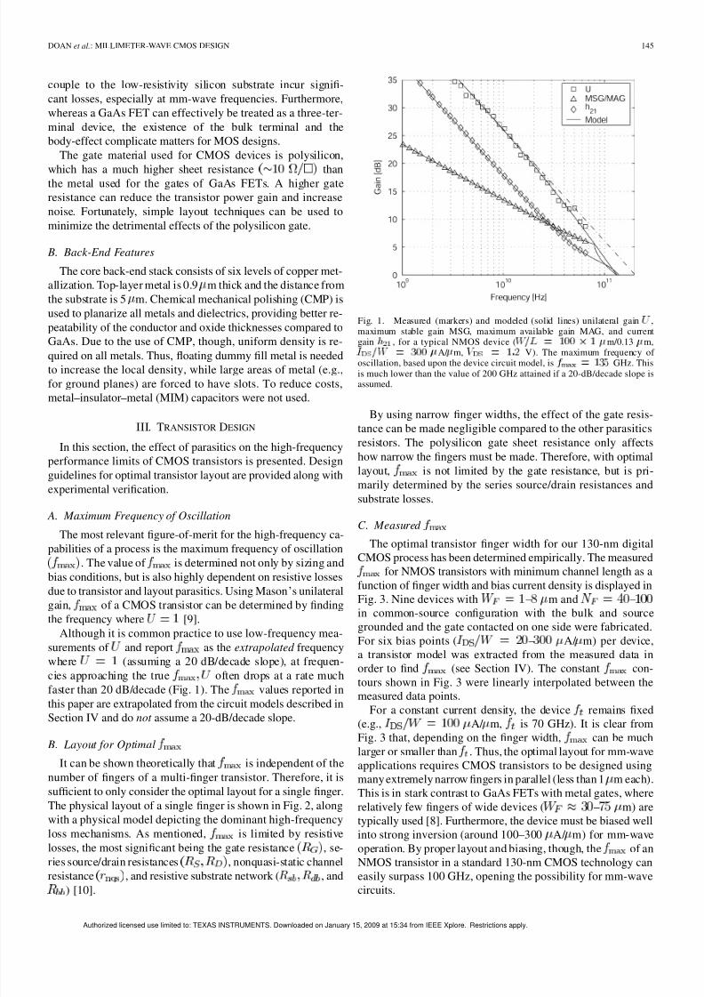
A. Maximum Frequency of Oscillation
The most relevant figure-of-merit for the high-frequency ca-
pabilities of a process is the maximum frequency of oscillation
. The value of is determined not only by sizing and
bias conditions, but is also highly dependent on resistive losses
due to transistor and layout parasitics. Using Mason’s unilateral
gain, of a CMOS transistor can be determined by finding
the frequency where [9].
Although it is common practice to use low-frequency mea-
surements of and report as the extrapolated frequency
where (assuming a 20 dB/decade slope), at frequen-
cies approaching the true often drops at a rate much
faster than 20 dB/decade (Fig. 1). The values reported in
this paper are extrapolated from the circuit models described in
Section IV and do not assume a 20-dB/decade slope.
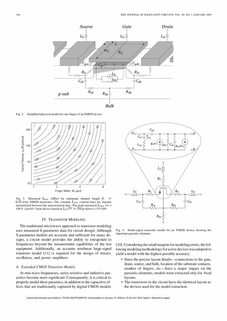
B. Layout for Optimal
It can be shown theoretically that is independent of the
number of fingers of a multi-finger transistor. Therefore, it is
suf ficient to only consider the optimal layout for a single finger.
The physical layout of a single finger is shown in Fig. 2, along
with a physical model depicting the dominant high-frequency
loss mechanisms. As mentioned, is limited by resistive
losses, the most significant being the gate resistance , se-
ries source/drain resistances , nonquasi-static channel
resistance , and resistive substrate network ( , and) [10].
Fig. 1. Measured (markers) and modeled (solid lines) unilateral gainU
,maximum stable gain MSG, maximum available gain MAG, and currentgain
h , for a typical NMOS device (
W = L = 1 0 0 2 1 m/0.13
m,
I = W = 3 0 0 A/ m, V = 1 : 2 V). The maximum frequency of oscillation, based upon the device circuit model, is f
= 1 3 5 GHz. This
is much lower than the value of 200 GHz attained if a 20-dB/decade slope isassumed.
By using narrow finger widths, the effect of the gate resis-
tance can be made negligible compared to the other parasitics
resistors. The polysilicon gate sheet resistance only affects
how narrow the fingers must be made. Therefore, with optimal
layout, is not limited by the gate resistance, but is pri-
marily determined by the series source/drain resistances and
substrate losses.
C. Measured
The optimal transistor finger width for our 130-nm digital
CMOS process has been determined empirically. The measured
for NMOS transistors with minimum channel length as a
function of finger width and bias current density is displayed in
Fig. 3. Nine devices with – m and –in common-source configuration with the bulk and source
grounded and the gate contacted on one side were fabricated.
For six bias points ( – A/ m) per device,
a transistor model was extracted from the measured data in
order to find (see Section IV). The constant con-
tours shown in Fig. 3 were linearly interpolated between the
measured data points.For a constant current density, the device remains fixed
(e.g., A/ m, is 70 GHz). It is clear from
Fig. 3 that, depending on the finger width, can be much
larger or smaller than . Thus, the optimal layout for mm-wave
applications requires CMOS transistors to be designed using
many extremely narrow fingers in parallel (less than 1 m each).
This is in stark contrast to GaAs FETs with metal gates, where
relatively few fingers of wide devices ( – m) are
typically used [8]. Furthermore, the device must be biased well
into strong inversion (around 100–300 A/ m) for mm-wave
operation. By proper layout and biasing, though, the of an
NMOS transistor in a standard 130-nm CMOS technology can
easily surpass 100 GHz, opening the possibility for mm-wavecircuits.
Authorized licensed use limited to: TEXAS INSTRUMENTS. Downloaded on January 15, 2009 at 15:34 from IEEE Xplore. Restrictions apply.
8/7/2019 Doan-Millimeter-Wave CMOS Design
http://slidepdf.com/reader/full/doan-millimeter-wave-cmos-design 3/12
146 IEEE JOURNAL OF SOLID-STATE CIRCUITS, VOL. 40, NO. 1, JANUARY 2005
Fig. 2. Simplified physical model for one finger of an NMOS device.
Fig. 3. Measured f [GHz] for minimum channel length (L =
0 : 1 3 m) NMOS transistors. The constant f contour lines are linearlyinterpolated between the measurement data. The peak measured f for a100 2 1 m/0.13 m device biased at I = W = 2 5 0 A/ m is 135 GHz.
IV. TRANSISTOR MODELING
The traditional microwave approach to transistor modelinguses measured S-parameter data for circuit design. Although
S-parameter models are accurate and suf ficient for many de-
signs, a circuit model provides the ability to extrapolate to
frequencies beyond the measurement capabilities of the test
equipment. Additionally, an accurate nonlinear large-signal
transistor model [11] is required for the design of mixers,
oscillators, and power amplifiers.
A. Extended CMOS Transistor Models
At mm-wave frequencies, series resistive and inductive par-
asitics become more significant. Consequently, it is critical to
properly model these parasitics, in addition to the capacitive ef-fects that are traditionally captured by digital CMOS models
Fig. 4. Small-signal transistor model for an NMOS device showing theimportant parasitic elements.
[10]. Considering the small margins for modeling errors, the fol-
lowing modeling methodology for active devices was adopted to
yield a model with the highest possible accuracy:
• Since the precise layout detailsconnections to the gate,
drain, source, and bulk, location of the substrate contacts,
number of fingers, etc.have a major impact on the
parasitic elements, models were extracted only for fixed
layouts.
• The transistors in the circuit have the identical layout asthe devices used for the model extraction.
Authorized licensed use limited to: TEXAS INSTRUMENTS. Downloaded on January 15, 2009 at 15:34 from IEEE Xplore. Restrictions apply.
8/7/2019 Doan-Millimeter-Wave CMOS Design
http://slidepdf.com/reader/full/doan-millimeter-wave-cmos-design 4/12
DOAN et al.: MILLIMETER-WAVE CMOS DESIGN 147
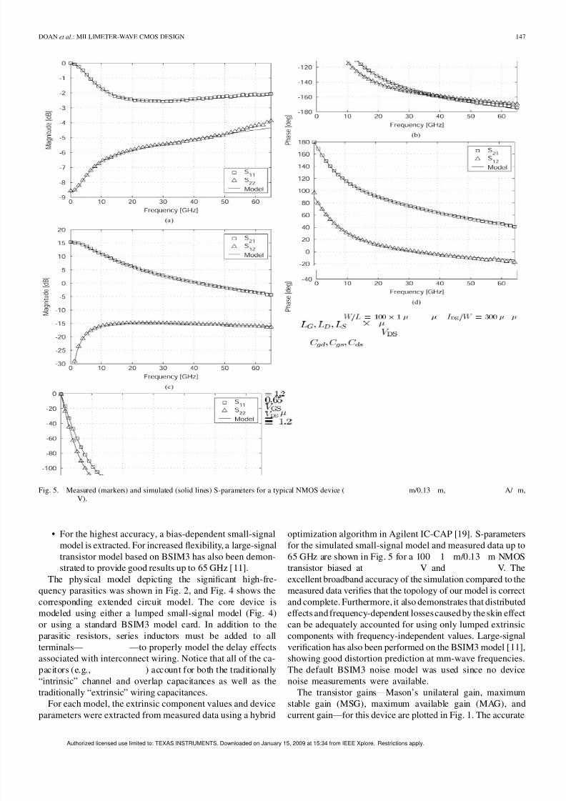
Fig. 5. Measured (markers) and simulated (solid lines) S-parameters for a typical NMOS device (W = L = 1 0 0 2 1
m/0.13
m,I = W = 3 0 0
A/
m,V = 1 : 2 V).
• For the highest accuracy, a bias-dependent small-signal
model is extracted. For increased flexibility, a large-signal
transistor model based on BSIM3 has also been demon-strated to provide good results up to 65 GHz [11].
The physical model depicting the significant high-fre-
quency parasitics was shown in Fig. 2, and Fig. 4 shows the
corresponding extended circuit model. The core device is
modeled using either a lumped small-signal model (Fig. 4)
or using a standard BSIM3 model card. In addition to the
parasitic resistors, series inductors must be added to all
terminals to properly model the delay effects
associated with interconnect wiring. Notice that all of the ca-
pacitors (e.g., ) account for both the traditionally
“intrinsic” channel and overlap capacitances as well as the
traditionally “extrinsic” wiring capacitances.
For each model, the extrinsic component values and deviceparameters were extracted from measured data using a hybrid
optimization algorithm in Agilent IC-CAP [19]. S-parameters
for the simulated small-signal model and measured data up to
65 GHz are shown in Fig. 5 for a 100 1 m/0.13 m NMOStransistor biased at V and V. The
excellent broadband accuracy of the simulation compared to the
measured data verifies that the topology of our model is correct
and complete. Furthermore, it also demonstrates that distributed
effects and frequency-dependent losses caused by the skin effect
can be adequately accounted for using only lumped extrinsic
components with frequency-independent values. Large-signal
verification has also been performed on the BSIM3 model [11],
showing good distortion prediction at mm-wave frequencies.
The default BSIM3 noise model was used since no device
noise measurements were available.
The transistor gainsMason’s unilateral gain, maximum
stable gain (MSG), maximum available gain (MAG), andcurrent gainfor this device are plotted in Fig. 1. The accurate
Authorized licensed use limited to: TEXAS INSTRUMENTS. Downloaded on January 15, 2009 at 15:34 from IEEE Xplore. Restrictions apply.
8/7/2019 Doan-Millimeter-Wave CMOS Design
http://slidepdf.com/reader/full/doan-millimeter-wave-cmos-design 5/12
148 IEEE JOURNAL OF SOLID-STATE CIRCUITS, VOL. 40, NO. 1, JANUARY 2005
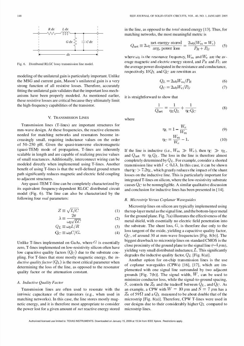
Fig. 6. Distributed RLGC lossy transmission line model.
modeling of the unilateral gain is particularly important. Unlike
the MSG and current gain, Mason’s unilateral gain is a very
strong function of all resistive losses. Therefore, accurately
fitting the unilateral gain validates that the important loss mech-
anisms have been properly modeled. As mentioned earlier,
these resistive losses are critical because they ultimately limit
the high-frequency capabilities of the transistor.
V. TRANSMISSION LINES
Transmission lines (T-lines) are important structures for
mm-wave design. At these frequencies, the reactive elements
needed for matching networks and resonators become in-
creasingly small, requiring inductance values on the order
of 50–250 pH. Given the quasi-transverse electromagnetic
(quasi-TEM) mode of propagation, T-lines are inherently
scalable in length and are capable of realizing precise values
of small reactances. Additionally, interconnect wiring can be
modeled directly when implemented using T-lines. Another
benefit of using T-lines is that the well-defined ground return
path significantly reduces magnetic and electric field coupling
to adjacent structures.
Any quasi-TEM T-line can be completely characterized by
its equivalent frequency-dependent RLGC distributed circuit
model (Fig. 6). The line can also be characterized by the
following four real parameters:
(1)
(2)
(3)
(4)
Unlike T-lines implemented on GaAs, where is essentiallyzero, T-lines implemented on low-resistivity silicon often have
low capacitive quality factors due to the substrate cou-
pling. For T-lines that store mostly magnetic energy, the in-
ductive quality factor is the most critical parameter when
determining the loss of the line, as opposed to the resonator
quality factor or the attenuation constant.
A. Inductive Quality Factor
Transmission lines are often used to resonate with the
intrinsic capacitance of the transistors (e.g., when used in
matching networks). In this case, the line stores mostly mag-
netic energy, and it is therefore most appropriate to considerthe power lost for a given amount of net reactive energy stored
in the line, as opposed to the total stored energy [13]. Thus, for
matching networks, the most meaningful metric is
(5)
where is the resonance frequency, and are the av-
erage magnetic and electric energy stored, and and arethe average power dissipated in the resistance and conductance,
respectively. If and are rewritten as
(6)
(7)
it is straightforward to show that
(8)
where
(9)
(10)
If the line is inductive (i.e., ), then ,
and . The loss in the line is therefore almost
completely determined by . For example, consider a shorted
transmission line with . In this case, it can be shown
that , which greatly reduces the impact of the shunt
losses on the inductive line. This is particularly important for
integrated T-lines on silicon, where the low-resistivity substratecauses to be nonnegligible. A similar qualitative discussion
and conclusion for inductive lines has been presented in [14].
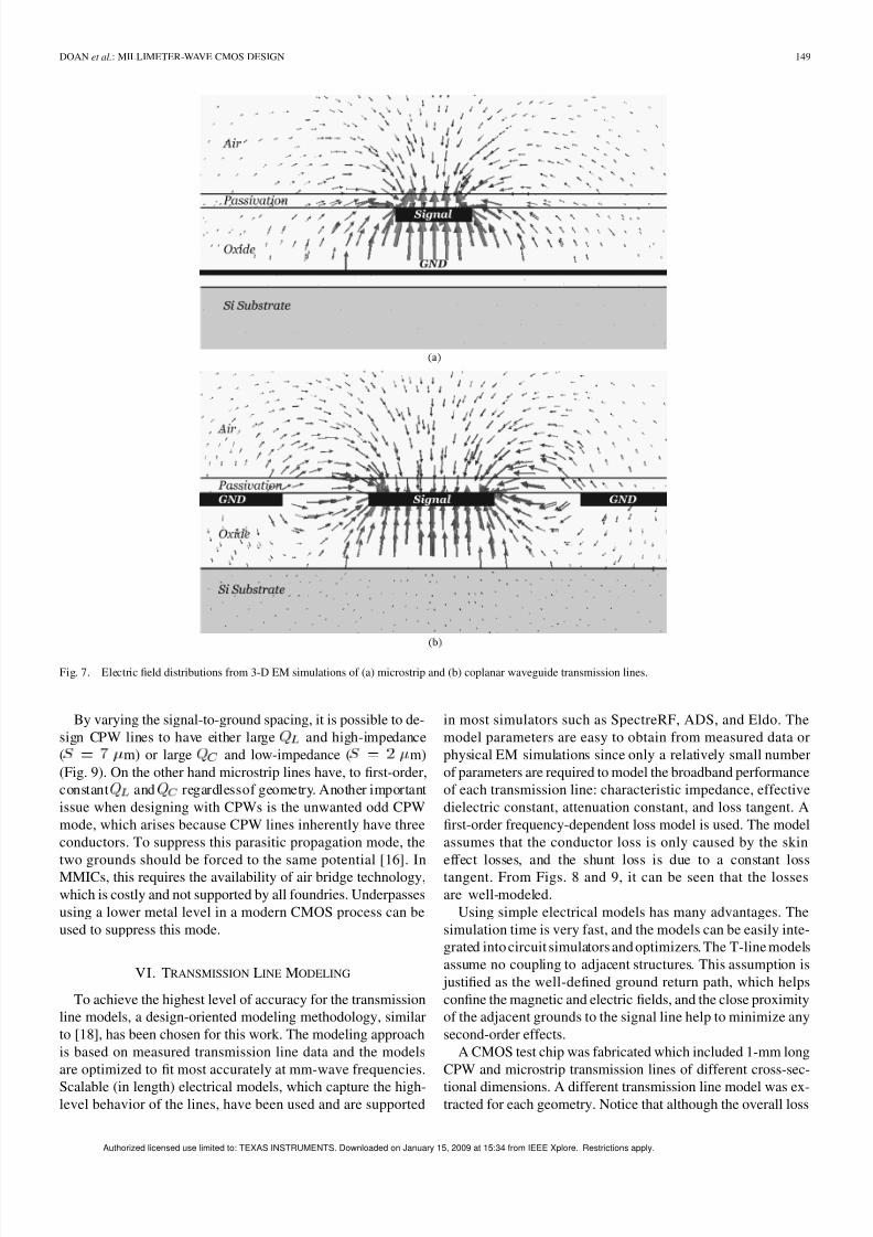
B. Microstrip Versus Coplanar Waveguides
Microstrip lines on silicon are typically implemented using
the top-layer metal as the signal line, and the bottom-layer metal
for the ground plane. Fig. 7(a) illustrates the effectiveness of the
metal shield, with essentially no electric field penetration into
the substrate. The shunt loss, , is therefore due only to the
loss tangent of the oxide, yielding a capacitive quality factor,
, of around 30 at mm-wave frequencies [Fig. 8(b)]. The
biggest drawback to microstrip lines on standard CMOS is theclose proximity of the ground plane to the signal line ( m),
yielding very small distributed inductance, . This significantly
degrades the inductive quality factor, [Fig. 8(a)].
Another option for on-chip transmission lines is the use
of coplanar waveguides (CPWs) [16], [17], which are im-
plemented with one signal line surrounded by two adjacent
grounds [Fig. 7(b)]. The signal width, , can be used to
minimize conductor loss, while the signal-to-ground spacing,
, controls the and the tradeoff between , and . As
an example, a CPW with m and m has a
of 59 and a measured to be about double that of the
microstrip [Fig. 8(a)]. Therefore, CPW T-lines were used in
our designs due to their considerably higher compared tomicrostrip lines.
Authorized licensed use limited to: TEXAS INSTRUMENTS. Downloaded on January 15, 2009 at 15:34 from IEEE Xplore. Restrictions apply.
8/7/2019 Doan-Millimeter-Wave CMOS Design
http://slidepdf.com/reader/full/doan-millimeter-wave-cmos-design 6/12
DOAN et al.: MILLIMETER-WAVE CMOS DESIGN 149
Fig. 7. Electric field distributions from 3-D EM simulations of (a) microstrip and (b) coplanar waveguide transmission lines.
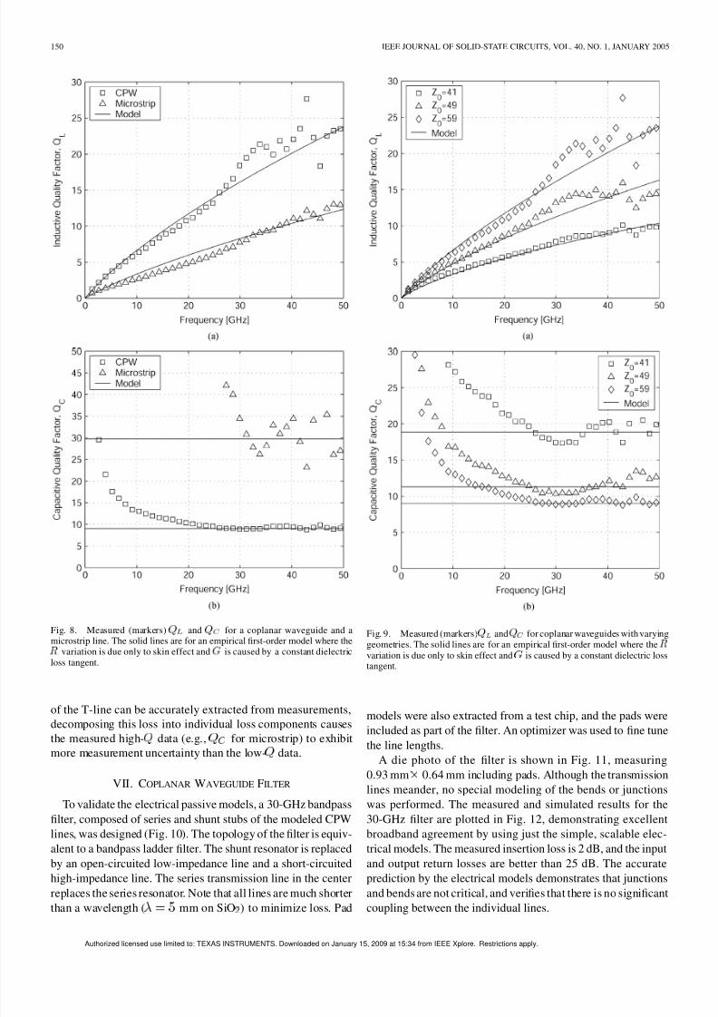
By varying the signal-to-ground spacing, it is possible to de-
sign CPW lines to have either large and high-impedance
( m) or large and low-impedance ( m)
(Fig. 9). On the other hand microstrip lines have, to first-order,
constant and regardlessof geometry. Another important
issue when designing with CPWs is the unwanted odd CPW
mode, which arises because CPW lines inherently have three
conductors. To suppress this parasitic propagation mode, the
two grounds should be forced to the same potential [16]. InMMICs, this requires the availability of air bridge technology,
which is costly and not supported by all foundries. Underpasses
using a lower metal level in a modern CMOS process can be
used to suppress this mode.
VI. TRANSMISSION LINE MODELING
To achieve the highest level of accuracy for the transmission
line models, a design-oriented modeling methodology, similar
to [18], has been chosen for this work. The modeling approach
is based on measured transmission line data and the models
are optimized to fit most accurately at mm-wave frequencies.
Scalable (in length) electrical models, which capture the high-level behavior of the lines, have been used and are supported
in most simulators such as SpectreRF, ADS, and Eldo. The
model parameters are easy to obtain from measured data or
physical EM simulations since only a relatively small number
of parameters are required to model the broadband performance
of each transmission line: characteristic impedance, effective
dielectric constant, attenuation constant, and loss tangent. A
first-order frequency-dependent loss model is used. The model
assumes that the conductor loss is only caused by the skin
effect losses, and the shunt loss is due to a constant losstangent. From Figs. 8 and 9, it can be seen that the losses
are well-modeled.
Using simple electrical models has many advantages. The
simulation time is very fast, and the models can be easily inte-
grated into circuit simulators and optimizers. The T-line models
assume no coupling to adjacent structures. This assumption is
justified as the well-defined ground return path, which helps
confine the magnetic and electric fields, and the close proximity
of the adjacent grounds to the signal line help to minimize any
second-order effects.
A CMOS test chip was fabricated which included 1-mm long
CPW and microstrip transmission lines of different cross-sec-
tional dimensions. A different transmission line model was ex-tracted for each geometry. Notice that although the overall loss
Authorized licensed use limited to: TEXAS INSTRUMENTS. Downloaded on January 15, 2009 at 15:34 from IEEE Xplore. Restrictions apply.
8/7/2019 Doan-Millimeter-Wave CMOS Design
http://slidepdf.com/reader/full/doan-millimeter-wave-cmos-design 7/12
150 IEEE JOURNAL OF SOLID-STATE CIRCUITS, VOL. 40, NO. 1, JANUARY 2005
Fig. 8. Measured (markers) Q and Q for a coplanar waveguide and amicrostrip line. The solid lines are for an empirical first-order model where the
R variation is due only to skin effect and
G is caused by a constant dielectric
loss tangent.
of the T-line can be accurately extracted from measurements,decomposing this loss into individual loss components causes
the measured high- data (e.g., for microstrip) to exhibit
more measurement uncertainty than the low- data.
VII. COPLANAR WAVEGUIDE FILTER
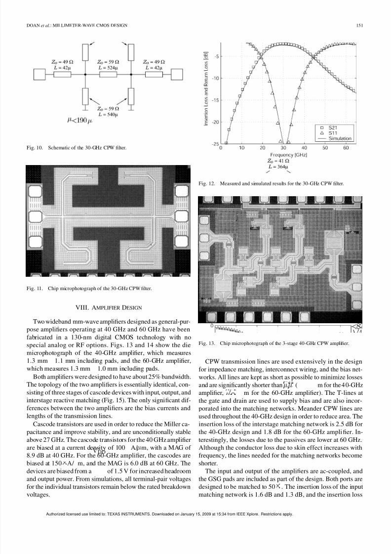
To validate the electrical passive models, a 30-GHz bandpass
filter, composed of series and shunt stubs of the modeled CPW
lines, was designed (Fig. 10). The topology of the filter is equiv-
alent to a bandpass ladder filter. The shunt resonator is replaced
by an open-circuited low-impedance line and a short-circuited
high-impedance line. The series transmission line in the center
replaces the series resonator. Note that all lines are much shorterthan a wavelength ( mm on SiO ) to minimize loss. Pad
Fig. 9. Measured (markers)Q
andQ
for coplanar waveguides with varyinggeometries. The solid lines are for an empirical first-order model where the
R
variation is due only to skin effect and G is caused by a constant dielectric losstangent.
models were also extracted from a test chip, and the pads wereincluded as part of the filter. An optimizer was used to fine tune
the line lengths.
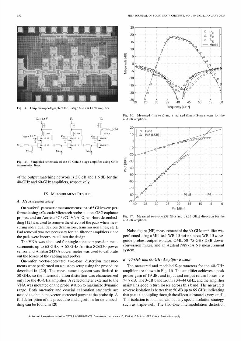
A die photo of the filter is shown in Fig. 11, measuring
0.93 mm 0.64 mm including pads. Although the transmission
lines meander, no special modeling of the bends or junctions
was performed. The measured and simulated results for the
30-GHz filter are plotted in Fig. 12, demonstrating excellent
broadband agreement by using just the simple, scalable elec-
trical models. The measured insertion loss is 2 dB, and the input
and output return losses are better than 25 dB. The accurate
prediction by the electrical models demonstrates that junctions
and bends are not critical, and verifies that there is no significantcoupling between the individual lines.
Authorized licensed use limited to: TEXAS INSTRUMENTS. Downloaded on January 15, 2009 at 15:34 from IEEE Xplore. Restrictions apply.
8/7/2019 Doan-Millimeter-Wave CMOS Design
http://slidepdf.com/reader/full/doan-millimeter-wave-cmos-design 8/12
DOAN et al.: MILLIMETER-WAVE CMOS DESIGN 151
Fig. 10. Schematic of the 30-GHz CPW filter.
Fig. 11. Chip microphotograph of the 30-GHz CPW filter.
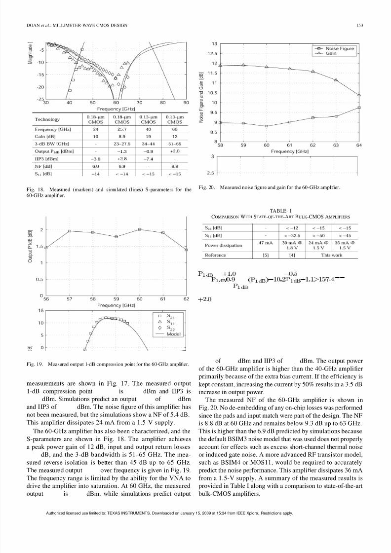
VIII. AMPLIFIER DESIGN
Two wideband mm-wave amplifiers designed as general-pur-
pose amplifiers operating at 40 GHz and 60 GHz have been
fabricated in a 130-nm digital CMOS technology with no
special analog or RF options. Figs. 13 and 14 show the die
microphotograph of the 40-GHz amplifier, which measures
1.3 mm 1.1 mm including pads, and the 60-GHz amplifier,
which measures 1.3 mm 1.0 mm including pads.
Both amplifiers were designed to have about 25% bandwidth.
The topology of the two amplifiers is essentially identical, con-
sisting of three stages of cascode devices with input, output, and
interstage reactive matching (Fig. 15). The only significant dif-
ferences between the two amplifiers are the bias currents and
lengths of the transmission lines.
Cascode transistors are used in order to reduce the Miller ca-
pacitance and improve stability, and are unconditionally stable
above 27 GHz. The cascode transistors for the 40 GHz amplifier
are biased at a current density of 100 A/ m, with a MAG of
8.9 dB at 40 GHz. For the 60-GHz amplifier, the cascodes are
biased at 150 A/ m, and the MAG is 6.0 dB at 60 GHz. The
devices are biased from a of 1.5 V for increased headroom
and output power. From simulations, all terminal-pair voltages
for the individual transistors remain below the rated breakdownvoltages.
Fig. 12. Measured and simulated results for the 30-GHz CPW filter.
Fig. 13. Chip microphotograph of the 3-stage 40-GHz CPW amplifier.
CPW transmission lines are used extensively in the design
for impedance matching, interconnect wiring, and the bias net-
works. All lines are kept as short as possible to minimize losses
and are significantly shorter than ( m for the 4 0-GHzamplifier, m for the 60-GHz amplifier). The T-lines at
the gate and drain are used to supply bias and are also incor-
porated into the matching networks. Meander CPW lines are
used throughout the 40-GHz design in order to reduce area. The
insertion loss of the interstage matching network is 2.5 dB for
the 40-GHz design and 1.8 dB for the 60-GHz amplifier. In-
terestingly, the losses due to the passives are lower at 60 GHz.
Although the conductor loss due to skin effect increases with
frequency, the lines needed for the matching networks become
shorter.
The input and output of the amplifiers are ac-coupled, and
the GSG pads are included as part of the design. Both ports are
designed to be matched to 50 . The insertion loss of the inputmatching network is 1.6 dB and 1.3 dB, and the insertion loss
Authorized licensed use limited to: TEXAS INSTRUMENTS. Downloaded on January 15, 2009 at 15:34 from IEEE Xplore. Restrictions apply.
8/7/2019 Doan-Millimeter-Wave CMOS Design
http://slidepdf.com/reader/full/doan-millimeter-wave-cmos-design 9/12
152 IEEE JOURNAL OF SOLID-STATE CIRCUITS, VOL. 40, NO. 1, JANUARY 2005
Fig. 14. Chip microphotograph of the 3-stage 60-GHz CPW amplifier.
Fig. 15. Simplified schematic of the 60-GHz 3-stage amplifier using CPWtransmission lines.
of the output matching network is 2.0 dB and 1.6 dB for the
40-GHz and 60-GHz amplifiers, respectively.
IX. MEASUREMENT RESULTS
A. Measurement Setup
On-wafer S-parameter measurements up to 65 GHz were per-
formed using a Cascade Microtech probe station, GSG coplanar
probes, and an Anritsu 37 397C VNA. Open-short de-embed-
ding [12] was used to remove the effects of the pads when mea-
suring individual devices (transistors, transmission lines, etc.).
Pad removal was not necessary for the filter or amplifiers since
the pads were incorporated into the design.
The VNA was also used for single-tone compression mea-
surements up to 65 GHz. A 65-GHz Anritsu SC6230 power
sensor and Anritsu 2437A power meter was used to calibrate
out the losses of the cabling and probes.
On-wafer vector-corrected two-tone distortion measure-
ments were performed on a custom setup using the procedure
described in [20]. The measurement system was limited to
50 GHz, so the intermodulation distortion was characterized
only for the 40-GHz amplifier. A reflectometer external to the
VNA was mounted on the probe station to maximize dynamic
range. Both on-wafer and coaxial calibration standards are
needed to obtain the vector-corrected power at the probe tip. A
full description of the procedure and algorithm for de-embed-ding can be found in [20].
Fig. 16. Measured (markers) and simulated (lines) S-parameters for the
40-GHz amplifier.
Fig. 17. Measured two-tone (38 GHz and 38.25 GHz) distortion for the40-GHz amplifier.
Noise figure (NF) measurement of the 60-GHz amplifier was
performed using a Millitech WR-15 noise source, WR-15 wave-
guide probes, output isolator, OML 50–75-GHz DSB down-
conversion mixer, and an Agilent N8973A NF measurement
system.
B. 40-GHz and 60-GHz Amplifier Results
The measured and modeled S-parameters for the 40-GHz
amplifier are shown in Fig. 16. The amplifier achieves a peak
power gain of 19 dB, and input and output return losses are
dB. The 3-dB bandwidth is 34–44 GHz, and the amplifier
maintains good return losses across this band. The measured
reverse isolation is better than 50 dB up to 65 GHz, indicating
that parasiticcoupling through the silicon substrateis very small.
This isolation is obtained without any special isolation strategysuch as triple-well. The two-tone intermodulation distortion
Authorized licensed use limited to: TEXAS INSTRUMENTS. Downloaded on January 15, 2009 at 15:34 from IEEE Xplore. Restrictions apply.
8/7/2019 Doan-Millimeter-Wave CMOS Design
http://slidepdf.com/reader/full/doan-millimeter-wave-cmos-design 10/12
DOAN et al.: MILLIMETER-WAVE CMOS DESIGN 153
Fig. 18. Measured (markers) and simulated (lines) S-parameters for the
60-GHz amplifier.
Fig. 19. Measured output 1-dB compression point for the 60-GHz amplifier.
measurements are shown in Fig. 17. The measured output
1-dB compression point is dBm and IIP3 is
dBm. Simulations predict an output of dBm
and IIP3 of dBm. The noise figure of this amplifier has
not been measured, but the simulations show a NF of 5.4 dB.
This amplifier dissipates 24 mA from a 1.5-V supply.
The 60-GHz amplifier has also been characterized, and the
S-parameters are shown in Fig. 18. The amplifier achieves
a peak power gain of 12 dB, input and output return losses
dB, and the 3-dB bandwidth is 51–65 GHz. The mea-
sured reverse isolation is better than 45 dB up to 65 GHz.
The measured output over frequency is given in Fig. 19.
The frequency range is limited by the ability for the VNA to
drive the amplifier into saturation. At 60 GHz, the measuredoutput is dBm, while simulations predict output
Fig. 20. Measured noise figure and gain for the 60-GHz amplifier.
TABLE ICOMPARISON WITH STATE-OF-THE-ART BULK-CMOS AMPLIFIERS
of dBm and IIP3 of dBm. The output power
of the 60-GHz amplifier is higher than the 40-GHz amplifier
primarily because of the extra bias current. If the ef ficiency is
kept constant, increasing the current by 50% results in a 3.5 dBincrease in output power.
The measured NF of the 60-GHz amplifier is shown in
Fig. 20. No de-embedding of any on-chip losses was performed
since the pads and input match were part of the design. The NF
is 8.8 dB at 60 GHz and remains below 9.3 dB up to 63 GHz.
This is higher than the 6.9 dB predicted by simulations because
the default BSIM3 noise model that was used does not properly
account for effects such as excess short-channel thermal noise
or induced gate noise. A more advanced RF transistor model,
such as BSIM4 or MOS11, would be required to accurately
predict the noise performance. This amplifier dissipates 36 mA
from a 1.5-V supply. A summary of the measured results is
provided in Table I along with a comparison to state-of-the-artbulk-CMOS amplifiers.
Authorized licensed use limited to: TEXAS INSTRUMENTS. Downloaded on January 15, 2009 at 15:34 from IEEE Xplore. Restrictions apply.
8/7/2019 Doan-Millimeter-Wave CMOS Design
http://slidepdf.com/reader/full/doan-millimeter-wave-cmos-design 11/12
154 IEEE JOURNAL OF SOLID-STATE CIRCUITS, VOL. 40, NO. 1, JANUARY 2005
X. CONCLUSION
A mm-wave design and modeling methodology for CMOS
devices and circuits has been presented. Optimization of the
active and passive components for mm-wave circuits leads to
transistors with finger widths m and the use of CPW trans-
mission lines. A modeling methodology, using relatively simple
models that carefully account for the resistive losses, has been
described and applied to transistors and transmission lines. The
models have been verified to achieve broadband accuracy from
dc to 65 GHz. Finally, two wideband mm-wave CMOS ampli-
fiers, operating at 40 GHz and 60 GHz, were fabricated using
a 130-nm bulk-CMOS technology. The measured S-parameters
correspond extremely well to the simulated models owing to
the accurate device modeling. The 40-GHz amplifier achieves
19-dB gain, output dBm, and dBm,
while consuming 36 mW. The 60-GHz amplifier achieves12-dB
gain, output dBm, and dB, while
consuming 54 mW. These are the first demonstrated amplifiers
operating above 30 GHz fabricated using a mainstream bulk-CMOS technology. These amplifiers greatly improve on the cur-
rent state-of-the-art, owing to the mm-wave CMOS design and
modeling approach described in this work.
ACKNOWLEDGMENT
The authors acknowledge STMicroelectronics and B. Gupta
for chip fabrication. The authors thank A. Cognata and
T. Shirley of Agilent Technologies, Santa Rosa, for help
with two-tone and distortion measurements, and H. Tran and
K. Fujii of Agilent Technologies, San Jose, for help with noisefigure measurements. Useful discussions and feedback from
G. Baldwin, A. Vladimirescu, D. Yee, I. O’Donnell, J. Vander-
haegen, J. Weldon, and the BWRC OGRE group were greatly
appreciated.
REFERENCES
[1] L. M. Franca-Neto, R. E. Bishop, and B. A. Bloechel, “64 GHz and100 GHz VCO’s in 90 nm CMOS using optimum pumping method,” inIEEE Int. Solid-State Circuits Conf. Dig. Tech. Papers, Feb. 2004, pp.
444–445.[2] R.-C. Liu, H.-Y. Chang, C.-H. Wang, and H. Wang, “A 63 GHz VCO
using a standard 0.25 m CMOS process,” in IEEE Int. Solid-State Cir-cuits Conf. Dig. Tech. Papers, Feb. 2004, pp. 446–447.
[3] M. Tiebout, H.-D. Wohlmuth, and W. Simbürger, “A 1 V 51 GHz fully-integrated VCO in 0.12
m CMOS,” in IEEE Int. Solid-State Circuits
Conf. Dig. Tech. Papers, Feb. 2002, pp. 238–239.[4] K.-W. Yu, Y.-L. Lu, D.-C. Ch ang, V. Liang, and M. F. Chang, “K-band
low-noise amplifiers using 0.18
m CMOS technology,” IEEE Microw.
Wireless Compon. Lett., vol. 14, no. 3, pp. 106 –108, Mar. 2004.[5] L. M. Franca-Neto, B. A. Bloechel, and K. Soumyanath, “17 GHz
and 24 GHz LNA designs based on extended-S-parameter with mi-crostrip-on-die in 0.18 m logic CMOS technology,” in Proc. Eur.Solid-State Circuits Conf., Sep. 2003, pp. 149–152.
[6] X. Guan and A. Hajimiri, “A 24 GHz CMOS front-end,” in Proc. Eur.Solid-State Circuits Conf., Sep. 2002, pp. 155–158.
[7] M. Madihian,H. Fujii,H. Yoshida, H. Suzuki, and T. Yamazaki, “A 1–10GHz, 0.18 m-CMOS chipset for multi-mode wireless applications,” in
IEEE MTT-S Int. Microwave Symp. Dig., June 2001, pp. 1865–1868.[8] I. Bahl and P. Bhartia, Microwave Solid State Circuit Design, 2nded. Hoboken, NJ: Wiley, 2003.
[9] R. Spence, Linear Active Networks, London: Wiley, 1970.[10] C. Enz, “An MOS transistor model for RF IC design valid in all regions
of operation,” IEEE Trans. Microw. Theory Tech., vol. 50, no. 1, pp.342–359, Jan. 2002.
[11] S. Emami, C. H. Doan, A. M. Niknejad, and R. W. Brodersen, “Large-signal millimeter-wave CMOS modeling with BSIM3,” in IEEE RFIC Symp. Dig., Jun. 2004, pp. 163–166.
[12] M. C. A. M. Koolen, J. A. M. Geelen, and M. P. J. G. Versleijen, “An
improved de-embedding technique for on-wafer high-frequency char-acterization,” in Proc. IEEE Bipolar/BiCMOS Circuits and TechnologyMeeting, Sep. 1991, pp. 188–191.
[13] C. P. Yue and S. S. Wong, “On-chip spiral inductors with patternedground shields for Si-based RF IC’s,” IEEE J. Solid-State Circuits, vol.33, no. 5, pp. 743–752, May 1998.
[14] F. Ellinger, “26–42 GHz SOI CMOSlownoise amplifier,” IEEE J. Solid-State Circuits, vol. 39, no. 3, pp. 522–528, Mar. 2004.
[15] S. Ramo, J. R. Whinnery, and T. Van Duzer, Fields and Waves in Com-munication Electronics, 3rd ed. New York: Wiley, 1994.
[16] T. C. Edwards and M. B. Steer, Foundations of Interconnect and Mi-crostrip Design, 3rd ed. New York: Wiley, 2000.
[17] B. Kleveland, C. H. Diaz, D. Vook, L. Madden, T. H. Lee, and S. S.Wong, “Exploiting CMOS reverse interconnect scaling in multigiga-hertz amplifier and oscillator design,” IEEE J. Solid-State Circuits, vol.36, no. 10, pp. 1480–1488, Oct. 2001.
[18] G. Carchon, W. De Raedt, and B. Nauwelaers, “Novel approach for a
design-oriented measurement-based fully scalable coplanar waveguidetransmission line model,” in IEE Proc. Microwave, Antennas Propagat.,vol. 148, Aug. 2001, pp. 227–232.
[19] Agilent IC-CAP 2002 User’s Guide [Online]. Available: http:// eesof.tm.agilent.com
[20] B. Hughes, A. Ferrero, and A. Cognata, “Accurate on-wafer power andharmonic measurements of mm-wave amplifiers and devices,” in IEEE MTT-S Int. Microwave Symp. Dig., Jun. 1992, pp. 1019–1022.
Chinh H. Doan (S’99) received the B.S. degree fromthe California Institute of Technology, Pasadena, in1997, and the M.S. degree from the University of California, Berkeley, in 2000, both in electrical en-
gineering. He is currently working toward the Ph.D.degree at the University of California, Berkeley,where he is a member of the Berkeley WirelessResearch Center.
He held an internship position at Agilent Tech-nologies, in 2002, where he designed and fabricated
broadband monolithic microwave integrated circuit(MMIC) power amplifiers for test and measurement equipment operating upto 50 GHz using GaAs pHEMT technology. His current area of research isfocused on the design of millimeter-wave transceiver circuits on CMOS, activeand passive device modeling, and de-embedding and verification techniquesfor on-wafer probing on lossy substrates.
Sohrab Emami received the B.S. degree from the
Sharif University of Technology, Tehran, Iran, in1995, and theM.S. degreefrom the Tokyo Instituteof Technology, in 2001, both in electrical engineering.He is currently working toward the Ph.D. degree atthe University of California, Berkeley, where he is amember of the Berkeley Wireless Research Center.
Hiscurrent research is focused on thedesign, mod-
eling, and analysis of CMOS frequency-convertingblocks such as mixers, frequency multipliers, and di-
viders, for 60-GHz wireless systems. From 1995 to1998, he co-founded KARA-Systems Inc. working on control and instrumenta-tion in the Iranian oil and natural gas industries. From 2000 to 2001, he held apart-time position at Hitachi Ltd., Tokyo, Japan, designing low-power CMOSbaseband filters for direct-conversion wideband-CDMA receivers. In 2003, hewas awarded the Hitachi-UC Berkeley Management of Technology Fellowship,where hisresponsibilities included thedesignand implementation of a multi-an-
tenna prototype reader for the Hitachi MuChip RFID.Mr. Emami also participated in the 21st International Physics Olympiad,Netherlands,and wasthe Gold Medal winnerof theNational Physics Olympiad.
Authorized licensed use limited to: TEXAS INSTRUMENTS. Downloaded on January 15, 2009 at 15:34 from IEEE Xplore. Restrictions apply.
8/7/2019 Doan-Millimeter-Wave CMOS Design
http://slidepdf.com/reader/full/doan-millimeter-wave-cmos-design 12/12
DOAN et al.: MILLIMETER-WAVE CMOS DESIGN 155
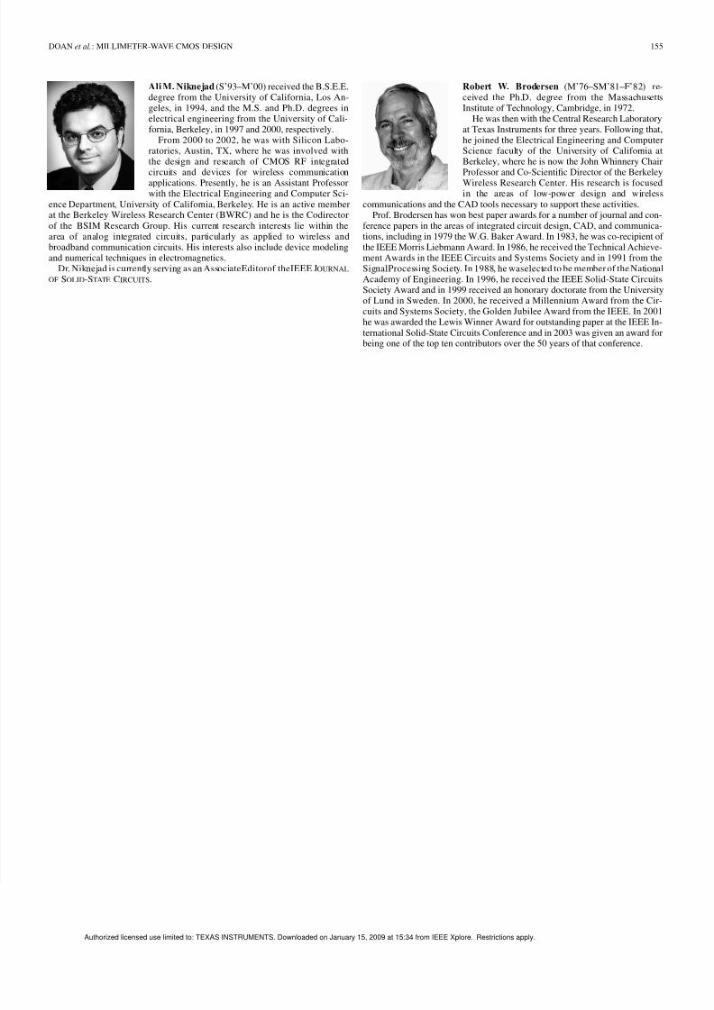
Ali M. Niknejad (S’93–M’00) received the B.S.E.E.degree from the University of California, Los An-geles, in 1994, and the M.S. and Ph.D. degrees inelectrical engineering from the University of Cali-fornia, Berkeley, in 1997 and 2000, respectively.
From 2000 to 2002, he was with Silicon Labo-ratories, Austin, TX, where he was involved withthe design and research of CMOS RF integrated
circuits and devices for wireless communicationapplications. Presently, he is an Assistant Professorwith the Electrical Engineering and Computer Sci-
ence Department, University of California, Berkeley. He is an active memberat the Berkeley Wireless Research Center (BWRC) and he is the Codirector
of the BSIM Research Group. His current research interests lie within thearea of analog integrated circuits, particularly as applied to wireless andbroadband communication circuits. His interests also include device modelingand numerical techniques in electromagnetics.
Dr. Niknejad is currently serving as an AssociateEditorof theIEEE JOURNAL
OF SOLID-STATE CIRCUITS.
Robert W. Brodersen (M’76–SM’81–F’82) re-ceived the Ph.D. degree from the MassachusettsInstitute of Technology, Cambridge, in 1972.
He was then with the Central Research Laboratoryat Texas Instruments for three years. Following that,he joined the Electrical Engineering and ComputerScience faculty of the University of California atBerkeley, where he is now the John Whinnery Chair
Professor and Co-Scientific Director of the BerkeleyWireless Research Center. His research is focusedin the areas of low-power design and wireless
communications and the CAD tools necessary to support these activities.Prof. Brodersen has won best paper awards for a number of journal and con-
ference papers in the areas of integrated circuit design, CAD, and communica-tions, including in 1979 the W.G. Baker Award. In 1983, he was co-recipient of the IEEE Morris Liebmann Award. In 1986, he received the Technical Achieve-ment Awards in the IEEE Circuits and Systems Society and in 1991 from theSignalProcessing Society. In 1988, he waselected to be member of the NationalAcademy of Engineering. In 1996, he received the IEEE Solid-State CircuitsSociety Award and in 1999 received an honorary doctorate from the Universityof Lund in Sweden. In 2000, he received a Millennium Award from the Cir-cuits and Systems Society, the Golden Jubilee Award from the IEEE. In 2001he was awarded the Lewis Winner Award for outstanding paper at the IEEE In-
ternational Solid-State Circuits Conference and in 2003 was given an award forbeing one of the top ten contributors over the 50 years of that conference.