
AMS Thesis
85
Design and Implementation of A Novel Single-Phase Switched Reluctance Motor Drive System By: Amanda Martin Staley Thesis submitted to the Faculty of the Virginia Polytechnic Institute and State University in partial fulfillment of the requirements for the degree of Master of Science in Electrical Engineering Approved: Dr. Krishnan Ramu, Chair Dr. Lamine Mili Dr. Hugh VanLandingham August 21, 2001 Blacksburg, Virginia Copyright © 2001, Amanda Martin Staley Keywords: Single Phase Switched Reluctance Motor, Auxiliary Windings, Reliable Starting, Minimum Cost, Minimum Component Control
-
Upload
ariana-ribeiro-lameirinhas -
Category
Documents
-
view
237 -
download
0
Transcript of AMS Thesis
Design and Implementation of A Novel Single-Phase Switched Reluctance Motor Drive System
By:
Amanda Martin Staley
Thesis submitted to the Faculty of the Virginia Polytechnic Institute and State University in partial fulfillment of the requirements for the degree of
Master of Science
in
Electrical Engineering
Approved:
Dr. Krishnan Ramu, Chair
Dr. Lamine Mili
Dr. Hugh VanLandingham
August 21, 2001 Blacksburg, Virginia
Copyright © 2001, Amanda Martin Staley
Keywords: Single Phase Switched Reluctance Motor, Auxiliary Windings, Reliable Starting, Minimum Cost, Minimum Component Control

Design and Implementation of A Novel Single-Phase Switched Reluctance Motor Drive System
By: Amanda Martin Staley
(Abstract) Single phase switched reluctance machines (SRMs) have a special place in the emerging
high-volume, low-cost and low-performance applications in appliances and also in high-speed low-power motor drives in various industrial applications. Single phase SRMs have a number of drawbacks: low power density as they have only 50% utilization of windings, lack of self-starting feature unless otherwise built in to the machine, most of the times with permanent magnets or sometimes with distinct and special machine rotor configurations or additional mechanisms. Many of these approaches are expensive or make the manufacturing process more difficult. In order to overcome such disadvantages a method involving interpoles and windings is discussed in this research. Also, a new and novel converter topology requiring only a single switch and a single diode is realized.
This research tests the concepts and feasibility of this new single-phase SRM motor
topology and converter in one quadrant operation. The converter electronics and a simple minimum component, minimum cost analog converter are designed and implemented. The entire system is simulated and evaluated on its advantages and disadvantages. Simple testing without load is performed.
This system has a large number of possibilities for development. Due to its lightweight,
compact design and efficient, variable high-speed operation, the system might find many applications in pumps, fans, and drills.

iii
Acknowledgements
There are numerous people I must thank that have helped me through the course of my
graduate studies. I would like to express my deepest gratitude to my advisor, Dr. Krishnan
Ramu. Without his constant support, this research would never have come to fruition. Also, I
would like to thank Dr. Lamine Mili and Dr. Hugh VanLandingham for taking the time to be part
of my examination committee.
I would also like to thank my family and my friends. Their constant prodding helped me
reach the heights I have found today. I would especially like to thank those that I worked with at
MCSRG, particularly Praveen Vijayraghavan, Phillip Vallance, and Ajit Bhanot. Also, I would
like to thank my parents, Brenda and David Martin, my brother, Kevin Martin, and my husband,
Shaun Staley. They had faith in me, even when I did not.
Finally, I would like to express my appreciation to the Via Family for supporting my
research and studies through the Bradley Fellowship. Without this funding, the research in this
area might not have been possible.

iv
Table of Contents ACKNOWLEDGEMENTS __________________________________________________________________ III
LIST OF FIGURES ________________________________________________________________________ VI
LIST OF TABLES ________________________________________________________________________ VII
LIST OF SYMBOLS ______________________________________________________________________VIII
CHAPTER 1. INTRODUCTION ______________________________________________________________ 1 1.1 HISTORY OF THE SWITCHED RELUCTANCE MACHINE AND PRINCIPLES OF ITS OPERATION________________ 1 1.2 PREVIOUS ART OF SINGLE-PHASE SWITCHED RELUCTANCE MOTOR DRIVES__________________________ 2 1.3 OBJECTIVES AND NOVEL CONCEPTS OF PROPOSED DRIVE SYSTEM _________________________________ 6 1.4 SCOPE OF SYSTEM DESIGN ________________________________________________________________ 6 1.5 ORGANIZATION OF MATERIALS PRESENTED___________________________________________________ 7
CHAPTER 2. MACHINE CONFIGURATION __________________________________________________ 8 2.1 MACHINE DESCRIPTION __________________________________________________________________ 8
2.1.1 Dimensions ________________________________________________________________________ 8 2.1.2 Power Statistics and Finite Element Analysis Results ______________________________________ 10
2.2 EXPERIMENTAL VERIFICATION OF MAIN WINDING INDUCTANCE__________________________________ 15 2.2.1 Experimental Test Setup _____________________________________________________________ 15 2.2.2 Experimental Results________________________________________________________________ 16
CHAPTER 3. CONVERTER SELECTION ____________________________________________________ 19 3.1 PURPOSE AND PLACE IN DRIVE SYSTEM _____________________________________________________ 19 3.2 ALTERNATIVES ________________________________________________________________________ 19 3.3 FINAL SELECTION ______________________________________________________________________ 20
3.3.1 Description _______________________________________________________________________ 20 3.3.2 Design Analysis____________________________________________________________________ 21
3.3.2.1 AC to DC Conversion ___________________________________________________________ 22 3.3.2.2 Control Circuit Power Supply _____________________________________________________ 24 3.3.2.3 Current Sensing Scheme _________________________________________________________ 26 3.3.2.3 Semiconductor Switch ___________________________________________________________ 26 3.3.2.5 Snubbering Circuit ______________________________________________________________ 26 3.3.2.6 External Resistor for Auxiliary Winding Current Limiting _______________________________ 28
3.3.3 Advantages and Disadvantages _______________________________________________________ 28 CHAPTER 4. CONTROL DESIGN___________________________________________________________ 30
4.1 DESIGN APPROACH_____________________________________________________________________ 30 4.2 COMPONENTS DESIGN __________________________________________________________________ 31
4.2.1 PWM Control and Gate Drive Signal ___________________________________________________ 31 4.2.2 Current Control Loop _______________________________________________________________ 36
4.2.2.1 Current Feedback _______________________________________________________________ 37 4.2.2.2 Current Error Determination ______________________________________________________ 41 4.2.2.3 Current PI Controller ____________________________________________________________ 42 4.2.2.4 Current Control Signal Limiter ____________________________________________________ 46
4.2.3 Speed Control Loop ________________________________________________________________ 46 4.2.3.1 Speed Feedback ________________________________________________________________ 47 4.2.3.2 Speed Command Generation ______________________________________________________ 50 4.2.3.3 Speed Error Determination________________________________________________________ 50 4.2.3.4 Speed PI Controller _____________________________________________________________ 51

v
4.2.3.4 Speed Control Signal Limiter______________________________________________________ 53 4.3 CONSTRUCTION AND CONNECTION_________________________________________________________ 53
CHAPTER 5. EXPERIMENTAL RESULTS AND EVALUATION ________________________________ 54 5.1 EXPERIMENTAL SETUP __________________________________________________________________ 54 5.2 EXPERIMENTAL RESULTS ________________________________________________________________ 55 5.3 EVALUATION _________________________________________________________________________ 64
CHAPTER 6. CONCLUSIONS ______________________________________________________________ 65 6.1 SUMMARY____________________________________________________________________________ 65 6.2 POSSIBLE APPLICATIONS ________________________________________________________________ 66 6.3 RECOMMENDATIONS FOR FUTURE WORK____________________________________________________ 66
REFERENCES ____________________________________________________________________________ 67
APPENDICES_____________________________________________________________________________ 69 APPENDIX A – EQUIPMENT LISTING AND COST ANALYSIS __________________________________________ 69 APPENDIX B – CONVERTER WIRING DIAGRAM ___________________________________________________ 71 APPENDIX C – CURRENT CONTROL LOOP LOGICAL SCHEMATIC______________________________________ 72 APPENDIX D – CURRENT CONTROL LOOP WIRING SCHEMATIC_______________________________________ 73 APPENDIX E – SPEED CONTROL LOOP LOGICAL SCHEMATIC ________________________________________ 74 APPENDIX F – SPEED CONTROL LOOP WIRING SCHEMATIC _________________________________________ 75 APPENDIX G – TOTAL SYSTEM WIRING DIAGRAM ________________________________________________ 76
VITA ____________________________________________________________________________________ 77

vi
List of Figures Figure 1.1 – Single-Phase SRM Involving a Holding Mechanism for Reliable Starting ______________________ 4 Figure 1.2 – Single-Phase SRM Involving a Vane for Reliable Starting __________________________________ 5 Figure 1.3 – Single-Phase SRM Involving Pole Shaping and Permanent Magnets for Starting _________________ 6 Figure 2.1 – Proposed machine configuration ______________________________________________________ 9 Figure 2.2 – FEA – Main Windings energized with 8 A DC __________________________________________ 11 Figure 2.3 – FEA – Interpole pair #1 energized with 2 A DC _________________________________________ 11 Figure 2.4 – Flux Linkage – Main windings energized ______________________________________________ 13 Figure 2.5 – Flux Linkage - Interpole pairs #1 and #2 energized _______________________________________ 13 Figure 2.6 – Torque – Main Windings energized ___________________________________________________ 14 Figure 2.7 – Torque – Interpole pairs #1 and #2 energized____________________________________________ 14 Figure 2.8 – Machine and components ___________________________________________________________ 15 Figure 2.9 – Inductance Measurement at 1 A DC___________________________________________________ 16 Figure 2.10 – Expanded Inductance Measurement at 1 A DC _________________________________________ 17 Figure 2.11 – Inductance Profile for 8 A DC From FEA Results _______________________________________ 18 Figure 2.12 – Inductance Profiles for Specific DC Currents from Experimental Results and Interpolation_______ 19 Figure 3.1 – Converter Design _________________________________________________________________ 21 Figure 3.2 – Typical Inductance and Main Current Profiles ___________________________________________ 22 Figure 4.1 – Control Methodology Block Diagram _________________________________________________ 30 Figure 4.2 – Hall Sensor Attachments to the Endbell ________________________________________________ 32 Figure 4.3 – Switching Analysis regarding Hall Sensor Outputs _______________________________________ 33 Figure 4.4 – Hall Sensor to Exclusive Or Logical Connections ________________________________________ 33 Figure 4.5 – PWM IC Connections______________________________________________________________ 35 Figure 4.6 – Gate Drive Logic Circuit Connections _________________________________________________ 36 Figure 4.7 – Gate Drive Signal Generation Analysis ________________________________________________ 36 Figure 4.8 – Current Control Loop Block Diagram _________________________________________________ 37 Figure 4.9 – Alternate Sensing Configuration Converter _____________________________________________ 38 Figure 4.10 – Summing Amplifier for Current Feedback _____________________________________________ 39 Figure 4.11 – Gain Amplifier for Current Feedback_________________________________________________ 40 Figure 4.12 – Current Feedback and Current in the Main Winding _____________________________________ 41 Figure 4.13 – Subtractor Circuit to determine Current Error __________________________________________ 42 Figure 4.14 – Proportional Gain Stage Circuit for Current PI _________________________________________ 43 Figure 4.15 – Noninverting Practical Integrator Stage Circuit for Current PI _____________________________ 44 Figure 4.16 – Summing Amplifier for Current PI___________________________________________________ 46 Figure 4.17 – Speed Control Loop Block Diagram__________________________________________________ 47 Figure 4.18 – Frequency to Voltage Converter Connections __________________________________________ 50 Figure 4.19 – Subtractor Circuit to determine Speed Error____________________________________________ 51 Figure 4.20 – Proportional Gain Stage Circuit for Speed PI___________________________________________ 52 Figure 4.21 – Noninverting Practical Integrator Stage Circuit for Speed PI_______________________________ 52 Figure 4.22 – Summing Amplifier for Speed PI ____________________________________________________ 53 Figure 5.1 – Proposed Wiring Schematic _________________________________________________________ 54 Figure 5.2 – Hall Sensor Outputs and Combination Output ___________________________________________ 55 Figure 5.3 – Gate Drive Signal from PWM and Hall Sensor Pulses_____________________________________ 56 Figure 5.4 – Speed Feedback and Speed Command _________________________________________________ 57 Figure 5.5 – Current Feedback and Current Command ______________________________________________ 58 Figure 5.6 – Main Winding Current Expanded to show Switching _____________________________________ 59 Figure 5.7 – Main Winding Current and Auxiliary Winding Current with 1 microfarad cap__________________ 60 Figure 5.8 – Main Winding Current and Auxiliary Winding Current with 4.7 microfarad cap ________________ 61 Figure 5.9 – Main Winding Voltage _____________________________________________________________ 62 Figure 5.10 – Main Winding Voltage Expanded View to show Pulsing _________________________________ 62 Figure 5.11 – Snubber Capacitor Voltage and Main Winding Current___________________________________ 63 Figure 5.12 – Expanded View of the Snubber Capacitor Voltage ______________________________________ 64

vii
List of Tables Table 2.1 – Aligned Position Inductances for specific DC currents _____________________________________ 17 Table 3.1 – Snubber Capacitor Calculation Required Experimental Values_______________________________ 27 Table 4.1 – Truth Table for Sensor Signals to Gate Signal Output______________________________________ 33 Table 4.2 – PWM Input Voltage and the Resulting Duty Cycle in the Output _____________________________ 34

viii
List of Symbols i* – Current Command / Current Reference if – Total Current Feedback iaf – Total Amplified Current Feedback im – Current Feedback from Sensing Resistor 1 (Main Current after the switch) ia – Current Feedback from Sensing Resistor 2 (Auxiliary Current at snubber capacitor node) Vac – AC Mains Voltage Vdc – DC Link Voltage w* – Speed Reference / Speed Command wf – Speed Feedback

1
Chapter 1. Introduction 1.1 History of the Switched Reluctance Machine and Principles of its Operation
Most people believe that switched reluctance motors (SRMs) is new to the machine
scene. In actuality, SR machines have been around since 1838. But, the effective and efficient
operation of SR machines has only recently been possible with the advent of power electronic
devices. With the dropping prices of devices and its increasing popularity, switched reluctance is
beginning to create a foothold in industry.
In order to understand the operation of a SR machine, we can look to its name. The
machine operates on the tendency for its rotor to move to a position where the reluctance is
minimized. SR motors also go by another name, Electronically Commutated Machines. These
two names fully explain the motor's operation. Stator windings are energized at specific times to
change the rotating magnetic field to move rotor poles to a position of minimized reluctance, or
equivalently maximized inductance. This position is where the rotor pole is aligned with the
energized stator pole. Movement in different directions and at different speeds can be achieved
by exciting stator windings in a particular sequence with a particular timing.
SR motors have several distinct advantages over most motors including induction motors.
♦ High efficiency - 80% efficiency depending on the application
♦ Salient rotor and stator poles and no rotor windings (singly excited) – reduced operation
and material costs
♦ A speed range that rivals induction motors – introduction of high speed switching devices
♦ Windings are energized and de-energized only when needed – decreased power
consumption
♦ Fault tolerant operation – independent windings
♦ High starting torque
♦ Low losses except switching losses
On the other hand, there are some disadvantages associated with switched reluctance.
♦ Requires knowledge of rotor position – usually must include sensors which increase cost

2
♦ Can require sophisticated acoustic noise control due to vibrations inherent with operation
♦ Sometimes requires high cost electronic components for control and power conversion
♦ Application needs to be unaffected by torque ripple or control is required
To date, work has been done on multi-phase switched reluctance drives, but single-phase
motors have been overlooked. For low power, low performance applications, single-phase
SRMs are a perfect match because they have: simplicity in construction, robustness,
compactness, low cost, and high efficiency. Single-phase machines have even further reduced
costs since the number of switching devices is decreased. The architecture of a single phase
SRM can also be simplified from the poly-phase SRM to involve a smaller number of poles and
windings, decreasing cost in the manufacturing process. However, they also have the same
disadvantages of polyphase SRMs such as the need for rotor position information. Also, single-
phase SRMs have a large problem in that they do not have reliable starting capability. This
roadblock to effective operation of a single-phase SR motor is the motor’s tendency to lock in a
position that does not allow further rotation. If the rotor is in a position of minimal reluctance to
begin with, it will be incapable of producing torque; therefore, making it necessary to restart and
reinitialize the motor to attempt another start.
1.2 Previous Art of Single-Phase Switched Reluctance Motor Drives
Most of the prior art is limited to machine design and converter topologies. In addition to
these topics, some patents are included that discuss the issue of reliable starting. A review of the
current literature follows.
Chan [1] in 1987 proposed a novel drive involving a machine configuration, converter
design, and a control circuit. Two converter-control schemes are evaluated. The first involves a
triac chopper with a synchronizing circuit with position sensor information. This circuit uses a
flip flop to fire the transistor when the state is changed by the input and a clock generated by a
zero crossing detector attached to a 15 V AC source. The second scheme has become well
known. It involves an asymmetric bridge converter with a PWM control circuit. Parking
magnets are used to ensure that the rotor stops in a position that will allow restarting. This
design did not attempt to eliminate devices to allow for a lower cost solution.

3
In [2], a new 4 rotor pole and 4 stator pole (4:4) SRM is presented. This configuration is
novel in that while retaining the advantages of a 4:4 machine, they have reduced the core length
and the copper loss to near that of a 2:2 machine. This is accomplished by using a 4:4 design but
creating the flux pattern of a 2:2 machine by allowing a pole sequence of NNSS instead of
NSNS. However, this machine has a drawback; the iron loss has been increased, and in order to
address starting, the use of permanent magnets has been introduced.
In [3], a novel machine design having both a radial and an axial air gap is disclosed. The
rotor and the stator have been stacked with two different sets of laminations. This design
increases the maximum inductance allowing for increased torque. This design does not address
the issue of starting.
In [4], an asymmetric half bridge converter is fitted with a voltage boosting circuit. Its
advantages include reducing the rise and fall times of the motor current and allowing for a higher
mean current without a higher supply voltage. Also, the mean output power is increased with the
addition of this boost circuit, but the capacitor must be sized appropriately to allow for maximum
advantage. The primary disadvantage of this design is the number of semiconductor devices that
is required. Three diodes and two switches are required in addition to the boost capacitor.
In [5], a novel power converter is introduced for single-phase SR motors. This topology
is a modification of a series DC link voltage boosting converter in that it requires one less diode.
This converter’s advantages include great control over turn on and turn off voltage boosting and
a reduction in the number of required devices. Its disadvantages include the negative voltage
applied is reduced leaving less voltage to reduce the current in the windings and the requirement
of two switches.
Barnes and Pollock [6] introduce a converter selection process. This paper realizes the
need to reduce costs for lower power drives and thereby select the converter that is optimal for
each specific application. Several different converter choices are discussed.

4
Single-phase SRMs inherently lack self-starting capability. The motor has a tendency to
lock in a position that does not allow further rotation while beginning the starting procedure. If
the rotor is in a position of minimal reluctance to begin with, i.e., when the stator and rotor poles
are perfectly aligned, it will not be able to produce a torque to turn; therefore, making it
necessary to provide an externally induced means of starting. Only a few designs have been
realized to help the single-phase motor overcome this difficulty and they are briefly described in
the following.
One such design is disclosed in [7]. This patent discloses a mechanism that engages the
rotor by means of teeth on the rotor shaft to the teeth on a starting shaft to allow for starting
shown in figure 1.1. Once engaged, the starting shaft sets the rotor into motion and then drops
into a holding position around the rotor shaft. The problem with this design is that it allows for
further mechanical problems that could be associated with the mechanism. Also, this will
increase the possibility of friction problems, which would otherwise not be an issue.
Figure 1.1 – Single-Phase SRM Involving a Holding Mechanism for Reliable Starting
One other design is disclosed in [8] which a vane is attached to the shaft of the motor
shown in figure 1.2. This vane includes permanent magnets and sensors that help align the rotor
in an appropriate position for reliable starting. Issues with this design also include further

5
mechanical problems and friction problems. Also, this vane adds to the size of the machine,
which detracts from the machine’s compactness and simplicity. Also, it adds to the total cost
since the vane requires permanent magnets and sensors for proper operation. Another design
involves the use of a parking magnet that is off center from the midpoint between the windings.
This enables the rotor to be parked in a position of minimum inductance, i.e., at the completely
unaligned position between the stator and rotor poles, thus enabling starting by energizing the
stator winding. But it requires the use of a magnet increasing the manufacturing complexity and
the cost of the machine significantly.
Figure 1.2 – Single-Phase SRM Involving a Vane for Reliable Starting
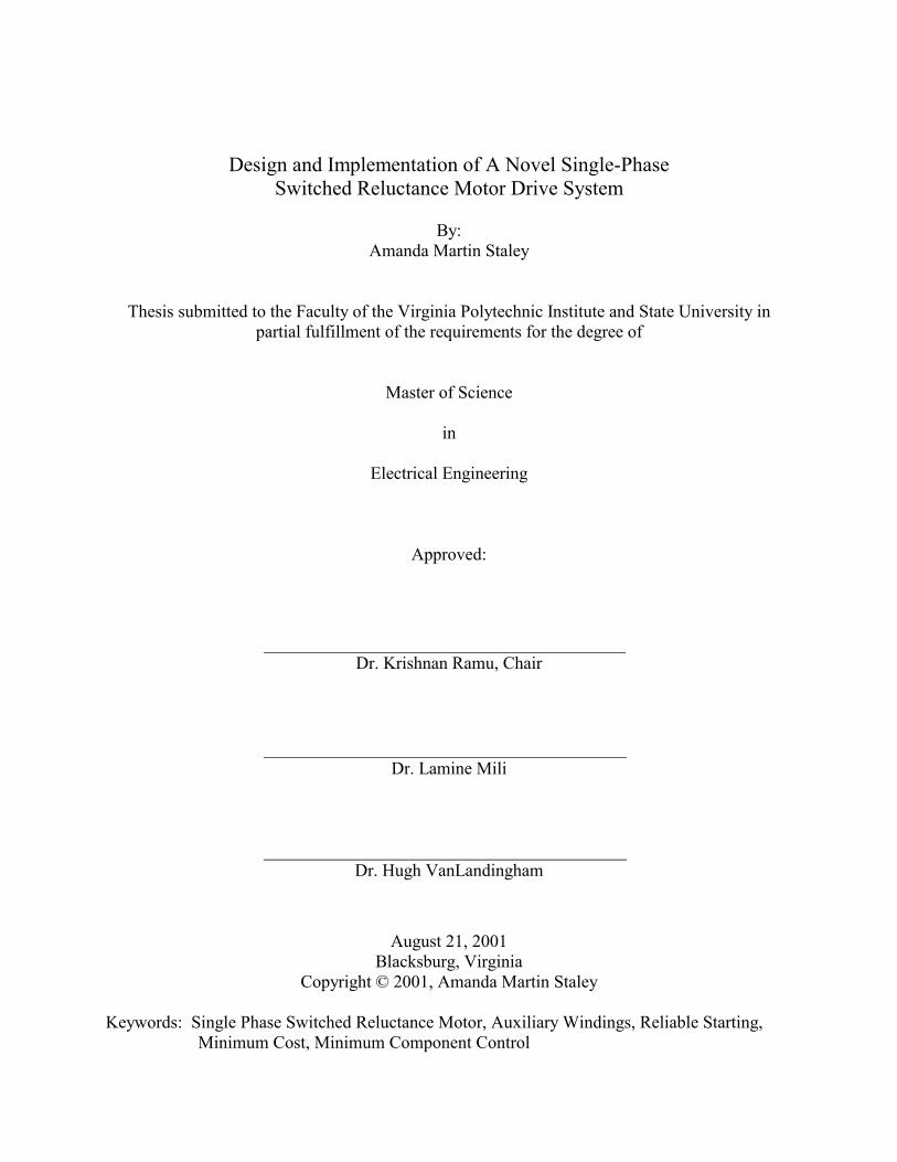
Another approach to this problem is to the shift a pole-pair [9]. The rotor poles of this
machine have shoulders that allow for different air gaps, thus lending itself to a continuous
variation of reluctance and hence to torque generation at all positions. This proposed technique
involves the use of a shifted stator pole that has a parking permanent magnet attached as shown
in figure 1.3. The reason for the shift is to eliminate the possibility of the locking the rotor into a
stable detent (completely aligned) position. This technique includes permanent magnets that are
undesirable in a low cost solution.
6
Figure 1.3 – Single-Phase SRM Involving Pole Shaping and Permanent Magnets for Starting
1.3 Objectives and Novel Concepts of Proposed Drive System The designed drive system will be a variable speed drive that is capable of speeds up to
10,000 revolutions per minute with a power output of 100 Watts and an average torque output of
0.1 Newton-meters. The novel contributions of this thesis include electronic design of the
converter and control circuitry, implementation of the proposed drive system, and experimental
verification of operation. The research results presented here are also presented in [11].
1.4 Scope of System Design
This topic presents a vast array of possibilities for research, but in the interest of time,
limitations must be placed on this thesis. This research is limited to system design including
motor topology and converter selections in addition to the control system design. The analysis
will include experimental verification and validation of results.

7
The control system design will be limited to energizing control of the machine, reliable
starting, and variable speed operation control. Acoustic noise control is outside of the scope of
this study.
1.5 Organization of Materials Presented This thesis will be organized into chapters in the following method. Chapter two will
present the motor topology and machine specifics. Discussion will include dimensions, machine
torque and flux linkage versus position characteristics, and inductance measurements. Finite
Element Analysis results will also be presented.
Chapter three will introduce the converter selection. In this section we will describe the
purpose of the converter and its place in the system. Also, this section will evaluate the different
converter topologies and the motivation behind the selection made. Advantages and
disadvantages of the chosen strategy will be reviewed.
Chapter four will present the requirements of the control system and the approaches taken
to meet the goals set. The electronics and components used will be discussed, and the details of
the construction of the subsystem and connection to the drive will be outlined. Advantages and
disadvantages of the methodology used will be discussed.
Chapter five presents and analyzes the results. Since it is the intention of this project to
construct a fully operational prototype, experimental results will be presented.
Finally, chapter six will summarize the project and provide results and key conclusions of
this research work. Advantages and limitations of the proposed system will be reviewed.
Possible applications and recommendations for future related work will be submitted.

8
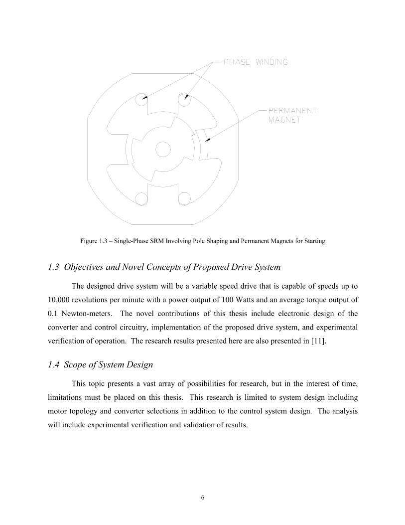
Chapter 2. Machine Configuration 2.1 Machine Description 2.1.1 Dimensions
The machine configuration used in this thesis was designed by Kartik Sitapati of
Kollmorgen Custom Motor Drives and Dr. Krishnan Ramu of Virginia Tech. It is shown in
figure 2.1 and, it has four stator poles, four rotor poles, and four auxiliary stator poles, which
hereafter are referred to as interpoles; this machine is shortly referred to as a 4:4:4 design. Each
stator pole is 25.5 millimeters (1.0039 inches) in width and has a radius of curvature of 36
degrees. The stator inner diameter is 74.5 millimeters (2.933 inches). The stator back iron
diameter is 102 millimeters (4.0157 inches). The outer stator width is 75 millimeters (2.95276
inches). The rotor outer diameter is 73.8 millimeters (2.9055 inches). The rotor poles are
slightly larger with a width of 26.5 millimeters (1.0433 inches) and a radius of curvature of 40
degrees. The rotor stack length is 18 mm (0.70866 inches). The rotor shaft diameter is 6.25 mm
(0.24606 inches). The case of the machine is square with a side length of 135 millimeters
(5.31496 inches). The stack length is 10 millimeters (0.3937 inches). The main purpose of the
interpoles is to provide reliable starting. This is achieved by pulsing the interpole windings with
a small current that will pull the nearest rotor poles to complete alignment with the interpoles.
Note that in this position the rotor poles are completely unaligned with respect to the main stator
poles. Then excitation of the main stator poles at this time will generate an air gap torque turning
the rotor. Note that only one set of interpoles is involved for starting in one direction and
therefore, at any time, only one set of interpoles is being used. The major advantages and
disadvantages of the proposed machine configuration are derived below.
9
Figure 2.1 – Proposed machine configuration
Advantages include:
(i) Provides reliable self-starting capability at all rotor positions.
(ii) Provides starting capability in both directions unlike other single-phase SRM
configurations and, therefore, this is the only single-phase configuration capable of true
four-quadrant operation.
(iii) Does not use permanent magnets thus reducing the manufacturing complexity of the
machine and cost.
(iv) The interpole winding can be used, in addition to self-starting, for probing to determine
the rotor position or as an inactive phase.
(v) After starting, the interpoles need not be used for continuous operation of the machine as
the main winding itself, and can be used for sensing the rotor position.

10
(vi) Since the interpole winding is only used for a small amount of time (during starting), it
can be designed to have a very small volume of copper thereby reducing its cost. During
the sensing part of the cycle, its current is very small even if its duty cycle is high and,
therefore, a small copper volume design is adequate.
(vii) If necessary, the air gap torque can be augmented by using the interpole winding as
another phase of a two-phase SRM or both the interpole windings can be used as other
two phases of a three-phase SRM. This allows the fullest utilization of the
electromagnetic capability of the machine. Many such modes of operation are possible
with this unique SRM.
(viii) Sensing of induced emf in the interpole winding during the excitation of the main
winding gives an indication of the mutual inductance and hence the rotor position. An
alternative is to apply high frequency signal at low current to the interpole winding and
measure its self-inductance from which the rotor positions can be estimated.
Disadvantages include:
(i) Interpole punchings and their windings and hence slightly higher cost of manufacturing.
(ii) Extra terminal connections for interpole windings and hence their unsuitability for
applications involving hermetic sealing.
2.1.2 Power Statistics and Finite Element Analysis Results
The operating power is 100 Watts and its maximum speed is 10,000 revolutions per
minute. The machine magnetic characterization can be derived by analytical or using finite
element analysis (FEA) software. The latter approach is selected for the present study. All FEA
results presented here are contributed by Kartik Sitapati. Sample results for only main winding
and interpole winding excitations with the aligned main poles aligned are shown in figures 2.2
and 2.3, respectively.

11
Figure 2.2 – FEA – Main Windings energized with 8 A DC
Figure 2.3 – FEA – Interpole pair #1 energized with 2 A DC

12
The flux in the aligned position for the main winding excitation is easier to determine
analytically but for the unaligned position becomes very demanding as in the case of any other
SRM. That is the reason for the use of FEA software for the analysis. It must be noted at this
time that the FEA analysis was performed for a machine that had the same dimensions as the
experimental prototype, but the stack length was 50 mm instead of 10 mm. Also, the number of
turns for the main poles was 100 instead of the actual 92 turns. The number of turns for the
auxiliary poles was 250 instead of the actual 205 turns. Accordingly, the graphs have been
scaled in order to provide a clear view of the prototype’s capabilities. The main pole
calculations have been scaled by:
=
turnsturns
stackmmstackmmMainsFEAMainsrototypeP
10092
5010
The auxiliary pole calculations have been scaled by:
=
turnsturns
stackmmstackmmInterpolesFEAInterpolesrototypeP
250205
5010
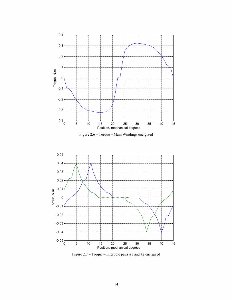
Figure 2.4 shows the beginning of torque production of interpole 1 and that corresponds
to unaligned position for the interpole but position of alignment for main poles.
Flux linkages for various rotor positions for main, and interpoles 1 and 2 are obtained by
mechanizing the results from FEA and are shown in figure 2.5, for 8 A main winding current and
2 A of interpole winding current. These are the rated values for these windings. Air gap torques
are extracted from the FEA results and are shown in figures 2.6 and 2.7 for main and interpole
windings 1 and 2, respectively. The interpole torques are designed with a maximum of 0.04 N-m.
The main windings produce a peak of 0.325 N-m but are required to produce only 0.1 N-m on
average, which is sufficient for a fan type load under consideration. Therefore, from the figures
2.6 and 2.7, it is seen that the machine is capable of providing the required torque and
performance.

13
0 5 10 15 20 25 30 35 40 450.01
0.015
0.02
0.025
0.03
0.035
0.04
0.045
Flux
link
age,
Wb
Position, mechanical degrees
Figure 2.4 – Flux Linkage – Main windings energized
0 5 10 15 20 25 30 35 40 452
3
4
5
6
7
8
9
10x 10-3
Flux
link
age,
Wb
Position, mechanical degrees
Figure 2.5 – Flux Linkage - Interpole pairs #1 and #2 energized
14
0 5 10 15 20 25 30 35 40 45-0.4
-0.3
-0.2
-0.1
0
0.1
0.2
0.3
0.4
Torq
ue, N
.m
Position, mechanical degrees
Figure 2.6 – Torque – Main Windings energized
0 5 10 15 20 25 30 35 40 45-0.05
-0.04
-0.03
-0.02
-0.01
0
0.01
0.02
0.03
0.04
0.05
Torq
ue, N
.m
Position, mechanical degrees
Figure 2.7 – Torque – Interpole pairs #1 and #2 energized
15
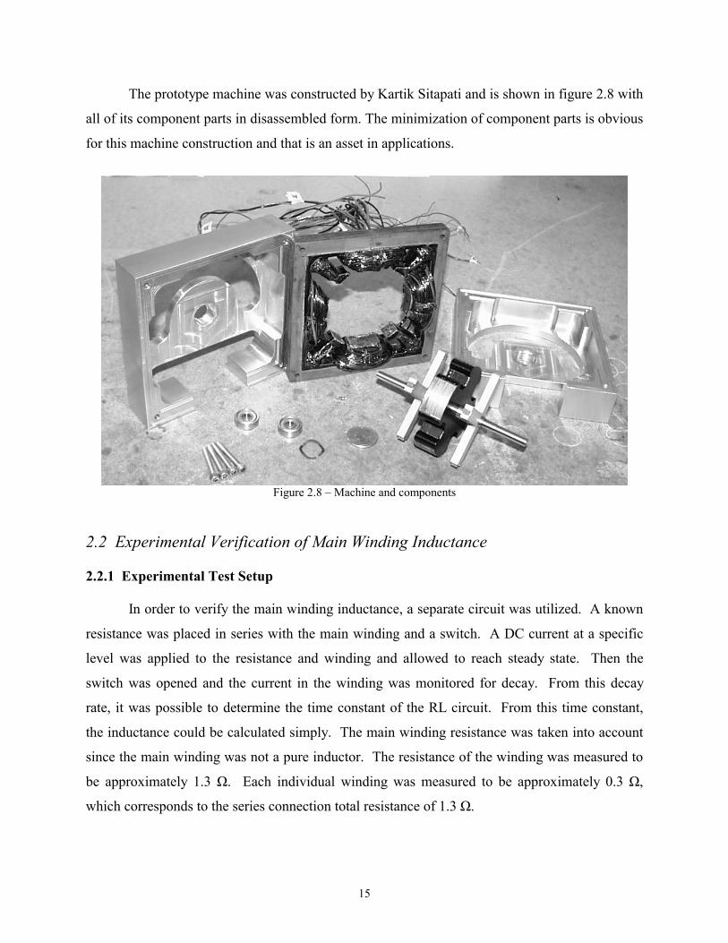
The prototype machine was constructed by Kartik Sitapati and is shown in figure 2.8 with
all of its component parts in disassembled form. The minimization of component parts is obvious
for this machine construction and that is an asset in applications.
Figure 2.8 – Machine and components
2.2 Experimental Verification of Main Winding Inductance 2.2.1 Experimental Test Setup In order to verify the main winding inductance, a separate circuit was utilized. A known
resistance was placed in series with the main winding and a switch. A DC current at a specific
level was applied to the resistance and winding and allowed to reach steady state. Then the
switch was opened and the current in the winding was monitored for decay. From this decay
rate, it was possible to determine the time constant of the RL circuit. From this time constant,
the inductance could be calculated simply. The main winding resistance was taken into account
since the main winding was not a pure inductor. The resistance of the winding was measured to
be approximately 1.3 Ω. Each individual winding was measured to be approximately 0.3 Ω,
which corresponds to the series connection total resistance of 1.3 Ω.

16
2.2.2 Experimental Results
The decay of the current is shown below in figure 2.9. The top curve (positive to
negative going) represents the current sensed in the main winding using an oscilloscope current
sensor. The bottom curve (negative to positive going) represents the feedback current, which is
why it is negative. From the plot, it can be seen that the feedback is the exact same as the sensed
current (except for the polarity). It is only necessary to determine the decay rate for one curve.
Figure 2.9 – Inductance Measurement at 1 A DC
Figure 2.10 shows the expanded view the decay of the current. From this plot, the
amplitude of the current was measured and then the 63.2 % value of the current was determined
and found on the curve. This point was then shifted to the axis for a marker, and then time
cursors were used to determine the time between the point where the current first started to decay
to the point when it reached the 63.2 % value. This value of time is equal to the time constant of
the RL circuit. Table 2.1 shows the time constants and inductances for DC currents ranging from
one Ampere to eight Amperes.
0.5 A/div
0.1 s/div

17
Figure 2.10 – Expanded Inductance Measurement at 1 A DC
I (A) Imeasure (A) 63.2 % of Imeasure R
L=τ Rexternal (Ω) Rtotal (Ω) L (mH)
1 1.01 0.6383 1.2290 ms 12.2 13.5 16.59150 2 1.98 1.2514 1.2547 ms 12.3 13.6 17.06392 3 2.96 1.8707 1.2538 ms 12.2 13.5 16.92630 4 3.83 2.4206 1.1642 ms 12.4 13.7 15.94954 5 5.06 3.1979 971.0 µs 11.9 13.2 12.81720 6 5.97 3.7730 796.4 µs 12.3 13.6 10.83104 7 6.75 4.2660 659.6 µs 11.9 13.2 8.70672 8 8.00 5.0565 533.4 µs 12.6 13.9 7.41426
Table 2.1 – Aligned Position Inductances for specific DC currents
Also, a measurement was taken for an unaligned inductance value. A small current of
0.25 A was passed through the setup while the rotor shaft was held at the unaligned position of
45 degrees. The same procedure as the one described in Section 2.2.1 was followed. The
measure point was 0.22 A, and the 63.2 % point was 0.13904 A. This corresponded to a time
constant of 220.1 µs. The external resistance was 12.1 Ω, and the total resistance was 13.4 Ω.
The inductance value calculated was 2.95 mH.
0.5 A/div
1 ms/div

18
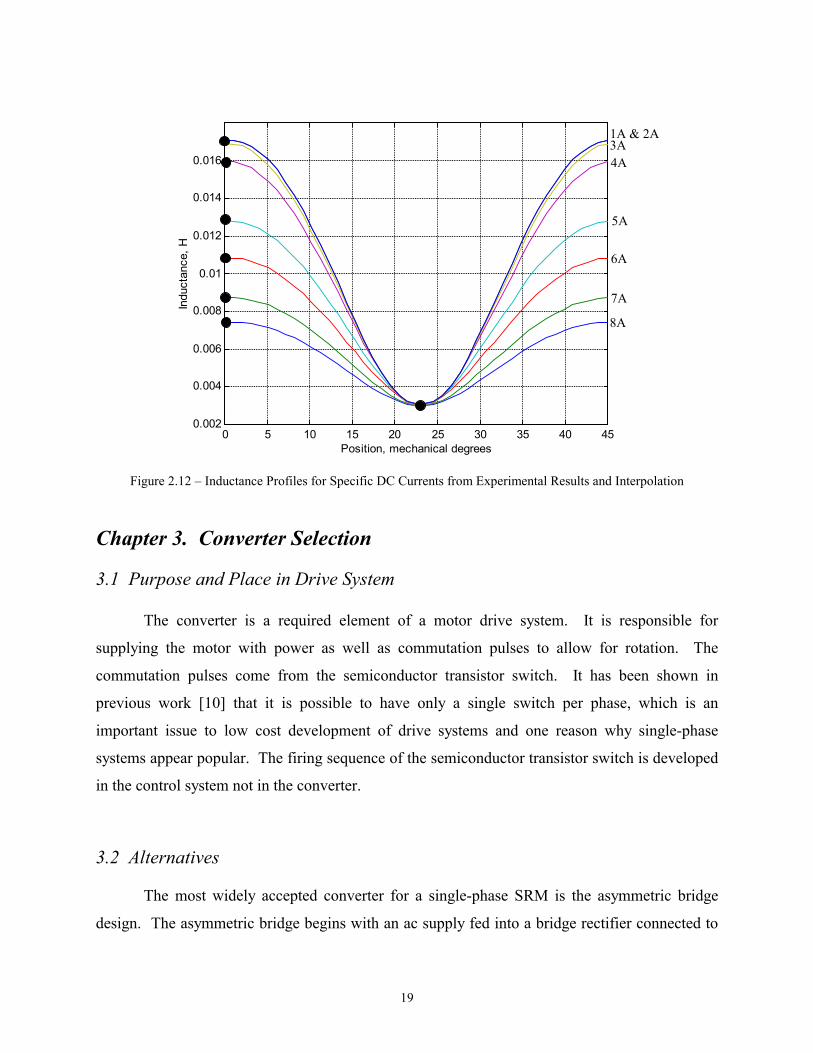
In figure 2.11 the analytical results for an inductance profile at eight Amperes DC is
given. Figure 2.12 presents the measured results for inductance profiles at currents ranging from
one Ampere to eight Amperes DC. Actual measurement points are denoted on figure 2.12 with a
dot. It can be seen that the measured results for eight Amperes does correspond to the analytical
results for eight Amperes with some slight error. The peak inductance for the analytical results
is approximately 5.55 mH while the experimental value is approximately 7.41 mH. The
unaligned position analytical result is approximately 1.65 mH, while the experimental result is
approximately 2.95 mH. The error is high, but it is still acceptable. From the shape of the
inductance profile from the analytical analysis and the measured inductance points for aligned
and unaligned positions, it was possible to extract the other inductance curves at different
currents. As the current is decreased, the inductance rises. Also, it can be noted that the
unaligned inductance does not vary much with decreasing current.
0 5 10 15 20 25 30 35 40 451.5
2
2.5
3
3.5
4
4.5
5
5.5
6x 10⁻³
Indu
ctan
ce, H
Position, mechanical degrees
Figure 2.11 – Inductance Profile for 8 A DC From FEA Results
19
0 5 10 15 20 25 30 35 400.002
0.004
0.006
0.008
0.01
0.012
0.014
0.016
Indu
ctan
ce, H
Position, mechanical degrees
Figure 2.12 – Inductance Profiles for Specific DC Currents from Experimental Results an Chapter 3. Converter Selection 3.1 Purpose and Place in Drive System
The converter is a required element of a motor drive system. It
supplying the motor with power as well as commutation pulses to allow f
commutation pulses come from the semiconductor transistor switch. It ha
previous work [10] that it is possible to have only a single switch per ph
important issue to low cost development of drive systems and one reason
systems appear popular. The firing sequence of the semiconductor transistor sw
in the control system not in the converter.
3.2 Alternatives
The most widely accepted converter for a single-phase SRM is the a
design. The asymmetric bridge begins with an ac supply fed into a bridge rec
A
8A
4
i
t
7A
6A
5A
4A
3A1A & 25
d Interpolation
s responsible for
or rotation. The
s been shown in
ase, which is an
why single-phase
itch is developed
symmetric bridge
ifier connected to
20
a DC link. This is then fed to the bridge, which consists of two transistor switches and two
diodes. The windings are connected in between the first transistor and the cathode of the first
diode and between the anode of the second diode and the second transistor. This design involves
four semiconductor devices for each phase, two IGBTs and two power diodes.
Other configurations, such as the split supply converter and the C-dump converter, also
require many semiconductor devices. The finalized converter design utilized only a single IGBT
and a single power diode, which is why the converter presented is much more attractive than
other options more commonly accepted. 3.3 Final Selection
3.3.1 Description
The converter used in this thesis was designed by Dr. Krishnan Ramu. It is shown in
figure 3.1 and begins as a normal converter with a supply fed into a bridge rectifier with a DC
link filter. This is where the similarities end. There is a branch, which acts as a voltage divider
with filter to smooth a voltage of 12 volts clipped by a zener diode to power the necessary
control circuitry, this is the section labeled as Logic Power Supply. Also, the converter has a
built in current sensing resistor network, which relates current after the switch and after the
snubber to the current in the main. So, when the switch is on, there will be current after the
switch in RS1, and when the switch is off (during the on time of the main current), the current
will flow through the snubber capacitor and through RS2. The addition of the currents sensed in
these two resistors will give a total picture of the current in the main windings at any given time.
Finally, there is a snubber circuit and an auxiliary winding circuit. The snubber is charged when
there is current in the main windings, and when the current is zero, the snubber supplies the
energy it stored to the auxiliaries. The auxiliary circuit requires an external resistor (significantly
large power resistor) to limit the current in the auxiliary winding to less than two Amperes for
which it is rated.
The significant factors influencing the converter design are the number of switching
devices that determines heat sink volume and area and the number of logic power supplies. To

have a cost-efficient design it is imperative to have as few switching devices as possible. The
proposed design uses a single switch for excitation of the main winding as well as for one
interpole winding. For the time being, the second interpole is neglected and not used in the
present study. A turn-off snubber is added to limit stress on the switch and also to provide the
energy to one interpole winding. In that process, the energy obtained through the current control
of main winding is effectively used to determine the level of excitation of the interpole winding.
But, since the auxiliary windings will be continuously supplied, an external power resistor is
preferable to limit the current.
In order to extend this system to sensorless applications, two small current sensing
resistors have been added at the switch and after the snubber. By detecting the current through
these two resistors, and the voltage across the snubber capacitor by means of another resistor
divider combination, it is possible to estimate the rotor position, thereby eliminating the need for
position sensors for control circuitry.
r
AC3.3.2 Des Up
presented
Rectifie
ign Analysis
to this point, th
is contributed di
DC Link Filter
21
Figure 3.1 – Converter Design
e work presented has been the work of
rectly by the author of this thesis.
Auxiliary Winding Circuit
Current Sensing Network
Logic Power Supply
others. Startin
Snubber Circuit
Main Winding Circuit
g here, the work

22
3.3.2.1 AC to DC Conversion The first section of the converter involves an AC to DC conversion. An AC to DC
converter is necessary to power the drive and derive power sources for other circuitry necessary.
Most projects would simply opt to use a prepackaged converter, but this research was
concentrated on minimum component, minimal cost design; therefore, the AC to DC conversion
section was also pieced together and built. A full wave bridge rectifier with a DC Link Filter
was chosen for the design. Its specifications are laid out below.
The first step to determining the components of the converter was to determine the duty
cycle. First, the inductance profile was approximated and the shape of the winding current
waveform was fitted to it to determine the appropriate switching point.
Figure 3.2 – Typical Inductance and Main Current Profiles
In order to switch at the point of maximum inductance, dT must equal ½T, this lead to a
duty cycle of ½.

23
Next, the amount of average current required must be determined in order to accurately
size the bridge rectifier for the AC to DC converter section.
[ ] AdTdTt
Tdt
Tidt
TI dT
dTdT
a 42188881811
000
=
====== ∫∫
From the current specification above, the bridge rectifier had to be able to provide 4
Amperes average current. They also had to be able to handle a reverse voltage equal to VDC.
( ) ( )( )
( ) VoltsVoltsVSpecsafetyForVoltsVVVV
D
SDCD
56.2541.1695.15.1:71.16912022
1
1
=======
The Diode rating for the Full Bridge Rectifier circuit was 400 Volts, 4 Amps.
In order to complete the AC to DC conversion section, the DC Link capacitor had to be
accurately sized. Also, this capacitor had to be able to withstand more of a voltage than was
required for normal operation for safety. An aluminum electric capacitor with a 250 Volt rating
was used. The sizing analysis follows:
( )
( )
( ) VFFC
msTTrevrev
rpmofspeedbaseaassumerevolutionaofcompletetotimeT
TTV
dTiC
flowingiscurrentwhentimettorelateswhichdTt
VCtiVcycleoneincircuitthetouppliedsEnergy
DCLink
DC
aDCLink
on
DCDCLinkaDC
250,10004.471010.004714.0
10min1sec60min00016666.0
min150025.0
150041
04714.01202
82
21 2
µµ ⇒==
=
=⇒=
⇒=
===
=
==
For safety’s sake, a bleed resistor and a LED were put in parallel with the DC Link
capacitor. Concerns for the sizing of this bleed-off resistor included the power that it must be
able to withstand and the time constant that it forms with the DC Link capacitor. This time
constant must be small in order to drain all of the charge from the capacitor quickly. The LED
was neglected in the sizing analysis, since the voltage that it operates at is very low. The LED’s

24
only purpose was to be a physical signal to indicate when the capacitor was still draining through
the resistor.
( )
( )( ) sFkCR
WkRkRR
VoltsWattR
VP
DCLinkB
BBBB
DC
8.1847040
1,408.2871.169122
=Ω==
Ω=⇒Ω=⇒===
µτ
This time constant was on the large side, but it was necessary to keep the size of the
resistor to a minimum. Most resistors with a power rating of higher than one Watt are large in
size and can be costly.
3.3.2.2 Control Circuit Power Supply
The next phase for this converter was the power supply branch for the control circuitry.
In order to avoid having to add a separate power supply for the controls, which typically run on 5
to 20 Volt supplies, a supply was been built into the converter topology to provide for a single 12
Volt supply to power all circuitry necessary from sensors to operational amplifiers. This circuit
design required the utmost of consideration in order to draw enough current into the branch but
still be close to the required 12 Volts in order to allow for appropriate regulation by the zener
diode.
In order to adequately power the control circuit, 100 mA would be an optimal amount of
current to be drawn into the branch. A great deal of this current would be lost within the voltage
divider circuit and the rest would be used to power the zener as well as the attached controls.
First, the top resistor of the voltage divider was to be determined:
( ) ( ) WattskV
RVP
kmA
VoltsI
VR
RIVoltsV
DC
R
DC
RDC
1557.1
71.15712
57.1100
1271.16912
12
2
1
2
1
1
1
1
=Ω
=−
=
Ω=−=−
=
=−
This value would allow for the right amount of current, but a 15-Watt resistor would be
too large, and too much energy would be expended in this resistor.

25
( ) ( )
mAk
VoltsR
VI
RIVoltsV
WkRRR
VWR
VP
DCR
RDC
DC
4.394
1271.16912
12
7,4355371.157712
1
1
111
2
1
2
1
1
=Ω
−=−
=
=−
Ω=⇒Ω=⇒==−
=
The 39.4 mA was not quite the desired amount of current, but it was sufficient.
From here, it was possible to determine the second resistor of the voltage divider in order
to provide 12 Volts at the zener. This voltage had to be close to that of the desired regulated
voltage by the zener. Since, it was known that R1 must be a 4 kΩ, the straightforward equations
of a voltage divider were used to determine R2.
( ) ( )
terPotentiomeaandWR
WVRVP
RRRR
RkR
RRRVVolts DC
ΩΩ=
===
Ω==⇒=+
+Ω=
+=
50021,100
44.096.324
1212
96.324000,4871.15771.16912000,48
471.16912
2
2
2
22
222
2
2
21
2
A known resistor in series with a potentiometer that can be adjusted to get an exact 12
Volts was used for R2.
The capacitor in the control power supply branch had two significant purposes. First, it
smoothed and filtered the voltage that was used to supply the control circuitry. Second, its
discharge was used to continuously supply voltage to the circuitry to ensure a supply.
The zener diode had to be able to regulate the voltage to 12 Volts. It must also require a
minimal amount of current. For these reasons, a 1N5242 Zener Diode with 12 Volt, ½ Watt
characteristics was chosen. It held the voltage right at 12 Volts and required only 8 mA of
current to function properly.

26
3.3.2.3 Current Sensing Scheme
In place of using expensive, bulky current sensors, current sensing resistors were used.
They were placed in strategic locations in order to monitor the current in the main windings.
With the addition of the current at the emitter of the IGBT and at the base of the auxiliary
windings and snubbering circuit, it was possible to monitor the current in the main winding at all
times. These were not designed per se, except to note that they must be small in order to not
create a voltage drop. They were set as small as possible. 0.01-Ohm sensing resistors were
used.
3.3.2.3 Semiconductor Switch At the heart of this converter is the semiconductor switch that is used to allow for
controllable firing. An IGBT was chosen for the controllable switch in this converter. This
device needed to be able to handle current of at least eight Amperes peak and 340 Volts. In case
of current spikes, it must be able to handle much more than eight Amperes. An International
Rectifier G4PC40U IGBT was selected. This device is rated for 40 Amperes and 400 Volts.
3.3.2.5 Snubbering Circuit
The snubbering circuit had many purposes. First, it was employed to reduce stress on the
IGBT, and second, its energy was used to supply the auxiliary winding circuit. It was required in
order fully utilize the interpoles and still retain a single-switch design.
The design of the snubber capacitor was one of the most critical. If it was too large then
it would store too much energy and would not allow the main winding current to go to zero when
the switching stops. But, if it is too small, then the auxiliary windings would not be supplied
with enough energy to be of any use. The size must allow the energy in the capacitor to be equal
to the energy in the main winding.
( ) ( )22
21
21
mainmainsnubbersnubber ILVC =
In order to determine the size of the capacitor, data was taken for the voltage that it would
store. At first, a 100 µF, 450 V aluminum electric capacitor was used in all the initial
27
calculation, and it was found to be too large. Also, with a full reference command given, the
maximum attainable speed was noted. The data taken follows below in table 3.1.
Vac (V) Vdc (V) Vsnubber (V) Maximum
Speed (RPM)
10.00 10.0 16.0 1920
20.53 23.9 36.5 3218
30.33 34.9 57.0 4160
40.5 49.0 73.0 5140
50.3 61.5 94.2 6080
60.2 74.0 145.0 6295
70 91.5 197.0 7145
80 104.0 220.0 7855
90 115.5 242.0 8545
100 126.0 268.0 9000
110 131.0 288.0 9061 Table 3.1 – Snubber Capacitor Calculation Required Experimental Values
From the values above and using a worst-case analysis, it was possible to determine the
precise value that the capacitor should be. From the inductance measurements in Section 2.2.2,
the inductance for a peak current of eight Amperes or an average current of 4.0 Amperes was
approximately 7.414 mH.
( ) ( )
( )( )
( )( )
VFC
FAmHC
VILC
ILVC
snubber
snubber
snubber
mainmainsnubber
mainmainsnubbersnubber
450,7.4
03.142.339
4414.7
21
21
2
2
2
2
22
µ
µ
=
==
=
=
A snubbering capacitor of 4.7 microfarads was used instead of a one microfarad capacitor
in order to allow for enough energy to be stored and transferred. A one microfarad capacitor was

28
right on the borderline of being able to store enough energy. A 4.7 microfarad capacitor was not
large enough to seriously inhibit the fall of current in the main windings during the off time, but
it was large enough to store enough energy to allow for current in the auxiliary windings during
the off period.
Since the snubber capacitor voltage was at its highest at 339.42 Volts, the auxiliary
circuit power diode had to be able to withstand at least that, and it was better if it could withstand
more for safety. The power diode chosen was a 40EPF04, which has a current rating of 40
Amperes and a voltage rating of 400 Volts.
3.3.2.6 External Resistor for Auxiliary Winding Current Limiting
The final component of the converter circuitry was a resistor combined in series with the
auxiliary windings. This resistor was necessary in order to limit the current in the auxiliary since
the windings were only designed for a maximum of two Amperes. This resistor was a large
external resistor. In future designs, it would be best to design another way to limit the current in
the auxiliary in order to reduce cost, size, and loss that this resistor contributes.
( )( )
( )
( )
esistorRPowerLugWirewoundWR
pulltosufficientisThisAVR
VI
RTryWVR
WRVP
WattsofpoweraforDesignavailableresonablyesistorRPowergestlartheisW
smallisitncesianceresistwindingauxiliaryNeglectRRAV
RIV
LIMIT
LIMIT
DCAUX
LIMITLIMIT
LIMIT
DC
LIMITLIMIT
LIMITAUXDC
−Ω=
=Ω
==
Ω=Ω==
==
Ω≥⇒==
225,1000
.33942.01000
42.3392
1000576200
42.339
2002
.200.225
.71.1692)71.169(2
2
2
2
3.3.3 Advantages and Disadvantages
There are many advantages as well as some disadvantages to using this circuit. The
advantages include:

29
(i) Permanent magnets and other distinct mechanical means are not necessary for starting
with the interpole design.
(ii) Design is compact and services both windings.
(iii) Only one controllable switch and one diode is required for all of the windings allowing
for the lowest cost possible.
(iv) Capability as good as one-switch based DC drives and for the first time a true competitor
to a single switch based chopper fed brush dc drive is made possible with this innovation
of power circuit.
(v) Control circuit isolation is not necessary since the switch gate signal is with respect to the
common.
(vi) Only common for current sensing and estimating position
(vii) Auxiliary winding is excited by the snubbing energy thus serving two needs.
(viii) Rotor position sensing is continuous since the auxiliary winding current is continuous.
(ix) Sensors are not required for sensorless operation since sensing resistors and interpoles are
involved in the design of the system thus providing an inexpensive solution to a critical
aspect of the single-phase SRM drive system.
The disadvantages include:
(i) The interpole winding continuously produces torque, which may generate some noise,
but the net torque that is produced by the interpole winding is zero. If the interpole torque
has to be utilized for load application, then it requires its own controlled switching power
device.
30
(iii) There is a need for an external resistor in order to limit the current through the auxiliary
winding, which contributes to energy losses and adds to the size of the system.
Chapter 4. Control Design 4.1 Design Approach
The objective of this section is to test the concept of the novel machine and converter.
Accordingly, the sensorless operation was not considered. Also, only a simple control algorithm
and strategy was devised for the basic testing of the prototype single-phase SRM drive system.
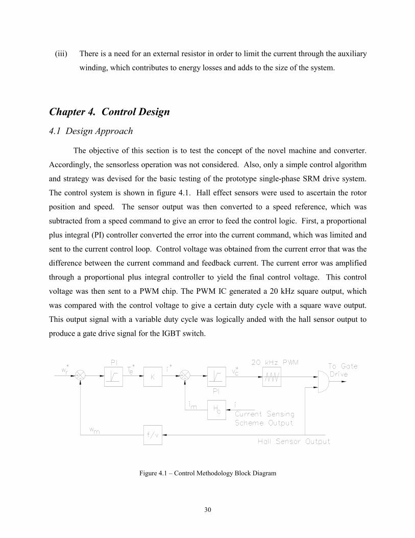
The control system is shown in figure 4.1. Hall effect sensors were used to ascertain the rotor
position and speed. The sensor output was then converted to a speed reference, which was
subtracted from a speed command to give an error to feed the control logic. First, a proportional
plus integral (PI) controller converted the error into the current command, which was limited and
sent to the current control loop. Control voltage was obtained from the current error that was the
difference between the current command and feedback current. The current error was amplified
through a proportional plus integral controller to yield the final control voltage. This control
voltage was then sent to a PWM chip. The PWM IC generated a 20 kHz square output, which
was compared with the control voltage to give a certain duty cycle with a square wave output.
This output signal with a variable duty cycle was logically anded with the hall sensor output to
produce a gate drive signal for the IGBT switch.
Figure 4.1 – Control Methodology Block Diagram

31
4.2 Components Design In experimental practice, each stage of the control was designed and then implemented.
Each phase was experimentally verified before moving on to the next part. The signal at the gate
was designed first, and then control loops were built around each previous section. The design
will be presented here in the same fashion.
4.2.1 PWM Control and Gate Drive Signal The first part of the control deals with delivering a signal to the gate of the semiconductor
switch in order to have accurate and precise firing of the phase to allow for proper rotation. This
gate drive signal was dependent on the output of the hall sensors and the output of the PWM.
First, we will explore the hall sensor outputs.
Two hall sensors were fastened to the endbell of the machine in fixtures that were
manufactured to have the same curvature as the endbell opening. These fixtures were also at a
particular height that allows magnets that are connected to a fixture on the rotor and shaft to have
minimal clearance over the sensors when the machine is in motion. These sensors were attached
at the zero degree (maximum inductance) and 45 degree (minimum inductance) points to
indicate turn on and turn off pulses, which is shown in figure 4.2. The sensors used were bipolar
Hall effect latches that change from zero to Vcc with a change in the magnetic field. They latch
at a particular level until a new pole passes over them.

32
Figure 4.2 – Hall Sensor Attachments to the Endbell
When the sensor signals were both low it was required the gate signal to be low as well.
If either one was high, then the position gate signal was also required to be high. If both signals
were high, it was required the position gate signal to be low. This was basically an Exclusive-
OR connection. This is shown in the graph and truth table below.
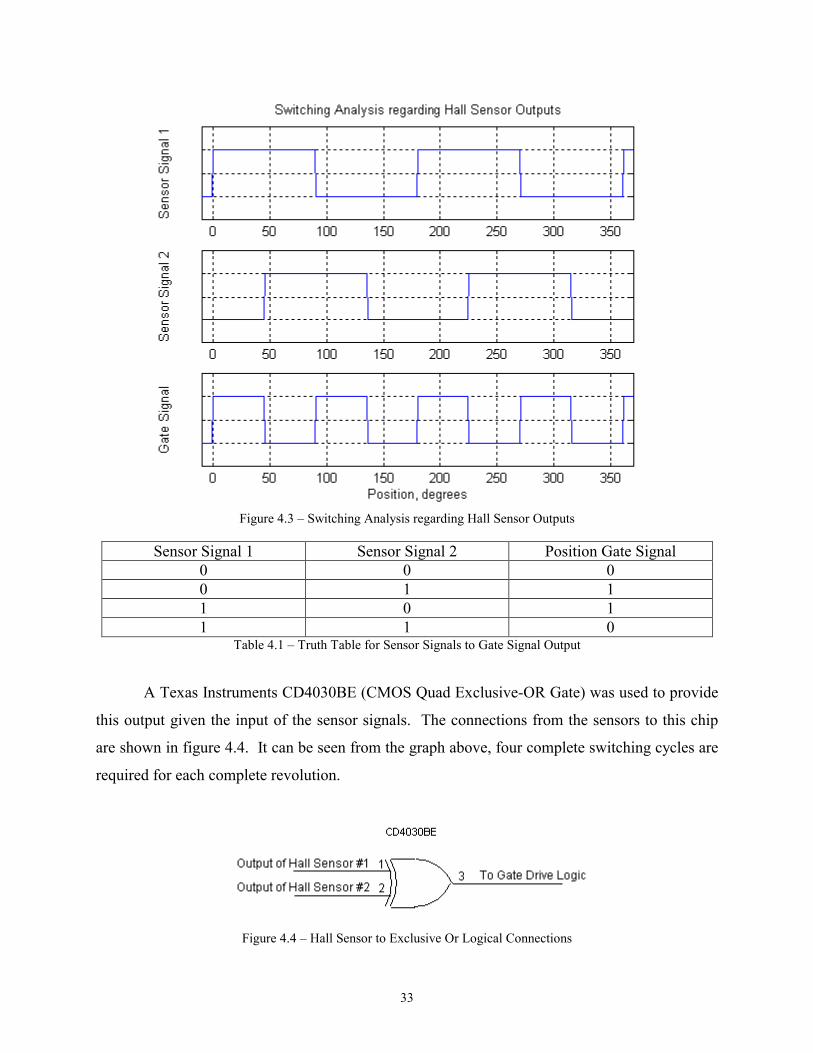
33
Figure 4.3 – Switching Analysis regarding Hall Sensor Outputs
Sensor Signal 1 Sensor Signal 2 Position Gate Signal
0 0 0 0 1 1 1 0 1 1 1 0
Table 4.1 – Truth Table for Sensor Signals to Gate Signal Output
A Texas Instruments CD4030BE (CMOS Quad Exclusive-OR Gate) was used to provide
this output given the input of the sensor signals. The connections from the sensors to this chip
are shown in figure 4.4. It can be seen from the graph above, four complete switching cycles are
required for each complete revolution.
Figure 4.4 – Hall Sensor to Exclusive Or Logical Connections

34
The gate drive signal was also dependent on the output of a PWM IC. All of the
connections for this IC are shown in figure 4.5. The PWM chip that was used in this research
was a Texas Instruments UC3524 (Advanced Regulating Pulse Width Modulator). This chip is a
single frequency pulse width modulation voltage regulator control circuit. A single timing
resistor and a single timing capacitor determine the frequency of operation. The equation to
determine the values of these components is given in the data sheet, and the calculations required
follow below.
( )
terpotentiomeawithseriesinkRkR
FRkHz
kHzfsetandeconveniencforFCSetCR
f
T
T
T
T
TT
ΩΩ=Ω=
=
==
=
5006.59.5
01.018.120
2001.0
18.1
µ
µ
A 5.6 kΩ resistor was used in series with a 500 Ω potentiometer to adjust the oscillation
to have a period of exactly 50 µs. The timing capacitor generates a ramp function of the
designed frequency, and then it is compared to the error between the inputs. This is then used to
generate a pulse train with a specific duty cycle depending on the input level. This duty cycle to
input signal ratio was verified experimentally. The table below demonstrates the proportions
used.
Input Voltage in PWM Circuit Resulting Duty Cycle
0.8 Volts 0 %
3.53 Volts 100 % Table 4.2 – PWM Input Voltage and the Resulting Duty Cycle in the Output
In order to power the IC, pins eight, 15, and 16 are used. Pin 15 is the power pin and pin
eight is the ground pin. Pin 16 is only used when a five volt reference supply is necessary for the
circuitry, but in this research the internal regulator was sufficient. Pin 16 was grounded through
a 0.1 microfarad capacitor as recommended in the datasheet.

35
This chip also has the capability to be a protection device, since it has current limiting
ability and shutdown ability. These functions were not utilized in this design; therefore, pins
four and five were grounded for the current limiting, and pin 10 for shutdown was left floating as
recommended in the datasheet.
The outputs of this IC are open collector outputs and can be tied together for single-ended
applications. In this research, the collectors (pins 12 and 13) were tied together and pulled up to
power through a resistor. The emitters were tied together and used as the output for the PWM
which is used as an input for the gate drive logic circuit.
Figure 4.5 – PWM IC Connections
The gate drive signal was a combination of the Hall sensor outputs and the PWM IC
output. It was desired to have the magnitude of the Hall sensor output with the switching of the
PWM IC output. This was a logical AND connection. A Texas Instruments CD4081BE
(CMOS Quad 2-input AND gate) was used to generate the final gate signal. Its connections can
be seen in figure 4.6. Pins one and two are the inputs to a two-input AND gate. Pin three is the
output of the corresponding gate. Pin 14 is the power pin, and pin seven is the ground pin. This
gate signal had the amplitude level of the position output from the hall sensor combination and it
had the switching duty cycle of the PWM output. The desired gate signal can be seen in figure
4.7.

36
Figure 4.6 – Gate Drive Logic Circuit Connections
Figure 4.7 – Gate Drive Signal Generation Analysis
4.2.2 Current Control Loop
Once the form of the gate drive signal had been established, the signals needed were
derived by working backwards. The only signal missing was the control voltage signal that was
required by the PWM IC. This was the signal that was to be generated by the current control
loop. The form of the current control loop is shown in figure 4.8. A dashed line is drawn
around each segment and its section of discussion is noted. The entire current control loop
logical schematic is shown in Appendix C. The actual wiring diagram for the current control
loop is shown in Appendix D.

37
Figure 4.8 – Current Control Loop Block Diagram
4.2.2.1 Current Feedback The first step in current control was to first be aware of the current that is in the system.
Most systems utilize current sensors to have current feedback. These sensors can be bulky and
expensive; therefore, we opted for inexpensive, small current sensing resistors. They were
placed in strategic locations within the converter circuit. Since, they are such small resistances,
they have no effect on the circuit and are negligible in calculations. With full current in the
windings, there will be a maximum voltage drop of 0.08 Volts.
( )( ) VAVIRV
08.001.08 =Ω==
At first, it was believed that only the resistor in series with the switch was required for the
feedback, but it was found that when the machine was unloaded, there was a significant amount
of current in the auxiliary windings. This current was not being taken into account as having
been in the main winding, and accordingly, the feedback was not truly indicative of the current
flowing in the main windings. In order to solve this problem, a summing amplifier was used to
add the feedback from both resistors together before using it as the total feedback. In a future
design, a single current resistor could be used in between the ground and the node, which
connects the switch, snubber capacitor, and auxiliary windings. This configuration is seen
below.

38
Figure 4.9 – Alternate Sensing Configuration Converter
For this research, the original converter design was used. A summing amplifier was
constructed. LM324AN (Quad Operational Amplifiers) were used in the construction of all
control circuitry. These chips were used because they require only a single positive supply of 12
Volts, which was perfectly suited to the supply circuit derived from the converter. But, there is a
drawback to the use of this chip. The LM324AN IC requires the use of only noninverting
amplifiers since they have no negative reference. Therefore, all stages were built in a
noninverting configuration. The design of the summer follows below. Since all of the resistors
are of the same value, the equations work out so the output in not dependent on their value;
therefore, a standard value of 1 kΩ was chosen.

39
Figure 4.10 – Summing Amplifier for Current Feedback
21
2121
21
21
222
2
22
000
::
RSRSO
RSRSO
RSRS
ORSRS
ORSRS
VVV
VVVVVVV
RV
RV
RVV
RV
RVV
RV
RVV
RVV
nalTermiInvertingnalTermingNoninverti
+=
+==
+=
=
+=
=−
+−=−
+−
Next, a gain determination was made. The maximum output voltage from the summer
was 0.08 Volts, which represents a full current situation. The reference was evaluated at this
point. Knowing that the output of the speed control loop (current command) would be limited, it
was decided that the current command would be limited to a maximum voltage of 4.7 Volts.
Therefore, the full current condition of 0.08 Volts must equate to the full current command of 4.7
Volts. If the command was all the way high, and the current in the winding was also full, there
would be no error. The following equation was utilized:

40
75.5808.07.4
=
=
V
V
A
AVoltsVolts
A simple noninverting gain amplifier was designed. The gain designed for was 60. A
standard value of 1 kΩ was selected for R1, and R2 was solved for accordingly.
Figure 4.11 – Gain Amplifier for Current Feedback
Ω=Ω=
Ω=+Ω
==
+==
+=
=
+
=−
+−=
−
−
kRkR
kRkRA
RRA
ii
RRVV
RV
RRV
RVV
RVVV
nalTermiInvertingnalTermingNoninverti
feedback
feedbackamplified
SummerOO
O
OSummerO
591
5911
60
1
1
11
00::
21
22
1
2
1
2
221
21
In order to ensure that the feedback was correct, the amplified signal was compared to the
sensed current in the main windings using a current monitor attached to a scope. The resulting

41
waveforms are seen in figure 4.12. It can be seen from these waveforms that the shape of the
current feedback does match that of the actual current in the windings.
2 ms/div
Figure 4.12 – Current Feedback and Current in the Main Winding
At this point, the feedback was ready to be compared to the reference to give an error and
generate a control signal for the PWM IC.
4.2.2.2 Current Error Determination
In order to determine the error, the feedback had to be subtracted from the command.
This was performed by way of a subtractor circuit with a gain of 1. The design justification is
derived below. Since all of the resistors are of the same value, the equations work out so the
output in not dependent on their value; therefore, a standard value of 1 kΩ was chosen. But,
when this circuit was put into practice, an offset was discovered. This offset was the result of a
voltage drop across the resistor fed by the current command. This voltage drop was being
reflected onto the input pins of the operational amplifier and thereby onto the output. This led
the output to show an error even if there was not one. In order to eliminate this problem, the
Current Feedback
Observed Current
Scale = 1 A/div
Scale = 0.588 V/A

42
resistance used was increased to 100 kΩ. Once these resistors were changed, the offset was
eliminated.
Figure 4.13 – Subtractor Circuit to determine Current Error
feedbackamplifiedO
feedbackamplifiedO
feedbackamplifiedO
feedbackamplifiedO
Ofeedbackamplified
iiV
iiV
iVViV
RiV
RV
Ri
RV
RVV
RiV
RV
RiV
nalTermiInvertingnalTermingNoninverti
−=
−=
−==
+=
=
=−
+−
=−+−
*
2*2
22*
2*2
000*
::
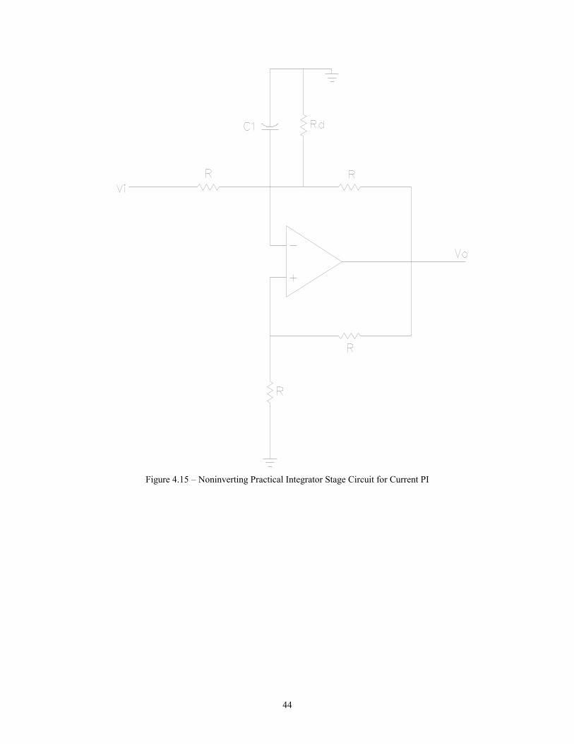
4.2.2.3 Current PI Controller
Once the error had been obtained, it was fed to a Proportional-plus-Integral Controller.
In order to effectively tune the PI Controller, the proportional stage was in a separate circuit from
the integral stage, and they were added together with a summing circuit. Since all of this control

43
was analog using discrete components, it was much easier to change gains and tune each stage
individually. The gains were chosen to be 10 for the proportional stage and 1 for the integral
stage. Once again, all of the stages had to be in a noninverting configuration in order to perform
as required. The most challenging section of this controller was designing a noninverting
practical integrator since the typical practical integrator is in inverting form. (Practical here
meaning that a resistor was also used in addition to a capacitor in order to drain the capacitor and
keep the circuit from saturating.) Anti-Windup on the integrator circuit was deemed unnecessary
since the application is not high performance; it would just add complexity to the system where it
was not needed. The P-stage is shown in figure 4.14, and the I-stage is shown in figure 4.15.
Figure 4.14 – Proportional Gain Stage Circuit for Current PI
Ω=Ω=Ω=+Ω
==
+==
+=
=
+
=−+−=
kRkRkRk
RA
RRA
VV
RRVV
RV
RRV
RVV
RVVV
nalTermiInvertingnalTermingNoninverti
i
O
iO
O
Oi
9.901090110
10
1
1
11
00::
2122
1
2
1
2
221
21
44
Figure 4.15 – Noninverting Practical Integrator Stage Circuit for Current PI

45
( )
FCkRMR
MRFCLetRC
A
kFmsR
msCRnecessaryantconsttimetheondependsdesignItssaturation
allownotandrgechadraintoorderinCwithparallelinaddedisR
sRCVV
RVsCV
RV
RVsC
RVVV
RV
RVsC
RV
RV
RV
RVV
sC
VR
VVRVV
RV
nalTermiInvertingnalTermingNoninverti
d
d
d
d
iO
iO
iOOO
iOO
OiO
µ
µ
µ
1472
2121
50150
50..
22
222
1
22
01
000::
=Ω=Ω=
Ω====
Ω=<
<
=
=
=−
+=
=−
+=
=−+−+−=−+−
The summing stage that was used is identical to the summer derived in Section 4.2.2.1
Current Feedback, and it only had a gain of 1. Its form is shown in figure 4.16.

46
Figure 4.16 – Summing Amplifier for Current PI
4.2.2.4 Current Control Signal Limiter
The duty cycle control signal had to be limited in order to be accurately inputted into the
PWM IC. From table 4.2, it can be seen that the maximum control signal that would be accepted
by the PWM is 3.53 Volts. But, it is not wise to have full 100 % duty cycle, therefore, it was
limited to at most 95 % duty cycle. In order to build a simple, minimum component limiter
circuit, a zener diode was used. 3.3 Volt zeners are readily available devices and they would
allow the restriction of less than 100 % duty cycle. The output of the PI Controller was fed into
a 1 kΩ resistor to limit the current in the 3.3 Volt zener. The output seen across the zener then
became the input to the noninverting input terminal of the PWM IC.
4.2.3 Speed Control Loop
Once the form of the gate drive signal and the PWM input signal had been established,
the signals needed are derived by working backwards again. The only signal missing was the
current command signal that was required to determine if there was current error. This was the
signal that will be generated by the speed control loop. The speed control loop, in essence,
mirrored the current control loop, and for this reason was simple in its construction, since most
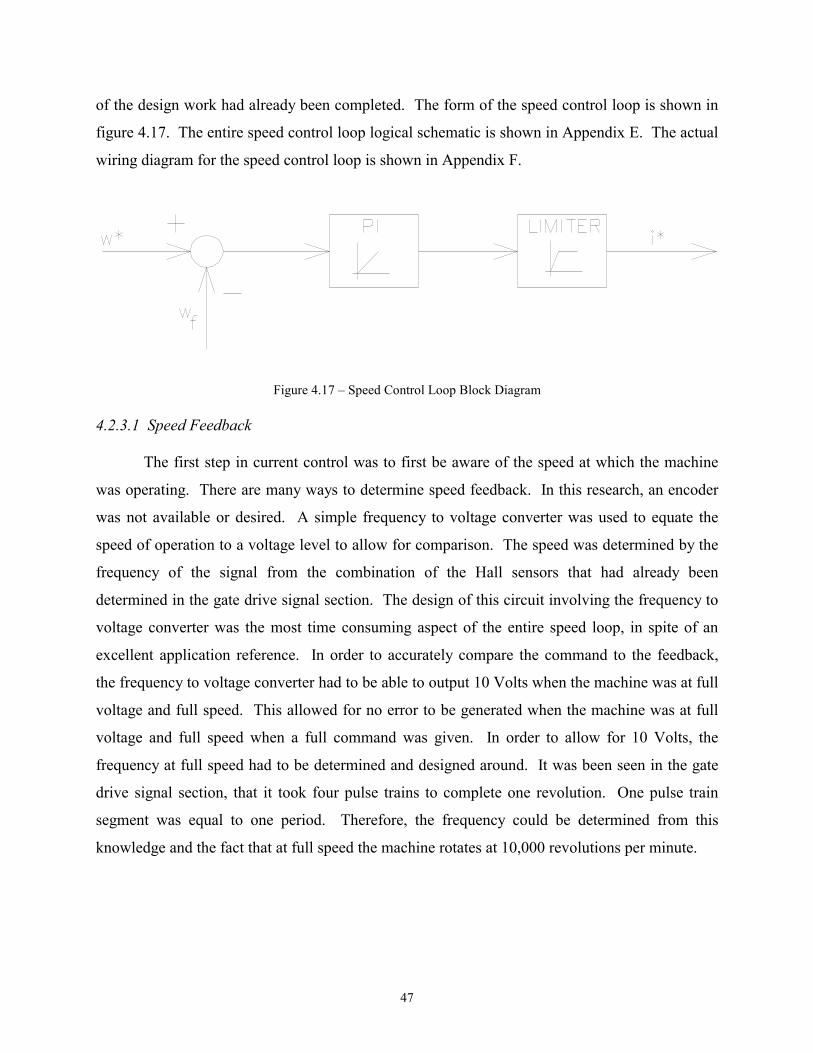
47
of the design work had already been completed. The form of the speed control loop is shown in
figure 4.17. The entire speed control loop logical schematic is shown in Appendix E. The actual
wiring diagram for the speed control loop is shown in Appendix F.
Figure 4.17 – Speed Control Loop Block Diagram
4.2.3.1 Speed Feedback The first step in current control was to first be aware of the speed at which the machine
was operating. There are many ways to determine speed feedback. In this research, an encoder
was not available or desired. A simple frequency to voltage converter was used to equate the
speed of operation to a voltage level to allow for comparison. The speed was determined by the
frequency of the signal from the combination of the Hall sensors that had already been
determined in the gate drive signal section. The design of this circuit involving the frequency to
voltage converter was the most time consuming aspect of the entire speed loop, in spite of an
excellent application reference. In order to accurately compare the command to the feedback,
the frequency to voltage converter had to be able to output 10 Volts when the machine was at full
voltage and full speed. This allowed for no error to be generated when the machine was at full
voltage and full speed when a full command was given. In order to allow for 10 Volts, the
frequency at full speed had to be determined and designed around. It was been seen in the gate
drive signal section, that it took four pulse trains to complete one revolution. One pulse train
segment was equal to one period. Therefore, the frequency could be determined from this
knowledge and the fact that at full speed the machine rotates at 10,000 revolutions per minute.
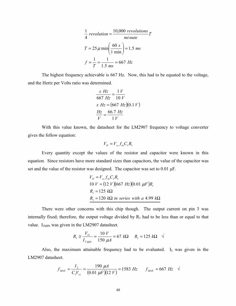
48
HzmsT
f
mssT
Tnutemi
srevolutionrevolution
6675.111
5.1min1
60min25
000,1041
===
=
=
=
µ
The highest frequency achievable is 667 Hz. Now, this had to be equated to the voltage,
and the Hertz per Volts ratio was determined.
( )( )
VHz
VHz
VHzHzxV
VHz
Hzx
17.66
1.0667101
667
=
=
=
With this value known, the datasheet for the LM2907 frequency to voltage converter
gives the follow equation:
11RCfVV inccO =
Every quantity except the values of the resistor and capacitor were known in this
equation. Since resistors have more standard sizes than capacitors, the value of the capacitor was
set and the value of the resistor was designed. The capacitor was set to 0.01 µF.
( )( )( )
ΩΩ=Ω=
==
kawithseriesinkRkR
RFHzVVRCfVV inccO
99.4120125
01.06671210
1
1
1
11
µ
There were other concerns with this chip though. The output current on pin 3 was
internally fixed; therefore, the output voltage divided by R1 had to be less than or equal to that
value. I3MIN was given in the LM2907 datasheet.
Ω=Ω==≥ kRkA
VIV
RMIN
O 12567150
101
31 µ
√
Also, the maximum attainable frequency had to be evaluated. I2 was given in the
LM2907 datasheet.
( )( ) HzfHzVF
AVCIf MAX
ccMAX 6671583
1201.0190
1
2 ====µ
µ √

49
As one final concern and design point, the ripple content of the output had to be
examined. The ripple content was determined by one final design component, a capacitor. But,
this capacitor also affected the response time, so a compromise had to be reached. A ripple of
less than 0.01 Volt ripple was required. That equated to approximately 10 rpm.
( )( )( )
( )( )( )
pkpkVVFCFC
AHzFV
VFVC
VpkpkI
CfVCCVV
Ripple
inccccRipple
−=⇒==
−=
=−
−
=
007.07.447.3
19066701.0121
01.0201.012
01.012
2
2
2
2
1
2
1
µµ
µµµ
With all of the components required designed for, the circuit was implemented and
tested. But, it was found that the circuit did not work. It was tested using a signal generator for
the input, and it was not until a dc offset was added did the circuit perform as expected. The
application notes are clear in that the reference for all input signals must be ground or below
ground. The sensor output signals were from ground to positive 12 Volts. The fact that the
circuit did not function with the given input signal was baffling, until a survey of the noise was
performed. The noise was not large enough to be of any consequence in any other function;
however it was sufficient to keep this circuit from performing as expected. In reviewing more
application notes on the LM2907, it was discovered that it was possible to use input signals that
were referenced above ground with a special configuration involving a reference voltage put to
the inverting terminal of the LM2907 (14 pin version only) instead of tying it to ground. A
voltage divider involving a potentiometer was designed to supply a reference voltage anywhere
from zero to 10 volts. Once this was done, the circuit performed up to expectations. Its
connections are shown in figure 4.18.

50
Figure 4.18 – Frequency to Voltage Converter Connections
At this point, the feedback was ready to be compared to the reference to give an error and
generate a current command signal.
4.2.3.2 Speed Command Generation The speed command generation involved a simple circuit that was a voltage divider to
provide 10 Volts at full command and zero Volts at no command. A 200 Ω resistor was placed
in series with a 1 kΩ Linear Taper Speed Potentiometer (Potentiometer involving a knob to allow
for easy control rather than a screwdriver type adjustment). A 12 Volt supply was connected,
and the output was drawn from the adjustable pin of the potentiometer. This allowed for a full
zero to 10 Volt command.
4.2.3.3 Speed Error Determination
In order to determine the error, the feedback must be subtracted from the command. This
was performed by way of a subtractor circuit with a gain of 1 just as in the current control loop.
The design justification is the same as the previous section and will not be derived again here.
Since all of the resistors are of the same value, the equations work out so the output in not
dependent on their value; therefore, the standard value of 100 kΩ was chosen so as to avoid the
same offset discovered in the current control loop. The form of the subtractor circuit used here is
shown in figure 4.19.

51
Figure 4.19 – Subtractor Circuit to determine Speed Error
4.2.3.4 Speed PI Controller
Once the error had been obtained, it was fed to a Proportional-plus-Integral Controller
just as in the current control loop. In order to effectively tune the PI Controller, the proportional
stage was in a separate circuit from the integral stage, and they were added together with a
summing circuit. Since all of this control stage was analog using discrete components, it was
much easier to change gains and tune each stage individually. The gains again were chosen to be
10 for the proportional stage and 1 for the integral stage. Once again, all of the stages had to be
in a noninverting configuration in order to perform as required. Just as in the current control
loop, anti-windup on the integrator circuit was deemed unnecessary since the application is not
high performance; it would just add complexity to the system where it was not needed. The form
of the proportional gain stage and the integral gain stage are shown in figures 4.20 and 4.21
respectively. The summing stage that was used is identical to the summer derived in Section
4.2.2.1 Current Feedback. Its form is shown in figure 4.22.

52
Figure 4.20 – Proportional Gain Stage Circuit for Speed PI
Figure 4.21 – Noninverting Practical Integrator Stage Circuit for Speed PI

53
Figure 4.22 – Summing Amplifier for Speed PI
4.2.3.4 Speed Control Signal Limiter
The current command signal had to be limited in order to be accurately compared to the
current feedback. From the design of the current feedback amplification, it is seen that the
maximum voltage allowed for the current command in order to have zero error with the signals
match was 4.7 Volts. In order to build a simple, minimum component limiter circuit, a zener
diode was used. 4.7 Volt zeners are readily available devices. The output of the PI Controller
was fed into a 1 kΩ resistor to limit the current in the 4.7 Volt zener. The output seen across the
zener then became the input to the noninverting input terminal of the subtractor circuit that
determined the current error.
4.3 Construction and Connection Each stage was constructed just as it was designed. First the PWM IC circuit was built
and tested to ensure that the output was a signal of varying duty cycle given a certain input.
Then the hall sensors and logic gates were connected to allow for proper gate drive signals. This
was tested and checked to make sure that the desired signal was achieved. Next, the current

54
control loop was built and closed. The feedback was confirmed to make sure that the loop was
indeed closed. Finally, the speed loop was built and closed. The speed feedback was then
confirmed to ensure that the loop was closed once again. With the closing of this last loop, a
command was given and the feedback was monitored. When the two signals matched, the drive
system was complete.
Chapter 5. Experimental Results and Evaluation 5.1 Experimental Setup
Since there are many ways of connecting the machine windings, some clarifications must
be made as to the experimental setup for this research. The main windings were connected in
series then connected to the converter circuit. The interpoles were connected in series in two sets
of pairs. Then they were introduced into the converter circuit separately. Since the interpoles
were not all connected in series, this would allow for bi-directional starting. The winding
diagrams for the main and interpole windings are shown in figure 5.1. For this thesis, only uni-
directional operation was considered; therefore, one set of the interpoles was not connected.
Figure 5.1 – Proposed Wiring Schematic

55
3177 Allegro Microsystems Hall effect sensors were used to obtain position information.
These sensors are attached as described in Section 4.2.1 PWM Control and Gate Drive Signal.
5.2 Experimental Results
The experimental results of this research are contained in this section. All measurements
were taken at 60 Volts AC at a maximum speed of 6800 RPM.
First, the Hall Sensor Scheme is examined. The outputs of the two hall sensors and their
respective combination through an exclusive OR gate is given in figure 5.2. From this graph, it
can be seen that the hall sensors give an output with the passing of a magnet (high for a north
pole and low for a south pole). This corresponds to two high signals and two low signals for
each rotation. From the staggering of the pulses, it can be noted that the sensors are 45 degrees
apart, just as specified in the mechanical diagram in figure 4.2. When these two signals are
combined by and exclusive OR, four pulses are generated with each single revolution.
10 ms/div
Figure 5.2 – Hall Sensor Outputs and Combination Output
Hall Sensor #1Output 5 V/div
Hall Sensor #2Output 5 V/div
XOR Output From CD4030 5 V/div

56
Next, the Gate Drive Signal logic is examined. The hall sensor XOR output, PWM
output and the output of the AND gate to the gate drive are given in figure 5.3. From this graph,
it can be seen that the level of the hall sensor XOR output is translated to the PWM pulses by the
AND to give the IGBT Gate Drive Signal. When the XOR is low, the drive signal is also low,
but when the XOR is high, the drive signal is a pattern of pulses with the duty cycle determined
by the PWM circuit.
10 ms/div
Figure 5.3 – Gate Drive Signal from PWM and Hall Sensor Pulses
Next, the speed command versus the speed feedback is analyzed and verified in figure
5.4. Both plots are on the same time division scale as well as the same amplitude division scale.
The top curve represents the speed command. This command varies between zero and two Volts
in approximately nine seconds, which represents a final command speed of 2000 RPM. The
waveform is slightly jumpy since, the reference is given by way of a speed knob, and the
operator’s hands are not capable of giving a perfect ramp as is a command given by a DSP. The
Hall Sensor XOR Pulses 5 V/div
PWM Pulses5 V/div
IGBT Gate Drive Signal 5 V/div
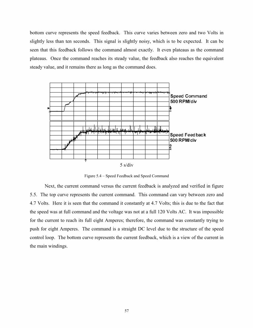
57
bottom curve represents the speed feedback. This curve varies between zero and two Volts in
slightly less than ten seconds. This signal is slightly noisy, which is to be expected. It can be
seen that this feedback follows the command almost exactly. It even plateaus as the command
plateaus. Once the command reaches its steady value, the feedback also reaches the equivalent
steady value, and it remains there as long as the command does.
5 s/div
Figure 5.4 – Speed Feedback and Speed Command
Next, the current command versus the current feedback is analyzed and verified in figure
5.5. The top curve represents the current command. This command can vary between zero and
4.7 Volts. Here it is seen that the command it constantly at 4.7 Volts; this is due to the fact that
the speed was at full command and the voltage was not at a full 120 Volts AC. It was impossible
for the current to reach its full eight Amperes; therefore, the command was constantly trying to
push for eight Amperes. The command is a straight DC level due to the structure of the speed
control loop. The bottom curve represents the current feedback, which is a view of the current in
the main windings.

58
1 ms/div
Figure 5.5 – Current Feedback and Current Command
At this point, it is important to expand the view of the current in the main windings as is
done in figure 5.6. This expanded view demonstrates the switching found in the current
waveform, which is expected with the drive signal being dependent on a PWM signal. This
graph demonstrates that the drive is performing as expected.
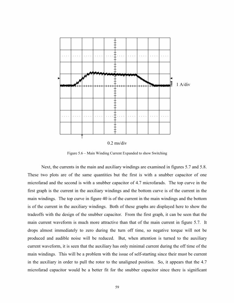
59
0.2 ms/div
Figure 5.6 – Main Winding Current Expanded to show Switching
Next, the currents in the main and auxiliary windings are examined in figures 5.7 and 5.8.
These two plots are of the same quantities but the first is with a snubber capacitor of one
microfarad and the second is with a snubber capacitor of 4.7 microfarads. The top curve in the
first graph is the current in the auxiliary windings and the bottom curve is of the current in the
main windings. The top curve in figure 40 is of the current in the main windings and the bottom
is of the current in the auxiliary windings. Both of these graphs are displayed here to show the
tradeoffs with the design of the snubber capacitor. From the first graph, it can be seen that the
main current waveform is much more attractive than that of the main current in figure 5.7. It
drops almost immediately to zero during the turn off time, so negative torque will not be
produced and audible noise will be reduced. But, when attention is turned to the auxiliary
current waveform, it is seen that the auxiliary has only minimal current during the off time of the
main windings. This will be a problem with the issue of self-starting since their must be current
in the auxiliary in order to pull the rotor to the unaligned position. So, it appears that the 4.7
microfarad capacitor would be a better fit for the snubber capacitor since there is significant
1 A/div

60
current in the auxiliary winding during the off time. The only problem is that the main winding
current is not allowed to fall to zero immediately in the off time, which will produce negative
torque and possibly more audible noise.
2 ms/div
Figure 5.7 – Main Winding Current and Auxiliary Winding Current with 1 microfarad cap
Auxiliary Current 0.1 A/div
Main Current 0.5 A/div

61
1 ms/div
Figure 5.8 – Main Winding Current and Auxiliary Winding Current with 4.7 micro
Next, the voltage for the main windings is shown is figure 5.9
measurements were taken with an AC voltage of approximately 60 V, whic
Link voltage of approximately 84 Volts, which is what the maximum is very n
show the switching of the voltage involved in the on time of the current. Fi
switching very clearly. Then at the end of the on time, the full negative volt
then falls to zero, when there is no current.
Z
Main Current 1 A/div
Auxiliary Current
farad cap
and 5.10. These
h leads to the DC
ear. These graphs
gure 41 shows the
age is applied and
ero

62
1 ms/div
Figure 5.9 – Main Winding Voltage
50 µs/div
Figure 5.10 – Main Winding Voltage Expanded View to show Pulsing
40 V/div
40 V/div
Zero
Zero
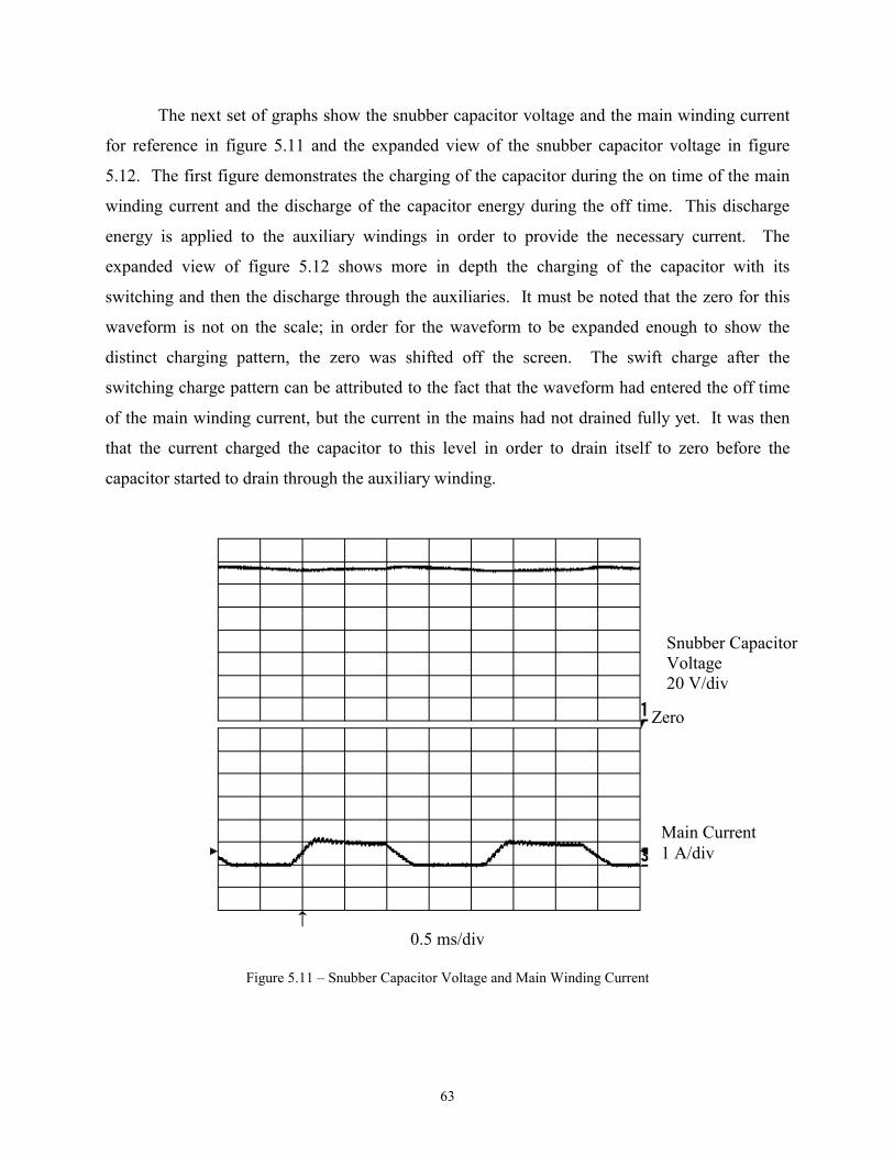
63
The next set of graphs show the snubber capacitor voltage and the main winding current
for reference in figure 5.11 and the expanded view of the snubber capacitor voltage in figure
5.12. The first figure demonstrates the charging of the capacitor during the on time of the main
winding current and the discharge of the capacitor energy during the off time. This discharge
energy is applied to the auxiliary windings in order to provide the necessary current. The
expanded view of figure 5.12 shows more in depth the charging of the capacitor with its
switching and then the discharge through the auxiliaries. It must be noted that the zero for this
waveform is not on the scale; in order for the waveform to be expanded enough to show the
distinct charging pattern, the zero was shifted off the screen. The swift charge after the
switching charge pattern can be attributed to the fact that the waveform had entered the off time
of the main winding current, but the current in the mains had not drained fully yet. It was then
that the current charged the capacitor to this level in order to drain itself to zero before the
capacitor started to drain through the auxiliary winding.
0.5 ms/div
Figure 5.11 – Snubber Capacitor Voltage and Main Winding Current
Z
Snubber Capacitor Voltage 20 V/div
Main Current 1 A/div
ero

64
0.5 ms/div
Figure 5.12 – Expanded View of the Snubber Capacitor Voltage
5.3 Evaluation
Overall, this research work reached the end result that was to be expected. The system
performs to expectations. At full voltage, the machine is capable of reaching a speed of
approximately 10,000 rpm. It reliably operates at the speed given by the operator. Although, the
machine was not officially connected to known load, it was loaded slightly by touch of hand, and
it performed as expected.
It is recommended that in future research with this machine that an anchoring mechanism
and an enclosure for the machine be built for safety concerns. Then a load may be attached and
tested fully. An enclosure should be required at speeds in excess of 5,000 rpm for if a rotor
fixture magnet came loose and was to fly out of the machine, the results could be dangerous.
This enclosure must also allow for proper air flow in order to keep the machine cool.
65
Chapter 6. Conclusions
6.1 Summary
This thesis describes a novel single phase SRM, an original converter to drive the
machine, and a controller to obtain a speed controlled drive system out of the single-phase SRM.
The research results are original and depart significantly from the single-phase SRM and drives
systems available in the literature and given in patents. The following conclusions are derived
from the research results of the thesis:
(i) Verification of analytical inductance results from finite element analysis by experimental
methods is given.
(ii) Current sensing, derivation of a logic power supply and a controller circuit and its
realization with least expense and ready for use in industrial applications are developed
and given.
(iii) In order to eliminate external expensive current sensors, simple resistor based current
sensing scheme is introduced as there is no need for isolation required between the power
circuit and control circuit with the novel converter topology.
(iv) A simple, inexpensive frequency to voltage converter is employed instead of using an
encoder to obtain speed feedback information.
(v) A simple minimum component, analog controller circuit has been developed and
recognized to implement a speed controlled drive.
(vi) The machine, converter and controller are developed and tested in the laboratory to prove
the feasibility of the proposed single phase SRM drive system.

66
All of the above clearly constitute a set of original contributions in the field of SRM drive
systems. The author of this thesis directly contributed to the electronics design of the converter
and controller. Also, the author implemented the system in its entirety and experimentally
verified its operation at a wide range of speed.
6.2 Possible Applications Many applications are possible with this drive system. The most obvious of applications
are for pump and fan loads. This drive is well suited for submersible pump or fan applications.
Also, a well-matched application would be for power tools that require variable speed operations
such as drills or drivers.
6.3 Recommendations for Future Work Possible avenues of future research could include acoustic noise control for extremely
high-speed operation, sensorless operation, bi-directional operation, analysis of different winding
connections, as well as multiple phase operation. Also, the tools for sensorless operation are
provided within this thesis, but true sensorless operation is not achieved. Simple implementation
of a new control methodology could provide for further reduced cost. Also, with the machine
configuration, bi-directional operation is possible but is not realized in this thesis. Furthermore,
with the selection of an appropriate converter, four-quadrant operation is possible.

67
References [1] C. C. Chan, “Single-phase switched reluctance motors,” IEE Proc.-B, vol. 134, no. 1, pp.
53-56, Jan. 1987.
[2] J. M. Stephenson and G. C. Jenkinson, “Single-phase switched reluctance motor
design,” IEE Proc. Electr. Power Appl., vol. 147, no. 2, pp. 131-139, Mar. 2000.
[3] J. Y. Lim, H. S. Kim, J. Y. Oh, D. H. Cheong, and J. C. Kim, “A performance of single
phase switched reluctance motor having both radial and axial air gap,” in Proc. IECON,
1998, pp. 905-910.
[4] S. Chan and H. R. Bolton, “Performance enhancement of single-phase switched-
reluctance motor by DC link voltage boosting,” IEE Proc.-B, vol. 140, no. 5, pp. 316-
322, Sept. 1993.
[5] M. Barnes and C. Pollock, “Power converter for single phase switched reluctance
motors,” Electronic Letters, vol. 31, no. 25, pp. 2137-2138, Dec. 1995.
[6] M. Barnes and C. Pollock, “Selecting power electronic converters for single phase
switched reluctance motors,” in Proc. Power Electronics and Variable Speed Drives,
1998, pp. 527-531.
[7] E. Buchan and N. Fulton, “Apparatus and method for starting a single-phase variable
reluctance motor,” US Patent number 5,753,984, May 19, 1998.
[8] J. Stephenson, “Apparatus and method for starting a single-phase variable reluctance
motor,” US Patent number 5,808,389, Sept. 15, 1998.
[9] G. Horst, “Shifted Pole Single Phase Variable Reluctance Motor,” US Patent number
5,294,856, Mar. 15, 1994.

68
[10] R. Krishnan and P. Materu, “Design of a Single-Switch-Per-Phase Converter for
Switched Reluctance Motor Drives,” in Proc. IECON, 1988, pp. 773-779.
[11] R. Krishnan, A. M. Staley, and K. Sitapati, “A Novel Single-Phase Switched Reluctance
Motor Drive System,” in Proc. IECON, 2001.

69
Appendices Appendix A – Equipment Listing and Cost Analysis
Part Number Part Description Manufacturer Number Required
Unit Cost Total Cost
Board Prototype Circuit Board
Vector Electronic Company
1 25.36 25.36
BTB Barrier Terminal Block
Cinch 1 3.37 3.37
TB (2 pin) Terminal Blocks
Thomas & Betts 1 1.72 1.72
TB (2 Pin) Terminal Blocks
Thomas & Betts 6 1.17 7.02
KBL04 400 V, 4 A Bridge Rectifier
General Semiconductor
1 2.07 2.07
UGN3177UA Hall Effect Latch Allegro Microsystems
2 0.90 1.80
G4PC40U IGBT International Rectifier
1 5.12 5.12
40EPF04 Power Diode International Rectifier
1 3.30 3.30
LM324AN Quad Op Amp Texas Instruments
3 0.68 2.04
LM2907N Frequency to Voltage
Converter
National Semiconductor
1 2.02 2.02
UC3524N Advanced Regulating Pulse Width Modulator
Texas Instruments
1 1.93 1.93
CD4081BE CMOS Quad “AND” Gate
Texas Instruments
1 0.45 0.45
CD4030BE CMOS Quad “XOR” Gate
Texas Instruments
1 0.66 0.66
1000 µF, 250 V
Aluminum Electrolytic Capacitor
Panasonic 1 8.09 8.09
47 µF, 35 V Aluminum Electrolytic Capacitor
Panasonic 1 0.28 0.28
4.7 µF, 450 V Aluminum Electrolytic Capacitor
Panasonic 1 1.19 1.19

70
0.01 µF Monolithic Capacitor
Panasonic 3 0.44 1.32
1 µF Monolithic Capacitor
Panasonic 2 3.12 6.24
4.7 µF Tantalum Capacitor
Panasonic 1 0.56 0.56
1N4728 3.3 V Zener Diodes, Inc. 1 0.36 0.36 1N4732 4.7 V Zener Diodes, Inc. 1 0.36 0.36 1N5242 12 V, ½ W
Zener Diodes, Inc. 1 0.36 0.36
250 V SP Metal Oxide Varistors
Harris Semiconductor
2 0.39 0.78
1 kΩ, 200 W Power Resistor Huntington Electric, Inc.
1 10.30 10.30
40 kΩ, 1 W Power Resistor XICON 1 0.13 0.13 4 kΩ, 10 W Power Resistor Ohmite 1 1.73 1.73 100 Ω, 1 W Power Resistor XICON 2 0.14 0.28
0.01 Ω Current Sensing Resistor
Ohmite 2 0.39 0.78
10 Ω, ¼ W Resistor Yageo 2 0.05 0.10 1 kΩ, ¼ W Resistor Yageo 19 0.05 0.95
4.99 kΩ, ¼ W Resistor Yageo 1 0.05 0.05 5.6 kΩ, ¼ W Resistor Yageo 1 0.05 0.05 10 kΩ, ¼ W Resistor Yageo 5 0.05 0.25 20 kΩ, ¼ W Resistor Yageo 1 0.05 0.05 39 kΩ, ¼ W Resistor Yageo 1 0.05 0.05 47 kΩ, ¼ W Resistor Yageo 2 0.05 0.10
90.9 kΩ, ¼ W Resistor Yageo 2 0.05 0.10 100 kΩ, ¼ W Resistor Yageo 8 0.05 0.40 120 kΩ, ¼ W Resistor Yageo 1 0.05 0.05 500 Ω, ½ W Potentiometer Bourns 2 1.20 2.40 1 kΩ, ½ W Potentiometer Bourns 2 0.88 1.76 1 kΩ, 5 W Linear Taper XICON 1 3.31 3.31
Knob Speed Pot Knob Kilo International
1 5.18 5.18
Total Components 91 Total Prototype
Cost
104.42

71
Appendix B – Converter W
iring Diagram

72
Appendix C – C
urrent Control Loop Logical Schem
atic
O
O
O
O O
O
OO
Oµ
O
O
O
OO
O
OO
O
O
O
O
O
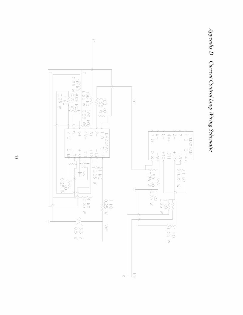
73
Appendix D – C
urrent Control Loop W
iring Schematic
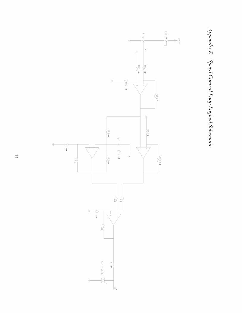
74
Appendix E – Speed Control Loop Logical Schem
atic
OO
O
O
O
µ
O
O
OO
O
O
O
OO
O
O
O O
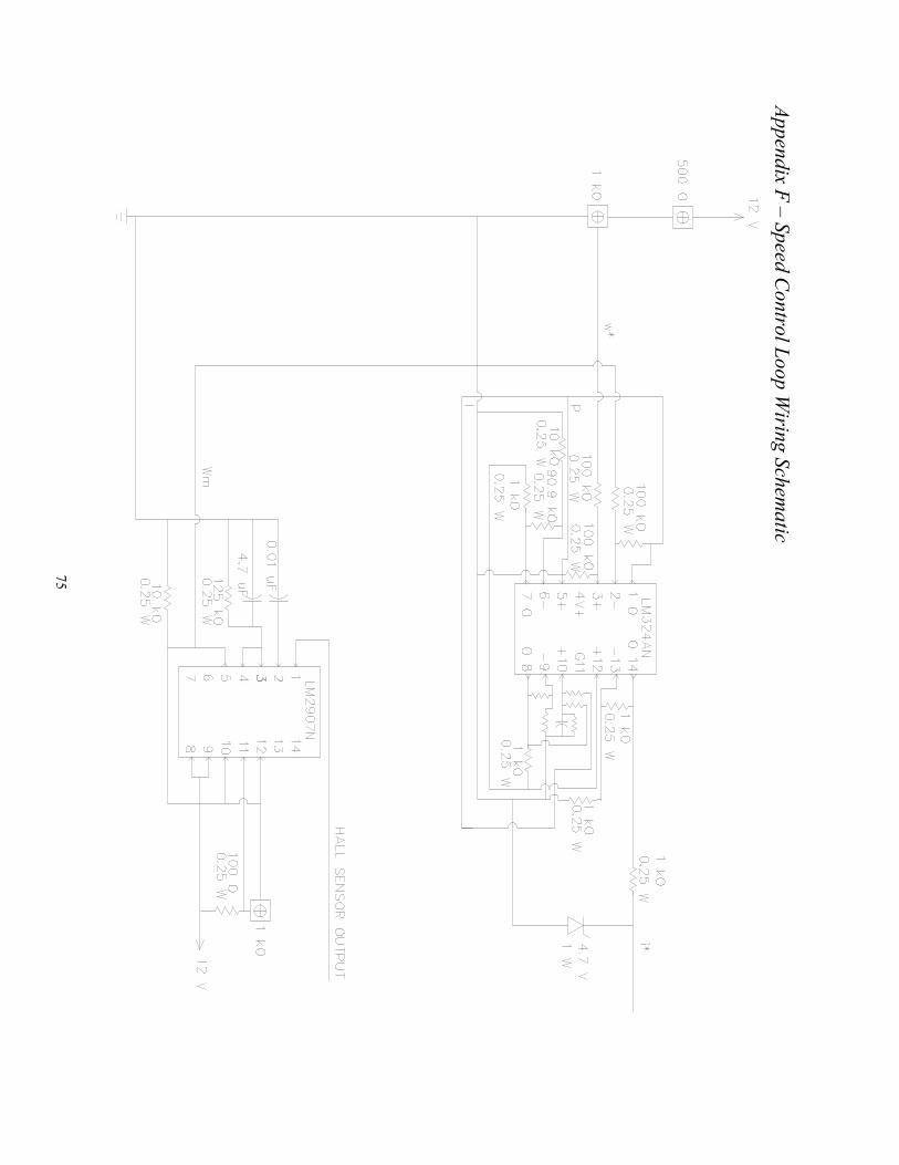
75
Appendix F – Speed Control Loop W
iring Schematic
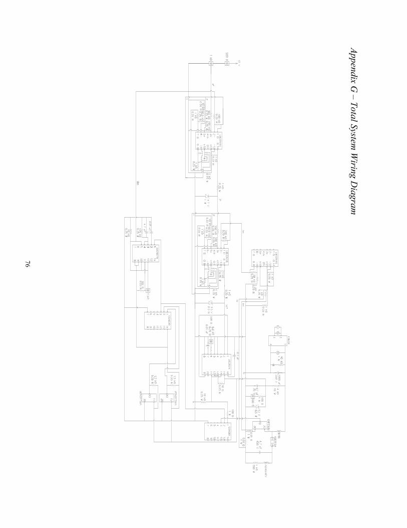
76
Appendix G – Total System
Wiring D
iagram

77
Vita
Amanda Martin Staley was born Amanda Christine Martin on February 8, 1978 in
Richmond, Virginia to Charles David and Brenda Jean Martin. She graduated with honors from
Monacan High School in Chesterfield County, Virginia in June of 1995. During her
undergraduate years, she interned with Philip Morris USA (Cigarette Manufacturing Division) in
Richmond, Virginia as an electrical engineer in the manufacturing and technical support
divisions. Also, she interned with Delta Airport Consultants, Inc. (Airport Design Consulting
Firm) as an electrical design engineer. She was named a Bradley Scholar in May of 1996 in the
Bradley Department of Electrical and Computer Engineering. She graduated Magna Cum Laude
as a Commonwealth Scholar from Virginia Polytechnic Institute and State University in May of
1999 with a Bachelor of Science in Electrical Engineering. She earned her Engineer-In-Training
(E.I.T.) certification in June of 1999. She was named a Bradley Fellow in May of 1999 in the
Bradley Department of Electrical and Computer Engineering. After the completion of her
master’s degree, she will pursue her Ph.D. in Electrical Engineering at Virginia Polytechnic
Institute and State University as a Bradley Fellow. Her research interests include: single-phase
switched reluctance motor drives, single-phase brushless DC drives, motor topology design, and
industrial control systems.