42LG60-Fall 2008-v25 - Diagramas dediagramas.diagramasde.com/otros/LG Flat TV 42LG60...
73
42LG60 42LG60 Direct View LCD
Transcript of 42LG60-Fall 2008-v25 - Diagramas dediagramas.diagramasde.com/otros/LG Flat TV 42LG60...

42LG6042LG60
Direct View LCD
LCD DV 42LG602
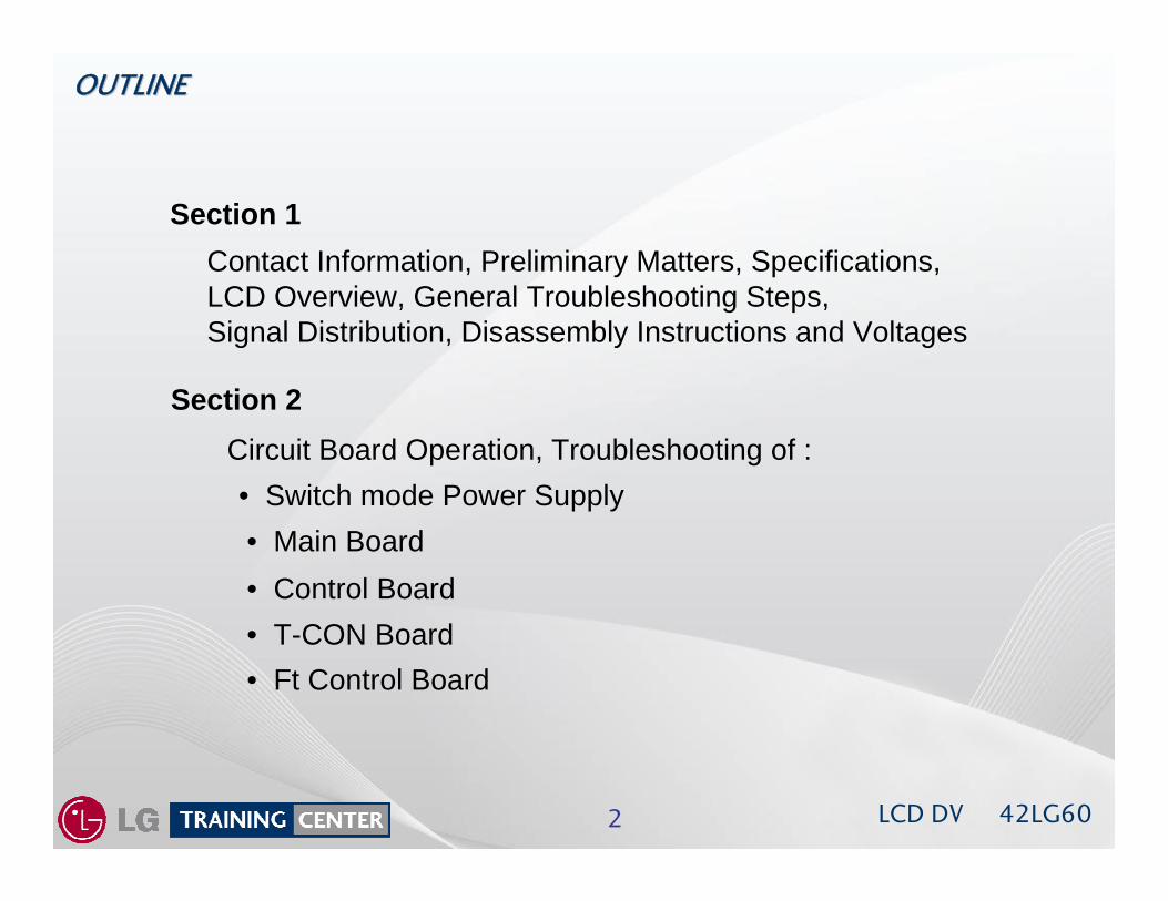
OUTLINEOUTLINE
• Main Board
• T-CON Board• Control Board
• Ft Control Board
Circuit Board Operation, Troubleshooting of :• Switch mode Power Supply
Section 1
Section 2
Contact Information, Preliminary Matters, Specifications,LCD Overview, General Troubleshooting Steps, Signal Distribution, Disassembly Instructions and Voltages
LCD DV 42LG603
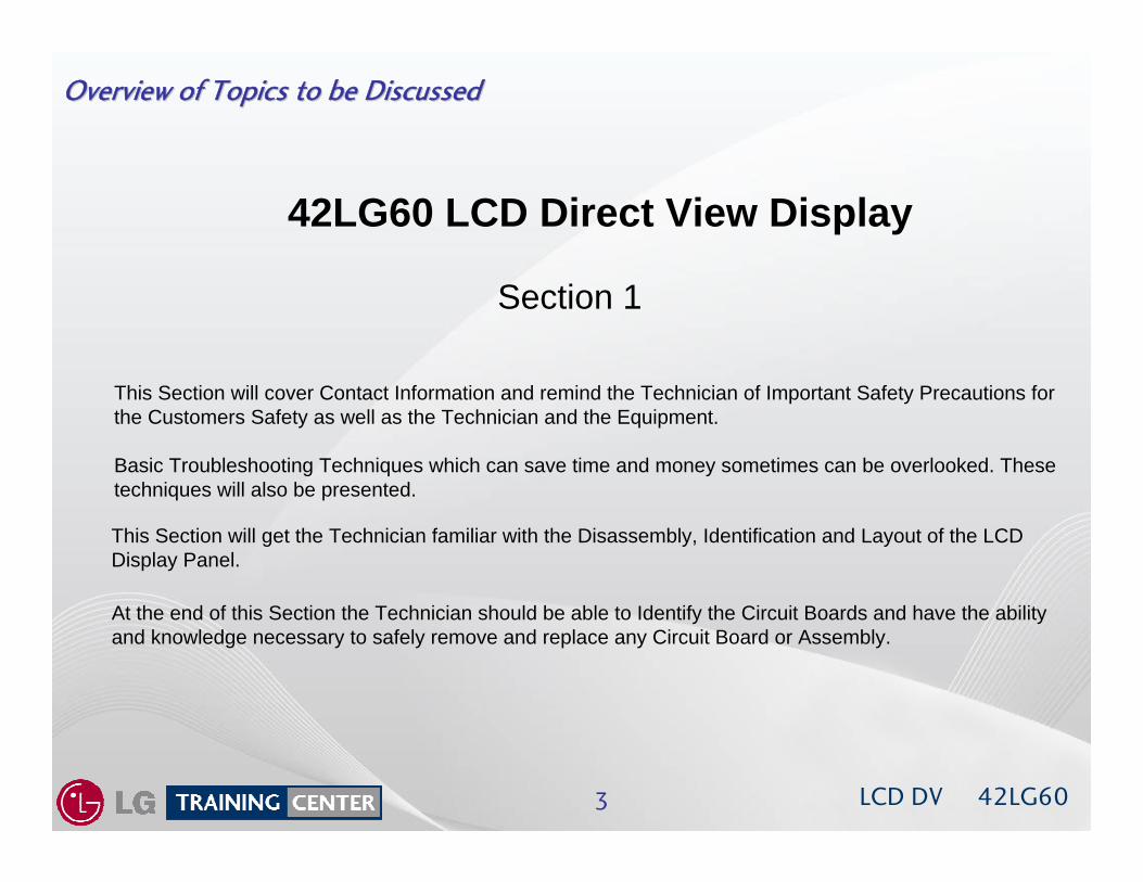
42LG60 LCD Direct View Display
Section 1
This Section will cover Contact Information and remind the Technician of Important Safety Precautions for the Customers Safety as well as the Technician and the Equipment.
Basic Troubleshooting Techniques which can save time and money sometimes can be overlooked. These techniques will also be presented.
This Section will get the Technician familiar with the Disassembly, Identification and Layout of the LCD Display Panel.
At the end of this Section the Technician should be able to Identify the Circuit Boards and have the ability and knowledge necessary to safely remove and replace any Circuit Board or Assembly.
Overview of Topics to be DiscussedOverview of Topics to be Discussed
LCD DV 42LG604
IMPORTANT SAFETY NOTICEIMPORTANT SAFETY NOTICE
The information in this training manual is intended for use by persons possessing an adequate background in electrical equipment, electronic devices, and mechanical systems. In any attempt to repair a major Product, personal injury and property damage can result. The manufacturer or seller maintains no liability for the interpretation of this information, nor can it assume any liability in conjunction with its use. When servicing this product, under no circumstances should the original design be modified or altered without permission from LG Electronics. Unauthorized modifications will not only void the warranty, but may lead to property damage or user injury. If wires, screws, clips, straps, nuts, or washers used to complete a ground path are removed for service, they must be returned to their original positions and properly fastened.
CAUTIONCAUTION
To avoid personal injury, disconnect the power before servicing this product. If electrical power is required for diagnosis or test purposes, disconnect the power immediately after performing the necessary checks. Also be aware that many household products present a weight hazard. At least two people should be involved in the installation or servicing of such devices. Failure to consider the weight of an product could result in physical injury.
Preliminary Matters (The Fine Print)Preliminary Matters (The Fine Print)
LCD DV 42LG605
Today’s sophisticated electronics are electrostatic discharge (ESD) sensitive. ESD can weaken or damage the electronics in a manner that renders them inoperative or reduces the time until their next failure. Connect an ESD wrist strap to a ground connection point or unpainted metal in the product. Alternatively, you can touch your finger repeatedly to a ground connection point or unpainted metal in the product. Before removing a replacement part from its package, touch the anti-static bag to a ground connection point or unpainted metal in the product. Handle the electronic control assembly by its edges only. When repackaging a failed electronic control assembly in an anti-static bag, observe these same precautions.
REGULATORY INFORMATIONREGULATORY INFORMATION
This equipment has been tested and found to comply with the limits for a Class B digital device, pursuant to Part 15 of the FCC Rules. These limits are designed to provide reasonable protection against harmful interference when the equipment is operated in a residential installation. This equipment generates, uses, and can radiate radio frequency energy, and, if not installed and used in accordance with the instruction manual, may cause harmful interference to radio communications. However, there is no guarantee that interference will not occur in a particular installation. If this equipment does cause harmful interference to radio or television reception, which can be determined by turning the equipment off and on, the user is encouraged to try to correct the interference by one or more of the following measures: Reorient or relocate the receiving antenna; Increase the separation between the equipment and the receiver; Connect the equipment to an outlet on a different circuit than that to which the receiver is connected; or consult the dealer or an experienced radio/TV technician for help.
ESD NOTICEESD NOTICE (Electrostatic Static Discharge)(Electrostatic Static Discharge)

LCD DV 42LG606
CONTACT INFORMATIONCONTACT INFORMATION
Customer Service (and Part Sales) (800) 243-0000
Technical Support (and Part Sales) (800) 847-7597
USA Website (GCSC) aic.lgservice.comCustomer Service Website us.lgservice.com
LG CS Academy lgcsacademy.com
LG Web Training lge.webex.com
Published March 2009 by LG Technical Support and Training
LG Electronics Alabama, Inc. 201 James Record Road,
Huntsville, AL, 35813.
LCD DV 42LG607
Safety & Handling Regulations
1. Check the appearance of the Replacement Panel and Circuit Boards for both physical damage and part number accuracy.
2. Check the model label. Verify model names and board model matches.
3. Check details of defective condition and history. Example: Oscillator failure dead set, etc…
1. Approximately 20 minute pre-run time is required before any adjustments are performed.
2. Refer to the Voltage Sticker on the Switch Mode Power Supply silk screening. (+/- ½ volt).
3. Be cautious of electric shock from the Backlight section, it uses high voltage AC. Check that the Power Supply
and Drive Circuits are completely discharged because of residual current stored before Circuit Board removal.
4. C-MOS circuits are sensitive to static electricity. Use caution when dealing with these IC and circuits.
5. Exercise care when making voltage and waveform checks to prevent costly short circuits from damaging the unit.
6. Be cautious of lost screws and other metal objects to prevent a possible short in the circuitry.
Checking Points to be Considered
TroubleshootingSECTION 1: SECTION 1: LCD OVERVIEWLCD OVERVIEW
LCD DV 42LG608
Basic Troubleshooting StepsBasic Troubleshooting Steps
Define, Localize, Isolate and Correct
•Define Look at the symptom carefully and determine what circuits could be causing the failure. Use your senses Sight, Smell, Touch and Hearing. Look for burned parts and check for possible overheated components. Capacitors will sometimes leak dielectric material and give off a distinct odor. Frequency of power supplies will change with the load, or listen for relay closing etc. Observation of the front Power LED may give some clues.
•Localize After carefully checking the symptom and determining the circuits to be checked and after giving a thorough examination using your senses the first check should always be the DC Supply Voltages to those circuits under test. Always confirm the supplies are not only the proper level but be sure they are noise free. If the supplies are missing check the resistance for possible short circuits.
•Isolate To further isolate the failure, check for the proper waveforms with the Oscilloscope to make a final determination of the failure. Look for correct Amplitude Phasing and Timing of the signals also check for the proper Duty Cycle of the signals. Sometimes “glitches” or “road bumps” will be an indication of an imminent failure.
•Correct The final step is to correct the problem. Be careful of ESD and make sure to check the DC Supplies for proper levels. Make all necessary adjustments and lastly always perform a Safety AC Leakage Test before returning the product back to the Customer.
LCD DV 42LG609
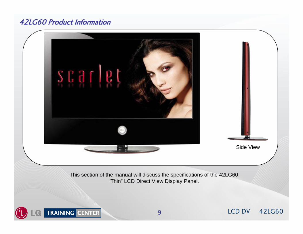
This section of the manual will discuss the specifications of the 42LG60“Thin” LCD Direct View Display Panel.
42LG60 Product Information42LG60 Product Information
Side View
LCD DV 42LG6010
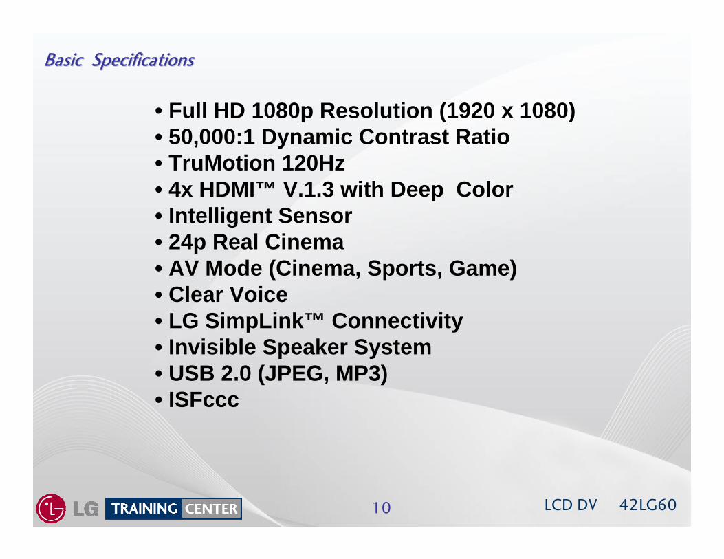
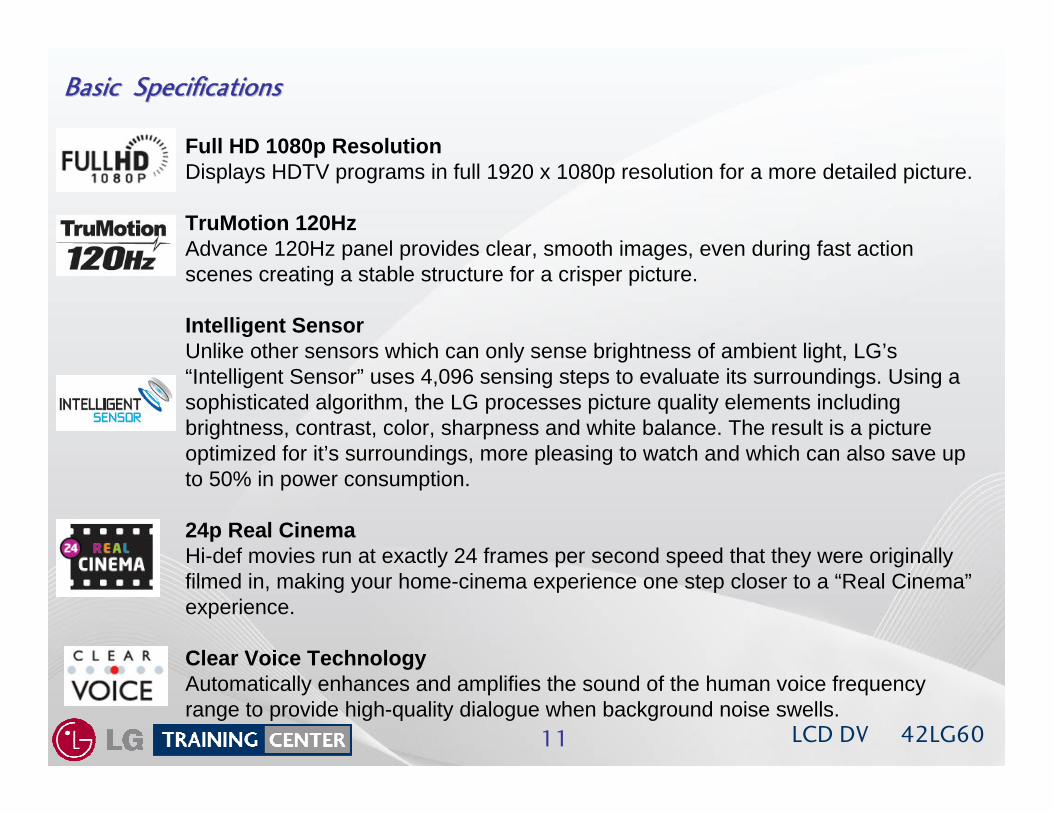
Basic SpecificationsBasic Specifications
• Full HD 1080p Resolution (1920 x 1080) • 50,000:1 Dynamic Contrast Ratio • TruMotion 120Hz • 4x HDMI™ V.1.3 with Deep Color • Intelligent Sensor • 24p Real Cinema • AV Mode (Cinema, Sports, Game) • Clear Voice • LG SimpLink™ Connectivity • Invisible Speaker System • USB 2.0 (JPEG, MP3) • ISFccc
LCD DV 42LG6011
Basic SpecificationsBasic Specifications
Full HD 1080p Resolution Displays HDTV programs in full 1920 x 1080p resolution for a more detailed picture.
TruMotion 120Hz Advance 120Hz panel provides clear, smooth images, even during fast action scenes creating a stable structure for a crisper picture.
Intelligent Sensor Unlike other sensors which can only sense brightness of ambient light, LG’s“Intelligent Sensor” uses 4,096 sensing steps to evaluate its surroundings. Using a sophisticated algorithm, the LG processes picture quality elements including brightness, contrast, color, sharpness and white balance. The result is a picture optimized for it’s surroundings, more pleasing to watch and which can also save up to 50% in power consumption.
24p Real Cinema Hi-def movies run at exactly 24 frames per second speed that they were originally filmed in, making your home-cinema experience one step closer to a “Real Cinema”experience.
Clear Voice Technology Automatically enhances and amplifies the sound of the human voice frequency range to provide high-quality dialogue when background noise swells.
LCD DV 42LG6012
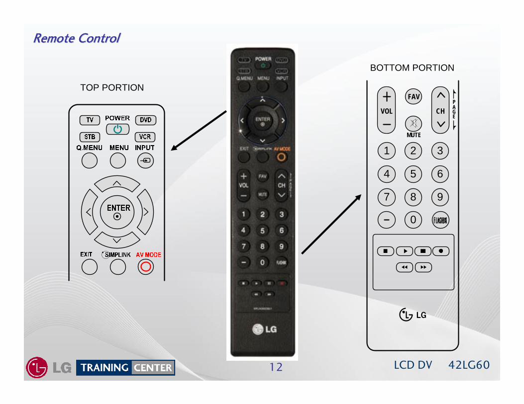
Remote ControlRemote Control
1 2 3
4 5 6
7 8 9
0
VOL CH
FAV
MUTE
PAGE
LG
TOP PORTION
BOTTOM PORTION
LCD DV 42LG6013
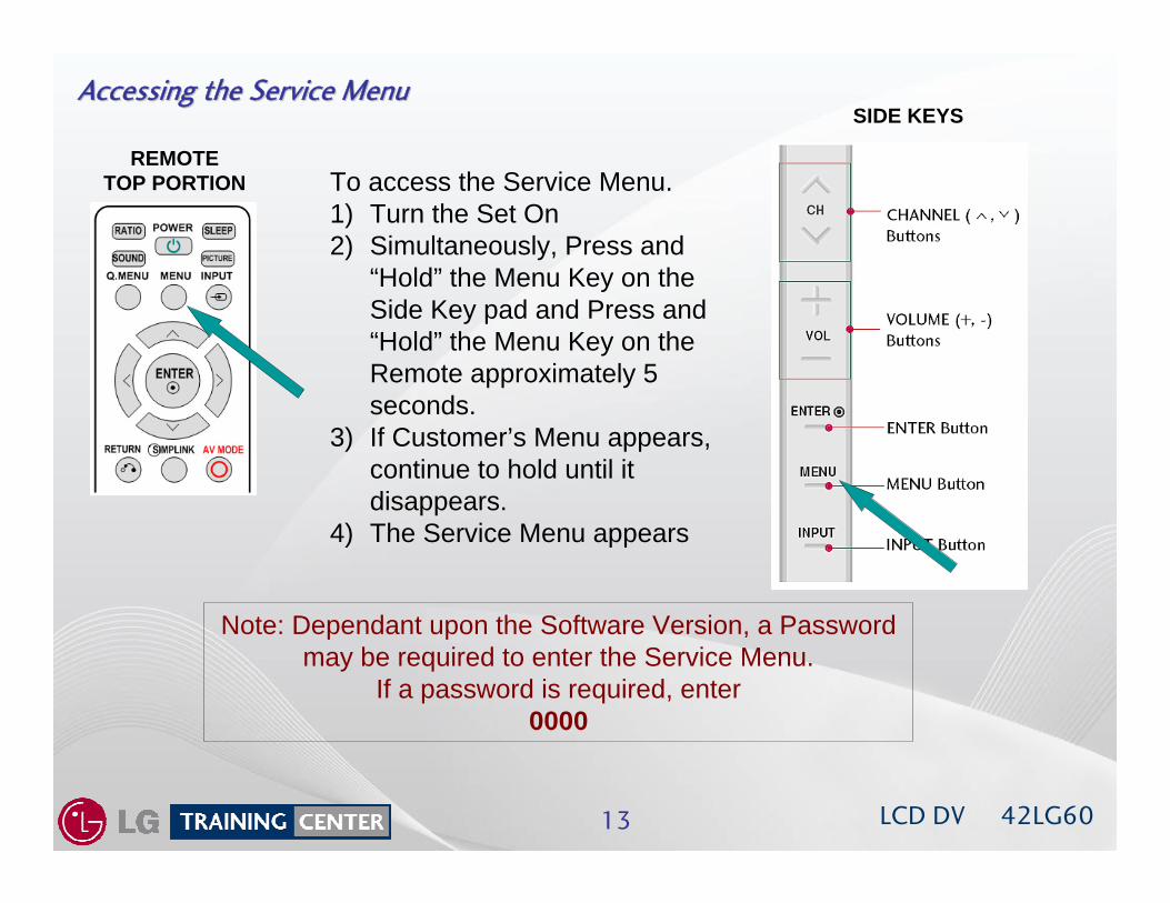
Accessing the Service MenuAccessing the Service Menu
REMOTETOP PORTION
SIDE KEYS
To access the Service Menu.1) Turn the Set On2) Simultaneously, Press and
“Hold” the Menu Key on the Side Key pad and Press and “Hold” the Menu Key on the Remote approximately 5 seconds.
3) If Customer’s Menu appears, continue to hold until it disappears.
4) The Service Menu appears
Note: Dependant upon the Software Version, a Password may be required to enter the Service Menu.
If a password is required, enter0000
LCD DV 42LG6014
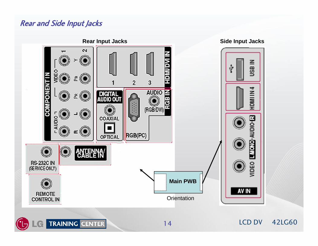
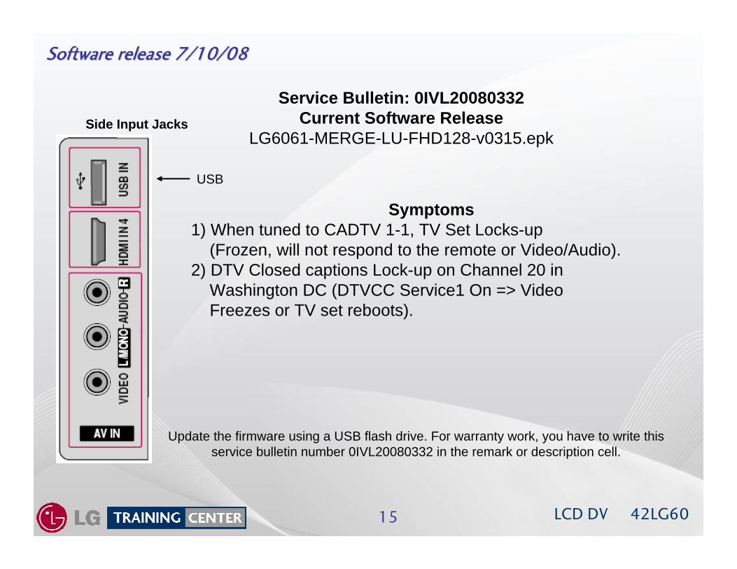
Side Input Jacks
Rear and Side Input JacksRear and Side Input Jacks
Main PWB
Orientation
Rear Input Jacks
LCD DV 42LG6015
Side Input Jacks
Software release 7/10/08Software release 7/10/08
USB
Service Bulletin: 0IVL20080332Current Software Release
LG6061-MERGE-LU-FHD128-v0315.epk
Symptoms1) When tuned to CADTV 1-1, TV Set Locks-up
(Frozen, will not respond to the remote or Video/Audio).2) DTV Closed captions Lock-up on Channel 20 in
Washington DC (DTVCC Service1 On => VideoFreezes or TV set reboots).
Update the firmware using a USB flash drive. For warranty work, you have to write this service bulletin number 0IVL20080332 in the remark or description cell.
LCD DV 42LG6016
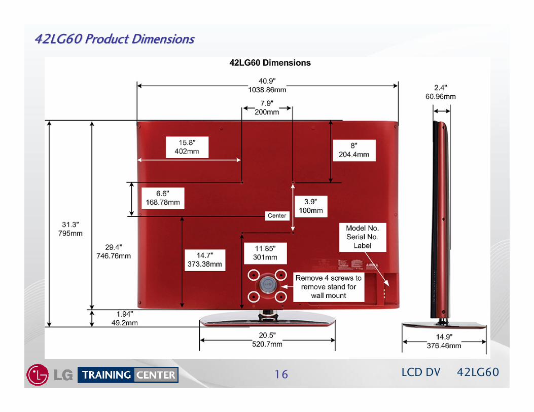
42LG60 Product Dimensions42LG60 Product Dimensions
LCD DV 42LG6017
This section of the manual will discuss Disassembly, Layout and Circuit Board Identification, of the 42LG60 LCD Direct View Television.
Upon completion of this section the Technician will have a better understanding of the disassembly procedures, the layout of the printed circuit boards and be able to identify each board.
DISASSEMBLY SECTIONDISASSEMBLY SECTION
LCD DV 42LG6018
This section of the manual will discuss troubleshooting.
Upon completion of this section the Technician will have a better understanding of how to diagnosis and resolve problems.
TROUBLESHOOTING SECTIONTROUBLESHOOTING SECTION
LCD DV 42LG6019
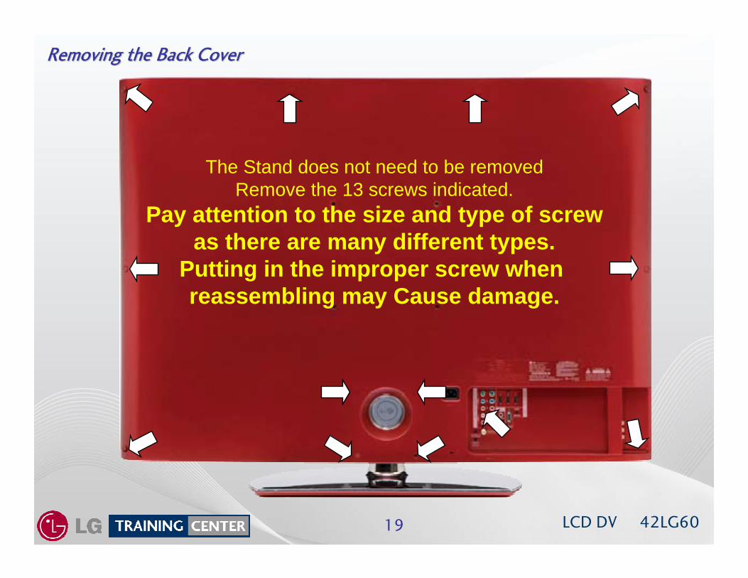
Removing the Back CoverRemoving the Back Cover
The Stand does not need to be removedRemove the 13 screws indicated.
Pay attention to the size and type of screwas there are many different types.
Putting in the improper screw when reassembling may Cause damage.
LCD DV 42LG6020
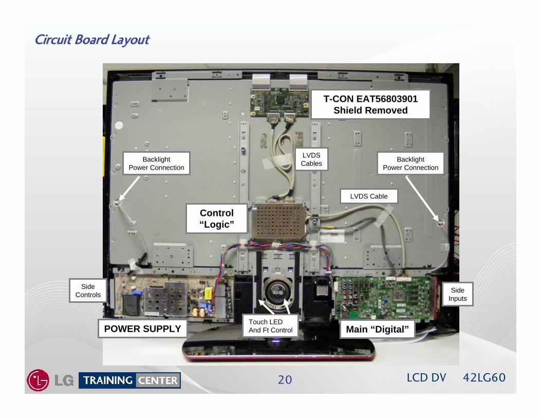
Circuit Board LayoutCircuit Board Layout
POWER SUPPLY Main “Digital”
Control “Logic”
SideInputs
T-CON EAT56803901Shield Removed
Touch LEDAnd Ft Control
BacklightPower Connection
BacklightPower Connection
LVDSCables
LVDS Cable
SideControls

LCD DV 42LG6021
Backlight InformationBacklight Information
Back View 18 Bulbs
Power Supply with Ballast
To Backlights Over 1.2KV
58Khz
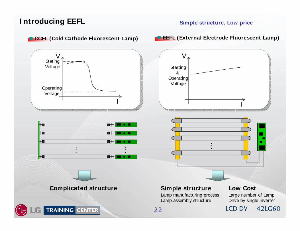
EEFL (External Electrode Fluorescent Lamp)LOW COST Large number of lamps driven by a single inverter
2.8V~3.1V RMS
LCD DV 42LG6022
CCFL (Cold Cathode Fluorescent Lamp) EEFL (External Electrode Fluorescent Lamp)
V
I
StatingVoltage
OperatingVoltage
V
I
Starting&
OperatingVoltage
......
...
Simple structureComplicated structure
Simple structure, Low price
Low CostLamp manufacturing processLamp assembly structure
Large number of Lamp Drive by single inverter
Introducing EEFL
LCD DV 42LG6023
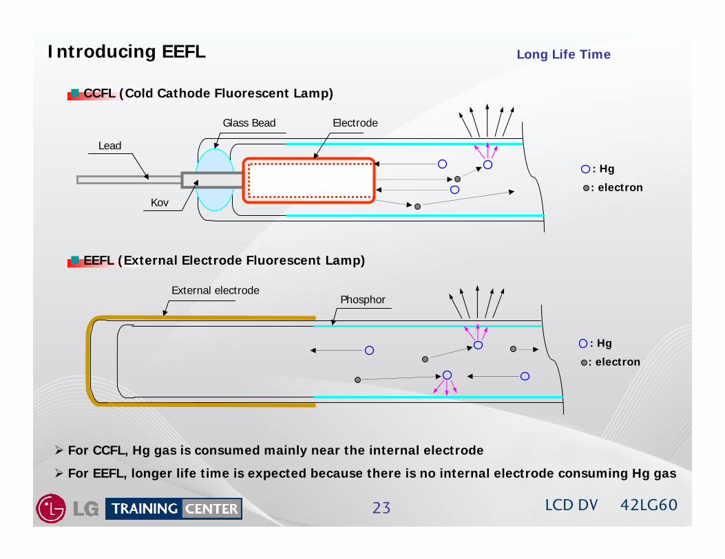
CCFL (Cold Cathode Fluorescent Lamp)
Introducing EEFL Long Life Time
ElectrodeGlass Bead
Kov
Lead
: Hg
: electron
EEFL (External Electrode Fluorescent Lamp)
External electrodePhosphor
: Hg
: electron
For CCFL, Hg gas is consumed mainly near the internal electrode
For EEFL, longer life time is expected because there is no internal electrode consuming Hg gas
LCD DV 42LG6024
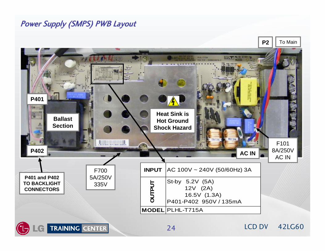
Power Supply (SMPS) PWB LayoutPower Supply (SMPS) PWB Layout
P2
AC INP402
P401
Ballast Section
To Main
P401 and P402TO BACKLIGHT CONNECTORS
INPUT AC 100V ~ 240V (50/60Hz) 3A
OU
TPU
T St-by 5.2V (5A) 12V (2A) 16.5V (1.3A)P401-P402 950V / 135mA
MODEL PLHL-T715A
F1018A/250V
AC IN
F7005A/250V
335V
Heat Sink isHot Ground
Shock Hazard
LCD DV 42LG6025
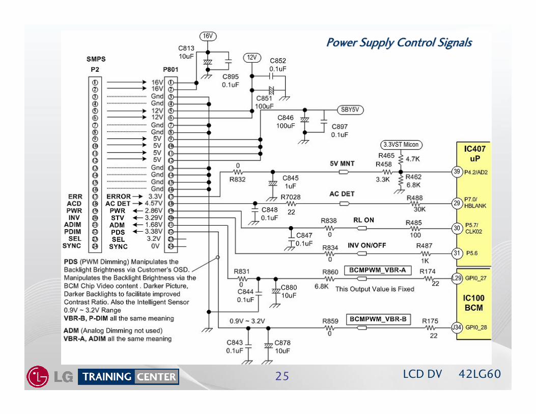
Power Supply Control SignalsPower Supply Control Signals
LCD DV 42LG6026
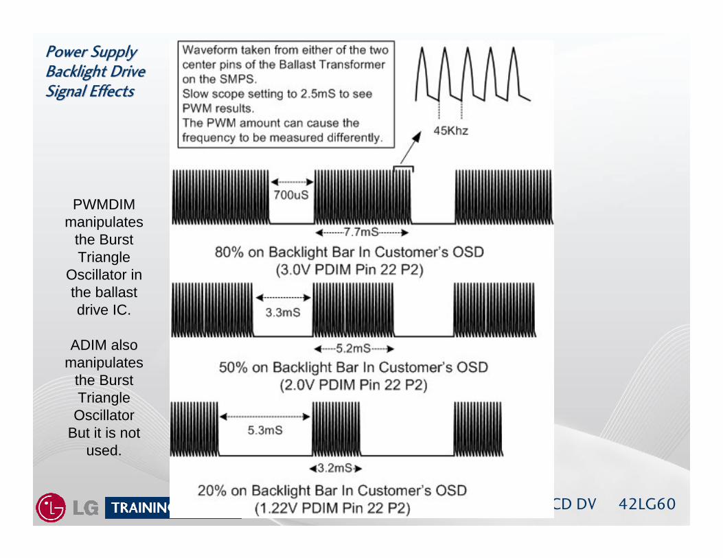
Power Supply Power Supply Backlight Drive Backlight Drive Signal EffectsSignal Effects
PWMDIMmanipulates
the Burst Triangle
Oscillator in the ballast drive IC.
ADIM also manipulates
the Burst Triangle
OscillatorBut it is not
used.
LCD DV 42LG6027
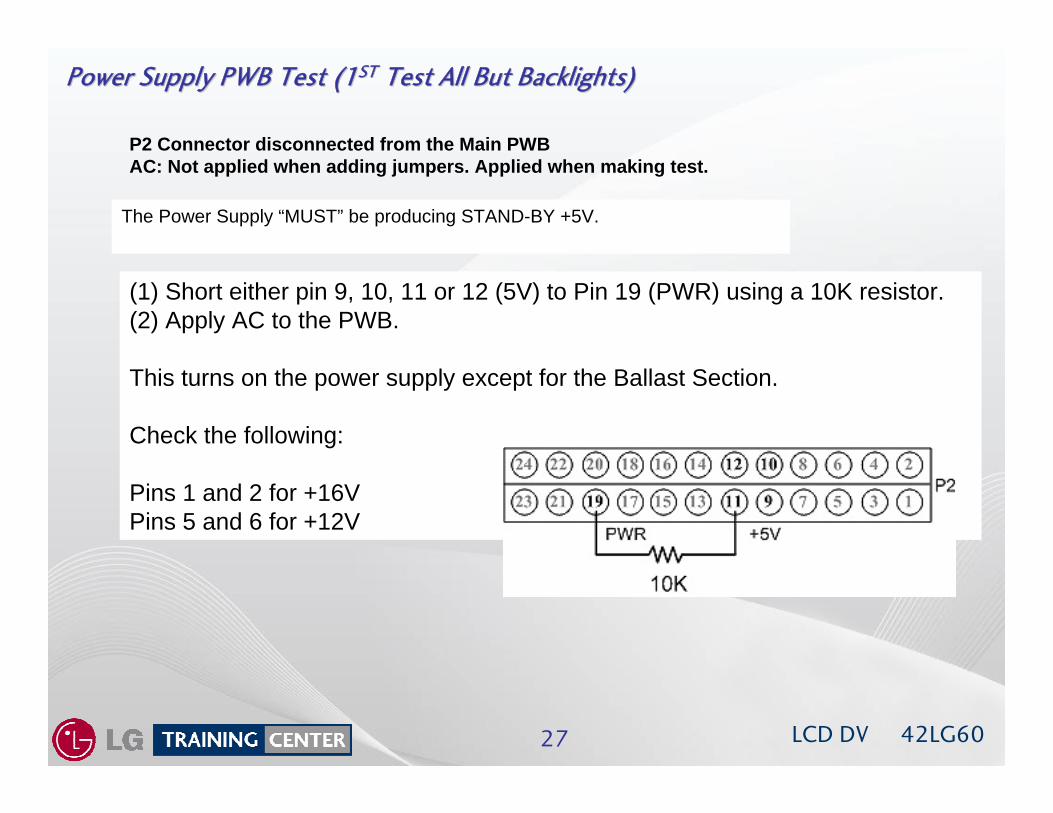
Power Supply PWB Test (1Power Supply PWB Test (1STST Test All But Backlights)Test All But Backlights)
The Power Supply “MUST” be producing STAND-BY +5V.
P2 Connector disconnected from the Main PWBAC: Not applied when adding jumpers. Applied when making test.
(1) Short either pin 9, 10, 11 or 12 (5V) to Pin 19 (PWR) using a 10K resistor.(2) Apply AC to the PWB.
This turns on the power supply except for the Ballast Section.
Check the following:
Pins 1 and 2 for +16VPins 5 and 6 for +12V
LCD DV 42LG6028
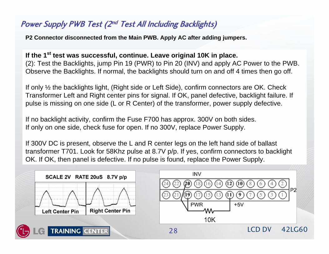
If the 1st test was successful, continue. Leave original 10K in place.(2): Test the Backlights, jump Pin 19 (PWR) to Pin 20 (INV) and apply AC Power to the PWB. Observe the Backlights. If normal, the backlights should turn on and off 4 times then go off.
If only ½ the backlights light, (Right side or Left Side), confirm connectors are OK. Check Transformer Left and Right center pins for signal. If OK, panel defective, backlight failure. If pulse is missing on one side (L or R Center) of the transformer, power supply defective.
If no backlight activity, confirm the Fuse F700 has approx. 300V on both sides.If only on one side, check fuse for open. If no 300V, replace Power Supply.
If 300V DC is present, observe the L and R center legs on the left hand side of ballast transformer T701. Look for 58Khz pulse at 8.7V p/p. If yes, confirm connectors to backlight OK. If OK, then panel is defective. If no pulse is found, replace the Power Supply.
Power Supply PWB Test (2Power Supply PWB Test (2ndnd Test All Including Backlights)Test All Including Backlights)
P2 Connector disconnected from the Main PWB. Apply AC after adding jumpers.
LCD DV 42LG6029
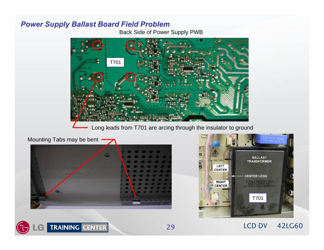
Power Supply Ballast Board Field Problem
T701
Long leads from T701 are arcing through the insulator to ground
Mounting Tabs may be bent
T701
Back Side of Power Supply PWB
LCD DV 42LG6030
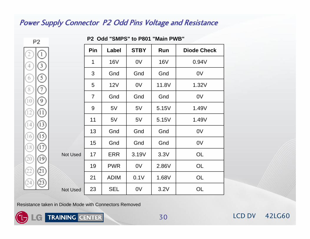
Power Supply Connector P2 Odd Pins Voltage and ResistancePower Supply Connector P2 Odd Pins Voltage and Resistance
Resistance taken in Diode Mode with Connectors Removed
OL3.2V0VSEL23
OL1.68V0.1VADIM21
OL2.86V0VPWR19
OL3.3V3.19VERR17
0VGndGndGnd15
0VGndGndGnd13
1.49V5.15V5V5V11
1.49V5.15V5V5V9
0VGndGndGnd7
1.32V11.8V0V12V5
0VGndGndGnd3
0.94V16V0V16V1
Diode CheckRun STBYLabelPin
P2 Odd "SMPS" to P801 "Main PWB"
Not Used
Not Used
LCD DV 42LG6031
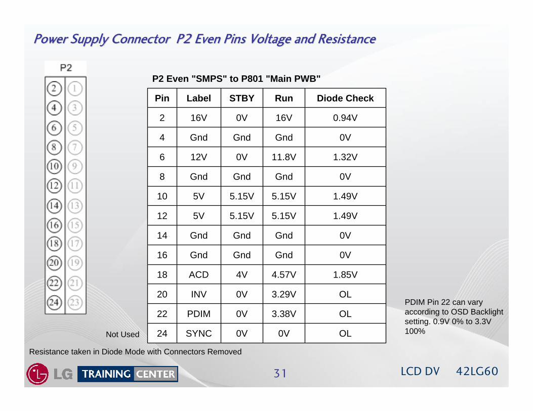
Power Supply Connector P2 Even Pins Voltage and ResistancePower Supply Connector P2 Even Pins Voltage and Resistance
Resistance taken in Diode Mode with Connectors Removed
OL0V0VSYNC24
OL3.38V0VPDIM22
OL3.29V0VINV20
1.85V4.57V4VACD18
0VGndGndGnd16
0VGndGndGnd14
1.49V5.15V5.15V5V12
1.49V5.15V5.15V5V10
0VGndGndGnd8
1.32V11.8V0V12V6
0VGndGndGnd4
0.94V16V0V16V2
Diode CheckRun STBYLabelPin
P2 Even "SMPS" to P801 "Main PWB"
PDIM Pin 22 can vary according to OSD Backlight setting. 0.9V 0% to 3.3V 100%Not Used
LCD DV 42LG6032
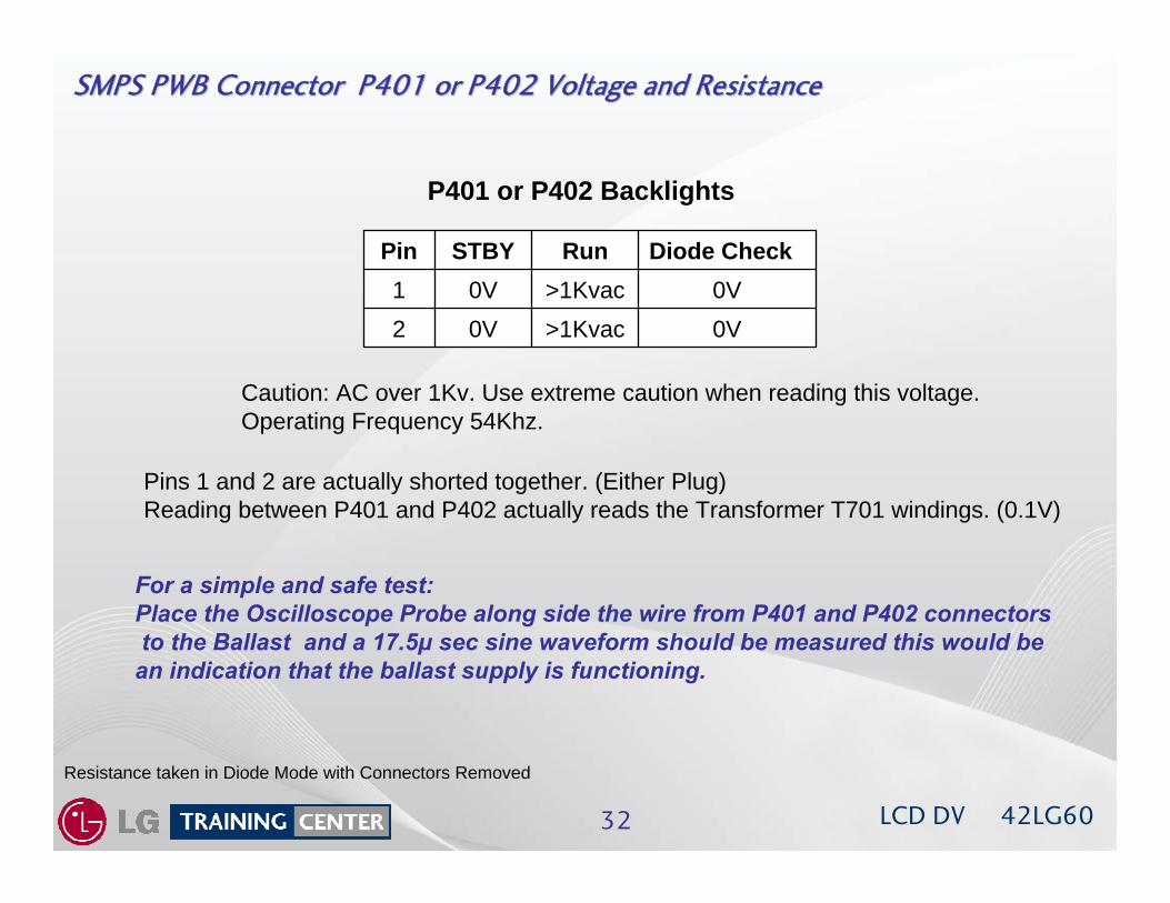
SMPS PWB Connector P401 or P402 Voltage and ResistanceSMPS PWB Connector P401 or P402 Voltage and Resistance
Resistance taken in Diode Mode with Connectors Removed
P401 or P402 Backlights
0V>1Kvac0V20V>1Kvac0V1
Diode CheckRun STBYPin
Caution: AC over 1Kv. Use extreme caution when reading this voltage.Operating Frequency 54Khz.
Pins 1 and 2 are actually shorted together. (Either Plug)Reading between P401 and P402 actually reads the Transformer T701 windings. (0.1V)
For a simple and safe test:Place the Oscilloscope Probe along side the wire from P401 and P402 connectorsto the Ballast and a 17.5μ sec sine waveform should be measured this would be
an indication that the ballast supply is functioning.
LCD DV 42LG6033
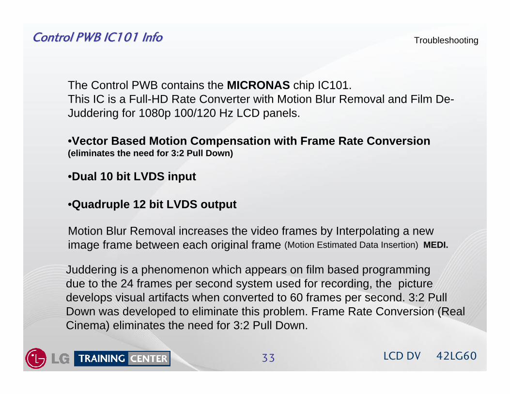
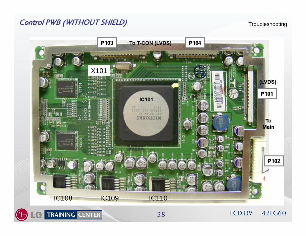
Control PWB IC101 InfoControl PWB IC101 Info Troubleshooting
The Control PWB contains the MICRONAS chip IC101. This IC is a Full-HD Rate Converter with Motion Blur Removal and Film De-Juddering for 1080p 100/120 Hz LCD panels.
•Vector Based Motion Compensation with Frame Rate Conversion (eliminates the need for 3:2 Pull Down)
•Dual 10 bit LVDS input
•Quadruple 12 bit LVDS output
Juddering is a phenomenon which appears on film based programming due to the 24 frames per second system used for recording, the picture develops visual artifacts when converted to 60 frames per second. 3:2 PullDown was developed to eliminate this problem. Frame Rate Conversion (Real Cinema) eliminates the need for 3:2 Pull Down.
Motion Blur Removal increases the video frames by Interpolating a new image frame between each original frame (Motion Estimated Data Insertion) MEDI.
LCD DV 42LG6034
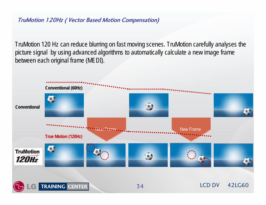
TruMotion 120Hz ( Vector Based Motion Compensation)TruMotion 120Hz ( Vector Based Motion Compensation)
Conventional (60Hz)
True Motion (120Hz)
Conventional
TruMotion 120 Hz can reduce blurring on fast moving scenes. TruMotion carefully analyses the picture signal by using advanced algorithms to automatically calculate a new image frame between each original frame (MEDI).
LCD DV 42LG6035
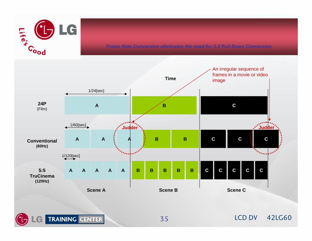
24p Real Cinema
A A A A A B B B B B C C C C C5:5 TruCinema
(120Hz)
Conventional(60Hz)
Scene A Scene B Scene C
A B C
A A A B B C C C
24P(Film)
1/24[sec]
Judder1/60[sec]
1/120[sec]
Time
An irregular sequence of frames in a movie or video image
Judder
Frame Rate Conversion eliminates the need for 3:2 Pull Down Conversion
LCD DV 42LG6036
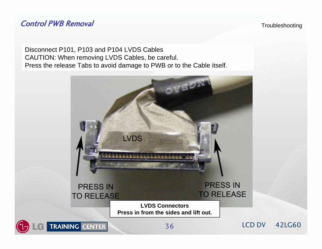
Control PWB RemovalControl PWB Removal Troubleshooting
Disconnect P101, P103 and P104 LVDS CablesCAUTION: When removing LVDS Cables, be careful. Press the release Tabs to avoid damage to PWB or to the Cable itself.
LVDS ConnectorsPress in from the sides and lift out.
LCD DV 42LG6037
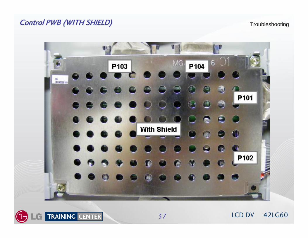
Control PWB (WITH SHIELD)Control PWB (WITH SHIELD) Troubleshooting
LCD DV 42LG6038
Control PWB (WITHOUT SHIELD)Control PWB (WITHOUT SHIELD) Troubleshooting
IC108 IC109 IC110
X101
LCD DV 42LG6039
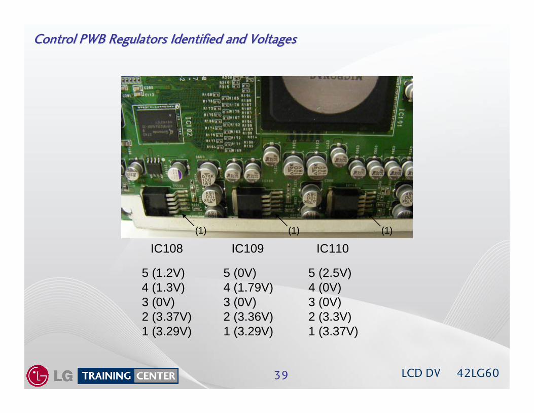
Control PWB Regulators Identified and VoltagesControl PWB Regulators Identified and Voltages
IC108 IC109 IC110
5 (1.2V)4 (1.3V)3 (0V)2 (3.37V)1 (3.29V)
5 (0V)4 (1.79V)3 (0V)2 (3.36V)1 (3.29V)
5 (2.5V)4 (0V)3 (0V)2 (3.3V)1 (3.37V)
(1) (1) (1)
LCD DV 42LG6040
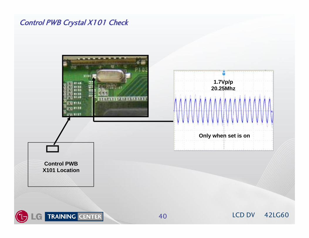
Control PWB Crystal X101 CheckControl PWB Crystal X101 Check
Control PWBX101 Location
1.7Vp/p20.25Mhz
Only when set is on
LCD DV 42LG6041
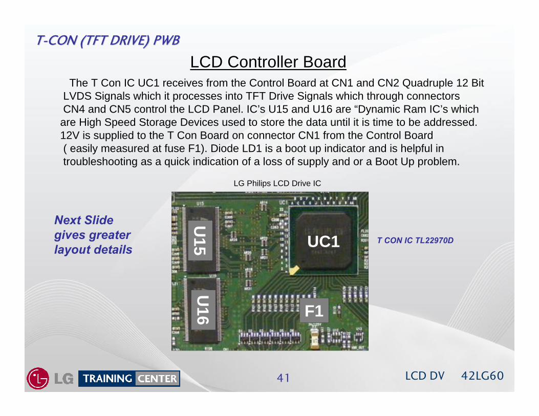
TT--CON (TFT DRIVE) PWB CON (TFT DRIVE) PWB
LCD Controller BoardThe T Con IC UC1 receives from the Control Board at CN1 and CN2 Quadruple 12 Bit
LVDS Signals which it processes into TFT Drive Signals which through connectorsCN4 and CN5 control the LCD Panel. IC’s U15 and U16 are “Dynamic Ram IC’s which are High Speed Storage Devices used to store the data until it is time to be addressed. 12V is supplied to the T Con Board on connector CN1 from the Control Board( easily measured at fuse F1). Diode LD1 is a boot up indicator and is helpful introubleshooting as a quick indication of a loss of supply and or a Boot Up problem.
T CON IC TL22970D
LG Philips LCD Drive IC
UC1
U15
U16 F1
Next Slidegives greater layout details
LCD DV 42LG6042
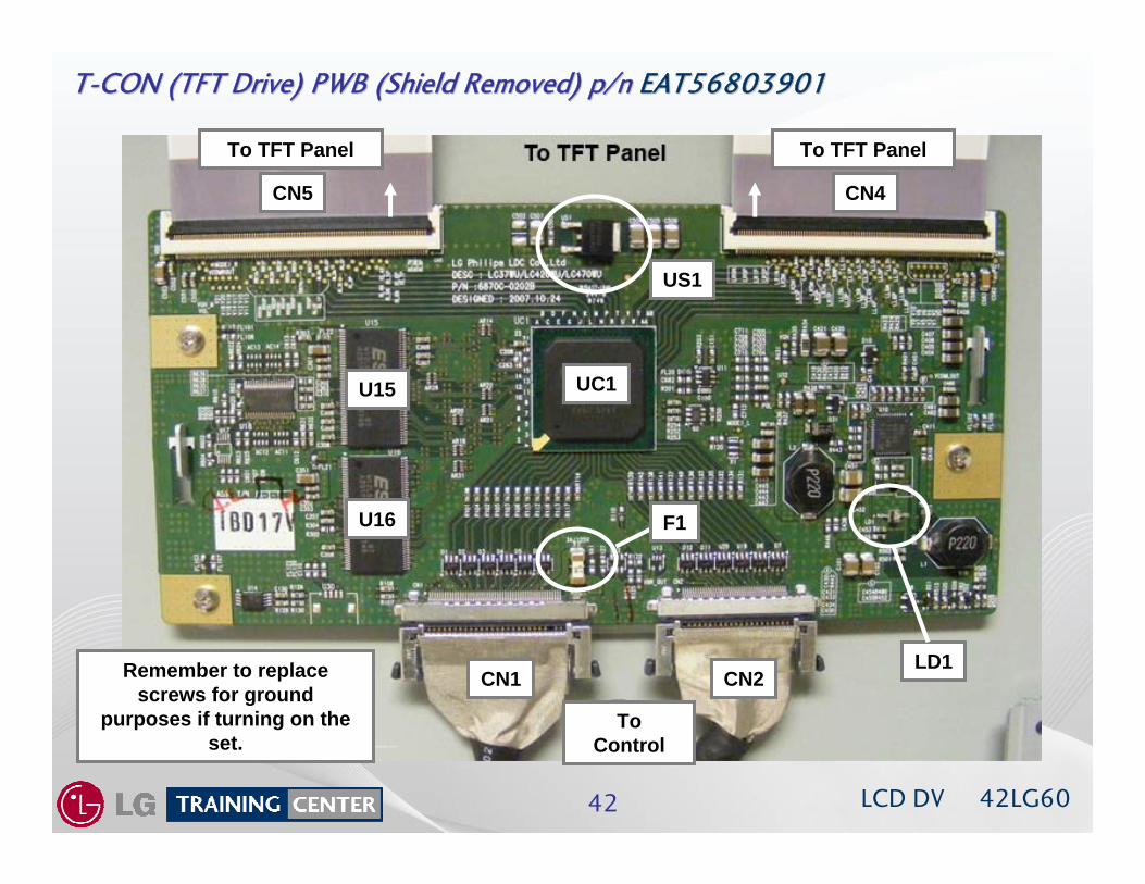
TT--CON (TFT Drive) PWB (Shield Removed) CON (TFT Drive) PWB (Shield Removed) p/np/n EAT56803901 EAT56803901
U15
U16
LD1
US1
F1
CN5 CN4
CN1 CN2
UC1
ToControl
To TFT Panel To TFT Panel
Remember to replace screws for ground
purposes if turning on the set.
LCD DV 42LG6043
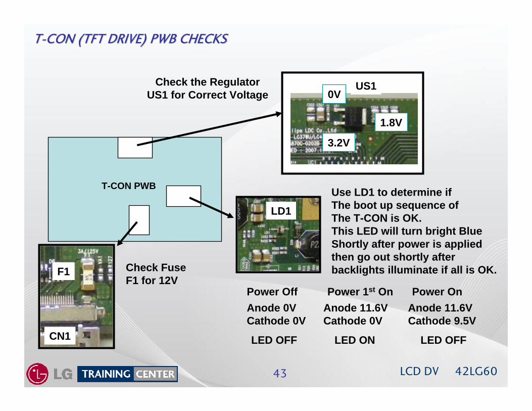
TT--CON (TFT DRIVE) PWB CHECKSCON (TFT DRIVE) PWB CHECKS
T-CON PWB
0V
3.2V
1.8V
US1
LD1
Use LD1 to determine ifThe boot up sequence ofThe T-CON is OK.This LED will turn bright BlueShortly after power is applied then go out shortly after backlights illuminate if all is OK.
Power Off Power 1st OnAnode 0VCathode 0V
Anode 11.6VCathode 0V
Power OnAnode 11.6VCathode 9.5V
LED OFF LED ON LED OFF
Check the Regulator US1 for Correct Voltage
Check FuseF1 for 12V
F1
CN1
LCD DV 42LG6044
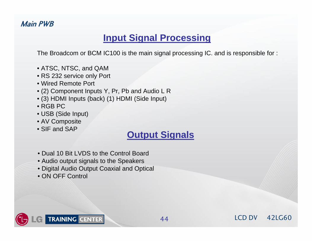
Main PWBMain PWB
Input Signal Processing The Broadcom or BCM IC100 is the main signal processing IC. and is responsible for :
• ATSC, NTSC, and QAM• RS 232 service only Port• Wired Remote Port• (2) Component Inputs Y, Pr, Pb and Audio L R• (3) HDMI Inputs (back) (1) HDMI (Side Input) • RGB PC• USB (Side Input)• AV Composite• SIF and SAP
Output Signals
• Dual 10 Bit LVDS to the Control Board• Audio output signals to the Speakers• Digital Audio Output Coaxial and Optical• ON OFF Control
LCD DV 42LG6045
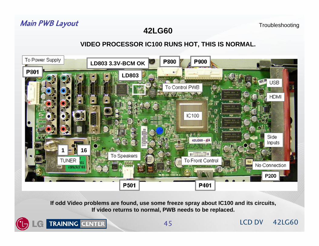
Main PWB LayoutMain PWB Layout Troubleshooting42LG60
VIDEO PROCESSOR IC100 RUNS HOT, THIS IS NORMAL.
If odd Video problems are found, use some freeze spray about IC100 and its circuits,If video returns to normal, PWB needs to be replaced.
LD803
1 16
LD803 3.3V-BCM OK
LCD DV 42LG6046
Main PWB (Back View) Regulator LayoutMain PWB (Back View) Regulator Layout
BCM ResetIC100 Video Processor
IC805
IC400
IC400
IC405
IC4053.29V
0V0.6V
3.31V0V
0.6V
123
SBY RUN IC8100V0V
0.3V
0V1.8V
3.31V
123
SBY RUN
0.4V0V
0.4V
3.37V0V
3.39V
123
SBY RUN
IC101
IC8020V
0.3V0V
5V3.3V
0V
123
SBY RUN
IC802
Q901 Q902 LVDS 12V Switch ControlLVDS 12V SwitchOutput 5~8 (12V)
IC810
IC805 0.V0V0V
0.4V0.1V
3.3V5V0V
3.39V1.2V
12345
SBY RUN3.3V BCM
LCD DV 42LG6047
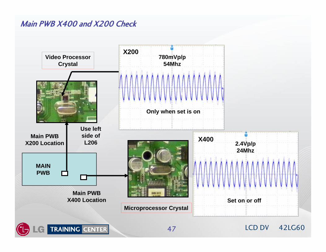
2.4Vp/p24Mhz
Main PWB X400 and X200 CheckMain PWB X400 and X200 Check
Main PWBX200 Location
780mVp/p54Mhz
Main PWBX400 Location
Only when set is on
Set on or off
Use left side of L206
MAIN PWB
X200
X400
Microprocessor Crystal
Video Processor Crystal
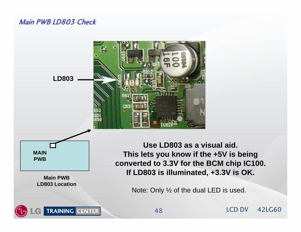
LCD DV 42LG6048
Main PWB LD803 CheckMain PWB LD803 Check
Main PWBLD803 Location
MAIN PWB
LD803
Use LD803 as a visual aid.This lets you know if the +5V is being
converted to 3.3V for the BCM chip IC100.If LD803 is illuminated, +3.3V is OK.
Note: Only ½ of the dual LED is used.
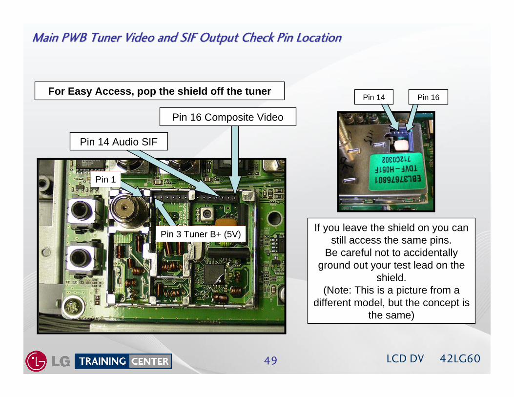
LCD DV 42LG6049
Main PWB Tuner Video and SIF Output Check Pin LocationMain PWB Tuner Video and SIF Output Check Pin Location
For Easy Access, pop the shield off the tuner
If you leave the shield on you can still access the same pins.
Be careful not to accidentally ground out your test lead on the
shield.(Note: This is a picture from a
different model, but the concept is the same)
Pin 14 Audio SIF
Pin 16 Composite Video
Pin 14 Pin 16
Pin 3 Tuner B+ (5V)
Pin 1
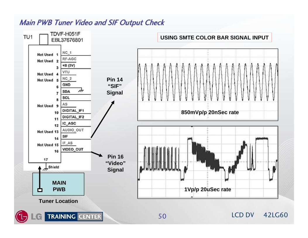
LCD DV 42LG6050
MAIN PWB
Main PWB Tuner Video and SIF Output CheckMain PWB Tuner Video and SIF Output Check
Tuner Location
1Vp/p 20uSec rate
Pin 16 “Video”Signal
Pin 14 “SIF”Signal
850mVp/p 20nSec rate
USING SMTE COLOR BAR SIGNAL INPUT
LCD DV 42LG6051
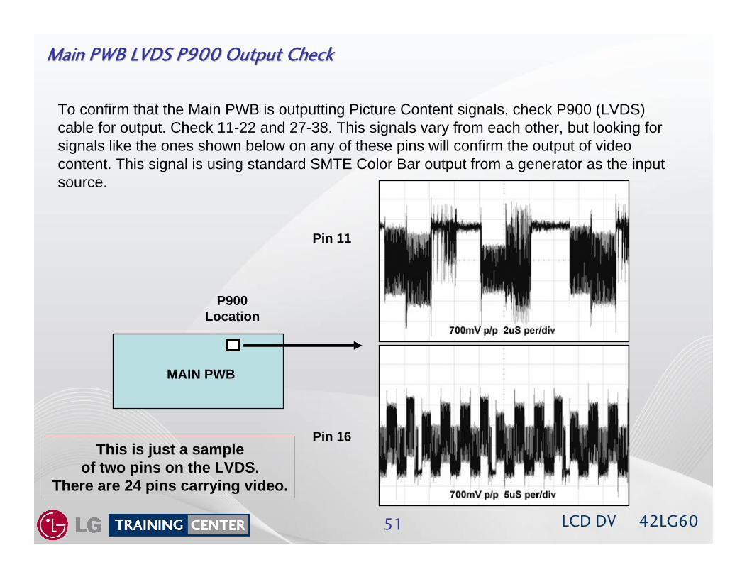
Main PWB LVDS P900 Output CheckMain PWB LVDS P900 Output Check
P900Location
To confirm that the Main PWB is outputting Picture Content signals, check P900 (LVDS) cable for output. Check 11-22 and 27-38. This signals vary from each other, but looking for signals like the ones shown below on any of these pins will confirm the output of video content. This signal is using standard SMTE Color Bar output from a generator as the input source.
MAIN PWB
Pin 11
Pin 16This is just a sample
of two pins on the LVDS.There are 24 pins carrying video.
LCD DV 42LG6052
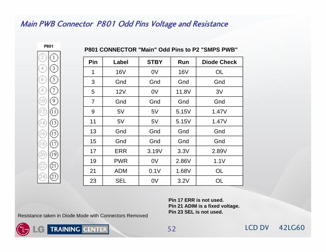
Main PWB Connector P801 Odd Pins Voltage and ResistanceMain PWB Connector P801 Odd Pins Voltage and Resistance
Resistance taken in Diode Mode with Connectors Removed
Pin 17 ERR is not used.Pin 21 ADIM is a fixed voltage.Pin 23 SEL is not used.
P801 CONNECTOR "Main" Odd Pins to P2 "SMPS PWB"
OL3.2V0VSEL23
OL1.68V0.1VADM21
1.1V2.86V0VPWR19
2.89V3.3V3.19VERR17
GndGndGndGnd15
GndGndGndGnd13
1.47V5.15V5V5V11
1.47V5.15V5V5V9
GndGndGndGnd7
3V11.8V0V12V5
GndGndGndGnd3
OL16V0V16V1
Diode CheckRun STBYLabelPin
LCD DV 42LG6053
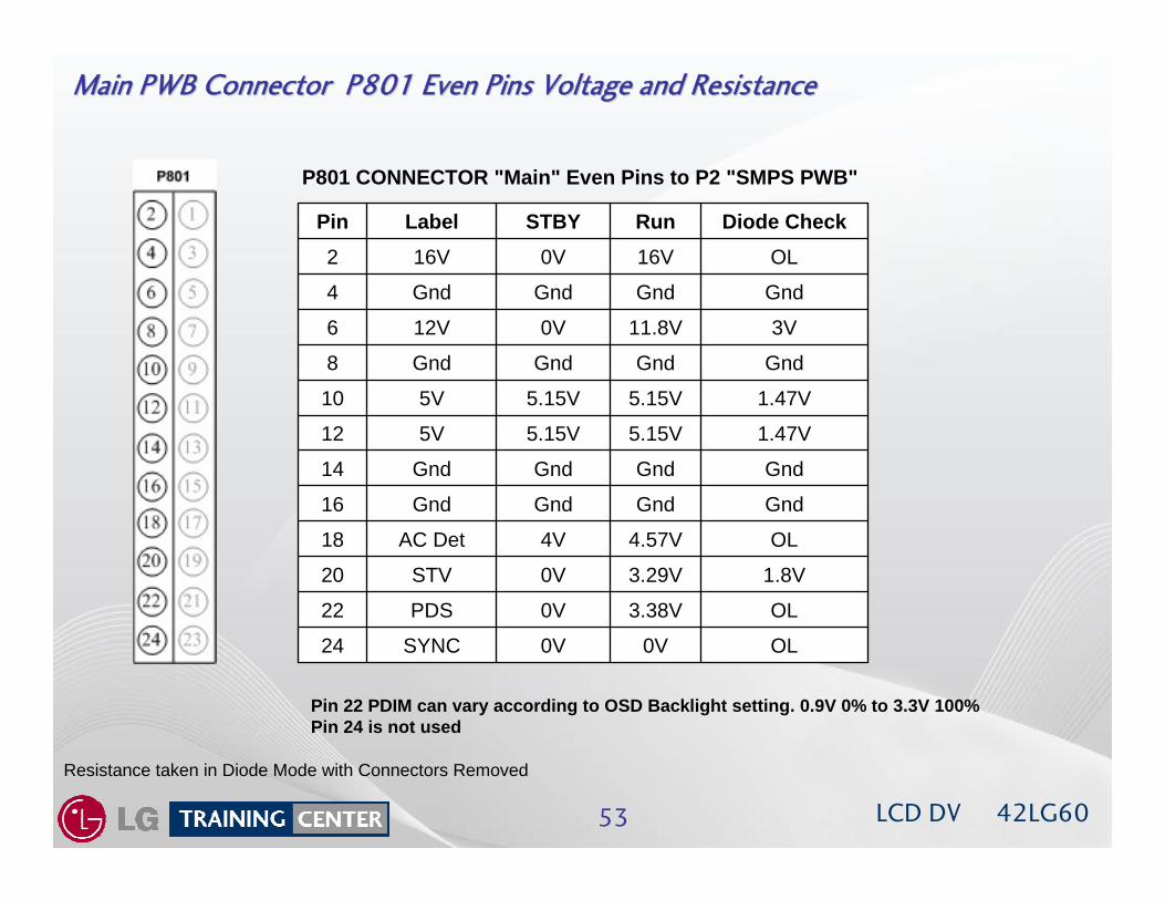
Main PWB Connector P801 Even Pins Voltage and ResistanceMain PWB Connector P801 Even Pins Voltage and Resistance
Resistance taken in Diode Mode with Connectors Removed
P801 CONNECTOR "Main" Even Pins to P2 "SMPS PWB"
OL0V0VSYNC24
OL3.38V0VPDS22
1.8V3.29V0VSTV20
OL4.57V4VAC Det18
GndGndGndGnd16
GndGndGndGnd14
1.47V5.15V5.15V5V12
1.47V5.15V5.15V5V10
GndGndGndGnd8
3V11.8V0V12V6
GndGndGndGnd4
OL16V0V16V2
Diode CheckRun STBYLabelPin
Pin 22 PDIM can vary according to OSD Backlight setting. 0.9V 0% to 3.3V 100%Pin 24 is not used
LCD DV 42LG6054
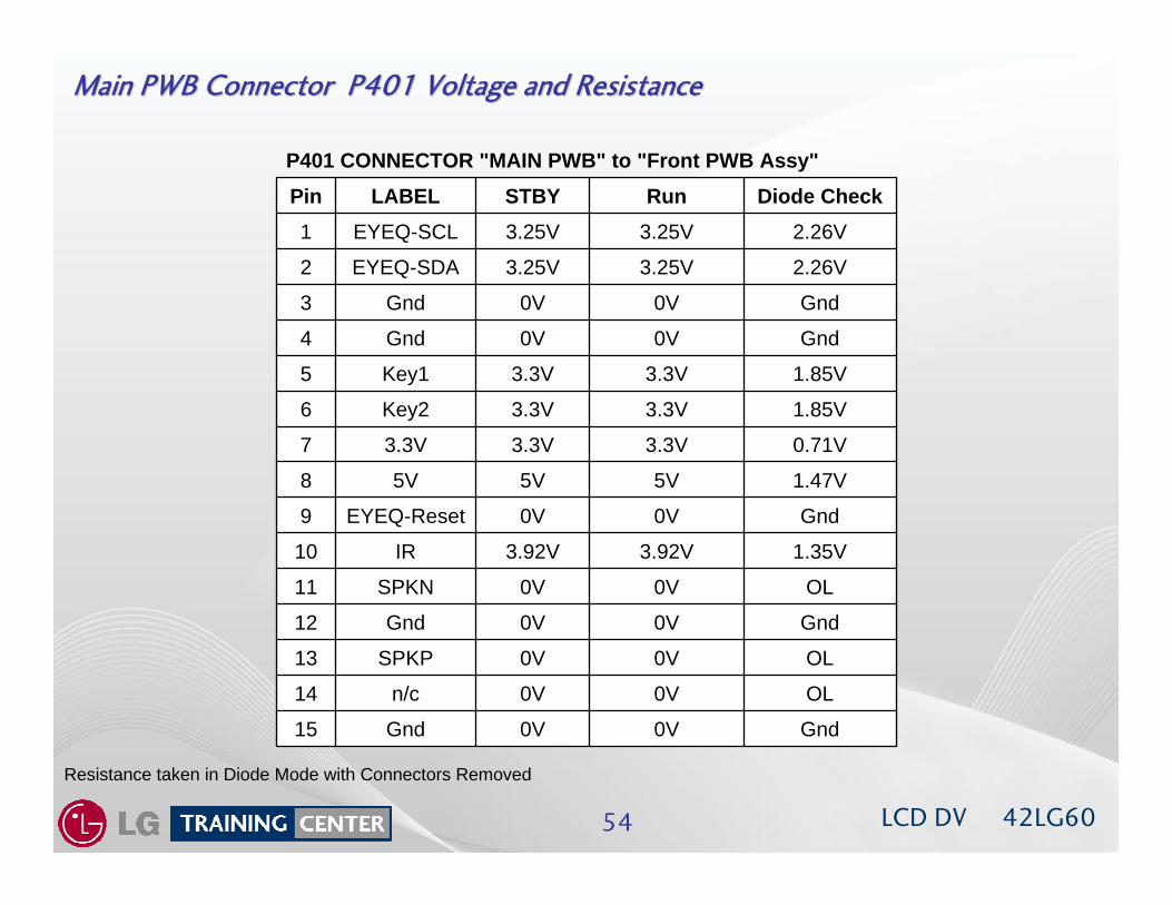
Main PWB Connector P401 Voltage and ResistanceMain PWB Connector P401 Voltage and Resistance
Resistance taken in Diode Mode with Connectors Removed
P401 CONNECTOR "MAIN PWB" to "Front PWB Assy"
Gnd0V0VGnd15
OL0V0Vn/c14
OL0V0VSPKP13
Gnd0V0VGnd12
OL0V0VSPKN11
1.35V3.92V3.92VIR10
Gnd0V0VEYEQ-Reset9
1.47V5V5V5V8
0.71V3.3V3.3V3.3V7
1.85V3.3V3.3VKey26
1.85V3.3V3.3VKey15
Gnd0V0VGnd4
Gnd0V0VGnd3
2.26V3.25V3.25VEYEQ-SDA2
2.26V3.25V3.25VEYEQ-SCL1
Diode CheckRun STBYLABELPin
LCD DV 42LG6055
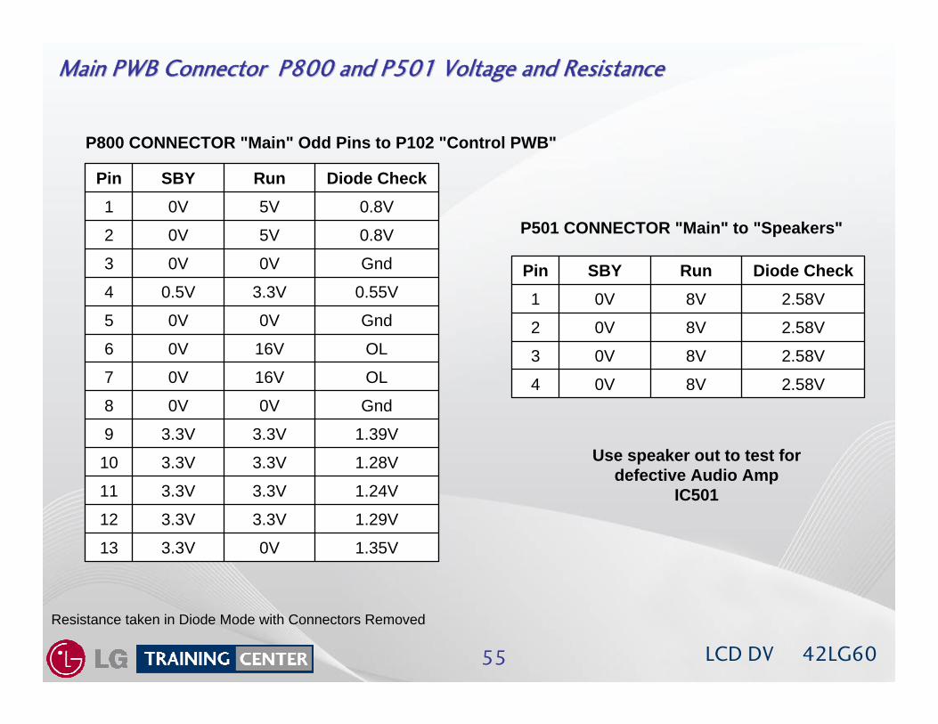
Main PWB Connector P800 and P501 Voltage and ResistanceMain PWB Connector P800 and P501 Voltage and Resistance
Resistance taken in Diode Mode with Connectors Removed
P800 CONNECTOR "Main" Odd Pins to P102 "Control PWB"
2.58V8V0V4
2.58V8V0V3
2.58V8V0V2
2.58V8V0V1
Diode CheckRunSBYPin
P501 CONNECTOR "Main" to "Speakers"
1.35V0V3.3V13
1.29V3.3V3.3V12
1.24V3.3V3.3V11
1.28V3.3V3.3V10
1.39V3.3V3.3V9
Gnd0V0V8
OL16V0V7
OL16V0V6
Gnd0V0V5
0.55V3.3V0.5V4
Gnd0V0V3
0.8V5V0V2
0.8V5V0V1
Diode CheckRunSBYPin
Use speaker out to test for defective Audio Amp
IC501
LCD DV 42LG6056
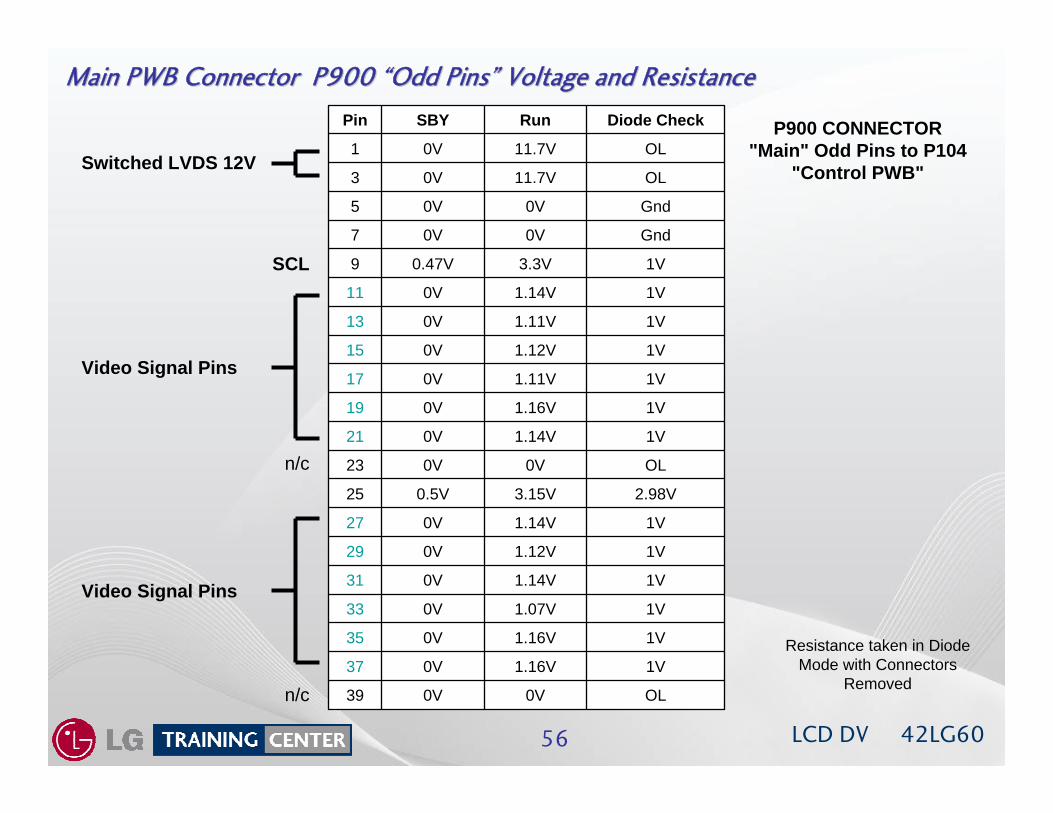
Main PWB Connector P900 Main PWB Connector P900 ““Odd PinsOdd Pins”” Voltage and ResistanceVoltage and Resistance
Resistance taken in Diode Mode with Connectors
Removed
P900 CONNECTOR "Main" Odd Pins to P104
"Control PWB"
OL0V0V39
1V1.16V0V37
1V1.16V0V35
1V1.07V0V33
1V1.14V0V31
1V1.12V0V29
1V1.14V0V27
2.98V3.15V0.5V25
OL0V0V23
1V1.14V0V21
1V1.16V0V19
1V1.11V0V17
1V1.12V0V15
1V1.11V0V13
1V1.14V0V11
1V3.3V0.47V9
Gnd0V0V7
Gnd0V0V5
OL11.7V0V3
OL11.7V0V1
Diode CheckRunSBYPin
Video Signal Pins
Video Signal Pins
Switched LVDS 12V
SCL
n/c
n/c
LCD DV 42LG6057
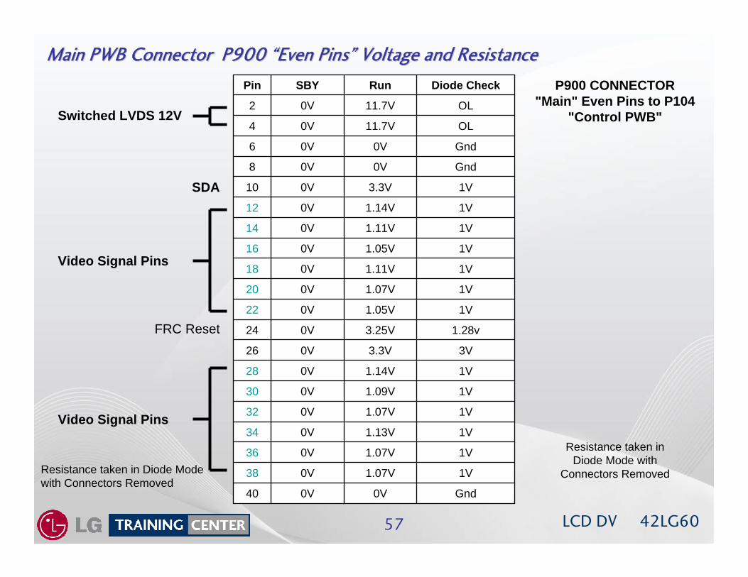
Main PWB Connector P900 Main PWB Connector P900 ““Even PinsEven Pins”” Voltage and ResistanceVoltage and Resistance
Resistance taken in Diode Mode with Connectors Removed
P900 CONNECTOR "Main" Even Pins to P104
"Control PWB"
Gnd0V0V40
1V1.07V0V38
1V1.07V0V36
1V1.13V0V34
1V1.07V0V32
1V1.09V0V30
1V1.14V0V28
3V3.3V0V26
1.28v3.25V0V24
1V1.05V0V22
1V1.07V0V20
1V1.11V0V18
1V1.05V0V16
1V1.11V0V14
1V1.14V0V12
1V3.3V0V10
Gnd0V0V8
Gnd0V0V6
OL11.7V0V4
OL11.7V0V2
Diode CheckRunSBYPin
Video Signal Pins
Video Signal Pins
Switched LVDS 12V
SDA
FRC Reset
Resistance taken in Diode Mode with
Connectors Removed
LCD DV 42LG6058
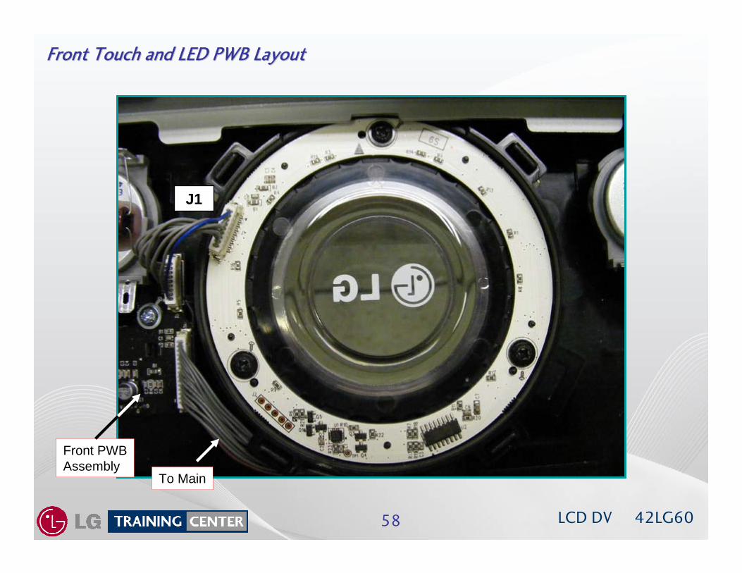
Front Touch and LED PWB LayoutFront Touch and LED PWB Layout
J1
Front PWBAssembly
To Main
LCD DV 42LG6059
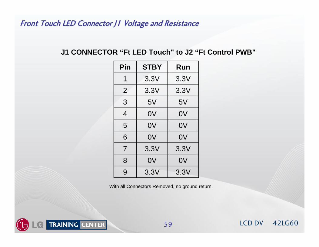
Front Touch LED Connector J1 Voltage and ResistanceFront Touch LED Connector J1 Voltage and Resistance
J1 CONNECTOR “Ft LED Touch" to J2 “Ft Control PWB"
3.3V3.3V90V0V8
3.3V3.3V70V0V60V0V50V0V45V5V3
3.3V3.3V23.3V3.3V1Run STBYPin
With all Connectors Removed, no ground return.
LCD DV 42LG6060
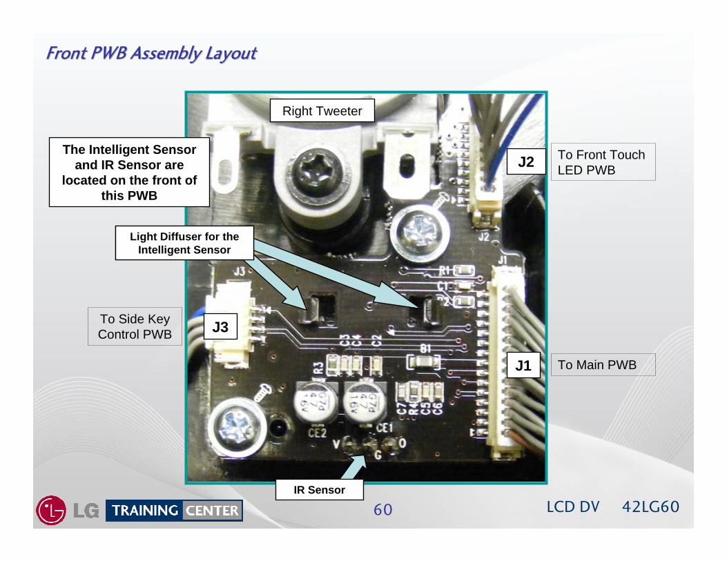
Front PWB Assembly LayoutFront PWB Assembly Layout
J3
J2
J1
To Front Touch LED PWB
To Main PWB
To Side KeyControl PWB
Right Tweeter
The Intelligent Sensor and IR Sensor are
located on the front of this PWB
Light Diffuser for the Intelligent Sensor
Light Diffuser for the Intelligent Sensor
IR Sensor
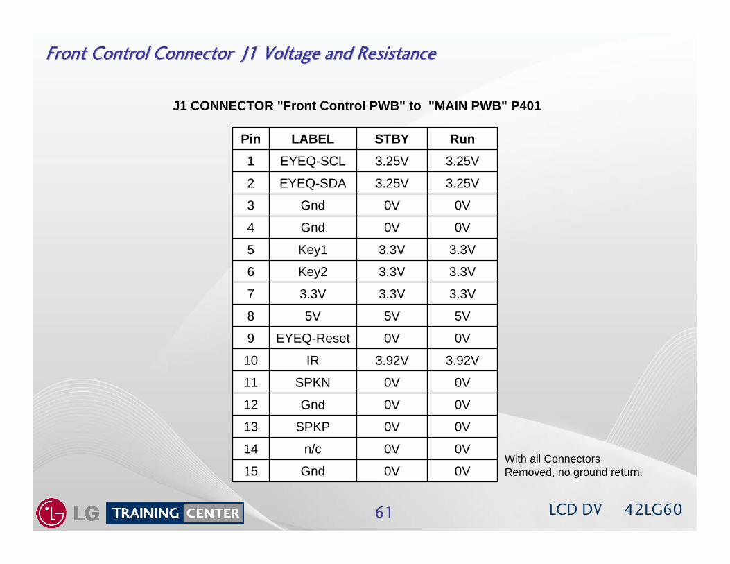
LCD DV 42LG6061
Front Control Connector J1 Voltage and ResistanceFront Control Connector J1 Voltage and Resistance
With all Connectors Removed, no ground return.
J1 CONNECTOR "Front Control PWB" to "MAIN PWB" P401
0V0VGnd15
0V0Vn/c14
0V0VSPKP13
0V0VGnd12
0V0VSPKN11
3.92V3.92VIR10
0V0VEYEQ-Reset9
5V5V5V8
3.3V3.3V3.3V7
3.3V3.3VKey26
3.3V3.3VKey15
0V0VGnd4
0V0VGnd3
3.25V3.25VEYEQ-SDA2
3.25V3.25VEYEQ-SCL1
Run STBYLABELPin
LCD DV 42LG6062
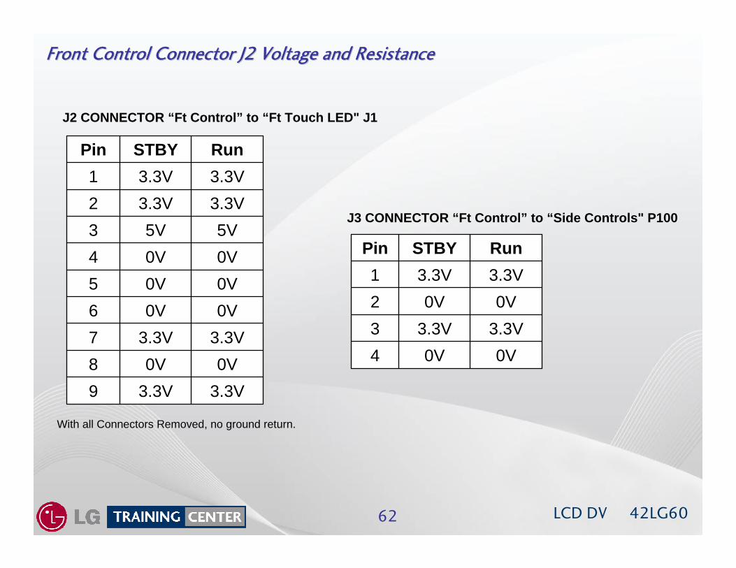
Front Control Connector J2 Voltage and ResistanceFront Control Connector J2 Voltage and Resistance
J2 CONNECTOR “Ft Control” to “Ft Touch LED" J1
3.3V3.3V90V0V8
3.3V3.3V70V0V60V0V50V0V45V5V3
3.3V3.3V23.3V3.3V1Run STBYPin
With all Connectors Removed, no ground return.
J3 CONNECTOR “Ft Control” to “Side Controls" P100
0V0V43.3V3.3V30V0V2
3.3V3.3V1Run STBYPin
LCD DV 42LG6063
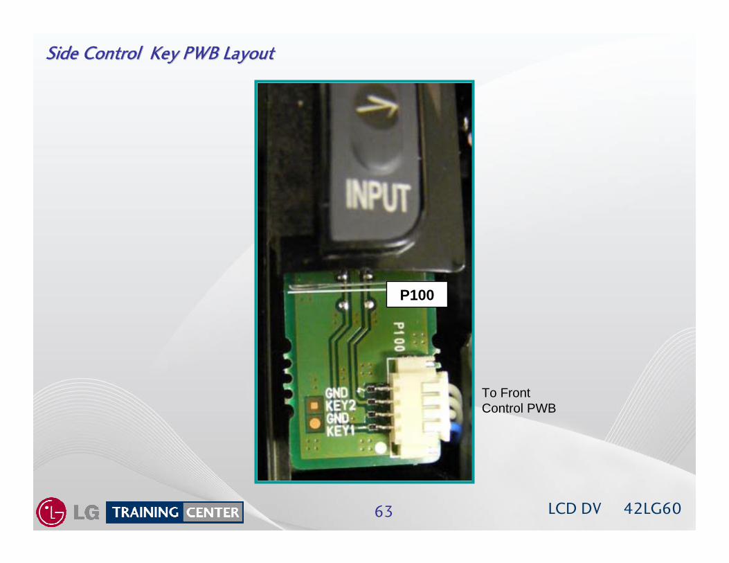
Side Control Key PWB LayoutSide Control Key PWB Layout
To FrontControl PWB
P100
LCD DV 42LG6064
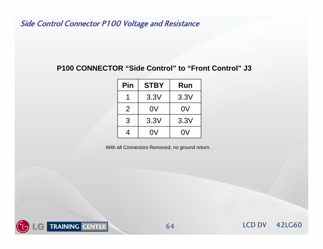
Side Control Connector P100 Voltage and ResistanceSide Control Connector P100 Voltage and Resistance
P100 CONNECTOR “Side Control” to “Front Control" J3
With all Connectors Removed, no ground return.
0V0V43.3V3.3V30V0V2
3.3V3.3V1Run STBYPin
LCD DV 42LG6065
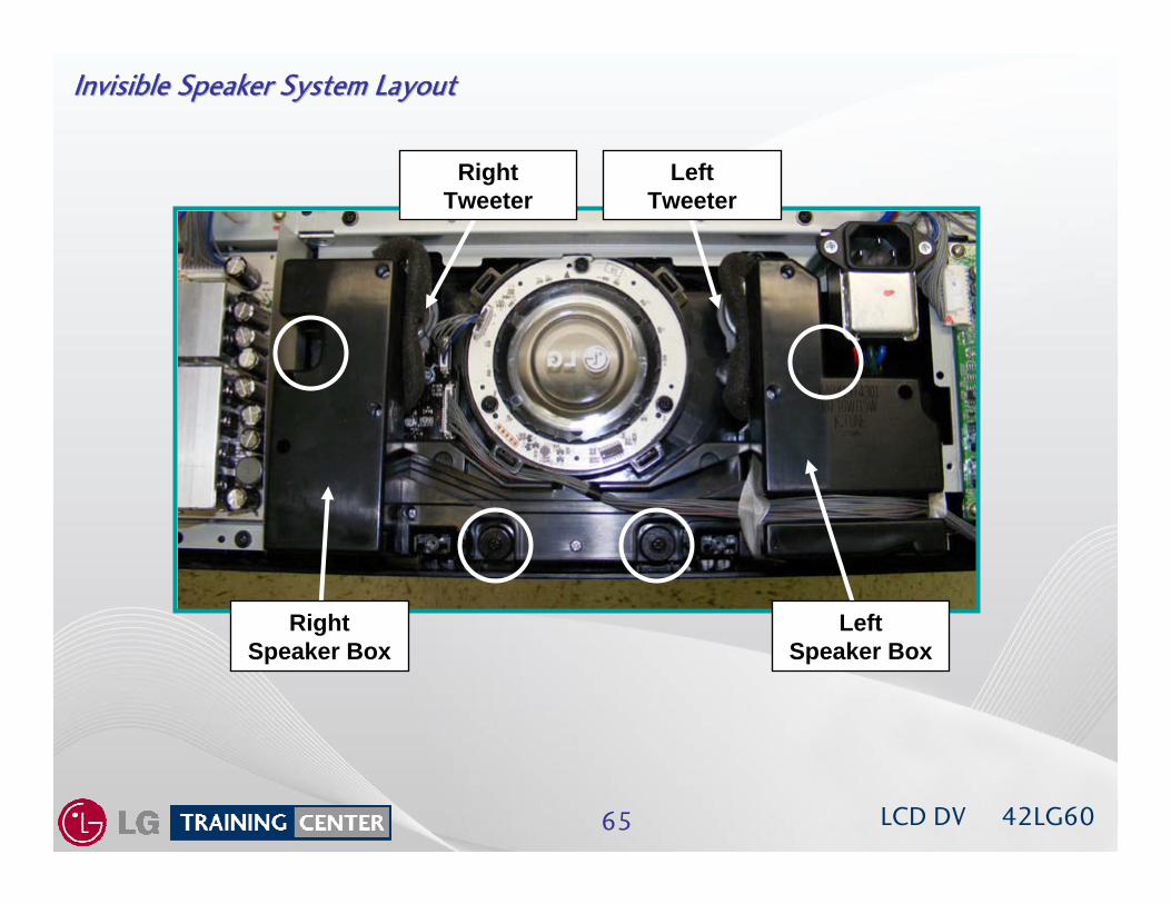
Invisible Speaker System LayoutInvisible Speaker System Layout
RightTweeter
LeftTweeter
Right Speaker Box
LeftSpeaker Box
LCD DV 42LG6066
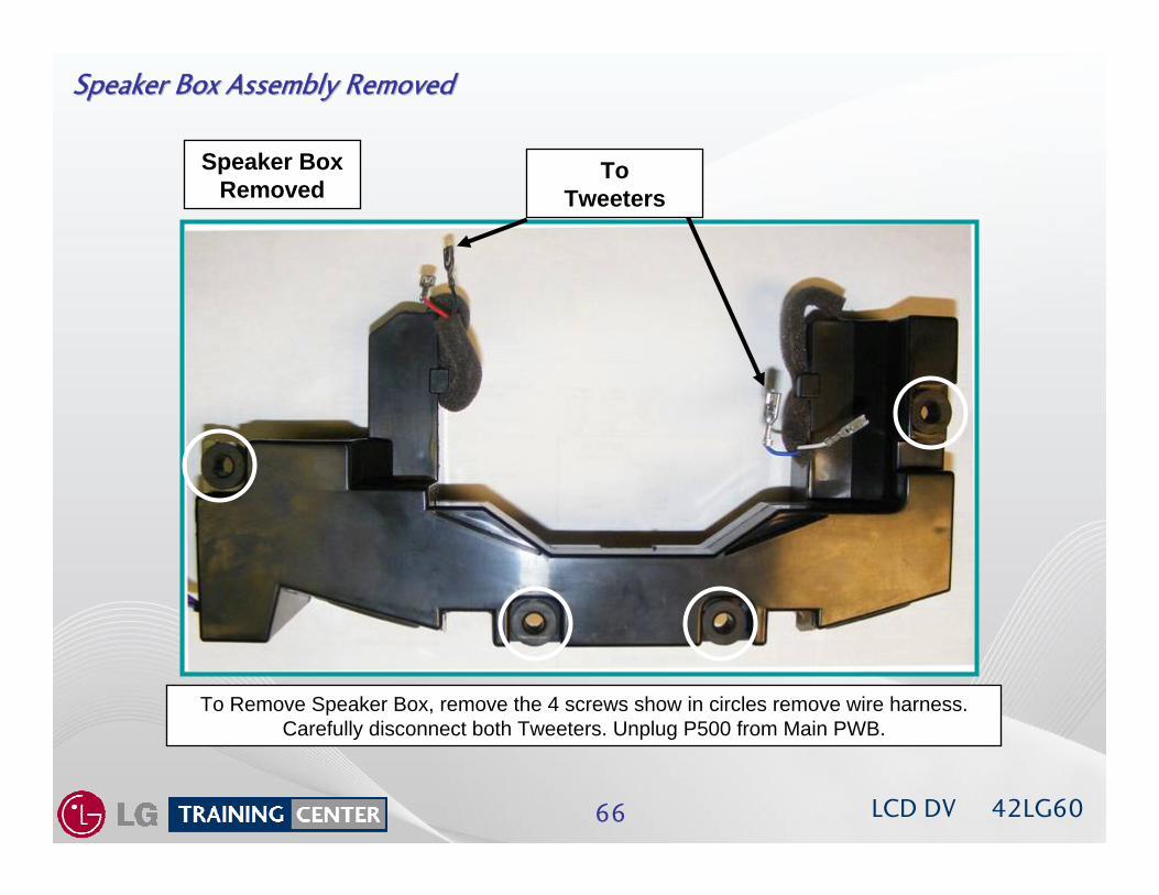
Speaker Box Assembly RemovedSpeaker Box Assembly Removed
ToTweeters
Speaker BoxRemoved
To Remove Speaker Box, remove the 4 screws show in circles remove wire harness.Carefully disconnect both Tweeters. Unplug P500 from Main PWB.
P900P800
P401P501
P801
TUNERATSC/QAM/
NTSC
IC100BCM
IC302
IC300
IC303
IC301 IC404
IC1000
X200 (54Mhz)
IC800IC806
IC402
IC503
IC701
IC600 IC820
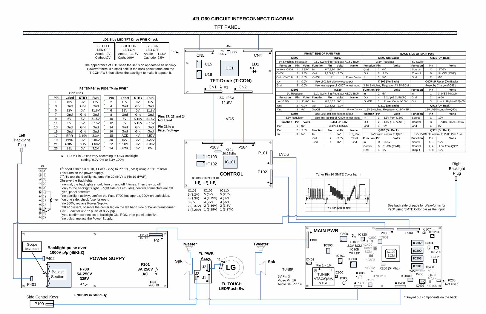
42LG60 CIRCUIT INTERCONNECT DIAGRAM
CN5 CN4
TFT-Drive (T-CON)CN1 CN2
P103 P104
CONTROL P102
P101
LVDS
POWER SUPPY J1
J2
J1J3
P2
LVDS
Ft. TOUCHLED/Push Sw
SpkSpk
Ft. PWB Assy.
AC In
LeftBacklight
Plug
RightBacklight
Plug
TFT PANEL
IC101IC103
IC102
IC108 IC109 IC110
5 (2.5V)4 (0V)3 (0V)2 (3.3V)1 (3.37V)
5 (0V)4 (1.79V)3 (0V)2 (3.36V)1 (3.29V)
5 (1.2V)4 (1.3V)3 (0V)2 (3.37V)1 (3.29V)
X10120.25Mhz
UC1LD1U15
U16
US10V
3.2V 1.8V
3A 125V11.6V
SET 0FFLED OFF
SET ONLED OFF
LD1 Blue LED TFT Drive PWB Check
AnodeCathode
0V0V
BOOT OKLED ON
AnodeCathode
11.6V0V
AnodeCathode
11.6V9.5V
F1018A 250V
ACF700
5A 250V335V
Backlight pulse over 1000V p/p (45KhZ)
IC500
X400
IC407
The appearance of LD1 when the set is on appears to be lit dimly. However there is a small hole in the back panel frame and the
T-CON PWB that allows the backlight to make it appear lit.
Side Control Keys
MAIN PWB
P200Not Used
F1
IC900
IC807IC1201
IC304
IC1200IC202
LD8033.3V BCM
IC805OK LED
IC501
Pin 1 ~ 16
Q400E B
24Mhz
P2
3
1
7
5
11
9
15
13
19
17
23
21
4
2
8
6
12
10
16
14
20
18
24
22
10K
1st” short either pin 9, 10, 11 or 12 (5V) to Pin 19 (PWR) using a 10K resistor.This turns on the power supply.2nd: To test the Backlights, jump Pin 20 (INV) to Pin 19 (PWR)Observe the Backlights.If normal, the backlights should turn on and off 4 times. Then they go off.If only ½ the backlights light, (Right side or Left Side), confirm connectors are OK. If yes, panel defective.If no backlight activity, confirm the Fuse F700 has approx. 300V on both sides.If on one side, check fuse for open. If no 300V, replace Power Supply.If 300V present, observe the center leg on the left hand side of ballast transformer T701. Look for 45Khz pulse at 8.7V p/p. If yes, confirm connectors to backlight OK, if OK, then panel defective.If no pulse, replace the Power Supply.
PDIM Pin 22 can vary according to OSD Backlight setting. 0.9V 0% to 3.3V 100%
P2 "SMPS" to P801 "Main PWB"
Pin Label STBY Run 1 16V 0V 16V3 Gnd Gnd Gnd5 12V 0V 11.8V7 Gnd Gnd Gnd9 5V 5V 5.15V11 5V 5V 5.15V13 Gnd Gnd Gnd15 Gnd Gnd Gnd17 ERR 3.19V 3.3V19 PWR 0V 2.86V21 ADIM 0.1V 1.68V23 SEL 0V 3.2V
Pin Label STBY Run 2 16V 0V 16V4 Gnd Gnd Gnd6 12V 0V 11.8V8 Gnd Gnd Gnd10 5V 5.15V 5.15V12 5V 5.15V 5.15V14 Gnd Gnd Gnd16 Gnd Gnd Gnd18 ACD 4V 4.57V20 INV 0V 3.29V22 *PDIM 0V 3.38V24 SYNC 0V 0V
Odd Pins
Pins 17, 23 and 24 Not Used
IC109IC108 IC110
1 16
*Q901*Q902
*IC400
*IC802
*IC810
*IC405
*Grayed out components on the back
Function Pin Volts Function Pin Volts Name Function Pin Volts Function Pin VoltsIn from IC806 1 8.95V In 6,7,8,10 5V 1 0V Source C ST-5VOn/Off 2 3.3V Out 1,2,3,4,5 2.6V Out 2 3.3V Control B RL-ON (PWR)Out (+5V-TU) 3 5.0V On/Off 17 Power Control In 3 5V Gnd E 0Vn/c 4 0.0VGnd 5 0.0V
Function Pin Volts Function Pin VoltsIn 2 5V In 1 3.3VST-MICOM
Function Pin Volts Function Pin Volts Name Out 4 3.3V (A3.3V-BCM) Gnd 2 0.0VIn (+12V) 1 11.6V In 6,7,8,10 5V On/Off 1 Power Control-3.3V Out 3 Low to High to B Q400Gnd 2 0.0V Out 1,2,3,4,5 1.2VOut 3 9V On/Off 17 Power Control
Function Pin Volts Function Pin VoltsIn 3 3.3V from IC802 Source C 12V
Function Pin Volts Out 2 1.8V (+1.8V-NTP) Control B LVDS-Panel-Control1 0V Gnd 1 Gnd E 0V
Out 2 3.3V Function Pin Volts NameIn 3 5V In 3 5V ST_+5V
Out 2 3.3V Reset Function Pin Volts Function Pin VoltsGnd 1 0V Gnd In C ST-5V Source 1, 3 12V
Control B RL-ON (PWR) Control 2, 4 Low from Q902Gnd E 0V Output 5~8 12V
Q901 (On Back)12V LVDS On control to P900 Pins 1~4
IC404 uP 3.3V3.3VST-MICOM
IC404
IC806 IC8201.2V Switching Regulator A1.2V-BCM
Use L014 left side to test output
Q802 (On Back)5V Switch control to Q801
IC8072.6V Switching Regulator A2.6V-BCM
Use L801 left side to test outputUse any top pin of IC807 to test input
Use any top pin of IC820 to test input
9V Regulator
3.3V Regulator
Q801 (On Back)5V Switch
IC405 uP Reset (On Back)Reset by Charge of C431
IC802 (On Back)3.3V Regulator
Q902 (On Back)
FRONT SIDE OF MAIN PWB
IC810 (On Back)1.8V Switching Regulator +1.8V-NTP
3.3V Switching Regulator A3.3V-BCMIC805 (On Back)
IC800BACK SIDE OF MAIN PWB
5V Switching Regulator
12V LVDS control to Q901
Gnd
Gnd
0V
P100
See back side of page for Waveforms forP900 using SMTE Color bar as the Input.
Tuner Pin 16 SMTE Color bar In
uP5V Pin 3Video Pin 16Audio SIF Pin 14
TUNERBallastSection
*IC805
ResetBCM
P402
P401
Scope test point
Tweeter Tweeter
Pin 24 Pin 23
LG
Pin 21 is a Fixed Voltage
F700 90V in Stand-By
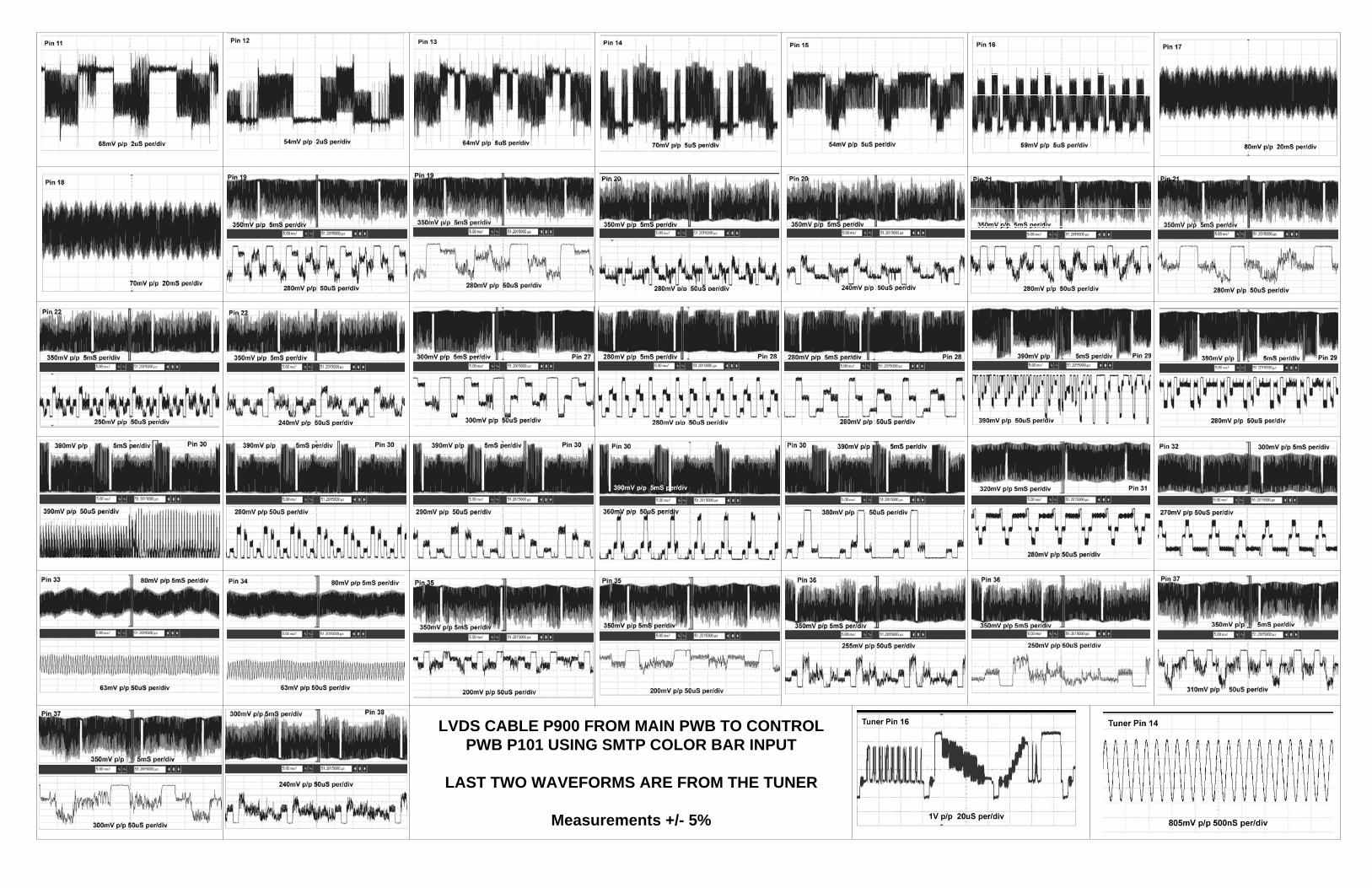
LVDS CABLE P900 FROM MAIN PWB TO CONTROL PWB P101 USING SMTP COLOR BAR INPUT
LAST TWO WAVEFORMS ARE FROM THE TUNER
Measurements +/- 5%
LCD DV 42LG6074
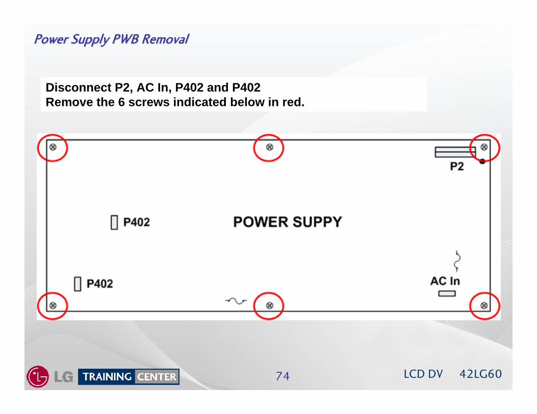
Power Supply PWB RemovalPower Supply PWB Removal
Disconnect P2, AC In, P402 and P402Remove the 6 screws indicated below in red.
LCD DV 42LG6075
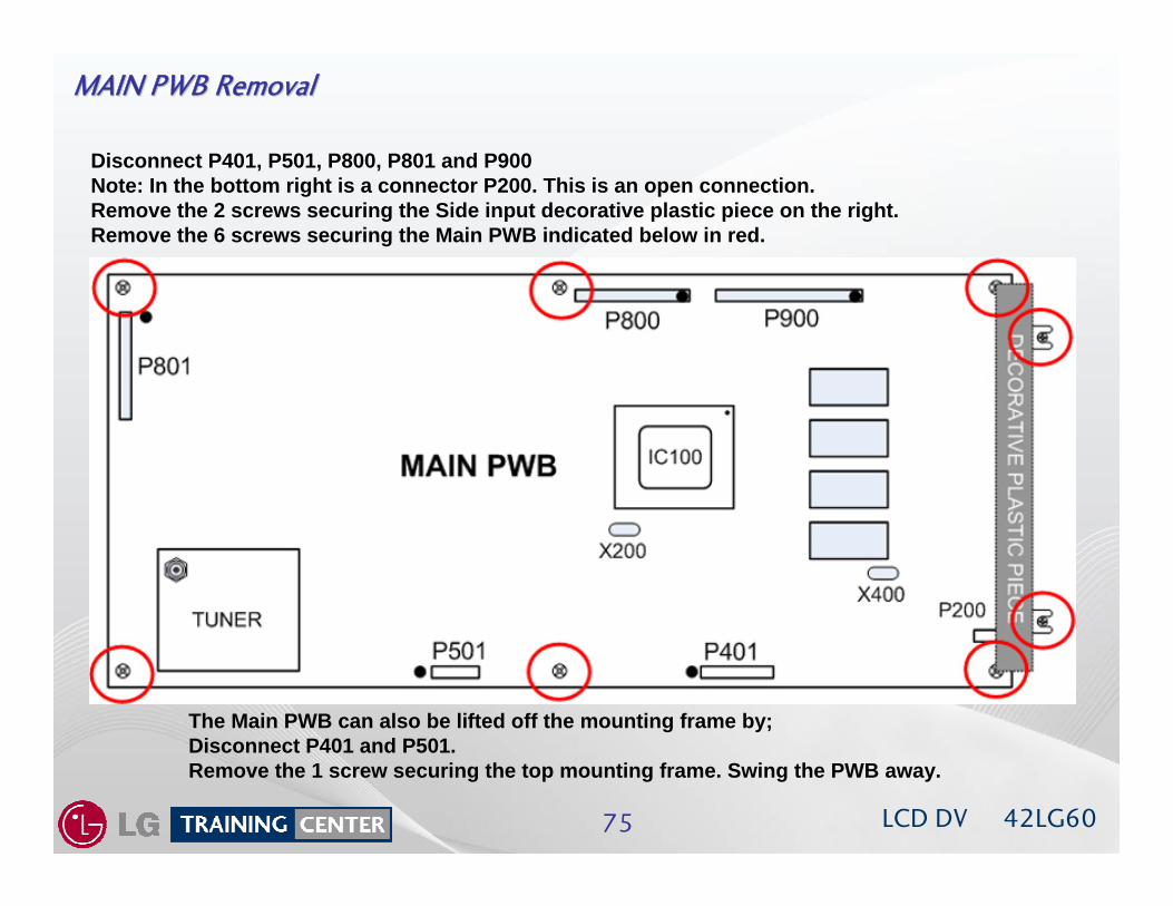
MAIN PWB RemovalMAIN PWB Removal
Disconnect P401, P501, P800, P801 and P900Note: In the bottom right is a connector P200. This is an open connection.Remove the 2 screws securing the Side input decorative plastic piece on the right.Remove the 6 screws securing the Main PWB indicated below in red.
The Main PWB can also be lifted off the mounting frame by;Disconnect P401 and P501.Remove the 1 screw securing the top mounting frame. Swing the PWB away.
LCD DV 42LG6076
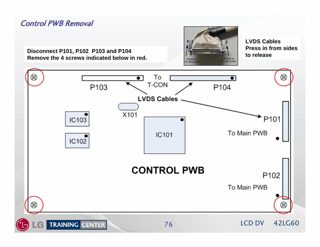
Control PWB RemovalControl PWB Removal
Disconnect P101, P102 P103 and P104Remove the 4 screws indicated below in red.
LVDS CablesPress in from sidesto release
LCD DV 42LG6077
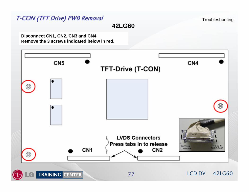
TT--CON (TFT Drive) PWB RemovalCON (TFT Drive) PWB Removal Troubleshooting42LG60
Disconnect CN1, CN2, CN3 and CN4Remove the 3 screws indicated below in red.

42LG6042LG60Direct View LCD
This concludes the 42LG60training session.